WO2023167129A1 - Qubit control circuit - Google Patents
Qubit control circuit Download PDFInfo
- Publication number
- WO2023167129A1 WO2023167129A1 PCT/JP2023/007010 JP2023007010W WO2023167129A1 WO 2023167129 A1 WO2023167129 A1 WO 2023167129A1 JP 2023007010 W JP2023007010 W JP 2023007010W WO 2023167129 A1 WO2023167129 A1 WO 2023167129A1
- Authority
- WO
- WIPO (PCT)
- Prior art keywords
- current
- excitation current
- output
- input
- control circuit
- Prior art date
Links
Images


Classifications
-
- G—PHYSICS
- G06—COMPUTING; CALCULATING OR COUNTING
- G06N—COMPUTING ARRANGEMENTS BASED ON SPECIFIC COMPUTATIONAL MODELS
- G06N10/00—Quantum computing, i.e. information processing based on quantum-mechanical phenomena
- G06N10/40—Physical realisations or architectures of quantum processors or components for manipulating qubits, e.g. qubit coupling or qubit control
-
- H—ELECTRICITY
- H03—ELECTRONIC CIRCUITRY
- H03K—PULSE TECHNIQUE
- H03K17/00—Electronic switching or gating, i.e. not by contact-making and –breaking
- H03K17/51—Electronic switching or gating, i.e. not by contact-making and –breaking characterised by the components used
- H03K17/92—Electronic switching or gating, i.e. not by contact-making and –breaking characterised by the components used by the use, as active elements, of superconductive devices
-
- H—ELECTRICITY
- H03—ELECTRONIC CIRCUITRY
- H03K—PULSE TECHNIQUE
- H03K19/00—Logic circuits, i.e. having at least two inputs acting on one output; Inverting circuits
- H03K19/02—Logic circuits, i.e. having at least two inputs acting on one output; Inverting circuits using specified components
- H03K19/195—Logic circuits, i.e. having at least two inputs acting on one output; Inverting circuits using specified components using superconductive devices
Definitions
- the present invention relates to qubit control circuits. This application claims priority based on Japanese Patent Application No. 2022-032905 filed in Japan on March 3, 2022, the contents of which are incorporated herein.
- Quantum computers can simulate quantum systems composed of a large number of electrons, so they are expected to be applied to material design and drug discovery. Quantum bits controlled in quantum computers need to be controlled at low temperatures because they are composed of superconducting elements. Therefore, the configuration of a quantum computer includes refrigerators to keep the qubits cold and equipment that operates at room temperature. Devices operating at room temperature output control signals to qubits through cables.
- a control circuit that operates on the low-temperature side, like a qubit, is required.
- a quantum computing system is known in which the number of communication lines is smaller than the number of devices to be controlled (Patent Document 1).
- a superconducting quantum processor having a superconducting digital/analog converter that uses magnetic flux quantum parametrons as shift registers (Patent Document 2).
- the present invention has been made in view of the above points, and provides a circuit that constitutes a qubit control circuit that can control a large number of qubits with a small number of cables.
- the present invention has been made to solve the above problems, and one aspect of the present invention includes a first power supply line to which a first excitation current that is a current with a predetermined frequency is input, and a current with a predetermined waveform.
- a second power supply line to which a second excitation current is input, an input signal line to which an input signal indicating a logic state is input, a magnetic coupling portion, and a Josephson junction, wherein the Josephson junction is the an output signal generating circuit that outputs an output signal according to the frequency of the first excitation current and the waveform of the second excitation current input via a magnetic coupling unit, and the logic state indicated by the input signal;
- a qubit control circuit comprising:
- the first excitation current input to the first power supply line includes a plurality of frequencies
- the resonance circuit includes a coupling unit that couples with the first power supply line, and a second magnetic coupling unit that magnetically couples with the magnetic coupling unit of the output signal generation circuit, having a resonance frequency that is one of the plurality of frequencies included in the first excitation current, and generating the corresponding output signal by causing a current having the resonance frequency to flow through the second magnetic coupling section;
- the resonance frequency is supplied to the circuit as the frequency of the first power supply line.
- a plurality of superconducting gate circuits each including the output signal generation circuit and a third magnetic coupling section through which a current flows according to the output signal; and a magnetic flux applied to the fourth magnetic coupling portion by the output signal generated by each of the plurality of superconducting gate circuits. and an output signal line for outputting an electromagnetic wave irradiated to the quantum bit according to.
- the amplitude and pulse width of the electromagnetic wave output by the output signal line are controlled by the amplitude of the first excitation current.
- the output signal generation circuit includes a configuration of a magnetic flux quantum parametron circuit.
- FIG. 1 is a diagram showing an example configuration of a quantum bit control circuit according to a first embodiment of the present invention
- FIG. FIG. 5 is a diagram showing an example of simulation results by the quantum bit control circuit according to the first embodiment of the present invention
- It is a figure which shows an example of the spectrum of the 2nd excitation current which is a baseband signal based on the 1st Embodiment of this invention.
- It is a figure which shows an example of the spectrum of the output microwave based on the 1st Embodiment of this invention.
- FIG. 5 is a diagram showing an example of the configuration of a quantum bit control circuit according to a second embodiment of the present invention;
- FIG. 10 is a diagram showing an example of simulation results by the quantum bit control circuit according to the second embodiment of the present invention
- FIG. 8 is a diagram showing an example of the relationship between the spectrum of the first excitation current and the amplitude of the output microwave according to the second embodiment of the present invention
- It is a figure for demonstrating the principle of operation of a magnetic flux quantum parametron.
- FIG. 1 is a diagram showing an example of the configuration of a quantum bit control circuit 1 according to this embodiment.
- the quantum bit control circuit 1 is a circuit for irradiating a quantum bit to be controlled with microwaves.
- the quantum bit control circuit 1 generates microwaves using a Quantum Flux Parametron (QFP) circuit.
- QFP Quantum Flux Parametron
- the qubit control circuit 1 functions as a nonlinear mixer.
- the qubit control circuit 1 includes a first power supply line 2, a second power supply line 3, a QFP gate 4a, a QFP gate 4b, an input signal line 5a, an input signal line 5b, an electromotive force output line 8, A bandpass filter 9 and a resistor 10 are provided.
- QFP gate 4a and QFP gate 4b are each QFP.
- the configuration of one QFP (QFP gate 4a) includes wiring 41a, inductor L31a, Josephson junction J1a, wiring 42a, inductor L32a, Josephson junction J2a, load inductor L4a, input signal line 5a, and output signal line. 6a is included.
- the configuration of one QFP (QFP gate 4b) includes wiring 41b, inductor L31b, Josephson junction J1b, wiring 42b, inductor L32b, Josephson junction J2b, load inductor L4b, input signal line 5b, and output signal Line 6b is included.
- a portion configured by the wiring 41a, the inductor L31a, the Josephson junction J1a, the wiring 42a, the inductor L32a, the Josephson junction J2a, and the input signal line 5a is also referred to as the output signal generation circuit 40a.
- the portion constituted by the wiring 41b, the inductor L31b, the Josephson junction J1b, the wiring 42b, the inductor L32b, the Josephson junction J2b, and the input signal line 5b is also called the output signal generation circuit 40b.
- the first power line 2 is a power line to which the first excitation current Ilo is input.
- the first excitation current Ilo is a current containing a predetermined frequency.
- the frequency of the first excitation current Ilo is, for example, 5 GHz.
- the first excitation current Ilo is a local oscillator signal provided by a Local Oscillator (not shown).
- the local oscillator is provided separately from the quantum bit control circuit 1 .
- the first power line 2 includes an inductor L11a, an inductor L12a, an inductor L11b, and an inductor L12b.
- a second power line 3 is a power line to which a second excitation current Ibb is input.
- the second excitation current Ibb is a current with a predetermined waveform.
- the second excitation current Ibb is a baseband signal supplied as an output signal from a baseband circuit (not shown).
- the baseband circuit is provided separately from the quantum bit control circuit 1 .
- a waveform of the second excitation current Ibb is, for example, a triangular wave.
- the second power line 3 includes an inductor L21a, an inductor L22a, an inductor L21b, and an inductor L22b.
- the input signal line 5a is a control line to which the input current Iina is input.
- the input signal line 5b is a control line to which the input current Iinb is input.
- Input current Iina and input current Iinb are currents that determine the logic states of QFP gate 4a and QFP gate 4b, respectively.
- QFP gate 4a generates output current Iouta according to input current Iina.
- QFP gate 4b generates output current Ioutb according to input current Iinb.
- FIG. 8 is a diagram for explaining the operating principle of the QFP.
- QFP 100 indicates the basic gate of QFP.
- QFP 100 is driven and clocked by alternating excitation current Ix.
- the AC excitation current Ix flows through the power line 101, magnetic fluxes are generated in the inductors Lx1 and Lx2 provided in the power line 101, respectively.
- the quantum bit control circuit 1 (FIG. 1) has two power lines (first power line 2 and second power line 3), in the QFP 100 (FIG.
- the power supply line corresponding to one of the first power supply line 2 and the second power supply line 3 is omitted, and one power supply line (power supply line 101) is provided.
- the power line 101 will be described as being equivalent to the first power line 2 in FIG.
- the QFP 100 corresponds to either the QFP gate 4a or the QFP gate 4b shown in FIG.
- the QFP 100 will be described as being equivalent to the QFP gate 4a in FIG.
- inductor Lx1 corresponds to inductor L11a in FIG. 1
- inductor Lx2 corresponds to inductor L12a in FIG.
- the alternating excitation current Ix corresponds to the first excitation current Ilo in FIG.
- Inductor Lx1 and inductor L1 provided in loop 102 are magnetically coupled by coupling constant k1.
- the inductor L1 corresponds to the inductor L31a in FIG.
- Inductor Lx2 and inductor L2 provided in loop 102 are magnetically coupled by coupling constant k2.
- the inductor L2 corresponds to the inductor L32a in FIG.
- the output signal line 104 corresponds to the output signal line 6a in FIG. 1
- the output current Iout corresponds to the output current Iouta in FIG. 1
- the load inductor Lq corresponds to the load inductor L4a in FIG.
- the QFP100 power consumption can be reduced by optimizing the parameters of inductor L1, inductor L2, load inductor Lq, Josephson junction J1, and Josephson junction J2. It is known that the QFP uses a superconducting element and therefore has no direct current resistance and consumes very low power. In QFP, the power consumption per gate is about 10 pW. Also, the QFP is capable of high-speed operation with a clock frequency of about 10 GHz. Also, since QFPs have ultra-low power consumption, it is possible to operate QFPs near qubits. Note that the values of the power consumption and clock frequency of the QFP described above are examples, and these values may vary depending on the circuit parameters and the type of circuit.
- the output current is generated by the Josephson junction.
- the parameters include the inductance magnitude of the inductor and the critical current value of the Josephson junction.
- the magnitude of the inductance of each of the inductor L1, the inductor L2, and the load inductor Lq, the critical current value of each of the Josephson junctions J1 and J2, and the output current Iout by the Josephson junctions J1 and J2 are determined. adjusted to generate For the QFP gate 4a and the QFP gate 4b shown in FIG. 1, various parameters of the circuit are adjusted so that an output current is generated by the Josephson junction.
- the description of the configuration of the quantum bit control circuit 1 will be continued. Since the configuration of the QFP gate 4a and the configuration of the QFP gate 4b are the same, the configuration of the QFP gate 4a will be described below, and the description of the configuration of the QFP gate 4b will be omitted.
- the wiring 41a, the wiring 42a, the output signal line 6a, and the above-described input signal line 5a are connected to each other at the connecting portion 7a.
- the inductor L31a and the Josephson junction J1a are provided on the wiring 41a.
- the inductor L31a and the Josephson junction J1a are arranged on the wiring 41a in this order from the side closest to the connection portion 7a.
- the order in which the inductor L31a and the Josephson junction J1a are arranged on the wiring 41a is not limited to this and is arbitrary.
- the end of the wiring 41a that is not connected to the connection portion 7a is grounded.
- the inductor L32a and the Josephson junction J2a are provided on the wiring 42a.
- the inductor L32a and the Josephson junction J2a are arranged on the wiring 42a in this order from the side closest to the connection portion 7a.
- the order in which the inductor L32a and the Josephson junction J2a are arranged on the wiring 42a is not limited to this and is arbitrary.
- the end of the wiring 42a that is not connected to the connecting portion 7a is grounded.
- the Josephson junction J1a, the Josephson junction J2a, the inductor L31a, and the inductor L32a constitute a superconducting quantum interference device having a pair of Josephson junctions in a superconducting ring.
- the superconducting ring is a circuit corresponding to the loop 102 shown in FIG.
- a superconducting quantum interference device having three or more Josephson junctions in a superconducting ring may be used as the superconducting quantum interference device.
- the electromotive force output line 8 includes an inductor L5a, an inductor L5b, a bandpass filter 9, and a resistor 10. One end of the electromotive force output line 8 is connected to the ground.
- the resistor 10, the inductor L5b, the inductor L5a, and the bandpass filter 9 are arranged in this order from the ground. Note that the resistor 10 may be omitted from the configuration of the electromotive force output line 8 .
- the Josephson junctions J1a and J2a determine the logic state and generate the output current Iouta according to the input current Iina flowing through the input signal line 5a. do.
- the first excitation current Ilo flows through the first power supply line 2 and the second excitation current Ibb flows through the second power supply line 3, thereby causing the input signal line 5a to flow through magnetic coupling.
- An output current Iouta is generated according to the input current Iina.
- a magnetic flux ⁇ a is generated in the inductor L5a by the output current Iouta.
- the magnetic flux ⁇ a changes as the first excitation current Ilo and the second excitation current Ibb change, and an induced electromotive force is generated in the inductor L5a in accordance with the change in the first excitation current Ilo and the second excitation current Ibb. do.
- the first excitation current Ilo flows through the first power supply line 2 and the second excitation current Ibb flows through the second power supply line 3, so that the QFP gate 4b has an input current flowing through the input signal line 5b due to magnetic coupling.
- An output current Ioutb is generated according to Iinb.
- a magnetic flux ⁇ b is generated in the inductor L5b by the output current Ioutb.
- the change in the first excitation current Ilo and the second excitation current Ibb causes the magnetic flux ⁇ b to change, and an induced electromotive force is generated in the inductor L5b according to the change in the first excitation current Ilo and the second excitation current Ibb. do.
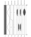
- FIG. 2 is a diagram showing an example of simulation results by the quantum bit control circuit 1 according to this embodiment.
- the value of each physical quantity is shown for 30 nanoseconds.
- the frequency of the first excitation current Ilo is 5 GHz as described above.
- the second excitation current Ibb is a triangular wave as described above.
- the values of the first excitation current Ilo and the second excitation current Ibb are expressed in arbitrary units.
- the input current Iina indicates a logic state of "0, 1" as an example. Depending on the logic state, the input current Iina changes value from low to high around 15 ns.
- the input current Iinb shows a logic state of "1, 1" as an example. Depending on the logic state, the input current Iinb is always high in value. Note that in FIG. 2, the units of the values of the input current Iina and the input current Iinb are 5 ⁇ A/tick.
- the output current Iouta is generated based on the first excitation current Ilo, the second excitation current Ibb, and the input current Iina.
- the output current Ioutb is generated based on the first excitation current Ilo, the second excitation current Ibb and the input current Iinb. Due to the magnetic flux applied by the first excitation current Ilo, which is the local oscillator signal, both the output current Iouta and the output current Ioutb oscillate at 5 GHz, the frequency of the first excitation current Ilo. Moreover, both the output current Iouta and the output current Ioutb are output based on the waveform of the second excitation current Ibb due to the magnetic flux applied by the second excitation current Ibb, which is the baseband signal.
- the waveform of the second excitation current Ibb defines the timing at which the output current Iouta and the output current Ioutb are output.
- the amplitude and duty ratio of each of the output currents Iouta and Ioutb are defined by the waveform of the second excitation current Ibb.
- the first power line 2 and the second power line 3, and the QFP gate 4a is excited and the output current Iouta is defined by the second excitation current Ibb generated. Since the output current Iouta is generated at the timing defined by the second excitation current Ibb, the amplitude and duty ratio of the output current Iouta gradually increase as the second excitation current Ibb rises, and the second excitation current Ibb It gradually decreases according to the fall of . Similarly, magnetic fluxes are applied to the QFP gate 4b from the first power line 2 and the second power line 3, respectively, to excite the QFP gate 4b and the output current Ioutb is defined by the second excitation current Ibb.
- the amplitude and duty ratio of the output current Ioutb gradually increase as the second excitation current Ibb rises, and the second excitation current Ibb It gradually decreases according to the fall of .
- the range in which the output current Iouta oscillates depends on the logical state indicated by the input current Iina. . That is, the logic value indicated by the output current Iouta is based on the logic value indicated by the input current Iina. When the input current Iina indicates a low, the output current Iouta oscillates in a range indicating a logic false value, and when the input current Iina indicates a high, the output current Iouta oscillates in a range indicating a true logic value.
- the range in which the output current Ioutb oscillates depends on the logical state indicated by the input current Iinb.
- the logic value indicated by the output current Ioutb is based on the logic value indicated by the input current Iinb.
- the input current Iinb always indicates high.
- the output current Ioutb oscillates in a range indicating the true logic value without changing with time in response to the input current Iinb always indicating high. Note that in FIG. 2, the unit of each value of the output current Iouta and the output current Ioutb is 20 ⁇ A/tick.
- the output microwave Vout is generated based on the output current Iouta and the output current Ioutb.
- the logic value indicated by the output current Iouta is based on the logic value indicated by the input current Iina
- the logic value indicated by the output current Ioutb is based on the logic value indicated by the input current Iinb.
- the output microwave Vout is output when the logical value indicated by the input current Iina matches the logical value indicated by the input current Iinb.
- the output microwave Vout is not output when the logical value indicated by the input current Iina and the logical value indicated by the input current Iinb do not match.
- whether or not the output microwave Vout is output is defined based on the logical value indicated by the output current Iouta. be done.
- the direction of oscillation is opposite to that of the output current Ioutb and the phases are aligned between the output current Iouta and the output current Ioutb.
- the amplitude of the output microwave Vout is zero.
- the direction and phase of oscillation are aligned between the output current Iouta and the output current Ioutb, and both the output current Iouta and the output current Ioutb are on the electromotive force output line.
- the waveform of the output microwave Vout becomes a waveform that oscillates at 5 GHz with the amplitude gradually increasing and then gradually decreasing.
- the unit of the value of the output microwave Vout is 10 ⁇ V/tick.
- the amplitudes of the output current Iouta, the output current Ioutb, and the output microwave Vout are compared.
- the amplitudes of the output currents Iouta and Ioutb tend to saturate.
- the amplitude of the output microwave Vout tends to continue increasing even after the amplitudes of the output currents Iouta and Ioutb start to saturate. This is because the duty ratio of the output signals (output current Iouta, output current Ioutb) generated by the QFP gates (QFP gate 4a, QFP gate 4b) changes during one cycle.
- the timing at which the output microwave Vout is output and the waveform (the envelope thereof) of the output microwave Vout are defined by the waveform of the second excitation current Ibb.
- the waveform of the output microwave Vout is a waveform obtained by mixing the waveform of the first excitation current Ilo and the waveform of the second excitation current Ibb. Therefore, the qubit control circuit 1 functions as a mixer. Further, it is possible to control whether or not the output microwave Vout is output according to the logical value indicated by the input current Iina and the logical value indicated by the input current Iinb.
- FIG. 3 is a diagram showing an example of the spectrum of the second excitation current Ibb, which is the baseband signal according to this embodiment.
- FIG. 4 is a diagram showing an example of the spectrum of the output microwave Vout according to this embodiment. 3 and 4 respectively show the amplitude values versus the frequency of the signal.
- the spectral maximum of the baseband signal shown in FIG. 3 is at 0 GHz, while the spectral maximum of the output microwave Vout shown in FIG. 4 is at 5 GHz. That is, it can be seen that the qubit control circuit 1 up-converts the second excitation current Ibb, which is the baseband signal, with the first excitation current Ilo, which is the local oscillator signal oscillating at 5 GHz.
- the qubit control circuit 1 since the second excitation current Ibb of the QFP and the output signals (output current Iouta, output current Ioutb) have a nonlinear relationship, the qubit control circuit 1 functions as a nonlinear mixer. . Further, the qubit control circuit 1 can control the waveform of the output microwave Vout based on the nonlinear relationship between the second excitation current Ibb and the output microwave Vout.
- a qubit control circuit may comprise only one QFP gate. That is, the quantum bit control circuit may be configured to include the first power line 2, the second power line 3, and the QFP gate (for example, the QFP gate 4a). Also, the qubit control circuit may comprise three or more QFP gates. That is, the quantum bit control circuit may have a configuration including the first power line 2, the second power line 3, and three or more QFP gates.
- the first power supply line 2 receives the first excitation current Ilo, which is a current with a predetermined frequency.
- a second excitation current Ibb which is a current having a predetermined waveform, is input to the second power supply line 3 .
- the output signal generation circuit 40a includes an input signal line (eg, an input signal line 5a) to which an input signal (eg, an input current Iina) indicating a logic state is input, and a magnetic coupling section (eg, an inductor L31a, an inductor L32a), and Josephson junctions (as examples, Josephson junction J1a and Josephson junction J2a).
- the Josephson junctions (for example, Josephson junction J1a and Josephson junction J2a) have the frequency of the first excitation current Ilo input via the magnetic coupling section (for example, inductor L31a and inductor L32a) and the second excitation current It outputs an output signal (eg, output current Iouta) corresponding to the waveform of Ibb and the logic state indicated by the input signal (eg, input current Iina).
- the quantum bit control circuit may be provided with one power line that serves both as the first power line 2 and the second power line 3 .
- the qubit control circuit is provided with one power line serving as both the first power line 2 and the second power line 3 .
- the one power line has the first excitation current Ilo and the second excitation current. Ibb and both excitation currents are input.
- a qubit control circuit including a first power supply line 2, a second power supply line 3, and an output signal generation circuit 40a outputs an output corresponding to the waveform of the first excitation current Ilo and the waveform of the second excitation current Ibb. Since the circuit to be obtained is configured by combining the magnetic coupling portion and the Josephson junction, it can be realized with a circuit configuration that suppresses heat generation. Since the quantum bit control circuit described above has a circuit configuration that suppresses heat generation, it can be arranged in a refrigerator.
- a qubit control circuit comprising the first power supply line 2, the second power supply line 3, and the output signal generation circuit 40a is an element constituting a qubit control circuit capable of controlling a large number of qubits with a small number of cables. It can be used as a circuit. A specific example of a qubit control circuit capable of controlling a large number of qubits with a small number of cables will be described in the second embodiment.
- the qubit control circuit 1 includes a plurality of superconducting gate circuits (QFP gates 4a and 4b in this embodiment), a fourth magnetic coupling section ( , an inductor L5a, an inductor L5b) and an output signal line (electromotive force output line 8 in this embodiment).
- a plurality of superconducting gate circuits each have an output signal generation circuit (in this embodiment, output signal generation circuit 40a and output signal generation circuit 40b) and an output signal (
- a third magnetic coupling section load inductor L4a, load inductor L4b in the present embodiment
- the fourth magnetic coupling section magnetically couples with the third magnetic coupling sections (load inductors L4a and L4b in this embodiment) of the plurality of superconducting gate circuits.
- the output signal line (in this embodiment, the electromotive force output line 8) is an output signal (in this embodiment, the output An electromagnetic wave (in this embodiment, the output microwave Vout ).
- the quantum bit control circuit 1 has a circuit configuration that suppresses heat generation, so it can be arranged inside the refrigerator.
- the qubit control circuit 1 can be used as a circuit that constitutes a qubit control circuit that can control a large number of qubits with a small number of cables.
- a specific example of a qubit control circuit capable of controlling a large number of qubits with a small number of cables will be described in the second embodiment.
- FIG. 5 is a diagram showing an example of the configuration of the quantum bit control circuit 1A according to this embodiment.
- the qubit control circuit 1A includes a first power line 2A, a second power line 3A, a resonant circuit 11A (resonant circuit 11A-1, resonant circuit 11A-2, resonant circuit 11A-3), and a QFP mixer 4A (QFP mixer 4A-1, QFP mixer 4A-2, and QFP mixer 4A-3).
- the quantum bit control circuit 1A includes a QFP mixer 4A and a resonance circuit 11A for each of multiple frequencies.
- the first power line 2A is a power line to which the first excitation current Ilo is input.
- the first excitation current Ilo is a current containing multiple frequencies. In other words, the first excitation current Ilo includes multiple frequencies.
- the plurality of frequencies included in the first excitation current Ilo are respectively frequencies corresponding to the qubits 12A-1, 12A-2, and 12A-3 to be controlled by the qubit control circuit 1A.
- the first excitation current Ilo includes, for example, three frequencies: frequency f1, frequency f2, and frequency f3.
- the first power line 2A includes an inductor L1-1, an inductor L1-2, and an inductor L1-3.
- the second power line 3A is a power line to which the second excitation current Ibb is input.
- the second excitation current Ibb is a current with a predetermined waveform.
- the second excitation current Ibb is a baseband signal supplied as an output signal from the baseband circuit.
- the waveform of the second excitation current Ibb flowing through the second power supply line 3A is, for example, a triangular wave like the waveform of the second excitation current Ibb flowing through the second power supply line 3 shown in FIG.
- the second power line 3A includes an inductor L4-1, an inductor L4-2, and an inductor L4-3.
- the resonant circuit 11A-1, resonant circuit 11A-2, and resonant circuit 11A-3 each extract a specific frequency from multiple frequencies contained in the first excitation current Ilo by resonance.
- the resonance circuits 11A-1, 11A-2, and 11A-3 have the same function except that they have different resonance frequencies. Therefore, the resonance circuit 11A-1 will be described below, and the description of the resonance circuits 11A-2 and 11A-3 will be omitted.
- the resonance circuit 11A-1 is a circuit that resonates at a predetermined frequency (resonance frequency).
- the resonance frequency is equal to one of the frequencies included in the first excitation current Ilo.
- the resonant circuit 11A-1 is, for example, an LC circuit.
- the resonance circuit 11A-1 includes an inductor L2-1 and an inductor L3-1.
- Inductor L2-1 is magnetically coupled with inductor L1-1 provided in first power supply line 2A.
- Inductor L3-1 is magnetically coupled with inductor L5-1 provided in QFP mixer 4A-1.
- QFP mixer 4A (QFP mixer 4A-1, QFP mixer 4A-2, QFP mixer 4A-3) mixes first excitation current Ilo as a local oscillator signal and second excitation current Ibb as a baseband signal. It is a QFP circuit for The QFP mixer 4A-1, the QFP mixer 4A-2, and the QFP mixer 4A-3 have similar functions except that the frequencies included in the first excitation current Ilo mixed with the second excitation current Ibb are different. Therefore, the QFP mixer 4A-1 will be explained below, and the explanation of the QFP mixers 4A-2 and 4A-3 will be omitted.
- the QFP mixer 4A-1 is a mixer having the same configuration as the quantum bit control circuit 1 shown in FIG. In FIG. 5, the magnetic coupling between the QFP mixer 4A-1 and other circuit elements is abstracted by the inductor L5-1.
- the resonance circuit 11A-1 when the first excitation current Ilo flows through the first power supply line 2A, the magnetic coupling between the inductor L2-1 and the inductor L1-1 causes a plurality of currents included in the first excitation current Ilo to flow. A current of a frequency that resonates itself among the frequencies flows. Therefore, the resonance circuit 11A-1 extracts the same frequency as its own resonance frequency from among a plurality of frequencies contained in the first excitation current Ilo flowing through the first power supply line 2A.
- the resonance circuit 11A-1 and the first power supply line 2A are coupled by magnetic coupling via the inductor L2-1 and the inductor L1-1 will be described, but the present invention is not limited to this. .
- the coupling between the resonance circuit 11A-1 and the first power supply line 2A may be capacitive coupling via a capacitor.
- the current having the resonant frequency flowing through the resonant circuit 11A-1 is referred to as component excitation current Ir1.
- the component excitation current Ir1 flows through the resonance circuit 11A-1 and the second excitation current Ibb flows through the second power supply line 3A. 1 and magnetic coupling between the inductor L5-1 and the inductor L4-1 provided in the second power supply line 3A, the input current Iin1 is a current that is input to an input signal line (not shown). outputs an output signal corresponding to
- FIG. 5 the fact that the second power supply line 3A and the QFP mixer 4A-1 are magnetically coupled is represented by an inductor L5-1 and an inductor L4-1. Magnetic coupling with the QFP mixer 4A-1 is represented by inductors L5-1 and L3-1.
- FIG. 5 the configuration corresponding to inductors L31a, L32a, L31b, and L32b shown in FIG. 1 is abstracted by inductor L5-1.
- the output signal output from the QFP mixer 4A-1 is the output microwave Vout1, which is a microwave.
- the frequency of the output microwave Vout1 is the same as the frequency f1 extracted by the resonant circuit 11A-1 from the frequency-multiplexed first excitation current Ilo. That is, the QFP mixer 4A-1 outputs, as an output signal, the microwave of frequency f1 extracted from the first excitation current Ilo by the resonance circuit 11A-1.
- the input current Iin1 is supplied from a circuit provided separately from the qubit control circuit 1A.
- the output microwave Vout1 of frequency f1 output by the QFP mixer 4A-1 is irradiated to the quantum bit 12A-1.
- the output microwave Vout2 of frequency f2 output by the QFP mixer 4A-2 is applied to the quantum bit 12A-2.
- the output microwave Vout3 of frequency f3 output by the QFP mixer 4A-3 is applied to the quantum bit 12A-3.
- ON and OFF of the output microwave Vout1, the output microwave Vout2, and the output microwave Vout3 are controlled by the logic states indicated by the input currents Iin1, Iin2, and Iin3, respectively.
- the amplitude of the output microwave of the output microwave Vout1, the output microwave Vout2, or the output microwave Vout3 is controlled by adjusting the amplitude of each frequency component included in the first excitation current Ilo. be able to. That is, in the qubit control circuit 1A, the amplitude of the output microwave can be controlled by the spectrum of the first excitation current Ilo.
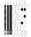
- FIG. 6 is a diagram showing an example of simulation results by the quantum bit control circuit 1A according to this embodiment.
- the simulation results shown in FIG. 6 are results for the case where the first excitation current Ilo contains two frequencies.
- the value of each physical quantity is shown for 65 nanoseconds.
- the first excitation current Ilo includes two frequencies of 4.5 GHz and 5 GHz.
- the frequency of the component excitation current Ir1 that flows through resonance in the resonance circuit 11A-1 is 4.5 GHz.
- the frequency of the component excitation current Ir2 that flows through resonance in the resonance circuit 11A-2 is 5 GHz.
- the second excitation current Ibb is a triangular wave.
- the values of the first excitation current Ilo, the component excitation current Ir1, the component excitation current Ir2, and the second excitation current Ibb are expressed in arbitrary units.
- An input current Iin1 input to the QFP mixer 4A-1 indicates a logic state of "0, 1, 0, 1" as an example.
- An input current Iin2 input to the QFP mixer 4A-2 exhibits logic states of "0, 0, 1, 1" as an example.
- the unit of each value of the input current Iin1 and the input current Iin2 is 5 ⁇ A/tick.
- the output microwave Vout1 is generated based on the frequency of 4.5 GHz included in the first excitation current Ilo, the second excitation current Ibb, and the input current Iin1.
- the output microwave Vout1 becomes the logic indicated by the input current Iin1. It oscillates at 4.5 GHz with an amplitude that depends on the state.
- the output microwave Vout1 has an amplitude of almost zero and does not oscillate during the period when the logic state indicated by the input current Iin1 is "0", and during the period when the logic state is "1", the second excitation current Ibb is non-linearly reflected and oscillates at 4.5 GHz.
- FIG. 6 shows the simulation results when the logic value of the other input signal is "1". Since the logic state of the other input signal is fixed at "1”, when the logic value of the input current Iin1 is "1", the output microwave Vout1 is output with a predetermined amplitude, and the input When the logic value of the current Iin1 is "0", the output microwave Vout1 has almost zero amplitude and is not output. The same applies to the relationship between the input current Iin2 and the output microwave Vout2.
- the output microwave Vout2 is generated based on the frequency of 5 GHz contained in the first excitation current Ilo, the second excitation current Ibb, and the input current Iin2.
- the output microwave Vout2 is brought to the logic state indicated by the input current Iin2. It oscillates at 5 GHz with a corresponding amplitude.
- the output microwave Vout2 has an amplitude of almost zero and does not oscillate during the period when the logic state indicated by the input current Iin2 is "0", and during the period when the logic state is "1", the second excitation current Ibb is non-linearly reflected and oscillates at 5 GHz.
- the unit of each value of the output microwave Vout1 and the output microwave Vout2 is 10 ⁇ V/tick.
- FIG. 7 is a diagram showing an example of the relationship between the spectrum of the first excitation current Ilo and the amplitude of the output microwave according to this embodiment.
- the amplitude of the 5 GHz frequency component is reduced in the first excitation current Ilo shown in FIG. 7 compared to the first excitation current Ilo shown in FIG.
- the power of the 5 GHz frequency component is ⁇ 55.7 dBm for the first excitation current Ilo shown in FIG. 6, whereas it is ⁇ 58.7 dBm for the first excitation current Ilo shown in FIG.
- the amplitude of the 4.5 GHz frequency component is -56.6 dBm for both the first excitation current Ilo shown in FIG. 6 and the first excitation current Ilo shown in FIG.
- the amplitude and pulse width of the output microwave Vout2 are reduced.
- the output microwave Vout1 is not changed in amplitude and pulse width.
- the electromagnetic waves output by the output signal line (not shown in this embodiment and corresponding to the electromotive force output line 8 in FIG. 1) (in this embodiment, the output microwave Vout1, the output microwave Vout2, the output microwave The amplitude and pulse width of Vout3) are controlled by the amplitude of the predetermined frequency component of the first excitation current Ilo. Note that even if only one configuration corresponding to the QFP mixer 4A is provided as in the quantum bit control circuit 1 (FIG. 1) according to the first embodiment described above, the first excitation current Ilo By changing the amplitude, the amplitude and pulse width of the output microwave Vout can be adjusted.
- the first excitation current Ilo input to the first power supply line 2A has a plurality of frequencies (frequency f1, f2 , and frequency f3), and an output signal generation circuit (not shown in this embodiment, an output signal generation circuit 40a in the configuration of the QFP gate 4a in FIG. 1, and an output signal generation circuit 40a in the configuration of the QFP gate 4b in FIG. generating circuit 40b) and a resonance circuit for each of a plurality of frequencies (frequency f1, frequency f2, and frequency f3 in this embodiment).
- the resonant circuit (resonant circuit 11A-1, resonant circuit 11A-2, and resonant circuit 11A-3 in this embodiment) includes a coupling portion (in this embodiment, inductor L2-1, inductor L2-2, inductor L2-3), an output signal generation circuit (not shown in the present embodiment, an output signal generation circuit 40a in the configuration of the QFP gate 4a in FIG. 1, and an output signal generation circuit 40a in the configuration of the QFP gate 4b in FIG.
- a coupling portion in this embodiment, inductor L2-1, inductor L2-2, inductor L2-3
- an output signal generation circuit (not shown in the present embodiment, an output signal generation circuit 40a in the configuration of the QFP gate 4a in FIG. 1, and an output signal generation circuit 40a in the configuration of the QFP gate 4b in FIG.
- the corresponding output signal is generated by flowing a current of the resonance frequency through the second magnetic coupling unit (inductor L3-1, inductor L3-2, and inductor L3-3 in this embodiment).
- a generation circuit (not shown in the present embodiment, corresponding to the output signal generation circuit 40a in the configuration of the QFP gate 4a in FIG. 1 and the output signal generation circuit 40b in the configuration of the QFP gate 4b) is supplied with the resonance frequency as the first frequency. Supplied as the frequency of 1 power line 2A.
- the number of cables required for controlling the qubits is two, the first power supply line 2A and the second power supply line 3A, regardless of the number of qubits. Because it is a book, a small number of cables can control a large number of qubits. Here, a small number of cables means a small number compared to the number of quantum bits to be controlled.
- the frequencies contained in the first excitation current Ilo may be one, two, four or more depending on the number of qubits to be controlled.
- the qubit control circuit includes at least a set of resonant circuits and output signal generating circuits, the number of which is equal to or greater than the number of frequencies included in the first excitation current Ilo. Some sets of resonant circuits and output signal generating circuits included in the qubit control circuit may not be used. Moreover, a plurality of sets of the resonance circuit and the output signal generation circuit may correspond to one frequency included in the first excitation current Ilo.
- the resonance circuit and the power supply line (first power supply line) are magnetically coupled
- the present invention is not limited to this.
- the resonant circuit and the power line may be coupled by capacitive coupling.
- the QFP provided in the qubit control circuit in each of the above-described embodiments may be an adiabatic flux quantum parametron (AQFP) or a directly coupled flux quantum parametron (DQFP).
- AQFP adiabatic flux quantum parametron
- DQFP directly coupled flux quantum parametron
- the electromagnetic waves generated by the quantum bit control circuits 1 and 1A and applied to the controlled object (qubit) are microwaves, but the present invention is not limited to this.
- the frequency of the electromagnetic wave generated by the quantum bit control circuits 1 and 1A and irradiated to the controlled object (qubit) may be other than the microwave frequency.
- the quantum bit control circuits 1 and 1A may generate electromagnetic waves with frequencies other than microwave frequencies and irradiate the control target with them.
- control target of the quantum bit control circuit is a quantum bit
- the invention is not limited to this.
- a control object other than the quantum bit may be controlled by a circuit having the same configuration as the quantum bit control circuit according to each of the embodiments described above.
- Control objects other than quantum bits are, for example, various components that make up a circuit of a quantum computer.
Abstract
This qubit control circuit comprises: a first power supply line to which a first excitation current that is a current of a predetermined frequency is input; a second power supply line to which a second excitation current that is a current having a predetermined waveform is input; an input signal line to which an input signal indicating a logic state is input; a magnetic coupling unit; and a Josephson junction, wherein the Josephson junction includes an output signal generation circuit for outputting an output signal according to the logic state indicated by the input signal and the waveform of the second excitation current and the frequency of the first excitation current input via the magnetic coupling unit.
Description
本発明は、量子ビット制御回路に関する。
本願は、2022年3月3日に、日本に出願された特願2022-032905号に基づき優先権を主張し、その内容をここに援用する。 The present invention relates to qubit control circuits.
This application claims priority based on Japanese Patent Application No. 2022-032905 filed in Japan on March 3, 2022, the contents of which are incorporated herein.
本願は、2022年3月3日に、日本に出願された特願2022-032905号に基づき優先権を主張し、その内容をここに援用する。 The present invention relates to qubit control circuits.
This application claims priority based on Japanese Patent Application No. 2022-032905 filed in Japan on March 3, 2022, the contents of which are incorporated herein.
量子コンピュータは、多数の電子から構成される量子系をシミュレートできるため、材料設計や創薬に応用できると期待されている。量子コンピュータにおいて制御される量子ビットは、超伝導素子によって構成されるため、低温において制御される必要がある。そのため、量子コンピュータの構成は、量子ビットを低温に保つための冷凍機と、室温で動作する機器とが含まれる。室温で動作する機器は、ケーブルを介して量子ビットに制御信号を出力する。
Quantum computers can simulate quantum systems composed of a large number of electrons, so they are expected to be applied to material design and drug discovery. Quantum bits controlled in quantum computers need to be controlled at low temperatures because they are composed of superconducting elements. Therefore, the configuration of a quantum computer includes refrigerators to keep the qubits cold and equipment that operates at room temperature. Devices operating at room temperature output control signals to qubits through cables.
量子コンピュータにおいて、冷凍機中の多数の量子ビットを制御するために、大量のケーブルが必要とされている。例えば、72個の量子ビットを制御するためには、168本のケーブルが必要である。しかしながら、量子ビットを制御するためのケーブルの数には上限があるため、量子ビットの数を増加させることは困難を極めている。
In quantum computers, a large amount of cables are required to control a large number of qubits in a refrigerator. For example, 168 cables are required to control 72 qubits. However, increasing the number of qubits is extremely difficult because there is an upper limit to the number of cables that can be used to control the qubits.
大規模な量子コンピュータを実現するためには、量子ビットと同じく低温の側で動作する制御回路が必要とされている。例えば、多数の通信線の数が制御対象のデバイスの数よりも少ない量子コンピューティングシステムが知られている(特許文献1)。また、磁束量子パラメトロンをシフトレジスタとして用いた超伝導デジタル/アナログ変換器を備えた超伝導量子プロセッサが知られている(特許文献2)。
In order to realize a large-scale quantum computer, a control circuit that operates on the low-temperature side, like a qubit, is required. For example, a quantum computing system is known in which the number of communication lines is smaller than the number of devices to be controlled (Patent Document 1). Also known is a superconducting quantum processor having a superconducting digital/analog converter that uses magnetic flux quantum parametrons as shift registers (Patent Document 2).
上述したように、少ない数のケーブルで多数の量子ビットを制御できることが求められている。そこで、少ない数のケーブルで多数の量子ビットを制御できる量子ビット制御回路を構成する要素となる回路が求められている。
As mentioned above, there is a demand to be able to control a large number of qubits with a small number of cables. Therefore, there is a demand for a circuit that constitutes a qubit control circuit that can control a large number of qubits with a small number of cables.
本発明は上記の点に鑑みてなされたものであり、少ない数のケーブルで多数の量子ビットを制御できる量子ビット制御回路を構成する要素となる回路を提供する。
The present invention has been made in view of the above points, and provides a circuit that constitutes a qubit control circuit that can control a large number of qubits with a small number of cables.
本発明は上記の課題を解決するためになされたものであり、本発明の一態様は、所定の周波数の電流である第1励起電流が入力される第1電源線と、所定の波形の電流である第2励起電流が入力される第2電源線と、論理状態を示す入力信号が入力される入力信号線と、磁気結合部と、ジョセフソン接合とを備え、前記ジョセフソン接合は、前記磁気結合部を介して入力される前記第1励起電流の周波数及び前記第2励起電流の波形と、前記入力信号が示す前記論理状態と、に応じた出力信号を出力する出力信号生成回路と、を備える量子ビット制御回路である。
The present invention has been made to solve the above problems, and one aspect of the present invention includes a first power supply line to which a first excitation current that is a current with a predetermined frequency is input, and a current with a predetermined waveform. a second power supply line to which a second excitation current is input, an input signal line to which an input signal indicating a logic state is input, a magnetic coupling portion, and a Josephson junction, wherein the Josephson junction is the an output signal generating circuit that outputs an output signal according to the frequency of the first excitation current and the waveform of the second excitation current input via a magnetic coupling unit, and the logic state indicated by the input signal; A qubit control circuit comprising:
また、本発明の一態様は、上記の量子ビット制御回路において、前記第1電源線に入力される前記第1励起電流には、複数の周波数が含まれ、前記出力信号生成回路と、共振回路とを前記複数の周波数ごとに備え、前記共振回路は、前記第1電源線と結合する結合部と、前記出力信号生成回路の前記磁気結合部と磁気結合する第2磁気結合部とを備え、前記第1励起電流に含まれる前記複数の周波数のうちのいずれかの周波数である共振周波数を有し、当該共振周波数の電流を前記第2磁気結合部に流すことにより、対応する前記出力信号生成回路に当該共振周波数を前記第1電源線の周波数として供給する。
Further, according to one aspect of the present invention, in the above-described quantum bit control circuit, the first excitation current input to the first power supply line includes a plurality of frequencies, and the output signal generation circuit and the resonance circuit and for each of the plurality of frequencies, the resonance circuit includes a coupling unit that couples with the first power supply line, and a second magnetic coupling unit that magnetically couples with the magnetic coupling unit of the output signal generation circuit, having a resonance frequency that is one of the plurality of frequencies included in the first excitation current, and generating the corresponding output signal by causing a current having the resonance frequency to flow through the second magnetic coupling section; The resonance frequency is supplied to the circuit as the frequency of the first power supply line.
また、本発明の一態様は、上記の量子ビット制御回路において、前記出力信号生成回路と、前記出力信号に応じた電流が流れる第3磁気結合部とを備える複数の超伝導ゲート回路と、複数の前記超伝導ゲート回路の前記第3磁気結合部とそれぞれ磁気結合する第4磁気結合部と、複数の前記超伝導ゲート回路がそれぞれ生成する前記出力信号が前記第4磁気結合部に印加する磁束に応じて、量子ビットに照射される電磁波を出力する出力信号線と、を備える。
In one aspect of the present invention, in the above-described quantum bit control circuit, a plurality of superconducting gate circuits each including the output signal generation circuit and a third magnetic coupling section through which a current flows according to the output signal; and a magnetic flux applied to the fourth magnetic coupling portion by the output signal generated by each of the plurality of superconducting gate circuits. and an output signal line for outputting an electromagnetic wave irradiated to the quantum bit according to.
また、本発明の一態様は、上記の量子ビット制御回路において、前記出力信号線が出力する前記電磁波の振幅及びパルス幅は、前記第1励起電流の振幅によって制御される。
Further, according to one aspect of the present invention, in the above-described quantum bit control circuit, the amplitude and pulse width of the electromagnetic wave output by the output signal line are controlled by the amplitude of the first excitation current.
また、本発明の一態様は、上記の量子ビット制御回路において、前記出力信号生成回路は、磁束量子パラメトロン回路の構成を含む。
Further, according to one aspect of the present invention, in the above-described quantum bit control circuit, the output signal generation circuit includes a configuration of a magnetic flux quantum parametron circuit.
本発明によれば、少ない数のケーブルで多数の量子ビットを制御できる量子ビット制御回路を構成する要素となる回路を提供できる。
According to the present invention, it is possible to provide a circuit that constitutes a qubit control circuit that can control a large number of qubits with a small number of cables.
(第1の実施形態)
以下、図面を参照しながら本発明の実施形態について詳しく説明する。図1は、本実施形態に係る量子ビット制御回路1の構成の一例を示す図である。量子ビット制御回路1は、制御対象の量子ビットにマイクロ波を照射するための回路である。量子ビット制御回路1では、マイクロ波を磁束量子パラメトロン(Quantum Flux Parametron:QFP)回路を用いて生成する。後述するように、量子ビット制御回路1は、非線形なミキサとして機能する。 (First embodiment)
BEST MODE FOR CARRYING OUT THE INVENTION Hereinafter, embodiments of the present invention will be described in detail with reference to the drawings. FIG. 1 is a diagram showing an example of the configuration of a quantumbit control circuit 1 according to this embodiment. The quantum bit control circuit 1 is a circuit for irradiating a quantum bit to be controlled with microwaves. The quantum bit control circuit 1 generates microwaves using a Quantum Flux Parametron (QFP) circuit. As will be described later, the qubit control circuit 1 functions as a nonlinear mixer.
以下、図面を参照しながら本発明の実施形態について詳しく説明する。図1は、本実施形態に係る量子ビット制御回路1の構成の一例を示す図である。量子ビット制御回路1は、制御対象の量子ビットにマイクロ波を照射するための回路である。量子ビット制御回路1では、マイクロ波を磁束量子パラメトロン(Quantum Flux Parametron:QFP)回路を用いて生成する。後述するように、量子ビット制御回路1は、非線形なミキサとして機能する。 (First embodiment)
BEST MODE FOR CARRYING OUT THE INVENTION Hereinafter, embodiments of the present invention will be described in detail with reference to the drawings. FIG. 1 is a diagram showing an example of the configuration of a quantum
なお、以下の説明では、一方のインダクタに電流が流れて磁束が発生した場合に、当該磁束によって他方のインダクタにも磁束が発生することを、一方のインダクタと他方のインダクタとが磁気結合しているという場合がある。
In the following description, when a current flows through one inductor and magnetic flux is generated, magnetic flux is generated in the other inductor due to the magnetic flux. Sometimes there are.
量子ビット制御回路1は、第1電源線2と、第2電源線3と、QFPゲート4aと、QFPゲート4bと、入力信号線5aと、入力信号線5bと、起電力出力線8と、バンドパスフィルタ9と、抵抗器10とを備える。
The qubit control circuit 1 includes a first power supply line 2, a second power supply line 3, a QFP gate 4a, a QFP gate 4b, an input signal line 5a, an input signal line 5b, an electromotive force output line 8, A bandpass filter 9 and a resistor 10 are provided.
QFPゲート4a及びQFPゲート4bはそれぞれ、QFPである。なお、1つのQFP(QFPゲート4a)の構成には、配線41a、インダクタL31a、ジョセフソン接合J1a、配線42a、インダクタL32a、ジョセフソン接合J2a、負荷インダクタL4a、入力信号線5a、及び出力信号線6aが含まれる。同様に、1つのQFP(QFPゲート4b)の構成には、配線41b、インダクタL31b、ジョセフソン接合J1b、配線42b、インダクタL32b、ジョセフソン接合J2b、負荷インダクタL4b、入力信号線5b、及び出力信号線6bが含まれる。
なお、QFPゲート4aの構成のうち、配線41a、インダクタL31a、ジョセフソン接合J1a、配線42a、インダクタL32a、ジョセフソン接合J2a、及び入力信号線5aによって構成される部分を出力信号生成回路40aともいう。同様に、QFPゲート4bの構成のうち、配線41b、インダクタL31b、ジョセフソン接合J1b、配線42b、インダクタL32b、ジョセフソン接合J2b、及び入力信号線5bによって構成される部分を出力信号生成回路40bともいう。QFP gate 4a and QFP gate 4b are each QFP. The configuration of one QFP (QFP gate 4a) includes wiring 41a, inductor L31a, Josephson junction J1a, wiring 42a, inductor L32a, Josephson junction J2a, load inductor L4a, input signal line 5a, and output signal line. 6a is included. Similarly, the configuration of one QFP (QFP gate 4b) includes wiring 41b, inductor L31b, Josephson junction J1b, wiring 42b, inductor L32b, Josephson junction J2b, load inductor L4b, input signal line 5b, and output signal Line 6b is included.
Note that, of the configuration of theQFP gate 4a, a portion configured by the wiring 41a, the inductor L31a, the Josephson junction J1a, the wiring 42a, the inductor L32a, the Josephson junction J2a, and the input signal line 5a is also referred to as the output signal generation circuit 40a. . Similarly, in the configuration of the QFP gate 4b, the portion constituted by the wiring 41b, the inductor L31b, the Josephson junction J1b, the wiring 42b, the inductor L32b, the Josephson junction J2b, and the input signal line 5b is also called the output signal generation circuit 40b. say.
なお、QFPゲート4aの構成のうち、配線41a、インダクタL31a、ジョセフソン接合J1a、配線42a、インダクタL32a、ジョセフソン接合J2a、及び入力信号線5aによって構成される部分を出力信号生成回路40aともいう。同様に、QFPゲート4bの構成のうち、配線41b、インダクタL31b、ジョセフソン接合J1b、配線42b、インダクタL32b、ジョセフソン接合J2b、及び入力信号線5bによって構成される部分を出力信号生成回路40bともいう。
Note that, of the configuration of the
第1電源線2は、第1励起電流Iloが入力される電源線である。第1励起電流Iloは、所定の周波数を含む電流である。第1励起電流Iloの周波数は、一例として、5GHzである。第1励起電流Iloは、局部発振器(Local Oscillator)(不図示)から供給されるローカルオシレータ信号である。当該局部発振器は、量子ビット制御回路1とは別体として備えられる。
第1電源線2は、インダクタL11aと、インダクタL12aと、インダクタL11bと、インダクタL12bとを備える。 Thefirst power line 2 is a power line to which the first excitation current Ilo is input. The first excitation current Ilo is a current containing a predetermined frequency. The frequency of the first excitation current Ilo is, for example, 5 GHz. The first excitation current Ilo is a local oscillator signal provided by a Local Oscillator (not shown). The local oscillator is provided separately from the quantum bit control circuit 1 .
Thefirst power line 2 includes an inductor L11a, an inductor L12a, an inductor L11b, and an inductor L12b.
第1電源線2は、インダクタL11aと、インダクタL12aと、インダクタL11bと、インダクタL12bとを備える。 The
The
第2電源線3は、第2励起電流Ibbが入力される電源線である。第2励起電流Ibbは、所定の波形の電流である。第2励起電流Ibbは、ベースバンド回路(不図示)から出力信号として供給されるベースバンド信号である。当該ベースバンド回路は、量子ビット制御回路1とは別体として備えられる。第2励起電流Ibbの波形は、一例として、三角波である。
第2電源線3は、インダクタL21aと、インダクタL22aと、インダクタL21bと、インダクタL22bとを備える。 Asecond power line 3 is a power line to which a second excitation current Ibb is input. The second excitation current Ibb is a current with a predetermined waveform. The second excitation current Ibb is a baseband signal supplied as an output signal from a baseband circuit (not shown). The baseband circuit is provided separately from the quantum bit control circuit 1 . A waveform of the second excitation current Ibb is, for example, a triangular wave.
Thesecond power line 3 includes an inductor L21a, an inductor L22a, an inductor L21b, and an inductor L22b.
第2電源線3は、インダクタL21aと、インダクタL22aと、インダクタL21bと、インダクタL22bとを備える。 A
The
入力信号線5aは、入力電流Iinaが入力される制御線である。入力信号線5bは、入力電流Iinbが入力される制御線である。入力電流Iina及び入力電流Iinbはそれぞれ、QFPゲート4aとQFPゲート4bの論理状態を決める電流である。
QFPゲート4aは、入力電流Iinaに応じて出力電流Ioutaを生成する。QFPゲート4bは、入力電流Iinbに応じて出力電流Ioutbを生成する。 Theinput signal line 5a is a control line to which the input current Iina is input. The input signal line 5b is a control line to which the input current Iinb is input. Input current Iina and input current Iinb are currents that determine the logic states of QFP gate 4a and QFP gate 4b, respectively.
QFP gate 4a generates output current Iouta according to input current Iina. QFP gate 4b generates output current Ioutb according to input current Iinb.
QFPゲート4aは、入力電流Iinaに応じて出力電流Ioutaを生成する。QFPゲート4bは、入力電流Iinbに応じて出力電流Ioutbを生成する。 The
ここで図8を参照し、QFPの動作原理について、図1に示したQFPと対比しつつ説明する。
図8は、QFPの動作原理を説明するための図である。QFP100は、QFPの基本ゲートを示す。QFP100は、交流励起電流Ixによって駆動、及びクロックされる。交流励起電流Ixが電源線101を流れることにより、電源線101に備えられるインダクタLx1、及びインダクタLx2にそれぞれ磁束が発生する。
なお、量子ビット制御回路1(図1)は2本の電源線(第1電源線2、第2電源線3)を備えているが、QFP100(図8)では、説明を簡単にするために、第1電源線2及び第2電源線3の一方に相当する電源線の図示を省略し、1本の電源線(電源線101)を備えるとしている。ここでは一例として、電源線101が、図1の第1電源線2に相当するものとして説明する。
また、QFP100は、図1に示すQFPゲート4a及びQFPゲート4bのいずれかに相当する。ここでは一例として、QFP100が、図1のQFPゲート4aに相当するものとして説明する。この一例の場合、インダクタLx1は、図1のインダクタL11aに相当し、インダクタLx2は、図1のインダクタL12aに相当する。交流励起電流Ixは、図1の第1励起電流Iloに相当する。 Here, referring to FIG. 8, the operating principle of the QFP will be described in comparison with the QFP shown in FIG.
FIG. 8 is a diagram for explaining the operating principle of the QFP.QFP 100 indicates the basic gate of QFP. QFP 100 is driven and clocked by alternating excitation current Ix. When the AC excitation current Ix flows through the power line 101, magnetic fluxes are generated in the inductors Lx1 and Lx2 provided in the power line 101, respectively.
Although the quantum bit control circuit 1 (FIG. 1) has two power lines (first power line 2 and second power line 3), in the QFP 100 (FIG. 8), for simplicity of explanation, , the power supply line corresponding to one of the first power supply line 2 and the second power supply line 3 is omitted, and one power supply line (power supply line 101) is provided. Here, as an example, the power line 101 will be described as being equivalent to the first power line 2 in FIG.
Also, theQFP 100 corresponds to either the QFP gate 4a or the QFP gate 4b shown in FIG. Here, as an example, the QFP 100 will be described as being equivalent to the QFP gate 4a in FIG. In this example, inductor Lx1 corresponds to inductor L11a in FIG. 1, and inductor Lx2 corresponds to inductor L12a in FIG. The alternating excitation current Ix corresponds to the first excitation current Ilo in FIG.
図8は、QFPの動作原理を説明するための図である。QFP100は、QFPの基本ゲートを示す。QFP100は、交流励起電流Ixによって駆動、及びクロックされる。交流励起電流Ixが電源線101を流れることにより、電源線101に備えられるインダクタLx1、及びインダクタLx2にそれぞれ磁束が発生する。
なお、量子ビット制御回路1(図1)は2本の電源線(第1電源線2、第2電源線3)を備えているが、QFP100(図8)では、説明を簡単にするために、第1電源線2及び第2電源線3の一方に相当する電源線の図示を省略し、1本の電源線(電源線101)を備えるとしている。ここでは一例として、電源線101が、図1の第1電源線2に相当するものとして説明する。
また、QFP100は、図1に示すQFPゲート4a及びQFPゲート4bのいずれかに相当する。ここでは一例として、QFP100が、図1のQFPゲート4aに相当するものとして説明する。この一例の場合、インダクタLx1は、図1のインダクタL11aに相当し、インダクタLx2は、図1のインダクタL12aに相当する。交流励起電流Ixは、図1の第1励起電流Iloに相当する。 Here, referring to FIG. 8, the operating principle of the QFP will be described in comparison with the QFP shown in FIG.
FIG. 8 is a diagram for explaining the operating principle of the QFP.
Although the quantum bit control circuit 1 (FIG. 1) has two power lines (
Also, the
インダクタLx1と、ループ102に備えられるインダクタL1とは、結合定数k1によって磁気結合されている。なお、インダクタL1は、図1のインダクタL31aに相当する。
インダクタLx2と、ループ102に備えられるインダクタL2とは、結合定数k2によって磁気結合されている。なお、インダクタL2は、図1のインダクタL32aに相当する。
インダクタL1及びインダクタL2に磁束が印加されると、ループ102に備えられる一対のジョセフソン接合であるジョセフソン接合J1及びジョセフソン接合J2は、入力信号線103を流れる入力電流Iinに応じて論理状態を決定するとともに、出力電流Ioutを生成する。なお、ジョセフソン接合J1は、図1のジョセフソン接合J1aに相当し、ジョセフソン接合J2は、図1のジョセフソン接合J2aに相当する。入力信号線103は、図1の入力信号線5aに相当し、入力電流Iinは、図1の入力電流Iinaに相当する。 Inductor Lx1 and inductor L1 provided inloop 102 are magnetically coupled by coupling constant k1. Note that the inductor L1 corresponds to the inductor L31a in FIG.
Inductor Lx2 and inductor L2 provided inloop 102 are magnetically coupled by coupling constant k2. Note that the inductor L2 corresponds to the inductor L32a in FIG.
When a magnetic flux is applied to inductor L1 and inductor L2, the pair of Josephson junctions provided inloop 102, Josephson junction J1 and Josephson junction J2, change logic state according to the input current Iin flowing through input signal line 103. is determined and an output current Iout is generated. The Josephson junction J1 corresponds to the Josephson junction J1a in FIG. 1, and the Josephson junction J2 corresponds to the Josephson junction J2a in FIG. The input signal line 103 corresponds to the input signal line 5a in FIG. 1, and the input current Iin corresponds to the input current Iina in FIG.
インダクタLx2と、ループ102に備えられるインダクタL2とは、結合定数k2によって磁気結合されている。なお、インダクタL2は、図1のインダクタL32aに相当する。
インダクタL1及びインダクタL2に磁束が印加されると、ループ102に備えられる一対のジョセフソン接合であるジョセフソン接合J1及びジョセフソン接合J2は、入力信号線103を流れる入力電流Iinに応じて論理状態を決定するとともに、出力電流Ioutを生成する。なお、ジョセフソン接合J1は、図1のジョセフソン接合J1aに相当し、ジョセフソン接合J2は、図1のジョセフソン接合J2aに相当する。入力信号線103は、図1の入力信号線5aに相当し、入力電流Iinは、図1の入力電流Iinaに相当する。 Inductor Lx1 and inductor L1 provided in
Inductor Lx2 and inductor L2 provided in
When a magnetic flux is applied to inductor L1 and inductor L2, the pair of Josephson junctions provided in
生成された出力電流Ioutが出力信号線104を流れることにより、出力信号線104に備えられる負荷インダクタLqに磁束が発生する。なお、出力信号線104は、図1の出力信号線6aに相当し、出力電流Ioutは、図1の出力電流Ioutaに相当し、負荷インダクタLqは、図1の負荷インダクタL4aに相当する。
When the generated output current Iout flows through the output signal line 104, a magnetic flux is generated in the load inductor Lq provided in the output signal line 104. The output signal line 104 corresponds to the output signal line 6a in FIG. 1, the output current Iout corresponds to the output current Iouta in FIG. 1, and the load inductor Lq corresponds to the load inductor L4a in FIG.
QFP100では、インダクタL1、インダクタL2、負荷インダクタLq、ジョセフソン接合J1、及びジョセフソン接合J2のパラメータを最適化することによって、消費電力の低減が可能である。QFPでは、超伝導素子を用いているため直流抵抗がなく超低消費電力であることが知られている。QFPでは、ゲート当りの消費電力は10pW程度である。また、QFPでは、クロック周波数が10GHz程度の高速動作が可能である。また、QFPは超低消費電力であるため、QFPを量子ビットの近くで動作させることが可能である。なお、上述したQFPの消費電力、クロック周波数それぞれの値は、一例であって、回路パラメータや回路の種類によってそれらの値は変わり得る。
In the QFP100, power consumption can be reduced by optimizing the parameters of inductor L1, inductor L2, load inductor Lq, Josephson junction J1, and Josephson junction J2. It is known that the QFP uses a superconducting element and therefore has no direct current resistance and consumes very low power. In QFP, the power consumption per gate is about 10 pW. Also, the QFP is capable of high-speed operation with a clock frequency of about 10 GHz. Also, since QFPs have ultra-low power consumption, it is possible to operate QFPs near qubits. Note that the values of the power consumption and clock frequency of the QFP described above are examples, and these values may vary depending on the circuit parameters and the type of circuit.
なお、QFPでは、回路についての各種のパラメータに応じて、ジョセフソン接合によって出力電流が生成されるか否かが決定される。当該パラメータには、インダクタのインダクタンスの大きさ、ジョセフソン接合の臨界電流値が含まれる。QFP100では、インダクタL1、インダクタL2、及び負荷インダクタLqそれぞれのインダクタンスの大きさ、ジョセフソン接合J1及びジョセフソン接合J2それぞれの臨界電流値が、ジョセフソン接合J1及びジョセフソン接合J2によって出力電流Ioutが生成されるように調整されている。
図1に示すQFPゲート4a及びQFPゲート4bについてもそれぞれ、回路についての各種のパラメータがジョセフソン接合によって出力電流が生成されるように調整されている。 It should be noted that in a QFP, depending on various parameters of the circuit, it is determined whether or not the output current is generated by the Josephson junction. The parameters include the inductance magnitude of the inductor and the critical current value of the Josephson junction. In theQFP 100, the magnitude of the inductance of each of the inductor L1, the inductor L2, and the load inductor Lq, the critical current value of each of the Josephson junctions J1 and J2, and the output current Iout by the Josephson junctions J1 and J2 are determined. adjusted to generate
For theQFP gate 4a and the QFP gate 4b shown in FIG. 1, various parameters of the circuit are adjusted so that an output current is generated by the Josephson junction.
図1に示すQFPゲート4a及びQFPゲート4bについてもそれぞれ、回路についての各種のパラメータがジョセフソン接合によって出力電流が生成されるように調整されている。 It should be noted that in a QFP, depending on various parameters of the circuit, it is determined whether or not the output current is generated by the Josephson junction. The parameters include the inductance magnitude of the inductor and the critical current value of the Josephson junction. In the
For the
図1に戻って量子ビット制御回路1の構成の説明を続ける。なお、QFPゲート4aの構成と、QFPゲート4bの構成とは同様であるため、以下では、QFPゲート4aの構成を説明し、QFPゲート4bの構成の説明は省略する。
Returning to FIG. 1, the description of the configuration of the quantum bit control circuit 1 will be continued. Since the configuration of the QFP gate 4a and the configuration of the QFP gate 4b are the same, the configuration of the QFP gate 4a will be described below, and the description of the configuration of the QFP gate 4b will be omitted.
配線41aと、配線42aと、出力信号線6aと、上述した入力信号線5aとは、接続部7aにおいて互いに接続される。インダクタL31aと、ジョセフソン接合J1aとは、配線41a上に備えられる。図1では、一例として、インダクタL31aと、ジョセフソン接合J1aとは、接続部7aから近い方からこの順において配線41aに配置される。インダクタL31aと、ジョセフソン接合J1aとが配線41aに配置される順序は、これに限られず任意である。配線41aの両端のうち、接続部7aと接続されていない方の端は、グラウンドに接続される。
The wiring 41a, the wiring 42a, the output signal line 6a, and the above-described input signal line 5a are connected to each other at the connecting portion 7a. The inductor L31a and the Josephson junction J1a are provided on the wiring 41a. In FIG. 1, as an example, the inductor L31a and the Josephson junction J1a are arranged on the wiring 41a in this order from the side closest to the connection portion 7a. The order in which the inductor L31a and the Josephson junction J1a are arranged on the wiring 41a is not limited to this and is arbitrary. The end of the wiring 41a that is not connected to the connection portion 7a is grounded.
インダクタL32aと、ジョセフソン接合J2aとは、配線42a上に備えられる。図1では、一例として、インダクタL32aと、ジョセフソン接合J2aとは、接続部7aから近い方からこの順において配線42aに配置される。インダクタL32aと、ジョセフソン接合J2aとが配線42aに配置される順序は、これに限られず任意である。配線42aの両端のうち、接続部7aと接続されていない方の端は、グラウンドに接続される。
The inductor L32a and the Josephson junction J2a are provided on the wiring 42a. In FIG. 1, as an example, the inductor L32a and the Josephson junction J2a are arranged on the wiring 42a in this order from the side closest to the connection portion 7a. The order in which the inductor L32a and the Josephson junction J2a are arranged on the wiring 42a is not limited to this and is arbitrary. The end of the wiring 42a that is not connected to the connecting portion 7a is grounded.
ジョセフソン接合J1aと、ジョセフソン接合J2aと、インダクタL31aと、インダクタL32aとは、超伝導リングに一対のジョセフソン接合を有する超伝導量子干渉素子を構成する。なお、超伝導リングとは、図8に示したループ102に相当する回路である。なお、超伝導量子干渉素子として、超伝導リングに3つ以上のジョセフソン接合を有する超伝導量子干渉素子が用いられてもよい。
The Josephson junction J1a, the Josephson junction J2a, the inductor L31a, and the inductor L32a constitute a superconducting quantum interference device having a pair of Josephson junctions in a superconducting ring. The superconducting ring is a circuit corresponding to the loop 102 shown in FIG. A superconducting quantum interference device having three or more Josephson junctions in a superconducting ring may be used as the superconducting quantum interference device.
起電力出力線8は、インダクタL5aとインダクタL5bと、バンドパスフィルタ9と、抵抗器10とを備える。起電力出力線8の一端は、グラウンドに接続される。起電力出力線8において、抵抗器10、インダクタL5b、インダクタL5a、及びバンドパスフィルタ9は、この順にグラウンドから近い順に配置される。なお、抵抗器10は、起電力出力線8の構成から省略されてよい。
The electromotive force output line 8 includes an inductor L5a, an inductor L5b, a bandpass filter 9, and a resistor 10. One end of the electromotive force output line 8 is connected to the ground. In the electromotive force output line 8, the resistor 10, the inductor L5b, the inductor L5a, and the bandpass filter 9 are arranged in this order from the ground. Note that the resistor 10 may be omitted from the configuration of the electromotive force output line 8 .
第1励起電流Iloが第1電源線2を流れ、第2励起電流Ibbが第2電源線3を流れることにより、インダクタL31aと、インダクタL11a及びインダクタL21aとのそれぞれの磁気結合によって、インダクタL31aに磁束が発生する。第1励起電流Iloが第1電源線2を流れ、第2励起電流Ibbが第2電源線3を流れることにより、インダクタL32aと、インダクタL12a及びインダクタL22aとのそれぞれの磁気結合によって、インダクタL32aに磁束が発生する。インダクタL31a及びインダクタL32aにそれぞれ磁束が発生することにより、ジョセフソン接合J1a及びジョセフソン接合J2aは、入力信号線5aを流れる入力電流Iinaに応じて、論理状態を決定するとともに、出力電流Ioutaを生成する。
When the first excitation current Ilo flows through the first power supply line 2 and the second excitation current Ibb flows through the second power supply line 3, magnetic coupling between the inductor L31a and the inductors L11a and L21a causes the inductor L31a to A magnetic flux is generated. When the first excitation current Ilo flows through the first power supply line 2 and the second excitation current Ibb flows through the second power supply line 3, magnetic coupling between the inductor L32a and the inductors L12a and L22a causes the inductor L32a to A magnetic flux is generated. By generating magnetic fluxes in the inductors L31a and L32a, respectively, the Josephson junctions J1a and J2a determine the logic state and generate the output current Iouta according to the input current Iina flowing through the input signal line 5a. do.
生成された出力電流Ioutaが出力信号線6aを流れることにより、出力信号線6aに備えられる負荷インダクタL4aに磁束が発生する。負荷インダクタL4aと、インダクタL5aとの磁気結合によって、インダクタL5aに磁束Φaが発生する。
When the generated output current Iouta flows through the output signal line 6a, magnetic flux is generated in the load inductor L4a provided in the output signal line 6a. A magnetic flux Φa is generated in the inductor L5a by magnetic coupling between the load inductor L4a and the inductor L5a.
上述したように、QFPゲート4aは、第1電源線2に第1励起電流Iloが流れ、第2電源線3に第2励起電流Ibbが流れることにより、磁気結合によって、入力信号線5aを流れる入力電流Iinaに応じて出力電流Ioutaを生成する。また、出力電流Ioutaによって、インダクタL5aに磁束Φaが発生する。さらに、第1励起電流Ilo及び第2励起電流Ibbが変化することで、磁束Φaが変化し、インダクタL5aには第1励起電流Ilo及び第2励起電流Ibbの変化に応じた誘導起電力が発生する。
同様にしてQFPゲート4bは、第1励起電流Iloが第1電源線2を流れ、第2励起電流Ibbが第2電源線3を流れることにより、磁気結合によって、入力信号線5bを流れる入力電流Iinbに応じて出力電流Ioutbを生成する。また、出力電流Ioutbによって、インダクタL5bに磁束Φbが発生する。さらに、第1励起電流Ilo及び第2励起電流Ibbが変化することで、磁束Φbが変化し、インダクタL5bには第1励起電流Ilo及び第2励起電流Ibbの変化に応じた誘導起電力が発生する。 As described above, in theQFP gate 4a, the first excitation current Ilo flows through the first power supply line 2 and the second excitation current Ibb flows through the second power supply line 3, thereby causing the input signal line 5a to flow through magnetic coupling. An output current Iouta is generated according to the input current Iina. Further, a magnetic flux Φa is generated in the inductor L5a by the output current Iouta. Furthermore, the magnetic flux Φa changes as the first excitation current Ilo and the second excitation current Ibb change, and an induced electromotive force is generated in the inductor L5a in accordance with the change in the first excitation current Ilo and the second excitation current Ibb. do.
Similarly, the first excitation current Ilo flows through the firstpower supply line 2 and the second excitation current Ibb flows through the second power supply line 3, so that the QFP gate 4b has an input current flowing through the input signal line 5b due to magnetic coupling. An output current Ioutb is generated according to Iinb. Also, a magnetic flux Φb is generated in the inductor L5b by the output current Ioutb. Furthermore, the change in the first excitation current Ilo and the second excitation current Ibb causes the magnetic flux Φb to change, and an induced electromotive force is generated in the inductor L5b according to the change in the first excitation current Ilo and the second excitation current Ibb. do.
同様にしてQFPゲート4bは、第1励起電流Iloが第1電源線2を流れ、第2励起電流Ibbが第2電源線3を流れることにより、磁気結合によって、入力信号線5bを流れる入力電流Iinbに応じて出力電流Ioutbを生成する。また、出力電流Ioutbによって、インダクタL5bに磁束Φbが発生する。さらに、第1励起電流Ilo及び第2励起電流Ibbが変化することで、磁束Φbが変化し、インダクタL5bには第1励起電流Ilo及び第2励起電流Ibbの変化に応じた誘導起電力が発生する。 As described above, in the
Similarly, the first excitation current Ilo flows through the first
インダクタL5a及びインダクタL5bにそれぞれ誘導起電力が発生することにより、誘導起電力の変化に応じた周波数の電流が起電力出力線8を流れ、バンドパスフィルタ9によって不要な周波数が除去された後、起電力出力線8から出力マイクロ波Voutが出力される。この出力マイクロ波Voutが、量子ビット制御回路1の制御対象の量子ビットに照射される。
By generating induced electromotive forces in the inductors L5a and L5b, respectively, a current having a frequency corresponding to the change in the induced electromotive force flows through the electromotive force output line 8, and after unnecessary frequencies are removed by the bandpass filter 9, An output microwave Vout is output from the electromotive force output line 8 . A quantum bit to be controlled by the quantum bit control circuit 1 is irradiated with this output microwave Vout.
次に図2を参照し、量子ビット制御回路1によるシミュレーション結果について説明する。図2は、本実施形態に係る量子ビット制御回路1によるシミュレーション結果の一例を示す図である。図2では、各物理量の値が30ナノ秒間について示されている。
Next, with reference to FIG. 2, simulation results by the quantum bit control circuit 1 will be described. FIG. 2 is a diagram showing an example of simulation results by the quantum bit control circuit 1 according to this embodiment. In FIG. 2, the value of each physical quantity is shown for 30 nanoseconds.
第1励起電流Iloの周波数は、上述したように5GHzである。第2励起電流Ibbは、上述したように三角波である。図2において第1励起電流Ilo、及び第2励起電流Ibbそれぞれの値は任意の単位で表されている。
The frequency of the first excitation current Ilo is 5 GHz as described above. The second excitation current Ibb is a triangular wave as described above. In FIG. 2, the values of the first excitation current Ilo and the second excitation current Ibb are expressed in arbitrary units.
入力電流Iinaは、一例として「0、1」の論理状態を示す。論理状態に応じて、入力電流Iinaは、15ナノ秒付近において、値がローからハイへと変化している。一方、入力電流Iinbは、一例として「1、1」の論理状態を示す。論理状態に応じて、入力電流Iinbは、値が常にハイである。なお、図2において、入力電流Iina、及び入力電流Iinbそれぞれの値の単位は、5μA/tickである。
The input current Iina indicates a logic state of "0, 1" as an example. Depending on the logic state, the input current Iina changes value from low to high around 15 ns. On the other hand, the input current Iinb shows a logic state of "1, 1" as an example. Depending on the logic state, the input current Iinb is always high in value. Note that in FIG. 2, the units of the values of the input current Iina and the input current Iinb are 5 μA/tick.
出力電流Ioutaは、第1励起電流Iloと、第2励起電流Ibbと、入力電流Iinaとに基づいて生成される。出力電流Ioutbは、第1励起電流Iloと、第2励起電流Ibbと、入力電流Iinbとに基づいて生成される。ローカルオシレータ信号である第1励起電流Iloにより印加される磁束によって、出力電流Iouta及び出力電流Ioutbはいずれも、第1励起電流Iloの周波数である5GHzで振動している。また、ベースバンド信号である第2励起電流Ibbにより印加される磁束によって、出力電流Iouta及び出力電流Ioutbはいずれも、第2励起電流Ibbの波形に基づいて出力される。第2励起電流Ibbの波形は、出力電流Iouta及び出力電流Ioutbが出力されるタイミングを規定する。出力電流Iouta及び出力電流Ioutbそれぞれの振幅やデューティ比は、第2励起電流Ibbの波形によって規定される。
The output current Iouta is generated based on the first excitation current Ilo, the second excitation current Ibb, and the input current Iina. The output current Ioutb is generated based on the first excitation current Ilo, the second excitation current Ibb and the input current Iinb. Due to the magnetic flux applied by the first excitation current Ilo, which is the local oscillator signal, both the output current Iouta and the output current Ioutb oscillate at 5 GHz, the frequency of the first excitation current Ilo. Moreover, both the output current Iouta and the output current Ioutb are output based on the waveform of the second excitation current Ibb due to the magnetic flux applied by the second excitation current Ibb, which is the baseband signal. The waveform of the second excitation current Ibb defines the timing at which the output current Iouta and the output current Ioutb are output. The amplitude and duty ratio of each of the output currents Iouta and Ioutb are defined by the waveform of the second excitation current Ibb.
第1電源線2と第2電源線3との2つの電源線から磁束がそれぞれQFPゲート4aに印加され、QFPゲート4aが励起されて出力電流Ioutaが第2励起電流Ibbによって規定されるタイミングにおいて生成される。出力電流Ioutaが第2励起電流Ibbによって規定されるタイミングにおいて生成されるため、出力電流Ioutaの振幅及びデューティ比は、第2励起電流Ibbの立ち上がりに応じて徐々に増加し、第2励起電流Ibbの立ち下がりに応じて徐々に減少している。
同様に、第1電源線2と第2電源線3との2つの電源線から磁束がそれぞれQFPゲート4bに印加され、QFPゲート4bが励起されて出力電流Ioutbが第2励起電流Ibbによって規定されるタイミングにおいて生成される。出力電流Ioutbが第2励起電流Ibbによって規定されるタイミングにおいて生成されるため、出力電流Ioutbの振幅及びデューティ比は、第2励起電流Ibbの立ち上がりに応じて徐々に増加し、第2励起電流Ibbの立ち下がりに応じて徐々に減少している。 At the timing when magnetic fluxes are applied to theQFP gate 4a from the two power lines, the first power line 2 and the second power line 3, and the QFP gate 4a is excited and the output current Iouta is defined by the second excitation current Ibb generated. Since the output current Iouta is generated at the timing defined by the second excitation current Ibb, the amplitude and duty ratio of the output current Iouta gradually increase as the second excitation current Ibb rises, and the second excitation current Ibb It gradually decreases according to the fall of .
Similarly, magnetic fluxes are applied to theQFP gate 4b from the first power line 2 and the second power line 3, respectively, to excite the QFP gate 4b and the output current Ioutb is defined by the second excitation current Ibb. generated at the timing Since the output current Ioutb is generated at the timing defined by the second excitation current Ibb, the amplitude and duty ratio of the output current Ioutb gradually increase as the second excitation current Ibb rises, and the second excitation current Ibb It gradually decreases according to the fall of .
同様に、第1電源線2と第2電源線3との2つの電源線から磁束がそれぞれQFPゲート4bに印加され、QFPゲート4bが励起されて出力電流Ioutbが第2励起電流Ibbによって規定されるタイミングにおいて生成される。出力電流Ioutbが第2励起電流Ibbによって規定されるタイミングにおいて生成されるため、出力電流Ioutbの振幅及びデューティ比は、第2励起電流Ibbの立ち上がりに応じて徐々に増加し、第2励起電流Ibbの立ち下がりに応じて徐々に減少している。 At the timing when magnetic fluxes are applied to the
Similarly, magnetic fluxes are applied to the
また、出力電流Ioutaが真(True)の論理値を示す範囲と偽(False)の論理値を示す範囲とのうちいずれの範囲において振動するかは、入力電流Iinaが示す論理状態に応じている。つまり、出力電流Ioutaが示す論理値は、入力電流Iinaが示す論理値に基づいている。入力電流Iinaがローを示す場合、出力電流Ioutaは偽の論理値を示す範囲において振動し、入力電流Iinaがハイを示す場合、出力電流Ioutaは真の論理値を示す範囲において振動している。
Further, the range in which the output current Iouta oscillates, the range indicating the logical value of True or the range indicating the logical value of false, depends on the logical state indicated by the input current Iina. . That is, the logic value indicated by the output current Iouta is based on the logic value indicated by the input current Iina. When the input current Iina indicates a low, the output current Iouta oscillates in a range indicating a logic false value, and when the input current Iina indicates a high, the output current Iouta oscillates in a range indicating a true logic value.
同様に、出力電流Ioutbが真(True)の論理値を示す範囲と偽(False)の論理値を示す範囲とのうちいずれの範囲において振動するかは、入力電流Iinbが示す論理状態に応じている。つまり、出力電流Ioutbが示す論理値は、入力電流Iinbが示す論理値に基づいている。図2に示す例では入力電流Iinbは常にハイを示す。出力電流Ioutbは、入力電流Iinbが常にハイを示すことに応じて、出力電流Ioutbが示す論理値は時間変化せず、真の論理値を示す範囲において振動している。
なお、図2において、出力電流Iouta、及び出力電流Ioutbそれぞれの値の単位は、20μA/tickである。 Similarly, the range in which the output current Ioutb oscillates, the range indicating the logical value of True or the range indicating the logical value of false, depends on the logical state indicated by the input current Iinb. there is That is, the logic value indicated by the output current Ioutb is based on the logic value indicated by the input current Iinb. In the example shown in FIG. 2, the input current Iinb always indicates high. The output current Ioutb oscillates in a range indicating the true logic value without changing with time in response to the input current Iinb always indicating high.
Note that in FIG. 2, the unit of each value of the output current Iouta and the output current Ioutb is 20 μA/tick.
出力マイクロ波Voutは、出力電流Ioutaと出力電流Ioutbとに基づいて生成される。上述したように、出力電流Ioutaが示す論理値は、入力電流Iinaが示す論理値に基づいており、出力電流Ioutbが示す論理値は、入力電流Iinbが示す論理値に基づいている。出力マイクロ波Voutは、入力電流Iinaが示す論理値と入力電流Iinbが示す論理値が一致する場合に出力される。一方、出力マイクロ波Voutは、入力電流Iinaが示す論理値と入力電流Iinbが示す論理値が一致しない場合に出力されない。特に、図2に示す例のように、入力電流Iinbが示す論理値が時間変化しない場合には、出力マイクロ波Voutが出力されるか否かは、出力電流Ioutaが示す論理値に基づいて規定される。
The output microwave Vout is generated based on the output current Iouta and the output current Ioutb. As described above, the logic value indicated by the output current Iouta is based on the logic value indicated by the input current Iina, and the logic value indicated by the output current Ioutb is based on the logic value indicated by the input current Iinb. The output microwave Vout is output when the logical value indicated by the input current Iina matches the logical value indicated by the input current Iinb. On the other hand, the output microwave Vout is not output when the logical value indicated by the input current Iina and the logical value indicated by the input current Iinb do not match. In particular, when the logical value indicated by the input current Iinb does not change with time as in the example shown in FIG. 2, whether or not the output microwave Vout is output is defined based on the logical value indicated by the output current Iouta. be done.
0ナノ秒から15ナノ秒までの期間においては、出力電流Ioutaと出力電流Ioutbとの間で振動の向きが逆向きかつ位相が揃っており、出力電流Ioutaと出力電流Ioutbとの両者が起電力出力線8に生成する誘導起電力が合成された結果、出力マイクロ波Voutの振幅はゼロである。
15ナノ秒から30ナノ秒までの期間においては、出力電流Ioutaと出力電流Ioutbとの間で振動の向きと位相とが揃っており、出力電流Ioutaと出力電流Ioutbとの両者が起電力出力線8に生成する誘導起電力が合成された結果、出力マイクロ波Voutの波形は、振幅が徐々に増加した後、徐々に減少する5GHzで振動する波形となっている。
なお、図2において、出力マイクロ波Voutの値の単位は、10μV/tickである。 In the period from 0 nanoseconds to 15 nanoseconds, the direction of oscillation is opposite to that of the output current Ioutb and the phases are aligned between the output current Iouta and the output current Ioutb. As a result of combining the induced electromotive force generated in theoutput line 8, the amplitude of the output microwave Vout is zero.
In the period from 15 nanoseconds to 30 nanoseconds, the direction and phase of oscillation are aligned between the output current Iouta and the output current Ioutb, and both the output current Iouta and the output current Ioutb are on the electromotive force output line. As a result of synthesizing the induced electromotive force generated in 8, the waveform of the output microwave Vout becomes a waveform that oscillates at 5 GHz with the amplitude gradually increasing and then gradually decreasing.
In addition, in FIG. 2, the unit of the value of the output microwave Vout is 10 μV/tick.
15ナノ秒から30ナノ秒までの期間においては、出力電流Ioutaと出力電流Ioutbとの間で振動の向きと位相とが揃っており、出力電流Ioutaと出力電流Ioutbとの両者が起電力出力線8に生成する誘導起電力が合成された結果、出力マイクロ波Voutの波形は、振幅が徐々に増加した後、徐々に減少する5GHzで振動する波形となっている。
なお、図2において、出力マイクロ波Voutの値の単位は、10μV/tickである。 In the period from 0 nanoseconds to 15 nanoseconds, the direction of oscillation is opposite to that of the output current Ioutb and the phases are aligned between the output current Iouta and the output current Ioutb. As a result of combining the induced electromotive force generated in the
In the period from 15 nanoseconds to 30 nanoseconds, the direction and phase of oscillation are aligned between the output current Iouta and the output current Ioutb, and both the output current Iouta and the output current Ioutb are on the electromotive force output line. As a result of synthesizing the induced electromotive force generated in 8, the waveform of the output microwave Vout becomes a waveform that oscillates at 5 GHz with the amplitude gradually increasing and then gradually decreasing.
In addition, in FIG. 2, the unit of the value of the output microwave Vout is 10 μV/tick.
ここで15ナノ秒から30ナノ秒までの期間において、出力電流Iouta、出力電流Ioutb、及び出力マイクロ波Voutそれぞれの振幅を比較する。出力電流Iouta及び出力電流Ioutbそれぞれの振幅は飽和する傾向がみられる。一方、出力マイクロ波Voutの振幅は、出力電流Iouta及び出力電流Ioutbそれぞれの振幅が飽和し始めた後であっても、増加し続ける傾向がみられる。これは、一周期の間にQFPゲート(QFPゲート4a、QFPゲート4b)が生成する出力信号(出力電流Iouta、出力電流Ioutb)のデューティ比が変化しているためである。
Here, in the period from 15 ns to 30 ns, the amplitudes of the output current Iouta, the output current Ioutb, and the output microwave Vout are compared. The amplitudes of the output currents Iouta and Ioutb tend to saturate. On the other hand, the amplitude of the output microwave Vout tends to continue increasing even after the amplitudes of the output currents Iouta and Ioutb start to saturate. This is because the duty ratio of the output signals (output current Iouta, output current Ioutb) generated by the QFP gates (QFP gate 4a, QFP gate 4b) changes during one cycle.
出力マイクロ波Voutが出力されるタイミングと、出力マイクロ波Voutの波形(の包絡線)とは、第2励起電流Ibbの波形によって規定されている。出力マイクロ波Voutの波形は、第1励起電流Iloの波形と第2励起電流Ibbの波形とが混合された波形である。したがって、量子ビット制御回路1は、ミキサとして機能する。
また、出力マイクロ波Voutは、入力電流Iinaが示す論理値及び入力電流Iinbが示す論理値によって出力されるか否かについて制御が可能である。 The timing at which the output microwave Vout is output and the waveform (the envelope thereof) of the output microwave Vout are defined by the waveform of the second excitation current Ibb. The waveform of the output microwave Vout is a waveform obtained by mixing the waveform of the first excitation current Ilo and the waveform of the second excitation current Ibb. Therefore, thequbit control circuit 1 functions as a mixer.
Further, it is possible to control whether or not the output microwave Vout is output according to the logical value indicated by the input current Iina and the logical value indicated by the input current Iinb.
また、出力マイクロ波Voutは、入力電流Iinaが示す論理値及び入力電流Iinbが示す論理値によって出力されるか否かについて制御が可能である。 The timing at which the output microwave Vout is output and the waveform (the envelope thereof) of the output microwave Vout are defined by the waveform of the second excitation current Ibb. The waveform of the output microwave Vout is a waveform obtained by mixing the waveform of the first excitation current Ilo and the waveform of the second excitation current Ibb. Therefore, the
Further, it is possible to control whether or not the output microwave Vout is output according to the logical value indicated by the input current Iina and the logical value indicated by the input current Iinb.
ここで図3及び図4を参照し、量子ビット制御回路1が、第1励起電流Iloと第2励起電流Ibbを印加された結果としての出力マイクロ波Voutのスペクトルについて説明する。
図3は、本実施形態に係るベースバンド信号である第2励起電流Ibbのスペクトルの一例を示す図である。図4は、本実施形態に係る出力マイクロ波Voutのスペクトルの一例を示す図である。図3及び図4ではそれぞれ、信号の周波数に対する振幅の値が示されている。 3 and 4, the spectrum of the output microwave Vout resulting from the application of the first excitation current Ilo and the second excitation current Ibb by thequbit control circuit 1 will now be described.
FIG. 3 is a diagram showing an example of the spectrum of the second excitation current Ibb, which is the baseband signal according to this embodiment. FIG. 4 is a diagram showing an example of the spectrum of the output microwave Vout according to this embodiment. 3 and 4 respectively show the amplitude values versus the frequency of the signal.
図3は、本実施形態に係るベースバンド信号である第2励起電流Ibbのスペクトルの一例を示す図である。図4は、本実施形態に係る出力マイクロ波Voutのスペクトルの一例を示す図である。図3及び図4ではそれぞれ、信号の周波数に対する振幅の値が示されている。 3 and 4, the spectrum of the output microwave Vout resulting from the application of the first excitation current Ilo and the second excitation current Ibb by the
FIG. 3 is a diagram showing an example of the spectrum of the second excitation current Ibb, which is the baseband signal according to this embodiment. FIG. 4 is a diagram showing an example of the spectrum of the output microwave Vout according to this embodiment. 3 and 4 respectively show the amplitude values versus the frequency of the signal.
図3に示すベースバンド信号のスペクトルの最大値は0GHzにあるのに対し、図4に示す出力マイクロ波Voutのスペクトルの最大値は5GHzにある。つまり、量子ビット制御回路1によって、ベースバンド信号である第2励起電流Ibbが、5GHzで振動するローカルオシレータ信号である第1励起電流Iloによってアップコンバートされたことがわかる。
なお、量子ビット制御回路1では、QFPの第2励起電流Ibbと出力信号(出力電流Iouta、出力電流Ioutb)とが非線形な関係にあるため、量子ビット制御回路1は、非線形なミキサとして機能する。また、量子ビット制御回路1では、第2励起電流Ibbと、出力マイクロ波Voutとの非線形な関係に基づいて、出力マイクロ波Voutの波形を制御できる。 The spectral maximum of the baseband signal shown in FIG. 3 is at 0 GHz, while the spectral maximum of the output microwave Vout shown in FIG. 4 is at 5 GHz. That is, it can be seen that thequbit control circuit 1 up-converts the second excitation current Ibb, which is the baseband signal, with the first excitation current Ilo, which is the local oscillator signal oscillating at 5 GHz.
In thequbit control circuit 1, since the second excitation current Ibb of the QFP and the output signals (output current Iouta, output current Ioutb) have a nonlinear relationship, the qubit control circuit 1 functions as a nonlinear mixer. . Further, the qubit control circuit 1 can control the waveform of the output microwave Vout based on the nonlinear relationship between the second excitation current Ibb and the output microwave Vout.
なお、量子ビット制御回路1では、QFPの第2励起電流Ibbと出力信号(出力電流Iouta、出力電流Ioutb)とが非線形な関係にあるため、量子ビット制御回路1は、非線形なミキサとして機能する。また、量子ビット制御回路1では、第2励起電流Ibbと、出力マイクロ波Voutとの非線形な関係に基づいて、出力マイクロ波Voutの波形を制御できる。 The spectral maximum of the baseband signal shown in FIG. 3 is at 0 GHz, while the spectral maximum of the output microwave Vout shown in FIG. 4 is at 5 GHz. That is, it can be seen that the
In the
なお、本実施形態では、量子ビット制御回路1が、QFPゲート4aと、QFPゲート4bとの2つのQFPゲートを備える場合の一例について説明したが、これに限られない。量子ビット制御回路は、QFPゲートを1つのみ備えてもよい。つまり、量子ビット制御回路は、第1電源線2と、第2電源線3と、QFPゲート(一例として、QFPゲート4a)と、を備える構成であってもよい。また、量子ビット制御回路は、QFPゲートを3つ以上備えてもよい。つまり、量子ビット制御回路は、第1電源線2と、第2電源線3と、3つ以上のQFPゲートと、を備える構成であってもよい。
In this embodiment, an example in which the quantum bit control circuit 1 includes two QFP gates, the QFP gate 4a and the QFP gate 4b, is described, but the present invention is not limited to this. A qubit control circuit may comprise only one QFP gate. That is, the quantum bit control circuit may be configured to include the first power line 2, the second power line 3, and the QFP gate (for example, the QFP gate 4a). Also, the qubit control circuit may comprise three or more QFP gates. That is, the quantum bit control circuit may have a configuration including the first power line 2, the second power line 3, and three or more QFP gates.
上述したように、第1電源線2は、所定の周波数の電流である第1励起電流Iloが入力される。第2電源線3は、所定の波形の電流である第2励起電流Ibbが入力される。
出力信号生成回路40aは、論理状態を示す入力信号(一例として、入力電流Iina)が入力される入力信号線(一例として、入力信号線5a)と、磁気結合部(一例として、インダクタL31a、インダクタL32a)と、ジョセフソン接合(一例として、ジョセフソン接合J1a、ジョセフソン接合J2a)とを備える。ジョセフソン接合(一例として、ジョセフソン接合J1a、ジョセフソン接合J2a)は、磁気結合部(一例として、インダクタL31a、インダクタL32a)を介して入力される第1励起電流Iloの周波数及び第2励起電流Ibbの波形と、入力信号(一例として、入力電流Iina)が示す論理状態と、に応じた出力信号(一例として、出力電流Iouta)を出力する。 As described above, the firstpower supply line 2 receives the first excitation current Ilo, which is a current with a predetermined frequency. A second excitation current Ibb, which is a current having a predetermined waveform, is input to the second power supply line 3 .
The output signal generation circuit 40a includes an input signal line (eg, aninput signal line 5a) to which an input signal (eg, an input current Iina) indicating a logic state is input, and a magnetic coupling section (eg, an inductor L31a, an inductor L32a), and Josephson junctions (as examples, Josephson junction J1a and Josephson junction J2a). The Josephson junctions (for example, Josephson junction J1a and Josephson junction J2a) have the frequency of the first excitation current Ilo input via the magnetic coupling section (for example, inductor L31a and inductor L32a) and the second excitation current It outputs an output signal (eg, output current Iouta) corresponding to the waveform of Ibb and the logic state indicated by the input signal (eg, input current Iina).
出力信号生成回路40aは、論理状態を示す入力信号(一例として、入力電流Iina)が入力される入力信号線(一例として、入力信号線5a)と、磁気結合部(一例として、インダクタL31a、インダクタL32a)と、ジョセフソン接合(一例として、ジョセフソン接合J1a、ジョセフソン接合J2a)とを備える。ジョセフソン接合(一例として、ジョセフソン接合J1a、ジョセフソン接合J2a)は、磁気結合部(一例として、インダクタL31a、インダクタL32a)を介して入力される第1励起電流Iloの周波数及び第2励起電流Ibbの波形と、入力信号(一例として、入力電流Iina)が示す論理状態と、に応じた出力信号(一例として、出力電流Iouta)を出力する。 As described above, the first
The output signal generation circuit 40a includes an input signal line (eg, an
なお、本実施形態では、量子ビット制御回路に、第1電源線2と、第2電源線3との2本の電源線が備えられる場合の一例について説明したが、これに限られない。量子ビット制御回路に、第1電源線2と、第2電源線3とを兼ねる1本の電源線が備えられてもよい。量子ビット制御回路に、第1電源線2と、第2電源線3とを兼ねる1本の電源線が備えられる場合、当該1本の電源線には、第1励起電流Iloと第2励起電流Ibbとの両方の励起電流が入力される。
In this embodiment, an example in which the quantum bit control circuit is provided with two power lines, that is, the first power line 2 and the second power line 3 has been described, but the present invention is not limited to this. The quantum bit control circuit may be provided with one power line that serves both as the first power line 2 and the second power line 3 . When the qubit control circuit is provided with one power line serving as both the first power line 2 and the second power line 3, the one power line has the first excitation current Ilo and the second excitation current. Ibb and both excitation currents are input.
第1電源線2と、第2電源線3と、出力信号生成回路40aとを備える量子ビット制御回路は、第1励起電流Iloの波形と、第2励起電流Ibbの波形とに応じた出力を得る回路を、磁気結合部とジョセフソン接合との組み合わせによって構成するため、発熱を抑えた回路構成で実現することができる。上記の量子ビット制御回路は、発熱を抑えた回路構成であるため、冷凍機内に配置することができる。
第1電源線2と、第2電源線3と、出力信号生成回路40aとを備える量子ビット制御回路は、少ない数のケーブルで多数の量子ビットを制御できる量子ビット制御回路を構成する要素となる回路として用いることができる。少ない数のケーブルで多数の量子ビットを制御できる量子ビット制御回路の具体例については、第2の実施形態において説明する。 A qubit control circuit including a firstpower supply line 2, a second power supply line 3, and an output signal generation circuit 40a outputs an output corresponding to the waveform of the first excitation current Ilo and the waveform of the second excitation current Ibb. Since the circuit to be obtained is configured by combining the magnetic coupling portion and the Josephson junction, it can be realized with a circuit configuration that suppresses heat generation. Since the quantum bit control circuit described above has a circuit configuration that suppresses heat generation, it can be arranged in a refrigerator.
A qubit control circuit comprising the firstpower supply line 2, the second power supply line 3, and the output signal generation circuit 40a is an element constituting a qubit control circuit capable of controlling a large number of qubits with a small number of cables. It can be used as a circuit. A specific example of a qubit control circuit capable of controlling a large number of qubits with a small number of cables will be described in the second embodiment.
第1電源線2と、第2電源線3と、出力信号生成回路40aとを備える量子ビット制御回路は、少ない数のケーブルで多数の量子ビットを制御できる量子ビット制御回路を構成する要素となる回路として用いることができる。少ない数のケーブルで多数の量子ビットを制御できる量子ビット制御回路の具体例については、第2の実施形態において説明する。 A qubit control circuit including a first
A qubit control circuit comprising the first
以上に説明したように、本実施形態に係る量子ビット制御回路1は、複数の超伝導ゲート回路(本実施形態において、QFPゲート4a、QFPゲート4b)と、第4磁気結合部(本実施形態において、インダクタL5a、インダクタL5b)と、出力信号線(本実施形態において、起電力出力線8)とを備える。
複数の超伝導ゲート回路(本実施形態において、QFPゲート4a、QFPゲート4b)はそれぞれ、出力信号生成回路(本実施形態において、出力信号生成回路40a、出力信号生成回路40b)と、出力信号(本実施形態において、出力電流Iouta、出力電流Ioutb)に応じた電流が流れる第3磁気結合部(本実施形態において、負荷インダクタL4a、負荷インダクタL4b)とを備える。
第4磁気結合部(本実施形態において、インダクタL5a、インダクタL5b)は、複数の超伝導ゲート回路の第3磁気結合部(本実施形態において、負荷インダクタL4a、負荷インダクタL4b)と磁気結合する。
出力信号線(本実施形態において、起電力出力線8)は、複数の超伝導ゲート回路(本実施形態において、QFPゲート4a、QFPゲート4b)がそれぞれ生成する出力信号(本実施形態において、出力電流Iouta、出力電流Ioutb)が第4磁気結合部(本実施形態において、インダクタL5a、インダクタL5b)に印加する磁束に応じて、量子ビットに照射される電磁波(本実施形態において、出力マイクロ波Vout)を出力する。 As described above, thequbit control circuit 1 according to this embodiment includes a plurality of superconducting gate circuits ( QFP gates 4a and 4b in this embodiment), a fourth magnetic coupling section ( , an inductor L5a, an inductor L5b) and an output signal line (electromotive force output line 8 in this embodiment).
A plurality of superconducting gate circuits (in this embodiment,QFP gate 4a and QFP gate 4b) each have an output signal generation circuit (in this embodiment, output signal generation circuit 40a and output signal generation circuit 40b) and an output signal ( In the present embodiment, a third magnetic coupling section (load inductor L4a, load inductor L4b in the present embodiment) through which a current corresponding to the output current Iouta, output current Ioutb) flows is provided.
The fourth magnetic coupling section (inductors L5a and L5b in this embodiment) magnetically couples with the third magnetic coupling sections (load inductors L4a and L4b in this embodiment) of the plurality of superconducting gate circuits.
The output signal line (in this embodiment, the electromotive force output line 8) is an output signal (in this embodiment, the output An electromagnetic wave (in this embodiment, the output microwave Vout ).
複数の超伝導ゲート回路(本実施形態において、QFPゲート4a、QFPゲート4b)はそれぞれ、出力信号生成回路(本実施形態において、出力信号生成回路40a、出力信号生成回路40b)と、出力信号(本実施形態において、出力電流Iouta、出力電流Ioutb)に応じた電流が流れる第3磁気結合部(本実施形態において、負荷インダクタL4a、負荷インダクタL4b)とを備える。
第4磁気結合部(本実施形態において、インダクタL5a、インダクタL5b)は、複数の超伝導ゲート回路の第3磁気結合部(本実施形態において、負荷インダクタL4a、負荷インダクタL4b)と磁気結合する。
出力信号線(本実施形態において、起電力出力線8)は、複数の超伝導ゲート回路(本実施形態において、QFPゲート4a、QFPゲート4b)がそれぞれ生成する出力信号(本実施形態において、出力電流Iouta、出力電流Ioutb)が第4磁気結合部(本実施形態において、インダクタL5a、インダクタL5b)に印加する磁束に応じて、量子ビットに照射される電磁波(本実施形態において、出力マイクロ波Vout)を出力する。 As described above, the
A plurality of superconducting gate circuits (in this embodiment,
The fourth magnetic coupling section (inductors L5a and L5b in this embodiment) magnetically couples with the third magnetic coupling sections (load inductors L4a and L4b in this embodiment) of the plurality of superconducting gate circuits.
The output signal line (in this embodiment, the electromotive force output line 8) is an output signal (in this embodiment, the output An electromagnetic wave (in this embodiment, the output microwave Vout ).
この構成により、本実施形態に係る量子ビット制御回路1は、発熱を抑えた回路構成であるため、冷凍機内に配置できる。量子ビット制御回路1は、少ない数のケーブルで多数の量子ビットを制御できる量子ビット制御回路を構成する要素となる回路として用いることができる。
少ない数のケーブルで多数の量子ビットを制御できる量子ビット制御回路の具体例については、第2の実施形態において説明する。 With this configuration, the quantumbit control circuit 1 according to the present embodiment has a circuit configuration that suppresses heat generation, so it can be arranged inside the refrigerator. The qubit control circuit 1 can be used as a circuit that constitutes a qubit control circuit that can control a large number of qubits with a small number of cables.
A specific example of a qubit control circuit capable of controlling a large number of qubits with a small number of cables will be described in the second embodiment.
少ない数のケーブルで多数の量子ビットを制御できる量子ビット制御回路の具体例については、第2の実施形態において説明する。 With this configuration, the quantum
A specific example of a qubit control circuit capable of controlling a large number of qubits with a small number of cables will be described in the second embodiment.
(第2の実施形態)
以下、図面を参照しながら本発明の第2の実施形態について詳しく説明する。
上記第1の実施形態では、第1電源線には、ローカルオシレータ信号に単一の周波数が含まれる場合について説明をした。本実施形態では、ローカルオシレータ信号に複数の周波数が含まれ、それぞれの周波数に基づく出力マイクロ波が出力される場合について説明をする。
本実施形態に係る量子ビット制御回路を量子ビット制御回路1Aという。 (Second embodiment)
A second embodiment of the present invention will be described in detail below with reference to the drawings.
In the above-described first embodiment, the case where the first power supply line includes a single frequency in the local oscillator signal has been described. In this embodiment, a case will be described in which the local oscillator signal includes a plurality of frequencies, and output microwaves based on the respective frequencies are output.
The quantum bit control circuit according to this embodiment is called a quantumbit control circuit 1A.
以下、図面を参照しながら本発明の第2の実施形態について詳しく説明する。
上記第1の実施形態では、第1電源線には、ローカルオシレータ信号に単一の周波数が含まれる場合について説明をした。本実施形態では、ローカルオシレータ信号に複数の周波数が含まれ、それぞれの周波数に基づく出力マイクロ波が出力される場合について説明をする。
本実施形態に係る量子ビット制御回路を量子ビット制御回路1Aという。 (Second embodiment)
A second embodiment of the present invention will be described in detail below with reference to the drawings.
In the above-described first embodiment, the case where the first power supply line includes a single frequency in the local oscillator signal has been described. In this embodiment, a case will be described in which the local oscillator signal includes a plurality of frequencies, and output microwaves based on the respective frequencies are output.
The quantum bit control circuit according to this embodiment is called a quantum
図5は、本実施形態に係る量子ビット制御回路1Aの構成の一例を示す図である。量子ビット制御回路1Aは、第1電源線2Aと、第2電源線3Aと、共振回路11A(共振回路11A-1、共振回路11A-2、共振回路11A-3)と、QFPミキサ4A(QFPミキサ4A-1、QFPミキサ4A―2、QFPミキサ4A―3)とを備える。量子ビット制御回路1Aは、QFPミキサ4Aと、共振回路11Aとをそれぞれ複数の周波数毎に備える。
FIG. 5 is a diagram showing an example of the configuration of the quantum bit control circuit 1A according to this embodiment. The qubit control circuit 1A includes a first power line 2A, a second power line 3A, a resonant circuit 11A (resonant circuit 11A-1, resonant circuit 11A-2, resonant circuit 11A-3), and a QFP mixer 4A (QFP mixer 4A-1, QFP mixer 4A-2, and QFP mixer 4A-3). The quantum bit control circuit 1A includes a QFP mixer 4A and a resonance circuit 11A for each of multiple frequencies.
第1電源線2Aは、第1励起電流Iloが入力される電源線である。第1励起電流Iloは、複数の周波数を含む電流である。換言すれば、第1励起電流Iloには、複数の周波数が多重化されて含まれる。
第1励起電流Iloに含まれる複数の周波数はそれぞれ、量子ビット制御回路1Aの制御対象の量子ビット12A-1、量子ビット12A-2、量子ビット12A-3それぞれに応じた周波数である。本実施形態では、第1励起電流Iloには、一例として、周波数f1、周波数f2、周波数f3の3つの周波数が含まれる。
第1電源線2Aは、インダクタL1-1と、インダクタL1-2と、インダクタL1-3とを備える。 Thefirst power line 2A is a power line to which the first excitation current Ilo is input. The first excitation current Ilo is a current containing multiple frequencies. In other words, the first excitation current Ilo includes multiple frequencies.
The plurality of frequencies included in the first excitation current Ilo are respectively frequencies corresponding to thequbits 12A-1, 12A-2, and 12A-3 to be controlled by the qubit control circuit 1A. In this embodiment, the first excitation current Ilo includes, for example, three frequencies: frequency f1, frequency f2, and frequency f3.
Thefirst power line 2A includes an inductor L1-1, an inductor L1-2, and an inductor L1-3.
第1励起電流Iloに含まれる複数の周波数はそれぞれ、量子ビット制御回路1Aの制御対象の量子ビット12A-1、量子ビット12A-2、量子ビット12A-3それぞれに応じた周波数である。本実施形態では、第1励起電流Iloには、一例として、周波数f1、周波数f2、周波数f3の3つの周波数が含まれる。
第1電源線2Aは、インダクタL1-1と、インダクタL1-2と、インダクタL1-3とを備える。 The
The plurality of frequencies included in the first excitation current Ilo are respectively frequencies corresponding to the
The
第2電源線3Aは、第2励起電流Ibbが入力される電源線である。第2励起電流Ibbは、所定の波形の電流である。第2励起電流Ibbは、ベースバンド回路から出力信号として供給されるベースバンド信号である。第2電源線3Aを流れる第2励起電流Ibbの波形は、図1に示した第2電源線3を流れる第2励起電流Ibbの波形と同様、一例として、三角波である。
第2電源線3Aは、インダクタL4-1と、インダクタL4-2と、インダクタL4-3とを備える。 Thesecond power line 3A is a power line to which the second excitation current Ibb is input. The second excitation current Ibb is a current with a predetermined waveform. The second excitation current Ibb is a baseband signal supplied as an output signal from the baseband circuit. The waveform of the second excitation current Ibb flowing through the second power supply line 3A is, for example, a triangular wave like the waveform of the second excitation current Ibb flowing through the second power supply line 3 shown in FIG.
Thesecond power line 3A includes an inductor L4-1, an inductor L4-2, and an inductor L4-3.
第2電源線3Aは、インダクタL4-1と、インダクタL4-2と、インダクタL4-3とを備える。 The
The
共振回路11A-1、共振回路11A-2、共振回路11A-3はそれぞれ、共振によって第1励起電流Iloに含まれる複数の周波数からそれぞれ特定の周波数を抽出する。共振回路11A-1、共振回路11A-2、共振回路11A-3はそれぞれ共振周波数が互いに異なる以外、同様の機能を有する。そのため、以下では、共振回路11A-1について説明をし、共振回路11A-2、共振回路11A-3の説明は省略する。
The resonant circuit 11A-1, resonant circuit 11A-2, and resonant circuit 11A-3 each extract a specific frequency from multiple frequencies contained in the first excitation current Ilo by resonance. The resonance circuits 11A-1, 11A-2, and 11A-3 have the same function except that they have different resonance frequencies. Therefore, the resonance circuit 11A-1 will be described below, and the description of the resonance circuits 11A-2 and 11A-3 will be omitted.
共振回路11A-1は、所定の周波数(共振周波数)にて共振する回路である。当該共振周波数は、第1励起電流Iloに含まれる複数の周波数のうちいずれかの周波数と等しい。共振回路11A-1は、一例として、LC回路である。共振回路11A-1は、インダクタL2-1と、インダクタL3-1とを備える。インダクタL2-1は、第1電源線2Aに備えられるインダクタL1-1と磁気結合している。インダクタL3-1は、QFPミキサ4A-1に備えられるインダクタL5-1と磁気結合している。
The resonance circuit 11A-1 is a circuit that resonates at a predetermined frequency (resonance frequency). The resonance frequency is equal to one of the frequencies included in the first excitation current Ilo. The resonant circuit 11A-1 is, for example, an LC circuit. The resonance circuit 11A-1 includes an inductor L2-1 and an inductor L3-1. Inductor L2-1 is magnetically coupled with inductor L1-1 provided in first power supply line 2A. Inductor L3-1 is magnetically coupled with inductor L5-1 provided in QFP mixer 4A-1.
QFPミキサ4A(QFPミキサ4A-1、QFPミキサ4A―2、QFPミキサ4A―3)は、ローカルオシレータ信号としての第1励起電流Iloと、ベースバンド信号としての第2励起電流Ibbとを混合するためのQFP回路である。QFPミキサ4A-1、QFPミキサ4A―2、QFPミキサ4A―3は、それぞれ第2励起電流Ibbと混合する第1励起電流Iloに含まれる周波数が互いに異なる以外、同様の機能を有する。そのため、以下では、QFPミキサ4A-1について説明をし、QFPミキサ4A―2、QFPミキサ4A―3の説明は省略する。
QFP mixer 4A (QFP mixer 4A-1, QFP mixer 4A-2, QFP mixer 4A-3) mixes first excitation current Ilo as a local oscillator signal and second excitation current Ibb as a baseband signal. It is a QFP circuit for The QFP mixer 4A-1, the QFP mixer 4A-2, and the QFP mixer 4A-3 have similar functions except that the frequencies included in the first excitation current Ilo mixed with the second excitation current Ibb are different. Therefore, the QFP mixer 4A-1 will be explained below, and the explanation of the QFP mixers 4A-2 and 4A-3 will be omitted.
QFPミキサ4A-1は、図1に示した量子ビット制御回路1と同様の構成を有するミキサである。図5では、QFPミキサ4A-1と他の回路素子との磁気結合がインダクタL5-1により抽象的に示されている。
The QFP mixer 4A-1 is a mixer having the same configuration as the quantum bit control circuit 1 shown in FIG. In FIG. 5, the magnetic coupling between the QFP mixer 4A-1 and other circuit elements is abstracted by the inductor L5-1.
共振回路11A-1では、第1励起電流Iloが第1電源線2Aを流れることにより、インダクタL2-1とインダクタL1-1との間の磁気結合によって、第1励起電流Iloに含まれる複数の周波数のうち自身が共振する周波数の電流が流れる。したがって、共振回路11A-1は、第1電源線2Aを流れる第1励起電流Iloに含まれる複数の周波数のなかから、自身の共振周波数と同じ周波数を抽出する。
なお、本実施形態では、共振回路11A-1と第1電源線2Aが、インダクタL2-1とインダクタL1-1を介した磁気結合により結合する場合の一例について説明するが、これに限られない。共振回路11A-1と第1電源線2Aの結合は、キャパシタを介した容量結合でもよい。
以下の説明では、共振回路11A-1に流れる共振周波数の電流を成分励起電流Ir1という。 In theresonance circuit 11A-1, when the first excitation current Ilo flows through the first power supply line 2A, the magnetic coupling between the inductor L2-1 and the inductor L1-1 causes a plurality of currents included in the first excitation current Ilo to flow. A current of a frequency that resonates itself among the frequencies flows. Therefore, the resonance circuit 11A-1 extracts the same frequency as its own resonance frequency from among a plurality of frequencies contained in the first excitation current Ilo flowing through the first power supply line 2A.
In this embodiment, an example in which theresonance circuit 11A-1 and the first power supply line 2A are coupled by magnetic coupling via the inductor L2-1 and the inductor L1-1 will be described, but the present invention is not limited to this. . The coupling between the resonance circuit 11A-1 and the first power supply line 2A may be capacitive coupling via a capacitor.
In the following description, the current having the resonant frequency flowing through theresonant circuit 11A-1 is referred to as component excitation current Ir1.
なお、本実施形態では、共振回路11A-1と第1電源線2Aが、インダクタL2-1とインダクタL1-1を介した磁気結合により結合する場合の一例について説明するが、これに限られない。共振回路11A-1と第1電源線2Aの結合は、キャパシタを介した容量結合でもよい。
以下の説明では、共振回路11A-1に流れる共振周波数の電流を成分励起電流Ir1という。 In the
In this embodiment, an example in which the
In the following description, the current having the resonant frequency flowing through the
QFPミキサ4A-1は共振回路11A-1に成分励起電流Ir1が流れかつ第2電源線3Aに第2励起電流Ibbが流れることにより、インダクタL5-1と共振回路11A-1が備えるインダクタL3-1との間の磁気結合、及びインダクタL5-1と第2電源線3Aが備えるインダクタL4-1との間の磁気結合によって、入力信号線(不図示)に入力される電流である入力電流Iin1に応じた出力信号を出力する。
In the QFP mixer 4A-1, the component excitation current Ir1 flows through the resonance circuit 11A-1 and the second excitation current Ibb flows through the second power supply line 3A. 1 and magnetic coupling between the inductor L5-1 and the inductor L4-1 provided in the second power supply line 3A, the input current Iin1 is a current that is input to an input signal line (not shown). outputs an output signal corresponding to
なお、図5では、第2電源線3AとQFPミキサ4A-1とが磁気結合していることを、インダクタL5-1とインダクタL4-1に代表させて示しており、共振回路11A-1とQFPミキサ4A-1とが磁気結合していることを、インダクタL5-1とインダクタL3-1に代表させて示している。図5では、図1に示したインダクタL31a、L32a、L31b、L32bに相当する構成はインダクタL5-1によって抽象的に示されている。
In FIG. 5, the fact that the second power supply line 3A and the QFP mixer 4A-1 are magnetically coupled is represented by an inductor L5-1 and an inductor L4-1. Magnetic coupling with the QFP mixer 4A-1 is represented by inductors L5-1 and L3-1. In FIG. 5, the configuration corresponding to inductors L31a, L32a, L31b, and L32b shown in FIG. 1 is abstracted by inductor L5-1.
ここで本実施形態では、QFPミキサ4A-1が出力する出力信号は、マイクロ波である出力マイクロ波Vout1である。出力マイクロ波Vout1の周波数は、周波数多重化された第1励起電流Iloから共振回路11A-1によって抽出される周波数f1と同じである。つまり、QFPミキサ4A-1は、出力信号として第1励起電流Iloから共振回路11A-1によって抽出される周波数f1のマイクロ波を出力する。
Here, in this embodiment, the output signal output from the QFP mixer 4A-1 is the output microwave Vout1, which is a microwave. The frequency of the output microwave Vout1 is the same as the frequency f1 extracted by the resonant circuit 11A-1 from the frequency-multiplexed first excitation current Ilo. That is, the QFP mixer 4A-1 outputs, as an output signal, the microwave of frequency f1 extracted from the first excitation current Ilo by the resonance circuit 11A-1.
入力電流Iin1は、量子ビット制御回路1Aとは別体として備えられる回路から供給される。
The input current Iin1 is supplied from a circuit provided separately from the qubit control circuit 1A.
なお、図1に示した量子ビット制御回路1では、2つの入力信号(入力電流Iina、入力電流Iinb)が入力されていたのに対して、図5に示すQFPミキサ4A-1では、1つの入力信号(入力電流Iin1)しか示されていない。図5に示すQFPミキサ4A-1についても、図1に示した量子ビット制御回路1と同様に、2つの入力信号が入力されている。入力電流Iin1は、当該2つの入力信号のうち一方を示したものである。当該2つの入力信号のうち他方は、論理状態が「1」または「0」に固定されている。QFPミキサ4A-2、QFPミキサ4A-3についても同様にそれぞれ、2つの入力信号のうち一方(それぞれ入力電流Iin2、入力電流Iin3)のみが示されている。
Note that two input signals (input current Iina and input current Iinb) are input to the qubit control circuit 1 shown in FIG. 1, whereas the QFP mixer 4A-1 shown in FIG. Only the input signal (input current Iin1) is shown. Two input signals are input to the QFP mixer 4A-1 shown in FIG. 5 as well as the quantum bit control circuit 1 shown in FIG. The input current Iin1 indicates one of the two input signals. The other of the two input signals is fixed to logic state "1" or "0". Similarly, only one of the two input signals (input current Iin2 and input current Iin3, respectively) is shown for QFP mixer 4A-2 and QFP mixer 4A-3.
QFPミキサ4A-1によって出力される周波数f1の出力マイクロ波Vout1は、量子ビット12A―1に照射される。同様に、QFPミキサ4A-2によって出力される周波数f2の出力マイクロ波Vout2は、量子ビット12A―2に照射される。また同様に、QFPミキサ4A-3によって出力される周波数f3の出力マイクロ波Vout3は、量子ビット12A―3に照射される。
The output microwave Vout1 of frequency f1 output by the QFP mixer 4A-1 is irradiated to the quantum bit 12A-1. Similarly, the output microwave Vout2 of frequency f2 output by the QFP mixer 4A-2 is applied to the quantum bit 12A-2. Similarly, the output microwave Vout3 of frequency f3 output by the QFP mixer 4A-3 is applied to the quantum bit 12A-3.
量子ビット制御回路1Aでは、出力マイクロ波Vout1、出力マイクロ波Vout2、出力マイクロ波Vout3のオンとオフとはそれぞれ、入力電流Iin1、入力電流Iin2、入力電流Iin3それぞれが示す論理状態によって制御される。
量子ビット制御回路1Aでは、出力マイクロ波Vout1、出力マイクロ波Vout2、または出力マイクロ波Vout3の出力マイクロ波の振幅は、第1励起電流Iloに含まれる各周波数成分の振幅を調整することによって制御することができる。つまり、量子ビット制御回路1Aでは、出力マイクロ波の振幅は、第1励起電流Iloのスペクトルによって制御することができる。 In thequbit control circuit 1A, ON and OFF of the output microwave Vout1, the output microwave Vout2, and the output microwave Vout3 are controlled by the logic states indicated by the input currents Iin1, Iin2, and Iin3, respectively.
In thequbit control circuit 1A, the amplitude of the output microwave of the output microwave Vout1, the output microwave Vout2, or the output microwave Vout3 is controlled by adjusting the amplitude of each frequency component included in the first excitation current Ilo. be able to. That is, in the qubit control circuit 1A, the amplitude of the output microwave can be controlled by the spectrum of the first excitation current Ilo.
量子ビット制御回路1Aでは、出力マイクロ波Vout1、出力マイクロ波Vout2、または出力マイクロ波Vout3の出力マイクロ波の振幅は、第1励起電流Iloに含まれる各周波数成分の振幅を調整することによって制御することができる。つまり、量子ビット制御回路1Aでは、出力マイクロ波の振幅は、第1励起電流Iloのスペクトルによって制御することができる。 In the
In the
次に図6を参照し、量子ビット制御回路1Aによるシミュレーション結果について説明する。図6は、本実施形態に係る量子ビット制御回路1Aによるシミュレーション結果の一例を示す図である。図6に示すシミュレーション結果は、第1励起電流Iloに2つの周波数が含まれている場合についての結果である。図6では、各物理量の値が65ナノ秒間について示されている。
Next, with reference to FIG. 6, simulation results by the quantum bit control circuit 1A will be described. FIG. 6 is a diagram showing an example of simulation results by the quantum bit control circuit 1A according to this embodiment. The simulation results shown in FIG. 6 are results for the case where the first excitation current Ilo contains two frequencies. In FIG. 6, the value of each physical quantity is shown for 65 nanoseconds.
第1励起電流Iloは、4.5GHzと5GHzとの2つの周波数を含む。共振回路11A-1に共振によって流れる成分励起電流Ir1の周波数は、4.5GHzである。共振回路11A-2に共振によって流れる成分励起電流Ir2の周波数は、5GHzである。第2励起電流Ibbは、三角波である。図6において第1励起電流Ilo、成分励起電流Ir1、成分励起電流Ir2、及び第2励起電流Ibbそれぞれの値は任意の単位で表されている。
The first excitation current Ilo includes two frequencies of 4.5 GHz and 5 GHz. The frequency of the component excitation current Ir1 that flows through resonance in the resonance circuit 11A-1 is 4.5 GHz. The frequency of the component excitation current Ir2 that flows through resonance in the resonance circuit 11A-2 is 5 GHz. The second excitation current Ibb is a triangular wave. In FIG. 6, the values of the first excitation current Ilo, the component excitation current Ir1, the component excitation current Ir2, and the second excitation current Ibb are expressed in arbitrary units.
QFPミキサ4A-1に入力される入力電流Iin1は、一例として「0、1、0、1」の論理状態を示す。QFPミキサ4A-2に入力される入力電流Iin2は、一例として「0、0、1、1」の論理状態を示す。なお、図6において、入力電流Iin1、及び入力電流Iin2それぞれの値の単位は、5μA/tickである。
An input current Iin1 input to the QFP mixer 4A-1 indicates a logic state of "0, 1, 0, 1" as an example. An input current Iin2 input to the QFP mixer 4A-2 exhibits logic states of "0, 0, 1, 1" as an example. In addition, in FIG. 6, the unit of each value of the input current Iin1 and the input current Iin2 is 5 μA/tick.
出力マイクロ波Vout1は、第1励起電流Iloに含まれる4.5GHzの周波数と、第2励起電流Ibbと、入力電流Iin1とに基づいて生成される。ローカルオシレータ信号である第1励起電流Iloに含まれる4.5GHzの周波数と、ベースバンド信号である第2励起電流Ibbとが混合されることによって、出力マイクロ波Vout1は、入力電流Iin1が示す論理状態に応じた振幅で、4.5GHzで振動している。出力マイクロ波Vout1は、入力電流Iin1が示す論理状態が「0」である期間においては、振幅がほぼゼロで振動せず、当該論理状態が「1」である期間においては、第2励起電流Ibbの波形が非線形に反映されて4.5GHzで振動している。
The output microwave Vout1 is generated based on the frequency of 4.5 GHz included in the first excitation current Ilo, the second excitation current Ibb, and the input current Iin1. By mixing the frequency of 4.5 GHz contained in the first excitation current Ilo, which is a local oscillator signal, with the second excitation current Ibb, which is a baseband signal, the output microwave Vout1 becomes the logic indicated by the input current Iin1. It oscillates at 4.5 GHz with an amplitude that depends on the state. The output microwave Vout1 has an amplitude of almost zero and does not oscillate during the period when the logic state indicated by the input current Iin1 is "0", and during the period when the logic state is "1", the second excitation current Ibb is non-linearly reflected and oscillates at 4.5 GHz.
なお、上述したように、QFPミキサ4A-1に入力される2つの入力信号のうちの一方が入力電流Iin1であり、他方は論理値が固定されている。図6では、他方の入力信号の論理値が「1」である場合のシミュレーション結果である。他方の入力信号の論理状態が「1」に固定されているため、入力電流Iin1の論理値が「1」である場合には、出力マイクロ波Vout1が所定の大きさの振幅で出力され、入力電流Iin1の論理値が「0」である場合には、出力マイクロ波Vout1は振幅がほぼゼロであり出力されない。入力電流Iin2と、出力マイクロ波Vout2との関係についても同様である。
As described above, one of the two input signals input to the QFP mixer 4A-1 is the input current Iin1, and the logic value of the other is fixed. FIG. 6 shows the simulation results when the logic value of the other input signal is "1". Since the logic state of the other input signal is fixed at "1", when the logic value of the input current Iin1 is "1", the output microwave Vout1 is output with a predetermined amplitude, and the input When the logic value of the current Iin1 is "0", the output microwave Vout1 has almost zero amplitude and is not output. The same applies to the relationship between the input current Iin2 and the output microwave Vout2.
出力マイクロ波Vout2は、第1励起電流Iloに含まれる5GHzの周波数と、第2励起電流Ibbと、入力電流Iin2とに基づいて生成される。ローカルオシレータ信号である第1励起電流Iloに含まれる5GHzの周波数と、ベースバンド信号である第2励起電流Ibbとが混合されることによって、出力マイクロ波Vout2は、入力電流Iin2が示す論理状態に応じた振幅で、5GHzで振動している。出力マイクロ波Vout2は、入力電流Iin2が示す論理状態が「0」である期間においては、振幅がほぼゼロで振動せず、当該論理状態が「1」である期間においては、第2励起電流Ibbの波形が非線形に反映されて5GHzで振動している。
なお、図6において、出力マイクロ波Vout1、及び出力マイクロ波Vout2それぞれの値の単位は、10μV/tickである。 The output microwave Vout2 is generated based on the frequency of 5 GHz contained in the first excitation current Ilo, the second excitation current Ibb, and the input current Iin2. By mixing the frequency of 5 GHz contained in the first excitation current Ilo, which is the local oscillator signal, with the second excitation current Ibb, which is the baseband signal, the output microwave Vout2 is brought to the logic state indicated by the input current Iin2. It oscillates at 5 GHz with a corresponding amplitude. The output microwave Vout2 has an amplitude of almost zero and does not oscillate during the period when the logic state indicated by the input current Iin2 is "0", and during the period when the logic state is "1", the second excitation current Ibb is non-linearly reflected and oscillates at 5 GHz.
In FIG. 6, the unit of each value of the output microwave Vout1 and the output microwave Vout2 is 10 μV/tick.
上述したように、出力マイクロ波の振幅は、第1励起電流Iloのスペクトルによって制御することができる。ここで図7を参照し、第1励起電流Iloのスペクトルによる出力マイクロ波の振幅の制御について説明する。図7は、本実施形態に係る第1励起電流Iloのスペクトルと出力マイクロ波の振幅との関係の一例を示す図である。
As mentioned above, the amplitude of the output microwave can be controlled by the spectrum of the first excitation current Ilo. Referring now to FIG. 7, the control of the output microwave amplitude by the spectrum of the first excitation current Ilo will be described. FIG. 7 is a diagram showing an example of the relationship between the spectrum of the first excitation current Ilo and the amplitude of the output microwave according to this embodiment.
5GHzの周波数成分の振幅は、図7に示す第1励起電流Iloでは図6に示す第1励起電流Iloに比べて低減されている。5GHzの周波数成分のパワー(電力)は、図6に示す第1励起電流Iloでは-55.7dBmであるのに対して、図7に示す第1励起電流Iloでは-58.7dBmである。なお、4.5GHzの周波数成分の振幅は、図6に示す第1励起電流Ilo、図7に示す第1励起電流Iloともに-56.6dBmである。
The amplitude of the 5 GHz frequency component is reduced in the first excitation current Ilo shown in FIG. 7 compared to the first excitation current Ilo shown in FIG. The power of the 5 GHz frequency component is −55.7 dBm for the first excitation current Ilo shown in FIG. 6, whereas it is −58.7 dBm for the first excitation current Ilo shown in FIG. The amplitude of the 4.5 GHz frequency component is -56.6 dBm for both the first excitation current Ilo shown in FIG. 6 and the first excitation current Ilo shown in FIG.
第1励起電流Iloに含まれる5GHzの周波数成分の振幅が低減されたことに応じて、出力マイクロ波Vout2は、振幅、及びパルス幅がそれぞれ低減されている。なお、第1励起電流Iloに含まれる4.5GHzの周波数成分の振幅は変更されていないため、出力マイクロ波Vout1は、振幅、及びパルス幅ともに変化していない。
As the amplitude of the 5 GHz frequency component contained in the first excitation current Ilo is reduced, the amplitude and pulse width of the output microwave Vout2 are reduced. In addition, since the amplitude of the 4.5 GHz frequency component contained in the first excitation current Ilo is not changed, the output microwave Vout1 is not changed in amplitude and pulse width.
したがって、出力信号線(本実施形態において、不図示であり、図1の起電力出力線8に相当)が出力する電磁波(本実施形態において、出力マイクロ波Vout1、出力マイクロ波Vout2、出力マイクロ波Vout3)の振幅及びパルス幅は、第1励起電流Iloのうち所定の周波数の成分の振幅によって制御される。なお、上述した第1の実施形態に係る量子ビット制御回路1(図1)のようにQFPミキサ4Aに相当する構成が1つしか備えられていない場合であっても、第1励起電流Iloの振幅を変更することによって出力マイクロ波Voutの振幅、及びパルス幅を調整することができる。
Therefore, the electromagnetic waves output by the output signal line (not shown in this embodiment and corresponding to the electromotive force output line 8 in FIG. 1) (in this embodiment, the output microwave Vout1, the output microwave Vout2, the output microwave The amplitude and pulse width of Vout3) are controlled by the amplitude of the predetermined frequency component of the first excitation current Ilo. Note that even if only one configuration corresponding to the QFP mixer 4A is provided as in the quantum bit control circuit 1 (FIG. 1) according to the first embodiment described above, the first excitation current Ilo By changing the amplitude, the amplitude and pulse width of the output microwave Vout can be adjusted.
以上に説明したように、本実施形態に係る量子ビット制御回路1Aでは、第1電源線2Aに入力される第1励起電流Iloには、複数の周波数(本実施形態において、周波数f1、周波数f2、周波数f3の周波数)が含まれ、出力信号生成回路(本実施形態において、不図示であり、図1のQFPゲート4aの構成のうち出力信号生成回路40a、QFPゲート4bの構成のうち出力信号生成回路40bに相当)と、共振回路とをそれぞれ複数の周波数(本実施形態において、周波数f1、周波数f2、周波数f3の周波数)毎に備える。
共振回路(本実施形態において、共振回路11A-1、共振回路11A-2、共振回路11A-3)は、第1電源線2Aと結合する結合部(本実施形態において、インダクタL2-1、インダクタL2-2、インダクタL2-3)と、出力信号生成回路(本実施形態において、不図示であり、図1のQFPゲート4aの構成のうち出力信号生成回路40a、QFPゲート4bの構成のうち出力信号生成回路40bに相当)の磁気結合部(本実施形態において、インダクタL5-1、インダクタL5-2、インダクタL5-3)と磁気結合する第2磁気結合部(本実施形態において、インダクタL3-1、インダクタL3-2、インダクタL3-3)とを備え、第1励起電流Iloに含まれる複数の周波数(本実施形態において、周波数f1、周波数f2、周波数f3の周波数)のうちのいずれかの周波数である共振周波数を有し、当該共振周波数の電流を第2磁気結合部(本実施形態において、インダクタL3-1、インダクタL3-2、インダクタL3-3)に流すことにより、対応する出力信号生成回路(本実施形態において、不図示であり、図1のQFPゲート4aの構成のうち出力信号生成回路40a、QFPゲート4bの構成のうち出力信号生成回路40bに相当)に当該共振周波数を第1電源線2Aの周波数として供給する。 As described above, in thequbit control circuit 1A according to the present embodiment, the first excitation current Ilo input to the first power supply line 2A has a plurality of frequencies (frequency f1, f2 , and frequency f3), and an output signal generation circuit (not shown in this embodiment, an output signal generation circuit 40a in the configuration of the QFP gate 4a in FIG. 1, and an output signal generation circuit 40a in the configuration of the QFP gate 4b in FIG. generating circuit 40b) and a resonance circuit for each of a plurality of frequencies (frequency f1, frequency f2, and frequency f3 in this embodiment).
The resonant circuit (resonant circuit 11A-1, resonant circuit 11A-2, and resonant circuit 11A-3 in this embodiment) includes a coupling portion (in this embodiment, inductor L2-1, inductor L2-2, inductor L2-3), an output signal generation circuit (not shown in the present embodiment, an output signal generation circuit 40a in the configuration of the QFP gate 4a in FIG. 1, and an output signal generation circuit 40a in the configuration of the QFP gate 4b in FIG. corresponding to the signal generation circuit 40b) magnetically coupled with the magnetic coupling portion (in this embodiment, the inductor L5-1, the inductor L5-2, the inductor L5-3) and the second magnetic coupling portion (in this embodiment, the inductor L3- 1, inductor L3-2, and inductor L3-3), and any one of a plurality of frequencies (in this embodiment, frequencies f1, f2, and f3) included in the first excitation current Ilo The corresponding output signal is generated by flowing a current of the resonance frequency through the second magnetic coupling unit (inductor L3-1, inductor L3-2, and inductor L3-3 in this embodiment). A generation circuit (not shown in the present embodiment, corresponding to the output signal generation circuit 40a in the configuration of the QFP gate 4a in FIG. 1 and the output signal generation circuit 40b in the configuration of the QFP gate 4b) is supplied with the resonance frequency as the first frequency. Supplied as the frequency of 1 power line 2A.
共振回路(本実施形態において、共振回路11A-1、共振回路11A-2、共振回路11A-3)は、第1電源線2Aと結合する結合部(本実施形態において、インダクタL2-1、インダクタL2-2、インダクタL2-3)と、出力信号生成回路(本実施形態において、不図示であり、図1のQFPゲート4aの構成のうち出力信号生成回路40a、QFPゲート4bの構成のうち出力信号生成回路40bに相当)の磁気結合部(本実施形態において、インダクタL5-1、インダクタL5-2、インダクタL5-3)と磁気結合する第2磁気結合部(本実施形態において、インダクタL3-1、インダクタL3-2、インダクタL3-3)とを備え、第1励起電流Iloに含まれる複数の周波数(本実施形態において、周波数f1、周波数f2、周波数f3の周波数)のうちのいずれかの周波数である共振周波数を有し、当該共振周波数の電流を第2磁気結合部(本実施形態において、インダクタL3-1、インダクタL3-2、インダクタL3-3)に流すことにより、対応する出力信号生成回路(本実施形態において、不図示であり、図1のQFPゲート4aの構成のうち出力信号生成回路40a、QFPゲート4bの構成のうち出力信号生成回路40bに相当)に当該共振周波数を第1電源線2Aの周波数として供給する。 As described above, in the
The resonant circuit (
この構成により、本実施形態に係る量子ビット制御回路1Aでは、量子ビットの数によらず、当該量子ビットの制御に必要なケーブルの数は第1電源線2Aと第2電源線3Aとの2本であるため、少ない数のケーブルで多数の量子ビットを制御できる。ここでケーブルの数が少ないとは、制御対象の量子ビットの数に比べて少ないことを意味する。
With this configuration, in the qubit control circuit 1A according to the present embodiment, the number of cables required for controlling the qubits is two, the first power supply line 2A and the second power supply line 3A, regardless of the number of qubits. Because it is a book, a small number of cables can control a large number of qubits. Here, a small number of cables means a small number compared to the number of quantum bits to be controlled.
なお、本実施形態では、第1励起電流Iloに含まれる周波数が3つである場合の一例について説明したが、これに限られない。第1励起電流Iloに含まれる周波数は、制御対象の量子ビットの数に応じて1つ、2つ、または4以上であってもよい。量子ビット制御回路は、第1励起電流Iloに含まれる周波数の数以上の共振回路と出力信号生成回路との組を少なくとも備える。量子ビット制御回路が備える共振回路と出力信号生成回路との組のうち使用されないものがあってもよい。また、第1励起電流Iloに含まれるある1つの周波数に対して、共振回路と出力信号生成回路の組が複数対応していてもよい。
In addition, in the present embodiment, an example in which three frequencies are included in the first excitation current Ilo has been described, but the present invention is not limited to this. The frequencies contained in the first excitation current Ilo may be one, two, four or more depending on the number of qubits to be controlled. The qubit control circuit includes at least a set of resonant circuits and output signal generating circuits, the number of which is equal to or greater than the number of frequencies included in the first excitation current Ilo. Some sets of resonant circuits and output signal generating circuits included in the qubit control circuit may not be used. Moreover, a plurality of sets of the resonance circuit and the output signal generation circuit may correspond to one frequency included in the first excitation current Ilo.
なお、本実施形態では、共振回路と、電源線(第1電源線)とが磁気結合によって結合される場合の一例について説明したが、これに限られない。共振回路と、電源線とは、容量結合によって結合されてもよい。
In the present embodiment, an example in which the resonance circuit and the power supply line (first power supply line) are magnetically coupled has been described, but the present invention is not limited to this. The resonant circuit and the power line may be coupled by capacitive coupling.
なお、上述した各実施形態において量子ビット制御回路に備えられるQFPは、断熱磁束量子パラメトロン(Adiabatic QFP:AQFP)や直結式磁束量子パラメトロン(Directly coupled QFP:DQFP)であってもよい。
The QFP provided in the qubit control circuit in each of the above-described embodiments may be an adiabatic flux quantum parametron (AQFP) or a directly coupled flux quantum parametron (DQFP).
なお、上述した各実施形態では、量子ビット制御回路1、1Aが生成し制御対象(量子ビット)に照射する電磁波がマイクロ波である場合の一例について説明したが、これに限られない。量子ビット制御回路1、1Aが生成し制御対象(量子ビット)に照射する電磁波の周波数は、マイクロ波の周波数以外であってもよい。つまり、量子ビット制御回路1、1Aは、マイクロ波の周波数以外の周波数の電磁波を生成し、制御対象に照射してもよい。
In each of the above-described embodiments, an example has been described in which the electromagnetic waves generated by the quantum bit control circuits 1 and 1A and applied to the controlled object (qubit) are microwaves, but the present invention is not limited to this. The frequency of the electromagnetic wave generated by the quantum bit control circuits 1 and 1A and irradiated to the controlled object (qubit) may be other than the microwave frequency. In other words, the quantum bit control circuits 1 and 1A may generate electromagnetic waves with frequencies other than microwave frequencies and irradiate the control target with them.
なお、上述した各実施形態では、量子ビット制御回路の制御対象が量子ビットである場合の一例について説明したが、これに限られない。上述した各実施形態に係る量子ビット制御回路と同様の構成を備える回路によって、量子ビット以外の制御対象が制御されてもよい。量子ビット以外の制御対象とは、例えば、量子コンピュータの回路を構成する種々の部品である。
In each of the above-described embodiments, an example in which the control target of the quantum bit control circuit is a quantum bit has been described, but the invention is not limited to this. A control object other than the quantum bit may be controlled by a circuit having the same configuration as the quantum bit control circuit according to each of the embodiments described above. Control objects other than quantum bits are, for example, various components that make up a circuit of a quantum computer.
以上、図面を参照してこの発明の一実施形態について詳しく説明してきたが、具体的な構成は上述のものに限られることはなく、この発明の要旨を逸脱しない範囲内において様々な設計変更等をすることが可能である。
Although one embodiment of the present invention has been described in detail above with reference to the drawings, the specific configuration is not limited to the above-described one, and various design changes and the like can be made without departing from the gist of the present invention. It is possible to
1、1A…量子ビット制御回路、2、2A…第1電源線、3、3A…第2電源線、40a、40b…出力信号生成回路、Ilo…第1励起電流、Ibb…第2励起電流、11A…共振回路、5a、5b…入力信号線、4a、4b…QFPゲート、4A…QFPミキサ、Iina、Iinb、Iin1、Iin2、Iin3…入力電流
1, 1A... qubit control circuit, 2, 2A... first power supply line, 3, 3A... second power supply line, 40a, 40b... output signal generation circuit, Ilo... first excitation current, Ibb... second excitation current, 11A... resonance circuit, 5a, 5b... input signal line, 4a, 4b... QFP gate, 4A... QFP mixer, Iina, Iinb, Iin1, Iin2, Iin3... input current
Claims (5)
- 所定の周波数の電流である第1励起電流が入力される第1電源線と、
所定の波形の電流である第2励起電流が入力される第2電源線と、
論理状態を示す入力信号が入力される入力信号線と、磁気結合部と、ジョセフソン接合とを備え、前記ジョセフソン接合は、前記磁気結合部を介して入力される前記第1励起電流の周波数及び前記第2励起電流の波形と、前記入力信号が示す前記論理状態と、に応じた出力信号を出力する出力信号生成回路と、
を備える量子ビット制御回路。 a first power supply line to which a first excitation current that is a current of a predetermined frequency is input;
a second power supply line to which a second excitation current, which is a current having a predetermined waveform, is input;
An input signal line to which an input signal indicating a logic state is input, a magnetic coupling portion, and a Josephson junction, wherein the Josephson junction has a frequency of the first excitation current input through the magnetic coupling portion. and an output signal generation circuit that outputs an output signal according to the waveform of the second excitation current and the logic state indicated by the input signal;
A qubit control circuit comprising: - 前記第1電源線に入力される前記第1励起電流には、複数の周波数が含まれ、
前記出力信号生成回路と、共振回路とを前記複数の周波数ごとに備え、
前記共振回路は、前記第1電源線と結合する結合部と、前記出力信号生成回路の前記磁気結合部と磁気結合する第2磁気結合部とを備え、前記第1励起電流に含まれる前記複数の周波数のうちのいずれかの周波数である共振周波数を有し、当該共振周波数の電流を前記第2磁気結合部に流すことにより、対応する前記出力信号生成回路に当該共振周波数を前記第1電源線の周波数として供給する
請求項1に記載の量子ビット制御回路。 The first excitation current input to the first power supply line includes a plurality of frequencies,
The output signal generation circuit and the resonance circuit are provided for each of the plurality of frequencies,
The resonance circuit includes a coupling section that couples with the first power supply line, and a second magnetic coupling section that magnetically couples with the magnetic coupling section of the output signal generation circuit, and the plurality of and by passing a current of the resonance frequency through the second magnetic coupling portion, the resonance frequency is applied to the corresponding output signal generation circuit of the first power supply 2. The qubit control circuit of claim 1, wherein the qubit control circuit is provided as a line frequency. - 前記出力信号生成回路と、前記出力信号に応じた電流が流れる第3磁気結合部とを備える複数の超伝導ゲート回路と、
複数の前記超伝導ゲート回路の前記第3磁気結合部とそれぞれ磁気結合する第4磁気結合部と、
複数の前記超伝導ゲート回路がそれぞれ生成する前記出力信号が前記第4磁気結合部に印加する磁束に応じて、量子ビットに照射される電磁波を出力する出力信号線と、
を備える請求項1または請求項2に記載の量子ビット制御回路。 a plurality of superconducting gate circuits including the output signal generating circuit and a third magnetic coupling portion through which a current flows according to the output signal;
a fourth magnetic coupling portion magnetically coupled to each of the third magnetic coupling portions of the plurality of superconducting gate circuits;
an output signal line for outputting an electromagnetic wave that irradiates a quantum bit according to the magnetic flux applied to the fourth magnetic coupling section by the output signals generated by the plurality of superconducting gate circuits;
3. A qubit control circuit according to claim 1 or claim 2, comprising: - 前記出力信号線が出力する前記電磁波の振幅及びパルス幅は、前記第1励起電流の振幅によって制御される
請求項3に記載の量子ビット制御回路。 4. The quantum bit control circuit according to claim 3, wherein the amplitude and pulse width of the electromagnetic wave output from the output signal line are controlled by the amplitude of the first excitation current. - 前記出力信号生成回路は、磁束量子パラメトロン回路の構成を含む
請求項1から請求項4のいずれか一項に記載の量子ビット制御回路。 The quantum bit control circuit according to any one of claims 1 to 4, wherein the output signal generation circuit includes a configuration of a flux quantum parametron circuit.
Applications Claiming Priority (2)
| Application Number | Priority Date | Filing Date | Title |
|---|---|---|---|
| JP2022032905 | 2022-03-03 | ||
| JP2022-032905 | 2022-03-03 |
Publications (1)
| Publication Number | Publication Date |
|---|---|
| WO2023167129A1 true WO2023167129A1 (en) | 2023-09-07 |
Family
ID=87883614
Family Applications (1)
| Application Number | Title | Priority Date | Filing Date |
|---|---|---|---|
| PCT/JP2023/007010 WO2023167129A1 (en) | 2022-03-03 | 2023-02-27 | Qubit control circuit |
Country Status (1)
| Country | Link |
|---|---|
| WO (1) | WO2023167129A1 (en) |
Citations (4)
| Publication number | Priority date | Publication date | Assignee | Title |
|---|---|---|---|---|
| JPS59143427A (en) * | 1983-02-04 | 1984-08-17 | Rikagaku Kenkyusho | Logical operation circuit of superconductive magnetic flux quantum |
| JPS6089126A (en) * | 1983-10-21 | 1985-05-20 | Agency Of Ind Science & Technol | Superconduction logical circuit |
| US5396242A (en) * | 1992-08-26 | 1995-03-07 | Lee; Gregory S. | Superconductivity binary odometer |
| JP2021518991A (en) * | 2018-06-26 | 2021-08-05 | ノースロップ グラマン システムズ コーポレーション | Flux source system |
-
2023
- 2023-02-27 WO PCT/JP2023/007010 patent/WO2023167129A1/en unknown
Patent Citations (4)
| Publication number | Priority date | Publication date | Assignee | Title |
|---|---|---|---|---|
| JPS59143427A (en) * | 1983-02-04 | 1984-08-17 | Rikagaku Kenkyusho | Logical operation circuit of superconductive magnetic flux quantum |
| JPS6089126A (en) * | 1983-10-21 | 1985-05-20 | Agency Of Ind Science & Technol | Superconduction logical circuit |
| US5396242A (en) * | 1992-08-26 | 1995-03-07 | Lee; Gregory S. | Superconductivity binary odometer |
| JP2021518991A (en) * | 2018-06-26 | 2021-08-05 | ノースロップ グラマン システムズ コーポレーション | Flux source system |
Similar Documents
| Publication | Publication Date | Title |
|---|---|---|
| US9780765B2 (en) | Josephson current source systems and method | |
| EP3052430B1 (en) | Josephson ac/dc converter systems and method | |
| EP3378163B1 (en) | Josephson current source systems and methods | |
| JP3560997B2 (en) | Microprocessor circuit | |
| JP6556952B2 (en) | Josephson transmission line (JTL) system | |
| WO2010120412A1 (en) | Voltage conversion and integrated circuits with stacked voltage domains | |
| TWI759415B (en) | Pulse generator | |
| WO2023167129A1 (en) | Qubit control circuit | |
| JP2008005446A (en) | Frequency divider and its control method | |
| CN102237859B (en) | Oscillator with frequency determined by relative magnitudes of current sources | |
| JP4733085B2 (en) | Device state readout device, method, and transmission type Josephson resonance circuit | |
| CA3120018C (en) | Josephson current source system | |
| US11476842B1 (en) | Superconducting current source system | |
| TW565758B (en) | Computer suppressing of unnecessary signals | |
| WO2023167070A1 (en) | Quantum bit control circuit | |
| Kuttappa et al. | Low frequency rotary traveling wave oscillators | |
| CN103297030A (en) | Level shifter, oscillator circuit using the same, and method | |
| Marconi et al. | A novel HDL coding style to reduce power consumption for reconfigurable devices | |
| Kebapcıoğlu et al. | A power-efficient magnetic actuator driver design | |
| Kuttappa et al. | Low Swing—Low Frequency Rotary Traveling Wave Oscillators | |
| JP2007526575A (en) | Programmable clock generation | |
| Teng et al. | Rotary traveling wave oscillator frequency division at nanoscale technologies | |
| Fu et al. | Using FPGA and CPLD ICs to achieve High-frequency PWM | |
| Honkote et al. | Skew analysis and design methodologies for improved performance of resonant clocking | |
| Bollapalli et al. | Digital Logic Using Non-DC Signals |
Legal Events
| Date | Code | Title | Description |
|---|---|---|---|
| 121 | Ep: the epo has been informed by wipo that ep was designated in this application |
Ref document number: 23763387 Country of ref document: EP Kind code of ref document: A1 |