WO2023166379A1 - Semiconductor device - Google Patents
Semiconductor device Download PDFInfo
- Publication number
- WO2023166379A1 WO2023166379A1 PCT/IB2023/051554 IB2023051554W WO2023166379A1 WO 2023166379 A1 WO2023166379 A1 WO 2023166379A1 IB 2023051554 W IB2023051554 W IB 2023051554W WO 2023166379 A1 WO2023166379 A1 WO 2023166379A1
- Authority
- WO
- WIPO (PCT)
- Prior art keywords
- layer
- transistor
- light
- semiconductor
- insulating layer
- Prior art date
Links
- 239000004065 semiconductor Substances 0.000 title claims abstract description 650
- 239000011701 zinc Substances 0.000 claims description 188
- 229910052760 oxygen Inorganic materials 0.000 claims description 59
- 239000001301 oxygen Substances 0.000 claims description 58
- QVGXLLKOCUKJST-UHFFFAOYSA-N atomic oxygen Chemical compound [O] QVGXLLKOCUKJST-UHFFFAOYSA-N 0.000 claims description 55
- APFVFJFRJDLVQX-UHFFFAOYSA-N indium atom Chemical compound [In] APFVFJFRJDLVQX-UHFFFAOYSA-N 0.000 claims description 55
- 229910052738 indium Inorganic materials 0.000 claims description 54
- IJGRMHOSHXDMSA-UHFFFAOYSA-N Atomic nitrogen Chemical compound N#N IJGRMHOSHXDMSA-UHFFFAOYSA-N 0.000 claims description 53
- 239000000203 mixture Substances 0.000 claims description 42
- 229910052710 silicon Inorganic materials 0.000 claims description 35
- 239000010703 silicon Substances 0.000 claims description 35
- 229910052725 zinc Inorganic materials 0.000 claims description 33
- HCHKCACWOHOZIP-UHFFFAOYSA-N Zinc Chemical compound [Zn] HCHKCACWOHOZIP-UHFFFAOYSA-N 0.000 claims description 28
- 229910052757 nitrogen Inorganic materials 0.000 claims description 26
- 229910052795 boron group element Inorganic materials 0.000 claims description 4
- 230000000149 penetrating effect Effects 0.000 claims description 4
- 229910052696 pnictogen Inorganic materials 0.000 claims description 3
- 239000010410 layer Substances 0.000 description 1245
- 239000000463 material Substances 0.000 description 154
- 239000010408 film Substances 0.000 description 137
- 230000006870 function Effects 0.000 description 111
- 238000000034 method Methods 0.000 description 111
- 229910044991 metal oxide Inorganic materials 0.000 description 104
- 150000004706 metal oxides Chemical class 0.000 description 104
- 239000000758 substrate Substances 0.000 description 99
- 239000012044 organic layer Substances 0.000 description 90
- 238000010586 diagram Methods 0.000 description 75
- 239000000126 substance Substances 0.000 description 72
- 229910052751 metal Inorganic materials 0.000 description 71
- 229910052733 gallium Inorganic materials 0.000 description 57
- 229920005989 resin Polymers 0.000 description 53
- 239000011347 resin Substances 0.000 description 53
- GYHNNYVSQQEPJS-UHFFFAOYSA-N Gallium Chemical compound [Ga] GYHNNYVSQQEPJS-UHFFFAOYSA-N 0.000 description 52
- 239000012535 impurity Substances 0.000 description 46
- 239000002184 metal Substances 0.000 description 46
- 238000002347 injection Methods 0.000 description 45
- 239000007924 injection Substances 0.000 description 45
- 230000015572 biosynthetic process Effects 0.000 description 42
- 229910052782 aluminium Inorganic materials 0.000 description 38
- XAGFODPZIPBFFR-UHFFFAOYSA-N aluminium Chemical compound [Al] XAGFODPZIPBFFR-UHFFFAOYSA-N 0.000 description 38
- 239000013078 crystal Substances 0.000 description 37
- 238000004519 manufacturing process Methods 0.000 description 33
- 239000003990 capacitor Substances 0.000 description 32
- 239000001257 hydrogen Substances 0.000 description 32
- 229910052739 hydrogen Inorganic materials 0.000 description 32
- XUIMIQQOPSSXEZ-UHFFFAOYSA-N Silicon Chemical compound [Si] XUIMIQQOPSSXEZ-UHFFFAOYSA-N 0.000 description 31
- 125000004429 atom Chemical group 0.000 description 31
- 239000004020 conductor Substances 0.000 description 29
- UFHFLCQGNIYNRP-UHFFFAOYSA-N Hydrogen Chemical compound [H][H] UFHFLCQGNIYNRP-UHFFFAOYSA-N 0.000 description 26
- 230000032258 transport Effects 0.000 description 26
- 238000012986 modification Methods 0.000 description 25
- 230000004048 modification Effects 0.000 description 25
- 230000000903 blocking effect Effects 0.000 description 22
- 238000012360 testing method Methods 0.000 description 21
- PXHVJJICTQNCMI-UHFFFAOYSA-N Nickel Chemical compound [Ni] PXHVJJICTQNCMI-UHFFFAOYSA-N 0.000 description 20
- VYPSYNLAJGMNEJ-UHFFFAOYSA-N silicon dioxide Inorganic materials O=[Si]=O VYPSYNLAJGMNEJ-UHFFFAOYSA-N 0.000 description 20
- 230000005525 hole transport Effects 0.000 description 19
- -1 polyethylene terephthalate Polymers 0.000 description 18
- 239000010936 titanium Substances 0.000 description 18
- 238000000231 atomic layer deposition Methods 0.000 description 17
- 229910052581 Si3N4 Inorganic materials 0.000 description 16
- 239000011810 insulating material Substances 0.000 description 16
- 238000000206 photolithography Methods 0.000 description 16
- HQVNEWCFYHHQES-UHFFFAOYSA-N silicon nitride Chemical compound N12[Si]34N5[Si]62N3[Si]51N64 HQVNEWCFYHHQES-UHFFFAOYSA-N 0.000 description 16
- RTAQQCXQSZGOHL-UHFFFAOYSA-N Titanium Chemical compound [Ti] RTAQQCXQSZGOHL-UHFFFAOYSA-N 0.000 description 15
- XLOMVQKBTHCTTD-UHFFFAOYSA-N Zinc monoxide Chemical compound [Zn]=O XLOMVQKBTHCTTD-UHFFFAOYSA-N 0.000 description 15
- 229910052796 boron Inorganic materials 0.000 description 15
- 239000003086 colorant Substances 0.000 description 15
- 229910052814 silicon oxide Inorganic materials 0.000 description 15
- 229910052719 titanium Inorganic materials 0.000 description 15
- 229910052727 yttrium Inorganic materials 0.000 description 15
- 238000005229 chemical vapour deposition Methods 0.000 description 14
- 230000007547 defect Effects 0.000 description 14
- 150000004767 nitrides Chemical class 0.000 description 14
- 229910045601 alloy Inorganic materials 0.000 description 13
- 239000000956 alloy Substances 0.000 description 13
- 239000000872 buffer Substances 0.000 description 13
- 229910052735 hafnium Inorganic materials 0.000 description 13
- VBJZVLUMGGDVMO-UHFFFAOYSA-N hafnium atom Chemical compound [Hf] VBJZVLUMGGDVMO-UHFFFAOYSA-N 0.000 description 13
- ATJFFYVFTNAWJD-UHFFFAOYSA-N Tin Chemical compound [Sn] ATJFFYVFTNAWJD-UHFFFAOYSA-N 0.000 description 12
- 238000002441 X-ray diffraction Methods 0.000 description 12
- 150000001875 compounds Chemical class 0.000 description 12
- 239000010949 copper Substances 0.000 description 12
- 238000010438 heat treatment Methods 0.000 description 12
- 239000012466 permeate Substances 0.000 description 12
- 229910052718 tin Inorganic materials 0.000 description 12
- 238000004891 communication Methods 0.000 description 11
- AJNVQOSZGJRYEI-UHFFFAOYSA-N digallium;oxygen(2-) Chemical compound [O-2].[O-2].[O-2].[Ga+3].[Ga+3] AJNVQOSZGJRYEI-UHFFFAOYSA-N 0.000 description 11
- 239000002019 doping agent Substances 0.000 description 11
- 229910001195 gallium oxide Inorganic materials 0.000 description 11
- XEEYBQQBJWHFJM-UHFFFAOYSA-N iron Substances [Fe] XEEYBQQBJWHFJM-UHFFFAOYSA-N 0.000 description 11
- 238000012545 processing Methods 0.000 description 11
- 239000011241 protective layer Substances 0.000 description 11
- 229910052715 tantalum Inorganic materials 0.000 description 11
- JBQYATWDVHIOAR-UHFFFAOYSA-N tellanylidenegermanium Chemical compound [Te]=[Ge] JBQYATWDVHIOAR-UHFFFAOYSA-N 0.000 description 11
- 229910052721 tungsten Inorganic materials 0.000 description 11
- 239000010937 tungsten Substances 0.000 description 11
- RYGMFSIKBFXOCR-UHFFFAOYSA-N Copper Chemical compound [Cu] RYGMFSIKBFXOCR-UHFFFAOYSA-N 0.000 description 10
- 238000010894 electron beam technology Methods 0.000 description 10
- 239000007789 gas Substances 0.000 description 10
- 229910052759 nickel Inorganic materials 0.000 description 10
- 230000002093 peripheral effect Effects 0.000 description 10
- 238000004544 sputter deposition Methods 0.000 description 10
- GUVRBAGPIYLISA-UHFFFAOYSA-N tantalum atom Chemical compound [Ta] GUVRBAGPIYLISA-UHFFFAOYSA-N 0.000 description 10
- WFKWXMTUELFFGS-UHFFFAOYSA-N tungsten Chemical compound [W] WFKWXMTUELFFGS-UHFFFAOYSA-N 0.000 description 10
- 230000008859 change Effects 0.000 description 9
- 230000000295 complement effect Effects 0.000 description 9
- 229910052802 copper Inorganic materials 0.000 description 9
- 239000011777 magnesium Substances 0.000 description 9
- 150000002894 organic compounds Chemical class 0.000 description 9
- VWQVUPCCIRVNHF-UHFFFAOYSA-N yttrium atom Chemical compound [Y] VWQVUPCCIRVNHF-UHFFFAOYSA-N 0.000 description 9
- OKTJSMMVPCPJKN-UHFFFAOYSA-N Carbon Chemical compound [C] OKTJSMMVPCPJKN-UHFFFAOYSA-N 0.000 description 8
- FYYHWMGAXLPEAU-UHFFFAOYSA-N Magnesium Chemical compound [Mg] FYYHWMGAXLPEAU-UHFFFAOYSA-N 0.000 description 8
- 229910052783 alkali metal Inorganic materials 0.000 description 8
- 150000001340 alkali metals Chemical class 0.000 description 8
- 229910052784 alkaline earth metal Inorganic materials 0.000 description 8
- 150000001342 alkaline earth metals Chemical class 0.000 description 8
- 238000006243 chemical reaction Methods 0.000 description 8
- 230000005669 field effect Effects 0.000 description 8
- 229910052732 germanium Inorganic materials 0.000 description 8
- GNPVGFCGXDBREM-UHFFFAOYSA-N germanium atom Chemical compound [Ge] GNPVGFCGXDBREM-UHFFFAOYSA-N 0.000 description 8
- 239000011521 glass Substances 0.000 description 8
- MRELNEQAGSRDBK-UHFFFAOYSA-N lanthanum(3+);oxygen(2-) Chemical compound [O-2].[O-2].[O-2].[La+3].[La+3] MRELNEQAGSRDBK-UHFFFAOYSA-N 0.000 description 8
- 229910052750 molybdenum Inorganic materials 0.000 description 8
- PLDDOISOJJCEMH-UHFFFAOYSA-N neodymium(3+);oxygen(2-) Chemical compound [O-2].[O-2].[O-2].[Nd+3].[Nd+3] PLDDOISOJJCEMH-UHFFFAOYSA-N 0.000 description 8
- 239000011787 zinc oxide Substances 0.000 description 8
- ZOXJGFHDIHLPTG-UHFFFAOYSA-N Boron Chemical compound [B] ZOXJGFHDIHLPTG-UHFFFAOYSA-N 0.000 description 7
- ZOKXTWBITQBERF-UHFFFAOYSA-N Molybdenum Chemical compound [Mo] ZOKXTWBITQBERF-UHFFFAOYSA-N 0.000 description 7
- 239000000969 carrier Substances 0.000 description 7
- 239000000470 constituent Substances 0.000 description 7
- KPUWHANPEXNPJT-UHFFFAOYSA-N disiloxane Chemical class [SiH3]O[SiH3] KPUWHANPEXNPJT-UHFFFAOYSA-N 0.000 description 7
- 229910003437 indium oxide Inorganic materials 0.000 description 7
- PJXISJQVUVHSOJ-UHFFFAOYSA-N indium(iii) oxide Chemical compound [O-2].[O-2].[O-2].[In+3].[In+3] PJXISJQVUVHSOJ-UHFFFAOYSA-N 0.000 description 7
- 239000012212 insulator Substances 0.000 description 7
- 229910052746 lanthanum Inorganic materials 0.000 description 7
- FZLIPJUXYLNCLC-UHFFFAOYSA-N lanthanum atom Chemical compound [La] FZLIPJUXYLNCLC-UHFFFAOYSA-N 0.000 description 7
- 229910052749 magnesium Inorganic materials 0.000 description 7
- 239000011733 molybdenum Substances 0.000 description 7
- BASFCYQUMIYNBI-UHFFFAOYSA-N platinum Chemical compound [Pt] BASFCYQUMIYNBI-UHFFFAOYSA-N 0.000 description 7
- 239000000523 sample Substances 0.000 description 7
- 238000001228 spectrum Methods 0.000 description 7
- XKRFYHLGVUSROY-UHFFFAOYSA-N Argon Chemical compound [Ar] XKRFYHLGVUSROY-UHFFFAOYSA-N 0.000 description 6
- 229910052779 Neodymium Inorganic materials 0.000 description 6
- KDLHZDBZIXYQEI-UHFFFAOYSA-N Palladium Chemical compound [Pd] KDLHZDBZIXYQEI-UHFFFAOYSA-N 0.000 description 6
- 239000004952 Polyamide Substances 0.000 description 6
- 238000004458 analytical method Methods 0.000 description 6
- 229910052799 carbon Inorganic materials 0.000 description 6
- 239000011651 chromium Substances 0.000 description 6
- 230000000694 effects Effects 0.000 description 6
- 230000005684 electric field Effects 0.000 description 6
- 238000002149 energy-dispersive X-ray emission spectroscopy Methods 0.000 description 6
- 229910000449 hafnium oxide Inorganic materials 0.000 description 6
- WIHZLLGSGQNAGK-UHFFFAOYSA-N hafnium(4+);oxygen(2-) Chemical compound [O-2].[O-2].[Hf+4] WIHZLLGSGQNAGK-UHFFFAOYSA-N 0.000 description 6
- AMGQUBHHOARCQH-UHFFFAOYSA-N indium;oxotin Chemical compound [In].[Sn]=O AMGQUBHHOARCQH-UHFFFAOYSA-N 0.000 description 6
- 229910052742 iron Inorganic materials 0.000 description 6
- QEFYFXOXNSNQGX-UHFFFAOYSA-N neodymium atom Chemical compound [Nd] QEFYFXOXNSNQGX-UHFFFAOYSA-N 0.000 description 6
- TWNQGVIAIRXVLR-UHFFFAOYSA-N oxo(oxoalumanyloxy)alumane Chemical compound O=[Al]O[Al]=O TWNQGVIAIRXVLR-UHFFFAOYSA-N 0.000 description 6
- 239000004925 Acrylic resin Substances 0.000 description 5
- 229920000178 Acrylic resin Polymers 0.000 description 5
- MYMOFIZGZYHOMD-UHFFFAOYSA-N Dioxygen Chemical compound O=O MYMOFIZGZYHOMD-UHFFFAOYSA-N 0.000 description 5
- OAICVXFJPJFONN-UHFFFAOYSA-N Phosphorus Chemical compound [P] OAICVXFJPJFONN-UHFFFAOYSA-N 0.000 description 5
- 239000004642 Polyimide Substances 0.000 description 5
- 229910000577 Silicon-germanium Inorganic materials 0.000 description 5
- BQCADISMDOOEFD-UHFFFAOYSA-N Silver Chemical compound [Ag] BQCADISMDOOEFD-UHFFFAOYSA-N 0.000 description 5
- QCWXUUIWCKQGHC-UHFFFAOYSA-N Zirconium Chemical compound [Zr] QCWXUUIWCKQGHC-UHFFFAOYSA-N 0.000 description 5
- LEVVHYCKPQWKOP-UHFFFAOYSA-N [Si].[Ge] Chemical compound [Si].[Ge] LEVVHYCKPQWKOP-UHFFFAOYSA-N 0.000 description 5
- 229910052790 beryllium Inorganic materials 0.000 description 5
- ATBAMAFKBVZNFJ-UHFFFAOYSA-N beryllium atom Chemical compound [Be] ATBAMAFKBVZNFJ-UHFFFAOYSA-N 0.000 description 5
- 229910052804 chromium Inorganic materials 0.000 description 5
- PMHQVHHXPFUNSP-UHFFFAOYSA-M copper(1+);methylsulfanylmethane;bromide Chemical compound Br[Cu].CSC PMHQVHHXPFUNSP-UHFFFAOYSA-M 0.000 description 5
- 238000009792 diffusion process Methods 0.000 description 5
- 229910001882 dioxygen Inorganic materials 0.000 description 5
- 238000005530 etching Methods 0.000 description 5
- 150000002431 hydrogen Chemical class 0.000 description 5
- 229910010272 inorganic material Inorganic materials 0.000 description 5
- 239000002159 nanocrystal Substances 0.000 description 5
- 239000011368 organic material Substances 0.000 description 5
- BPUBBGLMJRNUCC-UHFFFAOYSA-N oxygen(2-);tantalum(5+) Chemical compound [O-2].[O-2].[O-2].[O-2].[O-2].[Ta+5].[Ta+5] BPUBBGLMJRNUCC-UHFFFAOYSA-N 0.000 description 5
- RVTZCBVAJQQJTK-UHFFFAOYSA-N oxygen(2-);zirconium(4+) Chemical compound [O-2].[O-2].[Zr+4] RVTZCBVAJQQJTK-UHFFFAOYSA-N 0.000 description 5
- 229910052698 phosphorus Inorganic materials 0.000 description 5
- 239000011574 phosphorus Substances 0.000 description 5
- 229920002647 polyamide Polymers 0.000 description 5
- 229910021420 polycrystalline silicon Inorganic materials 0.000 description 5
- 229920001721 polyimide Polymers 0.000 description 5
- 230000008569 process Effects 0.000 description 5
- 229910052709 silver Inorganic materials 0.000 description 5
- 239000004332 silver Substances 0.000 description 5
- 239000002356 single layer Substances 0.000 description 5
- 238000003860 storage Methods 0.000 description 5
- 229910001936 tantalum oxide Inorganic materials 0.000 description 5
- 239000010409 thin film Substances 0.000 description 5
- 238000012546 transfer Methods 0.000 description 5
- YVTHLONGBIQYBO-UHFFFAOYSA-N zinc indium(3+) oxygen(2-) Chemical compound [O--].[Zn++].[In+3] YVTHLONGBIQYBO-UHFFFAOYSA-N 0.000 description 5
- 229910052726 zirconium Inorganic materials 0.000 description 5
- 229910001928 zirconium oxide Inorganic materials 0.000 description 5
- VYZAMTAEIAYCRO-UHFFFAOYSA-N Chromium Chemical compound [Cr] VYZAMTAEIAYCRO-UHFFFAOYSA-N 0.000 description 4
- WHXSMMKQMYFTQS-UHFFFAOYSA-N Lithium Chemical compound [Li] WHXSMMKQMYFTQS-UHFFFAOYSA-N 0.000 description 4
- NRTOMJZYCJJWKI-UHFFFAOYSA-N Titanium nitride Chemical compound [Ti]#N NRTOMJZYCJJWKI-UHFFFAOYSA-N 0.000 description 4
- 229910021417 amorphous silicon Inorganic materials 0.000 description 4
- UMIVXZPTRXBADB-UHFFFAOYSA-N benzocyclobutene Chemical compound C1=CC=C2CCC2=C1 UMIVXZPTRXBADB-UHFFFAOYSA-N 0.000 description 4
- XJHCXCQVJFPJIK-UHFFFAOYSA-M caesium fluoride Chemical compound [F-].[Cs+] XJHCXCQVJFPJIK-UHFFFAOYSA-M 0.000 description 4
- 238000000576 coating method Methods 0.000 description 4
- 239000002131 composite material Substances 0.000 description 4
- 238000002425 crystallisation Methods 0.000 description 4
- 239000003822 epoxy resin Substances 0.000 description 4
- 239000010931 gold Substances 0.000 description 4
- 238000001341 grazing-angle X-ray diffraction Methods 0.000 description 4
- 238000005224 laser annealing Methods 0.000 description 4
- 229910052744 lithium Inorganic materials 0.000 description 4
- 238000004768 lowest unoccupied molecular orbital Methods 0.000 description 4
- 238000005259 measurement Methods 0.000 description 4
- SIWVEOZUMHYXCS-UHFFFAOYSA-N oxo(oxoyttriooxy)yttrium Chemical compound O=[Y]O[Y]=O SIWVEOZUMHYXCS-UHFFFAOYSA-N 0.000 description 4
- 230000000737 periodic effect Effects 0.000 description 4
- 229920000647 polyepoxide Polymers 0.000 description 4
- 238000005001 rutherford backscattering spectroscopy Methods 0.000 description 4
- 238000001004 secondary ion mass spectrometry Methods 0.000 description 4
- 239000003707 silyl modified polymer Substances 0.000 description 4
- 229910052720 vanadium Inorganic materials 0.000 description 4
- GPPXJZIENCGNKB-UHFFFAOYSA-N vanadium Chemical compound [V]#[V] GPPXJZIENCGNKB-UHFFFAOYSA-N 0.000 description 4
- XESMNQMWRSEIET-UHFFFAOYSA-N 2,9-dinaphthalen-2-yl-4,7-diphenyl-1,10-phenanthroline Chemical compound C1=CC=CC=C1C1=CC(C=2C=C3C=CC=CC3=CC=2)=NC2=C1C=CC1=C(C=3C=CC=CC=3)C=C(C=3C=C4C=CC=CC4=CC=3)N=C21 XESMNQMWRSEIET-UHFFFAOYSA-N 0.000 description 3
- DHDHJYNTEFLIHY-UHFFFAOYSA-N 4,7-diphenyl-1,10-phenanthroline Chemical compound C1=CC=CC=C1C1=CC=NC2=C1C=CC1=C(C=3C=CC=CC=3)C=CN=C21 DHDHJYNTEFLIHY-UHFFFAOYSA-N 0.000 description 3
- 229910018137 Al-Zn Inorganic materials 0.000 description 3
- 229910018573 Al—Zn Inorganic materials 0.000 description 3
- JBRZTFJDHDCESZ-UHFFFAOYSA-N AsGa Chemical compound [As]#[Ga] JBRZTFJDHDCESZ-UHFFFAOYSA-N 0.000 description 3
- 229910052684 Cerium Inorganic materials 0.000 description 3
- PXGOKWXKJXAPGV-UHFFFAOYSA-N Fluorine Chemical compound FF PXGOKWXKJXAPGV-UHFFFAOYSA-N 0.000 description 3
- 229910001218 Gallium arsenide Inorganic materials 0.000 description 3
- 229910020994 Sn-Zn Inorganic materials 0.000 description 3
- 229910009069 Sn—Zn Inorganic materials 0.000 description 3
- 238000004833 X-ray photoelectron spectroscopy Methods 0.000 description 3
- 229910052769 Ytterbium Inorganic materials 0.000 description 3
- 230000004913 activation Effects 0.000 description 3
- 229910052786 argon Inorganic materials 0.000 description 3
- 239000002585 base Substances 0.000 description 3
- 230000005540 biological transmission Effects 0.000 description 3
- ZMIGMASIKSOYAM-UHFFFAOYSA-N cerium Chemical compound [Ce][Ce][Ce][Ce][Ce][Ce][Ce][Ce][Ce][Ce][Ce][Ce][Ce][Ce][Ce][Ce][Ce][Ce][Ce][Ce][Ce][Ce][Ce][Ce][Ce][Ce][Ce][Ce][Ce][Ce][Ce][Ce][Ce][Ce][Ce][Ce][Ce][Ce] ZMIGMASIKSOYAM-UHFFFAOYSA-N 0.000 description 3
- 239000011248 coating agent Substances 0.000 description 3
- 229910017052 cobalt Inorganic materials 0.000 description 3
- 239000010941 cobalt Substances 0.000 description 3
- GUTLYIVDDKVIGB-UHFFFAOYSA-N cobalt atom Chemical compound [Co] GUTLYIVDDKVIGB-UHFFFAOYSA-N 0.000 description 3
- 230000008025 crystallization Effects 0.000 description 3
- 238000000151 deposition Methods 0.000 description 3
- 238000013461 design Methods 0.000 description 3
- 238000002003 electron diffraction Methods 0.000 description 3
- 239000000284 extract Substances 0.000 description 3
- 210000001508 eye Anatomy 0.000 description 3
- 229910052731 fluorine Inorganic materials 0.000 description 3
- 239000011737 fluorine Substances 0.000 description 3
- YBMRDBCBODYGJE-UHFFFAOYSA-N germanium oxide Inorganic materials O=[Ge]=O YBMRDBCBODYGJE-UHFFFAOYSA-N 0.000 description 3
- PCHJSUWPFVWCPO-UHFFFAOYSA-N gold Chemical compound [Au] PCHJSUWPFVWCPO-UHFFFAOYSA-N 0.000 description 3
- 229910052737 gold Inorganic materials 0.000 description 3
- 125000005843 halogen group Chemical group 0.000 description 3
- 238000005984 hydrogenation reaction Methods 0.000 description 3
- 238000001095 inductively coupled plasma mass spectrometry Methods 0.000 description 3
- 238000002354 inductively-coupled plasma atomic emission spectroscopy Methods 0.000 description 3
- 150000002484 inorganic compounds Chemical class 0.000 description 3
- 229910052741 iridium Inorganic materials 0.000 description 3
- GKOZUEZYRPOHIO-UHFFFAOYSA-N iridium atom Chemical compound [Ir] GKOZUEZYRPOHIO-UHFFFAOYSA-N 0.000 description 3
- PQXKHYXIUOZZFA-UHFFFAOYSA-M lithium fluoride Chemical compound [Li+].[F-] PQXKHYXIUOZZFA-UHFFFAOYSA-M 0.000 description 3
- CPLXHLVBOLITMK-UHFFFAOYSA-N magnesium oxide Inorganic materials [Mg]=O CPLXHLVBOLITMK-UHFFFAOYSA-N 0.000 description 3
- 239000000395 magnesium oxide Substances 0.000 description 3
- AXZKOIWUVFPNLO-UHFFFAOYSA-N magnesium;oxygen(2-) Chemical compound [O-2].[Mg+2] AXZKOIWUVFPNLO-UHFFFAOYSA-N 0.000 description 3
- 239000011572 manganese Substances 0.000 description 3
- 239000011159 matrix material Substances 0.000 description 3
- 230000007246 mechanism Effects 0.000 description 3
- 150000002739 metals Chemical class 0.000 description 3
- 229910000476 molybdenum oxide Inorganic materials 0.000 description 3
- 239000010955 niobium Substances 0.000 description 3
- QGLKJKCYBOYXKC-UHFFFAOYSA-N nonaoxidotritungsten Chemical compound O=[W]1(=O)O[W](=O)(=O)O[W](=O)(=O)O1 QGLKJKCYBOYXKC-UHFFFAOYSA-N 0.000 description 3
- PVADDRMAFCOOPC-UHFFFAOYSA-N oxogermanium Chemical compound [Ge]=O PVADDRMAFCOOPC-UHFFFAOYSA-N 0.000 description 3
- PQQKPALAQIIWST-UHFFFAOYSA-N oxomolybdenum Chemical compound [Mo]=O PQQKPALAQIIWST-UHFFFAOYSA-N 0.000 description 3
- 239000005011 phenolic resin Substances 0.000 description 3
- 229920001568 phenolic resin Polymers 0.000 description 3
- 238000000623 plasma-assisted chemical vapour deposition Methods 0.000 description 3
- 229910052697 platinum Inorganic materials 0.000 description 3
- 239000002243 precursor Substances 0.000 description 3
- 238000004549 pulsed laser deposition Methods 0.000 description 3
- 229910052707 ruthenium Inorganic materials 0.000 description 3
- HBMJWWWQQXIZIP-UHFFFAOYSA-N silicon carbide Chemical compound [Si+]#[C-] HBMJWWWQQXIZIP-UHFFFAOYSA-N 0.000 description 3
- 229910010271 silicon carbide Inorganic materials 0.000 description 3
- 238000005477 sputtering target Methods 0.000 description 3
- 229910052712 strontium Inorganic materials 0.000 description 3
- CIOAGBVUUVVLOB-UHFFFAOYSA-N strontium atom Chemical compound [Sr] CIOAGBVUUVVLOB-UHFFFAOYSA-N 0.000 description 3
- MZLGASXMSKOWSE-UHFFFAOYSA-N tantalum nitride Chemical compound [Ta]#N MZLGASXMSKOWSE-UHFFFAOYSA-N 0.000 description 3
- 238000002230 thermal chemical vapour deposition Methods 0.000 description 3
- 229910001930 tungsten oxide Inorganic materials 0.000 description 3
- 238000007740 vapor deposition Methods 0.000 description 3
- XLYOFNOQVPJJNP-UHFFFAOYSA-N water Substances O XLYOFNOQVPJJNP-UHFFFAOYSA-N 0.000 description 3
- NAWDYIZEMPQZHO-UHFFFAOYSA-N ytterbium Chemical compound [Yb] NAWDYIZEMPQZHO-UHFFFAOYSA-N 0.000 description 3
- 229910001316 Ag alloy Inorganic materials 0.000 description 2
- 229910000838 Al alloy Inorganic materials 0.000 description 2
- 101150110971 CIN7 gene Proteins 0.000 description 2
- 229910001111 Fine metal Inorganic materials 0.000 description 2
- 101150110298 INV1 gene Proteins 0.000 description 2
- GPXJNWSHGFTCBW-UHFFFAOYSA-N Indium phosphide Chemical compound [In]#P GPXJNWSHGFTCBW-UHFFFAOYSA-N 0.000 description 2
- 239000004372 Polyvinyl alcohol Substances 0.000 description 2
- JUJWROOIHBZHMG-UHFFFAOYSA-N Pyridine Chemical group C1=CC=NC=C1 JUJWROOIHBZHMG-UHFFFAOYSA-N 0.000 description 2
- SMWDFEZZVXVKRB-UHFFFAOYSA-N Quinoline Chemical compound N1=CC=CC2=CC=CC=C21 SMWDFEZZVXVKRB-UHFFFAOYSA-N 0.000 description 2
- KJTLSVCANCCWHF-UHFFFAOYSA-N Ruthenium Chemical compound [Ru] KJTLSVCANCCWHF-UHFFFAOYSA-N 0.000 description 2
- GWEVSGVZZGPLCZ-UHFFFAOYSA-N Titan oxide Chemical compound O=[Ti]=O GWEVSGVZZGPLCZ-UHFFFAOYSA-N 0.000 description 2
- 101100397044 Xenopus laevis invs-a gene Proteins 0.000 description 2
- 230000001133 acceleration Effects 0.000 description 2
- 239000004760 aramid Substances 0.000 description 2
- 150000004982 aromatic amines Chemical class 0.000 description 2
- 229920003235 aromatic polyamide Polymers 0.000 description 2
- 125000003118 aryl group Chemical group 0.000 description 2
- 230000004888 barrier function Effects 0.000 description 2
- WZJYKHNJTSNBHV-UHFFFAOYSA-N benzo[h]quinoline Chemical class C1=CN=C2C3=CC=CC=C3C=CC2=C1 WZJYKHNJTSNBHV-UHFFFAOYSA-N 0.000 description 2
- 210000005252 bulbus oculi Anatomy 0.000 description 2
- 229910052792 caesium Inorganic materials 0.000 description 2
- TVFDJXOCXUVLDH-UHFFFAOYSA-N caesium atom Chemical compound [Cs] TVFDJXOCXUVLDH-UHFFFAOYSA-N 0.000 description 2
- 150000001716 carbazoles Chemical class 0.000 description 2
- 239000001913 cellulose Substances 0.000 description 2
- 229920002678 cellulose Polymers 0.000 description 2
- 238000011109 contamination Methods 0.000 description 2
- XCJYREBRNVKWGJ-UHFFFAOYSA-N copper(II) phthalocyanine Chemical compound [Cu+2].C12=CC=CC=C2C(N=C2[N-]C(C3=CC=CC=C32)=N2)=NC1=NC([C]1C=CC=CC1=1)=NC=1N=C1[C]3C=CC=CC3=C2[N-]1 XCJYREBRNVKWGJ-UHFFFAOYSA-N 0.000 description 2
- 238000012937 correction Methods 0.000 description 2
- 238000002484 cyclic voltammetry Methods 0.000 description 2
- 230000008021 deposition Effects 0.000 description 2
- 230000006866 deterioration Effects 0.000 description 2
- 230000005611 electricity Effects 0.000 description 2
- 230000001747 exhibiting effect Effects 0.000 description 2
- 238000000605 extraction Methods 0.000 description 2
- 125000001153 fluoro group Chemical group F* 0.000 description 2
- LNEPOXFFQSENCJ-UHFFFAOYSA-N haloperidol Chemical compound C1CC(O)(C=2C=CC(Cl)=CC=2)CCN1CCCC(=O)C1=CC=C(F)C=C1 LNEPOXFFQSENCJ-UHFFFAOYSA-N 0.000 description 2
- 150000002390 heteroarenes Chemical class 0.000 description 2
- 238000004770 highest occupied molecular orbital Methods 0.000 description 2
- AMWRITDGCCNYAT-UHFFFAOYSA-L hydroxy(oxo)manganese;manganese Chemical compound [Mn].O[Mn]=O.O[Mn]=O AMWRITDGCCNYAT-UHFFFAOYSA-L 0.000 description 2
- 238000005286 illumination Methods 0.000 description 2
- 238000007654 immersion Methods 0.000 description 2
- 239000011147 inorganic material Substances 0.000 description 2
- 238000009413 insulation Methods 0.000 description 2
- 239000011229 interlayer Substances 0.000 description 2
- 239000010985 leather Substances 0.000 description 2
- 239000003446 ligand Substances 0.000 description 2
- 239000007788 liquid Substances 0.000 description 2
- 229910052748 manganese Inorganic materials 0.000 description 2
- WPBNNNQJVZRUHP-UHFFFAOYSA-L manganese(2+);methyl n-[[2-(methoxycarbonylcarbamothioylamino)phenyl]carbamothioyl]carbamate;n-[2-(sulfidocarbothioylamino)ethyl]carbamodithioate Chemical compound [Mn+2].[S-]C(=S)NCCNC([S-])=S.COC(=O)NC(=S)NC1=CC=CC=C1NC(=S)NC(=O)OC WPBNNNQJVZRUHP-UHFFFAOYSA-L 0.000 description 2
- 229910021424 microcrystalline silicon Inorganic materials 0.000 description 2
- 229910052758 niobium Inorganic materials 0.000 description 2
- GUCVJGMIXFAOAE-UHFFFAOYSA-N niobium atom Chemical compound [Nb] GUCVJGMIXFAOAE-UHFFFAOYSA-N 0.000 description 2
- 230000003287 optical effect Effects 0.000 description 2
- 125000000962 organic group Chemical group 0.000 description 2
- 125000002524 organometallic group Chemical group 0.000 description 2
- 229910052763 palladium Inorganic materials 0.000 description 2
- 229920000139 polyethylene terephthalate Polymers 0.000 description 2
- 239000005020 polyethylene terephthalate Substances 0.000 description 2
- 229920001343 polytetrafluoroethylene Polymers 0.000 description 2
- 239000004810 polytetrafluoroethylene Substances 0.000 description 2
- 229920002451 polyvinyl alcohol Polymers 0.000 description 2
- 239000011148 porous material Substances 0.000 description 2
- 125000003373 pyrazinyl group Chemical group 0.000 description 2
- 150000003222 pyridines Chemical class 0.000 description 2
- 229940083082 pyrimidine derivative acting on arteriolar smooth muscle Drugs 0.000 description 2
- 150000003230 pyrimidines Chemical class 0.000 description 2
- 125000000714 pyrimidinyl group Chemical group 0.000 description 2
- 239000002096 quantum dot Substances 0.000 description 2
- 239000010453 quartz Substances 0.000 description 2
- 150000003252 quinoxalines Chemical class 0.000 description 2
- 229910052761 rare earth metal Inorganic materials 0.000 description 2
- 150000002910 rare earth metals Chemical class 0.000 description 2
- 239000002994 raw material Substances 0.000 description 2
- 230000006798 recombination Effects 0.000 description 2
- 229910052594 sapphire Inorganic materials 0.000 description 2
- 239000010980 sapphire Substances 0.000 description 2
- 239000007790 solid phase Substances 0.000 description 2
- 238000004528 spin coating Methods 0.000 description 2
- 230000003068 static effect Effects 0.000 description 2
- 238000012916 structural analysis Methods 0.000 description 2
- OGIDPMRJRNCKJF-UHFFFAOYSA-N titanium oxide Inorganic materials [Ti]=O OGIDPMRJRNCKJF-UHFFFAOYSA-N 0.000 description 2
- 238000002834 transmittance Methods 0.000 description 2
- 238000001771 vacuum deposition Methods 0.000 description 2
- 238000001039 wet etching Methods 0.000 description 2
- JYEUMXHLPRZUAT-UHFFFAOYSA-N 1,2,3-triazine Chemical group C1=CN=NN=C1 JYEUMXHLPRZUAT-UHFFFAOYSA-N 0.000 description 1
- QWENRTYMTSOGBR-UHFFFAOYSA-N 1H-1,2,3-Triazole Chemical group C=1C=NNN=1 QWENRTYMTSOGBR-UHFFFAOYSA-N 0.000 description 1
- KXGFMDJXCMQABM-UHFFFAOYSA-N 2-methoxy-6-methylphenol Chemical compound [CH]OC1=CC=CC([CH])=C1O KXGFMDJXCMQABM-UHFFFAOYSA-N 0.000 description 1
- DMEVMYSQZPJFOK-UHFFFAOYSA-N 3,4,5,6,9,10-hexazatetracyclo[12.4.0.02,7.08,13]octadeca-1(18),2(7),3,5,8(13),9,11,14,16-nonaene Chemical group N1=NN=C2C3=CC=CC=C3C3=CC=NN=C3C2=N1 DMEVMYSQZPJFOK-UHFFFAOYSA-N 0.000 description 1
- AEJARLYXNFRVLK-UHFFFAOYSA-N 4H-1,2,3-triazole Chemical group C1C=NN=N1 AEJARLYXNFRVLK-UHFFFAOYSA-N 0.000 description 1
- JWBHNEZMQMERHA-UHFFFAOYSA-N 5,6,11,12,17,18-hexaazatrinaphthylene Chemical compound C1=CC=C2N=C3C4=NC5=CC=CC=C5N=C4C4=NC5=CC=CC=C5N=C4C3=NC2=C1 JWBHNEZMQMERHA-UHFFFAOYSA-N 0.000 description 1
- ROFVEXUMMXZLPA-UHFFFAOYSA-N Bipyridyl Chemical class N1=CC=CC=C1C1=CC=CC=N1 ROFVEXUMMXZLPA-UHFFFAOYSA-N 0.000 description 1
- OYPRJOBELJOOCE-UHFFFAOYSA-N Calcium Chemical compound [Ca] OYPRJOBELJOOCE-UHFFFAOYSA-N 0.000 description 1
- ZAMOUSCENKQFHK-UHFFFAOYSA-N Chlorine atom Chemical compound [Cl] ZAMOUSCENKQFHK-UHFFFAOYSA-N 0.000 description 1
- 229910000881 Cu alloy Inorganic materials 0.000 description 1
- JOYRKODLDBILNP-UHFFFAOYSA-N Ethyl urethane Chemical compound CCOC(N)=O JOYRKODLDBILNP-UHFFFAOYSA-N 0.000 description 1
- 229910052693 Europium Inorganic materials 0.000 description 1
- 229910002601 GaN Inorganic materials 0.000 description 1
- JMASRVWKEDWRBT-UHFFFAOYSA-N Gallium nitride Chemical compound [Ga]#N JMASRVWKEDWRBT-UHFFFAOYSA-N 0.000 description 1
- 235000015842 Hesperis Nutrition 0.000 description 1
- 235000012633 Iberis amara Nutrition 0.000 description 1
- 229910018068 Li 2 O Inorganic materials 0.000 description 1
- 229910012294 LiPP Inorganic materials 0.000 description 1
- HBBGRARXTFLTSG-UHFFFAOYSA-N Lithium ion Chemical compound [Li+] HBBGRARXTFLTSG-UHFFFAOYSA-N 0.000 description 1
- PWHULOQIROXLJO-UHFFFAOYSA-N Manganese Chemical compound [Mn] PWHULOQIROXLJO-UHFFFAOYSA-N 0.000 description 1
- 229910000861 Mg alloy Inorganic materials 0.000 description 1
- 239000004677 Nylon Substances 0.000 description 1
- 240000007594 Oryza sativa Species 0.000 description 1
- 235000007164 Oryza sativa Nutrition 0.000 description 1
- ZCQWOFVYLHDMMC-UHFFFAOYSA-N Oxazole Chemical compound C1=COC=N1 ZCQWOFVYLHDMMC-UHFFFAOYSA-N 0.000 description 1
- 229910001252 Pd alloy Inorganic materials 0.000 description 1
- 206010034972 Photosensitivity reaction Diseases 0.000 description 1
- 229920012266 Poly(ether sulfone) PES Polymers 0.000 description 1
- 239000004962 Polyamide-imide Substances 0.000 description 1
- 239000002202 Polyethylene glycol Substances 0.000 description 1
- 239000004743 Polypropylene Substances 0.000 description 1
- 239000004793 Polystyrene Substances 0.000 description 1
- 229920001328 Polyvinylidene chloride Polymers 0.000 description 1
- 239000004373 Pullulan Substances 0.000 description 1
- 229920001218 Pullulan Polymers 0.000 description 1
- 229910008355 Si-Sn Inorganic materials 0.000 description 1
- 229910002808 Si–O–Si Inorganic materials 0.000 description 1
- 229910006453 Si—Sn Inorganic materials 0.000 description 1
- FZWLAAWBMGSTSO-UHFFFAOYSA-N Thiazole Chemical group C1=CSC=N1 FZWLAAWBMGSTSO-UHFFFAOYSA-N 0.000 description 1
- WGLPBDUCMAPZCE-UHFFFAOYSA-N Trioxochromium Chemical compound O=[Cr](=O)=O WGLPBDUCMAPZCE-UHFFFAOYSA-N 0.000 description 1
- 235000005811 Viola adunca Nutrition 0.000 description 1
- 240000009038 Viola odorata Species 0.000 description 1
- 235000013487 Viola odorata Nutrition 0.000 description 1
- 235000002254 Viola papilionacea Nutrition 0.000 description 1
- KPSZQYZCNSCYGG-UHFFFAOYSA-N [B].[B] Chemical compound [B].[B] KPSZQYZCNSCYGG-UHFFFAOYSA-N 0.000 description 1
- YKTSYUJCYHOUJP-UHFFFAOYSA-N [O--].[Al+3].[Al+3].[O-][Si]([O-])([O-])[O-] Chemical compound [O--].[Al+3].[Al+3].[O-][Si]([O-])([O-])[O-] YKTSYUJCYHOUJP-UHFFFAOYSA-N 0.000 description 1
- DZLPZFLXRVRDAE-UHFFFAOYSA-N [O--].[O--].[O--].[O--].[Al+3].[Zn++].[In+3] Chemical compound [O--].[O--].[O--].[O--].[Al+3].[Zn++].[In+3] DZLPZFLXRVRDAE-UHFFFAOYSA-N 0.000 description 1
- XHCLAFWTIXFWPH-UHFFFAOYSA-N [O-2].[O-2].[O-2].[O-2].[O-2].[V+5].[V+5] Chemical compound [O-2].[O-2].[O-2].[O-2].[O-2].[V+5].[V+5] XHCLAFWTIXFWPH-UHFFFAOYSA-N 0.000 description 1
- 238000010521 absorption reaction Methods 0.000 description 1
- 238000004847 absorption spectroscopy Methods 0.000 description 1
- 239000002253 acid Substances 0.000 description 1
- 229920000122 acrylonitrile butadiene styrene Polymers 0.000 description 1
- 238000004378 air conditioning Methods 0.000 description 1
- 150000001339 alkali metal compounds Chemical class 0.000 description 1
- 150000001341 alkaline earth metal compounds Chemical class 0.000 description 1
- 125000000217 alkyl group Chemical group 0.000 description 1
- 239000005407 aluminoborosilicate glass Substances 0.000 description 1
- 238000000137 annealing Methods 0.000 description 1
- 150000001454 anthracenes Chemical class 0.000 description 1
- 229940027991 antiseptic and disinfectant quinoline derivative Drugs 0.000 description 1
- 238000013459 approach Methods 0.000 description 1
- 229910052785 arsenic Inorganic materials 0.000 description 1
- RQNWIZPPADIBDY-UHFFFAOYSA-N arsenic atom Chemical compound [As] RQNWIZPPADIBDY-UHFFFAOYSA-N 0.000 description 1
- 229910052788 barium Inorganic materials 0.000 description 1
- DSAJWYNOEDNPEQ-UHFFFAOYSA-N barium atom Chemical compound [Ba] DSAJWYNOEDNPEQ-UHFFFAOYSA-N 0.000 description 1
- 210000000988 bone and bone Anatomy 0.000 description 1
- 239000005380 borophosphosilicate glass Substances 0.000 description 1
- 239000005388 borosilicate glass Substances 0.000 description 1
- YVVVSJAMVJMZRF-UHFFFAOYSA-N c1cncc(c1)-c1cccc(c1)-c1cccc(c1)-c1nc(nc(n1)-c1cccc(c1)-c1cccc(c1)-c1cccnc1)-c1cccc(c1)-c1cccc(c1)-c1cccnc1 Chemical compound c1cncc(c1)-c1cccc(c1)-c1cccc(c1)-c1nc(nc(n1)-c1cccc(c1)-c1cccc(c1)-c1cccnc1)-c1cccc(c1)-c1cccc(c1)-c1cccnc1 YVVVSJAMVJMZRF-UHFFFAOYSA-N 0.000 description 1
- OJIJEKBXJYRIBZ-UHFFFAOYSA-N cadmium nickel Chemical compound [Ni].[Cd] OJIJEKBXJYRIBZ-UHFFFAOYSA-N 0.000 description 1
- FJDQFPXHSGXQBY-UHFFFAOYSA-L caesium carbonate Chemical compound [Cs+].[Cs+].[O-]C([O-])=O FJDQFPXHSGXQBY-UHFFFAOYSA-L 0.000 description 1
- 229910000024 caesium carbonate Inorganic materials 0.000 description 1
- 229910052791 calcium Inorganic materials 0.000 description 1
- 239000011575 calcium Substances 0.000 description 1
- WUKWITHWXAAZEY-UHFFFAOYSA-L calcium difluoride Chemical compound [F-].[F-].[Ca+2] WUKWITHWXAAZEY-UHFFFAOYSA-L 0.000 description 1
- 229910001634 calcium fluoride Inorganic materials 0.000 description 1
- 229910052800 carbon group element Inorganic materials 0.000 description 1
- 239000003054 catalyst Substances 0.000 description 1
- 239000000919 ceramic Substances 0.000 description 1
- 229910000420 cerium oxide Inorganic materials 0.000 description 1
- 229910052801 chlorine Inorganic materials 0.000 description 1
- 239000000460 chlorine Substances 0.000 description 1
- 229910000423 chromium oxide Inorganic materials 0.000 description 1
- 238000004140 cleaning Methods 0.000 description 1
- 238000002485 combustion reaction Methods 0.000 description 1
- 150000004696 coordination complex Chemical class 0.000 description 1
- 238000007766 curtain coating Methods 0.000 description 1
- 150000001925 cycloalkenes Chemical class 0.000 description 1
- 230000002950 deficient Effects 0.000 description 1
- 238000006356 dehydrogenation reaction Methods 0.000 description 1
- JAONJTDQXUSBGG-UHFFFAOYSA-N dialuminum;dizinc;oxygen(2-) Chemical compound [O-2].[O-2].[O-2].[O-2].[O-2].[Al+3].[Al+3].[Zn+2].[Zn+2] JAONJTDQXUSBGG-UHFFFAOYSA-N 0.000 description 1
- 238000000502 dialysis Methods 0.000 description 1
- 229910003460 diamond Inorganic materials 0.000 description 1
- 239000010432 diamond Substances 0.000 description 1
- 125000005331 diazinyl group Chemical group N1=NC(=CC=C1)* 0.000 description 1
- 150000004826 dibenzofurans Chemical class 0.000 description 1
- IYYZUPMFVPLQIF-ALWQSETLSA-N dibenzothiophene Chemical class C1=CC=CC=2[34S]C3=C(C=21)C=CC=C3 IYYZUPMFVPLQIF-ALWQSETLSA-N 0.000 description 1
- 229910001873 dinitrogen Inorganic materials 0.000 description 1
- 238000003618 dip coating Methods 0.000 description 1
- 238000006073 displacement reaction Methods 0.000 description 1
- 238000009826 distribution Methods 0.000 description 1
- 238000001312 dry etching Methods 0.000 description 1
- 239000000428 dust Substances 0.000 description 1
- 229920001971 elastomer Polymers 0.000 description 1
- 238000002524 electron diffraction data Methods 0.000 description 1
- 125000006575 electron-withdrawing group Chemical group 0.000 description 1
- 230000007613 environmental effect Effects 0.000 description 1
- OGPBJKLSAFTDLK-UHFFFAOYSA-N europium atom Chemical compound [Eu] OGPBJKLSAFTDLK-UHFFFAOYSA-N 0.000 description 1
- 238000007687 exposure technique Methods 0.000 description 1
- 210000000744 eyelid Anatomy 0.000 description 1
- 239000004744 fabric Substances 0.000 description 1
- 230000002349 favourable effect Effects 0.000 description 1
- 150000002220 fluorenes Chemical class 0.000 description 1
- 210000001061 forehead Anatomy 0.000 description 1
- 239000000446 fuel Substances 0.000 description 1
- 150000002240 furans Chemical class 0.000 description 1
- YZZNJYQZJKSEER-UHFFFAOYSA-N gallium tin Chemical compound [Ga].[Sn] YZZNJYQZJKSEER-UHFFFAOYSA-N 0.000 description 1
- 230000009477 glass transition Effects 0.000 description 1
- 229910021389 graphene Inorganic materials 0.000 description 1
- 229910002804 graphite Inorganic materials 0.000 description 1
- 239000010439 graphite Substances 0.000 description 1
- 229910052736 halogen Inorganic materials 0.000 description 1
- 150000002367 halogens Chemical class 0.000 description 1
- 125000001072 heteroaryl group Chemical group 0.000 description 1
- 238000002173 high-resolution transmission electron microscopy Methods 0.000 description 1
- 150000002460 imidazoles Chemical class 0.000 description 1
- 125000002883 imidazolyl group Chemical group 0.000 description 1
- BDVZHDCXCXJPSO-UHFFFAOYSA-N indium(3+) oxygen(2-) titanium(4+) Chemical compound [O-2].[Ti+4].[In+3] BDVZHDCXCXJPSO-UHFFFAOYSA-N 0.000 description 1
- 239000011261 inert gas Substances 0.000 description 1
- 230000003993 interaction Effects 0.000 description 1
- 229940079865 intestinal antiinfectives imidazole derivative Drugs 0.000 description 1
- 238000002361 inverse photoelectron spectroscopy Methods 0.000 description 1
- 238000005468 ion implantation Methods 0.000 description 1
- 230000001678 irradiating effect Effects 0.000 description 1
- 238000003475 lamination Methods 0.000 description 1
- 150000002605 large molecules Chemical class 0.000 description 1
- 239000002649 leather substitute Substances 0.000 description 1
- 229910001416 lithium ion Inorganic materials 0.000 description 1
- FUJCRWPEOMXPAD-UHFFFAOYSA-N lithium oxide Chemical compound [Li+].[Li+].[O-2] FUJCRWPEOMXPAD-UHFFFAOYSA-N 0.000 description 1
- 229910001947 lithium oxide Inorganic materials 0.000 description 1
- 230000005389 magnetism Effects 0.000 description 1
- 238000013507 mapping Methods 0.000 description 1
- 229910001507 metal halide Inorganic materials 0.000 description 1
- 150000005309 metal halides Chemical class 0.000 description 1
- 238000002156 mixing Methods 0.000 description 1
- 238000012544 monitoring process Methods 0.000 description 1
- 229910021421 monocrystalline silicon Inorganic materials 0.000 description 1
- 239000002121 nanofiber Substances 0.000 description 1
- 150000002790 naphthalenes Chemical class 0.000 description 1
- RUFLMLWJRZAWLJ-UHFFFAOYSA-N nickel silicide Chemical compound [Ni]=[Si]=[Ni] RUFLMLWJRZAWLJ-UHFFFAOYSA-N 0.000 description 1
- 229910021334 nickel silicide Inorganic materials 0.000 description 1
- QELJHCBNGDEXLD-UHFFFAOYSA-N nickel zinc Chemical compound [Ni].[Zn] QELJHCBNGDEXLD-UHFFFAOYSA-N 0.000 description 1
- 229910000484 niobium oxide Inorganic materials 0.000 description 1
- URLJKFSTXLNXLG-UHFFFAOYSA-N niobium(5+);oxygen(2-) Chemical compound [O-2].[O-2].[O-2].[O-2].[O-2].[Nb+5].[Nb+5] URLJKFSTXLNXLG-UHFFFAOYSA-N 0.000 description 1
- 229920001778 nylon Polymers 0.000 description 1
- 238000007645 offset printing Methods 0.000 description 1
- 230000001151 other effect Effects 0.000 description 1
- 150000004866 oxadiazoles Chemical class 0.000 description 1
- 125000002971 oxazolyl group Chemical class 0.000 description 1
- BMMGVYCKOGBVEV-UHFFFAOYSA-N oxo(oxoceriooxy)cerium Chemical compound [Ce]=O.O=[Ce]=O BMMGVYCKOGBVEV-UHFFFAOYSA-N 0.000 description 1
- DYIZHKNUQPHNJY-UHFFFAOYSA-N oxorhenium Chemical compound [Re]=O DYIZHKNUQPHNJY-UHFFFAOYSA-N 0.000 description 1
- 125000004430 oxygen atom Chemical group O* 0.000 description 1
- NRNFFDZCBYOZJY-UHFFFAOYSA-N p-quinodimethane Chemical class C=C1C=CC(=C)C=C1 NRNFFDZCBYOZJY-UHFFFAOYSA-N 0.000 description 1
- 230000003071 parasitic effect Effects 0.000 description 1
- 239000002245 particle Substances 0.000 description 1
- 150000002987 phenanthrenes Chemical class 0.000 description 1
- 150000005041 phenanthrolines Chemical class 0.000 description 1
- 150000005359 phenylpyridines Chemical class 0.000 description 1
- 238000001420 photoelectron spectroscopy Methods 0.000 description 1
- 229920002120 photoresistant polymer Polymers 0.000 description 1
- 230000036211 photosensitivity Effects 0.000 description 1
- IEQIEDJGQAUEQZ-UHFFFAOYSA-N phthalocyanine Chemical compound N1C(N=C2C3=CC=CC=C3C(N=C3C4=CC=CC=C4C(=N4)N3)=N2)=C(C=CC=C2)C2=C1N=C1C2=CC=CC=C2C4=N1 IEQIEDJGQAUEQZ-UHFFFAOYSA-N 0.000 description 1
- 230000000704 physical effect Effects 0.000 description 1
- 239000000049 pigment Substances 0.000 description 1
- 238000009832 plasma treatment Methods 0.000 description 1
- 229920003023 plastic Polymers 0.000 description 1
- 239000004033 plastic Substances 0.000 description 1
- 150000003057 platinum Chemical class 0.000 description 1
- 238000005498 polishing Methods 0.000 description 1
- 229920003229 poly(methyl methacrylate) Polymers 0.000 description 1
- 229920002037 poly(vinyl butyral) polymer Polymers 0.000 description 1
- 229920002239 polyacrylonitrile Polymers 0.000 description 1
- 229920006122 polyamide resin Polymers 0.000 description 1
- 229920002312 polyamide-imide Polymers 0.000 description 1
- 239000004417 polycarbonate Substances 0.000 description 1
- 229920000515 polycarbonate Polymers 0.000 description 1
- 229920000728 polyester Polymers 0.000 description 1
- 229920001223 polyethylene glycol Polymers 0.000 description 1
- 239000011112 polyethylene naphthalate Substances 0.000 description 1
- 239000004926 polymethyl methacrylate Substances 0.000 description 1
- 229920001155 polypropylene Polymers 0.000 description 1
- 229920005591 polysilicon Polymers 0.000 description 1
- 229920001296 polysiloxane Polymers 0.000 description 1
- 229920002223 polystyrene Polymers 0.000 description 1
- 229920002635 polyurethane Polymers 0.000 description 1
- 239000004814 polyurethane Substances 0.000 description 1
- 239000004800 polyvinyl chloride Substances 0.000 description 1
- 229920000915 polyvinyl chloride Polymers 0.000 description 1
- 239000005033 polyvinylidene chloride Substances 0.000 description 1
- 229920000036 polyvinylpyrrolidone Polymers 0.000 description 1
- 239000001267 polyvinylpyrrolidone Substances 0.000 description 1
- 235000013855 polyvinylpyrrolidone Nutrition 0.000 description 1
- 238000003825 pressing Methods 0.000 description 1
- 238000007639 printing Methods 0.000 description 1
- 238000003672 processing method Methods 0.000 description 1
- 239000000047 product Substances 0.000 description 1
- 235000019423 pullulan Nutrition 0.000 description 1
- 150000003220 pyrenes Chemical class 0.000 description 1
- PBMFSQRYOILNGV-UHFFFAOYSA-N pyridazine Chemical group C1=CC=NN=C1 PBMFSQRYOILNGV-UHFFFAOYSA-N 0.000 description 1
- 150000003248 quinolines Chemical class 0.000 description 1
- 125000002943 quinolinyl group Chemical class N1=C(C=CC2=CC=CC=C12)* 0.000 description 1
- 230000005855 radiation Effects 0.000 description 1
- 150000003254 radicals Chemical class 0.000 description 1
- 238000004151 rapid thermal annealing Methods 0.000 description 1
- 238000005215 recombination Methods 0.000 description 1
- 230000002441 reversible effect Effects 0.000 description 1
- 229910003449 rhenium oxide Inorganic materials 0.000 description 1
- 235000009566 rice Nutrition 0.000 description 1
- 238000007788 roughening Methods 0.000 description 1
- 229910001925 ruthenium oxide Inorganic materials 0.000 description 1
- WOCIAKWEIIZHES-UHFFFAOYSA-N ruthenium(iv) oxide Chemical compound O=[Ru]=O WOCIAKWEIIZHES-UHFFFAOYSA-N 0.000 description 1
- 238000005488 sandblasting Methods 0.000 description 1
- 229910052706 scandium Inorganic materials 0.000 description 1
- SIXSYDAISGFNSX-UHFFFAOYSA-N scandium atom Chemical compound [Sc] SIXSYDAISGFNSX-UHFFFAOYSA-N 0.000 description 1
- 238000007650 screen-printing Methods 0.000 description 1
- VSZWPYCFIRKVQL-UHFFFAOYSA-N selanylidenegallium;selenium Chemical compound [Se].[Se]=[Ga].[Se]=[Ga] VSZWPYCFIRKVQL-UHFFFAOYSA-N 0.000 description 1
- 229910021332 silicide Inorganic materials 0.000 description 1
- FVBUAEGBCNSCDD-UHFFFAOYSA-N silicide(4-) Chemical compound [Si-4] FVBUAEGBCNSCDD-UHFFFAOYSA-N 0.000 description 1
- 229920002050 silicone resin Polymers 0.000 description 1
- 229920002379 silicone rubber Polymers 0.000 description 1
- 239000004945 silicone rubber Substances 0.000 description 1
- BSWGGJHLVUUXTL-UHFFFAOYSA-N silver zinc Chemical compound [Zn].[Ag] BSWGGJHLVUUXTL-UHFFFAOYSA-N 0.000 description 1
- 150000003384 small molecules Chemical class 0.000 description 1
- 239000000779 smoke Substances 0.000 description 1
- 239000007779 soft material Substances 0.000 description 1
- 238000005507 spraying Methods 0.000 description 1
- 229910002076 stabilized zirconia Inorganic materials 0.000 description 1
- 239000007858 starting material Substances 0.000 description 1
- 125000001424 substituent group Chemical group 0.000 description 1
- 238000006467 substitution reaction Methods 0.000 description 1
- 229910052717 sulfur Inorganic materials 0.000 description 1
- 230000001360 synchronised effect Effects 0.000 description 1
- 229940042055 systemic antimycotics triazole derivative Drugs 0.000 description 1
- 238000010345 tape casting Methods 0.000 description 1
- UGNWTBMOAKPKBL-UHFFFAOYSA-N tetrachloro-1,4-benzoquinone Chemical class ClC1=C(Cl)C(=O)C(Cl)=C(Cl)C1=O UGNWTBMOAKPKBL-UHFFFAOYSA-N 0.000 description 1
- 150000007979 thiazole derivatives Chemical class 0.000 description 1
- 150000003577 thiophenes Chemical class 0.000 description 1
- 125000005580 triphenylene group Chemical group 0.000 description 1
- LEONUFNNVUYDNQ-UHFFFAOYSA-N vanadium atom Chemical compound [V] LEONUFNNVUYDNQ-UHFFFAOYSA-N 0.000 description 1
- 229910001935 vanadium oxide Inorganic materials 0.000 description 1
- 230000004304 visual acuity Effects 0.000 description 1
- 239000011800 void material Substances 0.000 description 1
- 238000005406 washing Methods 0.000 description 1
- 238000005303 weighing Methods 0.000 description 1
- 239000013585 weight reducing agent Substances 0.000 description 1
- 229910052724 xenon Inorganic materials 0.000 description 1
- FHNFHKCVQCLJFQ-UHFFFAOYSA-N xenon atom Chemical compound [Xe] FHNFHKCVQCLJFQ-UHFFFAOYSA-N 0.000 description 1
- 229910001233 yttria-stabilized zirconia Inorganic materials 0.000 description 1
- TYHJXGDMRRJCRY-UHFFFAOYSA-N zinc indium(3+) oxygen(2-) tin(4+) Chemical compound [O-2].[Zn+2].[Sn+4].[In+3] TYHJXGDMRRJCRY-UHFFFAOYSA-N 0.000 description 1
- OPCPDIFRZGJVCE-UHFFFAOYSA-N zinc indium(3+) oxygen(2-) titanium(4+) Chemical compound [O-2].[Zn+2].[In+3].[Ti+4] OPCPDIFRZGJVCE-UHFFFAOYSA-N 0.000 description 1
Images


Classifications
-
- G—PHYSICS
- G09—EDUCATION; CRYPTOGRAPHY; DISPLAY; ADVERTISING; SEALS
- G09F—DISPLAYING; ADVERTISING; SIGNS; LABELS OR NAME-PLATES; SEALS
- G09F9/00—Indicating arrangements for variable information in which the information is built-up on a support by selection or combination of individual elements
- G09F9/30—Indicating arrangements for variable information in which the information is built-up on a support by selection or combination of individual elements in which the desired character or characters are formed by combining individual elements
-
- H—ELECTRICITY
- H01—ELECTRIC ELEMENTS
- H01L—SEMICONDUCTOR DEVICES NOT COVERED BY CLASS H10
- H01L21/00—Processes or apparatus adapted for the manufacture or treatment of semiconductor or solid state devices or of parts thereof
- H01L21/70—Manufacture or treatment of devices consisting of a plurality of solid state components formed in or on a common substrate or of parts thereof; Manufacture of integrated circuit devices or of parts thereof
- H01L21/77—Manufacture or treatment of devices consisting of a plurality of solid state components or integrated circuits formed in, or on, a common substrate
- H01L21/78—Manufacture or treatment of devices consisting of a plurality of solid state components or integrated circuits formed in, or on, a common substrate with subsequent division of the substrate into plural individual devices
- H01L21/82—Manufacture or treatment of devices consisting of a plurality of solid state components or integrated circuits formed in, or on, a common substrate with subsequent division of the substrate into plural individual devices to produce devices, e.g. integrated circuits, each consisting of a plurality of components
- H01L21/822—Manufacture or treatment of devices consisting of a plurality of solid state components or integrated circuits formed in, or on, a common substrate with subsequent division of the substrate into plural individual devices to produce devices, e.g. integrated circuits, each consisting of a plurality of components the substrate being a semiconductor, using silicon technology
- H01L21/8232—Field-effect technology
- H01L21/8234—MIS technology, i.e. integration processes of field effect transistors of the conductor-insulator-semiconductor type
- H01L21/8238—Complementary field-effect transistors, e.g. CMOS
-
- H—ELECTRICITY
- H01—ELECTRIC ELEMENTS
- H01L—SEMICONDUCTOR DEVICES NOT COVERED BY CLASS H10
- H01L27/00—Devices consisting of a plurality of semiconductor or other solid-state components formed in or on a common substrate
- H01L27/02—Devices consisting of a plurality of semiconductor or other solid-state components formed in or on a common substrate including semiconductor components specially adapted for rectifying, oscillating, amplifying or switching and having at least one potential-jump barrier or surface barrier; including integrated passive circuit elements with at least one potential-jump barrier or surface barrier
- H01L27/04—Devices consisting of a plurality of semiconductor or other solid-state components formed in or on a common substrate including semiconductor components specially adapted for rectifying, oscillating, amplifying or switching and having at least one potential-jump barrier or surface barrier; including integrated passive circuit elements with at least one potential-jump barrier or surface barrier the substrate being a semiconductor body
- H01L27/08—Devices consisting of a plurality of semiconductor or other solid-state components formed in or on a common substrate including semiconductor components specially adapted for rectifying, oscillating, amplifying or switching and having at least one potential-jump barrier or surface barrier; including integrated passive circuit elements with at least one potential-jump barrier or surface barrier the substrate being a semiconductor body including only semiconductor components of a single kind
- H01L27/085—Devices consisting of a plurality of semiconductor or other solid-state components formed in or on a common substrate including semiconductor components specially adapted for rectifying, oscillating, amplifying or switching and having at least one potential-jump barrier or surface barrier; including integrated passive circuit elements with at least one potential-jump barrier or surface barrier the substrate being a semiconductor body including only semiconductor components of a single kind including field-effect components only
- H01L27/088—Devices consisting of a plurality of semiconductor or other solid-state components formed in or on a common substrate including semiconductor components specially adapted for rectifying, oscillating, amplifying or switching and having at least one potential-jump barrier or surface barrier; including integrated passive circuit elements with at least one potential-jump barrier or surface barrier the substrate being a semiconductor body including only semiconductor components of a single kind including field-effect components only the components being field-effect transistors with insulated gate
- H01L27/092—Devices consisting of a plurality of semiconductor or other solid-state components formed in or on a common substrate including semiconductor components specially adapted for rectifying, oscillating, amplifying or switching and having at least one potential-jump barrier or surface barrier; including integrated passive circuit elements with at least one potential-jump barrier or surface barrier the substrate being a semiconductor body including only semiconductor components of a single kind including field-effect components only the components being field-effect transistors with insulated gate complementary MIS field-effect transistors
-
- H—ELECTRICITY
- H01—ELECTRIC ELEMENTS
- H01L—SEMICONDUCTOR DEVICES NOT COVERED BY CLASS H10
- H01L29/00—Semiconductor devices adapted for rectifying, amplifying, oscillating or switching, or capacitors or resistors with at least one potential-jump barrier or surface barrier, e.g. PN junction depletion layer or carrier concentration layer; Details of semiconductor bodies or of electrodes thereof ; Multistep manufacturing processes therefor
- H01L29/66—Types of semiconductor device ; Multistep manufacturing processes therefor
- H01L29/66007—Multistep manufacturing processes
- H01L29/66075—Multistep manufacturing processes of devices having semiconductor bodies comprising group 14 or group 13/15 materials
- H01L29/66227—Multistep manufacturing processes of devices having semiconductor bodies comprising group 14 or group 13/15 materials the devices being controllable only by the electric current supplied or the electric potential applied, to an electrode which does not carry the current to be rectified, amplified or switched, e.g. three-terminal devices
- H01L29/66409—Unipolar field-effect transistors
- H01L29/66477—Unipolar field-effect transistors with an insulated gate, i.e. MISFET
-
- H—ELECTRICITY
- H01—ELECTRIC ELEMENTS
- H01L—SEMICONDUCTOR DEVICES NOT COVERED BY CLASS H10
- H01L29/00—Semiconductor devices adapted for rectifying, amplifying, oscillating or switching, or capacitors or resistors with at least one potential-jump barrier or surface barrier, e.g. PN junction depletion layer or carrier concentration layer; Details of semiconductor bodies or of electrodes thereof ; Multistep manufacturing processes therefor
- H01L29/66—Types of semiconductor device ; Multistep manufacturing processes therefor
- H01L29/68—Types of semiconductor device ; Multistep manufacturing processes therefor controllable by only the electric current supplied, or only the electric potential applied, to an electrode which does not carry the current to be rectified, amplified or switched
- H01L29/76—Unipolar devices, e.g. field effect transistors
- H01L29/772—Field effect transistors
- H01L29/78—Field effect transistors with field effect produced by an insulated gate
- H01L29/786—Thin film transistors, i.e. transistors with a channel being at least partly a thin film
-
- H—ELECTRICITY
- H05—ELECTRIC TECHNIQUES NOT OTHERWISE PROVIDED FOR
- H05B—ELECTRIC HEATING; ELECTRIC LIGHT SOURCES NOT OTHERWISE PROVIDED FOR; CIRCUIT ARRANGEMENTS FOR ELECTRIC LIGHT SOURCES, IN GENERAL
- H05B33/00—Electroluminescent light sources
- H05B33/02—Details
-
- H—ELECTRICITY
- H10—SEMICONDUCTOR DEVICES; ELECTRIC SOLID-STATE DEVICES NOT OTHERWISE PROVIDED FOR
- H10K—ORGANIC ELECTRIC SOLID-STATE DEVICES
- H10K50/00—Organic light-emitting devices
Definitions
- One embodiment of the invention disclosed in this specification and the like relates to a product, a method, or a manufacturing method.
- one aspect of the inventions disclosed in this specification and the like relates to a process, machine, manufacture, or composition of matter.
- the present invention relates to a semiconductor device and a method for manufacturing the semiconductor device.
- One aspect of the present invention is not limited to the above technical fields.
- Technical fields of one embodiment of the invention disclosed in this specification and the like include semiconductor devices, display devices, light-emitting devices, power storage devices, memory devices, electronic devices, lighting devices, input devices (eg, touch sensors), and input/output devices. (eg, touch panels), their driving methods, or their manufacturing methods can be mentioned as an example.
- a semiconductor device is a device that utilizes semiconductor characteristics and refers to a circuit including a semiconductor element (transistor, diode, photodiode, or the like), a device having the same circuit, and the like. It also refers to all devices that can function by utilizing semiconductor characteristics. For example, an integrated circuit, a chip with an integrated circuit, and an electronic component in which the chip is housed in a package are examples of semiconductor devices. In addition, memory devices, display devices, light-emitting devices, lighting devices, electronic devices, and the like are themselves semiconductor devices, and each of them may have a semiconductor device.
- a display device which is a type of semiconductor device
- the drive circuit is generally composed of a CMOS (Complementary Metal Oxide Semiconductor) circuit.
- CMOS Complementary Metal Oxide Semiconductor
- a CMOS circuit is configured by combining an n-channel transistor and a p-channel transistor, and has a high degree of freedom in design.
- Patent Literature 1 discloses a technique of configuring a shift register with a unipolar circuit.
- An object of one embodiment of the present invention is to provide a semiconductor device that occupies a small area. Another object is to provide a semiconductor device with low power consumption. Another object is to provide a highly reliable semiconductor device. Another object is to provide a novel semiconductor device.
- One aspect of the present invention includes a first semiconductor layer provided over an insulating surface, a first insulating layer over the first semiconductor layer, a first conductive layer over the first insulating layer, and a first semiconductor.
- a second conductive layer electrically connected to a portion of the layer; a third conductive layer electrically connected to another portion of the first semiconductor layer; a second insulating layer covering the conductive layer; a third insulating layer over the second insulating layer; a fourth insulating layer over the third insulating layer; a fourth conductive layer over the fourth insulating layer; , a third insulating layer, a fourth insulating layer, and an opening penetrating through the fourth conductive layer; a second semiconductor layer having regions covering the sides and bottom of the opening; a fifth insulating layer having an overlapping region and a region overlapping the bottom of the opening, and a fifth conductive layer having a region overlapping the side surface of the opening and a region overlapping the bottom of the opening via the second semiconductor layer
- the second semiconductor layer may have a region overlapping with the first semiconductor layer with the second conductive layer interposed therebetween.
- Another aspect of the present invention includes a first semiconductor layer provided on an insulating surface, a first insulating layer on the first semiconductor layer, a first conductive layer on the first insulating layer, and a first conductive layer on the first insulating layer.
- a second conductive layer electrically connected to one semiconductor layer; a third conductive layer electrically connected to the first semiconductor layer; and a second conductive layer covering the first conductive layer, the second conductive layer, and the third conductive layer an insulating layer, a third insulating layer on the second insulating layer, a fourth insulating layer on the third insulating layer, a fourth conductive layer on the fourth insulating layer, a second insulating layer, a third insulating layer, a second semiconductor layer having an opening penetrating through the fourth insulating layer and the fourth conductive layer, a region covering the side surface and the bottom of the opening, and a region overlapping the side surface of the opening and the bottom of the opening through the second semiconductor layer and a fifth conductive
- the second insulating layer preferably contains silicon and nitrogen.
- the third insulating layer preferably contains silicon and oxygen.
- the fourth insulating layer preferably comprises silicon and nitrogen.
- the first semiconductor layer preferably has a composition different from that of the second semiconductor layer.
- silicon may be used for the first semiconductor layer and an oxide semiconductor may be used for the second semiconductor layer.
- the first semiconductor layer preferably contains one or both of a Group 13 element and a Group 15 element.
- the oxide semiconductor preferably contains one or both of indium and zinc.
- a semiconductor device that occupies a small area can be provided.
- a semiconductor device with low power consumption can be provided.
- a highly reliable semiconductor device can be provided.
- a novel semiconductor device can be provided.
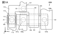
- FIG. 1A is a top view of a semiconductor device.
- FIG. 1B is a cross-sectional view of the semiconductor device.
- FIG. 1C is an equivalent circuit diagram of the semiconductor device.
- FIG. 1D is a timing chart of the semiconductor device.
- FIG. 1E is a circuit symbol of an inverter circuit.
- FIG. 2 is a cross-sectional view of the semiconductor device.
- FIG. 3A is a cross-sectional view of the semiconductor device.
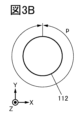
- FIG. 3B is a top view of the aperture.
- FIG. 3C is a cross-sectional view of the semiconductor device.
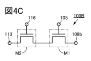
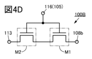
- FIG. 4A is a top view of the semiconductor device.
- FIG. 1A is a top view of a semiconductor device.
- FIG. 4B is a cross-sectional view of the semiconductor device.
- 4C and 4D are equivalent circuit diagrams
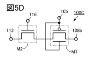
- FIG. 5A is a top view of the semiconductor device.
- FIG. 5B is a cross-sectional view of the semiconductor device.
- 5C and 5D are equivalent circuit diagrams of the semiconductor device.
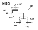
- FIG. 6A is a top view of the semiconductor device.
- FIG. 6B is a cross-sectional view of the semiconductor device.
- 6C and 6D are equivalent circuit diagrams of the semiconductor device.
- FIG. 7A is a top view of the semiconductor device.
- FIG. 8A is a top view of the semiconductor device.
- FIG. 8B is a cross-sectional view of the semiconductor device.
- 8C and 8D are equivalent circuit diagrams of the semiconductor device.
- FIG. 9A is a top view of the semiconductor device.
- FIG. 9B is a cross-sectional view of the semiconductor device.
- 9C and 9D are equivalent circuit diagrams of the semiconductor device.
- FIG. 10A is a top view of the semiconductor device.
- FIG. 10B is a cross-sectional view of the semiconductor device.
- 10C and 10D are equivalent circuit diagrams of the semiconductor device.
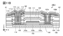
- FIG. 11A is a top view of a semiconductor device.
- FIG. 11B is a cross-sectional view of the semiconductor device.
- 11C and 11D are equivalent circuit diagrams of the semiconductor device.
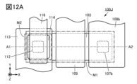
- FIG. 12A is a top view of a semiconductor device.
- FIG. 12B is a cross-sectional view of the semiconductor device.
- 12C and 12D are equivalent circuit diagrams of the semiconductor device.
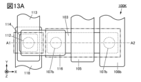
- FIG. 13A is a top view of the semiconductor device.
- FIG. 13B is a cross-sectional view of the semiconductor device.
- 13C and 13D are equivalent circuit diagrams of the semiconductor device.
- FIG. 14A is a top view of a semiconductor device.
- FIG. 14B is a cross-sectional view of the semiconductor device.
- 14C and 14D are equivalent circuit diagrams of the semiconductor device.
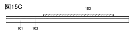
- 15A to 15E are diagrams illustrating a method for manufacturing a semiconductor device.
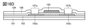
- 16A to 16D are diagrams illustrating a method for manufacturing a semiconductor device.
- 17A to 17D are diagrams illustrating a method for manufacturing a semiconductor device.
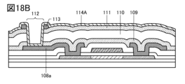
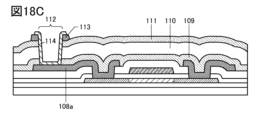
- 18A to 18C are diagrams illustrating a method for manufacturing a semiconductor device.
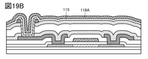
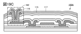
- 19A to 19C are diagrams illustrating a method for manufacturing a semiconductor device.
- FIG. 20A is a perspective view of the display device.
- FIG. 20B is a block diagram of a display device.
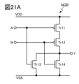
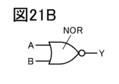
- 21A to 21F are diagrams illustrating configuration examples of logic circuits.
- 22A and 22B are diagrams illustrating configuration examples of D flip-flop circuits.
- FIG. 23 is a diagram illustrating a configuration example of a shift register circuit.
- 24A and 24B are circuit diagrams of latch circuits.
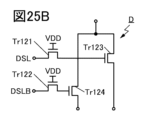
- 25A-25D are circuit diagrams of demultiplexer circuits.
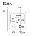
- 26A to 26D are circuit diagrams of pixel circuits.
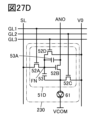
- 27A to 27D are circuit diagrams of pixel circuits.
- 28A and 28B are circuit diagrams of pixel circuits.
- 29A and 29B are circuit diagrams of pixel circuits.
- FIG. 30 is a diagram illustrating a configuration example of a pixel circuit.
- 31A to 31G are diagrams showing examples of pixels.
- 32A to 32K are diagrams showing examples of pixels.
- 33A to 33F are diagrams showing configuration examples of light emitting devices.
- 34A to 34C are diagrams showing configuration examples of light-emitting devices.
- 35A and 35B are diagrams showing configuration examples of a display device.
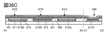
- 36A to 36D are diagrams showing configuration examples of display devices.
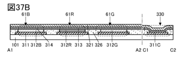
- 37A to 37C are diagrams showing configuration examples of display devices.
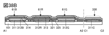
- 38A to 38D are diagrams showing configuration examples of display devices.
- 39A to 39F are diagrams showing configuration examples of display devices.
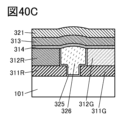
- 40A to 40F are diagrams showing configuration examples of display devices.
- 41A to 41F are diagrams illustrating examples of electronic devices.
- 42A to 42F are diagrams illustrating examples of electronic devices.
- the position, size, range, etc. of each configuration shown in the drawings may not represent the actual position, size, range, etc. in order to facilitate understanding of the invention. Therefore, the disclosed invention is not necessarily limited to the position, size, range, etc. disclosed in the drawings.
- a layer, a resist mask, and the like may be unintentionally reduced due to processing such as etching.
- top views also referred to as “plan views”
- perspective views descriptions of some components may be omitted in order to facilitate understanding of the invention. Also, description of some hidden lines may be omitted.
- ordinal numbers such as “first” and “second” are added to avoid confusion of constituent elements, and do not indicate any order or ranking such as the order of steps or the order of stacking.
- ordinal numbers used in the specification and the like may be different from the ordinal numbers used in the scope of claims.
- the ordinal number may be omitted in the scope of claims and the like.
- electrode and “wiring” in this specification and the like do not functionally limit these components.
- an “electrode” may be used as part of a “wiring” and vice versa.
- the terms “electrode” and “wiring” include the case where a plurality of “electrodes” and “wiring” are integrally provided.
- film and layer can be interchanged depending on the case or situation. For example, it may be possible to change the term “conductive layer” to the term “conductive film.” Or, for example, it may be possible to change the term “insulating film” to the term “insulating layer”.
- a transistor is an element having at least three terminals including a gate, a drain, and a source.
- a channel formation region is provided between the drain (drain terminal, drain region, or drain electrode) and the source (source terminal, source region, or source electrode). current can flow through the Note that in this specification and the like, a channel formation region means a region where current mainly flows.
- source and drain functions of a transistor may be interchanged, such as when employing transistors of different polarities or when the direction of current flow changes in circuit operation. Therefore, in this specification and the like, the terms “source” and “drain” can be used interchangeably.
- transistors described in this specification and the like are enhancement-type (normally-off) field-effect transistors unless otherwise specified.
- a transistor described in this specification and the like is an n-channel transistor, and the threshold voltage (also referred to as “Vth”) of the transistor is higher than 0 V unless otherwise specified.
- a transistor described in this specification and the like is a p-channel transistor and has a threshold voltage (also referred to as “Vth”) of 0 V or lower unless otherwise specified.
- an off-state current refers to a drain current (also referred to as “Id”) when a transistor is in an off state (also referred to as a non-conducting state or cutoff state).
- Id drain current
- Vg gate voltage
- the off-state current of an n-channel transistor sometimes refers to the drain current when Vg is lower than Vth.
- an off-state current sometimes refers to a current that flows between a source and a drain when a transistor is in an off state, for example.
- a high power supply potential VDD (hereinafter also simply referred to as “VDD” or “potential H”) indicates a power supply potential higher than the low power supply potential VSS.
- VDD high power supply potential
- VSS low power supply potential
- GND ground potential
- VSS voltage-senor ground potential or source potential
- electrode B on insulating layer A does not require that electrode B be formed on insulating layer A in direct contact with another configuration between insulating layer A and electrode B. Do not exclude those containing elements.
- electrode B overlapping the insulating layer A is not limited to the state in which the electrode B is formed on the insulating layer A, but the state in which the electrode B is formed under the insulating layer A or A state in which the electrode B is formed on the right (or left) side of the insulating layer A is not excluded.
- the terms “adjacent” and “adjacent” do not limit that components are in direct contact.
- electrode B adjacent to insulating layer A it is not necessary that insulating layer A and electrode B are formed in direct contact, and another component is provided between insulating layer A and electrode B. Do not exclude what is included.
- parallel means a state in which two straight lines are arranged at an angle of -10° or more and 10° or less. Therefore, the case of ⁇ 5° or more and 5° or less is also included.
- substantially parallel or “substantially parallel” refers to a state in which two straight lines are arranged at an angle of -30° or more and 30° or less.
- Perfect means that two straight lines are arranged at an angle of 80° or more and 100° or less. Therefore, the case of 85° or more and 95° or less is also included.
- arrows indicating the X direction, the Y direction, and the Z direction may be attached in the drawings and the like according to this specification.
- the “X direction” is the direction along the X axis, and the forward direction and the reverse direction may not be distinguished unless explicitly stated.
- the X direction, the Y direction, and the Z direction are directions that cross each other. More specifically, the X-direction, Y-direction, and Z-direction are directions orthogonal to each other.
- first direction or “first direction”
- second direction or a “second direction”
- third direction or “third direction”.
- the conductive layer 108 may be shown divided into a conductive layer 108a and a conductive layer 108b.
- FIG. 1A is a top view of a semiconductor device 100A.
- FIG. 1B is a schematic cross-sectional view of the portion indicated by the dashed-dotted line A1-A2 in FIG. 1A.
- FIG. 1C is an equivalent circuit diagram of the semiconductor device 100A.
- FIG. 2 is a schematic cross-sectional view of the portion indicated by the dashed-dotted line B1-B2-B3 in FIG. 1A.
- some constituent elements such as an insulating layer are omitted in order to facilitate understanding of the configuration of the semiconductor device.
- the semiconductor device 100A has a transistor M1 and a transistor M2.
- the transistor M1 is a p-channel transistor and the transistor M2 is an n-channel transistor.
- 3A and 3C are enlarged views of transistor M2 shown in FIG. 1B.
- FIG. 3B is a diagram of the opening 112 viewed from the Z direction.
- a semiconductor device 100A has an insulating layer 102 on a substrate 101 and a semiconductor layer 103 on the insulating layer 102 .
- An insulating layer 104 is provided over the insulating layer 102 and the semiconductor layer 103 .
- a conductive layer 105 is provided over the insulating layer 104 .
- the semiconductor layer 103 and the conductive layer 105 have regions that overlap each other.
- An insulating layer 106 is provided over the insulating layer 104 and the conductive layer 105 .
- An opening 107 a is provided in the insulating layer 104 and the insulating layer 106 in a region overlapping with part of the semiconductor layer 103 .
- An opening 107 b is provided in the insulating layer 104 and the insulating layer 106 in a region overlapping with another part of the semiconductor layer 103 .
- a conductive layer 108a is provided over the insulating layer 106 and the opening 107a, and a conductive layer 108b is provided over the insulating layer 106 and the opening 107b.
- Conductive layer 108a is electrically connected to semiconductor layer 103 at opening 107a.
- the conductive layer 108b is electrically connected to the semiconductor layer 103 through the opening 107b.
- the semiconductor layer 103 has a drain region 103a, a channel forming region 103b, and a source region 103c.
- a region overlapping with the conductive layer 105 functions as a channel formation region 103b. Therefore, the length of the channel formation region 103b in the X direction is the channel length L of the transistor M1 (see FIG. 1B).
- the length of the channel forming region 103b in the Y direction is the channel width W of the transistor M1 (see FIG. 2).
- the drain region 103a is electrically connected to the conductive layer 108a, and the source region 103c is electrically connected to the conductive layer 108b.
- an insulating layer 109 is provided over the insulating layer 106, the conductive layers 108a, and 108b, an insulating layer 110 is provided over the insulating layer 109, and an insulating layer 111 is provided over the insulating layer 110.
- a conductive layer 113 is provided over the insulating layer 111 .
- An opening 112 is provided in the conductive layer 113, the insulating layer 111, the insulating layer 110, and the insulating layer 109 in a region overlapping with part of the conductive layer 108a (see FIGS. 1B and 3A).
- a semiconductor layer 114 is provided over the opening 112 .
- the semiconductor layer 114 has a region that overlaps with the bottom of the opening 112 and a region that overlaps with the side surface of the opening 112 . Further, part of the semiconductor layer 114 is electrically connected to the conductive layer 113, and another part of the semiconductor layer 114 is electrically connected to the conductive layer 108a.
- An insulating layer 115 is provided over the insulating layer 111 , the conductive layer 113 , and the semiconductor layer 114 , and a conductive layer 116 is provided over the insulating layer 115 .
- An insulating layer 117 is provided over the insulating layer 115 and the conductive layer 116 .
- the insulating layer 115 has a region overlapping with the side surface of the opening 112 with the semiconductor layer 114 interposed therebetween.
- the conductive layer 116 has a region overlapping with the side surface of the opening 112 with the insulating layer 115 and the semiconductor layer 114 interposed therebetween.
- An opening 127 is provided in the insulating layer 115 , the insulating layer 111 , the insulating layer 110 , the insulating layer 109 , and the insulating layer 106 in a region overlapping with the conductive layer 105 .
- the conductive layer 105 and the conductive layer 116 are electrically connected in the opening 127 .
- the semiconductor layer 103 functions as a semiconductor layer in which the channel of the transistor M1 is formed, the insulating layer 104 functions as a gate insulating layer, and the conductive layer 105 functions as a gate electrode. Further, the conductive layer 108a functions as a drain electrode of the transistor M1, and the conductive layer 108b functions as a source electrode.
- the semiconductor layer 114 functions as a semiconductor layer in which a channel of the transistor M2 is formed, the insulating layer 115 functions as a gate insulating layer, and the conductive layer 116 functions as a gate electrode. Further, the conductive layer 108a functions as a drain electrode of the transistor M2, and the conductive layer 113 functions as a source electrode.
- the transistor M2 is provided in a region including the opening 112. FIG.
- Id flows in the Z direction (vertical direction). That is, Id flows along a direction perpendicular or substantially perpendicular to the substrate 101 surface.
- a transistor in which Id flows vertically is also called a “vertical channel transistor”.
- Id flows in the X direction (horizontal direction). That is, Id flows along a direction parallel or substantially parallel to the substrate 101 surface.
- a transistor in which Id flows in the horizontal direction is also called a “lateral channel transistor”.
- a transistor in which Id flows in the Y direction is also a "lateral channel transistor”.
- the vertical channel type transistor has the source electrode and the drain electrode arranged in the Z direction, the area occupied by the vertical channel type transistor can be significantly reduced compared to the horizontal channel type transistor.
- substrate There are no major restrictions on the material used for the substrate. Depending on the purpose, it may be determined by taking into consideration the presence or absence of translucency and the degree of heat resistance that can withstand heat treatment.
- glass substrates such as barium borosilicate glass and aluminoborosilicate glass, ceramic substrates, quartz substrates, and sapphire substrates can be used.
- a semiconductor substrate, a flexible substrate (flexible substrate), a laminated film, a base film, or the like may be used.
- Semiconductor substrates include, for example, semiconductor substrates made of silicon or germanium, or compound semiconductor substrates made of silicon carbide, silicon germanium, gallium arsenide, indium phosphide, zinc oxide, or gallium oxide.
- the semiconductor substrate may be a single crystal semiconductor or a polycrystalline semiconductor.
- Substrates for the case where the semiconductor device of one embodiment of the present invention is used for a display device include, for example, sixth generation (1500 mm ⁇ 1850 mm), seventh generation (1870 mm ⁇ 2200 mm), eighth generation (2200 mm ⁇ 2400 mm), and ninth generation substrates.
- a glass substrate having a large area such as (2400 mm ⁇ 2800 mm), 10th generation (2950 mm ⁇ 3400 mm), or the like can be used. Thereby, a large-sized display device can be manufactured.
- by increasing the size of the substrate more display devices can be produced from one substrate, and the production cost can be reduced.
- a flexible substrate, a bonding film, a base film, or the like may be used as the substrate in order to increase the flexibility of the semiconductor device.
- polyesters such as polyethylene terephthalate (PET) and polyethylene naphthalate (PEN), polyacrylonitrile, acrylic resins, polyimide, polymethyl methacrylate, polycarbonate ( PC), polyethersulfone (PES), polyamide (nylon, aramid, etc.), polysiloxane, cycloolefin, polystyrene, polyamideimide, polyurethane, polyvinyl chloride, polyvinylidene chloride, polypropylene, polytetrafluoroethylene (PTFE), ABS Resins, cellulose nanofibers, and the like can be used.
- PET polyethylene terephthalate
- PEN polyethylene naphthalate
- acrylic resins polyimide
- PC polymethyl methacrylate
- PC polycarbonate
- PES polyethersulfone
- polyamide nylon, aramid, etc.
- polysiloxane polystyrene
- polyamideimide polyurethane
- a lightweight semiconductor device can be provided. Further, by using the above material for the substrate, a semiconductor device that is resistant to impact can be provided. Further, by using the above material for the substrate, a semiconductor device that is less likely to be damaged can be provided.
- the flexible substrate used for the substrate preferably has a lower coefficient of linear expansion because deformation due to the environment is suppressed.
- a material having a coefficient of linear expansion of 1 ⁇ 10 ⁇ 3 /K or less, 5 ⁇ 10 ⁇ 5 /K or less, or 1 ⁇ 10 ⁇ 5 /K or less may be used.
- aramid is suitable as a flexible substrate because it has a low coefficient of linear expansion.
- Conductive layer Examples of conductive materials that can be used for conductive layers such as gate electrodes, source electrodes, and drain electrodes of transistors, as well as various wirings and electrodes that constitute semiconductor devices include aluminum (Al), chromium (Cr), and copper (Cu).
- alloys containing the above-mentioned metal elements as components, or the above-mentioned metal elements Combined alloys and the like can be used.
- a semiconductor typified by polycrystalline silicon containing an impurity element such as phosphorus, or a silicide such as nickel silicide may be used.
- a method for forming the conductive material is not particularly limited, and various forming methods such as a vapor deposition method, a CVD method, a sputtering method, and a spin coating method can be used.
- a Cu—X alloy (X is Mn, Ni, Cr, Fe, Co, Mo, Ta, or Ti) may also be applied as the conductive material.
- a layer formed of a Cu—X alloy can be processed by a wet etching process, so that manufacturing costs can be suppressed.
- an aluminum alloy containing one or more elements selected from titanium, tantalum, tungsten, molybdenum, chromium, neodymium, and scandium may be used as the conductive material.
- examples of conductive materials that can be used for the conductive layer include indium tin oxide, indium oxide containing tungsten oxide, indium zinc oxide containing tungsten oxide, indium oxide containing titanium oxide, and indium tin oxide containing titanium oxide.
- Oxygen-containing conductive materials such as oxides, indium zinc oxide, and indium tin oxide doped with silicon oxide can also be used.
- a conductive material containing nitrogen such as titanium nitride, tantalum nitride, or tungsten nitride can be used.
- the conductive layer can have a layered structure in which a conductive material containing oxygen, a conductive material containing nitrogen, and the above-described material containing a metal element are combined as appropriate.
- the conductive layer has a single-layer structure of an aluminum layer containing silicon, a two-layer structure of stacking a titanium layer on an aluminum layer, a two-layer structure of stacking a titanium layer on a titanium nitride layer, and a tungsten layer on a titanium nitride layer.
- the conductive layer may have a laminated structure in which the material containing the metal element described above and the conductive material containing oxygen are combined.
- a laminated structure may be employed in which the material containing the metal element described above and the conductive material containing nitrogen are combined.
- a laminated structure may be employed in which the material containing the metal element described above, the conductive material containing oxygen, and the conductive material containing nitrogen are combined.
- a conductive layer containing at least one of indium or zinc and oxygen is laminated on a conductive layer containing copper, and a conductive layer containing at least one of indium or zinc and oxygen is further laminated thereon. It is good also as a three-layer structure to carry out.
- the side surfaces of the conductive layer containing copper are also preferably covered with a conductive layer containing at least one of indium and zinc and oxygen.
- a plurality of conductive layers containing oxygen and at least one of indium and zinc may be stacked and used as the conductive layer.
- Each insulating layer includes aluminum nitride, aluminum oxide, aluminum nitride oxide, aluminum oxynitride, magnesium oxide, silicon nitride, silicon oxide, silicon nitride oxide, silicon oxynitride, gallium oxide, germanium oxide, yttrium oxide, zirconium oxide, and lanthanum oxide.
- neodymium oxide, hafnium oxide, tantalum oxide, aluminum silicate, etc. are used as a single layer or as a laminate.
- a material obtained by mixing a plurality of materials selected from oxide materials, nitride materials, oxynitride materials, and nitride oxide materials may be used.
- nitrided oxide refers to a material containing more nitrogen than oxygen.
- An oxynitride is a material containing more oxygen than nitrogen.
- the content of each element can be measured using, for example, Rutherford Backscattering Spectrometry (RBS).
- the insulating layer 102 and the insulating layer 117 are preferably formed using an insulating material through which impurities hardly permeate.
- Insulating materials containing, for example, boron, carbon, nitrogen, oxygen, fluorine, magnesium, aluminum, silicon, phosphorus, chlorine, argon, gallium, germanium, yttrium, zirconium, lanthanum, neodymium, hafnium or tantalum, in single layers, or Lamination may be used.
- Examples of insulating materials impermeable to impurities include aluminum oxide, aluminum nitride, aluminum oxynitride, aluminum oxynitride, gallium oxide, germanium oxide, yttrium oxide, zirconium oxide, lanthanum oxide, neodymium oxide, hafnium oxide, tantalum oxide, Silicon nitride etc. can be mentioned.
- the diffusion of impurities from the substrate 101 side can be suppressed, and the reliability of the semiconductor device can be improved.
- an insulating material through which impurities hardly permeate the insulating layer 117 By using an insulating material through which impurities hardly permeate the insulating layer 117, the diffusion of impurities from above the insulating layer 117 can be suppressed, and the reliability of the semiconductor device can be improved.
- an insulating material through which impurities do not easily permeate is preferably used for the insulating layer 106 .
- an insulating material through which impurities hardly permeate the insulating layer 106 the diffusion of impurities from below the insulating layer 106 can be suppressed, and the reliability of the semiconductor device can be improved.
- an insulating layer that can function as a planarization layer may be used as the insulating layer.
- a heat-resistant organic material such as polyimide, acrylic resin, benzocyclobutene resin, polyamide, or epoxy resin can be used.
- low dielectric constant materials low-k materials
- siloxane resins PSG (phosphorus glass), BPSG (boron boron glass), and the like can be used. Note that a plurality of insulating layers made of these materials may be stacked.
- the siloxane resin corresponds to a resin including a Si—O—Si bond formed using a siloxane-based material as a starting material.
- the siloxane resin may use an organic group (such as an alkyl group or an aryl group) or a fluoro group as a substituent. Moreover, the organic group may have a fluoro group.
- the surface of the insulating layer or the like may be subjected to CMP treatment.
- CMP treatment the unevenness of the surface of the sample can be reduced, and the coverage of the insulating layer and the conductive layer to be formed later can be improved.
- semiconductor layer For the semiconductor layers 103 and 114, a single crystal semiconductor, a polycrystalline semiconductor, a microcrystalline semiconductor, an amorphous semiconductor, or the like can be used alone or in combination.
- silicon, germanium, or the like can be used as the semiconductor material.
- Compound semiconductors such as silicon germanium, silicon carbide, gallium arsenide, and nitride semiconductors may also be used.
- an organic substance having semiconductor characteristics or a metal oxide having semiconductor characteristics also referred to as an oxide semiconductor
- These semiconductor materials may contain impurities as dopants.
- an oxide semiconductor has a bandgap of 2 eV or more
- a transistor in which an oxide semiconductor, which is a type of metal oxide, is used for a semiconductor layer in which a channel is formed also referred to as an "OS transistor"
- the OS transistor operates stably even in a high-temperature environment and has little characteristic variation.
- the off current hardly increases even in a high temperature environment.
- the off current hardly increases even under an environmental temperature of room temperature or higher and 200° C. or lower.
- the on-current is less likely to decrease even in a high-temperature environment. Therefore, a semiconductor device including an OS transistor can operate stably even in a high-temperature environment and have high reliability.
- a transistor in which silicon is used for a semiconductor layer in which a channel is formed (also referred to as a “Si transistor”) is used as the transistor M1.
- Si transistor a transistor in which silicon is used for a semiconductor layer in which a channel is formed
- the transistor M1 is used as a p-channel transistor.
- Silicon used for the semiconductor layer includes single crystal silicon, polycrystalline silicon, microcrystalline silicon, amorphous silicon, and the like.
- Examples of polycrystalline silicon include low temperature poly silicon (LTPS).
- a transistor using amorphous silicon for a semiconductor layer can be formed over a large glass substrate and manufactured at low cost.
- a transistor using polycrystalline silicon for a semiconductor layer has high field-effect mobility and can operate at high speed.
- a transistor using microcrystalline silicon for a semiconductor layer has higher field-effect mobility than a transistor using amorphous silicon and can operate at high speed.
- an OS transistor is used as the transistor M2. Since the OS transistor has high withstand voltage between the source and the drain, the channel length can be shortened. Therefore, the ON current can be increased.
- metal oxides that can be used for the semiconductor layer of the OS transistor include indium oxide, gallium oxide, and zinc oxide.
- the metal oxide preferably contains at least indium (In) or zinc (Zn).
- the metal oxide preferably contains two or three elements selected from indium, the element M, and zinc.
- Element M includes gallium, aluminum, silicon, boron, yttrium, tin, copper, vanadium, beryllium, titanium, iron, nickel, germanium, zirconium, molybdenum, lanthanum, cerium, neodymium, hafnium, tantalum, tungsten, cobalt, and magnesium.
- the element M is preferably one or more selected from aluminum, gallium, yttrium, and tin.
- indium tin oxide containing silicon, or the like can be used.
- Element M is preferably one or more selected from gallium, aluminum, yttrium, and tin.
- the element M is preferably gallium.
- composition of the metal oxide used for the semiconductor layer greatly affects the electrical characteristics and reliability of the OS transistor.
- a high on-current transistor can be realized by increasing the indium content of the metal oxide.
- a metal oxide in which the atomic ratio of indium is greater than or equal to that of zinc is preferably used.
- a metal oxide in which the atomic ratio of indium is higher than or equal to that of tin is preferably used.
- an In—Sn—Zn oxide is used for a semiconductor layer of an OS transistor
- a metal oxide in which the atomic ratio of indium is higher than that of tin can be used.
- a metal oxide in which the atomic ratio of zinc is higher than that of tin is preferable to use.
- an In—Al—Zn oxide is used for a semiconductor layer of an OS transistor
- a metal oxide in which the atomic ratio of indium is higher than that of aluminum can be used.
- a metal oxide in which the atomic ratio of zinc is higher than that of aluminum is preferable to use.
- a metal oxide in which the atomic ratio of indium to the atomic number of metal elements is higher than that of gallium can be used. Furthermore, it is more preferable to use a metal oxide in which the atomic ratio of zinc is higher than that of gallium.
- a metal oxide in which the atomic ratio of indium to the atomic number of the metal element is higher than that of the element M can be used. Furthermore, it is more preferable to use a metal oxide in which the atomic ratio of zinc is higher than the atomic ratio of the element M.
- the sum of the atomic ratios of the metal elements can be used as the atomic ratio of the element M.
- the atomic ratio of the element M can be the sum of the atomic ratio of gallium and the atomic ratio of aluminum.
- the atomic ratio of indium, the element M, and zinc is preferably within the above range.
- the ratio of the number of indium atoms to the number of atoms of the metal element contained in the metal oxide is 30 atomic % or more and 100 atomic % or less, preferably 30 atomic % or more and 95 atomic % or less, more preferably 35 atomic % or more and 95 atoms.
- the ratio of the number of indium atoms to the total number of atoms of indium, the element M, and zinc is preferably within the above range.
- the ratio of the number of indium atoms to the number of atoms of the contained metal element is sometimes referred to as the content of indium. The same applies to other metal elements.
- the transistor By increasing the indium content of the metal oxide, the transistor can have a large on-state current. By using the transistor, a circuit that can operate at high speed can be manufactured. Furthermore, it is possible to reduce the area occupied by the circuit. For example, when the transistor is applied to a large display device or a high-definition display device, signal delay in each wiring can be reduced and display unevenness can be suppressed even when the number of wirings is increased. . In addition, since the area occupied by the circuit can be reduced, the frame of the display device can be narrowed.
- Analysis of the composition of metal oxides can be performed, for example, by energy dispersive X-ray spectroscopy (EDX: Energy Dispersive X-ray spectroscopy), X-ray photoelectron spectroscopy (XPS: X-ray Photoelectron Spectroscopy), inductively coupled plasma mass spectroscopy.
- EDX Energy Dispersive X-ray spectroscopy
- XPS X-ray Photoelectron Spectroscopy
- ICP-MS Inductively Coupled Plasma-Mass Spectrometry
- ICP-AES Inductively Coupled Plasma-Atomic Emission Spectrometry
- a plurality of these techniques may be combined for analysis.
- the actual content rate and the content rate obtained by analysis may differ due to the influence of analysis accuracy. For example, when the content of element M is low, the content of element M obtained by analysis may be lower than the actual content.
- a sputtering method or an atomic layer deposition (ALD) method can be preferably used to form the metal oxide.
- the atomic ratio of the target may differ from the atomic ratio of the metal oxide.
- zinc may have a lower atomic ratio in the metal oxide than in the target.
- the atomic ratio of zinc contained in the target may be about 40% or more and 90% or less.
- GBT Gate Bias Temperature
- PBTS Positive Bias Temperature Stress
- NBTS Negative Bias Temperature Stress
- the PBTS test and the NBTS test which are performed under light irradiation, are called PBTIS (Positive Bias Temperature Illumination Stress) test and NBTIS (Negative Bias Temperature Illumination Stress) test, respectively.
- n-type transistor In an n-type transistor, a positive potential is applied to the gate when the transistor is turned on (a state in which current flows), so the amount of change in the threshold voltage in the PBTS test is an index of the reliability of the transistor. It is one of the important items to pay attention to.
- the transistor can have high reliability with respect to application of a positive bias. In other words, the transistor can have a small amount of change in threshold voltage in the PBTS test. Further, when a metal oxide containing gallium is used, the content of gallium is preferably lower than the content of indium. Accordingly, a highly reliable transistor can be realized.
- One factor of threshold voltage variation in the PBTS test is the defect level at or near the interface between the semiconductor layer and the gate insulating layer.
- a metal oxide in which the atomic ratio of indium is higher than the atomic ratio of gallium can be applied to the semiconductor layer.
- a metal oxide in which the atomic ratio of zinc is higher than the atomic ratio of gallium it is preferable to apply to the semiconductor layer a metal oxide that satisfies In>Ga and Zn>Ga in the atomic ratio of the metal element.
- the ratio of the number of gallium atoms to the number of atoms of the contained metal element is higher than 0 atomic % and 50 atomic % or less, preferably 0.1 atomic % or more and 40 atomic % or less, more preferably 0.1 atomic % or more and 35 atomic % or less, more preferably 0.1 atomic % or more and 30 atomic % or less, more preferably 0.1 atomic % or more and 25 atomic % or less, more preferably 0.1 atomic % or more and 20 atomic % % or less, more preferably 0.1 atomic % or more and 15 atomic % or less, more preferably 0.1 atomic % or more and 10 atomic % or less.
- the transistor can be highly resistant to the PBTS test.
- a metal oxide that does not contain gallium may be applied to the semiconductor layer of the OS transistor.
- In--Zn oxide can be applied to the semiconductor layer.
- the field-effect mobility of the transistor can be increased by increasing the atomic ratio of indium to the atomic number of the metal element contained in the metal oxide.
- the metal oxide becomes a highly crystalline metal oxide, which suppresses fluctuations in the electrical characteristics of the transistor and improves reliability. be able to.
- a metal oxide that does not contain gallium and zinc, such as indium oxide may be applied to the semiconductor layer. By using gallium-free metal oxides, in particular, threshold voltage variations in PBTS tests can be minimized.
- an oxide containing indium and zinc can be used for the semiconductor layer.
- gallium was used as a representative example, the present invention can also be applied to the case where the element M is used in place of gallium.
- a metal oxide in which the atomic ratio of indium is higher than the atomic ratio of the element M is preferably applied to the semiconductor layer.
- a metal oxide in which the atomic ratio of zinc is higher than the atomic ratio of the element M is preferable to use.
- the transistor By using a metal oxide with a low content of the element M for the semiconductor layer, the transistor can be highly reliable with respect to application of a positive bias. By applying the transistor to a transistor that requires high reliability against application of a positive bias, the semiconductor device can have high reliability.
- Light incident on the transistor might change the electrical characteristics of the transistor.
- a transistor applied to a region where light can enter have small variation in electrical characteristics under light irradiation and have high reliability against light. Reliability against light can be evaluated, for example, by the amount of change in threshold voltage in an NBTIS test.
- the transistor By increasing the content of the element M in the metal oxide used for the semiconductor layer, the transistor can have high reliability against light. That is, the transistor can have a small amount of change in threshold voltage in the NBTIS test. Specifically, a metal oxide in which the atomic ratio of the element M is equal to or higher than the atomic ratio of indium has a larger bandgap, and the variation of the threshold voltage in the NBTIS test of the transistor can be reduced. .
- the bandgap of the metal oxide of the semiconductor layer is preferably 2.0 eV or more, more preferably 2.5 eV or more, further preferably 3.0 eV or more, further preferably 3.2 eV or more, and 3.0 eV or more. 3 eV or more is preferable, 3.4 eV or more is preferable, and 3.5 eV or more is more preferable.
- the ratio of the number of atoms of the element M to the number of atoms of the metal element contained in the semiconductor layer is 20 atomic % or more and 70 atomic % or less, preferably 30 atomic % or more and 70 atomic % or less, more preferably 30 atomic %.
- a metal oxide having a content of 60 atomic % or more, more preferably 40 atomic % or more and 60 atomic % or less, more preferably 50 atomic % or more and 60 atomic % or less can be suitably used.
- a metal oxide in which the atomic ratio of indium to the atomic number of metal elements is equal to or lower than that of gallium can be used.
- the ratio of the number of atoms of gallium to the number of atoms of the metal element contained in the semiconductor layer is 20 atomic % or more and 60 atomic % or less, preferably 20 atomic % or more and 50 atomic % or less, more preferably 30 atomic % or more.
- a metal oxide having a content of 50 atomic % or less, more preferably 40 atomic % or more and 60 atomic % or less, more preferably 50 atomic % or more and 60 atomic % or less can be suitably used.
- the transistor By using a metal oxide with a high content of the element M for the semiconductor layer, the transistor can have high reliability against light. By applying the transistor to a transistor that requires high reliability against light, the semiconductor device can have high reliability.
- the electrical characteristics and reliability of the transistor differ depending on the composition of the metal oxide applied to the semiconductor layer. Therefore, by changing the composition of the metal oxide according to the electrical characteristics and reliability required for the transistor, a display device having both excellent electrical characteristics and high reliability can be obtained.
- the semiconductor layer may have a laminated structure having two or more metal oxide layers. Two or more metal oxide layers included in the semiconductor layer may have the same or substantially the same composition. By using a stacked structure of metal oxide layers having the same composition, for example, the same sputtering target can be used for formation, so that the manufacturing cost can be reduced.
- the two or more metal oxide layers included in the semiconductor layer may have different compositions.
- gallium or aluminum as the element M.
- a metal oxide layer having crystallinity is preferably used as the semiconductor layer.
- a metal oxide layer having a CAAC (c-axis aligned crystal) structure, a polycrystalline structure, a nano-crystal (nc) structure, or the like can be used.
- CAAC c-axis aligned crystal
- nc nano-crystal
- a metal oxide layer with low crystallinity a transistor through which large current can flow can be realized.
- a metal oxide layer with higher crystallinity can be formed as the ratio of the flow rate of oxygen gas to the total deposition gas used at the time of formation (hereinafter also referred to as the oxygen flow rate ratio) is higher.
- a semiconductor layer of the OS transistor may have a stacked structure of two or more metal oxide layers with different crystallinities.
- a stacked structure of a first metal oxide layer and a second metal oxide layer provided on the first metal oxide layer is used, and the second metal oxide layer is composed of the first metal oxide layer.
- a structure having a region with higher crystallinity than that of the oxide layer can be employed.
- the second metal oxide layer can have a region with lower crystallinity than the first metal oxide layer.
- Two or more metal oxide layers included in the semiconductor layer may have the same or substantially the same composition.
- the same sputtering target can be used for formation, so that the manufacturing cost can be reduced.
- a laminated structure of two or more metal oxide layers with different crystallinities can be formed. Note that two or more metal oxide layers included in the semiconductor layer may have different compositions.
- the channel length L of the transistor M2 described in this embodiment is determined by the thickness of the insulating layer provided between the conductive layer 113 and the conductive layer 108a. Therefore, a transistor with a short channel length can be manufactured with high accuracy. In addition, variations in characteristics among the plurality of transistors M2 are also reduced. Therefore, the operation of the semiconductor device using the transistor M2 is stabilized, and reliability can be improved. Further, when the variation in characteristics is reduced, the degree of freedom in circuit design of the semiconductor device is increased, and the operating voltage can be reduced. Therefore, power consumption of the semiconductor device can also be reduced.
- a material containing hydrogen is preferably used for the insulating layers 109 and 111 .
- the oxide semiconductor becomes n-type and can function as a source region or a drain region.
- silicon nitride containing hydrogen, silicon nitride oxide containing hydrogen, or the like may be used.
- the conductive layer 108 in contact with the semiconductor layer 114 and the conductive layer 113 in contact with the semiconductor layer 114 can be formed using a conductive material that makes the oxide semiconductor n-type.
- a conductive material containing nitrogen may be used.
- a conductive material containing titanium or tantalum and nitrogen may be used.
- another conductive material may be provided over the conductive material containing nitrogen.
- the insulating layer 110 it is preferable to use a material in which hydrogen is reduced and which contains oxygen.
- a material in which hydrogen is reduced and which contains oxygen For example, silicon oxide (SiOx) or the like may be used. Since hydrogen is an impurity element in an oxide semiconductor, contact between the semiconductor layer 114 which is an oxide semiconductor and the insulating layer 110 in which hydrogen is reduced makes it difficult to be n-type. Further, when the semiconductor layer 114 which is an oxide semiconductor is in contact with the insulating layer 110 containing oxygen, oxygen vacancies in the semiconductor layer 114 are reduced, the characteristics of the transistor M2 are stabilized, and reliability is improved.
- the insulating layer 110 preferably contains excess oxygen.
- excess oxygen oxygen released by heating
- a material containing excess oxygen it is preferable to use a material through which oxygen does not easily permeate the insulating layers 109 and 111 .
- a material that is difficult for oxygen to permeate for example, an oxide containing one or both of aluminum and hafnium, a nitride of silicon, or the like can be used.
- the thickness t of the insulating layer 110 corresponds to the channel length L of the transistor M2 (see FIG. 3A). Also, since the semiconductor layer 114 is provided in the opening 112, the outer peripheral length p of the opening 112 corresponds to the channel width W of the transistor M2 (see FIG. 3B). More specifically, the outer peripheral length p at the half (t/2) position of the thickness t of the insulating layer 110 corresponds to the channel width W of the transistor M2.
- the channel width W may be the outer peripheral length p of an arbitrary position of the opening 112, if necessary.
- the channel width W may be the peripheral length p of the bottom of the opening 112 , or the channel width W may be the peripheral length p of the top of the opening 112 .
- the insulating layer 109 and the insulating layer 111 may be formed using a material that does not contain hydrogen or that contains very little hydrogen.
- silicon nitride containing extremely little hydrogen, silicon nitride oxide containing extremely little hydrogen, or the like may be used.
- the region where the semiconductor layer 114 is in contact with the insulating layer 109 and the region where the semiconductor layer 114 is in contact with the insulating layer 111 are not made n-type. Therefore, the total thickness ts of the insulating layer 109, the insulating layer 110, and the insulating layer 111 corresponds to the channel length L of the transistor M2 (see FIG. 3C). Further, the outer peripheral length p at the half (ts/2) position of the thickness ts corresponds to the channel width W of the transistor M2.
- CMOS circuit with a reduced occupation area can be realized. That is, a semiconductor device with a reduced occupation area can be realized. Also, a CMOS circuit with reduced power consumption can be realized. That is, a semiconductor device with reduced power consumption can be realized. Also, a highly reliable CMOS circuit with little variation in characteristics can be realized. That is, it is possible to realize a highly reliable semiconductor device with little variation in characteristics.
- the conductive layer 116 is used as an input terminal (IN) by supplying a potential L (VSS) to the conductive layer 113 and supplying a potential H (VDD) to the conductive layer 108b. It functions as a CMOS inverting circuit (also referred to as an "inverter circuit” or a “NOT circuit”) using the conductive layer 108a as an output terminal (OUT) (see FIG. 1C).
- CMOS inverting circuit also referred to as an "inverter circuit” or a "NOT circuit”
- FIG. 1D is a timing chart showing an operation example of the semiconductor device 100A functioning as an inverter circuit.
- FIG. 1E shows the circuit symbol of the inverter circuit.
- FIG. 4A is a top view of the semiconductor device 100B.
- FIG. 4B is a schematic cross-sectional view of the portion indicated by the dashed-dotted line A1-A2 in FIG. 4A.
- FIG. 4C is an equivalent circuit diagram of the semiconductor device 100B.
- An n-channel transistor may be used as the transistor M1.
- an n-type semiconductor for the drain region 103a and the source region 103c of the semiconductor layer 103, an n-channel transistor M1 can be realized.
- the semiconductor device 100B uses an n-channel transistor as the transistor M1.
- an LDD (Lightly Doped Drain) region may be provided between the drain region 103a and the channel formation region 103b of the semiconductor layer 103 .
- LDD Lightly Doped Drain
- an LDD region may be provided not only between the drain region 103a and the channel formation region 103b but also between the source region 103c and the channel formation region 103b.
- FIGS. 4A to 4C shows an example in which the gate electrodes of the transistor M1 and the transistor M2 are not electrically connected, the gate electrodes may be electrically connected.
- FIG. 4D shows an equivalent circuit diagram of the semiconductor device 100B in which the gate electrodes of the transistor M1 and the transistor M2 are electrically connected.
- the transistor M1 and the transistor M2 can substantially function as one transistor. With such a structure, the withstand voltage between the source and the drain can be increased. In addition, off current can be reduced.
- FIG. 5A is a top view of the semiconductor device 100C.
- FIG. 5B is a schematic cross-sectional view of the portion indicated by the dashed-dotted line A1-A2 in FIG. 5A.
- 5C and 5D are equivalent circuit diagrams of the semiconductor device 100C.
- the semiconductor device 100C differs from the semiconductor devices 100A and 100B in having a conductive layer 119 between the substrate 101 and the insulating layer 102 .
- the conductive layer 119 functions as a backgate electrode of the transistor M1. Therefore, the conductive layer 119 preferably overlaps with the channel formation region 103b and extends beyond the end of the channel formation region 103b. That is, the conductive layer 119 is preferably larger than the channel formation region 103b. Also, the conductive layer 119 preferably extends beyond the edge of the semiconductor layer 103 . That is, the conductive layer 119 is preferably larger than the semiconductor layer 103 .
- the back gate electrode is arranged so that the channel formation region of the semiconductor layer is sandwiched between the gate electrode and the back gate electrode. Further, by changing the potential of the back gate electrode, the threshold voltage of the transistor can be changed.
- the potential of the back gate electrode may be the ground potential or any potential.
- the back gate electrode is formed of a conductive layer and can function similarly to the gate electrode.
- the potential of the back gate electrode may be the same as that of the gate electrode.
- FIG. 5D is an equivalent circuit diagram when the back gate electrode and gate electrode of the transistor M1 are electrically connected. Although the equivalent circuit diagrams shown in FIGS. 5C and 5D show the transistor M1 as a p-channel transistor, the transistor M1 may be an n-channel transistor.
- the back gate electrode may be formed using a material and method similar to those of the gate electrode, the source electrode, the drain electrode, and the like.
- the gate electrode and the back gate electrode are conductive layers, they have a function of preventing an electric field generated outside the transistor from acting on the semiconductor layer in which the channel is formed (particularly, an electric field shielding function against static electricity). That is, it is possible to prevent the electrical characteristics of the transistor from varying due to the influence of an external electric field such as static electricity.
- the amount of change in the threshold voltage of the transistor before and after a BT (Bias Temperature) stress test can be reduced by providing the back gate electrode. By providing the back gate electrode, variation in characteristics of the transistor can be reduced, and reliability of the semiconductor device can be improved.
- FIG. 6A is a top view of the semiconductor device 100D.
- FIG. 6B is a schematic cross-sectional view of the portion indicated by the dashed-dotted line A1-A2 in FIG. 6A.
- 6C and 6D are equivalent circuit diagrams of the semiconductor device 100D.
- the semiconductor device 100D differs from the semiconductor device 100A in that the opening 112 overlaps with the conductive layer 105 functioning as the gate electrode of the transistor M1. Therefore, in the semiconductor device 100D, the transistor M2 is provided so as to overlap the gate electrode of the transistor M1.
- opening 112 is formed by selectively removing part of each of conductive layer 113 , insulating layer 111 , insulating layer 110 , insulating layer 109 , and insulating layer 106 in a region overlapping conductive layer 105 . be.
- the opening 112 is provided so as to overlap with the channel forming region 103b, but the present invention is not limited to this.
- the opening 112 may be provided so as not to overlap with the channel formation region 103 b and overlap with the conductive layer 105 .
- the conductive layer 105 functions as the gate electrode of the transistor M1 and functions as the drain electrode of the transistor M2.
- the transistor M1 may be an n-channel transistor as shown in the equivalent circuit diagram of FIG. 6D.
- FIG. 7A is a top view of the semiconductor device 100E.
- FIG. 7B is a schematic cross-sectional view of the portion indicated by the dashed-dotted line A1-A2 in FIG. 7A.
- 7C and 7D are equivalent circuit diagrams of the semiconductor device 100E.
- the semiconductor device 100E differs from the semiconductor device 100D in that it has a conductive layer 119 between the substrate 101 and the insulating layer 102, like the semiconductor device 100C.
- the conductive layer 119 functions as the back gate electrode of the transistor M1. By providing the back gate electrode, variation in characteristics of the transistor can be reduced, and reliability of the semiconductor device can be improved.
- the transistor M1 may be an n-channel transistor as shown in the equivalent circuit diagram of FIG. 7D.
- the back gate electrode and the gate electrode of the transistor M1 are electrically connected, but the back gate electrode is not electrically connected to the gate electrode, and an arbitrary potential is applied to the back gate electrode. may be supplied.
- FIG. 8A is a top view of the semiconductor device 100F.
- FIG. 8B is a schematic cross-sectional view of the portion indicated by the dashed-dotted line A1-A2 in FIG. 8A.
- 8C and 8D are equivalent circuit diagrams of the semiconductor device 100F.
- Semiconductor device 100F differs from semiconductor device 100D in the configuration of opening 107 (opening 107a, opening 107b) and conductive layer 108 (conductive layer 108a, conductive layer 108b).
- the opening 107a is formed by selectively removing a part of each of the insulating layers 111, 110, 109, 106, and 104 in a region overlapping the drain region 103a of the semiconductor layer 103. formed by Further, in the semiconductor device 100F, the opening 107b selectively partially forms each of the insulating layers 111, 110, 109, 106, and 104 in the region overlapping with the source region 103c of the semiconductor layer 103. formed by removing the
- the conductive layer 108a is provided on the insulating layer 111 and electrically connected to the drain region 103a at the bottom of the opening 107a.
- the conductive layer 108b is provided on the insulating layer 111 and electrically connected to the source region 103c at the bottom of the opening 107b.
- the conductive layer 108 and the conductive layer 113 can be formed simultaneously using the same material and in the same manufacturing process. Since the conductive layer 108 and the conductive layer 113 do not need to be formed separately, the manufacturing process of the semiconductor device can be shortened and the productivity of the semiconductor device can be improved.
- the transistor M1 may be an n-channel transistor as shown in the equivalent circuit diagram of FIG. 8D.
- FIG. 9A is a top view of the semiconductor device 100G.
- FIG. 9B is a schematic cross-sectional view of the portion indicated by the dashed-dotted line A1-A2 in FIG. 9A.
- 9C and 9D are equivalent circuit diagrams of the semiconductor device 100G.
- the semiconductor device 100G differs from the semiconductor device 100F in that the insulating layer 106 is not provided. Formation of the insulating layer 106 may be omitted by using an insulating material through which impurities do not easily permeate for the insulating layer 109 . Since the insulating layer 106 is not provided, the number of layers to be removed when forming the openings (such as the openings 107a, 107b, and 112) is reduced. can.
- FIG. 10A is a top view of the semiconductor device 100H.
- FIG. 10B is a schematic cross-sectional view of the portion indicated by the dashed-dotted line A1-A2 in FIG. 10A.
- 10C and 10D are equivalent circuit diagrams of the semiconductor device 100H.
- the semiconductor device 100H differs from the semiconductor device 100A in that the transistor M2 is overlapped with the drain region 103a.
- the opening 112 is provided so as to overlap with the drain region 103a. Therefore, the semiconductor device 100H has a region where the transistor M1 and the transistor M2 overlap each other.
- the semiconductor layer 114 has a region overlapping with the semiconductor layer 103 . More specifically, the drain region 103a that is part of the semiconductor layer 103 and the semiconductor layer 114 have regions that overlap with each other with the conductive layer 108a interposed therebetween.
- a conductive layer 119 functioning as a back gate electrode may be provided between the substrate 101 and the insulating layer 102.
- FIG. 10C the transistor M1 may be an n-channel transistor as shown in FIG. 10D.
- FIG. 11A is a top view of the semiconductor device 100I.
- FIG. 11B is a schematic cross-sectional view of the portion indicated by the dashed-dotted line A1-A2 in FIG. 11A.
- 11C and 11D are equivalent circuit diagrams of the semiconductor device 100I.
- the semiconductor device 100I differs from the semiconductor device 100H in that it does not have a conductive layer 108a. In the semiconductor device 100I, it can be said that the opening 112 also serves as the opening 107a.
- the semiconductor device 100I has a region where the semiconductor layer 114 and the semiconductor layer 103 overlap. In addition, in the semiconductor device 100I, the semiconductor layer 114 and the semiconductor layer 103 are directly connected at the bottom of the opening 112 .
- opening 107b is provided so as to penetrate a part of insulating layer 104, insulating layer 106, insulating layer 109, insulating layer 110, and insulating layer 111, respectively.
- the conductive layer 108b is provided in the opening 107b and on the insulating layer 111 in the semiconductor device 100I.
- Opening 107b is formed by selectively removing a portion of insulating layer 104, insulating layer 106, insulating layer 109, insulating layer 110, and insulating layer 111 in a region overlapping with source region 103c.
- Conductive layer 108b provided on insulating layer 111 is electrically connected to source region 103c of semiconductor layer 103 at the bottom of opening 107b.
- the semiconductor layers 103 and 114 are in contact with each other at the bottom of the opening 112, the semiconductor layers 103 and 114 preferably contain common elements.
- the semiconductor layer 103 and the semiconductor layer 114 contain a common element, contact resistance can be reduced.
- an oxide semiconductor may be used for both the semiconductor layer 103 and the semiconductor layer 114 .
- FIG. 11C shows transistor M1 as a p-channel transistor
- transistor M1 may be an n-channel transistor as shown in FIG. 11D.
- FIG. 12A is a top view of the semiconductor device 100J.
- FIG. 12B is a schematic cross-sectional view of the portion indicated by the dashed-dotted line A1-A2 in FIG. 12A.
- 12C and 12D are equivalent circuit diagrams of the semiconductor device 100J.
- the semiconductor device 100J differs from the semiconductor device 100I in that the insulating layer 106 is not provided. Formation of the insulating layer 106 may be omitted by using an insulating material through which impurities do not easily permeate for the insulating layer 109 . Since the insulating layer 106 is not provided, the number of layers to be removed when forming the openings (such as the opening 107b and the opening 112) is reduced, so that the number of manufacturing steps of the semiconductor device can be shortened and the productivity of the semiconductor device can be improved.
- FIG. 13A is a top view of the semiconductor device 100K.
- FIG. 13B is a schematic cross-sectional view of the portion indicated by the dashed-dotted line A1-A2 in FIG. 13A.
- 13C and 13D are equivalent circuit diagrams of the semiconductor device 100K.
- the semiconductor device 100K has a conductive layer 118 on the insulating layer 104 .
- a transistor M2 is formed in a region different from the region in which the transistor M1 is formed on the substrate 101.
- FIG. Transistor M2 includes at least a portion of conductive layer 118 .
- the conductive layer 113 functions as the source electrode of the transistor M2
- the conductive layer 118 functions as the drain electrode.
- the conductive layer 118 functions as the source electrode.
- the conductive layer 118 can be formed at the same time using the same material as the conductive layer 105 in the same manufacturing process. Further, in semiconductor device 100K, opening 112 is provided in a part of each of conductive layer 113, insulating layer 111, insulating layer 110, insulating layer 109, and insulating layer . In the semiconductor device 100K, the insulating layer 115, the insulating layer 111, the insulating layer 110, the insulating layer 109, the insulating layer 106, and the insulating layer 104 are partially provided with the opening 107a, and the other portions are provided with the opening 107b. is provided.
- a portion of conductive layer 116 provided on insulating layer 115 covers opening 107a and is electrically connected to drain region 103a at the bottom of opening 107a.
- the conductive layer 108b of the semiconductor device 100K can be formed simultaneously with the conductive layer 116 using the same material and by the same manufacturing method. Conductive layer 108b is electrically connected to source region 103c at the bottom of opening 107b.
- the conductive layer 116 in the semiconductor device 100K functions not only as the gate electrode of the transistor M2, but also as the drain electrode.
- a conductive layer 119 functioning as a back gate electrode may be provided between the substrate 101 and the insulating layer 102.
- FIG. 13C the transistor M1 may be an n-channel transistor as shown in FIG. 13D.
- FIG. 14A is a top view of the semiconductor device 100L.
- FIG. 14B is a schematic cross-sectional view of the portion indicated by the dashed-dotted line A1-A2 in FIG. 14A.
- 14C and 14D are equivalent circuit diagrams of the semiconductor device 100L.
- the semiconductor device 100L differs from the semiconductor device 100K in that the insulating layer 106 is not provided. Formation of the insulating layer 106 may be omitted by using an insulating material through which impurities do not easily permeate for the insulating layer 109 . Since the insulating layer 106 is not provided, the number of layers to be removed when forming the openings (such as the opening 107b and the opening 112) is reduced, so that the number of manufacturing steps of the semiconductor device can be shortened and the productivity of the semiconductor device can be improved.
- An insulating layer, a semiconductor layer, a conductive layer for forming an electrode or wiring, etc. are formed by a sputtering method, a chemical vapor deposition (CVD) method, a vacuum deposition method, a pulsed laser deposition (PLD) method. , an atomic layer deposition (ALD) method, or the like.
- the CVD method may be a plasma-enhanced chemical vapor deposition (PECVD) method or a thermal CVD method. Examples of thermal CVD methods include metal organic chemical vapor deposition (MOCVD) methods.
- the insulating layer, semiconductor layer, conductive layer, etc. that make up the semiconductor device are coated by spin coating, dip coating, spray coating, inkjet, dispensing, screen printing, offset printing, slit coating, roll coating, curtain coating, knife coating, and the like. You may form by a method.
- the PECVD method provides high quality films at relatively low temperatures.
- a deposition method that does not use plasma for deposition such as MOCVD, ALD, or thermal CVD
- the formation surface is less likely to be damaged.
- wiring, electrodes, elements (transistors, capacitive elements, etc.) included in a semiconductor device may be charged up by receiving charges from plasma. At this time, the accumulated charges may destroy wiring, electrodes, elements, and the like included in the semiconductor device.
- a film formation method that does not use plasma since such plasma damage does not occur, the yield of semiconductor devices can be increased. Moreover, since plasma damage does not occur during film formation, a film with few defects can be obtained.
- the CVD method and the ALD method are film forming methods in which a film is formed by a reaction on the surface of the object to be processed, unlike film forming methods in which particles emitted from a target or the like are deposited. Therefore, it is a film forming method which is not easily affected by the shape of the object to be processed and which has good step coverage.
- the ALD method has excellent step coverage and excellent thickness uniformity, and is therefore suitable for coating the surface of an opening with a high aspect ratio.
- the ALD method since the ALD method has a relatively slow film formation rate, it may be preferable to use it in combination with another film formation method, such as the CVD method, which has a high film formation rate.
- the composition of the film obtained can be controlled by the flow rate ratio of the raw material gases.
- the CVD method and the ALD method it is possible to form a film of any composition depending on the flow rate ratio of source gases.
- the CVD method and the ALD method it is possible to form a film whose composition is continuously changed by changing the flow rate ratio of the source gases while forming the film.
- the time required for film formation can be shortened by the time required for transport and pressure adjustment, compared to the case of film formation using a plurality of film formation chambers. can. Therefore, productivity of semiconductor devices can be improved in some cases.
- a photolithography method or the like can be used when processing a layer (thin film) constituting a semiconductor device.
- an island-shaped layer may be formed by a film formation method using a shielding mask.
- the layer may be processed by a nanoimprint method, a sandblast method, a lift-off method, or the like.
- a photolithography method a resist mask is formed on a layer (thin film) to be processed, a part of the layer (thin film) is selectively removed using the resist mask as a mask, and then the resist mask is removed. and a method of forming a layer having photosensitivity and then exposing and developing the layer to process the layer into a desired shape.
- the light used for exposure can be, for example, i-line (wavelength 365 nm), g-line (wavelength 436 nm), h-line (wavelength 405 nm), or a mixture thereof.
- ultraviolet light, KrF laser light, ArF laser light, or the like can also be used.
- extreme ultraviolet (EUV: Extreme Ultra-violet) light or X-rays may be used.
- An electron beam can also be used instead of the light used for exposure. The use of extreme ultraviolet light, X-rays, or electron beams is preferable because extremely fine processing is possible.
- a photomask is not necessary when exposure is performed by scanning a beam such as an electron beam.
- a dry etching method, a wet etching method, a sandblasting method, or the like can be used for removing (etching) the layer (thin film). Also, these etching methods may be used in combination.
- the insulating layer 102 is provided on the substrate 101, and the semiconductor layer 103A is provided on the insulating layer 102 (see FIG. 15A).
- an insulating substrate having an insulating surface is used as the substrate 101.
- insulator substrates include glass substrates, quartz substrates, sapphire substrates, stabilized zirconia substrates (yttria stabilized zirconia substrates, etc.), resin substrates, and the like.
- a semiconductor substrate or a conductor substrate may be used as the substrate 101 as necessary.
- semiconductor substrates include semiconductor substrates such as silicon and germanium, and compound semiconductor substrates made of silicon carbide, silicon germanium, gallium arsenide, indium phosphide, zinc oxide, and gallium oxide.
- semiconductor substrates having an insulator region inside the semiconductor substrate, such as an SOI (Silicon On Insulator) substrate.
- SOI Silicon On Insulator
- conductive substrates include graphite substrates, metal substrates, alloy substrates, and conductive resin substrates.
- a substrate in which a conductor or a semiconductor is provided on an insulating substrate a substrate in which a semiconductor substrate is provided with a conductor or an insulator, a substrate in which a conductor substrate is provided with a semiconductor or an insulator, and the like.
- these substrates provided with elements may be used.
- Elements provided on the substrate include a capacitive element, a resistance element, a switch element, a light emitting element, a memory element, and the like.
- Insulating layer 102 is formed as the insulating layer 102 over the substrate 101 .
- Insulating layers that can be used in the semiconductor device 100A include insulating oxides, nitrides, oxynitrides, oxynitrides, metal oxides, metal oxynitrides, metal oxynitrides, and the like.
- the insulating layer with a low relative dielectric constant includes silicon oxide, silicon oxynitride, silicon nitride oxide, silicon nitride, silicon oxide to which fluorine is added, silicon oxide to which carbon is added, silicon oxide to which carbon and nitrogen are added, and vacancies. There are silicon oxide, resin, and the like.
- a nitrided oxide refers to a compound containing more nitrogen than oxygen.
- An oxynitride is a compound containing more oxygen than nitrogen.
- the content of each element can be measured using, for example, Rutherford Backscattering Spectrometry (RBS).
- Amorphous silicon is formed as the semiconductor layer 103A.
- the semiconductor layer 103A is preferably heated at 400 to 550° C. for several hours for dehydrogenation to reduce the amount of hydrogen contained to 5 atom % or less, and then the subsequent crystallization process is preferably performed.
- the amorphous semiconductor film may be formed by another manufacturing method such as a sputtering method or a vacuum deposition method, but it is desirable to sufficiently reduce impurity elements such as oxygen and nitrogen contained in the film.
- the semiconductor used for the semiconductor layer 103A is not limited to silicon, and for example, silicon germanium can be used.
- silicon germanium the concentration of germanium is preferably about 0.01 to 4.5 atomic %.
- the insulating layer 102 and the semiconductor layer 103A may be formed continuously without being exposed to the atmosphere in the middle.
- the insulating layer 102 and the semiconductor layer 103A may be formed continuously without being exposed to the atmosphere in the middle.
- surface contamination due to exposure to the atmosphere can be suppressed as much as possible, and variations in characteristics of manufactured transistors can be reduced.
- the semiconductor layer 103A is crystallized to form a semiconductor layer 103B having crystallinity (see FIG. 15B).
- a laser annealing method, a thermal annealing method (solid phase growth method), or a rapid thermal annealing method (RTA method) can be applied as a method for increasing the crystallinity (also referred to as “crystallization”) of the semiconductor layer 103A.
- RTA method rapid thermal annealing method
- the laser annealing method for example, an excimer laser light using XeCl, a second harmonic or a third harmonic of a YAG laser, or the like can be used.
- an infrared lamp, a halogen lamp, a metal halide lamp, a xenon lamp, or the like is used as a light source.
- the semiconductor layer 103B having crystallinity may be formed by a crystallization method using a catalyst element according to the technique disclosed in Japanese Patent Application Laid-Open No. 7-130652, for example.
- the semiconductor layer 103A may be crystallized by combining the above methods.
- the semiconductor layer 103B with few defects and high crystallinity can be formed by crystallizing the semiconductor layer 103A by a solid phase growth method and then irradiating it with laser light.
- the semiconductor layer 103A is crystallized using laser annealing. Specifically, the semiconductor layer 103A having a hydrogen content of 5 atom % or less is irradiated with the laser light 151 to form the semiconductor layer 103B.
- an impurity element that turns the semiconductor layer 103A into a p-type semiconductor also referred to as “p-type impurity element” or an impurity element that turns the semiconductor layer 103A into an n-type semiconductor (“n-type impurity element”).
- p-type impurity element also referred to as "p-type impurity element”
- n-type impurity element an impurity element that turns the semiconductor layer 103A into an n-type semiconductor
- Channel doping may be performed on the entire semiconductor layer 103A, or may be selectively performed on a part of the semiconductor layer 103A.
- the p-type impurity element for example, one or a plurality of elements selected from group 13 elements such as boron (B), aluminum (Al), and gallium (Ga) can be used.
- group 13 elements such as boron (B), aluminum (Al), and gallium (Ga)
- group 15 elements such as phosphorus (P) or arsenic (As) can be used.
- the threshold voltage of a transistor including the semiconductor layer can be controlled. For example, by adding boron to a semiconductor layer at a concentration of 1 ⁇ 10 16 atoms/cm 3 to 5 ⁇ 10 17 atoms/cm 3 , the threshold voltage of a transistor including the semiconductor layer is changed in the positive direction. be able to.
- an enhancement type (normally-off type) transistor and a depression type (normally-on type) transistor can be produced separately.
- a resist mask is formed over the semiconductor layer 103B by photolithography (not shown). Using the resist mask as a mask, the semiconductor layer 103B is selectively removed to form the semiconductor layer 103 (see FIG. 15C).
- an insulating layer 104 is formed over the insulating layer 102 and the semiconductor layer 103 .
- the insulating layer 104 can be formed with the same material and method as the insulating layer 102 (see FIG. 15D).
- microwave treatment is preferably performed in an oxygen-containing atmosphere after the insulating layer 104 is formed.
- the microwave treatment refers to treatment using an apparatus having a power supply for generating high-density plasma using microwaves, for example.
- microwaves refer to electromagnetic waves having a frequency of 300 MHz or more and 300 GHz or less.
- the frequency of the microwave processing device may be 300 MHz or more and 300 GHz or less, preferably 2.4 GHz or more and 2.5 GHz or less, for example, 2.45 GHz.
- High-density oxygen radicals can be generated by using high-density plasma.
- the power of the power source for applying microwaves in the microwave processing apparatus may be 1000 W or more and 10000 W or less, preferably 2000 W or more and 5000 W or less.
- the microwave processing apparatus may have a power supply for applying RF to the substrate side. Further, by applying RF to the substrate side, oxygen ions generated by high-density plasma can be efficiently guided into the oxide semiconductor.
- the above microwave treatment is preferably performed under reduced pressure, and the pressure may be 10 Pa or more and 1000 Pa or less, preferably 300 Pa or more and 700 Pa or less.
- the treatment temperature may be 750°C or lower, preferably 500°C or lower, for example, about 250°C.
- heat treatment may be continuously performed without exposure to the outside air.
- the temperature may be 100° C. or higher and 750° C. or lower, preferably 300° C. or higher and 500° C. or lower.
- the microwave treatment may be performed using oxygen gas and argon gas.
- the oxygen flow rate ratio (O 2 /(O 2 +Ar)) should be greater than 0% and 100% or less.
- the oxygen flow ratio (O 2 /(O 2 +Ar)) should be greater than 0% and 50% or less.
- the oxygen flow ratio (O 2 /(O 2 +Ar)) should be 10% or more and 40% or less.
- the oxygen flow ratio (O 2 /(O 2 +Ar)) should be 10% or more and 30% or less.
- a conductive layer 105A is formed over the insulating layer 104 (see FIG. 15E).
- tantalum nitride titanium nitride, tungsten, nitride containing titanium and aluminum, nitride containing tantalum and aluminum, ruthenium oxide, ruthenium nitride, oxide containing strontium and ruthenium, oxide containing lanthanum and nickel, and the like are used. is preferred.
- a plurality of conductive layers formed using any of the above materials may be stacked and used.
- a laminated structure in which the material containing the metal element described above and the conductive material containing oxygen are combined may be used.
- a laminated structure may be employed in which the material containing the metal element described above and the conductive material containing nitrogen are combined.
- a laminated structure may be employed in which the material containing the metal element described above, the conductive material containing oxygen, and the conductive material containing nitrogen are combined.
- a resist mask is formed over the conductive layer 105A by photolithography (not shown). Using the resist mask as a mask, the conductive layer 105A is selectively removed to form the conductive layer 105 (see FIG. 16A).
- an impurity element is introduced into the semiconductor layer 103 in order to form a drain region 103a, a channel forming region 103b, and a source region 103c in the semiconductor layer 103.
- an impurity element (dopant 128) is introduced into the semiconductor layer 103 using the conductive layer 105 as a mask (see FIG. 16B).
- the dopant 128 can be introduced by a method such as ion implantation or plasma doping.
- a rare gas element, carbon, nitrogen, or the like may be used as the dopant 128 .
- the dopant 128 is not introduced into the region of the semiconductor layer 103 overlapping the conductive layer 105 .
- a dopant 128 is introduced into a region of the semiconductor layer 103 that does not overlap with the conductive layer 105 .
- a region overlapping with the conductive layer 105 and into which the dopant 128 is not introduced functions as a channel formation region 103b.
- the region into which the dopant 128 is introduced functions as the drain region 103a or the source region 103c.
- the channel formation region 103b is formed by self-alignment. Also, the concentration distribution in the depth direction of the dopant 128 and the concentration of the metal element can be determined by the processing method and processing conditions.
- boron (B) which is one of Group 13 elements, is used as the dopant 128 for making the transistor M1 a p-channel transistor.
- an element of Group 15 for example, phosphorus (P) may be used as the dopant 128 for making the transistor M1 an n-channel transistor.
- heat treatment is performed.
- the heat treatment activates the introduced impurity element and recrystallizes the amorphous portion of the semiconductor layer 103 due to the introduction of the impurity element.
- the heat treatment is also referred to as activation treatment.
- the hydrogenation treatment is a treatment in which hydrogen excited by heat treatment or plasma treatment is added to the semiconductor layer 103.
- the heat treatment is performed in an atmosphere containing 3 to 100% hydrogen at 300 to 450° C. for 2 to 6 hours.
- a heat treatment step may be performed.
- an insulating layer 106 is formed over the insulating layer 104 and the conductive layer 105 (see FIG. 16C). Since the insulating layer 106 functions as an interlayer insulating layer, a material with a low dielectric constant may be used.
- an insulating material through which impurities hardly permeate is preferably used for the insulating layer 106 .
- an insulating material through which impurities hardly permeate the insulating layer 106 the diffusion of impurities from below the insulating layer 106 can be suppressed, and the reliability of the semiconductor device can be improved. For example, diffusion of hydrogen contained in the transistor M1 side to the transistor M2 side can be prevented.
- a resist mask is formed over the insulating layer 106 by photolithography (not shown).
- portions of the insulating layer 106 and the insulating layer 104 are selectively removed to form an opening 107a overlapping with the drain region 103a and an opening 107b overlapping with the source region 103c (see FIG. 16D).
- a portion of the drain region 103a is exposed at the bottom of the opening 107a, and a portion of the source region 103c is exposed at the bottom of the opening 107b.
- the side surface of the insulating layer 106 and the side surface of the insulating layer 104 are exposed at the openings 107a and 107b.
- a conductive layer 108 A is formed over the insulating layer 106 .
- the conductive layer 108A may be formed using a material and method similar to those of the conductive layer 105A (see FIG. 17A).
- a resist mask is formed over the conductive layer 108A by photolithography (not shown).
- the conductive layer 108A is selectively removed to form the conductive layer 108 (conductive layers 108a and 108b) (see FIG. 17B).
- Conductive layer 108a is electrically connected to drain region 103a at opening 107a
- conductive layer 108b is electrically connected to source region 103c at opening 107b.
- Transistor M1 can be formed in this manner.
- an insulating layer 109, an insulating layer 110, an insulating layer 111, and a conductive layer 113A are formed in this order over the insulating layer 106 and the conductive layer 108 (see FIG. 17C).
- the insulating layers 109 and 111 are formed using an insulating material containing hydrogen. For example, silicon nitride containing hydrogen is used.
- the insulating layer 110 is formed using an insulating material with reduced hydrogen.
- silicon oxide or silicon oxynitride may be used. Note that the insulating layer 110 preferably contains excess oxygen.
- the conductive layer 113A may be formed using a material and a method similar to those of the conductive layer 105A or the conductive layer 108A.
- a resist mask is formed over the conductive layer 113A by a photolithography method (not shown). Using the resist mask as a mask, the conductive layer 113A is selectively removed to form the conductive layer 113 (see FIG. 17D).
- a resist mask is formed over the insulating layer 111 by photolithography (not shown).
- part of each of the conductive layer 113, the insulating layer 111, the insulating layer 110, and the insulating layer 109 is selectively removed to form an opening 112 in a region overlapping with the conductive layer 108a (FIG. 18A).
- Part of the conductive layer 108a is exposed at the bottom of the opening 112 .
- the side surface of the insulating layer 111, the side surface of the insulating layer 110, and the side surface of the insulating layer 109 are exposed.
- a semiconductor layer 114A which later becomes the semiconductor layer 114 of the transistor M2, is formed over the insulating layer 111 (see FIG. 18B).
- an oxide semiconductor is formed as the semiconductor layer 114A.
- Oxide semiconductors include, for example, indium and M (M is gallium, aluminum, silicon, boron, yttrium, tin, copper, vanadium, beryllium, titanium, iron, nickel, germanium, zirconium, molybdenum, lanthanum, cerium, neodymium , hafnium, tantalum, tungsten, and magnesium) and zinc.
- M is preferably one or more selected from aluminum, gallium, yttrium, and tin.
- an oxide containing indium (In), gallium (Ga), and zinc (Zn) is preferably used for the semiconductor layer of the OS transistor.
- an oxide containing indium (In), aluminum (Al), and zinc (Zn) also referred to as “IAZO” may be used for the semiconductor layer.
- an oxide containing indium (In), aluminum (Al), gallium (Ga), and zinc (Zn) also referred to as “IAGZO”
- an oxide containing indium (In), gallium (Ga), zinc (Zn), and tin (Sn) also referred to as “IGZTO” may be used for the semiconductor layer.
- the In atomic ratio in the In-M-Zn oxide is preferably equal to or higher than the M atomic ratio.
- the semiconductor layer 114A is formed to cover not only the insulating layer 111 but also the inner surface of the opening 112 . Therefore, the semiconductor layer 114A is preferably formed by a film formation method with good step coverage. For example, the semiconductor layer 114A is preferably formed by ALD.
- a resist mask is formed over the semiconductor layer 114A by photolithography (not shown). Using the resist mask as a mask, part of the semiconductor layer 114A is selectively removed to form the semiconductor layer 114 (see FIG. 18C).
- the semiconductor layer 114 has a region in contact with the conductive layer 113, a region in contact with the insulating layer 111, a region in contact with the insulating layer 110, a region in contact with the insulating layer 109, and a region in contact with the conductive layer 108a. More specifically, in the opening 112 , the semiconductor layer 114 has a region in contact with the side surface of the conductive layer 113 , a region in contact with the side surface of the insulating layer 111 , a region in contact with the side surface of the insulating layer 110 , and a side surface of the insulating layer 109 . and a region in contact with the conductive layer 108 a at the bottom of the opening 112 .
- an insulating layer 115 is formed over the insulating layer 111, the conductive layer 113, and the semiconductor layer 114 (see FIG. 19A).
- the insulating layer 115 functions as a gate insulating layer of the transistor M2. Since an oxide semiconductor is used as the semiconductor layer 114 in this embodiment and the like, an insulating layer containing excess oxygen is preferably used as the insulating layer 115 .
- microwave treatment is preferably performed in the above atmosphere containing oxygen after the insulating layer 115 is formed.
- a resist mask is formed over the insulating layer 115 by a photolithography method. A portion of each of insulating layer 109 and insulating layer 106 is selectively removed to form opening 127 (not shown). A portion of the conductive layer 105 is exposed at the bottom of the opening 127 .
- a conductive layer 116A is formed over the insulating layer 115 (see FIG. 19B).
- a resist mask is formed over the conductive layer 116A by a photolithography method (not shown). Using the resist mask as a mask, part of the conductive layer 116A is selectively removed to form the conductive layer 116 (see FIG. 19C). Transistor M2 can be formed in this way.
- conductive layer 116 functions as the gate electrode of transistor M2.
- the conductive layer 116 is electrically connected to the conductive layer 105 through the opening 127 (see FIG. 2).
- an insulating layer 117 is formed over the insulating layer 115 and the conductive layer 116 (see FIG. 19C).
- the semiconductor device 100A can be formed.
- a metal oxide used for an OS transistor preferably contains at least indium or zinc, more preferably indium and zinc.
- metal oxides include indium and M (where M is gallium, aluminum, yttrium, tin, silicon, boron, copper, vanadium, beryllium, titanium, iron, nickel, germanium, zirconium, molybdenum, lanthanum, cerium, neodymium). , hafnium, tantalum, tungsten, magnesium, and cobalt) and zinc.
- M is preferably one or more selected from gallium, aluminum, yttrium and tin, more preferably gallium.
- the metal oxide is formed by chemical vapor deposition (CVD) such as sputtering, metal organic chemical vapor deposition (MOCVD), or atomic layer deposition (ALD). ) method or the like.
- CVD chemical vapor deposition
- MOCVD metal organic chemical vapor deposition
- ALD atomic layer deposition
- an oxide containing indium (In), gallium (Ga), and zinc (Zn) will be described as an example of a metal oxide.
- an oxide containing indium (In), gallium (Ga), and zinc (Zn) is sometimes called an In--Ga--Zn oxide.
- Crystal structures of oxide semiconductors include amorphous (including completely amorphous), CAAC (c-axis-aligned crystalline), nc (nanocrystalline), CAC (cloud-aligned composite), single crystal, and polycrystal. (poly crystal) and the like.
- the crystal structure of the film or substrate can be evaluated using an X-ray diffraction (XRD) spectrum.
- XRD X-ray diffraction
- it can be evaluated using an XRD spectrum obtained by GIXD (Grazing-Incidence XRD) measurement.
- the GIXD method is also called a thin film method or a Seemann-Bohlin method.
- the XRD spectrum obtained by the GIXD measurement may be simply referred to as the XRD spectrum.
- the peak shape of the XRD spectrum is almost symmetrical.
- the shape of the peak of the XRD spectrum is left-right asymmetric.
- the asymmetric shape of the peaks in the XRD spectra demonstrates the presence of crystals in the film or substrate. In other words, the film or substrate cannot be said to be in an amorphous state unless the shape of the peaks in the XRD spectrum is symmetrical.
- the crystal structure of the film or substrate can be evaluated by a diffraction pattern (also referred to as a nanobeam electron diffraction pattern) observed by nano beam electron diffraction (NBED).
- a diffraction pattern also referred to as a nanobeam electron diffraction pattern
- NBED nano beam electron diffraction
- a halo is observed in the diffraction pattern of a quartz glass substrate, and it can be confirmed that the quartz glass is in an amorphous state.
- a spot-like pattern is observed instead of a halo. For this reason, it is presumed that it cannot be concluded that the In-Ga-Zn oxide deposited at room temperature is in an intermediate state, neither single crystal nor polycrystal, nor amorphous state, and is in an amorphous state. be done.
- oxide semiconductors may be classified differently from the above when their structures are focused. For example, oxide semiconductors are classified into single-crystal oxide semiconductors and non-single-crystal oxide semiconductors.
- Non-single-crystal oxide semiconductors include, for example, the above CAAC-OS and nc-OS.
- Non-single-crystal oxide semiconductors include polycrystalline oxide semiconductors, amorphous-like oxide semiconductors (a-like OS), amorphous oxide semiconductors, and the like.
- CAAC-OS is an oxide semiconductor that includes a plurality of crystal regions, and the c-axes of the plurality of crystal regions are oriented in a specific direction. Note that the specific direction is the thickness direction of the CAAC-OS film, the normal direction to the formation surface of the CAAC-OS film, or the normal direction to the surface of the CAAC-OS film.
- a crystalline region is a region having periodicity in atomic arrangement. If the atomic arrangement is regarded as a lattice arrangement, the crystalline region is also a region with a uniform lattice arrangement.
- CAAC-OS has a region where a plurality of crystal regions are connected in the a-b plane direction, and the region may have strain.
- the strain refers to a portion where the orientation of the lattice arrangement changes between a region with a uniform lattice arrangement and another region with a uniform lattice arrangement in a region where a plurality of crystal regions are connected. That is, CAAC-OS is an oxide semiconductor that is c-axis oriented and has no obvious orientation in the ab plane direction.
- each of the plurality of crystal regions is composed of one or a plurality of minute crystals (crystals having a maximum diameter of less than 10 nm).
- the maximum diameter of the crystalline region is less than 10 nm.
- the maximum diameter of the crystal region may be about several tens of nanometers.
- the CAAC-OS includes a layer containing indium (In) and oxygen (hereinafter referred to as an In layer) and a layer containing gallium (Ga), zinc (Zn) and oxygen (
- an In layer a layer containing indium (In) and oxygen
- Ga gallium
- Zn zinc
- oxygen it tends to have a layered crystal structure (also referred to as a layered structure) in which (Ga, Zn) layers are laminated.
- the (Ga, Zn) layer may contain indium.
- the In layer may contain gallium.
- the In layer may contain zinc.
- the layered structure is observed as a lattice image in, for example, a high-resolution TEM (Transmission Electron Microscope) image.
- a plurality of bright points are observed in the electron beam diffraction pattern of the CAAC-OS film.
- a certain spot and another spot are observed at point-symmetrical positions with respect to the spot of the incident electron beam that has passed through the sample (also referred to as a direct spot) as the center of symmetry.
- the lattice arrangement in the crystal region is basically a hexagonal lattice, but the unit lattice is not always regular hexagon and may be non-regular hexagon. Moreover, the distortion may have a lattice arrangement of pentagons, heptagons, or the like. Note that in CAAC-OS, no clear crystal grain boundary can be observed even near the strain. That is, it can be seen that the distortion of the lattice arrangement suppresses the formation of grain boundaries. This is because the CAAC-OS can tolerate strain due to the fact that the arrangement of oxygen atoms is not dense in the ab plane direction, the bond distance between atoms changes due to the substitution of metal atoms, and the like. It is considered to be for
- a crystal structure in which clear grain boundaries are confirmed is called a so-called polycrystal.
- a grain boundary becomes a recombination center, and there is a high possibility that carriers are trapped and cause a decrease in the on-state current of a transistor, a decrease in field-effect mobility, and the like. Therefore, a CAAC-OS in which no clear grain boundaries are observed is one of crystalline oxides having a crystal structure suitable for a semiconductor layer of a transistor.
- a structure containing Zn is preferable for forming a CAAC-OS.
- In--Zn oxide and In--Ga--Zn oxide are preferable because they can suppress the generation of grain boundaries more than In oxide.
- a CAAC-OS is an oxide semiconductor with high crystallinity and no clear grain boundaries. Therefore, it can be said that the decrease in electron mobility due to grain boundaries is less likely to occur in CAAC-OS.
- the CAAC-OS can be said to be an oxide semiconductor with few impurities and defects (such as oxygen vacancies). Therefore, an oxide semiconductor including CAAC-OS has stable physical properties. Therefore, an oxide semiconductor including CAAC-OS is resistant to heat and has high reliability.
- CAAC-OS is also stable against high temperatures (so-called thermal budget) in the manufacturing process. Therefore, the use of the CAAC-OS for the OS transistor can increase the degree of freedom in the manufacturing process.
- nc-OS has periodic atomic arrangement in a minute region (eg, a region of 1 nm to 10 nm, particularly a region of 1 nm to 3 nm).
- the nc-OS has minute crystals.
- the size of the minute crystal is, for example, 1 nm or more and 10 nm or less, particularly 1 nm or more and 3 nm or less, the minute crystal is also called a nanocrystal.
- nc-OS does not show regularity in crystal orientation between different nanocrystals. Therefore, no orientation is observed in the entire film.
- an nc-OS may be indistinguishable from an a-like OS and an amorphous oxide semiconductor depending on the analysis method.
- an nc-OS film is subjected to structural analysis using an XRD apparatus, out-of-plane XRD measurement using ⁇ /2 ⁇ scanning does not detect a peak indicating crystallinity.
- an nc-OS film is subjected to electron beam diffraction (also referred to as selected area electron beam diffraction) using an electron beam with a probe diameter larger than that of nanocrystals (for example, 50 nm or more), a diffraction pattern such as a halo pattern is obtained. is observed.
- an nc-OS film is subjected to electron diffraction (also referred to as nanobeam electron diffraction) using an electron beam with a probe diameter close to or smaller than the size of a nanocrystal (for example, 1 nm or more and 30 nm or less)
- an electron beam diffraction pattern is obtained in which a plurality of spots are observed within a ring-shaped area centered on the direct spot.
- An a-like OS is an oxide semiconductor having a structure between an nc-OS and an amorphous oxide semiconductor.
- An a-like OS has void or low density regions. That is, a-like OS has lower crystallinity than nc-OS and CAAC-OS. In addition, the a-like OS has a higher hydrogen concentration in the film than the nc-OS and the CAAC-OS.
- CAC-OS relates to material composition.
- CAC-OS is, for example, one structure of a material in which elements constituting a metal oxide are unevenly distributed with a size of 0.5 nm or more and 10 nm or less, preferably 1 nm or more and 3 nm or less, or in the vicinity thereof.
- the metal oxide one or more metal elements are unevenly distributed, and the region having the metal element has a size of 0.5 nm or more and 10 nm or less, preferably 1 nm or more and 3 nm or less, or a size in the vicinity thereof.
- the mixed state is also called mosaic or patch.
- CAC-OS is a structure in which the material is separated into a first region and a second region to form a mosaic shape, and the first region is distributed in the film (hereinafter, also referred to as a cloud shape). ). That is, CAC-OS is a composite metal oxide in which the first region and the second region are mixed.
- the atomic ratios of In, Ga, and Zn to the metal elements constituting the CAC-OS in the In—Ga—Zn oxide are represented by [In], [Ga], and [Zn], respectively.
- the first region is a region where [In] is larger than [In] in the composition of the CAC-OS film.
- the second region is a region where [Ga] is greater than [Ga] in the composition of the CAC-OS film.
- the first region is a region in which [In] is larger than [In] in the second region and [Ga] is smaller than [Ga] in the second region.
- the second region is a region in which [Ga] is larger than [Ga] in the first region and [In] is smaller than [In] in the first region.
- the first region is a region mainly composed of indium oxide, indium zinc oxide, or the like.
- the second region is a region containing gallium oxide, gallium zinc oxide, or the like as a main component. That is, the first region can be rephrased as a region containing In as a main component. Also, the second region can be rephrased as a region containing Ga as a main component.
- the CAC-OS in the In—Ga—Zn oxide means a region containing Ga as a main component and a region containing In as a main component in a material structure containing In, Ga, Zn, and O. Each region is a mosaic, and refers to a configuration in which these regions exist randomly. Therefore, CAC-OS is presumed to have a structure in which metal elements are unevenly distributed.
- the CAC-OS can be formed, for example, by a sputtering method under conditions in which the substrate is not intentionally heated.
- a sputtering method one or more selected from an inert gas (typically argon), oxygen gas, and nitrogen gas may be used as the film forming gas. good.
- the flow rate ratio of the oxygen gas to the total flow rate of the film forming gas during film formation is preferably as low as possible.
- the flow ratio of the oxygen gas to the total flow rate of the film forming gas during film formation is 0% or more and less than 30%, preferably 0% or more and 10% or less.
- an EDX mapping obtained using energy dispersive X-ray spectroscopy shows that a region containing In as a main component It can be confirmed that the (first region) and the region (second region) containing Ga as the main component are unevenly distributed and have a mixed structure.
- the first region is a region with higher conductivity than the second region. That is, when carriers flow through the first region, conductivity as a metal oxide is developed. Therefore, by distributing the first region in the form of a cloud in the metal oxide, a high field effect mobility ( ⁇ ) can be realized.
- the second region is a region with higher insulation than the first region.
- the leakage current can be suppressed by distributing the second region in the metal oxide.
- CAC-OS when used for a transistor, the conductivity caused by the first region and the insulation caused by the second region act complementarily to provide a switching function (on/off). functions) can be given to the CAC-OS.
- a part of the material has a conductive function
- a part of the material has an insulating function
- the whole material has a semiconductor function.
- CAC-OS is most suitable for various semiconductor devices including display devices.
- Oxide semiconductors have various structures and each has different characteristics.
- An oxide semiconductor of one embodiment of the present invention includes two or more of an amorphous oxide semiconductor, a polycrystalline oxide semiconductor, an a-like OS, a CAC-OS, an nc-OS, and a CAAC-OS. may
- an oxide containing indium (In), gallium (Ga), and zinc (Zn) is preferably used for a semiconductor layer in which a channel is formed.
- an oxide containing indium (In), aluminum (Al), and zinc (Zn) also referred to as “IAZO” may be used for the semiconductor layer.
- an oxide containing indium (In), aluminum (Al), gallium (Ga), and zinc (Zn) also referred to as “IAGZO” may be used for the semiconductor layer.
- an oxide semiconductor with low carrier concentration is preferably used for a transistor.
- the carrier concentration of the oxide semiconductor is 1 ⁇ 10 17 cm ⁇ 3 or less, preferably 1 ⁇ 10 15 cm ⁇ 3 or less, more preferably 1 ⁇ 10 13 cm ⁇ 3 or less, more preferably 1 ⁇ 10 11 cm ⁇ 3 or less . 3 or less, more preferably less than 1 ⁇ 10 10 cm ⁇ 3 and 1 ⁇ 10 ⁇ 9 cm ⁇ 3 or more.
- the impurity concentration in the oxide semiconductor film may be lowered to lower the defect level density.
- a low impurity concentration and a low defect level density are referred to as high-purity intrinsic or substantially high-purity intrinsic.
- an oxide semiconductor with a low carrier concentration is sometimes referred to as a highly purified intrinsic or substantially highly purified intrinsic oxide semiconductor.
- the trap level density may also be low.
- a charge trapped in a trap level of an oxide semiconductor takes a long time to disappear and may behave like a fixed charge. Therefore, a transistor whose channel formation region is formed in an oxide semiconductor with a high trap level density might have unstable electrical characteristics.
- Impurities include hydrogen, nitrogen, alkali metals, alkaline earth metals, iron, nickel, silicon, and the like.
- the impurities in the oxide semiconductor refer to, for example, substances other than the main components of the oxide semiconductor. For example, an element whose concentration is less than 0.1 atomic percent can be said to be an impurity.
- the concentration of silicon or carbon in the oxide semiconductor is 2 ⁇ 10 atoms/cm or less, preferably 2 ⁇ 10 17 atoms/cm 3 or less.
- the concentration of alkali metal or alkaline earth metal in the oxide semiconductor obtained by SIMS is set to 1 ⁇ 10 18 atoms/cm 3 or less, preferably 2 ⁇ 10 16 atoms/cm 3 or less.
- the nitrogen concentration in the oxide semiconductor obtained by SIMS is less than 5 ⁇ 10 19 atoms/cm 3 , preferably 5 ⁇ 10 18 atoms/cm 3 or less, more preferably 1 ⁇ 10 18 atoms/cm 3 or less. , more preferably 5 ⁇ 10 17 atoms/cm 3 or less.
- Hydrogen contained in an oxide semiconductor reacts with oxygen that bonds to a metal atom to form water, which may cause oxygen vacancies. When hydrogen enters the oxygen vacancies, electrons, which are carriers, may be generated. In addition, part of hydrogen may bond with oxygen that bonds with a metal atom to generate an electron, which is a carrier. Therefore, a transistor including an oxide semiconductor containing hydrogen is likely to have normally-on characteristics. Therefore, hydrogen in the oxide semiconductor is preferably reduced as much as possible. Specifically, the hydrogen concentration in the oxide semiconductor obtained by SIMS is less than 1 ⁇ 10 20 atoms/cm 3 , preferably less than 1 ⁇ 10 19 atoms/cm 3 , more preferably 5 ⁇ 10 18 atoms/cm. Less than 3 , more preferably less than 1 ⁇ 10 18 atoms/cm 3 .
- FIG. 20A shows a perspective view of the display device 200. As shown in FIG. The display device 200 has a configuration in which a substrate 152 and a substrate 101 are bonded together. In FIG. 20A, substrate 152 is clearly indicated by dashed lines.
- the display device 200 includes a display portion 235, a connection portion 140, a first driver circuit portion 231, a second driver circuit portion 232, wirings 165, and the like.
- FIG. 20A shows an example in which an IC 173 and an FPC 172 are mounted on the display device 200.
- FIG. Therefore, the configuration shown in FIG. 20A can also be said to be a display module including the display device 200, an IC (integrated circuit), and an FPC.
- the connecting portion 140 is provided outside the display portion 235 .
- the connection portion 140 can be provided along one side or a plurality of sides of the display portion 235 .
- the number of connection parts 140 may be singular or plural.
- FIG. 20A shows an example in which connecting portions 140 are provided so as to surround the four sides of the display portion.
- the connection part 140 the common electrode of the light emitting device and the conductive layer are electrically connected, and a potential can be supplied to the common electrode.
- the wiring 165 has a function of supplying signals and power to the display portion 235 , the first driver circuit portion 231 , and the second driver circuit portion 232 .
- the signal and power are input to the wiring 165 from the outside through the FPC 172 or input to the wiring 165 from the IC 173 .
- FIG. 20A shows an example in which an IC 173 is provided on the substrate 101 by a COG (Chip On Glass) method, a COF (Chip On Film) method, or the like.
- the IC 173 may have, for example, a scanning line driver circuit or a signal line driver circuit.
- the display device 200 and the display module may be configured without an IC.
- the IC may be mounted on the FPC by the COF method or the like.
- the display unit 235 has a plurality of pixels 230 arranged in a matrix of m rows (m is an integer of 1 or more) and n columns (n is an integer of 1 or more). Also, the plurality of pixels 230 are classified into, for example, a pixel 230a, a pixel 230b, and a pixel 230c. Pixel 230a, pixel 230b, and pixel 230c have the function of exhibiting light of different colors. For example, the pixel 230a has a function of emitting red (R) light, the pixel 230b has a function of emitting green (G) light, and the pixel 230c has a function of emitting blue (B) light. good too.
- R red
- G green
- B blue
- the pixel 230a has a function of emitting yellow (Y) light
- the pixel 230b has a function of emitting cyan (C) light
- the pixel 230c has a function of emitting magenta (M) light.
- a full-color display can be realized by configuring one pixel 240 with one pixel 230a, one pixel 230b, and one pixel 230c.
- pixel 230 functions as a sub-pixel.
- the display device 200 shown in FIG. 20A shows an example in which pixels 230 functioning as sub-pixels are arranged in a stripe arrangement.
- the number of sub-pixels forming one pixel 240 is not limited to three, and may be four or more. For example, it may have four sub-pixels exhibiting R, G, B, and white (W) lights. Alternatively, it may have four sub-pixels that emit light of four colors of R, G, B, and Y.
- FIG. 20B is a block diagram illustrating the display device 200.
- the display device 200 has a display section 235 , a first drive circuit section 231 and a second drive circuit section 232 .
- the pixel 230 of the 1st row and n column is indicated as a pixel 230[1,n]
- the pixel 230 of the mth row and the 1st column is indicated as a pixel 230[m,1]
- the pixel 230 of the mth row and nth column is indicated as a pixel 230[m,1].
- pixel 230[m,n] an arbitrary pixel 230 included in the display unit 235 may be indicated as a pixel 230[r, s].
- r is an integer of 1 or more and m or less
- s is an integer of 1 or more and n or less.
- a circuit included in the first drive circuit section 231 functions, for example, as a scanning line drive circuit.
- a circuit included in the second drive circuit unit 232 functions, for example, as a signal line drive circuit. Some circuit may be provided at a position facing the first drive circuit section 231 with the display section 235 interposed therebetween. Some kind of circuit may be provided at a position facing the second drive circuit section 232 with the display section 235 interposed therebetween. Circuits included in the first drive circuit section 231 and the second drive circuit section 232 are collectively referred to as a peripheral drive circuit 233 .
- Various circuits such as a shift register circuit, a level shifter circuit, an inverter circuit, a latch circuit, an analog switch circuit, a multiplexer circuit, a demultiplexer circuit, and a logic circuit can be used for the peripheral driver circuit 233 .
- a transistor, a capacitor, or the like can be used for the peripheral driver circuit 233 .
- a transistor included in the peripheral driver circuit 233 may be formed in the same process as a transistor included in the pixel 230 .
- the display device 200 has m wirings 236 which are arranged substantially parallel to each other and whose potentials are controlled by circuits included in the first driving circuit section 231, and are arranged substantially parallel to each other, It also has n wirings 237 whose potentials are controlled by a circuit included in the second driver circuit portion 232 .
- FIG. 20B shows an example in which the wiring 236 and the wiring 237 are connected to the pixel 230 .
- the wiring 236 and the wiring 237 are only examples, and the wiring connected to the pixel 230 is not limited to the wiring 236 and the wiring 237 .
- Example of circuit configuration> A configuration example of a NOR circuit and a NAND circuit will be described as an example of a logic circuit to which a semiconductor device according to one embodiment of the present invention can be applied.
- FIG. 21A is a circuit diagram showing a configuration example of a 2-input 1-output NOR circuit (NOR). Also, FIG. 21B shows a circuit symbol of the NOR circuit.
- the NOR circuit shown in FIG. 21A has a transistor Tr11, a transistor Tr12, a transistor Tr13, and a transistor Tr14. P-channel transistors are used for the transistors Tr11 and Tr12, and n-channel transistors are used for the transistors Tr13 and Tr14.
- the transistor M1 can be used as the transistor Tr11 and the transistor Tr12. Further, the transistor M2 can be used as the transistor Tr13 and the transistor Tr14.
- the NOR circuit shown in FIGS. 21A and 21B has a function of outputting a potential H (VDD) from a terminal Y when a potential L (VSS) is input to both terminals A and B.
- FIG. Further, it has a function of outputting a potential L (VSS) from the terminal Y when a potential H (VDD) is input to one or both of the terminal A and the terminal B.
- an OR circuit can be realized by combining an inverter circuit (INV) with a NOR circuit.
- FIG. 21D is a circuit diagram showing a configuration example of a 2-input 1-output NAND circuit (NAND). Also, FIG. 21E shows the circuit symbol of the NAND circuit.
- the NAND circuit shown in FIG. 21D has a transistor Tr21, a transistor Tr22, a transistor Tr23, and a transistor Tr24. P-channel transistors are used for the transistors Tr21 and Tr22, and n-channel transistors are used for the transistors Tr23 and Tr24.
- the transistor M1 can be used as the transistor Tr21 and the transistor Tr22. Further, the transistor M2 can be used as the transistor Tr23 and the transistor Tr24.
- the NAND circuits illustrated in FIGS. 21D and 21E have a function of outputting a potential L (VSS) from a terminal Y when a potential H (VDD) is input to both terminals A and B.
- FIG. Further, it has a function of outputting a potential H (VDD) from the terminal Y when a potential L (VSS) is input to one or both of the terminal A and the terminal B.
- an AND circuit can be realized by combining an inverter circuit (INV) with a NAND circuit.
- DFF Delay Flip Flop
- FIG. 22A is a circuit diagram showing a configuration example of a D flip-flop circuit (DFF). Also, FIG. 22B shows the circuit symbol of the D flip-flop circuit.
- the D flip-flop circuit shown in FIG. 22A has transistors Tr61 to Tr69, Tr71 to Tr79, Tr81, Tr82, Tr91, and Tr92. P-channel transistors are used for the transistors Tr61 to Tr69, Tr81 and Tr82, and n-channel transistors are used for the transistors Tr71 to Tr79, Tr91 and Tr92.
- the transistor M1 can be used as the transistors Tr61 to Tr69, Tr81, and Tr82. Further, the transistor M2 can be used as the transistors Tr71 to Tr79, Tr91, and Tr92.
- the DFF shown in FIGS. 22A and 22B has a clock signal input terminal CK, an input terminal D, and an output terminal Q.
- FIG. In the DFF shown in FIGS. 22A and 22B information (potential) of the input terminal D is written while the potential H is being input to the clock signal input terminal CK, and the signal input to the clock signal input terminal CK is at the potential H. to the potential L, the information is held until the potential H is input to the clock signal input terminal CK next time. Also, from the output terminal Q, a signal (potential H or potential L) based on the information held by the DFF is always output.
- FIG. 23 is a block diagram showing a configuration example of a shift register circuit (SR).
- the SR is composed of multiple DFFs.
- the first-stage (first) DFF is indicated as “DFF[1]”
- the potential (data) output from the output terminal Q of DFF[1] is indicated as “data OUT[1]. ]”.
- FIG. 23 shows a block diagram of an SR including four stages (four) of DFFs (DFF[1] to DFF[4]).
- the data output from the output terminals Q of DFF[1] to DFF[4] are indicated as data OUT[1] to data OUT[4].
- Data OUT[1] is input to input terminal D of DFF[2]
- data OUT[2] is input to input terminal D of DFF[3]
- data OUT[3] is input to input terminal D of DFF[4].
- a signal SPL is input to the input terminal D of DFF[1].
- the signal SPL input to DFF[1] is sequentially transferred to subsequent DFFs in synchronization with the clock signal CLK.
- the data OUT has a value according to the data held by the DFF. Also, the timing at which the value of data OUT changes is synchronized with the clock signal CLK.
- SR can sequentially switch data OUT output from a plurality of DFFs in synchronization with clock signal CLK.
- a configuration example of a latch circuit LAT will be described as an example of a circuit to which a semiconductor device according to one embodiment of the present invention can be applied.
- FIG. 24A is a circuit diagram showing a configuration example of the latch circuit LAT.
- the latch circuit LAT shown in FIG. 24A has a transistor Tr31, a transistor Tr33, a transistor Tr35, a transistor Tr36, a capacitor C31, and an inverter circuit INV1.
- a node N is a node to which one of the source and drain of the transistor Tr33, the gate of the transistor Tr35, and one electrode of the capacitor C31 are electrically connected.
- the transistor Tr33 is turned on.
- the potential of the node N becomes a potential corresponding to the potential of the terminal ROUT, and data corresponding to the signal input from the terminal ROUT to the latch circuit LAT is written to the latch circuit LAT.
- the potential of the terminal SMP is set to a low potential to turn off the transistor Tr33. Thereby, the potential of the node N is held, and the data written in the latch circuit LAT is held.
- the latch circuit LAT holds data with a value of "0"
- the latch circuit It can be assumed that data with a value of "1" is held in the LAT.
- the transistor Tr33 is preferably a transistor with low off-state current, such as an OS transistor. This allows the latch circuit LAT to retain data for a long period of time. Therefore, the frequency of rewriting data to the latch circuit LAT can be reduced.
- FIG. 24B shows a configuration example of the latch circuit LAT different from that in FIG. 24A.
- the latch circuit LAT having the configuration shown in FIG. 24B includes a transistor Tr51, a transistor Tr52, a transistor Tr53, a transistor Tr54, a transistor Tr55, a transistor Tr56, a transistor Tr57, a transistor Tr58, a transistor Tr59, and a transistor Tr60. , a transistor Tr61, a transistor Tr62, an inverter circuit INV2_1, an inverter circuit INV2_2, and an inverter circuit INV2_3.
- One analog switch circuit is formed by transistors Tr59 and Tr60.
- One analog switch circuit is formed by transistors Tr61 and Tr62.
- Transistor Tr53, transistor Tr54, transistor Tr57, transistor Tr58, transistor Tr59, and transistor Tr61 can be n-channel transistors.
- Transistor Tr51, transistor Tr52, transistor Tr55, transistor Tr56, transistor Tr60, and transistor Tr62 can be p-channel transistors.
- Transistor Tr53, transistor Tr54, transistor Tr57, transistor Tr58, transistor Tr59, and transistor Tr61 can be, for example, OS transistors or Si transistors.
- Transistor Tr51, transistor Tr52, transistor Tr55, transistor Tr56, transistor Tr60, and transistor Tr62 can be Si transistors, for example.
- the latch circuit LAT can output a signal input from the terminal ROUT to the terminal LIN when the potential of the terminal SP1 is low. Further, when the potential of the terminal SP1 is high and the latch circuit LAT holds data with a value of "0", the latch circuit LAT does not output a signal from the terminal LIN or changes the potential of the terminal LIN. It can be low potential. Further, the latch circuit LAT outputs the signal input from the terminal SP1 to the terminal LIN when the potential of the terminal SP1 is high and the latch circuit LAT holds data with a value of "1". can be done.
- writing data to the latch circuit LAT such that a signal input from the terminal SP1 is output to the terminal LIN may be simply referred to as "writing data to the latch circuit LAT.”
- writing data having a value of "1" to the latch circuit LAT may simply be called “writing data to the latch circuit LAT.”
- the semiconductor device 100A or the like according to one embodiment of the present invention can be used as the inverter circuit INV1, the inverter circuit INV2_1, the inverter circuit INV2_2, and the inverter circuit INV2_3.
- the transistor M1 can be used as a p-channel transistor that constitutes the latch circuit LAT. Further, the transistor M1 or the transistor M2 can be used as an n-channel transistor that constitutes the latch circuit LAT.
- the semiconductor device 100A and the like according to one embodiment of the present invention can be applied to various circuits.
- FIG. 25A is a circuit diagram showing a configuration example of a demultiplexer circuit DeMUX.
- the demultiplexer circuit DeMUX has a demultiplexer circuit D.
- the demultiplexer circuit DeMUX has a configuration in which each stage is branched into two systems, and has a total of m paths. That is, the demultiplexer circuit D is connected in a tournament system. An input terminal of the first-stage demultiplexer circuit D is electrically connected to the terminal SPI. Output terminals of the log 2 (m)-th demultiplexer circuit D, which is the final stage, are electrically connected to two terminals SP (terminal SP[1], terminal SP[2]).
- a selection signal input terminal of the demultiplexer circuit D is electrically connected to the terminals DSL and DSLB.
- a complementary signal of the signal input to the terminal DSL is input to the terminal DSLB.
- a 1-bit digital signal whose value is “0” is input to the terminal DSL(1)
- a 1-bit digital signal whose value is “1” is input to the terminal DSLB(1).
- a 1-bit digital signal whose value is "0” is input to the terminal DSLB(1).
- terminals DSLB(2) to DSLB(log 2 (m) The same applies to terminals DSLB(2) to DSLB(log 2 (m)).
- the demultiplexer circuit DeMUX converts the signal input to the terminal SPI to the signal input to the terminals DSL(1) to DSL(log 2 (m)). can be output to the terminal SP corresponding to the value represented by .
- FIG. 25B, 25C, and 25D are circuit diagrams showing configuration examples of the demultiplexer circuit D.
- FIG. A demultiplexer circuit D configured as shown in FIG. 25B has a transistor Tr121, a transistor Tr122, a transistor Tr123, and a transistor Tr124.
- the transistors Tr121 to Tr124 can be n-channel transistors, for example.
- the terminal DSL is electrically connected to either the source or the drain of the transistor Tr121.
- the other of the source and drain of transistor Tr121 is electrically connected to the gate of transistor Tr123.
- Terminal DSLB is electrically connected to one of the source and drain of transistor Tr122.
- the other of the source and drain of transistor Tr122 is electrically connected to the gate of transistor Tr124.
- One of the source and the drain of the transistor Tr123 and one of the source and the drain of the transistor Tr124 are electrically connected to the input terminal of the demultiplexer circuit D.
- the other of the source and drain of the transistor Tr123 is electrically connected to the first output terminal of the demultiplexer circuit D.
- the other of the source and drain of the transistor Tr124 is electrically connected to the second output terminal of the demultiplexer circuit D.
- a high potential can be supplied to the gate of the transistor Tr121 and the gate of the transistor Tr122.
- FIG. 25C is a modification of the demultiplexer circuit D shown in FIG. 25B.
- the demultiplexer circuit D shown in FIG. 25C differs from the demultiplexer circuit D shown in FIG. 25B in that it has a transistor Tr125 and a transistor Tr126.
- one of the source and drain of the transistor Tr125 is electrically connected to the second output terminal of the demultiplexer circuit D, and the gate of the transistor Tr125 is connected to the gate of the transistor Tr123. electrically connected. Also, one of the source and drain of the transistor Tr126 is electrically connected to the first output terminal of the demultiplexer circuit D, and the gate of the transistor Tr126 is electrically connected to the gate of the transistor Tr124. A low potential can be supplied to the other of the source or the drain of the transistor Tr125 and the other of the source or the drain of the transistor Tr126.
- the transistors Tr123 and Tr125 are turned on, and the transistors Tr124 and Tr124 are turned on. Tr126 is turned off.
- the signal input from the input terminal of the demultiplexer circuit D is output from the first output terminal of the demultiplexer circuit D, and the potential of the second output terminal of the demultiplexer circuit D becomes low.
- the transistors Tr123 and Tr125 are turned off, and the transistors Tr124 and Tr126 are turned on.
- the signal input from the input terminal of the demultiplexer circuit D is output from the second output terminal of the demultiplexer circuit D, and the potential of the first output terminal of the demultiplexer circuit D becomes low.
- a demultiplexer circuit D configured as shown in FIG. 25D has a transistor Tr131, a transistor Tr132, a transistor Tr133, and a transistor Tr134.
- the transistors Tr131 and Tr133 can be n-channel transistors, and the transistors Tr132 and Tr134 can be p-channel transistors.
- the terminal DSL is electrically connected to the gates of the transistors Tr131 and Tr134.
- Terminal DSLB is electrically connected to the gates of transistors Tr132 and Tr133.
- An input terminal of the demultiplexer circuit D is electrically connected to one of the source or drain of the transistor Tr131, one of the source or drain of the transistor Tr132, one of the source or drain of the transistor Tr133, and one of the source or drain of the transistor Tr134. be done.
- the other of the source or the drain of the transistor Tr131 and the other of the source or the drain of the transistor Tr132 are electrically connected to the first output terminal of the demultiplexer circuit D.
- the other of the source or the drain of the transistor Tr133 and the other of the source or the drain of the transistor Tr134 are electrically connected to the second output terminal of the demultiplexer circuit D.
- the semiconductor device can be used for the demultiplexer circuit D.
- a transistor M1 can be used as a p-channel transistor that constitutes the demultiplexer circuit D.
- FIG. Further, the transistor M1 or the transistor M2 can be used as the n-channel transistor that constitutes the demultiplexer circuit D.
- FIG. Pixel 230 has pixel circuit 51 (pixel circuit 51A, pixel circuit 51B, pixel circuit 51C, pixel circuit 51D, or pixel circuit 51E) and light emitting element 61 .
- a light-emitting element (also referred to as a light-emitting device) described in this embodiment or the like refers to a self-luminous display element such as an organic EL element (also referred to as an OLED (Organic Light Emitting Diode)).
- the light-emitting elements electrically connected to the pixel circuit can be self-luminous light-emitting elements such as LEDs (Light Emitting Diodes), micro LEDs, QLEDs (Quantum-dot Light Emitting Diodes), and semiconductor lasers. is.
- a pixel circuit 51A shown in FIG. 26A is a 2Tr1C pixel circuit having a transistor 52A, a transistor 52B, and a capacitor 53.
- the pixel circuit 51A shown in FIG. 26A is a 2Tr1C pixel circuit having a transistor 52A, a transistor 52B, and a capacitor 53.
- the pixel circuit 51A shown in FIG. 26A is a 2Tr1C pixel circuit having a transistor 52A, a transistor 52B, and a capacitor 53.
- One of the source and drain of the transistor 52A is electrically connected to the wiring SL, and the gate of the transistor 52A is electrically connected to the wiring GL.
- the other of the source or drain of transistor 52A is electrically connected to the gate of transistor 52B.
- One of the source or drain of the transistor 52B and one terminal of the capacitor 53 are electrically connected to the wiring ANO.
- the other terminal of capacitor 53 is electrically connected to the gate of transistor 52B.
- a region electrically connected to the other of the source or drain of transistor 52A, the gate of transistor 52B, and the other terminal of capacitor 53 functions as node FN.
- the other of the source and drain of transistor 52B is electrically connected to the anode of light emitting element 61 .
- a cathode of the light emitting element 61 is electrically connected to the wiring VCOM.
- the wiring GL corresponds to the wiring 236 and the wiring SL corresponds to the wiring 237 .
- the wiring VCOM is a wiring that gives a potential for supplying a current to the light emitting element 61 .
- the transistor 52A has a function of controlling conduction or non-conduction between the wiring SL and the gate of the transistor 52B based on the potential of the wiring GL. For example, VDD is supplied to the wiring ANO, and VSS is supplied to the wiring VCOM.
- an image signal is supplied from the wiring SL to the node FN. After that, the image signal is held at the node FN by turning off the transistor 52A.
- a transistor with low off-state current is preferably used as the transistor 52A in order to reliably hold the image signal supplied to the node FN.
- an OS transistor is preferably used as the transistor 52A.
- the transistor 52B has a function of controlling the amount of current flowing through the light emitting element 61 .
- the capacitor 53 has a function of holding the gate potential of the transistor 52B.
- the intensity of light emitted by the light emitting element 61 is controlled according to the image signal supplied to the gate (node FN) of the transistor 52B.
- an n-channel transistor is used for the transistor 52A and a p-channel transistor is used for the transistor 52B.
- an n-channel transistor may be used as the transistor 52B.
- one terminal of the capacitor 53 may be electrically connected to the other of the source and the drain of the transistor 52B.
- a pixel circuit 51B shown in FIG. 26C is a 3Tr1C pixel circuit having a transistor 52A, a transistor 52B, a transistor 52C, and a capacitor 53.
- the pixel circuit 51B shown in FIG. A pixel circuit 51B shown in FIG. 26C has a configuration in which a transistor 52C is added to the pixel circuit 51A shown in FIG. 26A.
- a pixel circuit 51B shown in FIG. 26D has a configuration in which a transistor 52C is added to the pixel circuit 51A shown in FIG. 26B.
- One of the source and drain of transistor 52C is electrically connected to the other of the source and drain of transistor 52B.
- the other of the source and the drain of transistor 52C is electrically connected to line V0.
- the wiring V0 is supplied with a reference potential.
- the transistor 52C has a function of controlling conduction or non-conduction between the other of the source or drain of the transistor 52B and the wiring V0 based on the potential of the wiring GL.
- a wiring V0 is a wiring for applying a reference potential.
- a current value that can be used for setting pixel parameters can be obtained using the wiring V0.
- the wiring V0 can function as a monitor line for outputting the current flowing through the transistor 52B or the current flowing through the light emitting element 61 to the outside.
- the current output to the wiring V0 can be converted into a voltage by a source follower circuit or the like and output to the outside. Alternatively, it can be converted into a digital signal by an AD converter or the like and output to the outside.
- a pixel circuit 51C shown in FIG. 27A has a configuration in which a transistor 52D is added to the pixel circuit 51B shown in FIG. 26C.
- a pixel circuit 51C shown in FIG. 27A is a 4Tr1C pixel circuit having a transistor 52A, a transistor 52B, a transistor 52C, a transistor 52D, and a capacitor 53.
- One of the source and the drain of the transistor 52D is electrically connected to the wiring ANO, and the other is electrically connected to the other of the source and the drain of the transistor 52A, the other terminal of the capacitor 53 and the gate of the transistor 52B.
- a region electrically connected to the other of the source or drain of transistor 52D, the other of the source or drain of transistor 52A, the other terminal of capacitor 53, and the gate of transistor 52B functions as node FN.
- a wiring GL1, a wiring GL2, and a wiring GL3 are electrically connected to the pixel circuit 51C.
- the wiring GL1, the wiring GL2, and the wiring GL3 may be collectively referred to as the wiring GL. Therefore, the number of wirings GL is not limited to one, and may be plural.
- the wiring GL1 is electrically connected to the gate of the transistor 52A
- the wiring GL2 is electrically connected to the gate of the transistor 52C
- the wiring GL3 is electrically connected to the gate of the transistor 52D.
- the source and gate of the transistor 52B have the same potential, so that the transistor 52B can be turned off. Thereby, the current flowing through the light emitting element 61 can be forcibly cut off.
- Such a pixel circuit is suitable for a display method in which display periods and off periods are alternately provided.
- the transistor 52C may be turned on at the same time that the transistor 52D is turned on.
- n-channel transistors are used for the transistors 52A, 52C, and 52D, and p-channel transistors are used for the transistor 52B.
- an n-channel transistor may be used as the transistor 52B.
- one terminal of the capacitor 53 may be electrically connected to the other of the source and the drain of the transistor 52B.
- Either the source or the drain of the transistor 52D may be electrically connected to the wiring V0.
- a pixel circuit 51D shown in FIG. 27C has a configuration in which a capacitor 53A is added to the pixel circuit 51C shown in FIG. 27A.
- one terminal of the capacitor 53A is electrically connected to the other terminal of the source or drain of the transistor 52B, and the other terminal is electrically connected to the gate of the transistor 52B.
- a node FN is a region where the other of the source or the drain of the transistor 52D, the other of the source or the drain of the transistor 52A, the other terminal of the capacitor 53, the other terminal of the capacitor 53A, and the gate of the transistor 52B are electrically connected. Function.
- a pixel circuit 51D shown in FIG. 27D has a configuration in which a capacitor 53A is added to the pixel circuit 51C shown in FIG. 27B.
- a capacitor 53A is added to the pixel circuit 51C shown in FIG. 27B.
- one terminal of the capacitor 53A is electrically connected to the wiring ANO, and the other terminal is electrically connected to the gate of the transistor 52B.
- Capacitor 53 and capacitor 53A function as holding capacitors.
- a pixel circuit 51D shown in FIGS. 27C and 27D is a 4Tr2C type pixel circuit.
- the transistor 52A, the transistor 52B, the transistor 52C, and the transistor 52D preferably have a back gate electrode. It can be configured to provide
- P-channel transistors may be used as the transistors 52A, 52C, and 52D as well as the transistor 52B.
- a pixel circuit 51E shown in FIG. 28A is a 6Tr1C pixel circuit having a transistor 52A, a transistor 52B, a transistor 52C, a transistor 52D, a transistor 52E, a transistor 52F, and a capacitor 53.
- the pixel circuit 51E shown in FIG. 28A is a 6Tr1C pixel circuit having a transistor 52A, a transistor 52B, a transistor 52C, a transistor 52D, a transistor 52E, a transistor 52F, and a capacitor 53.
- One of the source and the drain of transistor 52A is electrically connected to wiring SL, and the gate of transistor 52A is electrically connected to wiring GL1.
- One of the source and drain of the transistor 52D is electrically connected to the wiring ANO, and the gate of the transistor 52D is electrically connected to the wiring GL2.
- the other of the source or drain of transistor 52D is electrically connected to one of the source or drain of transistor 52B.
- the other of the source or drain of transistor 52B is electrically connected to the other of the source or drain of transistor 52A and the other of the source or drain of transistor 52F.
- a gate of the transistor 52F is electrically connected to the wiring GL3.
- One of the source and drain of the transistor 52E is electrically connected to the other of the source and drain of the transistor 52D and one of the source and drain of the transistor 52B.
- the other of the source and drain of transistor 52E is electrically connected to the gate of transistor 52B and one terminal of capacitor 53 .
- the other terminal of the capacitor 53 is electrically connected to the other of the source or drain of the transistor 52F, the anode of the light emitting element 61, and one of the source or drain of the transistor 52C.
- the gates of transistors 52E and 52C are electrically connected to line GL4.
- the other of the source and the drain of transistor 52C is electrically connected to line V0.
- a region electrically connected to the other of the source or drain of the transistor 52E, the gate of the transistor 52B, and one terminal of the capacitor 53 functions as a node FN.
- n-channel transistors are used as the transistors 52A to 52F.
- an n-channel Si transistor may be used as the transistor 52B functioning as a driving transistor
- OS transistors may be used as the transistor 52A and the transistors 52C to 52F.
- the transistor M1 described in the above embodiment may be used as the Si transistor
- the transistor M2 described in the above embodiment may be used as the OS transistor.
- an OS transistor is preferably used as the transistor 52E in order to reliably hold the image signal supplied to the node FN.
- the transistor 52B functioning as a driving transistor is preferably of normally-off type.
- a Si transistor is suitable for the transistor 52B because it can easily be made normally-off by channel doping.
- an OS transistor may be used as the transistor 52B as long as it is a normally-off transistor.
- a transistor having a back gate may be used as the transistor 52B.
- the back gate of the transistor 52B may be electrically connected to the gate of the transistor 52B or the other of the source and drain of the transistor 52B.
- a p-channel transistor may be used as the transistor 52B.
- FIG. 29A shows a pixel circuit 51E in which a p-channel transistor is used for the transistor 52B.
- a pixel circuit 51E shown in FIG. 29A differs from the pixel circuit 51E shown in FIG. 28A in connection of a transistor 52A, a transistor 52E, and a capacitor 53 .
- the other of the source or drain of the transistor 52A is electrically connected to the other of the source or drain of the transistor 52D and the other of the source or drain of the transistor 52B.
- the other terminal of the capacitor 53 is electrically connected to one of the source and the drain of the transistor 52D.
- one of the source and the drain of the transistor 52E is electrically connected to the other of the source and the drain of the transistor 52B.
- a p-channel transistor having a back gate may be used as the transistor 52B.
- the back gate of the transistor 52B may be electrically connected to the gate of the transistor 52B or one of the source and the drain of the transistor 52B.
- FIG. 29B shows an example in which the back gate of the transistor 52B is electrically connected to either the source or the drain of the transistor 52B.
- the structure of the semiconductor device 100 can be applied not only to a driver circuit of a display device but also to a pixel circuit.
- FIG. 30 shows a cross-sectional view for explaining a configuration example of the pixel circuit 51E. Also, in order to reduce the repetition of description, this embodiment will mainly describe parts that are not described in other embodiments. Therefore, other embodiments may be referred to for matters not described in this embodiment.
- the transistors 52A, 52D, and 52F have the same configuration as the transistor M2 shown in FIG. 12B. Also, the transistor 52E has the same configuration as the transistor M2 shown in FIG. 9B. Also, the transistor 52B has the same configuration as the transistor M1 shown in FIG. 9B.
- Conductive layer 175 is formed on insulating layer 104 after the step of introducing impurity elements for forming drain region 103a and source region 103c into semiconductor layer 103 and before insulating layer 109 is formed.
- the conductive layer 175 may be formed using the same material and the same manufacturing method as the conductive layer 105 .
- a conductive layer 176 is provided over the insulating layer 111 .
- the conductive layer 176 can be formed at the same time using the same material as the conductive layer 113 in the same manufacturing process.
- Conductive layer 176 functions as the other of the source or drain of transistor 52F.
- a region where the conductive layer 175 and the conductive layer 176 overlap with each other functions as the capacitor 53 .
- Conductive layer 175 functions as one terminal of capacitor 53 .
- the conductive layer 175 is electrically connected to the conductive layer 105 in a region not shown.
- an insulating layer 182 is provided over the insulating layer 181 and an insulating layer 183 is provided over the insulating layer 182 .
- the insulating layer 181 may be formed using a material and a method similar to those of the insulating layer 109 .
- the insulating layer 182 may be formed using a material and a method similar to those of the insulating layer 110 .
- the insulating layer 183 may be formed using a material and a method similar to those of the insulating layer 111 .
- a conductive layer 184 is provided over the insulating layer 183 .
- the conductive layer 184 may be formed using a material and a method similar to those of the conductive layer 113 .
- an opening 129 is provided in each of the conductive layer 184, the insulating layer 183, the insulating layer 182, the insulating layer 181, and the insulating layer 115, and the transistor 52C is formed in the region including the opening 129. is provided.
- Transistor 52C has the same configuration as transistor M2 shown in FIG. 1B. Specifically, a semiconductor layer 189 is provided in the opening 129 , part of the semiconductor layer 189 is electrically connected to the conductive layer 176 , and another part of the semiconductor layer 189 is electrically connected to the conductive layer 184 . . Conductive layer 176 functions as one of the source or drain of transistor 52C. Conductive layer 184 also functions as the other of the source and drain of transistor 52C. The semiconductor layer 189 may be formed using a material and a method similar to those of the semiconductor layer 114 . An insulating layer 185 is provided over the insulating layer 183 and the semiconductor layer 189 . The insulating layer 185 may be formed using a material and a method similar to those of the insulating layer 115 . A portion of the insulating layer 185 functions as a gate insulating layer of the transistor 52C.
- a conductive layer 191 having a region overlapping with the opening 129 is provided over the insulating layer 185 .
- the conductive layer 191 may be formed using a material and a method similar to those of the conductive layer 116 . Part of the conductive layer 191 functions as the gate electrode of the transistor 52C.
- An insulating layer 186 is provided over the insulating layer 185 and the conductive layer 191 , and an insulating layer 187 is provided over the insulating layer 186 .
- the insulating layer 186 may be formed using a material and a method similar to those of the insulating layer 117 .
- the insulating layer 187 preferably functions as a planarization layer that reduces steps caused by transistors, capacitors, wirings, and the like formed below.
- An organic insulating film is suitable as a material that functions as a planarizing layer. Materials that can be used for the organic insulating film include acrylic resins, epoxy resins, polyimides, polyamides, polyimideamides, siloxane resins, benzocyclobutene resins, phenolic resins, precursors thereof, and the like.
- the insulating layer 187 may be subjected to planarization treatment using a chemical mechanical polishing (CMP) method or the like.
- CMP chemical mechanical polishing
- the insulating layer 187, the insulating layer 186, the insulating layer 185, the conductive layer 184, the insulating layer 183, the insulating layer 182, the insulating layer 181, and the insulating layer 115 are partially provided. have an opening.
- Conductive layer 188 is electrically connected to conductive layer 176 at the bottom of the opening.
- the conductive layer 188 corresponds to, for example, a lower electrode 761 which will be described later.
- the resolution is 1000 ppi or more, preferably 2000 ppi or more, more preferably 3000 ppi or more, still more preferably 4000 ppi or more, still more preferably 5000 ppi or more, still more preferably 6000 ppi or more, and 10000 ppi or less, 9000 ppi or less, or 8000 ppi or less
- the resolution is 1000 ppi or more, preferably 2000 ppi or more, more preferably 3000 ppi or more, still more preferably 4000 ppi or more, still more preferably 5000 ppi or more, still more preferably 6000 ppi or more, and 10000 ppi or less, 9000 ppi or less, or 8000 ppi or less.
- the number of pixels of the display device can be increased (the resolution can be increased).
- HD (1280 x 720 pixels
- FHD (1920 x 1080 pixels)
- WQHD 2560 x 1440 pixels
- WQXGA 2560 x 1600 pixels
- 4K2K 3840 x 2160 pixels
- 8K4K A display device with extremely high resolution such as 7680 ⁇ 4320 pixels can be realized.
- the display quality of the display device can be improved.
- the aperture ratio of a pixel can be increased.
- a pixel with a high aperture ratio can emit light with the same brightness as a pixel with a low aperture ratio with a lower current density than a pixel with a low aperture ratio. Therefore, the reliability of the display device can be improved.
- ⁇ Pixel layout> 31A to 31G and FIGS. 32A to 32K mainly the pixel layout different from that of FIG. 20A will be described.
- top surface shape of the sub-pixel shown in FIGS. 20A, 31A to 31G, and 32A to 32K corresponds to the top surface shape of the light emitting region.
- top surface shapes of the sub-pixels include triangles, quadrilaterals (including rectangles and squares), polygons such as pentagons, polygons with rounded corners, ellipses, and circles.
- the pixel circuit 51 included in the sub-pixel (pixel 230) may be arranged so as to overlap with the light emitting region, or may be arranged outside the light emitting region.
- Pixel 240 shown in FIG. 31A is configured using pixel 230a, pixel 230b, and pixel 230c as sub-pixels.
- the pixels 240 shown in FIG. 31B include a pixel 230a having a substantially trapezoidal or substantially triangular top shape with rounded corners, a pixel 230b having a substantially trapezoidal or substantially triangular top surface shape with rounded corners, and a substantially quadrangular or substantially hexagonal shape with rounded corners. and a pixel 230c having a rectangular top surface shape. Also, the pixel 230b has a larger light emitting area than the pixel 230a. Thus, the shape and size of each sub-pixel can be determined independently. For example, sub-pixels with more reliable light emitting devices can be smaller in size.
- FIG. 31C shows an example in which pixels 240A having pixels 230a and 230b and pixels 240B having pixels 230b and 230c are alternately arranged.
- Pixel 240A has two sub-pixels (pixel 230a and pixel 230b) in the upper row (first row) and one sub-pixel (pixel 230c) in the lower row (second row).
- Pixel 240B has one sub-pixel (pixel 230c) in the upper row (first row) and two sub-pixels (pixel 230a and pixel 230b) in the lower row (second row).
- FIG. 31D is an example in which each sub-pixel has a substantially square top surface shape with rounded corners
- FIG. 31E is an example in which each sub-pixel has a circular top surface shape
- FIG. which has a substantially hexagonal top shape with rounded corners.
- each sub-pixel is located inside a close-packed hexagonal region.
- Each sub-pixel is arranged so as to be surrounded by six sub-pixels when focusing on one sub-pixel.
- sub-pixels that emit light of the same color are provided so as not to be adjacent to each other. For example, when focusing on the pixel 230a, sub-pixels are provided so that three pixels 230b and three pixels 230c are alternately arranged so as to surround the pixel 230a.
- FIG. 31G is an example in which sub-pixels of each color are arranged in a zigzag pattern. Specifically, when viewed from above, the positions of the upper sides of two sub-pixels (for example, the pixel 230a and the pixel 230b or the pixel 230b and the pixel 230c) aligned in the column direction are shifted.
- the pixel 230a is a subpixel R that emits red light
- the pixel 230b is a subpixel G that emits green light
- the pixel 230c is a subpixel B that emits blue light.
- the configuration of the sub-pixels is not limited to this, and the colors exhibited by the sub-pixels and the order in which the sub-pixels are arranged can be determined as appropriate.
- the pixel 230b may be a sub-pixel R that emits red light
- the pixel 230a may be a sub-pixel G that emits green light.
- the top surface shape of the sub-pixel may be a polygonal shape with rounded corners, an elliptical shape, a circular shape, or the like.
- the resist film formed over the EL layer needs to be cured at a temperature lower than the heat resistance temperature of the EL layer. Therefore, curing of the resist film may be insufficient depending on the heat resistance temperature of the EL layer material and the curing temperature of the resist material.
- a resist film that is insufficiently hardened may take a shape away from the desired shape during processing.
- the top surface shape of the EL layer may be a polygon with rounded corners, an ellipse, or a circle. For example, when a resist mask having a square top surface is formed, a resist mask having a circular top surface is formed, and the EL layer may have a circular top surface.
- a technique for correcting the mask pattern in advance so that the design pattern and the transfer pattern match.
- OPC Optical Proximity Correction
- a pattern for correction is added to a corner portion of a figure on a mask pattern.
- a pixel can have four types of sub-pixels.
- a stripe arrangement is applied to the pixels 240 shown in FIGS. 32A to 32C.
- FIG. 32A is an example in which each sub-pixel has a rectangular top surface shape
- FIG. 32B is an example in which each sub-pixel has a top surface shape connecting two semicircles and a rectangle
- FIG. This is an example where the sub-pixel has an elliptical top surface shape.
- a matrix arrangement is applied to the pixels 240 shown in FIGS. 32D to 32F.
- FIG. 32D is an example in which each sub-pixel has a square top surface shape
- FIG. 32E is an example in which each sub-pixel has a substantially square top surface shape with rounded corners
- FIG. which have a circular top shape.
- 32G and 32H show an example in which one pixel 240 is composed of sub-pixels arranged in 2 rows and 3 columns.
- the pixel 240 shown in FIG. 32G has three sub-pixels (pixel 230a, pixel 230b, and pixel 230c) in the upper row (first row) within the pixel 240, and in the lower row (second row), It has one sub-pixel (pixel 230d).
- pixel 240 has pixel 230a in the left column (first column), pixel 230b in the middle column (second column), and pixel 230c in the right column (third column).
- pixels 230d are provided over these three columns.
- the pixel 240 shown in FIG. 32H has three sub-pixels (pixel 230a, pixel 230b, pixel 230c) in the upper row (first row) and three pixels 230d in the lower row (second row). have In other words, pixel 240 has pixel 230a and pixel 230d in the left column (first column) within pixel 240, pixel 230b and pixel 230d in the center column (second column), and pixel 240 on the right.
- a column (third column) has a pixel 230c and a pixel 230d.
- FIG. 32I shows an example in which one pixel 240 is composed of sub-pixels arranged in 3 rows and 2 columns.
- Pixel 240 shown in FIG. 32I has pixel 230a in the top row (first row) within pixel 240, pixel 230b in the middle row (second row), and rows 1 to 2. It has pixels 230c across the eyes and one sub-pixel (pixel 230d) in the bottom row (row 3). In other words, pixel 240 has pixel 230a and pixel 230b in the left column (first column) within pixel 240 and pixel 230c in the right column (second column). It has pixels 230d across the columns.
- Pixel 240 shown in FIGS. 32A-32I is composed of four sub-pixels: pixel 230a, pixel 230b, pixel 230c, and pixel 230d.
- Pixel 230a, pixel 230b, pixel 230c, and pixel 230d may each have a light emitting device that emits light of a different color.
- pixels 230a, 230b, 230c, and 230d four sub-pixels of R, G, B, and white (W), four sub-pixels of R, G, B, and Y, or R, G , B, and infrared (IR) sub-pixels.
- the pixel 230a is a subpixel R that emits red light
- the pixel 230b is a subpixel G that emits green light
- the pixel 230c is a subpixel that emits blue light.
- B and the pixel 230d may be either a sub-pixel W that emits white light, a sub-pixel Y that emits yellow light, or a sub-pixel IR that emits near-infrared light.
- the pixel 240 shown in FIGS. 32G and 32H has a layout of R, G, and B in a stripe arrangement, so that the display quality can be improved.
- the layout of R, G, and B is a so-called S-stripe arrangement, so the display quality can be improved.
- the pixel 240 may have a sub-pixel having a light receiving element (also referred to as a light receiving device).
- any one of pixels 230a-230d may be a sub-pixel having a light receiving device.
- the pixel 230a is a subpixel R that emits red light
- the pixel 230b is a subpixel G that emits green light
- the pixel 230c is a subpixel that emits blue light.
- B and the pixel 230d may be a sub-pixel S having a light receiving device.
- the pixel 240 shown in FIGS. 32G and 32H has a layout of R, G, and B in a stripe arrangement, so that the display quality can be improved.
- the layout of R, G, and B is a so-called S-stripe arrangement, so the display quality can be improved.
- the wavelength of light detected by the sub-pixel S having a light receiving device is not particularly limited.
- the sub-pixels S can be configured to detect one or both of visible light and infrared light.
- one pixel 240 may have five types of sub-pixels.
- FIG. 32J shows an example in which one pixel 240 is composed of sub-pixels arranged in two rows and three columns.
- the pixel 240 shown in FIG. 32J has three sub-pixels (pixel 230a, pixel 230b, and pixel 230c) in the upper row (first row) within the pixel 240, and in the lower row (second row), It has two sub-pixels (pixel 230d, pixel 230e).
- pixel 240 has pixels 230a and 230d in the left column (first column) within pixel 240, has pixel 230b in the center column (second column), and has pixel 230b in the right column (third column). 3rd column), and pixels 230e are provided from the second to third columns.
- FIG. 32K shows an example in which one pixel 240 is composed of sub-pixels arranged in 3 rows and 2 columns.
- Pixel 240 shown in FIG. 32K has pixel 230a in the upper row (first row) within pixel 240, pixel 230b in the middle row (second row), and pixels 230b in rows 1 to 2. It has pixels 230c across the eyes and two sub-pixels (pixels 230d and 230e) in the bottom row (third row). In other words, the pixel 240 has pixels 230a, 230b, and 230d in the left column (first column), and pixels 230c and 230e in the right column (second column).
- the pixel 230a is a subpixel R that emits red light
- the pixel 230b is a subpixel G that emits green light
- the pixel 230c is a subpixel that emits blue light. B is preferable.
- the pixel 240 shown in FIG. 32J has a sub-pixel layout of a stripe arrangement, so that the display quality can be improved.
- the layout of the sub-pixels is a so-called S-stripe arrangement, so the display quality can be improved.
- a sub-pixel S having a light receiving device may be applied to at least one of the pixels 230d and 230e.
- the configurations of the light receiving devices may be different from each other. For example, at least a part of the wavelength regions of the light to be detected may be different.
- one of the pixels 230d and 230e may have a light receiving device that mainly detects visible light, and the other may have a light receiving device that mainly detects infrared light.
- each pixel 240 shown in FIGS. 32J and 32K for example, one of the pixel 230d and the pixel 230e is applied with a subpixel S having a light receiving device, and the other has a light emitting device that can be used as a light source. Sub-pixels may also be applied.
- one of the pixels 230d and 230e may be a sub-pixel IR that emits infrared light, and the other may be a sub-pixel S having a light receiving device that detects infrared light.
- a pixel having sub-pixels R, G, B, IR, and S an image is displayed using the sub-pixels R, G, and B, and the sub-pixel IR is used as a light source at the sub-pixel S. It can detect the reflected light of the emitted infrared light.
- various layouts of sub-pixels can be applied to the pixel 240 in the display device of one embodiment of the present invention.
- a configuration in which the pixel 240 has both a light-emitting device and a light-receiving device may be applied.
- various layouts can be applied.
- the light emitting device has an EL layer 763 between a pair of electrodes (lower electrode 761 and upper electrode 762).
- EL layer 763 can be composed of multiple layers, such as layer 780 , light-emitting layer 771 , and layer 790 .
- the light-emitting layer 771 includes at least a light-emitting substance (also referred to as a light-emitting material).
- the layer 780 includes a layer containing a substance with high hole injection property (hole injection layer), a layer containing a substance with high hole transport property (positive hole-transporting layer) and a layer containing a highly electron-blocking substance (electron-blocking layer).
- the layer 790 includes a layer containing a substance with high electron injection properties (electron injection layer), a layer containing a substance with high electron transport properties (electron transport layer), and a layer containing a substance with high hole blocking properties (positive layer). pore blocking layer).
- a configuration having layer 780, light-emitting layer 771, and layer 790 provided between a pair of electrodes can function as a single light-emitting unit, and the configuration of FIG. 33A is referred to herein as a single structure.
- FIG. 33B is a modification of the EL layer 763 of the light emitting device shown in FIG. 33A. Specifically, the light-emitting device shown in FIG. It has a top layer 792 and a top electrode 762 on layer 792 .
- layer 781 is a hole injection layer
- layer 782 is a hole transport layer
- layer 791 is an electron transport layer
- layer 792 is an electron injection layer.
- the layer 781 is an electron injection layer
- the layer 782 is an electron transport layer
- the layer 791 is a hole transport layer
- the layer 792 is a hole injection layer.
- FIGS. 33C and 33D a configuration in which a plurality of light-emitting layers (light-emitting layers 771, 772, and 773) are provided between layers 780 and 790 is also a variation of the single structure.
- FIGS. 33C and 33D show an example having three light-emitting layers, the number of light-emitting layers in a single-structure light-emitting device may be two or four or more.
- a single structure light emitting device may also have a buffer layer between the two light emitting layers.
- the buffer layer for example, a carrier transport layer (a hole transport layer and an electron transport layer) can be used.
- tandem structure a configuration in which a plurality of light-emitting units (light-emitting unit 763a and light-emitting unit 763b) are connected in series via a charge generation layer 785 (also referred to as an intermediate layer) is referred to herein as a tandem structure. call.
- the tandem structure may also be called a stack structure.
- FIGS. 33D and 33F are examples in which the display device has a layer 764 that overlaps the light emitting device.
- Figure 33D is an example of layer 764 overlapping the light emitting device shown in Figure 33C
- Figure 33F is an example of layer 764 overlapping the light emitting device shown in Figure 33E.
- a conductive film that transmits visible light is used for the upper electrode 762 in order to extract light to the upper electrode 762 side.
- Layer 764 can use one or both of a color conversion layer and a color filter (colored layer).
- light-emitting layers 771, 772, and 773 may be made of light-emitting materials that emit light of the same color, or even the same light-emitting materials.
- the light-emitting layers 771, 772, and 773 may be formed using a light-emitting substance that emits blue light.
- blue light emitted by the light-emitting device can be extracted.
- a color conversion layer is provided as layer 764 shown in FIG. and can extract red or green light.
- the layer 764 preferably uses both a color conversion layer and a colored layer.
- Some of the light emitted by the light emitting device may pass through without being converted by the color conversion layer.
- the colored layer absorbs light of colors other than the desired color, and the color purity of the light exhibited by the sub-pixels can be increased.
- the light-emitting layer 771, the light-emitting layer 772, and the light-emitting layer 773 may use light-emitting substances that emit light of different colors.
- the light emitted from the light-emitting layer 771, the light-emitting layer 772, and the light-emitting layer 773 are complementary colors, white light emission is obtained.
- a single-structure light-emitting device preferably has a light-emitting layer containing a light-emitting substance that emits blue light and a light-emitting layer containing a light-emitting substance that emits visible light with a longer wavelength than blue.
- a color filter may be provided as layer 764 shown in FIG. 33D.
- a desired color of light can be obtained by passing the white light through the color filter.
- a single-structure light-emitting device has three light-emitting layers, a light-emitting layer having a light-emitting substance that emits red (R) light, a light-emitting layer having a light-emitting substance that emits green (G) light, and a light-emitting layer that emits blue light. It is preferable to have a light-emitting layer having a light-emitting substance (B) that emits light.
- the stacking order of the light-emitting layers can be R, G, B from the anode side, or R, B, G, etc. from the anode side.
- a buffer layer may be provided between R and G or B.
- a single-structure light-emitting device when it has two light-emitting layers, it has a light-emitting layer having a light-emitting material that emits blue (B) light and a light-emitting layer having a light-emitting material that emits yellow (Y) light. configuration is preferred. This structure is sometimes called a BY single structure.
- a light-emitting device that emits white light preferably contains two or more types of light-emitting substances.
- two or more light-emitting substances may be selected so that the light emission of each light-emitting substance has a complementary color relationship.
- the emission color of the first light-emitting layer and the emission color of the second light-emitting layer have a complementary color relationship, it is possible to obtain a light-emitting device that emits white light as a whole. The same applies to light-emitting devices having three or more light-emitting layers.
- the layer 780 and the layer 790 may each independently have a laminated structure consisting of two or more layers.
- the light-emitting layer 771 and the light-emitting layer 772 may be made of a light-emitting material that emits light of the same color, or even the same light-emitting material.
- a light-emitting substance that emits blue light may be used for each of the light-emitting layers 771 and 772 .
- blue light emitted by the light-emitting device can be extracted.
- a color conversion layer is provided as layer 764 shown in FIG. and can extract red or green light.
- the layer 764 preferably uses both a color conversion layer and a colored layer.
- a light-emitting device having the configuration shown in FIG. 33E or FIG. 33F is used for sub-pixels that emit light of each color
- different light-emitting materials may be used depending on the sub-pixels.
- a light-emitting substance that emits red light may be used for each of the light-emitting layers 771 and 772 .
- a light-emitting substance that emits green light may be used for each of the light-emitting layers 771 and 772 .
- a light-emitting substance that emits blue light may be used for each of the light-emitting layers 771 and 772 . It can be said that the display device having such a configuration employs a tandem structure light emitting device and has an SBS structure. Therefore, it is possible to have both the merit of the tandem structure and the merit of the SBS structure. As a result, a highly reliable light-emitting device capable of emitting light with high brightness can be realized.
- light-emitting materials that emit light of different colors may be used for the light-emitting layer 771 and the light-emitting layer 772 .
- the light emitted from the light-emitting layer 771 and the light emitted from the light-emitting layer 772 are complementary colors, white light emission is obtained.
- a color filter may be provided as layer 764 shown in FIG. 33F. A desired color of light can be obtained by passing the white light through the color filter.
- FIGS. 33E and 33F show an example in which the light-emitting unit 763a has one light-emitting layer 771 and the light-emitting unit 763b has one light-emitting layer 772, but the present invention is not limited to this.
- Each of the light-emitting unit 763a and the light-emitting unit 763b may have two or more light-emitting layers.
- FIG. 33E and FIG. 33F exemplify a light-emitting device having two light-emitting units
- the present invention is not limited to this.
- a light emitting device may have three or more light emitting units.
- a structure having two light-emitting units may be called a two-stage tandem structure, and a structure having three light-emitting units may be called a three-stage tandem structure.
- light emitting unit 763a has layers 780a, 771 and 790a
- light emitting unit 763b has layers 780b, 772 and 790b.
- layers 780a and 780b each comprise one or more of a hole injection layer, a hole transport layer, and an electron blocking layer.
- layers 790a and 790b each include one or more of an electron injection layer, an electron transport layer, and a hole blocking layer. If the bottom electrode 761 is the cathode and the top electrode 762 is the anode, then layers 780a and 790a would have the opposite arrangement, and layers 780b and 790b would also have the opposite arrangement.
- layer 780a has a hole-injection layer and a hole-transport layer over the hole-injection layer, and further includes a hole-transport layer. It may have an electron blocking layer on the layer.
- Layer 790a also has an electron-transporting layer and may also have a hole-blocking layer between the light-emitting layer 771 and the electron-transporting layer.
- Layer 780b also has a hole transport layer and may also have an electron blocking layer on the hole transport layer.
- Layer 790b also has an electron-transporting layer, an electron-injecting layer on the electron-transporting layer, and may also have a hole-blocking layer between the light-emitting layer 772 and the electron-transporting layer. If the bottom electrode 761 is the cathode and the top electrode 762 is the anode, for example, layer 780a has an electron injection layer, an electron transport layer on the electron injection layer, and a positive electrode on the electron transport layer. It may have a pore blocking layer. Layer 790a also has a hole-transporting layer and may also have an electron-blocking layer between the light-emitting layer 771 and the hole-transporting layer.
- Layer 780b also has an electron-transporting layer and may also have a hole-blocking layer on the electron-transporting layer.
- Layer 790b may also have a hole-transporting layer, a hole-injecting layer on the hole-transporting layer, and an electron-blocking layer between the light-emitting layer 772 and the hole-transporting layer. good.
- two light-emitting units are stacked with the charge generation layer 785 interposed therebetween.
- Charge generation layer 785 has at least a charge generation region.
- the charge-generating layer 785 has a function of injecting electrons into one of the two light-emitting units and holes into the other when a voltage is applied between the pair of electrodes.
- An example of a tandem-structured light-emitting device includes the configurations shown in FIGS. 34A to 34C.
- FIG. 34A shows a configuration having three light emitting units.
- a plurality of light-emitting units (light-emitting unit 763a, light-emitting unit 763b, and light-emitting unit 763c) are connected in series via charge generation layers 785, respectively.
- Light-emitting unit 763a includes layer 780a, light-emitting layer 771, and layer 790a
- light-emitting unit 763b includes layer 780b, light-emitting layer 772, and layer 790b
- light-emitting unit 763c includes , a layer 780c, a light-emitting layer 773, and a layer 790c.
- a structure applicable to the layers 780a and 780b can be used for the layer 780c
- a structure applicable to the layers 790a and 790b can be used for the layer 790c.
- light-emitting layer 771, light-emitting layer 772, and light-emitting layer 773 preferably have light-emitting materials that emit the same color of light.
- the light-emitting layer 771, the light-emitting layer 772, and the light-emitting layer 773 each include a red (R) light-emitting substance (so-called three-stage tandem structure of R ⁇ R ⁇ R), the light-emitting layer 771, the light-emitting layer 772 and 773 each include a green (G) light-emitting substance (a so-called G ⁇ G ⁇ G three-stage tandem structure), or the light-emitting layers 771, 772, and 773 each include a blue light-emitting substance.
- R red
- G green
- a structure (B) including a light-emitting substance (a so-called three-stage tandem structure of B ⁇ B ⁇ B) can be employed.
- a ⁇ b means that a light-emitting unit having a light-emitting substance that emits light b is provided over a light-emitting unit that has a light-emitting substance that emits light a through a charge generation layer.
- a, b denote colors.
- a light-emitting substance that emits light of a different color may be used for part or all of the light-emitting layers 771, 772, and 773.
- FIG. The combination of the emission colors of the light-emitting layer 771, the light-emitting layer 772, and the light-emitting layer 773 is, for example, a configuration in which any two are blue (B) and the remaining one is yellow (Y), and any one is red (R ), the other one is green (G), and the remaining one is blue (B).
- FIG. 34B shows a configuration in which two light-emitting units (light-emitting unit 763a and light-emitting unit 763b) are connected in series via a charge generation layer 785.
- FIG. Light-emitting unit 763a includes layer 780a, light-emitting layers 771a, 771b, and 771c, and layer 790a.
- Light-emitting unit 763b includes layer 780b, light-emitting layers 772a, 772b, and layer 790a. and a light-emitting layer 772c and a layer 790b.
- the configuration shown in FIG. 34B is a two-stage tandem structure of W ⁇ W. Note that there is no particular limitation on the stacking order of the light-emitting substances that are complementary colors. A practitioner can appropriately select the optimum stacking order. Although not shown, a three-stage tandem structure of W ⁇ W ⁇ W or a tandem structure of four or more stages may be employed.
- a tandem structure light-emitting device When using a tandem structure light-emitting device, a two-stage tandem structure of B ⁇ Y or Y ⁇ B having a light-emitting unit that emits yellow (Y) light and a light-emitting unit that emits blue (B) light, red (R ) and green (G) light, and a two-stage tandem structure of R ⁇ G ⁇ B or B ⁇ R ⁇ G having a light-emitting unit that emits blue (B) light, blue (B) light , a light-emitting unit that emits yellow (Y) light, and a light-emitting unit that emits blue (B) light, in this order.
- a three-stage tandem structure of B ⁇ YG ⁇ B having, in this order, a light-emitting unit that emits light, a light-emitting unit that emits yellow-green (YG) light, and a light-emitting unit that emits blue (B) light.
- a light-emitting unit that emits light
- a light-emitting unit that emits yellow-green (YG) light
- green (G) light-emitting light emitting unit, and blue (B) light-emitting unit in this order such as a three-stage tandem structure of B ⁇ G ⁇ B.
- a ⁇ b means that one light-emitting unit includes a light-emitting substance that emits light a and a light-emitting substance that emits light b.
- a light-emitting unit having one light-emitting layer and a light-emitting unit having multiple light-emitting layers may be combined.
- a plurality of light-emitting units (light-emitting unit 763a, light-emitting unit 763b, and light-emitting unit 763c) are connected in series via charge generation layer 785, respectively.
- Light-emitting unit 763a includes layer 780a, light-emitting layer 771, and layer 790a
- light-emitting unit 763b includes layer 780b, light-emitting layer 772a, light-emitting layer 772b, light-emitting layer 772c, and layer 790b.
- the light-emitting unit 763c includes a layer 780c, a light-emitting layer 773, and a layer 790c.
- the light-emitting unit 763a is a light-emitting unit that emits blue (B) light
- the light-emitting unit 763b emits red (R), green (G), and yellow-green (YG) light.
- a three-stage tandem structure of B ⁇ R, G, and YG ⁇ B, in which the light-emitting unit 763c is a light-emitting unit that emits blue (B) light, or the like can be applied.
- the number of stacked light emitting units and the order of colors are as follows: from the anode side, a two-stage structure of B and Y; a two-stage structure of B and light-emitting unit X; a three-stage structure of B, Y, and B;
- the order of the number of layers of the light-emitting layers and the colors in the light-emitting unit X is, from the anode side, a two-layer structure of R and Y, a two-layer structure of R and G, a two-layer structure of G and R, A three-layer structure of G, R, and G, or a three-layer structure of R, G, and R can be used.
- another layer may be provided between the two light-emitting layers.
- a conductive film that transmits visible light is used for the electrode on the light extraction side of the lower electrode 761 and the upper electrode 762 .
- a conductive film that reflects visible light is preferably used for the electrode on the side from which light is not extracted.
- the display device has a light-emitting device that emits infrared light
- a conductive film that transmits visible light and infrared light is used for the electrode on the side from which light is extracted
- a conductive film is used for the electrode on the side that does not extract light. It is preferable to use a conductive film that reflects visible light and infrared light.
- a conductive film that transmits visible light may also be used for the electrode on the side from which light is not extracted.
- the electrode is preferably placed between the reflective layer and the EL layer 763 . That is, the light emitted from the EL layer 763 may be reflected by the reflective layer and extracted from the display device.
- Metals, alloys, electrically conductive compounds, mixtures thereof, and the like can be appropriately used as materials for forming the pair of electrodes of the light-emitting device.
- Specific examples of such materials include aluminum, magnesium, titanium, chromium, manganese, iron, cobalt, nickel, copper, gallium, zinc, indium, tin, molybdenum, tantalum, tungsten, palladium, gold, platinum, silver, and yttrium.
- metals such as neodymium, and alloys containing appropriate combinations thereof.
- examples of such materials include indium tin oxide (In—Sn oxide, also referred to as ITO), In—Si—Sn oxide (also referred to as ITSO), indium zinc oxide (In—Zn oxide), and In— W—Zn oxide and the like can be mentioned.
- an alloy containing aluminum (aluminum alloy) such as an alloy of aluminum, nickel, and lanthanum (Al-Ni-La), an alloy of silver and magnesium, and an alloy of silver, palladium and copper ( silver-containing alloys such as Ag--Pd--Cu, also referred to as APC).
- elements belonging to Group 1 or Group 2 of the periodic table of elements not exemplified above e.g., lithium, cesium, calcium, strontium
- europium e.g., europium
- rare earth metals such as ytterbium, and appropriate combinations thereof alloys, graphene, and the like.
- the light-emitting device preferably employs a micro-optical resonator (microcavity) structure. Therefore, one of the pair of electrodes of the light-emitting device preferably has an electrode (semi-transmissive/semi-reflective electrode) that is transparent and reflective to visible light, and the other is an electrode that is reflective to visible light ( reflective electrode). Since the light-emitting device has a microcavity structure, the light emitted from the light-emitting layer can be resonated between both electrodes, and the light emitted from the light-emitting device can be enhanced.
- microcavity micro-optical resonator
- the light transmittance of the electrode that transmits visible light is set to 40% or more.
- an electrode that transmits visible light is used in a light-emitting device, it is preferable to use an electrode that has a transmittance of 40% or more for visible light (light having a wavelength of 400 nm or more and less than 750 nm).
- the visible light reflectance of the semi-transmissive/semi-reflective electrode is 10% or more and 95% or less, preferably 30% or more and 80% or less.
- the visible light reflectance of the reflective electrode is 40% or more and 100% or less, preferably 70% or more and 100% or less.
- the resistivity of these electrodes is preferably 1 ⁇ 10 ⁇ 2 ⁇ cm or less.
- a light-emitting device has at least a light-emitting layer. Further, in the light-emitting device, layers other than the light-emitting layer include a substance with high hole-injection property, a substance with high hole-transport property, a hole-blocking material, a substance with high electron-transport property, an electron-blocking material, and a layer with high electron-injection property. A layer containing a substance, a bipolar substance (a substance with high electron-transport properties and high hole-transport properties), or the like may be further included.
- the light-emitting device has, in addition to the light-emitting layer, one or more of a hole injection layer, a hole transport layer, a hole blocking layer, a charge generation layer, an electron blocking layer, an electron transport layer, and an electron injection layer. can be configured.
- Either a low-molecular-weight compound or a high-molecular-weight compound can be used in the light-emitting device, and an inorganic compound may be included.
- Each of the layers constituting the light-emitting device can be formed by a vapor deposition method (including a vacuum vapor deposition method), a transfer method, a printing method, an inkjet method, a coating method, or the like.
- the emissive layer has one or more emissive materials.
- a substance that emits light such as blue, purple, blue-violet, green, yellow-green, yellow, orange, or red is used as appropriate.
- a substance that emits near-infrared light can be used as the light-emitting substance.
- Luminescent materials include fluorescent materials, phosphorescent materials, TADF materials, quantum dot materials, and the like.
- fluorescent materials include pyrene derivatives, anthracene derivatives, triphenylene derivatives, fluorene derivatives, carbazole derivatives, dibenzothiophene derivatives, dibenzofuran derivatives, dibenzoquinoxaline derivatives, quinoxaline derivatives, pyridine derivatives, pyrimidine derivatives, phenanthrene derivatives, and naphthalene derivatives. be done.
- a phosphorescent material for example, a 4H-triazole skeleton, a 1H-triazole skeleton, an imidazole skeleton, a pyrimidine skeleton, a pyrazine skeleton, or an organometallic complex (especially an iridium complex) having a pyridine skeleton, or a phenylpyridine derivative having an electron-withdrawing group is coordinated.
- Organometallic complexes particularly iridium complexes
- platinum complexes, rare earth metal complexes, and the like, which are used as children, can be mentioned.
- the light-emitting layer may have one or more organic compounds (host material, assist material, etc.) in addition to the light-emitting substance (guest material).
- One or both of a highly hole-transporting substance (hole-transporting material) and a highly electron-transporting substance (electron-transporting material) can be used as the one or more organic compounds.
- a highly hole-transporting substance hole-transporting material
- a highly electron-transporting substance electron-transporting material
- electron-transporting material a substance having a high electron-transporting property that can be used for the electron-transporting layer, which will be described later, can be used.
- Bipolar materials or TADF materials may also be used as one or more organic compounds.
- the light-emitting layer preferably includes, for example, a phosphorescent material and a combination of a hole-transporting material and an electron-transporting material that easily form an exciplex.
- ExTET Exciplex-Triplet Energy Transfer
- a combination that forms an exciplex that emits light that overlaps with the wavelength of the absorption band on the lowest energy side of the light-emitting substance energy transfer becomes smooth and light emission can be efficiently obtained. With this configuration, high efficiency, low-voltage driving, and long life of the light-emitting device can be realized at the same time.
- the hole-injecting layer is a layer that injects holes from the anode to the hole-transporting layer, and contains a substance having a high hole-injecting property.
- Substances with high hole-injecting properties include aromatic amine compounds and composite materials containing a hole-transporting material and an acceptor material (electron-accepting material).
- the hole-transporting material a substance having a high hole-transporting property that can be used for the hole-transporting layer, which will be described later, can be used.
- oxides of metals belonging to groups 4 to 8 in the periodic table can be used.
- Specific examples include molybdenum oxide, vanadium oxide, niobium oxide, tantalum oxide, chromium oxide, tungsten oxide, manganese oxide, and rhenium oxide.
- molybdenum oxide is particularly preferred because it is stable even in the atmosphere, has low hygroscopicity, and is easy to handle.
- An organic acceptor material containing fluorine can also be used.
- Organic acceptor materials such as quinodimethane derivatives, chloranil derivatives, and hexaazatriphenylene derivatives can also be used.
- a material containing a hole-transporting material and an oxide of a metal belonging to Groups 4 to 8 in the above-described periodic table (typically molybdenum oxide) is used. may be used.
- the hole-transporting layer is a layer that transports holes injected from the anode to the light-emitting layer by means of the hole-injecting layer.
- a hole-transporting layer is a layer containing a hole-transporting material.
- the hole-transporting material is preferably a substance having a hole mobility of 1 ⁇ 10 ⁇ 6 cm 2 /Vs or more. Note that substances other than these can be used as long as they have a higher hole-transport property than electron-transport property.
- the hole-transporting materials are substances with high hole-transporting properties such as ⁇ -electron-rich heteroaromatic compounds (e.g., carbazole derivatives, thiophene derivatives, furan derivatives, etc.) and aromatic amines (compounds having an aromatic amine skeleton). preferable.
- ⁇ -electron-rich heteroaromatic compounds e.g., carbazole derivatives, thiophene derivatives, furan derivatives, etc.
- aromatic amines compounds having an aromatic amine skeleton.
- the electron blocking layer is provided in contact with the light emitting layer.
- the electron blocking layer is a layer containing a material capable of transporting holes and blocking electrons.
- a material having an electron blocking property can be used among the above hole-transporting materials.
- the electron blocking layer has hole-transporting properties, it can also be called a hole-transporting layer. Moreover, the layer which has electron blocking property can also be called an electron blocking layer among hole transport layers.
- the electron-transporting layer is a layer that transports electrons injected from the cathode to the light-emitting layer by the electron-injecting layer.
- the electron-transporting layer is a layer containing an electron-transporting material.
- the electron-transporting material is preferably a substance having an electron mobility of 1 ⁇ 10 ⁇ 6 cm 2 /Vs or more. Note that substances other than these substances can be used as long as they have a higher electron-transport property than hole-transport property.
- Electron-transporting materials include metal complexes having a quinoline skeleton, metal complexes having a benzoquinoline skeleton, metal complexes having an oxazole skeleton, metal complexes having a thiazole skeleton, oxadiazole derivatives, triazole derivatives, imidazole derivatives, and oxazole. derivatives, thiazole derivatives, phenanthroline derivatives, quinoline derivatives with quinoline ligands, benzoquinoline derivatives, quinoxaline derivatives, dibenzoquinoxaline derivatives, pyridine derivatives, bipyridine derivatives, pyrimidine derivatives, and other nitrogen-containing heteroaromatic compounds.
- a substance having a high electron-transport property such as a heteroaromatic compound can be used.
- the hole blocking layer is provided in contact with the light emitting layer.
- the hole-blocking layer is a layer containing a material that has electron-transport properties and can block holes. Among the above electron-transporting materials, materials having hole-blocking properties can be used for the hole-blocking layer.
- the hole blocking layer has electron transport properties, it can also be called an electron transport layer. Moreover, among the electron transport layers, a layer having hole blocking properties can also be referred to as a hole blocking layer.
- the electron injection layer is a layer that injects electrons from the cathode to the electron transport layer, and is a layer that contains a substance with high electron injection properties.
- Alkali metals, alkaline earth metals, or compounds thereof can be used as the substance with a high electron-injecting property.
- a composite material containing an electron-transporting material and a donor material (electron-donating material) can also be used as the substance with high electron-injecting properties.
- the lowest unoccupied molecular orbital (LUMO) level of a substance with high electron injection properties has a small difference (specifically, 0.5 eV or less) from the value of the work function of the material used for the cathode. preferable.
- the electron injection layer includes, for example, lithium, cesium, ytterbium, lithium fluoride (LiF), cesium fluoride (CsF), calcium fluoride (CaF x , X is an arbitrary number), 8-(quinolinolato)lithium (abbreviation: Liq), 2-(2-pyridyl)phenoratritium (abbreviation: LiPP), 2-(2-pyridyl)-3-pyridinolatritium (abbreviation: LiPPy), 4-phenyl-2-(2-pyridyl)pheno Alkali metals such as latolithium (abbreviation: LiPPP), lithium oxide (LiO x ), cesium carbonate, alkaline earth metals, or compounds thereof can be used.
- the electron injection layer may have a laminated structure of two or more layers. Examples of the laminated structure include a structure in which lithium fluoride is used for the first layer and ytterbium is provided for the second layer.
- the electron injection layer may have an electron transport material.
- a compound having a lone pair of electrons and an electron-deficient heteroaromatic ring can be used as the electron-transporting material.
- a compound having at least one of a pyridine ring, diazine ring (pyrimidine ring, pyrazine ring, pyridazine ring), and triazine ring can be used.
- the LUMO level of the organic compound having a lone pair of electrons is preferably ⁇ 3.6 eV or more and ⁇ 2.3 eV or less.
- CV cyclic voltammetry
- photoelectron spectroscopy optical absorption spectroscopy
- inverse photoemission spectroscopy etc. are used to measure the highest occupied molecular orbital (HOMO) level and LUMO level of an organic compound. can be estimated.
- BPhen 4,7-diphenyl-1,10-phenanthroline
- NBPhen 2,9-di(naphthalen-2-yl)-4,7-diphenyl-1,10-phenanthroline
- HATNA diquinoxalino [2,3-a:2′,3′-c]phenazine
- TmPPPyTz 2,4,6-tris[3′-(pyridin-3-yl)biphenyl-3-yl]-1,3 , 5-triazine
- the charge generation layer has at least a charge generation region, as described above.
- the charge generation region preferably contains an acceptor material, for example, preferably contains a hole transport material and an acceptor material applicable to the hole injection layer described above.
- the charge generation layer preferably has a layer containing a substance with high electron injection properties. This layer can also be called an electron injection buffer layer.
- the electron injection buffer layer is preferably provided between the charge generation region and the electron transport layer. Since the injection barrier between the charge generation region and the electron transport layer can be relaxed by providing the electron injection buffer layer, electrons generated in the charge generation region can be easily injected into the electron transport layer.
- the electron injection buffer layer preferably contains an alkali metal or an alkaline earth metal, and can be configured to contain, for example, an alkali metal compound or an alkaline earth metal compound.
- the electron injection buffer layer preferably has an inorganic compound containing an alkali metal and oxygen, or an inorganic compound containing an alkaline earth metal and oxygen. Lithium (Li 2 O), etc.) is more preferred.
- the above materials applicable to the electron injection layer can be preferably used.
- the charge generation layer preferably has a layer containing a substance having a high electron transport property. Such layers may also be referred to as electron relay layers.
- the electron relay layer is preferably provided between the charge generation region and the electron injection buffer layer. If the charge generation layer does not have an electron injection buffer layer, the electron relay layer is preferably provided between the charge generation region and the electron transport layer.
- the electron relay layer has a function of smoothly transferring electrons by preventing interaction between the charge generation region and the electron injection buffer layer (or electron transport layer).
- the electron relay layer preferably uses a phthalocyanine-based material such as copper (II) phthalocyanine (abbreviation: CuPc), or a metal complex having a metal-oxygen bond and an aromatic ligand.
- a phthalocyanine-based material such as copper (II) phthalocyanine (abbreviation: CuPc)
- CuPc copper phthalocyanine
- metal complex having a metal-oxygen bond and an aromatic ligand.
- charge generation region the electron injection buffer layer, and the electron relay layer described above may not be clearly distinguishable depending on their cross-sectional shape, characteristics, or the like.
- the charge generation layer may have a donor material instead of the acceptor material.
- the charge-generating layer may have a layer containing an electron-transporting material and a donor material, applicable to the electron-injecting layer described above.
- the plurality of light emitting elements 61 provided in the display section 235 of the display device 200 can be realized by photolithography without using a shadow mask such as a metal mask. As a result, it is possible to realize a display device having a high definition and a large aperture ratio, which has been difficult to achieve in the past. Furthermore, since leakage current between adjacent EL layers is reduced, a display device with extremely vivid, high-contrast, and high-quality display can be realized.
- the distance between adjacent light emitting elements 61 can be defined by the distance from end to end of two adjacent pixel electrodes.
- the distance between adjacent light-emitting elements 61 can be defined by the distance from end to end of two adjacent EL layers.
- a display device manufactured using a metal mask or FMM fine metal mask, high-definition metal mask
- a display device with an MM (metal mask) structure In this specification and the like, a display device manufactured without using a metal mask or FMM is sometimes referred to as a display device with an MML (metal maskless) structure.
- the aperture ratio can be 50% or more, 60% or more, 70% or more, 80% or more, or even 90% or more, and less than 100%.
- the pattern (also referred to as processing size) of the EL layer itself can be made much smaller than when a metal mask is used.
- the thickness of the EL layer varies between the center and the edge, so the effective area that can be used as the light emitting region is smaller than the area of the EL layer.
- the manufacturing method described above since the EL layer is formed by processing a film formed to have a uniform thickness, the thickness can be made uniform within the EL layer, and even a fine pattern can be formed in almost the entire area. can be used as the light emitting region. Therefore, according to the above manufacturing method, both high definition and high aperture ratio can be achieved.
- an organic film formed using FMM is often a film with an extremely small taper angle (for example, greater than 0 degree and less than 30 degrees) such that the thickness becomes thinner as it approaches the end. . Therefore, it is difficult to clearly confirm the side surface of the organic film formed by FMM because the side surface and the upper surface are continuously connected.
- FMM Fe Metal Mask
- the EL layer preferably has a portion with a taper angle of 30 degrees to 120 degrees, preferably 60 degrees to 120 degrees.
- the tapered end of the object means that the angle formed by the side surface (surface) and the surface to be formed (bottom surface) is greater than 0 degree and less than 90 degrees in the area of the end. and having a cross-sectional shape in which the thickness increases continuously from the end.
- a taper angle is an angle formed between a bottom surface (surface to be formed) and a side surface (surface) at an end of an object.
- FIG. 35A shows a schematic top view of part of the display portion 235 included in the display device 200.
- the display device 200 has a plurality of red light emitting elements 61R, green light emitting elements 61G, and blue light emitting elements 61B on a substrate 101 having a semiconductor circuit.
- the light emitting region of each light emitting element is labeled with R, G, and B.
- the substrate 101 is a substrate over which the semiconductor device described in the above embodiment is formed, and the description of the above embodiment can be referred to for details. Note that the semiconductor device provided on the substrate 101 is omitted in FIG.
- the light emitting elements 61R, 61G, and 61B are arranged in stripes.
- FIG. 35A shows a configuration in which two elements are alternately arranged in one direction.
- the arrangement method of the light-emitting elements is not limited to this, and an arrangement method such as an S-stripe arrangement, a delta arrangement, a Bayer arrangement, or a zigzag arrangement may be applied, or a pentile arrangement, a diamond arrangement, or the like may be used.
- connection electrode 311C electrically connected to the common electrode 313.
- FIG. 311 C of connection electrodes are given the electric potential (for example, anode electric potential or cathode electric potential) for supplying to the common electrode 313.
- the connection electrode 311C is provided outside the display area where the light emitting elements 61R and the like are arranged.
- the common electrode 313 is indicated by a dashed line.
- connection electrodes can be provided along the outer periphery of a display area. For example, it may be provided along one side of the periphery of the display area, or may be provided over two or more sides of the periphery of the display area. That is, when the top surface shape of the display area is rectangular, the top surface shape of the connection electrode 311C can be strip-shaped, L-shaped, U-shaped (square bracket-shaped), square, or the like.
- FIG. 35B is a schematic cross-sectional view corresponding to dashed-dotted lines A1-A2 and C1-C2 in FIG. 35A.
- FIG. 35B shows a schematic cross-sectional view of the light emitting element 61B, the light emitting element 61R, the light emitting element 61G, and the connection electrode 311C.
- the light emitting element 61B has a pixel electrode 311, an organic layer 312B, an organic layer 314, and a common electrode 313.
- the light emitting element 61R has a pixel electrode 311, an organic layer 312R, an organic layer 314, and a common electrode 313.
- the light emitting element 61G has a pixel electrode 311, an organic layer 312G, an organic layer 314, and a common electrode 313.
- the organic layer 314 and the common electrode 313 are commonly provided for the light emitting elements 61B, 61R, and 61G.
- Organic layer 314 may also be referred to as a common layer.
- the pixel electrodes 311 are separated from each other between the light emitting elements.
- the organic layer 312R, the organic layer 312G, and the organic layer 312B correspond to the EL layer 763 in the above embodiment.
- the organic layer 312R contains a light-emitting organic compound that emits light having an intensity in at least the red wavelength range.
- the organic layer 312G contains a light-emitting organic compound that emits light having an intensity in at least the green wavelength range.
- the organic layer 312B contains a light-emitting organic compound that emits light having an intensity in at least the blue wavelength range.
- the organic layer 312R, the organic layer 312G, and the organic layer 312B can each also be called an EL layer.
- Organic layer 312R, organic layer 312B, and organic layer 312G may each have one or more of an electron injection layer, an electron transport layer, a hole injection layer, and a hole transport layer.
- the organic layer 314 can have a structure without a light-emitting layer.
- organic layer 314 includes one or more of an electron injection layer, an electron transport layer, a hole injection layer, and a hole transport layer.
- the uppermost layer that is, the layer in contact with the organic layer 314.
- the uppermost layer is preferably a layer other than the light-emitting layer.
- an electron-injection layer, an electron-transport layer, a hole-injection layer, a hole-transport layer, or a layer other than these layers be provided to cover the light-emitting layer, and the layer and the organic layer 314 are in contact with each other. .
- the distance between pixels can be narrowed to 8 ⁇ m or less, 3 ⁇ m or less, 2 ⁇ m or less, or 1 ⁇ m or less.
- the distance between each pixel is, for example, the distance between the opposing ends of the organic layer 312B and the organic layer 312R, the distance between the opposing ends of the organic layer 312B and the organic layer 312G, and the distance between the opposing ends of the organic layer 312B and the organic layer 312G. 312R and the distance between the opposite ends of organic layer 312G.
- it can be defined by the distance between the opposing ends of adjacent EL layers of the same color.
- it can be defined by the distance between the opposing ends of adjacent pixel electrodes 311 .
- a pixel electrode 311 is provided for each element. Also, the common electrode 313 and the organic layer 314 are provided as a continuous layer common to each light emitting element. A conductive film having a property of transmitting visible light is used for one of the pixel electrodes and the common electrode 313, and a conductive film having a reflective property is used for the other. By making each pixel electrode translucent and the common electrode 313 reflective, a bottom emission type display device can be obtained. By making the display device light, a top emission display device can be obtained. Note that by making both the pixel electrodes and the common electrode 313 transparent, a dual-emission display device can be obtained.
- a pixel electrode 311 is electrically connected to a transistor provided in a semiconductor circuit on the substrate 101 .
- the transistor provided over the substrate 101 has a reduced channel length and is miniaturized as shown in the above embodiment mode. Therefore, even if the display device has a higher definition and the pixel area is reduced as described above, the pixel circuit can be accommodated in the reduced pixel area.
- An insulating layer 331 is provided to cover the edge of the pixel electrode 311 .
- the end of the insulating layer 331 is preferably tapered.
- the end of the object being tapered means that the angle formed by the surface and the surface to be formed is greater than 0 degree and less than 90 degrees in the region of the end, and It refers to having a cross-sectional shape that continuously increases in thickness.
- the surface can be made into a gently curved surface. Therefore, coverage with a film formed over the insulating layer 331 can be improved.
- Examples of materials that can be used for the insulating layer 331 include acrylic resins, polyimides, epoxy resins, polyamides, polyimideamides, siloxane resins, benzocyclobutene-based resins, phenolic resins, and precursors of these resins.
- an inorganic insulating material may be used as the insulating layer 331 .
- inorganic insulating materials that can be used for the insulating layer 331 include oxides or nitrides such as silicon oxide, silicon oxynitride, silicon nitride oxide, silicon nitride, aluminum oxide, aluminum oxynitride, or hafnium oxide. be able to. Yttrium oxide, zirconium oxide, gallium oxide, tantalum oxide, magnesium oxide, lanthanum oxide, cerium oxide, neodymium oxide, and the like may also be used.
- the organic layer 312R, the organic layer 312B, and the organic layer 312G are preferably provided so as not to contact each other. This can suitably prevent current from flowing through two adjacent organic layers and causing unintended light emission. Therefore, the contrast can be increased, and a display device with high display quality can be realized.
- the organic layer 312R, the organic layer 312B, and the organic layer 312G preferably have a taper angle of 30 degrees or more.
- the angle between the side surface (surface) and the bottom surface (formation surface) at the end is 30 degrees or more and 120 degrees or less, preferably 45 degrees or more and 120 degrees or less. It is preferably 60 degrees or more and 120 degrees.
- the organic layer 312R, the organic layer 312G, and the organic layer 312B preferably each have a taper angle of 90 degrees or its vicinity (for example, 80 degrees or more and 100 degrees or less).
- a protective layer 321 is provided on the common electrode 313 .
- the protective layer 321 has a function of preventing impurities such as water from diffusing into each light emitting element from above.
- the protective layer 321 can have, for example, a single-layer structure or a laminated structure including at least an inorganic insulating film.
- inorganic insulating films include oxide films and nitride films such as silicon oxide films, silicon oxynitride films, silicon nitride oxide films, silicon nitride films, aluminum oxide films, aluminum oxynitride films, and hafnium oxide films.
- a semiconductor material such as indium gallium oxide or indium gallium zinc oxide may be used as the protective layer 321 .
- a laminated film of an inorganic insulating film and an organic insulating film can be used as the protective layer 321 .
- a structure in which an organic insulating film is sandwiched between a pair of inorganic insulating films is preferable.
- the organic insulating film functions as a planarization layer.
- the upper surface of the organic insulating film can be flattened, so that the coverage of the inorganic insulating film thereon can be improved, and the barrier property can be enhanced.
- the upper surface of the protective layer 321 is flat, when a structure (for example, a color filter, an electrode of a touch sensor, or a lens array) is provided above the protective layer 321, unevenness due to the underlying structure may occur. This is preferable because it can reduce the impact.
- a structure for example, a color filter, an electrode of a touch sensor, or a lens array
- connection portion 330 the common electrode 313 is provided on the connection electrode 311 ⁇ /b>C so as to be in contact therewith, and the protective layer 321 is provided to cover the common electrode 313 .
- An insulating layer 331 is provided to cover the end of the connection electrode 311C.
- FIG. 35B A configuration example of a display device partially different from that in FIG. 35B will be described below. Specifically, an example in which the insulating layer 331 is not provided is shown.
- 36A to 36C show examples in which the side surface of the pixel electrode 311 and the side surface of the organic layer 312R, organic layer 312B, or organic layer 312G approximately match each other.
- organic layer 314 is provided over the top and sides of organic layer 312R, organic layer 312B, and organic layer 312G.
- the organic layer 314 can prevent the pixel electrode 311 and the common electrode 313 from coming into contact with each other and causing an electrical short circuit.
- FIG. 36B shows an example having an insulating layer 325 provided in contact with the side surface of the organic layer 312R, the organic layer 312B, and the organic layer 312G, and the pixel electrode 311.
- FIG. The insulating layer 325 can effectively suppress an electrical short between the pixel electrode 311 and the common electrode 313 and leakage current therebetween.
- the insulating layer 325 can be an insulating layer containing an inorganic material.
- an inorganic insulating film such as an oxide insulating film, a nitride insulating film, an oxynitride insulating film, or a nitride oxide insulating film can be used, for example.
- the insulating layer 325 may have a single-layer structure or a laminated structure.
- the oxide insulating film includes a silicon oxide film, an aluminum oxide film, a magnesium oxide film, an indium gallium zinc oxide film, a gallium oxide film, a germanium oxide film, an yttrium oxide film, a zirconium oxide film, a lanthanum oxide film, a neodymium oxide film, and an oxide film.
- a hafnium film, a tantalum oxide film, and the like are included.
- the nitride insulating film include a silicon nitride film and an aluminum nitride film.
- As the oxynitride insulating film a silicon oxynitride film, an aluminum oxynitride film, or the like can be given.
- nitride oxide insulating film a silicon nitride oxide film, an aluminum nitride oxide film, or the like can be given.
- an inorganic insulating film such as an aluminum oxide film, a hafnium oxide film, or a silicon oxide film formed by the ALD method to the insulating layer 325, the insulating layer 325 with few pinholes and excellent function of protecting the organic layer can be obtained. can be formed.
- a sputtering method, a CVD method, a PLD method, an ALD method, or the like can be used to form the insulating layer 325 .
- the insulating layer 325 is preferably formed by an ALD method with good coverage.
- a resin layer 326 is provided between two adjacent light emitting elements so as to fill the gap between two pixel electrodes facing each other and the gap between two organic layers facing each other. Since the surfaces on which the organic layer 314, the common electrode 313, and the like are formed can be planarized by the resin layer 326, it is possible to prevent disconnection of the common electrode 313 due to poor coverage of a step between adjacent light emitting elements. can be done.
- an insulating layer containing an organic material can be preferably used as the resin layer 326 .
- acrylic resin, epoxy resin, polyimide, polyamide, polyimideamide, silicone resin, siloxane resin, benzocyclobutene-based resin, phenolic resin, and precursors of these resins can be used as the resin layer 326 .
- the resin layer 326 may be made of an organic material such as polyvinyl alcohol (PVA), polyvinyl butyral, polyvinylpyrrolidone, polyethylene glycol, polyglycerin, pullulan, water-soluble cellulose, or alcohol-soluble polyamide.
- a photosensitive resin can be used as the resin layer 326 .
- a photoresist may be used as the photosensitive resin.
- a positive material or a negative material can be used for the photosensitive resin.
- a colored material for example, a material containing a black pigment
- a function of blocking stray light from adjacent pixels and suppressing color mixture may be imparted.
- an insulating layer 325 and a resin layer 326 are provided on the insulating layer 325 . Since the insulating layer 325 prevents contact between the organic layer 312R and the like and the resin layer 326, impurities such as moisture contained in the resin layer 326 can be prevented from diffusing into the organic layer 312R and the like, and highly reliable display can be achieved. can be a device.
- a reflective film for example, a metal film containing one or more selected from silver, palladium, copper, titanium, and aluminum
- a mechanism may be provided to improve the light extraction efficiency by reflecting emitted light with the reflective film.
- 37A to 37C show examples in which the width of the pixel electrode 311 is greater than the width of the organic layer 312R, organic layer 312B, or organic layer 312G.
- the organic layer 312R and the like are provided inside the edge of the pixel electrode 311 .
- FIG. 37A shows an example in which an insulating layer 325 is provided.
- the insulating layer 325 is provided to cover the side surfaces of the organic layer of the light emitting element and part of the upper surface and side surfaces of the pixel electrode 311 .
- FIG. 37B shows an example in which a resin layer 326 is provided.
- the resin layer 326 is located between two adjacent light emitting elements, and is provided to cover the side surfaces of the organic layer and the upper and side surfaces of the pixel electrode 311 .
- FIG. 37C shows an example in which both the insulating layer 325 and the resin layer 326 are provided.
- An insulating layer 325 is provided between the organic layer 312 ⁇ /b>R and the like and the resin layer 326 .
- 38A to 38D show examples where the width of the pixel electrode 311 is smaller than the width of the organic layer 312R, organic layer 312B, or organic layer 312G.
- the organic layer 312R and the like extend outside beyond the edge of the pixel electrode 311 .
- FIG. 38B shows an example with an insulating layer 325 .
- the insulating layer 325 is provided in contact with the side surfaces of the organic layers of the two adjacent light emitting elements. Note that the insulating layer 325 may be provided to cover not only the side surfaces of the organic layer 312R and the like, but also a portion of the upper surface thereof.
- FIG. 38C shows an example with a resin layer 326.
- the resin layer 326 is located between two adjacent light emitting elements, and is provided to partially cover the side surfaces and top surface of the organic layer 312R and the like. Note that the resin layer 326 may be in contact with the side surfaces of the organic layer 312R and the like and may not cover the upper surface.
- FIG. 38D shows an example in which both the insulating layer 325 and the resin layer 326 are provided.
- An insulating layer 325 is provided between the organic layer 312 ⁇ /b>R and the like and the resin layer 326 .
- the top surface of the resin layer 326 is as flat as possible. be.
- FIGS. 39A to 40F show enlarged views of the edge of the pixel electrode 311R of the light emitting element 61R, the edge of the pixel electrode 311G of the light emitting element 61G, and their vicinity.
- FIG. 39A, 39B, and 39C show enlarged views of the resin layer 326 and its vicinity when the upper surface of the resin layer 326 is flat.
- FIG. 39A shows an example in which the width of the organic layer 312R or the like is wider than the width of the pixel electrode 311.
- FIG. 39B is an example in which these widths are approximately the same.
- FIG. 39C is an example in which the width of the organic layer 312R or the like is smaller than the width of the pixel electrode 311.
- the ends of the pixel electrodes 311 are preferably tapered. As a result, the step coverage of the organic layer 312R or the like is improved, and a highly reliable display device can be obtained.
- FIG. 39D, 39E, and 39F show examples in which the upper surface of the resin layer 326 is concave.
- FIG. 39D corresponds to FIG. 39A, FIG. 39E to FIG. 39B, and FIG. 39F to FIG. 39C.
- concave portions reflecting the concave upper surface of the resin layer 326 are formed on the upper surfaces of the organic layer 314 , the common electrode 313 , and the protective layer 321 .
- 40A, 40B, and 40C show examples in which the upper surface of the resin layer 326 is convex.
- 40A corresponds to FIG. 39A
- FIG. 40B corresponds to FIG. 39B
- FIG. 40C corresponds to FIG. 39C.
- the top surfaces of the organic layer 314 , the common electrode 313 , and the protective layer 321 convex portions reflecting the convex top surface of the resin layer 326 are formed.
- FIGS. 40D, 40E, and 40F show examples in which part of the resin layer 326 covers part of the upper end and upper surface of the organic layer 312R and part of the upper end and upper surface of the organic layer 312G. is shown.
- FIG. 40D corresponds to FIG. 39A, FIG. 40E to FIG. 39B, and FIG. 40F to FIG. 39C.
- an insulating layer 325 is provided between the resin layer 326 and the upper surface of the organic layer 312R or the organic layer 312G.
- 40D, 40E, and 40F show examples in which a part of the upper surface of the resin layer 326 is concave.
- the organic layer 314 , the common electrode 313 , and the protective layer 321 are formed with an uneven shape reflecting the shape of the resin layer 326 .
- a semiconductor device can be applied to a display portion of an electronic device. Therefore, an electronic device with high display quality can be realized. Alternatively, an extremely high-definition electronic device can be realized. Alternatively, a highly reliable electronic device can be realized.
- Electronic devices using the semiconductor device or the like include display devices such as televisions and monitors, lighting devices, desktop or notebook personal computers, word processors, and recording media such as DVDs (Digital Versatile Discs).
- Image playback devices for playing back stored still images or moving images portable CD players, radios, tape recorders, headphone stereos, stereos, table clocks, wall clocks, cordless telephones, transceivers, car phones, mobile phones, personal digital assistants, High frequencies such as tablet terminals, portable game machines, fixed game machines such as pachinko machines, calculators, electronic notebooks, electronic book terminals, electronic translators, voice input devices, video cameras, digital still cameras, electric shavers, microwave ovens, etc.
- Heating devices electric rice cookers, electric washing machines, electric vacuum cleaners, water heaters, fans, hair dryers, air conditioners, humidifiers, dehumidifiers and other air conditioning equipment, dishwashers, dish dryers, clothes dryers, futon dryers instruments, electric refrigerators, electric freezers, electric refrigerator-freezers, DNA storage freezers, flashlights, tools such as chain saws, smoke detectors, medical devices such as dialysis machines, and the like. Further industrial equipment such as guide lights, traffic lights, belt conveyors, elevators, escalators, industrial robots, power storage systems, power storage devices for power leveling and smart grids.
- a mobile object that is propelled by an engine that uses fuel or an electric motor that uses power from a power storage unit may also be included in the category of electronic devices.
- the moving body include an electric vehicle (EV), a hybrid vehicle (HV) having both an internal combustion engine and an electric motor, a plug-in hybrid vehicle (PHV), a tracked vehicle in which the tires and wheels are changed to endless tracks, and an electrically assisted vehicle.
- EV electric vehicle
- HV hybrid vehicle
- PGV plug-in hybrid vehicle
- a tracked vehicle in which the tires and wheels are changed to endless tracks and an electrically assisted vehicle.
- motorized bicycles including bicycles, motorcycles, electric wheelchairs, golf carts, small or large ships, submarines, helicopters, aircraft, rockets, artificial satellites, space probes, planetary probes, and spacecraft.
- An electronic device may include a secondary battery (battery), and preferably can charge the secondary battery using contactless power transmission.
- a secondary battery battery
- Secondary batteries include, for example, lithium-ion secondary batteries, nickel-hydrogen batteries, nickel-cadmium batteries, organic radical batteries, lead-acid batteries, air secondary batteries, nickel-zinc batteries, and silver-zinc batteries.
- An electronic device may have an antenna. Images, information, and the like can be displayed on the display portion by receiving signals with the antenna. Also, if the electronic device has an antenna and a secondary battery, the antenna may be used for contactless power transmission.
- An electronic device includes sensors (force, displacement, position, speed, acceleration, angular velocity, number of revolutions, distance, light, liquid, magnetism, temperature, chemical substances, sound, time, hardness, electric field, current , voltage, power, radiation, flow, humidity, gradient, vibration, odor or infrared).
- An electronic device can have various functions. For example, functions to display various information (still images, moving images, text images, etc.) on the display unit, touch panel functions, calendars, functions to display the date or time, functions to execute various software (programs), wireless communication function, a function of reading a program or data recorded on a recording medium, and the like.
- an electronic device having a plurality of display units a function of mainly displaying image information on a part of the display unit and mainly displaying character information on another part, or an image with parallax consideration on the plurality of display units
- a function of displaying a stereoscopic image it is possible to have a function of displaying a stereoscopic image.
- the function of shooting still images or moving images the function of automatically or manually correcting the captured image, the function of saving the captured image to a recording medium (external or built into the electronic device) , a function of displaying a captured image on a display portion, and the like.
- the electronic device of one embodiment of the present invention is not limited to these functions, and can have various functions.
- a semiconductor device can display a high-definition image. Therefore, it can be suitably used particularly for portable electronic devices, wearable electronic devices (wearable devices), electronic book terminals, and the like. For example, it can be suitably used for xR equipment such as VR equipment or AR equipment.
- FIG. 41A is a diagram showing the appearance of camera 8000 with finder 8100 attached.
- a camera 8000 includes a housing 8001, a display portion 8002, operation buttons 8003, a shutter button 8004, and the like.
- a detachable lens 8006 is attached to the camera 8000 . Note that the camera 8000 may be integrated with the lens 8006 and the housing.
- the camera 8000 can capture an image by pressing the shutter button 8004 or by touching the display portion 8002 functioning as a touch panel.
- a housing 8001 has a mount having electrodes, and can be connected to a finder 8100, a strobe device, or the like.
- a viewfinder 8100 includes a housing 8101, a display portion 8102, buttons 8103, and the like.
- Housing 8101 is attached to camera 8000 by mounts that engage mounts of camera 8000 .
- a viewfinder 8100 can display an image or the like received from the camera 8000 on a display portion 8102 .
- a button 8103 has a function as a power button or the like.
- the semiconductor device according to one embodiment of the present invention can be applied to the display portion 8002 of the camera 8000 and the display portion 8102 of the viewfinder 8100 .
- the viewfinder 8100 may be built in the camera 8000. FIG.
- FIG. 41B is a diagram showing the appearance of head mounted display 8200. As shown in FIG. 41B
- the head mounted display 8200 has a mounting portion 8201, a lens 8202, a main body 8203, a display portion 8204, a cable 8205 and the like.
- a battery 8206 is built in the mounting portion 8201 .
- a main body 8203 includes a wireless receiver or the like, and can display received video information on a display portion 8204 .
- the main body 8203 is equipped with a camera, and information on the movement of the user's eyeballs or eyelids can be used as input means.
- the mounting portion 8201 may be provided with a plurality of electrodes capable of detecting a current that flows along with the movement of the user's eyeballs at a position that touches the user, and may have a function of recognizing the line of sight. Moreover, it may have a function of monitoring the user's pulse based on the current flowing through the electrode.
- the mounting unit 8201 may have various sensors such as a temperature sensor, a pressure sensor, an acceleration sensor, etc., and has a function of displaying biological information of the user on the display unit 8204, In addition, a function of changing an image displayed on the display portion 8204 may be provided.
- a semiconductor device can be applied to the display portion 8204 .
- FIG. 41C to 41E are diagrams showing the appearance of the head mounted display 8300.
- FIG. A head mounted display 8300 includes a housing 8301 , a display portion 8302 , a band-shaped fixture 8304 , and a pair of lenses 8305 .
- the user can see the display on the display portion 8302 through the lens 8305 .
- the display portion 8302 it is preferable to arrange the display portion 8302 in a curved manner because the user can feel a high presence.
- three-dimensional display or the like using parallax can be performed.
- the configuration is not limited to the configuration in which one display portion 8302 is provided, and two display portions 8302 may be provided and one display portion may be arranged for one eye of the user.
- a semiconductor device according to one embodiment of the present invention can be applied to the display portion 8302 .
- a semiconductor device according to one embodiment of the present invention can achieve extremely high definition. For example, even when the display is magnified using the lens 8305 as shown in FIG. 41E and visually recognized, the pixels are difficult for the user to visually recognize. In other words, the display portion 8302 can be used to allow the user to view highly realistic images.
- FIG. 41F is a diagram showing the appearance of a goggle-type head mounted display 8400.
- the head mounted display 8400 has a pair of housings 8401, a mounting section 8402, and a cushioning member 8403.
- a display portion 8404 and a lens 8405 are provided in the pair of housings 8401, respectively.
- a user can view the display portion 8404 through the lens 8405 .
- the lens 8405 has a focus adjustment mechanism, and its position can be adjusted according to the user's visual acuity.
- the display portion 8404 is preferably square or horizontally long rectangular. This makes it possible to enhance the sense of presence.
- the mounting portion 8402 preferably has plasticity and elasticity so that it can be adjusted according to the size of the user's face and does not slip off.
- a part of the mounting portion 8402 preferably has a vibration mechanism that functions as a bone conduction earphone. As a result, you can enjoy video and audio without the need for separate audio equipment such as earphones and speakers.
- the housing 8401 may have a function of outputting audio data by wireless communication.
- the mounting portion 8402 and the cushioning member 8403 are portions that come into contact with the user's face (forehead, cheeks, etc.). Since the cushioning member 8403 is in close contact with the user's face, it is possible to prevent light leakage and enhance the sense of immersion. It is preferable to use a soft material for the cushioning member 8403 so that the cushioning member 8403 comes into close contact with the user's face when the head mounted display 8400 is worn by the user. For example, materials such as rubber, silicone rubber, urethane, and sponge can be used.
- a member that touches the user's skin is preferably detachable for easy cleaning or replacement.
- FIG. 42A shows an example of a television device.
- a television set 7100 has a display portion 7000 incorporated in a housing 7101 .
- a configuration in which a housing 7101 is supported by a stand 7103 is shown.
- the semiconductor device of one embodiment of the present invention can be applied to the display portion 7000 .
- the operation of the television apparatus 7100 shown in FIG. 42A can be performed using operation switches provided in the housing 7101 and a separate remote controller 7111 .
- the display portion 7000 may be provided with a touch sensor, and the television device 7100 may be operated by touching the display portion 7000 with a finger or the like.
- the remote controller 7111 may have a display section for displaying information output from the remote controller 7111 .
- a channel and a volume can be operated with operation keys or a touch panel included in the remote controller 7111 , and an image displayed on the display portion 7000 can be operated.
- television apparatus 7100 is configured to include a receiver, a modem, and the like.
- the receiver can receive general television broadcasts. Also, by connecting to a wired or wireless communication network via a modem, one-way (from the sender to the receiver) or two-way (between the sender and the receiver, or between the receivers, etc.) information communication. is also possible.
- FIG. 42B shows an example of a notebook personal computer.
- a notebook personal computer 7200 has a housing 7211, a keyboard 7212, a pointing device 7213, an external connection port 7214, and the like.
- the display portion 7000 is incorporated in the housing 7211 .
- the semiconductor device of one embodiment of the present invention can be applied to the display portion 7000 .
- FIGS. 42C and 42D An example of digital signage is shown in FIGS. 42C and 42D.
- a digital signage 7300 illustrated in FIG. 42C includes a housing 7301, a display portion 7000, speakers 7303, and the like. Furthermore, it can have an LED lamp, an operation key (including a power switch or an operation switch), a connection terminal, various sensors, a microphone, and the like.
- FIG. 42D is a digital signage 7400 mounted on a cylindrical post 7401.
- FIG. A digital signage 7400 has a display section 7000 provided along the curved surface of a pillar 7401 .
- the semiconductor device of one embodiment of the present invention can be applied to the display portion 7000 in FIGS. 42C and 42D.
- the display portion 7000 As the display portion 7000 is wider, the amount of information that can be provided at one time can be increased. In addition, the wider the display unit 7000, the more conspicuous it is, and the more effective the advertisement can be, for example.
- a touch panel By applying a touch panel to the display portion 7000, not only an image or a moving image can be displayed on the display portion 7000 but also the user can intuitively operate the display portion 7000, which is preferable. Further, when used for providing information such as route information or traffic information, usability can be enhanced by intuitive operation.
- the digital signage 7300 or 7400 is preferably capable of cooperating with an information terminal 7311 or information terminal 7411 such as a smartphone possessed by the user through wireless communication.
- advertisement information displayed on the display unit 7000 can be displayed on the screen of the information terminal 7311 or the information terminal 7411 .
- display on the display portion 7000 can be switched.
- the digital signage 7300 or the digital signage 7400 can execute a game using the screen of the information terminal 7311 or 7411 as an operation means (controller). This allows an unspecified number of users to simultaneously participate in and enjoy the game.
- An information terminal 7550 illustrated in FIG. 42E includes a housing 7551, a display portion 7552, a microphone 7557, a speaker portion 7554, a camera 7553, operation switches 7555, and the like.
- a semiconductor device according to one embodiment of the present invention can be applied to the display portion 7552 .
- the display portion 7552 has a function as a touch panel.
- the information terminal 7550 also includes an antenna, a battery, and the like inside a housing 7551 .
- the information terminal 7550 can be used as, for example, a smartphone, a mobile phone, a tablet information terminal, a tablet personal computer, an e-book reader, or the like.
- FIG. 42F shows an example of a wristwatch type information terminal.
- An information terminal 7660 includes a housing 7661, a display portion 7662, a band 7663, a buckle 7664, an operation switch 7665, an input/output terminal 7666, and the like.
- the information terminal 7660 also includes an antenna, a battery, and the like inside a housing 7661 .
- Information terminal 7660 can run a variety of applications such as mobile telephony, e-mail, text viewing and composition, music playback, Internet communication, computer games, and the like.
- the display portion 7662 includes a touch sensor and can be operated by touching the screen with a finger, a stylus, or the like. For example, by touching an icon 7667 displayed on the display portion 7662, the application can be activated.
- the operation switch 7665 can have various functions such as time setting, power on/off operation, wireless communication on/off operation, manner mode execution/cancellation, and power saving mode execution/cancellation. .
- the operating system installed in the information terminal 7660 can set the function of the operation switch 7665 .
- the information terminal 7660 is capable of performing short-range wireless communication that conforms to communication standards. For example, by intercommunicating with a headset capable of wireless communication, hands-free communication is also possible.
- the information terminal 7660 has an input/output terminal 7666 and can transmit/receive data to/from another information terminal through the input/output terminal 7666 .
- charging can be performed through the input/output terminal 7666 . Note that the charging operation may be performed by wireless power supply without using the input/output terminal 7666 .
Abstract
Provided is a novel semiconductor device. In the semiconductor device, a lateral channel transistor and a vertical channel transistor are combined. A p-channel transistor is composed of the lateral channel transistor, and an n-channel transistor is composed of the vertical channel transistor to thereby achieve a CMOS semiconductor device. An opening is provided in an insulating layer in a region overlapping a gate electrode of the lateral channel transistor, and the vertical channel transistor is formed in the opening. An oxide semiconductor is used in a semiconductor layer of the vertical channel transistor.
Description
本明細書等で開示する発明の一態様は、物、方法、または、製造方法に関する。または、本明細書等で開示する発明の一態様は、プロセス、マシン、マニュファクチャ、または、組成物(コンポジション・オブ・マター)に関する。特に、半導体装置および半導体装置の作製方法に関する。
One embodiment of the invention disclosed in this specification and the like relates to a product, a method, or a manufacturing method. Alternatively, one aspect of the inventions disclosed in this specification and the like relates to a process, machine, manufacture, or composition of matter. In particular, the present invention relates to a semiconductor device and a method for manufacturing the semiconductor device.
本発明の一態様は、上記の技術分野に限定されない。本明細書等で開示する発明の一態様の技術分野としては、半導体装置、表示装置、発光装置、蓄電装置、記憶装置、電子機器、照明装置、入力装置(例えば、タッチセンサ)、入出力装置(例えば、タッチパネル)、それらの駆動方法、またはそれらの製造方法を一例として挙げることができる。
One aspect of the present invention is not limited to the above technical fields. Technical fields of one embodiment of the invention disclosed in this specification and the like include semiconductor devices, display devices, light-emitting devices, power storage devices, memory devices, electronic devices, lighting devices, input devices (eg, touch sensors), and input/output devices. (eg, touch panels), their driving methods, or their manufacturing methods can be mentioned as an example.
なお、本明細書等において、半導体装置とは、半導体特性を利用した装置であり、半導体素子(トランジスタ、ダイオード、フォトダイオード等)を含む回路、同回路を有する装置等をいう。また、半導体特性を利用することで機能しうる装置全般をいう。例えば、集積回路、集積回路を備えたチップ、パッケージにチップを収納した電子部品は半導体装置の一例である。また、記憶装置、表示装置、発光装置、照明装置および電子機器等は、それ自体が半導体装置であり、かつ、それぞれが半導体装置を有している場合がある。
Note that in this specification and the like, a semiconductor device is a device that utilizes semiconductor characteristics and refers to a circuit including a semiconductor element (transistor, diode, photodiode, or the like), a device having the same circuit, and the like. It also refers to all devices that can function by utilizing semiconductor characteristics. For example, an integrated circuit, a chip with an integrated circuit, and an electronic component in which the chip is housed in a package are examples of semiconductor devices. In addition, memory devices, display devices, light-emitting devices, lighting devices, electronic devices, and the like are themselves semiconductor devices, and each of them may have a semiconductor device.
半導体装置の一種である表示装置において、軽量化、狭額縁化を達成するための手段の一つとして、画素回路と共に、駆動回路の少なくとも一部を同一基板上に作製することが知られている。また、更なる狭額縁化を達成するためには駆動回路の縮小が求められている。
In a display device, which is a type of semiconductor device, it is known to fabricate at least part of a driver circuit and a pixel circuit on the same substrate as one means for achieving weight reduction and narrow frame. . Further, in order to achieve further narrowing of the frame, there is a demand for downsizing of the drive circuit.
駆動回路はCMOS(Complementary Metal Oxide Semiconductor)回路で構成することが一般的である。CMOS回路は、nチャネル型トランジスタとpチャネル型トランジスタを組み合わせて構成され、設計自由度が高い。
The drive circuit is generally composed of a CMOS (Complementary Metal Oxide Semiconductor) circuit. A CMOS circuit is configured by combining an n-channel transistor and a p-channel transistor, and has a high degree of freedom in design.
一方で、狭額縁化を実現するため、nチャネル型トランジスタのみ、またはpチャネル型トランジスタのみで構成する駆動回路も検討されている。このような構成の回路を「単極性回路」ともいう。例えば、特許文献1では、シフトレジスタを単極性回路で構成する技術が開示されている。
On the other hand, in order to realize a narrower frame, a driver circuit including only n-channel transistors or only p-channel transistors is also being studied. A circuit with such a configuration is also called a "unipolar circuit". For example, Patent Literature 1 discloses a technique of configuring a shift register with a unipolar circuit.
本発明の一態様は、占有面積が小さい半導体装置を提供することを課題の一つとする。または、消費電力の少ない半導体装置を提供することを課題の一つとする。または、信頼性が良好な半導体装置を提供することを課題の一つとする。または、新規な半導体装置を提供することを課題の一つとする。
An object of one embodiment of the present invention is to provide a semiconductor device that occupies a small area. Another object is to provide a semiconductor device with low power consumption. Another object is to provide a highly reliable semiconductor device. Another object is to provide a novel semiconductor device.
なお、これらの課題の記載は、他の課題の存在を妨げるものではない。なお、本発明の一態様は、これらの課題の全てを解決する必要はないものとする。なお、これら以外の課題は、明細書、図面、請求項などの記載から、自ずと明らかとなるものであり、明細書、図面、請求項などの記載から、これら以外の課題を抽出することが可能である。
The description of these problems does not preclude the existence of other problems. Note that one embodiment of the present invention does not necessarily solve all of these problems. Problems other than these are self-evident from the descriptions of the specification, drawings, claims, etc., and it is possible to extract problems other than these from the descriptions of the specification, drawings, claims, etc. is.
(1)本発明の一態様は、絶縁表面上に設けられた第1半導体層と、第1半導体層上の第1絶縁層と、第1絶縁層上の第1導電層と、第1半導体層の一部と電気的に接続する第2導電層と、第1半導体層の他の一部と電気的に接続する第3導電層と、第1導電層、第2導電層、および第3導電層を覆う第2絶縁層と、第2絶縁層上の第3絶縁層と、第3絶縁層上の第4絶縁層と、第4絶縁層上の第4導電層と、第2絶縁層、第3絶縁層、第4絶縁層、および第4導電層を貫通する開口と、開口の側面および底部を覆う領域を有する第2半導体層と、第2半導体層を介して、開口の側面と重なる領域および開口の底部と重なる領域を有する第5絶縁層と、第2半導体層および第5絶縁層を介して、開口の側面と重なる領域および開口の底部と重なる領域を有する第5導電層と、を有し、第2半導体層と第2導電層は電気的に接続される半導体装置である。
(1) One aspect of the present invention includes a first semiconductor layer provided over an insulating surface, a first insulating layer over the first semiconductor layer, a first conductive layer over the first insulating layer, and a first semiconductor. a second conductive layer electrically connected to a portion of the layer; a third conductive layer electrically connected to another portion of the first semiconductor layer; a second insulating layer covering the conductive layer; a third insulating layer over the second insulating layer; a fourth insulating layer over the third insulating layer; a fourth conductive layer over the fourth insulating layer; , a third insulating layer, a fourth insulating layer, and an opening penetrating through the fourth conductive layer; a second semiconductor layer having regions covering the sides and bottom of the opening; a fifth insulating layer having an overlapping region and a region overlapping the bottom of the opening, and a fifth conductive layer having a region overlapping the side surface of the opening and a region overlapping the bottom of the opening via the second semiconductor layer and the fifth insulating layer; , and the second semiconductor layer and the second conductive layer are electrically connected.
また、(1)において、第2半導体層は、第2導電層を介して前記第1半導体層と重なる領域を有してもよい。
In (1), the second semiconductor layer may have a region overlapping with the first semiconductor layer with the second conductive layer interposed therebetween.
(2)本発明の別の一態様は、絶縁表面上に設けられた第1半導体層と、第1半導体層上の第1絶縁層と、第1絶縁層上の第1導電層と、第1半導体層と電気的に接続する第2導電層と、第1半導体層と電気的に接続する第3導電層と、第1導電層、第2導電層、および第3導電層を覆う第2絶縁層と、第2絶縁層上の第3絶縁層と、第3絶縁層上の第4絶縁層と、第4絶縁層上の第4導電層と、第2絶縁層、第3絶縁層、第4絶縁層、および第4導電層を貫通する開口と、開口の側面および底部を覆う領域を有する第2半導体層と、第2半導体層を介して、開口の側面と重なる領域および開口の底部と重なる領域を有する第5絶縁層と、第2半導体層および第5絶縁層を介して、開口の側面と重なる領域および開口の底部と重なる領域を有する第5導電層と、を有し、第2半導体層と第1導電層は電気的に接続される半導体装置である。
(2) Another aspect of the present invention includes a first semiconductor layer provided on an insulating surface, a first insulating layer on the first semiconductor layer, a first conductive layer on the first insulating layer, and a first conductive layer on the first insulating layer. a second conductive layer electrically connected to one semiconductor layer; a third conductive layer electrically connected to the first semiconductor layer; and a second conductive layer covering the first conductive layer, the second conductive layer, and the third conductive layer an insulating layer, a third insulating layer on the second insulating layer, a fourth insulating layer on the third insulating layer, a fourth conductive layer on the fourth insulating layer, a second insulating layer, a third insulating layer, a second semiconductor layer having an opening penetrating through the fourth insulating layer and the fourth conductive layer, a region covering the side surface and the bottom of the opening, and a region overlapping the side surface of the opening and the bottom of the opening through the second semiconductor layer and a fifth conductive layer having a region overlapping with the side surface of the opening and a region overlapping with the bottom of the opening through the second semiconductor layer and the fifth insulating layer; The two semiconductor layers and the first conductive layer are electrically connected semiconductor devices.
また、上記(1)および(2)において、第2絶縁層は、シリコンと、窒素と、を有することが好ましい。第3絶縁層は、シリコンと、酸素と、を有することが好ましい。第4絶縁層は、シリコンと、窒素と、を有することが好ましい。
In (1) and (2) above, the second insulating layer preferably contains silicon and nitrogen. The third insulating layer preferably contains silicon and oxygen. The fourth insulating layer preferably comprises silicon and nitrogen.
また、上記(1)および(2)において、第1半導体層は、第2半導体層と異なる組成を有することが好ましい。例えば、第1半導体層にシリコンを用い、第2半導体層に酸化物半導体を用いてもよい。
In (1) and (2) above, the first semiconductor layer preferably has a composition different from that of the second semiconductor layer. For example, silicon may be used for the first semiconductor layer and an oxide semiconductor may be used for the second semiconductor layer.
また、上記(1)および(2)において、第1半導体層は、第13族元素または第15族元素の一方または双方を含むことが好ましい。
In (1) and (2) above, the first semiconductor layer preferably contains one or both of a Group 13 element and a Group 15 element.
酸化物半導体は、インジウムまたは亜鉛の一方または双方を含むことが好ましい。
The oxide semiconductor preferably contains one or both of indium and zinc.
本発明の一態様によれば、占有面積が小さい半導体装置を提供できる。または、消費電力の少ない半導体装置を提供できる。または、信頼性が良好な半導体装置を提供できる。または、新規な半導体装置を提供できる。
According to one embodiment of the present invention, a semiconductor device that occupies a small area can be provided. Alternatively, a semiconductor device with low power consumption can be provided. Alternatively, a highly reliable semiconductor device can be provided. Alternatively, a novel semiconductor device can be provided.
なお、これらの効果の記載は、他の効果の存在を妨げるものではない。なお、本発明の一態様は、これらの効果の全てを有する必要はない。なお、これら以外の効果は、明細書、図面、請求項などの記載から、自ずと明らかとなるものであり、明細書、図面、請求項などの記載から、これら以外の効果を抽出することが可能である。
Note that the description of these effects does not preclude the existence of other effects. Note that one embodiment of the present invention does not need to have all of these effects. Effects other than these are self-evident from the descriptions of the specification, drawings, claims, etc., and it is possible to extract effects other than these from the descriptions of the specification, drawings, claims, etc. is.
図1Aは、半導体装置の上面図である。図1Bは、半導体装置の断面図である。図1Cは、半導体装置の等価回路図である。図1Dは、半導体装置のタイミングチャートである。図1Eは、インバータ回路の回路記号である。
図2は、半導体装置の断面図である。
図3Aは、半導体装置の断面図である。図3Bは、開口の上面図である。図3Cは、半導体装置の断面図である。
図4Aは、半導体装置の上面図である。図4Bは、半導体装置の断面図である。図4Cおよび図4Dは、半導体装置の等価回路図である。
図5Aは、半導体装置の上面図である。図5Bは、半導体装置の断面図である。図5Cおよび図5Dは、半導体装置の等価回路図である。
図6Aは、半導体装置の上面図である。図6Bは、半導体装置の断面図である。図6Cおよび図6Dは、半導体装置の等価回路図である。
図7Aは、半導体装置の上面図である。図7Bは、半導体装置の断面図である。図7Cおよび図7Dは、半導体装置の等価回路図である。
図8Aは、半導体装置の上面図である。図8Bは、半導体装置の断面図である。図8Cおよび図8Dは、半導体装置の等価回路図である。
図9Aは、半導体装置の上面図である。図9Bは、半導体装置の断面図である。図9Cおよび図9Dは、半導体装置の等価回路図である。
図10Aは、半導体装置の上面図である。図10Bは、半導体装置の断面図である。図10Cおよび図10Dは、半導体装置の等価回路図である。
図11Aは、半導体装置の上面図である。図11Bは、半導体装置の断面図である。図11Cおよび図11Dは、半導体装置の等価回路図である。
図12Aは、半導体装置の上面図である。図12Bは、半導体装置の断面図である。図12Cおよび図12Dは、半導体装置の等価回路図である。
図13Aは、半導体装置の上面図である。図13Bは、半導体装置の断面図である。図13Cおよび図13Dは、半導体装置の等価回路図である。
図14Aは、半導体装置の上面図である。図14Bは、半導体装置の断面図である。図14Cおよび図14Dは、半導体装置の等価回路図である。
図15A乃至図15Eは、半導体装置の作製方法を説明する図である。
図16A乃至図16Dは、半導体装置の作製方法を説明する図である。
図17A乃至図17Dは、半導体装置の作製方法を説明する図である。
図18A乃至図18Cは、半導体装置の作製方法を説明する図である。
図19A乃至図19Cは、半導体装置の作製方法を説明する図である。
図20Aは表示装置の斜視図である。図20Bは表示装置のブロック図である。
図21A乃至図21Fは、論理回路の構成例を説明する図である。
図22Aおよび図22Bは、Dフリップフロップ回路の構成例を説明する図である。
図23は、シフトレジスタ回路の構成例を説明する図である。
図24Aおよび図24Bはラッチ回路の回路図である。
図25A乃至図25Dはデマルチプレクサ回路の回路図である。
図26A乃至図26Dは画素回路の回路図である。
図27A乃至図27Dは画素回路の回路図である。
図28Aおよび図28Bは画素回路の回路図である。
図29Aおよび図29Bは画素回路の回路図である。
図30は、画素回路の構成例を説明する図である。
図31A乃至図31Gは、画素の一例を示す図である。
図32A乃至図32Kは、画素の一例を示す図である。
図33A乃至図33Fは、発光デバイスの構成例を示す図である。
図34A乃至図34Cは、発光デバイスの構成例を示す図である。
図35Aおよび図35Bは、表示装置の構成例を示す図である。
図36A乃至図36Dは、表示装置の構成例を示す図である。
図37A乃至図37Cは、表示装置の構成例を示す図である。
図38A乃至図38Dは、表示装置の構成例を示す図である。
図39A乃至図39Fは、表示装置の構成例を示す図である。
図40A乃至図40Fは、表示装置の構成例を示す図である。
図41A乃至図41Fは、電子機器の一例を示す図である。
図42A乃至図42Fは、電子機器の一例を示す図である。 FIG. 1A is a top view of a semiconductor device. FIG. 1B is a cross-sectional view of the semiconductor device. FIG. 1C is an equivalent circuit diagram of the semiconductor device. FIG. 1D is a timing chart of the semiconductor device. FIG. 1E is a circuit symbol of an inverter circuit.
FIG. 2 is a cross-sectional view of the semiconductor device.
FIG. 3A is a cross-sectional view of the semiconductor device. FIG. 3B is a top view of the aperture. FIG. 3C is a cross-sectional view of the semiconductor device.
FIG. 4A is a top view of the semiconductor device. FIG. 4B is a cross-sectional view of the semiconductor device. 4C and 4D are equivalent circuit diagrams of the semiconductor device.
FIG. 5A is a top view of the semiconductor device. FIG. 5B is a cross-sectional view of the semiconductor device. 5C and 5D are equivalent circuit diagrams of the semiconductor device.
FIG. 6A is a top view of the semiconductor device. FIG. 6B is a cross-sectional view of the semiconductor device. 6C and 6D are equivalent circuit diagrams of the semiconductor device.
FIG. 7A is a top view of the semiconductor device. FIG. 7B is a cross-sectional view of the semiconductor device. 7C and 7D are equivalent circuit diagrams of the semiconductor device.
FIG. 8A is a top view of the semiconductor device. FIG. 8B is a cross-sectional view of the semiconductor device. 8C and 8D are equivalent circuit diagrams of the semiconductor device.
FIG. 9A is a top view of the semiconductor device. FIG. 9B is a cross-sectional view of the semiconductor device. 9C and 9D are equivalent circuit diagrams of the semiconductor device.
FIG. 10A is a top view of the semiconductor device. FIG. 10B is a cross-sectional view of the semiconductor device. 10C and 10D are equivalent circuit diagrams of the semiconductor device.
FIG. 11A is a top view of a semiconductor device. FIG. 11B is a cross-sectional view of the semiconductor device. 11C and 11D are equivalent circuit diagrams of the semiconductor device.
FIG. 12A is a top view of a semiconductor device. FIG. 12B is a cross-sectional view of the semiconductor device. 12C and 12D are equivalent circuit diagrams of the semiconductor device.
FIG. 13A is a top view of the semiconductor device. FIG. 13B is a cross-sectional view of the semiconductor device. 13C and 13D are equivalent circuit diagrams of the semiconductor device.
FIG. 14A is a top view of a semiconductor device. FIG. 14B is a cross-sectional view of the semiconductor device. 14C and 14D are equivalent circuit diagrams of the semiconductor device.
15A to 15E are diagrams illustrating a method for manufacturing a semiconductor device.
16A to 16D are diagrams illustrating a method for manufacturing a semiconductor device.
17A to 17D are diagrams illustrating a method for manufacturing a semiconductor device.
18A to 18C are diagrams illustrating a method for manufacturing a semiconductor device.
19A to 19C are diagrams illustrating a method for manufacturing a semiconductor device.
FIG. 20A is a perspective view of the display device. FIG. 20B is a block diagram of a display device.
21A to 21F are diagrams illustrating configuration examples of logic circuits.
22A and 22B are diagrams illustrating configuration examples of D flip-flop circuits.
FIG. 23 is a diagram illustrating a configuration example of a shift register circuit.
24A and 24B are circuit diagrams of latch circuits.
25A-25D are circuit diagrams of demultiplexer circuits.
26A to 26D are circuit diagrams of pixel circuits.
27A to 27D are circuit diagrams of pixel circuits.
28A and 28B are circuit diagrams of pixel circuits.
29A and 29B are circuit diagrams of pixel circuits.
FIG. 30 is a diagram illustrating a configuration example of a pixel circuit.
31A to 31G are diagrams showing examples of pixels.
32A to 32K are diagrams showing examples of pixels.
33A to 33F are diagrams showing configuration examples of light emitting devices.
34A to 34C are diagrams showing configuration examples of light-emitting devices.
35A and 35B are diagrams showing configuration examples of a display device.
36A to 36D are diagrams showing configuration examples of display devices.
37A to 37C are diagrams showing configuration examples of display devices.
38A to 38D are diagrams showing configuration examples of display devices.
39A to 39F are diagrams showing configuration examples of display devices.
40A to 40F are diagrams showing configuration examples of display devices.
41A to 41F are diagrams illustrating examples of electronic devices.
42A to 42F are diagrams illustrating examples of electronic devices.
実施の形態について、図面を用いて詳細に説明する。但し、本発明は以下の説明に限定されず、本発明の趣旨およびその範囲から逸脱することなくその形態および詳細を様々に変更し得ることは当業者であれば容易に理解される。従って、本発明は以下に示す実施の形態の記載内容に限定して解釈されるものではない。なお、以下に説明する発明の構成において、同一部分または同様な機能を有する部分には同一の符号を異なる図面間で共通して用い、その繰り返しの説明は省略する場合がある。
Embodiments will be described in detail with reference to the drawings. However, the present invention is not limited to the following description, and those skilled in the art will readily understand that various changes can be made in form and detail without departing from the spirit and scope of the present invention. Therefore, the present invention should not be construed as being limited to the descriptions of the embodiments shown below. In the configuration of the invention described below, the same reference numerals may be used in common for the same parts or parts having similar functions in different drawings, and repeated description thereof may be omitted.
また、図面などにおいて示す各構成の、位置、大きさ、範囲などは、発明の理解を容易とするため、実際の位置、大きさ、範囲などを表していない場合がある。このため、開示する発明は、必ずしも、図面などに開示された位置、大きさ、範囲などに限定されない。例えば、実際の製造工程において、エッチングなどの処理により層およびレジストマスクなどが意図せずに目減りすることがあるが、発明の理解を容易とするため、記載を省略する場合がある。
Further, the position, size, range, etc. of each configuration shown in the drawings may not represent the actual position, size, range, etc. in order to facilitate understanding of the invention. Therefore, the disclosed invention is not necessarily limited to the position, size, range, etc. disclosed in the drawings. For example, in an actual manufacturing process, a layer, a resist mask, and the like may be unintentionally reduced due to processing such as etching.
また、特に上面図(「平面図」ともいう。)および斜視図などにおいて、発明の理解を容易とするため、一部の構成要素の記載を省略する場合がある。また、一部の隠れ線などの記載を省略する場合がある。
In particular, in top views (also referred to as “plan views”) and perspective views, descriptions of some components may be omitted in order to facilitate understanding of the invention. Also, description of some hidden lines may be omitted.
本明細書等において、「第1」、「第2」などの序数詞は、構成要素の混同を避けるために付すものであり、工程順または積層順など、なんらかの順番または順位を示すものではない。また、本明細書等において序数詞が付されていない用語であっても、構成要素の混同を避けるため、特許請求の範囲において序数詞が付される場合がある。また、本明細書等において付された序数詞と、特許請求の範囲において付された序数詞が異なる場合がある。また、本明細書等において序数詞が付されている用語であっても、特許請求の範囲などにおいて序数詞を省略する場合がある。
In this specification and the like, ordinal numbers such as “first” and “second” are added to avoid confusion of constituent elements, and do not indicate any order or ranking such as the order of steps or the order of stacking. In addition, in order to avoid confusion between constituent elements, even a term that is not given an ordinal number in this specification etc. may be given an ordinal number in the scope of claims. Also, the ordinal numbers used in the specification and the like may be different from the ordinal numbers used in the scope of claims. Moreover, even if a term is given an ordinal number in this specification and the like, the ordinal number may be omitted in the scope of claims and the like.
また、本明細書等において「電極」および「配線」の用語は、これらの構成要素を機能的に限定するものではない。例えば、「電極」は「配線」の一部として用いられることがあり、その逆もまた同様である。さらに、「電極」および「配線」の用語は、複数の「電極」および「配線」が一体となって設けられている場合なども含む。
In addition, the terms “electrode” and “wiring” in this specification and the like do not functionally limit these components. For example, an "electrode" may be used as part of a "wiring" and vice versa. Furthermore, the terms "electrode" and "wiring" include the case where a plurality of "electrodes" and "wiring" are integrally provided.
また、本明細書等において、フォトリソグラフィ法によりレジストマスクを形成し、その後にエッチング工程(除去工程)を行う場合は、特段の説明がない限り、当該レジストマスクは、エッチング工程終了後に除去するものとする。
Further, in this specification and the like, when a resist mask is formed by a photolithography method and then an etching step (removal step) is performed, the resist mask is removed after the etching step unless otherwise specified. and
なお、「膜」という言葉と、「層」という言葉とは、場合によっては、または、状況に応じて、互いに入れ替えることが可能である。例えば、「導電層」という用語を、「導電膜」という用語に変更することが可能な場合がある。または、例えば、「絶縁膜」という用語を、「絶縁層」という用語に変更することが可能な場合がある。
It should be noted that the terms "film" and "layer" can be interchanged depending on the case or situation. For example, it may be possible to change the term "conductive layer" to the term "conductive film." Or, for example, it may be possible to change the term "insulating film" to the term "insulating layer".
また、本明細書等において、トランジスタとは、ゲートと、ドレインと、ソースとを含む少なくとも三つの端子を有する素子である。そして、ドレイン(ドレイン端子、ドレイン領域またはドレイン電極)とソース(ソース端子、ソース領域またはソース電極)の間にチャネル形成領域を有しており、チャネル形成領域を介して、ソースとドレインとの間に電流を流すことができるものである。なお、本明細書等において、チャネル形成領域とは、電流が主として流れる領域をいう。
In this specification and the like, a transistor is an element having at least three terminals including a gate, a drain, and a source. A channel formation region is provided between the drain (drain terminal, drain region, or drain electrode) and the source (source terminal, source region, or source electrode). current can flow through the Note that in this specification and the like, a channel formation region means a region where current mainly flows.
トランジスタの「ソース」および「ドレイン」の機能は、異なる極性のトランジスタを採用する場合、もしくは、回路動作において電流の方向が変化する場合などで入れ替わることがある。このため、本明細書等においては、「ソース」および「ドレイン」の用語は、入れ替えて用いることができるものとする。
The "source" and "drain" functions of a transistor may be interchanged, such as when employing transistors of different polarities or when the direction of current flow changes in circuit operation. Therefore, in this specification and the like, the terms “source” and “drain” can be used interchangeably.
また、本明細書等に示すトランジスタは、特に断りがない場合、エンハンスメント型(ノーマリーオフ型)の電界効果トランジスタとする。また、本明細書等に示すトランジスタがnチャネル型トランジスタであり、特に断りがない場合、該トランジスタのしきい値電圧(「Vth」ともいう。)は、0Vよりも大きいものとする。また、本明細書等に示すトランジスタがpチャネル型トランジスタであり、特に断りがない場合、該トランジスタのしきい値電圧(「Vth」ともいう。)は、0V以下であるものとする。
In addition, transistors described in this specification and the like are enhancement-type (normally-off) field-effect transistors unless otherwise specified. In addition, a transistor described in this specification and the like is an n-channel transistor, and the threshold voltage (also referred to as “Vth”) of the transistor is higher than 0 V unless otherwise specified. In addition, a transistor described in this specification and the like is a p-channel transistor and has a threshold voltage (also referred to as “Vth”) of 0 V or lower unless otherwise specified.
また、本明細書等において、特に断りがない場合、オフ電流とは、トランジスタがオフ状態(非導通状態、遮断状態、ともいう)にあるときのドレイン電流(「Id」ともいう。)をいう。オフ状態とは、特に断りがない場合、nチャネル型トランジスタでは、ソースを基準とした時のゲートとソースの間の電位差(「ゲート電圧」または「Vg」ともいう。)がしきい値電圧よりも低い状態、pチャネル型トランジスタでは、Vgがしきい値電圧よりも高い状態をいう。例えば、nチャネル型のトランジスタのオフ電流とは、VgがVthよりも低いときのドレイン電流を言う場合がある。
In this specification and the like, unless otherwise specified, an off-state current refers to a drain current (also referred to as “Id”) when a transistor is in an off state (also referred to as a non-conducting state or cutoff state). . Unless otherwise specified, in an n-channel transistor, the potential difference between the gate and the source with respect to the source (also referred to as “gate voltage” or “Vg”) is higher than the threshold voltage. Vg is lower than the threshold voltage for p-channel transistors. For example, the off-state current of an n-channel transistor sometimes refers to the drain current when Vg is lower than Vth.
また、本明細書等では、オフ電流と同じ意味で、リーク電流と記載する場合がある。また、本明細書等において、オフ電流とは、例えば、トランジスタがオフ状態にあるときに、ソースとドレインとの間に流れる電流を指す場合がある。
In this specification and the like, the term "leakage current" may be used in the same sense as "off current". In this specification and the like, an off-state current sometimes refers to a current that flows between a source and a drain when a transistor is in an off state, for example.
また、本明細書等において、高電源電位VDD(以下、単に「VDD」または「電位H」ともいう。)とは、低電源電位VSSよりも高い電位の電源電位を示す。また、低電源電位VSS(以下、単に「VSS」または「電位L」ともいう。)とは、高電源電位VDDよりも低い電位の電源電位を示す。また、接地電位GND(以下、単に「GND」ともいう。)をVDDまたはVSSとして用いることもできる。例えばVDDがGNDの場合には、VSSはGNDより低い電位であり、VSSがGNDの場合には、VDDはGNDより高い電位である。
In this specification and the like, a high power supply potential VDD (hereinafter also simply referred to as “VDD” or “potential H”) indicates a power supply potential higher than the low power supply potential VSS. A low power supply potential VSS (hereinafter also simply referred to as “VSS” or “potential L”) indicates a power supply potential lower than the high power supply potential VDD. Further, the ground potential GND (hereinafter also simply referred to as "GND") can be used as VDD or VSS. For example, when VDD is GND, VSS is a potential lower than GND, and when VSS is GND, VDD is a potential higher than GND.
また、一般に「電圧」とは、ある電位と基準の電位(例えば、接地電位またはソース電位など)との電位差のことを示す場合が多い。また、「電位」は相対的なものであり、基準となる電位によって配線等に与える電位が変化する場合がある。よって「電圧」と「電位」は互いに言い換えることが可能な場合がある。なお、本明細書等では、明示される場合を除き、VSSを基準の電位とする。
In general, "voltage" often indicates a potential difference between a certain potential and a reference potential (for example, ground potential or source potential). Also, the "potential" is relative, and the potential applied to the wiring or the like may change depending on the reference potential. Therefore, "voltage" and "potential" can be interchanged in some cases. Note that in this specification and the like, VSS is used as a reference potential unless otherwise specified.
本明細書等において、「上に」、「下に」、「上方に」、または「下方に」などの配置を示す語句は、構成要素同士の位置関係を、図面を参照して説明するために、便宜上用いている場合がある。また、構成要素同士の位置関係は、各構成を描写する方向に応じて適宜変化するものである。従って、明細書等で説明した語句に限定されず、状況に応じて適切に言い換えることができる。例えば、「導電体の上面に位置する絶縁体」の表現では、示している図面の向きを180度回転することによって、「導電体の下面に位置する絶縁体」と言い換えることができる。
In this specification and the like, terms such as “above”, “below”, “above”, and “below” are used to describe the positional relationship between constituent elements with reference to the drawings. are sometimes used for convenience. Moreover, the positional relationship between the constituent elements changes as appropriate according to the direction in which each constituent is drawn. Therefore, it is not limited to the words and phrases explained in the specification, etc., and can be appropriately rephrased according to the situation. For example, the expression "insulator on top of conductor" can be rephrased as "insulator on bottom of conductor" by rotating the orientation of the drawing shown by 180 degrees.
また、「上」および「下」の用語は、構成要素の位置関係が直上または直下で、かつ、直接接していることを限定するものではない。例えば、「絶縁層A上の電極B」の表現であれば、絶縁層Aの上に電極Bが直接接して形成されている必要はなく、絶縁層Aと電極Bとの間に他の構成要素を含むものを除外しない。
In addition, the terms "above" and "below" do not limit the positional relationship of components to being directly above or directly below and in direct contact with each other. For example, the expression “electrode B on insulating layer A” does not require that electrode B be formed on insulating layer A in direct contact with another configuration between insulating layer A and electrode B. Do not exclude those containing elements.
本明細書等において、「重なる」などの用語は、構成要素の積層順などの状態を限定するものではない。例えば、「絶縁層Aに重なる電極B」の表現であれば、絶縁層Aの上に電極Bが形成されている状態に限らず、絶縁層Aの下に電極Bが形成されている状態または絶縁層Aの右側(もしくは左側)に電極Bが形成されている状態などを除外しない。
In this specification and the like, terms such as “overlapping” do not limit the order of stacking of components. For example, the expression “electrode B overlapping the insulating layer A” is not limited to the state in which the electrode B is formed on the insulating layer A, but the state in which the electrode B is formed under the insulating layer A or A state in which the electrode B is formed on the right (or left) side of the insulating layer A is not excluded.
本明細書等において、「隣接」および「近接」の用語は、構成要素が直接接していることを限定するものではない。例えば、「絶縁層Aに隣接する電極B」の表現であれば、絶縁層Aと電極Bが直接接して形成されている必要はなく、絶縁層Aと電極Bの間に他の構成要素を含むものを除外しない。
In this specification and the like, the terms "adjacent" and "adjacent" do not limit that components are in direct contact. For example, in the expression “electrode B adjacent to insulating layer A”, it is not necessary that insulating layer A and electrode B are formed in direct contact, and another component is provided between insulating layer A and electrode B. Do not exclude what is included.
本明細書において、「平行」とは、二つの直線が−10°以上10°以下の角度で配置されている状態をいう。したがって、−5°以上5°以下の場合も含まれる。また、「略平行」または「概略平行」とは、二つの直線が−30°以上30°以下の角度で配置されている状態をいう。また、「垂直」とは、二つの直線が80°以上100°以下の角度で配置されている状態をいう。したがって、85°以上95°以下の場合も含まれる。また、「略垂直」または「概略垂直」とは、二つの直線が60°以上120°以下の角度で配置されている状態をいう。
In this specification, "parallel" means a state in which two straight lines are arranged at an angle of -10° or more and 10° or less. Therefore, the case of −5° or more and 5° or less is also included. Moreover, "substantially parallel" or "substantially parallel" refers to a state in which two straight lines are arranged at an angle of -30° or more and 30° or less. "Perpendicular" means that two straight lines are arranged at an angle of 80° or more and 100° or less. Therefore, the case of 85° or more and 95° or less is also included. Moreover, "substantially perpendicular" or "substantially perpendicular" means a state in which two straight lines are arranged at an angle of 60° or more and 120° or less.
本明細書等において、計数値および計量値に関して「同一」、「同じ」、「等しい」または「均一」(これらの同意語を含む)などと言う場合は、明示されている場合を除き、プラスマイナス20%の誤差を含むものとする。
In this specification and the like, when referring to counts and weighing values as “same”, “same”, “equal” or “uniform” (including synonyms), unless explicitly stated otherwise, plus An error of minus 20% shall be included.
また、本明細書に係る図面等において、X方向、Y方向、およびZ方向を示す矢印を付す場合がある。本明細書等において、「X方向」とはX軸に沿う方向であり、明示する場合を除き順方向と逆方向を区別しない場合がある。「Y方向」および「Z方向」についても同様である。また、X方向、Y方向、およびZ方向は、それぞれが互いに交差する方向である。より具体的には、X方向、Y方向、およびZ方向は、それぞれが互いに直交する方向である。本明細書などでは、X方向、Y方向、またはZ方向の1つを「第1方向」または「第1の方向」と呼ぶ場合がある。また、他の1つを「第2方向」または「第2の方向」と呼ぶ場合がある。また、残りの1つを「第3方向」または「第3の方向」と呼ぶ場合がある。
In addition, arrows indicating the X direction, the Y direction, and the Z direction may be attached in the drawings and the like according to this specification. In this specification and the like, the “X direction” is the direction along the X axis, and the forward direction and the reverse direction may not be distinguished unless explicitly stated. The same applies to the "Y direction" and the "Z direction". Also, the X direction, the Y direction, and the Z direction are directions that cross each other. More specifically, the X-direction, Y-direction, and Z-direction are directions orthogonal to each other. In this specification and the like, one of the X-direction, Y-direction, and Z-direction may be referred to as "first direction" or "first direction." Also, the other one may be called a "second direction" or a "second direction." In addition, the remaining one may be called "third direction" or "third direction".
本明細書等において、複数の要素に同じ符号を用いる場合、特に、それらを区別する必要があるときには、符号に“A”、“b”、“_1”、“[n]”、“[m,n]”などの識別用の符号を付記して記載する場合がある。例えば、導電層108を、導電層108aと導電層108bに分けて示す場合がある。
In this specification and the like, when the same reference numerals are used for a plurality of elements, especially when it is necessary to distinguish them, the reference characters are "A", "b", "_1", "[n]", "[m , n]”, etc., may be added. For example, the conductive layer 108 may be shown divided into a conductive layer 108a and a conductive layer 108b.
(実施の形態1)
本発明の一態様に係る半導体装置100Aについて説明する。図1Aは、半導体装置100Aの上面図である。図1Bは、図1AにA1−A2の一点鎖線で示した部位の断面模式図である。図1Cは、半導体装置100Aの等価回路図である。図2は、図1AにB1−B2−B3の一点鎖線で示した部位の断面模式図である。なお、図1Aでは、半導体装置の構成を理解しやすくするため、絶縁層など一部の構成要素の記載を省略している。 (Embodiment 1)
Asemiconductor device 100A according to one embodiment of the present invention will be described. FIG. 1A is a top view of a semiconductor device 100A. FIG. 1B is a schematic cross-sectional view of the portion indicated by the dashed-dotted line A1-A2 in FIG. 1A. FIG. 1C is an equivalent circuit diagram of the semiconductor device 100A. FIG. 2 is a schematic cross-sectional view of the portion indicated by the dashed-dotted line B1-B2-B3 in FIG. 1A. In FIG. 1A, some constituent elements such as an insulating layer are omitted in order to facilitate understanding of the configuration of the semiconductor device.
本発明の一態様に係る半導体装置100Aについて説明する。図1Aは、半導体装置100Aの上面図である。図1Bは、図1AにA1−A2の一点鎖線で示した部位の断面模式図である。図1Cは、半導体装置100Aの等価回路図である。図2は、図1AにB1−B2−B3の一点鎖線で示した部位の断面模式図である。なお、図1Aでは、半導体装置の構成を理解しやすくするため、絶縁層など一部の構成要素の記載を省略している。 (Embodiment 1)
A
<<構成例>>
半導体装置100Aは、トランジスタM1およびトランジスタM2を有する。トランジスタM1はpチャネル型のトランジスタであり、トランジスタM2はnチャネル型のトランジスタである。図3Aおよび図3Cは、図1Bに示すトランジスタM2の拡大図である。また、図3Bは、開口112をZ方向から見た図である。 <<Configuration example>>
Thesemiconductor device 100A has a transistor M1 and a transistor M2. The transistor M1 is a p-channel transistor and the transistor M2 is an n-channel transistor. 3A and 3C are enlarged views of transistor M2 shown in FIG. 1B. FIG. 3B is a diagram of the opening 112 viewed from the Z direction.
半導体装置100Aは、トランジスタM1およびトランジスタM2を有する。トランジスタM1はpチャネル型のトランジスタであり、トランジスタM2はnチャネル型のトランジスタである。図3Aおよび図3Cは、図1Bに示すトランジスタM2の拡大図である。また、図3Bは、開口112をZ方向から見た図である。 <<Configuration example>>
The
半導体装置100Aは、基板101上に絶縁層102を有し、絶縁層102上に半導体層103を有する。また、絶縁層102および半導体層103の上に絶縁層104を有する。また、絶縁層104の上に導電層105を有する。半導体層103と導電層105は、互いに重なる領域を有する。
A semiconductor device 100A has an insulating layer 102 on a substrate 101 and a semiconductor layer 103 on the insulating layer 102 . An insulating layer 104 is provided over the insulating layer 102 and the semiconductor layer 103 . In addition, a conductive layer 105 is provided over the insulating layer 104 . The semiconductor layer 103 and the conductive layer 105 have regions that overlap each other.
また、絶縁層104および導電層105の上に絶縁層106を有する。また、半導体層103の一部と重なる領域において、絶縁層104および絶縁層106に開口107aが設けられている。また、半導体層103の他の一部と重なる領域において、絶縁層104および絶縁層106に開口107bが設けられている。
An insulating layer 106 is provided over the insulating layer 104 and the conductive layer 105 . An opening 107 a is provided in the insulating layer 104 and the insulating layer 106 in a region overlapping with part of the semiconductor layer 103 . An opening 107 b is provided in the insulating layer 104 and the insulating layer 106 in a region overlapping with another part of the semiconductor layer 103 .
また、絶縁層106および開口107aの上に導電層108aが設けられ、絶縁層106および開口107bの上に導電層108bが設けられている。導電層108aは開口107aにおいて半導体層103と電気的に接続する。また、導電層108bは開口107bにおいて半導体層103と電気的に接続する。
A conductive layer 108a is provided over the insulating layer 106 and the opening 107a, and a conductive layer 108b is provided over the insulating layer 106 and the opening 107b. Conductive layer 108a is electrically connected to semiconductor layer 103 at opening 107a. In addition, the conductive layer 108b is electrically connected to the semiconductor layer 103 through the opening 107b.
また、半導体層103は、ドレイン領域103a、チャネル形成領域103b、ソース領域103cを有する。半導体層103において、導電層105と重なる領域がチャネル形成領域103bとして機能する。よって、チャネル形成領域103bのX方向の長さがトランジスタM1のチャネル長Lである(図1B参照)。また、チャネル形成領域103bのY方向の長さがトランジスタM1のチャネル幅Wである(図2参照)。
In addition, the semiconductor layer 103 has a drain region 103a, a channel forming region 103b, and a source region 103c. In the semiconductor layer 103, a region overlapping with the conductive layer 105 functions as a channel formation region 103b. Therefore, the length of the channel formation region 103b in the X direction is the channel length L of the transistor M1 (see FIG. 1B). The length of the channel forming region 103b in the Y direction is the channel width W of the transistor M1 (see FIG. 2).
また、ドレイン領域103aは導電層108aと電気的に接続され、ソース領域103cは導電層108bと電気的に接続される。
The drain region 103a is electrically connected to the conductive layer 108a, and the source region 103c is electrically connected to the conductive layer 108b.
また、絶縁層106、導電層108a、および導電層108bの上に絶縁層109が設けられ、絶縁層109の上に絶縁層110が設けられ、絶縁層110の上に絶縁層111が設けられている。また、絶縁層111の上に導電層113が設けられている。
In addition, an insulating layer 109 is provided over the insulating layer 106, the conductive layers 108a, and 108b, an insulating layer 110 is provided over the insulating layer 109, and an insulating layer 111 is provided over the insulating layer 110. there is A conductive layer 113 is provided over the insulating layer 111 .
また、導電層108aの一部と重なる領域において、導電層113、絶縁層111、絶縁層110、および絶縁層109に開口112が設けられている(図1Bおよび図3A参照)。また、開口112上に半導体層114を有する。また、半導体層114は、開口112の底部と重なる領域と、開口112の側面と重なる領域と、を有する。また、半導体層114の一部が導電層113と電気的に接続し、半導体層114の他の一部が導電層108aと電気的に接続する。
An opening 112 is provided in the conductive layer 113, the insulating layer 111, the insulating layer 110, and the insulating layer 109 in a region overlapping with part of the conductive layer 108a (see FIGS. 1B and 3A). A semiconductor layer 114 is provided over the opening 112 . In addition, the semiconductor layer 114 has a region that overlaps with the bottom of the opening 112 and a region that overlaps with the side surface of the opening 112 . Further, part of the semiconductor layer 114 is electrically connected to the conductive layer 113, and another part of the semiconductor layer 114 is electrically connected to the conductive layer 108a.
また、絶縁層111、導電層113、および半導体層114の上に絶縁層115を有し、絶縁層115の上に導電層116を有する。また、絶縁層115および導電層116の上に絶縁層117を有する。絶縁層115は、半導体層114を介して開口112の側面と重なる領域を有する。導電層116は、絶縁層115および半導体層114を介して開口112の側面と重なる領域を有する。
An insulating layer 115 is provided over the insulating layer 111 , the conductive layer 113 , and the semiconductor layer 114 , and a conductive layer 116 is provided over the insulating layer 115 . An insulating layer 117 is provided over the insulating layer 115 and the conductive layer 116 . The insulating layer 115 has a region overlapping with the side surface of the opening 112 with the semiconductor layer 114 interposed therebetween. The conductive layer 116 has a region overlapping with the side surface of the opening 112 with the insulating layer 115 and the semiconductor layer 114 interposed therebetween.
また、導電層105と重なる領域において、絶縁層115、絶縁層111、絶縁層110、絶縁層109、および絶縁層106に開口127が設けられている。開口127において、導電層105と導電層116が電気的に接続される。
An opening 127 is provided in the insulating layer 115 , the insulating layer 111 , the insulating layer 110 , the insulating layer 109 , and the insulating layer 106 in a region overlapping with the conductive layer 105 . The conductive layer 105 and the conductive layer 116 are electrically connected in the opening 127 .
半導体層103は、トランジスタM1のチャネルが形成される半導体層として機能し、絶縁層104はゲート絶縁層として機能し、導電層105はゲート電極として機能する。また、導電層108aはトランジスタM1のドレイン電極として機能し、導電層108bはソース電極として機能する。
The semiconductor layer 103 functions as a semiconductor layer in which the channel of the transistor M1 is formed, the insulating layer 104 functions as a gate insulating layer, and the conductive layer 105 functions as a gate electrode. Further, the conductive layer 108a functions as a drain electrode of the transistor M1, and the conductive layer 108b functions as a source electrode.
半導体層114は、トランジスタM2のチャネルが形成される半導体層として機能し、絶縁層115はゲート絶縁層として機能し、導電層116はゲート電極として機能する。また、導電層108aはトランジスタM2のドレイン電極として機能し、導電層113はソース電極として機能する。トランジスタM2は、開口112を含む領域に設けられている。
The semiconductor layer 114 functions as a semiconductor layer in which a channel of the transistor M2 is formed, the insulating layer 115 functions as a gate insulating layer, and the conductive layer 116 functions as a gate electrode. Further, the conductive layer 108a functions as a drain electrode of the transistor M2, and the conductive layer 113 functions as a source electrode. The transistor M2 is provided in a region including the opening 112. FIG.
トランジスタM2はソース電極とドレイン電極がZ方向に配置されるため、IdがZ方向(縦方向)に流れる。すなわち、Idが基板101表面に対して垂直な方向または略垂直な方向に沿って流れる。Idが縦方向に流れるトランジスタを、「縦チャネル型トランジスタ」ともいう。
Since the source electrode and the drain electrode of the transistor M2 are arranged in the Z direction, Id flows in the Z direction (vertical direction). That is, Id flows along a direction perpendicular or substantially perpendicular to the substrate 101 surface. A transistor in which Id flows vertically is also called a “vertical channel transistor”.
また、トランジスタM1はソース電極とドレイン電極がX方向に配置されるため、IdがX方向(横方向)に流れる。すなわち、Idが基板101表面と平行な方向または略平行な方向に沿って流れる。Idが横方向に流れるトランジスタを、「横チャネル型トランジスタ」ともいう。なお、IdがY方向に流れるトランジスタも「横チャネル型トランジスタ」である。
Further, since the source electrode and the drain electrode of the transistor M1 are arranged in the X direction, Id flows in the X direction (horizontal direction). That is, Id flows along a direction parallel or substantially parallel to the substrate 101 surface. A transistor in which Id flows in the horizontal direction is also called a “lateral channel transistor”. A transistor in which Id flows in the Y direction is also a "lateral channel transistor".
縦チャネル型トランジスタはソース電極とドレイン電極がZ方向に配置されるため、横チャネル型トランジスタと比較して、占有面積を著しく低減できる。
Since the vertical channel type transistor has the source electrode and the drain electrode arranged in the Z direction, the area occupied by the vertical channel type transistor can be significantly reduced compared to the horizontal channel type transistor.
ここで、本発明の一態様の半導体装置などに用いることができる材料について説明しておく。
Here, materials that can be used for the semiconductor device or the like of one embodiment of the present invention are described.
[基板]
基板に用いる材料に大きな制限はない。目的に応じて、透光性の有無および加熱処理に耐えうる程度の耐熱性などを勘案して決定すればよい。例えばバリウムホウケイ酸ガラスおよびアルミノホウケイ酸ガラスなどのガラス基板、セラミック基板、石英基板、サファイア基板などを用いることができる。また、半導体基板、可撓性基板(フレキシブル基板)、貼り合わせフィルム、基材フィルムなどを用いてもよい。 [substrate]
There are no major restrictions on the material used for the substrate. Depending on the purpose, it may be determined by taking into consideration the presence or absence of translucency and the degree of heat resistance that can withstand heat treatment. For example, glass substrates such as barium borosilicate glass and aluminoborosilicate glass, ceramic substrates, quartz substrates, and sapphire substrates can be used. Alternatively, a semiconductor substrate, a flexible substrate (flexible substrate), a laminated film, a base film, or the like may be used.
半導体基板としては、例えば、シリコン、もしくはゲルマニウムなどを材料とした半導体基板、または炭化シリコン、シリコンゲルマニウム、ヒ化ガリウム、リン化インジウム、酸化亜鉛、もしくは酸化ガリウムを材料とした化合物半導体基板などがある。また、半導体基板は、単結晶半導体であってもよいし、多結晶半導体であってもよい。
Semiconductor substrates include, for example, semiconductor substrates made of silicon or germanium, or compound semiconductor substrates made of silicon carbide, silicon germanium, gallium arsenide, indium phosphide, zinc oxide, or gallium oxide. . Also, the semiconductor substrate may be a single crystal semiconductor or a polycrystalline semiconductor.
本発明の一態様の半導体装置を表示装置に用いる場合の基板として、例えば、第6世代(1500mm×1850mm)、第7世代(1870mm×2200mm)、第8世代(2200mm×2400mm)、第9世代(2400mm×2800mm)、第10世代(2950mm×3400mm)等の面積が大きなガラス基板を用いることができる。これにより、大型の表示装置を作製できる。また、基板が大型化されることで、1枚の基板からより多くの表示装置を生産でき、生産コストを削減できる。
Substrates for the case where the semiconductor device of one embodiment of the present invention is used for a display device include, for example, sixth generation (1500 mm × 1850 mm), seventh generation (1870 mm × 2200 mm), eighth generation (2200 mm × 2400 mm), and ninth generation substrates. A glass substrate having a large area such as (2400 mm×2800 mm), 10th generation (2950 mm×3400 mm), or the like can be used. Thereby, a large-sized display device can be manufactured. In addition, by increasing the size of the substrate, more display devices can be produced from one substrate, and the production cost can be reduced.
なお、半導体装置の可撓性を高めるため、基板として可撓性基板(フレキシブル基板)、貼り合わせフィルム、基材フィルムなどを用いてもよい。
Note that a flexible substrate, a bonding film, a base film, or the like may be used as the substrate in order to increase the flexibility of the semiconductor device.
可撓性基板、貼り合わせフィルム、基材フィルムなどの材料としては、例えば、ポリエチレンテレフタレート(PET)、ポリエチレンナフタレート(PEN)等のポリエステル、ポリアクリロニトリル、アクリル樹脂、ポリイミド、ポリメチルメタクリレート、ポリカーボネイト(PC)、ポリエーテルスルホン(PES)、ポリアミド(ナイロン、アラミド等)、ポリシロキサン、シクロオレフィン、ポリスチレン、ポリアミドイミド、ポリウレタン、ポリ塩化ビニル、ポリ塩化ビニリデン、ポリプロピレン、ポリテトラフルオロエチレン(PTFE)、ABS樹脂、セルロースナノファイバーなどを用いることができる。
Examples of materials for flexible substrates, laminated films, and base films include polyesters such as polyethylene terephthalate (PET) and polyethylene naphthalate (PEN), polyacrylonitrile, acrylic resins, polyimide, polymethyl methacrylate, polycarbonate ( PC), polyethersulfone (PES), polyamide (nylon, aramid, etc.), polysiloxane, cycloolefin, polystyrene, polyamideimide, polyurethane, polyvinyl chloride, polyvinylidene chloride, polypropylene, polytetrafluoroethylene (PTFE), ABS Resins, cellulose nanofibers, and the like can be used.
基板として上記材料を用いることにより、軽量な半導体装置を提供できる。また、基板として上記材料を用いることにより、衝撃に強い半導体装置を提供できる。また、基板として上記材料を用いることにより、破損しにくい半導体装置を提供できる。
By using the above material for the substrate, a lightweight semiconductor device can be provided. Further, by using the above material for the substrate, a semiconductor device that is resistant to impact can be provided. Further, by using the above material for the substrate, a semiconductor device that is less likely to be damaged can be provided.
基板に用いる可撓性基板は、線膨張率が低いほど環境による変形が抑制されて好ましい。基板に用いる可撓性基板は、例えば、線膨張率が1×10⁻³/K以下、5×10−5/K以下、または1×10−5/K以下である材質を用いればよい。特に、アラミドは、線膨張率が低いため、可撓性基板として好適である。
The flexible substrate used for the substrate preferably has a lower coefficient of linear expansion because deformation due to the environment is suppressed. For the flexible substrate used for the substrate, for example, a material having a coefficient of linear expansion of 1×10 −3 /K or less, 5×10 −5 /K or less, or 1×10 −5 /K or less may be used. In particular, aramid is suitable as a flexible substrate because it has a low coefficient of linear expansion.
[導電層]
トランジスタのゲート電極、ソース電極およびドレイン電極のほか、半導体装置を構成する各種配線および電極などの導電層に用いることのできる導電性材料としては、アルミニウム(Al)、クロム(Cr)、銅(Cu)、銀(Ag)、金(Au)、白金(Pt)、タンタル(Ta)、ニッケル(Ni)、チタン(Ti)、モリブデン(Mo)、タングステン(W)、ハフニウム(Hf)、バナジウム(V)、ニオブ(Nb)、マンガン(Mn)、マグネシウム(Mg)、ジルコニウム(Zr)、ベリリウム(Be)等から選ばれた金属元素、上述した金属元素を成分とする合金、または上述した金属元素を組み合わせた合金などを用いることができる。また、リン等の不純物元素を含有させた多結晶シリコンに代表される半導体、ニッケルシリサイドなどのシリサイドを用いてもよい。導電性材料の形成方法は特に限定されず、蒸着法、CVD法、スパッタリング法、スピンコート法などの各種形成方法を用いることができる。 [Conductive layer]
Examples of conductive materials that can be used for conductive layers such as gate electrodes, source electrodes, and drain electrodes of transistors, as well as various wirings and electrodes that constitute semiconductor devices include aluminum (Al), chromium (Cr), and copper (Cu). ), silver (Ag), gold (Au), platinum (Pt), tantalum (Ta), nickel (Ni), titanium (Ti), molybdenum (Mo), tungsten (W), hafnium (Hf), vanadium (V ), niobium (Nb), manganese (Mn), magnesium (Mg), zirconium (Zr), beryllium (Be), etc., alloys containing the above-mentioned metal elements as components, or the above-mentioned metal elements Combined alloys and the like can be used. Alternatively, a semiconductor typified by polycrystalline silicon containing an impurity element such as phosphorus, or a silicide such as nickel silicide may be used. A method for forming the conductive material is not particularly limited, and various forming methods such as a vapor deposition method, a CVD method, a sputtering method, and a spin coating method can be used.
また、導電性材料として、Cu−X合金(Xは、Mn、Ni、Cr、Fe、Co、Mo、Ta、またはTi)を適用してもよい。Cu−X合金で形成した層は、ウエットエッチングプロセスで加工できるため、製造コストを抑制することが可能となる。また、導電性材料として、チタン、タンタル、タングステン、モリブデン、クロム、ネオジム、スカンジウムから選ばれた一または複数の元素を含むアルミニウム合金を用いてもよい。
A Cu—X alloy (X is Mn, Ni, Cr, Fe, Co, Mo, Ta, or Ti) may also be applied as the conductive material. A layer formed of a Cu—X alloy can be processed by a wet etching process, so that manufacturing costs can be suppressed. Alternatively, an aluminum alloy containing one or more elements selected from titanium, tantalum, tungsten, molybdenum, chromium, neodymium, and scandium may be used as the conductive material.
また、導電層に用いることのできる導電性材料として、インジウム錫酸化物、酸化タングステンを含むインジウム酸化物、酸化タングステンを含むインジウム亜鉛酸化物、酸化チタンを含むインジウム酸化物、酸化チタンを含むインジウム錫酸化物、インジウム亜鉛酸化物、酸化ケイ素を添加したインジウム錫酸化物などの、酸素を有する導電性材料を用いることもできる。また、窒化チタン、窒化タンタル、窒化タングステンなどの、窒素を含む導電性材料を用いることもできる。また、導電層を、酸素を有する導電性材料、窒素を含む導電性材料、前述した金属元素を含む材料を適宜組み合わせた積層構造とすることもできる。
In addition, examples of conductive materials that can be used for the conductive layer include indium tin oxide, indium oxide containing tungsten oxide, indium zinc oxide containing tungsten oxide, indium oxide containing titanium oxide, and indium tin oxide containing titanium oxide. Oxygen-containing conductive materials such as oxides, indium zinc oxide, and indium tin oxide doped with silicon oxide can also be used. Alternatively, a conductive material containing nitrogen such as titanium nitride, tantalum nitride, or tungsten nitride can be used. Alternatively, the conductive layer can have a layered structure in which a conductive material containing oxygen, a conductive material containing nitrogen, and the above-described material containing a metal element are combined as appropriate.
例えば、導電層を、シリコンを含むアルミニウム層の単層構造、アルミニウム層上にチタン層を積層する二層構造、窒化チタン層上にチタン層を積層する二層構造、窒化チタン層上にタングステン層を積層する二層構造、窒化タンタル層上にタングステン層を積層する二層構造、チタン層と、そのチタン層上にアルミニウム層を積層し、さらにその上にチタン層を積層する三層構造としてもよい。
For example, the conductive layer has a single-layer structure of an aluminum layer containing silicon, a two-layer structure of stacking a titanium layer on an aluminum layer, a two-layer structure of stacking a titanium layer on a titanium nitride layer, and a tungsten layer on a titanium nitride layer. A two-layer structure in which a tungsten layer is laminated on a tantalum nitride layer, a titanium layer, an aluminum layer on the titanium layer, and a titanium layer on top good.
また、上記の導電性材料で形成される導電層を複数積層して用いてもよい。例えば、導電層を前述した金属元素を含む材料と酸素を含む導電性材料を組み合わせた積層構造としてもよい。また、前述した金属元素を含む材料と、窒素を含む導電性材料を組み合わせた積層構造としてもよい。また、前述した金属元素を含む材料、酸素を含む導電性材料、および窒素を含む導電性材料を組み合わせた積層構造としてもよい。
Alternatively, a plurality of conductive layers formed from the above conductive materials may be stacked and used. For example, the conductive layer may have a laminated structure in which the material containing the metal element described above and the conductive material containing oxygen are combined. Alternatively, a laminated structure may be employed in which the material containing the metal element described above and the conductive material containing nitrogen are combined. Alternatively, a laminated structure may be employed in which the material containing the metal element described above, the conductive material containing oxygen, and the conductive material containing nitrogen are combined.
例えば、導電層を、インジウムまたは亜鉛の少なくとも一方と酸素とを含む導電層上に、銅を含む導電層を積層し、さらにその上にインジウムまたは亜鉛の少なくとも一方と酸素とを含む導電層を積層する三層構造としてもよい。この場合、銅を含む導電層の側面もインジウムまたは亜鉛の少なくとも一方と酸素とを含む導電層で覆うことが好ましい。また、例えば、導電層としてインジウムまたは亜鉛の少なくとも一方と酸素とを含む導電層を複数積層して用いてもよい。
For example, a conductive layer containing at least one of indium or zinc and oxygen is laminated on a conductive layer containing copper, and a conductive layer containing at least one of indium or zinc and oxygen is further laminated thereon. It is good also as a three-layer structure to carry out. In this case, the side surfaces of the conductive layer containing copper are also preferably covered with a conductive layer containing at least one of indium and zinc and oxygen. Alternatively, for example, a plurality of conductive layers containing oxygen and at least one of indium and zinc may be stacked and used as the conductive layer.
[絶縁層]
各絶縁層は、窒化アルミニウム、酸化アルミニウム、窒化酸化アルミニウム、酸化窒化アルミニウム、酸化マグネシウム、窒化シリコン、酸化シリコン、窒化酸化シリコン、酸化窒化シリコン、酸化ガリウム、酸化ゲルマニウム、酸化イットリウム、酸化ジルコニウム、酸化ランタン、酸化ネオジム、酸化ハフニウム、酸化タンタル、アルミニウムシリケートなどから選ばれた材料を、単層でまたは積層して用いる。また、酸化物材料、窒化物材料、酸化窒化物材料、窒化酸化物材料のうち、複数の材料を混合した材料を用いてもよい。 [Insulating layer]
Each insulating layer includes aluminum nitride, aluminum oxide, aluminum nitride oxide, aluminum oxynitride, magnesium oxide, silicon nitride, silicon oxide, silicon nitride oxide, silicon oxynitride, gallium oxide, germanium oxide, yttrium oxide, zirconium oxide, and lanthanum oxide. , neodymium oxide, hafnium oxide, tantalum oxide, aluminum silicate, etc. are used as a single layer or as a laminate. Alternatively, a material obtained by mixing a plurality of materials selected from oxide materials, nitride materials, oxynitride materials, and nitride oxide materials may be used.
なお、本明細書などにおいて、窒化酸化物とは、酸素よりも窒素の含有量が多い材料をいう。また、酸化窒化物とは、窒素よりも酸素の含有量が多い材料をいう。なお、各元素の含有量は、例えば、ラザフォード後方散乱法(RBS:Rutherford Backscattering Spectrometry)等を用いて測定することができる。
Note that in this specification and the like, nitrided oxide refers to a material containing more nitrogen than oxygen. An oxynitride is a material containing more oxygen than nitrogen. The content of each element can be measured using, for example, Rutherford Backscattering Spectrometry (RBS).
例えば、絶縁層102および絶縁層117は、不純物が透過しにくい絶縁性材料を用いて形成することが好ましい。例えば、ホウ素、炭素、窒素、酸素、フッ素、マグネシウム、アルミニウム、シリコン、リン、塩素、アルゴン、ガリウム、ゲルマニウム、イットリウム、ジルコニウム、ランタン、ネオジム、ハフニウムまたはタンタルを含む絶縁材料を、単層で、または積層で用いればよい。不純物が透過しにくい絶縁性材料の一例として、酸化アルミニウム、窒化アルミニウム、酸化窒化アルミニウム、窒化酸化アルミニウム、酸化ガリウム、酸化ゲルマニウム、酸化イットリウム、酸化ジルコニウム、酸化ランタン、酸化ネオジム、酸化ハフニウム、酸化タンタル、窒化シリコンなどを挙げることができる。
For example, the insulating layer 102 and the insulating layer 117 are preferably formed using an insulating material through which impurities hardly permeate. Insulating materials containing, for example, boron, carbon, nitrogen, oxygen, fluorine, magnesium, aluminum, silicon, phosphorus, chlorine, argon, gallium, germanium, yttrium, zirconium, lanthanum, neodymium, hafnium or tantalum, in single layers, or Lamination may be used. Examples of insulating materials impermeable to impurities include aluminum oxide, aluminum nitride, aluminum oxynitride, aluminum oxynitride, gallium oxide, germanium oxide, yttrium oxide, zirconium oxide, lanthanum oxide, neodymium oxide, hafnium oxide, tantalum oxide, Silicon nitride etc. can be mentioned.
絶縁層102に不純物が透過しにくい絶縁性材料を用いることで、基板101側からの不純物の拡散を抑制し、半導体装置の信頼性を高めることができる。絶縁層117に不純物が透過しにくい絶縁性材料を用いることで、絶縁層117よりも上側からの不純物の拡散を抑制し、半導体装置の信頼性を高めることができる。
By using an insulating material through which impurities do not easily permeate for the insulating layer 102, the diffusion of impurities from the substrate 101 side can be suppressed, and the reliability of the semiconductor device can be improved. By using an insulating material through which impurities hardly permeate the insulating layer 117, the diffusion of impurities from above the insulating layer 117 can be suppressed, and the reliability of the semiconductor device can be improved.
また、半導体層114に酸化物半導体を用いる場合は、絶縁層106に不純物が透過しにくい絶縁性材料を用いることが好ましい。絶縁層106に不純物が透過しにくい絶縁性材料を用いることで、絶縁層106よりも下側からの不純物の拡散を抑制し、半導体装置の信頼性を高めることができる。
In the case where an oxide semiconductor is used for the semiconductor layer 114 , an insulating material through which impurities do not easily permeate is preferably used for the insulating layer 106 . By using an insulating material through which impurities hardly permeate the insulating layer 106, the diffusion of impurities from below the insulating layer 106 can be suppressed, and the reliability of the semiconductor device can be improved.
また、絶縁層として平坦化層として機能できる絶縁層を用いてもよい。平坦化層として機能できる絶縁層としては、ポリイミド、アクリル樹脂、ベンゾシクロブテン樹脂、ポリアミド、エポキシ樹脂等の、耐熱性を有する有機材料を用いることができる。また上記有機材料の他に、低誘電率材料(low−k材料)、シロキサン樹脂、PSG(リンガラス)、BPSG(リンボロンガラス)等を用いることができる。なお、これらの材料で形成される絶縁層を複数積層してもよい。
Alternatively, an insulating layer that can function as a planarization layer may be used as the insulating layer. As the insulating layer that can function as a planarization layer, a heat-resistant organic material such as polyimide, acrylic resin, benzocyclobutene resin, polyamide, or epoxy resin can be used. In addition to the above organic materials, low dielectric constant materials (low-k materials), siloxane resins, PSG (phosphorus glass), BPSG (boron boron glass), and the like can be used. Note that a plurality of insulating layers made of these materials may be stacked.
なお、シロキサン樹脂とは、シロキサン系材料を出発材料として形成されたSi−O−Si結合を含む樹脂に相当する。シロキサン樹脂は置換基としては有機基(例えばアルキル基またはアリール基)またはフルオロ基を用いても良い。また、有機基はフルオロ基を有していても良い。
Note that the siloxane resin corresponds to a resin including a Si—O—Si bond formed using a siloxane-based material as a starting material. The siloxane resin may use an organic group (such as an alkyl group or an aryl group) or a fluoro group as a substituent. Moreover, the organic group may have a fluoro group.
また、絶縁層などの表面にCMP処理を行なってもよい。CMP処理を行うことにより、試料表面の凹凸を低減し、この後形成される絶縁層および導電層の被覆性を高めることができる。
Also, the surface of the insulating layer or the like may be subjected to CMP treatment. By performing the CMP treatment, the unevenness of the surface of the sample can be reduced, and the coverage of the insulating layer and the conductive layer to be formed later can be improved.
[半導体層]
半導体層103および半導体層114として、単結晶半導体、多結晶半導体、微結晶半導体、または非晶質半導体などを、単体でまたは組み合わせて用いることができる。半導体材料としては、例えば、シリコン、ゲルマニウムなどを用いることができる。また、シリコンゲルマニウム、炭化シリコン、ヒ化ガリウム、窒化物半導体などの化合物半導体を用いてもよい。化合物半導体として、半導体特性を有する有機物、または半導体特性を有する金属酸化物(酸化物半導体ともいう)を用いることができる。なお、これらの半導体材料に、ドーパントとして不純物が含まれてもよい。 [Semiconductor layer]
For the semiconductor layers 103 and 114, a single crystal semiconductor, a polycrystalline semiconductor, a microcrystalline semiconductor, an amorphous semiconductor, or the like can be used alone or in combination. For example, silicon, germanium, or the like can be used as the semiconductor material. Compound semiconductors such as silicon germanium, silicon carbide, gallium arsenide, and nitride semiconductors may also be used. As a compound semiconductor, an organic substance having semiconductor characteristics or a metal oxide having semiconductor characteristics (also referred to as an oxide semiconductor) can be used. These semiconductor materials may contain impurities as dopants.
酸化物半導体はバンドギャップが2eV以上であるため、チャネルが形成される半導体層に金属酸化物の一種である酸化物半導体を用いたトランジスタ(「OSトランジスタ」ともいう。)は、オフ電流が著しく少ない。よって、半導体装置100Aの消費電力を低減できる。また、OSトランジスタは高温環境下においても動作が安定し、特性変動が少ない。例えば、高温環境下でもオフ電流がほとんど増加しない。具体的には、室温以上200℃以下の環境温度下でもオフ電流がほとんど増加しない。また、高温環境下でもオン電流が低下しにくい。よって、OSトランジスタを用いた半導体装置は、高温環境下においても動作が安定し、高い信頼性が得られる。
Since an oxide semiconductor has a bandgap of 2 eV or more, a transistor in which an oxide semiconductor, which is a type of metal oxide, is used for a semiconductor layer in which a channel is formed (also referred to as an "OS transistor") has a significant off-state current. few. Therefore, power consumption of the semiconductor device 100A can be reduced. In addition, the OS transistor operates stably even in a high-temperature environment and has little characteristic variation. For example, the off current hardly increases even in a high temperature environment. Specifically, the off current hardly increases even under an environmental temperature of room temperature or higher and 200° C. or lower. Also, the on-current is less likely to decrease even in a high-temperature environment. Therefore, a semiconductor device including an OS transistor can operate stably even in a high-temperature environment and have high reliability.
一方で、OSトランジスタではpチャネル型のトランジスタの実現が難しい。OSトランジスタを用いてCMOS回路を構成する場合は、他の半導体材料を用いたpチャネル型のトランジスタと組み合わせることが好ましい。
On the other hand, it is difficult to realize a p-channel transistor as an OS transistor. In the case of forming a CMOS circuit using an OS transistor, it is preferably combined with a p-channel transistor using another semiconductor material.
本実施の形態では、チャネルが形成される半導体層にシリコンを用いたトランジスタ(「Siトランジスタ」ともいう。)をトランジスタM1に用いる。また、半導体層103のドレイン領域103aおよびソース領域103cにp型の半導体を用いることで、トランジスタM1をpチャネル型のトランジスタとして用いる。
In this embodiment mode, a transistor in which silicon is used for a semiconductor layer in which a channel is formed (also referred to as a “Si transistor”) is used as the transistor M1. By using a p-type semiconductor for the drain region 103a and the source region 103c of the semiconductor layer 103, the transistor M1 is used as a p-channel transistor.
半導体層に用いるシリコンとして、単結晶シリコン、多結晶シリコン、微結晶シリコン、非晶質シリコン等が挙げられる。多結晶シリコンとして、例えば、低温ポリシリコン(LTPS:Low Temperature Poly Silicon)が挙げられる。
Silicon used for the semiconductor layer includes single crystal silicon, polycrystalline silicon, microcrystalline silicon, amorphous silicon, and the like. Examples of polycrystalline silicon include low temperature poly silicon (LTPS).
半導体層に非晶質シリコンを用いたトランジスタは、大型のガラス基板上に形成でき、低コストで作製することができる。半導体層に多結晶シリコンを用いたトランジスタは、電界効果移動度が高く、高速動作が可能である。また、半導体層に微結晶シリコンを用いたトランジスタは、非晶質シリコンを用いたトランジスタより電界効果移動度が高く、高速動作が可能である。
A transistor using amorphous silicon for a semiconductor layer can be formed over a large glass substrate and manufactured at low cost. A transistor using polycrystalline silicon for a semiconductor layer has high field-effect mobility and can operate at high speed. In addition, a transistor using microcrystalline silicon for a semiconductor layer has higher field-effect mobility than a transistor using amorphous silicon and can operate at high speed.
また、本実施の形態では、OSトランジスタをトランジスタM2に用いる。OSトランジスタはソースとドレイン間の絶縁耐圧が高いため、チャネル長を短くすることができる。よって、オン電流を大きくすることができる。
Further, in this embodiment, an OS transistor is used as the transistor M2. Since the OS transistor has high withstand voltage between the source and the drain, the channel length can be shortened. Therefore, the ON current can be increased.
OSトランジスタの半導体層に用いることができる金属酸化物として、例えば、インジウム酸化物、ガリウム酸化物、および亜鉛酸化物が挙げられる。金属酸化物は、少なくともインジウム(In)または亜鉛(Zn)を含むことが好ましい。また、金属酸化物は、インジウムと、元素Mと、亜鉛と、の中から選ばれる二または三を有することが好ましい。なお、元素Mは、ガリウム、アルミニウム、シリコン、ホウ素、イットリウム、スズ、銅、バナジウム、ベリリウム、チタン、鉄、ニッケル、ゲルマニウム、ジルコニウム、モリブデン、ランタン、セリウム、ネオジム、ハフニウム、タンタル、タングステン、コバルト、およびマグネシウムから選ばれた一種または複数種である。特に、元素Mは、アルミニウム、ガリウム、イットリウム、およびスズから選ばれた一種または複数種であることが好ましい。
Examples of metal oxides that can be used for the semiconductor layer of the OS transistor include indium oxide, gallium oxide, and zinc oxide. The metal oxide preferably contains at least indium (In) or zinc (Zn). Also, the metal oxide preferably contains two or three elements selected from indium, the element M, and zinc. Element M includes gallium, aluminum, silicon, boron, yttrium, tin, copper, vanadium, beryllium, titanium, iron, nickel, germanium, zirconium, molybdenum, lanthanum, cerium, neodymium, hafnium, tantalum, tungsten, cobalt, and magnesium. In particular, the element M is preferably one or more selected from aluminum, gallium, yttrium, and tin.
例えば、酸化インジウム、インジウム亜鉛酸化物(In−Zn酸化物)、インジウムスズ酸化物(In−Sn酸化物)、インジウムチタン酸化物(In−Ti酸化物)、インジウムアルミニウム亜鉛酸化物(In−Al−Zn酸化物、IAZOとも記す)、インジウムスズ亜鉛酸化物(In−Sn−Zn酸化物)、インジウムチタン亜鉛酸化物(In−Ti−Zn酸化物)、インジウムガリウム亜鉛酸化物(In−Ga−Zn酸化物、IGZOとも記す)、インジウムガリウムスズ亜鉛酸化物(In−Ga−Sn−Zn酸化物)、インジウムガリウムアルミニウム亜鉛酸化物(In−Ga−Al−Zn酸化物、IGAZOまたはIAGZOとも記す)などを用いることができる。または、シリコンを含むインジウムスズ酸化物などを用いることができる。
For example, indium oxide, indium zinc oxide (In-Zn oxide), indium tin oxide (In-Sn oxide), indium titanium oxide (In-Ti oxide), indium aluminum zinc oxide (In-Al -Zn oxide, also referred to as IAZO), indium tin zinc oxide (In-Sn-Zn oxide), indium titanium zinc oxide (In-Ti-Zn oxide), indium gallium zinc oxide (In-Ga- Zn oxide, also referred to as IGZO), indium gallium tin zinc oxide (In-Ga-Sn-Zn oxide), indium gallium aluminum zinc oxide (In-Ga-Al-Zn oxide, also referred to as IGAZO or IAGZO) etc. can be used. Alternatively, indium tin oxide containing silicon, or the like can be used.
元素Mは、特に、ガリウム、アルミニウム、イットリウム、およびスズから選ばれた一種または複数種であることが好ましい。特に、元素Mは、ガリウムが好ましい。
Element M is preferably one or more selected from gallium, aluminum, yttrium, and tin. In particular, the element M is preferably gallium.
ここで、半導体層に用いる金属酸化物の組成は、OSトランジスタの電気的特性、および信頼性に大きく影響する。
Here, the composition of the metal oxide used for the semiconductor layer greatly affects the electrical characteristics and reliability of the OS transistor.
例えば、金属酸化物のインジウムの含有率を高くすることにより、オン電流の大きいトランジスタを実現できる。
For example, a high on-current transistor can be realized by increasing the indium content of the metal oxide.
OSトランジスタの半導体層にIn−Zn酸化物を用いる場合、インジウムの原子数比が亜鉛の原子数比以上である金属酸化物を適用することが好ましい。例えば、金属元素の原子数比が、In:Zn=1:1、In:Zn=2:1、In:Zn=3:1、In:Zn=4:1、In:Zn=5:1、In:Zn=7:1、またはIn:Zn=10:1、またはこれらの近傍の金属酸化物を用いることができる。
In the case of using an In—Zn oxide for a semiconductor layer of an OS transistor, a metal oxide in which the atomic ratio of indium is greater than or equal to that of zinc is preferably used. For example, the atomic ratios of the metal elements are In:Zn=1:1, In:Zn=2:1, In:Zn=3:1, In:Zn=4:1, In:Zn=5:1, In:Zn=7:1, or In:Zn=10:1, or metal oxides in the vicinity thereof can be used.
OSトランジスタの半導体層にIn−Sn酸化物を用いる場合、インジウムの原子数比がスズの原子数比以上である金属酸化物を適用することが好ましい。例えば、金属元素の原子数比が、In:Sn=1:1、In:Sn=2:1、In:Sn=3:1、In:Sn=4:1、In:Sn=5:1、In:Sn=7:1、またはIn:Sn=10:1、またはこれらの近傍の金属酸化物を用いることができる。
When an In—Sn oxide is used for a semiconductor layer of an OS transistor, a metal oxide in which the atomic ratio of indium is higher than or equal to that of tin is preferably used. For example, the atomic ratios of the metal elements are In:Sn=1:1, In:Sn=2:1, In:Sn=3:1, In:Sn=4:1, In:Sn=5:1, In:Sn=7:1, or In:Sn=10:1, or metal oxides in the vicinity thereof can be used.
OSトランジスタの半導体層にIn−Sn−Zn酸化物を用いる場合、インジウムの原子数比が、スズの原子数比よりも高い金属酸化物を適用することができる。さらには、亜鉛の原子数比が、スズの原子数比よりも高い金属酸化物を用いることが好ましい。例えば、金属元素の原子数比が、In:Sn:Zn=2:1:3、In:Sn:Zn=3:1:2、In:Sn:Zn=4:2:3、In:Sn:Zn=4:2:4.1、In:Sn:Zn=5:1:3、In:Sn:Zn=5:1:6、In:Sn:Zn=5:1:7、In:Sn:Zn=5:1:8、In:Sn:Zn=6:1:6、In:Sn:Zn=10:1:3、In:Sn:Zn=10:1:6、In:Sn:Zn=10:1:7、In:Sn:Zn=10:1:8、In:Sn:Zn=5:2:5、In:Sn:Zn=10:1:10、In:Sn:Zn=20:1:10、In:Sn:Zn=40:1:10、またはこれらの近傍の金属酸化物を用いることができる。
When an In—Sn—Zn oxide is used for a semiconductor layer of an OS transistor, a metal oxide in which the atomic ratio of indium is higher than that of tin can be used. Furthermore, it is preferable to use a metal oxide in which the atomic ratio of zinc is higher than that of tin. For example, the atomic ratios of the metal elements are In:Sn:Zn=2:1:3, In:Sn:Zn=3:1:2, In:Sn:Zn=4:2:3, In:Sn: Zn=4:2:4.1, In:Sn:Zn=5:1:3, In:Sn:Zn=5:1:6, In:Sn:Zn=5:1:7, In:Sn: Zn=5:1:8, In:Sn:Zn=6:1:6, In:Sn:Zn=10:1:3, In:Sn:Zn=10:1:6, In:Sn:Zn= 10:1:7, In:Sn:Zn=10:1:8, In:Sn:Zn=5:2:5, In:Sn:Zn=10:1:10, In:Sn:Zn=20: Metal oxides of 1:10, In:Sn:Zn=40:1:10, or near these can be used.
OSトランジスタの半導体層にIn−Al−Zn酸化物を用いる場合、インジウムの原子数比が、アルミニウムの原子数比よりも高い金属酸化物を適用することができる。さらには、亜鉛の原子数比が、アルミニウムの原子数比よりも高い金属酸化物を用いることが好ましい。例えば、金属元素の原子数比が、In:Al:Zn=2:1:3、In:Al:Zn=3:1:2、In:Al:Zn=4:2:3、In:Al:Zn=4:2:4.1、In:Al:Zn=5:1:3、In:Al:Zn=5:1:6、In:Al:Zn=5:1:7、In:Al:Zn=5:1:8、In:Al:Zn=6:1:6、In:Al:Zn=10:1:3、In:Al:Zn=10:1:6、In:Al:Zn=10:1:7、In:Al:Zn=10:1:8、In:Al:Zn=5:2:5、In:Al:Zn=10:1:10、In:Al:Zn=20:1:10、In:Al:Zn=40:1:10、またはこれらの近傍の金属酸化物を用いることができる。
When an In—Al—Zn oxide is used for a semiconductor layer of an OS transistor, a metal oxide in which the atomic ratio of indium is higher than that of aluminum can be used. Furthermore, it is preferable to use a metal oxide in which the atomic ratio of zinc is higher than that of aluminum. For example, the atomic ratios of the metal elements are In:Al:Zn=2:1:3, In:Al:Zn=3:1:2, In:Al:Zn=4:2:3, In:Al: Zn=4:2:4.1, In:Al:Zn=5:1:3, In:Al:Zn=5:1:6, In:Al:Zn=5:1:7, In:Al: Zn=5:1:8, In:Al:Zn=6:1:6, In:Al:Zn=10:1:3, In:Al:Zn=10:1:6, In:Al:Zn= 10:1:7, In:Al:Zn=10:1:8, In:Al:Zn=5:2:5, In:Al:Zn=10:1:10, In:Al:Zn=20: 1:10, In:Al:Zn=40:1:10, or metal oxides in the vicinity thereof can be used.
OSトランジスタの半導体層にIn−Ga−Zn酸化物を用いる場合、金属元素の原子数に対するインジウムの原子数比が、ガリウムの原子数比よりも高い金属酸化物を適用することができる。さらには、亜鉛の原子数比が、ガリウムの原子数比よりも高い金属酸化物を用いることが、より好ましい。例えば、半導体層は、金属元素の原子数比が、In:Ga:Zn=2:1:3、In:Ga:Zn=3:1:2、In:Ga:Zn=4:2:3、In:Ga:Zn=4:2:4.1、In:Ga:Zn=5:1:3、In:Ga:Zn=5:1:6、In:Ga:Zn=5:1:7、In:Ga:Zn=5:1:8、In:Ga:Zn=6:1:6、In:Ga:Zn=10:1:3、In:Ga:Zn=10:1:6、In:Ga:Zn=10:1:7、In:Ga:Zn=10:1:8、In:Ga:Zn=5:2:5、In:Ga:Zn=10:1:10、In:Ga:Zn=20:1:10、In:Ga:Zn=40:1:10、またはこれらの近傍の金属酸化物を用いることができる。
When an In—Ga—Zn oxide is used for a semiconductor layer of an OS transistor, a metal oxide in which the atomic ratio of indium to the atomic number of metal elements is higher than that of gallium can be used. Furthermore, it is more preferable to use a metal oxide in which the atomic ratio of zinc is higher than that of gallium. For example, in the semiconductor layer, the atomic ratios of metal elements are In:Ga:Zn=2:1:3, In:Ga:Zn=3:1:2, In:Ga:Zn=4:2:3, In:Ga:Zn=4:2:4.1, In:Ga:Zn=5:1:3, In:Ga:Zn=5:1:6, In:Ga:Zn=5:1:7, In:Ga:Zn=5:1:8, In:Ga:Zn=6:1:6, In:Ga:Zn=10:1:3, In:Ga:Zn=10:1:6, In: Ga:Zn=10:1:7, In:Ga:Zn=10:1:8, In:Ga:Zn=5:2:5, In:Ga:Zn=10:1:10, In:Ga: Zn=20:1:10, In:Ga:Zn=40:1:10, or metal oxides in the vicinity thereof can be used.
OSトランジスタの半導体層にIn−M−Zn酸化物を用いる場合、金属元素の原子数に対するインジウムの原子数比が、元素Mの原子数比よりも高い金属酸化物を適用することができる。さらには、亜鉛の原子数比が、元素Mの原子数比よりも高い金属酸化物を用いることが、より好ましい。例えば、半導体層は、金属元素の原子数比が、In:M:Zn=2:1:3、In:M:Zn=3:1:2、In:M:Zn=4:2:3、In:M:Zn=4:2:4.1、In:M:Zn=5:1:3、In:M:Zn=5:1:6、In:M:Zn=5:1:7、In:M:Zn=5:1:8、In:M:Zn=6:1:6、In:M:Zn=10:1:3、In:M:Zn=10:1:6、In:M:Zn=10:1:7、In:M:Zn=10:1:8、In:M:Zn=5:2:5、In:M:Zn=10:1:10、In:M:Zn=20:1:10、In:M:Zn=40:1:10、またはこれらの近傍の金属酸化物を用いることができる。
When an In-M-Zn oxide is used for the semiconductor layer of the OS transistor, a metal oxide in which the atomic ratio of indium to the atomic number of the metal element is higher than that of the element M can be used. Furthermore, it is more preferable to use a metal oxide in which the atomic ratio of zinc is higher than the atomic ratio of the element M. For example, in the semiconductor layer, the atomic ratios of metal elements are In:M:Zn=2:1:3, In:M:Zn=3:1:2, In:M:Zn=4:2:3, In:M:Zn=4:2:4.1, In:M:Zn=5:1:3, In:M:Zn=5:1:6, In:M:Zn=5:1:7, In:M:Zn=5:1:8, In:M:Zn=6:1:6, In:M:Zn=10:1:3, In:M:Zn=10:1:6, In: M:Zn=10:1:7, In:M:Zn=10:1:8, In:M:Zn=5:2:5, In:M:Zn=10:1:10, In:M: Zn=20:1:10, In:M:Zn=40:1:10, or metal oxides in the vicinity thereof can be used.
なお、元素Mとして複数の金属元素を有する場合は、当該金属元素の原子数比の合計を、元素Mの原子数比とすることができる。例えば、元素Mとしてガリウムとアルミニウムを有するIn−Ga−Al−Zn酸化物の場合、ガリウムの原子数比とアルミニウムの原子数比の合計を元素Mの原子数比とすることができる。また、インジウム、元素M、および亜鉛の原子数比が前述の範囲であることが好ましい。
When the element M includes a plurality of metal elements, the sum of the atomic ratios of the metal elements can be used as the atomic ratio of the element M. For example, in the case of an In-Ga-Al-Zn oxide containing gallium and aluminum as the element M, the atomic ratio of the element M can be the sum of the atomic ratio of gallium and the atomic ratio of aluminum. Also, the atomic ratio of indium, the element M, and zinc is preferably within the above range.
金属酸化物に含有される金属元素の原子数に対するインジウムの原子数の割合が、30原子%以上100原子%以下、好ましくは30原子%以上95原子%以下、より好ましくは35原子%以上95原子%以下、より好ましくは35原子%以上90原子%以下、より好ましくは40原子%以上90原子%以下、より好ましくは45原子%以上90原子%以下、より好ましくは50原子%以上80原子%以下、より好ましくは60原子%以上80原子%以下、より好ましくは70原子%以上80原子%以下である金属酸化物を用いることが好ましい。例えば、半導体層にIn−Ga−Zn酸化物を用いる場合、インジウム、元素M、および亜鉛の原子数の合計に対する、インジウムの原子数の割合が前述の範囲であることが好ましい。
The ratio of the number of indium atoms to the number of atoms of the metal element contained in the metal oxide is 30 atomic % or more and 100 atomic % or less, preferably 30 atomic % or more and 95 atomic % or less, more preferably 35 atomic % or more and 95 atoms. % or less, more preferably 35 atomic % or more and 90 atomic % or less, more preferably 40 atomic % or more and 90 atomic % or less, more preferably 45 atomic % or more and 90 atomic % or less, more preferably 50 atomic % or more and 80 atomic % or less , more preferably 60 atomic % or more and 80 atomic % or less, more preferably 70 atomic % or more and 80 atomic % or less, is preferably used. For example, when an In--Ga--Zn oxide is used for the semiconductor layer, the ratio of the number of indium atoms to the total number of atoms of indium, the element M, and zinc is preferably within the above range.
本明細書等において、含有される金属元素の原子数に対するインジウムの原子数の割合を、インジウムの含有率と記す場合がある。他の金属元素においても同様である。
In this specification and the like, the ratio of the number of indium atoms to the number of atoms of the contained metal element is sometimes referred to as the content of indium. The same applies to other metal elements.
金属酸化物のインジウムの含有率を高くすることにより、オン電流の大きいトランジスタとすることができる。当該トランジスタを用いることにより、高速動作が可能な回路を作製することができる。さらには回路の占有面積を縮小することが可能となる。例えば、当該トランジスタを大型の表示装置、または高精細な表示装置に適用する際、配線数が増加した場合においても、各配線における信号遅延を低減することができ、表示ムラを抑制することができる。また、回路の占有面積を縮小できるため、表示装置の額縁を狭くすることができる。
By increasing the indium content of the metal oxide, the transistor can have a large on-state current. By using the transistor, a circuit that can operate at high speed can be manufactured. Furthermore, it is possible to reduce the area occupied by the circuit. For example, when the transistor is applied to a large display device or a high-definition display device, signal delay in each wiring can be reduced and display unevenness can be suppressed even when the number of wirings is increased. . In addition, since the area occupied by the circuit can be reduced, the frame of the display device can be narrowed.
金属酸化物の組成の分析は、例えば、エネルギー分散型X線分光法(EDX:Energy Dispersive X−ray spectroscopy)、X線光電子分光法(XPS:X−ray Photoelectron Spectroscopy)、誘導結合プラズマ質量分析法(ICP−MS:Inductively Coupled Plasma−Mass Spectrometry)、または誘導結合高周波プラズマ発光分光法(ICP−AES:Inductively Coupled Plasma−Atomic Emission Spectrometry)を用いることができる。または、これらの手法を複数組み合わせて分析を行ってもよい。なお、含有率が低い元素は、分析精度の影響により、実際の含有率と分析によって得られた含有率が異なる場合がある。例えば、元素Mの含有率が低い場合、分析によって得られた元素Mの含有率が、実際の含有率より低くなる場合がある。
Analysis of the composition of metal oxides can be performed, for example, by energy dispersive X-ray spectroscopy (EDX: Energy Dispersive X-ray spectroscopy), X-ray photoelectron spectroscopy (XPS: X-ray Photoelectron Spectroscopy), inductively coupled plasma mass spectroscopy. (ICP-MS: Inductively Coupled Plasma-Mass Spectrometry) or inductively coupled plasma-atomic emission spectrometry (ICP-AES: Inductively Coupled Plasma-Atomic Emission Spectrometry) can be used. Alternatively, a plurality of these techniques may be combined for analysis. For elements with a low content rate, the actual content rate and the content rate obtained by analysis may differ due to the influence of analysis accuracy. For example, when the content of element M is low, the content of element M obtained by analysis may be lower than the actual content.
金属酸化物の形成は、スパッタリング法、または原子層堆積(ALD:Atomic Layer Deposition)法を好適に用いることができる。なお、金属酸化物をスパッタリング法で形成する場合、ターゲットの原子数比と、当該金属酸化物の原子数比が異なる場合がある。特に、亜鉛は、ターゲットの原子数比よりも金属酸化物の原子数比が小さくなる場合がある。具体的には、ターゲットに含まれる亜鉛の原子数比の40%以上90%以下程度となる場合がある。
A sputtering method or an atomic layer deposition (ALD) method can be preferably used to form the metal oxide. Note that when the metal oxide is formed by a sputtering method, the atomic ratio of the target may differ from the atomic ratio of the metal oxide. In particular, zinc may have a lower atomic ratio in the metal oxide than in the target. Specifically, the atomic ratio of zinc contained in the target may be about 40% or more and 90% or less.
ここで、トランジスタの信頼性について、説明する。トランジスタの信頼性を評価する指標の1つとして、ゲートに電界を印加した状態で保持する、GBT(Gate Bias Temperature)ストレス試験がある。その中でも、ソース電位およびドレイン電位に対して、ゲートに正の電位(正バイアス)を与えた状態で、高温下で保持する試験をPBTS(Positive Bias Temperature Stress)試験、ゲートに負の電位(負バイアス)を与えた状態で、高温下で保持する試験をNBTS(Negative Bias Temperature Stress)試験と呼ぶ。また、光を照射した状態で行うPBTS試験およびNBTS試験をそれぞれ、PBTIS(Positive Bias Temperature Illumination Stress)試験、NBTIS(Negative Bias Temperature Illumination Stress)試験と呼ぶ。
Here, the reliability of the transistor will be described. As one index for evaluating the reliability of a transistor, there is a GBT (Gate Bias Temperature) stress test in which an electric field is applied to the gate and held. Among them, the PBTS (Positive Bias Temperature Stress) test is a test in which a positive potential (positive bias) is applied to the gate with respect to the source potential and the drain potential, and the test is held at a high temperature. A test in which a sample is held at a high temperature while a bias is applied is called an NBTS (Negative Bias Temperature Stress) test. In addition, the PBTS test and the NBTS test, which are performed under light irradiation, are called PBTIS (Positive Bias Temperature Illumination Stress) test and NBTIS (Negative Bias Temperature Illumination Stress) test, respectively.
n型のトランジスタにおいては、トランジスタをオン状態(電流を流す状態)とする際にゲートに正の電位が与えられるため、PBTS試験でのしきい値電圧の変動量が、トランジスタの信頼性の指標として着目すべき重要な項目の1つとなる。
In an n-type transistor, a positive potential is applied to the gate when the transistor is turned on (a state in which current flows), so the amount of change in the threshold voltage in the PBTS test is an index of the reliability of the transistor. It is one of the important items to pay attention to.
半導体層にガリウムを含まない、またはガリウムの含有率の低い金属酸化物を用いることにより、正バイアス印加に対する信頼性が高いトランジスタとすることができる。つまり、PBTS試験でのしきい値電圧の変動量が小さいトランジスタとすることができる。また、ガリウムを含む金属酸化物を用いる場合は、インジウムの含有率よりも、ガリウムの含有率を低くすることが好ましい。これにより、信頼性の高いトランジスタを実現することができる。
By using a metal oxide containing no gallium or a low content of gallium for the semiconductor layer, the transistor can have high reliability with respect to application of a positive bias. In other words, the transistor can have a small amount of change in threshold voltage in the PBTS test. Further, when a metal oxide containing gallium is used, the content of gallium is preferably lower than the content of indium. Accordingly, a highly reliable transistor can be realized.
PBTS試験でのしきい値電圧の変動の1つの要因として、半導体層とゲート絶縁層の界面、または界面近傍における欠陥準位が挙げられる。欠陥準位密度が大きいほど、PBTS試験での劣化が顕著になる。半導体層の、ゲート絶縁層と接する領域におけるガリウムの含有率を低くすることにより、当該欠陥準位の生成を抑制できる。
One factor of threshold voltage variation in the PBTS test is the defect level at or near the interface between the semiconductor layer and the gate insulating layer. The higher the defect level density, the more pronounced the deterioration in the PBTS test. By reducing the content of gallium in the region of the semiconductor layer that is in contact with the gate insulating layer, generation of the defect level can be suppressed.
ガリウムを含まない、またはガリウムの含有率の低い金属酸化物を半導体層に用いることによりPBTS試験でのしきい値電圧の変動を抑制できる理由として、例えば、以下のようなことが考えられる。金属酸化物に含まれるガリウムは、他の金属元素(例えば、インジウムまたは亜鉛)と比較して、酸素を誘引しやすい性質を有する。そのため、ガリウムを多く含む金属酸化物と、ゲート絶縁層との界面において、ガリウムがゲート絶縁層中の余剰酸素と結合することにより、キャリア(ここでは電子)トラップサイトを生じさせやすくなると推察される。そのため、ゲートに正の電位を与えた際に、半導体層とゲート絶縁層との界面にキャリアがトラップされることにより、しきい値電圧が変動することが考えられる。
The following are possible reasons why fluctuations in threshold voltage in a PBTS test can be suppressed by using a metal oxide that does not contain gallium or has a low content of gallium for the semiconductor layer. Gallium contained in the metal oxide has a property of attracting oxygen more easily than other metal elements (for example, indium or zinc). Therefore, it is presumed that at the interface between the metal oxide containing a large amount of gallium and the gate insulating layer, gallium bonds with surplus oxygen in the gate insulating layer, making it easier to generate carrier (here, electron) trap sites. . Therefore, it is conceivable that when a positive potential is applied to the gate, carriers are trapped at the interface between the semiconductor layer and the gate insulating layer, causing the threshold voltage to fluctuate.
より具体的には、半導体層にIn−Ga−Zn酸化物を用いた場合、インジウムの原子数比が、ガリウムの原子数比よりも高い金属酸化物を、半導体層に適用することができる。また、亜鉛の原子数比が、ガリウムの原子数比よりも高い金属酸化物を用いることが、より好ましい。言い換えると、金属元素の原子数比が、In>Ga、且つZn>Gaを満たす金属酸化物を、半導体層に適用することが好ましい。
More specifically, when an In—Ga—Zn oxide is used for the semiconductor layer, a metal oxide in which the atomic ratio of indium is higher than the atomic ratio of gallium can be applied to the semiconductor layer. Moreover, it is more preferable to use a metal oxide in which the atomic ratio of zinc is higher than the atomic ratio of gallium. In other words, it is preferable to apply to the semiconductor layer a metal oxide that satisfies In>Ga and Zn>Ga in the atomic ratio of the metal element.
例えば、OSトランジスタの半導体層に、金属元素の原子数比が、In:Ga:Zn=2:1:3、In:Ga:Zn=3:1:2、In:Ga:Zn=4:2:3、In:Ga:Zn=4:2:4.1、In:Ga:Zn=5:1:3、In:Ga:Zn=5:1:6、In:Ga:Zn=5:1:7、In:Ga:Zn=5:1:8、In:Ga:Zn=6:1:6、In:Ga:Zn=10:1:3、In:Ga:Zn=10:1:6、In:Ga:Zn=10:1:7、In:Ga:Zn=10:1:8、In:Ga:Zn=5:2:5、In:Ga:Zn=10:1:10、In:Ga:Zn=20:1:10、In:Ga:Zn=40:1:10、またはこれらの近傍の金属酸化物を用いることができる。
For example, in the semiconductor layer of the OS transistor, the atomic ratios of the metal elements are In:Ga:Zn=2:1:3, In:Ga:Zn=3:1:2, and In:Ga:Zn=4:2. : 3, In:Ga:Zn=4:2:4.1, In:Ga:Zn=5:1:3, In:Ga:Zn=5:1:6, In:Ga:Zn=5:1 : 7, In:Ga:Zn=5:1:8, In:Ga:Zn=6:1:6, In:Ga:Zn=10:1:3, In:Ga:Zn=10:1:6 , In:Ga:Zn=10:1:7, In:Ga:Zn=10:1:8, In:Ga:Zn=5:2:5, In:Ga:Zn=10:1:10, In :Ga:Zn=20:1:10, In:Ga:Zn=40:1:10, or metal oxides in the vicinity thereof can be used.
OSトランジスタの半導体層は、含有される金属元素の原子数に対するガリウムの原子数の割合が、0原子%より高く50原子%以下、好ましくは0.1原子%以上40原子%以下、より好ましくは0.1原子%以上35原子%以下、より好ましくは0.1原子%以上30原子%以下、より好ましくは0.1原子%以上25原子%以下、より好ましくは0.1原子%以上20原子%以下、より好ましくは0.1原子%以上15原子%以下、より好ましくは0.1原子%以上10原子%以下である金属酸化物を用いることが好ましい。半導体層中のガリウムの含有率を低くすることにより、PBTS試験に対する耐性の高いトランジスタとすることができる。なお、金属酸化物にガリウムを含有させることにより、金属酸化物に酸素欠損(VO:Oxygen Vacancy)が生じにくくなるといった効果を奏する。
In the semiconductor layer of the OS transistor, the ratio of the number of gallium atoms to the number of atoms of the contained metal element is higher than 0 atomic % and 50 atomic % or less, preferably 0.1 atomic % or more and 40 atomic % or less, more preferably 0.1 atomic % or more and 35 atomic % or less, more preferably 0.1 atomic % or more and 30 atomic % or less, more preferably 0.1 atomic % or more and 25 atomic % or less, more preferably 0.1 atomic % or more and 20 atomic % % or less, more preferably 0.1 atomic % or more and 15 atomic % or less, more preferably 0.1 atomic % or more and 10 atomic % or less. By reducing the content of gallium in the semiconductor layer, the transistor can be highly resistant to the PBTS test. In addition, by including gallium in the metal oxide, there is an effect that oxygen vacancy (V 0 ) is less likely to occur in the metal oxide.
OSトランジスタの半導体層に、ガリウムを含まない金属酸化物を適用してもよい。例えば、In−Zn酸化物を半導体層に適用することができる。このとき、金属酸化物に含まれる金属元素の原子数に対するインジウムの原子数比を高くすることにより、トランジスタの電界効果移動度を高めることができる。一方、金属酸化物に含まれる金属元素の原子数に対する亜鉛の原子数比を高くすることにより、結晶性の高い金属酸化物となるため、トランジスタの電気特性の変動が抑制され、信頼性を高めることができる。また、半導体層には、酸化インジウムなどの、ガリウムおよび亜鉛を含まない金属酸化物を適用してもよい。ガリウムを含まない金属酸化物を用いることにより、特に、PBTS試験におけるしきい値電圧の変動を極めて小さなものとすることができる。
A metal oxide that does not contain gallium may be applied to the semiconductor layer of the OS transistor. For example, In--Zn oxide can be applied to the semiconductor layer. At this time, the field-effect mobility of the transistor can be increased by increasing the atomic ratio of indium to the atomic number of the metal element contained in the metal oxide. On the other hand, by increasing the atomic ratio of zinc to the number of atoms of the metal element contained in the metal oxide, the metal oxide becomes a highly crystalline metal oxide, which suppresses fluctuations in the electrical characteristics of the transistor and improves reliability. be able to. In addition, a metal oxide that does not contain gallium and zinc, such as indium oxide, may be applied to the semiconductor layer. By using gallium-free metal oxides, in particular, threshold voltage variations in PBTS tests can be minimized.
例えば、半導体層に、インジウムと亜鉛を含む酸化物を用いることができる。このとき、金属元素の原子数比が、例えばIn:Zn=2:3、In:Zn=4:1、またはこれらの近傍である金属酸化物を用いることができる。
For example, an oxide containing indium and zinc can be used for the semiconductor layer. At this time, metal oxides in which the atomic ratio of metal elements is, for example, In:Zn=2:3, In:Zn=4:1, or in the vicinity thereof can be used.
なお、代表的にガリウムを挙げて説明したが、ガリウムに代えて元素Mを用いた場合にも適用できる。半導体層には、インジウムの原子数比が元素Mの原子数比よりも高い金属酸化物を適用することが好ましい。また、亜鉛の原子数比が元素Mの原子数比よりも高い金属酸化物を適用することが好ましい。
Although gallium was used as a representative example, the present invention can also be applied to the case where the element M is used in place of gallium. A metal oxide in which the atomic ratio of indium is higher than the atomic ratio of the element M is preferably applied to the semiconductor layer. Moreover, it is preferable to use a metal oxide in which the atomic ratio of zinc is higher than the atomic ratio of the element M.
半導体層に元素Mの含有率が低い金属酸化物を適用することにより、正バイアス印加に対する信頼性が高いトランジスタとすることができる。当該トランジスタを正バイアス印加に対する高い信頼性が求められるトランジスタに適用することにより、高い信頼性を有する半導体装置とすることができる。
By using a metal oxide with a low content of the element M for the semiconductor layer, the transistor can be highly reliable with respect to application of a positive bias. By applying the transistor to a transistor that requires high reliability against application of a positive bias, the semiconductor device can have high reliability.
続いて、光に対するトランジスタの信頼性について、説明する。
Next, the reliability of the transistor against light is described.
トランジスタに光が入射することにより、トランジスタの電気特性が変動してしまう場合がある。特に、光が入射しうる領域に適用されるトランジスタは、光照射下での電気特性の変動が小さく、光に対する信頼性が高いことが好ましい。光に対する信頼性は、例えば、NBTIS試験でのしきい値電圧の変動量により評価することができる。
Light incident on the transistor might change the electrical characteristics of the transistor. In particular, it is preferable that a transistor applied to a region where light can enter have small variation in electrical characteristics under light irradiation and have high reliability against light. Reliability against light can be evaluated, for example, by the amount of change in threshold voltage in an NBTIS test.
半導体層に用いる金属酸化物の元素Mの含有率を高くすることにより、光に対する信頼性の高いトランジスタとすることができる。つまり、NBTIS試験でのしきい値電圧の変動量が小さいトランジスタとすることができる。具体的には、元素Mの原子数比がインジウムの原子数比以上である金属酸化物はバンドギャップがより大きくなり、トランジスタのNBTIS試験でのしきい値電圧の変動量を小さくすることができる。半導体層が有する金属酸化物のバンドギャップは、2.0eV以上が好ましく、さらには2.5eV以上が好ましく、さらには3.0eV以上が好ましく、さらには3.2eV以上が好ましく、さらには3.3eV以上が好ましく、さらには3.4eV以上が好ましく、さらには3.5eV以上が好ましい。
By increasing the content of the element M in the metal oxide used for the semiconductor layer, the transistor can have high reliability against light. That is, the transistor can have a small amount of change in threshold voltage in the NBTIS test. Specifically, a metal oxide in which the atomic ratio of the element M is equal to or higher than the atomic ratio of indium has a larger bandgap, and the variation of the threshold voltage in the NBTIS test of the transistor can be reduced. . The bandgap of the metal oxide of the semiconductor layer is preferably 2.0 eV or more, more preferably 2.5 eV or more, further preferably 3.0 eV or more, further preferably 3.2 eV or more, and 3.0 eV or more. 3 eV or more is preferable, 3.4 eV or more is preferable, and 3.5 eV or more is more preferable.
例えば、半導体層に、金属元素の原子数比が、In:M:Zn=1:1:1、In:M:Zn=1:1:1.2、In:M:Zn=1:3:2、In:M:Zn=1:3:3、In:M:Zn=1:3:4、またはこれらの近傍の金属酸化物を用いることができる。
For example, in the semiconductor layer, the atomic ratios of the metal elements are In:M:Zn=1:1:1, In:M:Zn=1:1:1.2, In:M:Zn=1:3: 2, In:M:Zn=1:3:3, In:M:Zn=1:3:4, or metal oxides in the vicinity thereof can be used.
特に、半導体層として、含有される金属元素の原子数に対する元素Mの原子数の割合が、20原子%以上70原子%以下、好ましくは30原子%以上70原子%以下、より好ましくは30原子%以上60原子%以下、より好ましくは40原子%以上60原子%以下、より好ましくは50原子%以上60原子%以下である金属酸化物を好適に用いることができる。
In particular, the ratio of the number of atoms of the element M to the number of atoms of the metal element contained in the semiconductor layer is 20 atomic % or more and 70 atomic % or less, preferably 30 atomic % or more and 70 atomic % or less, more preferably 30 atomic %. A metal oxide having a content of 60 atomic % or more, more preferably 40 atomic % or more and 60 atomic % or less, more preferably 50 atomic % or more and 60 atomic % or less can be suitably used.
半導体層にIn−Ga−Zn酸化物を用いた場合、金属元素の原子数に対するインジウムの原子数比が、ガリウムの原子数比以下の金属酸化物を適用することができる。例えば、金属元素の原子数比が、In:Ga:Zn=1:1:1、In:Ga:Zn=1:1:1.2、In:Ga:Zn=1:3:2、In:Ga:Zn=1:3:3、In:Ga:Zn=1:3:4、またはこれらの近傍の金属酸化物を用いることができる。
When an In—Ga—Zn oxide is used for the semiconductor layer, a metal oxide in which the atomic ratio of indium to the atomic number of metal elements is equal to or lower than that of gallium can be used. For example, the atomic ratios of the metal elements are In:Ga:Zn=1:1:1, In:Ga:Zn=1:1:1.2, In:Ga:Zn=1:3:2, In: Ga:Zn=1:3:3, In:Ga:Zn=1:3:4, or metal oxides in the vicinity thereof can be used.
半導体層として、特に、含有される金属元素の原子数に対するガリウムの原子数の割合が、20原子%以上60原子%以下、好ましくは20原子%以上50原子%以下、より好ましくは30原子%以上50原子%以下、より好ましくは40原子%以上60原子%以下、より好ましくは50原子%以上60原子%以下である金属酸化物を好適に用いることができる。
In particular, the ratio of the number of atoms of gallium to the number of atoms of the metal element contained in the semiconductor layer is 20 atomic % or more and 60 atomic % or less, preferably 20 atomic % or more and 50 atomic % or less, more preferably 30 atomic % or more. A metal oxide having a content of 50 atomic % or less, more preferably 40 atomic % or more and 60 atomic % or less, more preferably 50 atomic % or more and 60 atomic % or less can be suitably used.
半導体層に元素Mの含有率が高い金属酸化物を適用することにより、光に対する信頼性が高いトランジスタとすることができる。当該トランジスタを光に対する高い信頼性が求められるトランジスタに適用することにより、高い信頼性を有する半導体装置とすることができる。
By using a metal oxide with a high content of the element M for the semiconductor layer, the transistor can have high reliability against light. By applying the transistor to a transistor that requires high reliability against light, the semiconductor device can have high reliability.
前述したように、半導体層に適用する金属酸化物の組成により、トランジスタの電気特性、および信頼性が異なる。したがって、トランジスタに求められる電気特性、および信頼性に応じて金属酸化物の組成を異ならせることにより、優れた電気特性と高い信頼性を両立した表示装置とすることができる。
As described above, the electrical characteristics and reliability of the transistor differ depending on the composition of the metal oxide applied to the semiconductor layer. Therefore, by changing the composition of the metal oxide according to the electrical characteristics and reliability required for the transistor, a display device having both excellent electrical characteristics and high reliability can be obtained.
半導体層は、2以上の金属酸化物層を有する積層構造としてもよい。半導体層が有する2以上の金属酸化物層は、組成が互いに同じ、または概略同じであってもよい。組成が同じ金属酸化物層の積層構造とすることで、例えば、同じスパッタリングターゲットを用いて形成できるため、製造コストを削減できる。
The semiconductor layer may have a laminated structure having two or more metal oxide layers. Two or more metal oxide layers included in the semiconductor layer may have the same or substantially the same composition. By using a stacked structure of metal oxide layers having the same composition, for example, the same sputtering target can be used for formation, so that the manufacturing cost can be reduced.
半導体層が有する2以上の金属酸化物層は、組成が互いに異なってもよい。例えば、In:M:Zn=1:3:4[原子数比]もしくはその近傍の組成の第1の金属酸化物層と、当該第1の金属酸化物層上に設けられるIn:M:Zn=1:1:1[原子数比]もしくはその近傍の組成の第2の金属酸化物層と、の積層構造を好適に用いることができる。また、元素Mとして、ガリウムまたはアルミニウムを用いることが特に好ましい。例えば、インジウム酸化物、インジウムガリウム酸化物、およびIGZOの中から選ばれるいずれか一と、IAZO、IAGZO、およびITZO(登録商標)の中から選ばれるいずれか一と、の積層構造などを用いてもよい。
The two or more metal oxide layers included in the semiconductor layer may have different compositions. For example, a first metal oxide layer having a composition of In:M:Zn=1:3:4 [atomic ratio] or in the vicinity thereof, and In:M:Zn provided over the first metal oxide layer = 1:1:1 [atomic ratio] or a second metal oxide layer having a composition in the vicinity thereof. Moreover, it is particularly preferable to use gallium or aluminum as the element M. For example, using a stacked structure of one selected from indium oxide, indium gallium oxide, and IGZO and one selected from IAZO, IAGZO, and ITZO (registered trademark) good too.
半導体層は、結晶性を有する金属酸化物層を用いることが好ましい。例えば、CAAC(c−axis aligned crystal)構造、多結晶構造、微結晶(nc:nano−crystal)構造等を有する金属酸化物層を用いることができる。結晶性を有する金属酸化物層を半導体層に用いることにより、半導体層中の欠陥準位密度を低減でき、信頼性の高い表示装置を実現できる。
A metal oxide layer having crystallinity is preferably used as the semiconductor layer. For example, a metal oxide layer having a CAAC (c-axis aligned crystal) structure, a polycrystalline structure, a nano-crystal (nc) structure, or the like can be used. By using a crystalline metal oxide layer for a semiconductor layer, the defect level density in the semiconductor layer can be reduced, and a highly reliable display device can be realized.
半導体層に用いる金属酸化物層の結晶性が高いほど、半導体層中の欠陥準位密度を低減できる。一方、結晶性の低い金属酸化物層を用いることで、大きな電流を流すことができるトランジスタを実現することができる。
The higher the crystallinity of the metal oxide layer used for the semiconductor layer, the lower the defect level density in the semiconductor layer. On the other hand, with the use of a metal oxide layer with low crystallinity, a transistor through which large current can flow can be realized.
金属酸化物層をスパッタリング法により形成する場合、形成時の基板温度(ステージ温度)が高いほど、結晶性の高い金属酸化物層を形成することができる。また、形成時に用いる成膜ガス全体に対する酸素ガスの流量の割合(以下、酸素流量比ともいう)が高いほど、結晶性の高い金属酸化物層を形成することができる。
When the metal oxide layer is formed by sputtering, the higher the substrate temperature (stage temperature) during formation, the higher the crystallinity of the metal oxide layer. In addition, a metal oxide layer with higher crystallinity can be formed as the ratio of the flow rate of oxygen gas to the total deposition gas used at the time of formation (hereinafter also referred to as the oxygen flow rate ratio) is higher.
OSトランジスタの半導体層は、結晶性が異なる2以上の金属酸化物層の積層構造であってもよい。例えば、第1の金属酸化物層と、当該第1の金属酸化物層上に設けられる第2の金属酸化物層と、の積層構造とし、第2の金属酸化物層は、第1の金属酸化物層より結晶性が高い領域を有する構成とすることができる。または、第2の金属酸化物層は、第1の金属酸化物層より結晶性が低い領域を有する構成とすることができる。半導体層が有する2以上の金属酸化物層は、組成が互いに同じ、または概略同じであってもよい。組成が同じ金属酸化物層の積層構造とすることで、例えば、同じスパッタリングターゲットを用いて形成できるため、製造コストを削減できる。例えば、同じスパッタリングターゲットを用いて、酸素流量比を異ならせることにより、結晶性が異なる2以上の金属酸化物層の積層構造を形成することができる。なお、半導体層が有する2以上の金属酸化物層は、組成が互いに異なってもよい。
A semiconductor layer of the OS transistor may have a stacked structure of two or more metal oxide layers with different crystallinities. For example, a stacked structure of a first metal oxide layer and a second metal oxide layer provided on the first metal oxide layer is used, and the second metal oxide layer is composed of the first metal oxide layer. A structure having a region with higher crystallinity than that of the oxide layer can be employed. Alternatively, the second metal oxide layer can have a region with lower crystallinity than the first metal oxide layer. Two or more metal oxide layers included in the semiconductor layer may have the same or substantially the same composition. By using a stacked structure of metal oxide layers having the same composition, for example, the same sputtering target can be used for formation, so that the manufacturing cost can be reduced. For example, by using the same sputtering target and varying the oxygen flow ratio, a laminated structure of two or more metal oxide layers with different crystallinities can be formed. Note that two or more metal oxide layers included in the semiconductor layer may have different compositions.
本実施の形態に示すトランジスタM2は、導電層113と導電層108aの間に設けられる絶縁層の厚さでチャネル長Lが決定される。よって、短いチャネル長のトランジスタを精度よく作製できる。また、複数トランジスタM2間の特性ばらつきも低減される。よって、トランジスタM2を用いた半導体装置の動作が安定し、信頼性を高めることができる。また、特性ばらつきが減ると、半導体装置の回路設計自由度が高くなり、動作電圧も低減できる。よって、半導体装置の消費電力も低減できる。
The channel length L of the transistor M2 described in this embodiment is determined by the thickness of the insulating layer provided between the conductive layer 113 and the conductive layer 108a. Therefore, a transistor with a short channel length can be manufactured with high accuracy. In addition, variations in characteristics among the plurality of transistors M2 are also reduced. Therefore, the operation of the semiconductor device using the transistor M2 is stabilized, and reliability can be improved. Further, when the variation in characteristics is reduced, the degree of freedom in circuit design of the semiconductor device is increased, and the operating voltage can be reduced. Therefore, power consumption of the semiconductor device can also be reduced.
半導体層114に酸化物半導体を用いる場合は、絶縁層109と絶縁層111に水素を含む材料を用いることが好ましい。水素を含む絶縁層が酸化物半導体に接することで、酸化物半導体がn型化され、ソース領域またはドレイン領域として機能できる。例えば、水素を含む窒化シリコンまたは水素を含む窒化酸化シリコンなどを用いればよい。
In the case where an oxide semiconductor is used for the semiconductor layer 114 , a material containing hydrogen is preferably used for the insulating layers 109 and 111 . When the insulating layer containing hydrogen is in contact with the oxide semiconductor, the oxide semiconductor becomes n-type and can function as a source region or a drain region. For example, silicon nitride containing hydrogen, silicon nitride oxide containing hydrogen, or the like may be used.
また、半導体層114に酸化物半導体を用いる場合は、半導体層114と接する導電層108、および、半導体層114と接する導電層113は、酸化物半導体をn型化する導電性材料を用いることが好ましい。例えば、窒素を含む導電性材料を用いればよい。例えば、チタンまたはタンタルと、窒素と、を含む導電性材料を用いればよい。また、窒素を含む導電性材料に重ねて、他の導電性材料を設けてもよい。
In the case where an oxide semiconductor is used for the semiconductor layer 114, the conductive layer 108 in contact with the semiconductor layer 114 and the conductive layer 113 in contact with the semiconductor layer 114 can be formed using a conductive material that makes the oxide semiconductor n-type. preferable. For example, a conductive material containing nitrogen may be used. For example, a conductive material containing titanium or tantalum and nitrogen may be used. Further, another conductive material may be provided over the conductive material containing nitrogen.
一方で、絶縁層110には水素が低減され、酸素を含む材料を用いることが好ましい。例えば、酸化シリコン(SiOx)などを用いればよい。酸化物半導体において水素は不純物元素であるため、酸化物半導体である半導体層114と水素が低減された絶縁層110が接することで、n型化されにくくなる。また、酸化物半導体である半導体層114と酸素を含む絶縁層110が接することで、半導体層114の酸素欠損が低減され、トランジスタM2の特性が安定し、信頼性が向上する。
On the other hand, for the insulating layer 110, it is preferable to use a material in which hydrogen is reduced and which contains oxygen. For example, silicon oxide (SiOx) or the like may be used. Since hydrogen is an impurity element in an oxide semiconductor, contact between the semiconductor layer 114 which is an oxide semiconductor and the insulating layer 110 in which hydrogen is reduced makes it difficult to be n-type. Further, when the semiconductor layer 114 which is an oxide semiconductor is in contact with the insulating layer 110 containing oxygen, oxygen vacancies in the semiconductor layer 114 are reduced, the characteristics of the transistor M2 are stabilized, and reliability is improved.
また、半導体層114に酸化物半導体を用いる場合は、絶縁層110は過剰酸素を含むことが好ましい。本明細書等において、加熱により離脱する酸素を過剰酸素という。また、絶縁層110に過剰酸素を含む材料を用いる場合、絶縁層109と絶縁層111に酸素が透過しにくい材料を用いることが好ましい。酸素が透過しにくい材料として、例えば、アルミニウムおよびハフニウムの一方または双方を含む酸化物、シリコンの窒化物などを用いることができる。絶縁層109と絶縁層111に酸素が透過しにくい材料を用いることで、絶縁層110に含まれる過剰酸素が下層または上層に脱離しにくくなる。よって、酸化物半導体に十分な酸素を供給できる。
In the case where an oxide semiconductor is used for the semiconductor layer 114, the insulating layer 110 preferably contains excess oxygen. In this specification and the like, oxygen released by heating is referred to as excess oxygen. In the case where a material containing excess oxygen is used for the insulating layer 110 , it is preferable to use a material through which oxygen does not easily permeate the insulating layers 109 and 111 . As a material that is difficult for oxygen to permeate, for example, an oxide containing one or both of aluminum and hafnium, a nitride of silicon, or the like can be used. By using a material through which oxygen is not easily transmitted for the insulating layers 109 and 111, excess oxygen contained in the insulating layer 110 is less likely to escape to the lower layer or the upper layer. Therefore, sufficient oxygen can be supplied to the oxide semiconductor.
また、半導体層114に酸化物半導体を用いる場合は、絶縁層110の厚さtがトランジスタM2のチャネル長Lに相当する(図3A参照)。また、半導体層114は開口112に設けられているため、開口112の外周長pがトランジスタM2のチャネル幅Wに相当する(図3B参照)。より具体的には、絶縁層110の厚さtの半分(t/2)の位置の外周長pがトランジスタM2のチャネル幅Wに相当する。なお、必要に応じて、開口112の任意の位置の外周長pをチャネル幅Wとしてもよい。例えば、開口112の最下部の外周長pをチャネル幅Wとしてもよいし、開口112の最上部の外周長pをチャネル幅Wとしてもよい。
Further, when an oxide semiconductor is used for the semiconductor layer 114, the thickness t of the insulating layer 110 corresponds to the channel length L of the transistor M2 (see FIG. 3A). Also, since the semiconductor layer 114 is provided in the opening 112, the outer peripheral length p of the opening 112 corresponds to the channel width W of the transistor M2 (see FIG. 3B). More specifically, the outer peripheral length p at the half (t/2) position of the thickness t of the insulating layer 110 corresponds to the channel width W of the transistor M2. Note that the channel width W may be the outer peripheral length p of an arbitrary position of the opening 112, if necessary. For example, the channel width W may be the peripheral length p of the bottom of the opening 112 , or the channel width W may be the peripheral length p of the top of the opening 112 .
また、絶縁層109と絶縁層111に、水素を含まないまたは水素が極めて少ない材料を用いてもよい。例えば、水素が極めて少ない窒化シリコンまたは水素が極めて少ない窒化酸化シリコンなどを用いてもよい。この場合は、半導体層114が絶縁層109と接する領域および半導体層114が絶縁層111と接する領域がn型化されない。よって、絶縁層109、絶縁層110、および絶縁層111それぞれの厚さを合算した厚さtsがトランジスタM2のチャネル長Lに相当する(図3C参照)。また、厚さtsの半分(ts/2)の位置の外周長pがトランジスタM2のチャネル幅Wに相当する。
Alternatively, the insulating layer 109 and the insulating layer 111 may be formed using a material that does not contain hydrogen or that contains very little hydrogen. For example, silicon nitride containing extremely little hydrogen, silicon nitride oxide containing extremely little hydrogen, or the like may be used. In this case, the region where the semiconductor layer 114 is in contact with the insulating layer 109 and the region where the semiconductor layer 114 is in contact with the insulating layer 111 are not made n-type. Therefore, the total thickness ts of the insulating layer 109, the insulating layer 110, and the insulating layer 111 corresponds to the channel length L of the transistor M2 (see FIG. 3C). Further, the outer peripheral length p at the half (ts/2) position of the thickness ts corresponds to the channel width W of the transistor M2.
このように、トランジスタM1およびトランジスタM2それぞれの半導体層に異なる組成の材料を用いることで、占有面積が低減されたCMOS回路を実現できる。すなわち、占有面積が低減された半導体装置を実現できる。また、消費電力が低減されたCMOS回路を実現できる。すなわち、消費電力が低減された半導体装置を実現できる。また、特性ばらつきが少なく、信頼性の良好なCMOS回路を実現できる。すなわち、特性ばらつきが少なく、信頼性の良好な半導体装置を実現できる。
Thus, by using materials with different compositions for the semiconductor layers of the transistor M1 and the transistor M2, a CMOS circuit with a reduced occupation area can be realized. That is, a semiconductor device with a reduced occupation area can be realized. Also, a CMOS circuit with reduced power consumption can be realized. That is, a semiconductor device with reduced power consumption can be realized. Also, a highly reliable CMOS circuit with little variation in characteristics can be realized. That is, it is possible to realize a highly reliable semiconductor device with little variation in characteristics.
また、図1に示す半導体装置100Aは、導電層113に電位L(VSS)を供給し、導電層108bに電位H(VDD)を供給することで、導電層116を入力端子(IN)とし、導電層108aを出力端子(OUT)としたCMOS型の反転回路(「インバータ回路」または「NOT回路」ともいう。)として機能する(図1C参照)。インバータ回路は、入力端子に電位Hが入力されると出力端子から電位Lが出力され、入力端子に電位Lが入力されると出力端子から電位Hが出力される。図1Dは、インバータ回路として機能する半導体装置100Aの動作例を示すタイミングチャートである。図1Eに、インバータ回路の回路記号を示す。
In the semiconductor device 100A illustrated in FIG. 1, the conductive layer 116 is used as an input terminal (IN) by supplying a potential L (VSS) to the conductive layer 113 and supplying a potential H (VDD) to the conductive layer 108b. It functions as a CMOS inverting circuit (also referred to as an "inverter circuit" or a "NOT circuit") using the conductive layer 108a as an output terminal (OUT) (see FIG. 1C). In the inverter circuit, when the potential H is input to the input terminal, the potential L is output from the output terminal, and when the potential L is input to the input terminal, the potential H is output from the output terminal. FIG. 1D is a timing chart showing an operation example of the semiconductor device 100A functioning as an inverter circuit. FIG. 1E shows the circuit symbol of the inverter circuit.
<変形例1>
半導体装置100Aの変形例である半導体装置100Bについて説明する。なお、説明の繰り返しを減らすため、主に半導体装置100Bの半導体装置100Aと異なる点について説明する。図4Aは、半導体装置100Bの上面図である。図4Bは、図4AにA1−A2の一点鎖線で示した部位の断面模式図である。図4Cは、半導体装置100Bの等価回路図である。 <Modification 1>
Asemiconductor device 100B, which is a modification of the semiconductor device 100A, will be described. In order to reduce the repetition of the description, mainly the points of difference between the semiconductor device 100B and the semiconductor device 100A will be described. FIG. 4A is a top view of the semiconductor device 100B. FIG. 4B is a schematic cross-sectional view of the portion indicated by the dashed-dotted line A1-A2 in FIG. 4A. FIG. 4C is an equivalent circuit diagram of the semiconductor device 100B.
半導体装置100Aの変形例である半導体装置100Bについて説明する。なお、説明の繰り返しを減らすため、主に半導体装置100Bの半導体装置100Aと異なる点について説明する。図4Aは、半導体装置100Bの上面図である。図4Bは、図4AにA1−A2の一点鎖線で示した部位の断面模式図である。図4Cは、半導体装置100Bの等価回路図である。 <
A
トランジスタM1としてnチャネル型トランジスタを用いてもよい。半導体層103のドレイン領域103aおよびソース領域103cにn型の半導体を用いることで、nチャネル型のトランジスタM1を実現できる。半導体装置100Bは、トランジスタM1としてnチャネル型トランジスタを用いている。
An n-channel transistor may be used as the transistor M1. By using an n-type semiconductor for the drain region 103a and the source region 103c of the semiconductor layer 103, an n-channel transistor M1 can be realized. The semiconductor device 100B uses an n-channel transistor as the transistor M1.
また、半導体層103のドレイン領域103aとチャネル形成領域103bの間に、LDD(Lightly Doped Drain)領域を設けてもよい。LDD領域を設けることで、ゲートとドレイン間の電界を緩和し、トランジスタM1の特性劣化を軽減できる。
Also, an LDD (Lightly Doped Drain) region may be provided between the drain region 103a and the channel formation region 103b of the semiconductor layer 103 . By providing the LDD region, the electric field between the gate and the drain can be relaxed, and deterioration of the characteristics of the transistor M1 can be reduced.
なお、回路動作上で、ソースとドレインが入れ替わるトランジスタでは、ドレイン領域103aとチャネル形成領域103bの間だけでなく、ソース領域103cとチャネル形成領域103bの間にもLDD領域を設ければよい。
Note that in a transistor whose source and drain are interchanged in circuit operation, an LDD region may be provided not only between the drain region 103a and the channel formation region 103b but also between the source region 103c and the channel formation region 103b.
また、図4A乃至図4Cに示す半導体装置100Bでは、トランジスタM1とトランジスタM2それぞれのゲート電極が電気的に接続しない例を示しているが、それぞれのゲート電極は電気的に接続してもよい。図4Dに、トランジスタM1とトランジスタM2それぞれのゲート電極が電気的に接続された半導体装置100Bの等価回路図を示す。
Moreover, although the semiconductor device 100B shown in FIGS. 4A to 4C shows an example in which the gate electrodes of the transistor M1 and the transistor M2 are not electrically connected, the gate electrodes may be electrically connected. FIG. 4D shows an equivalent circuit diagram of the semiconductor device 100B in which the gate electrodes of the transistor M1 and the transistor M2 are electrically connected.
トランジスタM1とトランジスタM2それぞれのゲート電極が電気的に接続されることで、トランジスタM1とトランジスタM2を実質的に1つのトランジスタとして機能させることができる。このような構成とすることで、ソースとドレイン間の絶縁耐圧を高めることができる。また、オフ電流を低減できる。
By electrically connecting the gate electrodes of the transistor M1 and the transistor M2, the transistor M1 and the transistor M2 can substantially function as one transistor. With such a structure, the withstand voltage between the source and the drain can be increased. In addition, off current can be reduced.
<変形例2>
半導体装置100Aおよび半導体装置100Bの変形例である半導体装置100Cについて説明する。なお、説明の繰り返しを減らすため、主に半導体装置100Cの半導体装置100Aおよび半導体装置100Bと異なる点について説明する。図5Aは、半導体装置100Cの上面図である。図5Bは、図5AにA1−A2の一点鎖線で示した部位の断面模式図である。図5Cおよび図5Dは、半導体装置100Cの等価回路図である。 <Modification 2>
Asemiconductor device 100C, which is a modification of the semiconductor devices 100A and 100B, will be described. In order to reduce the repetition of the description, mainly the points of difference between the semiconductor device 100C and the semiconductor devices 100A and 100B will be described. FIG. 5A is a top view of the semiconductor device 100C. FIG. 5B is a schematic cross-sectional view of the portion indicated by the dashed-dotted line A1-A2 in FIG. 5A. 5C and 5D are equivalent circuit diagrams of the semiconductor device 100C.
半導体装置100Aおよび半導体装置100Bの変形例である半導体装置100Cについて説明する。なお、説明の繰り返しを減らすため、主に半導体装置100Cの半導体装置100Aおよび半導体装置100Bと異なる点について説明する。図5Aは、半導体装置100Cの上面図である。図5Bは、図5AにA1−A2の一点鎖線で示した部位の断面模式図である。図5Cおよび図5Dは、半導体装置100Cの等価回路図である。 <
A
半導体装置100Cは、基板101と絶縁層102の間に導電層119を有する点が、半導体装置100Aおよび半導体装置100Bと異なる。導電層119はトランジスタM1のバックゲート電極として機能する。よって、導電層119は、チャネル形成領域103bと重なり、かつ、チャネル形成領域103bの端部を越えて延在することが好ましい。すなわち、導電層119は、チャネル形成領域103bよりも大きいことが好ましい。また、導電層119は、半導体層103の端部を越えて延在することが好ましい。すなわち、導電層119は、半導体層103よりも大きいことが好ましい。
The semiconductor device 100C differs from the semiconductor devices 100A and 100B in having a conductive layer 119 between the substrate 101 and the insulating layer 102 . The conductive layer 119 functions as a backgate electrode of the transistor M1. Therefore, the conductive layer 119 preferably overlaps with the channel formation region 103b and extends beyond the end of the channel formation region 103b. That is, the conductive layer 119 is preferably larger than the channel formation region 103b. Also, the conductive layer 119 preferably extends beyond the edge of the semiconductor layer 103 . That is, the conductive layer 119 is preferably larger than the semiconductor layer 103 .
バックゲート電極は、ゲート電極とバックゲート電極で半導体層のチャネル形成領域を挟むように配置される。また、バックゲート電極の電位を変化させることで、トランジスタのしきい値電圧を変化させることができる。バックゲート電極の電位は、接地電位または任意の電位としてもよい。
The back gate electrode is arranged so that the channel formation region of the semiconductor layer is sandwiched between the gate electrode and the back gate electrode. Further, by changing the potential of the back gate electrode, the threshold voltage of the transistor can be changed. The potential of the back gate electrode may be the ground potential or any potential.
バックゲート電極は導電層で形成され、ゲート電極と同様に機能させることができる。例えば、バックゲート電極の電位をゲート電極と同電位としてもよい。図5Dは、トランジスタM1が有するバックゲート電極とゲート電極を電気的に接続した場合の等価回路図である。なお、図5Cおよび図5Dに示す等価回路図では、トランジスタM1をpチャネル型のトランジスタとして示しているが、トランジスタM1はnチャネル型のトランジスタであってもよい。
The back gate electrode is formed of a conductive layer and can function similarly to the gate electrode. For example, the potential of the back gate electrode may be the same as that of the gate electrode. FIG. 5D is an equivalent circuit diagram when the back gate electrode and gate electrode of the transistor M1 are electrically connected. Although the equivalent circuit diagrams shown in FIGS. 5C and 5D show the transistor M1 as a p-channel transistor, the transistor M1 may be an n-channel transistor.
バックゲート電極は、ゲート電極、ソース電極、ドレイン電極などと同様の材料および方法により形成すればよい。また、ゲート電極とバックゲート電極は導電層であるため、トランジスタの外部で生じる電場が、チャネルが形成される半導体層に作用しないようにする機能(特に静電気に対する電界遮蔽機能)を有する。すなわち、静電気などの外部の電場の影響によりトランジスタの電気的な特性が変動することを防止できる。また、バックゲート電極を設けることで、BT(BiasTemperature)ストレス試験前後におけるトランジスタのしきい値電圧の変化量を低減できる。バックゲート電極を設けることで、トランジスタの特性ばらつきが低減され、半導体装置の信頼性を向上できる。
The back gate electrode may be formed using a material and method similar to those of the gate electrode, the source electrode, the drain electrode, and the like. In addition, since the gate electrode and the back gate electrode are conductive layers, they have a function of preventing an electric field generated outside the transistor from acting on the semiconductor layer in which the channel is formed (particularly, an electric field shielding function against static electricity). That is, it is possible to prevent the electrical characteristics of the transistor from varying due to the influence of an external electric field such as static electricity. Further, the amount of change in the threshold voltage of the transistor before and after a BT (Bias Temperature) stress test can be reduced by providing the back gate electrode. By providing the back gate electrode, variation in characteristics of the transistor can be reduced, and reliability of the semiconductor device can be improved.
<変形例3>
半導体装置100Aの変形例である半導体装置100Dについて説明する。なお、説明の繰り返しを減らすため、主に半導体装置100Dの半導体装置100Aと異なる点について説明する。半導体装置100Dは、半導体装置100Bおよび半導体装置100Cの変形例ともいえる。図6Aは、半導体装置100Dの上面図である。図6Bは、図6AにA1−A2の一点鎖線で示した部位の断面模式図である。図6Cおよび図6Dは、半導体装置100Dの等価回路図である。 <Modification 3>
Asemiconductor device 100D that is a modification of the semiconductor device 100A will be described. Note that, in order to reduce the repetition of the description, mainly the differences between the semiconductor device 100D and the semiconductor device 100A will be described. The semiconductor device 100D can also be said to be a modification of the semiconductor device 100B and the semiconductor device 100C. FIG. 6A is a top view of the semiconductor device 100D. FIG. 6B is a schematic cross-sectional view of the portion indicated by the dashed-dotted line A1-A2 in FIG. 6A. 6C and 6D are equivalent circuit diagrams of the semiconductor device 100D.
半導体装置100Aの変形例である半導体装置100Dについて説明する。なお、説明の繰り返しを減らすため、主に半導体装置100Dの半導体装置100Aと異なる点について説明する。半導体装置100Dは、半導体装置100Bおよび半導体装置100Cの変形例ともいえる。図6Aは、半導体装置100Dの上面図である。図6Bは、図6AにA1−A2の一点鎖線で示した部位の断面模式図である。図6Cおよび図6Dは、半導体装置100Dの等価回路図である。 <
A
半導体装置100Dは、開口112が、トランジスタM1のゲート電極として機能する導電層105と重ねて設けられている点が半導体装置100Aと異なる。よって、半導体装置100Dは、トランジスタM2が、トランジスタM1のゲート電極上に重ねて設けられている。半導体装置100Dにおいて、開口112は、導電層105と重なる領域に、導電層113、絶縁層111、絶縁層110、絶縁層109、および絶縁層106それぞれの一部を選択的に除去して形成される。
The semiconductor device 100D differs from the semiconductor device 100A in that the opening 112 overlaps with the conductive layer 105 functioning as the gate electrode of the transistor M1. Therefore, in the semiconductor device 100D, the transistor M2 is provided so as to overlap the gate electrode of the transistor M1. In semiconductor device 100</b>D, opening 112 is formed by selectively removing part of each of conductive layer 113 , insulating layer 111 , insulating layer 110 , insulating layer 109 , and insulating layer 106 in a region overlapping conductive layer 105 . be.
図6Aおよび図6Bでは、開口112がチャネル形成領域103bと重ねて設けられているが、これに限定されない。開口112は、チャネル形成領域103bと重ならず、かつ、導電層105と重ねて設けてもよい。半導体装置100Dにおいて、導電層105は、トランジスタM1のゲート電極として機能し、かつ、トランジスタM2のドレイン電極として機能する。
In FIGS. 6A and 6B, the opening 112 is provided so as to overlap with the channel forming region 103b, but the present invention is not limited to this. The opening 112 may be provided so as not to overlap with the channel formation region 103 b and overlap with the conductive layer 105 . In the semiconductor device 100D, the conductive layer 105 functions as the gate electrode of the transistor M1 and functions as the drain electrode of the transistor M2.
トランジスタM1とトランジスタM2を重ねて設けることで、より占有面積が低減された半導体装置が実現できる。
By overlapping the transistor M1 and the transistor M2, a semiconductor device with a smaller occupation area can be realized.
なお、図6Cに示す等価回路図では、トランジスタM1をpチャネル型のトランジスタとして示しているが、図6Dの等価回路図に示すように、トランジスタM1はnチャネル型のトランジスタであってもよい。
Although the equivalent circuit diagram of FIG. 6C shows the transistor M1 as a p-channel transistor, the transistor M1 may be an n-channel transistor as shown in the equivalent circuit diagram of FIG. 6D.
<変形例4>
半導体装置100Dの変形例である半導体装置100Eについて説明する。なお、説明の繰り返しを減らすため、主に半導体装置100Eの半導体装置100Dと異なる点について説明する。図7Aは、半導体装置100Eの上面図である。図7Bは、図7AにA1−A2の一点鎖線で示した部位の断面模式図である。図7Cおよび図7Dは、半導体装置100Eの等価回路図である。 <Modification 4>
Asemiconductor device 100E, which is a modification of the semiconductor device 100D, will be described. In order to reduce the repetition of the description, mainly the points of difference between the semiconductor device 100E and the semiconductor device 100D will be described. FIG. 7A is a top view of the semiconductor device 100E. FIG. 7B is a schematic cross-sectional view of the portion indicated by the dashed-dotted line A1-A2 in FIG. 7A. 7C and 7D are equivalent circuit diagrams of the semiconductor device 100E.
半導体装置100Dの変形例である半導体装置100Eについて説明する。なお、説明の繰り返しを減らすため、主に半導体装置100Eの半導体装置100Dと異なる点について説明する。図7Aは、半導体装置100Eの上面図である。図7Bは、図7AにA1−A2の一点鎖線で示した部位の断面模式図である。図7Cおよび図7Dは、半導体装置100Eの等価回路図である。 <
A
半導体装置100Eは、半導体装置100Cと同様に、基板101と絶縁層102の間に導電層119を有する点が、半導体装置100Dと異なる。上記の変形例2で説明した通り、導電層119はトランジスタM1のバックゲート電極として機能する。バックゲート電極を設けることで、トランジスタの特性ばらつきが低減され、半導体装置の信頼性を向上できる。
The semiconductor device 100E differs from the semiconductor device 100D in that it has a conductive layer 119 between the substrate 101 and the insulating layer 102, like the semiconductor device 100C. As described in Modification 2 above, the conductive layer 119 functions as the back gate electrode of the transistor M1. By providing the back gate electrode, variation in characteristics of the transistor can be reduced, and reliability of the semiconductor device can be improved.
なお、図7Cに示す等価回路図では、トランジスタM1をpチャネル型のトランジスタとして示しているが、図7Dの等価回路図に示すように、トランジスタM1はnチャネル型のトランジスタであってもよい。また、図7Cおよび図7Dでは、トランジスタM1のバックゲート電極とゲート電極を電気的に接続しているが、バックゲート電極をゲート電極に電気的に接続せず、バックゲート電極に任意の電位を供給してもよい。
Although the equivalent circuit diagram of FIG. 7C shows the transistor M1 as a p-channel transistor, the transistor M1 may be an n-channel transistor as shown in the equivalent circuit diagram of FIG. 7D. Further, in FIGS. 7C and 7D, the back gate electrode and the gate electrode of the transistor M1 are electrically connected, but the back gate electrode is not electrically connected to the gate electrode, and an arbitrary potential is applied to the back gate electrode. may be supplied.
<変形例5>
半導体装置100Dの変形例である半導体装置100Fについて説明する。なお、説明の繰り返しを減らすため、主に半導体装置100Fの半導体装置100Dと異なる点について説明する。図8Aは、半導体装置100Fの上面図である。図8Bは、図8AにA1−A2の一点鎖線で示した部位の断面模式図である。図8Cおよび図8Dは、半導体装置100Fの等価回路図である。 <Modification 5>
Asemiconductor device 100F, which is a modification of the semiconductor device 100D, will be described. In order to reduce the repetition of the description, mainly the points of difference between the semiconductor device 100F and the semiconductor device 100D will be described. FIG. 8A is a top view of the semiconductor device 100F. FIG. 8B is a schematic cross-sectional view of the portion indicated by the dashed-dotted line A1-A2 in FIG. 8A. 8C and 8D are equivalent circuit diagrams of the semiconductor device 100F.
半導体装置100Dの変形例である半導体装置100Fについて説明する。なお、説明の繰り返しを減らすため、主に半導体装置100Fの半導体装置100Dと異なる点について説明する。図8Aは、半導体装置100Fの上面図である。図8Bは、図8AにA1−A2の一点鎖線で示した部位の断面模式図である。図8Cおよび図8Dは、半導体装置100Fの等価回路図である。 <Modification 5>
A
半導体装置100Fは、開口107(開口107a、開口107b)および導電層108(導電層108a、導電層108b)の構成が、半導体装置100Dと異なる。
Semiconductor device 100F differs from semiconductor device 100D in the configuration of opening 107 (opening 107a, opening 107b) and conductive layer 108 (conductive layer 108a, conductive layer 108b).
半導体装置100Fにおいて、開口107aは、半導体層103のドレイン領域103aと重なる領域に、絶縁層111、絶縁層110、絶縁層109、絶縁層106、および絶縁層104それぞれの一部を選択的に除去して形成される。また、半導体装置100Fにおいて、開口107bは、半導体層103のソース領域103cと重なる領域に、絶縁層111、絶縁層110、絶縁層109、絶縁層106、および絶縁層104それぞれの一部を選択的に除去して形成される。
In the semiconductor device 100F, the opening 107a is formed by selectively removing a part of each of the insulating layers 111, 110, 109, 106, and 104 in a region overlapping the drain region 103a of the semiconductor layer 103. formed by Further, in the semiconductor device 100F, the opening 107b selectively partially forms each of the insulating layers 111, 110, 109, 106, and 104 in the region overlapping with the source region 103c of the semiconductor layer 103. formed by removing the
また、半導体装置100Fにおいて、導電層108aは絶縁層111上に設けられ、開口107aの底部においてドレイン領域103aと電気的に接続する。また、半導体装置100Fにおいて、導電層108bは絶縁層111上に設けられ、開口107bの底部においてソース領域103cと電気的に接続する。
In the semiconductor device 100F, the conductive layer 108a is provided on the insulating layer 111 and electrically connected to the drain region 103a at the bottom of the opening 107a. In the semiconductor device 100F, the conductive layer 108b is provided on the insulating layer 111 and electrically connected to the source region 103c at the bottom of the opening 107b.
半導体装置100Fにおいて、導電層108は、導電層113と同じ材料を用いて同じ作製工程で同時に形成できる。導電層108と導電層113を別々に形成する必要がないため、半導体装置の作製工程が短縮され、半導体装置の生産性を高めることができる。
In the semiconductor device 100F, the conductive layer 108 and the conductive layer 113 can be formed simultaneously using the same material and in the same manufacturing process. Since the conductive layer 108 and the conductive layer 113 do not need to be formed separately, the manufacturing process of the semiconductor device can be shortened and the productivity of the semiconductor device can be improved.
なお、図8Cに示す等価回路図では、トランジスタM1をpチャネル型のトランジスタとして示しているが、図8Dの等価回路図に示すように、トランジスタM1はnチャネル型のトランジスタであってもよい。
Although the equivalent circuit diagram of FIG. 8C shows the transistor M1 as a p-channel transistor, the transistor M1 may be an n-channel transistor as shown in the equivalent circuit diagram of FIG. 8D.
<変形例6>
半導体装置100Fの変形例である半導体装置100Gについて説明する。なお、説明の繰り返しを減らすため、主に半導体装置100Gの半導体装置100Fと異なる点について説明する。図9Aは、半導体装置100Gの上面図である。図9Bは、図9AにA1−A2の一点鎖線で示した部位の断面模式図である。図9Cおよび図9Dは、半導体装置100Gの等価回路図である。 <Modification 6>
Asemiconductor device 100G, which is a modification of the semiconductor device 100F, will be described. In order to reduce the repetition of the description, mainly the points of difference between the semiconductor device 100G and the semiconductor device 100F will be described. FIG. 9A is a top view of the semiconductor device 100G. FIG. 9B is a schematic cross-sectional view of the portion indicated by the dashed-dotted line A1-A2 in FIG. 9A. 9C and 9D are equivalent circuit diagrams of the semiconductor device 100G.
半導体装置100Fの変形例である半導体装置100Gについて説明する。なお、説明の繰り返しを減らすため、主に半導体装置100Gの半導体装置100Fと異なる点について説明する。図9Aは、半導体装置100Gの上面図である。図9Bは、図9AにA1−A2の一点鎖線で示した部位の断面模式図である。図9Cおよび図9Dは、半導体装置100Gの等価回路図である。 <Modification 6>
A
半導体装置100Gは、絶縁層106を有さない点が半導体装置100Fと異なる。絶縁層109に不純物が透過しにくい絶縁性材料を用いることで、絶縁層106の形成を省略してもよい。絶縁層106を設けないことにより、開口(開口107a、開口107b、および開口112など)の形成時に除去する層が減るため、半導体装置の作製工程が短縮され、半導体装置の生産性を高めることができる。
The semiconductor device 100G differs from the semiconductor device 100F in that the insulating layer 106 is not provided. Formation of the insulating layer 106 may be omitted by using an insulating material through which impurities do not easily permeate for the insulating layer 109 . Since the insulating layer 106 is not provided, the number of layers to be removed when forming the openings (such as the openings 107a, 107b, and 112) is reduced. can.
<変形例7>
半導体装置100Aの変形例である半導体装置100Hについて説明する。なお、説明の繰り返しを減らすため、主に半導体装置100Hの半導体装置100Aと異なる点について説明する。図10Aは、半導体装置100Hの上面図である。図10Bは、図10AにA1−A2の一点鎖線で示した部位の断面模式図である。図10Cおよび図10Dは、半導体装置100Hの等価回路図である。 <Modification 7>
Asemiconductor device 100H, which is a modification of the semiconductor device 100A, will be described. In order to reduce the repetition of the description, mainly the points of difference between the semiconductor device 100H and the semiconductor device 100A will be described. FIG. 10A is a top view of the semiconductor device 100H. FIG. 10B is a schematic cross-sectional view of the portion indicated by the dashed-dotted line A1-A2 in FIG. 10A. 10C and 10D are equivalent circuit diagrams of the semiconductor device 100H.
半導体装置100Aの変形例である半導体装置100Hについて説明する。なお、説明の繰り返しを減らすため、主に半導体装置100Hの半導体装置100Aと異なる点について説明する。図10Aは、半導体装置100Hの上面図である。図10Bは、図10AにA1−A2の一点鎖線で示した部位の断面模式図である。図10Cおよび図10Dは、半導体装置100Hの等価回路図である。 <Modification 7>
A
半導体装置100Hは、トランジスタM2をドレイン領域103aと重ねて設ける点が、半導体装置100Aと異なる。半導体装置100Hでは、開口112がドレイン領域103aと重ねて設けられる。よって、半導体装置100Hは、トランジスタM1とトランジスタM2が、互いに重なる領域を有する。具体的には、半導体層114が半導体層103と重なる領域を有する。より具体的には、半導体層103の一部であるドレイン領域103aと、半導体層114は、導電層108aを介して互いに重なる領域を有する。
The semiconductor device 100H differs from the semiconductor device 100A in that the transistor M2 is overlapped with the drain region 103a. In the semiconductor device 100H, the opening 112 is provided so as to overlap with the drain region 103a. Therefore, the semiconductor device 100H has a region where the transistor M1 and the transistor M2 overlap each other. Specifically, the semiconductor layer 114 has a region overlapping with the semiconductor layer 103 . More specifically, the drain region 103a that is part of the semiconductor layer 103 and the semiconductor layer 114 have regions that overlap with each other with the conductive layer 108a interposed therebetween.
トランジスタM1とトランジスタM2を重ねて設けることで、より占有面積が低減された半導体装置が実現できる。
By overlapping the transistor M1 and the transistor M2, a semiconductor device with a smaller occupation area can be realized.
また、図5に示す半導体装置100Cのように、基板101と絶縁層102の間に、バックゲート電極として機能する導電層119を設けてもよい。また、図10CではトランジスタM1をpチャネル型のトランジスタとして示しているが、図10Dに示すように、トランジスタM1はnチャネル型のトランジスタであってもよい。
Further, as in a semiconductor device 100C shown in FIG. 5, a conductive layer 119 functioning as a back gate electrode may be provided between the substrate 101 and the insulating layer 102. FIG. Further, although the transistor M1 is shown as a p-channel transistor in FIG. 10C, the transistor M1 may be an n-channel transistor as shown in FIG. 10D.
<変形例8>
半導体装置100Hの変形例である半導体装置100Iについて説明する。なお、説明の繰り返しを減らすため、主に半導体装置100Iの半導体装置100Hと異なる点について説明する。図11Aは、半導体装置100Iの上面図である。図11Bは、図11AにA1−A2の一点鎖線で示した部位の断面模式図である。図11Cおよび図11Dは、半導体装置100Iの等価回路図である。 <Modification 8>
A semiconductor device 100I, which is a modification of thesemiconductor device 100H, will be described. In order to reduce the repetition of the description, mainly the points of difference between the semiconductor device 100I and the semiconductor device 100H will be described. FIG. 11A is a top view of the semiconductor device 100I. FIG. 11B is a schematic cross-sectional view of the portion indicated by the dashed-dotted line A1-A2 in FIG. 11A. 11C and 11D are equivalent circuit diagrams of the semiconductor device 100I.
半導体装置100Hの変形例である半導体装置100Iについて説明する。なお、説明の繰り返しを減らすため、主に半導体装置100Iの半導体装置100Hと異なる点について説明する。図11Aは、半導体装置100Iの上面図である。図11Bは、図11AにA1−A2の一点鎖線で示した部位の断面模式図である。図11Cおよび図11Dは、半導体装置100Iの等価回路図である。 <Modification 8>
A semiconductor device 100I, which is a modification of the
半導体装置100Iは、導電層108aを有さない点が半導体装置100Hと異なる。半導体装置100Iでは、開口112が開口107aを兼ねているとも言える。半導体装置100Iでは、半導体層114と半導体層103が重なる領域を有する。また、半導体装置100Iでは、開口112の底部において、半導体層114と半導体層103が直接接続する。
The semiconductor device 100I differs from the semiconductor device 100H in that it does not have a conductive layer 108a. In the semiconductor device 100I, it can be said that the opening 112 also serves as the opening 107a. The semiconductor device 100I has a region where the semiconductor layer 114 and the semiconductor layer 103 overlap. In addition, in the semiconductor device 100I, the semiconductor layer 114 and the semiconductor layer 103 are directly connected at the bottom of the opening 112 .
また、半導体装置100Iは、開口107bが、絶縁層104、絶縁層106、絶縁層109、絶縁層110、および絶縁層111それぞれの一部を貫いて設けられている。また、半導体装置100Iは、導電層108bが、開口107b内および絶縁層111上に設けられている。
In addition, in semiconductor device 100I, opening 107b is provided so as to penetrate a part of insulating layer 104, insulating layer 106, insulating layer 109, insulating layer 110, and insulating layer 111, respectively. In addition, the conductive layer 108b is provided in the opening 107b and on the insulating layer 111 in the semiconductor device 100I.
開口107bは、ソース領域103cと重なる領域において、絶縁層104、絶縁層106、絶縁層109、絶縁層110、および絶縁層111それぞれの一部を選択的に除去して形成される。また、絶縁層111上に設けられた導電層108bは、開口107bの底部で半導体層103のソース領域103cと電気的に接続される。
Opening 107b is formed by selectively removing a portion of insulating layer 104, insulating layer 106, insulating layer 109, insulating layer 110, and insulating layer 111 in a region overlapping with source region 103c. Conductive layer 108b provided on insulating layer 111 is electrically connected to source region 103c of semiconductor layer 103 at the bottom of opening 107b.
導電層108aを設けないことで、より占有面積が低減された半導体装置が実現できる。なお、図11Bに示す半導体装置100Iは、半導体層103と半導体層114が開口112の底部で接するため、半導体層103と半導体層114が、共通の元素を含む事が好ましい。半導体層103と半導体層114が共通の元素を含むことで、接触抵抗を低減できる。例えば、半導体層103と半導体層114の双方に酸化物半導体を用いればよい。
By not providing the conductive layer 108a, a semiconductor device with a smaller occupation area can be realized. In the semiconductor device 100I shown in FIG. 11B, since the semiconductor layers 103 and 114 are in contact with each other at the bottom of the opening 112, the semiconductor layers 103 and 114 preferably contain common elements. When the semiconductor layer 103 and the semiconductor layer 114 contain a common element, contact resistance can be reduced. For example, an oxide semiconductor may be used for both the semiconductor layer 103 and the semiconductor layer 114 .
図11CではトランジスタM1をpチャネル型のトランジスタとして示しているが、図11Dに示すように、トランジスタM1はnチャネル型のトランジスタであってもよい。
Although FIG. 11C shows transistor M1 as a p-channel transistor, transistor M1 may be an n-channel transistor as shown in FIG. 11D.
<変形例9>
半導体装置100Iの変形例である半導体装置100Jについて説明する。なお、説明の繰り返しを減らすため、主に半導体装置100Jの半導体装置100Iと異なる点について説明する。図12Aは、半導体装置100Jの上面図である。図12Bは、図12AにA1−A2の一点鎖線で示した部位の断面模式図である。図12Cおよび図12Dは、半導体装置100Jの等価回路図である。 <Modification 9>
Asemiconductor device 100J, which is a modification of the semiconductor device 100I, will be described. Note that, in order to reduce the repetition of the description, mainly the differences between the semiconductor device 100J and the semiconductor device 100I will be described. FIG. 12A is a top view of the semiconductor device 100J. FIG. 12B is a schematic cross-sectional view of the portion indicated by the dashed-dotted line A1-A2 in FIG. 12A. 12C and 12D are equivalent circuit diagrams of the semiconductor device 100J.
半導体装置100Iの変形例である半導体装置100Jについて説明する。なお、説明の繰り返しを減らすため、主に半導体装置100Jの半導体装置100Iと異なる点について説明する。図12Aは、半導体装置100Jの上面図である。図12Bは、図12AにA1−A2の一点鎖線で示した部位の断面模式図である。図12Cおよび図12Dは、半導体装置100Jの等価回路図である。 <Modification 9>
A
半導体装置100Jは、絶縁層106を有さない点が半導体装置100Iと異なる。絶縁層109に不純物が透過しにくい絶縁性材料を用いることで、絶縁層106の形成を省略してもよい。絶縁層106を設けないことにより、開口(開口107bおよび開口112など)の形成時に除去する層が減るため、半導体装置の作製工程が短縮され、半導体装置の生産性を高めることができる。
The semiconductor device 100J differs from the semiconductor device 100I in that the insulating layer 106 is not provided. Formation of the insulating layer 106 may be omitted by using an insulating material through which impurities do not easily permeate for the insulating layer 109 . Since the insulating layer 106 is not provided, the number of layers to be removed when forming the openings (such as the opening 107b and the opening 112) is reduced, so that the number of manufacturing steps of the semiconductor device can be shortened and the productivity of the semiconductor device can be improved.
<変形例10>
続いて、半導体装置100Kについて説明する。半導体装置100Kは、半導体装置100Aおよび半導体装置100Fなどの変形例でもある。なお、説明の繰り返しを減らすため、主に半導体装置100Kの半導体装置100Aおよび半導体装置100Fなどと異なる点について説明する。図13Aは、半導体装置100Kの上面図である。図13Bは、図13AにA1−A2の一点鎖線で示した部位の断面模式図である。図13Cおよび図13Dは、半導体装置100Kの等価回路図である。 <Modification 10>
Next, thesemiconductor device 100K will be described. The semiconductor device 100K is also a modified example of the semiconductor device 100A and the semiconductor device 100F. Note that, in order to reduce the repetition of the description, differences of the semiconductor device 100K from the semiconductor devices 100A and 100F will be mainly described. FIG. 13A is a top view of the semiconductor device 100K. FIG. 13B is a schematic cross-sectional view of the portion indicated by the dashed-dotted line A1-A2 in FIG. 13A. 13C and 13D are equivalent circuit diagrams of the semiconductor device 100K.
続いて、半導体装置100Kについて説明する。半導体装置100Kは、半導体装置100Aおよび半導体装置100Fなどの変形例でもある。なお、説明の繰り返しを減らすため、主に半導体装置100Kの半導体装置100Aおよび半導体装置100Fなどと異なる点について説明する。図13Aは、半導体装置100Kの上面図である。図13Bは、図13AにA1−A2の一点鎖線で示した部位の断面模式図である。図13Cおよび図13Dは、半導体装置100Kの等価回路図である。 <
Next, the
半導体装置100Kは、絶縁層104の上に導電層118を有する。また、基板101上のトランジスタM1が形成されている領域と異なる領域に、トランジスタM2が形成される。トランジスタM2は導電層118の少なくとも一部を含む。導電層113がトランジスタM2のソース電極として機能する場合、導電層118はドレイン電極として機能する。また、導電層113がトランジスタM2のドレイン電極として機能する場合、導電層118はソース電極として機能する。
The semiconductor device 100K has a conductive layer 118 on the insulating layer 104 . In addition, a transistor M2 is formed in a region different from the region in which the transistor M1 is formed on the substrate 101. FIG. Transistor M2 includes at least a portion of conductive layer 118 . When the conductive layer 113 functions as the source electrode of the transistor M2, the conductive layer 118 functions as the drain electrode. Further, in the case where the conductive layer 113 functions as the drain electrode of the transistor M2, the conductive layer 118 functions as the source electrode.
導電層118は、導電層105と同じ材料を用いて同じ作製工程で同時に形成できる。また、半導体装置100Kでは、導電層113、絶縁層111、絶縁層110、絶縁層109、および絶縁層106それぞれの一部に開口112が設けられている。また、半導体装置100Kでは、絶縁層115、絶縁層111、絶縁層110、絶縁層109、絶縁層106、および絶縁層104それぞれの一部に開口107aが設けられ、他の一部に開口107bが設けられている。
The conductive layer 118 can be formed at the same time using the same material as the conductive layer 105 in the same manufacturing process. Further, in semiconductor device 100K, opening 112 is provided in a part of each of conductive layer 113, insulating layer 111, insulating layer 110, insulating layer 109, and insulating layer . In the semiconductor device 100K, the insulating layer 115, the insulating layer 111, the insulating layer 110, the insulating layer 109, the insulating layer 106, and the insulating layer 104 are partially provided with the opening 107a, and the other portions are provided with the opening 107b. is provided.
また、絶縁層115上に設けられた導電層116の一部が開口107aを覆い、かつ、開口107aの底部でドレイン領域103aと電気的に接続される。また、半導体装置100Kの導電層108bは、導電層116と同じ材料を用いて同じ作製方法で同時に形成できる。導電層108bは、開口107bの底部でソース領域103cと電気的に接続される。
A portion of conductive layer 116 provided on insulating layer 115 covers opening 107a and is electrically connected to drain region 103a at the bottom of opening 107a. In addition, the conductive layer 108b of the semiconductor device 100K can be formed simultaneously with the conductive layer 116 using the same material and by the same manufacturing method. Conductive layer 108b is electrically connected to source region 103c at the bottom of opening 107b.
半導体装置100Kにおいて、導電層116の一部が半導体装置100Aなどの導電層108aとして機能する。よって、半導体装置100Kにおける導電層116は、トランジスタM2のゲート電極として機能するだけでなく、ドレイン電極としても機能する。
In the semiconductor device 100K, part of the conductive layer 116 functions as the conductive layer 108a of the semiconductor device 100A. Therefore, the conductive layer 116 in the semiconductor device 100K functions not only as the gate electrode of the transistor M2, but also as the drain electrode.
また、図5に示す半導体装置100Cのように、基板101と絶縁層102の間に、バックゲート電極として機能する導電層119を設けてもよい。また、図13CではトランジスタM1をpチャネル型のトランジスタとして示しているが、図13Dに示すように、トランジスタM1はnチャネル型のトランジスタであってもよい。
Further, as in a semiconductor device 100C shown in FIG. 5, a conductive layer 119 functioning as a back gate electrode may be provided between the substrate 101 and the insulating layer 102. FIG. Also, although the transistor M1 is shown as a p-channel transistor in FIG. 13C, the transistor M1 may be an n-channel transistor as shown in FIG. 13D.
<変形例11>
半導体装置100Kの変形例である半導体装置100Lについて説明する。なお、説明の繰り返しを減らすため、主に半導体装置100Kの半導体装置100Lと異なる点について説明する。図14Aは、半導体装置100Lの上面図である。図14Bは、図14AにA1−A2の一点鎖線で示した部位の断面模式図である。図14Cおよび図14Dは、半導体装置100Lの等価回路図である。 <Modification 11>
Asemiconductor device 100L, which is a modification of the semiconductor device 100K, will be described. Note that, in order to reduce the repetition of the description, mainly the differences between the semiconductor device 100K and the semiconductor device 100L will be described. FIG. 14A is a top view of the semiconductor device 100L. FIG. 14B is a schematic cross-sectional view of the portion indicated by the dashed-dotted line A1-A2 in FIG. 14A. 14C and 14D are equivalent circuit diagrams of the semiconductor device 100L.
半導体装置100Kの変形例である半導体装置100Lについて説明する。なお、説明の繰り返しを減らすため、主に半導体装置100Kの半導体装置100Lと異なる点について説明する。図14Aは、半導体装置100Lの上面図である。図14Bは、図14AにA1−A2の一点鎖線で示した部位の断面模式図である。図14Cおよび図14Dは、半導体装置100Lの等価回路図である。 <Modification 11>
A
半導体装置100Lは、絶縁層106を有さない点が半導体装置100Kと異なる。絶縁層109に不純物が透過しにくい絶縁性材料を用いることで、絶縁層106の形成を省略してもよい。絶縁層106を設けないことにより、開口(開口107bおよび開口112など)の形成時に除去する層が減るため、半導体装置の作製工程が短縮され、半導体装置の生産性を高めることができる。
The semiconductor device 100L differs from the semiconductor device 100K in that the insulating layer 106 is not provided. Formation of the insulating layer 106 may be omitted by using an insulating material through which impurities do not easily permeate for the insulating layer 109 . Since the insulating layer 106 is not provided, the number of layers to be removed when forming the openings (such as the opening 107b and the opening 112) is reduced, so that the number of manufacturing steps of the semiconductor device can be shortened and the productivity of the semiconductor device can be improved.
<<作製方法>>
次に、半導体装置100Aの作製方法の一例を説明する。まず、各層の構成材料、および各層の形成方法について説明しておく。 <<Manufacturing method>>
Next, an example of a method for manufacturing thesemiconductor device 100A will be described. First, the constituent materials of each layer and the method of forming each layer will be described.
次に、半導体装置100Aの作製方法の一例を説明する。まず、各層の構成材料、および各層の形成方法について説明しておく。 <<Manufacturing method>>
Next, an example of a method for manufacturing the
[各層の形成方法]
絶縁層、半導体層、電極または配線を形成するための導電層などは、スパッタリング法、化学気相堆積(CVD:Chemical Vapor Deposition)法、真空蒸着法、パルスレーザー堆積(PLD:Pulsed Laser Deposition)法、原子層堆積(ALD:Atomic Layer Deposition)法などを用いて形成することができる。CVD法としては、プラズマ化学気相堆積(PECVD)法または熱CVD法でもよい。熱CVD法の例として、有機金属化学気相堆積(MOCVD:Metal Organic CVD)法が挙げられる。 [Method of Forming Each Layer]
An insulating layer, a semiconductor layer, a conductive layer for forming an electrode or wiring, etc. are formed by a sputtering method, a chemical vapor deposition (CVD) method, a vacuum deposition method, a pulsed laser deposition (PLD) method. , an atomic layer deposition (ALD) method, or the like. The CVD method may be a plasma-enhanced chemical vapor deposition (PECVD) method or a thermal CVD method. Examples of thermal CVD methods include metal organic chemical vapor deposition (MOCVD) methods.
また、半導体装置を構成する絶縁層、半導体層、および導電層などは、スピンコート、ディップ、スプレー塗布、インクジェット、ディスペンス、スクリーン印刷、オフセット印刷、スリットコート、ロールコート、カーテンコート、ナイフコート等の方法により形成してもよい。
In addition, the insulating layer, semiconductor layer, conductive layer, etc. that make up the semiconductor device are coated by spin coating, dip coating, spray coating, inkjet, dispensing, screen printing, offset printing, slit coating, roll coating, curtain coating, knife coating, and the like. You may form by a method.
PECVD法は、比較的低温で高品質の膜が得られる。MOCVD法、ALD法、または熱CVD法などの、成膜時にプラズマを用いない成膜方法を用いると、被形成面にダメージが生じにくい。例えば、半導体装置に含まれる配線、電極、素子(トランジスタ、容量素子など)などは、プラズマから電荷を受け取ることでチャージアップする場合がある。このとき、蓄積した電荷によって、半導体装置に含まれる配線、電極、素子などが破壊される場合がある。一方、プラズマを用いない成膜方法の場合、こういったプラズマダメージが生じないため、半導体装置の歩留まりを高くすることができる。また、成膜中のプラズマダメージが生じないため、欠陥の少ない膜が得られる。
The PECVD method provides high quality films at relatively low temperatures. When a deposition method that does not use plasma for deposition, such as MOCVD, ALD, or thermal CVD, the formation surface is less likely to be damaged. For example, wiring, electrodes, elements (transistors, capacitive elements, etc.) included in a semiconductor device may be charged up by receiving charges from plasma. At this time, the accumulated charges may destroy wiring, electrodes, elements, and the like included in the semiconductor device. On the other hand, in the case of a film formation method that does not use plasma, since such plasma damage does not occur, the yield of semiconductor devices can be increased. Moreover, since plasma damage does not occur during film formation, a film with few defects can be obtained.
CVD法およびALD法は、ターゲットなどから放出される粒子が堆積する成膜方法とは異なり、被処理物の表面における反応により膜が形成される成膜方法である。したがって、被処理物の形状の影響を受けにくく、良好な段差被覆性を有する成膜方法である。特に、ALD法は、優れた段差被覆性と、優れた厚さの均一性を有するため、アスペクト比の高い開口部の表面を被覆する場合などに好適である。ただし、ALD法は、比較的成膜速度が遅いため、成膜速度の速いCVD法などの他の成膜方法と組み合わせて用いることが好ましい場合もある。
The CVD method and the ALD method are film forming methods in which a film is formed by a reaction on the surface of the object to be processed, unlike film forming methods in which particles emitted from a target or the like are deposited. Therefore, it is a film forming method which is not easily affected by the shape of the object to be processed and which has good step coverage. In particular, the ALD method has excellent step coverage and excellent thickness uniformity, and is therefore suitable for coating the surface of an opening with a high aspect ratio. However, since the ALD method has a relatively slow film formation rate, it may be preferable to use it in combination with another film formation method, such as the CVD method, which has a high film formation rate.
CVD法およびALD法は、原料ガスの流量比によって、得られる膜の組成を制御することができる。例えば、CVD法およびALD法では、原料ガスの流量比によって、任意の組成の膜を成膜することができる。また、例えば、CVD法およびALD法では、成膜しながら原料ガスの流量比を変化させることによって、組成が連続的に変化した膜を成膜することができる。原料ガスの流量比を変化させながら成膜する場合、複数の成膜室を用いて成膜する場合と比べて、搬送および圧力調整に掛かる時間の分、成膜に掛かる時間を短くすることができる。したがって、半導体装置の生産性を高めることができる場合がある。
In the CVD method and the ALD method, the composition of the film obtained can be controlled by the flow rate ratio of the raw material gases. For example, in the CVD method and the ALD method, it is possible to form a film of any composition depending on the flow rate ratio of source gases. Further, for example, in the CVD method and the ALD method, it is possible to form a film whose composition is continuously changed by changing the flow rate ratio of the source gases while forming the film. When film formation is performed while changing the flow rate ratio of the raw material gases, the time required for film formation can be shortened by the time required for transport and pressure adjustment, compared to the case of film formation using a plurality of film formation chambers. can. Therefore, productivity of semiconductor devices can be improved in some cases.
半導体装置を構成する層(薄膜)を加工する際には、フォトリソグラフィ法等を用いることができる。または、遮蔽マスクを用いた成膜方法により、島状の層を形成してもよい。または、ナノインプリント法、サンドブラスト法、リフトオフ法などにより層を加工してもよい。フォトリソグラフィ法としては、加工したい層(薄膜)上にレジストマスクを形成して、レジストマスクをマスクとして用いて、当該層(薄膜)の一部を選択的に除去し、その後レジストマスクを除去する方法と、感光性を有する層を成膜した後に、露光、現像を行って、当該層を所望の形状に加工する方法と、がある。
A photolithography method or the like can be used when processing a layer (thin film) constituting a semiconductor device. Alternatively, an island-shaped layer may be formed by a film formation method using a shielding mask. Alternatively, the layer may be processed by a nanoimprint method, a sandblast method, a lift-off method, or the like. As a photolithography method, a resist mask is formed on a layer (thin film) to be processed, a part of the layer (thin film) is selectively removed using the resist mask as a mask, and then the resist mask is removed. and a method of forming a layer having photosensitivity and then exposing and developing the layer to process the layer into a desired shape.
フォトリソグラフィ法において光を用いる場合、露光に用いる光は、例えばi線(波長365nm)、g線(波長436nm)、h線(波長405nm)、またはこれらを混合させた光を用いることができる。そのほか、紫外光、KrFレーザー光、またはArFレーザー光等を用いることもできる。また、液浸露光技術により露光を行ってもよい。また、露光に用いる光として、極端紫外(EUV:Extreme Ultra−violet)光またはX線を用いてもよい。また、露光に用いる光に換えて、電子ビームを用いることもできる。極端紫外光、X線または電子ビームを用いると、極めて微細な加工が可能となるため好ましい。なお、電子ビームなどのビームを走査することにより露光を行う場合には、フォトマスクは不要である。
When light is used in photolithography, the light used for exposure can be, for example, i-line (wavelength 365 nm), g-line (wavelength 436 nm), h-line (wavelength 405 nm), or a mixture thereof. In addition, ultraviolet light, KrF laser light, ArF laser light, or the like can also be used. Moreover, you may expose by a liquid immersion exposure technique. As the light used for exposure, extreme ultraviolet (EUV: Extreme Ultra-violet) light or X-rays may be used. An electron beam can also be used instead of the light used for exposure. The use of extreme ultraviolet light, X-rays, or electron beams is preferable because extremely fine processing is possible. A photomask is not necessary when exposure is performed by scanning a beam such as an electron beam.
層(薄膜)の除去(エッチング)には、ドライエッチング法、ウエットエッチング法、サンドブラスト法などを用いることができる。また、これらのエッチング方法を組み合わせて用いてもよい。
A dry etching method, a wet etching method, a sandblasting method, or the like can be used for removing (etching) the layer (thin film). Also, these etching methods may be used in combination.
続いて、半導体装置100Aの作製方法の一例を説明する。まず、基板101上に絶縁層102を設け、絶縁層102上に半導体層103Aを設ける(図15A参照)。
Next, an example of a method for manufacturing the semiconductor device 100A will be described. First, the insulating layer 102 is provided on the substrate 101, and the semiconductor layer 103A is provided on the insulating layer 102 (see FIG. 15A).
基板101として、例えば、絶縁表面を有する絶縁体基板を用いる。絶縁体基板として、例えば、ガラス基板、石英基板、サファイア基板、安定化ジルコニア基板(イットリア安定化ジルコニア基板等)、樹脂基板等がある。
As the substrate 101, for example, an insulating substrate having an insulating surface is used. Examples of insulator substrates include glass substrates, quartz substrates, sapphire substrates, stabilized zirconia substrates (yttria stabilized zirconia substrates, etc.), resin substrates, and the like.
また、必要に応じて、基板101として半導体基板または導電体基板を用いてもよい。半導体基板として、例えば、シリコン、ゲルマニウム等の半導体基板、または炭化シリコン、シリコンゲルマニウム、ヒ化ガリウム、リン化インジウム、酸化亜鉛、酸化ガリウムからなる化合物半導体基板等がある。さらには、前述の半導体基板内部に絶縁体領域を有する半導体基板、例えば、SOI(Silicon On Insulator)基板等がある。導電体基板として、黒鉛基板、金属基板、合金基板、導電性樹脂基板等がある。または、金属の窒化物を有する基板、金属の酸化物を有する基板等がある。さらには、絶縁体基板に導電体または半導体が設けられた基板、半導体基板に導電体または絶縁体が設けられた基板、導電体基板に半導体または絶縁体が設けられた基板等がある。または、これらの基板に素子が設けられたものを用いてもよい。基板に設けられる素子として、容量素子、抵抗素子、スイッチ素子、発光素子、記憶素子等がある。
Moreover, a semiconductor substrate or a conductor substrate may be used as the substrate 101 as necessary. Examples of semiconductor substrates include semiconductor substrates such as silicon and germanium, and compound semiconductor substrates made of silicon carbide, silicon germanium, gallium arsenide, indium phosphide, zinc oxide, and gallium oxide. Further, there is a semiconductor substrate having an insulator region inside the semiconductor substrate, such as an SOI (Silicon On Insulator) substrate. Examples of conductive substrates include graphite substrates, metal substrates, alloy substrates, and conductive resin substrates. Alternatively, there are a substrate having a metal nitride, a substrate having a metal oxide, and the like. Furthermore, there are a substrate in which a conductor or a semiconductor is provided on an insulating substrate, a substrate in which a semiconductor substrate is provided with a conductor or an insulator, a substrate in which a conductor substrate is provided with a semiconductor or an insulator, and the like. Alternatively, these substrates provided with elements may be used. Elements provided on the substrate include a capacitive element, a resistance element, a switch element, a light emitting element, a memory element, and the like.
基板101上に絶縁層102として酸化珪素を形成する。なお、半導体装置100Aに用いることができる絶縁層としては、絶縁性を有する酸化物、窒化物、酸化窒化物、窒化酸化物、金属酸化物、金属酸化窒化物、金属窒化酸化物などがある。
Silicon oxide is formed as the insulating layer 102 over the substrate 101 . Insulating layers that can be used in the semiconductor device 100A include insulating oxides, nitrides, oxynitrides, oxynitrides, metal oxides, metal oxynitrides, metal oxynitrides, and the like.
また、トランジスタの微細化、および高集積化が進むと、ゲート絶縁層の薄膜化により、リーク電流等の問題が生じる場合がある。ゲート絶縁層として機能する絶縁層に、high−k材料を用いることで物理膜厚を保ちながら、トランジスタ動作時の低電圧化が可能となる。一方、層間絶縁層として機能する絶縁層には、比誘電率が低い材料を用いることで、配線間に生じる寄生容量を低減できる。したがって、絶縁層の機能に応じて、材料を選択するとよい。
Further, as transistors are miniaturized and highly integrated, problems such as leakage current may occur due to thinning of the gate insulating layer. By using a high-k material for the insulating layer functioning as a gate insulating layer, it is possible to reduce the operating voltage of the transistor while maintaining the physical film thickness. On the other hand, by using a material with a low dielectric constant for the insulating layer that functions as an interlayer insulating layer, parasitic capacitance generated between wirings can be reduced. Therefore, the material should be selected according to the function of the insulating layer.
比誘電率の高い絶縁層として、酸化ガリウム、酸化ハフニウム、酸化ジルコニウム、アルミニウムおよびハフニウムを有する酸化物、アルミニウムおよびハフニウムを有する酸化窒化物、シリコンおよびハフニウムを有する酸化物、シリコンおよびハフニウムを有する酸化窒化物、またはシリコンおよびハフニウムを有する窒化物等がある。
Gallium oxide, hafnium oxide, zirconium oxide, oxide containing aluminum and hafnium, oxynitride containing aluminum and hafnium, oxide containing silicon and hafnium, and oxynitride containing silicon and hafnium as the insulating layer with a high dielectric constant and nitrides with silicon and hafnium.
比誘電率が低い絶縁層として、酸化シリコン、酸化窒化シリコン、窒化酸化シリコン、窒化シリコン、フッ素を添加した酸化シリコン、炭素を添加した酸化シリコン、炭素および窒素を添加した酸化シリコン、空孔を有する酸化シリコン、または樹脂等がある。
The insulating layer with a low relative dielectric constant includes silicon oxide, silicon oxynitride, silicon nitride oxide, silicon nitride, silicon oxide to which fluorine is added, silicon oxide to which carbon is added, silicon oxide to which carbon and nitrogen are added, and vacancies. There are silicon oxide, resin, and the like.
なお、本明細書などにおいて、窒化酸化物とは、酸素よりも窒素の含有量が多い化合物をいう。また、酸化窒化物とは、窒素よりも酸素の含有量が多い化合物をいう。なお、各元素の含有量は、例えば、ラザフォード後方散乱法(RBS:Rutherford Backscattering Spectrometry)等を用いて測定することができる。
Note that in this specification and the like, a nitrided oxide refers to a compound containing more nitrogen than oxygen. An oxynitride is a compound containing more oxygen than nitrogen. The content of each element can be measured using, for example, Rutherford Backscattering Spectrometry (RBS).
また、半導体層103Aとして、非晶質シリコンを形成する。半導体層103Aは含有水素量にもよるが、好ましくは400乃至550℃で数時間加熱して脱水素処理を行い、含有水素量を5atom%以下として、後の結晶化工程を行なうことが望ましい。また、非晶質半導体膜をスパッタ法または真空蒸着法などの他の作製方法で形成しても良いが、膜中に含まれる酸素、窒素などの不純物元素を十分低減させておくことが望ましい。
Amorphous silicon is formed as the semiconductor layer 103A. Depending on the amount of hydrogen contained in the semiconductor layer 103A, the semiconductor layer 103A is preferably heated at 400 to 550° C. for several hours for dehydrogenation to reduce the amount of hydrogen contained to 5 atom % or less, and then the subsequent crystallization process is preferably performed. In addition, the amorphous semiconductor film may be formed by another manufacturing method such as a sputtering method or a vacuum deposition method, but it is desirable to sufficiently reduce impurity elements such as oxygen and nitrogen contained in the film.
なお、半導体層103Aに用いる半導体はシリコンに限定されず、例えばシリコンゲルマニウムを用いることができる。シリコンゲルマニウムを用いる場合、ゲルマニウムの濃度は0.01乃至4.5atomic%程度であることが好ましい。
Note that the semiconductor used for the semiconductor layer 103A is not limited to silicon, and for example, silicon germanium can be used. When silicon germanium is used, the concentration of germanium is preferably about 0.01 to 4.5 atomic %.
なお、絶縁層102と半導体層103Aは、途中で大気に曝すことなく連続して形成してもよい。途中で大気に曝すことなく連続して成膜することによって、大気暴露による表面の汚染を極力抑え、作製されるトランジスタの特性バラツキを低減できる。
Note that the insulating layer 102 and the semiconductor layer 103A may be formed continuously without being exposed to the atmosphere in the middle. By continuously forming films without exposing to the atmosphere in the middle, surface contamination due to exposure to the atmosphere can be suppressed as much as possible, and variations in characteristics of manufactured transistors can be reduced.
次に、半導体層103Aの結晶化を行ない、結晶性を有する半導体層103Bを形成する(図15B参照)。半導体層103Aの結晶性を高める(「結晶化」ともいう。)方法として、レーザーアニール法、熱アニール法(固相成長法)、またはラピットサーマルアニール法(RTA法)を適用できる。基板101としてガラス基板または耐熱性の劣るプラスチック基板を用いる場合には、特にレーザーアニール法を適用することが好ましい。レーザー光として、例えば、XeClを用いたエキシマレーザ光、YAGレーザーの第2高調波または第3高調波などを用いることができる。RTA法では、赤外線ランプ、ハロゲンランプ、メタルハライドランプ、キセノンランプなどを光源に用いる。或いは、例えば特開平7−130652号公報で開示された技術に従って、触媒元素を用いる結晶化法で結晶性を有する半導体層103Bを形成してもよい。
Next, the semiconductor layer 103A is crystallized to form a semiconductor layer 103B having crystallinity (see FIG. 15B). A laser annealing method, a thermal annealing method (solid phase growth method), or a rapid thermal annealing method (RTA method) can be applied as a method for increasing the crystallinity (also referred to as “crystallization”) of the semiconductor layer 103A. When a glass substrate or a plastic substrate having poor heat resistance is used as the substrate 101, it is particularly preferable to apply the laser annealing method. As the laser light, for example, an excimer laser light using XeCl, a second harmonic or a third harmonic of a YAG laser, or the like can be used. In the RTA method, an infrared lamp, a halogen lamp, a metal halide lamp, a xenon lamp, or the like is used as a light source. Alternatively, the semiconductor layer 103B having crystallinity may be formed by a crystallization method using a catalyst element according to the technique disclosed in Japanese Patent Application Laid-Open No. 7-130652, for example.
また、上記の方法を組み合わせて半導体層103Aの結晶化を行なってもよい。例えば、固相成長法を用いて半導体層103Aを結晶化した後に、さらにレーザー光を照射することにより、欠陥が少なく、結晶性の高い半導体層103Bを形成することができる。
Also, the semiconductor layer 103A may be crystallized by combining the above methods. For example, the semiconductor layer 103B with few defects and high crystallinity can be formed by crystallizing the semiconductor layer 103A by a solid phase growth method and then irradiating it with laser light.
特にレーザーアニール法を用いる場合は、まず、非晶質半導体層が含有する水素を放出することが好ましい。400以上550℃以下1時間程度の熱処理を行なって、含有する水素量を5atom%以下にしてから結晶化を行うことにより、膜表面の荒れを防ぐことができる。本実施の形態では、レーザーアニール法を用いて半導体層103Aの結晶化を行なう。具体的には、含有水素量が5atom%以下の半導体層103Aに、レーザー光151を照射して、半導体層103Bを形成する。
Especially when laser annealing is used, it is preferable to first release hydrogen contained in the amorphous semiconductor layer. Roughening of the film surface can be prevented by performing heat treatment at 400 to 550° C. for about 1 hour to reduce the hydrogen content to 5 atom % or less before crystallization. In this embodiment, the semiconductor layer 103A is crystallized using laser annealing. Specifically, the semiconductor layer 103A having a hydrogen content of 5 atom % or less is irradiated with the laser light 151 to form the semiconductor layer 103B.
なお、半導体層103Aとして酸化物半導体を用いる場合は、上記の結晶性を高める処理は行わなくてもよい。
Note that in the case of using an oxide semiconductor for the semiconductor layer 103A, the above treatment for improving crystallinity is not necessary.
また、半導体層103Aの結晶化を行なう前に、半導体層103Aをp型半導体にする不純物元素(「p型不純物元素」ともいう。)、またはn型半導体にする不純物元素(「n型不純物元素」ともいう。)を低濃度に添加(「チャネルドープ」ともいう。)してもよい。チャネルドープは半導体層103A全体に対して行ってもよいし、半導体層103Aの一部に対して選択的に行ってもよい。
In addition, before the semiconductor layer 103A is crystallized, an impurity element that turns the semiconductor layer 103A into a p-type semiconductor (also referred to as "p-type impurity element") or an impurity element that turns the semiconductor layer 103A into an n-type semiconductor ("n-type impurity element"). ) may be added at a low concentration (also referred to as “channel doping”). Channel doping may be performed on the entire semiconductor layer 103A, or may be selectively performed on a part of the semiconductor layer 103A.
p型不純物元素としては、例えば、ホウ素(B)、アルミニウム(Al)、およびガリウム(Ga)などの第13族元素から選ばれる一つまたは複数を用いることができる。n型不純物元素としては、リン(P)またはヒ素(As)などの第15族元素の一つまたは複数を用いることができる。
As the p-type impurity element, for example, one or a plurality of elements selected from group 13 elements such as boron (B), aluminum (Al), and gallium (Ga) can be used. As the n-type impurity element, one or more group 15 elements such as phosphorus (P) or arsenic (As) can be used.
半導体層にチャネルドープを行なうことにより、該半導体層を含むトランジスタのしきい値電圧を制御できる。例えば、半導体層にホウ素を1×10¹⁶atoms/cm3以上5×1017atoms/cm3以下の濃度で添加することで、該半導体層を含むトランジスタのしきい値電圧を正方向に変化させることができる。
By channel doping a semiconductor layer, the threshold voltage of a transistor including the semiconductor layer can be controlled. For example, by adding boron to a semiconductor layer at a concentration of 1×10 16 atoms/cm 3 to 5×10 17 atoms/cm 3 , the threshold voltage of a transistor including the semiconductor layer is changed in the positive direction. be able to.
チャネルドープを行なうことにより、エンハンスメント型(ノーマリーオフ型)のトランジスタとデプレッション型(ノーマリーオン型)のトランジスタを作り分けることができる。
By performing channel doping, an enhancement type (normally-off type) transistor and a depression type (normally-on type) transistor can be produced separately.
次に、半導体層103B上に、フォトリソグラフィ法を用いてレジストマスクを形成する(図示せず)。当該レジストマスクをマスクとして用いて、半導体層103Bを選択的に除去し、半導体層103を形成する(図15C参照)。
Next, a resist mask is formed over the semiconductor layer 103B by photolithography (not shown). Using the resist mask as a mask, the semiconductor layer 103B is selectively removed to form the semiconductor layer 103 (see FIG. 15C).
次に、絶縁層102および半導体層103上に絶縁層104を形成する。絶縁層104は絶縁層102と同様の材料および方法で形成できる(図15D参照)。
Next, an insulating layer 104 is formed over the insulating layer 102 and the semiconductor layer 103 . The insulating layer 104 can be formed with the same material and method as the insulating layer 102 (see FIG. 15D).
半導体層103に酸化物半導体を用いる場合は、絶縁層104形成後に酸素を含む雰囲気でマイクロ波処理を行うことが好ましい。ここで、マイクロ波処理とは、例えばマイクロ波を用いて高密度プラズマを発生させる電源を有する装置を用いた処理のことを指す。また、本明細書などにおいて、マイクロ波とは、300MHz以上300GHz以下の周波数を有する電磁波を指すものとする。
In the case where an oxide semiconductor is used for the semiconductor layer 103, microwave treatment is preferably performed in an oxygen-containing atmosphere after the insulating layer 104 is formed. Here, the microwave treatment refers to treatment using an apparatus having a power supply for generating high-density plasma using microwaves, for example. In this specification and the like, microwaves refer to electromagnetic waves having a frequency of 300 MHz or more and 300 GHz or less.
マイクロ波処理は、例えばマイクロ波を用いた高密度プラズマを発生させる電源を有する、マイクロ波処理装置を用いることが好ましい。ここで、マイクロ波処理装置の周波数は、300MHz以上300GHz以下、好ましくは2.4GHz以上2.5GHz以下、例えば、2.45GHzにすればよい。高密度プラズマを用いることより、高密度の酸素ラジカルを生成できる。また、マイクロ波処理装置のマイクロ波を印加する電源の電力は、1000W以上10000W以下、好ましくは2000W以上5000W以下にすればよい。また、マイクロ波処理装置は基板側にRFを印加する電源を有してもよい。また、基板側にRFを印加することで、高密度プラズマによって生成された酸素イオンを、効率よく酸化物半導体中に導くことができる。
For microwave treatment, it is preferable to use a microwave treatment apparatus having a power supply for generating high-density plasma using microwaves, for example. Here, the frequency of the microwave processing device may be 300 MHz or more and 300 GHz or less, preferably 2.4 GHz or more and 2.5 GHz or less, for example, 2.45 GHz. High-density oxygen radicals can be generated by using high-density plasma. The power of the power source for applying microwaves in the microwave processing apparatus may be 1000 W or more and 10000 W or less, preferably 2000 W or more and 5000 W or less. Further, the microwave processing apparatus may have a power supply for applying RF to the substrate side. Further, by applying RF to the substrate side, oxygen ions generated by high-density plasma can be efficiently guided into the oxide semiconductor.
また、上記マイクロ波処理は、減圧下で行うことが好ましく、圧力は、10Pa以上1000Pa以下、好ましくは300Pa以上700Pa以下にすればよい。また、処理温度は、750℃以下、好ましくは500℃以下、例えば250℃程度とすればよい。また、酸素を含む雰囲気でマイクロ波処理を行った後に、外気に曝すことなく、連続して熱処理を行ってもよい。例えば、100℃以上750℃以下、好ましくは300℃以上500℃以下にすればよい。
Moreover, the above microwave treatment is preferably performed under reduced pressure, and the pressure may be 10 Pa or more and 1000 Pa or less, preferably 300 Pa or more and 700 Pa or less. Also, the treatment temperature may be 750°C or lower, preferably 500°C or lower, for example, about 250°C. Further, after performing microwave treatment in an atmosphere containing oxygen, heat treatment may be continuously performed without exposure to the outside air. For example, the temperature may be 100° C. or higher and 750° C. or lower, preferably 300° C. or higher and 500° C. or lower.
また、例えば、上記マイクロ波処理は、酸素ガスとアルゴンガスを用いて行えばよい。ここで、酸素流量比(O2/(O2+Ar))は、0%より大きく、100%以下にすればよい。好ましくは、酸素流量比(O2/(O2+Ar))を、0%より大きく、50%以下にすればよい。より好ましくは、酸素流量比(O2/(O2+Ar))を、10%以上、40%以下にすればよい。さらに好ましくは、酸素流量比(O2/(O2+Ar))を、10%以上、30%以下にすればよい。酸素を含む雰囲気でマイクロ波処理を行うことで、酸化物半導体中の水素および酸素欠損が低減される。よって、酸化物半導体中のキャリア濃度を低下させることができる。
Further, for example, the microwave treatment may be performed using oxygen gas and argon gas. Here, the oxygen flow rate ratio (O 2 /(O 2 +Ar)) should be greater than 0% and 100% or less. Preferably, the oxygen flow ratio (O 2 /(O 2 +Ar)) should be greater than 0% and 50% or less. More preferably, the oxygen flow ratio (O 2 /(O 2 +Ar)) should be 10% or more and 40% or less. More preferably, the oxygen flow ratio (O 2 /(O 2 +Ar)) should be 10% or more and 30% or less. By performing microwave treatment in an atmosphere containing oxygen, hydrogen and oxygen vacancies in the oxide semiconductor are reduced. Therefore, the carrier concentration in the oxide semiconductor can be reduced.
次に、絶縁層104上に導電層105Aを形成する(図15E参照)。導電層105Aとして、アルミニウム、クロム、銅、銀、金、白金、タンタル、ニッケル、チタン、モリブデン、タングステン、ハフニウム、バナジウム、ニオブ、マンガン、マグネシウム、ジルコニウム、ベリリウム、インジウム、ルテニウム、イリジウム、ストロンチウム、ランタン等から選ばれた金属元素、または上述した金属元素を成分とする合金か、上述した金属元素を組み合わせた合金等を用いることが好ましい。例えば、窒化タンタル、窒化チタン、タングステン、チタンとアルミニウムを含む窒化物、タンタルとアルミニウムを含む窒化物、酸化ルテニウム、窒化ルテニウム、ストロンチウムとルテニウムを含む酸化物、ランタンとニッケルを含む酸化物等を用いることが好ましい。
Next, a conductive layer 105A is formed over the insulating layer 104 (see FIG. 15E). Aluminum, chromium, copper, silver, gold, platinum, tantalum, nickel, titanium, molybdenum, tungsten, hafnium, vanadium, niobium, manganese, magnesium, zirconium, beryllium, indium, ruthenium, iridium, strontium, lanthanum, as conductive layer 105A. It is preferable to use a metal element selected from among the above, an alloy containing the above-described metal elements as a component, or an alloy or the like in which the above-described metal elements are combined. For example, tantalum nitride, titanium nitride, tungsten, nitride containing titanium and aluminum, nitride containing tantalum and aluminum, ruthenium oxide, ruthenium nitride, oxide containing strontium and ruthenium, oxide containing lanthanum and nickel, and the like are used. is preferred.
導電層105Aとして、上記の材料で形成される導電層を複数積層して用いてもよい。例えば、前述した金属元素を含む材料と、酸素を含む導電性材料と、を組み合わせた積層構造としてもよい。また、前述した金属元素を含む材料と、窒素を含む導電性材料と、を組み合わせた積層構造としてもよい。また、前述した金属元素を含む材料と、酸素を含む導電性材料と、窒素を含む導電性材料と、を組み合わせた積層構造としてもよい。
As the conductive layer 105A, a plurality of conductive layers formed using any of the above materials may be stacked and used. For example, a laminated structure in which the material containing the metal element described above and the conductive material containing oxygen are combined may be used. Alternatively, a laminated structure may be employed in which the material containing the metal element described above and the conductive material containing nitrogen are combined. Alternatively, a laminated structure may be employed in which the material containing the metal element described above, the conductive material containing oxygen, and the conductive material containing nitrogen are combined.
次に、導電層105A上に、フォトリソグラフィ法を用いてレジストマスクを形成する(図示せず)。当該レジストマスクをマスクとして用いて、導電層105Aを選択的に除去し、導電層105を形成する(図16A参照)。
Next, a resist mask is formed over the conductive layer 105A by photolithography (not shown). Using the resist mask as a mask, the conductive layer 105A is selectively removed to form the conductive layer 105 (see FIG. 16A).
次に、半導体層103にドレイン領域103a、チャネル形成領域103b、およびソース領域103cを形成するため、不純物元素を半導体層103に導入する。具体的には、導電層105をマスクとして用いて、不純物元素(ドーパント128)を半導体層103に導入する(図16B参照)。ドーパント128の導入は、イオンインプランテーション法またはプラズマドーピング法などの方法で行なうことができる。
Next, an impurity element is introduced into the semiconductor layer 103 in order to form a drain region 103a, a channel forming region 103b, and a source region 103c in the semiconductor layer 103. Next, as shown in FIG. Specifically, an impurity element (dopant 128) is introduced into the semiconductor layer 103 using the conductive layer 105 as a mask (see FIG. 16B). The dopant 128 can be introduced by a method such as ion implantation or plasma doping.
なお、半導体層103に酸化物半導体を用いる場合は、ドーパント128として希ガス元素、炭素、または窒素などを用いてもよい。
Note that in the case where an oxide semiconductor is used for the semiconductor layer 103 , a rare gas element, carbon, nitrogen, or the like may be used as the dopant 128 .
半導体層103の導電層105と重なる領域にはドーパント128が導入されない。また、半導体層103の導電層105と重ならない領域にドーパント128が導入される。半導体層103において、導電層105と重なり、ドーパント128が導入されない領域がチャネル形成領域103bとして機能する。また、半導体層103において、ドーパント128が導入される領域が、ドレイン領域103aまたはソース領域103cとして機能する。
The dopant 128 is not introduced into the region of the semiconductor layer 103 overlapping the conductive layer 105 . A dopant 128 is introduced into a region of the semiconductor layer 103 that does not overlap with the conductive layer 105 . In the semiconductor layer 103, a region overlapping with the conductive layer 105 and into which the dopant 128 is not introduced functions as a channel formation region 103b. In the semiconductor layer 103, the region into which the dopant 128 is introduced functions as the drain region 103a or the source region 103c.
導電層105をマスクとして用いることで、自己整合(セルフアライメント)でチャネル形成領域103bが形成される。また、ドーパント128の深さ方向の濃度分布、および金属元素の濃度は、処理方法および処理条件によって決定できる。
By using the conductive layer 105 as a mask, the channel formation region 103b is formed by self-alignment. Also, the concentration distribution in the depth direction of the dopant 128 and the concentration of the metal element can be determined by the processing method and processing conditions.
本実施の形態では、半導体層103として珪素を用いるため、トランジスタM1をpチャネル型のトランジスタにするためのドーパント128として、第13族元素の1つであるホウ素(B)を用いる。なお、トランジスタM1をnチャネル型のトランジスタにするためのドーパント128としては、第15族元素(例えば、リン(P)。)を用いればよい。
In this embodiment mode, since silicon is used for the semiconductor layer 103, boron (B), which is one of Group 13 elements, is used as the dopant 128 for making the transistor M1 a p-channel transistor. Note that an element of Group 15 (for example, phosphorus (P)) may be used as the dopant 128 for making the transistor M1 an n-channel transistor.
不純物元素の半導体層103への導入終了後、加熱処理を行なう。加熱処理を行うことにより、導入した不純物元素の活性化ならびに不純物元素の導入により半導体層103の非晶質化した部分の再結晶化をおこなう。本明細書等において、当該加熱処理を活性化処理ともいう。
After the introduction of the impurity element into the semiconductor layer 103 is completed, heat treatment is performed. The heat treatment activates the introduced impurity element and recrystallizes the amorphous portion of the semiconductor layer 103 due to the introduction of the impurity element. In this specification and the like, the heat treatment is also referred to as activation treatment.
活性化処理が終えたら水素化処理を行う。水素化処理は熱処理またはプラズマ処理により励起させた水素を半導体層103に添加する処理であり、熱処理による場合は3~100%の水素を含む雰囲気中で、300以上450℃以下2~6時間の熱処理工程を行えば良い。
After the activation treatment is completed, the hydrogenation treatment is performed. The hydrogenation treatment is a treatment in which hydrogen excited by heat treatment or plasma treatment is added to the semiconductor layer 103. In the case of heat treatment, the heat treatment is performed in an atmosphere containing 3 to 100% hydrogen at 300 to 450° C. for 2 to 6 hours. A heat treatment step may be performed.
なお、半導体層103に酸化物半導体を用いる場合は、活性化処理および水素化処理は行わなくてよい。
Note that in the case where an oxide semiconductor is used for the semiconductor layer 103, activation treatment and hydrogenation treatment are not required.
次に、絶縁層104および導電層105上に絶縁層106を形成する(図16C参照)。絶縁層106は層間絶縁層として機能するため、比誘電率が低い材料を用いればよい。
Next, an insulating layer 106 is formed over the insulating layer 104 and the conductive layer 105 (see FIG. 16C). Since the insulating layer 106 functions as an interlayer insulating layer, a material with a low dielectric constant may be used.
また、後に形成する半導体層114に酸化物半導体を用いる場合は、絶縁層106に不純物が透過しにくい絶縁性材料を用いることが好ましい。絶縁層106に不純物が透過しにくい絶縁性材料を用いることで、絶縁層106よりも下側からの不純物の拡散を抑制し、半導体装置の信頼性を高めることができる。例えば、トランジスタM1側に含まれる水素の、トランジスタM2側への拡散を防ぐことができる。
In the case where an oxide semiconductor is used for the semiconductor layer 114 which is formed later, an insulating material through which impurities hardly permeate is preferably used for the insulating layer 106 . By using an insulating material through which impurities hardly permeate the insulating layer 106, the diffusion of impurities from below the insulating layer 106 can be suppressed, and the reliability of the semiconductor device can be improved. For example, diffusion of hydrogen contained in the transistor M1 side to the transistor M2 side can be prevented.
次に、絶縁層106上に、フォトリソグラフィ法を用いてレジストマスクを形成する(図示せず)。当該レジストマスクをマスクとして用いて、絶縁層106および絶縁層104それぞれの一部を選択的に除去し、ドレイン領域103aと重なる開口107aと、ソース領域103cと重なる開口107bを形成する(図16D参照)。開口107aの底部においてドレイン領域103aの一部が露出し、開口107bの底部においてソース領域103cの一部が露出する。また、開口107aおよび開口107bにおいて、絶縁層106の側面および絶縁層104の側面が露出する。
Next, a resist mask is formed over the insulating layer 106 by photolithography (not shown). Using the resist mask as a mask, portions of the insulating layer 106 and the insulating layer 104 are selectively removed to form an opening 107a overlapping with the drain region 103a and an opening 107b overlapping with the source region 103c (see FIG. 16D). ). A portion of the drain region 103a is exposed at the bottom of the opening 107a, and a portion of the source region 103c is exposed at the bottom of the opening 107b. Moreover, the side surface of the insulating layer 106 and the side surface of the insulating layer 104 are exposed at the openings 107a and 107b.
次に、絶縁層106上に導電層108Aを形成する。導電層108Aは導電層105Aと同様の材料および方法で形成すればよい(図17A参照)。
Next, a conductive layer 108 A is formed over the insulating layer 106 . The conductive layer 108A may be formed using a material and method similar to those of the conductive layer 105A (see FIG. 17A).
次に、導電層108A上に、フォトリソグラフィ法を用いてレジストマスクを形成する(図示せず)。当該レジストマスクをマスクとして用いて、導電層108Aを選択的に除去し、導電層108(導電層108aおよび導電層108b)を形成する(図17B参照)。導電層108aは開口107aにおいてドレイン領域103aと電気的に接続し、導電層108bは開口107bにおいてソース領域103cと電気的に接続する。このようにしてトランジスタM1を形成できる。
Next, a resist mask is formed over the conductive layer 108A by photolithography (not shown). Using the resist mask as a mask, the conductive layer 108A is selectively removed to form the conductive layer 108 ( conductive layers 108a and 108b) (see FIG. 17B). Conductive layer 108a is electrically connected to drain region 103a at opening 107a, and conductive layer 108b is electrically connected to source region 103c at opening 107b. Transistor M1 can be formed in this manner.
次に、絶縁層106および導電層108上に、絶縁層109、絶縁層110、絶縁層111、および導電層113Aを順に形成する(図17C参照)。絶縁層109および絶縁層111は水素を含む絶縁性材料を用いて形成する。例えば、水素を含む窒化珪素を用いる。
Next, an insulating layer 109, an insulating layer 110, an insulating layer 111, and a conductive layer 113A are formed in this order over the insulating layer 106 and the conductive layer 108 (see FIG. 17C). The insulating layers 109 and 111 are formed using an insulating material containing hydrogen. For example, silicon nitride containing hydrogen is used.
絶縁層110は水素が低減された絶縁性材料を用いて形成する。例えば、酸化珪素または酸化窒化珪素を用いればよい。なお、絶縁層110は過剰酸素を含むことが好ましい。
The insulating layer 110 is formed using an insulating material with reduced hydrogen. For example, silicon oxide or silicon oxynitride may be used. Note that the insulating layer 110 preferably contains excess oxygen.
導電層113Aは、導電層105Aまたは導電層108Aと同様の材料および方法で形成すればよい。
The conductive layer 113A may be formed using a material and a method similar to those of the conductive layer 105A or the conductive layer 108A.
次に、導電層113A上に、フォトリソグラフィ法を用いてレジストマスクを形成する(図示せず)。当該レジストマスクをマスクとして用いて、導電層113Aを選択的に除去し、導電層113を形成する(図17D参照)。
Next, a resist mask is formed over the conductive layer 113A by a photolithography method (not shown). Using the resist mask as a mask, the conductive layer 113A is selectively removed to form the conductive layer 113 (see FIG. 17D).
次に、絶縁層111上に、フォトリソグラフィ法を用いてレジストマスクを形成する(図示せず)。当該レジストマスクをマスクとして用いて、導電層113、絶縁層111、絶縁層110、および絶縁層109それぞれの一部を選択的に除去し、導電層108aと重なる領域に開口112を形成する(図18A参照)。開口112の底部において導電層108aの一部が露出する。また、開口112において、絶縁層111の側面、絶縁層110の側面、および絶縁層109の側面が露出する。
Next, a resist mask is formed over the insulating layer 111 by photolithography (not shown). Using the resist mask as a mask, part of each of the conductive layer 113, the insulating layer 111, the insulating layer 110, and the insulating layer 109 is selectively removed to form an opening 112 in a region overlapping with the conductive layer 108a (FIG. 18A). Part of the conductive layer 108a is exposed at the bottom of the opening 112 . Also, in the opening 112, the side surface of the insulating layer 111, the side surface of the insulating layer 110, and the side surface of the insulating layer 109 are exposed.
次に、後にトランジスタM2の半導体層114となる半導体層114Aを絶縁層111上に形成する(図18B参照)。本実施の形態では、半導体層114Aとして酸化物半導体を形成する。
Next, a semiconductor layer 114A, which later becomes the semiconductor layer 114 of the transistor M2, is formed over the insulating layer 111 (see FIG. 18B). In this embodiment, an oxide semiconductor is formed as the semiconductor layer 114A.
酸化物半導体は、例えば、インジウムと、M(Mは、ガリウム、アルミニウム、シリコン、ホウ素、イットリウム、スズ、銅、バナジウム、ベリリウム、チタン、鉄、ニッケル、ゲルマニウム、ジルコニウム、モリブデン、ランタン、セリウム、ネオジム、ハフニウム、タンタル、タングステン、およびマグネシウムから選ばれた一種または複数種)と、亜鉛と、を有することが好ましい。特に、Mは、アルミニウム、ガリウム、イットリウム、およびスズから選ばれた一種または複数種であることが好ましい。
Oxide semiconductors include, for example, indium and M (M is gallium, aluminum, silicon, boron, yttrium, tin, copper, vanadium, beryllium, titanium, iron, nickel, germanium, zirconium, molybdenum, lanthanum, cerium, neodymium , hafnium, tantalum, tungsten, and magnesium) and zinc. In particular, M is preferably one or more selected from aluminum, gallium, yttrium, and tin.
特に、OSトランジスタの半導体層として、インジウム(In)、ガリウム(Ga)、および亜鉛(Zn)を含む酸化物(「IGZO」とも記す)を用いることが好ましい。または、半導体層としては、インジウム(In)、アルミニウム(Al)、および亜鉛(Zn)を含む酸化物(「IAZO」とも記す)を用いてもよい。または、半導体層としては、インジウム(In)、アルミニウム(Al)、ガリウム(Ga)、および亜鉛(Zn)を含む酸化物(「IAGZO」とも記す)を用いてもよい。または、半導体層としては、インジウム(In)、ガリウム(Ga)、亜鉛(Zn)、およびスズ(Sn)を含む酸化物(「IGZTO」とも記す)を用いてもよい。
In particular, an oxide containing indium (In), gallium (Ga), and zinc (Zn) (also referred to as “IGZO”) is preferably used for the semiconductor layer of the OS transistor. Alternatively, an oxide containing indium (In), aluminum (Al), and zinc (Zn) (also referred to as “IAZO”) may be used for the semiconductor layer. Alternatively, an oxide containing indium (In), aluminum (Al), gallium (Ga), and zinc (Zn) (also referred to as “IAGZO”) may be used for the semiconductor layer. Alternatively, an oxide containing indium (In), gallium (Ga), zinc (Zn), and tin (Sn) (also referred to as “IGZTO”) may be used for the semiconductor layer.
半導体層がIn−M−Zn酸化物の場合、当該In−M−Zn酸化物におけるInの原子数比はMの原子数比以上であることが好ましい。このようなIn−M−Zn酸化物の金属元素の原子数比として、In:M:Zn=1:1:1またはその近傍の組成、In:M:Zn=1:1:1.2またはその近傍の組成、In:M:Zn=1:3:2またはその近傍の組成、In:M:Zn=1:3:4またはその近傍の組成、In:M:Zn=2:1:3またはその近傍の組成、In:M:Zn=3:1:2またはその近傍の組成、In:M:Zn=4:2:3またはその近傍の組成、In:M:Zn=4:2:4.1またはその近傍の組成、In:M:Zn=5:1:3またはその近傍の組成、In:M:Zn=5:1:6またはその近傍の組成、In:M:Zn=5:1:7またはその近傍の組成、In:M:Zn=5:1:8またはその近傍の組成、In:M:Zn=6:1:6またはその近傍の組成、In:M:Zn=5:2:5またはその近傍の組成、等が挙げられる。なお、近傍の組成とは、所望の原子数比の±30%の範囲を含む。
When the semiconductor layer is an In-M-Zn oxide, the In atomic ratio in the In-M-Zn oxide is preferably equal to or higher than the M atomic ratio. The atomic number ratio of the metal elements of such In-M-Zn oxide is In:M:Zn=1:1:1 or a composition in the vicinity thereof, In:M:Zn=1:1:1.2 or In:M:Zn=1:3:2 or its neighboring composition In:M:Zn=1:3:4 or its neighboring composition In:M:Zn=2:1:3 or a composition in the vicinity thereof, In:M:Zn=3:1:2 or a composition in the vicinity thereof, In:M:Zn=4:2:3 or a composition in the vicinity thereof, In:M:Zn=4:2: 4.1 or a composition in the vicinity of In:M:Zn=5:1:3 or in the vicinity of In:M:Zn=5:1:6 or in the vicinity of In:M:Zn=5 : 1:7 or a composition in the vicinity thereof, In:M:Zn=5:1:8 or a composition in the vicinity thereof, In:M:Zn=6:1:6 or a composition in the vicinity thereof, In:M:Zn= 5:2:5 or a composition in the vicinity thereof, and the like. It should be noted that the neighboring composition includes a range of ±30% of the desired atomic number ratio.
例えば、原子数比がIn:Ga:Zn=4:2:3またはその近傍の組成と記載する場合、Inを4としたとき、Gaが1以上3以下であり、Znが2以上4以下である場合を含む。また、原子数比がIn:Ga:Zn=5:1:6またはその近傍の組成と記載する場合、Inを5としたときに、Gaが0.1より大きく2以下であり、Znが5以上7以下である場合を含む。また、原子数比がIn:Ga:Zn=1:1:1またはその近傍の組成と記載する場合、Inを1としたときに、Gaが0.1より大きく2以下であり、Znが0.1より大きく2以下である場合を含む。
For example, when the atomic number ratio is described as In:Ga:Zn=4:2:3 or a composition in the vicinity thereof, when In is 4, Ga is 1 or more and 3 or less, and Zn is 2 or more and 4 or less. Including if there is. In addition, when the atomic number ratio is described as In:Ga:Zn=5:1:6 or a composition in the vicinity thereof, when In is 5, Ga is greater than 0.1 and 2 or less, and Zn is 5 Including cases where the number is 7 or less. In addition, when the atomic number ratio is described as In:Ga:Zn=1:1:1 or a composition in the vicinity thereof, when In is 1, Ga is greater than 0.1 and 2 or less, and Zn is 0. .Including cases where it is greater than 1 and less than or equal to 2.
半導体層114Aは、絶縁層111の上だけでなく、開口112の内面を覆って形成する。よって、半導体層114Aは段差被覆性が良好な成膜方法で形成することが好ましい。例えば、半導体層114AをALD法で形成することが好ましい。
The semiconductor layer 114A is formed to cover not only the insulating layer 111 but also the inner surface of the opening 112 . Therefore, the semiconductor layer 114A is preferably formed by a film formation method with good step coverage. For example, the semiconductor layer 114A is preferably formed by ALD.
次に、半導体層114A上に、フォトリソグラフィ法を用いてレジストマスクを形成する(図示せず)。当該レジストマスクをマスクとして用いて、半導体層114Aの一部を選択的に除去し、半導体層114を形成する(図18C参照)。
Next, a resist mask is formed over the semiconductor layer 114A by photolithography (not shown). Using the resist mask as a mask, part of the semiconductor layer 114A is selectively removed to form the semiconductor layer 114 (see FIG. 18C).
開口112において、半導体層114は、導電層113と接する領域、絶縁層111と接する領域、絶縁層110と接する領域、絶縁層109と接する領域、および導電層108aと接する領域を有する。より具体的には、開口112において、半導体層114は、導電層113の側面と接する領域、絶縁層111の側面と接する領域、絶縁層110の側面と接する領域、および絶縁層109の側面と接する領域を有し、開口112の底部において導電層108aと接する領域を有する。
In the opening 112, the semiconductor layer 114 has a region in contact with the conductive layer 113, a region in contact with the insulating layer 111, a region in contact with the insulating layer 110, a region in contact with the insulating layer 109, and a region in contact with the conductive layer 108a. More specifically, in the opening 112 , the semiconductor layer 114 has a region in contact with the side surface of the conductive layer 113 , a region in contact with the side surface of the insulating layer 111 , a region in contact with the side surface of the insulating layer 110 , and a side surface of the insulating layer 109 . and a region in contact with the conductive layer 108 a at the bottom of the opening 112 .
次に、絶縁層111、導電層113、半導体層114上に、絶縁層115を形成する(図19A参照)。絶縁層115は、トランジスタM2のゲート絶縁層として機能する。本実施の形態などでは半導体層114として酸化物半導体を用いるため、絶縁層115として過剰酸素を含む絶縁層を用いることが好ましい。
Next, an insulating layer 115 is formed over the insulating layer 111, the conductive layer 113, and the semiconductor layer 114 (see FIG. 19A). The insulating layer 115 functions as a gate insulating layer of the transistor M2. Since an oxide semiconductor is used as the semiconductor layer 114 in this embodiment and the like, an insulating layer containing excess oxygen is preferably used as the insulating layer 115 .
また、半導体層114として酸化物半導体を用いる場合は、絶縁層115の形成後に、前述した酸素を含む雰囲気でマイクロ波処理を行うことが好ましい。
In the case where an oxide semiconductor is used for the semiconductor layer 114, microwave treatment is preferably performed in the above atmosphere containing oxygen after the insulating layer 115 is formed.
次に、絶縁層115上に、フォトリソグラフィ法を用いてレジストマスクを形成し、当該レジストマスクをマスクとして用いて、導電層105と重なる領域の、絶縁層115、絶縁層111、絶縁層110、絶縁層109、および絶縁層106それぞれの一部を選択的に除去して、開口127を形成する(図示せず)。開口127の底部において、導電層105の一部が露出する。
Next, a resist mask is formed over the insulating layer 115 by a photolithography method. A portion of each of insulating layer 109 and insulating layer 106 is selectively removed to form opening 127 (not shown). A portion of the conductive layer 105 is exposed at the bottom of the opening 127 .
次に、絶縁層115上に、導電層116Aを形成する(図19B参照)。
Next, a conductive layer 116A is formed over the insulating layer 115 (see FIG. 19B).
次に、導電層116A上に、フォトリソグラフィ法を用いてレジストマスクを形成する(図示せず)。当該レジストマスクをマスクとして用いて、導電層116Aの一部を選択的に除去し、導電層116を形成する(図19C参照)。このようにしてトランジスタM2を形成できる。
Next, a resist mask is formed over the conductive layer 116A by a photolithography method (not shown). Using the resist mask as a mask, part of the conductive layer 116A is selectively removed to form the conductive layer 116 (see FIG. 19C). Transistor M2 can be formed in this way.
前述した通り、導電層116は、トランジスタM2のゲート電極として機能する。また、導電層116は、開口127において導電層105と電気的に接続する(図2参照)。
As previously described, conductive layer 116 functions as the gate electrode of transistor M2. In addition, the conductive layer 116 is electrically connected to the conductive layer 105 through the opening 127 (see FIG. 2).
次に、絶縁層115および導電層116の上に、絶縁層117を形成する(図19C参照)。このようにして半導体装置100Aを形成できる。
Next, an insulating layer 117 is formed over the insulating layer 115 and the conductive layer 116 (see FIG. 19C). Thus, the semiconductor device 100A can be formed.
本実施の形態は、本明細書に記載する他の実施の形態と適宜組み合わせて実施することができる。
This embodiment can be implemented in appropriate combination with other embodiments described in this specification.
(実施の形態2)
本実施の形態では、上記の実施の形態で説明したOSトランジスタに用いることができる金属酸化物(以下、酸化物半導体ともいう。)について説明する。 (Embodiment 2)
In this embodiment, a metal oxide (hereinafter also referred to as an oxide semiconductor) that can be used for the OS transistor described in the above embodiment will be described.
本実施の形態では、上記の実施の形態で説明したOSトランジスタに用いることができる金属酸化物(以下、酸化物半導体ともいう。)について説明する。 (Embodiment 2)
In this embodiment, a metal oxide (hereinafter also referred to as an oxide semiconductor) that can be used for the OS transistor described in the above embodiment will be described.
OSトランジスタに用いる金属酸化物は、少なくともインジウムまたは亜鉛を有することが好ましく、インジウムおよび亜鉛を有することがより好ましい。例えば、金属酸化物は、インジウムと、M(Mは、ガリウム、アルミニウム、イットリウム、スズ、シリコン、ホウ素、銅、バナジウム、ベリリウム、チタン、鉄、ニッケル、ゲルマニウム、ジルコニウム、モリブデン、ランタン、セリウム、ネオジム、ハフニウム、タンタル、タングステン、マグネシウム、およびコバルトから選ばれた一種または複数種)と、亜鉛と、を有することが好ましい。特に、Mは、ガリウム、アルミニウム、イットリウム、およびスズから選ばれた一種または複数種であることが好ましく、ガリウムがより好ましい。
A metal oxide used for an OS transistor preferably contains at least indium or zinc, more preferably indium and zinc. For example, metal oxides include indium and M (where M is gallium, aluminum, yttrium, tin, silicon, boron, copper, vanadium, beryllium, titanium, iron, nickel, germanium, zirconium, molybdenum, lanthanum, cerium, neodymium). , hafnium, tantalum, tungsten, magnesium, and cobalt) and zinc. In particular, M is preferably one or more selected from gallium, aluminum, yttrium and tin, more preferably gallium.
金属酸化物は、スパッタリング法、有機金属化学気相成長(MOCVD:Metal Organic Chemical Vapor Deposition)法などの化学気相成長(CVD:Chemical Vapor Deposition)法、または、原子層堆積(ALD:Atomic Layer Deposition)法などにより形成することができる。
The metal oxide is formed by chemical vapor deposition (CVD) such as sputtering, metal organic chemical vapor deposition (MOCVD), or atomic layer deposition (ALD). ) method or the like.
以降では、金属酸化物の一例として、インジウム(In)、ガリウム(Ga)、および亜鉛(Zn)を含む酸化物について説明する。なお、インジウム(In)、ガリウム(Ga)、および亜鉛(Zn)を含む酸化物を、In−Ga−Zn酸化物と呼ぶ場合がある。
Hereinafter, an oxide containing indium (In), gallium (Ga), and zinc (Zn) will be described as an example of a metal oxide. Note that an oxide containing indium (In), gallium (Ga), and zinc (Zn) is sometimes called an In--Ga--Zn oxide.
<結晶構造の分類>
酸化物半導体の結晶構造としては、アモルファス(completely amorphousを含む)、CAAC(c−axis−aligned crystalline)、nc(nanocrystalline)、CAC(cloud−aligned composite)、単結晶(single crystal)、および多結晶(poly crystal)等が挙げられる。 <Classification of crystal structure>
Crystal structures of oxide semiconductors include amorphous (including completely amorphous), CAAC (c-axis-aligned crystalline), nc (nanocrystalline), CAC (cloud-aligned composite), single crystal, and polycrystal. (poly crystal) and the like.
なお、膜または基板の結晶構造は、X線回折(XRD:X−Ray Diffraction)スペクトルを用いて評価することができる。例えば、GIXD(Grazing−Incidence XRD)測定で得られるXRDスペクトルを用いて評価することができる。なお、GIXD法は、薄膜法またはSeemann−Bohlin法ともいう。また、以下では、GIXD測定で得られるXRDスペクトルを、単に、XRDスペクトルと記す場合がある。
Note that the crystal structure of the film or substrate can be evaluated using an X-ray diffraction (XRD) spectrum. For example, it can be evaluated using an XRD spectrum obtained by GIXD (Grazing-Incidence XRD) measurement. The GIXD method is also called a thin film method or a Seemann-Bohlin method. Moreover, hereinafter, the XRD spectrum obtained by the GIXD measurement may be simply referred to as the XRD spectrum.
例えば、石英ガラス基板では、XRDスペクトルのピークの形状がほぼ左右対称である。一方で、結晶構造を有するIn−Ga−Zn酸化物膜では、XRDスペクトルのピークの形状が左右非対称である。XRDスペクトルのピークの形状が左右非対称であることは、膜中または基板中の結晶の存在を明示している。別言すると、XRDスペクトルのピークの形状で左右対称でないと、膜または基板は非晶質状態であるとは言えない。
For example, in a quartz glass substrate, the peak shape of the XRD spectrum is almost symmetrical. On the other hand, in the In--Ga--Zn oxide film having a crystal structure, the shape of the peak of the XRD spectrum is left-right asymmetric. The asymmetric shape of the peaks in the XRD spectra demonstrates the presence of crystals in the film or substrate. In other words, the film or substrate cannot be said to be in an amorphous state unless the shape of the peaks in the XRD spectrum is symmetrical.
また、膜または基板の結晶構造は、極微電子線回折法(NBED:Nano Beam Electron Diffraction)によって観察される回折パターン(極微電子線回折パターンともいう)にて評価することができる。例えば、石英ガラス基板の回折パターンでは、ハローが観察され、石英ガラスは、非晶質状態であることが確認できる。また、室温成膜したIn−Ga−Zn酸化物膜の回折パターンでは、ハローではなく、スポット状のパターンが観察される。このため、室温成膜したIn−Ga−Zn酸化物は、単結晶または多結晶でもなく、非晶質状態でもない、中間状態であり、非晶質状態であると結論することはできないと推定される。
In addition, the crystal structure of the film or substrate can be evaluated by a diffraction pattern (also referred to as a nanobeam electron diffraction pattern) observed by nano beam electron diffraction (NBED). For example, a halo is observed in the diffraction pattern of a quartz glass substrate, and it can be confirmed that the quartz glass is in an amorphous state. Moreover, in the diffraction pattern of the In--Ga--Zn oxide film formed at room temperature, a spot-like pattern is observed instead of a halo. For this reason, it is presumed that it cannot be concluded that the In-Ga-Zn oxide deposited at room temperature is in an intermediate state, neither single crystal nor polycrystal, nor amorphous state, and is in an amorphous state. be done.
〔酸化物半導体の構造〕
なお、酸化物半導体は、構造に着目した場合、上記とは異なる分類となる場合がある。例えば、酸化物半導体は、単結晶酸化物半導体と、それ以外の非単結晶酸化物半導体と、に分けられる。非単結晶酸化物半導体として、例えば、上述のCAAC−OS、およびnc−OSがある。また、非単結晶酸化物半導体には、多結晶酸化物半導体、擬似非晶質酸化物半導体(a−like OS:amorphous−like oxide semiconductor)、非晶質酸化物半導体、等が含まれる。 [Structure of oxide semiconductor]
Note that oxide semiconductors may be classified differently from the above when their structures are focused. For example, oxide semiconductors are classified into single-crystal oxide semiconductors and non-single-crystal oxide semiconductors. Non-single-crystal oxide semiconductors include, for example, the above CAAC-OS and nc-OS. Non-single-crystal oxide semiconductors include polycrystalline oxide semiconductors, amorphous-like oxide semiconductors (a-like OS), amorphous oxide semiconductors, and the like.
ここで、上述のCAAC−OS、nc−OS、およびa−like OSの詳細について、説明を行う。
Details of the CAAC-OS, nc-OS, and a-like OS described above will now be described.
[CAAC−OS]
CAAC−OSは、複数の結晶領域を有し、当該複数の結晶領域はc軸が特定の方向に配向している酸化物半導体である。なお、特定の方向とは、CAAC−OS膜の厚さ方向、CAAC−OS膜の被形成面の法線方向、またはCAAC−OS膜の表面の法線方向である。また、結晶領域とは、原子配列に周期性を有する領域である。なお、原子配列を格子配列とみなすと、結晶領域とは、格子配列の揃った領域でもある。さらに、CAAC−OSは、a−b面方向において複数の結晶領域が連結する領域を有し、当該領域は歪みを有する場合がある。なお、歪みとは、複数の結晶領域が連結する領域において、格子配列の揃った領域と、別の格子配列の揃った領域と、の間で格子配列の向きが変化している箇所を指す。つまり、CAAC−OSは、c軸配向し、a−b面方向には明らかな配向をしていない酸化物半導体である。 [CAAC-OS]
A CAAC-OS is an oxide semiconductor that includes a plurality of crystal regions, and the c-axes of the plurality of crystal regions are oriented in a specific direction. Note that the specific direction is the thickness direction of the CAAC-OS film, the normal direction to the formation surface of the CAAC-OS film, or the normal direction to the surface of the CAAC-OS film. A crystalline region is a region having periodicity in atomic arrangement. If the atomic arrangement is regarded as a lattice arrangement, the crystalline region is also a region with a uniform lattice arrangement. Furthermore, CAAC-OS has a region where a plurality of crystal regions are connected in the a-b plane direction, and the region may have strain. The strain refers to a portion where the orientation of the lattice arrangement changes between a region with a uniform lattice arrangement and another region with a uniform lattice arrangement in a region where a plurality of crystal regions are connected. That is, CAAC-OS is an oxide semiconductor that is c-axis oriented and has no obvious orientation in the ab plane direction.
なお、上記複数の結晶領域のそれぞれは、1つまたは複数の微小な結晶(最大径が10nm未満である結晶)で構成される。結晶領域が1つの微小な結晶で構成されている場合、当該結晶領域の最大径は10nm未満となる。また、結晶領域が多数の微小な結晶で構成されている場合、当該結晶領域の最大径は、数十nm程度となる場合がある。
Note that each of the plurality of crystal regions is composed of one or a plurality of minute crystals (crystals having a maximum diameter of less than 10 nm). When the crystalline region is composed of one minute crystal, the maximum diameter of the crystalline region is less than 10 nm. Further, when the crystal region is composed of a large number of minute crystals, the maximum diameter of the crystal region may be about several tens of nanometers.
また、In−Ga−Zn酸化物において、CAAC−OSは、インジウム(In)、および酸素を有する層(以下、In層)と、ガリウム(Ga)、亜鉛(Zn)、および酸素を有する層(以下、(Ga,Zn)層)とが積層した、層状の結晶構造(層状構造ともいう)を有する傾向がある。なお、インジウムとガリウムは、互いに置換可能である。よって、(Ga,Zn)層にはインジウムが含まれる場合がある。また、In層にはガリウムが含まれる場合がある。なお、In層には亜鉛が含まれる場合もある。当該層状構造は、例えば、高分解能TEM(Transmission Electron Microscope)像において、格子像として観察される。
In the In—Ga—Zn oxide, the CAAC-OS includes a layer containing indium (In) and oxygen (hereinafter referred to as an In layer) and a layer containing gallium (Ga), zinc (Zn) and oxygen ( Hereinafter, it tends to have a layered crystal structure (also referred to as a layered structure) in which (Ga, Zn) layers are laminated. Note that indium and gallium can be substituted for each other. Therefore, the (Ga, Zn) layer may contain indium. Also, the In layer may contain gallium. Note that the In layer may contain zinc. The layered structure is observed as a lattice image in, for example, a high-resolution TEM (Transmission Electron Microscope) image.
CAAC−OS膜に対し、例えば、XRD装置を用いて構造解析を行うと、θ/2θスキャンを用いたOut−of−plane XRD測定では、c軸配向を示すピークが2θ=31°またはその近傍に検出される。なお、c軸配向を示すピークの位置(2θの値)は、CAAC−OSを構成する金属元素の種類、組成等により変動する場合がある。
When structural analysis is performed on the CAAC-OS film using, for example, an XRD device, the out-of-plane XRD measurement using a θ/2θ scan shows that the peak indicating the c-axis orientation is at or near 2θ=31°. detected at Note that the position of the peak indicating the c-axis orientation (value of 2θ) may vary depending on the type, composition, etc. of the metal elements forming the CAAC-OS.
また、例えば、CAAC−OS膜の電子線回折パターンにおいて、複数の輝点(スポット)が観測される。なお、あるスポットと別のスポットとは、試料を透過した入射電子線のスポット(ダイレクトスポットともいう。)を対称中心として、点対称の位置に観測される。
Further, for example, a plurality of bright points (spots) are observed in the electron beam diffraction pattern of the CAAC-OS film. A certain spot and another spot are observed at point-symmetrical positions with respect to the spot of the incident electron beam that has passed through the sample (also referred to as a direct spot) as the center of symmetry.
上記特定の方向から結晶領域を観察した場合、当該結晶領域内の格子配列は、六方格子を基本とするが、単位格子は正六角形とは限らず、非正六角形である場合がある。また、上記歪みにおいて、五角形、七角形等の格子配列を有する場合がある。なお、CAAC−OSにおいて、歪み近傍においても、明確な結晶粒界(グレインバウンダリー)を確認することはできない。即ち、格子配列の歪みによって、結晶粒界の形成が抑制されていることがわかる。これは、CAAC−OSが、a−b面方向において酸素原子の配列が稠密でないこと、金属原子が置換することで原子間の結合距離が変化すること、などによって、歪みを許容することができるためと考えられる。
When the crystal region is observed from the above specific direction, the lattice arrangement in the crystal region is basically a hexagonal lattice, but the unit lattice is not always regular hexagon and may be non-regular hexagon. Moreover, the distortion may have a lattice arrangement of pentagons, heptagons, or the like. Note that in CAAC-OS, no clear crystal grain boundary can be observed even near the strain. That is, it can be seen that the distortion of the lattice arrangement suppresses the formation of grain boundaries. This is because the CAAC-OS can tolerate strain due to the fact that the arrangement of oxygen atoms is not dense in the ab plane direction, the bond distance between atoms changes due to the substitution of metal atoms, and the like. It is considered to be for
なお、明確な結晶粒界が確認される結晶構造は、いわゆる多結晶と呼ばれる。結晶粒界は、再結合中心となり、キャリアが捕獲されトランジスタのオン電流の低下、電界効果移動度の低下等を引き起こす可能性が高い。よって、明確な結晶粒界が確認されないCAAC−OSは、トランジスタの半導体層に好適な結晶構造を有する結晶性の酸化物の一つである。なお、CAAC−OSを構成するには、Znを有する構成が好ましい。例えば、In−Zn酸化物、およびIn−Ga−Zn酸化物は、In酸化物よりも結晶粒界の発生を抑制できるため好適である。
A crystal structure in which clear grain boundaries are confirmed is called a so-called polycrystal. A grain boundary becomes a recombination center, and there is a high possibility that carriers are trapped and cause a decrease in the on-state current of a transistor, a decrease in field-effect mobility, and the like. Therefore, a CAAC-OS in which no clear grain boundaries are observed is one of crystalline oxides having a crystal structure suitable for a semiconductor layer of a transistor. Note that a structure containing Zn is preferable for forming a CAAC-OS. For example, In--Zn oxide and In--Ga--Zn oxide are preferable because they can suppress the generation of grain boundaries more than In oxide.
CAAC−OSは、結晶性が高く、明確な結晶粒界が確認されない酸化物半導体である。よって、CAAC−OSは、結晶粒界に起因する電子移動度の低下が起こりにくいといえる。また、酸化物半導体の結晶性は不純物の混入および/または欠陥の生成等によって低下する場合があるため、CAAC−OSは不純物および欠陥(酸素欠損等)の少ない酸化物半導体ともいえる。従って、CAAC−OSを有する酸化物半導体は、物理的性質が安定する。そのため、CAAC−OSを有する酸化物半導体は熱に強く、信頼性が高い。また、CAAC−OSは、製造工程における高い温度(所謂サーマルバジェット)に対しても安定である。したがって、OSトランジスタにCAAC−OSを用いると、製造工程の自由度を広げることが可能となる。
A CAAC-OS is an oxide semiconductor with high crystallinity and no clear grain boundaries. Therefore, it can be said that the decrease in electron mobility due to grain boundaries is less likely to occur in CAAC-OS. In addition, since the crystallinity of an oxide semiconductor may be deteriorated due to contamination of impurities and/or generation of defects, the CAAC-OS can be said to be an oxide semiconductor with few impurities and defects (such as oxygen vacancies). Therefore, an oxide semiconductor including CAAC-OS has stable physical properties. Therefore, an oxide semiconductor including CAAC-OS is resistant to heat and has high reliability. CAAC-OS is also stable against high temperatures (so-called thermal budget) in the manufacturing process. Therefore, the use of the CAAC-OS for the OS transistor can increase the degree of freedom in the manufacturing process.
[nc−OS]
nc−OSは、微小な領域(例えば、1nm以上10nm以下の領域、特に1nm以上3nm以下の領域)において原子配列に周期性を有する。別言すると、nc−OSは、微小な結晶を有する。なお、当該微小な結晶の大きさは、例えば、1nm以上10nm以下、特に1nm以上3nm以下であることから、当該微小な結晶をナノ結晶ともいう。また、nc−OSは、異なるナノ結晶間で結晶方位に規則性が見られない。そのため、膜全体で配向性が見られない。したがって、nc−OSは、分析方法によっては、a−like OSおよび非晶質酸化物半導体と区別が付かない場合がある。例えば、nc−OS膜に対し、XRD装置を用いて構造解析を行うと、θ/2θスキャンを用いたOut−of−plane XRD測定では、結晶性を示すピークが検出されない。また、nc−OS膜に対し、ナノ結晶よりも大きいプローブ径(例えば50nm以上)の電子線を用いる電子線回折(制限視野電子線回折ともいう。)を行うと、ハローパターンのような回折パターンが観測される。一方、nc−OS膜に対し、ナノ結晶の大きさと近いかナノ結晶より小さいプローブ径(例えば1nm以上30nm以下)の電子線を用いる電子線回折(ナノビーム電子線回折ともいう。)を行うと、ダイレクトスポットを中心とするリング状の領域内に複数のスポットが観測される電子線回折パターンが取得される場合がある。 [nc-OS]
The nc-OS has periodic atomic arrangement in a minute region (eg, a region of 1 nm to 10 nm, particularly a region of 1 nm to 3 nm). In other words, the nc-OS has minute crystals. In addition, since the size of the minute crystal is, for example, 1 nm or more and 10 nm or less, particularly 1 nm or more and 3 nm or less, the minute crystal is also called a nanocrystal. In addition, nc-OS does not show regularity in crystal orientation between different nanocrystals. Therefore, no orientation is observed in the entire film. Therefore, an nc-OS may be indistinguishable from an a-like OS and an amorphous oxide semiconductor depending on the analysis method. For example, when an nc-OS film is subjected to structural analysis using an XRD apparatus, out-of-plane XRD measurement using θ/2θ scanning does not detect a peak indicating crystallinity. Further, when an nc-OS film is subjected to electron beam diffraction (also referred to as selected area electron beam diffraction) using an electron beam with a probe diameter larger than that of nanocrystals (for example, 50 nm or more), a diffraction pattern such as a halo pattern is obtained. is observed. On the other hand, when an nc-OS film is subjected to electron diffraction (also referred to as nanobeam electron diffraction) using an electron beam with a probe diameter close to or smaller than the size of a nanocrystal (for example, 1 nm or more and 30 nm or less), In some cases, an electron beam diffraction pattern is obtained in which a plurality of spots are observed within a ring-shaped area centered on the direct spot.
[a−like OS]
a−like OSは、nc−OSと非晶質酸化物半導体との間の構造を有する酸化物半導体である。a−like OSは、鬆または低密度領域を有する。即ち、a−like OSは、nc−OSおよびCAAC−OSと比べて、結晶性が低い。また、a−like OSは、nc−OSおよびCAAC−OSと比べて、膜中の水素濃度が高い。 [a-like OS]
An a-like OS is an oxide semiconductor having a structure between an nc-OS and an amorphous oxide semiconductor. An a-like OS has void or low density regions. That is, a-like OS has lower crystallinity than nc-OS and CAAC-OS. In addition, the a-like OS has a higher hydrogen concentration in the film than the nc-OS and the CAAC-OS.
[酸化物半導体の構成]
次に、上述のCAC−OSの詳細について、説明を行う。なお、CAC−OSは材料構成に関する。 [Structure of oxide semiconductor]
Next, the details of the above CAC-OS will be described. Note that CAC-OS relates to material composition.
次に、上述のCAC−OSの詳細について、説明を行う。なお、CAC−OSは材料構成に関する。 [Structure of oxide semiconductor]
Next, the details of the above CAC-OS will be described. Note that CAC-OS relates to material composition.
[CAC−OS]
CAC−OSとは、例えば、金属酸化物を構成する元素が、0.5nm以上10nm以下、好ましくは、1nm以上3nm以下、またはその近傍のサイズで偏在した材料の一構成である。なお、以下では、金属酸化物において、一つまたは複数の金属元素が偏在し、該金属元素を有する領域が、0.5nm以上10nm以下、好ましくは、1nm以上3nm以下、またはその近傍のサイズで混合した状態をモザイク状、またはパッチ状ともいう。 [CAC-OS]
A CAC-OS is, for example, one structure of a material in which elements constituting a metal oxide are unevenly distributed with a size of 0.5 nm or more and 10 nm or less, preferably 1 nm or more and 3 nm or less, or in the vicinity thereof. In the following, in the metal oxide, one or more metal elements are unevenly distributed, and the region having the metal element has a size of 0.5 nm or more and 10 nm or less, preferably 1 nm or more and 3 nm or less, or a size in the vicinity thereof. The mixed state is also called mosaic or patch.
さらに、CAC−OSとは、第1の領域と、第2の領域と、に材料が分離することでモザイク状となり、当該第1の領域が、膜中に分布した構成(以下、クラウド状ともいう。)である。つまり、CAC−OSは、当該第1の領域と、当該第2の領域とが、混合している構成を有する複合金属酸化物である。
Furthermore, the CAC-OS is a structure in which the material is separated into a first region and a second region to form a mosaic shape, and the first region is distributed in the film (hereinafter, also referred to as a cloud shape). ). That is, CAC-OS is a composite metal oxide in which the first region and the second region are mixed.
ここで、In−Ga−Zn酸化物におけるCAC−OSを構成する金属元素に対するIn、Ga、およびZnの原子数比のそれぞれを、[In]、[Ga]、および[Zn]と表記する。例えば、In−Ga−Zn酸化物におけるCAC−OSにおいて、第1の領域は、[In]が、CAC−OS膜の組成における[In]よりも大きい領域である。また、第2の領域は、[Ga]が、CAC−OS膜の組成における[Ga]よりも大きい領域である。または、例えば、第1の領域は、[In]が、第2の領域における[In]よりも大きく、且つ、[Ga]が、第2の領域における[Ga]よりも小さい領域である。また、第2の領域は、[Ga]が、第1の領域における[Ga]よりも大きく、且つ、[In]が、第1の領域における[In]よりも小さい領域である。
Here, the atomic ratios of In, Ga, and Zn to the metal elements constituting the CAC-OS in the In—Ga—Zn oxide are represented by [In], [Ga], and [Zn], respectively. For example, in the CAC-OS in In—Ga—Zn oxide, the first region is a region where [In] is larger than [In] in the composition of the CAC-OS film. The second region is a region where [Ga] is greater than [Ga] in the composition of the CAC-OS film. Alternatively, for example, the first region is a region in which [In] is larger than [In] in the second region and [Ga] is smaller than [Ga] in the second region. The second region is a region in which [Ga] is larger than [Ga] in the first region and [In] is smaller than [In] in the first region.
具体的には、上記第1の領域は、インジウム酸化物、インジウム亜鉛酸化物等が主成分である領域である。また、上記第2の領域は、ガリウム酸化物、ガリウム亜鉛酸化物等が主成分である領域である。つまり、上記第1の領域を、Inを主成分とする領域と言い換えることができる。また、上記第2の領域を、Gaを主成分とする領域と言い換えることができる。
Specifically, the first region is a region mainly composed of indium oxide, indium zinc oxide, or the like. The second region is a region containing gallium oxide, gallium zinc oxide, or the like as a main component. That is, the first region can be rephrased as a region containing In as a main component. Also, the second region can be rephrased as a region containing Ga as a main component.
なお、上記第1の領域と、上記第2の領域とは、明確な境界が観察できない場合がある。
In some cases, a clear boundary cannot be observed between the first region and the second region.
また、In−Ga−Zn酸化物におけるCAC−OSとは、In、Ga、Zn、およびOを含む材料構成において、一部にGaを主成分とする領域と、一部にInを主成分とする領域とが、それぞれモザイク状であり、これらの領域がランダムに存在している構成をいう。よって、CAC−OSは、金属元素が不均一に分布した構造を有していると推測される。
In addition, the CAC-OS in the In—Ga—Zn oxide means a region containing Ga as a main component and a region containing In as a main component in a material structure containing In, Ga, Zn, and O. Each region is a mosaic, and refers to a configuration in which these regions exist randomly. Therefore, CAC-OS is presumed to have a structure in which metal elements are unevenly distributed.
CAC−OSは、例えば基板を意図的に加熱しない条件で、スパッタリング法により形成することができる。また、CAC−OSをスパッタリング法で形成する場合、成膜ガスとして、不活性ガス(代表的にはアルゴン)、酸素ガス、および窒素ガスの中から選ばれたいずれか一つまたは複数を用いればよい。また、成膜時の成膜ガスの総流量に対する酸素ガスの流量比は低いほど好ましい。例えば、成膜時の成膜ガスの総流量に対する酸素ガスの流量比を0%以上30%未満、好ましくは0%以上10%以下とする。
The CAC-OS can be formed, for example, by a sputtering method under conditions in which the substrate is not intentionally heated. When the CAC-OS is formed by a sputtering method, one or more selected from an inert gas (typically argon), oxygen gas, and nitrogen gas may be used as the film forming gas. good. Further, the flow rate ratio of the oxygen gas to the total flow rate of the film forming gas during film formation is preferably as low as possible. For example, the flow ratio of the oxygen gas to the total flow rate of the film forming gas during film formation is 0% or more and less than 30%, preferably 0% or more and 10% or less.
また、例えば、In−Ga−Zn酸化物におけるCAC−OSでは、エネルギー分散型X線分光法(EDX:Energy Dispersive X−ray spectroscopy)を用いて取得したEDXマッピングにより、Inを主成分とする領域(第1の領域)と、Gaを主成分とする領域(第2の領域)とが、偏在し、混合している構造を有することが確認できる。
Further, for example, in the CAC-OS in In-Ga-Zn oxide, an EDX mapping obtained using energy dispersive X-ray spectroscopy (EDX) shows that a region containing In as a main component It can be confirmed that the (first region) and the region (second region) containing Ga as the main component are unevenly distributed and have a mixed structure.
ここで、第1の領域は、第2の領域と比較して、導電性が高い領域である。つまり、第1の領域を、キャリアが流れることにより、金属酸化物としての導電性が発現する。従って、第1の領域が、金属酸化物中にクラウド状に分布することで、高い電界効果移動度(μ)が実現できる。
Here, the first region is a region with higher conductivity than the second region. That is, when carriers flow through the first region, conductivity as a metal oxide is developed. Therefore, by distributing the first region in the form of a cloud in the metal oxide, a high field effect mobility (μ) can be realized.
一方、第2の領域は、第1の領域と比較して、絶縁性が高い領域である。つまり、第2の領域が、金属酸化物中に分布することで、リーク電流を抑制することができる。
On the other hand, the second region is a region with higher insulation than the first region. In other words, the leakage current can be suppressed by distributing the second region in the metal oxide.
したがって、CAC−OSをトランジスタに用いる場合、第1の領域に起因する導電性と、第2の領域に起因する絶縁性とが、相補的に作用することにより、スイッチングさせる機能(On/Offさせる機能)をCAC−OSに付与することができる。つまり、CAC−OSとは、材料の一部では導電性の機能と、材料の一部では絶縁性の機能とを有し、材料の全体では半導体としての機能を有する。導電性の機能と絶縁性の機能とを分離させることで、双方の機能を最大限に高めることができる。よって、CAC−OSをトランジスタに用いることで、高いオン電流(Ion)、高い電界効果移動度(μ)、および良好なスイッチング動作を実現することができる。
Therefore, when the CAC-OS is used for a transistor, the conductivity caused by the first region and the insulation caused by the second region act complementarily to provide a switching function (on/off). functions) can be given to the CAC-OS. In other words, in CAC-OS, a part of the material has a conductive function, a part of the material has an insulating function, and the whole material has a semiconductor function. By separating the conductive and insulating functions, both functions can be maximized. Therefore, by using a CAC-OS for a transistor, high on-state current (I on ), high field-effect mobility (μ), and favorable switching operation can be achieved.
また、CAC−OSを用いたトランジスタは、信頼性が高い。従って、CAC−OSは、表示装置をはじめとするさまざまな半導体装置に最適である。
Further, a transistor using a CAC-OS has high reliability. Therefore, CAC-OS is most suitable for various semiconductor devices including display devices.
酸化物半導体は、多様な構造をとり、それぞれが異なる特性を有する。本発明の一態様の酸化物半導体は、非晶質酸化物半導体、多結晶酸化物半導体、a−like OS、CAC−OS、nc−OS、CAAC−OSのうち、二種以上を有していてもよい。
Oxide semiconductors have various structures and each has different characteristics. An oxide semiconductor of one embodiment of the present invention includes two or more of an amorphous oxide semiconductor, a polycrystalline oxide semiconductor, an a-like OS, a CAC-OS, an nc-OS, and a CAAC-OS. may
<酸化物半導体を有するトランジスタ>
続いて、上記酸化物半導体をトランジスタに用いる場合について説明する。 <Transistor including oxide semiconductor>
Next, the case where the above oxide semiconductor is used for a transistor is described.
続いて、上記酸化物半導体をトランジスタに用いる場合について説明する。 <Transistor including oxide semiconductor>
Next, the case where the above oxide semiconductor is used for a transistor is described.
上記酸化物半導体をトランジスタに用いることで、高い電界効果移動度のトランジスタを実現することができる。また、信頼性の高いトランジスタを実現することができる。
By using the above oxide semiconductor for a transistor, a transistor with high field-effect mobility can be realized. Further, a highly reliable transistor can be realized.
特に、チャネルが形成される半導体層として、インジウム(In)、ガリウム(Ga)、および亜鉛(Zn)を含む酸化物(「IGZO」とも記す)を用いることが好ましい。または、半導体層としては、インジウム(In)、アルミニウム(Al)、および亜鉛(Zn)を含む酸化物(「IAZO」とも記す)を用いてもよい。または、半導体層としては、インジウム(In)、アルミニウム(Al)、ガリウム(Ga)、および亜鉛(Zn)を含む酸化物(「IAGZO」とも記す)を用いてもよい。
In particular, an oxide containing indium (In), gallium (Ga), and zinc (Zn) (also referred to as “IGZO”) is preferably used for a semiconductor layer in which a channel is formed. Alternatively, an oxide containing indium (In), aluminum (Al), and zinc (Zn) (also referred to as “IAZO”) may be used for the semiconductor layer. Alternatively, an oxide containing indium (In), aluminum (Al), gallium (Ga), and zinc (Zn) (also referred to as “IAGZO”) may be used for the semiconductor layer.
トランジスタには、キャリア濃度の低い酸化物半導体を用いることが好ましい。例えば、酸化物半導体のキャリア濃度は1×1017cm−3以下、好ましくは1×1015cm−3以下、さらに好ましくは1×1013cm−3以下、より好ましくは1×1011cm−3以下、さらに好ましくは1×1010cm−3未満であり、1×10⁻⁹cm−3以上である。なお、酸化物半導体膜のキャリア濃度を低くする場合においては、酸化物半導体膜中の不純物濃度を低くし、欠陥準位密度を低くすればよい。本明細書等において、不純物濃度が低く、欠陥準位密度の低いことを高純度真性または実質的に高純度真性と言う。なお、キャリア濃度の低い酸化物半導体を、高純度真性または実質的に高純度真性な酸化物半導体と呼ぶ場合がある。
An oxide semiconductor with low carrier concentration is preferably used for a transistor. For example, the carrier concentration of the oxide semiconductor is 1×10 17 cm −3 or less, preferably 1×10 15 cm −3 or less, more preferably 1×10 13 cm −3 or less, more preferably 1×10 11 cm −3 or less . 3 or less, more preferably less than 1×10 10 cm −3 and 1×10 −9 cm −3 or more. Note that in the case of lowering the carrier concentration of the oxide semiconductor film, the impurity concentration in the oxide semiconductor film may be lowered to lower the defect level density. In this specification and the like, a low impurity concentration and a low defect level density are referred to as high-purity intrinsic or substantially high-purity intrinsic. Note that an oxide semiconductor with a low carrier concentration is sometimes referred to as a highly purified intrinsic or substantially highly purified intrinsic oxide semiconductor.
高純度真性または実質的に高純度真性である酸化物半導体膜は、欠陥準位密度が低いため、トラップ準位密度も低くなる場合がある。
Since a highly purified intrinsic or substantially highly purified intrinsic oxide semiconductor film has a low defect level density, the trap level density may also be low.
酸化物半導体のトラップ準位に捕獲された電荷は、消失するまでに要する時間が長く、あたかも固定電荷のように振る舞うことがある。そのため、トラップ準位密度の高い酸化物半導体にチャネル形成領域が形成されるトランジスタは、電気特性が不安定となる場合がある。
A charge trapped in a trap level of an oxide semiconductor takes a long time to disappear and may behave like a fixed charge. Therefore, a transistor whose channel formation region is formed in an oxide semiconductor with a high trap level density might have unstable electrical characteristics.
従って、トランジスタの電気特性を安定にするためには、酸化物半導体中の不純物濃度を低減することが有効である。また、酸化物半導体中の不純物濃度を低減するためには、近接する膜中の不純物濃度も低減することが好ましい。不純物は、水素、窒素、アルカリ金属、アルカリ土類金属、鉄、ニッケル、シリコン等がある。なお、酸化物半導体中の不純物とは、例えば、酸化物半導体を構成する主成分以外をいう。例えば、濃度が0.1原子%未満の元素は不純物と言える。
Therefore, it is effective to reduce the impurity concentration in the oxide semiconductor in order to stabilize the electrical characteristics of the transistor. In order to reduce the impurity concentration in the oxide semiconductor, it is preferable to also reduce the impurity concentration in adjacent films. Impurities include hydrogen, nitrogen, alkali metals, alkaline earth metals, iron, nickel, silicon, and the like. Note that the impurities in the oxide semiconductor refer to, for example, substances other than the main components of the oxide semiconductor. For example, an element whose concentration is less than 0.1 atomic percent can be said to be an impurity.
<不純物>
ここで、酸化物半導体中における各不純物の影響について説明する。 <Impurities>
Here, the influence of each impurity in the oxide semiconductor is described.
ここで、酸化物半導体中における各不純物の影響について説明する。 <Impurities>
Here, the influence of each impurity in the oxide semiconductor is described.
酸化物半導体において、第14族元素の一つであるシリコンまたは炭素が含まれると、酸化物半導体において欠陥準位が形成される。このため、酸化物半導体中のシリコンまたは炭素の濃度(二次イオン質量分析法(SIMS:Secondary Ion Mass Spectrometry)により得られる濃度)を、2×10¹⁸atoms/cm3以下、好ましくは2×1017atoms/cm3以下とする。
When an oxide semiconductor contains silicon or carbon, which is one of Group 14 elements, a defect level is formed in the oxide semiconductor. Therefore, the concentration of silicon or carbon in the oxide semiconductor (concentration obtained by secondary ion mass spectrometry (SIMS)) is 2× 10 atoms/cm or less, preferably 2×10 17 atoms/cm 3 or less.
酸化物半導体にアルカリ金属またはアルカリ土類金属が含まれると、欠陥準位を形成し、キャリアを生成する場合がある。従って、アルカリ金属またはアルカリ土類金属が含まれている酸化物半導体を用いたトランジスタはノーマリーオン特性となりやすい。このため、SIMSにより得られる酸化物半導体中のアルカリ金属またはアルカリ土類金属の濃度を、1×10¹⁸atoms/cm3以下、好ましくは2×1016atoms/cm3以下にする。
When an oxide semiconductor contains an alkali metal or an alkaline earth metal, a defect level may be formed to generate carriers. Therefore, a transistor using an oxide semiconductor containing an alkali metal or an alkaline earth metal tends to have normally-on characteristics. Therefore, the concentration of alkali metal or alkaline earth metal in the oxide semiconductor obtained by SIMS is set to 1×10 18 atoms/cm 3 or less, preferably 2×10 16 atoms/cm 3 or less.
酸化物半導体において、窒素が含まれると、キャリアである電子が生じ、キャリア濃度が増加し、n型化しやすい。この結果、窒素が含まれている酸化物半導体を半導体に用いたトランジスタはノーマリーオン特性となりやすい。または、酸化物半導体において、窒素が含まれると、トラップ準位が形成される場合がある。この結果、トランジスタの電気特性が不安定となる場合がある。このため、SIMSにより得られる酸化物半導体中の窒素濃度を、5×10¹⁹atoms/cm3未満、好ましくは5×1018atoms/cm3以下、より好ましくは1×1018atoms/cm3以下、さらに好ましくは5×1017atoms/cm3以下にする。
In the oxide semiconductor, when nitrogen is contained, electrons as carriers are generated, the carrier concentration is increased, and the oxide semiconductor tends to be n-type. As a result, a transistor including an oxide semiconductor containing nitrogen as a semiconductor tends to have normally-on characteristics. Alternatively, when an oxide semiconductor contains nitrogen, a trap level may be formed. As a result, the electrical characteristics of the transistor may become unstable. Therefore, the nitrogen concentration in the oxide semiconductor obtained by SIMS is less than 5×10 19 atoms/cm 3 , preferably 5×10 18 atoms/cm 3 or less, more preferably 1×10 18 atoms/cm 3 or less. , more preferably 5×10 17 atoms/cm 3 or less.
酸化物半導体に含まれる水素は、金属原子と結合する酸素と反応して水になるため、酸素欠損を形成する場合がある。該酸素欠損に水素が入ることで、キャリアである電子が生成される場合がある。また、水素の一部が金属原子と結合する酸素と結合して、キャリアである電子を生成することがある。従って、水素が含まれている酸化物半導体を用いたトランジスタはノーマリーオン特性となりやすい。このため、酸化物半導体中の水素はできる限り低減されていることが好ましい。具体的には、SIMSにより得られる酸化物半導体中の水素濃度を、1×10²⁰atoms/cm3未満、好ましくは1×1019atoms/cm3未満、より好ましくは5×1018atoms/cm3未満、さらに好ましくは1×1018atoms/cm3未満にする。
Hydrogen contained in an oxide semiconductor reacts with oxygen that bonds to a metal atom to form water, which may cause oxygen vacancies. When hydrogen enters the oxygen vacancies, electrons, which are carriers, may be generated. In addition, part of hydrogen may bond with oxygen that bonds with a metal atom to generate an electron, which is a carrier. Therefore, a transistor including an oxide semiconductor containing hydrogen is likely to have normally-on characteristics. Therefore, hydrogen in the oxide semiconductor is preferably reduced as much as possible. Specifically, the hydrogen concentration in the oxide semiconductor obtained by SIMS is less than 1×10 20 atoms/cm 3 , preferably less than 1×10 19 atoms/cm 3 , more preferably 5×10 18 atoms/cm. Less than 3 , more preferably less than 1×10 18 atoms/cm 3 .
不純物が十分に低減された酸化物半導体をトランジスタのチャネル形成領域に用いることで、安定した電気特性を付与することができる。
By using an oxide semiconductor in which impurities are sufficiently reduced for a channel formation region of a transistor, stable electrical characteristics can be imparted.
本実施の形態に示す構成は、他の実施の形態に示した構成と適宜組み合わせて用いることができる。
The structure described in this embodiment can be combined as appropriate with any of the structures described in other embodiments.
(実施の形態3)
本実施の形態では、本発明の一態様の半導体装置100Aなどを用いることができる表示装置200の構成例について説明する。 (Embodiment 3)
In this embodiment, a structural example of adisplay device 200 that can use the semiconductor device 100A or the like of one embodiment of the present invention will be described.
本実施の形態では、本発明の一態様の半導体装置100Aなどを用いることができる表示装置200の構成例について説明する。 (Embodiment 3)
In this embodiment, a structural example of a
図20Aに、表示装置200の斜視図を示す。表示装置200は、基板152と基板101とが貼り合わされた構成を有する。図20Aでは、基板152を破線で明示している。
FIG. 20A shows a perspective view of the display device 200. As shown in FIG. The display device 200 has a configuration in which a substrate 152 and a substrate 101 are bonded together. In FIG. 20A, substrate 152 is clearly indicated by dashed lines.
表示装置200は、表示部235、接続部140、第1駆動回路部231、第2駆動回路部232、配線165等を有する。図20Aでは表示装置200にIC173およびFPC172が実装されている例を示している。そのため、図20Aに示す構成は、表示装置200と、IC(集積回路)と、FPCと、を有する表示モジュールということもできる。
The display device 200 includes a display portion 235, a connection portion 140, a first driver circuit portion 231, a second driver circuit portion 232, wirings 165, and the like. FIG. 20A shows an example in which an IC 173 and an FPC 172 are mounted on the display device 200. FIG. Therefore, the configuration shown in FIG. 20A can also be said to be a display module including the display device 200, an IC (integrated circuit), and an FPC.
接続部140は、表示部235の外側に設けられる。接続部140は、表示部235の一辺または複数の辺に沿って設けることができる。接続部140は、単数であっても複数であってもよい。図20Aでは、表示部の四辺を囲むように接続部140が設けられている例を示す。接続部140では、発光デバイスの共通電極と、導電層とが電気的に接続されており、共通電極に電位を供給することができる。
The connecting portion 140 is provided outside the display portion 235 . The connection portion 140 can be provided along one side or a plurality of sides of the display portion 235 . The number of connection parts 140 may be singular or plural. FIG. 20A shows an example in which connecting portions 140 are provided so as to surround the four sides of the display portion. In the connection part 140, the common electrode of the light emitting device and the conductive layer are electrically connected, and a potential can be supplied to the common electrode.
配線165は、表示部235、第1駆動回路部231、および第2駆動回路部232に、信号および電力を供給する機能を有する。当該信号および電力は、FPC172を介して外部から配線165に入力される、またはIC173から配線165に入力される。
The wiring 165 has a function of supplying signals and power to the display portion 235 , the first driver circuit portion 231 , and the second driver circuit portion 232 . The signal and power are input to the wiring 165 from the outside through the FPC 172 or input to the wiring 165 from the IC 173 .
図20Aでは、COG(Chip On Glass)方式またはCOF(Chip On Film)方式等により、基板101にIC173が設けられている例を示す。IC173は、例えば走査線駆動回路または信号線駆動回路などを有してもよい。なお、表示装置200および表示モジュールは、ICを設けない構成としてもよい。また、ICを、COF方式等により、FPCに実装してもよい。
FIG. 20A shows an example in which an IC 173 is provided on the substrate 101 by a COG (Chip On Glass) method, a COF (Chip On Film) method, or the like. The IC 173 may have, for example, a scanning line driver circuit or a signal line driver circuit. Note that the display device 200 and the display module may be configured without an IC. Also, the IC may be mounted on the FPC by the COF method or the like.
表示部235は、m行(mは1以上の整数)n列(nは1以上の整数)のマトリクス状に配置された複数の画素230を有する。また、複数の画素230は、例えば、画素230a、画素230b、および画素230cに分類される。画素230a、画素230b、および画素230cは、それぞれ異なる色の光を呈する機能を有する。例えば、画素230aが赤色(R)の光を呈する機能を有し、画素230bが緑色(G)の光を呈する機能を有し、画素230cが青色(B)の光を呈する機能を有してもよい。または、例えば、画素230aが黄色(Y)の光を呈する機能を有し、画素230bがシアン(C)の光を呈する機能を有し、画素230cがマゼンタ(M)の光を呈する機能を有してもよい。
The display unit 235 has a plurality of pixels 230 arranged in a matrix of m rows (m is an integer of 1 or more) and n columns (n is an integer of 1 or more). Also, the plurality of pixels 230 are classified into, for example, a pixel 230a, a pixel 230b, and a pixel 230c. Pixel 230a, pixel 230b, and pixel 230c have the function of exhibiting light of different colors. For example, the pixel 230a has a function of emitting red (R) light, the pixel 230b has a function of emitting green (G) light, and the pixel 230c has a function of emitting blue (B) light. good too. Alternatively, for example, the pixel 230a has a function of emitting yellow (Y) light, the pixel 230b has a function of emitting cyan (C) light, and the pixel 230c has a function of emitting magenta (M) light. You may
1つの画素230a、1つの画素230b、および1つの画素230cで1つの画素240を構成することで、フルカラー表示を実現できる。よって、画素230は副画素として機能する。また、図20Aに示す表示装置200では、副画素として機能する画素230をストライプ配列で配置する例を示している。1つの画素240を構成する副画素の数は3つに限られず、4つ以上としてもよい。例えば、R、G、B、白色(W)の光を呈する4つの副画素を有してもよい。または、R、G、B、Yの4色の光を呈する4つの副画素を有してもよい。
A full-color display can be realized by configuring one pixel 240 with one pixel 230a, one pixel 230b, and one pixel 230c. Thus, pixel 230 functions as a sub-pixel. Further, the display device 200 shown in FIG. 20A shows an example in which pixels 230 functioning as sub-pixels are arranged in a stripe arrangement. The number of sub-pixels forming one pixel 240 is not limited to three, and may be four or more. For example, it may have four sub-pixels exhibiting R, G, B, and white (W) lights. Alternatively, it may have four sub-pixels that emit light of four colors of R, G, B, and Y.
図20Bは、表示装置200を説明するブロック図である。表示装置200は、表示部235、第1駆動回路部231、および第2駆動回路部232を有する。図20Bでは、1行n列目の画素230を画素230[1,n]と示し、m行1列目の画素230を画素230[m,1]と示し、m行n列目の画素230を画素230[m,n]と示している。また、表示部235に含まれる任意の画素230を画素230[r,s]と示す場合がある。rは1以上m以下の整数であり、sは1以上n以下の整数である。
FIG. 20B is a block diagram illustrating the display device 200. As shown in FIG. The display device 200 has a display section 235 , a first drive circuit section 231 and a second drive circuit section 232 . In FIG. 20B, the pixel 230 of the 1st row and n column is indicated as a pixel 230[1,n], the pixel 230 of the mth row and the 1st column is indicated as a pixel 230[m,1], and the pixel 230 of the mth row and nth column is indicated as a pixel 230[m,1]. is denoted as pixel 230[m,n]. Also, an arbitrary pixel 230 included in the display unit 235 may be indicated as a pixel 230[r, s]. r is an integer of 1 or more and m or less, and s is an integer of 1 or more and n or less.
第1駆動回路部231に含まれる回路は、例えば走査線駆動回路として機能する。第2駆動回路部232に含まれる回路は、例えば信号線駆動回路として機能する。なお、表示部235を挟んで第1駆動回路部231向き合う位置に、何らかの回路を設けてもよい。表示部235を挟んで第2駆動回路部232向き合う位置に、何らかの回路を設けてもよい。なお、第1駆動回路部231および第2駆動回路部232に含まれる回路をまとめて、周辺駆動回路233という。
A circuit included in the first drive circuit section 231 functions, for example, as a scanning line drive circuit. A circuit included in the second drive circuit unit 232 functions, for example, as a signal line drive circuit. Some circuit may be provided at a position facing the first drive circuit section 231 with the display section 235 interposed therebetween. Some kind of circuit may be provided at a position facing the second drive circuit section 232 with the display section 235 interposed therebetween. Circuits included in the first drive circuit section 231 and the second drive circuit section 232 are collectively referred to as a peripheral drive circuit 233 .
周辺駆動回路233には、シフトレジスタ回路、レベルシフタ回路、インバータ回路、ラッチ回路、アナログスイッチ回路、マルチプレクサ回路、デマルチプレクサ回路、論理回路等の様々な回路を用いることができる。周辺駆動回路233には、トランジスタおよび容量素子等を用いることができる。周辺駆動回路233が有するトランジスタを、画素230に含まれるトランジスタと同じ工程で形成してもよい。
Various circuits such as a shift register circuit, a level shifter circuit, an inverter circuit, a latch circuit, an analog switch circuit, a multiplexer circuit, a demultiplexer circuit, and a logic circuit can be used for the peripheral driver circuit 233 . A transistor, a capacitor, or the like can be used for the peripheral driver circuit 233 . A transistor included in the peripheral driver circuit 233 may be formed in the same process as a transistor included in the pixel 230 .
また、表示装置200は、各々が略平行に配設され、且つ、第1駆動回路部231に含まれる回路によって電位が制御されるm本の配線236と、各々が略平行に配設され、且つ、第2駆動回路部232に含まれる回路によって電位が制御されるn本の配線237と、を有する。
In addition, the display device 200 has m wirings 236 which are arranged substantially parallel to each other and whose potentials are controlled by circuits included in the first driving circuit section 231, and are arranged substantially parallel to each other, It also has n wirings 237 whose potentials are controlled by a circuit included in the second driver circuit portion 232 .
なお、図20Bでは、画素230に配線236と配線237が接続している例を示している。ただし、配線236と配線237は一例であり、画素230と接続する配線は、配線236と配線237に限らない。
Note that FIG. 20B shows an example in which the wiring 236 and the wiring 237 are connected to the pixel 230 . However, the wiring 236 and the wiring 237 are only examples, and the wiring connected to the pixel 230 is not limited to the wiring 236 and the wiring 237 .
<回路の構成例>
本発明の一態様に係る半導体装置を適用可能な論理回路の一例として、NOR回路とNAND回路の構成例を説明する。 <Example of circuit configuration>
A configuration example of a NOR circuit and a NAND circuit will be described as an example of a logic circuit to which a semiconductor device according to one embodiment of the present invention can be applied.
図21Aは、2入力1出力型のNOR回路(NOR)の構成例を示す回路図である。また、図21Bに、NOR回路の回路記号を示す。図21Aに示すNOR回路は、トランジスタTr11と、トランジスタTr12と、トランジスタTr13と、トランジスタTr14と、を有する。トランジスタTr11およびトランジスタTr12にpチャネル型のトランジスタを用い、トランジスタTr13およびトランジスタTr14にnチャネル型のトランジスタを用いている。
FIG. 21A is a circuit diagram showing a configuration example of a 2-input 1-output NOR circuit (NOR). Also, FIG. 21B shows a circuit symbol of the NOR circuit. The NOR circuit shown in FIG. 21A has a transistor Tr11, a transistor Tr12, a transistor Tr13, and a transistor Tr14. P-channel transistors are used for the transistors Tr11 and Tr12, and n-channel transistors are used for the transistors Tr13 and Tr14.
よって、トランジスタTr11およびトランジスタTr12に、トランジスタM1を用いることができる。また、トランジスタTr13およびトランジスタTr14に、トランジスタM2を用いることができる。
Therefore, the transistor M1 can be used as the transistor Tr11 and the transistor Tr12. Further, the transistor M2 can be used as the transistor Tr13 and the transistor Tr14.
図21Aおよび図21Bに示すNOR回路は、端子Aと端子Bの双方に電位L(VSS)が入力されると、端子Yから電位H(VDD)を出力する機能を有する。また、端子Aおよび端子Bの一方または双方に電位H(VDD)が入力されると、端子Yから電位L(VSS)を出力する機能を有する。
The NOR circuit shown in FIGS. 21A and 21B has a function of outputting a potential H (VDD) from a terminal Y when a potential L (VSS) is input to both terminals A and B. FIG. Further, it has a function of outputting a potential L (VSS) from the terminal Y when a potential H (VDD) is input to one or both of the terminal A and the terminal B.
また、図21Cに示すように、NOR回路にインバータ回路(INV)を組み合わせることで、OR回路(OR)が実現できる。
Also, as shown in FIG. 21C, an OR circuit (OR) can be realized by combining an inverter circuit (INV) with a NOR circuit.
図21Dは、2入力1出力型のNAND回路(NAND)の構成例を示す回路図である。また、図21Eに、NAND回路の回路記号を示す。図21Dに示すNAND回路は、トランジスタTr21と、トランジスタTr22と、トランジスタTr23と、トランジスタTr24と、を有する。トランジスタTr21およびトランジスタTr22にpチャネル型のトランジスタを用い、トランジスタTr23およびトランジスタTr24にnチャネル型のトランジスタを用いている。
FIG. 21D is a circuit diagram showing a configuration example of a 2-input 1-output NAND circuit (NAND). Also, FIG. 21E shows the circuit symbol of the NAND circuit. The NAND circuit shown in FIG. 21D has a transistor Tr21, a transistor Tr22, a transistor Tr23, and a transistor Tr24. P-channel transistors are used for the transistors Tr21 and Tr22, and n-channel transistors are used for the transistors Tr23 and Tr24.
よって、トランジスタTr21およびトランジスタTr22に、トランジスタM1を用いることができる。また、トランジスタTr23およびトランジスタTr24に、トランジスタM2を用いることができる。
Therefore, the transistor M1 can be used as the transistor Tr21 and the transistor Tr22. Further, the transistor M2 can be used as the transistor Tr23 and the transistor Tr24.
図21Dおよび図21Eに示すNAND回路は、端子Aと端子Bの双方に電位H(VDD)が入力されると、端子Yから電位L(VSS)を出力する機能を有する。また、端子Aおよび端子Bの一方または双方に電位L(VSS)が入力されると、端子Yから電位H(VDD)を出力する機能を有する。
The NAND circuits illustrated in FIGS. 21D and 21E have a function of outputting a potential L (VSS) from a terminal Y when a potential H (VDD) is input to both terminals A and B. FIG. Further, it has a function of outputting a potential H (VDD) from the terminal Y when a potential L (VSS) is input to one or both of the terminal A and the terminal B.
また、図21Fに示すように、NAND回路にインバータ回路(INV)を組み合わせることで、AND回路(AND)が実現できる。
Also, as shown in FIG. 21F, an AND circuit (AND) can be realized by combining an inverter circuit (INV) with a NAND circuit.
次に、本発明の一態様に係る半導体装置を適用可能な回路の一例として、Dフリップフロップ回路(DFF:Delay Flip Flop)の構成例を説明する。
Next, a configuration example of a D flip-flop circuit (DFF: Delay Flip Flop) will be described as an example of a circuit to which the semiconductor device of one embodiment of the present invention can be applied.
図22Aは、Dフリップフロップ回路(DFF)の構成例を示す回路図である。また、図22Bに、Dフリップフロップ回路の回路記号を示す。図22Aに示すDフリップフロップ回路は、トランジスタTr61乃至トランジスタTr69、トランジスタTr71乃至トランジスタTr79、トランジスタTr81、トランジスタTr82、トランジスタTr91、およびトランジスタTr92を有する。トランジスタTr61乃至トランジスタTr69、トランジスタTr81およびトランジスタTr82にpチャネル型のトランジスタを用い、トランジスタTr71乃至トランジスタTr79、トランジスタTr91およびトランジスタTr92にnチャネル型のトランジスタを用いている。
FIG. 22A is a circuit diagram showing a configuration example of a D flip-flop circuit (DFF). Also, FIG. 22B shows the circuit symbol of the D flip-flop circuit. The D flip-flop circuit shown in FIG. 22A has transistors Tr61 to Tr69, Tr71 to Tr79, Tr81, Tr82, Tr91, and Tr92. P-channel transistors are used for the transistors Tr61 to Tr69, Tr81 and Tr82, and n-channel transistors are used for the transistors Tr71 to Tr79, Tr91 and Tr92.
よって、トランジスタTr61乃至トランジスタTr69、トランジスタTr81およびトランジスタTr82に、トランジスタM1を用いることができる。また、トランジスタTr71乃至トランジスタTr79、トランジスタTr91およびトランジスタTr92に、トランジスタM2を用いることができる。
Therefore, the transistor M1 can be used as the transistors Tr61 to Tr69, Tr81, and Tr82. Further, the transistor M2 can be used as the transistors Tr71 to Tr79, Tr91, and Tr92.
図22Aおよび図22Bに示すDFFは、クロック信号入力端子CK、入力端子D、および出力端子Qを有する。図22Aおよび図22Bに示すDFFは、クロック信号入力端子CKに電位Hが入力されている間、入力端子Dの情報(電位)が書き込まれ、クロック信号入力端子CKに入力される信号が電位Hから電位Lに変化すると、次にクロック信号入力端子CKに電位Hが入力されるまで当該情報を保持する機能を有する。また、出力端子Qからは、DFFが保持している情報に基づく信号(電位Hまたは電位L)が常に出力される。
The DFF shown in FIGS. 22A and 22B has a clock signal input terminal CK, an input terminal D, and an output terminal Q. FIG. In the DFF shown in FIGS. 22A and 22B, information (potential) of the input terminal D is written while the potential H is being input to the clock signal input terminal CK, and the signal input to the clock signal input terminal CK is at the potential H. to the potential L, the information is held until the potential H is input to the clock signal input terminal CK next time. Also, from the output terminal Q, a signal (potential H or potential L) based on the information held by the DFF is always output.
図23は、シフトレジスタ回路(SR)の構成例を示すブロック図である。SRは、複数のDFFを含んで構成される。また、本明細書などにおいて、1段目(1つ目)のDFFを「DFF[1]」と示し、DFF[1]の出力端子Qから出力される電位(データ)を「データOUT[1]」と示す。図23では、4段(4つ)のDFF(DFF[1]乃至DFF[4])を含むSRのブロック図を示している。また、図23では、DFF[1]乃至DFF[4]それぞれの出力端子Qから、出力されるデータをデータOUT[1]乃至データOUT[4]と示している。
FIG. 23 is a block diagram showing a configuration example of a shift register circuit (SR). The SR is composed of multiple DFFs. In addition, in this specification and the like, the first-stage (first) DFF is indicated as “DFF[1]”, and the potential (data) output from the output terminal Q of DFF[1] is indicated as “data OUT[1]. ]”. FIG. 23 shows a block diagram of an SR including four stages (four) of DFFs (DFF[1] to DFF[4]). In FIG. 23, the data output from the output terminals Q of DFF[1] to DFF[4] are indicated as data OUT[1] to data OUT[4].
データOUT[1]はDFF[2]の入力端子Dに入力され、データOUT[2]はDFF[3]の入力端子Dに入力され、データOUT[3]はDFF[4]の入力端子Dに入力される。
Data OUT[1] is input to input terminal D of DFF[2], data OUT[2] is input to input terminal D of DFF[3], and data OUT[3] is input to input terminal D of DFF[4]. is entered in
DFF[1]の入力端子Dには信号SPLが入力される。DFF[1]に入力された信号SPLは、クロック信号CLKと同期して、順次後段のDFFに転送される。データOUTは、DFFが保持しているデータに応じた値になる。また、データOUTの値が変化するタイミングは、クロック信号CLKと同期する。SRはクロック信号CLKと同期して複数のDFFから出力されるデータOUTを順次切り替えることができる。
A signal SPL is input to the input terminal D of DFF[1]. The signal SPL input to DFF[1] is sequentially transferred to subsequent DFFs in synchronization with the clock signal CLK. The data OUT has a value according to the data held by the DFF. Also, the timing at which the value of data OUT changes is synchronized with the clock signal CLK. SR can sequentially switch data OUT output from a plurality of DFFs in synchronization with clock signal CLK.
本発明の一態様に係る半導体装置を適用可能な回路の一例として、ラッチ回路LATの構成例を説明する。
A configuration example of a latch circuit LAT will be described as an example of a circuit to which a semiconductor device according to one embodiment of the present invention can be applied.
図24Aは、ラッチ回路LATの構成例を示す回路図である。図24Aに示すラッチ回路LATは、トランジスタTr31と、トランジスタTr33と、トランジスタTr35と、トランジスタTr36と、容量C31と、インバータ回路INV1と、を有する。図24Aにおいて、トランジスタTr33のソースまたはドレインの一方と、トランジスタTr35のゲートと、容量C31の一方の電極と、が電気的に接続されるノードをノードNとする。
FIG. 24A is a circuit diagram showing a configuration example of the latch circuit LAT. The latch circuit LAT shown in FIG. 24A has a transistor Tr31, a transistor Tr33, a transistor Tr35, a transistor Tr36, a capacitor C31, and an inverter circuit INV1. In FIG. 24A, a node N is a node to which one of the source and drain of the transistor Tr33, the gate of the transistor Tr35, and one electrode of the capacitor C31 are electrically connected.
図24Aに示すラッチ回路LATにおいて、端子SMPに高電位の信号を入力すると、トランジスタTr33がオン状態となる。これにより、ノードNの電位が、端子ROUTの電位に対応する電位となり、端子ROUTからラッチ回路LATに入力される信号に対応するデータが、ラッチ回路LATに書き込まれる。ラッチ回路LATにデータを書き込んだ後、端子SMPの電位を低電位とすると、トランジスタTr33がオフ状態となる。これにより、ノードNの電位が保持され、ラッチ回路LATに書き込まれたデータが保持される。具体的には、例えばノードNの電位が低電位である場合は、ラッチ回路LATに値が“0”のデータが保持されているとし、ノードNの電位が高電位である場合は、ラッチ回路LATに値が“1”のデータが保持されているとすることができる。
In the latch circuit LAT shown in FIG. 24A, when a high-potential signal is input to the terminal SMP, the transistor Tr33 is turned on. As a result, the potential of the node N becomes a potential corresponding to the potential of the terminal ROUT, and data corresponding to the signal input from the terminal ROUT to the latch circuit LAT is written to the latch circuit LAT. After data is written in the latch circuit LAT, the potential of the terminal SMP is set to a low potential to turn off the transistor Tr33. Thereby, the potential of the node N is held, and the data written in the latch circuit LAT is held. Specifically, for example, when the potential of the node N is low, the latch circuit LAT holds data with a value of "0", and when the potential of the node N is high, the latch circuit It can be assumed that data with a value of "1" is held in the LAT.
トランジスタTr33は、OSトランジスタ等、オフ電流が低いトランジスタとすることが好ましい。これにより、ラッチ回路LATはデータを長期間保持することができる。よって、ラッチ回路LATへのデータの再書き込みの頻度を低くすることができる。
The transistor Tr33 is preferably a transistor with low off-state current, such as an OS transistor. This allows the latch circuit LAT to retain data for a long period of time. Therefore, the frequency of rewriting data to the latch circuit LAT can be reduced.
図24Bに、図24Aとは異なるラッチ回路LATの構成例を示す。図24Bに示す構成のラッチ回路LATは、トランジスタTr51と、トランジスタTr52と、トランジスタTr53と、トランジスタTr54と、トランジスタTr55と、トランジスタTr56と、トランジスタTr57と、トランジスタTr58と、トランジスタTr59と、トランジスタTr60と、トランジスタTr61と、トランジスタTr62と、インバータ回路INV2_1と、インバータ回路INV2_2と、インバータ回路INV2_3と、を有する。
FIG. 24B shows a configuration example of the latch circuit LAT different from that in FIG. 24A. The latch circuit LAT having the configuration shown in FIG. 24B includes a transistor Tr51, a transistor Tr52, a transistor Tr53, a transistor Tr54, a transistor Tr55, a transistor Tr56, a transistor Tr57, a transistor Tr58, a transistor Tr59, and a transistor Tr60. , a transistor Tr61, a transistor Tr62, an inverter circuit INV2_1, an inverter circuit INV2_2, and an inverter circuit INV2_3.
トランジスタTr59およびトランジスタTr60で1つのアナログスイッチ回路が構成される。トランジスタTr61およびトランジスタTr62で1つのアナログスイッチ回路が構成される。
One analog switch circuit is formed by transistors Tr59 and Tr60. One analog switch circuit is formed by transistors Tr61 and Tr62.
トランジスタTr53、トランジスタTr54、トランジスタTr57、トランジスタTr58、トランジスタTr59、およびトランジスタTr61は、nチャネル型トランジスタとすることができる。トランジスタTr51、トランジスタTr52、トランジスタTr55、トランジスタTr56、トランジスタTr60、およびトランジスタTr62は、pチャネル型トランジスタとすることができる。
Transistor Tr53, transistor Tr54, transistor Tr57, transistor Tr58, transistor Tr59, and transistor Tr61 can be n-channel transistors. Transistor Tr51, transistor Tr52, transistor Tr55, transistor Tr56, transistor Tr60, and transistor Tr62 can be p-channel transistors.
トランジスタTr53、トランジスタTr54、トランジスタTr57、トランジスタTr58、トランジスタTr59、およびトランジスタTr61は、例えばOSトランジスタ、またはSiトランジスタとすることができる。トランジスタTr51、トランジスタTr52、トランジスタTr55、トランジスタTr56、トランジスタTr60、およびトランジスタTr62は、例えばSiトランジスタとすることができる。
Transistor Tr53, transistor Tr54, transistor Tr57, transistor Tr58, transistor Tr59, and transistor Tr61 can be, for example, OS transistors or Si transistors. Transistor Tr51, transistor Tr52, transistor Tr55, transistor Tr56, transistor Tr60, and transistor Tr62 can be Si transistors, for example.
前述のように、端子SMPに高電位の信号を入力することにより、端子ROUTからラッチ回路LATに入力される信号に対応するデータが、ラッチ回路LATに書き込まれる。例えば、端子ROUTの電位が低電位である場合は、ラッチ回路LATに値が“0”のデータを書き込むことができ、端子ROUTの電位が高電位である場合は、ラッチ回路LATに値が“1”のデータを書き込むことができる。ラッチ回路LATにデータを書き込んだ後、端子SMPの電位を低電位とすると、ラッチ回路LATに書き込まれたデータが保持される。
As described above, by inputting a high-potential signal to the terminal SMP, data corresponding to the signal input from the terminal ROUT to the latch circuit LAT is written into the latch circuit LAT. For example, when the potential of the terminal ROUT is low, data with a value of "0" can be written in the latch circuit LAT, and when the potential of the terminal ROUT is high, data with a value of "0" can be written in the latch circuit LAT. 1” data can be written. When the potential of the terminal SMP is set low after data is written in the latch circuit LAT, the data written in the latch circuit LAT is held.
ラッチ回路LATは、端子SP1の電位が低電位である場合は、端子ROUTから入力される信号を端子LINに出力することができる。また、ラッチ回路LATは、端子SP1の電位が高電位であり、且つラッチ回路LATに値が“0”のデータが保持される場合は、端子LINから信号を出力しない、または端子LINの電位を低電位とすることができる。さらに、ラッチ回路LATは、端子SP1の電位が高電位であり、且つラッチ回路LATに値が“1”のデータが保持される場合は、端子SP1から入力される信号を端子LINに出力することができる。
The latch circuit LAT can output a signal input from the terminal ROUT to the terminal LIN when the potential of the terminal SP1 is low. Further, when the potential of the terminal SP1 is high and the latch circuit LAT holds data with a value of "0", the latch circuit LAT does not output a signal from the terminal LIN or changes the potential of the terminal LIN. It can be low potential. Further, the latch circuit LAT outputs the signal input from the terminal SP1 to the terminal LIN when the potential of the terminal SP1 is high and the latch circuit LAT holds data with a value of "1". can be done.
本明細書等において、端子SP1から入力される信号が端子LINに出力されるようなデータをラッチ回路LATに書き込むことを、単に「ラッチ回路LATにデータを書き込む。」という場合がある。つまり、例えば値が“1”のデータをラッチ回路LATに書き込むことを、単に「ラッチ回路LATにデータを書き込む。」という場合がある。
In this specification and the like, writing data to the latch circuit LAT such that a signal input from the terminal SP1 is output to the terminal LIN may be simply referred to as "writing data to the latch circuit LAT." In other words, for example, writing data having a value of "1" to the latch circuit LAT may simply be called "writing data to the latch circuit LAT."
インバータ回路INV1、インバータ回路INV2_1、インバータ回路INV2_2、インバータ回路INV2_3として、本発明の一態様に係る半導体装置100Aなどを用いることができる。
The semiconductor device 100A or the like according to one embodiment of the present invention can be used as the inverter circuit INV1, the inverter circuit INV2_1, the inverter circuit INV2_2, and the inverter circuit INV2_3.
また、ラッチ回路LATを構成するpチャネル型トランジスタに、トランジスタM1を用いることができる。また、ラッチ回路LATを構成するnチャネル型トランジスタに、トランジスタM1またはトランジスタM2を用いることができる。本発明の一態様に係る半導体装置100Aなどは、様々な回路に適用できる。
Further, the transistor M1 can be used as a p-channel transistor that constitutes the latch circuit LAT. Further, the transistor M1 or the transistor M2 can be used as an n-channel transistor that constitutes the latch circuit LAT. The semiconductor device 100A and the like according to one embodiment of the present invention can be applied to various circuits.
図25Aは、デマルチプレクサ回路DeMUXの構成例を示す回路図である。デマルチプレクサ回路DeMUXは、デマルチプレクサ回路Dを有する。
FIG. 25A is a circuit diagram showing a configuration example of a demultiplexer circuit DeMUX. The demultiplexer circuit DeMUX has a demultiplexer circuit D.
デマルチプレクサ回路DeMUXは、1段につき、2系統に枝分かれする構成となっており、合計m本の経路を有する。つまり、デマルチプレクサ回路Dは、トーナメント方式で接続される。1段目のデマルチプレクサ回路Dの入力端子は、端子SPIと電気的に接続される。最終段であるlog2(m)段目のデマルチプレクサ回路Dの出力端子は、2つの端子SP(端子SP[1]、端子SP[2])とそれぞれ電気的に接続される。
The demultiplexer circuit DeMUX has a configuration in which each stage is branched into two systems, and has a total of m paths. That is, the demultiplexer circuit D is connected in a tournament system. An input terminal of the first-stage demultiplexer circuit D is electrically connected to the terminal SPI. Output terminals of the log 2 (m)-th demultiplexer circuit D, which is the final stage, are electrically connected to two terminals SP (terminal SP[1], terminal SP[2]).
デマルチプレクサ回路Dの選択信号入力端子は、端子DSL、および端子DSLBと電気的に接続される。ここで、端子DSLに入力される信号の相補信号が、端子DSLBに入力される。例えば、端子DSL(1)に値が“0”である1ビットのデジタル信号が入力される場合は、端子DSLB(1)には値が“1”である1ビットのデジタル信号が入力される。一方、端子DSL(1)に値が“1”である1ビットのデジタル信号が入力される場合は、端子DSLB(1)には値が“0”である1ビットのデジタル信号が入力される。端子DSLB(2)乃至端子DSLB(log2(m))においても同様である。
A selection signal input terminal of the demultiplexer circuit D is electrically connected to the terminals DSL and DSLB. Here, a complementary signal of the signal input to the terminal DSL is input to the terminal DSLB. For example, when a 1-bit digital signal whose value is "0" is input to the terminal DSL(1), a 1-bit digital signal whose value is "1" is input to the terminal DSLB(1). . On the other hand, when a 1-bit digital signal whose value is "1" is input to the terminal DSL(1), a 1-bit digital signal whose value is "0" is input to the terminal DSLB(1). . The same applies to terminals DSLB(2) to DSLB(log 2 (m)).
デマルチプレクサ回路DeMUXを図25Aに示す構成とすることにより、デマルチプレクサ回路DeMUXは、端子SPIに入力される信号を、端子DSL(1)乃至端子DSL(log2(m))に入力される信号が表す値に対応する端子SPに出力することができる。
By configuring the demultiplexer circuit DeMUX as shown in FIG. 25A, the demultiplexer circuit DeMUX converts the signal input to the terminal SPI to the signal input to the terminals DSL(1) to DSL(log 2 (m)). can be output to the terminal SP corresponding to the value represented by .
図25B、図25C、および図25Dは、デマルチプレクサ回路Dの構成例を示す回路図である。図25Bに示す構成のデマルチプレクサ回路Dは、トランジスタTr121と、トランジスタTr122と、トランジスタTr123と、トランジスタTr124と、を有する。トランジスタTr121乃至トランジスタTr124は、例えばnチャネル型トランジスタとすることができる。
25B, 25C, and 25D are circuit diagrams showing configuration examples of the demultiplexer circuit D. FIG. A demultiplexer circuit D configured as shown in FIG. 25B has a transistor Tr121, a transistor Tr122, a transistor Tr123, and a transistor Tr124. The transistors Tr121 to Tr124 can be n-channel transistors, for example.
図25Bに示す構成のデマルチプレクサ回路Dでは、端子DSLは、トランジスタTr121のソースまたはドレインの一方と電気的に接続される。トランジスタTr121のソースまたはドレインの他方は、トランジスタTr123のゲートと電気的に接続される。端子DSLBは、トランジスタTr122のソースまたはドレインの一方と電気的に接続される。トランジスタTr122のソースまたはドレインの他方は、トランジスタTr124のゲートと電気的に接続される。トランジスタTr123のソースまたはドレインの一方、およびトランジスタTr124のソースまたはドレインの一方は、デマルチプレクサ回路Dの入力端子と電気的に接続される。トランジスタTr123のソースまたはドレインの他方は、デマルチプレクサ回路Dの第1の出力端子と電気的に接続される。トランジスタTr124のソースまたはドレインの他方は、デマルチプレクサ回路Dの第2の出力端子と電気的に接続される。また、トランジスタTr121のゲート、およびトランジスタTr122のゲートには、高電位を供給することができる。
In the demultiplexer circuit D configured as shown in FIG. 25B, the terminal DSL is electrically connected to either the source or the drain of the transistor Tr121. The other of the source and drain of transistor Tr121 is electrically connected to the gate of transistor Tr123. Terminal DSLB is electrically connected to one of the source and drain of transistor Tr122. The other of the source and drain of transistor Tr122 is electrically connected to the gate of transistor Tr124. One of the source and the drain of the transistor Tr123 and one of the source and the drain of the transistor Tr124 are electrically connected to the input terminal of the demultiplexer circuit D. The other of the source and drain of the transistor Tr123 is electrically connected to the first output terminal of the demultiplexer circuit D. The other of the source and drain of the transistor Tr124 is electrically connected to the second output terminal of the demultiplexer circuit D. A high potential can be supplied to the gate of the transistor Tr121 and the gate of the transistor Tr122.
図25Bに示す構成のデマルチプレクサ回路Dでは、端子DSLの電位が高電位であり、端子DSLBの電位が低電位である場合は、トランジスタTr123がオン状態となり、トランジスタTr124がオフ状態となる。これにより、デマルチプレクサ回路Dの入力端子から入力される信号が、デマルチプレクサ回路Dの第1の出力端子から出力される。一方、端子DSLの電位が低電位であり、端子DSLBの電位が高電位である場合は、トランジスタTr123がオフ状態となり、トランジスタTr124がオン状態となる。これにより、デマルチプレクサ回路Dの入力端子から入力される信号が、デマルチプレクサ回路Dの第2の出力端子から出力される。
In the demultiplexer circuit D configured as shown in FIG. 25B, when the potential of the terminal DSL is high and the potential of the terminal DSLB is low, the transistor Tr123 is turned on and the transistor Tr124 is turned off. As a result, the signal input from the input terminal of the demultiplexer circuit D is output from the first output terminal of the demultiplexer circuit D. FIG. On the other hand, when the potential of the terminal DSL is low and the potential of the terminal DSLB is high, the transistor Tr123 is turned off and the transistor Tr124 is turned on. As a result, the signal input from the input terminal of the demultiplexer circuit D is output from the second output terminal of the demultiplexer circuit D. FIG.
図25Cは、図25Bに示すデマルチプレクサ回路Dの変形例である。図25Cに示すデマルチプレクサ回路Dは、トランジスタTr125と、トランジスタTr126と、を有する点が、図25Bに示すデマルチプレクサ回路Dと異なる。
FIG. 25C is a modification of the demultiplexer circuit D shown in FIG. 25B. The demultiplexer circuit D shown in FIG. 25C differs from the demultiplexer circuit D shown in FIG. 25B in that it has a transistor Tr125 and a transistor Tr126.
図25Cに示す構成のデマルチプレクサ回路Dでは、トランジスタTr125のソースまたはドレインの一方は、デマルチプレクサ回路Dの第2の出力端子と電気的に接続され、トランジスタTr125のゲートは、トランジスタTr123のゲートと電気的に接続される。また、トランジスタTr126のソースまたはドレインの一方は、デマルチプレクサ回路Dの第1の出力端子と電気的に接続され、トランジスタTr126のゲートは、トランジスタTr124のゲートと電気的に接続される。トランジスタTr125のソースまたはドレインの他方、およびトランジスタTr126のソースまたはドレインの他方には、低電位を供給することができる。
In the demultiplexer circuit D configured as shown in FIG. 25C, one of the source and drain of the transistor Tr125 is electrically connected to the second output terminal of the demultiplexer circuit D, and the gate of the transistor Tr125 is connected to the gate of the transistor Tr123. electrically connected. Also, one of the source and drain of the transistor Tr126 is electrically connected to the first output terminal of the demultiplexer circuit D, and the gate of the transistor Tr126 is electrically connected to the gate of the transistor Tr124. A low potential can be supplied to the other of the source or the drain of the transistor Tr125 and the other of the source or the drain of the transistor Tr126.
図25Cに示す構成のデマルチプレクサ回路Dでは、端子DSLの電位が高電位であり、端子DSLBの電位が低電位である場合は、トランジスタTr123、およびトランジスタTr125がオン状態となり、トランジスタTr124、およびトランジスタTr126がオフ状態となる。これにより、デマルチプレクサ回路Dの入力端子から入力される信号が、デマルチプレクサ回路Dの第1の出力端子から出力され、またデマルチプレクサ回路Dの第2の出力端子の電位が低電位となる。一方、端子DSLの電位が低電位であり、端子DSLBの電位が高電位である場合は、トランジスタTr123、およびトランジスタTr125がオフ状態となり、トランジスタTr124、およびトランジスタTr126がオン状態となる。これにより、デマルチプレクサ回路Dの入力端子から入力される信号が、デマルチプレクサ回路Dの第2の出力端子から出力され、またデマルチプレクサ回路Dの第1の出力端子の電位が低電位となる。
In the demultiplexer circuit D configured as shown in FIG. 25C, when the potential of the terminal DSL is high and the potential of the terminal DSLB is low, the transistors Tr123 and Tr125 are turned on, and the transistors Tr124 and Tr124 are turned on. Tr126 is turned off. As a result, the signal input from the input terminal of the demultiplexer circuit D is output from the first output terminal of the demultiplexer circuit D, and the potential of the second output terminal of the demultiplexer circuit D becomes low. On the other hand, when the potential of the terminal DSL is low and the potential of the terminal DSLB is high, the transistors Tr123 and Tr125 are turned off, and the transistors Tr124 and Tr126 are turned on. As a result, the signal input from the input terminal of the demultiplexer circuit D is output from the second output terminal of the demultiplexer circuit D, and the potential of the first output terminal of the demultiplexer circuit D becomes low.
図25Dに示す構成のデマルチプレクサ回路Dは、トランジスタTr131と、トランジスタTr132と、トランジスタTr133と、トランジスタTr134と、を有する。トランジスタTr131、およびトランジスタTr133は、nチャネル型トランジスタとすることができ、トランジスタTr132、およびトランジスタTr134は、pチャネル型トランジスタとすることができる。
A demultiplexer circuit D configured as shown in FIG. 25D has a transistor Tr131, a transistor Tr132, a transistor Tr133, and a transistor Tr134. The transistors Tr131 and Tr133 can be n-channel transistors, and the transistors Tr132 and Tr134 can be p-channel transistors.
図25Dに示す構成のデマルチプレクサ回路Dでは、端子DSLは、トランジスタTr131のゲート、およびトランジスタTr134のゲートと電気的に接続される。端子DSLBは、トランジスタTr132のゲート、およびトランジスタTr133のゲートと電気的に接続される。デマルチプレクサ回路Dの入力端子は、トランジスタTr131のソースまたはドレインの一方、トランジスタTr132のソースまたはドレインの一方、トランジスタTr133のソースまたはドレインの一方、およびトランジスタTr134のソースまたはドレインの一方と電気的に接続される。トランジスタTr131のソースまたはドレインの他方、およびトランジスタTr132のソースまたはドレインの他方は、デマルチプレクサ回路Dの第1の出力端子と電気的に接続される。トランジスタTr133のソースまたはドレインの他方、およびトランジスタTr134のソースまたはドレインの他方は、デマルチプレクサ回路Dの第2の出力端子と電気的に接続される。
In the demultiplexer circuit D configured as shown in FIG. 25D, the terminal DSL is electrically connected to the gates of the transistors Tr131 and Tr134. Terminal DSLB is electrically connected to the gates of transistors Tr132 and Tr133. An input terminal of the demultiplexer circuit D is electrically connected to one of the source or drain of the transistor Tr131, one of the source or drain of the transistor Tr132, one of the source or drain of the transistor Tr133, and one of the source or drain of the transistor Tr134. be done. The other of the source or the drain of the transistor Tr131 and the other of the source or the drain of the transistor Tr132 are electrically connected to the first output terminal of the demultiplexer circuit D. The other of the source or the drain of the transistor Tr133 and the other of the source or the drain of the transistor Tr134 are electrically connected to the second output terminal of the demultiplexer circuit D.
図25Dに示す構成のデマルチプレクサ回路Dでは、端子DSLの電位が高電位であり、端子DSLBの電位が低電位である場合は、トランジスタTr131、およびトランジスタTr132がオン状態となり、トランジスタTr133、およびトランジスタTr134がオフ状態となる。これにより、デマルチプレクサ回路Dの入力端子から入力される信号が、デマルチプレクサ回路Dの第1の出力端子から出力される。一方、端子DSLの電位が低電位であり、端子DSLBの電位が高電位である場合は、トランジスタTr131、およびトランジスタTr132がオフ状態となり、トランジスタTr133、およびトランジスタTr134がオン状態となる。これにより、デマルチプレクサ回路Dの入力端子から入力される信号が、デマルチプレクサ回路Dの第2の出力端子から出力される。
In the demultiplexer circuit D configured as shown in FIG. 25D, when the potential of the terminal DSL is high and the potential of the terminal DSLB is low, the transistors Tr131 and Tr132 are turned on, and the transistors Tr133 and Tr133 are turned on. Tr134 is turned off. As a result, the signal input from the input terminal of the demultiplexer circuit D is output from the first output terminal of the demultiplexer circuit D. FIG. On the other hand, when the potential of the terminal DSL is low and the potential of the terminal DSLB is high, the transistors Tr131 and Tr132 are turned off, and the transistors Tr133 and Tr134 are turned on. As a result, the signal input from the input terminal of the demultiplexer circuit D is output from the second output terminal of the demultiplexer circuit D. FIG.
デマルチプレクサ回路Dに本発明の一態様に係る半導体装置を用いることができる。デマルチプレクサ回路Dを構成するpチャネル型トランジスタに、トランジスタM1を用いることができる。また、デマルチプレクサ回路Dを構成するnチャネル型トランジスタに、トランジスタM1またはトランジスタM2を用いることができる。
The semiconductor device according to one embodiment of the present invention can be used for the demultiplexer circuit D. A transistor M1 can be used as a p-channel transistor that constitutes the demultiplexer circuit D. FIG. Further, the transistor M1 or the transistor M2 can be used as the n-channel transistor that constitutes the demultiplexer circuit D. FIG.
<画素回路の構成例>
図26A乃至図26D、図27A乃至図27D、図28A、および図28Bに画素230の構成例を示す。画素230は画素回路51(画素回路51A、画素回路51B、画素回路51C、画素回路51D、または画素回路51E)および発光素子61を有する。 <Configuration example of pixel circuit>
26A to 26D, 27A to 27D, 28A, and 28B show configuration examples of thepixel 230. FIG. Pixel 230 has pixel circuit 51 (pixel circuit 51A, pixel circuit 51B, pixel circuit 51C, pixel circuit 51D, or pixel circuit 51E) and light emitting element 61 .
図26A乃至図26D、図27A乃至図27D、図28A、および図28Bに画素230の構成例を示す。画素230は画素回路51(画素回路51A、画素回路51B、画素回路51C、画素回路51D、または画素回路51E)および発光素子61を有する。 <Configuration example of pixel circuit>
26A to 26D, 27A to 27D, 28A, and 28B show configuration examples of the
本実施の形態などで説明する発光素子(発光デバイスともいう)とは、有機EL素子(OLED(Organic Light Emitting Diode)ともいう)などの自発光型の表示素子をいう。なお画素回路に電気的に接続される発光素子は、LED(Light Emitting Diode)、マイクロLED、QLED(Quantum−dot Light Emitting Diode)、半導体レーザー等の、自発光型の発光素子とすることが可能である。
A light-emitting element (also referred to as a light-emitting device) described in this embodiment or the like refers to a self-luminous display element such as an organic EL element (also referred to as an OLED (Organic Light Emitting Diode)). The light-emitting elements electrically connected to the pixel circuit can be self-luminous light-emitting elements such as LEDs (Light Emitting Diodes), micro LEDs, QLEDs (Quantum-dot Light Emitting Diodes), and semiconductor lasers. is.
図26Aに示す画素回路51Aは、トランジスタ52A、トランジスタ52B、および容量53を有する2Tr1C型の画素回路である。
A pixel circuit 51A shown in FIG. 26A is a 2Tr1C pixel circuit having a transistor 52A, a transistor 52B, and a capacitor 53. The pixel circuit 51A shown in FIG.
トランジスタ52Aのソースまたはドレインの一方は配線SLと電気的に接続され、トランジスタ52Aのゲートは配線GLと電気的に接続される。トランジスタ52Aのソースまたはドレインの他方は、トランジスタ52Bのゲートと電気的に接続される。トランジスタ52Bのソースまたはドレインの一方と、容量53の一方の端子は配線ANOと電気的に接続される。容量53の他方の端子はトランジスタ52Bのゲートと電気的に接続される。トランジスタ52Aのソースまたはドレインの他方、トランジスタ52Bのゲート、および容量53の他方の端子が電気的に接続される領域が、ノードFNとして機能する。トランジスタ52Bのソースまたはドレインの他方は、発光素子61のアノードと電気的に接続される。発光素子61のカソードは、配線VCOMと電気的に接続される。
One of the source and drain of the transistor 52A is electrically connected to the wiring SL, and the gate of the transistor 52A is electrically connected to the wiring GL. The other of the source or drain of transistor 52A is electrically connected to the gate of transistor 52B. One of the source or drain of the transistor 52B and one terminal of the capacitor 53 are electrically connected to the wiring ANO. The other terminal of capacitor 53 is electrically connected to the gate of transistor 52B. A region electrically connected to the other of the source or drain of transistor 52A, the gate of transistor 52B, and the other terminal of capacitor 53 functions as node FN. The other of the source and drain of transistor 52B is electrically connected to the anode of light emitting element 61 . A cathode of the light emitting element 61 is electrically connected to the wiring VCOM.
配線GLは配線236に相当し、配線SLは配線237に相当する。配線VCOMは、発光素子61に電流を供給するための電位を与える配線である。トランジスタ52Aは、配線GLの電位に基づいて、配線SLとトランジスタ52Bのゲート間の導通状態または非導通状態を制御する機能を有する。例えば、配線ANOにはVDDが供給され、配線VCOMにはVSSが供給される。
The wiring GL corresponds to the wiring 236 and the wiring SL corresponds to the wiring 237 . The wiring VCOM is a wiring that gives a potential for supplying a current to the light emitting element 61 . The transistor 52A has a function of controlling conduction or non-conduction between the wiring SL and the gate of the transistor 52B based on the potential of the wiring GL. For example, VDD is supplied to the wiring ANO, and VSS is supplied to the wiring VCOM.
トランジスタ52Aをオン状態にすることで、配線SLからノードFNに画像信号が供給される。その後、トランジスタ52Aをオフ状態にすることで、画像信号がノードFNに保持される。ノードFNに供給された画像信号を確実に保持するため、トランジスタ52Aはオフ電流が少ないトランジスタを用いることが好ましい。例えば、トランジスタ52AとしてOSトランジスタを用いることが好ましい。
By turning on the transistor 52A, an image signal is supplied from the wiring SL to the node FN. After that, the image signal is held at the node FN by turning off the transistor 52A. A transistor with low off-state current is preferably used as the transistor 52A in order to reliably hold the image signal supplied to the node FN. For example, an OS transistor is preferably used as the transistor 52A.
トランジスタ52Bは発光素子61に流れる電流量を制御する機能を有する。容量53は、トランジスタ52Bのゲート電位を保持する機能を有する。発光素子61が射出する光の強度は、トランジスタ52Bのゲート(ノードFN)に供給される画像信号に応じて制御される。
The transistor 52B has a function of controlling the amount of current flowing through the light emitting element 61 . The capacitor 53 has a function of holding the gate potential of the transistor 52B. The intensity of light emitted by the light emitting element 61 is controlled according to the image signal supplied to the gate (node FN) of the transistor 52B.
図26Aに示す画素回路51Aでは、トランジスタ52Aにnチャネル型トランジスタを用い、トランジスタ52Bにpチャネル型トランジスタを用いている。だだし、図26Bに示す画素回路51Aのように、トランジスタ52Bにnチャネル型トランジスタを用いてもよい。トランジスタ52Bにnチャネル型トランジスタを用いる場合は、容量53の一方の端子がトランジスタ52Bのソースまたはドレインの他方と電気的に接続すればよい。
In the pixel circuit 51A shown in FIG. 26A, an n-channel transistor is used for the transistor 52A and a p-channel transistor is used for the transistor 52B. However, like the pixel circuit 51A shown in FIG. 26B, an n-channel transistor may be used as the transistor 52B. When an n-channel transistor is used as the transistor 52B, one terminal of the capacitor 53 may be electrically connected to the other of the source and the drain of the transistor 52B.
図26Cに示す画素回路51Bは、トランジスタ52A、トランジスタ52B、トランジスタ52C、および容量53を有する3Tr1C型の画素回路である。図26Cに示す画素回路51Bは、図26Aに示す画素回路51Aにトランジスタ52Cを追加した構成を有する。
A pixel circuit 51B shown in FIG. 26C is a 3Tr1C pixel circuit having a transistor 52A, a transistor 52B, a transistor 52C, and a capacitor 53. The pixel circuit 51B shown in FIG. A pixel circuit 51B shown in FIG. 26C has a configuration in which a transistor 52C is added to the pixel circuit 51A shown in FIG. 26A.
また、トランジスタ52Bにnチャネル型トランジスタを用いる場合は、図26Dに示す画素回路51Bの回路構成にしてもよい。図26Dに示す画素回路51Bは、図26Bに示す画素回路51Aにトランジスタ52Cを追加した構成を有する。
Further, when an n-channel transistor is used for the transistor 52B, the circuit configuration of the pixel circuit 51B shown in FIG. 26D may be used. A pixel circuit 51B shown in FIG. 26D has a configuration in which a transistor 52C is added to the pixel circuit 51A shown in FIG. 26B.
トランジスタ52Cのソースまたはドレインの一方は、トランジスタ52Bのソースまたはドレインの他方と電気的に接続される。トランジスタ52Cのソースまたはドレインの他方は、配線V0と電気的に接続される。例えば、配線V0には基準電位が供給される。
One of the source and drain of transistor 52C is electrically connected to the other of the source and drain of transistor 52B. The other of the source and the drain of transistor 52C is electrically connected to line V0. For example, the wiring V0 is supplied with a reference potential.
トランジスタ52Cは、配線GLの電位に基づいて、トランジスタ52Bのソースまたはドレインの他方と配線V0間の導通状態または非導通状態を制御する機能を有する。配線V0は、基準電位を与えるための配線である。トランジスタ52Bにnチャネル型トランジスタを用いる場合は、トランジスタ52Cを介して与えられる配線V0の基準電位によって、トランジスタ52Bのゲート−ソース間電位のばらつきを抑制できる。
The transistor 52C has a function of controlling conduction or non-conduction between the other of the source or drain of the transistor 52B and the wiring V0 based on the potential of the wiring GL. A wiring V0 is a wiring for applying a reference potential. When an n-channel transistor is used as the transistor 52B, variations in potential between the gate and source of the transistor 52B can be suppressed by the reference potential of the wiring V0 applied through the transistor 52C.
また配線V0を用いて、画素パラメータの設定に用いることのできる電流値を取得できる。より具体的には、配線V0は、トランジスタ52Bに流れる電流、または発光素子61に流れる電流を、外部に出力するためのモニタ線として機能させることができる。配線V0に出力された電流は、ソースフォロア回路などにより電圧に変換され、外部に出力することができる。または、A−Dコンバータなどによりデジタル信号に変換され、外部に出力することができる。
Further, a current value that can be used for setting pixel parameters can be obtained using the wiring V0. More specifically, the wiring V0 can function as a monitor line for outputting the current flowing through the transistor 52B or the current flowing through the light emitting element 61 to the outside. The current output to the wiring V0 can be converted into a voltage by a source follower circuit or the like and output to the outside. Alternatively, it can be converted into a digital signal by an AD converter or the like and output to the outside.
図27Aに示す画素回路51Cは、図26Cに示す画素回路51Bにトランジスタ52Dを追加した構成を有する。図27Aに示す画素回路51Cは、トランジスタ52A、トランジスタ52B、トランジスタ52C、トランジスタ52D、および容量53を有する4Tr1C型の画素回路である。
A pixel circuit 51C shown in FIG. 27A has a configuration in which a transistor 52D is added to the pixel circuit 51B shown in FIG. 26C. A pixel circuit 51C shown in FIG. 27A is a 4Tr1C pixel circuit having a transistor 52A, a transistor 52B, a transistor 52C, a transistor 52D, and a capacitor 53. The pixel circuit 51C shown in FIG.
トランジスタ52Dのソースまたはドレインの一方は配線ANOと電気的に接続され、他方はトランジスタ52Aのソースまたはドレインの他方、容量53の他方の端子、およびトランジスタ52Bのゲートと電気的に接続される。トランジスタ52Dのソースまたはドレインの他方、トランジスタ52Aのソースまたはドレインの他方、容量53の他方の端子、およびトランジスタ52Bのゲートが電気的に接続される領域が、ノードFNとして機能する。
One of the source and the drain of the transistor 52D is electrically connected to the wiring ANO, and the other is electrically connected to the other of the source and the drain of the transistor 52A, the other terminal of the capacitor 53 and the gate of the transistor 52B. A region electrically connected to the other of the source or drain of transistor 52D, the other of the source or drain of transistor 52A, the other terminal of capacitor 53, and the gate of transistor 52B functions as node FN.
また、画素回路51Cには、配線GL1、配線GL2、および配線GL3が電気的に接続されている。なお、本実施の形態などにおいて、配線GL1、配線GL2、および配線GL3をまとめて配線GLと呼ぶ場合がある。よって、配線GLは1本に限らず、複数本の場合がある。
A wiring GL1, a wiring GL2, and a wiring GL3 are electrically connected to the pixel circuit 51C. Note that in this embodiment and the like, the wiring GL1, the wiring GL2, and the wiring GL3 may be collectively referred to as the wiring GL. Therefore, the number of wirings GL is not limited to one, and may be plural.
配線GL1はトランジスタ52Aのゲートと電気的に接続され、配線GL2はトランジスタ52Cのゲートと電気的に接続され、配線GL3はトランジスタ52Dのゲートと電気的に接続される。
The wiring GL1 is electrically connected to the gate of the transistor 52A, the wiring GL2 is electrically connected to the gate of the transistor 52C, and the wiring GL3 is electrically connected to the gate of the transistor 52D.
トランジスタ52Dをオン状態にすることで、トランジスタ52Bのソースとゲートが同電位となり、トランジスタ52Bを非導通状態とすることができる。これにより、発光素子61に流れる電流を強制的に遮断できる。このような画素回路は、表示期間と消灯期間を交互に設ける表示方法を用いる場合に適している。トランジスタ52Dをオン状態にすると同時に、トランジスタ52Cをオン状態にしてもよい。
By turning on the transistor 52D, the source and gate of the transistor 52B have the same potential, so that the transistor 52B can be turned off. Thereby, the current flowing through the light emitting element 61 can be forcibly cut off. Such a pixel circuit is suitable for a display method in which display periods and off periods are alternately provided. The transistor 52C may be turned on at the same time that the transistor 52D is turned on.
図27Aに示す画素回路51Cでは、トランジスタ52A、トランジスタ52C、およびトランジスタ52Dにnチャネル型トランジスタを用い、トランジスタ52Bにpチャネル型トランジスタを用いている。だだし、図27Bに示す画素回路51Cのように、トランジスタ52Bにnチャネル型トランジスタを用いてもよい。トランジスタ52Bにnチャネル型トランジスタを用いる場合は、容量53の一方の端子がトランジスタ52Bのソースまたはドレインの他方と電気的に接続すればよい。また、トランジスタ52Dのソースまたはドレインの一方が配線V0と電気的に接続すればよい。
In the pixel circuit 51C shown in FIG. 27A, n-channel transistors are used for the transistors 52A, 52C, and 52D, and p-channel transistors are used for the transistor 52B. However, like the pixel circuit 51C shown in FIG. 27B, an n-channel transistor may be used as the transistor 52B. When an n-channel transistor is used as the transistor 52B, one terminal of the capacitor 53 may be electrically connected to the other of the source and the drain of the transistor 52B. Either the source or the drain of the transistor 52D may be electrically connected to the wiring V0.
図27Cに示す画素回路51Dは、図27Aに示す画素回路51Cに容量53Aを追加した構成を有する。図27Cに示す画素回路51Dでは、容量53Aの一方の端子がトランジスタ52Bのソースまたはドレインの他方の端子と電気的に接続され、他方の端子がトランジスタ52Bのゲートと電気的に接続される。トランジスタ52Dのソースまたはドレインの他方、トランジスタ52Aのソースまたはドレインの他方、容量53の他方の端子、容量53Aの他方の端子、およびトランジスタ52Bのゲートが電気的に接続される領域が、ノードFNとして機能する。
A pixel circuit 51D shown in FIG. 27C has a configuration in which a capacitor 53A is added to the pixel circuit 51C shown in FIG. 27A. In the pixel circuit 51D shown in FIG. 27C, one terminal of the capacitor 53A is electrically connected to the other terminal of the source or drain of the transistor 52B, and the other terminal is electrically connected to the gate of the transistor 52B. A node FN is a region where the other of the source or the drain of the transistor 52D, the other of the source or the drain of the transistor 52A, the other terminal of the capacitor 53, the other terminal of the capacitor 53A, and the gate of the transistor 52B are electrically connected. Function.
図27Dに示す画素回路51Dは、図27Bに示す画素回路51Cに容量53Aを追加した構成を有する。図27Dに示す画素回路51Dでは、容量53Aの一方の端子が配線ANOと電気的に接続され、他方の端子がトランジスタ52Bのゲートと電気的に接続される。容量53および容量53A保持容量として機能する。図27Cおよび図27Dに示す画素回路51Dは、4Tr2C型の画素回路である。
A pixel circuit 51D shown in FIG. 27D has a configuration in which a capacitor 53A is added to the pixel circuit 51C shown in FIG. 27B. In the pixel circuit 51D shown in FIG. 27D, one terminal of the capacitor 53A is electrically connected to the wiring ANO, and the other terminal is electrically connected to the gate of the transistor 52B. Capacitor 53 and capacitor 53A function as holding capacitors. A pixel circuit 51D shown in FIGS. 27C and 27D is a 4Tr2C type pixel circuit.
トランジスタ52A、トランジスタ52B、トランジスタ52C、トランジスタ52Dは、バックゲート電極を備えていることが好ましく、この場合、バックゲート電極にゲート電極と同じ信号を与える構成、バックゲート電極にゲート電極と異なる信号を与える構成とすることができる。
The transistor 52A, the transistor 52B, the transistor 52C, and the transistor 52D preferably have a back gate electrode. It can be configured to provide
トランジスタ52Bだけでなく、トランジスタ52A、トランジスタ52C、およびトランジスタ52Dとしてpチャネル型トランジスタを用いてもよい。
P-channel transistors may be used as the transistors 52A, 52C, and 52D as well as the transistor 52B.
図28Aに示す画素回路51Eは、トランジスタ52A、トランジスタ52B、トランジスタ52C、トランジスタ52D、トランジスタ52E、トランジスタ52F、および容量53を有する6Tr1C型の画素回路である。
A pixel circuit 51E shown in FIG. 28A is a 6Tr1C pixel circuit having a transistor 52A, a transistor 52B, a transistor 52C, a transistor 52D, a transistor 52E, a transistor 52F, and a capacitor 53. The pixel circuit 51E shown in FIG.
トランジスタ52Aのソースまたはドレインの一方は配線SLと電気的に接続され、トランジスタ52Aのゲートは配線GL1と電気的に接続される。トランジスタ52Dのソースまたはドレインの一方は配線ANOと電気的に接続され、トランジスタ52Dのゲートは配線GL2と電気的に接続される。トランジスタ52Dのソースまたはドレインの他方はトランジスタ52Bのソースまたはドレインの一方と電気的に接続される。トランジスタ52Bのソースまたはドレインの他方は、トランジスタ52Aのソースまたはドレインの他方、および、トランジスタ52Fのソースまたはドレインの一方と電気的に接続される。トランジスタ52Fのゲートは配線GL3と電気的に接続される。
One of the source and the drain of transistor 52A is electrically connected to wiring SL, and the gate of transistor 52A is electrically connected to wiring GL1. One of the source and drain of the transistor 52D is electrically connected to the wiring ANO, and the gate of the transistor 52D is electrically connected to the wiring GL2. The other of the source or drain of transistor 52D is electrically connected to one of the source or drain of transistor 52B. The other of the source or drain of transistor 52B is electrically connected to the other of the source or drain of transistor 52A and the other of the source or drain of transistor 52F. A gate of the transistor 52F is electrically connected to the wiring GL3.
トランジスタ52Eのソースまたはドレインの一方は、トランジスタ52Dのソースまたはドレインの他方、および、トランジスタ52Bのソースまたはドレインの一方と電気的に接続される。トランジスタ52Eのソースまたはドレインの他方は、トランジスタ52Bのゲート、および、容量53の一方の端子と電気的に接続される。容量53の他方の端子は、トランジスタ52Fのソースまたはドレインの他方、発光素子61のアノード、およびトランジスタ52Cのソースまたはドレインの一方と電気的に接続される。トランジスタ52Eのゲートおよびトランジスタ52Cのゲートは配線GL4と電気的に接続される。トランジスタ52Cのソースまたはドレインの他方は、配線V0と電気的に接続される。トランジスタ52Eのソースまたはドレインの他方、トランジスタ52Bのゲート、および、容量53の一方の端子が電気的に接続される領域が、ノードFNとして機能する。
One of the source and drain of the transistor 52E is electrically connected to the other of the source and drain of the transistor 52D and one of the source and drain of the transistor 52B. The other of the source and drain of transistor 52E is electrically connected to the gate of transistor 52B and one terminal of capacitor 53 . The other terminal of the capacitor 53 is electrically connected to the other of the source or drain of the transistor 52F, the anode of the light emitting element 61, and one of the source or drain of the transistor 52C. The gates of transistors 52E and 52C are electrically connected to line GL4. The other of the source and the drain of transistor 52C is electrically connected to line V0. A region electrically connected to the other of the source or drain of the transistor 52E, the gate of the transistor 52B, and one terminal of the capacitor 53 functions as a node FN.
図28Aに示す画素回路51Eでは、トランジスタ52A乃至トランジスタ52Fとしてnチャネル型トランジスタを用いる。例えば、駆動トランジスタとして機能するトランジスタ52Bに、nチャネル型のSiトランジスタを用い、トランジスタ52A、および、トランジスタ52C乃至トランジスタ52FにOSトランジスタを用いればよい。Siトランジスタとして上記実施の形態に示したトランジスタM1を用い、OSトランジスタとして上記実施の形態に示したトランジスタM2を用いればよい。特に、ノードFNに供給された画像信号を確実に保持するため、トランジスタ52EにOSトランジスタを用いることが好ましい。
In the pixel circuit 51E shown in FIG. 28A, n-channel transistors are used as the transistors 52A to 52F. For example, an n-channel Si transistor may be used as the transistor 52B functioning as a driving transistor, and OS transistors may be used as the transistor 52A and the transistors 52C to 52F. The transistor M1 described in the above embodiment may be used as the Si transistor, and the transistor M2 described in the above embodiment may be used as the OS transistor. In particular, an OS transistor is preferably used as the transistor 52E in order to reliably hold the image signal supplied to the node FN.
駆動トランジスタとして機能するトランジスタ52Bはノーマリーオフ型であることが好ましい。特に、Siトランジスタは、チャネルドープを行なうことによりノーマリーオフ型化が容易であるため、トランジスタ52Bに好適である。なお、ノーマリーオフ型のトランジスタであれば、トランジスタ52BにOSトランジスタを用いてもよい。
The transistor 52B functioning as a driving transistor is preferably of normally-off type. In particular, a Si transistor is suitable for the transistor 52B because it can easily be made normally-off by channel doping. Note that an OS transistor may be used as the transistor 52B as long as it is a normally-off transistor.
また、図28Bに示すように、トランジスタ52Bにバックゲートを有するトランジスタを用いてもよい。トランジスタ52Bのバックゲートは、トランジスタ52Bのゲート、もしくは、トランジスタ52Bのソースまたはドレインの他方と電気的に接続すればよい。
Further, as shown in FIG. 28B, a transistor having a back gate may be used as the transistor 52B. The back gate of the transistor 52B may be electrically connected to the gate of the transistor 52B or the other of the source and drain of the transistor 52B.
図28Aおよび図28Bでは、駆動トランジスタとして機能するトランジスタ52Bにnチャネル型のトランジスタを用いたが、トランジスタ52Bにpチャネル型のトランジスタを用いてもよい。
Although an n-channel transistor is used as the transistor 52B functioning as a driving transistor in FIGS. 28A and 28B, a p-channel transistor may be used as the transistor 52B.
トランジスタ52Bにpチャネル型のトランジスタを用いた場合の画素回路51Eを図29Aに示す。図29Aに示す画素回路51Eは、図28Aに示す画素回路51Eと、トランジスタ52A、トランジスタ52E、および容量53の接続が異なる。図29Aに示す画素回路51Eにおいて、トランジスタ52Aのソースまたはドレインの他方は、トランジスタ52Dのソースまたはドレインの他方、およびトランジスタ52Bのソースまたはドレインの一方と電気的に接続する。また、容量53の他方の端子がトランジスタ52Dのソースまたはドレインの一方と電気的に接続する。また、トランジスタ52Eのソースまたはドレインの一方が、トランジスタ52Bのソースまたはドレインの他方と電気的に接続する。
FIG. 29A shows a pixel circuit 51E in which a p-channel transistor is used for the transistor 52B. A pixel circuit 51E shown in FIG. 29A differs from the pixel circuit 51E shown in FIG. 28A in connection of a transistor 52A, a transistor 52E, and a capacitor 53 . In the pixel circuit 51E shown in FIG. 29A, the other of the source or drain of the transistor 52A is electrically connected to the other of the source or drain of the transistor 52D and the other of the source or drain of the transistor 52B. Also, the other terminal of the capacitor 53 is electrically connected to one of the source and the drain of the transistor 52D. Also, one of the source and the drain of the transistor 52E is electrically connected to the other of the source and the drain of the transistor 52B.
また、図29Bに示す画素回路51Eのように、トランジスタ52Bにバックゲートを有するpチャネル型のトランジスタを用いてもよい。トランジスタ52Bにpチャネル型のトランジスタを用いる場合、トランジスタ52Bのバックゲートは、トランジスタ52Bのゲート、もしくは、トランジスタ52Bのソースまたはドレインの一方と電気的に接続すればよい。図29Bでは、トランジスタ52Bのバックゲートを、トランジスタ52Bのソースまたはドレインの一方と電気的に接続する例を示している。
Alternatively, as in the pixel circuit 51E shown in FIG. 29B, a p-channel transistor having a back gate may be used as the transistor 52B. When a p-channel transistor is used as the transistor 52B, the back gate of the transistor 52B may be electrically connected to the gate of the transistor 52B or one of the source and the drain of the transistor 52B. FIG. 29B shows an example in which the back gate of the transistor 52B is electrically connected to either the source or the drain of the transistor 52B.
本発明の一態様に係る半導体装置100(半導体装置100A乃至半導体装置100L)の構成は、表示装置の駆動回路だけでなく画素回路にも適用可能である。図30に、画素回路51Eの構成例を説明する断面図を示す。また、説明の繰り返しを減らすため、本実施の形態では、主に、他の実施の形態に記載の無い部分について説明する。よって、本実施の形態に説明の無い事柄については、他の実施の形態を参照すればよい。
The structure of the semiconductor device 100 (semiconductor devices 100A to 100L) according to one embodiment of the present invention can be applied not only to a driver circuit of a display device but also to a pixel circuit. FIG. 30 shows a cross-sectional view for explaining a configuration example of the pixel circuit 51E. Also, in order to reduce the repetition of description, this embodiment will mainly describe parts that are not described in other embodiments. Therefore, other embodiments may be referred to for matters not described in this embodiment.
図30に示す画素回路51Eの構成例において、トランジスタ52A、トランジスタ52D、およびトランジスタ52Fは、図12Bに示したトランジスタM2と同様の構成を有する。また、トランジスタ52Eは、図9Bに示したトランジスタM2と同様の構成を有する。また、トランジスタ52Bは、図9Bに示したトランジスタM1と同様の構成を有する。
In the configuration example of the pixel circuit 51E shown in FIG. 30, the transistors 52A, 52D, and 52F have the same configuration as the transistor M2 shown in FIG. 12B. Also, the transistor 52E has the same configuration as the transistor M2 shown in FIG. 9B. Also, the transistor 52B has the same configuration as the transistor M1 shown in FIG. 9B.
図30に示す画素回路51Eの構成例では、絶縁層104の上に導電層175を有する。導電層175は、半導体層103にドレイン領域103aおよびソース領域103cを形成するための不純物元素を導入する工程後、かつ、絶縁層109形成前に、絶縁層104の上に形成される。導電層175は、導電層105と同じ材料および同じ作製方法で形成すればよい。
The configuration example of the pixel circuit 51E shown in FIG. Conductive layer 175 is formed on insulating layer 104 after the step of introducing impurity elements for forming drain region 103a and source region 103c into semiconductor layer 103 and before insulating layer 109 is formed. The conductive layer 175 may be formed using the same material and the same manufacturing method as the conductive layer 105 .
また、絶縁層111の上に導電層176を有する。導電層176は、導電層113と同じ材料を用いて同じ作製工程で同時に形成できる。導電層176は、トランジスタ52Fのソースまたはドレインの他方として機能する。導電層175と導電層176が互いに重なる領域が容量53として機能する。導電層175は容量53の一方の端子として機能する。また、導電層175は図示しない領域で導電層105と電気的に接続される。
In addition, a conductive layer 176 is provided over the insulating layer 111 . The conductive layer 176 can be formed at the same time using the same material as the conductive layer 113 in the same manufacturing process. Conductive layer 176 functions as the other of the source or drain of transistor 52F. A region where the conductive layer 175 and the conductive layer 176 overlap with each other functions as the capacitor 53 . Conductive layer 175 functions as one terminal of capacitor 53 . Also, the conductive layer 175 is electrically connected to the conductive layer 105 in a region not shown.
また、図30に示す画素回路51Eの構成例では、絶縁層117に替えて絶縁層181を有する。また、絶縁層181上に絶縁層182を有し、絶縁層182上に絶縁層183を有する。絶縁層181は、絶縁層109と同様の材料および方法で形成すればよい。絶縁層182は、絶縁層110と同様の材料および方法で形成すればよい。絶縁層183は、絶縁層111と同様の材料および方法で形成すればよい。
In addition, the configuration example of the pixel circuit 51E shown in FIG. In addition, an insulating layer 182 is provided over the insulating layer 181 and an insulating layer 183 is provided over the insulating layer 182 . The insulating layer 181 may be formed using a material and a method similar to those of the insulating layer 109 . The insulating layer 182 may be formed using a material and a method similar to those of the insulating layer 110 . The insulating layer 183 may be formed using a material and a method similar to those of the insulating layer 111 .
また、絶縁層183上に導電層184を有する。導電層184は、導電層113と同様の材料および方法で形成すればよい。また、導電層176と重なる領域において、導電層184、絶縁層183、絶縁層182、絶縁層181、および絶縁層115それぞれの一部に開口129が設けられ、開口129を含む領域にトランジスタ52Cが設けられている。
A conductive layer 184 is provided over the insulating layer 183 . The conductive layer 184 may be formed using a material and a method similar to those of the conductive layer 113 . In a region overlapping with the conductive layer 176, an opening 129 is provided in each of the conductive layer 184, the insulating layer 183, the insulating layer 182, the insulating layer 181, and the insulating layer 115, and the transistor 52C is formed in the region including the opening 129. is provided.
トランジスタ52Cは、図1Bに示したトランジスタM2と同様の構成を有する。具体的には、開口129に半導体層189を有し、半導体層189の一部が導電層176と電気的に接続し、半導体層189の他の一部が導電層184と電気的に接続する。導電層176は、トランジスタ52Cのソースまたはドレインの一方として機能する。また、導電層184は、トランジスタ52Cのソースまたはドレインの他方として機能する。半導体層189は半導体層114と同様の材料および方法で形成すればよい。また、絶縁層183および半導体層189の上に絶縁層185を有する。絶縁層185は絶縁層115と同様の材料および方法で形成すればよい。絶縁層185の一部がトランジスタ52Cのゲート絶縁層として機能する。
Transistor 52C has the same configuration as transistor M2 shown in FIG. 1B. Specifically, a semiconductor layer 189 is provided in the opening 129 , part of the semiconductor layer 189 is electrically connected to the conductive layer 176 , and another part of the semiconductor layer 189 is electrically connected to the conductive layer 184 . . Conductive layer 176 functions as one of the source or drain of transistor 52C. Conductive layer 184 also functions as the other of the source and drain of transistor 52C. The semiconductor layer 189 may be formed using a material and a method similar to those of the semiconductor layer 114 . An insulating layer 185 is provided over the insulating layer 183 and the semiconductor layer 189 . The insulating layer 185 may be formed using a material and a method similar to those of the insulating layer 115 . A portion of the insulating layer 185 functions as a gate insulating layer of the transistor 52C.
また、絶縁層185上に、開口129と重なる領域を有する導電層191を有する。導電層191は導電層116と同様の材料および方法で形成すればよい。導電層191の一部がトランジスタ52Cのゲート電極として機能する。また、絶縁層185および導電層191の上に絶縁層186を有し、絶縁層186上に絶縁層187を有する。絶縁層186は絶縁層117と同様の材料および方法で形成すればよい。
In addition, a conductive layer 191 having a region overlapping with the opening 129 is provided over the insulating layer 185 . The conductive layer 191 may be formed using a material and a method similar to those of the conductive layer 116 . Part of the conductive layer 191 functions as the gate electrode of the transistor 52C. An insulating layer 186 is provided over the insulating layer 185 and the conductive layer 191 , and an insulating layer 187 is provided over the insulating layer 186 . The insulating layer 186 may be formed using a material and a method similar to those of the insulating layer 117 .
絶縁層187は、下層に形成されたトランジスタ、容量、配線などによって生じた段差を軽減する平坦化層としての機能することが好ましい。平坦化層として機能する材料としては、有機絶縁膜が好適である。有機絶縁膜に用いることができる材料としては、アクリル樹脂、エポキシ樹脂、ポリイミド、ポリアミド、ポリイミドアミド、シロキサン樹脂、ベンゾシクロブテン樹脂、フェノール樹脂、およびこれらの前駆体等が挙げられる。また、絶縁層187を無機材料または有機材料を用いて形成した後、絶縁層187に化学機械研磨(CMP:Chemical Mechanical Polishing)法等を用いた平坦化処理を行なってもよい。
The insulating layer 187 preferably functions as a planarization layer that reduces steps caused by transistors, capacitors, wirings, and the like formed below. An organic insulating film is suitable as a material that functions as a planarizing layer. Materials that can be used for the organic insulating film include acrylic resins, epoxy resins, polyimides, polyamides, polyimideamides, siloxane resins, benzocyclobutene resins, phenolic resins, precursors thereof, and the like. After the insulating layer 187 is formed using an inorganic material or an organic material, the insulating layer 187 may be subjected to planarization treatment using a chemical mechanical polishing (CMP) method or the like.
また、図30に示す画素回路51Eの構成例では、絶縁層187上に発光素子61のアノードとして機能する導電層188を有する。また、導電層176と重なる領域において、絶縁層187、絶縁層186、絶縁層185、導電層184、絶縁層183、絶縁層182、絶縁層181、および絶縁層115それぞれの一部に設けられた開口を有する。導電層188は、該開口の底部において導電層176と電気的に接続される。導電層188は、例えば、後述する下部電極761に相当する。
In addition, in the configuration example of the pixel circuit 51E shown in FIG. In addition, in a region overlapping with the conductive layer 176, the insulating layer 187, the insulating layer 186, the insulating layer 185, the conductive layer 184, the insulating layer 183, the insulating layer 182, the insulating layer 181, and the insulating layer 115 are partially provided. have an opening. Conductive layer 188 is electrically connected to conductive layer 176 at the bottom of the opening. The conductive layer 188 corresponds to, for example, a lower electrode 761 which will be described later.
本発明の一態様に係る半導体装置100の構成を表示装置の画素回路に用いることで、画素回路の占有面積を低減できる。よって、表示装置の精細度を高めることができる。例えば、精細度が1000ppi以上、好ましくは2000ppi以上、より好ましくは3000ppi以上、さらに好ましくは4000ppi以上、さらに好ましくは5000ppi以上、さらに好ましくは6000ppi以上であって、10000ppi以下、9000ppi以下、または8000ppi以下である表示装置を実現できる。
By using the structure of the semiconductor device 100 according to one embodiment of the present invention for the pixel circuit of the display device, the area occupied by the pixel circuit can be reduced. Therefore, the definition of the display device can be improved. For example, the resolution is 1000 ppi or more, preferably 2000 ppi or more, more preferably 3000 ppi or more, still more preferably 4000 ppi or more, still more preferably 5000 ppi or more, still more preferably 6000 ppi or more, and 10000 ppi or less, 9000 ppi or less, or 8000 ppi or less A certain display device can be realized.
また、画素回路の占有面積が低減することで、表示装置の画素数を多く(解像度を高く)することができる。例えば、HD(画素数1280×720)、FHD(画素数1920×1080)、WQHD(画素数2560×1440)、WQXGA(画素数2560×1600)、4K2K(画素数3840×2160)、または8K4K(画素数7680×4320)といった極めて高い解像度の表示装置を実現できる。
In addition, by reducing the area occupied by the pixel circuit, the number of pixels of the display device can be increased (the resolution can be increased). For example, HD (1280 x 720 pixels), FHD (1920 x 1080 pixels), WQHD (2560 x 1440 pixels), WQXGA (2560 x 1600 pixels), 4K2K (3840 x 2160 pixels), or 8K4K ( A display device with extremely high resolution such as 7680×4320 pixels can be realized.
よって、本発明の一態様に係る半導体装置100の構成を表示装置の画素回路に用いることで、表示装置の表示品位を高めることができる。また、EL素子を用いたボトムエミッション型の表示装置では、画素の開口率を高めることができる。開口率の高い画素は、開口率の低い画素と同じ輝度の発光を、開口率の低い画素よりも少ない電流密度で実現できる。よって、表示装置の信頼性を高めることができる。
Therefore, by using the structure of the semiconductor device 100 according to one embodiment of the present invention for the pixel circuit of the display device, the display quality of the display device can be improved. Further, in a bottom emission display device using an EL element, the aperture ratio of a pixel can be increased. A pixel with a high aperture ratio can emit light with the same brightness as a pixel with a low aperture ratio with a lower current density than a pixel with a low aperture ratio. Therefore, the reliability of the display device can be improved.
<画素レイアウト>
図31A乃至図31G、および図32A乃至図32Kを用いて、主に、図20Aとは異なる画素レイアウトについて説明する。副画素の配列に特段の限定はなく、様々な画素レイアウトを適用できる。副画素の配列として、例えば、ストライプ配列、Sストライプ配列、マトリクス配列、デルタ配列、ベイヤー配列、ペンタイル配列などが挙げられる。 <Pixel layout>
31A to 31G and FIGS. 32A to 32K, mainly the pixel layout different from that of FIG. 20A will be described. There is no particular limitation on the arrangement of sub-pixels, and various pixel layouts can be applied. Examples of the arrangement of sub-pixels include stripe arrangement, S-stripe arrangement, matrix arrangement, delta arrangement, Bayer arrangement, and pentile arrangement.
なお、図20A、図31A乃至図31G、および図32A乃至図32Kに示す副画素の上面形状は、発光領域の上面形状に相当する。
Note that the top surface shape of the sub-pixel shown in FIGS. 20A, 31A to 31G, and 32A to 32K corresponds to the top surface shape of the light emitting region.
なお、副画素の上面形状として、例えば、三角形、四角形(長方形、正方形を含む)、五角形などの多角形、これら多角形の角が丸い形状、楕円形、または円形などが挙げられる。
Examples of top surface shapes of the sub-pixels include triangles, quadrilaterals (including rectangles and squares), polygons such as pentagons, polygons with rounded corners, ellipses, and circles.
副画素(画素230)が有する画素回路51は、発光領域と重ねて配置されてもよく、発光領域の外側に配置されてもよい。
The pixel circuit 51 included in the sub-pixel (pixel 230) may be arranged so as to overlap with the light emitting region, or may be arranged outside the light emitting region.
図31Aに示す画素240には、Sストライプ配列が適用されている。図31Aに示す画素240は、画素230a、画素230b、および画素230cを副画素として用いて構成される。
The S-stripe arrangement is applied to the pixel 240 shown in FIG. 31A. Pixel 240 shown in FIG. 31A is configured using pixel 230a, pixel 230b, and pixel 230c as sub-pixels.
図31Bに示す画素240は、角が丸い略台形または略三角形の上面形状を有する画素230aと、角が丸い略台形または略三角形の上面形状を有する画素230bと、角が丸い略四角形または略六角形の上面形状を有する画素230cと、を有する。また、画素230bは、画素230aよりも発光面積が広い。このように、各副画素の形状およびサイズはそれぞれ独立に決定することができる。例えば、信頼性の高い発光デバイスを有する副画素ほど、サイズを小さくすることができる。
The pixels 240 shown in FIG. 31B include a pixel 230a having a substantially trapezoidal or substantially triangular top shape with rounded corners, a pixel 230b having a substantially trapezoidal or substantially triangular top surface shape with rounded corners, and a substantially quadrangular or substantially hexagonal shape with rounded corners. and a pixel 230c having a rectangular top surface shape. Also, the pixel 230b has a larger light emitting area than the pixel 230a. Thus, the shape and size of each sub-pixel can be determined independently. For example, sub-pixels with more reliable light emitting devices can be smaller in size.
図31Cに示す画素240A、および画素240Bには、ペンタイル配列が適用されている。図31Cでは、画素230aおよび画素230bを有する画素240Aと、画素230bおよび画素230cを有する画素240Bと、が交互に配置されている例を示す。
A pentile arrangement is applied to pixels 240A and 240B shown in FIG. 31C. FIG. 31C shows an example in which pixels 240A having pixels 230a and 230b and pixels 240B having pixels 230b and 230c are alternately arranged.
図31D乃至図31Fに示す画素240A、および画素240Bは、デルタ配列が適用されている。画素240Aは上の行(1行目)に、2つの副画素(画素230a、および画素230b)を有し、下の行(2行目)に、1つの副画素(画素230c)を有する。画素240Bは上の行(1行目)に、1つの副画素(画素230c)を有し、下の行(2行目)に、2つの副画素(画素230a、および画素230b)を有する。
A delta arrangement is applied to the pixels 240A and 240B shown in FIGS. 31D to 31F. Pixel 240A has two sub-pixels (pixel 230a and pixel 230b) in the upper row (first row) and one sub-pixel (pixel 230c) in the lower row (second row). Pixel 240B has one sub-pixel (pixel 230c) in the upper row (first row) and two sub-pixels (pixel 230a and pixel 230b) in the lower row (second row).
図31Dは、各副画素が、角が丸い略四角形の上面形状を有する例であり、図31Eは、各副画素が、円形の上面形状を有する例であり、図31Fは、各副画素が、角が丸い略六角形の上面形状を有する例である。
FIG. 31D is an example in which each sub-pixel has a substantially square top surface shape with rounded corners, FIG. 31E is an example in which each sub-pixel has a circular top surface shape, and FIG. , which has a substantially hexagonal top shape with rounded corners.
図31Fでは、各副画素が、最密に配列した六角形の領域の内側に配置されている。各副画素は、その1つの副画素に着目したとき、6つの副画素に囲まれるように、配置されている。また、同じ色の光を呈する副画素が隣り合わないように設けられている。例えば、画素230aに着目したとき、これを囲むように3つの画素230bと3つの画素230cが、交互に配置されるように、それぞれの副画素が設けられている。
In FIG. 31F, each sub-pixel is located inside a close-packed hexagonal region. Each sub-pixel is arranged so as to be surrounded by six sub-pixels when focusing on one sub-pixel. In addition, sub-pixels that emit light of the same color are provided so as not to be adjacent to each other. For example, when focusing on the pixel 230a, sub-pixels are provided so that three pixels 230b and three pixels 230c are alternately arranged so as to surround the pixel 230a.
図31Gは、各色の副画素がジグザグに配置されている例である。具体的には、上面視において、列方向に並ぶ2つの副画素(例えば、画素230aと画素230b、または、画素230bと画素230c)の上辺の位置がずれている。
FIG. 31G is an example in which sub-pixels of each color are arranged in a zigzag pattern. Specifically, when viewed from above, the positions of the upper sides of two sub-pixels (for example, the pixel 230a and the pixel 230b or the pixel 230b and the pixel 230c) aligned in the column direction are shifted.
図31A乃至図31Gに示す各画素において、例えば、画素230aを赤色の光を呈する副画素Rとし、画素230bを緑色の光を呈する副画素Gとし、画素230cを青色の光を呈する副画素Bとすることが好ましい。なお、副画素の構成はこれに限定されず、副画素が呈する色とその並び順は適宜決定することができる。例えば、画素230bを赤色の光を呈する副画素Rとし、画素230aを緑色の光を呈する副画素Gとしてもよい。
In each pixel shown in FIGS. 31A to 31G, for example, the pixel 230a is a subpixel R that emits red light, the pixel 230b is a subpixel G that emits green light, and the pixel 230c is a subpixel B that emits blue light. It is preferable to Note that the configuration of the sub-pixels is not limited to this, and the colors exhibited by the sub-pixels and the order in which the sub-pixels are arranged can be determined as appropriate. For example, the pixel 230b may be a sub-pixel R that emits red light, and the pixel 230a may be a sub-pixel G that emits green light.
フォトリソグラフィ法では、加工するパターンが微細になるほど、光の回折の影響を無視できなくなるため、露光によりフォトマスクのパターンを転写する際に忠実性が損なわれ、レジストマスクを所望の形状に加工することが困難になる。そのため、フォトマスクのパターンが矩形であっても、角が丸まったパターンが形成されやすい。したがって、副画素の上面形状が、多角形の角が丸い形状、楕円形、または円形などになることがある。
In photolithography, the finer the pattern to be processed, the more difficult it is to ignore the effects of light diffraction. becomes difficult. Therefore, even if the photomask pattern is rectangular, a pattern with rounded corners is likely to be formed. Therefore, the top surface shape of the sub-pixel may be a polygonal shape with rounded corners, an elliptical shape, a circular shape, or the like.
また、レジストマスクを用いてEL層を島状に加工する場合、EL層上に形成したレジスト膜は、EL層の耐熱温度よりも低い温度で硬化する必要がある。そのため、EL層の材料の耐熱温度およびレジスト材料の硬化温度によっては、レジスト膜の硬化が不十分になる場合がある。硬化が不十分なレジスト膜は、加工時に所望の形状から離れた形状をとることがある。その結果、EL層の上面形状が、多角形の角が丸い形状、楕円形、または円形などになることがある。例えば、上面形状が正方形のレジストマスクを形成しようとした場合に、円形の上面形状のレジストマスクが形成され、EL層の上面形状が円形になることがある。
Further, when the EL layer is processed into an island shape using a resist mask, the resist film formed over the EL layer needs to be cured at a temperature lower than the heat resistance temperature of the EL layer. Therefore, curing of the resist film may be insufficient depending on the heat resistance temperature of the EL layer material and the curing temperature of the resist material. A resist film that is insufficiently hardened may take a shape away from the desired shape during processing. As a result, the top surface shape of the EL layer may be a polygon with rounded corners, an ellipse, or a circle. For example, when a resist mask having a square top surface is formed, a resist mask having a circular top surface is formed, and the EL layer may have a circular top surface.
なお、EL層の上面形状を所望の形状とするために、設計パターンと、転写パターンとが、一致するように、あらかじめマスクパターンを補正する技術(OPC(Optical Proximity Correction:光近接効果補正)技術)を用いてもよい。具体的には、OPC技術では、マスクパターン上の図形コーナー部などに補正用のパターンを追加する。
In order to obtain the desired shape of the upper surface of the EL layer, a technique (OPC (Optical Proximity Correction) technique) for correcting the mask pattern in advance so that the design pattern and the transfer pattern match. ) may be used. Specifically, in the OPC technique, a pattern for correction is added to a corner portion of a figure on a mask pattern.
図32A乃至図32Iに示すように、画素は副画素を4種類有する構成とすることができる。
As shown in FIGS. 32A to 32I, a pixel can have four types of sub-pixels.
図32A乃至図32Cに示す画素240は、ストライプ配列が適用されている。
A stripe arrangement is applied to the pixels 240 shown in FIGS. 32A to 32C.
図32Aは、各副画素が、長方形の上面形状を有する例であり、図32Bは、各副画素が、2つの半円と長方形をつなげた上面形状を有する例であり、図32Cは、各副画素が、楕円形の上面形状を有する例である。
FIG. 32A is an example in which each sub-pixel has a rectangular top surface shape, FIG. 32B is an example in which each sub-pixel has a top surface shape connecting two semicircles and a rectangle, and FIG. This is an example where the sub-pixel has an elliptical top surface shape.
図32D乃至図32Fに示す画素240は、マトリクス配列が適用されている。
A matrix arrangement is applied to the pixels 240 shown in FIGS. 32D to 32F.
図32Dは、各副画素が、正方形の上面形状を有する例であり、図32Eは、各副画素が、角が丸い略正方形の上面形状を有する例であり、図32Fは、各副画素が、円形の上面形状を有する例である。
FIG. 32D is an example in which each sub-pixel has a square top surface shape, FIG. 32E is an example in which each sub-pixel has a substantially square top surface shape with rounded corners, and FIG. , which have a circular top shape.
図32Gおよび図32Hでは、1つの画素240が、2行3列に配置された副画素で構成されている例を示す。
32G and 32H show an example in which one pixel 240 is composed of sub-pixels arranged in 2 rows and 3 columns.
図32Gに示す画素240は、画素240内の上の行(1行目)に、3つの副画素(画素230a、画素230b、画素230c)を有し、下の行(2行目)に、1つの副画素(画素230d)を有する。言い換えると、画素240は、左の列(1列目)に、画素230aを有し、中央の列(2列目)に画素230bを有し、右の列(3列目)に画素230cを有し、さらに、この3列にわたって、画素230dを有する。
The pixel 240 shown in FIG. 32G has three sub-pixels (pixel 230a, pixel 230b, and pixel 230c) in the upper row (first row) within the pixel 240, and in the lower row (second row), It has one sub-pixel (pixel 230d). In other words, pixel 240 has pixel 230a in the left column (first column), pixel 230b in the middle column (second column), and pixel 230c in the right column (third column). In addition, pixels 230d are provided over these three columns.
図32Hに示す画素240は、上の行(1行目)に、3つの副画素(画素230a、画素230b、画素230c)を有し、下の行(2行目)に、3つの画素230dを有する。言い換えると、画素240は、画素240内の左の列(1列目)に、画素230aおよび画素230dを有し、中央の列(2列目)に画素230bおよび画素230dを有し、右の列(3列目)に画素230cおよび画素230dを有する。図32Hに示すように、上の行と下の行との副画素の配置を揃える構成とすることで、製造プロセスで生じうるゴミなどを効率よく除去することが可能となる。したがって、表示品位の高い表示装置を提供することができる。
The pixel 240 shown in FIG. 32H has three sub-pixels (pixel 230a, pixel 230b, pixel 230c) in the upper row (first row) and three pixels 230d in the lower row (second row). have In other words, pixel 240 has pixel 230a and pixel 230d in the left column (first column) within pixel 240, pixel 230b and pixel 230d in the center column (second column), and pixel 240 on the right. A column (third column) has a pixel 230c and a pixel 230d. As shown in FIG. 32H, by aligning the arrangement of the sub-pixels in the upper row and the lower row, it is possible to efficiently remove dust and the like that may occur in the manufacturing process. Therefore, a display device with high display quality can be provided.
図32Iでは、1つの画素240が、3行2列に配置された副画素で構成されている例を示す。
FIG. 32I shows an example in which one pixel 240 is composed of sub-pixels arranged in 3 rows and 2 columns.
図32Iに示す画素240は、画素240内の上の行(1行目)に、画素230aを有し、中央の行(2行目)に、画素230bを有し、1行目から2行目にわたって画素230cを有し、下の行(3行目)に、1つの副画素(画素230d)を有する。言い換えると、画素240は、画素240内の左の列(1列目)に、画素230a、および画素230bを有し、右の列(2列目)に画素230cを有し、さらに、この2列にわたって、画素230dを有する。
Pixel 240 shown in FIG. 32I has pixel 230a in the top row (first row) within pixel 240, pixel 230b in the middle row (second row), and rows 1 to 2. It has pixels 230c across the eyes and one sub-pixel (pixel 230d) in the bottom row (row 3). In other words, pixel 240 has pixel 230a and pixel 230b in the left column (first column) within pixel 240 and pixel 230c in the right column (second column). It has pixels 230d across the columns.
図32A乃至図32Iに示す画素240は、画素230a、画素230b、画素230c、および画素230dの4つの副画素で構成される。
Pixel 240 shown in FIGS. 32A-32I is composed of four sub-pixels: pixel 230a, pixel 230b, pixel 230c, and pixel 230d.
画素230a、画素230b、画素230c、および画素230dは、それぞれ異なる色の光を発する発光デバイスを有する構成とすることができる。画素230a、画素230b、画素230c、および画素230dとして、R、G、B、白色(W)の4色の副画素、R、G、B、Yの4色の副画素、または、R、G、B、赤外光(IR)の副画素などが挙げられる。
Pixel 230a, pixel 230b, pixel 230c, and pixel 230d may each have a light emitting device that emits light of a different color. As pixels 230a, 230b, 230c, and 230d, four sub-pixels of R, G, B, and white (W), four sub-pixels of R, G, B, and Y, or R, G , B, and infrared (IR) sub-pixels.
図32A乃至図32Iに示す各画素240において、例えば、画素230aを赤色の光を呈する副画素Rとし、画素230bを緑色の光を呈する副画素Gとし、画素230cを青色の光を呈する副画素Bとし、画素230dを白色の光を呈する副画素W、黄色の光を呈する副画素Y、または近赤外光を呈する副画素IRのいずれかとしてもよい。このような構成とする場合、図32Gおよび図32Hに示す画素240では、R、G、Bのレイアウトがストライプ配列となるため、表示品位を高めることができる。また、図32Iに示す画素240では、R、G、BのレイアウトがいわゆるSストライプ配列となるため、表示品位を高めることができる。
In each pixel 240 shown in FIGS. 32A to 32I, for example, the pixel 230a is a subpixel R that emits red light, the pixel 230b is a subpixel G that emits green light, and the pixel 230c is a subpixel that emits blue light. B, and the pixel 230d may be either a sub-pixel W that emits white light, a sub-pixel Y that emits yellow light, or a sub-pixel IR that emits near-infrared light. With such a configuration, the pixel 240 shown in FIGS. 32G and 32H has a layout of R, G, and B in a stripe arrangement, so that the display quality can be improved. Further, in the pixel 240 shown in FIG. 32I, the layout of R, G, and B is a so-called S-stripe arrangement, so the display quality can be improved.
なお、画素240は、受光素子(受光デバイスともいう)を有する副画素を有してもよい。
Note that the pixel 240 may have a sub-pixel having a light receiving element (also referred to as a light receiving device).
図32A乃至図32Iに示す各画素240において、画素230a乃至画素230dのいずれか一つを、受光デバイスを有する副画素としてもよい。
In each pixel 240 shown in FIGS. 32A-32I, any one of pixels 230a-230d may be a sub-pixel having a light receiving device.
図32A乃至図32Iに示す各画素240において、例えば、画素230aを赤色の光を呈する副画素Rとし、画素230bを緑色の光を呈する副画素Gとし、画素230cを青色の光を呈する副画素Bとし、画素230dを、受光デバイスを有する副画素Sとしてもよい。このような構成とする場合、図32Gおよび図32Hに示す画素240では、R、G、Bのレイアウトがストライプ配列となるため、表示品位を高めることができる。また、図32Iに示す画素240では、R、G、BのレイアウトがいわゆるSストライプ配列となるため、表示品位を高めることができる。
In each pixel 240 shown in FIGS. 32A to 32I, for example, the pixel 230a is a subpixel R that emits red light, the pixel 230b is a subpixel G that emits green light, and the pixel 230c is a subpixel that emits blue light. B, and the pixel 230d may be a sub-pixel S having a light receiving device. With such a configuration, the pixel 240 shown in FIGS. 32G and 32H has a layout of R, G, and B in a stripe arrangement, so that the display quality can be improved. Further, in the pixel 240 shown in FIG. 32I, the layout of R, G, and B is a so-called S-stripe arrangement, so the display quality can be improved.
受光デバイスを有する副画素Sが検出する光の波長は特に限定されない。副画素Sは、可視光および赤外光の一方または双方を検出する構成とすることができる。
The wavelength of light detected by the sub-pixel S having a light receiving device is not particularly limited. The sub-pixels S can be configured to detect one or both of visible light and infrared light.
図32Jおよび図32Kに示すように、1つの画素240が5種類の副画素を有する構成としてもよい。
As shown in FIGS. 32J and 32K, one pixel 240 may have five types of sub-pixels.
図32Jでは、1つの画素240が、2行3列に配置された副画素で構成されている例を示す。
FIG. 32J shows an example in which one pixel 240 is composed of sub-pixels arranged in two rows and three columns.
図32Jに示す画素240は、画素240内の上の行(1行目)に、3つの副画素(画素230a、画素230b、画素230c)を有し、下の行(2行目)に、2つの副画素(画素230d、画素230e)を有する。言い換えると、画素240は、画素240内の左の列(1列目)に、画素230a、画素230dを有し、中央の列(2列目)に画素230bを有し、右の列(3列目)に画素230cを有し、さらに、2列目から3列目にわたって、画素230eを有する。
The pixel 240 shown in FIG. 32J has three sub-pixels (pixel 230a, pixel 230b, and pixel 230c) in the upper row (first row) within the pixel 240, and in the lower row (second row), It has two sub-pixels (pixel 230d, pixel 230e). In other words, pixel 240 has pixels 230a and 230d in the left column (first column) within pixel 240, has pixel 230b in the center column (second column), and has pixel 230b in the right column (third column). 3rd column), and pixels 230e are provided from the second to third columns.
図32Kでは、1つの画素240が、3行2列に配置された副画素で構成されている例を示す。
FIG. 32K shows an example in which one pixel 240 is composed of sub-pixels arranged in 3 rows and 2 columns.
図32Kに示す画素240は、画素240内の上の行(1行目)に、画素230aを有し、中央の行(2行目)に、画素230bを有し、1行目から2行目にわたって画素230cを有し、下の行(3行目)に、2つの副画素(画素230d、画素230e)を有する。言い換えると、画素240は、左の列(1列目)に、画素230a、画素230b、画素230dを有し、右の列(2列目)に画素230c、画素230eを有する。
Pixel 240 shown in FIG. 32K has pixel 230a in the upper row (first row) within pixel 240, pixel 230b in the middle row (second row), and pixels 230b in rows 1 to 2. It has pixels 230c across the eyes and two sub-pixels ( pixels 230d and 230e) in the bottom row (third row). In other words, the pixel 240 has pixels 230a, 230b, and 230d in the left column (first column), and pixels 230c and 230e in the right column (second column).
図32Jおよび図32Kに示す各画素240において、例えば、画素230aを赤色の光を呈する副画素Rとし、画素230bを緑色の光を呈する副画素Gとし、画素230cを青色の光を呈する副画素Bとすることが好ましい。このような構成とする場合、図32Jに示す画素240では、副画素のレイアウトがストライプ配列となるため、表示品位を高めることができる。また、図32Kに示す画素240では、副画素のレイアウトがいわゆるSストライプ配列となるため、表示品位を高めることができる。
In each pixel 240 shown in FIGS. 32J and 32K, for example, the pixel 230a is a subpixel R that emits red light, the pixel 230b is a subpixel G that emits green light, and the pixel 230c is a subpixel that emits blue light. B is preferable. With such a configuration, the pixel 240 shown in FIG. 32J has a sub-pixel layout of a stripe arrangement, so that the display quality can be improved. In addition, in the pixel 240 shown in FIG. 32K, the layout of the sub-pixels is a so-called S-stripe arrangement, so the display quality can be improved.
図32Jおよび図32Kに示す各画素240において、例えば、画素230dと画素230eのうち、少なくとも一方に、受光デバイスを有する副画素Sを適用してもよい。画素230dと画素230eの両方に受光デバイスを用いる場合、受光デバイスの構成が互いに異なっていてもよい。例えば、互いに検出する光の波長域が少なくとも一部が異なっていてもよい。具体的には、画素230dと画素230eのうち、一方は主に可視光を検出する受光デバイスを有し、他方は主に赤外光を検出する受光デバイスを有してもよい。
In each pixel 240 shown in FIGS. 32J and 32K, for example, a sub-pixel S having a light receiving device may be applied to at least one of the pixels 230d and 230e. When light receiving devices are used for both the pixel 230d and the pixel 230e, the configurations of the light receiving devices may be different from each other. For example, at least a part of the wavelength regions of the light to be detected may be different. Specifically, one of the pixels 230d and 230e may have a light receiving device that mainly detects visible light, and the other may have a light receiving device that mainly detects infrared light.
図32Jおよび図32Kに示す各画素240において、例えば、画素230dと画素230eのうち、一方に、受光デバイスを有する副画素Sを適用し、他方に、光源として用いることが可能な発光デバイスを有する副画素を適用してもよい。例えば、画素230dと画素230eのうち、一方は赤外光を呈する副画素IRとし、他方は赤外光を検出する受光デバイスを有する副画素Sとしてもよい。
In each pixel 240 shown in FIGS. 32J and 32K, for example, one of the pixel 230d and the pixel 230e is applied with a subpixel S having a light receiving device, and the other has a light emitting device that can be used as a light source. Sub-pixels may also be applied. For example, one of the pixels 230d and 230e may be a sub-pixel IR that emits infrared light, and the other may be a sub-pixel S having a light receiving device that detects infrared light.
副画素R、G、B、IR、Sを有する画素では、副画素R、G、Bを用いて画像を表示しながら、副画素IRを光源として用いて、副画素Sにて副画素IRが発する赤外光の反射光を検出できる。
In a pixel having sub-pixels R, G, B, IR, and S, an image is displayed using the sub-pixels R, G, and B, and the sub-pixel IR is used as a light source at the sub-pixel S. It can detect the reflected light of the emitted infrared light.
以上のように、本発明の一態様の表示装置は、画素240に様々な副画素(画素230)のレイアウトを適用できる。また、画素240に発光デバイスと受光デバイスの双方を有する構成を適用してもよい。この場合においても、様々なレイアウトを適用できる。
As described above, various layouts of sub-pixels (pixels 230) can be applied to the pixel 240 in the display device of one embodiment of the present invention. Also, a configuration in which the pixel 240 has both a light-emitting device and a light-receiving device may be applied. Also in this case, various layouts can be applied.
本実施の形態に示す構成は、他の実施の形態に示した構成と適宜組み合わせて用いることができる。
The structure described in this embodiment can be combined as appropriate with any of the structures described in other embodiments.
(実施の形態4)
本実施の形態では、発光素子61に用いることができる発光デバイスについて説明する。 (Embodiment 4)
In this embodiment mode, a light-emitting device that can be used as the light-emittingelement 61 will be described.
本実施の形態では、発光素子61に用いることができる発光デバイスについて説明する。 (Embodiment 4)
In this embodiment mode, a light-emitting device that can be used as the light-emitting
図33Aに示すように、発光デバイスは、一対の電極(下部電極761および上部電極762)の間に、EL層763を有する。EL層763は、層780、発光層771、および、層790などの複数の層で構成することができる。
As shown in FIG. 33A, the light emitting device has an EL layer 763 between a pair of electrodes (lower electrode 761 and upper electrode 762). EL layer 763 can be composed of multiple layers, such as layer 780 , light-emitting layer 771 , and layer 790 .
発光層771は、少なくとも発光物質(発光材料ともいう)を有する。
The light-emitting layer 771 includes at least a light-emitting substance (also referred to as a light-emitting material).
下部電極761が陽極であり、上部電極762が陰極である場合、層780は、正孔注入性の高い物質を含む層(正孔注入層)、正孔輸送性の高い物質を含む層(正孔輸送層)、および、電子ブロック性の高い物質を含む層(電子ブロック層)のうち一つまたは複数を有する。また、層790は、電子注入性の高い物質を含む層(電子注入層)、電子輸送性の高い物質を含む層(電子輸送層)、および、正孔ブロック性の高い物質を含む層(正孔ブロック層)のうち一つまたは複数を有する。下部電極761が陰極であり、上部電極762が陽極である場合、層780と層790は互いに上記と逆の構成になる。
When the lower electrode 761 is an anode and the upper electrode 762 is a cathode, the layer 780 includes a layer containing a substance with high hole injection property (hole injection layer), a layer containing a substance with high hole transport property (positive hole-transporting layer) and a layer containing a highly electron-blocking substance (electron-blocking layer). The layer 790 includes a layer containing a substance with high electron injection properties (electron injection layer), a layer containing a substance with high electron transport properties (electron transport layer), and a layer containing a substance with high hole blocking properties (positive layer). pore blocking layer). When the bottom electrode 761 is the cathode and the top electrode 762 is the anode, layers 780 and 790 are reversed to each other.
一対の電極間に設けられた層780、発光層771、および層790を有する構成は単一の発光ユニットとして機能することができ、本明細書では図33Aの構成をシングル構造と呼ぶ。
A configuration having layer 780, light-emitting layer 771, and layer 790 provided between a pair of electrodes can function as a single light-emitting unit, and the configuration of FIG. 33A is referred to herein as a single structure.
図33Bは、図33Aに示す発光デバイスが有するEL層763の変形例である。具体的には、図33Bに示す発光デバイスは、下部電極761上の層781と、層781上の層782と、層782上の発光層771と、発光層771上の層791と、層791上の層792と、層792上の上部電極762と、を有する。
FIG. 33B is a modification of the EL layer 763 of the light emitting device shown in FIG. 33A. Specifically, the light-emitting device shown in FIG. It has a top layer 792 and a top electrode 762 on layer 792 .
下部電極761が陽極であり、上部電極762が陰極である場合、例えば、層781を正孔注入層、層782を正孔輸送層、層791を電子輸送層、層792を電子注入層とすることができる。また、下部電極761が陰極であり、上部電極762が陽極である場合、層781を電子注入層、層782を電子輸送層、層791を正孔輸送層、層792を正孔注入層とすることができる。このような層構造とすることで、発光層771に効率よくキャリアを注入し、発光層771内におけるキャリアの再結合の効率を高めることができる。
When the lower electrode 761 is the anode and the upper electrode 762 is the cathode, for example, layer 781 is a hole injection layer, layer 782 is a hole transport layer, layer 791 is an electron transport layer, and layer 792 is an electron injection layer. be able to. When the lower electrode 761 is a cathode and the upper electrode 762 is an anode, the layer 781 is an electron injection layer, the layer 782 is an electron transport layer, the layer 791 is a hole transport layer, and the layer 792 is a hole injection layer. be able to. With such a layer structure, carriers can be efficiently injected into the light-emitting layer 771, and the efficiency of carrier recombination in the light-emitting layer 771 can be increased.
なお、図33Cおよび図33Dに示すように、層780と層790との間に複数の発光層(発光層771、772、773)が設けられる構成もシングル構造のバリエーションである。なお、図33Cおよび図33Dでは、発光層を3層有する例を示すが、シングル構造の発光デバイスにおける発光層は、2層であってもよく、4層以上であってもよい。また、シングル構造の発光デバイスは、2つの発光層の間に、バッファ層を有してもよい。バッファ層として、例えば、キャリア輸送層(正孔輸送層および電子輸送層)を用いることができる。
As shown in FIGS. 33C and 33D, a configuration in which a plurality of light-emitting layers (light-emitting layers 771, 772, and 773) are provided between layers 780 and 790 is also a variation of the single structure. Although FIGS. 33C and 33D show an example having three light-emitting layers, the number of light-emitting layers in a single-structure light-emitting device may be two or four or more. A single structure light emitting device may also have a buffer layer between the two light emitting layers. As the buffer layer, for example, a carrier transport layer (a hole transport layer and an electron transport layer) can be used.
図33Eおよび図33Fに示すように、複数の発光ユニット(発光ユニット763aおよび発光ユニット763b)が電荷発生層785(中間層ともいう)を介して直列に接続された構成を本明細書ではタンデム構造と呼ぶ。なお、タンデム構造をスタック構造と呼んでもよい。タンデム構造とすることで、高輝度発光が可能な発光デバイスとすることができる。また、タンデム構造は、シングル構造と比べて、同じ輝度を得るために必要な電流を低減できるため、信頼性を高めることができる。
As shown in FIGS. 33E and 33F, a configuration in which a plurality of light-emitting units (light-emitting unit 763a and light-emitting unit 763b) are connected in series via a charge generation layer 785 (also referred to as an intermediate layer) is referred to herein as a tandem structure. call. Note that the tandem structure may also be called a stack structure. By adopting a tandem structure, a light-emitting device capable of emitting light with high luminance can be obtained. In addition, the tandem structure can reduce the current required to obtain the same luminance as compared with the single structure, so reliability can be improved.
なお、図33Dおよび図33Fは、表示装置が、発光デバイスと重なる層764を有する例である。図33Dは、層764が、図33Cに示す発光デバイスと重なる例であり、図33Fは、層764が、図33Eに示す発光デバイスと重なる例である。図33Dおよび図33Fでは、上部電極762側に光を取り出すため、上部電極762には、可視光を透過する導電膜を用いる。
Note that FIGS. 33D and 33F are examples in which the display device has a layer 764 that overlaps the light emitting device. Figure 33D is an example of layer 764 overlapping the light emitting device shown in Figure 33C, and Figure 33F is an example of layer 764 overlapping the light emitting device shown in Figure 33E. In FIGS. 33D and 33F, a conductive film that transmits visible light is used for the upper electrode 762 in order to extract light to the upper electrode 762 side.
層764は、色変換層およびカラーフィルタ(着色層)の一方または双方を用いることができる。
Layer 764 can use one or both of a color conversion layer and a color filter (colored layer).
図33Cおよび図33Dにおいて、発光層771、発光層772、および発光層773に、同じ色の光を発する発光物質、さらには、同じ発光物質を用いてもよい。例えば、発光層771、発光層772、および発光層773に、青色の光を発する発光物質を用いてもよい。青色の光を呈する副画素においては、発光デバイスが発する青色の光を取り出すことができる。また、赤色の光を呈する副画素および緑色の光を呈する副画素においては、図33Dに示す層764として色変換層を設けることで、発光デバイスが発する青色の光をより長波長の光に変換し、赤色または緑色の光を取り出すことができる。また、層764は、色変換層と着色層との双方を用いることが好ましい。発光デバイスが発する光の一部は、色変換層で変換されずにそのまま透過してしまうことがある。色変換層を透過した光を、着色層を介して取り出すことで、所望の色の光以外を着色層で吸収し、副画素が呈する光の色純度を高めることができる。
In FIGS. 33C and 33D, light-emitting layers 771, 772, and 773 may be made of light-emitting materials that emit light of the same color, or even the same light-emitting materials. For example, the light-emitting layers 771, 772, and 773 may be formed using a light-emitting substance that emits blue light. In sub-pixels that emit blue light, blue light emitted by the light-emitting device can be extracted. Also, in the sub-pixels that emit red light and the sub-pixels that emit green light, a color conversion layer is provided as layer 764 shown in FIG. and can extract red or green light. Also, the layer 764 preferably uses both a color conversion layer and a colored layer. Some of the light emitted by the light emitting device may pass through without being converted by the color conversion layer. By extracting the light transmitted through the color conversion layer through the colored layer, the colored layer absorbs light of colors other than the desired color, and the color purity of the light exhibited by the sub-pixels can be increased.
図33Cおよび図33Dにおいて、発光層771、発光層772、および発光層773に、それぞれ異なる色の光を発する発光物質を用いてもよい。発光層771、発光層772、および発光層773がそれぞれ発する光が補色の関係である場合、白色発光が得られる。例えば、シングル構造の発光デバイスは、青色の光を発する発光物質を有する発光層、および、青色よりも長波長の可視光を発する発光物質を有する発光層を有することが好ましい。
In FIGS. 33C and 33D, the light-emitting layer 771, the light-emitting layer 772, and the light-emitting layer 773 may use light-emitting substances that emit light of different colors. When the light emitted from the light-emitting layer 771, the light-emitting layer 772, and the light-emitting layer 773 are complementary colors, white light emission is obtained. For example, a single-structure light-emitting device preferably has a light-emitting layer containing a light-emitting substance that emits blue light and a light-emitting layer containing a light-emitting substance that emits visible light with a longer wavelength than blue.
図33Dに示す層764として、カラーフィルタを設けてもよい。白色光がカラーフィルタを透過することで、所望の色の光を得ることができる。
A color filter may be provided as layer 764 shown in FIG. 33D. A desired color of light can be obtained by passing the white light through the color filter.
例えば、シングル構造の発光デバイスが3層の発光層を有する場合、赤色(R)の光を発する発光物質を有する発光層、緑色(G)の光を発する発光物質を有する発光層、および、青色(B)の光を発する発光物質を有する発光層を有することが好ましい。発光層の積層順は、陽極側からR、G、B、または、陽極側からR、B、Gなどとすることができる。このとき、RとGまたはBとの間にバッファ層が設けられていてもよい。
For example, when a single-structure light-emitting device has three light-emitting layers, a light-emitting layer having a light-emitting substance that emits red (R) light, a light-emitting layer having a light-emitting substance that emits green (G) light, and a light-emitting layer that emits blue light. It is preferable to have a light-emitting layer having a light-emitting substance (B) that emits light. The stacking order of the light-emitting layers can be R, G, B from the anode side, or R, B, G, etc. from the anode side. At this time, a buffer layer may be provided between R and G or B.
例えば、シングル構造の発光デバイスが2層の発光層を有する場合、青色(B)の光を発する発光物質を有する発光層、および、黄色(Y)の光を発する発光物質を有する発光層を有する構成が好ましい。当該構成をBYシングル構造と呼称する場合がある。
For example, when a single-structure light-emitting device has two light-emitting layers, it has a light-emitting layer having a light-emitting material that emits blue (B) light and a light-emitting layer having a light-emitting material that emits yellow (Y) light. configuration is preferred. This structure is sometimes called a BY single structure.
白色の光を発する発光デバイスは、2種類以上の発光物質を含むことが好ましい。白色発光を得るには、2以上の発光物質の各々の発光が補色の関係となるような発光物質を選択すればよい。例えば、第1の発光層の発光色と第2の発光層の発光色を補色の関係になるようにすることで、発光デバイス全体として白色発光する発光デバイスを得ることができる。また、発光層を3つ以上有する発光デバイスの場合も同様である。
A light-emitting device that emits white light preferably contains two or more types of light-emitting substances. In order to obtain white light emission, two or more light-emitting substances may be selected so that the light emission of each light-emitting substance has a complementary color relationship. For example, by making the emission color of the first light-emitting layer and the emission color of the second light-emitting layer have a complementary color relationship, it is possible to obtain a light-emitting device that emits white light as a whole. The same applies to light-emitting devices having three or more light-emitting layers.
なお、図33C、図33Dにおいても、図33Bに示すように、層780と、層790とを、それぞれ独立に、2層以上の層からなる積層構造としてもよい。
Also in FIGS. 33C and 33D, as shown in FIG. 33B, the layer 780 and the layer 790 may each independently have a laminated structure consisting of two or more layers.
図33Eおよび図33Fにおいて、発光層771と、発光層772とに、同じ色の光を発する発光物質、さらには、同じ発光物質を用いてもよい。例えば、各色の光を呈する副画素が有する発光デバイスにおいて、発光層771と、発光層772に、それぞれ青色の光を発する発光物質を用いてもよい。青色の光を呈する副画素においては、発光デバイスが発する青色の光を取り出すことができる。また、赤色の光を呈する副画素および緑色の光を呈する副画素においては、図33Fに示す層764として色変換層を設けることで、発光デバイスが発する青色の光をより長波長の光に変換し、赤色または緑色の光を取り出すことができる。また、層764は、色変換層と着色層との双方を用いることが好ましい。
In FIGS. 33E and 33F, the light-emitting layer 771 and the light-emitting layer 772 may be made of a light-emitting material that emits light of the same color, or even the same light-emitting material. For example, in a light-emitting device included in a subpixel that emits light of each color, a light-emitting substance that emits blue light may be used for each of the light-emitting layers 771 and 772 . In sub-pixels that emit blue light, blue light emitted by the light-emitting device can be extracted. In addition, in the sub-pixels that emit red light and the sub-pixels that emit green light, a color conversion layer is provided as layer 764 shown in FIG. and can extract red or green light. Also, the layer 764 preferably uses both a color conversion layer and a colored layer.
各色の光を呈する副画素に、図33Eまたは図33Fに示す構成の発光デバイスを用いる場合、副画素によって、異なる発光物質を用いてもよい。具体的には、赤色の光を呈する副画素が有する発光デバイスにおいて、発光層771と、発光層772に、それぞれ赤色の光を発する発光物質を用いてもよい。同様に、緑色の光を呈する副画素が有する発光デバイスにおいて、発光層771と、発光層772に、それぞれ緑色の光を発する発光物質を用いてもよい。青色の光を呈する副画素が有する発光デバイスにおいて、発光層771と、発光層772に、それぞれ青色の光を発する発光物質を用いてもよい。このような構成の表示装置は、タンデム構造の発光デバイスが適用されており、かつ、SBS構造であるといえる。そのため、タンデム構造のメリットと、SBS構造のメリットの両方を併せ持つことができる。これにより、高輝度発光が可能であり、信頼性の高い発光デバイスを実現することができる。
When a light-emitting device having the configuration shown in FIG. 33E or FIG. 33F is used for sub-pixels that emit light of each color, different light-emitting materials may be used depending on the sub-pixels. Specifically, in a light-emitting device included in a subpixel that emits red light, a light-emitting substance that emits red light may be used for each of the light-emitting layers 771 and 772 . Similarly, in a light-emitting device included in a subpixel that emits green light, a light-emitting substance that emits green light may be used for each of the light-emitting layers 771 and 772 . In a light-emitting device included in a subpixel that emits blue light, a light-emitting substance that emits blue light may be used for each of the light-emitting layers 771 and 772 . It can be said that the display device having such a configuration employs a tandem structure light emitting device and has an SBS structure. Therefore, it is possible to have both the merit of the tandem structure and the merit of the SBS structure. As a result, a highly reliable light-emitting device capable of emitting light with high brightness can be realized.
図33Eおよび図33Fにおいて、発光層771と、発光層772とに、異なる色の光を発する発光物質を用いてもよい。発光層771が発する光と、発光層772が発する光が補色の関係である場合、白色発光が得られる。図33Fに示す層764として、カラーフィルタを設けてもよい。白色光がカラーフィルタを透過することで、所望の色の光を得ることができる。
In FIGS. 33E and 33F, light-emitting materials that emit light of different colors may be used for the light-emitting layer 771 and the light-emitting layer 772 . When the light emitted from the light-emitting layer 771 and the light emitted from the light-emitting layer 772 are complementary colors, white light emission is obtained. A color filter may be provided as layer 764 shown in FIG. 33F. A desired color of light can be obtained by passing the white light through the color filter.
なお、図33Eおよび図33Fにおいて、発光ユニット763aが1層の発光層771を有し、発光ユニット763bが1層の発光層772を有する例を示すが、これに限られない。発光ユニット763aおよび発光ユニット763bは、それぞれ、2層以上の発光層を有してもよい。
Note that FIGS. 33E and 33F show an example in which the light-emitting unit 763a has one light-emitting layer 771 and the light-emitting unit 763b has one light-emitting layer 772, but the present invention is not limited to this. Each of the light-emitting unit 763a and the light-emitting unit 763b may have two or more light-emitting layers.
図33Eおよび図33Fでは、発光ユニットを2つ有する発光デバイスを例示したが、これに限られない。発光デバイスは、発光ユニットを3つ以上有してもよい。なお、発光ユニットを2つ有する構成を2段タンデム構造と、発光ユニットを3つ有する構成を3段タンデム構造と、それぞれ呼称してもよい。
Although FIG. 33E and FIG. 33F exemplify a light-emitting device having two light-emitting units, the present invention is not limited to this. A light emitting device may have three or more light emitting units. A structure having two light-emitting units may be called a two-stage tandem structure, and a structure having three light-emitting units may be called a three-stage tandem structure.
図33Eおよび図33Fにおいて、発光ユニット763aは、層780a、発光層771、および、層790aを有し、発光ユニット763bは、層780b、発光層772、および、層790bを有する。
33E and 33F, light emitting unit 763a has layers 780a, 771 and 790a, and light emitting unit 763b has layers 780b, 772 and 790b.
下部電極761が陽極であり、上部電極762が陰極である場合、層780aおよび層780bは、それぞれ、正孔注入層、正孔輸送層、および、電子ブロック層のうち一つまたは複数を有する。また、層790aおよび層790bは、それぞれ、電子注入層、電子輸送層、および、正孔ブロック層のうち一つまたは複数を有する。下部電極761が陰極であり、上部電極762が陽極である場合、層780aと層790aは互いに上記と逆の構成になり、層780bと層790bも互いに上記と逆の構成になる。
When bottom electrode 761 is the anode and top electrode 762 is the cathode, layers 780a and 780b each comprise one or more of a hole injection layer, a hole transport layer, and an electron blocking layer. Also, layers 790a and 790b each include one or more of an electron injection layer, an electron transport layer, and a hole blocking layer. If the bottom electrode 761 is the cathode and the top electrode 762 is the anode, then layers 780a and 790a would have the opposite arrangement, and layers 780b and 790b would also have the opposite arrangement.
下部電極761が陽極であり、上部電極762が陰極である場合、例えば、層780aは、正孔注入層と、正孔注入層上の正孔輸送層と、を有し、さらに、正孔輸送層上の電子ブロック層を有してもよい。また、層790aは、電子輸送層を有し、さらに、発光層771と電子輸送層との間の正孔ブロック層を有してもよい。また、層780bは、正孔輸送層を有し、さらに、正孔輸送層上の電子ブロック層を有してもよい。また、層790bは、電子輸送層と、電子輸送層上の電子注入層と、を有し、さらに、発光層772と電子輸送層との間の正孔ブロック層を有してもよい。下部電極761が陰極であり、上部電極762が陽極である場合、例えば、層780aは、電子注入層と、電子注入層上の電子輸送層と、を有し、さらに、電子輸送層上の正孔ブロック層を有してもよい。また、層790aは、正孔輸送層を有し、さらに、発光層771と正孔輸送層との間の電子ブロック層を有してもよい。また、層780bは、電子輸送層を有し、さらに、電子輸送層上の正孔ブロック層を有してもよい。また、層790bは、正孔輸送層と、正孔輸送層上の正孔注入層と、を有し、さらに、発光層772と正孔輸送層との間の電子ブロック層を有してもよい。
If bottom electrode 761 is the anode and top electrode 762 is the cathode, for example, layer 780a has a hole-injection layer and a hole-transport layer over the hole-injection layer, and further includes a hole-transport layer. It may have an electron blocking layer on the layer. Layer 790a also has an electron-transporting layer and may also have a hole-blocking layer between the light-emitting layer 771 and the electron-transporting layer. Layer 780b also has a hole transport layer and may also have an electron blocking layer on the hole transport layer. Layer 790b also has an electron-transporting layer, an electron-injecting layer on the electron-transporting layer, and may also have a hole-blocking layer between the light-emitting layer 772 and the electron-transporting layer. If the bottom electrode 761 is the cathode and the top electrode 762 is the anode, for example, layer 780a has an electron injection layer, an electron transport layer on the electron injection layer, and a positive electrode on the electron transport layer. It may have a pore blocking layer. Layer 790a also has a hole-transporting layer and may also have an electron-blocking layer between the light-emitting layer 771 and the hole-transporting layer. Layer 780b also has an electron-transporting layer and may also have a hole-blocking layer on the electron-transporting layer. Layer 790b may also have a hole-transporting layer, a hole-injecting layer on the hole-transporting layer, and an electron-blocking layer between the light-emitting layer 772 and the hole-transporting layer. good.
タンデム構造の発光デバイスを作製する場合、2つの発光ユニットは、電荷発生層785を介して積層される。電荷発生層785は、少なくとも電荷発生領域を有する。電荷発生層785は、一対の電極間に電圧を印加したときに、2つの発光ユニットの一方に電子を注入し、他方に正孔を注入する機能を有する。
When manufacturing a tandem structure light-emitting device, two light-emitting units are stacked with the charge generation layer 785 interposed therebetween. Charge generation layer 785 has at least a charge generation region. The charge-generating layer 785 has a function of injecting electrons into one of the two light-emitting units and holes into the other when a voltage is applied between the pair of electrodes.
タンデム構造の発光デバイスの一例として、図34A乃至図34Cに示す構成が挙げられる。
An example of a tandem-structured light-emitting device includes the configurations shown in FIGS. 34A to 34C.
図34Aは、発光ユニットを3つ有する構成である。図34Aでは、複数の発光ユニット(発光ユニット763a、発光ユニット763b、および発光ユニット763c)がそれぞれ電荷発生層785を介して、直列に接続されている。また、発光ユニット763aは、層780aと、発光層771と、層790aと、を有し、発光ユニット763bは、層780bと、発光層772と、層790bと、を有し、発光ユニット763cは、層780cと、発光層773と、層790cと、を有する。なお、層780cは、層780aおよび層780bに適用可能な構成を用いることができ、層790cは、層790aおよび層790bに適用可能な構成を用いることができる。
FIG. 34A shows a configuration having three light emitting units. In FIG. 34A, a plurality of light-emitting units (light-emitting unit 763a, light-emitting unit 763b, and light-emitting unit 763c) are connected in series via charge generation layers 785, respectively. Light-emitting unit 763a includes layer 780a, light-emitting layer 771, and layer 790a, light-emitting unit 763b includes layer 780b, light-emitting layer 772, and layer 790b, and light-emitting unit 763c includes , a layer 780c, a light-emitting layer 773, and a layer 790c. Note that a structure applicable to the layers 780a and 780b can be used for the layer 780c, and a structure applicable to the layers 790a and 790b can be used for the layer 790c.
図34Aにおいて、発光層771、発光層772、および発光層773は、同じ色の光を発する発光物質を有すると好ましい。具体的には、発光層771、発光層772、および発光層773が、それぞれ赤色(R)の発光物質を有する構成(いわゆるR\R\Rの3段タンデム構造)、発光層771、発光層772、および発光層773が、それぞれ緑色(G)の発光物質を有する構成(いわゆるG\G\Gの3段タンデム構造)、または発光層771、発光層772、および発光層773が、それぞれ青色(B)の発光物質を有する構成(いわゆるB\B\Bの3段タンデム構造)とすることができる。なお、「a\b」は、aの光を発する発光物質を有する発光ユニット上に、電荷発生層を介して、bの光を発する発光物質を有する発光ユニットが設けられていることを意味し、a、bは、色を意味する。
In FIG. 34A, light-emitting layer 771, light-emitting layer 772, and light-emitting layer 773 preferably have light-emitting materials that emit the same color of light. Specifically, the light-emitting layer 771, the light-emitting layer 772, and the light-emitting layer 773 each include a red (R) light-emitting substance (so-called three-stage tandem structure of R\R\R), the light-emitting layer 771, the light-emitting layer 772 and 773 each include a green (G) light-emitting substance (a so-called G\G\G three-stage tandem structure), or the light-emitting layers 771, 772, and 773 each include a blue light-emitting substance. A structure (B) including a light-emitting substance (a so-called three-stage tandem structure of B\B\B) can be employed. Note that “a\b” means that a light-emitting unit having a light-emitting substance that emits light b is provided over a light-emitting unit that has a light-emitting substance that emits light a through a charge generation layer. , a, b denote colors.
図34Aにおいて、発光層771、発光層772、および発光層773のうち、一部または全てに異なる色の光を発する発光物質を用いてもよい。発光層771、発光層772、および発光層773の発光色の組み合わせは、例えば、いずれか2つが青色(B)、残りの一つが黄色(Y)の構成、並びに、いずれか一つが赤色(R)、他の一つが緑色(G)、残りの一つが青色(B)の構成が挙げられる。
In FIG. 34A, a light-emitting substance that emits light of a different color may be used for part or all of the light-emitting layers 771, 772, and 773. FIG. The combination of the emission colors of the light-emitting layer 771, the light-emitting layer 772, and the light-emitting layer 773 is, for example, a configuration in which any two are blue (B) and the remaining one is yellow (Y), and any one is red (R ), the other one is green (G), and the remaining one is blue (B).
なお、それぞれ同じ色の光を発する発光物質は、上記の構成に限定されない。例えば、図34Bに示すように、複数の発光層を有する発光ユニットを積層したタンデム型の発光デバイスとしてもよい。図34Bは、2つの発光ユニット(発光ユニット763a、および発光ユニット763b)が電荷発生層785を介して直列に接続された構成である。また、発光ユニット763aは、層780aと、発光層771a、発光層771b、および発光層771cと、層790aと、を有し、発光ユニット763bは、層780bと、発光層772a、発光層772b、および発光層772cと、層790bと、を有する。
Note that the light-emitting substances that emit light of the same color are not limited to the above structures. For example, as shown in FIG. 34B, a tandem light-emitting device in which light-emitting units having a plurality of light-emitting layers are stacked may be used. 34B shows a configuration in which two light-emitting units (light-emitting unit 763a and light-emitting unit 763b) are connected in series via a charge generation layer 785. FIG. Light-emitting unit 763a includes layer 780a, light-emitting layers 771a, 771b, and 771c, and layer 790a. Light-emitting unit 763b includes layer 780b, light-emitting layers 772a, 772b, and layer 790a. and a light-emitting layer 772c and a layer 790b.
図34Bにおいては、発光層771a、発光層771b、および発光層771cについて、補色の関係となる発光物質を選択し、発光ユニット763aを白色発光(W)が可能な構成とする。また、発光層772a、発光層772b、および発光層772cについても、補色の関係となる発光物質を選択し、発光ユニット763bを白色発光(W)が可能な構成とする。すなわち、図34Bに示す構成は、W\Wの2段タンデム構造である。なお、補色の関係となる発光物質の積層順については、特に限定はない。実施者が適宜最適な積層順を選択することができる。また、図示しないが、W\W\Wの3段タンデム構造、または4段以上のタンデム構造としてもよい。
In FIG. 34B, light-emitting substances having a complementary color relationship are selected for the light-emitting layers 771a, 771b, and 771c, and the light-emitting unit 763a is configured to emit white light (W). Further, for the light-emitting layers 772a, 772b, and 772c, light-emitting substances having complementary colors are selected so that the light-emitting unit 763b can emit white light (W). That is, the configuration shown in FIG. 34B is a two-stage tandem structure of W\W. Note that there is no particular limitation on the stacking order of the light-emitting substances that are complementary colors. A practitioner can appropriately select the optimum stacking order. Although not shown, a three-stage tandem structure of W\W\W or a tandem structure of four or more stages may be employed.
タンデム構造の発光デバイスを用いる場合、黄色(Y)の光を発する発光ユニットと、青色(B)の光を発する発光ユニットとを有するB\YまたはY\Bの2段タンデム構造、赤色(R)と緑色(G)の光を発する発光ユニットと、青色(B)の光を発する発光ユニットとを有するR・G\BまたはB\R・Gの2段タンデム構造、青色(B)の光を発する発光ユニットと、黄色(Y)の光を発する発光ユニットと、青色(B)の光を発する発光ユニットとをこの順で有するB\Y\Bの3段タンデム構造、青色(B)の光を発する発光ユニットと、黄緑色(YG)の光を発する発光ユニットと、青色(B)の光を発する発光ユニットとをこの順で有するB\YG\Bの3段タンデム構造、青色(B)の光を発する発光ユニットと、緑色(G)の光を発する発光ユニットと、青色(B)の光を発する発光ユニットとをこの順で有するB\G\Bの3段タンデム構造などが挙げられる。なお、「a・b」は、1つの発光ユニットにaの光を発する発光物質とbの光を発する発光物質とを有することを意味する。
When using a tandem structure light-emitting device, a two-stage tandem structure of B\Y or Y\B having a light-emitting unit that emits yellow (Y) light and a light-emitting unit that emits blue (B) light, red (R ) and green (G) light, and a two-stage tandem structure of R·G\B or B\R·G having a light-emitting unit that emits blue (B) light, blue (B) light , a light-emitting unit that emits yellow (Y) light, and a light-emitting unit that emits blue (B) light, in this order. A three-stage tandem structure of B\YG\B having, in this order, a light-emitting unit that emits light, a light-emitting unit that emits yellow-green (YG) light, and a light-emitting unit that emits blue (B) light. ) light-emitting unit, green (G) light-emitting light emitting unit, and blue (B) light-emitting unit in this order, such as a three-stage tandem structure of B\G\B. be done. Note that “a·b” means that one light-emitting unit includes a light-emitting substance that emits light a and a light-emitting substance that emits light b.
図34Cに示すように、1つの発光層を有する発光ユニットと、複数の発光層を有する発光ユニットと、を組み合わせてもよい。
As shown in FIG. 34C, a light-emitting unit having one light-emitting layer and a light-emitting unit having multiple light-emitting layers may be combined.
具体的には、図34Cに示す構成においては、複数の発光ユニット(発光ユニット763a、発光ユニット763b、および発光ユニット763c)がそれぞれ電荷発生層785を介して直列に接続された構成である。また、発光ユニット763aは、層780aと、発光層771と、層790aと、を有し、発光ユニット763bは、層780bと、発光層772a、発光層772b、および発光層772cと、層790bと、を有し、発光ユニット763cは、層780cと、発光層773と、層790cと、を有する。
Specifically, in the configuration shown in FIG. 34C, a plurality of light-emitting units (light-emitting unit 763a, light-emitting unit 763b, and light-emitting unit 763c) are connected in series via charge generation layer 785, respectively. Light-emitting unit 763a includes layer 780a, light-emitting layer 771, and layer 790a, and light-emitting unit 763b includes layer 780b, light-emitting layer 772a, light-emitting layer 772b, light-emitting layer 772c, and layer 790b. , and the light-emitting unit 763c includes a layer 780c, a light-emitting layer 773, and a layer 790c.
例えば、図34Cに示す構成において、発光ユニット763aが青色(B)の光を発する発光ユニットであり、発光ユニット763bが赤色(R)、緑色(G)、および黄緑色(YG)の光を発する発光ユニットであり、発光ユニット763cが青色(B)の光を発する発光ユニットである、B\R・G・YG\Bの3段タンデム構造などを適用することができる。
For example, in the configuration shown in FIG. 34C, the light-emitting unit 763a is a light-emitting unit that emits blue (B) light, and the light-emitting unit 763b emits red (R), green (G), and yellow-green (YG) light. A three-stage tandem structure of B\R, G, and YG\B, in which the light-emitting unit 763c is a light-emitting unit that emits blue (B) light, or the like can be applied.
例えば、発光ユニットの積層数と色の順番は、陽極側からB、Yの2段構造、Bと発光ユニットXとの2段構造、B、Y、Bの3段構造、B、X、Bの3段構造が挙げられ、発光ユニットXにおける発光層の積層数と色の順番は、陽極側からR、Yの2層構造、R、Gの2層構造、G、Rの2層構造、G、R、Gの3層構造、または、R、G、Rの3層構造などとすることができる。また、2つの発光層の間に他の層が設けられていてもよい。
For example, the number of stacked light emitting units and the order of colors are as follows: from the anode side, a two-stage structure of B and Y; a two-stage structure of B and light-emitting unit X; a three-stage structure of B, Y, and B; The order of the number of layers of the light-emitting layers and the colors in the light-emitting unit X is, from the anode side, a two-layer structure of R and Y, a two-layer structure of R and G, a two-layer structure of G and R, A three-layer structure of G, R, and G, or a three-layer structure of R, G, and R can be used. Also, another layer may be provided between the two light-emitting layers.
次に、発光デバイスに用いることができる材料について説明する。
Next, materials that can be used for light-emitting devices are described.
下部電極761と上部電極762のうち、光を取り出す側の電極には、可視光を透過する導電膜を用いる。また、光を取り出さない側の電極には、可視光を反射する導電膜を用いることが好ましい。また、表示装置が赤外光を発する発光デバイスを有する場合には、光を取り出す側の電極には、可視光および赤外光を透過する導電膜を用い、光を取り出さない側の電極には、可視光および赤外光を反射する導電膜を用いることが好ましい。
A conductive film that transmits visible light is used for the electrode on the light extraction side of the lower electrode 761 and the upper electrode 762 . A conductive film that reflects visible light is preferably used for the electrode on the side from which light is not extracted. Further, when the display device has a light-emitting device that emits infrared light, a conductive film that transmits visible light and infrared light is used for the electrode on the side from which light is extracted, and a conductive film is used for the electrode on the side that does not extract light. It is preferable to use a conductive film that reflects visible light and infrared light.
光を取り出さない側の電極にも可視光を透過する導電膜を用いてもよい。この場合、反射層と、EL層763との間に当該電極を配置することが好ましい。つまり、EL層763の発光は、当該反射層によって反射されて、表示装置から取り出されてもよい。
A conductive film that transmits visible light may also be used for the electrode on the side from which light is not extracted. In this case, the electrode is preferably placed between the reflective layer and the EL layer 763 . That is, the light emitted from the EL layer 763 may be reflected by the reflective layer and extracted from the display device.
発光デバイスの一対の電極を形成する材料として、金属、合金、電気伝導性化合物、およびこれらの混合物などを適宜用いることができる。当該材料として、具体的には、アルミニウム、マグネシウム、チタン、クロム、マンガン、鉄、コバルト、ニッケル、銅、ガリウム、亜鉛、インジウム、スズ、モリブデン、タンタル、タングステン、パラジウム、金、白金、銀、イットリウム、ネオジムなどの金属、およびこれらを適宜組み合わせて含む合金が挙げられる。また、当該材料として、インジウムスズ酸化物(In−Sn酸化物、ITOともいう)、In−Si−Sn酸化物(ITSOともいう)、インジウム亜鉛酸化物(In−Zn酸化物)、およびIn−W−Zn酸化物などを挙げることができる。また、当該材料として、アルミニウム、ニッケル、およびランタンの合金(Al−Ni−La)等のアルミニウムを含む合金(アルミニウム合金)、並びに、銀とマグネシウムの合金、および、銀とパラジウムと銅の合金(Ag−Pd−Cu、APCとも記す)等の銀を含む合金が挙げられる。その他、当該材料として、上記例示のない元素周期表の第1族または第2族に属する元素(例えば、リチウム、セシウム、カルシウム、ストロンチウム)、ユウロピウム、イッテルビウムなどの希土類金属およびこれらを適宜組み合わせて含む合金、グラフェン等が挙げられる。
Metals, alloys, electrically conductive compounds, mixtures thereof, and the like can be appropriately used as materials for forming the pair of electrodes of the light-emitting device. Specific examples of such materials include aluminum, magnesium, titanium, chromium, manganese, iron, cobalt, nickel, copper, gallium, zinc, indium, tin, molybdenum, tantalum, tungsten, palladium, gold, platinum, silver, and yttrium. , metals such as neodymium, and alloys containing appropriate combinations thereof. In addition, examples of such materials include indium tin oxide (In—Sn oxide, also referred to as ITO), In—Si—Sn oxide (also referred to as ITSO), indium zinc oxide (In—Zn oxide), and In— W—Zn oxide and the like can be mentioned. In addition, as the material, an alloy containing aluminum (aluminum alloy) such as an alloy of aluminum, nickel, and lanthanum (Al-Ni-La), an alloy of silver and magnesium, and an alloy of silver, palladium and copper ( silver-containing alloys such as Ag--Pd--Cu, also referred to as APC). In addition, as the material, elements belonging to Group 1 or Group 2 of the periodic table of elements not exemplified above (e.g., lithium, cesium, calcium, strontium), europium, rare earth metals such as ytterbium, and appropriate combinations thereof alloys, graphene, and the like.
発光デバイスには、微小光共振器(マイクロキャビティ)構造が適用されていることが好ましい。したがって、発光デバイスが有する一対の電極の一方は、可視光に対する透過性および反射性を有する電極(半透過・半反射電極)を有することが好ましく、他方は、可視光に対する反射性を有する電極(反射電極)を有することが好ましい。発光デバイスがマイクロキャビティ構造を有することで、発光層から得られる発光を両電極間で共振させ、発光デバイスから射出される光を強めることができる。
The light-emitting device preferably employs a micro-optical resonator (microcavity) structure. Therefore, one of the pair of electrodes of the light-emitting device preferably has an electrode (semi-transmissive/semi-reflective electrode) that is transparent and reflective to visible light, and the other is an electrode that is reflective to visible light ( reflective electrode). Since the light-emitting device has a microcavity structure, the light emitted from the light-emitting layer can be resonated between both electrodes, and the light emitted from the light-emitting device can be enhanced.
可視光に対して透過性を有する電極の光の透過率は、40%以上とする。例えば、発光デバイスに可視光に対して透過性を有する電極を用いる場合には、可視光(波長400nm以上750nm未満の光)の透過率が40%以上である電極を用いることが好ましい。半透過・半反射電極の可視光の反射率は、10%以上95%以下、好ましくは30%以上80%以下とする。反射電極の可視光の反射率は、40%以上100%以下、好ましくは70%以上100%以下とする。また、これらの電極の抵抗率は、1×10⁻²Ωcm以下が好ましい。
The light transmittance of the electrode that transmits visible light is set to 40% or more. For example, when an electrode that transmits visible light is used in a light-emitting device, it is preferable to use an electrode that has a transmittance of 40% or more for visible light (light having a wavelength of 400 nm or more and less than 750 nm). The visible light reflectance of the semi-transmissive/semi-reflective electrode is 10% or more and 95% or less, preferably 30% or more and 80% or less. The visible light reflectance of the reflective electrode is 40% or more and 100% or less, preferably 70% or more and 100% or less. Moreover, the resistivity of these electrodes is preferably 1×10 −2 Ωcm or less.
発光デバイスは少なくとも発光層を有する。また、発光デバイスは、発光層以外の層として、正孔注入性の高い物質、正孔輸送性の高い物質、正孔ブロック材料、電子輸送性の高い物質、電子ブロック材料、電子注入性の高い物質、またはバイポーラ性の物質(電子輸送性および正孔輸送性が高い物質)等を含む層をさらに有してもよい。例えば、発光デバイスは、発光層の他に、正孔注入層、正孔輸送層、正孔ブロック層、電荷発生層、電子ブロック層、電子輸送層、および電子注入層のうち1層以上を有する構成とすることができる。
A light-emitting device has at least a light-emitting layer. Further, in the light-emitting device, layers other than the light-emitting layer include a substance with high hole-injection property, a substance with high hole-transport property, a hole-blocking material, a substance with high electron-transport property, an electron-blocking material, and a layer with high electron-injection property. A layer containing a substance, a bipolar substance (a substance with high electron-transport properties and high hole-transport properties), or the like may be further included. For example, the light-emitting device has, in addition to the light-emitting layer, one or more of a hole injection layer, a hole transport layer, a hole blocking layer, a charge generation layer, an electron blocking layer, an electron transport layer, and an electron injection layer. can be configured.
発光デバイスには低分子化合物および高分子化合物のいずれを用いることもでき、無機化合物を含んでいてもよい。発光デバイスを構成する層は、それぞれ、蒸着法(真空蒸着法を含む)、転写法、印刷法、インクジェット法、塗布法等の方法で形成することができる。
Either a low-molecular-weight compound or a high-molecular-weight compound can be used in the light-emitting device, and an inorganic compound may be included. Each of the layers constituting the light-emitting device can be formed by a vapor deposition method (including a vacuum vapor deposition method), a transfer method, a printing method, an inkjet method, a coating method, or the like.
発光層は、1種または複数種の発光物質を有する。発光物質として、青色、紫色、青紫色、緑色、黄緑色、黄色、橙色、または赤色などの発光色を呈する物質を適宜用いる。また、発光物質として、近赤外光を発する物質を用いることもできる。
The emissive layer has one or more emissive materials. As a light-emitting substance, a substance that emits light such as blue, purple, blue-violet, green, yellow-green, yellow, orange, or red is used as appropriate. Alternatively, a substance that emits near-infrared light can be used as the light-emitting substance.
発光物質として、蛍光材料、燐光材料、TADF材料、および量子ドット材料などが挙げられる。
Luminescent materials include fluorescent materials, phosphorescent materials, TADF materials, quantum dot materials, and the like.
蛍光材料として、例えば、ピレン誘導体、アントラセン誘導体、トリフェニレン誘導体、フルオレン誘導体、カルバゾール誘導体、ジベンゾチオフェン誘導体、ジベンゾフラン誘導体、ジベンゾキノキサリン誘導体、キノキサリン誘導体、ピリジン誘導体、ピリミジン誘導体、フェナントレン誘導体、およびナフタレン誘導体などが挙げられる。
Examples of fluorescent materials include pyrene derivatives, anthracene derivatives, triphenylene derivatives, fluorene derivatives, carbazole derivatives, dibenzothiophene derivatives, dibenzofuran derivatives, dibenzoquinoxaline derivatives, quinoxaline derivatives, pyridine derivatives, pyrimidine derivatives, phenanthrene derivatives, and naphthalene derivatives. be done.
燐光材料として、例えば、4H−トリアゾール骨格、1H−トリアゾール骨格、イミダゾール骨格、ピリミジン骨格、ピラジン骨格、またはピリジン骨格を有する有機金属錯体(特にイリジウム錯体)、電子吸引基を有するフェニルピリジン誘導体を配位子とする有機金属錯体(特にイリジウム錯体)、白金錯体、および希土類金属錯体等が挙げられる。
As a phosphorescent material, for example, a 4H-triazole skeleton, a 1H-triazole skeleton, an imidazole skeleton, a pyrimidine skeleton, a pyrazine skeleton, or an organometallic complex (especially an iridium complex) having a pyridine skeleton, or a phenylpyridine derivative having an electron-withdrawing group is coordinated. Organometallic complexes (particularly iridium complexes), platinum complexes, rare earth metal complexes, and the like, which are used as children, can be mentioned.
発光層は、発光物質(ゲスト材料)に加えて、1種または複数種の有機化合物(ホスト材料、アシスト材料等)を有してもよい。1種または複数種の有機化合物として、正孔輸送性の高い物質(正孔輸送性材料)および電子輸送性の高い物質(電子輸送性材料)の一方または双方を用いることができる。正孔輸送性材料として、後述の、正孔輸送層に用いることができる正孔輸送性の高い物質を用いることができる。電子輸送性材料として、後述の、電子輸送層に用いることができる電子輸送性の高い物質を用いることができる。また、1種または複数種の有機化合物として、バイポーラ性材料、またはTADF材料を用いてもよい。
The light-emitting layer may have one or more organic compounds (host material, assist material, etc.) in addition to the light-emitting substance (guest material). One or both of a highly hole-transporting substance (hole-transporting material) and a highly electron-transporting substance (electron-transporting material) can be used as the one or more organic compounds. As the hole-transporting material, a substance having a high hole-transporting property that can be used for the hole-transporting layer, which will be described later, can be used. As the electron-transporting material, a substance having a high electron-transporting property that can be used for the electron-transporting layer, which will be described later, can be used. Bipolar materials or TADF materials may also be used as one or more organic compounds.
発光層は、例えば、燐光材料と、励起錯体を形成しやすい組み合わせである正孔輸送性材料および電子輸送性材料と、を有することが好ましい。このような構成とすることにより、励起錯体から発光物質(燐光材料)へのエネルギー移動であるExTET(Exciplex−Triplet Energy Transfer)を用いた発光を効率よく得ることができる。発光物質の最も低エネルギー側の吸収帯の波長と重なるような発光を呈する励起錯体を形成するような組み合わせを選択することで、エネルギー移動がスムーズとなり、効率よく発光を得ることができる。この構成により、発光デバイスの高効率、低電圧駆動、長寿命を同時に実現できる。
The light-emitting layer preferably includes, for example, a phosphorescent material and a combination of a hole-transporting material and an electron-transporting material that easily form an exciplex. With such a structure, light emission using ExTET (Exciplex-Triplet Energy Transfer), which is energy transfer from an exciplex to a light-emitting substance (phosphorescent material), can be efficiently obtained. By selecting a combination that forms an exciplex that emits light that overlaps with the wavelength of the absorption band on the lowest energy side of the light-emitting substance, energy transfer becomes smooth and light emission can be efficiently obtained. With this configuration, high efficiency, low-voltage driving, and long life of the light-emitting device can be realized at the same time.
正孔注入層は、陽極から正孔輸送層に正孔を注入する層であり、正孔注入性の高い物質を含む層である。正孔注入性の高い物質として、芳香族アミン化合物、および、正孔輸送性材料とアクセプター性材料(電子受容性材料)とを含む複合材料などが挙げられる。
The hole-injecting layer is a layer that injects holes from the anode to the hole-transporting layer, and contains a substance having a high hole-injecting property. Substances with high hole-injecting properties include aromatic amine compounds and composite materials containing a hole-transporting material and an acceptor material (electron-accepting material).
正孔輸送性材料として、後述の、正孔輸送層に用いることができる正孔輸送性の高い物質を用いることができる。
As the hole-transporting material, a substance having a high hole-transporting property that can be used for the hole-transporting layer, which will be described later, can be used.
アクセプター性材料は、例えば、元素周期表における第4族乃至第8族に属する金属の酸化物を用いることができる。具体的には、酸化モリブデン、酸化バナジウム、酸化ニオブ、酸化タンタル、酸化クロム、酸化タングステン、酸化マンガン、および、酸化レニウムが挙げられる。中でも特に、酸化モリブデンは大気中でも安定であり、吸湿性が低く、扱いやすいため好ましい。また、フッ素を含む有機アクセプター性材料を用いることもできる。また、キノジメタン誘導体、クロラニル誘導体、および、ヘキサアザトリフェニレン誘導体などの有機アクセプター性材料を用いることもできる。
For the acceptor material, for example, oxides of metals belonging to groups 4 to 8 in the periodic table can be used. Specific examples include molybdenum oxide, vanadium oxide, niobium oxide, tantalum oxide, chromium oxide, tungsten oxide, manganese oxide, and rhenium oxide. Among them, molybdenum oxide is particularly preferred because it is stable even in the atmosphere, has low hygroscopicity, and is easy to handle. An organic acceptor material containing fluorine can also be used. Organic acceptor materials such as quinodimethane derivatives, chloranil derivatives, and hexaazatriphenylene derivatives can also be used.
例えば、正孔注入性の高い物質として、正孔輸送性材料と、上述の元素周期表における第4族乃至第8族に属する金属の酸化物(代表的には酸化モリブデン)とを含む材料を用いてもよい。
For example, as a substance with a high hole-injection property, a material containing a hole-transporting material and an oxide of a metal belonging to Groups 4 to 8 in the above-described periodic table (typically molybdenum oxide) is used. may be used.
正孔輸送層は、正孔注入層によって、陽極から注入された正孔を発光層に輸送する層である。正孔輸送層は、正孔輸送性材料を含む層である。正孔輸送性材料は、1×10⁻⁶cm2/Vs以上の正孔移動度を有する物質が好ましい。なお、電子よりも正孔の輸送性の高い物質であれば、これら以外のものも用いることができる。正孔輸送性材料は、π電子過剰型複素芳香族化合物(例えばカルバゾール誘導体、チオフェン誘導体、フラン誘導体など)、芳香族アミン(芳香族アミン骨格を有する化合物)等の正孔輸送性の高い物質が好ましい。
The hole-transporting layer is a layer that transports holes injected from the anode to the light-emitting layer by means of the hole-injecting layer. A hole-transporting layer is a layer containing a hole-transporting material. The hole-transporting material is preferably a substance having a hole mobility of 1×10 −6 cm 2 /Vs or more. Note that substances other than these can be used as long as they have a higher hole-transport property than electron-transport property. The hole-transporting materials are substances with high hole-transporting properties such as π-electron-rich heteroaromatic compounds (e.g., carbazole derivatives, thiophene derivatives, furan derivatives, etc.) and aromatic amines (compounds having an aromatic amine skeleton). preferable.
電子ブロック層は、発光層に接して設けられる。電子ブロック層は、正孔輸送性を有し、かつ、電子をブロックすることが可能な材料を含む層である。電子ブロック層には、上記正孔輸送性材料のうち、電子ブロック性を有する材料を用いることができる。
The electron blocking layer is provided in contact with the light emitting layer. The electron blocking layer is a layer containing a material capable of transporting holes and blocking electrons. For the electron blocking layer, a material having an electron blocking property can be used among the above hole-transporting materials.
電子ブロック層は、正孔輸送性を有するため、正孔輸送層と呼ぶこともできる。また、正孔輸送層のうち、電子ブロック性を有する層を、電子ブロック層と呼ぶこともできる。
Since the electron blocking layer has hole-transporting properties, it can also be called a hole-transporting layer. Moreover, the layer which has electron blocking property can also be called an electron blocking layer among hole transport layers.
電子輸送層は、電子注入層によって、陰極から注入された電子を発光層に輸送する層である。電子輸送層は、電子輸送性材料を含む層である。電子輸送性材料は、1×10⁻⁶cm2/Vs以上の電子移動度を有する物質が好ましい。なお、正孔よりも電子の輸送性の高い物質であれば、これら以外のものも用いることができる。電子輸送性材料として、キノリン骨格を有する金属錯体、ベンゾキノリン骨格を有する金属錯体、オキサゾール骨格を有する金属錯体、チアゾール骨格を有する金属錯体等の他、オキサジアゾール誘導体、トリアゾール誘導体、イミダゾール誘導体、オキサゾール誘導体、チアゾール誘導体、フェナントロリン誘導体、キノリン配位子を有するキノリン誘導体、ベンゾキノリン誘導体、キノキサリン誘導体、ジベンゾキノキサリン誘導体、ピリジン誘導体、ビピリジン誘導体、ピリミジン誘導体、その他含窒素複素芳香族化合物を含むπ電子不足型複素芳香族化合物等の電子輸送性の高い物質を用いることができる。
The electron-transporting layer is a layer that transports electrons injected from the cathode to the light-emitting layer by the electron-injecting layer. The electron-transporting layer is a layer containing an electron-transporting material. The electron-transporting material is preferably a substance having an electron mobility of 1×10 −6 cm 2 /Vs or more. Note that substances other than these substances can be used as long as they have a higher electron-transport property than hole-transport property. Electron-transporting materials include metal complexes having a quinoline skeleton, metal complexes having a benzoquinoline skeleton, metal complexes having an oxazole skeleton, metal complexes having a thiazole skeleton, oxadiazole derivatives, triazole derivatives, imidazole derivatives, and oxazole. derivatives, thiazole derivatives, phenanthroline derivatives, quinoline derivatives with quinoline ligands, benzoquinoline derivatives, quinoxaline derivatives, dibenzoquinoxaline derivatives, pyridine derivatives, bipyridine derivatives, pyrimidine derivatives, and other nitrogen-containing heteroaromatic compounds. A substance having a high electron-transport property such as a heteroaromatic compound can be used.
正孔ブロック層は、発光層に接して設けられる。正孔ブロック層は、電子輸送性を有し、かつ、正孔をブロックすることが可能な材料を含む層である。正孔ブロック層には、上記電子輸送性材料のうち、正孔ブロック性を有する材料を用いることができる。
The hole blocking layer is provided in contact with the light emitting layer. The hole-blocking layer is a layer containing a material that has electron-transport properties and can block holes. Among the above electron-transporting materials, materials having hole-blocking properties can be used for the hole-blocking layer.
正孔ブロック層は、電子輸送性を有するため、電子輸送層と呼ぶこともできる。また、電子輸送層のうち、正孔ブロック性を有する層を、正孔ブロック層と呼ぶこともできる。
Since the hole blocking layer has electron transport properties, it can also be called an electron transport layer. Moreover, among the electron transport layers, a layer having hole blocking properties can also be referred to as a hole blocking layer.
電子注入層は、陰極から電子輸送層に電子を注入する層であり、電子注入性の高い物質を含む層である。電子注入性の高い物質として、アルカリ金属、アルカリ土類金属、またはそれらの化合物を用いることができる。電子注入性の高い物質として、電子輸送性材料とドナー性材料(電子供与性材料)とを含む複合材料を用いることもできる。
The electron injection layer is a layer that injects electrons from the cathode to the electron transport layer, and is a layer that contains a substance with high electron injection properties. Alkali metals, alkaline earth metals, or compounds thereof can be used as the substance with a high electron-injecting property. A composite material containing an electron-transporting material and a donor material (electron-donating material) can also be used as the substance with high electron-injecting properties.
電子注入性の高い物質の最低空軌道(LUMO:Lowest Unoccupied Molecular Orbital)準位は、陰極に用いる材料の仕事関数の値との差が小さい(具体的には0.5eV以下である)ことが好ましい。
The lowest unoccupied molecular orbital (LUMO) level of a substance with high electron injection properties has a small difference (specifically, 0.5 eV or less) from the value of the work function of the material used for the cathode. preferable.
電子注入層には、例えば、リチウム、セシウム、イッテルビウム、フッ化リチウム(LiF)、フッ化セシウム(CsF)、フッ化カルシウム(CaFx、Xは任意数)、8−(キノリノラト)リチウム(略称:Liq)、2−(2−ピリジル)フェノラトリチウム(略称:LiPP)、2−(2−ピリジル)−3−ピリジノラトリチウム(略称:LiPPy)、4−フェニル−2−(2−ピリジル)フェノラトリチウム(略称:LiPPP)、リチウム酸化物(LiOx)、炭酸セシウム等のようなアルカリ金属、アルカリ土類金属、またはこれらの化合物を用いることができる。また、電子注入層は、2以上の積層構造としてもよい。当該積層構造として、例えば、1層目にフッ化リチウムを用い、2層目にイッテルビウムを設ける構成が挙げられる。
The electron injection layer includes, for example, lithium, cesium, ytterbium, lithium fluoride (LiF), cesium fluoride (CsF), calcium fluoride (CaF x , X is an arbitrary number), 8-(quinolinolato)lithium (abbreviation: Liq), 2-(2-pyridyl)phenoratritium (abbreviation: LiPP), 2-(2-pyridyl)-3-pyridinolatritium (abbreviation: LiPPy), 4-phenyl-2-(2-pyridyl)pheno Alkali metals such as latolithium (abbreviation: LiPPP), lithium oxide (LiO x ), cesium carbonate, alkaline earth metals, or compounds thereof can be used. Also, the electron injection layer may have a laminated structure of two or more layers. Examples of the laminated structure include a structure in which lithium fluoride is used for the first layer and ytterbium is provided for the second layer.
電子注入層は、電子輸送性材料を有してもよい。例えば、非共有電子対を備え、電子不足型複素芳香環を有する化合物を、電子輸送性材料に用いることができる。具体的には、ピリジン環、ジアジン環(ピリミジン環、ピラジン環、ピリダジン環)、トリアジン環の少なくとも1つを有する化合物を用いることができる。
The electron injection layer may have an electron transport material. For example, a compound having a lone pair of electrons and an electron-deficient heteroaromatic ring can be used as the electron-transporting material. Specifically, a compound having at least one of a pyridine ring, diazine ring (pyrimidine ring, pyrazine ring, pyridazine ring), and triazine ring can be used.
なお、非共有電子対を備える有機化合物のLUMO準位は、−3.6eV以上−2.3eV以下であると好ましい。また、一般にCV(サイクリックボルタンメトリ)、光電子分光法、光吸収分光法、逆光電子分光法等により、有機化合物の最高被占有軌道(HOMO:Highest Occupied Molecular Orbital)準位およびLUMO準位を見積もることができる。
Note that the LUMO level of the organic compound having a lone pair of electrons is preferably −3.6 eV or more and −2.3 eV or less. In general, CV (cyclic voltammetry), photoelectron spectroscopy, optical absorption spectroscopy, inverse photoemission spectroscopy, etc. are used to measure the highest occupied molecular orbital (HOMO) level and LUMO level of an organic compound. can be estimated.
例えば、4,7−ジフェニル−1,10−フェナントロリン(略称:BPhen)、2,9−ジ(ナフタレン−2−イル)−4,7−ジフェニル−1,10−フェナントロリン(略称:NBPhen)、ジキノキサリノ[2,3−a:2’,3’−c]フェナジン(略称:HATNA)、2,4,6−トリス[3’−(ピリジン−3−イル)ビフェニル−3−イル]−1,3,5−トリアジン(略称:TmPPPyTz)等を、非共有電子対を備える有機化合物に用いることができる。なお、NBPhenはBPhenと比較して、高いガラス転移点(Tg)を備え、耐熱性に優れる。
For example, 4,7-diphenyl-1,10-phenanthroline (abbreviation: BPhen), 2,9-di(naphthalen-2-yl)-4,7-diphenyl-1,10-phenanthroline (abbreviation: NBPhen), diquinoxalino [2,3-a:2′,3′-c]phenazine (abbreviation: HATNA), 2,4,6-tris[3′-(pyridin-3-yl)biphenyl-3-yl]-1,3 , 5-triazine (abbreviation: TmPPPyTz) and the like can be used for organic compounds having a lone pair of electrons. Note that NBPhen has a higher glass transition point (Tg) than BPhen and has excellent heat resistance.
電荷発生層は、上述の通り、少なくとも電荷発生領域を有する。電荷発生領域は、アクセプター性材料を含むことが好ましく、例えば、上述の正孔注入層に適用可能な、正孔輸送性材料とアクセプター性材料とを含むことが好ましい。
The charge generation layer has at least a charge generation region, as described above. The charge generation region preferably contains an acceptor material, for example, preferably contains a hole transport material and an acceptor material applicable to the hole injection layer described above.
電荷発生層は、電子注入性の高い物質を含む層を有することが好ましい。当該層は、電子注入バッファ層と呼ぶこともできる。電子注入バッファ層は、電荷発生領域と電子輸送層との間に設けられることが好ましい。電子注入バッファ層を設けることで、電荷発生領域と電子輸送層との間の注入障壁を緩和することができるため、電荷発生領域で生じた電子を電子輸送層に容易に注入することができる。
The charge generation layer preferably has a layer containing a substance with high electron injection properties. This layer can also be called an electron injection buffer layer. The electron injection buffer layer is preferably provided between the charge generation region and the electron transport layer. Since the injection barrier between the charge generation region and the electron transport layer can be relaxed by providing the electron injection buffer layer, electrons generated in the charge generation region can be easily injected into the electron transport layer.
電子注入バッファ層は、アルカリ金属またはアルカリ土類金属を含むことが好ましく、例えば、アルカリ金属の化合物またはアルカリ土類金属の化合物を含む構成とすることができる。具体的には、電子注入バッファ層は、アルカリ金属と酸素とを含む無機化合物、または、アルカリ土類金属と酸素とを含む無機化合物を有することが好ましく、リチウムと酸素とを含む無機化合物(酸化リチウム(Li2O)など)を有することがより好ましい。その他、電子注入バッファ層には、上述の電子注入層に適用可能な材料を好適に用いることができる。
The electron injection buffer layer preferably contains an alkali metal or an alkaline earth metal, and can be configured to contain, for example, an alkali metal compound or an alkaline earth metal compound. Specifically, the electron injection buffer layer preferably has an inorganic compound containing an alkali metal and oxygen, or an inorganic compound containing an alkaline earth metal and oxygen. Lithium (Li 2 O), etc.) is more preferred. In addition, for the electron injection buffer layer, the above materials applicable to the electron injection layer can be preferably used.
電荷発生層は、電子輸送性の高い物質を含む層を有することが好ましい。当該層は、電子リレー層と呼ぶこともできる。電子リレー層は、電荷発生領域と電子注入バッファ層との間に設けられることが好ましい。電荷発生層が電子注入バッファ層を有さない場合、電子リレー層は、電荷発生領域と電子輸送層との間に設けられることが好ましい。電子リレー層は、電荷発生領域と電子注入バッファ層(または電子輸送層)との相互作用を防いで、電子をスムーズに受け渡す機能を有する。
The charge generation layer preferably has a layer containing a substance having a high electron transport property. Such layers may also be referred to as electron relay layers. The electron relay layer is preferably provided between the charge generation region and the electron injection buffer layer. If the charge generation layer does not have an electron injection buffer layer, the electron relay layer is preferably provided between the charge generation region and the electron transport layer. The electron relay layer has a function of smoothly transferring electrons by preventing interaction between the charge generation region and the electron injection buffer layer (or electron transport layer).
電子リレー層は、銅(II)フタロシアニン(略称:CuPc)などのフタロシアニン系の材料、または、金属−酸素結合と芳香族配位子を有する金属錯体を用いることが好ましい。
The electron relay layer preferably uses a phthalocyanine-based material such as copper (II) phthalocyanine (abbreviation: CuPc), or a metal complex having a metal-oxygen bond and an aromatic ligand.
なお、上述の電荷発生領域、電子注入バッファ層、および電子リレー層は、断面形状、または特性などによって明確に区別できない場合がある。
Note that the charge generation region, the electron injection buffer layer, and the electron relay layer described above may not be clearly distinguishable depending on their cross-sectional shape, characteristics, or the like.
なお、電荷発生層は、アクセプター性材料の代わりに、ドナー性材料を有してもよい。例えば、電荷発生層は、上述の電子注入層に適用可能な、電子輸送性材料とドナー性材料とを含む層を有してもよい。
The charge generation layer may have a donor material instead of the acceptor material. For example, the charge-generating layer may have a layer containing an electron-transporting material and a donor material, applicable to the electron-injecting layer described above.
発光ユニットを積層する際、2つの発光ユニットの間に電荷発生層を設けることで、駆動電圧の上昇を抑制することができる。
When stacking light-emitting units, an increase in driving voltage can be suppressed by providing a charge generation layer between two light-emitting units.
本実施の形態に示す構成は、他の実施の形態に示した構成と適宜組み合わせて用いることができる。
The structure described in this embodiment can be combined as appropriate with any of the structures described in other embodiments.
(実施の形態5)
本実施の形態では、表示装置200でフルカラー表示を実現する発光素子61の構成例について説明する。 (Embodiment 5)
In this embodiment, a configuration example of the light-emittingelement 61 that realizes full-color display in the display device 200 will be described.
本実施の形態では、表示装置200でフルカラー表示を実現する発光素子61の構成例について説明する。 (Embodiment 5)
In this embodiment, a configuration example of the light-emitting
表示装置200の表示部235に設ける複数の発光素子61は、メタルマスクなどのシャドーマスクを用いることなく、フォトリソグラフィ法により実現できる。これにより、これまで実現が困難であった高い精細度と、大きな開口率を有する表示装置を実現できる。さらに、隣接するEL層間のリーク電流が低減されるため、極めて鮮やかで、コントラストが高く、表示品位の高い表示装置を実現できる。
The plurality of light emitting elements 61 provided in the display section 235 of the display device 200 can be realized by photolithography without using a shadow mask such as a metal mask. As a result, it is possible to realize a display device having a high definition and a large aperture ratio, which has been difficult to achieve in the past. Furthermore, since leakage current between adjacent EL layers is reduced, a display device with extremely vivid, high-contrast, and high-quality display can be realized.
例えばメタルマスクを用いた形成方法では、隣接する発光素子61間の距離を10μm未満にすることは困難であるが、フォトリソグラフィ法を用いることで、8μm以下、3μm以下、2μm以下、または、1μm以下にまで狭めることができる。ここで、隣接する発光素子61間の距離は、隣接する2つの画素電極の端部から端部までの距離で規定できる。または、隣接する発光素子61間の距離は、隣接する2つのEL層の端部から端部までの距離で規定できる。
For example, in a formation method using a metal mask, it is difficult to make the distance between adjacent light emitting elements 61 less than 10 μm. It can be narrowed down to: Here, the distance between adjacent light-emitting elements 61 can be defined by the distance from end to end of two adjacent pixel electrodes. Alternatively, the distance between adjacent light-emitting elements 61 can be defined by the distance from end to end of two adjacent EL layers.
本明細書等において、メタルマスク、またはFMM(ファインメタルマスク、高精細なメタルマスク)を用いて作製される表示装置をMM(メタルマスク)構造の表示装置と呼称する場合がある。また、本明細書等において、メタルマスク、またはFMMを用いることなく作製される表示装置をMML(メタルマスクレス)構造の表示装置と呼称する場合がある。
In this specification and the like, a display device manufactured using a metal mask or FMM (fine metal mask, high-definition metal mask) is sometimes referred to as a display device with an MM (metal mask) structure. In this specification and the like, a display device manufactured without using a metal mask or FMM is sometimes referred to as a display device with an MML (metal maskless) structure.
隣接する発光素子61間の距離を上記のように縮小することにより、2つの発光素子間に存在しうる非発光領域の面積を大幅に縮小することができ、開口率を100%に近づけることが可能となる。例えば、開口率は、50%以上、60%以上、70%以上、80%以上、さらには90%以上であって、100%未満を実現することもできる。
By reducing the distance between the adjacent light-emitting elements 61 as described above, the area of the non-light-emitting region that can exist between the two light-emitting elements can be greatly reduced, and the aperture ratio can be brought close to 100%. It becomes possible. For example, the aperture ratio can be 50% or more, 60% or more, 70% or more, 80% or more, or even 90% or more, and less than 100%.
さらに、EL層自体のパターン(加工サイズともいえる)についても、メタルマスクを用いた場合に比べて極めて小さくすることができる。また、例えばEL層の作り分けにメタルマスクを用いた場合では、EL層の中央と端で厚さのばらつきが生じるため、EL層の面積に対して、発光領域として使用できる有効な面積は小さくなる。一方、上記作製方法では、均一な厚さに成膜した膜を加工することでEL層を形成するため、EL層内で厚さを均一にでき、微細なパターンであっても、そのほぼ全域を発光領域として用いることができる。そのため、上記作製方法によれば、高い精細度と高い開口率を兼ね備えることができる。
Furthermore, the pattern (also referred to as processing size) of the EL layer itself can be made much smaller than when a metal mask is used. In addition, for example, when a metal mask is used for different formation of the EL layer, the thickness of the EL layer varies between the center and the edge, so the effective area that can be used as the light emitting region is smaller than the area of the EL layer. Become. On the other hand, in the manufacturing method described above, since the EL layer is formed by processing a film formed to have a uniform thickness, the thickness can be made uniform within the EL layer, and even a fine pattern can be formed in almost the entire area. can be used as the light emitting region. Therefore, according to the above manufacturing method, both high definition and high aperture ratio can be achieved.
FMM(Fine Metal Mask)を用いて形成された有機膜は、端部に近いほど厚さが薄くなるような、極めてテーパー角の小さな(例えば0度より大きく30度未満)膜となる場合が多い。そのため、FMMを用いて形成された有機膜は、その側面と上面が連続的につながるため、側面を明確に確認することは困難である。一方、本発明の一態様においては、FMMを用いることなく加工されたEL層を有するため、明確な側面を有する。特に、本発明の一態様は、EL層のテーパー角が、30度以上120度以下、好ましくは60度以上120度以下である部分を有することが好ましい。
An organic film formed using FMM (Fine Metal Mask) is often a film with an extremely small taper angle (for example, greater than 0 degree and less than 30 degrees) such that the thickness becomes thinner as it approaches the end. . Therefore, it is difficult to clearly confirm the side surface of the organic film formed by FMM because the side surface and the upper surface are continuously connected. On the other hand, since one embodiment of the present invention has an EL layer processed without using FMM, it has a distinct aspect. In particular, in one embodiment of the present invention, the EL layer preferably has a portion with a taper angle of 30 degrees to 120 degrees, preferably 60 degrees to 120 degrees.
なお、本明細書等において、対象物の端部がテーパー形状であるとは、その端部の領域において側面(表面)と被形成面(底面)との成す角度が0度より大きく90度未満であり、端部から連続的に厚さが増加するような断面形状を有することをいう。また、テーパー角とは、対象物の端部における、底面(被形成面)と側面(表面)との成す角をいう。
In this specification and the like, the tapered end of the object means that the angle formed by the side surface (surface) and the surface to be formed (bottom surface) is greater than 0 degree and less than 90 degrees in the area of the end. and having a cross-sectional shape in which the thickness increases continuously from the end. A taper angle is an angle formed between a bottom surface (surface to be formed) and a side surface (surface) at an end of an object.
以下では、より具体的な構成例について説明する。
A more specific configuration example will be described below.
図35Aに、表示装置200が有する表示部235の一部の上面概略図を示す。表示装置200は、半導体回路を備える基板101の上に、赤色を呈する発光素子61R、緑色を呈する発光素子61G、および青色を呈する発光素子61Bを、それぞれ複数有する。図35Aでは、各発光素子の区別を簡単にするため、各発光素子の発光領域内にR、G、Bの符号を付している。なお、基板101は、先の実施の形態に示す半導体装置が形成された基板であり、詳細については、先の実施の形態の記載を参酌することができる。なお、図35では基板101上に設けられた半導体装置の記載を省略している。
FIG. 35A shows a schematic top view of part of the display portion 235 included in the display device 200. FIG. The display device 200 has a plurality of red light emitting elements 61R, green light emitting elements 61G, and blue light emitting elements 61B on a substrate 101 having a semiconductor circuit. In FIG. 35A, in order to easily distinguish each light emitting element, the light emitting region of each light emitting element is labeled with R, G, and B. As shown in FIG. Note that the substrate 101 is a substrate over which the semiconductor device described in the above embodiment is formed, and the description of the above embodiment can be referred to for details. Note that the semiconductor device provided on the substrate 101 is omitted in FIG.
発光素子61R、発光素子61G、および発光素子61Bは、それぞれストライプ状に配列している。図35Aは、一方向に2つの素子が交互に配列する構成を示している。なお、発光素子の配列方法はこれに限られず、Sストライプ配列、デルタ配列、ベイヤー配列、ジグザグ配列などの配列方法を適用してもよいし、ペンタイル配列、ダイヤモンド配列などを用いることもできる。
The light emitting elements 61R, 61G, and 61B are arranged in stripes. FIG. 35A shows a configuration in which two elements are alternately arranged in one direction. The arrangement method of the light-emitting elements is not limited to this, and an arrangement method such as an S-stripe arrangement, a delta arrangement, a Bayer arrangement, or a zigzag arrangement may be applied, or a pentile arrangement, a diamond arrangement, or the like may be used.
また、図35Aには、共通電極313と電気的に接続する接続電極311Cを示している。接続電極311Cは、共通電極313に供給するための電位(例えばアノード電位、またはカソード電位)が与えられる。接続電極311Cは、発光素子61Rなどが配列する表示領域の外に設けられる。また図35Aには、共通電極313を破線で示している。
35A also shows a connection electrode 311C electrically connected to the common electrode 313. FIG. 311 C of connection electrodes are given the electric potential (for example, anode electric potential or cathode electric potential) for supplying to the common electrode 313. FIG. The connection electrode 311C is provided outside the display area where the light emitting elements 61R and the like are arranged. Also, in FIG. 35A, the common electrode 313 is indicated by a dashed line.
接続電極311Cは、表示領域の外周に沿って設けることができる。例えば、表示領域の外周の一辺に沿って設けられていてもよいし、表示領域の外周の2辺以上にわたって設けられていてもよい。すなわち、表示領域の上面形状が長方形である場合には、接続電極311Cの上面形状は、帯状、L字状、コの字状(角括弧状)、または四角形などとすることができる。
311 C of connection electrodes can be provided along the outer periphery of a display area. For example, it may be provided along one side of the periphery of the display area, or may be provided over two or more sides of the periphery of the display area. That is, when the top surface shape of the display area is rectangular, the top surface shape of the connection electrode 311C can be strip-shaped, L-shaped, U-shaped (square bracket-shaped), square, or the like.
図35Bは、図35A中の一点鎖線A1−A2、および一点鎖線C1−C2に対応する断面概略図である。図35Bには、発光素子61B、発光素子61R、発光素子61G、および接続電極311Cの断面概略図を示している。
FIG. 35B is a schematic cross-sectional view corresponding to dashed-dotted lines A1-A2 and C1-C2 in FIG. 35A. FIG. 35B shows a schematic cross-sectional view of the light emitting element 61B, the light emitting element 61R, the light emitting element 61G, and the connection electrode 311C.
発光素子61Bは、画素電極311、有機層312B、有機層314、および共通電極313を有する。発光素子61Rは、画素電極311、有機層312R、有機層314、および共通電極313を有する。発光素子61Gは、画素電極311、有機層312G、有機層314、および共通電極313を有する。有機層314と共通電極313は、発光素子61B、発光素子61R、および発光素子61Gに共通に設けられる。有機層314は、共通層ともいうことができる。各発光素子間で、画素電極311は互いに離隔して設けられている。
The light emitting element 61B has a pixel electrode 311, an organic layer 312B, an organic layer 314, and a common electrode 313. The light emitting element 61R has a pixel electrode 311, an organic layer 312R, an organic layer 314, and a common electrode 313. The light emitting element 61G has a pixel electrode 311, an organic layer 312G, an organic layer 314, and a common electrode 313. The organic layer 314 and the common electrode 313 are commonly provided for the light emitting elements 61B, 61R, and 61G. Organic layer 314 may also be referred to as a common layer. The pixel electrodes 311 are separated from each other between the light emitting elements.
有機層312R、有機層312G、および有機層312Bは、上記実施の形態のEL層763に相当する。
The organic layer 312R, the organic layer 312G, and the organic layer 312B correspond to the EL layer 763 in the above embodiment.
有機層312Rは、少なくとも赤色の波長域に強度を有する光を発する発光性の有機化合物を有する。有機層312Gは、少なくとも緑色の波長域に強度を有する光を発する発光性の有機化合物を有する。有機層312Bは、少なくとも青色の波長域に強度を有する光を発する発光性の有機化合物を有する。有機層312R、有機層312G、および有機層312Bは、それぞれEL層とも呼ぶことができる。
The organic layer 312R contains a light-emitting organic compound that emits light having an intensity in at least the red wavelength range. The organic layer 312G contains a light-emitting organic compound that emits light having an intensity in at least the green wavelength range. The organic layer 312B contains a light-emitting organic compound that emits light having an intensity in at least the blue wavelength range. The organic layer 312R, the organic layer 312G, and the organic layer 312B can each also be called an EL layer.
有機層312R、有機層312B、および有機層312Gは、それぞれ電子注入層、電子輸送層、正孔注入層、および正孔輸送層のうち、一以上を有していてもよい。有機層314は、発光層を有さない構成とすることができる。例えば、有機層314は、電子注入層、電子輸送層、正孔注入層、および正孔輸送層のうち、一以上を有する。
Organic layer 312R, organic layer 312B, and organic layer 312G may each have one or more of an electron injection layer, an electron transport layer, a hole injection layer, and a hole transport layer. The organic layer 314 can have a structure without a light-emitting layer. For example, organic layer 314 includes one or more of an electron injection layer, an electron transport layer, a hole injection layer, and a hole transport layer.
ここで、有機層312R、有機層312B、および有機層312Gの積層構造のうち、最も上側に位置する層、すなわち有機層314と接する層は、発光層以外の層とすることが好ましい。例えば、発光層を覆って、電子注入層、電子輸送層、正孔注入層、正孔輸送層、またはこれら以外の層を設け、当該層と、有機層314とが接する構成とすることが好ましい。このように、各発光素子を作製する際に、発光層の上面を他の層で保護した状態とすることで、発光素子の信頼性を向上させることができる。
Here, in the stacked structure of the organic layers 312R, 312B, and 312G, the uppermost layer, that is, the layer in contact with the organic layer 314, is preferably a layer other than the light-emitting layer. For example, it is preferable that an electron-injection layer, an electron-transport layer, a hole-injection layer, a hole-transport layer, or a layer other than these layers be provided to cover the light-emitting layer, and the layer and the organic layer 314 are in contact with each other. . By protecting the top surface of the light-emitting layer with another layer in manufacturing each light-emitting element in this manner, the reliability of the light-emitting element can be improved.
各EL層を、フォトリソグラフィ法を用いて加工することにより、各画素間の距離を、8μm以下、3μm以下、2μm以下、または、1μm以下にまで狭めることができる。ここで、各画素間の距離とは、例えば、有機層312Bと有機層312Rの対向する端部の間の距離、有機層312Bと有機層312Gの対向する端部の間の距離、および有機層312Rと有機層312Gの対向する端部の間の距離で規定することができる。または、隣接する同色のEL層の対向する端部の間の距離で規定することができる。または、隣接する画素電極311の対向する端部の間の距離で規定することができる。このように、各画素間の距離を狭めることで、高い精細度と、大きな開口率を有する表示装置を提供することができる。
By processing each EL layer using a photolithography method, the distance between pixels can be narrowed to 8 μm or less, 3 μm or less, 2 μm or less, or 1 μm or less. Here, the distance between each pixel is, for example, the distance between the opposing ends of the organic layer 312B and the organic layer 312R, the distance between the opposing ends of the organic layer 312B and the organic layer 312G, and the distance between the opposing ends of the organic layer 312B and the organic layer 312G. 312R and the distance between the opposite ends of organic layer 312G. Alternatively, it can be defined by the distance between the opposing ends of adjacent EL layers of the same color. Alternatively, it can be defined by the distance between the opposing ends of adjacent pixel electrodes 311 . By narrowing the distance between pixels in this way, a display device with high definition and a large aperture ratio can be provided.
画素電極311は、それぞれ素子毎に設けられている。また、共通電極313および有機層314は、各発光素子に共通な一続きの層として設けられている。各画素電極と共通電極313のいずれか一方に可視光に対して透光性を有する導電膜を用い、他方に反射性を有する導電膜を用いる。各画素電極を透光性、共通電極313を反射性とすることで、下面射出型(ボトムエミッション型)の表示装置とすることができ、反対に各画素電極を反射性、共通電極313を透光性とすることで、上面射出型(トップエミッション型)の表示装置とすることができる。なお、各画素電極と共通電極313の双方を透光性とすることで、両面射出型(デュアルエミッション型)の表示装置とすることもできる。
A pixel electrode 311 is provided for each element. Also, the common electrode 313 and the organic layer 314 are provided as a continuous layer common to each light emitting element. A conductive film having a property of transmitting visible light is used for one of the pixel electrodes and the common electrode 313, and a conductive film having a reflective property is used for the other. By making each pixel electrode translucent and the common electrode 313 reflective, a bottom emission type display device can be obtained. By making the display device light, a top emission display device can be obtained. Note that by making both the pixel electrodes and the common electrode 313 transparent, a dual-emission display device can be obtained.
画素電極311は、基板101の半導体回路に設けられたトランジスタに電気的に接続される。基板101に設けられたトランジスタは、先の実施の形態に示すように、チャネル長が縮小されており、微細化されている。このため、上記のように表示装置が高精細化され、画素面積が縮小されても、画素回路を縮小された画素面積に収めることができる。
A pixel electrode 311 is electrically connected to a transistor provided in a semiconductor circuit on the substrate 101 . The transistor provided over the substrate 101 has a reduced channel length and is miniaturized as shown in the above embodiment mode. Therefore, even if the display device has a higher definition and the pixel area is reduced as described above, the pixel circuit can be accommodated in the reduced pixel area.
画素電極311の端部を覆って、絶縁層331が設けられている。絶縁層331の端部は、テーパー形状であることが好ましい。なお、本明細書等において、対象物の端部がテーパー形状であるとは、その端部の領域において表面と被形成面との成す角度が0度より大きく90度未満であり、端部から連続的に厚さが増加するような断面形状を有することをいう。
An insulating layer 331 is provided to cover the edge of the pixel electrode 311 . The end of the insulating layer 331 is preferably tapered. In this specification and the like, the end of the object being tapered means that the angle formed by the surface and the surface to be formed is greater than 0 degree and less than 90 degrees in the region of the end, and It refers to having a cross-sectional shape that continuously increases in thickness.
また、絶縁層331に有機樹脂を用いることで、その表面を緩やかな曲面とすることができる。そのため、絶縁層331の上に形成される膜の被覆性を高めることができる。
In addition, by using an organic resin for the insulating layer 331, the surface can be made into a gently curved surface. Therefore, coverage with a film formed over the insulating layer 331 can be improved.
絶縁層331に用いることのできる材料としては、例えばアクリル樹脂、ポリイミド、エポキシ樹脂、ポリアミド、ポリイミドアミド、シロキサン樹脂、ベンゾシクロブテン系樹脂、フェノール樹脂、およびこれら樹脂の前駆体等が挙げられる。
Examples of materials that can be used for the insulating layer 331 include acrylic resins, polyimides, epoxy resins, polyamides, polyimideamides, siloxane resins, benzocyclobutene-based resins, phenolic resins, and precursors of these resins.
または、絶縁層331として、無機絶縁材料を用いてもよい。絶縁層331に用いることのできる無機絶縁材料としては、例えば、酸化シリコン、酸化窒化シリコン、窒化酸化シリコン、窒化シリコン、酸化アルミニウム、酸化窒化アルミニウム、または酸化ハフニウムなどの、酸化物または窒化物を用いることができる。また、酸化イットリウム、酸化ジルコニウム、酸化ガリウム、酸化タンタル、酸化マグネシウム、酸化ランタン、酸化セリウム、および酸化ネオジム等を用いてもよい。
Alternatively, an inorganic insulating material may be used as the insulating layer 331 . Examples of inorganic insulating materials that can be used for the insulating layer 331 include oxides or nitrides such as silicon oxide, silicon oxynitride, silicon nitride oxide, silicon nitride, aluminum oxide, aluminum oxynitride, or hafnium oxide. be able to. Yttrium oxide, zirconium oxide, gallium oxide, tantalum oxide, magnesium oxide, lanthanum oxide, cerium oxide, neodymium oxide, and the like may also be used.
図35Bに示すように、発光色の異なる発光素子間において、2つの有機層は離隔して設けられ、これらの間に隙間が設けられている。このように、有機層312R、有機層312B、および有機層312Gが、互いに接しないように設けられていることが好ましい。これにより、隣接する2つの有機層を介して電流が流れ、意図しない発光が生じることを好適に防ぐことができる。そのため、コントラストを高めることができ、表示品位の高い表示装置を実現できる。
As shown in FIG. 35B, two organic layers are separated between the light emitting elements emitting different colors, and a gap is provided between them. In this manner, the organic layer 312R, the organic layer 312B, and the organic layer 312G are preferably provided so as not to contact each other. This can suitably prevent current from flowing through two adjacent organic layers and causing unintended light emission. Therefore, the contrast can be increased, and a display device with high display quality can be realized.
有機層312R、有機層312B、および有機層312Gは、テーパー角が30度以上であることが好ましい。有機層312R、有機層312G、および有機層312Bは、端部における側面(表面)と底面(被形成面)との角度が、30度以上120度以下、好ましくは45度以上120度以下、より好ましくは60度以上120度であることが好ましい。または、有機層312R、有機層312G、および有機層312Bは、テーパー角がそれぞれ90度またはその近傍(例えば80度以上100度以下)であることが好ましい。
The organic layer 312R, the organic layer 312B, and the organic layer 312G preferably have a taper angle of 30 degrees or more. In the organic layer 312R, the organic layer 312G, and the organic layer 312B, the angle between the side surface (surface) and the bottom surface (formation surface) at the end is 30 degrees or more and 120 degrees or less, preferably 45 degrees or more and 120 degrees or less. It is preferably 60 degrees or more and 120 degrees. Alternatively, the organic layer 312R, the organic layer 312G, and the organic layer 312B preferably each have a taper angle of 90 degrees or its vicinity (for example, 80 degrees or more and 100 degrees or less).
共通電極313上には、保護層321が設けられている。保護層321は、上方から各発光素子に水などの不純物が拡散することを防ぐ機能を有する。
A protective layer 321 is provided on the common electrode 313 . The protective layer 321 has a function of preventing impurities such as water from diffusing into each light emitting element from above.
保護層321としては、例えば、少なくとも無機絶縁膜を含む単層構造または積層構造とすることができる。無機絶縁膜としては、例えば、酸化シリコン膜、酸化窒化シリコン膜、窒化酸化シリコン膜、窒化シリコン膜、酸化アルミニウム膜、酸化窒化アルミニウム膜、酸化ハフニウム膜などの酸化物膜または窒化物膜が挙げられる。または、保護層321としてインジウムガリウム酸化物、インジウムガリウム亜鉛酸化物などの半導体材料を用いてもよい。
The protective layer 321 can have, for example, a single-layer structure or a laminated structure including at least an inorganic insulating film. Examples of inorganic insulating films include oxide films and nitride films such as silicon oxide films, silicon oxynitride films, silicon nitride oxide films, silicon nitride films, aluminum oxide films, aluminum oxynitride films, and hafnium oxide films. . Alternatively, a semiconductor material such as indium gallium oxide or indium gallium zinc oxide may be used as the protective layer 321 .
また、保護層321として、無機絶縁膜と、有機絶縁膜の積層膜を用いることもできる。例えば、一対の無機絶縁膜の間に、有機絶縁膜を挟んだ構成とすることが好ましい。さらに有機絶縁膜が平坦化層として機能することが好ましい。これにより、有機絶縁膜の上面を平坦なものとすることができるため、その上の無機絶縁膜の被覆性が向上し、バリア性を高めることができる。また、保護層321の上面が平坦となるため、保護層321の上方に構造物(例えばカラーフィルタ、タッチセンサの電極、またはレンズアレイなど)を設ける場合に、下方の構造に起因する凹凸形状の影響を軽減できるため好ましい。
Alternatively, a laminated film of an inorganic insulating film and an organic insulating film can be used as the protective layer 321 . For example, a structure in which an organic insulating film is sandwiched between a pair of inorganic insulating films is preferable. Furthermore, it is preferable that the organic insulating film functions as a planarization layer. As a result, the upper surface of the organic insulating film can be flattened, so that the coverage of the inorganic insulating film thereon can be improved, and the barrier property can be enhanced. In addition, since the upper surface of the protective layer 321 is flat, when a structure (for example, a color filter, an electrode of a touch sensor, or a lens array) is provided above the protective layer 321, unevenness due to the underlying structure may occur. This is preferable because it can reduce the impact.
接続部330では、接続電極311C上に共通電極313が接して設けられ、共通電極313を覆って保護層321が設けられている。また、接続電極311Cの端部を覆って絶縁層331が設けられている。
In the connection portion 330 , the common electrode 313 is provided on the connection electrode 311</b>C so as to be in contact therewith, and the protective layer 321 is provided to cover the common electrode 313 . An insulating layer 331 is provided to cover the end of the connection electrode 311C.
以下では、図35Bとは一部の構成が異なる表示装置の構成例について説明する。具体的には、絶縁層331を設けない場合の例を示す。
A configuration example of a display device partially different from that in FIG. 35B will be described below. Specifically, an example in which the insulating layer 331 is not provided is shown.
図36A乃至図36Cでは、画素電極311の側面と、有機層312R、有機層312B、または有機層312Gの側面とが概略一致している場合の例を示している。
36A to 36C show examples in which the side surface of the pixel electrode 311 and the side surface of the organic layer 312R, organic layer 312B, or organic layer 312G approximately match each other.
図36Aでは、有機層314が、有機層312R、有機層312B、および有機層312Gの上面および側面を覆って設けられている。有機層314により、画素電極311と共通電極313とが接し、電気的にショートしてしまうことを防ぐことができる。
In FIG. 36A, organic layer 314 is provided over the top and sides of organic layer 312R, organic layer 312B, and organic layer 312G. The organic layer 314 can prevent the pixel electrode 311 and the common electrode 313 from coming into contact with each other and causing an electrical short circuit.
図36Bでは、有機層312R、有機層312B、および有機層312G、並びに画素電極311の側面に接して設けられる絶縁層325を有する例を示している。絶縁層325により、画素電極311と共通電極313との電気的なショート、およびこれらの間のリーク電流を効果的に抑制することができる。
FIG. 36B shows an example having an insulating layer 325 provided in contact with the side surface of the organic layer 312R, the organic layer 312B, and the organic layer 312G, and the pixel electrode 311. FIG. The insulating layer 325 can effectively suppress an electrical short between the pixel electrode 311 and the common electrode 313 and leakage current therebetween.
絶縁層325としては、無機材料を有する絶縁層とすることができる。絶縁層325には、例えば、酸化絶縁膜、窒化絶縁膜、酸化窒化絶縁膜、および窒化酸化絶縁膜などの無機絶縁膜を用いることができる。絶縁層325は単層構造であってもよく積層構造であってもよい。酸化絶縁膜としては、酸化シリコン膜、酸化アルミニウム膜、酸化マグネシウム膜、インジウムガリウム亜鉛酸化物膜、酸化ガリウム膜、酸化ゲルマニウム膜、酸化イットリウム膜、酸化ジルコニウム膜、酸化ランタン膜、酸化ネオジム膜、酸化ハフニウム膜、および酸化タンタル膜などが挙げられる。窒化絶縁膜としては、窒化シリコン膜および窒化アルミニウム膜などが挙げられる。酸化窒化絶縁膜としては、酸化窒化シリコン膜、酸化窒化アルミニウム膜などが挙げられる。窒化酸化絶縁膜としては、窒化酸化シリコン膜、窒化酸化アルミニウム膜などが挙げられる。特にALD法により形成した酸化アルミニウム膜、酸化ハフニウム膜、酸化シリコン膜などの無機絶縁膜を絶縁層325に適用することで、ピンホールが少なく、有機層を保護する機能に優れた絶縁層325を形成することができる。
The insulating layer 325 can be an insulating layer containing an inorganic material. For the insulating layer 325, an inorganic insulating film such as an oxide insulating film, a nitride insulating film, an oxynitride insulating film, or a nitride oxide insulating film can be used, for example. The insulating layer 325 may have a single-layer structure or a laminated structure. The oxide insulating film includes a silicon oxide film, an aluminum oxide film, a magnesium oxide film, an indium gallium zinc oxide film, a gallium oxide film, a germanium oxide film, an yttrium oxide film, a zirconium oxide film, a lanthanum oxide film, a neodymium oxide film, and an oxide film. A hafnium film, a tantalum oxide film, and the like are included. Examples of the nitride insulating film include a silicon nitride film and an aluminum nitride film. As the oxynitride insulating film, a silicon oxynitride film, an aluminum oxynitride film, or the like can be given. As the nitride oxide insulating film, a silicon nitride oxide film, an aluminum nitride oxide film, or the like can be given. In particular, by applying an inorganic insulating film such as an aluminum oxide film, a hafnium oxide film, or a silicon oxide film formed by the ALD method to the insulating layer 325, the insulating layer 325 with few pinholes and excellent function of protecting the organic layer can be obtained. can be formed.
絶縁層325の形成は、スパッタリング法、CVD法、PLD法、ALD法などを用いることができる。絶縁層325は、被覆性が良好なALD法を用いて形成することが好ましい。
A sputtering method, a CVD method, a PLD method, an ALD method, or the like can be used to form the insulating layer 325 . The insulating layer 325 is preferably formed by an ALD method with good coverage.
図36Cでは、隣接する2つの発光素子間において、対向する2つの画素電極の隙間、および対向する2つの有機層の隙間を埋めるように、樹脂層326が設けられている。樹脂層326により、有機層314、共通電極313等の被形成面を平坦化することができるため、隣接する発光素子間の段差の被覆不良により、共通電極313が断線してしまうことを防ぐことができる。
In FIG. 36C, a resin layer 326 is provided between two adjacent light emitting elements so as to fill the gap between two pixel electrodes facing each other and the gap between two organic layers facing each other. Since the surfaces on which the organic layer 314, the common electrode 313, and the like are formed can be planarized by the resin layer 326, it is possible to prevent disconnection of the common electrode 313 due to poor coverage of a step between adjacent light emitting elements. can be done.
樹脂層326としては、有機材料を有する絶縁層を好適に用いることができる。例えば、樹脂層326として、アクリル樹脂、エポキシ樹脂、ポリイミド、ポリアミド、ポリイミドアミド、シリコーン樹脂、シロキサン樹脂、ベンゾシクロブテン系樹脂、フェノール樹脂、およびこれら樹脂の前駆体等を適用することができる。また、樹脂層326として、ポリビニルアルコール(PVA)、ポリビニルブチラル、ポリビニルピロリドン、ポリエチレングリコール、ポリグリセリン、プルラン、水溶性のセルロース、またはアルコール可溶性のポリアミドなどの有機材料を用いてもよい。また、樹脂層326として、感光性の樹脂を用いることができる。感光性の樹脂としてはフォトレジストを用いてもよい。感光性の樹脂は、ポジ型の材料、またはネガ型の材料を用いることができる。
As the resin layer 326, an insulating layer containing an organic material can be preferably used. For example, acrylic resin, epoxy resin, polyimide, polyamide, polyimideamide, silicone resin, siloxane resin, benzocyclobutene-based resin, phenolic resin, and precursors of these resins can be used as the resin layer 326 . Alternatively, the resin layer 326 may be made of an organic material such as polyvinyl alcohol (PVA), polyvinyl butyral, polyvinylpyrrolidone, polyethylene glycol, polyglycerin, pullulan, water-soluble cellulose, or alcohol-soluble polyamide. Also, a photosensitive resin can be used as the resin layer 326 . A photoresist may be used as the photosensitive resin. A positive material or a negative material can be used for the photosensitive resin.
また、樹脂層326として、着色された材料(例えば、黒色の顔料を含む材料など)を用いることで、隣接する画素からの迷光を遮断し、混色を抑制する機能を付与してもよい。
Further, by using a colored material (for example, a material containing a black pigment) as the resin layer 326, a function of blocking stray light from adjacent pixels and suppressing color mixture may be imparted.
図36Dでは、絶縁層325と、絶縁層325上に樹脂層326が設けられている。絶縁層325により、有機層312R等と樹脂層326とが接しないため、樹脂層326に含まれる水分などの不純物が、有機層312R等に拡散することを防ぐことができ、信頼性の高い表示装置とすることができる。
In FIG. 36D, an insulating layer 325 and a resin layer 326 are provided on the insulating layer 325 . Since the insulating layer 325 prevents contact between the organic layer 312R and the like and the resin layer 326, impurities such as moisture contained in the resin layer 326 can be prevented from diffusing into the organic layer 312R and the like, and highly reliable display can be achieved. can be a device.
また、絶縁層325と、樹脂層326との間に、反射膜(例えば、銀、パラジウム、銅、チタン、およびアルミニウムなどの中から選ばれる一または複数を含む金属膜)を設け、発光層から射出される光を当該反射膜で反射させることで、光取り出し効率を向上させる機構を設けてもよい。
In addition, a reflective film (for example, a metal film containing one or more selected from silver, palladium, copper, titanium, and aluminum) is provided between the insulating layer 325 and the resin layer 326 so that A mechanism may be provided to improve the light extraction efficiency by reflecting emitted light with the reflective film.
図37A乃至図37Cは、画素電極311の幅が、有機層312R、有機層312B、または有機層312Gの幅よりも大きい場合の例を示している。有機層312R等は、画素電極311の端部よりも内側に設けられている。
37A to 37C show examples in which the width of the pixel electrode 311 is greater than the width of the organic layer 312R, organic layer 312B, or organic layer 312G. The organic layer 312R and the like are provided inside the edge of the pixel electrode 311 .
図37Aは、絶縁層325を有する場合の例を示している。絶縁層325は、発光素子が有する有機層の側面と、画素電極311の上面の一部および側面を覆って設けられている。
FIG. 37A shows an example in which an insulating layer 325 is provided. The insulating layer 325 is provided to cover the side surfaces of the organic layer of the light emitting element and part of the upper surface and side surfaces of the pixel electrode 311 .
図37Bは、樹脂層326を有する場合の例を示している。樹脂層326は、隣接する2つの発光素子間に位置し、有機層の側面、および画素電極311の上面および側面を覆って設けられている。
FIG. 37B shows an example in which a resin layer 326 is provided. The resin layer 326 is located between two adjacent light emitting elements, and is provided to cover the side surfaces of the organic layer and the upper and side surfaces of the pixel electrode 311 .
図37Cは、絶縁層325と樹脂層326の両方を有する場合の例を示している。有機層312R等と樹脂層326との間には、絶縁層325が設けられている。
FIG. 37C shows an example in which both the insulating layer 325 and the resin layer 326 are provided. An insulating layer 325 is provided between the organic layer 312</b>R and the like and the resin layer 326 .
図38A乃至図38Dは、画素電極311の幅が、有機層312R、有機層312B、または有機層312Gの幅よりも小さい場合の例を示している。有機層312Rなどは、画素電極311の端部を超えて外側に延在している。
38A to 38D show examples where the width of the pixel electrode 311 is smaller than the width of the organic layer 312R, organic layer 312B, or organic layer 312G. The organic layer 312R and the like extend outside beyond the edge of the pixel electrode 311 .
図38Bは、絶縁層325を有する例を示している。絶縁層325は、隣接する2つの発光素子の有機層の側面に接して設けられている。なお、絶縁層325は、有機層312R等の側面だけでなく、上面の一部を覆って設けられていてもよい。
FIG. 38B shows an example with an insulating layer 325 . The insulating layer 325 is provided in contact with the side surfaces of the organic layers of the two adjacent light emitting elements. Note that the insulating layer 325 may be provided to cover not only the side surfaces of the organic layer 312R and the like, but also a portion of the upper surface thereof.
図38Cは、樹脂層326を有する例を示している。樹脂層326は、隣接する2つの発光素子の間に位置し、有機層312R等の側面および上面の一部を覆って設けられている。なお、樹脂層326は、有機層312R等の側面に接し、上面を覆わない構成としてもよい。
FIG. 38C shows an example with a resin layer 326. FIG. The resin layer 326 is located between two adjacent light emitting elements, and is provided to partially cover the side surfaces and top surface of the organic layer 312R and the like. Note that the resin layer 326 may be in contact with the side surfaces of the organic layer 312R and the like and may not cover the upper surface.
図38Dは、絶縁層325と樹脂層326の両方を有する場合の例を示している。有機層312R等と樹脂層326との間には、絶縁層325が設けられている。
FIG. 38D shows an example in which both the insulating layer 325 and the resin layer 326 are provided. An insulating layer 325 is provided between the organic layer 312</b>R and the like and the resin layer 326 .
ここで、上記樹脂層326の構成例について説明する。
Here, a configuration example of the resin layer 326 will be described.
樹脂層326の上面は、平坦であるほど好ましいが、樹脂層326の被形成面の凹凸形状、樹脂層326の形成条件などによって、樹脂層326の表面が凹状または凸状の形状になる場合がある。
It is preferable that the top surface of the resin layer 326 is as flat as possible. be.
図39A乃至図40Fには、発光素子61Rが有する画素電極311Rの端部、発光素子61Gが有する画素電極311Gの端部、およびこれらの近傍の拡大図を示している。
FIGS. 39A to 40F show enlarged views of the edge of the pixel electrode 311R of the light emitting element 61R, the edge of the pixel electrode 311G of the light emitting element 61G, and their vicinity.
図39A、図39B、図39Cでは、樹脂層326の上面が平坦である場合の、樹脂層326およびその近傍の拡大図を示している。図39Aは、画素電極311よりも有機層312R等の幅が大きい場合の例である。図39Bは、これらの幅が概略一致している場合の例である。図39Cは、画素電極311よりも有機層312R等の幅が小さい場合の例である。
39A, 39B, and 39C show enlarged views of the resin layer 326 and its vicinity when the upper surface of the resin layer 326 is flat. FIG. 39A shows an example in which the width of the organic layer 312R or the like is wider than the width of the pixel electrode 311. FIG. FIG. 39B is an example in which these widths are approximately the same. FIG. 39C is an example in which the width of the organic layer 312R or the like is smaller than the width of the pixel electrode 311. FIG.
図39Aに示すように、有機層312R等が、画素電極311の端部を覆って設けられるため、画素電極311の端部は、テーパー形状であることが好ましい。これにより、有機層312R等の段差被覆性が向上し、信頼性の高い表示装置とすることができる。
As shown in FIG. 39A, since the organic layer 312R and the like are provided to cover the ends of the pixel electrodes 311, the ends of the pixel electrodes 311 are preferably tapered. As a result, the step coverage of the organic layer 312R or the like is improved, and a highly reliable display device can be obtained.
図39D、図39E、図39Fには、樹脂層326の上面が凹状である場合の例を示している。ここで、図39Dは図39Aに、図39Eは図39Bに、図39Fは図39Cに対応する。このとき、有機層314、共通電極313、および保護層321の上面には、樹脂層326の凹状の上面を反映した凹状の部分が形成される。
39D, 39E, and 39F show examples in which the upper surface of the resin layer 326 is concave. Here, FIG. 39D corresponds to FIG. 39A, FIG. 39E to FIG. 39B, and FIG. 39F to FIG. 39C. At this time, concave portions reflecting the concave upper surface of the resin layer 326 are formed on the upper surfaces of the organic layer 314 , the common electrode 313 , and the protective layer 321 .
図40A、図40B、図40Cには、樹脂層326の上面が凸である場合の例を示している。ここで、図40Aは図39Aに、図40Bは図39Bに、図40Cは図39Cに対応する。このとき、有機層314、共通電極313、および保護層321の上面には、樹脂層326の凸状の上面を反映した凸状の部分が形成される。
40A, 40B, and 40C show examples in which the upper surface of the resin layer 326 is convex. 40A corresponds to FIG. 39A, FIG. 40B corresponds to FIG. 39B, and FIG. 40C corresponds to FIG. 39C. At this time, on the top surfaces of the organic layer 314 , the common electrode 313 , and the protective layer 321 , convex portions reflecting the convex top surface of the resin layer 326 are formed.
図40D、図40E、図40Fには、樹脂層326の一部が、有機層312Rの上端部および上面の一部、および有機層312Gの上端部および上面の一部を覆っている場合の例を示している。ここで、図40Dは図39Aに、図40Eは図39Bに、図40Fは図39Cに対応する。このとき、樹脂層326と、有機層312Rまたは有機層312Gの上面との間には絶縁層325が設けられる。
FIGS. 40D, 40E, and 40F show examples in which part of the resin layer 326 covers part of the upper end and upper surface of the organic layer 312R and part of the upper end and upper surface of the organic layer 312G. is shown. Here, FIG. 40D corresponds to FIG. 39A, FIG. 40E to FIG. 39B, and FIG. 40F to FIG. 39C. At this time, an insulating layer 325 is provided between the resin layer 326 and the upper surface of the organic layer 312R or the organic layer 312G.
また図40D、図40E、図40Fでは、樹脂層326の上面の一部が凹状である場合の例を示している。このとき、有機層314、共通電極313、および保護層321は、樹脂層326の形状を反映した凹凸形状が形成される。
40D, 40E, and 40F show examples in which a part of the upper surface of the resin layer 326 is concave. At this time, the organic layer 314 , the common electrode 313 , and the protective layer 321 are formed with an uneven shape reflecting the shape of the resin layer 326 .
以上が、樹脂層の構成例についての説明である。
The above is the description of the configuration example of the resin layer.
本実施の形態に示す構成は、他の実施の形態に示した構成と適宜組み合わせて用いることができる。
The structure described in this embodiment can be combined as appropriate with any of the structures described in other embodiments.
(実施の形態6)
本実施の形態では、本発明の一態様に係る半導体装置を適用可能な電子機器について説明する。 (Embodiment 6)
In this embodiment, electronic devices to which the semiconductor device of one embodiment of the present invention can be applied will be described.
本実施の形態では、本発明の一態様に係る半導体装置を適用可能な電子機器について説明する。 (Embodiment 6)
In this embodiment, electronic devices to which the semiconductor device of one embodiment of the present invention can be applied will be described.
本発明の一態様に係る半導体装置を、電子機器の表示部に適用することができる。したがって、表示品位の高い電子機器を実現できる。または、極めて高精細な電子機器を実現できる。または、信頼性の高い電子機器を実現できる。
A semiconductor device according to one embodiment of the present invention can be applied to a display portion of an electronic device. Therefore, an electronic device with high display quality can be realized. Alternatively, an extremely high-definition electronic device can be realized. Alternatively, a highly reliable electronic device can be realized.
本発明の一態様に係る半導体装置などを用いた電子機器として、テレビ、モニタ等の表示装置、照明装置、デスクトップ型或いはノート型のパーソナルコンピュータ、ワードプロセッサ、DVD(Digital Versatile Disc)などの記録媒体に記憶された静止画または動画を再生する画像再生装置、ポータブルCDプレーヤ、ラジオ、テープレコーダ、ヘッドホンステレオ、ステレオ、置き時計、壁掛け時計、コードレス電話子機、トランシーバ、自動車電話、携帯電話、携帯情報端末、タブレット型端末、携帯型ゲーム機、パチンコ機などの固定式ゲーム機、電卓、電子手帳、電子書籍端末、電子翻訳機、音声入力機器、ビデオカメラ、デジタルスチルカメラ、電気シェーバ、電子レンジ等の高周波加熱装置、電気炊飯器、電気洗濯機、電気掃除機、温水器、扇風機、毛髪乾燥機、エアコンディショナー、加湿器、除湿器などの空調設備、食器洗い器、食器乾燥器、衣類乾燥器、布団乾燥器、電気冷蔵庫、電気冷凍庫、電気冷凍冷蔵庫、DNA保存用冷凍庫、懐中電灯、チェーンソー等の工具、煙感知器、透析装置等の医療機器などが挙げられる。さらに、誘導灯、信号機、ベルトコンベア、エレベータ、エスカレータ、産業用ロボット、電力貯蔵システム、電力の平準化とスマートグリッドのための蓄電装置等の産業機器が挙げられる。また、燃料を用いたエンジン、または蓄電体からの電力を用いた電動機により推進する移動体なども、電子機器の範疇に含まれる場合がある。上記移動体として、例えば、電気自動車(EV)、内燃機関と電動機を併せ持ったハイブリッド車(HV)、プラグインハイブリッド車(PHV)、これらのタイヤ車輪を無限軌道に変えた装軌車両、電動アシスト自転車を含む原動機付自転車、自動二輪車、電動車椅子、ゴルフ用カート、小型または大型船舶、潜水艦、ヘリコプター、航空機、ロケット、人工衛星、宇宙探査機、惑星探査機、宇宙船などが挙げられる。
Electronic devices using the semiconductor device or the like according to one embodiment of the present invention include display devices such as televisions and monitors, lighting devices, desktop or notebook personal computers, word processors, and recording media such as DVDs (Digital Versatile Discs). Image playback devices for playing back stored still images or moving images, portable CD players, radios, tape recorders, headphone stereos, stereos, table clocks, wall clocks, cordless telephones, transceivers, car phones, mobile phones, personal digital assistants, High frequencies such as tablet terminals, portable game machines, fixed game machines such as pachinko machines, calculators, electronic notebooks, electronic book terminals, electronic translators, voice input devices, video cameras, digital still cameras, electric shavers, microwave ovens, etc. Heating devices, electric rice cookers, electric washing machines, electric vacuum cleaners, water heaters, fans, hair dryers, air conditioners, humidifiers, dehumidifiers and other air conditioning equipment, dishwashers, dish dryers, clothes dryers, futon dryers instruments, electric refrigerators, electric freezers, electric refrigerator-freezers, DNA storage freezers, flashlights, tools such as chain saws, smoke detectors, medical devices such as dialysis machines, and the like. Further industrial equipment such as guide lights, traffic lights, belt conveyors, elevators, escalators, industrial robots, power storage systems, power storage devices for power leveling and smart grids. In addition, a mobile object that is propelled by an engine that uses fuel or an electric motor that uses power from a power storage unit may also be included in the category of electronic devices. Examples of the moving body include an electric vehicle (EV), a hybrid vehicle (HV) having both an internal combustion engine and an electric motor, a plug-in hybrid vehicle (PHV), a tracked vehicle in which the tires and wheels are changed to endless tracks, and an electrically assisted vehicle. Examples include motorized bicycles including bicycles, motorcycles, electric wheelchairs, golf carts, small or large ships, submarines, helicopters, aircraft, rockets, artificial satellites, space probes, planetary probes, and spacecraft.
本発明の一態様に係る電子機器は、二次電池(バッテリ)を有していてもよく、非接触電力伝送を用いて、二次電池を充電することができると好ましい。
An electronic device according to one embodiment of the present invention may include a secondary battery (battery), and preferably can charge the secondary battery using contactless power transmission.
二次電池としては、例えば、リチウムイオン二次電池、ニッケル水素電池、ニカド電池、有機ラジカル電池、鉛蓄電池、空気二次電池、ニッケル亜鉛電池、銀亜鉛電池などが挙げられる。
Secondary batteries include, for example, lithium-ion secondary batteries, nickel-hydrogen batteries, nickel-cadmium batteries, organic radical batteries, lead-acid batteries, air secondary batteries, nickel-zinc batteries, and silver-zinc batteries.
本発明の一態様に係る電子機器は、アンテナを有していてもよい。アンテナで信号を受信することで、表示部で映像および情報等の表示を行うことができる。また、電子機器がアンテナおよび二次電池を有する場合、アンテナを、非接触電力伝送に用いてもよい。
An electronic device according to one embodiment of the present invention may have an antenna. Images, information, and the like can be displayed on the display portion by receiving signals with the antenna. Also, if the electronic device has an antenna and a secondary battery, the antenna may be used for contactless power transmission.
本発明の一態様に係る電子機器は、センサ(力、変位、位置、速度、加速度、角速度、回転数、距離、光、液、磁気、温度、化学物質、音声、時間、硬度、電場、電流、電圧、電力、放射線、流量、湿度、傾度、振動、においまたは赤外線を測定する機能を含むもの)を有していてもよい。
An electronic device according to an aspect of the present invention includes sensors (force, displacement, position, speed, acceleration, angular velocity, number of revolutions, distance, light, liquid, magnetism, temperature, chemical substances, sound, time, hardness, electric field, current , voltage, power, radiation, flow, humidity, gradient, vibration, odor or infrared).
本発明の一態様に係る電子機器は、様々な機能を有することができる。例えば、様々な情報(静止画、動画、テキスト画像など)を表示部に表示する機能、タッチパネル機能、カレンダー、日付または時刻などを表示する機能、様々なソフトウェア(プログラム)を実行する機能、無線通信機能、記録媒体に記録されているプログラムまたはデータを読み出す機能等を有することができる。
An electronic device according to one embodiment of the present invention can have various functions. For example, functions to display various information (still images, moving images, text images, etc.) on the display unit, touch panel functions, calendars, functions to display the date or time, functions to execute various software (programs), wireless communication function, a function of reading a program or data recorded on a recording medium, and the like.
さらに、複数の表示部を有する電子機器においては、表示部の一部を主として画像情報を表示し、別の一部を主として文字情報を表示する機能、または複数の表示部に視差を考慮した画像を表示することで立体的な画像を表示する機能等を有することができる。さらに、受像部を有する電子機器においては、静止画または動画を撮影する機能、撮影した画像を自動または手動で補正する機能、撮影した画像を記録媒体(外部または電子機器に内蔵)に保存する機能、撮影した画像を表示部に表示する機能等を有することができる。なお、本発明の一態様の電子機器が有する機能はこれらに限定されず、様々な機能を有することができる。
Furthermore, in an electronic device having a plurality of display units, a function of mainly displaying image information on a part of the display unit and mainly displaying character information on another part, or an image with parallax consideration on the plurality of display units By displaying , it is possible to have a function of displaying a stereoscopic image. In addition, in electronic devices with an image receiving unit, the function of shooting still images or moving images, the function of automatically or manually correcting the captured image, the function of saving the captured image to a recording medium (external or built into the electronic device) , a function of displaying a captured image on a display portion, and the like. Note that the electronic device of one embodiment of the present invention is not limited to these functions, and can have various functions.
本発明の一態様に係る半導体装置は、高精細な画像を表示することができる。そのため、特に携帯型の電子機器、装着型の電子機器(ウェアラブル機器)、および電子書籍端末などに好適に用いることができる。例えば、VR機器またはAR機器などのxR機器に好適に用いることができる。
A semiconductor device according to one embodiment of the present invention can display a high-definition image. Therefore, it can be suitably used particularly for portable electronic devices, wearable electronic devices (wearable devices), electronic book terminals, and the like. For example, it can be suitably used for xR equipment such as VR equipment or AR equipment.
図41Aは、ファインダー8100を取り付けた状態のカメラ8000の外観を示す図である。
FIG. 41A is a diagram showing the appearance of camera 8000 with finder 8100 attached.
カメラ8000は、筐体8001、表示部8002、操作ボタン8003、シャッターボタン8004等を有する。またカメラ8000には、着脱可能なレンズ8006が取り付けられている。なお、カメラ8000は、レンズ8006と筐体とが一体となっていてもよい。
A camera 8000 includes a housing 8001, a display portion 8002, operation buttons 8003, a shutter button 8004, and the like. A detachable lens 8006 is attached to the camera 8000 . Note that the camera 8000 may be integrated with the lens 8006 and the housing.
カメラ8000は、シャッターボタン8004を押す、またはタッチパネルとして機能する表示部8002をタッチすることにより撮像することができる。
The camera 8000 can capture an image by pressing the shutter button 8004 or by touching the display portion 8002 functioning as a touch panel.
筐体8001は、電極を有するマウントを有し、ファインダー8100のほか、ストロボ装置等を接続することができる。
A housing 8001 has a mount having electrodes, and can be connected to a finder 8100, a strobe device, or the like.
ファインダー8100は、筐体8101、表示部8102、ボタン8103等を有する。
A viewfinder 8100 includes a housing 8101, a display portion 8102, buttons 8103, and the like.
筐体8101は、カメラ8000のマウントと係合するマウントにより、カメラ8000に取り付けられている。ファインダー8100はカメラ8000から受信した映像等を表示部8102に表示させることができる。
Housing 8101 is attached to camera 8000 by mounts that engage mounts of camera 8000 . A viewfinder 8100 can display an image or the like received from the camera 8000 on a display portion 8102 .
ボタン8103は、電源ボタン等としての機能を有する。
A button 8103 has a function as a power button or the like.
カメラ8000の表示部8002、およびファインダー8100の表示部8102に、本発明の一態様に係る半導体装置を適用できる。なお、ファインダー8100は、カメラ8000に内蔵されていてもよい。
The semiconductor device according to one embodiment of the present invention can be applied to the display portion 8002 of the camera 8000 and the display portion 8102 of the viewfinder 8100 . Note that the viewfinder 8100 may be built in the camera 8000. FIG.
図41Bは、ヘッドマウントディスプレイ8200の外観を示す図である。
FIG. 41B is a diagram showing the appearance of head mounted display 8200. As shown in FIG.
ヘッドマウントディスプレイ8200は、装着部8201、レンズ8202、本体8203、表示部8204、ケーブル8205等を有している。また装着部8201には、バッテリ8206が内蔵されている。
The head mounted display 8200 has a mounting portion 8201, a lens 8202, a main body 8203, a display portion 8204, a cable 8205 and the like. A battery 8206 is built in the mounting portion 8201 .
ケーブル8205は、バッテリ8206から本体8203に電力を供給する。本体8203は無線受信機等を備え、受信した映像情報を表示部8204に表示させることができる。また、本体8203はカメラを備え、使用者の眼球またはまぶたの動きの情報を入力手段として用いることができる。
Cable 8205 supplies power from battery 8206 to body 8203 . A main body 8203 includes a wireless receiver or the like, and can display received video information on a display portion 8204 . In addition, the main body 8203 is equipped with a camera, and information on the movement of the user's eyeballs or eyelids can be used as input means.
また、装着部8201には、使用者に触れる位置に、使用者の眼球の動きに伴って流れる電流を検知可能な複数の電極が設けられ、視線を認識する機能を有していてもよい。また、当該電極に流れる電流により、使用者の脈拍をモニタする機能を有していてもよい。また、装着部8201には、温度センサ、圧力センサ、加速度センサ等の各種センサを有していてもよく、使用者の生体情報を表示部8204に表示する機能、使用者の頭部の動きに合わせて表示部8204に表示する映像を変化させる機能などを有していてもよい。
In addition, the mounting portion 8201 may be provided with a plurality of electrodes capable of detecting a current that flows along with the movement of the user's eyeballs at a position that touches the user, and may have a function of recognizing the line of sight. Moreover, it may have a function of monitoring the user's pulse based on the current flowing through the electrode. In addition, the mounting unit 8201 may have various sensors such as a temperature sensor, a pressure sensor, an acceleration sensor, etc., and has a function of displaying biological information of the user on the display unit 8204, In addition, a function of changing an image displayed on the display portion 8204 may be provided.
表示部8204に、本発明の一態様に係る半導体装置を適用できる。
A semiconductor device according to one embodiment of the present invention can be applied to the display portion 8204 .
図41C乃至図41Eは、ヘッドマウントディスプレイ8300の外観を示す図である。ヘッドマウントディスプレイ8300は、筐体8301と、表示部8302と、バンド状の固定具8304と、一対のレンズ8305と、を有する。
41C to 41E are diagrams showing the appearance of the head mounted display 8300. FIG. A head mounted display 8300 includes a housing 8301 , a display portion 8302 , a band-shaped fixture 8304 , and a pair of lenses 8305 .
使用者は、レンズ8305を通して、表示部8302の表示を視認することができる。なお、表示部8302を湾曲して配置させると、使用者が高い臨場感を感じることができるため好ましい。また、表示部8302の異なる領域に表示された別の画像を、レンズ8305を通して視認することで、視差を用いた3次元表示等を行うこともできる。なお、表示部8302を1つ設ける構成に限られず、表示部8302を2つ設け、使用者の片方の目につき1つの表示部を配置してもよい。
The user can see the display on the display portion 8302 through the lens 8305 . Note that it is preferable to arrange the display portion 8302 in a curved manner because the user can feel a high presence. By viewing another image displayed in a different region of the display portion 8302 through the lens 8305, three-dimensional display or the like using parallax can be performed. Note that the configuration is not limited to the configuration in which one display portion 8302 is provided, and two display portions 8302 may be provided and one display portion may be arranged for one eye of the user.
表示部8302に、本発明の一態様に係る半導体装置を適用できる。本発明の一態様に係る半導体装置は、極めて高い精細度を実現することも可能である。例えば、図41Eのようにレンズ8305を用いて表示を拡大して視認される場合でも、使用者に画素が視認されにくい。つまり、表示部8302を用いて、使用者に現実感の高い映像を視認させることができる。
A semiconductor device according to one embodiment of the present invention can be applied to the display portion 8302 . A semiconductor device according to one embodiment of the present invention can achieve extremely high definition. For example, even when the display is magnified using the lens 8305 as shown in FIG. 41E and visually recognized, the pixels are difficult for the user to visually recognize. In other words, the display portion 8302 can be used to allow the user to view highly realistic images.
図41Fは、ゴーグル型のヘッドマウントディスプレイ8400の外観を示す図である。ヘッドマウントディスプレイ8400は、一対の筐体8401と、装着部8402と、緩衝部材8403と、を有する。一対の筐体8401内には、それぞれ、表示部8404およびレンズ8405が設けられる。一対の表示部8404に互いに異なる画像を表示させることで、視差を用いた3次元表示を行うことができる。
FIG. 41F is a diagram showing the appearance of a goggle-type head mounted display 8400. FIG. The head mounted display 8400 has a pair of housings 8401, a mounting section 8402, and a cushioning member 8403. A display portion 8404 and a lens 8405 are provided in the pair of housings 8401, respectively. By displaying different images on the pair of display portions 8404, three-dimensional display using parallax can be performed.
使用者は、レンズ8405を通して表示部8404を視認することができる。レンズ8405はピント調整機構を有し、使用者の視力に応じて位置を調整することができる。表示部8404は、正方形または横長の長方形であることが好ましい。これにより、臨場感を高めることができる。
A user can view the display portion 8404 through the lens 8405 . The lens 8405 has a focus adjustment mechanism, and its position can be adjusted according to the user's visual acuity. The display portion 8404 is preferably square or horizontally long rectangular. This makes it possible to enhance the sense of presence.
装着部8402は、使用者の顔のサイズに応じて調整でき、かつ、ずれ落ちることのないよう、可塑性および弾性を有することが好ましい。また、装着部8402の一部は、骨伝導イヤフォンとして機能する振動機構を有していることが好ましい。これにより、別途イヤフォン、スピーカなどの音響機器を必要とせず、装着しただけで映像と音声を楽しむことができる。なお、筐体8401内に、無線通信により音声データを出力する機能を有していてもよい。
The mounting portion 8402 preferably has plasticity and elasticity so that it can be adjusted according to the size of the user's face and does not slip off. A part of the mounting portion 8402 preferably has a vibration mechanism that functions as a bone conduction earphone. As a result, you can enjoy video and audio without the need for separate audio equipment such as earphones and speakers. Note that the housing 8401 may have a function of outputting audio data by wireless communication.
装着部8402と緩衝部材8403は、使用者の顔(額、頬など)に接触する部分である。緩衝部材8403が使用者の顔と密着することにより、光漏れを防ぐことができ、より没入感を高めることができる。緩衝部材8403は、使用者がヘッドマウントディスプレイ8400を装着した際に使用者の顔に密着するよう、柔らかな素材を用いることが好ましい。例えばゴム、シリコーンゴム、ウレタン、スポンジなどの素材を用いることができる。また、スポンジ等の表面を布、革(天然皮革または合成皮革)、などで覆ったものを用いると、使用者の顔と緩衝部材8403との間に隙間が生じにくく光漏れを好適に防ぐことができる。また、このような素材を用いると、肌触りが良いことに加え、寒い季節などに装着した際に、使用者に冷たさを感じさせないため好ましい。緩衝部材8403または装着部8402などの、使用者の肌に触れる部材は、取り外し可能な構成とすると、クリーニングまたは交換が容易となるため好ましい。
The mounting portion 8402 and the cushioning member 8403 are portions that come into contact with the user's face (forehead, cheeks, etc.). Since the cushioning member 8403 is in close contact with the user's face, it is possible to prevent light leakage and enhance the sense of immersion. It is preferable to use a soft material for the cushioning member 8403 so that the cushioning member 8403 comes into close contact with the user's face when the head mounted display 8400 is worn by the user. For example, materials such as rubber, silicone rubber, urethane, and sponge can be used. If a sponge or the like whose surface is covered with cloth, leather (natural leather or synthetic leather) is used, it is difficult to create a gap between the user's face and the cushioning member 8403, thereby suitably preventing light leakage. can be done. Moreover, it is preferable to use such a material because it is pleasant to the touch and does not make the user feel cold when worn in the cold season. A member that touches the user's skin, such as the cushioning member 8403 or the mounting portion 8402, is preferably detachable for easy cleaning or replacement.
図42Aにテレビジョン装置の一例を示す。テレビジョン装置7100は、筐体7101に表示部7000が組み込まれている。ここでは、スタンド7103により筐体7101を支持した構成を示している。
FIG. 42A shows an example of a television device. A television set 7100 has a display portion 7000 incorporated in a housing 7101 . Here, a configuration in which a housing 7101 is supported by a stand 7103 is shown.
表示部7000に、本発明の一態様の半導体装置を適用することができる。
The semiconductor device of one embodiment of the present invention can be applied to the display portion 7000 .
図42Aに示すテレビジョン装置7100の操作は、筐体7101が備える操作スイッチ、および、別体のリモコン操作機7111により行うことができる。または、表示部7000にタッチセンサを備えていてもよく、指等で表示部7000に触れることでテレビジョン装置7100を操作してもよい。リモコン操作機7111は、当該リモコン操作機7111から出力する情報を表示する表示部を有していてもよい。リモコン操作機7111が備える操作キーまたはタッチパネルにより、チャンネルおよび音量の操作を行うことができ、表示部7000に表示される映像を操作することができる。
The operation of the television apparatus 7100 shown in FIG. 42A can be performed using operation switches provided in the housing 7101 and a separate remote controller 7111 . Alternatively, the display portion 7000 may be provided with a touch sensor, and the television device 7100 may be operated by touching the display portion 7000 with a finger or the like. The remote controller 7111 may have a display section for displaying information output from the remote controller 7111 . A channel and a volume can be operated with operation keys or a touch panel included in the remote controller 7111 , and an image displayed on the display portion 7000 can be operated.
なお、テレビジョン装置7100は、受信機およびモデムなどを備えた構成とする。受信機により一般のテレビ放送の受信を行うことができる。また、モデムを介して有線または無線による通信ネットワークに接続することにより、一方向(送信者から受信者)または双方向(送信者と受信者間、あるいは受信者同士など)の情報通信を行うことも可能である。
Note that television apparatus 7100 is configured to include a receiver, a modem, and the like. The receiver can receive general television broadcasts. Also, by connecting to a wired or wireless communication network via a modem, one-way (from the sender to the receiver) or two-way (between the sender and the receiver, or between the receivers, etc.) information communication. is also possible.
図42Bに、ノート型パーソナルコンピュータの一例を示す。ノート型パーソナルコンピュータ7200は、筐体7211、キーボード7212、ポインティングデバイス7213、外部接続ポート7214等を有する。筐体7211に、表示部7000が組み込まれている。
FIG. 42B shows an example of a notebook personal computer. A notebook personal computer 7200 has a housing 7211, a keyboard 7212, a pointing device 7213, an external connection port 7214, and the like. The display portion 7000 is incorporated in the housing 7211 .
表示部7000に、本発明の一態様の半導体装置を適用することができる。
The semiconductor device of one embodiment of the present invention can be applied to the display portion 7000 .
図42Cおよび図42Dに、デジタルサイネージの一例を示す。
An example of digital signage is shown in FIGS. 42C and 42D.
図42Cに示すデジタルサイネージ7300は、筐体7301、表示部7000、およびスピーカ7303等を有する。さらに、LEDランプ、操作キー(電源スイッチ、または操作スイッチを含む)、接続端子、各種センサ、マイク等を有することができる。
A digital signage 7300 illustrated in FIG. 42C includes a housing 7301, a display portion 7000, speakers 7303, and the like. Furthermore, it can have an LED lamp, an operation key (including a power switch or an operation switch), a connection terminal, various sensors, a microphone, and the like.
図42Dは円柱状の柱7401に取り付けられたデジタルサイネージ7400である。デジタルサイネージ7400は、柱7401の曲面に沿って設けられた表示部7000を有する。
FIG. 42D is a digital signage 7400 mounted on a cylindrical post 7401. FIG. A digital signage 7400 has a display section 7000 provided along the curved surface of a pillar 7401 .
図42Cおよび図42Dにおいて、表示部7000に、本発明の一態様の半導体装置を適用することができる。
The semiconductor device of one embodiment of the present invention can be applied to the display portion 7000 in FIGS. 42C and 42D.
表示部7000が広いほど、一度に提供できる情報量を増やすことができる。また、表示部7000が広いほど、人の目につきやすく、例えば、広告の宣伝効果を高めることができる。
As the display portion 7000 is wider, the amount of information that can be provided at one time can be increased. In addition, the wider the display unit 7000, the more conspicuous it is, and the more effective the advertisement can be, for example.
表示部7000にタッチパネルを適用することで、表示部7000に画像または動画を表示するだけでなく、使用者が直感的に操作することができ、好ましい。また、路線情報もしくは交通情報などの情報を提供するための用途に用いる場合には、直感的な操作によりユーザビリティを高めることができる。
By applying a touch panel to the display portion 7000, not only an image or a moving image can be displayed on the display portion 7000 but also the user can intuitively operate the display portion 7000, which is preferable. Further, when used for providing information such as route information or traffic information, usability can be enhanced by intuitive operation.
また、図42Cおよび図42Dに示すように、デジタルサイネージ7300またはデジタルサイネージ7400は、ユーザが所持するスマートフォン等の情報端末機7311または情報端末機7411と無線通信により連携可能であることが好ましい。例えば、表示部7000に表示される広告の情報を、情報端末機7311または情報端末機7411の画面に表示させることができる。また、情報端末機7311または情報端末機7411を操作することで、表示部7000の表示を切り替えることができる。
Also, as shown in FIGS. 42C and 42D , the digital signage 7300 or 7400 is preferably capable of cooperating with an information terminal 7311 or information terminal 7411 such as a smartphone possessed by the user through wireless communication. For example, advertisement information displayed on the display unit 7000 can be displayed on the screen of the information terminal 7311 or the information terminal 7411 . By operating the information terminal 7311 or the information terminal 7411, display on the display portion 7000 can be switched.
また、デジタルサイネージ7300またはデジタルサイネージ7400に、情報端末機7311または情報端末機7411の画面を操作手段(コントローラ)としたゲームを実行させることもできる。これにより、不特定多数のユーザが同時にゲームに参加し、楽しむことができる。
Also, the digital signage 7300 or the digital signage 7400 can execute a game using the screen of the information terminal 7311 or 7411 as an operation means (controller). This allows an unspecified number of users to simultaneously participate in and enjoy the game.
図42Eに示す情報端末7550は、筐体7551、表示部7552、マイク7557、スピーカ部7554、カメラ7553、および操作スイッチ7555などを有する。表示部7552に、本発明の一態様に係る半導体装置を適用できる。また、表示部7552は、タッチパネルとしての機能を有する。また、情報端末7550は、筐体7551の内側にアンテナ、バッテリなどを備える。情報端末7550は、例えば、スマートフォン、携帯電話、タブレット型情報端末、タブレット型パーソナルコンピュータ、電子書籍端末等として用いることができる。
An information terminal 7550 illustrated in FIG. 42E includes a housing 7551, a display portion 7552, a microphone 7557, a speaker portion 7554, a camera 7553, operation switches 7555, and the like. A semiconductor device according to one embodiment of the present invention can be applied to the display portion 7552 . Further, the display portion 7552 has a function as a touch panel. The information terminal 7550 also includes an antenna, a battery, and the like inside a housing 7551 . The information terminal 7550 can be used as, for example, a smartphone, a mobile phone, a tablet information terminal, a tablet personal computer, an e-book reader, or the like.
図42Fに腕時計型の情報端末の一例を示す。情報端末7660は、筐体7661、表示部7662、バンド7663、バックル7664、操作スイッチ7665、入出力端子7666などを備える。また、情報端末7660は、筐体7661の内側にアンテナおよびバッテリなどを備える。情報端末7660は、移動電話、電子メール、文章閲覧および作成、音楽再生、インターネット通信、コンピュータゲームなどの種々のアプリケーションを実行することができる。
FIG. 42F shows an example of a wristwatch type information terminal. An information terminal 7660 includes a housing 7661, a display portion 7662, a band 7663, a buckle 7664, an operation switch 7665, an input/output terminal 7666, and the like. The information terminal 7660 also includes an antenna, a battery, and the like inside a housing 7661 . Information terminal 7660 can run a variety of applications such as mobile telephony, e-mail, text viewing and composition, music playback, Internet communication, computer games, and the like.
また、表示部7662はタッチセンサを備え、指またはスタイラスなどで画面に触れることで操作できる。例えば、表示部7662に表示されたアイコン7667に触れることで、アプリケーションを起動できる。操作スイッチ7665は、時刻設定のほか、電源のオン、オフ動作、無線通信のオン、オフ動作、マナーモードの実行および解除、省電力モードの実行および解除など、様々な機能を持たせることができる。例えば、情報端末7660に組み込まれたオペレーティングシステムにより、操作スイッチ7665の機能を設定することもできる。
The display portion 7662 includes a touch sensor and can be operated by touching the screen with a finger, a stylus, or the like. For example, by touching an icon 7667 displayed on the display portion 7662, the application can be activated. The operation switch 7665 can have various functions such as time setting, power on/off operation, wireless communication on/off operation, manner mode execution/cancellation, and power saving mode execution/cancellation. . For example, the operating system installed in the information terminal 7660 can set the function of the operation switch 7665 .
また、情報端末7660は、通信規格された近距離無線通信を実行することが可能である。例えば無線通信可能なヘッドセットと相互通信することによって、ハンズフリーで通話することもできる。また、情報端末7660は入出力端子7666を備え、入出力端子7666を介して他の情報端末とデータの送受信を行うことができる。また入出力端子7666を介して充電を行うこともできる。なお、充電動作は入出力端子7666を介さずに無線給電により行ってもよい。
In addition, the information terminal 7660 is capable of performing short-range wireless communication that conforms to communication standards. For example, by intercommunicating with a headset capable of wireless communication, hands-free communication is also possible. In addition, the information terminal 7660 has an input/output terminal 7666 and can transmit/receive data to/from another information terminal through the input/output terminal 7666 . Also, charging can be performed through the input/output terminal 7666 . Note that the charging operation may be performed by wireless power supply without using the input/output terminal 7666 .
本実施の形態に示す構成は、他の実施の形態等に示した構成と適宜組み合わせて用いることができる。
The structure described in this embodiment can be used in combination with any of the structures described in other embodiments or the like as appropriate.
100:半導体装置、101:基板、102:絶縁層、103:半導体層、104:絶縁層、105:導電層、106:絶縁層、107:開口、108:導電層、109:絶縁層、110:絶縁層、111:絶縁層
100: semiconductor device, 101: substrate, 102: insulating layer, 103: semiconductor layer, 104: insulating layer, 105: conductive layer, 106: insulating layer, 107: opening, 108: conductive layer, 109: insulating layer, 110: insulating layer, 111: insulating layer
Claims (12)
- 絶縁表面上に設けられた第1半導体層と、
前記第1半導体層上の第1絶縁層と、
前記第1絶縁層上の第1導電層と、
前記第1半導体層と電気的に接続する第2導電層と、
前記第1半導体層と電気的に接続する第3導電層と、
前記第1導電層、前記第2導電層、および前記第3導電層を覆う第2絶縁層と、
前記第2絶縁層上の第3絶縁層と、
前記第3絶縁層上の第4絶縁層と、
前記第4絶縁層上の第4導電層と、
前記第2絶縁層、前記第3絶縁層、前記第4絶縁層、および前記第4導電層を貫通する開口と、
前記開口の側面および底部を覆う領域を有する第2半導体層と、
前記第2半導体層を介して、前記開口の側面と重なる領域および前記開口の底部と重なる領域を有する第5絶縁層と、
前記第2半導体層および前記第5絶縁層を介して、前記開口の側面と重なる領域および前記開口の底部と重なる領域を有する第5導電層と、を有し、
前記第2半導体層と前記第2導電層は電気的に接続される半導体装置。 a first semiconductor layer provided on an insulating surface;
a first insulating layer on the first semiconductor layer;
a first conductive layer on the first insulating layer;
a second conductive layer electrically connected to the first semiconductor layer;
a third conductive layer electrically connected to the first semiconductor layer;
a second insulating layer covering the first conductive layer, the second conductive layer, and the third conductive layer;
a third insulating layer on the second insulating layer;
a fourth insulating layer on the third insulating layer;
a fourth conductive layer on the fourth insulating layer;
an opening penetrating through the second insulating layer, the third insulating layer, the fourth insulating layer, and the fourth conductive layer;
a second semiconductor layer having regions covering the sides and bottom of the opening;
a fifth insulating layer having a region overlapping with the side surface of the opening and a region overlapping with the bottom of the opening through the second semiconductor layer;
a fifth conductive layer having a region overlapping the side surface of the opening and a region overlapping the bottom of the opening through the second semiconductor layer and the fifth insulating layer;
A semiconductor device in which the second semiconductor layer and the second conductive layer are electrically connected. - 請求項1において、
前記第2半導体層は、前記第2導電層を介して前記第1半導体層と重なる領域を有する半導体装置。 In claim 1,
The semiconductor device, wherein the second semiconductor layer has a region overlapping with the first semiconductor layer with the second conductive layer interposed therebetween. - 絶縁表面上に設けられた第1半導体層と、
前記第1半導体層上の第1絶縁層と、
前記第1絶縁層上の第1導電層と、
前記第1半導体層と電気的に接続する第2導電層と、
前記第1半導体層と電気的に接続する第3導電層と、
前記第1導電層、前記第2導電層、および前記第3導電層を覆う第2絶縁層と、
前記第2絶縁層上の第3絶縁層と、
前記第3絶縁層上の第4絶縁層と、
前記第4絶縁層上の第4導電層と、
前記第2絶縁層、前記第3絶縁層、前記第4絶縁層、および前記第4導電層を貫通する開口と、
前記開口の側面および底部を覆う領域を有する第2半導体層と、
前記第2半導体層を介して、前記開口の側面と重なる領域および前記開口の底部と重なる領域を有する第5絶縁層と、
前記第2半導体層および前記第5絶縁層を介して、前記開口の側面と重なる領域および前記開口の底部と重なる領域を有する第5導電層と、を有し、
前記第2半導体層と前記第1導電層は電気的に接続される半導体装置。 a first semiconductor layer provided on an insulating surface;
a first insulating layer on the first semiconductor layer;
a first conductive layer on the first insulating layer;
a second conductive layer electrically connected to the first semiconductor layer;
a third conductive layer electrically connected to the first semiconductor layer;
a second insulating layer covering the first conductive layer, the second conductive layer, and the third conductive layer;
a third insulating layer on the second insulating layer;
a fourth insulating layer on the third insulating layer;
a fourth conductive layer on the fourth insulating layer;
an opening penetrating through the second insulating layer, the third insulating layer, the fourth insulating layer, and the fourth conductive layer;
a second semiconductor layer having regions covering the sides and bottom of the opening;
a fifth insulating layer having a region overlapping with the side surface of the opening and a region overlapping with the bottom of the opening through the second semiconductor layer;
a fifth conductive layer having a region overlapping the side surface of the opening and a region overlapping the bottom of the opening through the second semiconductor layer and the fifth insulating layer;
A semiconductor device in which the second semiconductor layer and the first conductive layer are electrically connected. - 請求項1乃至請求項3のいずれか一項において、
前記第1半導体層は、第13族元素を含む半導体装置。 In any one of claims 1 to 3,
The semiconductor device, wherein the first semiconductor layer includes a Group 13 element. - 請求項1乃至請求項3のいずれか一項において、
前記第1半導体層は、第15族元素を含む半導体装置。 In any one of claims 1 to 3,
The semiconductor device, wherein the first semiconductor layer includes a Group 15 element. - 請求項1乃至請求項3のいずれか一項において、
前記第2絶縁層は、シリコンと、窒素と、を有する半導体装置。 In any one of claims 1 to 3,
The semiconductor device, wherein the second insulating layer contains silicon and nitrogen. - 請求項1乃至請求項3のいずれか一項において、
前記第3絶縁層は、シリコンと、酸素と、を有する半導体装置。 In any one of claims 1 to 3,
The semiconductor device, wherein the third insulating layer contains silicon and oxygen. - 請求項1乃至請求項3のいずれか一項において、
前記第4絶縁層は、シリコンと、窒素と、を有する半導体装置。 In any one of claims 1 to 3,
The semiconductor device, wherein the fourth insulating layer contains silicon and nitrogen. - 請求項1乃至請求項3のいずれか一項において、
前記第1半導体層は、前記第2半導体層と異なる組成を有する半導体装置。 In any one of claims 1 to 3,
The semiconductor device, wherein the first semiconductor layer has a composition different from that of the second semiconductor layer. - 請求項1乃至請求項3のいずれか一項において、
前記第1半導体層はシリコンを含む半導体装置。 In any one of claims 1 to 3,
The semiconductor device, wherein the first semiconductor layer includes silicon. - 請求項1乃至請求項3のいずれか一項において、
前記第2半導体層は酸化物半導体を含む半導体装置。 In any one of claims 1 to 3,
The semiconductor device, wherein the second semiconductor layer includes an oxide semiconductor. - 請求項11において、
前記酸化物半導体は、インジウムまたは亜鉛の一方または双方を含む半導体装置。 In claim 11,
The semiconductor device, wherein the oxide semiconductor contains one or both of indium and zinc.
Applications Claiming Priority (8)
| Application Number | Priority Date | Filing Date | Title |
|---|---|---|---|
| JP2022-033435 | 2022-03-04 | ||
| JP2022033435 | 2022-03-04 | ||
| JP2022038026 | 2022-03-11 | ||
| JP2022-038026 | 2022-03-11 | ||
| JP2022-044001 | 2022-03-18 | ||
| JP2022044001 | 2022-03-18 | ||
| JP2022-058775 | 2022-03-31 | ||
| JP2022058775 | 2022-03-31 |
Publications (1)
| Publication Number | Publication Date |
|---|---|
| WO2023166379A1 true WO2023166379A1 (en) | 2023-09-07 |
Family
ID=87883164
Family Applications (1)
| Application Number | Title | Priority Date | Filing Date |
|---|---|---|---|
| PCT/IB2023/051554 WO2023166379A1 (en) | 2022-03-04 | 2023-02-21 | Semiconductor device |
Country Status (2)
| Country | Link |
|---|---|
| TW (1) | TW202336967A (en) |
| WO (1) | WO2023166379A1 (en) |
Citations (4)
| Publication number | Priority date | Publication date | Assignee | Title |
|---|---|---|---|---|
| JP2009278078A (en) * | 2008-04-18 | 2009-11-26 | Semiconductor Energy Lab Co Ltd | Semiconductor device |
| JP2016146422A (en) * | 2015-02-09 | 2016-08-12 | 株式会社ジャパンディスプレイ | Display device |
| JP2016149552A (en) * | 2015-02-11 | 2016-08-18 | 株式会社半導体エネルギー研究所 | Semiconductor device, and manufacturing method for the same |
| JP2019040026A (en) * | 2017-08-24 | 2019-03-14 | 株式会社ジャパンディスプレイ | Display |
-
2023
- 2023-02-21 WO PCT/IB2023/051554 patent/WO2023166379A1/en unknown
- 2023-02-24 TW TW112106930A patent/TW202336967A/en unknown
Patent Citations (4)
| Publication number | Priority date | Publication date | Assignee | Title |
|---|---|---|---|---|
| JP2009278078A (en) * | 2008-04-18 | 2009-11-26 | Semiconductor Energy Lab Co Ltd | Semiconductor device |
| JP2016146422A (en) * | 2015-02-09 | 2016-08-12 | 株式会社ジャパンディスプレイ | Display device |
| JP2016149552A (en) * | 2015-02-11 | 2016-08-18 | 株式会社半導体エネルギー研究所 | Semiconductor device, and manufacturing method for the same |
| JP2019040026A (en) * | 2017-08-24 | 2019-03-14 | 株式会社ジャパンディスプレイ | Display |
Also Published As
| Publication number | Publication date |
|---|---|
| TW202336967A (en) | 2023-09-16 |
Similar Documents
| Publication | Publication Date | Title |
|---|---|---|
| TWI748456B (en) | Method for manufacturing display device and method for manufacturing electronic device | |
| CN107492574B (en) | Transistor with a high breakdown voltage | |
| WO2021130585A1 (en) | Display apparatus and electronic equipment | |
| WO2023166379A1 (en) | Semiconductor device | |
| US20220285560A1 (en) | Transistor and display device | |
| JP2023093390A (en) | Display device and electronic apparatus | |
| WO2022123383A1 (en) | Method for producing display device | |
| WO2024033742A1 (en) | Shift register | |
| WO2023067456A1 (en) | Display apparatus and electronic instrument | |
| TW202343590A (en) | Semiconductor device | |
| WO2022249001A1 (en) | Semiconductor device, display device and electronic apparatus | |
| WO2022123387A1 (en) | Display device and electronic equipment | |
| WO2023037203A1 (en) | Semiconductor device | |
| US20240065054A1 (en) | Display device and method for fabricating display device | |
| CN116913926A (en) | Semiconductor device with a semiconductor device having a plurality of semiconductor chips | |
| WO2023175436A1 (en) | Semiconductor device | |
| WO2023203417A1 (en) | Semiconductor device and method for manufacturing semiconductor device | |
| WO2022153138A1 (en) | Display device, method for manufacturing display device, and electronic instrument | |
| WO2023275676A1 (en) | Semiconductor device and drive method for semiconductor device | |
| WO2023002291A1 (en) | Semiconductor device | |
| WO2022248963A1 (en) | Semiconductor device | |
| WO2021070009A1 (en) | Display apparatus, and electronic equipment | |
| WO2022219447A1 (en) | Display device | |
| WO2024033735A1 (en) | Semiconductor device | |
| US20240054955A1 (en) | Display device |
Legal Events
| Date | Code | Title | Description |
|---|---|---|---|
| 121 | Ep: the epo has been informed by wipo that ep was designated in this application |
Ref document number: 23763059 Country of ref document: EP Kind code of ref document: A1 |