WO2023136255A1 - カーボンナノチューブ複合配線及びその製造方法 - Google Patents
カーボンナノチューブ複合配線及びその製造方法 Download PDFInfo
- Publication number
- WO2023136255A1 WO2023136255A1 PCT/JP2023/000406 JP2023000406W WO2023136255A1 WO 2023136255 A1 WO2023136255 A1 WO 2023136255A1 JP 2023000406 W JP2023000406 W JP 2023000406W WO 2023136255 A1 WO2023136255 A1 WO 2023136255A1
- Authority
- WO
- WIPO (PCT)
- Prior art keywords
- carbon nanotube
- cnt
- thin film
- composite wiring
- metal thin
- Prior art date
- Legal status (The legal status is an assumption and is not a legal conclusion. Google has not performed a legal analysis and makes no representation as to the accuracy of the status listed.)
- Ceased
Links
Images



Classifications
-
- D—TEXTILES; PAPER
- D01—NATURAL OR MAN-MADE THREADS OR FIBRES; SPINNING
- D01F—CHEMICAL FEATURES IN THE MANUFACTURE OF ARTIFICIAL FILAMENTS, THREADS, FIBRES, BRISTLES OR RIBBONS; APPARATUS SPECIALLY ADAPTED FOR THE MANUFACTURE OF CARBON FILAMENTS
- D01F9/00—Artificial filaments or the like of other substances; Manufacture thereof; Apparatus specially adapted for the manufacture of carbon filaments
- D01F9/08—Artificial filaments or the like of other substances; Manufacture thereof; Apparatus specially adapted for the manufacture of carbon filaments of inorganic material
- D01F9/12—Carbon filaments; Apparatus specially adapted for the manufacture thereof
-
- C—CHEMISTRY; METALLURGY
- C01—INORGANIC CHEMISTRY
- C01B—NON-METALLIC ELEMENTS; COMPOUNDS THEREOF; METALLOIDS OR COMPOUNDS THEREOF NOT COVERED BY SUBCLASS C01C
- C01B32/00—Carbon; Compounds thereof
- C01B32/15—Nano-sized carbon materials
- C01B32/158—Carbon nanotubes
- C01B32/168—After-treatment
-
- H—ELECTRICITY
- H01—ELECTRIC ELEMENTS
- H01B—CABLES; CONDUCTORS; INSULATORS; SELECTION OF MATERIALS FOR THEIR CONDUCTIVE, INSULATING OR DIELECTRIC PROPERTIES
- H01B13/00—Apparatus or processes specially adapted for manufacturing conductors or cables
-
- H—ELECTRICITY
- H01—ELECTRIC ELEMENTS
- H01B—CABLES; CONDUCTORS; INSULATORS; SELECTION OF MATERIALS FOR THEIR CONDUCTIVE, INSULATING OR DIELECTRIC PROPERTIES
- H01B5/00—Non-insulated conductors or conductive bodies characterised by their form
- H01B5/14—Non-insulated conductors or conductive bodies characterised by their form comprising conductive layers or films on insulating-supports
-
- D—TEXTILES; PAPER
- D10—INDEXING SCHEME ASSOCIATED WITH SUBLASSES OF SECTION D, RELATING TO TEXTILES
- D10B—INDEXING SCHEME ASSOCIATED WITH SUBLASSES OF SECTION D, RELATING TO TEXTILES
- D10B2101/00—Inorganic fibres
- D10B2101/10—Inorganic fibres based on non-oxides other than metals
- D10B2101/12—Carbon; Pitch
- D10B2101/122—Nanocarbons
Definitions
- the present invention relates to a carbon nanotube composite wiring and a manufacturing method thereof.
- Carbon nanotubes are lightweight and have high electrical conductivity, and thus are expected to be used as composite wirings in which CNTs and metals are combined.
- Patent Literature 1 proposes a CNT metal composite comprising a CNT aggregate in which a metal is coated on the surface of mixed CNTs.
- the metal has a volume content of 20 or more and less than 70 volume content, and the minimum volume resistivity of the CNT metal composite is 1.8 ⁇ 10 -5 ⁇ cm. is stated.
- the CNT metal composite material described in Patent Document 1 does not provide a higher conductivity than conventional wiring using only metal materials.
- a high CNT volume content ratio as in Patent Document 1 leads to high costs.
- the intensity ratio (G/D ratio) between the G band and the D band which is a measure of the crystallinity of CNTs, decreases.
- the properties of the CNTs themselves may change, resulting in deterioration of the conductive properties of the composite.
- An object of the present invention is to provide a CNT composite wiring that has higher conductivity than conventional metal materials while reducing the amount of CNTs in the CNT composite wiring, and a manufacturing method thereof.
- a carbon nanotube composite wiring according to an aspect of the present invention includes a substrate, a carbon nanotube, and a metal thin film formed on the carbon nanotube, and the carbon nanotube has a peak ratio of the G band and the D band in the Raman spectrum ( G/D) is 5 or more and 30 or less, and the carbon nanotube occupied area ratio, which is the ratio of the cross-sectional area of the carbon nanotube to the sum of the cross-sectional area of the carbon nanotube and the cross-sectional area of the metal thin film, is 10% or less.
- a method for manufacturing a carbon nanotube composite wiring comprises: (a) the step of spreading a carbon nanotube dispersion on a substrate; and (b) the metal thin film on the carbon nanotube after step (a) (c) after step (b), identifying positions of the carbon nanotubes on the metal thin film; and (d) after step (c), forming a mask on the metal thin film. and (e) after step (d), heat-treating in a reducing atmosphere.
- the present invention it is possible to provide a CNT composite wiring having a higher conductivity than conventional metal materials while reducing the amount of CNTs in the CNT composite wiring, and a method for manufacturing the same.
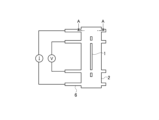
- FIG. 1 is a schematic diagram showing a CNT composite wiring and an electrode for electrical property evaluation.
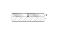
- FIG. 2 is a cross-sectional view of the CNT composite wiring shown in FIG. 1 along line AA.
- FIG. 3A is a schematic diagram for explaining a method of forming a CNT composite wiring.
- FIG. 3B is a schematic diagram for explaining a method of forming a CNT composite wiring.
- FIG. 3C is a schematic diagram for explaining a method of forming a CNT composite wiring.
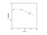
- FIG. 4 is a diagram showing the relationship between the resistivity ratio of the CNT composite wiring and the resistivity of the wiring using only aluminum, and the G/D ratio of CNT.
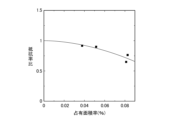
- FIG. 5 is a diagram showing the relationship between the ratio of the resistivity of the CNT composite wiring and the resistivity of the wiring using only aluminum, and the CNT occupied area ratio.
- FIG. 6A is a transmission electron microscope (TEM) photograph showing a cross-section of a CNT composite wire.
- FIG. 6B is a transmission electron microscope (TEM) photograph showing a cross section of the CNT composite wiring.
- FIG. 6C is a transmission electron microscope (TEM) photograph showing a cross section of the CNT composite wiring.
- the CNT composite wiring 10 of this embodiment includes CNTs 1 arranged on a substrate 3 and a metal thin film 2 formed on the CNTs 1 .
- metal films 4 and 5 are formed on the metal thin film 2 as electrodes 6 for evaluating the electrical characteristics of the CNT composite wiring 10 .
- CNT1 can be used as the CNT 1 that constitutes the CNT composite wiring 10 .
- CNT1 may be a single-walled single-wall nanotube (SWNT), a double-walled carbon nanotube (DWCNT), or a multi-walled multi-walled nanotube (MWNT). of MWNTs are preferred.
- the diameter of CNT is preferably 0.4 nm to 50 nm, and the average length of CNT1 is preferably 10 ⁇ m or more.
- the diameter and average length of CNT1 are measured by well-known methods, such as electron microscope observation, for example.
- the CNTs 1 that make up the CNT composite wiring 10 form a conductive path that conducts in the longitudinal direction of the CNT composite wiring 10 . Therefore, the CNTs 1 are oriented along the longitudinal direction (conduction direction) of the CNT composite wiring 10 .
- the orientation state of the CNTs 1 can be arbitrarily controlled.
- the conductive path consists of one or more CNTs 1.
- the CNTs 1 that constitute the conductive path may exist in a state in which one or more CNTs are extended, or may be aggregated to form a mass.
- the terminal portion of CNT1 may be open or closed.
- CNT1 When CNT1 is measured by Raman spectroscopic analysis, in the Raman spectrum, characteristic peaks derived from lattice vibrations, such as the D band near 1300 cm ⁇ 1 , the G band near 1590 cm ⁇ 1 , and the G′ band near 2700 cm ⁇ 1 appear. .
- the G band originates from the in-plane stretching vibration of the six-membered ring structure in the graphite structure, and the D band originates from its defect structure.
- the intensity ratio (G/D ratio) between the G band and the D band is an index representing the degree of crystallinity in the CNT1.
- the G/D ratio is preferably 5 or more and 30 or less, more preferably 12 or more and 20 or less.
- the CNT occupied area ratio in the CNT composite wiring 10 is preferably 10% or less, more preferably 0.01% or more and 1% or less, and further preferably 0.01% or more and 0.1% or less. .
- the CNT occupied area ratio indicates the ratio of the cross-sectional area of the CNT 1 to the sum of the cross-sectional area of the CNT 1 and the cross-sectional area of the metal thin film 2 .
- the CNT occupied area ratio in the CNT composite wiring 10 is preferably 10% or less.
- the CNT occupied area ratio is preferably the ratio of the cross-sectional area of the CNTs 1 to the sum of the cross-sectional areas of the CNTs 1 and the metal thin film 2 in the cross section of the CNT composite wiring 10 perpendicular to the longitudinal direction.
- the ratio of the CNT1 oriented along the longitudinal direction of the CNT composite wiring 10 increases, the CNT composite wiring 10 having a higher conductivity than the conventional metal material while further reducing the amount of the CNT1. can be obtained.
- the metal forming the metal thin film 2 it is preferable to use at least one selected from the group consisting of highly conductive metals such as copper, copper alloys, aluminum, and aluminum alloys.
- the metal forming the metal thin film does not have to be a pure metal, and may be an alloy of two or more elements.
- the metal thin film may be a single layer film or a multilayer film composed of two or more kinds of metals.
- the thickness of the metal thin film is not particularly limited, and can be, for example, 30 nm to 100 nm.
- an amorphous layer made of metal oxide is preferably present at the interface between the CNT 1 and the metal thin film 2.
- the film thickness of the amorphous layer is preferably 1 nm or more and 5 nm or less. Due to the presence of the amorphous layer, the lattice mismatch between the metal thin film 2 and the CNTs 1 is relaxed, and the CNT composite wiring 10 having high conductivity can be obtained.
- a known substrate can be used for the substrate 3 constituting the CNT composite wiring 10 .
- semiconductor substrates silicon substrates such as SiO 2 /Si and compound semiconductor substrates
- ceramic substrates glass substrates, and the like can be used as long as insulation is ensured.
- the metal films 4 and 5 used for the electrodes 6 for evaluating the electrical characteristics of the CNT composite wiring 10 known ones can be used.
- the metal films 4 and 5 can be made of at least one metal selected from the group consisting of Au, Ti, Ag, Cu, Al, Fe, Ni, Co, Cr, Mo, Nb and W, for example. can.
- the electrode 6 may be an alloy composed of two or more of the above metals, or may be a laminate composed of two or more of the above metals, as shown in FIG. Moreover, the thickness of the electrode 6 is not particularly limited.
- the CNTs 1 are oriented along the longitudinal direction (conducting direction) of the CNT composite wiring 10 to form a conductive path. Therefore, a conductive path is efficiently formed even with a low concentration of CNT1.
- the synergistic effect of the conductive path of the metal thin film 2 and the conductive path of the CNTs 1 results in a higher conductivity than that of conventional metal materials. It becomes the CNT composite wiring 10 which has.
- an amorphous layer made of metal oxide is present at the interface between the CNTs 1 and the metal thin film 2, so that the lattice mismatch between the CNTs 1 and the metal thin film 2 is alleviated. Affinity between the CNT 1 and the metal thin film 2 is enhanced. Therefore, a conductive path is easily connected between the CNT 1 and the metal thin film 2 . As a result, the CNT composite wiring 10 that effectively utilizes the conductivity of the CNTs 1 is obtained.
- the CNT composite wiring 10 of the present embodiment includes the substrate 3, the CNT 1, and the metal thin film 2 formed on the CNT 1, and the CNT 1 is the peak ratio of the G band and the D band in the Raman spectrum (G/D) is 5 or more and 30 or less, and the CNT occupied area ratio, which is the ratio of the cross-sectional area of CNT1 to the sum of the cross-sectional area of CNT1 and the cross-sectional area of metal thin film 2, is 10% or less. Therefore, the CNT composite wiring 10 can have a higher conductivity than conventional metal materials while reducing the amount of CNTs 1 in the CNT composite wiring 10 .
- the method for manufacturing a CNT composite wiring includes a step of developing a CNT dispersion on a substrate (step (a)), and a step of forming a metal thin film on the CNTs after step (a) (step ( b)), after step (b), a step of specifying the position of CNTs on the metal thin film (step (c)), and after step (c), after forming a mask on the metal thin film, It includes a step of removing unprotected portions by etching (step (d)), and a step of heat-treating in a reducing atmosphere after step (d) (step (e)). Each step will be described below.
- Step (a) is a step of developing a CNT dispersion on the substrate 3 (FIG. 3A).
- the CNT dispersion liquid spread on the substrate is prepared by highly dispersing CNT1 in a solvent.
- the solvent for dispersing CNT1 is not particularly limited, it is preferable to use an organic solvent.
- any of alcohol solvents, amide solvents, ketone solvents, and mixed solvents obtained by arbitrarily combining alcohol solvents, ketone solvents, and amide solvents can be used as the organic solvent.
- the alcoholic solvent at least one selected from the group consisting of methanol, ethanol, 1-propanol, 2-propanol, 1-butanol, 2-methyl-1-propanol, 2-butanol and 1-methyl-2-propanol can be used.
- the amide solvent at least one selected from the group consisting of N,N-dimethylformamide, N-methylpyrrolidone, dimethylsulfoxide and dimethylacetamide can be used. At least one of acetone and methyl ethyl ketone can be used as the ketone solvent.
- the CNT1 can use the one described above. Further, the CNT 1 may be previously washed with an acid to remove a metal catalyst such as platinum and amorphous carbon, or previously graphitized by heat treatment. By subjecting the CNT1 to such a pretreatment, the CNT1 can be highly purified or highly crystallized.
- a metal catalyst such as platinum and amorphous carbon
- the heating temperature for graphitization is preferably 500-3500°C.
- the heating time is determined in consideration of the heating temperature, and is preferably 10 minutes to 5 hours. Also, the rate of temperature increase up to 1500° C. is preferably 5 to 30° C./min.
- the inert gas used to create an inert gas atmosphere during heat treatment includes rare gases such as helium gas and argon gas, and nitrogen.
- the heat treatment in this step reduces defects on the CNT surface, and the peak ratio (G/D ratio) between the G band and the D band, which is an index of crystallinity by Raman spectrum, is 5 or more, and the crystal is degree improves.
- the method for highly dispersing CNT1 in the solvent is not particularly limited, and CNT1 can be dispersed by stirring at high speed after adding it to the solvent.
- an external force may be applied using an ultrasonic disperser or the like. Through such a process, the CNTs 1 are loosened and a highly dispersed CNT dispersion in the solvent can be obtained.
- the obtained CNT dispersion is dropped onto the substrate 3 and spread.
- the method of developing the CNT dispersion is not particularly limited, and known methods such as spin coating, casting and dipping can be used. Also, the CNTs 1 may be cleaned by annealing after the CNTs are developed and before the metal thin film is formed.
- Step (b) is a step of forming a thin metal film 2 on the CNTs 1 (FIG. 3A).
- a metal thin film 2 is formed on the substrate 3 on which the CNT dispersion has been spread in step (a).
- the metal forming the metal thin film 2 the above-described metals can be used.
- the method for forming the metal thin film 2 is not particularly limited, and may be appropriately selected according to the type and thickness of the thin film. For example, known methods such as resistance heating vacuum deposition, chemical vapor deposition (CVD), electron beam deposition, sputtering, and ion plating can be used.
- the metal thin film may be formed after spreading the CNT dispersion on the substrate on which the mask is placed.
- CNTs may be developed on a substrate on which a metal thin film has been formed in advance, and a metal thin film may be further formed thereon.
- Step (c) is a step of specifying the position of CNT 1 on metal thin film 2 (FIG. 3A).
- the position of the CNT 1 can be identified by observing the substrate 3 on which the metal thin film 2 is formed in step (b) with a scanning electron microscope (SEM). Specifically, the positions of the CNTs 1 can be measured using relative coordinates based on alignment marks formed in advance on the substrate 3 . By this step (c), the orientation state of the CNTs 1 in the CNT composite wiring 10 can be confirmed, and can be used as a mark for specifying the mask formation and etching positions performed in the step (d).
- SEM scanning electron microscope
- Step (d) is a step of forming a mask on the metal thin film 2 and then etching away portions not protected by the mask (FIGS. 3B and 3C).
- patterning is performed by forming a resist layer 15 on the surface of the substrate 3 on which the metal thin film 2 is formed, and this resist pattern is used as a mask. After developing the resist pattern, the portions not protected by the mask are selectively etched away. Thereafter, by removing the resist layer 15, the metal thin film 2 is patterned into a predetermined shape, and conductive wiring is formed on the substrate 3, as shown in FIG. 3C.
- an electron beam lithography method for direct writing with an electron beam for example, an electron beam lithography method for direct writing with an electron beam, a photolithography method using a short wavelength light source, a laser direct writing method, or the like can be used.
- the patterning of the metal thin film 2 may be performed by forming the metal thin film through a mask such as a stencil mask.
- thermosetting resists and UV curable resists are used.
- thermosetting resist for example, an epoxy resist or a urethane resist is used.
- a known method can be used as an etching method.
- dry etching or wet etching can be used.
- wet etching a mixed acid such as hydrofluoric acid, nitric acid, acetic acid, phosphoric acid, and sulfuric acid can be used as an etchant. can be processed using
- Step (e) is a step of heat-treating in a reducing atmosphere.
- the substrate 3 on which the metal thin film 2 is patterned in step (d) is heat-treated in an inert gas atmosphere such as argon and a reducing atmosphere such as a hydrogen atmosphere.
- This heat treatment allows crystal grains to grow while removing the grain boundary oxide film formed during the formation of the metal thin film.
- the heating temperature and heating time for the heat treatment in the reducing atmosphere are not particularly limited.
- An electrode can be produced by forming a metal film for the above-mentioned electrode for electrical property evaluation on the entire substrate obtained in step (e) by, for example, a vacuum deposition method.
- the method for manufacturing a CNT composite wiring includes (a) the step of developing a CNT dispersion on a substrate, and (b) forming a metal thin film on the CNTs after step (a). (c) after step (b), identifying the positions of the CNTs on the metal thin film; and (d) after step (c), after forming a mask on the metal thin film, protected by the mask. and (e) a step of heat-treating in a reducing atmosphere after step (d). Therefore, according to the manufacturing method of the present embodiment, it is possible to provide a CNT composite wiring having a higher conductivity than conventional metal materials while reducing the amount of CNTs in the CNT composite wiring.
- Example 1 MWNT (manufactured by Taiyo Nippon Sanso Corporation, grade S) was used as the CNT.
- the initial G/D ratio was 1-2, the average diameter was 13 nm, and the length was about 150 ⁇ m.
- a CNT dispersion liquid was prepared by immersing the heat-treated CNTs in 2-propanol and performing dispersion treatment for 30 minutes using an ultrasonic dispersing machine (manufactured by Thinky Corporation, PR-1).
- the CNT concentration in the dispersion was 1 ⁇ 10 ⁇ 5 mass %. This dispersion was dropped onto the SiO 2 /Si substrate and spin-coated at 1000 rpm.
- Metal thin film formation ⁇ step (b)> An aluminum thin film having a thickness of 50 nm was formed by an electron beam evaporation method on the substrate on which the CNT dispersion was spread using a vacuum deposition machine (VT-43N, manufactured by Canon Anelva Corporation). Pure aluminum pellets with a purity of 99.9% or higher (manufactured by Kojundo Chemical Laboratory Co., Ltd.) were used as the vapor deposition source, and vapor deposition was performed at a vapor deposition rate of about 2 ⁇ /s.
- VT-43N manufactured by Canon Anelva Corporation
- a negative type electron beam drawing resist (OEBR-CAN40 manufactured by Tokyo Ohka Kogyo Co., Ltd.) was applied to the surface of the substrate on which the aluminum thin film was formed, at 3000 rpm, and prebaked at 110° C. for 1 minute. Subsequently, using an electron beam lithography system (F7000S, manufactured by Advantest Co., Ltd.), an electron beam was irradiated at a dose of 25 ⁇ C/cm 2 and post-exposure baking (PEB) was performed at 110° C. for 1 minute.
- F7000S electron beam lithography system
- PEB post-exposure baking
- the resist pattern was developed by immersing it in a developer (manufactured by Tokyo Ohka Kogyo Co., Ltd., NMD-3W) for 50 seconds. After development, it is immersed in a mixed acid aluminum etchant (manufactured by Kanto Kagaku Co., Ltd.) for 1 to 2 minutes at room temperature to etch the aluminum pattern, and immersed in stripping solution 104 (manufactured by Tokyo Ohka Kogyo Co., Ltd.) at 60° C. for 20 minutes. The resist was stripped with a developer (manufactured by Tokyo Ohka Kogyo Co., Ltd., NMD-3W) for 50 seconds. After development, it is immersed in a mixed acid aluminum etchant (manufactured by Kanto Kagaku Co., Ltd.) for 1 to 2 minutes at room temperature to etch the aluminum pattern, and immersed in stripping solution 104 (manufactured by Tokyo Ohka Kogyo Co., Ltd.) at 60° C. for 20
- H 2 annealing was performed at 350° C. for 60 minutes in 3.2 vol % H 2 /Ar forming gas to allow grain growth while removing the grain boundary oxide film formed during aluminum deposition.
- the CNT composite wiring of this example was obtained.
- a positive resist (ZEP-520A, manufactured by Nippon Zeon Co., Ltd.) was applied to the surface of the substrate on which the aluminum thin film was formed at 6000 rpm, and an electron beam was applied at a dose of 100 ⁇ C/cm 2 using an electron beam drawing system. irradiated. After that, it was immersed in a developer (ZED-N50, manufactured by Nippon Zeon Co., Ltd.) and a rinse solution (ZMD-B, manufactured by Zeon Co., Ltd.) at room temperature to form a pattern. Subsequently, a titanium thin film (metal film 4 in FIG. 2) of 5 nm and a gold thin film (metal film 5 in FIG. 2) of 50 nm were formed by a vacuum deposition method, and then a stripping solution (ZDMAC, manufactured by Nippon Zeon Co., Ltd.) was applied. Electrodes were formed by immersion at 60° C. for 20 minutes.
- Example 1 The samples of Example 1 were evaluated by the following method. The results are shown in Figures 4-6.
- pattern confirmation The pattern shape of the formed aluminum/CNT localized composite was evaluated using a scanning electron microscope (SEM) (MERLIN, manufactured by Carl Zeiss). In addition, the film thickness of the aluminum thin film was evaluated by the dynamic force mode of a scanning probe microscope (SPM) (manufactured by Hitachi High-Tech Co., Ltd., AFM5000).
- SEM scanning electron microscope
- SPM scanning probe microscope
- Example 1 Electrical property evaluation
- FIG. 1 the sample of Example 1 in which four electrodes for electrical characteristic evaluation are formed is arranged, a constant current is passed between the outer two probes, and the inner two probes are The electrical resistance was measured by measuring the potential difference generated between the probes.
- a vacuum prober CPX-4K, manufactured by Toyo Technica Co., Ltd. was used as a measuring device.
- CNT occupied area ratio, metal-CNT interface evaluation The CNT occupied area ratio and the aluminum-CNT interface state in the CNT composite wiring were evaluated by observing the cross section of the CNT composite wiring with a transmission electron microscope (TEM) (manufactured by JEOL Ltd., JEM-2100F). . Specifically, using a focused ion beam device (FIB) (manufactured by FEI), the sample was thinned to 100 nm or less, and then observed by TEM. The acceleration voltage during observation was 200 kV, and the observation mode used was TEM and scanning transmission electron microscope (STEM).
- TEM transmission electron microscope
- 6A-6C show photographs of the cross section of the CNT composite wiring, respectively, CNT 1, substrate 3, metal thin film (aluminum) 2, electrode (gold/titanium) 6, protective film 7, crystalline aluminum 20 and amorphous layer 30. indicates Regarding the CNT occupied area ratio in the CNT composite wiring, the ratio of the cross-sectional area of CNT 1 to the sum of the cross-sectional area of CNT 1 and the cross-sectional area of metal thin film 2 was calculated based on the obtained photograph.
- FIG. 4 shows the relationship between the resistivity ratio (resistivity ratio) of the CNT composite wiring, the resistivity of the wiring using only aluminum (aluminum wiring), and the G/D ratio of the CNTs contained in the CNT composite wiring. If the resistivity ratio is less than 1, the CNT composite wire had a lower resistivity than the aluminum wire, indicating that the CNT composite wire was more conductive than the aluminum wire. As shown in FIG. 4, when the G/D ratio is less than 12, the resistivity of the CNT composite wiring is higher than that of the aluminum wiring, and when the G/D ratio is 12 or more, the resistivity of the CNT composite wiring is higher than that of the aluminum wiring. was also found to be low. Therefore, when the G/D ratio is 12 or more, the CNT composite wiring has higher conductivity than the aluminum wiring, and the resistivity of the CNT composite wiring can be reduced by 10% or more compared to the aluminum wiring.
- FIG. 5 shows the relationship between the ratio of the resistivity of the CNT composite wiring and the resistivity of the aluminum wiring (resistivity ratio) and the CNT occupied area ratio in the CNT composite wiring. It can be seen that the resistivity ratio decreases as the CNT occupied area ratio increases. As shown in FIG. 5, even if the CNT occupied area ratio is 0.1% or less, the CNT composite wiring has a higher electrical conductivity than the aluminum wiring because the resistivity ratio is less than 1. It can be seen that the resistivity of the wiring could be reduced by 10% or more compared to the aluminum wiring.
- FIGS. 6A to 6C the state of the aluminum-CNT interface was evaluated with reference to FIGS. 6A to 6C.
- FIGS. 6A to 6C it can be seen that CNTs 1 with a diameter of about 10 nm are present in the metal thin film (aluminum) 2.
- FIG. 6C which is a photograph with the highest magnification, it can be confirmed that an amorphous layer 30 of several nanometers exists at the interface between the crystalline aluminum 20 and the CNTs 1 .
- the amorphous layer 30 is made of a metal oxide (aluminum oxide), and it is believed that the amorphous layer 30 relaxes the lattice mismatch between the metal thin film (aluminum) 2 and the CNTs 1, resulting in high electrical conductivity.
- a metal oxide aluminum oxide
Landscapes
- Chemical & Material Sciences (AREA)
- Engineering & Computer Science (AREA)
- Materials Engineering (AREA)
- Nanotechnology (AREA)
- Organic Chemistry (AREA)
- Chemical Kinetics & Catalysis (AREA)
- General Chemical & Material Sciences (AREA)
- Textile Engineering (AREA)
- Inorganic Chemistry (AREA)
- Manufacturing & Machinery (AREA)
- Carbon And Carbon Compounds (AREA)
Abstract
カーボンナノチューブ複合配線(10)は、基板(3)と、カーボンナノチューブ(1)と、カーボンナノチューブ(1)の上に形成された金属薄膜(2)と、を備え、カーボンナノチューブ(1)は、ラマンスペクトルにおけるGバンド及びDバンドのピーク比(G/D)が5以上30以下であり、カーボンナノチューブ(1)の断面積及び金属薄膜(2)の断面積の合計に対するカーボンナノチューブ(1)の断面積が占める割合であるカーボンナノチューブ占有面積率が10%以下である。
Description
本発明は、カーボンナノチューブ複合配線及びその製造方法に関する。
電子機器の小型化や省電力化のため、配線材料の低抵抗化や許容電流密度の向上が求められている。そして、カーボンナノチューブ(CNT)は、軽量で高い導電性を有することから、CNTと金属とを複合化した複合配線としての活用が期待されている。
CNT複合配線として、例えば特許文献1には、配合しているCNTの表面に金属を被着させたCNT集合体を備えるCNT金属複合材が提案されている。そして、CNT金属複合材において、当該金属は20体積含有率以上70体積含有率未満以下を備えており、CNT金属複合材の体積抵抗率は最小で1.8×10⁻⁵Ω・cmであることが記載されている。
しかしながら、特許文献1に記載のCNT金属複合材では、従来の金属材料のみ使用した配線よりも高い導電性は得られていない。また、CNTは金属よりも高価であることから、特許文献1のような高いCNT体積含有率であると高コスト化を招く。さらに、特許文献1に記載のめっき法では、酸などの電解液にCNTが浸漬される際に、CNTの結晶性の尺度であるGバンドとDバンドの強度比(G/D比)が低下する等、CNT自体の特性が変化し、結果として複合体の導電特性が低下する恐れがある。
本発明の目的は、CNT複合配線中のCNTの量を低減しつつも、従来の金属材料よりも高い導電性を有するCNT複合配線及びその製造方法を提供することにある。
本発明の態様に係るカーボンナノチューブ複合配線は、基板と、カーボンナノチューブと、カーボンナノチューブの上に形成された金属薄膜と、を備え、カーボンナノチューブは、ラマンスペクトルにおけるGバンド及びDバンドのピーク比(G/D)が5以上30以下であり、カーボンナノチューブの断面積及び金属薄膜の断面積の合計に対するカーボンナノチューブの断面積が占める割合であるカーボンナノチューブ占有面積率が10%以下である。
本発明の態様に係るカーボンナノチューブ複合配線の製造方法は、(a)基板上にカーボンナノチューブ分散液を展開する工程と、(b)工程(a)の後、前記カーボンナノチューブの上に前記金属薄膜を形成する工程と、(c)工程(b)の後、前記金属薄膜上の前記カーボンナノチューブの位置を特定する工程と、(d)工程(c)の後、前記金属薄膜上にマスクを形成した後に、前記マスクで保護されていない箇所をエッチングにより除去する工程と、(e)工程(d)の後、還元雰囲気中で熱処理をする工程と、を含む。
本発明によれば、CNT複合配線中のCNTの量を低減しつつも、従来の金属材料よりも高い導電性を有するCNT複合配線及びその製造方法を提供することができる。
以下、図面を用いて本実施形態に係るCNT複合配線及びその製造方法について詳細に説明する。
本実施形態のCNT複合配線10は、基板3の上に配置されたCNT1と、CNT1の上に形成された金属薄膜2とを備えている。そして、図1及び図2では、金属薄膜2の上に、CNT複合配線10の電気特性を評価するための電極6として、金属膜4,5が成膜されている。
CNT複合配線10を構成するCNT1としては、公知のものを用いることができる。CNT1は、単層のシングルウォールナノチューブ(SWNT)であってもよく、2層のカーボンナノチューブ(DWCNT)や多層のマルチウォールナノチューブ(MWNT)であってもよいが、導電性の面から3層以上のMWNTが好ましい。CNTの直径は0.4nm~50nmであることが好ましく、CNT1の平均長さは10μm以上であることが好ましい。なお、CNT1の直径及び平均長さは、例えば、電子顕微鏡観察等の公知の方法により測定される。
CNT複合配線10を構成するCNT1は、CNT複合配線10の長手方向に導電する導電経路を形成するものである。そのため、CNT1はCNT複合配線10の長手方向(導電方向)に沿って配向している。なお、本実施形態のCNT複合配線10は、半導体プロセスを用いて作製されるため、CNT1の配向状態を任意に制御できる。
CNT複合配線10において、導電経路は1本以上のCNT1からなる。また、導電経路を構成するCNT1は、1本又は2本以上のCNTが伸びた状態で存在していてもよく、凝集して塊状になっていてもよい。さらに、CNT1の末端部分は開放状態であっても閉じた状態であってもよい。
ラマン分光分析によりCNT1を測定した場合、ラマンスペクトルでは、1300cm-1付近のDバンド、1590cm-1付近のGバンド、2700cm-1付近のG´バンドという格子振動に由来する特徴的なピークが現れる。Gバンドはグラファイト構造中の六員環構造の面内伸縮振動に由来し、Dバンドはその欠陥構造に由来する。そして、GバンドとDバンドの強度比(G/D比)は、CNT1中の結晶性の高さを表す指標となる。CNT1において、G/D比は、5以上30以下であることが好ましく、12以上20以下であることがより好ましい。CNT1のG/D比が5以上30以下であると、CNT表面の欠陥が少なく結晶性が高いため、導電性に優れる。
CNT複合配線10におけるCNT占有面積率は10%以下であることが好ましく、0.01%以上1%以下であることがより好ましく、0.01%以上0.1%以下であることがさらに好ましい。CNT占有面積率が10%以下であることにより、CNT複合配線10中のCNT1の量を低減しつつも、従来の金属材料よりも高い導電性を有するCNT複合配線10が得られる。CNT占有面積率とは、CNT1の断面積及び金属薄膜2の断面積の合計に対するCNT1の断面積が占める割合を示す。
上述のように、CNT複合配線10におけるCNT占有面積率は10%以下であることが好ましい。この際、CNT占有面積率は、CNT複合配線10の長手方向に垂直な断面において、CNT1の断面積及び金属薄膜2の断面積の合計に対するCNT1の断面積が占める割合であることが好ましい。この場合、CNT1がCNT複合配線10の長手方向に沿って配向している割合が高まることから、CNT1の量をさらに低減しつつも、従来の金属材料よりも高い導電性を有するCNT複合配線10が得ることができる。
金属薄膜2を形成する金属としては、導電性が高い金属、例えば、銅、銅合金、アルミニウム及びアルミニウム合金からなる群より選択される少なくとも一種を用いることが好ましい。金属薄膜を形成する金属は純金属である必要はなく、2種類以上の元素からなる合金であってもよい。また、金属薄膜は単層膜でもよく、2種類以上の金属からなる多層膜でもよい。金属薄膜の厚さは特に限定されず、例えば30nm~100nmとすることができる。
CNT複合配線10において、CNT1と金属薄膜2との間の界面には、金属酸化物からなるアモルファス層が存在することが好ましい。また、アモルファス層の膜厚は1nm以上5nm以下であることが好ましい。アモルファス層が存在することにより、金属薄膜2とCNT1の格子ミスマッチが緩和し、高い導電性を有するCNT複合配線10を得ることができる。
CNT複合配線10を構成する基板3は公知のものを用いることができる。例えば、半導体基板(SiO2/Si等のシリコン基板や化合物半導体基板)、セラミックス基板、ガラス基板等、絶縁性が担保されているものであれば用いることができる。
CNT複合配線10の電気特性評価用の電極6に使用する金属膜4,5は、公知のものを用いることができる。金属膜4,5は、例えば、Au、Ti、Ag、Cu、Al、Fe、Ni、Co、Cr、Mo、Nb及びWからなる群より選択される金属の少なくとも一種からなるものを用いることができる。電極6は、2種類以上の上記金属からなる合金であってもよく、図2に示すように、2種類以上の上記金属からなる積層体であってもよい。また、電極6の厚さは特に限定されない。
本実施形態のCNT複合配線10において、CNT1は、CNT複合配線10の長手方向(導電方向)に沿って配向し、導電経路を形成している。そのため、低濃度のCNT1であっても効率良く導電経路が形成される。そして、金属薄膜2からなる導電経路に、CNT1によって形成される導電経路が加わることで、金属薄膜2の導電経路とCNT1の導電経路との相乗効果により、従来の金属材料よりも高い導電性を有するCNT複合配線10となる。
また、本実施形態のCNT複合配線10において、CNT1と金属薄膜2との間の界面には、金属酸化物からなるアモルファス層が存在することにより、CNT1と金属薄膜2の格子ミスマッチが緩和され、CNT1と金属薄膜2との親和性が高まる。そのため、CNT1と金属薄膜2との間で導電経路がつながりやすくなる。結果として、CNT1の導電性を効果的に活用したCNT複合配線10となる。
以上の通り、本実施形態のCNT複合配線10は、基板3と、CNT1と、CNT1の上に形成された金属薄膜2と、を備え、CNT1は、ラマンスペクトルにおけるGバンド及びDバンドのピーク比(G/D)が5以上30以下であり、CNT1の断面積及び金属薄膜2の断面積の合計に対するCNT1の断面積が占める割合であるCNT占有面積率が10%以下である。そのため、CNT複合配線10中のCNT1の量を低減しつつも、従来の金属材料よりも高い導電性を有するCNT複合配線10となる。
<CNT複合配線の製造方法>
本実施形態のCNT複合配線の製造方法は、基板上にCNT分散液を展開する工程(工程(a))と、工程(a)の後、CNTの上に金属薄膜を形成する工程(工程(b))と、工程(b)の後、金属薄膜上のCNTの位置を特定する工程(工程(c))と、工程(c)の後、金属薄膜上にマスクを形成した後に、マスクで保護されていない箇所をエッチングにより除去する工程(工程(d))と、工程(d)の後、還元雰囲気中で熱処理をする工程(工程(e))と、を含む。以下に各工程について説明する。
本実施形態のCNT複合配線の製造方法は、基板上にCNT分散液を展開する工程(工程(a))と、工程(a)の後、CNTの上に金属薄膜を形成する工程(工程(b))と、工程(b)の後、金属薄膜上のCNTの位置を特定する工程(工程(c))と、工程(c)の後、金属薄膜上にマスクを形成した後に、マスクで保護されていない箇所をエッチングにより除去する工程(工程(d))と、工程(d)の後、還元雰囲気中で熱処理をする工程(工程(e))と、を含む。以下に各工程について説明する。
[工程(a)]
工程(a)は、基板3の上にCNT分散液を展開する工程である(図3A)。
工程(a)は、基板3の上にCNT分散液を展開する工程である(図3A)。
基板上に展開するCNT分散液は、溶媒中にCNT1を高分散させて作製する。CNT1を分散させる溶媒は特に限定されないが、有機溶媒を用いることが好ましい。
有機溶媒は、アルコール系溶媒、アミド系溶媒、ケトン系溶媒、並びにアルコール系溶媒、ケトン系溶媒及びアミド系溶媒を任意に組み合わせてなる混合溶媒のいずれかを用いることができる。アルコール系溶媒としては、メタノール、エタノール、1-プロパノール、2-プロパノール、1-ブタノール、2-メチル-1-プロパノール、2-ブタノール及び1-メチル-2-プロパノールからなる群より選ばれる少なくとも一つを用いることができる。アミド系溶媒としては、N,N-ジメチルホルムアミド、N-メチルピロリドン、ジメチルスルホキシド及びジメチルアセトアミドからなる群より選ばれる少なくとも一つを用いることができる。また、ケトン系溶媒としては、アセトン及びメチルエチルケトンの少なくとも一方を用いることができる。
CNT1は、上述のものを使用することができる。また、CNT1は、予め酸で洗浄することにより白金等の金属触媒やアモルファスカーボンを除去したり、予め加熱処理することにより黒鉛化したりしたものであってもよい。CNT1にこのような前処理を行うと、CNT1を高純度化したり高結晶化したりすることができる。
黒鉛化するための加熱温度は、500~3500℃とすることが好ましい。また、加熱時間は加熱温度を考慮して決定されるが、10分~5時間とすることが好ましい。また、1500℃までの昇温速度は、5~30℃/分とすることが好ましい。
加熱処理時に不活性ガス雰囲気とするために用いる不活性ガスは、ヘリウムガス、アルゴンガス等の希ガスや窒素が挙げられる。
CNT1は、本工程における加熱処理を施すことによりCNT表面の欠陥が減少し、ラマンスペクトルによる結晶度の指標であるGバンドとDバンドとのピーク比(G/D比)が5以上となり、結晶度が向上する。
溶媒中にCNT1を高分散させる方法は特に限定されず、CNT1を溶媒に添加した後に高速で攪拌することにより、分散させることができる。なお、CNT1を効率的に分散させるために、CNT1を溶媒に添加した後に、超音波分散機等を用いて外部からの力を付与してもよい。このような工程により、CNT1が解れ、溶媒中に高分散したCNT分散液を得ることができる。
得られたCNT分散液を基板3の上に滴下し、展開する。CNT分散液を展開する方法は特に限定されず、例えば、スピンコート法、キャスト法及びディッピング法等の公知の方法を用いることができる。また、CNT展開後に金属薄膜を形成する前にアニールを行うことで、CNT1をクリーニングしてもよい。
[工程(b)]
工程(b)は、CNT1の上に金属薄膜2を形成する工程である(図3A)。
工程(b)は、CNT1の上に金属薄膜2を形成する工程である(図3A)。
工程(a)によってCNT分散液が展開された基板3の上に金属薄膜2を形成する。金属薄膜2を形成する金属は、上述のものを使用することができる。金属薄膜2を形成する方法は特に限定されず、薄膜の種類、厚みに応じて適宜選択すればよい。例えば、抵抗加熱式真空蒸着法、化学気相成長法(CVD)、電子ビーム蒸着法、スパッタ法、イオンプレーティング等の公知の方法を用いることができる。
マスクを設置した基板上にCNT分散液を展開した後に金属薄膜を形成してもよい。また、予め金属薄膜を形成した基板上にCNTを展開し、その上からさらに金属薄膜を形成してもよい。
[工程(c)]
工程(c)は、金属薄膜2の上のCNT1の位置を特定する工程である(図3A)。
工程(c)は、金属薄膜2の上のCNT1の位置を特定する工程である(図3A)。
工程(b)によって金属薄膜2が形成された基板3を走査電子顕微鏡(SEM)によって観察することにより、CNT1の位置を特定することができる。具体的には、基板3に予め形成したアライメントマークを基準とした相対座標を用いてCNT1の位置を計測することができる。この工程(c)により、CNT複合配線10におけるCNT1の配向状態を確認し、工程(d)で実施するマスク形成とエッチングの位置を特定するための目印とすることができる。
[工程(d)]
工程(d)は、金属薄膜2の上にマスクを形成した後に、マスクで保護されていない箇所をエッチングにより除去する工程である(図3B及び図3C)。
工程(d)は、金属薄膜2の上にマスクを形成した後に、マスクで保護されていない箇所をエッチングにより除去する工程である(図3B及び図3C)。
図3Bのように、金属薄膜2が形成された基板3の表面にレジスト層15を形成することでパターニングし、このレジストパターンをマスクとして用いる。レジストパターンを現像後、マスクで保護されていない箇所を選択的にエッチング除去する。その後、レジスト層15を剥離することで、図3Cに示すように、金属薄膜2が所定の形状にパターニングされ、基板3上に導電性の配線が形成される。
金属薄膜2のパターニングに使用する方法としては、例えば、電子線で直接描画する電子線リソグラフィー法、短波長光源を利用したフォトリソグラフィー法、レーザー直接描画等を用いることができる。また、金属薄膜2のパターニングはステンシルマスク等のマスク越しに金属薄膜を形成することで行ってもよい。
レジストとしては、公知のものを用いることができる。例えば、熱硬化性レジストやUV硬化性レジストが用いられる。また、熱硬化性レジストとしては、例えば、エポキシ系レジストやウレタン系レジストが用いられる。
エッチング方法としては公知の方法を用いることができる。例えば、ドライエッチング、ウェットエッチングを用いることができる。ウェットエッチングの場合、エッチング液としてフッ化水素酸、硝酸、酢酸、リン酸、硫酸等の混酸を使用することができ、エッチング液に浸漬するディップ方式や、エッチング液を噴霧するスピンエッチング方式等を用いて処理することができる。
[工程(e)]
工程(e)は、還元雰囲気中で熱処理をする工程である。
工程(e)は、還元雰囲気中で熱処理をする工程である。
工程(d)によって金属薄膜2がパターニングされた基板3について、アルゴンなどの不活性ガス雰囲気及び水素雰囲気等の還元雰囲気において熱処理をする。この熱処理により、金属薄膜形成中に形成された結晶粒界酸化膜を除去しながら結晶粒を成長させることができる。還元雰囲気中で熱処理をする際の加熱温度や加熱時間は特に限定されない。
工程(e)によって得られた基板全体に、例えば真空蒸着法により、上述の電気特性評価用の電極の金属膜を成膜することで電極を作製することができる。
以上の通り、本実施形態のCNT複合配線の製造方法は、(a)基板上にCNT分散液を展開する工程と、(b)工程(a)の後、CNTの上に金属薄膜を形成する工程と、(c)工程(b)の後、金属薄膜上のCNTの位置を特定する工程と、(d)工程(c)の後、金属薄膜上にマスクを形成した後に、マスクで保護されていない箇所をエッチングにより除去する工程と、(e)工程(d)の後、還元雰囲気中で熱処理をする工程と、を含む。そのため、本実施形態の製造方法によれば、CNT複合配線中のCNTの量を低減しつつも、従来の金属材料よりも高い導電性を有するCNT複合配線を提供することができる。
以下、本実施形態を実施例により更に詳細に説明するが、本実施形態はこれら実施例に限定されるものではない。
[実施例1]
CNTは、MWNT(大陽日酸(株)製、Sグレード品)を用いた。初期のG/D比は1~2であり、平均直径は13nm、長さは約150μmであった。
CNTは、MWNT(大陽日酸(株)製、Sグレード品)を用いた。初期のG/D比は1~2であり、平均直径は13nm、長さは約150μmであった。
(CNT分散液の展開<工程(a)>)
粉末状のCNTを封入した黒鉛るつぼを、加熱炉((株)倉田技研製、SCC-220)内に設置した。加熱炉内を10Paに減圧した状態で30分間保持し、るつぼ内の残留ガス及びCNT表面への吸着ガスを脱気した(脱気工程)。次に、ヒーターへの通電を開始し、20℃/minの昇温速度で昇温した(昇温工程)。炉内温度が2200℃に到達した段階でアルゴンガス(純度99.9999%)をゲージ圧+40kPaとなるように封入した。さらに、炉内温度が最高温度2800℃に到達した段階で温度一定になるように保持した(保持工程)。2~12時間経過した後、ヒーターへの通電を停止し、炉内を徐冷した。
粉末状のCNTを封入した黒鉛るつぼを、加熱炉((株)倉田技研製、SCC-220)内に設置した。加熱炉内を10Paに減圧した状態で30分間保持し、るつぼ内の残留ガス及びCNT表面への吸着ガスを脱気した(脱気工程)。次に、ヒーターへの通電を開始し、20℃/minの昇温速度で昇温した(昇温工程)。炉内温度が2200℃に到達した段階でアルゴンガス(純度99.9999%)をゲージ圧+40kPaとなるように封入した。さらに、炉内温度が最高温度2800℃に到達した段階で温度一定になるように保持した(保持工程)。2~12時間経過した後、ヒーターへの通電を停止し、炉内を徐冷した。
加熱処理を施したCNTを2-プロパノールに浸漬し、超音波分散機((株)シンキー製、PR-1)を用いて30分間分散処理を行うことで、CNT分散液を作製した。分散液中のCNT濃度は1×10⁻⁵質量%であった。この分散液をSiO2/Si基板上に滴下し、1000rpmでスピンコートした。
(金属薄膜形成<工程(b)>)
CNT分散液が展開された基板上に、真空蒸着機(キヤノンアネルバ(株)製、VT-43N)で膜厚50nmのアルミニウム薄膜を電子ビーム蒸着法により成膜した。蒸着源には純度99.9%以上の純アルミニウムペレット((株)高純度化学研究所製)を用いて、蒸着レートは約2Å/sに設定して蒸着を行った。
CNT分散液が展開された基板上に、真空蒸着機(キヤノンアネルバ(株)製、VT-43N)で膜厚50nmのアルミニウム薄膜を電子ビーム蒸着法により成膜した。蒸着源には純度99.9%以上の純アルミニウムペレット((株)高純度化学研究所製)を用いて、蒸着レートは約2Å/sに設定して蒸着を行った。
(CNTの位置特定<工程(c)>)
走査電子顕微鏡(SEM)(カール・ツァイス社製、MERLIN)を用いて、CNTの位置を特定した後、基板に予め形成したアライメントマークを基準とした相対座標を用いてCNT位置を計測した。
走査電子顕微鏡(SEM)(カール・ツァイス社製、MERLIN)を用いて、CNTの位置を特定した後、基板に予め形成したアライメントマークを基準とした相対座標を用いてCNT位置を計測した。
(マスク形成、エッチング<工程(d)>)
アルミニウム薄膜が形成された基板の表面に、ネガ型の電子線描画用レジスト(東京応化工業(株)製、OEBR-CAN40)を3000rpmで塗布し、110℃で1分間プリベークした。続いて、電子線描画システム((株)アドバンテスト製、F7000S)を用いて、ドーズ量25μC/cm2で電子線を照射し、110℃1分間の露光後ベーク(PEB)を行った。次に現像液(東京応化工業(株)製、NMD-3W)に50秒間浸漬してレジストパターンを現像した。現像後、混酸アルミエッチング液(関東化学(株)製)に室温で1~2分浸漬し、アルミパターンをエッチングし、剥離液104(東京応化工業(株)製)に60℃20分間浸漬してレジストを剥離した。
アルミニウム薄膜が形成された基板の表面に、ネガ型の電子線描画用レジスト(東京応化工業(株)製、OEBR-CAN40)を3000rpmで塗布し、110℃で1分間プリベークした。続いて、電子線描画システム((株)アドバンテスト製、F7000S)を用いて、ドーズ量25μC/cm2で電子線を照射し、110℃1分間の露光後ベーク(PEB)を行った。次に現像液(東京応化工業(株)製、NMD-3W)に50秒間浸漬してレジストパターンを現像した。現像後、混酸アルミエッチング液(関東化学(株)製)に室温で1~2分浸漬し、アルミパターンをエッチングし、剥離液104(東京応化工業(株)製)に60℃20分間浸漬してレジストを剥離した。
(還元雰囲気中における熱処理<工程(e)>)
アルミニウム蒸着中に形成された結晶粒界酸化膜を除去しながら、結晶粒成長させるため、3.2体積%のH2/Arフォーミングガス中で350℃60分間H2アニールを実施した。このようにして、本実施例のCNT複合配線を得た。
アルミニウム蒸着中に形成された結晶粒界酸化膜を除去しながら、結晶粒成長させるため、3.2体積%のH2/Arフォーミングガス中で350℃60分間H2アニールを実施した。このようにして、本実施例のCNT複合配線を得た。
(電気特性評価用電極形成)
アルミニウム薄膜が形成された基板の表面に、ポジ型レジスト(日本ゼオン(株)製、ZEP-520A)を6000rpmで塗布し、電子線描画システムを用いて、ドーズ量100μC/cm2で電子線を照射した。その後、現像液(日本ゼオン(株)製、ZED-N50)、リンス液(日本ゼオン(株)製、ZMD-B)にそれぞれ室温で浸漬してパターンを形成した。続いて、真空蒸着法でチタン薄膜(図2における金属膜4)を5nm、金薄膜(図2における金属膜5)を50nm成膜した後、剥離液(日本ゼオン(株)製、ZDMAC)に60℃20分間浸漬することで、電極を形成した。
アルミニウム薄膜が形成された基板の表面に、ポジ型レジスト(日本ゼオン(株)製、ZEP-520A)を6000rpmで塗布し、電子線描画システムを用いて、ドーズ量100μC/cm2で電子線を照射した。その後、現像液(日本ゼオン(株)製、ZED-N50)、リンス液(日本ゼオン(株)製、ZMD-B)にそれぞれ室温で浸漬してパターンを形成した。続いて、真空蒸着法でチタン薄膜(図2における金属膜4)を5nm、金薄膜(図2における金属膜5)を50nm成膜した後、剥離液(日本ゼオン(株)製、ZDMAC)に60℃20分間浸漬することで、電極を形成した。
[評価方法]
実施例1のサンプルについて、次の方法により評価を実施した。結果を図4~6に示す。
実施例1のサンプルについて、次の方法により評価を実施した。結果を図4~6に示す。
(パターン確認)
形成したアルミニウム/CNT局所複合体のパターン形状を、走査電子顕微鏡(SEM)(カール・ツァイス社製、MERLIN)を用いて評価した。また、アルミニウム薄膜の膜厚を、走査型プローブ顕微鏡(SPM)((株)日立ハイテク製、AFM5000)のダイナミックフォースモードにより評価した。
形成したアルミニウム/CNT局所複合体のパターン形状を、走査電子顕微鏡(SEM)(カール・ツァイス社製、MERLIN)を用いて評価した。また、アルミニウム薄膜の膜厚を、走査型プローブ顕微鏡(SPM)((株)日立ハイテク製、AFM5000)のダイナミックフォースモードにより評価した。
(電気特性評価)
電気特性は、四端子法を用いた電気抵抗測定により評価した。具体的には、図1に示すように、電気特性評価用電極を4本形成した実施例1のサンプルを配置し、外側の2本の探針間に一定の電流を流し、内側の2本の探針間に生じる電位差を測定し電気抵抗を測定した。測定装置は、真空プローバ((株)東陽テクニカ製、CPX-4K)を用いた。
電気特性は、四端子法を用いた電気抵抗測定により評価した。具体的には、図1に示すように、電気特性評価用電極を4本形成した実施例1のサンプルを配置し、外側の2本の探針間に一定の電流を流し、内側の2本の探針間に生じる電位差を測定し電気抵抗を測定した。測定装置は、真空プローバ((株)東陽テクニカ製、CPX-4K)を用いた。
(CNT占有面積率、金属-CNT界面評価)
CNT複合配線におけるCNT占有面積率とアルミニウム-CNT界面状態については、透過型電子顕微鏡(TEM)(日本電子(株)製、JEM-2100F)により、CNT複合配線の断面を観察することで評価した。具体的には、集束イオン・ビーム装置(FIB)(FEI社製)を用いて、試料を100nm以下まで薄片化した後、TEMにより観察した。観察時の加速電圧は200kVとし、観察モードはTEM及び走査透過電子顕微鏡(STEM)を使用した。
CNT複合配線におけるCNT占有面積率とアルミニウム-CNT界面状態については、透過型電子顕微鏡(TEM)(日本電子(株)製、JEM-2100F)により、CNT複合配線の断面を観察することで評価した。具体的には、集束イオン・ビーム装置(FIB)(FEI社製)を用いて、試料を100nm以下まで薄片化した後、TEMにより観察した。観察時の加速電圧は200kVとし、観察モードはTEM及び走査透過電子顕微鏡(STEM)を使用した。
図6A~図6CはCNT複合配線の断面の写真を示し、それぞれ、CNT1、基板3、金属薄膜(アルミニウム)2、電極(金/チタン)6、保護膜7、結晶性アルミニウム20及びアモルファス層30を示す。CNT複合配線におけるCNT占有面積率については、得られた写真をもとに、CNT1の断面積及び金属薄膜2の断面積の合計に対するCNT1の断面積が占める割合を算出した。
図4に、CNT複合配線の抵抗率及びアルミニウムのみ使用した配線(アルミニウム配線)の抵抗率の比(抵抗率比)と、CNT複合配線に含まれるCNTのG/D比との関係を示す。抵抗率比が1未満である場合、CNT複合配線の抵抗率がアルミニウム配線よりも低かったことになり、CNT複合配線はアルミニウム配線よりも導電性が高かったことを示す。図4に示すように、G/D比が12未満の場合、CNT複合配線の抵抗率はアルミニウム配線よりも高く、G/D比が12以上の場合、CNT複合配線の抵抗率はアルミニウム配線よりも低かったことが分かる。よって、G/D比が12以上の場合、CNT複合配線はアルミニウム配線よりも高い導電性を有し、CNT複合配線の抵抗率はアルミニウム配線に比べて1割以上低減できたことが分かる。
図5に、CNT複合配線の抵抗率及びアルミニウム配線の抵抗率の比(抵抗率比)と、CNT複合配線におけるCNT占有面積率との関係を示す。CNT占有面積率が増加するほど、抵抗率比が低減することが分かる。図5に示すように、CNT占有面積率が0.1%以下であっても、抵抗率比が1未満であるために、CNT複合配線はアルミニウム配線よりも高い導電性を有し、CNT複合配線の抵抗率はアルミニウム配線に比べて1割以上低減できたことが分かる。
ここで、CNTの平均自由行程は結晶性が高いほど長くなり、十分に結晶性の高いCNTの平均自由行程はアルミニウムに比べて長いことが知られている。そのため、図4及び5の結果に示すように、アルミニウム中に結晶性が高いCNTが存在すると、複合配線としての見かけの平均自由行程が増加し、抵抗率が減少するものと考えられる。
次に、図6A~図6Cにより、アルミニウム-CNT界面状態について評価した。図6A~図6Cに示すように、直径10nm程度のCNT1が金属薄膜(アルミニウム)2中に存在していることが分かる。また、最も高倍率の写真である図6Cでは、結晶性アルミニウム20とCNT1との間の界面には数nm程度のアモルファス層30が存在することを確認できる。このアモルファス層30は金属酸化物(酸化アルミニウム)からなり、アモルファス層30により、金属薄膜(アルミニウム)2とCNT1の格子ミスマッチが緩和し、高い導電性が得られるものと考えられる。
以上、本実施形態を実施例によって説明したが、本実施形態はこれらに限定されるものではなく、本実施形態の要旨の範囲内で種々の変形が可能である。
特願2022-002308号(出願日:2022年1月11日)の全内容は、ここに援用される。
1 CNT
2 金属薄膜
3 基板
6 電極
10 CNT複合配線
15 レジスト層
30 アモルファス層
2 金属薄膜
3 基板
6 電極
10 CNT複合配線
15 レジスト層
30 アモルファス層
Claims (7)
- 基板と、
カーボンナノチューブと、
前記カーボンナノチューブの上に形成された金属薄膜と、
を備え、
前記カーボンナノチューブは、ラマンスペクトルにおけるGバンド及びDバンドのピーク比(G/D)が5以上30以下であり、
前記カーボンナノチューブの断面積及び前記金属薄膜の断面積の合計に対する前記カーボンナノチューブの断面積が占める割合であるカーボンナノチューブ占有面積率が10%以下である、カーボンナノチューブ複合配線。 - 前記金属薄膜を形成する金属は、銅、銅合金、アルミニウム及びアルミニウム合金からなる群より選択される少なくとも一種である、請求項1に記載のカーボンナノチューブ複合配線。
- 前記カーボンナノチューブと前記金属薄膜との間の界面には、金属酸化物からなるアモルファス層が存在し、前記アモルファス層の膜厚は1nm以上5nm以下である、請求項1又は2に記載のカーボンナノチューブ複合配線。
- 前記カーボンナノチューブ占有面積率が0.01%以上1%以下である、請求項1~3のいずれか一項に記載のカーボンナノチューブ複合配線。
- 前記カーボンナノチューブ占有面積率が0.01%以上0.1%以下である、請求項1~4のいずれか一項に記載のカーボンナノチューブ複合配線。
- 前記カーボンナノチューブは、ラマンスペクトルにおけるGバンド及びDバンドのピーク比(G/D)が12以上20以下である、請求項1~5のいずれか一項に記載のカーボンナノチューブ複合配線。
- 請求項1~6のいずれか一項に記載のカーボンナノチューブ複合配線の製造方法であって、
(a)基板上にカーボンナノチューブ分散液を展開する工程と、
(b)工程(a)の後、前記カーボンナノチューブの上に前記金属薄膜を形成する工程と、
(c)工程(b)の後、前記金属薄膜上の前記カーボンナノチューブの位置を特定する工程と、
(d)工程(c)の後、前記金属薄膜上にマスクを形成した後に、前記マスクで保護されていない箇所をエッチングにより除去する工程と、
(e)工程(d)の後、還元雰囲気中で熱処理をする工程と、を含むカーボンナノチューブ複合配線の製造方法。
Priority Applications (3)
| Application Number | Priority Date | Filing Date | Title |
|---|---|---|---|
| DE112023000559.1T DE112023000559T5 (de) | 2022-01-11 | 2023-01-11 | Kohlenstoffnanoröhren-Verbunddraht und Verfahren zu seiner Herstellung |
| CN202380013851.7A CN118056250A (zh) | 2022-01-11 | 2023-01-11 | 碳纳米管复合电线及其制造方法 |
| US18/609,812 US12529168B2 (en) | 2022-01-11 | 2024-03-19 | Carbon nanotube composite wire and manufacturing method therefor |
Applications Claiming Priority (2)
| Application Number | Priority Date | Filing Date | Title |
|---|---|---|---|
| JP2022-002308 | 2022-01-11 | ||
| JP2022002308A JP7513642B2 (ja) | 2022-01-11 | 2022-01-11 | カーボンナノチューブ複合配線及びその製造方法 |
Related Child Applications (1)
| Application Number | Title | Priority Date | Filing Date |
|---|---|---|---|
| US18/609,812 Continuation US12529168B2 (en) | 2022-01-11 | 2024-03-19 | Carbon nanotube composite wire and manufacturing method therefor |
Publications (1)
| Publication Number | Publication Date |
|---|---|
| WO2023136255A1 true WO2023136255A1 (ja) | 2023-07-20 |
Family
ID=87279137
Family Applications (1)
| Application Number | Title | Priority Date | Filing Date |
|---|---|---|---|
| PCT/JP2023/000406 Ceased WO2023136255A1 (ja) | 2022-01-11 | 2023-01-11 | カーボンナノチューブ複合配線及びその製造方法 |
Country Status (5)
| Country | Link |
|---|---|
| US (1) | US12529168B2 (ja) |
| JP (1) | JP7513642B2 (ja) |
| CN (1) | CN118056250A (ja) |
| DE (1) | DE112023000559T5 (ja) |
| WO (1) | WO2023136255A1 (ja) |
Citations (4)
| Publication number | Priority date | Publication date | Assignee | Title |
|---|---|---|---|---|
| JP2005048206A (ja) * | 2003-07-30 | 2005-02-24 | Toshiba Corp | 高強度高電気伝導度アルミニウム合金基複合材料およびその製造方法 |
| WO2005091345A1 (ja) * | 2004-03-24 | 2005-09-29 | Japan Science And Technology Agency | カーボンナノチューブ含有金属薄膜 |
| JP2006147170A (ja) * | 2004-11-16 | 2006-06-08 | Sumitomo Electric Ind Ltd | 導電材及びその製造方法 |
| JP2018133163A (ja) * | 2017-02-14 | 2018-08-23 | 矢崎総業株式会社 | 電線及びこれを用いたワイヤーハーネス |
Family Cites Families (3)
| Publication number | Priority date | Publication date | Assignee | Title |
|---|---|---|---|---|
| JPS5896422U (ja) | 1981-12-22 | 1983-06-30 | リンナイ株式会社 | 床暖房装置 |
| EP2660361A1 (en) | 2010-12-28 | 2013-11-06 | National Institute of Advanced Industrial Science And Technology | Carbon nanotube metal composite material and production method for same |
| WO2018204622A1 (en) | 2017-05-05 | 2018-11-08 | Cree, Inc. | High power mmic devices having bypassed gate transistors |
-
2022
- 2022-01-11 JP JP2022002308A patent/JP7513642B2/ja active Active
-
2023
- 2023-01-11 DE DE112023000559.1T patent/DE112023000559T5/de active Pending
- 2023-01-11 WO PCT/JP2023/000406 patent/WO2023136255A1/ja not_active Ceased
- 2023-01-11 CN CN202380013851.7A patent/CN118056250A/zh active Pending
-
2024
- 2024-03-19 US US18/609,812 patent/US12529168B2/en active Active
Patent Citations (4)
| Publication number | Priority date | Publication date | Assignee | Title |
|---|---|---|---|---|
| JP2005048206A (ja) * | 2003-07-30 | 2005-02-24 | Toshiba Corp | 高強度高電気伝導度アルミニウム合金基複合材料およびその製造方法 |
| WO2005091345A1 (ja) * | 2004-03-24 | 2005-09-29 | Japan Science And Technology Agency | カーボンナノチューブ含有金属薄膜 |
| JP2006147170A (ja) * | 2004-11-16 | 2006-06-08 | Sumitomo Electric Ind Ltd | 導電材及びその製造方法 |
| JP2018133163A (ja) * | 2017-02-14 | 2018-08-23 | 矢崎総業株式会社 | 電線及びこれを用いたワイヤーハーネス |
Also Published As
| Publication number | Publication date |
|---|---|
| CN118056250A (zh) | 2024-05-17 |
| US12529168B2 (en) | 2026-01-20 |
| US20240218568A1 (en) | 2024-07-04 |
| JP7513642B2 (ja) | 2024-07-09 |
| DE112023000559T5 (de) | 2024-11-28 |
| JP2023102011A (ja) | 2023-07-24 |
Similar Documents
| Publication | Publication Date | Title |
|---|---|---|
| US7399703B2 (en) | Process for patterning nanocarbon material, semiconductor device, and method for manufacturing semiconductor device | |
| CN112259609B (zh) | 通过腐蚀自对准工艺实现的碳纳米管晶体管器件制造方法 | |
| Kim et al. | Fabrication of an ultralow-resistance ohmic contact to MWCNT–metal interconnect using graphitic carbon by electron beam-induced deposition (EBID) | |
| EP1946833A1 (en) | Catalyst nanoparticles for obtaining carbon nanotubes | |
| KR101400961B1 (ko) | 레이저를 이용한 그래핀 패턴화 방법 | |
| US11005046B2 (en) | Carbon nanotube array, material, electronic device, process for producing carbon nanotube array, and process for producing field effect transistor | |
| JP2010516620A5 (ja) | ||
| CN101313092B (zh) | 基于纳米结构的互联线和散热器 | |
| Khan et al. | Carbon-and crack-free growth of hexagonal boron nitride nanosheets and their uncommon stacking order | |
| Lv et al. | Synthesis of ultrathin FES nanosheets via chemical vapor deposition | |
| JP2005347378A (ja) | ナノカーボン材料のパターン形成方法、並びに、半導体デバイス及びその製造方法 | |
| Raja et al. | Annealing and polycrystallinity effects on the thermal conductivity of supported CVD graphene monolayers | |
| WO2023136255A1 (ja) | カーボンナノチューブ複合配線及びその製造方法 | |
| Qu et al. | Direct growth of three-dimensional multicomponent micropatterns of vertically aligned single-walled carbon nanotubes interposed with their multi-walled counterparts on Al-activated iron substrates | |
| KR102934324B1 (ko) | Euv 펠리클 구조체 및 이의 제조방법 | |
| Hofmeister et al. | Carbon nanotube growth from Cu–Co alloys for field emission applications | |
| Kusunoki et al. | Patterned carbon nanotube films formed by surface decomposition of SiC wafers | |
| Gromov et al. | Formation of Planar Field-Emission Devices Based on Carbon Nanotubes on Co–Nb–N–(O) Alloy | |
| Merrell et al. | Graphene processing using electron beam assisted metal deposition and masked chemical vapor deposition growth | |
| Sato | Nanocarbon interconnects: Demonstration of properties better than Cu and remaining issues | |
| Bobadilla et al. | Research Article PMMA-Assisted Plasma Patterning of Graphene | |
| JP2025030459A (ja) | ボロメータ及び製造方法 | |
| Lee et al. | Enhancement of field emission characteristics for multi-walled carbon nanotubes treated with a mixed solution of chromic trioxide and nitric acid | |
| Tsai et al. | Selectively grown carbon nanotubes (CNTs): Characterization and field emission properties | |
| Xiao | Carbon nanotubes and tungsten oxide nanorods: Synthesis and applications |
Legal Events
| Date | Code | Title | Description |
|---|---|---|---|
| 121 | Ep: the epo has been informed by wipo that ep was designated in this application |
Ref document number: 23740264 Country of ref document: EP Kind code of ref document: A1 |
|
| WWE | Wipo information: entry into national phase |
Ref document number: 202380013851.7 Country of ref document: CN |
|
| WWE | Wipo information: entry into national phase |
Ref document number: 112023000559 Country of ref document: DE |
|
| 122 | Ep: pct application non-entry in european phase |
Ref document number: 23740264 Country of ref document: EP Kind code of ref document: A1 |