WO2023136170A1 - 半導体素子及び半導体装置 - Google Patents
半導体素子及び半導体装置 Download PDFInfo
- Publication number
- WO2023136170A1 WO2023136170A1 PCT/JP2022/048575 JP2022048575W WO2023136170A1 WO 2023136170 A1 WO2023136170 A1 WO 2023136170A1 JP 2022048575 W JP2022048575 W JP 2022048575W WO 2023136170 A1 WO2023136170 A1 WO 2023136170A1
- Authority
- WO
- WIPO (PCT)
- Prior art keywords
- pad
- wiring region
- capacitive element
- wiring
- semiconductor
- Prior art date
- Legal status (The legal status is an assumption and is not a legal conclusion. Google has not performed a legal analysis and makes no representation as to the accuracy of the status listed.)
- Ceased
Links
Images












Classifications
-
- H—ELECTRICITY
- H10—SEMICONDUCTOR DEVICES; ELECTRIC SOLID-STATE DEVICES NOT OTHERWISE PROVIDED FOR
- H10W—GENERIC PACKAGES, INTERCONNECTIONS, CONNECTORS OR OTHER CONSTRUCTIONAL DETAILS OF DEVICES COVERED BY CLASS H10
- H10W20/00—Interconnections in chips, wafers or substrates
- H10W20/40—Interconnections external to wafers or substrates, e.g. back-end-of-line [BEOL] metallisations or vias connecting to gate electrodes
- H10W20/495—Capacitive arrangements or effects of, or between wiring layers
- H10W20/496—Capacitor integral with wiring layers
-
- H—ELECTRICITY
- H10—SEMICONDUCTOR DEVICES; ELECTRIC SOLID-STATE DEVICES NOT OTHERWISE PROVIDED FOR
- H10F—INORGANIC SEMICONDUCTOR DEVICES SENSITIVE TO INFRARED RADIATION, LIGHT, ELECTROMAGNETIC RADIATION OF SHORTER WAVELENGTH OR CORPUSCULAR RADIATION
- H10F39/00—Integrated devices, or assemblies of multiple devices, comprising at least one element covered by group H10F30/00, e.g. radiation detectors comprising photodiode arrays
- H10F39/011—Manufacture or treatment of image sensors covered by group H10F39/12
- H10F39/014—Manufacture or treatment of image sensors covered by group H10F39/12 of CMOS image sensors
-
- H—ELECTRICITY
- H10—SEMICONDUCTOR DEVICES; ELECTRIC SOLID-STATE DEVICES NOT OTHERWISE PROVIDED FOR
- H10F—INORGANIC SEMICONDUCTOR DEVICES SENSITIVE TO INFRARED RADIATION, LIGHT, ELECTROMAGNETIC RADIATION OF SHORTER WAVELENGTH OR CORPUSCULAR RADIATION
- H10F39/00—Integrated devices, or assemblies of multiple devices, comprising at least one element covered by group H10F30/00, e.g. radiation detectors comprising photodiode arrays
- H10F39/011—Manufacture or treatment of image sensors covered by group H10F39/12
- H10F39/018—Manufacture or treatment of image sensors covered by group H10F39/12 of hybrid image sensors
-
- H—ELECTRICITY
- H10—SEMICONDUCTOR DEVICES; ELECTRIC SOLID-STATE DEVICES NOT OTHERWISE PROVIDED FOR
- H10F—INORGANIC SEMICONDUCTOR DEVICES SENSITIVE TO INFRARED RADIATION, LIGHT, ELECTROMAGNETIC RADIATION OF SHORTER WAVELENGTH OR CORPUSCULAR RADIATION
- H10F39/00—Integrated devices, or assemblies of multiple devices, comprising at least one element covered by group H10F30/00, e.g. radiation detectors comprising photodiode arrays
- H10F39/10—Integrated devices
- H10F39/12—Image sensors
- H10F39/199—Back-illuminated image sensors
-
- H—ELECTRICITY
- H10—SEMICONDUCTOR DEVICES; ELECTRIC SOLID-STATE DEVICES NOT OTHERWISE PROVIDED FOR
- H10F—INORGANIC SEMICONDUCTOR DEVICES SENSITIVE TO INFRARED RADIATION, LIGHT, ELECTROMAGNETIC RADIATION OF SHORTER WAVELENGTH OR CORPUSCULAR RADIATION
- H10F39/00—Integrated devices, or assemblies of multiple devices, comprising at least one element covered by group H10F30/00, e.g. radiation detectors comprising photodiode arrays
- H10F39/80—Constructional details of image sensors
- H10F39/809—Constructional details of image sensors of hybrid image sensors
-
- H—ELECTRICITY
- H10—SEMICONDUCTOR DEVICES; ELECTRIC SOLID-STATE DEVICES NOT OTHERWISE PROVIDED FOR
- H10F—INORGANIC SEMICONDUCTOR DEVICES SENSITIVE TO INFRARED RADIATION, LIGHT, ELECTROMAGNETIC RADIATION OF SHORTER WAVELENGTH OR CORPUSCULAR RADIATION
- H10F39/00—Integrated devices, or assemblies of multiple devices, comprising at least one element covered by group H10F30/00, e.g. radiation detectors comprising photodiode arrays
- H10F39/80—Constructional details of image sensors
- H10F39/803—Pixels having integrated switching, control, storage or amplification elements
-
- H—ELECTRICITY
- H10—SEMICONDUCTOR DEVICES; ELECTRIC SOLID-STATE DEVICES NOT OTHERWISE PROVIDED FOR
- H10F—INORGANIC SEMICONDUCTOR DEVICES SENSITIVE TO INFRARED RADIATION, LIGHT, ELECTROMAGNETIC RADIATION OF SHORTER WAVELENGTH OR CORPUSCULAR RADIATION
- H10F39/00—Integrated devices, or assemblies of multiple devices, comprising at least one element covered by group H10F30/00, e.g. radiation detectors comprising photodiode arrays
- H10F39/80—Constructional details of image sensors
- H10F39/811—Interconnections
-
- H—ELECTRICITY
- H10—SEMICONDUCTOR DEVICES; ELECTRIC SOLID-STATE DEVICES NOT OTHERWISE PROVIDED FOR
- H10W—GENERIC PACKAGES, INTERCONNECTIONS, CONNECTORS OR OTHER CONSTRUCTIONAL DETAILS OF DEVICES COVERED BY CLASS H10
- H10W72/00—Interconnections or connectors in packages
- H10W72/50—Bond wires
- H10W72/531—Shapes of wire connectors
- H10W72/536—Shapes of wire connectors the connected ends being ball-shaped
-
- H—ELECTRICITY
- H10—SEMICONDUCTOR DEVICES; ELECTRIC SOLID-STATE DEVICES NOT OTHERWISE PROVIDED FOR
- H10W—GENERIC PACKAGES, INTERCONNECTIONS, CONNECTORS OR OTHER CONSTRUCTIONAL DETAILS OF DEVICES COVERED BY CLASS H10
- H10W72/00—Interconnections or connectors in packages
- H10W72/90—Bond pads, in general
- H10W72/921—Structures or relative sizes of bond pads
- H10W72/923—Bond pads having multiple stacked layers
- H10W72/9232—Bond pads having multiple stacked layers with additional elements interposed between layers
-
- H—ELECTRICITY
- H10—SEMICONDUCTOR DEVICES; ELECTRIC SOLID-STATE DEVICES NOT OTHERWISE PROVIDED FOR
- H10W—GENERIC PACKAGES, INTERCONNECTIONS, CONNECTORS OR OTHER CONSTRUCTIONAL DETAILS OF DEVICES COVERED BY CLASS H10
- H10W72/00—Interconnections or connectors in packages
- H10W72/90—Bond pads, in general
- H10W72/941—Dispositions of bond pads
-
- H—ELECTRICITY
- H10—SEMICONDUCTOR DEVICES; ELECTRIC SOLID-STATE DEVICES NOT OTHERWISE PROVIDED FOR
- H10W—GENERIC PACKAGES, INTERCONNECTIONS, CONNECTORS OR OTHER CONSTRUCTIONAL DETAILS OF DEVICES COVERED BY CLASS H10
- H10W72/00—Interconnections or connectors in packages
- H10W72/90—Bond pads, in general
- H10W72/981—Auxiliary members, e.g. spacers
- H10W72/983—Reinforcing structures, e.g. collars
-
- H—ELECTRICITY
- H10—SEMICONDUCTOR DEVICES; ELECTRIC SOLID-STATE DEVICES NOT OTHERWISE PROVIDED FOR
- H10W—GENERIC PACKAGES, INTERCONNECTIONS, CONNECTORS OR OTHER CONSTRUCTIONAL DETAILS OF DEVICES COVERED BY CLASS H10
- H10W80/00—Direct bonding of chips, wafers or substrates
- H10W80/301—Bonding techniques, e.g. hybrid bonding
- H10W80/312—Bonding techniques, e.g. hybrid bonding characterised by the direct bonding of electrically conductive pads
-
- H—ELECTRICITY
- H10—SEMICONDUCTOR DEVICES; ELECTRIC SOLID-STATE DEVICES NOT OTHERWISE PROVIDED FOR
- H10W—GENERIC PACKAGES, INTERCONNECTIONS, CONNECTORS OR OTHER CONSTRUCTIONAL DETAILS OF DEVICES COVERED BY CLASS H10
- H10W80/00—Direct bonding of chips, wafers or substrates
- H10W80/301—Bonding techniques, e.g. hybrid bonding
- H10W80/327—Bonding techniques, e.g. hybrid bonding characterised by the direct bonding of insulating parts, e.g. of silicon oxide layers
-
- H—ELECTRICITY
- H10—SEMICONDUCTOR DEVICES; ELECTRIC SOLID-STATE DEVICES NOT OTHERWISE PROVIDED FOR
- H10W—GENERIC PACKAGES, INTERCONNECTIONS, CONNECTORS OR OTHER CONSTRUCTIONAL DETAILS OF DEVICES COVERED BY CLASS H10
- H10W80/00—Direct bonding of chips, wafers or substrates
- H10W80/701—Direct bonding of chips, wafers or substrates characterised by the pads after the direct bonding
-
- H—ELECTRICITY
- H10—SEMICONDUCTOR DEVICES; ELECTRIC SOLID-STATE DEVICES NOT OTHERWISE PROVIDED FOR
- H10W—GENERIC PACKAGES, INTERCONNECTIONS, CONNECTORS OR OTHER CONSTRUCTIONAL DETAILS OF DEVICES COVERED BY CLASS H10
- H10W90/00—Package configurations
- H10W90/701—Package configurations characterised by the relative positions of pads or connectors relative to package parts
- H10W90/791—Package configurations characterised by the relative positions of pads or connectors relative to package parts of direct-bonded pads
- H10W90/792—Package configurations characterised by the relative positions of pads or connectors relative to package parts of direct-bonded pads between multiple chips
Definitions
- the present disclosure relates to semiconductor elements and semiconductor devices.
- a semiconductor device is used that is constructed by bonding multiple semiconductor substrates together.
- the bonding of the semiconductor substrates can be performed by bonding the wiring regions arranged on the semiconductor substrates. Specifically, by activating the surface of the insulating layer in the wiring region and performing thermal pressure welding, the insulating layers in the wiring region can be joined together. Also, the exchange of electric signals between the joined wiring regions can be performed through the pads arranged on the joint surfaces of the respective wiring regions.
- the pad is a region in which metal such as an electrode is arranged. Aligned pads may be placed in each wiring area and bonded during bonding of the insulating layers as described above.
- an MIM (Metal Insulator Metal) capacitor is formed in a via plug arranged on the surface of one wiring region (see, for example, Patent Document 1). This capacitor is bonded to a pad arranged on the surface of the other wiring area.
- the conventional technology described above has the problem that manufacturing is difficult because the MIM capacitor is formed in a narrow via plug.
- the present disclosure proposes a semiconductor element and a semiconductor device having an easily manufacturable MIM capacitor.
- a semiconductor element includes a first semiconductor substrate, a second semiconductor substrate, a first wiring region arranged adjacent to the first semiconductor substrate, and adjacent to the second semiconductor substrate. a second wiring region having a surface thereof joined to the surface of the first wiring region; and a first pad embedded in the surface of the first wiring region. A position embedded in the surface of the second wiring region and overlapping the first pad in plan view when the surface of the first wiring region and the surface of the second wiring region are joined together and a first electrode, a dielectric layer, and a second electrode, which are arranged on either one of the first pad and the second pad, laminated in this order. and a capacitive element embedded in the surface of the first wiring region and connected to the second pad when the surfaces of the first wiring region and the second wiring region are joined together. and capacitive element connection pads, which are pads.
- a semiconductor device includes a first semiconductor substrate, a second semiconductor substrate, a first wiring region arranged adjacent to the first semiconductor substrate, and the second semiconductor substrate. a second wiring region arranged adjacent to and having its surface bonded to the surface of the first wiring region; and a first pad arranged embedded in the surface of the first wiring region. and, when the surface of the first wiring region and the surface of the second wiring region are bonded to each other while being buried in the surface of the second wiring region, in plan view with the first pad A second pad arranged at an overlapping position, a first electrode arranged on either one of the first pad and the second pad, a dielectric layer and a second electrode are laminated in this order.
- a first electronic circuit connected to the first pad via a capacitive element connection pad which is a connecting pad and a wiring arranged in the first wiring region; and a first electronic circuit arranged in the first wiring region. and a second electronic circuit connected to the capacitive element connection pad via wiring.
- FIG. 1 is a diagram showing a configuration example of a semiconductor device according to an embodiment of the present disclosure
- FIG. 1 is a diagram showing a configuration example of a semiconductor device according to a first embodiment of the present disclosure
- FIG. 1 is a diagram illustrating a configuration example of a capacitive element according to a first embodiment of the present disclosure
- FIG. 1 is a diagram illustrating a configuration example of a capacitive element according to a first embodiment of the present disclosure
- FIG. It is a figure which shows an example of the manufacturing method of the semiconductor element which concerns on 1st Embodiment of this indication. It is a figure which shows an example of the manufacturing method of the semiconductor element which concerns on 1st Embodiment of this indication.
- FIG. 1 shows an example of the manufacturing method of the semiconductor element which concerns on 1st Embodiment of this indication. It is a figure which shows an example of the manufacturing method of the semiconductor element which concerns on 1st Embodiment of this indication. It is a figure which shows an example of the manufacturing method of the semiconductor element which concerns on 1st Embodiment of this indication. It is a figure which shows an example of the manufacturing method of the semiconductor element which concerns on 1st Embodiment of this indication. It is a figure which shows an example of the manufacturing method of the semiconductor element which concerns on 1st Embodiment of this indication. It is a figure which shows an example of the manufacturing method of the semiconductor element which concerns on 1st Embodiment of this indication. It is a figure which shows an example of the manufacturing method of the semiconductor element which concerns on 1st Embodiment of this indication. FIG.
- FIG. 5 is a diagram showing a configuration example of a capacitive element according to a second embodiment of the present disclosure
- FIG. It is a figure which shows an example of the manufacturing method of the semiconductor element which concerns on 1st Embodiment of this indication. It is a figure which shows an example of the manufacturing method of the semiconductor element which concerns on 1st Embodiment of this indication. It is a figure which shows an example of the manufacturing method of the semiconductor element which concerns on 1st Embodiment of this indication.
- FIG. 11 is a diagram illustrating a configuration example of a capacitive element according to a third embodiment of the present disclosure
- FIG. FIG. 11 is a diagram illustrating a configuration example of a capacitive element according to a third embodiment of the present disclosure;
- FIG. 10 is a diagram showing another configuration example of the capacitive element according to the third embodiment of the present disclosure
- FIG. 10 is a diagram showing another configuration example of the capacitive element according to the third embodiment of the present disclosure
- FIG. 10 is a diagram showing another configuration example of the capacitive element according to the third embodiment of the present disclosure
- FIG. 10 is a diagram showing a configuration example of a capacitive element according to a modified example of the embodiment of the present disclosure
- FIG. 10 is a diagram showing a configuration example of a capacitive element according to a modified example of the embodiment of the present disclosure
- 1 is a block diagram showing a configuration example of an imaging element to which technology according to the present disclosure may be applied;
- FIG. 4 is a diagram illustrating a configuration example of a pixel to which technology according to the present disclosure can be applied; 1 is a diagram showing a configuration example of a current-voltage conversion circuit and a differentiating circuit to which technology according to the present disclosure can be applied; FIG. It is a figure which shows the structural example of the pixel array part to which the technique which concerns on this indication is applicable.
- FIG. 1 is a diagram showing a configuration example of a semiconductor device according to an embodiment of the present disclosure.
- This figure is a diagram showing a configuration example of the semiconductor element 10 .
- the semiconductor element 10 is a semiconductor element configured by stacking a semiconductor chip 100 and a semiconductor chip 200 .
- a semiconductor chip 100 shown in the figure includes a semiconductor substrate 110 and a wiring region 120 .
- the semiconductor chip 200 in FIG. As shown in the figure, the semiconductor chip 100 and the semiconductor chip 200 are stacked with their wiring regions joined.
- the semiconductor chip 100 and the semiconductor chip 200 are stacked in the semiconductor element 10, the area of the chip surface can be reduced. Also, circuits with different properties can be arranged on the semiconductor chips 100 and 200 . For example, a logic circuit that handles digital signals can be arranged on the semiconductor chip 100 and a circuit that handles analog signals can be arranged on the semiconductor chip 200 . In this case, the semiconductor chips 100 and 200 can be manufactured by applying a manufacturing process suitable for each circuit.
- FIG. 2 is a diagram showing a configuration example of a semiconductor device according to the first embodiment of the present disclosure. This figure is a cross-sectional view showing a configuration example of the semiconductor element 10 .
- the semiconductor chip 100 includes the semiconductor substrate 110 and the wiring area 120
- the semiconductor chip 200 includes the semiconductor substrate 210 and the wiring area 220 .
- the semiconductor substrate 110 is a semiconductor substrate on which diffusion layers of semiconductor elements are formed.
- a substrate made of silicon (Si) can be used.
- the wiring region 120 is arranged on the surface side of the semiconductor substrate 110 and is a region in which wirings of elements formed on the semiconductor substrate 110 are formed.
- the wiring region 120 includes an insulating layer 121 and wiring 122 .
- the insulating layer 121 insulates the semiconductor substrate 110 and the wiring 122 .
- This insulating layer 121 can be made of, for example, silicon oxide (SiO 2 ).
- the wiring 122 transmits electrical signals and the like to elements formed on the semiconductor substrate 110 .
- the wiring 122 can be made of metal such as copper (Cu), for example.
- the insulating layer 121 and the wiring 122 can also be configured in multiple layers. In this case, wirings 122 arranged in different layers can be connected by via plugs 124 .
- a via plug 124 in the figure connects between a pad 125 and a wiring 122, which will be described later.
- the via plug 124 is a columnar conductor and can be made of a metal such as Cu.
- a contact plug 123 is arranged between the wiring 122 and the semiconductor substrate 110 . This contact plug 123 is also a columnar conductor and can be made of metal such as tungsten (W).
- the semiconductor substrate 210 is a semiconductor substrate similar to the semiconductor substrate 110 .
- the wiring region 220 is arranged on the surface side of the semiconductor substrate 210 and includes an insulating layer 221 , wiring 222 , contact plugs 223 and via plugs 224 .
- a pad 125 is arranged on the surface of the wiring region 120 .
- a pad 225 is arranged on the surface of the wiring region 220 .
- These pads 125 and 225 are pads that are bonded and electrically connected when the wiring regions 120 and 220 are bonded together.
- Pads 125 and 225 can be made of Cu as well as via plugs 124 and 224 . Such connection by the pads 125 and 225 is hereinafter referred to as pad-to-pad connection.
- Pads 21 and capacitive element connection pads 30, which will be described later, are arranged in the wiring region 120. As shown in FIG. Via plugs 124 are connected to the pads 21 and the capacitive element connection pads 30 respectively.
- Pads 25, which will be described later, are arranged in the wiring region 220. As shown in FIG.
- a plurality of electronic circuits can be arranged in the semiconductor element 10.
- a semiconductor element 10 in the figure represents an example in which electronic circuits 11 to 13 are arranged.
- An electronic circuit 11 is arranged on a semiconductor substrate 210 of a semiconductor chip 200 shown in FIG.
- the electronic circuit 12 and the electronic circuit 13 are arranged on the semiconductor substrate 110 of the semiconductor chip 100 .
- the semiconductor element 10 in the figure further includes a capacitive element 20 .
- This capacitive element 20 is also called a capacitor, and is an element in which a dielectric is arranged between two conductors.
- the capacitive element 20 shown in the figure is buried in a recess formed in the pad 25 .
- the pad 21 is connected to the capacitive element 20 . That is, one conductor of the capacitive element 20 and the pad 25 are connected, and the other conductor of the capacitive element 20 and the pad 21 are connected. Also, this bonding connects the surface area of the pad 25 where the capacitive element 20 is not arranged and the capacitive element connection pad 30 .
- the capacitive element 20 will be connected between the electronic circuit 12 and the electronic circuit 13 .
- a signal line 16 connects between the electronic circuit 11 and the electronic circuit 12 .
- a signal line 17 connects between the electronic circuit 12 and the capacitive element 20 .
- the signal line 17 includes contact plugs 123 , wirings 122 , via plugs 124 and pads 21 .
- a signal line 18 connects between the capacitive element 20 and the electronic circuit 13 .
- the signal line 18 includes pads 25 , capacitive element connection pads 30 , via plugs 124 , wirings 122 and contact plugs 123 .
- the semiconductor substrate 110 is an example of the first semiconductor substrate described in the claims.
- the semiconductor substrate 210 is an example of the second semiconductor substrate described in the claims.
- the wiring area 120 is an example of the first wiring area described in the claims.
- the wiring area 220 is an example of the second wiring area described in the claims.
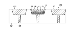
- FIG. 3A and 3B are diagrams showing configuration examples of the capacitive element according to the first embodiment of the present disclosure.
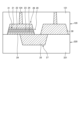
- FIG. 3A is a cross-sectional view showing a configuration example of the capacitive element 20.
- FIG. 20 As described above, the capacitive element 20 shown in the figure is arranged between the pad 21 and the pad 25 .
- the capacitive element 20 is configured by laminating a first electrode 22, a dielectric layer 23 and a second electrode 24 in this order.
- capacitive element 20 constitutes an MIM capacitor.
- Pads 21 are arranged in recesses 26 formed on the surface of insulating layer 121 .
- Pads 25 are arranged in recesses 27 formed in the surface of insulating layer 221 .
- the dielectric layer 23 can be made of an insulating member such as aluminum oxide (AlO x ), zirconium oxide (ZrO x ), hafnium oxide (HfO x ), titanium oxide (TiO x ), or the like.
- AlO x aluminum oxide
- ZrO x zirconium oxide
- HfO x hafnium oxide
- TiO x titanium oxide
- the first electrode 22 and the second electrode 24 are made of metals such as titanium (Ti), tantalum (Ta) and tungsten (W), and conductive members such as titanium nitride (TiN) and tantalum nitride (TaN). Can be configured. Also, these members can be used in combination.
- the first electrode 22 and the second electrode 24 can have a function as a barrier layer.
- the barrier layer is arranged between the pad 21 and the like and the insulating layer 121 in order to prevent diffusion of the members forming the pad 21 and the like into the insulating layer 121 and the like.
- a barrier layer is also arranged on the pad 21 , the via plug 124 and the wiring 122 .
- the capacitive element 20 shown in the figure can be placed in the recess 28 formed in the pad 25 .
- This recess 28 is formed in a partial region of the surface of pad 25 .
- the capacitive element 20 can be formed.
- the second electrode 24 must not be arranged on the side wall of the recess 28 in the region in contact with the pad 21 . This is to prevent short circuit between the pad 21 and the second electrode 24 . This can be done by selective deposition of the second electrode 24 only on the surface of the pad 25 in the recess 28 .
- the removal of the member of the second electrode 24 can be performed by anisotropic dry etching.
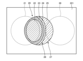
- FIG. 3B is a plan view showing a configuration example of the capacitive element 20.
- FIG. This figure shows the configuration of the surface of the wiring region 220 viewed from the semiconductor chip 100 side. Note that the dotted lines in FIG.
- the second electrode 24 and the first electrode 22 are arranged in the concave portion 28 so as not to overlap each other. Also, the capacitive element connection pad 30 is bonded and connected to a region different from the region where the recess 28 of the pad 25 is formed.
- the semiconductor element 10 can arrange the capacitive element 20 of the circuit to be accommodated at the interface between the wiring area 120 and the wiring area 220 . Since the capacitive element 20 can be arranged in the area used for inter-pad connection, the area of the semiconductor chip 100 can be reduced compared to the case where the capacitive element 20 is arranged in the wiring area 120 or the like. Also, the capacitive element 20 can be arranged in the dummy connection area of the pad-to-pad connection. Here, the dummy connection is an inter-pad connection by an electrically isolated pad. This dummy connection is arranged to improve the bonding strength of the wiring regions 120 and 220, or the like. The area of the semiconductor chip 100 and the like can be further reduced by arranging the capacitive element 20 in the dummy connection region of the pad-to-pad connection.
- the configuration of the pad 25 is not limited to this example.
- a pad 25 having a rectangular shape in plan view can also be used.
- the pads 21 and the capacitive element connection pads 30 can also be configured in a rectangular shape or the like in plan view.
- FIGS. 4A-4H are diagrams illustrating an example method of manufacturing a semiconductor device according to the first embodiment of the present disclosure.
- 4A and 4B are diagrams showing the manufacturing process of the semiconductor element 10.
- FIG. Note that the description of the semiconductor substrates 110 and 210 is omitted in FIG.
- the insulating layer 221 and the wiring 222 are arranged on the surface side of the semiconductor substrate 210 (FIG. 4A).
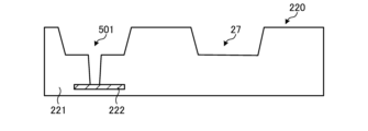
- the aforementioned recesses 27 and 501 are formed on the surface of the insulating layer 221 (FIG. 4B).
- a pad 225 and a via plug 224 are arranged in this recess 501 .
- the formation of the recesses 27 and 501 can be performed by etching the insulating layer 221 .
- a barrier layer (not shown) is placed on the walls of the recesses 27 and 501 to form via plugs 224, pads 225 and pads 25 (FIG. 4C). This can be done by plating a Cu layer.
- recesses 28 are formed in pads 25 (Fig. 4D). This can be done by etching the pads 25 .
- the second electrode 24 is placed in the recess 28 (Fig. 4E). This can be done by the selective deposition described above.
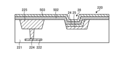
- a material film 502 forming the dielectric layer 23 and a material film 503 forming the first electrode 22 are laminated in order on the surface of the wiring region 220 including the recess 28 (FIG. 4F).
- the surface of the wiring region 220 is ground to remove the material films 502 and 503 located in regions other than the recesses 28 (FIG. 4G). Grinding of the surface of the wiring region 220 can be performed by chemical mechanical polishing (CMP), for example. Thereby, the capacitive element 20 can be formed.
- CMP chemical mechanical polishing
- the surface of the wiring region 120 of the semiconductor chip 100 is joined to the surface of the wiring region 220 (FIG. 4H). This can be done by subjecting the surfaces of the wiring region 220 and the wiring region 120 to plasma treatment, aligning and superimposing them, and heat-pressing them.
- the semiconductor device 10 can be manufactured by the above steps.
- the capacitive elements 20 are arranged on the pads 25 for connecting the semiconductor substrates. Since the concave portion 28 is formed in a region having a larger area than the via plug 224 and the like and the capacitive element 20 is arranged, the capacitive element 20 can be easily manufactured.
- the capacitive elements 20 are arranged on the pads 25 .
- the semiconductor element 10 of the second embodiment of the present disclosure differs from the above-described first embodiment in that the capacitive elements 20 are arranged on the pads 21 .
- FIG. 5 is a diagram illustrating a configuration example of a capacitive element according to a second embodiment of the present disclosure; This figure, like FIG. 3A, is a cross-sectional view showing a configuration example of the capacitive element 20. As shown in FIG. The capacitive element 20 in FIG. 3 is different from the capacitive element 20 in FIG. 3A in that it is arranged on the pad 21 .
- the capacitive element 20 in the figure is arranged in a recess 31 formed in the pad 21 .
- the capacitive element 20 shown in the figure is formed by laminating a first electrode 22 , a dielectric layer 23 and a second electrode 24 in order in a recess 31 .
- a conductive film 29 can be laminated on the capacitive element 20 .
- This conductive film 29 can be made of Cu, for example.
- FIGS. 4A-4H are diagrams illustrating an example of a method for manufacturing a semiconductor device according to the first embodiment of the present disclosure.
- 4A and 4B are diagrams showing the manufacturing process of the semiconductor element 10.
- FIG. Note that the semiconductor substrates 110 and 210 are omitted as in FIGS. 4A-4H.
- an insulating layer 121, wiring 122 (not shown), via plugs 124, pads 125 and 21, and capacitive element connection pads 30 are arranged on the surface side of the semiconductor substrate 110 (FIG. 6A).
- a recess 31 is formed in the surface of the pad 21 (FIG. 6B).
- the first electrode 22 , the dielectric layer 23 and the second electrode 24 are stacked in the recess 31 to form the capacitive element 20 .
- a conductive film 29 is formed. This can be done by a plating method using the second electrode 24 as a seed layer. It can also be formed by PVD (Physical Vapor Deposition) (Fig. 6C).
- the semiconductor element 10 can be manufactured.
- the configuration of the semiconductor device 10 other than this is the same as the configuration of the semiconductor device 10 according to the first embodiment of the present disclosure, so description thereof will be omitted.
- the capacitive elements 20 are arranged on the pads 21 .
- the capacitive element 20 can be easily manufactured.
- the capacitive elements 20 are arranged on the pads 25 .
- the semiconductor element 10 of the third embodiment of the present disclosure is connected to pads 25 .
- This embodiment differs from the above-described first embodiment in that the parasitic capacitance between the pad 21 and the capacitive element connection pad 30 is further used.
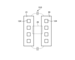
- FIGS. 7A and 7B are diagrams showing configuration examples of capacitive elements according to the third embodiment of the present disclosure. This figure shows the configuration of the capacitive element 20 viewed from the semiconductor substrate 110 side of the semiconductor chip 100 . A dashed line in the figure represents the pad 25 .
- the pads 21 and the capacitive element connection pads 30 in FIG. 7A are configured in a rectangular shape in plan view, and are arranged in a shape facing each other on the long sides. Thereby, a parasitic capacitance 510 having a relatively high capacitance is formed between the pad 21 and the capacitive element connection pad 30 . Since the parasitic capacitance 510 is connected in parallel to the capacitive element 20, the capacitance of the capacitive element 20 can be increased.
- FIG. 7B is a diagram showing an example in which via plugs 129 are arranged instead of via plugs 124.
- the via plug 129 is a via plug configured with a rectangular cross section.
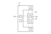
- FIGS. 8A and 8B are diagrams showing other configuration examples of the capacitive element according to the third embodiment of the present disclosure.
- This figure shows an example in which the surfaces of the pad 21 and the capacitive element connection pad 30 facing each other are further widened.
- this figure shows an example in which a plurality of pads 25 are arranged.
- a capacitive element 20 (not shown) can be arranged on each of these pads 25 .
- the configuration of the semiconductor device 10 other than this is the same as the configuration of the semiconductor device 10 according to the first embodiment of the present disclosure, so description thereof will be omitted.
- the semiconductor element 10 of the third embodiment of the present disclosure uses the pad 21 and the capacitive element connection pad 30 whose surfaces facing each other are widened. Thereby, the capacitance of the capacitive element 20 can be increased.
- FIGS. 9A and 9B are diagrams showing configuration examples of capacitive elements according to modifications of the embodiment of the present disclosure. This figure shows an example in which the capacitive element connection pad 30 is omitted and the pad 25 is connected to the via plug 224 .
- 9A shows an example in which the capacitive element 20 is arranged on the pad 25, and
- FIG. 9B shows an example in which the capacitive element 20 is arranged on the pad 21.
- FIG. When the capacitive element 20 is connected between the electronic circuits arranged on the semiconductor substrates 110 and 210, the via plugs 224 and wirings 222 (not shown) are connected to the pads 25 to connect to the electronic circuit of the semiconductor substrate 210. can be taken.
- the semiconductor device 10 of the first embodiment described above can be applied to various products.
- the technology according to the present disclosure may be applied to an EVS (Event-based Vision Sensor).
- This EVS is a system that detects the movement of an object by detecting changes in brightness of an image of the object.
- the EVS has an image sensor with a plurality of pixels. These pixels detect that the absolute value of the amount of change in luminance of incident light exceeds a threshold as an address event.
- This event includes, for example, an on-event indicating that the amount of increase in luminance has exceeded the threshold in the increasing direction, and an off-event indicating that the amount of decrease in luminance has fallen below the threshold in the decreasing direction.
- the imaging device generates a detection signal indicating the event detection result for each pixel.
- Each detection signal includes a detection signal indicating presence/absence of an on-event and a detection signal indicating presence/absence of an off-event.
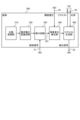
- FIG. 10 is a block diagram showing a configuration example of an imaging device to which the technology according to the present disclosure can be applied.
- An imaging device 1 in the figure constitutes an EVS system.
- the imaging device 1 includes a pixel array section 50 , a control circuit 60 , an arbiter 70 , a signal processing section 80 and a threshold voltage generation section 90 .
- the pixel array section 50 is configured by arranging a plurality of pixels 300 .
- a pixel array section 50 in the figure represents an example in which pixels 300 are arranged in a two-dimensional matrix.
- the pixel 300 includes a photoelectric conversion unit that photoelectrically converts incident light, and detects an event based on the amount of change in photocurrent based on the photoelectric conversion.
- the pixel 300 that has detected an event outputs an event detection signal to the control circuit 60 and the signal processing section 80, which will be described later.
- the control circuit 60 outputs a control signal to the pixel 300 that has output the detection signal, and resets the event detected in the pixel 300 .
- the signal processing unit 80 performs predetermined signal processing on the detection signal.
- the pixel 300 Prior to outputting this detection signal, the pixel 300 sends a request for outputting the detection signal to the arbiter 70, which will be described later.
- the arbiter 70 selects the pixel 300 that sent the request and outputs a response to the request. This response permits output of the detection signal.
- the control circuit 60 is a circuit that controls resetting of pixel address events in each pixel 300 of the pixel array section 50 .
- This control circuit 60 outputs a control signal for resetting a differentiating circuit 330 arranged in a pixel 300, which will be described later.
- a signal line 51 connects between the pixel 300 and the control circuit 60 .
- An event detection signal from the pixel 300 and a control signal from the control circuit 60 are transmitted by the signal line 51 .
- the arbiter 70 selects the pixel 300 that sent the request. As described above, the pixel 300 that has detected an address event outputs a detection signal to the control circuit 60 and the signal processing section 80 . This control signal must be supplied exclusively to one pixel 300 . This is to prevent collision when outputting detection signals in the plurality of pixels 300 . Therefore, the arbiter 70 arbitrates the plurality of pixels 300 for which the pixel address event has been detected. Specifically, the arbiter 70 selects one of the pixels 300 that sent the request and returns a response to this selected pixel 300 . This response represents the result of the selection. A signal line 52 connects between the pixel 300 and the arbiter 70 . Requests from pixels 300 and responses from arbiter 70 are communicated by signal line 52 .
- the arbiter 70 can select the pixels 300 in the order in which the requests were sent. At this time, the arbiter 70 can preferentially select a specific pixel 300 . For example, the arbiter 70 can preferentially select a pixel 300 that has transmitted a request with a high priority, which will be described later.
- the signal processing unit 80 performs predetermined signal processing on detection signals from the pixels 300 .
- the signal processing unit 80 can arrange such detection signals as image signals in a two-dimensional matrix to generate image data having 2-bit information for each pixel 300 .
- the signal processing unit 80 can perform signal processing such as image recognition processing on the generated image data.
- a signal line 53 connects between the pixel 300 and the signal processing unit 80 .
- a detection signal from the pixel 300 is transmitted through the signal line 53 .
- the threshold voltage generation unit 90 generates a threshold voltage, which is a voltage corresponding to the above threshold.
- the threshold voltage generator 90 supplies the generated threshold voltage to the pixels 300 .
- the threshold voltage is transmitted by signal line 54 .
- FIG. 11 is a diagram showing a configuration example of a pixel to which the technology according to the present disclosure can be applied. This figure is a diagram showing a configuration example of the pixel 300 . A pixel 300 shown in FIG.
- the photoelectric conversion unit 310 performs photoelectric conversion of incident light.
- This photoelectric conversion section 310 can be configured by a photodiode. This photoelectric conversion generates an electric charge corresponding to the luminance of the incident light.
- a photocurrent which is a current corresponding to the generated charges, can be supplied to an external circuit.
- the current-voltage conversion circuit 320 converts the photocurrent from the photoelectric conversion section 310 into a voltage signal. During this conversion, the current-voltage conversion circuit 320 also performs logarithmic compression of the voltage signal. The converted voltage signal is output to the differentiating circuit 330 . Details of the configuration of the current-voltage conversion circuit 320 will be described later.
- the differentiating circuit 330 extracts the amount of change in the voltage signal output from the current-voltage conversion circuit 320 and integrates the amount of change to generate a signal corresponding to the amount of change in the voltage signal. This signal corresponds to a signal corresponding to a change in luminance of incident light. This signal is called an optical signal.
- the differentiation circuit 330 outputs the generated optical signal to the luminance change detection section 340 . This optical signal is transmitted by the signal line 301 .
- the differentiating circuit 330 receives a control signal from the control circuit 60 . This control signal is a signal for resetting the circuit that detects the amount of change in the voltage signal. The details of the configuration of the differentiating circuit 330 will be described later.
- the luminance change detection section 340 detects the luminance change of incident light.
- a luminance change detector 340 in FIG. 2 detects a change in the optical signal output from the differentiating circuit 330 based on the threshold voltage supplied from the threshold voltage generator 90 .
- a detection result is output to the request generation unit 360 .
- the request generation unit 360 generates a request requesting transfer of the luminance change detection result in the luminance change detection unit 340 and outputs the request to the arbiter 70 . Further, when a response to the request is output from the arbiter 70 , the request generator 360 outputs a luminance change detection signal to the signal processor 80 and the control circuit 60 .
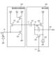
- FIG. 12 is a diagram illustrating a configuration example of a current-voltage conversion circuit and a differentiating circuit to which the technology according to the present disclosure can be applied; This figure is a circuit diagram showing a configuration example of the current-voltage conversion circuit 320 and the differentiating circuit 330 . Note that a photoelectric conversion unit 310 is further illustrated in FIG.
- a current-voltage conversion circuit 320 in the figure includes MOS transistors 321 to 323 .
- Vdd represents a power line Vdd for supplying power.
- Vb1 represents a signal line Vb1 that supplies a bias voltage.
- MOS transistors 321 and 323 can be n-channel MOS transistors. A p-channel MOS transistor can be used for the MOS transistor 322 .
- the anode of the photoelectric conversion unit 310 is grounded, and the cathode is connected to the input of the current-voltage conversion circuit 320 via the signal line 16.
- signal line 16 is connected to the source of MOS transistor 321 and the gate of MOS transistor 323 .
- the drains of the MOS transistors 321 and 322 are connected to the power supply line Vdd, and the gate of the MOS transistor 322 is connected to the signal line Vb1.
- the source of the MOS transistor 323 is grounded, and the drain is connected to the gate of the MOS transistor 321 , the drain of the MOS transistor 322 and the signal line 17 which is the output signal line of the current-voltage conversion circuit 320 .
- One end of the capacitor of the differentiating circuit 330 is connected to the signal line 17 .
- the MOS transistor 321 is a MOS transistor that supplies current to the photoelectric conversion section 310 .
- a sink current (photocurrent) corresponding to incident light flows through the photoelectric conversion unit 310 .
- MOS transistor 321 supplies this sink current.
- the gate of the MOS transistor 321 is driven by the output voltage of the MOS transistor 323 to be described later, and outputs a source current equal to the sink current of the photoelectric conversion section 310 . Since the gate-source voltage Vgs of the MOS transistor is a voltage corresponding to the source current, the source voltage of the MOS transistor 321 is a voltage corresponding to the current of the photoelectric conversion section 310 . Thereby, the photocurrent of the photoelectric conversion unit 310 is converted into a voltage signal.
- the MOS transistor 323 is a MOS transistor that amplifies the source voltage of the MOS transistor 321 .
- MOS transistor 322 forms a constant current load for MOS transistor 323 .
- An amplified voltage signal is output to the drain of the MOS transistor 323 .
- This voltage signal is output to signal line 17 and fed back to the gate of MOS transistor 321 .
- Vgs of MOS transistor 321 is equal to or lower than the threshold voltage, the source current changes exponentially with respect to changes in Vgs. Therefore, the output voltage of the MOS transistor 323 fed back to the gate of the MOS transistor 321 is a voltage signal obtained by logarithmically compressing the photocurrent of the photoelectric conversion unit 310 equal to the source current of the MOS transistor 321 .
- a differentiating circuit 330 in the figure includes capacitive elements 331 and 332 , MOS transistors 333 and 334 , and a constant current circuit 335 .
- MOS transistors 333 and 334 can be p-channel MOS transistors.
- one end of the capacitive element 331 is connected to the signal line 17, and the other end of the capacitive element 331 is connected to the gate of the MOS transistor 333, the drain of the MOS transistor 334, and one end of the capacitive element 332 via the signal line 18.
- the other end of the capacitive element 332 is connected to the drain of the MOS transistor 333 , the drain of the MOS transistor 334 , the sink side terminal of the constant current circuit 335 and the signal line 301 .
- the source of MOS transistor 333 is connected to power supply line Vdd
- the gate of MOS transistor 334 is connected to signal line 51 .
- a sink side terminal of the constant current circuit 335 is grounded.
- the capacitive element 331 corresponds to a coupling capacitor. This capacitive element 331 blocks the DC component of the output voltage of the current-voltage conversion circuit 320 and allows only the AC component to pass. Also, a current based on the change in the output voltage of the current-voltage conversion circuit 320 is supplied to the gate of the MOS transistor 333 via the capacitive element 331 . The AC component of the output voltage of the current-voltage conversion circuit 320 corresponds to the variation of the photocurrent.
- the MOS transistor 333 and constant current circuit 335 constitute an inverting amplifier circuit. MOS transistor 522 constitutes a constant current load.
- a change in the output voltage of the current-voltage conversion circuit 320 is input to the gate of the MOS transistor 333 via the capacitive element 331, inverted and amplified by the MOS transistor 333, and output to the drain. Therefore, a current based on the change in the output voltage of the current-voltage conversion circuit 320 flows through the capacitive element 332, and the capacitive element 332 is charged and discharged. That is, the amount of change in the output voltage of the current-voltage conversion circuit 320 is accumulated (integrated).
- An optical signal which is a signal corresponding to the amount of change in the voltage signal output from the current-voltage conversion circuit 320 , is output to the signal line 301 .
- the MOS transistor 334 resets the differentiating circuit 330 .
- both ends of the capacitive element 332 are short-circuited.
- the accumulated change in the output voltage of the current-voltage conversion circuit 320 is discharged and reset. Due to this reset, the output voltage of the differentiating circuit 330 becomes, for example, the midpoint voltage between the power supply line Vdd and the ground line.
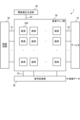
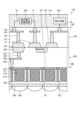
- FIG. 13 is a diagram illustrating a configuration example of a pixel array unit to which the technology according to the present disclosure can be applied; This figure is a cross-sectional view showing a configuration example of the pixel array section 50 .
- the pixel array section 50 can have the same configuration as the semiconductor element 10 in FIG.
- a photoelectric conversion unit 310 is arranged on the semiconductor substrate 210 .
- a semiconductor region 211 arranged on a semiconductor substrate 210 constitutes a photoelectric conversion section 310 .
- a photodiode composed of a pn junction formed between the semiconductor region 211 and the surrounding well region corresponds to the photoelectric conversion section 310 .
- Charges generated by the photoelectric conversion unit 310 are transferred to the semiconductor region 212 by a transfer transistor (not shown).
- a contact plug 223 forming the signal line 16 is connected to the semiconductor region 212 .
- An isolation region 219 is arranged between the photoelectric conversion units 310 of the semiconductor substrate 110 .
- a protective film 230 , a color filter 240 and an on-chip lens 250 are arranged in this order on the back surface side of the semiconductor substrate 110 .
- a current-voltage conversion circuit 320 and a differentiation circuit 330 are arranged on the semiconductor substrate 110 . Also, the capacitive element 331 is arranged on the pad 25 in the same manner as the capacitive element 20 in FIG.
- the EVS can be miniaturized.
- the configuration of the second embodiment of the present disclosure can be applied to other embodiments.
- the conductive film 29 in FIG. 5 can be applied to the capacitive element 20 in FIG. 3A.
- the present technology can also take the following configuration. (1) a first semiconductor substrate; a second semiconductor substrate; a first wiring region arranged adjacent to the first semiconductor substrate; a second wiring region arranged adjacent to the second semiconductor substrate and having its surface joined to the surface of the first wiring region; a first pad embedded in the surface of the first wiring region; A position embedded in the surface of the second wiring region and overlapping the first pad in plan view when the surface of the first wiring region and the surface of the second wiring region are joined together a second pad located in the a capacitive element configured by sequentially stacking a first electrode, a dielectric layer, and a second electrode disposed on either one of the first pad and the second pad; A capacitor which is a pad embedded in the surface of the first wiring region and connected to the second pad when the surface of the first wiring region and the surface of the second wiring region are joined together.
- the capacitive element is arranged in a recess formed in the surface of the second pad;
- Imaging element 10 semiconductor element 11-13 electronic circuit 20, 331 capacitive element 21, 25, 125, 225 pad 22 first electrode 23 dielectric layer 24 second electrode 26-28, 31 recess 29 conductive film 30 capacitive element Connection Pad 50 Pixel Array Section 100, 200 Semiconductor Chip 110, 210 Semiconductor Substrate 120, 220 Wiring Area 310 Photoelectric Conversion Section 320 Current-Voltage Conversion Circuit 330 Differentiation Circuit
Landscapes
- Semiconductor Integrated Circuits (AREA)
Abstract
Description
1.第1の実施形態
2.第2の実施形態
3.第3の実施形態
4.変形例
5.応用例
[半導体素子の構成]
図1は、本開示の実施形態に係る半導体素子の構成例を示す図である。同図は、半導体素子10の構成例を表す図である。半導体素子10は、半導体チップ100及び半導体チップ200が積層されて構成される半導体素子である。同図の半導体チップ100は、半導体基板110及び配線領域120を備える。また、同図の半導体チップ200は、半導体基板210及び配線領域220を備える。同図に表したように、半導体チップ100及び半導体チップ200は、それぞれの配線領域が接合されて積層される。
図2は、本開示の第1の実施形態に係る半導体素子の構成例を示す図である。同図は、半導体素子10の構成例を表す断面図である。前述のように、半導体チップ100は半導体基板110及び配線領域120を備え、半導体チップ200は半導体基板210及び配線領域220を備える。
図3A及び3Bは、本開示の第1の実施形態に係る容量素子の構成例を示す図である。図3Aは、容量素子20の構成例を表す断面図である。前述のように、同図の容量素子20は、パッド21及びパッド25の間に配置される。容量素子20は、第1の電極22、誘電体層23及び第2の電極24が順に積層されて構成される。このように、容量素子20は、MIMキャパシタを構成する。なお、パッド21は、絶縁層121の表面に形成された凹部26に配置される。パッド25は、絶縁層221の表面に形成された凹部27に配置される。
図4A-4Hは、本開示の第1の実施形態に係る半導体素子の製造方法の一例を示す図である。同図は、半導体素子10の製造工程を表す図である。なお、同図において、半導体基板110及び210の記載を省略する。
上述の第1の実施形態の半導体素子10は、パッド25に容量素子20が配置されていた。これに対し、本開示の第2の実施形態の半導体素子10は、パッド21に容量素子20が配置される点で、上述の第1の実施形態と異なる。
図5は、本開示の第2の実施形態に係る容量素子の構成例を示す図である。同図は、図3Aと同様に、容量素子20の構成例を表す断面図である。同図の容量素子20は、パッド21に配置される点で、図3Aの容量素子20と異なる。
図6A-6Cは、本開示の第1の実施形態に係る半導体素子の製造方法の一例を示す図である。同図は、半導体素子10の製造工程を表す図である。なお、図4A-4Hと同様に、半導体基板110及び210の記載を省略する。
上述の第1の実施形態の半導体素子10は、パッド25に容量素子20を配置していた。これに対し、本開示の第3の実施形態の半導体素子10は、パッド25に接続される。パッド21及び容量素子接続パッド30の間の寄生容量を更に使用する点で、上述の第1の実施形態と異なる。
図7A及び7Bは、本開示の第3の実施形態に係る容量素子の構成例を示す図である。同図は、半導体チップ100の半導体基板110の側から見た容量素子20の構成を表す図である。同図の破線は、パッド25を表す。
図8A及び8Bは、本開示の第3の実施形態に係る容量素子の他の構成例を示す図である。同図は、パッド21及び容量素子接続パッド30の互いに対向する面を更に広くする場合の例を表す図である。また、同図は、複数のパッド25を配置する例を表したものである。これらのパッド25には、それぞれ容量素子20(不図示)を配置することができる。
上述の第1の実施形態の半導体素子10は、容量素子接続パッド30を使用していたが、他の構成を採ることもできる。
図9A及び9Bは、本開示の実施形態の変形例に係る容量素子の構成例を示す図である。同図は、容量素子接続パッド30を省略し、パッド25にビアプラグ224を接続する場合の例を表したものである。図9Aはパッド25に容量素子20が配置される場合の例を表し、図9Bはパッド21に容量素子20が配置される場合の例を表す。容量素子20が半導体基板110及び210に配置される電子回路の間に接続される場合には、パッド25にビアプラグ224及び不図示の配線222を接続して半導体基板210の電子回路に接続する構成を採ることができる。
上述の第1の実施形態の半導体素子10は、様々な製品へ応用することができる。例えば、本開示に係る技術は、EVS(Event-based Vision Sensor)に適用されてもよい。このEVSは、被写体の画像の輝度変化を検出することにより、対象物の動きを検出するシステムである。EVSは、複数の画素を有する撮像素子を備える。これら複数の画素は、入射光の輝度の変化量の絶対値が閾値を超えた旨をアドレスイベントとして検出する。このイベントは、たとえば、輝度の上昇量が上昇方向の閾値を超えた旨を示すオンイベントと、輝度の低下量が低下方向の閾値を下回った旨を示すオフイベントとを含む。そして、撮像素子は、イベントの検出結果を示す検出信号を画素毎に生成する。それぞれの検出信号は、オンイベントの有無を示す検出信号と、オフイベントの有無を示す検出信号とを含む。
図10は、本開示に係る技術が適用され得る撮像素子の構成例を示すブロック図である。同図の撮像素子1は、EVSシステムを構成する。この撮像素子1は、画素アレイ部50と、制御回路60と、アービタ70と、信号処理部80と、閾値電圧生成部90とを備える。
図11は、本開示に係る技術が適用され得る画素の構成例を示す図である。同図は、画素300の構成例を表す図である。同図の画素300は、光電変換部310と、電流電圧変換回路320と、微分回路330と、輝度変化検出部340と、リクエスト生成部360とを備える。
図12は、本開示に係る技術が適用され得る電流電圧変換回路及び微分回路の構成例を示す図である。同図は、電流電圧変換回路320及び微分回路330の構成例を表す回路図である。なお、同図には、光電変換部310をさらに記載した。
同図の微分回路330は、容量素子331及び332と、MOSトランジスタ333及び334と、定電流回路335とを備える。MOSトランジスタ333及び334にはpチャネルMOSトランジスタを使用することができる。
図13は、本開示に係る技術が適用され得る画素アレイ部の構成例を示す図である。同図は、画素アレイ部50の構成例を表す断面図である。画素アレイ部50は、図2の半導体素子10と同様の構成を採ることができる。
(1)
第1の半導体基板と、
第2の半導体基板と、
前記第1の半導体基板に隣接して配置される第1の配線領域と、
前記第2の半導体基板に隣接して配置されるとともに自身の表面が前記第1の配線領域の表面に接合される第2の配線領域と、
前記第1の配線領域の表面に埋め込まれて配置される第1のパッドと、
前記第2の配線領域の表面に埋め込まれて配置されるとともに前記第1の配線領域の表面及び前記第2の配線領域の表面が接合された際に前記第1のパッドと平面視において重なる位置に配置される第2のパッドと、
前記第1のパッド及び前記第2のパッドの何れか一方に配置される第1の電極、誘電体層及び第2の電極が順に積層されて構成される容量素子と、
前記第1の配線領域の表面に埋め込まれて配置されて前記第1の配線領域の表面及び前記第2の配線領域の表面が接合された際に前記第2のパッドと接続するパッドである容量素子接続パッドと
を有する半導体素子。
(2)
前記容量素子に積層される導電膜を更に有する前記(1)に記載の半導体素子。
(3)
前記容量素子は、前記第1のパッド及び前記第2のパッドの何れかの表面に形成された凹部に配置される前記(1)又は(2)に記載の半導体素子。
(4)
前記容量素子は、前記第2のパッドの表面に形成された凹部に配置され、
前記容量素子接続パッドは、前記第2のパッドの表面における前記凹部とは異なる領域に接続される
前記(1)に記載の半導体素子。
(5)
前記第1の配線領域は、前記第1のパッドに接続する配線及び前記容量素子接続パッドに接続する配線を備える前記(1)から(4)の何れかに記載の半導体素子。
(6)
第1の半導体基板と、
第2の半導体基板と、
前記第1の半導体基板に隣接して配置される第1の配線領域と、
前記第2の半導体基板に隣接して配置されるとともに自身の表面が前記第1の配線領域の表面に接合される第2の配線領域と、
前記第1の配線領域の表面に埋め込まれて配置される第1のパッドと、
前記第2の配線領域の表面に埋め込まれて配置されるとともに前記第1の配線領域の表面及び前記第2の配線領域の表面が接合された際に前記第1のパッドと平面視において重なる位置に配置される第2のパッドと、
前記第1のパッド及び前記第2のパッドの何れか一方に配置される第1の電極、誘電体層及び第2の電極が順に積層されて構成される容量素子と、
前記第1の配線領域の表面に埋め込まれて配置されて前記第1の配線領域の表面及び前記第2の配線領域の表面が接合された際に前記第2のパッドと接続するパッドである容量素子接続パッドと
前記第1の配線領域に配置される配線を介して前記第1のパッドに接続される第1の電子回路と、
前記第1の配線領域に配置される配線を介して前記容量素子接続パッドに接続される第2の電子回路と、
を有する半導体装置。
10 半導体素子
11~13 電子回路
20、331 容量素子
21、25、125、225 パッド
22 第1の電極
23 誘電体層
24 第2の電極
26~28、31 凹部
29 導電膜
30 容量素子接続パッド
50 画素アレイ部
100、200 半導体チップ
110、210 半導体基板
120、220 配線領域
310 光電変換部
320 電流電圧変換回路
330 微分回路
Claims (6)
- 第1の半導体基板と、
第2の半導体基板と、
前記第1の半導体基板に隣接して配置される第1の配線領域と、
前記第2の半導体基板に隣接して配置されるとともに自身の表面が前記第1の配線領域の表面に接合される第2の配線領域と、
前記第1の配線領域の表面に埋め込まれて配置される第1のパッドと、
前記第2の配線領域の表面に埋め込まれて配置されるとともに前記第1の配線領域の表面及び前記第2の配線領域の表面が接合された際に前記第1のパッドと平面視において重なる位置に配置される第2のパッドと、
前記第1のパッド及び前記第2のパッドの何れか一方に配置される第1の電極、誘電体層及び第2の電極が順に積層されて構成される容量素子と、
前記第1の配線領域の表面に埋め込まれて配置されて前記第1の配線領域の表面及び前記第2の配線領域の表面が接合された際に前記第2のパッドと接続するパッドである容量素子接続パッドと
を有する半導体素子。 - 前記容量素子に積層される導電膜を更に有する請求項1に記載の半導体素子。
- 前記容量素子は、前記第1のパッド及び前記第2のパッドの何れかの表面に形成された凹部に配置される請求項1に記載の半導体素子。
- 前記容量素子は、前記第2のパッドの表面に形成された凹部に配置され、
前記容量素子接続パッドは、前記第2のパッドの表面における前記凹部とは異なる領域に接続される
請求項1に記載の半導体素子。 - 前記第1の配線領域は、前記第1のパッドに接続する配線及び前記容量素子接続パッドに接続する配線を備える請求項1に記載の半導体素子。
- 第1の半導体基板と、
第2の半導体基板と、
前記第1の半導体基板に隣接して配置される第1の配線領域と、
前記第2の半導体基板に隣接して配置されるとともに自身の表面が前記第1の配線領域の表面に接合される第2の配線領域と、
前記第1の配線領域の表面に埋め込まれて配置される第1のパッドと、
前記第2の配線領域の表面に埋め込まれて配置されるとともに前記第1の配線領域の表面及び前記第2の配線領域の表面が接合された際に前記第1のパッドと平面視において重なる位置に配置される第2のパッドと、
前記第1のパッド及び前記第2のパッドの何れか一方に配置される第1の電極、誘電体層及び第2の電極が順に積層されて構成される容量素子と、
前記第1の配線領域の表面に埋め込まれて配置されて前記第1の配線領域の表面及び前記第2の配線領域の表面が接合された際に前記第2のパッドと接続するパッドである容量素子接続パッドと
前記第1の配線領域に配置される配線を介して前記第1のパッドに接続される第1の電子回路と、
前記第1の配線領域に配置される配線を介して前記容量素子接続パッドに接続される第2の電子回路と、
を有する半導体装置。
Priority Applications (3)
| Application Number | Priority Date | Filing Date | Title |
|---|---|---|---|
| DE112022006462.5T DE112022006462T5 (de) | 2022-01-17 | 2022-12-28 | Halbleiterelement und halbleitereinrichtung |
| JP2023573988A JPWO2023136170A1 (ja) | 2022-01-17 | 2022-12-28 | |
| CN202280088513.5A CN118451551A (zh) | 2022-01-17 | 2022-12-28 | 半导体器件及半导体装置 |
Applications Claiming Priority (2)
| Application Number | Priority Date | Filing Date | Title |
|---|---|---|---|
| JP2022-005360 | 2022-01-17 | ||
| JP2022005360 | 2022-01-17 |
Publications (1)
| Publication Number | Publication Date |
|---|---|
| WO2023136170A1 true WO2023136170A1 (ja) | 2023-07-20 |
Family
ID=87278975
Family Applications (1)
| Application Number | Title | Priority Date | Filing Date |
|---|---|---|---|
| PCT/JP2022/048575 Ceased WO2023136170A1 (ja) | 2022-01-17 | 2022-12-28 | 半導体素子及び半導体装置 |
Country Status (4)
| Country | Link |
|---|---|
| JP (1) | JPWO2023136170A1 (ja) |
| CN (1) | CN118451551A (ja) |
| DE (1) | DE112022006462T5 (ja) |
| WO (1) | WO2023136170A1 (ja) |
Citations (7)
| Publication number | Priority date | Publication date | Assignee | Title |
|---|---|---|---|---|
| JP2008147300A (ja) * | 2006-12-07 | 2008-06-26 | Toshiba Corp | 半導体装置およびその製造方法 |
| JP2009010388A (ja) * | 2007-06-26 | 2009-01-15 | Dongbu Hitek Co Ltd | Mimキャパシタ及びその製造方法 |
| WO2014184988A1 (ja) * | 2013-05-16 | 2014-11-20 | パナソニックIpマネジメント株式会社 | 半導体装置及びその製造方法 |
| US20170092620A1 (en) * | 2015-09-28 | 2017-03-30 | Invensas Corporation | Capacitive Coupling of Integrated Circuit Die Components |
| US20190123088A1 (en) * | 2017-10-24 | 2019-04-25 | Samsung Electronics Co., Ltd. | Stacked cmos image sensor |
| WO2019124112A1 (ja) * | 2017-12-21 | 2019-06-27 | ソニーセミコンダクタソリューションズ株式会社 | 半導体装置およびその製造方法 |
| JP2021048204A (ja) * | 2019-09-17 | 2021-03-25 | キオクシア株式会社 | 半導体装置及びその製造方法 |
-
2022
- 2022-12-28 CN CN202280088513.5A patent/CN118451551A/zh active Pending
- 2022-12-28 DE DE112022006462.5T patent/DE112022006462T5/de active Pending
- 2022-12-28 WO PCT/JP2022/048575 patent/WO2023136170A1/ja not_active Ceased
- 2022-12-28 JP JP2023573988A patent/JPWO2023136170A1/ja active Pending
Patent Citations (7)
| Publication number | Priority date | Publication date | Assignee | Title |
|---|---|---|---|---|
| JP2008147300A (ja) * | 2006-12-07 | 2008-06-26 | Toshiba Corp | 半導体装置およびその製造方法 |
| JP2009010388A (ja) * | 2007-06-26 | 2009-01-15 | Dongbu Hitek Co Ltd | Mimキャパシタ及びその製造方法 |
| WO2014184988A1 (ja) * | 2013-05-16 | 2014-11-20 | パナソニックIpマネジメント株式会社 | 半導体装置及びその製造方法 |
| US20170092620A1 (en) * | 2015-09-28 | 2017-03-30 | Invensas Corporation | Capacitive Coupling of Integrated Circuit Die Components |
| US20190123088A1 (en) * | 2017-10-24 | 2019-04-25 | Samsung Electronics Co., Ltd. | Stacked cmos image sensor |
| WO2019124112A1 (ja) * | 2017-12-21 | 2019-06-27 | ソニーセミコンダクタソリューションズ株式会社 | 半導体装置およびその製造方法 |
| JP2021048204A (ja) * | 2019-09-17 | 2021-03-25 | キオクシア株式会社 | 半導体装置及びその製造方法 |
Also Published As
| Publication number | Publication date |
|---|---|
| CN118451551A (zh) | 2024-08-06 |
| DE112022006462T5 (de) | 2024-10-31 |
| JPWO2023136170A1 (ja) | 2023-07-20 |
Similar Documents
| Publication | Publication Date | Title |
|---|---|---|
| US11984462B2 (en) | Image pickup device and electronic apparatus | |
| US11991468B2 (en) | Solid-state imaging apparatus, manufacturing method of the same, and electronic device | |
| CN109698209B (zh) | 堆叠互补金属氧化物半导体图像传感器 | |
| US11742373B2 (en) | Semiconductor device and method of manufacturing semiconductor device | |
| US12349485B2 (en) | Imaging device | |
| JP6779825B2 (ja) | 半導体装置および機器 | |
| US9087760B2 (en) | Semiconductor device and method of manufacturing the same, and electronic apparatus | |
| US11296020B2 (en) | Semiconductor device and method for manufacturing the same | |
| US11923395B2 (en) | Semiconductor device, solid-state image pickup element, image pickup device, and electronic apparatus | |
| JP2015050463A (ja) | チップ積層イメージセンサ | |
| KR20170135309A (ko) | 3층 적층 이미지 센서 | |
| US11855116B2 (en) | Semiconductor apparatus and device | |
| US8895936B2 (en) | Pixel array and image sensor including the same | |
| CN113675186A (zh) | 光电转换装置、光电转换系统和可移动体 | |
| US12244947B2 (en) | Imaging element and imaging device | |
| WO2023136170A1 (ja) | 半導体素子及び半導体装置 | |
| US20040043556A1 (en) | Capacitor formed in a multilayer wiring structure of a semiconductor device | |
| CN118367005A (zh) | 图像传感器 | |
| US20070155106A1 (en) | Method of manufacturing cmos image sensor | |
| KR102935501B1 (ko) | 이미지 센서 | |
| WO2025197635A1 (ja) | 撮像装置 | |
| JP2024137419A (ja) | 半導体装置および光検出装置 | |
| WO2024004876A1 (ja) | 半導体素子および積層構造体 | |
| CN119856508A (zh) | 两个衬底上的像素布置及用于制造图像传感器的方法 |
Legal Events
| Date | Code | Title | Description |
|---|---|---|---|
| 121 | Ep: the epo has been informed by wipo that ep was designated in this application |
Ref document number: 22920685 Country of ref document: EP Kind code of ref document: A1 |
|
| ENP | Entry into the national phase |
Ref document number: 2023573988 Country of ref document: JP Kind code of ref document: A |
|
| WWE | Wipo information: entry into national phase |
Ref document number: 202280088513.5 Country of ref document: CN Ref document number: 18728043 Country of ref document: US |
|
| WWE | Wipo information: entry into national phase |
Ref document number: 112022006462 Country of ref document: DE |
|
| 122 | Ep: pct application non-entry in european phase |
Ref document number: 22920685 Country of ref document: EP Kind code of ref document: A1 |