WO2023135877A1 - Case - Google Patents
Case Download PDFInfo
- Publication number
- WO2023135877A1 WO2023135877A1 PCT/JP2022/038045 JP2022038045W WO2023135877A1 WO 2023135877 A1 WO2023135877 A1 WO 2023135877A1 JP 2022038045 W JP2022038045 W JP 2022038045W WO 2023135877 A1 WO2023135877 A1 WO 2023135877A1
- Authority
- WO
- WIPO (PCT)
- Prior art keywords
- shutter member
- guide slit
- pair
- case
- biasing member
- Prior art date
Links
- 239000000463 material Substances 0.000 claims description 7
- 210000000078 claw Anatomy 0.000 description 10
- 238000010586 diagram Methods 0.000 description 6
- 239000011347 resin Substances 0.000 description 4
- 229920005989 resin Polymers 0.000 description 4
- 230000004308 accommodation Effects 0.000 description 2
- 239000000853 adhesive Substances 0.000 description 2
- 230000001070 adhesive effect Effects 0.000 description 2
- 230000007246 mechanism Effects 0.000 description 2
- 229920000139 polyethylene terephthalate Polymers 0.000 description 2
- 239000005020 polyethylene terephthalate Substances 0.000 description 2
- -1 Polyethylene terephthalate Polymers 0.000 description 1
- 229920000122 acrylonitrile butadiene styrene Polymers 0.000 description 1
- 238000005452 bending Methods 0.000 description 1
- 239000003990 capacitor Substances 0.000 description 1
- 238000004519 manufacturing process Methods 0.000 description 1
- 239000002184 metal Substances 0.000 description 1
- 230000004048 modification Effects 0.000 description 1
- 238000012986 modification Methods 0.000 description 1
- 238000005192 partition Methods 0.000 description 1
Images


Classifications
-
- H—ELECTRICITY
- H05—ELECTRIC TECHNIQUES NOT OTHERWISE PROVIDED FOR
- H05K—PRINTED CIRCUITS; CASINGS OR CONSTRUCTIONAL DETAILS OF ELECTRIC APPARATUS; MANUFACTURE OF ASSEMBLAGES OF ELECTRICAL COMPONENTS
- H05K13/00—Apparatus or processes specially adapted for manufacturing or adjusting assemblages of electric components
- H05K13/04—Mounting of components, e.g. of leadless components
- H05K13/043—Feeding one by one by other means than belts
-
- H—ELECTRICITY
- H05—ELECTRIC TECHNIQUES NOT OTHERWISE PROVIDED FOR
- H05K—PRINTED CIRCUITS; CASINGS OR CONSTRUCTIONAL DETAILS OF ELECTRIC APPARATUS; MANUFACTURE OF ASSEMBLAGES OF ELECTRICAL COMPONENTS
- H05K5/00—Casings, cabinets or drawers for electric apparatus
- H05K5/06—Hermetically-sealed casings
- H05K5/069—Other details of the casing, e.g. wall structure, passage for a connector, a cable, a shaft
-
- H—ELECTRICITY
- H05—ELECTRIC TECHNIQUES NOT OTHERWISE PROVIDED FOR
- H05K—PRINTED CIRCUITS; CASINGS OR CONSTRUCTIONAL DETAILS OF ELECTRIC APPARATUS; MANUFACTURE OF ASSEMBLAGES OF ELECTRICAL COMPONENTS
- H05K13/00—Apparatus or processes specially adapted for manufacturing or adjusting assemblages of electric components
- H05K13/0084—Containers and magazines for components, e.g. tube-like magazines
-
- H—ELECTRICITY
- H05—ELECTRIC TECHNIQUES NOT OTHERWISE PROVIDED FOR
- H05K—PRINTED CIRCUITS; CASINGS OR CONSTRUCTIONAL DETAILS OF ELECTRIC APPARATUS; MANUFACTURE OF ASSEMBLAGES OF ELECTRICAL COMPONENTS
- H05K13/00—Apparatus or processes specially adapted for manufacturing or adjusting assemblages of electric components
- H05K13/02—Feeding of components
- H05K13/028—Simultaneously loading a plurality of loose objects, e.g. by means of vibrations, pressure differences, magnetic fields
-
- H—ELECTRICITY
- H05—ELECTRIC TECHNIQUES NOT OTHERWISE PROVIDED FOR
- H05K—PRINTED CIRCUITS; CASINGS OR CONSTRUCTIONAL DETAILS OF ELECTRIC APPARATUS; MANUFACTURE OF ASSEMBLAGES OF ELECTRICAL COMPONENTS
- H05K5/00—Casings, cabinets or drawers for electric apparatus
-
- H—ELECTRICITY
- H05—ELECTRIC TECHNIQUES NOT OTHERWISE PROVIDED FOR
- H05K—PRINTED CIRCUITS; CASINGS OR CONSTRUCTIONAL DETAILS OF ELECTRIC APPARATUS; MANUFACTURE OF ASSEMBLAGES OF ELECTRICAL COMPONENTS
- H05K5/00—Casings, cabinets or drawers for electric apparatus
- H05K5/06—Hermetically-sealed casings
- H05K5/065—Hermetically-sealed casings sealed by encapsulation, e.g. waterproof resin forming an integral casing, injection moulding
Definitions
- the present invention relates to a case for housing electronic components such as chip components.
- Patent Literature 1 discloses a case in which loose electronic components are collectively accommodated and the electronic components are dropped by their own weight into a feeder from a discharge port at the bottom. Electronic components are individually supplied to the mounting device by a feeder.
- a case according to the present invention contains a plurality of parts, a case body having an ejection port for ejecting the parts, a guide slit provided in the case body and communicating with the ejection port, and a guide slit that slides into the guide slit.
- a shutter member which is removably inserted and slides to open and close the outlet, wherein the case body has a pair of inner wall surfaces facing each other and forming the guide slit therebetween.
- the shutter member has a pair of main surfaces facing the pair of inner wall surfaces, respectively, and the shutter member is elastically attached to at least one of the pair of inner wall surfaces.
- a biasing member is arranged for biasing.
- the present invention it is possible to provide a case in which the stored parts are prevented from becoming lost, and the parts are easily ejected from the ejection port.
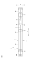
- FIG. 1 is a front view of a case according to a first embodiment
- FIG. 4 is a bottom view of the case according to the first embodiment
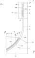
- FIG. 4 It is the figure which looked at the inside of the case which concerns on 1st Embodiment from one side.
- FIG. 4 is a view of the inside of the front portion of the case according to the first embodiment as seen from one side, showing an unsealed state in which the discharge port of the case is open.
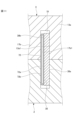
- FIG. 6 is an enlarged view of part VI of FIG. 5 and is a partial cross-sectional view.
- FIG. 7 is a diagram showing a part of a cross section taken along line VII-VII of FIG.
- FIG. 7 is a cross-sectional view showing the lower biasing member according to the second embodiment, and is a cross-sectional view corresponding to the cross section taken along line VII-VII in FIG. 6;
- FIG. 7 is a cross-sectional view showing the lower biasing member according to the third embodiment, and is a cross-sectional view corresponding to the cross section taken along line VII-VII in FIG. 6;
- FIG. 7 is a cross-sectional view showing the lower biasing member according to the fourth embodiment, and is a cross-sectional view corresponding to the cross section taken along line VII-VII in FIG. 6;
- FIG. 7 is a cross-sectional view showing the lower biasing member according to the fourth embodiment, and is a cross-sectional view corresponding to the cross section taken along line VII-VII in FIG. 6;
- FIG. 7 is a cross-sectional view showing a lower urging member according to a fifth embodiment, the cross-sectional view corresponding to the cross section taken along line VII-VII in FIG. 6;
- FIG. 7 is a cross-sectional view showing the lower biasing member according to the sixth embodiment, and is a cross-sectional view corresponding to the cross section taken along line VII-VII in FIG. 6;
- FIG. 1 is a perspective view of the case 1 according to the first embodiment as seen from below.
- FIG. 2 is a front view of the case 1 viewed from the front.
- 3 is a bottom view of the case 1.
- FIG. 4 is a view of the inside of the case 1 viewed from one side.
- FIG. 5 is a view of the inside of the front portion of the case 1 as seen from one side. 6 is an enlarged view of the VI part of FIG. 5.
- FIG. FIG. 7 shows part of a cross section along line VII-VII of FIG.
- the case 1 houses therein a plurality of electronic components M as components in a loose state.
- a case 1 containing a plurality of electronic components M is set in a feeder (not shown), and the electronic components M are ejected from the case 1 and supplied to a mounting device or the like by vibrating the feeder.
- the electronic component M of the present embodiment is, for example, a minute rectangular parallelepiped electronic component with a longitudinal length of 1.2 mm or less.
- Such electronic components include capacitors, inductors, and the like, but the present embodiment is not limited to these.
- the arrows X, Y, and Z shown in the reference drawings indicate the left-right direction (width direction), front-rear direction, and up-down direction, respectively, of the case 1 set in the feeder in use.
- the left-right direction X the left is X1
- the right is X2
- the front in the front-rear direction Y is Y1
- the rear is Y2
- the up-down direction Z is Z1
- the bottom is Z2.
- the left-right direction, the front-rear direction, and the up-down direction in the following description are based on the directions indicated by the arrows.
- the case 1 includes a case body 10 that accommodates a plurality of electronic components M, and a shutter member 30. As shown in FIGS. 1 to 4, the case 1 includes a case body 10 that accommodates a plurality of electronic components M, and a shutter member 30. As shown in FIGS. 1 to 4, the case 1 includes a case body 10 that accommodates a plurality of electronic components M, and a shutter member 30. As shown in FIGS. 1 to 4, the case 1 includes a case body 10 that accommodates a plurality of electronic components M, and a shutter member 30. As shown in FIGS.
- the case body 10 includes a first member 2 and a second member 3 that are divided into left and right.
- the first member 2 and the second member 3 are molded bodies made of resin such as ABS resin.
- the first member 2 and the second member 3 are united and joined together to form the case body 10 .
- the bonding between the first member 2 and the second member 3 is performed by means such as ultrasonic bonding or bonding with an adhesive, but is not limited to these means.
- FIG. 4 shows the inside of the right second member 3 without the left first member 2.
- FIG. The case body 10 has a flat box-like shape that is long in the front-rear direction and thin in the left-right direction.
- first member 2 and the second member 3 will not be described individually, and the structure in which the first member 2 and the second member 3 are joined together will be described.
- the case body 10 includes a top plate portion 12 and a bottom plate portion 13 extending in the front-rear direction, a front wall portion 14 and a rear wall portion 15 extending in the vertical direction, and a pair of left and right side wall portions. 16 and an inclined plate portion 17 that vertically partitions the inside of the case body 10 .
- the rear wall portion 15 includes an outer rear wall portion 15a forming the outer surface and an inner rear wall portion 15b in front of the outer rear wall portion.
- a housing space 11 is formed in the case body 10 to house a plurality of electronic components M in a loose state.
- the electronic component M housed in the housing space 11 is discharged from the discharge port 19 to the outside of the case main body 10 .
- the discharge port 19 is provided at the lower portion of the front wall portion 14 .
- the discharge port 19 is a rectangular opening. Note that the outlet 19 is not limited to a rectangular shape, and may be a circular or elliptical opening, for example.
- the outlet 19 is opened and closed by a shutter member 30 .
- the inclined plate portion 17 is a plate member that extends between the left and right side wall portions 16 and extends from the inner rear wall portion 15 b to the lower portion of the discharge port 19 .
- the inclined plate portion 17 is arranged below the center in the vertical direction inside the case body 10 .
- the upper side of the inclined plate portion 17 is the accommodation space 11
- the lower side is the lower space 18 .
- the inclined plate portion 17 is inclined downward toward the discharge port 19 , and its upper surface is an inclined surface 17 a that is downwardly inclined toward the discharge port 19 .
- the inclination angle ⁇ 1 of the inclined surface 17a is about 10° with respect to the horizontal direction when the case 1 is set on the feeder.
- the inclination angle ⁇ 1 of the inclined surface 17a is preferably 3° or more and 10° or less.
- the inclination angle .theta.1 of the inclined surface 17a is appropriately adjusted according to the vibration conditions of the feeder.
- An upper guide convex portion 17b that constitutes a lower guide portion 5, which will be described later, is formed at the lower portion of the front end of the inclined plate portion 17. As shown in FIG.
- a strip-shaped RFID tag 27 long in the front-rear direction is arranged in the rear portion of the lower space 18 .
- the RFID tag 27 is configured as, for example, a sticker and attached to the upper surface of the bottom plate portion 13 .
- the RFID tag 27 is stored in the lower space 18 through a longitudinally extending hole 16a provided in the side wall portion 16 shown in FIG.
- the RFID tag 27 has a known configuration including a transmitter/receiver, memory, antenna, and the like.
- a reader/writer for reading/writing information from/to the RFID tag 27 is arranged in the feeder in which the case 1 is set.
- the case body 10 has an upper grip portion 28A and a rear grip portion 28B.
- the upper gripping portions 28A are a pair of front and rear depressions provided at both front and rear ends of the upper side of the case body 10 .
- the rear gripping portions 28B are a pair of upper and lower depressions provided at both upper and lower ends of the rear side of the case body 10 .
- Each of the upper gripping portion 28A and the rear gripping portion 28B is gripped by the robot hand, for example, when the case 1 is transported by the robot hand.
- the case main body 10 has a plurality of claws on the bottom surface for detachably setting it on the feeder.
- the first claw portion 61, the second claw portion 62, and the third claw portion 63 are provided on the bottom surface at intervals in the front-rear direction.
- Each of the first claw portion 61 , the second claw portion 62 and the third claw portion 63 is formed integrally with the case body 10 .
- Each of the first claw portion 61 and the second claw portion 62 is configured as a T-shaped slot having an inverted T-shaped cross section in a plane along the vertical and horizontal directions.
- the third claw portion 63 is a plate piece portion that extends rearward and is L-shaped when viewed from the side.
- the shutter member 30 opens and closes the discharge port 19 by sliding.
- the shutter member 30 continuously extends from the upper surface of the bottom plate portion 13 to the inside of the front wall portion 14 and is slidable along the extending direction.
- a lower guide convex portion 13a that constitutes a lower guide portion 5, which will be described later, is formed.
- the shutter member 30 is an elongated strip-shaped film member having a constant width.
- the shutter member 30 is made of a flexible material that has some rigidity and is bendable, such as PET (Polyethylene terephthalate).
- PET Polyethylene terephthalate
- the thickness of the shutter member 30 made of such a film-like member is not limited, it preferably has a thickness of, for example, 0.1 mm or more and 0.5 mm or less.
- the width of the shutter member 30 is slightly larger than the width of the discharge port 19 and has a width that can cover the discharge port 19 without any gap.
- An opening hole 31 having substantially the same shape as the discharge port 19 is provided at the front end portion of the shutter member 30 .
- the shutter member 30 is slidable along the upper guide portion 4 and the lower guide portion 5 of the case body 10 .
- the upper guide portion 4 is arranged above the discharge port 19
- the lower guide portion 5 is arranged below the inclined plate portion 17 .
- the front side of the shutter member 30 slides vertically along the upper guide portion 4
- the rear side of the shutter member 30 slides along the lower guide portion 5 in a generally horizontal direction.
- Each of the upper guide portion 4 and the lower guide portion 5 forms a passage that slidably holds the shutter member 30 while maintaining the surface direction of the shutter member 30 along the horizontal direction. Details of the upper guide portion 4 and the lower guide portion 5 will be described later.
- the shutter member 30 is slid by a slide member 35 . As shown in FIG. 4 , a slide member 35 is arranged at the rear end portion of the shutter member 30 .
- the bottom plate portion 13 of the case body 10 has a protruding plate portion 21 on its front side.
- the protruding plate portion 21 protrudes downward and extends in the front-rear direction.
- the projecting plate portion 21 is provided with a long hole 21a extending in the front-rear direction.
- a plate portion 26 is arranged above the projecting plate portion 21 with a predetermined space 22 therebetween.
- the plate portion 26 is substantially parallel to the projecting plate portion 21 and is formed integrally with the bottom plate portion 13 .
- the space 22 is surrounded by the projecting plate portion 21 , the plate portion 26 and the left and right side wall portions 16 .
- the slide member 35 is arranged within the space 22 .
- the front end portion of the plate portion 26 is provided with a front convex portion 26a that protrudes downward.
- the rear end portion of the plate portion 26 is provided with a rear convex portion 26b that protrudes downward.
- the slide member 35 is a rectangular plate piece that is long in the front-rear direction.
- a circular operation hole 36 is formed through the slide member 35 in the vertical direction.
- the operation hole 36 communicates with the long hole 21a of the case body 10 and is exposed to the outside through the long hole 21a.
- a slit 37 extending in the front-rear direction and opening forward is formed in the middle of the slide member 35 in the vertical direction.
- the rear end portion of the shutter member 30 is inserted into the slit 37 through a front end opening 37 a that opens to the front side of the slit 37 .
- the slit 37 is not open on the rear side.
- the slits 37 may open on the left and right sides of the slide member 35 .
- the shutter member 30 is fixed to the slide member 35 by means of adhesion or the like. This allows the shutter member 30 to slide together with the slide member 35 .
- the slide member 35 slides in the front-rear direction while being guided by sliding on the projecting plate portion 21 of the bottom plate portion 13, the plate portion 26, and the left and right side wall portions 16. As shown in FIG.
- a front concave portion 32a is provided at the front end portion, and a rear concave portion 32b is provided at the rear end portion.
- the front convex portion 26a of the plate portion 26 enters and engages with the front concave portion 32a, and further forward sliding is restricted.
- the opening 31 of the shutter member 30 is arranged above the discharge port 19 as shown in FIG.
- FIG. 4 shows the inside of case 1 at the time of shipment.
- a user who has been supplied with the case 1 can open the discharge port 19, for example, as follows.
- the operation pin 60 is inserted into the operation hole 36 of the slide member 35, and the operation pin 60 is moved in the opening direction of the shutter member 30, that is, backward.
- the shutter member 30 is slid rearward in conjunction with the slide member 35, and the opening hole 31 of the shutter member 30 is aligned with the discharge port 19 so that the discharge port 19 is opened.
- the mechanism for opening and closing the discharge port 19 by sliding the shutter member 30 is not limited to the configuration in which the slide member 35 is provided integrally with the shutter member 30 as described above, and other mechanisms may be employed.
- case 1 is used, for example, as follows. After a predetermined number of electronic components M are accommodated in the housing space 11 of the case body 10 through the pre-opened discharge port 19, the discharge port 19 is closed and the case 1 is supplied to a predetermined supply destination. . At the supply destination, as described above, the case 1 is set in the feeder and the discharge port 19 is opened. By vibrating the feeder, the electronic component M is discharged from the discharge port 19 and supplied to a mounting device or the like.
- the upper guide part 4 includes an upper guide slit 41 as a guide slit arranged above the discharge port 19 and extending in the vertical direction.
- the upper guide slit 41 is formed inside the front wall portion 14 .
- the front wall portion 14 has a front plate portion 14a and a rear plate portion 14b that sandwich the upper guide slit 41 therebetween.
- the upper guide slit 41 communicates with the discharge port 19 through an opening 42 at the lower end.
- Each of the front plate portion 14a and the rear plate portion 14b has a pair of front inner wall surfaces 14a1 and rear inner wall surfaces 14b1 facing each other.
- the upper guide slit 41 is formed between the front inner wall surface 14a1 and the rear inner wall surface 14b1.
- the front end portion of the shutter member 30 is inserted into the upper guide slit 41 from the opening 42 and slides in the upper guide slit 41 along the vertical direction.
- the lower guide part 5 includes a lower guide slit 51 as a guide slit arranged below the discharge port 19 .
- the lower guide slit 51 is formed between the lower guide protrusion 13 a of the bottom plate portion 13 and the upper guide protrusion 17 b of the inclined plate portion 17 .
- the lower guide slit 51 communicates with the discharge port 19 through an opening 52 at the upper end.
- Each of the lower guide protrusion 13a and the upper guide protrusion 17b has a pair of lower inner wall surfaces 13a1 and upper inner wall surfaces 17b1 facing each other.
- the lower guide slit 51 is formed between the lower inner wall surface 13a1 and the upper inner wall surface 17b1.
- a lower inner wall surface 13a1 on the bottom plate portion 13 side is curved so as to gently extend upward toward the front.
- the upper inner wall surface 17b1 on the inclined plate portion 17 side is curved corresponding to the lower inner wall surface 13a1 so that the thickness dimension of the lower guide slit 51 is substantially constant. Therefore, the lower guide slit 51 is curved so as to smoothly extend upward toward the front.
- the rear portion of the shutter member 30 slides in the front-rear direction just above the bottom plate portion 13 .
- the front portion of the shutter member 30 on the bottom plate portion 13 slides through the lower guide slit 51 curved concavely in the front-rear direction, thereby bending upward at an angle of approximately 90° from the horizontal direction. Change to a posture that extends vertically.
- side guide slits 43 communicating with the upper guide slit 41 and the lower guide slit 51 are provided on both left and right sides of the lower portion of the front wall portion 14 corresponding to the discharge port 19 . is provided. Both left and right edge portions of the shutter member 30 passing through the outlet 19 enter the side guide slits 43 . As a result, the entire surface of the discharge port 19 can be closed by the shutter member 30 .
- the thickness dimensions of the upper guide slit 41 and the lower guide slit 51 are generally the same, and have a thickness dimension that allows the shutter member 30 to smoothly pass through and to hold the shutter member 30 .
- the thickness dimension is about 1 to 2 times the thickness of the shutter member 30, preferably 0.1 mm to 1 mm.
- the film-like shutter member 30 has a first principal surface 38a and a second principal surface 38b as a pair of principal surfaces.
- the surface facing forward at the position of the discharge port 19 is defined as a first main surface 38a
- the surface facing rearward is defined as a second main surface 38b.
- the first main surface 38a faces downward and the second main surface 38b faces upward.
- the biasing member 70 is arranged on the second main surface 38b of the shutter member 30. As shown in FIG. As shown in FIGS. 6 and 8, the biasing member 70 includes an upper biasing member 71 arranged above the aperture 31 of the shutter member 30 and an upper biasing member 71 arranged below the aperture 31 of the shutter member 30. and a lower biasing member 72 . Both the upper biasing member 71 and the lower biasing member 72 are made of a material having elasticity. is preferred.
- the upper urging member 71 and the lower urging member 72 are joined to the second main surface 38b of the shutter member 30 by means such as bonding with an adhesive. As a result, the upper biasing member 71 and the lower biasing member 72 slide integrally with the shutter member 30 .
- FIG. 8 is a diagram showing the shutter member 30 over its entire length, and is a plan view of the second main surface 38b side. As shown in FIG. 8 , the lower biasing member 72 arranged below the aperture 31 has a predetermined length and a width covering the entire width of the shutter member 30 .
- the lower urging member 72 is sandwiched between the second main surface 38b of the shutter member 30 and the upper inner wall surface 17b1 in the lower guide slit 51 and is in a compressed state. is placed in The shutter member 30 is pressed against the lower inner wall surface 13a1 by the elastic force of the lower biasing member 72 in the compressed state. Therefore, the lower urging member 72 closes the gap between the shutter member 30 and the upper inner wall surface 17b1 near the opening 52 of the lower guide slit 51 .
- the upper biasing member 71 has a predetermined length above the opening hole 31 and a width covering the entire width of the shutter member 30 .
- Upper biasing member 71 is shorter than lower biasing member 72 .
- the upper biasing member 71 is sandwiched between the second main surface 38b of the shutter member 30 and the rear inner wall surface 14b1 in the upper guide slit 41 and arranged in a compressed state. .
- the elastic force of the upper biasing member 71 in the compressed state presses the shutter member 30 against the front inner wall surface 14a1. Therefore, the upper biasing member 71 closes the gap between the shutter member 30 and the upper inner wall surface 17b1 in the vicinity of the opening 42 of the upper guide slit 41 .
- illustration of the cross section of the upper guide portion 4 is omitted here, the cross section of the upper guide portion 4 is also the same as that shown in FIG.
- the case 1 shown in FIG. 6 is in an unsealed state in which the opening hole 31 of the shutter member 30 matches the discharge port 19 of the case 1 and the discharge port 19 is open.
- the upper biasing member 71 is arranged above the outlet 19 and the lower biasing member 72 is arranged below the outlet 19 . That is, the biasing member 70 is arranged around the discharge port 19 .
- the lower biasing member 72 has a length that covers the outlet 19 in the closed state where the outlet 19 is closed by the shutter member 30 as shown in FIG.
- the lower urging member 72 passes through the outlet 19 when the shutter member 30 slides between the closing position that closes the outlet 19 and the opening position that opens the outlet 19 . At this time, both lateral ends of the lower biasing member 72 pass through the side guide slits 43 on both sides of the discharge port 19 together with the shutter member 30 . Accordingly, when the lower biasing member 72 passes through the discharge port 19 , the lower biasing member 72 does not hinder the slide of the shutter member 30 .
- the case 1 having the above configuration is set on the feeder as described above, and the electronic components M are discharged from the discharge port 19 .
- the electronic component M is so small that it can enter the gap formed in the opening 52 of the lower guide slit 51, the electronic component M falls into the lower guide slit 51 from the gap.
- the lower biasing member 72 is arranged between the shutter member 30 and the upper inner wall surface 17b1 in the vicinity of the opening 52 of the lower guide slit 51, so that the electronic component M falls.
- the lower urging member 72 receives the electronic component M and prevents it from entering the lower guide slit 51 to the deep end. Therefore, the electronic component M can be prevented from slipping into the lower guide slit 51 and becoming lost, and the shutter member 30 can always slide smoothly. Also, the electronic component M can be smoothly ejected from the ejection port 19 .
- the discharge port 19 When the discharge port 19 is closed by the shutter member 30, the discharge port 19 is covered with the lower biasing member 72, and a gap is formed between the opening 42 of the upper guide slit 41 and the opening 52 of the lower guide slit 51. does not occur. Therefore, even when the discharge port 19 is closed by the shutter member 30 and the case 1 is transported or stored, for example, the electronic component M does not enter the upper guide slit 41 or the lower guide slit 51. - ⁇ As a result, the electronic component M is prevented from being lost, and the shutter member 30 can always slide smoothly.
- the shutter member 30 while the shutter member 30 is being slid, a portion of the discharge port 19 on the side of the lower guide slit 51 is covered with the lower biasing member 72, and the upper guide slit 41 has An upper biasing member 71 is arranged. Therefore, even if the electronic component M enters the upper guide slit 41 through the gap of the opening 42, the upper biasing member 71 prevents the electronic component M from entering to the inside. Further, since the opening 52 of the lower guide slit 51 is covered with the lower urging member 72 , the electronic component M does not enter the lower guide slit 51 . As a result, the electronic component M is prevented from being lost, and the shutter member 30 can always slide smoothly.
- the case 1 includes a case main body 10 that houses a plurality of electronic components M and has a discharge port 19 through which the electronic components M are discharged, and a discharge port 19 provided in the case main body 10 . and a shutter member 30 which is slidably inserted into the upper guide slit 41 and the lower guide slit 51 and slides to open and close the discharge port 19.
- the case body 10 has a front inner wall surface 14a1 and a rear inner wall surface 14b1 as a pair of inner wall surfaces facing each other and forming an upper guide slit 41 therebetween, and a pair of lower guide slits 51.
- the shutter member 30 has a first main surface 38a and a second main surface 38b as a pair of main surfaces facing the pair of inner wall surfaces, respectively.
- the shutter member 30 is provided with an upper biasing member 71 and a lower biasing member 72 which are biasing members 70 that elastically bias the shutter member 30 toward at least one of the pair of inner wall surfaces. are placed.
- the electronic component M housed in the case 1 can be prevented from entering the upper guide slit 41 and the lower guide slit 51 by the upper biasing member 71 and the lower biasing member 72 . Therefore, it is possible to prevent the electronic component M from being lost, and to facilitate smooth ejection of the electronic component M from the ejection port 19 .
- the upper biasing member 71 and the lower biasing member 72 are arranged on the second main surface 38b, which is one main surface of the shutter member 30.
- the shutter member 30 is pressed against the front inner wall surface 14a1 of the upper guide slit 41, and the shutter member 30 is pressed against the lower inner wall surface 13a1 of the lower guide slit 51 by the lower biasing member 72, and the shutter member 30 and the upper guide are pressed.
- An upper biasing member 71 is arranged between the rear inner wall surface 14 b 1 of the slit 41 and a lower biasing member 72 is arranged between the shutter member 30 and the upper inner wall surface 17 b 1 of the lower guide slit 51 .
- the electronic component M housed in the case 1 is less likely to enter the upper guide slit 41 and the lower guide slit 51 due to the upper biasing member 71 and the lower biasing member 72, so that the electronic component M cannot be lost.
- the electronic component M can be easily ejected from the ejection port 19 while being prevented from being in such a state.
- each of the upper biasing member 71 and the lower biasing member 72 is preferably arranged around the discharge port 19 .
- FIG. 9 is a diagram showing the second embodiment, and is a sectional view of a portion corresponding to line VII-VII in FIG. 6 in the first embodiment.
- the lower biasing member 72 arranged in the lower guide slit 51 is arranged on the side of the first main surface 38a of the shutter member 30 .
- the lower biasing member 72 is sandwiched between the first main surface 38a of the shutter member 30 and the lower inner wall surface 13a1 in the lower guide slit 51 and arranged in a compressed state.
- the shutter member 30 is pressed against the upper inner wall surface 17b1 by the elastic force of the lower biasing member 72 in the compressed state.
- the electronic component M housed in the case 1 is less likely to enter the upper guide slit 41 and the lower guide slit 51 due to the upper biasing member 71 and the lower biasing member 72 . Therefore, the electronic component M is prevented from being lost, and the electronic component M is easily ejected from the ejection port 19 .
- FIG. 10 is a diagram showing the third embodiment, and is a cross-sectional view of a portion corresponding to line VII-VII in FIG. 6 in the first embodiment.
- a pair of lower biasing members 72 disposed in the lower guide slit 51 are provided on each of the first main surface 38a and the second main surface 38b of the shutter member 30. are placed in a state of These pair of lower biasing members 72 position the shutter member 30 between the upper inner wall surface 17b1 and the lower inner wall surface 13a1.
- the lower biasing member 72 on the side of the first main surface 38a is sandwiched between the first main surface 38a and the lower inner wall surface 13a1 and arranged in a compressed state.
- the lower biasing member 72 on the side of the second main surface 38b is sandwiched between the second main surface 38b and the upper inner wall surface 17b1 and arranged in a compressed state.
- the shutter member 30 is arranged between the front inner wall surface 14a1 and the rear inner wall surface 14b1.
- the electronic component M accommodated in the case 1 is provided with a pair of upper biasing elements arranged on the first main surface 38a side and the second main surface 38b side of the shutter member 30, respectively.
- the member 71 and the lower biasing member 72 make it difficult to enter the upper guide slit 41 and the lower guide slit 51 . Therefore, the electronic component M is prevented from being lost, and the electronic component M is easily ejected from the ejection port 19 .
- FIG. 11 shows a fourth embodiment, and is a cross-sectional view of a portion corresponding to line VII-VII in FIG. 6 in the first embodiment.
- the lower urging member 72 arranged in the lower guide slit 51 is arranged only on the second main surface 38b side of the shutter member 30 as in the first embodiment.
- the lower biasing member 72 of the fourth embodiment has a structure with a hollow portion 72a.
- the hollow portion 72a is formed over substantially the entire width and length of the lower biasing member 72, and the wrapping material portion 72b surrounding the hollow portion 72a is made of an airtight material such as rubber having a substantially constant thickness. formed by Compressed air enclosed in the hollow portion 72a can impart elastic force to the lower biasing member 72 .
- the shutter member 30 is pressed against the upper inner wall surface 17b1 by the lower biasing member 72 in the compressed state.
- the lower biasing member 72 has a hollow structure.
- the hollow structure can suppress an increase in the weight of the lower biasing member 72 , thereby suppressing an increase in the weight of the entire case 1 while suppressing loss of the electronic component M and smoothly ejecting it.
- the hollow biasing member can also be applied to the upper biasing member 71 of the first embodiment, and can also be applied to the upper biasing member 71 and the lower biasing member 72 of the second and third embodiments. .
- FIG. 12 is a diagram showing a fifth embodiment, and is a cross-sectional view of a portion corresponding to line VII-VII in FIG. 6 in the first embodiment.
- the lower urging member 72 arranged in the lower guide slit 51 is arranged only on the second main surface 38b side of the shutter member 30 as in the first embodiment.
- the lower biasing member 72 of the fifth embodiment is made of the same material as the shutter member 30 and is integrally formed with the shutter member 30 .
- a dashed line 72 s shown in FIG. 12 indicates a boundary between the lower biasing member 72 and the shutter member 30 .
- the shutter member 30 and the lower biasing member 72 integrated with the shutter member 30 are made of, for example, elastic resin.
- the lower biasing member 72 is made of the same material as the shutter member 30 and is integrally formed with the shutter member 30 .
- the lower biasing member 72 can be formed simultaneously with the shutter member 30, thereby improving manufacturing efficiency.
- the biasing member integral with the shutter member 30 can also be applied to the upper biasing member 71 of the first embodiment, and also to the upper biasing member 71 and the lower biasing member 72 of the second to fourth embodiments. Applicable.
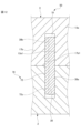
- FIG. 13 is a diagram showing a sixth embodiment, and is a cross-sectional view of a portion corresponding to line VII-VII in FIG. 6 in the first embodiment.
- the case body 10 is configured by combining the left and right first members 2 and the second members 3, which are resin molded bodies.
- the contact surface with the mold may be formed in a tapered shape as necessary.
- each of the lower inner wall surface 13a2 on the side of the first member 2 and the lower inner wall surface 13a3 on the side of the second member 3, which constitute the lower inner wall surface 13a1 of the lower guide portion 5 is formed such that the lower guide slit 51 widens toward the direction D2 opposite to the demolding direction D1.
- the tapered surface is such that the lower guide slit 51 widens.
- the lower inner wall surface 13a1 and the upper inner wall surface 17b1 are each formed in a groove shape having an isosceles triangular cross section.
- the lower inner wall surface 13a1 and the upper inner wall surface 17b1 respectively have a groove bottom portion 13a4 and a groove bottom portion 17b4 at the central portions in the width direction.
- the front inner wall surface 14a1 and the rear inner wall surface 14b1 of the upper guide portion 4 on the side of the first member 2 and the side of the second member 3 may also be formed in a tapered shape in some cases, but illustration thereof is omitted here. .
- the lower urging member 72 arranged in the lower guide slit 51 has the largest thickness at the substantially central portion in the width direction of the second main surface 38b, and the thickness gradually increases toward both sides in the width direction. is smaller than
- the width direction here is a direction orthogonal to the sliding direction of the shutter member 30, which is the vertical direction on the paper surface of FIG.
- the lower biasing member 72 is arranged in a compressed state between the second main surface 38b of the shutter member 30 and the upper inner wall surface 17b1, and is in contact with the groove bottom portion 13a4 of the upper inner wall surface 17b1.
- the gap between the second main surface 38b and the upper inner wall surface 17b1 is the widest in the widthwise central portion where the groove bottom 17b4 is located. Gradually getting smaller towards both sides.
- the thickness of the lower urging member 72 is the largest at the central portion in the width direction where the gap is the largest. That is, the central portion in the width direction, where the electronic component M is likely to enter, has the largest thickness. Therefore, it is difficult for the electronic component M to enter the lower guide slit 51 . Therefore, the electronic component M is prevented from being lost, and the electronic component M is easily ejected from the ejection port 19 .
- the mode in which the thickness of the central portion in the width direction is maximized can also be applied to the upper biasing member 71 .
- the biasing member 70 that biases the shutter member 30 toward the inner wall surface may be a spring made of metal, resin, or the like.
- the urging member 70 may have a form that urges the shutter member 30 toward the inner wall surface to make it difficult for the electronic component M to enter the upper guide slit 41 or the lower guide slit 51 . It is not limited to pressing against the inner wall surface.
- the biasing member 70 may be arranged at any position on the shutter member 30 as long as it is possible to prevent the electronic component M from entering the upper guide slit 41 or the lower guide slit 51 .
Landscapes
- Engineering & Computer Science (AREA)
- Microelectronics & Electronic Packaging (AREA)
- Manufacturing & Machinery (AREA)
- Packaging Frangible Articles (AREA)
- Supply And Installment Of Electrical Components (AREA)
- Casings For Electric Apparatus (AREA)
Abstract
Description
以下、図面を参照しつつ第1実施形態について説明する。
図1は、第1実施形態に係るケース1を下側から見た斜視図である。図2は、ケース1を前方から見た正面図である。図3は、ケース1の底面図である。図4は、ケース1の内部を一側方から見た図である。図5は、ケース1の前側部分の内部を一側方から見た図である。図6は、図5のVI部拡大図である。図7は、図6のVII-VII線に沿った横断面の一部を示している。 (First embodiment)
A first embodiment will be described below with reference to the drawings.
FIG. 1 is a perspective view of the
図9は、第2実施形態を示す図であって、上記第1実施形態における図6のVII-VII線に対応する部分の断面図である。 (Second embodiment)
FIG. 9 is a diagram showing the second embodiment, and is a sectional view of a portion corresponding to line VII-VII in FIG. 6 in the first embodiment.
図10は、第3実施形態を示す図であって、上記第1実施形態における図6のVII-VII線に対応する部分の断面図である。 (Third Embodiment)
FIG. 10 is a diagram showing the third embodiment, and is a cross-sectional view of a portion corresponding to line VII-VII in FIG. 6 in the first embodiment.
図11は、第4実施形態を示す図であって、上記第1実施形態における図6のVII-VII線に対応する部分の断面図である。 (Fourth embodiment)
FIG. 11 shows a fourth embodiment, and is a cross-sectional view of a portion corresponding to line VII-VII in FIG. 6 in the first embodiment.
図12は、第5実施形態を示す図であって、上記第1実施形態における図6のVII-VII線に対応する部分の断面図である。 (Fifth embodiment)
FIG. 12 is a diagram showing a fifth embodiment, and is a cross-sectional view of a portion corresponding to line VII-VII in FIG. 6 in the first embodiment.
図13は、第6実施形態を示す図であって、上記第1実施形態における図6のVII-VII線に対応する部分の断面図である。 (Sixth embodiment)
FIG. 13 is a diagram showing a sixth embodiment, and is a cross-sectional view of a portion corresponding to line VII-VII in FIG. 6 in the first embodiment.
10 ケース本体
13a1 下側内壁面(内壁面)
14a1 前側内壁面(内壁面)
14b1 後側内壁面(内壁面)
17b1 上側内壁面(内壁面)
19 排出口
30 シャッター部材
38a 第1主面(主面)
38b 第2主面(主面)
41 上側ガイドスリット(ガイドスリット)
51 下側ガイドスリット(ガイドスリット)
70 付勢部材
M 電子部品(部品) 1
14a1 front inner wall surface (inner wall surface)
14b1 rear inner wall surface (inner wall surface)
17b1 upper inner wall surface (inner wall surface)
19
38b second main surface (main surface)
41 upper guide slit (guide slit)
51 lower guide slit (guide slit)
70 biasing member M electronic component (component)
Claims (7)
- 複数の部品を収容し、当該部品が排出される排出口を有するケース本体と、
前記ケース本体に設けられ、前記排出口に連通するガイドスリットと、
前記ガイドスリットにスライド可能に挿入され、スライドすることにより前記排出口を開閉するシャッター部材と、を備えたケースであって、
前記ケース本体は、互いに対向してその間に前記ガイドスリットを形成する一対の内壁面を有し、
前記シャッター部材は、前記一対の内壁面のそれぞれに対向する一対の主面を有し、
前記シャッター部材に、当該シャッター部材を少なくとも前記一対の内壁面のうちの一方の側に弾性的に付勢する付勢部材が配置されている、ケース。 a case body containing a plurality of parts and having an ejection port through which the parts are ejected;
a guide slit provided in the case body and communicating with the discharge port;
a shutter member that is slidably inserted into the guide slit and slides to open and close the discharge port,
The case body has a pair of inner wall surfaces facing each other and forming the guide slit therebetween,
the shutter member has a pair of main surfaces facing each of the pair of inner wall surfaces,
A case, wherein the shutter member is provided with a biasing member that elastically biases the shutter member toward at least one of the pair of inner wall surfaces. - 前記付勢部材は、前記一対の主面の一方に配置され、当該付勢部材により、前記シャッター部材が前記一対の内壁面のうちの一方に押し付けられとともに、前記シャッター部材と他方の内壁面との間に、当該付勢部材が配置される、請求項1に記載のケース。 The urging member is arranged on one of the pair of main surfaces, and the urging member presses the shutter member against one of the pair of inner wall surfaces, and the shutter member and the other inner wall surface are pressed against each other. 2. The case of claim 1, wherein the biasing member is positioned between.
- 前記付勢部材は、前記一対の主面のそれぞれに一対の状態で配置され、当該一対の付勢部材により、前記シャッター部材が、前記一対の内壁面の間に配置されるとともに、前記一対の内壁面と前記シャッター部材との間に、当該一対の付勢部材のそれぞれが配置される、請求項1に記載のケース。 The biasing members are arranged in a pair on each of the pair of main surfaces, and the shutter member is arranged between the pair of inner wall surfaces by the pair of biasing members, The case according to claim 1, wherein each of said pair of biasing members is arranged between an inner wall surface and said shutter member.
- 前記付勢部材は、中空の構造を有する、請求項1~3のいずれか1項に記載のケース。 The case according to any one of claims 1 to 3, wherein the biasing member has a hollow structure.
- 前記付勢部材は、前記シャッター部材と同じ材質であって当該シャッター部材と一体に形成されている、請求項1~4のいずれか1項に記載のケース。 The case according to any one of claims 1 to 4, wherein the biasing member is made of the same material as the shutter member and is formed integrally with the shutter member.
- 前記付勢部材は、前記シャッター部材のスライド方向に直交する幅方向の略中央部の厚みが最も大きい、請求項1~5のいずれか1項に記載のケース。 The case according to any one of claims 1 to 5, wherein the biasing member has the greatest thickness at a substantially central portion in the width direction orthogonal to the sliding direction of the shutter member.
- 前記付勢部材は、前記排出口の周囲に配置される、請求項1~6のいずれか1項に記載のケース。 The case according to any one of claims 1 to 6, wherein the biasing member is arranged around the outlet.
Priority Applications (4)
| Application Number | Priority Date | Filing Date | Title |
|---|---|---|---|
| CN202280087176.8A CN118489299A (en) | 2022-01-12 | 2022-10-12 | Containing box |
| KR1020247022787A KR20240110901A (en) | 2022-01-12 | 2022-10-12 | case |
| JP2023573842A JPWO2023135877A1 (en) | 2022-01-12 | 2022-10-12 | |
| US18/619,240 US20240244811A1 (en) | 2022-01-12 | 2024-03-28 | Case |
Applications Claiming Priority (2)
| Application Number | Priority Date | Filing Date | Title |
|---|---|---|---|
| JP2022-003089 | 2022-01-12 | ||
| JP2022003089 | 2022-01-12 |
Related Child Applications (1)
| Application Number | Title | Priority Date | Filing Date |
|---|---|---|---|
| US18/619,240 Continuation US20240244811A1 (en) | 2022-01-12 | 2024-03-28 | Case |
Publications (1)
| Publication Number | Publication Date |
|---|---|
| WO2023135877A1 true WO2023135877A1 (en) | 2023-07-20 |
Family
ID=87278760
Family Applications (1)
| Application Number | Title | Priority Date | Filing Date |
|---|---|---|---|
| PCT/JP2022/038045 WO2023135877A1 (en) | 2022-01-12 | 2022-10-12 | Case |
Country Status (5)
| Country | Link |
|---|---|
| US (1) | US20240244811A1 (en) |
| JP (1) | JPWO2023135877A1 (en) |
| KR (1) | KR20240110901A (en) |
| CN (1) | CN118489299A (en) |
| WO (1) | WO2023135877A1 (en) |
Citations (6)
| Publication number | Priority date | Publication date | Assignee | Title |
|---|---|---|---|---|
| JPH0228490U (en) * | 1988-08-12 | 1990-02-23 | ||
| US5255970A (en) * | 1992-05-26 | 1993-10-26 | Theosabrata Yos S | Storage cabinet |
| JPH0890353A (en) * | 1994-09-20 | 1996-04-09 | Sony Corp | Buck case |
| JP2005016131A (en) * | 2003-06-25 | 2005-01-20 | Iris Ohyama Inc | Door with flexibility |
| JP2009295618A (en) | 2008-06-02 | 2009-12-17 | Taiyo Yuden Co Ltd | Part replenishment system for bulk feeder |
| JP2016205090A (en) * | 2015-04-28 | 2016-12-08 | 株式会社ニフコ | Slide type cover structure for container |
-
2022
- 2022-10-12 CN CN202280087176.8A patent/CN118489299A/en active Pending
- 2022-10-12 KR KR1020247022787A patent/KR20240110901A/en unknown
- 2022-10-12 WO PCT/JP2022/038045 patent/WO2023135877A1/en active Application Filing
- 2022-10-12 JP JP2023573842A patent/JPWO2023135877A1/ja active Pending
-
2024
- 2024-03-28 US US18/619,240 patent/US20240244811A1/en active Pending
Patent Citations (6)
| Publication number | Priority date | Publication date | Assignee | Title |
|---|---|---|---|---|
| JPH0228490U (en) * | 1988-08-12 | 1990-02-23 | ||
| US5255970A (en) * | 1992-05-26 | 1993-10-26 | Theosabrata Yos S | Storage cabinet |
| JPH0890353A (en) * | 1994-09-20 | 1996-04-09 | Sony Corp | Buck case |
| JP2005016131A (en) * | 2003-06-25 | 2005-01-20 | Iris Ohyama Inc | Door with flexibility |
| JP2009295618A (en) | 2008-06-02 | 2009-12-17 | Taiyo Yuden Co Ltd | Part replenishment system for bulk feeder |
| JP2016205090A (en) * | 2015-04-28 | 2016-12-08 | 株式会社ニフコ | Slide type cover structure for container |
Also Published As
| Publication number | Publication date |
|---|---|
| CN118489299A (en) | 2024-08-13 |
| US20240244811A1 (en) | 2024-07-18 |
| KR20240110901A (en) | 2024-07-16 |
| JPWO2023135877A1 (en) | 2023-07-20 |
Similar Documents
| Publication | Publication Date | Title |
|---|---|---|
| JP7416326B2 (en) | Case | |
| WO2023135877A1 (en) | Case | |
| WO2023135878A1 (en) | Case | |
| JP5867033B2 (en) | Image forming apparatus | |
| WO2022244537A1 (en) | Case and method for using same | |
| JP7487838B2 (en) | Case | |
| EP4400447A1 (en) | Case | |
| TWI847359B (en) | Electronic parts storage container | |
| JP7477042B2 (en) | Case | |
| US20240237320A1 (en) | Electronic component container | |
| WO2021182288A1 (en) | Biometric information measurement device and sphygmomanometer | |
| US8807722B2 (en) | Ink cartridge and inkjet printer | |
| JP2005000586A (en) | Card case | |
| WO2022264657A1 (en) | Case and seal | |
| WO2022009646A1 (en) | Storage case | |
| JP4509878B2 (en) | Printer | |
| CN210902901U (en) | Endoscope box body | |
| CN212118095U (en) | Endoscope box body | |
| JP6669012B2 (en) | Printing equipment | |
| JP4364500B2 (en) | Card storage cartridge | |
| JP2020075398A (en) | Image forming apparatus and ink container | |
| CN115108187A (en) | Component storage device | |
| JPH11240225A (en) | Protecting case, recording apparatus and, recording apparatus with protecting case | |
| JPH0423397A (en) | Electronic component chip housing cassette | |
| JP2018117901A (en) | Endoscope case |
Legal Events
| Date | Code | Title | Description |
|---|---|---|---|
| 121 | Ep: the epo has been informed by wipo that ep was designated in this application |
Ref document number: 22920400 Country of ref document: EP Kind code of ref document: A1 |
|
| WWE | Wipo information: entry into national phase |
Ref document number: 2023573842 Country of ref document: JP |
|
| ENP | Entry into the national phase |
Ref document number: 20247022787 Country of ref document: KR Kind code of ref document: A |
|
| WWE | Wipo information: entry into national phase |
Ref document number: 2022920400 Country of ref document: EP |
|
| NENP | Non-entry into the national phase |
Ref country code: DE |
|
| ENP | Entry into the national phase |
Ref document number: 2022920400 Country of ref document: EP Effective date: 20240812 |