WO2023123301A1 - Imaging systems with rotating image sensors - Google Patents
Imaging systems with rotating image sensors Download PDFInfo
- Publication number
- WO2023123301A1 WO2023123301A1 PCT/CN2021/143484 CN2021143484W WO2023123301A1 WO 2023123301 A1 WO2023123301 A1 WO 2023123301A1 CN 2021143484 W CN2021143484 W CN 2021143484W WO 2023123301 A1 WO2023123301 A1 WO 2023123301A1
- Authority
- WO
- WIPO (PCT)
- Prior art keywords
- image sensor
- radiation source
- radiation
- respect
- capturing
- Prior art date
Links
Images


Classifications
-
- A—HUMAN NECESSITIES
- A61—MEDICAL OR VETERINARY SCIENCE; HYGIENE
- A61B—DIAGNOSIS; SURGERY; IDENTIFICATION
- A61B6/00—Apparatus for radiation diagnosis, e.g. combined with radiation therapy equipment
- A61B6/42—Apparatus for radiation diagnosis, e.g. combined with radiation therapy equipment with arrangements for detecting radiation specially adapted for radiation diagnosis
- A61B6/4208—Apparatus for radiation diagnosis, e.g. combined with radiation therapy equipment with arrangements for detecting radiation specially adapted for radiation diagnosis characterised by using a particular type of detector
- A61B6/4233—Apparatus for radiation diagnosis, e.g. combined with radiation therapy equipment with arrangements for detecting radiation specially adapted for radiation diagnosis characterised by using a particular type of detector using matrix detectors
-
- A—HUMAN NECESSITIES
- A61—MEDICAL OR VETERINARY SCIENCE; HYGIENE
- A61B—DIAGNOSIS; SURGERY; IDENTIFICATION
- A61B6/00—Apparatus for radiation diagnosis, e.g. combined with radiation therapy equipment
- A61B6/44—Constructional features of apparatus for radiation diagnosis
- A61B6/4429—Constructional features of apparatus for radiation diagnosis related to the mounting of source units and detector units
- A61B6/4435—Constructional features of apparatus for radiation diagnosis related to the mounting of source units and detector units the source unit and the detector unit being coupled by a rigid structure
-
- G—PHYSICS
- G01—MEASURING; TESTING
- G01N—INVESTIGATING OR ANALYSING MATERIALS BY DETERMINING THEIR CHEMICAL OR PHYSICAL PROPERTIES
- G01N23/00—Investigating or analysing materials by the use of wave or particle radiation, e.g. X-rays or neutrons, not covered by groups G01N3/00 – G01N17/00, G01N21/00 or G01N22/00
- G01N23/02—Investigating or analysing materials by the use of wave or particle radiation, e.g. X-rays or neutrons, not covered by groups G01N3/00 – G01N17/00, G01N21/00 or G01N22/00 by transmitting the radiation through the material
- G01N23/04—Investigating or analysing materials by the use of wave or particle radiation, e.g. X-rays or neutrons, not covered by groups G01N3/00 – G01N17/00, G01N21/00 or G01N22/00 by transmitting the radiation through the material and forming images of the material
- G01N23/046—Investigating or analysing materials by the use of wave or particle radiation, e.g. X-rays or neutrons, not covered by groups G01N3/00 – G01N17/00, G01N21/00 or G01N22/00 by transmitting the radiation through the material and forming images of the material using tomography, e.g. computed tomography [CT]
-
- G—PHYSICS
- G01—MEASURING; TESTING
- G01T—MEASUREMENT OF NUCLEAR OR X-RADIATION
- G01T1/00—Measuring X-radiation, gamma radiation, corpuscular radiation, or cosmic radiation
- G01T1/29—Measurement performed on radiation beams, e.g. position or section of the beam; Measurement of spatial distribution of radiation
- G01T1/2914—Measurement of spatial distribution of radiation
- G01T1/2985—In depth localisation, e.g. using positron emitters; Tomographic imaging (longitudinal and transverse section imaging; apparatus for radiation diagnosis sequentially in different planes, steroscopic radiation diagnosis)
-
- A—HUMAN NECESSITIES
- A61—MEDICAL OR VETERINARY SCIENCE; HYGIENE
- A61B—DIAGNOSIS; SURGERY; IDENTIFICATION
- A61B6/00—Apparatus for radiation diagnosis, e.g. combined with radiation therapy equipment
- A61B6/02—Devices for diagnosis sequentially in different planes; Stereoscopic radiation diagnosis
- A61B6/03—Computerised tomographs
- A61B6/032—Transmission computed tomography [CT]
-
- A—HUMAN NECESSITIES
- A61—MEDICAL OR VETERINARY SCIENCE; HYGIENE
- A61B—DIAGNOSIS; SURGERY; IDENTIFICATION
- A61B6/00—Apparatus for radiation diagnosis, e.g. combined with radiation therapy equipment
- A61B6/06—Diaphragms
-
- A—HUMAN NECESSITIES
- A61—MEDICAL OR VETERINARY SCIENCE; HYGIENE
- A61B—DIAGNOSIS; SURGERY; IDENTIFICATION
- A61B6/00—Apparatus for radiation diagnosis, e.g. combined with radiation therapy equipment
- A61B6/40—Apparatus for radiation diagnosis, e.g. combined with radiation therapy equipment with arrangements for generating radiation specially adapted for radiation diagnosis
- A61B6/4064—Apparatus for radiation diagnosis, e.g. combined with radiation therapy equipment with arrangements for generating radiation specially adapted for radiation diagnosis specially adapted for producing a particular type of beam
- A61B6/4085—Cone-beams
-
- G—PHYSICS
- G01—MEASURING; TESTING
- G01N—INVESTIGATING OR ANALYSING MATERIALS BY DETERMINING THEIR CHEMICAL OR PHYSICAL PROPERTIES
- G01N2223/00—Investigating materials by wave or particle radiation
- G01N2223/30—Accessories, mechanical or electrical features
- G01N2223/33—Accessories, mechanical or electrical features scanning, i.e. relative motion for measurement of successive object-parts
- G01N2223/3303—Accessories, mechanical or electrical features scanning, i.e. relative motion for measurement of successive object-parts object fixed; source and detector move
Definitions
- a radiation detector is a device that measures a property of a radiation. Examples of the property may include a spatial distribution of the intensity, phase, and polarization of the radiation.
- the radiation measured by the radiation detector may be a radiation that has transmitted through an object.
- the radiation measured by the radiation detector may be electromagnetic radiation such as infrared light, visible light, ultraviolet light, X-ray, or ⁇ -ray.
- the radiation may be of other types such as ⁇ -rays and ⁇ -rays.
- An imaging system may include one or more image sensors each of which may have one or more radiation detectors.
- a method comprising: sending a radiation beam from a radiation source of an imaging system toward an object and toward an image sensor of the imaging system; first capturing with the image sensor a first image of the object using radiation of the radiation beam that has transmitted through the object; then first translating the radiation source and the image sensor with respect to the object while the radiation source and the image sensor are stationary with respect to each other such that the object moves away from the radiation source and toward the image sensor; then first rotating the radiation source and the image sensor about a rotation axis while the object is stationary with respect to the rotation axis; then second translating the radiation source and the image sensor with respect to the object while the radiation source and the image sensor are stationary with respect to each other such that the object moves toward the radiation source and away from the image sensor; and then second capturing with the image sensor a second image of the object using radiation of the radiation beam that has transmitted through the object.
- the object is positioned between the radiation source and the image sensor.
- the radiation beam is a divergent beam.
- the radiation beam is a cone beam or a pyramid beam.
- the radiation beam is an X-ray beam.
- the method further comprises reconstructing a 3D (3-dimensional) image of the object based on at least the first and second images of the object.
- the image sensor comprises (A) multiple active areas each of which comprises multiple sensing elements, and (B) a dead zone among the multiple active areas.
- every straight line intersecting the radiation source and the object intersects the image sensor.
- the rotation axis intersects the object.
- a straight line segment having 2 ends respectively on the radiation source and the image sensor has a midpoint on the rotation axis.
- the image sensor comprises multiple sensing elements.
- a best-fit plane passes through all sensing elements of the image sensor, and throughout said first rotating, the rotation axis is parallel to the best-fit plane.
- a point of the radiation source and a point of the image sensor move on a first straight line that intersects the object.
- a point of the radiation source and a point of the image sensor move on a second straight line that intersects the object.
- the image sensor comprises multiple sensing elements.
- a best-fit plane passes through all sensing elements of the image sensor, the first straight line is perpendicular to the best-fit plane throughout said first translating, and the second straight line is perpendicular to the best-fit plane throughout said second translating.
- a distance between two points respectively of the radiation source and the object at a time point during said first capturing and a distance between said two points at a time point during said second capturing are the same.
- the method further comprises: after said second capturing is performed, third translating the radiation source and the image sensor with respect to the object while the radiation source and the image sensor are stationary with respect to each other such that the object moves away from the radiation source and toward the image sensor; then second rotating the radiation source and the image sensor about the rotation axis while the object is stationary with respect to the rotation axis; then fourth translating the radiation source and the image sensor with respect to the object while the radiation source and the image sensor are stationary with respect to each other such that the object moves toward the radiation source and away from the image sensor; and then third capturing with the image sensor a third image of the object using radiation of the radiation beam that has transmitted through the object.
- the method further comprises reconstructing a 3D image of the object based on at least the first, second, and third images of the object.
- every straight line intersecting the radiation source and the object intersects the image sensor.
- the imaging system comprises a collimator which is (A) positioned between the image sensor and the object, (B) stationary with respect to the image sensor, and (C) configured to block any incident radiation particle whose coming path when extended does not intersect the radiation source.
- a point A of the radiation source, a point B of the image sensor, and a point C on the rotation axis are colinear, and (2) point C is a midpoint of a straight line segment between the point A and the point B.
- Fig. 1 schematically shows a radiation detector, according to an embodiment.
- Fig. 2 schematically shows a simplified cross-sectional view of the radiation detector, according to an embodiment.
- Fig. 3 schematically shows a detailed cross-sectional view of the radiation detector, according to an embodiment.
- Fig. 4 schematically shows a detailed cross-sectional view of the radiation detector, according to an alternative embodiment.
- Fig. 5 schematically shows a top view of a radiation detector package including the radiation detector and a printed circuit board (PCB) , according to an embodiment.
- PCB printed circuit board
- Fig. 6 schematically shows a cross-sectional view of an image sensor including the packages of Fig. 5 mounted to a system PCB (printed circuit board) , according to an embodiment.
- PCB printed circuit board
- FIG. 7A –Fig. 7G schematically show an imaging system in operation, according to an embodiment.
- Fig. 7H schematically show the imaging system with a collimator, according to an embodiment.
- Fig. 8 shows a flowchart generalizing the operation of the imaging system, according to an embodiment.
- Fig. 1 schematically shows a radiation detector 100, as an example.
- the radiation detector 100 may include an array of pixels 150 (also referred to as sensing elements 150) .
- the array may be a rectangular array (as shown in Fig. 1) , a honeycomb array, a hexagonal array, or any other suitable array.
- the array of pixels 150 in the example of Fig. 1 has 4 rows and 7 columns; however, in general, the array of pixels 150 may have any number of rows and any number of columns.
- Each pixel 150 may be configured to detect radiation from a radiation source (not shown) incident thereon and may be configured to measure a characteristic (e.g., the energy of the particles, the wavelength, and the frequency) of the radiation.
- a radiation may include particles such as photons and subatomic particles.
- Each pixel 150 may be configured to count numbers of particles of radiation incident thereon whose energy falls in a plurality of bins of energy, within a period of time. All the pixels 150 may be configured to count the numbers of particles of radiation incident thereon within a plurality of bins of energy within the same period of time. When the incident particles of radiation have similar energy, the pixels 150 may be simply configured to count numbers of particles of radiation incident thereon within a period of time, without measuring the energy of the individual particles of radiation.
- Each pixel 150 may have its own analog-to-digital converter (ADC) configured to digitize an analog signal representing the energy of an incident particle of radiation into a digital signal, or to digitize an analog signal representing the total energy of a plurality of incident particles of radiation into a digital signal.
- ADC analog-to-digital converter
- the pixels 150 may be configured to operate in parallel. For example, when one pixel 150 measures an incident particle of radiation, another pixel 150 may be waiting for a particle of radiation to arrive. The pixels 150 may not have to be individually addressable.
- the radiation detector 100 described here may have applications such as in an X-ray telescope, X-ray mammography, industrial X-ray defect detection, X-ray microscopy or microradiography, X-ray casting inspection, X-ray non-destructive testing, X-ray weld inspection, X-ray digital subtraction angiography, etc. It may be suitable to use this radiation detector 100 in place of a photographic plate, a photographic film, a PSP plate, an X-ray image intensifier, a scintillator, or another semiconductor X-ray detector.
- Fig. 2 schematically shows a simplified cross-sectional view of the radiation detector 100 of Fig. 1 along a line 2-2, according to an embodiment.
- the radiation detector 100 may include a radiation absorption layer 110 and an electronics layer 120 (which may include one or more ASICs or application-specific integrated circuits) for processing or analyzing electrical signals which incident radiation generates in the radiation absorption layer 110.
- the radiation detector 100 may or may not include a scintillator (not shown) .
- the radiation absorption layer 110 may include a semiconductor material such as silicon, germanium, GaAs, CdTe, CdZnTe, or a combination thereof.
- the semiconductor material may have a high mass attenuation coefficient for the radiation of interest.
- the radiation absorption layer 110 may include one or more diodes (e.g., p-i-n or p-n) formed by a first doped region 111, one or more discrete regions 114 of a second doped region 113.
- the second doped region 113 may be separated from the first doped region 111 by an optional intrinsic region 112.
- the discrete regions 114 may be separated from one another by the first doped region 111 or the intrinsic region 112.
- the first doped region 111 and the second doped region 113 may have opposite types of doping (e.g., region 111 is p-type and region 113 is n-type, or region 111 is n-type and region 113 is p-type) .
- each of the discrete regions 114 of the second doped region 113 forms a diode with the first doped region 111 and the optional intrinsic region 112.
- the radiation absorption layer 110 has a plurality of diodes (more specifically, 7 diodes corresponding to 7 pixels 150 of one row in the array of Fig. 1, of which only 2 pixels 150 are labeled in Fig. 3 for simplicity) .
- the plurality of diodes may have an electrical contact 119A as a shared (common) electrode.
- the first doped region 111 may also have discrete portions.
- the electronics layer 120 may include an electronic system 121 suitable for processing or interpreting signals generated by the radiation incident on the radiation absorption layer 110.
- the electronic system 121 may include an analog circuitry such as a filter network, amplifiers, integrators, and comparators, or a digital circuitry such as a microprocessor, and memory.
- the electronic system 121 may include one or more ADCs (analog to digital converters) .
- the electronic system 121 may include components shared by the pixels 150 or components dedicated to a single pixel 150.
- the electronic system 121 may include an amplifier dedicated to each pixel 150 and a microprocessor shared among all the pixels 150.
- the electronic system 121 may be electrically connected to the pixels 150 by vias 131. Space among the vias may be filled with a filler material 130, which may increase the mechanical stability of the connection of the electronics layer 120 to the radiation absorption layer 110. Other bonding techniques are possible to connect the electronic system 121 to the pixels 150 without using the vias 131.
- the radiation absorption layer 110 including diodes
- particles of the radiation may be absorbed and generate one or more charge carriers (e.g., electrons, holes) by a number of mechanisms.
- the charge carriers may drift to the electrodes of one of the diodes under an electric field.
- the electric field may be an external electric field.
- the electrical contact 119B may include discrete portions each of which is in electrical contact with the discrete regions 114.
- the term “electrical contact” may be used interchangeably with the word “electrode.
- the charge carriers may drift in directions such that the charge carriers generated by a single particle of the radiation are not substantially shared by two different discrete regions 114 ( “not substantially shared” here means less than 2%, less than 0.5%, less than 0.1%, or less than 0.01%of these charge carriers flow to a different one of the discrete regions 114 than the rest of the charge carriers) .
- Charge carriers generated by a particle of the radiation incident around the footprint of one of these discrete regions 114 are not substantially shared with another of these discrete regions 114.
- a pixel 150 associated with a discrete region 114 may be an area around the discrete region 114 in which substantially all (more than 98%, more than 99.5%, more than 99.9%, or more than 99.99%of) charge carriers generated by a particle of the radiation incident therein flow to the discrete region 114. Namely, less than 2%, less than 1%, less than 0.1%, or less than 0.01%of these charge carriers flow beyond the pixel 150.
- Fig. 4 schematically shows a detailed cross-sectional view of the radiation detector 100 of Fig. 1 along the line 2-2, according to an alternative embodiment.
- the radiation absorption layer 110 may include a resistor of a semiconductor material such as silicon, germanium, GaAs, CdTe, CdZnTe, or a combination thereof, but does not include a diode.
- the semiconductor material may have a high mass attenuation coefficient for the radiation of interest.
- the electronics layer 120 of Fig. 4 is similar to the electronics layer 120 of Fig. 3 in terms of structure and function.
- the radiation When the radiation hits the radiation absorption layer 110 including the resistor but not diodes, it may be absorbed and generate one or more charge carriers by a number of mechanisms.
- a particle of the radiation may generate 10 to 100,000 charge carriers.
- the charge carriers may drift to the electrical contacts 119A and 119B under an electric field.
- the electric field may be an external electric field.
- the electrical contact 119B may include discrete portions.
- the charge carriers may drift in directions such that the charge carriers generated by a single particle of the radiation are not substantially shared by two different discrete portions of the electrical contact 119B ( “not substantially shared” here means less than 2%, less than 0.5%, less than 0.1%, or less than 0.01%of these charge carriers flow to a different one of the discrete portions than the rest of the charge carriers) .
- a pixel 150 associated with a discrete portion of the electrical contact 119B may be an area around the discrete portion in which substantially all (more than 98%, more than 99.5%, more than 99.9%or more than 99.99%of) charge carriers generated by a particle of the radiation incident therein flow to the discrete portion of the electrical contact 119B. Namely, less than 2%, less than 0.5%, less than 0.1%, or less than 0.01%of these charge carriers flow beyond the pixel associated with the one discrete portion of the electrical contact 119B.
- Fig. 5 schematically shows a top view of a radiation detector package 500 including the radiation detector 100 and a printed circuit board (PCB) 510.
- PCB printed circuit board
- the term “PCB” as used herein is not limited to a particular material.
- a PCB may include a semiconductor.
- the radiation detector 100 may be mounted to the PCB 510.
- the wiring between the radiation detector 100 and the PCB 510 is not shown for the sake of clarity.
- the package 500 may have one or more radiation detectors 100.
- the PCB 510 may include an input/output (I/O) area 512 not covered by the radiation detector 100 (e.g., for accommodating bonding wires 514) .
- the radiation detector 100 may have an active area 190 which is where the pixels 150 (Fig. 1) are located.
- the radiation detector 100 may have a perimeter zone 195 near the edges of the radiation detector 100.
- the perimeter zone 195 has no pixels 150, and the radiation detector 100 does not detect particles of radiation incident on the perimeter zone
- Fig. 6 schematically shows a cross-sectional view of an image sensor 600, according to an embodiment.
- the image sensor 600 may include one or more radiation detector packages 500 of Fig. 5 mounted to a system PCB 650.
- the electrical connection between the PCBs 510 and the system PCB 650 may be made by bonding wires 514.
- the PCB 510 may have the I/O area 512 not covered by the radiation detectors 100.
- the packages 500 may have gaps in between. The gaps may be approximately 1 mm or more.
- a dead zone of a radiation detector (e.g., the radiation detector 100) is the area of the radiation-receiving surface of the radiation detector, on which incident particles of radiation cannot be detected by the radiation detector.
- a dead zone of a package (e.g., package 500) is the area of the radiation-receiving surface of the package, on which incident particles of radiation cannot be detected by the radiation detector or detectors in the package.
- the dead zone of the package 500 includes the perimeter zones 195 and the I/O area 512.
- a dead zone (e.g., 688) of an image sensor (e.g., image sensor 600) with a group of packages (e.g., packages 500 mounted on the same PCB and arranged in the same layer or in different layers) includes the combination of the dead zones of the packages in the group and the gaps between the packages.
- the radiation detector 100 (Fig. 1) operating by itself may be considered an image sensor.
- the package 500 (Fig. 5) operating by itself may be considered an image sensor.
- the image sensor 600 including the radiation detectors 100 may have the dead zone 688 among the active areas 190 of the radiation detectors 100. However, the image sensor 600 may capture multiple partial images of an object or scene (not shown) one by one, and then these captured partial images may be stitched to form a stitched image of the entire object or scene.
- image in the present specification is not limited to spatial distribution of a property of a radiation (such as intensity) .
- image may also include the spatial distribution of density of a substance or element.
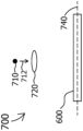
- Fig. 7A –Fig. 7G schematically show an imaging system 700 in operation, according to an embodiment.
- the imaging system 700 may include a radiation source 710 and the image sensor 600 of Fig. 6.
- an object 720 may be positioned between the radiation source 710 and the image sensor 600.
- the radiation source 710 may send a radiation beam 712 toward the object 720 and toward the image sensor 600.
- the radiation beam 712 may be an X-ray beam.
- the radiation beam 712 may be a divergent beam (e.g., a cone beam or a pyramid beam) .
- the image sensor 600 may capture a first image of the object 720 by using the radiation of the radiation beam 712 that has transmitted through the object 720.
- this process of capturing the first image is referred to as “first capturing” .
- the radiation source 710 and the image sensor 600 may be translated with respect to the object 720 while the radiation source 710 and the image sensor 600 are stationary with respect to each other such that the object 720 moves away from the radiation source 710 and toward the image sensor 600, resulting in the arrangement as shown in Fig. 7B.
- this process of translating the radiation source 710 and the image sensor 600 is referred to as “first translating” .
- said first translating may be such that throughout said first translating, a point of the radiation source 710 and a point of the image sensor 600 move on a first straight line (not shown for simplicity) that intersects the object 720.
- said first translating may be such that throughout said first translating, the first straight line mentioned above is perpendicular to a best-fit plane (e.g., best-fit plane 740) that passes through all the sensing elements 150 of the image sensor 600.
- a best-fit plane e.g., best-fit plane 740
- the best-fit plane 740 is chosen to be perpendicular to the page; therefore, the best-fit plane 740 is represented by a straight line as shown.
- the radiation source 710 and the image sensor 600 may be rotated about a rotation axis 730 while the object 720 is stationary with respect to the rotation axis 730.
- this process of rotating the radiation source 710 and the image sensor 600 is referred to as “first rotating” .
- rotation axis 730 is chosen to be perpendicular to the page; therefore, the rotation axis 730 is represented by a point as shown. In an embodiment, the rotation axis 730 may intersect the object 720 as shown.
- said first rotating may be clockwise or counterclockwise.
- a straight line segment (not shown) having 2 ends respectively on the radiation source 710 and the image sensor 600 has a midpoint on the rotation axis 730.
- said first rotating may be such that throughout said first rotating, (1) a point A of the radiation source 710, a point B of the image sensor 600, and a point C on the rotation axis 730 are colinear, and (2) point C is the midpoint of the straight line segment AB.
- points A, B, and C are not shown in Fig. 7B -Fig. 7C.
- said first rotating may be such that throughout said first rotating, the rotation axis 730 is parallel to a best-fit plane (e.g., the best-fit plane 740) that passes through all sensing elements 150 of the image sensor 600.
- a best-fit plane e.g., the best-fit plane 740
- the radiation source 710 and the image sensor 600 may be translated with respect to the object 720 while the radiation source 710 and the image sensor 600 are stationary with respect to each other such that the object 720 moves toward the radiation source 710 and away from the image sensor 600, resulting in the arrangement as shown in Fig. 7D.
- this process of translating the radiation source 710 and the image sensor 600 is referred to as “second translating” .
- said second translating may be such that throughout said second translating, a point of the radiation source 710 and a point of the image sensor 600 move on a second straight line (not shown for simplicity) that intersects the object 720.
- said second translating may be such that throughout said second translating, the second straight line mentioned above is perpendicular to a best-fit plane (e.g., the best-fit plane 740) that passes through all the sensing elements 150 of the image sensor 600.
- a best-fit plane e.g., the best-fit plane 740
- the image sensor 600 may capture a second image of the object 720 by using the radiation of the radiation beam 712 that has transmitted through the object 720.
- this process of capturing the second image is referred to as “second capturing” .
- the radiation source 710 and the image sensor 600 may be translated with respect to the object 720 while the radiation source 710 and the image sensor 600 are stationary with respect to each other such that the object 720 moves away from the radiation source 710 and toward the image sensor 600.
- third translating this process of translating the radiation source 710 and the image sensor 600 is referred to as “third translating” .
- said third translating may be similar to said first translating described above.
- the radiation source 710 and the image sensor 600 may be rotated about a rotation axis (e.g., the rotation axis 730) while the object 720 is stationary with respect to the rotation axis.
- this process of rotating the radiation source 710 and the image sensor 600 is referred to as “second rotating” .
- said second rotating may be similar to said first rotating described above.
- said second rotating may be clockwise or counterclockwise.
- the radiation source 710 and the image sensor 600 may be translated with respect to the object 720 while the radiation source 710 and the image sensor 600 are stationary with respect to each other such that the object 720 moves toward the radiation source 710 and away from the image sensor 600, resulting in the arrangement as shown in Fig. 7G.
- this process of translating the radiation source 710 and the image sensor 600 is referred to as “fourth translating” .
- said fourth translating may be similar to said second translating described above.
- the image sensor 600 may capture a third image of the object 720 by using the radiation of the radiation beam 712 that has transmitted through the object 720.
- this process of capturing the third image is referred to as “third capturing” .
- the imaging system 700 may further include a collimator 750 which is (A) positioned between the object 720 and the image sensor 600, (B) stationary with respect to the image sensor 600, and (C) configured to block any incident radiation particle whose coming path when extended does not intersect the radiation source 710.
- a collimator 750 which is (A) positioned between the object 720 and the image sensor 600, (B) stationary with respect to the image sensor 600, and (C) configured to block any incident radiation particle whose coming path when extended does not intersect the radiation source 710.
- the image sensor 600 including the collimator 750 may be used in the operation of the imaging system 700 as described above with reference to Fig. 7A –Fig. 7G.
- Fig. 8 shows a flowchart 800 generalizing the operation of the imaging system 700.
- Step 810 includes sending a radiation beam from a radiation source toward an object and toward an image sensor.
- the object is positioned between the radiation source and the image sensor.
- the radiation beam 712 is sent from the radiation source 710 toward the object 720 and toward the image sensor 600, and the object 720 is positioned between the radiation source 710 and the image sensor 600.
- Step 820 includes first capturing with the image sensor a first image of the object by using radiation of the radiation beam that has transmitted through the object.
- the image sensor 600 captures the first image of the object 720 by using the radiation of the radiation beam 712 that has transmitted through the object 720.
- Step 830 includes, after step 820 is performed, first translating the radiation source and the image sensor with respect to the object while the radiation source and the image sensor are stationary with respect to each other such that the object moves away from the radiation source and toward the image sensor.
- first translating the radiation source and the image sensor with respect to the object while the radiation source and the image sensor are stationary with respect to each other such that the object moves away from the radiation source and toward the image sensor.
- Step 840 includes, after step 830 is performed, first rotating the radiation source and the image sensor about a rotation axis while the object is stationary with respect to the rotation axis.
- first rotating the radiation source and the image sensor about a rotation axis while the object is stationary with respect to the rotation axis.
- the radiation source 710 and the image sensor 600 are rotated about the rotation axis 730 while the object 720 is stationary with respect to the rotation axis 730.
- Step 850 includes, after step 840 is performed, second translating the radiation source and the image sensor with respect to the object while the radiation source and the image sensor are stationary with respect to each other such that the object moves toward the radiation source and away from the image sensor.
- step 840 second translating the radiation source and the image sensor with respect to the object while the radiation source and the image sensor are stationary with respect to each other such that the object moves toward the radiation source and away from the image sensor.
- Step 860 includes, after step 850 is performed, second capturing with the image sensor a second image of the object using radiation of the radiation beam that has transmitted through the object.
- the image sensor 600 captures the second image of the object 720 by using the radiation of the radiation beam 712 that has transmitted through the object 720.
- a first 3D (3-dimensional) image of the object 720 may be reconstructed based on at least the first and second images of the object 720.
- a second 3D image of the object 720 may be reconstructed based on at least the first, second, and third images of the object 720.
- the imaging system 700 and the object 720 may be arranged such that at any time point during said first capturing, said second capturing, and said third capturing, every straight line intersecting the radiation source 710 and the object 720 intersects the image sensor 600.
- said first capturing, said second capturing, and said third capturing may be performed such that a distance between a point X (not shown) of the radiation source 710 and a point Y (not shown) of the object 720 at a time point during said first capturing (Fig. 7A) , a distance between said 2 points X and Y at a time point during said second capturing (Fig. 7D) , and a distance between said 2 points X and Y at a time point during said third capturing (Fig. 7G) are the same.
Abstract
An imaging method that includes imaging an object (720) with a radiation beam (712) from a radiation source (710) and an image sensor (600). During imaging, the object (720) may be closer to the radiation source (710) than to the image sensor (600). After imaging, the object (720) is moved relative to the combination of the image sensor (600) and the radiation source (710), such that the object (720) is farther from the radiation source (710) than during imaging. The combination of the radiation source (710) and the image sensor (600) is then rotated relative to the object (720). The object (720) is then moved relative to the combination of the image sensor (600) and the radiation source (710), such that the object (720) is closer to the radiation source (710) than during the rotation. Then the object (720) is imaged again.
Description
A radiation detector is a device that measures a property of a radiation. Examples of the property may include a spatial distribution of the intensity, phase, and polarization of the radiation. The radiation measured by the radiation detector may be a radiation that has transmitted through an object. The radiation measured by the radiation detector may be electromagnetic radiation such as infrared light, visible light, ultraviolet light, X-ray, or γ-ray. The radiation may be of other types such as α-rays and β-rays. An imaging system may include one or more image sensors each of which may have one or more radiation detectors.
Summary
Disclosed herein is a method comprising: sending a radiation beam from a radiation source of an imaging system toward an object and toward an image sensor of the imaging system; first capturing with the image sensor a first image of the object using radiation of the radiation beam that has transmitted through the object; then first translating the radiation source and the image sensor with respect to the object while the radiation source and the image sensor are stationary with respect to each other such that the object moves away from the radiation source and toward the image sensor; then first rotating the radiation source and the image sensor about a rotation axis while the object is stationary with respect to the rotation axis; then second translating the radiation source and the image sensor with respect to the object while the radiation source and the image sensor are stationary with respect to each other such that the object moves toward the radiation source and away from the image sensor; and then second capturing with the image sensor a second image of the object using radiation of the radiation beam that has transmitted through the object. The object is positioned between the radiation source and the image sensor.
In an aspect, the radiation beam is a divergent beam.
In an aspect, the radiation beam is a cone beam or a pyramid beam.
In an aspect, the radiation beam is an X-ray beam.
In an aspect, the method further comprises reconstructing a 3D (3-dimensional) image of the object based on at least the first and second images of the object.
In an aspect, there is no stitching of the first and second images of the object.
In an aspect, the image sensor comprises (A) multiple active areas each of which comprises multiple sensing elements, and (B) a dead zone among the multiple active areas.
In an aspect, at any time point during said first capturing and said second capturing, every straight line intersecting the radiation source and the object intersects the image sensor.
In an aspect, the rotation axis intersects the object.
In an aspect, at any time point during said first rotating, a straight line segment having 2 ends respectively on the radiation source and the image sensor has a midpoint on the rotation axis.
In an aspect, the image sensor comprises multiple sensing elements. A best-fit plane passes through all sensing elements of the image sensor, and throughout said first rotating, the rotation axis is parallel to the best-fit plane.
In an aspect, throughout said first translating, a point of the radiation source and a point of the image sensor move on a first straight line that intersects the object.
In an aspect, throughout said second translating, a point of the radiation source and a point of the image sensor move on a second straight line that intersects the object.
In an aspect, the image sensor comprises multiple sensing elements. A best-fit plane passes through all sensing elements of the image sensor, the first straight line is perpendicular to the best-fit plane throughout said first translating, and the second straight line is perpendicular to the best-fit plane throughout said second translating.
In an aspect, a distance between two points respectively of the radiation source and the object at a time point during said first capturing and a distance between said two points at a time point during said second capturing are the same.
In an aspect, the method further comprises: after said second capturing is performed, third translating the radiation source and the image sensor with respect to the object while the radiation source and the image sensor are stationary with respect to each other such that the object moves away from the radiation source and toward the image sensor; then second rotating the radiation source and the image sensor about the rotation axis while the object is stationary with respect to the rotation axis; then fourth translating the radiation source and the image sensor with respect to the object while the radiation source and the image sensor are stationary with respect to each other such that the object moves toward the radiation source and away from the image sensor; and then third capturing with the image sensor a third image of the object using radiation of the radiation beam that has transmitted through the object.
In an aspect, the method further comprises reconstructing a 3D image of the object based on at least the first, second, and third images of the object.
In an aspect, at any time point during said third capturing, every straight line intersecting the radiation source and the object intersects the image sensor.
In an aspect, the imaging system comprises a collimator which is (A) positioned between the image sensor and the object, (B) stationary with respect to the image sensor, and (C) configured to block any incident radiation particle whose coming path when extended does not intersect the radiation source.
In an aspect, throughout said first rotating, (1) a point A of the radiation source, a point B of the image sensor, and a point C on the rotation axis are colinear, and (2) point C is a midpoint of a straight line segment between the point A and the point B.
Brief Description of Figures
Fig. 1 schematically shows a radiation detector, according to an embodiment.
Fig. 2 schematically shows a simplified cross-sectional view of the radiation detector, according to an embodiment.
Fig. 3 schematically shows a detailed cross-sectional view of the radiation detector, according to an embodiment.
Fig. 4 schematically shows a detailed cross-sectional view of the radiation detector, according to an alternative embodiment.
Fig. 5 schematically shows a top view of a radiation detector package including the radiation detector and a printed circuit board (PCB) , according to an embodiment.
Fig. 6 schematically shows a cross-sectional view of an image sensor including the packages of Fig. 5 mounted to a system PCB (printed circuit board) , according to an embodiment.
Fig. 7A –Fig. 7G schematically show an imaging system in operation, according to an embodiment.
Fig. 7H schematically show the imaging system with a collimator, according to an embodiment.
Fig. 8 shows a flowchart generalizing the operation of the imaging system, according to an embodiment.
RADIATION DETECTOR
Fig. 1 schematically shows a radiation detector 100, as an example. The radiation detector 100 may include an array of pixels 150 (also referred to as sensing elements 150) . The array may be a rectangular array (as shown in Fig. 1) , a honeycomb array, a hexagonal array, or any other suitable array. The array of pixels 150 in the example of Fig. 1 has 4 rows and 7 columns; however, in general, the array of pixels 150 may have any number of rows and any number of columns.
Each pixel 150 may be configured to detect radiation from a radiation source (not shown) incident thereon and may be configured to measure a characteristic (e.g., the energy of the particles, the wavelength, and the frequency) of the radiation. A radiation may include particles such as photons and subatomic particles. Each pixel 150 may be configured to count numbers of particles of radiation incident thereon whose energy falls in a plurality of bins of energy, within a period of time. All the pixels 150 may be configured to count the numbers of particles of radiation incident thereon within a plurality of bins of energy within the same period of time. When the incident particles of radiation have similar energy, the pixels 150 may be simply configured to count numbers of particles of radiation incident thereon within a period of time, without measuring the energy of the individual particles of radiation.
Each pixel 150 may have its own analog-to-digital converter (ADC) configured to digitize an analog signal representing the energy of an incident particle of radiation into a digital signal, or to digitize an analog signal representing the total energy of a plurality of incident particles of radiation into a digital signal. The pixels 150 may be configured to operate in parallel. For example, when one pixel 150 measures an incident particle of radiation, another pixel 150 may be waiting for a particle of radiation to arrive. The pixels 150 may not have to be individually addressable.
The radiation detector 100 described here may have applications such as in an X-ray telescope, X-ray mammography, industrial X-ray defect detection, X-ray microscopy or microradiography, X-ray casting inspection, X-ray non-destructive testing, X-ray weld inspection, X-ray digital subtraction angiography, etc. It may be suitable to use this radiation detector 100 in place of a photographic plate, a photographic film, a PSP plate, an X-ray image intensifier, a scintillator, or another semiconductor X-ray detector.
Fig. 2 schematically shows a simplified cross-sectional view of the radiation detector 100 of Fig. 1 along a line 2-2, according to an embodiment. Specifically, the radiation detector 100 may include a radiation absorption layer 110 and an electronics layer 120 (which may include one or more ASICs or application-specific integrated circuits) for processing or analyzing electrical signals which incident radiation generates in the radiation absorption layer 110. The radiation detector 100 may or may not include a scintillator (not shown) . The radiation absorption layer 110 may include a semiconductor material such as silicon, germanium, GaAs, CdTe, CdZnTe, or a combination thereof. The semiconductor material may have a high mass attenuation coefficient for the radiation of interest.
Fig. 3 schematically shows a detailed cross-sectional view of the radiation detector 100 of Fig. 1 along the line 2-2, as an example. Specifically, the radiation absorption layer 110 may include one or more diodes (e.g., p-i-n or p-n) formed by a first doped region 111, one or more discrete regions 114 of a second doped region 113. The second doped region 113 may be separated from the first doped region 111 by an optional intrinsic region 112. The discrete regions 114 may be separated from one another by the first doped region 111 or the intrinsic region 112. The first doped region 111 and the second doped region 113 may have opposite types of doping (e.g., region 111 is p-type and region 113 is n-type, or region 111 is n-type and region 113 is p-type) . In the example of Fig. 3, each of the discrete regions 114 of the second doped region 113 forms a diode with the first doped region 111 and the optional intrinsic region 112. Namely, in the example in Fig. 3, the radiation absorption layer 110 has a plurality of diodes (more specifically, 7 diodes corresponding to 7 pixels 150 of one row in the array of Fig. 1, of which only 2 pixels 150 are labeled in Fig. 3 for simplicity) . The plurality of diodes may have an electrical contact 119A as a shared (common) electrode. The first doped region 111 may also have discrete portions.
The electronics layer 120 may include an electronic system 121 suitable for processing or interpreting signals generated by the radiation incident on the radiation absorption layer 110. The electronic system 121 may include an analog circuitry such as a filter network, amplifiers, integrators, and comparators, or a digital circuitry such as a microprocessor, and memory. The electronic system 121 may include one or more ADCs (analog to digital converters) . The electronic system 121 may include components shared by the pixels 150 or components dedicated to a single pixel 150. For example, the electronic system 121 may include an amplifier dedicated to each pixel 150 and a microprocessor shared among all the pixels 150. The electronic system 121 may be electrically connected to the pixels 150 by vias 131. Space among the vias may be filled with a filler material 130, which may increase the mechanical stability of the connection of the electronics layer 120 to the radiation absorption layer 110. Other bonding techniques are possible to connect the electronic system 121 to the pixels 150 without using the vias 131.
When radiation from the radiation source (not shown) hits the radiation absorption layer 110 including diodes, particles of the radiation may be absorbed and generate one or more charge carriers (e.g., electrons, holes) by a number of mechanisms. The charge carriers may drift to the electrodes of one of the diodes under an electric field. The electric field may be an external electric field. The electrical contact 119B may include discrete portions each of which is in electrical contact with the discrete regions 114. The term “electrical contact” may be used interchangeably with the word “electrode. ” In an embodiment, the charge carriers may drift in directions such that the charge carriers generated by a single particle of the radiation are not substantially shared by two different discrete regions 114 ( “not substantially shared” here means less than 2%, less than 0.5%, less than 0.1%, or less than 0.01%of these charge carriers flow to a different one of the discrete regions 114 than the rest of the charge carriers) . Charge carriers generated by a particle of the radiation incident around the footprint of one of these discrete regions 114 are not substantially shared with another of these discrete regions 114. A pixel 150 associated with a discrete region 114 may be an area around the discrete region 114 in which substantially all (more than 98%, more than 99.5%, more than 99.9%, or more than 99.99%of) charge carriers generated by a particle of the radiation incident therein flow to the discrete region 114. Namely, less than 2%, less than 1%, less than 0.1%, or less than 0.01%of these charge carriers flow beyond the pixel 150.
Fig. 4 schematically shows a detailed cross-sectional view of the radiation detector 100 of Fig. 1 along the line 2-2, according to an alternative embodiment. More specifically, the radiation absorption layer 110 may include a resistor of a semiconductor material such as silicon, germanium, GaAs, CdTe, CdZnTe, or a combination thereof, but does not include a diode. The semiconductor material may have a high mass attenuation coefficient for the radiation of interest. In an embodiment, the electronics layer 120 of Fig. 4 is similar to the electronics layer 120 of Fig. 3 in terms of structure and function.
When the radiation hits the radiation absorption layer 110 including the resistor but not diodes, it may be absorbed and generate one or more charge carriers by a number of mechanisms. A particle of the radiation may generate 10 to 100,000 charge carriers. The charge carriers may drift to the electrical contacts 119A and 119B under an electric field. The electric field may be an external electric field. The electrical contact 119B may include discrete portions. In an embodiment, the charge carriers may drift in directions such that the charge carriers generated by a single particle of the radiation are not substantially shared by two different discrete portions of the electrical contact 119B ( “not substantially shared” here means less than 2%, less than 0.5%, less than 0.1%, or less than 0.01%of these charge carriers flow to a different one of the discrete portions than the rest of the charge carriers) . Charge carriers generated by a particle of the radiation incident around the footprint of one of these discrete portions of the electrical contact 119B are not substantially shared with another of these discrete portions of the electrical contact 119B. A pixel 150 associated with a discrete portion of the electrical contact 119B may be an area around the discrete portion in which substantially all (more than 98%, more than 99.5%, more than 99.9%or more than 99.99%of) charge carriers generated by a particle of the radiation incident therein flow to the discrete portion of the electrical contact 119B. Namely, less than 2%, less than 0.5%, less than 0.1%, or less than 0.01%of these charge carriers flow beyond the pixel associated with the one discrete portion of the electrical contact 119B.
RADIATION DETECTOR PACKAGE
Fig. 5 schematically shows a top view of a radiation detector package 500 including the radiation detector 100 and a printed circuit board (PCB) 510. The term “PCB” as used herein is not limited to a particular material. For example, a PCB may include a semiconductor. The radiation detector 100 may be mounted to the PCB 510. The wiring between the radiation detector 100 and the PCB 510 is not shown for the sake of clarity. The package 500 may have one or more radiation detectors 100. The PCB 510 may include an input/output (I/O) area 512 not covered by the radiation detector 100 (e.g., for accommodating bonding wires 514) . The radiation detector 100 may have an active area 190 which is where the pixels 150 (Fig. 1) are located. The radiation detector 100 may have a perimeter zone 195 near the edges of the radiation detector 100. The perimeter zone 195 has no pixels 150, and the radiation detector 100 does not detect particles of radiation incident on the perimeter zone 195.
IMAGE SENSOR
Fig. 6 schematically shows a cross-sectional view of an image sensor 600, according to an embodiment. The image sensor 600 may include one or more radiation detector packages 500 of Fig. 5 mounted to a system PCB 650. The electrical connection between the PCBs 510 and the system PCB 650 may be made by bonding wires 514. In order to accommodate the bonding wires 514 on the PCB 510, the PCB 510 may have the I/O area 512 not covered by the radiation detectors 100. In order to accommodate the bonding wires 514 on the system PCB 650, the packages 500 may have gaps in between. The gaps may be approximately 1 mm or more. Particles of radiation incident on the perimeter zones 195, on the I/O area 512, or on the gaps cannot be detected by the packages 500 on the system PCB 650. A dead zone of a radiation detector (e.g., the radiation detector 100) is the area of the radiation-receiving surface of the radiation detector, on which incident particles of radiation cannot be detected by the radiation detector. A dead zone of a package (e.g., package 500) is the area of the radiation-receiving surface of the package, on which incident particles of radiation cannot be detected by the radiation detector or detectors in the package. In this example shown in Fig. 5 and Fig. 6, the dead zone of the package 500 includes the perimeter zones 195 and the I/O area 512. A dead zone (e.g., 688) of an image sensor (e.g., image sensor 600) with a group of packages (e.g., packages 500 mounted on the same PCB and arranged in the same layer or in different layers) includes the combination of the dead zones of the packages in the group and the gaps between the packages.
In an embodiment, the radiation detector 100 (Fig. 1) operating by itself may be considered an image sensor. In an embodiment, the package 500 (Fig. 5) operating by itself may be considered an image sensor.
The image sensor 600 including the radiation detectors 100 may have the dead zone 688 among the active areas 190 of the radiation detectors 100. However, the image sensor 600 may capture multiple partial images of an object or scene (not shown) one by one, and then these captured partial images may be stitched to form a stitched image of the entire object or scene.
The term “image” in the present specification is not limited to spatial distribution of a property of a radiation (such as intensity) . For example, the term “image” may also include the spatial distribution of density of a substance or element.
IMAGING SYSTEM
Fig. 7A –Fig. 7G schematically show an imaging system 700 in operation, according to an embodiment. In an embodiment, the imaging system 700 may include a radiation source 710 and the image sensor 600 of Fig. 6. In an embodiment, an object 720 may be positioned between the radiation source 710 and the image sensor 600.
In an embodiment, the radiation source 710 may send a radiation beam 712 toward the object 720 and toward the image sensor 600. In an embodiment, the radiation beam 712 may be an X-ray beam. In an embodiment, the radiation beam 712 may be a divergent beam (e.g., a cone beam or a pyramid beam) .
OPERATION OF IMAGING SYSTEM
FIRST CAPTURING
In an embodiment, with reference to Fig. 7A, while the radiation source 710, the image sensor 600, and the object 720 are arranged as shown in Fig. 7A, the image sensor 600 may capture a first image of the object 720 by using the radiation of the radiation beam 712 that has transmitted through the object 720. Hereafter, this process of capturing the first image is referred to as “first capturing” .
Note that the words “first” , “second” , and other ordinal numerals in the present patent application (including the claims) are used only for easy reference and do not imply any chronological order.
FIRST TRANSLATING
In an embodiment, with reference to Fig. 7A –Fig. 7B, after said first capturing is performed, the radiation source 710 and the image sensor 600 may be translated with respect to the object 720 while the radiation source 710 and the image sensor 600 are stationary with respect to each other such that the object 720 moves away from the radiation source 710 and toward the image sensor 600, resulting in the arrangement as shown in Fig. 7B. Hereafter, this process of translating the radiation source 710 and the image sensor 600 is referred to as “first translating” .
In an embodiment, with reference to Fig. 7A –Fig. 7B, said first translating may be such that throughout said first translating, a point of the radiation source 710 and a point of the image sensor 600 move on a first straight line (not shown for simplicity) that intersects the object 720.
In an embodiment, with reference to Fig. 7A –Fig. 7B, said first translating may be such that throughout said first translating, the first straight line mentioned above is perpendicular to a best-fit plane (e.g., best-fit plane 740) that passes through all the sensing elements 150 of the image sensor 600. Note that the best-fit plane 740 is chosen to be perpendicular to the page; therefore, the best-fit plane 740 is represented by a straight line as shown.
FIRST ROTATING
In an embodiment, with reference to Fig. 7B -Fig. 7C, after said first translating is performed, the radiation source 710 and the image sensor 600 may be rotated about a rotation axis 730 while the object 720 is stationary with respect to the rotation axis 730. Hereafter, this process of rotating the radiation source 710 and the image sensor 600 is referred to as “first rotating” .
Note that the rotation axis 730 is chosen to be perpendicular to the page; therefore, the rotation axis 730 is represented by a point as shown. In an embodiment, the rotation axis 730 may intersect the object 720 as shown.
In an embodiment, with reference to Fig. 7B -Fig. 7C, said first rotating may be clockwise or counterclockwise.
In an embodiment, with reference to Fig. 7B -Fig. 7C, at any time point during said first rotating, a straight line segment (not shown) having 2 ends respectively on the radiation source 710 and the image sensor 600 has a midpoint on the rotation axis 730.
In an embodiment, with reference to Fig. 7B -Fig. 7C, said first rotating may be such that throughout said first rotating, (1) a point A of the radiation source 710, a point B of the image sensor 600, and a point C on the rotation axis 730 are colinear, and (2) point C is the midpoint of the straight line segment AB. For simplicity, points A, B, and C are not shown in Fig. 7B -Fig. 7C.
In an embodiment, with reference to Fig. 7B -Fig. 7C, said first rotating may be such that throughout said first rotating, the rotation axis 730 is parallel to a best-fit plane (e.g., the best-fit plane 740) that passes through all sensing elements 150 of the image sensor 600.
SECOND TRANSLATING
In an embodiment, with reference to Fig. 7C –Fig. 7D, after said first rotating is performed, the radiation source 710 and the image sensor 600 may be translated with respect to the object 720 while the radiation source 710 and the image sensor 600 are stationary with respect to each other such that the object 720 moves toward the radiation source 710 and away from the image sensor 600, resulting in the arrangement as shown in Fig. 7D. Hereafter, this process of translating the radiation source 710 and the image sensor 600 is referred to as “second translating” .
In an embodiment, with reference to Fig. 7C –Fig. 7D, said second translating may be such that throughout said second translating, a point of the radiation source 710 and a point of the image sensor 600 move on a second straight line (not shown for simplicity) that intersects the object 720.
In an embodiment, with reference to Fig. 7C –Fig. 7D, said second translating may be such that throughout said second translating, the second straight line mentioned above is perpendicular to a best-fit plane (e.g., the best-fit plane 740) that passes through all the sensing elements 150 of the image sensor 600.
SECOND CAPTURING
In an embodiment, with reference to Fig. 7D, after said second translating is performed, while the radiation source 710, the image sensor 600, and the object 720 are arranged as shown in Fig. 7D, the image sensor 600 may capture a second image of the object 720 by using the radiation of the radiation beam 712 that has transmitted through the object 720. Hereafter, this process of capturing the second image is referred to as “second capturing” .
THIRD TRANSLATING
In an embodiment, with reference to Fig. 7D –Fig. 7E, after said second capturing is performed, the radiation source 710 and the image sensor 600 may be translated with respect to the object 720 while the radiation source 710 and the image sensor 600 are stationary with respect to each other such that the object 720 moves away from the radiation source 710 and toward the image sensor 600.
Hereafter, this process of translating the radiation source 710 and the image sensor 600 is referred to as “third translating” . In an embodiment, said third translating may be similar to said first translating described above.
SECOND ROTATING
In an embodiment, with reference to Fig. 7E –Fig. 7F, after said third translating is performed, the radiation source 710 and the image sensor 600 may be rotated about a rotation axis (e.g., the rotation axis 730) while the object 720 is stationary with respect to the rotation axis. Hereafter, this process of rotating the radiation source 710 and the image sensor 600 is referred to as “second rotating” .
In an embodiment, said second rotating may be similar to said first rotating described above. In an embodiment, with reference to Fig. 7E -Fig. 7F, said second rotating may be clockwise or counterclockwise.
FOURTH TRANSLATING
In an embodiment, with reference to Fig. 7F –Fig. 7G, after said second rotating is performed, the radiation source 710 and the image sensor 600 may be translated with respect to the object 720 while the radiation source 710 and the image sensor 600 are stationary with respect to each other such that the object 720 moves toward the radiation source 710 and away from the image sensor 600, resulting in the arrangement as shown in Fig. 7G.
Hereafter, this process of translating the radiation source 710 and the image sensor 600 is referred to as “fourth translating” . In an embodiment, said fourth translating may be similar to said second translating described above.
THIRD CAPTURING
In an embodiment, with reference to Fig. 7G, after said fourth translating is performed, while the radiation source 710, the image sensor 600, and the object 720 are arranged as shown in Fig. 7G, the image sensor 600 may capture a third image of the object 720 by using the radiation of the radiation beam 712 that has transmitted through the object 720. Hereafter, this process of capturing the third image is referred to as “third capturing” .
COLLIMATOR
In an embodiment, with reference to Fig. 7H, the imaging system 700 may further include a collimator 750 which is (A) positioned between the object 720 and the image sensor 600, (B) stationary with respect to the image sensor 600, and (C) configured to block any incident radiation particle whose coming path when extended does not intersect the radiation source 710.
In an embodiment, the image sensor 600 including the collimator 750 may be used in the operation of the imaging system 700 as described above with reference to Fig. 7A –Fig. 7G.
FLOWCHART GENERALIZING OPERATION OF IMAGING SYSTEM
Fig. 8 shows a flowchart 800 generalizing the operation of the imaging system 700. Step 810 includes sending a radiation beam from a radiation source toward an object and toward an image sensor. The object is positioned between the radiation source and the image sensor. For example, in the embodiments described above, with reference to Fig. 7A –Fig. 7G, the radiation beam 712 is sent from the radiation source 710 toward the object 720 and toward the image sensor 600, and the object 720 is positioned between the radiation source 710 and the image sensor 600.
Step 820 includes first capturing with the image sensor a first image of the object by using radiation of the radiation beam that has transmitted through the object. For example, in the embodiments described above, with reference to Fig. 7A, the image sensor 600 captures the first image of the object 720 by using the radiation of the radiation beam 712 that has transmitted through the object 720.
Step 830 includes, after step 820 is performed, first translating the radiation source and the image sensor with respect to the object while the radiation source and the image sensor are stationary with respect to each other such that the object moves away from the radiation source and toward the image sensor. For example, in the embodiments described above, with reference to Fig. 7B –Fig. 7C, after said first capturing is performed, the radiation source 710 and the image sensor 600 are translated with respect to the object 720 while the radiation source 710 and the image sensor 600 are stationary with respect to each other such that the object 720 moves away from the radiation source 710 and toward the image sensor 600.
Step 840 includes, after step 830 is performed, first rotating the radiation source and the image sensor about a rotation axis while the object is stationary with respect to the rotation axis. For example, in the embodiments described above, with reference to Fig. 7B –Fig. 7C, after said first translating is performed, the radiation source 710 and the image sensor 600 are rotated about the rotation axis 730 while the object 720 is stationary with respect to the rotation axis 730.
Step 850 includes, after step 840 is performed, second translating the radiation source and the image sensor with respect to the object while the radiation source and the image sensor are stationary with respect to each other such that the object moves toward the radiation source and away from the image sensor. For example, in the embodiments described above, with reference to Fig. 7C –Fig. 7D, after said first rotating is performed, the radiation source 710 and the image sensor 600 are translated with respect to the object 720 while the radiation source 710 and the image sensor 600 are stationary with respect to each other such that the object 720 moves toward the radiation source 710 and away from the image sensor 600.
Step 860 includes, after step 850 is performed, second capturing with the image sensor a second image of the object using radiation of the radiation beam that has transmitted through the object. For example, in the embodiments described above, with reference to Fig. 7D, after said second translating is performed, the image sensor 600 captures the second image of the object 720 by using the radiation of the radiation beam 712 that has transmitted through the object 720.
OTHER EMBODIMENTS
3D IMAGE RECONSTRUCTION
In an embodiment, with reference to Fig. 7A –Fig. 7D, after said second capturing is performed, a first 3D (3-dimensional) image of the object 720 may be reconstructed based on at least the first and second images of the object 720.
In an embodiment, with reference to Fig. 7A –Fig. 7G, after said third capturing is performed, a second 3D image of the object 720 may be reconstructed based on at least the first, second, and third images of the object 720.
NO STITCHING OF CAPTURED IMAGES
In an embodiment, there is no stitching of any images of the first, second, and third images of the object 720.
OBJECT IS NOT TOO CLOSE TO THE RADIATION SOURCE DURING IMAGE CAPTURING
In an embodiment, with reference to Fig. 7A, Fig. 7D, and Fig. 7G, the imaging system 700 and the object 720 may be arranged such that at any time point during said first capturing, said second capturing, and said third capturing, every straight line intersecting the radiation source 710 and the object 720 intersects the image sensor 600.
OBJECT AT SAME DISTANCE FROM RADIATION SOURCE FOR DIFFERENT IMAGE CAPTURINGS
In an embodiment, with reference to Fig. 7A, Fig. 7D, and Fig. 7G, said first capturing, said second capturing, and said third capturing may be performed such that a distance between a point X (not shown) of the radiation source 710 and a point Y (not shown) of the object 720 at a time point during said first capturing (Fig. 7A) , a distance between said 2 points X and Y at a time point during said second capturing (Fig. 7D) , and a distance between said 2 points X and Y at a time point during said third capturing (Fig. 7G) are the same.
While various aspects and embodiments have been disclosed herein, other aspects and embodiments will be apparent to those skilled in the art. The various aspects and embodiments disclosed herein are for purposes of illustration and are not intended to be limiting, with the true scope and spirit being indicated by the following claims.
Claims (20)
- A method, comprising:sending a radiation beam from a radiation source of an imaging system toward an object and toward an image sensor of the imaging system, wherein the object is positioned between the radiation source and the image sensor;first capturing with the image sensor a first image of the object using radiation of the radiation beam that has transmitted through the object; thenfirst translating the radiation source and the image sensor with respect to the object while the radiation source and the image sensor are stationary with respect to each other such that the object moves away from the radiation source and toward the image sensor; thenfirst rotating the radiation source and the image sensor about a rotation axis while the object is stationary with respect to the rotation axis; thensecond translating the radiation source and the image sensor with respect to the object while the radiation source and the image sensor are stationary with respect to each other such that the object moves toward the radiation source and away from the image sensor; and thensecond capturing with the image sensor a second image of the object using radiation of the radiation beam that has transmitted through the object.
- The method of claim 1, wherein the radiation beam is a divergent beam.
- The method of claim 2, wherein the radiation beam is a cone beam or a pyramid beam.
- The method of claim 1, wherein the radiation beam is an X-ray beam.
- The method of claim 1, further comprising reconstructing a 3D (3-dimensional) image of the object based on at least the first and second images of the object.
- The method of claim 1, wherein there is no stitching of the first and second images of the object.
- The method of claim 1, wherein the image sensor comprises (A) multiple active areas each of which comprises multiple sensing elements, and (B) a dead zone among the multiple active areas.
- The method of claim 1, wherein at any time point during said first capturing and said second capturing, every straight line intersecting the radiation source and the object intersects the image sensor.
- The method of claim 1, wherein the rotation axis intersects the object.
- The method of claim 1, wherein at any time point during said first rotating, a straight line segment having 2 ends respectively on the radiation source and the image sensor has a midpoint on the rotation axis.
- The method of claim 1,wherein the image sensor comprises multiple sensing elements,wherein a best-fit plane passes through all sensing elements of the image sensor, andwherein throughout said first rotating, the rotation axis is parallel to the best-fit plane.
- The method of claim 1, wherein throughout said first translating, a point of the radiation source and a point of the image sensor move on a first straight line that intersects the object.
- The method of claim 12, wherein throughout said second translating, a point of the radiation source and a point of the image sensor move on a second straight line that intersects the object.
- The method of claim 13,wherein the image sensor comprises multiple sensing elements,wherein a best-fit plane passes through all sensing elements of the image sensor,wherein the first straight line is perpendicular to the best-fit plane throughout said first translating, andwherein the second straight line is perpendicular to the best-fit plane throughout said second translating.
- The method of claim 1, wherein a distance between two points respectively of the radiation source and the object at a time point during said first capturing and a distance between said two points at a time point during said second capturing are the same.
- The method of claim 1, further comprising:after said second capturing is performed, third translating the radiation source and the image sensor with respect to the object while the radiation source and the image sensor are stationary with respect to each other such that the object moves away from the radiation source and toward the image sensor; thensecond rotating the radiation source and the image sensor about the rotation axis while the object is stationary with respect to the rotation axis; thenfourth translating the radiation source and the image sensor with respect to the object while the radiation source and the image sensor are stationary with respect to each other such that the object moves toward the radiation source and away from the image sensor; and thenthird capturing with the image sensor a third image of the object using radiation of the radiation beam that has transmitted through the object.
- The method of claim 16, further comprising reconstructing a 3D image of the object based on at least the first, second, and third images of the object.
- The method of claim 16, wherein at any time point during said third capturing, every straight line intersecting the radiation source and the object intersects the image sensor.
- The method of claim 1, wherein the imaging system comprises a collimator which is (A) positioned between the image sensor and the object, (B) stationary with respect to the image sensor, and (C) configured to block any incident radiation particle whose coming path when extended does not intersect the radiation source.
- The method of claim 1, wherein throughout said first rotating, (1) a point A of the radiation source, a point B of the image sensor, and a point C on the rotation axis are colinear, and (2) point C is a midpoint of a straight line segment between the point A and the point B.
Priority Applications (1)
| Application Number | Priority Date | Filing Date | Title |
|---|---|---|---|
| PCT/CN2021/143484 WO2023123301A1 (en) | 2021-12-31 | 2021-12-31 | Imaging systems with rotating image sensors |
Applications Claiming Priority (1)
| Application Number | Priority Date | Filing Date | Title |
|---|---|---|---|
| PCT/CN2021/143484 WO2023123301A1 (en) | 2021-12-31 | 2021-12-31 | Imaging systems with rotating image sensors |
Publications (1)
| Publication Number | Publication Date |
|---|---|
| WO2023123301A1 true WO2023123301A1 (en) | 2023-07-06 |
Family
ID=86997119
Family Applications (1)
| Application Number | Title | Priority Date | Filing Date |
|---|---|---|---|
| PCT/CN2021/143484 WO2023123301A1 (en) | 2021-12-31 | 2021-12-31 | Imaging systems with rotating image sensors |
Country Status (1)
| Country | Link |
|---|---|
| WO (1) | WO2023123301A1 (en) |
Citations (5)
| Publication number | Priority date | Publication date | Assignee | Title |
|---|---|---|---|---|
| CN101500488A (en) * | 2006-08-14 | 2009-08-05 | 皇家飞利浦电子股份有限公司 | Collecting images for image stitching with rotating a radiation detector |
| CN102014755A (en) * | 2008-05-01 | 2011-04-13 | 皇家飞利浦电子股份有限公司 | Source and/or detector positioning system |
| US20130039459A1 (en) * | 2009-05-13 | 2013-02-14 | Helmholz Zentrum München Deutsches Forschungszentrum für Gesundheit und Umwelt (GmbH) | Tomography apparatus and tomography method |
| CN112638257A (en) * | 2018-09-19 | 2021-04-09 | 深圳帧观德芯科技有限公司 | Image forming method |
| CN112933423A (en) * | 2019-12-11 | 2021-06-11 | 西门子医疗有限公司 | Medical hybrid device |
-
2021
- 2021-12-31 WO PCT/CN2021/143484 patent/WO2023123301A1/en unknown
Patent Citations (5)
| Publication number | Priority date | Publication date | Assignee | Title |
|---|---|---|---|---|
| CN101500488A (en) * | 2006-08-14 | 2009-08-05 | 皇家飞利浦电子股份有限公司 | Collecting images for image stitching with rotating a radiation detector |
| CN102014755A (en) * | 2008-05-01 | 2011-04-13 | 皇家飞利浦电子股份有限公司 | Source and/or detector positioning system |
| US20130039459A1 (en) * | 2009-05-13 | 2013-02-14 | Helmholz Zentrum München Deutsches Forschungszentrum für Gesundheit und Umwelt (GmbH) | Tomography apparatus and tomography method |
| CN112638257A (en) * | 2018-09-19 | 2021-04-09 | 深圳帧观德芯科技有限公司 | Image forming method |
| CN112933423A (en) * | 2019-12-11 | 2021-06-11 | 西门子医疗有限公司 | Medical hybrid device |
Similar Documents
| Publication | Publication Date | Title |
|---|---|---|
| US20230280482A1 (en) | Imaging systems | |
| US11904187B2 (en) | Imaging methods using multiple radiation beams | |
| US11666295B2 (en) | Method of phase contrast imaging | |
| US20220350038A1 (en) | Imaging system | |
| US20210327949A1 (en) | Imaging systems and methods of operating the same | |
| WO2023123301A1 (en) | Imaging systems with rotating image sensors | |
| WO2024031301A1 (en) | Imaging systems and corresponding operation methods | |
| WO2023115516A1 (en) | Imaging systems and methods of operation | |
| US11882378B2 (en) | Imaging methods using multiple radiation beams | |
| US20230281754A1 (en) | Imaging methods using an image sensor with multiple radiation detectors | |
| WO2022198468A1 (en) | Imaging systems with image sensors having multiple radiation detectors | |
| US11948285B2 (en) | Imaging systems with multiple radiation sources | |
| WO2023123302A1 (en) | Imaging methods using bi-directional counters | |
| WO2023141911A1 (en) | Method and system for performing diffractometry | |
| WO2023283848A1 (en) | Battery roll testing with imaging systems | |
| US11825201B2 (en) | Image sensors and methods of operating the same | |
| US11617554B2 (en) | Imaging systems using x-ray fluorescence | |
| WO2023123161A1 (en) | Imaging systems with image sensors for side radiation incidence during imaging | |
| WO2023039701A1 (en) | 3d (3-dimensional) printing with void filling | |
| WO2023173387A1 (en) | Radiation detectors including perovskite | |
| WO2023130199A1 (en) | Image sensors and methods of operation | |
| WO2023039774A1 (en) | Imaging methods using multiple radiation beams | |
| WO2023077367A1 (en) | Imaging methods with reduction of effects of features in an imaging system | |
| WO2023122921A1 (en) | Image sensors with small and thin integrated circuit chips | |
| US20230346332A1 (en) | Imaging methods using multiple radiation beams |
Legal Events
| Date | Code | Title | Description |
|---|---|---|---|
| 121 | Ep: the epo has been informed by wipo that ep was designated in this application |
Ref document number: 21969658 Country of ref document: EP Kind code of ref document: A1 |