WO2023112880A1 - 半導体装置、電磁波装置 - Google Patents
半導体装置、電磁波装置 Download PDFInfo
- Publication number
- WO2023112880A1 WO2023112880A1 PCT/JP2022/045616 JP2022045616W WO2023112880A1 WO 2023112880 A1 WO2023112880 A1 WO 2023112880A1 JP 2022045616 W JP2022045616 W JP 2022045616W WO 2023112880 A1 WO2023112880 A1 WO 2023112880A1
- Authority
- WO
- WIPO (PCT)
- Prior art keywords
- waveguide
- accommodation space
- semiconductor device
- semiconductor element
- dimension
- Prior art date
- Legal status (The legal status is an assumption and is not a legal conclusion. Google has not performed a legal analysis and makes no representation as to the accuracy of the status listed.)
- Ceased
Links
Images












Classifications
-
- H—ELECTRICITY
- H10—SEMICONDUCTOR DEVICES; ELECTRIC SOLID-STATE DEVICES NOT OTHERWISE PROVIDED FOR
- H10W—GENERIC PACKAGES, INTERCONNECTIONS, CONNECTORS OR OTHER CONSTRUCTIONAL DETAILS OF DEVICES COVERED BY CLASS H10
- H10W44/00—Electrical arrangements for controlling or matching impedance
- H10W44/20—Electrical arrangements for controlling or matching impedance at high-frequency [HF] or radio frequency [RF]
-
- H—ELECTRICITY
- H01—ELECTRIC ELEMENTS
- H01P—WAVEGUIDES; RESONATORS, LINES, OR OTHER DEVICES OF THE WAVEGUIDE TYPE
- H01P1/00—Auxiliary devices
- H01P1/20—Frequency-selective devices, e.g. filters
-
- H—ELECTRICITY
- H01—ELECTRIC ELEMENTS
- H01P—WAVEGUIDES; RESONATORS, LINES, OR OTHER DEVICES OF THE WAVEGUIDE TYPE
- H01P3/00—Waveguides; Transmission lines of the waveguide type
- H01P3/12—Hollow waveguides
- H01P3/127—Hollow waveguides with a circular, elliptic, or parabolic cross-section
-
- H—ELECTRICITY
- H01—ELECTRIC ELEMENTS
- H01P—WAVEGUIDES; RESONATORS, LINES, OR OTHER DEVICES OF THE WAVEGUIDE TYPE
- H01P5/00—Coupling devices of the waveguide type
- H01P5/02—Coupling devices of the waveguide type with invariable factor of coupling
- H01P5/022—Transitions between lines of the same kind and shape, but with different dimensions
- H01P5/024—Transitions between lines of the same kind and shape, but with different dimensions between hollow waveguides
-
- H—ELECTRICITY
- H01—ELECTRIC ELEMENTS
- H01P—WAVEGUIDES; RESONATORS, LINES, OR OTHER DEVICES OF THE WAVEGUIDE TYPE
- H01P5/00—Coupling devices of the waveguide type
- H01P5/12—Coupling devices having more than two ports
-
- H—ELECTRICITY
- H01—ELECTRIC ELEMENTS
- H01Q—ANTENNAS, i.e. RADIO AERIALS
- H01Q5/00—Arrangements for simultaneous operation of antennas on two or more different wavebands, e.g. dual-band or multi-band arrangements
- H01Q5/20—Arrangements for simultaneous operation of antennas on two or more different wavebands, e.g. dual-band or multi-band arrangements characterised by the operating wavebands
- H01Q5/22—RF wavebands combined with non-RF wavebands, e.g. infrared or optical
-
- H—ELECTRICITY
- H03—ELECTRONIC CIRCUITRY
- H03B—GENERATION OF OSCILLATIONS, DIRECTLY OR BY FREQUENCY-CHANGING, BY CIRCUITS EMPLOYING ACTIVE ELEMENTS WHICH OPERATE IN A NON-SWITCHING MANNER; GENERATION OF NOISE BY SUCH CIRCUITS
- H03B7/00—Generation of oscillations using active element having a negative resistance between two of its electrodes
- H03B7/12—Generation of oscillations using active element having a negative resistance between two of its electrodes with frequency-determining element comprising distributed inductance and capacitance
- H03B7/14—Generation of oscillations using active element having a negative resistance between two of its electrodes with frequency-determining element comprising distributed inductance and capacitance active element being semiconductor device
-
- H—ELECTRICITY
- H10—SEMICONDUCTOR DEVICES; ELECTRIC SOLID-STATE DEVICES NOT OTHERWISE PROVIDED FOR
- H10W—GENERIC PACKAGES, INTERCONNECTIONS, CONNECTORS OR OTHER CONSTRUCTIONAL DETAILS OF DEVICES COVERED BY CLASS H10
- H10W44/00—Electrical arrangements for controlling or matching impedance
- H10W44/20—Electrical arrangements for controlling or matching impedance at high-frequency [HF] or radio frequency [RF]
- H10W44/203—Electrical connections
- H10W44/206—Wires
-
- H—ELECTRICITY
- H10—SEMICONDUCTOR DEVICES; ELECTRIC SOLID-STATE DEVICES NOT OTHERWISE PROVIDED FOR
- H10W—GENERIC PACKAGES, INTERCONNECTIONS, CONNECTORS OR OTHER CONSTRUCTIONAL DETAILS OF DEVICES COVERED BY CLASS H10
- H10W44/00—Electrical arrangements for controlling or matching impedance
- H10W44/20—Electrical arrangements for controlling or matching impedance at high-frequency [HF] or radio frequency [RF]
- H10W44/203—Electrical connections
- H10W44/216—Waveguides, e.g. strip lines
-
- H—ELECTRICITY
- H10—SEMICONDUCTOR DEVICES; ELECTRIC SOLID-STATE DEVICES NOT OTHERWISE PROVIDED FOR
- H10W—GENERIC PACKAGES, INTERCONNECTIONS, CONNECTORS OR OTHER CONSTRUCTIONAL DETAILS OF DEVICES COVERED BY CLASS H10
- H10W44/00—Electrical arrangements for controlling or matching impedance
- H10W44/20—Electrical arrangements for controlling or matching impedance at high-frequency [HF] or radio frequency [RF]
- H10W44/241—Electrical arrangements for controlling or matching impedance at high-frequency [HF] or radio frequency [RF] for passive devices or passive elements
- H10W44/248—Electrical arrangements for controlling or matching impedance at high-frequency [HF] or radio frequency [RF] for passive devices or passive elements for antennas
Definitions
- the present invention relates to semiconductor devices and electromagnetic wave devices.
- low-loss hollow waveguides are usually used for the propagation of high-frequency signals exceeding millimeter waves.
- a semiconductor chip that generates a high-frequency electrical signal is housed in a cavity provided outside the waveguide, and its tip is connected to a transmission line inserted into the waveguide.
- a high-frequency electrical signal is transmitted from a semiconductor chip to an antenna at its tip via a transmission line, and is sent out as an electromagnetic wave from the antenna (see, for example, Patent Document 1).
- a semiconductor device includes a semiconductor element that oscillates and emits electromagnetic waves, a base that has an accommodation space that accommodates the semiconductor element, and a first waveguide that communicates with the accommodation space. a tube, wherein the first waveguide is configured to transmit the electromagnetic wave in a fundamental mode, and the accommodation space is a resonance space in which the electromagnetic wave resonates in a higher mode.
- a semiconductor device and an electromagnetic wave device can achieve high coupling of electromagnetic waves with a waveguide.
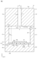
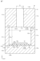
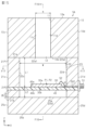
- FIG. 1 is a front cross-sectional view showing the semiconductor device of the first embodiment.
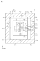
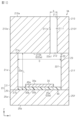
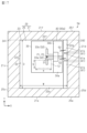
- FIG. 2 is a cross-sectional view taken along line F2-F2 of FIG.
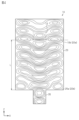
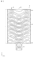
- FIG. 3 is a cross-sectional view taken along line F3-F3 of FIG.
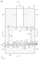
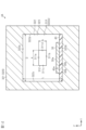
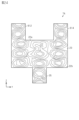
- FIG. 4 is an explanatory diagram schematically showing the electric field intensity distribution of electromagnetic waves in the semiconductor device of FIG.
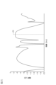
- FIG. 5 is an explanatory diagram showing the transmittance of electromagnetic waves with respect to the length of the accommodation space.
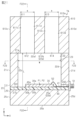
- FIG. 6 is a front sectional view showing the semiconductor device of the second embodiment.
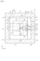
- 7 is a cross-sectional view taken along the line F7-F7 of FIG. 6.
- FIG. 8 is a cross-sectional view taken along line F8-F8 of FIG. 6.
- FIG. 9 is a front sectional view showing the semiconductor device of the third embodiment.
- 10 is a cross-sectional view taken along line F10-F10 of FIG. 9.
- FIG. 11 is a cross-sectional view taken along the line F11-F11 of FIG. 9.
- FIG. 12 is an explanatory diagram schematically showing the electric field strength distribution of electromagnetic waves in the semiconductor device of FIG.
- FIG. 13 is a front sectional view showing the semiconductor device of the fourth embodiment.
- 14 is a cross-sectional view taken along line F14-F14 of FIG. 13.
- FIG. 15 is a front sectional view showing the semiconductor device of the fifth embodiment.
- 16 is a cross-sectional view taken along line F16-F16 of FIG. 15.
- FIG. 17 is a cross-sectional view taken along line F17-F17 of FIG. 15.
- FIG. FIG. 18 is a front sectional view showing the semiconductor device of the sixth embodiment.
- 19 is a cross-sectional view taken along line F19-F19 of FIG. 18.
- FIG. 20 is a front sectional view showing a modification of the semiconductor device of FIG. 18.
- FIG. 21 is a front sectional view showing the semiconductor device of the seventh embodiment. 22 is a cross-sectional view taken along line F22-F22 of FIG. 21.
- FIG. 23 is a cross-sectional view taken along line F23-F23 of FIG. 21.
- FIG. 24 is an explanatory diagram schematically showing the electric field intensity distribution of electromagnetic waves in the semiconductor device of FIG. 21.
- FIG. 25 is an explanatory diagram showing the transmittance with respect to the frequency of electromagnetic waves.
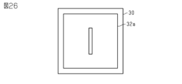
- FIG. 26 is a plan view showing the antenna of the semiconductor element of the modification.
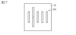
- FIG. 27 is a plan view showing a modified semiconductor element antenna.
- FIG. 28 is a plan view showing a modified semiconductor element antenna.
- FIG. 29 is a plan view showing a modified semiconductor element antenna.
- FIG. 30 is a plan view showing a modified semiconductor element antenna.
- a semiconductor device 1A of this embodiment has a waveguide 10, a base 20, and a semiconductor element 30.
- the semiconductor element 30 is an element that converts electromagnetic waves and electrical energy.
- the electromagnetic wave includes the concepts of either one or both of light and radio waves.
- the semiconductor element 30 is a functional device that oscillates and emits electromagnetic waves (terahertz waves) in a predetermined frequency band, for example, the terahertz band.
- the semiconductor element 30 can be said to be a terahertz element that oscillates and emits terahertz waves.
- the semiconductor element 30 is a functional device that receives and detects electromagnetic waves (terahertz waves) in a predetermined frequency band, for example, the terahertz band.
- the semiconductor device 30 can be said to be a terahertz device that receives and detects terahertz waves.
- the semiconductor element 30 converts the supplied electrical energy into electromagnetic waves by oscillating with the supplied electrical energy. Thereby, the semiconductor element 30 radiates electromagnetic waves in a desired frequency band. Also, the semiconductor element 30 receives electromagnetic waves and converts the electromagnetic waves into electrical energy. Thereby, the semiconductor element 30 detects electromagnetic waves in a desired frequency band.
- the semiconductor element 30 is arranged inside the base 20 .
- the disclosed semiconductor device 1A has a waveguide 10 that transmits electromagnetic waves, and a semiconductor element 30 that oscillates and radiates electromagnetic waves.
- the semiconductor element 30 of this embodiment is formed in a plate shape.
- the semiconductor element 30 has an element front surface 30a facing in the thickness direction and an element back surface 30b facing in the opposite direction to the element front surface 30a.
- the thickness direction of the semiconductor element 30 is defined as the Z direction (first direction).
- the directions perpendicular to the Z direction and perpendicular to each other are defined as the X direction (second direction) and the Y direction (third direction).
- the semiconductor element 30 of this embodiment has a rectangular shape when viewed from the Z direction.
- the shape of the semiconductor element 30 when viewed in the Z direction is not limited to a rectangular shape, and may be a circular shape, an elliptical shape, or a polygonal shape.
- the semiconductor element 30 has an active element 31, an antenna 32, a first electrode 34a, and a second electrode 34b on the element surface 30a.
- the active element 31 converts electromagnetic waves in a predetermined frequency band into electrical energy.
- Active element 31 is provided, for example, in the center of element surface 30a.
- the active element 31 is connected to the antenna 32 to convert supplied electrical energy into electromagnetic waves.
- the semiconductor element 30 radiates electromagnetic waves in a predetermined frequency band. Therefore, the active element 31 can be said to be an oscillation point P1 that oscillates electromagnetic waves, and the antenna 32 can be said to be a radiation point P2 that radiates electromagnetic waves.
- the semiconductor element 30 of this embodiment has a radiation point P2 at the center of the element surface 30a.
- the semiconductor element 30 has the radiation point P2 and the oscillation point P1 at the same position.
- the position of the oscillation point P1 is not limited to the same as the position of the radiation point P2, and can be set arbitrarily.
- the position of the oscillation point P1 can be an arbitrary position on the element surface 30a.
- the active element 31 is, for example, a resonant tunneling diode (RTD: Resonant Tunneling Diode).
- RTD Resonant Tunneling Diode
- TUNNETT Tunnel injection Transit Time
- IMPATT Immpatt: Impact Ionization Avalanche Transit Time
- FET Field Effect Transistor
- HEMT High Electron Mobility Transistor
- HBT Heterojunction Bipolar Transistor
- the semiconductor element 30 has a first conductive portion 33 a and a second conductive portion 33 b that function as an antenna 32 .
- the active element 31 is provided between the first conductive portion 33a and the second conductive portion 33b.
- the antenna 32 of this embodiment is a dipole antenna.
- the first conductive portion 33a and the second conductive portion 33b extend from the active element 31 in opposite directions.
- the length of the antenna 32 that is, the length from the tip of the first conductive portion 33a to the second conductive portion 33b is set to a half wavelength ( ⁇ /2) of the wavelength ⁇ of the electromagnetic wave emitted by the semiconductor element 30. be done.
- the element surface 30a of the semiconductor element 30 is provided with a first electrode 34a and a second electrode 34b.
- the first electrode 34a is connected to the first conductive portion 33a
- the second electrode 34b is connected to the second conductive portion 33b.
- the support substrate 40 is made of a material that transmits electromagnetic waves emitted by the semiconductor element 30 .
- the support substrate 40 is made of a dielectric.
- the dielectric for example, glass such as quartz glass, synthetic resin such as sapphire, epoxy resin, or single-crystal intrinsic semiconductor such as Si (silicon) can be used, and quartz glass is used in this embodiment.
- the support substrate 40 has a substrate front surface 40a and a substrate rear surface 40b.
- the substrate front surface 40a and the substrate back surface 40b face opposite sides in the Z direction.
- the substrate surface 40 a has a power feeding line 41 as a transmission line connected to the semiconductor element 30 .
- Feeding line 41 is, for example, a coplanar line.
- a microstrip line, a strip line, a slot line, or the like may be used as the feed line 41 .
- the feed line 41 includes a main conductor 41a and two ground conductors 41b.
- the main conductor 41a extends in the X direction.
- the ground conductors 41b are provided on both sides of the main conductor 41a.
- Main conductor 41a and ground conductor 41b are made of, for example, copper (Cu).
- the main conductor 41a of the support substrate 40 is connected to the connector 51.
- Connector 51 is capable of transmitting high-frequency signals, and is, for example, an SMA connector.
- a core wire of the connector 51 is connected to the main conductor 41a shown in FIG.
- the main conductor 41 a is connected to the first electrode 34 a of the semiconductor element 30 by a wire 52 .
- the housing of connector 51 is connected to base body 21 of base 20 .
- the ground conductor 41 b is in contact with the base body 21 and electrically connected to the base body 21 .
- the ground conductor 41b is connected to the second electrode 34b of the semiconductor element 30 by a wire 52.
- the waveguide 10 and the base 20 are made of a conductor material that is impermeable to electromagnetic waves emitted by the semiconductor element 30 .
- a conductor material metals such as Cu, Cu alloys, aluminum (Al), Al alloys, or the like, or those whose surfaces are plated with gold can be used.
- the waveguide 10 and the base 20 are connected to each other in the Z direction.
- the waveguide 10 and the base 20 are connected to each other by, for example, a conductive adhesive, a flange, or the like. It should be noted that the waveguide 10 and the base 20 may be formed as an integrated body connected to each other.
- a waveguide 10 is a hollow metal tube that transmits electromagnetic waves, and has a waveguide 12 extending in the Z direction.
- the waveguide 10 of this embodiment is a rectangular waveguide.
- the waveguide 10 has a substantially rectangular outer shape.
- the waveguide 10 has an upper surface 10a, a lower surface 10b and outer surfaces 10c, 10d, 10e and 10f.
- the upper surface 10a and the lower surface 10b face opposite sides in the Z direction.
- the outer side surfaces 10c and 10d face opposite sides in the X direction.
- the outer side surfaces 10e and 10f face opposite sides in the Y direction.
- the waveguide 10 has a through hole 11 .
- Through hole 11 is formed to penetrate waveguide 10 from upper surface 10a to lower surface 10b of waveguide 10 .
- the waveguide 10 has inner side surfaces 11 c , 11 d , 11 e and 11 f that define the through hole 11 .
- the inner side surfaces 11c and 11d face each other in the X direction.
- the inner side surfaces 11e and 11f face each other in the Y direction. That is, the through-hole 11 is formed in a rectangular annular shape when viewed from the Z direction.
- This through hole 11 constitutes a waveguide 12 in the waveguide 10 . That is, the waveguide 12 is defined by the inner side surfaces 11c to 11f of the waveguide 10.
- FIG. 1 Through hole 11 is formed to penetrate waveguide 10 from upper surface 10a to lower surface 10b of waveguide 10 .
- the waveguide 10 has inner side surfaces 11 c , 11 d , 11 e and 11 f that define the through hole 11 .
- the waveguide 12 is configured such that the electromagnetic wave emitted by the semiconductor element 30 is transmitted as a fundamental mode.
- the size of waveguide 12 is determined by the frequency band of the electromagnetic wave to be transmitted in order to maintain fundamental mode propagation.
- the size of the waveguide 12 is indicated by the dimension a of the waveguide 12 in the X direction and the dimension b of the waveguide 12 in the Y direction.
- dimension a is the distance between inner side 11 c and inner side 11 d that define waveguide 12 .
- dimension b is the distance between inner surfaces 11e and 11f that define waveguide 12.
- dimension a is greater than dimension b. That is, the waveguide 12 of this embodiment has a rectangular shape with the long side in the X direction and the short side in the Y direction when viewed from the Z direction in which the waveguide 12 extends.
- the base 20 has a substantially rectangular outer shape.
- the base 20 has an accommodation space 23 that accommodates the semiconductor element 30 .
- the accommodation space 23 accommodates the semiconductor element 30 .
- the base 20 of this embodiment has a base body 21 and a closing plate 25 .
- the base body 21 has a substantially rectangular outer shape.
- the base body 21 has an upper surface 21a, a lower surface 21b, and outer side surfaces 21c, 21d, 21e, and 21f.
- the upper surface 21a and the lower surface 21b face opposite sides in the Z direction.
- the outer side surfaces 21c and 21d face opposite sides in the X direction.
- the outer side surfaces 21e and 21f face opposite sides in the Y direction.
- the closing plate 25 has a rectangular plate-like outer shape.
- the closing plate 25 has an upper surface 25a, a lower surface 25b, and outer surfaces 25c, 25d, 25e, and 25f.
- the upper surface 25a and the lower surface 25b face opposite sides in the Z direction.
- the outer side surfaces 25c and 25d face opposite sides in the X direction.
- the outer side surfaces 25e and 25f face opposite sides in the Y direction.
- the base body 21 is connected to the waveguide 10 .
- the closing plate 25 is arranged on the side opposite to the waveguide 10 with respect to the base body 21 .
- the base body 21 and the closing plate 25 are connected to each other.
- the upper surface 21 a of the base body 21 is connected to the lower surface 10 b of the waveguide 10 .
- the lower surface 21 b of the base body 21 is connected to the upper surface 25 a of the closing plate 25 .
- the base body 21 and the closing plate 25 are connected to each other by, for example, a conductive adhesive, a flange, or the like. Note that the base body 21 and the closing plate 25 may be formed as an integrated body connected to each other.
- the base body 21 of this embodiment is formed in a rectangular annular shape when viewed from the Z direction.
- the base body 21 has a through hole 22 penetrating through the base body 21 in the Z direction from the upper surface 21a to the lower surface 21b.
- the through hole 22 is defined by inner side surfaces 22c, 22d, 22e, 22e of the base body 21.
- the inner side surfaces 22c and 22d face opposite sides in the X direction.
- the inner side surfaces 22e and 22f face opposite sides in the Y direction.
- a space surrounded by the inner side surfaces 22c to 22f constitutes an accommodation space 23 that accommodates the semiconductor element 30.
- the base body 21 of this embodiment has a first accommodation recess 241 and a second accommodation recess 242 recessed from the lower surface 21b toward the upper surface 21a.
- the first accommodation recess 241 is formed to accommodate the support substrate 40 .
- the second accommodation recess 242 accommodates the support substrate 40 and is formed so that the main conductor 41 a of the support substrate 40 does not come into contact with the base body 21 .
- the accommodation space 23 is defined by inner side surfaces 22c to 22f in the X direction and the Y direction. Also, the accommodation space 23 is defined by the waveguide 10 and the closing plate 25 connected to the base 20 in the Z direction. The waveguide 10 and the blocking plate 25 are arranged on opposite sides of the base 20 and connected to the base 20 . The closing plate 25 closes the through hole 22 of the base body 21 .
- the lower surface 10b of the waveguide 10 exposed through the through hole 22 of the base 20 is the first inner wall surface 22a that defines the accommodation space 23.
- the first inner wall surface 22 a has an opening 22 a 1 that communicates with the waveguide 12 through the through hole 11 of the waveguide 10 .
- the upper surface 25a of the closing plate 25 exposed through the through hole 22 of the base 20 is a second inner wall surface 22b that defines the accommodation space 23.
- the length dimension L of the housing space 23 in the Z direction is the length of the base body 21 in the Z direction.
- the length dimension L is also the distance between the first inner wall surface 22a and the second inner wall surface 22b.
- the width dimension W of the housing space 23 in the X direction is the distance between the inner side surface 22c and the inner side surface 22d that face each other in the X direction.
- the depth dimension D of the accommodation space 23 in the Y direction is the distance between the inner side surfaces 22e and 22f facing each other in the Y direction.
- connection position of the waveguide 12 with respect to the accommodation space 23 is set according to the electric field intensity of the electromagnetic waves generated in the accommodation space 23 .
- the waveguide 12 is set so as to be at the antinode position of the electric field intensity with respect to the electric field intensity of the higher mode generated in the housing space 23 . It can be said that the length dimension L, width dimension W, and depth dimension D that define the size of the accommodation space 23 are adjusted so that the position where the waveguide 12 is connected is the antinode position of the electric field strength.
- the waveguide 12 is indicated by a two-dot chain line.
- the waveguide 12 is connected (communicated) with the accommodation space 23 at the center of the accommodation space 23 .
- the semiconductor element 30 is arranged in the accommodation space 23 so that its oscillation point P1 coincides with the center of the accommodation space 23 . Therefore, the oscillation point P1 of the semiconductor element 30 is positioned within the waveguide 12 when viewed from the Z direction.
- the semiconductor element 30 has an outer shape larger than that of the waveguide 12 when viewed from the Z direction.
- the semiconductor element 30 is housed in the housing space 23 . Therefore, the width dimension W of the accommodation space 23 is larger than the dimension a of the waveguide 12 . Also, the depth dimension D of the accommodation space 23 is larger than the dimension b of the waveguide 12 .
- the width dimension W and depth dimension D of the accommodation space 23 are set so as to accommodate the semiconductor element 30 . Furthermore, the length dimension L, width dimension W, and depth dimension D, which are the sizes of the accommodation space 23, are set so that the electromagnetic waves radiated from the semiconductor element 30 resonate in a higher mode in the accommodation space 23. ing. That is, the accommodation space 23 is a resonant space in which electromagnetic waves resonate in higher modes.
- FIG. 4 is a model of the semiconductor device 1A described above, and schematically shows an example of the electric field intensity distribution of electromagnetic waves in the semiconductor device 1A of the present embodiment.
- the waveguide 35 simulates the semiconductor element 30 shown in FIGS. 1 to 3, and is set to transmit the electromagnetic waves emitted by the semiconductor element 30 in the fundamental mode.
- the waveguide 35 communicates with the accommodation space 23 on the upper surface 25a of the closing plate 25 defining the accommodation space 23 shown in FIGS.
- the electromagnetic waves radiated from the waveguide 35 into the accommodation space 23 resonate in the accommodation space 23 in higher-order modes.
- a two-dot chain line shown in FIG. 4 indicates the lower surface 10b of the waveguide 10 and the waveguide 12 shown in FIGS. Electromagnetic waves in the accommodation space 23 are output from this waveguide 12 .
- FIG. 5 shows a waveguide for outputting electromagnetic waves from a waveguide 35 for inputting electromagnetic waves when the length dimension L from the upper surface 25a of the blocking plate 25 to the lower surface 10b of the waveguide 10 shown in FIG. 4 is changed.
- a transmittance S21 to the wave path 12 is shown.
- the transmittance S21 is the electromagnetic wave output from the housing space 23 to the waveguide 12 of the waveguide 10 with respect to the electric field strength of the electromagnetic wave radiated from the semiconductor element 30. equivalent to a loss of electric field strength of The higher the transmittance S21, the higher the coupling rate between the accommodation space 23 and the waveguide 12, and the lower the loss.
- the transmittance S21 is high and the change in the transmittance S21 is small.
- the size of the base 20 (base main body 21) of the semiconductor device 1A shown in FIGS. 1 to 3 is set so that the length L is within the range including the dashed line LD1.
- the semiconductor device 1A having the accommodation space 23 with the length dimension L set in this way provides high coupling between the semiconductor element 30 and the waveguide 12 .
- this semiconductor device 1A can reduce the influence of dimensional errors such as processing errors.
- the semiconductor device 1A of this embodiment has an accommodation space 23 that is larger than the waveguide 12 when viewed from the Z direction.
- the semiconductor element 30 housed in this housing space 23 is larger than the waveguide 12 when viewed from the Z direction. Therefore, a semiconductor device 1A containing semiconductor elements 30 of various sizes can be obtained.
- the semiconductor device 1A can extract the electromagnetic wave emitted from the semiconductor element 30 with high efficiency to the waveguide 12 that transmits the electromagnetic wave in the fundamental mode.
- the semiconductor device 1A of this embodiment has the following effects.
- the semiconductor device 1A includes a semiconductor element 30 that oscillates and emits electromagnetic waves, a base 20 that has an accommodation space 23 that accommodates the semiconductor element 30, and a waveguide that has a waveguide 12 that communicates with the accommodation space 23. 10; Waveguide 12 is configured such that electromagnetic waves are transmitted in the fundamental mode.
- the accommodation space 23 is a resonant space in which electromagnetic waves resonate in higher modes.
- the waveguide 12 communicates with the accommodation space 23 at the antinode position of the electric field strength of the electromagnetic waves generated in the accommodation space 23 by the semiconductor element 30 .
- the waveguide 12 that transmits electromagnetic waves in the fundamental mode can be connected with high efficiency to the accommodation space 23 in which higher-order mode resonance occurs.
- the semiconductor device 1A has an accommodation space 23 larger than the waveguide 12 when viewed from the Z direction.
- the semiconductor element 30 housed in this housing space 23 is larger than the waveguide 12 when viewed from the Z direction. Therefore, a semiconductor device 1A containing semiconductor elements 30 of various sizes can be obtained.
- the semiconductor device 1A has an accommodation space 23 larger than the waveguide 12 when viewed from the Z direction.
- the semiconductor element 30 housed in this housing space 23 is larger than the waveguide 12 when viewed from the Z direction. Therefore, the semiconductor device 1A can extract the electromagnetic waves radiated from the semiconductor elements 30 of various sizes to the waveguide 12 that transmits the electromagnetic waves in the fundamental mode with high efficiency.
- the semiconductor device 1A of the present embodiment can extract electromagnetic waves radiated from the semiconductor element 30 with high efficiency to the waveguide 12 of the waveguide 10, which is a rectangular waveguide.
- the second embodiment will be described below.
- 6 to 8 show a semiconductor device 2A of this embodiment.
- a semiconductor device 2 ⁇ /b>A of this embodiment has a waveguide 110 , a base 120 and a semiconductor element 30 .
- Waveguide 110 and base 120 are made of a conductive material that is impermeable to electromagnetic waves emitted by semiconductor element 30 .
- the conductor material metals such as Cu, Cu alloys, Al, Al alloys, or the like, or metals whose surfaces are plated with gold can be used.
- the waveguide 110 and the base 120 are connected to each other in the Z direction. Waveguide 110 and base 120 are connected to each other by, for example, a conductive adhesive, a flange, or the like. It should be noted that the waveguide 110 and the base 120 may be formed as an integrated body connected to each other.
- the waveguide 110 is a hollow metal tube that transmits electromagnetic waves, and has a waveguide 112 extending in the Z direction.
- the waveguide 110 of this embodiment is a circular waveguide.
- Waveguide 110 has a cylindrical outer shape.
- the waveguide 110 has an upper surface 110a, a lower surface 110b, and an outer peripheral surface 110c.
- the upper surface 110a and the lower surface 110b face opposite sides in the Z direction.
- the waveguide 110 has a through hole 111 .
- the through hole 111 is formed to penetrate the waveguide 110 from the top surface 110a of the waveguide 110 to the bottom surface 110b.
- the through hole 111 is formed in a circular shape when viewed from the Z direction.
- Waveguide 110 has an inner peripheral surface 111 c that defines through hole 111 .
- This through hole 111 constitutes a waveguide 112 in the waveguide 110 . That is, the waveguide 112 is defined by the inner peripheral surface 111 c of the waveguide 110 .
- the waveguide 112 is formed so as to penetrate the waveguide 110 from the top surface 110a of the waveguide 110 to the bottom surface 110b. Waveguide 112 is defined by inner peripheral surface 111 c of waveguide 110 .
- the waveguide 112 is configured such that the electromagnetic wave emitted by the semiconductor element 30 is transmitted as the fundamental mode.
- the size of waveguide 112 is determined by the frequency band of the electromagnetic wave to be transmitted in order to maintain fundamental mode propagation.
- the inner diameter dimension D1 of the waveguide 112 is indicated by the diameter of the inner peripheral surface 111c viewed from the Z direction.
- the base 120 has a substantially cylindrical outer shape.
- the base 120 has an accommodation space 123 that accommodates the semiconductor element 30 .
- the base 120 of this embodiment has a base body 121 and a closing plate 125 .
- the base body 121 has a substantially cylindrical outer shape.
- the base body 121 has an upper surface 121a, a lower surface 121b, and an outer peripheral surface 121c.
- the upper surface 121a and the lower surface 121b face opposite sides in the Z direction.
- the closing plate 125 has a generally disk-shaped outer shape.
- the closing plate 125 has an upper surface 125a, a lower surface 125b, and an outer peripheral surface 125c.
- the upper surface 125a and the lower surface 125b face opposite sides in the Z direction.
- the base body 121 is connected to the waveguide 110 .
- the blocking plate 125 is arranged on the side opposite to the waveguide 110 with respect to the base body 121 .
- the base body 121 and the closing plate 125 are connected to each other.
- the base body 121 and the closing plate 125 are connected to each other by, for example, a conductive adhesive, a flange, or the like. Note that the base body 121 and the closing plate 125 may be formed as an integrated body connected to each other.
- the base body 121 of this embodiment is cylindrical.
- the base body 121 has a through-hole 122 extending through the base body 121 in the Z direction from the upper surface 121a to the lower surface 121b.
- the through hole 122 is defined by an inner peripheral surface 122c of the base body 121.
- the inner peripheral surface 122c has a circular shape when viewed from the Z direction.
- a space surrounded by the inner peripheral surface 122 c constitutes an accommodation space 123 that accommodates the semiconductor element 30 .
- the base body 121 of this embodiment has a first accommodation recess 1241 and a second accommodation recess 1242 recessed from the lower surface 121b toward the upper surface 121a.
- the first accommodation recess 1241 is formed to accommodate the support substrate 40 .
- the second accommodation recess 1242 accommodates the support substrate 40 and is formed so that the main conductor 41 a of the support substrate 40 does not come into contact with the base body 121 .
- the accommodation space 123 is defined by an inner peripheral surface 122c in the X direction and the Y direction. Also, the accommodation space 123 is defined by the waveguide 110 and the closing plate 125 connected to the base 120 in the Z direction. The waveguide 110 and the blocking plate 125 are arranged opposite to each other with respect to the base 120 and connected to the base 120 . The closing plate 125 closes the through hole 122 of the base body 121 .
- a lower surface 110 b of the waveguide 110 exposed through the through hole 122 of the base 120 is a first inner wall surface 122 a that defines the accommodation space 123 .
- the first inner wall surface 122 a has an opening 122 a 1 that communicates with the waveguide 112 through the through hole 111 of the waveguide 110 .
- a top surface 125 a of the closing plate 125 exposed through the through hole 122 of the base 120 is a second inner wall surface 122 b that defines the housing space 123 . That is, the length dimension L of the accommodation space 123 in the Z direction is the length of the base body 121 in the Z direction. The length dimension L is also the distance between the first inner wall surface 122a and the second inner wall surface 122b. The inner diameter dimension D2 of the accommodation space 123 is the diameter of the inner peripheral surface 122c viewed from the Z direction.
- connection position of the waveguide 112 with respect to the accommodation space 123 is set according to the electric field intensity of the electromagnetic waves generated in the accommodation space 123 .
- the waveguide 112 is set so as to be at the antinode position of the electric field intensity with respect to the electric field intensity of the higher mode generated in the housing space 123 . It can be said that the length dimension L and the inner diameter dimension D2 that define the size of the accommodation space 123 are adjusted so that the position where the waveguide 112 is connected is the antinode position of the electric field intensity.
- the waveguide 112 is indicated by a chain double-dashed line.
- the semiconductor element 30 has an outer shape larger than that of the waveguide 112 when viewed in the Z direction.
- the semiconductor element 30 is housed in the housing space 123 . Therefore, the inner diameter D2 of the accommodation space 123 is larger than the inner diameter D1 of the waveguide 112 .
- the inner diameter D2 which is the size of the accommodation space 123, is set so as to accommodate the semiconductor element 30 therein. Further, the length dimension L and the inner diameter dimension D2, which are the sizes of the accommodation space 123, are set so that the electromagnetic waves radiated from the semiconductor element 30 resonate in a higher mode in the accommodation space 123.
- the semiconductor device 2A of this embodiment has the following effects. (2-1) The same effects as (1-1) to (1-4) of the first embodiment can be obtained.
- the semiconductor device 2A of the present embodiment can extract electromagnetic waves radiated from the semiconductor element 30 with high efficiency to the waveguide 112 of the waveguide 110 which is a circular waveguide.
- the third embodiment will be described below.
- 9 to 11 show a semiconductor device 3A of the third embodiment. This semiconductor device 3A differs from the semiconductor device 1A of the first embodiment in the position of the waveguide 212 .
- the semiconductor device 3A has a waveguide 210, a base 20, and a semiconductor element 30.
- the waveguide 210 has a waveguide 212 that is arranged differently from the waveguide 10 of the first embodiment. That is, the waveguide 212 of this embodiment communicates with the housing space 23 at a position different from that of the waveguide 12 of the first embodiment.
- the waveguide 210 has an upper surface 210a, a lower surface 210b, outer surfaces 210c, 210d, 210e, and 210f.
- the upper surface 210a and the lower surface 210b face opposite sides in the Z direction.
- the outer side surfaces 210c and 210d face opposite sides in the X direction.
- the outer surfaces 210e and 210f face opposite sides in the Y direction.
- the waveguide 210 has a through hole 211 .
- Through hole 211 is formed to penetrate waveguide 210 from upper surface 210a to lower surface 210b of waveguide 210 .
- the waveguide 210 has inner side surfaces 211c, 211d, 211e, and 211f that define the through hole 211. As shown in FIG.
- the inner side surfaces 211c and 211d face each other in the X direction.
- the inner side surfaces 211e and 211f face each other in the Y direction.
- Waveguide 212 is defined by inner surfaces 211c, 211d, 211e, and 211f.
- the waveguide 212 is arranged closer to the inner side surface 22d of the housing space 23 in the X direction. Further, as shown in FIGS. 10 and 11, the waveguide 212 is arranged closer to the inner surface 22f of the accommodation space 23 in the Y direction.
- the arrangement position of the waveguide 212 is set at the antinode position of the electromagnetic wave that resonates in the higher mode in the accommodation space 23 . That is, the waveguide 212 of the waveguide 210 communicates with the accommodation space 23 at the antinode position of the electric field intensity of the electromagnetic wave resonating in the accommodation space 23 in the direction of the width W of the accommodation space 23 (X direction). ing.
- the waveguide 212 of the waveguide 210 communicates with the accommodation space 23 at the antinode position of the electric field strength of the electromagnetic wave resonating in the accommodation space 23 in the direction of the depth dimension D (Y direction) of the accommodation space 23 . ing.
- FIG. 12 is a model of the semiconductor device 3A described above, and schematically shows the electric field intensity distribution of electromagnetic waves in the semiconductor device 3A of this embodiment. Note that FIG. 12 shows an example of the electric field intensity distribution in a plane including the oscillation point P1 of the semiconductor element 30. As shown in FIG.
- the arrow AA indicates the antinode position of the electric field strength
- the arrow AB indicates the nodal position of the electric field strength.
- a transmittance S21 when the waveguide 212 is connected to the arrows AA and AB is calculated by simulation.
- the transmittance S21 in the waveguide 212 connected at the position of the arrow AA is -0.3 dB.
- the transmittance S21 in the waveguide 212 connected at the position of the arrow AB is -16.5 dB. Therefore, in FIG.
- the semiconductor device 3A of this embodiment has the following effects. (3-1) The same effects as (1-1) to (1-5) of the first embodiment can be obtained.
- the waveguide 212 of the semiconductor device 3A is arranged at a position deviated from the center of the accommodation space 23 and communicates with the accommodation space 23 .
- the waveguide 212 communicates with the accommodation space 23 at the antinode position of the electric field intensity of the electromagnetic wave resonating in the accommodation space 23 .
- a semiconductor device 4 ⁇ /b>A of this embodiment has a waveguide 310 , a base 320 and a semiconductor element 30 .
- the waveguide 310 and the base 320 are made of a conductor material that is impermeable to electromagnetic waves emitted by the semiconductor element 30 .
- a conductor material metals such as Cu, Cu alloys, Al, Al alloys, or the like, or metals whose surfaces are plated with gold can be used.
- the waveguide 310 and the base 320 are connected to each other in the X direction. Waveguide 310 and base 320 are connected to each other by, for example, a conductive adhesive, a flange, or the like. It should be noted that the waveguide 310 and the base 320 may be formed as a single piece connected to each other.
- a waveguide 310 is a hollow metal tube that transmits electromagnetic waves, and has a waveguide 312 extending in the X direction.
- the waveguide 310 of this embodiment is a rectangular waveguide.
- Waveguide 310 has a generally rectangular outer shape.
- the waveguide 310 has a first side surface 310a and a second side surface 310b facing opposite sides in the X direction.
- the waveguide 310 has a through hole 311 .
- Through hole 311 is formed to penetrate waveguide 310 from first side surface 310a to second side surface 310b of waveguide 310 .
- the waveguide 310 has inner side surfaces 311 a , 311 b , 311 c , 311 d that define a through hole 311 .
- the inner side surfaces 311a and 311b face each other in the Z direction.
- the inner side surfaces 311c and 311d face each other in the Y direction. That is, the waveguide 310 is formed in a rectangular annular shape when viewed from the X direction.
- Waveguide 312 is defined by inner surfaces 311 a , 311 b , 311 c , 311 d of waveguide 310 .
- the waveguide 312 is configured so that the electromagnetic wave emitted by the semiconductor element 30 is transmitted as the fundamental mode.
- the size of waveguide 312 is determined by the frequency band of the electromagnetic wave to be transmitted in order to maintain fundamental mode propagation. As shown in FIG. 14, in this embodiment, the size of the waveguide 312 is indicated by the dimension a of the waveguide 312 in the Y direction and the dimension b of the waveguide 312 in the Z direction. Dimension a is the distance between inner surfaces 311 c and 311 d that define waveguide 312 . Dimension b is the distance between inner surfaces 311 a and 311 b that define waveguide 312 . In this embodiment, dimension a is greater than dimension b. That is, the waveguide 312 of this embodiment has a rectangular shape with the long side in the Y direction and the short side in the Z direction when viewed from the X direction in which the waveguide 312 extends.
- the base 320 has a substantially rectangular outer shape.
- the base 320 has an accommodation space 323 that accommodates the semiconductor element 30 .
- the base 320 of this embodiment has a base body 321 and a closing plate 325 .
- the base body 321 has a substantially rectangular outer shape.
- the base body 321 has a first side surface 321a and a second side surface 321b.
- the first side surface 321a and the second side surface 321b face opposite sides in the X direction.
- the closing plate 325 has a rectangular plate-like outer shape when viewed from the X direction.
- the closing plate 325 has a first side surface 325a and a second side surface 325b.
- the first side surface 325a and the second side surface 325b face opposite sides in the X direction.
- the base body 321 is connected to the waveguide 310 .
- the blocking plate 325 is arranged on the side opposite to the waveguide 310 with respect to the base body 321 .
- the base body 321 and the closing plate 325 are connected to each other.
- the first side 321 a of the base body 321 is connected to the second side 310 b of the waveguide 310 .
- a second side surface 321 b of the base body 321 is connected to a first side surface 325 a of the closing plate 325 .
- the base body 321 and the closing plate 325 are connected to each other by, for example, a conductive adhesive, a flange, or the like. Note that the base body 321 and the closing plate 325 may be formed as an integrated body connected to each other.
- the base body 321 of this embodiment is formed in a rectangular annular shape when viewed from the X direction.
- the base body 321 has a through hole 322 that penetrates the base body 321 in the X direction from the first side surface 321a to the second side surface 321b.
- the through hole 322 is defined by inner side surfaces 322 a , 322 b , 322 c and 322 d of the base body 321 .
- the inner side surfaces 322a and 322b face opposite sides in the Z direction.
- the inner side surfaces 322c and 322d face opposite sides in the Y direction.
- a space surrounded by the inner side surfaces 322a to 322d constitutes an accommodation space 323 that accommodates the semiconductor element 30. As shown in FIG.
- the closure plate 325 of this embodiment has an accommodation hole 325c penetrating through the closure plate 325 in the X direction from the first side surface 325a to the second side surface 325b.
- the accommodation hole 325 c is formed so that the support substrate 40 penetrates the closing plate 325 . Further, the accommodation hole 325 c is formed so that the main conductor 41 a of the support substrate 40 does not come into contact with the closing plate 325 .
- the accommodation space 323 is defined by inner side surfaces 322a to 322d in the Z direction and the Y direction. Also, the accommodation space 323 is defined in the X direction by the waveguide 310 connected to the base 320 and the closing plate 325 .
- the waveguide 310 and the blocking plate 325 are arranged opposite to each other with respect to the base 320 and connected with the base 320 .
- the closing plate 325 closes the through hole 322 of the base body 321 .
- a second side surface 310 b of the waveguide 310 exposed through the through hole 322 of the base 320 is a first inner wall surface 322 e that defines the accommodation space 323 .
- a first side surface 325a of the closing plate 325 exposed through the through hole 322 of the base 320 is a second inner wall surface 322f that defines the accommodation space 323.
- the length dimension L of the accommodation space 323 in the Z direction is the distance between the inner side surfaces 322a and 322b facing each other in the Z direction.
- a width dimension W of the accommodation space 323 in the X direction is the length of the base body 321 in the X direction.
- the width dimension W is also the distance between the first inner wall surface 322e and the second inner wall surface 322f.
- the depth dimension D of the accommodation space 323 in the Y direction is the distance between the inner side surfaces 322c and 322d facing each other in the Y direction.
- the semiconductor element 30 is arranged in the housing space 323 so that the element surface 30a faces the Z direction. Therefore, the waveguide 312 extends in the X direction parallel to the element surface 30a of the semiconductor element 30. As shown in FIG.
- the connection position of the waveguide 312 with respect to the accommodation space 323 is set according to the electric field strength of the electromagnetic waves generated in the accommodation space 323 .
- the waveguide 312 is set so as to be at the antinode position of the electric field intensity with respect to the electric field intensity of the higher mode generated in the housing space 323 . It can be said that the length dimension L, width dimension W, and depth dimension D that define the size of the accommodation space 323 are adjusted so that the position where the waveguide 312 is connected is the antinode position of the electric field intensity.
- the waveguide 312 is connected (communicated) with the accommodation space 323 at the center of the accommodation space 323 when viewed from the X direction.
- the semiconductor element 30 has an outer shape larger than that of the waveguide 312 when viewed from the Z direction.
- the semiconductor element 30 is housed in the housing space 323 . Therefore, the length dimension L of the accommodation space 323 is larger than the dimension b of the waveguide 312 . Also, the depth dimension D of the accommodation space 323 is larger than the dimension a of the waveguide 312 .
- the width dimension W and depth dimension D of the accommodation space 323 are set to accommodate the semiconductor element 30 . Furthermore, the length dimension L, width dimension W, and depth dimension D, which are the sizes of the accommodation space 323, are set so that the electromagnetic waves radiated from the semiconductor element 30 resonate in a higher mode in the accommodation space 323. ing. That is, the accommodation space 323 is a resonance space in which electromagnetic waves resonate in higher modes.
- the semiconductor device 4A of this embodiment has the following effects. (4-1) The same effects as (1-1) to (1-5) of the first embodiment can be obtained.
- the semiconductor device 4A of the present embodiment can extract electromagnetic waves emitted from the semiconductor element 30 with high efficiency to the waveguide 312 extending in the X direction parallel to the element surface 30a of the semiconductor element 30. can.
- a semiconductor device 5A of the present embodiment differs from the semiconductor device 1A of the first embodiment in the arrangement position of the semiconductor element 30.
- FIG. 15 to 17 show a semiconductor device 5A of the fifth embodiment.
- a semiconductor device 5A of the present embodiment differs from the semiconductor device 1A of the first embodiment in the arrangement position of the semiconductor element 30.
- FIG. 15 to 17 show a semiconductor device 5A of the fifth embodiment.
- a semiconductor device 5A of the present embodiment differs from the semiconductor device 1A of the first embodiment in the arrangement position of the semiconductor element 30.
- the semiconductor element 30 is arranged closer to the inner side surface 22d defining the accommodation space 23 in the X direction.
- the semiconductor element 30 is arranged closer to the inner surface 22f defining the housing space 23 in the Y direction.
- the support substrate 40 on which the semiconductor element 30 is mounted is arranged away from the closing plate 25 in the Z direction.
- the base 20 of this embodiment is composed of a base body 21 and a closing plate 25 .
- the base body 21 of the base 20 can be composed of a first portion 21P1 closer to the waveguide 10 and a second portion 21P2 closer to the blocking plate 25 .
- the length dimension L of the accommodation space 23 includes, for example, a first length dimension L1 from the element back surface 30b of the semiconductor element 30 to the bottom surface 10b of the waveguide 10, and a first length dimension L1 from the element back surface 30b to the top surface 25a of the blocking plate 25. 2 and a length dimension L2.
- the length dimension L of the accommodation space 23 is defined by the length from the substrate rear surface 40b of the support substrate 40 to the lower surface 10b of the waveguide 10 and the length from the substrate rear surface 40b to the upper surface 25a of the closing plate 25. can also
- the accommodation space 23 is set so that the connection position of the waveguide 12 with respect to the accommodation space 23 is the antinode position of the electric field strength of the electromagnetic wave generated in the accommodation space 23 .
- the first length dimension L1, the second length dimension L2, the width dimension W, and the depth dimension D which define the size of the accommodation space 23, determine the connection position of the waveguide 12 with respect to the accommodation space 23. It is set to be the antinode position of the electric field intensity.
- the semiconductor device 5A of this embodiment has the following effects.
- (5-1) The same effects as (1-1) to (1-5) of the first embodiment can be obtained.
- the semiconductor element 30 is located at a position deviated from the center of the housing space 23 when viewed in the Z direction or from the lower surface 10b of the waveguide 10 to the upper surface 25a of the blocking plate 25 in the Z direction due to, for example, mounting restrictions. It can be placed anywhere up to Even in such a case, the first length dimension L1, the second length dimension L2, the width dimension W, and the depth dimension D that define the accommodation space 23 determine the connection position of the waveguide 12 with respect to the accommodation space 23. , can be the antinode position of the electric field intensity of the electromagnetic wave. Thereby, the electromagnetic wave radiated from the semiconductor element 30 can be extracted with high efficiency to the waveguide 12 of the waveguide 10 .
- a semiconductor device 6A of this embodiment has two waveguides 10 and 60 and a base 520 between the two waveguides 10 and 60. As shown in FIG. In order to distinguish between the two waveguides 10 and 60, the first waveguide 10 and the second waveguide 60 will be described.
- the first waveguide 10, the base 520 and the second waveguide 60 are connected in this order in the Z direction.
- the first waveguide 10 and the base 520 and the base 520 and the second waveguide 60 are connected to each other by, for example, conductive adhesives, flanges, or the like.
- the first waveguide 10 and the base 520, or the base 520 and the second waveguide 60, or the first waveguide 10, the base 520 and the second waveguide 60 are formed as an integrated body connected to each other. may be
- the first waveguide 10 has a first waveguide 12 extending in the Z direction.
- the base 520 of this embodiment is composed of the base body 21 .
- the base 520 can be composed of a first portion 21P1 closer to the first waveguide 10 and a second portion 21P2 closer to the second waveguide 60 .
- the second waveguide 60 is a hollow metal tube that transmits electromagnetic waves, and has a second waveguide 62 extending in the Z direction.
- the second waveguide 60 of this embodiment is a rectangular waveguide.
- the second waveguide 60 has a substantially rectangular outer shape.
- the second waveguide 60 has an upper surface 60a, a lower surface 60b and outer surfaces 60c, 60d, 60e and 60f.
- the upper surface 60a and the lower surface 60b face opposite sides in the Z direction.
- the outer side surfaces 60c and 60d face opposite sides in the X direction.
- the outer surfaces 60e and 60f face opposite sides in the Y direction.
- the second waveguide 62 is formed to penetrate the second waveguide 60 from the top surface 60a of the second waveguide 60 to the bottom surface 60b.
- a second waveguide 62 is defined by inner surfaces 61 c , 61 d , 61 e , 61 f of the second waveguide 60 .
- the inner side surfaces 61c and 61d face each other in the X direction.
- the inner side surfaces 61e and 61f face each other in the Y direction. That is, the second waveguide 60 is formed in a rectangular annular shape when viewed from the Z direction.
- the second waveguide 62 is configured so that the electromagnetic wave emitted by the semiconductor element 30 is transmitted as the fundamental mode.
- the size of the second waveguide 62 is determined by the frequency band of the transmitted electromagnetic wave in order to maintain fundamental mode propagation. In this embodiment, the size of the second waveguide 62 is the same as the size of the first waveguide 12 .
- the accommodation space 23 is defined by inner side surfaces 22c to 22f in the X direction and the Y direction. Also, the housing space 23 is defined by the first waveguide 10 and the second waveguide 60 connected to the base 520 in the Z direction.
- the first waveguide 10 and the second waveguide 60 are arranged opposite to each other with respect to the base 520 and connected to the base 520 .
- a lower surface 10 b of the first waveguide 10 exposed through the through hole 22 of the base 520 is a first inner wall surface 22 a that defines the accommodation space 23 .
- the first inner wall surface 22 a has a first opening 22 a 1 that communicates with the waveguide 12 through the through hole 11 of the waveguide 10 .
- the upper surface 60a of the second waveguide 60 exposed through the through hole 22 of the base 520 is the second inner wall surface 22b that defines the accommodation space 23. As shown in FIG.
- the second inner wall surface 22 b has a second opening 22 b 1 that communicates with the waveguide 62 through the through hole 61 of the waveguide 60 . That is, the length dimension L of the housing space 23 in the Z direction is the length of the base body 21 in the Z direction. The length dimension L is also the distance between the first inner wall surface 22a and the second inner wall surface 22b.
- the length dimension L is, for example, a first length dimension L1 from the element back surface 30b of the semiconductor element 30 mounted on the substrate surface 40a of the support substrate 40 to the bottom surface 10b of the first waveguide 10, and from the element back surface 30b. and a second length dimension L2 to the upper surface 60a of the second waveguide 60.
- the width dimension W of the housing space 23 in the X direction is the distance between the inner side surface 22c and the inner side surface 22d that face each other in the X direction.
- the depth dimension D of the accommodation space 23 in the Y direction is the distance between the inner side surfaces 22e and 22f facing each other in the Y direction.
- connection positions of the first waveguide 12 and the second waveguide 62 with respect to the accommodation space 23 are set according to the electric field intensity of the electromagnetic waves generated in the accommodation space 23 .
- the first waveguide 12 and the second waveguide 62 are set so as to be at antinode positions of the electric field intensity of the higher-order mode radiated from the semiconductor element 30 and generated in the housing space 23 .
- a first length dimension L1, a second length dimension L2, a width dimension W, and a depth dimension D that define the size of the accommodation space 23 are the positions where the first waveguide 12 and the second waveguide 62 are connected. It can be said that it is adjusted so as to be the antinode position of the electric field intensity.
- a semiconductor device 6A of this embodiment has a first waveguide 12 and a second waveguide 62 .
- the second waveguide 62 is the input port and the first waveguide 12 is the output port.
- An electromagnetic wave input through the second waveguide 62 is output from the first waveguide 12 .
- the first waveguide 12 may be used as an input port, and the second waveguide 62 may be used as an output port.
- the electromagnetic waves radiated by the semiconductor element 30 resonate in a higher mode in the accommodation space 23 .
- the first waveguide 12 is connected to the accommodation space 23 at the antinode position of the electric field strength of the resonating electromagnetic wave. Therefore, the electromagnetic waves radiated from the semiconductor element 30 are superimposed on the electromagnetic waves input from the second waveguide 62 and output from the first waveguide 12 . Therefore, this semiconductor device 6A functions as a mixer.
- the semiconductor element 30 is a functional device that includes an antenna 32 (see FIG. 3) and emits superimposed electromagnetic waves.
- the semiconductor device 6A of this embodiment has the following effects. (6-1) The same effects as (1-1) to (1-5) of the first embodiment can be obtained.
- the semiconductor device 6A of the present embodiment has the first waveguide 12 and the second waveguide 62.
- the second waveguide 62 is the input port and the first waveguide 12 is the output port.
- An electromagnetic wave input through the second waveguide 62 is output from the first waveguide 12 . Therefore, a semiconductor device 6A having an input port and an output port can be provided.
- the semiconductor element 30 is a functional device that includes an antenna 32 and emits superimposed electromagnetic waves.
- the electromagnetic wave emitted from the semiconductor element 30 is superimposed on the electromagnetic wave input from the second waveguide 62 and output from the first waveguide 12 . Therefore, this embodiment can provide the semiconductor device 6A functioning as a mixer.
- FIG. 20 shows a semiconductor device 6B that is a modification of the semiconductor device 6A of the sixth embodiment.
- This semiconductor device 6B is arranged so that the semiconductor element 30 faces the second waveguide 60 side.
- This semiconductor device 6B can obtain the same effect as the semiconductor device 6A of the sixth embodiment.
- the semiconductor device 7A of this embodiment has a waveguide 610, a base 20, and a semiconductor element 30. As shown in FIG.
- a waveguide 610 of this embodiment has two waveguides 612 and 614 .
- the two waveguides 612, 614 are arranged side by side in the X direction. Note that the arrangement positions of the waveguides 612 and 614 may be changed as appropriate. For example, they may be arranged side by side in the Y direction. Alternatively, they may be arranged side by side in the diagonal direction of the housing space 23 .
- the waveguide 610 has a substantially rectangular outer shape.
- Waveguide 610 has an upper surface 610a, a lower surface 610b and outer surfaces 610c, 610d, 610e and 610f.
- the upper surface 610a and the lower surface 610b face opposite sides in the Z direction.
- the outer side surfaces 610c and 610d face opposite sides in the X direction.
- the outer side surfaces 610e and 610f face opposite sides in the Y direction.
- the waveguide 610 has through holes 611 and 613 . Through holes 611 and 613 are formed to penetrate waveguide 610 from upper surface 610a to lower surface 610b of waveguide 610 .
- the waveguide 610 has inner side surfaces 611 c , 611 d , 611 e , 611 f defining through holes 611 .
- the inner side surfaces 611c and 611d face each other in the X direction.
- the inner side surfaces 611e and 611f face each other in the Y direction.
- First waveguide 612 is defined by inner surfaces 611 c , 611 d , 611 e , 611 f of waveguide 610 .
- the waveguide 610 also has inner side surfaces 613 c , 613 d , 613 e , 613 f that define the through hole 613 .
- the inner side surfaces 613c and 613d face each other in the X direction.
- the inner side surfaces 613e and 613f face each other in the Y direction.
- a second waveguide 614 is defined by inner surfaces 613 c , 613 d , 613 e , 613 f of waveguide 610 .
- the first waveguide 612 and the second waveguide 614 are configured so that the electromagnetic wave emitted by the semiconductor element 30 is transmitted as the fundamental mode.
- the dimensions of first waveguide 612 and second waveguide 614 are determined by the frequency band of the electromagnetic wave to be transmitted in order to maintain fundamental mode propagation.
- the dimensions of the first waveguide 612 and the second waveguide 614 are indicated by the dimension a of the waveguides 612, 614 in the X direction and the dimension b of the waveguides 612, 614 in the Y direction.
- Dimension a is the distance between inner surfaces 611c, 613c and 611d, 613d that define waveguides 612,614.
- Dimension b is the distance between inner surfaces 611e, 613e and 611e, 613f that define waveguides 612,614.
- dimension a is greater than dimension b. That is, the waveguides 612 and 614 of this embodiment have a rectangular shape with the X direction as the long side direction and the Y direction as the short side direction when viewed from the Z direction in which the waveguides 612 and 614 extend.
- connection positions of the first waveguide 612 and the second waveguide 614 with respect to the accommodation space 23 are set according to the electric field intensity of the electromagnetic waves generated in the accommodation space 23 .
- Each of the first waveguide 612 and the second waveguide 614 is set to be at an antinode position of the electric field intensity with respect to the electric field intensity of the higher-order mode generated in the housing space 23 . It can be said that the length dimension L, width dimension W, and depth dimension D that define the size of the accommodation space 23 are adjusted so that the position where the waveguides 612 and 614 are connected is the antinode position of the electric field intensity.
- FIG. 24 is a model of the semiconductor device 7A described above, and schematically shows an example of the electric field strength distribution of electromagnetic waves in the semiconductor device 7A of the present embodiment.
- the waveguide 35 simulates the semiconductor element 30 shown in FIGS. 21 to 23, and is set to transmit the electromagnetic waves emitted by the semiconductor element 30 in the fundamental mode.
- the waveguide 35 communicates with the accommodation space 23 on the upper surface 25a of the closing plate 25 defining the accommodation space 23 shown in FIGS.
- the electromagnetic waves radiated from the waveguide 35 into the accommodation space 23 resonate in the accommodation space 23 in higher-order modes. Electromagnetic waves are then output from the first waveguide 612 and the second waveguide 614 .
- the frequency dependence of the transmittance of the electric field intensity of the electromagnetic waves input from the waveguide 35 and the electric field intensity of the electromagnetic waves output from the first waveguide 612 and the second waveguide 614. indicate the line.
- a transmittance of approximately 1/2 (-3 dB) is obtained at the frequency indicated by the dashed line LD2. It can be seen that at this frequency, the electromagnetic waves input to the accommodation space 23, that is, the electromagnetic waves radiated by the semiconductor element 30 can be output to the first waveguide 612 and the second waveguide 614 with the same electric field intensity. Therefore, the coupling ratio of the first waveguide 612 and the second waveguide 614 with respect to the accommodation space 23 is high, and the loss is low.
- the semiconductor device 7A of this embodiment has the following effects. (7-1) The same effects as (1-1) to (1-5) of the first embodiment can be obtained.
- the waveguide 610 has two waveguides 612 and 614 .
- the two waveguides 612 and 614 are set to be antinode positions of the electric field intensity with respect to the electric field intensity of the higher mode generated in the housing space 23 . Therefore, this semiconductor device 7A has two waveguides 612 and 614 with high coupling ratios with respect to the housing space 23 housing the semiconductor element 30 .
- the semiconductor device 7A can output fundamental mode electromagnetic waves from the two waveguides 612 and 614 with low loss.
- FIG. 26 shows a semiconductor device 30 having a slot antenna 32a.
- FIG. 27 shows a semiconductor device 30 having a Yagi-Uda antenna 32b.
- FIG. 28 shows a semiconductor device 30 having a bowtie antenna 32c.
- FIG. 29 shows a semiconductor device 30 having a patch antenna 32d.
- FIG. 30 shows a semiconductor device 30 having a tapered slot antenna 32e.
- a ring antenna or the like can also be used as the antenna 32 .
- the semiconductor element 30 that radiates electromagnetic waves that is, a device having a function of radiating electromagnetic waves is provided, but a device having other functions may be provided.
- the semiconductor device 6A of the sixth embodiment and the semiconductor device 6B of the modification have a second waveguide 62 for inputting electromagnetic waves and a first waveguide 12 for outputting electromagnetic waves.
- a device that transmits the electromagnetic waves and has frequency characteristics in the transmittance with respect to the electromagnetic waves is mounted as a functional device instead of the semiconductor element 30 .
- An electromagnetic wave device equipped with such a functional device is a so-called filter.
- an electromagnetic wave device having input/output ports can be provided.
- a functional device having a mechanical driving portion and controlling passage and blocking of electromagnetic waves from the second waveguide 62 to the first waveguide 12 is mounted.
- the mechanical drive is operated by control signals supplied from connector 51 shown in FIG. 18, for example.
- An electromagnetic wave device equipped with such a functional device is a so-called chopper.
- an electromagnetic wave device having input/output ports can be provided.
- the position of the waveguide 112 of the waveguide 110 may be appropriately changed as in the semiconductor device 3A of the third embodiment.
- - Waveguide 610 is good also as composition provided with three or more waveguides to semiconductor device 7A of a 7th embodiment.
- the Z direction used in the present disclosure does not necessarily have to be the vertical direction, nor does it have to match the vertical direction perfectly.
- the various structures according to the present disclosure are not limited to the Z-direction "up” and “down” described herein being the vertical "up” and “down.”
- the X direction may be vertical, or the Y direction may be vertical.
- the names such as "upper surface”, “lower surface”, and “side surface” are names given in relation to the vertical relationship shown in FIG. It may be a face.
- a semiconductor element (30) that oscillates and radiates electromagnetic waves a base (20, 120, 320, 520) having a housing space (23) housing the semiconductor element (30); a first waveguide (10) having a first waveguide (12) communicating with the accommodation space (23); with said first waveguide (12) is configured such that said electromagnetic wave is transmitted in the fundamental mode;
- the accommodation space (23) is a resonance space in which the electromagnetic wave resonates in a higher mode, semiconductor device.
- the first waveguide (12) communicates with the accommodation space (23) at an antinode position of the electric field intensity of the electromagnetic wave generated in the accommodation space (23) by the semiconductor element (30). 2.
- the thickness direction of the semiconductor element (30) is defined as a first direction, and the direction parallel to the element surface (30a) of the semiconductor element (30) is defined as a second direction,
- the first waveguide (12) When viewed from the first direction, the first waveguide (12) communicates with the accommodation space (23) at the center of the accommodation space (23), The semiconductor element (30) is arranged at a position where an oscillation point and a radiation point do not overlap with the first waveguide (12) when viewed from the first direction.
- the first waveguide (12) has a rectangular shape when viewed from the first direction
- the accommodation space (23) has a rectangular shape when viewed from the first direction
- the accommodation space (23) has a length dimension (L) in the first direction, a width dimension (W) in the second direction, and a depth in a third direction orthogonal to the first direction and the second direction. defined by a dimension (D) and At least one of the width dimension (W) and the depth dimension (D) is greater than the inner diameter dimension (a, b) of the first waveguide (12),
- the semiconductor device according to any one of appendices 3 to 5.
- the first waveguide (12) has a circular shape when viewed from the first direction
- the accommodation space (23) has a circular shape when viewed from the first direction
- the accommodation space (23) is defined by a length dimension (L) in the first direction and an inner diameter dimension (D2) in the second direction,
- the inner diameter dimension (D2) of the accommodation space (23) is larger than the inner diameter dimension (D1) of the first waveguide (12),
- the semiconductor device according to any one of appendices 3 to 5.
- the accommodation space (23) is defined by a first inner wall surface and a second inner wall surface facing each other in the first direction,
- the semiconductor element (30) is arranged apart from the first inner wall surface and the second inner wall surface,
- the length dimension (L) is a first length dimension (L1) from the element back surface (30b) of the semiconductor element (30) to the first inner wall surface, and the element back surface (30b) of the semiconductor element (30). ) to the second inner wall surface (L2).
- the thickness direction of the semiconductor element (30) is defined as a first direction, and the direction parallel to the element surface (30a) of the semiconductor element (30) is defined as a second direction, The semiconductor device according to appendix 1 or appendix 2, wherein the first waveguide (12) is formed to extend in the second direction.
- the accommodation space (23) has a rectangular shape when viewed from the first direction,
- the accommodation space (23) has a length dimension (L) in the first direction, a width dimension (W) in the second direction, and a depth in a third direction orthogonal to the first direction and the second direction. defined by a dimension (D) and At least one of the length dimension (L) and the depth dimension (D) is greater than the inner diameter dimension (a, b) of the first waveguide (12), 13.
- the second waveguide (62) is provided on the side opposite to the first waveguide (12) with respect to the accommodation space (23), the second waveguide (62) is configured to transmit the electromagnetic wave in the fundamental mode;
- the semiconductor device according to any one of appendices 3 to 11.
- said first waveguide (610) comprises a second waveguide (614) arranged alongside said first waveguide (612) and extending along said first direction;
- the second waveguide (614) is arranged at a position different from the first waveguide (612) when viewed from the first direction,
- the second waveguide (614) communicates with the accommodation space (23) at an antinode position of the electric field intensity of the electromagnetic wave generated in the accommodation space (23) by the semiconductor element (30).
- the semiconductor device according to any one of appendices 3 to 11.
- the semiconductor element (30) according to appendix 18, comprising an antenna (32) connected to the active element (31) and having a direction (Z) orthogonal to the element surface (30a) as a radiation direction of the electromagnetic wave. semiconductor equipment.
- (Appendix 20) 20 The semiconductor device according to appendix 19, wherein the antenna (32) is any one of a dipole antenna, a bowtie antenna, a slot antenna, a patch antenna, and a ring antenna.
- the semiconductor element (30) according to appendix 18, comprising an antenna (32) connected to the active element (31) and having a direction (X) parallel to the element surface (30a) as a radiation direction of the electromagnetic wave. semiconductor equipment.
- antenna (32) is one of a tapered slot antenna, a Yagi-Uda antenna, a bowtie antenna, and a dipole antenna.
- (Appendix 23) 23 The semiconductor device according to any one of appendices 18 to 22, wherein the semiconductor element (30) is a terahertz element that oscillates electromagnetic waves in the terahertz band.
- the active element (31) is any one of a resonant tunneling diode, a tannet diode, an impatt diode, a GaAs-based field effect transistor, a GaN-based FET, a high electron mobility transistor, and a heterojunction bipolar transistor.
- the active element (31) is any one of a resonant tunneling diode, a tannet diode, an impatt diode, a GaAs-based field effect transistor, a GaN-based FET, a high electron mobility transistor, and a heterojunction bipolar transistor.
- a functional device having a predetermined function with respect to electromagnetic waves; a base (20) having an accommodation space (23) for accommodating the functional device; a first waveguide (10) having a first waveguide (12) communicating with the accommodation space (23); a second waveguide (60) having a second waveguide (62) communicating with the accommodation space (23); with said first waveguide (12) and said second waveguide (62) are configured such that said electromagnetic wave is transmitted in a fundamental mode;
- the second waveguide (62) is provided on the side opposite to the first waveguide (12) with respect to the accommodation space (23),
- the accommodation space (23) is a resonance space in which the electromagnetic wave resonates in a higher mode, electromagnetic wave device.
- the accommodation space (23) is defined by a first inner wall surface (22a) and a second inner wall surface (22b) facing each other,
- the first inner wall surface has a first opening (22a1) communicating with the first waveguide (12),
- the second inner wall surface has a second opening (22b1) communicating with the second waveguide (62), said functional device (30) is spaced apart from said first inner wall surface (22a) and said second inner wall surface (22b); 27.
Landscapes
- Waveguides (AREA)
- Control Of Motors That Do Not Use Commutators (AREA)
Abstract
Description
以下、第1実施形態を説明する。
図1~図3は、第1実施形態の半導体装置1Aを示す。
半導体素子30は、電磁波と電気エネルギーとの変換を行う素子である。なお、電磁波とは、光および電波のいずれか一方あるいは両方の概念を含むものとしている。半導体素子30は、所定の周波数帯、たとえばテラヘルツ帯の電磁波(テラヘルツ波)を発振および放射する機能デバイスである。たとえば、半導体素子30は、テラヘルツ波を発振および放射するテラヘルツ素子であると言える。また、半導体素子30は、所定の周波数帯、たとえばテラヘルツ帯の電磁波(テラヘルツ波)を受信および検出する機能デバイスである。たとえば、半導体素子30は、テラヘルツ波を受信および検波するテラヘルツ素子であると言える。
能動素子31は、所定の周波数帯の電磁波と電気エネルギーとの変換を行う。能動素子31は、たとえば素子表面30aの中心に設けられている。能動素子31は、アンテナ32と接続されることにより、供給される電気エネルギーを電磁波に変換する。これにより半導体素子30は、所定の周波数帯の電磁波を放射する。従って、能動素子31は、電磁波を発振する発振点P1ということができ、アンテナ32は、電磁波を放射する放射点P2ということができる。そして、本実施形態の半導体素子30は、素子表面30aの中心に放射点P2を有する。なお、本実施形態において、半導体素子30は、放射点P2と発振点P1とを同一位置に有する。なお、発振点P1の位置は、放射点P2の位置と同一に限られず任意とすることができる。また、発振点P1の位置は、素子表面30aにおいて任意の位置とすることができる。
支持基板40は、半導体素子30が放射する電磁波を透過する材料により形成されている。本実施形態において、支持基板40は、誘電体で形成されている。誘電体としては、例えば石英ガラス等のガラス、サファイア、エポキシ樹脂等の合成樹脂、Si(シリコン)等の単結晶の真性半導体を用いることができ、本実施形態では石英ガラスが用いられている。
基板表面40aには、半導体素子30に接続される伝送線路としての給電用線路41を有している。給電用線路41は、たとえばコプレーナ線路である。なお、給電用線路41として、マイクロストリップ線路、ストリップ線路、スロット線路、等とすることもできる。
導波管10は、概略矩形状の外形を有している。導波管10は、上面10a、下面10b、外側面10c,10d,10e,10fを有している。上面10aおよび下面10bは、Z方向において、互いに反対側を向く。外側面10c,10dは、X方向において互いに反対側を向く。外側面10e,10fは、Y方向において互いに反対側を向く。
ベース20は、半導体素子30を収容する収容空間23を有している。収容空間23は、半導体素子30を収容する。
ベース本体21は、概略矩形状の外形を有している。ベース本体21は、上面21a、下面21b、外側面21c,21d,21e,21fを有している。上面21aおよび下面21bは、Z方向において、互いに反対側を向く。図1に示すように、外側面21c,21dは、X方向において互いに反対側を向く。図2に示すように、外側面21e,21fは、Y方向において互いに反対側を向く。
次に、本実施形態の半導体装置1Aの作用を説明する。
図4は、上記の半導体装置1Aのモデルであり、本実施形態の半導体装置1Aにおける電磁波の電界強度分布の一例を模式的に示す。
以上記述したように、本実施形態の半導体装置1Aは、以下の効果を奏する。
(1-1)半導体装置1Aは、電磁波を発振および放射する半導体素子30と、半導体素子30を収容する収容空間23を有するベース20と、収容空間23と連通する導波路12を有する導波管10と、を備える。導波路12は、電磁波が基本モードにて伝送されるように構成されている。そして、収容空間23は、電磁波が高次モードにて共振する共振空間である。
(第2実施形態)
以下、第2実施形態を説明する。
図6から図8は、本実施形態の半導体装置2Aを示す。
導波管110およびベース120は、半導体素子30が放射する電磁波に対する非透過性を有する導体材料により形成されている。この導体材料として、Cu、Cu合金、Al、Al合金、等の金属、またはこれらの表面に金めっきを施したものを用いることができる。
導波管110は、円筒状の外形を有している。導波管110は、上面110a、下面110b、外周面110cを有している。上面110aおよび下面110bは、Z方向において互いに反対側を向く。
ベース120は、半導体素子30を収容する収容空間123を有している。本実施形態のベース120は、ベース本体121と、閉塞板125とを有している。
以上記述したように、本実施形態の半導体装置2Aは、以下の効果を奏する。
(2-1)第1実施形態の(1-1)~(1-4)と同様の効果を得ることができる。
(第3実施形態)
以下、第3実施形態を説明する。
図9から図11は、第3実施形態の半導体装置3Aを示す。この半導体装置3Aは、第1実施形態の半導体装置1Aに対して、導波路212の位置が異なる。
次に、本実施形態の半導体装置3Aの作用を説明する。
図12は、上記の半導体装置3Aのモデルであり、本実施形態の半導体装置3Aにおける電磁波の電界強度分布を模式的示す。なお、図12は、半導体素子30の発振点P1を含む平面における電界強度分布の一例を示す。
以上記述したように、本実施形態の半導体装置3Aは、以下の効果を奏する。
(3-1)第1実施形態の(1-1)~(1-5)と同様の効果を得ることができる。
以下、第4実施形態を説明する。
なお、この実施形態において、上記実施形態と同じ構成部材については同じ符号を付してその説明を省略する。
本実施形態の半導体装置4Aは、導波管310、ベース320、半導体素子30を有している。
導波管310は、概略矩形状の外形を有している。導波管310は、X方向において互いに反対側を向く第1側面310aおよび第2側面310bを有している。
ベース320は、半導体素子30を収容する収容空間323を有している。本実施形態のベース320は、ベース本体321と、閉塞板325とを有している。
以上記述したように、本実施形態の半導体装置4Aは、以下の効果を奏する。
(4-1)第1実施形態の(1-1)~(1-5)と同様の効果を得ることができる。
以下、第5実施形態を説明する。
なお、この実施形態において、上記実施形態と同じ構成部材については同じ符号を付してその説明を省略する。
本実施形態の半導体装置5Aは、第1実施形態の半導体装置1Aに対して、半導体素子30の配置位置が異なる。
収容空間23の長さ寸法Lは、たとえば、半導体素子30の素子裏面30bから導波管10の下面10bまでの第1長さ寸法L1と、素子裏面30bから閉塞板25の上面25aまでの第2長さ寸法L2とにより規定される。なお、収容空間23の長さ寸法Lは、支持基板40の基板裏面40bから導波管10の下面10bまでの長さと、基板裏面40bから閉塞板25の上面25aまでの長さとにより規定することもできる。
以上記述したように、本実施形態の半導体装置5Aは、以下の効果を奏する。
(5-1)第1実施形態の(1-1)~(1-5)と同様の効果を得ることができる。
以下、第6実施形態を説明する。
なお、この実施形態において、上記実施形態と同じ構成部材については同じ符号を付してその説明を省略する。
本実施形態の半導体装置6Aは、2つの導波管10,60と、2つの導波管10,60の間のベース520とを有している。2つの導波管10,60を区別するため、第1導波管10、第2導波管60として説明する。第1導波管10とベース520と第2導波管60は、Z方向においてこの順番で接続されている。第1導波管10とベース520との間と、ベース520と第2導波管60との間は、たとえば、導電性を有する接着材、フランジ、等によって互いに接続されている。なお、第1導波管10とベース520、またはベース520と第2導波管60、または第1導波管10とベース520と第2導波管60は、互いに接続された一体物として形成されてもよい。
本実施形態のベース520は、ベース本体21により構成されている。ベース520は、第1導波管10寄りの第1部分21P1と、第2導波管60寄りの第2部分21P2とから構成することができる。
第2導波管60は、概略矩形状の外形を有している。第2導波管60は、上面60a、下面60b、外側面60c,60d,60e,60fを有している。上面60aおよび下面60bは、Z方向において、互いに反対側を向く。外側面60c,60dは、X方向において互いに反対側を向く。外側面60e,60fは、Y方向において互いに反対側を向く。
次に、本実施形態の半導体装置6Aの作用を説明する。
本実施形態の半導体装置6Aは、第1導波路12と第2導波路62とを有している。たとえば、第2導波路62を入力ポートとし、第1導波路12を出力ポートとする。第2導波路62により入力した電磁波は、第1導波路12から出力される。なお、第1導波路12を入力ポート、第2導波路62を出力ポートとしてもよい。
以上記述したように、本実施形態の半導体装置6Aは、以下の効果を奏する。
(6-1)第1実施形態の(1-1)~(1-5)と同様の効果を得ることができる。
図20は、第6実施形態の半導体装置6Aの変更例の半導体装置6Bを示す。この半導体装置6Bは、半導体素子30が第2導波管60の側を向くように配置されている。この半導体装置6Bは、第6実施形態の半導体装置6Aと同様の作用効果を得ることができる。
以下、第7実施形態を説明する。
なお、この実施形態において、上記実施形態と同じ構成部材については同じ符号を付してその説明を省略する。
本実施形態の半導体装置7Aは、導波管610、ベース20、半導体素子30を有している。
次に、本実施形態の半導体装置7Aの作用を説明する。
図24は、上記の半導体装置7Aのモデルであり、本実施形態の半導体装置7Aにおける電磁波の電界強度分布の一例を模式的に示す。
以上記述したように、本実施形態の半導体装置7Aは、以下の効果を奏する。
(7-1)第1実施形態の(1-1)~(1-5)と同様の効果を得ることができる。
上記実施形態は例えば以下のように変更できる。上記実施形態と以下の各変更例は、技術的な矛盾が生じない限り、互いに組み合せることができる。なお、以下の変更例において、上記実施形態と共通する部分については、上記実施形態と同一の符号を付してその説明を省略する。
・第7実施形態の半導体装置7Aに対して、導波管610は、3つ以上の導波路を備える構成としてもよい。
(付記)
本開示から把握できる技術的思想を以下に記載する。なお、限定する意図ではなく理解の補助のために、付記に記載される構成要素には、実施形態中の対応する構成要素の参照符号が付されている。参照符号は、理解の補助のために例として示すものであり、各付記に記載された構成要素は、参照符号で示される構成要素に限定されるべきではない。
電磁波を発振および放射する半導体素子(30)と、
前記半導体素子(30)を収容する収容空間(23)を有するベース(20,120,320,520)と、
前記収容空間(23)と連通する第1導波路(12)を有する第1導波管(10)と、
を備え、
前記第1導波路(12)は、前記電磁波が基本モードにて伝送されるように構成され、
前記収容空間(23)は、前記電磁波が高次モードにて共振する共振空間である、
半導体装置。
前記第1導波路(12)は、前記半導体素子(30)により前記収容空間(23)内に生じた前記電磁波の電界強度の腹位置にて前記収容空間(23)と連通している、付記1に記載の半導体装置。
前記半導体素子(30)の厚さ方向を第1方向、前記半導体素子(30)の素子表面(30a)と平行な方向を第2方向とし、
前記第1導波路(12)は、前記第1方向に延びるように形成されている、付記1または付記2に記載の半導体装置。
前記第1導波路(12)は、前記第1方向から視て、前記半導体素子(30)の発振点および放射点に対して重ならない位置にて前記収容空間(23)と連通している、付記3に記載の半導体装置。
前記第1方向から視て、前記第1導波路(12)は、前記収容空間(23)の中央にて前記収容空間(23)と連通しており、
前記半導体素子(30)は、前記第1方向から視て、発振点および放射点が前記第1導波路(12)と重ならない位置に配置されている、
付記3または付記4に記載の半導体装置。
前記第1導波路(12)は、前記第1方向から視て矩形状であり、
前記収容空間(23)は、前記第1方向から視て矩形状であり、
前記収容空間(23)は、前記第1方向における長さ寸法(L)と、前記第2方向における幅寸法(W)と、前記第1方向および前記第2方向と直交する第3方向における奥行寸法(D)と、によって規定され、
前記幅寸法(W)および前記奥行寸法(D)の少なくとも一方は、前記第1導波路(12)の内径寸法(a,b)よりも大きい、
付記3から付記5のいずれか一つに記載の半導体装置。
前記第1導波路(12)は、前記第1方向から視て円形状であり、
前記収容空間(23)は、前記第1方向から視て円形状であり、
前記収容空間(23)は、前記第1方向における長さ寸法(L)と、前記第2方向における内径寸法(D2)と、によって規定され、
前記収容空間(23)の前記内径寸法(D2)は、前記第1導波路(12)の内径寸法(D1)よりも大きい、
付記3から付記5のいずれか一つに記載の半導体装置。
前記収容空間(23)は、前記第1方向において互いに対向する第1内壁面および第2内壁面により規定され、
前記半導体素子(30)は、前記第1内壁面および前記第2内壁面から離れて配置され、
前記長さ寸法(L)は、前記半導体素子(30)の素子裏面(30b)から前記第1内壁面までの第1長さ寸法(L1)と、前記半導体素子(30)の素子裏面(30b)から前記第2内壁面までの第2長さ寸法(L2)とを含む、付記6または付記7に記載の半導体装置。
前記半導体素子(30)が実装された基板表面(40a)と、前記基板表面(40a)とは反対側を向く基板裏面(40b)と、を有する支持基板(40)を備えた、付記3から付記8のいずれか一つに記載の半導体装置。
前記支持基板(40)は、前記基板表面(40a)が前記第1導波管(10)に向くように、前記ベース(20)に取着されている、付記9に記載の半導体装置。
前記支持基板(40)は、前記基板裏面(40b)が前記第1導波管(10)に向くように、前記ベース(20)に取着されている、付記9に記載の半導体装置。
前記半導体素子(30)の厚さ方向を第1方向、前記半導体素子(30)の素子表面(30a)と平行な方向を第2方向とし、
前記第1導波路(12)は、前記第2方向に延びるように形成されている、付記1または付記2に記載の半導体装置。
前記収容空間(23)は、前記第1方向から視て矩形状であり、
前記収容空間(23)は、前記第1方向における長さ寸法(L)と、前記第2方向における幅寸法(W)と、前記第1方向および前記第2方向と直交する第3方向における奥行寸法(D)と、によって規定され、
前記長さ寸法(L)および前記奥行寸法(D)の少なくとも一方は、前記第1導波路(12)の内径寸法(a,b)よりも大きい、
付記12に記載の半導体装置。
前記収容空間(23)と連通する第2導波路(62)を有する第2導波管(60)を備え、
前記第2導波路(62)は、前記収容空間(23)に対して前記第1導波路(12)とは反対側に設けられ、
前記第2導波路(62)は、前記電磁波が基本モードにて伝送されるように構成されている、
付記3から付記11のいずれか一つに記載の半導体装置。
前記第1導波管(610)は、前記第1導波路(612)と並んで配置され、前記第1方向に沿って延びる第2導波路(614)を備え、
前記第2導波路(614)は、前記第1方向から視て、前記第1導波路(612)と異なる位置に配置され、
前記第2導波路(614)は、前記半導体素子(30)により前記収容空間(23)内に生じる前記電磁波の電界強度の腹位置にて前記収容空間(23)と連通している、
付記3から付記11のいずれか一つに記載の半導体装置。
前記第1導波路(612)と前記第2導波路(614)は、前記第2方向に並んで配置されている、付記15に記載の半導体装置。
前記第1導波路(612)と前記第2導波路(614)は、前記第1方向および前記第2方向と直交する第3方向に並んで配置されている、付記15に記載の半導体装置。
前記半導体素子(30)は、発振点に、前記電磁波と電気エネルギーとの変換を行う能動素子(31)を有する、付記1から付記17のいずれか一つに記載の半導体装置。
前記半導体素子(30)は、前記能動素子(31)に接続され、素子表面(30a)と直交する方向(Z)を前記電磁波の放射方向とするアンテナ(32)を備えた、付記18に記載の半導体装置。
前記アンテナ(32)は、ダイポールアンテナ、ボウタイアンテナ、スロットアンテナ、パッチアンテナ、リングアンテナのいずれかである、付記19に記載の半導体装置。
前記半導体素子(30)は、前記能動素子(31)に接続され、素子表面(30a)と平行な方向(X)を前記電磁波の放射方向とするアンテナ(32)を備えた、付記18に記載の半導体装置。
前記アンテナ(32)は、テーパースロットアンテナ、八木・宇田アンテナ、ボウタイアンテナ、ダイポールアンテナ、のいずれかである、付記21に記載の半導体装置。
前記半導体素子(30)は、テラヘルツ帯の電磁波を発振するテラヘルツ素子である、付記18から付記22のいずれか一つに記載の半導体装置。
前記能動素子(31)は、共鳴トンネルダイオード、タンネットダイオード、インパットダイオード、GaAs系電界効果トランジスタ、GaN系FET、高電子移動度トランジスタ、ヘテロ接合バイポーラトランジスタのいずれかである、付記18から付記23のいずれか一つに記載の半導体装置。
基本モードの電磁波を伝送する第1導波路(12)を有する導波管が接続される半導体装置であって、
電磁波を発および放射する半導体素子(30)と、
前記半導体素子(30)を収容する収容空間(23)を有するベース(20)と、
を備え、
前記収容空間(23)は、前記電磁波が高次モードにて共振する共振空間であり、
前記ベース(20)は、前記収容空間(23)と前記第1導波路(12)とを連通するように、前記導波管に接続される、
半導体装置。
電磁波に対する所定の機能を有する機能デバイス(30)と、
前記機能デバイスを収容する収容空間(23)を有するベース(20)と、
前記収容空間(23)と連通する第1導波路(12)を有する第1導波管(10)と、
前記収容空間(23)と連通する第2導波路(62)を有する第2導波管(60)と、
を備え、
前記第1導波路(12)および前記第2導波路(62)は、前記電磁波が基本モードにて伝送されるように構成され、
前記第2導波路(62)は、前記収容空間(23)に対して前記第1導波路(12)とは反対側に設けられ、
前記収容空間(23)は、前記電磁波が高次モードにて共振する共振空間である、
電磁波装置。
前記収容空間(23)は、互いに対向する第1内壁面(22a)および第2内壁面(22b)により規定され、
前記第1内壁面は、前記第1導波路(12)に連通する第1開口(22a1)を有し、
前記第2内壁面は、前記第2導波路(62)に連通する第2開口(22b1)を有し、
前記機能デバイス(30)は、前記第1内壁面(22a)および前記第2内壁面(22b)から離れて配置されている、
付記26に記載の電磁波装置。
前記機能デバイス(30)は、電磁波を放射するアンテナ(32)を有する、付記26または付記27に記載の電磁波装置。
前記機能デバイス(30)は、前記電磁波を透過するとともに、前記電磁波に対して透過率に周波数特性を有する、付記26または付記27に記載の電磁波装置。
前記機能デバイス(30)は、機械的な駆動部を持ち、前記第2導波路(62)から前記第1導波路(12)への前記電磁波の通過と遮断とを制御する、付記26または付記27に記載の電磁波装置。
10 導波管(第1導波管)
10a 上面
10b 下面
10c~10f 外側面
11 貫通孔
11c~11f 内側面
12 導波路(第1導波路)
20 ベース
21 ベース本体
21a 上面
21b 下面
21c~21f 外側面
22 貫通孔
22a 第1内壁面
22a1 第1開口
22b1 第2開口
22b 第2内壁面
22c~22f 内側面
23 収容空間
25 閉塞板
25a 上面
25b 下面
25c~25f 外側面
30 半導体素子
30a 素子表面
30b 素子裏面
31 能動素子
32 アンテナ
32a スロットアンテナ
32b 八木・宇田アンテナ
32c ボウタイアンテナ
32d パッチアンテナ
32e テーパースロットアンテナ
33a 第1導電部
33b 第2導電部
34a 第1電極
34b 第2電極
35 導波路
40 支持基板
40a 基板表面
40b 基板裏面
41 給電用線路
41a 主導体
41b 接地導体
51 コネクタ
52 ワイヤ
60 導波管(第2導波管)
60a 上面
60b 下面
60c~60f 外側面
61 貫通孔
61c~61f 内側面
62 導波路(第2導波路)
110 導波管
110a 上面
110b 下面
110c 外周面
111 貫通孔
111c 内周面
112 導波路
120 ベース
121 ベース本体
121a 上面
121b 下面
121c 外周面
122 貫通孔
122a 第1内壁面
122a1 開口
122b 第2内壁面
122c 内周面
123 収容空間
125 閉塞板
125a 上面
210 導波管
212 導波路
21P1 第1部分
21P2 第2部分
241 第1収容凹部
242 第2収容凹部
310 導波管
310a 第1側面
310b 第2側面
311a~311d 内側面
312 導波路
320 ベース
321 ベース本体
321a 第1側面
321b 第2側面
322 貫通孔
322a~322d 内側面
322e 第1内壁面
322f 第2内壁面
323 収容空間
325 閉塞板
325a 第1側面
325b 第2側面
325c 収容孔
520 ベース
610 導波管
610a 上面
610b 下面
610c~610f 外側面
611c~611f 内側面
612 導波路(第1導波路)
613c~613f 内側面
614 導波路(第2導波路)
1241 第1収容凹部
1242 第2収容凹部
λ 波長
AA 矢印
AB 矢印
L 長さ寸法
L1 第1長さ寸法
L2 第2長さ寸法
D 奥行寸法
W 幅寸法
D1 内径寸法
D2 内径寸法
a 寸法
b 寸法
LD1 破線
LD2 破線
P1 発振点
P2 放射点
S21 透過率
Claims (19)
- 電磁波を発振および放射する半導体素子と、
前記半導体素子を収容する収容空間を有するベースと、
前記収容空間と連通する第1導波路を有する第1導波管と、
を備え、
前記第1導波路は、前記電磁波が基本モードにて伝送されるように構成され、
前記収容空間は、前記電磁波が高次モードにて共振する共振空間である、
半導体装置。 - 前記第1導波路は、前記半導体素子により前記収容空間内に生じた前記電磁波の電界強度の腹位置にて前記収容空間と連通している、請求項1に記載の半導体装置。
- 前記半導体素子の厚さ方向を第1方向、前記半導体素子の素子表面と平行な方向を第2方向とし、
前記第1導波路は、前記第1方向に延びるように形成されている、請求項1または請求項2に記載の半導体装置。 - 前記第1導波路は、前記第1方向から視て、前記半導体素子の発振点および放射点に対して重ならない位置にて前記収容空間と連通している、請求項3に記載の半導体装置。
- 前記第1方向から視て、前記第1導波路は、前記収容空間の中央にて前記収容空間と連通しており、
前記半導体素子は、前記第1方向から視て、発振点および放射点が前記第1導波路と重ならない位置に配置されている、
請求項3または請求項4に記載の半導体装置。 - 前記第1導波路は、前記第1方向から視て矩形状であり、
前記収容空間は、前記第1方向から視て矩形状であり、
前記収容空間は、前記第1方向における長さ寸法と、前記第2方向における幅寸法と、前記第1方向および前記第2方向と直交する第3方向における奥行寸法と、によって規定され、
前記幅寸法および前記奥行寸法の少なくとも一方は、前記第1導波路の内径寸法よりも大きい、
請求項3から請求項5のいずれか一項に記載の半導体装置。 - 前記第1導波路は、前記第1方向から視て円形状であり、
前記収容空間は、前記第1方向から視て円形状であり、
前記収容空間は、前記第1方向における長さ寸法と、前記第2方向における内径寸法と、によって規定され、
前記収容空間の前記内径寸法は、前記第1導波路の内径寸法よりも大きい、
請求項3から請求項5のいずれか一項に記載の半導体装置。 - 前記収容空間は、前記第1方向において互いに対向する第1内壁面および第2内壁面により規定され、
前記半導体素子は、前記第1内壁面および前記第2内壁面から離れて配置され、
前記長さ寸法は、前記半導体素子の素子裏面から前記第1内壁面までの第1長さ寸法と、前記半導体素子の素子裏面から前記第2内壁面までの第2長さ寸法とを含む、請求項6または請求項7に記載の半導体装置。 - 前記半導体素子が実装された基板表面と、前記基板表面とは反対側を向く基板裏面と、を有する支持基板を備えた、請求項3から請求項8のいずれか一項に記載の半導体装置。
- 前記支持基板は、前記基板表面が前記第1導波管に向くように、前記ベースに取着されている、請求項9に記載の半導体装置。
- 前記支持基板は、前記基板裏面が前記第1導波管に向くように、前記ベースに取着されている、請求項9に記載の半導体装置。
- 前記半導体素子の厚さ方向を第1方向、前記半導体素子の素子表面と平行な方向を第2方向とし、
前記第1導波路は、前記第2方向に延びるように形成されている、請求項1または請求項2に記載の半導体装置。 - 前記収容空間は、前記第1方向から視て矩形状であり、
前記収容空間は、前記第1方向における長さ寸法と、前記第2方向における幅寸法と、前記第1方向および前記第2方向と直交する第3方向における奥行寸法と、によって規定され、
前記長さ寸法および前記奥行寸法の少なくとも一方は、前記第1導波路の内径寸法よりも大きい、
請求項12に記載の半導体装置。 - 前記収容空間と連通する第2導波路を有する第2導波管を備え、
前記第2導波路は、前記収容空間に対して前記第1導波路とは反対側に設けられ、
前記第2導波路は、前記電磁波が基本モードにて伝送されるように構成されている、
請求項3から請求項11のいずれか一項に記載の半導体装置。 - 前記第1導波管は、前記第1導波路と並んで配置され、前記第1方向に沿って延びる第2導波路を備え、
前記第2導波路は、前記第1方向から視て、前記第1導波路と異なる位置に配置され、
前記第2導波路は、前記半導体素子により前記収容空間内に生じる前記電磁波の電界強度の腹位置にて前記収容空間と連通している、
請求項3から請求項11のいずれか一項に記載の半導体装置。 - 前記第1導波路と前記第2導波路は、前記第2方向に並んで配置されている、請求項15に記載の半導体装置。
- 前記第1導波路と前記第2導波路は、前記第1方向および前記第2方向と直交する第3方向に並んで配置されている、請求項15に記載の半導体装置。
- 電磁波に対する所定の機能を有する機能デバイスと、
前記機能デバイスを収容する収容空間を有するベースと、
前記収容空間と連通する第1導波路を有する第1導波管と、
前記収容空間と連通する第2導波路を有する第2導波管と、
を備え、
前記第1導波路および前記第2導波路は、前記電磁波が基本モードにて伝送されるように構成され、
前記第2導波路は、前記収容空間に対して前記第1導波路とは反対側に設けられ、
前記収容空間は、前記電磁波が高次モードにて共振する共振空間である、
電磁波装置。 - 前記収容空間は、互いに対向する第1内壁面および第2内壁面により規定され、
前記第1内壁面は、前記第1導波路に連通する第1開口を有し、
前記第2内壁面は、前記第2導波路に連通する第2開口を有し、
前記機能デバイスは、前記第1内壁面および前記第2内壁面から離れて配置されている、
請求項18に記載の電磁波装置。
Priority Applications (4)
| Application Number | Priority Date | Filing Date | Title |
|---|---|---|---|
| JP2023567768A JPWO2023112880A1 (ja) | 2021-12-14 | 2022-12-12 | |
| DE112022005981.8T DE112022005981T5 (de) | 2021-12-14 | 2022-12-12 | Halbleiterbauteil und vorrichtung für elektromagnetische wellen |
| CN202280082222.5A CN118382964A (zh) | 2021-12-14 | 2022-12-12 | 半导体装置、电磁波装置 |
| US18/739,921 US20240332226A1 (en) | 2021-12-14 | 2024-06-11 | Semiconductor device and electromagnetic wave device |
Applications Claiming Priority (2)
| Application Number | Priority Date | Filing Date | Title |
|---|---|---|---|
| JP2021-202712 | 2021-12-14 | ||
| JP2021202712 | 2021-12-14 |
Related Child Applications (1)
| Application Number | Title | Priority Date | Filing Date |
|---|---|---|---|
| US18/739,921 Continuation US20240332226A1 (en) | 2021-12-14 | 2024-06-11 | Semiconductor device and electromagnetic wave device |
Publications (1)
| Publication Number | Publication Date |
|---|---|
| WO2023112880A1 true WO2023112880A1 (ja) | 2023-06-22 |
Family
ID=86774723
Family Applications (1)
| Application Number | Title | Priority Date | Filing Date |
|---|---|---|---|
| PCT/JP2022/045616 Ceased WO2023112880A1 (ja) | 2021-12-14 | 2022-12-12 | 半導体装置、電磁波装置 |
Country Status (5)
| Country | Link |
|---|---|
| US (1) | US20240332226A1 (ja) |
| JP (1) | JPWO2023112880A1 (ja) |
| CN (1) | CN118382964A (ja) |
| DE (1) | DE112022005981T5 (ja) |
| WO (1) | WO2023112880A1 (ja) |
Citations (1)
| Publication number | Priority date | Publication date | Assignee | Title |
|---|---|---|---|---|
| WO2021070921A1 (ja) * | 2019-10-10 | 2021-04-15 | ローム株式会社 | テラヘルツ装置 |
-
2022
- 2022-12-12 DE DE112022005981.8T patent/DE112022005981T5/de active Pending
- 2022-12-12 JP JP2023567768A patent/JPWO2023112880A1/ja active Pending
- 2022-12-12 CN CN202280082222.5A patent/CN118382964A/zh active Pending
- 2022-12-12 WO PCT/JP2022/045616 patent/WO2023112880A1/ja not_active Ceased
-
2024
- 2024-06-11 US US18/739,921 patent/US20240332226A1/en active Pending
Patent Citations (1)
| Publication number | Priority date | Publication date | Assignee | Title |
|---|---|---|---|---|
| WO2021070921A1 (ja) * | 2019-10-10 | 2021-04-15 | ローム株式会社 | テラヘルツ装置 |
Non-Patent Citations (1)
| Title |
|---|
| NISHIDA, YOSUKE: "Wireless Communications and Packaging Technologies using Resonant Tunneling Diodes", PROCEEDINGS OF THE 2021 IEICE GENERAL CONFERENCE, 23 February 2021 (2021-02-23), pages SS43 - SS44, XP009546523 * |
Also Published As
| Publication number | Publication date |
|---|---|
| CN118382964A (zh) | 2024-07-23 |
| JPWO2023112880A1 (ja) | 2023-06-22 |
| US20240332226A1 (en) | 2024-10-03 |
| DE112022005981T5 (de) | 2024-09-26 |
Similar Documents
| Publication | Publication Date | Title |
|---|---|---|
| CN101383343B (zh) | 无线通信装置 | |
| US6369663B1 (en) | NRD guide Gunn oscillator | |
| US5309163A (en) | Active patch antenna transmitter | |
| US9088058B2 (en) | Waveguide interface with a launch transducer and a circular interface plate | |
| CN114503360B (zh) | 太赫兹装置 | |
| CN108711671A (zh) | 一种共口径频率可重构片上缝隙阵列天线及使用方法 | |
| WO1989010006A1 (en) | Diode device packaging arrangement | |
| CN112201934B (zh) | 一种双频天线及天线阵列 | |
| Li et al. | Multifeed metasurface-inspired antenna for D-band chip integration | |
| WO2023112880A1 (ja) | 半導体装置、電磁波装置 | |
| US10490524B2 (en) | Antenna apparatus having bond wires | |
| EP1837947B1 (en) | Dielectric resonator device, oscillator device and transmitting/receiving device | |
| WO2024009769A1 (ja) | テラヘルツ装置 | |
| US4025881A (en) | Microwave harmonic power conversion apparatus | |
| JPH10135726A (ja) | マイクロストリップアンテナ | |
| JP2009071437A (ja) | 発振装置および無線中継システム | |
| CN117293650A (zh) | 一种用于高速直调激光器to封装的射频结构 | |
| KR100626652B1 (ko) | 능동 위상 배열 안테나 시스템의 직선 모드 변환기 및 그제조 방법 | |
| KR200172759Y1 (ko) | 보조도선을 추가한 마이크로스트립 패치 안테나 | |
| JP2023055125A (ja) | 高周波装置 | |
| CN121603110A (zh) | 激光器带宽补偿集成结构及激光器发射模块 | |
| CN114335964A (zh) | 一种高集成度波导混频微系统 | |
| Kolias et al. | Device and packaging considerations for MMIC-based millimeter-wave quasi-optical amplifier arrays | |
| JP2005347961A (ja) | 誘電体基板を用いた高周波平面アンテナ | |
| JP2011234106A (ja) | 平面アンテナ |
Legal Events
| Date | Code | Title | Description |
|---|---|---|---|
| 121 | Ep: the epo has been informed by wipo that ep was designated in this application |
Ref document number: 22907404 Country of ref document: EP Kind code of ref document: A1 |
|
| ENP | Entry into the national phase |
Ref document number: 2023567768 Country of ref document: JP Kind code of ref document: A |
|
| WWE | Wipo information: entry into national phase |
Ref document number: 202280082222.5 Country of ref document: CN |
|
| 122 | Ep: pct application non-entry in european phase |
Ref document number: 22907404 Country of ref document: EP Kind code of ref document: A1 |