WO2023106345A1 - Packaging film for power storage devices, and power storage device - Google Patents
Packaging film for power storage devices, and power storage device Download PDFInfo
- Publication number
- WO2023106345A1 WO2023106345A1 PCT/JP2022/045168 JP2022045168W WO2023106345A1 WO 2023106345 A1 WO2023106345 A1 WO 2023106345A1 JP 2022045168 W JP2022045168 W JP 2022045168W WO 2023106345 A1 WO2023106345 A1 WO 2023106345A1
- Authority
- WO
- WIPO (PCT)
- Prior art keywords
- storage device
- electricity storage
- film
- packaging film
- electrical storage
- Prior art date
Links
- 238000003860 storage Methods 0.000 title claims abstract description 1619
- 239000012785 packaging film Substances 0.000 title claims abstract description 800
- 229920006280 packaging film Polymers 0.000 title claims abstract description 800
- 229920005989 resin Polymers 0.000 claims abstract description 497
- 239000011347 resin Substances 0.000 claims abstract description 497
- 230000005611 electricity Effects 0.000 claims description 649
- 239000010410 layer Substances 0.000 claims description 585
- 229910052751 metal Inorganic materials 0.000 claims description 312
- 239000002184 metal Substances 0.000 claims description 312
- 238000004519 manufacturing process Methods 0.000 claims description 129
- 239000000463 material Substances 0.000 claims description 115
- 239000012790 adhesive layer Substances 0.000 claims description 94
- 239000000758 substrate Substances 0.000 claims description 23
- 239000003792 electrolyte Substances 0.000 claims description 13
- 238000000034 method Methods 0.000 description 213
- 238000007789 sealing Methods 0.000 description 175
- 230000002093 peripheral effect Effects 0.000 description 171
- 238000004806 packaging method and process Methods 0.000 description 164
- -1 polyethylenes Polymers 0.000 description 110
- 230000008569 process Effects 0.000 description 98
- 239000007789 gas Substances 0.000 description 93
- 229920000098 polyolefin Polymers 0.000 description 77
- 239000000853 adhesive Substances 0.000 description 47
- 230000001070 adhesive effect Effects 0.000 description 47
- 239000008151 electrolyte solution Substances 0.000 description 47
- 230000035699 permeability Effects 0.000 description 44
- 239000003795 chemical substances by application Substances 0.000 description 36
- 239000004814 polyurethane Substances 0.000 description 34
- 229920002635 polyurethane Polymers 0.000 description 34
- 238000007872 degassing Methods 0.000 description 32
- 230000032683 aging Effects 0.000 description 31
- 238000002347 injection Methods 0.000 description 30
- 239000007924 injection Substances 0.000 description 30
- 229920000728 polyester Polymers 0.000 description 29
- 239000000314 lubricant Substances 0.000 description 28
- 238000002834 transmittance Methods 0.000 description 27
- PXHVJJICTQNCMI-UHFFFAOYSA-N Nickel Chemical compound [Ni] PXHVJJICTQNCMI-UHFFFAOYSA-N 0.000 description 26
- 239000004743 Polypropylene Substances 0.000 description 26
- 229920001155 polypropylene Polymers 0.000 description 26
- 230000006870 function Effects 0.000 description 25
- 239000012948 isocyanate Substances 0.000 description 25
- 239000002345 surface coating layer Substances 0.000 description 25
- 230000004048 modification Effects 0.000 description 24
- 238000012986 modification Methods 0.000 description 24
- 229920000139 polyethylene terephthalate Polymers 0.000 description 24
- 239000004952 Polyamide Substances 0.000 description 23
- 239000007788 liquid Substances 0.000 description 23
- 229920002647 polyamide Polymers 0.000 description 23
- 229920001577 copolymer Polymers 0.000 description 22
- 239000003086 colorant Substances 0.000 description 21
- CURLTUGMZLYLDI-UHFFFAOYSA-N Carbon dioxide Chemical compound O=C=O CURLTUGMZLYLDI-UHFFFAOYSA-N 0.000 description 20
- 238000000465 moulding Methods 0.000 description 20
- 238000001291 vacuum drying Methods 0.000 description 20
- 239000000047 product Substances 0.000 description 19
- 238000007599 discharging Methods 0.000 description 18
- 229920005862 polyol Polymers 0.000 description 18
- 238000000576 coating method Methods 0.000 description 16
- 238000010030 laminating Methods 0.000 description 16
- 239000000654 additive Substances 0.000 description 15
- 239000004677 Nylon Substances 0.000 description 14
- 239000002318 adhesion promoter Substances 0.000 description 14
- 238000010586 diagram Methods 0.000 description 14
- 229920001778 nylon Polymers 0.000 description 14
- 239000000126 substance Substances 0.000 description 14
- 125000004122 cyclic group Chemical group 0.000 description 13
- 229910052759 nickel Inorganic materials 0.000 description 13
- 238000012858 packaging process Methods 0.000 description 13
- RYGMFSIKBFXOCR-UHFFFAOYSA-N Copper Chemical compound [Cu] RYGMFSIKBFXOCR-UHFFFAOYSA-N 0.000 description 12
- HBBGRARXTFLTSG-UHFFFAOYSA-N Lithium ion Chemical compound [Li+] HBBGRARXTFLTSG-UHFFFAOYSA-N 0.000 description 12
- 150000001408 amides Chemical class 0.000 description 12
- 229910052802 copper Inorganic materials 0.000 description 12
- 239000010949 copper Substances 0.000 description 12
- 238000011049 filling Methods 0.000 description 12
- 239000011888 foil Substances 0.000 description 12
- 230000004927 fusion Effects 0.000 description 12
- 229910001416 lithium ion Inorganic materials 0.000 description 12
- UPMLOUAZCHDJJD-UHFFFAOYSA-N 4,4'-Diphenylmethane Diisocyanate Chemical compound C1=CC(N=C=O)=CC=C1CC1=CC=C(N=C=O)C=C1 UPMLOUAZCHDJJD-UHFFFAOYSA-N 0.000 description 11
- 229910052782 aluminium Inorganic materials 0.000 description 11
- XAGFODPZIPBFFR-UHFFFAOYSA-N aluminium Chemical compound [Al] XAGFODPZIPBFFR-UHFFFAOYSA-N 0.000 description 11
- 230000004888 barrier function Effects 0.000 description 11
- 229920001707 polybutylene terephthalate Polymers 0.000 description 11
- 239000005020 polyethylene terephthalate Substances 0.000 description 11
- XLYOFNOQVPJJNP-UHFFFAOYSA-N water Substances O XLYOFNOQVPJJNP-UHFFFAOYSA-N 0.000 description 11
- 239000001569 carbon dioxide Substances 0.000 description 10
- 229910002092 carbon dioxide Inorganic materials 0.000 description 10
- 150000001875 compounds Chemical class 0.000 description 10
- 238000001125 extrusion Methods 0.000 description 10
- 239000005001 laminate film Substances 0.000 description 10
- 239000002985 plastic film Substances 0.000 description 10
- 239000002253 acid Substances 0.000 description 9
- 239000003990 capacitor Substances 0.000 description 9
- 239000000835 fiber Substances 0.000 description 9
- 239000003063 flame retardant Substances 0.000 description 9
- 229920006284 nylon film Polymers 0.000 description 9
- 239000000049 pigment Substances 0.000 description 9
- 239000004698 Polyethylene Substances 0.000 description 8
- KKEYFWRCBNTPAC-UHFFFAOYSA-N Terephthalic acid Chemical compound OC(=O)C1=CC=C(C(O)=O)C=C1 KKEYFWRCBNTPAC-UHFFFAOYSA-N 0.000 description 8
- 125000003118 aryl group Chemical group 0.000 description 8
- 239000011248 coating agent Substances 0.000 description 8
- 208000028659 discharge Diseases 0.000 description 8
- 238000009820 dry lamination Methods 0.000 description 8
- 150000002513 isocyanates Chemical class 0.000 description 8
- QQVIHTHCMHWDBS-UHFFFAOYSA-N isophthalic acid Chemical compound OC(=O)C1=CC=CC(C(O)=O)=C1 QQVIHTHCMHWDBS-UHFFFAOYSA-N 0.000 description 8
- 238000005259 measurement Methods 0.000 description 8
- 239000000203 mixture Substances 0.000 description 8
- 239000000178 monomer Substances 0.000 description 8
- 229920000573 polyethylene Polymers 0.000 description 8
- 229920000642 polymer Polymers 0.000 description 8
- 239000002356 single layer Substances 0.000 description 8
- 238000010521 absorption reaction Methods 0.000 description 7
- 239000002313 adhesive film Substances 0.000 description 7
- 238000001816 cooling Methods 0.000 description 7
- 238000013461 design Methods 0.000 description 7
- 230000000694 effects Effects 0.000 description 7
- 239000002245 particle Substances 0.000 description 7
- 230000000717 retained effect Effects 0.000 description 7
- FKTHNVSLHLHISI-UHFFFAOYSA-N 1,2-bis(isocyanatomethyl)benzene Chemical compound O=C=NCC1=CC=CC=C1CN=C=O FKTHNVSLHLHISI-UHFFFAOYSA-N 0.000 description 6
- RNFJDJUURJAICM-UHFFFAOYSA-N 2,2,4,4,6,6-hexaphenoxy-1,3,5-triaza-2$l^{5},4$l^{5},6$l^{5}-triphosphacyclohexa-1,3,5-triene Chemical compound N=1P(OC=2C=CC=CC=2)(OC=2C=CC=CC=2)=NP(OC=2C=CC=CC=2)(OC=2C=CC=CC=2)=NP=1(OC=1C=CC=CC=1)OC1=CC=CC=C1 RNFJDJUURJAICM-UHFFFAOYSA-N 0.000 description 6
- VYPSYNLAJGMNEJ-UHFFFAOYSA-N Silicium dioxide Chemical compound O=[Si]=O VYPSYNLAJGMNEJ-UHFFFAOYSA-N 0.000 description 6
- 239000003822 epoxy resin Substances 0.000 description 6
- 229920000647 polyepoxide Polymers 0.000 description 6
- 229920001225 polyester resin Polymers 0.000 description 6
- 239000004645 polyester resin Substances 0.000 description 6
- 239000005056 polyisocyanate Substances 0.000 description 6
- 229920001228 polyisocyanate Polymers 0.000 description 6
- 229920005672 polyolefin resin Polymers 0.000 description 6
- LLLVZDVNHNWSDS-UHFFFAOYSA-N 4-methylidene-3,5-dioxabicyclo[5.2.2]undeca-1(9),7,10-triene-2,6-dione Chemical compound C1(C2=CC=C(C(=O)OC(=C)O1)C=C2)=O LLLVZDVNHNWSDS-UHFFFAOYSA-N 0.000 description 5
- 239000004925 Acrylic resin Substances 0.000 description 5
- 229910000838 Al alloy Inorganic materials 0.000 description 5
- 238000004566 IR spectroscopy Methods 0.000 description 5
- 229920002292 Nylon 6 Polymers 0.000 description 5
- 229920002302 Nylon 6,6 Polymers 0.000 description 5
- 229920000122 acrylonitrile butadiene styrene Polymers 0.000 description 5
- 230000000996 additive effect Effects 0.000 description 5
- 125000002723 alicyclic group Chemical group 0.000 description 5
- 125000001931 aliphatic group Chemical group 0.000 description 5
- 239000012298 atmosphere Substances 0.000 description 5
- 238000000071 blow moulding Methods 0.000 description 5
- 229910052799 carbon Inorganic materials 0.000 description 5
- 239000006229 carbon black Substances 0.000 description 5
- 229910002091 carbon monoxide Inorganic materials 0.000 description 5
- 238000001746 injection moulding Methods 0.000 description 5
- 238000003475 lamination Methods 0.000 description 5
- 239000007769 metal material Substances 0.000 description 5
- 229910052757 nitrogen Inorganic materials 0.000 description 5
- 229920006255 plastic film Polymers 0.000 description 5
- 229920006122 polyamide resin Polymers 0.000 description 5
- 229920006267 polyester film Polymers 0.000 description 5
- 238000004445 quantitative analysis Methods 0.000 description 5
- 229920005604 random copolymer Polymers 0.000 description 5
- 230000035939 shock Effects 0.000 description 5
- 238000010998 test method Methods 0.000 description 5
- ZXHZWRZAWJVPIC-UHFFFAOYSA-N 1,2-diisocyanatonaphthalene Chemical compound C1=CC=CC2=C(N=C=O)C(N=C=O)=CC=C21 ZXHZWRZAWJVPIC-UHFFFAOYSA-N 0.000 description 4
- 229920000178 Acrylic resin Polymers 0.000 description 4
- OKTJSMMVPCPJKN-UHFFFAOYSA-N Carbon Chemical compound [C] OKTJSMMVPCPJKN-UHFFFAOYSA-N 0.000 description 4
- VGGSQFUCUMXWEO-UHFFFAOYSA-N Ethene Chemical compound C=C VGGSQFUCUMXWEO-UHFFFAOYSA-N 0.000 description 4
- 239000005977 Ethylene Substances 0.000 description 4
- 239000005057 Hexamethylene diisocyanate Substances 0.000 description 4
- XEEYBQQBJWHFJM-UHFFFAOYSA-N Iron Chemical compound [Fe] XEEYBQQBJWHFJM-UHFFFAOYSA-N 0.000 description 4
- PPBRXRYQALVLMV-UHFFFAOYSA-N Styrene Chemical compound C=CC1=CC=CC=C1 PPBRXRYQALVLMV-UHFFFAOYSA-N 0.000 description 4
- TZCXTZWJZNENPQ-UHFFFAOYSA-L barium sulfate Chemical compound [Ba+2].[O-]S([O-])(=O)=O TZCXTZWJZNENPQ-UHFFFAOYSA-L 0.000 description 4
- 239000011230 binding agent Substances 0.000 description 4
- 229920001400 block copolymer Polymers 0.000 description 4
- KORSJDCBLAPZEQ-UHFFFAOYSA-N dicyclohexylmethane-4,4'-diisocyanate Chemical compound C1CC(N=C=O)CCC1CC1CCC(N=C=O)CC1 KORSJDCBLAPZEQ-UHFFFAOYSA-N 0.000 description 4
- 239000012467 final product Substances 0.000 description 4
- RRAMGCGOFNQTLD-UHFFFAOYSA-N hexamethylene diisocyanate Chemical compound O=C=NCCCCCCN=C=O RRAMGCGOFNQTLD-UHFFFAOYSA-N 0.000 description 4
- 125000002887 hydroxy group Chemical group [H]O* 0.000 description 4
- 230000006872 improvement Effects 0.000 description 4
- QQVIHTHCMHWDBS-UHFFFAOYSA-L isophthalate(2-) Chemical compound [O-]C(=O)C1=CC=CC(C([O-])=O)=C1 QQVIHTHCMHWDBS-UHFFFAOYSA-L 0.000 description 4
- FPYJFEHAWHCUMM-UHFFFAOYSA-N maleic anhydride Chemical compound O=C1OC(=O)C=C1 FPYJFEHAWHCUMM-UHFFFAOYSA-N 0.000 description 4
- 229920001568 phenolic resin Polymers 0.000 description 4
- 239000005011 phenolic resin Substances 0.000 description 4
- 230000000704 physical effect Effects 0.000 description 4
- 229920005906 polyester polyol Polymers 0.000 description 4
- 150000003077 polyols Chemical class 0.000 description 4
- 229920005629 polypropylene homopolymer Polymers 0.000 description 4
- 230000009467 reduction Effects 0.000 description 4
- 239000011342 resin composition Substances 0.000 description 4
- 150000004671 saturated fatty acids Chemical class 0.000 description 4
- DVKJHBMWWAPEIU-UHFFFAOYSA-N toluene 2,4-diisocyanate Chemical compound CC1=CC=C(N=C=O)C=C1N=C=O DVKJHBMWWAPEIU-UHFFFAOYSA-N 0.000 description 4
- 150000004670 unsaturated fatty acids Chemical class 0.000 description 4
- 235000021122 unsaturated fatty acids Nutrition 0.000 description 4
- NIXOWILDQLNWCW-UHFFFAOYSA-N 2-Propenoic acid Natural products OC(=O)C=C NIXOWILDQLNWCW-UHFFFAOYSA-N 0.000 description 3
- WSQZNZLOZXSBHA-UHFFFAOYSA-N 3,8-dioxabicyclo[8.2.2]tetradeca-1(12),10,13-triene-2,9-dione Chemical group O=C1OCCCCOC(=O)C2=CC=C1C=C2 WSQZNZLOZXSBHA-UHFFFAOYSA-N 0.000 description 3
- JHWNWJKBPDFINM-UHFFFAOYSA-N Laurolactam Chemical compound O=C1CCCCCCCCCCCN1 JHWNWJKBPDFINM-UHFFFAOYSA-N 0.000 description 3
- 229920000299 Nylon 12 Polymers 0.000 description 3
- 229920002873 Polyethylenimine Polymers 0.000 description 3
- 239000004721 Polyphenylene oxide Substances 0.000 description 3
- XUIMIQQOPSSXEZ-UHFFFAOYSA-N Silicon Chemical compound [Si] XUIMIQQOPSSXEZ-UHFFFAOYSA-N 0.000 description 3
- GWEVSGVZZGPLCZ-UHFFFAOYSA-N Titan oxide Chemical compound O=[Ti]=O GWEVSGVZZGPLCZ-UHFFFAOYSA-N 0.000 description 3
- 239000004840 adhesive resin Substances 0.000 description 3
- 229920006223 adhesive resin Polymers 0.000 description 3
- WNLRTRBMVRJNCN-UHFFFAOYSA-L adipate(2-) Chemical compound [O-]C(=O)CCCCC([O-])=O WNLRTRBMVRJNCN-UHFFFAOYSA-L 0.000 description 3
- 150000008064 anhydrides Chemical class 0.000 description 3
- 230000008901 benefit Effects 0.000 description 3
- 238000002485 combustion reaction Methods 0.000 description 3
- RTZKZFJDLAIYFH-UHFFFAOYSA-N ether Substances CCOCC RTZKZFJDLAIYFH-UHFFFAOYSA-N 0.000 description 3
- 239000008187 granular material Substances 0.000 description 3
- 239000010439 graphite Substances 0.000 description 3
- 229910002804 graphite Inorganic materials 0.000 description 3
- 229910052736 halogen Inorganic materials 0.000 description 3
- 150000002367 halogens Chemical class 0.000 description 3
- 238000010438 heat treatment Methods 0.000 description 3
- 238000000691 measurement method Methods 0.000 description 3
- 238000002156 mixing Methods 0.000 description 3
- 239000004745 nonwoven fabric Substances 0.000 description 3
- 229920003207 poly(ethylene-2,6-naphthalate) Polymers 0.000 description 3
- 229920000570 polyether Polymers 0.000 description 3
- 239000011112 polyethylene naphthalate Substances 0.000 description 3
- QQONPFPTGQHPMA-UHFFFAOYSA-N propylene Natural products CC=C QQONPFPTGQHPMA-UHFFFAOYSA-N 0.000 description 3
- 125000004805 propylene group Chemical group [H]C([H])([H])C([H])([*:1])C([H])([H])[*:2] 0.000 description 3
- 230000004044 response Effects 0.000 description 3
- 239000010703 silicon Substances 0.000 description 3
- 229910052710 silicon Inorganic materials 0.000 description 3
- OGIDPMRJRNCKJF-UHFFFAOYSA-N titanium oxide Inorganic materials [Ti]=O OGIDPMRJRNCKJF-UHFFFAOYSA-N 0.000 description 3
- 238000011282 treatment Methods 0.000 description 3
- SMZOUWXMTYCWNB-UHFFFAOYSA-N 2-(2-methoxy-5-methylphenyl)ethanamine Chemical compound COC1=CC=C(C)C=C1CCN SMZOUWXMTYCWNB-UHFFFAOYSA-N 0.000 description 2
- KXGFMDJXCMQABM-UHFFFAOYSA-N 2-methoxy-6-methylphenol Chemical compound [CH]OC1=CC=CC([CH])=C1O KXGFMDJXCMQABM-UHFFFAOYSA-N 0.000 description 2
- LZFNKJKBRGFWDU-UHFFFAOYSA-N 3,6-dioxabicyclo[6.3.1]dodeca-1(12),8,10-triene-2,7-dione Chemical compound O=C1OCCOC(=O)C2=CC=CC1=C2 LZFNKJKBRGFWDU-UHFFFAOYSA-N 0.000 description 2
- GVNWZKBFMFUVNX-UHFFFAOYSA-N Adipamide Chemical compound NC(=O)CCCCC(N)=O GVNWZKBFMFUVNX-UHFFFAOYSA-N 0.000 description 2
- 239000004953 Aliphatic polyamide Substances 0.000 description 2
- KAKZBPTYRLMSJV-UHFFFAOYSA-N Butadiene Chemical compound C=CC=C KAKZBPTYRLMSJV-UHFFFAOYSA-N 0.000 description 2
- VTYYLEPIZMXCLO-UHFFFAOYSA-L Calcium carbonate Chemical compound [Ca+2].[O-]C([O-])=O VTYYLEPIZMXCLO-UHFFFAOYSA-L 0.000 description 2
- 229920001634 Copolyester Polymers 0.000 description 2
- 229920000089 Cyclic olefin copolymer Polymers 0.000 description 2
- LYCAIKOWRPUZTN-UHFFFAOYSA-N Ethylene glycol Chemical compound OCCO LYCAIKOWRPUZTN-UHFFFAOYSA-N 0.000 description 2
- 240000006829 Ficus sundaica Species 0.000 description 2
- RRHGJUQNOFWUDK-UHFFFAOYSA-N Isoprene Chemical compound CC(=C)C=C RRHGJUQNOFWUDK-UHFFFAOYSA-N 0.000 description 2
- 229920000459 Nitrile rubber Polymers 0.000 description 2
- 229920003189 Nylon 4,6 Polymers 0.000 description 2
- 229920000305 Nylon 6,10 Polymers 0.000 description 2
- 239000004642 Polyimide Substances 0.000 description 2
- 229920006121 Polyxylylene adipamide Polymers 0.000 description 2
- UIIMBOGNXHQVGW-UHFFFAOYSA-M Sodium bicarbonate Chemical compound [Na+].OC([O-])=O UIIMBOGNXHQVGW-UHFFFAOYSA-M 0.000 description 2
- HCHKCACWOHOZIP-UHFFFAOYSA-N Zinc Chemical compound [Zn] HCHKCACWOHOZIP-UHFFFAOYSA-N 0.000 description 2
- XLOMVQKBTHCTTD-UHFFFAOYSA-N Zinc monoxide Chemical compound [Zn]=O XLOMVQKBTHCTTD-UHFFFAOYSA-N 0.000 description 2
- 239000000443 aerosol Substances 0.000 description 2
- 229920003231 aliphatic polyamide Polymers 0.000 description 2
- 150000001336 alkenes Chemical class 0.000 description 2
- 239000003963 antioxidant agent Substances 0.000 description 2
- 239000002216 antistatic agent Substances 0.000 description 2
- 229910052793 cadmium Inorganic materials 0.000 description 2
- BDOSMKKIYDKNTQ-UHFFFAOYSA-N cadmium atom Chemical compound [Cd] BDOSMKKIYDKNTQ-UHFFFAOYSA-N 0.000 description 2
- OSGAYBCDTDRGGQ-UHFFFAOYSA-L calcium sulfate Chemical compound [Ca+2].[O-]S([O-])(=O)=O OSGAYBCDTDRGGQ-UHFFFAOYSA-L 0.000 description 2
- 150000001732 carboxylic acid derivatives Chemical group 0.000 description 2
- 238000006243 chemical reaction Methods 0.000 description 2
- 239000003431 cross linking reagent Substances 0.000 description 2
- MGNZXYYWBUKAII-UHFFFAOYSA-N cyclohexa-1,3-diene Chemical compound C1CC=CC=C1 MGNZXYYWBUKAII-UHFFFAOYSA-N 0.000 description 2
- ZSWFCLXCOIISFI-UHFFFAOYSA-N cyclopentadiene Chemical compound C1C=CC=C1 ZSWFCLXCOIISFI-UHFFFAOYSA-N 0.000 description 2
- 235000014113 dietary fatty acids Nutrition 0.000 description 2
- 125000005442 diisocyanate group Chemical group 0.000 description 2
- VVTXSHLLIKXMPY-UHFFFAOYSA-L disodium;2-sulfobenzene-1,3-dicarboxylate Chemical compound [Na+].[Na+].OS(=O)(=O)C1=C(C([O-])=O)C=CC=C1C([O-])=O VVTXSHLLIKXMPY-UHFFFAOYSA-L 0.000 description 2
- GZCKIUIIYCBICZ-UHFFFAOYSA-L disodium;benzene-1,3-dicarboxylate Chemical compound [Na+].[Na+].[O-]C(=O)C1=CC=CC(C([O-])=O)=C1 GZCKIUIIYCBICZ-UHFFFAOYSA-L 0.000 description 2
- 239000006185 dispersion Substances 0.000 description 2
- 238000009826 distribution Methods 0.000 description 2
- 239000000975 dye Substances 0.000 description 2
- 239000000194 fatty acid Substances 0.000 description 2
- 229930195729 fatty acid Natural products 0.000 description 2
- 238000005429 filling process Methods 0.000 description 2
- 238000002290 gas chromatography-mass spectrometry Methods 0.000 description 2
- 239000003365 glass fiber Substances 0.000 description 2
- 238000007756 gravure coating Methods 0.000 description 2
- LNEPOXFFQSENCJ-UHFFFAOYSA-N haloperidol Chemical compound C1CC(O)(C=2C=CC(Cl)=CC=2)CCN1CCCC(=O)C1=CC=C(F)C=C1 LNEPOXFFQSENCJ-UHFFFAOYSA-N 0.000 description 2
- 229920001903 high density polyethylene Polymers 0.000 description 2
- 239000004700 high-density polyethylene Substances 0.000 description 2
- 238000009413 insulation Methods 0.000 description 2
- 229910052742 iron Inorganic materials 0.000 description 2
- NIMLQBUJDJZYEJ-UHFFFAOYSA-N isophorone diisocyanate Chemical compound CC1(C)CC(N=C=O)CC(C)(CN=C=O)C1 NIMLQBUJDJZYEJ-UHFFFAOYSA-N 0.000 description 2
- 229920000092 linear low density polyethylene Polymers 0.000 description 2
- 239000004707 linear low-density polyethylene Substances 0.000 description 2
- 229920001684 low density polyethylene Polymers 0.000 description 2
- 239000004702 low-density polyethylene Substances 0.000 description 2
- HQKMJHAJHXVSDF-UHFFFAOYSA-L magnesium stearate Chemical compound [Mg+2].CCCCCCCCCCCCCCCCCC([O-])=O.CCCCCCCCCCCCCCCCCC([O-])=O HQKMJHAJHXVSDF-UHFFFAOYSA-L 0.000 description 2
- 229920001179 medium density polyethylene Polymers 0.000 description 2
- 239000004701 medium-density polyethylene Substances 0.000 description 2
- VNWKTOKETHGBQD-UHFFFAOYSA-N methane Chemical compound C VNWKTOKETHGBQD-UHFFFAOYSA-N 0.000 description 2
- XMYQHJDBLRZMLW-UHFFFAOYSA-N methanolamine Chemical class NCO XMYQHJDBLRZMLW-UHFFFAOYSA-N 0.000 description 2
- PLDDOISOJJCEMH-UHFFFAOYSA-N neodymium(3+);oxygen(2-) Chemical compound [O-2].[O-2].[O-2].[Nd+3].[Nd+3] PLDDOISOJJCEMH-UHFFFAOYSA-N 0.000 description 2
- JFNLZVQOOSMTJK-KNVOCYPGSA-N norbornene Chemical compound C1[C@@H]2CC[C@H]1C=C2 JFNLZVQOOSMTJK-KNVOCYPGSA-N 0.000 description 2
- JRZJOMJEPLMPRA-UHFFFAOYSA-N olefin Natural products CCCCCCCC=C JRZJOMJEPLMPRA-UHFFFAOYSA-N 0.000 description 2
- 229920006111 poly(hexamethylene terephthalamide) Polymers 0.000 description 2
- 229920001281 polyalkylene Polymers 0.000 description 2
- 239000004417 polycarbonate Substances 0.000 description 2
- 229920000515 polycarbonate Polymers 0.000 description 2
- 229920006149 polyester-amide block copolymer Polymers 0.000 description 2
- 229920006146 polyetheresteramide block copolymer Polymers 0.000 description 2
- 229920000921 polyethylene adipate Polymers 0.000 description 2
- 229920006290 polyethylene naphthalate film Polymers 0.000 description 2
- 229920001721 polyimide Polymers 0.000 description 2
- 239000000377 silicon dioxide Substances 0.000 description 2
- NDVLTYZPCACLMA-UHFFFAOYSA-N silver oxide Chemical compound [O-2].[Ag+].[Ag+] NDVLTYZPCACLMA-UHFFFAOYSA-N 0.000 description 2
- 229920001897 terpolymer Polymers 0.000 description 2
- 239000013638 trimer Substances 0.000 description 2
- 239000013585 weight reducing agent Substances 0.000 description 2
- 229910052725 zinc Inorganic materials 0.000 description 2
- 239000011701 zinc Substances 0.000 description 2
- 239000004711 α-olefin Substances 0.000 description 2
- OYUBNQOGHWGLJB-WRBBJXAJSA-N (13z,33z)-hexatetraconta-13,33-dienediamide Chemical compound NC(=O)CCCCCCCCCCC\C=C/CCCCCCCCCCCCCCCCCC\C=C/CCCCCCCCCCCC(N)=O OYUBNQOGHWGLJB-WRBBJXAJSA-N 0.000 description 1
- MXJJJAKXVVAHKI-WRBBJXAJSA-N (9z,29z)-octatriaconta-9,29-dienediamide Chemical compound NC(=O)CCCCCCC\C=C/CCCCCCCCCCCCCCCCCC\C=C/CCCCCCCC(N)=O MXJJJAKXVVAHKI-WRBBJXAJSA-N 0.000 description 1
- CPUBMKFFRRFXIP-YPAXQUSRSA-N (9z,33z)-dotetraconta-9,33-dienediamide Chemical compound NC(=O)CCCCCCC\C=C/CCCCCCCCCCCCCCCCCCCCCC\C=C/CCCCCCCC(N)=O CPUBMKFFRRFXIP-YPAXQUSRSA-N 0.000 description 1
- VZGOTNLOZGRSJA-ZZEZOPTASA-N (z)-n-octadecyloctadec-9-enamide Chemical compound CCCCCCCCCCCCCCCCCCNC(=O)CCCCCCC\C=C/CCCCCCCC VZGOTNLOZGRSJA-ZZEZOPTASA-N 0.000 description 1
- HECLRDQVFMWTQS-RGOKHQFPSA-N 1755-01-7 Chemical compound C1[C@H]2[C@@H]3CC=C[C@@H]3[C@@H]1C=C2 HECLRDQVFMWTQS-RGOKHQFPSA-N 0.000 description 1
- RDYWHMBYTHVOKZ-UHFFFAOYSA-N 18-hydroxyoctadecanamide Chemical compound NC(=O)CCCCCCCCCCCCCCCCCO RDYWHMBYTHVOKZ-UHFFFAOYSA-N 0.000 description 1
- XHSVWKJCURCWFU-UHFFFAOYSA-N 19-[3-(19-amino-19-oxononadecyl)phenyl]nonadecanamide Chemical compound NC(=O)CCCCCCCCCCCCCCCCCCC1=CC=CC(CCCCCCCCCCCCCCCCCCC(N)=O)=C1 XHSVWKJCURCWFU-UHFFFAOYSA-N 0.000 description 1
- JAHNSTQSQJOJLO-UHFFFAOYSA-N 2-(3-fluorophenyl)-1h-imidazole Chemical compound FC1=CC=CC(C=2NC=CN=2)=C1 JAHNSTQSQJOJLO-UHFFFAOYSA-N 0.000 description 1
- 125000003504 2-oxazolinyl group Chemical group O1C(=NCC1)* 0.000 description 1
- ZVSXNPBSZYQDKJ-UHFFFAOYSA-N 3,8-dioxabicyclo[8.3.1]tetradeca-1(14),10,12-triene-2,9-dione Chemical compound O=C1OCCCCOC(=O)C2=CC=CC1=C2 ZVSXNPBSZYQDKJ-UHFFFAOYSA-N 0.000 description 1
- FVUKYCZRWSQGAS-UHFFFAOYSA-N 3-carbamoylbenzoic acid Chemical compound NC(=O)C1=CC=CC(C(O)=O)=C1 FVUKYCZRWSQGAS-UHFFFAOYSA-N 0.000 description 1
- OFNISBHGPNMTMS-UHFFFAOYSA-N 3-methylideneoxolane-2,5-dione Chemical compound C=C1CC(=O)OC1=O OFNISBHGPNMTMS-UHFFFAOYSA-N 0.000 description 1
- GZVHEAJQGPRDLQ-UHFFFAOYSA-N 6-phenyl-1,3,5-triazine-2,4-diamine Chemical compound NC1=NC(N)=NC(C=2C=CC=CC=2)=N1 GZVHEAJQGPRDLQ-UHFFFAOYSA-N 0.000 description 1
- 239000005995 Aluminium silicate Substances 0.000 description 1
- 229920000049 Carbon (fiber) Polymers 0.000 description 1
- 229920003043 Cellulose fiber Polymers 0.000 description 1
- ORAWFNKFUWGRJG-UHFFFAOYSA-N Docosanamide Chemical compound CCCCCCCCCCCCCCCCCCCCCC(N)=O ORAWFNKFUWGRJG-UHFFFAOYSA-N 0.000 description 1
- 101000576320 Homo sapiens Max-binding protein MNT Proteins 0.000 description 1
- 229920000877 Melamine resin Polymers 0.000 description 1
- 239000004640 Melamine resin Substances 0.000 description 1
- CERQOIWHTDAKMF-UHFFFAOYSA-N Methacrylic acid Chemical compound CC(=C)C(O)=O CERQOIWHTDAKMF-UHFFFAOYSA-N 0.000 description 1
- 238000005481 NMR spectroscopy Methods 0.000 description 1
- CBENFWSGALASAD-UHFFFAOYSA-N Ozone Chemical compound [O-][O+]=O CBENFWSGALASAD-UHFFFAOYSA-N 0.000 description 1
- 229910019142 PO4 Inorganic materials 0.000 description 1
- 239000005062 Polybutadiene Substances 0.000 description 1
- 229920001328 Polyvinylidene chloride Polymers 0.000 description 1
- OFOBLEOULBTSOW-UHFFFAOYSA-N Propanedioic acid Natural products OC(=O)CC(O)=O OFOBLEOULBTSOW-UHFFFAOYSA-N 0.000 description 1
- NRCMAYZCPIVABH-UHFFFAOYSA-N Quinacridone Chemical compound N1C2=CC=CC=C2C(=O)C2=C1C=C1C(=O)C3=CC=CC=C3NC1=C2 NRCMAYZCPIVABH-UHFFFAOYSA-N 0.000 description 1
- WGLPBDUCMAPZCE-UHFFFAOYSA-N Trioxochromium Chemical compound O=[Cr](=O)=O WGLPBDUCMAPZCE-UHFFFAOYSA-N 0.000 description 1
- 239000007983 Tris buffer Substances 0.000 description 1
- 229920001807 Urea-formaldehyde Polymers 0.000 description 1
- 229910021536 Zeolite Inorganic materials 0.000 description 1
- 150000008065 acid anhydrides Chemical class 0.000 description 1
- 230000009471 action Effects 0.000 description 1
- WNROFYMDJYEPJX-UHFFFAOYSA-K aluminium hydroxide Chemical compound [OH-].[OH-].[OH-].[Al+3] WNROFYMDJYEPJX-UHFFFAOYSA-K 0.000 description 1
- PNEYBMLMFCGWSK-UHFFFAOYSA-N aluminium oxide Inorganic materials [O-2].[O-2].[O-2].[Al+3].[Al+3] PNEYBMLMFCGWSK-UHFFFAOYSA-N 0.000 description 1
- 235000012211 aluminium silicate Nutrition 0.000 description 1
- 229920003180 amino resin Polymers 0.000 description 1
- PYKYMHQGRFAEBM-UHFFFAOYSA-N anthraquinone Natural products CCC(=O)c1c(O)c2C(=O)C3C(C=CC=C3O)C(=O)c2cc1CC(=O)OC PYKYMHQGRFAEBM-UHFFFAOYSA-N 0.000 description 1
- 150000004056 anthraquinones Chemical class 0.000 description 1
- 229910000410 antimony oxide Inorganic materials 0.000 description 1
- 238000007611 bar coating method Methods 0.000 description 1
- MYONAGGJKCJOBT-UHFFFAOYSA-N benzimidazol-2-one Chemical compound C1=CC=CC2=NC(=O)N=C21 MYONAGGJKCJOBT-UHFFFAOYSA-N 0.000 description 1
- 229920006378 biaxially oriented polypropylene Polymers 0.000 description 1
- 239000011127 biaxially oriented polypropylene Substances 0.000 description 1
- 230000005540 biological transmission Effects 0.000 description 1
- 239000004301 calcium benzoate Substances 0.000 description 1
- 235000010237 calcium benzoate Nutrition 0.000 description 1
- 229910000019 calcium carbonate Inorganic materials 0.000 description 1
- QXDMQSPYEZFLGF-UHFFFAOYSA-L calcium oxalate Chemical compound [Ca+2].[O-]C(=O)C([O-])=O QXDMQSPYEZFLGF-UHFFFAOYSA-L 0.000 description 1
- 239000000378 calcium silicate Substances 0.000 description 1
- 229910052918 calcium silicate Inorganic materials 0.000 description 1
- HZQXCUSDXIKLGS-UHFFFAOYSA-L calcium;dibenzoate;trihydrate Chemical compound O.O.O.[Ca+2].[O-]C(=O)C1=CC=CC=C1.[O-]C(=O)C1=CC=CC=C1 HZQXCUSDXIKLGS-UHFFFAOYSA-L 0.000 description 1
- OYACROKNLOSFPA-UHFFFAOYSA-N calcium;dioxido(oxo)silane Chemical compound [Ca+2].[O-][Si]([O-])=O OYACROKNLOSFPA-UHFFFAOYSA-N 0.000 description 1
- 239000004917 carbon fiber Substances 0.000 description 1
- 239000002041 carbon nanotube Substances 0.000 description 1
- 229910021393 carbon nanotube Inorganic materials 0.000 description 1
- 150000001735 carboxylic acids Chemical class 0.000 description 1
- 230000003197 catalytic effect Effects 0.000 description 1
- 150000001768 cations Chemical class 0.000 description 1
- 239000001913 cellulose Substances 0.000 description 1
- 229920002678 cellulose Polymers 0.000 description 1
- 239000000919 ceramic Substances 0.000 description 1
- 229910000420 cerium oxide Inorganic materials 0.000 description 1
- 238000006757 chemical reactions by type Methods 0.000 description 1
- 229910000423 chromium oxide Inorganic materials 0.000 description 1
- 239000002131 composite material Substances 0.000 description 1
- 239000000470 constituent Substances 0.000 description 1
- 238000011109 contamination Methods 0.000 description 1
- 238000003851 corona treatment Methods 0.000 description 1
- 229920003020 cross-linked polyethylene Polymers 0.000 description 1
- 239000004703 cross-linked polyethylene Substances 0.000 description 1
- LDHQCZJRKDOVOX-NSCUHMNNSA-N crotonic acid Chemical compound C\C=C\C(O)=O LDHQCZJRKDOVOX-NSCUHMNNSA-N 0.000 description 1
- 238000004925 denaturation Methods 0.000 description 1
- 230000036425 denaturation Effects 0.000 description 1
- 230000006866 deterioration Effects 0.000 description 1
- GUJOJGAPFQRJSV-UHFFFAOYSA-N dialuminum;dioxosilane;oxygen(2-);hydrate Chemical compound O.[O-2].[O-2].[O-2].[Al+3].[Al+3].O=[Si]=O.O=[Si]=O.O=[Si]=O.O=[Si]=O GUJOJGAPFQRJSV-UHFFFAOYSA-N 0.000 description 1
- GDVKFRBCXAPAQJ-UHFFFAOYSA-A dialuminum;hexamagnesium;carbonate;hexadecahydroxide Chemical compound [OH-].[OH-].[OH-].[OH-].[OH-].[OH-].[OH-].[OH-].[OH-].[OH-].[OH-].[OH-].[OH-].[OH-].[OH-].[OH-].[Mg+2].[Mg+2].[Mg+2].[Mg+2].[Mg+2].[Mg+2].[Al+3].[Al+3].[O-]C([O-])=O GDVKFRBCXAPAQJ-UHFFFAOYSA-A 0.000 description 1
- PPSZHCXTGRHULJ-UHFFFAOYSA-N dioxazine Chemical compound O1ON=CC=C1 PPSZHCXTGRHULJ-UHFFFAOYSA-N 0.000 description 1
- HNPSIPDUKPIQMN-UHFFFAOYSA-N dioxosilane;oxo(oxoalumanyloxy)alumane Chemical compound O=[Si]=O.O=[Al]O[Al]=O HNPSIPDUKPIQMN-UHFFFAOYSA-N 0.000 description 1
- 238000002845 discoloration Methods 0.000 description 1
- ILRSCQWREDREME-UHFFFAOYSA-N dodecanamide Chemical compound CCCCCCCCCCCC(N)=O ILRSCQWREDREME-UHFFFAOYSA-N 0.000 description 1
- 238000001035 drying Methods 0.000 description 1
- 229920001971 elastomer Polymers 0.000 description 1
- 238000010894 electron beam technology Methods 0.000 description 1
- UAUDZVJPLUQNMU-KTKRTIGZSA-N erucamide Chemical compound CCCCCCCC\C=C/CCCCCCCCCCCC(N)=O UAUDZVJPLUQNMU-KTKRTIGZSA-N 0.000 description 1
- JXZAVFLAOZYIOR-UHFFFAOYSA-N ethyl octadecanoate;octadecanamide Chemical compound CCCCCCCCCCCCCCCCCC(N)=O.CCCCCCCCCCCCCCCCCC(=O)OCC JXZAVFLAOZYIOR-UHFFFAOYSA-N 0.000 description 1
- 230000001747 exhibiting effect Effects 0.000 description 1
- 238000007765 extrusion coating Methods 0.000 description 1
- 239000004744 fabric Substances 0.000 description 1
- 239000000945 filler Substances 0.000 description 1
- 239000010419 fine particle Substances 0.000 description 1
- 125000000524 functional group Chemical group 0.000 description 1
- 239000011521 glass Substances 0.000 description 1
- 239000002241 glass-ceramic Substances 0.000 description 1
- PCHJSUWPFVWCPO-UHFFFAOYSA-N gold Chemical compound [Au] PCHJSUWPFVWCPO-UHFFFAOYSA-N 0.000 description 1
- 229910052737 gold Inorganic materials 0.000 description 1
- 239000010931 gold Substances 0.000 description 1
- 238000010559 graft polymerization reaction Methods 0.000 description 1
- FEEPBTVZSYQUDP-UHFFFAOYSA-N heptatriacontanediamide Chemical compound NC(=O)CCCCCCCCCCCCCCCCCCCCCCCCCCCCCCCCCCCC(N)=O FEEPBTVZSYQUDP-UHFFFAOYSA-N 0.000 description 1
- RKVQXYMNVZNJHZ-UHFFFAOYSA-N hexacosanediamide Chemical compound NC(=O)CCCCCCCCCCCCCCCCCCCCCCCCC(N)=O RKVQXYMNVZNJHZ-UHFFFAOYSA-N 0.000 description 1
- HSEMFIZWXHQJAE-UHFFFAOYSA-N hexadecanamide Chemical compound CCCCCCCCCCCCCCCC(N)=O HSEMFIZWXHQJAE-UHFFFAOYSA-N 0.000 description 1
- BHIXMQGGBKDGTH-UHFFFAOYSA-N hexatetracontanediamide Chemical compound NC(=O)CCCCCCCCCCCCCCCCCCCCCCCCCCCCCCCCCCCCCCCCCCCCC(N)=O BHIXMQGGBKDGTH-UHFFFAOYSA-N 0.000 description 1
- 239000012943 hotmelt Substances 0.000 description 1
- 229960001545 hydrotalcite Drugs 0.000 description 1
- 229910001701 hydrotalcite Inorganic materials 0.000 description 1
- WGCNASOHLSPBMP-UHFFFAOYSA-N hydroxyacetaldehyde Natural products OCC=O WGCNASOHLSPBMP-UHFFFAOYSA-N 0.000 description 1
- 238000007654 immersion Methods 0.000 description 1
- 230000003993 interaction Effects 0.000 description 1
- IQPQWNKOIGAROB-UHFFFAOYSA-N isocyanate group Chemical group [N-]=C=O IQPQWNKOIGAROB-UHFFFAOYSA-N 0.000 description 1
- NLYAJNPCOHFWQQ-UHFFFAOYSA-N kaolin Chemical compound O.O.O=[Al]O[Si](=O)O[Si](=O)O[Al]=O NLYAJNPCOHFWQQ-UHFFFAOYSA-N 0.000 description 1
- 238000009940 knitting Methods 0.000 description 1
- 150000003951 lactams Chemical class 0.000 description 1
- 239000004611 light stabiliser Substances 0.000 description 1
- XGZVUEUWXADBQD-UHFFFAOYSA-L lithium carbonate Chemical compound [Li+].[Li+].[O-]C([O-])=O XGZVUEUWXADBQD-UHFFFAOYSA-L 0.000 description 1
- 229910052808 lithium carbonate Inorganic materials 0.000 description 1
- 230000007774 longterm Effects 0.000 description 1
- VTHJTEIRLNZDEV-UHFFFAOYSA-L magnesium dihydroxide Chemical compound [OH-].[OH-].[Mg+2] VTHJTEIRLNZDEV-UHFFFAOYSA-L 0.000 description 1
- 239000000347 magnesium hydroxide Substances 0.000 description 1
- 229910001862 magnesium hydroxide Inorganic materials 0.000 description 1
- 239000000395 magnesium oxide Substances 0.000 description 1
- CPLXHLVBOLITMK-UHFFFAOYSA-N magnesium oxide Inorganic materials [Mg]=O CPLXHLVBOLITMK-UHFFFAOYSA-N 0.000 description 1
- 235000019359 magnesium stearate Nutrition 0.000 description 1
- AXZKOIWUVFPNLO-UHFFFAOYSA-N magnesium;oxygen(2-) Chemical compound [O-2].[Mg+2] AXZKOIWUVFPNLO-UHFFFAOYSA-N 0.000 description 1
- VZCYOOQTPOCHFL-UPHRSURJSA-N maleic acid Chemical compound OC(=O)\C=C/C(O)=O VZCYOOQTPOCHFL-UPHRSURJSA-N 0.000 description 1
- 239000011976 maleic acid Substances 0.000 description 1
- 239000006224 matting agent Substances 0.000 description 1
- 238000002844 melting Methods 0.000 description 1
- 230000008018 melting Effects 0.000 description 1
- 150000002739 metals Chemical class 0.000 description 1
- LVHBHZANLOWSRM-UHFFFAOYSA-N methylenebutanedioic acid Natural products OC(=O)CC(=C)C(O)=O LVHBHZANLOWSRM-UHFFFAOYSA-N 0.000 description 1
- 239000010445 mica Substances 0.000 description 1
- 229910052618 mica group Inorganic materials 0.000 description 1
- 229910052901 montmorillonite Inorganic materials 0.000 description 1
- JHOKTNSTUVKGJC-UHFFFAOYSA-N n-(hydroxymethyl)octadecanamide Chemical compound CCCCCCCCCCCCCCCCCC(=O)NCO JHOKTNSTUVKGJC-UHFFFAOYSA-N 0.000 description 1
- FTQWRYSLUYAIRQ-UHFFFAOYSA-N n-[(octadecanoylamino)methyl]octadecanamide Chemical compound CCCCCCCCCCCCCCCCCC(=O)NCNC(=O)CCCCCCCCCCCCCCCCC FTQWRYSLUYAIRQ-UHFFFAOYSA-N 0.000 description 1
- VMRGZRVLZQSNHC-ZCXUNETKSA-N n-[(z)-octadec-9-enyl]hexadecanamide Chemical compound CCCCCCCCCCCCCCCC(=O)NCCCCCCCC\C=C/CCCCCCCC VMRGZRVLZQSNHC-ZCXUNETKSA-N 0.000 description 1
- PECBPCUKEFYARY-ZPHPHTNESA-N n-[(z)-octadec-9-enyl]octadecanamide Chemical compound CCCCCCCCCCCCCCCCCC(=O)NCCCCCCCC\C=C/CCCCCCCC PECBPCUKEFYARY-ZPHPHTNESA-N 0.000 description 1
- KYMPOPAPQCIHEG-UHFFFAOYSA-N n-[2-(decanoylamino)ethyl]decanamide Chemical compound CCCCCCCCCC(=O)NCCNC(=O)CCCCCCCCC KYMPOPAPQCIHEG-UHFFFAOYSA-N 0.000 description 1
- DJWFNQUDPJTSAD-UHFFFAOYSA-N n-octadecyloctadecanamide Chemical compound CCCCCCCCCCCCCCCCCCNC(=O)CCCCCCCCCCCCCCCCC DJWFNQUDPJTSAD-UHFFFAOYSA-N 0.000 description 1
- SJYNFBVQFBRSIB-UHFFFAOYSA-N norbornadiene Chemical compound C1=CC2C=CC1C2 SJYNFBVQFBRSIB-UHFFFAOYSA-N 0.000 description 1
- LYRFLYHAGKPMFH-UHFFFAOYSA-N octadecanamide Chemical compound CCCCCCCCCCCCCCCCCC(N)=O LYRFLYHAGKPMFH-UHFFFAOYSA-N 0.000 description 1
- WGOROJDSDNILMB-UHFFFAOYSA-N octatriacontanediamide Chemical compound NC(=O)CCCCCCCCCCCCCCCCCCCCCCCCCCCCCCCCCCCCC(N)=O WGOROJDSDNILMB-UHFFFAOYSA-N 0.000 description 1
- FATBGEAMYMYZAF-KTKRTIGZSA-N oleamide Chemical compound CCCCCCCC\C=C/CCCCCCCC(N)=O FATBGEAMYMYZAF-KTKRTIGZSA-N 0.000 description 1
- 239000012860 organic pigment Substances 0.000 description 1
- 239000005026 oriented polypropylene Substances 0.000 description 1
- 239000007800 oxidant agent Substances 0.000 description 1
- 230000001590 oxidative effect Effects 0.000 description 1
- TWNQGVIAIRXVLR-UHFFFAOYSA-N oxo(oxoalumanyloxy)alumane Chemical compound O=[Al]O[Al]=O TWNQGVIAIRXVLR-UHFFFAOYSA-N 0.000 description 1
- BMMGVYCKOGBVEV-UHFFFAOYSA-N oxo(oxoceriooxy)cerium Chemical compound [Ce]=O.O=[Ce]=O BMMGVYCKOGBVEV-UHFFFAOYSA-N 0.000 description 1
- VTRUBDSFZJNXHI-UHFFFAOYSA-N oxoantimony Chemical compound [Sb]=O VTRUBDSFZJNXHI-UHFFFAOYSA-N 0.000 description 1
- 230000000149 penetrating effect Effects 0.000 description 1
- WOQDVIVTFCTQCE-UHFFFAOYSA-N pentacontanediamide Chemical compound NC(=O)CCCCCCCCCCCCCCCCCCCCCCCCCCCCCCCCCCCCCCCCCCCCCCCCC(N)=O WOQDVIVTFCTQCE-UHFFFAOYSA-N 0.000 description 1
- 239000010452 phosphate Substances 0.000 description 1
- NBIIXXVUZAFLBC-UHFFFAOYSA-K phosphate Chemical compound [O-]P([O-])([O-])=O NBIIXXVUZAFLBC-UHFFFAOYSA-K 0.000 description 1
- IEQIEDJGQAUEQZ-UHFFFAOYSA-N phthalocyanine Chemical compound N1C(N=C2C3=CC=CC=C3C(N=C3C4=CC=CC=C4C(=N4)N3)=N2)=C(C=CC=C2)C2=C1N=C1C2=CC=CC=C2C4=N1 IEQIEDJGQAUEQZ-UHFFFAOYSA-N 0.000 description 1
- 238000009832 plasma treatment Methods 0.000 description 1
- 229920001084 poly(chloroprene) Polymers 0.000 description 1
- 229920000768 polyamine Polymers 0.000 description 1
- 229920002857 polybutadiene Polymers 0.000 description 1
- 229920006289 polycarbonate film Polymers 0.000 description 1
- 229920001601 polyetherimide Polymers 0.000 description 1
- 238000006116 polymerization reaction Methods 0.000 description 1
- 230000000379 polymerizing effect Effects 0.000 description 1
- 229920006389 polyphenyl polymer Polymers 0.000 description 1
- 239000011118 polyvinyl acetate Substances 0.000 description 1
- 229920002689 polyvinyl acetate Polymers 0.000 description 1
- 239000005033 polyvinylidene chloride Substances 0.000 description 1
- XAEFZNCEHLXOMS-UHFFFAOYSA-M potassium benzoate Chemical compound [K+].[O-]C(=O)C1=CC=CC=C1 XAEFZNCEHLXOMS-UHFFFAOYSA-M 0.000 description 1
- 239000000843 powder Substances 0.000 description 1
- 239000005060 rubber Substances 0.000 description 1
- 239000004576 sand Substances 0.000 description 1
- 239000000565 sealant Substances 0.000 description 1
- 229940116351 sebacate Drugs 0.000 description 1
- CXMXRPHRNRROMY-UHFFFAOYSA-L sebacate(2-) Chemical compound [O-]C(=O)CCCCCCCCC([O-])=O CXMXRPHRNRROMY-UHFFFAOYSA-L 0.000 description 1
- 239000000741 silica gel Substances 0.000 description 1
- 229910002027 silica gel Inorganic materials 0.000 description 1
- 229910001923 silver oxide Inorganic materials 0.000 description 1
- 229910000030 sodium bicarbonate Inorganic materials 0.000 description 1
- 235000017557 sodium bicarbonate Nutrition 0.000 description 1
- 239000002904 solvent Substances 0.000 description 1
- 239000007921 spray Substances 0.000 description 1
- 230000000087 stabilizing effect Effects 0.000 description 1
- 229920003048 styrene butadiene rubber Polymers 0.000 description 1
- 238000004381 surface treatment Methods 0.000 description 1
- 239000000454 talc Substances 0.000 description 1
- 229910052623 talc Inorganic materials 0.000 description 1
- 238000009823 thermal lamination Methods 0.000 description 1
- 229920002725 thermoplastic elastomer Polymers 0.000 description 1
- 229920001187 thermosetting polymer Polymers 0.000 description 1
- RYYWUUFWQRZTIU-UHFFFAOYSA-K thiophosphate Chemical compound [O-]P([O-])([O-])=S RYYWUUFWQRZTIU-UHFFFAOYSA-K 0.000 description 1
- VZCYOOQTPOCHFL-UHFFFAOYSA-N trans-butenedioic acid Natural products OC(=O)C=CC(O)=O VZCYOOQTPOCHFL-UHFFFAOYSA-N 0.000 description 1
- LDHQCZJRKDOVOX-UHFFFAOYSA-N trans-crotonic acid Natural products CC=CC(O)=O LDHQCZJRKDOVOX-UHFFFAOYSA-N 0.000 description 1
- 239000002759 woven fabric Substances 0.000 description 1
- 239000010457 zeolite Substances 0.000 description 1
- 239000011787 zinc oxide Substances 0.000 description 1
Images


Classifications
-
- H—ELECTRICITY
- H01—ELECTRIC ELEMENTS
- H01G—CAPACITORS; CAPACITORS, RECTIFIERS, DETECTORS, SWITCHING DEVICES OR LIGHT-SENSITIVE DEVICES, OF THE ELECTROLYTIC TYPE
- H01G11/00—Hybrid capacitors, i.e. capacitors having different positive and negative electrodes; Electric double-layer [EDL] capacitors; Processes for the manufacture thereof or of parts thereof
- H01G11/74—Terminals, e.g. extensions of current collectors
-
- H—ELECTRICITY
- H01—ELECTRIC ELEMENTS
- H01G—CAPACITORS; CAPACITORS, RECTIFIERS, DETECTORS, SWITCHING DEVICES OR LIGHT-SENSITIVE DEVICES, OF THE ELECTROLYTIC TYPE
- H01G11/00—Hybrid capacitors, i.e. capacitors having different positive and negative electrodes; Electric double-layer [EDL] capacitors; Processes for the manufacture thereof or of parts thereof
- H01G11/78—Cases; Housings; Encapsulations; Mountings
-
- H—ELECTRICITY
- H01—ELECTRIC ELEMENTS
- H01G—CAPACITORS; CAPACITORS, RECTIFIERS, DETECTORS, SWITCHING DEVICES OR LIGHT-SENSITIVE DEVICES, OF THE ELECTROLYTIC TYPE
- H01G11/00—Hybrid capacitors, i.e. capacitors having different positive and negative electrodes; Electric double-layer [EDL] capacitors; Processes for the manufacture thereof or of parts thereof
- H01G11/84—Processes for the manufacture of hybrid or EDL capacitors, or components thereof
-
- H—ELECTRICITY
- H01—ELECTRIC ELEMENTS
- H01M—PROCESSES OR MEANS, e.g. BATTERIES, FOR THE DIRECT CONVERSION OF CHEMICAL ENERGY INTO ELECTRICAL ENERGY
- H01M10/00—Secondary cells; Manufacture thereof
- H01M10/04—Construction or manufacture in general
-
- H—ELECTRICITY
- H01—ELECTRIC ELEMENTS
- H01M—PROCESSES OR MEANS, e.g. BATTERIES, FOR THE DIRECT CONVERSION OF CHEMICAL ENERGY INTO ELECTRICAL ENERGY
- H01M50/00—Constructional details or processes of manufacture of the non-active parts of electrochemical cells other than fuel cells, e.g. hybrid cells
- H01M50/10—Primary casings, jackets or wrappings of a single cell or a single battery
- H01M50/102—Primary casings, jackets or wrappings of a single cell or a single battery characterised by their shape or physical structure
- H01M50/105—Pouches or flexible bags
-
- H—ELECTRICITY
- H01—ELECTRIC ELEMENTS
- H01M—PROCESSES OR MEANS, e.g. BATTERIES, FOR THE DIRECT CONVERSION OF CHEMICAL ENERGY INTO ELECTRICAL ENERGY
- H01M50/00—Constructional details or processes of manufacture of the non-active parts of electrochemical cells other than fuel cells, e.g. hybrid cells
- H01M50/10—Primary casings, jackets or wrappings of a single cell or a single battery
- H01M50/116—Primary casings, jackets or wrappings of a single cell or a single battery characterised by the material
- H01M50/121—Organic material
-
- H—ELECTRICITY
- H01—ELECTRIC ELEMENTS
- H01M—PROCESSES OR MEANS, e.g. BATTERIES, FOR THE DIRECT CONVERSION OF CHEMICAL ENERGY INTO ELECTRICAL ENERGY
- H01M50/00—Constructional details or processes of manufacture of the non-active parts of electrochemical cells other than fuel cells, e.g. hybrid cells
- H01M50/10—Primary casings, jackets or wrappings of a single cell or a single battery
- H01M50/116—Primary casings, jackets or wrappings of a single cell or a single battery characterised by the material
- H01M50/124—Primary casings, jackets or wrappings of a single cell or a single battery characterised by the material having a layered structure
- H01M50/126—Primary casings, jackets or wrappings of a single cell or a single battery characterised by the material having a layered structure comprising three or more layers
- H01M50/129—Primary casings, jackets or wrappings of a single cell or a single battery characterised by the material having a layered structure comprising three or more layers with two or more layers of only organic material
-
- H—ELECTRICITY
- H01—ELECTRIC ELEMENTS
- H01M—PROCESSES OR MEANS, e.g. BATTERIES, FOR THE DIRECT CONVERSION OF CHEMICAL ENERGY INTO ELECTRICAL ENERGY
- H01M50/00—Constructional details or processes of manufacture of the non-active parts of electrochemical cells other than fuel cells, e.g. hybrid cells
- H01M50/10—Primary casings, jackets or wrappings of a single cell or a single battery
- H01M50/131—Primary casings, jackets or wrappings of a single cell or a single battery characterised by physical properties, e.g. gas-permeability or size
-
- H—ELECTRICITY
- H01—ELECTRIC ELEMENTS
- H01M—PROCESSES OR MEANS, e.g. BATTERIES, FOR THE DIRECT CONVERSION OF CHEMICAL ENERGY INTO ELECTRICAL ENERGY
- H01M50/00—Constructional details or processes of manufacture of the non-active parts of electrochemical cells other than fuel cells, e.g. hybrid cells
- H01M50/10—Primary casings, jackets or wrappings of a single cell or a single battery
- H01M50/14—Primary casings, jackets or wrappings of a single cell or a single battery for protecting against damage caused by external factors
- H01M50/143—Fireproof; Explosion-proof
-
- H—ELECTRICITY
- H01—ELECTRIC ELEMENTS
- H01M—PROCESSES OR MEANS, e.g. BATTERIES, FOR THE DIRECT CONVERSION OF CHEMICAL ENERGY INTO ELECTRICAL ENERGY
- H01M50/00—Constructional details or processes of manufacture of the non-active parts of electrochemical cells other than fuel cells, e.g. hybrid cells
- H01M50/10—Primary casings, jackets or wrappings of a single cell or a single battery
- H01M50/172—Arrangements of electric connectors penetrating the casing
- H01M50/174—Arrangements of electric connectors penetrating the casing adapted for the shape of the cells
- H01M50/178—Arrangements of electric connectors penetrating the casing adapted for the shape of the cells for pouch or flexible bag cells
-
- H—ELECTRICITY
- H01—ELECTRIC ELEMENTS
- H01M—PROCESSES OR MEANS, e.g. BATTERIES, FOR THE DIRECT CONVERSION OF CHEMICAL ENERGY INTO ELECTRICAL ENERGY
- H01M50/00—Constructional details or processes of manufacture of the non-active parts of electrochemical cells other than fuel cells, e.g. hybrid cells
- H01M50/10—Primary casings, jackets or wrappings of a single cell or a single battery
- H01M50/183—Sealing members
- H01M50/184—Sealing members characterised by their shape or structure
Definitions
- the present disclosure relates to an electrical storage device packaging film and an electrical storage device.
- the exterior material is an indispensable member for sealing the power storage device elements such as electrodes and electrolytes.
- metal exterior materials have been frequently used as packaging films for electrical storage devices.
- a recess is generally formed by cold forming, and an electric storage device element such as an electrode or an electrolytic solution is placed in the space formed by the recess.
- an electricity storage device in which the electricity storage device element is accommodated inside the electricity storage device packaging film is obtained.
- an electricity storage device In the manufacturing process of an electricity storage device, generally, after an electricity storage device element is housed in an electricity storage device packaging film, the film is temporarily sealed, and an initial charging/discharging step, an aging step, and the like are performed. In these processes, it is known that gas such as CO 2 is generated from the electricity storage device element, and the gas is retained inside the temporarily sealed package (consisting of the electricity storage device packaging film). Furthermore, in order to provide a space for the storage of gas and to release the gas to the outside by removing the space in which the gas is retained, the size of the storage device that will be the final product is larger than the size required (for example, the storage device element At present, an electricity storage device is manufactured using an electricity storage device packaging film that is at least twice the size required for sealing.
- the inventors of the present disclosure created a problem of providing new value by imparting CO 2 permeability to the packaging film for electric storage devices.
- a primary object of the first aspect of the present disclosure is to provide an electrical storage device packaging film having a predetermined CO 2 permeability.
- a metal terminal protrudes from the heat-sealed portion of the electrical storage device packaging film, and the electrical storage device element sealed with the electrical storage device packaging film has a metal terminal electrically connected to the electrode of the electrical storage device element. is electrically connected to the outside. That is, among the heat-sealed portions of the electrical storage device packaging film, the portions where the metal terminals are present are heat-sealed in a state in which the metal terminals are sandwiched between the heat-sealable resin layers. Since the metal terminals and the heat-fusible resin layer are made of different materials, the adhesion between the metal terminals and the heat-fusible resin layer tends to deteriorate.
- the packaging film can be made thinner and lighter.
- the inventors of the present disclosure have created the problem of providing new value by combining the advantage of adhesion to metal and the advantage of not providing a metal layer in the packaging film for electrical storage devices.
- a main object of the second aspect of the present disclosure is to provide an electrical storage device packaging film that has adhesiveness to metal and does not have a metal layer formed of metal.
- a third aspect of the present disclosure aims to provide an electricity storage device manufacturing method capable of suitably manufacturing an electricity storage device, and an electricity storage device manufactured by this manufacturing method.
- the size of the storage device that will be the final product is larger than the size required (for example, the storage device element
- an electricity storage device is manufactured using an electricity storage device packaging film that is at least twice the size required for sealing. Therefore, the manufacturing process of the electricity storage device is complicated.
- a fourth aspect of the present disclosure aims to provide an electricity storage device manufacturing method that can easily manufacture an electricity storage device, and an electricity storage device manufactured by this manufacturing method.
- the power storage device has a function with high added value in addition to the function that the power storage device normally has.
- a fifth embodiment of the present disclosure aims to provide an electricity storage device having a high value-added function.
- a first aspect of the present disclosure provides inventions in the following aspects.
- An electricity storage device packaging film comprising at least a heat-fusible resin layer,
- a packaging film for an electrical storage device having a CO 2 permeation amount of 100 cc ⁇ 100 ⁇ m/m 2 /24 hr/atm or more in a temperature of 30° C. environment.
- An electricity storage device packaging film comprising at least a heat-fusible resin layer, The electrical storage device packaging film has adhesiveness to metal, The electrical storage device packaging film is an electrical storage device packaging film that does not have a metal layer formed of metal.
- a method for manufacturing an electricity storage device is a method for manufacturing an electricity storage device, wherein the electricity storage device includes an electricity storage device element and an inner package that accommodates the electricity storage device element.
- the inner packaging body is composed of a transparent electricity storage device packaging film, and an inner packaging step of wrapping the electricity storage device element with the electricity storage device packaging film, and after the inner packaging step and an inner sealing step of sealing the electrical storage device packaging film such that the electrical storage device element is sealed by the electrical storage device packaging film.
- a method for manufacturing an electricity storage device according to a second aspect of the third aspect of the present disclosure is the method for manufacturing an electricity storage device according to the first aspect, wherein the electricity storage device packaging film further has gas permeability, The method further includes a degassing step, which is performed after the inner sealing step and releases gas generated from the electricity storage device element through the electricity storage device packaging film.
- a method for manufacturing an electricity storage device according to a third aspect of the third aspect of the present disclosure is the method for manufacturing an electricity storage device according to the second aspect, wherein in the inner packaging step, the inner packaging included in the finished electricity storage device The electricity storage device element is wrapped with the electricity storage device packaging film having substantially the same size as the body.
- An electricity storage device accommodates an electricity storage device element, an inner package that accommodates the electricity storage device element, and the inner package that accommodates the electricity storage device element. and an outer packaging body, wherein the inner packaging body is composed of a transparent electrical storage device packaging film.
- a power storage device is the power storage device according to the fourth aspect, comprising: a metal terminal electrically connected to the power storage device element; a tab film arranged between the terminals, wherein the outer package is joined to the inner package, and the inner package and the metal terminal are joined via the tab film, At least a portion of the outer edge of the inner wrapper is exposed from the outer wrapper.
- a power storage device is the power storage device according to the fourth aspect, comprising: a metal terminal electrically connected to the power storage device element; a tab film disposed between the package and the metal terminal, wherein the inner package and the outer package are joined to the metal terminal via the tab film, and the inner package is entirely covered by the outer wrapping.
- An electricity storage device is the electricity storage device according to the fourth aspect, further comprising a metal terminal electrically connected to the electricity storage device element, the inner package and The metal terminal is joined, and at least a portion of the outer edge of the inner package is exposed from the outer package.
- An electricity storage device is the electricity storage device according to the fourth aspect, further comprising a metal terminal electrically connected to the electricity storage device element, the inner package and The outer package and the metal terminals are joined together, and the inner package is entirely covered with the outer package.
- An electricity storage device is an electricity storage device according to any one of the third to eighth aspects, wherein the electricity storage device packaging film further has gas permeability. have.
- a method for manufacturing an electricity storage device is a method for manufacturing an electricity storage device, wherein the electricity storage device includes an electricity storage device element and an inner package that accommodates the electricity storage device element.
- the inner packaging body is composed of an electricity storage device packaging film having gas permeability, and an inner packaging step of wrapping the electricity storage device element with the electricity storage device packaging film; an inner sealing step of sealing the electrical storage device packaging film so that the electrical storage device element is sealed by the electrical storage device packaging film; and a degassing step of releasing the generated gas through the electrical storage device packaging film.
- a method for manufacturing an electricity storage device according to a second aspect of the fourth aspect of the present disclosure is the method for manufacturing an electricity storage device according to the first aspect, wherein in the inner packaging step, the inner packaging included in the finished electricity storage device The electricity storage device element is wrapped with the electricity storage device packaging film having substantially the same size as the body.
- An electricity storage device accommodates an electricity storage device element, an inner package that accommodates the electricity storage device element, and the inner package that accommodates the electricity storage device element. and an outer packaging body, wherein the inner packaging body is composed of a gas-permeable electrical storage device packaging film.
- a power storage device is the power storage device according to the third aspect, comprising: a metal terminal electrically connected to the power storage device element; a tab film arranged between the terminals, wherein the outer package is joined to the inner package, and the inner package and the metal terminal are joined via the tab film, At least a portion of the outer edge of the inner wrapper is exposed from the outer wrapper.
- a power storage device is the power storage device according to the third aspect, comprising: a metal terminal electrically connected to the power storage device element; a tab film disposed between the package and the metal terminal, wherein the inner package and the outer package are joined to the metal terminal via the tab film, and the inner package is entirely covered by the outer wrapping.
- An electricity storage device is the electricity storage device according to the third aspect, further comprising a metal terminal electrically connected to the electricity storage device element, the inner package and The metal terminal is joined, and at least a portion of the outer edge of the inner package is exposed from the outer package.
- An electricity storage device is an electricity storage device according to any one of the third to sixth aspects, wherein the electricity storage device packaging film further has transparency. .
- An electricity storage device accommodates an electricity storage device element, an inner package that accommodates the electricity storage device element, and the inner package that accommodates the electricity storage device element. and a functional object arranged between the inner and outer packagings, wherein the functional object has shock absorption.
- An electricity storage device accommodates an electricity storage device element, an inner package that accommodates the electricity storage device element, and the inner package that accommodates the electricity storage device element. and a functional object disposed between the inner and outer packagings, wherein the functional object has flame retardancy.
- An electricity storage device accommodates an electricity storage device element, an inner package that accommodates the electricity storage device element, and the inner package that accommodates the electricity storage device element. and a functional object disposed between the inner and outer packagings, wherein the functional object has cooling properties.
- An electricity storage device accommodates an electricity storage device element, an inner package that accommodates the electricity storage device element, and the inner package that accommodates the electricity storage device element. and a functional object disposed between the inner and outer packagings, wherein the functional object has fire extinguishing properties.
- An electricity storage device accommodates an electricity storage device element, an inner package that accommodates the electricity storage device element, and the inner package that accommodates the electricity storage device element.
- at least one of the inner wrapper and the outer wrapper has at least one of shock absorption, flame retardancy, cooling, and fire extinguishing properties.
- An electricity storage device is an electricity storage device according to any one of the first to fifth aspects, wherein the inner package is transparent and gas permeable have at least one
- An electricity storage device is an electricity storage device according to any one of the first to sixth aspects, wherein a metal terminal electrically connected to the electricity storage device element and a tab film disposed between the inner package and the metal terminal, wherein the outer package is joined to the inner package, and the inner package and the metal terminal are: At least a part of the outer edge of the inner package is exposed from the outer package, which is joined through the tab film.
- An electricity storage device is an electricity storage device according to any one of the first to sixth aspects, wherein a metal terminal electrically connected to the electricity storage device element and a tab film disposed between the inner and outer packaging bodies and the metal terminals, wherein the inner and outer packaging bodies and the metal terminals are connected to each other with the tab films
- the inner package is entirely covered with the outer package.
- An electricity storage device is an electricity storage device according to any one of the first to sixth aspects, wherein a metal terminal electrically connected to the electricity storage device element wherein the inner package and the metal terminal are joined together, and at least a portion of the outer edge of the inner package is exposed from the outer package.
- An electricity storage device is an electricity storage device according to any one of the first to sixth aspects, wherein a metal terminal electrically connected to the electricity storage device element wherein the inner package and the outer package are joined to the metal terminals, and the inner package is entirely covered with the outer package.
- the electrical storage device packaging film of the first aspect of the present disclosure can be suitably used as a packaging film for directly packaging an electrical storage device element.
- the electricity storage device packaging film of the first aspect of the present disclosure is suitable for forming the inner package.
- the electricity storage device packaging film of the first aspect of the present disclosure is used as an inner packaging body, and before housing in the outer packaging body, the electricity storage device element is sealed in the inner packaging body, and the initial charging/discharging step, aging By carrying out the steps, gas (particularly CO 2 ) generated from the electricity storage device element can be suitably released to the outside during these steps.
- the size is larger than the size required for the final product of the power storage device (for example, at least twice the size required for sealing the power storage device element). It becomes unnecessary to use the packaging film for electrical storage devices.
- an electrical storage device packaging film that has adhesiveness to metal and does not have a metal layer formed of metal. Since the electrical storage device packaging film of the second aspect of the present disclosure has adhesiveness to metal, it can be adhered to, for example, a metal terminal. Specifically, the electrical storage device element can be sealed with the metal terminal sandwiched between the heat-sealable resin layers. Moreover, since it does not have a metal layer formed of a metal, it is possible to reduce the weight and thickness of the electrical storage device packaging film.
- the package containing the power storage device has a double structure of the inner package and the outer package, and the power storage device packaging film of the present disclosure is used as the inner package. It also becomes possible to use it suitably. According to the present disclosure, it is also possible to provide an electricity storage device using the electricity storage device packaging film.
- the power storage device can be suitably manufactured.
- the power storage device manufacturing method and the power storage device related to the fourth aspect of the present disclosure can be easily manufactured.
- the power storage device According to the power storage device according to the fifth aspect of the present disclosure, it has a high value-added function.
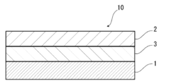
- FIG. 1 is a schematic diagram showing an example of a cross-sectional structure of a packaging film for an electricity storage device of the present disclosure
- BRIEF DESCRIPTION OF THE DRAWINGS FIG. 1 is a schematic diagram showing an example of a cross-sectional structure of a packaging film for an electricity storage device of the present disclosure
- BRIEF DESCRIPTION OF THE DRAWINGS FIG. 1 is a schematic diagram showing an example of a cross-sectional structure of a packaging film for an electricity storage device of the present disclosure
- BRIEF DESCRIPTION OF THE DRAWINGS FIG. 1 is a schematic diagram showing an example of a cross-sectional structure of a packaging film for an electricity storage device of the present disclosure
- BRIEF DESCRIPTION OF THE DRAWINGS FIG.
- FIG. 1 is a schematic diagram showing an example of a cross-sectional structure of a packaging film for an electricity storage device of the present disclosure
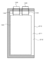
- FIG. 4 is a schematic diagram for explaining a method of housing an electricity storage device element in a package formed by the electricity storage device packaging film of the present disclosure.
- 1 is a schematic diagram showing an example of a cross-sectional structure of an electricity storage device of the present disclosure
- FIG. 1 is a schematic diagram showing an example of a cross-sectional structure of an electricity storage device of the present disclosure
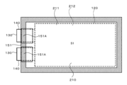
- FIG. FIG. 2 is a plan view of the power storage devices of the first and second embodiments A1, B1 and C1, and the third, fourth and fifth embodiments;
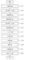
- FIG. 9 is a cross-sectional view along line D2-D2 of Embodiments A1 and B1 of the first and second aspects, the third aspect, and the fourth aspect of FIG. 8; 9 is a flow chart showing an example of a method of manufacturing an electricity storage device for Embodiments A1 and B1 of the first and second aspects, the third aspect, and the fourth aspect of FIG. 8.
- FIG. FIG. 11 is a diagram relating to the inner wrapping process of FIG. 10, and the same applies to the first and second aspects of the embodiment C1, the third, fourth and fifth aspects.
- FIG. 11 is a diagram relating to the first inner sealing step of FIG. 10 , and the same applies to the embodiment C1 of the first aspect and the second aspect, the third aspect, the fourth aspect and the fifth aspect.
- FIG. 11 is a diagram relating to the second inner sealing step of FIG. 10 , and the same applies to the embodiment C1 of the first aspect and the second aspect, the third aspect, the fourth aspect and the fifth aspect.
- 4 is a flow chart showing an example of a method for manufacturing an electricity storage device according to the first and second embodiments A2 and B2, the third embodiment, and the fourth embodiment;
- FIG. 15 is a diagram relating to the inner packaging process of FIG. 14, and the same applies to the first and second aspects of the embodiment C2, the third, fourth and fifth aspects.
- FIG. 15 is a diagram relating to the first inner sealing step of FIG. 14, and the same applies to Embodiment C2 of the first aspect and the second aspect, the third aspect, the fourth aspect and the fifth aspect.
- FIG. 15 is a diagram relating to the second inner sealing step of FIG. 14, and the same applies to the first and second aspects of the embodiment C2, the third aspect, the fourth aspect and the fifth aspect.
- FIG. 15 is a diagram relating to the inner sealing step of FIG. 14, and the same applies to Embodiment C2 of the first aspect and the second aspect, the third aspect, the fourth aspect and the fifth aspect.
- FIG. 10 is a cross-sectional view of the terminal seal portion of the power storage device of the first and second embodiments A2 and B2, the third and fourth embodiments;
- FIG. 10 is a cross-sectional view of the terminal seal portion of the electrical storage device of the first and second embodiments A3 and B3, the third and fourth embodiments;
- FIG. 10 is a cross-sectional view of the terminal seal portion of the electrical storage device of the first and second embodiments A3 and B3, the third and fourth embodiments;
- FIG. 9 is a cross-sectional view along the line D2-D2 of the embodiment C1 of the first and second aspects of FIG. 8 and the fifth aspect;
- FIG. 9 is a flow chart showing an example of a method for manufacturing an electricity storage device for Embodiment C1 of the first and second aspects of FIG. 8 and the fifth aspect.
- FIG. 10 is a flow chart showing an example of a method for manufacturing an electricity storage device according to the first and second aspects of the embodiment C2 and the fifth aspect.
- FIG. 10 is a cross-sectional view of the terminal seal portion of the power storage device according to the embodiment C2 of the first and second aspects and the fifth aspect;
- FIG. 10 is a cross-sectional view of the terminal seal portion of the power storage device according to Embodiment C3 of the first and second aspects and the fifth aspect;
- FIG. 10 is a cross-sectional view of the terminal seal portion of the power storage device according to Embodiment C3 of the first and second aspects and the fifth aspect;
- the electrical storage device packaging film of the first aspect of the present disclosure is an electrical storage device packaging film that includes at least a heat-sealable resin layer, and has a CO 2 permeation amount of 100 cc ⁇ 100 ⁇ m/m in an environment at a temperature of 30° C. 2/24 hr/atm or more.
- a power storage device packaging film is a power storage device packaging film that includes at least a heat-fusible resin layer, has adhesiveness to metal, and is made of metal. It is characterized by having no layer.
- the packaging film for power storage devices of the present disclosure will be described in detail below.
- the numerical range indicated by "-" means “more than” and “less than”.
- the notation of 2 to 15 mm means 2 mm or more and 15 mm or less.
- upper or lower limits described in a certain numerical range may be replaced with upper or lower limits of other numerical ranges described step by step.
- the upper limit and upper limit, the upper limit and lower limit, or the lower limit and lower limit, which are separately described may be combined to form a numerical range.
- upper or lower limits described in a certain numerical range may be replaced with values shown in Examples.
- the shielding layer means a layer that shields light transmission. element) becomes difficult to see.
- the metal layer means a layer formed of metal, and examples thereof include metal foil and metal plate. A few millimeters can be mentioned.
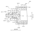
- the electrical storage device packaging film 10 of the present disclosure includes at least a heat-sealable resin layer 1, as shown in FIGS. 1 to 4, for example.
- the heat-sealable resin layers 1 of the electricity storage device packaging film 10 face each other, and the peripheral edges are heat-sealed.
- the electricity storage device element is accommodated in the space formed by .
- the electrical storage device packaging film 10 may be composed only of the heat-fusible resin layer 1, as shown in FIG.
- the electrical storage device packaging film 10 is composed only of the heat-fusible resin layer 1, it is preferable that at least one surface of the heat-fusible resin layer 1 has adhesiveness to metal.
- the electrical storage device packaging film 10 of the present disclosure is preferably composed of a laminate including at least the resin layer 2 and the heat-fusible resin layer 1, as shown in FIGS.
- the resin layer 2 is on the outside
- the heat-fusible resin layer 1 is on the inside (innermost layer).
- the electrical storage device packaging film 10 is composed of a laminate including the resin layer 2 and the heat-fusible resin layer 1, at least the outer surface of the resin layer 2 and the inner surface of the heat-fusible resin layer 1 On the one hand, it is preferable to impart adhesion to metals.
- the electrical storage device packaging film 10 of the present disclosure is composed of a laminate including at least a resin layer 2, a base material 3, and the heat-fusible resin layer 1. is preferred.
- the resin layer 2 is on the outside
- the heat-fusible resin layer 1 is on the inside (innermost layer)
- the base material 3 is the resin layer 2 and the heat-fusible resin layer 1. located between Even when the electrical storage device packaging film 10 is composed of a laminate including the resin layer 2, the substrate 3, and the heat-fusible resin layer 1, the outer surface of the resin layer 2 and the heat-fusible resin layer 1 It is preferred to impart adhesion to metal on at least one of the inner surfaces of the.
- Adhesive layers 4 and 5 can be provided, respectively.
- the electrical storage device packaging film 10 of the first aspect of the present disclosure has a CO 2 permeation amount of 100 cc ⁇ 100 ⁇ m/m 2 /24 hr/atm or more in an environment at a temperature of 30° C., preferably about 200 cc ⁇ 100 ⁇ m/m 2 . /24 hr/atm or more, more preferably about 300 cc ⁇ 100 ⁇ m/m 2 /24 hr/atm or more, more preferably about 500 cc ⁇ 100 ⁇ m/m 2 /24 hr/atm or more.
- the CO 2 permeation amount of the electrical storage device packaging film 10 of the first aspect of the present disclosure is, for example, about 2000 cc ⁇ 100 ⁇ m/m 2 /24 hr/atm or less, preferably about 1000 cc ⁇ 100 ⁇ m/m 2 /24 hr/atm or less. atm or less, more preferably about 800 cc ⁇ 100 ⁇ m/m 2 /24 hr/atm or less .
- At least one layer included in the electrical storage device packaging film 10 may be a shielding layer S having a shielding property.
- FIG. 4 shows a configuration in which the adhesive layer 4 that bonds between the resin layer 2 and the base material 3 is used as the shielding layer S.
- any layer included in the electrical storage device packaging film 10 can be used as the shielding layer S.
- a surface coating layer or the like may be further provided on the outside of the resin layer 2 (on the side opposite to the heat-fusible resin layer 1 side), if necessary.
- the thickness of the laminate constituting the electrical storage device packaging film 10 is not particularly limited, but from the viewpoint of cost reduction, energy density improvement, etc., it is, for example, 190 ⁇ m or less, preferably about 180 ⁇ m or less, and about 170 ⁇ m or less.
- the thickness of the laminate constituting the electrical storage device packaging film 10 is preferably about 35 ⁇ m or more, about 45 ⁇ m or more, about 60 ⁇ m or more can be mentioned.
- the preferred range of the laminate constituting the electrical storage device packaging film 10 is, for example, about 35 to 190 ⁇ m, about 35 to 180 ⁇ m, about 35 to 170 ⁇ m, about 45 to 190 ⁇ m, about 45 to 180 ⁇ m, and about 45 to 170 ⁇ m. , about 60 to 190 ⁇ m, about 60 to 180 ⁇ m, and about 60 to 170 ⁇ m, and particularly preferably about 45 to 170 ⁇ m.
- the resin layer 2, the adhesive layer 4, the base material 3, the adhesive layer 5, and the heat-sealable resin with respect to the thickness (total thickness) of the laminate constituting the electrical storage device packaging film 10
- the ratio of the total thickness of layer 1 is preferably 90% or more, more preferably 95% or more, and even more preferably 98% or more.
- the electrical storage device packaging film 10 of the present disclosure includes the resin layer 2, the adhesive layer 4, the base material 3, the adhesive layer 5, and the heat-fusible resin layer 1, the electrical storage device packaging film
- the ratio of the total thickness of these layers to the thickness (total thickness) of the laminate constituting 10 is preferably 90% or more, more preferably 95% or more, and still more preferably 98% or more.
- the electrical storage device packaging film 10 of the present disclosure is a laminate including the resin layer 2, the adhesive layer 4, and the heat-fusible resin layer 1, the laminate constituting the electrical storage device packaging film 10
- the ratio of the total thickness of these layers to the thickness (total thickness) of the layer can be, for example, 80% or more, preferably 90% or more, more preferably 95% or more, and still more preferably 98% or more.
- the laminate constituting the electrical storage device packaging film 10 of the present disclosure has a total light transmittance measured in accordance with JIS K7361-1: 1997, for example, 20% or less, 15% or less, 10% or less. , 8% or less.
- the laminate constituting the electrical storage device packaging film 10 of the present disclosure has a total light transmittance measured in accordance with JIS K7361-1:1997, for example, 80% or more, 85% or more, 90% or more. % or more.
- the lower the total light transmittance the higher the shielding properties of the electrical storage device packaging film 10 can be exhibited.
- the higher the total light transmittance the higher the translucency of the electrical storage device packaging film 10 can be exhibited.
- the lower limit of the total light transmittance is 0% and the upper limit is 100%.
- the total light transmittance of the electrical storage device packaging film conforms to the measurement method specified in JIS K7361-1: 1997, and is measured using a commercially available spectrophotometer (for example, a UV-visible-near-infrared spectrophotometer V- 670), the transmittance in the visible light region (400 to 700 nm) is measured, and the average value is taken as the total light transmittance.
- the measurement conditions are a halogen lamp as a light source, a UV/Vis bandwidth of 5.0 nm, a scanning speed of 1000 nm/min, a response of medium, and a data capturing interval of 1.0 nm.
- the power storage device packaging film 10 can be black.
- the power storage device packaging film 10 is black, the power storage device packaging film 10 has a high shielding property and a high anti-counterfeiting effect.
- the electrical storage device packaging film 10 of the second aspect of the present disclosure has a CO 2 permeation amount in an environment at a temperature of 30° C. of preferably 100 cc ⁇ 100 ⁇ m/m 2 /24 hr/atm or more, more preferably about 200 cc ⁇ 100 ⁇ m. /m 2 /24 hr/atm or more, more preferably about 300 cc ⁇ 100 ⁇ m/m 2 /24 hr/atm or more, more preferably about 500 cc ⁇ 100 ⁇ m/m 2 /24 hr/atm or more.
- the CO 2 permeation amount of the electrical storage device packaging film 10 of the second aspect of the present disclosure is, for example, about 2000 cc ⁇ 100 ⁇ m/m 2 /24 hr/atm or less, preferably about 1000 cc ⁇ 100 ⁇ m/m 2 /24 hr/atm or less. atm or less, more preferably about 800 cc ⁇ 100 ⁇ m/m 2 / 24 hr/atm or less.
- each layer forming the packaging film for the electrical storage device [heat-fusible resin layer 1]
- the heat-fusible resin layer 1 corresponds to the innermost layer, and when the electricity storage device is assembled, the heat-fusible resin layers are heat-sealed to seal the electricity storage device element. It is a layer (sealant layer) that exhibits its function.
- the electrical storage device packaging film 10 of the first aspect of the present disclosure may or may not have adhesiveness to metal, but preferably has adhesiveness to metal.
- the electrical storage device packaging film 10 of the first aspect is composed only of the heat-fusible resin layer 1, at least one surface of the heat-fusible resin layer 1 may have adhesiveness to metal.
- the electrical storage device packaging film 10 of the first aspect is composed of a laminate including the resin layer 2 and the heat-fusible resin layer 1, the outer surface of the resin layer 2 and the heat-fusible resin layer 1
- at least one of the inner surfaces is made adhesive to metal.
- the electrical storage device packaging film 10 of the first aspect is composed of a laminate including the resin layer 2, the base material 3, and the heat-fusible resin layer 1, the outer surface of the resin layer 2 and the At least one of the inner surfaces of the heat-fusible resin layer 1 may be imparted with adhesion to metal.
- the thermal adhesive resin layer 1 of the electrical storage device packaging film 10 is transparent, and the thermal adhesive resin layer 1 is transparent.
- the shielding layer S may be composed of the heat-fusible resin layer 1 mixed with the above-described coloring agent or the like.
- the electrical storage device packaging film 10 of the second aspect of the present disclosure is composed only of the heat-fusible resin layer 1, at least one surface of the heat-fusible resin layer 1 adheres to metal. have sex.
- the electrical storage device packaging film 10 of the second aspect is composed of a laminate including the resin layer 2 and the heat-fusible resin layer 1, the outer surface of the resin layer 2 and the heat-fusible resin layer 1 Adhesion to metal may be imparted to at least one of the inner surfaces.
- the electrical storage device packaging film 10 of the second aspect is composed of a laminate including the resin layer 2, the base material 3, and the heat-fusible resin layer 1, the outer surface of the resin layer 2 and the At least one of the inner surfaces of the heat-fusible resin layer 1 may be imparted with adhesion to metal.
- the heat-fusible resin layer 1 is transparent, and is laminated with the shielding layer S composed of a layer different from the heat-fusible resin layer 1.
- the shielding layer S may be formed by blending the above-described colorant or the like with the heat-fusible resin layer 1 .
- the resin constituting the heat-fusible resin layer 1 of the first embodiment is heat-fusible and the CO 2 permeation amount of the electrical storage device packaging film 10 is 100 cc ⁇ 100 ⁇ m/m 2 /24 hr/ Although it is not particularly limited as long as it is atm or more, resins containing polyolefin skeletons such as polyolefins and acid-modified polyolefins are preferable. Polyolefins are preferred in that, in addition to having heat-sealing properties, the CO 2 permeation amount is very high.
- the resin constituting the heat-fusible resin layer 1 of the second aspect is not particularly limited as long as it is heat-fusible, but a resin containing a polyolefin skeleton such as polyolefin or acid-modified polyolefin is preferable. .
- the inclusion of a polyolefin skeleton in the resin constituting the heat-fusible resin layer 1 can be analyzed by, for example, infrared spectroscopy, gas chromatography-mass spectrometry, or the like.
- a peak derived from maleic anhydride is detected.
- maleic anhydride-modified polyolefin is measured by infrared spectroscopy, peaks derived from maleic anhydride are detected near wavenumbers of 1760 cm ⁇ 1 and 1780 cm ⁇ 1 .
- the heat-fusible resin layer 1 is a layer composed of maleic anhydride-modified polyolefin
- a peak derived from maleic anhydride is detected when measured by infrared spectroscopy.
- the peak may be too small to be detected. In that case, it can be analyzed by nuclear magnetic resonance spectroscopy.
- polyolefins include polyethylenes such as low-density polyethylene, medium-density polyethylene, high-density polyethylene, and linear low-density polyethylene; ethylene- ⁇ -olefin copolymers; block copolymers of ethylene), random copolymers of polypropylene (for example, random copolymers of propylene and ethylene); propylene- ⁇ -olefin copolymers; ethylene-butene-propylene terpolymers; Among these, polypropylene is preferred.
- the polyolefin resin is a copolymer, it may be a block copolymer or a random copolymer. These polyolefin-based resins may be used alone or in combination of two or more.
- the polyolefin may be a cyclic polyolefin.
- a cyclic polyolefin is a copolymer of an olefin and a cyclic monomer.
- the olefin which is a constituent monomer of the cyclic polyolefin, include ethylene, propylene, 4-methyl-1-pentene, styrene, butadiene, and isoprene. be done.
- Examples of cyclic monomers constituting cyclic polyolefins include cyclic alkenes such as norbornene; cyclic dienes such as cyclopentadiene, dicyclopentadiene, cyclohexadiene and norbornadiene. Among these, cyclic alkenes are preferred, and norbornene is more preferred.
- the polyolefin may be an acid-modified polyolefin.
- Acid-modified polyolefin is a polymer modified by block polymerization or graft polymerization of polyolefin with an acid component.
- the acid-modified polyolefin the above polyolefin, a copolymer obtained by copolymerizing the above polyolefin with a polar molecule such as acrylic acid or methacrylic acid, or a polymer such as crosslinked polyolefin can be used.
- acid components used for acid modification include carboxylic acids such as maleic acid, acrylic acid, itaconic acid, crotonic acid, maleic anhydride and itaconic anhydride, and anhydrides thereof.
- the acid-modified polyolefin may be an acid-modified cyclic polyolefin.
- Acid-modified cyclic polyolefin is a polymer obtained by copolymerizing a part of the monomers constituting the cyclic polyolefin in place of the acid component, or by block-polymerizing or graft-polymerizing the acid component to the cyclic polyolefin. be.
- the acid-modified cyclic polyolefin is the same as described above.
- the acid component used for acid modification is the same as the acid component used for modification of polyolefin.
- Preferable acid-modified polyolefins include polyolefins modified with carboxylic acid or its anhydride, polypropylene modified with carboxylic acid or its anhydride, maleic anhydride-modified polyolefin, and maleic anhydride-modified polypropylene.
- the heat-fusible resin layer 1 may be formed of one type of resin alone, or may be formed of a blend polymer in which two or more types of resin are combined. Furthermore, the heat-fusible resin layer 1 may be formed of only one layer, or may be formed of two or more layers made of the same or different resins.
- the inner surface of the heat-fusible resin layer 1 has adhesiveness to metal.
- the inner surface of the heat-fusible resin layer 1 is coated with an acid-modified polyolefin (acid-modified polypropylene, acid-modified polyethylene, etc.).
- the heat-fusible resin layer 1 Not suitable as a resin for composing the inner surface.
- the heat-fusible resin layer 1 may contain a lubricant or the like as necessary.
- a lubricant is not particularly limited, and known lubricants can be used. Lubricants may be used singly or in combination of two or more.
- the lubricant is not particularly limited, but preferably includes an amide-based lubricant.
- Specific examples of the lubricant include those exemplified for the resin layer 2 .
- Lubricants may be used singly or in combination of two or more. By combining two or more types of lubricants, when the electrical storage device packaging film 10 is cold-molded with a mold, the lubricant is less likely to adhere to the mold due to the interaction between the lubricants. can suitably enhance the continuous productivity of. This also applies to the case where a lubricant is used for the resin layer 2, which will be described later.
- the amount is not particularly limited, but from the viewpoint of improving the moldability of the electrical storage device packaging film, it is preferably about 10 to 50 mg/m 2 . , and more preferably about 15 to 40 mg/m 2 .
- the lubricant present on the surface of the heat-fusible resin layer 1 may be obtained by exuding the lubricant contained in the resin constituting the heat-fusible resin layer 1, or The surface may be coated with a lubricant.
- the thickness of the heat-fusible resin layer 1 is not particularly limited as long as the heat-fusible resin layers are heat-sealed to each other to exhibit the function of sealing the electricity storage device element.
- the resin layer 2 is a layer provided for the purpose of, for example, exhibiting a function as a base material of the electrical storage device packaging film.
- the resin layer 2 is located on the outer layer side of the electrical storage device packaging film.
- the material for forming the resin layer 2 of the first aspect should have at least insulating properties, and the CO 2 permeation amount of the electrical storage device packaging film 10 should be 100 cc ⁇ 100 ⁇ m/m 2 /24 hr/atm or more. is not particularly limited.
- the resin layer 2 of the first aspect can be formed using a resin, and the resin may contain additives described later.
- the shielding layer S is provided in the electrical storage device packaging film 10 of the first aspect, it is preferable that the resin layer 2 is transparent and is used by being laminated with the shielding layer S composed of a layer different from the resin layer 2.
- the shielding layer S may be formed by blending the resin layer 2 with a coloring agent or the like, which will be described later.
- the material forming the resin layer 2 of the second aspect is not particularly limited as long as it has at least insulation.
- the resin layer 2 of the second aspect can be formed using a resin, and the resin may contain additives described later.
- the resin layer 2 of the second embodiment is transparent, and it is preferable to use it by laminating it with a shielding layer S composed of a layer different from the resin layer 2.
- a layer S may be constructed.
- the resin layer 2 may be, for example, a resin film formed of resin, or may be formed by applying resin.
- the resin film may be an unstretched film or a stretched film.
- stretched films include uniaxially stretched films and biaxially stretched films, with biaxially stretched films being preferred.
- stretching methods for forming a biaxially stretched film include successive biaxial stretching, inflation, and simultaneous biaxial stretching.
- Methods for applying the resin include a roll coating method, a gravure coating method, an extrusion coating method, and the like.
- resins forming the resin layer 2 include, for example, resins such as polyester, polyamide, polyolefin, epoxy resin, acrylic resin, fluororesin, polyurethane, silicon resin, phenolic resin, and modified products of these resins. mentioned. Further, the resin forming the resin layer 2 may be a copolymer of these resins or a modified copolymer thereof. Furthermore, it may be a mixture of these resins.
- the resin forming the resin layer 2 preferably includes polyester, polyamide, and polyolefin.
- polyester examples include polyethylene terephthalate, polybutylene terephthalate, polyethylene naphthalate, polybutylene naphthalate, polyethylene isophthalate, and copolymerized polyester.
- copolyester examples include copolyester having ethylene terephthalate as a main repeating unit.
- copolymer polyester polymerized with ethylene isophthalate with ethylene terephthalate as the main repeating unit hereinafter abbreviated after polyethylene (terephthalate / isophthalate)
- polyethylene (terephthalate / adipate) polyethylene (terephthalate / sodium sulfoisophthalate)
- polyethylene (terephthalate/sodium isophthalate) polyethylene (terephthalate/phenyl-dicarboxylate), polyethylene (terephthalate/decanedicarboxylate), and the like.
- These polyesters may be used singly or in combination of two or more.
- polyamide specifically, aliphatic polyamide such as nylon 6, nylon 66, nylon 610, nylon 12, nylon 46, copolymer of nylon 6 and nylon 66; terephthalic acid and / or isophthalic acid Hexamethylenediamine-isophthalic acid-terephthalic acid copolymer polyamide such as nylon 6I, nylon 6T, nylon 6IT, nylon 6I6T (I represents isophthalic acid, T represents terephthalic acid) containing structural units derived from, polyamide MXD6 (polymetallic Polyamides containing aromatics such as silylene adipamide); alicyclic polyamides such as polyamide PACM6 (polybis(4-aminocyclohexyl)methane adipamide); Copolymerized polyamides, polyesteramide copolymers and polyetheresteramide copolymers which are copolymers of copolymerized polyamides with polyesters or polyalkylene ether glycols; and polyamides such
- polyolefin a resin containing a polyolefin skeleton such as polyolefin and acid-modified polyolefin is preferable.
- Polyolefin is preferable from the viewpoint of imparting heat-sealing properties to the outer surface of the resin layer 2 .
- Specific examples of the polyolefin include the same polyolefins as those exemplified for the heat-fusible resin layer 1 described above.
- the resin layer 2 preferably includes at least one of a polyester film, a polyamide film, a polyolefin film, and an acid-modified polyolefin film. It preferably contains at least one of films, more preferably contains at least one of oriented polyethylene terephthalate film, oriented polybutylene terephthalate film, oriented nylon film, oriented polypropylene film, and oriented acid-modified polypropylene film.
- the resin layer 2 when at least part of the outer surface of the electrical storage device packaging film 10 is adhered to metal or the like, the resin layer 2 is the outermost layer, and the outer surface of the resin layer 2 has adhesiveness to metal.
- the outer surface of the resin layer 2 is preferably made of acid-modified polyolefin (acid-modified polypropylene, acid-modified polyethylene, etc.).
- the above-described polyolefin that has not been acid-modified does not have adhesiveness to metal. It is not suitable as a resin that constitutes the outer surface of the resin layer 2 .
- the electric storage device packaging film 10 is used as an inner packaging body, and the outer surface of the electric storage device packaging film 10 is made of a metal. (eg, metal foil, metal can, etc.).
- the resin layer 2 may be a single layer, or may be composed of two or more layers.
- the resin layer 2 may be a laminate obtained by laminating resin films with an adhesive or an adhesion promoter, or may be formed by coextrusion of the resin to form two layers.
- a laminate of resin films as described above may be used.
- a laminate of two or more resin films formed by co-extrusion of resin may be used as the resin layer 2 without being stretched, or may be formed as the resin layer 2 by being uniaxially or biaxially stretched.
- a laminate of two or more resin films include a laminate of a polyester film and a nylon film, a laminate of two or more nylon films, and a laminate of two or more polyester films.
- Examples include laminates, and preferred are laminates of stretched nylon films and stretched polyester films, laminates of two or more layers of stretched nylon films, and laminates of two or more layers of stretched polyester films.
- the resin layer 2 is a laminate of two resin films, a laminate of a polyester resin film and a polyester resin film, a laminate of a polyamide resin film and a polyamide resin film, or a laminate of a polyester resin film and a polyamide resin film.
- a laminate of polyethylene terephthalate film and polyethylene terephthalate film, a laminate of nylon film and nylon film, or a laminate of polyethylene terephthalate film and nylon film is more preferred.
- the polyester resin is resistant to discoloration when, for example, an electrolytic solution adheres to the surface. Therefore, when the resin layer 2 is a laminate of two or more resin films, the polyester resin film is the outermost layer of the resin layer 2. is preferably located in
- a laminate of two or more resin films include a laminate of polyolefin and polyester, and a laminate of polyolefin and polyolefin.
- Body laminates of polyolefins and polyamides are preferred.
- a laminate of polyolefin and polyester a laminate of polypropylene film and polyethylene terephthalate film, a laminate of polypropylene film and polyethylene naphthalate film, a laminate of polypropylene film and polybutylene terephthalate film, and an acid-modified polypropylene film.
- a laminate of polyolefin and polyolefin a laminate of polypropylene and polypropylene, a laminate of acid-modified polypropylene and acid-modified polypropylene, and a laminate of acid-modified polypropylene and polypropylene are preferable.
- a laminate of polyolefin and polyamide a laminate of polypropylene and nylon and a laminate of acid-modified polypropylene and nylon are preferred.
- the two or more layers of resin films may be laminated via an adhesive or an adhesion promoter.
- Preferred adhesives and adhesion promoters are the same as the adhesives and adhesion promoters exemplified for adhesive layers 4 and 5, respectively, which will be described later.
- the method for laminating two or more layers of resin films is not particularly limited, and known methods can be employed. Examples thereof include dry lamination, sandwich lamination, extrusion lamination, thermal lamination, and the like. A lamination method is mentioned. When laminating by dry lamination, it is preferable to use a polyurethane adhesive as the adhesive.
- the thickness of the adhesive is, for example, about 2 to 5 ⁇ m.
- an anchor coat layer may be formed on the resin film and laminated.
- the anchor coat layer may be the same as the adhesives exemplified for the adhesive layers 4 and 5 described later. At this time, the thickness of the anchor coat layer is, for example, about 0.01 to 1.0 ⁇ m.
- Anchor coat layers can be used as adhesive layers 4,5.
- additives such as lubricants, flame retardants, antiblocking agents, antioxidants, light stabilizers, tackifiers, and antistatic agents are present on at least one of the surface and the interior of the resin layer 2. good too. Only one type of additive may be used, or two or more types may be mixed and used.
- a lubricant exists on the surface of the resin layer 2 from the viewpoint of improving the formability of the electrical storage device packaging film.
- the lubricant is not particularly limited, but preferably includes an amide-based lubricant.
- Specific examples of amide lubricants include saturated fatty acid amides, unsaturated fatty acid amides, substituted amides, methylolamides, saturated fatty acid bisamides, unsaturated fatty acid bisamides, fatty acid ester amides, and aromatic bisamides.
- saturated fatty acid amides include lauric acid amide, palmitic acid amide, stearic acid amide, behenic acid amide, and hydroxystearic acid amide.
- unsaturated fatty acid amides include oleic acid amide and erucic acid amide.
- substituted amides include N-oleyl palmitic acid amide, N-stearyl stearic acid amide, N-stearyl oleic acid amide, N-oleyl stearic acid amide, N-stearyl erucic acid amide and the like.
- methylolamide include methylol stearamide.
- saturated fatty acid bisamides include methylenebisstearic acid amide, ethylenebiscapric acid amide, ethylenebislauric acid amide, ethylenebisstearic acid amide, ethylenebishydroxystearic acid amide, ethylenebisbehenic acid amide, hexamethylenebisstearin. acid amide, hexamethylenebisbehenamide, hexamethylenehydroxystearic acid amide, N,N'-distearyladipic acid amide, N,N'-distearylsebacic acid amide and the like.
- unsaturated fatty acid bisamides include ethylenebisoleic acid amide, ethylenebiserucic acid amide, hexamethylenebisoleic acid amide, N,N'-dioleyladipic acid amide, and N,N'-dioleylsebacic acid amide. etc.
- fatty acid ester amides include stearamide ethyl stearate.
- aromatic bisamide include m-xylylenebisstearic acid amide, m-xylylenebishydroxystearic acid amide, N,N'-distearyl isophthalic acid amide and the like.
- Lubricants may be used singly or in combination of two or more.
- the amount is not particularly limited, but is preferably about 3 mg/m 2 or more, more preferably about 4 to 15 mg/m 2 , and even more preferably about 4 to 15 mg/m 2 . About 5 to 14 mg/m 2 can be mentioned.
- the lubricant present on the surface of the resin layer 2 may be the lubricant contained in the resin constituting the resin layer 2 exuded, or may be the lubricant applied to the surface of the resin layer 2. There may be.
- the thickness of the resin layer 2 is not particularly limited, but is, for example, approximately 3 to 50 ⁇ m, preferably approximately 10 to 35 ⁇ m.
- the thickness of each resin film constituting each layer is preferably about 2 to 25 ⁇ m.
- the base material 3 is a layer that functions as a support.
- the electrical storage device packaging film 10 includes the resin layer 2, the substrate 3, and the heat-fusible resin layer 1, the resin layer 2 is on the outside, and the heat-fusible resin layer 1 is on the inside (innermost layer).
- a substrate 3 is positioned between the resin layer 2 and the heat-fusible resin layer 1 .
- the shielding layer S can be formed by adding a coloring agent or the like to the base material 3 .
- the material forming the base material 3 of the present disclosure is not particularly limited.
- materials that form the base material 3 include polyolefin resins, polyamide resins, polyester resins, epoxy resins, acrylic resins, fluororesins, silicon resins, phenolic resins, polyetherimides, polyimides, polycarbonates, and mixtures thereof. and copolymers, and among these, polyolefin resins are particularly preferred.
- the material forming the base material 3 is preferably a resin containing a polyolefin skeleton such as polyolefin or acid-modified polyolefin. Whether the resin constituting the base material 3 contains a polyolefin skeleton can be analyzed by, for example, infrared spectroscopy, gas chromatography mass spectrometry, or the like.
- polyesters include polyethylene terephthalate, polybutylene terephthalate, polyethylene naphthalate, polybutylene naphthalate, polyethylene isophthalate, copolymer polyester mainly composed of repeating units of ethylene terephthalate, and butylene terephthalate mainly composed of repeating units. and copolymerized polyester.
- copolymer polyester having ethylene terephthalate as the main repeating unit specifically, a copolymer polyester polymerized with ethylene isophthalate having ethylene terephthalate as the main repeating unit (hereinafter referred to as polyethylene (terephthalate/isophthalate) ), polyethylene (terephthalate/isophthalate), polyethylene (terephthalate/adipate), polyethylene (terephthalate/sodium sulfoisophthalate), polyethylene (terephthalate/sodium isophthalate), polyethylene (terephthalate/phenyl-dicarboxylate) , polyethylene (terephthalate/decanedicarboxylate), and the like.
- polyethylene (terephthalate/isophthalate) polyethylene (terephthalate/isophthalate)
- polyethylene (terephthalate/isophthalate) polyethylene (terephthalate/isophthalate)
- polyethylene (terephthalate/adipate) polyethylene (terephthal
- copolymer polyester having butylene terephthalate as the main repeating unit specifically, a copolymer polyester polymerized with butylene isophthalate having butylene terephthalate as the main repeating unit (hereinafter referred to as polybutylene (terephthalate/isophthalate) ), polybutylene (terephthalate/adipate), polybutylene (terephthalate/sebacate), polybutylene (terephthalate/decanedicarboxylate), polybutylene naphthalate, and the like.
- polybutylene (terephthalate/isophthalate) polybutylene (terephthalate/adipate)
- polybutylene (terephthalate/sebacate) polybutylene (terephthalate/sebacate)
- polybutylene (terephthalate/decanedicarboxylate) polybutylene naphthalate
- polyolefins include polyethylenes such as low density polyethylene, medium density polyethylene, high density polyethylene, and linear low density polyethylene; homopolypropylene, block copolymers of polypropylene (for example, block copolymers of propylene and ethylene); crystalline or amorphous polypropylene such as random copolymers (eg, random copolymers of propylene and ethylene); terpolymers of ethylene-butene-propylene; Among these polyolefins, polyethylene and polypropylene are preferred, and polypropylene is more preferred.
- the base material 3 preferably contains homopolypropylene, more preferably is formed of homopolypropylene, and is further preferably an unstretched homopolypropylene film, because of its excellent electrolyte resistance.
- polyamides include aliphatic polyamides such as nylon 6, nylon 66, nylon 610, nylon 12, nylon 46, and copolymers of nylon 6 and nylon 66; derived from terephthalic acid and/or isophthalic acid Hexamethylenediamine-isophthalic acid-terephthalic acid copolymer polyamide such as nylon 6I, nylon 6T, nylon 6IT, nylon 6I6T (I represents isophthalic acid, T represents terephthalic acid), polymetaxylylene adipamide Polyamides containing aromatics such as (MXD6); Alicyclic polyamides such as polyaminomethylcyclohexyladipamide (PACM6); Polyamides obtained by copolymerizing lactam components and isocyanate components such as 4,4'-diphenylmethane-diisocyanate.
- aliphatic polyamides such as nylon 6, nylon 66, nylon 610, nylon 12, nylon 46, and copolymers of nylon 6 and nylon 66
- polyester amide copolymers and polyether ester amide copolymers which are copolymers of copolyamide and polyester or polyalkylene ether glycol; and copolymers thereof.
- These polyamides may be used singly or in combination of two or more.
- the base material 3 of the present disclosure may be formed of a nonwoven fabric made of the above resin.
- the base material 3 is a non-woven fabric, it is preferable that the base material 3 is made of the aforementioned polyolefin resin, polyamide resin, or the like.
- the base material 3 of the present disclosure may be a single layer or multiple layers.
- the surface of the base material 3 is subjected, if necessary, to a known means for easy adhesion such as corona discharge treatment, ozone treatment, plasma treatment, and the like. good too.
- the thickness of the base material 3 is preferably 80 ⁇ m or less, more preferably 60 ⁇ m or less, even more preferably about 50 ⁇ m or less, and even more preferably about 40 ⁇ m or less. Also, the thickness of the base material 3 is preferably about 5 ⁇ m or more, more preferably about 8 ⁇ m or more, and even more preferably about 10 ⁇ m or more. Preferred ranges for the thickness of the base material 3 are about 5 to 80 ⁇ m, about 5 to 60 ⁇ m, about 5 to 50 ⁇ m, about 5 to 40 ⁇ m, about 8 to 80 ⁇ m, about 8 to 60 ⁇ m, about 8 to 50 ⁇ m, and 8 to 40 ⁇ m. about 10 to 80 ⁇ m, about 10 to 60 ⁇ m, about 10 to 50 ⁇ m, and about 10 to 40 ⁇ m.
- the adhesive layers 4 and 5 are provided between the resin layer 2 and the base material 3 or between the heat-fusible resin layer 1 and between the heat-fusible resin layer 1 and the base material, respectively. 3 or the resin layer 2, it is a layer provided between these as needed for the purpose of improving the adhesiveness between them.
- the adhesive layer 4 bonds the resin layer 2 and the substrate 3 or the heat-fusible resin layer 1 .
- the adhesive layer 5 bonds the heat-fusible resin layer 1 and the resin layer 2 or the substrate 3 together.
- the anchor coat layers described above can also be used as the adhesive layers 4 and 5 .
- the adhesive layers 4 and 5 can be blended with a coloring agent or the like to form the shielding layer S.
- a coloring agent is blended into the adhesive that forms the adhesive layer 4 and the shielding layer is formed by one-time coating, there is no need to separately provide a shielding layer at locations other than the adhesive layer 4 .
- the number of steps can be reduced, the production efficiency can be improved, and the risk of contamination by foreign matter can be reduced, compared to the case where a colored layer is separately provided as a shielding layer.
- a coloring agent to the adhesive layer 4 also from the viewpoint of long-term use.
- the adhesive layers 4 and 5 are formed from an adhesive or an adhesion promoter that can adhere to the resin layer 2 or the heat-fusible resin layer 1 .
- the adhesive used to form the adhesive layers 4 and 5 is not limited, but may be any of a chemical reaction type, a solvent volatilization type, a hot melt type, a hot pressure type, and the like. Further, it may be a two-liquid curing adhesive (two-liquid adhesive), a one-liquid curing adhesive (one-liquid adhesive), or a resin that does not involve a curing reaction. Also, the adhesive layers 4 and 5 may be single layers or multiple layers.
- the adhesive component contained in the adhesive include polyesters such as polyethylene terephthalate, polybutylene terephthalate, polyethylene naphthalate, polybutylene naphthalate, polyethylene isophthalate, and copolymerized polyester; polyether; polyurethane; epoxy resin; Phenolic resins; polyamides such as nylon 6, nylon 66, nylon 12, and copolymerized polyamides; polyolefin resins such as polyolefins, cyclic polyolefins, acid-modified polyolefins, and acid-modified cyclic polyolefins; polyvinyl acetate; cellulose; (meth)acrylic resins; polyimide; polycarbonate; amino resin such as urea resin and melamine resin; rubber such as chloroprene rubber, nitrile rubber and styrene-butadiene rubber; These adhesive components may be used singly or in combination of two or more.
- polyurethane adhesives are preferred.
- an appropriate curing agent can be used in combination with these adhesive component resins to increase the adhesive strength.
- the curing agent is selected from among polyisocyanates, polyfunctional epoxy resins, oxazoline group-containing polymers, polyamine resins, acid anhydrides, etc., depending on the functional groups of the adhesive component.
- polyurethane adhesives examples include polyurethane adhesives containing a first agent containing a polyol compound and a second agent containing an isocyanate compound.
- a two-component curing type polyurethane adhesive is used in which a polyol such as polyester polyol, polyether polyol, or acrylic polyol is used as the first agent and an aromatic or aliphatic polyisocyanate is used as the second agent.
- polyurethane adhesives include polyurethane adhesives containing an isocyanate compound and a polyurethane compound obtained by reacting a polyol compound and an isocyanate compound in advance.
- polyurethane adhesives examples include polyurethane adhesives containing a polyurethane compound obtained by reacting a polyol compound and an isocyanate compound in advance and a polyol compound.
- polyurethane adhesives examples include polyurethane adhesives obtained by reacting a polyurethane compound obtained by reacting a polyol compound and an isocyanate compound in advance with moisture in the air and curing the compound.
- the polyol compound it is preferable to use a polyester polyol having a hydroxyl group in a side chain in addition to the terminal hydroxyl group of the repeating unit.
- the second agent examples include aliphatic, alicyclic, aromatic, and araliphatic isocyanate compounds.
- isocyanate compounds include hexamethylene diisocyanate (HDI), xylylene diisocyanate (XDI), isophorone diisocyanate (IPDI), hydrogenated XDI (H6XDI), hydrogenated MDI (H12MDI), tolylene diisocyanate (TDI), and diphenylmethane diisocyanate. (MDI), naphthalene diisocyanate (NDI), and the like.
- polyfunctional isocyanate modified products of one or more of these diisocyanates are also included.
- a polymer for example, a trimer
- Such multimers include adducts, biurets, nurates and the like. Since the adhesive layers 4 and 5 are formed of a polyurethane adhesive, the electrical storage device packaging film is endowed with excellent electrolytic solution resistance, and peeling of the resin layer 2 is suppressed even if the electrolytic solution adheres to the side surface. be.
- the adhesion promoter used to form the adhesive layers 4 and 5 is not limited.
- known adhesion promoters such as isocyanate-based, polyethyleneimine-based, polyester-based, polyurethane-based, and polybutadiene-based adhesives can be used.
- the laminate containing the isocyanate component was excellent in lamination strength, and the decrease in lamination strength after immersion in the electrolytic solution was small.
- triphenylmethane-4,4′,4′′-triisocyanate which is a triisocyanate monomer
- polymethylene polyphenyl polyisocyanate which is a polymeric MDI (NCO content is about 30%, viscosity is 200 to 700 mPa s).
- NCO content is about 30%, viscosity is 200 to 700 mPa s.
- tris(p-isocyanatephenyl) thiophosphate which is also a triisocyanate monomer
- a two-liquid curing type adhesion promoter based on polyethyleneimine and using polycarbodiimide as a cross-linking agent show good results. there were.
- the adhesive layers 4 and 5 using an adhesion promoter can be formed by coating and drying by a well-known coating method such as a bar coating method, a roll coating method, or a gravure coating method.
- a well-known coating method such as a bar coating method, a roll coating method, or a gravure coating method.
- an isocyanate adhesion promoter it is 20 to 100 mg/m 2 , preferably 40 to 60 mg/m 2
- a polymeric MDI adhesion promoter it is 40 to 150 mg/m 2 , preferably 60 to It is 100 mg/m 2
- a two-liquid curing type adhesion promoter with polyethyleneimine as the main agent and polycarbodiimide as a cross-linking agent it is 5 to 50 mg/m 2 , preferably 10 to 30 mg/m 2 .
- the triisocyanate monomer is a monomer having three isocyanate groups in one molecule
- the polymeric MDI is a mixture of MDI and an MDI
- the adhesive layers 4 and 5 may contain other components as long as they do not impede adhesion, and may contain colorants, thermoplastic elastomers, tackifiers, fillers, and the like. Since the adhesive layers 4 and 5 contain a coloring agent, the electrical storage device packaging film can be colored.
- the adhesive layers 4 and 5 can be used as the shield layer S if the adhesive layers 4 and 5 are colored to such an extent that the electrical storage device packaging film can be provided with shielding properties.
- Known substances such as pigments and dyes can be used as the colorant. In addition, only one type of colorant may be used, or two or more types may be mixed and used.
- the type of pigment is not particularly limited as long as it does not impair the adhesiveness of the adhesive layers 4 and 5.
- organic pigments include azo-based, phthalocyanine-based, quinacridone-based, anthraquinone-based, dioxazine-based, indigothioindigo-based, perinone-perylene-based, isoindolenine-based, and benzimidazolone-based pigments.
- pigments include carbon black-based, titanium oxide-based, cadmium-based, lead-based, chromium oxide-based, iron-based, and copper-based pigments. be done.
- a black coloring agent is preferable in order to make the appearance of a packaging film for an electric storage device black, and among black coloring agents, carbon black is preferable.
- the electricity storage device packaging film 10 has a high shielding property and a high anti-counterfeiting effect.
- the average particle size of the pigment is not particularly limited, and is, for example, about 0.05 to 5 ⁇ m, preferably about 0.08 to 2 ⁇ m. Further, the average particle size of carbon black is within the range of 0.161 to 0.221 ⁇ m. The average particle size of the pigment is the median size measured with a laser diffraction/scattering particle size distribution analyzer.
- the content of the pigment in the adhesive layers 4 and 5 is not particularly limited as long as the electrical storage device packaging film is colored.
- the thickness of the adhesive layers 4 and 5 is not particularly limited as long as the resin layer 2 and the heat-fusible resin layer 1 can be adhered, but is, for example, about 1 ⁇ m or more, or about 2 ⁇ m or more. Also, the thickness of the adhesive layers 4 and 5 is, for example, about 10 ⁇ m or less, about 5 ⁇ m or less. Further, preferable ranges of the thickness of the adhesive layers 4 and 5 are about 1 to 10 ⁇ m, about 1 to 5 ⁇ m, about 2 to 10 ⁇ m, and about 2 to 5 ⁇ m.
- the colored layer C is a layer provided between the resin layer 2 and the heat-fusible resin layer 1 and outside the resin layer 2 as necessary.
- a colored layer C may be provided between the resin layer 2 and the adhesive layers 4 and 5 .
- the electrical storage device packaging film can be colored.
- the colored layer C can be used as the shielding layer S if the colored layer C is colored to such an extent that the electrical storage device packaging film can be provided with a shielding property. It is preferable to use the colored layer C as the shielding layer S in the electrical storage device packaging film 10 .
- the colored layer C between the resin layer 2 and the heat-fusible resin layer 1 may be called an inner colored layer, and the colored layer C outside the resin layer 2 may be called an outer colored layer.
- the colored layer C is preferably provided on at least one surface of the resin layer 2 (that is, the resin layer 2 and the colored layer C are in contact with each other).
- the colored layer C can be formed, for example, by applying ink containing a coloring agent to the surface of the resin layer 2 .
- a coloring agent such as pigments and dyes can be used as the colorant.
- only one type of colorant may be used, or two or more types may be mixed and used.
- the thickness of the colored layer C is not particularly limited as long as the electrical storage device packaging film 10 is colored, but is, for example, about 1 ⁇ m or more and about 2 ⁇ m or more. Moreover, the thickness of the colored layer C is, for example, about 10 ⁇ m or less, or about 5 ⁇ m or less. Further, the preferable range of the thickness of the colored layer C is about 1 to 10 ⁇ m, about 1 to 5 ⁇ m, about 2 to 10 ⁇ m, and about 2 to 5 ⁇ m.
- the packaging film for an electricity storage device of the present disclosure is provided on the resin layer 2 (heat of the resin layer 2), if necessary.
- a surface coating layer (not shown) may be provided on the side opposite to the fusible resin layer 1 side.
- the surface coating layer is a layer positioned on the outermost layer side of the electrical storage device packaging film when the electrical storage device is assembled using the electrical storage device packaging film.
- the surface coating layer may constitute the shielding layer S by blending the above-described coloring agent or the like.
- the surface coating layer examples include resins such as polyvinylidene chloride, polyester, polyamide, epoxy resin, acrylic resin, fluororesin, polyurethane, silicon resin, phenolic resin, and modified products of these resins. Copolymers of these resins or modified copolymers may also be used. Furthermore, it may be a mixture of these resins.
- the resin is preferably a curable resin. That is, the surface coating layer is preferably composed of a cured product of a resin composition containing a curable resin.
- the resin forming the surface coating layer is a curable resin
- the resin may be either a one-component curable type or a two-component curable type, preferably the two-component curable type.
- the two-liquid curing resin include two-liquid curing polyurethane, two-liquid curing polyester, and two-liquid curing epoxy resin. Among these, two-liquid curable polyurethane is preferred.
- two-liquid curable polyurethanes include polyurethanes containing a first agent containing a polyol compound and a second agent containing an isocyanate compound.
- Preferred examples include a two-component curing type polyurethane in which a polyol such as polyester polyol, polyether polyol, or acrylic polyol is used as the first agent and an aromatic or aliphatic polyisocyanate is used as the second agent.
- polyurethane include polyurethane containing a polyurethane compound obtained by reacting a polyol compound and an isocyanate compound in advance and an isocyanate compound.
- polyurethane examples include polyurethane containing a polyurethane compound obtained by reacting a polyol compound and an isocyanate compound in advance and a polyol compound.
- polyurethanes examples include polyurethanes obtained by reacting a polyurethane compound obtained by reacting a polyol compound and an isocyanate compound in advance with moisture in the air and the like to cure the compound.
- the polyol compound it is preferable to use a polyester polyol having a hydroxyl group in a side chain in addition to the terminal hydroxyl group of the repeating unit.
- the second agent examples include aliphatic, alicyclic, aromatic, and araliphatic isocyanate compounds.
- isocyanate compounds include hexamethylene diisocyanate (HDI), xylylene diisocyanate (XDI), isophorone diisocyanate (IPDI), hydrogenated XDI (H6XDI), hydrogenated MDI (H12MDI), tolylene diisocyanate (TDI), and diphenylmethane diisocyanate. (MDI), naphthalene diisocyanate (NDI), and the like.
- polyfunctional isocyanate-modified products of one or more of these diisocyanates are also included.
- a polymer for example, a trimer
- Such multimers include adducts, biurets, nurates and the like.
- the aliphatic isocyanate compound refers to an isocyanate having an aliphatic group and no aromatic ring
- the alicyclic isocyanate compound refers to an isocyanate having an alicyclic hydrocarbon group
- the aromatic isocyanate compound refers to an isocyanate having an aromatic ring. Since the surface coating layer is made of polyurethane, the electrical storage device packaging film is endowed with excellent electrolytic solution resistance.
- the surface coating layer may optionally contain the aforementioned lubricant, antiblocking agent, Additives such as matting agents, flame retardants, antioxidants, tackifiers, and antistatic agents may also be included.
- Additives such as matting agents, flame retardants, antioxidants, tackifiers, and antistatic agents may also be included.
- the additive include fine particles having an average particle size of about 0.5 nm to 5 ⁇ m. The average particle size of the additive is the median size measured with a laser diffraction/scattering particle size distribution analyzer.
- Additives may be either inorganic or organic.
- shape of the additive is not particularly limited, and examples thereof include spherical, fibrous, plate-like, amorphous, and scaly shapes.
- additives include talc, silica, graphite, kaolin, montmorillonite, mica, hydrotalcite, silica gel, zeolite, aluminum hydroxide, magnesium hydroxide, zinc oxide, magnesium oxide, aluminum oxide, neodymium oxide, and antimony oxide.
- Additives may be used singly or in combination of two or more.
- silica, barium sulfate, and titanium oxide are preferred from the viewpoint of dispersion stability and cost.
- the additive may be subjected to various surface treatments such as insulation treatment and high-dispersion treatment.
- the method for forming the surface coating layer is not particularly limited, and examples thereof include a method of applying a resin for forming the surface coating layer.
- a resin mixed with the additives may be applied.
- the thickness of the surface coating layer is not particularly limited as long as it exhibits the above functions as a surface coating layer.
- the method for producing the electrical storage device packaging film is not particularly limited as long as the electrical storage device packaging film of the present disclosure can be obtained.
- the electrical storage device packaging film of the first aspect of the present disclosure includes the resin layer 2 and the heat-fusible resin layer 1
- at least the resin layer and the heat-fusible resin layer are laminated in order from the outside.
- a step of obtaining a laminate is provided, and the laminate has a CO 2 permeation amount of 100 cc ⁇ 100 ⁇ m/m 2 /24 hr/atm or more in a temperature of 30° C. environment.
- the electrical storage device packaging film of the second aspect of the present disclosure includes the resin layer 2 and the heat-fusible resin layer 1, at least the resin layer and the heat-fusible resin layer are laminated in order from the outside. obtaining a laminated laminate, which has adhesion to metal and does not have a metal layer formed of metal.
- the production method for the case where the electrical storage device packaging film of the present disclosure is composed of a laminate comprising a resin layer 2, an adhesive layer 4, a base material 3, an adhesive layer 5, and a heat-fusible resin layer 1 in this order
- An example is as follows. First, materials for forming each layer are prepared. Next, the resin layer 2 and the base material 3 are laminated with the adhesive layer 4 interposed therebetween, and the base material 3 and the heat-fusible resin layer 1 are laminated with the adhesive layer 5 interposed therebetween. Specifically, by laminating the resin layer 2 and the base material 3 by a dry lamination method or the like using an adhesive that forms the adhesive layer 4, the resin layer 2, the adhesive layer 4, and the base material 3 are laminated.
- the electrical storage device packaging film 10 is produced. can be done.
- the resin layer 2, the base material 3, and the heat-fusible resin layer 1 are laminated without the adhesive layers 4 and 5 interposed therebetween, the resin constituting the resin layer 2 is placed on one side of the base material 3.
- the electrical storage device packaging film 10 can be manufactured by a method such as melt extrusion, or a method of melt extruding a resin forming the heat-fusible resin layer 1 on the other side of the base material 3 .
- the colored layer may be formed on the surface of the resin layer 2 and then laminated with the substrate 3 and the heat-fusible resin layer 1 .
- a surface coating layer it can be formed, for example, by coating the surface of the resin layer 2 with the above resin composition for forming the surface coating layer and curing the composition.
- the electrical storage device packaging film 10 may be subjected to heat treatment.
- the electricity storage device packaging film of the present disclosure is used for a packaging body for hermetically housing electricity storage device elements such as a positive electrode, a negative electrode, and an electrolyte. That is, an electricity storage device can be obtained by housing an electricity storage device element including at least a positive electrode, a negative electrode, and an electrolyte in a package formed by the electricity storage device packaging film of the present disclosure.
- an electricity storage device element having at least a positive electrode, a negative electrode, and an electrolyte is wrapped in the electricity storage device packaging film of the present disclosure in a state in which the metal terminals connected to the positive electrode and the negative electrode protrude outward.
- covering the periphery of the electricity storage device element so as to form a flange portion (area where the heat-fusible resin layers contact each other), and heat-sealing the heat-fusible resin layers of the flange portion to seal. provides an electricity storage device using the electricity storage device packaging film.
- the heat-fusible resin portion of the electricity storage device packaging film of the present disclosure is on the inside (surface in contact with the electricity storage device element ) to form a package.
- the heat-sealable resin layers of two electrical storage device packaging films may be placed facing each other, and the peripheral edges of the stacked electrical storage device packaging films may be heat-sealed to form a package.
- one electrical storage device packaging film may be folded back and overlapped, and the peripheral edges may be heat-sealed to form a packaging body. In the case of folding and stacking, as shown in the example shown in FIG.
- the sides other than the folded sides may be heat-sealed to form a package body by three-sided sealing, or the packages may be folded back so as to form a flange portion. It may be sealed on all sides.
- a recess for housing the electrical storage device element may be formed by deep drawing or stretch forming.
- one of the electrical storage device packaging films may be provided with a recessed portion and the other electrical storage device packaging film may not be provided with a recessed portion, or the other electrical storage device packaging film may also be provided with a recessed portion. may be provided.
- the electrical storage device packaging film 10 of the present disclosure is an electrical storage device 30 in which an electrical storage device element 32 is accommodated in a container having a double structure of an inner packaging body 10 a and an outer packaging body 20 . It can be suitably used as the inner package 10a. That is, an electricity storage device element 32 including at least a positive electrode, a negative electrode, and an electrolyte is housed in an inner packaging body 10a formed by the electricity storage device packaging film 10 of the present disclosure, and the inner packaging body 10a is accommodated in the outer packaging body 20. By housing inside, the electricity storage device 30 in which the electricity storage device elements are housed in a container having a double structure of the inner packaging body 10a and the outer packaging body 20 is obtained.
- each corner is drawn at a right angle, but the angle of each corner and ridgeline is not limited, and each corner and ridgeline may be rounded.
- the metal terminals 31 connected to the positive and negative electrodes of the electricity storage device element 32 are projected outward, and the electricity storage device packaging film 10 is wrapped around the electricity storage device element 32 .
- the formed flange portion of the inner packaging body 10a (the area where the heat-sealable resin layers 1 are in contact with each other, the peripheral edge portion 30a of the inner packaging body 10a) is covered so as to be formed, and the flange portion is heat-sealed.
- the electrical storage device element 32 can be directly packaged by adhering to the metal terminal 31. , can be suitably used.
- the packaging film 10 can be suitably used. Since the metal terminal 31 and the heat-fusible resin layer of the packaging film are made of different materials, generally the adhesion between the metal terminal 31 and the heat-fusible resin layer tends to deteriorate. For this reason, an adhesive film is generally placed between the metal terminal and the heat-sealable resin layer of the packaging film. Since it has adhesiveness, it is possible to seal the electrical storage device element 32 while adhering it to the metal terminal 31 without using such an adhesive film.
- the outer packaging body 20 is not particularly limited, and a packaging film, a metal can, or the like, which is composed of a film-like laminate in which a substrate layer/metal layer/thermal adhesive resin layer are sequentially laminated, can be used. can.
- the electrical storage device packaging film of the present disclosure can be suitably used for electrical storage devices such as batteries (including capacitors, capacitors, etc.). Moreover, the electrical storage device packaging film of the present disclosure may be used for either a primary battery or a secondary battery, but is preferably used for a secondary battery.
- the type of secondary battery to which the electrical storage device packaging film of the present disclosure is applied is not particularly limited. Cadmium storage batteries, nickel/iron storage batteries, nickel/zinc storage batteries, silver oxide/zinc storage batteries, metal-air batteries, polyvalent cation batteries, capacitors, capacitors, and the like. Among these secondary batteries, lithium ion batteries and lithium ion polymer batteries can be mentioned as suitable targets for application of the electrical storage device packaging film of the present disclosure.
- the electrical storage device packaging film of the first aspect of the present disclosure (at least, the electrical storage device packaging film comprising a heat-fusible resin layer, wherein the CO 2 permeation amount in an environment at a temperature of 30 ° C. is 100 cc ⁇ 100 ⁇ m / m 2 /24 hr/atm or more) and the electrical storage device packaging film of the second aspect of the present disclosure (at least an electrical storage device packaging film comprising a heat-fusible resin layer,
- the electrical storage device packaging film has adhesiveness to metal, and the electrical storage device packaging film does not have a metal layer formed of metal.
- Embodiment A (Embodiments A1 to A5 and modifications thereof) or the method for manufacturing the same
- the electricity storage device according to Embodiment B (Embodiments B1 to B5 and modifications thereof) or the method for manufacturing the same
- the power storage devices according to Embodiments C (Embodiments C1 to C5 and modifications thereof) or their manufacturing methods.
- the size of the storage device that will be the final product is larger than the size required (for example, the storage device element
- an electricity storage device is manufactured using an electricity storage device packaging film that is at least twice the size required for sealing. Therefore, the manufacturing process of the electricity storage device is complicated.
- An object of the invention according to Embodiment A is to provide an electricity storage device manufacturing method that can easily manufacture an electricity storage device, and an electricity storage device manufactured by this manufacturing method.
- a method for manufacturing an electricity storage device is a method for manufacturing an electricity storage device, wherein the electricity storage device includes an electricity storage device element and an inner package housing the electricity storage device element.
- the inner packaging body is composed of an electricity storage device packaging film having gas permeability, and an inner packaging step of wrapping the electricity storage device element with the electricity storage device packaging film; an inner sealing step of sealing the electrical storage device packaging film so that the electrical storage device element is sealed by the electrical storage device packaging film; and a degassing step of releasing the generated gas through the electrical storage device packaging film.
- a method for manufacturing an electricity storage device according to a second aspect of the invention according to Embodiment A is the method for manufacturing an electricity storage device according to the first aspect, wherein in the inner packaging step, the inner packaging included in the finished electricity storage device The electricity storage device element is wrapped with the electricity storage device packaging film having substantially the same size as the body.
- An electricity storage device contains an electricity storage device element, an inner packaging body that accommodates the electricity storage device element, and the inner packaging body that accommodates the electricity storage device element. and an outer packaging body, wherein the inner packaging body is composed of a gas-permeable electrical storage device packaging film.
- a power storage device is the power storage device according to the third aspect, comprising: a metal terminal electrically connected to the power storage device element; a tab film arranged between the terminals, wherein the outer package is joined to the inner package, and the inner package and the metal terminal are joined via the tab film, At least a portion of the outer edge of the inner wrapper is exposed from the outer wrapper.
- a power storage device is the power storage device according to the third aspect, comprising: a metal terminal electrically connected to the power storage device element; a tab film disposed between the package and the metal terminal, wherein the inner package and the outer package are joined to the metal terminal via the tab film, and the inner package is entirely covered by the outer wrapping.
- a power storage device is the power storage device according to the third aspect, further comprising a metal terminal electrically connected to the power storage device element, the inner package and The metal terminal is joined, and at least a portion of the outer edge of the inner package is exposed from the outer package.
- a power storage device is the power storage device according to any one of the third to sixth aspects, wherein the power storage device packaging film further has transparency. .
- FIG. 8 shows a plan view of an electricity storage device 100 according to Embodiment A1.
- 9 is a cross-sectional view taken along line D2-D2 in FIG. 8.
- FIG. 8 portions that are originally not visible from the outside are partially indicated by dotted lines for reference.
- the up-down direction in FIG. 8 is referred to as the "front-rear direction”
- the left-right direction is referred to as the "left-right direction”
- the up-down direction in FIG. 9 is referred to as the "up-down direction”.
- the orientation during use of the power storage device 100 is not limited to this.
- the relative positional relationship between the inner wrapping body 210 and the outer wrapping body 220 is simplified for simplification of the drawing.
- the electricity storage device 100 includes a container 110 , an electricity storage device element 120 , a pair of metal terminals 130 and a pair of tab films 140 .
- the container 110 has an internal space S ⁇ b>1 and a peripheral seal portion 150 .
- Electric storage device element 120 is housed in internal space S ⁇ b>1 of housing body 110 .
- One end of metal terminal 130 is joined to power storage device element 120 , and the other end protrudes outward from peripheral edge seal portion 150 of container 110 .
- a portion between one end and the other end of the metal terminal 130 is fused to the peripheral seal portion 150 via the tab film 140 .
- the container 110 includes a container 110A.
- Container 110A includes inner wrapper 210 and outer wrapper 220 .
- the inner package 210 accommodates the electricity storage device element 120 .
- the outer package 220 accommodates the inner package 210 in which the electricity storage device element 120 is accommodated.
- An internal space S1 is formed inside the inner package 210 .
- the inner packaging body 210 includes electrical storage device packaging films 211 and 212 .
- the outer wrapper 220 includes exterior films 221,222. In the outer peripheral portion of the container 110A in plan view, the inner packaging body 210 and the outer packaging body 220 are heat-sealed and fused together, thereby forming a peripheral edge seal portion 150 .
- An internal space S1 of the container 110A which is isolated from the external space, is formed in the inner package 210 by the peripheral edge seal portion 150. As shown in FIG.
- the peripheral seal portion 150 defines the peripheral edge of the interior space S1 of the container 110A.
- the mode of heat sealing referred to herein includes modes such as thermal fusion from a heat source and ultrasonic fusion.
- the peripheral seal portion 150 means a portion where the inner wrapping body 210 and the outer wrapping body 220 are fused and integrated.
- the peripheral seal portion 150 includes a top seal portion 151 , a pair of side seal portions 152 and 153 and a bottom seal portion 154 .
- Top seal portion 151 includes a portion (hereinafter referred to as “terminal seal portion 151A”) that seals across metal terminal 130 and tab film 140, and extends in the front-rear direction.
- a pair of side seal portions 152 and 153 extend in the left-right direction.
- the side seal portion 152 and the side seal portion 153 face each other with an internal space S1 interposed therebetween.
- the bottom seal portion 154 faces the top seal portion 151 via the internal space S1.
- the bottom seal portion 154 extends in the front-rear direction.
- the terminal seal portion 151A of the top seal portion 151 includes, from top to bottom, an exterior film 221, an electrical storage device packaging film 211, one tab film 140, a metal terminal 130, and the other tab film. 140, a power storage device packaging film 212, and an exterior film 222 are laminated and integrated. Therefore, the top seal portion 151 can be easily formed.
- an electricity storage device packaging film 211 one tab film 140, the other tab film 140, an electricity storage device packaging film 212, and an exterior film 222 are laminated and integrated.
- the outer portion of the terminal seal portion 151A of the top seal portion 151 is composed of, from top to bottom, the electrical storage device packaging film 211, the tab film 140 on one side, the metal The terminal 130, the other tab film 140, and the electrical storage device packaging film 212 are laminated and integrated.
- FIG. 8 illustrates the area of the peripheral edge seal portion 150 from above, and does not show the step as a boundary.
- the electrical storage device packaging films 211 and 212 that constitute the inner package 210 have gas permeability from the viewpoint of easily manufacturing the electrical storage device 100 .
- Preferred examples of the electrical storage device packaging films 211 and 212 constituting the inner package 210 will be described below. In the following description, when the electrical storage device packaging films 211 and 212 are not particularly distinguished, the electrical storage device packaging films 211 and 212 may be collectively referred to as the electrical storage device packaging film 10 .
- the shape of the inner package 210 is not particularly limited, and can be, for example, bag-like (pouch-like).
- the bag-like shape referred to herein includes a three-side seal type, a four-side seal type, a pillow type, a gusset type, and the like.
- the inner package 210 of Embodiment A1 has a shape as shown in FIG. It is manufactured by heat-sealing the electrical storage device packaging film 211 overlaid from above along the outer peripheral portion in a plan view.
- the electrical storage device packaging film 212 includes an angular ring-shaped flange portion 212A corresponding to an outer peripheral portion in a plan view, and a molded portion 212B that is continuous with the inner edge of the flange portion 212A and bulges downward therefrom.
- the electrical storage device packaging film 211 includes an angular ring-shaped flange portion 211A corresponding to the outer peripheral portion in a plan view, and a flange portion 211B that continues to the inner edge of the flange portion 211A and bulges upward therefrom.
- the electrical storage device packaging films 211 and 212 are overlapped so that the molded portions 211B and 212B bulge in opposite directions.
- the flange portion 211A of the electrical storage device packaging film 211 and the flange portion 212A of the electrical storage device packaging film 212 are heat-sealed so as to form a part of the peripheral edge seal portion 150 .
- One of the electrical storage device packaging films 211 and 212 may be in the form of a sheet.
- the exterior films 221 and 222 that make up the outer package 220 are made of, for example, resin moldings or films.
- the resin molded product referred to here can be manufactured by methods such as injection molding, pressure molding, vacuum molding, and blow molding, and may be subjected to in-mold molding to impart design and functionality.
- the type of resin can be polyolefin, polyester, nylon, ABS, and the like.
- the film referred to here is, for example, a resin film that can be produced by a method such as an inflation method or a T-die method, or a laminate of such a resin film on a metal foil or metal plate.
- the film referred to here may or may not be stretched, and may be a single-layer film or a multilayer film.
- the multilayer film referred to here may be produced by a coating method, may be produced by adhering a plurality of films with an adhesive or the like, or may be produced by a multilayer extrusion method.
- a laminate film can be a laminate obtained by laminating a substrate layer, a barrier layer, and a heat-fusible resin layer.
- the base material layer functions as a base material for the exterior films 221 and 222, typically forms the outer layer side of the outer package 220, and is an insulating resin layer.
- the barrier layer has a function of improving the strength of the exterior films 221 and 222 and at least preventing moisture from entering the power storage device 100, and is typically a metal layer made of an aluminum alloy foil or the like.
- the heat-sealable resin layer is typically made of a heat-sealable resin such as polyolefin, and forms the innermost layer of the outer package 220 .
- the shape of the outer wrapping body 220 is not particularly limited, and can be, for example, bag-like (pouch-like).
- the bag-like shape referred to herein includes a three-side seal type, a four-side seal type, a pillow type, a gusset type, and the like.
- a container 110A of the present embodiment A1 has a shape as shown in FIG. are heat-sealed along the outer peripheral portion in plan view.
- the exterior film 222 includes an angular ring-shaped flange portion 222A corresponding to an outer peripheral portion in a plan view, and a molded portion 222B that continues to the inner edge of the flange portion 222A and bulges downward therefrom.
- the exterior film 221 includes an angular ring-shaped flange portion 221A corresponding to the outer peripheral portion in a plan view, and a flange portion 221B that continues to the inner edge of the flange portion 221A and bulges upward therefrom.
- the exterior films 221 and 222 are superimposed so that the molded portions 221B and 222B bulge in opposite directions.
- the flange portion 221A of the exterior film 221 and the flange portion 222A of the exterior film 222 are heat-sealed so as to be integrated, forming part of the peripheral edge seal portion 150 .
- One of the exterior films 221 and 222 may be sheet-like.
- part of the flange portion 211A of the electrical storage device packaging film 211 is joined to one tab film 140 in the terminal seal portion 151A.
- a portion of the flange portion 212A of the electrical storage device packaging film 212 is joined to the other tab film 140 .
- the flange portion 221A of the exterior film 221 is joined to the flange portion 211A of the electrical storage device packaging film 211.
- the end portion 221X of the flange portion 221A is positioned closer to the power storage device element 120 than the end portion 211X of the power storage device packaging film 211 is. Therefore, at least a portion of the outer edge of inner wrapper 210 is exposed from outer wrapper 220 .
- the end 221X of the flange portion 221A is located at the same position as the end 211X of the electrical storage device packaging film 211 in the left-right direction, or at a position farther from the electrical storage device element 120 than the end 211X of the electrical storage device packaging film 211. may be located.
- the flange portion 222A of the exterior film 222 is joined to the flange portion 212A of the electrical storage device packaging film 212.
- the end portion 222X of the flange portion 222A is positioned closer to the power storage device element 120 than the end portion 212X of the power storage device packaging film 212 is. Therefore, at least a portion of the outer edge of inner wrapper 210 is exposed from outer wrapper 220 .
- the end 222X of the flange portion 222A is positioned at the same position as the end 212X of the electrical storage device packaging film 212 in the left-right direction, or is farther from the electrical storage device element 120 than the end 212X of the electrical storage device packaging film 212. may be located.
- the power storage device element 120 includes at least a positive electrode, a negative electrode, and an electrolyte, and is, for example, a lithium ion battery (secondary battery) or a power storage member such as a capacitor.
- the metal terminal 130 is a metal terminal used for power input/output of the electricity storage device element 120 .
- the metal terminal 130 is arranged, for example, in the top seal portion 151 of the container 110A, one of which constitutes a positive terminal and the other constitutes a negative terminal.
- One end in the left-right direction of each metal terminal 130 is electrically connected to the electrode (positive electrode or negative electrode) of the electricity storage device element 120 in the internal space S1 of the container 110A, and the other end is the peripheral seal portion. It protrudes outward from 150.
- the configuration of the power storage device 100 described above is particularly preferable for use in an electric vehicle such as an electric vehicle or a hybrid vehicle in which a large number of power storage devices 100 are connected in series and used at high voltage.
- the mounting positions of the two metal terminals 130 constituting the positive and negative terminals are not particularly limited.
- the metal material forming the metal terminal 130 is, for example, aluminum, nickel, copper, or the like.
- the metal terminal 130 connected to the positive electrode is typically made of aluminum or the like
- the metal terminal 130 connected to the negative electrode is typically made of copper, It is composed of nickel or the like.
- the tab film 140 is a so-called adhesive film, and is configured to adhere to both the electrical storage device packaging films 211 and 212 and the metal terminal 130 .
- the tab film 140 is previously fused and fixed to the metal terminal 130 to be integrated, and the power storage device packaging films 211 and 212 are fused to the metal terminal 130 to which the tab film 140 is fixed. be worn.
- FIG. 10 is a flowchart showing an example of a method for manufacturing the electricity storage device 100. As shown in FIG. The method for manufacturing the electricity storage device 100 includes multiple steps.
- the electricity storage device element 120 is wrapped by the molded electricity storage device packaging films 211 and 212.
- the electricity storage device 100 of Embodiment A1 since the electricity storage device packaging films 211 and 212 have gas permeability, a pre-chamber for temporarily storing gas generated from the electricity storage device element 120 in an initial filling step or the like described later is provided. No need to form. Therefore, in the inner wrapping step, the power storage device element is wrapped around the power storage device packaging films 211 and 212 having substantially the same size as the power storage device wrapping films 211 and 212 provided in the inner wrapping body 210 of the power storage device 100 as a finished product. 120 is wrapped. Therefore, the manufacturing process of the electricity storage device 100 can be simplified.
- the material used for the electrical storage device 100 can be reduced.
- the term "substantially the same size" includes the case where the electrical storage device packaging films 211 and 212 included in the inner packaging body 210 of the finished electrical storage device 100 are larger than the electrical storage device packaging films 211 and 212 to such an extent that an auxiliary chamber cannot be formed.
- a metal terminal 130 is connected in advance to the electricity storage device element 120 , and a tab film 140 is joined to the metal terminal 130 .
- the first inner sealing step of step S12 is performed after the inner packaging step.
- the portions corresponding to the top seal portion 151, the side seal portion 152, and the bottom seal portion 154 of the peripheral edges of the electrical storage device packaging films 211 and 212 are sealed. be done.
- an opening 213 is formed in a portion of the periphery of the electrical storage device packaging films 211 and 212 where the side seal portion 153 is to be formed.
- a vacuum drying step of step S13 is performed.
- the electrolytic solution injection process in step S14 is performed after the vacuum drying process.
- the electrolytic solution is injected through the opening 213 (see FIG. 12).
- the second inner sealing step of step S15 is performed after the electrolytic solution injection step.
- the opening 213 is closed by sealing the portions of the peripheral edges of the electrical storage device packaging films 211 and 212 where the side seal portions 153 are to be formed. be done.
- the electricity storage device 100 since the electricity storage device packaging films 211 and 212 are transparent, the electricity storage device packaging film 211 and the electricity storage device packaging film are separated after the first inner sealing step or the second inner sealing step is completed. 212 are properly sealed. Therefore, the electricity storage device 100 can be manufactured favorably.
- the state in which the electrical storage device packaging film 211 and the electrical storage device packaging film 212 are not properly sealed includes, for example, the first state, the second state, or the third state.
- the first state is a state in which the electrical storage device packaging film 211 and the electrical storage device packaging film 212 are sealed with foreign matter caught therein.
- a second condition is a condition in which part of the part to be sealed is not sealed.
- the third state is a state in which portions that should not be sealed are sealed.
- step S18 is performed in parallel with the initial charging/discharging process and the aging process.
- the electrical storage device packaging films 211 and 212 have gas permeability, carbon dioxide and the like generated from the electrical storage device element 120 during the initial charging/discharging step and the aging step are The gas is discharged to the outside through the electrical storage device packaging films 211 and 212 .
- the main charging process of step S19 is performed.
- step S20 The outer wrapping process of step S20 is performed after the main charging process.
- the inner packaging body 210 in which the electricity storage device element 120 is housed is wrapped with exterior films 221 and 222 .
- step S21 The outer sealing process of step S21 is performed after the outer wrapping process.
- the peripheral edges of the exterior films 221 and 222 are sealed to form the peripheral edge seal portion 150 .
- Electricity storage device 100 of Embodiment A2 differs from Embodiment A1 in that electricity storage device packaging films 211 and 212 do not have transparency, and other configurations are the same as those of Embodiment A1.
- the power storage device 100 of Embodiment A2 will be described below, focusing on the parts that differ from Embodiment A2.
- FIG. 11 is a flow chart showing an example of a method for manufacturing the electricity storage device 100 of Embodiment A2.
- the method for manufacturing the electricity storage device 100 includes multiple steps.
- the electricity storage device element 120 is wrapped by the molded electricity storage device packaging films 211 and 212.
- the auxiliary chamber 214 is formed to temporarily store the gas generated from the electricity storage device element 120 in the initial filling step or the like. Therefore, in the inner packaging step, the electricity storage device element 120 is wrapped by the electricity storage device packaging films 211 and 212 that are larger than the electricity storage device packaging films 211 and 212 included in the inner package 210 of the finished electricity storage device 100 .
- Storage chambers 215 for storing more gas generated from the electricity storage device elements 120 are formed in the sub chambers 214 of the electricity storage device packaging films 211 and 212 .
- the first inner sealing step of step S32 is performed after the inner packaging step.
- portions of the peripheral edges of the electrical storage device packaging films 211 and 212 corresponding to the top seal portion 151, the side seal portion 152, and the bottom seal portion 154 are secondary. It is sealed to extend to chamber 214 .
- an opening 213 is formed in a portion 216 of the peripheral edges of the electrical storage device packaging films 211 and 212 where the side seal portion 153 is to be formed and a portion 216 facing the auxiliary chamber 214 . It is formed.
- a vacuum drying step of step S33 is performed.
- the electrolytic solution injection process in step S34 is performed after the vacuum drying process.
- the electrolytic solution is injected through the opening 213 (see FIG. 16).
- the second inner sealing step of step S35 is performed after the electrolytic solution injection step. As shown in FIG. 17 , in the second inner sealing step, of the peripheral edges of the electrical storage device packaging films 211 and 212 , the portion where the side seal portion 153 is scheduled to be formed faces the portion 216 via the auxiliary chamber 214 . is sealed, the opening 213 is closed. After the second inner sealing step, an initial charging/discharging step of step S36 and an aging step of step S37 are performed in order.
- the degassing process in step S38 is performed after the aging process.
- gases such as carbon dioxide generated from the electricity storage device element 120 are temporarily stored in the auxiliary chambers 214 of the electricity storage device packaging films 211 and 212 .
- step S39 The pre-chamber removal process of step S39 is performed after the degassing process.
- the electricity storage device packaging films 211 and 212 are cut along the dashed line XA shown in FIG. removes the subchamber 214 .
- step S40 is performed after the pre-chamber removing process.
- the inner sealing step as shown in FIG. 18, portions of the peripheral edges of the electrical storage device packaging films 211 and 212 corresponding to the side seal portions 153 are sealed.
- the main charging process of step S41 is performed.
- step S42 The outer wrapping process of step S42 is performed after the main charging process.
- the inner packaging body 210 in which the electricity storage device element 120 is housed is wrapped with exterior films 221 and 222 .
- step S43 The outer sealing process of step S43 is performed after the outer packaging process.
- the peripheral edges of the exterior films 221 and 222 are sealed to form the peripheral edge seal portion 150 .
- Embodiment A3 The power storage device 300 of Embodiment A3 differs from Embodiment A1 in that the configuration of terminal seal portion 151A is different, and other configurations are the same as those of Embodiment A1.
- the power storage device 300 of Embodiment A3 will be described below, focusing on the parts that differ from Embodiment A1.
- FIG. 19 is a cross-sectional view of a terminal seal portion 351A included in the electricity storage device 300 of Embodiment A3.
- a portion of the flange portion 211A of the electrical storage device packaging film 211 is joined to one tab film 140 at the terminal seal portion 351A.
- a portion of the flange portion 212A of the electrical storage device packaging film 212 is joined to the other tab film 140 .
- the flange portion 221A of the exterior film 221 is joined to one tab film 140.
- a flange portion 222A of the exterior film 222 is joined to the other tab film 140 .
- An end portion 221X of the flange portion 221A is located farther from the electrical storage device element 120 than the end portion 211X of the electrical storage device packaging film 211 is.
- the end portion 222X of the flange portion 222A is located farther from the electrical storage device element 120 than the end portion 212X of the electrical storage device packaging film 212 is. Therefore, the inner wrapper 210 is entirely covered with the outer wrapper 220 .
- a power storage device 400 of Embodiment A4 differs from Embodiment A1 in that the configuration of terminal seal portion 151A is different, and other configurations are the same as those of Embodiment A1.
- the power storage device 400 of Embodiment A4 will be described below, focusing on the parts that differ from Embodiment A1.
- FIG. 20 is a cross-sectional view of a terminal seal portion 451A included in the electricity storage device 400 of Embodiment A4. Electricity storage device 400 does not have tab film 140 .
- the exterior film 221, the electricity storage device packaging film 211, the metal terminal 130, the electricity storage device packaging film 212, and the exterior film 222 are laminated in this order from the top, and these are integrated. It is
- the end portion 221X of the flange portion 221A is positioned closer to the power storage device element 120 than the end portion 211X of the power storage device packaging film 211 is. Therefore, at least a portion of the outer edge of inner wrapper 210 is exposed from outer wrapper 220 . Note that the end 221X of the flange portion 221A is located at the same position as the end 211X of the electrical storage device packaging film 211 in the left-right direction, or at a position farther from the electrical storage device element 120 than the end 211X of the electrical storage device packaging film 211. may be located.
- the flange portion 221A of the exterior film 221 is joined to the flange portion 211A of the electrical storage device packaging film 211.
- 222 A of flange parts of the exterior film 222 are joined to 212 A of flange parts of the packaging film 212 for electrical storage devices.
- the end portion 222X of the flange portion 222A is positioned closer to the power storage device element 120 than the end portion 212X of the power storage device packaging film 212 is. Therefore, at least a portion of the outer edge of inner wrapper 210 is exposed from outer wrapper 220 .
- end 222X of the flange portion 222A is positioned at the same position as the end 212X of the electrical storage device packaging film 212 in the left-right direction, or is farther from the electrical storage device element 120 than the end 212X of the electrical storage device packaging film 212. may be located.
- the electricity storage device 400 since the electricity storage device packaging films 211 and 212 and the metal terminal 130 are joined without the tab film 140 interposed therebetween, the number of members is small. Moreover, the manufacturing method of the electrical storage device 400 can be simplified.
- Embodiment A5 An electricity storage device 500 of Embodiment A5 differs from Embodiment A4 in that the configuration of a terminal seal portion 451A is different, and other configurations are the same as those of Embodiment A4.
- the power storage device 500 of Embodiment A5 will be described below, focusing on the parts that differ from Embodiment A4.
- FIG. 21 is a cross-sectional view of a terminal seal portion 551A included in the electricity storage device 500 of Embodiment A5.
- a portion of the flange portion 211A of the electrical storage device packaging film 211 is joined to the metal terminal 130 at the terminal seal portion 551A.
- a portion of the flange portion 212A of the electrical storage device packaging film 212 is joined to the metal terminal 130 .
- a flange portion 221A of the exterior film 221 is joined to the metal terminal 130.
- a flange portion 222A of the exterior film 222 is joined to the metal terminal 130 .
- An end portion 221X of the flange portion 221A is located farther from the electrical storage device element 120 than the end portion 211X of the electrical storage device packaging film 211 is.
- the end portion 222X of the flange portion 222A is located farther from the electrical storage device element 120 than the end portion 212X of the electrical storage device packaging film 212 is. Therefore, the inner wrapper 210 is entirely covered with the outer wrapper 220 .
- the power storage device 500 since the inner wrapping body 210 is covered with the outer wrapping body 220, entry of water or the like into the internal space S1 of the inner wrapping body 210 from the outside is suppressed.
- the electricity storage device packaging films 211 and 212 and the metal terminal 130 are joined without the tab film 140 interposed therebetween, the number of members is small.
- the manufacturing method of the electrical storage device 500 can be simplified.
- each of the above-described embodiments is an example of a form that can be taken by the power storage device and the method for manufacturing the power storage device according to the present disclosure, and is not intended to limit the form.
- the power storage device and the method for manufacturing the power storage device according to the present disclosure may take forms different from those illustrated in each embodiment.
- One example is a form in which part of the configuration of each embodiment is replaced, changed, or omitted, or a form in which a new configuration is added to each embodiment.
- one outer package 220 may be configured to accommodate a plurality of inner packages 210 in which the electricity storage device elements 120 are accommodated.
- the sizes of the plurality of inner wrappers 210 may be different or the same. According to this modification, the voltage can be easily adjusted because a plurality of power storage device elements 120 can be connected in series or in parallel.
- the electricity storage device packaging films 211 and 212 may not have transparency.
- the electrical storage device packaging films 211 and 212 may at least have gas permeability.
- the inner packaging body 210 may be configured by folding one power storage device packaging film 211 and heat-sealing the periphery.
- the outer wrapper 220 may be constructed by folding a sheet of exterior film 221 and heat-sealing the periphery.
- ⁇ Embodiment B> In the production process of an electricity storage device, generally, after an electricity storage device element is housed in an electricity storage device packaging film, the periphery of the electricity storage device packaging film is sealed to temporarily seal the film. After that, an initial charge/discharge process, an aging process, and the like are performed. Since the electrical storage device packaging film included in the secondary battery includes a metal layer, it has a shielding property. Therefore, when the electricity storage device element is sealed by the electricity storage device packaging film, it is impossible to check whether the periphery of the electricity storage device packaging film is properly sealed. For this reason, an electricity storage device cannot be suitably manufactured.
- An object of the invention according to Embodiment B is to provide an electricity storage device manufacturing method that can suitably manufacture an electricity storage device, and an electricity storage device manufactured by this manufacturing method.
- a method for manufacturing an electricity storage device is a method for manufacturing an electricity storage device, wherein the electricity storage device includes an electricity storage device element and an inner package housing the electricity storage device element.
- the inner packaging body is composed of a transparent electricity storage device packaging film, and an inner packaging step of wrapping the electricity storage device element with the electricity storage device packaging film, and after the inner packaging step and an inner sealing step of sealing the electrical storage device packaging film such that the electrical storage device element is sealed by the electrical storage device packaging film.
- a method for producing an electricity storage device according to a second aspect of the invention according to Embodiment B is the method for producing an electricity storage device according to the first aspect, wherein the packaging film for an electricity storage device further has gas permeability, The method further includes a degassing step, which is performed after the inner sealing step and releases gas generated from the electricity storage device element through the electricity storage device packaging film.
- a method for manufacturing an electricity storage device according to a third aspect of the invention according to Embodiment B is the method for manufacturing an electricity storage device according to the second aspect, wherein in the inner packaging step, the inner packaging included in the finished electricity storage device The electricity storage device element is wrapped with the electricity storage device packaging film having substantially the same size as the body.
- An electricity storage device contains an electricity storage device element, an inner packaging body containing the electricity storage device element, and the inner packaging body containing the electricity storage device element. and an outer packaging body, wherein the inner packaging body is composed of a transparent electrical storage device packaging film.
- a power storage device is the power storage device according to the fourth aspect, comprising a metal terminal electrically connected to the power storage device element, the inner packaging body, and the metal terminal. and a tab film disposed between the outer package and the inner package, the inner package and the metal terminal are joined via the tab film, and the At least a portion of the outer edge of the inner wrapper is exposed from the outer wrapper.
- a power storage device is the power storage device according to the fourth aspect, comprising: a metal terminal electrically connected to the power storage device element; a tab film disposed between the package and the metal terminal, wherein the inner package and the outer package are joined to the metal terminal via the tab film, and the inner package is entirely covered by the outer wrapping.
- a power storage device is the power storage device according to the fourth aspect, further comprising a metal terminal electrically connected to the power storage device element, the inner package and The metal terminal is joined, and at least a portion of the outer edge of the inner package is exposed from the outer package.
- An electricity storage device is the electricity storage device according to the fourth aspect, further comprising a metal terminal electrically connected to the electricity storage device element, the inner package and The outer package and the metal terminals are joined together, and the inner package is entirely covered with the outer package.
- An electricity storage device is the electricity storage device according to any one of the third to eighth aspects, wherein the packaging film for an electricity storage device further has gas permeability. have.
- FIG. 8 shows a plan view of an electricity storage device 100 according to Embodiment B1.
- 9 is a cross-sectional view taken along line D2-D2 in FIG. 8.
- FIG. 8 portions that are originally not visible from the outside are partially indicated by dotted lines for reference.
- the up-down direction in FIG. 8 is referred to as the "front-rear direction”
- the left-right direction is referred to as the "left-right direction”
- the up-down direction in FIG. 9 is referred to as the "up-down direction”.
- the orientation during use of the power storage device 100 is not limited to this.
- the relative positional relationship between the inner wrapping body 210 and the outer wrapping body 220 is simplified for simplification of the drawing.
- the electricity storage device 100 includes a container 110 , an electricity storage device element 120 , a pair of metal terminals 130 and a pair of tab films 140 .
- the container 110 has an internal space S ⁇ b>1 and a peripheral seal portion 150 .
- Electric storage device element 120 is housed in internal space S ⁇ b>1 of housing body 110 .
- One end of metal terminal 130 is joined to power storage device element 120 , and the other end protrudes outward from peripheral edge seal portion 150 of container 110 .
- a portion between one end and the other end of the metal terminal 130 is fused to the peripheral seal portion 150 via the tab film 140 .
- the container 110 includes a container 110A.
- Container 110A includes inner wrapper 210 and outer wrapper 220 .
- the inner package 210 accommodates the electricity storage device element 120 .
- the outer package 220 accommodates the inner package 210 in which the electricity storage device element 120 is accommodated.
- An internal space S1 is formed inside the inner package 210 .
- the inner packaging body 210 includes electrical storage device packaging films 211 and 212 .
- the outer wrapper 220 includes exterior films 221,222. In the outer peripheral portion of the container 110A in plan view, the inner packaging body 210 and the outer packaging body 220 are heat-sealed and fused together, thereby forming a peripheral edge seal portion 150 .
- An internal space S1 of the container 110A which is isolated from the external space, is formed in the inner package 210 by the peripheral edge seal portion 150. As shown in FIG.
- the peripheral seal portion 150 defines the peripheral edge of the interior space S1 of the container 110A.
- the mode of heat sealing referred to herein includes modes such as thermal fusion from a heat source and ultrasonic fusion.
- the peripheral seal portion 150 means a portion where the inner wrapping body 210 and the outer wrapping body 220 are fused and integrated.
- the peripheral seal portion 150 includes a top seal portion 151 , a pair of side seal portions 152 and 153 and a bottom seal portion 154 .
- Top seal portion 151 includes a portion (hereinafter referred to as “terminal seal portion 151A”) that seals across metal terminal 130 and tab film 140, and extends in the front-rear direction.
- a pair of side seal portions 152 and 153 extend in the left-right direction.
- the side seal portion 152 and the side seal portion 153 face each other with an internal space S1 interposed therebetween.
- the bottom seal portion 154 faces the top seal portion 151 via the internal space S1.
- the bottom seal portion 154 extends in the front-rear direction.
- the terminal seal portion 151A of the top seal portion 151 includes, from top to bottom, an exterior film 221, an electrical storage device packaging film 211, one tab film 140, a metal terminal 130, and the other tab film. 140, a power storage device packaging film 212, and an exterior film 222 are laminated and integrated. Therefore, the top seal portion 151 can be easily formed.
- an electricity storage device packaging film 211 one tab film 140, the other tab film 140, an electricity storage device packaging film 212, and an exterior film 222 are laminated and integrated.
- the outer portion of the terminal seal portion 151A of the top seal portion 151 is composed of, from top to bottom, the electrical storage device packaging film 211, the tab film 140 on one side, the metal The terminal 130, the other tab film 140, and the electrical storage device packaging film 212 are laminated and integrated.
- FIG. 8 illustrates the area of the peripheral edge seal portion 150 from above, and does not show the step as a boundary.
- the electrical storage device packaging films 211 and 212 that constitute the inner package 210 have transparency as a whole from the viewpoint of suitably manufacturing the electrical storage device 100 .
- Preferred examples of the electrical storage device packaging films 211 and 212 constituting the inner package 210 will be described below.
- the electrical storage device packaging films 211 and 212 may be collectively referred to as the electrical storage device packaging film 10 .
- the shape of the inner package 210 is not particularly limited, and can be, for example, bag-like (pouch-like).
- the bag-like shape referred to herein includes a three-side seal type, a four-side seal type, a pillow type, a gusset type, and the like.
- the inner package 210 of Embodiment B1 has a shape as shown in FIG. It is manufactured by heat-sealing the electrical storage device packaging film 211 overlaid from above along the outer peripheral portion in a plan view.
- the electrical storage device packaging film 212 includes an angular ring-shaped flange portion 212A corresponding to an outer peripheral portion in a plan view, and a molded portion 212B that is continuous with the inner edge of the flange portion 212A and bulges downward therefrom.
- the electrical storage device packaging film 211 includes an angular ring-shaped flange portion 211A corresponding to the outer peripheral portion in a plan view, and a flange portion 211B that continues to the inner edge of the flange portion 211A and bulges upward therefrom.
- the electrical storage device packaging films 211 and 212 are overlapped so that the molded portions 211B and 212B bulge in opposite directions.
- the flange portion 211A of the electrical storage device packaging film 211 and the flange portion 212A of the electrical storage device packaging film 212 are heat-sealed so as to form a part of the peripheral edge seal portion 150 .
- One of the electrical storage device packaging films 211 and 212 may be in the form of a sheet.
- the exterior films 221 and 222 that make up the outer package 220 are made of, for example, resin moldings or films.
- the resin molded product referred to here can be manufactured by methods such as injection molding, pressure molding, vacuum molding, and blow molding, and may be subjected to in-mold molding to impart design and functionality.
- the type of resin can be polyolefin, polyester, nylon, ABS, and the like.
- the film referred to here is, for example, a resin film that can be produced by a method such as an inflation method or a T-die method, or a laminate of such a resin film on a metal foil or metal plate.
- the film referred to here may or may not be stretched, and may be a single-layer film or a multilayer film.
- the multilayer film referred to here may be produced by a coating method, may be produced by adhering a plurality of films with an adhesive or the like, or may be produced by a multilayer extrusion method.
- a laminate film can be a laminate obtained by laminating a substrate layer, a barrier layer, and a heat-fusible resin layer.
- the base material layer functions as a base material for the exterior films 221 and 222, typically forms the outer layer side of the outer package 220, and is an insulating resin layer.
- the barrier layer has a function of improving the strength of the exterior films 221 and 222 and at least preventing moisture from entering the power storage device 100, and is typically a metal layer made of an aluminum alloy foil or the like.
- the heat-sealable resin layer is typically made of a heat-sealable resin such as polyolefin, and forms the innermost layer of the outer package 220 .
- the shape of the outer wrapping body 220 is not particularly limited, and can be, for example, bag-like (pouch-like).
- the bag-like shape referred to herein includes a three-side seal type, a four-side seal type, a pillow type, a gusset type, and the like.
- a container 110A of the present embodiment B1 has a shape as shown in FIG. are heat-sealed along the outer peripheral portion in plan view.
- the exterior film 222 includes an angular ring-shaped flange portion 222A corresponding to an outer peripheral portion in a plan view, and a molded portion 222B that continues to the inner edge of the flange portion 222A and bulges downward therefrom.
- the exterior film 221 includes an angular ring-shaped flange portion 221A corresponding to the outer peripheral portion in a plan view, and a flange portion 221B that continues to the inner edge of the flange portion 221A and bulges upward therefrom.
- the exterior films 221 and 222 are superimposed so that the molded portions 221B and 222B bulge in opposite directions.
- the flange portion 221A of the exterior film 221 and the flange portion 222A of the exterior film 222 are heat-sealed so as to be integrated, forming part of the peripheral edge seal portion 150 .
- One of the exterior films 221 and 222 may be sheet-like.
- part of the flange portion 211A of the electrical storage device packaging film 211 is joined to one tab film 140 in the terminal seal portion 151A.
- a portion of the flange portion 212A of the electrical storage device packaging film 212 is joined to the other tab film 140 .
- the flange portion 221A of the exterior film 221 is joined to the flange portion 211A of the electrical storage device packaging film 211.
- the end portion 221X of the flange portion 221A is positioned closer to the power storage device element 120 than the end portion 211X of the power storage device packaging film 211 is. Therefore, at least a portion of the outer edge of inner wrapper 210 is exposed from outer wrapper 220 .
- the end 221X of the flange portion 221A is located at the same position as the end 211X of the electrical storage device packaging film 211 in the left-right direction, or at a position farther from the electrical storage device element 120 than the end 211X of the electrical storage device packaging film 211. may be located.
- the flange portion 222A of the exterior film 222 is joined to the flange portion 212A of the electrical storage device packaging film 212.
- the end portion 222X of the flange portion 222A is positioned closer to the power storage device element 120 than the end portion 212X of the power storage device packaging film 212 is. Therefore, at least a portion of the outer edge of inner wrapper 210 is exposed from outer wrapper 220 .
- the end 222X of the flange portion 222A is positioned at the same position as the end 212X of the electrical storage device packaging film 212 in the left-right direction, or is farther from the electrical storage device element 120 than the end 212X of the electrical storage device packaging film 212. may be located.
- the power storage device element 120 includes at least a positive electrode, a negative electrode, and an electrolyte, and is, for example, a lithium ion battery (secondary battery) or a power storage member such as a capacitor.
- the metal terminal 130 is a metal terminal used for power input/output of the electricity storage device element 120 .
- the metal terminal 130 is arranged, for example, in the top seal portion 151 of the container 110A, one of which constitutes a positive terminal and the other constitutes a negative terminal.
- One end in the left-right direction of each metal terminal 130 is electrically connected to the electrode (positive electrode or negative electrode) of the electricity storage device element 120 in the internal space S1 of the container 110A, and the other end is the peripheral seal portion. It protrudes outward from 150.
- the configuration of the power storage device 100 described above is particularly preferable for use in an electric vehicle such as an electric vehicle or a hybrid vehicle in which a large number of power storage devices 100 are connected in series and used at high voltage.
- the mounting positions of the two metal terminals 130 constituting the positive and negative terminals are not particularly limited.
- the metal material forming the metal terminal 130 is, for example, aluminum, nickel, copper, or the like.
- the metal terminal 130 connected to the positive electrode is typically made of aluminum or the like
- the metal terminal 130 connected to the negative electrode is typically made of copper, It is composed of nickel or the like.
- the tab film 140 is a so-called adhesive film, and is configured to adhere to both the electrical storage device packaging films 211 and 212 and the metal terminal 130 .
- the tab film 140 is previously fused and fixed to the metal terminal 130 to be integrated, and the power storage device packaging films 211 and 212 are fused to the metal terminal 130 to which the tab film 140 is fixed. be worn.
- FIG. 10 is a flowchart showing an example of a method for manufacturing the electricity storage device 100. As shown in FIG. The method for manufacturing the electricity storage device 100 includes multiple steps.
- the electricity storage device element 120 is wrapped by the molded electricity storage device packaging films 211 and 212.
- the electricity storage device 100 of Embodiment B1 since the electricity storage device packaging films 211 and 212 have gas permeability, a pre-chamber for temporarily storing gas generated from the electricity storage device element 120 in an initial filling step or the like described later is provided. No need to form. Therefore, in the inner wrapping step, the power storage device element is wrapped around the power storage device packaging films 211 and 212 having substantially the same size as the power storage device wrapping films 211 and 212 provided in the inner wrapping body 210 of the power storage device 100 as a finished product. 120 is wrapped. Therefore, the manufacturing process of the electricity storage device 100 can be simplified.
- the material used for the electrical storage device 100 can be reduced.
- the term "substantially the same size" includes the case where the electrical storage device packaging films 211 and 212 included in the inner packaging body 210 of the finished electrical storage device 100 are larger than the electrical storage device packaging films 211 and 212 to such an extent that an auxiliary chamber cannot be formed.
- a metal terminal 130 is connected in advance to the electricity storage device element 120 , and a tab film 140 is joined to the metal terminal 130 .
- the first inner sealing step of step S12 is performed after the inner packaging step.
- the portions corresponding to the top seal portion 151, the side seal portion 152, and the bottom seal portion 154 of the peripheral edges of the electrical storage device packaging films 211 and 212 are sealed. be done.
- an opening 213 is formed in a portion of the periphery of the electrical storage device packaging films 211 and 212 where the side seal portion 153 is to be formed.
- a vacuum drying step of step S13 is performed.
- the electrolytic solution injection process in step S14 is performed after the vacuum drying process.
- the electrolytic solution is injected through the opening 213 (see FIG. 12).
- the second inner sealing step of step S15 is performed after the electrolytic solution injection step. As shown in FIG. 10, in the second inner sealing step, the opening 213 is closed by sealing the portions of the peripheral edges of the electrical storage device packaging films 211 and 212 where the side seal portions 153 are to be formed. be done. After the second inner sealing step, the initial charging/discharging step of step S16 and the aging step of step S17 are performed in order.
- step S18 is performed in parallel with the initial charging/discharging process and the aging process.
- the electrical storage device packaging films 211 and 212 have gas permeability, carbon dioxide or the like generated from the electrical storage device element 120 is released during the initial charge/discharge step and the aging step. The gas is discharged to the outside through the electrical storage device packaging films 211 and 212 .
- the main charging process of step S19 is performed.
- step S20 The outer wrapping process of step S20 is performed after the main charging process.
- the inner packaging body 210 in which the electricity storage device element 120 is housed is wrapped with exterior films 221 and 222 .
- step S21 The outer sealing process of step S21 is performed after the outer wrapping process.
- the peripheral edges of the exterior films 221 and 222 are sealed to form the peripheral edge seal portion 150 .
- the state in which the electrical storage device packaging film 211 and the electrical storage device packaging film 212 are not properly sealed includes, for example, the first state, the second state, or the third state.
- the first state is a state in which the electrical storage device packaging film 211 and the electrical storage device packaging film 212 are sealed with foreign matter caught therein.
- a second condition is a condition in which part of the part to be sealed is not sealed.
- the third state is a state in which portions that should not be sealed are sealed.
- Embodiment B2 In the electricity storage device 100 of Embodiment B2, the degassing step of step S18 described above is performed in that the electricity storage device packaging films 211 and 212 do not have gas permeability, or in comparison with Embodiment B1. Unlike Embodiment B1 in that it does not have a certain degree of gas permeability, other configurations are the same as those of Embodiment B1.
- the power storage device 100 of Embodiment B2 will be described below, focusing on the parts that differ from Embodiment B2.
- FIG. 11 is a flow chart showing an example of a method for manufacturing the electricity storage device 100 of Embodiment B2.
- the method for manufacturing the electricity storage device 100 includes multiple steps.
- the electricity storage device element 120 is wrapped by the formed electricity storage device packaging films 211 and 212.
- the auxiliary chamber 214 temporarily stores the gas generated from the electricity storage device element 120 in the initial filling step or the like. is preferably formed. Therefore, in the inner packaging step, the electricity storage device element 120 is wrapped by the electricity storage device packaging films 211 and 212 that are larger than the electricity storage device packaging films 211 and 212 included in the inner package 210 of the finished electricity storage device 100 .
- Storage chambers 215 for storing more gas generated from the electricity storage device elements 120 are formed in the sub chambers 214 of the electricity storage device packaging films 211 and 212 .
- the first inner sealing step of step S32 is performed after the inner packaging step.
- portions of the peripheral edges of the electrical storage device packaging films 211 and 212 corresponding to the top seal portion 151, the side seal portion 152, and the bottom seal portion 154 are secondary. It is sealed to extend to chamber 214 .
- an opening 213 is formed in a portion 216 of the peripheral edges of the electrical storage device packaging films 211 and 212 where the side seal portion 153 is to be formed and a portion 216 facing the auxiliary chamber 214 . It is formed.
- a vacuum drying step of step S33 is performed.
- the electrolytic solution injection process in step S34 is performed after the vacuum drying process.
- the electrolytic solution is injected through the opening 213 (see FIG. 16).
- the second inner sealing step of step S35 is performed after the electrolytic solution injection step. As shown in FIG. 17 , in the second inner sealing step, of the peripheral edges of the electrical storage device packaging films 211 and 212 , the portion where the side seal portion 153 is scheduled to be formed faces the portion 216 via the auxiliary chamber 214 . is sealed, the opening 213 is closed. After the second inner sealing step, an initial charging/discharging step of step S36 and an aging step of step S37 are performed in order.
- the degassing process in step S38 is performed after the aging process.
- gases such as carbon dioxide generated from the electricity storage device element 120 are temporarily stored in the auxiliary chambers 214 of the electricity storage device packaging films 211 and 212 .
- step S39 The pre-chamber removal process of step S39 is performed after the degassing process.
- the electricity storage device packaging films 211 and 212 are cut along the dashed line XA shown in FIG. removes the subchamber 214 .
- step S40 is performed after the pre-chamber removing process.
- the inner sealing step as shown in FIG. 18, portions of the peripheral edges of the electrical storage device packaging films 211 and 212 corresponding to the side seal portions 153 are sealed.
- the main charging process of step S41 is performed.
- step S42 The outer wrapping process of step S42 is performed after the main charging process.
- the inner packaging body 210 in which the electricity storage device element 120 is housed is wrapped with exterior films 221 and 222 .
- step S43 The outer sealing process of step S43 is performed after the outer packaging process.
- the peripheral edges of the exterior films 221 and 222 are sealed to form the peripheral edge seal portion 150 .
- Embodiment B3 An electricity storage device 300 of Embodiment B3 differs from Embodiment B1 in that the configuration of terminal seal portion 151A is different, and other configurations are the same as those of Embodiment B1.
- the power storage device 300 of Embodiment B3 will be described below, focusing on the parts that differ from Embodiment B1.
- FIG. 19 is a cross-sectional view of a terminal seal portion 351A included in the electricity storage device 300 of Embodiment B3.
- a portion of the flange portion 211A of the electrical storage device packaging film 211 is joined to one tab film 140 at the terminal seal portion 351A.
- a portion of the flange portion 212A of the electrical storage device packaging film 212 is joined to the other tab film 140 .
- the flange portion 221A of the exterior film 221 is joined to one tab film 140.
- a flange portion 222A of the exterior film 222 is joined to the other tab film 140 .
- An end portion 221X of the flange portion 221A is located farther from the electrical storage device element 120 than the end portion 211X of the electrical storage device packaging film 211 is.
- the end portion 222X of the flange portion 222A is located farther from the electrical storage device element 120 than the end portion 212X of the electrical storage device packaging film 212 is. Therefore, the inner wrapper 210 is entirely covered with the outer wrapper 220 .
- Embodiment B4 An electricity storage device 400 of Embodiment B4 differs from Embodiment B1 in that the configuration of terminal seal portion 151A is different, and other configurations are the same as those of Embodiment B1.
- the power storage device 400 of Embodiment B4 will be described below, focusing on the parts that differ from Embodiment B1.
- FIG. 20 is a cross-sectional view of a terminal seal portion 451A included in the electricity storage device 400 of Embodiment B4. Electricity storage device 400 does not have tab film 140 .
- the exterior film 221, the electricity storage device packaging film 211, the metal terminal 130, the electricity storage device packaging film 212, and the exterior film 222 are laminated in this order from the top, and these are integrated. It is
- the end portion 221X of the flange portion 221A is positioned closer to the power storage device element 120 than the end portion 211X of the power storage device packaging film 211 is. Therefore, at least a portion of the outer edge of inner wrapper 210 is exposed from outer wrapper 220 . Note that the end 221X of the flange portion 221A is located at the same position as the end 211X of the electrical storage device packaging film 211 in the left-right direction, or at a position farther from the electrical storage device element 120 than the end 211X of the electrical storage device packaging film 211. may be located.
- the flange portion 221A of the exterior film 221 is joined to the flange portion 211A of the electrical storage device packaging film 211.
- 222 A of flange parts of the exterior film 222 are joined to 212 A of flange parts of the packaging film 212 for electrical storage devices.
- the end portion 222X of the flange portion 222A is positioned closer to the power storage device element 120 than the end portion 212X of the power storage device packaging film 212 is. Therefore, at least a portion of the outer edge of inner wrapper 210 is exposed from outer wrapper 220 .
- end 222X of the flange portion 222A is positioned at the same position as the end 212X of the electrical storage device packaging film 212 in the left-right direction, or is farther from the electrical storage device element 120 than the end 212X of the electrical storage device packaging film 212. may be located.
- the electricity storage device 400 since the electricity storage device packaging films 211 and 212 and the metal terminal 130 are joined without the tab film 140 interposed therebetween, the number of members is small. Moreover, the manufacturing method of the electrical storage device 400 can be simplified.
- Embodiment B5 A power storage device 500 of Embodiment B5 differs from Embodiment B4 in that the configuration of a terminal seal portion 451A is different, and other configurations are the same as those of Embodiment B4.
- the power storage device 500 of Embodiment B5 will be described below, focusing on the parts that differ from Embodiment B4.
- FIG. 21 is a cross-sectional view of a terminal seal portion 551A included in the electricity storage device 500 of Embodiment B5.
- a portion of the flange portion 211A of the electrical storage device packaging film 211 is joined to the metal terminal 130 at the terminal seal portion 551A.
- a portion of the flange portion 212A of the electrical storage device packaging film 212 is joined to the metal terminal 130 .
- a flange portion 221A of the exterior film 221 is joined to the metal terminal 130.
- a flange portion 222A of the exterior film 222 is joined to the metal terminal 130 .
- An end portion 221X of the flange portion 221A is located farther from the electrical storage device element 120 than the end portion 211X of the electrical storage device packaging film 211 is.
- the end portion 222X of the flange portion 222A is located farther from the electrical storage device element 120 than the end portion 212X of the electrical storage device packaging film 212 is. Therefore, the inner wrapper 210 is entirely covered with the outer wrapper 220 .
- the power storage device 500 since the inner wrapping body 210 is covered with the outer wrapping body 220, entry of water or the like into the internal space S1 of the inner wrapping body 210 from the outside is suppressed.
- the electricity storage device packaging films 211 and 212 and the metal terminal 130 are joined without the tab film 140 interposed therebetween, the number of members is small.
- the manufacturing method of the electrical storage device 500 can be simplified.
- Embodiments B are an example of a form that can be taken by the electricity storage device and the method for manufacturing the electricity storage device according to the present disclosure, and is not intended to limit the form.
- the power storage device and the method for manufacturing the power storage device according to the present disclosure may take forms different from those illustrated in each embodiment.
- One example is a form in which part of the configuration of each embodiment is replaced, changed, or omitted, or a form in which a new configuration is added to each embodiment.
- one outer package 220 may be configured to accommodate a plurality of inner packages 210 in which the electricity storage device elements 120 are accommodated.
- the sizes of the plurality of inner wrappers 210 may be different or the same. According to this modification, the voltage can be easily adjusted because a plurality of power storage device elements 120 can be connected in series or in parallel.
- the electricity storage device packaging films 211 and 212 may not have gas permeability.
- the electrical storage device packaging films 211 and 212 may at least have transparency.
- the inner packaging body 210 may be configured by folding one power storage device packaging film 211 and heat-sealing the periphery.
- the outer wrapper 220 may be constructed by folding a sheet of exterior film 221 and heat-sealing the periphery.
- the power storage device has a function with high added value in addition to the function that the power storage device normally has.
- the object of the invention according to Embodiment C is to provide an electricity storage device having a high value-added function.
- An electricity storage device contains an electricity storage device element, an inner packaging body for accommodating the electricity storage device element, and the inner packaging body in which the electricity storage device element is accommodated. and a functional object arranged between the inner and outer packagings, wherein the functional object has shock absorption.
- An electricity storage device contains an electricity storage device element, an inner packaging body containing the electricity storage device element, and the inner packaging body containing the electricity storage device element. and a functional object disposed between the inner and outer packagings, wherein the functional object has flame retardancy.
- An electricity storage device contains an electricity storage device element, an inner packaging body containing the electricity storage device element, and the inner packaging body containing the electricity storage device element. and a functional object disposed between the inner and outer packagings, wherein the functional object has cooling properties.
- An electricity storage device contains an electricity storage device element, an inner packaging body that accommodates the electricity storage device element, and the inner packaging body that accommodates the electricity storage device element. and a functional object disposed between the inner and outer packagings, wherein the functional object has fire extinguishing properties.
- An electricity storage device contains an electricity storage device element, an inner packaging body that accommodates the electricity storage device element, and an inner packaging body that accommodates the electricity storage device element.
- at least one of the inner wrapper and the outer wrapper has at least one of shock absorption, flame retardancy, cooling, and fire extinguishing properties.
- a power storage device is the power storage device according to any one of the first to fifth aspects, wherein the inner package is transparent and gas permeable have at least one
- a power storage device is the power storage device according to any one of the first to sixth aspects, wherein the metal terminal electrically connected to the power storage device element and a tab film disposed between the inner package and the metal terminal, wherein the outer package is joined to the inner package, and the inner package and the metal terminal are: At least a part of the outer edge of the inner package is exposed from the outer package, which is joined through the tab film.
- An electricity storage device is the electricity storage device according to any one of the first to sixth aspects, wherein the metal terminal electrically connected to the electricity storage device element and a tab film disposed between the inner and outer packaging bodies and the metal terminals, wherein the inner and outer packaging bodies and the metal terminals are connected to each other with the tab films
- the inner package is entirely covered with the outer package.
- a power storage device is the power storage device according to any one of the first to sixth aspects, wherein the metal terminal electrically connected to the power storage device element wherein the inner package and the metal terminal are joined together, and at least a portion of the outer edge of the inner package is exposed from the outer package.
- a power storage device is the power storage device according to any one of the first to sixth aspects, wherein the metal terminal electrically connected to the power storage device element wherein the inner package and the outer package are joined to the metal terminals, and the inner package is entirely covered with the outer package.
- FIG. 8 shows a plan view of an electricity storage device 100 according to Embodiment C1.
- FIG. 22 is a cross-sectional view along line D2-D2 in FIG.
- FIG. 8 portions that are originally not visible from the outside are partially indicated by dotted lines for reference.
- the vertical direction in FIG. 8 is referred to as the "front-rear direction”
- the horizontal direction is referred to as the "left-right direction”
- the vertical direction in FIG. 22 is referred to as the "vertical direction”.
- the orientation during use of the power storage device 100 is not limited to this.
- the relative positional relationship between the inner wrapping body 210 and the outer wrapping body 220 is simplified for simplification of the drawing.
- the electricity storage device 100 includes a container 110 , an electricity storage device element 120 , a pair of metal terminals 130 and a pair of tab films 140 .
- the container 110 has an internal space S ⁇ b>1 and a peripheral seal portion 150 .
- Electric storage device element 120 is housed in internal space S ⁇ b>1 of housing body 110 .
- One end of metal terminal 130 is joined to power storage device element 120 , and the other end protrudes outward from peripheral edge seal portion 150 of container 110 .
- a portion between one end and the other end of the metal terminal 130 is fused to the peripheral seal portion 150 via the tab film 140 .
- the container 110 includes a container 110A.
- Container 110A includes inner wrapper 210 and outer wrapper 220 .
- the inner package 210 accommodates the electricity storage device element 120 .
- the outer package 220 accommodates the inner package 210 in which the electricity storage device element 120 is accommodated.
- An internal space S1 is formed inside the inner package 210 .
- the inner packaging body 210 includes electrical storage device packaging films 211 and 212 .
- the outer wrapper 220 includes exterior films 221,222. In the outer peripheral portion of the container 110A in plan view, the inner packaging body 210 and the outer packaging body 220 are heat-sealed and fused together, thereby forming a peripheral edge seal portion 150 .
- An internal space S1 of the container 110A which is isolated from the external space, is formed in the inner package 210 by the peripheral edge seal portion 150. As shown in FIG.
- the peripheral seal portion 150 defines the peripheral edge of the interior space S1 of the container 110A.
- the mode of heat sealing referred to herein includes modes such as thermal fusion from a heat source and ultrasonic fusion.
- the peripheral seal portion 150 means a portion where the inner wrapping body 210 and the outer wrapping body 220 are fused and integrated.
- the peripheral seal portion 150 includes a top seal portion 151 , a pair of side seal portions 152 and 153 and a bottom seal portion 154 .
- Top seal portion 151 includes a portion (hereinafter referred to as “terminal seal portion 151A”) that seals across metal terminal 130 and tab film 140, and extends in the front-rear direction.
- a pair of side seal portions 152 and 153 extend in the left-right direction.
- the side seal portion 152 and the side seal portion 153 face each other with an internal space S1 interposed therebetween.
- the bottom seal portion 154 faces the top seal portion 151 via the internal space S1.
- the bottom seal portion 154 extends in the front-rear direction.
- the terminal seal portion 151A of the top seal portion 151 includes, from top to bottom, an exterior film 221, an electrical storage device packaging film 211, one tab film 140, a metal terminal 130, and the other tab film. 140, a power storage device packaging film 212, and an exterior film 222 are laminated and integrated. Therefore, the top seal portion 151 can be easily formed.
- an electricity storage device packaging film 211, one tab film 140, the other tab film 140, an electricity storage device packaging film 212, and an exterior film 222 are laminated and integrated.
- the outer portion of the terminal seal portion 151A of the top seal portion 151 includes, from the top, the electrical storage device packaging film 211, the tab film 140 on one side, the metal The terminal 130, the other tab film 140, and the electrical storage device packaging film 212 are laminated and integrated. Therefore, between the outer portion of the terminal seal portion 151A where the exterior films 221 and 222 are not present and the inner portion of the terminal seal portion 151A where the exterior films 221 and 222 are present (the right portion bordering on the step in FIG. 22).
- FIG. 8 illustrates the area of the peripheral edge seal portion 150 from above, and does not show the step as a boundary.
- the electricity storage device packaging films 211 and 212 constituting the inner package 210 have transparency as a whole. From the viewpoint of easily manufacturing the electricity storage device 100, the electricity storage device packaging films 211 and 212 preferably have gas permeability. Preferred examples of the electrical storage device packaging films 211 and 212 constituting the inner package 210 will be described below. In the following description, when the electrical storage device packaging films 211 and 212 are not particularly distinguished, the electrical storage device packaging films 211 and 212 may be collectively referred to as the electrical storage device packaging film 10 .
- the shape of the inner package 210 is not particularly limited, and can be, for example, bag-like (pouch-like).
- the bag-like shape referred to herein includes a three-side seal type, a four-side seal type, a pillow type, a gusset type, and the like.
- the inner packaging body 210 of Embodiment C1 has a shape as shown in FIG. It is manufactured by heat-sealing the electrical storage device packaging film 211 overlaid from above along the outer peripheral portion in a plan view.
- the electrical storage device packaging film 212 includes an angular ring-shaped flange portion 212A corresponding to an outer peripheral portion in a plan view, and a molded portion 212B that is continuous with the inner edge of the flange portion 212A and bulges downward therefrom.
- the electrical storage device packaging film 211 includes an angular ring-shaped flange portion 211A corresponding to the outer peripheral portion in a plan view, and a flange portion 211B that continues to the inner edge of the flange portion 211A and bulges upward therefrom.
- the electrical storage device packaging films 211 and 212 are overlapped so that the molded portions 211B and 212B bulge in opposite directions.
- the flange portion 211A of the electrical storage device packaging film 211 and the flange portion 212A of the electrical storage device packaging film 212 are heat-sealed so as to form a part of the peripheral edge seal portion 150 .
- One of the electrical storage device packaging films 211 and 212 may be in the form of a sheet.
- the exterior films 221 and 222 that make up the outer package 220 are made of, for example, resin moldings or films.
- the resin molded product referred to here can be manufactured by methods such as injection molding, pressure molding, vacuum molding, and blow molding, and may be subjected to in-mold molding to impart design and functionality.
- the type of resin can be polyolefin, polyester, nylon, ABS, and the like.
- the film referred to here is, for example, a resin film that can be produced by a method such as an inflation method or a T-die method, or a laminate of such a resin film on a metal foil or metal plate.
- the film referred to here may or may not be stretched, and may be a single-layer film or a multilayer film.
- the multilayer film referred to here may be produced by a coating method, may be produced by adhering a plurality of films with an adhesive or the like, or may be produced by a multilayer extrusion method.
- a laminate film can be a laminate obtained by laminating a substrate layer, a barrier layer, and a heat-fusible resin layer.
- the base material layer functions as a base material for the exterior films 221 and 222, typically forms the outer layer side of the outer package 220, and is an insulating resin layer.
- the barrier layer has a function of improving the strength of the exterior films 221 and 222 and at least preventing moisture from entering the power storage device 100, and is typically a metal layer made of an aluminum alloy foil or the like.
- the heat-sealable resin layer is typically made of a heat-sealable resin such as polyolefin, and forms the innermost layer of the outer package 220 .
- the shape of the outer wrapping body 220 is not particularly limited, and can be, for example, bag-like (pouch-like).
- the bag-like shape referred to herein includes a three-side seal type, a four-side seal type, a pillow type, a gusset type, and the like.
- the container 110A of the present embodiment C1 has a shape as shown in FIG. are heat-sealed along the outer peripheral portion in plan view.
- the exterior film 222 includes an angular ring-shaped flange portion 222A corresponding to an outer peripheral portion in a plan view, and a molded portion 222B that continues to the inner edge of the flange portion 222A and bulges downward therefrom.
- the exterior film 221 includes an angular ring-shaped flange portion 221A corresponding to the outer peripheral portion in a plan view, and a flange portion 221B that continues to the inner edge of the flange portion 221A and bulges upward therefrom.
- the exterior films 221 and 222 are superimposed so that the molded portions 221B and 222B bulge in opposite directions.
- the flange portion 221A of the exterior film 221 and the flange portion 222A of the exterior film 222 are heat-sealed so as to be integrated, forming part of the peripheral edge seal portion 150 .
- One of the exterior films 221 and 222 may be sheet-like.
- part of the flange portion 211A of the electrical storage device packaging film 211 is joined to one tab film 140 at the terminal seal portion 151A.
- a portion of the flange portion 212A of the electrical storage device packaging film 212 is joined to the other tab film 140 .
- the flange portion 221A of the exterior film 221 is joined to the flange portion 211A of the electrical storage device packaging film 211.
- the end portion 221X of the flange portion 221A is positioned closer to the power storage device element 120 than the end portion 211X of the power storage device packaging film 211 is. Therefore, at least a portion of the outer edge of inner wrapper 210 is exposed from outer wrapper 220 .
- the end 221X of the flange portion 221A is located at the same position as the end 211X of the electrical storage device packaging film 211 in the left-right direction, or at a position farther from the electrical storage device element 120 than the end 211X of the electrical storage device packaging film 211. may be located.
- the flange portion 222A of the exterior film 222 is joined to the flange portion 212A of the electrical storage device packaging film 212.
- the end portion 222X of the flange portion 222A is positioned closer to the power storage device element 120 than the end portion 212X of the power storage device packaging film 212 is. Therefore, at least a portion of the outer edge of inner wrapper 210 is exposed from outer wrapper 220 .
- the end 222X of the flange portion 222A is positioned at the same position as the end 212X of the electrical storage device packaging film 212 in the left-right direction, or is farther from the electrical storage device element 120 than the end 212X of the electrical storage device packaging film 212. may be located.
- the power storage device element 120 includes at least a positive electrode, a negative electrode, and an electrolyte, and is, for example, a lithium ion battery (secondary battery) or a power storage member such as a capacitor.
- the metal terminal 130 is a metal terminal used for power input/output of the electricity storage device element 120 .
- the metal terminal 130 is arranged, for example, in the top seal portion 151 of the container 110A, one of which constitutes a positive terminal and the other constitutes a negative terminal.
- One end in the left-right direction of each metal terminal 130 is electrically connected to the electrode (positive electrode or negative electrode) of the electricity storage device element 120 in the internal space S1 of the container 110A, and the other end is the peripheral seal portion. It protrudes outward from 150.
- the configuration of the power storage device 100 described above is particularly preferable for use in an electric vehicle such as an electric vehicle or a hybrid vehicle in which a large number of power storage devices 100 are connected in series and used at high voltage.
- the mounting positions of the two metal terminals 130 constituting the positive and negative terminals are not particularly limited.
- the metal material forming the metal terminal 130 is, for example, aluminum, nickel, copper, or the like.
- the metal terminal 130 connected to the positive electrode is typically made of aluminum or the like
- the metal terminal 130 connected to the negative electrode is typically made of copper, It is composed of nickel or the like.
- the tab film 140 is a so-called adhesive film, and is configured to adhere to both the electrical storage device packaging films 211 and 212 and the metal terminal 130 .
- the tab film 140 is previously fused and fixed to the metal terminal 130 to be integrated, and the power storage device packaging films 211 and 212 are fused to the metal terminal 130 to which the tab film 140 is fixed. be worn.
- the power storage device 100 includes a functional object 230 so as to have a high value-added function in addition to the functions of a general power storage device.
- the functional object 230 has at least one function of shock absorption, flame retardancy, cooling, and fire extinguishing.
- Functional object 230 is placed between inner wrapper 210 and outer wrapper 220 .
- a specific form of the functional object 230 can be arbitrarily selected.
- the functional substance 230 may be in the form of a sheet such as a film, may be a liquid that can be applied to a film, or may be in the form of granules or liquid having predetermined fluidity (viscosity).
- the functional object 230 is in the form of a sheet such as a film
- the functional object 230 is wrapped around the inner packaging body 210 and joined to the inner packaging body 210, for example.
- the functional object 230 may be joined to the inner packaging 210 so as to cover at least a portion of the surface of the inner packaging 210. It is preferably joined.
- the functional substance 230 is a liquid that can be applied to a film or the like
- the functional substance 230 is applied to the surface of the inner package 210 or the inner surface of the outer package 220.
- Functional substance 230 may be applied to at least a portion of the surface of inner package 210 , but is preferably applied to substantially the entire surface of inner package 210 .
- the liquid that can be applied to the film or the like by the functional object 230 includes a state in which the inner packaging body 210 and the outer packaging body 220 can be sprayed with a spray or the like.
- the functional substance 230 When the functional substance 230 is granular or liquid with a predetermined fluidity (viscosity), the functional substance 230 is filled in the space between the inner package 210 and the outer package 220 .
- the functional object 230 may fill at least part of the space between the inner package 210 and the outer package 220, but substantially the entire space between the inner package 210 and the outer package 220. is preferably filled to
- the functional object 230 having impact absorption is, for example, a non-crosslinked highly expanded polyethylene sheet, an electron beam crosslinked highly expanded polyethylene sheet, a thermally welded composite highly expanded polyethylene sheet, or nitrile rubber.
- the flame-retardant functional object 230 is, for example, a flame-retardant polycarbonate film or flame-retardant polyethylene terephthalate.
- the functional object 230 having cooling properties is, for example, a high thermal conductive film, a high thermal conductive adhesive sheet, or an ultra-high thermal conductive graphite sheet.
- the functional object 230 having fire extinguishing properties is, for example, a fire extinguishing agent or a film containing the extinguishing agent (hereinafter referred to as "fireproof film").
- the fire extinguishing agent is, for example, general powder fire extinguishing agent such as potassium salt, sodium hydrogen carbonate, phosphate, ABC extinguishing agent, BC extinguishing agent, or sand.
- a fire extinguishing agent is used as functional object 230 , a fire extinguishing agent that does not contain water is preferable from the viewpoint of suppressing functional deterioration of power storage device 100 .
- a known fireproof film can be used as the fireproof film.
- a fireproof film is, for example, a laminated film comprising a base material (base material layer) and a fire-extinguishing agent-containing layer in this order.
- the extinguishing agent-containing layer may be provided on at least a portion of one surface of the substrate, but is preferably provided on the entire surface of the substrate.
- the substrate has a support region for the fire extinguishing agent component and the binder resin within the substrate and on the side of the fire extinguishing agent containing layer.
- the fire-retardant film can be used so that the extinguishing agent-containing layer faces an object that may catch fire.
- the fireproof film is bonded to the inner surface of the outer wrapper 220 such that the extinguishing agent-containing layer faces the surface of the inner wrapper 210 .
- the initial fire extinguishing is performed by the aerosol generated from the extinguishing agent-containing layer.
- the base material has voids, and has, for example, a non-woven fabric formed by entangling non-combustible or flame-retardant fibers, or a woven fabric formed by knitting non-combustible or flame-retardant fibers.
- Nonflammable or flame-retardant fibers include, for example, glass fibers, ceramic fibers, metal fibers, cellulose fibers, polyester fibers, carbon fibers, graphite fibers, thermosetting resin fibers, and the like. Glass fibers and ceramic fibers can be used from the viewpoint of having excellent noncombustibility.
- the base material include glass cloth and noncombustible paper.
- a non-combustible base material that corresponds to the first grade of flameproofing defined by JIS Z 2150-1966 can also be used.
- the carrying area on the base material is formed by part of the coating liquid penetrating into the base material when forming a coating film on the surface of the base material using the coating liquid containing the extinguishing agent component and the binder resin.
- the substrate can be said to comprise carrying regions of the extinguishing agent component and the binder resin, and non-carrying regions thereof.
- the extinguishing agent-containing layer is a layer containing an extinguishing agent component and a binder resin.
- the extinguishing agent component generates an aerosol upon combustion.
- the fire extinguishing agent component includes, for example, at least an inorganic oxidant and a radical generator.
- the radical generator has an action (negative catalytic action) of stabilizing combustion radicals and suppressing a chain reaction of combustion.
- FIG. 23 is a flow chart showing an example of a method for manufacturing the electricity storage device 100. As shown in FIG. The method for manufacturing the electricity storage device 100 includes multiple steps.
- the electricity storage device element 120 is wrapped by the formed electricity storage device packaging films 211 and 212.
- the electricity storage device 100 of Embodiment C1 since the electricity storage device packaging films 211 and 212 have gas permeability, a pre-chamber for temporarily storing gas generated from the electricity storage device element 120 in an initial filling step or the like described later is provided. No need to form. Therefore, in the inner wrapping step, the power storage device element is wrapped around the power storage device packaging films 211 and 212 having substantially the same size as the power storage device wrapping films 211 and 212 provided in the inner wrapping body 210 of the power storage device 100 as a finished product. 120 is wrapped. Therefore, the manufacturing process of the electricity storage device 100 can be simplified.
- the material used for the electrical storage device 100 can be reduced.
- the term "substantially the same size" includes the case where the electrical storage device packaging films 211 and 212 included in the inner packaging body 210 of the finished electrical storage device 100 are larger than the electrical storage device packaging films 211 and 212 to such an extent that an auxiliary chamber cannot be formed.
- a metal terminal 130 is connected in advance to the electricity storage device element 120 , and a tab film 140 is joined to the metal terminal 130 .
- the first inner sealing step of step S12 is performed after the inner packaging step.
- the portions corresponding to the top seal portion 151, the side seal portion 152, and the bottom seal portion 154 of the peripheral edges of the electrical storage device packaging films 211 and 212 are sealed. be done.
- an opening 213 is formed in a portion of the periphery of the electrical storage device packaging films 211 and 212 where the side seal portion 153 is to be formed.
- a vacuum drying step of step S13 is performed.
- the electrolytic solution injection process in step S14 is performed after the vacuum drying process.
- the electrolytic solution is injected through the opening 213 (see FIG. 12).
- the second inner sealing step of step S15 is performed after the electrolytic solution injection step. As shown in FIG. 23 , in the second inner sealing step, the opening 213 is closed by sealing the portions of the peripheral edges of the electrical storage device packaging films 211 and 212 where the side seal portions 153 are to be formed. be done. According to the electricity storage device 100, since the electricity storage device packaging films 211 and 212 are transparent, the electricity storage device packaging film 211 and the electricity storage device packaging film are separated after the first inner sealing step or the second inner sealing step is completed. 212 are properly sealed. Therefore, the electricity storage device 100 can be manufactured favorably.
- the state in which the electrical storage device packaging film 211 and the electrical storage device packaging film 212 are not properly sealed includes, for example, the first state, the second state, or the third state.
- the first state is a state in which the electrical storage device packaging film 211 and the electrical storage device packaging film 212 are sealed with foreign matter caught therein.
- a second condition is a condition in which part of the part to be sealed is not sealed.
- the third state is a state in which portions that should not be sealed are sealed.
- step S18 is performed in parallel with the initial charging/discharging process and the aging process.
- the electrical storage device packaging films 211 and 212 have gas permeability, carbon dioxide and the like generated from the electrical storage device element 120 during the initial charge/discharge step and the aging step are The gas is discharged to the outside through the electrical storage device packaging films 211 and 212 .
- the main charging process of step S19 is performed.
- step S20 The placement process of step S20 is performed after the main filling process.
- the functional object 230 is arranged between the inner package 210 and the outer package 230 according to the specific form of the functional object 230 .
- the functional object 230 is in the form of a sheet such as a film
- the functional object 230 is wrapped around the inner packaging body 210 and joined to the inner packaging body 210, for example.
- the functional substance 230 is a liquid that can be applied to a film or the like
- the functional substance 230 is applied to the surface of the inner package 210 or the inner surface of the outer package 220 .
- step S21 The outer wrapping process of step S21 is performed after the placement process.
- the inner packaging body 210 in which the electricity storage device element 120 is housed is wrapped with exterior films 221 and 222 .
- the outer sealing process of step S22 is performed after the outer packaging process.
- the peripheral edges of the exterior films 221 and 222 are sealed to form the peripheral edge seal portion 150 .
- the arranging step includes, for example, the top seal portion 151 and the side seal portions 152 of the peripheral edge seal portion 150 in the outer sealing step. , 153 are formed, the opening of the portion where the bottom seal portion 154 is formed may be filled.
- the power storage device 100 includes the functional object 230, it has a high added value.
- Embodiment C2 In the electricity storage device 100 of Embodiment C2, the degassing step of step S18 described above is performed in that the electricity storage device packaging films 211 and 212 do not have gas permeability, or in comparison with Embodiment C1. Unlike Embodiment C1 in that it does not have a certain degree of gas permeability, other configurations are the same as those of Embodiment C1.
- the power storage device 100 of Embodiment C2 will be described below, focusing on the parts that differ from Embodiment C2.
- FIG. 24 is a flow chart showing an example of a method for manufacturing the electricity storage device 100 of Embodiment C2.
- the method for manufacturing the electricity storage device 100 includes multiple steps.
- the electricity storage device element 120 is wrapped by the formed electricity storage device packaging films 211 and 212.
- the auxiliary chamber 214 temporarily stores the gas generated from the electricity storage device element 120 in the initial filling step or the like. is preferably formed. Therefore, in the inner packaging step, the electricity storage device element 120 is wrapped by the electricity storage device packaging films 211 and 212 that are larger than the electricity storage device packaging films 211 and 212 included in the inner package 210 of the finished electricity storage device 100 .
- Storage chambers 215 for storing more gas generated from the electricity storage device elements 120 are formed in the sub chambers 214 of the electricity storage device packaging films 211 and 212 .
- the first inner sealing step of step S32 is performed after the inner packaging step.
- portions of the peripheral edges of the electrical storage device packaging films 211 and 212 corresponding to the top seal portion 151, the side seal portion 152, and the bottom seal portion 154 are secondary. It is sealed to extend to chamber 214 .
- an opening 213 is formed in a portion 216 of the peripheral edges of the electrical storage device packaging films 211 and 212 where the side seal portion 153 is to be formed and a portion 216 facing the auxiliary chamber 214 . It is formed.
- a vacuum drying step of step S33 is performed.
- the electrolytic solution injection process in step S34 is performed after the vacuum drying process.
- the electrolytic solution is injected through the opening 213 (see FIG. 16).
- the second inner sealing step of step S35 is performed after the electrolytic solution injection step. As shown in FIG. 17 , in the second inner sealing step, of the peripheral edges of the electrical storage device packaging films 211 and 212 , the portion where the side seal portion 153 is scheduled to be formed faces the portion 216 via the auxiliary chamber 214 . is sealed, the opening 213 is closed. After the second inner sealing step, an initial charging/discharging step of step S36 and an aging step of step S37 are performed in order.
- the degassing process in step S38 is performed after the aging process.
- gases such as carbon dioxide generated from the electricity storage device element 120 are temporarily stored in the auxiliary chambers 214 of the electricity storage device packaging films 211 and 212 .
- step S39 The pre-chamber removal process of step S39 is performed after the degassing process.
- the electricity storage device packaging films 211 and 212 are cut along the dashed line XA shown in FIG. removes the subchamber 214 .
- step S40 is performed after the pre-chamber removing process.
- the inner sealing step as shown in FIG. 18, portions of the peripheral edges of the electrical storage device packaging films 211 and 212 corresponding to the side seal portions 153 are sealed.
- the main charging process of step S41 is performed.
- step S42 The placement process of step S42 is performed after the main filling process.
- the functional object 230 is arranged between the inner package 210 and the outer package 230 according to the specific form of the functional object 230 .
- the functional object 230 is in the form of a sheet such as a film
- the functional object 230 is wrapped around the inner packaging body 210 and joined to the inner packaging body 210, for example.
- the functional substance 230 is a liquid that can be applied to a film or the like
- the functional substance 230 is applied to the surface of the inner package 210 or the inner surface of the outer package 220 .
- step S43 The outer packaging process of step S43 is performed after the arrangement process.
- the inner packaging body 210 in which the electricity storage device element 120 is housed is wrapped with exterior films 221 and 222 .
- step S44 The outer sealing process of step S44 is performed after the outer packaging process.
- the peripheral edges of the exterior films 221 and 222 are sealed to form the peripheral edge seal portion 150 .
- the arranging step includes, for example, the top seal portion 151 and the side seal portions 152 of the peripheral edge seal portion 150 in the outer sealing step. , 153 are formed, the opening of the portion where the bottom seal portion 154 is formed may be filled.
- a power storage device 300 of Embodiment C3 differs from Embodiment C1 in that the configuration of a terminal seal portion 151A is different, and other configurations are the same as those of Embodiment C1.
- the power storage device 300 of Embodiment C3 will be described below, focusing on the parts that differ from Embodiment C1.
- FIG. 25 is a cross-sectional view of a terminal seal portion 351A included in the electricity storage device 300 of Embodiment C3.
- a portion of the flange portion 211A of the electrical storage device packaging film 211 is joined to one tab film 140 at the terminal seal portion 351A.
- a portion of the flange portion 212A of the electrical storage device packaging film 212 is joined to the other tab film 140 .
- the flange portion 221A of the exterior film 221 is joined to one tab film 140.
- a flange portion 222A of the exterior film 222 is joined to the other tab film 140 .
- An end portion 221X of the flange portion 221A is located farther from the electrical storage device element 120 than the end portion 211X of the electrical storage device packaging film 211 is.
- the end portion 222X of the flange portion 222A is located farther from the electrical storage device element 120 than the end portion 212X of the electrical storage device packaging film 212 is. Therefore, the inner wrapper 210 is entirely covered with the outer wrapper 220 .
- a power storage device 400 of Embodiment C4 differs from Embodiment C in that the configuration of a terminal seal portion 151A is different, and other configurations are the same as those of Embodiment C1.
- the power storage device 400 of Embodiment C4 will be described below, focusing on the parts that differ from Embodiment C1.
- FIG. 26 is a cross-sectional view of a terminal seal portion 451A included in the electricity storage device 400 of Embodiment C4. Electricity storage device 400 does not have tab film 140 .
- the exterior film 221, the electricity storage device packaging film 211, the metal terminal 130, the electricity storage device packaging film 212, and the exterior film 222 are laminated in this order from the top, and these are integrated. It is
- the end portion 221X of the flange portion 221A is positioned closer to the power storage device element 120 than the end portion 211X of the power storage device packaging film 211 is. Therefore, at least a portion of the outer edge of inner wrapper 210 is exposed from outer wrapper 220 . Note that the end 221X of the flange portion 221A is located at the same position as the end 211X of the electrical storage device packaging film 211 in the left-right direction, or at a position farther from the electrical storage device element 120 than the end 211X of the electrical storage device packaging film 211. may be located.
- the flange portion 221A of the exterior film 221 is joined to the flange portion 211A of the electrical storage device packaging film 211.
- 222 A of flange parts of the exterior film 222 are joined to 212 A of flange parts of the packaging film 212 for electrical storage devices.
- the end portion 222X of the flange portion 222A is positioned closer to the power storage device element 120 than the end portion 212X of the power storage device packaging film 212 is. Therefore, at least a portion of the outer edge of inner wrapper 210 is exposed from outer wrapper 220 .
- end 222X of the flange portion 222A is positioned at the same position as the end 212X of the electrical storage device packaging film 212 in the left-right direction, or is farther from the electrical storage device element 120 than the end 212X of the electrical storage device packaging film 212. may be located.
- the electricity storage device 400 since the electricity storage device packaging films 211 and 212 and the metal terminal 130 are joined without the tab film 140 interposed therebetween, the number of members is small. Moreover, the manufacturing method of the electrical storage device 400 can be simplified.
- a power storage device 500 of Embodiment C5 differs from Embodiment C4 in that the configuration of a terminal seal portion 451A is different, and other configurations are the same as those of Embodiment C4.
- the power storage device 500 of Embodiment C5 will be described below, focusing on the differences from Embodiment C4.
- FIG. 27 is a cross-sectional view of a terminal seal portion 551A included in the electricity storage device 500 of Embodiment C5.
- a portion of the flange portion 211A of the electrical storage device packaging film 211 is joined to the metal terminal 130 at the terminal seal portion 551A.
- a portion of the flange portion 212A of the electrical storage device packaging film 212 is joined to the metal terminal 130 .
- a flange portion 221A of the exterior film 221 is joined to the metal terminal 130.
- a flange portion 222A of the exterior film 222 is joined to the metal terminal 130 .
- An end portion 221X of the flange portion 221A is located farther from the electrical storage device element 120 than the end portion 211X of the electrical storage device packaging film 211 is.
- the end portion 222X of the flange portion 222A is located farther from the electrical storage device element 120 than the end portion 212X of the electrical storage device packaging film 212 is. Therefore, the inner wrapper 210 is entirely covered with the outer wrapper 220 .
- the power storage device 500 since the inner wrapping body 210 is covered with the outer wrapping body 220, entry of water or the like into the internal space S1 of the inner wrapping body 210 from the outside is suppressed.
- the electricity storage device packaging films 211 and 212 and the metal terminal 130 are joined without the tab film 140 interposed therebetween, the number of members is small.
- the manufacturing method of the electrical storage device 500 can be simplified.
- Embodiments C are an example of a form that can be taken by the power storage device and the method for manufacturing the power storage device according to the present disclosure, and is not intended to limit the form.
- the power storage device and the method for manufacturing the power storage device according to the present disclosure may take forms different from those illustrated in each embodiment.
- One example is a form in which part of the configuration of each embodiment is replaced, changed, or omitted, or a form in which a new configuration is added to each embodiment.
- the functional object 230 may be contained in at least one of the electricity storage device packaging films 211 and 212 or the exterior films 221 and 222 . That is, in the power storage device 100 of this modification, at least one of the inner package 210 and the outer package 220 is configured to have at least one of impact absorption, flame resistance, cooling, and fire extinguishing properties. .
- one outer package 220 may be configured to accommodate a plurality of inner packages 210 in which the electricity storage device elements 120 are accommodated.
- the sizes of the plurality of inner wrappers 210 may be different or the same. According to this modification, the voltage can be easily adjusted because a plurality of power storage device elements 120 can be connected in series or in parallel.
- the electricity storage device packaging films 211 and 212 may not have transparency and gas permeability.
- the inner packaging body 210 may be configured by folding one power storage device packaging film 211 and heat-sealing the periphery.
- the outer wrapper 220 may be constructed by folding a sheet of exterior film 221 and heat-sealing the periphery.
- FIG. 8 shows a plan view of the electricity storage device 100 according to the first embodiment.
- 9 is a cross-sectional view taken along line D2-D2 in FIG. 8.
- FIG. 8 portions that are originally not visible from the outside are partially indicated by dotted lines for reference.
- the up-down direction in FIG. 8 is referred to as the "front-rear direction”
- the left-right direction is referred to as the "left-right direction”
- the up-down direction in FIG. 9 is referred to as the "up-down direction”.
- the orientation during use of the power storage device 100 is not limited to this.
- the relative positional relationship between the inner wrapping body 210 and the outer wrapping body 220 is simplified for simplification of the drawing.
- the electricity storage device 100 includes a container 110 , an electricity storage device element 120 , a pair of metal terminals 130 and a pair of tab films 140 .
- the container 110 has an internal space S ⁇ b>1 and a peripheral seal portion 150 .
- Electric storage device element 120 is housed in internal space S ⁇ b>1 of housing body 110 .
- One end of metal terminal 130 is joined to power storage device element 120 , and the other end protrudes outward from peripheral edge seal portion 150 of container 110 .
- a portion between one end and the other end of the metal terminal 130 is fused to the peripheral seal portion 150 via the tab film 140 .
- the container 110 includes a container 110A.
- Container 110A includes inner wrapper 210 and outer wrapper 220 .
- the inner package 210 accommodates the electricity storage device element 120 .
- the outer package 220 accommodates the inner package 210 in which the electricity storage device element 120 is accommodated.
- An internal space S1 is formed inside the inner package 210 .
- the inner packaging body 210 includes electrical storage device packaging films 211 and 212 .
- the outer wrapper 220 includes exterior films 221,222. In the outer peripheral portion of the container 110A in plan view, the inner packaging body 210 and the outer packaging body 220 are heat-sealed and fused together, thereby forming a peripheral edge seal portion 150 .
- An internal space S1 of the container 110A which is isolated from the external space, is formed in the inner package 210 by the peripheral edge seal portion 150. As shown in FIG.
- the peripheral seal portion 150 defines the peripheral edge of the interior space S1 of the container 110A.
- the mode of heat sealing referred to herein includes modes such as thermal fusion from a heat source and ultrasonic fusion.
- the peripheral seal portion 150 means a portion where the inner wrapping body 210 and the outer wrapping body 220 are fused and integrated.
- the peripheral seal portion 150 includes a top seal portion 151 , a pair of side seal portions 152 and 153 and a bottom seal portion 154 .
- Top seal portion 151 includes a portion (hereinafter referred to as “terminal seal portion 151A”) that seals across metal terminal 130 and tab film 140, and extends in the front-rear direction.
- a pair of side seal portions 152 and 153 extend in the left-right direction.
- the side seal portion 152 and the side seal portion 153 face each other with an internal space S1 interposed therebetween.
- the bottom seal portion 154 faces the top seal portion 151 via the internal space S1.
- the bottom seal portion 154 extends in the front-rear direction.
- the terminal seal portion 151A of the top seal portion 151 includes, from top to bottom, an exterior film 221, an electrical storage device packaging film 211, one tab film 140, a metal terminal 130, and the other tab film. 140, a power storage device packaging film 212, and an exterior film 222 are laminated and integrated. Therefore, the top seal portion 151 can be easily formed.
- an electricity storage device packaging film 211 one tab film 140, the other tab film 140, an electricity storage device packaging film 212, and an exterior film 222 are laminated and integrated.
- the outer portion of the terminal seal portion 151A of the top seal portion 151 is composed of, from top to bottom, the electrical storage device packaging film 211, the tab film 140 on one side, the metal The terminal 130, the other tab film 140, and the electrical storage device packaging film 212 are laminated and integrated.
- FIG. 8 illustrates the area of the peripheral edge seal portion 150 from above, and does not show the step as a boundary.
- the electrical storage device packaging films 211 and 212 that constitute the inner package 210 have transparency as a whole from the viewpoint of suitably manufacturing the electrical storage device 100 .
- Preferred examples of the electrical storage device packaging films 211 and 212 constituting the inner package 210 will be described below.
- the electrical storage device packaging films 211 and 212 may be collectively referred to as the electrical storage device packaging film 10 .
- the electrical storage device packaging film 10 of the third aspect includes at least a heat-fusible resin layer 1, as shown in FIGS. 1 to 4, for example.
- the heat-sealable resin layers 1 of the electricity storage device packaging film 10 face each other, and the peripheral edges are heat-sealed.
- the electricity storage device element is accommodated in the space formed by .
- the electrical storage device packaging film 10 of the third aspect may be composed of only the heat-fusible resin layer 1, as shown in FIG.
- the electrical storage device packaging film 10 is composed only of the heat-fusible resin layer 1, it is preferable that at least one surface of the heat-fusible resin layer 1 has adhesiveness to metal.
- the electrical storage device packaging film 10 of the third aspect is preferably composed of a laminate comprising at least the resin layer 2 and the heat-fusible resin layer 1, as shown in FIGS.
- the resin layer 2 is on the outside
- the heat-fusible resin layer 1 is on the inside (innermost layer).
- the electrical storage device packaging film 10 is composed of a laminate including the resin layer 2 and the heat-fusible resin layer 1, at least the outer surface of the resin layer 2 and the inner surface of the heat-fusible resin layer 1 It is preferable to impart adhesiveness to metal on one side, and it is more preferable to impart adhesiveness to metal on the inner surface of the heat-fusible resin layer 1 facing the metal terminal 130 .
- the electrical storage device packaging film 10 of the third embodiment is composed of a laminate comprising at least a resin layer 2, a base material 3 and the heat-fusible resin layer 1, as shown in FIGS. preferably.
- the resin layer 2 is on the outside
- the heat-fusible resin layer 1 is on the inside (innermost layer)
- the base material 3 is the resin layer 2 and the heat-fusible resin layer 1.
- the electrical storage device packaging film 10 is composed of a laminate including the resin layer 2, the substrate 3, and the heat-fusible resin layer 1, the outer surface of the resin layer 2 and the heat-fusible resin layer 1
- At least one of the inner surfaces of the heat-fusible resin layer 1 preferably has adhesiveness to metal, and more preferably the inner surface of the heat-fusible resin layer 1 facing the metal terminal 130 has adhesiveness to metal.
- an adhesive layer 4 is provided between the resin layer 2 and the heat-fusible resin layer 1, and as shown in FIG. An adhesive layer 5 may be provided.
- the electrical storage device packaging film 10 of the third aspect preferably has a CO 2 permeation amount of 100 cc ⁇ 100 ⁇ m/m 2 /24 hr/atm or more in an environment at a temperature of 30° C., more preferably about 200 cc ⁇ 100 ⁇ m/m. 2/24 hr/atm or more, still more preferably about 300 cc ⁇ 100 ⁇ m/m 2 /24 hr/atm or more, still more preferably about 500 cc ⁇ 100 ⁇ m/m 2 /24 hr/atm or more.
- the CO 2 permeation amount of the electricity storage device packaging film 10 of the third aspect is, for example, about 2000 cc ⁇ 100 ⁇ m/m 2 /24 hr/atm or less, preferably about 1000 cc ⁇ 100 ⁇ m/m 2 /24 hr/atm or less, More preferably, it is about 800 cc ⁇ 100 ⁇ m/m 2 /24 hr/atm or less, and a preferable range is about 100 to 2000 cc ⁇ 100 ⁇ m/m 2 /24 hr/atm, and about 100 to 1000 cc ⁇ 100 ⁇ m/m 2 /24 hr/atm.
- a surface coating layer or the like may be further provided on the outside of the resin layer 2 (on the side opposite to the heat-fusible resin layer 1 side), if necessary.
- the thickness of the laminate constituting the electrical storage device packaging film 10 of the third aspect is not particularly limited, but from the viewpoint of cost reduction, energy density improvement, etc., it is, for example, 190 ⁇ m or less, preferably about 180 ⁇ m or less, about 170 ⁇ m. These include: The thickness of the laminate constituting the electrical storage device packaging film 10 is preferably about 35 ⁇ m or more, about 45 ⁇ m or more, about 60 ⁇ m or more can be mentioned. Further, the preferred range of the laminate constituting the electrical storage device packaging film 10 is, for example, about 35 to 190 ⁇ m, about 35 to 180 ⁇ m, about 35 to 170 ⁇ m, about 45 to 190 ⁇ m, about 45 to 180 ⁇ m, and about 45 to 170 ⁇ m. , about 60 to 190 ⁇ m, about 60 to 180 ⁇ m, and about 60 to 170 ⁇ m, and particularly preferably about 45 to 170 ⁇ m.
- the ratio of the total thickness of the heat-fusible resin layer 1 is preferably 90% or more, more preferably 95% or more, still more preferably 98% or more.
- the ratio of the total thickness of each layer to the thickness (total thickness) of the laminate constituting the packaging film 10 is preferably 90% or more, more preferably 95% or more, and still more preferably 98% or more.
- the electrical storage device packaging film 10 of the third aspect is a laminate including the resin layer 2, the adhesive layer 4, and the heat-fusible resin layer 1, the electrical storage device packaging film 10 is also constituted.
- the ratio of the total thickness of these layers to the thickness (total thickness) of the laminate can be, for example, 80% or more, preferably 90% or more, more preferably 95% or more, and even more preferably 98% or more.
- the laminate constituting the electrical storage device packaging film 10 of the third aspect has a total light transmittance measured in accordance with JIS K7361-1:1997, for example, 80% or more, 85% or more, 90% or more. % or more.
- the lower the total light transmittance the higher the shielding properties of the electrical storage device packaging film 10 can be exhibited.
- the higher the total light transmittance the higher the light transmittance of the electrical storage device packaging film 10. Therefore, the desired transparency can be maintained by keeping the total light transmittance at a certain lower limit.
- the lower limit of the total light transmittance is 0% and the upper limit is 100%.
- the total light transmittance of the electrical storage device packaging film conforms to the measurement method specified in JIS K7361-1: 1997, and is measured using a commercially available spectrophotometer (for example, a UV-visible-near-infrared spectrophotometer V- 670), the transmittance in the visible light region (400 to 700 nm) is measured, and the average value is taken as the total light transmittance.
- the measurement conditions are a halogen lamp as a light source, a UV/Vis bandwidth of 5.0 nm, a scanning speed of 1000 nm/min, a response of medium, and a data capturing interval of 1.0 nm.
- the electrical storage device packaging film 10 of the third aspect can be black colored and transparent by making it black.
- the electrical storage device packaging film 10 is black, the electrical storage device packaging film 10 exhibits a unique color and is highly identifiable and has a high design.
- Each layer forming the electrical storage device packaging film of the third aspect is common to the electrical storage device packaging films of the first aspect and the second aspect, and therefore description thereof is omitted.
- the method for producing the electrical storage device packaging film of the third aspect is not particularly limited as long as the electrical storage device packaging film of the third aspect can be obtained.
- the electrical storage device packaging film of the third aspect includes the resin layer 2 and the heat-fusible resin layer 1
- a laminate in which at least the resin layer and the heat-fusible resin layer are laminated in order from the outside is It is preferable that the laminate has a CO 2 permeation amount of 100 cc ⁇ 100 ⁇ m/m 2 /24 hr/atm or more in a temperature of 30° C. environment.
- the electrical storage device packaging film of the third aspect is composed of a laminate comprising a resin layer 2, an adhesive layer 4, a base material 3, an adhesive layer 5, and a heat-fusible resin layer 1 in this order
- An example of the method is as follows. First, materials for forming each layer are prepared. Next, the resin layer 2 and the base material 3 are laminated with the adhesive layer 4 interposed therebetween, and the base material 3 and the heat-fusible resin layer 1 are laminated with the adhesive layer 5 interposed therebetween. Specifically, by laminating the resin layer 2 and the base material 3 by a dry lamination method or the like using an adhesive that forms the adhesive layer 4, the resin layer 2, the adhesive layer 4, and the base material 3 are laminated.
- the electrical storage device packaging film 10 is produced. can be done.
- the resin layer 2, the base material 3, and the heat-fusible resin layer 1 are laminated without the adhesive layers 4 and 5 interposed therebetween, the resin constituting the resin layer 2 is placed on one side of the base material 3.
- the electrical storage device packaging film 10 can be manufactured by a method such as melt extrusion, or a method of melt extruding a resin forming the heat-fusible resin layer 1 on the other side of the base material 3 .
- the colored layer may be formed on the surface of the resin layer 2 and then laminated with the substrate 3 and the heat-fusible resin layer 1 .
- a surface coating layer it can be formed, for example, by coating the surface of the resin layer 2 with the above resin composition for forming the surface coating layer and curing the composition.
- the electrical storage device packaging film 10 may be subjected to heat treatment.
- the shape of the inner package 210 of the third aspect is not particularly limited, and can be, for example, bag-like (pouch-like).
- the bag-like shape referred to herein includes a three-side seal type, a four-side seal type, a pillow type, a gusset type, and the like.
- the inner package 210 of Embodiment 1 has a shape as shown in FIG. It is manufactured by heat-sealing the electrical storage device packaging film 211 overlaid from above along the outer peripheral portion in a plan view.
- the electrical storage device packaging film 212 includes an angular ring-shaped flange portion 212A corresponding to an outer peripheral portion in a plan view, and a molded portion 212B that is continuous with the inner edge of the flange portion 212A and bulges downward therefrom.
- the electrical storage device packaging film 211 includes an angular ring-shaped flange portion 211A corresponding to the outer peripheral portion in a plan view, and a flange portion 211B that continues to the inner edge of the flange portion 211A and bulges upward therefrom.
- the electrical storage device packaging films 211 and 212 are overlapped so that the molded portions 211B and 212B bulge in opposite directions.
- the flange portion 211A of the electrical storage device packaging film 211 and the flange portion 212A of the electrical storage device packaging film 212 are heat-sealed so as to form a part of the peripheral edge seal portion 150 .
- One of the electrical storage device packaging films 211 and 212 may be in the form of a sheet.
- the exterior films 221 and 222 that constitute the outer packaging body 220 of the third aspect are composed of, for example, resin moldings or films.
- the resin molded product referred to here can be manufactured by methods such as injection molding, pressure molding, vacuum molding, and blow molding, and may be subjected to in-mold molding to impart design and functionality.
- the type of resin can be polyolefin, polyester, nylon, ABS, and the like.
- the film referred to here is, for example, a resin film that can be produced by a method such as an inflation method or a T-die method, or a laminate of such a resin film on a metal foil or metal plate.
- the film referred to here may or may not be stretched, and may be a single-layer film or a multilayer film.
- the multilayer film referred to here may be produced by a coating method, may be produced by adhering a plurality of films with an adhesive or the like, or may be produced by a multilayer extrusion method.
- a laminate film can be a laminate obtained by laminating a substrate layer, a barrier layer, and a heat-fusible resin layer.
- the base material layer functions as a base material for the exterior films 221 and 222, typically forms the outer layer side of the outer package 220, and is an insulating resin layer.
- the barrier layer has a function of improving the strength of the exterior films 221 and 222 and at least preventing moisture from entering the power storage device 100, and is typically a metal layer made of an aluminum alloy foil or the like.
- the heat-sealable resin layer is typically made of a heat-sealable resin such as polyolefin, and forms the innermost layer of the outer package 220 .
- the shape of the outer package 220 of the third aspect is not particularly limited, and can be, for example, bag-like (pouch-like).
- the bag-like shape referred to herein includes a three-side seal type, a four-side seal type, a pillow type, a gusset type, and the like.
- the container 110A of Embodiment 1 has a shape as shown in FIG. are heat-sealed along the outer peripheral portion in plan view.
- the exterior film 222 includes an angular ring-shaped flange portion 222A corresponding to an outer peripheral portion in a plan view, and a molded portion 222B that continues to the inner edge of the flange portion 222A and bulges downward therefrom.
- the exterior film 221 includes an angular ring-shaped flange portion 221A corresponding to the outer peripheral portion in a plan view, and a flange portion 221B that continues to the inner edge of the flange portion 221A and bulges upward therefrom.
- the exterior films 221 and 222 are superimposed so that the molded portions 221B and 222B bulge in opposite directions.
- the flange portion 221A of the exterior film 221 and the flange portion 222A of the exterior film 222 are heat-sealed so as to be integrated, forming part of the peripheral edge seal portion 150 .
- One of the exterior films 221 and 222 may be sheet-like.
- part of the flange portion 211A of the electrical storage device packaging film 211 is joined to one tab film 140 at the terminal seal portion 151A.
- a portion of the flange portion 212A of the electrical storage device packaging film 212 is joined to the other tab film 140 .
- the flange portion 221A of the exterior film 221 of the third aspect is joined to the flange portion 211A of the electrical storage device packaging film 211.
- the end portion 221X of the flange portion 221A is positioned closer to the power storage device element 120 than the end portion 211X of the power storage device packaging film 211 is. Therefore, at least a portion of the outer edge of inner wrapper 210 is exposed from outer wrapper 220 .
- the end 221X of the flange portion 221A is located at the same position as the end 211X of the electrical storage device packaging film 211 in the left-right direction, or at a position farther from the electrical storage device element 120 than the end 211X of the electrical storage device packaging film 211. may be located.
- the flange portion 222A of the exterior film 222 of the third aspect is joined to the flange portion 212A of the electrical storage device packaging film 212.
- the end portion 222X of the flange portion 222A is positioned closer to the power storage device element 120 than the end portion 212X of the power storage device packaging film 212 is. Therefore, at least a portion of the outer edge of inner wrapper 210 is exposed from outer wrapper 220 .
- the end 222X of the flange portion 222A is positioned at the same position as the end 212X of the electrical storage device packaging film 212 in the left-right direction, or is farther from the electrical storage device element 120 than the end 212X of the electrical storage device packaging film 212. may be located.
- the power storage device element 120 of the third aspect includes at least a positive electrode, a negative electrode, and an electrolyte, and is, for example, a lithium ion battery (secondary battery) or a power storage member such as a capacitor.
- the metal terminal 130 is a metal terminal used for power input/output of the electricity storage device element 120 .
- the metal terminal 130 is arranged, for example, in the top seal portion 151 of the container 110A, one of which constitutes a positive terminal and the other constitutes a negative terminal.
- One end in the left-right direction of each metal terminal 130 is electrically connected to the electrode (positive electrode or negative electrode) of the electricity storage device element 120 in the internal space S1 of the container 110A, and the other end is the peripheral seal portion. It protrudes outward from 150.
- the configuration of the power storage device 100 described above is particularly preferable for use in an electric vehicle such as an electric vehicle or a hybrid vehicle in which a large number of power storage devices 100 are connected in series and used at high voltage.
- the mounting positions of the two metal terminals 130 constituting the positive and negative terminals are not particularly limited.
- the metal material forming the metal terminal 130 is, for example, aluminum, nickel, copper, or the like.
- the metal terminal 130 connected to the positive electrode is typically made of aluminum or the like
- the metal terminal 130 connected to the negative electrode is typically made of copper, It is composed of nickel or the like.
- the tab film 140 is a so-called adhesive film, and is configured to adhere to both the electrical storage device packaging films 211 and 212 and the metal terminal 130 .
- the tab film 140 is previously fused and fixed to the metal terminal 130 to be integrated, and the power storage device packaging films 211 and 212 are fused to the metal terminal 130 to which the tab film 140 is fixed. be worn.
- FIG. 10 is a flowchart showing an example of a method for manufacturing the electricity storage device 100. As shown in FIG. The method for manufacturing the electricity storage device 100 includes multiple steps.
- the electricity storage device element 120 is wrapped by the molded electricity storage device packaging films 211 and 212.
- the electricity storage device 100 of Embodiment 1 since the electricity storage device packaging films 211 and 212 have gas permeability, a pre-chamber for temporarily storing gas generated from the electricity storage device element 120 in an initial filling step or the like to be described later is provided. No need to form. Therefore, in the inner wrapping step, the power storage device element is wrapped around the power storage device packaging films 211 and 212 having substantially the same size as the power storage device wrapping films 211 and 212 provided in the inner wrapping body 210 of the power storage device 100 as a finished product. 120 is wrapped. Therefore, the manufacturing process of the electricity storage device 100 can be simplified.
- the material used for the electrical storage device 100 can be reduced.
- the term "substantially the same size" includes the case where the electrical storage device packaging films 211 and 212 included in the inner packaging body 210 of the finished electrical storage device 100 are larger than the electrical storage device packaging films 211 and 212 to such an extent that an auxiliary chamber cannot be formed.
- a metal terminal 130 is connected in advance to the electricity storage device element 120 , and a tab film 140 is joined to the metal terminal 130 .
- the first inner sealing step of step S12 is performed after the inner packaging step.
- the portions corresponding to the top seal portion 151, the side seal portion 152, and the bottom seal portion 154 of the peripheral edges of the electrical storage device packaging films 211 and 212 are sealed. be done.
- an opening 213 is formed in a portion of the periphery of the electrical storage device packaging films 211 and 212 where the side seal portion 153 is to be formed.
- a vacuum drying step of step S13 is performed.
- the electrolytic solution injection process in step S14 is performed after the vacuum drying process.
- the electrolytic solution is injected through the opening 213 (see FIG. 12).
- the second inner sealing step of step S15 is performed after the electrolytic solution injection step. As shown in FIG. 13 , in the second inner sealing step, the opening 213 is closed by sealing the portions of the peripheral edges of the electrical storage device packaging films 211 and 212 where the side seal portions 153 are to be formed. be done. After the second inner sealing step, the initial charging/discharging step of step S16 and the aging step of step S17 are performed in order.
- step S18 The degassing process in step S18 is performed in parallel with the initial charging/discharging process and the aging process.
- the electrical storage device packaging films 211 and 212 have gas permeability, carbon dioxide or the like generated from the electrical storage device element 120 is released during the initial charge/discharge step and the aging step. The gas is discharged to the outside through the electrical storage device packaging films 211 and 212 .
- the main charging process of step S19 is performed.
- step S20 The outer wrapping process of step S20 is performed after the main charging process.
- the inner packaging body 210 in which the electricity storage device element 120 is housed is wrapped with exterior films 221 and 222 .
- step S21 The outer sealing process of step S21 is performed after the outer wrapping process.
- the peripheral edges of the exterior films 221 and 222 are sealed to form the peripheral edge seal portion 150 .
- the state in which the electrical storage device packaging film 211 and the electrical storage device packaging film 212 are not properly sealed includes, for example, the first state, the second state, or the third state.
- the first state is a state in which the electrical storage device packaging film 211 and the electrical storage device packaging film 212 are sealed with foreign matter caught therein.
- a second condition is a condition in which part of the part to be sealed is not sealed.
- the third state is a state in which portions that should not be sealed are sealed.
- the degassing step of step S18 described above is performed in that the power storage device packaging films 211 and 212 do not have gas permeability, or in comparison with the first embodiment. Unlike the first embodiment in that it does not have a certain degree of gas permeability, other configurations are the same as those of the first embodiment.
- the power storage device 100 of the second embodiment will be described below, focusing on the parts that differ from the second embodiment.
- FIG. 14 is a flow chart showing an example of a method for manufacturing the electricity storage device 100 according to the second embodiment.
- the method for manufacturing the electricity storage device 100 includes multiple steps.
- the electricity storage device element 120 is wrapped by the formed electricity storage device packaging films 211 and 212.
- the auxiliary chamber 214 temporarily stores the gas generated from the electricity storage device element 120 in the initial filling step or the like. is preferably formed. Therefore, in the inner packaging step, the electricity storage device element 120 is wrapped by the electricity storage device packaging films 211 and 212 that are larger than the electricity storage device packaging films 211 and 212 included in the inner package 210 of the finished electricity storage device 100 .
- Storage chambers 215 for storing more gas generated from the electricity storage device elements 120 are formed in the sub chambers 214 of the electricity storage device packaging films 211 and 212 .
- the first inner sealing step of step S32 is performed after the inner packaging step.
- portions of the peripheral edges of the electrical storage device packaging films 211 and 212 corresponding to the top seal portion 151, the side seal portion 152, and the bottom seal portion 154 are secondary. It is sealed to extend to chamber 214 .
- an opening 213 is formed in a portion 216 of the peripheral edges of the electrical storage device packaging films 211 and 212 where the side seal portion 153 is to be formed and a portion 216 facing the auxiliary chamber 214 . It is formed.
- a vacuum drying step of step S33 is performed.
- the electrolytic solution injection process in step S34 is performed after the vacuum drying process.
- the electrolytic solution is injected through the opening 213 (see FIG. 16).
- the second inner sealing step of step S35 is performed after the electrolytic solution injection step. As shown in FIG. 17 , in the second inner sealing step, of the peripheral edges of the electrical storage device packaging films 211 and 212 , the portion where the side seal portion 153 is scheduled to be formed faces the portion 216 via the auxiliary chamber 214 . is sealed, the opening 213 is closed. After the second inner sealing step, an initial charging/discharging step of step S36 and an aging step of step S37 are performed in order.
- the degassing process in step S38 is performed after the aging process.
- gases such as carbon dioxide generated from the electricity storage device element 120 are temporarily stored in the auxiliary chambers 214 of the electricity storage device packaging films 211 and 212 .
- step S39 The pre-chamber removal process of step S39 is performed after the degassing process.
- the electricity storage device packaging films 211 and 212 are cut along the dashed line XA shown in FIG. removes the subchamber 214 .
- step S40 is performed after the pre-chamber removing process.
- the inner sealing step as shown in FIG. 18, portions of the peripheral edges of the electrical storage device packaging films 211 and 212 corresponding to the side seal portions 153 are sealed.
- the main charging process of step S41 is performed.
- step S42 The outer wrapping process of step S42 is performed after the main charging process.
- the inner packaging body 210 in which the electricity storage device element 120 is housed is wrapped with exterior films 221 and 222 .
- step S43 The outer sealing process of step S43 is performed after the outer packaging process.
- the peripheral edges of the exterior films 221 and 222 are sealed to form the peripheral edge seal portion 150 .
- Electricity storage device 300 of Embodiment 3 differs from Embodiment 1 in that the configuration of terminal seal portion 151A is different, and other configurations are the same as those of Embodiment 1.
- FIG. The power storage device 300 of the third embodiment will be described below, focusing on the parts that differ from the first embodiment.
- FIG. 19 is a cross-sectional view of a terminal seal portion 351A included in the electricity storage device 300 of Embodiment 3.
- FIG. A portion of the flange portion 211A of the electrical storage device packaging film 211 is joined to one tab film 140 at the terminal seal portion 351A.
- a portion of the flange portion 212A of the electrical storage device packaging film 212 is joined to the other tab film 140 .
- the flange portion 221A of the exterior film 221 is joined to one tab film 140.
- a flange portion 222A of the exterior film 222 is joined to the other tab film 140 .
- An end portion 221X of the flange portion 221A is located farther from the electrical storage device element 120 than the end portion 211X of the electrical storage device packaging film 211 is.
- the end portion 222X of the flange portion 222A is located farther from the electrical storage device element 120 than the end portion 212X of the electrical storage device packaging film 212 is. Therefore, the inner wrapper 210 is entirely covered with the outer wrapper 220 .
- Electricity storage device 400 of Embodiment 4 differs from Embodiment 1 in that the configuration of terminal seal portion 151A is different, and other configurations are the same as those of Embodiment 1.
- FIG. The power storage device 400 of the fourth embodiment will be described below, focusing on the parts that differ from the first embodiment.
- FIG. 20 is a cross-sectional view of a terminal seal portion 451A included in the power storage device 400 of Embodiment 4.
- FIG. Electricity storage device 400 does not have tab film 140 .
- the exterior film 221, the electricity storage device packaging film 211, the metal terminal 130, the electricity storage device packaging film 212, and the exterior film 222 are laminated in this order from the top, and these are integrated. It is
- the end portion 221X of the flange portion 221A is positioned closer to the power storage device element 120 than the end portion 211X of the power storage device packaging film 211 is. Therefore, at least a portion of the outer edge of inner wrapper 210 is exposed from outer wrapper 220 . Note that the end 221X of the flange portion 221A is located at the same position as the end 211X of the electrical storage device packaging film 211 in the left-right direction, or at a position farther from the electrical storage device element 120 than the end 211X of the electrical storage device packaging film 211. may be located.
- the flange portion 221A of the exterior film 221 is joined to the flange portion 211A of the electrical storage device packaging film 211.
- 222 A of flange parts of the exterior film 222 are joined to 212 A of flange parts of the packaging film 212 for electrical storage devices.
- the end portion 222X of the flange portion 222A is positioned closer to the power storage device element 120 than the end portion 212X of the power storage device packaging film 212 is. Therefore, at least a portion of the outer edge of inner wrapper 210 is exposed from outer wrapper 220 .
- end 222X of the flange portion 222A is positioned at the same position as the end 212X of the electrical storage device packaging film 212 in the left-right direction, or is farther from the electrical storage device element 120 than the end 212X of the electrical storage device packaging film 212. may be located.
- the electricity storage device 400 since the electricity storage device packaging films 211 and 212 and the metal terminal 130 are joined without the tab film 140 interposed therebetween, the number of members is small. Moreover, the manufacturing method of the electrical storage device 400 can be simplified.
- the power storage device 500 of the fifth embodiment differs from that of the fourth embodiment in that the configuration of the terminal seal portion 451A is different, and the rest of the configuration is the same as that of the fourth embodiment.
- the power storage device 500 of the fifth embodiment will be described below, focusing on the parts that differ from the fourth embodiment.
- FIG. 21 is a cross-sectional view of a terminal seal portion 551A included in the electricity storage device 500 of Embodiment 5.
- FIG. A portion of the flange portion 211A of the electrical storage device packaging film 211 is joined to the metal terminal 130 at the terminal seal portion 551A.
- a portion of the flange portion 212A of the electrical storage device packaging film 212 is joined to the metal terminal 130 .
- a flange portion 221A of the exterior film 221 is joined to the metal terminal 130.
- a flange portion 222A of the exterior film 222 is joined to the metal terminal 130 .
- An end portion 221X of the flange portion 221A is located farther from the electrical storage device element 120 than the end portion 211X of the electrical storage device packaging film 211 is.
- the end portion 222X of the flange portion 222A is located farther from the electrical storage device element 120 than the end portion 212X of the electrical storage device packaging film 212 is. Therefore, the inner wrapper 210 is entirely covered with the outer wrapper 220 .
- the power storage device 500 since the inner wrapping body 210 is covered with the outer wrapping body 220, entry of water or the like into the internal space S1 of the inner wrapping body 210 from the outside is suppressed.
- the electricity storage device packaging films 211 and 212 and the metal terminal 130 are joined without the tab film 140 interposed therebetween, the number of members is small.
- the manufacturing method of the electrical storage device 500 can be simplified.
- Each embodiment of the third aspect is an example of a form that can be taken by the power storage device and the method for manufacturing the power storage device according to the present disclosure, and is not intended to limit the form.
- the power storage device and the method for manufacturing the power storage device according to the present disclosure may take forms different from those illustrated in each embodiment.
- One example is a form in which part of the configuration of each embodiment is replaced, changed, or omitted, or a form in which a new configuration is added to each embodiment.
- one outer package 220 may be configured to accommodate a plurality of inner packages 210 in which the electricity storage device elements 120 are accommodated.
- the sizes of the plurality of inner wrappers 210 may be different or the same. According to this modification, the voltage can be easily adjusted because a plurality of power storage device elements 120 can be connected in series or in parallel.
- the electricity storage device packaging films 211 and 212 may not have gas permeability.
- the electrical storage device packaging films 211 and 212 may at least have transparency.
- the inner packaging body 210 may be constructed by folding one power storage device packaging film 211 and heat-sealing the periphery.
- the outer wrapper 220 may be constructed by folding a sheet of exterior film 221 and heat-sealing the periphery.
- FIG. 8 shows a plan view of the electricity storage device 100 according to Embodiment 1 of the fourth aspect.
- 9 is a cross-sectional view taken along line D2-D2 in FIG. 8.
- FIG. 8 portions that are originally not visible from the outside are partially indicated by dotted lines for reference.
- the up-down direction in FIG. 8 is referred to as the "front-rear direction”
- the left-right direction is referred to as the "left-right direction”
- the up-down direction in FIG. 9 is referred to as the "up-down direction”.
- the orientation during use of the power storage device 100 is not limited to this.
- the relative positional relationship between the inner wrapping body 210 and the outer wrapping body 220 is simplified for simplification of the drawing.
- the electric storage device 100 of the fourth aspect comprises a container 110, an electric storage device element 120, a pair of metal terminals 130, and a pair of tab films 140.
- the container 110 has an internal space S ⁇ b>1 and a peripheral seal portion 150 .
- Electric storage device element 120 is housed in internal space S ⁇ b>1 of housing body 110 .
- One end of metal terminal 130 is joined to power storage device element 120 , and the other end protrudes outward from peripheral edge seal portion 150 of container 110 .
- a portion between one end and the other end of the metal terminal 130 is fused to the peripheral seal portion 150 via the tab film 140 .
- the container 110 includes a container 110A.
- Container 110A includes inner wrapper 210 and outer wrapper 220 .
- the inner package 210 accommodates the electricity storage device element 120 .
- the outer package 220 accommodates the inner package 210 in which the electricity storage device element 120 is accommodated.
- An internal space S1 is formed inside the inner package 210 .
- the inner packaging body 210 includes electrical storage device packaging films 211 and 212 .
- the outer wrapper 220 includes exterior films 221,222. In the outer peripheral portion of the container 110A in plan view, the inner packaging body 210 and the outer packaging body 220 are heat-sealed and fused together, thereby forming a peripheral edge seal portion 150 .
- An internal space S1 of the container 110A which is isolated from the external space, is formed in the inner package 210 by the peripheral edge seal portion 150. As shown in FIG.
- the peripheral seal portion 150 defines the peripheral edge of the interior space S1 of the container 110A.
- the mode of heat sealing referred to herein includes modes such as thermal fusion from a heat source and ultrasonic fusion.
- the peripheral seal portion 150 means a portion where the inner wrapping body 210 and the outer wrapping body 220 are fused and integrated.
- the peripheral seal portion 150 includes a top seal portion 151 , a pair of side seal portions 152 and 153 and a bottom seal portion 154 .
- Top seal portion 151 includes a portion (hereinafter referred to as “terminal seal portion 151A”) that seals across metal terminal 130 and tab film 140, and extends in the front-rear direction.
- a pair of side seal portions 152 and 153 extend in the left-right direction.
- the side seal portion 152 and the side seal portion 153 face each other with an internal space S1 interposed therebetween.
- the bottom seal portion 154 faces the top seal portion 151 via the internal space S1.
- the bottom seal portion 154 extends in the front-rear direction.
- the terminal seal portion 151A of the top seal portion 151 includes, from top to bottom, an exterior film 221, an electrical storage device packaging film 211, one tab film 140, a metal terminal 130, and the other tab film. 140, a power storage device packaging film 212, and an exterior film 222 are laminated and integrated. Therefore, the top seal portion 151 can be easily formed.
- an electricity storage device packaging film 211 one tab film 140, the other tab film 140, an electricity storage device packaging film 212, and an exterior film 222 are laminated and integrated.
- the outer portion of the terminal seal portion 151A of the top seal portion 151 is composed of, from top to bottom, the electrical storage device packaging film 211, the tab film 140 on one side, the metal The terminal 130, the other tab film 140, and the electrical storage device packaging film 212 are laminated and integrated.
- FIG. 8 illustrates the area of the peripheral edge seal portion 150 from above, and does not show the step as a boundary.
- the electrical storage device packaging films 211 and 212 that constitute the inner package 210 have gas permeability from the viewpoint of easily manufacturing the electrical storage device 100 .
- Preferred examples of the electrical storage device packaging films 211 and 212 constituting the inner package 210 will be described below. In the following description, when the electrical storage device packaging films 211 and 212 are not particularly distinguished, the electrical storage device packaging films 211 and 212 may be collectively referred to as the electrical storage device packaging film 10 .
- the electrical storage device packaging film 10 of the fourth aspect includes at least a heat-fusible resin layer 1, as shown in FIGS. 1 to 4, for example.
- the heat-sealable resin layers 1 of the electricity storage device packaging film 10 face each other, and the peripheral edges are heat-sealed.
- the electricity storage device element is accommodated in the space formed by .
- the electrical storage device packaging film 10 of the fourth aspect may be composed only of the heat-fusible resin layer 1 as shown in FIG.
- the electrical storage device packaging film 10 is composed only of the heat-fusible resin layer 1
- at least one surface of the heat-fusible resin layer 1 preferably has adhesiveness to metal, and the metal terminals 130 It is more preferable to impart adhesion to metal to the inner surface of the heat-fusible resin layer 1 facing the .
- the electrical storage device packaging film 10 of the fourth aspect is preferably composed of a laminate comprising at least the resin layer 2 and the heat-fusible resin layer 1, as shown in FIGS.
- the resin layer 2 is on the outside
- the heat-fusible resin layer 1 is on the inside (innermost layer).
- the electrical storage device packaging film 10 is composed of a laminate including the resin layer 2 and the heat-fusible resin layer 1, at least the outer surface of the resin layer 2 and the inner surface of the heat-fusible resin layer 1 It is preferable to impart adhesiveness to metal on one side, and it is more preferable to impart adhesiveness to metal on the inner surface of the heat-fusible resin layer 1 facing the metal terminal 130 .
- the electrical storage device packaging film 10 of the fourth aspect is composed of a laminate comprising at least a resin layer 2, a base material 3 and the heat-fusible resin layer 1, as shown in FIGS. preferably.
- the resin layer 2 is on the outside
- the heat-fusible resin layer 1 is on the inside (innermost layer)
- the base material 3 is the resin layer 2 and the heat-fusible resin layer 1. located between Even when the electrical storage device packaging film 10 is composed of a laminate including the resin layer 2, the substrate 3, and the heat-fusible resin layer 1, the outer surface of the resin layer 2 and the heat-fusible resin layer 1 It is preferred to impart adhesion to metal on at least one of the inner surfaces of the.
- an adhesive layer 4 is provided between the resin layer 2 and the heat-fusible resin layer 1, and as shown in FIG. An adhesive layer 5 may be provided.
- the electrical storage device packaging film 10 of the fourth aspect preferably has a CO 2 permeation amount of 100 cc ⁇ 100 ⁇ m/m 2 /24 hr/atm or more in an environment at a temperature of 30° C., more preferably about 200 cc ⁇ 100 ⁇ m/m. 2/24 hr/atm or more, still more preferably about 300 cc ⁇ 100 ⁇ m/m 2 /24 hr/atm or more, still more preferably about 500 cc ⁇ 100 ⁇ m/m 2 /24 hr/atm or more.
- the CO 2 permeation amount of the electricity storage device packaging film 10 of the fourth aspect is, for example, about 2000 cc ⁇ 100 ⁇ m/m 2 /24 hr/atm or less, preferably about 1000 cc ⁇ 100 ⁇ m/m 2 /24 hr/atm or less, More preferably, it is about 800 cc ⁇ 100 ⁇ m/m 2 /24 hr/atm or less, and a preferable range is about 100 to 2000 cc ⁇ 100 ⁇ m/m 2 /24 hr/atm, and about 100 to 1000 cc ⁇ 100 ⁇ m/m 2 /24 hr/atm.
- At least one layer included in the electrical storage device packaging film 10 may be a shielding layer S having a shielding property.
- FIG. 2 shows a configuration in which an adhesive layer 4 that bonds between a resin layer 2 and a heat-fusible resin layer 1 is used as a shielding layer S
- FIG. A configuration in which the adhesive layer 4 for bonding between them is used as the shielding layer S is illustrated.
- any layer included in the electrical storage device packaging film 10 can be used as the shielding layer S.
- a surface coating layer or the like may be further provided on the outside of the resin layer 2 (on the side opposite to the heat-fusible resin layer 1 side), if necessary.
- the thickness of the laminate constituting the electrical storage device packaging film 10 of the fourth aspect is not particularly limited, but from the viewpoint of cost reduction, energy density improvement, etc., it is, for example, 190 ⁇ m or less, preferably about 180 ⁇ m or less, about 170 ⁇ m or less. These include: The thickness of the laminate constituting the electrical storage device packaging film 10 is preferably about 35 ⁇ m or more, about 45 ⁇ m or more, about 60 ⁇ m or more can be mentioned.
- the preferred range of the laminate constituting the electrical storage device packaging film 10 is, for example, about 35 to 190 ⁇ m, about 35 to 180 ⁇ m, about 35 to 170 ⁇ m, about 45 to 190 ⁇ m, about 45 to 180 ⁇ m, and about 45 to 170 ⁇ m. , about 60 to 190 ⁇ m, about 60 to 180 ⁇ m, and about 60 to 170 ⁇ m, and particularly preferably about 45 to 170 ⁇ m.
- the ratio of the total thickness of the heat-fusible resin layer 1 is preferably 90% or more, more preferably 95% or more, still more preferably 98% or more.
- the ratio of the total thickness of each layer to the thickness (total thickness) of the laminate constituting the packaging film 10 is preferably 90% or more, more preferably 95% or more, and still more preferably 98% or more.
- the electrical storage device packaging film 10 of the fourth aspect is a laminate including the resin layer 2, the adhesive layer 4, and the heat-fusible resin layer 1, the electrical storage device packaging film 10 is also constituted.
- the ratio of the total thickness of these layers to the thickness (total thickness) of the laminate can be, for example, 80% or more, preferably 90% or more, more preferably 95% or more, and even more preferably 98% or more.
- the laminate constituting the electrical storage device packaging film 10 of the fourth aspect has a total light transmittance measured in accordance with JIS K7361-1:1997, for example, 20% or less, 15% or less, 10% or less. % or less, 8% or less, or the like.
- the laminate constituting the electrical storage device packaging film 10 of the fourth aspect has a total light transmittance measured in accordance with JIS K7361-1:1997, for example, 80% or more, 85% or more. , 90% or more, and the like.
- the lower the total light transmittance the higher the shielding properties of the electrical storage device packaging film 10 can be exhibited.
- the higher the total light transmittance the higher the translucency of the electrical storage device packaging film 10 can be exhibited.
- the lower limit of the total light transmittance is 0% and the upper limit is 100%.
- the total light transmittance of the electrical storage device packaging film conforms to the measurement method specified in JIS K7361-1: 1997, and is measured using a commercially available spectrophotometer (for example, a UV-visible-near-infrared spectrophotometer V- 670), the transmittance in the visible light region (400 to 700 nm) is measured, and the average value is taken as the total light transmittance.
- the measurement conditions are a halogen lamp as a light source, a UV/Vis bandwidth of 5.0 nm, a scanning speed of 1000 nm/min, a response of medium, and a data capturing interval of 1.0 nm.
- the electrical storage device packaging film 10 of the fourth aspect can be black.
- the power storage device packaging film 10 is black, the power storage device packaging film 10 has a high shielding property and a high anti-counterfeiting effect.
- Each layer forming the electrical storage device packaging film of the fourth aspect is common to the electrical storage device packaging films of the first aspect and the second aspect, so description thereof is omitted.
- the method for producing the electrical storage device packaging film is not particularly limited as long as the electrical storage device packaging film of the fourth aspect can be obtained.
- the electrical storage device packaging film of the fourth aspect includes the resin layer 2 and the heat-fusible resin layer 1
- a laminate in which at least the resin layer and the heat-fusible resin layer are laminated in order from the outside is It is preferable that the laminate has a CO 2 permeation amount of 100 cc ⁇ 100 ⁇ m/m 2 /24 hr/atm or more in a temperature of 30° C. environment.
- the electrical storage device packaging film of the fourth aspect is composed of a laminate comprising a resin layer 2, an adhesive layer 4, a base material 3, an adhesive layer 5, and a heat-fusible resin layer 1 in this order
- An example of the method is as follows. First, materials for forming each layer are prepared. Next, the resin layer 2 and the base material 3 are laminated with the adhesive layer 4 interposed therebetween, and the base material 3 and the heat-fusible resin layer 1 are laminated with the adhesive layer 5 interposed therebetween. Specifically, by laminating the resin layer 2 and the base material 3 by a dry lamination method or the like using an adhesive that forms the adhesive layer 4, the resin layer 2, the adhesive layer 4, and the base material 3 are laminated.
- the electrical storage device packaging film 10 is produced. can be done.
- the resin layer 2, the base material 3, and the heat-fusible resin layer 1 are laminated without the adhesive layers 4 and 5 interposed therebetween, the resin constituting the resin layer 2 is placed on one side of the base material 3.
- the electrical storage device packaging film 10 can be manufactured by a method such as melt extrusion, or a method of melt extruding a resin forming the heat-fusible resin layer 1 on the other side of the base material 3 .
- the colored layer may be formed on the surface of the resin layer 2 and then laminated with the substrate 3 and the heat-fusible resin layer 1 .
- a surface coating layer it can be formed, for example, by coating the surface of the resin layer 2 with the above resin composition for forming the surface coating layer and curing the composition.
- the electrical storage device packaging film 10 may be subjected to heat treatment.
- the shape of the inner package 210 is not particularly limited, and can be, for example, bag-like (pouch-like).
- the bag-like shape referred to herein includes a three-side seal type, a four-side seal type, a pillow type, a gusset type, and the like.
- the inner package 210 of Embodiment 1 has a shape as shown in FIG. It is manufactured by heat-sealing the electrical storage device packaging film 211 overlaid from above along the outer peripheral portion in a plan view.
- the electrical storage device packaging film 212 includes an angular ring-shaped flange portion 212A corresponding to an outer peripheral portion in a plan view, and a molded portion 212B that is continuous with the inner edge of the flange portion 212A and bulges downward therefrom.
- the electrical storage device packaging film 211 includes an angular ring-shaped flange portion 211A corresponding to the outer peripheral portion in a plan view, and a flange portion 211B that continues to the inner edge of the flange portion 211A and bulges upward therefrom.
- the electrical storage device packaging films 211 and 212 are overlapped so that the molded portions 211B and 212B bulge in opposite directions.
- the flange portion 211A of the electrical storage device packaging film 211 and the flange portion 212A of the electrical storage device packaging film 212 are heat-sealed so as to form a part of the peripheral edge seal portion 150 .
- One of the electrical storage device packaging films 211 and 212 may be in the form of a sheet.
- the exterior films 221 and 222 that make up the outer package 220 are made of, for example, resin moldings or films.
- the resin molded product referred to here can be manufactured by methods such as injection molding, pressure molding, vacuum molding, and blow molding, and may be subjected to in-mold molding to impart design and functionality.
- the type of resin can be polyolefin, polyester, nylon, ABS, and the like.
- the film referred to here is, for example, a resin film that can be produced by a method such as an inflation method or a T-die method, or a laminate of such a resin film on a metal foil or metal plate.
- the film referred to here may or may not be stretched, and may be a single-layer film or a multilayer film.
- the multilayer film referred to here may be produced by a coating method, may be produced by adhering a plurality of films with an adhesive or the like, or may be produced by a multilayer extrusion method.
- a laminate film can be a laminate obtained by laminating a substrate layer, a barrier layer, and a heat-fusible resin layer.
- the base material layer functions as a base material for the exterior films 221 and 222, typically forms the outer layer side of the outer package 220, and is an insulating resin layer.
- the barrier layer has a function of improving the strength of the exterior films 221 and 222 and at least preventing moisture from entering the power storage device 100, and is typically a metal layer made of an aluminum alloy foil or the like.
- the heat-sealable resin layer is typically made of a heat-sealable resin such as polyolefin, and forms the innermost layer of the outer package 220 .
- the shape of the outer wrapping body 220 is not particularly limited, and can be, for example, bag-like (pouch-like).
- the bag-like shape referred to herein includes a three-side seal type, a four-side seal type, a pillow type, a gusset type, and the like.
- the container 110A of Embodiment 1 has a shape as shown in FIG. are heat-sealed along the outer peripheral portion in plan view.
- the exterior film 222 includes an angular ring-shaped flange portion 222A corresponding to an outer peripheral portion in a plan view, and a molded portion 222B that continues to the inner edge of the flange portion 222A and bulges downward therefrom.
- the exterior film 221 includes an angular ring-shaped flange portion 221A corresponding to the outer peripheral portion in a plan view, and a flange portion 221B that continues to the inner edge of the flange portion 221A and bulges upward therefrom.
- the exterior films 221 and 222 are superimposed so that the molded portions 221B and 222B bulge in opposite directions.
- the flange portion 221A of the exterior film 221 and the flange portion 222A of the exterior film 222 are heat-sealed so as to be integrated, forming part of the peripheral edge seal portion 150 .
- One of the exterior films 221 and 222 may be sheet-like.
- part of the flange portion 211A of the electrical storage device packaging film 211 is joined to one tab film 140 in the terminal seal portion 151A.
- a portion of the flange portion 212A of the electrical storage device packaging film 212 is joined to the other tab film 140 .
- the flange portion 221A of the exterior film 221 is joined to the flange portion 211A of the electrical storage device packaging film 211.
- the end portion 221X of the flange portion 221A is positioned closer to the power storage device element 120 than the end portion 211X of the power storage device packaging film 211 is. Therefore, at least a portion of the outer edge of inner wrapper 210 is exposed from outer wrapper 220 .
- the end 221X of the flange portion 221A is located at the same position as the end 211X of the electrical storage device packaging film 211 in the left-right direction, or at a position farther from the electrical storage device element 120 than the end 211X of the electrical storage device packaging film 211. may be located.
- the flange portion 222A of the exterior film 222 is joined to the flange portion 212A of the electrical storage device packaging film 212.
- the end portion 222X of the flange portion 222A is positioned closer to the power storage device element 120 than the end portion 212X of the power storage device packaging film 212 is. Therefore, at least a portion of the outer edge of inner wrapper 210 is exposed from outer wrapper 220 .
- the end 222X of the flange portion 222A is positioned at the same position as the end 212X of the electrical storage device packaging film 212 in the left-right direction, or is farther from the electrical storage device element 120 than the end 212X of the electrical storage device packaging film 212. may be located.
- the power storage device element 120 includes at least a positive electrode, a negative electrode, and an electrolyte, and is, for example, a lithium ion battery (secondary battery) or a power storage member such as a capacitor.
- the metal terminal 130 is a metal terminal used for power input/output of the electricity storage device element 120 .
- the metal terminal 130 is arranged, for example, in the top seal portion 151 of the container 110A, one of which constitutes a positive terminal and the other constitutes a negative terminal.
- One end in the left-right direction of each metal terminal 130 is electrically connected to the electrode (positive electrode or negative electrode) of the electricity storage device element 120 in the internal space S1 of the container 110A, and the other end is the peripheral seal portion. It protrudes outward from 150.
- the configuration of the power storage device 100 described above is particularly preferable for use in an electric vehicle such as an electric vehicle or a hybrid vehicle in which a large number of power storage devices 100 are connected in series and used at high voltage.
- the mounting positions of the two metal terminals 130 constituting the positive and negative terminals are not particularly limited.
- the metal material forming the metal terminal 130 is, for example, aluminum, nickel, copper, or the like.
- the metal terminal 130 connected to the positive electrode is typically made of aluminum or the like
- the metal terminal 130 connected to the negative electrode is typically made of copper, It is composed of nickel or the like.
- the tab film 140 is a so-called adhesive film, and is configured to adhere to both the electrical storage device packaging films 211 and 212 and the metal terminal 130 .
- the tab film 140 is previously fused and fixed to the metal terminal 130 to be integrated, and the power storage device packaging films 211 and 212 are fused to the metal terminal 130 to which the tab film 140 is fixed. be worn.
- FIG. 10 is a flowchart showing an example of a method for manufacturing the electricity storage device 100. As shown in FIG. The method for manufacturing the electricity storage device 100 includes multiple steps.
- the electricity storage device element 120 is wrapped by the molded electricity storage device packaging films 211 and 212.
- the electricity storage device 100 of Embodiment 1 since the electricity storage device packaging films 211 and 212 have gas permeability, a pre-chamber for temporarily storing gas generated from the electricity storage device element 120 in an initial filling step or the like to be described later is provided. No need to form. Therefore, in the inner wrapping step, the power storage device element is wrapped around the power storage device packaging films 211 and 212 having substantially the same size as the power storage device wrapping films 211 and 212 provided in the inner wrapping body 210 of the power storage device 100 as a finished product. 120 is wrapped. Therefore, the manufacturing process of the electricity storage device 100 can be simplified.
- the material used for the electrical storage device 100 can be reduced.
- the term "substantially the same size" includes the case where the electrical storage device packaging films 211 and 212 included in the inner packaging body 210 of the finished electrical storage device 100 are larger than the electrical storage device packaging films 211 and 212 to such an extent that an auxiliary chamber cannot be formed.
- a metal terminal 130 is connected in advance to the electricity storage device element 120 , and a tab film 140 is joined to the metal terminal 130 .
- the first inner sealing step of step S12 is performed after the inner packaging step.
- the portions corresponding to the top seal portion 151, the side seal portion 152, and the bottom seal portion 154 of the peripheral edges of the electrical storage device packaging films 211 and 212 are sealed. be done.
- an opening 213 is formed in a portion of the periphery of the electrical storage device packaging films 211 and 212 where the side seal portion 153 is to be formed.
- a vacuum drying step of step S13 is performed.
- the electrolytic solution injection process in step S14 is performed after the vacuum drying process.
- the electrolytic solution is injected through the opening 213 (see FIG. 12).
- the second inner sealing step of step S15 is performed after the electrolytic solution injection step. As shown in FIG. 13 , in the second inner sealing step, the opening 213 is closed by sealing the portions of the peripheral edges of the electrical storage device packaging films 211 and 212 where the side seal portions 153 are to be formed. be done. According to the electricity storage device 100, since the electricity storage device packaging films 211 and 212 are transparent, the electricity storage device packaging film 211 and the electricity storage device packaging film are separated after the first inner sealing step or the second inner sealing step is completed. 212 are properly sealed. Therefore, the electricity storage device 100 can be manufactured favorably.
- the state in which the electrical storage device packaging film 211 and the electrical storage device packaging film 212 are not properly sealed includes, for example, the first state, the second state, or the third state.
- the first state is a state in which the electrical storage device packaging film 211 and the electrical storage device packaging film 212 are sealed with foreign matter caught therein.
- a second condition is a condition in which part of the part to be sealed is not sealed.
- the third state is a state in which portions that should not be sealed are sealed.
- step S18 The degassing process in step S18 is performed in parallel with the initial charging/discharging process and the aging process.
- the electrical storage device packaging films 211 and 212 have gas permeability, carbon dioxide or the like generated from the electrical storage device element 120 is released during the initial charge/discharge step and the aging step. The gas is discharged to the outside through the electrical storage device packaging films 211 and 212 .
- the main charging process of step S19 is performed.
- step S20 The outer wrapping process of step S20 is performed after the main charging process.
- the inner packaging body 210 in which the electricity storage device element 120 is housed is wrapped with exterior films 221 and 222 .
- step S21 The outer sealing process of step S21 is performed after the outer wrapping process.
- the peripheral edges of the exterior films 221 and 222 are sealed to form the peripheral edge seal portion 150 .
- Electricity storage device 100 of Embodiment 2 differs from Embodiment 1 in that electricity storage device packaging films 211 and 212 do not have transparency, and other configurations are the same as those of Embodiment 1.
- FIG. The power storage device 100 of the second embodiment will be described below, focusing on the parts that differ from the second embodiment.
- FIG. 14 is a flow chart showing an example of a method for manufacturing the electricity storage device 100 according to the second embodiment.
- the method for manufacturing the electricity storage device 100 includes multiple steps.
- the electricity storage device element 120 is wrapped by the formed electricity storage device packaging films 211 and 212.
- an auxiliary chamber 214 is formed to temporarily store gas generated from the electricity storage device element 120 in the initial filling step or the like. Therefore, in the inner packaging step, the electricity storage device element 120 is wrapped by the electricity storage device packaging films 211 and 212 that are larger than the electricity storage device packaging films 211 and 212 included in the inner package 210 of the finished electricity storage device 100 .
- Storage chambers 215 for storing more gas generated from the electricity storage device elements 120 are formed in the sub chambers 214 of the electricity storage device packaging films 211 and 212 .
- the first inner sealing step of step S32 is performed after the inner packaging step.
- portions of the peripheral edges of the electrical storage device packaging films 211 and 212 corresponding to the top seal portion 151, the side seal portion 152, and the bottom seal portion 154 are secondary. It is sealed to extend to chamber 214 .
- an opening 213 is formed in a portion 216 of the peripheral edges of the electrical storage device packaging films 211 and 212 where the side seal portion 153 is to be formed and a portion 216 facing the auxiliary chamber 214 . It is formed.
- a vacuum drying step of step S33 is performed.
- the electrolytic solution injection process in step S34 is performed after the vacuum drying process.
- the electrolytic solution is injected through the opening 213 (see FIG. 16).
- the second inner sealing step of step S35 is performed after the electrolytic solution injection step. As shown in FIG. 17 , in the second inner sealing step, of the peripheral edges of the electrical storage device packaging films 211 and 212 , the portion where the side seal portion 153 is scheduled to be formed faces the portion 216 via the auxiliary chamber 214 . is sealed, the opening 213 is closed. After the second inner sealing step, an initial charging/discharging step of step S36 and an aging step of step S37 are performed in order.
- the degassing process in step S38 is performed after the aging process.
- gases such as carbon dioxide generated from the electricity storage device element 120 are temporarily stored in the auxiliary chambers 214 of the electricity storage device packaging films 211 and 212 .
- step S39 The pre-chamber removal process of step S39 is performed after the degassing process.
- the electricity storage device packaging films 211 and 212 are cut along the dashed line XA shown in FIG. removes the subchamber 214 .
- step S40 is performed after the pre-chamber removing process.
- the inner sealing step as shown in FIG. 18, portions of the peripheral edges of the electrical storage device packaging films 211 and 212 corresponding to the side seal portions 153 are sealed.
- the main charging process of step S41 is performed.
- step S42 The outer wrapping process of step S42 is performed after the main charging process.
- the inner packaging body 210 in which the electricity storage device element 120 is housed is wrapped with exterior films 221 and 222 .
- step S43 The outer sealing process of step S43 is performed after the outer packaging process.
- the peripheral edges of the exterior films 221 and 222 are sealed to form the peripheral edge seal portion 150 .
- Electricity storage device 300 of Embodiment 3 differs from Embodiment 1 in that the configuration of terminal seal portion 151A is different, and other configurations are the same as those of Embodiment 1.
- FIG. The power storage device 300 of the third embodiment will be described below, focusing on the parts that differ from the first embodiment.
- FIG. 19 is a cross-sectional view of a terminal seal portion 351A included in the electricity storage device 300 of Embodiment 3.
- FIG. A portion of the flange portion 211A of the electrical storage device packaging film 211 is joined to one tab film 140 at the terminal seal portion 351A.
- a portion of the flange portion 212A of the electrical storage device packaging film 212 is joined to the other tab film 140 .
- the flange portion 221A of the exterior film 221 is joined to one tab film 140.
- a flange portion 222A of the exterior film 222 is joined to the other tab film 140 .
- An end portion 221X of the flange portion 221A is located farther from the electrical storage device element 120 than the end portion 211X of the electrical storage device packaging film 211 is.
- the end portion 222X of the flange portion 222A is located farther from the electrical storage device element 120 than the end portion 212X of the electrical storage device packaging film 212 is. Therefore, the inner wrapper 210 is entirely covered with the outer wrapper 220 .
- Electricity storage device 400 of Embodiment 4 differs from Embodiment 1 in that the configuration of terminal seal portion 151A is different, and other configurations are the same as those of Embodiment 1.
- FIG. The power storage device 400 of the fourth embodiment will be described below, focusing on the parts that differ from the first embodiment.
- FIG. 20 is a cross-sectional view of a terminal seal portion 451A included in the power storage device 400 of Embodiment 4.
- FIG. Electricity storage device 400 does not have tab film 140 .
- the exterior film 221, the electricity storage device packaging film 211, the metal terminal 130, the electricity storage device packaging film 212, and the exterior film 222 are laminated in this order from the top, and these are integrated. It is
- the end portion 221X of the flange portion 221A is positioned closer to the power storage device element 120 than the end portion 211X of the power storage device packaging film 211 is. Therefore, at least a portion of the outer edge of inner wrapper 210 is exposed from outer wrapper 220 . Note that the end 221X of the flange portion 221A is located at the same position as the end 211X of the electrical storage device packaging film 211 in the left-right direction, or at a position farther from the electrical storage device element 120 than the end 211X of the electrical storage device packaging film 211. may be located.
- the flange portion 221A of the exterior film 221 is joined to the flange portion 211A of the electrical storage device packaging film 211.
- 222 A of flange parts of the exterior film 222 are joined to 212 A of flange parts of the packaging film 212 for electrical storage devices.
- the end portion 222X of the flange portion 222A is positioned closer to the power storage device element 120 than the end portion 212X of the power storage device packaging film 212 is. Therefore, at least a portion of the outer edge of inner wrapper 210 is exposed from outer wrapper 220 .
- end 222X of the flange portion 222A is positioned at the same position as the end 212X of the electrical storage device packaging film 212 in the left-right direction, or is farther from the electrical storage device element 120 than the end 212X of the electrical storage device packaging film 212. may be located.
- the electricity storage device 400 since the electricity storage device packaging films 211 and 212 and the metal terminal 130 are joined without the tab film 140 interposed therebetween, the number of members is small. Moreover, the manufacturing method of the electrical storage device 400 can be simplified.
- the power storage device 500 of the fifth embodiment differs from that of the fourth embodiment in that the configuration of the terminal seal portion 451A is different, and the rest of the configuration is the same as that of the fourth embodiment.
- the power storage device 500 of the fifth embodiment will be described below, focusing on the parts that differ from the fourth embodiment.
- FIG. 21 is a cross-sectional view of a terminal seal portion 551A included in the electricity storage device 500 of Embodiment 5.
- FIG. A portion of the flange portion 211A of the electrical storage device packaging film 211 is joined to the metal terminal 130 at the terminal seal portion 551A.
- a portion of the flange portion 212A of the electrical storage device packaging film 212 is joined to the metal terminal 130 .
- a flange portion 221A of the exterior film 221 is joined to the metal terminal 130.
- a flange portion 222A of the exterior film 222 is joined to the metal terminal 130 .
- An end portion 221X of the flange portion 221A is located farther from the electrical storage device element 120 than the end portion 211X of the electrical storage device packaging film 211 is.
- the end portion 222X of the flange portion 222A is located farther from the electrical storage device element 120 than the end portion 212X of the electrical storage device packaging film 212 is. Therefore, the inner wrapper 210 is entirely covered with the outer wrapper 220 .
- the power storage device 500 since the inner wrapping body 210 is covered with the outer wrapping body 220, entry of water or the like into the internal space S1 of the inner wrapping body 210 from the outside is suppressed.
- the electricity storage device packaging films 211 and 212 and the metal terminal 130 are joined without the tab film 140 interposed therebetween, the number of members is small.
- the manufacturing method of the electrical storage device 500 can be simplified.
- one outer package 220 may be configured to accommodate a plurality of inner packages 210 in which the power storage device elements 120 are accommodated.
- the sizes of the plurality of inner wrappers 210 may be different or the same. According to this modification, the voltage can be easily adjusted because a plurality of power storage device elements 120 can be connected in series or in parallel.
- the electricity storage device packaging films 211 and 212 may not have transparency.
- the electrical storage device packaging films 211 and 212 may at least have gas permeability.
- the inner packaging body 210 may be constructed by folding one power storage device packaging film 211 and heat-sealing the periphery.
- the outer wrapper 220 may be constructed by folding a sheet of exterior film 221 and heat-sealing the periphery.
- FIG. 8 shows a plan view of an electricity storage device 100 according to Embodiment 1 of the fifth aspect.
- FIG. 22 is a cross-sectional view along line D2-D2 in FIG.
- portions that are originally not visible from the outside are partially indicated by dotted lines for reference.
- the vertical direction in FIG. 8 is referred to as the "front-rear direction”
- the horizontal direction is referred to as the "left-right direction”
- the vertical direction in FIG. 22 is referred to as the "vertical direction”.
- the orientation during use of the power storage device 100 is not limited to this.
- the relative positional relationship between the inner wrapping body 210 and the outer wrapping body 220 is simplified for simplification of the drawing.
- the electricity storage device 100 includes a container 110 , an electricity storage device element 120 , a pair of metal terminals 130 and a pair of tab films 140 .
- the container 110 has an internal space S ⁇ b>1 and a peripheral seal portion 150 .
- Electric storage device element 120 is housed in internal space S ⁇ b>1 of housing body 110 .
- One end of metal terminal 130 is joined to power storage device element 120 , and the other end protrudes outward from peripheral edge seal portion 150 of container 110 .
- a portion between one end and the other end of the metal terminal 130 is fused to the peripheral seal portion 150 via the tab film 140 .
- the container 110 includes a container 110A.
- Container 110A includes inner wrapper 210 and outer wrapper 220 .
- the inner package 210 accommodates the electricity storage device element 120 .
- the outer package 220 accommodates the inner package 210 in which the electricity storage device element 120 is accommodated.
- An internal space S1 is formed inside the inner package 210 .
- the inner packaging body 210 includes electrical storage device packaging films 211 and 212 .
- the outer wrapper 220 includes exterior films 221,222. In the outer peripheral portion of the container 110A in plan view, the inner packaging body 210 and the outer packaging body 220 are heat-sealed and fused together, thereby forming a peripheral edge seal portion 150 .
- An internal space S1 of the container 110A which is isolated from the external space, is formed in the inner package 210 by the peripheral edge seal portion 150. As shown in FIG.
- the peripheral seal portion 150 defines the peripheral edge of the interior space S1 of the container 110A.
- the mode of heat sealing referred to herein includes modes such as thermal fusion from a heat source and ultrasonic fusion.
- the peripheral seal portion 150 means a portion where the inner wrapping body 210 and the outer wrapping body 220 are fused and integrated.
- the peripheral seal portion 150 includes a top seal portion 151 , a pair of side seal portions 152 and 153 and a bottom seal portion 154 .
- Top seal portion 151 includes a portion (hereinafter referred to as “terminal seal portion 151A”) that seals across metal terminal 130 and tab film 140, and extends in the front-rear direction.
- a pair of side seal portions 152 and 153 extend in the left-right direction.
- the side seal portion 152 and the side seal portion 153 face each other with an internal space S1 interposed therebetween.
- the bottom seal portion 154 faces the top seal portion 151 via the internal space S1.
- the bottom seal portion 154 extends in the front-rear direction.
- the terminal seal portion 151A of the top seal portion 151 includes, from top to bottom, an exterior film 221, an electrical storage device packaging film 211, one tab film 140, a metal terminal 130, and the other tab film. 140, a power storage device packaging film 212, and an exterior film 222 are laminated and integrated. Therefore, the top seal portion 151 can be easily formed.
- an electricity storage device packaging film 211, one tab film 140, the other tab film 140, an electricity storage device packaging film 212, and an exterior film 222 are laminated and integrated.
- the outer portion of the terminal seal portion 151A of the top seal portion 151 includes, from the top, the electrical storage device packaging film 211, the tab film 140 on one side, the metal The terminal 130, the other tab film 140, and the electrical storage device packaging film 212 are laminated and integrated. Therefore, between the outer portion of the terminal seal portion 151A where the exterior films 221 and 222 are not present and the inner portion of the terminal seal portion 151A where the exterior films 221 and 222 are present (the right portion bordering on the step in FIG. 22).
- FIG. 8 illustrates the area of the peripheral edge seal portion 150 from above, and does not show the step as a boundary.
- the electricity storage device packaging films 211 and 212 constituting the inner package 210 have transparency as a whole. From the viewpoint of easily manufacturing the electricity storage device 100, the electricity storage device packaging films 211 and 212 preferably have gas permeability. Preferred examples of the electrical storage device packaging films 211 and 212 constituting the inner package 210 will be described below. In the following description, when the electrical storage device packaging films 211 and 212 are not particularly distinguished, the electrical storage device packaging films 211 and 212 may be collectively referred to as the electrical storage device packaging film 10 .
- the electrical storage device packaging film 10 of the fifth aspect includes at least a heat-fusible resin layer 1, as shown in FIGS. 1 to 4, for example.
- the heat-sealable resin layers 1 of the electricity storage device packaging film 10 face each other, and the peripheral edges are heat-sealed.
- the electricity storage device element is accommodated in the space formed by .
- the electrical storage device packaging film 10 may be composed only of the heat-fusible resin layer 1, as shown in FIG.
- the electrical storage device packaging film 10 is composed only of the heat-fusible resin layer 1, it is preferable that at least one surface of the heat-fusible resin layer 1 has adhesiveness to metal.
- the electrical storage device packaging film 10 of the fifth aspect is preferably composed of a laminate comprising at least the resin layer 2 and the heat-fusible resin layer 1, as shown in FIGS.
- the resin layer 2 is on the outside
- the heat-fusible resin layer 1 is on the inside (innermost layer).
- the electrical storage device packaging film 10 is composed of a laminate including the resin layer 2 and the heat-fusible resin layer 1, at least the outer surface of the resin layer 2 and the inner surface of the heat-fusible resin layer 1 It is preferable to impart adhesiveness to metal on one side, and it is more preferable to impart adhesiveness to metal on the inner surface of the heat-fusible resin layer 1 facing the metal terminal 130 .
- the electrical storage device packaging film 10 of the fifth embodiment is composed of a laminate comprising at least a resin layer 2, a base material 3 and the heat-fusible resin layer 1, as shown in FIGS. preferably.
- the resin layer 2 is on the outside
- the heat-fusible resin layer 1 is on the inside (innermost layer)
- the base material 3 is the resin layer 2 and the heat-fusible resin layer 1.
- the electrical storage device packaging film 10 is composed of a laminate including the resin layer 2, the substrate 3, and the heat-fusible resin layer 1, the outer surface of the resin layer 2 and the heat-fusible resin layer 1
- At least one of the inner surfaces of the heat-fusible resin layer 1 preferably has adhesiveness to metal, and more preferably the inner surface of the heat-fusible resin layer 1 facing the metal terminal 130 has adhesiveness to metal.
- an adhesive layer 4 is provided between the resin layer 2 and the heat-fusible resin layer 1, and as shown in FIG. An adhesive layer 5 may be provided.
- the electrical storage device packaging film 10 of the fifth aspect preferably has a CO 2 permeation amount of 100 cc ⁇ 100 ⁇ m/m 2 /24 hr/atm or more in an environment at a temperature of 30° C., more preferably about 200 cc ⁇ 100 ⁇ m/m. 2/24 hr/atm or more, still more preferably about 300 cc ⁇ 100 ⁇ m/m 2 /24 hr/atm or more, still more preferably about 500 cc ⁇ 100 ⁇ m/m 2 /24 hr/atm or more.
- the CO 2 permeation amount of the electricity storage device packaging film 10 of the fifth aspect is, for example, about 2000 cc ⁇ 100 ⁇ m/m 2 /24 hr/atm or less, preferably about 1000 cc ⁇ 100 ⁇ m/m 2 /24 hr/atm or less, More preferably, it is about 800 cc ⁇ 100 ⁇ m/m 2 /24 hr/atm or less, and a preferable range is about 100 to 2000 cc ⁇ 100 ⁇ m/m 2 /24 hr/atm, and about 100 to 1000 cc ⁇ 100 ⁇ m/m 2 /24 hr/atm.
- At least one layer included in the electrical storage device packaging film 10 may be a shielding layer S having a shielding property.
- FIG. 2 shows a configuration in which an adhesive layer 4 that bonds between a resin layer 2 and a heat-fusible resin layer 1 is used as a shielding layer S
- FIG. A configuration in which the adhesive layer 4 for bonding between them is used as the shielding layer S is illustrated.
- any layer included in the electrical storage device packaging film 10 can be used as the shielding layer S.
- a surface coating layer or the like may be further provided on the outside of the resin layer 2 (on the side opposite to the heat-fusible resin layer 1 side), if necessary.
- the thickness of the laminate constituting the electrical storage device packaging film 10 is not particularly limited, but from the viewpoint of cost reduction, energy density improvement, etc., it is, for example, 190 ⁇ m or less, preferably about 180 ⁇ m or less, and about 170 ⁇ m or less.
- the thickness of the laminate constituting the electrical storage device packaging film 10 is preferably about 35 ⁇ m or more, about 45 ⁇ m or more, about 60 ⁇ m or more can be mentioned.
- the preferred range of the laminate constituting the electrical storage device packaging film 10 is, for example, about 35 to 190 ⁇ m, about 35 to 180 ⁇ m, about 35 to 170 ⁇ m, about 45 to 190 ⁇ m, about 45 to 180 ⁇ m, and about 45 to 170 ⁇ m. , about 60 to 190 ⁇ m, about 60 to 180 ⁇ m, and about 60 to 170 ⁇ m, and particularly preferably about 45 to 170 ⁇ m.
- the resin layer 2, the adhesive layer 4, the base material 3, the adhesive layer 5, and the heat-sealable resin with respect to the thickness (total thickness) of the laminate constituting the electrical storage device packaging film 10
- the ratio of the total thickness of layer 1 is preferably 90% or more, more preferably 95% or more, and even more preferably 98% or more.
- the electrical storage device packaging film 10 of the fifth aspect includes the resin layer 2, the adhesive layer 4, the base material 3, the adhesive layer 5, and the heat-fusible resin layer 1
- the ratio of the total thickness of each layer to the thickness (total thickness) of the laminate constituting the packaging film 10 is preferably 90% or more, more preferably 95% or more, and still more preferably 98% or more. .
- the electrical storage device packaging film 10 of the fifth aspect is a laminate including the resin layer 2, the adhesive layer 4, and the heat-fusible resin layer 1, the electrical storage device packaging film 10 is also constituted.
- the ratio of the total thickness of these layers to the thickness (total thickness) of the laminate can be, for example, 80% or more, preferably 90% or more, more preferably 95% or more, and even more preferably 98% or more.
- the laminate constituting the electrical storage device packaging film 10 of the fifth aspect has a total light transmittance measured in accordance with JIS K7361-1:1997, for example, 20% or less, 15% or less, 10% or less. % or less, 8% or less, or the like.
- the laminate constituting the electrical storage device packaging film 10 of the fifth aspect has a total light transmittance measured in accordance with JIS K7361-1:1997, for example, 80% or more, 85% or more. , 90% or more, and the like.
- the lower the total light transmittance the higher the shielding properties of the electrical storage device packaging film 10 can be exhibited.
- the higher the total light transmittance the higher the translucency of the electrical storage device packaging film 10 can be exhibited.
- the lower limit of the total light transmittance is 0% and the upper limit is 100%.
- the total light transmittance of the electrical storage device packaging film conforms to the measurement method specified in JIS K7361-1: 1997, and is measured using a commercially available spectrophotometer (for example, a UV-visible-near-infrared spectrophotometer V- 670), the transmittance in the visible light region (400 to 700 nm) is measured, and the average value is taken as the total light transmittance.
- the measurement conditions are a halogen lamp as a light source, a UV/Vis bandwidth of 5.0 nm, a scanning speed of 1000 nm/min, a response of medium, and a data capturing interval of 1.0 nm.
- the power storage device packaging film 10 can be black.
- the power storage device packaging film 10 is black, the power storage device packaging film 10 has a high shielding property and a high anti-counterfeiting effect.
- Each layer forming the electrical storage device packaging film of the fifth aspect is common to the electrical storage device packaging films of the first aspect and the second aspect, and therefore description thereof is omitted.
- the method for producing the electrical storage device packaging film is not particularly limited as long as the electrical storage device packaging film of the fifth aspect can be obtained.
- the electrical storage device packaging film of the fifth aspect includes the resin layer 2 and the heat-fusible resin layer 1
- a laminate in which at least the resin layer and the heat-fusible resin layer are laminated in order from the outside is It is preferable that the laminate has a CO 2 permeation amount of 100 cc ⁇ 100 ⁇ m/m 2 /24 hr/atm or more in a temperature of 30° C. environment.
- the electrical storage device packaging film of the fifth embodiment is composed of a laminate comprising a resin layer 2, an adhesive layer 4, a substrate 3, an adhesive layer 5, and a heat-fusible resin layer 1 in this order
- An example of the manufacturing method is as follows. First, materials for forming each layer are prepared. Next, the resin layer 2 and the base material 3 are laminated with the adhesive layer 4 interposed therebetween, and the base material 3 and the heat-fusible resin layer 1 are laminated with the adhesive layer 5 interposed therebetween. Specifically, by laminating the resin layer 2 and the base material 3 by a dry lamination method or the like using an adhesive that forms the adhesive layer 4, the resin layer 2, the adhesive layer 4, and the base material 3 are laminated.
- the electrical storage device packaging film 10 is produced. can be done.
- the resin layer 2, the base material 3, and the heat-fusible resin layer 1 are laminated without the adhesive layers 4 and 5 interposed therebetween, the resin constituting the resin layer 2 is placed on one side of the base material 3.
- the electrical storage device packaging film 10 can be manufactured by a method such as melt extrusion, or a method of melt extruding a resin forming the heat-fusible resin layer 1 on the other side of the base material 3 .
- the colored layer may be formed on the surface of the resin layer 2 and then laminated with the substrate 3 and the heat-fusible resin layer 1 .
- a surface coating layer it can be formed, for example, by coating the surface of the resin layer 2 with the above resin composition for forming the surface coating layer and curing the composition.
- the electrical storage device packaging film 10 may be subjected to heat treatment.
- the shape of the inner package 210 is not particularly limited, and can be, for example, bag-like (pouch-like).
- the bag-like shape referred to herein includes a three-side seal type, a four-side seal type, a pillow type, a gusset type, and the like.
- the inner package 210 of Embodiment 1 has a shape as shown in FIG. It is manufactured by heat-sealing the electrical storage device packaging film 211 overlaid from above along the outer peripheral portion in a plan view.
- the electrical storage device packaging film 212 includes an angular ring-shaped flange portion 212A corresponding to an outer peripheral portion in a plan view, and a molded portion 212B that is continuous with the inner edge of the flange portion 212A and bulges downward therefrom.
- the electrical storage device packaging film 211 includes an angular ring-shaped flange portion 211A corresponding to the outer peripheral portion in a plan view, and a flange portion 211B that continues to the inner edge of the flange portion 211A and bulges upward therefrom.
- the electrical storage device packaging films 211 and 212 are overlapped so that the molded portions 211B and 212B bulge in opposite directions.
- the flange portion 211A of the electrical storage device packaging film 211 and the flange portion 212A of the electrical storage device packaging film 212 are heat-sealed so as to form a part of the peripheral edge seal portion 150 .
- One of the electrical storage device packaging films 211 and 212 may be in the form of a sheet.
- the exterior films 221 and 222 that make up the outer package 220 are made of, for example, resin moldings or films.
- the resin molded product referred to here can be manufactured by methods such as injection molding, pressure molding, vacuum molding, and blow molding, and may be subjected to in-mold molding to impart design and functionality.
- the type of resin can be polyolefin, polyester, nylon, ABS, and the like.
- the film referred to here is, for example, a resin film that can be produced by a method such as an inflation method or a T-die method, or a laminate of such a resin film on a metal foil or metal plate.
- the film referred to here may or may not be stretched, and may be a single-layer film or a multilayer film.
- the multilayer film referred to here may be produced by a coating method, may be produced by adhering a plurality of films with an adhesive or the like, or may be produced by a multilayer extrusion method.
- a laminate film can be a laminate obtained by laminating a substrate layer, a barrier layer, and a heat-fusible resin layer.
- the base material layer functions as a base material for the exterior films 221 and 222, typically forms the outer layer side of the outer package 220, and is an insulating resin layer.
- the barrier layer has a function of improving the strength of the exterior films 221 and 222 and at least preventing moisture from entering the power storage device 100, and is typically a metal layer made of an aluminum alloy foil or the like.
- the heat-sealable resin layer is typically made of a heat-sealable resin such as polyolefin, and forms the innermost layer of the outer package 220 .
- the shape of the outer wrapping body 220 is not particularly limited, and can be, for example, bag-like (pouch-like).
- the bag-like shape referred to herein includes a three-side seal type, a four-side seal type, a pillow type, a gusset type, and the like.
- the container 110A of Embodiment 1 has a shape as shown in FIG. are heat-sealed along the outer peripheral portion in plan view.
- the exterior film 222 includes an angular ring-shaped flange portion 222A corresponding to an outer peripheral portion in a plan view, and a molded portion 222B that continues to the inner edge of the flange portion 222A and bulges downward therefrom.
- the exterior film 221 includes an angular ring-shaped flange portion 221A corresponding to the outer peripheral portion in a plan view, and a flange portion 221B that continues to the inner edge of the flange portion 221A and bulges upward therefrom.
- the exterior films 221 and 222 are superimposed so that the molded portions 221B and 222B bulge in opposite directions.
- the flange portion 221A of the exterior film 221 and the flange portion 222A of the exterior film 222 are heat-sealed so as to be integrated, forming part of the peripheral edge seal portion 150 .
- One of the exterior films 221 and 222 may be sheet-like.
- part of the flange portion 211A of the electrical storage device packaging film 211 is joined to one tab film 140 at the terminal seal portion 151A.
- a portion of the flange portion 212A of the electrical storage device packaging film 212 is joined to the other tab film 140 .
- the flange portion 221A of the exterior film 221 is joined to the flange portion 211A of the electrical storage device packaging film 211.
- the end portion 221X of the flange portion 221A is positioned closer to the power storage device element 120 than the end portion 211X of the power storage device packaging film 211 is. Therefore, at least a portion of the outer edge of inner wrapper 210 is exposed from outer wrapper 220 .
- the end 221X of the flange portion 221A is located at the same position as the end 211X of the electrical storage device packaging film 211 in the left-right direction, or at a position farther from the electrical storage device element 120 than the end 211X of the electrical storage device packaging film 211. may be located.
- the flange portion 222A of the exterior film 222 is joined to the flange portion 212A of the electrical storage device packaging film 212.
- the end portion 222X of the flange portion 222A is positioned closer to the power storage device element 120 than the end portion 212X of the power storage device packaging film 212 is. Therefore, at least a portion of the outer edge of inner wrapper 210 is exposed from outer wrapper 220 .
- the end 222X of the flange portion 222A is positioned at the same position as the end 212X of the electrical storage device packaging film 212 in the left-right direction, or is farther from the electrical storage device element 120 than the end 212X of the electrical storage device packaging film 212. may be located.
- the power storage device element 120 includes at least a positive electrode, a negative electrode, and an electrolyte, and is, for example, a lithium ion battery (secondary battery) or a power storage member such as a capacitor.
- the metal terminal 130 is a metal terminal used for power input/output of the electricity storage device element 120 .
- the metal terminal 130 is arranged, for example, in the top seal portion 151 of the container 110A, one of which constitutes a positive terminal and the other constitutes a negative terminal.
- One end in the left-right direction of each metal terminal 130 is electrically connected to the electrode (positive electrode or negative electrode) of the electricity storage device element 120 in the internal space S1 of the container 110A, and the other end is the peripheral seal portion. It protrudes outward from 150.
- the configuration of the power storage device 100 described above is particularly preferable for use in an electric vehicle such as an electric vehicle or a hybrid vehicle in which a large number of power storage devices 100 are connected in series and used at high voltage.
- the mounting positions of the two metal terminals 130 constituting the positive and negative terminals are not particularly limited.
- the metal material forming the metal terminal 130 is, for example, aluminum, nickel, copper, or the like.
- the metal terminal 130 connected to the positive electrode is typically made of aluminum or the like
- the metal terminal 130 connected to the negative electrode is typically made of copper, It is composed of nickel or the like.
- the tab film 140 is a so-called adhesive film, and is configured to adhere to both the electrical storage device packaging films 211 and 212 and the metal terminal 130 .
- the tab film 140 is previously fused and fixed to the metal terminal 130 to be integrated, and the power storage device packaging films 211 and 212 are fused to the metal terminal 130 to which the tab film 140 is fixed. be worn.
- Electricity storage device 100 includes functional object 230 so as to have a high value-added function in addition to the functions of a general electricity storage device.
- the functional object 230 has at least one function of shock absorption, flame retardancy, cooling, and fire extinguishing.
- Functional object 230 is placed between inner wrapper 210 and outer wrapper 220 .
- a specific form of the functional object 230 can be arbitrarily selected.
- the functional substance 230 may be in the form of a sheet such as a film, may be a liquid that can be applied to a film, or may be in the form of granules or liquid having predetermined fluidity (viscosity).
- the functional object 230 is in the form of a sheet such as a film
- the functional object 230 is wrapped around the inner packaging body 210 and joined to the inner packaging body 210, for example.
- the functional object 230 may be joined to the inner packaging 210 so as to cover at least a portion of the surface of the inner packaging 210. It is preferably joined.
- the functional substance 230 is a liquid that can be applied to a film or the like
- the functional substance 230 is applied to the surface of the inner package 210 or the inner surface of the outer package 220.
- Functional substance 230 may be applied to at least a portion of the surface of inner package 210 , but is preferably applied to substantially the entire surface of inner package 210 .
- the liquid that can be applied to the film or the like by the functional object 230 includes a state in which the inner packaging body 210 and the outer packaging body 220 can be sprayed with a spray or the like.
- the functional substance 230 When the functional substance 230 is granular or liquid with a predetermined fluidity (viscosity), the functional substance 230 is filled in the space between the inner package 210 and the outer package 220 .
- the functional object 230 may fill at least part of the space between the inner package 210 and the outer package 220, but substantially the entire space between the inner package 210 and the outer package 220. is preferably filled to
- the functional object 230 having impact absorption is, for example, a non-crosslinked highly expanded polyethylene sheet, an electron beam crosslinked highly expanded polyethylene sheet, a thermally welded composite highly expanded polyethylene sheet, or nitrile rubber.
- the flame-retardant functional object 230 is, for example, a flame-retardant polycarbonate film or flame-retardant polyethylene terephthalate.
- the functional object 230 having cooling properties is, for example, a high thermal conductive film, a high thermal conductive adhesive sheet, or an ultra-high thermal conductive graphite sheet.
- the functional object 230 having fire extinguishing properties is, for example, a fire extinguishing agent or a film containing the extinguishing agent (hereinafter referred to as "fireproof film").
- the fire extinguishing agent is, for example, general powder fire extinguishing agent such as potassium salt, sodium hydrogen carbonate, phosphate, ABC extinguishing agent, BC extinguishing agent, or sand.
- a fire extinguishing agent is used as functional object 230 , a fire extinguishing agent that does not contain water is preferable from the viewpoint of suppressing functional deterioration of power storage device 100 .
- a known fireproof film can be used as the fireproof film.
- a fireproof film is, for example, a laminated film comprising a base material (base material layer) and a fire-extinguishing agent-containing layer in this order.
- the extinguishing agent-containing layer may be provided on at least a portion of one surface of the substrate, but is preferably provided on the entire surface of the substrate.
- the substrate has a support region for the fire extinguishing agent component and the binder resin within the substrate and on the side of the fire extinguishing agent containing layer.
- the fire-retardant film can be used so that the extinguishing agent-containing layer faces an object that may catch fire.
- the fire-retardant film is bonded to the inner surface of outer wrapper 220 such that the extinguishing agent-containing layer faces the surface of inner wrapper 210 .
- the initial fire extinguishing is performed by the aerosol generated from the extinguishing agent-containing layer.
- the base material has voids, and has, for example, a non-woven fabric formed by entangling non-combustible or flame-retardant fibers, or a woven fabric formed by knitting non-combustible or flame-retardant fibers.
- Nonflammable or flame-retardant fibers include, for example, glass fibers, ceramic fibers, metal fibers, cellulose fibers, polyester fibers, carbon fibers, graphite fibers, thermosetting resin fibers, and the like. Glass fibers and ceramic fibers can be used from the viewpoint of having excellent noncombustibility.
- the base material include glass cloth and noncombustible paper.
- a non-combustible base material that corresponds to the first grade of flameproofing defined by JIS Z 2150-1966 can also be used.
- the carrying area on the base material is formed by part of the coating liquid penetrating into the base material when forming a coating film on the surface of the base material using the coating liquid containing the extinguishing agent component and the binder resin.
- the substrate can be said to comprise carrying regions of the extinguishing agent component and the binder resin, and non-carrying regions thereof.
- the extinguishing agent-containing layer is a layer containing an extinguishing agent component and a binder resin.
- the extinguishing agent component generates an aerosol upon combustion.
- the fire extinguishing agent component includes, for example, at least an inorganic oxidant and a radical generator.
- the radical generator has an action (negative catalytic action) of stabilizing combustion radicals and suppressing a chain reaction of combustion.
- FIG. 23 is a flow chart showing an example of a method for manufacturing the electricity storage device 100. As shown in FIG. The method for manufacturing the electricity storage device 100 includes multiple steps.
- the electricity storage device element 120 is wrapped by the molded electricity storage device packaging films 211 and 212.
- the electricity storage device 100 of Embodiment 1 since the electricity storage device packaging films 211 and 212 have gas permeability, a pre-chamber for temporarily storing gas generated from the electricity storage device element 120 in an initial filling step or the like to be described later is provided. No need to form. Therefore, in the inner wrapping step, the power storage device element is wrapped around the power storage device packaging films 211 and 212 having substantially the same size as the power storage device wrapping films 211 and 212 provided in the inner wrapping body 210 of the power storage device 100 as a finished product. 120 is wrapped. Therefore, the manufacturing process of the electricity storage device 100 can be simplified.
- the material used for the electrical storage device 100 can be reduced.
- the term "substantially the same size" includes the case where the electrical storage device packaging films 211 and 212 included in the inner packaging body 210 of the finished electrical storage device 100 are larger than the electrical storage device packaging films 211 and 212 to such an extent that an auxiliary chamber cannot be formed.
- a metal terminal 130 is connected in advance to the electricity storage device element 120 , and a tab film 140 is joined to the metal terminal 130 .
- the first inner sealing step of step S12 is performed after the inner packaging step.
- the portions corresponding to the top seal portion 151, the side seal portion 152, and the bottom seal portion 154 of the peripheral edges of the electrical storage device packaging films 211 and 212 are sealed. be done.
- an opening 213 is formed in a portion of the periphery of the electrical storage device packaging films 211 and 212 where the side seal portion 153 is to be formed.
- a vacuum drying step of step S13 is performed.
- the electrolytic solution injection process in step S14 is performed after the vacuum drying process.
- the electrolytic solution is injected through the opening 213 (see FIG. 12).
- the second inner sealing step of step S15 is performed after the electrolytic solution injection step.
- the opening 213 is closed by sealing the portions of the peripheral edges of the electrical storage device packaging films 211 and 212 where the side seal portions 153 are to be formed. be done.
- the electricity storage device 100 since the electricity storage device packaging films 211 and 212 are transparent, the electricity storage device packaging film 211 and the electricity storage device packaging film are separated after the first inner sealing step or the second inner sealing step is completed. 212 are properly sealed. Therefore, the electricity storage device 100 can be manufactured favorably.
- the state in which the electrical storage device packaging film 211 and the electrical storage device packaging film 212 are not properly sealed includes, for example, the first state, the second state, or the third state.
- the first state is a state in which the electrical storage device packaging film 211 and the electrical storage device packaging film 212 are sealed with foreign matter caught therein.
- a second condition is a condition in which part of the part to be sealed is not sealed.
- the third state is a state in which portions that should not be sealed are sealed.
- step S18 The degassing process in step S18 is performed in parallel with the initial charging/discharging process and the aging process.
- the electrical storage device packaging films 211 and 212 have gas permeability, carbon dioxide or the like generated from the electrical storage device element 120 is released during the initial charge/discharge step and the aging step. The gas is discharged to the outside through the electrical storage device packaging films 211 and 212 .
- the main charging process of step S19 is performed.
- step S20 The placement process of step S20 is performed after the main filling process.
- the functional object 230 is arranged between the inner package 210 and the outer package 230 according to the specific form of the functional object 230 .
- the functional object 230 is in the form of a sheet such as a film
- the functional object 230 is wrapped around the inner packaging body 210 and joined to the inner packaging body 210, for example.
- the functional substance 230 is a liquid that can be applied to a film or the like
- the functional substance 230 is applied to the surface of the inner package 210 or the inner surface of the outer package 220 .
- step S21 The outer wrapping process of step S21 is performed after the placement process.
- the inner packaging body 210 in which the electricity storage device element 120 is housed is wrapped with exterior films 221 and 222 .
- step S22 The outer sealing process of step S22 is performed after the outer wrapping process.
- the peripheral edges of the exterior films 221 and 222 are sealed to form the peripheral edge seal portion 150 .
- the arranging step includes, for example, the top seal portion 151 and the side seal portions 152 of the peripheral edge seal portion 150 in the outer sealing step. , 153 are formed, the opening of the portion where the bottom seal portion 154 is formed may be filled.
- the power storage device 100 includes the functional object 230, it has a high added value.
- the degassing step of step S18 described above is performed in that the power storage device packaging films 211 and 212 do not have gas permeability, or in comparison with the first embodiment. Unlike the first embodiment in that it does not have a certain degree of gas permeability, other configurations are the same as those of the first embodiment.
- the power storage device 100 of the second embodiment will be described below, focusing on the parts that differ from the second embodiment.
- FIG. 24 is a flow chart showing an example of a method for manufacturing the electricity storage device 100 according to the second embodiment.
- the method for manufacturing the electricity storage device 100 includes multiple steps.
- the electricity storage device element 120 is wrapped by the formed electricity storage device packaging films 211 and 212.
- the auxiliary chamber 214 temporarily stores the gas generated from the electricity storage device element 120 in the initial filling step or the like. is preferably formed. Therefore, in the inner packaging step, the electricity storage device element 120 is wrapped by the electricity storage device packaging films 211 and 212 that are larger than the electricity storage device packaging films 211 and 212 included in the inner package 210 of the finished electricity storage device 100 .
- Storage chambers 215 for storing more gas generated from the electricity storage device elements 120 are formed in the sub chambers 214 of the electricity storage device packaging films 211 and 212 .
- the first inner sealing step of step S32 is performed after the inner packaging step.
- portions of the peripheral edges of the electrical storage device packaging films 211 and 212 corresponding to the top seal portion 151, the side seal portion 152, and the bottom seal portion 154 are secondary. It is sealed to extend to chamber 214 .
- an opening 213 is formed in a portion 216 of the peripheral edges of the electrical storage device packaging films 211 and 212 where the side seal portion 153 is to be formed and a portion 216 facing the auxiliary chamber 214 . It is formed.
- a vacuum drying step of step S33 is performed.
- the electrolytic solution injection process in step S34 is performed after the vacuum drying process.
- the electrolytic solution is injected through the opening 213 (see FIG. 16).
- the second inner sealing step of step S35 is performed after the electrolytic solution injection step. As shown in FIG. 17 , in the second inner sealing step, of the peripheral edges of the electrical storage device packaging films 211 and 212 , the portion where the side seal portion 153 is scheduled to be formed faces the portion 216 via the auxiliary chamber 214 . is sealed, the opening 213 is closed. After the second inner sealing step, an initial charging/discharging step of step S36 and an aging step of step S37 are performed in order.
- the degassing process in step S38 is performed after the aging process.
- gases such as carbon dioxide generated from the electricity storage device element 120 are temporarily stored in the auxiliary chambers 214 of the electricity storage device packaging films 211 and 212 .
- step S39 The pre-chamber removal process of step S39 is performed after the degassing process.
- the electricity storage device packaging films 211 and 212 are cut along the dashed line XA shown in FIG. removes the subchamber 214 .
- step S40 is performed after the pre-chamber removing process.
- the inner sealing step as shown in FIG. 18, portions of the peripheral edges of the electrical storage device packaging films 211 and 212 corresponding to the side seal portions 153 are sealed.
- the main charging process of step S41 is performed.
- step S42 The placement process of step S42 is performed after the main filling process.
- the functional object 230 is arranged between the inner package 210 and the outer package 230 according to the specific form of the functional object 230 .
- the functional object 230 is in the form of a sheet such as a film
- the functional object 230 is wrapped around the inner packaging body 210 and joined to the inner packaging body 210, for example.
- the functional substance 230 is a liquid that can be applied to a film or the like
- the functional substance 230 is applied to the surface of the inner package 210 or the inner surface of the outer package 220 .
- step S43 The outer packaging process of step S43 is performed after the placement process.
- the inner packaging body 210 in which the electricity storage device element 120 is housed is wrapped with exterior films 221 and 222 .
- step S44 The outer sealing process of step S44 is performed after the outer wrapping process.
- the peripheral edges of the exterior films 221 and 222 are sealed to form the peripheral edge seal portion 150 .
- the arranging step includes, for example, the top seal portion 151 and the side seal portions 152 of the peripheral edge seal portion 150 in the outer sealing step. , 153 are formed, the opening of the portion where the bottom seal portion 154 is formed may be filled.
- Electricity storage device 300 of Embodiment 3 differs from Embodiment 1 in that the configuration of terminal seal portion 151A is different, and other configurations are the same as those of Embodiment 1.
- FIG. The power storage device 300 of the third embodiment will be described below, focusing on the parts that differ from the first embodiment.
- FIG. 25 is a cross-sectional view of a terminal seal portion 351A included in the electricity storage device 300 of Embodiment 3.
- FIG. A portion of the flange portion 211A of the electrical storage device packaging film 211 is joined to one tab film 140 at the terminal seal portion 351A.
- a portion of the flange portion 212A of the electrical storage device packaging film 212 is joined to the other tab film 140 .
- the flange portion 221A of the exterior film 221 is joined to one tab film 140.
- a flange portion 222A of the exterior film 222 is joined to the other tab film 140 .
- An end portion 221X of the flange portion 221A is located farther from the electrical storage device element 120 than the end portion 211X of the electrical storage device packaging film 211 is.
- the end portion 222X of the flange portion 222A is located farther from the electrical storage device element 120 than the end portion 212X of the electrical storage device packaging film 212 is. Therefore, the inner wrapper 210 is entirely covered with the outer wrapper 220 .
- Electricity storage device 400 of Embodiment 4 differs from Embodiment 1 in that the configuration of terminal seal portion 151A is different, and other configurations are the same as those of Embodiment 1.
- FIG. The power storage device 400 of the fourth embodiment will be described below, focusing on the parts that differ from the first embodiment.
- FIG. 26 is a cross-sectional view of a terminal seal portion 451A included in the power storage device 400 of Embodiment 4.
- FIG. Electricity storage device 400 does not have tab film 140 .
- the exterior film 221, the electricity storage device packaging film 211, the metal terminal 130, the electricity storage device packaging film 212, and the exterior film 222 are laminated in this order from the top, and these are integrated. It is
- the end portion 221X of the flange portion 221A is positioned closer to the power storage device element 120 than the end portion 211X of the power storage device packaging film 211 is. Therefore, at least a portion of the outer edge of inner wrapper 210 is exposed from outer wrapper 220 . Note that the end 221X of the flange portion 221A is located at the same position as the end 211X of the electrical storage device packaging film 211 in the left-right direction, or at a position farther from the electrical storage device element 120 than the end 211X of the electrical storage device packaging film 211. may be located.
- the flange portion 221A of the exterior film 221 is joined to the flange portion 211A of the electrical storage device packaging film 211.
- 222 A of flange parts of the exterior film 222 are joined to 212 A of flange parts of the packaging film 212 for electrical storage devices.
- the end portion 222X of the flange portion 222A is positioned closer to the power storage device element 120 than the end portion 212X of the power storage device packaging film 212 is. Therefore, at least a portion of the outer edge of inner wrapper 210 is exposed from outer wrapper 220 .
- end 222X of the flange portion 222A is positioned at the same position as the end 212X of the electrical storage device packaging film 212 in the left-right direction, or is farther from the electrical storage device element 120 than the end 212X of the electrical storage device packaging film 212. may be located.
- the electricity storage device 400 since the electricity storage device packaging films 211 and 212 and the metal terminal 130 are joined without the tab film 140 interposed therebetween, the number of members is small. Moreover, the manufacturing method of the electrical storage device 400 can be simplified.
- the power storage device 500 of the fifth embodiment differs from that of the fourth embodiment in that the configuration of the terminal seal portion 451A is different, and the rest of the configuration is the same as that of the fourth embodiment.
- the power storage device 500 of the fifth embodiment will be described below, focusing on the parts that differ from the fourth embodiment.
- FIG. 27 is a cross-sectional view of a terminal seal portion 551A included in the electricity storage device 500 of Embodiment 5.
- FIG. A portion of the flange portion 211A of the electrical storage device packaging film 211 is joined to the metal terminal 130 at the terminal seal portion 551A.
- a portion of the flange portion 212A of the electrical storage device packaging film 212 is joined to the metal terminal 130 .
- a flange portion 221A of the exterior film 221 is joined to the metal terminal 130.
- a flange portion 222A of the exterior film 222 is joined to the metal terminal 130 .
- An end portion 221X of the flange portion 221A is located farther from the electrical storage device element 120 than the end portion 211X of the electrical storage device packaging film 211 is.
- the end portion 222X of the flange portion 222A is located farther from the electrical storage device element 120 than the end portion 212X of the electrical storage device packaging film 212 is. Therefore, the inner wrapper 210 is entirely covered with the outer wrapper 220 .
- the power storage device 500 since the inner wrapping body 210 is covered with the outer wrapping body 220, entry of water or the like into the internal space S1 of the inner wrapping body 210 from the outside is suppressed.
- the electricity storage device packaging films 211 and 212 and the metal terminal 130 are joined without the tab film 140 interposed therebetween, the number of members is small.
- the manufacturing method of the electrical storage device 500 can be simplified.
- the functional object 230 may be contained in at least one of the electricity storage device packaging films 211 and 212 or the exterior films 221 and 222 . That is, in the power storage device 100 of this modification, at least one of the inner package 210 and the outer package 220 is configured to have at least one of impact absorption, flame resistance, cooling, and fire extinguishing properties. .
- one outer package 220 may be configured to accommodate a plurality of inner packages 210 in which the electricity storage device elements 120 are accommodated.
- the sizes of the plurality of inner wrappers 210 may be different or the same. According to this modification, the voltage can be easily adjusted because a plurality of power storage device elements 120 can be connected in series or in parallel.
- the electricity storage device packaging films 211 and 212 may not have transparency and gas permeability.
- the inner packaging body 210 may be configured by folding one power storage device packaging film 211 and heat-sealing the periphery.
- the outer wrapper 220 may be constructed by folding a sheet of exterior film 221 and heat-sealing the periphery.
- Example 1A A polyethylene terephthalate (PET) film (thickness: 12 ⁇ m) was prepared as a resin layer. Also, an unstretched polypropylene film (CPP, thickness 50 ⁇ m) was prepared as a heat-fusible resin layer. A two-liquid type urethane adhesive containing carbon black (the average particle size of carbon black is in the range of 0.161 to 0.221 ⁇ m) is used to separate the resin layer and the heat-fusible resin layer, and the adhesive layer is cured. The resin layer and the heat-fusible resin layer were adhered to each other via a black adhesive layer by a dry lamination method so that the subsequent thickness would be 3 ⁇ m.
- PTT polyethylene terephthalate
- CPP unstretched polypropylene film
- a black adhesive layer was used as a shielding layer.
- a packaging film for an electric storage device was obtained in which the resin layer/adhesive layer (shielding layer)/heat-fusible resin layer were laminated in this order.
- the PP of the heat-fusible resin layer of Example 1A contains only erucamide as a lubricant.
- Example 2A A maleic anhydride-modified polypropylene (PPa) film (20 ⁇ m thick) was prepared as a resin layer. Also, a polyethylene naphthalate (PEN) film (thickness: 12 ⁇ m) was prepared as a base material. A maleic anhydride-modified polypropylene (PPa) film (thickness: 20 ⁇ m) was prepared as a heat-fusible resin layer. Using a two-liquid type urethane adhesive, the resin layer and the substrate were adhered via the adhesive layer by a dry lamination method so that the thickness of the adhesive layer after curing was 1 ⁇ m or less. Further, the base material of the obtained laminate and the heat-fusible resin layer were adhered via the same adhesive layer.
- PEN polyethylene naphthalate
- a packaging film for an electric storage device was obtained in which resin layer/adhesive layer/base material/adhesive layer/heat-fusible resin layer were laminated in this order.
- the PPa of the resin layer and the heat-fusible resin layer of Example 2A contain two types of lubricants, erucamide and behenamide, respectively.
- Example 3A Resin layer/adhesive layer/base material/adhesive layer/heat-fusible resin layer in the same manner as in Example 2A, except that a polyethylene terephthalate (PET) film (thickness: 9 ⁇ m) was used as the base material. were laminated in this order to obtain an electrical storage device packaging film.
- PET polyethylene terephthalate
- the PPa of the resin layer and the heat-fusible resin layer of Example 3A contain two types of lubricants, erucamide and behenamide, respectively.
- Example 4A Resin layer/adhesive layer/base material/adhesive layer/heat-fusible resin layer in the same manner as in Example 3A, except that a polyethylene terephthalate (PET) film (thickness: 12 ⁇ m) was used as the base material. were laminated in this order to obtain an electrical storage device packaging film.
- PET polyethylene terephthalate
- the PPa of the resin layer and the heat-fusible resin layer of Example 4A contain two types of lubricants, erucamide and behenamide, respectively.
- Example 5A Resin layer/adhesive layer/base material/adhesive layer/heat-fusible resin layer in the same manner as in Example 3A, except that a polyethylene terephthalate (PET) film (thickness: 25 ⁇ m) was used as the base material. were laminated in this order to obtain an electrical storage device packaging film.
- PET polyethylene terephthalate
- the PPa of the resin layer and the heat-fusible resin layer of Example 5A contain two types of lubricants, erucamide and behenamide, respectively.
- Example 6A A maleic anhydride-modified polypropylene (PPa) film (thickness: 30 ⁇ m) was used as the resin layer, and a maleic anhydride-modified polypropylene (PPa) film (thickness: 30 ⁇ m) was used as the heat-sealable resin layer. Except for this, in the same manner as in Example 4A, an electrical storage device packaging film in which resin layer/adhesive layer/base material/adhesive layer/heat-fusible resin layer were laminated in this order was obtained.
- the PPa of the resin layer and the heat-fusible resin layer of Example 6A contain two types of lubricants, erucamide and behenamide, respectively.
- Example 7A A maleic anhydride-modified polypropylene (PPa) film (15 ⁇ m thick) was used as the resin layer, and a maleic anhydride-modified polypropylene (PPa) film (15 ⁇ m thick) was used as the heat-sealable resin layer. Except for this, in the same manner as in Example 4A, an electrical storage device packaging film in which resin layer/adhesive layer/base material/adhesive layer/heat-fusible resin layer were laminated in this order was obtained.
- the PPa of the resin layer and the heat-fusible resin layer of Example 7A contain two types of lubricants, erucamide and behenamide, respectively.
- Example 8A A polypropylene (PP) film (20 ⁇ m thick) was prepared as a resin layer. Also, a polyethylene terephthalate (PET) film (thickness: 12 ⁇ m) was prepared as a base material. Also, a polypropylene (PP) film (thickness: 20 ⁇ m) was prepared as a heat-fusible resin layer. Using a two-liquid type urethane adhesive, the resin layer and the substrate were adhered via the adhesive layer by a dry lamination method so that the thickness of the adhesive layer after curing was 1 ⁇ m or less.
- PET polyethylene terephthalate
- PP polypropylene
- the base material of the obtained laminate and the heat-fusible resin layer are subjected to a dry lamination method using a two-liquid urethane adhesive so that the thickness of the adhesive layer after curing is 1 ⁇ m or less. , were adhered via an adhesive layer.
- a packaging film for an electric storage device was obtained in which resin layer/adhesive layer/base material/adhesive layer/heat-fusible resin layer were laminated in this order.
- the PP of the resin layer and the heat-fusible resin layer of Example 8A each contained only erucamide as a lubricant.
- Example 9A is the same as Example 4A except that the PPa of the resin layer and the heat-fusible resin layer each contain only erucamide as a lubricant.
- Example 10A A resin layer/adhesive layer/base material/adhesive layer/heat-fusible resin layer was formed in the same manner as in Example 4A, except that a polypropylene (PP) film (thickness: 20 ⁇ m) was used as the resin layer. A power storage device packaging film laminated in this order was obtained. PP and PPa of the resin layer and the heat-fusible resin layer of Example 10A contain two types of lubricants, erucamide and behenamide, respectively.
- PP polypropylene
- Example 11A A maleic anhydride-modified polypropylene (PPa) film (20 ⁇ m thick) was used as the resin layer, and a maleic anhydride-modified polyethylene (PEa) film (20 ⁇ m thick) was used as the heat-sealable resin layer. Except for this, in the same manner as in Example 9A, an electrical storage device packaging film in which resin layer/adhesive layer/base material/adhesive layer/heat-fusible resin layer were laminated in this order was obtained. PPa and PEa of the resin layer and the heat-fusible resin layer of Example 11A each contained only erucamide as a lubricant.
- PPa and PEa of the resin layer and the heat-fusible resin layer of Example 11A each contained only erucamide as a lubricant.
- Example 12A A maleic anhydride-modified polypropylene (PPa) film (thickness: 100 ⁇ m) was used as an electrical storage device packaging film consisting only of a heat-sealable resin layer.
- the PPa of the heat-fusible resin layer of Example 12A contained only erucamide as a lubricant.
- Example 13A A polypropylene (PP) film (20 ⁇ m thick) was melt-extruded on one side of an unstretched polypropylene (CPP) film (60 ⁇ m thick) as a substrate, and maleic anhydride-modified polypropylene (PPa) was applied on the other side of the CPP film. A film (thickness: 20 ⁇ m) was melt extruded to obtain an electric storage device packaging film in which a resin layer/base material/heat-fusible resin layer were laminated in this order. PP and PPa of the resin layer and the heat-fusible resin layer of Example 13A each contained only erucamide as a lubricant.
- Example 14A An adhesion promoter of triphenylmethane-4,4′,4′′-triisocyanate (hereinafter referred to as T1) was applied to one side of PET (12 ⁇ m) which had been subjected to corona discharge treatment on both sides as a base material.
- T1 triphenylmethane-4,4′,4′′-triisocyanate
- a maleic anhydride-modified polypropylene (PPa) film (thickness 30 ⁇ m) to which 0.15 parts by weight of carbon black was added was melt extruded, and then the other side of PET (12 ⁇ m) 50 mg / m 2 of T1 as a solid content is applied and dried, and then a maleic anhydride-modified polypropylene (PPa) film (thickness 30 ⁇ m) to which 0.15 parts by weight of carbon black is added is melt extruded to pack for an electric storage device. got the film.
- Example 15A On one side of PET (12 ⁇ m) which has been subjected to corona discharge treatment on both sides as a substrate, 50 mg/m 2 of an adhesion promoter of polymeric diphenylmethane diisocyanate (hereinafter referred to as T2) as a solid content is applied and dried.
- T2 polymeric diphenylmethane diisocyanate
- a polypropylene (PP) film Thickness: 30 ⁇ m) is melt extruded, then T2 is applied to the other side of PET (12 ⁇ m) at a solid content of 50 mg/m 2 , dried, and then a polypropylene (PP) film ((thickness: 30 ⁇ m) was melt-extruded to obtain an electrical storage device packaging film.
- Example 16A A polypropylene (PP) film (thickness: 30 ⁇ m) was prepared as a resin layer. Also, a polyethylene terephthalate (PET) film (thickness: 12 ⁇ m) was prepared as a base material. Also, a polypropylene (PP) film (thickness: 30 ⁇ m) was prepared as a heat-fusible resin layer. Using a two-component adhesive consisting of an acid-modified polypropylene (PPa) as a main component and an isocyanurate as a curing agent, the thickness of the adhesive layer after curing is 3 ⁇ m, and the resin layer and the resin layer are laminated by a dry lamination method. The substrate was adhered via an adhesive layer.
- PPa polypropylene
- the base material of the obtained laminate and the heat-fusible resin layer are bonded together using a two-component adhesive consisting of an acid-modified polypropylene (PPa) as a main component and an isocyanurate as a curing agent, and the adhesive layer is They were adhered via an adhesive layer by a dry lamination method so that the thickness after curing was 3 ⁇ m.
- a packaging film for an electric storage device was obtained in which resin layer/adhesive layer/base material/adhesive layer/heat-fusible resin layer were laminated in this order.
- the PP of the resin layer and the heat-fusible resin layer of Example 16A each contained only erucamide as a lubricant.
- Comparative Example 1A An oriented nylon (ONy) film (thickness: 25 ⁇ m) was prepared as a substrate layer. Also, an aluminum (ALM) foil (40 ⁇ m thick) was prepared as a barrier layer. Also, maleic anhydride-modified polypropylene (PPa) was prepared as an adhesive layer. Also, polypropylene (PP) was prepared as a heat-fusible resin layer. Using a two-liquid urethane adhesive, the substrate layer and the barrier layer were adhered via the adhesive layer by a dry lamination method so that the adhesive layer had a thickness of 3 ⁇ m after curing.
- ALM aluminum
- PPa maleic anhydride-modified polypropylene
- PP polypropylene
- an adhesive layer (23 ⁇ m thick) and a heat-fusible resin layer (23 ⁇ m thick) are melt-extruded on the surface of the barrier layer of the obtained laminate to form a substrate layer/adhesive layer/barrier layer/
- An exterior material for an electric storage device was obtained in which an adhesive layer/a heat-fusible resin layer were laminated in this order.
- the PP of the heat-sealable resin layer of Comparative Example 1A contains two types of lubricants, erucamide and behenamide.
- the exterior material for an electricity storage device of Comparative Example 1A can be suitably used as an outer package.
- Comparative Example 2A A maleic anhydride-modified polypropylene (PPa) film (20 ⁇ m thick) was prepared as a resin layer. Also, an aluminum (ALM) foil (thickness: 35 ⁇ m) was prepared as a barrier layer. Also, maleic anhydride-modified polypropylene was prepared as a resin for forming a heat-fusible resin layer. Using a two-component urethane adhesive, the resin layer and the barrier layer were adhered via the adhesive layer by a dry lamination method so that the thickness of the adhesive layer after curing was 1 ⁇ m or less.
- a heat-fusible resin layer (thickness: 20 ⁇ m) is melt-extruded on the surface of the barrier layer of the obtained laminate to form an example of the outer package, which is a resin layer/adhesive layer/barrier layer/heat-fusible layer.
- a packaging film for an electric storage device was obtained in which the adhesive resin layers were laminated in this order.
- Comparative Example 3A A polypropylene (PP) film (20 ⁇ m thick) was prepared as a resin layer. Also, an aluminum (ALM) foil (thickness: 35 ⁇ m) was prepared as a barrier layer. Also, a polypropylene (PP) film (thickness: 20 ⁇ m) was prepared as a heat-fusible resin layer. Using a two-component urethane adhesive, the resin layer and the barrier layer were adhered via the adhesive layer by a dry lamination method so that the thickness of the adhesive layer after curing was 1 ⁇ m or less. Further, the base material of the obtained laminate and the heat-fusible resin layer were adhered via the same adhesive layer. According to the above procedure, an electric storage device packaging film in which resin layer/adhesive layer/barrier layer/adhesive layer/heat-fusible resin layer were laminated in this order was obtained as an example of the outer packaging.
- Comparative Example 4A The procedure was the same as in Comparative Example 3A, except that a polypropylene (PP) film (10 ⁇ m thick) was used as the resin layer and a polypropylene (PP) film (10 ⁇ m thick) was used as the heat-sealable resin layer.
- a packaging film for an electric storage device was obtained in which a resin layer/adhesive layer/barrier layer/adhesive layer/heat-fusible resin layer were laminated in this order.
- the PP of the resin layer and the heat-fusible resin layer of Comparative Example 4A contained two types of lubricants, erucamide and behenamide, respectively.
- Comparative Example 5A is the same as Comparative Example 4A except that the PP of the resin layer and the heat-fusible resin layer each contain only erucamide as a lubricant.
- the CO 2 permeation amount in an environment at a temperature of 30° C. was 0 cc ⁇ 100 ⁇ m/m 2 /24 hr/atm.
- A+ The CO 2 permeation amount in a temperature of 30° C. environment is 2000 cc ⁇ 100 ⁇ m/m 2 /24 hr/atm or more.
- B The CO 2 permeation amount in a temperature of 30° C. environment is 200 cc ⁇ 100 ⁇ m/m 2 /24 hr/atm or more and less than 400 cc ⁇ 100 cc ⁇ 100 ⁇ m/m 2 /24 hr/atm.
- C The CO 2 permeation amount in a temperature of 30° C. environment is 100 cc ⁇ 100 ⁇ m/m 2 /24 hr/atm or more and less than 200 cc ⁇ 100 ⁇ m/m 2 /24 hr/atm.
- D The CO 2 permeation amount in a temperature of 30° C. environment is 0 cc ⁇ 100 ⁇ m/m 2 /24 hr/atm or more and less than 100 cc ⁇ 100 ⁇ m/m 2 /24 hr/atm.
- ⁇ 1 ⁇ m described in Table 1A indicates 1 ⁇ m or less.
- “/” in the laminated structure shown in Table 1A indicates a separation of layers.
- the numerical value ( ⁇ m) in parentheses indicates the thickness of the layer.
- the electrical storage device packaging films of Examples 1A to 13A are electrical storage device packaging films comprising at least a heat-fusible resin layer, and the CO 2 permeation amount in an environment at a temperature of 30° C. is 100 cc ⁇ 100 ⁇ m/m 2 /. Since it is 24 hr/atm or more, when an electricity storage device element is sealed using a package composed of the electricity storage device packaging film, gas (especially CO 2 ) generated from the electricity storage device is preferably released to the outside. be able to. Moreover, the electrical storage device packaging films of Examples 1A to 13A can be suitably used as packaging films for directly packaging electrical storage device elements.
- an electricity storage device 30 in which an electricity storage device element 32 is housed in a double structure package including an inner package 10a and an outer package 20 as shown in FIG.
- the electrical storage device packaging film 10 can be suitably used.
- the electrical storage device packaging film 10 of the present disclosure is used as the inner packaging body 10a, and before being housed in the outer packaging body 20, the electrical storage device element is sealed in the inner packaging body 10a, the initial charging/discharging step, the aging step can suitably release the gas (especially CO 2 ) generated from the electricity storage device element to the outside during these steps.
- the size is larger than the size required for the final product of the power storage device (for example, at least twice the size required for sealing the power storage device element). It becomes unnecessary to use the packaging film for electrical storage devices.
- the electrical storage device packaging film of Example 1A does not have a metal layer made of metal, it is considered that the provision of the shielding layer makes it difficult to see the electrical storage device element having a complicated shape, thereby suppressing counterfeiting. .
- the electrical storage device packaging films of Examples 2A to 7A and Examples 9A to 13A have adhesiveness to metal and do not have a metal layer formed of metal. Since the electrical storage device packaging films of Examples 2A to 7A and Examples 9A to 13A have adhesiveness to metal, they can be preferably adhered to metal terminals, for example. That is, the electrical storage device packaging films of Examples 2A to 7A and Examples 9A to 13A can be suitably used as packaging films for directly packaging electrical storage device elements by adhering them to metal terminals. For example, in an electricity storage device 30 in which an electricity storage device element 32 is accommodated in a double structure package including an inner package 10a and an outer package 20 as shown in FIGS. The disclosed electrical storage device packaging film 10 can be suitably used.
- Example 1B A maleic anhydride-modified polypropylene (PPa) film (20 ⁇ m thick) was prepared as a resin layer. Also, a polyethylene naphthalate (PEN) film (thickness: 12 ⁇ m) was prepared as a base material. A maleic anhydride-modified polypropylene (PPa) film (thickness: 20 ⁇ m) was prepared as a heat-fusible resin layer. Using a two-liquid type urethane adhesive, the resin layer and the substrate were adhered via the adhesive layer by a dry lamination method so that the thickness of the adhesive layer after curing was 1 ⁇ m or less.
- PPa polypropylene
- PEN polyethylene naphthalate
- PPa polypropylene
- the base material of the obtained laminate and the heat-fusible resin layer were adhered via the same adhesive layer.
- a packaging film for an electric storage device was obtained in which resin layer/adhesive layer/base material/adhesive layer/heat-fusible resin layer were laminated in this order.
- the PPa of the resin layer and the heat-fusible resin layer of Example 1B contain two types of lubricants, erucamide and behenamide, respectively.
- Example 2B Resin layer/adhesive layer/base material/adhesive layer/heat-fusible resin layer in the same manner as in Example 1B, except that a polyethylene terephthalate (PET) film (thickness: 9 ⁇ m) was used as the base material. were laminated in this order to obtain an electrical storage device packaging film.
- PET polyethylene terephthalate
- the PPa of the resin layer and the heat-fusible resin layer of Example 2B contain two types of lubricants, erucamide and behenamide, respectively.
- Example 3B Resin layer/adhesive layer/base material/adhesive layer/heat-fusible resin layer in the same manner as in Example 1B, except that a polyethylene terephthalate (PET) film (thickness: 12 ⁇ m) was used as the base material. were laminated in this order to obtain an electrical storage device packaging film.
- PET polyethylene terephthalate
- the PPa of the resin layer and the heat-fusible resin layer of Example 3B contain two types of lubricants, erucamide and behenamide, respectively.
- Example 4B Resin layer/adhesive layer/base material/adhesive layer/heat-fusible resin layer in the same manner as in Example 1B, except that a polyethylene terephthalate (PET) film (thickness: 25 ⁇ m) was used as the base material. were laminated in this order to obtain an electrical storage device packaging film.
- PET polyethylene terephthalate
- the PPa of the B resin layer and the heat-fusible resin layer of Example 4B contain two types of lubricants, erucamide and behenamide, respectively.
- Example 5B A maleic anhydride-modified polypropylene (PPa) film (thickness: 30 ⁇ m) was used as the resin layer, and a maleic anhydride-modified polypropylene (PPa) film (thickness: 30 ⁇ m) was used as the heat-sealable resin layer. Except for this, in the same manner as in Example 3B, an electrical storage device packaging film in which resin layer/adhesive layer/base material/adhesive layer/heat-fusible resin layer were laminated in this order was obtained.
- the PPa of the resin layer and the heat-fusible resin layer of Example 5B contain two types of lubricants, erucamide and behenamide, respectively.
- Example 6B A maleic anhydride-modified polypropylene (PPa) film (15 ⁇ m thick) was used as the resin layer, and a maleic anhydride-modified polypropylene (PPa) film (15 ⁇ m thick) was used as the heat-sealable resin layer. Except for this, in the same manner as in Example 3B, a power storage device packaging film in which resin layer (shielding layer)/adhesive layer/base material/adhesive layer/heat-fusible resin layer was laminated in this order was obtained. .
- the PPa of the resin layer and the heat-fusible resin layer of Example 6B contain two types of lubricants, erucamide and behenamide, respectively.
- Example 7B is the same as Example 3B except that the PPa of the resin layer and the heat-fusible resin layer each contain only erucamide as a lubricant.
- Example 8B A maleic anhydride-modified polypropylene (PPa) film (20 ⁇ m thick) was prepared as a resin layer. Also, a polyethylene terephthalate (PET) film (thickness: 12 ⁇ m) was prepared as a base material. A maleic anhydride-modified polypropylene (PPa) film (thickness: 20 ⁇ m) was prepared as a heat-fusible resin layer. Using a two-component urethane adhesive containing carbon black (the average particle size of carbon black is in the range of 0.161 to 0.221 ⁇ m), the thickness of the adhesive layer after curing is 3 ⁇ m. The resin layer and the substrate were adhered via an adhesive layer by lamination.
- PPa polypropylene
- the base material of the obtained laminate and the heat-fusible resin layer are subjected to a dry lamination method using a two-liquid urethane adhesive so that the thickness of the adhesive layer after curing is 1 ⁇ m or less. , were adhered via an adhesive layer.
- a black adhesive layer between the resin layer and the substrate was used as a shielding layer.
- a packaging film for an electric storage device was obtained in which resin layer/adhesive layer (shielding layer)/base material/adhesive layer/heat-fusible resin layer were laminated in this order.
- the PPa of the resin layer and the heat-fusible resin layer of Example 8B each contained only erucamide as a lubricant.
- Example 9B As the resin layer, a polypropylene (PP) film (thickness 20 ⁇ m) containing carbon black (the average particle size of carbon black is in the range of 0.161 to 0.221 ⁇ m) is used, and a heat-sealable resin Resin layer (shielding layer)/adhesive layer/substrate/adhesive layer/ A packaging film for an electric storage device was obtained in which the heat-fusible resin layers were laminated in this order.
- PP and PPa of the resin layer and the heat-fusible resin layer of Example 9B contain two kinds of lubricants, erucamide and behenamide, respectively.
- Example 10B As the resin layer, a maleic anhydride-modified polypropylene (PPa) film (20 ⁇ m thick) containing carbon black (the average particle size of carbon black is in the range of 0.161 to 0.221 ⁇ m) was used; Resin layer (shielding layer)/adhesive layer/base material/ A packaging film for an electric storage device was obtained in which the adhesive layer/the heat-fusible resin layer were laminated in this order. PPa and PEa of the resin layer and the heat-fusible resin layer of Example 10B each contained only erucamide as a lubricant.
- PPa and PEa of the resin layer and the heat-fusible resin layer of Example 10B each contained only erucamide as a lubricant.
- Example 11B A maleic anhydride-modified polypropylene (PPa) film (thickness: 100 ⁇ m) containing carbon black (the average particle size of carbon black is in the range of 0.161 to 0.221 ⁇ m) is used as a power storage device consisting only of a heat-fusible resin layer. It was used as a packaging film for devices.
- the PPa of the heat-fusible resin layer of Example 11B contained only erucamide as a lubricant.
- Example 12B A polypropylene (PP) film containing carbon black (the average particle size of carbon black is in the range of 0.161 to 0.221 ⁇ m) on one side of an unstretched polypropylene (CPP) film (thickness 60 ⁇ m) as a substrate. (thickness 20 ⁇ m) is melt-extruded, and on the other side of the CPP film, a maleic anhydride-modified polypropylene (PPa) film (thickness 20 ⁇ m) is melt-extruded, resin layer (shielding layer) / base material / heat-sealable A packaging film for an electric storage device was obtained in which the resin layers were laminated in this order. PP and PPa of the resin layer and heat-fusible resin layer of Example 12B each contained only erucamide as a lubricant.
- CPP unstretched polypropylene
- Comparative Example 1B A polyethylene terephthalate (PET) film (thickness: 12 ⁇ m) was prepared as the resin layer. Also, an unstretched polypropylene film (CPP, thickness 50 ⁇ m) was prepared as a heat-fusible resin layer. A two-liquid type urethane adhesive containing carbon black (the average particle size of carbon black is in the range of 0.161 to 0.221 ⁇ m) is used to separate the resin layer and the heat-fusible resin layer, and the adhesive layer is cured. The resin layer and the heat-fusible resin layer were adhered to each other via a black adhesive layer by a dry lamination method so that the subsequent thickness would be 3 ⁇ m. A black adhesive layer was used as a shielding layer.
- PEP unstretched polypropylene film
- a packaging film for an electric storage device was obtained in which the resin layer/adhesive layer (shielding layer)/heat-fusible resin layer were laminated in this order.
- the PP of the heat-fusible resin layer of Comparative Example 1B contained only erucamide as a lubricant.
- Comparative Example 2B Example 8B except that a polypropylene (PP) film (20 ⁇ m thick) was used as the resin layer, and a polypropylene (PP) film (20 ⁇ m thick) was used as the heat-sealable resin layer. Similarly, a packaging film for an electric storage device was obtained in which resin layer/adhesive layer (shielding layer)/base material/adhesive layer/heat-fusible resin layer were laminated in this order.
- the PP of the resin layer and the heat-fusible resin layer of Comparative Example 2B contained two types of lubricants, erucamide and behenamide, respectively.
- Comparative Example 3B A polypropylene (PP) film (20 ⁇ m thick) was prepared as a resin layer. Also, a polyethylene terephthalate (PET) film (thickness: 12 ⁇ m) was prepared as a base material. Also, a polypropylene (PP) film (thickness: 20 ⁇ m) was prepared as a heat-fusible resin layer. Using a two-liquid type urethane adhesive, the resin layer and the substrate were adhered via the adhesive layer by a dry lamination method so that the thickness of the adhesive layer after curing was 1 ⁇ m or less.
- PET polyethylene terephthalate
- PP polypropylene
- a heat-fusible resin layer is melt-extruded on the surface of the base material of the obtained laminate, and a power storage device in which resin layer/adhesive layer/base material/heat-fusible resin layer are laminated in this order.
- a packaging film for The PP of the resin layer and the heat-fusible resin layer of Comparative Example 3B contained two types of lubricants, erucamide and behenamide, respectively.
- Comparative Example 4B A polypropylene (PP) film (20 ⁇ m thick) was prepared as a resin layer. Also, an aluminum (ALM) foil (thickness: 35 ⁇ m) was prepared as a barrier layer. Also, a polypropylene (PP) film (thickness: 20 ⁇ m) was prepared as a heat-fusible resin layer. Using a two-component urethane adhesive, the resin layer and the barrier layer were adhered via the adhesive layer by a dry lamination method so that the thickness of the adhesive layer after curing was 1 ⁇ m or less.
- the thickness of the adhesive layer after curing is 1 ⁇ m or less, and the barrier layer side and the heat-fusible resin layer of the obtained laminate are separated by a dry lamination method. were adhered via an adhesive layer.
- an electric storage device packaging film in which resin layer/adhesive layer/barrier layer/adhesive layer/heat-fusible resin layer were laminated in this order was obtained as an example of the outer packaging.
- the PP of the resin layer and the heat-fusible resin layer of Comparative Example 4B contained two types of lubricants, erucamide and behenamide, respectively.
- Comparative Example 5B The procedure was the same as in Comparative Example 4, except that a polypropylene (PP) film (10 ⁇ m thick) was used as the resin layer, and a polypropylene (PP) film (10 ⁇ m thick) was used as the heat-sealable resin layer.
- a packaging film for an electric storage device was obtained in which a resin layer/adhesive layer/barrier layer/adhesive layer/heat-fusible resin layer were laminated in this order.
- the PP of the resin layer and the heat-fusible resin layer of Comparative Example 5B contained two types of lubricants, erucamide and behenamide, respectively.
- Comparative Example 6B Comparative Example 6 is the same as Comparative Example 5B except that the PP of the resin layer and the heat-fusible resin layer each contain only erucamide as a lubricant.
- Total light transmittance The total light transmittance of the electrical storage device packaging film is measured in the visible light region ( 400 to 700 nm), and the average value was taken as the total light transmittance. Measurement conditions were as follows: a halogen lamp was used as the light source, UV/Vis bandwidth: 5.0 nm, scanning speed: 1000 nm/min, response: medium, and data acquisition interval: 1.0 nm. Results are shown in Table 1B.
- ⁇ 1 ⁇ m described in Table 1B indicates 1 ⁇ m or less.
- “/” in the laminated structure shown in Table 1B indicates a separation of layers.
- the numerical value ( ⁇ m) in parentheses indicates the thickness of the layer.
- the electrical storage device packaging films of Examples 1B to 12B have adhesiveness to metal and do not have a metal layer formed of metal. Since the electrical storage device packaging films of Examples 1B to 12B have adhesiveness to metals, they can be suitably adhered to, for example, metal terminals. That is, the electrical storage device packaging films of Examples 1B to 12B can be suitably used as packaging films for directly packaging electrical storage device elements by adhering them to metal terminals. For example, in an electricity storage device 30 in which an electricity storage device element 32 is housed in a double structure package including an inner package 10a and an outer package 20 as shown in FIG. The electrical storage device packaging film 10 can be suitably used.
- the electrical storage device packaging films of Examples 8B to 12B did not have a metal layer formed of metal, but had a shielding layer, so even a very simple letter A was shielded and had the effect of making it difficult to see. rice field. Therefore, it is considered that the provision of the shielding layer makes it difficult to see the electricity storage device element having a complicated shape, thereby suppressing counterfeiting.
- Example 13B A maleic anhydride-modified polypropylene (PPa) film (20 ⁇ m thick) was prepared as a resin layer. Also, a polyethylene naphthalate (PEN) film (thickness: 12 ⁇ m) was prepared as a base material. A maleic anhydride-modified polypropylene (PPa) film (thickness: 20 ⁇ m) was prepared as a heat-fusible resin layer. Using a two-liquid type urethane adhesive, the resin layer and the substrate were adhered via the adhesive layer by a dry lamination method so that the thickness of the adhesive layer after curing was 1 ⁇ m or less.
- PPa polypropylene
- the base material of the obtained laminate and the heat-fusible resin layer were adhered via the same adhesive layer.
- a packaging film for an electric storage device was obtained in which resin layer/adhesive layer/base material/adhesive layer/heat-fusible resin layer were laminated in this order.
- the PPa of the resin layer and the heat-fusible resin layer of Example 13B contained two kinds of lubricants, erucamide and behenamide, respectively.
- Example 14B Resin layer/adhesive layer/base material/adhesive layer/heat-fusible resin layer in the same manner as in Example 13B, except that a polyethylene terephthalate (PET) film (thickness: 9 ⁇ m) was used as the base material. were laminated in this order to obtain an electrical storage device packaging film.
- PET polyethylene terephthalate
- the PPa of the resin layer and the heat-fusible resin layer of Example 14B contained two types of lubricants, erucamide and behenamide, respectively.
- Example 15B Resin layer/adhesive layer/base material/adhesive layer/heat-fusible resin layer in the same manner as in Example 14B, except that a polyethylene terephthalate (PET) film (thickness: 12 ⁇ m) was used as the base material. were laminated in this order to obtain an electrical storage device packaging film.
- the PPa of the resin layer and the heat-fusible resin layer of Example 15B contained two types of lubricants, erucamide and behenamide, respectively.
- Example 16B Resin layer/adhesive layer/base material/adhesive layer/heat-fusible resin layer in the same manner as in Example 14B, except that a polyethylene terephthalate (PET) film (thickness: 25 ⁇ m) was used as the base material. were laminated in this order to obtain an electrical storage device packaging film.
- PET polyethylene terephthalate
- the PPa of the resin layer and the heat-fusible resin layer of Example 16B contained two types of lubricants, erucamide and behenamide, respectively.
- Example 17B A maleic anhydride-modified polypropylene (PPa) film (thickness: 30 ⁇ m) was used as the resin layer, and a maleic anhydride-modified polypropylene (PPa) film (thickness: 30 ⁇ m) was used as the heat-sealable resin layer. Except for the above, in the same manner as in Example 15B, a power storage device packaging film in which resin layer/adhesive layer/base material/adhesive layer/heat-fusible resin layer were laminated in this order was obtained.
- the PPa of the resin layer and the heat-fusible resin layer of Example 17B contained two types of lubricants, erucamide and behenamide, respectively.
- Example 18B A maleic anhydride-modified polypropylene (PPa) film (15 ⁇ m thick) was used as the resin layer, and a maleic anhydride-modified polypropylene (PPa) film (15 ⁇ m thick) was used as the heat-sealable resin layer. Except for the above, in the same manner as in Example 15B, a power storage device packaging film in which resin layer/adhesive layer/base material/adhesive layer/heat-fusible resin layer were laminated in this order was obtained.
- the PPa of the resin layer and the heat-fusible resin layer of Example 18B contained two types of lubricants, erucamide and behenamide, respectively.
- Example 19B is the same as Example 15B except that the PPa of the resin layer and the heat-fusible resin layer each contain only erucamide as a lubricant.
- Example 20B A resin layer/adhesive layer/base material/adhesive layer/heat-fusible resin layer was formed in the same manner as in Example 15B, except that a polypropylene (PP) film (thickness: 20 ⁇ m) was used as the resin layer. A power storage device packaging film laminated in this order was obtained. PP and PPa of the resin layer and the heat-fusible resin layer of Example 20B contain two kinds of lubricants, erucamide and behenamide, respectively.
- PP polypropylene
- Example 21B A maleic anhydride-modified polypropylene (PPa) film (20 ⁇ m thick) was used as the resin layer, and a maleic anhydride-modified polyethylene (PEa) film (20 ⁇ m thick) was used as the heat-sealable resin layer. Except for the above, in the same manner as in Example 19B, an electrical storage device packaging film in which resin layer/adhesive layer/base material/adhesive layer/heat-fusible resin layer were laminated in this order was obtained. PPa and PEa of the resin layer and the heat-fusible resin layer of Example 21B each contained only erucamide as a lubricant.
- PPa and PEa of the resin layer and the heat-fusible resin layer of Example 21B each contained only erucamide as a lubricant.
- Example 22B A maleic anhydride-modified polypropylene (PPa) film (thickness: 100 ⁇ m) was used as an electrical storage device packaging film consisting only of a heat-sealable resin layer.
- the PPa of the heat-fusible resin layer of Example 22B contained only erucamide as a lubricant.
- Example 23B A polypropylene (PP) film (20 ⁇ m thick) was melt-extruded on one side of an unstretched polypropylene (CPP) film (60 ⁇ m thick) as a substrate, and maleic anhydride-modified polypropylene (PPa) was applied on the other side of the CPP film. A film (thickness: 20 ⁇ m) was melt extruded to obtain an electric storage device packaging film in which a resin layer/base material/heat-fusible resin layer were laminated in this order. PP and PPa of the resin layer and heat-fusible resin layer of Example 23B each contained only erucamide as a lubricant.
- Comparative Example 7B An oriented nylon (ONy) film (thickness: 25 ⁇ m) was prepared as a substrate layer. Also, an aluminum (ALM) foil (40 ⁇ m thick) was prepared as a barrier layer. Also, maleic anhydride-modified polypropylene (PPa) was prepared as an adhesive layer. Also, polypropylene (PP) was prepared as a heat-fusible resin layer. Using a two-liquid urethane adhesive, the substrate layer and the barrier layer were adhered via the adhesive layer by a dry lamination method so that the adhesive layer had a thickness of 3 ⁇ m after curing.
- ALM aluminum
- PPa maleic anhydride-modified polypropylene
- PP polypropylene
- an adhesive layer (23 ⁇ m thick) and a heat-fusible resin layer (23 ⁇ m thick) are melt-extruded on the surface of the barrier layer of the obtained laminate to form a substrate layer/adhesive layer/barrier layer/
- An exterior material for an electric storage device was obtained in which an adhesive layer/a heat-fusible resin layer were laminated in this order.
- the PP of the heat-fusible resin layer of Comparative Example 7 contains two types of lubricants, erucamide and behenamide.
- the exterior material for an electricity storage device of Comparative Example 7B can be suitably used as an outer package.
- Comparative Example 8B A maleic anhydride-modified polypropylene (PPa) film (20 ⁇ m thick) was prepared as a resin layer. Also, an aluminum (ALM) foil (thickness: 35 ⁇ m) was prepared as a barrier layer. Also, maleic anhydride-modified polypropylene was prepared as a resin for forming a heat-fusible resin layer. Using a two-component urethane adhesive, the resin layer and the barrier layer were adhered via the adhesive layer by a dry lamination method so that the thickness of the adhesive layer after curing was 1 ⁇ m or less.
- a heat-fusible resin layer (thickness: 20 ⁇ m) is melt-extruded on the surface of the barrier layer of the obtained laminate to form an example of the outer package, which is a resin layer/adhesive layer/barrier layer/heat-fusible layer.
- a packaging film for an electric storage device was obtained in which the adhesive resin layers were laminated in this order.
- Comparative Example 9B A polypropylene (PP) film (20 ⁇ m thick) was prepared as a resin layer. Also, an aluminum (ALM) foil (thickness: 35 ⁇ m) was prepared as a barrier layer. Also, a polypropylene (PP) film (thickness: 20 ⁇ m) was prepared as a heat-fusible resin layer. Using a two-component urethane adhesive, the resin layer and the barrier layer were adhered via the adhesive layer by a dry lamination method so that the thickness of the adhesive layer after curing was 1 ⁇ m or less. Further, the base material of the obtained laminate and the heat-fusible resin layer were adhered via the same adhesive layer. According to the above procedure, an electric storage device packaging film in which resin layer/adhesive layer/barrier layer/adhesive layer/heat-fusible resin layer were laminated in this order was obtained as an example of the outer packaging.
- Comparative Example 10B The procedure was the same as in Comparative Example 3B, except that a polypropylene (PP) film (10 ⁇ m thick) was used as the resin layer and a polypropylene (PP) film (10 ⁇ m thick) was used as the heat-fusible resin layer.
- a packaging film for an electric storage device was obtained in which a resin layer/adhesive layer/barrier layer/adhesive layer/heat-fusible resin layer were laminated in this order.
- the PP of the resin layer and the heat-fusible resin layer of Comparative Example 10B contained two types of lubricants, erucamide and behenamide, respectively.
- Comparative Example 11B is the same as Comparative Example 10B except that the PP of the resin layer and the heat-fusible resin layer each contain only erucamide as a lubricant.
- the CO 2 permeation amount in an environment at a temperature of 30° C. was 0 cc ⁇ 100 ⁇ m/m 2 /24 hr/atm.
- A+ The CO 2 permeation amount in a temperature of 30° C. environment is 2000 cc ⁇ 100 ⁇ m/m 2 /24 hr/atm or more.
- B The CO 2 permeation amount in a temperature of 30° C. environment is 200 cc ⁇ 100 ⁇ m/m 2 /24 hr/atm or more and less than 400 cc ⁇ 100 cc ⁇ 100 ⁇ m/m 2 /24 hr/atm.
- C The CO 2 permeation amount in a temperature of 30° C. environment is 100 cc ⁇ 100 ⁇ m/m 2 /24 hr/atm or more and less than 200 cc ⁇ 100 ⁇ m/m 2 /24 hr/atm.
- D The CO 2 permeation amount in a temperature of 30° C. environment is 0 cc ⁇ 100 ⁇ m/m 2 /24 hr/atm or more and less than 100 cc ⁇ 100 ⁇ m/m 2 /24 hr/atm.
- ⁇ 1 ⁇ m described in Table 2B indicates 1 ⁇ m or less.
- “/” in the laminated structure shown in Table 2B indicates a separation of layers.
- the numerical value ( ⁇ m) in parentheses indicates the thickness of the layer.
- the electrical storage device packaging films of Examples 13B to 23B are electrical storage device packaging films comprising at least a heat-fusible resin layer, and have a CO 2 permeation amount in an environment at a temperature of 30° C. of 100 cc ⁇ 100 ⁇ m/m 2 /. Since it is 24 hr/atm or more, when an electricity storage device element is sealed using a package composed of the electricity storage device packaging film, gas (especially CO 2 ) generated from the electricity storage device is preferably released to the outside. be able to. Moreover, the electrical storage device packaging films of Examples 13B to 23B can be suitably used as packaging films for directly packaging electrical storage device elements.
- an electricity storage device 30 in which an electricity storage device element 32 is housed in a double structure package including an inner package 10a and an outer package 20 as shown in FIG.
- the electrical storage device packaging film 10 can be suitably used.
- the electrical storage device packaging film 10 of the present disclosure is used as the inner packaging body 10a, and before being housed in the outer packaging body 20, the electrical storage device element is sealed in the inner packaging body 10a, the initial charging/discharging step, the aging step can suitably release the gas (especially CO 2 ) generated from the electricity storage device element to the outside during these steps.
- the size is larger than the size required for the final product of the power storage device (for example, at least twice the size required for sealing the power storage device element). It becomes unnecessary to use the packaging film for electrical storage devices.
- the electrical storage device packaging films of Examples 13B to 23B have adhesiveness to metal and do not have a metal layer formed of metal. Since the electrical storage device packaging films of Examples 13B to 23B have adhesiveness to metals, they can be suitably adhered to, for example, metal terminals. That is, the electrical storage device packaging films of Examples 13B to 23B can be suitably used as packaging films for directly packaging electrical storage device elements by adhering them to metal terminals. For example, in an electricity storage device 30 in which an electricity storage device element 32 is accommodated in a double structure package including an inner package 10a and an outer package 20 as shown in FIGS. The disclosed electrical storage device packaging film 10 can be suitably used.
- Section 1A An electricity storage device packaging film comprising at least a heat-fusible resin layer, A packaging film for an electrical storage device, having a CO 2 permeation amount of 100 cc ⁇ 100 ⁇ m/m 2 /24 hr/atm or more in a temperature of 30° C. environment.
- Section 2A The electrical storage device packaging film according to Item 1A, which is composed of a laminate including, in order from the outside, at least a resin layer and the heat-fusible resin layer.
- the electrical storage device packaging film according to Item 2A which is composed of a laminate including, in order from the outside, at least the resin layer, the substrate, and the heat-fusible resin layer.
- Section 4A The electrical storage device packaging film according to Item 3A, which is composed of a laminate including, in order from the outside, at least the resin layer, the adhesive layer, the base material, and the heat-fusible resin layer.
- Item 4A The electrical storage device packaging film according to Item 4A, which is composed of a laminate including, in order from the outside, at least the resin layer, the adhesive layer, the substrate, the adhesive layer, and the heat-fusible resin layer. .
- Section 6A Section 6A.
- An electricity storage device element comprising at least a positive electrode, a negative electrode, and an electrolyte is accommodated in an inner package formed of the electricity storage device packaging film according to any one of Items 1A to 7A, An electricity storage device, wherein the inner package is further housed in an outer package.
- Item 10A The electricity storage device according to Item 9A, wherein the outer wrapper has a metal layer made of metal.
- Item 11A The electricity storage device according to any one of Items 8A to 10A, wherein the electricity storage device packaging film is in contact with a metal terminal electrically connected to the positive electrode or the negative electrode.
- Item 12A The electricity storage device element comprising at least a positive electrode, a negative electrode, and an electrolyte is accommodated in an inner package formed of the electricity storage device packaging film according to any one of Items 1A to 7A, An electricity storage device, wherein the inner package is further housed in an outer package.
- Item 10A The electricity storage device according to Item 9A, wherein the outer wrapper has
- a method for producing a packaging film for an electrical storage device comprising at least a step of providing a heat-fusible resin layer,
- a method for producing a packaging film for an electric storage device wherein the CO 2 permeation amount in a temperature of 30° C. environment is 100 cc ⁇ 100 ⁇ m/m 2 /24 hr/atm or more.
- Section 1B An electricity storage device packaging film comprising at least a heat-fusible resin layer, The electrical storage device packaging film has adhesiveness to metal,
- the electrical storage device packaging film is an electrical storage device packaging film that does not have a metal layer formed of metal.
- Section 2B The electrical storage device packaging film according to Item 1B, which is composed of a laminate including, in order from the outside, at least a resin layer and the heat-fusible resin layer.
- Item 3B The electrical storage device packaging film according to Item 2B, which is composed of a laminate including, in order from the outside, at least the resin layer, the substrate, and the heat-fusible resin layer.
- Item 4B The electrical storage device packaging film according to Item 1B, which is composed of a laminate including, in order from the outside, at least the resin layer, the substrate, and the heat-fusible resin layer.
- Item 3B wherein the electrical storage device packaging film is composed of a laminate including, in order from the outside, at least the resin layer, the adhesive layer, the substrate, and the heat-fusible resin layer.
- Item 5B Item 4B The electrical storage device packaging film according to Item 4B, which is composed of a laminate including, in order from the outside, at least the resin layer, the adhesive layer, the substrate, the adhesive layer, and the heat-fusible resin layer. .
- Item 6B The electrical storage device packaging film according to any one of Items 2B to 5B, wherein the outer surface of the resin layer has adhesiveness to metal. Section 7B.
- Item 8B. The electrical storage device packaging film according to any one of Items 1B to 7B, which has a CO 2 permeation amount of 100 cc ⁇ 100 ⁇ m/m 2 /24 hr/atm or more in a temperature of 30° C. environment.
- Item 9B An electricity storage device, wherein an electricity storage device element comprising at least a positive electrode, a negative electrode, and an electrolyte is accommodated in a package formed of the electricity storage device packaging film according to any one of Items 1B to 8B.
- An electricity storage device element comprising at least a positive electrode, a negative electrode, and an electrolyte is accommodated in an inner package formed of the electricity storage device packaging film according to any one of Items 1B to 8B, An electricity storage device, wherein the inner package is further housed in an outer package.
- Item 11B The electricity storage device according to Item 10B, wherein the outer wrapper has a metal layer made of metal.
- Item 12B The electricity storage device according to any one of Items 9B to 10B, wherein the electricity storage device packaging film is in contact with a metal terminal electrically connected to the positive electrode or the negative electrode.
- a method for producing a packaging film for an electrical storage device comprising at least a step of providing a heat-fusible resin layer,
- the electrical storage device packaging film has adhesiveness to metal
- Section 1C A method for manufacturing an electricity storage device, The electricity storage device an electricity storage device element; an inner package that houses the electricity storage device element,
- the inner packaging body is composed of a transparent electrical storage device packaging film, an inner packaging step of wrapping the electricity storage device element with the electricity storage device packaging film; an inner sealing step, which is performed after the inner wrapping step, for sealing the power storage device packaging film so that the power storage device element is sealed by the power storage device packaging film.
- the electrical storage device packaging film further has gas permeability
- Item 2C. The method for manufacturing an electricity storage device according to Item 2C, wherein in the inner packaging step, the electricity storage device element is wrapped with the electricity storage device packaging film having substantially the same size as the inner package provided in the finished electricity storage device.
- Item 5C a metal terminal electrically connected to the electricity storage device element; a tab film disposed between the inner package and the metal terminal; The outer wrapper is joined to the inner wrapper, The inner package and the metal terminal are joined via the tab film, The electricity storage device according to Item 4C, wherein at least part of the outer edge of the inner package is exposed from the outer package.
- Item 6C a metal terminal electrically connected to the electricity storage device element; a tab film disposed between the inner package and the outer package and the metal terminal; The inner package, the outer package, and the metal terminal are joined via the tab film, The power storage device according to Item 4C, wherein the inner package is entirely covered with the outer package.
- Item 7C a metal terminal electrically connected to the electricity storage device element; a tab film disposed between the inner package and the metal terminal; The outer wrapper is joined to the inner wrapper, The inner package and the metal terminal are joined via the tab film, The electricity storage device according to Item 4C, wherein the inner package is entirely covered with the
- Section 1D A method for manufacturing an electricity storage device, The electricity storage device an electricity storage device element; an inner package that houses the electricity storage device element,
- the inner packaging body is composed of a gas-permeable electrical storage device packaging film, an inner packaging step of wrapping the electricity storage device element with the electricity storage device packaging film; an inner sealing step, which is performed after the inner wrapping step and seals the power storage device packaging film so that the power storage device element is sealed by the power storage device packaging film; a degassing step, which is performed after the inner sealing step and releases gas generated from the electricity storage device element through the electricity storage device packaging film.
- Section 2D Item 1D.
- the method of manufacturing an electricity storage device according to Item 1D wherein, in the inner wrapping step, the electricity storage device element is wrapped with the electricity storage device packaging film having substantially the same size as the inner package provided in the finished electricity storage device.
- Section 3D an electricity storage device element; an inner package housing the electricity storage device element; an outer packaging body that houses the inner packaging body in which the electricity storage device element is housed, The power storage device, wherein the inner package is made of a gas-permeable power storage device packaging film.
- a metal terminal electrically connected to the electricity storage device element a tab film disposed between the inner package and the metal terminal;
- the outer wrapper is joined to the inner wrapper,
- the inner package and the metal terminal are joined via the tab film,
- the electricity storage device according to Item 3D wherein at least part of the outer edge of the inner package is exposed from the outer package.
- Section 5D a metal terminal electrically connected to the electricity storage device element; a tab film disposed between the inner package and the outer package and the metal terminal;
- the inner package, the outer package, and the metal terminal are joined via the tab film,
- the electricity storage device according to Item 3D wherein the entire inner package is covered with the outer package.
- Section 1E an electricity storage device element; an inner package housing the electricity storage device element; an outer packaging body that houses the inner packaging body in which the electricity storage device element is housed; a functional object disposed between the inner package and the outer package; The power storage device, wherein the functional object has shock absorption properties.
- Section 2E an electricity storage device element; an inner package housing the electricity storage device element; an outer packaging body that houses the inner packaging body in which the electricity storage device element is housed; a functional object disposed between the inner package and the outer package; The electrical storage device, wherein the functional object has flame retardancy.
- an electricity storage device element an electricity storage device element; an inner package housing the electricity storage device element; an outer packaging body that houses the inner packaging body in which the electricity storage device element is housed; a functional object disposed between the inner package and the outer package; The power storage device, wherein the functional object has cooling properties.
- Item 4E an electricity storage device element; an inner package housing the electricity storage device element; an outer packaging body that houses the inner packaging body in which the electricity storage device element is housed; a functional object disposed between the inner package and the outer package; The power storage device, wherein the functional object has fire extinguishing properties. Section 5E.
- an electricity storage device element an electricity storage device element; an inner package housing the electricity storage device element; an outer packaging body that houses the inner packaging body in which the electricity storage device element is housed, At least one of the inner wrapper and the outer wrapper has at least one of impact absorption, flame retardancy, cooling, and fire extinguishing properties.
- Item 6E The power storage device according to any one of Items 1E to 5E, wherein the inner wrapping body has at least one of transparency and gas permeability.
Abstract
The present invention provides a packaging film for power storage devices, the packaging film comprising at least a thermally fusible resin layer, wherein the CO2 permeation amount in an environment at the temperature of 30°C is 100 cc∙100 µm/m2/24 hr/atm or more.
Description
本開示は、蓄電デバイス用包装フィルム及び蓄電デバイスに関する。
The present disclosure relates to an electrical storage device packaging film and an electrical storage device.
従来、様々なタイプの蓄電デバイスが開発されているが、あらゆる蓄電デバイスにおいて、電極や電解質などの蓄電デバイス素子を封止するために外装材が不可欠な部材になっている。従来、蓄電デバイス用包装フィルムとして金属製の外装材が多用されていた。
Various types of power storage devices have been developed in the past, but in all power storage devices, the exterior material is an indispensable member for sealing the power storage device elements such as electrodes and electrolytes. Conventionally, metal exterior materials have been frequently used as packaging films for electrical storage devices.
一方、近年、電気自動車、ハイブリッド電気自動車、パソコン、カメラ、携帯電話などの高性能化に伴い、蓄電デバイスには、多様な形状が要求されると共に、薄型化や軽量化が求められている。しかしながら、従来多用されていた金属製の蓄電デバイス用包装フィルムでは、形状の多様化に追従することが困難であり、しかも軽量化にも限界があるという欠点がある。
On the other hand, in recent years, with the increasing performance of electric vehicles, hybrid electric vehicles, personal computers, cameras, mobile phones, etc., power storage devices are required to have various shapes, as well as to be thinner and lighter. However, it is difficult to follow the diversification of the shape of the metal storage device packaging film, which has been widely used in the past, and there is a limit to weight reduction.
そこで、近年、多様な形状に加工が容易で、薄型化や軽量化を実現し得る蓄電デバイス用包装フィルムとして、基材層/金属層/熱融着性樹脂層が順次積層されたフィルム状の積層体が提案されている(例えば、特許文献1を参照)。
Therefore, in recent years, as a packaging film for electric storage devices, which can be easily processed into various shapes and can realize thinness and weight reduction, a film-like film in which a base layer, a metal layer, and a heat-fusible resin layer are sequentially laminated has been developed. Laminates have been proposed (see Patent Document 1, for example).
このような蓄電デバイス用包装フィルムにおいては、一般的に、冷間成形により凹部が形成され、当該凹部によって形成された空間に電極や電解液などの蓄電デバイス素子を配し、熱融着性樹脂層を熱融着させることにより、蓄電デバイス用包装フィルムの内部に蓄電デバイス素子が収容された蓄電デバイスが得られる。
In such a packaging film for an electric storage device, a recess is generally formed by cold forming, and an electric storage device element such as an electrode or an electrolytic solution is placed in the space formed by the recess. By heat-sealing the layers, an electricity storage device in which the electricity storage device element is accommodated inside the electricity storage device packaging film is obtained.
(第1の態様)
蓄電デバイスの製造工程においては、一般に、蓄電デバイス素子を蓄電デバイス用包装フィルム内に収容した後、仮封止され、初回充放電工程、エージング工程などが行われる。これらの工程においては、蓄電デバイス素子からCO2などのガスが発生することが知られており、仮封止された包装体(蓄電デバイス用包装フィルムから構成されたもの)の内側にガスを保持するためのスペースを設けるため、さらには、ガスが保持されたスペースごと除去してガスを外部に放出するために、最終的に製品となる蓄電デバイスに必要な大きさ以上(例えば蓄電デバイス素子の封止に必要な大きさの2倍以上)の蓄電デバイス用包装フィルムを用いて、蓄電デバイスが製造されていることが現状である。 (First aspect)
In the manufacturing process of an electricity storage device, generally, after an electricity storage device element is housed in an electricity storage device packaging film, the film is temporarily sealed, and an initial charging/discharging step, an aging step, and the like are performed. In these processes, it is known that gas such as CO 2 is generated from the electricity storage device element, and the gas is retained inside the temporarily sealed package (consisting of the electricity storage device packaging film). Furthermore, in order to provide a space for the storage of gas and to release the gas to the outside by removing the space in which the gas is retained, the size of the storage device that will be the final product is larger than the size required (for example, the storage device element At present, an electricity storage device is manufactured using an electricity storage device packaging film that is at least twice the size required for sealing.
本開示の発明者等は、蓄電デバイス用包装フィルムにCO2透過性を付与することで、新たな価値を提供する課題を創出した。
The inventors of the present disclosure created a problem of providing new value by imparting CO 2 permeability to the packaging film for electric storage devices.
本開示の第1の態様は、所定のCO2透過性を有する蓄電デバイス用包装フィルムを提供することを主な目的とする。
A primary object of the first aspect of the present disclosure is to provide an electrical storage device packaging film having a predetermined CO 2 permeability.
(第2の態様)
また、蓄電デバイス用包装フィルムのヒートシール部分からは、金属端子が突出しており、蓄電デバイス用包装フィルムによって封止された蓄電デバイス素子は、蓄電デバイス素子の電極に電気的に接続された金属端子によって外部と電気的に接続される。すなわち、蓄電デバイス用包装フィルムがヒートシールされた部分のうち、金属端子が存在する部分は、金属端子が熱融着性樹脂層に挟持された状態でヒートシールされている。金属端子と熱融着性樹脂層とは、互いに異種材料により構成されているため、金属端子と熱融着性樹脂層との界面において、密着性が低下しやすい。 (Second aspect)
A metal terminal protrudes from the heat-sealed portion of the electrical storage device packaging film, and the electrical storage device element sealed with the electrical storage device packaging film has a metal terminal electrically connected to the electrode of the electrical storage device element. is electrically connected to the outside. That is, among the heat-sealed portions of the electrical storage device packaging film, the portions where the metal terminals are present are heat-sealed in a state in which the metal terminals are sandwiched between the heat-sealable resin layers. Since the metal terminals and the heat-fusible resin layer are made of different materials, the adhesion between the metal terminals and the heat-fusible resin layer tends to deteriorate.
また、蓄電デバイス用包装フィルムに金属層を設けないことで、より薄型化、軽量化された包装フィルムとすることができるという利点がある。
In addition, by not providing a metal layer on the packaging film for electrical storage devices, there is the advantage that the packaging film can be made thinner and lighter.
本開示の発明者等は、蓄電デバイス用包装フィルムにおいて、金属に対する接着性という利点と、金属層を設けないという利点とを組み合わせることで、新たな価値を提供する課題を創出した。
The inventors of the present disclosure have created the problem of providing new value by combining the advantage of adhesion to metal and the advantage of not providing a metal layer in the packaging film for electrical storage devices.
本開示の第2の態様は、金属に対する接着性を有し、かつ、金属により形成された金属層を有していない、蓄電デバイス用包装フィルムを提供することを主な目的とする。
A main object of the second aspect of the present disclosure is to provide an electrical storage device packaging film that has adhesiveness to metal and does not have a metal layer formed of metal.
(第3の態様)
蓄電デバイスの製造工程においては、一般に、蓄電デバイス素子が蓄電デバイス用包装フィルム内に収容された後、蓄電デバイス用包装フィルムの周縁がシールされることによって、仮封止される。その後、初回充放電工程、及び、エージング工程等が行われる。上記二次電池が備える蓄電デバイス用包装フィルムは、金属層を含むため、遮蔽性を有する。このため、蓄電デバイス素子が蓄電デバイス用包装フィルムによって封止された状態では、蓄電デバイス用包装フィルムの周縁が適切にシールされているか否かを確認することができない。このため、蓄電デバイスを好適に製造できない。 (Third aspect)
In the production process of an electricity storage device, generally, after an electricity storage device element is housed in an electricity storage device packaging film, the periphery of the electricity storage device packaging film is sealed to temporarily seal the film. After that, an initial charge/discharge process, an aging process, and the like are performed. Since the electrical storage device packaging film included in the secondary battery includes a metal layer, it has a shielding property. Therefore, when the electricity storage device element is sealed by the electricity storage device packaging film, it is impossible to check whether the periphery of the electricity storage device packaging film is properly sealed. For this reason, an electricity storage device cannot be suitably manufactured.
本開示の第3の態様は、蓄電デバイスを好適に製造できる蓄電デバイスの製造方法、及び、この製造方法によって製造される蓄電デバイスを提供することを目的とする。
A third aspect of the present disclosure aims to provide an electricity storage device manufacturing method capable of suitably manufacturing an electricity storage device, and an electricity storage device manufactured by this manufacturing method.
(第4の態様)
蓄電デバイスの製造工程においては、一般に、蓄電デバイス素子が蓄電デバイス用包装フィルム内に収容された後、蓄電デバイス用包装フィルムの周縁がシールされることによって、仮封止される。その後、初回充放電工程、及び、エージング工程等が行われる。これらの工程においては、蓄電デバイス素子からCO2等のガスが発生することが知られており、仮封止された包装体(蓄電デバイス用包装フィルムから構成されたもの)の内側にガスを保持するためのスペースを設けるため、さらには、ガスが保持されたスペースごと除去してガスを外部に放出するために、最終的に製品となる蓄電デバイスに必要な大きさ以上(例えば蓄電デバイス素子の封止に必要な大きさの2倍以上)の蓄電デバイス用包装フィルムを用いて、蓄電デバイスが製造されていることが現状である。このため、蓄電デバイスの製造工程が煩雑である。 (Fourth aspect)
In the production process of an electricity storage device, generally, after an electricity storage device element is housed in an electricity storage device packaging film, the periphery of the electricity storage device packaging film is sealed to temporarily seal the film. After that, an initial charge/discharge process, an aging process, and the like are performed. In these processes, it is known that gas such as CO 2 is generated from the electricity storage device element, and the gas is retained inside the temporarily sealed package (consisting of the electricity storage device packaging film). Furthermore, in order to provide a space for the storage of gas and to release the gas to the outside by removing the space in which the gas is retained, the size of the storage device that will be the final product is larger than the size required (for example, the storage device element At present, an electricity storage device is manufactured using an electricity storage device packaging film that is at least twice the size required for sealing. Therefore, the manufacturing process of the electricity storage device is complicated.
本開示の第4の態様は、蓄電デバイスを容易に製造できる蓄電デバイスの製造方法、及び、この製造方法によって製造される蓄電デバイスを提供することを目的とする。
A fourth aspect of the present disclosure aims to provide an electricity storage device manufacturing method that can easily manufacture an electricity storage device, and an electricity storage device manufactured by this manufacturing method.
(第5の態様)
蓄電デバイスにおいては、蓄電デバイスが通常有する機能に加えて、付加価値が高い機能を有していることが好ましい。 (Fifth aspect)
It is preferable that the power storage device has a function with high added value in addition to the function that the power storage device normally has.
蓄電デバイスにおいては、蓄電デバイスが通常有する機能に加えて、付加価値が高い機能を有していることが好ましい。 (Fifth aspect)
It is preferable that the power storage device has a function with high added value in addition to the function that the power storage device normally has.
本開示の第5の実施態様は、付加価値の高い機能を有する蓄電デバイスを提供することを目的とする。
A fifth embodiment of the present disclosure aims to provide an electricity storage device having a high value-added function.
(第1の態様)
本開示の第1の態様は、下記に掲げる態様の発明を提供する。
少なくとも、熱融着性樹脂層を備える蓄電デバイス用包装フィルムであって、
温度30℃環境におけるCO2透過量が、100cc・100μm/m2/24hr/atm以上である、蓄電デバイス用包装フィルム。 (First aspect)
A first aspect of the present disclosure provides inventions in the following aspects.
An electricity storage device packaging film comprising at least a heat-fusible resin layer,
A packaging film for an electrical storage device, having a CO 2 permeation amount of 100 cc·100 μm/m 2 /24 hr/atm or more in a temperature of 30° C. environment.
(第2の態様)
本開示の第2の態様は、下記に掲げる態様の発明を提供する。
少なくとも、熱融着性樹脂層を備える蓄電デバイス用包装フィルムであって、
前記蓄電デバイス用包装フィルムは、金属に対する接着性を有し、
前記蓄電デバイス用包装フィルムは、金属により形成された金属層を有しない、蓄電デバイス用包装フィルム。 (Second aspect)
A second aspect of the present disclosure provides the following aspects of the invention.
An electricity storage device packaging film comprising at least a heat-fusible resin layer,
The electrical storage device packaging film has adhesiveness to metal,
The electrical storage device packaging film is an electrical storage device packaging film that does not have a metal layer formed of metal.
(第3の態様)
本開示の第3の態様の第1観点に係る蓄電デバイスの製造方法は、蓄電デバイスの製造方法であって、前記蓄電デバイスは、蓄電デバイス素子と、前記蓄電デバイス素子を収容する内側包装体と、を備え、前記内側包装体は、透明性を有する蓄電デバイス用包装フィルムによって構成されており、前記蓄電デバイス用包装フィルムによって、前記蓄電デバイス素子を包む内側包装工程と、前記内側包装工程の後に実施され、前記蓄電デバイス用包装フィルムによって前記蓄電デバイス素子が密封されるように、前記蓄電デバイス用包装フィルムをシールする内側シール工程と、を含む。 (Third aspect)
A method for manufacturing an electricity storage device according to a first aspect of a third aspect of the present disclosure is a method for manufacturing an electricity storage device, wherein the electricity storage device includes an electricity storage device element and an inner package that accommodates the electricity storage device element. , wherein the inner packaging body is composed of a transparent electricity storage device packaging film, and an inner packaging step of wrapping the electricity storage device element with the electricity storage device packaging film, and after the inner packaging step and an inner sealing step of sealing the electrical storage device packaging film such that the electrical storage device element is sealed by the electrical storage device packaging film.
本開示の第3の態様の第2観点に係る蓄電デバイスの製造方法は、第1観点に係る蓄電デバイスの製造方法であって、前記蓄電デバイス用包装フィルムは、ガス透過性をさらに有し、前記内側シール工程の後に実施され、前記蓄電デバイス素子から発生したガスを前記蓄電デバイス用包装フィルムを介して放出するガス抜き工程をさらに備える。
A method for manufacturing an electricity storage device according to a second aspect of the third aspect of the present disclosure is the method for manufacturing an electricity storage device according to the first aspect, wherein the electricity storage device packaging film further has gas permeability, The method further includes a degassing step, which is performed after the inner sealing step and releases gas generated from the electricity storage device element through the electricity storage device packaging film.
本開示の第3の態様の第3観点に係る蓄電デバイスの製造方法は、第2観点に係る蓄電デバイスの製造方法であって、前記内側包装工程では、完成品の蓄電デバイスが備える前記内側包装体と実質的に同じ大きさの前記蓄電デバイス用包装フィルムによって、前記蓄電デバイス素子を包む。
A method for manufacturing an electricity storage device according to a third aspect of the third aspect of the present disclosure is the method for manufacturing an electricity storage device according to the second aspect, wherein in the inner packaging step, the inner packaging included in the finished electricity storage device The electricity storage device element is wrapped with the electricity storage device packaging film having substantially the same size as the body.
本開示の第3の態様の第4観点に係る蓄電デバイスは、蓄電デバイス素子と、前記蓄電デバイス素子を収容する内側包装体と、前記蓄電デバイス素子が収容された状態の前記内側包装体を収容する外側包装体と、を備え、前記内側包装体は、透明性を有する蓄電デバイス用包装フィルムによって構成される。
An electricity storage device according to a fourth aspect of the third aspect of the present disclosure accommodates an electricity storage device element, an inner package that accommodates the electricity storage device element, and the inner package that accommodates the electricity storage device element. and an outer packaging body, wherein the inner packaging body is composed of a transparent electrical storage device packaging film.
本開示の第3の態様の第5観点に係る蓄電デバイスは、第4観点に係る蓄電デバイスであって、前記蓄電デバイス素子と電気的に接続される金属端子と、前記内側包装体と前記金属端子との間に配置されるタブフィルムと、をさらに備え、前記外側包装体は、前記内側包装体と接合され、前記内側包装体と前記金属端子とは、前記タブフィルムを介して接合され、前記内側包装体の外縁の少なくとも一部は、前記外側包装体から露出している。
A power storage device according to a fifth aspect of the third aspect of the present disclosure is the power storage device according to the fourth aspect, comprising: a metal terminal electrically connected to the power storage device element; a tab film arranged between the terminals, wherein the outer package is joined to the inner package, and the inner package and the metal terminal are joined via the tab film, At least a portion of the outer edge of the inner wrapper is exposed from the outer wrapper.
本開示の第3の態様の第6観点に係る蓄電デバイスは、第4観点に係る蓄電デバイスであって、前記蓄電デバイス素子と電気的に接続される金属端子と、前記内側包装体及び前記外側包装体と前記金属端子との間に配置されるタブフィルムと、をさらに備え、前記内側包装体及び前記外側包装体と前記金属端子とは、前記タブフィルムを介して接合され、前記内側包装体の全体が前記外側包装体によって覆われている。
A power storage device according to a sixth aspect of the third aspect of the present disclosure is the power storage device according to the fourth aspect, comprising: a metal terminal electrically connected to the power storage device element; a tab film disposed between the package and the metal terminal, wherein the inner package and the outer package are joined to the metal terminal via the tab film, and the inner package is entirely covered by the outer wrapping.
本開示の第3の態様の第7観点に係る蓄電デバイスは、第4観点に係る蓄電デバイスであって、前記蓄電デバイス素子と電気的に接続される金属端子をさらに備え、前記内側包装体と前記金属端子とが接合され、前記内側包装体の外縁の少なくとも一部は、前記外側包装体から露出している。
An electricity storage device according to a seventh aspect of the third aspect of the present disclosure is the electricity storage device according to the fourth aspect, further comprising a metal terminal electrically connected to the electricity storage device element, the inner package and The metal terminal is joined, and at least a portion of the outer edge of the inner package is exposed from the outer package.
本開示の第3の態様の第8観点に係る蓄電デバイスは、第4観点に係る蓄電デバイスであって、前記蓄電デバイス素子と電気的に接続される金属端子をさらに備え、前記内側包装体及び前記外側包装体と前記金属端子とが接合され、前記内側包装体の全体が前記外側包装体によって覆われている。
An electricity storage device according to an eighth aspect of the third aspect of the present disclosure is the electricity storage device according to the fourth aspect, further comprising a metal terminal electrically connected to the electricity storage device element, the inner package and The outer package and the metal terminals are joined together, and the inner package is entirely covered with the outer package.
本開示の第3の態様の第9観点に係る蓄電デバイスは、第3観点~第8観点のいずれか1つに係る蓄電デバイスであって、前記蓄電デバイス用包装フィルムは、ガス透過性をさらに有する。
An electricity storage device according to a ninth aspect of the third aspect of the present disclosure is an electricity storage device according to any one of the third to eighth aspects, wherein the electricity storage device packaging film further has gas permeability. have.
(第4の態様)
本開示の第4の態様の第1観点に係る蓄電デバイスの製造方法は、蓄電デバイスの製造方法であって、前記蓄電デバイスは、蓄電デバイス素子と、前記蓄電デバイス素子を収容する内側包装体と、を備え、前記内側包装体は、ガス透過性を有する蓄電デバイス用包装フィルムによって構成されており、前記蓄電デバイス用包装フィルムによって、前記蓄電デバイス素子を包む内側包装工程と、前記内側包装工程の後に実施され、前記蓄電デバイス用包装フィルムによって前記蓄電デバイス素子が密封されるように、前記蓄電デバイス用包装フィルムをシールする内側シール工程と、前記内側シール工程の後に実施され、前記蓄電デバイス素子から発生したガスを前記蓄電デバイス用包装フィルムを介して放出するガス抜き工程と、を含む。 (Fourth aspect)
A method for manufacturing an electricity storage device according to a first aspect of a fourth aspect of the present disclosure is a method for manufacturing an electricity storage device, wherein the electricity storage device includes an electricity storage device element and an inner package that accommodates the electricity storage device element. , wherein the inner packaging body is composed of an electricity storage device packaging film having gas permeability, and an inner packaging step of wrapping the electricity storage device element with the electricity storage device packaging film; an inner sealing step of sealing the electrical storage device packaging film so that the electrical storage device element is sealed by the electrical storage device packaging film; and a degassing step of releasing the generated gas through the electrical storage device packaging film.
本開示の第4の態様の第2観点に係る蓄電デバイスの製造方法は、第1観点に係る蓄電デバイスの製造方法であって、前記内側包装工程では、完成品の蓄電デバイスが備える前記内側包装体と実質的に同じ大きさの前記蓄電デバイス用包装フィルムによって、前記蓄電デバイス素子を包む。
A method for manufacturing an electricity storage device according to a second aspect of the fourth aspect of the present disclosure is the method for manufacturing an electricity storage device according to the first aspect, wherein in the inner packaging step, the inner packaging included in the finished electricity storage device The electricity storage device element is wrapped with the electricity storage device packaging film having substantially the same size as the body.
本開示の第4の態様の第3観点に係る蓄電デバイスは、蓄電デバイス素子と、前記蓄電デバイス素子を収容する内側包装体と、前記蓄電デバイス素子が収容された状態の前記内側包装体を収容する外側包装体と、を備え、前記内側包装体は、ガス透過性を有する蓄電デバイス用包装フィルムによって構成される。
An electricity storage device according to a third aspect of the fourth aspect of the present disclosure accommodates an electricity storage device element, an inner package that accommodates the electricity storage device element, and the inner package that accommodates the electricity storage device element. and an outer packaging body, wherein the inner packaging body is composed of a gas-permeable electrical storage device packaging film.
本開示の第4の態様の第4観点に係る蓄電デバイスは、第3観点に係る蓄電デバイスであって、前記蓄電デバイス素子と電気的に接続される金属端子と、前記内側包装体と前記金属端子との間に配置されるタブフィルムと、をさらに備え、前記外側包装体は、前記内側包装体と接合され、前記内側包装体と前記金属端子とは、前記タブフィルムを介して接合され、前記内側包装体の外縁の少なくとも一部は、前記外側包装体から露出している。
A power storage device according to a fourth aspect of the fourth aspect of the present disclosure is the power storage device according to the third aspect, comprising: a metal terminal electrically connected to the power storage device element; a tab film arranged between the terminals, wherein the outer package is joined to the inner package, and the inner package and the metal terminal are joined via the tab film, At least a portion of the outer edge of the inner wrapper is exposed from the outer wrapper.
本開示の第4の態様の第5観点に係る蓄電デバイスは、第3観点に係る蓄電デバイスであって、前記蓄電デバイス素子と電気的に接続される金属端子と、前記内側包装体及び前記外側包装体と前記金属端子との間に配置されるタブフィルムと、をさらに備え、前記内側包装体及び前記外側包装体と前記金属端子とは、前記タブフィルムを介して接合され、前記内側包装体の全体が前記外側包装体によって覆われている。
A power storage device according to a fifth aspect of the fourth aspect of the present disclosure is the power storage device according to the third aspect, comprising: a metal terminal electrically connected to the power storage device element; a tab film disposed between the package and the metal terminal, wherein the inner package and the outer package are joined to the metal terminal via the tab film, and the inner package is entirely covered by the outer wrapping.
本開示の第4の態様の第6観点に係る蓄電デバイスは、第3観点に係る蓄電デバイスであって、前記蓄電デバイス素子と電気的に接続される金属端子をさらに備え、前記内側包装体と前記金属端子とが接合され、前記内側包装体の外縁の少なくとも一部は、前記外側包装体から露出している。
An electricity storage device according to a sixth aspect of the fourth aspect of the present disclosure is the electricity storage device according to the third aspect, further comprising a metal terminal electrically connected to the electricity storage device element, the inner package and The metal terminal is joined, and at least a portion of the outer edge of the inner package is exposed from the outer package.
本開示の第4の態様の第7観点に係る蓄電デバイスは、第3観点~第6観点のいずれか1つに係る蓄電デバイスであって、前記蓄電デバイス用包装フィルムは、透明性をさらに有する。
An electricity storage device according to a seventh aspect of the fourth aspect of the present disclosure is an electricity storage device according to any one of the third to sixth aspects, wherein the electricity storage device packaging film further has transparency. .
(第5の態様)
本開示の第5の態様の第1観点に係る蓄電デバイスは、蓄電デバイス素子と、前記蓄電デバイス素子を収容する内側包装体と、前記蓄電デバイス素子が収容された状態の前記内側包装体を収容する外側包装体と、前記内側包装体と前記外側包装体との間に配置される機能性物体と、を備え、前記機能性物体は、衝撃吸収性を有する。 (Fifth aspect)
An electricity storage device according to a first aspect of a fifth aspect of the present disclosure accommodates an electricity storage device element, an inner package that accommodates the electricity storage device element, and the inner package that accommodates the electricity storage device element. and a functional object arranged between the inner and outer packagings, wherein the functional object has shock absorption.
本開示の第5の態様の第2観点に係る蓄電デバイスは、蓄電デバイス素子と、前記蓄電デバイス素子を収容する内側包装体と、前記蓄電デバイス素子が収容された状態の前記内側包装体を収容する外側包装体と、前記内側包装体と前記外側包装体との間に配置される機能性物体と、を備え、前記機能性物体は、難燃性を有する。
An electricity storage device according to a second aspect of the fifth aspect of the present disclosure accommodates an electricity storage device element, an inner package that accommodates the electricity storage device element, and the inner package that accommodates the electricity storage device element. and a functional object disposed between the inner and outer packagings, wherein the functional object has flame retardancy.
本開示の第5の態様の第3観点に係る蓄電デバイスは、蓄電デバイス素子と、前記蓄電デバイス素子を収容する内側包装体と、前記蓄電デバイス素子が収容された状態の前記内側包装体を収容する外側包装体と、前記内側包装体と前記外側包装体との間に配置される機能性物体と、を備え、前記機能性物体は、冷却性を有する。
An electricity storage device according to a third aspect of the fifth aspect of the present disclosure accommodates an electricity storage device element, an inner package that accommodates the electricity storage device element, and the inner package that accommodates the electricity storage device element. and a functional object disposed between the inner and outer packagings, wherein the functional object has cooling properties.
本開示の第5の態様の第4観点に係る蓄電デバイスは、蓄電デバイス素子と、前記蓄電デバイス素子を収容する内側包装体と、前記蓄電デバイス素子が収容された状態の前記内側包装体を収容する外側包装体と、前記内側包装体と前記外側包装体との間に配置される機能性物体と、を備え、前記機能性物体は、消火性を有する。
An electricity storage device according to a fourth aspect of the fifth aspect of the present disclosure accommodates an electricity storage device element, an inner package that accommodates the electricity storage device element, and the inner package that accommodates the electricity storage device element. and a functional object disposed between the inner and outer packagings, wherein the functional object has fire extinguishing properties.
本開示の第5の態様の第5観点に係る蓄電デバイスは、蓄電デバイス素子と、前記蓄電デバイス素子を収容する内側包装体と、前記蓄電デバイス素子が収容された状態の前記内側包装体を収容する外側包装体と、を備え、前記内側包装体及び前記外側包装体の少なくとも一方は、衝撃吸収性、難燃性、冷却性、及び、消火性の少なくとも1つを有する。
An electricity storage device according to a fifth aspect of a fifth aspect of the present disclosure accommodates an electricity storage device element, an inner package that accommodates the electricity storage device element, and the inner package that accommodates the electricity storage device element. at least one of the inner wrapper and the outer wrapper has at least one of shock absorption, flame retardancy, cooling, and fire extinguishing properties.
本開示の第5の態様の第6観点に係る蓄電デバイスは、第1観点~第5観点のいずれか1つに係る蓄電デバイスであって、前記内側包装体は、透明性及びガス透過性の少なくとも一方を有する。
An electricity storage device according to a sixth aspect of the fifth aspect of the present disclosure is an electricity storage device according to any one of the first to fifth aspects, wherein the inner package is transparent and gas permeable have at least one
本開示の第5の態様の第7観点に係る蓄電デバイスは、第1観点~第6観点のいずれか1つに係る蓄電デバイスであって、前記蓄電デバイス素子と電気的に接続される金属端子と、前記内側包装体と前記金属端子との間に配置されるタブフィルムと、をさらに備え、前記外側包装体は、前記内側包装体と接合され、前記内側包装体と前記金属端子とは、前記タブフィルムを介して接合され、前記内側包装体の外縁の少なくとも一部は、前記外側包装体から露出している。
An electricity storage device according to a seventh aspect of the fifth aspect of the present disclosure is an electricity storage device according to any one of the first to sixth aspects, wherein a metal terminal electrically connected to the electricity storage device element and a tab film disposed between the inner package and the metal terminal, wherein the outer package is joined to the inner package, and the inner package and the metal terminal are: At least a part of the outer edge of the inner package is exposed from the outer package, which is joined through the tab film.
本開示の第5の態様の第8観点に係る蓄電デバイスは、第1観点~第6観点のいずれか1つに係る蓄電デバイスであって、前記蓄電デバイス素子と電気的に接続される金属端子と、前記内側包装体及び前記外側包装体と前記金属端子との間に配置されるタブフィルムと、をさらに備え、前記内側包装体及び前記外側包装体と前記金属端子とは、前記タブフィルムを介して接合され、前記内側包装体の全体が前記外側包装体によって覆われている。
An electricity storage device according to an eighth aspect of the fifth aspect of the present disclosure is an electricity storage device according to any one of the first to sixth aspects, wherein a metal terminal electrically connected to the electricity storage device element and a tab film disposed between the inner and outer packaging bodies and the metal terminals, wherein the inner and outer packaging bodies and the metal terminals are connected to each other with the tab films The inner package is entirely covered with the outer package.
本開示の第5の態様の第9観点に係る蓄電デバイスは、第1観点~第6観点のいずれか1つに係る蓄電デバイスであって、前記蓄電デバイス素子と電気的に接続される金属端子をさらに備え、前記内側包装体と前記金属端子とが接合され、前記内側包装体の外縁の少なくとも一部は、前記外側包装体から露出している。
An electricity storage device according to a ninth aspect of the fifth aspect of the present disclosure is an electricity storage device according to any one of the first to sixth aspects, wherein a metal terminal electrically connected to the electricity storage device element wherein the inner package and the metal terminal are joined together, and at least a portion of the outer edge of the inner package is exposed from the outer package.
本開示の第5の態様の第10観点に係る蓄電デバイスは、第1観点~第6観点のいずれか1つに係る蓄電デバイスであって、前記蓄電デバイス素子と電気的に接続される金属端子をさらに備え、前記内側包装体及び前記外側包装体と前記金属端子とが接合され、前記内側包装体の全体が前記外側包装体によって覆われている。
An electricity storage device according to a tenth aspect of the fifth aspect of the present disclosure is an electricity storage device according to any one of the first to sixth aspects, wherein a metal terminal electrically connected to the electricity storage device element wherein the inner package and the outer package are joined to the metal terminals, and the inner package is entirely covered with the outer package.
本開示の第1の態様によれば、所定のCO2透過性を有する蓄電デバイス用包装フィルムを提供することができる。また、本開示の第1の態様の蓄電デバイス用包装フィルムは、蓄電デバイス素子を直接包装する包装フィルムとして、好適に利用することができる。例えば、内側包装体と外側包装体を備える二重構造の包装体に蓄電デバイス素子が収容された蓄電デバイスにおいて、内側包装体の形成に本開示の第1の態様の蓄電デバイス用包装フィルムを好適に利用することができる。例えば、本開示の第1の態様の蓄電デバイス用包装フィルムを内側包装体とし、外側包装体中に収容する前に、内側包装体中に蓄電デバイス素子を封止し、初回充放電工程、エージング工程を行うことで、蓄電デバイス素子から発生するガス(特にCO2)をこれらの工程中において好適に外部に放出することができる。このため、従来のバリア層を備える蓄電デバイス用外装材を用いる場合のように、仮封止された蓄電デバイス用包装フィルムの内側にガスを保持するためのスペースを設けること、さらには、ガスが保持されたスペースごと除去してガスを外部に放出するために、最終的に製品となる蓄電デバイスに必要な大きさ以上(例えば蓄電デバイス素子の封止に必要な大きさの2倍以上)の蓄電デバイス用包装フィルムを用いることが不要となる。
According to the first aspect of the present disclosure, it is possible to provide an electricity storage device packaging film having a predetermined CO 2 permeability. Moreover, the electrical storage device packaging film of the first aspect of the present disclosure can be suitably used as a packaging film for directly packaging an electrical storage device element. For example, in an electricity storage device in which an electricity storage device element is accommodated in a double-structured package including an inner package and an outer package, the electricity storage device packaging film of the first aspect of the present disclosure is suitable for forming the inner package. can be used for For example, the electricity storage device packaging film of the first aspect of the present disclosure is used as an inner packaging body, and before housing in the outer packaging body, the electricity storage device element is sealed in the inner packaging body, and the initial charging/discharging step, aging By carrying out the steps, gas (particularly CO 2 ) generated from the electricity storage device element can be suitably released to the outside during these steps. For this reason, as in the case of using a conventional exterior material for an electricity storage device having a barrier layer, it is necessary to provide a space for holding the gas inside the temporarily sealed packaging film for the electricity storage device, and furthermore, to prevent the gas from In order to remove the retained space and release the gas to the outside, the size is larger than the size required for the final product of the power storage device (for example, at least twice the size required for sealing the power storage device element). It becomes unnecessary to use the packaging film for electrical storage devices.
さらに、本開示の第1の態様によれば、当該蓄電デバイス用包装フィルムを利用した蓄電デバイスを提供することもできる。
Furthermore, according to the first aspect of the present disclosure, it is possible to provide an electricity storage device using the electricity storage device packaging film.
本開示の第2の態様によれば、金属に対する接着性を有し、かつ、金属により形成された金属層を有していない、蓄電デバイス用包装フィルムを提供することができる。本開示の第2の態様の蓄電デバイス用包装フィルムは、金属に対する接着性を備えることから、例えば金属端子に対して接着させることができる。具体的には、金属端子が熱融着性樹脂層に挟持された状態で蓄電デバイス素子を密封することができる。また、金属により形成された金属層を有していないことから、蓄電デバイス用包装フィルムを軽量化、薄膜化することができる。また、例えば、本開示の第2の態様によれば、蓄電デバイスを収容する包装体を、内側包装体と外側包装体の二重構造とし、本開示の蓄電デバイス用包装フィルムを内側包装体として好適に利用することも可能となる。本開示によれば、当該蓄電デバイス用包装フィルムを利用した蓄電デバイスを提供することもできる。
According to the second aspect of the present disclosure, it is possible to provide an electrical storage device packaging film that has adhesiveness to metal and does not have a metal layer formed of metal. Since the electrical storage device packaging film of the second aspect of the present disclosure has adhesiveness to metal, it can be adhered to, for example, a metal terminal. Specifically, the electrical storage device element can be sealed with the metal terminal sandwiched between the heat-sealable resin layers. Moreover, since it does not have a metal layer formed of a metal, it is possible to reduce the weight and thickness of the electrical storage device packaging film. Further, for example, according to the second aspect of the present disclosure, the package containing the power storage device has a double structure of the inner package and the outer package, and the power storage device packaging film of the present disclosure is used as the inner package. It also becomes possible to use it suitably. According to the present disclosure, it is also possible to provide an electricity storage device using the electricity storage device packaging film.
本開示の第3の態様に関する蓄電デバイスの製造方法、及び、蓄電デバイスによれば、蓄電デバイスを好適に製造できる。
According to the power storage device manufacturing method and the power storage device related to the third aspect of the present disclosure, the power storage device can be suitably manufactured.
本開示の第4の態様に関する蓄電デバイスの製造方法、及び、蓄電デバイスによれば、蓄電デバイスを容易に製造できる。
According to the power storage device manufacturing method and the power storage device related to the fourth aspect of the present disclosure, the power storage device can be easily manufactured.
本開示の第5の態様に関する蓄電デバイスによれば、付加価値の高い機能を有する。
According to the power storage device according to the fifth aspect of the present disclosure, it has a high value-added function.
本開示の第1の態様の蓄電デバイス用包装フィルムは、少なくとも、熱融着性樹脂層を備える蓄電デバイス用包装フィルムであって、温度30℃環境におけるCO2透過量が、100cc・100μm/m2/24hr/atm以上であることを特徴とする。
The electrical storage device packaging film of the first aspect of the present disclosure is an electrical storage device packaging film that includes at least a heat-sealable resin layer, and has a CO 2 permeation amount of 100 cc·100 μm/m in an environment at a temperature of 30° C. 2/24 hr/atm or more.
本開示の第2の態様の蓄電デバイス用包装フィルムは、少なくとも、熱融着性樹脂層を備える蓄電デバイス用包装フィルムであって、金属に対する接着性を有し、かつ、金属により形成された金属層を有しないことを特徴とする。
A power storage device packaging film according to a second aspect of the present disclosure is a power storage device packaging film that includes at least a heat-fusible resin layer, has adhesiveness to metal, and is made of metal. It is characterized by having no layer.
以下、本開示の蓄電デバイス用包装フィルムについて詳述する。なお、本開示において、「~」で示される数値範囲は「以上」、「以下」を意味する。例えば、2~15mmとの表記は、2mm以上15mm以下を意味する。本開示に段階的に記載されている数値範囲において、ある数値範囲で記載された上限値又は下限値は、他の段階的な記載の数値範囲の上限値又は下限値に置き換えてもよい。また、別個に記載された、上限値と上限値、上限値と下限値、又は下限値と下限値を組み合わせて、それぞれ、数値範囲としてもよい。また、本開示に記載されている数値範囲において、ある数値範囲で記載された上限値又は下限値は、実施例に示されている値に置き換えてもよい。
The packaging film for power storage devices of the present disclosure will be described in detail below. In the present disclosure, the numerical range indicated by "-" means "more than" and "less than". For example, the notation of 2 to 15 mm means 2 mm or more and 15 mm or less. In the numerical ranges described step by step in the present disclosure, upper or lower limits described in a certain numerical range may be replaced with upper or lower limits of other numerical ranges described step by step. Alternatively, the upper limit and upper limit, the upper limit and lower limit, or the lower limit and lower limit, which are separately described, may be combined to form a numerical range. In addition, in the numerical ranges described in the present disclosure, upper or lower limits described in a certain numerical range may be replaced with values shown in Examples.
また、本開示において、遮蔽層とは、光透過を遮蔽する層を意味しており、本開示の蓄電デバイス用包装フィルムが遮蔽層を有する場合、遮蔽層によって蓄電デバイスの内容物(例えば蓄電デバイス素子)が見えにくくなる。また、金属層とは、金属により形成された層を意味しており、例えば、金属箔や金属板などが挙げられ、金属箔の厚みは例えば10~200μm程度、金属板の厚みは例えば200μmから数mm程度が挙げられる。
Further, in the present disclosure, the shielding layer means a layer that shields light transmission. element) becomes difficult to see. In addition, the metal layer means a layer formed of metal, and examples thereof include metal foil and metal plate. A few millimeters can be mentioned.
本開示の説明において、本開示の第1の態様から第5の態様の各態様に特有の事項については、いずれの態様に関する説明であるかを明示し、各態様に共通する事項については、特に明示せずに本開示に関する事項として包括的に説明する。なお、はじめに、本開示全体に共通する内容と、本開示の第1の態様及び第2の態様に関する内容とについて説明を行い、続いて、第3の態様から第5の態様に関する内容を説明する。
In the description of the present disclosure, for matters specific to each aspect of the first to fifth aspects of the present disclosure, specify which aspect the description is about, and for matters common to each aspect, particularly It will be described generically as matters related to the present disclosure without explicit indication. First, the contents common to the entire present disclosure and the contents related to the first and second aspects of the present disclosure will be described, and then the contents related to the third to fifth aspects will be described. .
1.蓄電デバイス用包装フィルムの積層構造と物性
本開示の蓄電デバイス用包装フィルム10は、例えば図1~4に示すように、少なくとも、熱融着性樹脂層1を備える。蓄電デバイス用包装フィルム10と蓄電デバイス素子を用いて蓄電デバイスを組み立てる際に、蓄電デバイス用包装フィルム10の熱融着性樹脂層1同士を対向させた状態で、周縁部を熱融着させることによって形成された空間に、蓄電デバイス素子が収容される。 1. Laminated structure and physical properties of electrical storage device packaging film The electrical storagedevice packaging film 10 of the present disclosure includes at least a heat-sealable resin layer 1, as shown in FIGS. 1 to 4, for example. When an electricity storage device is assembled using the electricity storage device packaging film 10 and electricity storage device elements, the heat-sealable resin layers 1 of the electricity storage device packaging film 10 face each other, and the peripheral edges are heat-sealed. The electricity storage device element is accommodated in the space formed by .
本開示の蓄電デバイス用包装フィルム10は、例えば図1~4に示すように、少なくとも、熱融着性樹脂層1を備える。蓄電デバイス用包装フィルム10と蓄電デバイス素子を用いて蓄電デバイスを組み立てる際に、蓄電デバイス用包装フィルム10の熱融着性樹脂層1同士を対向させた状態で、周縁部を熱融着させることによって形成された空間に、蓄電デバイス素子が収容される。 1. Laminated structure and physical properties of electrical storage device packaging film The electrical storage
蓄電デバイス用包装フィルム10は、図1に示されるように、熱融着性樹脂層1のみから構成されていてもよい。蓄電デバイス用包装フィルム10が、熱融着性樹脂層1のみから構成されている場合、熱融着性樹脂層1の少なくとも一方側の表面が金属に対する接着性を有することが好ましい。
The electrical storage device packaging film 10 may be composed only of the heat-fusible resin layer 1, as shown in FIG. When the electrical storage device packaging film 10 is composed only of the heat-fusible resin layer 1, it is preferable that at least one surface of the heat-fusible resin layer 1 has adhesiveness to metal.
また、本開示の蓄電デバイス用包装フィルム10は、図2~4に示すように、少なくとも、樹脂層2及び熱融着性樹脂層1を備える積層体から構成されていることが好ましい。このような蓄電デバイス用包装フィルム10において、樹脂層2が外側になり、熱融着性樹脂層1は内側(最内層)になる。蓄電デバイス用包装フィルム10が、樹脂層2及び前記熱融着性樹脂層1を備える積層体から構成されている場合、樹脂層2の外側表面及び熱融着性樹脂層1の内側表面の少なくとも一方について、金属に対する接着性を付与することが好ましい。
In addition, the electrical storage device packaging film 10 of the present disclosure is preferably composed of a laminate including at least the resin layer 2 and the heat-fusible resin layer 1, as shown in FIGS. In such an electric storage device packaging film 10, the resin layer 2 is on the outside, and the heat-fusible resin layer 1 is on the inside (innermost layer). When the electrical storage device packaging film 10 is composed of a laminate including the resin layer 2 and the heat-fusible resin layer 1, at least the outer surface of the resin layer 2 and the inner surface of the heat-fusible resin layer 1 On the one hand, it is preferable to impart adhesion to metals.
さらに、本開示の蓄電デバイス用包装フィルム10は、図3~4に示すように、少なくとも、樹脂層2、基材3及び前記熱融着性樹脂層1を備える積層体から構成されていることが好ましい。このような蓄電デバイス用包装フィルム10において、樹脂層2が外側になり、熱融着性樹脂層1は内側(最内層)になり、基材3が樹脂層2と熱融着性樹脂層1の間に位置する。蓄電デバイス用包装フィルム10が、樹脂層2、基材3及び熱融着性樹脂層1を備える積層体から構成されている場合についても、樹脂層2の外側表面及び熱融着性樹脂層1の内側表面の少なくとも一方について、金属に対する接着性を付与することが好ましい。
Furthermore, as shown in FIGS. 3 and 4, the electrical storage device packaging film 10 of the present disclosure is composed of a laminate including at least a resin layer 2, a base material 3, and the heat-fusible resin layer 1. is preferred. In such an electric storage device packaging film 10, the resin layer 2 is on the outside, the heat-fusible resin layer 1 is on the inside (innermost layer), and the base material 3 is the resin layer 2 and the heat-fusible resin layer 1. located between Even when the electrical storage device packaging film 10 is composed of a laminate including the resin layer 2, the substrate 3, and the heat-fusible resin layer 1, the outer surface of the resin layer 2 and the heat-fusible resin layer 1 It is preferred to impart adhesion to metal on at least one of the inner surfaces of the.
図2,図4に示すように、樹脂層2と基材3又は熱融着性樹脂層1との間、熱融着性樹脂層1と基材3又は樹脂層2との間には、それぞれ、接着剤層4,5を設けることができる。
As shown in FIGS. 2 and 4, between the resin layer 2 and the base material 3 or the heat-fusible resin layer 1, between the heat-fusible resin layer 1 and the base material 3 or the resin layer 2, Adhesive layers 4 and 5 can be provided, respectively.
本開示の第1の態様の蓄電デバイス用包装フィルム10は、温度30℃環境におけるCO2透過量が、100cc・100μm/m2/24hr/atm以上であり、好ましくは約200cc・100μm/m2/24hr/atm以上、より好ましくは約300cc・100μm/m2/24hr/atm以上、さらに好ましくは約500cc・100μm/m2/24hr/atm以上である。また、本開示の第1の態様の蓄電デバイス用包装フィルム10の当該CO2透過量は、例えば約2000cc・100μm/m2/24hr/atm以下、好ましくは約1000cc・100μm/m2/24hr/atm以下、より好ましくは約800cc・100μm/m2/24hr/atm以下であり、好ましい範囲としては、100~2000cc・100μm/m2/24hr/atm程度、100~1000cc・100μm/m2/24hr/atm程度、100~800cc・100μm/m2/24hr/atm程度、200~2000cc・100μm/m2/24hr/atm程度、200~1000cc・100μm/m2/24hr/atm程度、200~800cc・100μm/m2/24hr/atm程度、300~2000cc・100μm/m2/24hr/atm程度、300~1000cc・100μm/m2/24hr/atm程度、300~800cc・100μm/m2/24hr/atm程度、500~2000cc・100μm/m2/24hr/atm程度、500~1000cc・100μm/m2/24hr/atm程度、500~800cc・100μm/m2/24hr/atm程度が挙げられる。蓄電デバイス用包装フィルムの当該CO2透過量は、以下の通りである。
The electrical storage device packaging film 10 of the first aspect of the present disclosure has a CO 2 permeation amount of 100 cc·100 μm/m 2 /24 hr/atm or more in an environment at a temperature of 30° C., preferably about 200 cc·100 μm/m 2 . /24 hr/atm or more, more preferably about 300 cc·100 µm/m 2 /24 hr/atm or more, more preferably about 500 cc·100 µm/m 2 /24 hr/atm or more. In addition, the CO 2 permeation amount of the electrical storage device packaging film 10 of the first aspect of the present disclosure is, for example, about 2000 cc·100 μm/m 2 /24 hr/atm or less, preferably about 1000 cc·100 μm/m 2 /24 hr/atm or less. atm or less, more preferably about 800 cc·100 µm/m 2 /24 hr/atm or less . /atm, about 100 to 800 cc/100 μm/m 2 /24 hr/atm, about 200 to 2,000 cc, 100 μm/m 2 /24 hr/atm, about 200 to 1,000 cc, 100 μm/m 2 /24 hr/atm, 100 μm/m 2 /24 hr/atm, 300-2000 cc・100 μm/m 2 /24 hr/atm, 300-1000 cc・100 μm/m 2 /24 hr/atm, 300-800 cc・100 μm/m 2 /24 hr/atm about 500 to 2000 cc·100 μm/m 2 /24 hr/atm, about 500 to 1000 cc·100 μm/m 2 /24 hr/atm, and about 500 to 800 cc·100 μm/m 2 /24 hr/atm. The CO 2 permeation amount of the electrical storage device packaging film is as follows.
<CO2透過量の測定>
JIS K7126-1(プラスチック-フィルム及びシート-ガス透過度試験方法-第1部:差圧法)に準拠し、30℃雰囲気下にて、蓄電デバイス用包装フィルム10のφ60mmを透過したCO2をガスクロマトグラフィーで定量分析することによって、透過量を測定する。 <Measurement of CO 2 permeation amount>
In accordance with JIS K7126-1 (Plastic - Film and sheet - Gas permeability test method - Part 1: Differential pressure method), in an atmosphere of 30 ° C, CO 2 permeated through φ 60 mm of the electrical storagedevice packaging film 10 is gaseous. The amount of permeation is determined by chromatographic quantitative analysis.
JIS K7126-1(プラスチック-フィルム及びシート-ガス透過度試験方法-第1部:差圧法)に準拠し、30℃雰囲気下にて、蓄電デバイス用包装フィルム10のφ60mmを透過したCO2をガスクロマトグラフィーで定量分析することによって、透過量を測定する。 <Measurement of CO 2 permeation amount>
In accordance with JIS K7126-1 (Plastic - Film and sheet - Gas permeability test method - Part 1: Differential pressure method), in an atmosphere of 30 ° C, CO 2 permeated through φ 60 mm of the electrical storage
本開示の蓄電デバイス用包装フィルム10に遮蔽性を付与する場合、蓄電デバイス用包装フィルム10に含まれる少なくとも1層について、遮蔽性を備える遮蔽層Sとすればよい。例えば図4には、樹脂層2と基材3との間を接着する接着剤層4を遮蔽層Sとした構成を図示している。本開示においては、蓄電デバイス用包装フィルム10に含まれる任意の層を遮蔽層Sとすることができる。
When imparting a shielding property to the electrical storage device packaging film 10 of the present disclosure, at least one layer included in the electrical storage device packaging film 10 may be a shielding layer S having a shielding property. For example, FIG. 4 shows a configuration in which the adhesive layer 4 that bonds between the resin layer 2 and the base material 3 is used as the shielding layer S. As shown in FIG. In the present disclosure, any layer included in the electrical storage device packaging film 10 can be used as the shielding layer S.
また、図示を省略するが、樹脂層2の外側(熱融着性樹脂層1側とは反対側)には、必要に応じて表面被覆層などがさらに設けられていてもよい。
Although not shown, a surface coating layer or the like may be further provided on the outside of the resin layer 2 (on the side opposite to the heat-fusible resin layer 1 side), if necessary.
蓄電デバイス用包装フィルム10を構成する積層体の厚みとしては、特に制限されないが、コスト削減、エネルギー密度向上等の観点からは、例えば190μm以下、好ましくは約180μm以下、約170μm以下が挙げられる。また、蓄電デバイス用包装フィルム10を構成する積層体の厚みとしては、蓄電デバイス素子を保護するという蓄電デバイス用包装フィルムの機能を維持する観点からは、好ましくは約35μm以上、約45μm以上、約60μm以上が挙げられる。また、蓄電デバイス用包装フィルム10を構成する積層体の好ましい範囲については、例えば、35~190μm程度、35~180μm程度、35~170μm程度、45~190μm程度、45~180μm程度、45~170μm程度、60~190μm程度、60~180μm程度、60~170μm程度、が挙げられ、特に45~170μm程度が好ましい。
The thickness of the laminate constituting the electrical storage device packaging film 10 is not particularly limited, but from the viewpoint of cost reduction, energy density improvement, etc., it is, for example, 190 μm or less, preferably about 180 μm or less, and about 170 μm or less. The thickness of the laminate constituting the electrical storage device packaging film 10 is preferably about 35 μm or more, about 45 μm or more, about 60 μm or more can be mentioned. Further, the preferred range of the laminate constituting the electrical storage device packaging film 10 is, for example, about 35 to 190 μm, about 35 to 180 μm, about 35 to 170 μm, about 45 to 190 μm, about 45 to 180 μm, and about 45 to 170 μm. , about 60 to 190 μm, about 60 to 180 μm, and about 60 to 170 μm, and particularly preferably about 45 to 170 μm.
蓄電デバイス用包装フィルム10において、蓄電デバイス用包装フィルム10を構成する積層体の厚み(総厚み)に対する、樹脂層2、接着剤層4、基材3、接着剤層5、熱融着性樹脂層1の合計厚みの割合は、好ましくは90%以上であり、より好ましくは95%以上であり、さらに好ましくは98%以上である。具体例としては、本開示の蓄電デバイス用包装フィルム10が、樹脂層2、接着剤層4、基材3、接着剤層5、熱融着性樹脂層1を含む場合、蓄電デバイス用包装フィルム10を構成する積層体の厚み(総厚み)に対する、これら各層の合計厚みの割合は、好ましくは90%以上であり、より好ましくは95%以上であり、さらに好ましくは98%以上である。また、本開示の蓄電デバイス用包装フィルム10が、樹脂層2、接着剤層4、熱融着性樹脂層1を含む積層体である場合にも、蓄電デバイス用包装フィルム10を構成する積層体の厚み(総厚み)に対する、これら各層の合計厚みの割合は、例えば80%以上、好ましくは90%以上、より好ましくは95%以上、さらに好ましくは98%以上とすることができる。
In the electrical storage device packaging film 10, the resin layer 2, the adhesive layer 4, the base material 3, the adhesive layer 5, and the heat-sealable resin with respect to the thickness (total thickness) of the laminate constituting the electrical storage device packaging film 10 The ratio of the total thickness of layer 1 is preferably 90% or more, more preferably 95% or more, and even more preferably 98% or more. As a specific example, when the electrical storage device packaging film 10 of the present disclosure includes the resin layer 2, the adhesive layer 4, the base material 3, the adhesive layer 5, and the heat-fusible resin layer 1, the electrical storage device packaging film The ratio of the total thickness of these layers to the thickness (total thickness) of the laminate constituting 10 is preferably 90% or more, more preferably 95% or more, and still more preferably 98% or more. Further, when the electrical storage device packaging film 10 of the present disclosure is a laminate including the resin layer 2, the adhesive layer 4, and the heat-fusible resin layer 1, the laminate constituting the electrical storage device packaging film 10 The ratio of the total thickness of these layers to the thickness (total thickness) of the layer can be, for example, 80% or more, preferably 90% or more, more preferably 95% or more, and still more preferably 98% or more.
本開示の蓄電デバイス用包装フィルム10を構成する積層体は、JIS K7361-1:1997の規定に準拠して測定される全光線透過率を、例えば、20%以下、15%以下、10%以下、8%以下等とすることができる。また、本開示の蓄電デバイス用包装フィルム10を構成する積層体は、JIS K7361-1:1997の規定に準拠して測定される全光線透過率を、例えば、80%以上、85%以上、90%以上等とすることもできる。全光線透過率が低いほど、蓄電デバイス用包装フィルム10が高い遮蔽性を発揮できる。一方、全光線透過率が高いほど、蓄電デバイス用包装フィルム10が高い透光性を発揮できる。全光線透過率の下限値は0%であり、上限は100%である。蓄電デバイス用包装フィルムの全光線透過率は、JIS K7361-1:1997に規定された測定方法に準拠し、市販の分光光度計(例えば、日本分光製、紫外可視近赤外分光光度計V-670)を用い、可視光領域(400~700nm)における透過率測定を行い、平均値を全光線透過率とする。測定条件は、光源としてハロゲンランプを使用し、UV/Visバンド幅:5.0nm、走査速度:1000nm/min、レスポンス:Medium、データ取り込み間隔:1.0nmとする。
The laminate constituting the electrical storage device packaging film 10 of the present disclosure has a total light transmittance measured in accordance with JIS K7361-1: 1997, for example, 20% or less, 15% or less, 10% or less. , 8% or less. In addition, the laminate constituting the electrical storage device packaging film 10 of the present disclosure has a total light transmittance measured in accordance with JIS K7361-1:1997, for example, 80% or more, 85% or more, 90% or more. % or more. The lower the total light transmittance, the higher the shielding properties of the electrical storage device packaging film 10 can be exhibited. On the other hand, the higher the total light transmittance, the higher the translucency of the electrical storage device packaging film 10 can be exhibited. The lower limit of the total light transmittance is 0% and the upper limit is 100%. The total light transmittance of the electrical storage device packaging film conforms to the measurement method specified in JIS K7361-1: 1997, and is measured using a commercially available spectrophotometer (for example, a UV-visible-near-infrared spectrophotometer V- 670), the transmittance in the visible light region (400 to 700 nm) is measured, and the average value is taken as the total light transmittance. The measurement conditions are a halogen lamp as a light source, a UV/Vis bandwidth of 5.0 nm, a scanning speed of 1000 nm/min, a response of medium, and a data capturing interval of 1.0 nm.
蓄電デバイス用包装フィルム10は、黒色とすることができる。蓄電デバイス用包装フィルム10を黒色にすると、遮蔽性が高く、偽造防止効果が高い蓄電デバイス用包装フィルム10となる。また、蓄電デバイスの製造工程において、センサーによる位置の把握をより高精度で行うことが可能となり、蓄電デバイス用包装フィルム10の搬送や、蓄電デバイス素子の封止などをより正確に行うことが可能となる。さらに、蓄電デバイスと他の電装品を共に黒色で統一して、製品としての高級感を付与することも可能となる。
The power storage device packaging film 10 can be black. When the power storage device packaging film 10 is black, the power storage device packaging film 10 has a high shielding property and a high anti-counterfeiting effect. In addition, in the manufacturing process of the electricity storage device, it becomes possible to grasp the position with a higher degree of accuracy by the sensor, and it is possible to carry out the transportation of the electricity storage device packaging film 10 and the sealing of the electricity storage device elements more accurately. becomes. Furthermore, it is also possible to make the electric storage device and other electrical components black in color to give the product a high-class appearance.
本開示の第2の態様の蓄電デバイス用包装フィルム10は、温度30℃環境におけるCO2透過量が、好ましくは100cc・100μm/m2/24hr/atm以上であり、より好ましくは約200cc・100μm/m2/24hr/atm以上、さらに好ましくは約300cc・100μm/m2/24hr/atm以上、さらに好ましくは約500cc・100μm/m2/24hr/atm以上である。また、本開示の第2の態様の蓄電デバイス用包装フィルム10の当該CO2透過量は、例えば約2000cc・100μm/m2/24hr/atm以下、好ましくは約1000cc・100μm/m2/24hr/atm以下、より好ましくは約800cc・100μm/m2/24hr/atm以下であり、好ましい範囲としては、100~2000cc・100μm/m2/24hr/atm程度、100~1000cc・100μm/m2/24hr/atm程度、100~800cc・100μm/m2/24hr/atm程度、200~2000cc・100μm/m2/24hr/atm程度、200~1000cc・100μm/m2/24hr/atm程度、200~800cc・100μm/m2/24hr/atm程度、300~2000cc・100μm/m2/24hr/atm程度、300~1000cc・100μm/m2/24hr/atm程度、300~800cc・100μm/m2/24hr/atm程度、500~2000cc・100μm/m2/24hr/atm程度、500~1000cc・100μm/m2/24hr/atm程度、500~800cc・100μm/m2/24hr/atm程度が挙げられる。蓄電デバイス用包装フィルムの当該CO2透過量は、以下の通りである。
The electrical storage device packaging film 10 of the second aspect of the present disclosure has a CO 2 permeation amount in an environment at a temperature of 30° C. of preferably 100 cc·100 μm/m 2 /24 hr/atm or more, more preferably about 200 cc·100 μm. /m 2 /24 hr/atm or more, more preferably about 300 cc·100 µm/m 2 /24 hr/atm or more, more preferably about 500 cc·100 µm/m 2 /24 hr/atm or more. In addition, the CO 2 permeation amount of the electrical storage device packaging film 10 of the second aspect of the present disclosure is, for example, about 2000 cc·100 μm/m 2 /24 hr/atm or less, preferably about 1000 cc·100 μm/m 2 /24 hr/atm or less. atm or less, more preferably about 800 cc·100 µm/m 2 / 24 hr/atm or less. /atm, about 100 to 800 cc/100 μm/m 2 /24 hr/atm, about 200 to 2,000 cc, 100 μm/m 2 /24 hr/atm, about 200 to 1,000 cc, 100 μm/m 2 /24 hr/atm, 100 μm/m 2 /24 hr/atm, 300-2000 cc・100 μm/m 2 /24 hr/atm, 300-1000 cc・100 μm/m 2 /24 hr/atm, 300-800 cc・100 μm/m 2 /24 hr/atm about 500 to 2000 cc·100 μm/m 2 /24 hr/atm, about 500 to 1000 cc·100 μm/m 2 /24 hr/atm, and about 500 to 800 cc·100 μm/m 2 /24 hr/atm. The CO 2 permeation amount of the electrical storage device packaging film is as follows.
<CO2透過量の測定>
JIS K7126-1(プラスチック-フィルム及びシート-ガス透過度試験方法-第1部:差圧法)に準拠し、30℃雰囲気下にて、蓄電デバイス用包装フィルム10のφ60mmを透過したCO2をガスクロマトグラフィーで定量分析することによって、透過量を測定する。 <Measurement of CO 2 permeation amount>
In accordance with JIS K7126-1 (Plastic - Film and sheet - Gas permeability test method - Part 1: Differential pressure method), in an atmosphere of 30 ° C, CO 2 permeated through φ 60 mm of the electrical storagedevice packaging film 10 is gaseous. The amount of permeation is determined by chromatographic quantitative analysis.
JIS K7126-1(プラスチック-フィルム及びシート-ガス透過度試験方法-第1部:差圧法)に準拠し、30℃雰囲気下にて、蓄電デバイス用包装フィルム10のφ60mmを透過したCO2をガスクロマトグラフィーで定量分析することによって、透過量を測定する。 <Measurement of CO 2 permeation amount>
In accordance with JIS K7126-1 (Plastic - Film and sheet - Gas permeability test method - Part 1: Differential pressure method), in an atmosphere of 30 ° C, CO 2 permeated through φ 60 mm of the electrical storage
2.蓄電デバイス用包装フィルムを形成する各層
[熱融着性樹脂層1]
本開示の蓄電デバイス用包装フィルム10において、熱融着性樹脂層1は、最内層に該当し、蓄電デバイスの組み立て時に熱融着性樹脂層同士が熱融着して蓄電デバイス素子を密封する機能を発揮する層(シーラント層)である。 2. Each layer forming the packaging film for the electrical storage device [heat-fusible resin layer 1]
In the electricity storagedevice packaging film 10 of the present disclosure, the heat-fusible resin layer 1 corresponds to the innermost layer, and when the electricity storage device is assembled, the heat-fusible resin layers are heat-sealed to seal the electricity storage device element. It is a layer (sealant layer) that exhibits its function.
[熱融着性樹脂層1]
本開示の蓄電デバイス用包装フィルム10において、熱融着性樹脂層1は、最内層に該当し、蓄電デバイスの組み立て時に熱融着性樹脂層同士が熱融着して蓄電デバイス素子を密封する機能を発揮する層(シーラント層)である。 2. Each layer forming the packaging film for the electrical storage device [heat-fusible resin layer 1]
In the electricity storage
本開示の第1の態様の蓄電デバイス用包装フィルム10は、金属に対する接着性を有していてもよいし、有していなくてもよいが、金属に対する接着性を有することが好ましい。例えば第1の態様の蓄電デバイス用包装フィルム10が熱融着性樹脂層1のみから構成されている場合、熱融着性樹脂層1の少なくとも一方側の表面が金属に対する接着性を有することが好ましい。第1の態様の蓄電デバイス用包装フィルム10が、樹脂層2及び熱融着性樹脂層1を備える積層体から構成されている場合、樹脂層2の外側表面及び熱融着性樹脂層1の内側表面の少なくとも一方について、金属に対する接着性を付与することが好ましい。また、第1の態様の蓄電デバイス用包装フィルム10が、樹脂層2、基材3及び熱融着性樹脂層1を備える積層体から構成されている場合についても、樹脂層2の外側表面及び熱融着性樹脂層1の内側表面の少なくとも一方について、金属に対する接着性を付与すればよい。
The electrical storage device packaging film 10 of the first aspect of the present disclosure may or may not have adhesiveness to metal, but preferably has adhesiveness to metal. For example, when the electrical storage device packaging film 10 of the first aspect is composed only of the heat-fusible resin layer 1, at least one surface of the heat-fusible resin layer 1 may have adhesiveness to metal. preferable. When the electrical storage device packaging film 10 of the first aspect is composed of a laminate including the resin layer 2 and the heat-fusible resin layer 1, the outer surface of the resin layer 2 and the heat-fusible resin layer 1 Preferably, at least one of the inner surfaces is made adhesive to metal. Further, when the electrical storage device packaging film 10 of the first aspect is composed of a laminate including the resin layer 2, the base material 3, and the heat-fusible resin layer 1, the outer surface of the resin layer 2 and the At least one of the inner surfaces of the heat-fusible resin layer 1 may be imparted with adhesion to metal.
また、本開示の第1の態様の蓄電デバイス用包装フィルム10に遮蔽層Sを設ける場合、蓄電デバイス用包装フィルム10の前記熱融着性樹脂層1は透明とし、熱融着性樹脂層1とは別の層で構成する遮蔽層Sと積層して用いることが好ましいが、熱融着性樹脂層1に前述する着色剤などを配合して遮蔽層Sを構成してもよい。
In addition, when the shielding layer S is provided in the electrical storage device packaging film 10 of the first aspect of the present disclosure, the thermal adhesive resin layer 1 of the electrical storage device packaging film 10 is transparent, and the thermal adhesive resin layer 1 is transparent. Although it is preferable to use it by laminating it with the shielding layer S composed of a layer different from the above, the shielding layer S may be composed of the heat-fusible resin layer 1 mixed with the above-described coloring agent or the like.
また、本開示の第2の態様の蓄電デバイス用包装フィルム10が、熱融着性樹脂層1のみから構成されている場合、熱融着性樹脂層1の少なくとも一方側の表面が金属に対する接着性を有する。第2の態様の蓄電デバイス用包装フィルム10が、樹脂層2及び熱融着性樹脂層1を備える積層体から構成されている場合、樹脂層2の外側表面及び熱融着性樹脂層1の内側表面の少なくとも一方について、金属に対する接着性を付与すればよい。また、第2の態様の蓄電デバイス用包装フィルム10が、樹脂層2、基材3及び熱融着性樹脂層1を備える積層体から構成されている場合についても、樹脂層2の外側表面及び熱融着性樹脂層1の内側表面の少なくとも一方について、金属に対する接着性を付与すればよい。
In addition, when the electrical storage device packaging film 10 of the second aspect of the present disclosure is composed only of the heat-fusible resin layer 1, at least one surface of the heat-fusible resin layer 1 adheres to metal. have sex. When the electrical storage device packaging film 10 of the second aspect is composed of a laminate including the resin layer 2 and the heat-fusible resin layer 1, the outer surface of the resin layer 2 and the heat-fusible resin layer 1 Adhesion to metal may be imparted to at least one of the inner surfaces. Further, when the electrical storage device packaging film 10 of the second aspect is composed of a laminate including the resin layer 2, the base material 3, and the heat-fusible resin layer 1, the outer surface of the resin layer 2 and the At least one of the inner surfaces of the heat-fusible resin layer 1 may be imparted with adhesion to metal.
第2の態様の蓄電デバイス用包装フィルム10に遮蔽層Sを設ける場合、熱融着性樹脂層1は透明とし、熱融着性樹脂層1とは別の層で構成する遮蔽層Sと積層して用いることが好ましいが、熱融着性樹脂層1に前述する着色剤などを配合して遮蔽層Sを構成してもよい。
When the shielding layer S is provided in the electrical storage device packaging film 10 of the second aspect, the heat-fusible resin layer 1 is transparent, and is laminated with the shielding layer S composed of a layer different from the heat-fusible resin layer 1. Although it is preferable to use the heat-fusible resin layer 1 as described above, the shielding layer S may be formed by blending the above-described colorant or the like with the heat-fusible resin layer 1 .
第1の態様の熱融着性樹脂層1を構成する樹脂については、熱融着可能であり、かつ、蓄電デバイス用包装フィルム10の前記CO2透過量が100cc・100μm/m2/24hr/atm以上になることを限度として特に制限されないが、ポリオレフィン、酸変性ポリオレフィンなどのポリオレフィン骨格を含む樹脂が好ましい。ポリオレフィンは、熱融着性を有することに加えて、前記CO2透過量が非常に高いという点でも好ましい。
The resin constituting the heat-fusible resin layer 1 of the first embodiment is heat-fusible and the CO 2 permeation amount of the electrical storage device packaging film 10 is 100 cc·100 μm/m 2 /24 hr/ Although it is not particularly limited as long as it is atm or more, resins containing polyolefin skeletons such as polyolefins and acid-modified polyolefins are preferable. Polyolefins are preferred in that, in addition to having heat-sealing properties, the CO 2 permeation amount is very high.
また、第2の態様の熱融着性樹脂層1を構成する樹脂については、熱融着可能であることを限度として特に制限されないが、ポリオレフィン、酸変性ポリオレフィンなどのポリオレフィン骨格を含む樹脂が好ましい。
In addition, the resin constituting the heat-fusible resin layer 1 of the second aspect is not particularly limited as long as it is heat-fusible, but a resin containing a polyolefin skeleton such as polyolefin or acid-modified polyolefin is preferable. .
熱融着性樹脂層1を構成している樹脂がポリオレフィン骨格を含むことは、例えば、赤外分光法、ガスクロマトグラフィー質量分析法などにより分析可能である。また、熱融着性樹脂層1を構成している樹脂を赤外分光法で分析すると、無水マレイン酸に由来するピークが検出されることが好ましい。例えば、赤外分光法にて無水マレイン酸変性ポリオレフィンを測定すると、波数1760cm-1付近と波数1780cm-1付近に無水マレイン酸由来のピークが検出される。熱融着性樹脂層1が無水マレイン酸変性ポリオレフィンより構成された層である場合、赤外分光法にて測定すると、無水マレイン酸由来のピークが検出される。ただし、酸変性度が低いとピークが小さくなり検出されない場合がある。その場合は核磁気共鳴分光法にて分析可能である。
The inclusion of a polyolefin skeleton in the resin constituting the heat-fusible resin layer 1 can be analyzed by, for example, infrared spectroscopy, gas chromatography-mass spectrometry, or the like. Moreover, when the resin constituting the heat-fusible resin layer 1 is analyzed by infrared spectroscopy, it is preferable that a peak derived from maleic anhydride is detected. For example, when maleic anhydride-modified polyolefin is measured by infrared spectroscopy, peaks derived from maleic anhydride are detected near wavenumbers of 1760 cm −1 and 1780 cm −1 . When the heat-fusible resin layer 1 is a layer composed of maleic anhydride-modified polyolefin, a peak derived from maleic anhydride is detected when measured by infrared spectroscopy. However, if the degree of acid denaturation is low, the peak may be too small to be detected. In that case, it can be analyzed by nuclear magnetic resonance spectroscopy.
ポリオレフィンとしては、具体的には、低密度ポリエチレン、中密度ポリエチレン、高密度ポリエチレン、線状低密度ポリエチレン等のポリエチレン;エチレン-αオレフィン共重合体;ホモポリプロピレン、ポリプロピレンのブロックコポリマー(例えば、プロピレンとエチレンのブロックコポリマー)、ポリプロピレンのランダムコポリマー(例えば、プロピレンとエチレンのランダムコポリマー)等のポリプロピレン;プロピレン-αオレフィン共重合体;エチレン-ブテン-プロピレンのターポリマー等が挙げられる。これらの中でも、ポリプロピレンが好ましい。共重合体である場合のポリオレフィン樹脂は、ブロック共重合体であってもよく、ランダム共重合体であってもよい。これらポリオレフィン系樹脂は、1種を単独で使用してもよく、2種以上を併用してもよい。
Specific examples of polyolefins include polyethylenes such as low-density polyethylene, medium-density polyethylene, high-density polyethylene, and linear low-density polyethylene; ethylene-α-olefin copolymers; block copolymers of ethylene), random copolymers of polypropylene (for example, random copolymers of propylene and ethylene); propylene-α-olefin copolymers; ethylene-butene-propylene terpolymers; Among these, polypropylene is preferred. When the polyolefin resin is a copolymer, it may be a block copolymer or a random copolymer. These polyolefin-based resins may be used alone or in combination of two or more.
また、ポリオレフィンは、環状ポリオレフィンであってもよい。環状ポリオレフィンは、オレフィンと環状モノマーとの共重合体であり、前記環状ポリオレフィンの構成モノマーであるオレフィンとしては、例えば、エチレン、プロピレン、4-メチル-1-ペンテン、スチレン、ブタジエン、イソプレン等が挙げられる。また、環状ポリオレフィンの構成モノマーである環状モノマーとしては、例えば、ノルボルネン等の環状アルケン;シクロペンタジエン、ジシクロペンタジエン、シクロヘキサジエン、ノルボルナジエン等の環状ジエン等が挙げられる。これらの中でも、好ましくは環状アルケン、さらに好ましくはノルボルネンが挙げられる。
Also, the polyolefin may be a cyclic polyolefin. A cyclic polyolefin is a copolymer of an olefin and a cyclic monomer. Examples of the olefin, which is a constituent monomer of the cyclic polyolefin, include ethylene, propylene, 4-methyl-1-pentene, styrene, butadiene, and isoprene. be done. Examples of cyclic monomers constituting cyclic polyolefins include cyclic alkenes such as norbornene; cyclic dienes such as cyclopentadiene, dicyclopentadiene, cyclohexadiene and norbornadiene. Among these, cyclic alkenes are preferred, and norbornene is more preferred.
ポリオレフィンは酸変性ポリオレフィンであってもよい。酸変性ポリオレフィンとは、ポリオレフィンを酸成分でブロック重合又はグラフト重合することにより変性したポリマーである。酸変性されるポリオレフィンとしては、前記のポリオレフィンや、前記のポリオレフィンにアクリル酸若しくはメタクリル酸等の極性分子を共重合させた共重合体、又は、架橋ポリオレフィン等の重合体等も使用できる。また、酸変性に使用される酸成分としては、例えば、マレイン酸、アクリル酸、イタコン酸、クロトン酸、無水マレイン酸、無水イタコン酸等のカルボン酸またはその無水物が挙げられる。
The polyolefin may be an acid-modified polyolefin. Acid-modified polyolefin is a polymer modified by block polymerization or graft polymerization of polyolefin with an acid component. As the acid-modified polyolefin, the above polyolefin, a copolymer obtained by copolymerizing the above polyolefin with a polar molecule such as acrylic acid or methacrylic acid, or a polymer such as crosslinked polyolefin can be used. Examples of acid components used for acid modification include carboxylic acids such as maleic acid, acrylic acid, itaconic acid, crotonic acid, maleic anhydride and itaconic anhydride, and anhydrides thereof.
酸変性ポリオレフィンは、酸変性環状ポリオレフィンであってもよい。酸変性環状ポリオレフィンとは、環状ポリオレフィンを構成するモノマーの一部を、酸成分に代えて共重合することにより、または環状ポリオレフィンに対して酸成分をブロック重合又はグラフト重合することにより得られるポリマーである。酸変性される環状ポリオレフィンについては、前記と同様である。また、酸変性に使用される酸成分としては、前記のポリオレフィンの変性に使用される酸成分と同様である。
The acid-modified polyolefin may be an acid-modified cyclic polyolefin. Acid-modified cyclic polyolefin is a polymer obtained by copolymerizing a part of the monomers constituting the cyclic polyolefin in place of the acid component, or by block-polymerizing or graft-polymerizing the acid component to the cyclic polyolefin. be. The acid-modified cyclic polyolefin is the same as described above. The acid component used for acid modification is the same as the acid component used for modification of polyolefin.
好ましい酸変性ポリオレフィンとしては、カルボン酸またはその無水物で変性されたポリオレフィン、カルボン酸またはその無水物で変性されたポリプロピレン、無水マレイン酸変性ポリオレフィン、無水マレイン酸変性ポリプロピレンが挙げられる。
Preferable acid-modified polyolefins include polyolefins modified with carboxylic acid or its anhydride, polypropylene modified with carboxylic acid or its anhydride, maleic anhydride-modified polyolefin, and maleic anhydride-modified polypropylene.
熱融着性樹脂層1は、1種の樹脂単独で形成してもよく、また2種以上の樹脂を組み合わせたブレンドポリマーにより形成してもよい。さらに、熱融着性樹脂層1は、1層のみで形成されていてもよいが、同一又は異なる樹脂によって2層以上で形成されていてもよい。
The heat-fusible resin layer 1 may be formed of one type of resin alone, or may be formed of a blend polymer in which two or more types of resin are combined. Furthermore, the heat-fusible resin layer 1 may be formed of only one layer, or may be formed of two or more layers made of the same or different resins.
蓄電デバイス用包装フィルム10の内側表面の少なくとも一部を金属(例えば、金属端子)などに接着させる場合には、熱融着性樹脂層1の内側表面が、金属に対する接着性を有する。熱融着性樹脂層1の内側表面に対して、金属接着性を付与するためには、例えば、熱融着性樹脂層1の内側表面を酸変性ポリオレフィン(酸変性ポリプロピレン、酸変性ポリエチレンなど)によって構成することが好ましい。前述した酸変性されていないポリオレフィンは、金属に対する接着性を有していないため、熱融着性樹脂層1の内側表面に金属接着性を付与する場合には、熱融着性樹脂層1の内側表面を構成する樹脂として適してない。
When at least part of the inner surface of the electrical storage device packaging film 10 is adhered to a metal (for example, a metal terminal), the inner surface of the heat-fusible resin layer 1 has adhesiveness to metal. In order to impart metal adhesiveness to the inner surface of the heat-fusible resin layer 1, for example, the inner surface of the heat-fusible resin layer 1 is coated with an acid-modified polyolefin (acid-modified polypropylene, acid-modified polyethylene, etc.). It is preferable to configure by Since the above-mentioned non-acid-modified polyolefin does not have adhesiveness to metal, when imparting metal adhesiveness to the inner surface of the heat-fusible resin layer 1, the heat-fusible resin layer 1 Not suitable as a resin for composing the inner surface.
また、熱融着性樹脂層1は、必要に応じて滑剤などを含んでいてもよい。熱融着性樹脂層1が滑剤を含む場合、蓄電デバイス用包装フィルムの成形性を高め得る。滑剤としては、特に制限されず、公知の滑剤を用いることができる。滑剤は、1種単独で使用してもよく、また2種以上を組み合わせて使用してもよい。
In addition, the heat-fusible resin layer 1 may contain a lubricant or the like as necessary. When the heat-fusible resin layer 1 contains a lubricant, the formability of the electrical storage device packaging film can be enhanced. The lubricant is not particularly limited, and known lubricants can be used. Lubricants may be used singly or in combination of two or more.
滑剤としては、特に制限されないが、好ましくはアミド系滑剤が挙げられる。滑剤の具体例としては、樹脂層2で例示したものが挙げられる。滑剤は、1種類単独で使用してもよいし、2種類以上を組み合わせて使用してもよい。滑剤を2種類以上組み合わせることにより、滑剤同士の相互作用などから、蓄電デバイス用包装フィルム10を金型で冷間成形する場合に、金型に対して滑剤が付着することを低減し、蓄電デバイスの連続生産性を好適に高め得る。これは、後述する樹脂層2に滑剤を用いる場合についても同様である。
The lubricant is not particularly limited, but preferably includes an amide-based lubricant. Specific examples of the lubricant include those exemplified for the resin layer 2 . Lubricants may be used singly or in combination of two or more. By combining two or more types of lubricants, when the electrical storage device packaging film 10 is cold-molded with a mold, the lubricant is less likely to adhere to the mold due to the interaction between the lubricants. can suitably enhance the continuous productivity of. This also applies to the case where a lubricant is used for the resin layer 2, which will be described later.
熱融着性樹脂層1の表面に滑剤が存在する場合、その存在量としては、特に制限されないが、蓄電デバイス用包装フィルムの成形性を高める観点からは、好ましくは10~50mg/m2程度、さらに好ましくは15~40mg/m2程度が挙げられる。
When a lubricant exists on the surface of the heat-fusible resin layer 1, the amount is not particularly limited, but from the viewpoint of improving the moldability of the electrical storage device packaging film, it is preferably about 10 to 50 mg/m 2 . , and more preferably about 15 to 40 mg/m 2 .
熱融着性樹脂層1の表面に存在する滑剤は、熱融着性樹脂層1を構成する樹脂に含まれる滑剤を滲出させたものであってもよいし、熱融着性樹脂層1の表面に滑剤を塗布したものであってもよい。
The lubricant present on the surface of the heat-fusible resin layer 1 may be obtained by exuding the lubricant contained in the resin constituting the heat-fusible resin layer 1, or The surface may be coated with a lubricant.
また、熱融着性樹脂層1の厚みとしては、熱融着性樹脂層同士が熱融着して蓄電デバイス素子を密封する機能を発揮すれば特に制限されないが、例えば約150μm以下、好ましくは約85μm以下、より好ましくは15~85μm程度、さらに好ましくは35~85μm程度が挙げられる。
The thickness of the heat-fusible resin layer 1 is not particularly limited as long as the heat-fusible resin layers are heat-sealed to each other to exhibit the function of sealing the electricity storage device element. About 85 μm or less, more preferably about 15 to 85 μm, more preferably about 35 to 85 μm.
[樹脂層2]
本開示において、樹脂層2は、蓄電デバイス用包装フィルムの基材としての機能を発揮させることなどを目的として設けられる層である。蓄電デバイス用包装フィルム10が樹脂層2を有する場合、樹脂層2は、蓄電デバイス用包装フィルムの外層側に位置する。 [Resin layer 2]
In the present disclosure, theresin layer 2 is a layer provided for the purpose of, for example, exhibiting a function as a base material of the electrical storage device packaging film. When the electrical storage device packaging film 10 has the resin layer 2 , the resin layer 2 is located on the outer layer side of the electrical storage device packaging film.
本開示において、樹脂層2は、蓄電デバイス用包装フィルムの基材としての機能を発揮させることなどを目的として設けられる層である。蓄電デバイス用包装フィルム10が樹脂層2を有する場合、樹脂層2は、蓄電デバイス用包装フィルムの外層側に位置する。 [Resin layer 2]
In the present disclosure, the
第1の態様の樹脂層2を形成する素材については、少なくとも絶縁性を備え、かつ、蓄電デバイス用包装フィルム10の前記CO2透過量が100cc・100μm/m2/24hr/atm以上になることを限度として特に制限されない。第1の態様の樹脂層2は、樹脂を用いて形成することができ、樹脂には後述の添加剤が含まれていてもよい。第1の態様の蓄電デバイス用包装フィルム10に遮蔽層Sを設ける場合、樹脂層2は透明とし、樹脂層2とは別の層で構成する遮蔽層Sと積層して用いることが好ましいが、樹脂層2に後述する着色剤などを配合して遮蔽層Sを構成してもよい。
The material for forming the resin layer 2 of the first aspect should have at least insulating properties, and the CO 2 permeation amount of the electrical storage device packaging film 10 should be 100 cc·100 μm/m 2 /24 hr/atm or more. is not particularly limited. The resin layer 2 of the first aspect can be formed using a resin, and the resin may contain additives described later. When the shielding layer S is provided in the electrical storage device packaging film 10 of the first aspect, it is preferable that the resin layer 2 is transparent and is used by being laminated with the shielding layer S composed of a layer different from the resin layer 2. The shielding layer S may be formed by blending the resin layer 2 with a coloring agent or the like, which will be described later.
また、第2の態様の樹脂層2を形成する素材については、少なくとも絶縁性を備えるものであることを限度として特に制限されない。第2の態様の樹脂層2は、樹脂を用いて形成することができ、樹脂には後述の添加剤が含まれていてもよい。第2の態様の樹脂層2は透明とし、樹脂層2とは別の層で構成する遮蔽層Sと積層して用いることが好ましいが、樹脂層2に後述する着色剤などを配合して遮蔽層Sを構成してもよい。
Further, the material forming the resin layer 2 of the second aspect is not particularly limited as long as it has at least insulation. The resin layer 2 of the second aspect can be formed using a resin, and the resin may contain additives described later. The resin layer 2 of the second embodiment is transparent, and it is preferable to use it by laminating it with a shielding layer S composed of a layer different from the resin layer 2. A layer S may be constructed.
本開示において、樹脂層2は、例えば、樹脂により形成された樹脂フィルムであってもよいし、樹脂を塗布して形成したものであってもよい。樹脂フィルムは、未延伸フィルムであってもよいし、延伸フィルムであってもよい。延伸フィルムとしては、一軸延伸フィルム、二軸延伸フィルムが挙げられ、二軸延伸フィルムが好ましい。二軸延伸フィルムを形成する延伸方法としては、例えば、逐次二軸延伸法、インフレーション法、同時二軸延伸法等が挙げられる。樹脂を塗布する方法としては、ロールコーティング法、グラビアコーティング法、押出コーティング法などが挙げられる。
In the present disclosure, the resin layer 2 may be, for example, a resin film formed of resin, or may be formed by applying resin. The resin film may be an unstretched film or a stretched film. Examples of stretched films include uniaxially stretched films and biaxially stretched films, with biaxially stretched films being preferred. Examples of stretching methods for forming a biaxially stretched film include successive biaxial stretching, inflation, and simultaneous biaxial stretching. Methods for applying the resin include a roll coating method, a gravure coating method, an extrusion coating method, and the like.
本開示において、樹脂層2を形成する樹脂としては、例えば、ポリエステル、ポリアミド、ポリオレフィン、エポキシ樹脂、アクリル樹脂、フッ素樹脂、ポリウレタン、珪素樹脂、フェノール樹脂などの樹脂や、これらの樹脂の変性物が挙げられる。また、樹脂層2を形成する樹脂は、これらの樹脂の共重合物であってもよいし、共重合物の変性物であってもよい。さらに、これらの樹脂の混合物であってもよい。
In the present disclosure, resins forming the resin layer 2 include, for example, resins such as polyester, polyamide, polyolefin, epoxy resin, acrylic resin, fluororesin, polyurethane, silicon resin, phenolic resin, and modified products of these resins. mentioned. Further, the resin forming the resin layer 2 may be a copolymer of these resins or a modified copolymer thereof. Furthermore, it may be a mixture of these resins.
本開示において、樹脂層2を形成する樹脂としては、これらの中でも、好ましくはポリエステル、ポリアミド、ポリオレフィンが挙げられる。
In the present disclosure, among these, the resin forming the resin layer 2 preferably includes polyester, polyamide, and polyolefin.
ポリエステルとしては、具体的には、ポリエチレンテレフタレート、ポリブチレンテレフタレート、ポリエチレンナフタレート、ポリブチレンナフタレート、ポリエチレンイソフタレート、共重合ポリエステル等が挙げられる。また、共重合ポリエステルとしては、エチレンテレフタレートを繰り返し単位の主体とした共重合ポリエステル等が挙げられる。具体的には、エチレンテレフタレートを繰り返し単位の主体としてエチレンイソフタレートと重合する共重合体ポリエステル(以下、ポリエチレン(テレフタレート/イソフタレート)にならって略す)、ポリエチレン(テレフタレート/アジペート)、ポリエチレン(テレフタレート/ナトリウムスルホイソフタレート)、ポリエチレン(テレフタレート/ナトリウムイソフタレート)、ポリエチレン(テレフタレート/フェニル-ジカルボキシレート)、ポリエチレン(テレフタレート/デカンジカルボキシレート)等が挙げられる。これらのポリエステルは、1種単独で使用してもよく、また2種以上を組み合わせて使用してもよい。
Specific examples of polyester include polyethylene terephthalate, polybutylene terephthalate, polyethylene naphthalate, polybutylene naphthalate, polyethylene isophthalate, and copolymerized polyester. Examples of copolyester include copolyester having ethylene terephthalate as a main repeating unit. Specifically, copolymer polyester polymerized with ethylene isophthalate with ethylene terephthalate as the main repeating unit (hereinafter abbreviated after polyethylene (terephthalate / isophthalate)), polyethylene (terephthalate / adipate), polyethylene (terephthalate / sodium sulfoisophthalate), polyethylene (terephthalate/sodium isophthalate), polyethylene (terephthalate/phenyl-dicarboxylate), polyethylene (terephthalate/decanedicarboxylate), and the like. These polyesters may be used singly or in combination of two or more.
また、ポリアミドとしては、具体的には、ナイロン6、ナイロン66、ナイロン610、ナイロン12、ナイロン46、ナイロン6とナイロン66との共重合体等の脂肪族ポリアミド;テレフタル酸及び/又はイソフタル酸に由来する構成単位を含むナイロン6I、ナイロン6T、ナイロン6IT、ナイロン6I6T(Iはイソフタル酸、Tはテレフタル酸を表す)等のヘキサメチレンジアミン-イソフタル酸-テレフタル酸共重合ポリアミド、ポリアミドMXD6(ポリメタキシリレンアジパミド)等の芳香族を含むポリアミド;ポリアミドPACM6(ポリビス(4-アミノシクロヘキシル)メタンアジパミド)等の脂環式ポリアミド;さらにラクタム成分や、4,4’-ジフェニルメタン-ジイソシアネート等のイソシアネート成分を共重合させたポリアミド、共重合ポリアミドとポリエステルやポリアルキレンエーテルグリコールとの共重合体であるポリエステルアミド共重合体やポリエーテルエステルアミド共重合体;これらの共重合体等のポリアミドが挙げられる。これらのポリアミドは、1種単独で使用してもよく、また2種以上を組み合わせて使用してもよい。
Further, as the polyamide, specifically, aliphatic polyamide such as nylon 6, nylon 66, nylon 610, nylon 12, nylon 46, copolymer of nylon 6 and nylon 66; terephthalic acid and / or isophthalic acid Hexamethylenediamine-isophthalic acid-terephthalic acid copolymer polyamide such as nylon 6I, nylon 6T, nylon 6IT, nylon 6I6T (I represents isophthalic acid, T represents terephthalic acid) containing structural units derived from, polyamide MXD6 (polymetallic Polyamides containing aromatics such as silylene adipamide); alicyclic polyamides such as polyamide PACM6 (polybis(4-aminocyclohexyl)methane adipamide); Copolymerized polyamides, polyesteramide copolymers and polyetheresteramide copolymers which are copolymers of copolymerized polyamides with polyesters or polyalkylene ether glycols; and polyamides such as these copolymers. These polyamides may be used singly or in combination of two or more.
また、ポリオレフィンとしては、ポリオレフィン、酸変性ポリオレフィンなどのポリオレフィン骨格を含む樹脂が好ましい。ポリオレフィンは、樹脂層2の外側表面に熱融着性を付与する観点から好ましい。ポリオレフィンの具体例としては、前述した熱融着性樹脂層1で例示したポリオレフィンと同じものが例示される。
Also, as the polyolefin, a resin containing a polyolefin skeleton such as polyolefin and acid-modified polyolefin is preferable. Polyolefin is preferable from the viewpoint of imparting heat-sealing properties to the outer surface of the resin layer 2 . Specific examples of the polyolefin include the same polyolefins as those exemplified for the heat-fusible resin layer 1 described above.
本開示において、樹脂層2は、ポリエステルフィルム、ポリアミドフィルム、ポリオレフィンフィルム、酸変性ポリオレフィンフィルムのうち少なくとも1つを含むことが好ましく、延伸ポリエステルフィルム、及び延伸ポリアミドフィルム、延伸ポリオレフィンフィルム及び延伸酸変性ポリオレフィンフィルムのうち少なくとも1つを含むことが好ましく、延伸ポリエチレンテレフタレートフィルム、延伸ポリブチレンテレフタレートフィルム、延伸ナイロンフィルム、延伸ポリプロピレンフィルム、延伸酸変性ポリプロピレンフィルムのうち少なくとも1つを含むことがさらに好ましく、二軸延伸ポリエチレンテレフタレートフィルム、二軸延伸ポリブチレンテレフタレートフィルム、二軸延伸ナイロンフィルム、二軸延伸ポリプロピレンフィルム、二軸延伸酸変性ポリプロピレンフィルムのうち少なくとも1つを含むことがさらに好ましい。
In the present disclosure, the resin layer 2 preferably includes at least one of a polyester film, a polyamide film, a polyolefin film, and an acid-modified polyolefin film. It preferably contains at least one of films, more preferably contains at least one of oriented polyethylene terephthalate film, oriented polybutylene terephthalate film, oriented nylon film, oriented polypropylene film, and oriented acid-modified polypropylene film. It is more preferable to include at least one of an oriented polyethylene terephthalate film, a biaxially oriented polybutylene terephthalate film, a biaxially oriented nylon film, a biaxially oriented polypropylene film, and a biaxially oriented acid-modified polypropylene film.
本開示において、蓄電デバイス用包装フィルム10の外側表面の少なくとも一部を金属などに接着させる場合には、樹脂層2を最外層とし、樹脂層2の外側表面が、金属に対する接着性を有する。樹脂層2の外側表面に対して、金属接着性を付与するためには、例えば、樹脂層2の外側表面を酸変性ポリオレフィン(酸変性ポリプロピレン、酸変性ポリエチレンなど)によって構成することが好ましい。熱融着性樹脂層4について説明したとおり、前述した酸変性されていないポリオレフィンは、金属に対する接着性を有していないため、樹脂層2の外側表面に金属接着性を付与する場合には、樹脂層2の外側表面を構成する樹脂として適してない。なお、前記のように、基材層1の外側表面に金属に対する接着性を付与した場合には、蓄電デバイス用包装フィルム10を内側包装体として、蓄電デバイス用包装フィルム10の外側表面を、金属(例えば金属箔、金属缶など)により構成された外側包装体に好適に接着させることができる。
In the present disclosure, when at least part of the outer surface of the electrical storage device packaging film 10 is adhered to metal or the like, the resin layer 2 is the outermost layer, and the outer surface of the resin layer 2 has adhesiveness to metal. In order to impart metal adhesiveness to the outer surface of the resin layer 2, for example, the outer surface of the resin layer 2 is preferably made of acid-modified polyolefin (acid-modified polypropylene, acid-modified polyethylene, etc.). As described for the heat-fusible resin layer 4, the above-described polyolefin that has not been acid-modified does not have adhesiveness to metal. It is not suitable as a resin that constitutes the outer surface of the resin layer 2 . As described above, when the outer surface of the base material layer 1 is imparted with adhesiveness to metal, the electric storage device packaging film 10 is used as an inner packaging body, and the outer surface of the electric storage device packaging film 10 is made of a metal. (eg, metal foil, metal can, etc.).
本開示において、樹脂層2は、単層であってもよいし、2層以上により構成されていてもよい。樹脂層2が2層以上により構成されている場合、樹脂層2は、樹脂フィルムを接着剤又は接着促進剤などで積層させた積層体であってもよいし、樹脂を共押出しして2層以上とした樹脂フィルムの積層体であってもよい。また、樹脂を共押出しして2層以上とした樹脂フィルムの積層体を、未延伸のまま樹脂層2としてもよいし、一軸延伸または二軸延伸して樹脂層2としてもよい。
In the present disclosure, the resin layer 2 may be a single layer, or may be composed of two or more layers. When the resin layer 2 is composed of two or more layers, the resin layer 2 may be a laminate obtained by laminating resin films with an adhesive or an adhesion promoter, or may be formed by coextrusion of the resin to form two layers. A laminate of resin films as described above may be used. A laminate of two or more resin films formed by co-extrusion of resin may be used as the resin layer 2 without being stretched, or may be formed as the resin layer 2 by being uniaxially or biaxially stretched.
本開示の樹脂層2において、2層以上の樹脂フィルムの積層体の具体例としては、ポリエステルフィルムとナイロンフィルムとの積層体、2層以上のナイロンフィルムの積層体、2層以上のポリエステルフィルムの積層体などが挙げられ、好ましくは、延伸ナイロンフィルムと延伸ポリエステルフィルムとの積層体、2層以上の延伸ナイロンフィルムの積層体、2層以上の延伸ポリエステルフィルムの積層体が好ましい。例えば、樹脂層2が2層の樹脂フィルムの積層体である場合、ポリエステル樹脂フィルムとポリエステル樹脂フィルムの積層体、ポリアミド樹脂フィルムとポリアミド樹脂フィルムの積層体、またはポリエステル樹脂フィルムとポリアミド樹脂フィルムの積層体が好ましく、ポリエチレンテレフタレートフィルムとポリエチレンテレフタレートフィルムの積層体、ナイロンフィルムとナイロンフィルムの積層体、またはポリエチレンテレフタレートフィルムとナイロンフィルムの積層体がより好ましい。また、ポリエステル樹脂は、例えば電解液が表面に付着した際に変色し難いことなどから、樹脂層2が2層以上の樹脂フィルムの積層体である場合、ポリエステル樹脂フィルムが樹脂層2の最外層に位置することが好ましい。
In the resin layer 2 of the present disclosure, specific examples of a laminate of two or more resin films include a laminate of a polyester film and a nylon film, a laminate of two or more nylon films, and a laminate of two or more polyester films. Examples include laminates, and preferred are laminates of stretched nylon films and stretched polyester films, laminates of two or more layers of stretched nylon films, and laminates of two or more layers of stretched polyester films. For example, when the resin layer 2 is a laminate of two resin films, a laminate of a polyester resin film and a polyester resin film, a laminate of a polyamide resin film and a polyamide resin film, or a laminate of a polyester resin film and a polyamide resin film. A laminate of polyethylene terephthalate film and polyethylene terephthalate film, a laminate of nylon film and nylon film, or a laminate of polyethylene terephthalate film and nylon film is more preferred. In addition, the polyester resin is resistant to discoloration when, for example, an electrolytic solution adheres to the surface. Therefore, when the resin layer 2 is a laminate of two or more resin films, the polyester resin film is the outermost layer of the resin layer 2. is preferably located in
また、本開示の樹脂層2の外側表面に熱融着性を付与する観点からは、2層以上の樹脂フィルムの積層体の具体例としては、ポリオレフィンとポリエステルの積層体、ポリオレフィンとポリオレフィンの積層体、ポリオレフィンとポリアミドの積層体が好ましい。例えば、ポリオレフィンとポリエステルの積層体の場合、ポリプロピレンフィルムとポリエチレンテレフタレートフィルムとの積層体、ポリプロピレンフィルムとポリエチレンナフタレートフィルムとの積層体、ポリプロピレンフィルムとポリブチレンテレフタレートフィルムとの積層体、酸変性ポリプロピレンフィルムとポリエチレンテレフタレートフィルムとの積層体、酸変性ポリプロピレンフィルムとポリエチレンナフタレートフィルムとの積層体、酸変性ポリプロピレンフィルムとポリブチレンテレフタレートフィルムとの積層体が好ましい。また、例えば、ポリオレフィンとポリオレフィンの積層体の場合、ポリプロピレンとポリプロピレンの積層体、酸変性ポリプロピレンと酸変性ポリプロピレンの積層体、酸変性ポリプロピレンとポリプロピレンの積層体が好ましい。ポリオレフィンとポリアミドの積層体の場合、ポリプロピレンとナイロンとの積層体、酸変性ポリプロピレンとナイロンとの積層体が好ましい。
In addition, from the viewpoint of imparting heat-sealing properties to the outer surface of the resin layer 2 of the present disclosure, specific examples of a laminate of two or more resin films include a laminate of polyolefin and polyester, and a laminate of polyolefin and polyolefin. Body, laminates of polyolefins and polyamides are preferred. For example, in the case of a laminate of polyolefin and polyester, a laminate of polypropylene film and polyethylene terephthalate film, a laminate of polypropylene film and polyethylene naphthalate film, a laminate of polypropylene film and polybutylene terephthalate film, and an acid-modified polypropylene film. and a polyethylene terephthalate film, a laminate of an acid-modified polypropylene film and a polyethylene naphthalate film, and a laminate of an acid-modified polypropylene film and a polybutylene terephthalate film. Further, for example, in the case of a laminate of polyolefin and polyolefin, a laminate of polypropylene and polypropylene, a laminate of acid-modified polypropylene and acid-modified polypropylene, and a laminate of acid-modified polypropylene and polypropylene are preferable. In the case of a laminate of polyolefin and polyamide, a laminate of polypropylene and nylon and a laminate of acid-modified polypropylene and nylon are preferred.
本開示において、樹脂層2が、2層以上の樹脂フィルムの積層体である場合、2層以上の樹脂フィルムは、接着剤又は接着促進剤を介して積層させてもよい。好ましい接着剤及び接着促進剤については、それぞれ、後述の接着剤層4,5で例示する接着剤及び接着促進剤と同様のものが挙げられる。なお、2層以上の樹脂フィルムを積層させる方法としては、特に制限されず、公知方法が採用でき、例えばドライラミネート法、サンドイッチラミネート法、押出ラミネート法、サーマルラミネート法などが挙げられ、好ましくはドライラミネート法が挙げられる。ドライラミネート法により積層させる場合には、接着剤としてポリウレタン接着剤を用いることが好ましい。このとき、接着剤の厚みとしては、例えば2~5μm程度が挙げられる。また、樹脂フィルムにアンカーコート層を形成し積層させても良い。アンカーコート層は、後述の接着剤層4,5で例示する接着剤と同様のものが挙げられる。このとき、アンカーコート層の厚みとしては、例えば0.01~1.0μm程度が挙げられる。アンカーコート層を接着剤層4,5として使用することができる。
In the present disclosure, when the resin layer 2 is a laminate of two or more layers of resin films, the two or more layers of resin films may be laminated via an adhesive or an adhesion promoter. Preferred adhesives and adhesion promoters are the same as the adhesives and adhesion promoters exemplified for adhesive layers 4 and 5, respectively, which will be described later. The method for laminating two or more layers of resin films is not particularly limited, and known methods can be employed. Examples thereof include dry lamination, sandwich lamination, extrusion lamination, thermal lamination, and the like. A lamination method is mentioned. When laminating by dry lamination, it is preferable to use a polyurethane adhesive as the adhesive. At this time, the thickness of the adhesive is, for example, about 2 to 5 μm. Alternatively, an anchor coat layer may be formed on the resin film and laminated. The anchor coat layer may be the same as the adhesives exemplified for the adhesive layers 4 and 5 described later. At this time, the thickness of the anchor coat layer is, for example, about 0.01 to 1.0 μm. Anchor coat layers can be used as adhesive layers 4,5.
本開示において、樹脂層2の表面及び内部の少なくとも一方には、滑剤、難燃剤、アンチブロッキング剤、酸化防止剤、光安定剤、粘着付与剤、耐電防止剤等の添加剤が存在していてもよい。添加剤は、1種類のみを用いてもよいし、2種類以上を混合して用いてもよい。
In the present disclosure, additives such as lubricants, flame retardants, antiblocking agents, antioxidants, light stabilizers, tackifiers, and antistatic agents are present on at least one of the surface and the interior of the resin layer 2. good too. Only one type of additive may be used, or two or more types may be mixed and used.
本開示において、蓄電デバイス用包装フィルムの成形性を高める観点からは、樹脂層2の表面には、滑剤が存在していることが好ましい。滑剤としては、特に制限されないが、好ましくはアミド系滑剤が挙げられる。アミド系滑剤の具体例としては、例えば、飽和脂肪酸アミド、不飽和脂肪酸アミド、置換アミド、メチロールアミド、飽和脂肪酸ビスアミド、不飽和脂肪酸ビスアミド、脂肪酸エステルアミド、芳香族ビスアミドなどが挙げられる。飽和脂肪酸アミドの具体例としては、ラウリン酸アミド、パルミチン酸アミド、ステアリン酸アミド、ベヘン酸アミド、ヒドロキシステアリン酸アミドなどが挙げられる。不飽和脂肪酸アミドの具体例としては、オレイン酸アミド、エルカ酸アミドなどが挙げられる。置換アミドの具体例としては、N-オレイルパルミチン酸アミド、N-ステアリルステアリン酸アミド、N-ステアリルオレイン酸アミド、N-オレイルステアリン酸アミド、N-ステアリルエルカ酸アミドなどが挙げられる。また、メチロールアミドの具体例としては、メチロールステアリン酸アミドなどが挙げられる。飽和脂肪酸ビスアミドの具体例としては、メチレンビスステアリン酸アミド、エチレンビスカプリン酸アミド、エチレンビスラウリン酸アミド、エチレンビスステアリン酸アミド、エチレンビスヒドロキシステアリン酸アミド、エチレンビスベヘン酸アミド、ヘキサメチレンビスステアリン酸アミド、ヘキサメチレンビスベヘン酸アミド、ヘキサメチレンヒドロキシステアリン酸アミド、N,N’-ジステアリルアジピン酸アミド、N,N’-ジステアリルセバシン酸アミドなどが挙げられる。不飽和脂肪酸ビスアミドの具体例としては、エチレンビスオレイン酸アミド、エチレンビスエルカ酸アミド、ヘキサメチレンビスオレイン酸アミド、N,N’-ジオレイルアジピン酸アミド、N,N’-ジオレイルセバシン酸アミドなどが挙げられる。脂肪酸エステルアミドの具体例としては、ステアロアミドエチルステアレートなどが挙げられる。また、芳香族ビスアミドの具体例としては、m-キシリレンビスステアリン酸アミド、m-キシリレンビスヒドロキシステアリン酸アミド、N,N’-ジステアリルイソフタル酸アミドなどが挙げられる。滑剤は、1種類単独で使用してもよいし、2種類以上を組み合わせて使用してもよい。
In the present disclosure, it is preferable that a lubricant exists on the surface of the resin layer 2 from the viewpoint of improving the formability of the electrical storage device packaging film. The lubricant is not particularly limited, but preferably includes an amide-based lubricant. Specific examples of amide lubricants include saturated fatty acid amides, unsaturated fatty acid amides, substituted amides, methylolamides, saturated fatty acid bisamides, unsaturated fatty acid bisamides, fatty acid ester amides, and aromatic bisamides. Specific examples of saturated fatty acid amides include lauric acid amide, palmitic acid amide, stearic acid amide, behenic acid amide, and hydroxystearic acid amide. Specific examples of unsaturated fatty acid amides include oleic acid amide and erucic acid amide. Specific examples of substituted amides include N-oleyl palmitic acid amide, N-stearyl stearic acid amide, N-stearyl oleic acid amide, N-oleyl stearic acid amide, N-stearyl erucic acid amide and the like. Further, specific examples of methylolamide include methylol stearamide. Specific examples of saturated fatty acid bisamides include methylenebisstearic acid amide, ethylenebiscapric acid amide, ethylenebislauric acid amide, ethylenebisstearic acid amide, ethylenebishydroxystearic acid amide, ethylenebisbehenic acid amide, hexamethylenebisstearin. acid amide, hexamethylenebisbehenamide, hexamethylenehydroxystearic acid amide, N,N'-distearyladipic acid amide, N,N'-distearylsebacic acid amide and the like. Specific examples of unsaturated fatty acid bisamides include ethylenebisoleic acid amide, ethylenebiserucic acid amide, hexamethylenebisoleic acid amide, N,N'-dioleyladipic acid amide, and N,N'-dioleylsebacic acid amide. etc. Specific examples of fatty acid ester amides include stearamide ethyl stearate. Further, specific examples of the aromatic bisamide include m-xylylenebisstearic acid amide, m-xylylenebishydroxystearic acid amide, N,N'-distearyl isophthalic acid amide and the like. Lubricants may be used singly or in combination of two or more.
本開示において、樹脂層2の表面に滑剤が存在する場合、その存在量としては、特に制限されないが、好ましくは約3mg/m2以上、より好ましくは4~15mg/m2程度、さらに好ましくは5~14mg/m2程度が挙げられる。
In the present disclosure, when a lubricant exists on the surface of the resin layer 2, the amount is not particularly limited, but is preferably about 3 mg/m 2 or more, more preferably about 4 to 15 mg/m 2 , and even more preferably about 4 to 15 mg/m 2 . About 5 to 14 mg/m 2 can be mentioned.
本開示において、樹脂層2の表面に存在する滑剤は、樹脂層2を構成する樹脂に含まれる滑剤を滲出させたものであってもよいし、樹脂層2の表面に滑剤を塗布したものであってもよい。
In the present disclosure, the lubricant present on the surface of the resin layer 2 may be the lubricant contained in the resin constituting the resin layer 2 exuded, or may be the lubricant applied to the surface of the resin layer 2. There may be.
本開示において、樹脂層2の厚みについては、特に制限されないが、例えば、3~50μm程度、好ましくは10~35μm程度が挙げられる。樹脂層2が、2層以上の樹脂フィルムの積層体である場合、各層を構成している樹脂フィルムの厚みとしては、それぞれ、好ましくは2~25μm程度が挙げられる。
In the present disclosure, the thickness of the resin layer 2 is not particularly limited, but is, for example, approximately 3 to 50 μm, preferably approximately 10 to 35 μm. When the resin layer 2 is a laminate of two or more resin films, the thickness of each resin film constituting each layer is preferably about 2 to 25 μm.
[基材3]
本開示の蓄電デバイス用包装フィルム10において、基材3は、支持体として機能する層である。蓄電デバイス用包装フィルム10が樹脂層2、基材3及び熱融着性樹脂層1を備える場合、樹脂層2が外側になり、熱融着性樹脂層1は内側(最内層)になり、基材3が樹脂層2と熱融着性樹脂層1の間に位置する。 [Base material 3]
In the electrical storagedevice packaging film 10 of the present disclosure, the base material 3 is a layer that functions as a support. When the electrical storage device packaging film 10 includes the resin layer 2, the substrate 3, and the heat-fusible resin layer 1, the resin layer 2 is on the outside, and the heat-fusible resin layer 1 is on the inside (innermost layer). A substrate 3 is positioned between the resin layer 2 and the heat-fusible resin layer 1 .
本開示の蓄電デバイス用包装フィルム10において、基材3は、支持体として機能する層である。蓄電デバイス用包装フィルム10が樹脂層2、基材3及び熱融着性樹脂層1を備える場合、樹脂層2が外側になり、熱融着性樹脂層1は内側(最内層)になり、基材3が樹脂層2と熱融着性樹脂層1の間に位置する。 [Base material 3]
In the electrical storage
本開示の蓄電デバイス用包装フィルム10において、基材3に着色剤などを配合して、遮蔽層Sとすることができる。
In the electrical storage device packaging film 10 of the present disclosure, the shielding layer S can be formed by adding a coloring agent or the like to the base material 3 .
本開示の基材3を形成する素材については、特に制限されるものではない。基材3を形成する素材としては、例えば、ポリオレフィン系樹脂、ポリアミド系樹脂、ポリエステル系樹脂、エポキシ樹脂、アクリル樹脂、フッ素樹脂、珪素樹脂、フェノール樹脂、ポリエーテルイミド、ポリイミド、ポリカーボネート及びこれらの混合物や共重合物等が挙げられ、これらの中でも、特にポリオレフィン系樹脂が好ましい。すなわち、基材3を形成する素材は、ポリオレフィン、酸変性ポリオレフィンなどのポリオレフィン骨格を含む樹脂が好ましい。基材3を構成している樹脂がポリオレフィン骨格を含むことは、例えば、赤外分光法、ガスクロマトグラフィー質量分析法などにより分析可能である。
The material forming the base material 3 of the present disclosure is not particularly limited. Examples of materials that form the base material 3 include polyolefin resins, polyamide resins, polyester resins, epoxy resins, acrylic resins, fluororesins, silicon resins, phenolic resins, polyetherimides, polyimides, polycarbonates, and mixtures thereof. and copolymers, and among these, polyolefin resins are particularly preferred. That is, the material forming the base material 3 is preferably a resin containing a polyolefin skeleton such as polyolefin or acid-modified polyolefin. Whether the resin constituting the base material 3 contains a polyolefin skeleton can be analyzed by, for example, infrared spectroscopy, gas chromatography mass spectrometry, or the like.
ポリエステルとしては、具体的には、ポリエチレンテレフタレート、ポリブチレンテレフタレート、ポリエチレンナフタレート、ポリブチレンナフタレート、ポリエチレンイソフタレート、エチレンテレフタレートを繰り返し単位の主体とした共重合ポリエステル、ブチレンテレフタレートを繰り返し単位の主体とした共重合ポリエステル等が挙げられる。また、エチレンテレフタレートを繰り返し単位の主体とした共重合ポリエステルとしては、具体的には、エチレンテレフタレートを繰り返し単位の主体としてエチレンイソフタレートと重合する共重合体ポリエステル(以下、ポリエチレン(テレフタレート/イソフタレート)にならって略す)、ポリエチレン(テレフタレート/イソフタレート)、ポリエチレン(テレフタレート/アジペート)、ポリエチレン(テレフタレート/ナトリウムスルホイソフタレート)、ポリエチレン(テレフタレート/ナトリウムイソフタレート)、ポリエチレン(テレフタレート/フェニル-ジカルボキシレート)、ポリエチレン(テレフタレート/デカンジカルボキシレート)等が挙げられる。また、ブチレンテレフタレートを繰り返し単位の主体とした共重合ポリエステルとしては、具体的には、ブチレンテレフタレートを繰り返し単位の主体としてブチレンイソフタレートと重合する共重合体ポリエステル(以下、ポリブチレン(テレフタレート/イソフタレート)にならって略す)、ポリブチレン(テレフタレート/アジペート)、ポリブチレン(テレフタレート/セバケート)、ポリブチレン(テレフタレート/デカンジカルボキシレート)、ポリブチレンナフタレート等が挙げられる。これらのポリエステルは、1種単独で使用してもよく、また2種以上を組み合わせて使用してもよい。
Specific examples of polyesters include polyethylene terephthalate, polybutylene terephthalate, polyethylene naphthalate, polybutylene naphthalate, polyethylene isophthalate, copolymer polyester mainly composed of repeating units of ethylene terephthalate, and butylene terephthalate mainly composed of repeating units. and copolymerized polyester. Further, as the copolymer polyester having ethylene terephthalate as the main repeating unit, specifically, a copolymer polyester polymerized with ethylene isophthalate having ethylene terephthalate as the main repeating unit (hereinafter referred to as polyethylene (terephthalate/isophthalate) ), polyethylene (terephthalate/isophthalate), polyethylene (terephthalate/adipate), polyethylene (terephthalate/sodium sulfoisophthalate), polyethylene (terephthalate/sodium isophthalate), polyethylene (terephthalate/phenyl-dicarboxylate) , polyethylene (terephthalate/decanedicarboxylate), and the like. Further, as the copolymer polyester having butylene terephthalate as the main repeating unit, specifically, a copolymer polyester polymerized with butylene isophthalate having butylene terephthalate as the main repeating unit (hereinafter referred to as polybutylene (terephthalate/isophthalate) ), polybutylene (terephthalate/adipate), polybutylene (terephthalate/sebacate), polybutylene (terephthalate/decanedicarboxylate), polybutylene naphthalate, and the like. These polyesters may be used singly or in combination of two or more.
ポリオレフィンとしては、具体的には、低密度ポリエチレン、中密度ポリエチレン、高密度ポリエチレン、線状低密度ポリエチレン等のポリエチレン;ホモポリプロピレン、ポリプロピレンのブロックコポリマー(例えば、プロピレンとエチレンのブロックコポリマー)、ポリプロピレンのランダムコポリマー(例えば、プロピレンとエチレンのランダムコポリマー)等の結晶性又は非晶性のポリプロピレン;エチレン-ブテン-プロピレンのターポリマー等が挙げられる。これらのポリオレフィンの中でも、好ましくはポリエチレン及びポリプロピレンが挙げられ、より好ましくはポリプロピレンが挙げられる。また、耐電解液性に優れることから、基材3は、ホモポリプロピレンを含むことが好ましく、ホモポリプロピレンにより形成されていることがより好ましく、未延伸ホモポリプロピレンフィルムであることがさらに好ましい。
Specific examples of polyolefins include polyethylenes such as low density polyethylene, medium density polyethylene, high density polyethylene, and linear low density polyethylene; homopolypropylene, block copolymers of polypropylene (for example, block copolymers of propylene and ethylene); crystalline or amorphous polypropylene such as random copolymers (eg, random copolymers of propylene and ethylene); terpolymers of ethylene-butene-propylene; Among these polyolefins, polyethylene and polypropylene are preferred, and polypropylene is more preferred. Further, the base material 3 preferably contains homopolypropylene, more preferably is formed of homopolypropylene, and is further preferably an unstretched homopolypropylene film, because of its excellent electrolyte resistance.
ポリアミドとしては、具体的には、ナイロン6、ナイロン66、ナイロン610、ナイロン12、ナイロン46、ナイロン6とナイロン66との共重合体等の脂肪族系ポリアミド;テレフタル酸及び/又はイソフタル酸に由来する構成単位を含むナイロン6I、ナイロン6T、ナイロン6IT、ナイロン6I6T(Iはイソフタル酸、Tはテレフタル酸を表す)等のヘキサメチレンジアミン-イソフタル酸-テレフタル酸共重合ポリアミド、ポリメタキシリレンアジパミド(MXD6)等の芳香族を含むポリアミド;ポリアミノメチルシクロヘキシルアジパミド(PACM6)等の脂環系ポリアミド;さらにラクタム成分や、4,4’-ジフェニルメタン-ジイソシアネート等のイソシアネート成分を共重合させたポリアミド、共重合ポリアミドとポリエステルやポリアルキレンエーテルグリコールとの共重合体であるポリエステルアミド共重合体やポリエーテルエステルアミド共重合体;これらの共重合体等が挙げられる。これらのポリアミドは、1種単独で使用してもよく、また2種以上を組み合わせて使用してもよい。
Specific examples of polyamides include aliphatic polyamides such as nylon 6, nylon 66, nylon 610, nylon 12, nylon 46, and copolymers of nylon 6 and nylon 66; derived from terephthalic acid and/or isophthalic acid Hexamethylenediamine-isophthalic acid-terephthalic acid copolymer polyamide such as nylon 6I, nylon 6T, nylon 6IT, nylon 6I6T (I represents isophthalic acid, T represents terephthalic acid), polymetaxylylene adipamide Polyamides containing aromatics such as (MXD6); Alicyclic polyamides such as polyaminomethylcyclohexyladipamide (PACM6); Polyamides obtained by copolymerizing lactam components and isocyanate components such as 4,4'-diphenylmethane-diisocyanate. , polyester amide copolymers and polyether ester amide copolymers, which are copolymers of copolyamide and polyester or polyalkylene ether glycol; and copolymers thereof. These polyamides may be used singly or in combination of two or more.
また、本開示の基材3は、上記の樹脂で形成された不織布により形成されていてもよい。基材3が不織布である場合、基材3は、前述のポリオレフィン系樹脂、ポリアミド樹脂等で構成されていることが好ましい。
Further, the base material 3 of the present disclosure may be formed of a nonwoven fabric made of the above resin. When the base material 3 is a non-woven fabric, it is preferable that the base material 3 is made of the aforementioned polyolefin resin, polyamide resin, or the like.
本開示の基材3は、単層であってもよいし、複層であってもよい。
The base material 3 of the present disclosure may be a single layer or multiple layers.
本開示の基材3が樹脂フィルムにより構成されている場合、基材3の表面には、必要に応じて、コロナ放電処理、オゾン処理、プラズマ処理等の公知の易接着手段が施されていてもよい。
When the base material 3 of the present disclosure is made of a resin film, the surface of the base material 3 is subjected, if necessary, to a known means for easy adhesion such as corona discharge treatment, ozone treatment, plasma treatment, and the like. good too.
本開示の効果をより好適に奏する観点から、基材3の厚さは、好ましくは80μm以下、より好ましくは60μm以下、さらに好ましくは約50μm以下、さらに好ましくは約40μm以下である。また、基材3の厚さは、好ましくは約5μm以上、より好ましくは約8μm以上、さらに好ましくは約10μm以上である。基材3の厚さの好ましい範囲としては、5~80μm程度、5~60μm程度、5~50μm程度、5~40μm程度、8~80μm程度、8~60μm程度、8~50μm程度、8~40μm程度、10~80μm程度、10~60μm程度、10~50μm程度、10~40μm程度が挙げられる。
From the viewpoint of achieving the effects of the present disclosure more preferably, the thickness of the base material 3 is preferably 80 μm or less, more preferably 60 μm or less, even more preferably about 50 μm or less, and even more preferably about 40 μm or less. Also, the thickness of the base material 3 is preferably about 5 μm or more, more preferably about 8 μm or more, and even more preferably about 10 μm or more. Preferred ranges for the thickness of the base material 3 are about 5 to 80 μm, about 5 to 60 μm, about 5 to 50 μm, about 5 to 40 μm, about 8 to 80 μm, about 8 to 60 μm, about 8 to 50 μm, and 8 to 40 μm. about 10 to 80 μm, about 10 to 60 μm, about 10 to 50 μm, and about 10 to 40 μm.
[接着剤層4,5]
本開示の蓄電デバイス用包装フィルム10において、接着剤層4,5は、それぞれ、樹脂層2と基材3又は熱融着性樹脂層1との間、熱融着性樹脂層1と基材3又は樹脂層2との間の接着性を高めることを目的として、必要に応じて、これらの間に設けられる層である。接着剤層4は、樹脂層2と、基材3又は熱融着性樹脂層1とを接着する。接着剤層5は、熱融着性樹脂層1と、樹脂層2又は基材3とを接着する。前記のアンカーコート層を接着剤層4,5として使用することもできる。 [Adhesive layers 4 and 5]
In the electrical storagedevice packaging film 10 of the present disclosure, the adhesive layers 4 and 5 are provided between the resin layer 2 and the base material 3 or between the heat-fusible resin layer 1 and between the heat-fusible resin layer 1 and the base material, respectively. 3 or the resin layer 2, it is a layer provided between these as needed for the purpose of improving the adhesiveness between them. The adhesive layer 4 bonds the resin layer 2 and the substrate 3 or the heat-fusible resin layer 1 . The adhesive layer 5 bonds the heat-fusible resin layer 1 and the resin layer 2 or the substrate 3 together. The anchor coat layers described above can also be used as the adhesive layers 4 and 5 .
本開示の蓄電デバイス用包装フィルム10において、接着剤層4,5は、それぞれ、樹脂層2と基材3又は熱融着性樹脂層1との間、熱融着性樹脂層1と基材3又は樹脂層2との間の接着性を高めることを目的として、必要に応じて、これらの間に設けられる層である。接着剤層4は、樹脂層2と、基材3又は熱融着性樹脂層1とを接着する。接着剤層5は、熱融着性樹脂層1と、樹脂層2又は基材3とを接着する。前記のアンカーコート層を接着剤層4,5として使用することもできる。 [
In the electrical storage
蓄電デバイス用包装フィルム10において、接着剤層4,5に着色剤などを配合して、遮蔽層Sとすることができる。例えば接着剤層4を形成する接着剤に着色剤を配合し、1度のコーティングで遮蔽層を形成すれば、接着剤層4以外の箇所に別途遮蔽層を設ける必要が無い。そうすると、例えば、別途、着色層を遮蔽層として設ける場合と比較して、工程数が削減され、生産効率の向上、及び異物混入リスクの軽減が図られる。また、樹脂層2と接着剤層4の間に着色層を設けた場合、樹脂層2と着色層の間、および、着色層と接着剤層4の間の界面強度が低下する恐れがある。よって、長期使用の観点からも、接着剤層4に着色剤を配合することが好ましい。
In the electrical storage device packaging film 10, the adhesive layers 4 and 5 can be blended with a coloring agent or the like to form the shielding layer S. For example, if a coloring agent is blended into the adhesive that forms the adhesive layer 4 and the shielding layer is formed by one-time coating, there is no need to separately provide a shielding layer at locations other than the adhesive layer 4 . As a result, the number of steps can be reduced, the production efficiency can be improved, and the risk of contamination by foreign matter can be reduced, compared to the case where a colored layer is separately provided as a shielding layer. Further, when a colored layer is provided between the resin layer 2 and the adhesive layer 4, there is a possibility that the interface strength between the resin layer 2 and the colored layer and between the colored layer and the adhesive layer 4 may be lowered. Therefore, it is preferable to add a coloring agent to the adhesive layer 4 also from the viewpoint of long-term use.
接着剤層4,5は、樹脂層2又は熱融着性樹脂層1と接着可能である接着剤又は接着促進剤によって形成される。接着剤層4,5の形成に使用される接着剤は限定されないが、化学反応型、溶剤揮発型、熱溶融型、熱圧型等のいずれであってもよい。また、2液硬化型接着剤(2液性接着剤)であってもよく、1液硬化型接着剤(1液性接着剤)であってもよく、硬化反応を伴わない樹脂でもよい。また、接着剤層4,5は単層であってもよいし、多層であってもよい。
The adhesive layers 4 and 5 are formed from an adhesive or an adhesion promoter that can adhere to the resin layer 2 or the heat-fusible resin layer 1 . The adhesive used to form the adhesive layers 4 and 5 is not limited, but may be any of a chemical reaction type, a solvent volatilization type, a hot melt type, a hot pressure type, and the like. Further, it may be a two-liquid curing adhesive (two-liquid adhesive), a one-liquid curing adhesive (one-liquid adhesive), or a resin that does not involve a curing reaction. Also, the adhesive layers 4 and 5 may be single layers or multiple layers.
接着剤に含まれる接着成分としては、具体的には、ポリエチレンテレフタレート、ポリブチレンテレフタレート、ポリエチレンナフタレート、ポリブチレンナフタレート、ポリエチレンイソフタレート、共重合ポリエステル等のポリエステル;ポリエーテル;ポリウレタン;エポキシ樹脂;フェノール樹脂;ナイロン6、ナイロン66、ナイロン12、共重合ポリアミド等のポリアミド;ポリオレフィン、環状ポリオレフィン、酸変性ポリオレフィン、酸変性環状ポリオレフィンなどのポリオレフィン系樹脂;ポリ酢酸ビニル;セルロース;(メタ)アクリル樹脂;ポリイミド;ポリカーボネート;尿素樹脂、メラミン樹脂等のアミノ樹脂;クロロプレンゴム、ニトリルゴム、スチレン-ブタジエンゴム等のゴム;シリコーン樹脂等が挙げられる。これらの接着成分は1種単独で使用してもよく、また2種以上を組み合わせて使用してもよい。これらの接着成分の中でも、好ましくはポリウレタン接着剤が挙げられる。また、これらの接着成分となる樹脂は適切な硬化剤を併用して接着強度を高めることができる。前記硬化剤は、接着成分の持つ官能基に応じて、ポリイソシアネート、多官能エポキシ樹脂、オキサゾリン基含有ポリマー、ポリアミン樹脂、酸無水物などから適切なものを選択する。
Specific examples of the adhesive component contained in the adhesive include polyesters such as polyethylene terephthalate, polybutylene terephthalate, polyethylene naphthalate, polybutylene naphthalate, polyethylene isophthalate, and copolymerized polyester; polyether; polyurethane; epoxy resin; Phenolic resins; polyamides such as nylon 6, nylon 66, nylon 12, and copolymerized polyamides; polyolefin resins such as polyolefins, cyclic polyolefins, acid-modified polyolefins, and acid-modified cyclic polyolefins; polyvinyl acetate; cellulose; (meth)acrylic resins; polyimide; polycarbonate; amino resin such as urea resin and melamine resin; rubber such as chloroprene rubber, nitrile rubber and styrene-butadiene rubber; These adhesive components may be used singly or in combination of two or more. Among these adhesive components, polyurethane adhesives are preferred. In addition, an appropriate curing agent can be used in combination with these adhesive component resins to increase the adhesive strength. The curing agent is selected from among polyisocyanates, polyfunctional epoxy resins, oxazoline group-containing polymers, polyamine resins, acid anhydrides, etc., depending on the functional groups of the adhesive component.
ポリウレタン接着剤としては、例えば、ポリオール化合物を含有する第1剤と、イソシアネート化合物を含有する第2剤とを含むポリウレタン接着剤が挙げられる。好ましくはポリエステルポリオール、ポリエーテルポリオール、およびアクリルポリオール等のポリオールを第1剤として、芳香族系又は脂肪族系のポリイソシアネートを第2剤とした二液硬化型のポリウレタン接着剤が挙げられる。また、ポリウレタン接着剤としては、例えば、予めポリオール化合物とイソシアネート化合物とを反応させたポリウレタン化合物と、イソシアネート化合物とを含むポリウレタン接着剤が挙げられる。また、ポリウレタン接着剤としては、例えば、予めポリオール化合物とイソシアネート化合物とを反応させたポリウレタン化合物と、ポリオール化合物とを含むポリウレタン接着剤が挙げられる。また、ポリウレタン接着剤としては、例えば、予めポリオール化合物とイソシアネート化合物とを反応させたポリウレタン化合物を、空気中などの水分と反応させることによって硬化させたポリウレタン接着剤が挙げられる。ポリオール化合物としては、繰り返し単位の末端の水酸基に加えて、側鎖にも水酸基を有するポリエステルポリオールを用いることが好ましい。第2剤としては、脂肪族、脂環式、芳香族、芳香脂肪族のイソシアネート系化合物が挙げられる。イソシアネート系化合物としては、例えばヘキサメチレンジイソシアネート(HDI)、キシリレンジイソシアネート(XDI)、イソホロンジイソシアネート(IPDI)、水素化XDI(H6XDI)、水素化MDI(H12MDI)、トリレンジイソシアネート(TDI)、ジフェニルメタンジイソシアネート(MDI)、ナフタレンジイソシアネート(NDI)等が挙げられる。また、これらのジイソシアネートの1種類又は2種類以上からの多官能イソシアネート変性体等が挙げられる。また、ポリイソシアネート化合物として多量体(例えば三量体)を使用することもできる。このような多量体には、アダクト体、ビウレット体、ヌレート体等が挙げられる。接着剤層4,5がポリウレタン接着剤により形成されていることで蓄電デバイス用包装フィルムに優れた電解液耐性が付与され、側面に電解液が付着しても樹脂層2が剥がれることが抑制される。
Examples of polyurethane adhesives include polyurethane adhesives containing a first agent containing a polyol compound and a second agent containing an isocyanate compound. Preferably, a two-component curing type polyurethane adhesive is used in which a polyol such as polyester polyol, polyether polyol, or acrylic polyol is used as the first agent and an aromatic or aliphatic polyisocyanate is used as the second agent. Examples of polyurethane adhesives include polyurethane adhesives containing an isocyanate compound and a polyurethane compound obtained by reacting a polyol compound and an isocyanate compound in advance. Examples of polyurethane adhesives include polyurethane adhesives containing a polyurethane compound obtained by reacting a polyol compound and an isocyanate compound in advance and a polyol compound. Examples of polyurethane adhesives include polyurethane adhesives obtained by reacting a polyurethane compound obtained by reacting a polyol compound and an isocyanate compound in advance with moisture in the air and curing the compound. As the polyol compound, it is preferable to use a polyester polyol having a hydroxyl group in a side chain in addition to the terminal hydroxyl group of the repeating unit. Examples of the second agent include aliphatic, alicyclic, aromatic, and araliphatic isocyanate compounds. Examples of isocyanate compounds include hexamethylene diisocyanate (HDI), xylylene diisocyanate (XDI), isophorone diisocyanate (IPDI), hydrogenated XDI (H6XDI), hydrogenated MDI (H12MDI), tolylene diisocyanate (TDI), and diphenylmethane diisocyanate. (MDI), naphthalene diisocyanate (NDI), and the like. In addition, polyfunctional isocyanate modified products of one or more of these diisocyanates are also included. Moreover, a polymer (for example, a trimer) can also be used as a polyisocyanate compound. Such multimers include adducts, biurets, nurates and the like. Since the adhesive layers 4 and 5 are formed of a polyurethane adhesive, the electrical storage device packaging film is endowed with excellent electrolytic solution resistance, and peeling of the resin layer 2 is suppressed even if the electrolytic solution adheres to the side surface. be.
また、接着剤層4,5の形成に使用される接着促進剤についても限定されない。接着促進剤としては、例えば、イソシアネート系、ポリエチレンイミン系、ポリエステル系、ポリウレタン系、ポリブタジエン系等の周知の接着促進剤を用いることができるが、実験の結果では、トリイソシアネートモノマー、ポリメリックMDIから選ばれたイソシアネート成分からなるものがラミネート強度に優れ、かつ、電解液浸漬後のラミネート強度の低下が少なかった。特にトリイソシアネートモノマーであるトリフェニルメタン-4,4’,4’’-トリイソシアネートやポリメリックMDIであるポリメチレンポリフェニルポリイソシアネート(NCO含有率が約30%、粘度が200~700mPa・s)からなる接着促進剤を用いた場合に最も良好な結果を得ることができた。次いで、同じくトリイソシアネートモノマーであるトリス(p-イソシアネートフェニル)チオフォスフェイトや、ポリエチレンイミン系を主剤とし、ポリカルボジイミドを架橋剤とした2液硬化型の接着促進剤が良好な結果を示すものであった。接着促進剤を用いた接着剤層4,5は、バーコート法、ロールコート法、グラビアコート法等の周知の塗布法で塗布・乾燥することにより形成することができ、塗布量としては、トリイソシアネートからなる接着促進剤の場合は、20~100mg/m2、好ましくは40~60mg/m2であり、ポリメリックMDIからなる接着促進剤の場合は、40~150mg/m2、好ましくは60~100mg/m2であり、ポリエチレンイミン系を主剤とし、ポリカルボジイミドを架橋剤とした2液硬化型の接着促進剤の場合は、5~50mg/m2、好ましくは10~30mg/m2である。なお、トリイソシアネートモノマーは、1分子中にイソシアネート基を3個持つモノマーであり、ポリメリックMDIは、MDIおよびMDIが重合したMDIオリゴマーの混合物であり、下記式(1)で示されるものである。
Also, the adhesion promoter used to form the adhesive layers 4 and 5 is not limited. As the adhesion promoter, for example, known adhesion promoters such as isocyanate-based, polyethyleneimine-based, polyester-based, polyurethane-based, and polybutadiene-based adhesives can be used. The laminate containing the isocyanate component was excellent in lamination strength, and the decrease in lamination strength after immersion in the electrolytic solution was small. In particular, triphenylmethane-4,4′,4″-triisocyanate, which is a triisocyanate monomer, and polymethylene polyphenyl polyisocyanate, which is a polymeric MDI (NCO content is about 30%, viscosity is 200 to 700 mPa s). The best results were obtained with different adhesion promoters. Next, tris(p-isocyanatephenyl) thiophosphate, which is also a triisocyanate monomer, and a two-liquid curing type adhesion promoter based on polyethyleneimine and using polycarbodiimide as a cross-linking agent show good results. there were. The adhesive layers 4 and 5 using an adhesion promoter can be formed by coating and drying by a well-known coating method such as a bar coating method, a roll coating method, or a gravure coating method. In the case of an isocyanate adhesion promoter, it is 20 to 100 mg/m 2 , preferably 40 to 60 mg/m 2 , and in the case of a polymeric MDI adhesion promoter, it is 40 to 150 mg/m 2 , preferably 60 to It is 100 mg/m 2 , and in the case of a two-liquid curing type adhesion promoter with polyethyleneimine as the main agent and polycarbodiimide as a cross-linking agent, it is 5 to 50 mg/m 2 , preferably 10 to 30 mg/m 2 . . The triisocyanate monomer is a monomer having three isocyanate groups in one molecule, and the polymeric MDI is a mixture of MDI and an MDI oligomer obtained by polymerizing MDI, represented by the following formula (1).

また、接着剤層4,5は、接着性を阻害しない限り他成分の添加が許容され、着色剤や熱可塑性エラストマー、粘着付与剤、フィラーなどを含有してもよい。接着剤層4,5が着色剤を含んでいることにより、蓄電デバイス用包装フィルムを着色することができる。蓄電デバイス用包装フィルムに遮蔽性を付与できる程度に接着剤層4,5を着色すれば、接着剤層4,5は遮蔽層Sとすることができる。着色剤としては、顔料、染料などの公知のものが使用できる。また、着色剤は、1種類のみを用いてもよいし、2種類以上を混合して用いてもよい。
In addition, the adhesive layers 4 and 5 may contain other components as long as they do not impede adhesion, and may contain colorants, thermoplastic elastomers, tackifiers, fillers, and the like. Since the adhesive layers 4 and 5 contain a coloring agent, the electrical storage device packaging film can be colored. The adhesive layers 4 and 5 can be used as the shield layer S if the adhesive layers 4 and 5 are colored to such an extent that the electrical storage device packaging film can be provided with shielding properties. Known substances such as pigments and dyes can be used as the colorant. In addition, only one type of colorant may be used, or two or more types may be mixed and used.
顔料の種類は、接着剤層4,5の接着性を損なわない範囲であれば、特に限定されない。有機顔料としては、例えば、アゾ系、フタロシアニン系、キナクリドン系、アンスラキノン系、ジオキサジン系、インジゴチオインジゴ系、ペリノン-ペリレン系、イソインドレニン系、ベンズイミダゾロン系等の顔料が挙げられ、無機顔料としては、カーボンブラック系、酸化チタン系、カドミウム系、鉛系、酸化クロム系、鉄系、銅系等の顔料が挙げられ、その他に、マイカ(雲母)の微粉末、魚鱗箔等が挙げられる。
The type of pigment is not particularly limited as long as it does not impair the adhesiveness of the adhesive layers 4 and 5. Examples of organic pigments include azo-based, phthalocyanine-based, quinacridone-based, anthraquinone-based, dioxazine-based, indigothioindigo-based, perinone-perylene-based, isoindolenine-based, and benzimidazolone-based pigments. Examples of pigments include carbon black-based, titanium oxide-based, cadmium-based, lead-based, chromium oxide-based, iron-based, and copper-based pigments. be done.
着色剤の中でも、例えば蓄電デバイス用包装フィルムの外観を黒色とするためには、黒色の着色剤が好ましく、黒色の着色剤の中でもカーボンブラックが好ましい。黒色の着色剤を使用して黒色の蓄電デバイス用包装フィルム10とすることにより、遮蔽性が高く、偽造防止効果が高い蓄電デバイス用包装フィルム10となる。また、蓄電デバイスの製造工程において、センサーによる位置の把握をより高精度で行うことが可能となり、蓄電デバイス用包装フィルム10の搬送や、蓄電デバイス素子の封止などをより正確に行うことが可能となる。さらに、蓄電デバイスと他の電装品を共に黒色で統一して、製品としての高級感を付与することも可能となる。カーボンブラックは、遮蔽性が高い点において、より好ましい着色剤である。
Among the coloring agents, for example, a black coloring agent is preferable in order to make the appearance of a packaging film for an electric storage device black, and among black coloring agents, carbon black is preferable. By using a black colorant to form the black electricity storage device packaging film 10, the electricity storage device packaging film 10 has a high shielding property and a high anti-counterfeiting effect. In addition, in the manufacturing process of the electricity storage device, it becomes possible to grasp the position with a higher degree of accuracy by the sensor, and it is possible to carry out the transportation of the electricity storage device packaging film 10 and the sealing of the electricity storage device elements more accurately. becomes. Furthermore, it is also possible to make the electric storage device and other electrical components black in color to give the product a high-class appearance. Carbon black is a more preferable colorant because of its high shielding properties.
顔料の平均粒子径としては、特に制限されず、例えば、0.05~5μm程度、好ましくは0.08~2μm程度が挙げられる。また、カーボンブラックの平均粒子径は、0.161~0.221μmの範囲内が挙げられる。なお、顔料の平均粒子径は、レーザ回折/散乱式粒子径分布測定装置で測定されたメジアン径とする。
The average particle size of the pigment is not particularly limited, and is, for example, about 0.05 to 5 μm, preferably about 0.08 to 2 μm. Further, the average particle size of carbon black is within the range of 0.161 to 0.221 μm. The average particle size of the pigment is the median size measured with a laser diffraction/scattering particle size distribution analyzer.
接着剤層4,5における顔料の含有量としては、蓄電デバイス用包装フィルムが着色されれば特に制限されず、例えば5~60質量%程度、好ましくは10~40質量%が挙げられる。
The content of the pigment in the adhesive layers 4 and 5 is not particularly limited as long as the electrical storage device packaging film is colored.
接着剤層4,5の厚みは、樹脂層2と熱融着性樹脂層1とを接着できれば、特に制限されないが、例えば、約1μm以上、約2μm以上である。また、接着剤層4,5の厚みは、例えば、約10μm以下、約5μm以下である。また、接着剤層4,5の厚みの好ましい範囲については、1~10μm程度、1~5μm程度、2~10μm程度、2~5μm程度が挙げられる。
The thickness of the adhesive layers 4 and 5 is not particularly limited as long as the resin layer 2 and the heat-fusible resin layer 1 can be adhered, but is, for example, about 1 μm or more, or about 2 μm or more. Also, the thickness of the adhesive layers 4 and 5 is, for example, about 10 μm or less, about 5 μm or less. Further, preferable ranges of the thickness of the adhesive layers 4 and 5 are about 1 to 10 μm, about 1 to 5 μm, about 2 to 10 μm, and about 2 to 5 μm.
[着色層C]
本開示において、図示はしないが、着色層Cは、樹脂層2と熱融着性樹脂層1との間、樹脂層2の外側に、必要に応じて設けられる層である。接着剤層4,5を有する場合には、樹脂層2と接着剤層4,5との間に着色層Cを設けてもよい。着色層Cを設けることにより、蓄電デバイス用包装フィルムを着色することができる。蓄電デバイス用包装フィルムに遮蔽性を付与できる程度に着色層Cを着色すれば、着色層Cは遮蔽層Sとすることができる。蓄電デバイス用包装フィルム10において、着色層Cを遮蔽層Sとすることが好ましい。樹脂層2と熱融着性樹脂層1との間の着色層C内側着色層ということがあり、また、樹脂層2の外側の着色層Cを外側着色層ということがある。着色層Cは、樹脂層2の少なくとも一方の表面に設ける(すなわち、樹脂層2と着色層Cとは接触している)ことが好ましい。 [Colored layer C]
In the present disclosure, although not shown, the colored layer C is a layer provided between theresin layer 2 and the heat-fusible resin layer 1 and outside the resin layer 2 as necessary. When the adhesive layers 4 and 5 are provided, a colored layer C may be provided between the resin layer 2 and the adhesive layers 4 and 5 . By providing the colored layer C, the electrical storage device packaging film can be colored. The colored layer C can be used as the shielding layer S if the colored layer C is colored to such an extent that the electrical storage device packaging film can be provided with a shielding property. It is preferable to use the colored layer C as the shielding layer S in the electrical storage device packaging film 10 . The colored layer C between the resin layer 2 and the heat-fusible resin layer 1 may be called an inner colored layer, and the colored layer C outside the resin layer 2 may be called an outer colored layer. The colored layer C is preferably provided on at least one surface of the resin layer 2 (that is, the resin layer 2 and the colored layer C are in contact with each other).
本開示において、図示はしないが、着色層Cは、樹脂層2と熱融着性樹脂層1との間、樹脂層2の外側に、必要に応じて設けられる層である。接着剤層4,5を有する場合には、樹脂層2と接着剤層4,5との間に着色層Cを設けてもよい。着色層Cを設けることにより、蓄電デバイス用包装フィルムを着色することができる。蓄電デバイス用包装フィルムに遮蔽性を付与できる程度に着色層Cを着色すれば、着色層Cは遮蔽層Sとすることができる。蓄電デバイス用包装フィルム10において、着色層Cを遮蔽層Sとすることが好ましい。樹脂層2と熱融着性樹脂層1との間の着色層C内側着色層ということがあり、また、樹脂層2の外側の着色層Cを外側着色層ということがある。着色層Cは、樹脂層2の少なくとも一方の表面に設ける(すなわち、樹脂層2と着色層Cとは接触している)ことが好ましい。 [Colored layer C]
In the present disclosure, although not shown, the colored layer C is a layer provided between the
本開示において、着色層Cは、例えば、着色剤を含むインキを樹脂層2の表面に塗布することにより形成することができる。着色剤としては、顔料、染料などの公知のものが使用できる。また、着色剤は、1種類のみを用いてもよいし、2種類以上を混合して用いてもよい。
In the present disclosure, the colored layer C can be formed, for example, by applying ink containing a coloring agent to the surface of the resin layer 2 . Known substances such as pigments and dyes can be used as the colorant. In addition, only one type of colorant may be used, or two or more types may be mixed and used.
本開示において、着色層Cに含まれる着色剤の具体例としては、[接着剤層4,5]の欄で例示したものと同じものが例示される。
In the present disclosure, specific examples of the colorant contained in the colored layer C are the same as those exemplified in the [adhesive layers 4 and 5] section.
本開示において、着色層Cの厚みは、蓄電デバイス用包装フィルム10が着色されれば、特に制限されないが、例えば、約1μm以上、約2μm以上である。また、着色層Cの厚みは、例えば、約10μm以下、約5μm以下である。また、着色層Cの厚みの好ましい範囲については、1~10μm程度、1~5μm程度、2~10μm程度、2~5μm程度が挙げられる。
In the present disclosure, the thickness of the colored layer C is not particularly limited as long as the electrical storage device packaging film 10 is colored, but is, for example, about 1 μm or more and about 2 μm or more. Moreover, the thickness of the colored layer C is, for example, about 10 μm or less, or about 5 μm or less. Further, the preferable range of the thickness of the colored layer C is about 1 to 10 μm, about 1 to 5 μm, about 2 to 10 μm, and about 2 to 5 μm.
[表面被覆層]
本開示の蓄電デバイス用包装フィルムは、意匠性、耐電解液性、耐傷性、成形性などの向上の少なくとも一つを目的として、必要に応じて、樹脂層2の上(樹脂層2の熱融着性樹脂層1側とは反対側)に、表面被覆層(図示せず)を備えていてもよい。表面被覆層は、蓄電デバイス用包装フィルムを用いて蓄電デバイスを組み立てた時に、蓄電デバイス用包装フィルムの最外層側に位置する層である。表面被覆層は、前述の着色剤などを配合して遮蔽層Sを構成してもよい。 [Surface coating layer]
For the purpose of at least one of improving the design, electrolytic solution resistance, scratch resistance, moldability, etc., the packaging film for an electricity storage device of the present disclosure is provided on the resin layer 2 (heat of the resin layer 2), if necessary. A surface coating layer (not shown) may be provided on the side opposite to thefusible resin layer 1 side. The surface coating layer is a layer positioned on the outermost layer side of the electrical storage device packaging film when the electrical storage device is assembled using the electrical storage device packaging film. The surface coating layer may constitute the shielding layer S by blending the above-described coloring agent or the like.
本開示の蓄電デバイス用包装フィルムは、意匠性、耐電解液性、耐傷性、成形性などの向上の少なくとも一つを目的として、必要に応じて、樹脂層2の上(樹脂層2の熱融着性樹脂層1側とは反対側)に、表面被覆層(図示せず)を備えていてもよい。表面被覆層は、蓄電デバイス用包装フィルムを用いて蓄電デバイスを組み立てた時に、蓄電デバイス用包装フィルムの最外層側に位置する層である。表面被覆層は、前述の着色剤などを配合して遮蔽層Sを構成してもよい。 [Surface coating layer]
For the purpose of at least one of improving the design, electrolytic solution resistance, scratch resistance, moldability, etc., the packaging film for an electricity storage device of the present disclosure is provided on the resin layer 2 (heat of the resin layer 2), if necessary. A surface coating layer (not shown) may be provided on the side opposite to the
表面被覆層は、例えば、ポリ塩化ビニリデン、ポリエステル、ポリアミド、エポキシ樹脂、アクリル樹脂、フッ素樹脂、ポリウレタン、珪素樹脂、フェノール樹脂などの樹脂や、これらの樹脂の変性物が挙げられる。また、これらの樹脂の共重合物であってもよいし、共重合物の変性物であってもよい。さらに、これらの樹脂の混合物であってもよい。樹脂は、好ましくは硬化性樹脂である。すなわち、表面被覆層は、硬化性樹脂を含む樹脂組成物の硬化物から構成されていることが好ましい。
Examples of the surface coating layer include resins such as polyvinylidene chloride, polyester, polyamide, epoxy resin, acrylic resin, fluororesin, polyurethane, silicon resin, phenolic resin, and modified products of these resins. Copolymers of these resins or modified copolymers may also be used. Furthermore, it may be a mixture of these resins. The resin is preferably a curable resin. That is, the surface coating layer is preferably composed of a cured product of a resin composition containing a curable resin.
表面被覆層を形成する樹脂が硬化型の樹脂である場合、当該樹脂は、1液硬化型及び2液硬化型のいずれであってもよいが、好ましくは2液硬化型である。2液硬化型樹脂としては、例えば、2液硬化型ポリウレタン、2液硬化型ポリエステル、2液硬化型エポキシ樹脂などが挙げられる。これらの中でも2液硬化型ポリウレタンが好ましい。
When the resin forming the surface coating layer is a curable resin, the resin may be either a one-component curable type or a two-component curable type, preferably the two-component curable type. Examples of the two-liquid curing resin include two-liquid curing polyurethane, two-liquid curing polyester, and two-liquid curing epoxy resin. Among these, two-liquid curable polyurethane is preferred.
2液硬化型ポリウレタンとしては、例えば、ポリオール化合物を含有する第1剤と、イソシアネート化合物を含有する第2剤とを含むポリウレタンが挙げられる。好ましくはポリエステルポリオール、ポリエーテルポリオール、およびアクリルポリオール等のポリオールを第1剤として、芳香族系又は脂肪族系のポリイソシアネートを第2剤とした二液硬化型のポリウレタンが挙げられる。また、ポリウレタンとしては、例えば、予めポリオール化合物とイソシアネート化合物とを反応させたポリウレタン化合物と、イソシアネート化合物とを含むポリウレタンが挙げられる。ポリウレタンとしては、例えば、予めポリオール化合物とイソシアネート化合物とを反応させたポリウレタン化合物と、ポリオール化合物とを含むポリウレタンが挙げられる。ポリウレタンとしては、例えば、予めポリオール化合物とイソシアネート化合物とを反応させたポリウレタン化合物を、空気中などの水分と反応させることによって硬化させたポリウレタンが挙げられる。ポリオール化合物としては、繰り返し単位の末端の水酸基に加えて、側鎖にも水酸基を有するポリエステルポリオールを用いることが好ましい。第2剤としては、脂肪族、脂環式、芳香族、芳香脂肪族のイソシアネート系化合物が挙げられる。イソシアネート系化合物としては、例えばヘキサメチレンジイソシアネート(HDI)、キシリレンジイソシアネート(XDI)、イソホロンジイソシアネート(IPDI)、水素化XDI(H6XDI)、水素化MDI(H12MDI)、トリレンジイソシアネート(TDI)、ジフェニルメタンジイソシアネート(MDI)、ナフタレンジイソシアネート(NDI)等が挙げられる。また、これらのジイソシアネートの1種類又は2種類以上からの多官能イソシアネート変性体等が挙げられる。また、ポリイソシアネート化合物として多量体(例えば三量体)を使用することもできる。このような多量体には、アダクト体、ビウレット体、ヌレート体等が挙げられる。なお、脂肪族イソシアネート系化合物とは脂肪族基を有し芳香環を有さないイソシアネートを指し、脂環式イソシアネート系化合物とは脂環式炭化水素基を有するイソシアネートを指し、芳香族イソシアネート系化合物とは芳香環を有するイソシアネートを指す。表面被覆層がポリウレタンにより形成されていることで蓄電デバイス用包装フィルムに優れた電解液耐性が付与される。
Examples of two-liquid curable polyurethanes include polyurethanes containing a first agent containing a polyol compound and a second agent containing an isocyanate compound. Preferred examples include a two-component curing type polyurethane in which a polyol such as polyester polyol, polyether polyol, or acrylic polyol is used as the first agent and an aromatic or aliphatic polyisocyanate is used as the second agent. Examples of polyurethane include polyurethane containing a polyurethane compound obtained by reacting a polyol compound and an isocyanate compound in advance and an isocyanate compound. Examples of polyurethane include polyurethane containing a polyurethane compound obtained by reacting a polyol compound and an isocyanate compound in advance and a polyol compound. Examples of polyurethanes include polyurethanes obtained by reacting a polyurethane compound obtained by reacting a polyol compound and an isocyanate compound in advance with moisture in the air and the like to cure the compound. As the polyol compound, it is preferable to use a polyester polyol having a hydroxyl group in a side chain in addition to the terminal hydroxyl group of the repeating unit. Examples of the second agent include aliphatic, alicyclic, aromatic, and araliphatic isocyanate compounds. Examples of isocyanate compounds include hexamethylene diisocyanate (HDI), xylylene diisocyanate (XDI), isophorone diisocyanate (IPDI), hydrogenated XDI (H6XDI), hydrogenated MDI (H12MDI), tolylene diisocyanate (TDI), and diphenylmethane diisocyanate. (MDI), naphthalene diisocyanate (NDI), and the like. In addition, polyfunctional isocyanate-modified products of one or more of these diisocyanates are also included. Moreover, a polymer (for example, a trimer) can also be used as a polyisocyanate compound. Such multimers include adducts, biurets, nurates and the like. In addition, the aliphatic isocyanate compound refers to an isocyanate having an aliphatic group and no aromatic ring, and the alicyclic isocyanate compound refers to an isocyanate having an alicyclic hydrocarbon group, and the aromatic isocyanate compound refers to an isocyanate having an aromatic ring. Since the surface coating layer is made of polyurethane, the electrical storage device packaging film is endowed with excellent electrolytic solution resistance.
表面被覆層は、表面被覆層の表面及び内部の少なくとも一方には、該表面被覆層やその表面に備えさせるべき機能性等に応じて、必要に応じて、前述した滑剤や、アンチブロッキング剤、艶消し剤、難燃剤、酸化防止剤、粘着付与剤、耐電防止剤等の添加剤を含んでいてもよい。添加剤としては、例えば、平均粒子径が0.5nm~5μm程度の微粒子が挙げられる。添加剤の平均粒子径は、レーザ回折/散乱式粒子径分布測定装置で測定されたメジアン径とする。
In at least one of the surface and the inside of the surface coating layer, the surface coating layer may optionally contain the aforementioned lubricant, antiblocking agent, Additives such as matting agents, flame retardants, antioxidants, tackifiers, and antistatic agents may also be included. Examples of the additive include fine particles having an average particle size of about 0.5 nm to 5 μm. The average particle size of the additive is the median size measured with a laser diffraction/scattering particle size distribution analyzer.
添加剤は、無機物及び有機物のいずれであってもよい。また、添加剤の形状についても、特に制限されず、例えば、球状、繊維状、板状、不定形、鱗片状などが挙げられる。
Additives may be either inorganic or organic. Also, the shape of the additive is not particularly limited, and examples thereof include spherical, fibrous, plate-like, amorphous, and scaly shapes.
添加剤の具体例としては、タルク、シリカ、グラファイト、カオリン、モンモリロナイト、マイカ、ハイドロタルサイト、シリカゲル、ゼオライト、水酸化アルミニウム、水酸化マグネシウム、酸化亜鉛、酸化マグネシウム、酸化アルミニウム、酸化ネオジウム、酸化アンチモン、酸化チタン、酸化セリウム、硫酸カルシウム、硫酸バリウム、炭酸カルシウム、ケイ酸カルシウム、炭酸リチウム、安息香酸カルシウム、シュウ酸カルシウム、ステアリン酸マグネシウム、アルミナ、カーボンブラック、カーボンナノチューブ、高融点ナイロン、アクリレート樹脂、架橋アクリル、架橋スチレン、架橋ポリエチレン、ベンゾグアナミン、金、アルミニウム、銅、ニッケルなどが挙げられる。添加剤は、1種単独で使用してもよく、また2種以上を組み合わせて使用してもよい。これらの添加剤の中でも、分散安定性やコストなどの観点から、好ましくはシリカ、硫酸バリウム、酸化チタンが挙げられる。また、添加剤には、表面に絶縁処理、高分散性処理などの各種表面処理を施してもよい。
Specific examples of additives include talc, silica, graphite, kaolin, montmorillonite, mica, hydrotalcite, silica gel, zeolite, aluminum hydroxide, magnesium hydroxide, zinc oxide, magnesium oxide, aluminum oxide, neodymium oxide, and antimony oxide. , titanium oxide, cerium oxide, calcium sulfate, barium sulfate, calcium carbonate, calcium silicate, lithium carbonate, calcium benzoate, calcium oxalate, magnesium stearate, alumina, carbon black, carbon nanotube, high melting point nylon, acrylate resin, Crosslinked acrylic, crosslinked styrene, crosslinked polyethylene, benzoguanamine, gold, aluminum, copper, nickel, and the like. Additives may be used singly or in combination of two or more. Among these additives, silica, barium sulfate, and titanium oxide are preferred from the viewpoint of dispersion stability and cost. In addition, the additive may be subjected to various surface treatments such as insulation treatment and high-dispersion treatment.
表面被覆層を形成する方法としては、特に制限されず、例えば、表面被覆層を形成する樹脂を塗布する方法が挙げられる。表面被覆層に添加剤を配合する場合には、添加剤を混合した樹脂を塗布すればよい。
The method for forming the surface coating layer is not particularly limited, and examples thereof include a method of applying a resin for forming the surface coating layer. When additives are added to the surface coating layer, a resin mixed with the additives may be applied.
表面被覆層の厚みとしては、表面被覆層としての上記の機能を発揮すれば特に制限されず、例えば0.5~10μm程度、好ましくは1~5μm程度が挙げられる。
The thickness of the surface coating layer is not particularly limited as long as it exhibits the above functions as a surface coating layer.
3.蓄電デバイス用包装フィルムの製造方法
蓄電デバイス用包装フィルムの製造方法については、本開示の蓄電デバイス用包装フィルムが得られる限り、特に制限されない。例えば、本開示の第1の態様の蓄電デバイス用包装フィルムが樹脂層2及び熱融着性樹脂層1を備える場合、外側から順に、少なくとも、樹脂層及び熱融着性樹脂層が積層された積層体を得る工程を備えており、積層体は、温度30℃環境におけるCO2透過量が、100cc・100μm/m2/24hr/atm以上である。また、例えば、本開示の第2の態様の蓄電デバイス用包装フィルムが樹脂層2及び熱融着性樹脂層1を備える場合、外側から順に、少なくとも、樹脂層及び熱融着性樹脂層が積層された積層体を得る工程を備えており、積層体は、金属に対する接着性を有し、かつ、金属により形成された金属層を有しない。 3. Method for producing the electrical storage device packaging film The method for producing the electrical storage device packaging film is not particularly limited as long as the electrical storage device packaging film of the present disclosure can be obtained. For example, when the electrical storage device packaging film of the first aspect of the present disclosure includes theresin layer 2 and the heat-fusible resin layer 1, at least the resin layer and the heat-fusible resin layer are laminated in order from the outside. A step of obtaining a laminate is provided, and the laminate has a CO 2 permeation amount of 100 cc·100 μm/m 2 /24 hr/atm or more in a temperature of 30° C. environment. Further, for example, when the electrical storage device packaging film of the second aspect of the present disclosure includes the resin layer 2 and the heat-fusible resin layer 1, at least the resin layer and the heat-fusible resin layer are laminated in order from the outside. obtaining a laminated laminate, which has adhesion to metal and does not have a metal layer formed of metal.
蓄電デバイス用包装フィルムの製造方法については、本開示の蓄電デバイス用包装フィルムが得られる限り、特に制限されない。例えば、本開示の第1の態様の蓄電デバイス用包装フィルムが樹脂層2及び熱融着性樹脂層1を備える場合、外側から順に、少なくとも、樹脂層及び熱融着性樹脂層が積層された積層体を得る工程を備えており、積層体は、温度30℃環境におけるCO2透過量が、100cc・100μm/m2/24hr/atm以上である。また、例えば、本開示の第2の態様の蓄電デバイス用包装フィルムが樹脂層2及び熱融着性樹脂層1を備える場合、外側から順に、少なくとも、樹脂層及び熱融着性樹脂層が積層された積層体を得る工程を備えており、積層体は、金属に対する接着性を有し、かつ、金属により形成された金属層を有しない。 3. Method for producing the electrical storage device packaging film The method for producing the electrical storage device packaging film is not particularly limited as long as the electrical storage device packaging film of the present disclosure can be obtained. For example, when the electrical storage device packaging film of the first aspect of the present disclosure includes the
本開示の蓄電デバイス用包装フィルムが樹脂層2、接着剤層4、基材3、接着剤層5、熱融着性樹脂層1をこの順に備える積層体により構成されている場合の製造方法の一例としては、以下の通りである。まず、各層を構成する材料をそれぞれ用意する。次いで、接着剤層4を介して樹脂層2と基材3とを積層すると共に、接着剤層5を介して基材3と熱融着性樹脂層1とを積層する。具体的には、接着剤層4を形成する接着剤を用いて、樹脂層2と基材3とをドライラミネート法などにより積層することで、樹脂層2、接着剤層4、基材3が積層され、さらに、接着剤層5を形成する接着剤を用いて、基材3と熱融着性樹脂層1をドライラミネート法などにより積層することで、蓄電デバイス用包装フィルム10を製造することができる。また、樹脂層2と基材3と熱融着性樹脂層1とを接着剤層4,5を介さずに積層する場合には、基材3の一方側に樹脂層2を構成する樹脂を溶融押出し、基材3の他方側に熱融着性樹脂層1を構成する樹脂を溶融押出しする方法などにより、蓄電デバイス用包装フィルム10を製造することができる。着色層を設ける場合には、樹脂層2の表面に着色層を形成してから、基材3や熱融着性樹脂層1と積層すればよい。表面被覆層を設ける場合には、例えば表面被覆層を形成する上記の樹脂組成物を樹脂層2の表面に塗布し、硬化させることにより形成することができる。
The production method for the case where the electrical storage device packaging film of the present disclosure is composed of a laminate comprising a resin layer 2, an adhesive layer 4, a base material 3, an adhesive layer 5, and a heat-fusible resin layer 1 in this order An example is as follows. First, materials for forming each layer are prepared. Next, the resin layer 2 and the base material 3 are laminated with the adhesive layer 4 interposed therebetween, and the base material 3 and the heat-fusible resin layer 1 are laminated with the adhesive layer 5 interposed therebetween. Specifically, by laminating the resin layer 2 and the base material 3 by a dry lamination method or the like using an adhesive that forms the adhesive layer 4, the resin layer 2, the adhesive layer 4, and the base material 3 are laminated. By laminating the base material 3 and the heat-fusible resin layer 1 by a dry lamination method or the like using an adhesive that is laminated to form the adhesive layer 5, the electrical storage device packaging film 10 is produced. can be done. When the resin layer 2, the base material 3, and the heat-fusible resin layer 1 are laminated without the adhesive layers 4 and 5 interposed therebetween, the resin constituting the resin layer 2 is placed on one side of the base material 3. The electrical storage device packaging film 10 can be manufactured by a method such as melt extrusion, or a method of melt extruding a resin forming the heat-fusible resin layer 1 on the other side of the base material 3 . When a colored layer is provided, the colored layer may be formed on the surface of the resin layer 2 and then laminated with the substrate 3 and the heat-fusible resin layer 1 . When a surface coating layer is provided, it can be formed, for example, by coating the surface of the resin layer 2 with the above resin composition for forming the surface coating layer and curing the composition.
接着剤層4,5の接着性を強固にするために、さらに、蓄電デバイス用包装フィルム10を加熱処理に供してもよい。
In order to strengthen the adhesion of the adhesive layers 4 and 5, the electrical storage device packaging film 10 may be subjected to heat treatment.
4.蓄電デバイス用包装フィルムの用途
本開示の蓄電デバイス用包装フィルムは、正極、負極、電解質等の蓄電デバイス素子を密封して収容するための包装体に使用される。すなわち、本開示の蓄電デバイス用包装フィルムによって形成された包装体中に、少なくとも正極、負極、及び電解質を備えた蓄電デバイス素子を収容して、蓄電デバイスとすることができる。 4. Uses of Electricity Storage Device Packaging Film The electricity storage device packaging film of the present disclosure is used for a packaging body for hermetically housing electricity storage device elements such as a positive electrode, a negative electrode, and an electrolyte. That is, an electricity storage device can be obtained by housing an electricity storage device element including at least a positive electrode, a negative electrode, and an electrolyte in a package formed by the electricity storage device packaging film of the present disclosure.
本開示の蓄電デバイス用包装フィルムは、正極、負極、電解質等の蓄電デバイス素子を密封して収容するための包装体に使用される。すなわち、本開示の蓄電デバイス用包装フィルムによって形成された包装体中に、少なくとも正極、負極、及び電解質を備えた蓄電デバイス素子を収容して、蓄電デバイスとすることができる。 4. Uses of Electricity Storage Device Packaging Film The electricity storage device packaging film of the present disclosure is used for a packaging body for hermetically housing electricity storage device elements such as a positive electrode, a negative electrode, and an electrolyte. That is, an electricity storage device can be obtained by housing an electricity storage device element including at least a positive electrode, a negative electrode, and an electrolyte in a package formed by the electricity storage device packaging film of the present disclosure.
具体的には、少なくとも正極、負極、及び電解質を備えた蓄電デバイス素子を、本開示の蓄電デバイス用包装フィルムで、前記正極及び負極の各々に接続された金属端子を外側に突出させた状態で、蓄電デバイス素子の周縁にフランジ部(熱融着性樹脂層同士が接触する領域)が形成できるようにして被覆し、前記フランジ部の熱融着性樹脂層同士をヒートシールして密封させることによって、蓄電デバイス用包装フィルムを使用した蓄電デバイスが提供される。なお、本開示の蓄電デバイス用包装フィルムにより形成された包装体中に蓄電デバイス素子を収容する場合、本開示の蓄電デバイス用包装フィルムの熱融着性樹脂部分が内側(蓄電デバイス素子と接する面)になるようにして、包装体を形成する。2つの蓄電デバイス用包装フィルムの熱融着性樹脂層同士を対向させて重ね合わせ、重ねられた蓄電デバイス用包装フィルムの周縁部を熱融着して包装体を形成してもよく、また、図5に示す例のように、1つの蓄電デバイス用包装フィルムを折り返して重ね合わせ、周縁部を熱融着して包装体を形成してもよい。折り返して重ね合わせる場合は、図5に示す例のように、折り返した辺以外の辺を熱融着して三方シールにより包装体を形成してもよいし、フランジ部が形成できるように折り返して四方シールしてもよい。また、蓄電デバイス用包装フィルムには、蓄電デバイス素子を収容するための凹部が、深絞り成形または張出成形によって形成されてもよい。図5に示す例のように、一方の蓄電デバイス用包装フィルムには凹部を設けて他方の蓄電デバイス用包装フィルムには凹部を設けなくてもよいし、他方の蓄電デバイス用包装フィルムにも凹部を設けてもよい。
Specifically, an electricity storage device element having at least a positive electrode, a negative electrode, and an electrolyte is wrapped in the electricity storage device packaging film of the present disclosure in a state in which the metal terminals connected to the positive electrode and the negative electrode protrude outward. , covering the periphery of the electricity storage device element so as to form a flange portion (area where the heat-fusible resin layers contact each other), and heat-sealing the heat-fusible resin layers of the flange portion to seal. provides an electricity storage device using the electricity storage device packaging film. In addition, when housing an electricity storage device element in a package formed by the electricity storage device packaging film of the present disclosure, the heat-fusible resin portion of the electricity storage device packaging film of the present disclosure is on the inside (surface in contact with the electricity storage device element ) to form a package. The heat-sealable resin layers of two electrical storage device packaging films may be placed facing each other, and the peripheral edges of the stacked electrical storage device packaging films may be heat-sealed to form a package. As in the example shown in FIG. 5 , one electrical storage device packaging film may be folded back and overlapped, and the peripheral edges may be heat-sealed to form a packaging body. In the case of folding and stacking, as shown in the example shown in FIG. 5, the sides other than the folded sides may be heat-sealed to form a package body by three-sided sealing, or the packages may be folded back so as to form a flange portion. It may be sealed on all sides. Further, in the electrical storage device packaging film, a recess for housing the electrical storage device element may be formed by deep drawing or stretch forming. As in the example shown in FIG. 5, one of the electrical storage device packaging films may be provided with a recessed portion and the other electrical storage device packaging film may not be provided with a recessed portion, or the other electrical storage device packaging film may also be provided with a recessed portion. may be provided.
また、図7に示されるように、本開示の蓄電デバイス用包装フィルム10は、内側包装体10aと外側包装体20の二重構造を有する容器に蓄電デバイス素子32が収容された蓄電デバイス30の内側包装体10aとして、好適に利用することができる。すなわち、少なくとも正極、負極、及び電解質を備えた蓄電デバイス素子32を、本開示の蓄電デバイス用包装フィルム10によって形成された内側包装体10a中に収容し、さらに内側包装体10aを外側包装体20中に収容することで、内側包装体10a及び外側包装体20の二重構造を有する容器に蓄電デバイス素子が収容された蓄電デバイス30が得られる。本開示の蓄電デバイス用包装フィルム10によって形成された内側包装体10a中に蓄電デバイス素子32が収容された部材を1個又は2個以上用意し、1個又は2個以上の部材を外側包装体20中に収容して蓄電デバイス30とすることができる。なお、図5~7において、各角部を直角に描いているが、各角部や稜線部の角度は限定されず、各角部や稜線部は丸みをおびていてもよい。
Further, as shown in FIG. 7 , the electrical storage device packaging film 10 of the present disclosure is an electrical storage device 30 in which an electrical storage device element 32 is accommodated in a container having a double structure of an inner packaging body 10 a and an outer packaging body 20 . It can be suitably used as the inner package 10a. That is, an electricity storage device element 32 including at least a positive electrode, a negative electrode, and an electrolyte is housed in an inner packaging body 10a formed by the electricity storage device packaging film 10 of the present disclosure, and the inner packaging body 10a is accommodated in the outer packaging body 20. By housing inside, the electricity storage device 30 in which the electricity storage device elements are housed in a container having a double structure of the inner packaging body 10a and the outer packaging body 20 is obtained. One or two or more members in which the electricity storage device element 32 is accommodated in the inner packaging body 10a formed by the electrical storage device packaging film 10 of the present disclosure are prepared, and one or two or more members are placed in the outer packaging body. It can be housed in 20 to form an electricity storage device 30 . In FIGS. 5 to 7, each corner is drawn at a right angle, but the angle of each corner and ridgeline is not limited, and each corner and ridgeline may be rounded.
図7の蓄電デバイス30においては、蓄電デバイス素子32の正極及び負極の各々に接続された金属端子31を外側に突出させた状態で、蓄電デバイス素子32の周縁に、蓄電デバイス用包装フィルム10によって形成された内側包装体10aのフランジ部(熱融着性樹脂層1同士が接触する領域であり、内側包装体10aの周縁部30a)が形成できるようにして被覆し、フランジ部の熱融着性樹脂層1同士をヒートシールして密封させることによって、金属端子10に熱融着性樹脂層1が接着しつつ、蓄電デバイス素子32が内側包装体10aで密封されている。本開示の蓄電デバイス用包装フィルム10の熱融着性樹脂層1の内側表面が金属に対する接着性を有する場合、金属端子31に接着するようにして、蓄電デバイス素子32を直接包装する包装フィルムとして、好適に利用することができる。図7に示すような、内側包装体10aと外側包装体20を備える二重構造の包装体に蓄電デバイス素子32が収容された蓄電デバイス30において、内側包装体10aの形成に本開示の蓄電デバイス用包装フィルム10を好適に利用することができる。金属端子31と包装フィルムの熱融着性樹脂層とは、互いに異種材料により構成されているため、一般に、金属端子31と熱融着性樹脂層との界面において、密着性が低下しやすい。このため、金属端子と、包装フィルムの熱融着性樹脂層との間には、接着性フィルムが配置されることが一般的であるが、本開示の蓄電デバイス用包装フィルム10は、金属に対する接着性を備えているため、このような接着性フィルムを用いることなく、金属端子31に接着しながら蓄電デバイス素子32を密封することができる。
In the electricity storage device 30 of FIG. 7 , the metal terminals 31 connected to the positive and negative electrodes of the electricity storage device element 32 are projected outward, and the electricity storage device packaging film 10 is wrapped around the electricity storage device element 32 . The formed flange portion of the inner packaging body 10a (the area where the heat-sealable resin layers 1 are in contact with each other, the peripheral edge portion 30a of the inner packaging body 10a) is covered so as to be formed, and the flange portion is heat-sealed. By heat-sealing the heat-sealable resin layers 1 to each other, the heat-sealable resin layer 1 adheres to the metal terminal 10, and the electrical storage device element 32 is sealed with the inner package 10a. When the inner surface of the heat-fusible resin layer 1 of the electrical storage device packaging film 10 of the present disclosure has adhesiveness to metal, the electrical storage device element 32 can be directly packaged by adhering to the metal terminal 31. , can be suitably used. In an electricity storage device 30 in which an electricity storage device element 32 is accommodated in a double structure package including an inner package 10a and an outer package 20 as shown in FIG. Therefore, the packaging film 10 can be suitably used. Since the metal terminal 31 and the heat-fusible resin layer of the packaging film are made of different materials, generally the adhesion between the metal terminal 31 and the heat-fusible resin layer tends to deteriorate. For this reason, an adhesive film is generally placed between the metal terminal and the heat-sealable resin layer of the packaging film. Since it has adhesiveness, it is possible to seal the electrical storage device element 32 while adhering it to the metal terminal 31 without using such an adhesive film.
外側包装体20については、特に制限されず、基材層/金属層/熱融着性樹脂層が順次積層されたフィルム状の積層体により構成された包装フィルム、金属缶などを使用することができる。
The outer packaging body 20 is not particularly limited, and a packaging film, a metal can, or the like, which is composed of a film-like laminate in which a substrate layer/metal layer/thermal adhesive resin layer are sequentially laminated, can be used. can.
本開示の蓄電デバイス用包装フィルムは、電池(コンデンサー、キャパシター等を含む)などの蓄電デバイスに好適に使用することができる。また、本開示の蓄電デバイス用包装フィルムは、一次電池、二次電池のいずれに使用してもよいが、好ましくは二次電池に使用される。本開示の蓄電デバイス用包装フィルムが適用される二次電池の種類については、特に制限されず、例えば、リチウムイオン電池、リチウムイオンポリマー電池、全固体電池、鉛蓄電池、ニッケル・水素蓄電池、ニッケル・カドミウム蓄電池、ニッケル・鉄蓄電池、ニッケル・亜鉛蓄電池、酸化銀・亜鉛蓄電池、金属空気電池、多価カチオン電池、コンデンサー、キャパシター等が挙げられる。これらの二次電池の中でも、本開示の蓄電デバイス用包装フィルムの好適な適用対象として、リチウムイオン電池及びリチウムイオンポリマー電池が挙げられる。
The electrical storage device packaging film of the present disclosure can be suitably used for electrical storage devices such as batteries (including capacitors, capacitors, etc.). Moreover, the electrical storage device packaging film of the present disclosure may be used for either a primary battery or a secondary battery, but is preferably used for a secondary battery. The type of secondary battery to which the electrical storage device packaging film of the present disclosure is applied is not particularly limited. Cadmium storage batteries, nickel/iron storage batteries, nickel/zinc storage batteries, silver oxide/zinc storage batteries, metal-air batteries, polyvalent cation batteries, capacitors, capacitors, and the like. Among these secondary batteries, lithium ion batteries and lithium ion polymer batteries can be mentioned as suitable targets for application of the electrical storage device packaging film of the present disclosure.
さらに、本開示の第1の態様の蓄電デバイス用包装フィルム(少なくとも、熱融着性樹脂層を備える蓄電デバイス用包装フィルムであって、温度30℃環境におけるCO2透過量が、100cc・100μm/m2/24hr/atm以上である、蓄電デバイス用包装フィルム)及び本開示の第2の態様の蓄電デバイス用包装フィルム(少なくとも、熱融着性樹脂層を備える蓄電デバイス用包装フィルムであって、前記蓄電デバイス用包装フィルムは、金属に対する接着性を有し、前記蓄電デバイス用包装フィルムは、金属により形成された金属層を有しない、蓄電デバイス用包装フィルム)は、それぞれ、以下に示す、実施の形態A(実施の形態A1-A5及びこれらの変形例)に係る蓄電デバイス又はその製造方法、実施の形態B(実施の形態B1-B5及びこれらの変形例)に係る蓄電デバイス又はその製造方法、及び実施の形態C(実施の形態C1-C5及びこれらの変形例)に係る蓄電デバイス又はその製造方法に対して、好適に適用することができる。以下、第1の態様及び第2の態様におけるこれらの実施の形態A、B、Cについて詳述する。
Furthermore, the electrical storage device packaging film of the first aspect of the present disclosure (at least, the electrical storage device packaging film comprising a heat-fusible resin layer, wherein the CO 2 permeation amount in an environment at a temperature of 30 ° C. is 100 cc · 100 μm / m 2 /24 hr/atm or more) and the electrical storage device packaging film of the second aspect of the present disclosure (at least an electrical storage device packaging film comprising a heat-fusible resin layer, The electrical storage device packaging film has adhesiveness to metal, and the electrical storage device packaging film does not have a metal layer formed of metal. The electricity storage device according to Embodiment A (Embodiments A1 to A5 and modifications thereof) or the method for manufacturing the same, the electricity storage device according to Embodiment B (Embodiments B1 to B5 and modifications thereof) or the method for manufacturing the same , and the power storage devices according to Embodiments C (Embodiments C1 to C5 and modifications thereof) or their manufacturing methods. These embodiments A, B, and C in the first aspect and the second aspect will be described in detail below.
<実施の形態A>
前記の通り、蓄電デバイスの製造工程においては、一般に、蓄電デバイス素子が蓄電デバイス用包装フィルム内に収容された後、蓄電デバイス用包装フィルムの周縁がシールされることによって、仮封止される。その後、初回充放電工程、及び、エージング工程等が行われる。これらの工程においては、蓄電デバイス素子からCO2等のガスが発生することが知られており、仮封止された包装体(蓄電デバイス用包装フィルムから構成されたもの)の内側にガスを保持するためのスペースを設けるため、さらには、ガスが保持されたスペースごと除去してガスを外部に放出するために、最終的に製品となる蓄電デバイスに必要な大きさ以上(例えば蓄電デバイス素子の封止に必要な大きさの2倍以上)の蓄電デバイス用包装フィルムを用いて、蓄電デバイスが製造されていることが現状である。このため、蓄電デバイスの製造工程が煩雑である。 <Embodiment A>
As described above, in the production process of an electricity storage device, generally, after an electricity storage device element is housed in an electricity storage device packaging film, the peripheral edges of the electricity storage device packaging film are sealed to temporarily seal. After that, an initial charge/discharge process, an aging process, and the like are performed. In these processes, it is known that gas such as CO 2 is generated from the electricity storage device element, and the gas is retained inside the temporarily sealed package (consisting of the electricity storage device packaging film). Furthermore, in order to provide a space for the storage of gas and to release the gas to the outside by removing the space in which the gas is retained, the size of the storage device that will be the final product is larger than the size required (for example, the storage device element At present, an electricity storage device is manufactured using an electricity storage device packaging film that is at least twice the size required for sealing. Therefore, the manufacturing process of the electricity storage device is complicated.
実施の形態Aに係る発明は、蓄電デバイスを容易に製造できる蓄電デバイスの製造方法、及び、この製造方法によって製造される蓄電デバイスを提供することを目的とする。
An object of the invention according to Embodiment A is to provide an electricity storage device manufacturing method that can easily manufacture an electricity storage device, and an electricity storage device manufactured by this manufacturing method.
実施の形態Aに係る発明の第1観点に係る蓄電デバイスの製造方法は、蓄電デバイスの製造方法であって、前記蓄電デバイスは、蓄電デバイス素子と、前記蓄電デバイス素子を収容する内側包装体と、を備え、前記内側包装体は、ガス透過性を有する蓄電デバイス用包装フィルムによって構成されており、前記蓄電デバイス用包装フィルムによって、前記蓄電デバイス素子を包む内側包装工程と、前記内側包装工程の後に実施され、前記蓄電デバイス用包装フィルムによって前記蓄電デバイス素子が密封されるように、前記蓄電デバイス用包装フィルムをシールする内側シール工程と、前記内側シール工程の後に実施され、前記蓄電デバイス素子から発生したガスを前記蓄電デバイス用包装フィルムを介して放出するガス抜き工程と、を含む。
A method for manufacturing an electricity storage device according to a first aspect of the invention pertaining to Embodiment A is a method for manufacturing an electricity storage device, wherein the electricity storage device includes an electricity storage device element and an inner package housing the electricity storage device element. , wherein the inner packaging body is composed of an electricity storage device packaging film having gas permeability, and an inner packaging step of wrapping the electricity storage device element with the electricity storage device packaging film; an inner sealing step of sealing the electrical storage device packaging film so that the electrical storage device element is sealed by the electrical storage device packaging film; and a degassing step of releasing the generated gas through the electrical storage device packaging film.
実施の形態Aに係る発明の第2観点に係る蓄電デバイスの製造方法は、第1観点に係る蓄電デバイスの製造方法であって、前記内側包装工程では、完成品の蓄電デバイスが備える前記内側包装体と実質的に同じ大きさの前記蓄電デバイス用包装フィルムによって、前記蓄電デバイス素子を包む。
A method for manufacturing an electricity storage device according to a second aspect of the invention according to Embodiment A is the method for manufacturing an electricity storage device according to the first aspect, wherein in the inner packaging step, the inner packaging included in the finished electricity storage device The electricity storage device element is wrapped with the electricity storage device packaging film having substantially the same size as the body.
実施の形態Aに係る発明の第3観点に係る蓄電デバイスは、蓄電デバイス素子と、前記蓄電デバイス素子を収容する内側包装体と、前記蓄電デバイス素子が収容された状態の前記内側包装体を収容する外側包装体と、を備え、前記内側包装体は、ガス透過性を有する蓄電デバイス用包装フィルムによって構成される。
An electricity storage device according to a third aspect of the invention according to Embodiment A contains an electricity storage device element, an inner packaging body that accommodates the electricity storage device element, and the inner packaging body that accommodates the electricity storage device element. and an outer packaging body, wherein the inner packaging body is composed of a gas-permeable electrical storage device packaging film.
実施の形態Aに係る発明の第4観点に係る蓄電デバイスは、第3観点に係る蓄電デバイスであって、前記蓄電デバイス素子と電気的に接続される金属端子と、前記内側包装体と前記金属端子との間に配置されるタブフィルムと、をさらに備え、前記外側包装体は、前記内側包装体と接合され、前記内側包装体と前記金属端子とは、前記タブフィルムを介して接合され、前記内側包装体の外縁の少なくとも一部は、前記外側包装体から露出している。
A power storage device according to a fourth aspect of the invention according to Embodiment A is the power storage device according to the third aspect, comprising: a metal terminal electrically connected to the power storage device element; a tab film arranged between the terminals, wherein the outer package is joined to the inner package, and the inner package and the metal terminal are joined via the tab film, At least a portion of the outer edge of the inner wrapper is exposed from the outer wrapper.
実施の形態Aに係る発明の第5観点に係る蓄電デバイスは、第3観点に係る蓄電デバイスであって、前記蓄電デバイス素子と電気的に接続される金属端子と、前記内側包装体及び前記外側包装体と前記金属端子との間に配置されるタブフィルムと、をさらに備え、前記内側包装体及び前記外側包装体と前記金属端子とは、前記タブフィルムを介して接合され、前記内側包装体の全体が前記外側包装体によって覆われている。
A power storage device according to a fifth aspect of the invention according to Embodiment A is the power storage device according to the third aspect, comprising: a metal terminal electrically connected to the power storage device element; a tab film disposed between the package and the metal terminal, wherein the inner package and the outer package are joined to the metal terminal via the tab film, and the inner package is entirely covered by the outer wrapping.
実施の形態Aに係る発明の第6観点に係る蓄電デバイスは、第3観点に係る蓄電デバイスであって、前記蓄電デバイス素子と電気的に接続される金属端子をさらに備え、前記内側包装体と前記金属端子とが接合され、前記内側包装体の外縁の少なくとも一部は、前記外側包装体から露出している。
A power storage device according to a sixth aspect of the invention according to Embodiment A is the power storage device according to the third aspect, further comprising a metal terminal electrically connected to the power storage device element, the inner package and The metal terminal is joined, and at least a portion of the outer edge of the inner package is exposed from the outer package.
実施の形態Aに係る発明の第7観点に係る蓄電デバイスは、第3観点~第6観点のいずれか1つに係る蓄電デバイスであって、前記蓄電デバイス用包装フィルムは、透明性をさらに有する。
A power storage device according to a seventh aspect of the invention according to Embodiment A is the power storage device according to any one of the third to sixth aspects, wherein the power storage device packaging film further has transparency. .
[実施の形態A1]
図8に、本実施の形態A1に係る蓄電デバイス100の平面図を示す。図9は、図8のD2-D2線に沿う断面図である。図8では、本来外部から視認できない部位が、参考のため、部分的に点線で示されている。以下では、説明の便宜のため、特に断らない限り、図8の上下方向を「前後方向」と称し、左右方向を「左右方向」と称し、図9の上下方向を「上下方向」と称する。ただし、蓄電デバイス100の使用時の向きは、これに限定されない。また、図8では、図面の簡略化のため、内側包装体210と外側包装体220との相対的な位置関係を簡略化している。 [Embodiment A1]
FIG. 8 shows a plan view of anelectricity storage device 100 according to Embodiment A1. 9 is a cross-sectional view taken along line D2-D2 in FIG. 8. FIG. In FIG. 8, portions that are originally not visible from the outside are partially indicated by dotted lines for reference. Hereinafter, for convenience of explanation, unless otherwise specified, the up-down direction in FIG. 8 is referred to as the "front-rear direction", the left-right direction is referred to as the "left-right direction", and the up-down direction in FIG. 9 is referred to as the "up-down direction". However, the orientation during use of the power storage device 100 is not limited to this. In addition, in FIG. 8, the relative positional relationship between the inner wrapping body 210 and the outer wrapping body 220 is simplified for simplification of the drawing.
図8に、本実施の形態A1に係る蓄電デバイス100の平面図を示す。図9は、図8のD2-D2線に沿う断面図である。図8では、本来外部から視認できない部位が、参考のため、部分的に点線で示されている。以下では、説明の便宜のため、特に断らない限り、図8の上下方向を「前後方向」と称し、左右方向を「左右方向」と称し、図9の上下方向を「上下方向」と称する。ただし、蓄電デバイス100の使用時の向きは、これに限定されない。また、図8では、図面の簡略化のため、内側包装体210と外側包装体220との相対的な位置関係を簡略化している。 [Embodiment A1]
FIG. 8 shows a plan view of an
蓄電デバイス100は、収容体110、蓄電デバイス素子120、一対の金属端子130、及び、一対のタブフィルム140を備える。収容体110は、内部空間S1及び周縁シール部150を備える。蓄電デバイス素子120は、収容体110の内部空間S1に収容される。金属端子130は、その一端が蓄電デバイス素子120と接合しており、その他端が収容体110の周縁シール部150から外側に突出している。金属端子130の一端と他端との間の一部は、タブフィルム140を介して周縁シール部150に融着されている。
The electricity storage device 100 includes a container 110 , an electricity storage device element 120 , a pair of metal terminals 130 and a pair of tab films 140 . The container 110 has an internal space S<b>1 and a peripheral seal portion 150 . Electric storage device element 120 is housed in internal space S<b>1 of housing body 110 . One end of metal terminal 130 is joined to power storage device element 120 , and the other end protrudes outward from peripheral edge seal portion 150 of container 110 . A portion between one end and the other end of the metal terminal 130 is fused to the peripheral seal portion 150 via the tab film 140 .
収容体110は、容器110Aを含む。容器110Aは、内側包装体210及び外側包装体220を含む。内側包装体210は、蓄電デバイス素子120を収容する。外側包装体220は、蓄電デバイス素子120が収容された状態の内側包装体210を収容する。内部空間S1は、内側包装体210の内部に形成される。内側包装体210は、蓄電デバイス用包装フィルム211、212を含む。外側包装体220は、外装フィルム221、222を含む。平面視における容器110Aの外周部分においては、内側包装体210及び外側包装体220がヒートシールされ、互いに融着しており、これにより、周縁シール部150が形成されている。そして、この周縁シール部150によって、外部空間から遮断された容器110Aの内部空間S1が内側包装体210に形成される。周縁シール部150は、容器110Aの内部空間S1の周縁を画定する。なお、ここでいうヒートシールの態様には、熱源からの加熱融着、超音波融着等の態様が想定される。いずれにせよ、周縁シール部150とは、内側包装体210及び外側包装体220が融着され、一体化している部分を意味する。
The container 110 includes a container 110A. Container 110A includes inner wrapper 210 and outer wrapper 220 . The inner package 210 accommodates the electricity storage device element 120 . The outer package 220 accommodates the inner package 210 in which the electricity storage device element 120 is accommodated. An internal space S1 is formed inside the inner package 210 . The inner packaging body 210 includes electrical storage device packaging films 211 and 212 . The outer wrapper 220 includes exterior films 221,222. In the outer peripheral portion of the container 110A in plan view, the inner packaging body 210 and the outer packaging body 220 are heat-sealed and fused together, thereby forming a peripheral edge seal portion 150 . An internal space S1 of the container 110A, which is isolated from the external space, is formed in the inner package 210 by the peripheral edge seal portion 150. As shown in FIG. The peripheral seal portion 150 defines the peripheral edge of the interior space S1 of the container 110A. It should be noted that the mode of heat sealing referred to herein includes modes such as thermal fusion from a heat source and ultrasonic fusion. In any case, the peripheral seal portion 150 means a portion where the inner wrapping body 210 and the outer wrapping body 220 are fused and integrated.
周縁シール部150は、トップシール部151、一対のサイドシール部152、153、及び、ボトムシール部154を含む。トップシール部151は、金属端子130とタブフィルム140とを挟んでシールされる部分(以下では、「端子シール部151A」という)を含み、前後方向に延びる。一対のサイドシール部152、153は、左右方向に延びる。サイドシール部152とサイドシール部153とは、内部空間S1を介して対向する。ボトムシール部154は、内部空間S1を介してトップシール部151と対向する。ボトムシール部154は、前後方向に延びる。
The peripheral seal portion 150 includes a top seal portion 151 , a pair of side seal portions 152 and 153 and a bottom seal portion 154 . Top seal portion 151 includes a portion (hereinafter referred to as “terminal seal portion 151A”) that seals across metal terminal 130 and tab film 140, and extends in the front-rear direction. A pair of side seal portions 152 and 153 extend in the left-right direction. The side seal portion 152 and the side seal portion 153 face each other with an internal space S1 interposed therebetween. The bottom seal portion 154 faces the top seal portion 151 via the internal space S1. The bottom seal portion 154 extends in the front-rear direction.
図9に示されるように、トップシール部151のうちの端子シール部151Aは、上から順に、外装フィルム221、蓄電デバイス用包装フィルム211、一方のタブフィルム140、金属端子130、他方のタブフィルム140、蓄電デバイス用包装フィルム212、及び、外装フィルム222が積層され、これらが一体化されている。このため、トップシール部151を容易に形成できる。なお、トップシール部151のうちの端子シール部151A以外の部分、換言すれば、内側包装体210及び外側包装体220によって一対のタブフィルム140のみが挟まれる部分は、上から順に、外装フィルム221、蓄電デバイス用包装フィルム211、一方のタブフィルム140、他方のタブフィルム140、蓄電デバイス用包装フィルム212、及び、外装フィルム222が積層され、これらが一体化されている。さらに、トップシール部151のうちの端子シール部151Aの外側部分(図9では、段差を境界とする左側の部分)は、上から順に、蓄電デバイス用包装フィルム211、一方のタブフィルム140、金属端子130、他方のタブフィルム140、及び蓄電デバイス用包装フィルム212が積層され、これらが一体化されている。したがって、外装フィルム221、222が存在しない端子シール部151Aの外側部分と、外装フィルム221、222が存在する端子シール部151Aの内側部分(図9では段差を境界とする右側部分)との間には、段差が存在するが、図8では、周縁シール部150の領域を俯瞰的に説明するものであり、境界となる段差を図示していない。
As shown in FIG. 9, the terminal seal portion 151A of the top seal portion 151 includes, from top to bottom, an exterior film 221, an electrical storage device packaging film 211, one tab film 140, a metal terminal 130, and the other tab film. 140, a power storage device packaging film 212, and an exterior film 222 are laminated and integrated. Therefore, the top seal portion 151 can be easily formed. The portion of the top seal portion 151 other than the terminal seal portion 151A, in other words, the portion where only the pair of tab films 140 are sandwiched between the inner packaging body 210 and the outer packaging body 220, is covered with the exterior film 221 in order from the top. , an electricity storage device packaging film 211, one tab film 140, the other tab film 140, an electricity storage device packaging film 212, and an exterior film 222 are laminated and integrated. Furthermore, the outer portion of the terminal seal portion 151A of the top seal portion 151 (in FIG. 9, the portion on the left side bordering on the step) is composed of, from top to bottom, the electrical storage device packaging film 211, the tab film 140 on one side, the metal The terminal 130, the other tab film 140, and the electrical storage device packaging film 212 are laminated and integrated. Therefore, between the outer portion of the terminal seal portion 151A where the exterior films 221 and 222 are not present and the inner portion of the terminal seal portion 151A where the exterior films 221 and 222 are present (the right portion bordering on the step in FIG. 9) Although there is a step, FIG. 8 illustrates the area of the peripheral edge seal portion 150 from above, and does not show the step as a boundary.
内側包装体210を構成する蓄電デバイス用包装フィルム211、212は、蓄電デバイス100を容易に製造する観点から、ガス透過性を有する。以下、内側包装体210を構成する蓄電デバイス用包装フィルム211、212の好ましい例について説明する。なお、以下において、蓄電デバイス用包装フィルム211、212を特に区別しない場合には、蓄電デバイス用包装フィルム211、212をまとめて、蓄電デバイス用包装フィルム10と称する場合がある。
The electrical storage device packaging films 211 and 212 that constitute the inner package 210 have gas permeability from the viewpoint of easily manufacturing the electrical storage device 100 . Preferred examples of the electrical storage device packaging films 211 and 212 constituting the inner package 210 will be described below. In the following description, when the electrical storage device packaging films 211 and 212 are not particularly distinguished, the electrical storage device packaging films 211 and 212 may be collectively referred to as the electrical storage device packaging film 10 .
内側包装体210の形状は、特に限定されず、例えば、袋状(パウチ状)とすることができる。ここでいう袋状には、三方シールタイプ、四方シールタイプ、ピロータイプ、ガセットタイプ等が考えられる。本実施の形態A1の内側包装体210は、図9のような形状を有し、トレイ状に成形された蓄電デバイス用包装フィルム212と、同じくトレイ状に成形され、蓄電デバイス用包装フィルム212の上から重ね合わされた蓄電デバイス用包装フィルム211とを、平面視における外周部分に沿ってヒートシールすることにより製造される。蓄電デバイス用包装フィルム212は、平面視における外周部分に相当する角環状のフランジ部212Aと、フランジ部212Aの内縁に連続し、そこから下方に膨出する成形部212Bとを含む。同様に、蓄電デバイス用包装フィルム211は、平面視における外周部分に相当する角環状のフランジ部211Aと、フランジ部211Aの内縁に連続し、そこから上方に膨出する211Bとを含む。蓄電デバイス用包装フィルム211、212は、それぞれの成形部211B、212Bが互いに反対方向に膨出するように重ね合わされる。この状態で、蓄電デバイス用包装フィルム211のフランジ部211Aと、蓄電デバイス用包装フィルム212のフランジ部212Aとが、一体化するようにヒートシールされ、周縁シール部150の一部を構成する。なお、蓄電デバイス用包装フィルム211、212の一方は、シート状であってもよい。
The shape of the inner package 210 is not particularly limited, and can be, for example, bag-like (pouch-like). The bag-like shape referred to herein includes a three-side seal type, a four-side seal type, a pillow type, a gusset type, and the like. The inner package 210 of Embodiment A1 has a shape as shown in FIG. It is manufactured by heat-sealing the electrical storage device packaging film 211 overlaid from above along the outer peripheral portion in a plan view. The electrical storage device packaging film 212 includes an angular ring-shaped flange portion 212A corresponding to an outer peripheral portion in a plan view, and a molded portion 212B that is continuous with the inner edge of the flange portion 212A and bulges downward therefrom. Similarly, the electrical storage device packaging film 211 includes an angular ring-shaped flange portion 211A corresponding to the outer peripheral portion in a plan view, and a flange portion 211B that continues to the inner edge of the flange portion 211A and bulges upward therefrom. The electrical storage device packaging films 211 and 212 are overlapped so that the molded portions 211B and 212B bulge in opposite directions. In this state, the flange portion 211A of the electrical storage device packaging film 211 and the flange portion 212A of the electrical storage device packaging film 212 are heat-sealed so as to form a part of the peripheral edge seal portion 150 . One of the electrical storage device packaging films 211 and 212 may be in the form of a sheet.
外側包装体220を構成する外装フィルム221、222は、例えば、樹脂成形品又はフィルムから構成される。ここでいう樹脂成形品とは、射出成形や圧空成形、真空成形、ブロー成形等の方法により製造することができ、意匠性や機能性を付与するためにインモールド成形を行ってもよい。樹脂の種類は、ポリオレフィン、ポリエステル、ナイロン、ABS等とすることができる。また、ここでいうフィルムとは、例えば、インフレーション法やTダイ法等の方法により製造することができる樹脂フィルムや、このような樹脂フィルムを金属箔又は金属板に積層したものである。また、ここでいうフィルムは、延伸されたものであってもなくてもよく、単層のフィルムであっても多層フィルムであってもよい。また、ここでいう多層フィルムは、コーティング法により製造されてもよいし、複数枚のフィルムが接着剤等により接着されたものでもよいし、多層押出法により製造されてもよい。
The exterior films 221 and 222 that make up the outer package 220 are made of, for example, resin moldings or films. The resin molded product referred to here can be manufactured by methods such as injection molding, pressure molding, vacuum molding, and blow molding, and may be subjected to in-mold molding to impart design and functionality. The type of resin can be polyolefin, polyester, nylon, ABS, and the like. The film referred to here is, for example, a resin film that can be produced by a method such as an inflation method or a T-die method, or a laminate of such a resin film on a metal foil or metal plate. The film referred to here may or may not be stretched, and may be a single-layer film or a multilayer film. The multilayer film referred to here may be produced by a coating method, may be produced by adhering a plurality of films with an adhesive or the like, or may be produced by a multilayer extrusion method.
外装フィルム221、222は様々に構成することができるが、本実施の形態A1では、ラミネートフィルムから構成される。ラミネートフィルムは、基材層、バリア層、及び、熱融着性樹脂層を積層した積層体とすることができる。基材層は、外装フィルム221、222の基材として機能し、典型的には、外側包装体220の外層側を形成し、絶縁性を有する樹脂層である。バリア層は、外装フィルム221、222の強度向上の他、蓄電デバイス100内に少なくとも水分等が侵入することを防止する機能を有し、典型的には、アルミニウム合金箔等からなる金属層である。熱融着性樹脂層は、典型的には、ポリオレフィン等の熱融着可能な樹脂からなり、外側包装体220の最内層を形成する。
Although the exterior films 221 and 222 can be configured in various ways, they are composed of laminate films in the present embodiment A1. A laminate film can be a laminate obtained by laminating a substrate layer, a barrier layer, and a heat-fusible resin layer. The base material layer functions as a base material for the exterior films 221 and 222, typically forms the outer layer side of the outer package 220, and is an insulating resin layer. The barrier layer has a function of improving the strength of the exterior films 221 and 222 and at least preventing moisture from entering the power storage device 100, and is typically a metal layer made of an aluminum alloy foil or the like. . The heat-sealable resin layer is typically made of a heat-sealable resin such as polyolefin, and forms the innermost layer of the outer package 220 .
外側包装体220の形状は、特に限定されず、例えば、袋状(パウチ状)とすることができる。ここでいう袋状には、三方シールタイプ、四方シールタイプ、ピロータイプ、ガセットタイプ等が考えられる。本実施の形態A1の容器110Aは、図9のような形状を有し、トレイ状に成形された外装フィルム222と、同じくトレイ状に成形され、外装フィルム222の上から重ね合わされた外装フィルム221とを、平面視における外周部分に沿ってヒートシールすることにより製造される。外装フィルム222は、平面視における外周部分に相当する角環状のフランジ部222Aと、フランジ部222Aの内縁に連続し、そこから下方に膨出する成形部222Bとを含む。同様に、外装フィルム221は、平面視における外周部分に相当する角環状のフランジ部221Aと、フランジ部221Aの内縁に連続し、そこから上方に膨出する221Bとを含む。外装フィルム221、222は、それぞれの成形部221B、222Bが互いに反対方向に膨出するように重ね合わされる。この状態で、外装フィルム221のフランジ部221Aと、外装フィルム222のフランジ部222Aとが、一体化するようにヒートシールされ、周縁シール部150の一部を構成する。なお、外装フィルム221、222の一方は、シート状であってもよい。
The shape of the outer wrapping body 220 is not particularly limited, and can be, for example, bag-like (pouch-like). The bag-like shape referred to herein includes a three-side seal type, a four-side seal type, a pillow type, a gusset type, and the like. A container 110A of the present embodiment A1 has a shape as shown in FIG. are heat-sealed along the outer peripheral portion in plan view. The exterior film 222 includes an angular ring-shaped flange portion 222A corresponding to an outer peripheral portion in a plan view, and a molded portion 222B that continues to the inner edge of the flange portion 222A and bulges downward therefrom. Similarly, the exterior film 221 includes an angular ring-shaped flange portion 221A corresponding to the outer peripheral portion in a plan view, and a flange portion 221B that continues to the inner edge of the flange portion 221A and bulges upward therefrom. The exterior films 221 and 222 are superimposed so that the molded portions 221B and 222B bulge in opposite directions. In this state, the flange portion 221A of the exterior film 221 and the flange portion 222A of the exterior film 222 are heat-sealed so as to be integrated, forming part of the peripheral edge seal portion 150 . One of the exterior films 221 and 222 may be sheet-like.
図9に示されるように、端子シール部151Aにおいて、蓄電デバイス用包装フィルム211のフランジ部211Aの一部は、一方のタブフィルム140と接合している。蓄電デバイス用包装フィルム212のフランジ部212Aの一部は、他方のタブフィルム140と接合している。
As shown in FIG. 9, part of the flange portion 211A of the electrical storage device packaging film 211 is joined to one tab film 140 in the terminal seal portion 151A. A portion of the flange portion 212A of the electrical storage device packaging film 212 is joined to the other tab film 140 .
外装フィルム221のフランジ部221Aは、蓄電デバイス用包装フィルム211のフランジ部211Aと接合している。フランジ部221Aの端部221Xは、蓄電デバイス用包装フィルム211の端部211Xよりも蓄電デバイス素子120の近くに位置している。このため、内側包装体210の外縁の少なくとも一部は、外側包装体220から露出している。なお、フランジ部221Aの端部221Xは、左右方向において、蓄電デバイス用包装フィルム211の端部211Xと同じ位置、又は、蓄電デバイス用包装フィルム211の端部211Xよりも蓄電デバイス素子120から遠くに位置していてもよい。
The flange portion 221A of the exterior film 221 is joined to the flange portion 211A of the electrical storage device packaging film 211. The end portion 221X of the flange portion 221A is positioned closer to the power storage device element 120 than the end portion 211X of the power storage device packaging film 211 is. Therefore, at least a portion of the outer edge of inner wrapper 210 is exposed from outer wrapper 220 . Note that the end 221X of the flange portion 221A is located at the same position as the end 211X of the electrical storage device packaging film 211 in the left-right direction, or at a position farther from the electrical storage device element 120 than the end 211X of the electrical storage device packaging film 211. may be located.
外装フィルム222のフランジ部222Aは、蓄電デバイス用包装フィルム212のフランジ部212Aと接合している。フランジ部222Aの端部222Xは、蓄電デバイス用包装フィルム212の端部212Xよりも蓄電デバイス素子120の近くに位置している。このため、内側包装体210の外縁の少なくとも一部は、外側包装体220から露出している。なお、フランジ部222Aの端部222Xは、左右方向において、蓄電デバイス用包装フィルム212の端部212Xと同じ位置、又は、蓄電デバイス用包装フィルム212の端部212Xよりも蓄電デバイス素子120から遠くに位置していてもよい。
The flange portion 222A of the exterior film 222 is joined to the flange portion 212A of the electrical storage device packaging film 212. The end portion 222X of the flange portion 222A is positioned closer to the power storage device element 120 than the end portion 212X of the power storage device packaging film 212 is. Therefore, at least a portion of the outer edge of inner wrapper 210 is exposed from outer wrapper 220 . In addition, the end 222X of the flange portion 222A is positioned at the same position as the end 212X of the electrical storage device packaging film 212 in the left-right direction, or is farther from the electrical storage device element 120 than the end 212X of the electrical storage device packaging film 212. may be located.
蓄電デバイス素子120は、少なくとも正極、負極、及び、電解質を備えており、例えば、リチウムイオン電池(二次電池)、又は、キャパシタ等の蓄電部材である。
The power storage device element 120 includes at least a positive electrode, a negative electrode, and an electrolyte, and is, for example, a lithium ion battery (secondary battery) or a power storage member such as a capacitor.
金属端子130は、蓄電デバイス素子120の電力の入出力に用いられる金属端子である。金属端子130は、例えば、容器110Aのトップシール部151に配置されており、一方が正極側の端子を構成し、他方が負極側の端子を構成する。各金属端子130の左右方向の一方の端部は、容器110Aの内部空間S1において蓄電デバイス素子120の電極(正極又は負極)に電気的に接続されており、他方の端部は、周縁シール部150から外側に突出している。以上の蓄電デバイス100の形態は、例えば、蓄電デバイス100を多数直列接続して高電圧で使用する電気自動車やハイブリッド自動車等の電動車両で使用するのに特に好ましい。なお、正極及び負極の端子を構成する2つの金属端子130の取付け位置は特に限定されず、例えば、周縁シール部150のサイドシール部152、153、又はボトムシール部154に配置されてもよい。
The metal terminal 130 is a metal terminal used for power input/output of the electricity storage device element 120 . The metal terminal 130 is arranged, for example, in the top seal portion 151 of the container 110A, one of which constitutes a positive terminal and the other constitutes a negative terminal. One end in the left-right direction of each metal terminal 130 is electrically connected to the electrode (positive electrode or negative electrode) of the electricity storage device element 120 in the internal space S1 of the container 110A, and the other end is the peripheral seal portion. It protrudes outward from 150. The configuration of the power storage device 100 described above is particularly preferable for use in an electric vehicle such as an electric vehicle or a hybrid vehicle in which a large number of power storage devices 100 are connected in series and used at high voltage. The mounting positions of the two metal terminals 130 constituting the positive and negative terminals are not particularly limited.
金属端子130を構成する金属材料は、例えば、アルミニウム、ニッケル、銅等である。蓄電デバイス素子120がリチウムイオン電池である場合、正極に接続される金属端子130は、典型的には、アルミニウム等によって構成され、負極に接続される金属端子130は、典型的には、銅、ニッケル等によって構成される。
The metal material forming the metal terminal 130 is, for example, aluminum, nickel, copper, or the like. When the electricity storage device element 120 is a lithium ion battery, the metal terminal 130 connected to the positive electrode is typically made of aluminum or the like, and the metal terminal 130 connected to the negative electrode is typically made of copper, It is composed of nickel or the like.
タブフィルム140は、いわゆる接着性フィルムであり、蓄電デバイス用包装フィルム211、212と、金属端子130との両方に接着するように構成されている。タブフィルム140を介することによって、金属端子130と、蓄電デバイス用包装フィルム211、212の最内層(熱融着性樹脂層)とが異素材であっても、両者を固定することができる。なお、タブフィルム140は、金属端子130に予め融着して固定することで一体化しておき、このタブフィルム140が固定された金属端子130に対して、蓄電デバイス用包装フィルム211、212が融着される。
The tab film 140 is a so-called adhesive film, and is configured to adhere to both the electrical storage device packaging films 211 and 212 and the metal terminal 130 . By interposing the tab film 140, even if the metal terminal 130 and the innermost layers (heat-fusible resin layers) of the electrical storage device packaging films 211 and 212 are made of different materials, they can be fixed. The tab film 140 is previously fused and fixed to the metal terminal 130 to be integrated, and the power storage device packaging films 211 and 212 are fused to the metal terminal 130 to which the tab film 140 is fixed. be worn.
[蓄電デバイスの製造方法]
図10は、蓄電デバイス100の製造方法の一例を示すフローチャートである。蓄電デバイス100の製造方法は、複数の工程を含む。 [Method for manufacturing power storage device]
FIG. 10 is a flowchart showing an example of a method for manufacturing theelectricity storage device 100. As shown in FIG. The method for manufacturing the electricity storage device 100 includes multiple steps.
図10は、蓄電デバイス100の製造方法の一例を示すフローチャートである。蓄電デバイス100の製造方法は、複数の工程を含む。 [Method for manufacturing power storage device]
FIG. 10 is a flowchart showing an example of a method for manufacturing the
ステップS11の内側包装工程では、図11に示されるように、成形された蓄電デバイス用包装フィルム211、212によって、蓄電デバイス素子120が包まれる。本実施の形態A1の蓄電デバイス100では、蓄電デバイス用包装フィルム211、212がガス透過性を有するため、後述する初回充填工程等において蓄電デバイス素子120から発生するガスを一時的に溜める副室を形成する必要がない。このため、内側包装工程では、完成品の蓄電デバイス100の内側包装体210が備える蓄電デバイス用包装フィルム211、212と実質的に同じ大きさの蓄電デバイス用包装フィルム211、212によって、蓄電デバイス素子120が包まれる。このため、蓄電デバイス100の製造工程を簡略化できる。また、蓄電デバイス100に使用する材料を少なくできる。実質的に同じ大きさとは、完成品の蓄電デバイス100の内側包装体210が備える蓄電デバイス用包装フィルム211、212よりも、副室を形成できない程度に大きい場合を含む。なお、蓄電デバイス素子120には、予め、金属端子130が接続され、金属端子130には、タブフィルム140が接合されている。
In the inner packaging process of step S11, as shown in FIG. 11, the electricity storage device element 120 is wrapped by the molded electricity storage device packaging films 211 and 212. In the electricity storage device 100 of Embodiment A1, since the electricity storage device packaging films 211 and 212 have gas permeability, a pre-chamber for temporarily storing gas generated from the electricity storage device element 120 in an initial filling step or the like described later is provided. No need to form. Therefore, in the inner wrapping step, the power storage device element is wrapped around the power storage device packaging films 211 and 212 having substantially the same size as the power storage device wrapping films 211 and 212 provided in the inner wrapping body 210 of the power storage device 100 as a finished product. 120 is wrapped. Therefore, the manufacturing process of the electricity storage device 100 can be simplified. Moreover, the material used for the electrical storage device 100 can be reduced. The term "substantially the same size" includes the case where the electrical storage device packaging films 211 and 212 included in the inner packaging body 210 of the finished electrical storage device 100 are larger than the electrical storage device packaging films 211 and 212 to such an extent that an auxiliary chamber cannot be formed. A metal terminal 130 is connected in advance to the electricity storage device element 120 , and a tab film 140 is joined to the metal terminal 130 .
ステップS12の第1内側シール工程は、内側包装工程の後に実施される。第1内側シール工程では、図12に示されるように、蓄電デバイス用包装フィルム211、212の周縁のうちのトップシール部151、サイドシール部152、及び、ボトムシール部154に対応する部分がシールされる。第1内側シール工程が完了することによって、蓄電デバイス用包装フィルム211、212の周縁のうちのサイドシール部153が形成される予定の部分に開口213が形成される。第1内側シール工程の後に、ステップS13の真空乾燥工程が実施される。
The first inner sealing step of step S12 is performed after the inner packaging step. In the first inner sealing step, as shown in FIG. 12, the portions corresponding to the top seal portion 151, the side seal portion 152, and the bottom seal portion 154 of the peripheral edges of the electrical storage device packaging films 211 and 212 are sealed. be done. By completing the first inner sealing step, an opening 213 is formed in a portion of the periphery of the electrical storage device packaging films 211 and 212 where the side seal portion 153 is to be formed. After the first inner sealing step, a vacuum drying step of step S13 is performed.
ステップS14の電解液注入工程は、真空乾燥工程の後に実施される。電解液注入工程では、開口213(図12参照)を介して電解液が注入される。
The electrolytic solution injection process in step S14 is performed after the vacuum drying process. In the electrolytic solution injection step, the electrolytic solution is injected through the opening 213 (see FIG. 12).
ステップS15の第2内側シール工程は、電解液注入工程の後に実施される。図16に示されるように、第2内側シール工程では、蓄電デバイス用包装フィルム211、212の周縁のうちのサイドシール部153が形成される予定の部分がシールされることによって、開口213が閉じられる。蓄電デバイス100によれば、蓄電デバイス用包装フィルム211、212が透明性を有するため、第1内側シール工程又は第2内側シール工程が完了した後、蓄電デバイス用包装フィルム211と蓄電デバイス用包装フィルム212とが適切にシールされているか否かを容易に確認できる。このため、蓄電デバイス100を好適に製造できる。なお、蓄電デバイス用包装フィルム211と蓄電デバイス用包装フィルム212とが適切にシールされていない状態とは、例えば、第1状態、第2状態、又は、第3状態を含む。第1状態は、蓄電デバイス用包装フィルム211と蓄電デバイス用包装フィルム212とが異物を噛んだ状態でシールされている状態である。第2状態は、シールされるべき部分の一部がシールされていない状態である。第3状態は、シールされてはいけない部分がシールされている状態である。第2内側シール工程の後に、ステップS16の初回充放電工程、及び、ステップS17のエージング工程が順に実施される。
The second inner sealing step of step S15 is performed after the electrolytic solution injection step. As shown in FIG. 16, in the second inner sealing step, the opening 213 is closed by sealing the portions of the peripheral edges of the electrical storage device packaging films 211 and 212 where the side seal portions 153 are to be formed. be done. According to the electricity storage device 100, since the electricity storage device packaging films 211 and 212 are transparent, the electricity storage device packaging film 211 and the electricity storage device packaging film are separated after the first inner sealing step or the second inner sealing step is completed. 212 are properly sealed. Therefore, the electricity storage device 100 can be manufactured favorably. The state in which the electrical storage device packaging film 211 and the electrical storage device packaging film 212 are not properly sealed includes, for example, the first state, the second state, or the third state. The first state is a state in which the electrical storage device packaging film 211 and the electrical storage device packaging film 212 are sealed with foreign matter caught therein. A second condition is a condition in which part of the part to be sealed is not sealed. The third state is a state in which portions that should not be sealed are sealed. After the second inner sealing step, the initial charging/discharging step of step S16 and the aging step of step S17 are performed in order.
ステップS18のガス抜き工程は、初回充放電工程、及び、エージング工程と平行して実施される。本実施の形態A1では、蓄電デバイス用包装フィルム211、212は、ガス透過性を有するため、初回充放電工程及びエージング工程を実施しているときに、蓄電デバイス素子120から発生した二酸化炭素等のガスは、蓄電デバイス用包装フィルム211、212を介して外部に排出される。ガス抜き工程の後にステップS19の本充電工程が実施される。
The degassing process in step S18 is performed in parallel with the initial charging/discharging process and the aging process. In the present embodiment A1, since the electrical storage device packaging films 211 and 212 have gas permeability, carbon dioxide and the like generated from the electrical storage device element 120 during the initial charging/discharging step and the aging step are The gas is discharged to the outside through the electrical storage device packaging films 211 and 212 . After the degassing process, the main charging process of step S19 is performed.
ステップS20の外側包装工程は、本充電工程の後に実施される。外側包装工程では、蓄電デバイス素子120が収容された状態の内側包装体210が外装フィルム221、222によって包まれる。
The outer wrapping process of step S20 is performed after the main charging process. In the outer packaging step, the inner packaging body 210 in which the electricity storage device element 120 is housed is wrapped with exterior films 221 and 222 .
ステップS21の外側シール工程は、外側包装工程の後に実施される。外側シール工程では、外装フィルム221、222の周縁がシールされることによって、周縁シール部150が形成される。
The outer sealing process of step S21 is performed after the outer wrapping process. In the outer sealing step, the peripheral edges of the exterior films 221 and 222 are sealed to form the peripheral edge seal portion 150 .
[蓄電デバイスの特徴]
本実施の形態A1の蓄電デバイス100では、蓄電デバイス用包装フィルム211、212がガス透過性を有するため、後述する初回充填工程等において蓄電デバイス素子120から発生するガスを一時的に溜める副室を形成する必要がない。このため、蓄電デバイス100の製造工程を簡略化できる。また、蓄電デバイス100に使用する材料を少なくできる。 [Features of power storage devices]
In theelectricity storage device 100 of Embodiment A1, since the electricity storage device packaging films 211 and 212 have gas permeability, a pre-chamber for temporarily storing gas generated from the electricity storage device element 120 in an initial filling step or the like described later is provided. No need to form. Therefore, the manufacturing process of the electricity storage device 100 can be simplified. Moreover, the material used for the electrical storage device 100 can be reduced.
本実施の形態A1の蓄電デバイス100では、蓄電デバイス用包装フィルム211、212がガス透過性を有するため、後述する初回充填工程等において蓄電デバイス素子120から発生するガスを一時的に溜める副室を形成する必要がない。このため、蓄電デバイス100の製造工程を簡略化できる。また、蓄電デバイス100に使用する材料を少なくできる。 [Features of power storage devices]
In the
[実施の形態A2]
実施の形態A2の蓄電デバイス100は、蓄電デバイス用包装フィルム211、212が透明性を有していない点において、実施の形態A1と異なり、その他の構成は、実施の形態A1と同様である。以下では、実施の形態A2の蓄電デバイス100について、実施の形態A2と異なる部分を中心に説明する。 [Embodiment A2]
Electricity storage device 100 of Embodiment A2 differs from Embodiment A1 in that electricity storage device packaging films 211 and 212 do not have transparency, and other configurations are the same as those of Embodiment A1. The power storage device 100 of Embodiment A2 will be described below, focusing on the parts that differ from Embodiment A2.
実施の形態A2の蓄電デバイス100は、蓄電デバイス用包装フィルム211、212が透明性を有していない点において、実施の形態A1と異なり、その他の構成は、実施の形態A1と同様である。以下では、実施の形態A2の蓄電デバイス100について、実施の形態A2と異なる部分を中心に説明する。 [Embodiment A2]
[蓄電デバイスの製造方法]
図11は、実施の形態A2の蓄電デバイス100の製造方法の一例を示すフローチャートである。蓄電デバイス100の製造方法は、複数の工程を含む。 [Method for manufacturing power storage device]
FIG. 11 is a flow chart showing an example of a method for manufacturing theelectricity storage device 100 of Embodiment A2. The method for manufacturing the electricity storage device 100 includes multiple steps.
図11は、実施の形態A2の蓄電デバイス100の製造方法の一例を示すフローチャートである。蓄電デバイス100の製造方法は、複数の工程を含む。 [Method for manufacturing power storage device]
FIG. 11 is a flow chart showing an example of a method for manufacturing the
ステップS31の内側包装工程では、図12に示されるように、成形された蓄電デバイス用包装フィルム211、212によって、蓄電デバイス素子120が包まれる。本実施の形態A2の蓄電デバイス100では、初回充填工程等において蓄電デバイス素子120から発生するガスを一時的に溜める副室214が形成される。このため、内側包装工程では、完成品の蓄電デバイス100の内側包装体210が備える蓄電デバイス用包装フィルム211、212よりも大きい蓄電デバイス用包装フィルム211、212によって、蓄電デバイス素子120が包まれる。蓄電デバイス用包装フィルム211、212の副室214には、蓄電デバイス素子120から発生するより多くのガスを溜めるための収容室215が形成される。
In the inner packaging process of step S31, as shown in FIG. 12, the electricity storage device element 120 is wrapped by the molded electricity storage device packaging films 211 and 212. In the electricity storage device 100 of Embodiment A2, the auxiliary chamber 214 is formed to temporarily store the gas generated from the electricity storage device element 120 in the initial filling step or the like. Therefore, in the inner packaging step, the electricity storage device element 120 is wrapped by the electricity storage device packaging films 211 and 212 that are larger than the electricity storage device packaging films 211 and 212 included in the inner package 210 of the finished electricity storage device 100 . Storage chambers 215 for storing more gas generated from the electricity storage device elements 120 are formed in the sub chambers 214 of the electricity storage device packaging films 211 and 212 .
ステップS32の第1内側シール工程は、内側包装工程の後に実施される。第1内側シール工程では、図16に示されるように、蓄電デバイス用包装フィルム211、212の周縁のうちのトップシール部151、サイドシール部152、及び、ボトムシール部154に対応する部分が副室214まで延長するようにシールされる。第1内側シール工程が完了することによって、蓄電デバイス用包装フィルム211、212の周縁のうちのサイドシール部153が形成される予定の部分と副室214を介して対向する部分216に開口213が形成される。第1内側シール工程の後に、ステップS33の真空乾燥工程が実施される。
The first inner sealing step of step S32 is performed after the inner packaging step. In the first inner sealing step, as shown in FIG. 16 , portions of the peripheral edges of the electrical storage device packaging films 211 and 212 corresponding to the top seal portion 151, the side seal portion 152, and the bottom seal portion 154 are secondary. It is sealed to extend to chamber 214 . By completing the first inner sealing step, an opening 213 is formed in a portion 216 of the peripheral edges of the electrical storage device packaging films 211 and 212 where the side seal portion 153 is to be formed and a portion 216 facing the auxiliary chamber 214 . It is formed. After the first inner sealing step, a vacuum drying step of step S33 is performed.
ステップS34の電解液注入工程は、真空乾燥工程の後に実施される。電解液注入工程では、開口213(図16参照)を介して電解液が注入される。
The electrolytic solution injection process in step S34 is performed after the vacuum drying process. In the electrolytic solution injection step, the electrolytic solution is injected through the opening 213 (see FIG. 16).
ステップS35の第2内側シール工程は、電解液注入工程の後に実施される。図17に示されるように、第2内側シール工程では、蓄電デバイス用包装フィルム211、212の周縁のうちのサイドシール部153が形成される予定の部分と副室214を介して対向する部分216がシールされることによって、開口213が閉じられる。第2内側シール工程の後に、ステップS36の初回充放電工程、及び、ステップS37のエージング工程が順に実施される。
The second inner sealing step of step S35 is performed after the electrolytic solution injection step. As shown in FIG. 17 , in the second inner sealing step, of the peripheral edges of the electrical storage device packaging films 211 and 212 , the portion where the side seal portion 153 is scheduled to be formed faces the portion 216 via the auxiliary chamber 214 . is sealed, the opening 213 is closed. After the second inner sealing step, an initial charging/discharging step of step S36 and an aging step of step S37 are performed in order.
ステップS38のガス抜き工程は、エージング工程の後に実施される。ガス抜き工程では、蓄電デバイス素子120から発生した二酸化炭素等のガスは、蓄電デバイス用包装フィルム211、212の副室214に一時的に溜められる。
The degassing process in step S38 is performed after the aging process. In the degassing step, gases such as carbon dioxide generated from the electricity storage device element 120 are temporarily stored in the auxiliary chambers 214 of the electricity storage device packaging films 211 and 212 .
ステップS39の副室除去工程は、ガス抜き工程の後に実施される。副室除去工程では、完成品の蓄電デバイス100が備える内側包装体210と同じ大きさとなるように、蓄電デバイス用包装フィルム211、212が図17に示される一点鎖線XAに沿って切断されることによって、副室214が除去される。
The pre-chamber removal process of step S39 is performed after the degassing process. In the pre-chamber removing step, the electricity storage device packaging films 211 and 212 are cut along the dashed line XA shown in FIG. removes the subchamber 214 .
ステップS40の内側密封工程は、副室除去工程の後に実施される。内側密封工程では、図18に示されるように、蓄電デバイス用包装フィルム211、212の周縁のうちのサイドシール部153に対応する部分がシールされる。内側密封工程の後に、ステップS41の本充電工程が実施される。
The inner sealing process of step S40 is performed after the pre-chamber removing process. In the inner sealing step, as shown in FIG. 18, portions of the peripheral edges of the electrical storage device packaging films 211 and 212 corresponding to the side seal portions 153 are sealed. After the inner sealing process, the main charging process of step S41 is performed.
ステップS42の外側包装工程は、本充電工程の後に実施される。外側包装工程では、蓄電デバイス素子120が収容された状態の内側包装体210が外装フィルム221、222によって包まれる。
The outer wrapping process of step S42 is performed after the main charging process. In the outer packaging step, the inner packaging body 210 in which the electricity storage device element 120 is housed is wrapped with exterior films 221 and 222 .
ステップS43の外側シール工程は、外側包装工程の後に実施される。外側シール工程では、外装フィルム221、222の周縁がシールされることによって、周縁シール部150が形成される。
The outer sealing process of step S43 is performed after the outer packaging process. In the outer sealing step, the peripheral edges of the exterior films 221 and 222 are sealed to form the peripheral edge seal portion 150 .
[実施の形態A3]
実施の形態A3の蓄電デバイス300は、端子シール部151Aの構成が異なる点において実施の形態A1と異なり、その他の構成は、実施の形態A1と同様である。以下では、実施の形態A3の蓄電デバイス300について、実施の形態A1と異なる部分を中心に説明する。 [Embodiment A3]
Thepower storage device 300 of Embodiment A3 differs from Embodiment A1 in that the configuration of terminal seal portion 151A is different, and other configurations are the same as those of Embodiment A1. The power storage device 300 of Embodiment A3 will be described below, focusing on the parts that differ from Embodiment A1.
実施の形態A3の蓄電デバイス300は、端子シール部151Aの構成が異なる点において実施の形態A1と異なり、その他の構成は、実施の形態A1と同様である。以下では、実施の形態A3の蓄電デバイス300について、実施の形態A1と異なる部分を中心に説明する。 [Embodiment A3]
The
図19は、実施の形態A3の蓄電デバイス300が備える端子シール部351Aの断面図である。端子シール部351Aにおいて、蓄電デバイス用包装フィルム211のフランジ部211Aの一部は、一方のタブフィルム140と接合している。蓄電デバイス用包装フィルム212のフランジ部212Aの一部は、他方のタブフィルム140と接合している。
FIG. 19 is a cross-sectional view of a terminal seal portion 351A included in the electricity storage device 300 of Embodiment A3. A portion of the flange portion 211A of the electrical storage device packaging film 211 is joined to one tab film 140 at the terminal seal portion 351A. A portion of the flange portion 212A of the electrical storage device packaging film 212 is joined to the other tab film 140 .
外装フィルム221のフランジ部221Aは、一方のタブフィルム140と接合している。外装フィルム222のフランジ部222Aは、他方のタブフィルム140と接合している。フランジ部221Aの端部221Xは、蓄電デバイス用包装フィルム211の端部211Xよりも蓄電デバイス素子120の遠くに位置している。フランジ部222Aの端部222Xは、蓄電デバイス用包装フィルム212の端部212Xよりも蓄電デバイス素子120の遠くに位置している。このため、内側包装体210の全体は、外側包装体220によって覆われている。
The flange portion 221A of the exterior film 221 is joined to one tab film 140. A flange portion 222A of the exterior film 222 is joined to the other tab film 140 . An end portion 221X of the flange portion 221A is located farther from the electrical storage device element 120 than the end portion 211X of the electrical storage device packaging film 211 is. The end portion 222X of the flange portion 222A is located farther from the electrical storage device element 120 than the end portion 212X of the electrical storage device packaging film 212 is. Therefore, the inner wrapper 210 is entirely covered with the outer wrapper 220 .
[蓄電デバイスの特徴]
蓄電デバイス300によれば、内側包装体210が外側包装体220によって覆われているため、内側包装体210の内部空間S1に外部から水分等が侵入することが抑制される。 [Features of power storage devices]
According to thepower storage device 300 , since the inner wrapping body 210 is covered with the outer wrapping body 220 , entry of water or the like from the outside into the internal space S<b>1 of the inner wrapping body 210 is suppressed.
蓄電デバイス300によれば、内側包装体210が外側包装体220によって覆われているため、内側包装体210の内部空間S1に外部から水分等が侵入することが抑制される。 [Features of power storage devices]
According to the
[実施の形態A4]
実施の形態A4の蓄電デバイス400は、端子シール部151Aの構成が異なる点において実施の形態A1と異なり、その他の構成は、実施の形態A1と同様である。以下では、実施の形態A4の蓄電デバイス400について、実施の形態A1と異なる部分を中心に説明する。 [Embodiment A4]
Apower storage device 400 of Embodiment A4 differs from Embodiment A1 in that the configuration of terminal seal portion 151A is different, and other configurations are the same as those of Embodiment A1. The power storage device 400 of Embodiment A4 will be described below, focusing on the parts that differ from Embodiment A1.
実施の形態A4の蓄電デバイス400は、端子シール部151Aの構成が異なる点において実施の形態A1と異なり、その他の構成は、実施の形態A1と同様である。以下では、実施の形態A4の蓄電デバイス400について、実施の形態A1と異なる部分を中心に説明する。 [Embodiment A4]
A
図20は、実施の形態A4の蓄電デバイス400が備える端子シール部451Aの断面図である。蓄電デバイス400は、タブフィルム140を有していない。蓄電デバイス400の端子シール部451Aにおいては、上から順に、外装フィルム221、蓄電デバイス用包装フィルム211、金属端子130、蓄電デバイス用包装フィルム212、及び、外装フィルム222が積層され、これらが一体化されている。
FIG. 20 is a cross-sectional view of a terminal seal portion 451A included in the electricity storage device 400 of Embodiment A4. Electricity storage device 400 does not have tab film 140 . In the terminal seal portion 451A of the electricity storage device 400, the exterior film 221, the electricity storage device packaging film 211, the metal terminal 130, the electricity storage device packaging film 212, and the exterior film 222 are laminated in this order from the top, and these are integrated. It is
フランジ部221Aの端部221Xは、蓄電デバイス用包装フィルム211の端部211Xよりも蓄電デバイス素子120の近くに位置している。このため、内側包装体210の外縁の少なくとも一部は、外側包装体220から露出している。なお、フランジ部221Aの端部221Xは、左右方向において、蓄電デバイス用包装フィルム211の端部211Xと同じ位置、又は、蓄電デバイス用包装フィルム211の端部211Xよりも蓄電デバイス素子120から遠くに位置していてもよい。
The end portion 221X of the flange portion 221A is positioned closer to the power storage device element 120 than the end portion 211X of the power storage device packaging film 211 is. Therefore, at least a portion of the outer edge of inner wrapper 210 is exposed from outer wrapper 220 . Note that the end 221X of the flange portion 221A is located at the same position as the end 211X of the electrical storage device packaging film 211 in the left-right direction, or at a position farther from the electrical storage device element 120 than the end 211X of the electrical storage device packaging film 211. may be located.
外装フィルム221のフランジ部221Aは、蓄電デバイス用包装フィルム211のフランジ部211Aと接合している。外装フィルム222のフランジ部222Aは、蓄電デバイス用包装フィルム212のフランジ部212Aと接合している。フランジ部222Aの端部222Xは、蓄電デバイス用包装フィルム212の端部212Xよりも蓄電デバイス素子120の近くに位置している。このため、内側包装体210の外縁の少なくとも一部は、外側包装体220から露出している。なお、フランジ部222Aの端部222Xは、左右方向において、蓄電デバイス用包装フィルム212の端部212Xと同じ位置、又は、蓄電デバイス用包装フィルム212の端部212Xよりも蓄電デバイス素子120から遠くに位置していてもよい。
The flange portion 221A of the exterior film 221 is joined to the flange portion 211A of the electrical storage device packaging film 211. 222 A of flange parts of the exterior film 222 are joined to 212 A of flange parts of the packaging film 212 for electrical storage devices. The end portion 222X of the flange portion 222A is positioned closer to the power storage device element 120 than the end portion 212X of the power storage device packaging film 212 is. Therefore, at least a portion of the outer edge of inner wrapper 210 is exposed from outer wrapper 220 . In addition, the end 222X of the flange portion 222A is positioned at the same position as the end 212X of the electrical storage device packaging film 212 in the left-right direction, or is farther from the electrical storage device element 120 than the end 212X of the electrical storage device packaging film 212. may be located.
[蓄電デバイスの特徴]
蓄電デバイス400によれば、タブフィルム140を介さずに、蓄電デバイス用包装フィルム211、212と、金属端子130とが接合されているため、部材点数が少ない。また、蓄電デバイス400の製造方法を簡略化できる。 [Features of power storage devices]
According to theelectricity storage device 400, since the electricity storage device packaging films 211 and 212 and the metal terminal 130 are joined without the tab film 140 interposed therebetween, the number of members is small. Moreover, the manufacturing method of the electrical storage device 400 can be simplified.
蓄電デバイス400によれば、タブフィルム140を介さずに、蓄電デバイス用包装フィルム211、212と、金属端子130とが接合されているため、部材点数が少ない。また、蓄電デバイス400の製造方法を簡略化できる。 [Features of power storage devices]
According to the
[実施の形態A5]
実施の形態A5の蓄電デバイス500は、端子シール部451Aの構成が異なる点において実施の形態A4と異なり、その他の構成は、実施の形態A4と同様である。以下では、実施の形態A5の蓄電デバイス500について、実施の形態A4と異なる部分を中心に説明する。 [Embodiment A5]
Anelectricity storage device 500 of Embodiment A5 differs from Embodiment A4 in that the configuration of a terminal seal portion 451A is different, and other configurations are the same as those of Embodiment A4. The power storage device 500 of Embodiment A5 will be described below, focusing on the parts that differ from Embodiment A4.
実施の形態A5の蓄電デバイス500は、端子シール部451Aの構成が異なる点において実施の形態A4と異なり、その他の構成は、実施の形態A4と同様である。以下では、実施の形態A5の蓄電デバイス500について、実施の形態A4と異なる部分を中心に説明する。 [Embodiment A5]
An
図21は、実施の形態A5の蓄電デバイス500が備える端子シール部551Aの断面図である。端子シール部551Aにおいて、蓄電デバイス用包装フィルム211のフランジ部211Aの一部は、金属端子130と接合している。蓄電デバイス用包装フィルム212のフランジ部212Aの一部は、金属端子130と接合している。
FIG. 21 is a cross-sectional view of a terminal seal portion 551A included in the electricity storage device 500 of Embodiment A5. A portion of the flange portion 211A of the electrical storage device packaging film 211 is joined to the metal terminal 130 at the terminal seal portion 551A. A portion of the flange portion 212A of the electrical storage device packaging film 212 is joined to the metal terminal 130 .
外装フィルム221のフランジ部221Aは、金属端子130と接合している。外装フィルム222のフランジ部222Aは、金属端子130と接合している。フランジ部221Aの端部221Xは、蓄電デバイス用包装フィルム211の端部211Xよりも蓄電デバイス素子120の遠くに位置している。フランジ部222Aの端部222Xは、蓄電デバイス用包装フィルム212の端部212Xよりも蓄電デバイス素子120の遠くに位置している。このため、内側包装体210の全体は、外側包装体220によって覆われている。
A flange portion 221A of the exterior film 221 is joined to the metal terminal 130. A flange portion 222A of the exterior film 222 is joined to the metal terminal 130 . An end portion 221X of the flange portion 221A is located farther from the electrical storage device element 120 than the end portion 211X of the electrical storage device packaging film 211 is. The end portion 222X of the flange portion 222A is located farther from the electrical storage device element 120 than the end portion 212X of the electrical storage device packaging film 212 is. Therefore, the inner wrapper 210 is entirely covered with the outer wrapper 220 .
[蓄電デバイスの特徴]
蓄電デバイス500によれば、内側包装体210が外側包装体220によって覆われているため、内側包装体210の内部空間S1に外部から水分等が侵入することが抑制される。また、蓄電デバイス500によれば、タブフィルム140を介さずに、蓄電デバイス用包装フィルム211、212と、金属端子130とが接合されているため、部材点数が少ない。また、蓄電デバイス500の製造方法を簡略化できる。 [Features of power storage devices]
According to thepower storage device 500, since the inner wrapping body 210 is covered with the outer wrapping body 220, entry of water or the like into the internal space S1 of the inner wrapping body 210 from the outside is suppressed. In addition, according to the electricity storage device 500, since the electricity storage device packaging films 211 and 212 and the metal terminal 130 are joined without the tab film 140 interposed therebetween, the number of members is small. Moreover, the manufacturing method of the electrical storage device 500 can be simplified.
蓄電デバイス500によれば、内側包装体210が外側包装体220によって覆われているため、内側包装体210の内部空間S1に外部から水分等が侵入することが抑制される。また、蓄電デバイス500によれば、タブフィルム140を介さずに、蓄電デバイス用包装フィルム211、212と、金属端子130とが接合されているため、部材点数が少ない。また、蓄電デバイス500の製造方法を簡略化できる。 [Features of power storage devices]
According to the
[変形例]
上記各実施の形態は本開示に関する蓄電デバイス、及び、蓄電デバイスの製造方法が取り得る形態の例示であり、その形態を制限することを意図していない。本開示に関する蓄電デバイス、及び、蓄電デバイスの製造方法は、各実施の形態に例示された形態とは異なる形態を取り得る。その一例は、各実施の形態の構成の一部を置換、変更、もしくは、省略した形態、又は、各実施の形態に新たな構成を付加した形態である。以下に各実施の形態の変形例の幾つかの例を示す。なお、以下の変形例は、技術的に矛盾しない限り互いに組み合わせることができる。 [Variation]
Each of the above-described embodiments is an example of a form that can be taken by the power storage device and the method for manufacturing the power storage device according to the present disclosure, and is not intended to limit the form. The power storage device and the method for manufacturing the power storage device according to the present disclosure may take forms different from those illustrated in each embodiment. One example is a form in which part of the configuration of each embodiment is replaced, changed, or omitted, or a form in which a new configuration is added to each embodiment. Some examples of modifications of each embodiment are shown below. It should be noted that the following modifications can be combined with each other as long as there is no technical contradiction.
実施の形態A1の蓄電デバイス100において、1つの外側包装体220は、蓄電デバイス素子120を収容した状態の複数の内側包装体210を収容するように構成されてもよい。この変形例において、複数の内側包装体210の大きさは、異なっていてもよく、同じであってもよい。この変形例によれば、複数の蓄電デバイス素子120を直列又は並列に接続できるため、電圧を容易に調整できる。
In the electricity storage device 100 of Embodiment A1, one outer package 220 may be configured to accommodate a plurality of inner packages 210 in which the electricity storage device elements 120 are accommodated. In this variation, the sizes of the plurality of inner wrappers 210 may be different or the same. According to this modification, the voltage can be easily adjusted because a plurality of power storage device elements 120 can be connected in series or in parallel.
実施の形態A1の蓄電デバイス100において、蓄電デバイス用包装フィルム211、212は、透明性を有していなくてもよい。蓄電デバイス用包装フィルム211、212は、少なくとも、ガス透過性を有していればよい。
In the electricity storage device 100 of Embodiment A1, the electricity storage device packaging films 211 and 212 may not have transparency. The electrical storage device packaging films 211 and 212 may at least have gas permeability.
実施の形態A1の蓄電デバイス100において、内側包装体210は、1枚の蓄電デバイス用包装フィルム211を折り畳み、周縁部をヒートシールすることによって構成されてもよい。同様に、外側包装体220は、1枚の外装フィルム221を折り畳み、周縁部をヒートシールすることによって構成されてもよい。
In the power storage device 100 of Embodiment A1, the inner packaging body 210 may be configured by folding one power storage device packaging film 211 and heat-sealing the periphery. Similarly, the outer wrapper 220 may be constructed by folding a sheet of exterior film 221 and heat-sealing the periphery.
<実施の形態B>
蓄電デバイスの製造工程においては、一般に、蓄電デバイス素子が蓄電デバイス用包装フィルム内に収容された後、蓄電デバイス用包装フィルムの周縁がシールされることによって、仮封止される。その後、初回充放電工程、及び、エージング工程等が行われる。上記二次電池が備える蓄電デバイス用包装フィルムは、金属層を含むため、遮蔽性を有する。このため、蓄電デバイス素子が蓄電デバイス用包装フィルムによって封止された状態では、蓄電デバイス用包装フィルムの周縁が適切にシールされているか否かを確認することができない。このため、蓄電デバイスを好適に製造できない。 <Embodiment B>
In the production process of an electricity storage device, generally, after an electricity storage device element is housed in an electricity storage device packaging film, the periphery of the electricity storage device packaging film is sealed to temporarily seal the film. After that, an initial charge/discharge process, an aging process, and the like are performed. Since the electrical storage device packaging film included in the secondary battery includes a metal layer, it has a shielding property. Therefore, when the electricity storage device element is sealed by the electricity storage device packaging film, it is impossible to check whether the periphery of the electricity storage device packaging film is properly sealed. For this reason, an electricity storage device cannot be suitably manufactured.
実施の形態Bに係る発明は、蓄電デバイスを好適に製造できる蓄電デバイスの製造方法、及び、この製造方法によって製造される蓄電デバイスを提供することを目的とする。
An object of the invention according to Embodiment B is to provide an electricity storage device manufacturing method that can suitably manufacture an electricity storage device, and an electricity storage device manufactured by this manufacturing method.
実施の形態Bに係る発明の第1観点に係る蓄電デバイスの製造方法は、蓄電デバイスの製造方法であって、前記蓄電デバイスは、蓄電デバイス素子と、前記蓄電デバイス素子を収容する内側包装体と、を備え、前記内側包装体は、透明性を有する蓄電デバイス用包装フィルムによって構成されており、前記蓄電デバイス用包装フィルムによって、前記蓄電デバイス素子を包む内側包装工程と、前記内側包装工程の後に実施され、前記蓄電デバイス用包装フィルムによって前記蓄電デバイス素子が密封されるように、前記蓄電デバイス用包装フィルムをシールする内側シール工程と、を含む。
A method for manufacturing an electricity storage device according to a first aspect of the invention pertaining to Embodiment B is a method for manufacturing an electricity storage device, wherein the electricity storage device includes an electricity storage device element and an inner package housing the electricity storage device element. , wherein the inner packaging body is composed of a transparent electricity storage device packaging film, and an inner packaging step of wrapping the electricity storage device element with the electricity storage device packaging film, and after the inner packaging step and an inner sealing step of sealing the electrical storage device packaging film such that the electrical storage device element is sealed by the electrical storage device packaging film.
実施の形態Bに係る発明の第2観点に係る蓄電デバイスの製造方法は、第1観点に係る蓄電デバイスの製造方法であって、前記蓄電デバイス用包装フィルムは、ガス透過性をさらに有し、前記内側シール工程の後に実施され、前記蓄電デバイス素子から発生したガスを前記蓄電デバイス用包装フィルムを介して放出するガス抜き工程をさらに備える。
A method for producing an electricity storage device according to a second aspect of the invention according to Embodiment B is the method for producing an electricity storage device according to the first aspect, wherein the packaging film for an electricity storage device further has gas permeability, The method further includes a degassing step, which is performed after the inner sealing step and releases gas generated from the electricity storage device element through the electricity storage device packaging film.
実施の形態Bに係る発明の第3観点に係る蓄電デバイスの製造方法は、第2観点に係る蓄電デバイスの製造方法であって、前記内側包装工程では、完成品の蓄電デバイスが備える前記内側包装体と実質的に同じ大きさの前記蓄電デバイス用包装フィルムによって、前記蓄電デバイス素子を包む。
A method for manufacturing an electricity storage device according to a third aspect of the invention according to Embodiment B is the method for manufacturing an electricity storage device according to the second aspect, wherein in the inner packaging step, the inner packaging included in the finished electricity storage device The electricity storage device element is wrapped with the electricity storage device packaging film having substantially the same size as the body.
実施の形態Bに係る発明の第4観点に係る蓄電デバイスは、蓄電デバイス素子と、前記蓄電デバイス素子を収容する内側包装体と、前記蓄電デバイス素子が収容された状態の前記内側包装体を収容する外側包装体と、を備え、前記内側包装体は、透明性を有する蓄電デバイス用包装フィルムによって構成される。
An electricity storage device according to a fourth aspect of the invention according to Embodiment B contains an electricity storage device element, an inner packaging body containing the electricity storage device element, and the inner packaging body containing the electricity storage device element. and an outer packaging body, wherein the inner packaging body is composed of a transparent electrical storage device packaging film.
実施の形態Bに係る発明第5観点に係る蓄電デバイスは、第4観点に係る蓄電デバイスであって、前記蓄電デバイス素子と電気的に接続される金属端子と、前記内側包装体と前記金属端子との間に配置されるタブフィルムと、をさらに備え、前記外側包装体は、前記内側包装体と接合され、前記内側包装体と前記金属端子とは、前記タブフィルムを介して接合され、前記内側包装体の外縁の少なくとも一部は、前記外側包装体から露出している。
A power storage device according to a fifth aspect of the invention according to Embodiment B is the power storage device according to the fourth aspect, comprising a metal terminal electrically connected to the power storage device element, the inner packaging body, and the metal terminal. and a tab film disposed between the outer package and the inner package, the inner package and the metal terminal are joined via the tab film, and the At least a portion of the outer edge of the inner wrapper is exposed from the outer wrapper.
実施の形態Bに係る発明の第6観点に係る蓄電デバイスは、第4観点に係る蓄電デバイスであって、前記蓄電デバイス素子と電気的に接続される金属端子と、前記内側包装体及び前記外側包装体と前記金属端子との間に配置されるタブフィルムと、をさらに備え、前記内側包装体及び前記外側包装体と前記金属端子とは、前記タブフィルムを介して接合され、前記内側包装体の全体が前記外側包装体によって覆われている。
A power storage device according to a sixth aspect of the invention according to Embodiment B is the power storage device according to the fourth aspect, comprising: a metal terminal electrically connected to the power storage device element; a tab film disposed between the package and the metal terminal, wherein the inner package and the outer package are joined to the metal terminal via the tab film, and the inner package is entirely covered by the outer wrapping.
実施の形態Bに係る発明の第7観点に係る蓄電デバイスは、第4観点に係る蓄電デバイスであって、前記蓄電デバイス素子と電気的に接続される金属端子をさらに備え、前記内側包装体と前記金属端子とが接合され、前記内側包装体の外縁の少なくとも一部は、前記外側包装体から露出している。
A power storage device according to a seventh aspect of the invention according to Embodiment B is the power storage device according to the fourth aspect, further comprising a metal terminal electrically connected to the power storage device element, the inner package and The metal terminal is joined, and at least a portion of the outer edge of the inner package is exposed from the outer package.
実施の形態Bに係る発明の第8観点に係る蓄電デバイスは、第4観点に係る蓄電デバイスであって、前記蓄電デバイス素子と電気的に接続される金属端子をさらに備え、前記内側包装体及び前記外側包装体と前記金属端子とが接合され、前記内側包装体の全体が前記外側包装体によって覆われている。
An electricity storage device according to an eighth aspect of the invention according to Embodiment B is the electricity storage device according to the fourth aspect, further comprising a metal terminal electrically connected to the electricity storage device element, the inner package and The outer package and the metal terminals are joined together, and the inner package is entirely covered with the outer package.
実施の形態Bに係る発明の第9観点に係る蓄電デバイスは、第3観点~第8観点のいずれか1つに係る蓄電デバイスであって、前記蓄電デバイス用包装フィルムは、ガス透過性をさらに有する。
An electricity storage device according to a ninth aspect of the invention according to Embodiment B is the electricity storage device according to any one of the third to eighth aspects, wherein the packaging film for an electricity storage device further has gas permeability. have.
[実施の形態B1]
図8に、本実施の形態B1に係る蓄電デバイス100の平面図を示す。図9は、図8のD2-D2線に沿う断面図である。図8では、本来外部から視認できない部位が、参考のため、部分的に点線で示されている。以下では、説明の便宜のため、特に断らない限り、図8の上下方向を「前後方向」と称し、左右方向を「左右方向」と称し、図9の上下方向を「上下方向」と称する。ただし、蓄電デバイス100の使用時の向きは、これに限定されない。また、図8では、図面の簡略化のため、内側包装体210と外側包装体220との相対的な位置関係を簡略化している。 [Embodiment B1]
FIG. 8 shows a plan view of anelectricity storage device 100 according to Embodiment B1. 9 is a cross-sectional view taken along line D2-D2 in FIG. 8. FIG. In FIG. 8, portions that are originally not visible from the outside are partially indicated by dotted lines for reference. Hereinafter, for convenience of explanation, unless otherwise specified, the up-down direction in FIG. 8 is referred to as the "front-rear direction", the left-right direction is referred to as the "left-right direction", and the up-down direction in FIG. 9 is referred to as the "up-down direction". However, the orientation during use of the power storage device 100 is not limited to this. In addition, in FIG. 8, the relative positional relationship between the inner wrapping body 210 and the outer wrapping body 220 is simplified for simplification of the drawing.
図8に、本実施の形態B1に係る蓄電デバイス100の平面図を示す。図9は、図8のD2-D2線に沿う断面図である。図8では、本来外部から視認できない部位が、参考のため、部分的に点線で示されている。以下では、説明の便宜のため、特に断らない限り、図8の上下方向を「前後方向」と称し、左右方向を「左右方向」と称し、図9の上下方向を「上下方向」と称する。ただし、蓄電デバイス100の使用時の向きは、これに限定されない。また、図8では、図面の簡略化のため、内側包装体210と外側包装体220との相対的な位置関係を簡略化している。 [Embodiment B1]
FIG. 8 shows a plan view of an
蓄電デバイス100は、収容体110、蓄電デバイス素子120、一対の金属端子130、及び、一対のタブフィルム140を備える。収容体110は、内部空間S1及び周縁シール部150を備える。蓄電デバイス素子120は、収容体110の内部空間S1に収容される。金属端子130は、その一端が蓄電デバイス素子120と接合しており、その他端が収容体110の周縁シール部150から外側に突出している。金属端子130の一端と他端との間の一部は、タブフィルム140を介して周縁シール部150に融着されている。
The electricity storage device 100 includes a container 110 , an electricity storage device element 120 , a pair of metal terminals 130 and a pair of tab films 140 . The container 110 has an internal space S<b>1 and a peripheral seal portion 150 . Electric storage device element 120 is housed in internal space S<b>1 of housing body 110 . One end of metal terminal 130 is joined to power storage device element 120 , and the other end protrudes outward from peripheral edge seal portion 150 of container 110 . A portion between one end and the other end of the metal terminal 130 is fused to the peripheral seal portion 150 via the tab film 140 .
収容体110は、容器110Aを含む。容器110Aは、内側包装体210及び外側包装体220を含む。内側包装体210は、蓄電デバイス素子120を収容する。外側包装体220は、蓄電デバイス素子120が収容された状態の内側包装体210を収容する。内部空間S1は、内側包装体210の内部に形成される。内側包装体210は、蓄電デバイス用包装フィルム211、212を含む。外側包装体220は、外装フィルム221、222を含む。平面視における容器110Aの外周部分においては、内側包装体210及び外側包装体220がヒートシールされ、互いに融着しており、これにより、周縁シール部150が形成されている。そして、この周縁シール部150によって、外部空間から遮断された容器110Aの内部空間S1が内側包装体210に形成される。周縁シール部150は、容器110Aの内部空間S1の周縁を画定する。なお、ここでいうヒートシールの態様には、熱源からの加熱融着、超音波融着等の態様が想定される。いずれにせよ、周縁シール部150とは、内側包装体210及び外側包装体220が融着され、一体化している部分を意味する。
The container 110 includes a container 110A. Container 110A includes inner wrapper 210 and outer wrapper 220 . The inner package 210 accommodates the electricity storage device element 120 . The outer package 220 accommodates the inner package 210 in which the electricity storage device element 120 is accommodated. An internal space S1 is formed inside the inner package 210 . The inner packaging body 210 includes electrical storage device packaging films 211 and 212 . The outer wrapper 220 includes exterior films 221,222. In the outer peripheral portion of the container 110A in plan view, the inner packaging body 210 and the outer packaging body 220 are heat-sealed and fused together, thereby forming a peripheral edge seal portion 150 . An internal space S1 of the container 110A, which is isolated from the external space, is formed in the inner package 210 by the peripheral edge seal portion 150. As shown in FIG. The peripheral seal portion 150 defines the peripheral edge of the interior space S1 of the container 110A. It should be noted that the mode of heat sealing referred to herein includes modes such as thermal fusion from a heat source and ultrasonic fusion. In any case, the peripheral seal portion 150 means a portion where the inner wrapping body 210 and the outer wrapping body 220 are fused and integrated.
周縁シール部150は、トップシール部151、一対のサイドシール部152、153、及び、ボトムシール部154を含む。トップシール部151は、金属端子130とタブフィルム140とを挟んでシールされる部分(以下では、「端子シール部151A」という)を含み、前後方向に延びる。一対のサイドシール部152、153は、左右方向に延びる。サイドシール部152とサイドシール部153とは、内部空間S1を介して対向する。ボトムシール部154は、内部空間S1を介してトップシール部151と対向する。ボトムシール部154は、前後方向に延びる。
The peripheral seal portion 150 includes a top seal portion 151 , a pair of side seal portions 152 and 153 and a bottom seal portion 154 . Top seal portion 151 includes a portion (hereinafter referred to as “terminal seal portion 151A”) that seals across metal terminal 130 and tab film 140, and extends in the front-rear direction. A pair of side seal portions 152 and 153 extend in the left-right direction. The side seal portion 152 and the side seal portion 153 face each other with an internal space S1 interposed therebetween. The bottom seal portion 154 faces the top seal portion 151 via the internal space S1. The bottom seal portion 154 extends in the front-rear direction.
図9に示されるように、トップシール部151のうちの端子シール部151Aは、上から順に、外装フィルム221、蓄電デバイス用包装フィルム211、一方のタブフィルム140、金属端子130、他方のタブフィルム140、蓄電デバイス用包装フィルム212、及び、外装フィルム222が積層され、これらが一体化されている。このため、トップシール部151を容易に形成できる。なお、トップシール部151のうちの端子シール部151A以外の部分、換言すれば、内側包装体210及び外側包装体220によって一対のタブフィルム140のみが挟まれる部分は、上から順に、外装フィルム221、蓄電デバイス用包装フィルム211、一方のタブフィルム140、他方のタブフィルム140、蓄電デバイス用包装フィルム212、及び、外装フィルム222が積層され、これらが一体化されている。さらに、トップシール部151のうちの端子シール部151Aの外側部分(図9では、段差を境界とする左側の部分)は、上から順に、蓄電デバイス用包装フィルム211、一方のタブフィルム140、金属端子130、他方のタブフィルム140、及び蓄電デバイス用包装フィルム212が積層され、これらが一体化されている。したがって、外装フィルム221、222が存在しない端子シール部151Aの外側部分と、外装フィルム221、222が存在する端子シール部151Aの内側部分(図9では段差を境界とする右側部分)との間には、段差が存在するが、図8では、周縁シール部150の領域を俯瞰的に説明するものであり、境界となる段差を図示していない。
As shown in FIG. 9, the terminal seal portion 151A of the top seal portion 151 includes, from top to bottom, an exterior film 221, an electrical storage device packaging film 211, one tab film 140, a metal terminal 130, and the other tab film. 140, a power storage device packaging film 212, and an exterior film 222 are laminated and integrated. Therefore, the top seal portion 151 can be easily formed. The portion of the top seal portion 151 other than the terminal seal portion 151A, in other words, the portion where only the pair of tab films 140 are sandwiched between the inner packaging body 210 and the outer packaging body 220, is covered with the exterior film 221 in order from the top. , an electricity storage device packaging film 211, one tab film 140, the other tab film 140, an electricity storage device packaging film 212, and an exterior film 222 are laminated and integrated. Furthermore, the outer portion of the terminal seal portion 151A of the top seal portion 151 (in FIG. 9, the portion on the left side bordering on the step) is composed of, from top to bottom, the electrical storage device packaging film 211, the tab film 140 on one side, the metal The terminal 130, the other tab film 140, and the electrical storage device packaging film 212 are laminated and integrated. Therefore, between the outer portion of the terminal seal portion 151A where the exterior films 221 and 222 are not present and the inner portion of the terminal seal portion 151A where the exterior films 221 and 222 are present (the right portion bordering on the step in FIG. 9) Although there is a step, FIG. 8 illustrates the area of the peripheral edge seal portion 150 from above, and does not show the step as a boundary.
内側包装体210を構成する蓄電デバイス用包装フィルム211、212は、蓄電デバイス100を好適に製造する観点から、全体として、透明性を有する。以下、内側包装体210を構成する蓄電デバイス用包装フィルム211、212の好ましい例について説明する。なお、以下において、蓄電デバイス用包装フィルム211、212を特に区別しない場合には、蓄電デバイス用包装フィルム211、212をまとめて、蓄電デバイス用包装フィルム10と称する場合がある。
The electrical storage device packaging films 211 and 212 that constitute the inner package 210 have transparency as a whole from the viewpoint of suitably manufacturing the electrical storage device 100 . Preferred examples of the electrical storage device packaging films 211 and 212 constituting the inner package 210 will be described below. In the following description, when the electrical storage device packaging films 211 and 212 are not particularly distinguished, the electrical storage device packaging films 211 and 212 may be collectively referred to as the electrical storage device packaging film 10 .
内側包装体210の形状は、特に限定されず、例えば、袋状(パウチ状)とすることができる。ここでいう袋状には、三方シールタイプ、四方シールタイプ、ピロータイプ、ガセットタイプ等が考えられる。本実施の形態B1の内側包装体210は、図9のような形状を有し、トレイ状に成形された蓄電デバイス用包装フィルム212と、同じくトレイ状に成形され、蓄電デバイス用包装フィルム212の上から重ね合わされた蓄電デバイス用包装フィルム211とを、平面視における外周部分に沿ってヒートシールすることにより製造される。蓄電デバイス用包装フィルム212は、平面視における外周部分に相当する角環状のフランジ部212Aと、フランジ部212Aの内縁に連続し、そこから下方に膨出する成形部212Bとを含む。同様に、蓄電デバイス用包装フィルム211は、平面視における外周部分に相当する角環状のフランジ部211Aと、フランジ部211Aの内縁に連続し、そこから上方に膨出する211Bとを含む。蓄電デバイス用包装フィルム211、212は、それぞれの成形部211B、212Bが互いに反対方向に膨出するように重ね合わされる。この状態で、蓄電デバイス用包装フィルム211のフランジ部211Aと、蓄電デバイス用包装フィルム212のフランジ部212Aとが、一体化するようにヒートシールされ、周縁シール部150の一部を構成する。なお、蓄電デバイス用包装フィルム211、212の一方は、シート状であってもよい。
The shape of the inner package 210 is not particularly limited, and can be, for example, bag-like (pouch-like). The bag-like shape referred to herein includes a three-side seal type, a four-side seal type, a pillow type, a gusset type, and the like. The inner package 210 of Embodiment B1 has a shape as shown in FIG. It is manufactured by heat-sealing the electrical storage device packaging film 211 overlaid from above along the outer peripheral portion in a plan view. The electrical storage device packaging film 212 includes an angular ring-shaped flange portion 212A corresponding to an outer peripheral portion in a plan view, and a molded portion 212B that is continuous with the inner edge of the flange portion 212A and bulges downward therefrom. Similarly, the electrical storage device packaging film 211 includes an angular ring-shaped flange portion 211A corresponding to the outer peripheral portion in a plan view, and a flange portion 211B that continues to the inner edge of the flange portion 211A and bulges upward therefrom. The electrical storage device packaging films 211 and 212 are overlapped so that the molded portions 211B and 212B bulge in opposite directions. In this state, the flange portion 211A of the electrical storage device packaging film 211 and the flange portion 212A of the electrical storage device packaging film 212 are heat-sealed so as to form a part of the peripheral edge seal portion 150 . One of the electrical storage device packaging films 211 and 212 may be in the form of a sheet.
外側包装体220を構成する外装フィルム221、222は、例えば、樹脂成形品又はフィルムから構成される。ここでいう樹脂成形品とは、射出成形や圧空成形、真空成形、ブロー成形等の方法により製造することができ、意匠性や機能性を付与するためにインモールド成形を行ってもよい。樹脂の種類は、ポリオレフィン、ポリエステル、ナイロン、ABS等とすることができる。また、ここでいうフィルムとは、例えば、インフレーション法やTダイ法等の方法により製造することができる樹脂フィルムや、このような樹脂フィルムを金属箔又は金属板に積層したものである。また、ここでいうフィルムは、延伸されたものであってもなくてもよく、単層のフィルムであっても多層フィルムであってもよい。また、ここでいう多層フィルムは、コーティング法により製造されてもよいし、複数枚のフィルムが接着剤等により接着されたものでもよいし、多層押出法により製造されてもよい。
The exterior films 221 and 222 that make up the outer package 220 are made of, for example, resin moldings or films. The resin molded product referred to here can be manufactured by methods such as injection molding, pressure molding, vacuum molding, and blow molding, and may be subjected to in-mold molding to impart design and functionality. The type of resin can be polyolefin, polyester, nylon, ABS, and the like. The film referred to here is, for example, a resin film that can be produced by a method such as an inflation method or a T-die method, or a laminate of such a resin film on a metal foil or metal plate. The film referred to here may or may not be stretched, and may be a single-layer film or a multilayer film. The multilayer film referred to here may be produced by a coating method, may be produced by adhering a plurality of films with an adhesive or the like, or may be produced by a multilayer extrusion method.
外装フィルム221、222は様々に構成することができるが、本実施の形態B1では、ラミネートフィルムから構成される。ラミネートフィルムは、基材層、バリア層、及び、熱融着性樹脂層を積層した積層体とすることができる。基材層は、外装フィルム221、222の基材として機能し、典型的には、外側包装体220の外層側を形成し、絶縁性を有する樹脂層である。バリア層は、外装フィルム221、222の強度向上の他、蓄電デバイス100内に少なくとも水分等が侵入することを防止する機能を有し、典型的には、アルミニウム合金箔等からなる金属層である。熱融着性樹脂層は、典型的には、ポリオレフィン等の熱融着可能な樹脂からなり、外側包装体220の最内層を形成する。
Although the exterior films 221 and 222 can be configured in various ways, they are composed of laminate films in the present embodiment B1. A laminate film can be a laminate obtained by laminating a substrate layer, a barrier layer, and a heat-fusible resin layer. The base material layer functions as a base material for the exterior films 221 and 222, typically forms the outer layer side of the outer package 220, and is an insulating resin layer. The barrier layer has a function of improving the strength of the exterior films 221 and 222 and at least preventing moisture from entering the power storage device 100, and is typically a metal layer made of an aluminum alloy foil or the like. . The heat-sealable resin layer is typically made of a heat-sealable resin such as polyolefin, and forms the innermost layer of the outer package 220 .
外側包装体220の形状は、特に限定されず、例えば、袋状(パウチ状)とすることができる。ここでいう袋状には、三方シールタイプ、四方シールタイプ、ピロータイプ、ガセットタイプ等が考えられる。本実施の形態B1の容器110Aは、図9のような形状を有し、トレイ状に成形された外装フィルム222と、同じくトレイ状に成形され、外装フィルム222の上から重ね合わされた外装フィルム221とを、平面視における外周部分に沿ってヒートシールすることにより製造される。外装フィルム222は、平面視における外周部分に相当する角環状のフランジ部222Aと、フランジ部222Aの内縁に連続し、そこから下方に膨出する成形部222Bとを含む。同様に、外装フィルム221は、平面視における外周部分に相当する角環状のフランジ部221Aと、フランジ部221Aの内縁に連続し、そこから上方に膨出する221Bとを含む。外装フィルム221、222は、それぞれの成形部221B、222Bが互いに反対方向に膨出するように重ね合わされる。この状態で、外装フィルム221のフランジ部221Aと、外装フィルム222のフランジ部222Aとが、一体化するようにヒートシールされ、周縁シール部150の一部を構成する。なお、外装フィルム221、222の一方は、シート状であってもよい。
The shape of the outer wrapping body 220 is not particularly limited, and can be, for example, bag-like (pouch-like). The bag-like shape referred to herein includes a three-side seal type, a four-side seal type, a pillow type, a gusset type, and the like. A container 110A of the present embodiment B1 has a shape as shown in FIG. are heat-sealed along the outer peripheral portion in plan view. The exterior film 222 includes an angular ring-shaped flange portion 222A corresponding to an outer peripheral portion in a plan view, and a molded portion 222B that continues to the inner edge of the flange portion 222A and bulges downward therefrom. Similarly, the exterior film 221 includes an angular ring-shaped flange portion 221A corresponding to the outer peripheral portion in a plan view, and a flange portion 221B that continues to the inner edge of the flange portion 221A and bulges upward therefrom. The exterior films 221 and 222 are superimposed so that the molded portions 221B and 222B bulge in opposite directions. In this state, the flange portion 221A of the exterior film 221 and the flange portion 222A of the exterior film 222 are heat-sealed so as to be integrated, forming part of the peripheral edge seal portion 150 . One of the exterior films 221 and 222 may be sheet-like.
図9に示されるように、端子シール部151Aにおいて、蓄電デバイス用包装フィルム211のフランジ部211Aの一部は、一方のタブフィルム140と接合している。蓄電デバイス用包装フィルム212のフランジ部212Aの一部は、他方のタブフィルム140と接合している。
As shown in FIG. 9, part of the flange portion 211A of the electrical storage device packaging film 211 is joined to one tab film 140 in the terminal seal portion 151A. A portion of the flange portion 212A of the electrical storage device packaging film 212 is joined to the other tab film 140 .
外装フィルム221のフランジ部221Aは、蓄電デバイス用包装フィルム211のフランジ部211Aと接合している。フランジ部221Aの端部221Xは、蓄電デバイス用包装フィルム211の端部211Xよりも蓄電デバイス素子120の近くに位置している。このため、内側包装体210の外縁の少なくとも一部は、外側包装体220から露出している。なお、フランジ部221Aの端部221Xは、左右方向において、蓄電デバイス用包装フィルム211の端部211Xと同じ位置、又は、蓄電デバイス用包装フィルム211の端部211Xよりも蓄電デバイス素子120から遠くに位置していてもよい。
The flange portion 221A of the exterior film 221 is joined to the flange portion 211A of the electrical storage device packaging film 211. The end portion 221X of the flange portion 221A is positioned closer to the power storage device element 120 than the end portion 211X of the power storage device packaging film 211 is. Therefore, at least a portion of the outer edge of inner wrapper 210 is exposed from outer wrapper 220 . Note that the end 221X of the flange portion 221A is located at the same position as the end 211X of the electrical storage device packaging film 211 in the left-right direction, or at a position farther from the electrical storage device element 120 than the end 211X of the electrical storage device packaging film 211. may be located.
外装フィルム222のフランジ部222Aは、蓄電デバイス用包装フィルム212のフランジ部212Aと接合している。フランジ部222Aの端部222Xは、蓄電デバイス用包装フィルム212の端部212Xよりも蓄電デバイス素子120の近くに位置している。このため、内側包装体210の外縁の少なくとも一部は、外側包装体220から露出している。なお、フランジ部222Aの端部222Xは、左右方向において、蓄電デバイス用包装フィルム212の端部212Xと同じ位置、又は、蓄電デバイス用包装フィルム212の端部212Xよりも蓄電デバイス素子120から遠くに位置していてもよい。
The flange portion 222A of the exterior film 222 is joined to the flange portion 212A of the electrical storage device packaging film 212. The end portion 222X of the flange portion 222A is positioned closer to the power storage device element 120 than the end portion 212X of the power storage device packaging film 212 is. Therefore, at least a portion of the outer edge of inner wrapper 210 is exposed from outer wrapper 220 . In addition, the end 222X of the flange portion 222A is positioned at the same position as the end 212X of the electrical storage device packaging film 212 in the left-right direction, or is farther from the electrical storage device element 120 than the end 212X of the electrical storage device packaging film 212. may be located.
蓄電デバイス素子120は、少なくとも正極、負極、及び、電解質を備えており、例えば、リチウムイオン電池(二次電池)、又は、キャパシタ等の蓄電部材である。
The power storage device element 120 includes at least a positive electrode, a negative electrode, and an electrolyte, and is, for example, a lithium ion battery (secondary battery) or a power storage member such as a capacitor.
金属端子130は、蓄電デバイス素子120の電力の入出力に用いられる金属端子である。金属端子130は、例えば、容器110Aのトップシール部151に配置されており、一方が正極側の端子を構成し、他方が負極側の端子を構成する。各金属端子130の左右方向の一方の端部は、容器110Aの内部空間S1において蓄電デバイス素子120の電極(正極又は負極)に電気的に接続されており、他方の端部は、周縁シール部150から外側に突出している。以上の蓄電デバイス100の形態は、例えば、蓄電デバイス100を多数直列接続して高電圧で使用する電気自動車やハイブリッド自動車等の電動車両で使用するのに特に好ましい。なお、正極及び負極の端子を構成する2つの金属端子130の取付け位置は特に限定されず、例えば、周縁シール部150のサイドシール部152、153、又はボトムシール部154に配置されてもよい。
The metal terminal 130 is a metal terminal used for power input/output of the electricity storage device element 120 . The metal terminal 130 is arranged, for example, in the top seal portion 151 of the container 110A, one of which constitutes a positive terminal and the other constitutes a negative terminal. One end in the left-right direction of each metal terminal 130 is electrically connected to the electrode (positive electrode or negative electrode) of the electricity storage device element 120 in the internal space S1 of the container 110A, and the other end is the peripheral seal portion. It protrudes outward from 150. The configuration of the power storage device 100 described above is particularly preferable for use in an electric vehicle such as an electric vehicle or a hybrid vehicle in which a large number of power storage devices 100 are connected in series and used at high voltage. The mounting positions of the two metal terminals 130 constituting the positive and negative terminals are not particularly limited.
金属端子130を構成する金属材料は、例えば、アルミニウム、ニッケル、銅等である。蓄電デバイス素子120がリチウムイオン電池である場合、正極に接続される金属端子130は、典型的には、アルミニウム等によって構成され、負極に接続される金属端子130は、典型的には、銅、ニッケル等によって構成される。
The metal material forming the metal terminal 130 is, for example, aluminum, nickel, copper, or the like. When the electricity storage device element 120 is a lithium ion battery, the metal terminal 130 connected to the positive electrode is typically made of aluminum or the like, and the metal terminal 130 connected to the negative electrode is typically made of copper, It is composed of nickel or the like.
タブフィルム140は、いわゆる接着性フィルムであり、蓄電デバイス用包装フィルム211、212と、金属端子130との両方に接着するように構成されている。タブフィルム140を介することによって、金属端子130と、蓄電デバイス用包装フィルム211、212の最内層(熱融着性樹脂層)とが異素材であっても、両者を固定することができる。なお、タブフィルム140は、金属端子130に予め融着して固定することで一体化しておき、このタブフィルム140が固定された金属端子130に対して、蓄電デバイス用包装フィルム211、212が融着される。
The tab film 140 is a so-called adhesive film, and is configured to adhere to both the electrical storage device packaging films 211 and 212 and the metal terminal 130 . By interposing the tab film 140, even if the metal terminal 130 and the innermost layers (heat-fusible resin layers) of the electrical storage device packaging films 211 and 212 are made of different materials, they can be fixed. The tab film 140 is previously fused and fixed to the metal terminal 130 to be integrated, and the power storage device packaging films 211 and 212 are fused to the metal terminal 130 to which the tab film 140 is fixed. be worn.
[蓄電デバイスの製造方法]
図10は、蓄電デバイス100の製造方法の一例を示すフローチャートである。蓄電デバイス100の製造方法は、複数の工程を含む。 [Method for manufacturing power storage device]
FIG. 10 is a flowchart showing an example of a method for manufacturing theelectricity storage device 100. As shown in FIG. The method for manufacturing the electricity storage device 100 includes multiple steps.
図10は、蓄電デバイス100の製造方法の一例を示すフローチャートである。蓄電デバイス100の製造方法は、複数の工程を含む。 [Method for manufacturing power storage device]
FIG. 10 is a flowchart showing an example of a method for manufacturing the
ステップS11の内側包装工程では、図11に示されるように、成形された蓄電デバイス用包装フィルム211、212によって、蓄電デバイス素子120が包まれる。本実施の形態B1の蓄電デバイス100では、蓄電デバイス用包装フィルム211、212がガス透過性を有するため、後述する初回充填工程等において蓄電デバイス素子120から発生するガスを一時的に溜める副室を形成する必要がない。このため、内側包装工程では、完成品の蓄電デバイス100の内側包装体210が備える蓄電デバイス用包装フィルム211、212と実質的に同じ大きさの蓄電デバイス用包装フィルム211、212によって、蓄電デバイス素子120が包まれる。このため、蓄電デバイス100の製造工程を簡略化できる。また、蓄電デバイス100に使用する材料を少なくできる。実質的に同じ大きさとは、完成品の蓄電デバイス100の内側包装体210が備える蓄電デバイス用包装フィルム211、212よりも、副室を形成できない程度に大きい場合を含む。なお、蓄電デバイス素子120には、予め、金属端子130が接続され、金属端子130には、タブフィルム140が接合されている。
In the inner packaging process of step S11, as shown in FIG. 11, the electricity storage device element 120 is wrapped by the molded electricity storage device packaging films 211 and 212. In the electricity storage device 100 of Embodiment B1, since the electricity storage device packaging films 211 and 212 have gas permeability, a pre-chamber for temporarily storing gas generated from the electricity storage device element 120 in an initial filling step or the like described later is provided. No need to form. Therefore, in the inner wrapping step, the power storage device element is wrapped around the power storage device packaging films 211 and 212 having substantially the same size as the power storage device wrapping films 211 and 212 provided in the inner wrapping body 210 of the power storage device 100 as a finished product. 120 is wrapped. Therefore, the manufacturing process of the electricity storage device 100 can be simplified. Moreover, the material used for the electrical storage device 100 can be reduced. The term "substantially the same size" includes the case where the electrical storage device packaging films 211 and 212 included in the inner packaging body 210 of the finished electrical storage device 100 are larger than the electrical storage device packaging films 211 and 212 to such an extent that an auxiliary chamber cannot be formed. A metal terminal 130 is connected in advance to the electricity storage device element 120 , and a tab film 140 is joined to the metal terminal 130 .
ステップS12の第1内側シール工程は、内側包装工程の後に実施される。第1内側シール工程では、図12に示されるように、蓄電デバイス用包装フィルム211、212の周縁のうちのトップシール部151、サイドシール部152、及び、ボトムシール部154に対応する部分がシールされる。第1内側シール工程が完了することによって、蓄電デバイス用包装フィルム211、212の周縁のうちのサイドシール部153が形成される予定の部分に開口213が形成される。第1内側シール工程の後に、ステップS13の真空乾燥工程が実施される。
The first inner sealing step of step S12 is performed after the inner packaging step. In the first inner sealing step, as shown in FIG. 12, the portions corresponding to the top seal portion 151, the side seal portion 152, and the bottom seal portion 154 of the peripheral edges of the electrical storage device packaging films 211 and 212 are sealed. be done. By completing the first inner sealing step, an opening 213 is formed in a portion of the periphery of the electrical storage device packaging films 211 and 212 where the side seal portion 153 is to be formed. After the first inner sealing step, a vacuum drying step of step S13 is performed.
ステップS14の電解液注入工程は、真空乾燥工程の後に実施される。電解液注入工程では、開口213(図12参照)を介して電解液が注入される。
The electrolytic solution injection process in step S14 is performed after the vacuum drying process. In the electrolytic solution injection step, the electrolytic solution is injected through the opening 213 (see FIG. 12).
ステップS15の第2内側シール工程は、電解液注入工程の後に実施される。図10に示されるように、第2内側シール工程では、蓄電デバイス用包装フィルム211、212の周縁のうちのサイドシール部153が形成される予定の部分がシールされることによって、開口213が閉じられる。第2内側シール工程の後に、ステップS16の初回充放電工程、及び、ステップS17のエージング工程が順に実施される。
The second inner sealing step of step S15 is performed after the electrolytic solution injection step. As shown in FIG. 10, in the second inner sealing step, the opening 213 is closed by sealing the portions of the peripheral edges of the electrical storage device packaging films 211 and 212 where the side seal portions 153 are to be formed. be done. After the second inner sealing step, the initial charging/discharging step of step S16 and the aging step of step S17 are performed in order.
ステップS18のガス抜き工程は、初回充放電工程、及び、エージング工程と平行して実施される。本実施の形態B1では、蓄電デバイス用包装フィルム211、212は、ガス透過性を有するため、初回充放電工程及びエージング工程を実施しているときに、蓄電デバイス素子120から発生した二酸化炭素等のガスは、蓄電デバイス用包装フィルム211、212を介して外部に排出される。ガス抜き工程の後にステップS19の本充電工程が実施される。
The degassing process in step S18 is performed in parallel with the initial charging/discharging process and the aging process. In Embodiment B1, since the electrical storage device packaging films 211 and 212 have gas permeability, carbon dioxide or the like generated from the electrical storage device element 120 is released during the initial charge/discharge step and the aging step. The gas is discharged to the outside through the electrical storage device packaging films 211 and 212 . After the degassing process, the main charging process of step S19 is performed.
ステップS20の外側包装工程は、本充電工程の後に実施される。外側包装工程では、蓄電デバイス素子120が収容された状態の内側包装体210が外装フィルム221、222によって包まれる。
The outer wrapping process of step S20 is performed after the main charging process. In the outer packaging step, the inner packaging body 210 in which the electricity storage device element 120 is housed is wrapped with exterior films 221 and 222 .
ステップS21の外側シール工程は、外側包装工程の後に実施される。外側シール工程では、外装フィルム221、222の周縁がシールされることによって、周縁シール部150が形成される。
The outer sealing process of step S21 is performed after the outer wrapping process. In the outer sealing step, the peripheral edges of the exterior films 221 and 222 are sealed to form the peripheral edge seal portion 150 .
[蓄電デバイスの特徴]
蓄電デバイス100によれば、蓄電デバイス用包装フィルム211、212が透明性を有するため、第1内側シール工程又は第2内側シール工程が完了した後、蓄電デバイス用包装フィルム211と蓄電デバイス用包装フィルム212とが適切にシールされているか否かを容易に確認できる。このため、蓄電デバイス100を好適に製造できる。なお、蓄電デバイス用包装フィルム211と蓄電デバイス用包装フィルム212とが適切にシールされていない状態とは、例えば、第1状態、第2状態、又は、第3状態を含む。第1状態は、蓄電デバイス用包装フィルム211と蓄電デバイス用包装フィルム212とが異物を噛んだ状態でシールされている状態である。第2状態は、シールされるべき部分の一部がシールされていない状態である。第3状態は、シールされてはいけない部分がシールされている状態である。 [Features of power storage devices]
According to theelectricity storage device 100, since the electricity storage device packaging films 211 and 212 are transparent, the electricity storage device packaging film 211 and the electricity storage device packaging film are separated after the first inner sealing step or the second inner sealing step is completed. 212 are properly sealed. Therefore, the electricity storage device 100 can be manufactured favorably. The state in which the electrical storage device packaging film 211 and the electrical storage device packaging film 212 are not properly sealed includes, for example, the first state, the second state, or the third state. The first state is a state in which the electrical storage device packaging film 211 and the electrical storage device packaging film 212 are sealed with foreign matter caught therein. A second condition is a condition in which part of the part to be sealed is not sealed. The third state is a state in which portions that should not be sealed are sealed.
蓄電デバイス100によれば、蓄電デバイス用包装フィルム211、212が透明性を有するため、第1内側シール工程又は第2内側シール工程が完了した後、蓄電デバイス用包装フィルム211と蓄電デバイス用包装フィルム212とが適切にシールされているか否かを容易に確認できる。このため、蓄電デバイス100を好適に製造できる。なお、蓄電デバイス用包装フィルム211と蓄電デバイス用包装フィルム212とが適切にシールされていない状態とは、例えば、第1状態、第2状態、又は、第3状態を含む。第1状態は、蓄電デバイス用包装フィルム211と蓄電デバイス用包装フィルム212とが異物を噛んだ状態でシールされている状態である。第2状態は、シールされるべき部分の一部がシールされていない状態である。第3状態は、シールされてはいけない部分がシールされている状態である。 [Features of power storage devices]
According to the
[実施の形態B2]
実施の形態B2の蓄電デバイス100は、蓄電デバイス用包装フィルム211、212がガス透過性を有していない点において、あるいは、実施の形態B1に比べて、前述したステップS18のガス抜き工程を行う程度のガス透過性を備えない点において、実施の形態B1と異なり、その他の構成は、実施の形態B1と同様である。以下では、実施の形態B2の蓄電デバイス100について、実施の形態B2と異なる部分を中心に説明する。 [Embodiment B2]
In theelectricity storage device 100 of Embodiment B2, the degassing step of step S18 described above is performed in that the electricity storage device packaging films 211 and 212 do not have gas permeability, or in comparison with Embodiment B1. Unlike Embodiment B1 in that it does not have a certain degree of gas permeability, other configurations are the same as those of Embodiment B1. The power storage device 100 of Embodiment B2 will be described below, focusing on the parts that differ from Embodiment B2.
実施の形態B2の蓄電デバイス100は、蓄電デバイス用包装フィルム211、212がガス透過性を有していない点において、あるいは、実施の形態B1に比べて、前述したステップS18のガス抜き工程を行う程度のガス透過性を備えない点において、実施の形態B1と異なり、その他の構成は、実施の形態B1と同様である。以下では、実施の形態B2の蓄電デバイス100について、実施の形態B2と異なる部分を中心に説明する。 [Embodiment B2]
In the
[蓄電デバイスの製造方法]
図11は、実施の形態B2の蓄電デバイス100の製造方法の一例を示すフローチャートである。蓄電デバイス100の製造方法は、複数の工程を含む。 [Method for manufacturing power storage device]
FIG. 11 is a flow chart showing an example of a method for manufacturing theelectricity storage device 100 of Embodiment B2. The method for manufacturing the electricity storage device 100 includes multiple steps.
図11は、実施の形態B2の蓄電デバイス100の製造方法の一例を示すフローチャートである。蓄電デバイス100の製造方法は、複数の工程を含む。 [Method for manufacturing power storage device]
FIG. 11 is a flow chart showing an example of a method for manufacturing the
ステップS31の内側包装工程では、図15に示されるように、成形された蓄電デバイス用包装フィルム211、212によって、蓄電デバイス素子120が包まれる。本実施の形態B2の蓄電デバイス100では、蓄電デバイス用包装フィルム211、212がガス透過性を有さないため、初回充填工程等において蓄電デバイス素子120から発生するガスを一時的に溜める副室214を形成することが好ましい。このため、内側包装工程では、完成品の蓄電デバイス100の内側包装体210が備える蓄電デバイス用包装フィルム211、212よりも大きい蓄電デバイス用包装フィルム211、212によって、蓄電デバイス素子120が包まれる。蓄電デバイス用包装フィルム211、212の副室214には、蓄電デバイス素子120から発生するより多くのガスを溜めるための収容室215が形成される。
In the inner packaging step of step S31, as shown in FIG. 15, the electricity storage device element 120 is wrapped by the formed electricity storage device packaging films 211 and 212. In the electricity storage device 100 of Embodiment B2, since the electricity storage device packaging films 211 and 212 do not have gas permeability, the auxiliary chamber 214 temporarily stores the gas generated from the electricity storage device element 120 in the initial filling step or the like. is preferably formed. Therefore, in the inner packaging step, the electricity storage device element 120 is wrapped by the electricity storage device packaging films 211 and 212 that are larger than the electricity storage device packaging films 211 and 212 included in the inner package 210 of the finished electricity storage device 100 . Storage chambers 215 for storing more gas generated from the electricity storage device elements 120 are formed in the sub chambers 214 of the electricity storage device packaging films 211 and 212 .
ステップS32の第1内側シール工程は、内側包装工程の後に実施される。第1内側シール工程では、図16に示されるように、蓄電デバイス用包装フィルム211、212の周縁のうちのトップシール部151、サイドシール部152、及び、ボトムシール部154に対応する部分が副室214まで延長するようにシールされる。第1内側シール工程が完了することによって、蓄電デバイス用包装フィルム211、212の周縁のうちのサイドシール部153が形成される予定の部分と副室214を介して対向する部分216に開口213が形成される。第1内側シール工程の後に、ステップS33の真空乾燥工程が実施される。
The first inner sealing step of step S32 is performed after the inner packaging step. In the first inner sealing step, as shown in FIG. 16 , portions of the peripheral edges of the electrical storage device packaging films 211 and 212 corresponding to the top seal portion 151, the side seal portion 152, and the bottom seal portion 154 are secondary. It is sealed to extend to chamber 214 . By completing the first inner sealing step, an opening 213 is formed in a portion 216 of the peripheral edges of the electrical storage device packaging films 211 and 212 where the side seal portion 153 is to be formed and a portion 216 facing the auxiliary chamber 214 . It is formed. After the first inner sealing step, a vacuum drying step of step S33 is performed.
ステップS34の電解液注入工程は、真空乾燥工程の後に実施される。電解液注入工程では、開口213(図16参照)を介して電解液が注入される。
The electrolytic solution injection process in step S34 is performed after the vacuum drying process. In the electrolytic solution injection step, the electrolytic solution is injected through the opening 213 (see FIG. 16).
ステップS35の第2内側シール工程は、電解液注入工程の後に実施される。図17に示されるように、第2内側シール工程では、蓄電デバイス用包装フィルム211、212の周縁のうちのサイドシール部153が形成される予定の部分と副室214を介して対向する部分216がシールされることによって、開口213が閉じられる。第2内側シール工程の後に、ステップS36の初回充放電工程、及び、ステップS37のエージング工程が順に実施される。
The second inner sealing step of step S35 is performed after the electrolytic solution injection step. As shown in FIG. 17 , in the second inner sealing step, of the peripheral edges of the electrical storage device packaging films 211 and 212 , the portion where the side seal portion 153 is scheduled to be formed faces the portion 216 via the auxiliary chamber 214 . is sealed, the opening 213 is closed. After the second inner sealing step, an initial charging/discharging step of step S36 and an aging step of step S37 are performed in order.
ステップS38のガス抜き工程は、エージング工程の後に実施される。ガス抜き工程では、蓄電デバイス素子120から発生した二酸化炭素等のガスは、蓄電デバイス用包装フィルム211、212の副室214に一時的に溜められる。
The degassing process in step S38 is performed after the aging process. In the degassing step, gases such as carbon dioxide generated from the electricity storage device element 120 are temporarily stored in the auxiliary chambers 214 of the electricity storage device packaging films 211 and 212 .
ステップS39の副室除去工程は、ガス抜き工程の後に実施される。副室除去工程では、完成品の蓄電デバイス100が備える内側包装体210と同じ大きさとなるように、蓄電デバイス用包装フィルム211、212が図17に示される一点鎖線XAに沿って切断されることによって、副室214が除去される。
The pre-chamber removal process of step S39 is performed after the degassing process. In the pre-chamber removing step, the electricity storage device packaging films 211 and 212 are cut along the dashed line XA shown in FIG. removes the subchamber 214 .
ステップS40の内側密封工程は、副室除去工程の後に実施される。内側密封工程では、図18に示されるように、蓄電デバイス用包装フィルム211、212の周縁のうちのサイドシール部153に対応する部分がシールされる。内側密封工程の後に、ステップS41の本充電工程が実施される。
The inner sealing process of step S40 is performed after the pre-chamber removing process. In the inner sealing step, as shown in FIG. 18, portions of the peripheral edges of the electrical storage device packaging films 211 and 212 corresponding to the side seal portions 153 are sealed. After the inner sealing process, the main charging process of step S41 is performed.
ステップS42の外側包装工程は、本充電工程の後に実施される。外側包装工程では、蓄電デバイス素子120が収容された状態の内側包装体210が外装フィルム221、222によって包まれる。
The outer wrapping process of step S42 is performed after the main charging process. In the outer packaging step, the inner packaging body 210 in which the electricity storage device element 120 is housed is wrapped with exterior films 221 and 222 .
ステップS43の外側シール工程は、外側包装工程の後に実施される。外側シール工程では、外装フィルム221、222の周縁がシールされることによって、周縁シール部150が形成される。
The outer sealing process of step S43 is performed after the outer packaging process. In the outer sealing step, the peripheral edges of the exterior films 221 and 222 are sealed to form the peripheral edge seal portion 150 .
[蓄電デバイスの特徴]
実施の形態B3の蓄電デバイス100によれば、蓄電デバイス用包装フィルム211、212が透明性を有するため、実施の形態B1の蓄電デバイス100と同様の効果が得られる。 [Features of power storage devices]
According to theelectricity storage device 100 of the embodiment B3, since the electricity storage device packaging films 211 and 212 are transparent, the same effect as the electricity storage device 100 of the embodiment B1 can be obtained.
実施の形態B3の蓄電デバイス100によれば、蓄電デバイス用包装フィルム211、212が透明性を有するため、実施の形態B1の蓄電デバイス100と同様の効果が得られる。 [Features of power storage devices]
According to the
[実施の形態B3]
実施の形態B3の蓄電デバイス300は、端子シール部151Aの構成が異なる点において実施の形態B1と異なり、その他の構成は、実施の形態B1と同様である。以下では、実施の形態B3の蓄電デバイス300について、実施の形態B1と異なる部分を中心に説明する。 [Embodiment B3]
Anelectricity storage device 300 of Embodiment B3 differs from Embodiment B1 in that the configuration of terminal seal portion 151A is different, and other configurations are the same as those of Embodiment B1. The power storage device 300 of Embodiment B3 will be described below, focusing on the parts that differ from Embodiment B1.
実施の形態B3の蓄電デバイス300は、端子シール部151Aの構成が異なる点において実施の形態B1と異なり、その他の構成は、実施の形態B1と同様である。以下では、実施の形態B3の蓄電デバイス300について、実施の形態B1と異なる部分を中心に説明する。 [Embodiment B3]
An
図19は、実施の形態B3の蓄電デバイス300が備える端子シール部351Aの断面図である。端子シール部351Aにおいて、蓄電デバイス用包装フィルム211のフランジ部211Aの一部は、一方のタブフィルム140と接合している。蓄電デバイス用包装フィルム212のフランジ部212Aの一部は、他方のタブフィルム140と接合している。
FIG. 19 is a cross-sectional view of a terminal seal portion 351A included in the electricity storage device 300 of Embodiment B3. A portion of the flange portion 211A of the electrical storage device packaging film 211 is joined to one tab film 140 at the terminal seal portion 351A. A portion of the flange portion 212A of the electrical storage device packaging film 212 is joined to the other tab film 140 .
外装フィルム221のフランジ部221Aは、一方のタブフィルム140と接合している。外装フィルム222のフランジ部222Aは、他方のタブフィルム140と接合している。フランジ部221Aの端部221Xは、蓄電デバイス用包装フィルム211の端部211Xよりも蓄電デバイス素子120の遠くに位置している。フランジ部222Aの端部222Xは、蓄電デバイス用包装フィルム212の端部212Xよりも蓄電デバイス素子120の遠くに位置している。このため、内側包装体210の全体は、外側包装体220によって覆われている。
The flange portion 221A of the exterior film 221 is joined to one tab film 140. A flange portion 222A of the exterior film 222 is joined to the other tab film 140 . An end portion 221X of the flange portion 221A is located farther from the electrical storage device element 120 than the end portion 211X of the electrical storage device packaging film 211 is. The end portion 222X of the flange portion 222A is located farther from the electrical storage device element 120 than the end portion 212X of the electrical storage device packaging film 212 is. Therefore, the inner wrapper 210 is entirely covered with the outer wrapper 220 .
[蓄電デバイスの特徴]
蓄電デバイス300によれば、内側包装体210が外側包装体220によって覆われているため、内側包装体210の内部空間S1に外部から水分等が侵入することが抑制される。 [Features of power storage devices]
According to thepower storage device 300 , since the inner wrapping body 210 is covered with the outer wrapping body 220 , entry of water or the like from the outside into the internal space S<b>1 of the inner wrapping body 210 is suppressed.
蓄電デバイス300によれば、内側包装体210が外側包装体220によって覆われているため、内側包装体210の内部空間S1に外部から水分等が侵入することが抑制される。 [Features of power storage devices]
According to the
[実施の形態B4]
実施の形態B4の蓄電デバイス400は、端子シール部151Aの構成が異なる点において実施の形態B1と異なり、その他の構成は、実施の形態B1と同様である。以下では、実施の形態B4の蓄電デバイス400について、実施の形態B1と異なる部分を中心に説明する。 [Embodiment B4]
Anelectricity storage device 400 of Embodiment B4 differs from Embodiment B1 in that the configuration of terminal seal portion 151A is different, and other configurations are the same as those of Embodiment B1. The power storage device 400 of Embodiment B4 will be described below, focusing on the parts that differ from Embodiment B1.
実施の形態B4の蓄電デバイス400は、端子シール部151Aの構成が異なる点において実施の形態B1と異なり、その他の構成は、実施の形態B1と同様である。以下では、実施の形態B4の蓄電デバイス400について、実施の形態B1と異なる部分を中心に説明する。 [Embodiment B4]
An
図20は、実施の形態B4の蓄電デバイス400が備える端子シール部451Aの断面図である。蓄電デバイス400は、タブフィルム140を有していない。蓄電デバイス400の端子シール部451Aにおいては、上から順に、外装フィルム221、蓄電デバイス用包装フィルム211、金属端子130、蓄電デバイス用包装フィルム212、及び、外装フィルム222が積層され、これらが一体化されている。
FIG. 20 is a cross-sectional view of a terminal seal portion 451A included in the electricity storage device 400 of Embodiment B4. Electricity storage device 400 does not have tab film 140 . In the terminal seal portion 451A of the electricity storage device 400, the exterior film 221, the electricity storage device packaging film 211, the metal terminal 130, the electricity storage device packaging film 212, and the exterior film 222 are laminated in this order from the top, and these are integrated. It is
フランジ部221Aの端部221Xは、蓄電デバイス用包装フィルム211の端部211Xよりも蓄電デバイス素子120の近くに位置している。このため、内側包装体210の外縁の少なくとも一部は、外側包装体220から露出している。なお、フランジ部221Aの端部221Xは、左右方向において、蓄電デバイス用包装フィルム211の端部211Xと同じ位置、又は、蓄電デバイス用包装フィルム211の端部211Xよりも蓄電デバイス素子120から遠くに位置していてもよい。
The end portion 221X of the flange portion 221A is positioned closer to the power storage device element 120 than the end portion 211X of the power storage device packaging film 211 is. Therefore, at least a portion of the outer edge of inner wrapper 210 is exposed from outer wrapper 220 . Note that the end 221X of the flange portion 221A is located at the same position as the end 211X of the electrical storage device packaging film 211 in the left-right direction, or at a position farther from the electrical storage device element 120 than the end 211X of the electrical storage device packaging film 211. may be located.
外装フィルム221のフランジ部221Aは、蓄電デバイス用包装フィルム211のフランジ部211Aと接合している。外装フィルム222のフランジ部222Aは、蓄電デバイス用包装フィルム212のフランジ部212Aと接合している。フランジ部222Aの端部222Xは、蓄電デバイス用包装フィルム212の端部212Xよりも蓄電デバイス素子120の近くに位置している。このため、内側包装体210の外縁の少なくとも一部は、外側包装体220から露出している。なお、フランジ部222Aの端部222Xは、左右方向において、蓄電デバイス用包装フィルム212の端部212Xと同じ位置、又は、蓄電デバイス用包装フィルム212の端部212Xよりも蓄電デバイス素子120から遠くに位置していてもよい。
The flange portion 221A of the exterior film 221 is joined to the flange portion 211A of the electrical storage device packaging film 211. 222 A of flange parts of the exterior film 222 are joined to 212 A of flange parts of the packaging film 212 for electrical storage devices. The end portion 222X of the flange portion 222A is positioned closer to the power storage device element 120 than the end portion 212X of the power storage device packaging film 212 is. Therefore, at least a portion of the outer edge of inner wrapper 210 is exposed from outer wrapper 220 . In addition, the end 222X of the flange portion 222A is positioned at the same position as the end 212X of the electrical storage device packaging film 212 in the left-right direction, or is farther from the electrical storage device element 120 than the end 212X of the electrical storage device packaging film 212. may be located.
[蓄電デバイスの特徴]
蓄電デバイス400によれば、タブフィルム140を介さずに、蓄電デバイス用包装フィルム211、212と、金属端子130とが接合されているため、部材点数が少ない。また、蓄電デバイス400の製造方法を簡略化できる。 [Features of power storage devices]
According to theelectricity storage device 400, since the electricity storage device packaging films 211 and 212 and the metal terminal 130 are joined without the tab film 140 interposed therebetween, the number of members is small. Moreover, the manufacturing method of the electrical storage device 400 can be simplified.
蓄電デバイス400によれば、タブフィルム140を介さずに、蓄電デバイス用包装フィルム211、212と、金属端子130とが接合されているため、部材点数が少ない。また、蓄電デバイス400の製造方法を簡略化できる。 [Features of power storage devices]
According to the
[実施の形態B5]
実施の形態B5の蓄電デバイス500は、端子シール部451Aの構成が異なる点において実施の形態B4と異なり、その他の構成は、実施の形態B4と同様である。以下では、実施の形態B5の蓄電デバイス500について、実施の形態B4と異なる部分を中心に説明する。 [Embodiment B5]
Apower storage device 500 of Embodiment B5 differs from Embodiment B4 in that the configuration of a terminal seal portion 451A is different, and other configurations are the same as those of Embodiment B4. The power storage device 500 of Embodiment B5 will be described below, focusing on the parts that differ from Embodiment B4.
実施の形態B5の蓄電デバイス500は、端子シール部451Aの構成が異なる点において実施の形態B4と異なり、その他の構成は、実施の形態B4と同様である。以下では、実施の形態B5の蓄電デバイス500について、実施の形態B4と異なる部分を中心に説明する。 [Embodiment B5]
A
図21は、実施の形態B5の蓄電デバイス500が備える端子シール部551Aの断面図である。端子シール部551Aにおいて、蓄電デバイス用包装フィルム211のフランジ部211Aの一部は、金属端子130と接合している。蓄電デバイス用包装フィルム212のフランジ部212Aの一部は、金属端子130と接合している。
FIG. 21 is a cross-sectional view of a terminal seal portion 551A included in the electricity storage device 500 of Embodiment B5. A portion of the flange portion 211A of the electrical storage device packaging film 211 is joined to the metal terminal 130 at the terminal seal portion 551A. A portion of the flange portion 212A of the electrical storage device packaging film 212 is joined to the metal terminal 130 .
外装フィルム221のフランジ部221Aは、金属端子130と接合している。外装フィルム222のフランジ部222Aは、金属端子130と接合している。フランジ部221Aの端部221Xは、蓄電デバイス用包装フィルム211の端部211Xよりも蓄電デバイス素子120の遠くに位置している。フランジ部222Aの端部222Xは、蓄電デバイス用包装フィルム212の端部212Xよりも蓄電デバイス素子120の遠くに位置している。このため、内側包装体210の全体は、外側包装体220によって覆われている。
A flange portion 221A of the exterior film 221 is joined to the metal terminal 130. A flange portion 222A of the exterior film 222 is joined to the metal terminal 130 . An end portion 221X of the flange portion 221A is located farther from the electrical storage device element 120 than the end portion 211X of the electrical storage device packaging film 211 is. The end portion 222X of the flange portion 222A is located farther from the electrical storage device element 120 than the end portion 212X of the electrical storage device packaging film 212 is. Therefore, the inner wrapper 210 is entirely covered with the outer wrapper 220 .
[蓄電デバイスの特徴]
蓄電デバイス500によれば、内側包装体210が外側包装体220によって覆われているため、内側包装体210の内部空間S1に外部から水分等が侵入することが抑制される。また、蓄電デバイス500によれば、タブフィルム140を介さずに、蓄電デバイス用包装フィルム211、212と、金属端子130とが接合されているため、部材点数が少ない。また、蓄電デバイス500の製造方法を簡略化できる。 [Features of power storage devices]
According to thepower storage device 500, since the inner wrapping body 210 is covered with the outer wrapping body 220, entry of water or the like into the internal space S1 of the inner wrapping body 210 from the outside is suppressed. In addition, according to the electricity storage device 500, since the electricity storage device packaging films 211 and 212 and the metal terminal 130 are joined without the tab film 140 interposed therebetween, the number of members is small. Moreover, the manufacturing method of the electrical storage device 500 can be simplified.
蓄電デバイス500によれば、内側包装体210が外側包装体220によって覆われているため、内側包装体210の内部空間S1に外部から水分等が侵入することが抑制される。また、蓄電デバイス500によれば、タブフィルム140を介さずに、蓄電デバイス用包装フィルム211、212と、金属端子130とが接合されているため、部材点数が少ない。また、蓄電デバイス500の製造方法を簡略化できる。 [Features of power storage devices]
According to the
[変形例]
上記各実施の形態Bは本開示に関する蓄電デバイス、及び、蓄電デバイスの製造方法が取り得る形態の例示であり、その形態を制限することを意図していない。本開示に関する蓄電デバイス、及び、蓄電デバイスの製造方法は、各実施の形態に例示された形態とは異なる形態を取り得る。その一例は、各実施の形態の構成の一部を置換、変更、もしくは、省略した形態、又は、各実施の形態に新たな構成を付加した形態である。以下に各実施の形態の変形例の幾つかの例を示す。なお、以下の変形例は、技術的に矛盾しない限り互いに組み合わせることができる。 [Variation]
Each of the above-described Embodiments B is an example of a form that can be taken by the electricity storage device and the method for manufacturing the electricity storage device according to the present disclosure, and is not intended to limit the form. The power storage device and the method for manufacturing the power storage device according to the present disclosure may take forms different from those illustrated in each embodiment. One example is a form in which part of the configuration of each embodiment is replaced, changed, or omitted, or a form in which a new configuration is added to each embodiment. Some examples of modifications of each embodiment are shown below. It should be noted that the following modifications can be combined with each other as long as there is no technical contradiction.
実施の形態B1の蓄電デバイス100において、1つの外側包装体220は、蓄電デバイス素子120を収容した状態の複数の内側包装体210を収容するように構成されてもよい。この変形例において、複数の内側包装体210の大きさは、異なっていてもよく、同じであってもよい。この変形例によれば、複数の蓄電デバイス素子120を直列又は並列に接続できるため、電圧を容易に調整できる。
In the electricity storage device 100 of Embodiment B1, one outer package 220 may be configured to accommodate a plurality of inner packages 210 in which the electricity storage device elements 120 are accommodated. In this variation, the sizes of the plurality of inner wrappers 210 may be different or the same. According to this modification, the voltage can be easily adjusted because a plurality of power storage device elements 120 can be connected in series or in parallel.
実施の形態B1の蓄電デバイス100において、蓄電デバイス用包装フィルム211、212は、ガス透過性を有していなくてもよい。蓄電デバイス用包装フィルム211、212は、少なくとも、透明性を有していればよい。
In the electricity storage device 100 of Embodiment B1, the electricity storage device packaging films 211 and 212 may not have gas permeability. The electrical storage device packaging films 211 and 212 may at least have transparency.
実施の形態B1の蓄電デバイス100において、内側包装体210は、1枚の蓄電デバイス用包装フィルム211を折り畳み、周縁部をヒートシールすることによって構成されてもよい。同様に、外側包装体220は、1枚の外装フィルム221を折り畳み、周縁部をヒートシールすることによって構成されてもよい。
In the power storage device 100 of Embodiment B1, the inner packaging body 210 may be configured by folding one power storage device packaging film 211 and heat-sealing the periphery. Similarly, the outer wrapper 220 may be constructed by folding a sheet of exterior film 221 and heat-sealing the periphery.
<実施の形態C>
蓄電デバイスにおいては、蓄電デバイスが通常有する機能に加えて、付加価値が高い機能を有していることが好ましい。 <Embodiment C>
It is preferable that the power storage device has a function with high added value in addition to the function that the power storage device normally has.
蓄電デバイスにおいては、蓄電デバイスが通常有する機能に加えて、付加価値が高い機能を有していることが好ましい。 <Embodiment C>
It is preferable that the power storage device has a function with high added value in addition to the function that the power storage device normally has.
実施の形態Cに係る発明は、付加価値の高い機能を有する蓄電デバイスを提供することを目的とする。
The object of the invention according to Embodiment C is to provide an electricity storage device having a high value-added function.
実施の形態Cに係る発明の第1観点に係る蓄電デバイスは、蓄電デバイス素子と、前記蓄電デバイス素子を収容する内側包装体と、前記蓄電デバイス素子が収容された状態の前記内側包装体を収容する外側包装体と、前記内側包装体と前記外側包装体との間に配置される機能性物体と、を備え、前記機能性物体は、衝撃吸収性を有する。
An electricity storage device according to a first aspect of the invention according to Embodiment C contains an electricity storage device element, an inner packaging body for accommodating the electricity storage device element, and the inner packaging body in which the electricity storage device element is accommodated. and a functional object arranged between the inner and outer packagings, wherein the functional object has shock absorption.
実施の形態Cに係る発明の第2観点に係る蓄電デバイスは、蓄電デバイス素子と、前記蓄電デバイス素子を収容する内側包装体と、前記蓄電デバイス素子が収容された状態の前記内側包装体を収容する外側包装体と、前記内側包装体と前記外側包装体との間に配置される機能性物体と、を備え、前記機能性物体は、難燃性を有する。
An electricity storage device according to a second aspect of the invention according to Embodiment C contains an electricity storage device element, an inner packaging body containing the electricity storage device element, and the inner packaging body containing the electricity storage device element. and a functional object disposed between the inner and outer packagings, wherein the functional object has flame retardancy.
実施の形態Cに係る発明の第3観点に係る蓄電デバイスは、蓄電デバイス素子と、前記蓄電デバイス素子を収容する内側包装体と、前記蓄電デバイス素子が収容された状態の前記内側包装体を収容する外側包装体と、前記内側包装体と前記外側包装体との間に配置される機能性物体と、を備え、前記機能性物体は、冷却性を有する。
An electricity storage device according to a third aspect of the invention according to Embodiment C contains an electricity storage device element, an inner packaging body containing the electricity storage device element, and the inner packaging body containing the electricity storage device element. and a functional object disposed between the inner and outer packagings, wherein the functional object has cooling properties.
実施の形態Cに係る発明の第4観点に係る蓄電デバイスは、蓄電デバイス素子と、前記蓄電デバイス素子を収容する内側包装体と、前記蓄電デバイス素子が収容された状態の前記内側包装体を収容する外側包装体と、前記内側包装体と前記外側包装体との間に配置される機能性物体と、を備え、前記機能性物体は、消火性を有する。
An electricity storage device according to a fourth aspect of the invention according to Embodiment C contains an electricity storage device element, an inner packaging body that accommodates the electricity storage device element, and the inner packaging body that accommodates the electricity storage device element. and a functional object disposed between the inner and outer packagings, wherein the functional object has fire extinguishing properties.
実施の形態Cに係る発明の第5観点に係る蓄電デバイスは、蓄電デバイス素子と、前記蓄電デバイス素子を収容する内側包装体と、前記蓄電デバイス素子が収容された状態の前記内側包装体を収容する外側包装体と、を備え、前記内側包装体及び前記外側包装体の少なくとも一方は、衝撃吸収性、難燃性、冷却性、及び、消火性の少なくとも1つを有する。
An electricity storage device according to a fifth aspect of the invention according to Embodiment C contains an electricity storage device element, an inner packaging body that accommodates the electricity storage device element, and an inner packaging body that accommodates the electricity storage device element. at least one of the inner wrapper and the outer wrapper has at least one of shock absorption, flame retardancy, cooling, and fire extinguishing properties.
実施の形態Cに係る発明の第6観点に係る蓄電デバイスは、第1観点~第5観点のいずれか1つに係る蓄電デバイスであって、前記内側包装体は、透明性及びガス透過性の少なくとも一方を有する。
A power storage device according to a sixth aspect of the invention according to Embodiment C is the power storage device according to any one of the first to fifth aspects, wherein the inner package is transparent and gas permeable have at least one
実施の形態Cに係る発明の第7観点に係る蓄電デバイスは、第1観点~第6観点のいずれか1つに係る蓄電デバイスであって、前記蓄電デバイス素子と電気的に接続される金属端子と、前記内側包装体と前記金属端子との間に配置されるタブフィルムと、をさらに備え、前記外側包装体は、前記内側包装体と接合され、前記内側包装体と前記金属端子とは、前記タブフィルムを介して接合され、前記内側包装体の外縁の少なくとも一部は、前記外側包装体から露出している。
A power storage device according to a seventh aspect of the invention according to Embodiment C is the power storage device according to any one of the first to sixth aspects, wherein the metal terminal electrically connected to the power storage device element and a tab film disposed between the inner package and the metal terminal, wherein the outer package is joined to the inner package, and the inner package and the metal terminal are: At least a part of the outer edge of the inner package is exposed from the outer package, which is joined through the tab film.
実施の形態Cに係る発明の第8観点に係る蓄電デバイスは、第1観点~第6観点のいずれか1つに係る蓄電デバイスであって、前記蓄電デバイス素子と電気的に接続される金属端子と、前記内側包装体及び前記外側包装体と前記金属端子との間に配置されるタブフィルムと、をさらに備え、前記内側包装体及び前記外側包装体と前記金属端子とは、前記タブフィルムを介して接合され、前記内側包装体の全体が前記外側包装体によって覆われている。
An electricity storage device according to an eighth aspect of the invention according to Embodiment C is the electricity storage device according to any one of the first to sixth aspects, wherein the metal terminal electrically connected to the electricity storage device element and a tab film disposed between the inner and outer packaging bodies and the metal terminals, wherein the inner and outer packaging bodies and the metal terminals are connected to each other with the tab films The inner package is entirely covered with the outer package.
実施の形態Cに係る発明の第9観点に係る蓄電デバイスは、第1観点~第6観点のいずれか1つに係る蓄電デバイスであって、前記蓄電デバイス素子と電気的に接続される金属端子をさらに備え、前記内側包装体と前記金属端子とが接合され、前記内側包装体の外縁の少なくとも一部は、前記外側包装体から露出している。
A power storage device according to a ninth aspect of the invention according to Embodiment C is the power storage device according to any one of the first to sixth aspects, wherein the metal terminal electrically connected to the power storage device element wherein the inner package and the metal terminal are joined together, and at least a portion of the outer edge of the inner package is exposed from the outer package.
実施の形態Cに係る発明の第10観点に係る蓄電デバイスは、第1観点~第6観点のいずれか1つに係る蓄電デバイスであって、前記蓄電デバイス素子と電気的に接続される金属端子をさらに備え、前記内側包装体及び前記外側包装体と前記金属端子とが接合され、前記内側包装体の全体が前記外側包装体によって覆われている。
A power storage device according to a tenth aspect of the invention according to Embodiment C is the power storage device according to any one of the first to sixth aspects, wherein the metal terminal electrically connected to the power storage device element wherein the inner package and the outer package are joined to the metal terminals, and the inner package is entirely covered with the outer package.
[実施の形態C1]
図8に、本実施の形態C1に係る蓄電デバイス100の平面図を示す。図22は、図8のD2-D2線に沿う断面図である。図8では、本来外部から視認できない部位が、参考のため、部分的に点線で示されている。以下では、説明の便宜のため、特に断らない限り、図8の上下方向を「前後方向」と称し、左右方向を「左右方向」と称し、図22の上下方向を「上下方向」と称する。ただし、蓄電デバイス100の使用時の向きは、これに限定されない。また、図8では、図面の簡略化のため、内側包装体210と外側包装体220との相対的な位置関係を簡略化している。 [Embodiment C1]
FIG. 8 shows a plan view of anelectricity storage device 100 according to Embodiment C1. FIG. 22 is a cross-sectional view along line D2-D2 in FIG. In FIG. 8, portions that are originally not visible from the outside are partially indicated by dotted lines for reference. Hereinafter, for convenience of explanation, unless otherwise specified, the vertical direction in FIG. 8 is referred to as the "front-rear direction", the horizontal direction is referred to as the "left-right direction", and the vertical direction in FIG. 22 is referred to as the "vertical direction". However, the orientation during use of the power storage device 100 is not limited to this. In addition, in FIG. 8, the relative positional relationship between the inner wrapping body 210 and the outer wrapping body 220 is simplified for simplification of the drawing.
図8に、本実施の形態C1に係る蓄電デバイス100の平面図を示す。図22は、図8のD2-D2線に沿う断面図である。図8では、本来外部から視認できない部位が、参考のため、部分的に点線で示されている。以下では、説明の便宜のため、特に断らない限り、図8の上下方向を「前後方向」と称し、左右方向を「左右方向」と称し、図22の上下方向を「上下方向」と称する。ただし、蓄電デバイス100の使用時の向きは、これに限定されない。また、図8では、図面の簡略化のため、内側包装体210と外側包装体220との相対的な位置関係を簡略化している。 [Embodiment C1]
FIG. 8 shows a plan view of an
蓄電デバイス100は、収容体110、蓄電デバイス素子120、一対の金属端子130、及び、一対のタブフィルム140を備える。収容体110は、内部空間S1及び周縁シール部150を備える。蓄電デバイス素子120は、収容体110の内部空間S1に収容される。金属端子130は、その一端が蓄電デバイス素子120と接合しており、その他端が収容体110の周縁シール部150から外側に突出している。金属端子130の一端と他端との間の一部は、タブフィルム140を介して周縁シール部150に融着されている。
The electricity storage device 100 includes a container 110 , an electricity storage device element 120 , a pair of metal terminals 130 and a pair of tab films 140 . The container 110 has an internal space S<b>1 and a peripheral seal portion 150 . Electric storage device element 120 is housed in internal space S<b>1 of housing body 110 . One end of metal terminal 130 is joined to power storage device element 120 , and the other end protrudes outward from peripheral edge seal portion 150 of container 110 . A portion between one end and the other end of the metal terminal 130 is fused to the peripheral seal portion 150 via the tab film 140 .
収容体110は、容器110Aを含む。容器110Aは、内側包装体210及び外側包装体220を含む。内側包装体210は、蓄電デバイス素子120を収容する。外側包装体220は、蓄電デバイス素子120が収容された状態の内側包装体210を収容する。内部空間S1は、内側包装体210の内部に形成される。内側包装体210は、蓄電デバイス用包装フィルム211、212を含む。外側包装体220は、外装フィルム221、222を含む。平面視における容器110Aの外周部分においては、内側包装体210及び外側包装体220がヒートシールされ、互いに融着しており、これにより、周縁シール部150が形成されている。そして、この周縁シール部150によって、外部空間から遮断された容器110Aの内部空間S1が内側包装体210に形成される。周縁シール部150は、容器110Aの内部空間S1の周縁を画定する。なお、ここでいうヒートシールの態様には、熱源からの加熱融着、超音波融着等の態様が想定される。いずれにせよ、周縁シール部150とは、内側包装体210及び外側包装体220が融着され、一体化している部分を意味する。
The container 110 includes a container 110A. Container 110A includes inner wrapper 210 and outer wrapper 220 . The inner package 210 accommodates the electricity storage device element 120 . The outer package 220 accommodates the inner package 210 in which the electricity storage device element 120 is accommodated. An internal space S1 is formed inside the inner package 210 . The inner packaging body 210 includes electrical storage device packaging films 211 and 212 . The outer wrapper 220 includes exterior films 221,222. In the outer peripheral portion of the container 110A in plan view, the inner packaging body 210 and the outer packaging body 220 are heat-sealed and fused together, thereby forming a peripheral edge seal portion 150 . An internal space S1 of the container 110A, which is isolated from the external space, is formed in the inner package 210 by the peripheral edge seal portion 150. As shown in FIG. The peripheral seal portion 150 defines the peripheral edge of the interior space S1 of the container 110A. It should be noted that the mode of heat sealing referred to herein includes modes such as thermal fusion from a heat source and ultrasonic fusion. In any case, the peripheral seal portion 150 means a portion where the inner wrapping body 210 and the outer wrapping body 220 are fused and integrated.
周縁シール部150は、トップシール部151、一対のサイドシール部152、153、及び、ボトムシール部154を含む。トップシール部151は、金属端子130とタブフィルム140とを挟んでシールされる部分(以下では、「端子シール部151A」という)を含み、前後方向に延びる。一対のサイドシール部152、153は、左右方向に延びる。サイドシール部152とサイドシール部153とは、内部空間S1を介して対向する。ボトムシール部154は、内部空間S1を介してトップシール部151と対向する。ボトムシール部154は、前後方向に延びる。
The peripheral seal portion 150 includes a top seal portion 151 , a pair of side seal portions 152 and 153 and a bottom seal portion 154 . Top seal portion 151 includes a portion (hereinafter referred to as “terminal seal portion 151A”) that seals across metal terminal 130 and tab film 140, and extends in the front-rear direction. A pair of side seal portions 152 and 153 extend in the left-right direction. The side seal portion 152 and the side seal portion 153 face each other with an internal space S1 interposed therebetween. The bottom seal portion 154 faces the top seal portion 151 via the internal space S1. The bottom seal portion 154 extends in the front-rear direction.
図22に示されるように、トップシール部151のうちの端子シール部151Aは、上から順に、外装フィルム221、蓄電デバイス用包装フィルム211、一方のタブフィルム140、金属端子130、他方のタブフィルム140、蓄電デバイス用包装フィルム212、及び、外装フィルム222が積層され、これらが一体化されている。このため、トップシール部151を容易に形成できる。なお、トップシール部151のうちの端子シール部151A以外の部分、換言すれば、内側包装体210及び外側包装体220によって一対のタブフィルム140のみが挟まれる部分は、上から順に、外装フィルム221、蓄電デバイス用包装フィルム211、一方のタブフィルム140、他方のタブフィルム140、蓄電デバイス用包装フィルム212、及び、外装フィルム222が積層され、これらが一体化されている。さらに、トップシール部151のうちの端子シール部151Aの外側部分(図22では、段差を境界とする左側の部分)は、上から順に、蓄電デバイス用包装フィルム211、一方のタブフィルム140、金属端子130、他方のタブフィルム140、及び蓄電デバイス用包装フィルム212が積層され、これらが一体化されている。したがって、外装フィルム221、222が存在しない端子シール部151Aの外側部分と、外装フィルム221、222が存在する端子シール部151Aの内側部分(図22では段差を境界とする右側部分)との間には、段差が存在するが、図8では、周縁シール部150の領域を俯瞰的に説明するものであり、境界となる段差を図示していない。
As shown in FIG. 22, the terminal seal portion 151A of the top seal portion 151 includes, from top to bottom, an exterior film 221, an electrical storage device packaging film 211, one tab film 140, a metal terminal 130, and the other tab film. 140, a power storage device packaging film 212, and an exterior film 222 are laminated and integrated. Therefore, the top seal portion 151 can be easily formed. The portion of the top seal portion 151 other than the terminal seal portion 151A, in other words, the portion where only the pair of tab films 140 are sandwiched between the inner packaging body 210 and the outer packaging body 220, is covered with the exterior film 221 in order from the top. , an electricity storage device packaging film 211, one tab film 140, the other tab film 140, an electricity storage device packaging film 212, and an exterior film 222 are laminated and integrated. Furthermore, the outer portion of the terminal seal portion 151A of the top seal portion 151 (in FIG. 22, the portion on the left side bordering on the step) includes, from the top, the electrical storage device packaging film 211, the tab film 140 on one side, the metal The terminal 130, the other tab film 140, and the electrical storage device packaging film 212 are laminated and integrated. Therefore, between the outer portion of the terminal seal portion 151A where the exterior films 221 and 222 are not present and the inner portion of the terminal seal portion 151A where the exterior films 221 and 222 are present (the right portion bordering on the step in FIG. 22). Although there is a step, FIG. 8 illustrates the area of the peripheral edge seal portion 150 from above, and does not show the step as a boundary.
内側包装体210を構成する蓄電デバイス用包装フィルム211、212は、蓄電デバイス100を好適に製造する観点から、全体として、透明性を有することが好ましい。蓄電デバイス用包装フィルム211、212は、蓄電デバイス100を容易に製造する観点から、ガス透過性を有することが好ましい。以下、内側包装体210を構成する蓄電デバイス用包装フィルム211、212の好ましい例について説明する。なお、以下において、蓄電デバイス用包装フィルム211、212を特に区別しない場合には、蓄電デバイス用包装フィルム211、212をまとめて、蓄電デバイス用包装フィルム10と称する場合がある。
From the viewpoint of suitably manufacturing the electricity storage device 100, it is preferable that the electricity storage device packaging films 211 and 212 constituting the inner package 210 have transparency as a whole. From the viewpoint of easily manufacturing the electricity storage device 100, the electricity storage device packaging films 211 and 212 preferably have gas permeability. Preferred examples of the electrical storage device packaging films 211 and 212 constituting the inner package 210 will be described below. In the following description, when the electrical storage device packaging films 211 and 212 are not particularly distinguished, the electrical storage device packaging films 211 and 212 may be collectively referred to as the electrical storage device packaging film 10 .
内側包装体210の形状は、特に限定されず、例えば、袋状(パウチ状)とすることができる。ここでいう袋状には、三方シールタイプ、四方シールタイプ、ピロータイプ、ガセットタイプ等が考えられる。本実施の形態C1の内側包装体210は、図22のような形状を有し、トレイ状に成形された蓄電デバイス用包装フィルム212と、同じくトレイ状に成形され、蓄電デバイス用包装フィルム212の上から重ね合わされた蓄電デバイス用包装フィルム211とを、平面視における外周部分に沿ってヒートシールすることにより製造される。蓄電デバイス用包装フィルム212は、平面視における外周部分に相当する角環状のフランジ部212Aと、フランジ部212Aの内縁に連続し、そこから下方に膨出する成形部212Bとを含む。同様に、蓄電デバイス用包装フィルム211は、平面視における外周部分に相当する角環状のフランジ部211Aと、フランジ部211Aの内縁に連続し、そこから上方に膨出する211Bとを含む。蓄電デバイス用包装フィルム211、212は、それぞれの成形部211B、212Bが互いに反対方向に膨出するように重ね合わされる。この状態で、蓄電デバイス用包装フィルム211のフランジ部211Aと、蓄電デバイス用包装フィルム212のフランジ部212Aとが、一体化するようにヒートシールされ、周縁シール部150の一部を構成する。なお、蓄電デバイス用包装フィルム211、212の一方は、シート状であってもよい。
The shape of the inner package 210 is not particularly limited, and can be, for example, bag-like (pouch-like). The bag-like shape referred to herein includes a three-side seal type, a four-side seal type, a pillow type, a gusset type, and the like. The inner packaging body 210 of Embodiment C1 has a shape as shown in FIG. It is manufactured by heat-sealing the electrical storage device packaging film 211 overlaid from above along the outer peripheral portion in a plan view. The electrical storage device packaging film 212 includes an angular ring-shaped flange portion 212A corresponding to an outer peripheral portion in a plan view, and a molded portion 212B that is continuous with the inner edge of the flange portion 212A and bulges downward therefrom. Similarly, the electrical storage device packaging film 211 includes an angular ring-shaped flange portion 211A corresponding to the outer peripheral portion in a plan view, and a flange portion 211B that continues to the inner edge of the flange portion 211A and bulges upward therefrom. The electrical storage device packaging films 211 and 212 are overlapped so that the molded portions 211B and 212B bulge in opposite directions. In this state, the flange portion 211A of the electrical storage device packaging film 211 and the flange portion 212A of the electrical storage device packaging film 212 are heat-sealed so as to form a part of the peripheral edge seal portion 150 . One of the electrical storage device packaging films 211 and 212 may be in the form of a sheet.
外側包装体220を構成する外装フィルム221、222は、例えば、樹脂成形品又はフィルムから構成される。ここでいう樹脂成形品とは、射出成形や圧空成形、真空成形、ブロー成形等の方法により製造することができ、意匠性や機能性を付与するためにインモールド成形を行ってもよい。樹脂の種類は、ポリオレフィン、ポリエステル、ナイロン、ABS等とすることができる。また、ここでいうフィルムとは、例えば、インフレーション法やTダイ法等の方法により製造することができる樹脂フィルムや、このような樹脂フィルムを金属箔又は金属板に積層したものである。また、ここでいうフィルムは、延伸されたものであってもなくてもよく、単層のフィルムであっても多層フィルムであってもよい。また、ここでいう多層フィルムは、コーティング法により製造されてもよいし、複数枚のフィルムが接着剤等により接着されたものでもよいし、多層押出法により製造されてもよい。
The exterior films 221 and 222 that make up the outer package 220 are made of, for example, resin moldings or films. The resin molded product referred to here can be manufactured by methods such as injection molding, pressure molding, vacuum molding, and blow molding, and may be subjected to in-mold molding to impart design and functionality. The type of resin can be polyolefin, polyester, nylon, ABS, and the like. The film referred to here is, for example, a resin film that can be produced by a method such as an inflation method or a T-die method, or a laminate of such a resin film on a metal foil or metal plate. The film referred to here may or may not be stretched, and may be a single-layer film or a multilayer film. The multilayer film referred to here may be produced by a coating method, may be produced by adhering a plurality of films with an adhesive or the like, or may be produced by a multilayer extrusion method.
外装フィルム221、222は様々に構成することができるが、本実施の形態C1では、ラミネートフィルムから構成される。ラミネートフィルムは、基材層、バリア層、及び、熱融着性樹脂層を積層した積層体とすることができる。基材層は、外装フィルム221、222の基材として機能し、典型的には、外側包装体220の外層側を形成し、絶縁性を有する樹脂層である。バリア層は、外装フィルム221、222の強度向上の他、蓄電デバイス100内に少なくとも水分等が侵入することを防止する機能を有し、典型的には、アルミニウム合金箔等からなる金属層である。熱融着性樹脂層は、典型的には、ポリオレフィン等の熱融着可能な樹脂からなり、外側包装体220の最内層を形成する。
Although the exterior films 221 and 222 can be configured in various ways, they are composed of laminate films in the present embodiment C1. A laminate film can be a laminate obtained by laminating a substrate layer, a barrier layer, and a heat-fusible resin layer. The base material layer functions as a base material for the exterior films 221 and 222, typically forms the outer layer side of the outer package 220, and is an insulating resin layer. The barrier layer has a function of improving the strength of the exterior films 221 and 222 and at least preventing moisture from entering the power storage device 100, and is typically a metal layer made of an aluminum alloy foil or the like. . The heat-sealable resin layer is typically made of a heat-sealable resin such as polyolefin, and forms the innermost layer of the outer package 220 .
外側包装体220の形状は、特に限定されず、例えば、袋状(パウチ状)とすることができる。ここでいう袋状には、三方シールタイプ、四方シールタイプ、ピロータイプ、ガセットタイプ等が考えられる。本実施の形態C1の容器110Aは、図22のような形状を有し、トレイ状に成形された外装フィルム222と、同じくトレイ状に成形され、外装フィルム222の上から重ね合わされた外装フィルム221とを、平面視における外周部分に沿ってヒートシールすることにより製造される。外装フィルム222は、平面視における外周部分に相当する角環状のフランジ部222Aと、フランジ部222Aの内縁に連続し、そこから下方に膨出する成形部222Bとを含む。同様に、外装フィルム221は、平面視における外周部分に相当する角環状のフランジ部221Aと、フランジ部221Aの内縁に連続し、そこから上方に膨出する221Bとを含む。外装フィルム221、222は、それぞれの成形部221B、222Bが互いに反対方向に膨出するように重ね合わされる。この状態で、外装フィルム221のフランジ部221Aと、外装フィルム222のフランジ部222Aとが、一体化するようにヒートシールされ、周縁シール部150の一部を構成する。なお、外装フィルム221、222の一方は、シート状であってもよい。
The shape of the outer wrapping body 220 is not particularly limited, and can be, for example, bag-like (pouch-like). The bag-like shape referred to herein includes a three-side seal type, a four-side seal type, a pillow type, a gusset type, and the like. The container 110A of the present embodiment C1 has a shape as shown in FIG. are heat-sealed along the outer peripheral portion in plan view. The exterior film 222 includes an angular ring-shaped flange portion 222A corresponding to an outer peripheral portion in a plan view, and a molded portion 222B that continues to the inner edge of the flange portion 222A and bulges downward therefrom. Similarly, the exterior film 221 includes an angular ring-shaped flange portion 221A corresponding to the outer peripheral portion in a plan view, and a flange portion 221B that continues to the inner edge of the flange portion 221A and bulges upward therefrom. The exterior films 221 and 222 are superimposed so that the molded portions 221B and 222B bulge in opposite directions. In this state, the flange portion 221A of the exterior film 221 and the flange portion 222A of the exterior film 222 are heat-sealed so as to be integrated, forming part of the peripheral edge seal portion 150 . One of the exterior films 221 and 222 may be sheet-like.
図22に示されるように、端子シール部151Aにおいて、蓄電デバイス用包装フィルム211のフランジ部211Aの一部は、一方のタブフィルム140と接合している。蓄電デバイス用包装フィルム212のフランジ部212Aの一部は、他方のタブフィルム140と接合している。
As shown in FIG. 22, part of the flange portion 211A of the electrical storage device packaging film 211 is joined to one tab film 140 at the terminal seal portion 151A. A portion of the flange portion 212A of the electrical storage device packaging film 212 is joined to the other tab film 140 .
外装フィルム221のフランジ部221Aは、蓄電デバイス用包装フィルム211のフランジ部211Aと接合している。フランジ部221Aの端部221Xは、蓄電デバイス用包装フィルム211の端部211Xよりも蓄電デバイス素子120の近くに位置している。このため、内側包装体210の外縁の少なくとも一部は、外側包装体220から露出している。なお、フランジ部221Aの端部221Xは、左右方向において、蓄電デバイス用包装フィルム211の端部211Xと同じ位置、又は、蓄電デバイス用包装フィルム211の端部211Xよりも蓄電デバイス素子120から遠くに位置していてもよい。
The flange portion 221A of the exterior film 221 is joined to the flange portion 211A of the electrical storage device packaging film 211. The end portion 221X of the flange portion 221A is positioned closer to the power storage device element 120 than the end portion 211X of the power storage device packaging film 211 is. Therefore, at least a portion of the outer edge of inner wrapper 210 is exposed from outer wrapper 220 . Note that the end 221X of the flange portion 221A is located at the same position as the end 211X of the electrical storage device packaging film 211 in the left-right direction, or at a position farther from the electrical storage device element 120 than the end 211X of the electrical storage device packaging film 211. may be located.
外装フィルム222のフランジ部222Aは、蓄電デバイス用包装フィルム212のフランジ部212Aと接合している。フランジ部222Aの端部222Xは、蓄電デバイス用包装フィルム212の端部212Xよりも蓄電デバイス素子120の近くに位置している。このため、内側包装体210の外縁の少なくとも一部は、外側包装体220から露出している。なお、フランジ部222Aの端部222Xは、左右方向において、蓄電デバイス用包装フィルム212の端部212Xと同じ位置、又は、蓄電デバイス用包装フィルム212の端部212Xよりも蓄電デバイス素子120から遠くに位置していてもよい。
The flange portion 222A of the exterior film 222 is joined to the flange portion 212A of the electrical storage device packaging film 212. The end portion 222X of the flange portion 222A is positioned closer to the power storage device element 120 than the end portion 212X of the power storage device packaging film 212 is. Therefore, at least a portion of the outer edge of inner wrapper 210 is exposed from outer wrapper 220 . In addition, the end 222X of the flange portion 222A is positioned at the same position as the end 212X of the electrical storage device packaging film 212 in the left-right direction, or is farther from the electrical storage device element 120 than the end 212X of the electrical storage device packaging film 212. may be located.
蓄電デバイス素子120は、少なくとも正極、負極、及び、電解質を備えており、例えば、リチウムイオン電池(二次電池)、又は、キャパシタ等の蓄電部材である。
The power storage device element 120 includes at least a positive electrode, a negative electrode, and an electrolyte, and is, for example, a lithium ion battery (secondary battery) or a power storage member such as a capacitor.
金属端子130は、蓄電デバイス素子120の電力の入出力に用いられる金属端子である。金属端子130は、例えば、容器110Aのトップシール部151に配置されており、一方が正極側の端子を構成し、他方が負極側の端子を構成する。各金属端子130の左右方向の一方の端部は、容器110Aの内部空間S1において蓄電デバイス素子120の電極(正極又は負極)に電気的に接続されており、他方の端部は、周縁シール部150から外側に突出している。以上の蓄電デバイス100の形態は、例えば、蓄電デバイス100を多数直列接続して高電圧で使用する電気自動車やハイブリッド自動車等の電動車両で使用するのに特に好ましい。なお、正極及び負極の端子を構成する2つの金属端子130の取付け位置は特に限定されず、例えば、周縁シール部150のサイドシール部152、153、又はボトムシール部154に配置されてもよい。
The metal terminal 130 is a metal terminal used for power input/output of the electricity storage device element 120 . The metal terminal 130 is arranged, for example, in the top seal portion 151 of the container 110A, one of which constitutes a positive terminal and the other constitutes a negative terminal. One end in the left-right direction of each metal terminal 130 is electrically connected to the electrode (positive electrode or negative electrode) of the electricity storage device element 120 in the internal space S1 of the container 110A, and the other end is the peripheral seal portion. It protrudes outward from 150. The configuration of the power storage device 100 described above is particularly preferable for use in an electric vehicle such as an electric vehicle or a hybrid vehicle in which a large number of power storage devices 100 are connected in series and used at high voltage. The mounting positions of the two metal terminals 130 constituting the positive and negative terminals are not particularly limited.
金属端子130を構成する金属材料は、例えば、アルミニウム、ニッケル、銅等である。蓄電デバイス素子120がリチウムイオン電池である場合、正極に接続される金属端子130は、典型的には、アルミニウム等によって構成され、負極に接続される金属端子130は、典型的には、銅、ニッケル等によって構成される。
The metal material forming the metal terminal 130 is, for example, aluminum, nickel, copper, or the like. When the electricity storage device element 120 is a lithium ion battery, the metal terminal 130 connected to the positive electrode is typically made of aluminum or the like, and the metal terminal 130 connected to the negative electrode is typically made of copper, It is composed of nickel or the like.
タブフィルム140は、いわゆる接着性フィルムであり、蓄電デバイス用包装フィルム211、212と、金属端子130との両方に接着するように構成されている。タブフィルム140を介することによって、金属端子130と、蓄電デバイス用包装フィルム211、212の最内層(熱融着性樹脂層)とが異素材であっても、両者を固定することができる。なお、タブフィルム140は、金属端子130に予め融着して固定することで一体化しておき、このタブフィルム140が固定された金属端子130に対して、蓄電デバイス用包装フィルム211、212が融着される。
The tab film 140 is a so-called adhesive film, and is configured to adhere to both the electrical storage device packaging films 211 and 212 and the metal terminal 130 . By interposing the tab film 140, even if the metal terminal 130 and the innermost layers (heat-fusible resin layers) of the electrical storage device packaging films 211 and 212 are made of different materials, they can be fixed. The tab film 140 is previously fused and fixed to the metal terminal 130 to be integrated, and the power storage device packaging films 211 and 212 are fused to the metal terminal 130 to which the tab film 140 is fixed. be worn.
本実施の形態C1に係る蓄電デバイス100は、一般的な蓄電デバイスが有する機能に加えて、付加価値の高い機能を有するように機能性物体230を備える。機能性物体230は、衝撃吸収性、難燃性、冷却性、及び、消火性の少なくとも1つの機能を有する。機能性物体230は、内側包装体210と外側包装体220との間に配置される。機能性物体230の具体的な形態は、任意に選択可能である。機能性物体230は、フィルム等のシート状であってもよく、フィルムに塗布可能な液体であってもよく、所定の流動性(粘度)を有する粒状又は液状であってもよい。
The power storage device 100 according to Embodiment C1 includes a functional object 230 so as to have a high value-added function in addition to the functions of a general power storage device. The functional object 230 has at least one function of shock absorption, flame retardancy, cooling, and fire extinguishing. Functional object 230 is placed between inner wrapper 210 and outer wrapper 220 . A specific form of the functional object 230 can be arbitrarily selected. The functional substance 230 may be in the form of a sheet such as a film, may be a liquid that can be applied to a film, or may be in the form of granules or liquid having predetermined fluidity (viscosity).
機能性物体230がフィルム等のシート状である場合、機能性物体230は、例えば、内側包装体210に巻き付けられ、内側包装体210と接合される。機能性物体230は、内側包装体210の表面の少なくとも一部を覆うように内側包装体210と接合されていればよいが、内側包装体210表面の概ね全体を覆うように内側包装体210と接合されることが好ましい。
When the functional object 230 is in the form of a sheet such as a film, the functional object 230 is wrapped around the inner packaging body 210 and joined to the inner packaging body 210, for example. The functional object 230 may be joined to the inner packaging 210 so as to cover at least a portion of the surface of the inner packaging 210. It is preferably joined.
機能性物体230がフィルム等に塗布可能な液体である場合、機能性物体230は、内側包装体210の表面、又は、外側包装体220の内面に塗布される。機能性物体230は、内側包装体210の表面の少なくとも一部に塗布されていればよいが、内側包装体210の表面の概ね全体に塗布されていることが好ましい。なお、機能性物体230がフィルム等に塗布可能な液体とは、スプレー等によって、内側包装体210及び外側包装体220に吹き付けることが可能な状態を含む。
When the functional substance 230 is a liquid that can be applied to a film or the like, the functional substance 230 is applied to the surface of the inner package 210 or the inner surface of the outer package 220. Functional substance 230 may be applied to at least a portion of the surface of inner package 210 , but is preferably applied to substantially the entire surface of inner package 210 . The liquid that can be applied to the film or the like by the functional object 230 includes a state in which the inner packaging body 210 and the outer packaging body 220 can be sprayed with a spray or the like.
機能性物体230が所定の流動性(粘度)を有する粒状又は液状である場合、機能性物体230は、内側包装体210と外側包装体220との間の空間に充填される。機能性物体230は、内側包装体210と外側包装体220との間の空間の少なくとも一部に充填されていればよいが、内側包装体210と外側包装体220との間の空間の概ね全体に充填されていることが好ましい。
When the functional substance 230 is granular or liquid with a predetermined fluidity (viscosity), the functional substance 230 is filled in the space between the inner package 210 and the outer package 220 . The functional object 230 may fill at least part of the space between the inner package 210 and the outer package 220, but substantially the entire space between the inner package 210 and the outer package 220. is preferably filled to
衝撃吸収性を有する機能性物体230は、例えば、無架橋高発泡ポリエチレンシート、電子線架橋高発泡ポリエチレンシート、熱溶着複合高発泡ポリエチレンシート、又は、ニトリルゴムである。
The functional object 230 having impact absorption is, for example, a non-crosslinked highly expanded polyethylene sheet, an electron beam crosslinked highly expanded polyethylene sheet, a thermally welded composite highly expanded polyethylene sheet, or nitrile rubber.
難燃性を有する機能性物体230は、例えば、難燃ポリカーボネートフィルム又は難燃ポリエチレンテレフタレートである。
The flame-retardant functional object 230 is, for example, a flame-retardant polycarbonate film or flame-retardant polyethylene terephthalate.
冷却性を有する機能性物体230は、例えば、高熱伝導フィルム、高熱伝導性接着シート、又は、超高熱伝導グラファイトシートである。
The functional object 230 having cooling properties is, for example, a high thermal conductive film, a high thermal conductive adhesive sheet, or an ultra-high thermal conductive graphite sheet.
消火性を有する機能性物体230は、例えば、消火剤、又は、消火剤を含有するフィルム(以下では、「防火性フィルム」という)である。消火剤は、例えば、カリウム塩、炭酸水素ナトリウム、リン酸塩等の一般的な粉末系消火剤、ABC消火剤、BC消火剤、又は、砂である。機能性物体230として消火剤を用いる場合、蓄電デバイス100の機能の低下を抑制する観点から、水を含んでいない消火剤が好ましい。
The functional object 230 having fire extinguishing properties is, for example, a fire extinguishing agent or a film containing the extinguishing agent (hereinafter referred to as "fireproof film"). The fire extinguishing agent is, for example, general powder fire extinguishing agent such as potassium salt, sodium hydrogen carbonate, phosphate, ABC extinguishing agent, BC extinguishing agent, or sand. When a fire extinguishing agent is used as functional object 230 , a fire extinguishing agent that does not contain water is preferable from the viewpoint of suppressing functional deterioration of power storage device 100 .
防火性フィルムは、公知の防火フィルムを用いることが出きる。防火性フィルムは、例えば、基材(基材層)と、消火剤含有層とをこの順に備える積層フィルムである。消火剤含有層は、基材の一方の表面の少なくとも一部に設けられていればよいが、基材の表面の全面に設けられることが好ましい。基材は、基材内であり、かつ、消火剤含有層側に消火剤成分及びバインダー樹脂の担持領域を有する。
A known fireproof film can be used as the fireproof film. A fireproof film is, for example, a laminated film comprising a base material (base material layer) and a fire-extinguishing agent-containing layer in this order. The extinguishing agent-containing layer may be provided on at least a portion of one surface of the substrate, but is preferably provided on the entire surface of the substrate. The substrate has a support region for the fire extinguishing agent component and the binder resin within the substrate and on the side of the fire extinguishing agent containing layer.
防火性フィルムは、その消火剤含有層が発火する虞のある対象物に対面するようにして用いることができる。本実施の形態C1では、防火性フィルムは、消火剤含有層が内側包装体210の表面に面するように、外側包装体220の内面に接合される。例えば、蓄電デバイス素子120が発火した場合、消火剤含有層から生じるエアロゾルにより初期消火が行われる。
The fire-retardant film can be used so that the extinguishing agent-containing layer faces an object that may catch fire. In this embodiment C1, the fireproof film is bonded to the inner surface of the outer wrapper 220 such that the extinguishing agent-containing layer faces the surface of the inner wrapper 210 . For example, when the electricity storage device element 120 catches fire, the initial fire extinguishing is performed by the aerosol generated from the extinguishing agent-containing layer.
基材は空隙を有しており、例えば、不燃性又は難燃性の繊維を絡ませてなる不織布、あるいは、不燃性若しくは難燃性の繊維を編み込む等してなる織布形状を有している。不燃性又は難燃性の繊維としては、例えば、ガラス繊維、セラミック繊維、金属繊維、セルロース繊維、ポリエステル繊維、炭素繊維、グラファイト繊維、熱硬化性樹脂繊維等が挙げられる。優れた不燃性を有する観点からは、ガラス繊維及びセラミック繊維を用いることができる。基材としては、ガラスクロス、不燃紙等が挙げられる。基材としては、JIS Z 2150-1966で定める防炎1級に該当する不燃性基材を用いることもできる。
The base material has voids, and has, for example, a non-woven fabric formed by entangling non-combustible or flame-retardant fibers, or a woven fabric formed by knitting non-combustible or flame-retardant fibers. . Nonflammable or flame-retardant fibers include, for example, glass fibers, ceramic fibers, metal fibers, cellulose fibers, polyester fibers, carbon fibers, graphite fibers, thermosetting resin fibers, and the like. Glass fibers and ceramic fibers can be used from the viewpoint of having excellent noncombustibility. Examples of the base material include glass cloth and noncombustible paper. As the base material, a non-combustible base material that corresponds to the first grade of flameproofing defined by JIS Z 2150-1966 can also be used.
基材における担持領域は、消火剤成分及びバインダー樹脂を含む塗液を用いて基材の表面上に塗膜を形成する際に、塗液の一部が基材中に浸入することにより形成される。基材は、消火剤成分及びバインダー樹脂の担持領域と、それらの非担持領域とを備えるということができる。
The carrying area on the base material is formed by part of the coating liquid penetrating into the base material when forming a coating film on the surface of the base material using the coating liquid containing the extinguishing agent component and the binder resin. be. The substrate can be said to comprise carrying regions of the extinguishing agent component and the binder resin, and non-carrying regions thereof.
消火剤含有層は、消火剤成分と、バインダー樹脂とを含む層である。消火剤成分は、燃焼によってエアロゾルを発生するものである。消火剤成分は、例えば、無機酸化剤と、ラジカル発生剤とを少なくとも含む。ラジカル発生剤は燃焼ラジカルを安定化して燃焼の連鎖反応を抑制する作用(負触媒作用)を有する。
The extinguishing agent-containing layer is a layer containing an extinguishing agent component and a binder resin. The extinguishing agent component generates an aerosol upon combustion. The fire extinguishing agent component includes, for example, at least an inorganic oxidant and a radical generator. The radical generator has an action (negative catalytic action) of stabilizing combustion radicals and suppressing a chain reaction of combustion.
[蓄電デバイスの製造方法]
図23は、蓄電デバイス100の製造方法の一例を示すフローチャートである。蓄電デバイス100の製造方法は、複数の工程を含む。 [Method for manufacturing power storage device]
FIG. 23 is a flow chart showing an example of a method for manufacturing theelectricity storage device 100. As shown in FIG. The method for manufacturing the electricity storage device 100 includes multiple steps.
図23は、蓄電デバイス100の製造方法の一例を示すフローチャートである。蓄電デバイス100の製造方法は、複数の工程を含む。 [Method for manufacturing power storage device]
FIG. 23 is a flow chart showing an example of a method for manufacturing the
ステップS11の内側包装工程では、図24に示されるように、成形された蓄電デバイス用包装フィルム211、212によって、蓄電デバイス素子120が包まれる。本実施の形態C1の蓄電デバイス100では、蓄電デバイス用包装フィルム211、212がガス透過性を有するため、後述する初回充填工程等において蓄電デバイス素子120から発生するガスを一時的に溜める副室を形成する必要がない。このため、内側包装工程では、完成品の蓄電デバイス100の内側包装体210が備える蓄電デバイス用包装フィルム211、212と実質的に同じ大きさの蓄電デバイス用包装フィルム211、212によって、蓄電デバイス素子120が包まれる。このため、蓄電デバイス100の製造工程を簡略化できる。また、蓄電デバイス100に使用する材料を少なくできる。実質的に同じ大きさとは、完成品の蓄電デバイス100の内側包装体210が備える蓄電デバイス用包装フィルム211、212よりも、副室を形成できない程度に大きい場合を含む。なお、蓄電デバイス素子120には、予め、金属端子130が接続され、金属端子130には、タブフィルム140が接合されている。
In the inner packaging step of step S11, as shown in FIG. 24, the electricity storage device element 120 is wrapped by the formed electricity storage device packaging films 211 and 212. In the electricity storage device 100 of Embodiment C1, since the electricity storage device packaging films 211 and 212 have gas permeability, a pre-chamber for temporarily storing gas generated from the electricity storage device element 120 in an initial filling step or the like described later is provided. No need to form. Therefore, in the inner wrapping step, the power storage device element is wrapped around the power storage device packaging films 211 and 212 having substantially the same size as the power storage device wrapping films 211 and 212 provided in the inner wrapping body 210 of the power storage device 100 as a finished product. 120 is wrapped. Therefore, the manufacturing process of the electricity storage device 100 can be simplified. Moreover, the material used for the electrical storage device 100 can be reduced. The term "substantially the same size" includes the case where the electrical storage device packaging films 211 and 212 included in the inner packaging body 210 of the finished electrical storage device 100 are larger than the electrical storage device packaging films 211 and 212 to such an extent that an auxiliary chamber cannot be formed. A metal terminal 130 is connected in advance to the electricity storage device element 120 , and a tab film 140 is joined to the metal terminal 130 .
ステップS12の第1内側シール工程は、内側包装工程の後に実施される。第1内側シール工程では、図12に示されるように、蓄電デバイス用包装フィルム211、212の周縁のうちのトップシール部151、サイドシール部152、及び、ボトムシール部154に対応する部分がシールされる。第1内側シール工程が完了することによって、蓄電デバイス用包装フィルム211、212の周縁のうちのサイドシール部153が形成される予定の部分に開口213が形成される。第1内側シール工程の後に、ステップS13の真空乾燥工程が実施される。
The first inner sealing step of step S12 is performed after the inner packaging step. In the first inner sealing step, as shown in FIG. 12, the portions corresponding to the top seal portion 151, the side seal portion 152, and the bottom seal portion 154 of the peripheral edges of the electrical storage device packaging films 211 and 212 are sealed. be done. By completing the first inner sealing step, an opening 213 is formed in a portion of the periphery of the electrical storage device packaging films 211 and 212 where the side seal portion 153 is to be formed. After the first inner sealing step, a vacuum drying step of step S13 is performed.
ステップS14の電解液注入工程は、真空乾燥工程の後に実施される。電解液注入工程では、開口213(図12参照)を介して電解液が注入される。
The electrolytic solution injection process in step S14 is performed after the vacuum drying process. In the electrolytic solution injection step, the electrolytic solution is injected through the opening 213 (see FIG. 12).
ステップS15の第2内側シール工程は、電解液注入工程の後に実施される。図23に示されるように、第2内側シール工程では、蓄電デバイス用包装フィルム211、212の周縁のうちのサイドシール部153が形成される予定の部分がシールされることによって、開口213が閉じられる。蓄電デバイス100によれば、蓄電デバイス用包装フィルム211、212が透明性を有するため、第1内側シール工程又は第2内側シール工程が完了した後、蓄電デバイス用包装フィルム211と蓄電デバイス用包装フィルム212とが適切にシールされているか否かを容易に確認できる。このため、蓄電デバイス100を好適に製造できる。なお、蓄電デバイス用包装フィルム211と蓄電デバイス用包装フィルム212とが適切にシールされていない状態とは、例えば、第1状態、第2状態、又は、第3状態を含む。第1状態は、蓄電デバイス用包装フィルム211と蓄電デバイス用包装フィルム212とが異物を噛んだ状態でシールされている状態である。第2状態は、シールされるべき部分の一部がシールされていない状態である。第3状態は、シールされてはいけない部分がシールされている状態である。第2内側シール工程の後に、ステップS16の初回充放電工程、及び、ステップS17のエージング工程が順に実施される。
The second inner sealing step of step S15 is performed after the electrolytic solution injection step. As shown in FIG. 23 , in the second inner sealing step, the opening 213 is closed by sealing the portions of the peripheral edges of the electrical storage device packaging films 211 and 212 where the side seal portions 153 are to be formed. be done. According to the electricity storage device 100, since the electricity storage device packaging films 211 and 212 are transparent, the electricity storage device packaging film 211 and the electricity storage device packaging film are separated after the first inner sealing step or the second inner sealing step is completed. 212 are properly sealed. Therefore, the electricity storage device 100 can be manufactured favorably. The state in which the electrical storage device packaging film 211 and the electrical storage device packaging film 212 are not properly sealed includes, for example, the first state, the second state, or the third state. The first state is a state in which the electrical storage device packaging film 211 and the electrical storage device packaging film 212 are sealed with foreign matter caught therein. A second condition is a condition in which part of the part to be sealed is not sealed. The third state is a state in which portions that should not be sealed are sealed. After the second inner sealing step, the initial charging/discharging step of step S16 and the aging step of step S17 are performed in order.
ステップS18のガス抜き工程は、初回充放電工程、及び、エージング工程と平行して実施される。本実施の形態C1では、蓄電デバイス用包装フィルム211、212は、ガス透過性を有するため、初回充放電工程及びエージング工程を実施しているときに、蓄電デバイス素子120から発生した二酸化炭素等のガスは、蓄電デバイス用包装フィルム211、212を介して外部に排出される。ガス抜き工程の後にステップS19の本充電工程が実施される。
The degassing process in step S18 is performed in parallel with the initial charging/discharging process and the aging process. In the present embodiment C1, since the electrical storage device packaging films 211 and 212 have gas permeability, carbon dioxide and the like generated from the electrical storage device element 120 during the initial charge/discharge step and the aging step are The gas is discharged to the outside through the electrical storage device packaging films 211 and 212 . After the degassing process, the main charging process of step S19 is performed.
ステップS20の配置工程は、本充填工程の後に実施される。配置工程では、機能性物体230の具体的な形態に応じて、機能性物体230が内側包装体210と外側包装体230との間に配置される。機能性物体230がフィルム等のシート状である場合、機能性物体230は、例えば、内側包装体210に巻き付けられ、内側包装体210と接合される。機能性物体230がフィルム等に塗布可能な液体である場合、機能性物体230は、内側包装体210の表面、又は、外側包装体220の内面に塗布される。
The placement process of step S20 is performed after the main filling process. In the arranging step, the functional object 230 is arranged between the inner package 210 and the outer package 230 according to the specific form of the functional object 230 . When the functional object 230 is in the form of a sheet such as a film, the functional object 230 is wrapped around the inner packaging body 210 and joined to the inner packaging body 210, for example. When the functional substance 230 is a liquid that can be applied to a film or the like, the functional substance 230 is applied to the surface of the inner package 210 or the inner surface of the outer package 220 .
ステップS21の外側包装工程は、配置工程の後に実施される。外側包装工程では、蓄電デバイス素子120が収容された状態の内側包装体210が外装フィルム221、222によって包まれる。
The outer wrapping process of step S21 is performed after the placement process. In the outer packaging step, the inner packaging body 210 in which the electricity storage device element 120 is housed is wrapped with exterior films 221 and 222 .
ステップS22の外側シール工程は、外側包装工程の後に実施される。外側シール工程では、外装フィルム221、222の周縁がシールされることによって、周縁シール部150が形成される。なお、機能性物体230が所定の流動性(粘度)を有する粒状又は液状である場合、配置工程は、外側シール工程において、例えば、周縁シール部150のうちのトップシール部151、サイドシール部152、153が形成された後、ボトムシール部154が形成される部分の開口から充填されてもよい。
The outer sealing process of step S22 is performed after the outer packaging process. In the outer sealing step, the peripheral edges of the exterior films 221 and 222 are sealed to form the peripheral edge seal portion 150 . When the functional substance 230 is in the form of granules or liquid having a predetermined fluidity (viscosity), the arranging step includes, for example, the top seal portion 151 and the side seal portions 152 of the peripheral edge seal portion 150 in the outer sealing step. , 153 are formed, the opening of the portion where the bottom seal portion 154 is formed may be filled.
[蓄電デバイスの特徴]
蓄電デバイス100によれば、機能性物体230を備えるため、付加価値が高い。 [Features of power storage devices]
Since thepower storage device 100 includes the functional object 230, it has a high added value.
蓄電デバイス100によれば、機能性物体230を備えるため、付加価値が高い。 [Features of power storage devices]
Since the
[実施の形態C2]
実施の形態C2の蓄電デバイス100は、蓄電デバイス用包装フィルム211、212がガス透過性を有していない点において、あるいは、実施の形態C1に比べて、前述したステップS18のガス抜き工程を行う程度のガス透過性を備えない点において、実施の形態C1と異なり、その他の構成は、実施の形態C1と同様である。以下では、実施の形態C2の蓄電デバイス100について、実施の形態C2と異なる部分を中心に説明する。 [Embodiment C2]
In theelectricity storage device 100 of Embodiment C2, the degassing step of step S18 described above is performed in that the electricity storage device packaging films 211 and 212 do not have gas permeability, or in comparison with Embodiment C1. Unlike Embodiment C1 in that it does not have a certain degree of gas permeability, other configurations are the same as those of Embodiment C1. The power storage device 100 of Embodiment C2 will be described below, focusing on the parts that differ from Embodiment C2.
実施の形態C2の蓄電デバイス100は、蓄電デバイス用包装フィルム211、212がガス透過性を有していない点において、あるいは、実施の形態C1に比べて、前述したステップS18のガス抜き工程を行う程度のガス透過性を備えない点において、実施の形態C1と異なり、その他の構成は、実施の形態C1と同様である。以下では、実施の形態C2の蓄電デバイス100について、実施の形態C2と異なる部分を中心に説明する。 [Embodiment C2]
In the
[蓄電デバイスの製造方法]
図24は、実施の形態C2の蓄電デバイス100の製造方法の一例を示すフローチャートである。蓄電デバイス100の製造方法は、複数の工程を含む。 [Method for manufacturing power storage device]
FIG. 24 is a flow chart showing an example of a method for manufacturing theelectricity storage device 100 of Embodiment C2. The method for manufacturing the electricity storage device 100 includes multiple steps.
図24は、実施の形態C2の蓄電デバイス100の製造方法の一例を示すフローチャートである。蓄電デバイス100の製造方法は、複数の工程を含む。 [Method for manufacturing power storage device]
FIG. 24 is a flow chart showing an example of a method for manufacturing the
ステップS31の内側包装工程では、図15に示されるように、成形された蓄電デバイス用包装フィルム211、212によって、蓄電デバイス素子120が包まれる。本実施の形態C2の蓄電デバイス100では、蓄電デバイス用包装フィルム211、212がガス透過性を有さないため、初回充填工程等において蓄電デバイス素子120から発生するガスを一時的に溜める副室214を形成することが好ましい。このため、内側包装工程では、完成品の蓄電デバイス100の内側包装体210が備える蓄電デバイス用包装フィルム211、212よりも大きい蓄電デバイス用包装フィルム211、212によって、蓄電デバイス素子120が包まれる。蓄電デバイス用包装フィルム211、212の副室214には、蓄電デバイス素子120から発生するより多くのガスを溜めるための収容室215が形成される。
In the inner packaging step of step S31, as shown in FIG. 15, the electricity storage device element 120 is wrapped by the formed electricity storage device packaging films 211 and 212. In the electricity storage device 100 of Embodiment C2, since the electricity storage device packaging films 211 and 212 do not have gas permeability, the auxiliary chamber 214 temporarily stores the gas generated from the electricity storage device element 120 in the initial filling step or the like. is preferably formed. Therefore, in the inner packaging step, the electricity storage device element 120 is wrapped by the electricity storage device packaging films 211 and 212 that are larger than the electricity storage device packaging films 211 and 212 included in the inner package 210 of the finished electricity storage device 100 . Storage chambers 215 for storing more gas generated from the electricity storage device elements 120 are formed in the sub chambers 214 of the electricity storage device packaging films 211 and 212 .
ステップS32の第1内側シール工程は、内側包装工程の後に実施される。第1内側シール工程では、図16に示されるように、蓄電デバイス用包装フィルム211、212の周縁のうちのトップシール部151、サイドシール部152、及び、ボトムシール部154に対応する部分が副室214まで延長するようにシールされる。第1内側シール工程が完了することによって、蓄電デバイス用包装フィルム211、212の周縁のうちのサイドシール部153が形成される予定の部分と副室214を介して対向する部分216に開口213が形成される。第1内側シール工程の後に、ステップS33の真空乾燥工程が実施される。
The first inner sealing step of step S32 is performed after the inner packaging step. In the first inner sealing step, as shown in FIG. 16 , portions of the peripheral edges of the electrical storage device packaging films 211 and 212 corresponding to the top seal portion 151, the side seal portion 152, and the bottom seal portion 154 are secondary. It is sealed to extend to chamber 214 . By completing the first inner sealing step, an opening 213 is formed in a portion 216 of the peripheral edges of the electrical storage device packaging films 211 and 212 where the side seal portion 153 is to be formed and a portion 216 facing the auxiliary chamber 214 . It is formed. After the first inner sealing step, a vacuum drying step of step S33 is performed.
ステップS34の電解液注入工程は、真空乾燥工程の後に実施される。電解液注入工程では、開口213(図16参照)を介して電解液が注入される。
The electrolytic solution injection process in step S34 is performed after the vacuum drying process. In the electrolytic solution injection step, the electrolytic solution is injected through the opening 213 (see FIG. 16).
ステップS35の第2内側シール工程は、電解液注入工程の後に実施される。図17に示されるように、第2内側シール工程では、蓄電デバイス用包装フィルム211、212の周縁のうちのサイドシール部153が形成される予定の部分と副室214を介して対向する部分216がシールされることによって、開口213が閉じられる。第2内側シール工程の後に、ステップS36の初回充放電工程、及び、ステップS37のエージング工程が順に実施される。
The second inner sealing step of step S35 is performed after the electrolytic solution injection step. As shown in FIG. 17 , in the second inner sealing step, of the peripheral edges of the electrical storage device packaging films 211 and 212 , the portion where the side seal portion 153 is scheduled to be formed faces the portion 216 via the auxiliary chamber 214 . is sealed, the opening 213 is closed. After the second inner sealing step, an initial charging/discharging step of step S36 and an aging step of step S37 are performed in order.
ステップS38のガス抜き工程は、エージング工程の後に実施される。ガス抜き工程では、蓄電デバイス素子120から発生した二酸化炭素等のガスは、蓄電デバイス用包装フィルム211、212の副室214に一時的に溜められる。
The degassing process in step S38 is performed after the aging process. In the degassing step, gases such as carbon dioxide generated from the electricity storage device element 120 are temporarily stored in the auxiliary chambers 214 of the electricity storage device packaging films 211 and 212 .
ステップS39の副室除去工程は、ガス抜き工程の後に実施される。副室除去工程では、完成品の蓄電デバイス100が備える内側包装体210と同じ大きさとなるように、蓄電デバイス用包装フィルム211、212が図17に示される一点鎖線XAに沿って切断されることによって、副室214が除去される。
The pre-chamber removal process of step S39 is performed after the degassing process. In the pre-chamber removing step, the electricity storage device packaging films 211 and 212 are cut along the dashed line XA shown in FIG. removes the subchamber 214 .
ステップS40の内側密封工程は、副室除去工程の後に実施される。内側密封工程では、図18に示されるように、蓄電デバイス用包装フィルム211、212の周縁のうちのサイドシール部153に対応する部分がシールされる。内側密封工程の後に、ステップS41の本充電工程が実施される。
The inner sealing process of step S40 is performed after the pre-chamber removing process. In the inner sealing step, as shown in FIG. 18, portions of the peripheral edges of the electrical storage device packaging films 211 and 212 corresponding to the side seal portions 153 are sealed. After the inner sealing process, the main charging process of step S41 is performed.
ステップS42の配置工程は、本充填工程の後に実施される。配置工程では、機能性物体230の具体的な形態に応じて、機能性物体230が内側包装体210と外側包装体230との間に配置される。機能性物体230がフィルム等のシート状である場合、機能性物体230は、例えば、内側包装体210に巻き付けられ、内側包装体210と接合される。機能性物体230がフィルム等に塗布可能な液体である場合、機能性物体230は、内側包装体210の表面、又は、外側包装体220の内面に塗布される。
The placement process of step S42 is performed after the main filling process. In the arranging step, the functional object 230 is arranged between the inner package 210 and the outer package 230 according to the specific form of the functional object 230 . When the functional object 230 is in the form of a sheet such as a film, the functional object 230 is wrapped around the inner packaging body 210 and joined to the inner packaging body 210, for example. When the functional substance 230 is a liquid that can be applied to a film or the like, the functional substance 230 is applied to the surface of the inner package 210 or the inner surface of the outer package 220 .
ステップS43の外側包装工程は、配置工程の後に実施される。外側包装工程では、蓄電デバイス素子120が収容された状態の内側包装体210が外装フィルム221、222によって包まれる。
The outer packaging process of step S43 is performed after the arrangement process. In the outer packaging step, the inner packaging body 210 in which the electricity storage device element 120 is housed is wrapped with exterior films 221 and 222 .
ステップS44の外側シール工程は、外側包装工程の後に実施される。外側シール工程では、外装フィルム221、222の周縁がシールされることによって、周縁シール部150が形成される。なお、機能性物体230が所定の流動性(粘度)を有する粒状又は液状である場合、配置工程は、外側シール工程において、例えば、周縁シール部150のうちのトップシール部151、サイドシール部152、153が形成された後、ボトムシール部154が形成される部分の開口から充填されてもよい。
The outer sealing process of step S44 is performed after the outer packaging process. In the outer sealing step, the peripheral edges of the exterior films 221 and 222 are sealed to form the peripheral edge seal portion 150 . When the functional substance 230 is in the form of granules or liquid having a predetermined fluidity (viscosity), the arranging step includes, for example, the top seal portion 151 and the side seal portions 152 of the peripheral edge seal portion 150 in the outer sealing step. , 153 are formed, the opening of the portion where the bottom seal portion 154 is formed may be filled.
[蓄電デバイスの特徴]
実施の形態C3の蓄電デバイス100によれば、機能性物体230を備えるため、実施の形態C1の蓄電デバイス100と同様の効果が得られる。 [Features of power storage devices]
According to thepower storage device 100 of the embodiment C3, since the functional object 230 is provided, the same effect as the power storage device 100 of the embodiment C1 can be obtained.
実施の形態C3の蓄電デバイス100によれば、機能性物体230を備えるため、実施の形態C1の蓄電デバイス100と同様の効果が得られる。 [Features of power storage devices]
According to the
[実施の形態C3]
実施の形態C3の蓄電デバイス300は、端子シール部151Aの構成が異なる点において実施の形態C1と異なり、その他の構成は、実施の形態C1と同様である。以下では、実施の形態C3の蓄電デバイス300について、実施の形態C1と異なる部分を中心に説明する。 [Embodiment C3]
Apower storage device 300 of Embodiment C3 differs from Embodiment C1 in that the configuration of a terminal seal portion 151A is different, and other configurations are the same as those of Embodiment C1. The power storage device 300 of Embodiment C3 will be described below, focusing on the parts that differ from Embodiment C1.
実施の形態C3の蓄電デバイス300は、端子シール部151Aの構成が異なる点において実施の形態C1と異なり、その他の構成は、実施の形態C1と同様である。以下では、実施の形態C3の蓄電デバイス300について、実施の形態C1と異なる部分を中心に説明する。 [Embodiment C3]
A
図25は、実施の形態C3の蓄電デバイス300が備える端子シール部351Aの断面図である。端子シール部351Aにおいて、蓄電デバイス用包装フィルム211のフランジ部211Aの一部は、一方のタブフィルム140と接合している。蓄電デバイス用包装フィルム212のフランジ部212Aの一部は、他方のタブフィルム140と接合している。
FIG. 25 is a cross-sectional view of a terminal seal portion 351A included in the electricity storage device 300 of Embodiment C3. A portion of the flange portion 211A of the electrical storage device packaging film 211 is joined to one tab film 140 at the terminal seal portion 351A. A portion of the flange portion 212A of the electrical storage device packaging film 212 is joined to the other tab film 140 .
外装フィルム221のフランジ部221Aは、一方のタブフィルム140と接合している。外装フィルム222のフランジ部222Aは、他方のタブフィルム140と接合している。フランジ部221Aの端部221Xは、蓄電デバイス用包装フィルム211の端部211Xよりも蓄電デバイス素子120の遠くに位置している。フランジ部222Aの端部222Xは、蓄電デバイス用包装フィルム212の端部212Xよりも蓄電デバイス素子120の遠くに位置している。このため、内側包装体210の全体は、外側包装体220によって覆われている。
The flange portion 221A of the exterior film 221 is joined to one tab film 140. A flange portion 222A of the exterior film 222 is joined to the other tab film 140 . An end portion 221X of the flange portion 221A is located farther from the electrical storage device element 120 than the end portion 211X of the electrical storage device packaging film 211 is. The end portion 222X of the flange portion 222A is located farther from the electrical storage device element 120 than the end portion 212X of the electrical storage device packaging film 212 is. Therefore, the inner wrapper 210 is entirely covered with the outer wrapper 220 .
[蓄電デバイスの特徴]
蓄電デバイス300によれば、内側包装体210が外側包装体220によって覆われているため、内側包装体210の内部空間S1に外部から水分等が侵入することが抑制される。 [Features of power storage devices]
According to thepower storage device 300 , since the inner wrapping body 210 is covered with the outer wrapping body 220 , entry of water or the like from the outside into the internal space S<b>1 of the inner wrapping body 210 is suppressed.
蓄電デバイス300によれば、内側包装体210が外側包装体220によって覆われているため、内側包装体210の内部空間S1に外部から水分等が侵入することが抑制される。 [Features of power storage devices]
According to the
[実施の形態C4]
実施の形態C4の蓄電デバイス400は、端子シール部151Aの構成が異なる点において実施の形態Cと異なり、その他の構成は、実施の形態C1と同様である。以下では、実施の形態C4の蓄電デバイス400について、実施の形態C1と異なる部分を中心に説明する。 [Embodiment C4]
Apower storage device 400 of Embodiment C4 differs from Embodiment C in that the configuration of a terminal seal portion 151A is different, and other configurations are the same as those of Embodiment C1. The power storage device 400 of Embodiment C4 will be described below, focusing on the parts that differ from Embodiment C1.
実施の形態C4の蓄電デバイス400は、端子シール部151Aの構成が異なる点において実施の形態Cと異なり、その他の構成は、実施の形態C1と同様である。以下では、実施の形態C4の蓄電デバイス400について、実施の形態C1と異なる部分を中心に説明する。 [Embodiment C4]
A
図26は、実施の形態C4の蓄電デバイス400が備える端子シール部451Aの断面図である。蓄電デバイス400は、タブフィルム140を有していない。蓄電デバイス400の端子シール部451Aにおいては、上から順に、外装フィルム221、蓄電デバイス用包装フィルム211、金属端子130、蓄電デバイス用包装フィルム212、及び、外装フィルム222が積層され、これらが一体化されている。
FIG. 26 is a cross-sectional view of a terminal seal portion 451A included in the electricity storage device 400 of Embodiment C4. Electricity storage device 400 does not have tab film 140 . In the terminal seal portion 451A of the electricity storage device 400, the exterior film 221, the electricity storage device packaging film 211, the metal terminal 130, the electricity storage device packaging film 212, and the exterior film 222 are laminated in this order from the top, and these are integrated. It is
フランジ部221Aの端部221Xは、蓄電デバイス用包装フィルム211の端部211Xよりも蓄電デバイス素子120の近くに位置している。このため、内側包装体210の外縁の少なくとも一部は、外側包装体220から露出している。なお、フランジ部221Aの端部221Xは、左右方向において、蓄電デバイス用包装フィルム211の端部211Xと同じ位置、又は、蓄電デバイス用包装フィルム211の端部211Xよりも蓄電デバイス素子120から遠くに位置していてもよい。
The end portion 221X of the flange portion 221A is positioned closer to the power storage device element 120 than the end portion 211X of the power storage device packaging film 211 is. Therefore, at least a portion of the outer edge of inner wrapper 210 is exposed from outer wrapper 220 . Note that the end 221X of the flange portion 221A is located at the same position as the end 211X of the electrical storage device packaging film 211 in the left-right direction, or at a position farther from the electrical storage device element 120 than the end 211X of the electrical storage device packaging film 211. may be located.
外装フィルム221のフランジ部221Aは、蓄電デバイス用包装フィルム211のフランジ部211Aと接合している。外装フィルム222のフランジ部222Aは、蓄電デバイス用包装フィルム212のフランジ部212Aと接合している。フランジ部222Aの端部222Xは、蓄電デバイス用包装フィルム212の端部212Xよりも蓄電デバイス素子120の近くに位置している。このため、内側包装体210の外縁の少なくとも一部は、外側包装体220から露出している。なお、フランジ部222Aの端部222Xは、左右方向において、蓄電デバイス用包装フィルム212の端部212Xと同じ位置、又は、蓄電デバイス用包装フィルム212の端部212Xよりも蓄電デバイス素子120から遠くに位置していてもよい。
The flange portion 221A of the exterior film 221 is joined to the flange portion 211A of the electrical storage device packaging film 211. 222 A of flange parts of the exterior film 222 are joined to 212 A of flange parts of the packaging film 212 for electrical storage devices. The end portion 222X of the flange portion 222A is positioned closer to the power storage device element 120 than the end portion 212X of the power storage device packaging film 212 is. Therefore, at least a portion of the outer edge of inner wrapper 210 is exposed from outer wrapper 220 . In addition, the end 222X of the flange portion 222A is positioned at the same position as the end 212X of the electrical storage device packaging film 212 in the left-right direction, or is farther from the electrical storage device element 120 than the end 212X of the electrical storage device packaging film 212. may be located.
[蓄電デバイスの特徴]
蓄電デバイス400によれば、タブフィルム140を介さずに、蓄電デバイス用包装フィルム211、212と、金属端子130とが接合されているため、部材点数が少ない。また、蓄電デバイス400の製造方法を簡略化できる。 [Features of power storage devices]
According to theelectricity storage device 400, since the electricity storage device packaging films 211 and 212 and the metal terminal 130 are joined without the tab film 140 interposed therebetween, the number of members is small. Moreover, the manufacturing method of the electrical storage device 400 can be simplified.
蓄電デバイス400によれば、タブフィルム140を介さずに、蓄電デバイス用包装フィルム211、212と、金属端子130とが接合されているため、部材点数が少ない。また、蓄電デバイス400の製造方法を簡略化できる。 [Features of power storage devices]
According to the
[実施の形態C5]
実施の形態C5の蓄電デバイス500は、端子シール部451Aの構成が異なる点において実施の形態C4と異なり、その他の構成は、実施の形態C4と同様である。以下では、実施の形態C5の蓄電デバイス500について、実施の形態C4と異なる部分を中心に説明する。 [Embodiment C5]
Apower storage device 500 of Embodiment C5 differs from Embodiment C4 in that the configuration of a terminal seal portion 451A is different, and other configurations are the same as those of Embodiment C4. The power storage device 500 of Embodiment C5 will be described below, focusing on the differences from Embodiment C4.
実施の形態C5の蓄電デバイス500は、端子シール部451Aの構成が異なる点において実施の形態C4と異なり、その他の構成は、実施の形態C4と同様である。以下では、実施の形態C5の蓄電デバイス500について、実施の形態C4と異なる部分を中心に説明する。 [Embodiment C5]
A
図27は、実施の形態C5の蓄電デバイス500が備える端子シール部551Aの断面図である。端子シール部551Aにおいて、蓄電デバイス用包装フィルム211のフランジ部211Aの一部は、金属端子130と接合している。蓄電デバイス用包装フィルム212のフランジ部212Aの一部は、金属端子130と接合している。
FIG. 27 is a cross-sectional view of a terminal seal portion 551A included in the electricity storage device 500 of Embodiment C5. A portion of the flange portion 211A of the electrical storage device packaging film 211 is joined to the metal terminal 130 at the terminal seal portion 551A. A portion of the flange portion 212A of the electrical storage device packaging film 212 is joined to the metal terminal 130 .
外装フィルム221のフランジ部221Aは、金属端子130と接合している。外装フィルム222のフランジ部222Aは、金属端子130と接合している。フランジ部221Aの端部221Xは、蓄電デバイス用包装フィルム211の端部211Xよりも蓄電デバイス素子120の遠くに位置している。フランジ部222Aの端部222Xは、蓄電デバイス用包装フィルム212の端部212Xよりも蓄電デバイス素子120の遠くに位置している。このため、内側包装体210の全体は、外側包装体220によって覆われている。
A flange portion 221A of the exterior film 221 is joined to the metal terminal 130. A flange portion 222A of the exterior film 222 is joined to the metal terminal 130 . An end portion 221X of the flange portion 221A is located farther from the electrical storage device element 120 than the end portion 211X of the electrical storage device packaging film 211 is. The end portion 222X of the flange portion 222A is located farther from the electrical storage device element 120 than the end portion 212X of the electrical storage device packaging film 212 is. Therefore, the inner wrapper 210 is entirely covered with the outer wrapper 220 .
[蓄電デバイスの特徴]
蓄電デバイス500によれば、内側包装体210が外側包装体220によって覆われているため、内側包装体210の内部空間S1に外部から水分等が侵入することが抑制される。また、蓄電デバイス500によれば、タブフィルム140を介さずに、蓄電デバイス用包装フィルム211、212と、金属端子130とが接合されているため、部材点数が少ない。また、蓄電デバイス500の製造方法を簡略化できる。 [Features of power storage devices]
According to thepower storage device 500, since the inner wrapping body 210 is covered with the outer wrapping body 220, entry of water or the like into the internal space S1 of the inner wrapping body 210 from the outside is suppressed. In addition, according to the electricity storage device 500, since the electricity storage device packaging films 211 and 212 and the metal terminal 130 are joined without the tab film 140 interposed therebetween, the number of members is small. Moreover, the manufacturing method of the electrical storage device 500 can be simplified.
蓄電デバイス500によれば、内側包装体210が外側包装体220によって覆われているため、内側包装体210の内部空間S1に外部から水分等が侵入することが抑制される。また、蓄電デバイス500によれば、タブフィルム140を介さずに、蓄電デバイス用包装フィルム211、212と、金属端子130とが接合されているため、部材点数が少ない。また、蓄電デバイス500の製造方法を簡略化できる。 [Features of power storage devices]
According to the
[変形例]
上記各実施の形態Cは本開示に関する蓄電デバイス、及び、蓄電デバイスの製造方法が取り得る形態の例示であり、その形態を制限することを意図していない。本開示に関する蓄電デバイス、及び、蓄電デバイスの製造方法は、各実施の形態に例示された形態とは異なる形態を取り得る。その一例は、各実施の形態の構成の一部を置換、変更、もしくは、省略した形態、又は、各実施の形態に新たな構成を付加した形態である。以下に各実施の形態の変形例の幾つかの例を示す。なお、以下の変形例は、技術的に矛盾しない限り互いに組み合わせることができる。 [Variation]
Each of the above-described Embodiments C is an example of a form that can be taken by the power storage device and the method for manufacturing the power storage device according to the present disclosure, and is not intended to limit the form. The power storage device and the method for manufacturing the power storage device according to the present disclosure may take forms different from those illustrated in each embodiment. One example is a form in which part of the configuration of each embodiment is replaced, changed, or omitted, or a form in which a new configuration is added to each embodiment. Some examples of modifications of each embodiment are shown below. It should be noted that the following modifications can be combined with each other as long as there is no technical contradiction.
実施の形態C1の蓄電デバイス100において、機能性物体230は、蓄電デバイス用包装フィルム211、212、又は、外装フィルム221、222の少なくとも一方に含有されていてもよい。すなわち、この変形例の蓄電デバイス100は、内側包装体210及び外側包装体220の少なくとも一方が衝撃吸収性、難燃性、冷却性、及び、消火性の少なくとも1つを有するように構成される。
In the electricity storage device 100 of Embodiment C1, the functional object 230 may be contained in at least one of the electricity storage device packaging films 211 and 212 or the exterior films 221 and 222 . That is, in the power storage device 100 of this modification, at least one of the inner package 210 and the outer package 220 is configured to have at least one of impact absorption, flame resistance, cooling, and fire extinguishing properties. .
実施の形態C1の蓄電デバイス100において、1つの外側包装体220は、蓄電デバイス素子120を収容した状態の複数の内側包装体210を収容するように構成されてもよい。この変形例において、複数の内側包装体210の大きさは、異なっていてもよく、同じであってもよい。この変形例によれば、複数の蓄電デバイス素子120を直列又は並列に接続できるため、電圧を容易に調整できる。
In the electricity storage device 100 of Embodiment C1, one outer package 220 may be configured to accommodate a plurality of inner packages 210 in which the electricity storage device elements 120 are accommodated. In this variation, the sizes of the plurality of inner wrappers 210 may be different or the same. According to this modification, the voltage can be easily adjusted because a plurality of power storage device elements 120 can be connected in series or in parallel.
実施の形態C1の蓄電デバイス100において、蓄電デバイス用包装フィルム211、212は、透明性及びガス透過性を有していなくてもよい。
In the electricity storage device 100 of Embodiment C1, the electricity storage device packaging films 211 and 212 may not have transparency and gas permeability.
実施の形態C1の蓄電デバイス100において、内側包装体210は、1枚の蓄電デバイス用包装フィルム211を折り畳み、周縁部をヒートシールすることによって構成されてもよい。同様に、外側包装体220は、1枚の外装フィルム221を折り畳み、周縁部をヒートシールすることによって構成されてもよい。
In the power storage device 100 of Embodiment C1, the inner packaging body 210 may be configured by folding one power storage device packaging film 211 and heat-sealing the periphery. Similarly, the outer wrapper 220 may be constructed by folding a sheet of exterior film 221 and heat-sealing the periphery.
<第3の態様>
[実施の形態1]
図8に、本実施の形態1に係る蓄電デバイス100の平面図を示す。図9は、図8のD2-D2線に沿う断面図である。図8では、本来外部から視認できない部位が、参考のため、部分的に点線で示されている。以下では、説明の便宜のため、特に断らない限り、図8の上下方向を「前後方向」と称し、左右方向を「左右方向」と称し、図9の上下方向を「上下方向」と称する。ただし、蓄電デバイス100の使用時の向きは、これに限定されない。また、図8では、図面の簡略化のため、内側包装体210と外側包装体220との相対的な位置関係を簡略化している。 <Third Aspect>
[Embodiment 1]
FIG. 8 shows a plan view of theelectricity storage device 100 according to the first embodiment. 9 is a cross-sectional view taken along line D2-D2 in FIG. 8. FIG. In FIG. 8, portions that are originally not visible from the outside are partially indicated by dotted lines for reference. Hereinafter, for convenience of explanation, unless otherwise specified, the up-down direction in FIG. 8 is referred to as the "front-rear direction", the left-right direction is referred to as the "left-right direction", and the up-down direction in FIG. 9 is referred to as the "up-down direction". However, the orientation during use of the power storage device 100 is not limited to this. In addition, in FIG. 8, the relative positional relationship between the inner wrapping body 210 and the outer wrapping body 220 is simplified for simplification of the drawing.
[実施の形態1]
図8に、本実施の形態1に係る蓄電デバイス100の平面図を示す。図9は、図8のD2-D2線に沿う断面図である。図8では、本来外部から視認できない部位が、参考のため、部分的に点線で示されている。以下では、説明の便宜のため、特に断らない限り、図8の上下方向を「前後方向」と称し、左右方向を「左右方向」と称し、図9の上下方向を「上下方向」と称する。ただし、蓄電デバイス100の使用時の向きは、これに限定されない。また、図8では、図面の簡略化のため、内側包装体210と外側包装体220との相対的な位置関係を簡略化している。 <Third Aspect>
[Embodiment 1]
FIG. 8 shows a plan view of the
蓄電デバイス100は、収容体110、蓄電デバイス素子120、一対の金属端子130、及び、一対のタブフィルム140を備える。収容体110は、内部空間S1及び周縁シール部150を備える。蓄電デバイス素子120は、収容体110の内部空間S1に収容される。金属端子130は、その一端が蓄電デバイス素子120と接合しており、その他端が収容体110の周縁シール部150から外側に突出している。金属端子130の一端と他端との間の一部は、タブフィルム140を介して周縁シール部150に融着されている。
The electricity storage device 100 includes a container 110 , an electricity storage device element 120 , a pair of metal terminals 130 and a pair of tab films 140 . The container 110 has an internal space S<b>1 and a peripheral seal portion 150 . Electric storage device element 120 is housed in internal space S<b>1 of housing body 110 . One end of metal terminal 130 is joined to power storage device element 120 , and the other end protrudes outward from peripheral edge seal portion 150 of container 110 . A portion between one end and the other end of the metal terminal 130 is fused to the peripheral seal portion 150 via the tab film 140 .
収容体110は、容器110Aを含む。容器110Aは、内側包装体210及び外側包装体220を含む。内側包装体210は、蓄電デバイス素子120を収容する。外側包装体220は、蓄電デバイス素子120が収容された状態の内側包装体210を収容する。内部空間S1は、内側包装体210の内部に形成される。内側包装体210は、蓄電デバイス用包装フィルム211、212を含む。外側包装体220は、外装フィルム221、222を含む。平面視における容器110Aの外周部分においては、内側包装体210及び外側包装体220がヒートシールされ、互いに融着しており、これにより、周縁シール部150が形成されている。そして、この周縁シール部150によって、外部空間から遮断された容器110Aの内部空間S1が内側包装体210に形成される。周縁シール部150は、容器110Aの内部空間S1の周縁を画定する。なお、ここでいうヒートシールの態様には、熱源からの加熱融着、超音波融着等の態様が想定される。いずれにせよ、周縁シール部150とは、内側包装体210及び外側包装体220が融着され、一体化している部分を意味する。
The container 110 includes a container 110A. Container 110A includes inner wrapper 210 and outer wrapper 220 . The inner package 210 accommodates the electricity storage device element 120 . The outer package 220 accommodates the inner package 210 in which the electricity storage device element 120 is accommodated. An internal space S1 is formed inside the inner package 210 . The inner packaging body 210 includes electrical storage device packaging films 211 and 212 . The outer wrapper 220 includes exterior films 221,222. In the outer peripheral portion of the container 110A in plan view, the inner packaging body 210 and the outer packaging body 220 are heat-sealed and fused together, thereby forming a peripheral edge seal portion 150 . An internal space S1 of the container 110A, which is isolated from the external space, is formed in the inner package 210 by the peripheral edge seal portion 150. As shown in FIG. The peripheral seal portion 150 defines the peripheral edge of the interior space S1 of the container 110A. It should be noted that the mode of heat sealing referred to herein includes modes such as thermal fusion from a heat source and ultrasonic fusion. In any case, the peripheral seal portion 150 means a portion where the inner wrapping body 210 and the outer wrapping body 220 are fused and integrated.
周縁シール部150は、トップシール部151、一対のサイドシール部152、153、及び、ボトムシール部154を含む。トップシール部151は、金属端子130とタブフィルム140とを挟んでシールされる部分(以下では、「端子シール部151A」という)を含み、前後方向に延びる。一対のサイドシール部152、153は、左右方向に延びる。サイドシール部152とサイドシール部153とは、内部空間S1を介して対向する。ボトムシール部154は、内部空間S1を介してトップシール部151と対向する。ボトムシール部154は、前後方向に延びる。
The peripheral seal portion 150 includes a top seal portion 151 , a pair of side seal portions 152 and 153 and a bottom seal portion 154 . Top seal portion 151 includes a portion (hereinafter referred to as “terminal seal portion 151A”) that seals across metal terminal 130 and tab film 140, and extends in the front-rear direction. A pair of side seal portions 152 and 153 extend in the left-right direction. The side seal portion 152 and the side seal portion 153 face each other with an internal space S1 interposed therebetween. The bottom seal portion 154 faces the top seal portion 151 via the internal space S1. The bottom seal portion 154 extends in the front-rear direction.
図9に示されるように、トップシール部151のうちの端子シール部151Aは、上から順に、外装フィルム221、蓄電デバイス用包装フィルム211、一方のタブフィルム140、金属端子130、他方のタブフィルム140、蓄電デバイス用包装フィルム212、及び、外装フィルム222が積層され、これらが一体化されている。このため、トップシール部151を容易に形成できる。なお、トップシール部151のうちの端子シール部151A以外の部分、換言すれば、内側包装体210及び外側包装体220によって一対のタブフィルム140のみが挟まれる部分は、上から順に、外装フィルム221、蓄電デバイス用包装フィルム211、一方のタブフィルム140、他方のタブフィルム140、蓄電デバイス用包装フィルム212、及び、外装フィルム222が積層され、これらが一体化されている。さらに、トップシール部151のうちの端子シール部151Aの外側部分(図9では、段差を境界とする左側の部分)は、上から順に、蓄電デバイス用包装フィルム211、一方のタブフィルム140、金属端子130、他方のタブフィルム140、及び蓄電デバイス用包装フィルム212が積層され、これらが一体化されている。したがって、外装フィルム221、222が存在しない端子シール部151Aの外側部分と、外装フィルム221、222が存在する端子シール部151Aの内側部分(図9では段差を境界とする右側部分)との間には、段差が存在するが、図8では、周縁シール部150の領域を俯瞰的に説明するものであり、境界となる段差を図示していない。
As shown in FIG. 9, the terminal seal portion 151A of the top seal portion 151 includes, from top to bottom, an exterior film 221, an electrical storage device packaging film 211, one tab film 140, a metal terminal 130, and the other tab film. 140, a power storage device packaging film 212, and an exterior film 222 are laminated and integrated. Therefore, the top seal portion 151 can be easily formed. The portion of the top seal portion 151 other than the terminal seal portion 151A, in other words, the portion where only the pair of tab films 140 are sandwiched between the inner packaging body 210 and the outer packaging body 220, is covered with the exterior film 221 in order from the top. , an electricity storage device packaging film 211, one tab film 140, the other tab film 140, an electricity storage device packaging film 212, and an exterior film 222 are laminated and integrated. Furthermore, the outer portion of the terminal seal portion 151A of the top seal portion 151 (in FIG. 9, the portion on the left side bordering on the step) is composed of, from top to bottom, the electrical storage device packaging film 211, the tab film 140 on one side, the metal The terminal 130, the other tab film 140, and the electrical storage device packaging film 212 are laminated and integrated. Therefore, between the outer portion of the terminal seal portion 151A where the exterior films 221 and 222 are not present and the inner portion of the terminal seal portion 151A where the exterior films 221 and 222 are present (the right portion bordering on the step in FIG. 9) Although there is a step, FIG. 8 illustrates the area of the peripheral edge seal portion 150 from above, and does not show the step as a boundary.
内側包装体210を構成する蓄電デバイス用包装フィルム211、212は、蓄電デバイス100を好適に製造する観点から、全体として、透明性を有する。以下、内側包装体210を構成する蓄電デバイス用包装フィルム211、212の好ましい例について説明する。なお、以下において、蓄電デバイス用包装フィルム211、212を特に区別しない場合には、蓄電デバイス用包装フィルム211、212をまとめて、蓄電デバイス用包装フィルム10と称する場合がある。
The electrical storage device packaging films 211 and 212 that constitute the inner package 210 have transparency as a whole from the viewpoint of suitably manufacturing the electrical storage device 100 . Preferred examples of the electrical storage device packaging films 211 and 212 constituting the inner package 210 will be described below. In the following description, when the electrical storage device packaging films 211 and 212 are not particularly distinguished, the electrical storage device packaging films 211 and 212 may be collectively referred to as the electrical storage device packaging film 10 .
[第3の態様の蓄電デバイス用包装フィルムの積層構造と物性]
第3の態様の蓄電デバイス用包装フィルム10は、例えば図1~4に示すように、少なくとも、熱融着性樹脂層1を備える。蓄電デバイス用包装フィルム10と蓄電デバイス素子を用いて蓄電デバイスを組み立てる際に、蓄電デバイス用包装フィルム10の熱融着性樹脂層1同士を対向させた状態で、周縁部を熱融着させることによって形成された空間に、蓄電デバイス素子が収容される。 [Laminate structure and physical properties of the third aspect of the electrical storage device packaging film]
The electrical storagedevice packaging film 10 of the third aspect includes at least a heat-fusible resin layer 1, as shown in FIGS. 1 to 4, for example. When an electricity storage device is assembled using the electricity storage device packaging film 10 and electricity storage device elements, the heat-sealable resin layers 1 of the electricity storage device packaging film 10 face each other, and the peripheral edges are heat-sealed. The electricity storage device element is accommodated in the space formed by .
第3の態様の蓄電デバイス用包装フィルム10は、例えば図1~4に示すように、少なくとも、熱融着性樹脂層1を備える。蓄電デバイス用包装フィルム10と蓄電デバイス素子を用いて蓄電デバイスを組み立てる際に、蓄電デバイス用包装フィルム10の熱融着性樹脂層1同士を対向させた状態で、周縁部を熱融着させることによって形成された空間に、蓄電デバイス素子が収容される。 [Laminate structure and physical properties of the third aspect of the electrical storage device packaging film]
The electrical storage
第3の態様の蓄電デバイス用包装フィルム10は、図1に示されるように、熱融着性樹脂層1のみから構成されていてもよい。蓄電デバイス用包装フィルム10が、熱融着性樹脂層1のみから構成されている場合、熱融着性樹脂層1の少なくとも一方側の表面が金属に対する接着性を有することが好ましい。
The electrical storage device packaging film 10 of the third aspect may be composed of only the heat-fusible resin layer 1, as shown in FIG. When the electrical storage device packaging film 10 is composed only of the heat-fusible resin layer 1, it is preferable that at least one surface of the heat-fusible resin layer 1 has adhesiveness to metal.
また、第3の態様の蓄電デバイス用包装フィルム10は、図2~4に示すように、少なくとも、樹脂層2及び熱融着性樹脂層1を備える積層体から構成されていることが好ましい。このような蓄電デバイス用包装フィルム10において、樹脂層2が外側になり、熱融着性樹脂層1は内側(最内層)になる。蓄電デバイス用包装フィルム10が、樹脂層2及び前記熱融着性樹脂層1を備える積層体から構成されている場合、樹脂層2の外側表面及び熱融着性樹脂層1の内側表面の少なくとも一方について、金属に対する接着性を付与することが好ましく、金属端子130と対向する熱融着性樹脂層1の内側表面について、金属に対する接着性を付与することが、より好ましい。
Also, the electrical storage device packaging film 10 of the third aspect is preferably composed of a laminate comprising at least the resin layer 2 and the heat-fusible resin layer 1, as shown in FIGS. In such an electric storage device packaging film 10, the resin layer 2 is on the outside, and the heat-fusible resin layer 1 is on the inside (innermost layer). When the electrical storage device packaging film 10 is composed of a laminate including the resin layer 2 and the heat-fusible resin layer 1, at least the outer surface of the resin layer 2 and the inner surface of the heat-fusible resin layer 1 It is preferable to impart adhesiveness to metal on one side, and it is more preferable to impart adhesiveness to metal on the inner surface of the heat-fusible resin layer 1 facing the metal terminal 130 .
さらに、第3の態様の蓄電デバイス用包装フィルム10は、図3~4に示すように、少なくとも、樹脂層2、基材3及び前記熱融着性樹脂層1を備える積層体から構成されていることが好ましい。このような蓄電デバイス用包装フィルム10において、樹脂層2が外側になり、熱融着性樹脂層1は内側(最内層)になり、基材3が樹脂層2と熱融着性樹脂層1の間に位置する。蓄電デバイス用包装フィルム10が、樹脂層2、基材3及び熱融着性樹脂層1を備える積層体から構成されている場合についても、樹脂層2の外側表面及び熱融着性樹脂層1の内側表面の少なくとも一方について、金属に対する接着性を付与することが好ましく、金属端子130と対向する熱融着性樹脂層1の内側表面について、金属に対する接着性を付与することが、より好ましい。
Furthermore, the electrical storage device packaging film 10 of the third embodiment is composed of a laminate comprising at least a resin layer 2, a base material 3 and the heat-fusible resin layer 1, as shown in FIGS. preferably. In such an electric storage device packaging film 10, the resin layer 2 is on the outside, the heat-fusible resin layer 1 is on the inside (innermost layer), and the base material 3 is the resin layer 2 and the heat-fusible resin layer 1. located between Even when the electrical storage device packaging film 10 is composed of a laminate including the resin layer 2, the substrate 3, and the heat-fusible resin layer 1, the outer surface of the resin layer 2 and the heat-fusible resin layer 1 At least one of the inner surfaces of the heat-fusible resin layer 1 preferably has adhesiveness to metal, and more preferably the inner surface of the heat-fusible resin layer 1 facing the metal terminal 130 has adhesiveness to metal.
図2に示すように、樹脂層2と熱融着性樹脂層1との間に接着剤層4を、図4に示すように、熱融着性樹脂層1と基材3との間に接着剤層5を設けることができる。
As shown in FIG. 2, an adhesive layer 4 is provided between the resin layer 2 and the heat-fusible resin layer 1, and as shown in FIG. An adhesive layer 5 may be provided.
第3の態様の蓄電デバイス用包装フィルム10は、温度30℃環境におけるCO2透過量が、100cc・100μm/m2/24hr/atm以上であることが好ましく、より好ましくは約200cc・100μm/m2/24hr/atm以上、さらにより好ましくは約300cc・100μm/m2/24hr/atm以上、さらにより好ましくは約500cc・100μm/m2/24hr/atm以上である。また、第3の態様の蓄電デバイス用包装フィルム10の当該CO2透過量は、例えば約2000cc・100μm/m2/24hr/atm以下、好ましくは約1000cc・100μm/m2/24hr/atm以下、より好ましくは約800cc・100μm/m2/24hr/atm以下であり、好ましい範囲としては、100~2000cc・100μm/m2/24hr/atm程度、100~1000cc・100μm/m2/24hr/atm程度、100~800cc・100μm/m2/24hr/atm程度、200~2000cc・100μm/m2/24hr/atm程度、200~1000cc・100μm/m2/24hr/atm程度、200~800cc・100μm/m2/24hr/atm程度、300~2000cc・100μm/m2/24hr/atm程度、300~1000cc・100μm/m2/24hr/atm程度、300~800cc・100μm/m2/24hr/atm程度、500~2000cc・100μm/m2/24hr/atm程度、500~1000cc・100μm/m2/24hr/atm程度、500~800cc・100μm/m2/24hr/atm程度が挙げられる。蓄電デバイス用包装フィルムの当該CO2透過量の測定方法は、以下の通りである。
The electrical storage device packaging film 10 of the third aspect preferably has a CO 2 permeation amount of 100 cc·100 μm/m 2 /24 hr/atm or more in an environment at a temperature of 30° C., more preferably about 200 cc·100 μm/m. 2/24 hr/atm or more, still more preferably about 300 cc·100 μm/m 2 /24 hr/atm or more, still more preferably about 500 cc·100 μm/m 2 /24 hr/atm or more. Further, the CO 2 permeation amount of the electricity storage device packaging film 10 of the third aspect is, for example, about 2000 cc·100 μm/m 2 /24 hr/atm or less, preferably about 1000 cc·100 μm/m 2 /24 hr/atm or less, More preferably, it is about 800 cc·100 μm/m 2 /24 hr/atm or less, and a preferable range is about 100 to 2000 cc·100 μm/m 2 /24 hr/atm, and about 100 to 1000 cc·100 μm/m 2 /24 hr/atm. , 100 to 800 cc.100 μm/m 2 /24 hr/atm, 200 to 2000 cc.100 μm/m 2 /24 hr/atm, 200 to 1000 cc.100 μm/m 2 /24 hr/atm, 200 to 800 cc.100 μm/m 2/24 hr/atm, 300 to 2000 cc/100 μm/m 2 /24 hr/atm, 300 to 1000 cc/100 μm/m 2 /24 hr/atm, 300 to 800 cc/100 μm/m 2 /24 hr/atm, 500 Up to 2000 cc·100 μm/m 2 /24 hr/atm, 500 to 1000 cc·100 μm/m 2 /24 hr/atm, and 500 to 800 cc·100 μm/m 2 /24 hr/atm. The method for measuring the CO 2 permeation amount of the electrical storage device packaging film is as follows.
[CO2透過量の測定]
JIS K7126-1(プラスチック-フィルム及びシート-ガス透過度試験方法-第1部:差圧法)に準拠し、30℃雰囲気下にて、蓄電デバイス用包装フィルム10のφ60mmを透過したCO2をガスクロマトグラフィーで定量分析することによって、透過量を測定する。 [Measurement of CO 2 permeation amount]
In accordance with JIS K7126-1 (Plastic - Film and sheet - Gas permeability test method - Part 1: Differential pressure method), in an atmosphere of 30 ° C, CO 2 permeated through φ 60 mm of the electrical storagedevice packaging film 10 is gaseous. The amount of permeation is determined by chromatographic quantitative analysis.
JIS K7126-1(プラスチック-フィルム及びシート-ガス透過度試験方法-第1部:差圧法)に準拠し、30℃雰囲気下にて、蓄電デバイス用包装フィルム10のφ60mmを透過したCO2をガスクロマトグラフィーで定量分析することによって、透過量を測定する。 [Measurement of CO 2 permeation amount]
In accordance with JIS K7126-1 (Plastic - Film and sheet - Gas permeability test method - Part 1: Differential pressure method), in an atmosphere of 30 ° C, CO 2 permeated through φ 60 mm of the electrical storage
また、図示を省略するが、樹脂層2の外側(熱融着性樹脂層1側とは反対側)には、必要に応じて表面被覆層などがさらに設けられていてもよい。
Although not shown, a surface coating layer or the like may be further provided on the outside of the resin layer 2 (on the side opposite to the heat-fusible resin layer 1 side), if necessary.
第3の態様の蓄電デバイス用包装フィルム10を構成する積層体の厚みとしては、特に制限されないが、コスト削減、エネルギー密度向上等の観点からは、例えば190μm以下、好ましくは約180μm以下、約170μm以下が挙げられる。また、蓄電デバイス用包装フィルム10を構成する積層体の厚みとしては、蓄電デバイス素子を保護するという蓄電デバイス用包装フィルムの機能を維持する観点からは、好ましくは約35μm以上、約45μm以上、約60μm以上が挙げられる。また、蓄電デバイス用包装フィルム10を構成する積層体の好ましい範囲については、例えば、35~190μm程度、35~180μm程度、35~170μm程度、45~190μm程度、45~180μm程度、45~170μm程度、60~190μm程度、60~180μm程度、60~170μm程度、が挙げられ、特に45~170μm程度が好ましい。
The thickness of the laminate constituting the electrical storage device packaging film 10 of the third aspect is not particularly limited, but from the viewpoint of cost reduction, energy density improvement, etc., it is, for example, 190 μm or less, preferably about 180 μm or less, about 170 μm. These include: The thickness of the laminate constituting the electrical storage device packaging film 10 is preferably about 35 μm or more, about 45 μm or more, about 60 μm or more can be mentioned. Further, the preferred range of the laminate constituting the electrical storage device packaging film 10 is, for example, about 35 to 190 μm, about 35 to 180 μm, about 35 to 170 μm, about 45 to 190 μm, about 45 to 180 μm, and about 45 to 170 μm. , about 60 to 190 μm, about 60 to 180 μm, and about 60 to 170 μm, and particularly preferably about 45 to 170 μm.
第3の態様の蓄電デバイス用包装フィルム10において、蓄電デバイス用包装フィルム10を構成する積層体の厚み(総厚み)に対する、樹脂層2、接着剤層4、基材3、接着剤層5、熱融着性樹脂層1の合計厚みの割合は、好ましくは90%以上であり、より好ましくは95%以上であり、さらに好ましくは98%以上である。具体例としては、第3の態様の蓄電デバイス用包装フィルム10が、樹脂層2、接着剤層4、基材3、接着剤層5、熱融着性樹脂層1を含む場合、蓄電デバイス用包装フィルム10を構成する積層体の厚み(総厚み)に対する、これら各層の合計厚みの割合は、好ましくは90%以上であり、より好ましくは95%以上であり、さらに好ましくは98%以上である。また、第3の態様の蓄電デバイス用包装フィルム10が、樹脂層2、接着剤層4、熱融着性樹脂層1を含む積層体である場合にも、蓄電デバイス用包装フィルム10を構成する積層体の厚み(総厚み)に対する、これら各層の合計厚みの割合は、例えば80%以上、好ましくは90%以上、より好ましくは95%以上、さらに好ましくは98%以上とすることができる。
In the electrical storage device packaging film 10 of the third aspect, the resin layer 2, the adhesive layer 4, the base material 3, the adhesive layer 5, The ratio of the total thickness of the heat-fusible resin layer 1 is preferably 90% or more, more preferably 95% or more, still more preferably 98% or more. As a specific example, when the electrical storage device packaging film 10 of the third aspect includes the resin layer 2, the adhesive layer 4, the base material 3, the adhesive layer 5, and the heat-fusible resin layer 1, The ratio of the total thickness of each layer to the thickness (total thickness) of the laminate constituting the packaging film 10 is preferably 90% or more, more preferably 95% or more, and still more preferably 98% or more. . Moreover, when the electrical storage device packaging film 10 of the third aspect is a laminate including the resin layer 2, the adhesive layer 4, and the heat-fusible resin layer 1, the electrical storage device packaging film 10 is also constituted. The ratio of the total thickness of these layers to the thickness (total thickness) of the laminate can be, for example, 80% or more, preferably 90% or more, more preferably 95% or more, and even more preferably 98% or more.
第3の態様の蓄電デバイス用包装フィルム10を構成する積層体は、JIS K7361-1:1997の規定に準拠して測定される全光線透過率を、例えば、80%以上、85%以上、90%以上等とすることができる。全光線透過率が低いほど、蓄電デバイス用包装フィルム10が高い遮蔽性を発揮できる。一方、全光線透過率が高いほど、蓄電デバイス用包装フィルム10が高い透光性を発揮するので、全光線透過率がある程度の下限を保つことで所望の透明性を維持することができる。全光線透過率の下限値は0%であり、上限は100%である。蓄電デバイス用包装フィルムの全光線透過率は、JIS K7361-1:1997に規定された測定方法に準拠し、市販の分光光度計(例えば、日本分光製、紫外可視近赤外分光光度計V-670)を用い、可視光領域(400~700nm)における透過率測定を行い、平均値を全光線透過率とする。測定条件は、光源としてハロゲンランプを使用し、UV/Visバンド幅:5.0nm、走査速度:1000nm/min、レスポンス:Medium、データ取り込み間隔:1.0nmとする。
The laminate constituting the electrical storage device packaging film 10 of the third aspect has a total light transmittance measured in accordance with JIS K7361-1:1997, for example, 80% or more, 85% or more, 90% or more. % or more. The lower the total light transmittance, the higher the shielding properties of the electrical storage device packaging film 10 can be exhibited. On the other hand, the higher the total light transmittance, the higher the light transmittance of the electrical storage device packaging film 10. Therefore, the desired transparency can be maintained by keeping the total light transmittance at a certain lower limit. The lower limit of the total light transmittance is 0% and the upper limit is 100%. The total light transmittance of the electrical storage device packaging film conforms to the measurement method specified in JIS K7361-1: 1997, and is measured using a commercially available spectrophotometer (for example, a UV-visible-near-infrared spectrophotometer V- 670), the transmittance in the visible light region (400 to 700 nm) is measured, and the average value is taken as the total light transmittance. The measurement conditions are a halogen lamp as a light source, a UV/Vis bandwidth of 5.0 nm, a scanning speed of 1000 nm/min, a response of medium, and a data capturing interval of 1.0 nm.
第3の態様の蓄電デバイス用包装フィルム10は、黒色系とすることで黒色系の有色透明とすることができる。蓄電デバイス用包装フィルム10を黒色系にすると、独特の色を呈することで識別性が高く、意匠性が高い蓄電デバイス用包装フィルム10となる。また、蓄電デバイスの製造工程において、センサーによる位置の把握をより高精度で行うことが可能となり、蓄電デバイス用包装フィルム10の搬送や、蓄電デバイス素子の封止などをより正確に行うことが可能となる。さらに、蓄電デバイスと他の電装品を共に黒色系で統一して、製品としての高級感を付与することも可能となる。
The electrical storage device packaging film 10 of the third aspect can be black colored and transparent by making it black. When the electrical storage device packaging film 10 is black, the electrical storage device packaging film 10 exhibits a unique color and is highly identifiable and has a high design. In addition, in the manufacturing process of the electricity storage device, it becomes possible to grasp the position with a higher degree of accuracy by the sensor, and it is possible to carry out the transportation of the electricity storage device packaging film 10 and the sealing of the electricity storage device elements more accurately. becomes. Furthermore, it is also possible to unify both the power storage device and the other electrical equipment in black to impart a high-class feeling as a product.
<第3の態様の蓄電デバイス用包装フィルムを形成する各層>
第3の態様の蓄電デバイス用包装フィルムを形成する各層については、第1の態様及び第2の態様の蓄電デバイス用包装フィルムと共通するため記載を省略する。 <Each layer forming the electrical storage device packaging film of the third aspect>
Each layer forming the electrical storage device packaging film of the third aspect is common to the electrical storage device packaging films of the first aspect and the second aspect, and therefore description thereof is omitted.
[第3の態様の蓄電デバイス用包装フィルムの製造方法]
第3の態様の蓄電デバイス用包装フィルムの製造方法については、第3の態様の蓄電デバイス用包装フィルムが得られる限り、特に制限されない。例えば、第3の態様の蓄電デバイス用包装フィルムが樹脂層2及び熱融着性樹脂層1を備える場合、外側から順に、少なくとも、樹脂層及び熱融着性樹脂層が積層された積層体を得る工程を備えており、積層体は、温度30℃環境におけるCO2透過量が、100cc・100μm/m2/24hr/atm以上であることが好ましい。 [Method for producing a packaging film for a power storage device according to the third aspect]
The method for producing the electrical storage device packaging film of the third aspect is not particularly limited as long as the electrical storage device packaging film of the third aspect can be obtained. For example, when the electrical storage device packaging film of the third aspect includes theresin layer 2 and the heat-fusible resin layer 1, a laminate in which at least the resin layer and the heat-fusible resin layer are laminated in order from the outside is It is preferable that the laminate has a CO 2 permeation amount of 100 cc·100 μm/m 2 /24 hr/atm or more in a temperature of 30° C. environment.
第3の態様の蓄電デバイス用包装フィルムの製造方法については、第3の態様の蓄電デバイス用包装フィルムが得られる限り、特に制限されない。例えば、第3の態様の蓄電デバイス用包装フィルムが樹脂層2及び熱融着性樹脂層1を備える場合、外側から順に、少なくとも、樹脂層及び熱融着性樹脂層が積層された積層体を得る工程を備えており、積層体は、温度30℃環境におけるCO2透過量が、100cc・100μm/m2/24hr/atm以上であることが好ましい。 [Method for producing a packaging film for a power storage device according to the third aspect]
The method for producing the electrical storage device packaging film of the third aspect is not particularly limited as long as the electrical storage device packaging film of the third aspect can be obtained. For example, when the electrical storage device packaging film of the third aspect includes the
第3の態様の蓄電デバイス用包装フィルムが樹脂層2、接着剤層4、基材3、接着剤層5、熱融着性樹脂層1をこの順に備える積層体により構成されている場合の製造方法の一例としては、以下の通りである。まず、各層を構成する材料をそれぞれ用意する。次いで、接着剤層4を介して樹脂層2と基材3とを積層すると共に、接着剤層5を介して基材3と熱融着性樹脂層1とを積層する。具体的には、接着剤層4を形成する接着剤を用いて、樹脂層2と基材3とをドライラミネート法などにより積層することで、樹脂層2、接着剤層4、基材3が積層され、さらに、接着剤層5を形成する接着剤を用いて、基材3と熱融着性樹脂層1をドライラミネート法などにより積層することで、蓄電デバイス用包装フィルム10を製造することができる。また、樹脂層2と基材3と熱融着性樹脂層1とを接着剤層4,5を介さずに積層する場合には、基材3の一方側に樹脂層2を構成する樹脂を溶融押出し、基材3の他方側に熱融着性樹脂層1を構成する樹脂を溶融押出しする方法などにより、蓄電デバイス用包装フィルム10を製造することができる。着色層を設ける場合には、樹脂層2の表面に着色層を形成してから、基材3や熱融着性樹脂層1と積層すればよい。表面被覆層を設ける場合には、例えば表面被覆層を形成する上記の樹脂組成物を樹脂層2の表面に塗布し、硬化させることにより形成することができる。
Production when the electrical storage device packaging film of the third aspect is composed of a laminate comprising a resin layer 2, an adhesive layer 4, a base material 3, an adhesive layer 5, and a heat-fusible resin layer 1 in this order An example of the method is as follows. First, materials for forming each layer are prepared. Next, the resin layer 2 and the base material 3 are laminated with the adhesive layer 4 interposed therebetween, and the base material 3 and the heat-fusible resin layer 1 are laminated with the adhesive layer 5 interposed therebetween. Specifically, by laminating the resin layer 2 and the base material 3 by a dry lamination method or the like using an adhesive that forms the adhesive layer 4, the resin layer 2, the adhesive layer 4, and the base material 3 are laminated. By laminating the base material 3 and the heat-fusible resin layer 1 by a dry lamination method or the like using an adhesive that is laminated to form the adhesive layer 5, the electrical storage device packaging film 10 is produced. can be done. When the resin layer 2, the base material 3, and the heat-fusible resin layer 1 are laminated without the adhesive layers 4 and 5 interposed therebetween, the resin constituting the resin layer 2 is placed on one side of the base material 3. The electrical storage device packaging film 10 can be manufactured by a method such as melt extrusion, or a method of melt extruding a resin forming the heat-fusible resin layer 1 on the other side of the base material 3 . When a colored layer is provided, the colored layer may be formed on the surface of the resin layer 2 and then laminated with the substrate 3 and the heat-fusible resin layer 1 . When a surface coating layer is provided, it can be formed, for example, by coating the surface of the resin layer 2 with the above resin composition for forming the surface coating layer and curing the composition.
接着剤層4,5の接着性を強固にするために、さらに、蓄電デバイス用包装フィルム10を加熱処理に供してもよい。
In order to strengthen the adhesion of the adhesive layers 4 and 5, the electrical storage device packaging film 10 may be subjected to heat treatment.
第3の態様の内側包装体210の形状は、特に限定されず、例えば、袋状(パウチ状)とすることができる。ここでいう袋状には、三方シールタイプ、四方シールタイプ、ピロータイプ、ガセットタイプ等が考えられる。本実施の形態1の内側包装体210は、図2のような形状を有し、トレイ状に成形された蓄電デバイス用包装フィルム212と、同じくトレイ状に成形され、蓄電デバイス用包装フィルム212の上から重ね合わされた蓄電デバイス用包装フィルム211とを、平面視における外周部分に沿ってヒートシールすることにより製造される。蓄電デバイス用包装フィルム212は、平面視における外周部分に相当する角環状のフランジ部212Aと、フランジ部212Aの内縁に連続し、そこから下方に膨出する成形部212Bとを含む。同様に、蓄電デバイス用包装フィルム211は、平面視における外周部分に相当する角環状のフランジ部211Aと、フランジ部211Aの内縁に連続し、そこから上方に膨出する211Bとを含む。蓄電デバイス用包装フィルム211、212は、それぞれの成形部211B、212Bが互いに反対方向に膨出するように重ね合わされる。この状態で、蓄電デバイス用包装フィルム211のフランジ部211Aと、蓄電デバイス用包装フィルム212のフランジ部212Aとが、一体化するようにヒートシールされ、周縁シール部150の一部を構成する。なお、蓄電デバイス用包装フィルム211、212の一方は、シート状であってもよい。
The shape of the inner package 210 of the third aspect is not particularly limited, and can be, for example, bag-like (pouch-like). The bag-like shape referred to herein includes a three-side seal type, a four-side seal type, a pillow type, a gusset type, and the like. The inner package 210 of Embodiment 1 has a shape as shown in FIG. It is manufactured by heat-sealing the electrical storage device packaging film 211 overlaid from above along the outer peripheral portion in a plan view. The electrical storage device packaging film 212 includes an angular ring-shaped flange portion 212A corresponding to an outer peripheral portion in a plan view, and a molded portion 212B that is continuous with the inner edge of the flange portion 212A and bulges downward therefrom. Similarly, the electrical storage device packaging film 211 includes an angular ring-shaped flange portion 211A corresponding to the outer peripheral portion in a plan view, and a flange portion 211B that continues to the inner edge of the flange portion 211A and bulges upward therefrom. The electrical storage device packaging films 211 and 212 are overlapped so that the molded portions 211B and 212B bulge in opposite directions. In this state, the flange portion 211A of the electrical storage device packaging film 211 and the flange portion 212A of the electrical storage device packaging film 212 are heat-sealed so as to form a part of the peripheral edge seal portion 150 . One of the electrical storage device packaging films 211 and 212 may be in the form of a sheet.
第3の態様の外側包装体220を構成する外装フィルム221、222は、例えば、樹脂成形品又はフィルムから構成される。ここでいう樹脂成形品とは、射出成形や圧空成形、真空成形、ブロー成形等の方法により製造することができ、意匠性や機能性を付与するためにインモールド成形を行ってもよい。樹脂の種類は、ポリオレフィン、ポリエステル、ナイロン、ABS等とすることができる。また、ここでいうフィルムとは、例えば、インフレーション法やTダイ法等の方法により製造することができる樹脂フィルムや、このような樹脂フィルムを金属箔又は金属板に積層したものである。また、ここでいうフィルムは、延伸されたものであってもなくてもよく、単層のフィルムであっても多層フィルムであってもよい。また、ここでいう多層フィルムは、コーティング法により製造されてもよいし、複数枚のフィルムが接着剤等により接着されたものでもよいし、多層押出法により製造されてもよい。
The exterior films 221 and 222 that constitute the outer packaging body 220 of the third aspect are composed of, for example, resin moldings or films. The resin molded product referred to here can be manufactured by methods such as injection molding, pressure molding, vacuum molding, and blow molding, and may be subjected to in-mold molding to impart design and functionality. The type of resin can be polyolefin, polyester, nylon, ABS, and the like. The film referred to here is, for example, a resin film that can be produced by a method such as an inflation method or a T-die method, or a laminate of such a resin film on a metal foil or metal plate. The film referred to here may or may not be stretched, and may be a single-layer film or a multilayer film. The multilayer film referred to here may be produced by a coating method, may be produced by adhering a plurality of films with an adhesive or the like, or may be produced by a multilayer extrusion method.
第3の態様の外装フィルム221、222は様々に構成することができるが、本実施の形態1では、ラミネートフィルムから構成される。ラミネートフィルムは、基材層、バリア層、及び、熱融着性樹脂層を積層した積層体とすることができる。基材層は、外装フィルム221、222の基材として機能し、典型的には、外側包装体220の外層側を形成し、絶縁性を有する樹脂層である。バリア層は、外装フィルム221、222の強度向上の他、蓄電デバイス100内に少なくとも水分等が侵入することを防止する機能を有し、典型的には、アルミニウム合金箔等からなる金属層である。熱融着性樹脂層は、典型的には、ポリオレフィン等の熱融着可能な樹脂からなり、外側包装体220の最内層を形成する。
Although the exterior films 221 and 222 of the third aspect can be configured in various ways, they are composed of laminate films in the first embodiment. A laminate film can be a laminate obtained by laminating a substrate layer, a barrier layer, and a heat-fusible resin layer. The base material layer functions as a base material for the exterior films 221 and 222, typically forms the outer layer side of the outer package 220, and is an insulating resin layer. The barrier layer has a function of improving the strength of the exterior films 221 and 222 and at least preventing moisture from entering the power storage device 100, and is typically a metal layer made of an aluminum alloy foil or the like. . The heat-sealable resin layer is typically made of a heat-sealable resin such as polyolefin, and forms the innermost layer of the outer package 220 .
第3の態様の外側包装体220の形状は、特に限定されず、例えば、袋状(パウチ状)とすることができる。ここでいう袋状には、三方シールタイプ、四方シールタイプ、ピロータイプ、ガセットタイプ等が考えられる。本実施の形態1の容器110Aは、図2のような形状を有し、トレイ状に成形された外装フィルム222と、同じくトレイ状に成形され、外装フィルム222の上から重ね合わされた外装フィルム221とを、平面視における外周部分に沿ってヒートシールすることにより製造される。外装フィルム222は、平面視における外周部分に相当する角環状のフランジ部222Aと、フランジ部222Aの内縁に連続し、そこから下方に膨出する成形部222Bとを含む。同様に、外装フィルム221は、平面視における外周部分に相当する角環状のフランジ部221Aと、フランジ部221Aの内縁に連続し、そこから上方に膨出する221Bとを含む。外装フィルム221、222は、それぞれの成形部221B、222Bが互いに反対方向に膨出するように重ね合わされる。この状態で、外装フィルム221のフランジ部221Aと、外装フィルム222のフランジ部222Aとが、一体化するようにヒートシールされ、周縁シール部150の一部を構成する。なお、外装フィルム221、222の一方は、シート状であってもよい。
The shape of the outer package 220 of the third aspect is not particularly limited, and can be, for example, bag-like (pouch-like). The bag-like shape referred to herein includes a three-side seal type, a four-side seal type, a pillow type, a gusset type, and the like. The container 110A of Embodiment 1 has a shape as shown in FIG. are heat-sealed along the outer peripheral portion in plan view. The exterior film 222 includes an angular ring-shaped flange portion 222A corresponding to an outer peripheral portion in a plan view, and a molded portion 222B that continues to the inner edge of the flange portion 222A and bulges downward therefrom. Similarly, the exterior film 221 includes an angular ring-shaped flange portion 221A corresponding to the outer peripheral portion in a plan view, and a flange portion 221B that continues to the inner edge of the flange portion 221A and bulges upward therefrom. The exterior films 221 and 222 are superimposed so that the molded portions 221B and 222B bulge in opposite directions. In this state, the flange portion 221A of the exterior film 221 and the flange portion 222A of the exterior film 222 are heat-sealed so as to be integrated, forming part of the peripheral edge seal portion 150 . One of the exterior films 221 and 222 may be sheet-like.
図2に示されるように、端子シール部151Aにおいて、蓄電デバイス用包装フィルム211のフランジ部211Aの一部は、一方のタブフィルム140と接合している。蓄電デバイス用包装フィルム212のフランジ部212Aの一部は、他方のタブフィルム140と接合している。
As shown in FIG. 2, part of the flange portion 211A of the electrical storage device packaging film 211 is joined to one tab film 140 at the terminal seal portion 151A. A portion of the flange portion 212A of the electrical storage device packaging film 212 is joined to the other tab film 140 .
第3の態様の外装フィルム221のフランジ部221Aは、蓄電デバイス用包装フィルム211のフランジ部211Aと接合している。フランジ部221Aの端部221Xは、蓄電デバイス用包装フィルム211の端部211Xよりも蓄電デバイス素子120の近くに位置している。このため、内側包装体210の外縁の少なくとも一部は、外側包装体220から露出している。なお、フランジ部221Aの端部221Xは、左右方向において、蓄電デバイス用包装フィルム211の端部211Xと同じ位置、又は、蓄電デバイス用包装フィルム211の端部211Xよりも蓄電デバイス素子120から遠くに位置していてもよい。
The flange portion 221A of the exterior film 221 of the third aspect is joined to the flange portion 211A of the electrical storage device packaging film 211. The end portion 221X of the flange portion 221A is positioned closer to the power storage device element 120 than the end portion 211X of the power storage device packaging film 211 is. Therefore, at least a portion of the outer edge of inner wrapper 210 is exposed from outer wrapper 220 . Note that the end 221X of the flange portion 221A is located at the same position as the end 211X of the electrical storage device packaging film 211 in the left-right direction, or at a position farther from the electrical storage device element 120 than the end 211X of the electrical storage device packaging film 211. may be located.
第3の態様の外装フィルム222のフランジ部222Aは、蓄電デバイス用包装フィルム212のフランジ部212Aと接合している。フランジ部222Aの端部222Xは、蓄電デバイス用包装フィルム212の端部212Xよりも蓄電デバイス素子120の近くに位置している。このため、内側包装体210の外縁の少なくとも一部は、外側包装体220から露出している。なお、フランジ部222Aの端部222Xは、左右方向において、蓄電デバイス用包装フィルム212の端部212Xと同じ位置、又は、蓄電デバイス用包装フィルム212の端部212Xよりも蓄電デバイス素子120から遠くに位置していてもよい。
The flange portion 222A of the exterior film 222 of the third aspect is joined to the flange portion 212A of the electrical storage device packaging film 212. The end portion 222X of the flange portion 222A is positioned closer to the power storage device element 120 than the end portion 212X of the power storage device packaging film 212 is. Therefore, at least a portion of the outer edge of inner wrapper 210 is exposed from outer wrapper 220 . In addition, the end 222X of the flange portion 222A is positioned at the same position as the end 212X of the electrical storage device packaging film 212 in the left-right direction, or is farther from the electrical storage device element 120 than the end 212X of the electrical storage device packaging film 212. may be located.
第3の態様の蓄電デバイス素子120は、少なくとも正極、負極、及び、電解質を備えており、例えば、リチウムイオン電池(二次電池)、又は、キャパシタ等の蓄電部材である。
The power storage device element 120 of the third aspect includes at least a positive electrode, a negative electrode, and an electrolyte, and is, for example, a lithium ion battery (secondary battery) or a power storage member such as a capacitor.
金属端子130は、蓄電デバイス素子120の電力の入出力に用いられる金属端子である。金属端子130は、例えば、容器110Aのトップシール部151に配置されており、一方が正極側の端子を構成し、他方が負極側の端子を構成する。各金属端子130の左右方向の一方の端部は、容器110Aの内部空間S1において蓄電デバイス素子120の電極(正極又は負極)に電気的に接続されており、他方の端部は、周縁シール部150から外側に突出している。以上の蓄電デバイス100の形態は、例えば、蓄電デバイス100を多数直列接続して高電圧で使用する電気自動車やハイブリッド自動車等の電動車両で使用するのに特に好ましい。なお、正極及び負極の端子を構成する2つの金属端子130の取付け位置は特に限定されず、例えば、周縁シール部150のサイドシール部152、153、又はボトムシール部154に配置されてもよい。
The metal terminal 130 is a metal terminal used for power input/output of the electricity storage device element 120 . The metal terminal 130 is arranged, for example, in the top seal portion 151 of the container 110A, one of which constitutes a positive terminal and the other constitutes a negative terminal. One end in the left-right direction of each metal terminal 130 is electrically connected to the electrode (positive electrode or negative electrode) of the electricity storage device element 120 in the internal space S1 of the container 110A, and the other end is the peripheral seal portion. It protrudes outward from 150. The configuration of the power storage device 100 described above is particularly preferable for use in an electric vehicle such as an electric vehicle or a hybrid vehicle in which a large number of power storage devices 100 are connected in series and used at high voltage. The mounting positions of the two metal terminals 130 constituting the positive and negative terminals are not particularly limited.
金属端子130を構成する金属材料は、例えば、アルミニウム、ニッケル、銅等である。蓄電デバイス素子120がリチウムイオン電池である場合、正極に接続される金属端子130は、典型的には、アルミニウム等によって構成され、負極に接続される金属端子130は、典型的には、銅、ニッケル等によって構成される。
The metal material forming the metal terminal 130 is, for example, aluminum, nickel, copper, or the like. When the electricity storage device element 120 is a lithium ion battery, the metal terminal 130 connected to the positive electrode is typically made of aluminum or the like, and the metal terminal 130 connected to the negative electrode is typically made of copper, It is composed of nickel or the like.
タブフィルム140は、いわゆる接着性フィルムであり、蓄電デバイス用包装フィルム211、212と、金属端子130との両方に接着するように構成されている。タブフィルム140を介することによって、金属端子130と、蓄電デバイス用包装フィルム211、212の最内層(熱融着性樹脂層)とが異素材であっても、両者を固定することができる。なお、タブフィルム140は、金属端子130に予め融着して固定することで一体化しておき、このタブフィルム140が固定された金属端子130に対して、蓄電デバイス用包装フィルム211、212が融着される。
The tab film 140 is a so-called adhesive film, and is configured to adhere to both the electrical storage device packaging films 211 and 212 and the metal terminal 130 . By interposing the tab film 140, even if the metal terminal 130 and the innermost layers (heat-fusible resin layers) of the electrical storage device packaging films 211 and 212 are made of different materials, they can be fixed. The tab film 140 is previously fused and fixed to the metal terminal 130 to be integrated, and the power storage device packaging films 211 and 212 are fused to the metal terminal 130 to which the tab film 140 is fixed. be worn.
[第3の態様の蓄電デバイスの製造方法]
図10は、蓄電デバイス100の製造方法の一例を示すフローチャートである。蓄電デバイス100の製造方法は、複数の工程を含む。 [Method for producing an electricity storage device according to the third aspect]
FIG. 10 is a flowchart showing an example of a method for manufacturing theelectricity storage device 100. As shown in FIG. The method for manufacturing the electricity storage device 100 includes multiple steps.
図10は、蓄電デバイス100の製造方法の一例を示すフローチャートである。蓄電デバイス100の製造方法は、複数の工程を含む。 [Method for producing an electricity storage device according to the third aspect]
FIG. 10 is a flowchart showing an example of a method for manufacturing the
ステップS11の内側包装工程では、図11に示されるように、成形された蓄電デバイス用包装フィルム211、212によって、蓄電デバイス素子120が包まれる。本実施の形態1の蓄電デバイス100では、蓄電デバイス用包装フィルム211、212がガス透過性を有するため、後述する初回充填工程等において蓄電デバイス素子120から発生するガスを一時的に溜める副室を形成する必要がない。このため、内側包装工程では、完成品の蓄電デバイス100の内側包装体210が備える蓄電デバイス用包装フィルム211、212と実質的に同じ大きさの蓄電デバイス用包装フィルム211、212によって、蓄電デバイス素子120が包まれる。このため、蓄電デバイス100の製造工程を簡略化できる。また、蓄電デバイス100に使用する材料を少なくできる。実質的に同じ大きさとは、完成品の蓄電デバイス100の内側包装体210が備える蓄電デバイス用包装フィルム211、212よりも、副室を形成できない程度に大きい場合を含む。なお、蓄電デバイス素子120には、予め、金属端子130が接続され、金属端子130には、タブフィルム140が接合されている。
In the inner packaging process of step S11, as shown in FIG. 11, the electricity storage device element 120 is wrapped by the molded electricity storage device packaging films 211 and 212. In the electricity storage device 100 of Embodiment 1, since the electricity storage device packaging films 211 and 212 have gas permeability, a pre-chamber for temporarily storing gas generated from the electricity storage device element 120 in an initial filling step or the like to be described later is provided. No need to form. Therefore, in the inner wrapping step, the power storage device element is wrapped around the power storage device packaging films 211 and 212 having substantially the same size as the power storage device wrapping films 211 and 212 provided in the inner wrapping body 210 of the power storage device 100 as a finished product. 120 is wrapped. Therefore, the manufacturing process of the electricity storage device 100 can be simplified. Moreover, the material used for the electrical storage device 100 can be reduced. The term "substantially the same size" includes the case where the electrical storage device packaging films 211 and 212 included in the inner packaging body 210 of the finished electrical storage device 100 are larger than the electrical storage device packaging films 211 and 212 to such an extent that an auxiliary chamber cannot be formed. A metal terminal 130 is connected in advance to the electricity storage device element 120 , and a tab film 140 is joined to the metal terminal 130 .
ステップS12の第1内側シール工程は、内側包装工程の後に実施される。第1内側シール工程では、図12に示されるように、蓄電デバイス用包装フィルム211、212の周縁のうちのトップシール部151、サイドシール部152、及び、ボトムシール部154に対応する部分がシールされる。第1内側シール工程が完了することによって、蓄電デバイス用包装フィルム211、212の周縁のうちのサイドシール部153が形成される予定の部分に開口213が形成される。第1内側シール工程の後に、ステップS13の真空乾燥工程が実施される。
The first inner sealing step of step S12 is performed after the inner packaging step. In the first inner sealing step, as shown in FIG. 12, the portions corresponding to the top seal portion 151, the side seal portion 152, and the bottom seal portion 154 of the peripheral edges of the electrical storage device packaging films 211 and 212 are sealed. be done. By completing the first inner sealing step, an opening 213 is formed in a portion of the periphery of the electrical storage device packaging films 211 and 212 where the side seal portion 153 is to be formed. After the first inner sealing step, a vacuum drying step of step S13 is performed.
ステップS14の電解液注入工程は、真空乾燥工程の後に実施される。電解液注入工程では、開口213(図12参照)を介して電解液が注入される。
The electrolytic solution injection process in step S14 is performed after the vacuum drying process. In the electrolytic solution injection step, the electrolytic solution is injected through the opening 213 (see FIG. 12).
ステップS15の第2内側シール工程は、電解液注入工程の後に実施される。図13に示されるように、第2内側シール工程では、蓄電デバイス用包装フィルム211、212の周縁のうちのサイドシール部153が形成される予定の部分がシールされることによって、開口213が閉じられる。第2内側シール工程の後に、ステップS16の初回充放電工程、及び、ステップS17のエージング工程が順に実施される。
The second inner sealing step of step S15 is performed after the electrolytic solution injection step. As shown in FIG. 13 , in the second inner sealing step, the opening 213 is closed by sealing the portions of the peripheral edges of the electrical storage device packaging films 211 and 212 where the side seal portions 153 are to be formed. be done. After the second inner sealing step, the initial charging/discharging step of step S16 and the aging step of step S17 are performed in order.
ステップS18のガス抜き工程は、初回充放電工程、及び、エージング工程と平行して実施される。本実施の形態1では、蓄電デバイス用包装フィルム211、212は、ガス透過性を有するため、初回充放電工程及びエージング工程を実施しているときに、蓄電デバイス素子120から発生した二酸化炭素等のガスは、蓄電デバイス用包装フィルム211、212を介して外部に排出される。ガス抜き工程の後にステップS19の本充電工程が実施される。
The degassing process in step S18 is performed in parallel with the initial charging/discharging process and the aging process. In Embodiment 1, since the electrical storage device packaging films 211 and 212 have gas permeability, carbon dioxide or the like generated from the electrical storage device element 120 is released during the initial charge/discharge step and the aging step. The gas is discharged to the outside through the electrical storage device packaging films 211 and 212 . After the degassing process, the main charging process of step S19 is performed.
ステップS20の外側包装工程は、本充電工程の後に実施される。外側包装工程では、蓄電デバイス素子120が収容された状態の内側包装体210が外装フィルム221、222によって包まれる。
The outer wrapping process of step S20 is performed after the main charging process. In the outer packaging step, the inner packaging body 210 in which the electricity storage device element 120 is housed is wrapped with exterior films 221 and 222 .
ステップS21の外側シール工程は、外側包装工程の後に実施される。外側シール工程では、外装フィルム221、222の周縁がシールされることによって、周縁シール部150が形成される。
The outer sealing process of step S21 is performed after the outer wrapping process. In the outer sealing step, the peripheral edges of the exterior films 221 and 222 are sealed to form the peripheral edge seal portion 150 .
[第3の態様の蓄電デバイスの特徴]
蓄電デバイス100によれば、蓄電デバイス用包装フィルム211、212が透明性を有するため、第1内側シール工程又は第2内側シール工程が完了した後、蓄電デバイス用包装フィルム211と蓄電デバイス用包装フィルム212とが適切にシールされているか否かを容易に確認できる。このため、蓄電デバイス100を好適に製造できる。なお、蓄電デバイス用包装フィルム211と蓄電デバイス用包装フィルム212とが適切にシールされていない状態とは、例えば、第1状態、第2状態、又は、第3状態を含む。第1状態は、蓄電デバイス用包装フィルム211と蓄電デバイス用包装フィルム212とが異物を噛んだ状態でシールされている状態である。第2状態は、シールされるべき部分の一部がシールされていない状態である。第3状態は、シールされてはいけない部分がシールされている状態である。 [Characteristics of the power storage device of the third aspect]
According to theelectricity storage device 100, since the electricity storage device packaging films 211 and 212 are transparent, the electricity storage device packaging film 211 and the electricity storage device packaging film are separated after the first inner sealing step or the second inner sealing step is completed. 212 are properly sealed. Therefore, the electricity storage device 100 can be manufactured favorably. The state in which the electrical storage device packaging film 211 and the electrical storage device packaging film 212 are not properly sealed includes, for example, the first state, the second state, or the third state. The first state is a state in which the electrical storage device packaging film 211 and the electrical storage device packaging film 212 are sealed with foreign matter caught therein. A second condition is a condition in which part of the part to be sealed is not sealed. The third state is a state in which portions that should not be sealed are sealed.
蓄電デバイス100によれば、蓄電デバイス用包装フィルム211、212が透明性を有するため、第1内側シール工程又は第2内側シール工程が完了した後、蓄電デバイス用包装フィルム211と蓄電デバイス用包装フィルム212とが適切にシールされているか否かを容易に確認できる。このため、蓄電デバイス100を好適に製造できる。なお、蓄電デバイス用包装フィルム211と蓄電デバイス用包装フィルム212とが適切にシールされていない状態とは、例えば、第1状態、第2状態、又は、第3状態を含む。第1状態は、蓄電デバイス用包装フィルム211と蓄電デバイス用包装フィルム212とが異物を噛んだ状態でシールされている状態である。第2状態は、シールされるべき部分の一部がシールされていない状態である。第3状態は、シールされてはいけない部分がシールされている状態である。 [Characteristics of the power storage device of the third aspect]
According to the
[第3の態様の実施の形態2]
実施の形態2の蓄電デバイス100は、蓄電デバイス用包装フィルム211、212がガス透過性を有していない点において、あるいは、実施の形態1に比べて、前述したステップS18のガス抜き工程を行う程度のガス透過性を備えない点において、実施の形態1と異なり、その他の構成は、実施の形態1と同様である。以下では、実施の形態2の蓄電デバイス100について、実施の形態2と異なる部分を中心に説明する。 [Embodiment 2 of the third aspect]
In thepower storage device 100 of the second embodiment, the degassing step of step S18 described above is performed in that the power storage device packaging films 211 and 212 do not have gas permeability, or in comparison with the first embodiment. Unlike the first embodiment in that it does not have a certain degree of gas permeability, other configurations are the same as those of the first embodiment. The power storage device 100 of the second embodiment will be described below, focusing on the parts that differ from the second embodiment.
実施の形態2の蓄電デバイス100は、蓄電デバイス用包装フィルム211、212がガス透過性を有していない点において、あるいは、実施の形態1に比べて、前述したステップS18のガス抜き工程を行う程度のガス透過性を備えない点において、実施の形態1と異なり、その他の構成は、実施の形態1と同様である。以下では、実施の形態2の蓄電デバイス100について、実施の形態2と異なる部分を中心に説明する。 [
In the
[蓄電デバイスの製造方法]
図14は、実施の形態2の蓄電デバイス100の製造方法の一例を示すフローチャートである。蓄電デバイス100の製造方法は、複数の工程を含む。 [Method for manufacturing power storage device]
FIG. 14 is a flow chart showing an example of a method for manufacturing theelectricity storage device 100 according to the second embodiment. The method for manufacturing the electricity storage device 100 includes multiple steps.
図14は、実施の形態2の蓄電デバイス100の製造方法の一例を示すフローチャートである。蓄電デバイス100の製造方法は、複数の工程を含む。 [Method for manufacturing power storage device]
FIG. 14 is a flow chart showing an example of a method for manufacturing the
ステップS31の内側包装工程では、図15に示されるように、成形された蓄電デバイス用包装フィルム211、212によって、蓄電デバイス素子120が包まれる。本実施の形態2の蓄電デバイス100では、蓄電デバイス用包装フィルム211、212がガス透過性を有さないため、初回充填工程等において蓄電デバイス素子120から発生するガスを一時的に溜める副室214を形成することが好ましい。このため、内側包装工程では、完成品の蓄電デバイス100の内側包装体210が備える蓄電デバイス用包装フィルム211、212よりも大きい蓄電デバイス用包装フィルム211、212によって、蓄電デバイス素子120が包まれる。蓄電デバイス用包装フィルム211、212の副室214には、蓄電デバイス素子120から発生するより多くのガスを溜めるための収容室215が形成される。
In the inner packaging step of step S31, as shown in FIG. 15, the electricity storage device element 120 is wrapped by the formed electricity storage device packaging films 211 and 212. In the electricity storage device 100 of Embodiment 2, since the electricity storage device packaging films 211 and 212 do not have gas permeability, the auxiliary chamber 214 temporarily stores the gas generated from the electricity storage device element 120 in the initial filling step or the like. is preferably formed. Therefore, in the inner packaging step, the electricity storage device element 120 is wrapped by the electricity storage device packaging films 211 and 212 that are larger than the electricity storage device packaging films 211 and 212 included in the inner package 210 of the finished electricity storage device 100 . Storage chambers 215 for storing more gas generated from the electricity storage device elements 120 are formed in the sub chambers 214 of the electricity storage device packaging films 211 and 212 .
ステップS32の第1内側シール工程は、内側包装工程の後に実施される。第1内側シール工程では、図16に示されるように、蓄電デバイス用包装フィルム211、212の周縁のうちのトップシール部151、サイドシール部152、及び、ボトムシール部154に対応する部分が副室214まで延長するようにシールされる。第1内側シール工程が完了することによって、蓄電デバイス用包装フィルム211、212の周縁のうちのサイドシール部153が形成される予定の部分と副室214を介して対向する部分216に開口213が形成される。第1内側シール工程の後に、ステップS33の真空乾燥工程が実施される。
The first inner sealing step of step S32 is performed after the inner packaging step. In the first inner sealing step, as shown in FIG. 16 , portions of the peripheral edges of the electrical storage device packaging films 211 and 212 corresponding to the top seal portion 151, the side seal portion 152, and the bottom seal portion 154 are secondary. It is sealed to extend to chamber 214 . By completing the first inner sealing step, an opening 213 is formed in a portion 216 of the peripheral edges of the electrical storage device packaging films 211 and 212 where the side seal portion 153 is to be formed and a portion 216 facing the auxiliary chamber 214 . It is formed. After the first inner sealing step, a vacuum drying step of step S33 is performed.
ステップS34の電解液注入工程は、真空乾燥工程の後に実施される。電解液注入工程では、開口213(図16参照)を介して電解液が注入される。
The electrolytic solution injection process in step S34 is performed after the vacuum drying process. In the electrolytic solution injection step, the electrolytic solution is injected through the opening 213 (see FIG. 16).
ステップS35の第2内側シール工程は、電解液注入工程の後に実施される。図17に示されるように、第2内側シール工程では、蓄電デバイス用包装フィルム211、212の周縁のうちのサイドシール部153が形成される予定の部分と副室214を介して対向する部分216がシールされることによって、開口213が閉じられる。第2内側シール工程の後に、ステップS36の初回充放電工程、及び、ステップS37のエージング工程が順に実施される。
The second inner sealing step of step S35 is performed after the electrolytic solution injection step. As shown in FIG. 17 , in the second inner sealing step, of the peripheral edges of the electrical storage device packaging films 211 and 212 , the portion where the side seal portion 153 is scheduled to be formed faces the portion 216 via the auxiliary chamber 214 . is sealed, the opening 213 is closed. After the second inner sealing step, an initial charging/discharging step of step S36 and an aging step of step S37 are performed in order.
ステップS38のガス抜き工程は、エージング工程の後に実施される。ガス抜き工程では、蓄電デバイス素子120から発生した二酸化炭素等のガスは、蓄電デバイス用包装フィルム211、212の副室214に一時的に溜められる。
The degassing process in step S38 is performed after the aging process. In the degassing step, gases such as carbon dioxide generated from the electricity storage device element 120 are temporarily stored in the auxiliary chambers 214 of the electricity storage device packaging films 211 and 212 .
ステップS39の副室除去工程は、ガス抜き工程の後に実施される。副室除去工程では、完成品の蓄電デバイス100が備える内側包装体210と同じ大きさとなるように、蓄電デバイス用包装フィルム211、212が図17に示される一点鎖線XAに沿って切断されることによって、副室214が除去される。
The pre-chamber removal process of step S39 is performed after the degassing process. In the pre-chamber removing step, the electricity storage device packaging films 211 and 212 are cut along the dashed line XA shown in FIG. removes the subchamber 214 .
ステップS40の内側密封工程は、副室除去工程の後に実施される。内側密封工程では、図18に示されるように、蓄電デバイス用包装フィルム211、212の周縁のうちのサイドシール部153に対応する部分がシールされる。内側密封工程の後に、ステップS41の本充電工程が実施される。
The inner sealing process of step S40 is performed after the pre-chamber removing process. In the inner sealing step, as shown in FIG. 18, portions of the peripheral edges of the electrical storage device packaging films 211 and 212 corresponding to the side seal portions 153 are sealed. After the inner sealing process, the main charging process of step S41 is performed.
ステップS42の外側包装工程は、本充電工程の後に実施される。外側包装工程では、蓄電デバイス素子120が収容された状態の内側包装体210が外装フィルム221、222によって包まれる。
The outer wrapping process of step S42 is performed after the main charging process. In the outer packaging step, the inner packaging body 210 in which the electricity storage device element 120 is housed is wrapped with exterior films 221 and 222 .
ステップS43の外側シール工程は、外側包装工程の後に実施される。外側シール工程では、外装フィルム221、222の周縁がシールされることによって、周縁シール部150が形成される。
The outer sealing process of step S43 is performed after the outer packaging process. In the outer sealing step, the peripheral edges of the exterior films 221 and 222 are sealed to form the peripheral edge seal portion 150 .
[蓄電デバイスの特徴]
実施の形態3の蓄電デバイス100によれば、蓄電デバイス用包装フィルム211、212が透明性を有するため、実施の形態1の蓄電デバイス100と同様の効果が得られる。 [Features of power storage devices]
According to theelectricity storage device 100 of the third embodiment, since the electricity storage device packaging films 211 and 212 are transparent, the same effect as the electricity storage device 100 of the first embodiment can be obtained.
実施の形態3の蓄電デバイス100によれば、蓄電デバイス用包装フィルム211、212が透明性を有するため、実施の形態1の蓄電デバイス100と同様の効果が得られる。 [Features of power storage devices]
According to the
[第3の態様の実施の形態3]
実施の形態3の蓄電デバイス300は、端子シール部151Aの構成が異なる点において実施の形態1と異なり、その他の構成は、実施の形態1と同様である。以下では、実施の形態3の蓄電デバイス300について、実施の形態1と異なる部分を中心に説明する。 [Embodiment 3 of the third aspect]
Electricity storage device 300 of Embodiment 3 differs from Embodiment 1 in that the configuration of terminal seal portion 151A is different, and other configurations are the same as those of Embodiment 1. FIG. The power storage device 300 of the third embodiment will be described below, focusing on the parts that differ from the first embodiment.
実施の形態3の蓄電デバイス300は、端子シール部151Aの構成が異なる点において実施の形態1と異なり、その他の構成は、実施の形態1と同様である。以下では、実施の形態3の蓄電デバイス300について、実施の形態1と異なる部分を中心に説明する。 [
図19は、実施の形態3の蓄電デバイス300が備える端子シール部351Aの断面図である。端子シール部351Aにおいて、蓄電デバイス用包装フィルム211のフランジ部211Aの一部は、一方のタブフィルム140と接合している。蓄電デバイス用包装フィルム212のフランジ部212Aの一部は、他方のタブフィルム140と接合している。
FIG. 19 is a cross-sectional view of a terminal seal portion 351A included in the electricity storage device 300 of Embodiment 3. FIG. A portion of the flange portion 211A of the electrical storage device packaging film 211 is joined to one tab film 140 at the terminal seal portion 351A. A portion of the flange portion 212A of the electrical storage device packaging film 212 is joined to the other tab film 140 .
外装フィルム221のフランジ部221Aは、一方のタブフィルム140と接合している。外装フィルム222のフランジ部222Aは、他方のタブフィルム140と接合している。フランジ部221Aの端部221Xは、蓄電デバイス用包装フィルム211の端部211Xよりも蓄電デバイス素子120の遠くに位置している。フランジ部222Aの端部222Xは、蓄電デバイス用包装フィルム212の端部212Xよりも蓄電デバイス素子120の遠くに位置している。このため、内側包装体210の全体は、外側包装体220によって覆われている。
The flange portion 221A of the exterior film 221 is joined to one tab film 140. A flange portion 222A of the exterior film 222 is joined to the other tab film 140 . An end portion 221X of the flange portion 221A is located farther from the electrical storage device element 120 than the end portion 211X of the electrical storage device packaging film 211 is. The end portion 222X of the flange portion 222A is located farther from the electrical storage device element 120 than the end portion 212X of the electrical storage device packaging film 212 is. Therefore, the inner wrapper 210 is entirely covered with the outer wrapper 220 .
[蓄電デバイスの特徴]
蓄電デバイス300によれば、内側包装体210が外側包装体220によって覆われているため、内側包装体210の内部空間S1に外部から水分等が侵入することが抑制される。 [Features of power storage devices]
According to thepower storage device 300 , since the inner wrapping body 210 is covered with the outer wrapping body 220 , entry of water or the like from the outside into the internal space S<b>1 of the inner wrapping body 210 is suppressed.
蓄電デバイス300によれば、内側包装体210が外側包装体220によって覆われているため、内側包装体210の内部空間S1に外部から水分等が侵入することが抑制される。 [Features of power storage devices]
According to the
[第3の態様の実施の形態4]
実施の形態4の蓄電デバイス400は、端子シール部151Aの構成が異なる点において実施の形態1と異なり、その他の構成は、実施の形態1と同様である。以下では、実施の形態4の蓄電デバイス400について、実施の形態1と異なる部分を中心に説明する。 [Embodiment 4 of the third aspect]
Electricity storage device 400 of Embodiment 4 differs from Embodiment 1 in that the configuration of terminal seal portion 151A is different, and other configurations are the same as those of Embodiment 1. FIG. The power storage device 400 of the fourth embodiment will be described below, focusing on the parts that differ from the first embodiment.
実施の形態4の蓄電デバイス400は、端子シール部151Aの構成が異なる点において実施の形態1と異なり、その他の構成は、実施の形態1と同様である。以下では、実施の形態4の蓄電デバイス400について、実施の形態1と異なる部分を中心に説明する。 [
図20は、実施の形態4の蓄電デバイス400が備える端子シール部451Aの断面図である。蓄電デバイス400は、タブフィルム140を有していない。蓄電デバイス400の端子シール部451Aにおいては、上から順に、外装フィルム221、蓄電デバイス用包装フィルム211、金属端子130、蓄電デバイス用包装フィルム212、及び、外装フィルム222が積層され、これらが一体化されている。
FIG. 20 is a cross-sectional view of a terminal seal portion 451A included in the power storage device 400 of Embodiment 4. FIG. Electricity storage device 400 does not have tab film 140 . In the terminal seal portion 451A of the electricity storage device 400, the exterior film 221, the electricity storage device packaging film 211, the metal terminal 130, the electricity storage device packaging film 212, and the exterior film 222 are laminated in this order from the top, and these are integrated. It is
フランジ部221Aの端部221Xは、蓄電デバイス用包装フィルム211の端部211Xよりも蓄電デバイス素子120の近くに位置している。このため、内側包装体210の外縁の少なくとも一部は、外側包装体220から露出している。なお、フランジ部221Aの端部221Xは、左右方向において、蓄電デバイス用包装フィルム211の端部211Xと同じ位置、又は、蓄電デバイス用包装フィルム211の端部211Xよりも蓄電デバイス素子120から遠くに位置していてもよい。
The end portion 221X of the flange portion 221A is positioned closer to the power storage device element 120 than the end portion 211X of the power storage device packaging film 211 is. Therefore, at least a portion of the outer edge of inner wrapper 210 is exposed from outer wrapper 220 . Note that the end 221X of the flange portion 221A is located at the same position as the end 211X of the electrical storage device packaging film 211 in the left-right direction, or at a position farther from the electrical storage device element 120 than the end 211X of the electrical storage device packaging film 211. may be located.
外装フィルム221のフランジ部221Aは、蓄電デバイス用包装フィルム211のフランジ部211Aと接合している。外装フィルム222のフランジ部222Aは、蓄電デバイス用包装フィルム212のフランジ部212Aと接合している。フランジ部222Aの端部222Xは、蓄電デバイス用包装フィルム212の端部212Xよりも蓄電デバイス素子120の近くに位置している。このため、内側包装体210の外縁の少なくとも一部は、外側包装体220から露出している。なお、フランジ部222Aの端部222Xは、左右方向において、蓄電デバイス用包装フィルム212の端部212Xと同じ位置、又は、蓄電デバイス用包装フィルム212の端部212Xよりも蓄電デバイス素子120から遠くに位置していてもよい。
The flange portion 221A of the exterior film 221 is joined to the flange portion 211A of the electrical storage device packaging film 211. 222 A of flange parts of the exterior film 222 are joined to 212 A of flange parts of the packaging film 212 for electrical storage devices. The end portion 222X of the flange portion 222A is positioned closer to the power storage device element 120 than the end portion 212X of the power storage device packaging film 212 is. Therefore, at least a portion of the outer edge of inner wrapper 210 is exposed from outer wrapper 220 . In addition, the end 222X of the flange portion 222A is positioned at the same position as the end 212X of the electrical storage device packaging film 212 in the left-right direction, or is farther from the electrical storage device element 120 than the end 212X of the electrical storage device packaging film 212. may be located.
[蓄電デバイスの特徴]
蓄電デバイス400によれば、タブフィルム140を介さずに、蓄電デバイス用包装フィルム211、212と、金属端子130とが接合されているため、部材点数が少ない。また、蓄電デバイス400の製造方法を簡略化できる。 [Features of power storage devices]
According to theelectricity storage device 400, since the electricity storage device packaging films 211 and 212 and the metal terminal 130 are joined without the tab film 140 interposed therebetween, the number of members is small. Moreover, the manufacturing method of the electrical storage device 400 can be simplified.
蓄電デバイス400によれば、タブフィルム140を介さずに、蓄電デバイス用包装フィルム211、212と、金属端子130とが接合されているため、部材点数が少ない。また、蓄電デバイス400の製造方法を簡略化できる。 [Features of power storage devices]
According to the
[第3の態様の実施の形態5]
実施の形態5の蓄電デバイス500は、端子シール部451Aの構成が異なる点において実施の形態4と異なり、その他の構成は、実施の形態4と同様である。以下では、実施の形態5の蓄電デバイス500について、実施の形態4と異なる部分を中心に説明する。 [Embodiment 5 of the third aspect]
Thepower storage device 500 of the fifth embodiment differs from that of the fourth embodiment in that the configuration of the terminal seal portion 451A is different, and the rest of the configuration is the same as that of the fourth embodiment. The power storage device 500 of the fifth embodiment will be described below, focusing on the parts that differ from the fourth embodiment.
実施の形態5の蓄電デバイス500は、端子シール部451Aの構成が異なる点において実施の形態4と異なり、その他の構成は、実施の形態4と同様である。以下では、実施の形態5の蓄電デバイス500について、実施の形態4と異なる部分を中心に説明する。 [
The
図21は、実施の形態5の蓄電デバイス500が備える端子シール部551Aの断面図である。端子シール部551Aにおいて、蓄電デバイス用包装フィルム211のフランジ部211Aの一部は、金属端子130と接合している。蓄電デバイス用包装フィルム212のフランジ部212Aの一部は、金属端子130と接合している。
FIG. 21 is a cross-sectional view of a terminal seal portion 551A included in the electricity storage device 500 of Embodiment 5. FIG. A portion of the flange portion 211A of the electrical storage device packaging film 211 is joined to the metal terminal 130 at the terminal seal portion 551A. A portion of the flange portion 212A of the electrical storage device packaging film 212 is joined to the metal terminal 130 .
外装フィルム221のフランジ部221Aは、金属端子130と接合している。外装フィルム222のフランジ部222Aは、金属端子130と接合している。フランジ部221Aの端部221Xは、蓄電デバイス用包装フィルム211の端部211Xよりも蓄電デバイス素子120の遠くに位置している。フランジ部222Aの端部222Xは、蓄電デバイス用包装フィルム212の端部212Xよりも蓄電デバイス素子120の遠くに位置している。このため、内側包装体210の全体は、外側包装体220によって覆われている。
A flange portion 221A of the exterior film 221 is joined to the metal terminal 130. A flange portion 222A of the exterior film 222 is joined to the metal terminal 130 . An end portion 221X of the flange portion 221A is located farther from the electrical storage device element 120 than the end portion 211X of the electrical storage device packaging film 211 is. The end portion 222X of the flange portion 222A is located farther from the electrical storage device element 120 than the end portion 212X of the electrical storage device packaging film 212 is. Therefore, the inner wrapper 210 is entirely covered with the outer wrapper 220 .
[蓄電デバイスの特徴]
蓄電デバイス500によれば、内側包装体210が外側包装体220によって覆われているため、内側包装体210の内部空間S1に外部から水分等が侵入することが抑制される。また、蓄電デバイス500によれば、タブフィルム140を介さずに、蓄電デバイス用包装フィルム211、212と、金属端子130とが接合されているため、部材点数が少ない。また、蓄電デバイス500の製造方法を簡略化できる。 [Features of power storage devices]
According to thepower storage device 500, since the inner wrapping body 210 is covered with the outer wrapping body 220, entry of water or the like into the internal space S1 of the inner wrapping body 210 from the outside is suppressed. In addition, according to the electricity storage device 500, since the electricity storage device packaging films 211 and 212 and the metal terminal 130 are joined without the tab film 140 interposed therebetween, the number of members is small. Moreover, the manufacturing method of the electrical storage device 500 can be simplified.
蓄電デバイス500によれば、内側包装体210が外側包装体220によって覆われているため、内側包装体210の内部空間S1に外部から水分等が侵入することが抑制される。また、蓄電デバイス500によれば、タブフィルム140を介さずに、蓄電デバイス用包装フィルム211、212と、金属端子130とが接合されているため、部材点数が少ない。また、蓄電デバイス500の製造方法を簡略化できる。 [Features of power storage devices]
According to the
[第3の態様の変形例]
第3の態様の各実施の形態は本開示に関する蓄電デバイス、及び、蓄電デバイスの製造方法が取り得る形態の例示であり、その形態を制限することを意図していない。本開示に関する蓄電デバイス、及び、蓄電デバイスの製造方法は、各実施の形態に例示された形態とは異なる形態を取り得る。その一例は、各実施の形態の構成の一部を置換、変更、もしくは、省略した形態、又は、各実施の形態に新たな構成を付加した形態である。以下に各実施の形態の変形例の幾つかの例を示す。なお、以下の変形例は、技術的に矛盾しない限り互いに組み合わせることができる。 [Modification of the third aspect]
Each embodiment of the third aspect is an example of a form that can be taken by the power storage device and the method for manufacturing the power storage device according to the present disclosure, and is not intended to limit the form. The power storage device and the method for manufacturing the power storage device according to the present disclosure may take forms different from those illustrated in each embodiment. One example is a form in which part of the configuration of each embodiment is replaced, changed, or omitted, or a form in which a new configuration is added to each embodiment. Some examples of modifications of each embodiment are shown below. It should be noted that the following modifications can be combined with each other as long as there is no technical contradiction.
第3の態様の実施の形態1の蓄電デバイス100において、1つの外側包装体220は、蓄電デバイス素子120を収容した状態の複数の内側包装体210を収容するように構成されてもよい。この変形例において、複数の内側包装体210の大きさは、異なっていてもよく、同じであってもよい。この変形例によれば、複数の蓄電デバイス素子120を直列又は並列に接続できるため、電圧を容易に調整できる。
In the electricity storage device 100 of Embodiment 1 of the third aspect, one outer package 220 may be configured to accommodate a plurality of inner packages 210 in which the electricity storage device elements 120 are accommodated. In this variation, the sizes of the plurality of inner wrappers 210 may be different or the same. According to this modification, the voltage can be easily adjusted because a plurality of power storage device elements 120 can be connected in series or in parallel.
第3の態様の実施の形態1の蓄電デバイス100において、蓄電デバイス用包装フィルム211、212は、ガス透過性を有していなくてもよい。蓄電デバイス用包装フィルム211、212は、少なくとも、透明性を有していればよい。
In the electricity storage device 100 of Embodiment 1 of the third aspect, the electricity storage device packaging films 211 and 212 may not have gas permeability. The electrical storage device packaging films 211 and 212 may at least have transparency.
第3の態様の実施の形態1の蓄電デバイス100において、内側包装体210は、1枚の蓄電デバイス用包装フィルム211を折り畳み、周縁部をヒートシールすることによって構成されてもよい。同様に、外側包装体220は、1枚の外装フィルム221を折り畳み、周縁部をヒートシールすることによって構成されてもよい。
In the power storage device 100 of Embodiment 1 of the third aspect, the inner packaging body 210 may be constructed by folding one power storage device packaging film 211 and heat-sealing the periphery. Similarly, the outer wrapper 220 may be constructed by folding a sheet of exterior film 221 and heat-sealing the periphery.
<第4の態様>
[実施の形態1]
図8に、第4の態様の実施の形態1に係る蓄電デバイス100の平面図を示す。図9は、図8のD2-D2線に沿う断面図である。図8では、本来外部から視認できない部位が、参考のため、部分的に点線で示されている。以下では、説明の便宜のため、特に断らない限り、図8の上下方向を「前後方向」と称し、左右方向を「左右方向」と称し、図9の上下方向を「上下方向」と称する。ただし、蓄電デバイス100の使用時の向きは、これに限定されない。また、図8では、図面の簡略化のため、内側包装体210と外側包装体220との相対的な位置関係を簡略化している。 <Fourth Aspect>
[Embodiment 1]
FIG. 8 shows a plan view of theelectricity storage device 100 according to Embodiment 1 of the fourth aspect. 9 is a cross-sectional view taken along line D2-D2 in FIG. 8. FIG. In FIG. 8, portions that are originally not visible from the outside are partially indicated by dotted lines for reference. Hereinafter, for convenience of explanation, unless otherwise specified, the up-down direction in FIG. 8 is referred to as the "front-rear direction", the left-right direction is referred to as the "left-right direction", and the up-down direction in FIG. 9 is referred to as the "up-down direction". However, the orientation during use of the power storage device 100 is not limited to this. In addition, in FIG. 8, the relative positional relationship between the inner wrapping body 210 and the outer wrapping body 220 is simplified for simplification of the drawing.
[実施の形態1]
図8に、第4の態様の実施の形態1に係る蓄電デバイス100の平面図を示す。図9は、図8のD2-D2線に沿う断面図である。図8では、本来外部から視認できない部位が、参考のため、部分的に点線で示されている。以下では、説明の便宜のため、特に断らない限り、図8の上下方向を「前後方向」と称し、左右方向を「左右方向」と称し、図9の上下方向を「上下方向」と称する。ただし、蓄電デバイス100の使用時の向きは、これに限定されない。また、図8では、図面の簡略化のため、内側包装体210と外側包装体220との相対的な位置関係を簡略化している。 <Fourth Aspect>
[Embodiment 1]
FIG. 8 shows a plan view of the
第4の態様の蓄電デバイス100は、収容体110、蓄電デバイス素子120、一対の金属端子130、及び、一対のタブフィルム140を備える。収容体110は、内部空間S1及び周縁シール部150を備える。蓄電デバイス素子120は、収容体110の内部空間S1に収容される。金属端子130は、その一端が蓄電デバイス素子120と接合しており、その他端が収容体110の周縁シール部150から外側に突出している。金属端子130の一端と他端との間の一部は、タブフィルム140を介して周縁シール部150に融着されている。
The electric storage device 100 of the fourth aspect comprises a container 110, an electric storage device element 120, a pair of metal terminals 130, and a pair of tab films 140. The container 110 has an internal space S<b>1 and a peripheral seal portion 150 . Electric storage device element 120 is housed in internal space S<b>1 of housing body 110 . One end of metal terminal 130 is joined to power storage device element 120 , and the other end protrudes outward from peripheral edge seal portion 150 of container 110 . A portion between one end and the other end of the metal terminal 130 is fused to the peripheral seal portion 150 via the tab film 140 .
収容体110は、容器110Aを含む。容器110Aは、内側包装体210及び外側包装体220を含む。内側包装体210は、蓄電デバイス素子120を収容する。外側包装体220は、蓄電デバイス素子120が収容された状態の内側包装体210を収容する。内部空間S1は、内側包装体210の内部に形成される。内側包装体210は、蓄電デバイス用包装フィルム211、212を含む。外側包装体220は、外装フィルム221、222を含む。平面視における容器110Aの外周部分においては、内側包装体210及び外側包装体220がヒートシールされ、互いに融着しており、これにより、周縁シール部150が形成されている。そして、この周縁シール部150によって、外部空間から遮断された容器110Aの内部空間S1が内側包装体210に形成される。周縁シール部150は、容器110Aの内部空間S1の周縁を画定する。なお、ここでいうヒートシールの態様には、熱源からの加熱融着、超音波融着等の態様が想定される。いずれにせよ、周縁シール部150とは、内側包装体210及び外側包装体220が融着され、一体化している部分を意味する。
The container 110 includes a container 110A. Container 110A includes inner wrapper 210 and outer wrapper 220 . The inner package 210 accommodates the electricity storage device element 120 . The outer package 220 accommodates the inner package 210 in which the electricity storage device element 120 is accommodated. An internal space S1 is formed inside the inner package 210 . The inner packaging body 210 includes electrical storage device packaging films 211 and 212 . The outer wrapper 220 includes exterior films 221,222. In the outer peripheral portion of the container 110A in plan view, the inner packaging body 210 and the outer packaging body 220 are heat-sealed and fused together, thereby forming a peripheral edge seal portion 150 . An internal space S1 of the container 110A, which is isolated from the external space, is formed in the inner package 210 by the peripheral edge seal portion 150. As shown in FIG. The peripheral seal portion 150 defines the peripheral edge of the interior space S1 of the container 110A. It should be noted that the mode of heat sealing referred to herein includes modes such as thermal fusion from a heat source and ultrasonic fusion. In any case, the peripheral seal portion 150 means a portion where the inner wrapping body 210 and the outer wrapping body 220 are fused and integrated.
周縁シール部150は、トップシール部151、一対のサイドシール部152、153、及び、ボトムシール部154を含む。トップシール部151は、金属端子130とタブフィルム140とを挟んでシールされる部分(以下では、「端子シール部151A」という)を含み、前後方向に延びる。一対のサイドシール部152、153は、左右方向に延びる。サイドシール部152とサイドシール部153とは、内部空間S1を介して対向する。ボトムシール部154は、内部空間S1を介してトップシール部151と対向する。ボトムシール部154は、前後方向に延びる。
The peripheral seal portion 150 includes a top seal portion 151 , a pair of side seal portions 152 and 153 and a bottom seal portion 154 . Top seal portion 151 includes a portion (hereinafter referred to as “terminal seal portion 151A”) that seals across metal terminal 130 and tab film 140, and extends in the front-rear direction. A pair of side seal portions 152 and 153 extend in the left-right direction. The side seal portion 152 and the side seal portion 153 face each other with an internal space S1 interposed therebetween. The bottom seal portion 154 faces the top seal portion 151 via the internal space S1. The bottom seal portion 154 extends in the front-rear direction.
図9に示されるように、トップシール部151のうちの端子シール部151Aは、上から順に、外装フィルム221、蓄電デバイス用包装フィルム211、一方のタブフィルム140、金属端子130、他方のタブフィルム140、蓄電デバイス用包装フィルム212、及び、外装フィルム222が積層され、これらが一体化されている。このため、トップシール部151を容易に形成できる。なお、トップシール部151のうちの端子シール部151A以外の部分、換言すれば、内側包装体210及び外側包装体220によって一対のタブフィルム140のみが挟まれる部分は、上から順に、外装フィルム221、蓄電デバイス用包装フィルム211、一方のタブフィルム140、他方のタブフィルム140、蓄電デバイス用包装フィルム212、及び、外装フィルム222が積層され、これらが一体化されている。さらに、トップシール部151のうちの端子シール部151Aの外側部分(図9では、段差を境界とする左側の部分)は、上から順に、蓄電デバイス用包装フィルム211、一方のタブフィルム140、金属端子130、他方のタブフィルム140、及び蓄電デバイス用包装フィルム212が積層され、これらが一体化されている。したがって、外装フィルム221、222が存在しない端子シール部151Aの外側部分と、外装フィルム221、222が存在する端子シール部151Aの内側部分(図9では段差を境界とする右側部分)との間には、段差が存在するが、図8では、周縁シール部150の領域を俯瞰的に説明するものであり、境界となる段差を図示していない。
As shown in FIG. 9, the terminal seal portion 151A of the top seal portion 151 includes, from top to bottom, an exterior film 221, an electrical storage device packaging film 211, one tab film 140, a metal terminal 130, and the other tab film. 140, a power storage device packaging film 212, and an exterior film 222 are laminated and integrated. Therefore, the top seal portion 151 can be easily formed. The portion of the top seal portion 151 other than the terminal seal portion 151A, in other words, the portion where only the pair of tab films 140 are sandwiched between the inner packaging body 210 and the outer packaging body 220, is covered with the exterior film 221 in order from the top. , an electricity storage device packaging film 211, one tab film 140, the other tab film 140, an electricity storage device packaging film 212, and an exterior film 222 are laminated and integrated. Furthermore, the outer portion of the terminal seal portion 151A of the top seal portion 151 (in FIG. 9, the portion on the left side bordering on the step) is composed of, from top to bottom, the electrical storage device packaging film 211, the tab film 140 on one side, the metal The terminal 130, the other tab film 140, and the electrical storage device packaging film 212 are laminated and integrated. Therefore, between the outer portion of the terminal seal portion 151A where the exterior films 221 and 222 are not present and the inner portion of the terminal seal portion 151A where the exterior films 221 and 222 are present (the right portion bordering on the step in FIG. 9) Although there is a step, FIG. 8 illustrates the area of the peripheral edge seal portion 150 from above, and does not show the step as a boundary.
内側包装体210を構成する蓄電デバイス用包装フィルム211、212は、蓄電デバイス100を容易に製造する観点から、ガス透過性を有する。以下、内側包装体210を構成する蓄電デバイス用包装フィルム211、212の好ましい例について説明する。なお、以下において、蓄電デバイス用包装フィルム211、212を特に区別しない場合には、蓄電デバイス用包装フィルム211、212をまとめて、蓄電デバイス用包装フィルム10と称する場合がある。
The electrical storage device packaging films 211 and 212 that constitute the inner package 210 have gas permeability from the viewpoint of easily manufacturing the electrical storage device 100 . Preferred examples of the electrical storage device packaging films 211 and 212 constituting the inner package 210 will be described below. In the following description, when the electrical storage device packaging films 211 and 212 are not particularly distinguished, the electrical storage device packaging films 211 and 212 may be collectively referred to as the electrical storage device packaging film 10 .
[第4の態様の蓄電デバイス用包装フィルムの積層構造と物性]
第4の態様の蓄電デバイス用包装フィルム10は、例えば図1~4に示すように、少なくとも、熱融着性樹脂層1を備える。蓄電デバイス用包装フィルム10と蓄電デバイス素子を用いて蓄電デバイスを組み立てる際に、蓄電デバイス用包装フィルム10の熱融着性樹脂層1同士を対向させた状態で、周縁部を熱融着させることによって形成された空間に、蓄電デバイス素子が収容される。 [Laminate structure and physical properties of the electrical storage device packaging film of the fourth embodiment]
The electrical storagedevice packaging film 10 of the fourth aspect includes at least a heat-fusible resin layer 1, as shown in FIGS. 1 to 4, for example. When an electricity storage device is assembled using the electricity storage device packaging film 10 and electricity storage device elements, the heat-sealable resin layers 1 of the electricity storage device packaging film 10 face each other, and the peripheral edges are heat-sealed. The electricity storage device element is accommodated in the space formed by .
第4の態様の蓄電デバイス用包装フィルム10は、例えば図1~4に示すように、少なくとも、熱融着性樹脂層1を備える。蓄電デバイス用包装フィルム10と蓄電デバイス素子を用いて蓄電デバイスを組み立てる際に、蓄電デバイス用包装フィルム10の熱融着性樹脂層1同士を対向させた状態で、周縁部を熱融着させることによって形成された空間に、蓄電デバイス素子が収容される。 [Laminate structure and physical properties of the electrical storage device packaging film of the fourth embodiment]
The electrical storage
第4の態様の蓄電デバイス用包装フィルム10は、図1に示されるように、熱融着性樹脂層1のみから構成されていてもよい。蓄電デバイス用包装フィルム10が、熱融着性樹脂層1のみから構成されている場合、熱融着性樹脂層1の少なくとも一方側の表面が金属に対する接着性を有することが好ましく、金属端子130と対向する熱融着性樹脂層1の内側表面について、金属に対する接着性を付与することが、より好ましい。
The electrical storage device packaging film 10 of the fourth aspect may be composed only of the heat-fusible resin layer 1 as shown in FIG. When the electrical storage device packaging film 10 is composed only of the heat-fusible resin layer 1 , at least one surface of the heat-fusible resin layer 1 preferably has adhesiveness to metal, and the metal terminals 130 It is more preferable to impart adhesion to metal to the inner surface of the heat-fusible resin layer 1 facing the .
また、第4の態様の蓄電デバイス用包装フィルム10は、図2~4に示すように、少なくとも、樹脂層2及び熱融着性樹脂層1を備える積層体から構成されていることが好ましい。このような蓄電デバイス用包装フィルム10において、樹脂層2が外側になり、熱融着性樹脂層1は内側(最内層)になる。蓄電デバイス用包装フィルム10が、樹脂層2及び前記熱融着性樹脂層1を備える積層体から構成されている場合、樹脂層2の外側表面及び熱融着性樹脂層1の内側表面の少なくとも一方について、金属に対する接着性を付与することが好ましく、金属端子130と対向する熱融着性樹脂層1の内側表面について、金属に対する接着性を付与することが、より好ましい。
Also, the electrical storage device packaging film 10 of the fourth aspect is preferably composed of a laminate comprising at least the resin layer 2 and the heat-fusible resin layer 1, as shown in FIGS. In such an electric storage device packaging film 10, the resin layer 2 is on the outside, and the heat-fusible resin layer 1 is on the inside (innermost layer). When the electrical storage device packaging film 10 is composed of a laminate including the resin layer 2 and the heat-fusible resin layer 1, at least the outer surface of the resin layer 2 and the inner surface of the heat-fusible resin layer 1 It is preferable to impart adhesiveness to metal on one side, and it is more preferable to impart adhesiveness to metal on the inner surface of the heat-fusible resin layer 1 facing the metal terminal 130 .
さらに、第4の態様の蓄電デバイス用包装フィルム10は、図3~4に示すように、少なくとも、樹脂層2、基材3及び前記熱融着性樹脂層1を備える積層体から構成されていることが好ましい。このような蓄電デバイス用包装フィルム10において、樹脂層2が外側になり、熱融着性樹脂層1は内側(最内層)になり、基材3が樹脂層2と熱融着性樹脂層1の間に位置する。蓄電デバイス用包装フィルム10が、樹脂層2、基材3及び熱融着性樹脂層1を備える積層体から構成されている場合についても、樹脂層2の外側表面及び熱融着性樹脂層1の内側表面の少なくとも一方について、金属に対する接着性を付与することが好ましい。
Furthermore, the electrical storage device packaging film 10 of the fourth aspect is composed of a laminate comprising at least a resin layer 2, a base material 3 and the heat-fusible resin layer 1, as shown in FIGS. preferably. In such an electric storage device packaging film 10, the resin layer 2 is on the outside, the heat-fusible resin layer 1 is on the inside (innermost layer), and the base material 3 is the resin layer 2 and the heat-fusible resin layer 1. located between Even when the electrical storage device packaging film 10 is composed of a laminate including the resin layer 2, the substrate 3, and the heat-fusible resin layer 1, the outer surface of the resin layer 2 and the heat-fusible resin layer 1 It is preferred to impart adhesion to metal on at least one of the inner surfaces of the.
図2に示すように、樹脂層2と熱融着性樹脂層1との間に接着剤層4を、図4に示すように、熱融着性樹脂層1と基材3との間に接着剤層5を設けることができる。
As shown in FIG. 2, an adhesive layer 4 is provided between the resin layer 2 and the heat-fusible resin layer 1, and as shown in FIG. An adhesive layer 5 may be provided.
第4の態様の蓄電デバイス用包装フィルム10は、温度30℃環境におけるCO2透過量が、100cc・100μm/m2/24hr/atm以上であることが好ましく、より好ましくは約200cc・100μm/m2/24hr/atm以上、さらにより好ましくは約300cc・100μm/m2/24hr/atm以上、さらにより好ましくは約500cc・100μm/m2/24hr/atm以上である。また、第4の態様の蓄電デバイス用包装フィルム10の当該CO2透過量は、例えば約2000cc・100μm/m2/24hr/atm以下、好ましくは約1000cc・100μm/m2/24hr/atm以下、より好ましくは約800cc・100μm/m2/24hr/atm以下であり、好ましい範囲としては、100~2000cc・100μm/m2/24hr/atm程度、100~1000cc・100μm/m2/24hr/atm程度、100~800cc・100μm/m2/24hr/atm程度、200~2000cc・100μm/m2/24hr/atm程度、200~1000cc・100μm/m2/24hr/atm程度、200~800cc・100μm/m2/24hr/atm程度、300~2000cc・100μm/m2/24hr/atm程度、300~1000cc・100μm/m2/24hr/atm程度、300~800cc・100μm/m2/24hr/atm程度、500~2000cc・100μm/m2/24hr/atm程度、500~1000cc・100μm/m2/24hr/atm程度、500~800cc・100μm/m2/24hr/atm程度が挙げられる。蓄電デバイス用包装フィルムの当該CO2透過量の測定方法は、以下の通りである。
The electrical storage device packaging film 10 of the fourth aspect preferably has a CO 2 permeation amount of 100 cc·100 μm/m 2 /24 hr/atm or more in an environment at a temperature of 30° C., more preferably about 200 cc·100 μm/m. 2/24 hr/atm or more, still more preferably about 300 cc·100 μm/m 2 /24 hr/atm or more, still more preferably about 500 cc·100 μm/m 2 /24 hr/atm or more. In addition, the CO 2 permeation amount of the electricity storage device packaging film 10 of the fourth aspect is, for example, about 2000 cc·100 μm/m 2 /24 hr/atm or less, preferably about 1000 cc·100 μm/m 2 /24 hr/atm or less, More preferably, it is about 800 cc·100 μm/m 2 /24 hr/atm or less, and a preferable range is about 100 to 2000 cc·100 μm/m 2 /24 hr/atm, and about 100 to 1000 cc·100 μm/m 2 /24 hr/atm. , 100 to 800 cc.100 μm/m 2 /24 hr/atm, 200 to 2000 cc.100 μm/m 2 /24 hr/atm, 200 to 1000 cc.100 μm/m 2 /24 hr/atm, 200 to 800 cc.100 μm/m 2/24 hr/atm, 300 to 2000 cc/100 μm/m 2 /24 hr/atm, 300 to 1000 cc/100 μm/m 2 /24 hr/atm, 300 to 800 cc/100 μm/m 2 /24 hr/atm, 500 Up to 2000 cc·100 μm/m 2 /24 hr/atm, 500 to 1000 cc·100 μm/m 2 /24 hr/atm, and 500 to 800 cc·100 μm/m 2 /24 hr/atm. The method for measuring the CO 2 permeation amount of the electrical storage device packaging film is as follows.
[CO2透過量の測定]
JIS K7126-1(プラスチック-フィルム及びシート-ガス透過度試験方法-第1部:差圧法)に準拠し、30℃雰囲気下にて、蓄電デバイス用包装フィルム10のφ60mmを透過したCO2をガスクロマトグラフィーで定量分析することによって、透過量を測定する。 [Measurement of CO 2 permeation amount]
In accordance with JIS K7126-1 (Plastic - Film and sheet - Gas permeability test method - Part 1: Differential pressure method), in an atmosphere of 30 ° C, CO 2 permeated through φ 60 mm of the electrical storagedevice packaging film 10 is gaseous. The amount of permeation is determined by chromatographic quantitative analysis.
JIS K7126-1(プラスチック-フィルム及びシート-ガス透過度試験方法-第1部:差圧法)に準拠し、30℃雰囲気下にて、蓄電デバイス用包装フィルム10のφ60mmを透過したCO2をガスクロマトグラフィーで定量分析することによって、透過量を測定する。 [Measurement of CO 2 permeation amount]
In accordance with JIS K7126-1 (Plastic - Film and sheet - Gas permeability test method - Part 1: Differential pressure method), in an atmosphere of 30 ° C, CO 2 permeated through φ 60 mm of the electrical storage
第4の態様の蓄電デバイス用包装フィルム10に遮蔽性を付与する場合、蓄電デバイス用包装フィルム10に含まれる少なくとも1層について、遮蔽性を備える遮蔽層Sとすればよい。例えば図2には、樹脂層2と熱融着性樹脂層1との間を接着する接着剤層4を遮蔽層Sとした構成を、図4には、樹脂層2と基材3との間を接着する接着剤層4を遮蔽層Sとした構成を図示している。第4の態様においては、蓄電デバイス用包装フィルム10に含まれる任意の層を遮蔽層Sとすることができる。
In the case of imparting a shielding property to the electrical storage device packaging film 10 of the fourth aspect, at least one layer included in the electrical storage device packaging film 10 may be a shielding layer S having a shielding property. For example, FIG. 2 shows a configuration in which an adhesive layer 4 that bonds between a resin layer 2 and a heat-fusible resin layer 1 is used as a shielding layer S, and FIG. A configuration in which the adhesive layer 4 for bonding between them is used as the shielding layer S is illustrated. In the fourth aspect, any layer included in the electrical storage device packaging film 10 can be used as the shielding layer S. FIG.
また、図示を省略するが、樹脂層2の外側(熱融着性樹脂層1側とは反対側)には、必要に応じて表面被覆層などがさらに設けられていてもよい。
Although not shown, a surface coating layer or the like may be further provided on the outside of the resin layer 2 (on the side opposite to the heat-fusible resin layer 1 side), if necessary.
第4の態様の蓄電デバイス用包装フィルム10を構成する積層体の厚みとしては、特に制限されないが、コスト削減、エネルギー密度向上等の観点からは、例えば190μm以下、好ましくは約180μm以下、約170μm以下が挙げられる。また、蓄電デバイス用包装フィルム10を構成する積層体の厚みとしては、蓄電デバイス素子を保護するという蓄電デバイス用包装フィルムの機能を維持する観点からは、好ましくは約35μm以上、約45μm以上、約60μm以上が挙げられる。また、蓄電デバイス用包装フィルム10を構成する積層体の好ましい範囲については、例えば、35~190μm程度、35~180μm程度、35~170μm程度、45~190μm程度、45~180μm程度、45~170μm程度、60~190μm程度、60~180μm程度、60~170μm程度、が挙げられ、特に45~170μm程度が好ましい。
The thickness of the laminate constituting the electrical storage device packaging film 10 of the fourth aspect is not particularly limited, but from the viewpoint of cost reduction, energy density improvement, etc., it is, for example, 190 μm or less, preferably about 180 μm or less, about 170 μm or less. These include: The thickness of the laminate constituting the electrical storage device packaging film 10 is preferably about 35 μm or more, about 45 μm or more, about 60 μm or more can be mentioned. Further, the preferred range of the laminate constituting the electrical storage device packaging film 10 is, for example, about 35 to 190 μm, about 35 to 180 μm, about 35 to 170 μm, about 45 to 190 μm, about 45 to 180 μm, and about 45 to 170 μm. , about 60 to 190 μm, about 60 to 180 μm, and about 60 to 170 μm, and particularly preferably about 45 to 170 μm.
第4の態様の蓄電デバイス用包装フィルム10において、蓄電デバイス用包装フィルム10を構成する積層体の厚み(総厚み)に対する、樹脂層2、接着剤層4、基材3、接着剤層5、熱融着性樹脂層1の合計厚みの割合は、好ましくは90%以上であり、より好ましくは95%以上であり、さらに好ましくは98%以上である。具体例としては、第4の態様の蓄電デバイス用包装フィルム10が、樹脂層2、接着剤層4、基材3、接着剤層5、熱融着性樹脂層1を含む場合、蓄電デバイス用包装フィルム10を構成する積層体の厚み(総厚み)に対する、これら各層の合計厚みの割合は、好ましくは90%以上であり、より好ましくは95%以上であり、さらに好ましくは98%以上である。また、第4の態様の蓄電デバイス用包装フィルム10が、樹脂層2、接着剤層4、熱融着性樹脂層1を含む積層体である場合にも、蓄電デバイス用包装フィルム10を構成する積層体の厚み(総厚み)に対する、これら各層の合計厚みの割合は、例えば80%以上、好ましくは90%以上、より好ましくは95%以上、さらに好ましくは98%以上とすることができる。
In the electrical storage device packaging film 10 of the fourth aspect, the resin layer 2, the adhesive layer 4, the base material 3, the adhesive layer 5, The ratio of the total thickness of the heat-fusible resin layer 1 is preferably 90% or more, more preferably 95% or more, still more preferably 98% or more. As a specific example, when the electrical storage device packaging film 10 of the fourth aspect includes the resin layer 2, the adhesive layer 4, the base material 3, the adhesive layer 5, and the heat-fusible resin layer 1, The ratio of the total thickness of each layer to the thickness (total thickness) of the laminate constituting the packaging film 10 is preferably 90% or more, more preferably 95% or more, and still more preferably 98% or more. . Moreover, when the electrical storage device packaging film 10 of the fourth aspect is a laminate including the resin layer 2, the adhesive layer 4, and the heat-fusible resin layer 1, the electrical storage device packaging film 10 is also constituted. The ratio of the total thickness of these layers to the thickness (total thickness) of the laminate can be, for example, 80% or more, preferably 90% or more, more preferably 95% or more, and even more preferably 98% or more.
第4の態様の蓄電デバイス用包装フィルム10を構成する積層体は、JIS K7361-1:1997の規定に準拠して測定される全光線透過率を、例えば、20%以下、15%以下、10%以下、8%以下等とすることができる。また、第4の態様の蓄電デバイス用包装フィルム10を構成する積層体は、JIS K7361-1:1997の規定に準拠して測定される全光線透過率を、例えば、80%以上、85%以上、90%以上等とすることもできる。全光線透過率が低いほど、蓄電デバイス用包装フィルム10が高い遮蔽性を発揮できる。一方、全光線透過率が高いほど、蓄電デバイス用包装フィルム10が高い透光性を発揮できる。全光線透過率の下限値は0%であり、上限は100%である。蓄電デバイス用包装フィルムの全光線透過率は、JIS K7361-1:1997に規定された測定方法に準拠し、市販の分光光度計(例えば、日本分光製、紫外可視近赤外分光光度計V-670)を用い、可視光領域(400~700nm)における透過率測定を行い、平均値を全光線透過率とする。測定条件は、光源としてハロゲンランプを使用し、UV/Visバンド幅:5.0nm、走査速度:1000nm/min、レスポンス:Medium、データ取り込み間隔:1.0nmとする。
The laminate constituting the electrical storage device packaging film 10 of the fourth aspect has a total light transmittance measured in accordance with JIS K7361-1:1997, for example, 20% or less, 15% or less, 10% or less. % or less, 8% or less, or the like. In addition, the laminate constituting the electrical storage device packaging film 10 of the fourth aspect has a total light transmittance measured in accordance with JIS K7361-1:1997, for example, 80% or more, 85% or more. , 90% or more, and the like. The lower the total light transmittance, the higher the shielding properties of the electrical storage device packaging film 10 can be exhibited. On the other hand, the higher the total light transmittance, the higher the translucency of the electrical storage device packaging film 10 can be exhibited. The lower limit of the total light transmittance is 0% and the upper limit is 100%. The total light transmittance of the electrical storage device packaging film conforms to the measurement method specified in JIS K7361-1: 1997, and is measured using a commercially available spectrophotometer (for example, a UV-visible-near-infrared spectrophotometer V- 670), the transmittance in the visible light region (400 to 700 nm) is measured, and the average value is taken as the total light transmittance. The measurement conditions are a halogen lamp as a light source, a UV/Vis bandwidth of 5.0 nm, a scanning speed of 1000 nm/min, a response of medium, and a data capturing interval of 1.0 nm.
第4の態様の蓄電デバイス用包装フィルム10は、黒色とすることができる。蓄電デバイス用包装フィルム10を黒色にすると、遮蔽性が高く、偽造防止効果が高い蓄電デバイス用包装フィルム10となる。また、蓄電デバイスの製造工程において、センサーによる位置の把握をより高精度で行うことが可能となり、蓄電デバイス用包装フィルム10の搬送や、蓄電デバイス素子の封止などをより正確に行うことが可能となる。さらに、蓄電デバイスと他の電装品を共に黒色で統一して、製品としての高級感を付与することも可能となる。
The electrical storage device packaging film 10 of the fourth aspect can be black. When the power storage device packaging film 10 is black, the power storage device packaging film 10 has a high shielding property and a high anti-counterfeiting effect. In addition, in the manufacturing process of the electricity storage device, it becomes possible to grasp the position with a higher degree of accuracy by the sensor, and it is possible to carry out the transportation of the electricity storage device packaging film 10 and the sealing of the electricity storage device elements more accurately. becomes. Furthermore, it is also possible to make the electric storage device and other electrical components black in color to give the product a high-class appearance.
<第4の態様の蓄電デバイス用包装フィルムを形成する各層>
第4の態様の蓄電デバイス用包装フィルムを形成する各層については、第1の態様及び第2の態様の蓄電デバイス用包装フィルムと共通するため記載を省略する。 <Each layer forming the electrical storage device packaging film of the fourth aspect>
Each layer forming the electrical storage device packaging film of the fourth aspect is common to the electrical storage device packaging films of the first aspect and the second aspect, so description thereof is omitted.
[第4の態様の蓄電デバイス用包装フィルムの製造方法]
蓄電デバイス用包装フィルムの製造方法については、第4の態様の蓄電デバイス用包装フィルムが得られる限り、特に制限されない。例えば、第4の態様の蓄電デバイス用包装フィルムが樹脂層2及び熱融着性樹脂層1を備える場合、外側から順に、少なくとも、樹脂層及び熱融着性樹脂層が積層された積層体を得る工程を備えており、積層体は、温度30℃環境におけるCO2透過量が、100cc・100μm/m2/24hr/atm以上であることが好ましい。 [Method for producing a packaging film for a power storage device according to the fourth aspect]
The method for producing the electrical storage device packaging film is not particularly limited as long as the electrical storage device packaging film of the fourth aspect can be obtained. For example, when the electrical storage device packaging film of the fourth aspect includes theresin layer 2 and the heat-fusible resin layer 1, a laminate in which at least the resin layer and the heat-fusible resin layer are laminated in order from the outside is It is preferable that the laminate has a CO 2 permeation amount of 100 cc·100 μm/m 2 /24 hr/atm or more in a temperature of 30° C. environment.
蓄電デバイス用包装フィルムの製造方法については、第4の態様の蓄電デバイス用包装フィルムが得られる限り、特に制限されない。例えば、第4の態様の蓄電デバイス用包装フィルムが樹脂層2及び熱融着性樹脂層1を備える場合、外側から順に、少なくとも、樹脂層及び熱融着性樹脂層が積層された積層体を得る工程を備えており、積層体は、温度30℃環境におけるCO2透過量が、100cc・100μm/m2/24hr/atm以上であることが好ましい。 [Method for producing a packaging film for a power storage device according to the fourth aspect]
The method for producing the electrical storage device packaging film is not particularly limited as long as the electrical storage device packaging film of the fourth aspect can be obtained. For example, when the electrical storage device packaging film of the fourth aspect includes the
第4の態様の蓄電デバイス用包装フィルムが樹脂層2、接着剤層4、基材3、接着剤層5、熱融着性樹脂層1をこの順に備える積層体により構成されている場合の製造方法の一例としては、以下の通りである。まず、各層を構成する材料をそれぞれ用意する。次いで、接着剤層4を介して樹脂層2と基材3とを積層すると共に、接着剤層5を介して基材3と熱融着性樹脂層1とを積層する。具体的には、接着剤層4を形成する接着剤を用いて、樹脂層2と基材3とをドライラミネート法などにより積層することで、樹脂層2、接着剤層4、基材3が積層され、さらに、接着剤層5を形成する接着剤を用いて、基材3と熱融着性樹脂層1をドライラミネート法などにより積層することで、蓄電デバイス用包装フィルム10を製造することができる。また、樹脂層2と基材3と熱融着性樹脂層1とを接着剤層4,5を介さずに積層する場合には、基材3の一方側に樹脂層2を構成する樹脂を溶融押出し、基材3の他方側に熱融着性樹脂層1を構成する樹脂を溶融押出しする方法などにより、蓄電デバイス用包装フィルム10を製造することができる。着色層を設ける場合には、樹脂層2の表面に着色層を形成してから、基材3や熱融着性樹脂層1と積層すればよい。表面被覆層を設ける場合には、例えば表面被覆層を形成する上記の樹脂組成物を樹脂層2の表面に塗布し、硬化させることにより形成することができる。
Production when the electrical storage device packaging film of the fourth aspect is composed of a laminate comprising a resin layer 2, an adhesive layer 4, a base material 3, an adhesive layer 5, and a heat-fusible resin layer 1 in this order An example of the method is as follows. First, materials for forming each layer are prepared. Next, the resin layer 2 and the base material 3 are laminated with the adhesive layer 4 interposed therebetween, and the base material 3 and the heat-fusible resin layer 1 are laminated with the adhesive layer 5 interposed therebetween. Specifically, by laminating the resin layer 2 and the base material 3 by a dry lamination method or the like using an adhesive that forms the adhesive layer 4, the resin layer 2, the adhesive layer 4, and the base material 3 are laminated. By laminating the base material 3 and the heat-fusible resin layer 1 by a dry lamination method or the like using an adhesive that is laminated to form the adhesive layer 5, the electrical storage device packaging film 10 is produced. can be done. When the resin layer 2, the base material 3, and the heat-fusible resin layer 1 are laminated without the adhesive layers 4 and 5 interposed therebetween, the resin constituting the resin layer 2 is placed on one side of the base material 3. The electrical storage device packaging film 10 can be manufactured by a method such as melt extrusion, or a method of melt extruding a resin forming the heat-fusible resin layer 1 on the other side of the base material 3 . When a colored layer is provided, the colored layer may be formed on the surface of the resin layer 2 and then laminated with the substrate 3 and the heat-fusible resin layer 1 . When a surface coating layer is provided, it can be formed, for example, by coating the surface of the resin layer 2 with the above resin composition for forming the surface coating layer and curing the composition.
接着剤層4,5の接着性を強固にするために、さらに、蓄電デバイス用包装フィルム10を加熱処理に供してもよい。
In order to strengthen the adhesion of the adhesive layers 4 and 5, the electrical storage device packaging film 10 may be subjected to heat treatment.
内側包装体210の形状は、特に限定されず、例えば、袋状(パウチ状)とすることができる。ここでいう袋状には、三方シールタイプ、四方シールタイプ、ピロータイプ、ガセットタイプ等が考えられる。本実施の形態1の内側包装体210は、図9のような形状を有し、トレイ状に成形された蓄電デバイス用包装フィルム212と、同じくトレイ状に成形され、蓄電デバイス用包装フィルム212の上から重ね合わされた蓄電デバイス用包装フィルム211とを、平面視における外周部分に沿ってヒートシールすることにより製造される。蓄電デバイス用包装フィルム212は、平面視における外周部分に相当する角環状のフランジ部212Aと、フランジ部212Aの内縁に連続し、そこから下方に膨出する成形部212Bとを含む。同様に、蓄電デバイス用包装フィルム211は、平面視における外周部分に相当する角環状のフランジ部211Aと、フランジ部211Aの内縁に連続し、そこから上方に膨出する211Bとを含む。蓄電デバイス用包装フィルム211、212は、それぞれの成形部211B、212Bが互いに反対方向に膨出するように重ね合わされる。この状態で、蓄電デバイス用包装フィルム211のフランジ部211Aと、蓄電デバイス用包装フィルム212のフランジ部212Aとが、一体化するようにヒートシールされ、周縁シール部150の一部を構成する。なお、蓄電デバイス用包装フィルム211、212の一方は、シート状であってもよい。
The shape of the inner package 210 is not particularly limited, and can be, for example, bag-like (pouch-like). The bag-like shape referred to herein includes a three-side seal type, a four-side seal type, a pillow type, a gusset type, and the like. The inner package 210 of Embodiment 1 has a shape as shown in FIG. It is manufactured by heat-sealing the electrical storage device packaging film 211 overlaid from above along the outer peripheral portion in a plan view. The electrical storage device packaging film 212 includes an angular ring-shaped flange portion 212A corresponding to an outer peripheral portion in a plan view, and a molded portion 212B that is continuous with the inner edge of the flange portion 212A and bulges downward therefrom. Similarly, the electrical storage device packaging film 211 includes an angular ring-shaped flange portion 211A corresponding to the outer peripheral portion in a plan view, and a flange portion 211B that continues to the inner edge of the flange portion 211A and bulges upward therefrom. The electrical storage device packaging films 211 and 212 are overlapped so that the molded portions 211B and 212B bulge in opposite directions. In this state, the flange portion 211A of the electrical storage device packaging film 211 and the flange portion 212A of the electrical storage device packaging film 212 are heat-sealed so as to form a part of the peripheral edge seal portion 150 . One of the electrical storage device packaging films 211 and 212 may be in the form of a sheet.
外側包装体220を構成する外装フィルム221、222は、例えば、樹脂成形品又はフィルムから構成される。ここでいう樹脂成形品とは、射出成形や圧空成形、真空成形、ブロー成形等の方法により製造することができ、意匠性や機能性を付与するためにインモールド成形を行ってもよい。樹脂の種類は、ポリオレフィン、ポリエステル、ナイロン、ABS等とすることができる。また、ここでいうフィルムとは、例えば、インフレーション法やTダイ法等の方法により製造することができる樹脂フィルムや、このような樹脂フィルムを金属箔又は金属板に積層したものである。また、ここでいうフィルムは、延伸されたものであってもなくてもよく、単層のフィルムであっても多層フィルムであってもよい。また、ここでいう多層フィルムは、コーティング法により製造されてもよいし、複数枚のフィルムが接着剤等により接着されたものでもよいし、多層押出法により製造されてもよい。
The exterior films 221 and 222 that make up the outer package 220 are made of, for example, resin moldings or films. The resin molded product referred to here can be manufactured by methods such as injection molding, pressure molding, vacuum molding, and blow molding, and may be subjected to in-mold molding to impart design and functionality. The type of resin can be polyolefin, polyester, nylon, ABS, and the like. The film referred to here is, for example, a resin film that can be produced by a method such as an inflation method or a T-die method, or a laminate of such a resin film on a metal foil or metal plate. The film referred to here may or may not be stretched, and may be a single-layer film or a multilayer film. The multilayer film referred to here may be produced by a coating method, may be produced by adhering a plurality of films with an adhesive or the like, or may be produced by a multilayer extrusion method.
外装フィルム221、222は様々に構成することができるが、本実施の形態1では、ラミネートフィルムから構成される。ラミネートフィルムは、基材層、バリア層、及び、熱融着性樹脂層を積層した積層体とすることができる。基材層は、外装フィルム221、222の基材として機能し、典型的には、外側包装体220の外層側を形成し、絶縁性を有する樹脂層である。バリア層は、外装フィルム221、222の強度向上の他、蓄電デバイス100内に少なくとも水分等が侵入することを防止する機能を有し、典型的には、アルミニウム合金箔等からなる金属層である。熱融着性樹脂層は、典型的には、ポリオレフィン等の熱融着可能な樹脂からなり、外側包装体220の最内層を形成する。
Although the exterior films 221 and 222 can be configured in various ways, they are composed of laminate films in the first embodiment. A laminate film can be a laminate obtained by laminating a substrate layer, a barrier layer, and a heat-fusible resin layer. The base material layer functions as a base material for the exterior films 221 and 222, typically forms the outer layer side of the outer package 220, and is an insulating resin layer. The barrier layer has a function of improving the strength of the exterior films 221 and 222 and at least preventing moisture from entering the power storage device 100, and is typically a metal layer made of an aluminum alloy foil or the like. . The heat-sealable resin layer is typically made of a heat-sealable resin such as polyolefin, and forms the innermost layer of the outer package 220 .
外側包装体220の形状は、特に限定されず、例えば、袋状(パウチ状)とすることができる。ここでいう袋状には、三方シールタイプ、四方シールタイプ、ピロータイプ、ガセットタイプ等が考えられる。本実施の形態1の容器110Aは、図9のような形状を有し、トレイ状に成形された外装フィルム222と、同じくトレイ状に成形され、外装フィルム222の上から重ね合わされた外装フィルム221とを、平面視における外周部分に沿ってヒートシールすることにより製造される。外装フィルム222は、平面視における外周部分に相当する角環状のフランジ部222Aと、フランジ部222Aの内縁に連続し、そこから下方に膨出する成形部222Bとを含む。同様に、外装フィルム221は、平面視における外周部分に相当する角環状のフランジ部221Aと、フランジ部221Aの内縁に連続し、そこから上方に膨出する221Bとを含む。外装フィルム221、222は、それぞれの成形部221B、222Bが互いに反対方向に膨出するように重ね合わされる。この状態で、外装フィルム221のフランジ部221Aと、外装フィルム222のフランジ部222Aとが、一体化するようにヒートシールされ、周縁シール部150の一部を構成する。なお、外装フィルム221、222の一方は、シート状であってもよい。
The shape of the outer wrapping body 220 is not particularly limited, and can be, for example, bag-like (pouch-like). The bag-like shape referred to herein includes a three-side seal type, a four-side seal type, a pillow type, a gusset type, and the like. The container 110A of Embodiment 1 has a shape as shown in FIG. are heat-sealed along the outer peripheral portion in plan view. The exterior film 222 includes an angular ring-shaped flange portion 222A corresponding to an outer peripheral portion in a plan view, and a molded portion 222B that continues to the inner edge of the flange portion 222A and bulges downward therefrom. Similarly, the exterior film 221 includes an angular ring-shaped flange portion 221A corresponding to the outer peripheral portion in a plan view, and a flange portion 221B that continues to the inner edge of the flange portion 221A and bulges upward therefrom. The exterior films 221 and 222 are superimposed so that the molded portions 221B and 222B bulge in opposite directions. In this state, the flange portion 221A of the exterior film 221 and the flange portion 222A of the exterior film 222 are heat-sealed so as to be integrated, forming part of the peripheral edge seal portion 150 . One of the exterior films 221 and 222 may be sheet-like.
図9に示されるように、端子シール部151Aにおいて、蓄電デバイス用包装フィルム211のフランジ部211Aの一部は、一方のタブフィルム140と接合している。蓄電デバイス用包装フィルム212のフランジ部212Aの一部は、他方のタブフィルム140と接合している。
As shown in FIG. 9, part of the flange portion 211A of the electrical storage device packaging film 211 is joined to one tab film 140 in the terminal seal portion 151A. A portion of the flange portion 212A of the electrical storage device packaging film 212 is joined to the other tab film 140 .
外装フィルム221のフランジ部221Aは、蓄電デバイス用包装フィルム211のフランジ部211Aと接合している。フランジ部221Aの端部221Xは、蓄電デバイス用包装フィルム211の端部211Xよりも蓄電デバイス素子120の近くに位置している。このため、内側包装体210の外縁の少なくとも一部は、外側包装体220から露出している。なお、フランジ部221Aの端部221Xは、左右方向において、蓄電デバイス用包装フィルム211の端部211Xと同じ位置、又は、蓄電デバイス用包装フィルム211の端部211Xよりも蓄電デバイス素子120から遠くに位置していてもよい。
The flange portion 221A of the exterior film 221 is joined to the flange portion 211A of the electrical storage device packaging film 211. The end portion 221X of the flange portion 221A is positioned closer to the power storage device element 120 than the end portion 211X of the power storage device packaging film 211 is. Therefore, at least a portion of the outer edge of inner wrapper 210 is exposed from outer wrapper 220 . Note that the end 221X of the flange portion 221A is located at the same position as the end 211X of the electrical storage device packaging film 211 in the left-right direction, or at a position farther from the electrical storage device element 120 than the end 211X of the electrical storage device packaging film 211. may be located.
外装フィルム222のフランジ部222Aは、蓄電デバイス用包装フィルム212のフランジ部212Aと接合している。フランジ部222Aの端部222Xは、蓄電デバイス用包装フィルム212の端部212Xよりも蓄電デバイス素子120の近くに位置している。このため、内側包装体210の外縁の少なくとも一部は、外側包装体220から露出している。なお、フランジ部222Aの端部222Xは、左右方向において、蓄電デバイス用包装フィルム212の端部212Xと同じ位置、又は、蓄電デバイス用包装フィルム212の端部212Xよりも蓄電デバイス素子120から遠くに位置していてもよい。
The flange portion 222A of the exterior film 222 is joined to the flange portion 212A of the electrical storage device packaging film 212. The end portion 222X of the flange portion 222A is positioned closer to the power storage device element 120 than the end portion 212X of the power storage device packaging film 212 is. Therefore, at least a portion of the outer edge of inner wrapper 210 is exposed from outer wrapper 220 . In addition, the end 222X of the flange portion 222A is positioned at the same position as the end 212X of the electrical storage device packaging film 212 in the left-right direction, or is farther from the electrical storage device element 120 than the end 212X of the electrical storage device packaging film 212. may be located.
蓄電デバイス素子120は、少なくとも正極、負極、及び、電解質を備えており、例えば、リチウムイオン電池(二次電池)、又は、キャパシタ等の蓄電部材である。
The power storage device element 120 includes at least a positive electrode, a negative electrode, and an electrolyte, and is, for example, a lithium ion battery (secondary battery) or a power storage member such as a capacitor.
金属端子130は、蓄電デバイス素子120の電力の入出力に用いられる金属端子である。金属端子130は、例えば、容器110Aのトップシール部151に配置されており、一方が正極側の端子を構成し、他方が負極側の端子を構成する。各金属端子130の左右方向の一方の端部は、容器110Aの内部空間S1において蓄電デバイス素子120の電極(正極又は負極)に電気的に接続されており、他方の端部は、周縁シール部150から外側に突出している。以上の蓄電デバイス100の形態は、例えば、蓄電デバイス100を多数直列接続して高電圧で使用する電気自動車やハイブリッド自動車等の電動車両で使用するのに特に好ましい。なお、正極及び負極の端子を構成する2つの金属端子130の取付け位置は特に限定されず、例えば、周縁シール部150のサイドシール部152、153、又はボトムシール部154に配置されてもよい。
The metal terminal 130 is a metal terminal used for power input/output of the electricity storage device element 120 . The metal terminal 130 is arranged, for example, in the top seal portion 151 of the container 110A, one of which constitutes a positive terminal and the other constitutes a negative terminal. One end in the left-right direction of each metal terminal 130 is electrically connected to the electrode (positive electrode or negative electrode) of the electricity storage device element 120 in the internal space S1 of the container 110A, and the other end is the peripheral seal portion. It protrudes outward from 150. The configuration of the power storage device 100 described above is particularly preferable for use in an electric vehicle such as an electric vehicle or a hybrid vehicle in which a large number of power storage devices 100 are connected in series and used at high voltage. The mounting positions of the two metal terminals 130 constituting the positive and negative terminals are not particularly limited.
金属端子130を構成する金属材料は、例えば、アルミニウム、ニッケル、銅等である。蓄電デバイス素子120がリチウムイオン電池である場合、正極に接続される金属端子130は、典型的には、アルミニウム等によって構成され、負極に接続される金属端子130は、典型的には、銅、ニッケル等によって構成される。
The metal material forming the metal terminal 130 is, for example, aluminum, nickel, copper, or the like. When the electricity storage device element 120 is a lithium ion battery, the metal terminal 130 connected to the positive electrode is typically made of aluminum or the like, and the metal terminal 130 connected to the negative electrode is typically made of copper, It is composed of nickel or the like.
タブフィルム140は、いわゆる接着性フィルムであり、蓄電デバイス用包装フィルム211、212と、金属端子130との両方に接着するように構成されている。タブフィルム140を介することによって、金属端子130と、蓄電デバイス用包装フィルム211、212の最内層(熱融着性樹脂層)とが異素材であっても、両者を固定することができる。なお、タブフィルム140は、金属端子130に予め融着して固定することで一体化しておき、このタブフィルム140が固定された金属端子130に対して、蓄電デバイス用包装フィルム211、212が融着される。
The tab film 140 is a so-called adhesive film, and is configured to adhere to both the electrical storage device packaging films 211 and 212 and the metal terminal 130 . By interposing the tab film 140, even if the metal terminal 130 and the innermost layers (heat-fusible resin layers) of the electrical storage device packaging films 211 and 212 are made of different materials, they can be fixed. The tab film 140 is previously fused and fixed to the metal terminal 130 to be integrated, and the power storage device packaging films 211 and 212 are fused to the metal terminal 130 to which the tab film 140 is fixed. be worn.
[第4の態様の蓄電デバイスの製造方法]
図10は、蓄電デバイス100の製造方法の一例を示すフローチャートである。蓄電デバイス100の製造方法は、複数の工程を含む。 [Method for manufacturing power storage device of fourth aspect]
FIG. 10 is a flowchart showing an example of a method for manufacturing theelectricity storage device 100. As shown in FIG. The method for manufacturing the electricity storage device 100 includes multiple steps.
図10は、蓄電デバイス100の製造方法の一例を示すフローチャートである。蓄電デバイス100の製造方法は、複数の工程を含む。 [Method for manufacturing power storage device of fourth aspect]
FIG. 10 is a flowchart showing an example of a method for manufacturing the
ステップS11の内側包装工程では、図11に示されるように、成形された蓄電デバイス用包装フィルム211、212によって、蓄電デバイス素子120が包まれる。本実施の形態1の蓄電デバイス100では、蓄電デバイス用包装フィルム211、212がガス透過性を有するため、後述する初回充填工程等において蓄電デバイス素子120から発生するガスを一時的に溜める副室を形成する必要がない。このため、内側包装工程では、完成品の蓄電デバイス100の内側包装体210が備える蓄電デバイス用包装フィルム211、212と実質的に同じ大きさの蓄電デバイス用包装フィルム211、212によって、蓄電デバイス素子120が包まれる。このため、蓄電デバイス100の製造工程を簡略化できる。また、蓄電デバイス100に使用する材料を少なくできる。実質的に同じ大きさとは、完成品の蓄電デバイス100の内側包装体210が備える蓄電デバイス用包装フィルム211、212よりも、副室を形成できない程度に大きい場合を含む。なお、蓄電デバイス素子120には、予め、金属端子130が接続され、金属端子130には、タブフィルム140が接合されている。
In the inner packaging process of step S11, as shown in FIG. 11, the electricity storage device element 120 is wrapped by the molded electricity storage device packaging films 211 and 212. In the electricity storage device 100 of Embodiment 1, since the electricity storage device packaging films 211 and 212 have gas permeability, a pre-chamber for temporarily storing gas generated from the electricity storage device element 120 in an initial filling step or the like to be described later is provided. No need to form. Therefore, in the inner wrapping step, the power storage device element is wrapped around the power storage device packaging films 211 and 212 having substantially the same size as the power storage device wrapping films 211 and 212 provided in the inner wrapping body 210 of the power storage device 100 as a finished product. 120 is wrapped. Therefore, the manufacturing process of the electricity storage device 100 can be simplified. Moreover, the material used for the electrical storage device 100 can be reduced. The term "substantially the same size" includes the case where the electrical storage device packaging films 211 and 212 included in the inner packaging body 210 of the finished electrical storage device 100 are larger than the electrical storage device packaging films 211 and 212 to such an extent that an auxiliary chamber cannot be formed. A metal terminal 130 is connected in advance to the electricity storage device element 120 , and a tab film 140 is joined to the metal terminal 130 .
ステップS12の第1内側シール工程は、内側包装工程の後に実施される。第1内側シール工程では、図12に示されるように、蓄電デバイス用包装フィルム211、212の周縁のうちのトップシール部151、サイドシール部152、及び、ボトムシール部154に対応する部分がシールされる。第1内側シール工程が完了することによって、蓄電デバイス用包装フィルム211、212の周縁のうちのサイドシール部153が形成される予定の部分に開口213が形成される。第1内側シール工程の後に、ステップS13の真空乾燥工程が実施される。
The first inner sealing step of step S12 is performed after the inner packaging step. In the first inner sealing step, as shown in FIG. 12, the portions corresponding to the top seal portion 151, the side seal portion 152, and the bottom seal portion 154 of the peripheral edges of the electrical storage device packaging films 211 and 212 are sealed. be done. By completing the first inner sealing step, an opening 213 is formed in a portion of the periphery of the electrical storage device packaging films 211 and 212 where the side seal portion 153 is to be formed. After the first inner sealing step, a vacuum drying step of step S13 is performed.
ステップS14の電解液注入工程は、真空乾燥工程の後に実施される。電解液注入工程では、開口213(図12参照)を介して電解液が注入される。
The electrolytic solution injection process in step S14 is performed after the vacuum drying process. In the electrolytic solution injection step, the electrolytic solution is injected through the opening 213 (see FIG. 12).
ステップS15の第2内側シール工程は、電解液注入工程の後に実施される。図13に示されるように、第2内側シール工程では、蓄電デバイス用包装フィルム211、212の周縁のうちのサイドシール部153が形成される予定の部分がシールされることによって、開口213が閉じられる。蓄電デバイス100によれば、蓄電デバイス用包装フィルム211、212が透明性を有するため、第1内側シール工程又は第2内側シール工程が完了した後、蓄電デバイス用包装フィルム211と蓄電デバイス用包装フィルム212とが適切にシールされているか否かを容易に確認できる。このため、蓄電デバイス100を好適に製造できる。なお、蓄電デバイス用包装フィルム211と蓄電デバイス用包装フィルム212とが適切にシールされていない状態とは、例えば、第1状態、第2状態、又は、第3状態を含む。第1状態は、蓄電デバイス用包装フィルム211と蓄電デバイス用包装フィルム212とが異物を噛んだ状態でシールされている状態である。第2状態は、シールされるべき部分の一部がシールされていない状態である。第3状態は、シールされてはいけない部分がシールされている状態である。第2内側シール工程の後に、ステップS16の初回充放電工程、及び、ステップS17のエージング工程が順に実施される。
The second inner sealing step of step S15 is performed after the electrolytic solution injection step. As shown in FIG. 13 , in the second inner sealing step, the opening 213 is closed by sealing the portions of the peripheral edges of the electrical storage device packaging films 211 and 212 where the side seal portions 153 are to be formed. be done. According to the electricity storage device 100, since the electricity storage device packaging films 211 and 212 are transparent, the electricity storage device packaging film 211 and the electricity storage device packaging film are separated after the first inner sealing step or the second inner sealing step is completed. 212 are properly sealed. Therefore, the electricity storage device 100 can be manufactured favorably. The state in which the electrical storage device packaging film 211 and the electrical storage device packaging film 212 are not properly sealed includes, for example, the first state, the second state, or the third state. The first state is a state in which the electrical storage device packaging film 211 and the electrical storage device packaging film 212 are sealed with foreign matter caught therein. A second condition is a condition in which part of the part to be sealed is not sealed. The third state is a state in which portions that should not be sealed are sealed. After the second inner sealing step, the initial charging/discharging step of step S16 and the aging step of step S17 are performed in order.
ステップS18のガス抜き工程は、初回充放電工程、及び、エージング工程と平行して実施される。本実施の形態1では、蓄電デバイス用包装フィルム211、212は、ガス透過性を有するため、初回充放電工程及びエージング工程を実施しているときに、蓄電デバイス素子120から発生した二酸化炭素等のガスは、蓄電デバイス用包装フィルム211、212を介して外部に排出される。ガス抜き工程の後にステップS19の本充電工程が実施される。
The degassing process in step S18 is performed in parallel with the initial charging/discharging process and the aging process. In Embodiment 1, since the electrical storage device packaging films 211 and 212 have gas permeability, carbon dioxide or the like generated from the electrical storage device element 120 is released during the initial charge/discharge step and the aging step. The gas is discharged to the outside through the electrical storage device packaging films 211 and 212 . After the degassing process, the main charging process of step S19 is performed.
ステップS20の外側包装工程は、本充電工程の後に実施される。外側包装工程では、蓄電デバイス素子120が収容された状態の内側包装体210が外装フィルム221、222によって包まれる。
The outer wrapping process of step S20 is performed after the main charging process. In the outer packaging step, the inner packaging body 210 in which the electricity storage device element 120 is housed is wrapped with exterior films 221 and 222 .
ステップS21の外側シール工程は、外側包装工程の後に実施される。外側シール工程では、外装フィルム221、222の周縁がシールされることによって、周縁シール部150が形成される。
The outer sealing process of step S21 is performed after the outer wrapping process. In the outer sealing step, the peripheral edges of the exterior films 221 and 222 are sealed to form the peripheral edge seal portion 150 .
[蓄電デバイスの特徴]
本実施の形態1の蓄電デバイス100では、蓄電デバイス用包装フィルム211、212がガス透過性を有するため、後述する初回充填工程等において蓄電デバイス素子120から発生するガスを一時的に溜める副室を形成する必要がない。このため、蓄電デバイス100の製造工程を簡略化できる。また、蓄電デバイス100に使用する材料を少なくできる。 [Features of power storage devices]
In theelectricity storage device 100 of Embodiment 1, since the electricity storage device packaging films 211 and 212 have gas permeability, a pre-chamber for temporarily storing gas generated from the electricity storage device element 120 in an initial filling step or the like to be described later is provided. No need to form. Therefore, the manufacturing process of the electricity storage device 100 can be simplified. Moreover, the material used for the electrical storage device 100 can be reduced.
本実施の形態1の蓄電デバイス100では、蓄電デバイス用包装フィルム211、212がガス透過性を有するため、後述する初回充填工程等において蓄電デバイス素子120から発生するガスを一時的に溜める副室を形成する必要がない。このため、蓄電デバイス100の製造工程を簡略化できる。また、蓄電デバイス100に使用する材料を少なくできる。 [Features of power storage devices]
In the
[第4の態様の実施の形態2]
実施の形態2の蓄電デバイス100は、蓄電デバイス用包装フィルム211、212が透明性を有していない点において、実施の形態1と異なり、その他の構成は、実施の形態1と同様である。以下では、実施の形態2の蓄電デバイス100について、実施の形態2と異なる部分を中心に説明する。 [Embodiment 2 of the fourth aspect]
Electricity storage device 100 of Embodiment 2 differs from Embodiment 1 in that electricity storage device packaging films 211 and 212 do not have transparency, and other configurations are the same as those of Embodiment 1. FIG. The power storage device 100 of the second embodiment will be described below, focusing on the parts that differ from the second embodiment.
実施の形態2の蓄電デバイス100は、蓄電デバイス用包装フィルム211、212が透明性を有していない点において、実施の形態1と異なり、その他の構成は、実施の形態1と同様である。以下では、実施の形態2の蓄電デバイス100について、実施の形態2と異なる部分を中心に説明する。 [
[蓄電デバイスの製造方法]
図14は、実施の形態2の蓄電デバイス100の製造方法の一例を示すフローチャートである。蓄電デバイス100の製造方法は、複数の工程を含む。 [Method for manufacturing power storage device]
FIG. 14 is a flow chart showing an example of a method for manufacturing theelectricity storage device 100 according to the second embodiment. The method for manufacturing the electricity storage device 100 includes multiple steps.
図14は、実施の形態2の蓄電デバイス100の製造方法の一例を示すフローチャートである。蓄電デバイス100の製造方法は、複数の工程を含む。 [Method for manufacturing power storage device]
FIG. 14 is a flow chart showing an example of a method for manufacturing the
ステップS31の内側包装工程では、図15に示されるように、成形された蓄電デバイス用包装フィルム211、212によって、蓄電デバイス素子120が包まれる。本実施の形態2の蓄電デバイス100では、初回充填工程等において蓄電デバイス素子120から発生するガスを一時的に溜める副室214が形成される。このため、内側包装工程では、完成品の蓄電デバイス100の内側包装体210が備える蓄電デバイス用包装フィルム211、212よりも大きい蓄電デバイス用包装フィルム211、212によって、蓄電デバイス素子120が包まれる。蓄電デバイス用包装フィルム211、212の副室214には、蓄電デバイス素子120から発生するより多くのガスを溜めるための収容室215が形成される。
In the inner packaging step of step S31, as shown in FIG. 15, the electricity storage device element 120 is wrapped by the formed electricity storage device packaging films 211 and 212. In the electricity storage device 100 of Embodiment 2, an auxiliary chamber 214 is formed to temporarily store gas generated from the electricity storage device element 120 in the initial filling step or the like. Therefore, in the inner packaging step, the electricity storage device element 120 is wrapped by the electricity storage device packaging films 211 and 212 that are larger than the electricity storage device packaging films 211 and 212 included in the inner package 210 of the finished electricity storage device 100 . Storage chambers 215 for storing more gas generated from the electricity storage device elements 120 are formed in the sub chambers 214 of the electricity storage device packaging films 211 and 212 .
ステップS32の第1内側シール工程は、内側包装工程の後に実施される。第1内側シール工程では、図16に示されるように、蓄電デバイス用包装フィルム211、212の周縁のうちのトップシール部151、サイドシール部152、及び、ボトムシール部154に対応する部分が副室214まで延長するようにシールされる。第1内側シール工程が完了することによって、蓄電デバイス用包装フィルム211、212の周縁のうちのサイドシール部153が形成される予定の部分と副室214を介して対向する部分216に開口213が形成される。第1内側シール工程の後に、ステップS33の真空乾燥工程が実施される。
The first inner sealing step of step S32 is performed after the inner packaging step. In the first inner sealing step, as shown in FIG. 16 , portions of the peripheral edges of the electrical storage device packaging films 211 and 212 corresponding to the top seal portion 151, the side seal portion 152, and the bottom seal portion 154 are secondary. It is sealed to extend to chamber 214 . By completing the first inner sealing step, an opening 213 is formed in a portion 216 of the peripheral edges of the electrical storage device packaging films 211 and 212 where the side seal portion 153 is to be formed and a portion 216 facing the auxiliary chamber 214 . It is formed. After the first inner sealing step, a vacuum drying step of step S33 is performed.
ステップS34の電解液注入工程は、真空乾燥工程の後に実施される。電解液注入工程では、開口213(図16参照)を介して電解液が注入される。
The electrolytic solution injection process in step S34 is performed after the vacuum drying process. In the electrolytic solution injection step, the electrolytic solution is injected through the opening 213 (see FIG. 16).
ステップS35の第2内側シール工程は、電解液注入工程の後に実施される。図17に示されるように、第2内側シール工程では、蓄電デバイス用包装フィルム211、212の周縁のうちのサイドシール部153が形成される予定の部分と副室214を介して対向する部分216がシールされることによって、開口213が閉じられる。第2内側シール工程の後に、ステップS36の初回充放電工程、及び、ステップS37のエージング工程が順に実施される。
The second inner sealing step of step S35 is performed after the electrolytic solution injection step. As shown in FIG. 17 , in the second inner sealing step, of the peripheral edges of the electrical storage device packaging films 211 and 212 , the portion where the side seal portion 153 is scheduled to be formed faces the portion 216 via the auxiliary chamber 214 . is sealed, the opening 213 is closed. After the second inner sealing step, an initial charging/discharging step of step S36 and an aging step of step S37 are performed in order.
ステップS38のガス抜き工程は、エージング工程の後に実施される。ガス抜き工程では、蓄電デバイス素子120から発生した二酸化炭素等のガスは、蓄電デバイス用包装フィルム211、212の副室214に一時的に溜められる。
The degassing process in step S38 is performed after the aging process. In the degassing step, gases such as carbon dioxide generated from the electricity storage device element 120 are temporarily stored in the auxiliary chambers 214 of the electricity storage device packaging films 211 and 212 .
ステップS39の副室除去工程は、ガス抜き工程の後に実施される。副室除去工程では、完成品の蓄電デバイス100が備える内側包装体210と同じ大きさとなるように、蓄電デバイス用包装フィルム211、212が図17に示される一点鎖線XAに沿って切断されることによって、副室214が除去される。
The pre-chamber removal process of step S39 is performed after the degassing process. In the pre-chamber removing step, the electricity storage device packaging films 211 and 212 are cut along the dashed line XA shown in FIG. removes the subchamber 214 .
ステップS40の内側密封工程は、副室除去工程の後に実施される。内側密封工程では、図18に示されるように、蓄電デバイス用包装フィルム211、212の周縁のうちのサイドシール部153に対応する部分がシールされる。内側密封工程の後に、ステップS41の本充電工程が実施される。
The inner sealing process of step S40 is performed after the pre-chamber removing process. In the inner sealing step, as shown in FIG. 18, portions of the peripheral edges of the electrical storage device packaging films 211 and 212 corresponding to the side seal portions 153 are sealed. After the inner sealing process, the main charging process of step S41 is performed.
ステップS42の外側包装工程は、本充電工程の後に実施される。外側包装工程では、蓄電デバイス素子120が収容された状態の内側包装体210が外装フィルム221、222によって包まれる。
The outer wrapping process of step S42 is performed after the main charging process. In the outer packaging step, the inner packaging body 210 in which the electricity storage device element 120 is housed is wrapped with exterior films 221 and 222 .
ステップS43の外側シール工程は、外側包装工程の後に実施される。外側シール工程では、外装フィルム221、222の周縁がシールされることによって、周縁シール部150が形成される。
The outer sealing process of step S43 is performed after the outer packaging process. In the outer sealing step, the peripheral edges of the exterior films 221 and 222 are sealed to form the peripheral edge seal portion 150 .
[第4の態様の実施の形態3]
実施の形態3の蓄電デバイス300は、端子シール部151Aの構成が異なる点において実施の形態1と異なり、その他の構成は、実施の形態1と同様である。以下では、実施の形態3の蓄電デバイス300について、実施の形態1と異なる部分を中心に説明する。 [Embodiment 3 of the fourth aspect]
Electricity storage device 300 of Embodiment 3 differs from Embodiment 1 in that the configuration of terminal seal portion 151A is different, and other configurations are the same as those of Embodiment 1. FIG. The power storage device 300 of the third embodiment will be described below, focusing on the parts that differ from the first embodiment.
実施の形態3の蓄電デバイス300は、端子シール部151Aの構成が異なる点において実施の形態1と異なり、その他の構成は、実施の形態1と同様である。以下では、実施の形態3の蓄電デバイス300について、実施の形態1と異なる部分を中心に説明する。 [
図19は、実施の形態3の蓄電デバイス300が備える端子シール部351Aの断面図である。端子シール部351Aにおいて、蓄電デバイス用包装フィルム211のフランジ部211Aの一部は、一方のタブフィルム140と接合している。蓄電デバイス用包装フィルム212のフランジ部212Aの一部は、他方のタブフィルム140と接合している。
FIG. 19 is a cross-sectional view of a terminal seal portion 351A included in the electricity storage device 300 of Embodiment 3. FIG. A portion of the flange portion 211A of the electrical storage device packaging film 211 is joined to one tab film 140 at the terminal seal portion 351A. A portion of the flange portion 212A of the electrical storage device packaging film 212 is joined to the other tab film 140 .
外装フィルム221のフランジ部221Aは、一方のタブフィルム140と接合している。外装フィルム222のフランジ部222Aは、他方のタブフィルム140と接合している。フランジ部221Aの端部221Xは、蓄電デバイス用包装フィルム211の端部211Xよりも蓄電デバイス素子120の遠くに位置している。フランジ部222Aの端部222Xは、蓄電デバイス用包装フィルム212の端部212Xよりも蓄電デバイス素子120の遠くに位置している。このため、内側包装体210の全体は、外側包装体220によって覆われている。
The flange portion 221A of the exterior film 221 is joined to one tab film 140. A flange portion 222A of the exterior film 222 is joined to the other tab film 140 . An end portion 221X of the flange portion 221A is located farther from the electrical storage device element 120 than the end portion 211X of the electrical storage device packaging film 211 is. The end portion 222X of the flange portion 222A is located farther from the electrical storage device element 120 than the end portion 212X of the electrical storage device packaging film 212 is. Therefore, the inner wrapper 210 is entirely covered with the outer wrapper 220 .
[蓄電デバイスの特徴]
蓄電デバイス300によれば、内側包装体210が外側包装体220によって覆われているため、内側包装体210の内部空間S1に外部から水分等が侵入することが抑制される。 [Features of power storage devices]
According to thepower storage device 300 , since the inner wrapping body 210 is covered with the outer wrapping body 220 , entry of water or the like from the outside into the internal space S<b>1 of the inner wrapping body 210 is suppressed.
蓄電デバイス300によれば、内側包装体210が外側包装体220によって覆われているため、内側包装体210の内部空間S1に外部から水分等が侵入することが抑制される。 [Features of power storage devices]
According to the
[第4の態様の実施の形態4]
実施の形態4の蓄電デバイス400は、端子シール部151Aの構成が異なる点において実施の形態1と異なり、その他の構成は、実施の形態1と同様である。以下では、実施の形態4の蓄電デバイス400について、実施の形態1と異なる部分を中心に説明する。 [Embodiment 4 of the fourth aspect]
Electricity storage device 400 of Embodiment 4 differs from Embodiment 1 in that the configuration of terminal seal portion 151A is different, and other configurations are the same as those of Embodiment 1. FIG. The power storage device 400 of the fourth embodiment will be described below, focusing on the parts that differ from the first embodiment.
実施の形態4の蓄電デバイス400は、端子シール部151Aの構成が異なる点において実施の形態1と異なり、その他の構成は、実施の形態1と同様である。以下では、実施の形態4の蓄電デバイス400について、実施の形態1と異なる部分を中心に説明する。 [
図20は、実施の形態4の蓄電デバイス400が備える端子シール部451Aの断面図である。蓄電デバイス400は、タブフィルム140を有していない。蓄電デバイス400の端子シール部451Aにおいては、上から順に、外装フィルム221、蓄電デバイス用包装フィルム211、金属端子130、蓄電デバイス用包装フィルム212、及び、外装フィルム222が積層され、これらが一体化されている。
FIG. 20 is a cross-sectional view of a terminal seal portion 451A included in the power storage device 400 of Embodiment 4. FIG. Electricity storage device 400 does not have tab film 140 . In the terminal seal portion 451A of the electricity storage device 400, the exterior film 221, the electricity storage device packaging film 211, the metal terminal 130, the electricity storage device packaging film 212, and the exterior film 222 are laminated in this order from the top, and these are integrated. It is
フランジ部221Aの端部221Xは、蓄電デバイス用包装フィルム211の端部211Xよりも蓄電デバイス素子120の近くに位置している。このため、内側包装体210の外縁の少なくとも一部は、外側包装体220から露出している。なお、フランジ部221Aの端部221Xは、左右方向において、蓄電デバイス用包装フィルム211の端部211Xと同じ位置、又は、蓄電デバイス用包装フィルム211の端部211Xよりも蓄電デバイス素子120から遠くに位置していてもよい。
The end portion 221X of the flange portion 221A is positioned closer to the power storage device element 120 than the end portion 211X of the power storage device packaging film 211 is. Therefore, at least a portion of the outer edge of inner wrapper 210 is exposed from outer wrapper 220 . Note that the end 221X of the flange portion 221A is located at the same position as the end 211X of the electrical storage device packaging film 211 in the left-right direction, or at a position farther from the electrical storage device element 120 than the end 211X of the electrical storage device packaging film 211. may be located.
外装フィルム221のフランジ部221Aは、蓄電デバイス用包装フィルム211のフランジ部211Aと接合している。外装フィルム222のフランジ部222Aは、蓄電デバイス用包装フィルム212のフランジ部212Aと接合している。フランジ部222Aの端部222Xは、蓄電デバイス用包装フィルム212の端部212Xよりも蓄電デバイス素子120の近くに位置している。このため、内側包装体210の外縁の少なくとも一部は、外側包装体220から露出している。なお、フランジ部222Aの端部222Xは、左右方向において、蓄電デバイス用包装フィルム212の端部212Xと同じ位置、又は、蓄電デバイス用包装フィルム212の端部212Xよりも蓄電デバイス素子120から遠くに位置していてもよい。
The flange portion 221A of the exterior film 221 is joined to the flange portion 211A of the electrical storage device packaging film 211. 222 A of flange parts of the exterior film 222 are joined to 212 A of flange parts of the packaging film 212 for electrical storage devices. The end portion 222X of the flange portion 222A is positioned closer to the power storage device element 120 than the end portion 212X of the power storage device packaging film 212 is. Therefore, at least a portion of the outer edge of inner wrapper 210 is exposed from outer wrapper 220 . In addition, the end 222X of the flange portion 222A is positioned at the same position as the end 212X of the electrical storage device packaging film 212 in the left-right direction, or is farther from the electrical storage device element 120 than the end 212X of the electrical storage device packaging film 212. may be located.
[蓄電デバイスの特徴]
蓄電デバイス400によれば、タブフィルム140を介さずに、蓄電デバイス用包装フィルム211、212と、金属端子130とが接合されているため、部材点数が少ない。また、蓄電デバイス400の製造方法を簡略化できる。 [Features of power storage devices]
According to theelectricity storage device 400, since the electricity storage device packaging films 211 and 212 and the metal terminal 130 are joined without the tab film 140 interposed therebetween, the number of members is small. Moreover, the manufacturing method of the electrical storage device 400 can be simplified.
蓄電デバイス400によれば、タブフィルム140を介さずに、蓄電デバイス用包装フィルム211、212と、金属端子130とが接合されているため、部材点数が少ない。また、蓄電デバイス400の製造方法を簡略化できる。 [Features of power storage devices]
According to the
[第4の態様の実施の形態5]
実施の形態5の蓄電デバイス500は、端子シール部451Aの構成が異なる点において実施の形態4と異なり、その他の構成は、実施の形態4と同様である。以下では、実施の形態5の蓄電デバイス500について、実施の形態4と異なる部分を中心に説明する。 [Embodiment 5 of the fourth aspect]
Thepower storage device 500 of the fifth embodiment differs from that of the fourth embodiment in that the configuration of the terminal seal portion 451A is different, and the rest of the configuration is the same as that of the fourth embodiment. The power storage device 500 of the fifth embodiment will be described below, focusing on the parts that differ from the fourth embodiment.
実施の形態5の蓄電デバイス500は、端子シール部451Aの構成が異なる点において実施の形態4と異なり、その他の構成は、実施の形態4と同様である。以下では、実施の形態5の蓄電デバイス500について、実施の形態4と異なる部分を中心に説明する。 [
The
図21は、実施の形態5の蓄電デバイス500が備える端子シール部551Aの断面図である。端子シール部551Aにおいて、蓄電デバイス用包装フィルム211のフランジ部211Aの一部は、金属端子130と接合している。蓄電デバイス用包装フィルム212のフランジ部212Aの一部は、金属端子130と接合している。
FIG. 21 is a cross-sectional view of a terminal seal portion 551A included in the electricity storage device 500 of Embodiment 5. FIG. A portion of the flange portion 211A of the electrical storage device packaging film 211 is joined to the metal terminal 130 at the terminal seal portion 551A. A portion of the flange portion 212A of the electrical storage device packaging film 212 is joined to the metal terminal 130 .
外装フィルム221のフランジ部221Aは、金属端子130と接合している。外装フィルム222のフランジ部222Aは、金属端子130と接合している。フランジ部221Aの端部221Xは、蓄電デバイス用包装フィルム211の端部211Xよりも蓄電デバイス素子120の遠くに位置している。フランジ部222Aの端部222Xは、蓄電デバイス用包装フィルム212の端部212Xよりも蓄電デバイス素子120の遠くに位置している。このため、内側包装体210の全体は、外側包装体220によって覆われている。
A flange portion 221A of the exterior film 221 is joined to the metal terminal 130. A flange portion 222A of the exterior film 222 is joined to the metal terminal 130 . An end portion 221X of the flange portion 221A is located farther from the electrical storage device element 120 than the end portion 211X of the electrical storage device packaging film 211 is. The end portion 222X of the flange portion 222A is located farther from the electrical storage device element 120 than the end portion 212X of the electrical storage device packaging film 212 is. Therefore, the inner wrapper 210 is entirely covered with the outer wrapper 220 .
[蓄電デバイスの特徴]
蓄電デバイス500によれば、内側包装体210が外側包装体220によって覆われているため、内側包装体210の内部空間S1に外部から水分等が侵入することが抑制される。また、蓄電デバイス500によれば、タブフィルム140を介さずに、蓄電デバイス用包装フィルム211、212と、金属端子130とが接合されているため、部材点数が少ない。また、蓄電デバイス500の製造方法を簡略化できる。 [Features of power storage devices]
According to thepower storage device 500, since the inner wrapping body 210 is covered with the outer wrapping body 220, entry of water or the like into the internal space S1 of the inner wrapping body 210 from the outside is suppressed. In addition, according to the electricity storage device 500, since the electricity storage device packaging films 211 and 212 and the metal terminal 130 are joined without the tab film 140 interposed therebetween, the number of members is small. Moreover, the manufacturing method of the electrical storage device 500 can be simplified.
蓄電デバイス500によれば、内側包装体210が外側包装体220によって覆われているため、内側包装体210の内部空間S1に外部から水分等が侵入することが抑制される。また、蓄電デバイス500によれば、タブフィルム140を介さずに、蓄電デバイス用包装フィルム211、212と、金属端子130とが接合されているため、部材点数が少ない。また、蓄電デバイス500の製造方法を簡略化できる。 [Features of power storage devices]
According to the
[第4の態様の変形例]
第4の態様の上記各実施の形態は本開示に関する蓄電デバイス、及び、蓄電デバイスの製造方法が取り得る形態の例示であり、その形態を制限することを意図していない。本開示に関する蓄電デバイス、及び、蓄電デバイスの製造方法は、各実施の形態に例示された形態とは異なる形態を取り得る。その一例は、各実施の形態の構成の一部を置換、変更、もしくは、省略した形態、又は、各実施の形態に新たな構成を付加した形態である。以下に各実施の形態の変形例の幾つかの例を示す。なお、以下の変形例は、技術的に矛盾しない限り互いに組み合わせることができる。 [Modification of the fourth aspect]
Each of the above-described embodiments of the fourth aspect is an example of a form that can be taken by the power storage device and the method for manufacturing the power storage device according to the present disclosure, and is not intended to limit the form. The power storage device and the method for manufacturing the power storage device according to the present disclosure may take forms different from those illustrated in each embodiment. One example is a form in which part of the configuration of each embodiment is replaced, changed, or omitted, or a form in which a new configuration is added to each embodiment. Some examples of modifications of each embodiment are shown below. It should be noted that the following modifications can be combined with each other as long as there is no technical contradiction.
第4の態様の実施の形態1の蓄電デバイス100において、1つの外側包装体220は、蓄電デバイス素子120を収容した状態の複数の内側包装体210を収容するように構成されてもよい。この変形例において、複数の内側包装体210の大きさは、異なっていてもよく、同じであってもよい。この変形例によれば、複数の蓄電デバイス素子120を直列又は並列に接続できるため、電圧を容易に調整できる。
In the power storage device 100 of Embodiment 1 of the fourth aspect, one outer package 220 may be configured to accommodate a plurality of inner packages 210 in which the power storage device elements 120 are accommodated. In this variation, the sizes of the plurality of inner wrappers 210 may be different or the same. According to this modification, the voltage can be easily adjusted because a plurality of power storage device elements 120 can be connected in series or in parallel.
第4の態様の実施の形態1の蓄電デバイス100において、蓄電デバイス用包装フィルム211、212は、透明性を有していなくてもよい。蓄電デバイス用包装フィルム211、212は、少なくとも、ガス透過性を有していればよい。
In the electricity storage device 100 of Embodiment 1 of the fourth aspect, the electricity storage device packaging films 211 and 212 may not have transparency. The electrical storage device packaging films 211 and 212 may at least have gas permeability.
第4の態様の実施の形態1の蓄電デバイス100において、内側包装体210は、1枚の蓄電デバイス用包装フィルム211を折り畳み、周縁部をヒートシールすることによって構成されてもよい。同様に、外側包装体220は、1枚の外装フィルム221を折り畳み、周縁部をヒートシールすることによって構成されてもよい。
In the power storage device 100 of Embodiment 1 of the fourth aspect, the inner packaging body 210 may be constructed by folding one power storage device packaging film 211 and heat-sealing the periphery. Similarly, the outer wrapper 220 may be constructed by folding a sheet of exterior film 221 and heat-sealing the periphery.
<第5の態様>
[第5の態様の実施の形態1]
図8に、第5の態様の実施の形態1に係る蓄電デバイス100の平面図を示す。図22は、図8のD2-D2線に沿う断面図である。図8では、本来外部から視認できない部位が、参考のため、部分的に点線で示されている。以下では、説明の便宜のため、特に断らない限り、図8の上下方向を「前後方向」と称し、左右方向を「左右方向」と称し、図22の上下方向を「上下方向」と称する。ただし、蓄電デバイス100の使用時の向きは、これに限定されない。また、図8では、図面の簡略化のため、内側包装体210と外側包装体220との相対的な位置関係を簡略化している。 <Fifth Aspect>
[Embodiment 1 of the fifth aspect]
FIG. 8 shows a plan view of anelectricity storage device 100 according to Embodiment 1 of the fifth aspect. FIG. 22 is a cross-sectional view along line D2-D2 in FIG. In FIG. 8, portions that are originally not visible from the outside are partially indicated by dotted lines for reference. Hereinafter, for convenience of explanation, unless otherwise specified, the vertical direction in FIG. 8 is referred to as the "front-rear direction", the horizontal direction is referred to as the "left-right direction", and the vertical direction in FIG. 22 is referred to as the "vertical direction". However, the orientation during use of the power storage device 100 is not limited to this. In addition, in FIG. 8, the relative positional relationship between the inner wrapping body 210 and the outer wrapping body 220 is simplified for simplification of the drawing.
[第5の態様の実施の形態1]
図8に、第5の態様の実施の形態1に係る蓄電デバイス100の平面図を示す。図22は、図8のD2-D2線に沿う断面図である。図8では、本来外部から視認できない部位が、参考のため、部分的に点線で示されている。以下では、説明の便宜のため、特に断らない限り、図8の上下方向を「前後方向」と称し、左右方向を「左右方向」と称し、図22の上下方向を「上下方向」と称する。ただし、蓄電デバイス100の使用時の向きは、これに限定されない。また、図8では、図面の簡略化のため、内側包装体210と外側包装体220との相対的な位置関係を簡略化している。 <Fifth Aspect>
[
FIG. 8 shows a plan view of an
蓄電デバイス100は、収容体110、蓄電デバイス素子120、一対の金属端子130、及び、一対のタブフィルム140を備える。収容体110は、内部空間S1及び周縁シール部150を備える。蓄電デバイス素子120は、収容体110の内部空間S1に収容される。金属端子130は、その一端が蓄電デバイス素子120と接合しており、その他端が収容体110の周縁シール部150から外側に突出している。金属端子130の一端と他端との間の一部は、タブフィルム140を介して周縁シール部150に融着されている。
The electricity storage device 100 includes a container 110 , an electricity storage device element 120 , a pair of metal terminals 130 and a pair of tab films 140 . The container 110 has an internal space S<b>1 and a peripheral seal portion 150 . Electric storage device element 120 is housed in internal space S<b>1 of housing body 110 . One end of metal terminal 130 is joined to power storage device element 120 , and the other end protrudes outward from peripheral edge seal portion 150 of container 110 . A portion between one end and the other end of the metal terminal 130 is fused to the peripheral seal portion 150 via the tab film 140 .
収容体110は、容器110Aを含む。容器110Aは、内側包装体210及び外側包装体220を含む。内側包装体210は、蓄電デバイス素子120を収容する。外側包装体220は、蓄電デバイス素子120が収容された状態の内側包装体210を収容する。内部空間S1は、内側包装体210の内部に形成される。内側包装体210は、蓄電デバイス用包装フィルム211、212を含む。外側包装体220は、外装フィルム221、222を含む。平面視における容器110Aの外周部分においては、内側包装体210及び外側包装体220がヒートシールされ、互いに融着しており、これにより、周縁シール部150が形成されている。そして、この周縁シール部150によって、外部空間から遮断された容器110Aの内部空間S1が内側包装体210に形成される。周縁シール部150は、容器110Aの内部空間S1の周縁を画定する。なお、ここでいうヒートシールの態様には、熱源からの加熱融着、超音波融着等の態様が想定される。いずれにせよ、周縁シール部150とは、内側包装体210及び外側包装体220が融着され、一体化している部分を意味する。
The container 110 includes a container 110A. Container 110A includes inner wrapper 210 and outer wrapper 220 . The inner package 210 accommodates the electricity storage device element 120 . The outer package 220 accommodates the inner package 210 in which the electricity storage device element 120 is accommodated. An internal space S1 is formed inside the inner package 210 . The inner packaging body 210 includes electrical storage device packaging films 211 and 212 . The outer wrapper 220 includes exterior films 221,222. In the outer peripheral portion of the container 110A in plan view, the inner packaging body 210 and the outer packaging body 220 are heat-sealed and fused together, thereby forming a peripheral edge seal portion 150 . An internal space S1 of the container 110A, which is isolated from the external space, is formed in the inner package 210 by the peripheral edge seal portion 150. As shown in FIG. The peripheral seal portion 150 defines the peripheral edge of the interior space S1 of the container 110A. It should be noted that the mode of heat sealing referred to herein includes modes such as thermal fusion from a heat source and ultrasonic fusion. In any case, the peripheral seal portion 150 means a portion where the inner wrapping body 210 and the outer wrapping body 220 are fused and integrated.
周縁シール部150は、トップシール部151、一対のサイドシール部152、153、及び、ボトムシール部154を含む。トップシール部151は、金属端子130とタブフィルム140とを挟んでシールされる部分(以下では、「端子シール部151A」という)を含み、前後方向に延びる。一対のサイドシール部152、153は、左右方向に延びる。サイドシール部152とサイドシール部153とは、内部空間S1を介して対向する。ボトムシール部154は、内部空間S1を介してトップシール部151と対向する。ボトムシール部154は、前後方向に延びる。
The peripheral seal portion 150 includes a top seal portion 151 , a pair of side seal portions 152 and 153 and a bottom seal portion 154 . Top seal portion 151 includes a portion (hereinafter referred to as “terminal seal portion 151A”) that seals across metal terminal 130 and tab film 140, and extends in the front-rear direction. A pair of side seal portions 152 and 153 extend in the left-right direction. The side seal portion 152 and the side seal portion 153 face each other with an internal space S1 interposed therebetween. The bottom seal portion 154 faces the top seal portion 151 via the internal space S1. The bottom seal portion 154 extends in the front-rear direction.
図22に示されるように、トップシール部151のうちの端子シール部151Aは、上から順に、外装フィルム221、蓄電デバイス用包装フィルム211、一方のタブフィルム140、金属端子130、他方のタブフィルム140、蓄電デバイス用包装フィルム212、及び、外装フィルム222が積層され、これらが一体化されている。このため、トップシール部151を容易に形成できる。なお、トップシール部151のうちの端子シール部151A以外の部分、換言すれば、内側包装体210及び外側包装体220によって一対のタブフィルム140のみが挟まれる部分は、上から順に、外装フィルム221、蓄電デバイス用包装フィルム211、一方のタブフィルム140、他方のタブフィルム140、蓄電デバイス用包装フィルム212、及び、外装フィルム222が積層され、これらが一体化されている。さらに、トップシール部151のうちの端子シール部151Aの外側部分(図22では、段差を境界とする左側の部分)は、上から順に、蓄電デバイス用包装フィルム211、一方のタブフィルム140、金属端子130、他方のタブフィルム140、及び蓄電デバイス用包装フィルム212が積層され、これらが一体化されている。したがって、外装フィルム221、222が存在しない端子シール部151Aの外側部分と、外装フィルム221、222が存在する端子シール部151Aの内側部分(図22では段差を境界とする右側部分)との間には、段差が存在するが、図8では、周縁シール部150の領域を俯瞰的に説明するものであり、境界となる段差を図示していない。
As shown in FIG. 22, the terminal seal portion 151A of the top seal portion 151 includes, from top to bottom, an exterior film 221, an electrical storage device packaging film 211, one tab film 140, a metal terminal 130, and the other tab film. 140, a power storage device packaging film 212, and an exterior film 222 are laminated and integrated. Therefore, the top seal portion 151 can be easily formed. The portion of the top seal portion 151 other than the terminal seal portion 151A, in other words, the portion where only the pair of tab films 140 are sandwiched between the inner packaging body 210 and the outer packaging body 220, is covered with the exterior film 221 in order from the top. , an electricity storage device packaging film 211, one tab film 140, the other tab film 140, an electricity storage device packaging film 212, and an exterior film 222 are laminated and integrated. Furthermore, the outer portion of the terminal seal portion 151A of the top seal portion 151 (in FIG. 22, the portion on the left side bordering on the step) includes, from the top, the electrical storage device packaging film 211, the tab film 140 on one side, the metal The terminal 130, the other tab film 140, and the electrical storage device packaging film 212 are laminated and integrated. Therefore, between the outer portion of the terminal seal portion 151A where the exterior films 221 and 222 are not present and the inner portion of the terminal seal portion 151A where the exterior films 221 and 222 are present (the right portion bordering on the step in FIG. 22). Although there is a step, FIG. 8 illustrates the area of the peripheral edge seal portion 150 from above, and does not show the step as a boundary.
内側包装体210を構成する蓄電デバイス用包装フィルム211、212は、蓄電デバイス100を好適に製造する観点から、全体として、透明性を有することが好ましい。蓄電デバイス用包装フィルム211、212は、蓄電デバイス100を容易に製造する観点から、ガス透過性を有することが好ましい。以下、内側包装体210を構成する蓄電デバイス用包装フィルム211、212の好ましい例について説明する。なお、以下において、蓄電デバイス用包装フィルム211、212を特に区別しない場合には、蓄電デバイス用包装フィルム211、212をまとめて、蓄電デバイス用包装フィルム10と称する場合がある。
From the viewpoint of suitably manufacturing the electricity storage device 100, it is preferable that the electricity storage device packaging films 211 and 212 constituting the inner package 210 have transparency as a whole. From the viewpoint of easily manufacturing the electricity storage device 100, the electricity storage device packaging films 211 and 212 preferably have gas permeability. Preferred examples of the electrical storage device packaging films 211 and 212 constituting the inner package 210 will be described below. In the following description, when the electrical storage device packaging films 211 and 212 are not particularly distinguished, the electrical storage device packaging films 211 and 212 may be collectively referred to as the electrical storage device packaging film 10 .
[第5の態様の蓄電デバイス用包装フィルムの積層構造と物性]
第5の態様の蓄電デバイス用包装フィルム10は、例えば図1~4に示すように、少なくとも、熱融着性樹脂層1を備える。蓄電デバイス用包装フィルム10と蓄電デバイス素子を用いて蓄電デバイスを組み立てる際に、蓄電デバイス用包装フィルム10の熱融着性樹脂層1同士を対向させた状態で、周縁部を熱融着させることによって形成された空間に、蓄電デバイス素子が収容される。 [Laminate structure and physical properties of the electrical storage device packaging film of the fifth aspect]
The electrical storagedevice packaging film 10 of the fifth aspect includes at least a heat-fusible resin layer 1, as shown in FIGS. 1 to 4, for example. When an electricity storage device is assembled using the electricity storage device packaging film 10 and electricity storage device elements, the heat-sealable resin layers 1 of the electricity storage device packaging film 10 face each other, and the peripheral edges are heat-sealed. The electricity storage device element is accommodated in the space formed by .
第5の態様の蓄電デバイス用包装フィルム10は、例えば図1~4に示すように、少なくとも、熱融着性樹脂層1を備える。蓄電デバイス用包装フィルム10と蓄電デバイス素子を用いて蓄電デバイスを組み立てる際に、蓄電デバイス用包装フィルム10の熱融着性樹脂層1同士を対向させた状態で、周縁部を熱融着させることによって形成された空間に、蓄電デバイス素子が収容される。 [Laminate structure and physical properties of the electrical storage device packaging film of the fifth aspect]
The electrical storage
蓄電デバイス用包装フィルム10は、図1に示されるように、熱融着性樹脂層1のみから構成されていてもよい。蓄電デバイス用包装フィルム10が、熱融着性樹脂層1のみから構成されている場合、熱融着性樹脂層1の少なくとも一方側の表面が金属に対する接着性を有することが好ましい。
The electrical storage device packaging film 10 may be composed only of the heat-fusible resin layer 1, as shown in FIG. When the electrical storage device packaging film 10 is composed only of the heat-fusible resin layer 1, it is preferable that at least one surface of the heat-fusible resin layer 1 has adhesiveness to metal.
また、第5の態様の蓄電デバイス用包装フィルム10は、図2~4に示すように、少なくとも、樹脂層2及び熱融着性樹脂層1を備える積層体から構成されていることが好ましい。このような蓄電デバイス用包装フィルム10において、樹脂層2が外側になり、熱融着性樹脂層1は内側(最内層)になる。蓄電デバイス用包装フィルム10が、樹脂層2及び前記熱融着性樹脂層1を備える積層体から構成されている場合、樹脂層2の外側表面及び熱融着性樹脂層1の内側表面の少なくとも一方について、金属に対する接着性を付与することが好ましく、金属端子130と対向する熱融着性樹脂層1の内側表面について、金属に対する接着性を付与することが、より好ましい。
Also, the electrical storage device packaging film 10 of the fifth aspect is preferably composed of a laminate comprising at least the resin layer 2 and the heat-fusible resin layer 1, as shown in FIGS. In such an electric storage device packaging film 10, the resin layer 2 is on the outside, and the heat-fusible resin layer 1 is on the inside (innermost layer). When the electrical storage device packaging film 10 is composed of a laminate including the resin layer 2 and the heat-fusible resin layer 1, at least the outer surface of the resin layer 2 and the inner surface of the heat-fusible resin layer 1 It is preferable to impart adhesiveness to metal on one side, and it is more preferable to impart adhesiveness to metal on the inner surface of the heat-fusible resin layer 1 facing the metal terminal 130 .
さらに、第5の態様の蓄電デバイス用包装フィルム10は、図3~4に示すように、少なくとも、樹脂層2、基材3及び前記熱融着性樹脂層1を備える積層体から構成されていることが好ましい。このような蓄電デバイス用包装フィルム10において、樹脂層2が外側になり、熱融着性樹脂層1は内側(最内層)になり、基材3が樹脂層2と熱融着性樹脂層1の間に位置する。蓄電デバイス用包装フィルム10が、樹脂層2、基材3及び熱融着性樹脂層1を備える積層体から構成されている場合についても、樹脂層2の外側表面及び熱融着性樹脂層1の内側表面の少なくとも一方について、金属に対する接着性を付与することが好ましく、金属端子130と対向する熱融着性樹脂層1の内側表面について、金属に対する接着性を付与することが、より好ましい。
Furthermore, the electrical storage device packaging film 10 of the fifth embodiment is composed of a laminate comprising at least a resin layer 2, a base material 3 and the heat-fusible resin layer 1, as shown in FIGS. preferably. In such an electric storage device packaging film 10, the resin layer 2 is on the outside, the heat-fusible resin layer 1 is on the inside (innermost layer), and the base material 3 is the resin layer 2 and the heat-fusible resin layer 1. located between Even when the electrical storage device packaging film 10 is composed of a laminate including the resin layer 2, the substrate 3, and the heat-fusible resin layer 1, the outer surface of the resin layer 2 and the heat-fusible resin layer 1 At least one of the inner surfaces of the heat-fusible resin layer 1 preferably has adhesiveness to metal, and more preferably the inner surface of the heat-fusible resin layer 1 facing the metal terminal 130 has adhesiveness to metal.
図2に示すように、樹脂層2と熱融着性樹脂層1との間に接着剤層4を、図4に示すように、熱融着性樹脂層1と基材3との間に接着剤層5を設けることができる。
As shown in FIG. 2, an adhesive layer 4 is provided between the resin layer 2 and the heat-fusible resin layer 1, and as shown in FIG. An adhesive layer 5 may be provided.
第5の態様の蓄電デバイス用包装フィルム10は、温度30℃環境におけるCO2透過量が、100cc・100μm/m2/24hr/atm以上であることが好ましく、より好ましくは約200cc・100μm/m2/24hr/atm以上、さらにより好ましくは約300cc・100μm/m2/24hr/atm以上、さらにより好ましくは約500cc・100μm/m2/24hr/atm以上である。また、第5の態様の蓄電デバイス用包装フィルム10の当該CO2透過量は、例えば約2000cc・100μm/m2/24hr/atm以下、好ましくは約1000cc・100μm/m2/24hr/atm以下、より好ましくは約800cc・100μm/m2/24hr/atm以下であり、好ましい範囲としては、100~2000cc・100μm/m2/24hr/atm程度、100~1000cc・100μm/m2/24hr/atm程度、100~800cc・100μm/m2/24hr/atm程度、200~2000cc・100μm/m2/24hr/atm程度、200~1000cc・100μm/m2/24hr/atm程度、200~800cc・100μm/m2/24hr/atm程度、300~2000cc・100μm/m2/24hr/atm程度、300~1000cc・100μm/m2/24hr/atm程度、300~800cc・100μm/m2/24hr/atm程度、500~2000cc・100μm/m2/24hr/atm程度、500~1000cc・100μm/m2/24hr/atm程度、500~800cc・100μm/m2/24hr/atm程度が挙げられる。蓄電デバイス用包装フィルムの当該CO2透過量の測定方法は、以下の通りである。
The electrical storage device packaging film 10 of the fifth aspect preferably has a CO 2 permeation amount of 100 cc·100 μm/m 2 /24 hr/atm or more in an environment at a temperature of 30° C., more preferably about 200 cc·100 μm/m. 2/24 hr/atm or more, still more preferably about 300 cc·100 μm/m 2 /24 hr/atm or more, still more preferably about 500 cc·100 μm/m 2 /24 hr/atm or more. Further, the CO 2 permeation amount of the electricity storage device packaging film 10 of the fifth aspect is, for example, about 2000 cc·100 μm/m 2 /24 hr/atm or less, preferably about 1000 cc·100 μm/m 2 /24 hr/atm or less, More preferably, it is about 800 cc·100 μm/m 2 /24 hr/atm or less, and a preferable range is about 100 to 2000 cc·100 μm/m 2 /24 hr/atm, and about 100 to 1000 cc·100 μm/m 2 /24 hr/atm. , 100 to 800 cc.100 μm/m 2 /24 hr/atm, 200 to 2000 cc.100 μm/m 2 /24 hr/atm, 200 to 1000 cc.100 μm/m 2 /24 hr/atm, 200 to 800 cc.100 μm/m 2/24 hr/atm, 300 to 2000 cc/100 μm/m 2 /24 hr/atm, 300 to 1000 cc/100 μm/m 2 /24 hr/atm, 300 to 800 cc/100 μm/m 2 /24 hr/atm, 500 Up to 2000 cc·100 μm/m 2 /24 hr/atm, 500 to 1000 cc·100 μm/m 2 /24 hr/atm, and 500 to 800 cc·100 μm/m 2 /24 hr/atm. The method for measuring the CO 2 permeation amount of the electrical storage device packaging film is as follows.
[CO2透過量の測定]
JIS K7126-1(プラスチック-フィルム及びシート-ガス透過度試験方法-第1部:差圧法)に準拠し、30℃雰囲気下にて、蓄電デバイス用包装フィルム10のφ60mmを透過したCO2をガスクロマトグラフィーで定量分析することによって、透過量を測定する。 [Measurement of CO 2 permeation amount]
In accordance with JIS K7126-1 (Plastic - Film and sheet - Gas permeability test method - Part 1: Differential pressure method), in an atmosphere of 30 ° C, CO 2 permeated through φ 60 mm of the electrical storagedevice packaging film 10 is gaseous. The amount of permeation is determined by chromatographic quantitative analysis.
JIS K7126-1(プラスチック-フィルム及びシート-ガス透過度試験方法-第1部:差圧法)に準拠し、30℃雰囲気下にて、蓄電デバイス用包装フィルム10のφ60mmを透過したCO2をガスクロマトグラフィーで定量分析することによって、透過量を測定する。 [Measurement of CO 2 permeation amount]
In accordance with JIS K7126-1 (Plastic - Film and sheet - Gas permeability test method - Part 1: Differential pressure method), in an atmosphere of 30 ° C, CO 2 permeated through φ 60 mm of the electrical storage
第5の態様の蓄電デバイス用包装フィルム10に遮蔽性を付与する場合、蓄電デバイス用包装フィルム10に含まれる少なくとも1層について、遮蔽性を備える遮蔽層Sとすればよい。例えば図2には、樹脂層2と熱融着性樹脂層1との間を接着する接着剤層4を遮蔽層Sとした構成を、図4には、樹脂層2と基材3との間を接着する接着剤層4を遮蔽層Sとした構成を図示している。第5の態様においては、蓄電デバイス用包装フィルム10に含まれる任意の層を遮蔽層Sとすることができる。
When imparting a shielding property to the electrical storage device packaging film 10 of the fifth aspect, at least one layer included in the electrical storage device packaging film 10 may be a shielding layer S having a shielding property. For example, FIG. 2 shows a configuration in which an adhesive layer 4 that bonds between a resin layer 2 and a heat-fusible resin layer 1 is used as a shielding layer S, and FIG. A configuration in which the adhesive layer 4 for bonding between them is used as the shielding layer S is illustrated. In the fifth aspect, any layer included in the electrical storage device packaging film 10 can be used as the shielding layer S. FIG.
また、図示を省略するが、樹脂層2の外側(熱融着性樹脂層1側とは反対側)には、必要に応じて表面被覆層などがさらに設けられていてもよい。
Although not shown, a surface coating layer or the like may be further provided on the outside of the resin layer 2 (on the side opposite to the heat-fusible resin layer 1 side), if necessary.
蓄電デバイス用包装フィルム10を構成する積層体の厚みとしては、特に制限されないが、コスト削減、エネルギー密度向上等の観点からは、例えば190μm以下、好ましくは約180μm以下、約170μm以下が挙げられる。また、蓄電デバイス用包装フィルム10を構成する積層体の厚みとしては、蓄電デバイス素子を保護するという蓄電デバイス用包装フィルムの機能を維持する観点からは、好ましくは約35μm以上、約45μm以上、約60μm以上が挙げられる。また、蓄電デバイス用包装フィルム10を構成する積層体の好ましい範囲については、例えば、35~190μm程度、35~180μm程度、35~170μm程度、45~190μm程度、45~180μm程度、45~170μm程度、60~190μm程度、60~180μm程度、60~170μm程度、が挙げられ、特に45~170μm程度が好ましい。
The thickness of the laminate constituting the electrical storage device packaging film 10 is not particularly limited, but from the viewpoint of cost reduction, energy density improvement, etc., it is, for example, 190 μm or less, preferably about 180 μm or less, and about 170 μm or less. The thickness of the laminate constituting the electrical storage device packaging film 10 is preferably about 35 μm or more, about 45 μm or more, about 60 μm or more can be mentioned. Further, the preferred range of the laminate constituting the electrical storage device packaging film 10 is, for example, about 35 to 190 μm, about 35 to 180 μm, about 35 to 170 μm, about 45 to 190 μm, about 45 to 180 μm, and about 45 to 170 μm. , about 60 to 190 μm, about 60 to 180 μm, and about 60 to 170 μm, and particularly preferably about 45 to 170 μm.
蓄電デバイス用包装フィルム10において、蓄電デバイス用包装フィルム10を構成する積層体の厚み(総厚み)に対する、樹脂層2、接着剤層4、基材3、接着剤層5、熱融着性樹脂層1の合計厚みの割合は、好ましくは90%以上であり、より好ましくは95%以上であり、さらに好ましくは98%以上である。具体例としては、第5の態様の蓄電デバイス用包装フィルム10が、樹脂層2、接着剤層4、基材3、接着剤層5、熱融着性樹脂層1を含む場合、蓄電デバイス用包装フィルム10を構成する積層体の厚み(総厚み)に対する、これら各層の合計厚みの割合は、好ましくは90%以上であり、より好ましくは95%以上であり、さらに好ましくは98%以上である。また、第5の態様の蓄電デバイス用包装フィルム10が、樹脂層2、接着剤層4、熱融着性樹脂層1を含む積層体である場合にも、蓄電デバイス用包装フィルム10を構成する積層体の厚み(総厚み)に対する、これら各層の合計厚みの割合は、例えば80%以上、好ましくは90%以上、より好ましくは95%以上、さらに好ましくは98%以上とすることができる。
In the electrical storage device packaging film 10, the resin layer 2, the adhesive layer 4, the base material 3, the adhesive layer 5, and the heat-sealable resin with respect to the thickness (total thickness) of the laminate constituting the electrical storage device packaging film 10 The ratio of the total thickness of layer 1 is preferably 90% or more, more preferably 95% or more, and even more preferably 98% or more. As a specific example, when the electrical storage device packaging film 10 of the fifth aspect includes the resin layer 2, the adhesive layer 4, the base material 3, the adhesive layer 5, and the heat-fusible resin layer 1, The ratio of the total thickness of each layer to the thickness (total thickness) of the laminate constituting the packaging film 10 is preferably 90% or more, more preferably 95% or more, and still more preferably 98% or more. . Moreover, when the electrical storage device packaging film 10 of the fifth aspect is a laminate including the resin layer 2, the adhesive layer 4, and the heat-fusible resin layer 1, the electrical storage device packaging film 10 is also constituted. The ratio of the total thickness of these layers to the thickness (total thickness) of the laminate can be, for example, 80% or more, preferably 90% or more, more preferably 95% or more, and even more preferably 98% or more.
第5の態様の蓄電デバイス用包装フィルム10を構成する積層体は、JIS K7361-1:1997の規定に準拠して測定される全光線透過率を、例えば、20%以下、15%以下、10%以下、8%以下等とすることができる。また、第5の態様の蓄電デバイス用包装フィルム10を構成する積層体は、JIS K7361-1:1997の規定に準拠して測定される全光線透過率を、例えば、80%以上、85%以上、90%以上等とすることもできる。全光線透過率が低いほど、蓄電デバイス用包装フィルム10が高い遮蔽性を発揮できる。一方、全光線透過率が高いほど、蓄電デバイス用包装フィルム10が高い透光性を発揮できる。全光線透過率の下限値は0%であり、上限は100%である。蓄電デバイス用包装フィルムの全光線透過率は、JIS K7361-1:1997に規定された測定方法に準拠し、市販の分光光度計(例えば、日本分光製、紫外可視近赤外分光光度計V-670)を用い、可視光領域(400~700nm)における透過率測定を行い、平均値を全光線透過率とする。測定条件は、光源としてハロゲンランプを使用し、UV/Visバンド幅:5.0nm、走査速度:1000nm/min、レスポンス:Medium、データ取り込み間隔:1.0nmとする。
The laminate constituting the electrical storage device packaging film 10 of the fifth aspect has a total light transmittance measured in accordance with JIS K7361-1:1997, for example, 20% or less, 15% or less, 10% or less. % or less, 8% or less, or the like. In addition, the laminate constituting the electrical storage device packaging film 10 of the fifth aspect has a total light transmittance measured in accordance with JIS K7361-1:1997, for example, 80% or more, 85% or more. , 90% or more, and the like. The lower the total light transmittance, the higher the shielding properties of the electrical storage device packaging film 10 can be exhibited. On the other hand, the higher the total light transmittance, the higher the translucency of the electrical storage device packaging film 10 can be exhibited. The lower limit of the total light transmittance is 0% and the upper limit is 100%. The total light transmittance of the electrical storage device packaging film conforms to the measurement method specified in JIS K7361-1: 1997, and is measured using a commercially available spectrophotometer (for example, a UV-visible-near-infrared spectrophotometer V- 670), the transmittance in the visible light region (400 to 700 nm) is measured, and the average value is taken as the total light transmittance. The measurement conditions are a halogen lamp as a light source, a UV/Vis bandwidth of 5.0 nm, a scanning speed of 1000 nm/min, a response of medium, and a data capturing interval of 1.0 nm.
蓄電デバイス用包装フィルム10は、黒色とすることができる。蓄電デバイス用包装フィルム10を黒色にすると、遮蔽性が高く、偽造防止効果が高い蓄電デバイス用包装フィルム10となる。また、蓄電デバイスの製造工程において、センサーによる位置の把握をより高精度で行うことが可能となり、蓄電デバイス用包装フィルム10の搬送や、蓄電デバイス素子の封止などをより正確に行うことが可能となる。さらに、蓄電デバイスと他の電装品を共に黒色で統一して、製品としての高級感を付与することも可能となる。
The power storage device packaging film 10 can be black. When the power storage device packaging film 10 is black, the power storage device packaging film 10 has a high shielding property and a high anti-counterfeiting effect. In addition, in the manufacturing process of the electricity storage device, it becomes possible to grasp the position with a higher degree of accuracy by the sensor, and it is possible to carry out the transportation of the electricity storage device packaging film 10 and the sealing of the electricity storage device elements more accurately. becomes. Furthermore, it is also possible to make the electric storage device and other electrical components black in color to give the product a high-class appearance.
<第5の態様の蓄電デバイス用包装フィルムを形成する各層>
第5の態様の蓄電デバイス用包装フィルムを形成する各層については、第1の態様及び第2の態様の蓄電デバイス用包装フィルムと共通するため記載を省略する。 <Each layer forming the electrical storage device packaging film of the fifth aspect>
Each layer forming the electrical storage device packaging film of the fifth aspect is common to the electrical storage device packaging films of the first aspect and the second aspect, and therefore description thereof is omitted.
[蓄電デバイス用包装フィルムの製造方法]
蓄電デバイス用包装フィルムの製造方法については、第5の態様の蓄電デバイス用包装フィルムが得られる限り、特に制限されない。例えば、第5の態様の蓄電デバイス用包装フィルムが樹脂層2及び熱融着性樹脂層1を備える場合、外側から順に、少なくとも、樹脂層及び熱融着性樹脂層が積層された積層体を得る工程を備えており、積層体は、温度30℃環境におけるCO2透過量が、100cc・100μm/m2/24hr/atm以上であることが好ましい。 [Method for producing packaging film for power storage device]
The method for producing the electrical storage device packaging film is not particularly limited as long as the electrical storage device packaging film of the fifth aspect can be obtained. For example, when the electrical storage device packaging film of the fifth aspect includes theresin layer 2 and the heat-fusible resin layer 1, a laminate in which at least the resin layer and the heat-fusible resin layer are laminated in order from the outside is It is preferable that the laminate has a CO 2 permeation amount of 100 cc·100 μm/m 2 /24 hr/atm or more in a temperature of 30° C. environment.
蓄電デバイス用包装フィルムの製造方法については、第5の態様の蓄電デバイス用包装フィルムが得られる限り、特に制限されない。例えば、第5の態様の蓄電デバイス用包装フィルムが樹脂層2及び熱融着性樹脂層1を備える場合、外側から順に、少なくとも、樹脂層及び熱融着性樹脂層が積層された積層体を得る工程を備えており、積層体は、温度30℃環境におけるCO2透過量が、100cc・100μm/m2/24hr/atm以上であることが好ましい。 [Method for producing packaging film for power storage device]
The method for producing the electrical storage device packaging film is not particularly limited as long as the electrical storage device packaging film of the fifth aspect can be obtained. For example, when the electrical storage device packaging film of the fifth aspect includes the
第5の実施態様の蓄電デバイス用包装フィルムが樹脂層2、接着剤層4、基材3、接着剤層5、熱融着性樹脂層1をこの順に備える積層体により構成されている場合の製造方法の一例としては、以下の通りである。まず、各層を構成する材料をそれぞれ用意する。次いで、接着剤層4を介して樹脂層2と基材3とを積層すると共に、接着剤層5を介して基材3と熱融着性樹脂層1とを積層する。具体的には、接着剤層4を形成する接着剤を用いて、樹脂層2と基材3とをドライラミネート法などにより積層することで、樹脂層2、接着剤層4、基材3が積層され、さらに、接着剤層5を形成する接着剤を用いて、基材3と熱融着性樹脂層1をドライラミネート法などにより積層することで、蓄電デバイス用包装フィルム10を製造することができる。また、樹脂層2と基材3と熱融着性樹脂層1とを接着剤層4,5を介さずに積層する場合には、基材3の一方側に樹脂層2を構成する樹脂を溶融押出し、基材3の他方側に熱融着性樹脂層1を構成する樹脂を溶融押出しする方法などにより、蓄電デバイス用包装フィルム10を製造することができる。着色層を設ける場合には、樹脂層2の表面に着色層を形成してから、基材3や熱融着性樹脂層1と積層すればよい。表面被覆層を設ける場合には、例えば表面被覆層を形成する上記の樹脂組成物を樹脂層2の表面に塗布し、硬化させることにより形成することができる。
When the electrical storage device packaging film of the fifth embodiment is composed of a laminate comprising a resin layer 2, an adhesive layer 4, a substrate 3, an adhesive layer 5, and a heat-fusible resin layer 1 in this order, An example of the manufacturing method is as follows. First, materials for forming each layer are prepared. Next, the resin layer 2 and the base material 3 are laminated with the adhesive layer 4 interposed therebetween, and the base material 3 and the heat-fusible resin layer 1 are laminated with the adhesive layer 5 interposed therebetween. Specifically, by laminating the resin layer 2 and the base material 3 by a dry lamination method or the like using an adhesive that forms the adhesive layer 4, the resin layer 2, the adhesive layer 4, and the base material 3 are laminated. By laminating the base material 3 and the heat-fusible resin layer 1 by a dry lamination method or the like using an adhesive that is laminated to form the adhesive layer 5, the electrical storage device packaging film 10 is produced. can be done. When the resin layer 2, the base material 3, and the heat-fusible resin layer 1 are laminated without the adhesive layers 4 and 5 interposed therebetween, the resin constituting the resin layer 2 is placed on one side of the base material 3. The electrical storage device packaging film 10 can be manufactured by a method such as melt extrusion, or a method of melt extruding a resin forming the heat-fusible resin layer 1 on the other side of the base material 3 . When a colored layer is provided, the colored layer may be formed on the surface of the resin layer 2 and then laminated with the substrate 3 and the heat-fusible resin layer 1 . When a surface coating layer is provided, it can be formed, for example, by coating the surface of the resin layer 2 with the above resin composition for forming the surface coating layer and curing the composition.
接着剤層4,5の接着性を強固にするために、さらに、蓄電デバイス用包装フィルム10を加熱処理に供してもよい。
In order to strengthen the adhesion of the adhesive layers 4 and 5, the electrical storage device packaging film 10 may be subjected to heat treatment.
内側包装体210の形状は、特に限定されず、例えば、袋状(パウチ状)とすることができる。ここでいう袋状には、三方シールタイプ、四方シールタイプ、ピロータイプ、ガセットタイプ等が考えられる。本実施の形態1の内側包装体210は、図22のような形状を有し、トレイ状に成形された蓄電デバイス用包装フィルム212と、同じくトレイ状に成形され、蓄電デバイス用包装フィルム212の上から重ね合わされた蓄電デバイス用包装フィルム211とを、平面視における外周部分に沿ってヒートシールすることにより製造される。蓄電デバイス用包装フィルム212は、平面視における外周部分に相当する角環状のフランジ部212Aと、フランジ部212Aの内縁に連続し、そこから下方に膨出する成形部212Bとを含む。同様に、蓄電デバイス用包装フィルム211は、平面視における外周部分に相当する角環状のフランジ部211Aと、フランジ部211Aの内縁に連続し、そこから上方に膨出する211Bとを含む。蓄電デバイス用包装フィルム211、212は、それぞれの成形部211B、212Bが互いに反対方向に膨出するように重ね合わされる。この状態で、蓄電デバイス用包装フィルム211のフランジ部211Aと、蓄電デバイス用包装フィルム212のフランジ部212Aとが、一体化するようにヒートシールされ、周縁シール部150の一部を構成する。なお、蓄電デバイス用包装フィルム211、212の一方は、シート状であってもよい。
The shape of the inner package 210 is not particularly limited, and can be, for example, bag-like (pouch-like). The bag-like shape referred to herein includes a three-side seal type, a four-side seal type, a pillow type, a gusset type, and the like. The inner package 210 of Embodiment 1 has a shape as shown in FIG. It is manufactured by heat-sealing the electrical storage device packaging film 211 overlaid from above along the outer peripheral portion in a plan view. The electrical storage device packaging film 212 includes an angular ring-shaped flange portion 212A corresponding to an outer peripheral portion in a plan view, and a molded portion 212B that is continuous with the inner edge of the flange portion 212A and bulges downward therefrom. Similarly, the electrical storage device packaging film 211 includes an angular ring-shaped flange portion 211A corresponding to the outer peripheral portion in a plan view, and a flange portion 211B that continues to the inner edge of the flange portion 211A and bulges upward therefrom. The electrical storage device packaging films 211 and 212 are overlapped so that the molded portions 211B and 212B bulge in opposite directions. In this state, the flange portion 211A of the electrical storage device packaging film 211 and the flange portion 212A of the electrical storage device packaging film 212 are heat-sealed so as to form a part of the peripheral edge seal portion 150 . One of the electrical storage device packaging films 211 and 212 may be in the form of a sheet.
外側包装体220を構成する外装フィルム221、222は、例えば、樹脂成形品又はフィルムから構成される。ここでいう樹脂成形品とは、射出成形や圧空成形、真空成形、ブロー成形等の方法により製造することができ、意匠性や機能性を付与するためにインモールド成形を行ってもよい。樹脂の種類は、ポリオレフィン、ポリエステル、ナイロン、ABS等とすることができる。また、ここでいうフィルムとは、例えば、インフレーション法やTダイ法等の方法により製造することができる樹脂フィルムや、このような樹脂フィルムを金属箔又は金属板に積層したものである。また、ここでいうフィルムは、延伸されたものであってもなくてもよく、単層のフィルムであっても多層フィルムであってもよい。また、ここでいう多層フィルムは、コーティング法により製造されてもよいし、複数枚のフィルムが接着剤等により接着されたものでもよいし、多層押出法により製造されてもよい。
The exterior films 221 and 222 that make up the outer package 220 are made of, for example, resin moldings or films. The resin molded product referred to here can be manufactured by methods such as injection molding, pressure molding, vacuum molding, and blow molding, and may be subjected to in-mold molding to impart design and functionality. The type of resin can be polyolefin, polyester, nylon, ABS, and the like. The film referred to here is, for example, a resin film that can be produced by a method such as an inflation method or a T-die method, or a laminate of such a resin film on a metal foil or metal plate. The film referred to here may or may not be stretched, and may be a single-layer film or a multilayer film. The multilayer film referred to here may be produced by a coating method, may be produced by adhering a plurality of films with an adhesive or the like, or may be produced by a multilayer extrusion method.
外装フィルム221、222は様々に構成することができるが、本実施の形態1では、ラミネートフィルムから構成される。ラミネートフィルムは、基材層、バリア層、及び、熱融着性樹脂層を積層した積層体とすることができる。基材層は、外装フィルム221、222の基材として機能し、典型的には、外側包装体220の外層側を形成し、絶縁性を有する樹脂層である。バリア層は、外装フィルム221、222の強度向上の他、蓄電デバイス100内に少なくとも水分等が侵入することを防止する機能を有し、典型的には、アルミニウム合金箔等からなる金属層である。熱融着性樹脂層は、典型的には、ポリオレフィン等の熱融着可能な樹脂からなり、外側包装体220の最内層を形成する。
Although the exterior films 221 and 222 can be configured in various ways, they are composed of laminate films in the first embodiment. A laminate film can be a laminate obtained by laminating a substrate layer, a barrier layer, and a heat-fusible resin layer. The base material layer functions as a base material for the exterior films 221 and 222, typically forms the outer layer side of the outer package 220, and is an insulating resin layer. The barrier layer has a function of improving the strength of the exterior films 221 and 222 and at least preventing moisture from entering the power storage device 100, and is typically a metal layer made of an aluminum alloy foil or the like. . The heat-sealable resin layer is typically made of a heat-sealable resin such as polyolefin, and forms the innermost layer of the outer package 220 .
外側包装体220の形状は、特に限定されず、例えば、袋状(パウチ状)とすることができる。ここでいう袋状には、三方シールタイプ、四方シールタイプ、ピロータイプ、ガセットタイプ等が考えられる。本実施の形態1の容器110Aは、図22のような形状を有し、トレイ状に成形された外装フィルム222と、同じくトレイ状に成形され、外装フィルム222の上から重ね合わされた外装フィルム221とを、平面視における外周部分に沿ってヒートシールすることにより製造される。外装フィルム222は、平面視における外周部分に相当する角環状のフランジ部222Aと、フランジ部222Aの内縁に連続し、そこから下方に膨出する成形部222Bとを含む。同様に、外装フィルム221は、平面視における外周部分に相当する角環状のフランジ部221Aと、フランジ部221Aの内縁に連続し、そこから上方に膨出する221Bとを含む。外装フィルム221、222は、それぞれの成形部221B、222Bが互いに反対方向に膨出するように重ね合わされる。この状態で、外装フィルム221のフランジ部221Aと、外装フィルム222のフランジ部222Aとが、一体化するようにヒートシールされ、周縁シール部150の一部を構成する。なお、外装フィルム221、222の一方は、シート状であってもよい。
The shape of the outer wrapping body 220 is not particularly limited, and can be, for example, bag-like (pouch-like). The bag-like shape referred to herein includes a three-side seal type, a four-side seal type, a pillow type, a gusset type, and the like. The container 110A of Embodiment 1 has a shape as shown in FIG. are heat-sealed along the outer peripheral portion in plan view. The exterior film 222 includes an angular ring-shaped flange portion 222A corresponding to an outer peripheral portion in a plan view, and a molded portion 222B that continues to the inner edge of the flange portion 222A and bulges downward therefrom. Similarly, the exterior film 221 includes an angular ring-shaped flange portion 221A corresponding to the outer peripheral portion in a plan view, and a flange portion 221B that continues to the inner edge of the flange portion 221A and bulges upward therefrom. The exterior films 221 and 222 are superimposed so that the molded portions 221B and 222B bulge in opposite directions. In this state, the flange portion 221A of the exterior film 221 and the flange portion 222A of the exterior film 222 are heat-sealed so as to be integrated, forming part of the peripheral edge seal portion 150 . One of the exterior films 221 and 222 may be sheet-like.
図22に示されるように、端子シール部151Aにおいて、蓄電デバイス用包装フィルム211のフランジ部211Aの一部は、一方のタブフィルム140と接合している。蓄電デバイス用包装フィルム212のフランジ部212Aの一部は、他方のタブフィルム140と接合している。
As shown in FIG. 22, part of the flange portion 211A of the electrical storage device packaging film 211 is joined to one tab film 140 at the terminal seal portion 151A. A portion of the flange portion 212A of the electrical storage device packaging film 212 is joined to the other tab film 140 .
外装フィルム221のフランジ部221Aは、蓄電デバイス用包装フィルム211のフランジ部211Aと接合している。フランジ部221Aの端部221Xは、蓄電デバイス用包装フィルム211の端部211Xよりも蓄電デバイス素子120の近くに位置している。このため、内側包装体210の外縁の少なくとも一部は、外側包装体220から露出している。なお、フランジ部221Aの端部221Xは、左右方向において、蓄電デバイス用包装フィルム211の端部211Xと同じ位置、又は、蓄電デバイス用包装フィルム211の端部211Xよりも蓄電デバイス素子120から遠くに位置していてもよい。
The flange portion 221A of the exterior film 221 is joined to the flange portion 211A of the electrical storage device packaging film 211. The end portion 221X of the flange portion 221A is positioned closer to the power storage device element 120 than the end portion 211X of the power storage device packaging film 211 is. Therefore, at least a portion of the outer edge of inner wrapper 210 is exposed from outer wrapper 220 . Note that the end 221X of the flange portion 221A is located at the same position as the end 211X of the electrical storage device packaging film 211 in the left-right direction, or at a position farther from the electrical storage device element 120 than the end 211X of the electrical storage device packaging film 211. may be located.
外装フィルム222のフランジ部222Aは、蓄電デバイス用包装フィルム212のフランジ部212Aと接合している。フランジ部222Aの端部222Xは、蓄電デバイス用包装フィルム212の端部212Xよりも蓄電デバイス素子120の近くに位置している。このため、内側包装体210の外縁の少なくとも一部は、外側包装体220から露出している。なお、フランジ部222Aの端部222Xは、左右方向において、蓄電デバイス用包装フィルム212の端部212Xと同じ位置、又は、蓄電デバイス用包装フィルム212の端部212Xよりも蓄電デバイス素子120から遠くに位置していてもよい。
The flange portion 222A of the exterior film 222 is joined to the flange portion 212A of the electrical storage device packaging film 212. The end portion 222X of the flange portion 222A is positioned closer to the power storage device element 120 than the end portion 212X of the power storage device packaging film 212 is. Therefore, at least a portion of the outer edge of inner wrapper 210 is exposed from outer wrapper 220 . In addition, the end 222X of the flange portion 222A is positioned at the same position as the end 212X of the electrical storage device packaging film 212 in the left-right direction, or is farther from the electrical storage device element 120 than the end 212X of the electrical storage device packaging film 212. may be located.
蓄電デバイス素子120は、少なくとも正極、負極、及び、電解質を備えており、例えば、リチウムイオン電池(二次電池)、又は、キャパシタ等の蓄電部材である。
The power storage device element 120 includes at least a positive electrode, a negative electrode, and an electrolyte, and is, for example, a lithium ion battery (secondary battery) or a power storage member such as a capacitor.
金属端子130は、蓄電デバイス素子120の電力の入出力に用いられる金属端子である。金属端子130は、例えば、容器110Aのトップシール部151に配置されており、一方が正極側の端子を構成し、他方が負極側の端子を構成する。各金属端子130の左右方向の一方の端部は、容器110Aの内部空間S1において蓄電デバイス素子120の電極(正極又は負極)に電気的に接続されており、他方の端部は、周縁シール部150から外側に突出している。以上の蓄電デバイス100の形態は、例えば、蓄電デバイス100を多数直列接続して高電圧で使用する電気自動車やハイブリッド自動車等の電動車両で使用するのに特に好ましい。なお、正極及び負極の端子を構成する2つの金属端子130の取付け位置は特に限定されず、例えば、周縁シール部150のサイドシール部152、153、又はボトムシール部154に配置されてもよい。
The metal terminal 130 is a metal terminal used for power input/output of the electricity storage device element 120 . The metal terminal 130 is arranged, for example, in the top seal portion 151 of the container 110A, one of which constitutes a positive terminal and the other constitutes a negative terminal. One end in the left-right direction of each metal terminal 130 is electrically connected to the electrode (positive electrode or negative electrode) of the electricity storage device element 120 in the internal space S1 of the container 110A, and the other end is the peripheral seal portion. It protrudes outward from 150. The configuration of the power storage device 100 described above is particularly preferable for use in an electric vehicle such as an electric vehicle or a hybrid vehicle in which a large number of power storage devices 100 are connected in series and used at high voltage. The mounting positions of the two metal terminals 130 constituting the positive and negative terminals are not particularly limited.
金属端子130を構成する金属材料は、例えば、アルミニウム、ニッケル、銅等である。蓄電デバイス素子120がリチウムイオン電池である場合、正極に接続される金属端子130は、典型的には、アルミニウム等によって構成され、負極に接続される金属端子130は、典型的には、銅、ニッケル等によって構成される。
The metal material forming the metal terminal 130 is, for example, aluminum, nickel, copper, or the like. When the electricity storage device element 120 is a lithium ion battery, the metal terminal 130 connected to the positive electrode is typically made of aluminum or the like, and the metal terminal 130 connected to the negative electrode is typically made of copper, It is composed of nickel or the like.
タブフィルム140は、いわゆる接着性フィルムであり、蓄電デバイス用包装フィルム211、212と、金属端子130との両方に接着するように構成されている。タブフィルム140を介することによって、金属端子130と、蓄電デバイス用包装フィルム211、212の最内層(熱融着性樹脂層)とが異素材であっても、両者を固定することができる。なお、タブフィルム140は、金属端子130に予め融着して固定することで一体化しておき、このタブフィルム140が固定された金属端子130に対して、蓄電デバイス用包装フィルム211、212が融着される。
The tab film 140 is a so-called adhesive film, and is configured to adhere to both the electrical storage device packaging films 211 and 212 and the metal terminal 130 . By interposing the tab film 140, even if the metal terminal 130 and the innermost layers (heat-fusible resin layers) of the electrical storage device packaging films 211 and 212 are made of different materials, they can be fixed. The tab film 140 is previously fused and fixed to the metal terminal 130 to be integrated, and the power storage device packaging films 211 and 212 are fused to the metal terminal 130 to which the tab film 140 is fixed. be worn.
第5の実施態様の実施の形態1に係る蓄電デバイス100は、一般的な蓄電デバイスが有する機能に加えて、付加価値の高い機能を有するように機能性物体230を備える。機能性物体230は、衝撃吸収性、難燃性、冷却性、及び、消火性の少なくとも1つの機能を有する。機能性物体230は、内側包装体210と外側包装体220との間に配置される。機能性物体230の具体的な形態は、任意に選択可能である。機能性物体230は、フィルム等のシート状であってもよく、フィルムに塗布可能な液体であってもよく、所定の流動性(粘度)を有する粒状又は液状であってもよい。
Electricity storage device 100 according to Embodiment 1 of the fifth embodiment includes functional object 230 so as to have a high value-added function in addition to the functions of a general electricity storage device. The functional object 230 has at least one function of shock absorption, flame retardancy, cooling, and fire extinguishing. Functional object 230 is placed between inner wrapper 210 and outer wrapper 220 . A specific form of the functional object 230 can be arbitrarily selected. The functional substance 230 may be in the form of a sheet such as a film, may be a liquid that can be applied to a film, or may be in the form of granules or liquid having predetermined fluidity (viscosity).
機能性物体230がフィルム等のシート状である場合、機能性物体230は、例えば、内側包装体210に巻き付けられ、内側包装体210と接合される。機能性物体230は、内側包装体210の表面の少なくとも一部を覆うように内側包装体210と接合されていればよいが、内側包装体210表面の概ね全体を覆うように内側包装体210と接合されることが好ましい。
When the functional object 230 is in the form of a sheet such as a film, the functional object 230 is wrapped around the inner packaging body 210 and joined to the inner packaging body 210, for example. The functional object 230 may be joined to the inner packaging 210 so as to cover at least a portion of the surface of the inner packaging 210. It is preferably joined.
機能性物体230がフィルム等に塗布可能な液体である場合、機能性物体230は、内側包装体210の表面、又は、外側包装体220の内面に塗布される。機能性物体230は、内側包装体210の表面の少なくとも一部に塗布されていればよいが、内側包装体210の表面の概ね全体に塗布されていることが好ましい。なお、機能性物体230がフィルム等に塗布可能な液体とは、スプレー等によって、内側包装体210及び外側包装体220に吹き付けることが可能な状態を含む。
When the functional substance 230 is a liquid that can be applied to a film or the like, the functional substance 230 is applied to the surface of the inner package 210 or the inner surface of the outer package 220. Functional substance 230 may be applied to at least a portion of the surface of inner package 210 , but is preferably applied to substantially the entire surface of inner package 210 . The liquid that can be applied to the film or the like by the functional object 230 includes a state in which the inner packaging body 210 and the outer packaging body 220 can be sprayed with a spray or the like.
機能性物体230が所定の流動性(粘度)を有する粒状又は液状である場合、機能性物体230は、内側包装体210と外側包装体220との間の空間に充填される。機能性物体230は、内側包装体210と外側包装体220との間の空間の少なくとも一部に充填されていればよいが、内側包装体210と外側包装体220との間の空間の概ね全体に充填されていることが好ましい。
When the functional substance 230 is granular or liquid with a predetermined fluidity (viscosity), the functional substance 230 is filled in the space between the inner package 210 and the outer package 220 . The functional object 230 may fill at least part of the space between the inner package 210 and the outer package 220, but substantially the entire space between the inner package 210 and the outer package 220. is preferably filled to
衝撃吸収性を有する機能性物体230は、例えば、無架橋高発泡ポリエチレンシート、電子線架橋高発泡ポリエチレンシート、熱溶着複合高発泡ポリエチレンシート、又は、ニトリルゴムである。
The functional object 230 having impact absorption is, for example, a non-crosslinked highly expanded polyethylene sheet, an electron beam crosslinked highly expanded polyethylene sheet, a thermally welded composite highly expanded polyethylene sheet, or nitrile rubber.
難燃性を有する機能性物体230は、例えば、難燃ポリカーボネートフィルム又は難燃ポリエチレンテレフタレートである。
The flame-retardant functional object 230 is, for example, a flame-retardant polycarbonate film or flame-retardant polyethylene terephthalate.
冷却性を有する機能性物体230は、例えば、高熱伝導フィルム、高熱伝導性接着シート、又は、超高熱伝導グラファイトシートである。
The functional object 230 having cooling properties is, for example, a high thermal conductive film, a high thermal conductive adhesive sheet, or an ultra-high thermal conductive graphite sheet.
消火性を有する機能性物体230は、例えば、消火剤、又は、消火剤を含有するフィルム(以下では、「防火性フィルム」という)である。消火剤は、例えば、カリウム塩、炭酸水素ナトリウム、リン酸塩等の一般的な粉末系消火剤、ABC消火剤、BC消火剤、又は、砂である。機能性物体230として消火剤を用いる場合、蓄電デバイス100の機能の低下を抑制する観点から、水を含んでいない消火剤が好ましい。
The functional object 230 having fire extinguishing properties is, for example, a fire extinguishing agent or a film containing the extinguishing agent (hereinafter referred to as "fireproof film"). The fire extinguishing agent is, for example, general powder fire extinguishing agent such as potassium salt, sodium hydrogen carbonate, phosphate, ABC extinguishing agent, BC extinguishing agent, or sand. When a fire extinguishing agent is used as functional object 230 , a fire extinguishing agent that does not contain water is preferable from the viewpoint of suppressing functional deterioration of power storage device 100 .
防火性フィルムは、公知の防火フィルムを用いることが出きる。防火性フィルムは、例えば、基材(基材層)と、消火剤含有層とをこの順に備える積層フィルムである。消火剤含有層は、基材の一方の表面の少なくとも一部に設けられていればよいが、基材の表面の全面に設けられることが好ましい。基材は、基材内であり、かつ、消火剤含有層側に消火剤成分及びバインダー樹脂の担持領域を有する。
A known fireproof film can be used as the fireproof film. A fireproof film is, for example, a laminated film comprising a base material (base material layer) and a fire-extinguishing agent-containing layer in this order. The extinguishing agent-containing layer may be provided on at least a portion of one surface of the substrate, but is preferably provided on the entire surface of the substrate. The substrate has a support region for the fire extinguishing agent component and the binder resin within the substrate and on the side of the fire extinguishing agent containing layer.
防火性フィルムは、その消火剤含有層が発火する虞のある対象物に対面するようにして用いることができる。本実施の形態1では、防火性フィルムは、消火剤含有層が内側包装体210の表面に面するように、外側包装体220の内面に接合される。例えば、蓄電デバイス素子120が発火した場合、消火剤含有層から生じるエアロゾルにより初期消火が行われる。
The fire-retardant film can be used so that the extinguishing agent-containing layer faces an object that may catch fire. In Embodiment 1, the fire-retardant film is bonded to the inner surface of outer wrapper 220 such that the extinguishing agent-containing layer faces the surface of inner wrapper 210 . For example, when the electricity storage device element 120 catches fire, the initial fire extinguishing is performed by the aerosol generated from the extinguishing agent-containing layer.
基材は空隙を有しており、例えば、不燃性又は難燃性の繊維を絡ませてなる不織布、あるいは、不燃性若しくは難燃性の繊維を編み込む等してなる織布形状を有している。不燃性又は難燃性の繊維としては、例えば、ガラス繊維、セラミック繊維、金属繊維、セルロース繊維、ポリエステル繊維、炭素繊維、グラファイト繊維、熱硬化性樹脂繊維等が挙げられる。優れた不燃性を有する観点からは、ガラス繊維及びセラミック繊維を用いることができる。基材としては、ガラスクロス、不燃紙等が挙げられる。基材としては、JIS Z 2150-1966で定める防炎1級に該当する不燃性基材を用いることもできる。
The base material has voids, and has, for example, a non-woven fabric formed by entangling non-combustible or flame-retardant fibers, or a woven fabric formed by knitting non-combustible or flame-retardant fibers. . Nonflammable or flame-retardant fibers include, for example, glass fibers, ceramic fibers, metal fibers, cellulose fibers, polyester fibers, carbon fibers, graphite fibers, thermosetting resin fibers, and the like. Glass fibers and ceramic fibers can be used from the viewpoint of having excellent noncombustibility. Examples of the base material include glass cloth and noncombustible paper. As the base material, a non-combustible base material that corresponds to the first grade of flameproofing defined by JIS Z 2150-1966 can also be used.
基材における担持領域は、消火剤成分及びバインダー樹脂を含む塗液を用いて基材の表面上に塗膜を形成する際に、塗液の一部が基材中に浸入することにより形成される。基材は、消火剤成分及びバインダー樹脂の担持領域と、それらの非担持領域とを備えるということができる。
The carrying area on the base material is formed by part of the coating liquid penetrating into the base material when forming a coating film on the surface of the base material using the coating liquid containing the extinguishing agent component and the binder resin. be. The substrate can be said to comprise carrying regions of the extinguishing agent component and the binder resin, and non-carrying regions thereof.
消火剤含有層は、消火剤成分と、バインダー樹脂とを含む層である。消火剤成分は、燃焼によってエアロゾルを発生するものである。消火剤成分は、例えば、無機酸化剤と、ラジカル発生剤とを少なくとも含む。ラジカル発生剤は燃焼ラジカルを安定化して燃焼の連鎖反応を抑制する作用(負触媒作用)を有する。
The extinguishing agent-containing layer is a layer containing an extinguishing agent component and a binder resin. The extinguishing agent component generates an aerosol upon combustion. The fire extinguishing agent component includes, for example, at least an inorganic oxidant and a radical generator. The radical generator has an action (negative catalytic action) of stabilizing combustion radicals and suppressing a chain reaction of combustion.
[蓄電デバイスの製造方法]
図23は、蓄電デバイス100の製造方法の一例を示すフローチャートである。蓄電デバイス100の製造方法は、複数の工程を含む。 [Method for manufacturing power storage device]
FIG. 23 is a flow chart showing an example of a method for manufacturing theelectricity storage device 100. As shown in FIG. The method for manufacturing the electricity storage device 100 includes multiple steps.
図23は、蓄電デバイス100の製造方法の一例を示すフローチャートである。蓄電デバイス100の製造方法は、複数の工程を含む。 [Method for manufacturing power storage device]
FIG. 23 is a flow chart showing an example of a method for manufacturing the
ステップS11の内側包装工程では、図11に示されるように、成形された蓄電デバイス用包装フィルム211、212によって、蓄電デバイス素子120が包まれる。本実施の形態1の蓄電デバイス100では、蓄電デバイス用包装フィルム211、212がガス透過性を有するため、後述する初回充填工程等において蓄電デバイス素子120から発生するガスを一時的に溜める副室を形成する必要がない。このため、内側包装工程では、完成品の蓄電デバイス100の内側包装体210が備える蓄電デバイス用包装フィルム211、212と実質的に同じ大きさの蓄電デバイス用包装フィルム211、212によって、蓄電デバイス素子120が包まれる。このため、蓄電デバイス100の製造工程を簡略化できる。また、蓄電デバイス100に使用する材料を少なくできる。実質的に同じ大きさとは、完成品の蓄電デバイス100の内側包装体210が備える蓄電デバイス用包装フィルム211、212よりも、副室を形成できない程度に大きい場合を含む。なお、蓄電デバイス素子120には、予め、金属端子130が接続され、金属端子130には、タブフィルム140が接合されている。
In the inner packaging process of step S11, as shown in FIG. 11, the electricity storage device element 120 is wrapped by the molded electricity storage device packaging films 211 and 212. In the electricity storage device 100 of Embodiment 1, since the electricity storage device packaging films 211 and 212 have gas permeability, a pre-chamber for temporarily storing gas generated from the electricity storage device element 120 in an initial filling step or the like to be described later is provided. No need to form. Therefore, in the inner wrapping step, the power storage device element is wrapped around the power storage device packaging films 211 and 212 having substantially the same size as the power storage device wrapping films 211 and 212 provided in the inner wrapping body 210 of the power storage device 100 as a finished product. 120 is wrapped. Therefore, the manufacturing process of the electricity storage device 100 can be simplified. Moreover, the material used for the electrical storage device 100 can be reduced. The term "substantially the same size" includes the case where the electrical storage device packaging films 211 and 212 included in the inner packaging body 210 of the finished electrical storage device 100 are larger than the electrical storage device packaging films 211 and 212 to such an extent that an auxiliary chamber cannot be formed. A metal terminal 130 is connected in advance to the electricity storage device element 120 , and a tab film 140 is joined to the metal terminal 130 .
ステップS12の第1内側シール工程は、内側包装工程の後に実施される。第1内側シール工程では、図12に示されるように、蓄電デバイス用包装フィルム211、212の周縁のうちのトップシール部151、サイドシール部152、及び、ボトムシール部154に対応する部分がシールされる。第1内側シール工程が完了することによって、蓄電デバイス用包装フィルム211、212の周縁のうちのサイドシール部153が形成される予定の部分に開口213が形成される。第1内側シール工程の後に、ステップS13の真空乾燥工程が実施される。
The first inner sealing step of step S12 is performed after the inner packaging step. In the first inner sealing step, as shown in FIG. 12, the portions corresponding to the top seal portion 151, the side seal portion 152, and the bottom seal portion 154 of the peripheral edges of the electrical storage device packaging films 211 and 212 are sealed. be done. By completing the first inner sealing step, an opening 213 is formed in a portion of the periphery of the electrical storage device packaging films 211 and 212 where the side seal portion 153 is to be formed. After the first inner sealing step, a vacuum drying step of step S13 is performed.
ステップS14の電解液注入工程は、真空乾燥工程の後に実施される。電解液注入工程では、開口213(図12参照)を介して電解液が注入される。
The electrolytic solution injection process in step S14 is performed after the vacuum drying process. In the electrolytic solution injection step, the electrolytic solution is injected through the opening 213 (see FIG. 12).
ステップS15の第2内側シール工程は、電解液注入工程の後に実施される。図18に示されるように、第2内側シール工程では、蓄電デバイス用包装フィルム211、212の周縁のうちのサイドシール部153が形成される予定の部分がシールされることによって、開口213が閉じられる。蓄電デバイス100によれば、蓄電デバイス用包装フィルム211、212が透明性を有するため、第1内側シール工程又は第2内側シール工程が完了した後、蓄電デバイス用包装フィルム211と蓄電デバイス用包装フィルム212とが適切にシールされているか否かを容易に確認できる。このため、蓄電デバイス100を好適に製造できる。なお、蓄電デバイス用包装フィルム211と蓄電デバイス用包装フィルム212とが適切にシールされていない状態とは、例えば、第1状態、第2状態、又は、第3状態を含む。第1状態は、蓄電デバイス用包装フィルム211と蓄電デバイス用包装フィルム212とが異物を噛んだ状態でシールされている状態である。第2状態は、シールされるべき部分の一部がシールされていない状態である。第3状態は、シールされてはいけない部分がシールされている状態である。第2内側シール工程の後に、ステップS16の初回充放電工程、及び、ステップS17のエージング工程が順に実施される。
The second inner sealing step of step S15 is performed after the electrolytic solution injection step. As shown in FIG. 18, in the second inner sealing step, the opening 213 is closed by sealing the portions of the peripheral edges of the electrical storage device packaging films 211 and 212 where the side seal portions 153 are to be formed. be done. According to the electricity storage device 100, since the electricity storage device packaging films 211 and 212 are transparent, the electricity storage device packaging film 211 and the electricity storage device packaging film are separated after the first inner sealing step or the second inner sealing step is completed. 212 are properly sealed. Therefore, the electricity storage device 100 can be manufactured favorably. The state in which the electrical storage device packaging film 211 and the electrical storage device packaging film 212 are not properly sealed includes, for example, the first state, the second state, or the third state. The first state is a state in which the electrical storage device packaging film 211 and the electrical storage device packaging film 212 are sealed with foreign matter caught therein. A second condition is a condition in which part of the part to be sealed is not sealed. The third state is a state in which portions that should not be sealed are sealed. After the second inner sealing step, the initial charging/discharging step of step S16 and the aging step of step S17 are performed in order.
ステップS18のガス抜き工程は、初回充放電工程、及び、エージング工程と平行して実施される。本実施の形態1では、蓄電デバイス用包装フィルム211、212は、ガス透過性を有するため、初回充放電工程及びエージング工程を実施しているときに、蓄電デバイス素子120から発生した二酸化炭素等のガスは、蓄電デバイス用包装フィルム211、212を介して外部に排出される。ガス抜き工程の後にステップS19の本充電工程が実施される。
The degassing process in step S18 is performed in parallel with the initial charging/discharging process and the aging process. In Embodiment 1, since the electrical storage device packaging films 211 and 212 have gas permeability, carbon dioxide or the like generated from the electrical storage device element 120 is released during the initial charge/discharge step and the aging step. The gas is discharged to the outside through the electrical storage device packaging films 211 and 212 . After the degassing process, the main charging process of step S19 is performed.
ステップS20の配置工程は、本充填工程の後に実施される。配置工程では、機能性物体230の具体的な形態に応じて、機能性物体230が内側包装体210と外側包装体230との間に配置される。機能性物体230がフィルム等のシート状である場合、機能性物体230は、例えば、内側包装体210に巻き付けられ、内側包装体210と接合される。機能性物体230がフィルム等に塗布可能な液体である場合、機能性物体230は、内側包装体210の表面、又は、外側包装体220の内面に塗布される。
The placement process of step S20 is performed after the main filling process. In the arranging step, the functional object 230 is arranged between the inner package 210 and the outer package 230 according to the specific form of the functional object 230 . When the functional object 230 is in the form of a sheet such as a film, the functional object 230 is wrapped around the inner packaging body 210 and joined to the inner packaging body 210, for example. When the functional substance 230 is a liquid that can be applied to a film or the like, the functional substance 230 is applied to the surface of the inner package 210 or the inner surface of the outer package 220 .
ステップS21の外側包装工程は、配置工程の後に実施される。外側包装工程では、蓄電デバイス素子120が収容された状態の内側包装体210が外装フィルム221、222によって包まれる。
The outer wrapping process of step S21 is performed after the placement process. In the outer packaging step, the inner packaging body 210 in which the electricity storage device element 120 is housed is wrapped with exterior films 221 and 222 .
ステップS22の外側シール工程は、外側包装工程の後に実施される。外側シール工程では、外装フィルム221、222の周縁がシールされることによって、周縁シール部150が形成される。なお、機能性物体230が所定の流動性(粘度)を有する粒状又は液状である場合、配置工程は、外側シール工程において、例えば、周縁シール部150のうちのトップシール部151、サイドシール部152、153が形成された後、ボトムシール部154が形成される部分の開口から充填されてもよい。
The outer sealing process of step S22 is performed after the outer wrapping process. In the outer sealing step, the peripheral edges of the exterior films 221 and 222 are sealed to form the peripheral edge seal portion 150 . When the functional substance 230 is in the form of granules or liquid having a predetermined fluidity (viscosity), the arranging step includes, for example, the top seal portion 151 and the side seal portions 152 of the peripheral edge seal portion 150 in the outer sealing step. , 153 are formed, the opening of the portion where the bottom seal portion 154 is formed may be filled.
[蓄電デバイスの特徴]
蓄電デバイス100によれば、機能性物体230を備えるため、付加価値が高い。 [Features of power storage devices]
Since thepower storage device 100 includes the functional object 230, it has a high added value.
蓄電デバイス100によれば、機能性物体230を備えるため、付加価値が高い。 [Features of power storage devices]
Since the
[第5の実施態様の実施の形態2]
実施の形態2の蓄電デバイス100は、蓄電デバイス用包装フィルム211、212がガス透過性を有していない点において、あるいは、実施の形態1に比べて、前述したステップS18のガス抜き工程を行う程度のガス透過性を備えない点において、実施の形態1と異なり、その他の構成は、実施の形態1と同様である。以下では、実施の形態2の蓄電デバイス100について、実施の形態2と異なる部分を中心に説明する。 [Embodiment 2 of the fifth embodiment]
In thepower storage device 100 of the second embodiment, the degassing step of step S18 described above is performed in that the power storage device packaging films 211 and 212 do not have gas permeability, or in comparison with the first embodiment. Unlike the first embodiment in that it does not have a certain degree of gas permeability, other configurations are the same as those of the first embodiment. The power storage device 100 of the second embodiment will be described below, focusing on the parts that differ from the second embodiment.
実施の形態2の蓄電デバイス100は、蓄電デバイス用包装フィルム211、212がガス透過性を有していない点において、あるいは、実施の形態1に比べて、前述したステップS18のガス抜き工程を行う程度のガス透過性を備えない点において、実施の形態1と異なり、その他の構成は、実施の形態1と同様である。以下では、実施の形態2の蓄電デバイス100について、実施の形態2と異なる部分を中心に説明する。 [
In the
[蓄電デバイスの製造方法]
図24は、実施の形態2の蓄電デバイス100の製造方法の一例を示すフローチャートである。蓄電デバイス100の製造方法は、複数の工程を含む。 [Method for manufacturing power storage device]
FIG. 24 is a flow chart showing an example of a method for manufacturing theelectricity storage device 100 according to the second embodiment. The method for manufacturing the electricity storage device 100 includes multiple steps.
図24は、実施の形態2の蓄電デバイス100の製造方法の一例を示すフローチャートである。蓄電デバイス100の製造方法は、複数の工程を含む。 [Method for manufacturing power storage device]
FIG. 24 is a flow chart showing an example of a method for manufacturing the
ステップS31の内側包装工程では、図15に示されるように、成形された蓄電デバイス用包装フィルム211、212によって、蓄電デバイス素子120が包まれる。本実施の形態2の蓄電デバイス100では、蓄電デバイス用包装フィルム211、212がガス透過性を有さないため、初回充填工程等において蓄電デバイス素子120から発生するガスを一時的に溜める副室214を形成することが好ましい。このため、内側包装工程では、完成品の蓄電デバイス100の内側包装体210が備える蓄電デバイス用包装フィルム211、212よりも大きい蓄電デバイス用包装フィルム211、212によって、蓄電デバイス素子120が包まれる。蓄電デバイス用包装フィルム211、212の副室214には、蓄電デバイス素子120から発生するより多くのガスを溜めるための収容室215が形成される。
In the inner packaging step of step S31, as shown in FIG. 15, the electricity storage device element 120 is wrapped by the formed electricity storage device packaging films 211 and 212. In the electricity storage device 100 of Embodiment 2, since the electricity storage device packaging films 211 and 212 do not have gas permeability, the auxiliary chamber 214 temporarily stores the gas generated from the electricity storage device element 120 in the initial filling step or the like. is preferably formed. Therefore, in the inner packaging step, the electricity storage device element 120 is wrapped by the electricity storage device packaging films 211 and 212 that are larger than the electricity storage device packaging films 211 and 212 included in the inner package 210 of the finished electricity storage device 100 . Storage chambers 215 for storing more gas generated from the electricity storage device elements 120 are formed in the sub chambers 214 of the electricity storage device packaging films 211 and 212 .
ステップS32の第1内側シール工程は、内側包装工程の後に実施される。第1内側シール工程では、図16に示されるように、蓄電デバイス用包装フィルム211、212の周縁のうちのトップシール部151、サイドシール部152、及び、ボトムシール部154に対応する部分が副室214まで延長するようにシールされる。第1内側シール工程が完了することによって、蓄電デバイス用包装フィルム211、212の周縁のうちのサイドシール部153が形成される予定の部分と副室214を介して対向する部分216に開口213が形成される。第1内側シール工程の後に、ステップS33の真空乾燥工程が実施される。
The first inner sealing step of step S32 is performed after the inner packaging step. In the first inner sealing step, as shown in FIG. 16 , portions of the peripheral edges of the electrical storage device packaging films 211 and 212 corresponding to the top seal portion 151, the side seal portion 152, and the bottom seal portion 154 are secondary. It is sealed to extend to chamber 214 . By completing the first inner sealing step, an opening 213 is formed in a portion 216 of the peripheral edges of the electrical storage device packaging films 211 and 212 where the side seal portion 153 is to be formed and a portion 216 facing the auxiliary chamber 214 . It is formed. After the first inner sealing step, a vacuum drying step of step S33 is performed.
ステップS34の電解液注入工程は、真空乾燥工程の後に実施される。電解液注入工程では、開口213(図16参照)を介して電解液が注入される。
The electrolytic solution injection process in step S34 is performed after the vacuum drying process. In the electrolytic solution injection step, the electrolytic solution is injected through the opening 213 (see FIG. 16).
ステップS35の第2内側シール工程は、電解液注入工程の後に実施される。図17に示されるように、第2内側シール工程では、蓄電デバイス用包装フィルム211、212の周縁のうちのサイドシール部153が形成される予定の部分と副室214を介して対向する部分216がシールされることによって、開口213が閉じられる。第2内側シール工程の後に、ステップS36の初回充放電工程、及び、ステップS37のエージング工程が順に実施される。
The second inner sealing step of step S35 is performed after the electrolytic solution injection step. As shown in FIG. 17 , in the second inner sealing step, of the peripheral edges of the electrical storage device packaging films 211 and 212 , the portion where the side seal portion 153 is scheduled to be formed faces the portion 216 via the auxiliary chamber 214 . is sealed, the opening 213 is closed. After the second inner sealing step, an initial charging/discharging step of step S36 and an aging step of step S37 are performed in order.
ステップS38のガス抜き工程は、エージング工程の後に実施される。ガス抜き工程では、蓄電デバイス素子120から発生した二酸化炭素等のガスは、蓄電デバイス用包装フィルム211、212の副室214に一時的に溜められる。
The degassing process in step S38 is performed after the aging process. In the degassing step, gases such as carbon dioxide generated from the electricity storage device element 120 are temporarily stored in the auxiliary chambers 214 of the electricity storage device packaging films 211 and 212 .
ステップS39の副室除去工程は、ガス抜き工程の後に実施される。副室除去工程では、完成品の蓄電デバイス100が備える内側包装体210と同じ大きさとなるように、蓄電デバイス用包装フィルム211、212が図17に示される一点鎖線XAに沿って切断されることによって、副室214が除去される。
The pre-chamber removal process of step S39 is performed after the degassing process. In the pre-chamber removing step, the electricity storage device packaging films 211 and 212 are cut along the dashed line XA shown in FIG. removes the subchamber 214 .
ステップS40の内側密封工程は、副室除去工程の後に実施される。内側密封工程では、図18に示されるように、蓄電デバイス用包装フィルム211、212の周縁のうちのサイドシール部153に対応する部分がシールされる。内側密封工程の後に、ステップS41の本充電工程が実施される。
The inner sealing process of step S40 is performed after the pre-chamber removing process. In the inner sealing step, as shown in FIG. 18, portions of the peripheral edges of the electrical storage device packaging films 211 and 212 corresponding to the side seal portions 153 are sealed. After the inner sealing process, the main charging process of step S41 is performed.
ステップS42の配置工程は、本充填工程の後に実施される。配置工程では、機能性物体230の具体的な形態に応じて、機能性物体230が内側包装体210と外側包装体230との間に配置される。機能性物体230がフィルム等のシート状である場合、機能性物体230は、例えば、内側包装体210に巻き付けられ、内側包装体210と接合される。機能性物体230がフィルム等に塗布可能な液体である場合、機能性物体230は、内側包装体210の表面、又は、外側包装体220の内面に塗布される。
The placement process of step S42 is performed after the main filling process. In the arranging step, the functional object 230 is arranged between the inner package 210 and the outer package 230 according to the specific form of the functional object 230 . When the functional object 230 is in the form of a sheet such as a film, the functional object 230 is wrapped around the inner packaging body 210 and joined to the inner packaging body 210, for example. When the functional substance 230 is a liquid that can be applied to a film or the like, the functional substance 230 is applied to the surface of the inner package 210 or the inner surface of the outer package 220 .
ステップS43の外側包装工程は、配置工程の後に実施される。外側包装工程では、蓄電デバイス素子120が収容された状態の内側包装体210が外装フィルム221、222によって包まれる。
The outer packaging process of step S43 is performed after the placement process. In the outer packaging step, the inner packaging body 210 in which the electricity storage device element 120 is housed is wrapped with exterior films 221 and 222 .
ステップS44の外側シール工程は、外側包装工程の後に実施される。外側シール工程では、外装フィルム221、222の周縁がシールされることによって、周縁シール部150が形成される。なお、機能性物体230が所定の流動性(粘度)を有する粒状又は液状である場合、配置工程は、外側シール工程において、例えば、周縁シール部150のうちのトップシール部151、サイドシール部152、153が形成された後、ボトムシール部154が形成される部分の開口から充填されてもよい。
The outer sealing process of step S44 is performed after the outer wrapping process. In the outer sealing step, the peripheral edges of the exterior films 221 and 222 are sealed to form the peripheral edge seal portion 150 . When the functional substance 230 is in the form of granules or liquid having a predetermined fluidity (viscosity), the arranging step includes, for example, the top seal portion 151 and the side seal portions 152 of the peripheral edge seal portion 150 in the outer sealing step. , 153 are formed, the opening of the portion where the bottom seal portion 154 is formed may be filled.
[蓄電デバイスの特徴]
実施の形態3の蓄電デバイス100によれば、機能性物体230を備えるため、実施の形態1の蓄電デバイス100と同様の効果が得られる。 [Features of power storage devices]
According to thepower storage device 100 of the third embodiment, since the functional object 230 is provided, the same effect as the power storage device 100 of the first embodiment can be obtained.
実施の形態3の蓄電デバイス100によれば、機能性物体230を備えるため、実施の形態1の蓄電デバイス100と同様の効果が得られる。 [Features of power storage devices]
According to the
[第5の実施態様の実施の形態3]
実施の形態3の蓄電デバイス300は、端子シール部151Aの構成が異なる点において実施の形態1と異なり、その他の構成は、実施の形態1と同様である。以下では、実施の形態3の蓄電デバイス300について、実施の形態1と異なる部分を中心に説明する。 [Embodiment 3 of the fifth embodiment]
Electricity storage device 300 of Embodiment 3 differs from Embodiment 1 in that the configuration of terminal seal portion 151A is different, and other configurations are the same as those of Embodiment 1. FIG. The power storage device 300 of the third embodiment will be described below, focusing on the parts that differ from the first embodiment.
実施の形態3の蓄電デバイス300は、端子シール部151Aの構成が異なる点において実施の形態1と異なり、その他の構成は、実施の形態1と同様である。以下では、実施の形態3の蓄電デバイス300について、実施の形態1と異なる部分を中心に説明する。 [
図25は、実施の形態3の蓄電デバイス300が備える端子シール部351Aの断面図である。端子シール部351Aにおいて、蓄電デバイス用包装フィルム211のフランジ部211Aの一部は、一方のタブフィルム140と接合している。蓄電デバイス用包装フィルム212のフランジ部212Aの一部は、他方のタブフィルム140と接合している。
25 is a cross-sectional view of a terminal seal portion 351A included in the electricity storage device 300 of Embodiment 3. FIG. A portion of the flange portion 211A of the electrical storage device packaging film 211 is joined to one tab film 140 at the terminal seal portion 351A. A portion of the flange portion 212A of the electrical storage device packaging film 212 is joined to the other tab film 140 .
外装フィルム221のフランジ部221Aは、一方のタブフィルム140と接合している。外装フィルム222のフランジ部222Aは、他方のタブフィルム140と接合している。フランジ部221Aの端部221Xは、蓄電デバイス用包装フィルム211の端部211Xよりも蓄電デバイス素子120の遠くに位置している。フランジ部222Aの端部222Xは、蓄電デバイス用包装フィルム212の端部212Xよりも蓄電デバイス素子120の遠くに位置している。このため、内側包装体210の全体は、外側包装体220によって覆われている。
The flange portion 221A of the exterior film 221 is joined to one tab film 140. A flange portion 222A of the exterior film 222 is joined to the other tab film 140 . An end portion 221X of the flange portion 221A is located farther from the electrical storage device element 120 than the end portion 211X of the electrical storage device packaging film 211 is. The end portion 222X of the flange portion 222A is located farther from the electrical storage device element 120 than the end portion 212X of the electrical storage device packaging film 212 is. Therefore, the inner wrapper 210 is entirely covered with the outer wrapper 220 .
[蓄電デバイスの特徴]
蓄電デバイス300によれば、内側包装体210が外側包装体220によって覆われているため、内側包装体210の内部空間S1に外部から水分等が侵入することが抑制される。 [Features of power storage devices]
According to thepower storage device 300 , since the inner wrapping body 210 is covered with the outer wrapping body 220 , entry of water or the like from the outside into the internal space S<b>1 of the inner wrapping body 210 is suppressed.
蓄電デバイス300によれば、内側包装体210が外側包装体220によって覆われているため、内側包装体210の内部空間S1に外部から水分等が侵入することが抑制される。 [Features of power storage devices]
According to the
[第5の実施態様の実施の形態4]
実施の形態4の蓄電デバイス400は、端子シール部151Aの構成が異なる点において実施の形態1と異なり、その他の構成は、実施の形態1と同様である。以下では、実施の形態4の蓄電デバイス400について、実施の形態1と異なる部分を中心に説明する。 [Embodiment 4 of the fifth embodiment]
Electricity storage device 400 of Embodiment 4 differs from Embodiment 1 in that the configuration of terminal seal portion 151A is different, and other configurations are the same as those of Embodiment 1. FIG. The power storage device 400 of the fourth embodiment will be described below, focusing on the parts that differ from the first embodiment.
実施の形態4の蓄電デバイス400は、端子シール部151Aの構成が異なる点において実施の形態1と異なり、その他の構成は、実施の形態1と同様である。以下では、実施の形態4の蓄電デバイス400について、実施の形態1と異なる部分を中心に説明する。 [
図26は、実施の形態4の蓄電デバイス400が備える端子シール部451Aの断面図である。蓄電デバイス400は、タブフィルム140を有していない。蓄電デバイス400の端子シール部451Aにおいては、上から順に、外装フィルム221、蓄電デバイス用包装フィルム211、金属端子130、蓄電デバイス用包装フィルム212、及び、外装フィルム222が積層され、これらが一体化されている。
FIG. 26 is a cross-sectional view of a terminal seal portion 451A included in the power storage device 400 of Embodiment 4. FIG. Electricity storage device 400 does not have tab film 140 . In the terminal seal portion 451A of the electricity storage device 400, the exterior film 221, the electricity storage device packaging film 211, the metal terminal 130, the electricity storage device packaging film 212, and the exterior film 222 are laminated in this order from the top, and these are integrated. It is
フランジ部221Aの端部221Xは、蓄電デバイス用包装フィルム211の端部211Xよりも蓄電デバイス素子120の近くに位置している。このため、内側包装体210の外縁の少なくとも一部は、外側包装体220から露出している。なお、フランジ部221Aの端部221Xは、左右方向において、蓄電デバイス用包装フィルム211の端部211Xと同じ位置、又は、蓄電デバイス用包装フィルム211の端部211Xよりも蓄電デバイス素子120から遠くに位置していてもよい。
The end portion 221X of the flange portion 221A is positioned closer to the power storage device element 120 than the end portion 211X of the power storage device packaging film 211 is. Therefore, at least a portion of the outer edge of inner wrapper 210 is exposed from outer wrapper 220 . Note that the end 221X of the flange portion 221A is located at the same position as the end 211X of the electrical storage device packaging film 211 in the left-right direction, or at a position farther from the electrical storage device element 120 than the end 211X of the electrical storage device packaging film 211. may be located.
外装フィルム221のフランジ部221Aは、蓄電デバイス用包装フィルム211のフランジ部211Aと接合している。外装フィルム222のフランジ部222Aは、蓄電デバイス用包装フィルム212のフランジ部212Aと接合している。フランジ部222Aの端部222Xは、蓄電デバイス用包装フィルム212の端部212Xよりも蓄電デバイス素子120の近くに位置している。このため、内側包装体210の外縁の少なくとも一部は、外側包装体220から露出している。なお、フランジ部222Aの端部222Xは、左右方向において、蓄電デバイス用包装フィルム212の端部212Xと同じ位置、又は、蓄電デバイス用包装フィルム212の端部212Xよりも蓄電デバイス素子120から遠くに位置していてもよい。
The flange portion 221A of the exterior film 221 is joined to the flange portion 211A of the electrical storage device packaging film 211. 222 A of flange parts of the exterior film 222 are joined to 212 A of flange parts of the packaging film 212 for electrical storage devices. The end portion 222X of the flange portion 222A is positioned closer to the power storage device element 120 than the end portion 212X of the power storage device packaging film 212 is. Therefore, at least a portion of the outer edge of inner wrapper 210 is exposed from outer wrapper 220 . In addition, the end 222X of the flange portion 222A is positioned at the same position as the end 212X of the electrical storage device packaging film 212 in the left-right direction, or is farther from the electrical storage device element 120 than the end 212X of the electrical storage device packaging film 212. may be located.
[蓄電デバイスの特徴]
蓄電デバイス400によれば、タブフィルム140を介さずに、蓄電デバイス用包装フィルム211、212と、金属端子130とが接合されているため、部材点数が少ない。また、蓄電デバイス400の製造方法を簡略化できる。 [Features of power storage devices]
According to theelectricity storage device 400, since the electricity storage device packaging films 211 and 212 and the metal terminal 130 are joined without the tab film 140 interposed therebetween, the number of members is small. Moreover, the manufacturing method of the electrical storage device 400 can be simplified.
蓄電デバイス400によれば、タブフィルム140を介さずに、蓄電デバイス用包装フィルム211、212と、金属端子130とが接合されているため、部材点数が少ない。また、蓄電デバイス400の製造方法を簡略化できる。 [Features of power storage devices]
According to the
[第5の実施態様の実施の形態5]
実施の形態5の蓄電デバイス500は、端子シール部451Aの構成が異なる点において実施の形態4と異なり、その他の構成は、実施の形態4と同様である。以下では、実施の形態5の蓄電デバイス500について、実施の形態4と異なる部分を中心に説明する。 [Embodiment 5 of the fifth embodiment]
Thepower storage device 500 of the fifth embodiment differs from that of the fourth embodiment in that the configuration of the terminal seal portion 451A is different, and the rest of the configuration is the same as that of the fourth embodiment. The power storage device 500 of the fifth embodiment will be described below, focusing on the parts that differ from the fourth embodiment.
実施の形態5の蓄電デバイス500は、端子シール部451Aの構成が異なる点において実施の形態4と異なり、その他の構成は、実施の形態4と同様である。以下では、実施の形態5の蓄電デバイス500について、実施の形態4と異なる部分を中心に説明する。 [
The
図27は、実施の形態5の蓄電デバイス500が備える端子シール部551Aの断面図である。端子シール部551Aにおいて、蓄電デバイス用包装フィルム211のフランジ部211Aの一部は、金属端子130と接合している。蓄電デバイス用包装フィルム212のフランジ部212Aの一部は、金属端子130と接合している。
FIG. 27 is a cross-sectional view of a terminal seal portion 551A included in the electricity storage device 500 of Embodiment 5. FIG. A portion of the flange portion 211A of the electrical storage device packaging film 211 is joined to the metal terminal 130 at the terminal seal portion 551A. A portion of the flange portion 212A of the electrical storage device packaging film 212 is joined to the metal terminal 130 .
外装フィルム221のフランジ部221Aは、金属端子130と接合している。外装フィルム222のフランジ部222Aは、金属端子130と接合している。フランジ部221Aの端部221Xは、蓄電デバイス用包装フィルム211の端部211Xよりも蓄電デバイス素子120の遠くに位置している。フランジ部222Aの端部222Xは、蓄電デバイス用包装フィルム212の端部212Xよりも蓄電デバイス素子120の遠くに位置している。このため、内側包装体210の全体は、外側包装体220によって覆われている。
A flange portion 221A of the exterior film 221 is joined to the metal terminal 130. A flange portion 222A of the exterior film 222 is joined to the metal terminal 130 . An end portion 221X of the flange portion 221A is located farther from the electrical storage device element 120 than the end portion 211X of the electrical storage device packaging film 211 is. The end portion 222X of the flange portion 222A is located farther from the electrical storage device element 120 than the end portion 212X of the electrical storage device packaging film 212 is. Therefore, the inner wrapper 210 is entirely covered with the outer wrapper 220 .
[蓄電デバイスの特徴]
蓄電デバイス500によれば、内側包装体210が外側包装体220によって覆われているため、内側包装体210の内部空間S1に外部から水分等が侵入することが抑制される。また、蓄電デバイス500によれば、タブフィルム140を介さずに、蓄電デバイス用包装フィルム211、212と、金属端子130とが接合されているため、部材点数が少ない。また、蓄電デバイス500の製造方法を簡略化できる。 [Features of power storage devices]
According to thepower storage device 500, since the inner wrapping body 210 is covered with the outer wrapping body 220, entry of water or the like into the internal space S1 of the inner wrapping body 210 from the outside is suppressed. In addition, according to the electricity storage device 500, since the electricity storage device packaging films 211 and 212 and the metal terminal 130 are joined without the tab film 140 interposed therebetween, the number of members is small. Moreover, the manufacturing method of the electrical storage device 500 can be simplified.
蓄電デバイス500によれば、内側包装体210が外側包装体220によって覆われているため、内側包装体210の内部空間S1に外部から水分等が侵入することが抑制される。また、蓄電デバイス500によれば、タブフィルム140を介さずに、蓄電デバイス用包装フィルム211、212と、金属端子130とが接合されているため、部材点数が少ない。また、蓄電デバイス500の製造方法を簡略化できる。 [Features of power storage devices]
According to the
[第5の実施態様の変形例]
上記各実施の形態は第5の実施態様に関する蓄電デバイス、及び、蓄電デバイスの製造方法が取り得る形態の例示であり、その形態を制限することを意図していない。本開示に関する蓄電デバイス、及び、蓄電デバイスの製造方法は、各実施の形態に例示された形態とは異なる形態を取り得る。その一例は、各実施の形態の構成の一部を置換、変更、もしくは、省略した形態、又は、各実施の形態に新たな構成を付加した形態である。以下に各実施の形態の変形例の幾つかの例を示す。なお、以下の変形例は、技術的に矛盾しない限り互いに組み合わせることができる。 [Modification of the fifth embodiment]
Each of the above-described embodiments is an example of a form that can be taken by the electricity storage device and the method of manufacturing the electricity storage device related to the fifth embodiment, and is not intended to limit the form. The power storage device and the method for manufacturing the power storage device according to the present disclosure may take forms different from those illustrated in each embodiment. One example is a form in which part of the configuration of each embodiment is replaced, changed, or omitted, or a form in which a new configuration is added to each embodiment. Some examples of modifications of each embodiment are shown below. It should be noted that the following modifications can be combined with each other as long as there is no technical contradiction.
実施の形態1の蓄電デバイス100において、機能性物体230は、蓄電デバイス用包装フィルム211、212、又は、外装フィルム221、222の少なくとも一方に含有されていてもよい。すなわち、この変形例の蓄電デバイス100は、内側包装体210及び外側包装体220の少なくとも一方が衝撃吸収性、難燃性、冷却性、及び、消火性の少なくとも1つを有するように構成される。
In the electricity storage device 100 of Embodiment 1, the functional object 230 may be contained in at least one of the electricity storage device packaging films 211 and 212 or the exterior films 221 and 222 . That is, in the power storage device 100 of this modification, at least one of the inner package 210 and the outer package 220 is configured to have at least one of impact absorption, flame resistance, cooling, and fire extinguishing properties. .
実施の形態1の蓄電デバイス100において、1つの外側包装体220は、蓄電デバイス素子120を収容した状態の複数の内側包装体210を収容するように構成されてもよい。この変形例において、複数の内側包装体210の大きさは、異なっていてもよく、同じであってもよい。この変形例によれば、複数の蓄電デバイス素子120を直列又は並列に接続できるため、電圧を容易に調整できる。
In the electricity storage device 100 of Embodiment 1, one outer package 220 may be configured to accommodate a plurality of inner packages 210 in which the electricity storage device elements 120 are accommodated. In this variation, the sizes of the plurality of inner wrappers 210 may be different or the same. According to this modification, the voltage can be easily adjusted because a plurality of power storage device elements 120 can be connected in series or in parallel.
実施の形態1の蓄電デバイス100において、蓄電デバイス用包装フィルム211、212は、透明性及びガス透過性を有していなくてもよい。
In the electricity storage device 100 of Embodiment 1, the electricity storage device packaging films 211 and 212 may not have transparency and gas permeability.
実施の形態1の蓄電デバイス100において、内側包装体210は、1枚の蓄電デバイス用包装フィルム211を折り畳み、周縁部をヒートシールすることによって構成されてもよい。同様に、外側包装体220は、1枚の外装フィルム221を折り畳み、周縁部をヒートシールすることによって構成されてもよい。
In the power storage device 100 of Embodiment 1, the inner packaging body 210 may be configured by folding one power storage device packaging film 211 and heat-sealing the periphery. Similarly, the outer wrapper 220 may be constructed by folding a sheet of exterior film 221 and heat-sealing the periphery.
以下に実施例及び比較例を示して本開示を詳細に説明する。但し本開示は実施例に限定されるものではない。
The present disclosure will be described in detail below with examples and comparative examples. However, the present disclosure is not limited to the examples.
<第1の態様の蓄電デバイス用包装フィルムの製造>
実施例1A
樹脂層として、ポリエチレンテレフタレート(PET)フィルム(厚さ12μm)を準備した。また、熱融着性樹脂層として未延伸ポリプロピレンフィルム(CPP、厚み50μm)を用意した。樹脂層と熱融着性樹脂層とを、カーボンブラックを含む2液型ウレタン接着剤(カーボンブラックの平均粒子径は、0.161~0.221μmの範囲内)を用い、接着剤層の硬化後の厚みが3μmとなるようにして、ドライラミネート法により、樹脂層と熱融着性樹脂層とを黒色の接着剤層を介して接着させた。黒色の接着剤層を遮蔽層とした。以上の手順により、樹脂層/接着剤層(遮蔽層)/熱融着性樹脂層がこの順に積層された蓄電デバイス用包装フィルムを得た。実施例1Aの熱融着性樹脂層のPPには、滑剤としてエルカ酸アミドのみが含まれている。 <Production of packaging film for electrical storage device according to first aspect>
Example 1A
A polyethylene terephthalate (PET) film (thickness: 12 μm) was prepared as a resin layer. Also, an unstretched polypropylene film (CPP, thickness 50 μm) was prepared as a heat-fusible resin layer. A two-liquid type urethane adhesive containing carbon black (the average particle size of carbon black is in the range of 0.161 to 0.221 μm) is used to separate the resin layer and the heat-fusible resin layer, and the adhesive layer is cured. The resin layer and the heat-fusible resin layer were adhered to each other via a black adhesive layer by a dry lamination method so that the subsequent thickness would be 3 μm. A black adhesive layer was used as a shielding layer. Through the above procedure, a packaging film for an electric storage device was obtained in which the resin layer/adhesive layer (shielding layer)/heat-fusible resin layer were laminated in this order. The PP of the heat-fusible resin layer of Example 1A contains only erucamide as a lubricant.
実施例2A
樹脂層として、無水マレイン酸変性ポリプロピレン(PPa)フィルム(厚さ20μm)を準備した。また、基材として、ポリエチレンナフタレート(PEN)フィルム(厚さ12μm)を準備した。また、熱融着性樹脂層として無水マレイン酸変性ポリプロピレン(PPa)フィルム(厚さ20μm)を準備した。2液型ウレタン接着剤を用い、接着剤層の硬化後の厚みが1μm以下となるようにして、ドライラミネート法により、樹脂層と基材とを接着剤層を介して接着させた。さらに、得られた積層体の基材と熱融着性樹脂層とを、同じ接着剤層を介して接着させた。以上の手順により、樹脂層/接着剤層/基材/接着剤層/熱融着性樹脂層がこの順に積層された蓄電デバイス用包装フィルムを得た。実施例2Aの樹脂層と熱融着性樹脂層のPPaには、それぞれ、滑剤としてエルカ酸アミドとベヘン酸アミドの2種が含まれている。 Example 2A
A maleic anhydride-modified polypropylene (PPa) film (20 μm thick) was prepared as a resin layer. Also, a polyethylene naphthalate (PEN) film (thickness: 12 μm) was prepared as a base material. A maleic anhydride-modified polypropylene (PPa) film (thickness: 20 μm) was prepared as a heat-fusible resin layer. Using a two-liquid type urethane adhesive, the resin layer and the substrate were adhered via the adhesive layer by a dry lamination method so that the thickness of the adhesive layer after curing was 1 μm or less. Further, the base material of the obtained laminate and the heat-fusible resin layer were adhered via the same adhesive layer. Through the above procedure, a packaging film for an electric storage device was obtained in which resin layer/adhesive layer/base material/adhesive layer/heat-fusible resin layer were laminated in this order. The PPa of the resin layer and the heat-fusible resin layer of Example 2A contain two types of lubricants, erucamide and behenamide, respectively.
実施例3A
基材として、ポリエチレンテレフタレート(PET)フィルム(厚さ9μm)を用いたこと以外は、実施例2Aと同様にして、樹脂層/接着剤層/基材/接着剤層/熱融着性樹脂層がこの順に積層された蓄電デバイス用包装フィルムを得た。実施例3Aの樹脂層と熱融着性樹脂層のPPaには、それぞれ、滑剤としてエルカ酸アミドとベヘン酸アミドの2種が含まれている。 Example 3A
Resin layer/adhesive layer/base material/adhesive layer/heat-fusible resin layer in the same manner as in Example 2A, except that a polyethylene terephthalate (PET) film (thickness: 9 μm) was used as the base material. were laminated in this order to obtain an electrical storage device packaging film. The PPa of the resin layer and the heat-fusible resin layer of Example 3A contain two types of lubricants, erucamide and behenamide, respectively.
実施例4A
基材として、ポリエチレンテレフタレート(PET)フィルム(厚さ12μm)を用いたこと以外は、実施例3Aと同様にして、樹脂層/接着剤層/基材/接着剤層/熱融着性樹脂層がこの順に積層された蓄電デバイス用包装フィルムを得た。実施例4Aの樹脂層と熱融着性樹脂層のPPaには、それぞれ、滑剤としてエルカ酸アミドとベヘン酸アミドの2種が含まれている。 Example 4A
Resin layer/adhesive layer/base material/adhesive layer/heat-fusible resin layer in the same manner as in Example 3A, except that a polyethylene terephthalate (PET) film (thickness: 12 μm) was used as the base material. were laminated in this order to obtain an electrical storage device packaging film. The PPa of the resin layer and the heat-fusible resin layer of Example 4A contain two types of lubricants, erucamide and behenamide, respectively.
実施例5A
基材として、ポリエチレンテレフタレート(PET)フィルム(厚さ25μm)を用いたこと以外は、実施例3Aと同様にして、樹脂層/接着剤層/基材/接着剤層/熱融着性樹脂層がこの順に積層された蓄電デバイス用包装フィルムを得た。実施例5Aの樹脂層と熱融着性樹脂層のPPaには、それぞれ、滑剤としてエルカ酸アミドとベヘン酸アミドの2種が含まれている。 Example 5A
Resin layer/adhesive layer/base material/adhesive layer/heat-fusible resin layer in the same manner as in Example 3A, except that a polyethylene terephthalate (PET) film (thickness: 25 μm) was used as the base material. were laminated in this order to obtain an electrical storage device packaging film. The PPa of the resin layer and the heat-fusible resin layer of Example 5A contain two types of lubricants, erucamide and behenamide, respectively.
実施例6A
樹脂層として、無水マレイン酸変性ポリプロピレン(PPa)フィルム(厚さ30μm)を用いたこと、及び、熱融着性樹脂層として、無水マレイン酸変性ポリプロピレン(PPa)フィルム(厚さ30μm)を用いたこと以外は、実施例4Aと同様にして、樹脂層/接着剤層/基材/接着剤層/熱融着性樹脂層がこの順に積層された蓄電デバイス用包装フィルムを得た。実施例6Aの樹脂層と熱融着性樹脂層のPPaには、それぞれ、滑剤としてエルカ酸アミドとベヘン酸アミドの2種が含まれている。 Example 6A
A maleic anhydride-modified polypropylene (PPa) film (thickness: 30 μm) was used as the resin layer, and a maleic anhydride-modified polypropylene (PPa) film (thickness: 30 μm) was used as the heat-sealable resin layer. Except for this, in the same manner as in Example 4A, an electrical storage device packaging film in which resin layer/adhesive layer/base material/adhesive layer/heat-fusible resin layer were laminated in this order was obtained. The PPa of the resin layer and the heat-fusible resin layer of Example 6A contain two types of lubricants, erucamide and behenamide, respectively.
実施例7A
樹脂層として、無水マレイン酸変性ポリプロピレン(PPa)フィルム(厚さ15μm)を用いたこと、及び、熱融着性樹脂層として、無水マレイン酸変性ポリプロピレン(PPa)フィルム(厚さ15μm)を用いたこと以外は、実施例4Aと同様にして、樹脂層/接着剤層/基材/接着剤層/熱融着性樹脂層がこの順に積層された蓄電デバイス用包装フィルムを得た。実施例7Aの樹脂層と熱融着性樹脂層のPPaには、それぞれ、滑剤としてエルカ酸アミドとベヘン酸アミドの2種が含まれている。 Example 7A
A maleic anhydride-modified polypropylene (PPa) film (15 μm thick) was used as the resin layer, and a maleic anhydride-modified polypropylene (PPa) film (15 μm thick) was used as the heat-sealable resin layer. Except for this, in the same manner as in Example 4A, an electrical storage device packaging film in which resin layer/adhesive layer/base material/adhesive layer/heat-fusible resin layer were laminated in this order was obtained. The PPa of the resin layer and the heat-fusible resin layer of Example 7A contain two types of lubricants, erucamide and behenamide, respectively.
実施例8A
樹脂層として、ポリプロピレン(PP)フィルム(厚さ20μm)を準備した。また、基材として、ポリエチレンテレフタレート(PET)フィルム(厚さ12μm)を準備した。また、熱融着性樹脂層としてポリプロピレン(PP)フィルム(厚さ20μm)を準備した。2液型ウレタン接着剤を用い、接着剤層の硬化後の厚みが1μm以下となるようにして、ドライラミネート法により、樹脂層と基材とを接着剤層を介して接着させた。さらに、得られた積層体の基材と熱融着性樹脂層とを、2液型ウレタン接着剤を用い、接着剤層の硬化後の厚みが1μm以下となるようにして、ドライラミネート法により、接着剤層を介して接着させた。以上の手順により、樹脂層/接着剤層/基材/接着剤層/熱融着性樹脂層がこの順に積層された蓄電デバイス用包装フィルムを得た。実施例8Aの樹脂層と熱融着性樹脂層のPPには、それぞれ、滑剤としてエルカ酸アミドのみが含まれている。 Example 8A
A polypropylene (PP) film (20 μm thick) was prepared as a resin layer. Also, a polyethylene terephthalate (PET) film (thickness: 12 μm) was prepared as a base material. Also, a polypropylene (PP) film (thickness: 20 μm) was prepared as a heat-fusible resin layer. Using a two-liquid type urethane adhesive, the resin layer and the substrate were adhered via the adhesive layer by a dry lamination method so that the thickness of the adhesive layer after curing was 1 μm or less. Furthermore, the base material of the obtained laminate and the heat-fusible resin layer are subjected to a dry lamination method using a two-liquid urethane adhesive so that the thickness of the adhesive layer after curing is 1 μm or less. , were adhered via an adhesive layer. Through the above procedure, a packaging film for an electric storage device was obtained in which resin layer/adhesive layer/base material/adhesive layer/heat-fusible resin layer were laminated in this order. The PP of the resin layer and the heat-fusible resin layer of Example 8A each contained only erucamide as a lubricant.
実施例9A
実施例9Aは、樹脂層と熱融着性樹脂層のPPaに、それぞれ、滑剤としてエルカ酸アミドのみが含まれていること以外は、実施例4Aと同じである。 Example 9A
Example 9A is the same as Example 4A except that the PPa of the resin layer and the heat-fusible resin layer each contain only erucamide as a lubricant.
実施例9Aは、樹脂層と熱融着性樹脂層のPPaに、それぞれ、滑剤としてエルカ酸アミドのみが含まれていること以外は、実施例4Aと同じである。 Example 9A
Example 9A is the same as Example 4A except that the PPa of the resin layer and the heat-fusible resin layer each contain only erucamide as a lubricant.
実施例10A
樹脂層として、ポリプロピレン(PP)フィルム(厚さ20μm)を用いたこと以外は、実施例4Aと同様にして、樹脂層/接着剤層/基材/接着剤層/熱融着性樹脂層がこの順に積層された蓄電デバイス用包装フィルムを得た。実施例10Aの樹脂層と熱融着性樹脂層のPPとPPaには、それぞれ、滑剤としてエルカ酸アミドとベヘン酸アミドの2種が含まれている。 Example 10A
A resin layer/adhesive layer/base material/adhesive layer/heat-fusible resin layer was formed in the same manner as in Example 4A, except that a polypropylene (PP) film (thickness: 20 μm) was used as the resin layer. A power storage device packaging film laminated in this order was obtained. PP and PPa of the resin layer and the heat-fusible resin layer of Example 10A contain two types of lubricants, erucamide and behenamide, respectively.
実施例11A
樹脂層として、無水マレイン酸変性ポリプロピレン(PPa)フィルム(厚さ20μm)を用いたこと、及び、熱融着性樹脂層として、無水マレイン酸変性ポリエチレン(PEa)フィルム(厚さ20μm)を用いたこと以外は、実施例9Aと同様にして、樹脂層/接着剤層/基材/接着剤層/熱融着性樹脂層がこの順に積層された蓄電デバイス用包装フィルムを得た。実施例11Aの樹脂層と熱融着性樹脂層のPPaとPEaには、それぞれ、滑剤としてエルカ酸アミドのみが含まれている。 Example 11A
A maleic anhydride-modified polypropylene (PPa) film (20 μm thick) was used as the resin layer, and a maleic anhydride-modified polyethylene (PEa) film (20 μm thick) was used as the heat-sealable resin layer. Except for this, in the same manner as in Example 9A, an electrical storage device packaging film in which resin layer/adhesive layer/base material/adhesive layer/heat-fusible resin layer were laminated in this order was obtained. PPa and PEa of the resin layer and the heat-fusible resin layer of Example 11A each contained only erucamide as a lubricant.
実施例12A
無水マレイン酸変性ポリプロピレン(PPa)フィルム(厚さ100μm)を、熱融着性樹脂層のみからなる蓄電デバイス用包装フィルムとした。実施例12Aの熱融着性樹脂層のPPaには、滑剤としてエルカ酸アミドのみが含まれている。 Example 12A
A maleic anhydride-modified polypropylene (PPa) film (thickness: 100 μm) was used as an electrical storage device packaging film consisting only of a heat-sealable resin layer. The PPa of the heat-fusible resin layer of Example 12A contained only erucamide as a lubricant.
実施例13A
基材としての未延伸ポリプロピレン(CPP)フィルム(厚さ60μm)の一方面に、ポリプロピレン(PP)フィルム(厚さ20μm)を溶融押し出し、CPPフィルムの他方面に、無水マレイン酸変性ポリプロピレン(PPa)フィルム(厚さ20μm)を溶融押し出しして、樹脂層/基材/熱融着性樹脂層がこの順に積層された蓄電デバイス用包装フィルムを得た。実施例13Aの樹脂層と熱融着性樹脂層のPPとPPaには、それぞれ、滑剤としてエルカ酸アミドのみが含まれている。 Example 13A
A polypropylene (PP) film (20 μm thick) was melt-extruded on one side of an unstretched polypropylene (CPP) film (60 μm thick) as a substrate, and maleic anhydride-modified polypropylene (PPa) was applied on the other side of the CPP film. A film (thickness: 20 μm) was melt extruded to obtain an electric storage device packaging film in which a resin layer/base material/heat-fusible resin layer were laminated in this order. PP and PPa of the resin layer and the heat-fusible resin layer of Example 13A each contained only erucamide as a lubricant.
実施例14A
基材としての両面コロナ放電処理を施したPET(12μm)の一方の面に、トリフェニルメタン-4,4’,4”-トリイソシアネートの接着促進剤(以下、T1と呼称する)を固形分として50mg/m2塗布乾燥し、その後、カーボンブラックを0.15重量部添加した無水マレイン酸変性ポリプロピレン(PPa)フィルム(厚さ30μm)を溶融押し出しし、その後にPET(12μm)の他方の面にT1を固形分として50mg/m2塗布乾燥し、その後、カーボンブラックを0.15重量部添加した無水マレイン酸変性ポリプロピレン(PPa)フィルム(厚さ30μm)を溶融押し出しして、蓄電デバイス用包装フィルムを得た。 Example 14A
An adhesion promoter of triphenylmethane-4,4′,4″-triisocyanate (hereinafter referred to as T1) was applied to one side of PET (12 μm) which had been subjected to corona discharge treatment on both sides as a base material. 50 mg / m 2 was coated and dried, then a maleic anhydride-modified polypropylene (PPa) film (thickness 30 μm) to which 0.15 parts by weight of carbon black was added was melt extruded, and then the other side of PET (12 μm) 50 mg / m 2 of T1 as a solid content is applied and dried, and then a maleic anhydride-modified polypropylene (PPa) film (thickness 30 μm) to which 0.15 parts by weight of carbon black is added is melt extruded to pack for an electric storage device. got the film.
基材としての両面コロナ放電処理を施したPET(12μm)の一方の面に、トリフェニルメタン-4,4’,4”-トリイソシアネートの接着促進剤(以下、T1と呼称する)を固形分として50mg/m2塗布乾燥し、その後、カーボンブラックを0.15重量部添加した無水マレイン酸変性ポリプロピレン(PPa)フィルム(厚さ30μm)を溶融押し出しし、その後にPET(12μm)の他方の面にT1を固形分として50mg/m2塗布乾燥し、その後、カーボンブラックを0.15重量部添加した無水マレイン酸変性ポリプロピレン(PPa)フィルム(厚さ30μm)を溶融押し出しして、蓄電デバイス用包装フィルムを得た。 Example 14A
An adhesion promoter of triphenylmethane-4,4′,4″-triisocyanate (hereinafter referred to as T1) was applied to one side of PET (12 μm) which had been subjected to corona discharge treatment on both sides as a base material. 50 mg / m 2 was coated and dried, then a maleic anhydride-modified polypropylene (PPa) film (
実施例15A
基材としての両面コロナ放電処理を施したPET(12μm)の一方の面に、ポリメリックジフェニルメタンジイソシアネートの接着促進剤(以下、T2と呼称する)を固形分として50mg/m2塗布乾燥し、その後、ポリプロピレン(PP)フィルム(厚さ30μm)を溶融押し出しし、その後にPET(12μm)の他方の面にT2を固形分として50mg/m2塗布乾燥し、その後、ポリプロピレン(PP)フィルム((厚さ30μm)を溶融押し出しして、蓄電デバイス用包装フィルムを得た。 Example 15A
On one side of PET (12 μm) which has been subjected to corona discharge treatment on both sides as a substrate, 50 mg/m 2 of an adhesion promoter of polymeric diphenylmethane diisocyanate (hereinafter referred to as T2) as a solid content is applied and dried. A polypropylene (PP) film (thickness: 30 μm) is melt extruded, then T2 is applied to the other side of PET (12 μm) at a solid content of 50 mg/m 2 , dried, and then a polypropylene (PP) film ((thickness: 30 μm) was melt-extruded to obtain an electrical storage device packaging film.
実施例16A
樹脂層として、ポリプロピレン(PP)フィルム(厚さ30μm)を準備した。また、基材として、ポリエチレンテレフタレート(PET)フィルム(厚さ12μm)を準備した。また、熱融着性樹脂層としてポリプロピレン(PP)フィルム(厚さ30μm)を準備した。酸変性ポリプロピレン(PPa)からなる主剤と、イソシアヌレートからなる硬化剤の2液型接着剤を用い、接着剤層の硬化後の厚みが3μmとなるようにして、ドライラミネート法により、樹脂層と基材とを接着剤層を介して接着させた。さらに、得られた積層体の基材と熱融着性樹脂層とを、酸変性ポリプロピレン(PPa)からなる主剤と、イソシアヌレートからなる硬化剤の2液型接着剤を用い、接着剤層の硬化後の厚みが3μmとなるようにして、ドライラミネート法により、接着剤層を介して接着させた。以上の手順により、樹脂層/接着剤層/基材/接着剤層/熱融着性樹脂層がこの順に積層された蓄電デバイス用包装フィルムを得た。実施例16Aの樹脂層と熱融着性樹脂層のPPには、それぞれ、滑剤としてエルカ酸アミドのみが含まれている。 Example 16A
A polypropylene (PP) film (thickness: 30 μm) was prepared as a resin layer. Also, a polyethylene terephthalate (PET) film (thickness: 12 μm) was prepared as a base material. Also, a polypropylene (PP) film (thickness: 30 μm) was prepared as a heat-fusible resin layer. Using a two-component adhesive consisting of an acid-modified polypropylene (PPa) as a main component and an isocyanurate as a curing agent, the thickness of the adhesive layer after curing is 3 μm, and the resin layer and the resin layer are laminated by a dry lamination method. The substrate was adhered via an adhesive layer. Furthermore, the base material of the obtained laminate and the heat-fusible resin layer are bonded together using a two-component adhesive consisting of an acid-modified polypropylene (PPa) as a main component and an isocyanurate as a curing agent, and the adhesive layer is They were adhered via an adhesive layer by a dry lamination method so that the thickness after curing was 3 μm. Through the above procedure, a packaging film for an electric storage device was obtained in which resin layer/adhesive layer/base material/adhesive layer/heat-fusible resin layer were laminated in this order. The PP of the resin layer and the heat-fusible resin layer of Example 16A each contained only erucamide as a lubricant.
比較例1A
基材層として、延伸ナイロン(ONy)フィルム(厚さ25μm)を準備した。また、バリア層として、アルミニウム(ALM)箔(厚さ40μm)を準備した。また、接着層として、無水マレイン酸変性ポリプロピレン(PPa)を準備した。また、熱融着性樹脂層としてポリプロピレン(PP)を準備した。2液型ウレタン接着剤を用い、接着剤層の硬化後の厚みが3μmとなるようにして、ドライラミネート法により、基材層とバリア層とを接着剤層を介して接着させた。さらに、得られた積層体のバリア層の表面に、接着層(厚さ23μm)及び熱融着性樹脂層(厚さ23μm)を溶融押し出しして、基材層/接着剤層/バリア層/接着層/熱融着性樹脂層がこの順に積層された蓄電デバイス用外装材を得た。比較例1Aの熱融着性樹脂層のPPには、滑剤としてエルカ酸アミドとベヘン酸アミドの2種が含まれている。比較例1Aの蓄電デバイス用外装材は、外側包装体として好適に使用できる。 Comparative Example 1A
An oriented nylon (ONy) film (thickness: 25 μm) was prepared as a substrate layer. Also, an aluminum (ALM) foil (40 μm thick) was prepared as a barrier layer. Also, maleic anhydride-modified polypropylene (PPa) was prepared as an adhesive layer. Also, polypropylene (PP) was prepared as a heat-fusible resin layer. Using a two-liquid urethane adhesive, the substrate layer and the barrier layer were adhered via the adhesive layer by a dry lamination method so that the adhesive layer had a thickness of 3 μm after curing. Further, an adhesive layer (23 μm thick) and a heat-fusible resin layer (23 μm thick) are melt-extruded on the surface of the barrier layer of the obtained laminate to form a substrate layer/adhesive layer/barrier layer/ An exterior material for an electric storage device was obtained in which an adhesive layer/a heat-fusible resin layer were laminated in this order. The PP of the heat-sealable resin layer of Comparative Example 1A contains two types of lubricants, erucamide and behenamide. The exterior material for an electricity storage device of Comparative Example 1A can be suitably used as an outer package.
比較例2A
樹脂層として無水マレイン酸変性ポリプロピレン(PPa)フィルム(厚さ20μm)を準備した。また、バリア層として、アルミニウム(ALM)箔(厚さ35μm)を準備した。また、熱融着性樹脂層を形成する樹脂として無水マレイン酸変性ポリプロピレを準備した。2液型ウレタン接着剤を用い、接着剤層の硬化後の厚みが1μm以下となるようにして、ドライラミネート法により、樹脂層とバリア層とを接着剤層を介して接着させた。さらに、得られた積層体のバリア層の表面に、熱融着性樹脂層(厚さ20μm)を溶融押し出しして、外側包装体の一例として、樹脂層/接着剤層/バリア層/熱融着性樹脂層がこの順に積層された蓄電デバイス用包装フィルムを得た。 Comparative Example 2A
A maleic anhydride-modified polypropylene (PPa) film (20 μm thick) was prepared as a resin layer. Also, an aluminum (ALM) foil (thickness: 35 μm) was prepared as a barrier layer. Also, maleic anhydride-modified polypropylene was prepared as a resin for forming a heat-fusible resin layer. Using a two-component urethane adhesive, the resin layer and the barrier layer were adhered via the adhesive layer by a dry lamination method so that the thickness of the adhesive layer after curing was 1 μm or less. Furthermore, a heat-fusible resin layer (thickness: 20 μm) is melt-extruded on the surface of the barrier layer of the obtained laminate to form an example of the outer package, which is a resin layer/adhesive layer/barrier layer/heat-fusible layer. A packaging film for an electric storage device was obtained in which the adhesive resin layers were laminated in this order.
比較例3A
樹脂層としてポリプロピレン(PP)フィルム(厚さ20μm)を準備した。また、バリア層として、アルミニウム(ALM)箔(厚さ35μm)を準備した。また、熱融着性樹脂層としてポリプロピレン(PP)フィルム(厚さ20μm)を準備した。2液型ウレタン接着剤を用い、接着剤層の硬化後の厚みが1μm以下となるようにして、ドライラミネート法により、樹脂層とバリア層とを接着剤層を介して接着させた。さらに、得られた積層体の基材と熱融着性樹脂層とを、同じ接着剤層を介して接着させた。以上の手順により、外側包装体の一例として、樹脂層/接着剤層/バリア層/接着剤層/熱融着性樹脂層がこの順に積層された蓄電デバイス用包装フィルムを得た。 Comparative Example 3A
A polypropylene (PP) film (20 μm thick) was prepared as a resin layer. Also, an aluminum (ALM) foil (thickness: 35 μm) was prepared as a barrier layer. Also, a polypropylene (PP) film (thickness: 20 μm) was prepared as a heat-fusible resin layer. Using a two-component urethane adhesive, the resin layer and the barrier layer were adhered via the adhesive layer by a dry lamination method so that the thickness of the adhesive layer after curing was 1 μm or less. Further, the base material of the obtained laminate and the heat-fusible resin layer were adhered via the same adhesive layer. According to the above procedure, an electric storage device packaging film in which resin layer/adhesive layer/barrier layer/adhesive layer/heat-fusible resin layer were laminated in this order was obtained as an example of the outer packaging.
比較例4A
樹脂層としてポリプロピレン(PP)フィルム(厚さ10μm)を用いたこと、及び、熱融着性樹脂層としてポリプロピレン(PP)フィルム(厚さ10μm)を用いたこと以外は、比較例3Aと同様にして、外側包装体の一例として、樹脂層/接着剤層/バリア層/接着剤層/熱融着性樹脂層がこの順に積層された蓄電デバイス用包装フィルムを得た。比較例4Aの樹脂層と熱融着性樹脂層のPPには、それぞれ、滑剤としてエルカ酸アミドとベヘン酸アミドの2種が含まれている。 Comparative Example 4A
The procedure was the same as in Comparative Example 3A, except that a polypropylene (PP) film (10 μm thick) was used as the resin layer and a polypropylene (PP) film (10 μm thick) was used as the heat-sealable resin layer. As an example of the outer packaging body, a packaging film for an electric storage device was obtained in which a resin layer/adhesive layer/barrier layer/adhesive layer/heat-fusible resin layer were laminated in this order. The PP of the resin layer and the heat-fusible resin layer of Comparative Example 4A contained two types of lubricants, erucamide and behenamide, respectively.
比較例5A
比較例5Aは、樹脂層と熱融着性樹脂層のPPに、それぞれ、滑剤としてエルカ酸アミドのみが含まれていること以外は、比較例4Aと同じである。 Comparative Example 5A
Comparative Example 5A is the same as Comparative Example 4A except that the PP of the resin layer and the heat-fusible resin layer each contain only erucamide as a lubricant.
比較例5Aは、樹脂層と熱融着性樹脂層のPPに、それぞれ、滑剤としてエルカ酸アミドのみが含まれていること以外は、比較例4Aと同じである。 Comparative Example 5A
Comparative Example 5A is the same as Comparative Example 4A except that the PP of the resin layer and the heat-fusible resin layer each contain only erucamide as a lubricant.
<CO2透過量の測定>
蓄電デバイス用包装フィルムの温度30℃環境におけるCO2透過量(cc・100μm/m2/24hr/atm)を以下の方法により測定し、得られたCO2透過量に応じて以下の基準でCO2透過性を評価した。JIS K7126-1(プラスチック-フィルム及びシート-ガス透過度試験方法-第1部:差圧法)に準拠し、30℃雰囲気下にて、蓄電デバイス用包装フィルム10のφ60mmを透過したCO2をガスクロマトグラフィーで定量分析することによって、透過量を測定した。結果を表1Aに示す。なお、比較例1A~5Aの蓄電デバイス用包装フィルムにはALM層が積層されているため、温度30℃環境におけるCO2透過量は0cc・100μm/m2/24hr/atmであった。
A+:温度30℃環境におけるCO2透過量が2000cc・100μm/m2/24hr/atm以上である。
A:温度30℃環境におけるCO2透過量が400cc・100μm/m2/24hr/atm以上2000cc・100μm/m2/24hr/atm未満である。
B:温度30℃環境におけるCO2透過量が200cc・100μm/m2/24hr/atm以上400cc・100cc・100μm/m2/24hr/atm未満である。
C:温度30℃環境におけるCO2透過量が100cc・100μm/m2/24hr/atm以上200cc・100μm/m2/24hr/atm未満である。
D:温度30℃環境におけるCO2透過量が0cc・100μm/m2/24hr/atm以上100cc・100μm/m2/24hr/atm未満である。 <Measurement of CO 2 permeation amount>
The CO 2 permeation amount (cc 100 μm/m 2 /24 hr/atm) in an environment at a temperature of 30 ° C. of the electrical storage device packaging film was measured by the following method, and the CO 2 permeation amount obtained was measured according to the following criteria. 2 Permeability was evaluated. In accordance with JIS K7126-1 (Plastic - Film and sheet - Gas permeability test method - Part 1: Differential pressure method), in an atmosphere of 30 ° C, CO 2 permeated through φ 60 mm of the electrical storage device packaging film 10 is gaseous. The amount of permeation was measured by quantitative analysis by chromatography. Results are shown in Table 1A. Since the ALM layer was laminated on the electrical storage device packaging films of Comparative Examples 1A to 5A, the CO 2 permeation amount in an environment at a temperature of 30° C. was 0 cc·100 μm/m 2 /24 hr/atm.
A+: The CO 2 permeation amount in a temperature of 30° C. environment is 2000 cc·100 μm/m 2 /24 hr/atm or more.
A: The CO 2 permeation amount in a temperature of 30° C. environment is 400 cc·100 μm/m 2 /24 hr/atm or more and less than 2000 cc·100 μm/m 2 /24 hr/atm.
B: The CO 2 permeation amount in a temperature of 30° C. environment is 200 cc·100 μm/m 2 /24 hr/atm or more and less than 400 cc·100 cc·100 μm/m 2 /24 hr/atm.
C: The CO 2 permeation amount in a temperature of 30° C. environment is 100 cc·100 μm/m 2 /24 hr/atm or more and less than 200 cc·100 μm/m 2 /24 hr/atm.
D: The CO 2 permeation amount in a temperature of 30° C. environment is 0 cc·100 μm/m 2 /24 hr/atm or more and less than 100 cc·100 μm/m 2 /24 hr/atm.
蓄電デバイス用包装フィルムの温度30℃環境におけるCO2透過量(cc・100μm/m2/24hr/atm)を以下の方法により測定し、得られたCO2透過量に応じて以下の基準でCO2透過性を評価した。JIS K7126-1(プラスチック-フィルム及びシート-ガス透過度試験方法-第1部:差圧法)に準拠し、30℃雰囲気下にて、蓄電デバイス用包装フィルム10のφ60mmを透過したCO2をガスクロマトグラフィーで定量分析することによって、透過量を測定した。結果を表1Aに示す。なお、比較例1A~5Aの蓄電デバイス用包装フィルムにはALM層が積層されているため、温度30℃環境におけるCO2透過量は0cc・100μm/m2/24hr/atmであった。
A+:温度30℃環境におけるCO2透過量が2000cc・100μm/m2/24hr/atm以上である。
A:温度30℃環境におけるCO2透過量が400cc・100μm/m2/24hr/atm以上2000cc・100μm/m2/24hr/atm未満である。
B:温度30℃環境におけるCO2透過量が200cc・100μm/m2/24hr/atm以上400cc・100cc・100μm/m2/24hr/atm未満である。
C:温度30℃環境におけるCO2透過量が100cc・100μm/m2/24hr/atm以上200cc・100μm/m2/24hr/atm未満である。
D:温度30℃環境におけるCO2透過量が0cc・100μm/m2/24hr/atm以上100cc・100μm/m2/24hr/atm未満である。 <Measurement of CO 2 permeation amount>
The CO 2 permeation amount (
A+: The CO 2 permeation amount in a temperature of 30° C. environment is 2000 cc·100 μm/m 2 /24 hr/atm or more.
A: The CO 2 permeation amount in a temperature of 30° C. environment is 400 cc·100 μm/m 2 /24 hr/atm or more and less than 2000 cc·100 μm/m 2 /24 hr/atm.
B: The CO 2 permeation amount in a temperature of 30° C. environment is 200 cc·100 μm/m 2 /24 hr/atm or more and less than 400 cc·100 cc·100 μm/m 2 /24 hr/atm.
C: The CO 2 permeation amount in a temperature of 30° C. environment is 100 cc·100 μm/m 2 /24 hr/atm or more and less than 200 cc·100 μm/m 2 /24 hr/atm.
D: The CO 2 permeation amount in a temperature of 30° C. environment is 0 cc·100 μm/m 2 /24 hr/atm or more and less than 100 cc·100 μm/m 2 /24 hr/atm.

表1Aに記載された「≦1μm」は、1μm以下を示している。また、表1Aに示された積層構成の「/」は層の区切りを示している。また、( )内の数値(μm)は、層の厚みを示している。
"≦1 μm" described in Table 1A indicates 1 μm or less. In addition, "/" in the laminated structure shown in Table 1A indicates a separation of layers. Also, the numerical value (μm) in parentheses indicates the thickness of the layer.
実施例1A~13Aの蓄電デバイス用包装フィルムは、少なくとも、熱融着性樹脂層を備える蓄電デバイス用包装フィルムであって、温度30℃環境におけるCO2透過量が、100cc・100μm/m2/24hr/atm以上であることから、蓄電デバイス用包装フィルムから構成された包装体を用いて蓄電デバイス素子を封止した場合、蓄電デバイスから発生するガス(特にCO2)を好適に外部に放出することができる。また、実施例1A~13Aの蓄電デバイス用包装フィルムは、蓄電デバイス素子を直接包装する包装フィルムとして、好適に利用することができる。例えば、図7に示すような、内側包装体10aと外側包装体20を備える二重構造の包装体に蓄電デバイス素子32が収容された蓄電デバイス30において、内側包装体10aの形成に本開示の蓄電デバイス用包装フィルム10を好適に利用することができる。例えば、本開示の蓄電デバイス用包装フィルム10を内側包装体10aとし、外側包装体20中に収容する前に、内側包装体10a中に蓄電デバイス素子を封止し、初回充放電工程、エージング工程を行うことで、蓄電デバイス素子から発生するガス(特にCO2)をこれらの工程中において好適に外部に放出することができる。このため、従来のバリア層を備える蓄電デバイス用外装材を用いる場合のように、仮封止された蓄電デバイス用包装フィルムの内側にガスを保持するためのスペースを設けること、さらには、ガスが保持されたスペースごと除去してガスを外部に放出するために、最終的に製品となる蓄電デバイスに必要な大きさ以上(例えば蓄電デバイス素子の封止に必要な大きさの2倍以上)の蓄電デバイス用包装フィルムを用いることが不要となる。
The electrical storage device packaging films of Examples 1A to 13A are electrical storage device packaging films comprising at least a heat-fusible resin layer, and the CO 2 permeation amount in an environment at a temperature of 30° C. is 100 cc·100 μm/m 2 /. Since it is 24 hr/atm or more, when an electricity storage device element is sealed using a package composed of the electricity storage device packaging film, gas (especially CO 2 ) generated from the electricity storage device is preferably released to the outside. be able to. Moreover, the electrical storage device packaging films of Examples 1A to 13A can be suitably used as packaging films for directly packaging electrical storage device elements. For example, in an electricity storage device 30 in which an electricity storage device element 32 is housed in a double structure package including an inner package 10a and an outer package 20 as shown in FIG. The electrical storage device packaging film 10 can be suitably used. For example, the electrical storage device packaging film 10 of the present disclosure is used as the inner packaging body 10a, and before being housed in the outer packaging body 20, the electrical storage device element is sealed in the inner packaging body 10a, the initial charging/discharging step, the aging step can suitably release the gas (especially CO 2 ) generated from the electricity storage device element to the outside during these steps. For this reason, as in the case of using a conventional exterior material for an electricity storage device having a barrier layer, it is necessary to provide a space for holding the gas inside the temporarily sealed packaging film for the electricity storage device, and furthermore, to prevent the gas from In order to remove the retained space and release the gas to the outside, the size is larger than the size required for the final product of the power storage device (for example, at least twice the size required for sealing the power storage device element). It becomes unnecessary to use the packaging film for electrical storage devices.
また、実施例1Aの蓄電デバイス用包装フィルムは、金属により形成された金属層を有しないが、遮蔽層を備えることで複雑な形状の蓄電デバイス素子を見えにくくし、偽造を抑制できると考えられる。
In addition, although the electrical storage device packaging film of Example 1A does not have a metal layer made of metal, it is considered that the provision of the shielding layer makes it difficult to see the electrical storage device element having a complicated shape, thereby suppressing counterfeiting. .
実施例2A~7A、実施例9A~13Aの蓄電デバイス用包装フィルムは、金属に対する接着性を有し、かつ、金属により形成された金属層を有しない。実施例2A~7A、実施例9A~13Aの蓄電デバイス用包装フィルムは、金属に対する接着性を備えていることから、例えば、金属端子に対して好適に接着させることができる。すなわち、実施例2A~7A、実施例9A~13Aの蓄電デバイス用包装フィルムは、金属端子に接着するようにして、蓄電デバイス素子を直接包装する包装フィルムとして、好適に利用することができる。例えば、図6、7に示すような、内側包装体10aと外側包装体20を備える二重構造の包装体に蓄電デバイス素子32が収容された蓄電デバイス30において、内側包装体10aの形成に本開示の蓄電デバイス用包装フィルム10を好適に利用することができる。金属端子と包装フィルムの熱融着性樹脂層とは、互いに異種材料により構成されているため、一般に、金属端子と熱融着性樹脂層との界面において、密着性が低下しやすい。このため、金属端子と、包装フィルムの熱融着性樹脂層との間には、接着性フィルムが配置されることが一般的であるが、本開示の蓄電デバイス用包装フィルムは、金属に対する接着性を備えているため、このような接着性フィルムを用いることなく、金属端子に接着しながら蓄電デバイス素子を密封することができる。また、比較例1~5は外側包装体20として好適に利用することができる。
The electrical storage device packaging films of Examples 2A to 7A and Examples 9A to 13A have adhesiveness to metal and do not have a metal layer formed of metal. Since the electrical storage device packaging films of Examples 2A to 7A and Examples 9A to 13A have adhesiveness to metal, they can be preferably adhered to metal terminals, for example. That is, the electrical storage device packaging films of Examples 2A to 7A and Examples 9A to 13A can be suitably used as packaging films for directly packaging electrical storage device elements by adhering them to metal terminals. For example, in an electricity storage device 30 in which an electricity storage device element 32 is accommodated in a double structure package including an inner package 10a and an outer package 20 as shown in FIGS. The disclosed electrical storage device packaging film 10 can be suitably used. Since the metal terminals and the heat-fusible resin layer of the packaging film are made of different materials, generally the adhesion between the metal terminals and the heat-fusible resin layer tends to deteriorate. For this reason, an adhesive film is generally placed between the metal terminal and the heat-sealable resin layer of the packaging film. Since it has the property of being flexible, it is possible to seal the electrical storage device element while adhering it to the metal terminal without using such an adhesive film. In addition, Comparative Examples 1 to 5 can be suitably used as the outer package 20.
<電池の連続生産性>
また、実施例1A~13A及び比較例1A~5Aで得られた蓄電デバイス用包装フィルムについて、金型を用いた冷間成形を行ったところ、樹脂層及び/又は熱融着性樹脂層の滑剤としてエルカ酸アミドとベヘン酸アミドの2種類を用いた実施例2A~7A、10A及び比較例1A、4Aの蓄電デバイス用包装フィルムは、樹脂層及び/又は熱融着性樹脂層の滑剤としてエルカ酸アミドのみを用いた実施例1A、8A、11A~13A及び比較例2A、3A、5Aと比較して、金型への滑剤の付着が抑制されることで、金型の清掃頻度が低減され、蓄電デバイス用包装フィルムの連続生産性に優れていた。表1Aにおいて、電池の連続生産性により優れている実施例及び比較例を評価Aとし、評価Aよりも劣る場合を評価Bとした。 <Continuous battery productivity>
In addition, when the electrical storage device packaging films obtained in Examples 1A to 13A and Comparative Examples 1A to 5A were subjected to cold molding using a mold, the lubricant in the resin layer and/or the heat-fusible resin layer The electrical storage device packaging films of Examples 2A to 7A and 10A and Comparative Examples 1A and 4A using two types of erucic acid amide and behenic acid amide as the resin layer and / or the heat-fusible resin layer erucic acid as a lubricant Compared to Examples 1A, 8A, 11A to 13A and Comparative Examples 2A, 3A, and 5A using only acid amide, the adhesion of the lubricant to the mold is suppressed, and the frequency of cleaning the mold is reduced. , excellent in continuous productivity of packaging film for electric storage devices. In Table 1A, evaluation A was given to the examples and comparative examples in which the continuous productivity of the battery was superior, and evaluation B was given to cases inferior to evaluation A.
<第2の態様の蓄電デバイス用包装フィルムの製造>
実施例1B
樹脂層として、無水マレイン酸変性ポリプロピレン(PPa)フィルム(厚さ20μm)を準備した。また、基材として、ポリエチレンナフタレート(PEN)フィルム(厚さ12μm)を準備した。また、熱融着性樹脂層として無水マレイン酸変性ポリプロピレン(PPa)フィルム(厚さ20μm)を準備した。2液型ウレタン接着剤を用い、接着剤層の硬化後の厚みが1μm以下となるようにして、ドライラミネート法により、樹脂層と基材とを接着剤層を介して接着させた。さらに、得られた積層体の基材と熱融着性樹脂層とを、同じ接着剤層を介して接着させた。以上の手順により、樹脂層/接着剤層/基材/接着剤層/熱融着性樹脂層がこの順に積層された蓄電デバイス用包装フィルムを得た。実施例1Bの樹脂層と熱融着性樹脂層のPPaには、それぞれ、滑剤としてエルカ酸アミドとベヘン酸アミドの2種が含まれている。 <Production of packaging film for electrical storage device according to second embodiment>
Example 1B
A maleic anhydride-modified polypropylene (PPa) film (20 μm thick) was prepared as a resin layer. Also, a polyethylene naphthalate (PEN) film (thickness: 12 μm) was prepared as a base material. A maleic anhydride-modified polypropylene (PPa) film (thickness: 20 μm) was prepared as a heat-fusible resin layer. Using a two-liquid type urethane adhesive, the resin layer and the substrate were adhered via the adhesive layer by a dry lamination method so that the thickness of the adhesive layer after curing was 1 μm or less. Further, the base material of the obtained laminate and the heat-fusible resin layer were adhered via the same adhesive layer. Through the above procedure, a packaging film for an electric storage device was obtained in which resin layer/adhesive layer/base material/adhesive layer/heat-fusible resin layer were laminated in this order. The PPa of the resin layer and the heat-fusible resin layer of Example 1B contain two types of lubricants, erucamide and behenamide, respectively.
実施例2B
基材として、ポリエチレンテレフタレート(PET)フィルム(厚さ9μm)を用いたこと以外は、実施例1Bと同様にして、樹脂層/接着剤層/基材/接着剤層/熱融着性樹脂層がこの順に積層された蓄電デバイス用包装フィルムを得た。実施例2Bの樹脂層と熱融着性樹脂層のPPaには、それぞれ、滑剤としてエルカ酸アミドとベヘン酸アミドの2種が含まれている。 Example 2B
Resin layer/adhesive layer/base material/adhesive layer/heat-fusible resin layer in the same manner as in Example 1B, except that a polyethylene terephthalate (PET) film (thickness: 9 μm) was used as the base material. were laminated in this order to obtain an electrical storage device packaging film. The PPa of the resin layer and the heat-fusible resin layer of Example 2B contain two types of lubricants, erucamide and behenamide, respectively.
実施例3B
基材として、ポリエチレンテレフタレート(PET)フィルム(厚さ12μm)を用いたこと以外は、実施例1Bと同様にして、樹脂層/接着剤層/基材/接着剤層/熱融着性樹脂層がこの順に積層された蓄電デバイス用包装フィルムを得た。実施例3Bの樹脂層と熱融着性樹脂層のPPaには、それぞれ、滑剤としてエルカ酸アミドとベヘン酸アミドの2種が含まれている。 Example 3B
Resin layer/adhesive layer/base material/adhesive layer/heat-fusible resin layer in the same manner as in Example 1B, except that a polyethylene terephthalate (PET) film (thickness: 12 μm) was used as the base material. were laminated in this order to obtain an electrical storage device packaging film. The PPa of the resin layer and the heat-fusible resin layer of Example 3B contain two types of lubricants, erucamide and behenamide, respectively.
実施例4B
基材として、ポリエチレンテレフタレート(PET)フィルム(厚さ25μm)を用いたこと以外は、実施例1Bと同様にして、樹脂層/接着剤層/基材/接着剤層/熱融着性樹脂層がこの順に積層された蓄電デバイス用包装フィルムを得た。実施例4BのB樹脂層と熱融着性樹脂層のPPaには、それぞれ、滑剤としてエルカ酸アミドとベヘン酸アミドの2種が含まれている。 Example 4B
Resin layer/adhesive layer/base material/adhesive layer/heat-fusible resin layer in the same manner as in Example 1B, except that a polyethylene terephthalate (PET) film (thickness: 25 μm) was used as the base material. were laminated in this order to obtain an electrical storage device packaging film. The PPa of the B resin layer and the heat-fusible resin layer of Example 4B contain two types of lubricants, erucamide and behenamide, respectively.
実施例5B
樹脂層として、無水マレイン酸変性ポリプロピレン(PPa)フィルム(厚さ30μm)を用いたこと、及び、熱融着性樹脂層として、無水マレイン酸変性ポリプロピレン(PPa)フィルム(厚さ30μm)を用いたこと以外は、実施例3Bと同様にして、樹脂層/接着剤層/基材/接着剤層/熱融着性樹脂層がこの順に積層された蓄電デバイス用包装フィルムを得た。実施例5Bの樹脂層と熱融着性樹脂層のPPaには、それぞれ、滑剤としてエルカ酸アミドとベヘン酸アミドの2種が含まれている。 Example 5B
A maleic anhydride-modified polypropylene (PPa) film (thickness: 30 μm) was used as the resin layer, and a maleic anhydride-modified polypropylene (PPa) film (thickness: 30 μm) was used as the heat-sealable resin layer. Except for this, in the same manner as in Example 3B, an electrical storage device packaging film in which resin layer/adhesive layer/base material/adhesive layer/heat-fusible resin layer were laminated in this order was obtained. The PPa of the resin layer and the heat-fusible resin layer of Example 5B contain two types of lubricants, erucamide and behenamide, respectively.
実施例6B
樹脂層として、無水マレイン酸変性ポリプロピレン(PPa)フィルム(厚さ15μm)を用いたこと、及び、熱融着性樹脂層として、無水マレイン酸変性ポリプロピレン(PPa)フィルム(厚さ15μm)を用いたこと以外は、実施例3Bと同様にして、樹脂層(遮蔽層)/接着剤層/基材/接着剤層/熱融着性樹脂層がこの順に積層された蓄電デバイス用包装フィルムを得た。実施例6Bの樹脂層と熱融着性樹脂層のPPaには、それぞれ、滑剤としてエルカ酸アミドとベヘン酸アミドの2種が含まれている。 Example 6B
A maleic anhydride-modified polypropylene (PPa) film (15 μm thick) was used as the resin layer, and a maleic anhydride-modified polypropylene (PPa) film (15 μm thick) was used as the heat-sealable resin layer. Except for this, in the same manner as in Example 3B, a power storage device packaging film in which resin layer (shielding layer)/adhesive layer/base material/adhesive layer/heat-fusible resin layer was laminated in this order was obtained. . The PPa of the resin layer and the heat-fusible resin layer of Example 6B contain two types of lubricants, erucamide and behenamide, respectively.
実施例7B
実施例7Bは、樹脂層と熱融着性樹脂層のPPaに、それぞれ、滑剤としてエルカ酸アミドのみが含まれていること以外は、実施例3Bと同じである。 Example 7B
Example 7B is the same as Example 3B except that the PPa of the resin layer and the heat-fusible resin layer each contain only erucamide as a lubricant.
実施例7Bは、樹脂層と熱融着性樹脂層のPPaに、それぞれ、滑剤としてエルカ酸アミドのみが含まれていること以外は、実施例3Bと同じである。 Example 7B
Example 7B is the same as Example 3B except that the PPa of the resin layer and the heat-fusible resin layer each contain only erucamide as a lubricant.
実施例8B
樹脂層として、無水マレイン酸変性ポリプロピレン(PPa)フィルム(厚さ20μm)を準備した。また、基材として、ポリエチレンテレフタレート(PET)フィルム(厚さ12μm)を準備した。また、熱融着性樹脂層として無水マレイン酸変性ポリプロピレン(PPa)フィルム(厚さ20μm)を準備した。カーボンブラック(カーボンブラックの平均粒子径は、0.161~0.221μmの範囲内)を含む2液型ウレタン接着剤を用い、接着剤層の硬化後の厚みが3μmとなるようにして、ドライラミネート法により、樹脂層と基材とを接着剤層を介して接着させた。さらに、得られた積層体の基材と熱融着性樹脂層とを、2液型ウレタン接着剤を用い、接着剤層の硬化後の厚みが1μm以下となるようにして、ドライラミネート法により、接着剤層を介して接着させた。樹脂層と基材との間の黒色の接着剤層を遮蔽層とした。以上の手順により、樹脂層/接着剤層(遮蔽層)/基材/接着剤層/熱融着性樹脂層がこの順に積層された蓄電デバイス用包装フィルムを得た。実施例8Bの樹脂層と熱融着性樹脂層のPPaには、それぞれ、滑剤としてエルカ酸アミドのみが含まれている。 Example 8B
A maleic anhydride-modified polypropylene (PPa) film (20 μm thick) was prepared as a resin layer. Also, a polyethylene terephthalate (PET) film (thickness: 12 μm) was prepared as a base material. A maleic anhydride-modified polypropylene (PPa) film (thickness: 20 μm) was prepared as a heat-fusible resin layer. Using a two-component urethane adhesive containing carbon black (the average particle size of carbon black is in the range of 0.161 to 0.221 μm), the thickness of the adhesive layer after curing is 3 μm. The resin layer and the substrate were adhered via an adhesive layer by lamination. Furthermore, the base material of the obtained laminate and the heat-fusible resin layer are subjected to a dry lamination method using a two-liquid urethane adhesive so that the thickness of the adhesive layer after curing is 1 μm or less. , were adhered via an adhesive layer. A black adhesive layer between the resin layer and the substrate was used as a shielding layer. Through the above procedure, a packaging film for an electric storage device was obtained in which resin layer/adhesive layer (shielding layer)/base material/adhesive layer/heat-fusible resin layer were laminated in this order. The PPa of the resin layer and the heat-fusible resin layer of Example 8B each contained only erucamide as a lubricant.
実施例9B
樹脂層として、カーボンブラック(カーボンブラックの平均粒子径は、0.161~0.221μmの範囲内)を含むポリプロピレン(PP)フィルム(厚さ20μm)を用いたこと、及び、熱融着性樹脂層として、無水マレイン酸変性ポリプロピレン(PPa)フィルム(厚さ20μm)を用いたこと以外は、実施例3Bと同様にして、樹脂層(遮蔽層)/接着剤層/基材/接着剤層/熱融着性樹脂層がこの順に積層された蓄電デバイス用包装フィルムを得た。実施例9Bの樹脂層と熱融着性樹脂層のPPとPPaには、それぞれ、滑剤としてエルカ酸アミドとベヘン酸アミドの2種が含まれている。 Example 9B
As the resin layer, a polypropylene (PP) film (thickness 20 μm) containing carbon black (the average particle size of carbon black is in the range of 0.161 to 0.221 μm) is used, and a heat-sealable resin Resin layer (shielding layer)/adhesive layer/substrate/adhesive layer/ A packaging film for an electric storage device was obtained in which the heat-fusible resin layers were laminated in this order. PP and PPa of the resin layer and the heat-fusible resin layer of Example 9B contain two kinds of lubricants, erucamide and behenamide, respectively.
樹脂層として、カーボンブラック(カーボンブラックの平均粒子径は、0.161~0.221μmの範囲内)を含むポリプロピレン(PP)フィルム(厚さ20μm)を用いたこと、及び、熱融着性樹脂層として、無水マレイン酸変性ポリプロピレン(PPa)フィルム(厚さ20μm)を用いたこと以外は、実施例3Bと同様にして、樹脂層(遮蔽層)/接着剤層/基材/接着剤層/熱融着性樹脂層がこの順に積層された蓄電デバイス用包装フィルムを得た。実施例9Bの樹脂層と熱融着性樹脂層のPPとPPaには、それぞれ、滑剤としてエルカ酸アミドとベヘン酸アミドの2種が含まれている。 Example 9B
As the resin layer, a polypropylene (PP) film (
実施例10B
樹脂層として、カーボンブラック(カーボンブラックの平均粒子径は、0.161~0.221μmの範囲内)を含む無水マレイン酸変性ポリプロピレン(PPa)フィルム(厚さ20μm)を用いたこと、及び、熱融着性樹脂層として、無水マレイン酸変性ポリエチレン(PEa)フィルム(厚さ20μm)を用いたこと以外は、実施例9Bと同様にして、樹脂層(遮蔽層)/接着剤層/基材/接着剤層/熱融着性樹脂層がこの順に積層された蓄電デバイス用包装フィルムを得た。実施例10Bの樹脂層と熱融着性樹脂層のPPaとPEaには、それぞれ、滑剤としてエルカ酸アミドのみが含まれている。 Example 10B
As the resin layer, a maleic anhydride-modified polypropylene (PPa) film (20 μm thick) containing carbon black (the average particle size of carbon black is in the range of 0.161 to 0.221 μm) was used; Resin layer (shielding layer)/adhesive layer/base material/ A packaging film for an electric storage device was obtained in which the adhesive layer/the heat-fusible resin layer were laminated in this order. PPa and PEa of the resin layer and the heat-fusible resin layer of Example 10B each contained only erucamide as a lubricant.
実施例11B
カーボンブラック(カーボンブラックの平均粒子径は、0.161~0.221μmの範囲内)を含む無水マレイン酸変性ポリプロピレン(PPa)フィルム(厚さ100μm)を、熱融着性樹脂層のみからなる蓄電デバイス用包装フィルムとした。実施例11Bの熱融着性樹脂層のPPaには、滑剤としてエルカ酸アミドのみが含まれている。 Example 11B
A maleic anhydride-modified polypropylene (PPa) film (thickness: 100 μm) containing carbon black (the average particle size of carbon black is in the range of 0.161 to 0.221 μm) is used as a power storage device consisting only of a heat-fusible resin layer. It was used as a packaging film for devices. The PPa of the heat-fusible resin layer of Example 11B contained only erucamide as a lubricant.
実施例12B
基材としての未延伸ポリプロピレン(CPP)フィルム(厚さ60μm)の一方面に、カーボンブラック(カーボンブラックの平均粒子径は、0.161~0.221μmの範囲内)を含むポリプロピレン(PP)フィルム(厚さ20μm)を溶融押し出し、CPPフィルムの他方面に、無水マレイン酸変性ポリプロピレン(PPa)フィルム(厚さ20μm)を溶融押し出しして、樹脂層(遮蔽層)/基材/熱融着性樹脂層がこの順に積層された蓄電デバイス用包装フィルムを得た。実施例12Bの樹脂層と熱融着性樹脂層のPPとPPaには、それぞれ、滑剤としてエルカ酸アミドのみが含まれている。 Example 12B
A polypropylene (PP) film containing carbon black (the average particle size of carbon black is in the range of 0.161 to 0.221 μm) on one side of an unstretched polypropylene (CPP) film (thickness 60 μm) as a substrate. (thickness 20 μm) is melt-extruded, and on the other side of the CPP film, a maleic anhydride-modified polypropylene (PPa) film (thickness 20 μm) is melt-extruded, resin layer (shielding layer) / base material / heat-sealable A packaging film for an electric storage device was obtained in which the resin layers were laminated in this order. PP and PPa of the resin layer and heat-fusible resin layer of Example 12B each contained only erucamide as a lubricant.
基材としての未延伸ポリプロピレン(CPP)フィルム(厚さ60μm)の一方面に、カーボンブラック(カーボンブラックの平均粒子径は、0.161~0.221μmの範囲内)を含むポリプロピレン(PP)フィルム(厚さ20μm)を溶融押し出し、CPPフィルムの他方面に、無水マレイン酸変性ポリプロピレン(PPa)フィルム(厚さ20μm)を溶融押し出しして、樹脂層(遮蔽層)/基材/熱融着性樹脂層がこの順に積層された蓄電デバイス用包装フィルムを得た。実施例12Bの樹脂層と熱融着性樹脂層のPPとPPaには、それぞれ、滑剤としてエルカ酸アミドのみが含まれている。 Example 12B
A polypropylene (PP) film containing carbon black (the average particle size of carbon black is in the range of 0.161 to 0.221 μm) on one side of an unstretched polypropylene (CPP) film (thickness 60 μm) as a substrate. (
比較例1B
樹脂層として、ポリエチレンテレフタレート(PET)フィルム(厚さ12μm)を準備した。また、熱融着性樹脂層として未延伸ポリプロピレンフィルム(CPP、厚み50μm)を用意した。樹脂層と熱融着性樹脂層とを、カーボンブラックを含む2液型ウレタン接着剤(カーボンブラックの平均粒子径は、0.161~0.221μmの範囲内)を用い、接着剤層の硬化後の厚みが3μmとなるようにして、ドライラミネート法により、樹脂層と熱融着性樹脂層とを黒色の接着剤層を介して接着させた。黒色の接着剤層を遮蔽層とした。以上の手順により、樹脂層/接着剤層(遮蔽層)/熱融着性樹脂層がこの順に積層された蓄電デバイス用包装フィルムを得た。比較例1Bの熱融着性樹脂層のPPには、滑剤としてエルカ酸アミドのみが含まれている。 Comparative Example 1B
A polyethylene terephthalate (PET) film (thickness: 12 μm) was prepared as the resin layer. Also, an unstretched polypropylene film (CPP, thickness 50 μm) was prepared as a heat-fusible resin layer. A two-liquid type urethane adhesive containing carbon black (the average particle size of carbon black is in the range of 0.161 to 0.221 μm) is used to separate the resin layer and the heat-fusible resin layer, and the adhesive layer is cured. The resin layer and the heat-fusible resin layer were adhered to each other via a black adhesive layer by a dry lamination method so that the subsequent thickness would be 3 μm. A black adhesive layer was used as a shielding layer. Through the above procedure, a packaging film for an electric storage device was obtained in which the resin layer/adhesive layer (shielding layer)/heat-fusible resin layer were laminated in this order. The PP of the heat-fusible resin layer of Comparative Example 1B contained only erucamide as a lubricant.
比較例2B
樹脂層として、ポリプロピレン(PP)フィルム(厚さ20μm)を用いたこと、及び、熱融着性樹脂層として、ポリプロピレン(PP)フィルム(厚さ20μm)を用いたこと以外は、実施例8Bと同様にして、樹脂層/接着剤層(遮蔽層)/基材/接着剤層/熱融着性樹脂層がこの順に積層された蓄電デバイス用包装フィルムを得た。比較例2Bの樹脂層と熱融着性樹脂層のPPには、それぞれ、滑剤としてエルカ酸アミドとベヘン酸アミドの2種が含まれている。 Comparative Example 2B
Example 8B except that a polypropylene (PP) film (20 μm thick) was used as the resin layer, and a polypropylene (PP) film (20 μm thick) was used as the heat-sealable resin layer. Similarly, a packaging film for an electric storage device was obtained in which resin layer/adhesive layer (shielding layer)/base material/adhesive layer/heat-fusible resin layer were laminated in this order. The PP of the resin layer and the heat-fusible resin layer of Comparative Example 2B contained two types of lubricants, erucamide and behenamide, respectively.
比較例3B
樹脂層として、ポリプロピレン(PP)フィルム(厚さ20μm)を準備した。また、基材として、ポリエチレンテレフタレート(PET)フィルム(厚さ12μm)を準備した。また、熱融着性樹脂層としてポリプロピレン(PP)フィルム(厚さ20μm)を準備した。2液型ウレタン接着剤を用い、接着剤層の硬化後の厚みが1μm以下となるようにして、ドライラミネート法により、樹脂層と基材とを接着剤層を介して接着させた。さらに、得られた積層体の基材の表面に、熱融着性樹脂層を溶融押し出しして、樹脂層/接着剤層/基材/熱融着性樹脂層がこの順に積層された蓄電デバイス用包装フィルムを得た。比較例3Bの樹脂層及び熱融着性樹脂層のPPには、それぞれ、滑剤としてエルカ酸アミドとベヘン酸アミドの2種が含まれている。 Comparative Example 3B
A polypropylene (PP) film (20 μm thick) was prepared as a resin layer. Also, a polyethylene terephthalate (PET) film (thickness: 12 μm) was prepared as a base material. Also, a polypropylene (PP) film (thickness: 20 μm) was prepared as a heat-fusible resin layer. Using a two-liquid type urethane adhesive, the resin layer and the substrate were adhered via the adhesive layer by a dry lamination method so that the thickness of the adhesive layer after curing was 1 μm or less. Furthermore, a heat-fusible resin layer is melt-extruded on the surface of the base material of the obtained laminate, and a power storage device in which resin layer/adhesive layer/base material/heat-fusible resin layer are laminated in this order. A packaging film for The PP of the resin layer and the heat-fusible resin layer of Comparative Example 3B contained two types of lubricants, erucamide and behenamide, respectively.
比較例4B
樹脂層としてポリプロピレン(PP)フィルム(厚さ20μm)を準備した。また、バリア層として、アルミニウム(ALM)箔(厚さ35μm)を準備した。また、熱融着性樹脂層としてポリプロピレン(PP)フィルム(厚さ20μm)を準備した。2液型ウレタン接着剤を用い、接着剤層の硬化後の厚みが1μm以下となるようにして、ドライラミネート法により、樹脂層とバリア層とを接着剤層を介して接着させた。さらに、2液型ウレタン接着剤を用い、接着剤層の硬化後の厚みが1μm以下となるようにして、ドライラミネート法により、得られた積層体のバリア層側と熱融着性樹脂層とを接着剤層を介して接着させた。以上の手順により、外側包装体の一例として、樹脂層/接着剤層/バリア層/接着剤層/熱融着性樹脂層がこの順に積層された蓄電デバイス用包装フィルムを得た。比較例4Bの樹脂層と熱融着性樹脂層のPPには、それぞれ、滑剤としてエルカ酸アミドとベヘン酸アミドの2種が含まれている。 Comparative Example 4B
A polypropylene (PP) film (20 μm thick) was prepared as a resin layer. Also, an aluminum (ALM) foil (thickness: 35 μm) was prepared as a barrier layer. Also, a polypropylene (PP) film (thickness: 20 μm) was prepared as a heat-fusible resin layer. Using a two-component urethane adhesive, the resin layer and the barrier layer were adhered via the adhesive layer by a dry lamination method so that the thickness of the adhesive layer after curing was 1 μm or less. Furthermore, using a two-liquid urethane adhesive, the thickness of the adhesive layer after curing is 1 μm or less, and the barrier layer side and the heat-fusible resin layer of the obtained laminate are separated by a dry lamination method. were adhered via an adhesive layer. According to the above procedure, an electric storage device packaging film in which resin layer/adhesive layer/barrier layer/adhesive layer/heat-fusible resin layer were laminated in this order was obtained as an example of the outer packaging. The PP of the resin layer and the heat-fusible resin layer of Comparative Example 4B contained two types of lubricants, erucamide and behenamide, respectively.
比較例5B
樹脂層としてポリプロピレン(PP)フィルム(厚さ10μm)を用いたこと、及び、熱融着性樹脂層としてポリプロピレン(PP)フィルム(厚さ10μm)を用いたこと以外は、比較例4と同様にして、外側包装体の一例として、樹脂層/接着剤層/バリア層/接着剤層/熱融着性樹脂層がこの順に積層された蓄電デバイス用包装フィルムを得た。比較例5Bの樹脂層と熱融着性樹脂層のPPには、それぞれ、滑剤としてエルカ酸アミドとベヘン酸アミドの2種が含まれている。 Comparative Example 5B
The procedure was the same as in Comparative Example 4, except that a polypropylene (PP) film (10 μm thick) was used as the resin layer, and a polypropylene (PP) film (10 μm thick) was used as the heat-sealable resin layer. As an example of the outer packaging body, a packaging film for an electric storage device was obtained in which a resin layer/adhesive layer/barrier layer/adhesive layer/heat-fusible resin layer were laminated in this order. The PP of the resin layer and the heat-fusible resin layer of Comparative Example 5B contained two types of lubricants, erucamide and behenamide, respectively.
比較例6B
比較例6は、樹脂層と熱融着性樹脂層のPPに、それぞれ、滑剤としてエルカ酸アミドのみが含まれていること以外は、比較例5Bと同じである。 Comparative Example 6B
Comparative Example 6 is the same as Comparative Example 5B except that the PP of the resin layer and the heat-fusible resin layer each contain only erucamide as a lubricant.
比較例6は、樹脂層と熱融着性樹脂層のPPに、それぞれ、滑剤としてエルカ酸アミドのみが含まれていること以外は、比較例5Bと同じである。 Comparative Example 6B
Comparative Example 6 is the same as Comparative Example 5B except that the PP of the resin layer and the heat-fusible resin layer each contain only erucamide as a lubricant.
<全光線透過率>
蓄電デバイス用包装フィルムの全光線透過率は、JIS K7361-1:1997に規定された測定方法に準拠し、日本分光製、紫外可視近赤外分光光度計V-670を用い、可視光領域(400~700nm)における透過率測定を行い、平均値を全光線透過率とした。測定条件は、光源としてハロゲンランプを使用し、UV/Visバンド幅:5.0nm、走査速度:1000nm/min、レスポンス:Medium、データ取り込み間隔:1.0nmとした。結果を表1Bに示す。 <Total light transmittance>
The total light transmittance of the electrical storage device packaging film is measured in the visible light region ( 400 to 700 nm), and the average value was taken as the total light transmittance. Measurement conditions were as follows: a halogen lamp was used as the light source, UV/Vis bandwidth: 5.0 nm, scanning speed: 1000 nm/min, response: medium, and data acquisition interval: 1.0 nm. Results are shown in Table 1B.
<遮蔽性評価>
フォントはArial、フォントサイズは36、線の太さは約1mmのアルファベット「A」の文字を、レーザープリンタで黒色にて印刷した紙を用意した。室内の照明(300~500ルクス)の環境下において、蓄電デバイス用包装フィルムの下に「A」の文字が記載された紙を置いた。蓄電デバイス用包装フィルムの正面30cmの距離から、蓄電デバイス用包装フィルムを通して「A」の文字を目視観察した。文字の見えやすさについて、以下のレベル1~5の基準で遮蔽性を評価した。結果を表1Bに示す。
レベル1:見えやすい。
レベル2:少し見えにくいが文字を認識できる。
レベル3:見えにくいが文字を認識できる。
レベル4:非常に見えにくいがうっすら文字を認識できる。
レベル5:文字が見えない。 <Shielding evaluation>
A sheet of paper was prepared on which the letter "A" was printed in black with an Arial font, a font size of 36, and a line thickness of about 1 mm using a laser printer. Under an environment of indoor lighting (300 to 500 lux), a piece of paper bearing the letter "A" was placed under the electrical storage device packaging film. The letter "A" was visually observed through the electrical storage device packaging film from a distance of 30 cm in front of the electrical storage device packaging film. Regarding the visibility of characters, the shielding property was evaluated according to the following criteria oflevels 1 to 5. Results are shown in Table 1B.
Level 1: Visible.
Level 2: A little difficult to see, but characters can be recognized.
Level 3: It is difficult to see, but the characters can be recognized.
Level 4: It is very difficult to see, but the characters are faintly recognizable.
Level 5: I can't see the letters.
フォントはArial、フォントサイズは36、線の太さは約1mmのアルファベット「A」の文字を、レーザープリンタで黒色にて印刷した紙を用意した。室内の照明(300~500ルクス)の環境下において、蓄電デバイス用包装フィルムの下に「A」の文字が記載された紙を置いた。蓄電デバイス用包装フィルムの正面30cmの距離から、蓄電デバイス用包装フィルムを通して「A」の文字を目視観察した。文字の見えやすさについて、以下のレベル1~5の基準で遮蔽性を評価した。結果を表1Bに示す。
レベル1:見えやすい。
レベル2:少し見えにくいが文字を認識できる。
レベル3:見えにくいが文字を認識できる。
レベル4:非常に見えにくいがうっすら文字を認識できる。
レベル5:文字が見えない。 <Shielding evaluation>
A sheet of paper was prepared on which the letter "A" was printed in black with an Arial font, a font size of 36, and a line thickness of about 1 mm using a laser printer. Under an environment of indoor lighting (300 to 500 lux), a piece of paper bearing the letter "A" was placed under the electrical storage device packaging film. The letter "A" was visually observed through the electrical storage device packaging film from a distance of 30 cm in front of the electrical storage device packaging film. Regarding the visibility of characters, the shielding property was evaluated according to the following criteria of
Level 1: Visible.
Level 2: A little difficult to see, but characters can be recognized.
Level 3: It is difficult to see, but the characters can be recognized.
Level 4: It is very difficult to see, but the characters are faintly recognizable.
Level 5: I can't see the letters.

表1Bに記載された「≦1μm」は、1μm以下を示している。また、表1Bに示された積層構成の「/」は層の区切りを示している。また、( )内の数値(μm)は、層の厚みを示している。
"≦1 μm" described in Table 1B indicates 1 μm or less. In addition, "/" in the laminated structure shown in Table 1B indicates a separation of layers. Also, the numerical value (μm) in parentheses indicates the thickness of the layer.
実施例1B~12Bの蓄電デバイス用包装フィルムは、金属に対する接着性を有し、かつ、金属により形成された金属層を有しない。実施例1B~12Bの蓄電デバイス用包装フィルムは、金属に対する接着性を備えていることから、例えば、金属端子に対して好適に接着させることができる。すなわち、実施例1B~12Bの蓄電デバイス用包装フィルムは、金属端子に接着するようにして、蓄電デバイス素子を直接包装する包装フィルムとして、好適に利用することができる。例えば、図7に示すような、内側包装体10aと外側包装体20を備える二重構造の包装体に蓄電デバイス素子32が収容された蓄電デバイス30において、内側包装体10aの形成に本開示の蓄電デバイス用包装フィルム10を好適に利用することができる。金属端子と包装フィルムの熱融着性樹脂層とは、互いに異種材料により構成されているため、一般に、金属端子と熱融着性樹脂層との界面において、密着性が低下しやすい。このため、金属端子と、包装フィルムの熱融着性樹脂層との間には、接着性フィルムが配置されることが一般的であるが、本開示の蓄電デバイス用包装フィルムは、金属に対する接着性を備えているため、このような接着性フィルムを用いることなく、金属端子に接着しながら蓄電デバイス素子を密封することができる。また、比較例4B~6Bは外側包装体20として好適に利用することができる。
The electrical storage device packaging films of Examples 1B to 12B have adhesiveness to metal and do not have a metal layer formed of metal. Since the electrical storage device packaging films of Examples 1B to 12B have adhesiveness to metals, they can be suitably adhered to, for example, metal terminals. That is, the electrical storage device packaging films of Examples 1B to 12B can be suitably used as packaging films for directly packaging electrical storage device elements by adhering them to metal terminals. For example, in an electricity storage device 30 in which an electricity storage device element 32 is housed in a double structure package including an inner package 10a and an outer package 20 as shown in FIG. The electrical storage device packaging film 10 can be suitably used. Since the metal terminals and the heat-fusible resin layer of the packaging film are made of different materials, generally the adhesion between the metal terminals and the heat-fusible resin layer tends to deteriorate. For this reason, an adhesive film is generally placed between the metal terminal and the heat-sealable resin layer of the packaging film. Since it has the property of being flexible, it is possible to seal the electrical storage device element while adhering it to the metal terminal without using such an adhesive film. In addition, Comparative Examples 4B to 6B can be suitably used as the outer package 20.
また、実施例8B~12Bの蓄電デバイス用包装フィルムは、金属により形成された金属層を有しないが、遮蔽層を備えるため、Aという非常に単純な文字でも遮蔽され、見えにくくする効果があった。従って、遮蔽層を備えることで複雑な形状の蓄電デバイス素子を見えにくくし、偽造を抑制できると考えられる。
In addition, the electrical storage device packaging films of Examples 8B to 12B did not have a metal layer formed of metal, but had a shielding layer, so even a very simple letter A was shielded and had the effect of making it difficult to see. rice field. Therefore, it is considered that the provision of the shielding layer makes it difficult to see the electricity storage device element having a complicated shape, thereby suppressing counterfeiting.
<電池の連続生産性>
また、実施例1B~12B及び比較例1B~6Bで得られた蓄電デバイス用包装フィルムについて、金型を用いた冷間成形を行ったところ、樹脂層及び/又は熱融着性樹脂層の滑剤としてエルカ酸アミドとベヘン酸アミドの2種類を用いた実施例1B~6B、9B及び比較例2B~5Bの蓄電デバイス用包装フィルムは、樹脂層及び/又は熱融着性樹脂層の滑剤としてエルカ酸アミドのみを用いた実施例7B~8B、10B~12B及び比較例1B、6Bと比較して、金型への滑剤の付着が抑制されることで、金型の清掃頻度が低減され、蓄電デバイス用包装フィルムの連続生産性に優れていた。表1Bにおいて、電池の連続生産性により優れている実施例及び比較例を評価Aとし、評価Aよりも劣る場合を評価Bとした。 <Continuous battery productivity>
In addition, when the electrical storage device packaging films obtained in Examples 1B to 12B and Comparative Examples 1B to 6B were subjected to cold molding using a mold, the lubricant in the resin layer and/or the heat-fusible resin layer The electrical storage device packaging films of Examples 1B to 6B and 9B and Comparative Examples 2B to 5B using two kinds of erucic acid amide and behenic acid amide as the resin layer and / or the erucic acid as a lubricant for the heat-fusible resin layer Compared to Examples 7B to 8B, 10B to 12B and Comparative Examples 1B and 6B using only acid amide, the adhesion of the lubricant to the mold is suppressed, so that the frequency of cleaning the mold is reduced and electricity storage is improved. Excellent continuous productivity of device packaging film. In Table 1B, evaluation A was given to the examples and comparative examples in which the continuous productivity of the battery was excellent, and evaluation B was given to the cases inferior to evaluation A.
<第2の態様の蓄電デバイス用包装フィルムの製造>
実施例13B
樹脂層として、無水マレイン酸変性ポリプロピレン(PPa)フィルム(厚さ20μm)を準備した。また、基材として、ポリエチレンナフタレート(PEN)フィルム(厚さ12μm)を準備した。また、熱融着性樹脂層として無水マレイン酸変性ポリプロピレン(PPa)フィルム(厚さ20μm)を準備した。2液型ウレタン接着剤を用い、接着剤層の硬化後の厚みが1μm以下となるようにして、ドライラミネート法により、樹脂層と基材とを接着剤層を介して接着させた。さらに、得られた積層体の基材と熱融着性樹脂層とを、同じ接着剤層を介して接着させた。以上の手順により、樹脂層/接着剤層/基材/接着剤層/熱融着性樹脂層がこの順に積層された蓄電デバイス用包装フィルムを得た。実施例13Bの樹脂層と熱融着性樹脂層のPPaには、それぞれ、滑剤としてエルカ酸アミドとベヘン酸アミドの2種が含まれている。 <Production of packaging film for electrical storage device according to second embodiment>
Example 13B
A maleic anhydride-modified polypropylene (PPa) film (20 μm thick) was prepared as a resin layer. Also, a polyethylene naphthalate (PEN) film (thickness: 12 μm) was prepared as a base material. A maleic anhydride-modified polypropylene (PPa) film (thickness: 20 μm) was prepared as a heat-fusible resin layer. Using a two-liquid type urethane adhesive, the resin layer and the substrate were adhered via the adhesive layer by a dry lamination method so that the thickness of the adhesive layer after curing was 1 μm or less. Further, the base material of the obtained laminate and the heat-fusible resin layer were adhered via the same adhesive layer. Through the above procedure, a packaging film for an electric storage device was obtained in which resin layer/adhesive layer/base material/adhesive layer/heat-fusible resin layer were laminated in this order. The PPa of the resin layer and the heat-fusible resin layer of Example 13B contained two kinds of lubricants, erucamide and behenamide, respectively.
実施例14B
基材として、ポリエチレンテレフタレート(PET)フィルム(厚さ9μm)を用いたこと以外は、実施例13Bと同様にして、樹脂層/接着剤層/基材/接着剤層/熱融着性樹脂層がこの順に積層された蓄電デバイス用包装フィルムを得た。実施例14Bの樹脂層と熱融着性樹脂層のPPaには、それぞれ、滑剤としてエルカ酸アミドとベヘン酸アミドの2種が含まれている。 Example 14B
Resin layer/adhesive layer/base material/adhesive layer/heat-fusible resin layer in the same manner as in Example 13B, except that a polyethylene terephthalate (PET) film (thickness: 9 μm) was used as the base material. were laminated in this order to obtain an electrical storage device packaging film. The PPa of the resin layer and the heat-fusible resin layer of Example 14B contained two types of lubricants, erucamide and behenamide, respectively.
実施例15B
基材として、ポリエチレンテレフタレート(PET)フィルム(厚さ12μm)を用いたこと以外は、実施例14Bと同様にして、樹脂層/接着剤層/基材/接着剤層/熱融着性樹脂層がこの順に積層された蓄電デバイス用包装フィルムを得た。実施例15Bの樹脂層と熱融着性樹脂層のPPaには、それぞれ、滑剤としてエルカ酸アミドとベヘン酸アミドの2種が含まれている。 Example 15B
Resin layer/adhesive layer/base material/adhesive layer/heat-fusible resin layer in the same manner as in Example 14B, except that a polyethylene terephthalate (PET) film (thickness: 12 μm) was used as the base material. were laminated in this order to obtain an electrical storage device packaging film. The PPa of the resin layer and the heat-fusible resin layer of Example 15B contained two types of lubricants, erucamide and behenamide, respectively.
実施例16B
基材として、ポリエチレンテレフタレート(PET)フィルム(厚さ25μm)を用いたこと以外は、実施例14Bと同様にして、樹脂層/接着剤層/基材/接着剤層/熱融着性樹脂層がこの順に積層された蓄電デバイス用包装フィルムを得た。実施例16Bの樹脂層と熱融着性樹脂層のPPaには、それぞれ、滑剤としてエルカ酸アミドとベヘン酸アミドの2種が含まれている。 Example 16B
Resin layer/adhesive layer/base material/adhesive layer/heat-fusible resin layer in the same manner as in Example 14B, except that a polyethylene terephthalate (PET) film (thickness: 25 μm) was used as the base material. were laminated in this order to obtain an electrical storage device packaging film. The PPa of the resin layer and the heat-fusible resin layer of Example 16B contained two types of lubricants, erucamide and behenamide, respectively.
実施例17B
樹脂層として、無水マレイン酸変性ポリプロピレン(PPa)フィルム(厚さ30μm)を用いたこと、及び、熱融着性樹脂層として、無水マレイン酸変性ポリプロピレン(PPa)フィルム(厚さ30μm)を用いたこと以外は、実施例15Bと同様にして、樹脂層/接着剤層/基材/接着剤層/熱融着性樹脂層がこの順に積層された蓄電デバイス用包装フィルムを得た。実施例17Bの樹脂層と熱融着性樹脂層のPPaには、それぞれ、滑剤としてエルカ酸アミドとベヘン酸アミドの2種が含まれている。 Example 17B
A maleic anhydride-modified polypropylene (PPa) film (thickness: 30 μm) was used as the resin layer, and a maleic anhydride-modified polypropylene (PPa) film (thickness: 30 μm) was used as the heat-sealable resin layer. Except for the above, in the same manner as in Example 15B, a power storage device packaging film in which resin layer/adhesive layer/base material/adhesive layer/heat-fusible resin layer were laminated in this order was obtained. The PPa of the resin layer and the heat-fusible resin layer of Example 17B contained two types of lubricants, erucamide and behenamide, respectively.
実施例18B
樹脂層として、無水マレイン酸変性ポリプロピレン(PPa)フィルム(厚さ15μm)を用いたこと、及び、熱融着性樹脂層として、無水マレイン酸変性ポリプロピレン(PPa)フィルム(厚さ15μm)を用いたこと以外は、実施例15Bと同様にして、樹脂層/接着剤層/基材/接着剤層/熱融着性樹脂層がこの順に積層された蓄電デバイス用包装フィルムを得た。実施例18Bの樹脂層と熱融着性樹脂層のPPaには、それぞれ、滑剤としてエルカ酸アミドとベヘン酸アミドの2種が含まれている。 Example 18B
A maleic anhydride-modified polypropylene (PPa) film (15 μm thick) was used as the resin layer, and a maleic anhydride-modified polypropylene (PPa) film (15 μm thick) was used as the heat-sealable resin layer. Except for the above, in the same manner as in Example 15B, a power storage device packaging film in which resin layer/adhesive layer/base material/adhesive layer/heat-fusible resin layer were laminated in this order was obtained. The PPa of the resin layer and the heat-fusible resin layer of Example 18B contained two types of lubricants, erucamide and behenamide, respectively.
実施例19B
実施例19Bは、樹脂層と熱融着性樹脂層のPPaに、それぞれ、滑剤としてエルカ酸アミドのみが含まれていること以外は、実施例15Bと同じである。 Example 19B
Example 19B is the same as Example 15B except that the PPa of the resin layer and the heat-fusible resin layer each contain only erucamide as a lubricant.
実施例19Bは、樹脂層と熱融着性樹脂層のPPaに、それぞれ、滑剤としてエルカ酸アミドのみが含まれていること以外は、実施例15Bと同じである。 Example 19B
Example 19B is the same as Example 15B except that the PPa of the resin layer and the heat-fusible resin layer each contain only erucamide as a lubricant.
実施例20B
樹脂層として、ポリプロピレン(PP)フィルム(厚さ20μm)を用いたこと以外は、実施例15Bと同様にして、樹脂層/接着剤層/基材/接着剤層/熱融着性樹脂層がこの順に積層された蓄電デバイス用包装フィルムを得た。実施例20Bの樹脂層と熱融着性樹脂層のPPとPPaには、それぞれ、滑剤としてエルカ酸アミドとベヘン酸アミドの2種が含まれている。 Example 20B
A resin layer/adhesive layer/base material/adhesive layer/heat-fusible resin layer was formed in the same manner as in Example 15B, except that a polypropylene (PP) film (thickness: 20 μm) was used as the resin layer. A power storage device packaging film laminated in this order was obtained. PP and PPa of the resin layer and the heat-fusible resin layer of Example 20B contain two kinds of lubricants, erucamide and behenamide, respectively.
実施例21B
樹脂層として、無水マレイン酸変性ポリプロピレン(PPa)フィルム(厚さ20μm)を用いたこと、及び、熱融着性樹脂層として、無水マレイン酸変性ポリエチレン(PEa)フィルム(厚さ20μm)を用いたこと以外は、実施例19Bと同様にして、樹脂層/接着剤層/基材/接着剤層/熱融着性樹脂層がこの順に積層された蓄電デバイス用包装フィルムを得た。実施例21Bの樹脂層と熱融着性樹脂層のPPaとPEaには、それぞれ、滑剤としてエルカ酸アミドのみが含まれている。 Example 21B
A maleic anhydride-modified polypropylene (PPa) film (20 μm thick) was used as the resin layer, and a maleic anhydride-modified polyethylene (PEa) film (20 μm thick) was used as the heat-sealable resin layer. Except for the above, in the same manner as in Example 19B, an electrical storage device packaging film in which resin layer/adhesive layer/base material/adhesive layer/heat-fusible resin layer were laminated in this order was obtained. PPa and PEa of the resin layer and the heat-fusible resin layer of Example 21B each contained only erucamide as a lubricant.
実施例22B
無水マレイン酸変性ポリプロピレン(PPa)フィルム(厚さ100μm)を、熱融着性樹脂層のみからなる蓄電デバイス用包装フィルムとした。実施例22Bの熱融着性樹脂層のPPaには、滑剤としてエルカ酸アミドのみが含まれている。 Example 22B
A maleic anhydride-modified polypropylene (PPa) film (thickness: 100 μm) was used as an electrical storage device packaging film consisting only of a heat-sealable resin layer. The PPa of the heat-fusible resin layer of Example 22B contained only erucamide as a lubricant.
実施例23B
基材としての未延伸ポリプロピレン(CPP)フィルム(厚さ60μm)の一方面に、ポリプロピレン(PP)フィルム(厚さ20μm)を溶融押し出し、CPPフィルムの他方面に、無水マレイン酸変性ポリプロピレン(PPa)フィルム(厚さ20μm)を溶融押し出しして、樹脂層/基材/熱融着性樹脂層がこの順に積層された蓄電デバイス用包装フィルムを得た。実施例23Bの樹脂層と熱融着性樹脂層のPPとPPaには、それぞれ、滑剤としてエルカ酸アミドのみが含まれている。 Example 23B
A polypropylene (PP) film (20 μm thick) was melt-extruded on one side of an unstretched polypropylene (CPP) film (60 μm thick) as a substrate, and maleic anhydride-modified polypropylene (PPa) was applied on the other side of the CPP film. A film (thickness: 20 μm) was melt extruded to obtain an electric storage device packaging film in which a resin layer/base material/heat-fusible resin layer were laminated in this order. PP and PPa of the resin layer and heat-fusible resin layer of Example 23B each contained only erucamide as a lubricant.
比較例7B
基材層として、延伸ナイロン(ONy)フィルム(厚さ25μm)を準備した。また、バリア層として、アルミニウム(ALM)箔(厚さ40μm)を準備した。また、接着層として、無水マレイン酸変性ポリプロピレン(PPa)を準備した。また、熱融着性樹脂層としてポリプロピレン(PP)を準備した。2液型ウレタン接着剤を用い、接着剤層の硬化後の厚みが3μmとなるようにして、ドライラミネート法により、基材層とバリア層とを接着剤層を介して接着させた。さらに、得られた積層体のバリア層の表面に、接着層(厚さ23μm)及び熱融着性樹脂層(厚さ23μm)を溶融押し出しして、基材層/接着剤層/バリア層/接着層/熱融着性樹脂層がこの順に積層された蓄電デバイス用外装材を得た。比較例7の熱融着性樹脂層のPPには、滑剤としてエルカ酸アミドとベヘン酸アミドの2種が含まれている。比較例7Bの蓄電デバイス用外装材は、外側包装体として好適に使用できる。 Comparative Example 7B
An oriented nylon (ONy) film (thickness: 25 μm) was prepared as a substrate layer. Also, an aluminum (ALM) foil (40 μm thick) was prepared as a barrier layer. Also, maleic anhydride-modified polypropylene (PPa) was prepared as an adhesive layer. Also, polypropylene (PP) was prepared as a heat-fusible resin layer. Using a two-liquid urethane adhesive, the substrate layer and the barrier layer were adhered via the adhesive layer by a dry lamination method so that the adhesive layer had a thickness of 3 μm after curing. Further, an adhesive layer (23 μm thick) and a heat-fusible resin layer (23 μm thick) are melt-extruded on the surface of the barrier layer of the obtained laminate to form a substrate layer/adhesive layer/barrier layer/ An exterior material for an electric storage device was obtained in which an adhesive layer/a heat-fusible resin layer were laminated in this order. The PP of the heat-fusible resin layer of Comparative Example 7 contains two types of lubricants, erucamide and behenamide. The exterior material for an electricity storage device of Comparative Example 7B can be suitably used as an outer package.
比較例8B
樹脂層として無水マレイン酸変性ポリプロピレン(PPa)フィルム(厚さ20μm)を準備した。また、バリア層として、アルミニウム(ALM)箔(厚さ35μm)を準備した。また、熱融着性樹脂層を形成する樹脂として無水マレイン酸変性ポリプロピレを準備した。2液型ウレタン接着剤を用い、接着剤層の硬化後の厚みが1μm以下となるようにして、ドライラミネート法により、樹脂層とバリア層とを接着剤層を介して接着させた。さらに、得られた積層体のバリア層の表面に、熱融着性樹脂層(厚さ20μm)を溶融押し出しして、外側包装体の一例として、樹脂層/接着剤層/バリア層/熱融着性樹脂層がこの順に積層された蓄電デバイス用包装フィルムを得た。 Comparative Example 8B
A maleic anhydride-modified polypropylene (PPa) film (20 μm thick) was prepared as a resin layer. Also, an aluminum (ALM) foil (thickness: 35 μm) was prepared as a barrier layer. Also, maleic anhydride-modified polypropylene was prepared as a resin for forming a heat-fusible resin layer. Using a two-component urethane adhesive, the resin layer and the barrier layer were adhered via the adhesive layer by a dry lamination method so that the thickness of the adhesive layer after curing was 1 μm or less. Furthermore, a heat-fusible resin layer (thickness: 20 μm) is melt-extruded on the surface of the barrier layer of the obtained laminate to form an example of the outer package, which is a resin layer/adhesive layer/barrier layer/heat-fusible layer. A packaging film for an electric storage device was obtained in which the adhesive resin layers were laminated in this order.
比較例9B
樹脂層としてポリプロピレン(PP)フィルム(厚さ20μm)を準備した。また、バリア層として、アルミニウム(ALM)箔(厚さ35μm)を準備した。また、熱融着性樹脂層としてポリプロピレン(PP)フィルム(厚さ20μm)を準備した。2液型ウレタン接着剤を用い、接着剤層の硬化後の厚みが1μm以下となるようにして、ドライラミネート法により、樹脂層とバリア層とを接着剤層を介して接着させた。さらに、得られた積層体の基材と熱融着性樹脂層とを、同じ接着剤層を介して接着させた。以上の手順により、外側包装体の一例として、樹脂層/接着剤層/バリア層/接着剤層/熱融着性樹脂層がこの順に積層された蓄電デバイス用包装フィルムを得た。 Comparative Example 9B
A polypropylene (PP) film (20 μm thick) was prepared as a resin layer. Also, an aluminum (ALM) foil (thickness: 35 μm) was prepared as a barrier layer. Also, a polypropylene (PP) film (thickness: 20 μm) was prepared as a heat-fusible resin layer. Using a two-component urethane adhesive, the resin layer and the barrier layer were adhered via the adhesive layer by a dry lamination method so that the thickness of the adhesive layer after curing was 1 μm or less. Further, the base material of the obtained laminate and the heat-fusible resin layer were adhered via the same adhesive layer. According to the above procedure, an electric storage device packaging film in which resin layer/adhesive layer/barrier layer/adhesive layer/heat-fusible resin layer were laminated in this order was obtained as an example of the outer packaging.
比較例10B
樹脂層としてポリプロピレン(PP)フィルム(厚さ10μm)を用いたこと、及び、熱融着性樹脂層としてポリプロピレン(PP)フィルム(厚さ10μm)を用いたこと以外は、比較例3Bと同様にして、外側包装体の一例として、樹脂層/接着剤層/バリア層/接着剤層/熱融着性樹脂層がこの順に積層された蓄電デバイス用包装フィルムを得た。比較例10Bの樹脂層と熱融着性樹脂層のPPには、それぞれ、滑剤としてエルカ酸アミドとベヘン酸アミドの2種が含まれている。 Comparative Example 10B
The procedure was the same as in Comparative Example 3B, except that a polypropylene (PP) film (10 μm thick) was used as the resin layer and a polypropylene (PP) film (10 μm thick) was used as the heat-fusible resin layer. As an example of the outer packaging body, a packaging film for an electric storage device was obtained in which a resin layer/adhesive layer/barrier layer/adhesive layer/heat-fusible resin layer were laminated in this order. The PP of the resin layer and the heat-fusible resin layer of Comparative Example 10B contained two types of lubricants, erucamide and behenamide, respectively.
比較例11B
比較例11Bは、樹脂層と熱融着性樹脂層のPPに、それぞれ、滑剤としてエルカ酸アミドのみが含まれていること以外は、比較例10Bと同じである。 Comparative Example 11B
Comparative Example 11B is the same as Comparative Example 10B except that the PP of the resin layer and the heat-fusible resin layer each contain only erucamide as a lubricant.
比較例11Bは、樹脂層と熱融着性樹脂層のPPに、それぞれ、滑剤としてエルカ酸アミドのみが含まれていること以外は、比較例10Bと同じである。 Comparative Example 11B
Comparative Example 11B is the same as Comparative Example 10B except that the PP of the resin layer and the heat-fusible resin layer each contain only erucamide as a lubricant.
<CO2透過量の測定>
蓄電デバイス用包装フィルムの温度30℃環境におけるCO2透過量(cc・100μm/m2/24hr/atm)を以下の方法により測定し、得られたCO2透過量に応じて以下の基準でCO2透過性を評価した。JIS K7126-1(プラスチック-フィルム及びシート-ガス透過度試験方法-第1部:差圧法)に準拠し、30℃雰囲気下にて、蓄電デバイス用包装フィルム10のφ60mmを透過したCO2をガスクロマトグラフィーで定量分析することによって、透過量を測定した。結果を表2Bに示す。なお、比較例7~11の蓄電デバイス用包装フィルムにはALM層が積層されているため、温度30℃環境におけるCO2透過量は0cc・100μm/m2/24hr/atmであった。
A+:温度30℃環境におけるCO2透過量が2000cc・100μm/m2/24hr/atm以上である。
A:温度30℃環境におけるCO2透過量が400cc・100μm/m2/24hr/atm以上2000cc・100μm/m2/24hr/atm未満である。
B:温度30℃環境におけるCO2透過量が200cc・100μm/m2/24hr/atm以上400cc・100cc・100μm/m2/24hr/atm未満である。
C:温度30℃環境におけるCO2透過量が100cc・100μm/m2/24hr/atm以上200cc・100μm/m2/24hr/atm未満である。
D:温度30℃環境におけるCO2透過量が0cc・100μm/m2/24hr/atm以上100cc・100μm/m2/24hr/atm未満である。 <Measurement of CO 2 permeation amount>
The CO 2 permeation amount (cc 100 μm/m 2 /24 hr/atm) in an environment at a temperature of 30 ° C. of the electrical storage device packaging film was measured by the following method, and the CO 2 permeation amount obtained was measured according to the following criteria. 2 Permeability was evaluated. In accordance with JIS K7126-1 (Plastic - Film and sheet - Gas permeability test method - Part 1: Differential pressure method), in an atmosphere of 30 ° C, CO 2 permeated through φ 60 mm of the electrical storage device packaging film 10 is gaseous. The amount of permeation was measured by quantitative analysis by chromatography. Results are shown in Table 2B. Since the ALM layer was laminated on the electrical storage device packaging films of Comparative Examples 7 to 11, the CO 2 permeation amount in an environment at a temperature of 30° C. was 0 cc·100 μm/m 2 /24 hr/atm.
A+: The CO 2 permeation amount in a temperature of 30° C. environment is 2000 cc·100 μm/m 2 /24 hr/atm or more.
A: The CO 2 permeation amount in a temperature of 30° C. environment is 400 cc·100 μm/m 2 /24 hr/atm or more and less than 2000 cc·100 μm/m 2 /24 hr/atm.
B: The CO 2 permeation amount in a temperature of 30° C. environment is 200 cc·100 μm/m 2 /24 hr/atm or more and less than 400 cc·100 cc·100 μm/m 2 /24 hr/atm.
C: The CO 2 permeation amount in a temperature of 30° C. environment is 100 cc·100 μm/m 2 /24 hr/atm or more and less than 200 cc·100 μm/m 2 /24 hr/atm.
D: The CO 2 permeation amount in a temperature of 30° C. environment is 0 cc·100 μm/m 2 /24 hr/atm or more and less than 100 cc·100 μm/m 2 /24 hr/atm.
蓄電デバイス用包装フィルムの温度30℃環境におけるCO2透過量(cc・100μm/m2/24hr/atm)を以下の方法により測定し、得られたCO2透過量に応じて以下の基準でCO2透過性を評価した。JIS K7126-1(プラスチック-フィルム及びシート-ガス透過度試験方法-第1部:差圧法)に準拠し、30℃雰囲気下にて、蓄電デバイス用包装フィルム10のφ60mmを透過したCO2をガスクロマトグラフィーで定量分析することによって、透過量を測定した。結果を表2Bに示す。なお、比較例7~11の蓄電デバイス用包装フィルムにはALM層が積層されているため、温度30℃環境におけるCO2透過量は0cc・100μm/m2/24hr/atmであった。
A+:温度30℃環境におけるCO2透過量が2000cc・100μm/m2/24hr/atm以上である。
A:温度30℃環境におけるCO2透過量が400cc・100μm/m2/24hr/atm以上2000cc・100μm/m2/24hr/atm未満である。
B:温度30℃環境におけるCO2透過量が200cc・100μm/m2/24hr/atm以上400cc・100cc・100μm/m2/24hr/atm未満である。
C:温度30℃環境におけるCO2透過量が100cc・100μm/m2/24hr/atm以上200cc・100μm/m2/24hr/atm未満である。
D:温度30℃環境におけるCO2透過量が0cc・100μm/m2/24hr/atm以上100cc・100μm/m2/24hr/atm未満である。 <Measurement of CO 2 permeation amount>
The CO 2 permeation amount (
A+: The CO 2 permeation amount in a temperature of 30° C. environment is 2000 cc·100 μm/m 2 /24 hr/atm or more.
A: The CO 2 permeation amount in a temperature of 30° C. environment is 400 cc·100 μm/m 2 /24 hr/atm or more and less than 2000 cc·100 μm/m 2 /24 hr/atm.
B: The CO 2 permeation amount in a temperature of 30° C. environment is 200 cc·100 μm/m 2 /24 hr/atm or more and less than 400 cc·100 cc·100 μm/m 2 /24 hr/atm.
C: The CO 2 permeation amount in a temperature of 30° C. environment is 100 cc·100 μm/m 2 /24 hr/atm or more and less than 200 cc·100 μm/m 2 /24 hr/atm.
D: The CO 2 permeation amount in a temperature of 30° C. environment is 0 cc·100 μm/m 2 /24 hr/atm or more and less than 100 cc·100 μm/m 2 /24 hr/atm.

表2Bに記載された「≦1μm」は、1μm以下を示している。また、表2Bに示された積層構成の「/」は層の区切りを示している。また、( )内の数値(μm)は、層の厚みを示している。
"≦1 μm" described in Table 2B indicates 1 μm or less. In addition, "/" in the laminated structure shown in Table 2B indicates a separation of layers. Also, the numerical value (μm) in parentheses indicates the thickness of the layer.
実施例13B~23Bの蓄電デバイス用包装フィルムは、少なくとも、熱融着性樹脂層を備える蓄電デバイス用包装フィルムであって、温度30℃環境におけるCO2透過量が、100cc・100μm/m2/24hr/atm以上であることから、蓄電デバイス用包装フィルムから構成された包装体を用いて蓄電デバイス素子を封止した場合、蓄電デバイスから発生するガス(特にCO2)を好適に外部に放出することができる。また、実施例13B~23Bの蓄電デバイス用包装フィルムは、蓄電デバイス素子を直接包装する包装フィルムとして、好適に利用することができる。例えば、図7に示すような、内側包装体10aと外側包装体20を備える二重構造の包装体に蓄電デバイス素子32が収容された蓄電デバイス30において、内側包装体10aの形成に本開示の蓄電デバイス用包装フィルム10を好適に利用することができる。例えば、本開示の蓄電デバイス用包装フィルム10を内側包装体10aとし、外側包装体20中に収容する前に、内側包装体10a中に蓄電デバイス素子を封止し、初回充放電工程、エージング工程を行うことで、蓄電デバイス素子から発生するガス(特にCO2)をこれらの工程中において好適に外部に放出することができる。このため、従来のバリア層を備える蓄電デバイス用外装材を用いる場合のように、仮封止された蓄電デバイス用包装フィルムの内側にガスを保持するためのスペースを設けること、さらには、ガスが保持されたスペースごと除去してガスを外部に放出するために、最終的に製品となる蓄電デバイスに必要な大きさ以上(例えば蓄電デバイス素子の封止に必要な大きさの2倍以上)の蓄電デバイス用包装フィルムを用いることが不要となる。
The electrical storage device packaging films of Examples 13B to 23B are electrical storage device packaging films comprising at least a heat-fusible resin layer, and have a CO 2 permeation amount in an environment at a temperature of 30° C. of 100 cc·100 μm/m 2 /. Since it is 24 hr/atm or more, when an electricity storage device element is sealed using a package composed of the electricity storage device packaging film, gas (especially CO 2 ) generated from the electricity storage device is preferably released to the outside. be able to. Moreover, the electrical storage device packaging films of Examples 13B to 23B can be suitably used as packaging films for directly packaging electrical storage device elements. For example, in an electricity storage device 30 in which an electricity storage device element 32 is housed in a double structure package including an inner package 10a and an outer package 20 as shown in FIG. The electrical storage device packaging film 10 can be suitably used. For example, the electrical storage device packaging film 10 of the present disclosure is used as the inner packaging body 10a, and before being housed in the outer packaging body 20, the electrical storage device element is sealed in the inner packaging body 10a, the initial charging/discharging step, the aging step can suitably release the gas (especially CO 2 ) generated from the electricity storage device element to the outside during these steps. For this reason, as in the case of using a conventional exterior material for an electricity storage device having a barrier layer, it is necessary to provide a space for holding the gas inside the temporarily sealed packaging film for the electricity storage device, and furthermore, to prevent the gas from In order to remove the retained space and release the gas to the outside, the size is larger than the size required for the final product of the power storage device (for example, at least twice the size required for sealing the power storage device element). It becomes unnecessary to use the packaging film for electrical storage devices.
実施例13B~23Bの蓄電デバイス用包装フィルムは、金属に対する接着性を有し、かつ、金属により形成された金属層を有しない。実施例13B~23Bの蓄電デバイス用包装フィルムは、金属に対する接着性を備えていることから、例えば、金属端子に対して好適に接着させることができる。すなわち、実施例13B~23Bの蓄電デバイス用包装フィルムは、金属端子に接着するようにして、蓄電デバイス素子を直接包装する包装フィルムとして、好適に利用することができる。例えば、図6、7に示すような、内側包装体10aと外側包装体20を備える二重構造の包装体に蓄電デバイス素子32が収容された蓄電デバイス30において、内側包装体10aの形成に本開示の蓄電デバイス用包装フィルム10を好適に利用することができる。金属端子と包装フィルムの熱融着性樹脂層とは、互いに異種材料により構成されているため、一般に、金属端子と熱融着性樹脂層との界面において、密着性が低下しやすい。このため、金属端子と、包装フィルムの熱融着性樹脂層との間には、接着性フィルムが配置されることが一般的であるが、本開示の蓄電デバイス用包装フィルムは、金属に対する接着性を備えているため、このような接着性フィルムを用いることなく、金属端子に接着しながら蓄電デバイス素子を密封することができる。また、比較例7B~11Bは外側包装体20として好適に利用することができる。
The electrical storage device packaging films of Examples 13B to 23B have adhesiveness to metal and do not have a metal layer formed of metal. Since the electrical storage device packaging films of Examples 13B to 23B have adhesiveness to metals, they can be suitably adhered to, for example, metal terminals. That is, the electrical storage device packaging films of Examples 13B to 23B can be suitably used as packaging films for directly packaging electrical storage device elements by adhering them to metal terminals. For example, in an electricity storage device 30 in which an electricity storage device element 32 is accommodated in a double structure package including an inner package 10a and an outer package 20 as shown in FIGS. The disclosed electrical storage device packaging film 10 can be suitably used. Since the metal terminals and the heat-fusible resin layer of the packaging film are made of different materials, generally the adhesion between the metal terminals and the heat-fusible resin layer tends to deteriorate. For this reason, an adhesive film is generally placed between the metal terminal and the heat-sealable resin layer of the packaging film. Since it has the property of being flexible, it is possible to seal the electrical storage device element while adhering it to the metal terminal without using such an adhesive film. In addition, Comparative Examples 7B to 11B can be suitably used as the outer package 20.
以上の通り、本開示の第1の態様は、以下に示す態様の発明を提供する。
項1A. 少なくとも、熱融着性樹脂層を備える蓄電デバイス用包装フィルムであって、
温度30℃環境におけるCO2透過量が、100cc・100μm/m2/24hr/atm以上である、蓄電デバイス用包装フィルム。
項2A. 外側から順に、少なくとも、樹脂層及び前記熱融着性樹脂層を備える積層体から構成されている、項1Aに記載の蓄電デバイス用包装フィルム。
項3A. 外側から順に、少なくとも、前記樹脂層、基材及び前記熱融着性樹脂層を備える積層体から構成されている、項2Aに記載の蓄電デバイス用包装フィルム。
項4A. 外側から順に、少なくとも、前記樹脂層、接着剤層、前記基材及び前記熱融着性樹脂層を備える積層体から構成されている、項3Aに記載の蓄電デバイス用包装フィルム。
項5A. 外側から順に、少なくとも、前記樹脂層、前記接着剤層、前記基材、接着剤層及び前記熱融着性樹脂層を備える積層体から構成されている、項4Aに記載の蓄電デバイス用包装フィルム。
項6A. 前記樹脂層の外側表面が、金属に対する接着性を有する、項2A~5Aのいずれか1項に記載の蓄電デバイス用包装フィルム。
項7A. 前記熱融着性樹脂層の内側表面が、金属に対する接着性を有する、項1A~6Aのいずれか1項に記載の蓄電デバイス用包装フィルム。
項8A. 少なくとも正極、負極、及び電解質を備えた蓄電デバイス素子が、項1A~7Aのいずれか1項に記載の蓄電デバイス用包装フィルムにより形成された包装体中に収容されている、蓄電デバイス。
項9A. 少なくとも正極、負極、及び電解質を備えた蓄電デバイス素子が、項1A~7Aのいずれか1項に記載の蓄電デバイス用包装フィルムにより形成された内側包装体中に収容されており、
前記内側包装体が、さらに外側包装体中に収容されている、蓄電デバイス。
項10A. 前記外側包装体が、金属により形成された金属層を有する、項9Aに記載の蓄電デバイス。
項11A. 項前記蓄電デバイス用包装フィルムが、前記正極又は前記負極に電気的に接続された金属端子と接している、項8A~10Aのいずれか1項に記載の蓄電デバイス。
項12A. 少なくとも、熱融着性樹脂層を設ける工程を備える蓄電デバイス用包装フィルムの製造方法であって、
温度30℃環境におけるCO2透過量が、100cc・100μm/m2/24hr/atm以上である、蓄電デバイス用包装フィルムの製造方法。 As described above, the first aspect of the present disclosure provides inventions in the following aspects.
Section 1A. An electricity storage device packaging film comprising at least a heat-fusible resin layer,
A packaging film for an electrical storage device, having a CO 2 permeation amount of 100 cc·100 μm/m 2 /24 hr/atm or more in a temperature of 30° C. environment.
Section 2A. The electrical storage device packaging film according to Item 1A, which is composed of a laminate including, in order from the outside, at least a resin layer and the heat-fusible resin layer.
Section 3A. 2A. The electrical storage device packaging film according to Item 2A, which is composed of a laminate including, in order from the outside, at least the resin layer, the substrate, and the heat-fusible resin layer.
Section 4A. The electrical storage device packaging film according to Item 3A, which is composed of a laminate including, in order from the outside, at least the resin layer, the adhesive layer, the base material, and the heat-fusible resin layer.
Section 5A. Item 4A The electrical storage device packaging film according to Item 4A, which is composed of a laminate including, in order from the outside, at least the resin layer, the adhesive layer, the substrate, the adhesive layer, and the heat-fusible resin layer. .
Section 6A. The electrical storage device packaging film according to any one of Items 2A to 5A, wherein the outer surface of the resin layer has adhesiveness to metal.
Section 7A. The electrical storage device packaging film according to any one of Items 1A to 6A, wherein the inner surface of the heat-fusible resin layer has adhesiveness to metal.
Section 8A. An electricity storage device, wherein an electricity storage device element comprising at least a positive electrode, a negative electrode, and an electrolyte is accommodated in a package formed of the electricity storage device packaging film according to any one of Items 1A to 7A.
Section 9A. An electricity storage device element comprising at least a positive electrode, a negative electrode, and an electrolyte is accommodated in an inner package formed of the electricity storage device packaging film according to any one of Items 1A to 7A,
An electricity storage device, wherein the inner package is further housed in an outer package.
Item 10A. The electricity storage device according to Item 9A, wherein the outer wrapper has a metal layer made of metal.
Item 11A. Item 8A The electricity storage device according to any one of Items 8A to 10A, wherein the electricity storage device packaging film is in contact with a metal terminal electrically connected to the positive electrode or the negative electrode.
Item 12A. A method for producing a packaging film for an electrical storage device, comprising at least a step of providing a heat-fusible resin layer,
A method for producing a packaging film for an electric storage device, wherein the CO 2 permeation amount in a temperature of 30° C. environment is 100 cc·100 μm/m 2 /24 hr/atm or more.
以上の通り、本開示の第2の態様は、以下に示す態様の発明を提供する。
項1B. 少なくとも、熱融着性樹脂層を備える蓄電デバイス用包装フィルムであって、
前記蓄電デバイス用包装フィルムは、金属に対する接着性を有し、
前記蓄電デバイス用包装フィルムは、金属により形成された金属層を有しない、蓄電デバイス用包装フィルム。
項2B. 外側から順に、少なくとも、樹脂層及び前記熱融着性樹脂層を備える積層体から構成されている、項1Bに記載の蓄電デバイス用包装フィルム。
項3B. 外側から順に、少なくとも、前記樹脂層、基材及び前記熱融着性樹脂層を備える積層体から構成されている、項2Bに記載の蓄電デバイス用包装フィルム。
項4B. 外側から順に、少なくとも、前記樹脂層、接着剤層、前記基材及び前記熱融着性樹脂層を備える積層体から構成されている、項3Bに記載の蓄電デバイス用包装フィルム。
項5B. 外側から順に、少なくとも、前記樹脂層、前記接着剤層、前記基材、接着剤層及び前記熱融着性樹脂層を備える積層体から構成されている、項4Bに記載の蓄電デバイス用包装フィルム。
項6B. 前記樹脂層の外側表面が、金属に対する接着性を有する、項2B~5Bのいずれか1項に記載の蓄電デバイス用包装フィルム。
項7B. 前記熱融着性樹脂層の内側表面が、金属に対する接着性を有する、項1B~6Bのいずれか1項に記載の蓄電デバイス用包装フィルム。
項8B. 温度30℃環境におけるCO2透過量が、100cc・100μm/m2/24hr/atm以上である、項1B~7Bのいずれか1項に記載の蓄電デバイス用包装フィルム。
項9B. 少なくとも正極、負極、及び電解質を備えた蓄電デバイス素子が、項1B~8Bのいずれか1項に記載の蓄電デバイス用包装フィルムにより形成された包装体中に収容されている、蓄電デバイス。
項10B. 少なくとも正極、負極、及び電解質を備えた蓄電デバイス素子が、項1B~8Bのいずれか1項に記載の蓄電デバイス用包装フィルムにより形成された内側包装体中に収容されており、
前記内側包装体が、さらに外側包装体中に収容されている、蓄電デバイス。
項11B. 前記外側包装体が、金属により形成された金属層を有する、項10Bに記載の蓄電デバイス。
項12B. 前記蓄電デバイス用包装フィルムが、前記正極又は前記負極に電気的に接続された金属端子と接している、項9B~10Bのいずれか1項に記載の蓄電デバイス。
項13B. 少なくとも、熱融着性樹脂層を設ける工程を備える蓄電デバイス用包装フィルムの製造方法であって、
前記蓄電デバイス用包装フィルムは、金属に対する接着性を有し、
前記蓄電デバイス用包装フィルムは、金属により形成された金属層を有しない、蓄電デバイス用包装フィルムの製造方法。 As described above, the second aspect of the present disclosure provides the following aspects of the invention.
Section 1B. An electricity storage device packaging film comprising at least a heat-fusible resin layer,
The electrical storage device packaging film has adhesiveness to metal,
The electrical storage device packaging film is an electrical storage device packaging film that does not have a metal layer formed of metal.
Section 2B. The electrical storage device packaging film according to Item 1B, which is composed of a laminate including, in order from the outside, at least a resin layer and the heat-fusible resin layer.
Item 3B. The electrical storage device packaging film according to Item 2B, which is composed of a laminate including, in order from the outside, at least the resin layer, the substrate, and the heat-fusible resin layer.
Item 4B. Item 3B, wherein the electrical storage device packaging film is composed of a laminate including, in order from the outside, at least the resin layer, the adhesive layer, the substrate, and the heat-fusible resin layer.
Item 5B. Item 4B The electrical storage device packaging film according to Item 4B, which is composed of a laminate including, in order from the outside, at least the resin layer, the adhesive layer, the substrate, the adhesive layer, and the heat-fusible resin layer. .
Item 6B. The electrical storage device packaging film according to any one of Items 2B to 5B, wherein the outer surface of the resin layer has adhesiveness to metal.
Section 7B. The electrical storage device packaging film according to any one of Items 1B to 6B, wherein the inner surface of the heat-fusible resin layer has adhesiveness to metal.
Item 8B. The electrical storage device packaging film according to any one of Items 1B to 7B, which has a CO 2 permeation amount of 100 cc·100 μm/m 2 /24 hr/atm or more in a temperature of 30° C. environment.
Item 9B. An electricity storage device, wherein an electricity storage device element comprising at least a positive electrode, a negative electrode, and an electrolyte is accommodated in a package formed of the electricity storage device packaging film according to any one of Items 1B to 8B.
Item 10B. An electricity storage device element comprising at least a positive electrode, a negative electrode, and an electrolyte is accommodated in an inner package formed of the electricity storage device packaging film according to any one of Items 1B to 8B,
An electricity storage device, wherein the inner package is further housed in an outer package.
Item 11B. The electricity storage device according to Item 10B, wherein the outer wrapper has a metal layer made of metal.
Item 12B. The electricity storage device according to any one of Items 9B to 10B, wherein the electricity storage device packaging film is in contact with a metal terminal electrically connected to the positive electrode or the negative electrode.
Item 13B. A method for producing a packaging film for an electrical storage device, comprising at least a step of providing a heat-fusible resin layer,
The electrical storage device packaging film has adhesiveness to metal,
The method for producing an electrical storage device packaging film, wherein the electrical storage device packaging film does not have a metal layer formed of metal.
以上の通り、本開示の第3の態様は、以下に示す態様の発明を提供する。
項1C. 蓄電デバイスの製造方法であって、
前記蓄電デバイスは、
蓄電デバイス素子と、
前記蓄電デバイス素子を収容する内側包装体と、を備え、
前記内側包装体は、透明性を有する蓄電デバイス用包装フィルムによって構成されており、
前記蓄電デバイス用包装フィルムによって、前記蓄電デバイス素子を包む内側包装工程と、
前記内側包装工程の後に実施され、前記蓄電デバイス用包装フィルムによって前記蓄電デバイス素子が密封されるように、前記蓄電デバイス用包装フィルムをシールする内側シール工程と、を含む
蓄電デバイスの製造方法。
項2C. 前記蓄電デバイス用包装フィルムは、ガス透過性をさらに有し、
前記内側シール工程の後に実施され、前記蓄電デバイス素子から発生したガスを前記蓄電デバイス用包装フィルムを介して放出するガス抜き工程をさらに備える
項1Cに記載の蓄電デバイスの製造方法。
項3C. 前記内側包装工程では、完成品の蓄電デバイスが備える前記内側包装体と実質的に同じ大きさの前記蓄電デバイス用包装フィルムによって、前記蓄電デバイス素子を包む
項2Cに記載の蓄電デバイスの製造方法。
項4C. 蓄電デバイス素子と、
前記蓄電デバイス素子を収容する内側包装体と、
前記蓄電デバイス素子が収容された状態の前記内側包装体を収容する外側包装体と、を備え、
前記内側包装体は、透明性を有する蓄電デバイス用包装フィルムによって構成される
蓄電デバイス。
項5C. 前記蓄電デバイス素子と電気的に接続される金属端子と、
前記内側包装体と前記金属端子との間に配置されるタブフィルムと、をさらに備え、
前記外側包装体は、前記内側包装体と接合され、
前記内側包装体と前記金属端子とは、前記タブフィルムを介して接合され、
前記内側包装体の外縁の少なくとも一部は、前記外側包装体から露出している
項4Cに記載の蓄電デバイス。
項6C. 前記蓄電デバイス素子と電気的に接続される金属端子と、
前記内側包装体及び前記外側包装体と前記金属端子との間に配置されるタブフィルムと、をさらに備え、
前記内側包装体及び前記外側包装体と前記金属端子とは、前記タブフィルムを介して接合され、
前記内側包装体の全体が前記外側包装体によって覆われている
項4Cに記載の蓄電デバイス。
項7C. 前記蓄電デバイス素子と電気的に接続される金属端子をさらに備え、
前記内側包装体と前記金属端子とが接合され、
前記内側包装体の外縁の少なくとも一部は、前記外側包装体から露出している
項4Cに記載の蓄電デバイス。
項8C. 前記蓄電デバイス素子と電気的に接続される金属端子をさらに備え、
前記内側包装体及び前記外側包装体と前記金属端子とが接合され、
前記内側包装体の全体が前記外側包装体によって覆われている
項4Cに記載の蓄電デバイス。
項9C. 前記蓄電デバイス用包装フィルムは、ガス透過性をさらに有する
項3C~8Cのいずれか一項に記載の蓄電デバイス。 As described above, the third aspect of the present disclosure provides inventions in the following aspects.
Section 1C. A method for manufacturing an electricity storage device,
The electricity storage device
an electricity storage device element;
an inner package that houses the electricity storage device element,
The inner packaging body is composed of a transparent electrical storage device packaging film,
an inner packaging step of wrapping the electricity storage device element with the electricity storage device packaging film;
an inner sealing step, which is performed after the inner wrapping step, for sealing the power storage device packaging film so that the power storage device element is sealed by the power storage device packaging film.
Section 2C. The electrical storage device packaging film further has gas permeability,
The method for manufacturing an electricity storage device according to Item 1C, further comprising a degassing step that is performed after the inner sealing step and releases gas generated from the electricity storage device element through the electricity storage device packaging film.
Item 3C. Item 2C. The method for manufacturing an electricity storage device according to Item 2C, wherein in the inner packaging step, the electricity storage device element is wrapped with the electricity storage device packaging film having substantially the same size as the inner package provided in the finished electricity storage device.
Item 4C. an electricity storage device element;
an inner package housing the electricity storage device element;
an outer packaging body that houses the inner packaging body in which the electricity storage device element is housed,
The power storage device, wherein the inner package is made of a transparent power storage device packaging film.
Item 5C. a metal terminal electrically connected to the electricity storage device element;
a tab film disposed between the inner package and the metal terminal;
The outer wrapper is joined to the inner wrapper,
The inner package and the metal terminal are joined via the tab film,
The electricity storage device according to Item 4C, wherein at least part of the outer edge of the inner package is exposed from the outer package.
Item 6C. a metal terminal electrically connected to the electricity storage device element;
a tab film disposed between the inner package and the outer package and the metal terminal;
The inner package, the outer package, and the metal terminal are joined via the tab film,
The power storage device according to Item 4C, wherein the inner package is entirely covered with the outer package.
Item 7C. further comprising a metal terminal electrically connected to the electricity storage device element,
the inner wrapping body and the metal terminal are joined,
The electricity storage device according to Item 4C, wherein at least part of the outer edge of the inner package is exposed from the outer package.
Item 8C. further comprising a metal terminal electrically connected to the electricity storage device element,
The inner package, the outer package, and the metal terminal are joined,
The power storage device according to Item 4C, wherein the inner package is entirely covered with the outer package.
Item 9C. The electricity storage device according to any one of Items 3C to 8C, wherein the electricity storage device packaging film further has gas permeability.
以上の通り、本開示の第4の態様は、以下に示す態様の発明を提供する。
項1D. 蓄電デバイスの製造方法であって、
前記蓄電デバイスは、
蓄電デバイス素子と、
前記蓄電デバイス素子を収容する内側包装体と、を備え、
前記内側包装体は、ガス透過性を有する蓄電デバイス用包装フィルムによって構成されており、
前記蓄電デバイス用包装フィルムによって、前記蓄電デバイス素子を包む内側包装工程と、
前記内側包装工程の後に実施され、前記蓄電デバイス用包装フィルムによって前記蓄電デバイス素子が密封されるように、前記蓄電デバイス用包装フィルムをシールする内側シール工程と、
前記内側シール工程の後に実施され、前記蓄電デバイス素子から発生したガスを前記蓄電デバイス用包装フィルムを介して放出するガス抜き工程と、を含む
蓄電デバイスの製造方法。
項2D. 前記内側包装工程では、完成品の蓄電デバイスが備える前記内側包装体と実質的に同じ大きさの前記蓄電デバイス用包装フィルムによって、前記蓄電デバイス素子を包む
項1Dに記載の蓄電デバイスの製造方法。
項3D. 蓄電デバイス素子と、
前記蓄電デバイス素子を収容する内側包装体と、
前記蓄電デバイス素子が収容された状態の前記内側包装体を収容する外側包装体と、を備え、
前記内側包装体は、ガス透過性を有する蓄電デバイス用包装フィルムによって構成される
蓄電デバイス。
項4D. 前記蓄電デバイス素子と電気的に接続される金属端子と、
前記内側包装体と前記金属端子との間に配置されるタブフィルムと、をさらに備え、
前記外側包装体は、前記内側包装体と接合され、
前記内側包装体と前記金属端子とは、前記タブフィルムを介して接合され、
前記内側包装体の外縁の少なくとも一部は、前記外側包装体から露出している
項3Dに記載の蓄電デバイス。
項5D. 前記蓄電デバイス素子と電気的に接続される金属端子と、
前記内側包装体及び前記外側包装体と前記金属端子との間に配置されるタブフィルムと、をさらに備え、
前記内側包装体及び前記外側包装体と前記金属端子とは、前記タブフィルムを介して接合され、
前記内側包装体の全体が前記外側包装体によって覆われている
項3Dに記載の蓄電デバイス。
項6D. 前記蓄電デバイス素子と電気的に接続される金属端子をさらに備え、
前記内側包装体と前記金属端子とが接合され、
前記内側包装体の外縁の少なくとも一部は、前記外側包装体から露出している
項3Dに記載の蓄電デバイス。
項7D. 前記蓄電デバイス素子と電気的に接続される金属端子をさらに備え、
前記内側包装体及び前記外側包装体と前記金属端子とが接合され、
前記内側包装体の全体が前記外側包装体によって覆われている
項3Dに記載の蓄電デバイス。
項8D. 前記蓄電デバイス用包装フィルムは、透明性をさらに有する
項3D~7Dのいずれか一項に記載の蓄電デバイス。 As described above, the fourth aspect of the present disclosure provides inventions in the following aspects.
Section 1D. A method for manufacturing an electricity storage device,
The electricity storage device
an electricity storage device element;
an inner package that houses the electricity storage device element,
The inner packaging body is composed of a gas-permeable electrical storage device packaging film,
an inner packaging step of wrapping the electricity storage device element with the electricity storage device packaging film;
an inner sealing step, which is performed after the inner wrapping step and seals the power storage device packaging film so that the power storage device element is sealed by the power storage device packaging film;
a degassing step, which is performed after the inner sealing step and releases gas generated from the electricity storage device element through the electricity storage device packaging film.
Section 2D. Item 1D. The method of manufacturing an electricity storage device according to Item 1D, wherein, in the inner wrapping step, the electricity storage device element is wrapped with the electricity storage device packaging film having substantially the same size as the inner package provided in the finished electricity storage device.
Section 3D. an electricity storage device element;
an inner package housing the electricity storage device element;
an outer packaging body that houses the inner packaging body in which the electricity storage device element is housed,
The power storage device, wherein the inner package is made of a gas-permeable power storage device packaging film.
Section 4D. a metal terminal electrically connected to the electricity storage device element;
a tab film disposed between the inner package and the metal terminal;
The outer wrapper is joined to the inner wrapper,
The inner package and the metal terminal are joined via the tab film,
The electricity storage device according to Item 3D, wherein at least part of the outer edge of the inner package is exposed from the outer package.
Section 5D. a metal terminal electrically connected to the electricity storage device element;
a tab film disposed between the inner package and the outer package and the metal terminal;
The inner package, the outer package, and the metal terminal are joined via the tab film,
The electricity storage device according to Item 3D, wherein the entire inner package is covered with the outer package.
Section 6D. further comprising a metal terminal electrically connected to the electricity storage device element,
the inner wrapping body and the metal terminal are joined,
The electricity storage device according to Item 3D, wherein at least part of the outer edge of the inner package is exposed from the outer package.
Section 7D. further comprising a metal terminal electrically connected to the electricity storage device element,
The inner package, the outer package, and the metal terminal are joined,
The electricity storage device according to Item 3D, wherein the entire inner package is covered with the outer package.
Section 8D. The electricity storage device according to any one of Items 3D to 7D, wherein the electricity storage device packaging film further has transparency.
以上の通り、本開示の第5の態様は、以下に示す態様の発明を提供する。
項1E. 蓄電デバイス素子と、
前記蓄電デバイス素子を収容する内側包装体と、
前記蓄電デバイス素子が収容された状態の前記内側包装体を収容する外側包装体と、
前記内側包装体と前記外側包装体との間に配置される機能性物体と、を備え、
前記機能性物体は、衝撃吸収性を有する
蓄電デバイス。
項2E. 蓄電デバイス素子と、
前記蓄電デバイス素子を収容する内側包装体と、
前記蓄電デバイス素子が収容された状態の前記内側包装体を収容する外側包装体と、
前記内側包装体と前記外側包装体との間に配置される機能性物体と、を備え、
前記機能性物体は、難燃性を有する
蓄電デバイス。
項3E. 蓄電デバイス素子と、
前記蓄電デバイス素子を収容する内側包装体と、
前記蓄電デバイス素子が収容された状態の前記内側包装体を収容する外側包装体と、
前記内側包装体と前記外側包装体との間に配置される機能性物体と、を備え、
前記機能性物体は、冷却性を有する
蓄電デバイス。
項4E. 蓄電デバイス素子と、
前記蓄電デバイス素子を収容する内側包装体と、
前記蓄電デバイス素子が収容された状態の前記内側包装体を収容する外側包装体と、
前記内側包装体と前記外側包装体との間に配置される機能性物体と、を備え、
前記機能性物体は、消火性を有する
蓄電デバイス。
項5E. 蓄電デバイス素子と、
前記蓄電デバイス素子を収容する内側包装体と、
前記蓄電デバイス素子が収容された状態の前記内側包装体を収容する外側包装体と、を備え、
前記内側包装体及び前記外側包装体の少なくとも一方は、衝撃吸収性、難燃性、冷却性、及び、消火性の少なくとも1つを有する
蓄電デバイス。
項6E. 前記内側包装体は、透明性及びガス透過性の少なくとも一方を有する
項1E~5Eのいずれか一項に記載の蓄電デバイス。
項7E. 前記蓄電デバイス素子と電気的に接続される金属端子と、
前記内側包装体と前記金属端子との間に配置されるタブフィルムと、をさらに備え、
前記外側包装体は、前記内側包装体と接合され、
前記内側包装体と前記金属端子とは、前記タブフィルムを介して接合され、
前記内側包装体の外縁の少なくとも一部は、前記外側包装体から露出している
項1E~6Eのいずれか一項に記載の蓄電デバイス。
項8E. 前記蓄電デバイス素子と電気的に接続される金属端子と、
前記内側包装体及び前記外側包装体と前記金属端子との間に配置されるタブフィルムと、をさらに備え、
前記内側包装体及び前記外側包装体と前記金属端子とは、前記タブフィルムを介して接合され、
前記内側包装体の全体が前記外側包装体によって覆われている
項1E~6Eのいずれか一項に記載の蓄電デバイス。
項9E. 前記蓄電デバイス素子と電気的に接続される金属端子をさらに備え、
前記内側包装体と前記金属端子とが接合され、
前記内側包装体の外縁の少なくとも一部は、前記外側包装体から露出している
項1E~6Eのいずれか一項に記載の蓄電デバイス。
項10E. 前記蓄電デバイス素子と電気的に接続される金属端子をさらに備え、
前記内側包装体及び前記外側包装体と前記金属端子とが接合され、
前記内側包装体の全体が前記外側包装体によって覆われている
項1E~6Eのいずれか一項に記載の蓄電デバイス。 As described above, the fifth aspect of the present disclosure provides inventions in the following aspects.
Section 1E. an electricity storage device element;
an inner package housing the electricity storage device element;
an outer packaging body that houses the inner packaging body in which the electricity storage device element is housed;
a functional object disposed between the inner package and the outer package;
The power storage device, wherein the functional object has shock absorption properties.
Section 2E. an electricity storage device element;
an inner package housing the electricity storage device element;
an outer packaging body that houses the inner packaging body in which the electricity storage device element is housed;
a functional object disposed between the inner package and the outer package;
The electrical storage device, wherein the functional object has flame retardancy.
Item 3E. an electricity storage device element;
an inner package housing the electricity storage device element;
an outer packaging body that houses the inner packaging body in which the electricity storage device element is housed;
a functional object disposed between the inner package and the outer package;
The power storage device, wherein the functional object has cooling properties.
Item 4E. an electricity storage device element;
an inner package housing the electricity storage device element;
an outer packaging body that houses the inner packaging body in which the electricity storage device element is housed;
a functional object disposed between the inner package and the outer package;
The power storage device, wherein the functional object has fire extinguishing properties.
Section 5E. an electricity storage device element;
an inner package housing the electricity storage device element;
an outer packaging body that houses the inner packaging body in which the electricity storage device element is housed,
At least one of the inner wrapper and the outer wrapper has at least one of impact absorption, flame retardancy, cooling, and fire extinguishing properties.
Item 6E. The power storage device according to any one of Items 1E to 5E, wherein the inner wrapping body has at least one of transparency and gas permeability.
Item 7E. a metal terminal electrically connected to the electricity storage device element;
a tab film disposed between the inner package and the metal terminal;
The outer wrapper is joined to the inner wrapper,
The inner package and the metal terminal are joined via the tab film,
The power storage device according to any one of Items 1E to 6E, wherein at least part of the outer edge of the inner package is exposed from the outer package.
Item 8E. a metal terminal electrically connected to the electricity storage device element;
a tab film disposed between the inner package and the outer package and the metal terminal;
The inner package, the outer package, and the metal terminal are joined via the tab film,
The power storage device according to any one of Items 1E to 6E, wherein the entire inner package is covered with the outer package.
Item 9E. further comprising a metal terminal electrically connected to the electricity storage device element,
the inner wrapping body and the metal terminal are joined,
The power storage device according to any one of Items 1E to 6E, wherein at least part of the outer edge of the inner package is exposed from the outer package.
Item 10E. further comprising a metal terminal electrically connected to the electricity storage device element,
The inner package and the outer package are joined to the metal terminals,
The power storage device according to any one of Items 1E to 6E, wherein the entire inner package is covered with the outer package.
1 熱融着性樹脂層
2 樹脂層
3 基材
4 接着剤層
5 接着剤層
10 蓄電デバイス用包装フィルム
10a 内側包装体
20 外側包装体
30 蓄電デバイス
30a 周縁部
31 金属端子
32 蓄電デバイス素子
S 遮蔽層
100 蓄電デバイス
130 金属端子
140 タブフィルム
210 内側包装体
211 蓄電デバイス用包装フィルム
212 蓄電デバイス用包装フィルム
220 外側包装体
230 機能性物体 1 Heat-fusible resin layer 2 Resin layer 3 Base material 4 Adhesive layer 5 Adhesive layer 10 Electricity storage device packaging film 10a Inner package 20 Outer package 30 Electricity storage device 30a Peripheral edge 31 Metal terminal 32 Electricity storage device element S Shielding Layer 100 Electricity storage device 130 Metal terminal 140 Tab film 210 Inner packaging 211 Electricity storage device packaging film 212 Electricity storage device packaging film 220 Outer packaging 230 Functional object
2 樹脂層
3 基材
4 接着剤層
5 接着剤層
10 蓄電デバイス用包装フィルム
10a 内側包装体
20 外側包装体
30 蓄電デバイス
30a 周縁部
31 金属端子
32 蓄電デバイス素子
S 遮蔽層
100 蓄電デバイス
130 金属端子
140 タブフィルム
210 内側包装体
211 蓄電デバイス用包装フィルム
212 蓄電デバイス用包装フィルム
220 外側包装体
230 機能性物体 1 Heat-
Claims (12)
- 少なくとも、熱融着性樹脂層を備える蓄電デバイス用包装フィルムであって、
温度30℃環境におけるCO2透過量が、100cc・100μm/m2/24hr/atm以上である、蓄電デバイス用包装フィルム。 An electricity storage device packaging film comprising at least a heat-fusible resin layer,
A packaging film for an electrical storage device, having a CO 2 permeation amount of 100 cc·100 μm/m 2 /24 hr/atm or more in a temperature of 30° C. environment. - 外側から順に、少なくとも、樹脂層及び前記熱融着性樹脂層を備える積層体から構成されている、請求項1に記載の蓄電デバイス用包装フィルム。 The electrical storage device packaging film according to claim 1, which is composed of a laminate comprising, in order from the outside, at least a resin layer and the heat-fusible resin layer.
- 外側から順に、少なくとも、前記樹脂層、基材及び前記熱融着性樹脂層を備える積層体から構成されている、請求項2に記載の蓄電デバイス用包装フィルム。 The electrical storage device packaging film according to claim 2, which is composed of a laminate comprising, in order from the outside, at least the resin layer, the substrate, and the heat-fusible resin layer.
- 外側から順に、少なくとも、前記樹脂層、接着剤層、前記基材及び前記熱融着性樹脂層を備える積層体から構成されている、請求項3に記載の蓄電デバイス用包装フィルム。 The electrical storage device packaging film according to claim 3, which is composed of a laminate including, in order from the outside, at least the resin layer, the adhesive layer, the base material, and the heat-fusible resin layer.
- 外側から順に、少なくとも、前記樹脂層、前記接着剤層、前記基材、接着剤層及び前記熱融着性樹脂層を備える積層体から構成されている、請求項4に記載の蓄電デバイス用包装フィルム。 5. The electrical storage device package according to claim 4, comprising a laminate comprising, in order from the outside, at least the resin layer, the adhesive layer, the base material, the adhesive layer and the heat-fusible resin layer. the film.
- 前記樹脂層の外側表面が、金属に対する接着性を有する、請求項2~5のいずれか1項に記載の蓄電デバイス用包装フィルム。 The electrical storage device packaging film according to any one of claims 2 to 5, wherein the outer surface of the resin layer has adhesiveness to metal.
- 前記熱融着性樹脂層の内側表面が、金属に対する接着性を有する、請求項1~5のいずれか1項に記載の蓄電デバイス用包装フィルム。 The electrical storage device packaging film according to any one of claims 1 to 5, wherein the inner surface of the heat-fusible resin layer has adhesiveness to metal.
- 少なくとも正極、負極、及び電解質を備えた蓄電デバイス素子が、請求項1~5のいずれか1項に記載の蓄電デバイス用包装フィルムにより形成された包装体中に収容されている、蓄電デバイス。 An electricity storage device, wherein an electricity storage device element comprising at least a positive electrode, a negative electrode, and an electrolyte is housed in a package formed of the electricity storage device packaging film according to any one of claims 1 to 5.
- 少なくとも正極、負極、及び電解質を備えた蓄電デバイス素子が、請求項1~5のいずれか1項に記載の蓄電デバイス用包装フィルムにより形成された内側包装体中に収容されており、
前記内側包装体が、さらに外側包装体中に収容されている、蓄電デバイス。 An electricity storage device element comprising at least a positive electrode, a negative electrode, and an electrolyte is accommodated in an inner package formed of the electricity storage device packaging film according to any one of claims 1 to 5,
An electricity storage device, wherein the inner package is further housed in an outer package. - 前記外側包装体が、金属により形成された金属層を有する、請求項9に記載の蓄電デバイス。 The electricity storage device according to claim 9, wherein the outer wrapper has a metal layer made of metal.
- 前記蓄電デバイス用包装フィルムが、前記正極又は前記負極に電気的に接続された金属端子と接している、請求項8に記載の蓄電デバイス。 The electricity storage device according to claim 8, wherein the electricity storage device packaging film is in contact with a metal terminal electrically connected to the positive electrode or the negative electrode.
- 少なくとも、熱融着性樹脂層を設ける工程を備える蓄電デバイス用包装フィルムの製造方法であって、
温度30℃環境におけるCO2透過量が、100cc・100μm/m2/24hr/atm以上である、蓄電デバイス用包装フィルムの製造方法。 A method for producing a packaging film for an electrical storage device, comprising at least a step of providing a heat-fusible resin layer,
A method for producing a packaging film for an electric storage device, wherein the CO 2 permeation amount in a temperature of 30° C. environment is 100 cc·100 μm/m 2 /24 hr/atm or more.
Applications Claiming Priority (12)
| Application Number | Priority Date | Filing Date | Title |
|---|---|---|---|
| JP2021198728 | 2021-12-07 | ||
| JP2021-198728 | 2021-12-07 | ||
| JP2021213423 | 2021-12-27 | ||
| JP2021-213495 | 2021-12-27 | ||
| JP2021-213322 | 2021-12-27 | ||
| JP2021-213423 | 2021-12-27 | ||
| JP2021213322 | 2021-12-27 | ||
| JP2021-213427 | 2021-12-27 | ||
| JP2021-213405 | 2021-12-27 | ||
| JP2021213495 | 2021-12-27 | ||
| JP2021213405 | 2021-12-27 | ||
| JP2021213427 | 2021-12-27 |
Publications (1)
| Publication Number | Publication Date |
|---|---|
| WO2023106345A1 true WO2023106345A1 (en) | 2023-06-15 |
Family
ID=86730593
Family Applications (1)
| Application Number | Title | Priority Date | Filing Date |
|---|---|---|---|
| PCT/JP2022/045168 WO2023106345A1 (en) | 2021-12-07 | 2022-12-07 | Packaging film for power storage devices, and power storage device |
Country Status (1)
| Country | Link |
|---|---|
| WO (1) | WO2023106345A1 (en) |
Citations (6)
| Publication number | Priority date | Publication date | Assignee | Title |
|---|---|---|---|---|
| JP2014053322A (en) * | 2013-11-11 | 2014-03-20 | Dainippon Printing Co Ltd | Electrochemical cell |
| WO2015093110A1 (en) * | 2013-12-17 | 2015-06-25 | Jmエナジー株式会社 | Electricity storage device |
| WO2017126520A1 (en) * | 2016-01-21 | 2017-07-27 | 三井化学株式会社 | Composition, laminate, packaging material, packaging material for battery cases, and battery |
| WO2018221331A1 (en) * | 2017-05-31 | 2018-12-06 | 三井化学株式会社 | Composition, coating agent, adhesive, and laminate |
| CN111463366A (en) * | 2019-01-21 | 2020-07-28 | 宁德时代新能源科技股份有限公司 | Casing and power battery |
| WO2020153456A1 (en) * | 2019-01-23 | 2020-07-30 | 大日本印刷株式会社 | Exterior material for all-solid-state battery, method for manufacturing same, and all-solid-state battery |
-
2022
- 2022-12-07 WO PCT/JP2022/045168 patent/WO2023106345A1/en active Application Filing
Patent Citations (6)
| Publication number | Priority date | Publication date | Assignee | Title |
|---|---|---|---|---|
| JP2014053322A (en) * | 2013-11-11 | 2014-03-20 | Dainippon Printing Co Ltd | Electrochemical cell |
| WO2015093110A1 (en) * | 2013-12-17 | 2015-06-25 | Jmエナジー株式会社 | Electricity storage device |
| WO2017126520A1 (en) * | 2016-01-21 | 2017-07-27 | 三井化学株式会社 | Composition, laminate, packaging material, packaging material for battery cases, and battery |
| WO2018221331A1 (en) * | 2017-05-31 | 2018-12-06 | 三井化学株式会社 | Composition, coating agent, adhesive, and laminate |
| CN111463366A (en) * | 2019-01-21 | 2020-07-28 | 宁德时代新能源科技股份有限公司 | Casing and power battery |
| WO2020153456A1 (en) * | 2019-01-23 | 2020-07-30 | 大日本印刷株式会社 | Exterior material for all-solid-state battery, method for manufacturing same, and all-solid-state battery |
Similar Documents
| Publication | Publication Date | Title |
|---|---|---|
| CN107431150B (en) | Battery packaging material and battery | |
| EP3043399B1 (en) | Resin composition for sealant layer of battery packaging material | |
| JP6747636B1 (en) | Exterior material for all-solid-state battery, manufacturing method thereof, and all-solid-state battery | |
| JP6648863B2 (en) | Battery packaging material, method for producing the same, and battery | |
| US10121995B2 (en) | Battery packaging material | |
| JP2019029300A (en) | Battery-packaging material, method for manufacturing the same, and battery | |
| WO2017188445A1 (en) | Battery packaging material and battery | |
| JP7136102B2 (en) | Adhesive film for metal terminal, metal terminal with adhesive film for metal terminal, battery using said adhesive film for metal terminal, and method for manufacturing battery | |
| WO2017175837A1 (en) | Battery packaging material, method for manufacturing same, and battery | |
| CN113330620A (en) | Exterior material for all-solid-state battery, method for producing same, and all-solid-state battery | |
| JP6780230B2 (en) | Adhesive protective film | |
| JP6892025B1 (en) | Adhesive film for metal terminals, method for manufacturing adhesive film for metal terminals, metal terminal with adhesive film for metal terminals, power storage device using the adhesive film for metal terminals, and method for manufacturing power storage device | |
| KR102318004B1 (en) | Battery packaging material and battery | |
| JP6950857B2 (en) | Adhesive film for metal terminals, metal terminals with adhesive film for metal terminals, power storage devices using the adhesive film for metal terminals, and methods for manufacturing power storage devices | |
| WO2023106345A1 (en) | Packaging film for power storage devices, and power storage device | |
| JP6885239B2 (en) | Battery packaging materials and batteries | |
| US20230116359A1 (en) | Adhesive film for metal terminals, method for producing adhesive film for metal terminals, metal terminal with adhesive film for metal terminal, electricity storage device using said adhesive film for metal terminals, and method for producing electricity storage device | |
| WO2021090950A1 (en) | Adhesive film for metal terminal, method for producing adhesive film for metal terminal, metal terminal with adhesive film for metal terminal attached thereto, power storage device using said adhesive film for metal terminal, and method for producing power storage device | |
| JP2022175137A (en) | Metal terminal adhesive film, method of manufacturing the same, metal terminal with metal terminal adhesive film, power storage device, and method of manufacturing the power storage device | |
| JPWO2016159233A1 (en) | Battery packaging material, manufacturing method thereof, and battery | |
| JP6969227B2 (en) | Battery case and battery | |
| WO2021090951A1 (en) | Adhesive film for metal terminal, method for manufacturing adhesive film for metal terminal, metal terminal with adhesive film for metal terminal, power storage device using adhesive film for metal terminal, and method for manufacturing power storage device | |
| JP7222446B2 (en) | Exterior material for power storage device, manufacturing method thereof, and power storage device | |
| JP6863541B1 (en) | Adhesive film for metal terminals, method for manufacturing adhesive film for metal terminals, metal terminal with adhesive film for metal terminals, power storage device using the adhesive film for metal terminals, and method for manufacturing power storage device | |
| CN117280529A (en) | Adhesive film, power storage device, and method for manufacturing power storage device |
Legal Events
| Date | Code | Title | Description |
|---|---|---|---|
| 121 | Ep: the epo has been informed by wipo that ep was designated in this application |
Ref document number: 22904273 Country of ref document: EP Kind code of ref document: A1 |
|
| WWE | Wipo information: entry into national phase |
Ref document number: 2023566344 Country of ref document: JP |