WO2023089443A1 - Display device and method for producing display device - Google Patents
Display device and method for producing display device Download PDFInfo
- Publication number
- WO2023089443A1 WO2023089443A1 PCT/IB2022/060668 IB2022060668W WO2023089443A1 WO 2023089443 A1 WO2023089443 A1 WO 2023089443A1 IB 2022060668 W IB2022060668 W IB 2022060668W WO 2023089443 A1 WO2023089443 A1 WO 2023089443A1
- Authority
- WO
- WIPO (PCT)
- Prior art keywords
- layer
- light
- insulating layer
- display device
- pixel electrode
- Prior art date
Links
Images


Classifications
-
- G—PHYSICS
- G09—EDUCATION; CRYPTOGRAPHY; DISPLAY; ADVERTISING; SEALS
- G09F—DISPLAYING; ADVERTISING; SIGNS; LABELS OR NAME-PLATES; SEALS
- G09F9/00—Indicating arrangements for variable information in which the information is built-up on a support by selection or combination of individual elements
- G09F9/30—Indicating arrangements for variable information in which the information is built-up on a support by selection or combination of individual elements in which the desired character or characters are formed by combining individual elements
-
- H—ELECTRICITY
- H10—SEMICONDUCTOR DEVICES; ELECTRIC SOLID-STATE DEVICES NOT OTHERWISE PROVIDED FOR
- H10K—ORGANIC ELECTRIC SOLID-STATE DEVICES
- H10K50/00—Organic light-emitting devices
- H10K50/80—Constructional details
- H10K50/84—Passivation; Containers; Encapsulations
-
- H—ELECTRICITY
- H10—SEMICONDUCTOR DEVICES; ELECTRIC SOLID-STATE DEVICES NOT OTHERWISE PROVIDED FOR
- H10K—ORGANIC ELECTRIC SOLID-STATE DEVICES
- H10K50/00—Organic light-emitting devices
- H10K50/80—Constructional details
- H10K50/84—Passivation; Containers; Encapsulations
- H10K50/844—Encapsulations
-
- H—ELECTRICITY
- H10—SEMICONDUCTOR DEVICES; ELECTRIC SOLID-STATE DEVICES NOT OTHERWISE PROVIDED FOR
- H10K—ORGANIC ELECTRIC SOLID-STATE DEVICES
- H10K59/00—Integrated devices, or assemblies of multiple devices, comprising at least one organic light-emitting element covered by group H10K50/00
- H10K59/10—OLED displays
- H10K59/12—Active-matrix OLED [AMOLED] displays
- H10K59/122—Pixel-defining structures or layers, e.g. banks
-
- H—ELECTRICITY
- H10—SEMICONDUCTOR DEVICES; ELECTRIC SOLID-STATE DEVICES NOT OTHERWISE PROVIDED FOR
- H10K—ORGANIC ELECTRIC SOLID-STATE DEVICES
- H10K59/00—Integrated devices, or assemblies of multiple devices, comprising at least one organic light-emitting element covered by group H10K50/00
- H10K59/30—Devices specially adapted for multicolour light emission
- H10K59/38—Devices specially adapted for multicolour light emission comprising colour filters or colour changing media [CCM]
-
- H—ELECTRICITY
- H10—SEMICONDUCTOR DEVICES; ELECTRIC SOLID-STATE DEVICES NOT OTHERWISE PROVIDED FOR
- H10K—ORGANIC ELECTRIC SOLID-STATE DEVICES
- H10K71/00—Manufacture or treatment specially adapted for the organic devices covered by this subclass
Definitions
- One embodiment of the present invention relates to a display device, a display module, and an electronic device.
- One embodiment of the present invention relates to a method for manufacturing a display device.
- a technical field of one embodiment of the present invention includes semiconductor devices, display devices, light-emitting devices, power storage devices, memory devices, electronic devices, lighting devices, input devices (eg, touch sensors), input/output devices (eg, touch panels), and driving thereof. Methods, or methods for their production, may be mentioned as an example.
- Display devices are expected to be applied to various uses. For example, applications of large display devices include home television devices (also referred to as televisions or television receivers), digital signage (digital signage), and PIDs (Public Information Displays).
- home television devices also referred to as televisions or television receivers
- digital signage digital signage
- PIDs Public Information Displays
- development of smart phones, tablet terminals, and the like having touch panels is underway as personal digital assistants.
- a light-emitting device including a light-emitting element As a display device, for example, a light-emitting device including a light-emitting element (also referred to as a light-emitting device) has been developed.
- a light-emitting element also referred to as an EL element or an EL device
- EL electroluminescence
- Patent Document 1 discloses a flexible light-emitting device to which an organic EL element (also referred to as an organic EL device) is applied.
- a display device that performs color display can be provided.
- all the light emitting elements can emit light of the same color, so that each light emitting element can share the light emitting layer as a continuous film.
- leakage current may occur between the light emitting elements.
- the leakage current may cause crosstalk, which is a phenomenon in which adjacent light emitting elements unintentionally emit light. The occurrence of crosstalk may degrade the display quality of the display device.
- an object of one embodiment of the present invention is to provide a display device in which a light-emitting layer is separated between light-emitting elements. Another object of one embodiment of the present invention is to provide a display device in which crosstalk is suppressed. Another object of one embodiment of the present invention is to provide a display device with high display quality. Another object of one embodiment of the present invention is to provide a high-definition display device. Alternatively, an object of one embodiment of the present invention is to provide a high-resolution display device. Alternatively, an object of one embodiment of the present invention is to provide a highly reliable display device. Alternatively, an object of one embodiment of the present invention is to provide a novel display device.
- Another object of one embodiment of the present invention is to provide a method for manufacturing a display device in which light-emitting layers are separated between light-emitting elements.
- an object of one embodiment of the present invention is to provide a method for manufacturing a display device in which the number of steps is small.
- Another object of one embodiment of the present invention is to provide a method for manufacturing a display device in which crosstalk is suppressed.
- Another object of one embodiment of the present invention is to provide a method for manufacturing a display device with high display quality.
- Another object of one embodiment of the present invention is to provide a method for manufacturing a high-definition display device.
- Another object of one embodiment of the present invention is to provide a method for manufacturing a high-resolution display device.
- Another object of one embodiment of the present invention is to provide a highly reliable method for manufacturing a display device.
- Another object of one embodiment of the present invention is to provide a novel method for manufacturing a display device.
- One embodiment of the present invention includes a first organic insulating layer, a first inorganic insulating layer over the first organic insulating layer, a second inorganic insulating layer, a first light-emitting element, and a second light-emitting element. and a second organic insulating layer, and the first light emitting element includes a first pixel electrode on the first inorganic insulating layer and a first EL layer on the first pixel electrode. , a common electrode on the first EL layer, and the second light emitting element includes a second pixel electrode on the second inorganic insulating layer and a second EL layer on the second pixel electrode.
- the second organic insulating layer is provided between the first EL layer and the second EL layer and on the second organic insulating layer , a common electrode is provided, the first organic insulating layer has a recess in a region overlapping the second organic insulating layer, the first inorganic insulating layer has a first protrusion overlapping the recess, The second inorganic insulating layer is a display device having a second protrusion that overlaps with the recess.
- the ratio of the width of the first protrusion to the film thickness of the first EL layer is 0.3 or more, and the ratio of the width of the second protrusion to the film thickness of the second EL layer is 0.3 or more.
- the ratio may be 0.3 or greater.
- the first EL layer may have the same material as the second EL layer, and the first EL layer may be separated from the second EL layer.
- an organic layer may be provided, the organic layer may be provided in the recess, and the second organic insulating layer may be provided on the organic layer.
- the organic layer may be separated from the first EL layer and the second EL layer.
- the first EL layer may cover at least part of the side surface of the first pixel electrode
- the second EL layer may cover at least part of the side surface of the second pixel electrode.
- a third inorganic insulating layer is provided, and the third inorganic insulating layer includes the first organic insulating layer, the first EL layer, the second EL layer, and the second organic insulating layer. It may be provided between the layers.
- a common layer may be provided, and the common layer may be provided between the first EL layer, the second EL layer, the second organic insulating layer, and the common electrode.
- the first colored layer has a region overlapping with the first light emitting element
- the second colored layer is The color of light transmitted through the first colored layer, which has a region overlapping with the second light-emitting element, may be different from the color of light transmitted through the second colored layer.
- a first organic insulating layer, an inorganic insulating film, and a conductive film are sequentially formed, and part of the conductive film is removed to form the first pixel electrode and the first pixel electrode.
- 2 pixel electrodes are formed, and a part of the inorganic insulating film is removed to form a first inorganic insulating layer under the first pixel electrode and a second inorganic insulating layer under the second pixel electrode.
- a second organic insulating layer is formed between the first EL layer and the second EL layer so as to have a region overlapping with the recess, and the second organic insulating layer is formed over the first EL layer. , a second EL layer, and a second organic insulating layer to form a common electrode.
- the ratio of the width of the first protrusion to the film thickness of the first EL layer is 0.3 or more, and the ratio of the width of the second protrusion to the film thickness of the second EL layer is 0.3 or more.
- the ratio may be 0.3 or greater.
- the second EL layer may be separate from the first EL layer, and the second EL layer may have the same material as the first EL layer.
- the organic layer may be formed in the concave portion when forming the first EL layer and the second EL layer, and the second organic insulating layer may be formed on the organic layer.
- the organic layer may be separated from the first EL layer and the second EL layer.
- the recess may be formed by ashing.
- the second organic insulating layer may be formed using a photolithographic method.
- the first EL layer is formed to cover at least part of the side surface of the first pixel electrode
- the second EL layer is formed to cover at least part of the side surface of the second pixel electrode. It may be formed to cover.
- a common layer is formed on the first EL layer, the second EL layer, and the second organic insulating layer, and a common layer is formed on the common layer. Electrodes may be formed.
- the first colored layer having a region overlapping with the first pixel electrode and the first EL layer overlaps with the second pixel electrode and the second EL layer.
- a second colored layer having a region and transmitting light having a color different from that of the first colored layer may be formed.
- One embodiment of the present invention can provide a display device in which a light-emitting layer is separated between light-emitting elements.
- a display device in which crosstalk is suppressed can be provided.
- a display device with high display quality can be provided.
- one embodiment of the present invention can provide a high-definition display device.
- a high-resolution display device can be provided.
- one embodiment of the present invention can provide a highly reliable display device.
- one embodiment of the present invention can provide a novel display device.
- one embodiment of the present invention can provide a method for manufacturing a display device in which light-emitting layers are separated between light-emitting elements.
- a method for manufacturing a display device in which the number of steps is small can be provided.
- a method for manufacturing a display device in which crosstalk is suppressed can be provided.
- a method for manufacturing a display device with high display quality can be provided.
- one embodiment of the present invention can provide a method for manufacturing a high-definition display device.
- one embodiment of the present invention can provide a method for manufacturing a high-resolution display device.
- one embodiment of the present invention can provide a highly reliable method for manufacturing a display device.
- one embodiment of the present invention can provide a novel method for manufacturing a display device.
- FIG. 1A is a plan view showing an example of a display device.
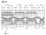
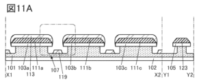
- FIG. 1B is a cross-sectional view showing an example of a display device; 2A and 2B are cross-sectional views showing examples of display devices. 3A and 3B are cross-sectional views showing examples of display devices. 4A and 4B are cross-sectional views showing examples of display devices. 5A and 5B are cross-sectional views showing examples of display devices. 6A and 6B are cross-sectional views showing examples of display devices. 7A and 7B are cross-sectional views showing examples of display devices. 8A and 8B are cross-sectional views showing examples of display devices. 9A and 9B are cross-sectional views illustrating an example of a method for manufacturing a display device.
- 10A1, 10A2, and 10B are cross-sectional views illustrating an example of a method for manufacturing a display device.
- 11A and 11B are cross-sectional views illustrating an example of a method for manufacturing a display device.
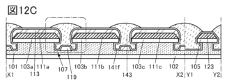
- 12A to 12C are cross-sectional views illustrating an example of a method for manufacturing a display device.
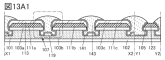
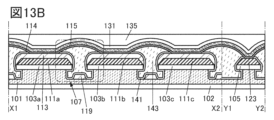
- 13A1, 13A2, and 13B are cross-sectional views illustrating an example of a method for manufacturing a display device.
- 14A1, 14A2, and 14B are cross-sectional views illustrating an example of a method for manufacturing a display device.
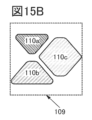
- 15A to 15G are diagrams showing examples of pixels.
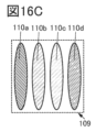
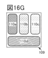
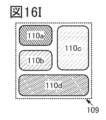
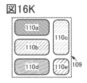
- 16A to 16K are diagrams showing examples of pixels.
- FIG. 17 is a perspective view showing an example of a display device.
- 18A is a cross-sectional view showing an example of a display device
- 18B and 18C are cross-sectional views showing examples of transistors.
- FIG. 19 is a cross-sectional view showing an example of a display device.
- 20A to 20F are diagrams showing configuration examples of light-emitting elements.
- 21A to 21C are diagrams showing configuration examples of light-emitting elements.
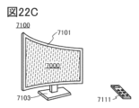
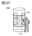
- 22A to 22F are diagrams illustrating examples of electronic devices.
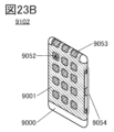
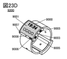
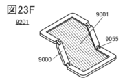
- 23A to 23G are diagrams illustrating examples of electronic devices.
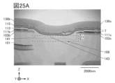
- FIG. 24 is a cross-sectional view showing the structure of a sample produced in this example.
- 25A and 25B are STEM images of the cross section of the sample produced in this example.
- film and “layer” can be used interchangeably depending on the case or situation. For example, it may be possible to change the term “conductive layer” to the term “conductive film.” Or, for example, it may be possible to change the term “insulating film” to the term “insulating layer”.
- pixels are arranged in a matrix and each pixel has a plurality of subpixels.
- a sub-pixel has a light-emitting element and a colored layer.
- a light-emitting element has an EL layer between a pair of electrodes.
- one of a pair of electrodes may be referred to as a pixel electrode and the other may be referred to as a common electrode.
- the EL layer has at least a light-emitting layer.
- layers included in the EL layer include a light emitting layer, a carrier injection layer, a carrier transport layer, a carrier block layer, and the like.
- layers other than the light-emitting layer are called functional layers.
- holes or electrons are sometimes referred to as “carriers”.
- the hole injection layer or electron injection layer is referred to as a "carrier injection layer”
- the hole transport layer or electron transport layer is referred to as a “carrier transport layer”
- the hole blocking layer or electron blocking layer is referred to as a "carrier It is sometimes called a block layer.
- the carrier injection layer, the carrier transport layer, and the carrier block layer described above may not be clearly distinguished from each other due to their cross-sectional shape, characteristics, or the like.
- one layer may serve two or three functions of the carrier injection layer, the carrier transport layer, and the carrier block layer.
- a display device of one embodiment of the present invention can have a structure in which a plurality of subpixels included in one pixel include light-emitting elements that emit light of the same color, for example, white light. Colored layers that transmit lights of different colors are provided for each sub-pixel in a region overlapping with the light-emitting element. Accordingly, the display device of one embodiment of the present invention can perform full-color display.
- the EL layer included in the light-emitting elements can be shared among the plurality of sub-pixels.
- multiple sub-pixels can share a stretch of film.
- multiple sub-pixels sharing a string of films may cause leakage current between sub-pixels.
- crosstalk occurs between adjacent sub-pixels, which may lead to degradation of the display quality of the display device, for example.
- a display device of one embodiment of the present invention includes an island-shaped EL layer for each light-emitting element. Since the EL layer is separated for each light emitting element, it is possible to suppress the occurrence of crosstalk between adjacent sub-pixels. Accordingly, the display device of one embodiment of the present invention can have high display quality.
- an island shape means that two or more layers formed in the same process using the same material are physically separated.
- an island-shaped EL layer means that the EL layer is physically separated from an adjacent EL layer.
- an island-shaped EL layer can be formed by a vacuum deposition method using a metal mask.
- various influences such as precision of the metal mask, misalignment between the metal mask and the substrate, bending of the metal mask, and broadening of the contour of the film to be formed due to vapor scattering, for example, cause island-shaped ELs. Deviations from the design occur in the shape and position of the layers. Therefore, it is difficult to increase the definition of the display device and the aperture ratio.
- the edge of the layer may be thin due to blurring of the layer contour during deposition. That is, the thickness of the island-shaped EL layer formed using a metal mask may vary.
- the manufacturing yield will be low due to low dimensional accuracy of the metal mask and deformation due to heat or the like.
- an island-shaped EL layer is formed without using a shadow mask such as a metal mask. Specifically, first, an organic insulating layer on a substrate, an inorganic insulating layer on the organic insulating layer, and a conductive layer on the inorganic insulating layer are sequentially formed. Subsequently, a plurality of pixel electrodes are formed by removing part of the conductive layer. Subsequently, the inorganic insulating layer is separated by removing a region of the inorganic insulating layer that does not overlap with the pixel electrode. Subsequently, a recess is formed in the organic insulating layer between the separated inorganic insulating layers.
- the concave portion is formed so that the end portion of each inorganic insulating layer overlaps with the concave portion of the organic insulating layer. That is, the concave portion is formed so that the inorganic insulating layer has a protruding portion that overlaps with the concave portion of the organic insulating layer.
- the above processing of the conductive layer and the inorganic insulating layer can be performed, for example, by etching after forming a pattern by photolithography.
- the organic insulating layer is processed by a method that is easier to process isotropically than the processing method of the inorganic insulating layer.
- the organic insulating layer is processed by ashing using oxygen plasma. Thereby, the concave portion can be formed in the organic insulating layer so that the inorganic insulating layer has the protruding portion.
- ashing means to remove at least part of an organic insulating layer by chemically acting on the organic insulating layer with, for example, active oxygen molecules, ozone molecules, or oxygen atoms generated by discharge.
- processing a layer or film means removing a desired region of the layer or film.
- the film is separated by processing the film to form a plurality of layers.
- the horizontal direction indicates, for example, a direction parallel to the substrate surface.
- the vertical direction means, for example, a direction perpendicular to the substrate surface.
- a direction horizontal to a flat portion of a layer provided on a substrate may be referred to as a horizontal direction
- a direction perpendicular to the flat portion may be referred to as a vertical direction.
- the substrate surface, the flat portion of the layer, and the like do not necessarily have to be completely flat, and may be substantially planar with a fine curvature or substantially planar with fine unevenness.
- an EL layer is formed over a plurality of pixel electrodes.
- the EL layer is separated into islands by the protrusions of the inorganic insulating layer, and one island-shaped EL layer is formed for one pixel electrode. That is, an island-shaped EL layer can be formed for each sub-pixel.
- a functional layer other than the light-emitting layer for example, a carrier injection layer, a carrier transport layer, or a carrier block layer, more specifically a hole injection layer, a hole transport layer, or an electron block layer, etc.
- a functional layer other than the light-emitting layer for example, a carrier injection layer, a carrier transport layer, or a carrier block layer, more specifically a hole injection layer, a hole transport layer, or an electron block layer, etc.
- leakage current which may be referred to as lateral leakage current, lateral leakage current, or lateral leakage current
- the hole-injection layer can be processed into an island shape, the lateral leakage current between adjacent subpixels is substantially not generated or the lateral leakage current is extremely small. be able to.
- a device manufactured using a metal mask or FMM fine metal mask, high-definition metal mask
- a device with an MM (metal mask) structure is sometimes referred to as a device with an MML (metal maskless) structure.
- each step performed after the formation of the EL layer is performed at a temperature higher than the heat-resistant temperature of the EL layer, the EL layer may be deteriorated and the light emission efficiency and reliability of the light emitting element may be lowered. be.
- the heat resistance temperature of the compounds included in the light-emitting element is preferably 100° C. to 180° C., preferably 120° C. to 180° C., and 140° C. to 180° C. °C or less is more preferable.
- indices of heat resistance temperature examples include glass transition point (Tg), softening point, melting point, thermal decomposition temperature, and 5% weight loss temperature.
- Tg glass transition point
- softening point melting point
- thermal decomposition temperature thermal decomposition temperature
- 5% weight loss temperature 5% weight loss temperature.
- the glass transition point of the material of the layer can be used as an index of the heat resistance temperature of each layer forming the EL layer.
- the glass transition point of the material of the layer can be used.
- the layer is a mixed layer made of a plurality of materials
- the glass transition point of the most abundant material can be used.
- the lowest temperature among the glass transition points of the plurality of materials may be used.
- the heat resistance temperature of the functional layer provided on the light emitting layer it is preferable to increase the heat resistance temperature of the functional layer provided on the light emitting layer. Further, it is more preferable to increase the heat resistance temperature of the functional layer provided on and in contact with the light emitting layer. Since the functional layer has high heat resistance, the light-emitting layer can be effectively protected, and damage to the light-emitting layer can be reduced.
- the heat resistance temperature of the light-emitting layer it is preferable to increase the heat resistance temperature of the light-emitting layer. As a result, it is possible to prevent the light-emitting layer from being damaged by heating, thereby reducing the light-emitting efficiency and shortening the life of the light-emitting layer.
- the reliability of the light-emitting element can be improved.
- the width of the temperature range in the manufacturing process of the display device can be widened, and the manufacturing yield and reliability can be improved.
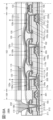
- FIG. 1A A plan view of a display device 100 that is one embodiment of the present invention is shown in FIG. 1A.
- FIG. 1A is also referred to as a top view of the display device 100 .
- the display device 100 has a display portion in which a plurality of pixels 109 are arranged in a matrix and a connection portion 140 outside the display portion.
- Each pixel 109 has multiple sub-pixels.
- FIG. 1A shows two rows and two columns of pixels 109 .
- each pixel 109 has three sub-pixels (sub-pixel 110a, sub-pixel 110b, and sub-pixel 110c), and sub-pixels for 2 rows and 6 columns are shown.
- Each sub-pixel has a light-emitting element.
- the top surface shape of the sub-pixel shown in FIG. 1A corresponds to the top surface shape of the light emitting region of the light emitting element.
- the top surface shape of the sub-pixel can be triangular, quadrangular (including rectangular and square), elliptical, or circular, for example. Further, the top surface shape of the sub-pixel can be, for example, a polygon such as a pentagon, or a polygon with rounded corners.
- Each sub-pixel has a pixel circuit that functions to control a light-emitting element.
- the pixel circuit is not limited to the range of the sub-pixels shown in FIG. 1A, and may be arranged outside thereof.
- the transistors included in the pixel circuit of sub-pixel 110a may be located within sub-pixel 110b shown in FIG. 1A.
- part or all of the elements such as transistors that constitute the pixel circuit of the sub-pixel 110a may be located outside the range of the sub-pixel 110a in plan view.
- FIG. 1A shows a structure in which the subpixels 110a, 110b, and 110c have the same or approximately the same aperture ratio (which can also be called the size or the size of the light-emitting region), which is one embodiment of the present invention. Not limited.
- the aperture ratios of the sub-pixel 110a, the sub-pixel 110b, and the sub-pixel 110c can be determined as appropriate.
- the sub-pixel 110a, the sub-pixel 110b, and the sub-pixel 110c may have different aperture ratios, and two or more may have the same or substantially the same aperture ratio.
- Pixel 109 shown in FIG. 1A is composed of three sub-pixels, sub-pixel 110a, sub-pixel 110b, and sub-pixel 110c.
- Subpixel 110a, subpixel 110b, and subpixel 110c exhibit different colors of light.
- sub-pixels 110a, 110b, and 110c there are three sub-pixels of red (R), green (G), and blue (B), yellow (Y), cyan (C), and magenta (M). ), and the like.
- the number of sub-pixel color types is not limited to three, and may be four or more.
- four-color sub-pixels for example, four-color sub-pixels of R, G, B, and white (W), four-color sub-pixels of R, G, B, and Y, and R, G, B, and Infrared (IR) four-color sub-pixels are included.
- W white
- IR Infrared
- the red light can be light with a peak wavelength of 630 nm or more and 780 nm or less, for example.
- the green light can be light with a peak wavelength of 500 nm or more and less than 570 nm, for example.
- the blue light can be light with a peak wavelength of 450 nm or more and less than 480 nm, for example.
- FIG. 1A shows an example in which sub-pixels 110 of different colors are arranged side by side in the X direction and sub-pixels 110 of the same color are arranged side by side in the Y direction.
- FIG. 1A shows an example in which the connecting portion 140 is positioned below the display portion in plan view
- the connecting portion 140 may be provided in at least one of the upper side, the right side, the left side, and the lower side of the display portion in plan view, and may be provided so as to surround the four sides of the display portion.
- the shape of the upper surface of the connecting portion 140 is not particularly limited, and may be strip-shaped, L-shaped, U-shaped, frame-shaped, or the like.
- the number of connection parts 140 may be singular or plural.
- FIG. 1B shows a cross-sectional view between the dashed line X1-X2 and the dashed line Y1-Y2 in FIG. 1A.
- FIG. 1B is a cross-sectional view of the XZ plane.
- cross-sectional views other than FIG. 1B between the dashed-dotted line X1-X2 in FIG. 1A and between the dashed-dotted line Y1-Y2 similarly show the XZ plane.
- a configuration in which the sub-pixel 110a emits red light, the sub-pixel 110b emits green light, and the sub-pixel 110c emits blue light will be described below as an example.
- the X direction may be referred to as the horizontal direction
- the Z direction may be referred to as the height direction or the vertical direction.
- the Y direction is sometimes referred to as the horizontal direction.
- the X direction, Y direction, and Z direction can be perpendicular to each other, and these three directions can represent a three-dimensional space.
- the XY plane can be called a plane or a top surface
- the XZ plane and the YZ plane can be called a cross section.
- the sub-pixel 110a has a light-emitting element 130a and a colored layer 132a.
- the light emitting element 130a has a function of emitting white light, for example.
- the colored layer 132a has a region overlapping with the light emitting element 130a, and has a higher transmittance for red light than for other colors of light, for example. As a result, light emitted from the light emitting element 130a is extracted as red light to the outside of the display device through the colored layer 132a.
- the sub-pixel 110b has a light-emitting element 130b and a colored layer 132b.
- the light emitting element 130b has a function of emitting white light, for example.
- the colored layer 132b has a region overlapping with the light emitting element 130b.
- the colored layer 132b transmits light of a color different from that of the colored layer 132a.
- the colored layer 132b has, for example, a higher transmittance for green light than for other colors of light. As described above, light emitted from the light emitting element 130b is extracted as green light to the outside of the display device through the colored layer 132b.
- the sub-pixel 110c has a light-emitting element 130c and a colored layer 132c.
- the light emitting element 130c has a function of emitting white light, for example.
- the colored layer 132c has a region overlapping with the light emitting element 130c.
- the colored layer 132c transmits light of a color different from that of the colored layers 132a and 132b.
- the colored layer 132c has a higher transmittance for blue light than for other colors of light. As described above, light emitted from the light emitting element 130c is extracted as blue light to the outside of the display device through the colored layer 132c.
- different colors of transmitted light means different wavelengths with the highest transmittance.
- the colored layer 132a has the highest transmittance of light (red light) of 630 nm or more and 780 nm or less in visible light
- the colored layer 132b has the highest transmittance of light (green light) of 500 nm or more and less than 570 nm in visible light. is the highest, it can be said that the color of light transmitted through the colored layer 132a is different from the color of light transmitted through the colored layer 132b.
- visible light refers to light with a wavelength of 380 nm or more and 780 nm or less.
- the display device 100 has an insulating layer 101 on a substrate 102, and insulating layers 103a, 103b, and 103c on the insulating layer 101.
- a light-emitting element 130a is provided over the insulating layer 103a
- a light-emitting element 130b is provided over the insulating layer 103b
- a light-emitting element 130c is provided over the insulating layer 103c.
- a protective layer 131 is provided to cover the light-emitting elements 130 a , 130 b , and 130 c
- a protective layer 135 is provided over the protective layer 131 .
- a colored layer 132 a , a colored layer 132 b , and a colored layer 132 c are provided on the protective layer 135 , and the substrate 120 is bonded with the adhesive layer 122 .
- a transistor for example, is provided between the substrate 102 and the insulating layer 101 .
- An insulating layer containing a material different from that of the insulating layer 101 can be provided between the substrate 102 and the insulating layer 101, for example.
- FIG. 1B shows a plurality of cross sections of the insulating layer 141 and the insulating layer 143; It can be configured to be connected to one. That is, the display device 100 can be configured to have one insulating layer 141 and one insulating layer 143, for example. Note that the display device 100 may have a plurality of insulating layers 141 and insulating layers 143 that are separated from each other.
- a structure in which a colored layer that transmits white light is provided or a structure in which a colored layer is not provided may be employed.
- a display device of one embodiment of the present invention is a top emission type in which light is emitted in a direction opposite to a substrate provided with a light-emitting element, and light is emitted toward a substrate provided with a light-emitting element.
- a bottom emission type bottom emission type
- a double emission type dual emission type in which light is emitted from both sides may be used.
- Glass, quartz, ceramic, sapphire, resin, metal, alloy, semiconductor, or the like can be used for the substrate 102 and the substrate 120 .
- a material that transmits the light is used for the substrate on the side from which the light from the light emitting element 130 is extracted. That is, when the display device 100 is a top emission display device, at least the substrate 120 is made of a material that transmits light emitted by the light emitting element 130, and when the display device 100 is a bottom emission display device, At least the substrate 102 is made of a material that transmits light emitted from the light emitting element 130 .
- both the substrate 102 and the substrate 120 are made of a material that transmits light emitted by the light emitting element 130 .
- the flexibility of the display device 100 can be increased.
- a polarizing plate may be used as the substrate 102 and the substrate 120 .
- the substrate 102 and the substrate 120 are made of polyester resin such as polyethylene terephthalate (PET) and polyethylene naphthalate (PEN), polyacrylonitrile resin, acrylic resin, polyimide resin, polymethyl methacrylate resin, polycarbonate (PC) resin, polyether resin, respectively.
- glass having a thickness that is flexible may be used.
- the light emitting element 130 it is preferable to use, for example, an OLED (Organic Light Emitting Diode) or a QLED (Quantum-dot Light Emitting Diode).
- the light-emitting substance that the light-emitting element 130 can have include a substance that emits fluorescence (fluorescent material), a substance that emits phosphorescence (phosphorescent material), an inorganic compound (e.g., quantum dot material), and a substance that exhibits thermally activated delayed fluorescence. (thermally activated delayed fluorescence (TADF) material).
- TADF thermally activated delayed fluorescence
- an LED such as a micro LED (Light Emitting Diode) can be used.
- a conductive film that transmits visible light can be used for the electrode from which light is extracted, and a conductive film that reflects visible light can be used for the electrode from which light is not extracted.
- a conductive film that transmits visible light may also be used for the electrode on the side from which light is not extracted.
- a conductive film that transmits visible light is preferably provided between the conductive film that reflects visible light and the EL layer.
- one electrode functions as an anode and the other electrode functions as a cathode.
- the case where the pixel electrode functions as an anode and the common electrode functions as a cathode may be described as an example.
- the light emitting element 130a has a pixel electrode 111a on the insulating layer 103a, an island-shaped EL layer 113 on the pixel electrode 111a, a common layer 114 on the EL layer 113, and a common electrode 115 on the common layer 114.
- the light emitting element 130b has a pixel electrode 111b on the insulating layer 103b, an island-shaped EL layer 113 on the pixel electrode 111b, a common layer 114 on the EL layer 113, and a common electrode 115 on the common layer 114.
- the light emitting element 130c has a pixel electrode 111c on the insulating layer 103c, an island-shaped EL layer 113 on the pixel electrode 111c, a common layer 114 on the EL layer 113, and a common electrode 115 on the common layer 114.
- the EL layer 113 and the common layer 114 can be collectively called an EL layer.
- a display device which is one embodiment of the present invention includes an island-shaped EL layer 113 for each light-emitting element 130 .
- the light-emitting elements 130a, 130b, and 130c each have an EL layer 113, and the EL layers 113 do not have regions in contact with each other and are separated.
- the EL layer 113 in an island shape for each light emitting element 130, leakage current between adjacent light emitting elements 130 can be prevented. Thereby, crosstalk due to unintended light emission can be prevented, and a display device with extremely high contrast can be realized. In particular, a display device with high current efficiency at low luminance can be realized.
- Each EL layer 113 can be formed in the same process using the same material.
- the manufacturing steps of the display device can be reduced. . This makes it possible to reduce the manufacturing cost of the display device and improve the manufacturing yield.
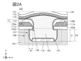
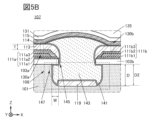
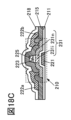
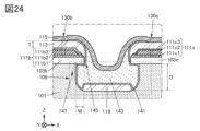
- region 107 which is the region between and surrounding light emitting elements 130a and 130b, is shown in FIG. 2A.
- insulating layer 101 has recesses 108 .
- the recess 108 is provided between adjacent light emitting elements 130 .
- a portion of the insulating layer 103 overlaps with the recess 108 , specifically, an end portion 145 of the insulating layer 103 overlaps with the recess 108 . That is, the insulating layer 103 has protrusions that overlap with the recesses 108 .
- the surface on which the EL layer 113 is formed has a step due to the protrusion of the insulating layer 103 . Since the coverage of the EL layer 113 is low due to the step, the EL layer 113 is separated when the EL layer 113 is formed. That is, disconnection occurs in the EL layer 113 . Therefore, there is a region where the EL layer 113 is not formed.
- discontinuity refers to a phenomenon in which a layer, film, electrode, or the like is divided due to the shape of a formation surface (for example, a step).
- a region in which the EL layer 113 is not formed due to a discontinuity is referred to as a discontinuous region.
- the width W of the protrusion overlapping with the recess 108 of the insulating layer 103 is larger, the EL layer 113 is more likely to be broken. Therefore, the EL layer 113 is easily separated for each light emitting element 130, which is preferable.
- the ratio (W/T) of the width W of the protrusion of the insulating layer 103 to the thickness T of the EL layer 113 is preferably 0.3 or more, more preferably 0.5 or more, and more preferably 0.7 or more. , is more preferably 0.9 or more, and more preferably 1.0 or more.
- the productivity of the display device may decrease, for example.
- the protruding portion of the insulating layer 103 tends to collapse, which may reduce the production yield of the display device.
- the ratio (W/T) of the width W of the protrusion of the insulating layer 103 to the film thickness T of the EL layer 113 is preferably 10.0 or less, more preferably 5.0 or less.
- the width W of the protrusion of the insulating layer 103 is preferably 20 nm or more, more preferably 50 nm or more, more preferably 80 nm or more, more preferably 110 nm or more, still more preferably 140 nm or more, more preferably 160 nm or more, and 180 nm. The above is more preferable. Also, the width W of the protruding portion of the insulating layer 103 is preferably 2000 nm or less, more preferably 1000 nm or less.
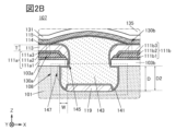
- the width W of the protruding portion of the insulating layer 103 is the width of the insulating layer 103 between the end portion 145 of the insulating layer 103 and the end portion 147 of the recessed portion 108, for example, when viewed from the XZ plane or the YZ plane. Indicates the distance on the bottom surface. That is, the width W is the distance between the lower end of the insulating layer 103, which is the lower end of the end portion 145, and the upper end of the recess 108, which is the upper end of the end portion 147 when viewed from the XZ plane or the YZ plane, for example. show.
- the film thickness T of the EL layer 113 is determined by the position of the upper surface of the EL layer 113 and the position of the lower surface of the EL layer 113 in the region overlapping with the upper surface of the pixel electrode 111 when viewed from the XZ plane or the YZ plane, for example. Show the difference.
- the film thickness T may be the distance in the Z direction between the upper surface of the pixel electrode 111 and the lower surface of the common layer 114 or the common electrode 115 .
- the ratio (D/T) of the depth D of the recess 108 to the film thickness T of the EL layer 113 is preferably 1.0 or more, more preferably 2.0 or more, more preferably 3.0 or more. 5 or more is more preferable, and 4.0 or more is even more preferable.
- the ratio (D/T) of the depth D of the concave portion 108 to the film thickness T of the EL layer 113 is preferably 50.0 or less, more preferably 30.0 or less, and even more preferably 20.0 or less.
- the depth D of the concave portion 108 is preferably 50 nm or more, more preferably 150 nm or more, more preferably 300 nm or more, more preferably 450 nm or more, still more preferably 600 nm or more, and even more preferably 700 nm or more. Also, the depth D of the concave portion 108 is preferably 10 ⁇ m or less, more preferably 5 ⁇ m or less, more preferably 4 ⁇ m or less, and even more preferably 3 ⁇ m or less.
- the depth D of the recess 108 indicates the distance in the Z direction between the lower surface of the insulating layer 103 and the bottom of the recess 108 when viewed from the XZ plane or the YZ plane, for example.
- the depth D of the recess 108 is, for example, the height of the lower surface of the insulating layer 103 from the substrate 102 when viewed from the XZ plane or the YZ plane, and the deepest part of the recess 108 in the cross section of the substrate. It is represented by the difference between the height from 102 and .
- the depth D of the recess 108 is the height of the lower surface of the insulating layer 103 from the substrate 102 when viewed from the XZ plane or the YZ plane, and the height of the recess 108 in the cross section from the substrate 102. It is represented by the difference between the height from the substrate 102 of the lowest portion.
- the height of A from B indicates the distance from A to B in the Z direction.
- the width W, the film thickness T, and the depth D are, for example, a scanning electron microscope (SEM) image, a transmission electron microscope (TEM) image, or a scanning transmission electron microscope of a cross section of the light emitting element 130. (STEM: Scanning Transmission Electron Microscopy) image can be measured.
- a film to be the insulating layer 103, and a film to be the pixel electrode 111 by processing these, the pixel electrode 111 and the insulating layer 103 are formed. Also, a recess 108 is formed in the insulating layer 101 .
- forming a film is referred to as forming a film.
- the insulating layer 101 is processed by a method that is more isotropically processed than the processing method of the film that becomes the insulating layer 103, so that the concave portion 108 is formed so that the insulating layer 103 has a projecting portion.
- the insulating layer 101 can be processed, for example, by ashing using oxygen plasma.
- the insulating layer 101 can be processed using oxygen gas and CF4 , C4F8 , SF6 , CHF3 , Cl2 , H2O , BCl3 , or a Group 18 element.
- He can be used as the Group 18 element.
- the insulating layer 101 may be processed using etching, such as wet etching.
- the insulating layer 101 can be an organic insulating layer.
- the insulating layer 103 can be an inorganic insulating layer. It should be noted that the insulating layer 101 may not be an organic insulating layer, and the insulating layer 103 may not be an inorganic insulating layer as long as the concave portion 108 can be formed so that the insulating layer 103 has a projecting portion.
- both the insulating layer 101 and the insulating layer 103 may be inorganic insulating layers.
- an insulating layer using an organic material is called an organic insulating layer
- an insulating layer using an inorganic material is called an inorganic insulating layer.
- a resin material for example, can be used as the insulating layer 101 .
- the insulating layer 101 can be made of acrylic resin, polyimide resin, epoxy resin, polyamide resin, polyimideamide resin, siloxane resin, benzocyclobutene-based resin, phenolic resin, precursors of these resins, or the like.
- oxides include silicon oxide, aluminum oxide, magnesium oxide, indium gallium zinc oxide, gallium oxide, germanium oxide, yttrium oxide, zirconium oxide, lanthanum oxide, neodymium oxide, hafnium oxide, and tantalum oxide.
- Nitrides include silicon nitride and aluminum nitride.
- Oxynitrides include silicon oxynitride and aluminum oxynitride.
- Nitride oxides include silicon oxynitride and aluminum oxynitride.
- oxynitride refers to a material whose composition contains more oxygen than nitrogen
- nitride oxide refers to a material whose composition contains more nitrogen than oxygen. point to the material.
- silicon oxynitride refers to a material whose composition contains more oxygen than nitrogen
- silicon nitride oxide refers to a material whose composition contains more nitrogen than oxygen. indicates
- An organic layer 119 may be provided in the recess 108 .
- the organic layer 119 is formed by reaching the recess 108 with the material of the EL layer 113 when the EL layer 113 is formed. That is, the organic layer 119 is formed using the same material and in the same process as the EL layer 113 .
- FIG. 2A shows an example in which an organic layer 119 is provided on the insulating layer 101 at the bottom of the recess 108 .
- the organic layer 119 if the organic layer 119 has a region in contact with the EL layer 113, the EL layers 113 of adjacent light-emitting elements 130 are connected through the organic layer 119, which may cause leakage current. Therefore, the organic layer 119 preferably does not have a region in contact with the EL layer 113 . In other words, the organic layer 119 is preferably separated from the EL layer 113 . For example, when the distance between the side surfaces of the adjacent pixel electrodes 111 is short, the organic layer 119 may not be formed.
- the boundary between the insulating layer 101 and the organic layer 119 may not be clearly recognized.
- the boundary between the insulating layer 101 and the organic layer 119 cannot be clearly confirmed, for example, when viewed from the XZ plane or the YZ plane, the height of the lower surface of the insulating layer 103 from the substrate 102 and the clear The difference between the height of the deepest portion of the recess 108 from the substrate 102 within a range that can be confirmed by the depth of the recess 108 can be defined as the depth of the recess 108 .
- the height of the lower surface of the insulating layer 103 from the substrate 102 and the lowest portion of the lower surface of the insulating layer 141 from the substrate 102 in the cross section of the substrate 102 The depth D 2 , which is the difference between the height from and the depth of the recess 108 , can be taken as the depth of the recess 108 .
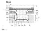
- FIGS. 1B and 2A show a configuration in which the EL layer 113 covers the upper surface and at least part of the side surface of the pixel electrode 111.
- FIG. By adopting such a structure, it is possible to use the entire region overlapping with the upper surface of the pixel electrode 111 as a light emitting region in plan view. Therefore, the aperture ratio of the display device can be increased as compared with the structure in which the side surfaces of the pixel electrode 111 are not covered with the island-shaped EL layer 113 .
- the EL layer 113 may cover not only the side surfaces of the pixel electrodes 111 but also the side surfaces of the insulating layer 103 .
- side surfaces of the pixel electrode 111a, the pixel electrode 111b, and the pixel electrode 111c may each have a tapered shape.
- the end portions of the pixel electrode 111a, the pixel electrode 111b, and the pixel electrode 111c may each have a taper shape with a taper angle of less than 90° when viewed from the XZ plane or the YZ plane, for example.
- the coverage of the pixel electrode 111 with the EL layer 113 can be improved as compared with the case where the side surface of the pixel electrode 111 is vertical.
- the conductive layer 123 provided in the connection portion 140 which will be described later, can be formed in the same step as the pixel electrodes 111a, 111b, and 111c. Therefore, when the side surfaces of the pixel electrode 111a, the pixel electrode 111b, and the pixel electrode 111c are tapered, the conductive layer 123 may also be tapered.
- a tapered shape refers to a shape in which at least a part of the side surface of the structure is inclined with respect to the substrate surface. For example, it is preferable to have a region where the angle between the inclined side surface and the substrate surface (also referred to as a taper angle) is less than 90°. Note that the side surfaces of the structure and the substrate surface are not necessarily completely flat, and may be substantially planar with a fine curvature or substantially planar with fine unevenness.
- Side surfaces of the insulating layer 103a, the insulating layer 103b, and the insulating layer 103c may also have a tapered shape with a taper angle of less than 90° when viewed from the XZ plane or the YZ plane, for example.
- the side surface of the recess 108 in the insulating layer 101 may also have a tapered shape with a taper angle of less than 90° when viewed from the XZ plane or the YZ plane, for example.
- the insulating layer 105 provided in the connection portion 140 which will be described later, can be formed in the same step as the insulating layers 103a, 103b, and 103c. Therefore, when the insulating layer 103a, the insulating layer 103b, and the insulating layer 103c have tapered side surfaces, the insulating layer 105 can also have a tapered shape.
- the taper angle of the side surface of the insulating layer 103 and the taper angle of the side surface of the insulating layer 101 in the recess 108 may not be equal to the taper angle of the side surface of the pixel electrode 111 .
- at least one of the taper angle of the side surface of the insulating layer 103 and the taper angle of the side surface of the insulating layer 101 in the recess 108 may be larger (the taper is steeper) than the taper angle of the side surface of the pixel electrode 111 .
- the taper angle of the side surfaces of the insulating layer 105 may not be equal to the taper angle of the side surfaces of the conductive layer 123, and may be greater than the taper angle of the side surfaces of the conductive layer 123, for example.
- the upper end of the side surface of the insulating layer 103 and the lower end of the side surface of the pixel electrode 111 are aligned, and the upper end of the side surface of the insulating layer 105 and the side surface of the conductive layer 123 are aligned.
- the lower end and the do not have to coincide.
- the lower edge of the side surface of the pixel electrode 111 may be located inside the upper edge of the side surface of the insulating layer 103
- the lower edge of the side surface of the conductive layer 123 may be located inside the upper edge of the side surface of the insulating layer 105 .
- an insulating layer covering the top surface end portion of the pixel electrode 111 is provided between the pixel electrode 111 and the EL layer 113. not Therefore, the distance between adjacent light emitting elements 130 can be reduced. Therefore, a high-definition or high-resolution display device can be obtained. Moreover, a mask for forming the insulating layer is not required, and the manufacturing cost of the display device can be reduced.
- a configuration in which no insulating layer is provided between the pixel electrode 111 and the EL layer 113 to cover the edge of the upper surface of the pixel electrode 111 in other words, a configuration in which no insulating layer is provided between the pixel electrode 111 and the EL layer 113. Accordingly, light emitted from the EL layer 113 can be efficiently extracted. Therefore, the viewing angle dependency of the display device of one embodiment of the present invention can be extremely reduced. By reducing the viewing angle dependency, it is possible to improve the visibility of the image on the display device.
- the viewing angle (the maximum angle at which a constant contrast ratio is maintained when the screen is viewed obliquely) is 100° or more and less than 180°, preferably 150°. It can be in the range of 170° or more. It should be noted that the viewing angle described above can be applied to each of the vertical and horizontal directions.
- the light emitting element 130 may have a single structure (a structure having only one light emitting unit) or a tandem structure (a structure having a plurality of light emitting units).
- the light-emitting unit has at least one light-emitting layer.
- the EL layer 113 has at least a light-emitting layer. Also, the EL layer 113 may have one or more of a hole injection layer, a hole transport layer, a hole blocking layer, a charge generation layer, an electron blocking layer, an electron transport layer, and an electron injection layer.
- the EL layer 113 can have a luminescent material that emits blue light and a luminescent material that emits visible light with a longer wavelength than blue.
- the EL layer 113 includes a light-emitting substance that emits blue light and a light-emitting substance that emits yellow light, or a light-emitting substance that emits blue light, a light-emitting substance that emits green light, and a light-emitting substance that emits red light.
- a structure including a light-emitting substance that emits light, or the like can be applied.
- the light-emitting elements 130a, 130b, and 130c are single-structure light-emitting elements having two light-emitting layers, for example, a light-emitting layer that emits yellow (Y) light and a light-emitting layer that emits blue (B) light.
- a single-structure light-emitting element having three light-emitting layers that is, a light-emitting layer that emits red (R) light, a light-emitting layer that emits green (G) light, and a light-emitting layer that emits blue light, can be used. .
- the number of laminations of the light-emitting layers and the order of colors can be a three-layer structure of R, G, and B or a three-layer structure of R, B, and G from the anode side.
- Another layer also referred to as a buffer layer
- a two-stage tandem structure having a light-emitting unit that emits yellow light and a light-emitting unit that emits blue light, a light-emitting unit that emits red and green light, and a light-emitting unit that emits blue light. or a light-emitting unit that emits blue light, a light-emitting unit that emits yellow, yellow-green, or green light and red light, and a light-emitting unit that emits blue light
- a three-stage tandem structure having in this order can be applied.
- the order of the number of layers of the light-emitting unit and the color may include a two-stage structure of B and Y, a two-stage structure of B and X, and a three-stage structure of B, X and B from the anode side.
- the order of the number of laminated layers and colors of the light-emitting layers in is, from the anode side, a two-layer structure of R and Y, a two-layer structure of R and G, a two-layer structure of G and R, a three-layer structure of G, R, and G, or A three-layer structure of R, G, and R can be used.
- other layers may be provided between the two light-emitting layers.
- the EL layer 113 has a plurality of light-emitting units.
- a charge generating layer is preferably provided between each light emitting unit.
- the light emitting element 130 can emit white light.
- the light emitting unit may have one or more of a hole injection layer, a hole transport layer, a hole blocking layer, an electron blocking layer, an electron transport layer, and an electron injection layer.
- the EL layer 113 may have a hole-injection layer, a hole-transport layer, a light-emitting layer, and an electron-transport layer in this order. Moreover, you may have an electron block layer between a hole transport layer and a light emitting layer. Further, a hole blocking layer may be provided between the electron transport layer and the light emitting layer. Moreover, you may have an electron injection layer on the electron transport layer.
- the EL layer 113 may have an electron-injection layer, an electron-transport layer, a light-emitting layer, and a hole-transport layer in this order.
- a hole blocking layer may be provided between the electron transport layer and the light emitting layer.
- you may have an electron block layer between a hole transport layer and a light emitting layer.
- a hole injection layer may be provided on the hole transport layer.
- the EL layer 113 preferably has a light-emitting layer and a carrier-transporting layer (an electron-transporting layer or a hole-transporting layer) over the light-emitting layer. Further, the EL layer 113 preferably has a light-emitting layer and a carrier blocking layer (a hole blocking layer or an electron blocking layer) over the light-emitting layer. Further, the EL layer 113 preferably has a light-emitting layer, a carrier-blocking layer over the light-emitting layer, and a carrier-transporting layer over the carrier-blocking layer.
- the carrier-transporting layer and the carrier-blocking layer are provided over the light-emitting layer to prevent the light-emitting layer from being exposed to the outermost surface. , the damage to the light-emitting layer can be reduced. Thereby, the reliability of the light emitting element can be improved.
- the heat resistance temperature of each of the compounds contained in the EL layer 113 is preferably 100° C. to 180° C., preferably 120° C. to 180° C., and more preferably 140° C. to 180° C.
- the glass transition points of these compounds are preferably 100° C. or higher and 180° C. or lower, preferably 120° C. or higher and 180° C. or lower, and more preferably 140° C. or higher and 180° C. or lower.
- the functional layer provided on the light-emitting layer has a high heat resistance temperature. Further, it is more preferable that the functional layer provided in contact with the light-emitting layer has a high heat resistance temperature. Since the functional layer has high heat resistance, the light-emitting layer can be effectively protected, and damage to the light-emitting layer can be reduced.
- the heat resistance temperature of the light-emitting layer is high. As a result, it is possible to prevent the light-emitting layer from being damaged by heating, thereby reducing the light-emitting efficiency and shortening the life of the light-emitting layer.
- the light-emitting layer includes a light-emitting substance (also referred to as a light-emitting organic compound, guest material, or the like) and an organic compound (also referred to as a host material or the like). Since the light-emitting layer contains more organic compounds than the light-emitting substance, the Tg of the organic compound can be used as an index of the heat-resistant temperature of the light-emitting layer.
- the EL layer 113 has, for example, a first light-emitting unit, a charge generation layer, and a second light-emitting unit.
- the second light-emitting unit preferably has a light-emitting layer and a carrier-transporting layer (electron-transporting layer or hole-transporting layer) on the light-emitting layer. Also, the second light emitting unit preferably has a light emitting layer and a carrier blocking layer (hole blocking layer or electron blocking layer) on the light emitting layer. Also, the second light emitting unit preferably has a light emitting layer, a carrier blocking layer on the light emitting layer, and a carrier transport layer on the carrier blocking layer.
- the light-emitting unit provided in the uppermost layer preferably has a light-emitting layer and one or both of a carrier transport layer and a carrier block layer over the light-emitting layer.
- a common layer 114 can be provided over the EL layer 113 .
- Common layer 114 is shared by light emitting element 130a, light emitting element 130b, and light emitting element 130c.
- Common layer 114 comprises, for example, an electron injection layer or a hole injection layer.
- the common layer 114 has, for example, an electron transport layer or a hole transport layer.
- the common layer 114 may have, for example, an electron-transporting layer and an electron-injecting layer stacked together, or may have a hole-transporting layer and a hole-injecting layer stacked together.
- a common electrode 115 is provided on the common layer 114 .
- the common electrode 115 is shared by the light emitting elements 130a, 130b, and 130c.
- the common electrode 115 can be formed by, for example, a sputtering method, a vacuum deposition method, or the like.
- the common electrode 115 shared by the plurality of light emitting elements 130 is electrically connected to the conductive layer 123 provided on the connecting portion 140 .
- the conductive layer 123 is preferably formed using the same material and in the same process as the pixel electrodes 111a, 111b, and 111c.
- an insulating layer 105 is provided between the conductive layer 123 and the insulating layer 101 .
- the insulating layer 105 can be formed using the same material and in the same process as the insulating layers 103a, 103b, and 103c.
- the insulating layer 105 can have protrusions like the insulating layers 103a, 103b, and 103c.
- the conductive layer 123 and the common electrode 115 are electrically connected at the connecting portion 140 .
- the conductive layer 123 is electrically connected to, for example, an FPC (not shown).
- FPC an FPC
- the power supply potential can be supplied to the common electrode 115 through the conductive layer 123 in the connection portion 140 .
- the connection portion 140 can be called a cathode contact portion.
- the common layer 114 when the electrical resistance of the common layer 114 in the thickness direction is negligibly small, even if the common layer 114 is provided between the conductive layer 123 and the common electrode 115, the conductive layer 123 and , the electrical connection with the common electrode 115 can be ensured.
- a mask for defining a film formation area also called an area mask or a rough metal mask to distinguish from a fine metal mask
- the common layer 114 can be formed without the included metal mask. Therefore, the manufacturing process of the display device 100 can be simplified.
- connection portion 140 the conductive layer 123 and the common electrode 115 may be in direct contact and electrically connected without providing the common layer 114 over the conductive layer 123 .
- the common layer 114 can be formed only in a desired area.
- the common electrode 115 can be formed continuously after forming the common layer 114 without intervening a process such as etching. For example, after forming the common layer 114 in a vacuum, the common electrode 115 can be formed in a vacuum without removing the substrate 102 into the atmosphere. That is, the common layer 114 and the common electrode 115 can be formed in vacuum. As a result, the lower surface of the common electrode 115 can be made cleaner than when the common layer 114 is not provided in the display device 100 . Therefore, the light-emitting element 130 can be a light-emitting element with high reliability and favorable characteristics.
- a metal, an alloy, an electrically conductive compound, a mixture thereof, or the like can be used as a single layer or a laminated layer as appropriate.
- indium tin oxide also referred to as In—Sn oxide, ITO
- In—Si—Sn oxide also referred to as ITSO
- indium zinc oxide In—Zn oxide
- indium gallium zinc oxide In--Ga--Zn oxide, also referred to as IGZO
- alloys containing silver such as silver-magnesium alloys and silver-palladium-copper alloys (Ag-Pd-Cu, also referred to as APC) can be used.
- alloys containing aluminum such as alloys of aluminum, nickel and lanthanum (Al-Ni-La) are included.
- elements belonging to Group 1 or Group 2 of the periodic table of elements not exemplified above e.g., lithium (Li), cesium (Cs), calcium (Ca), or strontium (Sr)), europium (Eu),
- a rare earth metal such as ytterbium (Yb), an alloy containing an appropriate combination thereof, graphene, or the like can be used.
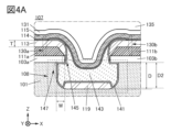
- Side surfaces of the EL layer 113 are covered with an insulating layer 141 .
- the side surface of the insulating layer 105 can be covered with the insulating layer 141 .
- part of the top surface of the EL layer 113 can be covered with the insulating layer 141 .
- the insulating layer 143 is provided over the insulating layer 141 and provided between adjacent EL layers 113 .
- the insulating layer 143 can be provided between adjacent pixel electrodes 111 .
- insulating layers 143 may be provided between adjacent insulating layers 103 .
- the insulating layer 143 is provided around the conductive layer 123 and the insulating layer 105 .
- the insulating layer 143 has a region overlapping with the recess 108 . Further, the insulating layer 143 can have a region overlapping with the organic layer 119 . Note that the insulating layers 141 and 143 can overlap with part of the top surface of the EL layer 113 .
- the common layer 114 and the common electrode 115 are provided not only on the light emitting element 130 but also on the insulating layer 143 .
- the insulating layer 143 between the adjacent EL layers 113 and providing the common layer 114 and the common electrode 115 over the insulating layer 143 extreme unevenness of the surfaces on which the common layer 114 and the common electrode 115 are formed can be reduced. , can be flatter. Therefore, the coverage of the common layer 114 and the common electrode 115 can be improved as compared with the case where the insulating layer 143 is not provided. Therefore, for example, it is possible to prevent a connection failure due to step disconnection of the common layer 114 and the common electrode 115 and an increase in electric resistance due to local thinning.
- At least one of the insulating layer 141 and the insulating layer 143 is provided between the adjacent EL layers 113 to prevent the common layer 114 and the common electrode 115 from contacting side surfaces of the EL layers 113, thereby preventing the light-emitting element 130 from short circuit can be prevented. Accordingly, the display device 100 can be a highly reliable display device.
- the insulating layer 141 is preferably in contact with side surfaces of the EL layer 113 . Accordingly, peeling of the EL layer 113 can be suppressed.
- the display device 100 can be a highly reliable display device.
- the display device 100 can be manufactured by a method with high yield.
- the insulating layer 141 is preferably formed by a method with high coverage, for example, by using an atomic layer deposition (ALD) method.
- ALD atomic layer deposition
- the insulating layer 141 can suitably cover, for example, the lower surface of the protrusion overlapping the recess 108 of the insulating layer 103 and the side surface of the recess 108 . Therefore, it is possible to prevent the width W of the protruding portion of the insulating layer 103 from becoming shorter than when the insulating layer 141 is formed by a method with low coverage.
- FIG. 2A shows a configuration in which the insulating layer 141 is in contact with the side surface of the recess 108 , but the insulating layer 141 does not have to be in contact with the side surface of the recess 108 .
- the insulating layer 141 may not come into contact with the side surface of the recess 108 .
- an insulating layer 143 is provided on the insulating layer 141 so as to fill the concave portion formed in the insulating layer 141 .
- the insulating layer 143 is provided between the island-shaped EL layers 113 .
- the display device 100 employs a process of forming the island-shaped EL layer 113 and then providing the insulating layer 143 so as to overlap with the end portion of the island-shaped EL layer 113 (hereinafter referred to as process 1). .
- process 2 As a process different from the process 1, after forming the pixel electrode 111 in an island shape, an insulating layer covering the end portion of the pixel electrode 111 is formed, and then an island shape is formed on the pixel electrode and the insulating layer.
- a process for forming an EL layer (hereinafter referred to as process 2) can be given.
- Process 1 described above is preferable because the margin can be widened compared to process 2 described above. More specifically, process 1 provides a wider margin for alignment accuracy between different patternings than process 2, and provides a display device with less variation in characteristics. Therefore, since the manufacturing method of the display device 100 is based on the process 1, a display device with little variation and high display quality can be provided.
- An insulating layer 141 is provided to cover at least part of the side surface of the conductive layer 123 in the connection portion 140 .
- an insulating layer 141 can be provided so as to cover side surfaces of the insulating layer 105 .
- An insulating layer 143 , a common layer 114 , and a common electrode 115 are provided over the insulating layer 141 .
- the insulating layer 141 can be an insulating layer having an inorganic material. That is, the insulating layer 141 can be an inorganic insulating layer.
- an inorganic insulating film such as an oxide insulating film, a nitride insulating film, an oxynitride insulating film, or a nitride oxide insulating film can be used, for example.
- the insulating layer 141 may have a single-layer structure or a laminated structure.
- the oxide insulating film includes a silicon oxide film, an aluminum oxide film, a magnesium oxide film, an indium gallium zinc oxide film, a gallium oxide film, a germanium oxide film, an yttrium oxide film, a zirconium oxide film, a lanthanum oxide film, a neodymium oxide film, and an oxide film.
- a hafnium film, a tantalum oxide film, and the like are included.
- the nitride insulating film include a silicon nitride film, an aluminum nitride film, and the like.
- Examples of the oxynitride insulating film include a silicon oxynitride film, an aluminum oxynitride film, and the like.
- the nitride oxide insulating film examples include a silicon nitride oxide film, an aluminum nitride oxide film, and the like.
- aluminum oxide is preferable because it has a high etching selectivity with respect to the EL layer and has a function of protecting the EL layer during formation of the insulating layer 143 described later.
- an inorganic insulating film such as an aluminum oxide film, a hafnium oxide film, or a silicon oxide film formed by an ALD method to the insulating layer 141, the insulating layer has few pinholes and has an excellent function of protecting the EL layer 113. 141 can be formed.
- the insulating layer 141 may have a layered structure of a film formed by an ALD method and a film formed by a sputtering method.
- the insulating layer 141 may have a laminated structure of, for example, an aluminum oxide film formed by ALD and a silicon nitride film formed by sputtering.
- the insulating layer 141 preferably functions as a barrier insulating layer against at least one of water and oxygen. Further, the insulating layer 141 preferably has a function of suppressing diffusion of at least one of water and oxygen. Further, the insulating layer 141 preferably has a function of capturing or fixing at least one of water and oxygen (also referred to as gettering).
- a barrier insulating layer means an insulating layer having a barrier property.
- the barrier property is defined as a function of suppressing diffusion of a corresponding substance (also referred to as low permeability).
- the corresponding substance has a function of capturing or fixing (also called gettering).
- the insulating layer 141 functions as a barrier insulating layer, it is possible to suppress entry of impurities (typically, at least one of water and oxygen) that can diffuse into the light-emitting element 130 from the outside. . With such a structure, a highly reliable light-emitting element and a highly reliable display device can be provided.
- the insulating layer 141 preferably has a low impurity concentration. Accordingly, it is possible to suppress deterioration of the EL layer 113 caused by impurities entering the EL layer 113 from the insulating layer 141 . In addition, by reducing the impurity concentration in the insulating layer 141, a barrier property against at least one of water and oxygen can be improved.
- the insulating layer 141 preferably has sufficiently low hydrogen concentration and/or carbon concentration, or preferably both.
- an insulating layer containing an organic material can be preferably used. That is, the insulating layer 143 can be an organic insulating layer.
- the organic material it is preferable to use a photosensitive material such as a photosensitive organic resin.
- a photosensitive resin composition containing an acrylic resin it is preferable to use a photosensitive resin composition containing an acrylic resin.
- acrylic resin does not only refer to polymethacrylate esters or methacrylic resins, but may refer to all acrylic polymers in a broad sense.
- an acrylic resin, a polyimide resin, an epoxy resin, an imide resin, a polyamide resin, a polyimideamide resin, a silicone resin, a siloxane resin, a benzocyclobutene-based resin, a phenolic resin, a precursor of these resins, or the like is used.
- an organic material such as polyvinyl alcohol (PVA), polyvinyl butyral, polyvinylpyrrolidone, polyethylene glycol, polyglycerin, pullulan, water-soluble cellulose, or alcohol-soluble polyamide resin may be used for the insulating layer 143 .
- a photoresist may be used as the photosensitive resin.
- the photosensitive organic resin either a positive material or a negative material may be used.
- a material that absorbs visible light may be used for the insulating layer 143 . Since the insulating layer 143 absorbs light emitted from the light emitting element 130 , leakage of light (stray light) from the light emitting element 130 to the adjacent light emitting element 130 via the insulating layer 143 can be suppressed. Thereby, the display quality of the display device can be improved. In addition, since the display quality can be improved without using a polarizing plate for the display device, the weight and thickness of the display device can be reduced.
- Materials that absorb visible light include materials containing pigments such as black, materials containing dyes, light-absorbing resin materials (e.g., polyimide), and resin materials that can be used for color filters (color filter materials). mentioned.
- resin material obtained by laminating or mixing color filter materials of two colors or three colors or more because the effect of shielding visible light can be enhanced.
- color filter materials it is possible to obtain a black or near-black resin layer.
- the material used for the insulating layer 143 preferably has a low volumetric shrinkage rate. This facilitates formation of the insulating layer 143 in a desired shape. Insulating layer 143 preferably has a low volume shrinkage after curing. This makes it easier to maintain the shape of the insulating layer 143 in various processes after forming the insulating layer 143 .
- the volume shrinkage rate of the insulating layer 143 after thermal curing, after photocuring, or after photocuring and thermal curing is preferably 10% or less, more preferably 5% or less, and further preferably 1% or less. preferable.
- the volume shrinkage rate one of the volume shrinkage rate due to light irradiation and the volume shrinkage rate due to heating, or the sum of both can be used.
- a protective layer 131 is preferably provided over the light-emitting elements 130a, 130b, and 130c. By providing the protective layer 131, the reliability of the light-emitting element 130 can be improved.
- the protective layer 131 may have a single layer structure or a laminated structure of two or more layers.
- the conductivity of the protective layer 131 does not matter. At least one of an insulating material, a semiconductor material, and a conductive material can be used for the protective layer 131 .
- the protective layer 131 contains an inorganic material, deterioration of the light-emitting element 130 is suppressed, such as by preventing oxidation of the common electrode 115 and by suppressing entry of impurities (moisture, oxygen, etc.) into the light-emitting element 130, thereby improving the display.
- impurities moisture, oxygen, etc.
- the protective layer 131 for example, an inorganic film having an oxide, nitride, oxynitride, or oxynitride can be used. Specific examples thereof are as described in the description of the insulating layer 103 .
- the protective layer 131 preferably comprises nitride or oxynitride.
- the protective layer 131 includes In—Sn oxide (also referred to as ITO), In—Zn oxide, Ga—Zn oxide, Al—Zn oxide, or indium gallium zinc oxide (In—Ga—Zn oxide, Inorganic materials including IGZO) and the like can also be used.
- the inorganic material preferably has a high resistance, and specifically, preferably has a higher resistance than the common electrode 115 .
- the inorganic material may further contain nitrogen.
- the protective layer 131 When the light emitted from the light emitting element 130 is extracted through the protective layer 131, the protective layer 131 preferably has high visible light transmittance.
- ITO, IGZO, and aluminum oxide are each preferred because they are inorganic materials that are highly transparent to visible light.
- the protective layer 131 for example, a stacked structure of an aluminum oxide film and a silicon nitride film over the aluminum oxide film, a stacked structure of an aluminum oxide film and an IGZO film over the aluminum oxide film, or the like can be used.
- a stacked structure of an aluminum oxide film and an IGZO film over the aluminum oxide film or the like can be used.
- impurities such as water and oxygen
- the protective layer 135 functions as a planarization layer.
- an organic material can be used as the protective layer 135 .
- organic materials that can be used for the protective layer 135 include acrylic resins, polyimide resins, epoxy resins, imide resins, polyamide resins, polyimideamide resins, silicone resins, siloxane resins, benzocyclobutene resins, phenol resins, and the like.
- a resin precursor or the like may also be used.
- the colored layer 132 can be provided over a flat surface. Therefore, the colored layer 132 can be easily formed.
- a light shielding layer may be provided on the surface of the substrate 120 on the adhesive layer 122 side.
- various optical members can be arranged outside the substrate 120 .
- optical members include polarizing plates, retardation plates, light diffusion layers (diffusion films, etc.), antireflection layers, and light collecting films.
- an antistatic film that suppresses adhesion of dust
- a water-repellent film that prevents adhesion of dirt
- a hard coat film that suppresses the occurrence of scratches due to use
- a protective layer may be arranged on the outside of the substrate 120.
- the surface protective layer may be made of DLC (diamond-like carbon), aluminum oxide (AlO x ), polyester-based material, polycarbonate-based material, or the like.
- a material having a high visible light transmittance is preferably used for the surface protective layer.
- a substrate having high optical isotropy is preferably used as the substrate included in the display device 100 .
- a substrate with high optical isotropy can also be said to be a substrate with small birefringence (a small amount of birefringence).
- the absolute value of the retardation (phase difference) of the substrate with high optical isotropy is preferably 30 nm or less, more preferably 20 nm or less, and even more preferably 10 nm or less.
- Films with high optical isotropy include triacetyl cellulose (TAC, also called cellulose triacetate) films, cycloolefin polymer (COP) films, cycloolefin copolymer (COC) films, and acrylic films.
- TAC triacetyl cellulose
- COP cycloolefin polymer
- COC cycloolefin copolymer
- the film When a film is used as the substrate, the film may absorb water, and the shape of the display device 100 may be changed, such as wrinkling. Therefore, it is preferable to use a film having a low water absorption rate as the substrate. For example, it is preferable to use a film with a water absorption of 1% or less, more preferably 0.1% or less, and even more preferably 0.01% or less.
- various curable adhesives such as photocurable adhesives such as ultraviolet curable adhesives, reaction curable adhesives, thermosetting adhesives, and anaerobic adhesives can be used.
- these adhesives include epoxy resins, acrylic resins, silicone resins, phenol resins, polyimide resins, imide resins, PVC (polyvinyl chloride) resins, PVB (polyvinyl butyral) resins, and EVA (ethylene vinyl acetate) resins.
- a material with low moisture permeability such as epoxy resin is preferable.
- a two-liquid mixed type resin may be used.
- an adhesive sheet may be used.
- FIG. 1B shows an example in which a colored layer 132a, a colored layer 132b, and a colored layer 132c are provided directly over the light-emitting element 130a, the light-emitting element 130b, and the light-emitting element 130c with the protective layer 131 and the protective layer 135 interposed therebetween. indicates With such a structure, the accuracy of alignment between the light emitting element 130 and the colored layer 132 can be improved. In addition, by bringing the light-emitting element 130 and the colored layer 132 close to each other, color mixture can be suppressed and viewing angle characteristics can be improved, which is preferable.
- FIG. 2A shows an example in which the pixel electrode 111a and the pixel electrode 111b have a three-layer laminated structure. Note that the pixel electrode 111c and the conductive layer 123 can also have structures similar to those of the pixel electrode 111a and the pixel electrode 111b.
- the pixel electrode 111a has a pixel electrode 111a1, a pixel electrode 111a2 on the pixel electrode 111a1, and a pixel electrode 111a3 on the pixel electrode 111a1 and the pixel electrode 111a2.
- the pixel electrode 111a3 can be configured to cover the top and side surfaces of the pixel electrode 111a2.
- the pixel electrode 111a2 can be covered with the pixel electrode 111a1 and the pixel electrode 111a3.
- the pixel electrode 111b has a pixel electrode 111b1, a pixel electrode 111b2 on the pixel electrode 111b1, and a pixel electrode 111b3 on the pixel electrode 111b1 and the pixel electrode 111b2. It can be covered with the pixel electrode 111b1 and the pixel electrode 111b3.
- Examples of materials for the pixel electrode 111a1, the pixel electrode 111a2, and the pixel electrode 111a3 included in the pixel electrode 111a are described below. Note that the same material as the pixel electrode 111a1 can be used for the pixel electrode 111b1, the same material as the pixel electrode 111a2 can be used for the pixel electrode 111b2, and the same material as the pixel electrode 111a3 can be used for the pixel electrode 111b3. can be used. Materials similar to those described below can also be used for the pixel electrode 111 c and the conductive layer 123 .
- the pixel electrode 111a2 is a layer having a higher reflectance for visible light (for example, a reflectance for light with a predetermined wavelength in the range of 380 nm to 780 nm) than the pixel electrodes 111a1 and 111a3.
- the reflectance of the pixel electrode 111a2 to visible light can be, for example, 40% or more and 100% or less, preferably 60% or more and 100% or less, and more preferably 80% or more and 100% or less.
- a metal or an alloy, for example can be used as the pixel electrode 111a2.
- silver or an alloy containing silver for example, can be used for the pixel electrode 111a2.
- the display device 100 can be a display device with high light extraction efficiency.
- an alloy containing silver for example, an alloy of silver, palladium and copper (APC) can be used.
- APC palladium and copper
- the pixel electrode 111a2 for example, aluminum or an alloy containing aluminum can be used.
- an alloy containing aluminum for example, an alloy of aluminum, nickel, and lanthanum can be used.
- the display device 100 can be a display device with high light extraction efficiency.
- the display device 100 can be a highly reliable display device.
- the pixel electrode 111a1 may be in contact with the insulating layer 103a, and the pixel electrode 111a2 may not be in contact with the insulating layer 103a.
- an oxide containing any one or more of indium, tin, zinc, gallium, titanium, aluminum, and silicon can be used, for example.
- a conductive oxide containing at least one of indium zinc oxide containing silicon, indium tin oxide containing silicon, and indium zinc oxide containing silicon is preferable to use.
- the pixel electrode 111a3 is a layer having a large work function when the pixel electrode 111a functions as an anode, that is, when the pixel electrode 111a3 is in contact with a hole injection layer or a hole transport layer provided in the EL layer 113, for example.
- the pixel electrode 111a3 is, for example, a layer having a larger work function than the pixel electrode 111a2. This makes it easier to inject holes into, for example, the hole injection layer or the hole transport layer, so that the driving voltage of the light emitting element 130 can be lowered.
- a material similar to the material that can be used for the pixel electrode 111a1 can be used.
- the same material can be used for the pixel electrode 111a1 and the pixel electrode 111a3.
- indium tin oxide when used for the pixel electrode 111a1, indium tin oxide can also be used for the pixel electrode 111a3.
- the pixel electrode 111a3 functions as a cathode, that is, when the pixel electrode 111a3 is in contact with an electron injection layer or an electron transport layer provided in the EL layer 113, for example, the pixel electrode 111a3 is a layer with a small work function.
- the pixel electrode 111a3 is, for example, a layer whose work function is smaller than that of the pixel electrode 111a2. This makes it easier to inject electrons into, for example, an electron injection layer or an electron transport layer, so that the driving voltage of the light emitting element 130 can be lowered.
- the pixel electrode 111a3 is preferably a layer having a high visible light transmittance (for example, a light having a predetermined wavelength in the range of 380 nm to 780 nm).
- the transmittance of the pixel electrode 111a3 to visible light is preferably higher than the transmittance of the pixel electrode 111a2 to visible light.
- the visible light transmittance of the pixel electrode 111a3 can be 60% or more and 100% or less, preferably 70% or more and 100% or less, and more preferably 80% or more and 100% or less.
- the pixel electrode 111a2 under the pixel electrode 111a3 can be a layer having a high reflectance with respect to visible light. Therefore, the display device 100 can be a display device with high light extraction efficiency.
- the pixel electrode 111a2 is a layer having high reflectance with respect to light emitted from the EL layer 113
- the pixel electrode 111a3 is a layer having high transmittance with respect to light emitted from the EL layer 113.
- FIG. For example, when the EL layer 113 emits infrared light, the pixel electrode 111a2 is a layer with high infrared light reflectance, and the pixel electrode 111a3 is a layer with high infrared light transmittance.
- visible light can be read as infrared light in the above description of the pixel electrodes 111a2 and 111a3.
- the display device 100 can be a display device with high reliability and high light extraction efficiency. Further, the display device 100 can be a display device including light-emitting elements with low driving voltage.
- the top surface of the insulating layer 143 has a convex shape when viewed from the XZ plane; however, one embodiment of the present invention is not limited to this.
- FIG. 3A shows an example in which the upper surface of the insulating layer 143 is flat when viewed from the XZ plane.
- the coverage of the insulating layer 143 with the common layer 114 and the common electrode 115 can be improved. Therefore, it is possible to preferably prevent a connection failure due to step disconnection of the common layer 114 and the common electrode 115 and an increase in electrical resistance due to local thinning.
- FIG. 3B shows an example in which the insulating layer 143 has two convex curved surfaces when viewed from the XZ plane, and a concave curved surface is provided between the two convex curved surfaces.
- FIG. 4A shows an example in which the upper surface of the insulating layer 143 has a concave surface shape.
- FIG. 4A shows an example in which the common layer 114 and common electrode 115 enter between adjacent EL layers 113 . Even with such a structure, the coverage of the common layer 114 and the common electrode 115 can be improved as compared with the case where the insulating layer 143 is not provided.
- FIG. 4B shows an example in which the common layer 114 is not provided.
- the common electrode 115 has a region in contact with the EL layer 113 and the insulating layer 143 .
- FIG. 5A shows a cross-sectional view of a configuration example different from that in FIG. 1B between the dashed line X1-X2 and the dashed line Y1-Y2 in FIG. 1A. Also, FIG. 5B shows an enlarged view of the region 107 shown in FIG. 5A.
- the configurations shown in FIGS. 5A and 5B mainly differ from the configurations shown in FIGS. 1B, 2A and 2B in that the film thicknesses of the pixel electrodes 111a, 111b and 111c are different from each other.
- the film thickness of the conductive layer 123 is equal or approximately equal to the film thickness of the pixel electrode 111c, but may be equal or approximately equal to the film thickness of the pixel electrode 111a or the pixel electrode 111b.
- the pixel electrode 111 can have the same configuration as in FIG. 2B.
- a micro optical resonator (microcavity) structure is applied to the display device shown in FIGS. 5A and 5B.
- One of the pair of electrodes included in the light-emitting element 130 is, for example, an electrode that transmits and reflects visible light (semi-transmissive/semi-reflective electrode), and the other electrode has, for example, a reflective electrode that reflects visible light. ) is used.
- the microcavity structure By applying the microcavity structure to the light emitting element 130, light obtained from the light emitting layer can be resonated between both electrodes, and the light emitted from the light emitting element 130 can be enhanced.
- the emission intensity of light with a specific wavelength can be increased, color purity can be increased.
- the EL layers 113 have the same structure, light of different wavelengths (monochromatic light) can be extracted. Furthermore, since it is possible to increase the emission intensity of the specific wavelength in the front direction, it is possible to reduce power consumption. Note that the colored layer 132 may be omitted if the color purity of the light emitted from the light emitting element 130 can be sufficiently enhanced by the microcavity structure.
- the EL layers 113 included in the light-emitting elements 130a, 130b, and 130c are formed using the same material in the same process; Matches or roughly matches.
- a reflective electrode is used for the pixel electrode 111a2, the pixel electrode 111b2, and the like shown in FIG. 5B, and an electrode (transparent electrode) having transparency to visible light is used for the pixel electrode 111a3, the pixel electrode 111b3, and the like.
- the optical path length of the light emitted from the EL layer 113 of the light emitting element 130a and the light emitted from the EL layer 113 of the light emitting element 130b can be changed. can be different.
- the distance between the upper surface of the pixel electrode 111a2 and the lower surface of the common electrode 115 is m ⁇ a /2 (m is an integer of 1 or more) or It is preferable to adjust the film thickness of the pixel electrode 111a3 so as to be in the vicinity thereof.
- the pixel electrode 111b3 is arranged such that the distance between the upper surface of the pixel electrode 111b2 and the lower surface of the common electrode 115 is m ⁇ b /2 or its vicinity, for example, with respect to the wavelength ⁇ b of light to be extracted from the sub-pixel 110b. It is preferable to adjust the film thickness. Accordingly, the color purity of light extracted from the sub-pixels 110a and 110b can be increased.
- the pixel electrode 111c also has a structure in which a transparent electrode is provided on the reflective electrode, and by adjusting the film thickness of the transparent electrode, the color purity of the light extracted from the sub-pixel 110c can be enhanced.
- FIG. 6A shows a cross-sectional view of a configuration example different from that in FIG. 1B between dashed lines X1-X2 and Y1-Y2 in FIG. 1A. Also, FIG. 6B shows an enlarged view of the region 107 shown in FIG. 6A.
- the configuration shown in FIGS. 6A and 6B mainly differs from the configuration shown in FIGS. 1B and 2A in that the insulating layer 141, the insulating layer 143, and the common layer 114 are omitted. Note that the common layer 114 may be provided. Also, an insulating layer 141 may be provided.
- the manufacturing process of the display device 100 can be simplified. Also, the aperture ratio of the display device 100 can be increased.
- the common electrode 115 may be in contact with the side surfaces of the EL layers 113 .
- the EL layer 113 has a tandem structure in which a plurality of light-emitting units and a charge-generating layer are provided between the light-emitting units
- the common electrode 115 when the common electrode 115 is in contact with the charge-generating layer, a short circuit occurs to partially The light-emitting unit may stop emitting light.
- the EL layer 113 has a first light-emitting unit, a charge generation layer on the first light-emitting unit, and a second light-emitting unit on the charge generation layer
- the common electrode 115 is in contact with the charge generation layer.
- the charge generation layer and the common electrode 115 may be short-circuited.
- current may not flow through the second light emitting unit, and the second light emitting unit may not emit light.
- the display device 100 can be a highly reliable display device.
- the common electrode 115 may be disconnected. Also, if the depth D of the concave portion 108 is too deep, the common electrode 115 may be cut off. When a disconnection occurs in the common electrode 115, no voltage is applied to the EL layer 113, and the light emitting element 130 may not emit light. Therefore, the width W of the projecting portion of the insulating layer 103 and the depth D of the recess 108 are adjusted so that the EL layer 113 and the common electrode 115 are not disconnected.
- the common electrode 115 can be formed by a method such as a sputtering method, a vacuum deposition method, or the like, which has lower coverage than the ALD method.
- the common electrode 115 may not be in contact with the side surfaces of the recess 108 as shown in FIGS. 6A and 6B, and a gap may be formed between the side surfaces of the recess 108 and the common electrode 115 .
- the common electrode 115 may not be provided in the region of the recess 108 that overlaps the insulating layer 103 .
- the common electrode 115 may not contact the sides of the organic layer 119 . Note that the common electrode 115 may have a region in contact with the side surface of the recess 108 .
- 7A, 7B, 8A, and 8B show cross-sectional views of configuration examples different from that of FIG. 1B between the dashed-dotted lines X1-X2 and between the dashed-dotted lines Y1-Y2 in FIG. 1A.
- a substrate 120 provided with a colored layer 132 may be attached to a protective layer 131 with an adhesive layer 122 .
- the processing temperature in the step of forming the colored layer 132 can be increased.
- the display device 100 may be provided with a lens array 133 .
- the lens array 133 can be provided in a region overlapping with the light emitting element 130 .
- the colored layers 132a, 132b, and 132c are provided over the light-emitting elements 130a, 130b, and 130c with the protective layers 131 and 135 interposed therebetween.
- the light emitted from the light emitting element 130 is transmitted through the colored layer 132 and then through the lens array 133 to be taken out of the display device 100 .
- the lens array 133 may be provided over the light-emitting element 130 and the colored layer 132 may be provided over the lens array 133 .
- FIG. 8A shows an example in which a substrate 120 provided with a colored layer 132a, a colored layer 132b, a colored layer 132c, and a lens array 133 is bonded onto a protective layer 131 with an adhesive layer 122.
- FIG. 8A By providing the colored layer 132a, the colored layer 132b, the colored layer 132c, and the lens array 133 over the substrate 120, the temperature of the heat treatment in these formation steps can be increased.
- the colored layers 132a, 132b, and 132c are provided in contact with the substrate 120, the insulating layer 134 is provided in contact with the colored layers 132a, 132b, and 132c, and the insulating layer 134 is provided.
- An example in which a lens array 133 is provided on each side is shown.
- the light emitted from the light emitting element 130 passes through the lens array 133 and then through the colored layer 132 to be taken out of the display device 100 .
- the lens array 133 may be provided in contact with the substrate 120
- the insulating layer 134 may be provided in contact with the lens array 133
- the colored layer 132 may be provided in contact with the insulating layer 134 .
- the light emitted from the light emitting element 130 is transmitted through the colored layer 132 and then through the lens array 133 to be taken out of the display device 100 .
- FIGS. 7B and 8A by providing a region where the colored layers 132 of different colors overlap between the lens array 133 and the adjacent lens array 133, color mixture of light emitted from the light emitting element 130 is suppressed. can be preferred.
- the lens array 133 is provided over the light-emitting elements 130a, 130b, and 130c with the protective layer 131 interposed therebetween, and the substrate 120 provided with the colored layers 132a, 132b, and 132c is formed. , are attached on the lens array 133 and the protective layer 131 by the adhesive layer 122 .
- the lens array 133 may be provided on the substrate 120 and the colored layer 132 may be formed directly on the protective layer 131 . In this manner, one of the lens array 133 and the colored layer 132 may be provided on the protective layer 131 and the other may be provided on the substrate 120 .
- FIG. 7A, 8A, and 8B show examples in which the protective layer 135 is not provided on the protective layer 131.
- FIG. 7B shows an example in which a protective layer 135 is provided on the protective layer 131.
- the protective layer 135 functioning as a planarization layer is provided on the protective layer 131, and the colored layer 132 is provided on the protective layer 135.
- a layer 132 can be provided on the planar surface. Therefore, the colored layer 132 can be easily formed.
- FIGS. 7A, 8A, and 8B since the colored layer 132 is provided above the adhesive layer 122, there is no need to provide the protective layer 135 functioning as a planarizing layer.
- the convex surface of the lens array 133 may face the substrate 120 side or the light emitting element 130 side.
- the lens array 133 can be formed using at least one of an inorganic material and an organic material.
- a material containing resin can be used for the lens.
- a material containing at least one of an oxide and a sulfide can be used for the lens.
- a microlens array can be used as the lens array 133 .
- the lens array 133 may be formed directly on the substrate or the light emitting element, or may be attached to a separately formed lens array.
- the island-shaped EL layer 113 is provided for each light-emitting element 130, whereby leakage current can be prevented from occurring between subpixels. Thereby, crosstalk due to unintended light emission can be prevented, and a display device with extremely high contrast can be realized. Further, the island-shaped EL layer 113 can be formed without using a fine metal mask, and the display device can have high definition and a high aperture ratio. In addition, productivity of the display device can be improved.
- Thin films (insulating films, semiconductor films, conductive films, etc.) that make up the display device are formed by sputtering, chemical vapor deposition (CVD), vacuum deposition, pulsed laser deposition (PLD). It can be formed using a method, an ALD method, or the like.
- the CVD method includes a plasma enhanced CVD (PECVD) method, a thermal CVD method, and the like. Also, one of the thermal CVD methods is the metal organic CVD (MOCVD) method.
- Thin films (insulating films, semiconductor films, conductive films, etc.) that make up the display device can be processed by spin coating, dipping, spray coating, inkjet, dispensing, screen printing, offset printing, doctor knife method, slit coating, roll coating, curtain coating. , or by a wet film formation method such as knife coating.
- a vacuum process such as a vapor deposition method and a solution process such as a spin coating method or an inkjet method can be used for manufacturing a light-emitting element.
- Vapor deposition methods include a physical vapor deposition (PVD) method, a CVD method, and the like. Examples of PVD methods include sputtering, ion plating, ion beam deposition, molecular beam deposition, and vacuum deposition.
- the functional layers (hole injection layer, hole transport layer, hole block layer, electron block layer, electron transport layer, charge generation layer, etc.) included in the EL layer are formed by vapor deposition (vacuum vapor deposition).
- coating method dip coating method, die coating method, bar coating method, spin coating method, spray coating method, etc.
- printing method inkjet method, screen (stencil printing) method, offset (lithographic printing) method, It can be formed by a method such as a flexographic (letterpress printing) method, a gravure method, or a microcontact method.
- a thin film forming a display device can be processed by, for example, forming a pattern by photolithography and then etching the thin film according to the pattern.
- the thin film may be processed by a nanoimprint method, a sandblast method, a lift-off method, or the like.
- an island-shaped thin film may be directly formed by a film formation method using a shielding mask such as a metal mask.
- a thin film having photosensitivity can be processed by performing exposure and development. That is, a thin film having photosensitivity can be processed by photolithography.
- the light used for exposure may be, for example, i-line (wavelength 365 nm), g-line (wavelength 436 nm), h-line (wavelength 405 nm), or a mixture thereof.
- ultraviolet rays, KrF laser light, ArF laser light, or the like can also be used.
- extreme ultraviolet rays (EUV: Extreme Ultra-Violet) or X-rays may be used as light used for exposure.
- An electron beam can also be used instead of the light used for exposure.
- the use of extreme ultraviolet rays, X-rays, or electron beams is preferable because extremely fine processing is possible.
- a photomask is not necessary when exposure is performed by scanning a beam such as an electron beam.
- a dry etching method, a wet etching method, a sandblasting method, or the like can be used for etching the thin film.
- the insulating layer 101 is formed on the substrate 102 . Subsequently, over the insulating layer 101, an insulating layer 103a, an insulating layer 103b, an insulating layer 103c, and an insulating film 103f which will be the insulating layer 105 later are formed.
- a substrate having heat resistance that can withstand at least subsequent heat treatment can be used as described above.
- a glass substrate, a quartz substrate, a sapphire substrate, a ceramic substrate, an organic resin substrate, or the like can be used.
- a semiconductor substrate such as a single crystal semiconductor substrate, a polycrystalline semiconductor substrate, a compound semiconductor substrate made of silicon germanium or the like, or an SOI substrate made of silicon, silicon carbide, or the like can be used.
- Insulating layer 101 can be an organic insulating layer as previously described.
- the insulating layer 101 can be formed by a wet film formation method such as spin coating, dipping, spray coating, inkjet, dispensing, screen printing, offset printing, doctor knife method, slit coating, roll coating, curtain coating, or knife coating.
- the insulating film 103f can be an inorganic insulating film.
- the insulating film 103f can be formed using a vacuum evaporation method, a sputtering method, a CVD method, an ALD method, or the like.
- a conductive film 111f that will later become the pixel electrode 111a, the pixel electrode 111b, the pixel electrode 111c, and the conductive layer 123 is formed over the insulating film 103f.
- the conductive film 111f can be formed by a sputtering method, a vacuum evaporation method, or the like.
- a resist mask 191 is formed over the conductive film 111f.
- the resist mask 191 can be formed by applying a photosensitive material (photoresist) and performing exposure and development.
- the conductive film 111f in a region not overlapping with the resist mask 191 is removed using, for example, an etching method such as a wet etching method.
- an etching method such as a wet etching method.
- the conductive film 111f when the conductive film 111f is processed by a wet etching method, the conductive film 111f may be etched not only in the vertical direction but also in the horizontal direction.
- side surfaces of the pixel electrode 111a, the pixel electrode 111b, the pixel electrode 111c, and the conductive layer 123 are tapered in some cases.
- the side surfaces of the pixel electrode 111a, the pixel electrode 111b, the pixel electrode 111c, and the conductive layer 123 may have a taper shape with a taper angle of less than 90° when viewed from the XZ plane or the YZ plane, for example.
- a first conductive film which will later become the pixel electrode 111a1, the pixel electrode 111b1, etc., and a pixel electrode 111a2, the pixel electrode 111b2, etc. later, are formed on the insulating film 103f. and a second conductive film are formed in this order.
- the second conductive film is processed by etching to form the pixel electrode 111a2, the pixel electrode 111b2, and the like.
- a third conductive film which later becomes the pixel electrode 111a3, the pixel electrode 111b3, and the like, is formed on the first conductive film, the pixel electrode 111a2, the pixel electrode 111b2, and the like.
- a resist mask 191 is formed over the third conductive film, and regions of the third conductive film and the first conductive film that do not overlap with the resist mask 191 are removed by, for example, an etching method.
- the pixel electrode 111 having the structure shown in FIG. 2B can be formed.
- a conductive layer 123 having a structure similar to that of the pixel electrode 111 shown in FIG. 2B can be formed.
- the pixel electrode 111a, the pixel electrode 111b, the pixel electrode 111c, and the insulating film 103f in a region not overlapping with the conductive layer 123 are removed using an etching method.
- an insulating layer 103a, an insulating layer 103b, an insulating layer 103c, and an insulating layer 105 are formed.
- the insulating film 103f can be processed using a dry etching method, for example.
- the side surfaces of the insulating layer 103a, the insulating layer 103b, the insulating layer 103c, and the insulating layer 105 may be tapered with a taper angle of less than 90° when viewed from the XZ plane or the YZ plane, for example.
- the upper edge of the side surface of the insulating layer 103 and the lower edge of the side surface of the pixel electrode 111 may or may not match.
- the upper edge of the side surface of the insulating layer 105 and the lower edge of the side surface of the conductive layer 123 may or may not match.
- the lower edge of the side surface of the pixel electrode 111 may be located inside the upper edge of the side surface of the insulating layer 103, and the lower edge of the side surface of the conductive layer 123 may be located inside the upper edge of the side surface of the insulating layer 105. .
- the taper angles of the side surfaces of the insulating layer 103a, the insulating layer 103b, the insulating layer 103c, and the insulating layer 105 are tapered, the taper angles of the side surfaces of the insulating layer 103a, the insulating layer 103b, the insulating layer 103c, and the insulating layer 105 are The taper angles of the pixel electrode 111a, the pixel electrode 111b, the pixel electrode 111c, and the side surfaces of the conductive layer 123 may or may not match.
- the taper angles of the side surfaces of the insulating layer 103a, the insulating layer 103b, the insulating layer 103c, and the insulating layer 105 are larger than the taper angles of the side surfaces of the pixel electrode 111a, the pixel electrode 111b, the pixel electrode 111c, and the conductive layer 123.
- the resist mask 191 may be removed and another resist mask may be formed.
- the insulating layer 103 and the insulating layer 105 can be formed in a pattern different from that of the pixel electrode 111 and the conductive layer 123 .
- the lower end of the side surface of the pixel electrode 111 is positioned inside the upper end of the side surface of the insulating layer 103
- the lower end of the side surface of the conductive layer 123 is positioned inside the upper end of the side surface of the insulating layer 105.
- An insulating layer 103 and an insulating layer 105 can be formed.
- FIG. 10A1 is an enlarged view of region 107 in the cross-sectional view shown in FIG. 10A1.
- the recessed portion 108 of the insulating layer 101 is formed in a region between the adjacent insulating layers 103 in plan view, and the end portion 145 of the insulating layer 103 overlaps the recessed portion 108 . That is, by forming the recess 108 , a projecting portion overlapping the recess 108 is formed in the insulating layer 103 .
- the concave portion 108 can be formed so that the insulating layer 103 has a projecting portion.
- the insulating layer 101 can be processed by, for example, ashing using oxygen plasma.
- the insulating layer 101 can be processed using oxygen gas and CF4 , C4F8 , SF6 , CHF3 , Cl2 , H2O , BCl3 , or a Group 18 element.
- He can be used as the Group 18 element.
- the insulating layer 101 may be processed using etching, such as wet etching. Note that the resist mask 191 may recede (shrink) due to the processing of the insulating layer 101 . Further, the resist mask 191 may be removed by processing the insulating layer 101 .
- the insulating layer 101 may be an inorganic insulating layer, for example, if the insulating layer 101 can be processed under conditions that have high selectivity with respect to the insulating layer 103 and that are at least more isotropic than the processing conditions for the insulating film 103f. can.
- the insulating layer 101 can be processed using etching such as dry etching.
- the side surface of the insulating layer 101 in the concave portion 108 may be formed in a tapered shape with a taper angle of less than 90° when viewed from the XZ plane or the YZ plane, for example.
- the taper angle of the side surface of the insulating layer 101 in the recess 108 may or may not match the taper angle of the side surface of the pixel electrode 111 or the side surface of the insulating layer 103 .
- the taper angle of the side surface of the insulating layer 101 in the concave portion 108 may be larger than the taper angle of the side surface of the pixel electrode 111 .
- the resist mask 191 is removed.
- the resist mask 191 can be removed by wet etching, for example. Note that, when the resist mask 191 is removed in the step of forming the recesses 108 in the insulating layer 101, the above wet etching may not be performed, for example.
- the pixel electrode 111 is preferably subjected to hydrophobic treatment.
- the surface to be treated can be changed from hydrophilic to hydrophobic, or the hydrophobicity of the surface to be treated can be increased.
- the adhesion between the pixel electrode 111 and the EL layer 113 to be formed in a later step can be enhanced, and film peeling of the EL layer 113 can be suppressed.
- the hydrophobic treatment may not be performed.
- Hydrophobic treatment can be performed, for example, by modifying the pixel electrode 111 with fluorine.
- Fluorine modification can be performed, for example, by treatment with a fluorine-containing gas, heat treatment, plasma treatment in a fluorine-containing gas atmosphere, or the like.
- fluorine gas can be used, and for example, fluorocarbon gas can be used.
- fluorocarbon gas for example, carbon tetrafluoride (CF 4 ) gas, C 4 F 6 gas, C 2 F 6 gas, C 4 F 8 gas, or lower fluorocarbon gas such as C 5 F 8 can be used.
- SF6 gas, NF3 gas, CHF3 gas, or the like can be used.
- helium gas, argon gas, hydrogen gas, or the like can be added to these gases as appropriate.
- the surface of the pixel electrode 111 is subjected to plasma treatment in a gas atmosphere containing a Group 18 element, such as argon, and then treated with a silylating agent to make the surface of the pixel electrode 111 hydrophobic.
- a silylating agent hexamethyldisilazane (HMDS), trimethylsilylimidazole (TMSI), or the like can be used.
- the surface of the pixel electrode 111 can also be treated with a silane coupling agent after plasma treatment is performed on the surface of the pixel electrode 111 in a gas atmosphere containing a group 18 element such as argon. It can be hydrophobized.
- the surface of the pixel electrode 111 By subjecting the surface of the pixel electrode 111 to plasma treatment in a gas atmosphere containing a Group 18 element such as argon, the surface of the pixel electrode 111 can be damaged. This makes it easier for the methyl groups contained in the silylating agent such as HMDS to bond to the surface of the pixel electrode 111 . In addition, silane coupling by the silane coupling agent is likely to occur. As described above, the surface of the pixel electrode 111 is subjected to plasma treatment in a gas atmosphere containing a group 18 element such as argon, and then to treatment using a silylating agent or a silane coupling agent. The surface of the pixel electrode 111 can be made hydrophobic.
- the treatment using a silylating agent, a silane coupling agent, or the like can be performed by applying the silylating agent, the silane coupling agent, or the like using, for example, a spin coating method, a dipping method, or the like.
- a gas phase method is used to form a film containing a silylating agent or a film containing a silane coupling agent on the pixel electrode 111 or the like.
- the material containing the silylating agent or the material containing the silane coupling agent is volatilized so that the atmosphere contains the silylating agent, the silane coupling agent, or the like.
- the substrate 102 on which the pixel electrodes 111 and the like are formed is placed in the atmosphere.
- a film containing a silylating agent, a silane coupling agent, or the like can be formed on the pixel electrode 111, and the surface of the pixel electrode 111 can be made hydrophobic.
- FIG. 11A is an enlarged view of region 107 in the cross-sectional view shown in FIG. 11A.
- the EL layer 113 is not formed over the conductive layer 123 .
- the EL layer 113 can be formed only in desired regions.
- the EL layer 113 is preferably formed using a method with low coverage.
- the EL layer 113 can be formed, for example, by a vapor deposition method, specifically a vacuum vapor deposition method.
- the EL layer 113 may be formed by a transfer method, a printing method, an inkjet method, a coating method, or the like.
- the EL layer 113 When the EL layer 113 is formed, the EL layer 113 is separated due to the projecting portion that the insulating layer 103 has so as to overlap with the recess 108 . Thus, an island-shaped EL layer 113 is formed. Note that the organic layer 119 may be formed in the recess 108 when the material of the EL layer 113 reaches the recess 108 when the EL layer 113 is formed and the EL layer 113 is separated.
- a plurality of island-shaped EL layers 113 can be formed using the same material and the same process without using a fine metal mask. Since it is possible to prevent the EL layers 113 from being in contact with each other in the adjacent sub-pixels, it is possible to prevent leakage current from occurring between the sub-pixels. As a result, deterioration in display quality of the display device can be suppressed. Further, it is possible to achieve both high definition of the display device and high display quality.
- the island-shaped EL layer 113 can be formed so as to cover the top surface and at least part of the side surface of the pixel electrode 111 .
- the entire upper surface of the pixel electrode 111 can be used as a light emitting region. Therefore, the aperture ratio of the display device can be increased as compared with the structure in which the side surfaces of the pixel electrode 111 are not covered with the island-shaped EL layer 113 .
- the EL layer 113 covers the side surface of the pixel electrode 111, if the side surface of the pixel electrode 111 has a tapered shape, the coverage of the pixel electrode 111 with the EL layer 113 is greater than when the side surface of the pixel electrode 111 is vertical. can be enhanced.
- the EL layer 113 may cover not only the side surfaces of the pixel electrodes 111 but also the side surfaces of the insulating layer 103 .
- the ratio (W/T) of the width W of the projecting portion of the insulating layer 103 to the film thickness T of the EL layer 113 is preferably 0.3 or more, more preferably 0.5 or more, and 0.7 or more. is more preferable, 0.9 or more is more preferable, and 1.0 or more is even more preferable.
- W/T is preferably 10.0 or less, more preferably 5.0 or less.
- the ratio (D/T) of the depth D of the recess 108 to the film thickness T of the EL layer 113 is preferably 1.0 or more, more preferably 2.0 or more, and 3.0 or more. It is more preferably 3.5 or more, and even more preferably 4.0 or more.
- D/T is preferably 50.0 or less, more preferably 30.0 or less, and even more preferably 20.0 or less.
- an insulating film 141f that will later become the insulating layer 141 and an insulating film 143f that will later become the insulating layer 143 are formed so as to cover the EL layer 113, the organic layer 119, and the conductive layer 123. form in order.
- the upper surface of the insulating film 141f preferably has a high affinity with the material used for the insulating film 143f (for example, a photosensitive resin composition containing an acrylic resin).
- the material used for the insulating film 143f for example, a photosensitive resin composition containing an acrylic resin.
- a silylating agent such as HMDS.
- the insulating films 141f and 143f are preferably formed by a method that causes less damage to the EL layer 113 .
- the insulating film 141f is formed in contact with the side surface of the EL layer 113, it is preferably formed by a method that causes less damage to the EL layer 113 than the insulating film 143f.
- the insulating films 141f and 143f are each formed at a temperature lower than the heat-resistant temperature of the EL layer 113 .
- the insulating film 141f has a low impurity concentration and a high barrier property against at least one of water and oxygen even if the insulating film 141f is thin. can do.
- the temperature of the substrate 102 when forming the insulating film 141f and the insulating film 143f is 60° C. or higher, 80° C. or higher, 100° C. or higher, or 120° C. or higher, and 200° C. or lower, 180° C. or lower, and 160° C., respectively. Below, it is preferable that it is 150 degrees C or less or 140 degrees C or less.
- the insulating film 141f is preferably formed using, for example, the ALD method.
- the ALD method By using the ALD method, film formation damage can be reduced, and a film with high coverage can be formed.
- the insulating film 141f can preferably cover the lower surface of the protrusion overlapping the recess 108 of the insulating layer 103 and the side surface of the recess 108 . Therefore, it is possible to prevent the width W of the protruding portion of the insulating layer 103 from becoming shorter than when the insulating layer 141 is formed by a method with low coverage.
- the insulating film 141f for example, an aluminum oxide film can be formed using the ALD method.
- the insulating film 141f may be formed using a sputtering method, a CVD method, or a PECVD method, which has a higher deposition rate than the ALD method. Accordingly, a highly reliable display device can be manufactured with high productivity.
- the insulating film 143f is preferably formed using the wet film formation method described above.
- the insulating film 143f is preferably formed using a photosensitive material, for example, by spin coating, and more specifically, is preferably formed using a photosensitive resin composition containing an acrylic resin.
- the insulating film 143f is preferably formed using, for example, a resin composition containing a polymer, an acid generator, and a solvent.
- a polymer is formed using one or more types of monomers and has a structure in which one or more types of structural units (also referred to as structural units) are regularly or irregularly repeated.
- the acid generator one or both of a compound that generates an acid upon exposure to light and a compound that generates an acid upon heating can be used.
- the resin composition may further comprise one or more of photosensitizers, sensitizers, catalysts, adhesion aids, surfactants, and antioxidants.
- heat treatment is preferably performed after the insulating film 143f is formed.
- the heat treatment is performed at a temperature lower than the heat-resistant temperature of the EL layer 113 .
- the temperature of the substrate 102 during the heat treatment is preferably 50° C. to 200° C., more preferably 60° C. to 150° C., and even more preferably 70° C. to 120° C. Thereby, the solvent contained in the insulating film 143f can be removed.
- a portion of the insulating film 143f is irradiated with light 195, which is visible light or ultraviolet rays, to expose a portion of the insulating film 143f.
- light 195 which is visible light or ultraviolet rays
- a region where the insulating layer 143 is not formed in a later step is irradiated with light 195 using a mask 193.
- a mask 193 is placed over a region where the insulating layer 143 is to be formed in a later step, and the insulating film 143f and the mask 193 are irradiated with light 195 .
- the insulating layer 143 is formed between adjacent EL layers 113 and around the conductive layer 123 . Therefore, as shown in FIG. 12B, a portion of the insulating film 143f overlapping with the EL layer 113 and a portion overlapping with the conductive layer 123 are irradiated with light 195. Then, as shown in FIG. 12B, a portion of the insulating film 143f overlapping with the EL layer 113 and a portion overlapping with the conductive layer 123 are irradiated with light 195. Then, as shown in FIG.
- Light 195 preferably includes i-line (wavelength 365 nm). Also, the light 195 may include at least one of g-line (wavelength 436 nm) and h-line (wavelength 405 nm).
- a negative photosensitive material may be used for the insulating film 143f.
- the insulating film 143f in the region where the insulating layer 143 is to be formed is irradiated with light 195 .
- a mask 193 is superimposed on a region where the insulating layer 143 is not formed in a later step, and the insulating film 143f and the mask 193 are irradiated with light 195 .
- the insulating layer 143 is formed between adjacent EL layers 113 as described above. Also, the insulating layer 143 can be formed between adjacent pixel electrodes 111 . Additionally, insulating layers 143 may be formed between adjacent insulating layers 103 . Also, the insulating layer 143 is formed around the conductive layer 123 and the insulating layer 105 .
- insulating layer 143 is formed to have a region overlapping recess 108 . Also, the insulating layer 143 can be formed so as to have a region overlapping with the organic layer 119 . Note that the insulating layer 143 can be formed so as to overlap with part of the top surface of the EL layer 113 .
- an acrylic resin is used for the insulating film 143f
- an alkaline solution is preferably used as a developer, and for example, TMAH can be used.
- the insulating layer 143 can be formed by processing the photosensitive insulating film 143f by exposure and development. Therefore, the insulating layer 143 can be formed using a photolithography method.
- residues during development may be removed.
- the residue can be removed by ashing using oxygen plasma.
- etching may be performed to adjust the height of the surface of the insulating layer 143 .
- the insulating layer 143 may be processed, for example, by ashing using oxygen plasma. Further, even when a non-photosensitive material is used for the insulating film 143f, the height of the surface of the insulating film 143f can be adjusted by, for example, the ashing.
- FIGS. 12C and 13A1 etching is performed using the insulating layer 143 as a mask to partially remove the insulating film 141f.
- the insulating layer 141 is formed under the insulating layer 143 .
- the upper surface of the EL layer 113 and the upper surface of the conductive layer 123 are exposed.
- FIG. 13A2 is an enlarged view of region 107 in FIG. 13A1.
- the insulating film 141f is preferably processed by a wet etching method because damage to the EL layer 113 can be reduced as compared with the case where the insulating film 141f is processed by a dry etching method, for example.
- the insulating film 141f may be processed by a dry etching method.
- the sub-pixels 110a, 110b, and 110c can be made finer than when the insulating film 141f is processed by wet etching, for example.
- a common layer 114 is formed over the EL layer 113, the conductive layer 123, and the insulating layer 143. Then, as shown in FIG.
- the common layer 114 can be formed by a vapor deposition method (including a vacuum vapor deposition method), a transfer method, a printing method, an inkjet method, a coating method, or the like.
- common layer 114 comprises, for example, an electron injection layer or a hole injection layer.
- the common layer 114 has, for example, an electron transport layer or a hole transport layer.
- the common layer 114 may have, for example, an electron-transporting layer and an electron-injecting layer stacked together, or may have a hole-transporting layer and a hole-injecting layer stacked together.
- a common electrode 115 is formed on the common layer 114, as shown in FIG. 13B.
- the common electrode 115 can be formed by a sputtering method, a vacuum deposition method, or the like.
- the common electrode 115 may be formed by stacking a film formed by an evaporation method and a film formed by a sputtering method.
- a protective layer 131 is formed on the common electrode 115 .
- the protective layer 131 can be formed by a method such as a vacuum deposition method, a sputtering method, a CVD method, or an ALD method.
- a protective layer 135 is formed on the protective layer 131 .
- the protective layer 135 can be formed by a wet film formation method such as spin coating, dipping, spray coating, inkjet, dispensing, screen printing, offset printing, doctor knife method, slit coating, roll coating, curtain coating, or knife coating.
- a colored layer 132a, a colored layer 132b, and a colored layer 132c are formed over the protective layer 135.
- the colored layer 132a is formed so as to have a region overlapping with the pixel electrode 111a and the EL layer 113 included in the light emitting element 130a.
- the colored layer 132b is formed so as to have a region overlapping with the pixel electrode 111b and the EL layer 113 included in the light emitting element 130b.
- the colored layer 132c is formed so as to have a region overlapping with the pixel electrode 111c and the EL layer 113 included in the light emitting element 130c.
- the display device 100 having the configuration shown in FIG. can be made.
- the insulating layer 101, the insulating layer 103, the insulating layer 105, the pixel electrode 111, the conductive layer 123, the EL layer 113, and the like are formed over the substrate . Also, recesses 108 are formed in the insulating layer 101 .
- the concave portion 108 is formed so that the width W of the protruding portion of the insulating layer 103 and the depth D of the concave portion 108 are such that the EL layer 113 and the common electrode 115 are free from step disconnection. do.
- FIG. 14A2 is an enlarged view of region 107 shown in FIG. 14A1.
- the common electrode 115 can be formed by a method such as a sputtering method or a vacuum deposition method that provides lower coverage than the ALD method.
- the common electrode 115 may not be in contact with the side surface of the recess 108 and a gap may be formed between the side surface of the recess 108 and the common electrode 115.
- the common electrode 115 may not be formed in the region of the recess 108 that overlaps the insulating layer 103 .
- the common electrode 115 may be formed so as not to contact the side surface of the organic layer 119 . Note that the common electrode 115 may be formed so as to have a region in contact with the side surface of the recess 108 .
- a protective layer 131 is formed on the common electrode 115 and a protective layer 135 is formed on the protective layer 131 .
- a colored layer 132a, a colored layer 132b, and a colored layer 132c are formed over the protective layer 135.
- the adhesive layer 122 is used to bond the substrate 120 onto the colored layer 132 a , the colored layer 132 b , the colored layer 132 c and the protective layer 135 .
- insulating layer 141, insulating layer 143 and common layer 114 are not formed. Therefore, the method for manufacturing the display device 100 can be simplified. Note that the common layer 114 may be provided. Also, an insulating layer 141 may be provided.
- the island-shaped EL layer 113 is provided for each light-emitting element 130, whereby leakage current can be prevented from occurring between subpixels. Accordingly, crosstalk due to unintended light emission can be prevented, and a display device with extremely high contrast can be manufactured.
- the island-shaped EL layer 113 can be formed without using a fine metal mask, and a display device with high definition and high aperture ratio can be manufactured. In addition, a display device can be manufactured with high productivity.
- the arrangement of sub-pixels is not particularly limited, and various methods can be applied.
- the arrangement of sub-pixels includes, for example, a stripe arrangement, an S-stripe arrangement, a matrix arrangement, a delta arrangement, a Bayer arrangement, and a pentile arrangement.
- the top surface shape of the sub-pixel shown in the drawings in this embodiment mode corresponds to the top surface shape of the light emitting region.
- top surface shapes of sub-pixels include triangles, quadrilaterals (including rectangles and squares), polygons such as pentagons, shapes with rounded corners, ellipses, and circles.
- the circuit layout forming the sub-pixels is not limited to the range of the sub-pixels shown in the drawing, and may be arranged outside the sub-pixels.
- a pixel 109 shown in FIG. 15A is composed of three sub-pixels, sub-pixel 110a, sub-pixel 110b, and sub-pixel 110c.
- the pixel 109 shown in FIG. 15B includes a subpixel 110a having a substantially triangular top surface shape with rounded corners, a subpixel 110b having a substantially trapezoidal top surface shape with rounded corners, and a substantially quadrangular or substantially hexagonal top surface shape with rounded corners. and a sub-pixel 110c having Also, the sub-pixel 110b has a larger light emitting area than the sub-pixel 110a.
- the shape and size of each sub-pixel can be determined independently. For example, sub-pixels having more reliable light-emitting elements can be made smaller.
- FIG. 15C shows an example in which pixels 124a having sub-pixels 110a and 110b and pixels 124b having sub-pixels 110b and 110c are alternately arranged.
- Pixels 124a and 124b shown in FIGS. 15D, 15E, and 15F apply a delta arrangement.
- Pixel 124a has two subpixels (subpixel 110a and subpixel 110b) in the upper row (first row) and one subpixel (subpixel 110c) in the lower row (second row).
- Pixel 124b has one subpixel (subpixel 110c) in the upper row (first row) and two subpixels (subpixel 110a and subpixel 110b) in the lower row (second row).
- FIG. 15D shows an example in which each sub-pixel has a substantially square top surface shape with rounded corners
- FIG. 15E shows an example in which each sub-pixel has a circular top surface shape
- FIG. 15F shows an example in which each sub-pixel has a , which has a substantially hexagonal top shape with rounded corners.
- FIG. 15G is an example in which sub-pixels of each color are arranged in a zigzag pattern. Specifically, in plan view, the positions of the upper sides of two sub-pixels (for example, sub-pixel 110a and sub-pixel 110b or sub-pixel 110b and sub-pixel 110c) aligned in the column direction are shifted.
- the sub-pixel 110a is a sub-pixel R that emits red light
- the sub-pixel 110b is a sub-pixel G that emits green light
- the sub-pixel 110c is a sub-pixel that emits blue light.
- Sub-pixel B is preferable. Note that the configuration of the sub-pixels is not limited to this, and the colors exhibited by the sub-pixels and the arrangement order thereof can be determined as appropriate.
- the sub-pixel 110b may be a sub-pixel R that emits red light
- the sub-pixel 110a may be a sub-pixel G that emits green light.
- the top surface shape of the pixel electrode may be a polygonal shape with rounded corners, an elliptical shape, a circular shape, or the like.
- the top surface shape of the EL layer and further, the top surface shape of the light-emitting element are influenced by the top surface shape of the pixel electrode, and are polygonal with rounded corners, elliptical, or circular. etc.
- an optical proximity correction (OPC) technique which is a technique for correcting the mask pattern in advance so that the design pattern and the transfer pattern match each other, is used.
- OPC optical proximity correction
- a correction pattern is added to the figure corner portion on the mask pattern.
- a pixel can have four types of sub-pixels.
- a stripe arrangement is applied to the pixels 109 shown in FIGS. 16A to 16C.
- FIG. 16A is an example in which each sub-pixel has a rectangular top surface shape
- FIG. 16B is an example in which each sub-pixel has a top surface shape connecting two semicircles and a rectangle
- FIG. This is an example where the sub-pixel has an elliptical top surface shape.
- a matrix arrangement is applied to the pixels 109 shown in FIGS. 16D to 16F.
- FIG. 16D is an example in which each sub-pixel has a square top surface shape
- FIG. 16E is an example in which each sub-pixel has a substantially square top surface shape with rounded corners
- FIG. which have a circular top shape.
- 16G and 16H show an example in which one pixel 109 is composed of 2 rows and 3 columns.
- the pixel 109 shown in FIG. 16G has three sub-pixels (sub-pixel 110a, sub-pixel 110b, and sub-pixel 110c) in the upper row (first row), and It has one sub-pixel (sub-pixel 110d).
- pixel 109 has subpixel 110a in the left column (column 1), subpixel 110b in the center column (column 2), and subpixel 110b in the right column (column 3).
- 110c, and sub-pixels 110d are provided over these three columns.
- the pixel 109 shown in FIG. 16H has three sub-pixels (sub-pixel 110a, sub-pixel 110b, and sub-pixel 110c) in the upper row (first row), and It has three sub-pixels 110d.
- pixel 109 has sub-pixels 110a and 110d in the left column (first column), sub-pixels 110b and 110d in the middle column (second column), and sub-pixels 110b and 110d in the right column.
- the (third column) has a sub-pixel 110c and a sub-pixel 110d.
- by aligning the arrangement of the sub-pixels in the upper row and the lower row it is possible to efficiently remove dust that may be generated in the manufacturing process, for example. Therefore, a display device with high display quality can be provided.
- FIG. 16I shows an example in which one pixel 109 is composed of 3 rows and 2 columns.
- Pixel 109 shown in FIG. 16I has sub-pixel 110a in the upper row (first row), sub-pixel 110b in the middle row (second row), and sub-pixels in the first and second rows. 110c and one sub-pixel (sub-pixel 110d) in the lower row (third row). In other words, pixel 109 has subpixel 110a and subpixel 110b in the left column (first column), subpixel 110c in the right column (second column), and subpixel 110c across the two columns. It has a pixel 110d.
- Pixel 109 shown in FIGS. 16A-16I consists of four sub-pixels, sub-pixel 110a, sub-pixel 110b, sub-pixel 110c, and sub-pixel 110d.
- the sub-pixel 110a, the sub-pixel 110b, the sub-pixel 110c, and the sub-pixel 110d can have light-emitting elements that emit light of different colors.
- sub-pixel 110a, sub-pixel 110b, sub-pixel 110c, and sub-pixel 110d sub-pixels of four colors of R, G, B, and white (W), sub-pixels of four colors of R, G, B, and Y, or Sub-pixels for R, G, B, and infrared light (IR) may be used.
- the sub-pixel 110a is a sub-pixel that emits red light
- the sub-pixel 110b is a sub-pixel that emits green light
- the sub-pixel 110c is a sub-pixel that emits blue light.
- the sub-pixel 110d be a sub-pixel that emits white light, a sub-pixel that emits yellow light, or a sub-pixel that emits near-infrared light.
- the pixel 109 shown in FIGS. 16G and 16H has a stripe arrangement of R, G, and B, so that the display quality can be improved.
- the layout of R, G, and B is a so-called S-stripe arrangement, so the display quality can be improved.
- the pixel can be configured with five types of sub-pixels.
- five-color sub-pixels include R, G, B, Y, and W sub-pixels.
- FIG. 16J shows an example in which one pixel 109 is composed of 2 rows and 3 columns.
- the pixel 109 shown in FIG. 16J has three sub-pixels (sub-pixel 110a, sub-pixel 110b, and sub-pixel 110c) in the upper row (first row), and It has two sub-pixels (sub-pixel 110d and sub-pixel 110e).
- pixel 109 has sub-pixel 110a and sub-pixel 110d in the left column (column 1), sub-pixel 110b in the center column (column 2), and sub-pixel 110b in the right column (column 3).
- (first) has sub-pixels 110c, and further has sub-pixels 110e from the second to third columns.
- FIG. 16K shows an example in which one pixel 109 is composed of 3 rows and 2 columns.
- a pixel 109 shown in FIG. 16K has sub-pixels 110a in the upper row (first row), sub-pixels 110b in the middle row (second row), and sub-pixels from the first row to the second row. 110c, and two sub-pixels (sub-pixel 110d and sub-pixel 110e) in the bottom row (row 3).
- pixel 109 has subpixels 110a, 110b, and 110d in the left column (first column) and subpixels 110c and 110e in the right column (second column). have.
- various layouts can be applied to pixels each including a subpixel including a light-emitting element.
- the display device of this embodiment can be a high-resolution display device or a large-sized display device. Therefore, the display device of the present embodiment can be used to display relatively large screens such as televisions, desktop or notebook personal computers, computer monitors, digital signage, and large game machines such as pachinko machines. It can be used for the display portions of digital cameras, digital video cameras, digital photo frames, mobile phones, portable game machines, personal digital assistants, and sound reproducing devices, in addition to electronic devices having such devices.
- FIG. 17 shows a perspective view of the display device 100A
- FIG. 18A shows a cross-sectional view of the display device 100A.
- the display device 100A has a configuration in which a substrate 120 and a substrate 102 are bonded together.
- the substrate 120 is clearly indicated by dashed lines.
- the display device 100A includes a display portion 162, a connection portion 140, a circuit 164, wirings 165, and the like.
- FIG. 17 shows an example in which an IC 173 and an FPC 172 are mounted on the display device 100A. Therefore, the configuration shown in FIG. 17 can also be said to be a display module including the display device 100A, an IC (integrated circuit), and an FPC.
- a display module having a connector such as an FPC attached to a substrate of a display device or having an IC mounted on the substrate is referred to as a display module.
- connection portion 140 is provided outside the display portion 162 .
- the connection portion 140 can be provided along one side or a plurality of sides of the display portion 162 .
- the number of connection parts 140 may be singular or plural.
- FIG. 17 shows an example in which connection portions 140 are provided so as to surround the four sides of the display portion.
- a scanning line driver circuit can be used as the circuit 164 .
- the wiring 165 has a function of supplying signals and power to the display portion 162 and the circuit 164 .
- the signal and power are input to the wiring 165 from the outside through the FPC 172 or from the IC 173 .
- FIG. 17 shows an example in which the IC 173 is provided on the substrate 102 by a COG (Chip On Glass) method, a COF (Chip On Film) method, or the like.
- a COG Chip On Glass
- COF Chip On Film
- the IC 173 for example, an IC having a scanning line driving circuit or a signal line driving circuit can be applied.
- the display device 100A and the display module may be configured without an IC.
- the IC may be mounted on the FPC by, for example, the COF method.
- part of the area including the FPC 172, part of the circuit 164, part of the display part 162, part of the connection part 140, and part of the area including the end of the display device 100A are cut off.
- a display device 100A illustrated in FIG. 18A includes a transistor 201, a transistor 205, a light-emitting element 130a, a light-emitting element 130b, a light-emitting element 130c, a colored layer 132a, a colored layer 132b, a colored layer 132c, and the like between a substrate 102 and a substrate 120. have.
- the light emitting element 130a, the light emitting element 130b, and the light emitting element 130c can emit white light, for example.
- the colored layer 132a has a higher transmittance for red light than for other colors of light, for example.
- the colored layer 132b has a higher transmittance for green light than for other colors of light, for example.
- the colored layer 132c has a higher transmittance for blue light than for other colors of light, for example.
- an organic layer 119, an insulating layer 141, and an insulating layer 143 are provided between adjacent light emitting elements 130.
- Embodiment 1 the structure described in Embodiment 1 can be applied to the light-emitting elements 130a, 130b, and 130c, except that the structure of the pixel electrode is different.
- the light-emitting element 130a has a conductive layer 112a and a conductive layer 126a over the conductive layer 112a.
- the conductive layer 112a and the conductive layer 126a correspond to the pixel electrode 111a described in Embodiment 1.
- FIG. 1 is a diagrammatic representation of the light-emitting element 130a.
- the light-emitting element 130b has a conductive layer 112b and a conductive layer 126b over the conductive layer 112b.
- the conductive layer 112b and the conductive layer 126b correspond to the pixel electrode 111b described in Embodiment 1.
- FIG. 1 is a diagrammatic representation of the light-emitting element 130b.
- the light-emitting element 130c has a conductive layer 112c and a conductive layer 126c over the conductive layer 112c.
- the conductive layer 112c and the conductive layer 126c correspond to the pixel electrode 111c described in Embodiment 1.
- the conductive layer 112a is connected to the conductive layer 222b included in the transistor 205 through openings provided in the insulating layers 101 and 103a.
- the end of the conductive layer 126a is located outside the end of the conductive layer 112a.
- the conductive layers 112b and 126b in the light-emitting element 130b and the conductive layers 112c and 126c in the light-emitting element 130c are the same as the conductive layers 112a and 126a in the light-emitting element 130a, so detailed description thereof is omitted. .
- a recess is formed in the conductive layer 112a so as to cover the openings provided in the insulating layers 101 and 103a.
- a recess is formed in the conductive layer 112b so as to cover the openings provided in the insulating layers 101 and 103b.
- a recess is formed in the conductive layer 112c so as to cover the openings provided in the insulating layers 101 and 103c.
- a layer 128 is embedded in recesses of the conductive layers 112a, 112b, and 112c.
- the layer 128 has a function of planarizing recesses of the conductive layers 112a, 112b, and 112c.
- a conductive layer 126a electrically connected to the conductive layer 112a is provided over the conductive layer 112a and the layer 128 .
- a conductive layer 126 b electrically connected to the conductive layer 112 b is provided over the conductive layer 112 b and the layer 128 .
- a conductive layer 126c electrically connected to the conductive layer 112c is provided over the conductive layer 112c and the layer 128 .
- regions of the conductive layers 112a, 112b, and 112c, which overlap with the recessed portions can also be used as light-emitting regions, and the aperture ratio of the pixel can be increased.
- Layer 128 may be an insulating layer or a conductive layer.
- Various inorganic insulating materials, organic insulating materials, and conductive materials can be used as appropriate for layer 128 .
- layer 128 is preferably formed using an insulating material, and particularly preferably formed using an organic insulating material.
- an organic insulating material that can be used for the protective layer 135 described above can be applied.
- a protective layer 131 is provided over the light-emitting elements 130 a , 130 b , and 130 c , and a protective layer 135 is provided over the protective layer 131 .
- a colored layer 132 a , a colored layer 132 b , and a colored layer 132 c are provided over the protective layer 135 .
- the colored layer 132a, the colored layer 132b, the colored layer 132c, the protective layer 135, and the substrate 120 are adhered via the adhesive layer 122.
- a solid sealing structure, a hollow sealing structure, or the like can be applied.
- the space between the substrate 120 and the protective layer 135 is filled with an adhesive layer 122 to apply a solid sealing structure.
- the space may be filled with an inert gas (nitrogen, argon, or the like) to apply a hollow sealing structure.
- the adhesive layer 122 may be provided so as not to overlap the light emitting element 130 .
- the space may be filled with a frame-shaped resin different from the adhesive layer 122 .
- the insulating layer 105 is provided on the insulating layer 101 and the conductive layer 123 is provided on the insulating layer 105 .
- the conductive layer 123 is a conductive layer obtained by processing the same conductive film as the conductive layers 112a, 112b, and 112c, and the same conductive film as the conductive layers 126a, 126b, and 126c. It is possible to form a laminated structure with the conductive layer obtained by the above.
- An end portion of the conductive layer 123 is covered with an insulating layer 141 and an insulating layer 143 .
- a common layer 114 is provided over the conductive layer 123 and a common electrode 115 is provided over the common layer 114 .
- the conductive layer 123 and the common electrode 115 are electrically connected through the common layer 114 .
- the common layer 114 may not be formed in the connecting portion 140 . In this case, the conductive layer 123 and the common electrode 115 are directly contacted and electrically connected.
- the display device 100A is of a top emission type. Light emitted by the light emitting element is emitted to the substrate 120 side. A material having high visible light transmittance is preferably used for the substrate 120 . On the other hand, the material used for the substrate 102 does not matter whether it is light-transmitting or not.
- the pixel electrodes (conductive layers 112 and 126) contain a material that reflects visible light, and the counter electrode (common electrode 115) contains a material that transmits visible light.
- Both the transistor 201 and the transistor 205 are formed over the substrate 102 . These transistors can be manufactured by the same process using the same material.
- An insulating layer 211 , an insulating layer 213 , an insulating layer 215 , and an insulating layer 101 are provided in this order over the substrate 102 .
- Part of the insulating layer 211 functions as a gate insulating layer of each transistor.
- Part of the insulating layer 213 functions as a gate insulating layer of each transistor.
- An insulating layer 215 is provided over the transistor.
- An insulating layer 101 is provided over the transistor and functions as a planarization layer. Note that the number of gate insulating layers and the number of insulating layers covering a transistor are not limited, and each may have a single layer or two or more layers.
- a material into which impurities such as water and hydrogen are difficult to diffuse is preferably used for at least one insulating layer that covers the transistor. This allows the insulating layer to function as a barrier layer. With such a structure, diffusion of impurities from the outside into the transistor can be effectively suppressed, and the reliability of the display device can be improved.
- An inorganic insulating film is preferably used for each of the insulating layers 211 , 213 , and 215 .
- the inorganic insulating film for example, a silicon nitride film, a silicon oxynitride film, a silicon oxide film, a silicon nitride oxide film, an aluminum oxide film, an aluminum nitride film, or the like can be used.
- a hafnium oxide film, an yttrium oxide film, a zirconium oxide film, a gallium oxide film, a tantalum oxide film, a magnesium oxide film, a lanthanum oxide film, a cerium oxide film, a neodymium oxide film, or the like may be used.
- two or more of the insulating films described above may be laminated and used.
- the transistors 201 and 205 include a conductive layer 221 functioning as a gate, an insulating layer 211 functioning as a gate insulating layer, conductive layers 222a and 222b functioning as sources and drains, a semiconductor layer 231, and an insulating layer functioning as a gate insulating layer. It has a layer 213 and a conductive layer 223 that functions as a gate. Here, the same hatching pattern is attached to a plurality of layers obtained by processing the same conductive film.
- the insulating layer 211 is located between the conductive layer 221 and the semiconductor layer 231 .
- the insulating layer 213 is located between the conductive layer 223 and the semiconductor layer 231 .
- transistors included in the display device of this embodiment There is no particular limitation on the structure of the transistor included in the display device of this embodiment. For example, planar transistors, staggered transistors, or inverted staggered transistors can be used. Further, either a top-gate transistor structure or a bottom-gate transistor structure may be used. Alternatively, gates may be provided above and below a semiconductor layer in which a channel is formed.
- a structure in which a semiconductor layer in which a channel is formed is sandwiched between two gates is applied to the transistors 201 and 205 .
- a transistor may be driven by connecting two gates and applying the same signal to them.
- the threshold voltage of the transistor may be controlled by supplying one of the two gates with a potential for controlling the threshold voltage and supplying the other with a potential for driving.
- crystallinity of a semiconductor material used for a transistor there is no particular limitation on the crystallinity of a semiconductor material used for a transistor, and an amorphous semiconductor or a crystalline semiconductor (a microcrystalline semiconductor, a polycrystalline semiconductor, a single crystal semiconductor, or a semiconductor partially including a crystalline region) is used. Either may be used. It is preferable to use a crystalline semiconductor because deterioration of transistor characteristics can be suppressed.
- a semiconductor layer of a transistor preferably includes a metal oxide (also referred to as an oxide semiconductor).
- the display device of this embodiment preferably uses a transistor including a metal oxide for a channel formation region (hereinafter referred to as an OS transistor).
- crystalline oxide semiconductors examples include CAAC (c-axis-aligned crystalline)-OS, nc (nanocrystalline)-OS, and the like.
- a transistor using silicon for a channel formation region may be used.
- silicon examples include monocrystalline silicon, polycrystalline silicon, amorphous silicon, and the like.
- a transistor including low temperature poly silicon (LTPS) in a semiconductor layer hereinafter also referred to as an LTPS transistor
- the LTPS transistor has high field effect mobility and good frequency characteristics.
- a circuit that needs to be driven at a high frequency (for example, a source driver circuit) can be formed over the same substrate as the display portion.
- a source driver circuit for example, a source driver circuit
- OS transistors have much higher field-effect mobility than transistors using amorphous silicon.
- an OS transistor has extremely low source-drain leakage current (hereinafter also referred to as an off-state current) in an off state, and can retain charge accumulated in a capacitor connected in series with the transistor for a long time. is possible. Further, by using the OS transistor, power consumption of the display device can be reduced.
- the OS transistor When the transistor operates in the saturation region, the OS transistor can reduce the change in the source-drain current with respect to the change in the gate-source voltage compared to the Si transistor. Therefore, by applying an OS transistor as a drive transistor included in a pixel circuit, it is possible to finely control the amount of current flowing between the source and the drain, that is, the amount of current flowing through the light emitting element, due to changes in the voltage between the gate and the source. Therefore, the number of gradations that can be controlled by the pixel circuit can be increased.
- the OS transistor In the saturation characteristics of the current that flows when the transistor operates in the saturation region, the OS transistor can flow a more stable current (saturation current) than the Si transistor even when the source-drain voltage gradually increases. can. Therefore, by using the OS transistor as the driving transistor, a stable current can be supplied to the light-emitting element even when the current-voltage characteristics of the EL element are varied, for example. That is, when the OS transistor operates in the saturation region, even if the source-drain voltage is increased, the source-drain current hardly changes, so that the light emission luminance of the light-emitting element can be stabilized.
- the semiconductor layer includes, for example, indium and M (M is gallium, aluminum, silicon, boron, yttrium, tin, copper, vanadium, beryllium, titanium, iron, nickel, germanium, zirconium, molybdenum, lanthanum, cerium, neodymium, one or more selected from hafnium, tantalum, tungsten, and magnesium) and zinc.
- M is preferably one or more selected from aluminum, gallium, yttrium, and tin.
- an oxide containing indium (In), gallium (Ga), and zinc (Zn) (also referred to as IGZO) is preferably used for the semiconductor layer.
- oxides containing indium, tin, and zinc are preferably used.
- oxides containing indium, gallium, tin, and zinc are preferably used.
- an oxide containing indium (In), aluminum (Al), and zinc (Zn) (also referred to as IAZO) is preferably used.
- an oxide containing indium (In), aluminum (Al), gallium (Ga), and zinc (Zn) (also referred to as IAGZO) is preferably used.
- the In atomic ratio in the In-M-Zn oxide is preferably equal to or higher than the M atomic ratio.
- the atomic ratio of In is 1, the atomic ratio of Ga is greater than 0.1. 2 or less, including the case where the atomic number ratio of Zn is greater than 0.1 and 2 or less.
- the transistors included in the circuit 164 and the transistors included in the display portion 162 may have the same structure or different structures.
- the plurality of transistors included in the circuit 164 may all have the same structure, or may have two or more types.
- the structures of the plurality of transistors included in the display portion 162 may all be the same, or may be of two or more types.
- All of the transistors in the display portion 162 may be OS transistors, all of the transistors in the display portion 162 may be Si transistors, or some of the transistors in the display portion 162 may be OS transistors and the rest may be Si transistors. good.
- LTPS transistors and OS transistors are combined in the display portion 162
- a display device with low power consumption and high driving capability can be realized.
- a structure in which an LTPS transistor and an OS transistor are combined is sometimes called an LTPO.
- an OS transistor as a transistor functioning as a switch for controlling conduction/non-conduction between wirings and an LTPS transistor as a transistor for controlling current.
- one of the transistors included in the display portion 162 functions as a transistor for controlling current flowing through the light-emitting element 130 and can also be called a driving transistor.
- One of the source and drain of the drive transistor is electrically connected to the pixel electrode of the light emitting element 130 .
- An LTPS transistor is preferably used as the driving transistor. This makes it possible to increase the current flowing through the light emitting element 130 in the pixel circuit.
- the other transistor included in the display portion 162 functions as a switch for controlling selection/non-selection of pixels and can also be called a selection transistor.
- the gate of the select transistor is electrically connected to the gate line, and one of the source and drain is electrically connected to the signal line.
- An OS transistor is preferably used as the selection transistor.
- the display device of one embodiment of the present invention can have high aperture ratio, high definition, high display quality, and low power consumption.
- the display device of one embodiment of the present invention includes an OS transistor and a light-emitting element with an MML (metal maskless) structure.
- MML metal maskless
- leakage current that can flow through the transistor and leakage current that can flow between adjacent light-emitting elements also referred to as lateral leakage current, side leakage current, or the like
- an observer can observe any one or more of sharpness of the image, sharpness of the image, high saturation, and high contrast ratio.
- the leakage current that can flow in the transistor and the lateral leakage current between light-emitting elements are extremely low, so that light leakage that can occur during black display (so-called black floating) can be minimized.
- 18B and 18C show other configuration examples of the transistor.
- the transistor 209 and the transistor 210 each include a conductive layer 221 functioning as a gate, an insulating layer 211 functioning as a gate insulating layer, a semiconductor layer 231 having a channel formation region 231i and a pair of low-resistance regions 231n, and one of the pair of low-resistance regions 231n.
- a conductive layer 222a connected to a pair of low-resistance regions 231n, a conductive layer 222b connected to the other of a pair of low-resistance regions 231n, an insulating layer 225 functioning as a gate insulating layer, a conductive layer 223 functioning as a gate, and an insulating layer 215 covering the conductive layer 223 have
- the insulating layer 211 is located between the conductive layer 221 and the channel formation region 231i.
- the insulating layer 225 is located at least between the conductive layer 223 and the channel formation region 231i.
- an insulating layer 218 may be provided to cover the transistor.
- the transistor 209 illustrated in FIG. 18B illustrates an example in which the insulating layer 225 covers the top and side surfaces of the semiconductor layer 231 .
- the conductive layers 222a and 222b are connected to the low-resistance region 231n through openings provided in the insulating layers 225 and 215, respectively.
- One of the conductive layers 222a and 222b functions as a source and the other functions as a drain.
- the insulating layer 225 overlaps with the channel formation region 231i of the semiconductor layer 231 and does not overlap with the low resistance region 231n.
- the structure shown in FIG. 18C can be manufactured by processing the insulating layer 225 using the conductive layer 223 as a mask.
- the insulating layer 215 is provided to cover the insulating layer 225 and the conductive layer 223, and the conductive layers 222a and 222b are connected to the low-resistance region 231n through openings in the insulating layer 215. be.
- a connection portion 204 is provided in a region of the substrate 102 where the substrate 120 does not overlap.
- the wiring 165 is electrically connected to the FPC 172 via the conductive layer 166 and the connecting layer 242 .
- the conductive layer 166 is a conductive layer obtained by processing the same conductive film as the conductive layers 112a, 112b, and 112c, and the same conductive film as the conductive layers 126a, 126b, and 126c. It is possible to form a laminated structure with the conductive layer obtained by the above. Also, various optical members can be arranged outside the substrate 120 .
- An anisotropic conductive film (ACF), an anisotropic conductive paste (ACP), or the like can be used for the connection layer 242 .
- Display device 100B A display device 100B shown in FIG. 19 is mainly different from the display device 100A in that it is a bottom emission type display device.
- Light emitted by the light emitting element is emitted to the substrate 102 side.
- a material having high visible light transmittance is preferably used for the substrate 102 .
- the material used for the substrate 120 does not matter whether it is translucent.
- a light-blocking layer 117 is preferably formed between the substrate 102 and the transistor 201 and between the substrate 102 and the transistor 205 .
- 19 shows an example in which the light-blocking layer 117 is provided over the substrate 102, the insulating layer 153 is provided over the substrate 102 and the light-blocking layer 117, and the transistor 201, the transistor 205, and the like are provided over the insulating layer 153. .
- the conductive layer 112a, the conductive layer 112b, the conductive layer 126a, and the conductive layer 126b each use a material having high visible light transmittance.
- a material that reflects visible light is preferably used for the common electrode 115 .
- the upper surface of layer 128 can have a shape in which the center and the vicinity thereof are depressed when viewed from the XZ plane or the YZ plane, that is, have a concave curved surface.
- the upper surface of the layer 128 can have a shape in which the center and the vicinity thereof bulge when viewed from the XZ plane or the YZ plane, that is, have a convex curved surface.
- the top surface of layer 128 may have both convex and concave surfaces.
- the number of convex curved surfaces and concave curved surfaces that the upper surface of the layer 128 has is not limited, and can be one or more.
- the height of the top surface of layer 128 and the height of the top surface of conductive layer 112 may be the same or substantially the same, or may be different from each other.
- the height of the top surface of layer 128 may be lower or higher than the height of the top surface of conductive layer 112 .
- the light emitting device has an EL layer 763 between a pair of electrodes (lower electrode 761 and upper electrode 762).
- EL layer 763 can be composed of multiple layers, such as layer 780 , light-emitting layer 771 , and layer 790 .
- the light-emitting layer 771 has at least a light-emitting substance.
- the layer 780 includes a layer containing a substance with high hole injection property (hole injection layer), a layer containing a substance with high hole transport property (positive hole-transporting layer) and a layer containing a highly electron-blocking substance (electron-blocking layer).
- the layer 790 includes a layer containing a substance with high electron injection properties (electron injection layer), a layer containing a substance with high electron transport properties (electron transport layer), and a layer containing a substance with high hole blocking properties (hole block layer).
- layers 780 and 790 are reversed to each other.
- a structure including a layer 780, a light-emitting layer 771, and a layer 790 provided between a pair of electrodes can function as a single light-emitting unit, and the structure in FIG. 20A is referred to as a single structure in this specification and the like.
- FIG. 20B is a modification of the EL layer 763 included in the light emitting element shown in FIG. 20A. Specifically, the light-emitting element shown in FIG. It has a top layer 792 and a top electrode 762 on layer 792 .
- layer 781 is a hole injection layer
- layer 782 is a hole transport layer
- layer 791 is an electron transport layer
- layer 792 is an electron injection layer.
- the layer 781 is an electron injection layer
- the layer 782 is an electron transport layer
- the layer 791 is a hole transport layer
- the layer 792 is a hole injection layer.
- FIGS. 20C and 20D a configuration in which a plurality of light-emitting layers (light-emitting layers 771, 772, and 773) are provided between layers 780 and 790 is also a variation of the single structure.
- FIGS. 20C and 20D show an example having three light-emitting layers, the number of light-emitting layers in a single-structure light-emitting element may be two, or four or more.
- the single-structure light-emitting device may have a buffer layer between the two light-emitting layers.
- tandem structure a structure in which a plurality of light-emitting units (light-emitting unit 763a and light-emitting unit 763b) are connected in series via a charge generation layer 785 (also referred to as an intermediate layer) is described in this specification. etc. is called a tandem structure.
- the tandem structure may be called a stack structure.
- a light-emitting element capable of emitting light with high luminance can be obtained.
- the tandem structure can reduce the current required to obtain the same luminance as compared with the single structure, so reliability can be improved.
- FIGS. 20D and 20F are examples in which the display device includes a layer 764 overlapping with the light emitting element.
- FIG. 20D is an example in which layer 764 overlaps the light emitting element shown in FIG. 20C
- FIG. 20F is an example in which layer 764 overlaps the light emitting element shown in FIG. 20E.
- a conductive film that transmits visible light is used for the upper electrode 762 in order to extract light to the upper electrode 762 side.
- the layer 764 one or both of a color conversion layer and a color filter (colored layer) can be used.
- the light-emitting layer 771, the light-emitting layer 772, and the light-emitting layer 773 may be made of a light-emitting material that emits light of the same color, or may be the same light-emitting material.
- a light-emitting substance that emits blue light may be used for the light-emitting layers 771 , 772 , and 773 .
- Blue light emitted from the light-emitting element can be extracted from the sub-pixel that emits blue light.
- a color conversion layer is provided as the layer 764 shown in FIG. It can be converted to extract red or green light.
- both a color conversion layer and a colored layer are preferably used. Part of the light emitted by the light emitting element may pass through without being converted by the color conversion layer.
- the colored layer absorbs light of colors other than the desired color, and the color purity of the light exhibited by the sub-pixels can be increased.
- the light-emitting layers 771, 772, and 773 may be formed using light-emitting substances that emit light of different colors.
- the light emitted from the light-emitting layer 771, the light-emitting layer 772, and the light-emitting layer 773 are complementary colors, white light emission can be obtained.
- a light-emitting element with a single structure preferably includes a light-emitting layer containing a light-emitting substance that emits blue light and a light-emitting layer containing a light-emitting substance that emits visible light with a wavelength longer than that of blue light.
- a color filter may be provided as layer 764 shown in FIG. 20D.
- a desired color of light can be obtained by passing the white light through the color filter.
- a light-emitting layer containing a light-emitting substance that emits red (R) light a light-emitting layer containing a light-emitting substance that emits green (G) light
- a light-emitting layer containing a light-emitting substance that emits green (G) light It is preferable to have a light-emitting layer having a light-emitting material that emits light of B).
- the stacking order of the light-emitting layers can be R, G, B from the anode side, or R, B, G, etc. from the anode side.
- a buffer layer may be provided between R and G or B.
- a light-emitting element with a single structure has two light-emitting layers
- a light-emitting layer containing a light-emitting substance that emits blue (B) light and a light-emitting layer containing a light-emitting substance that emits yellow (Y) light are used.
- B blue
- Y yellow
- This configuration is sometimes called a BY single structure.
- a light-emitting element that emits white light preferably has two or more light-emitting layers.
- the light-emitting layers may be selected such that the respective colors of light emitted from the two light-emitting layers are in a complementary color relationship.
- the emission color of the first light-emitting layer and the emission color of the second light-emitting layer may have a complementary color relationship, it is possible to obtain a configuration in which the entire light-emitting element emits white light.
- the light-emitting element as a whole may emit white light by combining the light-emitting colors of the three or more light-emitting layers.
- the layer 780 and the layer 790 may each independently have a laminated structure consisting of two or more layers.
- the light-emitting layer 771 and the light-emitting layer 772 may be made of a light-emitting material that emits light of the same color, or may be the same light-emitting material.
- a light-emitting substance that emits blue light may be used for each of the light-emitting layers 771 and 772 . Blue light emitted from the light-emitting element can be extracted from the sub-pixel that emits blue light.
- a color conversion layer is provided as the layer 764 shown in FIG. and extract red or green light.
- both a color conversion layer and a colored layer are preferably used.
- the light-emitting element having the structure shown in FIG. 20E or 20F is used for the sub-pixel that emits light of each color
- different light-emitting substances may be used depending on the sub-pixel.
- a light-emitting substance that emits red light may be used for each of the light-emitting layers 771 and 772 .
- the light-emitting layers 771 and 772 may each use a light-emitting substance that emits green light.
- a light-emitting substance that emits blue light may be used for each of the light-emitting layers 771 and 772 . It can be said that the display device having such a configuration employs a tandem structure light emitting element and has an SBS structure. Therefore, it is possible to have both the merit of the tandem structure and the merit of the SBS structure. Accordingly, a highly reliable light-emitting element capable of emitting light with high brightness can be realized.
- light-emitting substances that emit light of different colors may be used for the light-emitting layers 771 and 772 .
- the light emitted from the light-emitting layer 771 and the light emitted from the light-emitting layer 772 are complementary colors, white light emission is obtained.
- a color filter may be provided as layer 764 shown in FIG. 20F. A desired color of light can be obtained by passing the white light through the color filter.
- 20E and 20F show an example in which the light-emitting unit 763a has one light-emitting layer 771 and the light-emitting unit 763b has one light-emitting layer 772, but the present invention is not limited to this.
- Each of the light-emitting unit 763a and the light-emitting unit 763b may have two or more light-emitting layers.
- a light-emitting element may have three or more light-emitting units.
- a structure having two light-emitting units may be referred to as a two-stage tandem structure, and a structure having three light-emitting units may be referred to as a three-stage tandem structure.
- light-emitting unit 763a has layer 780a, light-emitting layer 771, and layer 790a
- light-emitting unit 763b has layer 780b, light-emitting layer 772, and layer 790b.
- layers 780a and 780b each comprise one or more of a hole injection layer, a hole transport layer, and an electron blocking layer.
- layers 790a and 790b each include one or more of an electron injection layer, an electron transport layer, and a hole blocking layer. If the bottom electrode 761 is the cathode and the top electrode 762 is the anode, then layers 780a and 790a would have the opposite arrangement, and layers 780b and 790b would also have the opposite arrangement.
- layer 780a has a hole-injection layer and a hole-transport layer over the hole-injection layer, and further includes a hole-transport layer. It may have an electron blocking layer on the layer.
- Layer 790a also has an electron-transporting layer and may also have a hole-blocking layer between the light-emitting layer 771 and the electron-transporting layer.
- Layer 780b also has a hole transport layer and may also have an electron blocking layer on the hole transport layer.
- Layer 790b also has an electron-transporting layer, an electron-injecting layer on the electron-transporting layer, and may also have a hole-blocking layer between the light-emitting layer 772 and the electron-transporting layer. If the bottom electrode 761 is the cathode and the top electrode 762 is the anode, for example, layer 780a has an electron injection layer, an electron transport layer on the electron injection layer, and a positive electrode on the electron transport layer. It may have a pore blocking layer. Layer 790a also has a hole-transporting layer and may also have an electron-blocking layer between the light-emitting layer 771 and the hole-transporting layer.
- Layer 780b also has an electron-transporting layer and may also have a hole-blocking layer on the electron-transporting layer.
- Layer 790b may also have a hole-transporting layer, a hole-injecting layer on the hole-transporting layer, and an electron-blocking layer between the light-emitting layer 772 and the hole-transporting layer. good.
- charge generation layer 785 has at least a charge generation region.
- the charge-generating layer 785 has a function of injecting electrons into one of the two light-emitting units and holes into the other when a voltage is applied between the pair of electrodes.
- FIGS. 21A to 21C are given.
- FIG. 21A shows a configuration having three light emitting units.
- a plurality of light-emitting units (light-emitting unit 763a, light-emitting unit 763b, and light-emitting unit 763c) are connected in series via the charge generation layer 785, respectively.
- Light-emitting unit 763a includes layer 780a, light-emitting layer 771, and layer 790a
- light-emitting unit 763b includes layer 780b, light-emitting layer 772, and layer 790b
- light-emitting unit 763c includes , a layer 780c, a light-emitting layer 773, and a layer 790c.
- a structure applicable to the layers 780a and 780b can be used for the layer 780c
- a structure applicable to the layers 790a and 790b can be used for the layer 790c.
- light-emitting layer 771, light-emitting layer 772, and light-emitting layer 773 preferably have light-emitting materials that emit light of the same color.
- the light-emitting layer 771, the light-emitting layer 772, and the light-emitting layer 773 each include a red (R) light-emitting substance (so-called three-stage tandem structure of R ⁇ R ⁇ R), the light-emitting layer 771, and the light-emitting layer 772 and 773 each include a green (G) light-emitting substance (a so-called G ⁇ G ⁇ G three-stage tandem structure), or the light-emitting layers 771, 772, and 773 each include a blue light-emitting layer.
- R red
- G green
- a structure (B) including a light-emitting substance (a so-called three-stage tandem structure of B ⁇ B ⁇ B) can be employed.
- a ⁇ b means that a light-emitting unit having a light-emitting substance that emits light b is provided via a charge generation layer on a light-emitting unit that has a light-emitting substance that emits light a.
- b means color.
- a light-emitting substance that emits light of a different color may be used for part or all of the light-emitting layers 771, 772, and 773.
- FIG. The combination of the emission colors of the light-emitting layer 771, the light-emitting layer 772, and the light-emitting layer 773 is, for example, a configuration in which any two are blue (B) and the remaining one is yellow (Y), and any one is red (R ), the other one is green (G), and the remaining one is blue (B).
- FIG. 21B shows a configuration in which two light-emitting units (light-emitting unit 763 a and light-emitting unit 763 b ) are connected in series via the charge generation layer 785 .
- the light-emitting unit 763a includes a layer 780a, a light-emitting layer 771a, a light-emitting layer 771b, a light-emitting layer 771c, and a layer 790a. and a light-emitting layer 772c and a layer 790b.
- the configuration shown in FIG. 21B is a two-stage tandem structure of W ⁇ W. Note that there is no particular limitation on the stacking order of the light-emitting substances that are complementary colors. An operator can appropriately select the optimum stacking order. Although not shown, a three-stage tandem structure of W ⁇ W ⁇ W or a tandem structure of four or more stages may be employed.
- a two-stage tandem structure of B ⁇ Y or Y ⁇ B having a light-emitting unit that emits yellow (Y) light and a light-emitting unit that emits blue (B) light.
- Two-stage tandem structure of R ⁇ G ⁇ B or B ⁇ R ⁇ G having a light-emitting unit that emits (R) and green (G) light and a light-emitting unit that emits blue (B) light, blue (B)
- a three-stage tandem structure of B ⁇ Y ⁇ B having, in this order, a light-emitting unit that emits light of yellow (Y), and a light-emitting unit that emits light of blue (B).
- a light-emitting unit that emits yellow-green (YG) light, and a light-emitting unit that emits blue (B) light in this order, a three-stage tandem structure of B ⁇ YG ⁇ B, and A three-stage tandem structure of B ⁇ G ⁇ B having, in this order, a light-emitting unit that emits blue (B) light, a light-emitting unit that emits green (G) light, and a light-emitting unit that emits blue (B) light.
- a ⁇ b means that one light-emitting unit includes a light-emitting substance that emits light a and a light-emitting substance that emits light b.
- a light-emitting unit having one light-emitting layer and a light-emitting unit having a plurality of light-emitting layers may be combined.
- a plurality of light-emitting units (light-emitting unit 763a, light-emitting unit 763b, and light-emitting unit 763c) are connected in series with the charge generation layer 785 interposed therebetween.
- Light-emitting unit 763a includes layer 780a, light-emitting layer 771, and layer 790a
- light-emitting unit 763b includes layer 780b, light-emitting layer 772a, light-emitting layer 772b, light-emitting layer 772c, and layer 790b.
- the light-emitting unit 763c includes a layer 780c, a light-emitting layer 773, and a layer 790c.
- the light-emitting unit 763a is a light-emitting unit that emits blue (B) light
- the light-emitting unit 763b emits red (R), green (G), and yellow-green (YG) light.
- a three-stage tandem structure of B ⁇ R, G, and YG ⁇ B, in which the light-emitting unit 763c is a light-emitting unit that emits blue (B) light, can be applied.
- the number of layers of the light emitting units and the order of colors are, from the anode side, a two-stage structure of B and Y, a two-stage structure of B and the light-emitting unit X, a three-stage structure of B, Y, and B, and B, A three-stage structure of X and B can be mentioned.
- the order of the number of laminated layers and colors of the light-emitting layers in the light-emitting unit X is, from the anode side, a two-layer structure of R and Y, a two-layer structure of R and G, a two-layer structure of G and R, and a two-layer structure of G, R and G.
- a three-layer structure, or a three-layer structure of R, G, R, or the like can be used.
- other layers may be provided between the two light-emitting layers.
- a conductive film that transmits visible light is used for the electrode on the light extraction side of the lower electrode 761 and the upper electrode 762 .
- a conductive film that reflects visible light is preferably used for the electrode on the side from which light is not extracted.
- a conductive film that transmits visible light and infrared light is used for the electrode on the side from which light is extracted, and a conductive film is used for the electrode on the side that does not extract light.
- a conductive film that reflects visible light and infrared light is preferably used.
- a conductive film that transmits visible light may also be used for the electrode on the side from which light is not extracted.
- the electrode is preferably placed between the reflective layer and the EL layer 763 . That is, the light emitted from the EL layer 763 may be reflected by the reflective layer and extracted from the display device.
- metals, alloys, electrically conductive compounds, mixtures thereof, and the like can be used as appropriate.
- specific examples of such materials include aluminum, magnesium, titanium, chromium, manganese, iron, cobalt, nickel, copper, gallium, zinc, indium, tin, molybdenum, tantalum, tungsten, palladium, gold, platinum, silver,
- Examples include metals such as yttrium and neodymium, and alloys containing these in appropriate combinations.
- the material include indium tin oxide, indium tin oxide containing silicon, indium zinc oxide, and indium zinc oxide containing tungsten.
- Such materials include alloys containing aluminum such as alloys of aluminum, nickel, and lanthanum (Al-Ni-La), alloys of silver and magnesium, and alloys of silver, palladium and copper (APC).
- Al-Ni-La alloys of aluminum, nickel, and lanthanum
- APC alloys of silver, palladium and copper
- An alloy containing silver is mentioned.
- elements belonging to Group 1 or Group 2 of the periodic table of elements not exemplified above e.g., lithium, cesium, calcium, or strontium
- rare earth metals such as europium and ytterbium
- a microcavity structure is preferably applied to the light emitting device. Therefore, one of the pair of electrodes of the light-emitting element preferably has an electrode (semi-transmissive/semi-reflective electrode) that is transparent and reflective to visible light, and the other is an electrode that is reflective to visible light ( reflective electrode). Since the light-emitting element has a microcavity structure, the light emitted from the light-emitting layer can be resonated between the two electrodes, and the light emitted from the light-emitting element can be enhanced.
- the semi-transmissive/semi-reflective electrode has a laminated structure of a conductive layer that can be used as a reflective electrode and a conductive layer that can be used as an electrode that transmits visible light (also referred to as a transparent electrode). can be done.
- the light transmittance of the transparent electrode is set to 40% or more.
- an electrode having a transmittance of 40% or more for visible light (light having a wavelength of 400 nm or more and less than 750 nm) as the transparent electrode of the light emitting element.
- the visible light reflectance of the semi-transmissive/semi-reflective electrode is 10% or more and 95% or less, preferably 30% or more and 80% or less.
- the visible light reflectance of the reflective electrode is 40% or more and 100% or less, preferably 70% or more and 100% or less.
- the resistivity of these electrodes is preferably 1 ⁇ 10 ⁇ 2 ⁇ cm or less.
- a light-emitting element has at least a light-emitting layer. Further, in the light-emitting element, layers other than the light-emitting layer include a substance with a high hole-injection property, a substance with a high hole-transport property, a hole-blocking material, a substance with a high electron-transport property, an electron-blocking material, and a substance with a high electron-injection property.
- a layer containing a substance, a bipolar substance (a substance with high electron-transport properties and high hole-transport properties), or the like may be further included.
- the light-emitting device has one or more layers selected from a hole injection layer, a hole transport layer, a hole blocking layer, a charge generation layer, an electron blocking layer, an electron transport layer, and an electron injection layer. can be configured.
- Either a low-molecular-weight compound or a high-molecular-weight compound can be used for the light-emitting element, and an inorganic compound may be included.
- Each of the layers constituting the light-emitting element can be formed by a vapor deposition method (including a vacuum vapor deposition method), a transfer method, a printing method, an inkjet method, a coating method, or the like.
- the emissive layer has one or more emissive materials.
- a substance emitting light of blue, purple, blue-violet, green, yellow-green, yellow, orange, red, or the like is used as appropriate.
- a substance that emits near-infrared light can be used as the light-emitting substance.
- Examples of light-emitting substances include fluorescent materials, phosphorescent materials, TADF materials, quantum dot materials, and the like.
- fluorescent materials include pyrene derivatives, anthracene derivatives, triphenylene derivatives, fluorene derivatives, carbazole derivatives, dibenzothiophene derivatives, dibenzofuran derivatives, dibenzoquinoxaline derivatives, quinoxaline derivatives, pyridine derivatives, pyrimidine derivatives, phenanthrene derivatives, and naphthalene derivatives. mentioned.
- Examples of phosphorescent materials include organometallic complexes (especially iridium complexes) having a 4H-triazole skeleton, 1H-triazole skeleton, imidazole skeleton, pyrimidine skeleton, pyrazine skeleton, or pyridine skeleton, and phenylpyridine derivatives having an electron-withdrawing group.
- organometallic complexes especially iridium complexes
- platinum complexes, rare earth metal complexes, and the like, which serve as ligands, can be mentioned.
- the light-emitting layer may contain one or more organic compounds (host material, assist material, etc.) in addition to the light-emitting substance (guest material).
- One or both of a highly hole-transporting substance (hole-transporting material) and a highly electron-transporting substance (electron-transporting material) can be used as the one or more organic compounds.
- a highly hole-transporting substance hole-transporting material
- a highly electron-transporting substance electron-transporting material
- electron-transporting material a material having a high electron-transporting property that can be used for the electron-transporting layer, which will be described later, can be used.
- Bipolar materials or TADF materials may also be used as one or more organic compounds.
- the light-emitting layer preferably includes, for example, a phosphorescent material and a combination of a hole-transporting material and an electron-transporting material that easily form an exciplex.
- ExTET Exciplex-Triplet Energy Transfer
- a combination that forms an exciplex that emits light that overlaps with the wavelength of the absorption band on the lowest energy side of the light-emitting substance energy transfer becomes smooth and light emission can be efficiently obtained. With this configuration, high efficiency, low-voltage driving, and long life of the light-emitting element can be realized at the same time.
- the hole-injecting layer is a layer that injects holes from the anode to the hole-transporting layer, and contains a material with high hole-injecting properties.
- highly hole-injecting materials include aromatic amine compounds and composite materials containing a hole-transporting material and an acceptor material (electron-accepting material).
- hole-transporting material a material having a high hole-transporting property that can be used for the hole-transporting layer, which will be described later, can be used.
- oxides of metals belonging to groups 4 to 8 in the periodic table can be used.
- Specific examples include molybdenum oxide, vanadium oxide, niobium oxide, tantalum oxide, chromium oxide, tungsten oxide, manganese oxide, and rhenium oxide.
- molybdenum oxide is particularly preferred because it is stable even in the atmosphere, has low hygroscopicity, and is easy to handle.
- An organic acceptor material containing fluorine can also be used.
- Organic acceptor materials such as quinodimethane derivatives, chloranil derivatives, and hexaazatriphenylene derivatives can also be used.
- a material with a high hole-injection property a material containing a hole-transporting material and an oxide of a metal belonging to Groups 4 to 8 in the above-described periodic table (typically molybdenum oxide) is used. may be used.
- the hole-transporting layer is a layer that transports holes injected from the anode to the light-emitting layer by means of the hole-injecting layer.
- a hole-transporting layer is a layer containing a hole-transporting material.
- the hole-transporting material a substance having a hole mobility of 1 ⁇ 10 ⁇ 6 cm 2 /Vs or more is preferable. Note that substances other than these can be used as long as they have a higher hole-transport property than electron-transport property.
- hole-transporting materials include ⁇ -electron-rich heteroaromatic compounds (e.g., carbazole derivatives, thiophene derivatives, or furan derivatives), aromatic amines (compounds having an aromatic amine skeleton), and other highly hole-transporting materials. Materials are preferred.
- the electron blocking layer is provided in contact with the light emitting layer.
- the electron blocking layer is a layer containing a material that has a hole-transport property and can block electrons.
- a material having an electron blocking property can be used among the above hole-transporting materials.
- the electron blocking layer has a hole-transporting property, it can also be called a hole-transporting layer. Moreover, the layer which has electron blocking property can also be called an electron blocking layer among hole transport layers.
- the electron-transporting layer is a layer that transports electrons injected from the cathode to the light-emitting layer by the electron-injecting layer.
- the electron-transporting layer is a layer containing an electron-transporting material.
- an electron-transporting material a substance having an electron mobility of 1 ⁇ 10 ⁇ 6 cm 2 /Vs or more is preferable. Note that substances other than these substances can be used as long as they have a higher electron-transport property than hole-transport property.
- electron-transporting materials include metal complexes having a quinoline skeleton, metal complexes having a benzoquinoline skeleton, metal complexes having an oxazole skeleton, and metal complexes having a thiazole skeleton, as well as oxadiazole derivatives, triazole derivatives, and imidazole derivatives.
- oxazole derivatives thiazole derivatives, phenanthroline derivatives, quinoline derivatives with quinoline ligands, benzoquinoline derivatives, quinoxaline derivatives, dibenzoquinoxaline derivatives, pyridine derivatives, bipyridine derivatives, pyrimidine derivatives, or other nitrogen-containing heteroaromatic compounds
- a material having a high electron-transport property such as an electron-deficient heteroaromatic compound can be used.
- the hole blocking layer is provided in contact with the light emitting layer.
- the hole-blocking layer is a layer containing a material that has electron-transport properties and can block holes. Among the above electron-transporting materials, materials having hole-blocking properties can be used for the hole-blocking layer.
- the hole blocking layer has electron transport properties, it can also be called an electron transport layer. Further, among the electron transport layers, a layer having hole blocking properties can also be referred to as a hole blocking layer.
- the electron injection layer is a layer that injects electrons from the cathode into the electron transport layer, and is a layer containing a material with high electron injection properties.
- Alkali metals, alkaline earth metals, or compounds thereof can be used as materials with high electron injection properties.
- a composite material containing an electron-transporting material and a donor material (electron-donating material) can also be used as a material with high electron-injecting properties.
- the LUMO level of the material with high electron injection properties has a small difference (specifically, 0.5 eV or less) from the value of the work function of the material used for the cathode.
- the electron injection layer includes, for example, lithium, cesium, ytterbium, lithium fluoride (LiF), cesium fluoride (CsF), calcium fluoride (CaF x , X is an arbitrary number), 8-(quinolinolato)lithium (abbreviation: Liq), 2-(2-pyridyl)phenoratritium (abbreviation: LiPP), 2-(2-pyridyl)-3-pyridinolatritium (abbreviation: LiPPy), 4-phenyl-2-(2-pyridyl)pheno Alkali metals such as latolithium (abbreviation: LiPPP), lithium oxide (LiO x ), cesium carbonate, alkaline earth metals, or compounds thereof can be used.
- the electron injection layer may have a laminated structure of two or more layers. Examples of the laminated structure include a structure in which lithium fluoride is used for the first layer and ytterbium is provided for the second layer.
- the electron injection layer may have an electron transport material.
- a compound having a lone pair of electrons and an electron-deficient heteroaromatic ring can be used as the electron-transporting material.
- a compound having at least one of a pyridine ring, a diazine ring (pyrimidine ring, pyrazine ring, and pyridazine ring), and a triazine ring can be used.
- the lowest unoccupied molecular orbital (LUMO) level of an organic compound having an unshared electron pair is preferably ⁇ 3.6 eV or more and ⁇ 2.3 eV or less.
- CV cyclic voltammetry
- photoelectron spectroscopy optical absorption spectroscopy
- inverse photoelectron spectroscopy is used to determine the highest occupied molecular orbital (HOMO: Highest Occupied Molecular Orbital) level and LUMO level of an organic compound. can be estimated.
- BPhen 4,7-diphenyl-1,10-phenanthroline
- NBPhen 2,9-di(naphthalen-2-yl)-4,7-diphenyl-1,10-phenanthroline
- HATNA diquinoxalino [2,3-a:2′,3′-c]phenazine
- TmPPPyTz 2,4,6-tris[3′-(pyridin-3-yl)biphenyl-3-yl]-1, 3,5-triazine
- TmPPPyTz 2,4,6-tris[3′-(pyridin-3-yl)biphenyl-3-yl]-1, 3,5-triazine
- TmPPPyTz 2,4,6-tris[3′-(pyridin-3-yl)biphenyl-3-yl]-1, 3,5-triazine
- TmPPPyTz 2,4,6-tris[3′-(pyridin-3-yl)biphenyl
- the charge generation layer has at least a charge generation region, as described above.
- the charge generation region preferably contains an acceptor material, for example, preferably contains a hole transport material and an acceptor material applicable to the hole injection layer described above.
- the charge generation layer preferably has a layer containing a material with high electron injection properties.
- This layer can also be called an electron injection buffer layer.
- the electron injection buffer layer is preferably provided between the charge generation region and the electron transport layer. By providing the electron injection buffer layer, the injection barrier between the charge generation region and the electron transport layer can be relaxed, so that electrons generated in the charge generation region can be easily injected into the electron transport layer.
- the electron injection buffer layer preferably contains an alkali metal or an alkaline earth metal, and can be configured to contain, for example, an alkali metal compound or an alkaline earth metal compound.
- the electron injection buffer layer preferably has an inorganic compound containing an alkali metal and oxygen or an inorganic compound containing an alkaline earth metal and oxygen. Lithium (Li 2 O)) is more preferred.
- the above materials applicable to the electron injection layer can be preferably used.
- the charge generation layer preferably has a layer containing a material with high electron transport properties.
- the layer can also be called an electron relay layer.
- the electron relay layer is preferably provided between the charge generation region and the electron injection buffer layer. If the charge generation layer does not have an electron injection buffer layer, the electron relay layer is preferably provided between the charge generation region and the electron transport layer.
- the electron relay layer has a function of smoothly transferring electrons by preventing interaction between the charge generation region and the electron injection buffer layer (or electron transport layer).
- a phthalocyanine-based material such as copper (II) phthalocyanine (abbreviation: CuPc) or a metal complex having a metal-oxygen bond and an aromatic ligand.
- charge generation region the electron injection buffer layer, and the electron relay layer described above may not be clearly distinguishable depending on, for example, the cross-sectional shape or characteristics.
- the charge generation layer may have a donor material instead of the acceptor material.
- the charge-generating layer may have a layer containing an electron-transporting material and a donor material, which are applicable to the electron-injecting layer described above.
- the electronic devices of this embodiment each include the display device of one embodiment of the present invention in a display portion.
- the display device of one embodiment of the present invention has high display quality and can easily have high resolution. Therefore, it can be used for display portions of various electronic devices.
- Electronic devices include, for example, televisions, desktop or notebook personal computers, computer monitors, digital signage, electronic devices with relatively large screens such as large game machines such as pachinko machines, and digital cameras. , digital video cameras, digital photo frames, mobile phones, portable game machines, personal digital assistants, sound reproduction devices, and the like.
- a display device of one embodiment of the present invention includes HD (1280 ⁇ 720 pixels), FHD (1920 ⁇ 1080 pixels), WQHD (2560 ⁇ 1440 pixels), WQXGA (2560 ⁇ 1600 pixels), 4K (2560 ⁇ 1600 pixels), 3840 ⁇ 2160) or 8K (7680 ⁇ 4320 pixels).
- the screen ratio (aspect ratio) of the display device of one embodiment of the present invention can accommodate various screen ratios such as 1:1 (square), 4:3, 16:9, and 16:10.
- the electronic device of this embodiment includes sensors (force, displacement, position, velocity, acceleration, angular velocity, number of revolutions, distance, light, liquid, magnetism, temperature, chemical substance, sound, time, hardness, electric field, current, voltage , power, radiation, flow, humidity, gradient, vibration, odor, or infrared).
- the electronic device of this embodiment can have various functions. For example, a function to display various information (still images, moving images, text images, etc.) on the display unit, a touch panel function, a calendar, a function to display the date or time, a function to execute various software (programs), a wireless It can have a communication function, a function of reading a program or data recorded on a recording medium, and the like.
- An electronic device 6500 illustrated in FIG. 22A is a personal digital assistant that can be used as a smart phone.
- An electronic device 6500 includes a housing 6501, a display portion 6502, a power button 6503, a button 6504, a speaker 6505, a microphone 6506, a camera 6507, a light source 6508, and the like.
- a display portion 6502 has a touch panel function.
- the display device of one embodiment of the present invention can be applied to the display portion 6502 . Accordingly, an image with high display quality can be displayed on the display portion 6502 .
- FIG. 22B is a schematic cross-sectional view including the end of the housing 6501 on the microphone 6506 side.
- a light-transmitting protective member 6510 is provided on the display surface side of the housing 6501, and a display panel 6511, an optical member 6512, a touch sensor panel 6513, and a printer are placed in a space surrounded by the housing 6501 and the protective member 6510.
- a substrate 6517, a battery 6518, and the like are arranged.
- a display panel 6511, an optical member 6512, and a touch sensor panel 6513 are fixed to the protective member 6510 with an adhesive layer (not shown).
- a portion of the display panel 6511 is folded back in a region outside the display portion 6502, and the FPC 6515 is connected to the folded portion.
- An IC 6516 is mounted on the FPC 6515 .
- the FPC 6515 is connected to terminals provided on the printed circuit board 6517 .
- the flexible display of one embodiment of the present invention can be applied to the display panel 6511 . Therefore, an extremely lightweight electronic device can be realized. In addition, since the display panel 6511 is extremely thin, the thickness of the electronic device can be reduced and the large-capacity battery 6518 can be mounted. In addition, by folding back part of the display panel 6511 and arranging a connection portion with the FPC 6515 on the back side of the pixel portion, an electronic device with a narrow frame can be realized.
- FIG. 22C shows an example of a television device.
- a television set 7100 has a display portion 7000 incorporated in a housing 7101 .
- a configuration in which a housing 7101 is supported by a stand 7103 is shown.
- Operation of the television apparatus 7100 shown in FIG. 22C can be performed by operation switches included in the housing 7101 and a separate remote controller 7111 .
- the display portion 7000 may be provided with a touch sensor, and the television device 7100 may be operated by touching the display portion 7000 with a finger, for example.
- the remote controller 7111 may have a display section for displaying information output from the remote controller 7111 .
- a channel and a volume can be operated with operation keys or a touch panel included in the remote controller 7111 , and an image displayed on the display portion 7000 can be operated.
- the television device 7100 is configured to include a receiver, a modem, and the like.
- the receiver can receive general television broadcasts. Also, by connecting to a wired or wireless communication network via a modem, one-way (from the sender to the receiver) or two-way (between the sender and the receiver, or between the receivers, etc.) information communication. is also possible.
- FIG. 22D shows an example of a notebook personal computer.
- a notebook personal computer 7200 has a housing 7211, a keyboard 7212, a pointing device 7213, an external connection port 7214, and the like.
- the display portion 7000 is incorporated in the housing 7211 .
- FIGS. 22E and 22F An example of digital signage is shown in FIGS. 22E and 22F.
- a digital signage 7300 illustrated in FIG. 22E includes a housing 7301, a display portion 7000, speakers 7303, and the like. Furthermore, it can have an LED lamp, an operation key (including a power switch or an operation switch), connection terminals, various sensors, a microphone, and the like.
- FIG. 22F is a digital signage 7400 mounted on a cylindrical post 7401.
- FIG. A digital signage 7400 has a display section 7000 provided along the curved surface of a pillar 7401 .
- the display device of one embodiment of the present invention can be applied to the display portion 7000 in FIGS. 22C to 22F. Accordingly, an image with high display quality can be displayed on the display portion 7000 .
- the display portion 7000 As the display portion 7000 is wider, the amount of information that can be provided at one time can be increased. In addition, the wider the display unit 7000, the more conspicuous it is, and the more effective the advertisement can be, for example.
- a touch panel By applying a touch panel to the display portion 7000, not only an image or a moving image can be displayed on the display portion 7000 but also the user can intuitively operate the display portion 7000, which is preferable. Further, when used for providing information such as route information or traffic information, usability can be enhanced by intuitive operation.
- the digital signage 7300 or digital signage 7400 is preferably capable of cooperating with an information terminal 7311 or 7411 such as a smartphone possessed by the user through wireless communication.
- advertisement information displayed on the display portion 7000 can be displayed on the screen of the information terminal 7311 or the information terminal 7411 .
- display on the display portion 7000 can be switched.
- the digital signage 7300 or the digital signage 7400 can also execute a game using the screen of the information terminal 7311 or 7411 as an operating means (controller). This allows an unspecified number of users to simultaneously participate in and enjoy the game.
- the electronic device shown in FIGS. 23A to 23G includes a housing 9000, a display unit 9001, a speaker 9003, operation keys 9005 (including power switches or operation switches), connection terminals 9006, sensors 9007 (force, displacement, position, speed , acceleration, angular velocity, number of rotations, distance, light, liquid, magnetism, temperature, chemical substances, sound, time, hardness, electric field, current, voltage, power, radiation, flow rate, humidity, gradient, vibration, smell, or infrared rays measuring function), and a microphone 9008 and the like.
- the display device of one embodiment of the present invention can be applied to the display portion 9001 in FIGS. 23A and 23G. Accordingly, an image with high display quality can be displayed on the display portion 9001 .
- the electronic devices shown in FIGS. 23A to 23G have various functions. For example, a function to display various information (still images, moving images, text images, etc.) on the display unit, a touch panel function, a calendar, a function to display the date or time, etc., a function to control processing by various software (programs) , a wireless communication function, and a function of reading and processing programs or data recorded on a recording medium.
- a function to display various information (still images, moving images, text images, etc.) on the display unit a touch panel function, a calendar, a function to display the date or time, etc.
- a function to control processing by various software (programs) a wireless communication function
- a function of reading and processing programs or data recorded on a recording medium a recording medium.
- the electronic device may have a plurality of display units.
- the electronic device may be provided with, for example, a camera.
- the electronic device may have a function of capturing a still image or moving image and storing it in a recording medium, a function of displaying the captured image on the display unit, and the like.
- the recording medium may be provided outside the electronic device, or may be built in the camera, for example.
- FIG. 23A is a perspective view showing a mobile information terminal 9101.
- the mobile information terminal 9101 can be used as a smart phone, for example.
- the portable information terminal 9101 may be provided with a speaker 9003, a connection terminal 9006, a sensor 9007, and the like.
- the mobile information terminal 9101 can display text and image information on its multiple surfaces.
- FIG. 23A shows an example in which three icons 9050 are displayed.
- Information 9051 indicated by a dashed rectangle can also be displayed on another surface of the display portion 9001 . Examples of the information 9051 include notification of incoming e-mails, SNSs, telephone calls, titles of e-mails or SNSs, sender names, date and time, remaining battery power, radio wave intensity, and the like.
- an icon 9050 may be displayed at the position where the information 9051 is displayed.
- FIG. 23B is a perspective view showing the mobile information terminal 9102.
- the portable information terminal 9102 has a function of displaying information on three or more sides of the display portion 9001 .
- information 9052, information 9053, and information 9054 are displayed on different surfaces.
- the user can confirm the information 9053 displayed at a position where the mobile information terminal 9102 can be viewed from above the mobile information terminal 9102 while the mobile information terminal 9102 is stored in the chest pocket of the clothes.
- the user can check the display without taking out the portable information terminal 9102 from the pocket, and can determine, for example, whether to receive a call.
- FIG. 23C is a perspective view showing the tablet terminal 9103.
- the tablet terminal 9103 is capable of executing various applications such as mobile phone, e-mail, reading and creating text, playing music, Internet communication, and computer games, for example.
- a tablet terminal 9103 has a display portion 9001, a camera 9002, a microphone 9008, and a speaker 9003 on the front of a housing 9000, and operation keys 9005 as operation buttons on the left side of the housing 9000.
- FIG. 23D is a perspective view showing a wristwatch-type personal digital assistant 9200.
- the mobile information terminal 9200 can be used as a smart watch (registered trademark), for example.
- the display portion 9001 has a curved display surface, and display can be performed along the curved display surface.
- the mobile information terminal 9200 can also make hands-free calls by mutual communication with a headset capable of wireless communication, for example.
- the portable information terminal 9200 can perform mutual data transmission and charging with another information terminal through the connection terminal 9006 . Note that the charging operation may be performed by wireless power supply.
- FIG. 23E-23G are perspective views showing a foldable personal digital assistant 9201.
- FIG. FIG. 23E is a state in which the portable information terminal 9201 is unfolded
- FIG. 23G is a state in which it is folded
- FIG. 23F is a perspective view of a state in the middle of changing from one of FIGS.
- the portable information terminal 9201 has excellent portability in the folded state, and has excellent display visibility due to a seamless wide display area in the unfolded state.
- a display portion 9001 included in the portable information terminal 9201 is supported by three housings 9000 connected by hinges 9055 .
- the display portion 9001 can be bent with a curvature radius of 0.1 mm or more and 150 mm or less.
- Example 1 In this example, a result of manufacturing a sample including the light-emitting element described in Embodiment 1 will be described.
- FIG. 24 is a cross-sectional view showing the structure of a sample produced in this example.
- FIG. 24 shows the light emitting element 130b, the light emitting element 130c, and their peripheral regions. Although not shown in FIG. 24, the light emitting element 130a was also manufactured.
- the configuration shown in FIG. 24 is a configuration in which the common layer 114, protective layer 131, and protective layer 135 are omitted from FIG. 4A.
- the pixel electrode 111 has the structure shown in FIG. 5B, and the light emitting element 130 has a microcavity structure.
- the pixel electrode 111c has a pixel electrode 111c1, a pixel electrode 111c2 on the pixel electrode 111c1, and a pixel electrode 111c3 on the pixel electrode 111c1 and the pixel electrode 111c2. That is, the pixel electrode 111c2 is covered with the pixel electrode 111c1 and the pixel electrode 111c3.
- Acrylic resin was used as the insulating layer 101 .
- the insulating layer 103 had a stacked-layer structure of a layer using silicon nitride and a layer using silicon oxynitride over the layer.
- ITSO was used as the pixel electrode 111b1, the pixel electrode 111c1, and the like.
- APC was used as the pixel electrode 111b2, the pixel electrode 111c2, and the like.
- ITSO was used as the pixel electrode 111b3, the pixel electrode 111c3, and the like.
- the EL layer 113 has a structure including a first light-emitting unit, a charge-generating layer over the first light-emitting unit, and a second light-emitting unit over the charge-generating layer.
- the first light emitting unit comprises a hole injection layer, a hole transport layer on the hole injection layer, a blue light emitting layer on the hole transport layer, and a blue light emitting layer on the hole transport layer. and an electron transport layer.
- the second light emitting unit comprises a hole transport layer, a green light emitting layer on the hole transport layer, a red light emitting layer on the green light emitting layer, and a red light emitting layer on the hole transport layer.
- a structure having an electron-transporting layer on a light-emitting layer that emits light and an electron-injecting layer on the electron-transporting layer was adopted.
- the common electrode 115 had a laminated structure of a layer using an alloy of silver and magnesium and a layer using IGZO on the layer.
- Aluminum oxide was used as the insulating layer 141 .
- a positive photoresist was used as the insulating layer 143 .
- an insulating layer 101 using an acrylic resin was formed on a substrate (not shown) by spin coating.
- a film to be the insulating layer 103 in which a silicon nitride film and a silicon oxynitride film were stacked was formed over the insulating layer 101 by a CVD method.
- the target film thickness of the silicon nitride film was set to 10 nm
- the target film thickness of the silicon oxynitride film was set to 200 nm.
- a film to be the pixel electrode 111b1, the pixel electrode 111c1, and the like using ITSO was formed over the film to be the insulating layer 103 by a sputtering method so as to have a thickness of 40 nm.
- a film to be the pixel electrode 111b2, the pixel electrode 111c2, etc. using APC was formed by sputtering so as to have a film thickness of 100 nm. .
- a resist mask was formed on the film that will become the pixel electrode 111b2, the pixel electrode 111c2, and the like.
- the film to be the pixel electrode 111b2, the pixel electrode 111c2, and the like was processed by a wet etching method to form the pixel electrode 111b2, the pixel electrode 111c2, and the like.
- the resist mask was removed.
- a step of forming an ITSO film using a sputtering method, forming a resist mask, processing by a wet etching method, and removing the resist mask is performed three times.
- a pixel electrode 111a3, a pixel electrode 111b3, and a pixel electrode 111c3 are formed. Note that FIG. 24 does not show the pixel electrode 111a1 and the pixel electrode 111a3.
- the target film thickness of the ITSO film was set so that the film thickness of the pixel electrode 111a3 was 108 nm, the film thickness of the pixel electrode 111b3 was 50 nm, and the film thickness of the pixel electrode 111c3 was 11 nm. Through the above steps, the pixel electrode 111 was formed.
- a resist mask was formed on the pixel electrode 111a, the pixel electrode 111b, the pixel electrode 111c, the insulating layer 103b, the insulating layer 103c, and the like.
- the insulating layer 103 was formed by processing the films to be the insulating layers 103b and 103c by dry etching.
- the insulating layer 101 was processed by ashing using oxygen plasma to form recesses 108 .
- the resist mask was removed using a wet etching method.
- the EL layer 113 was formed with a film thickness of 180.9 nm using a vacuum evaporation method. Specifically, the EL layer 113 is formed so that the first light-emitting unit has a thickness of 75.2 nm, the charge generation layer has a thickness of 14.7 nm, and the second light-emitting unit has a thickness of 91.0 nm. formed. A fine metal mask was not used to form the EL layer 113 .
- a film to be the insulating layer 141 was formed using aluminum oxide over the EL layer 113 and the insulating layer 101 to a thickness of 30 nm by an ALD method.
- a film to be the insulating layer 143 was formed using a positive photoresist on the film to be the insulating layer 141 by spin coating.
- the film to be the insulating layer 143 was exposed and developed to form the insulating layer 143 .
- wet etching was performed using the insulating layer 143 as a mask to form the insulating layer 141 .
- a common electrode 115 having a stacked structure of a layer using an alloy of silver and magnesium over the EL layer 113, the insulating layer 141, and the insulating layer 143 and a layer using IGZO over the layers. was deposited by a sputtering method.
- the target film thickness of the layer using an alloy of silver and magnesium was set to 15 nm
- the target film thickness of the layer using IGZO was set to 70 nm.
- FIG. 25A and 25B are STEM images of the sample produced in this example.
- FIG. 25B is an enlarged image of the light emitting element 130c shown in FIG. 25A and its surrounding area.
- the ratio (W/T) of the width W of the protruding portion of the insulating layer 103 to the film thickness T of the EL layer 113 is at least 1.20 in the cross section of the XZ plane, and the EL It has been confirmed that the EL layer 113 is separated between the light-emitting elements 130b and 130c when the ratio of the depth D of the recess 108 to the film thickness T of the layer 113 (D/T) is 4.10 or more. rice field.
- the width W of the projecting portion of the insulating layer 103 in the cross section of the XZ plane is 700 nm or more and the depth D of the concave portion 108 in the cross section of the XZ plane is 200 nm or more, the light emitting elements 130b and 130c It was confirmed that the EL layer 113 was separated between.
Abstract
Provided is a display device having high display quality. This display device includes: a first organic insulating layer; a first inorganic insulating layer and a second inorganic insulating layer disposed on the first organic insulating layer; a first light-emitting element; a second light-emitting element; and a second organic insulating layer. The first light-emitting element includes: a first pixel electrode disposed on the first inorganic insulating layer; a first EL layer disposed on the first pixel electrode; and a common electrode disposed on the first EL layer. The second light-emitting element includes: a second pixel electrode disposed on the second inorganic insulation layer; a second EL layer disposed on the second pixel electrode; and a common electrode disposed on the second EL layer. The second organic insulating layer is disposed between the first EL layer and the second EL layer, and the common electrode is disposed on the second organic insulating layer. The first organic insulating layer has a recess in a region overlapping the second organic insulating layer. The first inorganic insulating layer has a first protrusion overlapping the recess. The second inorganic insulating layer has a second protrusion overlapping the recess.
Description
本発明の一態様は、表示装置、表示モジュール、及び電子機器に関する。本発明の一態様は、表示装置の作製方法に関する。
One embodiment of the present invention relates to a display device, a display module, and an electronic device. One embodiment of the present invention relates to a method for manufacturing a display device.
なお、本発明の一態様は、上記の技術分野に限定されない。本発明の一態様の技術分野として、半導体装置、表示装置、発光装置、蓄電装置、記憶装置、電子機器、照明装置、入力装置(例えばタッチセンサ)、入出力装置(例えばタッチパネル)、それらの駆動方法、又はそれらの製造方法を一例として挙げることができる。
Note that one embodiment of the present invention is not limited to the above technical field. A technical field of one embodiment of the present invention includes semiconductor devices, display devices, light-emitting devices, power storage devices, memory devices, electronic devices, lighting devices, input devices (eg, touch sensors), input/output devices (eg, touch panels), and driving thereof. Methods, or methods for their production, may be mentioned as an example.
表示装置は様々な用途への応用が期待されている。例えば、大型の表示装置の用途として、家庭用のテレビジョン装置(テレビ又はテレビジョン受信機ともいう)、デジタルサイネージ(Digital Signage:電子看板)、及びPID(Public Information Display)等が挙げられる。また、携帯情報端末として、タッチパネルを有するスマートフォン及びタブレット端末等の開発が進められている。
Display devices are expected to be applied to various uses. For example, applications of large display devices include home television devices (also referred to as televisions or television receivers), digital signage (digital signage), and PIDs (Public Information Displays). In addition, development of smart phones, tablet terminals, and the like having touch panels is underway as personal digital assistants.
表示装置として例えば、発光素子(発光デバイスともいう)を有する発光装置が開発されている。特に、エレクトロルミネッセンス(EL:Electroluminescence)現象を利用した発光素子(EL素子、又はELデバイスともいう)は、薄型軽量化が容易である、入力信号に対し高速に応答可能である、及び直流定電圧電源を用いて駆動可能である等の特徴を有し、表示装置に応用されている。例えば、特許文献1に、有機EL素子(有機ELデバイスともいう)が適用された、可撓性を有する発光装置が開示されている。
As a display device, for example, a light-emitting device including a light-emitting element (also referred to as a light-emitting device) has been developed. In particular, a light-emitting element (also referred to as an EL element or an EL device) that utilizes the electroluminescence (EL) phenomenon can easily be made thin and light, can respond quickly to an input signal, and has a constant DC voltage. It has characteristics such as being able to be driven using a power supply, and is applied to display devices. For example, Patent Document 1 discloses a flexible light-emitting device to which an organic EL element (also referred to as an organic EL device) is applied.
例えば白色光を発する発光素子と重なるように着色層を設けることにより、カラー表示を行う表示装置を提供できる。着色層を設けることによりカラー表示を行う表示装置では、全ての発光素子が同一の色の光を発する構成にできることから、発光層を一続きの膜として各発光素子で共有できる。しかしながら、発光層を各発光素子で共有する場合、発光素子間にリーク電流が発生する場合がある。リーク電流により、隣り合う発光素子が意図せず発光する現象であるクロストークが発生する場合がある。クロストークの発生により、表示装置の表示品位が低下する場合がある。
For example, by providing a colored layer so as to overlap with a light-emitting element that emits white light, a display device that performs color display can be provided. In a display device in which color display is performed by providing a colored layer, all the light emitting elements can emit light of the same color, so that each light emitting element can share the light emitting layer as a continuous film. However, when each light emitting element shares a light emitting layer, leakage current may occur between the light emitting elements. The leakage current may cause crosstalk, which is a phenomenon in which adjacent light emitting elements unintentionally emit light. The occurrence of crosstalk may degrade the display quality of the display device.
そこで、本発明の一態様は、発光層が発光素子間で分離される表示装置を提供することを課題の一つとする。又は、本発明の一態様は、クロストークの発生を抑制した表示装置を提供することを課題の一つとする。又は、本発明の一態様は、表示品位の高い表示装置を提供することを課題の一つとする。又は、本発明の一態様は、高精細な表示装置を提供することを課題の一つとする。又は、本発明の一態様は、高解像度の表示装置を提供することを課題の一つとする。又は、本発明の一態様は、信頼性の高い表示装置を提供することを課題の一つとする。又は、本発明の一態様は、新規な表示装置を提供することを課題の一つとする。
Therefore, an object of one embodiment of the present invention is to provide a display device in which a light-emitting layer is separated between light-emitting elements. Another object of one embodiment of the present invention is to provide a display device in which crosstalk is suppressed. Another object of one embodiment of the present invention is to provide a display device with high display quality. Another object of one embodiment of the present invention is to provide a high-definition display device. Alternatively, an object of one embodiment of the present invention is to provide a high-resolution display device. Alternatively, an object of one embodiment of the present invention is to provide a highly reliable display device. Alternatively, an object of one embodiment of the present invention is to provide a novel display device.
又は、本発明の一態様は、発光層が発光素子間で分離される表示装置の作製方法を提供することを課題の一つとする。又は、本発明の一態様は、工程数が少ない表示装置の作製方法を提供することを課題の一つとする。又は、本発明の一態様は、クロストークの発生を抑制した表示装置の作製方法を提供することを課題の一つとする。又は、本発明の一態様は、表示品位の高い表示装置の作製方法を提供することを課題の一つとする。又は、本発明の一態様は、高精細な表示装置の作製方法を提供することを課題の一つとする。又は、本発明の一態様は、高解像度の表示装置の作製方法を提供することを課題の一つとする。又は、本発明の一態様は、信頼性の高い表示装置の作製方法を提供することを課題の一つとする。又は、本発明の一態様は、新規な表示装置の作製方法を提供することを課題の一つとする。
Another object of one embodiment of the present invention is to provide a method for manufacturing a display device in which light-emitting layers are separated between light-emitting elements. Alternatively, an object of one embodiment of the present invention is to provide a method for manufacturing a display device in which the number of steps is small. Another object of one embodiment of the present invention is to provide a method for manufacturing a display device in which crosstalk is suppressed. Another object of one embodiment of the present invention is to provide a method for manufacturing a display device with high display quality. Another object of one embodiment of the present invention is to provide a method for manufacturing a high-definition display device. Another object of one embodiment of the present invention is to provide a method for manufacturing a high-resolution display device. Another object of one embodiment of the present invention is to provide a highly reliable method for manufacturing a display device. Another object of one embodiment of the present invention is to provide a novel method for manufacturing a display device.
なお、これらの課題の記載は、他の課題の存在を妨げるものではない。本発明の一態様は、必ずしも、これらの課題の全てを解決する必要はないものとする。明細書、図面、請求項の記載から、これら以外の課題を抽出することが可能である。
The description of these problems does not preclude the existence of other problems. One aspect of the present invention does not necessarily have to solve all of these problems. Problems other than these can be extracted from the descriptions of the specification, drawings, and claims.
本発明の一態様は、第1の有機絶縁層と、第1の有機絶縁層上の第1の無機絶縁層、及び第2の無機絶縁層と、第1の発光素子と、第2の発光素子と、第2の有機絶縁層と、を有し、第1の発光素子は、第1の無機絶縁層上の第1の画素電極と、第1の画素電極上の第1のEL層と、第1のEL層上の共通電極と、を有し、第2の発光素子は、第2の無機絶縁層上の第2の画素電極と、第2の画素電極上の第2のEL層と、第2のEL層上の共通電極と、を有し、第2の有機絶縁層は、第1のEL層と第2のEL層の間に設けられ、第2の有機絶縁層上に、共通電極が設けられ、第1の有機絶縁層は、第2の有機絶縁層と重なる領域に凹部を有し、第1の無機絶縁層は、凹部と重なる第1の突出部を有し、第2の無機絶縁層は、凹部と重なる第2の突出部を有する表示装置である。
One embodiment of the present invention includes a first organic insulating layer, a first inorganic insulating layer over the first organic insulating layer, a second inorganic insulating layer, a first light-emitting element, and a second light-emitting element. and a second organic insulating layer, and the first light emitting element includes a first pixel electrode on the first inorganic insulating layer and a first EL layer on the first pixel electrode. , a common electrode on the first EL layer, and the second light emitting element includes a second pixel electrode on the second inorganic insulating layer and a second EL layer on the second pixel electrode. and a common electrode on the second EL layer, wherein the second organic insulating layer is provided between the first EL layer and the second EL layer and on the second organic insulating layer , a common electrode is provided, the first organic insulating layer has a recess in a region overlapping the second organic insulating layer, the first inorganic insulating layer has a first protrusion overlapping the recess, The second inorganic insulating layer is a display device having a second protrusion that overlaps with the recess.
又は、上記態様において、第1のEL層の膜厚に対する第1の突出部の幅の比は、0.3以上であり、第2のEL層の膜厚に対する第2の突出部の幅の比は、0.3以上であってもよい。
Alternatively, in the above aspect, the ratio of the width of the first protrusion to the film thickness of the first EL layer is 0.3 or more, and the ratio of the width of the second protrusion to the film thickness of the second EL layer is 0.3 or more. The ratio may be 0.3 or greater.
又は、上記態様において、第1のEL層は、第2のEL層と同じ材料を有し、第1のEL層は、第2のEL層と分離されていてもよい。
Alternatively, in the above aspect, the first EL layer may have the same material as the second EL layer, and the first EL layer may be separated from the second EL layer.
又は、上記態様において、有機層を有し、有機層は、凹部に設けられ、第2の有機絶縁層は、有機層上に設けられてもよい。
Alternatively, in the above aspect, an organic layer may be provided, the organic layer may be provided in the recess, and the second organic insulating layer may be provided on the organic layer.
又は、上記態様において、有機層は、第1のEL層、及び第2のEL層と分離されていてもよい。
Alternatively, in the above aspect, the organic layer may be separated from the first EL layer and the second EL layer.
又は、上記態様において、第1のEL層は、第1の画素電極の側面の少なくとも一部を覆い、第2のEL層は、第2の画素電極の側面の少なくとも一部を覆ってもよい。
Alternatively, in the above aspect, the first EL layer may cover at least part of the side surface of the first pixel electrode, and the second EL layer may cover at least part of the side surface of the second pixel electrode. .
又は、上記態様において、第3の無機絶縁層を有し、第3の無機絶縁層は、第1の有機絶縁層、第1のEL層、及び第2のEL層と、第2の有機絶縁層と、の間に設けられてもよい。
Alternatively, in the above aspect, a third inorganic insulating layer is provided, and the third inorganic insulating layer includes the first organic insulating layer, the first EL layer, the second EL layer, and the second organic insulating layer. It may be provided between the layers.
又は、上記態様において、共通層を有し、共通層は、第1のEL層、第2のEL層、及び第2の有機絶縁層と、共通電極と、の間に設けられてもよい。
Alternatively, in the above aspect, a common layer may be provided, and the common layer may be provided between the first EL layer, the second EL layer, the second organic insulating layer, and the common electrode.
又は、上記態様において、第1の着色層と、第2の着色層と、を有し、第1の着色層は、第1の発光素子と重なる領域を有し、第2の着色層は、第2の発光素子と重なる領域を有し、第1の着色層が透過する光の色は、第2の着色層が透過する光の色と異なってもよい。
Alternatively, in the above aspect, it has a first colored layer and a second colored layer, the first colored layer has a region overlapping with the first light emitting element, and the second colored layer is The color of light transmitted through the first colored layer, which has a region overlapping with the second light-emitting element, may be different from the color of light transmitted through the second colored layer.
又は、本発明の一態様は、第1の有機絶縁層と、無機絶縁膜と、導電膜と、を順に形成し、導電膜の一部を除去することにより、第1の画素電極と、第2の画素電極と、を形成し、無機絶縁膜の一部を除去することにより、第1の画素電極下の第1の無機絶縁層と、第2の画素電極下の第2の無機絶縁層と、を形成し、第1の有機絶縁層の、平面視における第1の無機絶縁層と第2の無機絶縁層の間の領域に凹部を形成することにより、第1の無機絶縁層に凹部と重なる第1の突出部を、第2の無機絶縁層に凹部と重なる第2の突出部をそれぞれ形成し、第1の画素電極上に第1のEL層を、第2の画素電極上に第2のEL層を、それぞれ形成し、凹部と重なる領域を有するように、第1のEL層と第2のEL層の間に第2の有機絶縁層を形成し、第1のEL層上、第2のEL層上、及び第2の有機絶縁層上に、共通電極を形成する表示装置の作製方法である。
Alternatively, in one embodiment of the present invention, a first organic insulating layer, an inorganic insulating film, and a conductive film are sequentially formed, and part of the conductive film is removed to form the first pixel electrode and the first pixel electrode. 2 pixel electrodes are formed, and a part of the inorganic insulating film is removed to form a first inorganic insulating layer under the first pixel electrode and a second inorganic insulating layer under the second pixel electrode. and forming a recess in the first organic insulating layer in a region between the first inorganic insulating layer and the second inorganic insulating layer in plan view, thereby forming a recess in the first inorganic insulating layer and a second protrusion overlapping with the recess is formed on the second inorganic insulating layer, and the first EL layer is formed on the first pixel electrode, and the second EL layer is formed on the second pixel electrode. A second organic insulating layer is formed between the first EL layer and the second EL layer so as to have a region overlapping with the recess, and the second organic insulating layer is formed over the first EL layer. , a second EL layer, and a second organic insulating layer to form a common electrode.
又は、上記態様において、第1のEL層の膜厚に対する第1の突出部の幅の比は、0.3以上であり、第2のEL層の膜厚に対する第2の突出部の幅の比は、0.3以上であってもよい。
Alternatively, in the above aspect, the ratio of the width of the first protrusion to the film thickness of the first EL layer is 0.3 or more, and the ratio of the width of the second protrusion to the film thickness of the second EL layer is 0.3 or more. The ratio may be 0.3 or greater.
又は、上記態様において、第2のEL層は、第1のEL層と分離され、第2のEL層は、第1のEL層と同じ材料を有してもよい。
Alternatively, in the above aspect, the second EL layer may be separate from the first EL layer, and the second EL layer may have the same material as the first EL layer.
又は、上記態様において、第1のEL層、及び第2のEL層の形成の際に、凹部に有機層が形成され、第2の有機絶縁層は、有機層上に形成されてもよい。
Alternatively, in the above aspect, the organic layer may be formed in the concave portion when forming the first EL layer and the second EL layer, and the second organic insulating layer may be formed on the organic layer.
又は、上記態様において、有機層は、第1のEL層、及び第2のEL層と分離されてもよい。
Alternatively, in the above aspect, the organic layer may be separated from the first EL layer and the second EL layer.
又は、上記態様において、凹部を、アッシングで形成してもよい。
Alternatively, in the above aspect, the recess may be formed by ashing.
又は、上記態様において、第2の有機絶縁層は、フォトリソグラフィ法を用いて形成してもよい。
Alternatively, in the above aspect, the second organic insulating layer may be formed using a photolithographic method.
又は、上記態様において、第1のEL層は、第1の画素電極の側面の少なくとも一部を覆うように形成され、第2のEL層は、第2の画素電極の側面の少なくとも一部を覆うように形成されてもよい。
Alternatively, in the above aspect, the first EL layer is formed to cover at least part of the side surface of the first pixel electrode, and the second EL layer is formed to cover at least part of the side surface of the second pixel electrode. It may be formed to cover.
又は、上記態様において、第2の有機絶縁層の形成後、第1のEL層上、第2のEL層上、及び第2の有機絶縁層上に共通層を形成し、共通層上に共通電極を形成してもよい。
Alternatively, in the above aspect, after forming the second organic insulating layer, a common layer is formed on the first EL layer, the second EL layer, and the second organic insulating layer, and a common layer is formed on the common layer. Electrodes may be formed.
又は、上記態様において、共通電極の形成後、第1の画素電極、及び第1のEL層と重なる領域を有する第1の着色層と、第2の画素電極、及び第2のEL層と重なる領域を有し、且つ透過する光の色が第1の着色層と異なる第2の着色層と、を形成してもよい。
Alternatively, in the above aspect, after the formation of the common electrode, the first colored layer having a region overlapping with the first pixel electrode and the first EL layer overlaps with the second pixel electrode and the second EL layer. A second colored layer having a region and transmitting light having a color different from that of the first colored layer may be formed.
本発明の一態様により、発光層が発光素子間で分離される表示装置を提供できる。又は、本発明の一態様により、クロストークの発生を抑制した表示装置を提供できる。又は、本発明の一態様により、表示品位の高い表示装置を提供できる。又は、本発明の一態様により、高精細な表示装置を提供できる。又は、本発明の一態様により、高解像度の表示装置を提供できる。又は、本発明の一態様により、信頼性の高い表示装置を提供できる。又は、本発明の一態様により、新規な表示装置を提供できる。
One embodiment of the present invention can provide a display device in which a light-emitting layer is separated between light-emitting elements. Alternatively, according to one embodiment of the present invention, a display device in which crosstalk is suppressed can be provided. Alternatively, according to one embodiment of the present invention, a display device with high display quality can be provided. Alternatively, one embodiment of the present invention can provide a high-definition display device. Alternatively, according to one embodiment of the present invention, a high-resolution display device can be provided. Alternatively, one embodiment of the present invention can provide a highly reliable display device. Alternatively, one embodiment of the present invention can provide a novel display device.
又は、本発明の一態様により、発光層が発光素子間で分離される表示装置の作製方法を提供できる。又は、本発明の一態様により、工程数が少ない表示装置の作製方法を提供できる。又は、本発明の一態様により、クロストークの発生を抑制した表示装置の作製方法を提供できる。又は、本発明の一態様により、表示品位の高い表示装置の作製方法を提供できる。又は、本発明の一態様により、高精細な表示装置の作製方法を提供できる。又は、本発明の一態様により、高解像度の表示装置の作製方法を提供できる。又は、本発明の一態様により、信頼性の高い表示装置の作製方法を提供できる。又は、本発明の一態様により、新規な表示装置の作製方法を提供できる。
Alternatively, one embodiment of the present invention can provide a method for manufacturing a display device in which light-emitting layers are separated between light-emitting elements. Alternatively, according to one embodiment of the present invention, a method for manufacturing a display device in which the number of steps is small can be provided. Alternatively, according to one embodiment of the present invention, a method for manufacturing a display device in which crosstalk is suppressed can be provided. Alternatively, according to one embodiment of the present invention, a method for manufacturing a display device with high display quality can be provided. Alternatively, one embodiment of the present invention can provide a method for manufacturing a high-definition display device. Alternatively, one embodiment of the present invention can provide a method for manufacturing a high-resolution display device. Alternatively, one embodiment of the present invention can provide a highly reliable method for manufacturing a display device. Alternatively, one embodiment of the present invention can provide a novel method for manufacturing a display device.
なお、これらの効果の記載は、他の効果の存在を妨げるものではない。本発明の一態様は、必ずしも、これらの効果の全てを有する必要はない。明細書、図面、請求項の記載から、これら以外の効果を抽出することが可能である。
Note that the description of these effects does not preclude the existence of other effects. One aspect of the present invention does not necessarily have all of these effects. Effects other than these can be extracted from the descriptions of the specification, drawings, and claims.
図1Aは、表示装置の一例を示す平面図である。図1Bは、表示装置の一例を示す断面図である。
図2A、及び図2Bは、表示装置の一例を示す断面図である。
図3A、及び図3Bは、表示装置の一例を示す断面図である。
図4A、及び図4Bは、表示装置の一例を示す断面図である。
図5A、及び図5Bは、表示装置の一例を示す断面図である。
図6A、及び図6Bは、表示装置の一例を示す断面図である。
図7A、及び図7Bは、表示装置の一例を示す断面図である。
図8A、及び図8Bは、表示装置の一例を示す断面図である。
図9A、及び図9Bは、表示装置の作製方法の一例を示す断面図である。
図10A1、図10A2、及び図10Bは、表示装置の作製方法の一例を示す断面図である。
図11A、及び図11Bは、表示装置の作製方法の一例を示す断面図である。
図12A乃至図12Cは、表示装置の作製方法の一例を示す断面図である。
図13A1、図13A2、及び図13Bは、表示装置の作製方法の一例を示す断面図である。
図14A1、図14A2、及び図14Bは、表示装置の作製方法の一例を示す断面図である。
図15A乃至図15Gは、画素の一例を示す図である。
図16A乃至図16Kは、画素の一例を示す図である。
図17は、表示装置の一例を示す斜視図である。
図18Aは、表示装置の一例を示す断面図である。図18B、及び図18Cは、トランジスタの一例を示す断面図である。
図19は、表示装置の一例を示す断面図である。
図20A乃至図20Fは、発光素子の構成例を示す図である。
図21A乃至図21Cは、発光素子の構成例を示す図である。
図22A乃至図22Fは、電子機器の一例を示す図である。
図23A乃至図23Gは、電子機器の一例を示す図である。
図24は、本実施例で作製したサンプルの構成を示す断面図である。
図25A、及び図25Bは、本実施例で作製したサンプル断面のSTEM像である。 FIG. 1A is a plan view showing an example of a display device. FIG. 1B is a cross-sectional view showing an example of a display device;
2A and 2B are cross-sectional views showing examples of display devices.
3A and 3B are cross-sectional views showing examples of display devices.
4A and 4B are cross-sectional views showing examples of display devices.
5A and 5B are cross-sectional views showing examples of display devices.
6A and 6B are cross-sectional views showing examples of display devices.
7A and 7B are cross-sectional views showing examples of display devices.
8A and 8B are cross-sectional views showing examples of display devices.
9A and 9B are cross-sectional views illustrating an example of a method for manufacturing a display device.
10A1, 10A2, and 10B are cross-sectional views illustrating an example of a method for manufacturing a display device.
11A and 11B are cross-sectional views illustrating an example of a method for manufacturing a display device.
12A to 12C are cross-sectional views illustrating an example of a method for manufacturing a display device.
13A1, 13A2, and 13B are cross-sectional views illustrating an example of a method for manufacturing a display device.
14A1, 14A2, and 14B are cross-sectional views illustrating an example of a method for manufacturing a display device.
15A to 15G are diagrams showing examples of pixels.
16A to 16K are diagrams showing examples of pixels.
FIG. 17 is a perspective view showing an example of a display device.
FIG. 18A is a cross-sectional view showing an example of a display device; 18B and 18C are cross-sectional views showing examples of transistors.
FIG. 19 is a cross-sectional view showing an example of a display device.
20A to 20F are diagrams showing configuration examples of light-emitting elements.
21A to 21C are diagrams showing configuration examples of light-emitting elements.
22A to 22F are diagrams illustrating examples of electronic devices.
23A to 23G are diagrams illustrating examples of electronic devices.
FIG. 24 is a cross-sectional view showing the structure of a sample produced in this example.
25A and 25B are STEM images of the cross section of the sample produced in this example.
実施の形態について、図面を用いて詳細に説明する。但し、本発明は以下の説明に限定されず、本発明の趣旨及びその範囲から逸脱することなくその形態及び詳細を様々に変更し得ることは当業者であれば容易に理解される。従って、本発明は以下に示す実施の形態の記載内容に限定して解釈されるものではない。
Embodiments will be described in detail with reference to the drawings. However, the present invention is not limited to the following description, and those skilled in the art will easily understand that various changes can be made in form and detail without departing from the spirit and scope of the present invention. Therefore, the present invention should not be construed as being limited to the descriptions of the embodiments shown below.
なお、以下に説明する発明の構成において、同一部分又は同様な機能を有する部分には同一の符号を異なる図面間で共通して用い、その繰り返しの説明は省略する。また、同様の機能を指す場合には、ハッチングパターンを同じくし、特に符号を付さない場合がある。
In the configuration of the invention to be described below, the same reference numerals are used in common for the same parts or parts having similar functions in different drawings, and repeated description thereof will be omitted. Moreover, when referring to similar functions, the hatching pattern may be the same and no particular reference numerals may be attached.
図面において示す各構成の、位置、大きさ、及び範囲等は、理解の簡単のため、実際の位置、大きさ、及び範囲等を表していない場合がある。このため、開示する発明は、必ずしも、図面に開示された位置、大きさ、及び範囲等に限定されない。
For ease of understanding, the position, size, range, etc. of each configuration shown in the drawings may not represent the actual position, size, range, etc. Therefore, the disclosed invention is not necessarily limited to the position, size, range, etc. disclosed in the drawings.
本明細書等において、「上に」、「下に」、「上方に」、又は「下方に」等の配置を示す語句は、構成要素同士の位置関係を、図面を参照して説明するために、便宜上用いている場合がある。また、構成要素同士の位置関係は、各構成を描写する方向に応じて適宜変化するものである。従って、本明細書等で説明した語句に限定されず、状況に応じて適切に言い換えることができる。例えば、「導電層の上に位置する絶縁層」の表現では、示している図面の向きを180度回転することによって、「導電層の下に位置する絶縁層」と言い換えることができる。
In this specification and the like, terms such as “above”, “below”, “above”, and “below” are used to describe the positional relationship between constituent elements with reference to the drawings. are sometimes used for convenience. Moreover, the positional relationship between the constituent elements changes as appropriate according to the direction in which each constituent is drawn. Therefore, it is not limited to the words and phrases described in this specification and the like, and can be appropriately rephrased according to the situation. For example, the expression "insulating layer overlying a conductive layer" can be rephrased as "insulating layer underlying a conductive layer" by rotating the orientation of the drawing shown by 180 degrees.
「膜」という言葉と、「層」という言葉とは、場合によっては、又は状況に応じて、互いに入れ替えることが可能である。例えば、「導電層」という用語を、「導電膜」という用語に変更することが可能である場合がある。又は、例えば「絶縁膜」という用語を、「絶縁層」という用語に変更することが可能である場合がある。
The terms "film" and "layer" can be used interchangeably depending on the case or situation. For example, it may be possible to change the term "conductive layer" to the term "conductive film." Or, for example, it may be possible to change the term "insulating film" to the term "insulating layer".
(実施の形態1)
本実施の形態では、本発明の一態様の表示装置について、図面を用いて説明する。 (Embodiment 1)
In this embodiment, a display device of one embodiment of the present invention will be described with reference to drawings.
本実施の形態では、本発明の一態様の表示装置について、図面を用いて説明する。 (Embodiment 1)
In this embodiment, a display device of one embodiment of the present invention will be described with reference to drawings.
本発明の一態様の表示装置が有する表示部には、画素がマトリクス状に配列され、画素は複数の副画素を有する。副画素は、発光素子と、着色層と、を有する。発光素子は、一対の電極間にEL層を有する。本明細書等では、一対の電極の一方を画素電極と記し、他方を共通電極と記すことがある。
In a display portion included in a display device of one embodiment of the present invention, pixels are arranged in a matrix and each pixel has a plurality of subpixels. A sub-pixel has a light-emitting element and a colored layer. A light-emitting element has an EL layer between a pair of electrodes. In this specification and the like, one of a pair of electrodes may be referred to as a pixel electrode and the other may be referred to as a common electrode.
EL層は、少なくとも発光層を有する。ここで、EL層が有する層として、発光層、キャリア注入層、キャリア輸送層、及びキャリアブロック層等が挙げられる。ここで、EL層が有する層のうち、発光層以外の層を機能層という。
The EL layer has at least a light-emitting layer. Here, layers included in the EL layer include a light emitting layer, a carrier injection layer, a carrier transport layer, a carrier block layer, and the like. Here, among the layers included in the EL layer, layers other than the light-emitting layer are called functional layers.
本明細書等において、正孔又は電子を、「キャリア」といって示す場合がある。具体的には、正孔注入層又は電子注入層を「キャリア注入層」といい、正孔輸送層又は電子輸送層を「キャリア輸送層」といい、正孔ブロック層又は電子ブロック層を「キャリアブロック層」という場合がある。なお、上述のキャリア注入層、キャリア輸送層、及びキャリアブロック層は、それぞれ、断面形状、又は特性等によって明確に区別できない場合がある。また、1つの層が、キャリア注入層、キャリア輸送層、及びキャリアブロック層のうち2つ又は3つの機能を兼ねる場合がある。
In this specification and the like, holes or electrons are sometimes referred to as “carriers”. Specifically, the hole injection layer or electron injection layer is referred to as a "carrier injection layer", the hole transport layer or electron transport layer is referred to as a "carrier transport layer", and the hole blocking layer or electron blocking layer is referred to as a "carrier It is sometimes called a block layer. Note that the carrier injection layer, the carrier transport layer, and the carrier block layer described above may not be clearly distinguished from each other due to their cross-sectional shape, characteristics, or the like. Also, one layer may serve two or three functions of the carrier injection layer, the carrier transport layer, and the carrier block layer.
本発明の一態様の表示装置は、1つの画素に含まれる複数の副画素が、互いに同一の色の光、例えば白色の光を発する発光素子を有する構成とすることができる。そして、互いに異なる色の光を透過する着色層が、発光素子と重なる領域に、副画素毎に設けられる。これにより、本発明の一態様の表示装置は、フルカラー表示を行うことができる。
A display device of one embodiment of the present invention can have a structure in which a plurality of subpixels included in one pixel include light-emitting elements that emit light of the same color, for example, white light. Colored layers that transmit lights of different colors are provided for each sub-pixel in a region overlapping with the light-emitting element. Accordingly, the display device of one embodiment of the present invention can perform full-color display.
1つの画素に含まれる複数の副画素が、互いに同一の色の光を発する発光素子を有する構成とする場合、発光素子に含まれるEL層を、複数の副画素間で共通にすることができる。そのため、複数の副画素が一続きの膜を共有できる。しかしながら、複数の副画素が一続きの膜を共有することにより、副画素間にリーク電流が発生する場合がある。これにより、隣り合う副画素間にクロストークが発生し、例えば表示装置の表示品位の低下を引き起こす恐れがある。
When a plurality of sub-pixels included in one pixel have light-emitting elements that emit light of the same color, the EL layer included in the light-emitting elements can be shared among the plurality of sub-pixels. . As such, multiple sub-pixels can share a stretch of film. However, multiple sub-pixels sharing a string of films may cause leakage current between sub-pixels. As a result, crosstalk occurs between adjacent sub-pixels, which may lead to degradation of the display quality of the display device, for example.
本発明の一態様の表示装置は、発光素子ごとに島状のEL層を有する。EL層が発光素子ごとに分離されていることで、隣り合う副画素間のクロストークの発生を抑制できる。これにより、本発明の一態様の表示装置は、表示品位が高い表示装置とすることができる。
A display device of one embodiment of the present invention includes an island-shaped EL layer for each light-emitting element. Since the EL layer is separated for each light emitting element, it is possible to suppress the occurrence of crosstalk between adjacent sub-pixels. Accordingly, the display device of one embodiment of the present invention can have high display quality.
本明細書等において、島状とは、同じ材料を用いて同じ工程で形成された2以上の層が、物理的に分離されていることを示す。例えば、島状のEL層とは、当該EL層と、隣り合うEL層が、物理的に分離されていることを示す。
In this specification and the like, an island shape means that two or more layers formed in the same process using the same material are physically separated. For example, an island-shaped EL layer means that the EL layer is physically separated from an adjacent EL layer.
例えば、メタルマスクを用いた真空蒸着法により、島状のEL層を成膜できる。しかし、この方法ではメタルマスクの精度、メタルマスクと基板との位置ずれ、メタルマスクのたわみ、及び例えば蒸気の散乱による成膜される膜の輪郭の広がり等、様々な影響により、島状のEL層の形状及び位置に設計からのずれが生じる。よって、表示装置の精細度を高めること、及び開口率を高めることが困難である。また、蒸着の際に層の輪郭がぼやけて、端部の厚さが薄くなることがある。つまり、メタルマスクを用いて形成した島状のEL層は厚さにばらつきが生じることがある。また、大型、高解像度、又は高精細な表示装置を作製する場合、メタルマスクの寸法精度の低さ、及び熱等による変形により、製造歩留まりが低くなる懸念がある。
For example, an island-shaped EL layer can be formed by a vacuum deposition method using a metal mask. However, in this method, various influences such as precision of the metal mask, misalignment between the metal mask and the substrate, bending of the metal mask, and broadening of the contour of the film to be formed due to vapor scattering, for example, cause island-shaped ELs. Deviations from the design occur in the shape and position of the layers. Therefore, it is difficult to increase the definition of the display device and the aperture ratio. In addition, the edge of the layer may be thin due to blurring of the layer contour during deposition. That is, the thickness of the island-shaped EL layer formed using a metal mask may vary. In addition, when manufacturing a large-sized, high-resolution, or high-definition display device, there is a concern that the manufacturing yield will be low due to low dimensional accuracy of the metal mask and deformation due to heat or the like.
そこで、本発明の一態様の表示装置を作製する際には、島状のEL層をメタルマスク等のシャドーマスクを用いることなく形成する。具体的には、まず、基板上の有機絶縁層と、有機絶縁層上の無機絶縁層と、無機絶縁層上の導電層と、を順に成膜する。続いて、導電層の一部を除去することにより、複数の画素電極を形成する。続いて、無機絶縁層の、画素電極と重ならない領域を除去することにより、無機絶縁層を分離する。続いて、分離された無機絶縁層間において、有機絶縁層に凹部を形成する。ここで、各無機絶縁層の端部が、有機絶縁層の凹部と重なるように、当該凹部を形成する。つまり、無機絶縁層が、有機絶縁層の凹部と重なる突出部を有するように、当該凹部を形成する。
Therefore, in manufacturing a display device of one embodiment of the present invention, an island-shaped EL layer is formed without using a shadow mask such as a metal mask. Specifically, first, an organic insulating layer on a substrate, an inorganic insulating layer on the organic insulating layer, and a conductive layer on the inorganic insulating layer are sequentially formed. Subsequently, a plurality of pixel electrodes are formed by removing part of the conductive layer. Subsequently, the inorganic insulating layer is separated by removing a region of the inorganic insulating layer that does not overlap with the pixel electrode. Subsequently, a recess is formed in the organic insulating layer between the separated inorganic insulating layers. Here, the concave portion is formed so that the end portion of each inorganic insulating layer overlaps with the concave portion of the organic insulating layer. That is, the concave portion is formed so that the inorganic insulating layer has a protruding portion that overlaps with the concave portion of the organic insulating layer.
導電層、及び無機絶縁層の上記加工は、例えばフォトリソグラフィ法によりパターンを形成した後、エッチングを行うことにより行うことができる。また、有機絶縁層は、無機絶縁層の加工方法より等方的に加工されやすい方法で加工する。例えば、酸素プラズマを用いたアッシングにより、有機絶縁層を加工する。これにより、無機絶縁層が上記突出部を有するように、有機絶縁層に上記凹部を形成できる。
The above processing of the conductive layer and the inorganic insulating layer can be performed, for example, by etching after forming a pattern by photolithography. In addition, the organic insulating layer is processed by a method that is easier to process isotropically than the processing method of the inorganic insulating layer. For example, the organic insulating layer is processed by ashing using oxygen plasma. Thereby, the concave portion can be formed in the organic insulating layer so that the inorganic insulating layer has the protruding portion.
本明細書等において、アッシングとは、例えば放電により生成した活性酸素分子、オゾン分子、又は酸素原子を有機絶縁層に化学的に作用させることにより、当該有機絶縁層の少なくとも一部を除去することを示す。
In this specification and the like, ashing means to remove at least part of an organic insulating layer by chemically acting on the organic insulating layer with, for example, active oxygen molecules, ozone molecules, or oxygen atoms generated by discharge. indicates
本明細書等において、層又は膜を加工するとは、層又は膜の所望の領域を除去することを示す。ここで、膜を加工することにより膜が分離されて複数の層が形成されるということができる。
In this specification and the like, processing a layer or film means removing a desired region of the layer or film. Here, it can be said that the film is separated by processing the film to form a plurality of layers.
また、本明細書等において、水平方向とは、例えば基板面に対して水平な方向を示す。また、垂直方向とは、例えば基板面に対して垂直な方向を示す。なお、例えば基板上に設けられる層の平坦部に対して水平な方向を水平方向といい、当該平坦部に対して垂直な方向を垂直方向という場合もある。また、基板面、及び層の平坦部等は、必ずしも完全に平坦である必要はなく、微細な曲率を有する略平面状、又は微細な凹凸を有する略平面状であってもよい。
Further, in this specification and the like, the horizontal direction indicates, for example, a direction parallel to the substrate surface. Also, the vertical direction means, for example, a direction perpendicular to the substrate surface. Note that, for example, a direction horizontal to a flat portion of a layer provided on a substrate may be referred to as a horizontal direction, and a direction perpendicular to the flat portion may be referred to as a vertical direction. Further, the substrate surface, the flat portion of the layer, and the like do not necessarily have to be completely flat, and may be substantially planar with a fine curvature or substantially planar with fine unevenness.
続いて、複数の画素電極にわたってEL層を成膜する。EL層を成膜する際、無機絶縁層の突出部によってEL層は島状に分離され、1つの画素電極に対して1つの島状のEL層が形成される。つまり、副画素ごとに島状のEL層を形成できる。
Subsequently, an EL layer is formed over a plurality of pixel electrodes. When forming the EL layer, the EL layer is separated into islands by the protrusions of the inorganic insulating layer, and one island-shaped EL layer is formed for one pixel electrode. That is, an island-shaped EL layer can be formed for each sub-pixel.
EL層を島状に形成することで、発光層以外の機能層(例えば、キャリア注入層、キャリア輸送層、又はキャリアブロック層、より具体的には正孔注入層、正孔輸送層、又は電子ブロック層等)も島状に形成される。機能層を島状に加工することで、隣り合う副画素の間に生じうるリーク電流(横方向リーク電流、横リーク電流、又はラテラルリーク電流という場合がある)を低減することが可能となる。例えば、隣り合う副画素間で正孔注入層を共通して用いる場合、当該正孔注入層に起因して、横リーク電流が発生しうる。一方で本発明の一態様の表示装置においては、正孔注入層を島状に加工できるため、隣り合う副画素間での横リーク電流が実質的に発生しない、又は横リーク電流を極めて小さくすることができる。
By forming the EL layer in an island shape, a functional layer other than the light-emitting layer (for example, a carrier injection layer, a carrier transport layer, or a carrier block layer, more specifically a hole injection layer, a hole transport layer, or an electron block layer, etc.) are also formed in an island shape. By processing the functional layer into an island shape, it is possible to reduce leakage current (which may be referred to as lateral leakage current, lateral leakage current, or lateral leakage current) that may occur between adjacent sub-pixels. For example, when a hole injection layer is shared between adjacent sub-pixels, lateral leakage current may occur due to the hole injection layer. On the other hand, in the display device of one embodiment of the present invention, since the hole-injection layer can be processed into an island shape, the lateral leakage current between adjacent subpixels is substantially not generated or the lateral leakage current is extremely small. be able to.
本明細書等において、メタルマスク、又はFMM(ファインメタルマスク、高精細なメタルマスク)を用いて作製されるデバイスをMM(メタルマスク)構造のデバイスという場合がある。また、本明細書等において、メタルマスク、又はFMMを用いることなく作製されるデバイスをMML(メタルマスクレス)構造のデバイスという場合がある。
In this specification and the like, a device manufactured using a metal mask or FMM (fine metal mask, high-definition metal mask) is sometimes referred to as a device with an MM (metal mask) structure. In this specification and the like, a device manufactured without using a metal mask or FMM may be referred to as a device with an MML (metal maskless) structure.
ここで、EL層を成膜した後に行われる各工程が、EL層の耐熱温度よりも高い温度で行われると、EL層の劣化が進み、発光素子の発光効率及び信頼性が低下する恐れがある。
Here, if each step performed after the formation of the EL layer is performed at a temperature higher than the heat-resistant temperature of the EL layer, the EL layer may be deteriorated and the light emission efficiency and reliability of the light emitting element may be lowered. be.
そのため、本発明の一態様において、発光素子に含まれる化合物の耐熱温度は、それぞれ、100℃以上180℃以下であることが好ましく、120℃以上180℃以下であることが好ましく、140℃以上180℃以下であることがより好ましい。
Therefore, in one embodiment of the present invention, the heat resistance temperature of the compounds included in the light-emitting element is preferably 100° C. to 180° C., preferably 120° C. to 180° C., and 140° C. to 180° C. °C or less is more preferable.
耐熱温度の指標として、例えば、ガラス転移点(Tg)、軟化点、融点、熱分解温度、及び5%重量減少温度等が挙げられる。例えば、EL層を構成する各層の耐熱温度の指標として、当該層が有する材料のガラス転移点を用いることができる。また、当該層が複数の材料からなる混合層の場合、例えば、最も多く含まれる材料のガラス転移点を用いることができる。また、当該複数の材料のガラス転移点のうち最も低い温度を用いてもよい。
Examples of indices of heat resistance temperature include glass transition point (Tg), softening point, melting point, thermal decomposition temperature, and 5% weight loss temperature. For example, as an index of the heat resistance temperature of each layer forming the EL layer, the glass transition point of the material of the layer can be used. In addition, when the layer is a mixed layer made of a plurality of materials, for example, the glass transition point of the most abundant material can be used. Alternatively, the lowest temperature among the glass transition points of the plurality of materials may be used.
特に、発光層上に設けられる機能層の耐熱温度を高くすることが好ましい。また、発光層上に接して設けられる機能層の耐熱温度を高くすることがより好ましい。当該機能層の耐熱性が高いことで、発光層を効果的に保護することが可能となり、発光層が受けるダメージを低減できる。
In particular, it is preferable to increase the heat resistance temperature of the functional layer provided on the light emitting layer. Further, it is more preferable to increase the heat resistance temperature of the functional layer provided on and in contact with the light emitting layer. Since the functional layer has high heat resistance, the light-emitting layer can be effectively protected, and damage to the light-emitting layer can be reduced.
特に、発光層の耐熱温度を高くすることが好ましい。これにより、加熱により発光層がダメージを受けて発光効率が低下すること、及び寿命が短くなることを抑制できる。
In particular, it is preferable to increase the heat resistance temperature of the light-emitting layer. As a result, it is possible to prevent the light-emitting layer from being damaged by heating, thereby reducing the light-emitting efficiency and shortening the life of the light-emitting layer.
発光素子の耐熱温度を高めることで、発光素子の信頼性を高めることができる。また、表示装置の作製工程における温度範囲の幅を広くすることができ、製造歩留まりの向上及び信頼性の向上が可能となる。
By increasing the heat-resistant temperature of the light-emitting element, the reliability of the light-emitting element can be improved. In addition, the width of the temperature range in the manufacturing process of the display device can be widened, and the manufacturing yield and reliability can be improved.
本実施の形態では、本発明の一態様の表示装置について、説明する。
In this embodiment, a display device of one embodiment of the present invention will be described.
<構成例>
本発明の一態様である表示装置100の平面図を、図1Aに示す。なお、図1Aは、表示装置100の上面図ともいう。表示装置100は、複数の画素109がマトリクス状に配置された表示部と、表示部の外側の接続部140と、を有する。画素109はそれぞれ、複数の副画素を有する。図1Aは、2行2列の画素109を示している。また、それぞれの画素109が3つの副画素(副画素110a、副画素110b、及び副画素110c)を有する構成として、2行6列分の副画素を示している。 <Configuration example>
A plan view of adisplay device 100 that is one embodiment of the present invention is shown in FIG. 1A. Note that FIG. 1A is also referred to as a top view of the display device 100 . The display device 100 has a display portion in which a plurality of pixels 109 are arranged in a matrix and a connection portion 140 outside the display portion. Each pixel 109 has multiple sub-pixels. FIG. 1A shows two rows and two columns of pixels 109 . In addition, each pixel 109 has three sub-pixels (sub-pixel 110a, sub-pixel 110b, and sub-pixel 110c), and sub-pixels for 2 rows and 6 columns are shown.
本発明の一態様である表示装置100の平面図を、図1Aに示す。なお、図1Aは、表示装置100の上面図ともいう。表示装置100は、複数の画素109がマトリクス状に配置された表示部と、表示部の外側の接続部140と、を有する。画素109はそれぞれ、複数の副画素を有する。図1Aは、2行2列の画素109を示している。また、それぞれの画素109が3つの副画素(副画素110a、副画素110b、及び副画素110c)を有する構成として、2行6列分の副画素を示している。 <Configuration example>
A plan view of a
副画素はそれぞれ、発光素子を有する。図1Aに示す副画素の上面形状は、発光素子の発光領域の上面形状に相当する。副画素の上面形状は、例えば、三角形、四角形(長方形、及び正方形を含む)、楕円形、又は円形とすることができる。また、副画素の上面形状は、例えば五角形等の多角形、又は多角形の角が丸い形状とすることができる。
Each sub-pixel has a light-emitting element. The top surface shape of the sub-pixel shown in FIG. 1A corresponds to the top surface shape of the light emitting region of the light emitting element. The top surface shape of the sub-pixel can be triangular, quadrangular (including rectangular and square), elliptical, or circular, for example. Further, the top surface shape of the sub-pixel can be, for example, a polygon such as a pentagon, or a polygon with rounded corners.
副画素はそれぞれ、発光素子を制御する機能を有する画素回路を有する。画素回路は、図1Aに示す副画素の範囲に限定されず、その外側に配置されていてもよい。例えば、副画素110aの画素回路が有するトランジスタは、図1Aに示す副画素110bの範囲内に位置してもよい。また、例えば副画素110aの画素回路を構成する、トランジスタ等の要素の一部又は全てが、平面視において副画素110aの範囲外に位置してもよい。
Each sub-pixel has a pixel circuit that functions to control a light-emitting element. The pixel circuit is not limited to the range of the sub-pixels shown in FIG. 1A, and may be arranged outside thereof. For example, the transistors included in the pixel circuit of sub-pixel 110a may be located within sub-pixel 110b shown in FIG. 1A. Also, part or all of the elements such as transistors that constitute the pixel circuit of the sub-pixel 110a, for example, may be located outside the range of the sub-pixel 110a in plan view.
図1Aでは、副画素110a、副画素110b、及び副画素110cの開口率(サイズ、又は発光領域のサイズともいえる)を等しく、又は概略等しくする構成を示すが、本発明の一態様はこれに限定されない。副画素110a、副画素110b、及び副画素110cの開口率は、それぞれ適宜決定できる。副画素110a、副画素110b、及び副画素110cの開口率はそれぞれ、異なっていてもよく、2つ以上が等しい、又は概略等しくてもよい。
FIG. 1A shows a structure in which the subpixels 110a, 110b, and 110c have the same or approximately the same aperture ratio (which can also be called the size or the size of the light-emitting region), which is one embodiment of the present invention. Not limited. The aperture ratios of the sub-pixel 110a, the sub-pixel 110b, and the sub-pixel 110c can be determined as appropriate. The sub-pixel 110a, the sub-pixel 110b, and the sub-pixel 110c may have different aperture ratios, and two or more may have the same or substantially the same aperture ratio.
図1Aに示す画素109には、ストライプ配列が適用されている。図1Aに示す画素109は、副画素110a、副画素110b、及び副画素110cの、3つの副画素から構成される。副画素110a、副画素110b、及び副画素110cは、それぞれ異なる色の光を呈する。副画素110a、副画素110b、及び副画素110cとして、赤(R)、緑(G)、及び青(B)の3色の副画素、黄(Y)、シアン(C)、及びマゼンタ(M)の3色の副画素等が挙げられる。また、副画素の色の種類は3つに限られず、4つ以上としてもよい。4色の副画素として、例えば、R、G、B、及び白(W)の4色の副画素、R、G、B、及びYの4色の副画素、並びにR、G、B、及び赤外(IR)の4色の副画素が挙げられる。
A stripe arrangement is applied to the pixels 109 shown in FIG. 1A. Pixel 109 shown in FIG. 1A is composed of three sub-pixels, sub-pixel 110a, sub-pixel 110b, and sub-pixel 110c. Subpixel 110a, subpixel 110b, and subpixel 110c exhibit different colors of light. As sub-pixels 110a, 110b, and 110c, there are three sub-pixels of red (R), green (G), and blue (B), yellow (Y), cyan (C), and magenta (M). ), and the like. Also, the number of sub-pixel color types is not limited to three, and may be four or more. As four-color sub-pixels, for example, four-color sub-pixels of R, G, B, and white (W), four-color sub-pixels of R, G, B, and Y, and R, G, B, and Infrared (IR) four-color sub-pixels are included.
ここで、赤色の光は、例えばピーク波長630nm以上780nm以下の光とすることができる。また、緑色の光は、例えばピーク波長500nm以上570nm未満の光とすることができる。さらに、青色の光は、例えばピーク波長450nm以上480nm未満の光とすることができる。
Here, the red light can be light with a peak wavelength of 630 nm or more and 780 nm or less, for example. Also, the green light can be light with a peak wavelength of 500 nm or more and less than 570 nm, for example. Furthermore, the blue light can be light with a peak wavelength of 450 nm or more and less than 480 nm, for example.
本明細書等において、画素又は副画素の辺に対して垂直な方向をX方向、及びY方向という場合がある。X方向とY方向は交差し、例えば垂直に交差する。図1Aでは、異なる色の副画素110がX方向に並べて配置されており、同じ色の副画素110がY方向に並べて配置されている例を示す。
In this specification and the like, the directions perpendicular to the sides of pixels or subpixels are sometimes referred to as the X direction and the Y direction. The X and Y directions intersect, for example perpendicularly intersect. FIG. 1A shows an example in which sub-pixels 110 of different colors are arranged side by side in the X direction and sub-pixels 110 of the same color are arranged side by side in the Y direction.
図1Aでは、平面視で、接続部140が表示部の下側に位置する例を示すが、接続部140の位置は特に限定されない。接続部140は、平面視で、表示部の上側、右側、左側、下側の少なくとも一箇所に設けられていればよく、表示部の四辺を囲むように設けられてもよい。接続部140の上面形状は特に限定されず、帯状、L字状、U字状、又は枠状等とすることができる。また、接続部140は、単数であっても複数であってもよい。
Although FIG. 1A shows an example in which the connecting portion 140 is positioned below the display portion in plan view, the position of the connecting portion 140 is not particularly limited. The connecting portion 140 may be provided in at least one of the upper side, the right side, the left side, and the lower side of the display portion in plan view, and may be provided so as to surround the four sides of the display portion. The shape of the upper surface of the connecting portion 140 is not particularly limited, and may be strip-shaped, L-shaped, U-shaped, frame-shaped, or the like. Moreover, the number of connection parts 140 may be singular or plural.
図1Aにおける一点鎖線X1−X2間、及び一点鎖線Y1−Y2間の断面図を、図1Bに示す。図1Bは、XZ面の断面図である。なお、図1Aにおける一点鎖線X1−X2間、及び一点鎖線Y1−Y2間の、図1B以外の断面図も、同様にXZ面を示す。以下では、副画素110aが赤色の光を呈し、副画素110bが緑色の光を呈し、副画素110cが青色の光を呈する構成を例に挙げて、説明する。
FIG. 1B shows a cross-sectional view between the dashed line X1-X2 and the dashed line Y1-Y2 in FIG. 1A. FIG. 1B is a cross-sectional view of the XZ plane. In addition, cross-sectional views other than FIG. 1B between the dashed-dotted line X1-X2 in FIG. 1A and between the dashed-dotted line Y1-Y2 similarly show the XZ plane. A configuration in which the sub-pixel 110a emits red light, the sub-pixel 110b emits green light, and the sub-pixel 110c emits blue light will be described below as an example.
本明細書等において、X方向を水平方向といい、Z方向を高さ方向、又は垂直方向という場合がある。また、Y方向を水平方向という場合がある。また、X方向、Y方向、及びZ方向は、互いに垂直な方向とすることができ、これら3方向により3次元空間を表すことができる。ここで、XY面は平面、又は上面ということができ、XZ面、及びYZ面は断面ということができる。
In this specification and the like, the X direction may be referred to as the horizontal direction, and the Z direction may be referred to as the height direction or the vertical direction. Also, the Y direction is sometimes referred to as the horizontal direction. Also, the X direction, Y direction, and Z direction can be perpendicular to each other, and these three directions can represent a three-dimensional space. Here, the XY plane can be called a plane or a top surface, and the XZ plane and the YZ plane can be called a cross section.
副画素110aは、発光素子130aと、着色層132aと、を有する。発光素子130aは、例えば白色の光を発する機能を有する。着色層132aは、発光素子130aと重なる領域を有し、例えば赤色の光の透過率が、他の色の光の透過率より高い。これにより、発光素子130aの発光は、着色層132aを介して表示装置の外部に赤色の光として取り出される。
The sub-pixel 110a has a light-emitting element 130a and a colored layer 132a. The light emitting element 130a has a function of emitting white light, for example. The colored layer 132a has a region overlapping with the light emitting element 130a, and has a higher transmittance for red light than for other colors of light, for example. As a result, light emitted from the light emitting element 130a is extracted as red light to the outside of the display device through the colored layer 132a.
副画素110bは、発光素子130bと、着色層132bと、を有する。発光素子130bは、例えば白色の光を発する機能を有する。着色層132bは、発光素子130bと重なる領域を有する。着色層132bは、着色層132aと異なる色の光を透過する。着色層132bは、例えば緑色の光の透過率が、他の色の光の透過率より高い。以上により、発光素子130bの発光は、着色層132bを介して表示装置の外部に緑色の光として取り出される。
The sub-pixel 110b has a light-emitting element 130b and a colored layer 132b. The light emitting element 130b has a function of emitting white light, for example. The colored layer 132b has a region overlapping with the light emitting element 130b. The colored layer 132b transmits light of a color different from that of the colored layer 132a. The colored layer 132b has, for example, a higher transmittance for green light than for other colors of light. As described above, light emitted from the light emitting element 130b is extracted as green light to the outside of the display device through the colored layer 132b.
副画素110cは、発光素子130cと、着色層132cと、を有する。発光素子130cは、例えば白色の光を発する機能を有する。着色層132cは、発光素子130cと重なる領域を有する。着色層132cは、着色層132a、及び着色層132bと異なる色の光を透過する。着色層132cは、例えば青色の光の透過率が、他の色の光の透過率より高い。以上により、発光素子130cの発光は、着色層132cを介して表示装置の外部に青色の光として取り出される。
The sub-pixel 110c has a light-emitting element 130c and a colored layer 132c. The light emitting element 130c has a function of emitting white light, for example. The colored layer 132c has a region overlapping with the light emitting element 130c. The colored layer 132c transmits light of a color different from that of the colored layers 132a and 132b. For example, the colored layer 132c has a higher transmittance for blue light than for other colors of light. As described above, light emitted from the light emitting element 130c is extracted as blue light to the outside of the display device through the colored layer 132c.
ここで、透過する光の色が異なるとは、最も透過率が高い波長が異なることを示す。例えば、着色層132aは630nm以上780nm以下の光(赤色光)の透過率が可視光の中で最も高く、着色層132bは500nm以上570nm未満の光(緑色光)の透過率が可視光の中で最も高い場合、着色層132aが透過する光の色は、着色層132bが透過する光の色と異なるということができる。
Here, different colors of transmitted light means different wavelengths with the highest transmittance. For example, the colored layer 132a has the highest transmittance of light (red light) of 630 nm or more and 780 nm or less in visible light, and the colored layer 132b has the highest transmittance of light (green light) of 500 nm or more and less than 570 nm in visible light. is the highest, it can be said that the color of light transmitted through the colored layer 132a is different from the color of light transmitted through the colored layer 132b.
本明細書等において、可視光とは、波長が380nm以上780nm以下である光を示す。
In this specification and the like, visible light refers to light with a wavelength of 380 nm or more and 780 nm or less.
なお、発光素子130a、発光素子130b、及び発光素子130cに共通する事項を説明する場合には、これらを区別するアルファベットを省略し、発光素子130と記す場合がある。同様に、着色層132a、着色層132b、及び着色層132c等、アルファベットで区別する構成要素についても、これらに共通する事項を説明する場合には、アルファベットを省略した符号を用いて説明する場合がある。
Note that when describing items common to the light emitting elements 130a, 130b, and 130c, they may be referred to as the light emitting element 130 by omitting alphabets for distinguishing them. Similarly, for constituent elements that are distinguished by alphabets, such as the colored layer 132a, the colored layer 132b, and the colored layer 132c, there are cases in which reference numerals omitting the alphabets are used to describe common matters. be.
図1Bに示すように、表示装置100は、基板102上の絶縁層101と、絶縁層101上の絶縁層103a、絶縁層103b、及び絶縁層103cと、を有する。絶縁層103a上には発光素子130aが設けられ、絶縁層103b上には発光素子130bが設けられ、絶縁層103c上には発光素子130cが設けられる。発光素子130a、発光素子130b、及び発光素子130cを覆うように保護層131が設けられ、保護層131上に保護層135が設けられる。保護層135上には、着色層132a、着色層132b、及び着色層132cが設けられ、接着層122によって基板120が貼り合わされている。なお、図1Bには示していないが、基板102と絶縁層101の間には、例えばトランジスタが設けられる。また、基板102と絶縁層101の間には、例えば絶縁層101とは異なる材料を有する絶縁層を設けることができる。
As shown in FIG. 1B, the display device 100 has an insulating layer 101 on a substrate 102, and insulating layers 103a, 103b, and 103c on the insulating layer 101. As shown in FIG. A light-emitting element 130a is provided over the insulating layer 103a, a light-emitting element 130b is provided over the insulating layer 103b, and a light-emitting element 130c is provided over the insulating layer 103c. A protective layer 131 is provided to cover the light-emitting elements 130 a , 130 b , and 130 c , and a protective layer 135 is provided over the protective layer 131 . A colored layer 132 a , a colored layer 132 b , and a colored layer 132 c are provided on the protective layer 135 , and the substrate 120 is bonded with the adhesive layer 122 . Although not shown in FIG. 1B, a transistor, for example, is provided between the substrate 102 and the insulating layer 101 . An insulating layer containing a material different from that of the insulating layer 101 can be provided between the substrate 102 and the insulating layer 101, for example.
また、隣り合う発光素子130の間に絶縁層141が設けられ、絶縁層141上に絶縁層143が設けられる。なお、図1Bでは絶縁層141の断面、及び絶縁層143の断面が複数示されているが、平面視において、絶縁層141は1つに繋がる構成とすることができ、また絶縁層143は1つに繋がる構成とすることができる。つまり、表示装置100は、例えば、絶縁層141と絶縁層143を1つずつ有する構成とすることができる。なお、表示装置100は、互いに分離された複数の絶縁層141、及び絶縁層143を有してもよい。
An insulating layer 141 is provided between adjacent light emitting elements 130 , and an insulating layer 143 is provided over the insulating layer 141 . Note that FIG. 1B shows a plurality of cross sections of the insulating layer 141 and the insulating layer 143; It can be configured to be connected to one. That is, the display device 100 can be configured to have one insulating layer 141 and one insulating layer 143, for example. Note that the display device 100 may have a plurality of insulating layers 141 and insulating layers 143 that are separated from each other.
白色の光が射出される副画素を設ける場合は、白色の光を透過する着色層を設ける構成、又は着色層を設けない構成とすればよい。
In the case of providing a subpixel that emits white light, a structure in which a colored layer that transmits white light is provided or a structure in which a colored layer is not provided may be employed.
本発明の一態様の表示装置は、発光素子が形成されている基板とは反対方向に光を射出する上面射出型(トップエミッション型)、発光素子が形成されている基板側に光を射出する下面射出型(ボトムエミッション型)、及び両面に光を射出する両面射出型(デュアルエミッション型)のいずれであってもよい。
A display device of one embodiment of the present invention is a top emission type in which light is emitted in a direction opposite to a substrate provided with a light-emitting element, and light is emitted toward a substrate provided with a light-emitting element. Either a bottom emission type (bottom emission type) or a double emission type (dual emission type) in which light is emitted from both sides may be used.
基板102、及び基板120には、ガラス、石英、セラミック、サファイア、樹脂、金属、合金、又は半導体等を用いることができる。発光素子130からの光を取り出す側の基板には、当該光を透過する材料を用いる。つまり、表示装置100をトップエミッション型の表示装置とする場合は、少なくとも基板120には発光素子130が発する光を透過する材料を用い、表示装置100をボトムエミッション型の表示装置とする場合は、少なくとも基板102には発光素子130が発する光を透過する材料を用いる。また、表示装置100をデュアルエミッション型の表示装置とする場合は、基板102と基板120の両方に、発光素子130が発する光を透過する材料を用いる。ここで、基板102、及び基板120に可撓性を有する材料を用いると、表示装置100の可撓性を高めることができる。また、基板102、及び基板120として偏光板を用いてもよい。
Glass, quartz, ceramic, sapphire, resin, metal, alloy, semiconductor, or the like can be used for the substrate 102 and the substrate 120 . A material that transmits the light is used for the substrate on the side from which the light from the light emitting element 130 is extracted. That is, when the display device 100 is a top emission display device, at least the substrate 120 is made of a material that transmits light emitted by the light emitting element 130, and when the display device 100 is a bottom emission display device, At least the substrate 102 is made of a material that transmits light emitted from the light emitting element 130 . When the display device 100 is a dual-emission display device, both the substrate 102 and the substrate 120 are made of a material that transmits light emitted by the light emitting element 130 . Here, when flexible materials are used for the substrates 102 and 120, the flexibility of the display device 100 can be increased. Alternatively, a polarizing plate may be used as the substrate 102 and the substrate 120 .
基板102、及び基板120は、それぞれ、ポリエチレンテレフタレート(PET)、ポリエチレンナフタレート(PEN)等のポリエステル樹脂、ポリアクリロニトリル樹脂、アクリル樹脂、ポリイミド樹脂、ポリメチルメタクリレート樹脂、ポリカーボネート(PC)樹脂、ポリエーテルスルホン(PES)樹脂、ポリアミド樹脂(ナイロン、又はアラミド等)、ポリシロキサン樹脂、シクロオレフィン樹脂、ポリスチレン樹脂、ポリアミドイミド樹脂、ポリウレタン樹脂、ポリ塩化ビニル樹脂、ポリ塩化ビニリデン樹脂、ポリプロピレン樹脂、ポリテトラフルオロエチレン(PTFE)樹脂、ABS樹脂、又はセルロースナノファイバー等を用いることができる。基板102、及び基板120に、可撓性を有する程度の厚さのガラスを用いてもよい。
The substrate 102 and the substrate 120 are made of polyester resin such as polyethylene terephthalate (PET) and polyethylene naphthalate (PEN), polyacrylonitrile resin, acrylic resin, polyimide resin, polymethyl methacrylate resin, polycarbonate (PC) resin, polyether resin, respectively. Sulfone (PES) resin, polyamide resin (nylon, aramid, etc.), polysiloxane resin, cycloolefin resin, polystyrene resin, polyamideimide resin, polyurethane resin, polyvinyl chloride resin, polyvinylidene chloride resin, polypropylene resin, polytetrafluoro Ethylene (PTFE) resin, ABS resin, cellulose nanofiber, or the like can be used. For the substrate 102 and the substrate 120, glass having a thickness that is flexible may be used.
発光素子130には、例えば、OLED(Organic Light Emitting Diode)、又はQLED(Quantum−dot Light Emitting Diode)を用いることが好ましい。発光素子130が有することができる発光物質として、例えば、蛍光を発する物質(蛍光材料)、燐光を発する物質(燐光材料)、無機化合物(例えば量子ドット材料)、及び熱活性化遅延蛍光を示す物質(熱活性化遅延蛍光(Thermally Activated Delayed Fluorescence:TADF)材料)が挙げられる。また、発光素子130として、マイクロLED(Light Emitting Diode)等のLEDを用いることもできる。
For the light emitting element 130, it is preferable to use, for example, an OLED (Organic Light Emitting Diode) or a QLED (Quantum-dot Light Emitting Diode). Examples of the light-emitting substance that the light-emitting element 130 can have include a substance that emits fluorescence (fluorescent material), a substance that emits phosphorescence (phosphorescent material), an inorganic compound (e.g., quantum dot material), and a substance that exhibits thermally activated delayed fluorescence. (thermally activated delayed fluorescence (TADF) material). Also, as the light emitting element 130, an LED such as a micro LED (Light Emitting Diode) can be used.
発光素子130が有する一対の電極のうち、光を取り出す側の電極には可視光を透過する導電膜を用い、光を取り出さない側の電極には可視光を反射する導電膜を用いることができる。なお、光を取り出さない側の電極にも可視光を透過する導電膜を用いてもよい。この場合、可視光を反射する導電膜と、EL層との間に可視光を透過する導電膜を配置することが好ましい。
Of the pair of electrodes included in the light-emitting element 130, a conductive film that transmits visible light can be used for the electrode from which light is extracted, and a conductive film that reflects visible light can be used for the electrode from which light is not extracted. . Note that a conductive film that transmits visible light may also be used for the electrode on the side from which light is not extracted. In this case, a conductive film that transmits visible light is preferably provided between the conductive film that reflects visible light and the EL layer.
発光素子130が有する一対の電極のうち、一方の電極は陽極として機能し、他方の電極は陰極として機能する。以下では、特に明示が無い場合、画素電極が陽極として機能し、共通電極が陰極として機能する場合を例に挙げて説明する場合がある。
Of the pair of electrodes included in the light-emitting element 130, one electrode functions as an anode and the other electrode functions as a cathode. In the following, unless otherwise specified, the case where the pixel electrode functions as an anode and the common electrode functions as a cathode may be described as an example.
発光素子130aは、絶縁層103a上の画素電極111aと、画素電極111a上の島状のEL層113と、EL層113上の共通層114と、共通層114上の共通電極115と、を有する。発光素子130bは、絶縁層103b上の画素電極111bと、画素電極111b上の島状のEL層113と、EL層113上の共通層114と、共通層114上の共通電極115と、を有する。発光素子130cは、絶縁層103c上の画素電極111cと、画素電極111c上の島状のEL層113と、EL層113上の共通層114と、共通層114上の共通電極115と、を有する。なお、EL層113と共通層114をまとめてEL層ということもできる。
The light emitting element 130a has a pixel electrode 111a on the insulating layer 103a, an island-shaped EL layer 113 on the pixel electrode 111a, a common layer 114 on the EL layer 113, and a common electrode 115 on the common layer 114. . The light emitting element 130b has a pixel electrode 111b on the insulating layer 103b, an island-shaped EL layer 113 on the pixel electrode 111b, a common layer 114 on the EL layer 113, and a common electrode 115 on the common layer 114. . The light emitting element 130c has a pixel electrode 111c on the insulating layer 103c, an island-shaped EL layer 113 on the pixel electrode 111c, a common layer 114 on the EL layer 113, and a common electrode 115 on the common layer 114. . Note that the EL layer 113 and the common layer 114 can be collectively called an EL layer.
本発明の一態様である表示装置は、発光素子130ごとに島状に設けられたEL層113を有する。具体的には、発光素子130a、発光素子130b、及び発光素子130cはそれぞれ、EL層113を有し、各EL層113は互いに接する領域を有さず、分離している。発光素子130ごとにEL層113を島状に設けることで、隣り合う発光素子130間のリーク電流を防止できる。これにより、意図しない発光に起因したクロストークを防ぐことができ、コントラストの極めて高い表示装置を実現できる。特に、低輝度における電流効率の高い表示装置を実現できる。
A display device which is one embodiment of the present invention includes an island-shaped EL layer 113 for each light-emitting element 130 . Specifically, the light-emitting elements 130a, 130b, and 130c each have an EL layer 113, and the EL layers 113 do not have regions in contact with each other and are separated. By providing the EL layer 113 in an island shape for each light emitting element 130, leakage current between adjacent light emitting elements 130 can be prevented. Thereby, crosstalk due to unintended light emission can be prevented, and a display device with extremely high contrast can be realized. In particular, a display device with high current efficiency at low luminance can be realized.
各EL層113は、同じ材料を用いて同じ工程で形成できる。発光素子130aが有するEL層113の構成と、発光素子130bが有するEL層113の構成と、発光素子130cが有するEL層113の構成と、が互いに等しいことで、表示装置の作製工程を削減できる。これにより、表示装置の製造コストの低減、及び製造歩留まりの向上が可能となる。
Each EL layer 113 can be formed in the same process using the same material. When the structure of the EL layer 113 of the light-emitting element 130a, the structure of the EL layer 113 of the light-emitting element 130b, and the structure of the EL layer 113 of the light-emitting element 130c are the same, the manufacturing steps of the display device can be reduced. . This makes it possible to reduce the manufacturing cost of the display device and improve the manufacturing yield.
発光素子130aと発光素子130bの間の領域、及びその周辺の領域である、領域107の拡大図を、図2Aに示す。図2Aに示すように、絶縁層101は、凹部108を有する。凹部108は、隣り合う発光素子130の間に設けられる。また、絶縁層103の一部は凹部108と重なり、具体的には絶縁層103の端部145は、凹部108と重なる。つまり、絶縁層103は、凹部108と重なる突出部を有する。
An enlarged view of region 107, which is the region between and surrounding light emitting elements 130a and 130b, is shown in FIG. 2A. As shown in FIG. 2A, insulating layer 101 has recesses 108 . The recess 108 is provided between adjacent light emitting elements 130 . Also, a portion of the insulating layer 103 overlaps with the recess 108 , specifically, an end portion 145 of the insulating layer 103 overlaps with the recess 108 . That is, the insulating layer 103 has protrusions that overlap with the recesses 108 .
EL層113の被形成面は、絶縁層103が有する突出部により生じる段差を有する。当該段差によりEL層113の被覆性が低くなるため、EL層113の形成の際にEL層113が分離する。つまり、EL層113に段切れが発生する。よって、EL層113が形成されない領域が生じる。
The surface on which the EL layer 113 is formed has a step due to the protrusion of the insulating layer 103 . Since the coverage of the EL layer 113 is low due to the step, the EL layer 113 is separated when the EL layer 113 is formed. That is, disconnection occurs in the EL layer 113 . Therefore, there is a region where the EL layer 113 is not formed.
本明細書等において、段切れとは、層、膜、又は電極等が、被形成面の形状(例えば段差)に起因して分断される現象を示す。また、本明細書等において、段切れによりEL層113が形成されない領域を、段切れ領域という。
In this specification and the like, discontinuity refers to a phenomenon in which a layer, film, electrode, or the like is divided due to the shape of a formation surface (for example, a step). In this specification and the like, a region in which the EL layer 113 is not formed due to a discontinuity is referred to as a discontinuous region.
ここで、絶縁層103の凹部108と重なる突出部の幅Wが大きいほど、EL層113に段切れが発生しやすくなる。よって、EL層113が発光素子130毎に分離されやすくなり、好ましい。例えば、EL層113の膜厚Tに対する絶縁層103の突出部の幅Wの比(W/T)は、0.3以上が好ましく、0.5以上がより好ましく、0.7以上がより好ましく、0.9以上がさらに好ましく、1.0以上がさらに好ましい。一方、絶縁層103の突出部の幅Wが大きくなりすぎると、例えば表示装置の生産性が低下する場合がある。また、例えば絶縁層103の突出部が倒壊しやすくなり、表示装置の作製歩留まりが低下する場合がある。以上より、EL層113の膜厚Tに対する絶縁層103の突出部の幅Wの比(W/T)は、10.0以下が好ましく、5.0以下がより好ましい。
Here, as the width W of the protrusion overlapping with the recess 108 of the insulating layer 103 is larger, the EL layer 113 is more likely to be broken. Therefore, the EL layer 113 is easily separated for each light emitting element 130, which is preferable. For example, the ratio (W/T) of the width W of the protrusion of the insulating layer 103 to the thickness T of the EL layer 113 is preferably 0.3 or more, more preferably 0.5 or more, and more preferably 0.7 or more. , is more preferably 0.9 or more, and more preferably 1.0 or more. On the other hand, if the width W of the protruding portion of the insulating layer 103 is too large, the productivity of the display device may decrease, for example. In addition, for example, the protruding portion of the insulating layer 103 tends to collapse, which may reduce the production yield of the display device. From the above, the ratio (W/T) of the width W of the protrusion of the insulating layer 103 to the film thickness T of the EL layer 113 is preferably 10.0 or less, more preferably 5.0 or less.
ここで、絶縁層103の突出部の幅Wは、20nm以上が好ましく、50nm以上がより好ましく、80nm以上がより好ましく、110nm以上がより好ましく、140nm以上がさらに好ましく、160nm以上がより好ましく、180nm以上がさらに好ましい。また、絶縁層103の突出部の幅Wは、2000nm以下が好ましく、1000nm以下がより好ましい。
Here, the width W of the protrusion of the insulating layer 103 is preferably 20 nm or more, more preferably 50 nm or more, more preferably 80 nm or more, more preferably 110 nm or more, still more preferably 140 nm or more, more preferably 160 nm or more, and 180 nm. The above is more preferable. Also, the width W of the protruding portion of the insulating layer 103 is preferably 2000 nm or less, more preferably 1000 nm or less.
なお、絶縁層103の突出部の幅Wは、絶縁層103の端部145と、凹部108の端部147と、の間の、例えばXZ面、又はYZ面から見た場合における絶縁層103の下面での距離を示す。つまり、幅Wは、例えばXZ面、又はYZ面から見た場合における端部145の下端である絶縁層103の下端部と、端部147の上端である凹部108の上端部と、の距離を示す。また、EL層113の膜厚Tは、例えばXZ面、又はYZ面から見た場合において、画素電極111の上面と重なる領域における、EL層113の上面の位置とEL層113の下面の位置の差を示す。また、画素電極111の上面と、共通層114又は共通電極115の下面と、のZ方向の距離を、膜厚Tとしてもよい。
Note that the width W of the protruding portion of the insulating layer 103 is the width of the insulating layer 103 between the end portion 145 of the insulating layer 103 and the end portion 147 of the recessed portion 108, for example, when viewed from the XZ plane or the YZ plane. Indicates the distance on the bottom surface. That is, the width W is the distance between the lower end of the insulating layer 103, which is the lower end of the end portion 145, and the upper end of the recess 108, which is the upper end of the end portion 147 when viewed from the XZ plane or the YZ plane, for example. show. Further, the film thickness T of the EL layer 113 is determined by the position of the upper surface of the EL layer 113 and the position of the lower surface of the EL layer 113 in the region overlapping with the upper surface of the pixel electrode 111 when viewed from the XZ plane or the YZ plane, for example. Show the difference. Alternatively, the film thickness T may be the distance in the Z direction between the upper surface of the pixel electrode 111 and the lower surface of the common layer 114 or the common electrode 115 .
また、凹部108の深さDが深いほど、つまりZ方向の長さが長いほど、EL層113に段切れが発生しやすく好ましい。例えば、EL層113の膜厚Tに対する凹部108の深さDの比(D/T)は、1.0以上が好ましく、2.0以上がより好ましく、3.0以上がより好ましく、3.5以上がさらに好ましく、4.0以上がさらに好ましい。一方、凹部108の深さDが深くなりすぎると、例えば表示装置の生産性が低下する場合がある。よって、EL層113の膜厚Tに対する凹部108の深さDの比(D/T)は、50.0以下が好ましく、30.0以下がより好ましく、20.0以下がさらに好ましい。
Further, the deeper the depth D of the concave portion 108 , that is, the longer the length in the Z direction, the more easily the EL layer 113 is broken, which is preferable. For example, the ratio (D/T) of the depth D of the recess 108 to the film thickness T of the EL layer 113 is preferably 1.0 or more, more preferably 2.0 or more, more preferably 3.0 or more. 5 or more is more preferable, and 4.0 or more is even more preferable. On the other hand, if the depth D of the concave portion 108 is too deep, the productivity of the display device may decrease, for example. Therefore, the ratio (D/T) of the depth D of the concave portion 108 to the film thickness T of the EL layer 113 is preferably 50.0 or less, more preferably 30.0 or less, and even more preferably 20.0 or less.
ここで、凹部108の深さDは、50nm以上が好ましく、150nm以上がより好ましく、300nm以上がより好ましく、450nm以上がより好ましく、600nm以上がさらに好ましく、700nm以上がさらに好ましい。また、凹部108の深さDは、10μm以下が好ましく、5μm以下がより好ましく、4μm以下がより好ましく、3μm以下がさらに好ましい。
Here, the depth D of the concave portion 108 is preferably 50 nm or more, more preferably 150 nm or more, more preferably 300 nm or more, more preferably 450 nm or more, still more preferably 600 nm or more, and even more preferably 700 nm or more. Also, the depth D of the concave portion 108 is preferably 10 μm or less, more preferably 5 μm or less, more preferably 4 μm or less, and even more preferably 3 μm or less.
なお、凹部108の深さDは、例えばXZ面、又はYZ面から見た場合における、絶縁層103の下面と、凹部108の底部と、のZ方向の距離を示す。具体的には、凹部108の深さDは、例えばXZ面、又はYZ面から見た場合における、絶縁層103の下面の基板102からの高さと、当該断面における凹部108の最も深い部分の基板102からの高さと、の差で表される。つまり、凹部108の深さDは、例えばXZ面、又はYZ面から見た場合における、絶縁層103の下面の基板102からの高さと、当該断面における凹部108の、基板102からの高さが最も低い部分の基板102からの高さと、の差で表される。
The depth D of the recess 108 indicates the distance in the Z direction between the lower surface of the insulating layer 103 and the bottom of the recess 108 when viewed from the XZ plane or the YZ plane, for example. Specifically, the depth D of the recess 108 is, for example, the height of the lower surface of the insulating layer 103 from the substrate 102 when viewed from the XZ plane or the YZ plane, and the deepest part of the recess 108 in the cross section of the substrate. It is represented by the difference between the height from 102 and . That is, the depth D of the recess 108 is the height of the lower surface of the insulating layer 103 from the substrate 102 when viewed from the XZ plane or the YZ plane, and the height of the recess 108 in the cross section from the substrate 102. It is represented by the difference between the height from the substrate 102 of the lowest portion.
本明細書等において、AのBからの高さとは、AからBまでのZ方向の距離を示す。
In this specification and the like, the height of A from B indicates the distance from A to B in the Z direction.
幅W、膜厚T、及び深さDは、例えば発光素子130の断面の走査電子顕微鏡(SEM:Scanning Electron Microscopy)像、透過型電子顕微鏡(TEM:Transmission Electron Microscope)像、又は走査透過電子顕微鏡(STEM:Scanning Transmission Electron Microscopy)像により測定できる。
The width W, the film thickness T, and the depth D are, for example, a scanning electron microscope (SEM) image, a transmission electron microscope (TEM) image, or a scanning transmission electron microscope of a cross section of the light emitting element 130. (STEM: Scanning Transmission Electron Microscopy) image can be measured.
絶縁層101と、絶縁層103となる膜と、画素電極111となる膜と、を形成した後、これらを加工することにより、画素電極111、及び絶縁層103が形成される。また、絶縁層101に凹部108が形成される。
After forming the insulating layer 101, a film to be the insulating layer 103, and a film to be the pixel electrode 111, by processing these, the pixel electrode 111 and the insulating layer 103 are formed. Also, a recess 108 is formed in the insulating layer 101 .
本明細書等において、膜を成膜することを、膜を形成するという。
In this specification and the like, forming a film is referred to as forming a film.
例えば、絶縁層101として有機材料を用い、絶縁層103として無機材料を用いる場合、フォトリソグラフィ法によりパターンを形成した後、画素電極111となる膜、及び絶縁層103となる膜をエッチング法で加工することにより、画素電極111、及び絶縁層103を形成できる。また、絶縁層101は、絶縁層103となる膜の加工方法より等方的に加工されやすい方法で加工することにより、絶縁層103が突出部を有するように凹部108が形成される。絶縁層101は、例えば、酸素プラズマを用いたアッシングにより加工できる。又は、絶縁層101は、酸素ガスと、CF4、C4F8、SF6、CHF3、Cl2、H2O、BCl3、又は第18族元素と、を用いて加工できる。第18族元素として、例えばHeを用いることができる。又は、絶縁層101は、エッチング、例えばウェットエッチングを用いて加工してもよい。
For example, when an organic material is used for the insulating layer 101 and an inorganic material is used for the insulating layer 103, a pattern is formed by photolithography, and then a film to be the pixel electrode 111 and a film to be the insulating layer 103 are processed by an etching method. By doing so, the pixel electrode 111 and the insulating layer 103 can be formed. Further, the insulating layer 101 is processed by a method that is more isotropically processed than the processing method of the film that becomes the insulating layer 103, so that the concave portion 108 is formed so that the insulating layer 103 has a projecting portion. The insulating layer 101 can be processed, for example, by ashing using oxygen plasma. Alternatively, the insulating layer 101 can be processed using oxygen gas and CF4 , C4F8 , SF6 , CHF3 , Cl2 , H2O , BCl3 , or a Group 18 element. For example, He can be used as the Group 18 element. Alternatively, the insulating layer 101 may be processed using etching, such as wet etching.
絶縁層101は、有機絶縁層とすることができる。また、絶縁層103は、無機絶縁層とすることができる。なお、絶縁層103が突出部を有するように凹部108を形成できるのであれば、絶縁層101を有機絶縁層としなくてもよく、絶縁層103を無機絶縁層としなくてもよい。例えば、絶縁層101と絶縁層103の両方を無機絶縁層としてもよい。
The insulating layer 101 can be an organic insulating layer. Also, the insulating layer 103 can be an inorganic insulating layer. It should be noted that the insulating layer 101 may not be an organic insulating layer, and the insulating layer 103 may not be an inorganic insulating layer as long as the concave portion 108 can be formed so that the insulating layer 103 has a projecting portion. For example, both the insulating layer 101 and the insulating layer 103 may be inorganic insulating layers.
本明細書等において、有機材料を用いた絶縁層を有機絶縁層といい、無機材料を用いた絶縁層を無機絶縁層という。
In this specification and the like, an insulating layer using an organic material is called an organic insulating layer, and an insulating layer using an inorganic material is called an inorganic insulating layer.
絶縁層101として、例えば樹脂材料を用いることができる。例えば、絶縁層101として、アクリル樹脂、ポリイミド樹脂、エポキシ樹脂、ポリアミド樹脂、ポリイミドアミド樹脂、シロキサン樹脂、ベンゾシクロブテン系樹脂、フェノール樹脂、又はこれら樹脂の前駆体等を用いることができる。
A resin material, for example, can be used as the insulating layer 101 . For example, the insulating layer 101 can be made of acrylic resin, polyimide resin, epoxy resin, polyamide resin, polyimideamide resin, siloxane resin, benzocyclobutene-based resin, phenolic resin, precursors of these resins, or the like.
絶縁層103として、例えば酸化物、窒化物、酸化窒化物、又は窒化酸化物の一又は複数を用いることができる。酸化物として、酸化シリコン、酸化アルミニウム、酸化マグネシウム、インジウムガリウム亜鉛酸化物、酸化ガリウム、酸化ゲルマニウム、酸化イットリウム、酸化ジルコニウム、酸化ランタン、酸化ネオジム、酸化ハフニウム、及び酸化タンタルが挙げられる。窒化物として、窒化シリコン、及び窒化アルミニウムが挙げられる。酸化窒化物として、酸化窒化シリコン、及び酸化窒化アルミニウムが挙げられる。窒化酸化物として、窒化酸化シリコン、及び窒化酸化アルミニウムが挙げられる。
For the insulating layer 103, one or more of oxides, nitrides, oxynitrides, or nitride oxides can be used, for example. Oxides include silicon oxide, aluminum oxide, magnesium oxide, indium gallium zinc oxide, gallium oxide, germanium oxide, yttrium oxide, zirconium oxide, lanthanum oxide, neodymium oxide, hafnium oxide, and tantalum oxide. Nitrides include silicon nitride and aluminum nitride. Oxynitrides include silicon oxynitride and aluminum oxynitride. Nitride oxides include silicon oxynitride and aluminum oxynitride.
なお、本明細書等において、酸化窒化物とは、その組成として、窒素よりも酸素の含有量が多い材料を指し、窒化酸化物とは、その組成として、酸素よりも窒素の含有量が多い材料を指す。例えば、酸化窒化シリコンと記載した場合は、その組成として窒素よりも酸素の含有量が多い材料を指し、窒化酸化シリコンと記載した場合は、その組成として、酸素よりも窒素の含有量が多い材料を示す。
In this specification and the like, oxynitride refers to a material whose composition contains more oxygen than nitrogen, and nitride oxide refers to a material whose composition contains more nitrogen than oxygen. point to the material. For example, silicon oxynitride refers to a material whose composition contains more oxygen than nitrogen, and silicon nitride oxide refers to a material whose composition contains more nitrogen than oxygen. indicates
凹部108内に、有機層119が設けられてもよい。有機層119は、EL層113の形成時に、EL層113の材料が凹部108内に到達することで形成される。つまり、有機層119は、EL層113と同じ材料を用いて同じ工程で形成される。図2Aは、凹部108の底部において、有機層119が絶縁層101上に設けられる例を示している。
An organic layer 119 may be provided in the recess 108 . The organic layer 119 is formed by reaching the recess 108 with the material of the EL layer 113 when the EL layer 113 is formed. That is, the organic layer 119 is formed using the same material and in the same process as the EL layer 113 . FIG. 2A shows an example in which an organic layer 119 is provided on the insulating layer 101 at the bottom of the recess 108 .
ここで、有機層119がEL層113と接する領域を有すると、隣り合う発光素子130が有するEL層113が有機層119を介して繋がり、リーク電流が発生してしまう恐れがある。よって、有機層119は、EL層113と接する領域を有さないことが好ましい。つまり、有機層119はEL層113と分離されていることが好ましい。なお、例えば隣り合う画素電極111の側面間の距離が短い場合は、有機層119が形成されない場合がある。
Here, if the organic layer 119 has a region in contact with the EL layer 113, the EL layers 113 of adjacent light-emitting elements 130 are connected through the organic layer 119, which may cause leakage current. Therefore, the organic layer 119 preferably does not have a region in contact with the EL layer 113 . In other words, the organic layer 119 is preferably separated from the EL layer 113 . For example, when the distance between the side surfaces of the adjacent pixel electrodes 111 is short, the organic layer 119 may not be formed.
また、特に絶縁層101を有機絶縁層とする場合、絶縁層101と有機層119の境界は明確に確認できない場合がある。ここで、絶縁層101と有機層119の境界を明確に確認できない場合、例えばXZ面、又はYZ面から見た場合における、絶縁層103の下面の基板102からの高さと、当該断面における、明確に確認できる範囲内で凹部108の最も深い部分の基板102からの高さと、の差を、凹部108の深さとすることができる。例えば、XZ面、又はYZ面から見た場合における、絶縁層103の下面の基板102からの高さと、当該断面における絶縁層141の下面の、基板102からの高さが最も低い部分の基板102からの高さと、の差である深さD2を、凹部108の深さとすることができる。
In particular, when the insulating layer 101 is an organic insulating layer, the boundary between the insulating layer 101 and the organic layer 119 may not be clearly recognized. Here, when the boundary between the insulating layer 101 and the organic layer 119 cannot be clearly confirmed, for example, when viewed from the XZ plane or the YZ plane, the height of the lower surface of the insulating layer 103 from the substrate 102 and the clear The difference between the height of the deepest portion of the recess 108 from the substrate 102 within a range that can be confirmed by the depth of the recess 108 can be defined as the depth of the recess 108 . For example, when viewed from the XZ plane or the YZ plane, the height of the lower surface of the insulating layer 103 from the substrate 102 and the lowest portion of the lower surface of the insulating layer 141 from the substrate 102 in the cross section of the substrate 102 The depth D 2 , which is the difference between the height from and the depth of the recess 108 , can be taken as the depth of the recess 108 .
図1B、及び図2Aには、EL層113が画素電極111の上面と、側面の少なくとも一部と、を覆う構成を示す。このような構成とすることで、平面視において、画素電極111の上面と重なる領域全体を発光領域とすることも可能となる。よって、島状のEL層113が画素電極111の側面を覆わない構成と比べて、表示装置の開口率を高めることができる。なお、図1B、及び図2Aに示すように、EL層113が画素電極111の側面だけでなく、絶縁層103の側面を覆う場合もある。
FIGS. 1B and 2A show a configuration in which the EL layer 113 covers the upper surface and at least part of the side surface of the pixel electrode 111. FIG. By adopting such a structure, it is possible to use the entire region overlapping with the upper surface of the pixel electrode 111 as a light emitting region in plan view. Therefore, the aperture ratio of the display device can be increased as compared with the structure in which the side surfaces of the pixel electrode 111 are not covered with the island-shaped EL layer 113 . Note that, as shown in FIGS. 1B and 2A, the EL layer 113 may cover not only the side surfaces of the pixel electrodes 111 but also the side surfaces of the insulating layer 103 .
ここで、画素電極111a、画素電極111b、及び画素電極111cの側面はそれぞれ、テーパ形状を有する場合がある。具体的には、画素電極111a、画素電極111b、及び画素電極111cの端部はそれぞれ、例えばXZ面、又はYZ面から見てテーパ角90°未満のテーパ形状を有する場合がある。この場合、画素電極111の側面が垂直である場合より、EL層113の画素電極111に対する被覆性を高めることができる。なお、後述する接続部140に設けられる導電層123は、画素電極111a、画素電極111b、及び画素電極111cと同一工程で形成できる。よって、画素電極111a、画素電極111b、及び画素電極111cの側面がテーパ形状を有する場合、導電層123もテーパ形状を有する場合がある。
Here, side surfaces of the pixel electrode 111a, the pixel electrode 111b, and the pixel electrode 111c may each have a tapered shape. Specifically, the end portions of the pixel electrode 111a, the pixel electrode 111b, and the pixel electrode 111c may each have a taper shape with a taper angle of less than 90° when viewed from the XZ plane or the YZ plane, for example. In this case, the coverage of the pixel electrode 111 with the EL layer 113 can be improved as compared with the case where the side surface of the pixel electrode 111 is vertical. Note that the conductive layer 123 provided in the connection portion 140, which will be described later, can be formed in the same step as the pixel electrodes 111a, 111b, and 111c. Therefore, when the side surfaces of the pixel electrode 111a, the pixel electrode 111b, and the pixel electrode 111c are tapered, the conductive layer 123 may also be tapered.
本明細書等において、テーパ形状とは、構造の側面の少なくとも一部が、基板面に対して傾斜して設けられる形状のことを指す。例えば、傾斜した側面と基板面とがなす角(テーパ角ともいう)が90°未満である領域を有すると好ましい。なお、構造の側面及び基板面は、必ずしも完全に平坦である必要はなく、微細な曲率を有する略平面状、又は微細な凹凸を有する略平面状であってもよい。
In this specification and the like, a tapered shape refers to a shape in which at least a part of the side surface of the structure is inclined with respect to the substrate surface. For example, it is preferable to have a region where the angle between the inclined side surface and the substrate surface (also referred to as a taper angle) is less than 90°. Note that the side surfaces of the structure and the substrate surface are not necessarily completely flat, and may be substantially planar with a fine curvature or substantially planar with fine unevenness.
なお、絶縁層103a、絶縁層103b、及び絶縁層103cの側面も、例えばXZ面、又はYZ面から見てテーパ角90°未満のテーパ形状を有する場合がある。また、絶縁層101における凹部108の側面も、例えばXZ面、又はYZ面から見てテーパ角90°未満のテーパ形状を有する場合がある。なお、後述する接続部140に設けられる絶縁層105は、絶縁層103a、絶縁層103b、及び絶縁層103cと同一工程で形成できる。よって、絶縁層103a、絶縁層103b、及び絶縁層103cの側面がテーパ形状を有する場合、絶縁層105もテーパ形状を有することができる。
Side surfaces of the insulating layer 103a, the insulating layer 103b, and the insulating layer 103c may also have a tapered shape with a taper angle of less than 90° when viewed from the XZ plane or the YZ plane, for example. The side surface of the recess 108 in the insulating layer 101 may also have a tapered shape with a taper angle of less than 90° when viewed from the XZ plane or the YZ plane, for example. Note that the insulating layer 105 provided in the connection portion 140, which will be described later, can be formed in the same step as the insulating layers 103a, 103b, and 103c. Therefore, when the insulating layer 103a, the insulating layer 103b, and the insulating layer 103c have tapered side surfaces, the insulating layer 105 can also have a tapered shape.
ここで、絶縁層103の側面のテーパ角、及び凹部108における絶縁層101の側面のテーパ角は、画素電極111の側面のテーパ角と等しくなくてもよい。例えば、絶縁層103の側面のテーパ角、及び凹部108における絶縁層101の側面のテーパ角の少なくとも一方は、画素電極111の側面のテーパ角より大きい(テーパが急である)場合がある。同様に、絶縁層105の側面のテーパ角は、導電層123の側面のテーパ角と等しくなくてもよく、例えば導電層123の側面のテーパ角より大きくてもよい。
Here, the taper angle of the side surface of the insulating layer 103 and the taper angle of the side surface of the insulating layer 101 in the recess 108 may not be equal to the taper angle of the side surface of the pixel electrode 111 . For example, at least one of the taper angle of the side surface of the insulating layer 103 and the taper angle of the side surface of the insulating layer 101 in the recess 108 may be larger (the taper is steeper) than the taper angle of the side surface of the pixel electrode 111 . Similarly, the taper angle of the side surfaces of the insulating layer 105 may not be equal to the taper angle of the side surfaces of the conductive layer 123, and may be greater than the taper angle of the side surfaces of the conductive layer 123, for example.
また、図1B、及び図2Aでは、絶縁層103の側面の上端部と、画素電極111の側面の下端部と、は一致し、絶縁層105の側面の上端部と、導電層123の側面の下端部と、は一致しているが、一致しなくてもよい。例えば、画素電極111の側面の下端部が絶縁層103の側面の上端部より内側に位置し、導電層123の側面の下端部が絶縁層105の側面の上端部より内側に位置してもよい。
1B and 2A, the upper end of the side surface of the insulating layer 103 and the lower end of the side surface of the pixel electrode 111 are aligned, and the upper end of the side surface of the insulating layer 105 and the side surface of the conductive layer 123 are aligned. Although the lower end and the , do not have to coincide. For example, the lower edge of the side surface of the pixel electrode 111 may be located inside the upper edge of the side surface of the insulating layer 103 , and the lower edge of the side surface of the conductive layer 123 may be located inside the upper edge of the side surface of the insulating layer 105 . .
例えば図1B、及び図2Aに示すように、本発明の一態様である表示装置は、画素電極111とEL層113との間には、画素電極111の上面端部を覆う絶縁層が設けられていない。そのため、隣り合う発光素子130の距離を狭くすることができる。したがって、高精細、又は高解像度の表示装置とすることができる。また、当該絶縁層を形成するためのマスクも不要となり、表示装置の製造コストを削減できる。
For example, as shown in FIGS. 1B and 2A, in the display device of one embodiment of the present invention, an insulating layer covering the top surface end portion of the pixel electrode 111 is provided between the pixel electrode 111 and the EL layer 113. not Therefore, the distance between adjacent light emitting elements 130 can be reduced. Therefore, a high-definition or high-resolution display device can be obtained. Moreover, a mask for forming the insulating layer is not required, and the manufacturing cost of the display device can be reduced.
画素電極111とEL層113との間に、画素電極111の上面端部を覆う絶縁層を設けない構成、別言すると、画素電極111とEL層113との間に絶縁層が設けられない構成とすることで、EL層113からの発光を効率良く取り出すことができる。したがって、本発明の一態様の表示装置は、視野角依存性を極めて小さくすることができる。視野角依存性を小さくすることで、表示装置における画像の視認性を高めることができる。例えば、本発明の一態様の表示装置においては、視野角(斜め方向から画面を見たときの、一定のコントラスト比が維持される最大の角度)を100°以上180°未満、好ましくは150°以上170°以下の範囲とすることができる。なお、上記の視野角については、上下、及び左右のそれぞれに適用できる。
A configuration in which no insulating layer is provided between the pixel electrode 111 and the EL layer 113 to cover the edge of the upper surface of the pixel electrode 111, in other words, a configuration in which no insulating layer is provided between the pixel electrode 111 and the EL layer 113. Accordingly, light emitted from the EL layer 113 can be efficiently extracted. Therefore, the viewing angle dependency of the display device of one embodiment of the present invention can be extremely reduced. By reducing the viewing angle dependency, it is possible to improve the visibility of the image on the display device. For example, in the display device of one embodiment of the present invention, the viewing angle (the maximum angle at which a constant contrast ratio is maintained when the screen is viewed obliquely) is 100° or more and less than 180°, preferably 150°. It can be in the range of 170° or more. It should be noted that the viewing angle described above can be applied to each of the vertical and horizontal directions.
発光素子130は、シングル構造(発光ユニットを1つだけ有する構造)を適用してもよく、タンデム構造(発光ユニットを複数有する構造)を適用してもよい。発光ユニットは、少なくとも1層の発光層を有する。
The light emitting element 130 may have a single structure (a structure having only one light emitting unit) or a tandem structure (a structure having a plurality of light emitting units). The light-emitting unit has at least one light-emitting layer.
EL層113は、少なくとも発光層を有する。また、EL層113は、正孔注入層、正孔輸送層、正孔ブロック層、電荷発生層、電子ブロック層、電子輸送層、及び電子注入層のうち1つ以上を有してもよい。
The EL layer 113 has at least a light-emitting layer. Also, the EL layer 113 may have one or more of a hole injection layer, a hole transport layer, a hole blocking layer, a charge generation layer, an electron blocking layer, an electron transport layer, and an electron injection layer.
例えば、EL層113は、青色の光を発する発光物質と、青色よりも長波長の可視光を発する発光物質と、を有することができる。例えば、EL層113は、青色の光を発する発光物質と、黄色の光を発する発光物質と、を有する構成、又は青色の光を発する発光物質と、緑色の光を発する発光物質と、赤色の光を発する発光物質と、を有する構成等を適用できる。
For example, the EL layer 113 can have a luminescent material that emits blue light and a luminescent material that emits visible light with a longer wavelength than blue. For example, the EL layer 113 includes a light-emitting substance that emits blue light and a light-emitting substance that emits yellow light, or a light-emitting substance that emits blue light, a light-emitting substance that emits green light, and a light-emitting substance that emits red light. A structure including a light-emitting substance that emits light, or the like can be applied.
発光素子130a、発光素子130b、及び発光素子130cは、例えば、黄色(Y)の光を発する発光層、及び青色(B)の光を発する発光層の2つの発光層を有するシングル構造の発光素子、又は、赤色(R)の光を発する発光層、緑色(G)の光を発する発光層、及び青色の光を発する発光層の3つの発光層を有するシングル構造の発光素子を用いることができる。例えば、発光層の積層数と色の順番は、陽極側からR、G、Bの3層構造、又はR、B、Gの3層構造とすることができる。また、2つの発光層の間に他の層(バッファ層ともいう)が設けられてもよい。
The light-emitting elements 130a, 130b, and 130c are single-structure light-emitting elements having two light-emitting layers, for example, a light-emitting layer that emits yellow (Y) light and a light-emitting layer that emits blue (B) light. Alternatively, a single-structure light-emitting element having three light-emitting layers, that is, a light-emitting layer that emits red (R) light, a light-emitting layer that emits green (G) light, and a light-emitting layer that emits blue light, can be used. . For example, the number of laminations of the light-emitting layers and the order of colors can be a three-layer structure of R, G, and B or a three-layer structure of R, B, and G from the anode side. Another layer (also referred to as a buffer layer) may be provided between the two light-emitting layers.
タンデム構造の発光素子130を用いる場合、例えば、黄色の光を発する発光ユニットと、青色の光を発する発光ユニットとを有する2段タンデム構造、赤色と緑色の光を発する発光ユニットと、青色の光を発する発光ユニットとを有する2段タンデム構造、又は、青色の光を発する発光ユニットと、黄色、黄緑色、又は緑色の光と赤色の光を発する発光ユニットと、青色の光を発する発光ユニットとをこの順で有する3段タンデム構造を適用できる。例えば、発光ユニットの積層数と色の順番として、陽極側から、B、Yの2段構造、B、Xの2段構造、及びB、X、Bの3段構造が挙げられ、発光ユニットXにおける発光層の積層数と色の順番は、陽極側からR、Yの2層構造、R、Gの2層構造、G、Rの2層構造、G、R、Gの3層構造、又はR、G、Rの3層構造等とすることができる。また、2つの発光層の間に他の層が設けられてもよい。
When using the light-emitting element 130 with a tandem structure, for example, a two-stage tandem structure having a light-emitting unit that emits yellow light and a light-emitting unit that emits blue light, a light-emitting unit that emits red and green light, and a light-emitting unit that emits blue light. or a light-emitting unit that emits blue light, a light-emitting unit that emits yellow, yellow-green, or green light and red light, and a light-emitting unit that emits blue light A three-stage tandem structure having in this order can be applied. For example, the order of the number of layers of the light-emitting unit and the color may include a two-stage structure of B and Y, a two-stage structure of B and X, and a three-stage structure of B, X and B from the anode side. The order of the number of laminated layers and colors of the light-emitting layers in is, from the anode side, a two-layer structure of R and Y, a two-layer structure of R and G, a two-layer structure of G and R, a three-layer structure of G, R, and G, or A three-layer structure of R, G, and R can be used. Also, other layers may be provided between the two light-emitting layers.
タンデム構造の発光素子130を用いる場合、EL層113は、複数の発光ユニットを有する。各発光ユニットの間には、電荷発生層を設けることが好ましい。
When the tandem structure light-emitting element 130 is used, the EL layer 113 has a plurality of light-emitting units. A charge generating layer is preferably provided between each light emitting unit.
例えば、複数の発光ユニットが発する光が補色の関係であると、発光素子130は、白色の光を発することができる。また、発光ユニットは、正孔注入層、正孔輸送層、正孔ブロック層、電子ブロック層、電子輸送層、及び電子注入層のうち1つ以上を有してもよい。
For example, if the lights emitted by the plurality of light emitting units are complementary colors, the light emitting element 130 can emit white light. Also, the light emitting unit may have one or more of a hole injection layer, a hole transport layer, a hole blocking layer, an electron blocking layer, an electron transport layer, and an electron injection layer.
例えば、EL層113は、正孔注入層、正孔輸送層、発光層、及び電子輸送層をこの順で有していてもよい。また、正孔輸送層と発光層との間に電子ブロック層を有していてもよい。また、電子輸送層と発光層との間に正孔ブロック層を有していてもよい。また、電子輸送層上に電子注入層を有していてもよい。
For example, the EL layer 113 may have a hole-injection layer, a hole-transport layer, a light-emitting layer, and an electron-transport layer in this order. Moreover, you may have an electron block layer between a hole transport layer and a light emitting layer. Further, a hole blocking layer may be provided between the electron transport layer and the light emitting layer. Moreover, you may have an electron injection layer on the electron transport layer.
例えば、EL層113は、電子注入層、電子輸送層、発光層、及び正孔輸送層をこの順で有していてもよい。また、電子輸送層と発光層との間に正孔ブロック層を有していてもよい。また、正孔輸送層と発光層との間に電子ブロック層を有していてもよい。また、正孔輸送層上に正孔注入層を有していてもよい。
For example, the EL layer 113 may have an electron-injection layer, an electron-transport layer, a light-emitting layer, and a hole-transport layer in this order. Further, a hole blocking layer may be provided between the electron transport layer and the light emitting layer. Moreover, you may have an electron block layer between a hole transport layer and a light emitting layer. Also, a hole injection layer may be provided on the hole transport layer.
このように、EL層113は、発光層と、発光層上のキャリア輸送層(電子輸送層又は正孔輸送層)と、を有することが好ましい。また、EL層113は、発光層と、発光層上のキャリアブロック層(正孔ブロック層又は電子ブロック層)と、を有することが好ましい。また、EL層113は、発光層と、発光層上のキャリアブロック層と、キャリアブロック層上のキャリア輸送層と、を有することが好ましい。EL層113の表面は、表示装置の作製工程中に露出するため、キャリア輸送層及びキャリアブロック層の一方又は双方を発光層上に設けることで、発光層が最表面に露出することを抑制し、発光層が受けるダメージを低減できる。これにより、発光素子の信頼性を高めることができる。
Thus, the EL layer 113 preferably has a light-emitting layer and a carrier-transporting layer (an electron-transporting layer or a hole-transporting layer) over the light-emitting layer. Further, the EL layer 113 preferably has a light-emitting layer and a carrier blocking layer (a hole blocking layer or an electron blocking layer) over the light-emitting layer. Further, the EL layer 113 preferably has a light-emitting layer, a carrier-blocking layer over the light-emitting layer, and a carrier-transporting layer over the carrier-blocking layer. Since the surface of the EL layer 113 is exposed during the manufacturing process of the display device, one or both of the carrier-transporting layer and the carrier-blocking layer are provided over the light-emitting layer to prevent the light-emitting layer from being exposed to the outermost surface. , the damage to the light-emitting layer can be reduced. Thereby, the reliability of the light emitting element can be improved.
EL層113に含まれる化合物の耐熱温度は、それぞれ、100℃以上180℃以下であることが好ましく、120℃以上180℃以下が好ましく、140℃以上180℃以下がより好ましい。例えば、これらの化合物のガラス転移点は、それぞれ、100℃以上180℃以下であることが好ましく、120℃以上180℃以下が好ましく、140℃以上180℃以下がより好ましい。
The heat resistance temperature of each of the compounds contained in the EL layer 113 is preferably 100° C. to 180° C., preferably 120° C. to 180° C., and more preferably 140° C. to 180° C. For example, the glass transition points of these compounds are preferably 100° C. or higher and 180° C. or lower, preferably 120° C. or higher and 180° C. or lower, and more preferably 140° C. or higher and 180° C. or lower.
特に、発光層上に設けられる機能層の耐熱温度は高いことが好ましい。また、発光層上に接して設けられる機能層の耐熱温度は高いことがより好ましい。当該機能層の耐熱性が高いことで、発光層を効果的に保護することが可能となり、発光層が受けるダメージを低減できる。
In particular, it is preferable that the functional layer provided on the light-emitting layer has a high heat resistance temperature. Further, it is more preferable that the functional layer provided in contact with the light-emitting layer has a high heat resistance temperature. Since the functional layer has high heat resistance, the light-emitting layer can be effectively protected, and damage to the light-emitting layer can be reduced.
発光層の耐熱温度は高いことが好ましい。これにより、加熱により発光層がダメージを受けて発光効率が低下すること、及び寿命が短くなることを抑制できる。
It is preferable that the heat resistance temperature of the light-emitting layer is high. As a result, it is possible to prevent the light-emitting layer from being damaged by heating, thereby reducing the light-emitting efficiency and shortening the life of the light-emitting layer.
発光層は、発光物質(発光性の有機化合物、又はゲスト材料等ともいう)と、有機化合物(ホスト材料等ともいう)と、を有する。発光層には、発光物質に比べて有機化合物が多く含まれるため、当該有機化合物のTgを発光層の耐熱温度の指標に用いることができる。
The light-emitting layer includes a light-emitting substance (also referred to as a light-emitting organic compound, guest material, or the like) and an organic compound (also referred to as a host material or the like). Since the light-emitting layer contains more organic compounds than the light-emitting substance, the Tg of the organic compound can be used as an index of the heat-resistant temperature of the light-emitting layer.
EL層113は、例えば、第1の発光ユニット、電荷発生層、及び第2の発光ユニットを有する。
The EL layer 113 has, for example, a first light-emitting unit, a charge generation layer, and a second light-emitting unit.
第2の発光ユニットは、発光層と、発光層上のキャリア輸送層(電子輸送層又は正孔輸送層)と、を有することが好ましい。また、第2の発光ユニットは、発光層と、発光層上のキャリアブロック層(正孔ブロック層又は電子ブロック層)と、を有することが好ましい。また、第2の発光ユニットは、発光層と、発光層上のキャリアブロック層と、キャリアブロック層上のキャリア輸送層と、を有することが好ましい。第2の発光ユニットの表面は、表示装置の作製工程中に露出するため、キャリア輸送層及びキャリアブロック層の一方又は双方を発光層上に設けることで、発光層が最表面に露出することを抑制し、発光層が受けるダメージを低減できる。これにより、発光素子の信頼性を高めることができる。なお、発光ユニットを3つ以上有する場合は、最も上層に設けられる発光ユニットにおいて、発光層と、発光層上のキャリア輸送層及びキャリアブロック層の一方又は双方と、を有することが好ましい。
The second light-emitting unit preferably has a light-emitting layer and a carrier-transporting layer (electron-transporting layer or hole-transporting layer) on the light-emitting layer. Also, the second light emitting unit preferably has a light emitting layer and a carrier blocking layer (hole blocking layer or electron blocking layer) on the light emitting layer. Also, the second light emitting unit preferably has a light emitting layer, a carrier blocking layer on the light emitting layer, and a carrier transport layer on the carrier blocking layer. Since the surface of the second light-emitting unit is exposed during the manufacturing process of the display device, one or both of the carrier-transporting layer and the carrier-blocking layer are provided over the light-emitting layer so that the light-emitting layer is exposed on the outermost surface. can be suppressed, and damage to the light-emitting layer can be reduced. Thereby, the reliability of the light emitting element can be improved. Note that when three or more light-emitting units are provided, the light-emitting unit provided in the uppermost layer preferably has a light-emitting layer and one or both of a carrier transport layer and a carrier block layer over the light-emitting layer.
EL層113上には、共通層114を設けることができる。共通層114は、発光素子130a、発光素子130b、及び発光素子130cで共有されている。共通層114は、例えば、電子注入層、又は正孔注入層を有する。また、共通層114は、例えば電子輸送層、又は正孔輸送層を有する。さらに、共通層114は、例えば電子輸送層と電子注入層とを積層して有していてもよく、正孔輸送層と正孔注入層とを積層して有していてもよい。
A common layer 114 can be provided over the EL layer 113 . Common layer 114 is shared by light emitting element 130a, light emitting element 130b, and light emitting element 130c. Common layer 114 comprises, for example, an electron injection layer or a hole injection layer. Also, the common layer 114 has, for example, an electron transport layer or a hole transport layer. Further, the common layer 114 may have, for example, an electron-transporting layer and an electron-injecting layer stacked together, or may have a hole-transporting layer and a hole-injecting layer stacked together.
共通電極115は、共通層114上に設けられる。共通電極115は、発光素子130a、発光素子130b、及び発光素子130cで共有されている。共通電極115は、例えばスパッタリング法、又は真空蒸着法等により形成できる。
A common electrode 115 is provided on the common layer 114 . The common electrode 115 is shared by the light emitting elements 130a, 130b, and 130c. The common electrode 115 can be formed by, for example, a sputtering method, a vacuum deposition method, or the like.
図1Bに示すように、複数の発光素子130が共通して有する共通電極115は、接続部140に設けられた導電層123と電気的に接続される。導電層123は、画素電極111a、画素電極111b、及び画素電極111cと同じ材料を用いて同じ工程で形成された導電層とすることが好ましい。
As shown in FIG. 1B , the common electrode 115 shared by the plurality of light emitting elements 130 is electrically connected to the conductive layer 123 provided on the connecting portion 140 . The conductive layer 123 is preferably formed using the same material and in the same process as the pixel electrodes 111a, 111b, and 111c.
なお、導電層123と絶縁層101の間には、絶縁層105が設けられる。絶縁層105は、絶縁層103a、絶縁層103b、及び絶縁層103cと同じ材料を用いて同じ工程で形成された絶縁層とすることができる。絶縁層105は、絶縁層103a、絶縁層103b、及び絶縁層103cと同様に、突出部を有することができる。
Note that an insulating layer 105 is provided between the conductive layer 123 and the insulating layer 101 . The insulating layer 105 can be formed using the same material and in the same process as the insulating layers 103a, 103b, and 103c. The insulating layer 105 can have protrusions like the insulating layers 103a, 103b, and 103c.
接続部140において、導電層123と、共通電極115と、が電気的に接続される。導電層123は、例えばFPC(図示せず)と電気的に接続される。以上により、例えばFPCに電源電位を供給することで、接続部140において、導電層123を介して共通電極115に電源電位を供給できる。以上より、共通電極115が陰極(カソード)として機能する場合、接続部140はカソードコンタクト部ということができる。
The conductive layer 123 and the common electrode 115 are electrically connected at the connecting portion 140 . The conductive layer 123 is electrically connected to, for example, an FPC (not shown). As described above, for example, by supplying the power supply potential to the FPC, the power supply potential can be supplied to the common electrode 115 through the conductive layer 123 in the connection portion 140 . As described above, when the common electrode 115 functions as a cathode, the connection portion 140 can be called a cathode contact portion.
ここで、共通層114の厚さ方向の電気抵抗が無視できる程度に小さい場合、導電層123と、共通電極115と、の間に共通層114が設けられる場合であっても、導電層123と、共通電極115との導通を確保できる。表示部だけでなく、接続部140にも共通層114を設けることで、例えば成膜エリアを規定するためのマスク(ファインメタルマスクと区別して、エリアマスク、又はラフメタルマスク等ともいう。)も含めたメタルマスクを用いずに、共通層114を形成できる。よって、表示装置100の作製工程を簡略化できる。
Here, when the electrical resistance of the common layer 114 in the thickness direction is negligibly small, even if the common layer 114 is provided between the conductive layer 123 and the common electrode 115, the conductive layer 123 and , the electrical connection with the common electrode 115 can be ensured. By providing the common layer 114 not only in the display portion but also in the connection portion 140, for example, a mask for defining a film formation area (also called an area mask or a rough metal mask to distinguish from a fine metal mask) can be realized. The common layer 114 can be formed without the included metal mask. Therefore, the manufacturing process of the display device 100 can be simplified.
なお、接続部140において、導電層123上に共通層114を設けず、導電層123と共通電極115が直接接して、電気的に接続されてもよい。例えば、共通層114を形成する領域を決めるためのエリアマスクを用いることで、共通層114を所望の領域にのみ形成できる。
Note that in the connection portion 140 , the conductive layer 123 and the common electrode 115 may be in direct contact and electrically connected without providing the common layer 114 over the conductive layer 123 . For example, by using an area mask for determining the area where the common layer 114 is to be formed, the common layer 114 can be formed only in a desired area.
共通電極115は、共通層114の成膜後、間にエッチング等の工程を挟まずに連続して成膜できる。例えば、真空中で共通層114を形成した後、基板102を大気中に取り出すことなく、真空中で共通電極115を形成できる。つまり、共通層114と、共通電極115と、は真空一貫で形成できる。これにより、表示装置100に共通層114を設けない場合より、共通電極115の下面を清浄な面とすることができる。よって、発光素子130を、信頼性が高く、特性が良好な発光素子とすることができる。
The common electrode 115 can be formed continuously after forming the common layer 114 without intervening a process such as etching. For example, after forming the common layer 114 in a vacuum, the common electrode 115 can be formed in a vacuum without removing the substrate 102 into the atmosphere. That is, the common layer 114 and the common electrode 115 can be formed in vacuum. As a result, the lower surface of the common electrode 115 can be made cleaner than when the common layer 114 is not provided in the display device 100 . Therefore, the light-emitting element 130 can be a light-emitting element with high reliability and favorable characteristics.
画素電極111、及び共通電極115としては、金属、合金、電気伝導性化合物、又はこれらの混合物等を、単層又は積層で適宜用いることができる。具体的には、インジウムスズ酸化物(In−Sn酸化物、ITOともいう)、In−Si−Sn酸化物(ITSOともいう)、インジウム亜鉛酸化物(In−Zn酸化物)、インジウムガリウム亜鉛酸化物(In−Ga−Zn酸化物、IGZOともいう)、及びIn−W−Zn酸化物が挙げられる。また、銀とマグネシウムの合金、及び銀とパラジウムと銅の合金(Ag−Pd−Cu、APCとも記す)等の銀を含む合金が挙げられる。さらに、アルミニウムとニッケルとランタンの合金(Al−Ni−La)等のアルミニウムを含む合金(アルミニウム合金)が挙げられる。その他、アルミニウム(Al)、マグネシウム(Mg)、チタン(Ti)、クロム(Cr)、マンガン(Mn)、鉄(Fe)、コバルト(Co)、ニッケル(Ni)、銅(Cu)、ガリウム(Ga)、亜鉛(Zn)、インジウム(In)、スズ(Sn)、モリブデン(Mo)、タンタル(Ta)、タングステン(W)、パラジウム(Pd)、金(Au)、白金(Pt)、銀(Ag)、イットリウム(Y)、若しくはネオジム(Nd)等の金属、又はこれらを適宜組み合わせて含む合金を用いることもできる。その他、上記例示のない元素周期表の第1族又は第2族に属する元素(例えば、リチウム(Li)、セシウム(Cs)、カルシウム(Ca)、又はストロンチウム(Sr))、ユウロピウム(Eu)、又はイッテルビウム(Yb)等の希土類金属及びこれらを適宜組み合わせて含む合金、又はグラフェン等を用いることができる。
As the pixel electrode 111 and the common electrode 115, a metal, an alloy, an electrically conductive compound, a mixture thereof, or the like can be used as a single layer or a laminated layer as appropriate. Specifically, indium tin oxide (also referred to as In—Sn oxide, ITO), In—Si—Sn oxide (also referred to as ITSO), indium zinc oxide (In—Zn oxide), indium gallium zinc oxide (In--Ga--Zn oxide, also referred to as IGZO) and In--W--Zn oxide. Further, alloys containing silver such as silver-magnesium alloys and silver-palladium-copper alloys (Ag-Pd-Cu, also referred to as APC) can be used. Furthermore, alloys containing aluminum (aluminum alloys) such as alloys of aluminum, nickel and lanthanum (Al-Ni-La) are included. In addition, aluminum (Al), magnesium (Mg), titanium (Ti), chromium (Cr), manganese (Mn), iron (Fe), cobalt (Co), nickel (Ni), copper (Cu), gallium (Ga ), zinc (Zn), indium (In), tin (Sn), molybdenum (Mo), tantalum (Ta), tungsten (W), palladium (Pd), gold (Au), platinum (Pt), silver (Ag ), yttrium (Y), or neodymium (Nd), or an alloy containing an appropriate combination thereof. In addition, elements belonging to Group 1 or Group 2 of the periodic table of elements not exemplified above (e.g., lithium (Li), cesium (Cs), calcium (Ca), or strontium (Sr)), europium (Eu), Alternatively, a rare earth metal such as ytterbium (Yb), an alloy containing an appropriate combination thereof, graphene, or the like can be used.
EL層113の側面は、絶縁層141によって覆われる。また、画素電極111の側面と、絶縁層103の側面と、絶縁層101における凹部108の上面(底面ともいう)及び側面と、有機層119の上面及び側面と、導電層123の上面及び側面と、絶縁層105の側面と、は絶縁層141によって覆われる構成とすることができる。さらに、EL層113の上面の一部は、絶縁層141によって覆われる構成とすることができる。
Side surfaces of the EL layer 113 are covered with an insulating layer 141 . In addition, the side surface of the pixel electrode 111, the side surface of the insulating layer 103, the top surface (also referred to as the bottom surface) and side surfaces of the recess 108 in the insulating layer 101, the top surface and side surfaces of the organic layer 119, and the top surface and side surfaces of the conductive layer 123. , and the side surface of the insulating layer 105 can be covered with the insulating layer 141 . Further, part of the top surface of the EL layer 113 can be covered with the insulating layer 141 .
絶縁層143は、絶縁層141上に設けられ、隣り合うEL層113の間に設けられる。また、絶縁層143は、隣り合う画素電極111の間に設けることができる。さらに、絶縁層143は、隣り合う絶縁層103の間に設けられる場合がある。また、絶縁層143は、導電層123、及び絶縁層105の周囲に設けられる。
The insulating layer 143 is provided over the insulating layer 141 and provided between adjacent EL layers 113 . In addition, the insulating layer 143 can be provided between adjacent pixel electrodes 111 . Furthermore, insulating layers 143 may be provided between adjacent insulating layers 103 . In addition, the insulating layer 143 is provided around the conductive layer 123 and the insulating layer 105 .
絶縁層143は、凹部108と重なる領域を有する。また、絶縁層143は、有機層119と重なる領域を有する構成とすることができる。なお、絶縁層141及び絶縁層143は、EL層113の上面の一部と重なる構成とすることができる。
The insulating layer 143 has a region overlapping with the recess 108 . Further, the insulating layer 143 can have a region overlapping with the organic layer 119 . Note that the insulating layers 141 and 143 can overlap with part of the top surface of the EL layer 113 .
共通層114及び共通電極115は、発光素子130上だけでなく、絶縁層143上にも設けられる。隣り合うEL層113の間に絶縁層143を設け、絶縁層143上に共通層114及び共通電極115を設けることにより、共通層114、及び共通電極115の被形成面の極端な凹凸を低減し、より平坦にすることができる。よって、絶縁層143を設けない場合より、共通層114及び共通電極115の被覆性を高めることができる。したがって、例えば共通層114及び共通電極115の段切れによる接続不良、及び局所的な薄膜化による電気抵抗の増大を防止できる。
The common layer 114 and the common electrode 115 are provided not only on the light emitting element 130 but also on the insulating layer 143 . By providing the insulating layer 143 between the adjacent EL layers 113 and providing the common layer 114 and the common electrode 115 over the insulating layer 143, extreme unevenness of the surfaces on which the common layer 114 and the common electrode 115 are formed can be reduced. , can be flatter. Therefore, the coverage of the common layer 114 and the common electrode 115 can be improved as compared with the case where the insulating layer 143 is not provided. Therefore, for example, it is possible to prevent a connection failure due to step disconnection of the common layer 114 and the common electrode 115 and an increase in electric resistance due to local thinning.
また、隣り合うEL層113の間に、絶縁層141及び絶縁層143の少なくとも一方が設けられることにより、共通層114及び共通電極115が、EL層113の側面と接することを防ぎ、発光素子130のショートを防止できる。これにより、表示装置100を信頼性が高い表示装置とすることができる。
At least one of the insulating layer 141 and the insulating layer 143 is provided between the adjacent EL layers 113 to prevent the common layer 114 and the common electrode 115 from contacting side surfaces of the EL layers 113, thereby preventing the light-emitting element 130 from short circuit can be prevented. Accordingly, the display device 100 can be a highly reliable display device.
絶縁層141は、EL層113の側面と接することが好ましい。これにより、EL層113の膜剥がれを抑制できる。絶縁層141とEL層113が密着することで、例えば隣り合うEL層113が、絶縁層141によって固定される、又は接着される効果を奏する。これにより、表示装置100を、信頼性が高い表示装置とすることができる。また、表示装置100を、歩留まりが高い方法で作製できる。
The insulating layer 141 is preferably in contact with side surfaces of the EL layer 113 . Accordingly, peeling of the EL layer 113 can be suppressed. When the insulating layer 141 and the EL layer 113 are brought into close contact with each other, for example, the adjacent EL layers 113 are fixed or adhered by the insulating layer 141 . Accordingly, the display device 100 can be a highly reliable display device. In addition, the display device 100 can be manufactured by a method with high yield.
ここで、絶縁層141は、被覆性が高い方法で形成することが好ましく、例えば原子層堆積(ALD:Atomic Layer Deposition)法を用いて形成することが好ましい。これにより、絶縁層141は、例えば絶縁層103の凹部108と重なる突出部の下面、及び凹部108の側面を好適に被覆できる。よって、絶縁層141を被覆性が低い方法で形成する場合より、絶縁層103の突出部の幅Wが短くなることを抑制できる。なお、例えば図2Aでは、絶縁層141が、凹部108の側面と接する構成を示しているが、絶縁層141は凹部108の側面と接さなくてもよい。例えば、絶縁層103の突出部の幅Wが大きい場合は、絶縁層141が、凹部108の側面と接しない場合がある。
Here, the insulating layer 141 is preferably formed by a method with high coverage, for example, by using an atomic layer deposition (ALD) method. Thereby, the insulating layer 141 can suitably cover, for example, the lower surface of the protrusion overlapping the recess 108 of the insulating layer 103 and the side surface of the recess 108 . Therefore, it is possible to prevent the width W of the protruding portion of the insulating layer 103 from becoming shorter than when the insulating layer 141 is formed by a method with low coverage. For example, FIG. 2A shows a configuration in which the insulating layer 141 is in contact with the side surface of the recess 108 , but the insulating layer 141 does not have to be in contact with the side surface of the recess 108 . For example, when the width W of the protrusion of the insulating layer 103 is large, the insulating layer 141 may not come into contact with the side surface of the recess 108 .
なお、表示装置100においては、絶縁層141に形成された凹部を充填するように、絶縁層141上に絶縁層143が設けられる。また、絶縁層143は、島状のEL層113の間に設けられる。換言すると、表示装置100は、島状のEL層113を形成したのち、島状のEL層113の端部と重畳するように絶縁層143を設けるプロセス(以下プロセス1という)が適用されている。一方、プロセス1とは異なるプロセスとしては、画素電極111を島状に形成した後に、画素電極111の端部を覆う絶縁層を形成し、その後、画素電極、及び上記絶縁層上に島状のEL層を形成するプロセス(以下プロセス2という)が挙げられる。
In addition, in the display device 100 , an insulating layer 143 is provided on the insulating layer 141 so as to fill the concave portion formed in the insulating layer 141 . The insulating layer 143 is provided between the island-shaped EL layers 113 . In other words, the display device 100 employs a process of forming the island-shaped EL layer 113 and then providing the insulating layer 143 so as to overlap with the end portion of the island-shaped EL layer 113 (hereinafter referred to as process 1). . On the other hand, as a process different from the process 1, after forming the pixel electrode 111 in an island shape, an insulating layer covering the end portion of the pixel electrode 111 is formed, and then an island shape is formed on the pixel electrode and the insulating layer. A process for forming an EL layer (hereinafter referred to as process 2) can be given.
上記プロセス1は、上記プロセス2と比較して、マージンを広くすることができるため好適である。より具体的には、上記プロセス1は、上記プロセス2よりも異なるパターニング間での合わせ精度に対してマージンが広く、特性バラツキが少ない表示装置を提供できる。したがって、表示装置100の作製方法においては、上記プロセス1に準じた工程であるため、バラツキが少なく、表示品位の高い表示装置を提供できる。
Process 1 described above is preferable because the margin can be widened compared to process 2 described above. More specifically, process 1 provides a wider margin for alignment accuracy between different patternings than process 2, and provides a display device with less variation in characteristics. Therefore, since the manufacturing method of the display device 100 is based on the process 1, a display device with little variation and high display quality can be provided.
接続部140では、導電層123の側面の少なくとも一部を覆うように絶縁層141が設けられる。また、絶縁層105の側面を覆うように絶縁層141を設けることができる。絶縁層141上には、絶縁層143、共通層114、及び共通電極115が設けられる。
An insulating layer 141 is provided to cover at least part of the side surface of the conductive layer 123 in the connection portion 140 . In addition, an insulating layer 141 can be provided so as to cover side surfaces of the insulating layer 105 . An insulating layer 143 , a common layer 114 , and a common electrode 115 are provided over the insulating layer 141 .
次に、絶縁層141及び絶縁層143の材料の例について説明する。
Next, examples of materials for the insulating layers 141 and 143 are described.
絶縁層141は、無機材料を有する絶縁層とすることができる。つまり、絶縁層141は、無機絶縁層とすることができる。絶縁層141には、例えば、酸化絶縁膜、窒化絶縁膜、酸化窒化絶縁膜、及び窒化酸化絶縁膜等の無機絶縁膜を用いることができる。絶縁層141は単層構造であってもよく積層構造であってもよい。酸化絶縁膜としては、酸化シリコン膜、酸化アルミニウム膜、酸化マグネシウム膜、インジウムガリウム亜鉛酸化物膜、酸化ガリウム膜、酸化ゲルマニウム膜、酸化イットリウム膜、酸化ジルコニウム膜、酸化ランタン膜、酸化ネオジム膜、酸化ハフニウム膜、及び酸化タンタル膜等が挙げられる。窒化絶縁膜としては、窒化シリコン膜、及び窒化アルミニウム膜等が挙げられる。酸化窒化絶縁膜としては、酸化窒化シリコン膜、及び酸化窒化アルミニウム膜等が挙げられる。窒化酸化絶縁膜としては、窒化酸化シリコン膜、及び窒化酸化アルミニウム膜等が挙げられる。特に、酸化アルミニウムは、エッチングにおいて、EL層との選択比が高く、後述する絶縁層143の形成において、EL層を保護する機能を有するため、好ましい。特にALD法により形成した酸化アルミニウム膜、酸化ハフニウム膜、又は酸化シリコン膜等の無機絶縁膜を絶縁層141に適用することで、ピンホールが少なく、EL層113を保護する機能に優れた絶縁層141を形成できる。また、絶縁層141は、ALD法により形成した膜と、スパッタリング法により形成した膜と、の積層構造としてもよい。絶縁層141は、例えば、ALD法によって形成された酸化アルミニウム膜と、スパッタリング法によって形成された窒化シリコン膜と、の積層構造であってもよい。
The insulating layer 141 can be an insulating layer having an inorganic material. That is, the insulating layer 141 can be an inorganic insulating layer. For the insulating layer 141, an inorganic insulating film such as an oxide insulating film, a nitride insulating film, an oxynitride insulating film, or a nitride oxide insulating film can be used, for example. The insulating layer 141 may have a single-layer structure or a laminated structure. The oxide insulating film includes a silicon oxide film, an aluminum oxide film, a magnesium oxide film, an indium gallium zinc oxide film, a gallium oxide film, a germanium oxide film, an yttrium oxide film, a zirconium oxide film, a lanthanum oxide film, a neodymium oxide film, and an oxide film. A hafnium film, a tantalum oxide film, and the like are included. Examples of the nitride insulating film include a silicon nitride film, an aluminum nitride film, and the like. Examples of the oxynitride insulating film include a silicon oxynitride film, an aluminum oxynitride film, and the like. Examples of the nitride oxide insulating film include a silicon nitride oxide film, an aluminum nitride oxide film, and the like. In particular, aluminum oxide is preferable because it has a high etching selectivity with respect to the EL layer and has a function of protecting the EL layer during formation of the insulating layer 143 described later. In particular, by applying an inorganic insulating film such as an aluminum oxide film, a hafnium oxide film, or a silicon oxide film formed by an ALD method to the insulating layer 141, the insulating layer has few pinholes and has an excellent function of protecting the EL layer 113. 141 can be formed. Alternatively, the insulating layer 141 may have a layered structure of a film formed by an ALD method and a film formed by a sputtering method. The insulating layer 141 may have a laminated structure of, for example, an aluminum oxide film formed by ALD and a silicon nitride film formed by sputtering.
絶縁層141は、水及び酸素の少なくとも一方に対するバリア絶縁層としての機能を有することが好ましい。また、絶縁層141は、水及び酸素の少なくとも一方の拡散を抑制する機能を有することが好ましい。また、絶縁層141は、水及び酸素の少なくとも一方を捕獲、又は固着する(ゲッタリングともいう)機能を有することが好ましい。
The insulating layer 141 preferably functions as a barrier insulating layer against at least one of water and oxygen. Further, the insulating layer 141 preferably has a function of suppressing diffusion of at least one of water and oxygen. Further, the insulating layer 141 preferably has a function of capturing or fixing at least one of water and oxygen (also referred to as gettering).
なお、本明細書等において、バリア絶縁層とは、バリア性を有する絶縁層のことを示す。また、本明細書等において、バリア性とは、対応する物質の拡散を抑制する機能(透過性が低いともいう)とする。又は、対応する物質を、捕獲、又は固着する(ゲッタリングともいう)機能とする。
Note that in this specification and the like, a barrier insulating layer means an insulating layer having a barrier property. In this specification and the like, the barrier property is defined as a function of suppressing diffusion of a corresponding substance (also referred to as low permeability). Alternatively, the corresponding substance has a function of capturing or fixing (also called gettering).
絶縁層141がバリア絶縁層としての機能を有することで、外部から発光素子130に拡散しうる不純物(代表的には、水及び酸素の少なくとも一方)の侵入を抑制することが可能な構成となる。当該構成とすることで、信頼性が高い発光素子、さらには、信頼性が高い表示装置を提供できる。
Since the insulating layer 141 functions as a barrier insulating layer, it is possible to suppress entry of impurities (typically, at least one of water and oxygen) that can diffuse into the light-emitting element 130 from the outside. . With such a structure, a highly reliable light-emitting element and a highly reliable display device can be provided.
また、絶縁層141は、不純物濃度が低いことが好ましい。これにより、絶縁層141からEL層113に不純物が混入し、EL層113が劣化することを抑制できる。また、絶縁層141において、不純物濃度を低くすることで、水及び酸素の少なくとも一方に対するバリア性を高めることができる。例えば、絶縁層141は、水素濃度及び炭素濃度の一方、好ましくは双方が十分に低いことが望ましい。
Further, the insulating layer 141 preferably has a low impurity concentration. Accordingly, it is possible to suppress deterioration of the EL layer 113 caused by impurities entering the EL layer 113 from the insulating layer 141 . In addition, by reducing the impurity concentration in the insulating layer 141, a barrier property against at least one of water and oxygen can be improved. For example, the insulating layer 141 preferably has sufficiently low hydrogen concentration and/or carbon concentration, or preferably both.
絶縁層143としては、有機材料を有する絶縁層を好適に用いることができる。つまり、絶縁層143は、有機絶縁層とすることができる。有機材料としては、感光性材料、例えば感光性の有機樹脂を用いることが好ましく、例えば、アクリル樹脂を含む感光性の樹脂組成物を用いることが好ましい。なお、本明細書等において、アクリル樹脂とは、ポリメタクリル酸エステル、又はメタクリル樹脂だけを指すものではなく、広義のアクリル系ポリマー全体を指す場合がある。
As the insulating layer 143, an insulating layer containing an organic material can be preferably used. That is, the insulating layer 143 can be an organic insulating layer. As the organic material, it is preferable to use a photosensitive material such as a photosensitive organic resin. For example, it is preferable to use a photosensitive resin composition containing an acrylic resin. In this specification and the like, acrylic resin does not only refer to polymethacrylate esters or methacrylic resins, but may refer to all acrylic polymers in a broad sense.
また、絶縁層143として、アクリル樹脂、ポリイミド樹脂、エポキシ樹脂、イミド樹脂、ポリアミド樹脂、ポリイミドアミド樹脂、シリコーン樹脂、シロキサン樹脂、ベンゾシクロブテン系樹脂、フェノール樹脂、又はこれら樹脂の前駆体等を用いてもよい。また、絶縁層143として、ポリビニルアルコール(PVA)、ポリビニルブチラル、ポリビニルピロリドン、ポリエチレングリコール、ポリグリセリン、プルラン、水溶性のセルロース、又はアルコール可溶性のポリアミド樹脂等の有機材料を用いてもよい。また、感光性の樹脂としてはフォトレジストを用いてもよい。感光性の有機樹脂として、ポジ型の材料及びネガ型の材料のどちらを用いてもよい。
For the insulating layer 143, an acrylic resin, a polyimide resin, an epoxy resin, an imide resin, a polyamide resin, a polyimideamide resin, a silicone resin, a siloxane resin, a benzocyclobutene-based resin, a phenolic resin, a precursor of these resins, or the like is used. may Alternatively, an organic material such as polyvinyl alcohol (PVA), polyvinyl butyral, polyvinylpyrrolidone, polyethylene glycol, polyglycerin, pullulan, water-soluble cellulose, or alcohol-soluble polyamide resin may be used for the insulating layer 143 . A photoresist may be used as the photosensitive resin. As the photosensitive organic resin, either a positive material or a negative material may be used.
絶縁層143には可視光を吸収する材料を用いてもよい。絶縁層143が発光素子130からの発光を吸収することで、発光素子130から絶縁層143を介して隣接する発光素子130に光が漏れること(迷光)を抑制できる。これにより、表示装置の表示品位を高めることができる。また、表示装置に偏光板を用いなくても、表示品位を高めることができるため、表示装置の軽量化及び薄型化を図ることができる。
A material that absorbs visible light may be used for the insulating layer 143 . Since the insulating layer 143 absorbs light emitted from the light emitting element 130 , leakage of light (stray light) from the light emitting element 130 to the adjacent light emitting element 130 via the insulating layer 143 can be suppressed. Thereby, the display quality of the display device can be improved. In addition, since the display quality can be improved without using a polarizing plate for the display device, the weight and thickness of the display device can be reduced.
可視光を吸収する材料としては、黒色等の顔料を含む材料、染料を含む材料、光吸収性を有する樹脂材料(例えばポリイミド)、及びカラーフィルタに用いることのできる樹脂材料(カラーフィルタ材料)が挙げられる。特に、2色、又は3色以上のカラーフィルタ材料を積層又は混合した樹脂材料を用いると、可視光の遮蔽効果を高めることができるため好ましい。特に3色以上のカラーフィルタ材料を混合させることで、黒色又は黒色近傍の樹脂層とすることが可能となる。
Materials that absorb visible light include materials containing pigments such as black, materials containing dyes, light-absorbing resin materials (e.g., polyimide), and resin materials that can be used for color filters (color filter materials). mentioned. In particular, it is preferable to use a resin material obtained by laminating or mixing color filter materials of two colors or three colors or more because the effect of shielding visible light can be enhanced. In particular, by mixing color filter materials of three or more colors, it is possible to obtain a black or near-black resin layer.
また、絶縁層143に用いる材料は体積収縮率が低いことが好ましい。これにより、絶縁層143を所望の形状で形成することが容易となる。また、絶縁層143は硬化後の体積収縮率が低いことが好ましい。これにより、絶縁層143を形成した後の各種工程にて絶縁層143の形状を保ちやすくなる。具体的には、熱硬化後、光硬化後、又は光硬化及び熱硬化後の絶縁層143の体積収縮率は、それぞれ、10%以下が好ましく、5%以下がより好ましく、1%以下がさらに好ましい。ここで、体積収縮率としては、光照射による体積収縮率及び加熱による体積収縮率の一方の値、又は双方の和を用いることができる。
Further, the material used for the insulating layer 143 preferably has a low volumetric shrinkage rate. This facilitates formation of the insulating layer 143 in a desired shape. Insulating layer 143 preferably has a low volume shrinkage after curing. This makes it easier to maintain the shape of the insulating layer 143 in various processes after forming the insulating layer 143 . Specifically, the volume shrinkage rate of the insulating layer 143 after thermal curing, after photocuring, or after photocuring and thermal curing is preferably 10% or less, more preferably 5% or less, and further preferably 1% or less. preferable. Here, as the volume shrinkage rate, one of the volume shrinkage rate due to light irradiation and the volume shrinkage rate due to heating, or the sum of both can be used.
発光素子130a、発光素子130b、及び発光素子130c上に、保護層131を設けることが好ましい。保護層131を設けることで、発光素子130の信頼性を高めることができる。保護層131は単層構造でもよく、2層以上の積層構造であってもよい。
A protective layer 131 is preferably provided over the light-emitting elements 130a, 130b, and 130c. By providing the protective layer 131, the reliability of the light-emitting element 130 can be improved. The protective layer 131 may have a single layer structure or a laminated structure of two or more layers.
保護層131の導電性は問わない。保護層131は、絶縁材料、半導体材料、及び導電材料の少なくとも一種を用いることができる。
The conductivity of the protective layer 131 does not matter. At least one of an insulating material, a semiconductor material, and a conductive material can be used for the protective layer 131 .
保護層131が無機材料を有することで、共通電極115の酸化を防止する、及び発光素子130に不純物(水分及び酸素等)が入り込むことを抑制する等、発光素子130の劣化を抑制し、表示装置100の信頼性を高めることができる。
When the protective layer 131 contains an inorganic material, deterioration of the light-emitting element 130 is suppressed, such as by preventing oxidation of the common electrode 115 and by suppressing entry of impurities (moisture, oxygen, etc.) into the light-emitting element 130, thereby improving the display. The reliability of the device 100 can be enhanced.
保護層131として、例えば、酸化物、窒化物、酸化窒化物、又は窒化酸化物を有する無機膜を用いることができる。これらの具体例は、絶縁層103の説明で挙げた通りである。特に、保護層131は、窒化物、又は窒化酸化物を有することが好ましい。
As the protective layer 131, for example, an inorganic film having an oxide, nitride, oxynitride, or oxynitride can be used. Specific examples thereof are as described in the description of the insulating layer 103 . In particular, the protective layer 131 preferably comprises nitride or oxynitride.
保護層131には、In−Sn酸化物(ITOともいう)、In−Zn酸化物、Ga−Zn酸化物、Al−Zn酸化物、又はインジウムガリウム亜鉛酸化物(In−Ga−Zn酸化物、IGZOともいう)等を含む無機材料を用いることもできる。当該無機材料は、高抵抗であることが好ましく、具体的には、共通電極115よりも高抵抗であることが好ましい。当該無機材料は、さらに窒素を含んでいてもよい。
The protective layer 131 includes In—Sn oxide (also referred to as ITO), In—Zn oxide, Ga—Zn oxide, Al—Zn oxide, or indium gallium zinc oxide (In—Ga—Zn oxide, Inorganic materials including IGZO) and the like can also be used. The inorganic material preferably has a high resistance, and specifically, preferably has a higher resistance than the common electrode 115 . The inorganic material may further contain nitrogen.
発光素子130の発光を、保護層131を介して取り出す場合、保護層131は、可視光に対する透過性が高いことが好ましい。例えば、ITO、IGZO、及び酸化アルミニウムは、それぞれ、可視光に対する透過性が高い無機材料であるため、好ましい。
When the light emitted from the light emitting element 130 is extracted through the protective layer 131, the protective layer 131 preferably has high visible light transmittance. For example, ITO, IGZO, and aluminum oxide are each preferred because they are inorganic materials that are highly transparent to visible light.
保護層131は、例えば、酸化アルミニウム膜と、酸化アルミニウム膜上の窒化シリコン膜との積層構造、又は酸化アルミニウム膜と、酸化アルミニウム膜上のIGZO膜と、の積層構造等を用いることができる。当該積層構造を用いることで、EL層113側に不純物(水及び酸素等)が拡散することを抑制できる。
For the protective layer 131, for example, a stacked structure of an aluminum oxide film and a silicon nitride film over the aluminum oxide film, a stacked structure of an aluminum oxide film and an IGZO film over the aluminum oxide film, or the like can be used. By using the stacked-layer structure, diffusion of impurities (such as water and oxygen) to the EL layer 113 side can be suppressed.
保護層135は、平坦化層としての機能を有する。保護層135として、例えば有機材料を用いることができる。保護層135に用いることができる有機材料として、例えば、アクリル樹脂、ポリイミド樹脂、エポキシ樹脂、イミド樹脂、ポリアミド樹脂、ポリイミドアミド樹脂、シリコーン樹脂、シロキサン樹脂、ベンゾシクロブテン系樹脂、フェノール樹脂、及びこれら樹脂の前駆体等を用いてもよい。
The protective layer 135 functions as a planarization layer. For example, an organic material can be used as the protective layer 135 . Examples of organic materials that can be used for the protective layer 135 include acrylic resins, polyimide resins, epoxy resins, imide resins, polyamide resins, polyimideamide resins, silicone resins, siloxane resins, benzocyclobutene resins, phenol resins, and the like. A resin precursor or the like may also be used.
保護層131上に保護層135を設けることにより、着色層132を平坦面上に設けることができる。よって、着色層132を形成しやすくすることができる。
By providing the protective layer 135 over the protective layer 131, the colored layer 132 can be provided over a flat surface. Therefore, the colored layer 132 can be easily formed.
基板120の接着層122側の面には、遮光層を設けてもよい。また、基板120の外側には各種光学部材を配置できる。光学部材として、偏光板、位相差板、光拡散層(拡散フィルム等)、反射防止層、及び集光フィルム等が挙げられる。また、基板120の外側には、ゴミの付着を抑制する帯電防止膜、汚れを付着しにくくする撥水性の膜、使用に伴う傷の発生を抑制するハードコート膜、又は衝撃吸収層等の表面保護層を配置してもよい。例えば、表面保護層として、ガラス層又はシリカ層(SiOx層)を設けることで、表面汚染及び傷の発生を抑制することができ、好ましい。また、表面保護層は、DLC(ダイヤモンドライクカーボン)、酸化アルミニウム(AlOx)、ポリエステル系材料、又はポリカーボネート系材料等を用いてもよい。なお、表面保護層には、可視光に対する透過率が高い材料を用いることが好ましい。また、表面保護層には、硬度が高い材料を用いることが好ましい。
A light shielding layer may be provided on the surface of the substrate 120 on the adhesive layer 122 side. Also, various optical members can be arranged outside the substrate 120 . Examples of optical members include polarizing plates, retardation plates, light diffusion layers (diffusion films, etc.), antireflection layers, and light collecting films. In addition, on the outside of the substrate 120, an antistatic film that suppresses adhesion of dust, a water-repellent film that prevents adhesion of dirt, a hard coat film that suppresses the occurrence of scratches due to use, or a surface such as an impact absorption layer. A protective layer may be arranged. For example, it is preferable to provide a glass layer or a silica layer (SiO x layer) as a surface protective layer, because surface contamination and scratching can be suppressed. Also, the surface protective layer may be made of DLC (diamond-like carbon), aluminum oxide (AlO x ), polyester-based material, polycarbonate-based material, or the like. A material having a high visible light transmittance is preferably used for the surface protective layer. Moreover, it is preferable to use a material having high hardness for the surface protective layer.
なお、表示装置100に円偏光板を重ねる場合、表示装置100が有する基板には、光学等方性の高い基板を用いることが好ましい。光学等方性が高い基板は、複屈折が小さい(複屈折量が小さい)基板ともいえる。
Note that when a circularly polarizing plate is stacked on the display device 100 , a substrate having high optical isotropy is preferably used as the substrate included in the display device 100 . A substrate with high optical isotropy can also be said to be a substrate with small birefringence (a small amount of birefringence).
光学等方性が高い基板のリタデーション(位相差)の絶対値は、30nm以下が好ましく、20nm以下がより好ましく、10nm以下がさらに好ましい。
The absolute value of the retardation (phase difference) of the substrate with high optical isotropy is preferably 30 nm or less, more preferably 20 nm or less, and even more preferably 10 nm or less.
光学等方性が高いフィルムとして、トリアセチルセルロース(TAC、セルローストリアセテートともいう)フィルム、シクロオレフィンポリマー(COP)フィルム、シクロオレフィンコポリマー(COC)フィルム、及びアクリルフィルム等が挙げられる。
Films with high optical isotropy include triacetyl cellulose (TAC, also called cellulose triacetate) films, cycloolefin polymer (COP) films, cycloolefin copolymer (COC) films, and acrylic films.
基板としてフィルムを用いる場合、フィルムが吸水することで、表示装置100にしわが発生する等の形状変化が生じる恐れがある。そのため、基板には、吸水率の低いフィルムを用いることが好ましい。例えば、吸水率が1%以下のフィルムを用いることが好ましく、0.1%以下のフィルムを用いることがより好ましく、0.01%以下のフィルムを用いることがさらに好ましい。
When a film is used as the substrate, the film may absorb water, and the shape of the display device 100 may be changed, such as wrinkling. Therefore, it is preferable to use a film having a low water absorption rate as the substrate. For example, it is preferable to use a film with a water absorption of 1% or less, more preferably 0.1% or less, and even more preferably 0.01% or less.
接着層122として、紫外線硬化型等の光硬化型接着剤、反応硬化型接着剤、熱硬化型接着剤、及び嫌気型接着剤等の各種硬化型接着剤を用いることができる。これら接着剤として、エポキシ樹脂、アクリル樹脂、シリコーン樹脂、フェノール樹脂、ポリイミド樹脂、イミド樹脂、PVC(ポリビニルクロライド)樹脂、PVB(ポリビニルブチラル)樹脂、及びEVA(エチレンビニルアセテート)樹脂等が挙げられる。特に、エポキシ樹脂等の透湿性が低い材料が好ましい。また、二液混合型の樹脂を用いてもよい。また、例えば接着シートを用いてもよい。
As the adhesive layer 122, various curable adhesives such as photocurable adhesives such as ultraviolet curable adhesives, reaction curable adhesives, thermosetting adhesives, and anaerobic adhesives can be used. Examples of these adhesives include epoxy resins, acrylic resins, silicone resins, phenol resins, polyimide resins, imide resins, PVC (polyvinyl chloride) resins, PVB (polyvinyl butyral) resins, and EVA (ethylene vinyl acetate) resins. . In particular, a material with low moisture permeability such as epoxy resin is preferable. Also, a two-liquid mixed type resin may be used. Alternatively, for example, an adhesive sheet may be used.
図1Bでは、発光素子130a上、発光素子130b上、及び発光素子130c上に、保護層131、及び保護層135を介して、直接、着色層132a、着色層132b、及び着色層132cを設ける例を示す。このような構成とすることで、発光素子130と着色層132との位置合わせの精度を高めることができる。また、発光素子130と着色層132の位置を近づけることで、混色の抑制及び視野角特性の向上を図ることができ、好ましい。
FIG. 1B shows an example in which a colored layer 132a, a colored layer 132b, and a colored layer 132c are provided directly over the light-emitting element 130a, the light-emitting element 130b, and the light-emitting element 130c with the protective layer 131 and the protective layer 135 interposed therebetween. indicates With such a structure, the accuracy of alignment between the light emitting element 130 and the colored layer 132 can be improved. In addition, by bringing the light-emitting element 130 and the colored layer 132 close to each other, color mixture can be suppressed and viewing angle characteristics can be improved, which is preferable.
図2Aでは、画素電極111a、及び画素電極111bを単層構造としているが、本発明の一態様はこれに限らない。図2Bでは、画素電極111a、及び画素電極111bが3層積層構造である例を示している。なお、画素電極111c、及び導電層123も、画素電極111a、及び画素電極111bと同様の構成とすることができる。
Although the pixel electrode 111a and the pixel electrode 111b have a single-layer structure in FIG. 2A, one embodiment of the present invention is not limited thereto. FIG. 2B shows an example in which the pixel electrode 111a and the pixel electrode 111b have a three-layer laminated structure. Note that the pixel electrode 111c and the conductive layer 123 can also have structures similar to those of the pixel electrode 111a and the pixel electrode 111b.
図2Bに示す例において、画素電極111aは、画素電極111a1と、画素電極111a1上の画素電極111a2と、画素電極111a1上、及び画素電極111a2上の画素電極111a3と、を有する。画素電極111a3は、画素電極111a2の上面及び側面を覆う構成とすることができる。以上により、画素電極111a2は、画素電極111a1及び画素電極111a3により覆われる構成とすることができる。同様に、画素電極111bは、画素電極111b1と、画素電極111b1上の画素電極111b2と、画素電極111b1上、及び画素電極111b2上の画素電極111b3と、を有し、画素電極111b2は、画素電極111b1及び画素電極111b3より覆われる構成とすることができる。
In the example shown in FIG. 2B, the pixel electrode 111a has a pixel electrode 111a1, a pixel electrode 111a2 on the pixel electrode 111a1, and a pixel electrode 111a3 on the pixel electrode 111a1 and the pixel electrode 111a2. The pixel electrode 111a3 can be configured to cover the top and side surfaces of the pixel electrode 111a2. As described above, the pixel electrode 111a2 can be covered with the pixel electrode 111a1 and the pixel electrode 111a3. Similarly, the pixel electrode 111b has a pixel electrode 111b1, a pixel electrode 111b2 on the pixel electrode 111b1, and a pixel electrode 111b3 on the pixel electrode 111b1 and the pixel electrode 111b2. It can be covered with the pixel electrode 111b1 and the pixel electrode 111b3.
以下では、画素電極111aが有する画素電極111a1、画素電極111a2、及び画素電極111a3の材料の例について説明する。なお、画素電極111b1には画素電極111a1と同様の材料を用いることができ、画素電極111b2には画素電極111a2と同様の材料を用いることができ、画素電極111b3には画素電極111a3と同様の材料を用いることができる。また、画素電極111c、及び導電層123にも、以下に示す材料と同様の材料を用いることができる。
Examples of materials for the pixel electrode 111a1, the pixel electrode 111a2, and the pixel electrode 111a3 included in the pixel electrode 111a are described below. Note that the same material as the pixel electrode 111a1 can be used for the pixel electrode 111b1, the same material as the pixel electrode 111a2 can be used for the pixel electrode 111b2, and the same material as the pixel electrode 111a3 can be used for the pixel electrode 111b3. can be used. Materials similar to those described below can also be used for the pixel electrode 111 c and the conductive layer 123 .
画素電極111a2は、可視光に対する反射率(例えば380nm以上780nm以下の範囲内の所定の波長の光に対する反射率)が、画素電極111a1、及び画素電極111a3より高い層とする。画素電極111a2の可視光に対する反射率は、例えば40%以上100%以下とすることができ、好ましくは60%以上100%以下であり、より好ましくは80%以上100%以下である。画素電極111a2として、例えば金属、又は合金を用いることができる。具体的には、画素電極111a2として、例えば銀、又は銀を含む合金を用いることができる。銀を含む合金として、例えば銀、パラジウム、及び銅の合金(APC)を用いることができる。また、画素電極111a2として、例えばアルミニウム、又はアルミニウムを含む合金を用いることができる。アルミニウムを含む合金として、例えばアルミニウム、ニッケル、及びランタンの合金を用いることができる。以上により、表示装置100を、光取り出し効率が高い表示装置とすることができる。
The pixel electrode 111a2 is a layer having a higher reflectance for visible light (for example, a reflectance for light with a predetermined wavelength in the range of 380 nm to 780 nm) than the pixel electrodes 111a1 and 111a3. The reflectance of the pixel electrode 111a2 to visible light can be, for example, 40% or more and 100% or less, preferably 60% or more and 100% or less, and more preferably 80% or more and 100% or less. A metal or an alloy, for example, can be used as the pixel electrode 111a2. Specifically, silver or an alloy containing silver, for example, can be used for the pixel electrode 111a2. As an alloy containing silver, for example, an alloy of silver, palladium and copper (APC) can be used. Further, for the pixel electrode 111a2, for example, aluminum or an alloy containing aluminum can be used. As an alloy containing aluminum, for example, an alloy of aluminum, nickel, and lanthanum can be used. As described above, the display device 100 can be a display device with high light extraction efficiency.
ここで、画素電極111a2として上記材料を用いる場合、絶縁層103aと画素電極111a2が接する構成とすると、画素電極111a2の膜剥がれが発生する場合がある。そこで、絶縁層103aと画素電極111a2の間に、絶縁層103aに対する密着性が画素電極111a2より高い画素電極111a1を設ける。これにより、画素電極111aの膜剥がれを抑制できる。よって、表示装置100を信頼性が高い表示装置とすることができる。なお、図2Bに示すように、画素電極111a1は絶縁層103aと接し、画素電極111a2は絶縁層103aと接しない構成とすることができる。
Here, when the above material is used for the pixel electrode 111a2, film peeling of the pixel electrode 111a2 may occur if the insulating layer 103a and the pixel electrode 111a2 are in contact with each other. Therefore, a pixel electrode 111a1 having higher adhesion to the insulating layer 103a than the pixel electrode 111a2 is provided between the insulating layer 103a and the pixel electrode 111a2. This can suppress film peeling of the pixel electrode 111a. Therefore, the display device 100 can be a highly reliable display device. In addition, as shown in FIG. 2B, the pixel electrode 111a1 may be in contact with the insulating layer 103a, and the pixel electrode 111a2 may not be in contact with the insulating layer 103a.
画素電極111a1として、例えばインジウム、スズ、亜鉛、ガリウム、チタン、アルミニウム、及びシリコンの中から選ばれるいずれか一又は複数を有する酸化物を用いることができる。例えば、酸化インジウム、インジウムスズ酸化物、インジウム亜鉛酸化物、酸化亜鉛、ガリウムを含む酸化亜鉛、酸化チタン、インジウムチタン酸化物、チタン酸亜鉛、アルミニウム亜鉛酸化物、ガリウムを含むインジウム亜鉛酸化物、アルミニウムを含むインジウム亜鉛酸化物、シリコンを含むインジウムスズ酸化物、及びシリコンを含むインジウム亜鉛酸化物等のいずれか一又は複数を含む導電性酸化物を用いることが好ましい。
For the pixel electrode 111a1, an oxide containing any one or more of indium, tin, zinc, gallium, titanium, aluminum, and silicon can be used, for example. For example, indium oxide, indium tin oxide, indium zinc oxide, zinc oxide, zinc oxide containing gallium, titanium oxide, indium titanium oxide, zinc titanate, aluminum zinc oxide, indium zinc oxide containing gallium, aluminum It is preferable to use a conductive oxide containing at least one of indium zinc oxide containing silicon, indium tin oxide containing silicon, and indium zinc oxide containing silicon.
画素電極111a3は、画素電極111aを陽極として機能させる場合、つまり例えば画素電極111a3がEL層113に設けられる正孔注入層、又は正孔輸送層と接する場合、仕事関数が大きい層とする。画素電極111a3は、例えば、画素電極111a2より仕事関数が大きい層とする。これにより、例えば正孔注入層、又は正孔輸送層への正孔の注入が容易となるため、発光素子130の駆動電圧を低くできる。画素電極111a3として、例えば画素電極111a1に用いることができる材料と同様の材料を用いることができる。例えば、画素電極111a1と画素電極111a3に同一種の材料を用いる構成とすることができる。例えば、画素電極111a1にインジウムスズ酸化物を用いる場合は、画素電極111a3にもインジウムスズ酸化物を用いることができる。
The pixel electrode 111a3 is a layer having a large work function when the pixel electrode 111a functions as an anode, that is, when the pixel electrode 111a3 is in contact with a hole injection layer or a hole transport layer provided in the EL layer 113, for example. The pixel electrode 111a3 is, for example, a layer having a larger work function than the pixel electrode 111a2. This makes it easier to inject holes into, for example, the hole injection layer or the hole transport layer, so that the driving voltage of the light emitting element 130 can be lowered. As the pixel electrode 111a3, for example, a material similar to the material that can be used for the pixel electrode 111a1 can be used. For example, the same material can be used for the pixel electrode 111a1 and the pixel electrode 111a3. For example, when indium tin oxide is used for the pixel electrode 111a1, indium tin oxide can also be used for the pixel electrode 111a3.
なお、画素電極111a3は、画素電極111aを陰極として機能させる場合、つまり例えば画素電極111a3がEL層113に設けられる電子注入層、又は電子輸送層と接する場合、仕事関数が小さい層とする。画素電極111a3は、例えば、画素電極111a2より仕事関数が小さい層とする。これにより、例えば電子注入層、又は電子輸送層への電子の注入が容易となるため、発光素子130の駆動電圧を低くできる。
When the pixel electrode 111a3 functions as a cathode, that is, when the pixel electrode 111a3 is in contact with an electron injection layer or an electron transport layer provided in the EL layer 113, for example, the pixel electrode 111a3 is a layer with a small work function. The pixel electrode 111a3 is, for example, a layer whose work function is smaller than that of the pixel electrode 111a2. This makes it easier to inject electrons into, for example, an electron injection layer or an electron transport layer, so that the driving voltage of the light emitting element 130 can be lowered.
また、画素電極111a3は、可視光に対する透過率(例えば380nm以上780nm以下の範囲内の所定の波長の光に対する透過率)が高い層とすることが好ましい。例えば、画素電極111a3の可視光に対する透過率は、画素電極111a2の可視光に対する透過率より高いことが好ましい。例えば、画素電極111a3の可視光に対する透過率は、60%以上100%以下とすることができ、好ましくは70%以上100%以下であり、より好ましくは80%以上100%以下である。以上により、EL層113が発する光のうち、画素電極111a3に吸収される光を少なくすることができる。また、前述のように、画素電極111a3下の画素電極111a2は、可視光に対する反射率が高い層とすることができる。よって、表示装置100を、光取り出し効率が高い表示装置とすることができる。
In addition, the pixel electrode 111a3 is preferably a layer having a high visible light transmittance (for example, a light having a predetermined wavelength in the range of 380 nm to 780 nm). For example, the transmittance of the pixel electrode 111a3 to visible light is preferably higher than the transmittance of the pixel electrode 111a2 to visible light. For example, the visible light transmittance of the pixel electrode 111a3 can be 60% or more and 100% or less, preferably 70% or more and 100% or less, and more preferably 80% or more and 100% or less. As described above, out of the light emitted from the EL layer 113, the light absorbed by the pixel electrode 111a3 can be reduced. Further, as described above, the pixel electrode 111a2 under the pixel electrode 111a3 can be a layer having a high reflectance with respect to visible light. Therefore, the display device 100 can be a display device with high light extraction efficiency.
なお、画素電極111a2は、EL層113が発する光に対する反射率が高い層とし、画素電極111a3は、EL層113が発する光に対する透過率が高い層とする。例えば、EL層113が赤外光を発する場合、画素電極111a2は、赤外光に対する反射率が高い層とし、画素電極111a3は、赤外光に対する透過率が高い層とする。例えば、EL層113が赤外光を発する場合、画素電極111a2及び画素電極111a3についての上記説明において、可視光を赤外光と読み替えることができる。
Note that the pixel electrode 111a2 is a layer having high reflectance with respect to light emitted from the EL layer 113, and the pixel electrode 111a3 is a layer having high transmittance with respect to light emitted from the EL layer 113. FIG. For example, when the EL layer 113 emits infrared light, the pixel electrode 111a2 is a layer with high infrared light reflectance, and the pixel electrode 111a3 is a layer with high infrared light transmittance. For example, when the EL layer 113 emits infrared light, visible light can be read as infrared light in the above description of the pixel electrodes 111a2 and 111a3.
以上により、表示装置100は、信頼性が高く、且つ光取り出し効率が高い表示装置とすることができる。また、表示装置100は、駆動電圧が低い発光素子を有する表示装置とすることができる。
As described above, the display device 100 can be a display device with high reliability and high light extraction efficiency. Further, the display device 100 can be a display device including light-emitting elements with low driving voltage.
また、例えば図2Aでは、XZ面から見て、絶縁層143の上面が凸曲面形状を有しているが、本発明の一態様はこれに限らない。図3Aでは、XZ面から見て、絶縁層143の上面が平坦である例を示している。
Further, for example, in FIG. 2A, the top surface of the insulating layer 143 has a convex shape when viewed from the XZ plane; however, one embodiment of the present invention is not limited to this. FIG. 3A shows an example in which the upper surface of the insulating layer 143 is flat when viewed from the XZ plane.
絶縁層143の上面を平坦とすることにより、共通層114及び共通電極115の、絶縁層143に対する被覆性を高めることができる。よって、例えば共通層114及び共通電極115の段切れによる接続不良、及び局所的な薄膜化による電気抵抗の増大を好適に防止できる。
By flattening the upper surface of the insulating layer 143, the coverage of the insulating layer 143 with the common layer 114 and the common electrode 115 can be improved. Therefore, it is possible to preferably prevent a connection failure due to step disconnection of the common layer 114 and the common electrode 115 and an increase in electrical resistance due to local thinning.
図3Bでは、絶縁層143が、XZ面から見て凸曲面を2つ有し、2つの凸曲面の間に凹曲面が設けられる例を示している。図4Aでは、絶縁層143の上面が凹曲面形状を有する例を示している。図4Aでは、共通層114、及び共通電極115が、隣り合うEL層113間に入り込む例を示している。このような構成であっても、絶縁層143を設けない場合より、共通層114及び共通電極115の被覆性を高めることができる。
FIG. 3B shows an example in which the insulating layer 143 has two convex curved surfaces when viewed from the XZ plane, and a concave curved surface is provided between the two convex curved surfaces. FIG. 4A shows an example in which the upper surface of the insulating layer 143 has a concave surface shape. FIG. 4A shows an example in which the common layer 114 and common electrode 115 enter between adjacent EL layers 113 . Even with such a structure, the coverage of the common layer 114 and the common electrode 115 can be improved as compared with the case where the insulating layer 143 is not provided.
図4Bは、共通層114が設けられない例を示している。図4Bに示す例では、共通電極115が、EL層113及び絶縁層143と接する領域を有する。共通層114を設けないことにより、表示装置の作製工程を簡略化できる。
FIG. 4B shows an example in which the common layer 114 is not provided. In the example shown in FIG. 4B, the common electrode 115 has a region in contact with the EL layer 113 and the insulating layer 143 . By not providing the common layer 114, the manufacturing process of the display device can be simplified.
図1Aにおける一点鎖線X1−X2間、及び一点鎖線Y1−Y2間の、図1Bとは異なる構成例の断面図を、図5Aに示す。また、図5Aに示す領域107の拡大図を、図5Bに示す。
FIG. 5A shows a cross-sectional view of a configuration example different from that in FIG. 1B between the dashed line X1-X2 and the dashed line Y1-Y2 in FIG. 1A. Also, FIG. 5B shows an enlarged view of the region 107 shown in FIG. 5A.
図5A、及び図5Bに示す構成は、画素電極111a、画素電極111b、及び画素電極111cの膜厚が互いに異なる点で、図1B、図2A、及び図2Bに示す構成と主に相違する。なお、図5Aでは導電層123の膜厚は、画素電極111cの膜厚と等しい、又は概略等しいとしているが、画素電極111a又は画素電極111bの膜厚と等しい、又は概略等しいとしてもよい。図5Bに示すように、画素電極111は、図2Bと同様の構成とすることができる。
The configurations shown in FIGS. 5A and 5B mainly differ from the configurations shown in FIGS. 1B, 2A and 2B in that the film thicknesses of the pixel electrodes 111a, 111b and 111c are different from each other. In FIG. 5A, the film thickness of the conductive layer 123 is equal or approximately equal to the film thickness of the pixel electrode 111c, but may be equal or approximately equal to the film thickness of the pixel electrode 111a or the pixel electrode 111b. As shown in FIG. 5B, the pixel electrode 111 can have the same configuration as in FIG. 2B.
図5A、及び図5Bに示す表示装置は、微小光共振器(マイクロキャビティ)構造が適用されている。発光素子130が有する一対の電極の一方に、例えば可視光に対する透過性及び反射性を有する電極(半透過・半反射電極)を用い、他方に、例えば可視光に対する反射性を有する電極(反射電極)を用いる。発光素子130にマイクロキャビティ構造を適用することで、発光層から得られる光を両電極間で共振させ、発光素子130から射出される光を強めることができる。また、特定の波長の光の発光強度を高めることができるため、色純度を高めることができる。同じ構成のEL層113を有していても異なる波長の光(単色光)を取り出すことができる。さらに、特定波長の正面方向の発光強度を強めることが可能となるため、低消費電力化を図ることができる。なお、マイクロキャビティ構造により、発光素子130から射出される光の色純度を十分高められる場合は、着色層132を省略できる場合がある。
A micro optical resonator (microcavity) structure is applied to the display device shown in FIGS. 5A and 5B. One of the pair of electrodes included in the light-emitting element 130 is, for example, an electrode that transmits and reflects visible light (semi-transmissive/semi-reflective electrode), and the other electrode has, for example, a reflective electrode that reflects visible light. ) is used. By applying the microcavity structure to the light emitting element 130, light obtained from the light emitting layer can be resonated between both electrodes, and the light emitted from the light emitting element 130 can be enhanced. In addition, since the emission intensity of light with a specific wavelength can be increased, color purity can be increased. Even if the EL layers 113 have the same structure, light of different wavelengths (monochromatic light) can be extracted. Furthermore, since it is possible to increase the emission intensity of the specific wavelength in the front direction, it is possible to reduce power consumption. Note that the colored layer 132 may be omitted if the color purity of the light emitted from the light emitting element 130 can be sufficiently enhanced by the microcavity structure.
本発明の一態様である表示装置は、発光素子130a、発光素子130b、及び発光素子130cが有する各EL層113を同じ材料を用いて同じ工程で形成するため、各EL層113の膜厚は一致、又は概略一致する。また、図5Bに示す画素電極111a2、及び画素電極111b2等には反射電極が用いられ、画素電極111a3、及び画素電極111b3等には可視光に対する透過性を有する電極(透明電極)が用いられる。以上より、例えば画素電極111a3の膜厚と画素電極111b3の膜厚を異ならせることにより、発光素子130aが有するEL層113が発する光の光路長と、発光素子130bが有するEL層113が発する光の光路長と、を異ならせることができる。具体的には、副画素110aから取り出したい光の波長λaに対して、例えば画素電極111a2の上面と共通電極115の下面の間の距離がmλa/2(mは1以上の整数)又はその近傍となるように、画素電極111a3の膜厚を調整することが好ましい。また、副画素110bから取り出したい光の波長λbに対して、例えば画素電極111b2の上面と共通電極115の下面の間の距離がmλb/2又はその近傍となるように、画素電極111b3の膜厚を調整することが好ましい。これにより、副画素110a、及び副画素110bから取り出される光の色純度を高めることができる。なお、画素電極111cも反射電極上に透明電極が設けられる構成とし、透明電極の膜厚を調整することにより、副画素110cから取り出される光の色純度を高めることができる。
In the display device which is one embodiment of the present invention, the EL layers 113 included in the light-emitting elements 130a, 130b, and 130c are formed using the same material in the same process; Matches or roughly matches. A reflective electrode is used for the pixel electrode 111a2, the pixel electrode 111b2, and the like shown in FIG. 5B, and an electrode (transparent electrode) having transparency to visible light is used for the pixel electrode 111a3, the pixel electrode 111b3, and the like. As described above, for example, by making the film thickness of the pixel electrode 111a3 and the film thickness of the pixel electrode 111b3 different, the optical path length of the light emitted from the EL layer 113 of the light emitting element 130a and the light emitted from the EL layer 113 of the light emitting element 130b can be changed. can be different. Specifically, for the wavelength λ a of light to be extracted from the sub-pixel 110a, for example, the distance between the upper surface of the pixel electrode 111a2 and the lower surface of the common electrode 115 is mλ a /2 (m is an integer of 1 or more) or It is preferable to adjust the film thickness of the pixel electrode 111a3 so as to be in the vicinity thereof. Further, the pixel electrode 111b3 is arranged such that the distance between the upper surface of the pixel electrode 111b2 and the lower surface of the common electrode 115 is mλb /2 or its vicinity, for example, with respect to the wavelength λb of light to be extracted from the sub-pixel 110b. It is preferable to adjust the film thickness. Accordingly, the color purity of light extracted from the sub-pixels 110a and 110b can be increased. The pixel electrode 111c also has a structure in which a transparent electrode is provided on the reflective electrode, and by adjusting the film thickness of the transparent electrode, the color purity of the light extracted from the sub-pixel 110c can be enhanced.
図1Aにおける一点鎖線X1−X2間、及び一点鎖線Y1−Y2間の、図1Bとは異なる構成例の断面図を、図6Aに示す。また、図6Aに示す領域107の拡大図を、図6Bに示す。
FIG. 6A shows a cross-sectional view of a configuration example different from that in FIG. 1B between dashed lines X1-X2 and Y1-Y2 in FIG. 1A. Also, FIG. 6B shows an enlarged view of the region 107 shown in FIG. 6A.
図6A、及び図6Bに示す構成は、絶縁層141、絶縁層143、及び共通層114が省略されている点で、図1B、及び図2Aに示す構成と主に相違する。なお、共通層114は設けられてもよい。また、絶縁層141が設けられてもよい。
The configuration shown in FIGS. 6A and 6B mainly differs from the configuration shown in FIGS. 1B and 2A in that the insulating layer 141, the insulating layer 143, and the common layer 114 are omitted. Note that the common layer 114 may be provided. Also, an insulating layer 141 may be provided.
表示装置100を図6Aに示す構成とすることにより、表示装置100の作製工程を簡略化できる。また、表示装置100の開口率を高めることができる。
By configuring the display device 100 as shown in FIG. 6A, the manufacturing process of the display device 100 can be simplified. Also, the aperture ratio of the display device 100 can be increased.
一方、図6A、及び図6Bに示す構成では、共通電極115がEL層113の側面と接する場合がある。ここで、EL層113が、複数の発光ユニットを有し、各発光ユニットの間に電荷発生層が設けられるタンデム構造である場合、共通電極115が電荷発生層と接すると、ショートにより一部の発光ユニットが発光しなくなる場合がある。例えば、EL層113が第1の発光ユニットと、第1の発光ユニット上の電荷発生層と、電荷発生層上の第2の発光ユニットと、を有する場合、共通電極115が電荷発生層と接することにより、電荷発生層と共通電極115がショートする場合がある。これにより、第2の発光ユニットに電流が流れず、第2の発光ユニットが発光しなくなる場合がある。
On the other hand, in the structures shown in FIGS. 6A and 6B, the common electrode 115 may be in contact with the side surfaces of the EL layers 113 . Here, in the case where the EL layer 113 has a tandem structure in which a plurality of light-emitting units and a charge-generating layer are provided between the light-emitting units, when the common electrode 115 is in contact with the charge-generating layer, a short circuit occurs to partially The light-emitting unit may stop emitting light. For example, if the EL layer 113 has a first light-emitting unit, a charge generation layer on the first light-emitting unit, and a second light-emitting unit on the charge generation layer, the common electrode 115 is in contact with the charge generation layer. As a result, the charge generation layer and the common electrode 115 may be short-circuited. As a result, current may not flow through the second light emitting unit, and the second light emitting unit may not emit light.
以上より、表示装置100に図6A、及び図6Bに示す構成を適用する場合、発光素子130にはシングル構造を適用することが好ましい。これにより、表示装置100を信頼性が高い表示装置とすることができる。
As described above, when the structure shown in FIGS. 6A and 6B is applied to the display device 100, it is preferable to apply the single structure to the light emitting element 130. FIG. Accordingly, the display device 100 can be a highly reliable display device.
また、表示装置100に図6A、及び図6Bに示す構成を適用する場合、絶縁層103の突出部の幅Wが大きすぎると、共通電極115に段切れが発生する場合がある。また、凹部108の深さDが深すぎると、共通電極115に段切れが発生する場合がある。共通電極115に段切れが発生すると、EL層113に電圧が印加されなくなり、発光素子130が発光しなくなる場合がある。よって、EL層113に段切れが発生し、且つ共通電極115に段切れが発生しないように、絶縁層103の突出部の幅W、及び凹部108の深さDを調整する。
6A and 6B is applied to the display device 100, if the width W of the protruding portion of the insulating layer 103 is too large, the common electrode 115 may be disconnected. Also, if the depth D of the concave portion 108 is too deep, the common electrode 115 may be cut off. When a disconnection occurs in the common electrode 115, no voltage is applied to the EL layer 113, and the light emitting element 130 may not emit light. Therefore, the width W of the projecting portion of the insulating layer 103 and the depth D of the recess 108 are adjusted so that the EL layer 113 and the common electrode 115 are not disconnected.
共通電極115は、スパッタリング法、又は真空蒸着法等、例えばALD法より被覆性が低い方法で形成できる。この場合、共通電極115は、図6A、及び図6Bに示すように凹部108の側面と接さず、凹部108の側面と共通電極115の間に空隙が形成される場合がある。また、共通電極115は、凹部108の絶縁層103と重なる領域には設けられない場合がある。さらに、共通電極115は、有機層119の側面と接しない場合がある。なお、共通電極115が、凹部108の側面と接する領域を有してもよい。
The common electrode 115 can be formed by a method such as a sputtering method, a vacuum deposition method, or the like, which has lower coverage than the ALD method. In this case, the common electrode 115 may not be in contact with the side surfaces of the recess 108 as shown in FIGS. 6A and 6B, and a gap may be formed between the side surfaces of the recess 108 and the common electrode 115 . In addition, the common electrode 115 may not be provided in the region of the recess 108 that overlaps the insulating layer 103 . Furthermore, the common electrode 115 may not contact the sides of the organic layer 119 . Note that the common electrode 115 may have a region in contact with the side surface of the recess 108 .
図1Aにおける一点鎖線X1−X2間、及び一点鎖線Y1−Y2間の、図1Bとは異なる構成例の断面図を、図7A、図7B、図8A、及び図8Bに示す。
7A, 7B, 8A, and 8B show cross-sectional views of configuration examples different from that of FIG. 1B between the dashed-dotted lines X1-X2 and between the dashed-dotted lines Y1-Y2 in FIG. 1A.
図7Aに示すように、着色層132を設けた基板120を、接着層122により保護層131に貼り合わせてもよい。基板120に着色層132を設けることで、着色層132の形成工程に係る処理温度を高めることができる。
As shown in FIG. 7A, a substrate 120 provided with a colored layer 132 may be attached to a protective layer 131 with an adhesive layer 122 . By providing the colored layer 132 on the substrate 120, the processing temperature in the step of forming the colored layer 132 can be increased.
図7B及び図8Aに示すように、表示装置100にはレンズアレイ133を設けてもよい。レンズアレイ133は、発光素子130と重なる領域に設けることができる。
As shown in FIGS. 7B and 8A, the display device 100 may be provided with a lens array 133 . The lens array 133 can be provided in a region overlapping with the light emitting element 130 .
図7Bでは、発光素子130a、発光素子130b、及び発光素子130c上に、保護層131、及び保護層135を介して、着色層132a、着色層132b、及び着色層132cを設け、着色層132a、着色層132b、及び着色層132c上に絶縁層134を設け、絶縁層134上にレンズアレイ133を設ける例を示す。発光素子130を形成した基板102上に、直接、着色層132a、着色層132b、着色層132c、及びレンズアレイ133を形成することで、発光素子130と、着色層132及びレンズアレイ133との位置合わせの精度を高めることができる。
In FIG. 7B, the colored layers 132a, 132b, and 132c are provided over the light-emitting elements 130a, 130b, and 130c with the protective layers 131 and 135 interposed therebetween. An example in which the insulating layer 134 is provided over the colored layers 132b and 132c and the lens array 133 is provided over the insulating layer 134 is shown. By forming the colored layer 132a, the colored layer 132b, the colored layer 132c, and the lens array 133 directly on the substrate 102 on which the light emitting element 130 is formed, the positions of the light emitting element 130, the colored layer 132, and the lens array 133 can be changed. Alignment accuracy can be improved.
図7Bでは、発光素子130の発光は、着色層132を透過した後、レンズアレイ133を透過して、表示装置100の外部に取り出される。発光素子130と着色層132の位置を近づけることで、混色の抑制及び視野角特性の向上を図ることができ、好ましい。なお、発光素子130上にレンズアレイ133を設け、レンズアレイ133上に着色層132を設けてもよい。
In FIG. 7B , the light emitted from the light emitting element 130 is transmitted through the colored layer 132 and then through the lens array 133 to be taken out of the display device 100 . By bringing the light-emitting element 130 and the colored layer 132 close to each other, color mixture can be suppressed and viewing angle characteristics can be improved, which is preferable. Note that the lens array 133 may be provided over the light-emitting element 130 and the colored layer 132 may be provided over the lens array 133 .
図8Aは、着色層132a、着色層132b、着色層132c、及びレンズアレイ133が設けられた基板120が、接着層122によって保護層131上に貼り合わされている例である。基板120に、着色層132a、着色層132b、着色層132c、及びレンズアレイ133を設けることで、これらの形成工程における加熱処理の温度を高めることができる。
8A shows an example in which a substrate 120 provided with a colored layer 132a, a colored layer 132b, a colored layer 132c, and a lens array 133 is bonded onto a protective layer 131 with an adhesive layer 122. FIG. By providing the colored layer 132a, the colored layer 132b, the colored layer 132c, and the lens array 133 over the substrate 120, the temperature of the heat treatment in these formation steps can be increased.
図8Aでは、基板120に接して着色層132a、着色層132b、及び着色層132cを設け、着色層132a、着色層132b、及び着色層132cに接して絶縁層134を設け、絶縁層134に接してレンズアレイ133を設ける例を示す。
8A, the colored layers 132a, 132b, and 132c are provided in contact with the substrate 120, the insulating layer 134 is provided in contact with the colored layers 132a, 132b, and 132c, and the insulating layer 134 is provided. An example in which a lens array 133 is provided on each side is shown.
図8Aでは、発光素子130の発光は、レンズアレイ133を透過した後、着色層132を透過して、表示装置100の外部に取り出される。なお、基板120に接してレンズアレイ133を設け、レンズアレイ133に接して絶縁層134を設け、絶縁層134に接して着色層132を設けてもよい。この場合、発光素子130の発光は、着色層132を透過した後、レンズアレイ133を透過して、表示装置100の外部に取り出される。なお、図7B及び図8Aに示すように、レンズアレイ133と、隣り合うレンズアレイ133との間に、異なる色の着色層132が重なる領域を設けることで、発光素子130の発光の混色を抑制することができ好ましい。
In FIG. 8A , the light emitted from the light emitting element 130 passes through the lens array 133 and then through the colored layer 132 to be taken out of the display device 100 . Note that the lens array 133 may be provided in contact with the substrate 120 , the insulating layer 134 may be provided in contact with the lens array 133 , and the colored layer 132 may be provided in contact with the insulating layer 134 . In this case, the light emitted from the light emitting element 130 is transmitted through the colored layer 132 and then through the lens array 133 to be taken out of the display device 100 . In addition, as shown in FIGS. 7B and 8A, by providing a region where the colored layers 132 of different colors overlap between the lens array 133 and the adjacent lens array 133, color mixture of light emitted from the light emitting element 130 is suppressed. can be preferred.
図8Bでは、発光素子130a、発光素子130b、及び発光素子130c上に、保護層131を介してレンズアレイ133を設け、着色層132a、着色層132b、及び着色層132cが設けられた基板120が、接着層122によってレンズアレイ133上及び保護層131上に貼り合わされている例である。
In FIG. 8B, the lens array 133 is provided over the light-emitting elements 130a, 130b, and 130c with the protective layer 131 interposed therebetween, and the substrate 120 provided with the colored layers 132a, 132b, and 132c is formed. , are attached on the lens array 133 and the protective layer 131 by the adhesive layer 122 .
図8Bとは異なり、レンズアレイ133を基板120に設け、着色層132を保護層131上に直接形成してもよい。このように、レンズアレイ133及び着色層132の一方を保護層131上に設け、他方を基板120に設けてもよい。
Different from FIG. 8B, the lens array 133 may be provided on the substrate 120 and the colored layer 132 may be formed directly on the protective layer 131 . In this manner, one of the lens array 133 and the colored layer 132 may be provided on the protective layer 131 and the other may be provided on the substrate 120 .
図7A、図8A、及び図8Bでは、保護層131上に保護層135を設けない例を示している。一方、図7Bでは、保護層131上に保護層135を設ける例を示している。図7Bでは、接着層122より下層に着色層132が設けられることから、保護層131上に平坦化層として機能する保護層135を設け、保護層135上に着色層132を設けることにより、着色層132を平坦面上に設けることができる。よって、着色層132を形成しやすくすることができる。一方、図7A、図8A、及び図8Bでは、接着層122より上層に着色層132が設けられることから、平坦化層として機能する保護層135を設ける必要がない。
7A, 8A, and 8B show examples in which the protective layer 135 is not provided on the protective layer 131. FIG. On the other hand, FIG. 7B shows an example in which a protective layer 135 is provided on the protective layer 131. As shown in FIG. In FIG. 7B, since the colored layer 132 is provided below the adhesive layer 122, the protective layer 135 functioning as a planarization layer is provided on the protective layer 131, and the colored layer 132 is provided on the protective layer 135. A layer 132 can be provided on the planar surface. Therefore, the colored layer 132 can be easily formed. On the other hand, in FIGS. 7A, 8A, and 8B, since the colored layer 132 is provided above the adhesive layer 122, there is no need to provide the protective layer 135 functioning as a planarizing layer.
レンズアレイ133は、凸面が基板120側を向いていてもよく、発光素子130側を向いていてもよい。
The convex surface of the lens array 133 may face the substrate 120 side or the light emitting element 130 side.
レンズアレイ133は、無機材料及び有機材料の少なくとも一方を用いて形成できる。例えば、樹脂を含む材料をレンズに用いることができる。また、酸化物及び硫化物の少なくとも一方を含む材料をレンズに用いることができる。レンズアレイ133として、例えば、マイクロレンズアレイを用いることができる。レンズアレイ133は、基板上又は発光素子上に直接形成してもよく、別途形成されたレンズアレイを貼り合わせてもよい。
The lens array 133 can be formed using at least one of an inorganic material and an organic material. For example, a material containing resin can be used for the lens. Also, a material containing at least one of an oxide and a sulfide can be used for the lens. For example, a microlens array can be used as the lens array 133 . The lens array 133 may be formed directly on the substrate or the light emitting element, or may be attached to a separately formed lens array.
本発明の一態様の表示装置は、発光素子130ごとにEL層113が島状に設けられることで、副画素間にリーク電流が発生することを防止できる。これにより、意図しない発光に起因したクロストークを防ぐことができ、コントラストの極めて高い表示装置を実現できる。また、ファインメタルマスクを用いずに島状のEL層113を形成でき、高い精細度、及び高い開口率を有する表示装置とすることができる。また、表示装置の生産性を高めることができる。
In the display device of one embodiment of the present invention, the island-shaped EL layer 113 is provided for each light-emitting element 130, whereby leakage current can be prevented from occurring between subpixels. Thereby, crosstalk due to unintended light emission can be prevented, and a display device with extremely high contrast can be realized. Further, the island-shaped EL layer 113 can be formed without using a fine metal mask, and the display device can have high definition and a high aperture ratio. In addition, productivity of the display device can be improved.
<作製方法例>
以下では、本発明の一態様の表示装置の作製方法の一例について説明する。 <Example of manufacturing method>
An example of a method for manufacturing a display device of one embodiment of the present invention is described below.
以下では、本発明の一態様の表示装置の作製方法の一例について説明する。 <Example of manufacturing method>
An example of a method for manufacturing a display device of one embodiment of the present invention is described below.
表示装置を構成する薄膜(絶縁膜、半導体膜、及び導電膜等)は、スパッタリング法、化学気相堆積(CVD:Chemical Vapor Deposition)法、真空蒸着法、パルスレーザー堆積(PLD:Pulsed Laser Deposition)法、又はALD法等を用いて形成できる。CVD法は、プラズマ化学気相堆積(PECVD:Plasma Enhanced CVD)法、及び熱CVD法等がある。また、熱CVD法のひとつに、有機金属化学気相堆積(MOCVD:Metal Organic CVD)法がある。
Thin films (insulating films, semiconductor films, conductive films, etc.) that make up the display device are formed by sputtering, chemical vapor deposition (CVD), vacuum deposition, pulsed laser deposition (PLD). It can be formed using a method, an ALD method, or the like. The CVD method includes a plasma enhanced CVD (PECVD) method, a thermal CVD method, and the like. Also, one of the thermal CVD methods is the metal organic CVD (MOCVD) method.
表示装置を構成する薄膜(絶縁膜、半導体膜、及び導電膜等)は、スピンコート、ディップ、スプレー塗布、インクジェット、ディスペンス、スクリーン印刷、オフセット印刷、ドクターナイフ法、スリットコート、ロールコート、カーテンコート、又はナイフコート等の湿式の成膜方法により形成できる。
Thin films (insulating films, semiconductor films, conductive films, etc.) that make up the display device can be processed by spin coating, dipping, spray coating, inkjet, dispensing, screen printing, offset printing, doctor knife method, slit coating, roll coating, curtain coating. , or by a wet film formation method such as knife coating.
特に、発光素子の作製には、蒸着法等の真空プロセス、及びスピンコート法又はインクジェット法等の溶液プロセスを用いることができる。蒸着法として、物理蒸着(PVD:Physical Vapor Deposition)法、及びCVD法等が挙げられる。PVD法として、スパッタリング法、イオンプレーティング法、イオンビーム蒸着法、分子線蒸着法、及び真空蒸着法等が挙げられる。特に、EL層に含まれる機能層(正孔注入層、正孔輸送層、正孔ブロック層、電子ブロック層、電子輸送層、電子注入層、及び電荷発生層等)は、蒸着法(真空蒸着法等)、塗布法(ディップコート法、ダイコート法、バーコート法、スピンコート法、又はスプレーコート法等)、又は印刷法(インクジェット法、スクリーン(孔版印刷)法、オフセット(平版印刷)法、フレキソ(凸版印刷)法、グラビア法、又はマイクロコンタクト法等)等の方法により形成できる。
In particular, a vacuum process such as a vapor deposition method and a solution process such as a spin coating method or an inkjet method can be used for manufacturing a light-emitting element. Vapor deposition methods include a physical vapor deposition (PVD) method, a CVD method, and the like. Examples of PVD methods include sputtering, ion plating, ion beam deposition, molecular beam deposition, and vacuum deposition. In particular, the functional layers (hole injection layer, hole transport layer, hole block layer, electron block layer, electron transport layer, electron injection layer, charge generation layer, etc.) included in the EL layer are formed by vapor deposition (vacuum vapor deposition). method, etc.), coating method (dip coating method, die coating method, bar coating method, spin coating method, spray coating method, etc.), or printing method (inkjet method, screen (stencil printing) method, offset (lithographic printing) method, It can be formed by a method such as a flexographic (letterpress printing) method, a gravure method, or a microcontact method.
表示装置を構成する薄膜は、例えばフォトリソグラフィ法によりパターンを形成した後、パターンに合わせて薄膜をエッチングすることにより加工できる。又は、ナノインプリント法、サンドブラスト法、又はリフトオフ法等により薄膜を加工してもよい。また、メタルマスク等の遮蔽マスクを用いた成膜方法により、島状の薄膜を直接形成してもよい。また、感光性を有する薄膜は、露光及び現像を行うことにより加工できる。つまり、感光性を有する薄膜は、フォトリソグラフィ法により加工できる。
A thin film forming a display device can be processed by, for example, forming a pattern by photolithography and then etching the thin film according to the pattern. Alternatively, the thin film may be processed by a nanoimprint method, a sandblast method, a lift-off method, or the like. Alternatively, an island-shaped thin film may be directly formed by a film formation method using a shielding mask such as a metal mask. Moreover, a thin film having photosensitivity can be processed by performing exposure and development. That is, a thin film having photosensitivity can be processed by photolithography.
フォトリソグラフィ法において、露光に用いる光は、例えばi線(波長365nm)、g線(波長436nm)、h線(波長405nm)、又はこれらを混合させた光を用いることができる。そのほか、紫外線、KrFレーザ光、又はArFレーザ光等を用いることもできる。また、液浸露光技術により露光を行ってもよい。また、露光に用いる光として、極端紫外線(EUV:Extreme Ultra−Violet)、又はX線を用いてもよい。また、露光に用いる光に換えて、電子ビームを用いることもできる。極端紫外線、X線、又は電子ビームを用いると、極めて微細な加工が可能となるため好ましい。なお、電子ビーム等のビームを走査することにより露光を行う場合には、フォトマスクは不要である。
In the photolithography method, the light used for exposure may be, for example, i-line (wavelength 365 nm), g-line (wavelength 436 nm), h-line (wavelength 405 nm), or a mixture thereof. In addition, ultraviolet rays, KrF laser light, ArF laser light, or the like can also be used. Moreover, you may expose by a liquid immersion exposure technique. Moreover, as light used for exposure, extreme ultraviolet rays (EUV: Extreme Ultra-Violet) or X-rays may be used. An electron beam can also be used instead of the light used for exposure. The use of extreme ultraviolet rays, X-rays, or electron beams is preferable because extremely fine processing is possible. A photomask is not necessary when exposure is performed by scanning a beam such as an electron beam.
薄膜のエッチングには、ドライエッチング法、ウェットエッチング法、又はサンドブラスト法等を用いることができる。
A dry etching method, a wet etching method, a sandblasting method, or the like can be used for etching the thin film.
図1Bに示す構成を有する表示装置100の作製方法の一例について、図面を用いて説明する。まず、図9Aに示すように、基板102上に絶縁層101を形成する。続いて、絶縁層101上に、後に絶縁層103a、絶縁層103b、絶縁層103c、及び絶縁層105となる絶縁膜103fを形成する。
An example of a method for manufacturing the display device 100 having the structure illustrated in FIG. 1B will be described with reference to drawings. First, as shown in FIG. 9A, the insulating layer 101 is formed on the substrate 102 . Subsequently, over the insulating layer 101, an insulating layer 103a, an insulating layer 103b, an insulating layer 103c, and an insulating film 103f which will be the insulating layer 105 later are formed.
基板102としては、前述のように少なくとも後の熱処理に耐えうる程度の耐熱性を有する基板を用いることができる。基板102として、絶縁性基板を用いる場合には、ガラス基板、石英基板、サファイア基板、セラミック基板、又は有機樹脂基板等を用いることができる。また、シリコン又は炭化シリコン等を材料とした単結晶半導体基板、多結晶半導体基板、シリコンゲルマニウム等の化合物半導体基板、又はSOI基板等の半導体基板を用いることができる。
As the substrate 102, a substrate having heat resistance that can withstand at least subsequent heat treatment can be used as described above. When an insulating substrate is used as the substrate 102, a glass substrate, a quartz substrate, a sapphire substrate, a ceramic substrate, an organic resin substrate, or the like can be used. Alternatively, a semiconductor substrate such as a single crystal semiconductor substrate, a polycrystalline semiconductor substrate, a compound semiconductor substrate made of silicon germanium or the like, or an SOI substrate made of silicon, silicon carbide, or the like can be used.
絶縁層101は、前述のように有機絶縁層とすることができる。絶縁層101は、スピンコート、ディップ、スプレー塗布、インクジェット、ディスペンス、スクリーン印刷、オフセット印刷、ドクターナイフ法、スリットコート、ロールコート、カーテンコート、又はナイフコート等の湿式の成膜方法により形成できる。
Insulating layer 101 can be an organic insulating layer as previously described. The insulating layer 101 can be formed by a wet film formation method such as spin coating, dipping, spray coating, inkjet, dispensing, screen printing, offset printing, doctor knife method, slit coating, roll coating, curtain coating, or knife coating.
絶縁膜103fは、無機絶縁膜とすることができる。絶縁膜103fは、真空蒸着法、スパッタリング法、CVD法、又はALD法等を用いて形成できる。
The insulating film 103f can be an inorganic insulating film. The insulating film 103f can be formed using a vacuum evaporation method, a sputtering method, a CVD method, an ALD method, or the like.
続いて、図9Aに示すように、絶縁膜103f上に、後に画素電極111a、画素電極111b、画素電極111c、及び導電層123となる導電膜111fを形成する。導電膜111fは、スパッタリング法、又は真空蒸着法等を用いて形成できる。
Subsequently, as shown in FIG. 9A, a conductive film 111f that will later become the pixel electrode 111a, the pixel electrode 111b, the pixel electrode 111c, and the conductive layer 123 is formed over the insulating film 103f. The conductive film 111f can be formed by a sputtering method, a vacuum evaporation method, or the like.
続いて、図9Aに示すように、導電膜111f上にレジストマスク191を形成する。レジストマスク191は、感光性材料(フォトレジスト)を塗布し、露光及び現像を行うことで形成できる。
Subsequently, as shown in FIG. 9A, a resist mask 191 is formed over the conductive film 111f. The resist mask 191 can be formed by applying a photosensitive material (photoresist) and performing exposure and development.
続いて、図9A、及び図9Bに示すように、例えばレジストマスク191と重ならない領域の導電膜111fを、例えばエッチング法、例えばウェットエッチング法を用いて除去する。これにより、画素電極111a、画素電極111b、画素電極111c、及び導電層123が形成される。
Subsequently, as shown in FIGS. 9A and 9B, for example, the conductive film 111f in a region not overlapping with the resist mask 191 is removed using, for example, an etching method such as a wet etching method. Thereby, the pixel electrode 111a, the pixel electrode 111b, the pixel electrode 111c, and the conductive layer 123 are formed.
ここで、導電膜111fをウェットエッチング法で加工する場合、導電膜111fが垂直方向だけでなく水平方向にもエッチングされる場合がある。これにより、画素電極111a、画素電極111b、画素電極111c、及び導電層123の側面にテーパ形状が形成される場合がある。具体的には、画素電極111a、画素電極111b、画素電極111c、及び導電層123の側面が、例えばXZ面、又はYZ面から見て、テーパ角90°未満のテーパ形状を有する場合がある。
Here, when the conductive film 111f is processed by a wet etching method, the conductive film 111f may be etched not only in the vertical direction but also in the horizontal direction. As a result, side surfaces of the pixel electrode 111a, the pixel electrode 111b, the pixel electrode 111c, and the conductive layer 123 are tapered in some cases. Specifically, the side surfaces of the pixel electrode 111a, the pixel electrode 111b, the pixel electrode 111c, and the conductive layer 123 may have a taper shape with a taper angle of less than 90° when viewed from the XZ plane or the YZ plane, for example.
なお、図2Bに示す構成の画素電極111を形成する場合は、絶縁膜103f上に、後に画素電極111a1及び画素電極111b1等となる第1の導電膜と、後に画素電極111a2及び画素電極111b2等となる第2の導電膜と、を順に形成する。続いて、例えばフォトリソグラフィ法によりパターンを形成した後、エッチング法を用いて第2の導電膜を加工し、画素電極111a2、及び画素電極111b2等を形成する。続いて、第1の導電膜上、画素電極111a2上、及び画素電極111b2上等に、後に画素電極111a3及び画素電極111b3等となる第3の導電膜を形成する。続いて、第3の導電膜上にレジストマスク191を形成し、レジストマスク191と重ならない領域の第3の導電膜、及び第1の導電膜を、例えばエッチング法を用いて除去する。以上により、図2Bに示す構成の画素電極111を形成できる。また、図2Bに示す画素電極111と同様の構成の導電層123を形成できる。
When the pixel electrode 111 having the configuration shown in FIG. 2B is formed, a first conductive film, which will later become the pixel electrode 111a1, the pixel electrode 111b1, etc., and a pixel electrode 111a2, the pixel electrode 111b2, etc. later, are formed on the insulating film 103f. and a second conductive film are formed in this order. Subsequently, after a pattern is formed by, for example, photolithography, the second conductive film is processed by etching to form the pixel electrode 111a2, the pixel electrode 111b2, and the like. Subsequently, a third conductive film, which later becomes the pixel electrode 111a3, the pixel electrode 111b3, and the like, is formed on the first conductive film, the pixel electrode 111a2, the pixel electrode 111b2, and the like. Subsequently, a resist mask 191 is formed over the third conductive film, and regions of the third conductive film and the first conductive film that do not overlap with the resist mask 191 are removed by, for example, an etching method. Through the above steps, the pixel electrode 111 having the structure shown in FIG. 2B can be formed. Further, a conductive layer 123 having a structure similar to that of the pixel electrode 111 shown in FIG. 2B can be formed.
続いて、図9A、及び図9Bに示すように、例えば画素電極111a、画素電極111b、画素電極111c、及び導電層123と重ならない領域の絶縁膜103fを、エッチング法を用いて除去する。これにより、絶縁層103a、絶縁層103b、絶縁層103c、及び絶縁層105が形成される。絶縁膜103fは、例えばドライエッチング法を用いて加工できる。
Subsequently, as shown in FIGS. 9A and 9B, for example, the pixel electrode 111a, the pixel electrode 111b, the pixel electrode 111c, and the insulating film 103f in a region not overlapping with the conductive layer 123 are removed using an etching method. Thus, an insulating layer 103a, an insulating layer 103b, an insulating layer 103c, and an insulating layer 105 are formed. The insulating film 103f can be processed using a dry etching method, for example.
ここで、絶縁層103a、絶縁層103b、絶縁層103c、及び絶縁層105の側面に、例えばXZ面、又はYZ面から見てテーパ角が90°未満のテーパ形状が形成される場合がある。また、絶縁層103の側面の上端部と、画素電極111の側面の下端部と、は一致する場合もあるし、一致しない場合もある。同様に、絶縁層105の側面の上端部と、導電層123の側面の下端部と、は一致する場合もあるし、一致しない場合もある。例えば、画素電極111の側面の下端部が絶縁層103の側面の上端部より内側に位置し、導電層123の側面の下端部が絶縁層105の側面の上端部より内側に位置する場合がある。
Here, the side surfaces of the insulating layer 103a, the insulating layer 103b, the insulating layer 103c, and the insulating layer 105 may be tapered with a taper angle of less than 90° when viewed from the XZ plane or the YZ plane, for example. Moreover, the upper edge of the side surface of the insulating layer 103 and the lower edge of the side surface of the pixel electrode 111 may or may not match. Similarly, the upper edge of the side surface of the insulating layer 105 and the lower edge of the side surface of the conductive layer 123 may or may not match. For example, the lower edge of the side surface of the pixel electrode 111 may be located inside the upper edge of the side surface of the insulating layer 103, and the lower edge of the side surface of the conductive layer 123 may be located inside the upper edge of the side surface of the insulating layer 105. .
絶縁層103a、絶縁層103b、絶縁層103c、及び絶縁層105の側面にテーパ形状が形成される場合、絶縁層103a、絶縁層103b、絶縁層103c、及び絶縁層105の側面のテーパ角は、画素電極111a、画素電極111b、画素電極111c、及び導電層123の側面のテーパ角と一致する場合もあるし、一致しない場合もある。例えば、絶縁層103a、絶縁層103b、絶縁層103c、及び絶縁層105の側面のテーパ角が、画素電極111a、画素電極111b、画素電極111c、及び導電層123の側面のテーパ角より大きくなる場合がある。
When the side surfaces of the insulating layer 103a, the insulating layer 103b, the insulating layer 103c, and the insulating layer 105 are tapered, the taper angles of the side surfaces of the insulating layer 103a, the insulating layer 103b, the insulating layer 103c, and the insulating layer 105 are The taper angles of the pixel electrode 111a, the pixel electrode 111b, the pixel electrode 111c, and the side surfaces of the conductive layer 123 may or may not match. For example, when the taper angles of the side surfaces of the insulating layer 103a, the insulating layer 103b, the insulating layer 103c, and the insulating layer 105 are larger than the taper angles of the side surfaces of the pixel electrode 111a, the pixel electrode 111b, the pixel electrode 111c, and the conductive layer 123. There is
なお、画素電極111、及び導電層123の形成後、且つ絶縁層103、及び絶縁層105の形成前に、レジストマスク191を除去し、再度レジストマスクを形成してもよい。これにより、絶縁層103、及び絶縁層105を、画素電極111及び導電層123と異なるパターンで形成できる。例えば、画素電極111の側面の下端部が絶縁層103の側面の上端部より内側に位置し、導電層123の側面の下端部が絶縁層105の側面の上端部より内側に位置するように、絶縁層103、及び絶縁層105を形成できる。
Note that after the pixel electrode 111 and the conductive layer 123 are formed and before the insulating layers 103 and 105 are formed, the resist mask 191 may be removed and another resist mask may be formed. Accordingly, the insulating layer 103 and the insulating layer 105 can be formed in a pattern different from that of the pixel electrode 111 and the conductive layer 123 . For example, the lower end of the side surface of the pixel electrode 111 is positioned inside the upper end of the side surface of the insulating layer 103, and the lower end of the side surface of the conductive layer 123 is positioned inside the upper end of the side surface of the insulating layer 105. An insulating layer 103 and an insulating layer 105 can be formed.
続いて、図10A1に示すように、絶縁層101を加工し、凹部108を形成する。図10A2は、図10A1に示す断面図における、領域107の拡大図である。
Subsequently, as shown in FIG. 10A1, the insulating layer 101 is processed to form recesses . FIG. 10A2 is an enlarged view of region 107 in the cross-sectional view shown in FIG. 10A1.
絶縁層101の凹部108は、平面視における隣り合う絶縁層103の間の領域に形成され、絶縁層103の端部145は、凹部108と重なる。つまり、凹部108を形成することにより、絶縁層103に凹部108と重なる突出部が形成される。
The recessed portion 108 of the insulating layer 101 is formed in a region between the adjacent insulating layers 103 in plan view, and the end portion 145 of the insulating layer 103 overlaps the recessed portion 108 . That is, by forming the recess 108 , a projecting portion overlapping the recess 108 is formed in the insulating layer 103 .
絶縁層101は、絶縁膜103fの加工方法より等方的に加工されやすい方法で加工することにより、絶縁層103が突出部を有するように凹部108を形成できる。例えば、絶縁層101を有機絶縁層、絶縁層103を無機絶縁層とする場合、絶縁層101は、例えば、酸素プラズマを用いたアッシングにより加工できる。又は、絶縁層101は、酸素ガスと、CF4、C4F8、SF6、CHF3、Cl2、H2O、BCl3、又は第18族元素と、を用いて加工できる。第18族元素として、例えばHeを用いることができる。又は、絶縁層101は、エッチング、例えばウェットエッチングを用いて加工してもよい。なお、絶縁層101の加工により、レジストマスク191が後退(縮小)する場合がある。また、絶縁層101の加工により、レジストマスク191が除去される場合がある。
By processing the insulating layer 101 by a method that is easier to process isotropically than the processing method of the insulating film 103f, the concave portion 108 can be formed so that the insulating layer 103 has a projecting portion. For example, when the insulating layer 101 is an organic insulating layer and the insulating layer 103 is an inorganic insulating layer, the insulating layer 101 can be processed by, for example, ashing using oxygen plasma. Alternatively, the insulating layer 101 can be processed using oxygen gas and CF4 , C4F8 , SF6 , CHF3 , Cl2 , H2O , BCl3 , or a Group 18 element. For example, He can be used as the Group 18 element. Alternatively, the insulating layer 101 may be processed using etching, such as wet etching. Note that the resist mask 191 may recede (shrink) due to the processing of the insulating layer 101 . Further, the resist mask 191 may be removed by processing the insulating layer 101 .
なお、絶縁層103との選択性が高く、且つ少なくとも絶縁膜103fの加工条件より等方性が高い条件で絶縁層101を加工できるのであれば、絶縁層101を例えば無機絶縁層とすることができる。絶縁層101を無機絶縁層とする場合、絶縁層101はエッチング、例えばドライエッチングを用いて加工できる。
Note that the insulating layer 101 may be an inorganic insulating layer, for example, if the insulating layer 101 can be processed under conditions that have high selectivity with respect to the insulating layer 103 and that are at least more isotropic than the processing conditions for the insulating film 103f. can. When the insulating layer 101 is an inorganic insulating layer, the insulating layer 101 can be processed using etching such as dry etching.
ここで、凹部108における絶縁層101の側面に、例えばXZ面、又はYZ面から見てテーパ角が90°未満のテーパ形状が形成される場合がある。この場合、凹部108における絶縁層101の側面のテーパ角は、画素電極111の側面のテーパ角、又は絶縁層103の側面のテーパ角と一致する場合もあるし、一致しない場合もある。例えば、凹部108における絶縁層101の側面のテーパ角が、画素電極111の側面のテーパ角より大きくなる場合がある。
Here, the side surface of the insulating layer 101 in the concave portion 108 may be formed in a tapered shape with a taper angle of less than 90° when viewed from the XZ plane or the YZ plane, for example. In this case, the taper angle of the side surface of the insulating layer 101 in the recess 108 may or may not match the taper angle of the side surface of the pixel electrode 111 or the side surface of the insulating layer 103 . For example, the taper angle of the side surface of the insulating layer 101 in the concave portion 108 may be larger than the taper angle of the side surface of the pixel electrode 111 .
続いて、図10A1、及び図10Bに示すように、レジストマスク191を除去する。レジストマスク191は、例えばウェットエッチングにより除去できる。なお、絶縁層101への凹部108の形成工程でレジストマスク191が除去される場合は、例えば上記ウェットエッチングは行わなくてもよい。
Subsequently, as shown in FIGS. 10A1 and 10B, the resist mask 191 is removed. The resist mask 191 can be removed by wet etching, for example. Note that, when the resist mask 191 is removed in the step of forming the recesses 108 in the insulating layer 101, the above wet etching may not be performed, for example.
続いて、画素電極111の疎水化処理を行うことが好ましい。疎水化処理では、処理対象となる表面を親水性から疎水性にすること、又は処理対象となる表面の疎水性を高めることができる。画素電極111の疎水化処理を行うことで、画素電極111と後の工程で形成されるEL層113の密着性を高め、EL層113の膜剥がれを抑制できる。なお、疎水化処理は行わなくてもよい。
Subsequently, the pixel electrode 111 is preferably subjected to hydrophobic treatment. In the hydrophobizing treatment, the surface to be treated can be changed from hydrophilic to hydrophobic, or the hydrophobicity of the surface to be treated can be increased. By subjecting the pixel electrode 111 to hydrophobic treatment, the adhesion between the pixel electrode 111 and the EL layer 113 to be formed in a later step can be enhanced, and film peeling of the EL layer 113 can be suppressed. Note that the hydrophobic treatment may not be performed.
疎水化処理は、例えば、画素電極111へのフッ素修飾により行うことができる。フッ素修飾は例えば、フッ素を含むガスによる処理又は加熱処理、又はフッ素を含むガス雰囲気中におけるプラズマ処理等により行うことができる。フッ素を含むガスとして、例えばフッ素ガスを用いることができ、例えばフルオロカーボンガスを用いることができる。フルオロカーボンガスとして、例えば四フッ化炭素(CF4)ガス、C4F6ガス、C2F6ガス、C4F8ガス、又はC5F8等の低級フッ化炭素ガスを用いることができる。また、フッ素を含むガスとして、例えばSF6ガス、NF3ガス、又はCHF3ガス等を用いることができる。また、これらのガスに、ヘリウムガス、アルゴンガス、又は水素ガス等を適宜添加できる。
Hydrophobic treatment can be performed, for example, by modifying the pixel electrode 111 with fluorine. Fluorine modification can be performed, for example, by treatment with a fluorine-containing gas, heat treatment, plasma treatment in a fluorine-containing gas atmosphere, or the like. As the gas containing fluorine, for example, fluorine gas can be used, and for example, fluorocarbon gas can be used. As the fluorocarbon gas, for example, carbon tetrafluoride (CF 4 ) gas, C 4 F 6 gas, C 2 F 6 gas, C 4 F 8 gas, or lower fluorocarbon gas such as C 5 F 8 can be used. . As the gas containing fluorine, for example, SF6 gas, NF3 gas, CHF3 gas, or the like can be used. In addition, helium gas, argon gas, hydrogen gas, or the like can be added to these gases as appropriate.
画素電極111の表面に対して、アルゴン等の第18族元素を含むガス雰囲気中におけるプラズマ処理を行った後、シリル化剤を用いた処理を行うことで、画素電極111の表面を疎水化できる。シリル化剤として、ヘキサメチルジシラザン(HMDS)、又はトリメチルシリルイミダゾール(TMSI)等を用いることができる。さらに、画素電極111の表面に対して、アルゴン等の第18族元素を含むガス雰囲気中におけるプラズマ処理を行った後、シランカップリング剤を用いた処理を行うことでも、画素電極111の表面を疎水化できる。
The surface of the pixel electrode 111 is subjected to plasma treatment in a gas atmosphere containing a Group 18 element, such as argon, and then treated with a silylating agent to make the surface of the pixel electrode 111 hydrophobic. . As a silylating agent, hexamethyldisilazane (HMDS), trimethylsilylimidazole (TMSI), or the like can be used. Furthermore, the surface of the pixel electrode 111 can also be treated with a silane coupling agent after plasma treatment is performed on the surface of the pixel electrode 111 in a gas atmosphere containing a group 18 element such as argon. It can be hydrophobized.
画素電極111の表面に対して、アルゴン等の第18族元素を含むガス雰囲気中におけるプラズマ処理を行うことにより、画素電極111の表面に対してダメージを与えることができる。これにより、HMDS等のシリル化剤に含まれるメチル基が、画素電極111の表面に結合しやすくなる。また、シランカップリング剤によるシランカップリングが発生しやすくなる。以上により、画素電極111の表面に対して、アルゴン等の第18族元素を含むガス雰囲気中におけるプラズマ処理を行った後、シリル化剤、又はシランカップリング剤を用いた処理を行うことで、画素電極111の表面を疎水化できる。
By subjecting the surface of the pixel electrode 111 to plasma treatment in a gas atmosphere containing a Group 18 element such as argon, the surface of the pixel electrode 111 can be damaged. This makes it easier for the methyl groups contained in the silylating agent such as HMDS to bond to the surface of the pixel electrode 111 . In addition, silane coupling by the silane coupling agent is likely to occur. As described above, the surface of the pixel electrode 111 is subjected to plasma treatment in a gas atmosphere containing a group 18 element such as argon, and then to treatment using a silylating agent or a silane coupling agent. The surface of the pixel electrode 111 can be made hydrophobic.
シリル化剤、又はシランカップリング剤等を用いた処理は、例えばスピンコート法、又はディップ法等を用いてシリル化剤、又はシランカップリング剤等を塗布することにより行うことができる。また、シリル化剤、又はシランカップリング剤等を用いた処理は、例えば気相法を用いて、画素電極111上等にシリル化剤を有する膜、又はシランカップリング剤を有する膜等を形成することにより行うことができる。気相法では、まず、シリル化剤を有する材料、又はシランカップリング剤を有する材料等を揮発させることにより、シリル化剤、又はシランカップリング剤等を雰囲気中に含ませる。続いて、当該雰囲気中に、画素電極111等が形成されている基板102を置く。これにより、画素電極111上に、シリル化剤、又はシランカップリング剤等を有する膜を形成することができ、画素電極111の表面を疎水化できる。
The treatment using a silylating agent, a silane coupling agent, or the like can be performed by applying the silylating agent, the silane coupling agent, or the like using, for example, a spin coating method, a dipping method, or the like. In the treatment using a silylating agent or a silane coupling agent, for example, a gas phase method is used to form a film containing a silylating agent or a film containing a silane coupling agent on the pixel electrode 111 or the like. It can be done by In the gas-phase method, first, the material containing the silylating agent or the material containing the silane coupling agent is volatilized so that the atmosphere contains the silylating agent, the silane coupling agent, or the like. Subsequently, the substrate 102 on which the pixel electrodes 111 and the like are formed is placed in the atmosphere. Thereby, a film containing a silylating agent, a silane coupling agent, or the like can be formed on the pixel electrode 111, and the surface of the pixel electrode 111 can be made hydrophobic.
続いて、図11Aに示すように、画素電極111a、画素電極111b、及び画素電極111c上に、EL層113を形成する。図11Bは、図11Aに示す断面図における、領域107の拡大図である。
Subsequently, as shown in FIG. 11A, an EL layer 113 is formed over the pixel electrodes 111a, 111b, and 111c. FIG. 11B is an enlarged view of region 107 in the cross-sectional view shown in FIG. 11A.
図11Aに示すように、導電層123上にはEL層113を形成していない。例えば、エリアマスクを用いることで、EL層113を所望の領域にのみ成膜できる。
As shown in FIG. 11A, the EL layer 113 is not formed over the conductive layer 123 . For example, by using an area mask, the EL layer 113 can be formed only in desired regions.
EL層113は、被覆性の低い方法を用いて形成することが好ましい。EL層113は、例えば、蒸着法、具体的には真空蒸着法により形成できる。また、EL層113は、転写法、印刷法、インクジェット法、又は塗布法等の方法で形成してもよい。
The EL layer 113 is preferably formed using a method with low coverage. The EL layer 113 can be formed, for example, by a vapor deposition method, specifically a vacuum vapor deposition method. Alternatively, the EL layer 113 may be formed by a transfer method, a printing method, an inkjet method, a coating method, or the like.
EL層113の成膜の際に、絶縁層103が凹部108と重なるように有する突出部に起因して、EL層113が分離する。これにより、島状のEL層113が形成される。なお、EL層113の成膜の際にEL層113の材料が凹部108内に到達し、EL層113が分離することにより、凹部108に有機層119が形成される場合がある。
When the EL layer 113 is formed, the EL layer 113 is separated due to the projecting portion that the insulating layer 103 has so as to overlap with the recess 108 . Thus, an island-shaped EL layer 113 is formed. Note that the organic layer 119 may be formed in the recess 108 when the material of the EL layer 113 reaches the recess 108 when the EL layer 113 is formed and the EL layer 113 is separated.
以上より、ファインメタルマスクを用いずに、複数の島状のEL層113を、同じ材料を用いて同じ工程により形成できる。隣り合う副画素においてEL層113が互いに接することを抑制できるため、副画素間にリーク電流が発生することを抑制できる。これにより、表示装置の表示品位の低下を抑制できる。また、表示装置の高精細化と高い表示品位の両立を図ることができる。
As described above, a plurality of island-shaped EL layers 113 can be formed using the same material and the same process without using a fine metal mask. Since it is possible to prevent the EL layers 113 from being in contact with each other in the adjacent sub-pixels, it is possible to prevent leakage current from occurring between the sub-pixels. As a result, deterioration in display quality of the display device can be suppressed. Further, it is possible to achieve both high definition of the display device and high display quality.
島状のEL層113は、画素電極111の上面と、側面の少なくとも一部と、を覆うように形成できる。このような構成とすることで、前述のように、画素電極111の上面全体を発光領域とすることも可能となる。よって、島状のEL層113が画素電極111の側面を覆わない構成と比べて、表示装置の開口率を高めることができる。また、EL層113が画素電極111の側面を覆う場合、画素電極111の側面がテーパ形状を有すると、画素電極111の側面が垂直である場合より、EL層113の画素電極111に対する被覆性を高めることができる。なお、図11A、及び図11Bに示すように、EL層113が画素電極111の側面だけでなく、絶縁層103の側面を覆う場合もある。
The island-shaped EL layer 113 can be formed so as to cover the top surface and at least part of the side surface of the pixel electrode 111 . With such a configuration, as described above, the entire upper surface of the pixel electrode 111 can be used as a light emitting region. Therefore, the aperture ratio of the display device can be increased as compared with the structure in which the side surfaces of the pixel electrode 111 are not covered with the island-shaped EL layer 113 . In addition, when the EL layer 113 covers the side surface of the pixel electrode 111, if the side surface of the pixel electrode 111 has a tapered shape, the coverage of the pixel electrode 111 with the EL layer 113 is greater than when the side surface of the pixel electrode 111 is vertical. can be enhanced. Note that, as shown in FIGS. 11A and 11B, the EL layer 113 may cover not only the side surfaces of the pixel electrodes 111 but also the side surfaces of the insulating layer 103 .
前述のように、EL層113の膜厚Tに対する絶縁層103の突出部の幅Wの比(W/T)は、0.3以上が好ましく、0.5以上がより好ましく、0.7以上がより好ましく、0.9以上がさらに好ましく、1.0以上がさらに好ましい。また、W/Tは、10.0以下が好ましく、5.0以下がより好ましい。また、前述のように、EL層113の膜厚Tに対する凹部108の深さDの比(D/T)は、1.0以上が好ましく、2.0以上がより好ましく、3.0以上がより好ましく、3.5以上がさらに好ましく、4.0以上がさらに好ましい。また、D/Tは、50.0以下が好ましく、30.0以下がより好ましく、20.0以下がさらに好ましい。
As described above, the ratio (W/T) of the width W of the projecting portion of the insulating layer 103 to the film thickness T of the EL layer 113 is preferably 0.3 or more, more preferably 0.5 or more, and 0.7 or more. is more preferable, 0.9 or more is more preferable, and 1.0 or more is even more preferable. W/T is preferably 10.0 or less, more preferably 5.0 or less. Further, as described above, the ratio (D/T) of the depth D of the recess 108 to the film thickness T of the EL layer 113 is preferably 1.0 or more, more preferably 2.0 or more, and 3.0 or more. It is more preferably 3.5 or more, and even more preferably 4.0 or more. Also, D/T is preferably 50.0 or less, more preferably 30.0 or less, and even more preferably 20.0 or less.
続いて、図12Aに示すように、EL層113、有機層119、及び導電層123を覆うように、後に絶縁層141となる絶縁膜141fと、後に絶縁層143となる絶縁膜143fと、を順に形成する。
Subsequently, as shown in FIG. 12A, an insulating film 141f that will later become the insulating layer 141 and an insulating film 143f that will later become the insulating layer 143 are formed so as to cover the EL layer 113, the organic layer 119, and the conductive layer 123. form in order.
絶縁膜141fの上面は、絶縁膜143fに用いる材料(例えば、アクリル樹脂を含む感光性の樹脂組成物)に対して親和性が高いことが好ましい。当該親和性を向上させるため、表面処理を行って絶縁膜141fの上面を疎水化すること、又は疎水性を高めることが好ましい。例えば、HMDS等のシリル化剤を用いて処理を行うことが好ましい。このように絶縁膜141fの上面を疎水化することにより、絶縁膜143fを絶縁膜141fに対して密着性良く形成できる。なお、表面処理としては、前述の疎水化処理を行ってもよい。
The upper surface of the insulating film 141f preferably has a high affinity with the material used for the insulating film 143f (for example, a photosensitive resin composition containing an acrylic resin). In order to improve the affinity, it is preferable to perform surface treatment to make the top surface of the insulating film 141f hydrophobic or to increase the hydrophobicity. For example, it is preferable to perform the treatment using a silylating agent such as HMDS. By making the upper surface of the insulating film 141f hydrophobic in this manner, the insulating film 143f can be formed with good adhesion to the insulating film 141f. As the surface treatment, the aforementioned hydrophobization treatment may be performed.
絶縁膜141f及び絶縁膜143fは、EL層113へのダメージが少ない方法で形成されることが好ましい。特に、絶縁膜141fは、EL層113の側面に接して形成されるため、絶縁膜143fよりも、EL層113へのダメージが少ない方法で形成されることが好ましい。
The insulating films 141f and 143f are preferably formed by a method that causes less damage to the EL layer 113 . In particular, since the insulating film 141f is formed in contact with the side surface of the EL layer 113, it is preferably formed by a method that causes less damage to the EL layer 113 than the insulating film 143f.
また、絶縁膜141f及び絶縁膜143fは、それぞれ、EL層113の耐熱温度よりも低い温度で形成する。また、絶縁膜141fを形成する際の基板102の温度を高くすることで、絶縁膜141fは、不純物濃度が低く、また膜厚が薄くても水及び酸素の少なくとも一方に対するバリア性の高い膜とすることができる。
The insulating films 141f and 143f are each formed at a temperature lower than the heat-resistant temperature of the EL layer 113 . In addition, by increasing the temperature of the substrate 102 when the insulating film 141f is formed, the insulating film 141f has a low impurity concentration and a high barrier property against at least one of water and oxygen even if the insulating film 141f is thin. can do.
絶縁膜141f及び絶縁膜143fを形成する際の基板102の温度としては、それぞれ、60℃以上、80℃以上、100℃以上、又は120℃以上、且つ、200℃以下、180℃以下、160℃以下、150℃以下、又は140℃以下であることが好ましい。
The temperature of the substrate 102 when forming the insulating film 141f and the insulating film 143f is 60° C. or higher, 80° C. or higher, 100° C. or higher, or 120° C. or higher, and 200° C. or lower, 180° C. or lower, and 160° C., respectively. Below, it is preferable that it is 150 degrees C or less or 140 degrees C or less.
絶縁膜141fとしては、上記の基板102の温度の範囲で、3nm以上、5nm以上、又は10nm以上、且つ、200nm以下、150nm以下、100nm以下、又は50nm以下の厚さの絶縁膜を形成することが好ましい。
As the insulating film 141f, an insulating film having a thickness of 3 nm or more, 5 nm or more, or 10 nm or more and 200 nm or less, 150 nm or less, 100 nm or less, or 50 nm or less is formed within the temperature range of the substrate 102 described above. is preferred.
絶縁膜141fは、例えば、ALD法を用いて形成することが好ましい。ALD法を用いることで、成膜ダメージを小さくすることができ、また、被覆性の高い膜を形成できる。これにより、例えば絶縁膜141fは、絶縁層103の凹部108と重なる突出部の下面、及び凹部108の側面を好適に被覆できる。よって、絶縁層141を被覆性が低い方法で形成する場合より、絶縁層103の突出部の幅Wが短くなることを抑制できる。絶縁膜141fとしては、例えば、ALD法を用いて、酸化アルミニウム膜を形成できる。
The insulating film 141f is preferably formed using, for example, the ALD method. By using the ALD method, film formation damage can be reduced, and a film with high coverage can be formed. As a result, for example, the insulating film 141f can preferably cover the lower surface of the protrusion overlapping the recess 108 of the insulating layer 103 and the side surface of the recess 108 . Therefore, it is possible to prevent the width W of the protruding portion of the insulating layer 103 from becoming shorter than when the insulating layer 141 is formed by a method with low coverage. As the insulating film 141f, for example, an aluminum oxide film can be formed using the ALD method.
そのほか、絶縁膜141fは、ALD法よりも成膜速度が速いスパッタリング法、CVD法、又はPECVD法を用いて形成してもよい。これにより、信頼性が高い表示装置を生産性高く作製できる。
In addition, the insulating film 141f may be formed using a sputtering method, a CVD method, or a PECVD method, which has a higher deposition rate than the ALD method. Accordingly, a highly reliable display device can be manufactured with high productivity.
絶縁膜143fは、前述の湿式の成膜方法を用いて形成することが好ましい。絶縁膜143fは、例えばスピンコートにより、感光性材料を用いて形成することが好ましく、より具体的には、アクリル樹脂を含む感光性の樹脂組成物を用いて形成することが好ましい。
The insulating film 143f is preferably formed using the wet film formation method described above. The insulating film 143f is preferably formed using a photosensitive material, for example, by spin coating, and more specifically, is preferably formed using a photosensitive resin composition containing an acrylic resin.
絶縁膜143fは、例えば、重合体、酸発生剤、及び溶媒を有する樹脂組成物を用いて形成することが好ましい。重合体は、1種又は複数種の単量体を用いて形成され、1種又は複数種の構造単位(構成単位ともいう)が規則的又は不規則に繰り返された構造を有する。酸発生剤としては、光の照射により酸を発生する化合物、及び加熱により酸を発生する化合物の一方又は双方を用いることができる。樹脂組成物は、さらに、感光剤、増感剤、触媒、接着助剤、界面活性剤、及び酸化防止剤のうち一つ又は複数を有してもよい。
The insulating film 143f is preferably formed using, for example, a resin composition containing a polymer, an acid generator, and a solvent. A polymer is formed using one or more types of monomers and has a structure in which one or more types of structural units (also referred to as structural units) are regularly or irregularly repeated. As the acid generator, one or both of a compound that generates an acid upon exposure to light and a compound that generates an acid upon heating can be used. The resin composition may further comprise one or more of photosensitizers, sensitizers, catalysts, adhesion aids, surfactants, and antioxidants.
また、絶縁膜143fの形成後に加熱処理(プリベークともいう)を行うことが好ましい。当該加熱処理は、EL層113の耐熱温度よりも低い温度で行う。加熱処理の際の基板102の温度としては、50℃以上200℃以下が好ましく、60℃以上150℃以下がより好ましく、70℃以上120℃以下がさらに好ましい。これにより、絶縁膜143f中に含まれる溶媒を除去できる。
Further, heat treatment (also referred to as pre-baking) is preferably performed after the insulating film 143f is formed. The heat treatment is performed at a temperature lower than the heat-resistant temperature of the EL layer 113 . The temperature of the substrate 102 during the heat treatment is preferably 50° C. to 200° C., more preferably 60° C. to 150° C., and even more preferably 70° C. to 120° C. Thereby, the solvent contained in the insulating film 143f can be removed.
続いて、図12Bに示すように、可視光線又は紫外線である光195を絶縁膜143fの一部に照射し、絶縁膜143fの一部に対して露光を行う。ここで、絶縁膜143fにポジ型の感光性材料を用いる場合、後の工程で絶縁層143を形成しない領域に、マスク193を用いて光195を照射する。具体的には、後の工程で絶縁層143を形成する領域にマスク193を重ねて、絶縁膜143f及びマスク193に光195を照射する。絶縁層143は、隣り合うEL層113の間、及び導電層123の周囲に形成される。よって、図12Bに示すように、絶縁膜143fの、EL層113と重なる部分、及び導電層123と重なる部分に、光195を照射する。
Subsequently, as shown in FIG. 12B, a portion of the insulating film 143f is irradiated with light 195, which is visible light or ultraviolet rays, to expose a portion of the insulating film 143f. Here, when a positive photosensitive material is used for the insulating film 143f, a region where the insulating layer 143 is not formed in a later step is irradiated with light 195 using a mask 193. FIG. Specifically, a mask 193 is placed over a region where the insulating layer 143 is to be formed in a later step, and the insulating film 143f and the mask 193 are irradiated with light 195 . The insulating layer 143 is formed between adjacent EL layers 113 and around the conductive layer 123 . Therefore, as shown in FIG. 12B, a portion of the insulating film 143f overlapping with the EL layer 113 and a portion overlapping with the conductive layer 123 are irradiated with light 195. Then, as shown in FIG.
光195は、i線(波長365nm)を含むことが好ましい。また、光195は、g線(波長436nm)、及びh線(波長405nm)の少なくとも一方を含んでもよい。
Light 195 preferably includes i-line (wavelength 365 nm). Also, the light 195 may include at least one of g-line (wavelength 436 nm) and h-line (wavelength 405 nm).
なお、絶縁膜143fにネガ型の感光性材料を用いてもよい。この場合、絶縁層143を形成する領域の絶縁膜143fに、光195を照射する。具体的には、後の工程で絶縁層143を形成しない領域にマスク193を重ねて、絶縁膜143f及びマスク193に光195を照射する。
Note that a negative photosensitive material may be used for the insulating film 143f. In this case, the insulating film 143f in the region where the insulating layer 143 is to be formed is irradiated with light 195 . Specifically, a mask 193 is superimposed on a region where the insulating layer 143 is not formed in a later step, and the insulating film 143f and the mask 193 are irradiated with light 195 .
続いて、図12Cに示すように、現像を行って、絶縁膜143fの露光させた領域を除去し、絶縁層143を形成する。絶縁層143は、前述のように隣り合うEL層113の間に形成される。また、絶縁層143は、隣り合う画素電極111の間に形成できる。さらに、絶縁層143は、隣り合う絶縁層103の間に形成される場合がある。また、絶縁層143は、導電層123、及び絶縁層105の周囲に形成される。
Subsequently, as shown in FIG. 12C, development is performed to remove the exposed region of the insulating film 143f to form the insulating layer 143. Next, as shown in FIG. The insulating layer 143 is formed between adjacent EL layers 113 as described above. Also, the insulating layer 143 can be formed between adjacent pixel electrodes 111 . Additionally, insulating layers 143 may be formed between adjacent insulating layers 103 . Also, the insulating layer 143 is formed around the conductive layer 123 and the insulating layer 105 .
前述のように、絶縁層143は、凹部108と重なる領域を有するように形成される。また、絶縁層143は、有機層119と重なる領域を有するように形成できる。なお、絶縁層143は、EL層113の上面の一部と重なるように形成できる。ここで、絶縁膜143fにアクリル樹脂を用いる場合、現像液として、アルカリ性の溶液を用いることが好ましく、例えば、TMAHを用いることができる。
As described above, insulating layer 143 is formed to have a region overlapping recess 108 . Also, the insulating layer 143 can be formed so as to have a region overlapping with the organic layer 119 . Note that the insulating layer 143 can be formed so as to overlap with part of the top surface of the EL layer 113 . Here, when an acrylic resin is used for the insulating film 143f, an alkaline solution is preferably used as a developer, and for example, TMAH can be used.
以上のように、感光性を有する絶縁膜143fを露光及び現像により加工することにより、絶縁層143を形成できる。よって、絶縁層143は、フォトリソグラフィ法を用いて形成できる。
As described above, the insulating layer 143 can be formed by processing the photosensitive insulating film 143f by exposure and development. Therefore, the insulating layer 143 can be formed using a photolithography method.
続いて、現像時の残渣(いわゆるスカム)を除去してもよい。例えば、酸素プラズマを用いたアッシングを行うことで、残渣を除去できる。
Subsequently, residues (so-called scum) during development may be removed. For example, the residue can be removed by ashing using oxygen plasma.
なお、絶縁層143の表面の高さを調整するために、エッチングを行ってもよい。絶縁層143は、例えば、酸素プラズマを用いたアッシングにより加工してもよい。また、絶縁膜143fとして非感光性の材料を用いる場合においても、例えば当該アッシングにより、絶縁膜143fの表面の高さを調整できる。
Note that etching may be performed to adjust the height of the surface of the insulating layer 143 . The insulating layer 143 may be processed, for example, by ashing using oxygen plasma. Further, even when a non-photosensitive material is used for the insulating film 143f, the height of the surface of the insulating film 143f can be adjusted by, for example, the ashing.
続いて、図12C、及び図13A1に示すように、絶縁層143をマスクとしてエッチング処理を行って、絶縁膜141fの一部を除去する。これにより、絶縁層143の下に絶縁層141が形成される。また、EL層113の上面、及び導電層123の上面が露出する。図13A2は、図13A1における領域107の拡大図である。絶縁膜141fは、特にウェットエッチング法を用いて加工すると、絶縁膜141fを例えばドライエッチング法で加工する場合と比較してEL層113へのダメージを低減できるため好ましい。なお、EL層113へのダメージを無視できるのであれば、絶縁膜141fをドライエッチング法で加工してもよい。この場合、絶縁膜141fを例えばウェットエッチング法で加工する場合と比較して、副画素110a、副画素110b、及び副画素110cを微細化できる。
Subsequently, as shown in FIGS. 12C and 13A1, etching is performed using the insulating layer 143 as a mask to partially remove the insulating film 141f. Thereby, the insulating layer 141 is formed under the insulating layer 143 . In addition, the upper surface of the EL layer 113 and the upper surface of the conductive layer 123 are exposed. FIG. 13A2 is an enlarged view of region 107 in FIG. 13A1. The insulating film 141f is preferably processed by a wet etching method because damage to the EL layer 113 can be reduced as compared with the case where the insulating film 141f is processed by a dry etching method, for example. Note that if damage to the EL layer 113 can be ignored, the insulating film 141f may be processed by a dry etching method. In this case, the sub-pixels 110a, 110b, and 110c can be made finer than when the insulating film 141f is processed by wet etching, for example.
続いて、図13Bに示すように、EL層113上、導電層123上、及び絶縁層143上に共通層114を形成する。共通層114は、蒸着法(真空蒸着法を含む)、転写法、印刷法、インクジェット法、又は塗布法等の方法で形成できる。前述のように、共通層114は、例えば、電子注入層、又は正孔注入層を有する。また、共通層114は、例えば電子輸送層、又は正孔輸送層を有する。さらに、共通層114は、例えば電子輸送層と電子注入層とを積層して有していてもよく、正孔輸送層と正孔注入層とを積層して有していてもよい。
Subsequently, as shown in FIG. 13B, a common layer 114 is formed over the EL layer 113, the conductive layer 123, and the insulating layer 143. Then, as shown in FIG. The common layer 114 can be formed by a vapor deposition method (including a vacuum vapor deposition method), a transfer method, a printing method, an inkjet method, a coating method, or the like. As noted above, common layer 114 comprises, for example, an electron injection layer or a hole injection layer. Also, the common layer 114 has, for example, an electron transport layer or a hole transport layer. Further, the common layer 114 may have, for example, an electron-transporting layer and an electron-injecting layer stacked together, or may have a hole-transporting layer and a hole-injecting layer stacked together.
続いて、図13Bに示すように、共通層114上に共通電極115を形成する。これにより、発光素子130a、発光素子130b、及び発光素子130cが形成される。共通電極115は、スパッタリング法、又は真空蒸着法等の方法で形成できる。又は、蒸着法で形成した膜と、スパッタリング法で形成した膜を積層させて、共通電極115を形成してもよい。
Subsequently, a common electrode 115 is formed on the common layer 114, as shown in FIG. 13B. Thereby, the light emitting element 130a, the light emitting element 130b, and the light emitting element 130c are formed. The common electrode 115 can be formed by a sputtering method, a vacuum deposition method, or the like. Alternatively, the common electrode 115 may be formed by stacking a film formed by an evaporation method and a film formed by a sputtering method.
続いて、図13Bに示すように、共通電極115上に保護層131を形成する。保護層131は、真空蒸着法、スパッタリング法、CVD法、又はALD法等の方法で形成できる。
Subsequently, as shown in FIG. 13B, a protective layer 131 is formed on the common electrode 115 . The protective layer 131 can be formed by a method such as a vacuum deposition method, a sputtering method, a CVD method, or an ALD method.
続いて、図13Bに示すように、保護層131上に保護層135を形成する。保護層135は、スピンコート、ディップ、スプレー塗布、インクジェット、ディスペンス、スクリーン印刷、オフセット印刷、ドクターナイフ法、スリットコート、ロールコート、カーテンコート、又はナイフコート等の湿式の成膜方法により形成できる。
Subsequently, as shown in FIG. 13B, a protective layer 135 is formed on the protective layer 131 . The protective layer 135 can be formed by a wet film formation method such as spin coating, dipping, spray coating, inkjet, dispensing, screen printing, offset printing, doctor knife method, slit coating, roll coating, curtain coating, or knife coating.
続いて、保護層135上に、着色層132a、着色層132b、及び着色層132cを形成する。着色層132aは、発光素子130aが有する、画素電極111a及びEL層113と重なる領域を有するように形成される。着色層132bは、発光素子130bが有する、画素電極111b及びEL層113と重なる領域を有するように形成される。着色層132cは、発光素子130cが有する、画素電極111c及びEL層113と重なる領域を有するように形成される。
Subsequently, over the protective layer 135, a colored layer 132a, a colored layer 132b, and a colored layer 132c are formed. The colored layer 132a is formed so as to have a region overlapping with the pixel electrode 111a and the EL layer 113 included in the light emitting element 130a. The colored layer 132b is formed so as to have a region overlapping with the pixel electrode 111b and the EL layer 113 included in the light emitting element 130b. The colored layer 132c is formed so as to have a region overlapping with the pixel electrode 111c and the EL layer 113 included in the light emitting element 130c.
続いて、接着層122を用いて、着色層132a上、着色層132b上、着色層132c上、及び保護層135上に、基板120を貼り合わせることで、図1Bに示す構成を有する表示装置100を作製できる。
Subsequently, the display device 100 having the configuration shown in FIG. can be made.
次に、図6Aに示す構成を有する表示装置100の作製方法の一例について、図面を用いて説明する。なお、図9A乃至図13Bを用いて説明した方法と同様の方法については、適宜説明を省略する。
Next, an example of a method for manufacturing the display device 100 having the structure shown in FIG. 6A is described with reference to drawings. It should be noted that description of methods similar to the methods described with reference to FIGS. 9A to 13B will be omitted as appropriate.
まず、図9A乃至図11Bに示す方法と同様の方法の工程を行う。これにより、基板102上に絶縁層101、絶縁層103、絶縁層105、画素電極111、導電層123、及びEL層113等を形成する。また、絶縁層101に凹部108を形成する。
First, method steps similar to those shown in FIGS. 9A to 11B are performed. Thus, the insulating layer 101, the insulating layer 103, the insulating layer 105, the pixel electrode 111, the conductive layer 123, the EL layer 113, and the like are formed over the substrate . Also, recesses 108 are formed in the insulating layer 101 .
前述のように、絶縁層103の突出部の幅Wが大きすぎると、後の工程で形成する共通電極115に段切れが発生する場合がある。また、凹部108の深さDが深すぎると、後の工程で形成する共通電極115に段切れが発生する場合がある。共通電極115に段切れが発生すると、EL層113に電圧が印加されなくなり、発光素子130が発光しなくなる場合がある。よって、EL層113に段切れが発生し、且つ共通電極115に段切れが発生しないような絶縁層103の突出部の幅W、及び凹部108の深さDとなるように、凹部108を形成する。
As described above, if the width W of the protruding portion of the insulating layer 103 is too large, the common electrode 115 formed in a later step may be cut off. Also, if the depth D of the concave portion 108 is too deep, the common electrode 115 to be formed in a later step may be cut off. When a disconnection occurs in the common electrode 115, no voltage is applied to the EL layer 113, and the light emitting element 130 may not emit light. Therefore, the concave portion 108 is formed so that the width W of the protruding portion of the insulating layer 103 and the depth D of the concave portion 108 are such that the EL layer 113 and the common electrode 115 are free from step disconnection. do.
続いて、図14A1に示すように、EL層113上、及び導電層123上に、共通電極115を形成する。図14A2は、図14A1に示す領域107の拡大図である。
Subsequently, the common electrode 115 is formed over the EL layer 113 and the conductive layer 123 as shown in FIG. 14A1. FIG. 14A2 is an enlarged view of region 107 shown in FIG. 14A1.
前述のように、共通電極115は、スパッタリング法、又は真空蒸着法等、例えばALD法より被覆性が低い方法で形成できる。この場合、共通電極115は、図14A1、及び図14A2に示すように凹部108の側面と接さず、凹部108の側面と共通電極115の間に空隙が形成される場合がある。また、共通電極115は、凹部108の絶縁層103と重なる領域には形成されない場合がある。さらに、共通電極115は、有機層119の側面と接しないように形成される場合がある。なお、共通電極115が、凹部108の側面と接する領域を有するように形成されてもよい。
As described above, the common electrode 115 can be formed by a method such as a sputtering method or a vacuum deposition method that provides lower coverage than the ALD method. In this case, as shown in FIGS. 14A1 and 14A2, the common electrode 115 may not be in contact with the side surface of the recess 108 and a gap may be formed between the side surface of the recess 108 and the common electrode 115. FIG. In addition, the common electrode 115 may not be formed in the region of the recess 108 that overlaps the insulating layer 103 . Furthermore, the common electrode 115 may be formed so as not to contact the side surface of the organic layer 119 . Note that the common electrode 115 may be formed so as to have a region in contact with the side surface of the recess 108 .
続いて、図14Bに示すように、共通電極115上に保護層131を形成し、保護層131上に保護層135を形成する。続いて、保護層135上に、着色層132a、着色層132b、及び着色層132cを形成する。続いて、接着層122を用いて、着色層132a上、着色層132b上、着色層132c上、及び保護層135上に、基板120を貼り合わせる。以上により、図6Aに示す構成を有する表示装置100を作製できる。
Subsequently, as shown in FIG. 14B , a protective layer 131 is formed on the common electrode 115 and a protective layer 135 is formed on the protective layer 131 . Subsequently, over the protective layer 135, a colored layer 132a, a colored layer 132b, and a colored layer 132c are formed. Subsequently, the adhesive layer 122 is used to bond the substrate 120 onto the colored layer 132 a , the colored layer 132 b , the colored layer 132 c and the protective layer 135 . Through the above steps, the display device 100 having the structure shown in FIG. 6A can be manufactured.
図14A1、図14A2、及び図14Bに示す方法では、絶縁層141、絶縁層143、及び共通層114を形成しない。よって、表示装置100の作製方法を簡略化できる。なお、共通層114は設けられてもよい。また、絶縁層141が設けられてもよい。
In the method shown in FIGS. 14A1, 14A2 and 14B, insulating layer 141, insulating layer 143 and common layer 114 are not formed. Therefore, the method for manufacturing the display device 100 can be simplified. Note that the common layer 114 may be provided. Also, an insulating layer 141 may be provided.
本発明の一態様の表示装置の作製方法では、発光素子130ごとにEL層113が島状に設けられることで、副画素間にリーク電流が発生することを防止できる。これにより、意図しない発光に起因したクロストークを防ぐことができ、コントラストの極めて高い表示装置を作製できる。また、ファインメタルマスクを用いずに島状のEL層113を形成でき、高い精細度、高い開口率を有する表示装置を作製できる。また、高い生産性で表示装置を作製できる。
In the method for manufacturing a display device of one embodiment of the present invention, the island-shaped EL layer 113 is provided for each light-emitting element 130, whereby leakage current can be prevented from occurring between subpixels. Accordingly, crosstalk due to unintended light emission can be prevented, and a display device with extremely high contrast can be manufactured. In addition, the island-shaped EL layer 113 can be formed without using a fine metal mask, and a display device with high definition and high aperture ratio can be manufactured. In addition, a display device can be manufactured with high productivity.
本実施の形態は、他の実施の形態、又は実施例と適宜組み合わせることができる。
This embodiment can be appropriately combined with other embodiments or examples.
(実施の形態2)
本実施の形態では、本発明の一態様の表示装置について、図面を用いて説明する。 (Embodiment 2)
In this embodiment, a display device of one embodiment of the present invention will be described with reference to drawings.
本実施の形態では、本発明の一態様の表示装置について、図面を用いて説明する。 (Embodiment 2)
In this embodiment, a display device of one embodiment of the present invention will be described with reference to drawings.
[画素のレイアウト]
本実施の形態では、主に、図1Aとは異なる画素レイアウトについて説明する。副画素の配列に特に限定はなく、様々な方法を適用できる。副画素の配列として、例えば、ストライプ配列、Sストライプ配列、マトリクス配列、デルタ配列、ベイヤー配列、及びペンタイル配列等が挙げられる。 [Pixel layout]
In this embodiment, a pixel layout different from that in FIG. 1A is mainly described. The arrangement of sub-pixels is not particularly limited, and various methods can be applied. The arrangement of sub-pixels includes, for example, a stripe arrangement, an S-stripe arrangement, a matrix arrangement, a delta arrangement, a Bayer arrangement, and a pentile arrangement.
本実施の形態で図に示す副画素の上面形状は、発光領域の上面形状に相当する。
The top surface shape of the sub-pixel shown in the drawings in this embodiment mode corresponds to the top surface shape of the light emitting region.
なお、副画素の上面形状として、例えば、三角形、四角形(長方形、正方形を含む)、五角形等の多角形、これら多角形の角が丸い形状、楕円形、及び円形等が挙げられる。
Examples of top surface shapes of sub-pixels include triangles, quadrilaterals (including rectangles and squares), polygons such as pentagons, shapes with rounded corners, ellipses, and circles.
副画素を構成する回路レイアウトは、図に示す副画素の範囲に限定されず、その外側に配置されていてもよい。
The circuit layout forming the sub-pixels is not limited to the range of the sub-pixels shown in the drawing, and may be arranged outside the sub-pixels.
図15Aに示す画素109には、Sストライプ配列が適用されている。図15Aに示す画素109は、副画素110a、副画素110b、及び副画素110cの3つの副画素から構成される。
The S-stripe arrangement is applied to the pixel 109 shown in FIG. 15A. A pixel 109 shown in FIG. 15A is composed of three sub-pixels, sub-pixel 110a, sub-pixel 110b, and sub-pixel 110c.
図15Bに示す画素109は、角が丸い略三角形の上面形状を有する副画素110aと、角が丸い略台形の上面形状を有する副画素110bと、角が丸い略四角形又は略六角形の上面形状を有する副画素110cと、を有する。また、副画素110bは、副画素110aよりも発光面積が広い。このように、各副画素の形状及びサイズはそれぞれ独立に決定できる。例えば、信頼性の高い発光素子を有する副画素ほど、サイズを小さくすることができる。
The pixel 109 shown in FIG. 15B includes a subpixel 110a having a substantially triangular top surface shape with rounded corners, a subpixel 110b having a substantially trapezoidal top surface shape with rounded corners, and a substantially quadrangular or substantially hexagonal top surface shape with rounded corners. and a sub-pixel 110c having Also, the sub-pixel 110b has a larger light emitting area than the sub-pixel 110a. Thus, the shape and size of each sub-pixel can be determined independently. For example, sub-pixels having more reliable light-emitting elements can be made smaller.
図15Cに示す画素124a、及び画素124bには、ペンタイル配列が適用されている。図15Cでは、副画素110a及び副画素110bを有する画素124aと、副画素110b及び副画素110cを有する画素124bと、が交互に配置されている例を示す。
A pentile arrangement is applied to the pixels 124a and 124b shown in FIG. 15C. FIG. 15C shows an example in which pixels 124a having sub-pixels 110a and 110b and pixels 124b having sub-pixels 110b and 110c are alternately arranged.
図15D、図15E、及び図15Fに示す画素124a、及び画素124bは、デルタ配列が適用されている。画素124aは上の行(1行目)に、2つの副画素(副画素110a、及び副画素110b)を有し、下の行(2行目)に、1つの副画素(副画素110c)を有する。画素124bは上の行(1行目)に、1つの副画素(副画素110c)を有し、下の行(2行目)に、2つの副画素(副画素110a、及び副画素110b)を有する。
Pixels 124a and 124b shown in FIGS. 15D, 15E, and 15F apply a delta arrangement. Pixel 124a has two subpixels (subpixel 110a and subpixel 110b) in the upper row (first row) and one subpixel (subpixel 110c) in the lower row (second row). have Pixel 124b has one subpixel (subpixel 110c) in the upper row (first row) and two subpixels (subpixel 110a and subpixel 110b) in the lower row (second row). have
図15Dは、各副画素が、角が丸い略四角形の上面形状を有する例であり、図15Eは、各副画素が、円形の上面形状を有する例であり、図15Fは、各副画素が、角が丸い略六角形の上面形状を有する例である。
FIG. 15D shows an example in which each sub-pixel has a substantially square top surface shape with rounded corners, FIG. 15E shows an example in which each sub-pixel has a circular top surface shape, and FIG. 15F shows an example in which each sub-pixel has a , which has a substantially hexagonal top shape with rounded corners.
図15Gは、各色の副画素がジグザグに配置されている例である。具体的には、平面視において、列方向に並ぶ2つの副画素(例えば、副画素110aと副画素110b、又は副画素110bと副画素110c)の上辺の位置がずれている。
FIG. 15G is an example in which sub-pixels of each color are arranged in a zigzag pattern. Specifically, in plan view, the positions of the upper sides of two sub-pixels (for example, sub-pixel 110a and sub-pixel 110b or sub-pixel 110b and sub-pixel 110c) aligned in the column direction are shifted.
図15A乃至図15Gに示す各画素において、例えば、副画素110aを赤色の光を呈する副画素Rとし、副画素110bを緑色の光を呈する副画素Gとし、副画素110cを青色の光を呈する副画素Bとすることが好ましい。なお、副画素の構成はこれに限定されず、副画素が呈する色とその並び順は適宜決定できる。例えば、副画素110bを赤色の光を呈する副画素Rとし、副画素110aを緑色の光を呈する副画素Gとしてもよい。
In each pixel shown in FIGS. 15A to 15G, for example, the sub-pixel 110a is a sub-pixel R that emits red light, the sub-pixel 110b is a sub-pixel G that emits green light, and the sub-pixel 110c is a sub-pixel that emits blue light. Sub-pixel B is preferable. Note that the configuration of the sub-pixels is not limited to this, and the colors exhibited by the sub-pixels and the arrangement order thereof can be determined as appropriate. For example, the sub-pixel 110b may be a sub-pixel R that emits red light, and the sub-pixel 110a may be a sub-pixel G that emits green light.
フォトリソグラフィ法では、加工するパターンが微細になるほど、光の回折の影響を無視できなくなるため、露光によりフォトマスクのパターンを転写する際に忠実性が損なわれ、レジストマスクを所望の形状に加工することが困難になる。そのため、フォトマスクのパターンが矩形であっても、角が丸まったパターンが形成されやすい。したがって、画素電極の上面形状が、多角形の角が丸い形状、楕円形、又は円形等になることがある。本発明の一態様の表示装置では、EL層の上面形状、さらには、発光素子の上面形状が、画素電極の上面形状の影響を受けて、多角形の角が丸い形状、楕円形、又は円形等になることがある。
In photolithography, the finer the pattern to be processed, the more difficult it is to ignore the effects of light diffraction. becomes difficult. Therefore, even if the photomask pattern is rectangular, a pattern with rounded corners is likely to be formed. Therefore, the top surface shape of the pixel electrode may be a polygonal shape with rounded corners, an elliptical shape, a circular shape, or the like. In the display device of one embodiment of the present invention, the top surface shape of the EL layer and further, the top surface shape of the light-emitting element are influenced by the top surface shape of the pixel electrode, and are polygonal with rounded corners, elliptical, or circular. etc.
なお、画素電極の上面形状を所望の形状とするために、設計パターンと転写パターンが一致するようにあらかじめマスクパターンを補正する技術である光近接効果補正(OPC:Optical Proximity Correction)技術を用いてもよい。具体的には、OPC技術では、例えばマスクパターン上の図形コーナー部に補正用のパターンを追加する。
In order to obtain the desired top surface shape of the pixel electrode, an optical proximity correction (OPC) technique, which is a technique for correcting the mask pattern in advance so that the design pattern and the transfer pattern match each other, is used. good too. Specifically, in the OPC technique, for example, a correction pattern is added to the figure corner portion on the mask pattern.
図16A乃至図16Iに示すように、画素は副画素を4種類有する構成とすることができる。
As shown in FIGS. 16A to 16I, a pixel can have four types of sub-pixels.
図16A乃至図16Cに示す画素109は、ストライプ配列が適用されている。
A stripe arrangement is applied to the pixels 109 shown in FIGS. 16A to 16C.
図16Aは、各副画素が、長方形の上面形状を有する例であり、図16Bは、各副画素が、2つの半円と長方形をつなげた上面形状を有する例であり、図16Cは、各副画素が、楕円形の上面形状を有する例である。
16A is an example in which each sub-pixel has a rectangular top surface shape, FIG. 16B is an example in which each sub-pixel has a top surface shape connecting two semicircles and a rectangle, and FIG. This is an example where the sub-pixel has an elliptical top surface shape.
図16D乃至図16Fに示す画素109には、マトリクス配列が適用されている。
A matrix arrangement is applied to the pixels 109 shown in FIGS. 16D to 16F.
図16Dは、各副画素が、正方形の上面形状を有する例であり、図16Eは、各副画素が、角が丸い略正方形の上面形状を有する例であり、図16Fは、各副画素が、円形の上面形状を有する例である。
FIG. 16D is an example in which each sub-pixel has a square top surface shape, FIG. 16E is an example in which each sub-pixel has a substantially square top surface shape with rounded corners, and FIG. , which have a circular top shape.
図16G及び図16Hでは、1つの画素109が、2行3列で構成される例を示す。
16G and 16H show an example in which one pixel 109 is composed of 2 rows and 3 columns.
図16Gに示す画素109は、上の行(1行目)に、3つの副画素(副画素110a、副画素110b、及び副画素110c)を有し、下の行(2行目)に、1つの副画素(副画素110d)を有する。言い換えると、画素109は、左の列(1列目)に副画素110aを有し、中央の列(2列目)に副画素110bを有し、右の列(3列目)に副画素110cを有し、さらに、この3列にわたって、副画素110dを有する。
The pixel 109 shown in FIG. 16G has three sub-pixels (sub-pixel 110a, sub-pixel 110b, and sub-pixel 110c) in the upper row (first row), and It has one sub-pixel (sub-pixel 110d). In other words, pixel 109 has subpixel 110a in the left column (column 1), subpixel 110b in the center column (column 2), and subpixel 110b in the right column (column 3). 110c, and sub-pixels 110d are provided over these three columns.
図16Hに示す画素109は、上の行(1行目)に、3つの副画素(副画素110a、副画素110b、及び副画素110c)を有し、下の行(2行目)に、3つの副画素110dを有する。言い換えると、画素109は、左の列(1列目)に副画素110a及び副画素110dを有し、中央の列(2列目)に副画素110b及び副画素110dを有し、右の列(3列目)に副画素110c及び副画素110dを有する。図16Hに示すように、上の行と下の行の副画素の配置を揃える構成とすることで、例えば製造プロセスで生じうるゴミを効率良く除去することが可能となる。したがって、表示品位の高い表示装置を提供できる。
The pixel 109 shown in FIG. 16H has three sub-pixels (sub-pixel 110a, sub-pixel 110b, and sub-pixel 110c) in the upper row (first row), and It has three sub-pixels 110d. In other words, pixel 109 has sub-pixels 110a and 110d in the left column (first column), sub-pixels 110b and 110d in the middle column (second column), and sub-pixels 110b and 110d in the right column. The (third column) has a sub-pixel 110c and a sub-pixel 110d. As shown in FIG. 16H, by aligning the arrangement of the sub-pixels in the upper row and the lower row, it is possible to efficiently remove dust that may be generated in the manufacturing process, for example. Therefore, a display device with high display quality can be provided.
図16Iでは、1つの画素109が、3行2列で構成される例を示す。
FIG. 16I shows an example in which one pixel 109 is composed of 3 rows and 2 columns.
図16Iに示す画素109は、上の行(1行目)に副画素110aを有し、中央の行(2行目)に副画素110bを有し、1行目から2行目にわたって副画素110cを有し、下の行(3行目)に1つの副画素(副画素110d)を有する。言い換えると、画素109は、左の列(1列目)に副画素110a、及び副画素110bを有し、右の列(2列目)に副画素110cを有し、さらにこの2列にわたって副画素110dを有する。
Pixel 109 shown in FIG. 16I has sub-pixel 110a in the upper row (first row), sub-pixel 110b in the middle row (second row), and sub-pixels in the first and second rows. 110c and one sub-pixel (sub-pixel 110d) in the lower row (third row). In other words, pixel 109 has subpixel 110a and subpixel 110b in the left column (first column), subpixel 110c in the right column (second column), and subpixel 110c across the two columns. It has a pixel 110d.
図16A乃至図16Iに示す画素109は、副画素110a、副画素110b、副画素110c、及び副画素110dの、4つの副画素から構成される。
Pixel 109 shown in FIGS. 16A-16I consists of four sub-pixels, sub-pixel 110a, sub-pixel 110b, sub-pixel 110c, and sub-pixel 110d.
副画素110a、副画素110b、副画素110c、及び副画素110dは、それぞれ異なる色の光を発する発光素子を有する構成とすることができる。副画素110a、副画素110b、副画素110c、及び副画素110dとして、R、G、B、白色(W)の4色の副画素、R、G、B、Yの4色の副画素、又はR、G、B、赤外光(IR)の副画素等が挙げられる。
The sub-pixel 110a, the sub-pixel 110b, the sub-pixel 110c, and the sub-pixel 110d can have light-emitting elements that emit light of different colors. As the sub-pixel 110a, sub-pixel 110b, sub-pixel 110c, and sub-pixel 110d, sub-pixels of four colors of R, G, B, and white (W), sub-pixels of four colors of R, G, B, and Y, or Sub-pixels for R, G, B, and infrared light (IR) may be used.
図16A乃至図16Iに示す各画素109において、例えば、副画素110aを赤色の光を呈する副画素とし、副画素110bを緑色の光を呈する副画素とし、副画素110cを青色の光を呈する副画素とし、副画素110dを白色の光を呈する副画素、黄色の光を呈する副画素、又は近赤外光を呈する副画素のいずれかとすることが好ましい。このような構成とする場合、図16G及び図16Hに示す画素109では、R、G、Bのレイアウトがストライプ配列となるため、表示品位を高めることができる。また、図16Iに示す画素109では、R、G、BのレイアウトがいわゆるSストライプ配列となるため、表示品位を高めることができる。
In each pixel 109 shown in FIGS. 16A to 16I, for example, the sub-pixel 110a is a sub-pixel that emits red light, the sub-pixel 110b is a sub-pixel that emits green light, and the sub-pixel 110c is a sub-pixel that emits blue light. It is preferable that the sub-pixel 110d be a sub-pixel that emits white light, a sub-pixel that emits yellow light, or a sub-pixel that emits near-infrared light. With such a structure, the pixel 109 shown in FIGS. 16G and 16H has a stripe arrangement of R, G, and B, so that the display quality can be improved. In addition, in the pixel 109 shown in FIG. 16I, the layout of R, G, and B is a so-called S-stripe arrangement, so the display quality can be improved.
図16J及び図16Kに示すように、画素は副画素を5種類有する構成とすることができる。5色の副画素として、例えば、R、G、B、Y、Wの5色の副画素が挙げられる。
As shown in FIGS. 16J and 16K, the pixel can be configured with five types of sub-pixels. Examples of five-color sub-pixels include R, G, B, Y, and W sub-pixels.
図16Jでは、1つの画素109が、2行3列で構成される例を示す。
FIG. 16J shows an example in which one pixel 109 is composed of 2 rows and 3 columns.
図16Jに示す画素109は、上の行(1行目)に、3つの副画素(副画素110a、副画素110b、及び副画素110c)を有し、下の行(2行目)に、2つの副画素(副画素110d、及び副画素110e)を有する。言い換えると、画素109は、左の列(1列目)に副画素110a、及び副画素110dを有し、中央の列(2列目)に副画素110bを有し、右の列(3列目)に副画素110cを有し、さらに、2列目から3列目にわたって副画素110eを有する。
The pixel 109 shown in FIG. 16J has three sub-pixels (sub-pixel 110a, sub-pixel 110b, and sub-pixel 110c) in the upper row (first row), and It has two sub-pixels (sub-pixel 110d and sub-pixel 110e). In other words, pixel 109 has sub-pixel 110a and sub-pixel 110d in the left column (column 1), sub-pixel 110b in the center column (column 2), and sub-pixel 110b in the right column (column 3). (first) has sub-pixels 110c, and further has sub-pixels 110e from the second to third columns.
図16Kでは、1つの画素109が、3行2列で構成される例を示す。
FIG. 16K shows an example in which one pixel 109 is composed of 3 rows and 2 columns.
図16Kに示す画素109は、上の行(1行目)に副画素110aを有し、中央の行(2行目)に副画素110bを有し、1行目から2行目にわたって副画素110cを有し、下の行(3行目)に2つの副画素(副画素110d、及び副画素110e)を有する。言い換えると、画素109は、左の列(1列目)に副画素110a、副画素110b、及び副画素110dを有し、右の列(2列目)に副画素110c、及び副画素110eを有する。
A pixel 109 shown in FIG. 16K has sub-pixels 110a in the upper row (first row), sub-pixels 110b in the middle row (second row), and sub-pixels from the first row to the second row. 110c, and two sub-pixels (sub-pixel 110d and sub-pixel 110e) in the bottom row (row 3). In other words, pixel 109 has subpixels 110a, 110b, and 110d in the left column (first column) and subpixels 110c and 110e in the right column (second column). have.
以上のように、本発明の一態様の表示装置は、発光素子を有する副画素からなる構成の画素に、様々なレイアウトを適用できる。
As described above, in the display device of one embodiment of the present invention, various layouts can be applied to pixels each including a subpixel including a light-emitting element.
本実施の形態は、他の実施の形態、又は実施例と適宜組み合わせることができる。
This embodiment can be appropriately combined with other embodiments or examples.
(実施の形態3)
本実施の形態では、本発明の一態様の表示装置について、図面を用いて説明する。 (Embodiment 3)
In this embodiment, a display device of one embodiment of the present invention will be described with reference to drawings.
本実施の形態では、本発明の一態様の表示装置について、図面を用いて説明する。 (Embodiment 3)
In this embodiment, a display device of one embodiment of the present invention will be described with reference to drawings.
本実施の形態の表示装置は、高解像度な表示装置又は大型な表示装置とすることができる。したがって、本実施の形態の表示装置は、例えば、テレビジョン装置、デスクトップ型若しくはノート型のパーソナルコンピュータ、コンピュータ用等のモニタ、デジタルサイネージ、及びパチンコ機等の大型ゲーム機等の比較的大きな画面を有する電子機器の他、デジタルカメラ、デジタルビデオカメラ、デジタルフォトフレーム、携帯電話機、携帯型ゲーム機、携帯情報端末、及び音響再生装置の表示部に用いることができる。
The display device of this embodiment can be a high-resolution display device or a large-sized display device. Therefore, the display device of the present embodiment can be used to display relatively large screens such as televisions, desktop or notebook personal computers, computer monitors, digital signage, and large game machines such as pachinko machines. It can be used for the display portions of digital cameras, digital video cameras, digital photo frames, mobile phones, portable game machines, personal digital assistants, and sound reproducing devices, in addition to electronic devices having such devices.
[表示装置100A]
図17に表示装置100Aの斜視図を示し、図18Aに表示装置100Aの断面図を示す。 [Display device 100A]
FIG. 17 shows a perspective view of thedisplay device 100A, and FIG. 18A shows a cross-sectional view of the display device 100A.
図17に表示装置100Aの斜視図を示し、図18Aに表示装置100Aの断面図を示す。 [
FIG. 17 shows a perspective view of the
表示装置100Aは、基板120と基板102とが貼り合わされた構成を有する。図17では、基板120を破線で明示している。
The display device 100A has a configuration in which a substrate 120 and a substrate 102 are bonded together. In FIG. 17, the substrate 120 is clearly indicated by dashed lines.
表示装置100Aは、表示部162、接続部140、回路164、及び配線165等を有する。図17では表示装置100AにIC173及びFPC172が実装される例を示している。そのため、図17に示す構成は、表示装置100Aと、IC(集積回路)と、FPCと、を有する表示モジュールということもできる。
The display device 100A includes a display portion 162, a connection portion 140, a circuit 164, wirings 165, and the like. FIG. 17 shows an example in which an IC 173 and an FPC 172 are mounted on the display device 100A. Therefore, the configuration shown in FIG. 17 can also be said to be a display module including the display device 100A, an IC (integrated circuit), and an FPC.
本明細書等において、表示装置の基板に、FPC等のコネクタが取り付けられたもの、又は当該基板にICが実装されたものを、表示モジュールという。
In this specification and the like, a display module having a connector such as an FPC attached to a substrate of a display device or having an IC mounted on the substrate is referred to as a display module.
接続部140は、表示部162の外側に設けられる。接続部140は、表示部162の一辺又は複数の辺に沿って設けることができる。接続部140は、単数であっても複数であってもよい。図17では、表示部の四辺を囲むように接続部140が設けられる例を示す。
The connecting portion 140 is provided outside the display portion 162 . The connection portion 140 can be provided along one side or a plurality of sides of the display portion 162 . The number of connection parts 140 may be singular or plural. FIG. 17 shows an example in which connection portions 140 are provided so as to surround the four sides of the display portion.
回路164として、例えば、走査線駆動回路を用いることができる。
For example, a scanning line driver circuit can be used as the circuit 164 .
配線165は、表示部162及び回路164に信号及び電力を供給する機能を有する。当該信号及び電力は、FPC172を介して外部から、又はIC173から配線165に入力される。
The wiring 165 has a function of supplying signals and power to the display portion 162 and the circuit 164 . The signal and power are input to the wiring 165 from the outside through the FPC 172 or from the IC 173 .
図17では、COG(Chip On Glass)方式又はCOF(Chip On Film)方式等により、基板102にIC173が設けられる例を示す。IC173は、例えば走査線駆動回路又は信号線駆動回路等を有するICを適用できる。なお、表示装置100A及び表示モジュールは、ICを設けない構成としてもよい。また、ICを、例えばCOF方式により、FPCに実装してもよい。
FIG. 17 shows an example in which the IC 173 is provided on the substrate 102 by a COG (Chip On Glass) method, a COF (Chip On Film) method, or the like. For the IC 173, for example, an IC having a scanning line driving circuit or a signal line driving circuit can be applied. Note that the display device 100A and the display module may be configured without an IC. Also, the IC may be mounted on the FPC by, for example, the COF method.
図18Aに、表示装置100Aの、FPC172を含む領域の一部、回路164の一部、表示部162の一部、接続部140の一部、及び端部を含む領域の一部をそれぞれ切断したときの断面の一例を示す。
In FIG. 18A, part of the area including the FPC 172, part of the circuit 164, part of the display part 162, part of the connection part 140, and part of the area including the end of the display device 100A are cut off. An example of a cross section when
図18Aに示す表示装置100Aは、基板102と基板120の間に、トランジスタ201、トランジスタ205、発光素子130a、発光素子130b、発光素子130c、着色層132a、着色層132b、及び着色層132c等を有する。発光素子130a、発光素子130b、及び発光素子130cは、例えば白色の光を発することができる。また、着色層132aは、例えば赤色の光の透過率が、他の色の光の透過率より高い。また、着色層132bは、例えば緑色の光の透過率が、他の色の光の透過率より高い。また、着色層132cは、例えば青色の光の透過率が、他の色の光の透過率より高い。さらに、隣り合う発光素子130の間には、有機層119、絶縁層141、及び絶縁層143が設けられる。
A display device 100A illustrated in FIG. 18A includes a transistor 201, a transistor 205, a light-emitting element 130a, a light-emitting element 130b, a light-emitting element 130c, a colored layer 132a, a colored layer 132b, a colored layer 132c, and the like between a substrate 102 and a substrate 120. have. The light emitting element 130a, the light emitting element 130b, and the light emitting element 130c can emit white light, for example. In addition, the colored layer 132a has a higher transmittance for red light than for other colors of light, for example. In addition, the colored layer 132b has a higher transmittance for green light than for other colors of light, for example. In addition, the colored layer 132c has a higher transmittance for blue light than for other colors of light, for example. Further, an organic layer 119, an insulating layer 141, and an insulating layer 143 are provided between adjacent light emitting elements 130. FIG.
発光素子130a、発光素子130b、及び発光素子130cは、画素電極の構成が異なる点以外は、例えば実施の形態1に示す構成を適用できる。
For example, the structure described in Embodiment 1 can be applied to the light-emitting elements 130a, 130b, and 130c, except that the structure of the pixel electrode is different.
発光素子130aは、導電層112aと、導電層112a上の導電層126aと、を有する。導電層112a、及び導電層126aは、実施の形態1に示した画素電極111aに相当する。
The light-emitting element 130a has a conductive layer 112a and a conductive layer 126a over the conductive layer 112a. The conductive layer 112a and the conductive layer 126a correspond to the pixel electrode 111a described in Embodiment 1. FIG.
発光素子130bは、導電層112bと、導電層112b上の導電層126bと、を有する。導電層112b、及び導電層126bは、実施の形態1に示した画素電極111bに相当する。
The light-emitting element 130b has a conductive layer 112b and a conductive layer 126b over the conductive layer 112b. The conductive layer 112b and the conductive layer 126b correspond to the pixel electrode 111b described in Embodiment 1. FIG.
発光素子130cは、導電層112cと、導電層112c上の導電層126cと、を有する。導電層112c、及び導電層126cは、実施の形態1に示した画素電極111cに相当する。
The light-emitting element 130c has a conductive layer 112c and a conductive layer 126c over the conductive layer 112c. The conductive layer 112c and the conductive layer 126c correspond to the pixel electrode 111c described in Embodiment 1.
導電層112aは、絶縁層101、及び絶縁層103aに設けられた開口を介して、トランジスタ205が有する導電層222bと接続される。導電層112aの端部よりも外側に導電層126aの端部が位置している。
The conductive layer 112a is connected to the conductive layer 222b included in the transistor 205 through openings provided in the insulating layers 101 and 103a. The end of the conductive layer 126a is located outside the end of the conductive layer 112a.
発光素子130bにおける導電層112b及び導電層126b、並びに発光素子130cにおける導電層112c及び導電層126cについては、発光素子130aにおける導電層112a、及び導電層126aと同様であるため詳細な説明は省略する。
The conductive layers 112b and 126b in the light-emitting element 130b and the conductive layers 112c and 126c in the light-emitting element 130c are the same as the conductive layers 112a and 126a in the light-emitting element 130a, so detailed description thereof is omitted. .
導電層112aには、絶縁層101、及び絶縁層103aに設けられた開口を覆うように凹部が形成される。導電層112bには、絶縁層101、及び絶縁層103bに設けられた開口を覆うように凹部が形成される。導電層112cには、絶縁層101、及び絶縁層103cに設けられた開口を覆うように凹部が形成される。導電層112a、導電層112b、及び導電層112cの凹部には、層128が埋め込まれている。
A recess is formed in the conductive layer 112a so as to cover the openings provided in the insulating layers 101 and 103a. A recess is formed in the conductive layer 112b so as to cover the openings provided in the insulating layers 101 and 103b. A recess is formed in the conductive layer 112c so as to cover the openings provided in the insulating layers 101 and 103c. A layer 128 is embedded in recesses of the conductive layers 112a, 112b, and 112c.
層128は、導電層112a、導電層112b、及び導電層112cの凹部を平坦化する機能を有する。導電層112a上、及び層128上には、導電層112aと電気的に接続される導電層126aが設けられる。また、導電層112b上、及び層128上には、導電層112bと電気的に接続される導電層126bが設けられる。さらに、導電層112c上、及び層128上には、導電層112cと電気的に接続される導電層126cが設けられる。以上により、導電層112a、導電層112b、及び導電層112cの凹部と重なる領域も発光領域として使用でき、画素の開口率を高めることができる。
The layer 128 has a function of planarizing recesses of the conductive layers 112a, 112b, and 112c. A conductive layer 126a electrically connected to the conductive layer 112a is provided over the conductive layer 112a and the layer 128 . A conductive layer 126 b electrically connected to the conductive layer 112 b is provided over the conductive layer 112 b and the layer 128 . Further, a conductive layer 126c electrically connected to the conductive layer 112c is provided over the conductive layer 112c and the layer 128 . As described above, regions of the conductive layers 112a, 112b, and 112c, which overlap with the recessed portions, can also be used as light-emitting regions, and the aperture ratio of the pixel can be increased.
層128は、絶縁層であってもよく、導電層であってもよい。層128には、各種無機絶縁材料、有機絶縁材料、及び導電材料を適宜用いることができる。特に、層128は、絶縁材料を用いて形成されることが好ましく、有機絶縁材料を用いて形成されることが特に好ましい。層128には、例えば前述の保護層135に用いることができる有機絶縁材料を適用できる。
Layer 128 may be an insulating layer or a conductive layer. Various inorganic insulating materials, organic insulating materials, and conductive materials can be used as appropriate for layer 128 . In particular, layer 128 is preferably formed using an insulating material, and particularly preferably formed using an organic insulating material. For the layer 128, for example, an organic insulating material that can be used for the protective layer 135 described above can be applied.
発光素子130a、発光素子130b、及び発光素子130c上には保護層131が設けられ、保護層131上には保護層135が設けられる。保護層135上には着色層132a、着色層132b、及び着色層132cが設けられる。着色層132a、着色層132b、着色層132c、及び保護層135と、基板120と、は接着層122を介して接着されている。
A protective layer 131 is provided over the light-emitting elements 130 a , 130 b , and 130 c , and a protective layer 135 is provided over the protective layer 131 . A colored layer 132 a , a colored layer 132 b , and a colored layer 132 c are provided over the protective layer 135 . The colored layer 132a, the colored layer 132b, the colored layer 132c, the protective layer 135, and the substrate 120 are adhered via the adhesive layer 122. FIG.
発光素子130の封止には、固体封止構造又は中空封止構造等が適用できる。図18Aでは、基板120と保護層135の間の空間が、接着層122で充填されており、固体封止構造が適用されている。又は、当該空間を不活性ガス(窒素又はアルゴン等)で充填し、中空封止構造を適用してもよい。このとき、接着層122は、発光素子130と重ならないように設けられてもよい。また、当該空間を、接着層122とは異なる樹脂を枠状に設けることにより充填してもよい。
For sealing the light emitting element 130, a solid sealing structure, a hollow sealing structure, or the like can be applied. In FIG. 18A, the space between the substrate 120 and the protective layer 135 is filled with an adhesive layer 122 to apply a solid sealing structure. Alternatively, the space may be filled with an inert gas (nitrogen, argon, or the like) to apply a hollow sealing structure. At this time, the adhesive layer 122 may be provided so as not to overlap the light emitting element 130 . Alternatively, the space may be filled with a frame-shaped resin different from the adhesive layer 122 .
接続部140においては、絶縁層101上に絶縁層105が設けられ、絶縁層105上に導電層123が設けられる。導電層123は、導電層112a、導電層112b、及び導電層112cと同じ導電膜を加工して得られた導電層と、導電層126a、導電層126b、及び導電層126cと同じ導電膜を加工して得られた導電層との積層構造とすることができる。導電層123の端部は、絶縁層141、及び絶縁層143によって覆われている。また、導電層123上に共通層114が設けられ、共通層114上に共通電極115が設けられる。導電層123と共通電極115は、共通層114を介して電気的に接続される。なお、接続部140には、共通層114が形成されていなくてもよい。この場合、導電層123と共通電極115とが直接接して電気的に接続される。
In the connecting portion 140 , the insulating layer 105 is provided on the insulating layer 101 and the conductive layer 123 is provided on the insulating layer 105 . The conductive layer 123 is a conductive layer obtained by processing the same conductive film as the conductive layers 112a, 112b, and 112c, and the same conductive film as the conductive layers 126a, 126b, and 126c. It is possible to form a laminated structure with the conductive layer obtained by the above. An end portion of the conductive layer 123 is covered with an insulating layer 141 and an insulating layer 143 . A common layer 114 is provided over the conductive layer 123 and a common electrode 115 is provided over the common layer 114 . The conductive layer 123 and the common electrode 115 are electrically connected through the common layer 114 . Note that the common layer 114 may not be formed in the connecting portion 140 . In this case, the conductive layer 123 and the common electrode 115 are directly contacted and electrically connected.
表示装置100Aは、トップエミッション型である。発光素子が発する光は、基板120側に射出される。基板120には、可視光に対する透過性が高い材料を用いることが好ましい。一方、基板102に用いる材料の透光性は問わない。画素電極(導電層112及び導電層126)は可視光を反射する材料を含み、対向電極(共通電極115)は可視光を透過する材料を含む。
The display device 100A is of a top emission type. Light emitted by the light emitting element is emitted to the substrate 120 side. A material having high visible light transmittance is preferably used for the substrate 120 . On the other hand, the material used for the substrate 102 does not matter whether it is light-transmitting or not. The pixel electrodes (conductive layers 112 and 126) contain a material that reflects visible light, and the counter electrode (common electrode 115) contains a material that transmits visible light.
トランジスタ201及びトランジスタ205は、いずれも基板102上に形成されている。これらのトランジスタは、同じ材料を用いて同じ工程により作製できる。
Both the transistor 201 and the transistor 205 are formed over the substrate 102 . These transistors can be manufactured by the same process using the same material.
基板102上には、絶縁層211、絶縁層213、絶縁層215、及び絶縁層101がこの順で設けられる。絶縁層211は、その一部が各トランジスタのゲート絶縁層として機能する。絶縁層213は、その一部が各トランジスタのゲート絶縁層として機能する。絶縁層215は、トランジスタを覆って設けられる。絶縁層101は、トランジスタを覆って設けられ、平坦化層としての機能を有する。なお、ゲート絶縁層の数及びトランジスタを覆う絶縁層の数は限定されず、それぞれ単層であっても2層以上であってもよい。
An insulating layer 211 , an insulating layer 213 , an insulating layer 215 , and an insulating layer 101 are provided in this order over the substrate 102 . Part of the insulating layer 211 functions as a gate insulating layer of each transistor. Part of the insulating layer 213 functions as a gate insulating layer of each transistor. An insulating layer 215 is provided over the transistor. An insulating layer 101 is provided over the transistor and functions as a planarization layer. Note that the number of gate insulating layers and the number of insulating layers covering a transistor are not limited, and each may have a single layer or two or more layers.
トランジスタを覆う絶縁層の少なくとも一層に、水及び水素等の不純物が拡散しにくい材料を用いることが好ましい。これにより、絶縁層をバリア層として機能させることができる。このような構成とすることで、トランジスタに外部から不純物が拡散することを効果的に抑制でき、表示装置の信頼性を高めることができる。
A material into which impurities such as water and hydrogen are difficult to diffuse is preferably used for at least one insulating layer that covers the transistor. This allows the insulating layer to function as a barrier layer. With such a structure, diffusion of impurities from the outside into the transistor can be effectively suppressed, and the reliability of the display device can be improved.
絶縁層211、絶縁層213、及び絶縁層215はそれぞれ、無機絶縁膜を用いることが好ましい。無機絶縁膜として、例えば、窒化シリコン膜、酸化窒化シリコン膜、酸化シリコン膜、窒化酸化シリコン膜、酸化アルミニウム膜、又は窒化アルミニウム膜等を用いることができる。また、酸化ハフニウム膜、酸化イットリウム膜、酸化ジルコニウム膜、酸化ガリウム膜、酸化タンタル膜、酸化マグネシウム膜、酸化ランタン膜、酸化セリウム膜、又は酸化ネオジム膜等を用いてもよい。また、上述の絶縁膜を2以上積層して用いてもよい。
An inorganic insulating film is preferably used for each of the insulating layers 211 , 213 , and 215 . As the inorganic insulating film, for example, a silicon nitride film, a silicon oxynitride film, a silicon oxide film, a silicon nitride oxide film, an aluminum oxide film, an aluminum nitride film, or the like can be used. Alternatively, a hafnium oxide film, an yttrium oxide film, a zirconium oxide film, a gallium oxide film, a tantalum oxide film, a magnesium oxide film, a lanthanum oxide film, a cerium oxide film, a neodymium oxide film, or the like may be used. Further, two or more of the insulating films described above may be laminated and used.
トランジスタ201及びトランジスタ205は、ゲートとして機能する導電層221、ゲート絶縁層として機能する絶縁層211、ソース及びドレインとして機能する導電層222a及び導電層222b、半導体層231、ゲート絶縁層として機能する絶縁層213、並びに、ゲートとして機能する導電層223を有する。ここでは、同じ導電膜を加工して得られる複数の層に、同じハッチングパターンを付している。絶縁層211は、導電層221と半導体層231との間に位置する。絶縁層213は、導電層223と半導体層231との間に位置する。
The transistors 201 and 205 include a conductive layer 221 functioning as a gate, an insulating layer 211 functioning as a gate insulating layer, conductive layers 222a and 222b functioning as sources and drains, a semiconductor layer 231, and an insulating layer functioning as a gate insulating layer. It has a layer 213 and a conductive layer 223 that functions as a gate. Here, the same hatching pattern is attached to a plurality of layers obtained by processing the same conductive film. The insulating layer 211 is located between the conductive layer 221 and the semiconductor layer 231 . The insulating layer 213 is located between the conductive layer 223 and the semiconductor layer 231 .
本実施の形態の表示装置が有するトランジスタの構造は特に限定されない。例えば、プレーナ型のトランジスタ、スタガ型のトランジスタ、又は逆スタガ型のトランジスタを用いることができる。また、トップゲート型又はボトムゲート型のいずれのトランジスタ構造としてもよい。又は、チャネルが形成される半導体層の上下にゲートが設けられてもよい。
There is no particular limitation on the structure of the transistor included in the display device of this embodiment. For example, planar transistors, staggered transistors, or inverted staggered transistors can be used. Further, either a top-gate transistor structure or a bottom-gate transistor structure may be used. Alternatively, gates may be provided above and below a semiconductor layer in which a channel is formed.
トランジスタ201及びトランジスタ205には、チャネルが形成される半導体層を2つのゲートで挟持する構成が適用されている。2つのゲートを接続し、これらに同一の信号を供給することによりトランジスタを駆動してもよい。又は、2つのゲートのうち、一方に閾値電圧を制御するための電位を供給し、他方に駆動のための電位を供給することで、トランジスタの閾値電圧を制御してもよい。
A structure in which a semiconductor layer in which a channel is formed is sandwiched between two gates is applied to the transistors 201 and 205 . A transistor may be driven by connecting two gates and applying the same signal to them. Alternatively, the threshold voltage of the transistor may be controlled by supplying one of the two gates with a potential for controlling the threshold voltage and supplying the other with a potential for driving.
トランジスタに用いる半導体材料の結晶性についても特に限定されず、非晶質半導体、又は結晶性を有する半導体(微結晶半導体、多結晶半導体、単結晶半導体、又は一部に結晶領域を有する半導体)のいずれを用いてもよい。結晶性を有する半導体を用いると、トランジスタ特性の劣化を抑制できるため好ましい。
There is no particular limitation on the crystallinity of a semiconductor material used for a transistor, and an amorphous semiconductor or a crystalline semiconductor (a microcrystalline semiconductor, a polycrystalline semiconductor, a single crystal semiconductor, or a semiconductor partially including a crystalline region) is used. Either may be used. It is preferable to use a crystalline semiconductor because deterioration of transistor characteristics can be suppressed.
トランジスタの半導体層は、金属酸化物(酸化物半導体ともいう)を有することが好ましい。つまり、本実施の形態の表示装置は、金属酸化物をチャネル形成領域に用いたトランジスタ(以下、OSトランジスタ)を用いることが好ましい。
A semiconductor layer of a transistor preferably includes a metal oxide (also referred to as an oxide semiconductor). In other words, the display device of this embodiment preferably uses a transistor including a metal oxide for a channel formation region (hereinafter referred to as an OS transistor).
結晶性を有する酸化物半導体として、CAAC(c−axis−aligned crystalline)−OS、及びnc(nanocrystalline)−OS等が挙げられる。
Examples of crystalline oxide semiconductors include CAAC (c-axis-aligned crystalline)-OS, nc (nanocrystalline)-OS, and the like.
又は、シリコンをチャネル形成領域に用いたトランジスタ(以下、Siトランジスタともいう)を用いてもよい。シリコンとして、単結晶シリコン、多結晶シリコン、及び非晶質シリコン等が挙げられる。特に、半導体層に低温ポリシリコン(LTPS:Low Temperature Poly Silicon)を有するトランジスタ(以下、LTPSトランジスタともいう)を用いることができる。LTPSトランジスタは、電界効果移動度が高く、周波数特性が良好である。
Alternatively, a transistor using silicon for a channel formation region (hereinafter also referred to as a Si transistor) may be used. Examples of silicon include monocrystalline silicon, polycrystalline silicon, amorphous silicon, and the like. In particular, a transistor including low temperature poly silicon (LTPS) in a semiconductor layer (hereinafter also referred to as an LTPS transistor) can be used. The LTPS transistor has high field effect mobility and good frequency characteristics.
トランジスタ201及びトランジスタ205等として、LTPSトランジスタ等のSiトランジスタを用いることで、高周波数で駆動する必要のある回路(例えばソースドライバ回路)を表示部と同一基板上に作り込むことができる。これにより、表示装置に実装される外部回路を簡略化でき、部品コスト及び実装コストを削減できる。
By using Si transistors such as LTPS transistors for the transistors 201, 205, and the like, a circuit that needs to be driven at a high frequency (for example, a source driver circuit) can be formed over the same substrate as the display portion. As a result, the external circuit mounted on the display device can be simplified, and the component cost and mounting cost can be reduced.
OSトランジスタは、非晶質シリコンを用いたトランジスタと比較して電界効果移動度が極めて高い。また、OSトランジスタは、オフ状態におけるソース−ドレイン間のリーク電流(以下、オフ電流ともいう)が著しく小さく、当該トランジスタと直列に接続された容量に蓄積した電荷を長期間に亘って保持することが可能である。また、OSトランジスタを適用することで、表示装置の消費電力を低減できる。
OS transistors have much higher field-effect mobility than transistors using amorphous silicon. In addition, an OS transistor has extremely low source-drain leakage current (hereinafter also referred to as an off-state current) in an off state, and can retain charge accumulated in a capacitor connected in series with the transistor for a long time. is possible. Further, by using the OS transistor, power consumption of the display device can be reduced.
画素回路に含まれる発光素子の発光輝度を高くする場合、発光素子に流す電流量を大きくする必要がある。そのためには、画素回路に含まれている駆動トランジスタのソース−ドレイン間電圧を高くする必要がある。OSトランジスタは、Siトランジスタと比較して、ソース−ドレイン間において耐圧が高いため、OSトランジスタのソース−ドレイン間には高い電圧を印加できる。したがって、画素回路に含まれる駆動トランジスタをOSトランジスタとすることで、発光素子に流れる電流量を大きくし、発光素子の発光輝度を高くすることができる。
In order to increase the light emission luminance of a light emitting element included in a pixel circuit, it is necessary to increase the amount of current flowing through the light emitting element. For this purpose, it is necessary to increase the source-drain voltage of the drive transistor included in the pixel circuit. Since the OS transistor has a higher breakdown voltage between the source and the drain than the Si transistor, a high voltage can be applied between the source and the drain of the OS transistor. Therefore, by using an OS transistor as the driving transistor included in the pixel circuit, the amount of current flowing through the light emitting element can be increased, and the light emission luminance of the light emitting element can be increased.
トランジスタが飽和領域で動作する場合において、OSトランジスタは、Siトランジスタよりも、ゲート−ソース間電圧の変化に対して、ソース−ドレイン間電流の変化を小さくすることができる。このため、画素回路に含まれる駆動トランジスタとしてOSトランジスタを適用することによって、ゲート−ソース間電圧の変化により、ソース−ドレイン間に流れる電流、すなわち発光素子に流れる電流量を細かく制御できる。このため、画素回路で制御できる階調数を多くすることができる。
When the transistor operates in the saturation region, the OS transistor can reduce the change in the source-drain current with respect to the change in the gate-source voltage compared to the Si transistor. Therefore, by applying an OS transistor as a drive transistor included in a pixel circuit, it is possible to finely control the amount of current flowing between the source and the drain, that is, the amount of current flowing through the light emitting element, due to changes in the voltage between the gate and the source. Therefore, the number of gradations that can be controlled by the pixel circuit can be increased.
トランジスタが飽和領域で動作するときに流れる電流の飽和特性において、OSトランジスタは、ソース−ドレイン間電圧が徐々に高くなった場合においても、Siトランジスタよりも安定した電流(飽和電流)を流すことができる。そのため、OSトランジスタを駆動トランジスタとして用いることで、例えば、EL素子の電流−電圧特性にばらつきが生じた場合においても、発光素子に安定した電流を流すことができる。つまり、OSトランジスタは、飽和領域で動作する場合において、ソース−ドレイン間電圧を高くしても、ソース−ドレイン間電流がほぼ変化しないため、発光素子の発光輝度を安定させることができる。
In the saturation characteristics of the current that flows when the transistor operates in the saturation region, the OS transistor can flow a more stable current (saturation current) than the Si transistor even when the source-drain voltage gradually increases. can. Therefore, by using the OS transistor as the driving transistor, a stable current can be supplied to the light-emitting element even when the current-voltage characteristics of the EL element are varied, for example. That is, when the OS transistor operates in the saturation region, even if the source-drain voltage is increased, the source-drain current hardly changes, so that the light emission luminance of the light-emitting element can be stabilized.
上記のとおり、画素回路に含まれる駆動トランジスタにOSトランジスタを用いることで、「黒浮きの抑制」、「発光輝度の上昇」、「多階調化」、及び「発光素子の特性ばらつきの抑制」等を図ることができる。
As described above, by using an OS transistor as a driving transistor included in a pixel circuit, it is possible to "suppress black floating", "increase emission luminance", "multi-gray scale", and "suppress variation in characteristics of light-emitting elements". etc. can be achieved.
半導体層は、例えば、インジウムと、M(Mは、ガリウム、アルミニウム、シリコン、ホウ素、イットリウム、スズ、銅、バナジウム、ベリリウム、チタン、鉄、ニッケル、ゲルマニウム、ジルコニウム、モリブデン、ランタン、セリウム、ネオジム、ハフニウム、タンタル、タングステン、及びマグネシウムから選ばれた一種又は複数種)と、亜鉛と、を有することが好ましい。特に、Mは、アルミニウム、ガリウム、イットリウム、及びスズから選ばれた一種又は複数種であることが好ましい。
The semiconductor layer includes, for example, indium and M (M is gallium, aluminum, silicon, boron, yttrium, tin, copper, vanadium, beryllium, titanium, iron, nickel, germanium, zirconium, molybdenum, lanthanum, cerium, neodymium, one or more selected from hafnium, tantalum, tungsten, and magnesium) and zinc. In particular, M is preferably one or more selected from aluminum, gallium, yttrium, and tin.
特に、半導体層として、インジウム(In)、ガリウム(Ga)、及び亜鉛(Zn)を含む酸化物(IGZOとも記す)を用いることが好ましい。又は、インジウム、スズ、及び亜鉛を含む酸化物を用いることが好ましい。又は、インジウム、ガリウム、スズ、及び亜鉛を含む酸化物を用いることが好ましい。又は、インジウム(In)、アルミニウム(Al)、及び亜鉛(Zn)を含む酸化物(IAZOとも記す)を用いることが好ましい。又は、インジウム(In)、アルミニウム(Al)、ガリウム(Ga)、及び亜鉛(Zn)を含む酸化物(IAGZOとも記す)を用いることが好ましい。
In particular, an oxide containing indium (In), gallium (Ga), and zinc (Zn) (also referred to as IGZO) is preferably used for the semiconductor layer. Alternatively, oxides containing indium, tin, and zinc are preferably used. Alternatively, oxides containing indium, gallium, tin, and zinc are preferably used. Alternatively, an oxide containing indium (In), aluminum (Al), and zinc (Zn) (also referred to as IAZO) is preferably used. Alternatively, an oxide containing indium (In), aluminum (Al), gallium (Ga), and zinc (Zn) (also referred to as IAGZO) is preferably used.
半導体層がIn−M−Zn酸化物の場合、当該In−M−Zn酸化物におけるInの原子数比はMの原子数比以上であることが好ましい。このようなIn−M−Zn酸化物の金属元素の原子数比として、In:M:Zn=1:1:1又はその近傍の組成、In:M:Zn=1:1:1.2又はその近傍の組成、In:M:Zn=1:3:2又はその近傍の組成、In:M:Zn=1:3:4又はその近傍の組成、In:M:Zn=2:1:3又はその近傍の組成、In:M:Zn=3:1:2又はその近傍の組成、In:M:Zn=4:2:3又はその近傍の組成、In:M:Zn=4:2:4.1又はその近傍の組成、In:M:Zn=5:1:3又はその近傍の組成、In:M:Zn=5:1:6又はその近傍の組成、In:M:Zn=5:1:7又はその近傍の組成、In:M:Zn=5:1:8又はその近傍の組成、In:M:Zn=6:1:6又はその近傍の組成、In:M:Zn=5:2:5又はその近傍の組成、等が挙げられる。なお、近傍の組成とは、所望の原子数比の±30%の範囲を含む。
When the semiconductor layer is an In-M-Zn oxide, the In atomic ratio in the In-M-Zn oxide is preferably equal to or higher than the M atomic ratio. The atomic ratio of the metal elements of such In-M-Zn oxide is In:M:Zn=1:1:1 or a composition in the vicinity thereof, In:M:Zn=1:1:1.2 or In:M:Zn=1:3:2 or its neighboring composition In:M:Zn=1:3:4 or its neighboring composition In:M:Zn=2:1:3 or a composition in the vicinity thereof, In:M:Zn=3:1:2 or a composition in the vicinity thereof, In:M:Zn=4:2:3 or a composition in the vicinity thereof, In:M:Zn=4:2: 4.1 or a composition in the vicinity of In:M:Zn=5:1:3 or in the vicinity of In:M:Zn=5:1:6 or in the vicinity of In:M:Zn=5 : 1:7 or its neighboring composition, In:M:Zn=5:1:8 or its neighboring composition, In:M:Zn=6:1:6 or its neighboring composition, In:M:Zn= 5:2:5 or a composition in the vicinity thereof, and the like. It should be noted that the neighboring composition includes a range of ±30% of the desired atomic number ratio.
例えば、原子数比がIn:Ga:Zn=4:2:3又はその近傍の組成と記載する場合、Inの原子数比を4としたとき、Gaの原子数比が1以上3以下であり、Znの原子数比が2以上4以下である場合を含む。また、原子数比がIn:Ga:Zn=5:1:6又はその近傍の組成と記載する場合、Inの原子数比を5としたときに、Gaの原子数比が0.1より大きく2以下であり、Znの原子数比が5以上7以下である場合を含む。また、原子数比がIn:Ga:Zn=1:1:1又はその近傍の組成と記載する場合、Inの原子数比を1としたときに、Gaの原子数比が0.1より大きく2以下であり、Znの原子数比が0.1より大きく2以下である場合を含む。
For example, when the atomic ratio of In:Ga:Zn=4:2:3 or a composition in the vicinity thereof is described, when the atomic ratio of In is 4, the atomic ratio of Ga is 1 or more and 3 or less. , and Zn having an atomic ratio of 2 or more and 4 or less. Further, when the atomic ratio of In:Ga:Zn=5:1:6 or a composition in the vicinity thereof is described, when the atomic ratio of In is 5, the atomic ratio of Ga is greater than 0.1. 2 or less, including the case where the atomic number ratio of Zn is 5 or more and 7 or less. In addition, when the atomic ratio is described as In:Ga:Zn=1:1:1 or a composition in the vicinity thereof, when the atomic ratio of In is 1, the atomic ratio of Ga is greater than 0.1. 2 or less, including the case where the atomic number ratio of Zn is greater than 0.1 and 2 or less.
回路164が有するトランジスタと、表示部162が有するトランジスタは、同じ構造であってもよく、異なる構造であってもよい。回路164が有する複数のトランジスタの構造は、全て同じであってもよく、2種類以上あってもよい。同様に、表示部162が有する複数のトランジスタの構造は、全て同じであってもよく、2種類以上あってもよい。
The transistors included in the circuit 164 and the transistors included in the display portion 162 may have the same structure or different structures. The plurality of transistors included in the circuit 164 may all have the same structure, or may have two or more types. Similarly, the structures of the plurality of transistors included in the display portion 162 may all be the same, or may be of two or more types.
表示部162が有するトランジスタの全てをOSトランジスタとしてもよく、表示部162が有するトランジスタの全てをSiトランジスタとしてもよく、表示部162が有するトランジスタの一部をOSトランジスタとし、残りをSiトランジスタとしてもよい。
All of the transistors in the display portion 162 may be OS transistors, all of the transistors in the display portion 162 may be Si transistors, or some of the transistors in the display portion 162 may be OS transistors and the rest may be Si transistors. good.
例えば、表示部162にLTPSトランジスタとOSトランジスタとの双方を用いることで、消費電力が低く、駆動能力の高い表示装置を実現できる。また、LTPSトランジスタと、OSトランジスタとを、組み合わせる構成をLTPOという場合がある。なお、例えば配線間の導通、非導通を制御するためのスイッチとして機能するトランジスタにOSトランジスタを適用し、電流を制御するトランジスタにLTPSトランジスタを適用することがより好ましい。
For example, by using both LTPS transistors and OS transistors in the display portion 162, a display device with low power consumption and high driving capability can be realized. A structure in which an LTPS transistor and an OS transistor are combined is sometimes called an LTPO. Note that, for example, it is more preferable to use an OS transistor as a transistor functioning as a switch for controlling conduction/non-conduction between wirings and an LTPS transistor as a transistor for controlling current.
例えば、表示部162が有するトランジスタの1つは、発光素子130に流れる電流を制御するためのトランジスタとして機能し、駆動トランジスタともいうことができる。駆動トランジスタのソース及びドレインの一方は、発光素子130の画素電極と電気的に接続される。当該駆動トランジスタには、LTPSトランジスタを用いることが好ましい。これにより、画素回路において発光素子130に流れる電流を大きくできる。
For example, one of the transistors included in the display portion 162 functions as a transistor for controlling current flowing through the light-emitting element 130 and can also be called a driving transistor. One of the source and drain of the drive transistor is electrically connected to the pixel electrode of the light emitting element 130 . An LTPS transistor is preferably used as the driving transistor. This makes it possible to increase the current flowing through the light emitting element 130 in the pixel circuit.
一方、表示部162が有するトランジスタの他の1つは、画素の選択、非選択を制御するためのスイッチとして機能し、選択トランジスタともいうことができる。選択トランジスタのゲートはゲート線と電気的に接続され、ソース及びドレインの一方は、信号線と電気的に接続される。選択トランジスタには、OSトランジスタを適用することが好ましい。これにより、フレーム周波数を著しく小さく(例えば1fps以下)しても、画素の階調を維持できるため、静止画を表示する際にドライバを停止することで、消費電力を低減できる。
On the other hand, the other transistor included in the display portion 162 functions as a switch for controlling selection/non-selection of pixels and can also be called a selection transistor. The gate of the select transistor is electrically connected to the gate line, and one of the source and drain is electrically connected to the signal line. An OS transistor is preferably used as the selection transistor. As a result, even if the frame frequency is significantly reduced (for example, 1 fps or less), the gradation of the pixels can be maintained, so power consumption can be reduced by stopping the driver when displaying a still image.
このように本発明の一態様の表示装置は、高い開口率と、高い精細度と、高い表示品位と、低い消費電力と、を兼ね備えることができる。
Thus, the display device of one embodiment of the present invention can have high aperture ratio, high definition, high display quality, and low power consumption.
なお、本発明の一態様の表示装置は、OSトランジスタを有し、且つMML(メタルマスクレス)構造の発光素子を有する構成である。当該構成とすることで、トランジスタに流れうるリーク電流、及び隣り合う発光素子間に流れうるリーク電流(横リーク電流、サイドリーク電流等ともいう)を、極めて低くすることができる。また、上記構成とすることで、表示装置に画像を表示した場合に、観察者が画像のきれ、画像のするどさ、高い彩度、及び高いコントラスト比のいずれか一又は複数を観測できる。なお、トランジスタに流れうるリーク電流、及び発光素子間の横リーク電流が極めて低い構成とすることで、黒表示時に生じうる光漏れ(いわゆる黒浮き)等が限りなく少ない表示とすることができる。
Note that the display device of one embodiment of the present invention includes an OS transistor and a light-emitting element with an MML (metal maskless) structure. With this structure, leakage current that can flow through the transistor and leakage current that can flow between adjacent light-emitting elements (also referred to as lateral leakage current, side leakage current, or the like) can be extremely reduced. In addition, with the above structure, when an image is displayed on the display device, an observer can observe any one or more of sharpness of the image, sharpness of the image, high saturation, and high contrast ratio. Note that the leakage current that can flow in the transistor and the lateral leakage current between light-emitting elements are extremely low, so that light leakage that can occur during black display (so-called black floating) can be minimized.
図18B及び図18Cに、トランジスタの他の構成例を示す。
18B and 18C show other configuration examples of the transistor.
トランジスタ209及びトランジスタ210は、ゲートとして機能する導電層221、ゲート絶縁層として機能する絶縁層211、チャネル形成領域231i及び一対の低抵抗領域231nを有する半導体層231、一対の低抵抗領域231nの一方と接続する導電層222a、一対の低抵抗領域231nの他方と接続する導電層222b、ゲート絶縁層として機能する絶縁層225、ゲートとして機能する導電層223、並びに、導電層223を覆う絶縁層215を有する。絶縁層211は、導電層221とチャネル形成領域231iとの間に位置する。絶縁層225は、少なくとも導電層223とチャネル形成領域231iとの間に位置する。さらに、トランジスタを覆う絶縁層218を設けてもよい。
The transistor 209 and the transistor 210 each include a conductive layer 221 functioning as a gate, an insulating layer 211 functioning as a gate insulating layer, a semiconductor layer 231 having a channel formation region 231i and a pair of low-resistance regions 231n, and one of the pair of low-resistance regions 231n. a conductive layer 222a connected to a pair of low-resistance regions 231n, a conductive layer 222b connected to the other of a pair of low-resistance regions 231n, an insulating layer 225 functioning as a gate insulating layer, a conductive layer 223 functioning as a gate, and an insulating layer 215 covering the conductive layer 223 have The insulating layer 211 is located between the conductive layer 221 and the channel formation region 231i. The insulating layer 225 is located at least between the conductive layer 223 and the channel formation region 231i. Furthermore, an insulating layer 218 may be provided to cover the transistor.
図18Bに示すトランジスタ209では、絶縁層225が半導体層231の上面及び側面を覆う例を示す。導電層222a及び導電層222bは、それぞれ、絶縁層225及び絶縁層215に設けられた開口を介して低抵抗領域231nと接続される。導電層222a及び導電層222bのうち、一方はソースとして機能し、他方はドレインとして機能する。
The transistor 209 illustrated in FIG. 18B illustrates an example in which the insulating layer 225 covers the top and side surfaces of the semiconductor layer 231 . The conductive layers 222a and 222b are connected to the low-resistance region 231n through openings provided in the insulating layers 225 and 215, respectively. One of the conductive layers 222a and 222b functions as a source and the other functions as a drain.
一方、図18Cに示すトランジスタ210では、絶縁層225は、半導体層231のチャネル形成領域231iと重なり、低抵抗領域231nとは重ならない。例えば、導電層223をマスクとして絶縁層225を加工することで、図18Cに示す構造を作製できる。図18Cに示すトランジスタ210では、絶縁層225及び導電層223を覆って絶縁層215が設けられ、絶縁層215の開口を介して、導電層222a及び導電層222bがそれぞれ低抵抗領域231nと接続される。
On the other hand, in the transistor 210 shown in FIG. 18C, the insulating layer 225 overlaps with the channel formation region 231i of the semiconductor layer 231 and does not overlap with the low resistance region 231n. For example, the structure shown in FIG. 18C can be manufactured by processing the insulating layer 225 using the conductive layer 223 as a mask. In the transistor 210 illustrated in FIG. 18C, the insulating layer 215 is provided to cover the insulating layer 225 and the conductive layer 223, and the conductive layers 222a and 222b are connected to the low-resistance region 231n through openings in the insulating layer 215. be.
基板102の、基板120が重ならない領域には、接続部204が設けられる。接続部204では、配線165が導電層166、及び接続層242を介してFPC172と電気的に接続される。導電層166は、導電層112a、導電層112b、及び導電層112cと同じ導電膜を加工して得られた導電層と、導電層126a、導電層126b、及び導電層126cと同じ導電膜を加工して得られた導電層との積層構造とすることができる。また、基板120の外側には各種光学部材を配置できる。
A connection portion 204 is provided in a region of the substrate 102 where the substrate 120 does not overlap. At the connecting portion 204 , the wiring 165 is electrically connected to the FPC 172 via the conductive layer 166 and the connecting layer 242 . The conductive layer 166 is a conductive layer obtained by processing the same conductive film as the conductive layers 112a, 112b, and 112c, and the same conductive film as the conductive layers 126a, 126b, and 126c. It is possible to form a laminated structure with the conductive layer obtained by the above. Also, various optical members can be arranged outside the substrate 120 .
接続層242は、異方性導電フィルム(ACF:Anisotropic Conductive Film)、又は異方性導電ペースト(ACP:Anisotropic Conductive Paste)等を用いることができる。
An anisotropic conductive film (ACF), an anisotropic conductive paste (ACP), or the like can be used for the connection layer 242 .
[表示装置100B]
図19に示す表示装置100Bは、ボトムエミッション型の表示装置である点で、表示装置100Aと主に相違する。 [Display device 100B]
Adisplay device 100B shown in FIG. 19 is mainly different from the display device 100A in that it is a bottom emission type display device.
図19に示す表示装置100Bは、ボトムエミッション型の表示装置である点で、表示装置100Aと主に相違する。 [
A
発光素子が発する光は、基板102側に射出される。基板102には、可視光に対する透過性が高い材料を用いることが好ましい。一方、基板120に用いる材料の透光性は問わない。
Light emitted by the light emitting element is emitted to the substrate 102 side. A material having high visible light transmittance is preferably used for the substrate 102 . On the other hand, the material used for the substrate 120 does not matter whether it is translucent.
基板102とトランジスタ201との間、及び基板102とトランジスタ205との間には、遮光層117を形成することが好ましい。図19では、基板102上に遮光層117が設けられ、基板102上、及び遮光層117上に絶縁層153が設けられ、絶縁層153上にトランジスタ201、及びトランジスタ205等が設けられる例を示す。
A light-blocking layer 117 is preferably formed between the substrate 102 and the transistor 201 and between the substrate 102 and the transistor 205 . 19 shows an example in which the light-blocking layer 117 is provided over the substrate 102, the insulating layer 153 is provided over the substrate 102 and the light-blocking layer 117, and the transistor 201, the transistor 205, and the like are provided over the insulating layer 153. .
導電層112a、導電層112b、導電層126a、導電層126bはそれぞれ、可視光に対する透過性が高い材料を用いる。共通電極115には可視光を反射する材料を用いることが好ましい。
The conductive layer 112a, the conductive layer 112b, the conductive layer 126a, and the conductive layer 126b each use a material having high visible light transmittance. A material that reflects visible light is preferably used for the common electrode 115 .
図18A及び図19では、層128の上面が平坦部を有する例を示すが、層128の形状は特に限定されない。層128の上面は、例えばXZ面、又はYZ面から見て、中央及びその近傍が窪んだ形状、つまり、凹曲面を有する構成とすることができる。又は、層128の上面は、例えばXZ面、又はYZ面から見て、中央及びその近傍が膨らんだ形状、つまり、凸曲面を有する構成とすることができる。また、層128の上面は、凸曲面及び凹曲面の双方を有していてもよい。さらに、層128の上面が有する凸曲面及び凹曲面の数はそれぞれ限定されず、一つ又は複数とすることができる。
18A and 19 show an example in which the upper surface of layer 128 has a flat portion, but the shape of layer 128 is not particularly limited. The upper surface of the layer 128 can have a shape in which the center and the vicinity thereof are depressed when viewed from the XZ plane or the YZ plane, that is, have a concave curved surface. Alternatively, the upper surface of the layer 128 can have a shape in which the center and the vicinity thereof bulge when viewed from the XZ plane or the YZ plane, that is, have a convex curved surface. Also, the top surface of layer 128 may have both convex and concave surfaces. Furthermore, the number of convex curved surfaces and concave curved surfaces that the upper surface of the layer 128 has is not limited, and can be one or more.
層128の上面の高さと、導電層112の上面の高さと、は、一致又は概略一致していてもよく、互いに異なっていてもよい。例えば、層128の上面の高さは、導電層112の上面の高さより低くてもよく、高くてもよい。
The height of the top surface of layer 128 and the height of the top surface of conductive layer 112 may be the same or substantially the same, or may be different from each other. For example, the height of the top surface of layer 128 may be lower or higher than the height of the top surface of conductive layer 112 .
本実施の形態は、他の実施の形態、又は実施例と適宜組み合わせることができる。
This embodiment can be appropriately combined with other embodiments or examples.
(実施の形態4)
本実施の形態では、本発明の一態様の表示装置に用いることができる発光素子について、図面を用いて説明する。 (Embodiment 4)
In this embodiment, a light-emitting element that can be used for the display device of one embodiment of the present invention will be described with reference to drawings.
本実施の形態では、本発明の一態様の表示装置に用いることができる発光素子について、図面を用いて説明する。 (Embodiment 4)
In this embodiment, a light-emitting element that can be used for the display device of one embodiment of the present invention will be described with reference to drawings.
図20Aに示すように、発光素子は、一対の電極(下部電極761及び上部電極762)の間に、EL層763を有する。EL層763は、層780、発光層771、及び層790等の複数の層で構成できる。
As shown in FIG. 20A, the light emitting device has an EL layer 763 between a pair of electrodes (lower electrode 761 and upper electrode 762). EL layer 763 can be composed of multiple layers, such as layer 780 , light-emitting layer 771 , and layer 790 .
発光層771は、少なくとも発光物質を有する。
The light-emitting layer 771 has at least a light-emitting substance.
下部電極761が陽極であり、上部電極762が陰極である場合、層780は、正孔注入性の高い物質を含む層(正孔注入層)、正孔輸送性の高い物質を含む層(正孔輸送層)、及び電子ブロック性の高い物質を含む層(電子ブロック層)のうち一つ又は複数を有する。また、層790は、電子注入性の高い物質を含む層(電子注入層)、電子輸送性の高い物質を含む層(電子輸送層)、及び正孔ブロック性の高い物質を含む層(正孔ブロック層)のうち一つ又は複数を有する。下部電極761が陰極であり、上部電極762が陽極である場合、層780と層790は互いに上記と逆の構成になる。
When the lower electrode 761 is an anode and the upper electrode 762 is a cathode, the layer 780 includes a layer containing a substance with high hole injection property (hole injection layer), a layer containing a substance with high hole transport property (positive hole-transporting layer) and a layer containing a highly electron-blocking substance (electron-blocking layer). The layer 790 includes a layer containing a substance with high electron injection properties (electron injection layer), a layer containing a substance with high electron transport properties (electron transport layer), and a layer containing a substance with high hole blocking properties (hole block layer). When the bottom electrode 761 is the cathode and the top electrode 762 is the anode, layers 780 and 790 are reversed to each other.
一対の電極間に設けられた層780、発光層771、及び層790を有する構成は単一の発光ユニットとして機能でき、本明細書等では図20Aの構成をシングル構造という。
A structure including a layer 780, a light-emitting layer 771, and a layer 790 provided between a pair of electrodes can function as a single light-emitting unit, and the structure in FIG. 20A is referred to as a single structure in this specification and the like.
また、図20Bは、図20Aに示す発光素子が有するEL層763の変形例である。具体的には、図20Bに示す発光素子は、下部電極761上の層781と、層781上の層782と、層782上の発光層771と、発光層771上の層791と、層791上の層792と、層792上の上部電極762と、を有する。
FIG. 20B is a modification of the EL layer 763 included in the light emitting element shown in FIG. 20A. Specifically, the light-emitting element shown in FIG. It has a top layer 792 and a top electrode 762 on layer 792 .
下部電極761が陽極であり、上部電極762が陰極である場合、例えば、層781を正孔注入層、層782を正孔輸送層、層791を電子輸送層、層792を電子注入層とすることができる。また、下部電極761が陰極であり、上部電極762が陽極である場合、層781を電子注入層、層782を電子輸送層、層791を正孔輸送層、層792を正孔注入層とすることができる。このような層構造とすることで、発光層771に効率良くキャリアを注入し、発光層771内におけるキャリアの再結合の効率を高めることができる。
When the lower electrode 761 is the anode and the upper electrode 762 is the cathode, for example, layer 781 is a hole injection layer, layer 782 is a hole transport layer, layer 791 is an electron transport layer, and layer 792 is an electron injection layer. be able to. When the lower electrode 761 is a cathode and the upper electrode 762 is an anode, the layer 781 is an electron injection layer, the layer 782 is an electron transport layer, the layer 791 is a hole transport layer, and the layer 792 is a hole injection layer. be able to. With such a layer structure, carriers can be efficiently injected into the light-emitting layer 771 and the efficiency of recombination of carriers in the light-emitting layer 771 can be increased.
なお、図20C及び図20Dに示すように、層780と層790との間に複数の発光層(発光層771、発光層772、及び発光層773)が設けられる構成もシングル構造のバリエーションである。なお、図20C及び図20Dでは、発光層を3層有する例を示すが、シングル構造の発光素子における発光層は、2層であってもよく、4層以上であってもよい。また、シングル構造の発光素子は、2つの発光層の間に、バッファ層を有してもよい。
Note that, as shown in FIGS. 20C and 20D, a configuration in which a plurality of light-emitting layers (light-emitting layers 771, 772, and 773) are provided between layers 780 and 790 is also a variation of the single structure. . Note that although FIGS. 20C and 20D show an example having three light-emitting layers, the number of light-emitting layers in a single-structure light-emitting element may be two, or four or more. Also, the single-structure light-emitting device may have a buffer layer between the two light-emitting layers.
また、図20E及び図20Fに示すように、複数の発光ユニット(発光ユニット763a、及び発光ユニット763b)が電荷発生層785(中間層ともいう)を介して直列に接続された構成を本明細書等ではタンデム構造という。なお、タンデム構造をスタック構造といってもよい。タンデム構造とすることで、高輝度発光が可能な発光素子とすることができる。また、タンデム構造は、シングル構造と比べて、同じ輝度を得るために必要な電流を低減できるため、信頼性を高めることができる。
In addition, as shown in FIGS. 20E and 20F, a structure in which a plurality of light-emitting units (light-emitting unit 763a and light-emitting unit 763b) are connected in series via a charge generation layer 785 (also referred to as an intermediate layer) is described in this specification. etc. is called a tandem structure. Note that the tandem structure may be called a stack structure. By adopting a tandem structure, a light-emitting element capable of emitting light with high luminance can be obtained. In addition, the tandem structure can reduce the current required to obtain the same luminance as compared with the single structure, so reliability can be improved.
なお、図20D及び図20Fは、表示装置が、発光素子と重なる層764を有する例である。図20Dは、層764が、図20Cに示す発光素子と重なる例であり、図20Fは、層764が、図20Eに示す発光素子と重なる例である。図20D及び図20Fでは、上部電極762側に光を取り出すため、上部電極762には、可視光を透過する導電膜を用いる。
Note that FIGS. 20D and 20F are examples in which the display device includes a layer 764 overlapping with the light emitting element. FIG. 20D is an example in which layer 764 overlaps the light emitting element shown in FIG. 20C, and FIG. 20F is an example in which layer 764 overlaps the light emitting element shown in FIG. 20E. In FIGS. 20D and 20F, a conductive film that transmits visible light is used for the upper electrode 762 in order to extract light to the upper electrode 762 side.
層764としては、色変換層及びカラーフィルタ(着色層)の一方又は双方を用いることができる。
As the layer 764, one or both of a color conversion layer and a color filter (colored layer) can be used.
図20C及び図20Dにおいて、発光層771、発光層772、及び発光層773に、同じ色の光を発する発光物質、さらには、同じ発光物質を用いてもよい。例えば、発光層771、発光層772、及び発光層773に、青色の光を発する発光物質を用いてもよい。青色の光を呈する副画素においては、発光素子が発する青色の光を取り出すことができる。また、赤色の光を呈する副画素、及び緑色の光を呈する副画素においては、図20Dに示す層764として色変換層を設けることで、発光素子が発する青色の光をより長波長の光に変換し、赤色又は緑色の光を取り出すことができる。また、層764としては、色変換層と着色層との双方を用いることが好ましい。発光素子が発する光の一部は、色変換層で変換されずにそのまま透過してしまうことがある。色変換層を透過した光を、着色層を介して取り出すことで、所望の色の光以外を着色層で吸収し、副画素が呈する光の色純度を高めることができる。
In FIGS. 20C and 20D, the light-emitting layer 771, the light-emitting layer 772, and the light-emitting layer 773 may be made of a light-emitting material that emits light of the same color, or may be the same light-emitting material. For example, a light-emitting substance that emits blue light may be used for the light-emitting layers 771 , 772 , and 773 . Blue light emitted from the light-emitting element can be extracted from the sub-pixel that emits blue light. Further, in the subpixels that emit red light and the subpixels that emit green light, a color conversion layer is provided as the layer 764 shown in FIG. It can be converted to extract red or green light. Moreover, as the layer 764, both a color conversion layer and a colored layer are preferably used. Part of the light emitted by the light emitting element may pass through without being converted by the color conversion layer. By extracting the light transmitted through the color conversion layer through the colored layer, the colored layer absorbs light of colors other than the desired color, and the color purity of the light exhibited by the sub-pixels can be increased.
また、図20C及び図20Dにおいて、発光層771、発光層772、及び発光層773に、それぞれ異なる色の光を発する発光物質を用いてもよい。発光層771、発光層772、及び発光層773がそれぞれ発する光が補色の関係である場合、白色発光が得られる。例えば、シングル構造の発光素子は、青色の光を発する発光物質を有する発光層、及び青色よりも長波長の可視光を発する発光物質を有する発光層を有することが好ましい。
20C and 20D, the light-emitting layers 771, 772, and 773 may be formed using light-emitting substances that emit light of different colors. When the light emitted from the light-emitting layer 771, the light-emitting layer 772, and the light-emitting layer 773 are complementary colors, white light emission can be obtained. For example, a light-emitting element with a single structure preferably includes a light-emitting layer containing a light-emitting substance that emits blue light and a light-emitting layer containing a light-emitting substance that emits visible light with a wavelength longer than that of blue light.
図20Dに示す層764として、カラーフィルタを設けてもよい。白色光がカラーフィルタを透過することで、所望の色の光を得ることができる。
A color filter may be provided as layer 764 shown in FIG. 20D. A desired color of light can be obtained by passing the white light through the color filter.
例えば、シングル構造の発光素子が3層の発光層を有する場合、赤色(R)の光を発する発光物質を有する発光層、緑色(G)の光を発する発光物質を有する発光層、及び青色(B)の光を発する発光物質を有する発光層を有することが好ましい。発光層の積層順としては、陽極側から、R、G、B、又は陽極側からR、B、G等とすることができる。このとき、RとG又はBとの間にバッファ層が設けられてもよい。
For example, when a light-emitting element with a single structure has three light-emitting layers, a light-emitting layer containing a light-emitting substance that emits red (R) light, a light-emitting layer containing a light-emitting substance that emits green (G) light, and a light-emitting layer containing a light-emitting substance that emits green (G) light It is preferable to have a light-emitting layer having a light-emitting material that emits light of B). The stacking order of the light-emitting layers can be R, G, B from the anode side, or R, B, G, etc. from the anode side. At this time, a buffer layer may be provided between R and G or B.
また、例えば、シングル構造の発光素子が2層の発光層を有する場合、青色(B)の光を発する発光物質を有する発光層、及び黄色(Y)の光を発する発光物質を有する発光層を有する構成が好ましい。当該構成をBYシングル構造という場合がある。
Further, for example, when a light-emitting element with a single structure has two light-emitting layers, a light-emitting layer containing a light-emitting substance that emits blue (B) light and a light-emitting layer containing a light-emitting substance that emits yellow (Y) light are used. is preferred. This configuration is sometimes called a BY single structure.
白色の光を発する発光素子は、2以上の発光層を有することが好ましい。例えば、2の発光層を用いて白色発光を得る場合、2の発光層の各々の発光色が補色の関係となるような発光層を選択すればよい。例えば、第1の発光層の発光色と第2の発光層の発光色を補色の関係になるようにすることで、発光素子全体として白色発光する構成を得ることができる。また、3以上の発光層を用いて白色発光を得る場合、3以上の発光層のそれぞれの発光色が合わさることで、発光素子全体として白色発光することができる構成とすればよい。
A light-emitting element that emits white light preferably has two or more light-emitting layers. For example, when obtaining white light emission using two light-emitting layers, the light-emitting layers may be selected such that the respective colors of light emitted from the two light-emitting layers are in a complementary color relationship. For example, by setting the emission color of the first light-emitting layer and the emission color of the second light-emitting layer to have a complementary color relationship, it is possible to obtain a configuration in which the entire light-emitting element emits white light. When three or more light-emitting layers are used to emit white light, the light-emitting element as a whole may emit white light by combining the light-emitting colors of the three or more light-emitting layers.
なお、図20C及び図20Dにおいても、図20Bに示すように、層780と層790をそれぞれ独立に、2層以上の層からなる積層構造としてもよい。
20C and 20D, as shown in FIG. 20B, the layer 780 and the layer 790 may each independently have a laminated structure consisting of two or more layers.
また、図20E及び図20Fにおいて、発光層771と、発光層772とに、同じ色の光を発する発光物質、さらには、同じ発光物質を用いてもよい。例えば、各色の光を呈する副画素が有する発光素子において、発光層771と、発光層772に、それぞれ青色の光を発する発光物質を用いてもよい。青色の光を呈する副画素においては、発光素子が発する青色の光を取り出すことができる。また、赤色の光を呈する副画素及び緑色の光を呈する副画素においては、図20Fに示す層764として色変換層を設けることで、発光素子が発する青色の光をより長波長の光に変換し、赤色又は緑色の光を取り出すことができる。また、層764としては、色変換層と着色層との双方を用いることが好ましい。
In addition, in FIGS. 20E and 20F, the light-emitting layer 771 and the light-emitting layer 772 may be made of a light-emitting material that emits light of the same color, or may be the same light-emitting material. For example, in a light-emitting element included in a subpixel that emits light of each color, a light-emitting substance that emits blue light may be used for each of the light-emitting layers 771 and 772 . Blue light emitted from the light-emitting element can be extracted from the sub-pixel that emits blue light. In addition, in the subpixels that emit red light and the subpixels that emit green light, a color conversion layer is provided as the layer 764 shown in FIG. and extract red or green light. Moreover, as the layer 764, both a color conversion layer and a colored layer are preferably used.
また、各色の光を呈する副画素に、図20E又は図20Fに示す構成の発光素子を用いる場合、副画素によって、異なる発光物質を用いてもよい。具体的には、赤色の光を呈する副画素が有する発光素子において、発光層771と、発光層772に、それぞれ赤色の光を発する発光物質を用いてもよい。同様に、緑色の光を呈する副画素が有する発光素子において、発光層771と、発光層772に、それぞれ緑色の光を発する発光物質を用いてもよい。青色の光を呈する副画素が有する発光素子において、発光層771と、発光層772に、それぞれ青色の光を発する発光物質を用いてもよい。このような構成の表示装置は、タンデム構造の発光素子が適用されており、且つ、SBS構造であるといえる。そのため、タンデム構造のメリットと、SBS構造のメリットの両方を併せ持つことができる。これにより、高輝度発光が可能であり、信頼性が高い発光素子を実現できる。
In addition, when the light-emitting element having the structure shown in FIG. 20E or 20F is used for the sub-pixel that emits light of each color, different light-emitting substances may be used depending on the sub-pixel. Specifically, in a light-emitting element included in a subpixel that emits red light, a light-emitting substance that emits red light may be used for each of the light-emitting layers 771 and 772 . Similarly, in the light-emitting element included in the subpixel that emits green light, the light-emitting layers 771 and 772 may each use a light-emitting substance that emits green light. In the light-emitting element included in the subpixel that emits blue light, a light-emitting substance that emits blue light may be used for each of the light-emitting layers 771 and 772 . It can be said that the display device having such a configuration employs a tandem structure light emitting element and has an SBS structure. Therefore, it is possible to have both the merit of the tandem structure and the merit of the SBS structure. Accordingly, a highly reliable light-emitting element capable of emitting light with high brightness can be realized.
また、図20E及び図20Fにおいて、発光層771と、発光層772とに、異なる色の光を発する発光物質を用いてもよい。発光層771が発する光と、発光層772が発する光が補色の関係である場合、白色発光が得られる。図20Fに示す層764として、カラーフィルタを設けてもよい。白色光がカラーフィルタを透過することで、所望の色の光を得ることができる。
In addition, in FIGS. 20E and 20F, light-emitting substances that emit light of different colors may be used for the light-emitting layers 771 and 772 . When the light emitted from the light-emitting layer 771 and the light emitted from the light-emitting layer 772 are complementary colors, white light emission is obtained. A color filter may be provided as layer 764 shown in FIG. 20F. A desired color of light can be obtained by passing the white light through the color filter.
なお、図20E及び図20Fにおいて、発光ユニット763aが1層の発光層771を有し、発光ユニット763bが1層の発光層772を有する例を示すが、これに限られない。発光ユニット763a及び発光ユニット763bは、それぞれ、2層以上の発光層を有してもよい。
20E and 20F show an example in which the light-emitting unit 763a has one light-emitting layer 771 and the light-emitting unit 763b has one light-emitting layer 772, but the present invention is not limited to this. Each of the light-emitting unit 763a and the light-emitting unit 763b may have two or more light-emitting layers.
また、図20E及び図20Fでは、発光ユニットを2つ有する発光素子を例示したが、これに限られない。発光素子は、発光ユニットを3つ以上有してもよい。なお、発光ユニットを2つ有する構成を2段タンデム構造といい、発光ユニットを3つ有する構成を3段タンデム構造といってもよい。
Moreover, in FIG. 20E and FIG. 20F, although the light emitting element which has two light emitting units was illustrated, it is not restricted to this. A light-emitting element may have three or more light-emitting units. A structure having two light-emitting units may be referred to as a two-stage tandem structure, and a structure having three light-emitting units may be referred to as a three-stage tandem structure.
また、図20E及び図20Fにおいて、発光ユニット763aは、層780a、発光層771、及び層790aを有し、発光ユニット763bは、層780b、発光層772、及び層790bを有する。
20E and 20F, light-emitting unit 763a has layer 780a, light-emitting layer 771, and layer 790a, and light-emitting unit 763b has layer 780b, light-emitting layer 772, and layer 790b.
下部電極761が陽極であり、上部電極762が陰極である場合、層780a及び層780bは、それぞれ、正孔注入層、正孔輸送層、及び電子ブロック層のうち一つ又は複数を有する。また、層790a及び層790bは、それぞれ、電子注入層、電子輸送層、及び正孔ブロック層のうち一つ又は複数を有する。下部電極761が陰極であり、上部電極762が陽極である場合、層780aと層790aは互いに上記と逆の構成になり、層780bと層790bも互いに上記と逆の構成になる。
When bottom electrode 761 is the anode and top electrode 762 is the cathode, layers 780a and 780b each comprise one or more of a hole injection layer, a hole transport layer, and an electron blocking layer. Also, layers 790a and 790b each include one or more of an electron injection layer, an electron transport layer, and a hole blocking layer. If the bottom electrode 761 is the cathode and the top electrode 762 is the anode, then layers 780a and 790a would have the opposite arrangement, and layers 780b and 790b would also have the opposite arrangement.
下部電極761が陽極であり、上部電極762が陰極である場合、例えば、層780aは、正孔注入層と、正孔注入層上の正孔輸送層と、を有し、さらに、正孔輸送層上の電子ブロック層を有してもよい。また、層790aは、電子輸送層を有し、さらに、発光層771と電子輸送層との間の正孔ブロック層を有してもよい。また、層780bは、正孔輸送層を有し、さらに、正孔輸送層上の電子ブロック層を有してもよい。また、層790bは、電子輸送層と、電子輸送層上の電子注入層と、を有し、さらに、発光層772と電子輸送層との間の正孔ブロック層を有してもよい。下部電極761が陰極であり、上部電極762が陽極である場合、例えば、層780aは、電子注入層と、電子注入層上の電子輸送層と、を有し、さらに、電子輸送層上の正孔ブロック層を有してもよい。また、層790aは、正孔輸送層を有し、さらに、発光層771と正孔輸送層との間の電子ブロック層を有してもよい。また、層780bは、電子輸送層を有し、さらに、電子輸送層上の正孔ブロック層を有してもよい。また、層790bは、正孔輸送層と、正孔輸送層上の正孔注入層と、を有し、さらに、発光層772と正孔輸送層との間の電子ブロック層を有してもよい。
If bottom electrode 761 is the anode and top electrode 762 is the cathode, for example, layer 780a has a hole-injection layer and a hole-transport layer over the hole-injection layer, and further includes a hole-transport layer. It may have an electron blocking layer on the layer. Layer 790a also has an electron-transporting layer and may also have a hole-blocking layer between the light-emitting layer 771 and the electron-transporting layer. Layer 780b also has a hole transport layer and may also have an electron blocking layer on the hole transport layer. Layer 790b also has an electron-transporting layer, an electron-injecting layer on the electron-transporting layer, and may also have a hole-blocking layer between the light-emitting layer 772 and the electron-transporting layer. If the bottom electrode 761 is the cathode and the top electrode 762 is the anode, for example, layer 780a has an electron injection layer, an electron transport layer on the electron injection layer, and a positive electrode on the electron transport layer. It may have a pore blocking layer. Layer 790a also has a hole-transporting layer and may also have an electron-blocking layer between the light-emitting layer 771 and the hole-transporting layer. Layer 780b also has an electron-transporting layer and may also have a hole-blocking layer on the electron-transporting layer. Layer 790b may also have a hole-transporting layer, a hole-injecting layer on the hole-transporting layer, and an electron-blocking layer between the light-emitting layer 772 and the hole-transporting layer. good.
また、タンデム構造の発光素子を作製する場合、2つの発光ユニットは、電荷発生層785を介して積層される。電荷発生層785は、少なくとも電荷発生領域を有する。電荷発生層785は、一対の電極間に電圧を印加したときに、2つの発光ユニットの一方に電子を注入し、他方に正孔を注入する機能を有する。
In addition, in the case of manufacturing a light-emitting element with a tandem structure, two light-emitting units are stacked with the charge generation layer 785 interposed therebetween. Charge generation layer 785 has at least a charge generation region. The charge-generating layer 785 has a function of injecting electrons into one of the two light-emitting units and holes into the other when a voltage is applied between the pair of electrodes.
また、タンデム構造の発光素子の一例として、図21A乃至図21Cに示す構成が挙げられる。
Further, as an example of a light-emitting element having a tandem structure, structures shown in FIGS. 21A to 21C are given.
図21Aは、発光ユニットを3つ有する構成である。図21Aでは、複数の発光ユニット(発光ユニット763a、発光ユニット763b、及び発光ユニット763c)がそれぞれ電荷発生層785を介して直列に接続される。また、発光ユニット763aは、層780aと、発光層771と、層790aと、を有し、発光ユニット763bは、層780bと、発光層772と、層790bと、を有し、発光ユニット763cは、層780cと、発光層773と、層790cと、を有する。なお、層780cは、層780a及び層780bに適用可能な構成を用いることができ、層790cは、層790a及び層790bに適用可能な構成を用いることができる。
FIG. 21A shows a configuration having three light emitting units. In FIG. 21A, a plurality of light-emitting units (light-emitting unit 763a, light-emitting unit 763b, and light-emitting unit 763c) are connected in series via the charge generation layer 785, respectively. Light-emitting unit 763a includes layer 780a, light-emitting layer 771, and layer 790a, light-emitting unit 763b includes layer 780b, light-emitting layer 772, and layer 790b, and light-emitting unit 763c includes , a layer 780c, a light-emitting layer 773, and a layer 790c. Note that a structure applicable to the layers 780a and 780b can be used for the layer 780c, and a structure applicable to the layers 790a and 790b can be used for the layer 790c.
図21Aにおいて、発光層771、発光層772、及び発光層773は、同じ色の光を発する発光物質を有すると好ましい。具体的には、発光層771、発光層772、及び発光層773が、それぞれ赤色(R)の発光物質を有する構成(いわゆるR\R\Rの3段タンデム構造)、発光層771、発光層772、及び発光層773が、それぞれ緑色(G)の発光物質を有する構成(いわゆるG\G\Gの3段タンデム構造)、又は発光層771、発光層772、及び発光層773が、それぞれ青色(B)の発光物質を有する構成(いわゆるB\B\Bの3段タンデム構造)とすることができる。なお、「a\b」は、aの光を発する発光物質を有する発光ユニット上に、電荷発生層を介して、bの光を発する発光物質を有する発光ユニットが設けられることを意味し、a、bは、色を意味する。
In FIG. 21A, light-emitting layer 771, light-emitting layer 772, and light-emitting layer 773 preferably have light-emitting materials that emit light of the same color. Specifically, the light-emitting layer 771, the light-emitting layer 772, and the light-emitting layer 773 each include a red (R) light-emitting substance (so-called three-stage tandem structure of R\R\R), the light-emitting layer 771, and the light-emitting layer 772 and 773 each include a green (G) light-emitting substance (a so-called G\G\G three-stage tandem structure), or the light-emitting layers 771, 772, and 773 each include a blue light-emitting layer. A structure (B) including a light-emitting substance (a so-called three-stage tandem structure of B\B\B) can be employed. Note that “a\b” means that a light-emitting unit having a light-emitting substance that emits light b is provided via a charge generation layer on a light-emitting unit that has a light-emitting substance that emits light a. , b means color.
また、図21Aにおいて、発光層771、発光層772、及び発光層773のうち、一部又は全てに異なる色の光を発する発光物質を用いてもよい。発光層771、発光層772、及び発光層773の発光色の組み合わせは、例えば、いずれか2つが青色(B)、残りの一つが黄色(Y)の構成、並びに、いずれか一つが赤色(R)、他の一つが緑色(G)、残りの一つが青色(B)の構成が挙げられる。
Further, in FIG. 21A, a light-emitting substance that emits light of a different color may be used for part or all of the light-emitting layers 771, 772, and 773. FIG. The combination of the emission colors of the light-emitting layer 771, the light-emitting layer 772, and the light-emitting layer 773 is, for example, a configuration in which any two are blue (B) and the remaining one is yellow (Y), and any one is red (R ), the other one is green (G), and the remaining one is blue (B).
なお、発光ユニットの構成は、図21Aに限定されない。例えば、図21Bに示すように、複数の発光層を有する発光ユニットを積層したタンデム型の発光素子としてもよい。図21Bは、2つの発光ユニット(発光ユニット763a、及び発光ユニット763b)が電荷発生層785を介して直列に接続された構成である。また、発光ユニット763aは、層780aと、発光層771a、発光層771b、及び発光層771cと、層790aと、を有し、発光ユニット763bは、層780bと、発光層772a、発光層772b、及び発光層772cと、層790bと、を有する。
Note that the configuration of the light emitting unit is not limited to that shown in FIG. 21A. For example, as shown in FIG. 21B, a tandem light-emitting element in which light-emitting units having a plurality of light-emitting layers are stacked may be used. FIG. 21B shows a configuration in which two light-emitting units (light-emitting unit 763 a and light-emitting unit 763 b ) are connected in series via the charge generation layer 785 . The light-emitting unit 763a includes a layer 780a, a light-emitting layer 771a, a light-emitting layer 771b, a light-emitting layer 771c, and a layer 790a. and a light-emitting layer 772c and a layer 790b.
図21Bにおいては、発光層771a、発光層771b、及び発光層771cについて、補色の関係となる発光物質を選択し、発光ユニット763aを白色発光(W)が可能な構成とする。また、発光層772a、発光層772b、及び発光層772cについても、補色の関係となる発光物質を選択し、発光ユニット763bを白色発光(W)が可能な構成とする。すなわち、図21Bに示す構成は、W\Wの2段タンデム構造である。なお、補色の関係となる発光物質の積層順については、特に限定はない。実施者が適宜最適な積層順を選択できる。また、図示しないが、W\W\Wの3段タンデム構造、又は4段以上のタンデム構造としてもよい。
In FIG. 21B, light-emitting substances having a complementary color relationship are selected for the light-emitting layers 771a, 771b, and 771c, and the light-emitting unit 763a is configured to emit white light (W). Further, for the light-emitting layer 772a, the light-emitting layer 772b, and the light-emitting layer 772c, light-emitting substances having complementary colors are selected, and the light-emitting unit 763b is configured to emit white light (W). That is, the configuration shown in FIG. 21B is a two-stage tandem structure of W\W. Note that there is no particular limitation on the stacking order of the light-emitting substances that are complementary colors. An operator can appropriately select the optimum stacking order. Although not shown, a three-stage tandem structure of W\W\W or a tandem structure of four or more stages may be employed.
また、タンデム構造の発光素子を用いる場合、黄色(Y)の光を発する発光ユニットと、青色(B)の光を発する発光ユニットとを有するB\Y又はY\Bの2段タンデム構造、赤色(R)と緑色(G)の光を発する発光ユニットと、青色(B)の光を発する発光ユニットとを有するR・G\B又はB\R・Gの2段タンデム構造、青色(B)の光を発する発光ユニットと、黄色(Y)の光を発する発光ユニットと、青色(B)の光を発する発光ユニットとをこの順で有するB\Y\Bの3段タンデム構造、青色(B)の光を発する発光ユニットと、黄緑色(YG)の光を発する発光ユニットと、青色(B)の光を発する発光ユニットとをこの順で有するB\YG\Bの3段タンデム構造、及び青色(B)の光を発する発光ユニットと、緑色(G)の光を発する発光ユニットと、青色(B)の光を発する発光ユニットとをこの順で有するB\G\Bの3段タンデム構造等が挙げられる。なお、「a・b」は、1つの発光ユニットにaの光を発する発光物質とbの光を発する発光物質とを有することを意味する。
In the case of using a light-emitting element with a tandem structure, a two-stage tandem structure of B\Y or Y\B having a light-emitting unit that emits yellow (Y) light and a light-emitting unit that emits blue (B) light. Two-stage tandem structure of R·G\B or B\R·G having a light-emitting unit that emits (R) and green (G) light and a light-emitting unit that emits blue (B) light, blue (B) A three-stage tandem structure of B\Y\B having, in this order, a light-emitting unit that emits light of yellow (Y), and a light-emitting unit that emits light of blue (B). ), a light-emitting unit that emits yellow-green (YG) light, and a light-emitting unit that emits blue (B) light, in this order, a three-stage tandem structure of B\YG\B, and A three-stage tandem structure of B\G\B having, in this order, a light-emitting unit that emits blue (B) light, a light-emitting unit that emits green (G) light, and a light-emitting unit that emits blue (B) light. etc. Note that “a·b” means that one light-emitting unit includes a light-emitting substance that emits light a and a light-emitting substance that emits light b.
また、図21Cに示すように、1つの発光層を有する発光ユニットと、複数の発光層を有する発光ユニットと、を組み合わせてもよい。
Further, as shown in FIG. 21C, a light-emitting unit having one light-emitting layer and a light-emitting unit having a plurality of light-emitting layers may be combined.
具体的には、図21Cに示す構成においては、複数の発光ユニット(発光ユニット763a、発光ユニット763b、及び発光ユニット763c)がそれぞれ電荷発生層785を介して直列に接続された構成である。また、発光ユニット763aは、層780aと、発光層771と、層790aと、を有し、発光ユニット763bは、層780bと、発光層772a、発光層772b、及び発光層772cと、層790bと、を有し、発光ユニット763cは、層780cと、発光層773と、層790cと、を有する。
Specifically, in the structure shown in FIG. 21C, a plurality of light-emitting units (light-emitting unit 763a, light-emitting unit 763b, and light-emitting unit 763c) are connected in series with the charge generation layer 785 interposed therebetween. Light-emitting unit 763a includes layer 780a, light-emitting layer 771, and layer 790a, and light-emitting unit 763b includes layer 780b, light-emitting layer 772a, light-emitting layer 772b, light-emitting layer 772c, and layer 790b. , and the light-emitting unit 763c includes a layer 780c, a light-emitting layer 773, and a layer 790c.
例えば、図21Cに示す構成において、発光ユニット763aが青色(B)の光を発する発光ユニットであり、発光ユニット763bが赤色(R)、緑色(G)、及び黄緑色(YG)の光を発する発光ユニットであり、発光ユニット763cが青色(B)の光を発する発光ユニットである、B\R・G・YG\Bの3段タンデム構造を適用できる。
For example, in the configuration shown in FIG. 21C, the light-emitting unit 763a is a light-emitting unit that emits blue (B) light, and the light-emitting unit 763b emits red (R), green (G), and yellow-green (YG) light. A three-stage tandem structure of B\R, G, and YG\B, in which the light-emitting unit 763c is a light-emitting unit that emits blue (B) light, can be applied.
例えば、発光ユニットの積層数と色の順番としては、陽極側から、B、Yの2段構造、Bと発光ユニットXとの2段構造、B、Y、Bの3段構造、及びB、X、Bの3段構造が挙げられる。発光ユニットXにおける発光層の積層数と色の順番としては、陽極側から、R、Yの2層構造、R、Gの2層構造、G、Rの2層構造、G、R、Gの3層構造、又はR、G、Rの3層構造等とすることができる。また、2つの発光層の間に他の層が設けられてもよい。
For example, the number of layers of the light emitting units and the order of colors are, from the anode side, a two-stage structure of B and Y, a two-stage structure of B and the light-emitting unit X, a three-stage structure of B, Y, and B, and B, A three-stage structure of X and B can be mentioned. The order of the number of laminated layers and colors of the light-emitting layers in the light-emitting unit X is, from the anode side, a two-layer structure of R and Y, a two-layer structure of R and G, a two-layer structure of G and R, and a two-layer structure of G, R and G. A three-layer structure, or a three-layer structure of R, G, R, or the like can be used. Also, other layers may be provided between the two light-emitting layers.
次に、発光素子に用いることができる材料について説明する。
Next, materials that can be used for the light-emitting element are described.
下部電極761と上部電極762のうち、光を取り出す側の電極には、可視光を透過する導電膜を用いる。また、光を取り出さない側の電極には、可視光を反射する導電膜を用いることが好ましい。また、表示装置が赤外光を発する発光素子を有する場合には、光を取り出す側の電極には、可視光及び赤外光を透過する導電膜を用い、光を取り出さない側の電極には、可視光及び赤外光を反射する導電膜を用いることが好ましい。
A conductive film that transmits visible light is used for the electrode on the light extraction side of the lower electrode 761 and the upper electrode 762 . A conductive film that reflects visible light is preferably used for the electrode on the side from which light is not extracted. In the case where the display device has a light-emitting element that emits infrared light, a conductive film that transmits visible light and infrared light is used for the electrode on the side from which light is extracted, and a conductive film is used for the electrode on the side that does not extract light. A conductive film that reflects visible light and infrared light is preferably used.
また、光を取り出さない側の電極にも可視光を透過する導電膜を用いてもよい。この場合、反射層と、EL層763との間に当該電極を配置することが好ましい。つまり、EL層763の発光は、当該反射層によって反射されて、表示装置から取り出されてもよい。
A conductive film that transmits visible light may also be used for the electrode on the side from which light is not extracted. In this case, the electrode is preferably placed between the reflective layer and the EL layer 763 . That is, the light emitted from the EL layer 763 may be reflected by the reflective layer and extracted from the display device.
発光素子の一対の電極を形成する材料としては、金属、合金、電気伝導性化合物、及びこれらの混合物等を適宜用いることができる。当該材料としては、具体的には、アルミニウム、マグネシウム、チタン、クロム、マンガン、鉄、コバルト、ニッケル、銅、ガリウム、亜鉛、インジウム、スズ、モリブデン、タンタル、タングステン、パラジウム、金、白金、銀、イットリウム、ネオジム等の金属、及びこれらを適宜組み合わせて含む合金が挙げられる。また、当該材料としては、インジウムスズ酸化物、シリコンを含むインジウムスズ酸化物、インジウム亜鉛酸化物、及びタングステンを含むインジウム亜鉛酸化物等を挙げることができる。また、当該材料としては、アルミニウム、ニッケル、及びランタンの合金(Al−Ni−La)等のアルミニウムを含む合金、並びに、銀とマグネシウムの合金、及び銀とパラジウムと銅の合金(APC)等の銀を含む合金が挙げられる。その他、当該材料としては、上記例示のない元素周期表の第1族又は第2族に属する元素(例えば、リチウム、セシウム、カルシウム、又はストロンチウム)、ユウロピウム及びイッテルビウム等の希土類金属、これらを適宜組み合わせて含む合金、及びグラフェン等が挙げられる。
As materials for forming the pair of electrodes of the light-emitting element, metals, alloys, electrically conductive compounds, mixtures thereof, and the like can be used as appropriate. Specific examples of such materials include aluminum, magnesium, titanium, chromium, manganese, iron, cobalt, nickel, copper, gallium, zinc, indium, tin, molybdenum, tantalum, tungsten, palladium, gold, platinum, silver, Examples include metals such as yttrium and neodymium, and alloys containing these in appropriate combinations. Examples of the material include indium tin oxide, indium tin oxide containing silicon, indium zinc oxide, and indium zinc oxide containing tungsten. Examples of such materials include alloys containing aluminum such as alloys of aluminum, nickel, and lanthanum (Al-Ni-La), alloys of silver and magnesium, and alloys of silver, palladium and copper (APC). An alloy containing silver is mentioned. In addition, as the material, elements belonging to Group 1 or Group 2 of the periodic table of elements not exemplified above (e.g., lithium, cesium, calcium, or strontium), rare earth metals such as europium and ytterbium, and appropriate combinations of these and graphene.
発光素子には、マイクロキャビティ構造が適用されていることが好ましい。したがって、発光素子が有する一対の電極の一方は、可視光に対する透過性及び反射性を有する電極(半透過・半反射電極)を有することが好ましく、他方は、可視光に対する反射性を有する電極(反射電極)を有することが好ましい。発光素子がマイクロキャビティ構造を有することで、発光層から得られる発光を両電極間で共振させ、発光素子から射出される光を強めることができる。
A microcavity structure is preferably applied to the light emitting device. Therefore, one of the pair of electrodes of the light-emitting element preferably has an electrode (semi-transmissive/semi-reflective electrode) that is transparent and reflective to visible light, and the other is an electrode that is reflective to visible light ( reflective electrode). Since the light-emitting element has a microcavity structure, the light emitted from the light-emitting layer can be resonated between the two electrodes, and the light emitted from the light-emitting element can be enhanced.
なお、半透過・半反射電極は、反射電極として用いることができる導電層と、可視光に対する透過性を有する電極(透明電極ともいう)として用いることができる導電層と、の積層構造とすることができる。
Note that the semi-transmissive/semi-reflective electrode has a laminated structure of a conductive layer that can be used as a reflective electrode and a conductive layer that can be used as an electrode that transmits visible light (also referred to as a transparent electrode). can be done.
透明電極の光の透過率は、40%以上とする。例えば、発光素子の透明電極には、可視光(波長400nm以上750nm未満の光)の透過率が40%以上である電極を用いることが好ましい。半透過・半反射電極の可視光の反射率は、10%以上95%以下、好ましくは30%以上80%以下とする。反射電極の可視光の反射率は、40%以上100%以下、好ましくは70%以上100%以下とする。また、これらの電極の抵抗率は、1×10⁻²Ωcm以下が好ましい。
The light transmittance of the transparent electrode is set to 40% or more. For example, it is preferable to use an electrode having a transmittance of 40% or more for visible light (light having a wavelength of 400 nm or more and less than 750 nm) as the transparent electrode of the light emitting element. The visible light reflectance of the semi-transmissive/semi-reflective electrode is 10% or more and 95% or less, preferably 30% or more and 80% or less. The visible light reflectance of the reflective electrode is 40% or more and 100% or less, preferably 70% or more and 100% or less. Moreover, the resistivity of these electrodes is preferably 1×10 −2 Ωcm or less.
発光素子は少なくとも発光層を有する。また、発光素子は、発光層以外の層として、正孔注入性の高い物質、正孔輸送性の高い物質、正孔ブロック材料、電子輸送性の高い物質、電子ブロック材料、電子注入性の高い物質、又はバイポーラ性の物質(電子輸送性及び正孔輸送性が高い物質)等を含む層をさらに有してもよい。例えば、発光素子は、発光層の他に、正孔注入層、正孔輸送層、正孔ブロック層、電荷発生層、電子ブロック層、電子輸送層、及び電子注入層のうち1層以上を有する構成とすることができる。
A light-emitting element has at least a light-emitting layer. Further, in the light-emitting element, layers other than the light-emitting layer include a substance with a high hole-injection property, a substance with a high hole-transport property, a hole-blocking material, a substance with a high electron-transport property, an electron-blocking material, and a substance with a high electron-injection property. A layer containing a substance, a bipolar substance (a substance with high electron-transport properties and high hole-transport properties), or the like may be further included. For example, in addition to the light-emitting layer, the light-emitting device has one or more layers selected from a hole injection layer, a hole transport layer, a hole blocking layer, a charge generation layer, an electron blocking layer, an electron transport layer, and an electron injection layer. can be configured.
発光素子には低分子化合物及び高分子化合物のいずれを用いることもでき、無機化合物を含んでいてもよい。発光素子を構成する層は、それぞれ、蒸着法(真空蒸着法を含む)、転写法、印刷法、インクジェット法、又は塗布法等の方法で形成できる。
Either a low-molecular-weight compound or a high-molecular-weight compound can be used for the light-emitting element, and an inorganic compound may be included. Each of the layers constituting the light-emitting element can be formed by a vapor deposition method (including a vacuum vapor deposition method), a transfer method, a printing method, an inkjet method, a coating method, or the like.
発光層は、1種又は複数種の発光物質を有する。発光物質としては、青色、紫色、青紫色、緑色、黄緑色、黄色、橙色、又は赤色等の発光色を呈する物質を適宜用いる。また、発光物質として、近赤外光を発する物質を用いることもできる。
The emissive layer has one or more emissive materials. As the light-emitting substance, a substance emitting light of blue, purple, blue-violet, green, yellow-green, yellow, orange, red, or the like is used as appropriate. Alternatively, a substance that emits near-infrared light can be used as the light-emitting substance.
発光物質としては、蛍光材料、燐光材料、TADF材料、及び量子ドット材料等が挙げられる。
Examples of light-emitting substances include fluorescent materials, phosphorescent materials, TADF materials, quantum dot materials, and the like.
蛍光材料としては、例えば、ピレン誘導体、アントラセン誘導体、トリフェニレン誘導体、フルオレン誘導体、カルバゾール誘導体、ジベンゾチオフェン誘導体、ジベンゾフラン誘導体、ジベンゾキノキサリン誘導体、キノキサリン誘導体、ピリジン誘導体、ピリミジン誘導体、フェナントレン誘導体、及びナフタレン誘導体等が挙げられる。
Examples of fluorescent materials include pyrene derivatives, anthracene derivatives, triphenylene derivatives, fluorene derivatives, carbazole derivatives, dibenzothiophene derivatives, dibenzofuran derivatives, dibenzoquinoxaline derivatives, quinoxaline derivatives, pyridine derivatives, pyrimidine derivatives, phenanthrene derivatives, and naphthalene derivatives. mentioned.
燐光材料としては、例えば、4H−トリアゾール骨格、1H−トリアゾール骨格、イミダゾール骨格、ピリミジン骨格、ピラジン骨格、又はピリジン骨格を有する有機金属錯体(特にイリジウム錯体)、電子吸引基を有するフェニルピリジン誘導体を配位子とする有機金属錯体(特にイリジウム錯体)、白金錯体、及び希土類金属錯体等が挙げられる。
Examples of phosphorescent materials include organometallic complexes (especially iridium complexes) having a 4H-triazole skeleton, 1H-triazole skeleton, imidazole skeleton, pyrimidine skeleton, pyrazine skeleton, or pyridine skeleton, and phenylpyridine derivatives having an electron-withdrawing group. Organometallic complexes (particularly iridium complexes), platinum complexes, rare earth metal complexes, and the like, which serve as ligands, can be mentioned.
発光層は、発光物質(ゲスト材料)に加えて、1種又は複数種の有機化合物(ホスト材料、アシスト材料等)を有してもよい。1種又は複数種の有機化合物としては、正孔輸送性の高い物質(正孔輸送性材料)及び電子輸送性の高い物質(電子輸送性材料)の一方又は双方を用いることができる。正孔輸送性材料としては、後述の、正孔輸送層に用いることができる正孔輸送性の高い材料を用いることができる。電子輸送性材料としては、後述の、電子輸送層に用いることができる電子輸送性の高い材料を用いることができる。また、1種又は複数種の有機化合物として、バイポーラ性材料、又はTADF材料を用いてもよい。
The light-emitting layer may contain one or more organic compounds (host material, assist material, etc.) in addition to the light-emitting substance (guest material). One or both of a highly hole-transporting substance (hole-transporting material) and a highly electron-transporting substance (electron-transporting material) can be used as the one or more organic compounds. As the hole-transporting material, a material having a high hole-transporting property that can be used for the hole-transporting layer, which will be described later, can be used. As the electron-transporting material, a material having a high electron-transporting property that can be used for the electron-transporting layer, which will be described later, can be used. Bipolar materials or TADF materials may also be used as one or more organic compounds.
発光層は、例えば、燐光材料と、励起錯体を形成しやすい組み合わせである正孔輸送性材料及び電子輸送性材料と、を有することが好ましい。このような構成とすることにより、励起錯体から発光物質(燐光材料)へのエネルギー移動であるExTET(Exciplex−Triplet Energy Transfer)を用いた発光を効率良く得ることができる。発光物質の最も低エネルギー側の吸収帯の波長と重なるような発光を呈する励起錯体を形成するような組み合わせを選択することで、エネルギー移動がスムーズとなり、効率良く発光を得ることができる。この構成により、発光素子の高効率、低電圧駆動、及び長寿命を同時に実現できる。
The light-emitting layer preferably includes, for example, a phosphorescent material and a combination of a hole-transporting material and an electron-transporting material that easily form an exciplex. With such a structure, light emission using ExTET (Exciplex-Triplet Energy Transfer), which is energy transfer from an exciplex to a light-emitting substance (phosphorescent material), can be efficiently obtained. By selecting a combination that forms an exciplex that emits light that overlaps with the wavelength of the absorption band on the lowest energy side of the light-emitting substance, energy transfer becomes smooth and light emission can be efficiently obtained. With this configuration, high efficiency, low-voltage driving, and long life of the light-emitting element can be realized at the same time.
正孔注入層は、陽極から正孔輸送層に正孔を注入する層であり、正孔注入性の高い材料を含む層である。正孔注入性の高い材料としては、芳香族アミン化合物、及び正孔輸送性材料とアクセプター性材料(電子受容性材料)とを含む複合材料等が挙げられる。
The hole-injecting layer is a layer that injects holes from the anode to the hole-transporting layer, and contains a material with high hole-injecting properties. Examples of highly hole-injecting materials include aromatic amine compounds and composite materials containing a hole-transporting material and an acceptor material (electron-accepting material).
正孔輸送性材料としては、後述の、正孔輸送層に用いることができる正孔輸送性の高い材料を用いることができる。
As the hole-transporting material, a material having a high hole-transporting property that can be used for the hole-transporting layer, which will be described later, can be used.
アクセプター性材料としては、例えば、元素周期表における第4族乃至第8族に属する金属の酸化物を用いることができる。具体的には、酸化モリブデン、酸化バナジウム、酸化ニオブ、酸化タンタル、酸化クロム、酸化タングステン、酸化マンガン、及び酸化レニウムが挙げられる。中でも特に、酸化モリブデンは大気中でも安定であり、吸湿性が低く、扱いやすいため好ましい。また、フッ素を含む有機アクセプター性材料を用いることもできる。また、キノジメタン誘導体、クロラニル誘導体、及びヘキサアザトリフェニレン誘導体等の有機アクセプター性材料を用いることもできる。
As the acceptor material, for example, oxides of metals belonging to groups 4 to 8 in the periodic table can be used. Specific examples include molybdenum oxide, vanadium oxide, niobium oxide, tantalum oxide, chromium oxide, tungsten oxide, manganese oxide, and rhenium oxide. Among them, molybdenum oxide is particularly preferred because it is stable even in the atmosphere, has low hygroscopicity, and is easy to handle. An organic acceptor material containing fluorine can also be used. Organic acceptor materials such as quinodimethane derivatives, chloranil derivatives, and hexaazatriphenylene derivatives can also be used.
例えば、正孔注入性の高い材料として、正孔輸送性材料と、上述の元素周期表における第4族乃至第8族に属する金属の酸化物(代表的には酸化モリブデン)とを含む材料を用いてもよい。
For example, as a material with a high hole-injection property, a material containing a hole-transporting material and an oxide of a metal belonging to Groups 4 to 8 in the above-described periodic table (typically molybdenum oxide) is used. may be used.
正孔輸送層は、正孔注入層によって、陽極から注入された正孔を発光層に輸送する層である。正孔輸送層は、正孔輸送性材料を含む層である。正孔輸送性材料としては、1×10⁻⁶cm2/Vs以上の正孔移動度を有する物質が好ましい。なお、電子よりも正孔の輸送性の高い物質であれば、これら以外のものも用いることができる。正孔輸送性材料としては、π電子過剰型複素芳香族化合物(例えばカルバゾール誘導体、チオフェン誘導体、又はフラン誘導体)、又は芳香族アミン(芳香族アミン骨格を有する化合物)等の正孔輸送性の高い材料が好ましい。
The hole-transporting layer is a layer that transports holes injected from the anode to the light-emitting layer by means of the hole-injecting layer. A hole-transporting layer is a layer containing a hole-transporting material. As the hole-transporting material, a substance having a hole mobility of 1×10 −6 cm 2 /Vs or more is preferable. Note that substances other than these can be used as long as they have a higher hole-transport property than electron-transport property. Examples of hole-transporting materials include π-electron-rich heteroaromatic compounds (e.g., carbazole derivatives, thiophene derivatives, or furan derivatives), aromatic amines (compounds having an aromatic amine skeleton), and other highly hole-transporting materials. Materials are preferred.
電子ブロック層は、発光層に接して設けられる。電子ブロック層は、正孔輸送性を有し、且つ、電子をブロックすることが可能な材料を含む層である。電子ブロック層には、上記正孔輸送性材料のうち、電子ブロック性を有する材料を用いることができる。
The electron blocking layer is provided in contact with the light emitting layer. The electron blocking layer is a layer containing a material that has a hole-transport property and can block electrons. For the electron blocking layer, a material having an electron blocking property can be used among the above hole-transporting materials.
電子ブロック層は、正孔輸送性を有するため、正孔輸送層ということもできる。また、正孔輸送層のうち、電子ブロック性を有する層を、電子ブロック層ということもできる。
Since the electron blocking layer has a hole-transporting property, it can also be called a hole-transporting layer. Moreover, the layer which has electron blocking property can also be called an electron blocking layer among hole transport layers.
電子輸送層は、電子注入層によって、陰極から注入された電子を発光層に輸送する層である。電子輸送層は、電子輸送性材料を含む層である。電子輸送性材料としては、1×10⁻⁶cm2/Vs以上の電子移動度を有する物質が好ましい。なお、正孔よりも電子の輸送性の高い物質であれば、これら以外のものも用いることができる。電子輸送性材料としては、キノリン骨格を有する金属錯体、ベンゾキノリン骨格を有する金属錯体、オキサゾール骨格を有する金属錯体、又はチアゾール骨格を有する金属錯体等の他、オキサジアゾール誘導体、トリアゾール誘導体、イミダゾール誘導体、オキサゾール誘導体、チアゾール誘導体、フェナントロリン誘導体、キノリン配位子を有するキノリン誘導体、ベンゾキノリン誘導体、キノキサリン誘導体、ジベンゾキノキサリン誘導体、ピリジン誘導体、ビピリジン誘導体、ピリミジン誘導体、又はその他含窒素複素芳香族化合物を含むπ電子不足型複素芳香族化合物等の電子輸送性の高い材料を用いることができる。
The electron-transporting layer is a layer that transports electrons injected from the cathode to the light-emitting layer by the electron-injecting layer. The electron-transporting layer is a layer containing an electron-transporting material. As an electron-transporting material, a substance having an electron mobility of 1×10 −6 cm 2 /Vs or more is preferable. Note that substances other than these substances can be used as long as they have a higher electron-transport property than hole-transport property. Examples of electron-transporting materials include metal complexes having a quinoline skeleton, metal complexes having a benzoquinoline skeleton, metal complexes having an oxazole skeleton, and metal complexes having a thiazole skeleton, as well as oxadiazole derivatives, triazole derivatives, and imidazole derivatives. , oxazole derivatives, thiazole derivatives, phenanthroline derivatives, quinoline derivatives with quinoline ligands, benzoquinoline derivatives, quinoxaline derivatives, dibenzoquinoxaline derivatives, pyridine derivatives, bipyridine derivatives, pyrimidine derivatives, or other nitrogen-containing heteroaromatic compounds A material having a high electron-transport property such as an electron-deficient heteroaromatic compound can be used.
正孔ブロック層は、発光層に接して設けられる。正孔ブロック層は、電子輸送性を有し、且つ、正孔をブロックすることが可能な材料を含む層である。正孔ブロック層には、上記電子輸送性材料のうち、正孔ブロック性を有する材料を用いることができる。
The hole blocking layer is provided in contact with the light emitting layer. The hole-blocking layer is a layer containing a material that has electron-transport properties and can block holes. Among the above electron-transporting materials, materials having hole-blocking properties can be used for the hole-blocking layer.
正孔ブロック層は、電子輸送性を有するため、電子輸送層ということもできる。また、電子輸送層のうち、正孔ブロック性を有する層を、正孔ブロック層ということもできる。
Since the hole blocking layer has electron transport properties, it can also be called an electron transport layer. Further, among the electron transport layers, a layer having hole blocking properties can also be referred to as a hole blocking layer.
電子注入層は、陰極から電子輸送層に電子を注入する層であり、電子注入性の高い材料を含む層である。電子注入性の高い材料としては、アルカリ金属、アルカリ土類金属、又はそれらの化合物を用いることができる。電子注入性の高い材料としては、電子輸送性材料とドナー性材料(電子供与性材料)とを含む複合材料を用いることもできる。
The electron injection layer is a layer that injects electrons from the cathode into the electron transport layer, and is a layer containing a material with high electron injection properties. Alkali metals, alkaline earth metals, or compounds thereof can be used as materials with high electron injection properties. A composite material containing an electron-transporting material and a donor material (electron-donating material) can also be used as a material with high electron-injecting properties.
また、電子注入性の高い材料のLUMO準位は、陰極に用いる材料の仕事関数の値との差が小さい(具体的には0.5eV以下)ことが好ましい。
In addition, it is preferable that the LUMO level of the material with high electron injection properties has a small difference (specifically, 0.5 eV or less) from the value of the work function of the material used for the cathode.
電子注入層には、例えば、リチウム、セシウム、イッテルビウム、フッ化リチウム(LiF)、フッ化セシウム(CsF)、フッ化カルシウム(CaFx、Xは任意数)、8−(キノリノラト)リチウム(略称:Liq)、2−(2−ピリジル)フェノラトリチウム(略称:LiPP)、2−(2−ピリジル)−3−ピリジノラトリチウム(略称:LiPPy)、4−フェニル−2−(2−ピリジル)フェノラトリチウム(略称:LiPPP)、リチウム酸化物(LiOx)、炭酸セシウム等のようなアルカリ金属、アルカリ土類金属、又はこれらの化合物を用いることができる。また、電子注入層は、2以上の積層構造としてもよい。当該積層構造としては、例えば、1層目にフッ化リチウムを用い、2層目にイッテルビウムを設ける構成が挙げられる。
The electron injection layer includes, for example, lithium, cesium, ytterbium, lithium fluoride (LiF), cesium fluoride (CsF), calcium fluoride (CaF x , X is an arbitrary number), 8-(quinolinolato)lithium (abbreviation: Liq), 2-(2-pyridyl)phenoratritium (abbreviation: LiPP), 2-(2-pyridyl)-3-pyridinolatritium (abbreviation: LiPPy), 4-phenyl-2-(2-pyridyl)pheno Alkali metals such as latolithium (abbreviation: LiPPP), lithium oxide (LiO x ), cesium carbonate, alkaline earth metals, or compounds thereof can be used. Also, the electron injection layer may have a laminated structure of two or more layers. Examples of the laminated structure include a structure in which lithium fluoride is used for the first layer and ytterbium is provided for the second layer.
電子注入層は、電子輸送性材料を有してもよい。例えば、非共有電子対を備え、電子不足型複素芳香環を有する化合物を、電子輸送性材料に用いることができる。具体的には、ピリジン環、ジアジン環(ピリミジン環、ピラジン環、及びピリダジン環)、及びトリアジン環の少なくとも1つを有する化合物を用いることができる。
The electron injection layer may have an electron transport material. For example, a compound having a lone pair of electrons and an electron-deficient heteroaromatic ring can be used as the electron-transporting material. Specifically, a compound having at least one of a pyridine ring, a diazine ring (pyrimidine ring, pyrazine ring, and pyridazine ring), and a triazine ring can be used.
なお、非共有電子対を有する有機化合物の最低空軌道(LUMO:Lowest Unoccupied Molecular Orbital)準位は、−3.6eV以上−2.3eV以下であると好ましい。また、一般にCV(サイクリックボルタンメトリ)、光電子分光法、光吸収分光法、又は逆光電子分光法等により、有機化合物の最高被占有軌道(HOMO:Highest Occupied Molecular Orbital)準位及びLUMO準位を見積もることができる。
Note that the lowest unoccupied molecular orbital (LUMO) level of an organic compound having an unshared electron pair is preferably −3.6 eV or more and −2.3 eV or less. In general, CV (cyclic voltammetry), photoelectron spectroscopy, optical absorption spectroscopy, or inverse photoelectron spectroscopy is used to determine the highest occupied molecular orbital (HOMO: Highest Occupied Molecular Orbital) level and LUMO level of an organic compound. can be estimated.
例えば、4,7−ジフェニル−1,10−フェナントロリン(略称:BPhen)、2,9−ジ(ナフタレン−2−イル)−4,7−ジフェニル−1,10−フェナントロリン(略称:NBPhen)、ジキノキサリノ[2,3−a:2’,3’−c]フェナジン(略称:HATNA)、又は2,4,6−トリス[3’−(ピリジン−3−イル)ビフェニル−3−イル]−1,3,5−トリアジン(略称:TmPPPyTz)等を、非共有電子対を有する有機化合物に用いることができる。なお、NBPhenはBPhenと比較して、高いガラス転移点を備え、耐熱性に優れる。
For example, 4,7-diphenyl-1,10-phenanthroline (abbreviation: BPhen), 2,9-di(naphthalen-2-yl)-4,7-diphenyl-1,10-phenanthroline (abbreviation: NBPhen), diquinoxalino [2,3-a:2′,3′-c]phenazine (abbreviation: HATNA), or 2,4,6-tris[3′-(pyridin-3-yl)biphenyl-3-yl]-1, 3,5-triazine (abbreviation: TmPPPyTz) or the like can be used as an organic compound having a lone pair of electrons. Note that NBPhen has a higher glass transition point than BPhen and is superior in heat resistance.
電荷発生層は、上述の通り、少なくとも電荷発生領域を有する。電荷発生領域は、アクセプター性材料を含むことが好ましく、例えば、上述の正孔注入層に適用可能な、正孔輸送性材料とアクセプター性材料とを含むことが好ましい。
The charge generation layer has at least a charge generation region, as described above. The charge generation region preferably contains an acceptor material, for example, preferably contains a hole transport material and an acceptor material applicable to the hole injection layer described above.
また、電荷発生層は、電子注入性の高い材料を含む層を有することが好ましい。当該層は、電子注入バッファ層ということもできる。電子注入バッファ層は、電荷発生領域と電子輸送層との間に設けられることが好ましい。電子注入バッファ層を設けることで、電荷発生領域と電子輸送層との間の注入障壁を緩和できるため、電荷発生領域で生じた電子を電子輸送層に容易に注入できる。
Also, the charge generation layer preferably has a layer containing a material with high electron injection properties. This layer can also be called an electron injection buffer layer. The electron injection buffer layer is preferably provided between the charge generation region and the electron transport layer. By providing the electron injection buffer layer, the injection barrier between the charge generation region and the electron transport layer can be relaxed, so that electrons generated in the charge generation region can be easily injected into the electron transport layer.
電子注入バッファ層は、アルカリ金属又はアルカリ土類金属を含むことが好ましく、例えば、アルカリ金属の化合物又はアルカリ土類金属の化合物を含む構成とすることができる。具体的には、電子注入バッファ層は、アルカリ金属と酸素とを含む無機化合物、又はアルカリ土類金属と酸素とを含む無機化合物を有することが好ましく、リチウムと酸素とを含む無機化合物(例えば酸化リチウム(Li2O))を有することがより好ましい。その他、電子注入バッファ層には、上述の電子注入層に適用可能な材料を好適に用いることができる。
The electron injection buffer layer preferably contains an alkali metal or an alkaline earth metal, and can be configured to contain, for example, an alkali metal compound or an alkaline earth metal compound. Specifically, the electron injection buffer layer preferably has an inorganic compound containing an alkali metal and oxygen or an inorganic compound containing an alkaline earth metal and oxygen. Lithium (Li 2 O)) is more preferred. In addition, for the electron injection buffer layer, the above materials applicable to the electron injection layer can be preferably used.
電荷発生層は、電子輸送性の高い材料を含む層を有することが好ましい。当該層は、電子リレー層ということもできる。電子リレー層は、電荷発生領域と電子注入バッファ層との間に設けられることが好ましい。電荷発生層が電子注入バッファ層を有さない場合、電子リレー層は、電荷発生領域と電子輸送層との間に設けられることが好ましい。電子リレー層は、電荷発生領域と電子注入バッファ層(又は電子輸送層)との相互作用を防いで、電子をスムーズに受け渡す機能を有する。
The charge generation layer preferably has a layer containing a material with high electron transport properties. The layer can also be called an electron relay layer. The electron relay layer is preferably provided between the charge generation region and the electron injection buffer layer. If the charge generation layer does not have an electron injection buffer layer, the electron relay layer is preferably provided between the charge generation region and the electron transport layer. The electron relay layer has a function of smoothly transferring electrons by preventing interaction between the charge generation region and the electron injection buffer layer (or electron transport layer).
電子リレー層としては、銅(II)フタロシアニン(略称:CuPc)等のフタロシアニン系の材料、又は金属−酸素結合と芳香族配位子を有する金属錯体を用いることが好ましい。
As the electron relay layer, it is preferable to use a phthalocyanine-based material such as copper (II) phthalocyanine (abbreviation: CuPc) or a metal complex having a metal-oxygen bond and an aromatic ligand.
なお、上述の電荷発生領域、電子注入バッファ層、及び電子リレー層は、例えば断面形状又は特性によって明確に区別できない場合がある。
It should be noted that the charge generation region, the electron injection buffer layer, and the electron relay layer described above may not be clearly distinguishable depending on, for example, the cross-sectional shape or characteristics.
なお、電荷発生層は、アクセプター性材料の代わりに、ドナー性材料を有してもよい。例えば、電荷発生層としては、上述の電子注入層に適用可能な、電子輸送性材料とドナー性材料とを含む層を有してもよい。
The charge generation layer may have a donor material instead of the acceptor material. For example, the charge-generating layer may have a layer containing an electron-transporting material and a donor material, which are applicable to the electron-injecting layer described above.
発光ユニットを積層する際、2つの発光ユニットの間に電荷発生層を設けることで、駆動電圧の上昇を抑制できる。
When stacking light-emitting units, an increase in driving voltage can be suppressed by providing a charge generation layer between two light-emitting units.
本実施の形態は、他の実施の形態、又は実施例と適宜組み合わせることができる。
This embodiment can be appropriately combined with other embodiments or examples.
(実施の形態5)
本実施の形態では、本発明の一態様の電子機器について、図面を用いて説明する。 (Embodiment 5)
In this embodiment, an electronic device of one embodiment of the present invention will be described with reference to drawings.
本実施の形態では、本発明の一態様の電子機器について、図面を用いて説明する。 (Embodiment 5)
In this embodiment, an electronic device of one embodiment of the present invention will be described with reference to drawings.
本実施の形態の電子機器は、表示部に本発明の一態様の表示装置を有する。本発明の一態様の表示装置は、表示品位が高く、且つ高解像度化が容易である。したがって、様々な電子機器の表示部に用いることができる。
The electronic devices of this embodiment each include the display device of one embodiment of the present invention in a display portion. The display device of one embodiment of the present invention has high display quality and can easily have high resolution. Therefore, it can be used for display portions of various electronic devices.
電子機器として、例えば、テレビジョン装置、デスクトップ型若しくはノート型のパーソナルコンピュータ、コンピュータ用等のモニタ、デジタルサイネージ、パチンコ機等の大型ゲーム機等の比較的大きな画面を有する電子機器の他、デジタルカメラ、デジタルビデオカメラ、デジタルフォトフレーム、携帯電話機、携帯型ゲーム機、携帯情報端末、音響再生装置、等が挙げられる。
Electronic devices include, for example, televisions, desktop or notebook personal computers, computer monitors, digital signage, electronic devices with relatively large screens such as large game machines such as pachinko machines, and digital cameras. , digital video cameras, digital photo frames, mobile phones, portable game machines, personal digital assistants, sound reproduction devices, and the like.
本発明の一態様の表示装置は、HD(画素数1280×720)、FHD(画素数1920×1080)、WQHD(画素数2560×1440)、WQXGA(画素数2560×1600)、4K(画素数3840×2160)、又は8K(画素数7680×4320)等の極めて高い解像度を有していることが好ましい。特に4K、8K、又はそれ以上の解像度とすることが好ましい。また、本発明の一態様の表示装置の画面比率(アスペクト比)については、特に限定はない。例えば、表示装置は、1:1(正方形)、4:3、16:9、及び16:10等様々な画面比率に対応できる。
A display device of one embodiment of the present invention includes HD (1280×720 pixels), FHD (1920×1080 pixels), WQHD (2560×1440 pixels), WQXGA (2560×1600 pixels), 4K (2560×1600 pixels), 3840×2160) or 8K (7680×4320 pixels). In particular, it is preferable to set the resolution to 4K, 8K, or higher. Further, there is no particular limitation on the screen ratio (aspect ratio) of the display device of one embodiment of the present invention. For example, the display can accommodate various screen ratios such as 1:1 (square), 4:3, 16:9, and 16:10.
本実施の形態の電子機器は、センサ(力、変位、位置、速度、加速度、角速度、回転数、距離、光、液、磁気、温度、化学物質、音声、時間、硬度、電場、電流、電圧、電力、放射線、流量、湿度、傾度、振動、におい、又は赤外線を測定する機能を含むもの)を有していてもよい。
The electronic device of this embodiment includes sensors (force, displacement, position, velocity, acceleration, angular velocity, number of revolutions, distance, light, liquid, magnetism, temperature, chemical substance, sound, time, hardness, electric field, current, voltage , power, radiation, flow, humidity, gradient, vibration, odor, or infrared).
本実施の形態の電子機器は、様々な機能を有することができる。例えば、様々な情報(静止画、動画、及びテキスト画像等)を表示部に表示する機能、タッチパネル機能、カレンダー、日付又は時刻等を表示する機能、様々なソフトウェア(プログラム)を実行する機能、無線通信機能、及び記録媒体に記録されているプログラム又はデータを読み出す機能等を有することができる。
The electronic device of this embodiment can have various functions. For example, a function to display various information (still images, moving images, text images, etc.) on the display unit, a touch panel function, a calendar, a function to display the date or time, a function to execute various software (programs), a wireless It can have a communication function, a function of reading a program or data recorded on a recording medium, and the like.
図22Aに示す電子機器6500は、スマートフォンとして用いることのできる携帯情報端末機である。
An electronic device 6500 illustrated in FIG. 22A is a personal digital assistant that can be used as a smart phone.
電子機器6500は、筐体6501、表示部6502、電源ボタン6503、ボタン6504、スピーカ6505、マイク6506、カメラ6507、及び光源6508等を有する。表示部6502はタッチパネル機能を有する。
An electronic device 6500 includes a housing 6501, a display portion 6502, a power button 6503, a button 6504, a speaker 6505, a microphone 6506, a camera 6507, a light source 6508, and the like. A display portion 6502 has a touch panel function.
表示部6502に、本発明の一態様の表示装置を適用できる。これにより、表示部6502に、表示品位が高い画像を表示できる。
The display device of one embodiment of the present invention can be applied to the display portion 6502 . Accordingly, an image with high display quality can be displayed on the display portion 6502 .
図22Bは、筐体6501のマイク6506側の端部を含む断面概略図である。
FIG. 22B is a schematic cross-sectional view including the end of the housing 6501 on the microphone 6506 side.
筐体6501の表示面側には透光性を有する保護部材6510が設けられ、筐体6501と保護部材6510に囲まれた空間内に、表示パネル6511、光学部材6512、タッチセンサパネル6513、プリント基板6517、及びバッテリ6518等が配置されている。
A light-transmitting protective member 6510 is provided on the display surface side of the housing 6501, and a display panel 6511, an optical member 6512, a touch sensor panel 6513, and a printer are placed in a space surrounded by the housing 6501 and the protective member 6510. A substrate 6517, a battery 6518, and the like are arranged.
保護部材6510には、表示パネル6511、光学部材6512、及びタッチセンサパネル6513が接着層(図示せず)により固定されている。
A display panel 6511, an optical member 6512, and a touch sensor panel 6513 are fixed to the protective member 6510 with an adhesive layer (not shown).
表示部6502よりも外側の領域において、表示パネル6511の一部が折り返されており、当該折り返された部分にFPC6515が接続される。FPC6515には、IC6516が実装される。FPC6515は、プリント基板6517に設けられた端子に接続される。
A portion of the display panel 6511 is folded back in a region outside the display portion 6502, and the FPC 6515 is connected to the folded portion. An IC 6516 is mounted on the FPC 6515 . The FPC 6515 is connected to terminals provided on the printed circuit board 6517 .
表示パネル6511には本発明の一態様のフレキシブルディスプレイを適用できる。そのため、極めて軽量な電子機器を実現できる。また、表示パネル6511が極めて薄いため、電子機器の厚さを抑えつつ、大容量のバッテリ6518を搭載することもできる。また、表示パネル6511の一部を折り返して、画素部の裏側にFPC6515との接続部を配置することにより、狭額縁の電子機器を実現できる。
The flexible display of one embodiment of the present invention can be applied to the display panel 6511 . Therefore, an extremely lightweight electronic device can be realized. In addition, since the display panel 6511 is extremely thin, the thickness of the electronic device can be reduced and the large-capacity battery 6518 can be mounted. In addition, by folding back part of the display panel 6511 and arranging a connection portion with the FPC 6515 on the back side of the pixel portion, an electronic device with a narrow frame can be realized.
図22Cにテレビジョン装置の一例を示す。テレビジョン装置7100は、筐体7101に表示部7000が組み込まれている。ここでは、スタンド7103により筐体7101を支持した構成を示している。
FIG. 22C shows an example of a television device. A television set 7100 has a display portion 7000 incorporated in a housing 7101 . Here, a configuration in which a housing 7101 is supported by a stand 7103 is shown.
図22Cに示すテレビジョン装置7100の操作は、筐体7101が有する操作スイッチ、及び別体のリモコン操作機7111により行うことができる。又は、表示部7000にタッチセンサを備えていてもよく、例えば指で表示部7000に触れることでテレビジョン装置7100を操作してもよい。リモコン操作機7111は、当該リモコン操作機7111から出力する情報を表示する表示部を有していてもよい。リモコン操作機7111が有する操作キー又はタッチパネルにより、チャンネル及び音量の操作を行うことができ、表示部7000に表示される映像を操作できる。
Operation of the television apparatus 7100 shown in FIG. 22C can be performed by operation switches included in the housing 7101 and a separate remote controller 7111 . Alternatively, the display portion 7000 may be provided with a touch sensor, and the television device 7100 may be operated by touching the display portion 7000 with a finger, for example. The remote controller 7111 may have a display section for displaying information output from the remote controller 7111 . A channel and a volume can be operated with operation keys or a touch panel included in the remote controller 7111 , and an image displayed on the display portion 7000 can be operated.
なお、テレビジョン装置7100は、受信機及びモデム等を備えた構成とする。受信機により一般のテレビ放送の受信を行うことができる。また、モデムを介して有線又は無線による通信ネットワークに接続することにより、一方向(送信者から受信者)又は双方向(送信者と受信者間、あるいは受信者同士等)の情報通信を行うことも可能である。
Note that the television device 7100 is configured to include a receiver, a modem, and the like. The receiver can receive general television broadcasts. Also, by connecting to a wired or wireless communication network via a modem, one-way (from the sender to the receiver) or two-way (between the sender and the receiver, or between the receivers, etc.) information communication. is also possible.
図22Dに、ノート型パーソナルコンピュータの一例を示す。ノート型パーソナルコンピュータ7200は、筐体7211、キーボード7212、ポインティングデバイス7213、及び外部接続ポート7214等を有する。筐体7211に、表示部7000が組み込まれている。
FIG. 22D shows an example of a notebook personal computer. A notebook personal computer 7200 has a housing 7211, a keyboard 7212, a pointing device 7213, an external connection port 7214, and the like. The display portion 7000 is incorporated in the housing 7211 .
図22E及び図22Fに、デジタルサイネージの一例を示す。
An example of digital signage is shown in FIGS. 22E and 22F.
図22Eに示すデジタルサイネージ7300は、筐体7301、表示部7000、及びスピーカ7303等を有する。さらに、LEDランプ、操作キー(電源スイッチ、又は操作スイッチを含む)、接続端子、各種センサ、及びマイクロフォン等を有することができる。
A digital signage 7300 illustrated in FIG. 22E includes a housing 7301, a display portion 7000, speakers 7303, and the like. Furthermore, it can have an LED lamp, an operation key (including a power switch or an operation switch), connection terminals, various sensors, a microphone, and the like.
図22Fは円柱状の柱7401に取り付けられたデジタルサイネージ7400である。デジタルサイネージ7400は、柱7401の曲面に沿って設けられた表示部7000を有する。
FIG. 22F is a digital signage 7400 mounted on a cylindrical post 7401. FIG. A digital signage 7400 has a display section 7000 provided along the curved surface of a pillar 7401 .
図22C乃至図22Fにおいて、表示部7000に、本発明の一態様の表示装置を適用できる。これにより、表示部7000に、表示品位が高い画像を表示できる。
The display device of one embodiment of the present invention can be applied to the display portion 7000 in FIGS. 22C to 22F. Accordingly, an image with high display quality can be displayed on the display portion 7000 .
表示部7000が広いほど、一度に提供できる情報量を増やすことができる。また、表示部7000が広いほど、人の目につきやすく、例えば、広告の宣伝効果を高めることができる。
As the display portion 7000 is wider, the amount of information that can be provided at one time can be increased. In addition, the wider the display unit 7000, the more conspicuous it is, and the more effective the advertisement can be, for example.
表示部7000にタッチパネルを適用することで、表示部7000に画像又は動画を表示するだけでなく、使用者が直感的に操作することができ、好ましい。また、路線情報又は交通情報等の情報を提供するための用途に用いる場合には、直感的な操作によりユーザビリティを高めることができる。
By applying a touch panel to the display portion 7000, not only an image or a moving image can be displayed on the display portion 7000 but also the user can intuitively operate the display portion 7000, which is preferable. Further, when used for providing information such as route information or traffic information, usability can be enhanced by intuitive operation.
図22E及び図22Fに示すように、デジタルサイネージ7300又はデジタルサイネージ7400は、使用者が所持するスマートフォン等の情報端末機7311又は情報端末機7411と無線通信により連携可能であることが好ましい。例えば、表示部7000に表示される広告の情報を、情報端末機7311又は情報端末機7411の画面に表示させることができる。また、情報端末機7311又は情報端末機7411を操作することで、表示部7000の表示を切り替えることができる。
As shown in FIGS. 22E and 22F, the digital signage 7300 or digital signage 7400 is preferably capable of cooperating with an information terminal 7311 or 7411 such as a smartphone possessed by the user through wireless communication. For example, advertisement information displayed on the display portion 7000 can be displayed on the screen of the information terminal 7311 or the information terminal 7411 . By operating the information terminal 7311 or the information terminal 7411, display on the display portion 7000 can be switched.
デジタルサイネージ7300又はデジタルサイネージ7400に、情報端末機7311又は情報端末機7411の画面を操作手段(コントローラ)としたゲームを実行させることもできる。これにより、不特定多数の使用者が同時にゲームに参加し、楽しむことができる。
The digital signage 7300 or the digital signage 7400 can also execute a game using the screen of the information terminal 7311 or 7411 as an operating means (controller). This allows an unspecified number of users to simultaneously participate in and enjoy the game.
図23A乃至図23Gに示す電子機器は、筐体9000、表示部9001、スピーカ9003、操作キー9005(電源スイッチ、又は操作スイッチを含む)、接続端子9006、センサ9007(力、変位、位置、速度、加速度、角速度、回転数、距離、光、液、磁気、温度、化学物質、音声、時間、硬度、電場、電流、電圧、電力、放射線、流量、湿度、傾度、振動、におい、又は赤外線を測定する機能を含むもの)、及びマイクロフォン9008等を有する。
The electronic device shown in FIGS. 23A to 23G includes a housing 9000, a display unit 9001, a speaker 9003, operation keys 9005 (including power switches or operation switches), connection terminals 9006, sensors 9007 (force, displacement, position, speed , acceleration, angular velocity, number of rotations, distance, light, liquid, magnetism, temperature, chemical substances, sound, time, hardness, electric field, current, voltage, power, radiation, flow rate, humidity, gradient, vibration, smell, or infrared rays measuring function), and a microphone 9008 and the like.
図23A及び図23Gにおいて、表示部9001に、本発明の一態様の表示装置を適用できる。これにより、表示部9001に、表示品位が高い画像を表示できる。
The display device of one embodiment of the present invention can be applied to the display portion 9001 in FIGS. 23A and 23G. Accordingly, an image with high display quality can be displayed on the display portion 9001 .
図23A乃至図23Gに示す電子機器は、様々な機能を有する。例えば、様々な情報(静止画、動画、及びテキスト画像等)を表示部に表示する機能、タッチパネル機能、カレンダー、日付又は時刻等を表示する機能、様々なソフトウェア(プログラム)によって処理を制御する機能、無線通信機能、及び記録媒体に記録されているプログラム又はデータを読み出して処理する機能等を有することができる。なお、電子機器の機能はこれらに限られず、様々な機能を有することができる。電子機器は、複数の表示部を有していてもよい。また、電子機器に例えばカメラを設けてもよい。この場合、電子機器は、静止画又は動画を撮影して記録媒体に保存する機能、及び撮影した画像を表示部に表示する機能等を有していてもよい。なお、記録媒体は、電子機器の外部に設けてもよいし、例えばカメラに内蔵してもよい。
The electronic devices shown in FIGS. 23A to 23G have various functions. For example, a function to display various information (still images, moving images, text images, etc.) on the display unit, a touch panel function, a calendar, a function to display the date or time, etc., a function to control processing by various software (programs) , a wireless communication function, and a function of reading and processing programs or data recorded on a recording medium. Note that the functions of the electronic device are not limited to these, and can have various functions. The electronic device may have a plurality of display units. Also, the electronic device may be provided with, for example, a camera. In this case, the electronic device may have a function of capturing a still image or moving image and storing it in a recording medium, a function of displaying the captured image on the display unit, and the like. Note that the recording medium may be provided outside the electronic device, or may be built in the camera, for example.
図23A乃至図23Gに示す電子機器の詳細について、以下説明を行う。
Details of the electronic device shown in FIGS. 23A to 23G are described below.
図23Aは、携帯情報端末9101を示す斜視図である。携帯情報端末9101は、例えばスマートフォンとして用いることができる。なお、携帯情報端末9101は、スピーカ9003、接続端子9006、及びセンサ9007等を設けてもよい。また、携帯情報端末9101は、文字及び画像情報をその複数の面に表示できる。図23Aでは3つのアイコン9050を表示した例を示している。また、破線の矩形で示す情報9051を表示部9001の他の面に表示することもできる。情報9051の一例として、電子メール、SNS、電話等の着信の通知、電子メール又はSNS等の題名、送信者名、日時、時刻、バッテリの残量、及び電波強度等が挙げられる。又は、情報9051が表示される位置に例えばアイコン9050を表示してもよい。
23A is a perspective view showing a mobile information terminal 9101. FIG. The mobile information terminal 9101 can be used as a smart phone, for example. Note that the portable information terminal 9101 may be provided with a speaker 9003, a connection terminal 9006, a sensor 9007, and the like. Also, the mobile information terminal 9101 can display text and image information on its multiple surfaces. FIG. 23A shows an example in which three icons 9050 are displayed. Information 9051 indicated by a dashed rectangle can also be displayed on another surface of the display portion 9001 . Examples of the information 9051 include notification of incoming e-mails, SNSs, telephone calls, titles of e-mails or SNSs, sender names, date and time, remaining battery power, radio wave intensity, and the like. Alternatively, for example, an icon 9050 may be displayed at the position where the information 9051 is displayed.
図23Bは、携帯情報端末9102を示す斜視図である。携帯情報端末9102は、表示部9001の3面以上に情報を表示する機能を有する。ここでは、情報9052、情報9053、及び情報9054がそれぞれ異なる面に表示される例を示す。例えば使用者は、洋服の胸ポケットに携帯情報端末9102を収納した状態で、携帯情報端末9102の上方から観察できる位置に表示された情報9053を確認することもできる。使用者は、携帯情報端末9102をポケットから取り出すことなく表示を確認し、例えば電話を受けるか否かを判断できる。
23B is a perspective view showing the mobile information terminal 9102. FIG. The portable information terminal 9102 has a function of displaying information on three or more sides of the display portion 9001 . Here, an example in which information 9052, information 9053, and information 9054 are displayed on different surfaces is shown. For example, the user can confirm the information 9053 displayed at a position where the mobile information terminal 9102 can be viewed from above the mobile information terminal 9102 while the mobile information terminal 9102 is stored in the chest pocket of the clothes. The user can check the display without taking out the portable information terminal 9102 from the pocket, and can determine, for example, whether to receive a call.
図23Cは、タブレット端末9103を示す斜視図である。タブレット端末9103は、一例として、移動電話、電子メール、文章閲覧及び作成、音楽再生、インターネット通信、及びコンピュータゲーム等の種々のアプリケーションの実行が可能である。タブレット端末9103は、筐体9000の正面に表示部9001、カメラ9002、マイクロフォン9008、及びスピーカ9003を有し、筐体9000の左側面には操作用のボタンとしての操作キー9005を有し、底面には接続端子9006を有する。
23C is a perspective view showing the tablet terminal 9103. FIG. The tablet terminal 9103 is capable of executing various applications such as mobile phone, e-mail, reading and creating text, playing music, Internet communication, and computer games, for example. A tablet terminal 9103 has a display portion 9001, a camera 9002, a microphone 9008, and a speaker 9003 on the front of a housing 9000, and operation keys 9005 as operation buttons on the left side of the housing 9000. has a connection terminal 9006 .
図23Dは、腕時計型の携帯情報端末9200を示す斜視図である。携帯情報端末9200は、例えばスマートウォッチ(登録商標)として用いることができる。また、表示部9001はその表示面が湾曲して設けられ、湾曲した表示面に沿って表示を行うことができる。また、携帯情報端末9200は、例えば無線通信可能なヘッドセットと相互通信することによって、ハンズフリーで通話することもできる。また、携帯情報端末9200は、接続端子9006により、他の情報端末と相互にデータ伝送を行うこと、及び充電を行うこともできる。なお、充電動作は無線給電により行ってもよい。
FIG. 23D is a perspective view showing a wristwatch-type personal digital assistant 9200. FIG. The mobile information terminal 9200 can be used as a smart watch (registered trademark), for example. Further, the display portion 9001 has a curved display surface, and display can be performed along the curved display surface. The mobile information terminal 9200 can also make hands-free calls by mutual communication with a headset capable of wireless communication, for example. In addition, the portable information terminal 9200 can perform mutual data transmission and charging with another information terminal through the connection terminal 9006 . Note that the charging operation may be performed by wireless power supply.
図23E乃至図23Gは、折り畳み可能な携帯情報端末9201を示す斜視図である。図23Eは携帯情報端末9201を展開した状態、図23Gは折り畳んだ状態、図23Fは図23Eと図23Gの一方から他方に変化する途中の状態の斜視図である。携帯情報端末9201は、折り畳んだ状態では可搬性に優れ、展開した状態では継ぎ目のない広い表示領域により表示の一覧性に優れる。携帯情報端末9201が有する表示部9001は、ヒンジ9055によって連結された3つの筐体9000に支持されている。例えば、表示部9001は、曲率半径0.1mm以上150mm以下で曲げることができる。
23E-23G are perspective views showing a foldable personal digital assistant 9201. FIG. FIG. 23E is a state in which the portable information terminal 9201 is unfolded, FIG. 23G is a state in which it is folded, and FIG. 23F is a perspective view of a state in the middle of changing from one of FIGS. The portable information terminal 9201 has excellent portability in the folded state, and has excellent display visibility due to a seamless wide display area in the unfolded state. A display portion 9001 included in the portable information terminal 9201 is supported by three housings 9000 connected by hinges 9055 . For example, the display portion 9001 can be bent with a curvature radius of 0.1 mm or more and 150 mm or less.
本実施の形態は、他の実施の形態、又は実施例と適宜組み合わせることができる。
This embodiment can be appropriately combined with other embodiments or examples.
本実施例では、実施の形態1に示す発光素子を含むサンプルを作製した結果について説明する。
Example 1 In this example, a result of manufacturing a sample including the light-emitting element described in Embodiment 1 will be described.
図24は、本実施例で作製したサンプルの構成を示す断面図である。図24では、発光素子130b、発光素子130c、及びその周辺の領域を示している。なお、図24には示していないが、発光素子130aも作製した。
FIG. 24 is a cross-sectional view showing the structure of a sample produced in this example. FIG. 24 shows the light emitting element 130b, the light emitting element 130c, and their peripheral regions. Although not shown in FIG. 24, the light emitting element 130a was also manufactured.
図24に示す構成は、図4Aから共通層114、保護層131、及び保護層135を省略した構成である。また、画素電極111は、図5Bに示す構成とし、発光素子130にマイクロキャビティ構造を適用した。ここで、画素電極111cは、画素電極111c1と、画素電極111c1上の画素電極111c2と、画素電極111c1上、及び画素電極111c2上の画素電極111c3と、を有する構成とした。つまり、画素電極111c2が、画素電極111c1と画素電極111c3により覆われる構成とした。発光素子130にマイクロキャビティ構造を適用することにより、図24に示す発光素子130bは緑色が強まった光を発し、発光素子130cは青色が強まった光を発する構成とした。
The configuration shown in FIG. 24 is a configuration in which the common layer 114, protective layer 131, and protective layer 135 are omitted from FIG. 4A. The pixel electrode 111 has the structure shown in FIG. 5B, and the light emitting element 130 has a microcavity structure. Here, the pixel electrode 111c has a pixel electrode 111c1, a pixel electrode 111c2 on the pixel electrode 111c1, and a pixel electrode 111c3 on the pixel electrode 111c1 and the pixel electrode 111c2. That is, the pixel electrode 111c2 is covered with the pixel electrode 111c1 and the pixel electrode 111c3. By applying the microcavity structure to the light emitting element 130, the light emitting element 130b shown in FIG. 24 emits light with enhanced green color, and the light emitting element 130c emits light with enhanced blue color.
絶縁層101として、アクリル樹脂を用いた。絶縁層103は、窒化シリコンを用いた層と、当該層上の酸化窒化シリコンを用いた層と、の積層構造とした。画素電極111b1、及び画素電極111c1等としてITSOを用いた。画素電極111b2、及び画素電極111c2等としてAPCを用いた。画素電極111b3、及び画素電極111c3等としてITSOを用いた。
Acrylic resin was used as the insulating layer 101 . The insulating layer 103 had a stacked-layer structure of a layer using silicon nitride and a layer using silicon oxynitride over the layer. ITSO was used as the pixel electrode 111b1, the pixel electrode 111c1, and the like. APC was used as the pixel electrode 111b2, the pixel electrode 111c2, and the like. ITSO was used as the pixel electrode 111b3, the pixel electrode 111c3, and the like.
EL層113は、第1の発光ユニットと、第1の発光ユニット上の電荷発生層と、電荷発生層上の第2の発光ユニットと、を有する構成とした。第1の発光ユニットは、正孔注入層と、正孔注入層上の正孔輸送層と、正孔輸送層上の、青色の光を発する発光層と、青色の光を発する発光層上の電子輸送層と、を有する構成とした。第2の発光ユニットは、正孔輸送層と、正孔輸送層上の、緑色の光を発する発光層と、緑色の光を発する発光層上の、赤色の光を発する発光層と、赤色の光を発する発光層上の電子輸送層と、電子輸送層上の電子注入層と、を有する構成とした。
The EL layer 113 has a structure including a first light-emitting unit, a charge-generating layer over the first light-emitting unit, and a second light-emitting unit over the charge-generating layer. The first light emitting unit comprises a hole injection layer, a hole transport layer on the hole injection layer, a blue light emitting layer on the hole transport layer, and a blue light emitting layer on the hole transport layer. and an electron transport layer. The second light emitting unit comprises a hole transport layer, a green light emitting layer on the hole transport layer, a red light emitting layer on the green light emitting layer, and a red light emitting layer on the hole transport layer. A structure having an electron-transporting layer on a light-emitting layer that emits light and an electron-injecting layer on the electron-transporting layer was adopted.
共通電極115は、銀とマグネシウムの合金を用いた層と、当該層上のIGZOを用いた層と、の積層構造とした。絶縁層141として、酸化アルミニウムを用いた。絶縁層143として、ポジ型のフォトレジストを用いた。
The common electrode 115 had a laminated structure of a layer using an alloy of silver and magnesium and a layer using IGZO on the layer. Aluminum oxide was used as the insulating layer 141 . A positive photoresist was used as the insulating layer 143 .
サンプルの作製では、まず、基板(図示せず)上にアクリル樹脂を用いた絶縁層101を、スピンコート法を用いて形成した。続いて、絶縁層101上に、窒化シリコン膜と酸化窒化シリコン膜が積層された、絶縁層103となる膜を、CVD法を用いて成膜した。ここで、窒化シリコン膜の狙い膜厚は10nmとし、酸化窒化シリコン膜の狙い膜厚は200nmとした。
In preparing the sample, first, an insulating layer 101 using an acrylic resin was formed on a substrate (not shown) by spin coating. Subsequently, a film to be the insulating layer 103 in which a silicon nitride film and a silicon oxynitride film were stacked was formed over the insulating layer 101 by a CVD method. Here, the target film thickness of the silicon nitride film was set to 10 nm, and the target film thickness of the silicon oxynitride film was set to 200 nm.
続いて、絶縁層103となる膜上に、ITSOを用いた画素電極111b1及び画素電極111c1等となる膜を、膜厚が40nmとなるようにスパッタリング法を用いて成膜した。続いて、画素電極111b1及び画素電極111c1等となる膜上に、APCを用いた画素電極111b2及び画素電極111c2等となる膜を、膜厚が100nmとなるようにスパッタリング法を用いて成膜した。
Subsequently, a film to be the pixel electrode 111b1, the pixel electrode 111c1, and the like using ITSO was formed over the film to be the insulating layer 103 by a sputtering method so as to have a thickness of 40 nm. Subsequently, on the film to be the pixel electrode 111b1, the pixel electrode 111c1, etc., a film to be the pixel electrode 111b2, the pixel electrode 111c2, etc. using APC was formed by sputtering so as to have a film thickness of 100 nm. .
続いて、画素電極111b2及び画素電極111c2等となる膜上に、レジストマスクを形成した。続いて、レジストマスクに基づき、画素電極111b2及び画素電極111c2等となる膜をウェットエッチング法により加工し、画素電極111b2及び画素電極111c2等を形成した。続いて、レジストマスクを除去した。
Subsequently, a resist mask was formed on the film that will become the pixel electrode 111b2, the pixel electrode 111c2, and the like. Subsequently, based on the resist mask, the film to be the pixel electrode 111b2, the pixel electrode 111c2, and the like was processed by a wet etching method to form the pixel electrode 111b2, the pixel electrode 111c2, and the like. Subsequently, the resist mask was removed.
続いて、スパッタリング法を用いたITSO膜の成膜、レジストマスクの形成、ウェットエッチング法による加工、及びレジストマスクの除去からなる工程を3回行い、画素電極111a1、画素電極111b1、画素電極111c1、画素電極111a3、画素電極111b3、及び画素電極111c3を形成した。なお、図24には、画素電極111a1、及び画素電極111a3は示していない。ここで、画素電極111a3の膜厚が108nmとなり、画素電極111b3の膜厚が50nmとなり、画素電極111c3の膜厚が11nmとなるように、ITSO膜の狙い膜厚を設定した。以上により、画素電極111を形成した。
Subsequently, a step of forming an ITSO film using a sputtering method, forming a resist mask, processing by a wet etching method, and removing the resist mask is performed three times. A pixel electrode 111a3, a pixel electrode 111b3, and a pixel electrode 111c3 are formed. Note that FIG. 24 does not show the pixel electrode 111a1 and the pixel electrode 111a3. Here, the target film thickness of the ITSO film was set so that the film thickness of the pixel electrode 111a3 was 108 nm, the film thickness of the pixel electrode 111b3 was 50 nm, and the film thickness of the pixel electrode 111c3 was 11 nm. Through the above steps, the pixel electrode 111 was formed.
続いて、画素電極111a上、画素電極111b、画素電極111c上、並びに絶縁層103b及び絶縁層103c等となる膜上に、レジストマスクを形成した。続いて、レジストマスクに基づき、絶縁層103b及び絶縁層103c等となる膜をドライエッチング法により加工し、絶縁層103を形成した。続いて、絶縁層101を酸素プラズマを用いたアッシングにより加工し、凹部108を形成した。続いて、ウェットエッチング法を用いて、レジストマスクを除去した。
Subsequently, a resist mask was formed on the pixel electrode 111a, the pixel electrode 111b, the pixel electrode 111c, the insulating layer 103b, the insulating layer 103c, and the like. Subsequently, based on the resist mask, the insulating layer 103 was formed by processing the films to be the insulating layers 103b and 103c by dry etching. Subsequently, the insulating layer 101 was processed by ashing using oxygen plasma to form recesses 108 . Subsequently, the resist mask was removed using a wet etching method.
続いて、真空蒸着法を用いて、膜厚が180.9nmとなるようにEL層113を形成した。具体的には、第1の発光ユニットの膜厚が75.2nm、電荷発生層の膜厚が14.7nm、第2の発光ユニットの膜厚が91.0nmとなるように、EL層113を形成した。EL層113の形成には、ファインメタルマスクを用いなかった。
Subsequently, the EL layer 113 was formed with a film thickness of 180.9 nm using a vacuum evaporation method. Specifically, the EL layer 113 is formed so that the first light-emitting unit has a thickness of 75.2 nm, the charge generation layer has a thickness of 14.7 nm, and the second light-emitting unit has a thickness of 91.0 nm. formed. A fine metal mask was not used to form the EL layer 113 .
続いて、EL層113上、及び絶縁層101上に、酸化アルミニウムを用いた絶縁層141となる膜を、膜厚が30nmとなるようにALD法を用いて成膜した。続いて、絶縁層141となる膜上に、ポジ型のフォトレジストを用いた絶縁層143となる膜を、スピンコート法を用いて成膜した。続いて、絶縁層143となる膜に対して露光及び現像を行い、絶縁層143を形成した。続いて、絶縁層143をマスクとしてウェットエッチングを行って、絶縁層141を形成した。続いて、EL層113上、絶縁層141上、及び絶縁層143上に、銀とマグネシウムの合金を用いた層と、当該層上のIGZOを用いた層と、の積層構造である共通電極115を、スパッタリング法で成膜した。ここで、銀とマグネシウムの合金を用いた層の狙い膜厚は15nmとし、IGZOを用いた層の狙い膜厚は70nmとした。以上により、発光素子130を含むサンプルを作製した。
Subsequently, a film to be the insulating layer 141 was formed using aluminum oxide over the EL layer 113 and the insulating layer 101 to a thickness of 30 nm by an ALD method. Subsequently, a film to be the insulating layer 143 was formed using a positive photoresist on the film to be the insulating layer 141 by spin coating. Subsequently, the film to be the insulating layer 143 was exposed and developed to form the insulating layer 143 . Subsequently, wet etching was performed using the insulating layer 143 as a mask to form the insulating layer 141 . Subsequently, a common electrode 115 having a stacked structure of a layer using an alloy of silver and magnesium over the EL layer 113, the insulating layer 141, and the insulating layer 143 and a layer using IGZO over the layers. was deposited by a sputtering method. Here, the target film thickness of the layer using an alloy of silver and magnesium was set to 15 nm, and the target film thickness of the layer using IGZO was set to 70 nm. Through the above steps, a sample including the light-emitting element 130 was manufactured.
図25A、及び図25Bは、本実施例で作製したサンプルのSTEM像である。図25Bは、図25Aに示す発光素子130c、及びその周辺の領域を拡大した像である。
25A and 25B are STEM images of the sample produced in this example. FIG. 25B is an enlarged image of the light emitting element 130c shown in FIG. 25A and its surrounding area.
図25A、及び図25Bに示すように、絶縁層101に凹部108が形成され、絶縁層103b、及び絶縁層103cは凹部108と重なる突出部を有することが確認された。また、少なくとも、XZ面の断面における、EL層113の膜厚Tに対する絶縁層103の突出部の幅Wの比(W/T)が1.20以上であり、またXZ面の断面における、EL層113の膜厚Tに対する凹部108の深さDの比(D/T)が4.10以上であれば、発光素子130bと発光素子130cの間でEL層113が分離されることが確認された。また、XZ面の断面における、絶縁層103の突出部の幅Wが700nm以上であり、且つXZ面の断面における、凹部108の深さDが200nm以上であれば、発光素子130bと発光素子130cの間でEL層113が分離されることが確認された。
As shown in FIGS. 25A and 25B, it was confirmed that recesses 108 were formed in insulating layer 101, and that insulating layers 103b and 103c had protrusions overlapping recesses 108. FIG. In addition, the ratio (W/T) of the width W of the protruding portion of the insulating layer 103 to the film thickness T of the EL layer 113 is at least 1.20 in the cross section of the XZ plane, and the EL It has been confirmed that the EL layer 113 is separated between the light-emitting elements 130b and 130c when the ratio of the depth D of the recess 108 to the film thickness T of the layer 113 (D/T) is 4.10 or more. rice field. Further, if the width W of the projecting portion of the insulating layer 103 in the cross section of the XZ plane is 700 nm or more and the depth D of the concave portion 108 in the cross section of the XZ plane is 200 nm or more, the light emitting elements 130b and 130c It was confirmed that the EL layer 113 was separated between.
本実施例は、他の実施の形態、又は実施例と適宜組み合わせることができる。
This embodiment can be appropriately combined with other embodiments or embodiments.
100A:表示装置、100B:表示装置、100:表示装置、101:絶縁層、102:基板、103a:絶縁層、103b:絶縁層、103c:絶縁層、103f:絶縁膜、103:絶縁層、105:絶縁層、107:領域、108:凹部、109:画素、110a:副画素、110b:副画素、110c:副画素、110d:副画素、110e:副画素、110:副画素、111a:画素電極、111b:画素電極、111c:画素電極、111f:導電膜、111:画素電極、112a:導電層、112b:導電層、112c:導電層、112:導電層、113:EL層、114:共通層、115:共通電極、117:遮光層、119:有機層、120:基板、122:接着層、123:導電層、124a:画素、124b:画素、126a:導電層、126b:導電層、126c:導電層、126:導電層、128:層、130a:発光素子、130b:発光素子、130c:発光素子、130:発光素子、131:保護層、132a:着色層、132b:着色層、132c:着色層、132:着色層、133:レンズアレイ、134:絶縁層、135:保護層、140:接続部、141f:絶縁膜、141:絶縁層、143f:絶縁膜、143:絶縁層、145:端部、147:端部、153:絶縁層、162:表示部、164:回路、165:配線、166:導電層、172:FPC、173:IC、191:レジストマスク、193:マスク、195:光、201:トランジスタ、204:接続部、205:トランジスタ、209:トランジスタ、210:トランジスタ、211:絶縁層、213:絶縁層、215:絶縁層、218:絶縁層、221:導電層、222a:導電層、222b:導電層、223:導電層、225:絶縁層、231i:チャネル形成領域、231n:低抵抗領域、231:半導体層、242:接続層、761:下部電極、762:上部電極、763a:発光ユニット、763b:発光ユニット、763c:発光ユニット、763:EL層、764:層、771a:発光層、771b:発光層、771c:発光層、771:発光層、772a:発光層、772b:発光層、772c:発光層、772:発光層、773:発光層、780a:層、780b:層、780c:層、780:層、781:層、782:層、785:電荷発生層、790a:層、790b:層、790c:層、790:層、791:層、792:層、6500:電子機器、6501:筐体、6502:表示部、6503:電源ボタン、6504:ボタン、6505:スピーカ、6506:マイク、6507:カメラ、6508:光源、6510:保護部材、6511:表示パネル、6512:光学部材、6513:タッチセンサパネル、6515:FPC、6516:IC、6517:プリント基板、6518:バッテリ、7000:表示部、7100:テレビジョン装置、7101:筐体、7103:スタンド、7111:リモコン操作機、7200:ノート型パーソナルコンピュータ、7211:筐体、7212:キーボード、7213:ポインティングデバイス、7214:外部接続ポート、7300:デジタルサイネージ、7301:筐体、7303:スピーカ、7311:情報端末機、7400:デジタルサイネージ、7401:柱、7411:情報端末機、9000:筐体、9001:表示部、9002:カメラ、9003:スピーカ、9005:操作キー、9006:接続端子、9007:センサ、9008:マイクロフォン、9050:アイコン、9051:情報、9052:情報、9053:情報、9054:情報、9055:ヒンジ、9101:携帯情報端末、9102:携帯情報端末、9103:タブレット端末、9200:携帯情報端末、9201:携帯情報端末
100A: display device, 100B: display device, 100: display device, 101: insulating layer, 102: substrate, 103a: insulating layer, 103b: insulating layer, 103c: insulating layer, 103f: insulating film, 103: insulating layer, 105 : insulating layer 107: region 108: concave portion 109: pixel 110a: sub-pixel 110b: sub-pixel 110c: sub-pixel 110d: sub-pixel 110e: sub-pixel 110: sub-pixel 111a: pixel electrode , 111b: pixel electrode, 111c: pixel electrode, 111f: conductive film, 111: pixel electrode, 112a: conductive layer, 112b: conductive layer, 112c: conductive layer, 112: conductive layer, 113: EL layer, 114: common layer , 115: common electrode, 117: light shielding layer, 119: organic layer, 120: substrate, 122: adhesive layer, 123: conductive layer, 124a: pixel, 124b: pixel, 126a: conductive layer, 126b: conductive layer, 126c: Conductive layer, 126: Conductive layer, 128: Layer, 130a: Light emitting element, 130b: Light emitting element, 130c: Light emitting element, 130: Light emitting element, 131: Protective layer, 132a: Colored layer, 132b: Colored layer, 132c: Colored layer, 132: colored layer, 133: lens array, 134: insulating layer, 135: protective layer, 140: connection portion, 141f: insulating film, 141: insulating layer, 143f: insulating film, 143: insulating layer, 145: edge part, 147: end part, 153: insulating layer, 162: display part, 164: circuit, 165: wiring, 166: conductive layer, 172: FPC, 173: IC, 191: resist mask, 193: mask, 195: light , 201: transistor, 204: connection part, 205: transistor, 209: transistor, 210: transistor, 211: insulating layer, 213: insulating layer, 215: insulating layer, 218: insulating layer, 221: conductive layer, 222a: conductive Layer 222b: Conductive layer 223: Conductive layer 225: Insulating layer 231i: Channel formation region 231n: Low resistance region 231: Semiconductor layer 242: Connection layer 761: Lower electrode 762: Upper electrode 763a : Light-emitting unit 763b: Light-emitting unit 763c: Light-emitting unit 763: EL layer 764: Layer 771a: Light-emitting layer 771b: Light-emitting layer 771c: Light-emitting layer 771: Light-emitting layer 772a: Light-emitting layer 772b: Light-emitting layer, 772c: Light-emitting layer, 772: Light-emitting layer, 773: Light-emitting layer, 780a: Layer, 780b: Layer, 780c: Layer, 780: Layer, 781: Layer, 782: Layer, 785: Charge generation layer, 790a: Layer 790b: Layer 790c: Layer 790: Layer 791: Layer 792: Layer 6500: Electronic device 6501: Housing 6502: Display unit 6503: Power button 6504: Button 6505: Speaker 6506: Microphone, 6507: Camera, 6508: Light source, 6510: Protective member, 6511: Display panel, 6512: Optical member, 6513: Touch sensor panel, 6515: FPC, 6516: IC, 6517: Printed circuit board, 6518: Battery, 7000: Display unit, 7100: Television device, 7101: Case, 7103: Stand, 7111: Remote controller, 7200: Notebook personal computer, 7211: Case, 7212: Keyboard, 7213: Pointing device, 7214: External Connection port 7300: digital signage 7301: housing 7303: speaker 7311: information terminal 7400: digital signage 7401: pillar 7411: information terminal 9000: housing 9001: display unit 9002: camera, 9003: speaker, 9005: operation key, 9006: connection terminal, 9007: sensor, 9008: microphone, 9050: icon, 9051: information, 9052: information, 9053: information, 9054: information, 9055: hinge, 9101: Personal digital assistant 9102: Personal digital assistant 9103: Tablet terminal 9200: Personal digital assistant 9201: Personal digital assistant
Claims (19)
- 第1の有機絶縁層と、前記第1の有機絶縁層上の第1の無機絶縁層、及び第2の無機絶縁層と、第1の発光素子と、第2の発光素子と、第2の有機絶縁層と、を有し、
前記第1の発光素子は、前記第1の無機絶縁層上の第1の画素電極と、前記第1の画素電極上の第1のEL層と、前記第1のEL層上の共通電極と、を有し、
前記第2の発光素子は、前記第2の無機絶縁層上の第2の画素電極と、前記第2の画素電極上の第2のEL層と、前記第2のEL層上の前記共通電極と、を有し、
前記第2の有機絶縁層は、前記第1のEL層と前記第2のEL層の間に設けられ、
前記第2の有機絶縁層上に、前記共通電極が設けられ、
前記第1の有機絶縁層は、前記第2の有機絶縁層と重なる領域に凹部を有し、
前記第1の無機絶縁層は、前記凹部と重なる第1の突出部を有し、
前記第2の無機絶縁層は、前記凹部と重なる第2の突出部を有する表示装置。 A first organic insulating layer, a first inorganic insulating layer on the first organic insulating layer, a second inorganic insulating layer, a first light emitting element, a second light emitting element, and a second an organic insulating layer;
The first light emitting element includes a first pixel electrode on the first inorganic insulating layer, a first EL layer on the first pixel electrode, and a common electrode on the first EL layer. , has
The second light emitting element includes a second pixel electrode on the second inorganic insulating layer, a second EL layer on the second pixel electrode, and the common electrode on the second EL layer. and
the second organic insulating layer is provided between the first EL layer and the second EL layer;
the common electrode is provided on the second organic insulating layer,
The first organic insulating layer has a recess in a region overlapping with the second organic insulating layer,
The first inorganic insulating layer has a first protrusion that overlaps with the recess,
The display device, wherein the second inorganic insulating layer has a second projection overlapping with the recess. - 請求項1において、
前記第1のEL層の膜厚に対する前記第1の突出部の幅の比は、0.3以上であり、
前記第2のEL層の膜厚に対する前記第2の突出部の幅の比は、0.3以上である表示装置。 In claim 1,
a ratio of the width of the first protrusion to the film thickness of the first EL layer is 0.3 or more;
The display device, wherein a ratio of the width of the second protrusion to the film thickness of the second EL layer is 0.3 or more. - 請求項1又は2において、
前記第1のEL層は、前記第2のEL層と同じ材料を有し、
前記第1のEL層は、前記第2のEL層と分離されている表示装置。 In claim 1 or 2,
the first EL layer has the same material as the second EL layer;
The display device, wherein the first EL layer is separated from the second EL layer. - 請求項1乃至3のいずれか一項において、
有機層を有し、
前記有機層は、前記凹部に設けられ、
前記第2の有機絶縁層は、前記有機層上に設けられる表示装置。 In any one of claims 1 to 3,
having an organic layer,
The organic layer is provided in the recess,
The display device, wherein the second organic insulating layer is provided on the organic layer. - 請求項4において、
前記有機層は、前記第1のEL層、及び前記第2のEL層と分離されている表示装置。 In claim 4,
The display device, wherein the organic layer is separated from the first EL layer and the second EL layer. - 請求項1乃至5のいずれか一項において、
前記第1のEL層は、前記第1の画素電極の側面の少なくとも一部を覆い、
前記第2のEL層は、前記第2の画素電極の側面の少なくとも一部を覆う表示装置。 In any one of claims 1 to 5,
the first EL layer covers at least part of a side surface of the first pixel electrode;
The display device, wherein the second EL layer covers at least part of a side surface of the second pixel electrode. - 請求項1乃至6のいずれか一項において、
第3の無機絶縁層を有し、
前記第3の無機絶縁層は、前記第1の有機絶縁層、前記第1のEL層、及び前記第2のEL層と、前記第2の有機絶縁層と、の間に設けられる表示装置。 In any one of claims 1 to 6,
having a third inorganic insulating layer,
The display device, wherein the third inorganic insulating layer is provided between the first organic insulating layer, the first EL layer, the second EL layer, and the second organic insulating layer. - 請求項1乃至7のいずれか一項において、
共通層を有し、
前記共通層は、前記第1のEL層、前記第2のEL層、及び前記第2の有機絶縁層と、前記共通電極と、の間に設けられる表示装置。 In any one of claims 1 to 7,
have a common layer,
The display device, wherein the common layer is provided between the first EL layer, the second EL layer, the second organic insulating layer, and the common electrode. - 請求項1乃至8のいずれか一項において、
第1の着色層と、第2の着色層と、を有し、
前記第1の着色層は、前記第1の発光素子と重なる領域を有し、
前記第2の着色層は、前記第2の発光素子と重なる領域を有し、
前記第1の着色層が透過する光の色は、前記第2の着色層が透過する光の色と異なる表示装置。 In any one of claims 1 to 8,
Having a first colored layer and a second colored layer,
The first colored layer has a region overlapping with the first light emitting element,
The second colored layer has a region overlapping with the second light emitting element,
A display device in which a color of light transmitted through the first colored layer is different from a color of light transmitted through the second colored layer. - 第1の有機絶縁層と、無機絶縁膜と、導電膜と、を順に形成し、
前記導電膜の一部を除去することにより、第1の画素電極と、第2の画素電極と、を形成し、
前記無機絶縁膜の一部を除去することにより、前記第1の画素電極下の第1の無機絶縁層と、前記第2の画素電極下の第2の無機絶縁層と、を形成し、
前記第1の有機絶縁層の、平面視における前記第1の無機絶縁層と前記第2の無機絶縁層の間の領域に凹部を形成することにより、前記第1の無機絶縁層に前記凹部と重なる第1の突出部を、前記第2の無機絶縁層に前記凹部と重なる第2の突出部をそれぞれ形成し、
前記第1の画素電極上に第1のEL層を、前記第2の画素電極上に第2のEL層を、それぞれ形成し、
前記凹部と重なる領域を有するように、前記第1のEL層と前記第2のEL層の間に第2の有機絶縁層を形成し、
前記第1のEL層上、前記第2のEL層上、及び前記第2の有機絶縁層上に、共通電極を形成する表示装置の作製方法。 sequentially forming a first organic insulating layer, an inorganic insulating film, and a conductive film;
forming a first pixel electrode and a second pixel electrode by removing a portion of the conductive film;
forming a first inorganic insulating layer under the first pixel electrode and a second inorganic insulating layer under the second pixel electrode by removing a part of the inorganic insulating film;
By forming a recess in a region of the first organic insulating layer between the first inorganic insulating layer and the second inorganic insulating layer in plan view, the recess is formed in the first inorganic insulating layer. forming a first protrusion overlapping with the recess, and forming a second protrusion overlapping the recess in the second inorganic insulating layer;
forming a first EL layer on the first pixel electrode and a second EL layer on the second pixel electrode;
forming a second organic insulating layer between the first EL layer and the second EL layer so as to have a region overlapping with the recess;
A method of manufacturing a display device, wherein a common electrode is formed on the first EL layer, the second EL layer, and the second organic insulating layer. - 請求項10において、
前記第1のEL層の膜厚に対する前記第1の突出部の幅の比は、0.3以上であり、
前記第2のEL層の膜厚に対する前記第2の突出部の幅の比は、0.3以上である表示装置の作製方法。 In claim 10,
a ratio of the width of the first protrusion to the film thickness of the first EL layer is 0.3 or more;
A method of manufacturing a display device, wherein the ratio of the width of the second projecting portion to the film thickness of the second EL layer is 0.3 or more. - 請求項10又は11において、
前記第2のEL層は、前記第1のEL層と分離され、
前記第2のEL層は、前記第1のEL層と同じ材料を有する表示装置の作製方法。 In claim 10 or 11,
the second EL layer is separated from the first EL layer;
A method of manufacturing a display device in which the second EL layer has the same material as the first EL layer. - 請求項10乃至12のいずれか一項において、
前記第1のEL層、及び前記第2のEL層の形成の際に、前記凹部に有機層が形成され、
前記第2の有機絶縁層は、前記有機層上に形成される表示装置の作製方法。 In any one of claims 10 to 12,
an organic layer is formed in the recess during the formation of the first EL layer and the second EL layer,
The method of manufacturing a display device, wherein the second organic insulating layer is formed on the organic layer. - 請求項13において、
前記有機層は、前記第1のEL層、及び前記第2のEL層と分離される表示装置の作製方法。 In claim 13,
The method of manufacturing a display device, wherein the organic layer is separated from the first EL layer and the second EL layer. - 請求項10乃至14のいずれか一項において、
前記凹部を、アッシングで形成する表示装置の作製方法。 In any one of claims 10 to 14,
A method of manufacturing a display device, wherein the concave portion is formed by ashing. - 請求項10乃至15のいずれか一項において、
前記第2の有機絶縁層は、フォトリソグラフィ法を用いて形成する表示装置の作製方法。 In any one of claims 10 to 15,
The method of manufacturing a display device, wherein the second organic insulating layer is formed using a photolithographic method. - 請求項10乃至16のいずれか一項において、
前記第1のEL層は、前記第1の画素電極の側面の少なくとも一部を覆うように形成され、
前記第2のEL層は、前記第2の画素電極の側面の少なくとも一部を覆うように形成される表示装置の作製方法。 In any one of claims 10-16,
the first EL layer is formed to cover at least part of a side surface of the first pixel electrode;
A method of manufacturing a display device, wherein the second EL layer is formed to cover at least part of a side surface of the second pixel electrode. - 請求項10乃至17のいずれか一項において、
前記第2の有機絶縁層の形成後、前記第1のEL層上、前記第2のEL層上、及び前記第2の有機絶縁層上に共通層を形成し、
前記共通層上に前記共通電極を形成する表示装置の作製方法。 In any one of claims 10-17,
forming a common layer on the first EL layer, the second EL layer, and the second organic insulating layer after forming the second organic insulating layer;
A method of manufacturing a display device, wherein the common electrode is formed on the common layer. - 請求項10乃至18のいずれか一項において、
前記共通電極の形成後、前記第1の画素電極、及び前記第1のEL層と重なる領域を有する第1の着色層と、前記第2の画素電極、及び前記第2のEL層と重なる領域を有し、且つ透過する光の色が前記第1の着色層と異なる第2の着色層と、を形成する表示装置の作製方法。 In any one of claims 10-18,
After forming the common electrode, a first colored layer having a region overlapping with the first pixel electrode and the first EL layer, and a region overlapping with the second pixel electrode and the second EL layer and a second colored layer in which the color of transmitted light is different from that of the first colored layer.
Applications Claiming Priority (2)
| Application Number | Priority Date | Filing Date | Title |
|---|---|---|---|
| JP2021188125 | 2021-11-18 | ||
| JP2021-188125 | 2021-11-18 |
Publications (1)
| Publication Number | Publication Date |
|---|---|
| WO2023089443A1 true WO2023089443A1 (en) | 2023-05-25 |
Family
ID=86396322
Family Applications (1)
| Application Number | Title | Priority Date | Filing Date |
|---|---|---|---|
| PCT/IB2022/060668 WO2023089443A1 (en) | 2021-11-18 | 2022-11-07 | Display device and method for producing display device |
Country Status (2)
| Country | Link |
|---|---|
| TW (1) | TW202321887A (en) |
| WO (1) | WO2023089443A1 (en) |
Citations (9)
| Publication number | Priority date | Publication date | Assignee | Title |
|---|---|---|---|---|
| JPH11307243A (en) * | 1998-11-12 | 1999-11-05 | Tdk Corp | Organic electroluminescent display device and its manufacture |
| JP2012216338A (en) * | 2011-03-31 | 2012-11-08 | Sony Corp | Display device and method for manufacturing the same |
| JP2017174811A (en) * | 2016-03-18 | 2017-09-28 | 株式会社半導体エネルギー研究所 | Display device |
| JP2019102462A (en) * | 2017-12-05 | 2019-06-24 | エルジー ディスプレイ カンパニー リミテッド | Electroluminescent display device |
| US20210043705A1 (en) * | 2019-08-07 | 2021-02-11 | Lg Display Co., Ltd. | Display Device and Method for Manufacturing the Same |
| KR20210040519A (en) * | 2019-10-04 | 2021-04-14 | 엘지디스플레이 주식회사 | Display device |
| US20210202886A1 (en) * | 2019-12-31 | 2021-07-01 | Lg Display Co., Ltd. | Organic light emitting display apparatus |
| US20210202651A1 (en) * | 2019-12-30 | 2021-07-01 | Lg Display Co., Ltd. | Display device |
| WO2022163123A1 (en) * | 2021-02-01 | 2022-08-04 | 株式会社ジャパンディスプレイ | Display device |
-
2022
- 2022-11-07 WO PCT/IB2022/060668 patent/WO2023089443A1/en unknown
- 2022-11-14 TW TW111143425A patent/TW202321887A/en unknown
Patent Citations (9)
| Publication number | Priority date | Publication date | Assignee | Title |
|---|---|---|---|---|
| JPH11307243A (en) * | 1998-11-12 | 1999-11-05 | Tdk Corp | Organic electroluminescent display device and its manufacture |
| JP2012216338A (en) * | 2011-03-31 | 2012-11-08 | Sony Corp | Display device and method for manufacturing the same |
| JP2017174811A (en) * | 2016-03-18 | 2017-09-28 | 株式会社半導体エネルギー研究所 | Display device |
| JP2019102462A (en) * | 2017-12-05 | 2019-06-24 | エルジー ディスプレイ カンパニー リミテッド | Electroluminescent display device |
| US20210043705A1 (en) * | 2019-08-07 | 2021-02-11 | Lg Display Co., Ltd. | Display Device and Method for Manufacturing the Same |
| KR20210040519A (en) * | 2019-10-04 | 2021-04-14 | 엘지디스플레이 주식회사 | Display device |
| US20210202651A1 (en) * | 2019-12-30 | 2021-07-01 | Lg Display Co., Ltd. | Display device |
| US20210202886A1 (en) * | 2019-12-31 | 2021-07-01 | Lg Display Co., Ltd. | Organic light emitting display apparatus |
| WO2022163123A1 (en) * | 2021-02-01 | 2022-08-04 | 株式会社ジャパンディスプレイ | Display device |
Also Published As
| Publication number | Publication date |
|---|---|
| TW202321887A (en) | 2023-06-01 |
Similar Documents
| Publication | Publication Date | Title |
|---|---|---|
| WO2023089443A1 (en) | Display device and method for producing display device | |
| WO2023281352A1 (en) | Display device, method for producing display device, display module, and electronic device | |
| WO2023057851A1 (en) | Display device and method for producing display device | |
| WO2023084355A1 (en) | Display device, display module, and electronic apparatus | |
| WO2023052894A1 (en) | Display device, display module, electronic apparatus, and method for manufacturing display device | |
| WO2023073481A1 (en) | Display device and method for producing display device | |
| WO2023073472A1 (en) | Display device, display module, electronic device, and method for producing display device | |
| WO2023026128A1 (en) | Display device | |
| WO2022248962A1 (en) | Display device, display module, and electronic apparatus | |
| WO2023026126A1 (en) | Display device, display module, electronic device, and method for producing display device | |
| WO2023012576A1 (en) | Display device, display module, electronic device, and method for producing display device | |
| WO2023073477A1 (en) | Display device, display module, electronic apparatus, and method for manufacturing display device | |
| WO2023126749A1 (en) | Display device, display module, and electronic apparatus | |
| WO2023017357A1 (en) | Display device | |
| WO2023139448A1 (en) | Display device and method for producing display device | |
| WO2022172128A1 (en) | Display device, method for manufacturing display device, display module, and electronic apparatus | |
| US20230120875A1 (en) | Display Device, Display Module, Electronic Device, And Method For Manufacturing Display Device | |
| WO2023073478A1 (en) | Display device | |
| WO2022259077A1 (en) | Display device, display module, electronic device, and method for producing display device | |
| WO2023144643A1 (en) | Display apparatus and method for manufacturing display apparatus | |
| WO2022175781A1 (en) | Display device, display module, and electronic apparatus | |
| WO2022185150A1 (en) | Display apparatus, display module, electronic equipment, and method for manufacturing display apparatus | |
| WO2023073489A1 (en) | Display device, display module, and electronic apparatus | |
| WO2023089439A1 (en) | Method for producing display device | |
| WO2023021365A1 (en) | Method for manufacturing display device, display device, display module, and electronic apparatus |
Legal Events
| Date | Code | Title | Description |
|---|---|---|---|
| 121 | Ep: the epo has been informed by wipo that ep was designated in this application |
Ref document number: 22895060 Country of ref document: EP Kind code of ref document: A1 |