WO2023079786A1 - Imaging device - Google Patents
Imaging device Download PDFInfo
- Publication number
- WO2023079786A1 WO2023079786A1 PCT/JP2022/025833 JP2022025833W WO2023079786A1 WO 2023079786 A1 WO2023079786 A1 WO 2023079786A1 JP 2022025833 W JP2022025833 W JP 2022025833W WO 2023079786 A1 WO2023079786 A1 WO 2023079786A1
- Authority
- WO
- WIPO (PCT)
- Prior art keywords
- housing
- imaging device
- substrate
- fixing member
- electromagnetic noise
- Prior art date
Links
- 238000003384 imaging method Methods 0.000 title claims abstract description 45
- 239000000758 substrate Substances 0.000 claims abstract description 30
- 229910052751 metal Inorganic materials 0.000 claims abstract description 7
- 239000002184 metal Substances 0.000 claims abstract description 7
- 238000011282 treatment Methods 0.000 claims description 16
- 238000005260 corrosion Methods 0.000 claims description 9
- 238000000576 coating method Methods 0.000 claims description 7
- 239000011248 coating agent Substances 0.000 claims description 5
- 230000007797 corrosion Effects 0.000 claims description 5
- 238000004070 electrodeposition Methods 0.000 claims description 5
- 239000011347 resin Substances 0.000 claims description 5
- 229920005989 resin Polymers 0.000 claims description 5
- 238000010586 diagram Methods 0.000 description 7
- 238000005536 corrosion prevention Methods 0.000 description 6
- 239000004020 conductor Substances 0.000 description 5
- 230000003287 optical effect Effects 0.000 description 5
- 230000008878 coupling Effects 0.000 description 4
- 238000010168 coupling process Methods 0.000 description 4
- 238000005859 coupling reaction Methods 0.000 description 4
- 239000007769 metal material Substances 0.000 description 3
- PXHVJJICTQNCMI-UHFFFAOYSA-N Nickel Chemical compound [Ni] PXHVJJICTQNCMI-UHFFFAOYSA-N 0.000 description 2
- 239000000853 adhesive Substances 0.000 description 2
- 230000001070 adhesive effect Effects 0.000 description 2
- 239000003990 capacitor Substances 0.000 description 2
- 239000010410 layer Substances 0.000 description 2
- 239000007788 liquid Substances 0.000 description 2
- 239000000463 material Substances 0.000 description 2
- 238000000034 method Methods 0.000 description 2
- 238000012856 packing Methods 0.000 description 2
- 230000035515 penetration Effects 0.000 description 2
- 239000010935 stainless steel Substances 0.000 description 2
- 229910001220 stainless steel Inorganic materials 0.000 description 2
- XLYOFNOQVPJJNP-UHFFFAOYSA-N water Substances O XLYOFNOQVPJJNP-UHFFFAOYSA-N 0.000 description 2
- 239000004925 Acrylic resin Substances 0.000 description 1
- 229920000178 Acrylic resin Polymers 0.000 description 1
- 229910000838 Al alloy Inorganic materials 0.000 description 1
- 229910000861 Mg alloy Inorganic materials 0.000 description 1
- 239000012790 adhesive layer Substances 0.000 description 1
- 229910052782 aluminium Inorganic materials 0.000 description 1
- XAGFODPZIPBFFR-UHFFFAOYSA-N aluminium Chemical compound [Al] XAGFODPZIPBFFR-UHFFFAOYSA-N 0.000 description 1
- 238000013459 approach Methods 0.000 description 1
- 230000000052 comparative effect Effects 0.000 description 1
- 230000000295 complement effect Effects 0.000 description 1
- 230000007423 decrease Effects 0.000 description 1
- 230000002542 deteriorative effect Effects 0.000 description 1
- 238000004512 die casting Methods 0.000 description 1
- 238000009826 distribution Methods 0.000 description 1
- 239000003822 epoxy resin Substances 0.000 description 1
- 239000011521 glass Substances 0.000 description 1
- 230000006872 improvement Effects 0.000 description 1
- 238000005304 joining Methods 0.000 description 1
- 230000007257 malfunction Effects 0.000 description 1
- 229910044991 metal oxide Inorganic materials 0.000 description 1
- 150000004706 metal oxides Chemical class 0.000 description 1
- 238000012986 modification Methods 0.000 description 1
- 230000004048 modification Effects 0.000 description 1
- 229910052759 nickel Inorganic materials 0.000 description 1
- 239000012811 non-conductive material Substances 0.000 description 1
- 238000010422 painting Methods 0.000 description 1
- 239000004033 plastic Substances 0.000 description 1
- 238000007747 plating Methods 0.000 description 1
- 229920000647 polyepoxide Polymers 0.000 description 1
- 230000008569 process Effects 0.000 description 1
- 238000012545 processing Methods 0.000 description 1
- 239000004065 semiconductor Substances 0.000 description 1
Images


Classifications
-
- G—PHYSICS
- G03—PHOTOGRAPHY; CINEMATOGRAPHY; ANALOGOUS TECHNIQUES USING WAVES OTHER THAN OPTICAL WAVES; ELECTROGRAPHY; HOLOGRAPHY
- G03B—APPARATUS OR ARRANGEMENTS FOR TAKING PHOTOGRAPHS OR FOR PROJECTING OR VIEWING THEM; APPARATUS OR ARRANGEMENTS EMPLOYING ANALOGOUS TECHNIQUES USING WAVES OTHER THAN OPTICAL WAVES; ACCESSORIES THEREFOR
- G03B17/00—Details of cameras or camera bodies; Accessories therefor
- G03B17/02—Bodies
Abstract
An imaging device according to an aspect of the present embodiment comprises a substrate, a housing, and a conductive member. An imaging element is mounted on the substrate. The housing has a first housing and a second housing each made of metal, and accommodates the substrate inside the space thereof formed by the first housing and the second housing. The conductive member is disposed at a joint part between the first housing and the second housing, and has conductivity. One or both of the first housing and the second housing has an insulating layer on a surface thereof.
Description
本開示は、撮像装置に関する。
The present disclosure relates to imaging devices.
従来、基板を備える電子機器では、基板を金属筐体で覆うことで電子機器が発生する電磁ノイズを遮蔽することが行われている(例えば、特許文献1、2)。電磁ノイズは、例えば、電子機器が外部に対して不要な電磁ノイズを放射する電磁障害(EMI(Electromagnetic Interference))や、電子機器が様々な外的要因(ノイズ)で性能を低下せずに作動する電磁感受性(EMS(Electromagnetic Susceptibility))がある。電子機器は、上述した電磁ノイズを除去し、電磁両立性(EMC(Electromagnetic Compatibility))を保つように設計、製造する必要がある。
Conventionally, in an electronic device provided with a substrate, electromagnetic noise generated by the electronic device is shielded by covering the substrate with a metal housing (for example, Patent Documents 1 and 2). Electromagnetic noise is, for example, electromagnetic interference (EMI (Electromagnetic Interference)) in which electronic equipment emits unnecessary electromagnetic noise to the outside, and electronic equipment operates without deteriorating performance due to various external factors (noise). There is electromagnetic susceptibility (EMS (Electromagnetic Susceptibility)). Electronic devices must be designed and manufactured to eliminate the electromagnetic noise described above and to maintain electromagnetic compatibility (EMC).
近年、車両の運転支援システムの普及に伴い、車載カメラ(撮像装置)が車両に搭載されることが増えつつある。電子機器の一つである車載カメラでは、例えば、小型化等の観点から、撮像の光軸方向に光学ユニットと基板とを配置し、基板を筐体で覆う構成がある。このような構成では、例えば、光軸の上下方向で分割された筐体を組み合わせることになるため、ねじ等の固定部材で筐体間を接続することが行われている。
In recent years, with the spread of vehicle driving support systems, the number of vehicles equipped with in-vehicle cameras (imaging devices) is increasing. 2. Description of the Related Art An on-vehicle camera, which is one type of electronic equipment, has a configuration in which an optical unit and a substrate are arranged in the optical axis direction of imaging, and the substrate is covered with a housing, for example, from the viewpoint of miniaturization. In such a configuration, for example, since housings divided in the vertical direction of the optical axis are combined, the housings are connected by fixing members such as screws.
また、筐体内に水滴が侵入することを防止するため、筐体間の隙間にゴムパッキン等の非導電性の弾性体を設けることが行われている。
In addition, in order to prevent water droplets from entering the housing, a non-conductive elastic body such as rubber packing is provided in the gap between the housings.
しかしながら、上述した従来の構成では、内部で発生した電磁ノイズが筐体間の隙間から漏洩及び侵入する可能性がある。また、内部で発生した電磁ノイズが筐体間の隙間で共振を起こし、筐体全体を共振させることで電磁ノイズが外部に漏洩及び侵入する可能性がある。
However, in the conventional configuration described above, there is a possibility that internally generated electromagnetic noise may leak and enter through the gaps between the housings. In addition, electromagnetic noise generated inside may cause resonance in a gap between the housings, causing the entire housing to resonate, thereby leaking or intruding the electromagnetic noise to the outside.
本開示が解決しようとする課題は、電磁ノイズの漏洩及び侵入を低減することができる撮像装置を提供することである。
The problem to be solved by the present disclosure is to provide an imaging device capable of reducing leakage and intrusion of electromagnetic noise.
本実施形態の一態様に係る撮像装置は、基板、筐体及び導電部材を備える。基板は、撮像素子が実装される。筐体は、金属製の第1筐体及び第2筐体を有し、前記第1筐体と前記第2筐体とで形成される空間内部に前記基板を収容する。導電部材は、前記第1筐体と前記第2筐体との間の接合部分に配置され、導電性を有する。前記第1筐体及び前記第2筐体の何れか一方又は両方は、表面に絶縁層を有する。
An imaging device according to one aspect of this embodiment includes a substrate, a housing, and a conductive member. An imaging device is mounted on the substrate. The housing has a first housing and a second housing made of metal, and accommodates the substrate in a space formed by the first housing and the second housing. A conductive member is disposed at a joint portion between the first housing and the second housing and has conductivity. Either one or both of the first housing and the second housing have an insulating layer on the surface.
本開示によれば、電磁ノイズの漏洩及び侵入を抑制することができる。
According to the present disclosure, leakage and intrusion of electromagnetic noise can be suppressed.
以下、適宜図面を参照しながら、本開示の実施形態を詳細に説明する。ただし、必要以上に詳細な説明は省略する場合がある。なお、添付図面及び以下の説明は、当業者が本開示を十分に理解するために提供されるのであって、これらにより請求の範囲に記載の主題を限定することは意図されていない。
Hereinafter, embodiments of the present disclosure will be described in detail with reference to the drawings as appropriate. However, more detailed description than necessary may be omitted. It should be noted that the accompanying drawings and the following description are provided for a thorough understanding of the present disclosure by those skilled in the art and are not intended to limit the claimed subject matter.
本実施形態に係る撮像装置は、例えば、車両に搭載され、車両の運転支援に用いられ得る車載カメラである。運転支援用の撮像装置は、内部のISP(Image Signal Processor)による画像処理により、車両、歩行者、障害物等の物体を検知し、運転者に警告を行ったり、車両を強制的に停止させたりする等、車両の運転支援システムにおいて主要な役割を担っている。
The imaging device according to this embodiment is, for example, an in-vehicle camera that is mounted on a vehicle and that can be used for driving assistance of the vehicle. The imaging device for driving support detects objects such as vehicles, pedestrians, and obstacles by image processing by the internal ISP (Image Signal Processor), warns the driver, and forces the vehicle to stop. It plays a major role in the driving support system of the vehicle.
なお、撮像装置は、車載カメラに限らず、ドローン等の移動体に取り付けられるカメラであってもよいし、防犯カメラであってもよいし、他のカメラであってもよい。
Note that the imaging device is not limited to an in-vehicle camera, and may be a camera attached to a moving object such as a drone, a security camera, or other cameras.
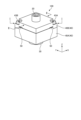
図1は、実施形態に係る撮像装置100の斜視図である。図2は、実施形態に係る撮像装置100の部品構成図である。図3は、図1に示した撮像装置100のI-I断面図である。図4は、図1に示した撮像装置100のII-II断面図である。
FIG. 1 is a perspective view of an imaging device 100 according to an embodiment. FIG. 2 is a component configuration diagram of the imaging device 100 according to the embodiment. FIG. 3 is a cross-sectional view of the imaging device 100 shown in FIG. 1 taken along line II. FIG. 4 is a II-II cross-sectional view of the imaging device 100 shown in FIG.
なお、以下に説明する図面において、便宜上、互いに直交するX軸、Y軸、Z軸を示しており、実施形態の撮像装置100における左右方向(X方向)、前後方向(Y方向)、上下方向(Z方向)をX軸、Y軸、Z軸を用いて説明する。なお、以下の説明において、単に、X方向、Y方向、又はZ方向と記載した場合には、それぞれの軸方向であり、逆向きの2方向を含む。
In the drawings described below, the X-axis, Y-axis, and Z-axis that are orthogonal to each other are shown for convenience, and the left-right direction (X-direction), the front-back direction (Y-direction), and the up-down direction in the imaging device 100 of the embodiment are shown. (Z direction) will be described using the X axis, Y axis, and Z axis. In the following description, simply describing the X direction, the Y direction, or the Z direction means each axial direction and includes two opposite directions.
また、X軸の正の方向と特定した場合には左側から右側への一方向であり、Y軸の正の方向と特定した場合には前側から後ろ側への一方向であり、Z軸の正の方向と特定した場合には下側から上側への一方向である。X軸の負の方向と特定した場合には右側から左側への一方向であり、Y軸の負の方向と特定した場合には後ろ側から前側への一方向であり、Z軸の負の方向と特定した場合には上側から下側への一方向である。
When the positive direction of the X-axis is specified, it is one direction from left to right; when the positive direction of the Y-axis is specified, it is one direction from front to back; If specified as a positive direction, it is one direction from bottom to top. When specified as the negative direction of the X-axis, it is one direction from right to left; when specified as the negative direction of the Y-axis, it is one direction from the rear to the front; When the direction is specified, it is one direction from the upper side to the lower side.
実施形態に係る撮像装置100は、基板10、第1固定部材11A、第2固定部材11B、ケーブル部材20、レンズユニット30、筐体40、第3固定部材43A、第4固定部材43B及び導電部材50を備える。
The imaging device 100 according to the embodiment includes a substrate 10, a first fixing member 11A, a second fixing member 11B, a cable member 20, a lens unit 30, a housing 40, a third fixing member 43A, a fourth fixing member 43B, and a conductive member. 50.
基板10は、筐体40に収容される。基板10は、レンズ32により撮像面に形成された被写体像を撮像する撮像素子(図示せず)を実装する。撮像素子は、例えば、CMOS(Complementary Metal Oxide Semiconductor)型イメージセンサである。また、基板10は、撮像素子が動作することで、電磁ノイズを発生する。つまり、基板10は、電磁ノイズを発生する発生源である。
The substrate 10 is housed in the housing 40 . The substrate 10 is mounted with an imaging device (not shown) that captures the subject image formed on the imaging surface by the lens 32 . The imaging element is, for example, a CMOS (Complementary Metal Oxide Semiconductor) image sensor. Further, the substrate 10 generates electromagnetic noise due to the operation of the imaging device. In other words, the substrate 10 is a source of electromagnetic noise.
第1固定部材11A及び第2固定部材11Bは、基板10をZ軸方向の負の方向に向かって、後述する第1筐体40Aと締結する。第1固定部材11A及び第2固定部材11Bは、例えば、金属材料(一例として、ステンレス)等の導電材料から作製された固定ねじである。これにより、基板10が第1筐体40Aに電気的にグランド接続されている状態となる。つまり、第1筐体40Aの電位が、基板10のグランド電位と同一になる。
The first fixing member 11A and the second fixing member 11B fasten the substrate 10 to the first housing 40A, which will be described later, in the negative direction of the Z-axis. The first fixing member 11A and the second fixing member 11B are, for example, fixing screws made of a conductive material such as a metal material (eg, stainless steel). As a result, the substrate 10 is electrically grounded to the first housing 40A. In other words, the potential of the first housing 40A becomes the same as the ground potential of the substrate 10 .
本実施形態において、第1固定部材11A及び第2固定部材11Bは、XY平面上で対向するように設けられる。より具体的には、第1固定部材11A及び第2固定部材11Bは、基板10の角部のうち、対角位置の角部に設けられる。なお、第1固定部材11A及び第2固定部材11Bは、第1固定部材11A及び第2固定部材11Bを結ぶ直線と、後述する第3固定部材43A及び第4固定部材43Bを結ぶ直線とで、略直交するように設けられる。
In this embodiment, the first fixing member 11A and the second fixing member 11B are provided so as to face each other on the XY plane. More specifically, the first fixing member 11A and the second fixing member 11B are provided at diagonally opposite corners of the corners of the substrate 10 . The first fixing member 11A and the second fixing member 11B are arranged by a straight line connecting the first fixing member 11A and the second fixing member 11B and a straight line connecting a third fixing member 43A and a fourth fixing member 43B, which will be described later. They are provided so as to be substantially perpendicular to each other.
ケーブル部材20は、基板10と外部装置(図示せず)とを接続する。ケーブル部材20は、後述する第2筐体40Bに形成された貫通穴21を通過する。ケーブル部材20は、例えば、電力ケーブルや信号ケーブルである。
The cable member 20 connects the board 10 and an external device (not shown). The cable member 20 passes through a through hole 21 formed in a second housing 40B, which will be described later. Cable member 20 is, for example, a power cable or a signal cable.
レンズユニット30は、鏡筒31と、レンズ32とを有する。鏡筒31は、両端が開口された円筒形の部材である。鏡筒31の内側には、レンズ32が所定の位置に配置される。鏡筒31は、例えば、樹脂材料あるいは金属材料等を用いて形成することができる。レンズ32は、プラスチックあるいはガラス等で形成される。レンズ32は、鏡筒31の内側において光軸に沿って配置され、基板10に実装された撮像素子(図示せず)上に被写体からの光を結像させる。つまり、撮像素子は、レンズユニット30の光軸上に配置される。なお、レンズ32は、1枚であってもよく、複数であってもよい。
The lens unit 30 has a lens barrel 31 and a lens 32. The lens barrel 31 is a cylindrical member with both ends opened. A lens 32 is arranged at a predetermined position inside the lens barrel 31 . The lens barrel 31 can be formed using, for example, a resin material or a metal material. The lens 32 is made of plastic, glass, or the like. The lens 32 is arranged along the optical axis inside the lens barrel 31 and forms an image of light from a subject on an imaging device (not shown) mounted on the substrate 10 . That is, the imaging device is arranged on the optical axis of the lens unit 30 . Note that the number of lenses 32 may be one or plural.
筐体40は、金属等の導電材料から作製され、基板10を収容する。筐体40は、直方体形状であって、第1筐体40A及び第2筐体40Bを備える。筐体40は、例えば、アルミダイカスト(一例として、ADC12等のアルミニウム合金)やマグネシウム合金等から作製される。なお、筐体40は、直方体形状に限らず、筐体の角が丸い状態である略直方体形状や、多角形形状でも良く、筐体40は、基板10を収容できる形状であれば良い。
The housing 40 is made of a conductive material such as metal and accommodates the substrate 10 . The housing 40 has a rectangular parallelepiped shape and includes a first housing 40A and a second housing 40B. The housing 40 is made of, for example, aluminum die-casting (for example, an aluminum alloy such as the ADC 12), a magnesium alloy, or the like. The shape of the housing 40 is not limited to a rectangular parallelepiped shape, and may be a substantially rectangular parallelepiped shape with rounded corners or a polygonal shape.
筐体40を導電材料とすることで、筐体40内部に収容する基板10から発生する電磁ノイズが、筐体40の外部へ放射(EMI:Electromagnetic Interference)されてしまうことを抑制するとともに、外部から筐体40の内部へのノイズ侵入を抑え、撮像装置100の誤動作耐性(EMS:Electromagnetic Susceptibility)を向上させることができる。
By using a conductive material for the housing 40, electromagnetic noise generated from the substrate 10 accommodated inside the housing 40 is suppressed from being radiated to the outside of the housing 40 (EMI: Electromagnetic Interference). Intrusion of noise from the housing 40 into the housing 40 can be suppressed, and the malfunction tolerance (EMS: Electromagnetic Susceptibility) of the imaging device 100 can be improved.
第1筐体40A及び第2筐体40Bは、第1筐体40Aと第2筐体40Bとを組み合わせることで形成される空間内部に基板10を収容する。具体的には、第1筐体40Aは、第1凹部41A及び第2凹部41B(以下、凹部41ともいう)を備える。第2筐体40Bは、第1凸部42A及び第2凸部42B(以下、凸部42ともいう)を備える。第1筐体40A及び第2筐体40Bは、凹部41と凸部42とを組み合わせ、後述する第3固定部材43A及び第4固定部材43Bを介して接続される。
The first housing 40A and the second housing 40B accommodate the substrate 10 inside the space formed by combining the first housing 40A and the second housing 40B. Specifically, the first housing 40A includes a first recess 41A and a second recess 41B (hereinafter also referred to as recess 41). The second housing 40B includes a first convex portion 42A and a second convex portion 42B (hereinafter also referred to as convex portion 42). The first housing 40A and the second housing 40B combine the concave portion 41 and the convex portion 42 and are connected via third fixing members 43A and fourth fixing members 43B, which will be described later.
第3固定部材43A及び第4固定部材43Bは、第2筐体40BからZ軸方向の負の方向に向かって、第1筐体40Aと締結する。第3固定部材43A及び第4固定部材43Bは、例えば、金属材料(一例として、ステンレス)等の導電材料から作製された固定ねじである。また、第3固定部材43A及び第4固定部材43Bは、XY平面上に対向となるように位置する。
The third fixing member 43A and the fourth fixing member 43B are fastened to the first housing 40A from the second housing 40B toward the negative direction of the Z-axis direction. The third fixing member 43A and the fourth fixing member 43B are, for example, fixing screws made of a conductive material such as a metal material (eg, stainless steel). Also, the third fixing member 43A and the fourth fixing member 43B are positioned to face each other on the XY plane.
なお、本実施形態の第1筐体40A及び第2筐体40Bは、腐食防止のための処理が施されている。腐食防止処理は、例えば、アルマイト処理、ニッケルメッキ処理等である。腐食防止処理のため、第1筐体40A及び第2筐体40Bの表面は、酸化膜によって覆われている。したがって、第1筐体40A及び第2筐体40Bの表面は非導電性(以下、絶縁層ともいう)を有するが、上述した第3固定部材43A及び第4固定部材43Bにより、第1筐体40A及び第2筐体40Bは電気的に接続される。
It should be noted that the first housing 40A and the second housing 40B of the present embodiment are treated for corrosion prevention. Corrosion prevention treatments include, for example, alumite treatment and nickel plating treatment. For corrosion prevention treatment, the surfaces of the first housing 40A and the second housing 40B are covered with an oxide film. Therefore, although the surfaces of the first housing 40A and the second housing 40B have non-conductivity (hereinafter also referred to as an insulating layer), the first housing 40A and the second housing 40B are secured by the above-described third fixing member 43A and fourth fixing member 43B. 40A and the second housing 40B are electrically connected.
次に、第1筐体40Aと第2筐体40Bとの接合部分について説明する。上述したように、第1筐体40A及び第2筐体40Bの表面は腐食防止処理が施されている。したがって、第1筐体40Aと第2筐体40Bとの接合部分は、電気的に接続されておらず、非導電性を有する。
Next, a joint portion between the first housing 40A and the second housing 40B will be described. As described above, the surfaces of the first housing 40A and the second housing 40B are subjected to anti-corrosion treatment. Therefore, the joint portion between the first housing 40A and the second housing 40B is not electrically connected and has non-conductivity.
ところで、第1筐体40Aと第2筐体40Bとの接合部分には、微小な隙間が生じる。そのため、従来では、防水性能の向上を図るため、筐体間の隙間にゴムパッキン等の非導電性の弾性体を設け、当該弾性体を介して筐体40を係合させることが行われている。
By the way, a minute gap occurs at the joint between the first housing 40A and the second housing 40B. Therefore, conventionally, in order to improve the waterproof performance, a non-conductive elastic body such as rubber packing is provided in the gap between the housings, and the housing 40 is engaged through the elastic body. there is
しかしながら、従来の構成では、非導電性の弾性体によって防水性能を向上させることができるが、隙間から漏れ出す電磁ノイズを防ぐことができず、更なる改善の余地がある。
However, in the conventional configuration, although the non-conductive elastic body can improve the waterproof performance, it is not possible to prevent electromagnetic noise from leaking through the gaps, and there is room for further improvement.
また、上述の構成では、筐体40は、第1筐体40A及び第2筐体40Bの接合部分の隙間において、第3固定部材43A及び第4固定部材43Bを介して互いに固定された固定部が、あたかもダイポールアンテナの給電点として機能する。また、その給電点として機能する固定部から離れる方向に延在する隙間部分の側壁が、電磁ノイズを受信するダイポールアンテナのエレメントとして機能する。そして、基板10から発生した電磁ノイズをこのダイポールアンテナが受信し筐体40自体が共振することで、外部に電磁ノイズを漏洩させ、外部から電磁ノイズを侵入する可能性がある。
Further, in the above-described configuration, the housing 40 is a fixed portion fixed to each other via the third fixing member 43A and the fourth fixing member 43B in the gap between the joint portions of the first housing 40A and the second housing 40B. functions as if it were a feeding point for a dipole antenna. Further, the side wall of the gap portion extending away from the fixed portion functioning as the feeding point functions as an element of the dipole antenna that receives electromagnetic noise. Electromagnetic noise generated from the substrate 10 is received by the dipole antenna and the housing 40 itself resonates, thereby leaking the electromagnetic noise to the outside and possibly intruding the electromagnetic noise from the outside.
そこで、本実施形態の撮像装置100では、上述した電磁ノイズの漏洩及び侵入を抑えるため、以下の構成を備える。
Therefore, the imaging apparatus 100 of the present embodiment has the following configuration in order to suppress leakage and intrusion of the electromagnetic noise described above.
本実施形態の撮像装置100は、導電部材50を備える。導電部材50は、基板10と後述する筐体40との共振を抑制する部品である。導電部材50は、例えば、リング部材であり、平板方形環状を有する。導電部材50は、導電性を有し、弾性体から成る樹脂部材で形成される。導電部材50は、第1筐体40Aと第2筐体40Bの間との接合部分に配置される。
The imaging device 100 of this embodiment includes a conductive member 50 . The conductive member 50 is a component that suppresses resonance between the board 10 and the housing 40, which will be described later. The conductive member 50 is, for example, a ring member and has a flat plate rectangular annular shape. The conductive member 50 is made of an elastic resin member having electrical conductivity. The conductive member 50 is arranged at the joint between the first housing 40A and the second housing 40B.
上記の構成において、導電部材50は、第1筐体40Aと第2筐体40Bとを電気的に結合させることができる。具体的には、導電部材50は、第1筐体40Aと第2筐体40Bとの接合部分で、あたかもコンデンサのように機能し、第1筐体40Aと第2筐体40Bとを電気的に結合させる(以下、容量結合ともいう)。
In the above configuration, the conductive member 50 can electrically couple the first housing 40A and the second housing 40B. Specifically, the conductive member 50 functions like a capacitor at the joint portion between the first housing 40A and the second housing 40B, and electrically connects the first housing 40A and the second housing 40B. (hereinafter also referred to as capacitive coupling).
また、容量結合は周波数が高くなるとインピーダンスが低くなるため、結合度が増加し導通状態に近づく。一般的に、上述した容量結合が電磁両立性(EMC(Electromagnetic Compatibility))の性能に影響が出てくるのは高周波(1GHz以上)であり、この高周波領域では導通状態とみなせる。そのため、第1筐体40A及び第2筐体40Bの外観の表面は非導電性であるが、導電部材50を介して第1筐体40Aと第2筐体40Bは高周波で導通することになる。
In addition, as the frequency of capacitive coupling increases, the impedance decreases, so the degree of coupling increases and approaches a conducting state. In general, the capacitive coupling described above affects the performance of electromagnetic compatibility (EMC) at high frequencies (1 GHz or higher), and this high frequency region can be regarded as a conductive state. Therefore, although the external surfaces of the first housing 40A and the second housing 40B are non-conductive, the first housing 40A and the second housing 40B are electrically connected to each other at high frequencies via the conductive member 50. .
このように、筐体40は、導電部材50を介すことで、第1筐体40Aと第2筐体40Bとの隙間を埋めることができるとともに、第1筐体40Aと第2筐体40Bとの電位差をなくすことができる。これにより、第1筐体40Aと第2筐体40Bとの隙間がダイポールアンテナとして機能してしまうことを防ぐことができる。したがって、筐体40は、第1筐体40Aと第2筐体40Bとの隙間から漏洩及び侵入する電磁ノイズの漏洩及び侵入を低減させることができるとともに、共振による電磁ノイズの漏洩及び侵入を低減することができる。
In this way, the housing 40 can fill the gap between the first housing 40A and the second housing 40B through the conductive member 50, and also can can eliminate the potential difference between This can prevent the gap between the first housing 40A and the second housing 40B from functioning as a dipole antenna. Therefore, the housing 40 can reduce leakage and penetration of electromagnetic noise that leaks and enters through the gap between the first housing 40A and the second housing 40B, and also reduces leakage and penetration of electromagnetic noise due to resonance. can do.
なお、腐食防止処理は、第1筐体40A及び第2筐体40Bの何れか一方に施してもよいし、第1筐体40A及び第2筐体40Bの何れにも施さないようにしてもよい。また、第1筐体40Aと第2筐体40Bとの接合部分のみ、第1筐体40A及び第2筐体40Bの何れか一方又は両方に腐食防止処理を施さないようにしてもよい。なお、第1筐体40A及び第2筐体40Bの腐食処理の厚さは、導電部材50がコンデンサとして機能することが可能な範囲の厚さとすることが好ましい。例えば、腐食処理の厚さは数μm~数十μmであれば良く、これに限定されない。
The corrosion prevention treatment may be applied to either one of the first housing 40A and the second housing 40B, or may be applied to neither the first housing 40A nor the second housing 40B. good. Further, only the joint portion between the first housing 40A and the second housing 40B, either one or both of the first housing 40A and the second housing 40B may not be subjected to corrosion prevention treatment. The thickness of the corrosion treatment of the first housing 40A and the second housing 40B is preferably within a range in which the conductive member 50 can function as a capacitor. For example, the thickness of the corrosion treatment is not limited to several micrometers to several tens of micrometers.
また、導電部材50は、水等の液体が撮像装置100の内部に入り込むことを抑制する部品としても機能するため、防水性能の向上を図ることができる。つまり、導電部材50は、第1筐体40Aと第2筐体40Bとの間から液体が侵入することを抑制することもできる。
In addition, since the conductive member 50 also functions as a component that prevents liquid such as water from entering the interior of the imaging device 100, it is possible to improve the waterproof performance. In other words, the conductive member 50 can also prevent liquid from entering from between the first housing 40A and the second housing 40B.
次に、第1筐体40Aと鏡筒31の接合構成について説明する。第1筐体40Aの表面には、上述したとおり腐食防止のための処理が施されている。第1筐体40Aは、腐食防止処理を施した後、さらに塗装処理が施されてもよい。塗装処理は、例えば、電着塗装であり、電着塗装の厚さは数μm~数十μm程度となる。電着塗装の材料は、例えば、エポキシ樹脂あるいはアクリル樹脂等である。
Next, the joining configuration of the first housing 40A and the lens barrel 31 will be described. The surface of the first housing 40A is treated for corrosion prevention as described above. The first housing 40A may be further subjected to a coating process after being subjected to the anti-corrosion process. The coating process is, for example, electrodeposition coating, and the thickness of the electrodeposition coating is about several μm to several tens of μm. The electrodeposition coating material is, for example, epoxy resin or acrylic resin.
腐食防止処理及び塗装処理を施された第1筐体40Aは、接着剤からなる接着層を介して鏡筒31に接着される。鏡筒31の表面が樹脂である場合、鏡筒31は電着塗装により樹脂の表面を有する第1筐体40Aと接着されることが接着のしやすさから好ましい。鏡筒31の表面が金属である場合、鏡筒31は腐食防止処理により金属の表面を有する第1筐体40Aと接着されることが接着のしやすさから好ましい。なお、第1筐体40Aに対する鏡筒31の取り付け方法は、接着剤に限定されない。
The first housing 40A, which has been subjected to anti-corrosion treatment and painting treatment, is adhered to the lens barrel 31 via an adhesive layer made of adhesive. When the surface of the lens barrel 31 is made of resin, it is preferable that the lens barrel 31 is adhered to the first housing 40A having the surface of resin by electrodeposition coating for ease of adhesion. When the surface of the lens barrel 31 is made of metal, it is preferable that the lens barrel 31 is adhered to the first housing 40A having a metal surface by anti-corrosion treatment for ease of adhesion. Note that the method of attaching the lens barrel 31 to the first housing 40A is not limited to the adhesive.
続いて、筐体40から放射される電磁ノイズ分布について説明する。図5は、基板10から放射される電磁ノイズの周波数と、筐体40から放射される電磁ノイズの強度の関係について示している。図5において、縦軸は、電磁ノイズ[dBuV/m]を示し、横軸は、周波数[GHz]を示す。
Next, the electromagnetic noise distribution radiated from the housing 40 will be described. FIG. 5 shows the relationship between the frequency of electromagnetic noise radiated from substrate 10 and the intensity of electromagnetic noise radiated from housing 40 . In FIG. 5, the vertical axis indicates electromagnetic noise [dBuV/m], and the horizontal axis indicates frequency [GHz].
また、図5に示すグラフは、第1筐体40A及び第2筐体40Bの間に設けられた導電部材50の状態が導電性の材質の場合はL1、比較例として導電部材50が非導電性の場合をL2で示す。
In addition, the graph shown in FIG. 5 shows L1 when the state of the conductive member 50 provided between the first housing 40A and the second housing 40B is a conductive material, and L1 when the conductive member 50 is a non-conductive material as a comparative example. The case of sex is indicated by L2.
導電性L1と非導電性L2を比較すると、共に、周波数が高くなるにつれ、電磁ノイズの強度は高くなる傾向を示しているが、導電性L1より非導電性L2のほうが電磁ノイズの強度は高い。
Comparing the conductive L1 and the non-conductive L2, both show a tendency that the strength of the electromagnetic noise increases as the frequency increases, but the strength of the electromagnetic noise is higher in the non-conductive L2 than in the conductive L1. .
また、非導電性L2は、例えば、周波数が2[GHz]の場合、急激に電磁ノイズの強度が高くなっている。これは、基板10から発生する電磁ノイズにより、筐体40に共振が発生しているためである。一方、導電性L1は、例えば、周波数が2[GHz]の場合、急激に強度が高くなっていない。これは、導電部材50が導電性を有することで、基板10から発生する電磁ノイズの影響を受けにくくなっており、筐体40の共振の発生を抑制しているためである。
Also, in the non-conductive L2, for example, when the frequency is 2 [GHz], the strength of the electromagnetic noise increases sharply. This is because electromagnetic noise generated from the substrate 10 causes resonance in the housing 40 . On the other hand, the electrical conductivity L1 does not sharply increase in strength when the frequency is 2 [GHz], for example. This is because the electrically conductive member 50 is less likely to be affected by electromagnetic noise generated from the substrate 10 and suppresses the occurrence of resonance in the housing 40 .
これにより、筐体40は、第1筐体40A及び第2筐体40Bの間との接合部分に導電性を有する導電部材50を設けることで、筐体40の接合部分は酸化膜を有している状態であっても、第1筐体40A及び第2筐体40Bの隙間や電位差をなくすことができ、電磁ノイズ低減に効果があることがわかる。したがって、撮像装置100は、筐体40から漏洩及び侵入する電磁ノイズを低減することができる。
As a result, the housing 40 is provided with the conductive member 50 having conductivity in the joint portion between the first housing 40A and the second housing 40B, so that the joint portion of the housing 40 has an oxide film. It can be seen that the gap and the potential difference between the first housing 40A and the second housing 40B can be eliminated even in the state where the housing 40A and the second housing 40B are closed, which is effective in reducing electromagnetic noise. Therefore, the imaging device 100 can reduce electromagnetic noise that leaks and enters from the housing 40 .
なお、電磁ノイズを低減するために、さらに固定部材を追加し、第1筐体40Aと第2筐体40Bとの接合部分の微小な隙間をなくすこともできる。しかしながら、固定部材を追加すると、コストの増加に繋がる。また、第1筐体40A及び第2筐体40Bの形状が複雑化に繋がるため、第1筐体40A及び第2筐体40Bの間との接合部分に導電性を有する導電部材50を設けることは、追加コストが発生しないことに繋がる。
Further, in order to reduce electromagnetic noise, it is also possible to add a fixing member to eliminate a minute gap at the joint portion between the first housing 40A and the second housing 40B. However, adding fixing members leads to an increase in cost. In addition, since the shapes of the first housing 40A and the second housing 40B are complicated, it is necessary to provide a conductive member 50 having conductivity at the joint between the first housing 40A and the second housing 40B. leads to no additional cost.
なお、上述した実施形態は、例として提示したものであり、本開示の範囲を限定することは意図していない。上記実施形態は、その他の様々な形態で実施されることが可能であり、発明の要旨を逸脱しない範囲で、種々の省略、置き換え、変更を行うことができる。上記実施形態は、本開示の範囲又は要旨に含まれるとともに、請求の範囲に記載された発明とその均等の範囲に含まれる。
It should be noted that the above-described embodiments are presented as examples and are not intended to limit the scope of the present disclosure. The above embodiment can be implemented in various other forms, and various omissions, replacements, and modifications can be made without departing from the scope of the invention. The above-described embodiments are included in the scope or gist of the present disclosure, and are included in the invention described in the claims and their equivalents.
10 基板
11A 第1固定部材
11B 第2固定部材
20 ケーブル部材
30 レンズユニット
31 鏡筒
32 レンズ
40 筐体
40A 第1筐体
40B 第2筐体
43A 第3固定部材
43B 第4固定部材
50 導電部材
100 撮像装置 REFERENCE SIGNSLIST 10 substrate 11A first fixing member 11B second fixing member 20 cable member 30 lens unit 31 lens barrel 32 lens 40 housing 40A first housing 40B second housing 43A third fixing member 43B fourth fixing member 50 conductive member 100 Imaging device
11A 第1固定部材
11B 第2固定部材
20 ケーブル部材
30 レンズユニット
31 鏡筒
32 レンズ
40 筐体
40A 第1筐体
40B 第2筐体
43A 第3固定部材
43B 第4固定部材
50 導電部材
100 撮像装置 REFERENCE SIGNS
Claims (9)
- 撮像素子が実装される基板と、
金属製の第1筐体及び第2筐体を有し、前記第1筐体と前記第2筐体とで形成される空間内部に前記基板を収容する筐体と、
前記第1筐体と前記第2筐体との間の接合部分に配置され、導電性を有する導電部材と、を備え、
前記第1筐体及び前記第2筐体の何れか一方又は両方は、表面に絶縁層を有する、
撮像装置。 a substrate on which an imaging device is mounted;
a housing having a first housing and a second housing made of metal, and housing the substrate in a space formed by the first housing and the second housing;
a conductive member disposed at a joint portion between the first housing and the second housing and having conductivity;
Either one or both of the first housing and the second housing have an insulating layer on the surface,
Imaging device. - 前記絶縁層は、前記導電部材との前記接合部分に設けられる、
請求項1に記載の撮像装置。 The insulating layer is provided at the joint portion with the conductive member,
The imaging device according to claim 1 . - 前記絶縁層は、前記表面に腐食処理を施すことで形成される、
請求項1又は2に記載の撮像装置。 The insulating layer is formed by subjecting the surface to corrosion treatment,
The imaging device according to claim 1 or 2. - 前記腐食処理は、アルマイト処理である、
請求項3に記載の撮像装置。 The corrosion treatment is alumite treatment,
The imaging device according to claim 3. - 前記腐食処理の厚さは、数μm~数十μmである、
請求項4に記載の撮像装置。 The thickness of the corrosion treatment is several μm to several tens of μm,
The imaging device according to claim 4. - 前記導電部材は、防水性を有する、
請求項1又は2に記載の撮像装置。 The conductive member is waterproof,
The imaging device according to claim 1 or 2. - 前記第1筐体と前記第2筐体は、前記導電部材を介して高周波で導通する、
請求項1又は2に記載の撮像装置。 The first housing and the second housing are electrically connected at a high frequency via the conductive member.
The imaging device according to claim 1 or 2. - 前記第1筐体の絶縁層の表面に、樹脂が電着塗装される、
請求項1に記載の撮像装置。 A resin is electrodeposited on the surface of the insulating layer of the first housing,
The imaging device according to claim 1 . - 前記電着塗装の厚さは、数μm~数十μmである、
請求項8に記載の撮像装置。
The thickness of the electrodeposition coating is several μm to several tens of μm.
The imaging device according to claim 8 .
Applications Claiming Priority (2)
| Application Number | Priority Date | Filing Date | Title |
|---|---|---|---|
| JP2021181227 | 2021-11-05 | ||
| JP2021-181227 | 2021-11-05 |
Publications (1)
| Publication Number | Publication Date |
|---|---|
| WO2023079786A1 true WO2023079786A1 (en) | 2023-05-11 |
Family
ID=86241117
Family Applications (1)
| Application Number | Title | Priority Date | Filing Date |
|---|---|---|---|
| PCT/JP2022/025833 WO2023079786A1 (en) | 2021-11-05 | 2022-06-28 | Imaging device |
Country Status (1)
| Country | Link |
|---|---|
| WO (1) | WO2023079786A1 (en) |
Citations (3)
| Publication number | Priority date | Publication date | Assignee | Title |
|---|---|---|---|---|
| JP2001124206A (en) * | 1999-10-25 | 2001-05-11 | Nec Corp | Gasket fitting structure of casing, gasket and casing |
| JP2011071362A (en) * | 2009-09-28 | 2011-04-07 | Kyocera Corp | Metal casing for communication device |
| JP2013058595A (en) * | 2011-09-08 | 2013-03-28 | Sony Corp | Electronic apparatus |
-
2022
- 2022-06-28 WO PCT/JP2022/025833 patent/WO2023079786A1/en unknown
Patent Citations (3)
| Publication number | Priority date | Publication date | Assignee | Title |
|---|---|---|---|---|
| JP2001124206A (en) * | 1999-10-25 | 2001-05-11 | Nec Corp | Gasket fitting structure of casing, gasket and casing |
| JP2011071362A (en) * | 2009-09-28 | 2011-04-07 | Kyocera Corp | Metal casing for communication device |
| JP2013058595A (en) * | 2011-09-08 | 2013-03-28 | Sony Corp | Electronic apparatus |
Similar Documents
| Publication | Publication Date | Title |
|---|---|---|
| US11303785B2 (en) | Camera module | |
| EP3430797B1 (en) | Camera assembly with shielded imager circuit | |
| CN105959523B (en) | Camera module for vehicle | |
| EP1357780A2 (en) | Camera module having a shield casing and a sealing mechanism | |
| KR101444024B1 (en) | Camera module for car | |
| EP2876873B1 (en) | Grounding part, electronic device, imaging device, and grounding part production method | |
| KR20170084550A (en) | Camera module | |
| EP3512316B1 (en) | Electronic device, camera apparatus, and shield chassis | |
| US20130215311A1 (en) | Camera device, electronic apparatus and flexible chassis | |
| US10432828B2 (en) | Camera module having a shield member | |
| WO2023079786A1 (en) | Imaging device | |
| US7897913B2 (en) | Image sensing device having a shielding layer | |
| US20190268512A1 (en) | Image capturing apparatus | |
| US10609261B2 (en) | Optical camera to be mounted on vehicles | |
| KR20180010422A (en) | Camera module | |
| WO2023145129A1 (en) | Imaging device | |
| US20220397738A1 (en) | Impact-protected lens module with buffering pad and electronic device | |
| CN110178363A (en) | Filming apparatus | |
| CN218734571U (en) | Image pickup apparatus | |
| JP2022113407A (en) | Imaging module | |
| CN217508852U (en) | Image acquisition device | |
| EP4366319A1 (en) | Camera module | |
| KR20230020308A (en) | Camera module | |
| KR20170036531A (en) | Camera module | |
| JP2018042218A (en) | Imaging apparatus |
Legal Events
| Date | Code | Title | Description |
|---|---|---|---|
| ENP | Entry into the national phase |
Ref document number: 2023557619 Country of ref document: JP Kind code of ref document: A |