WO2023067981A1 - 液晶素子、照明装置 - Google Patents
液晶素子、照明装置 Download PDFInfo
- Publication number
- WO2023067981A1 WO2023067981A1 PCT/JP2022/035267 JP2022035267W WO2023067981A1 WO 2023067981 A1 WO2023067981 A1 WO 2023067981A1 JP 2022035267 W JP2022035267 W JP 2022035267W WO 2023067981 A1 WO2023067981 A1 WO 2023067981A1
- Authority
- WO
- WIPO (PCT)
- Prior art keywords
- liquid crystal
- pixel
- substrate
- electrode
- pixel electrode
- Prior art date
- Legal status (The legal status is an assumption and is not a legal conclusion. Google has not performed a legal analysis and makes no representation as to the accuracy of the status listed.)
- Ceased
Links
Images


Classifications
-
- G—PHYSICS
- G02—OPTICS
- G02F—OPTICAL DEVICES OR ARRANGEMENTS FOR THE CONTROL OF LIGHT BY MODIFICATION OF THE OPTICAL PROPERTIES OF THE MEDIA OF THE ELEMENTS INVOLVED THEREIN; NON-LINEAR OPTICS; FREQUENCY-CHANGING OF LIGHT; OPTICAL LOGIC ELEMENTS; OPTICAL ANALOGUE/DIGITAL CONVERTERS
- G02F1/00—Devices or arrangements for the control of the intensity, colour, phase, polarisation or direction of light arriving from an independent light source, e.g. switching, gating or modulating; Non-linear optics
- G02F1/01—Devices or arrangements for the control of the intensity, colour, phase, polarisation or direction of light arriving from an independent light source, e.g. switching, gating or modulating; Non-linear optics for the control of the intensity, phase, polarisation or colour
- G02F1/13—Devices or arrangements for the control of the intensity, colour, phase, polarisation or direction of light arriving from an independent light source, e.g. switching, gating or modulating; Non-linear optics for the control of the intensity, phase, polarisation or colour based on liquid crystals, e.g. single liquid crystal display cells
- G02F1/133—Constructional arrangements; Operation of liquid crystal cells; Circuit arrangements
- G02F1/1333—Constructional arrangements; Manufacturing methods
- G02F1/1343—Electrodes
Definitions
- the present disclosure relates to liquid crystal elements and lighting devices.
- a counter electrode is provided on one surface side of a first substrate, and a plurality of inter-pixel electrodes, a plurality of wiring portions, and a plurality of pixel electrodes are provided on one surface side of a second substrate. is provided with an insulating layer interposed therebetween, and a liquid crystal element is described in which a liquid crystal layer is provided between the substrates.
- a liquid crystal element an inter-pixel electrode or a part of a wiring portion connected to the inter-pixel electrode is arranged between the pixel electrodes in a plan view. However, it is configured to switch between light transmission and non-transmission.
- the areas between the pixel electrodes are prevented from being conspicuous as bright spots or dark spots.
- One of the purposes of the specific aspect of the present disclosure is to provide a technique for providing a portion capable of switching between light transmission/non-transmission in a region between pixel electrodes of a liquid crystal element.
- a liquid crystal element is a liquid crystal element including a plurality of segment regions including at least two segment regions having different sizes in plan view, and (b) a plurality of wiring portions arranged on one surface side of the first substrate and having terminal portions for connection with the outside; (d) a plurality of auxiliary electrodes arranged on one surface side of a first substrate and configured separately from each wiring portion; and (d) each wiring portion and each auxiliary electrode on one surface side of the first substrate. and (e) a first insulating layer disposed on a surface of the first insulating layer facing the second substrate, each of which is substantially the same as one of the segment regions in plan view.
- each auxiliary electrode is connected to one of the pixel electrodes through a through hole provided in the first insulating layer; The two pixel electrodes are arranged so as to overlap the gap between the two pixel electrodes having adjacent portions in a plan view, and have the adjacent portions via through holes provided in the first insulating layer.
- a liquid crystal element connected to one of the pixel electrodes.
- a lighting device includes the liquid crystal element of [1], a light source that emits light to be incident on the liquid crystal element, and a pair of polarizing elements arranged to face each other with the liquid crystal element interposed therebetween. and a lens for projecting the light transmitted through the liquid crystal element.
- FIG. 1 is a plan view showing the pixel shape of the liquid crystal element of the first embodiment.
- 2A and 2B are schematic cross-sectional views showing the structure of a liquid crystal element.
- FIG. 3A is a schematic plan view showing the configuration of pixel electrodes, wiring portions, and dummy electrodes of a liquid crystal element
- FIG. 3B is a schematic plan view showing the configuration of the wiring portions and dummy electrodes. It is a diagram.
- FIG. 4 is a diagram showing an electrode configuration of a comparative example.
- FIG. 5 is a plan view showing the pixel shape of the liquid crystal element of the second embodiment.
- 6A and 6B are schematic cross-sectional views showing the structure of the first substrate of the liquid crystal element.
- FIG. 7A is a schematic plan view showing the configuration of pixel electrodes, wiring portions, and dummy electrodes of a liquid crystal element
- FIG. 7B is a schematic plan view showing the configuration of the wiring portions and dummy electrodes. It is a diagram.
- FIG. 8A is a schematic plan view showing the electrode structure of the liquid crystal element of the comparative example
- FIG. 8B is a schematic cross-sectional view showing the electrode structure of the liquid crystal element of the comparative example.
- FIG. 9 is a plan view showing the pixel shape of the liquid crystal element of the third embodiment.
- FIG. 10 is a plan view showing an electrode structure corresponding to region R shown in FIG. FIG.
- FIG. 11 is a diagram showing a structural example of a liquid crystal element according to a modified embodiment in which an insulating layer (second insulating layer) is provided so as to individually cover each pixel electrode.
- FIG. 12 is a diagram showing a configuration example of a vehicle lamp, which is an example of a lighting device.
- FIG. 1 is a plan view showing the pixel shape of the liquid crystal element of the first embodiment.
- the illustrated liquid crystal element 100 includes a plurality (six in the illustrated example) of substantially square pixels 2a and a plurality (three in the illustrated example) of substantially rectangular pixels 2b arranged in an effective display area 1.
- These pixels 2a and 2b are segment regions (light modulation regions) capable of independently switching light transmission/non-transmission.
- Each pixel 2a is arranged along the X direction (horizontal direction) in the drawing.
- Each pixel 2b has its longitudinal direction in the X direction in the drawing, and is arranged adjacent to each other along the Y direction (vertical direction) in the drawing.
- one pixel 2b is adjacent to a column of pixels 2a in the Y direction.
- Each pixel 2a and each pixel 2b have different sizes (size/area) in plan view.
- FIG. 2(A) and 2(B) are schematic cross-sectional views showing the configuration of the liquid crystal element.
- FIG. 3A is a schematic plan view showing the configuration of pixel electrodes, wiring portions and dummy electrodes of a liquid crystal element
- FIG. 3B is a schematic plan view showing the configuration of wiring portions and dummy electrodes. is a plan view. Note that the cross-sectional view shown in FIG. 2A corresponds to the aa line cross-section in FIG. 3A, and the cross-sectional view shown in FIG. 2B corresponds to the bb line cross-section in FIG. 3A. are doing.
- polarizing elements polarizing plates, polarizing beam splitters, etc.
- an optical compensator may be appropriately arranged between the polarizing element and the liquid crystal element.
- the liquid crystal element 100 includes a first substrate 11, a second substrate 12, a wiring portion (wiring electrode) 13, a common electrode (counter electrode) 14, an insulating layer (first insulating layer) 15, a pixel electrode, and a 16 , a first alignment film 17 , a second alignment film 18 , a liquid crystal layer 19 and a dummy electrode (auxiliary electrode) 20 .
- each pixel 2a, 2b is formed in each region (partial region) where each pixel electrode 16 and the common electrode 14 face each other with the liquid crystal layer 19 interposed therebetween.
- the first substrate 11 and the second substrate 12 are, for example, rectangular substrates in a plan view, and are closer to the liquid crystal layer 19 (hereinafter referred to as a substrate). , referred to as “one side”) are arranged to face each other.
- a translucent substrate such as a glass substrate or a plastic substrate can be used.
- spherical spacers (not shown) made of, for example, a resin film are dispersedly arranged, and the spherical spacers provide a substrate gap of a desired size (for example, several ⁇ m). is kept in Instead of spherical spacers, columnar bodies made of resin or the like may be provided on the first substrate 11 side or the second substrate 12 side and used as spacers.
- Each wiring part 13 is provided on one surface side of the first substrate 11 .
- Each dummy electrode 20 is provided on one surface side of the first substrate 11 .
- the “dummy electrode” in this embodiment refers to an island-shaped (floating island-shaped) electrode that is physically separated and independently formed from each wiring section 13 (see FIG. 3B described later).
- Each wiring part 13 and each dummy electrode 20 are formed by appropriately patterning a transparent conductive film such as indium tin oxide (ITO).
- ITO indium tin oxide
- the common electrode 14 is provided on one side of the second substrate 12 .
- the common electrode 14 is integrally provided so as to face each pixel electrode 16 .
- the common electrode 14 is formed by appropriately patterning a transparent conductive film such as indium tin oxide (ITO). Note that the common electrode 14 may be divided into a plurality of parts (for example, when duty driving is performed).
- the insulating layer 15 is provided on one side of the first substrate 11 so as to cover the wiring portions 13 and the dummy electrodes 20 .
- the insulating layer 15 serves as an interlayer insulating film for providing insulation between each wiring portion 13 and each dummy electrode 20 and each pixel electrode 16 .
- the insulating layer 15 may be any material as long as it has good insulating properties and light transmittance. It can be configured using various insulating films such as a film.
- Each pixel electrode 16 is provided on the surface of the insulating layer 15 close to the liquid crystal layer 19 on the one surface side of the first substrate 11 (the surface facing the one surface of the second substrate 12). Each pixel electrode 16 is formed by appropriately patterning a transparent conductive film such as indium tin oxide (ITO). Each pixel electrode 16 is electrically/physically connected to the wiring portion 13 and the dummy electrode 20 via each through hole 21 provided in the insulating layer 15 .
- ITO indium tin oxide
- the first alignment film 17 is arranged on the upper side of the first substrate 11 so as to cover the pixel electrodes 16 .
- the second alignment film 18 is arranged on the one surface side of the second substrate 12 so as to cover the common electrode 14 .
- These first alignment film 17 and second alignment film 18 are for defining the alignment state of the liquid crystal layer 19 in the initial state (when no voltage is applied).
- Each of the alignment films 17 and 18 is subjected to a uniaxial alignment treatment such as rubbing treatment, and has a uniaxial alignment regulating force that regulates the alignment of the liquid crystal molecules of the liquid crystal layer 19 along the direction.
- the direction in which the uniaxial orientation regulating force is expressed is called the orientation easy axis.
- the directions of the alignment treatment on the alignment films 17 and 18 are set, for example, to be anti-parallel.
- a horizontal alignment film or a vertical alignment film is appropriately used according to the operation mode of the liquid crystal layer 19.
- FIG. for example, in the present embodiment, each of the alignment films 17 and 18 regulates the pretilt angle of the liquid crystal molecules in the vicinity of the interface between each of them and the liquid crystal layer 19 in a vertical direction close to 90° (for example, 80° to 89.9°).
- An alignment film is used.
- the liquid crystal layer 19 is provided between the first substrate 11 and the second substrate 12 .
- the liquid crystal layer 19 is configured using, for example, a fluid nematic liquid crystal material.
- the liquid crystal layer 19 is configured using a liquid crystal material having negative dielectric anisotropy.
- the layer thickness of the liquid crystal layer 19 can be set to, for example, about 4 ⁇ m.
- a liquid crystal material having positive dielectric anisotropy may be used depending on the operation mode of the liquid crystal layer 19 .
- each wiring portion 13, each pixel electrode 16, and each dummy electrode 20 will be described in detail with reference to FIGS. 3(A) and 3(B). 13h to distinguish the wiring portions 13, and pixel electrodes 16a, 16b, . . . 16j to distinguish the pixel electrodes 16 from each other.
- portions that have a common use or function and do not need to be distinguished are denoted by the same reference numerals.
- Pixel electrodes 16a, 16b, 16c, 16d, 16e, and 16f shown in FIG. 3A correspond to the pixels 2a described above, and are electrically/physically separated from each other. They are arranged side by side along the direction.
- Each pixel electrode 16g, 16h, 16j corresponds to each pixel 2b described above, is electrically/physically separated from each other, and is arranged so as to have its longitudinal direction in the illustrated X direction.
- the pixel electrodes 16a to 16f have substantially the same planar shape as the pixel 2a
- the pixel electrodes 16g to 16i have substantially the same planar shape as the pixel 2b.
- Pixels 2a and 2b are formed in respective overlapping regions of the pixel electrodes 16a and the like and the common electrode 14 (see FIG. 2A).
- the orientation of the liquid crystal molecules is changed in the regions corresponding to each pixel 2a and each pixel 2b of the liquid crystal layer 19 to change the light transmittance.
- the wiring portion 13a extends in the Y direction in the drawing, and is arranged so as to overlap with each of the pixel electrodes 16a, 16g, 16h, and 16j in plan view.
- One end region of the wiring portion 13a located below the pixel electrode 16j in the figure is used as an external electrode terminal (terminal portion).
- the wiring portion 13a is electrically/physically connected to the pixel electrode 16a via one through hole 21. As shown in FIG. Thereby, a voltage input from an external device (not shown) connected to the external extraction electrode terminal is applied to the pixel electrode 16a through the wiring portion 13a.
- an external device not shown
- relatively large electrodes are provided between the relatively small pixel electrodes 16a, 16b, 16c, 16d, 16e, and 16f and the external extraction electrode terminals.
- Each pixel electrode 16g, 16h, 16j is arranged. That is, the wiring portion 13a is arranged from the side of the external lead-out electrode terminal to under the pixel electrode 16a, passing under the relatively large pixel electrode 16j, pixel electrode 16g, pixel electrode 16h, and pixel electrode 16a in this order. It is
- the wiring portion 13a has a portion 131 that protrudes to the left of the pixel electrode 16a in plan view. Further, the wiring portion 13a has a portion 132 having a relatively large length (width) in the X direction. This portion 132 is arranged so as to overlap the gap between the pixel electrode 16a and the pixel electrode 16h, and has substantially the same length (width) in the X direction as the pixel electrode 16a. Since these parts 131 and 132 have substantially the same potential as the pixel electrode 16a, voltage can be applied to the liquid crystal layer 19 also in the lower area and the left area of the pixel electrode 16a in the drawing when voltage is applied to the pixel electrode 16a. become able to. As a result, light transmission/non-transmission can be switched between the lower area and the left area in conjunction with the area corresponding to the pixel electrode 16a.
- the wiring portion 13a has portions (first portions) 133 and 134 in which the length (width) in the X direction is relatively small.
- the portion 133 is arranged so as to overlap the gap between the pixel electrodes 16g and 16h, and the portion 134 is arranged so as to overlap the gap between the pixel electrodes 16h and 16j.
- These parts 133 and 134 and a relatively wide part (second part) connected to them define a concave area in plan view.
- Each dummy electrode 20 is arranged in association with each of the recessed regions. In other words, each dummy electrode 20 is arranged adjacent to one of the portions 133 and 134 in plan view.
- each dummy electrode 20 is arranged between two of the wiring portions 13a to 13h which have adjacent portions in a plan view (dummy electrode arranged on the right side of the wiring portion 13h in the drawing). 20). For example, when looking at the wiring portion 13a and the wiring portion 13b, at least the portions 133 and 134 are adjacent to each other, and one dummy electrode 20 is arranged between them.
- these portions 133 and 134 have substantially the same potential as the pixel electrode 16a, voltage is applied to the liquid crystal layer 19 also in the regions corresponding to these portions 133 and 134 when voltage is applied to the pixel electrode 16a. , the width is relatively narrow, so that it does not stand out as a bright spot due to the transmission of light.
- light shielding films may be provided corresponding to these portions 133 and the like, or columnar bodies made of resin or the like may be provided.
- the other wiring portions 13b, 13c, 13d, 13e, and 13f have slightly different shapes in plan view, but have the same uses/functions as the portions 131, 132, 133, and 134 of the wiring portion 13a described above. Each part 131, 132, 133, 134 is provided. Dummy electrodes 20 are arranged corresponding to the small width portions 133 and 134 in each of the wiring portions 13b to 13f as well.
- the wiring portions 13b, 13c, 13d, and 13e are formed in a substantially triangular shape on the right side of the portion 131. As shown in FIG.
- the wiring portions 13b to 13f are arranged so as to overlap the pixel electrodes 16b to 16f in plan view, respectively, and are arranged to overlap each of the pixel electrodes 16g, 16h, and 16j in plan view. .
- Each of the wiring portions 13b to 13f has one end region below the pixel electrode 16j in the figure and is used as an external electrode terminal.
- the wiring portions 13b to 13f are electrically/physically connected to the pixel electrodes 16b to 16f via one through hole 21, respectively. As a result, the voltage input from the external extraction electrode terminal is individually applied to the pixel electrodes 16b and the like through the wiring portions 13b and the like.
- the wiring portion 13g extends in the Y direction and is arranged so as to overlap with the pixel electrodes 16g and 16j. Also, the wiring portion 13g is electrically/physically connected to the pixel electrode 16g through one through hole 21 . As a result, the voltage input from the external extraction electrode terminal is applied to the pixel electrode 16g through the wiring portion 13g. Further, the wiring portion 13g has a portion 135 arranged so as to overlap the gap between the pixel electrode 16g and the pixel electrode 16j. This portion 135 has substantially the same length (width) in the X direction as the entire wiring portion 13g.
- this portion 135 has substantially the same potential as the pixel electrode 16g, voltage can be applied to the liquid crystal layer 19 even in the lower region of the pixel electrode 16g in the figure when voltage is applied to the pixel electrode 16g. As a result, light transmission/non-transmission can be switched in this lower region in conjunction with the region corresponding to the pixel electrode 16g.
- the wiring portion 13h extends in the Y direction and is arranged so as to overlap the pixel electrodes 16g, 16h, and 16j.
- the wiring portion 13h is electrically/physically connected to the pixel electrode 16h via one through hole 21 .
- the wiring portion 13h has a portion 136 arranged so as to overlap the gap between the pixel electrode 16h and the pixel electrode 16g. This portion 136 has a relatively large length (width) in the X direction in the entire wiring portion 13h.
- the wiring portion 13h is used for the same purpose as each portion 134 of the wiring portion 13a.
- a voltage can be applied to the liquid crystal layer 19 even in the middle and lower regions. As a result, light transmission/non-transmission can be switched in this lower region in conjunction with the region corresponding to the pixel electrode 16h.
- the wiring portion 13h has a relatively narrow portion 134. As shown in FIG. One dummy electrode 20 is arranged in association with the small-width portion 134 .
- the wiring portion 13j extends in the Y direction and is arranged so as to overlap with the pixel electrode 16j.
- the wiring portion 13j is electrically/physically connected to the pixel electrode 16j via one through hole 21. As shown in FIG. As a result, the voltage input from the external extraction electrode terminal is applied to the pixel electrode 16j through the wiring portion 13j.
- each dummy electrode 20 will be described in more detail.
- Each dummy electrode 20 provided corresponding to each portion 133 of each of the wiring portions 13a to 13e is arranged along the X direction so as to overlap the gap between the pixel electrode 16h and the pixel electrode 16g.
- Each dummy electrode 20 is connected to the pixel electrode 16h through one through hole 21 (indicated by a black dot in the drawing).
- each dummy electrode 20 shares one pixel electrode 16h and is electrically connected to each other using the pixel electrode 16h as a connecting wire.
- these dummy electrodes 20 have the same potential as the pixel electrode 16h, so that when a voltage is applied to the pixel electrode 16h, a voltage can be applied to the liquid crystal layer 19 even in the lower region of the pixel electrode 16h in the drawing.
- a voltage can be applied to the liquid crystal layer 19 even in the lower region of the pixel electrode 16h in the drawing.
- the portion 136 of the wiring portion 13h described above in most of the gap between the pixel electrode 16h and the pixel electrode 16g, the light is interlocked with the switching of light transmission/non-transmission by voltage application to the pixel electrode 16h. You can switch between transparent and non-transparent.
- each dummy electrode 20 is provided corresponding to each portion 134 of each of the wiring portions 13a to 13f and 13h, and each dummy electrode 20 overlaps the gap between the pixel electrode 16g and the pixel electrode 16j. are arranged along the X direction.
- Each dummy electrode 20 is connected to the pixel electrode 16g through one through hole 21 (indicated by a black dot in the drawing). In other words, each dummy electrode 20 shares one pixel electrode 16g and is electrically connected to each other using this as a transition wiring.
- these dummy electrodes 20 have the same potential as the pixel electrode 16g, so that when a voltage is applied to the pixel electrode 16g, a voltage can be applied to the liquid crystal layer 19 even in the lower region of the pixel electrode 16g in the figure.
- a voltage can be applied to the liquid crystal layer 19 even in the lower region of the pixel electrode 16g in the figure.
- the light is interlocked with the switching of light transmission/non-transmission by voltage application to the pixel electrode 16h. You can switch between transparent and non-transparent.
- the island-shaped dummy electrodes 20 are provided at positions overlapping the pixel electrodes and connected to the same potential as neighboring pixel electrodes. It becomes possible to switch between light transmission/non-transmission in conjunction with the pixel electrodes even between the pixel electrodes.
- FIG. 4 shows the electrode configuration of the comparative example.
- the pixel electrodes 216a to 216h and 216j have the same configuration as the liquid crystal element 100 described above, and the pixel electrodes 216a to 216f are connected to the wiring portions 213a to 213f through the through holes 221, respectively. and the pixel electrodes 216g, 216h, and 216j are connected to the wirings 213g, 213h, and 213j through the through holes 221, respectively.
- FIG. 5 is a plan view showing the pixel shape of the liquid crystal element of the second embodiment.
- the illustrated liquid crystal element 100A includes a circular pixel 2c arranged in the effective display area 1, and annular pixels 2d and 2e concentrically arranged with respect to the pixel 2c.
- These pixels 2c, 2d, and 2e are segment regions (light modulation regions) capable of independently switching light transmission/non-transmission.
- description of contents common to the above-described first embodiment will be omitted as appropriate.
- FIG. 6(A) and 6(B) are schematic cross-sectional views showing the configuration of the first substrate of the liquid crystal element 100A.
- FIG. 7A is a schematic plan view showing the configuration of pixel electrodes, wiring portions, and dummy electrodes of the liquid crystal element 100A
- FIG. 7B is a schematic plan view showing the configuration of the wiring portions and dummy electrodes. is a typical plan view. Note that the cross-sectional view shown in FIG. 6A shows the cc line cross-section in FIG. 5A, and the cross-sectional view shown in FIG. 6B shows the dd line cross-section in FIG. 7A. Although shown, the scale of each figure has been arbitrarily adjusted to facilitate understanding of the drawings.
- wiring portions 313a, 313b, and 313c are provided on a first substrate 311, and an insulating layer 315 is provided so as to cover them. , 316c are provided. Further, as shown in FIG. 6B, dummy electrodes 320 are provided on the first substrate 311, and the dummy electrodes 320 are connected to the pixel electrodes 316c via one through hole 321. As shown in FIG. Further, as shown in FIG. 7A, each pixel electrode 316a, 316b, 316c is connected to each wiring part 313a, 313b, 313c via one through hole 321, respectively.
- the wiring portion 313a is arranged so that the annular portion overlaps the gap between the pixel electrode 316a and the pixel electrode 316b in plan view.
- the wiring portion 313b is arranged so that its annular portion overlaps the gap between the pixel electrode 316b and the pixel electrode 316c in plan view.
- the wiring portion 313c is arranged such that the annular portion overlaps with the outer edge region of the pixel electrode 316c in plan view.
- Each of the wiring portions 313a to 313c is used as an external extraction electrode terminal at one end region on the lower side in the figure.
- a dummy electrode 320 is arranged between the linear portions of the wiring portion 313b and the wiring portion 313c.
- FIG. 8A shows a plan view of the electrode structure of the liquid crystal element of the comparative example
- FIG. 8B shows a cross-sectional view thereof.
- Elements common to the liquid crystal element of the second embodiment are denoted by the same reference numerals, and detailed description thereof will be omitted.
- a structure corresponding to the dummy electrode 320 is not provided in the liquid crystal element of the comparative example. For this reason, it is impossible to switch between light transmission/non-transmission in the gap between the linear portions of the wiring portion 313b and the wiring portion 313c. Therefore, in terms of appearance, an area 350 that is always lit or always unlit occurs in a part of the lower side of the pixel 2e.
- FIG. 9 is a plan view showing the pixel shape of the liquid crystal element of the third embodiment.
- the illustrated liquid crystal element 100B includes pixels of various shapes arranged in the effective display area 1, and is configured so as to be able to arbitrarily display alphabetic characters, numerals, and the like. For example, if attention is paid to the illustrated area R, pixels such as substantially triangular pixels 2f and 2g and substantially trapezoidal pixels 2h and 2j are included. These pixels 2f and the like are segment regions (light modulation regions) capable of independently switching light transmission/non-transmission. Note that the basic configuration of the liquid crystal element 100B is the same as that of the above-described first embodiment, so the description is omitted.
- FIG. 10 is a plan view showing an electrode structure corresponding to region R shown in FIG.
- the pixel electrode 416f corresponds to the pixel 2f
- the pixel electrode 416g corresponds to the pixel 2g
- the pixel electrode 416h corresponds to the pixel 2h
- the pixel electrode 416j corresponds to the pixel 2j.
- the wiring portion 413f is connected to the pixel electrode 416f through one through hole 421.
- the wiring portion 413j is connected to the pixel electrode 416j via one through hole 421.
- FIG. In order to make it easier to understand the range of each wiring part 413f, 413j, they are patterned.
- each of the other pixel electrodes (not shown) is similarly associated with one wiring portion (indicated by a dotted line in the figure) and connected through a through hole.
- a dummy electrode 420 is provided at a position overlapping the gap between the pixel electrode 416f and the pixel electrode 416h, and the dummy electrode 420 is connected to the pixel electrode 416f via one through hole 421 and is made to have the same potential. ing.
- a voltage can be applied to the liquid crystal layer 19 even in the right region of the pixel electrode 416f in the figure.
- a dummy electrode 420 is provided at a position overlapping the gap between the pixel electrode 416j and the pixel electrode 416g, and this dummy electrode 420 is connected to the pixel electrode 416j via one through hole 421 to make the same potential. It is As a result, when a voltage is applied to the pixel electrode 416j, a voltage can be applied to the liquid crystal layer 19 also in the right side region of the pixel electrode 416j in the drawing.
- the present disclosure is not limited to the contents of the above-described embodiments, and can be implemented in various modifications within the scope of the gist of the present disclosure.
- the plan view shapes and layouts of the pixel electrodes, the wiring portions, the dummy electrodes, etc. in each of the above-described embodiments, and the materials used for their formation are examples, and are not limited to the disclosed contents.
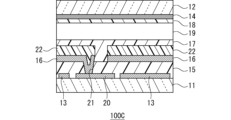
- an insulating layer (second insulating layer) may be provided so as to individually cover each pixel electrode.
- FIG. a cross-sectional view of a configuration example in which a second insulating layer is added based on the liquid crystal element 100 of the first embodiment is shown.
- the same reference numerals are used for each common configuration, and description thereof will be omitted.
- each second insulating layer 22 is arranged so as to cover each pixel electrode 16 .
- These second insulating layers 22 may have good insulating properties and light transmittance like the insulating layer (first insulating layer) 15 described above.
- Various insulating films can be used, such as an insulating film made of a resin material or the like, and an inorganic oxide film such as a silicon oxide film or a silicon nitride film.
- an insulating film made of a resin material or the like and an inorganic oxide film such as a silicon oxide film or a silicon nitride film.
- the liquid crystal elements of each of the above-described embodiments and modified examples can be suitably used, for example, for image display applications, and can also be suitably used in various lighting devices.
- the illuminating device as used herein refers to a device that transmits light through a liquid crystal element to form various images and project the images.
- the lighting device according to the present disclosure includes, for example, a vehicle lamp that projects various images around the vehicle (front, side, or road surface), a stage lighting device used for performances such as plays, or a street light. is included.
- FIG. 12 is a diagram showing a configuration example of a vehicle lamp, which is an example of a lighting device.
- the illustrated vehicle lamp includes a light source 500 , a liquid crystal element 501 , a pair of polarizing elements (polarizing plates) 502 and 503 , a projection lens 504 , a camera 505 , a controller 506 and a driver 507 .
- This vehicle lamp causes light emitted from a light source 500 to enter a liquid crystal element 501, forms various images using the liquid crystal element 501, and projects the images forward of a vehicle through a projection lens 504.
- FIG. 1 is a diagram showing a configuration example of a vehicle lamp, which is an example of a lighting device.
- the illustrated vehicle lamp includes a light source 500 , a liquid crystal element 501 , a pair of polarizing elements (polarizing plates) 502 and 503 , a projection lens 504 , a camera 505 , a controller 506 and a driver 507 .
- this vehicle lamp uses a camera 505 to detect the positions of a preceding vehicle and an oncoming vehicle in the space ahead of the vehicle, and generates a light distribution pattern that includes a dimming range according to the positions of the preceding vehicle.
- a driving voltage is applied to the liquid crystal element 501 by a driver 507 so as to realize the light distribution pattern set by the controller 506 .
- the high beam whose light is dimmed in a predetermined range corresponding to the position of the preceding vehicle or the like is projected forward of the vehicle, so that the preceding vehicle or the like can be prevented from being glared.
- the liquid crystal element 501 in such a vehicle lamp for example, the liquid crystal element 100 according to the above-described first embodiment or the liquid crystal element 100C of the modified example thereof can be preferably used.
Landscapes
- Physics & Mathematics (AREA)
- Nonlinear Science (AREA)
- Chemical & Material Sciences (AREA)
- Crystallography & Structural Chemistry (AREA)
- General Physics & Mathematics (AREA)
- Optics & Photonics (AREA)
- Liquid Crystal (AREA)
- Mathematical Physics (AREA)
Priority Applications (1)
| Application Number | Priority Date | Filing Date | Title |
|---|---|---|---|
| CN202280069739.0A CN118103766A (zh) | 2021-10-18 | 2022-09-21 | 液晶元件、照明装置 |
Applications Claiming Priority (2)
| Application Number | Priority Date | Filing Date | Title |
|---|---|---|---|
| JP2021170261A JP7708642B2 (ja) | 2021-10-18 | 2021-10-18 | 液晶素子、照明装置 |
| JP2021-170261 | 2021-10-18 |
Publications (1)
| Publication Number | Publication Date |
|---|---|
| WO2023067981A1 true WO2023067981A1 (ja) | 2023-04-27 |
Family
ID=86059069
Family Applications (1)
| Application Number | Title | Priority Date | Filing Date |
|---|---|---|---|
| PCT/JP2022/035267 Ceased WO2023067981A1 (ja) | 2021-10-18 | 2022-09-21 | 液晶素子、照明装置 |
Country Status (3)
| Country | Link |
|---|---|
| JP (1) | JP7708642B2 (https=) |
| CN (1) | CN118103766A (https=) |
| WO (1) | WO2023067981A1 (https=) |
Citations (5)
| Publication number | Priority date | Publication date | Assignee | Title |
|---|---|---|---|---|
| JP2008009386A (ja) * | 2006-05-31 | 2008-01-17 | Nikon Corp | 液晶表示素子、表示装置、観察装置およびカメラ |
| WO2009119865A1 (ja) * | 2008-03-25 | 2009-10-01 | シチズンホールディングス株式会社 | 表示パネル及びカメラ |
| JP2011248334A (ja) * | 2010-04-30 | 2011-12-08 | Seiko Instruments Inc | 液晶表示装置 |
| JP2012133002A (ja) * | 2010-12-20 | 2012-07-12 | Citizen Holdings Co Ltd | 強誘電性液晶パネル |
| JP2019120730A (ja) * | 2017-12-28 | 2019-07-22 | スタンレー電気株式会社 | 液晶素子、照明装置 |
Family Cites Families (1)
| Publication number | Priority date | Publication date | Assignee | Title |
|---|---|---|---|---|
| GB9319351D0 (en) * | 1993-09-18 | 1993-11-03 | Central Research Lab Ltd | Light modulator |
-
2021
- 2021-10-18 JP JP2021170261A patent/JP7708642B2/ja active Active
-
2022
- 2022-09-21 WO PCT/JP2022/035267 patent/WO2023067981A1/ja not_active Ceased
- 2022-09-21 CN CN202280069739.0A patent/CN118103766A/zh not_active Withdrawn
Patent Citations (5)
| Publication number | Priority date | Publication date | Assignee | Title |
|---|---|---|---|---|
| JP2008009386A (ja) * | 2006-05-31 | 2008-01-17 | Nikon Corp | 液晶表示素子、表示装置、観察装置およびカメラ |
| WO2009119865A1 (ja) * | 2008-03-25 | 2009-10-01 | シチズンホールディングス株式会社 | 表示パネル及びカメラ |
| JP2011248334A (ja) * | 2010-04-30 | 2011-12-08 | Seiko Instruments Inc | 液晶表示装置 |
| JP2012133002A (ja) * | 2010-12-20 | 2012-07-12 | Citizen Holdings Co Ltd | 強誘電性液晶パネル |
| JP2019120730A (ja) * | 2017-12-28 | 2019-07-22 | スタンレー電気株式会社 | 液晶素子、照明装置 |
Also Published As
| Publication number | Publication date |
|---|---|
| JP7708642B2 (ja) | 2025-07-15 |
| CN118103766A (zh) | 2024-05-28 |
| JP2023060585A (ja) | 2023-04-28 |
Similar Documents
| Publication | Publication Date | Title |
|---|---|---|
| CN110778981B (zh) | 车辆用灯具 | |
| CN107203078A (zh) | 显示装置 | |
| US20150316822A1 (en) | Liquid crystal display device | |
| US8810895B2 (en) | Electrophoretic display device | |
| JP7148240B2 (ja) | 液晶素子、照明装置 | |
| US20240111189A1 (en) | Display apparatus having back-light unit and liquid crystal panel | |
| US9310652B2 (en) | Liquid crystal display device | |
| US6750936B2 (en) | Display device | |
| US9341906B2 (en) | Liquid crystal display device | |
| JP7145704B2 (ja) | 表示装置及びルーム装置 | |
| US9052555B2 (en) | Liquid crystal display device | |
| JP2024001679A (ja) | 液晶素子、照明装置、車両用灯具システム | |
| JP7708642B2 (ja) | 液晶素子、照明装置 | |
| US11906854B2 (en) | Liquid crystal element, lighting apparatus | |
| US11119365B2 (en) | Liquid crystal element, lighting apparatus | |
| JP2014115561A (ja) | 液晶表示装置 | |
| TWI587042B (zh) | Liquid crystal display device | |
| JP7714451B2 (ja) | 液晶素子、照明装置 | |
| US9235086B2 (en) | Liquid crystal display device | |
| US9030636B2 (en) | Liquid crystal display apparatus | |
| JP2020154153A (ja) | 液晶素子、照明装置 | |
| WO2020054303A1 (ja) | 表示装置及びミラー装置 | |
| JP2015072374A (ja) | 液晶表示装置 |
Legal Events
| Date | Code | Title | Description |
|---|---|---|---|
| 121 | Ep: the epo has been informed by wipo that ep was designated in this application |
Ref document number: 22883291 Country of ref document: EP Kind code of ref document: A1 |
|
| WWE | Wipo information: entry into national phase |
Ref document number: 202280069739.0 Country of ref document: CN |
|
| NENP | Non-entry into the national phase |
Ref country code: DE |
|
| 122 | Ep: pct application non-entry in european phase |
Ref document number: 22883291 Country of ref document: EP Kind code of ref document: A1 |