WO2023047660A1 - 誘電膜の製造方法及びそれを用いたアクチュエータの製造方法 - Google Patents
誘電膜の製造方法及びそれを用いたアクチュエータの製造方法 Download PDFInfo
- Publication number
- WO2023047660A1 WO2023047660A1 PCT/JP2022/013821 JP2022013821W WO2023047660A1 WO 2023047660 A1 WO2023047660 A1 WO 2023047660A1 JP 2022013821 W JP2022013821 W JP 2022013821W WO 2023047660 A1 WO2023047660 A1 WO 2023047660A1
- Authority
- WO
- WIPO (PCT)
- Prior art keywords
- organic compound
- containing organic
- polar group
- dielectric film
- pdms
- Prior art date
- Legal status (The legal status is an assumption and is not a legal conclusion. Google has not performed a legal analysis and makes no representation as to the accuracy of the status listed.)
- Ceased
Links
Images






Classifications
-
- C—CHEMISTRY; METALLURGY
- C08—ORGANIC MACROMOLECULAR COMPOUNDS; THEIR PREPARATION OR CHEMICAL WORKING-UP; COMPOSITIONS BASED THEREON
- C08J—WORKING-UP; GENERAL PROCESSES OF COMPOUNDING; AFTER-TREATMENT NOT COVERED BY SUBCLASSES C08B, C08C, C08F, C08G or C08H
- C08J5/00—Manufacture of articles or shaped materials containing macromolecular substances
- C08J5/18—Manufacture of films or sheets
-
- C—CHEMISTRY; METALLURGY
- C08—ORGANIC MACROMOLECULAR COMPOUNDS; THEIR PREPARATION OR CHEMICAL WORKING-UP; COMPOSITIONS BASED THEREON
- C08K—Use of inorganic or non-macromolecular organic substances as compounding ingredients
- C08K5/00—Use of organic ingredients
- C08K5/16—Nitrogen-containing compounds
- C08K5/315—Compounds containing carbon-to-nitrogen triple bonds
-
- C—CHEMISTRY; METALLURGY
- C08—ORGANIC MACROMOLECULAR COMPOUNDS; THEIR PREPARATION OR CHEMICAL WORKING-UP; COMPOSITIONS BASED THEREON
- C08L—COMPOSITIONS OF MACROMOLECULAR COMPOUNDS
- C08L101/00—Compositions of unspecified macromolecular compounds
-
- C—CHEMISTRY; METALLURGY
- C08—ORGANIC MACROMOLECULAR COMPOUNDS; THEIR PREPARATION OR CHEMICAL WORKING-UP; COMPOSITIONS BASED THEREON
- C08L—COMPOSITIONS OF MACROMOLECULAR COMPOUNDS
- C08L83/00—Compositions of macromolecular compounds obtained by reactions forming in the main chain of the macromolecule a linkage containing silicon with or without sulfur, nitrogen, oxygen or carbon only; Compositions of derivatives of such polymers
- C08L83/04—Polysiloxanes
-
- H—ELECTRICITY
- H01—ELECTRIC ELEMENTS
- H01B—CABLES; CONDUCTORS; INSULATORS; SELECTION OF MATERIALS FOR THEIR CONDUCTIVE, INSULATING OR DIELECTRIC PROPERTIES
- H01B3/00—Insulators or insulating bodies characterised by the insulating materials; Selection of materials for their insulating or dielectric properties
- H01B3/18—Insulators or insulating bodies characterised by the insulating materials; Selection of materials for their insulating or dielectric properties mainly consisting of organic substances
- H01B3/28—Insulators or insulating bodies characterised by the insulating materials; Selection of materials for their insulating or dielectric properties mainly consisting of organic substances natural or synthetic rubbers
Definitions
- the present invention relates to a method for manufacturing a polymer actuator, and more particularly to a method for manufacturing a dielectric film used in the polymer actuator.
- Polymer actuators with excellent flexibility, light weight, and moldability are expected as smart materials.
- polymer actuators are driven by external stimuli such as light, heat, magnetic fields, electric fields, temperature, solvents, pH.
- Polymer actuators are broadly classified into current-driven types and voltage-driven types. Current-driven types include ion-conductive polymers, conductive polymers, and carbon nanotubes. Gels, dielectric elastomers are used. Actuators using dielectric elastomers that are driven in air are flexible and are being studied using acrylic, silicone, polyurethane elastomers, etc. as their materials.
- Dielectric particles such as barium titanate generally tend to agglomerate, making it difficult to disperse them uniformly in the elastomer.
- the present inventors have found that by compounding a polar group-containing organic compound such as cyanoethyl sucrose instead of barium titanate with a silicone elastomer, deformation based on the non-uniformity of the space charge distribution when a DC voltage is applied. reported a possible polymer actuator (see Non-Patent Document 1).
- Non-Patent Document 1 the formation of an asymmetric cross-sectional internal structure certainly causes non-uniform space charge distribution, but in order to form such a special internal structure, It is not clear how the manufacturing conditions of the dielectric film can be controlled.
- an object of the present invention is to provide a method for producing a dielectric film using a polymer material and a polar group-containing organic compound.
- the present inventors have made extensive studies and found that by using a solvent that has an affinity with the polymer material used in the production of the dielectric film and adjusting the film formation conditions, it is excellent as an actuator material. It has been found that a dielectric film having a That is, the present invention includes the following embodiments.
- a method for producing a dielectric film characterized by preparing a mixed solution so as to phase-separate into a dispersed phase.
- Polymer materials include silicone, polyurethane, polyacrylonitrile, nitrile rubber (NBR), hydrogenated nitrile rubber (H-NBR), nylon, polyethylene terephthalate, polypropylene, polyethylene, polyketone, polyvinyl alcohol, polyvinyl butyral, and polyvinyl acetic acid.
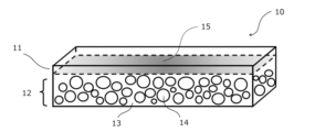
- FIG. 1 is a schematic diagram of a dielectric film according to one embodiment.
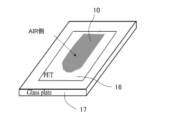
- FIG. 2A is a schematic diagram showing the procedure for producing a PDMS composite membrane produced in Examples.
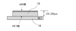
- FIG. 2B is the film produced in the example.
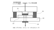
- FIG. 3 is a schematic diagram of an electrode portion of a pulsed electrostatic acoustic non-destructive testing device (PEANUT) used for measuring space charge distribution.
- PEANUT pulsed electrostatic acoustic non-destructive testing device
- FIG. 4 is a schematic diagram of a deformation measurement sample.
- FIG. 5 is an experimental setup for measuring deformation.
- FIG. 6 is a graph showing the relationship between the viscosity of PDMS/CR-U solutions and the THF content.
- FIG. 7 is a graph showing the relationship between the elastic modulus of the PDMS/CR-U composite membrane and the THF content.
- FIG. 1 is a schematic diagram of a dielectric film according to one embodiment.
- FIG. 2A is
- FIG. 8 is a cross-sectional image of a PDMS/CR-U composite membrane.
- (a) is PDMS/CR-U (A100/T0)
- (b) is PDMS/CR-U (A50/T50)
- (c) is PDMS/CR-U (A25/T75)
- (d ) indicate PDMS/CR-U (A0/T100), respectively.
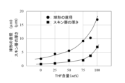
- FIG. 9 is a graph showing the THF content dependence of the diameter of the spheroids and the thickness of the skin layer.
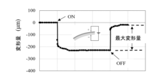
- FIG. 10A is a graph showing the time dependence of the amount of deformation.
- FIG. 10B is a graph showing the time dependence of the electric field.
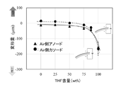
- FIG. 11 is a graph showing the relationship between maximum deformation amount and THF content.
- FIG. 12 is a graph showing the relationship between maximum deformation amount and electric field intensity.
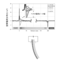
- FIG. 13A is a schematic illustration of the space charge distribution and deformation mechanism when the AIR side is attached to the anode.
- FIG. 13B is a schematic illustration of the space charge distribution and deformation mechanism when the AIR side is attached to the cathode.
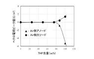
- FIG. 14 is a graph showing the relationship between the peak value of the hetero charge and the electric field strength.
- FIG. 15 is a graph showing the relationship between the maximum deformation amount and the hetero-charge peak intensity.
- dielectric film 11 dense layer (skin layer) 12 Sea-island structure 13 Base polymer (continuous phase) 14 dispersed phase 15 interface 16 PET film 17 glass plate 21 Al electrode 22 upper electrode (semiconductive rubber) 23, 31, 43 Silicone elastomer film (dielectric film) 24 lower electrode (Al) 25 piezo element (sensor) 32 Gold leaf 41 Digital microscope 42 Computer 43 DC power supply
- the dielectric film according to the manufacturing method of the present invention contains a polymer material and a polar group-containing organic compound, and has a sea-island structure as shown in FIG.
- the dielectric film 10 shown in FIG. 1 contains a dispersed phase 14 mainly composed of a polar group-containing organic compound in a base polymer 13 .
- a dense layer 11 made of a base polymer is provided on one surface of the dielectric film 10 (upper surface in FIG. 1).
- the dense layer 11 is a uniform layer (sometimes referred to as a “skin layer”) substantially made of a base polymer.
- the thickness of the dielectric film 10 is preferably 500 ⁇ m or less in order to easily deform, and the thickness of the dense layer 11 is preferably about 5 to 50 ⁇ m.
- the dispersed phase is mainly composed of a polar group-containing organic compound, and its shape is spherical (perfectly spherical or nearly spherical), ellipsoidal (ellipsoidal), polyhedral (polypyramidal, square, cuboid, etc.). body-like), plate-like (flat, scaly or flaky, etc.), rod-like or bar-like, fiber-like, irregular shape, etc., but it is preferable to form a spherical dispersed phase.
- an interface 15 exists between the sea-island structure 12 and the dense layer 11 .
- the dispersed phase 14 is preferably spherical and has a spherical diameter of about 1 to 100 ⁇ m. A more preferable spherical diameter of the dispersed layer is 10 to 100 ⁇ m.
- the term “heterocharge” refers to a charge that exists in the vicinity of an electrode and has a polarity opposite to that of the electrode.
- the polymer material constituting the base polymer, the polar group-containing organic compound constituting the dispersion layer, and the like will be described in detail.
- the type of the base polymer used in this embodiment is not particularly limited as long as it is a flexible elastomer.
- silicone polyurethane, polyvinyl chloride, polyacrylonitrile, nitrile rubber (NBR), hydrogenated nitrile rubber (H-NBR), nylon, polyethylene terephthalate, polypropylene, polyethylene, polyketone, polyvinyl alcohol, polyvinyl acetate, polymethyl methacrylate , poly-n-butyl acrylate, cellulose and wool.
- the elastomer may be appropriately selected according to the performance required for the actuator.
- an elastomer having a large polarity that is, a large dielectric constant.
- a dielectric constant of 2.8 or more (measurement frequency of 100 Hz) is suitable.
- elastomers having a high dielectric constant include nitrile rubber (NBR), hydrogenated nitrile rubber (H-NBR), chlorinated polyethylene, chlorosulfonated polyethylene, and polyurethane.
- NBR nitrile rubber
- H-NBR hydrogenated nitrile rubber
- chlorinated polyethylene chlorosulfonated polyethylene
- polyurethane polyurethane.
- an elastomer having a large electric resistance even if the relative permittivity is small is desirable in that dielectric breakdown is less likely to occur when a voltage is applied. Silicone rubber etc.
- elastomer with a large electrical resistance.
- an elastomer modified by, for example, introducing a functional group may be used.
- Suitable modified elastomers include, for example, carboxyl group-modified nitrile rubber (X-NBR) and carboxyl group-modified hydrogenated nitrile rubber (XH-NBR).
- thermoplastic elastomers do not use cross-linking agents, impurities are less likely to enter, making them suitable.
- Thermoplastic elastomers include styrene (SBS, SEBS, SEPS), olefin (TPO), polyvinyl chloride (TPVC), urethane (TPU), ester (TPEE), amide (TPAE), and their co- Examples include polymers and blends.
- the polar group-containing organic compound of the present embodiment includes, but is not limited to, cyanoethyl group-containing organic compounds, modified silicone oils, phthalocyanines, various ionic liquids, and the like. For example, it may be selected from a variety of polar materials that are compatible or partially incompatible with the base polymer.
- the "cyanoethyl group-containing organic compound” is not particularly limited as long as it is a compound having a cyanoethyl group in the molecule, but it is preferable to use an organic polymer or organic oligomer containing a cyanoethyl group.
- a cyanoethyl group-containing organic compound has a highly polar cyanoethyl group in its molecule, so that when placed in an electric field, it forms a large dipole moment and exhibits a high dielectric constant.
- the cyanoethyl group-containing organic compound is preferably an organic dielectric material with a dielectric constant of 10 or more.
- cyanoethyl sucrose (cyanoethyl sucrose, dielectric constant 24), cyanoethyl pullulan (relative dielectric constant 18), cyanoethyl cellulose (relative dielectric constant 16), cyanoethyl hydroxyethyl cellulose (relative dielectric constant 18), cyanoethyl hydroxypropyl Cellulose (relative dielectric constant 14), cyanoethyl amylose (relative dielectric constant 17), cyanoethyl starch (relative dielectric constant 17), cyanoethyl dihydroxypropyl starch (relative dielectric constant 18), cyanoethylglycidol pullulan (relative dielectric constant 20), cyanoethyl polyvinyl alcohol (relative dielectric constant 20), cyanoethy
- the cyanoethyl group-containing organic compound is preferably contained in an amount of 5 to 60% by mass, more preferably 25 to 45% by mass, based on the total amount of the composition constituting the dielectric film of this embodiment. This is because when the content of the cyanoethyl group-containing organic compound is 5% by mass or more, the effect of improving the displacement as an actuator is high, and when the content is 60% by mass or less, the stability of the actuator member is enhanced.
- These cyanoethyl group-containing organic compounds are sold, for example, by Shin-Etsu Chemical Co., Ltd. under the product name: Cyanoresin (registered trademark).
- Modified silicone oil, phthalocyanines, various ionic liquids, and the like may be used as the polar group-containing organic compound contained in the dielectric film of the present embodiment.
- a silicone oil that is liquid at room temperature (15 to 25°C) and is obtained by modifying a compound having a polydimethylsiloxane skeleton with a polar group can be used.
- Polar groups that modify polydimethylsiloxane include —CH 2 CH 2 CF 3 groups (fluoroalkyl-modified), O(EO) n — groups (polyether-modified), —OH groups (hydroxyl-modified), and —NH 2 groups. (amino-modified), —CH 2 OH group (carbinol-modified), —COOH group (carboxyl-modified), and the like.
- These modified silicone oils having polar groups may be of the side chain modified copolymer type or the linear modified copolymer type, and the portion to be modified with the polar group may be a side chain, one end or both ends.
- modified silicone oils include modified silicone oils carboxyl-modified with —COOH groups, modified silicone oils fluoroalkyl-modified with —CH 2 CH 2 CF 3 groups, and modified silicone oils amino-modified with —NH 2 groups. preferable.
- imidazolium salts As the ionic liquid, imidazolium salts, piperidinium salts, pyridinium compounds, pyrrolidinium salts, and the like can be used.
- Bis(trifluoromethylsulfonyl)imide [EMI][TFSI]), 1-ethyl-3-methylimidazolium tetrafluoroborate ([EMI][BF4]), 1-butyl-3-methylimidazolium Tetrafluoroborate ([BMI][BF4]), 1-hexyl-3-methylimidazolium tetrafluoroborate ([HMI][BF4]), 1-ethyl-3-methylimidazolium 2-(2- methoxyethoxy)-ethylsulfate ([EMI][MEES]), 1-butyl-1-methylpyrrolidinium bis(trifluoromethanesulfonyl)imide ([BMP][TFSI]), and the like.
- phthalocyanines which are metal complexes having Mg, Cr, Mn, Fe, Co, Ni, Cu, Zn, Al, Mo, Ru, Rh, Pd, Re, Os, Ir or Pt as a central metal, are dielectric polymers. It has also been reported that it acts as a charge trapping agent in the layer and charges inside the actuator (see Japanese Patent Application Laid-Open No. 2005-323482).
- the dielectric film of the present invention may contain other components in addition to the polymer material and the polar group-containing organic compound.
- Other components include cross-linking agents, reinforcing agents, plasticizers, antioxidants, colorants, and the like.
- the mechanical strength and electrical resistance of the dielectric film can be increased.
- the dielectric breakdown strength of the dielectric film is increased, and durability against repeated deformation is improved.
- a method for manufacturing a dielectric film according to the present invention includes a mixed solution preparing process, a coating process, and a film forming process. Each step will be described in order below.
- This step is a step of dissolving the above-mentioned polymeric material and a polar group-containing organic compound in a solvent to prepare a mixed solution of the polymeric material and the polar group-containing organic compound.
- the mixing ratio of the polymer material and the polar group-containing organic compound is preferably 4:1 to 1:1 in mass ratio.
- the blending ratio of the polar group-containing organic compound to the polymer material By setting the blending ratio of the polar group-containing organic compound to the polymer material to be 1/5 or more, a dielectric film having a sufficient dielectric constant can be produced, while the blending ratio of the polar group-containing organic compound is is 1/2 or less, it is possible to impart sufficient durability as a dielectric film.
- the solvent preferably dissolves the polymer material and the polar group-containing organic compound.
- aromatic hydrocarbons such as benzene, toluene, and xylene
- aliphatic hydrocarbons such as pentane, hexane, cyclohexane, heptane, and cyclopentane.
- halogenated hydrocarbons such as chloroform, dichloromethane and carbon tetrachloride
- amides such as N,N-dimethylformamide (DMF), dimethylacetamide and N-methylpyrrolidone
- sulfoxides such as dimethylsulfoxide (DMSO)
- sulfones such as sulfolane Ethers such as dimethyl ether (DME), diethyl ether, diisopropyl ether, diglyme, tetrahydrofuran (THF), 1,4-dioxane, t-butyl methyl ether
- Nitriles such as acetonitrile
- Esters such as methyl acetate, ethyl acetate, and propion carbonate and ketones such as acetone and methyl ethyl ketone.
- One or more of these solvents can be used.
- the mixed solvent preferably has a viscosity of 1 Pa ⁇ s or less at 20°C. This is because if the viscosity of the mixed solvent exceeds 1 Pa ⁇ s, the fluidity of the mixed solution decreases in the film forming process for curing the polymer material, making it difficult for the dielectric film to form a desired internal structure.
- the mixed solvent In order to form a dispersed phase consisting mainly of a polar group-containing organic compound, it is more preferable that the mixed solvent has a viscosity of 0.5 Pa ⁇ s or less at 20°C. The lower limit of the viscosity of the mixed solvent at 20 ° C.
- the viscosity of the solvent at 20 ° C. can be obtained, for example, by using a tuning fork vibration viscometer SV-10A [product name] (manufactured by A&D Co., Ltd.) for the solvent temperature-controlled in a constant temperature bath at 20 ° C. can be measured by
- the dielectric film contains a large number of particles with a large particle diameter relative to the film thickness, the particles tend to become starting points and cause dielectric breakdown. Therefore, in order to improve the dielectric breakdown strength of the dielectric film, it is desirable to make the particle diameter of the particles forming the dispersed phase smaller than the film thickness. However, the smaller the particle diameter of the particles forming the dispersed phase, the smaller the heterocharge accumulation. Therefore, in order to increase the accumulation of hetero-charges in the dielectric film, it is desirable to increase the particle size of the particles forming the dispersed phase as much as possible. Therefore, the particle diameter of the particles forming the dispersed phase may be appropriately determined in consideration of the thickness of the dielectric film and efficient accumulation of the hetero-charge.
- the resin composition of the present embodiment is coated on the surface of the support.
- the support is not particularly limited as long as it has heat resistance to the heating temperature in the subsequent film forming step (heating step) and has good peelability in the peeling step.
- the support include glass substrates such as alkali-free glass substrates; silicon wafers; PET (polyethylene terephthalate), OPP (oriented polypropylene), polyethylene glycol terephthalate, polyethylene glycol naphthalate, polycarbonate, polyimide, polyamideimide, and polyetherimide. , polyether ether ketone, polyether sulfone, polyphenylene sulfone, polyphenylene sulfide, etc.; metal substrates such as stainless steel, alumina, copper, nickel, etc.;
- Coating methods generally include doctor blade knife coater, air knife coater, roll coater, rotary coater, flow coater, die coater, bar coater, etc.; spin coating, spray coating, dip coating, etc.; screen printing. and printing techniques such as gravure printing.
- the temperature in the coating step may be room temperature, or the mixed solvent may be heated to, for example, 40 to 80° C. in order to lower the viscosity and improve workability.
- the coating step may be followed by a drying step, or the drying step may be omitted and the next film-forming step (heating step) may proceed directly.
- the drying step can be performed by subjecting the mixed solvent to a degree of vacuum of 100 Pa or less for the purpose of removing the solvent in the mixed solvent.
- a hot plate, a box-type dryer, a conveyor-type dryer, or the like can be used.
- the temperature of the drying step is preferably 80-200°C, more preferably 100-150°C.
- the duration of the drying step is preferably 1 minute to 10 hours, more preferably 3 minutes to 5 hours.
- the heating step is a step of removing the solvent contained in the coating film and advancing the curing reaction of the elastomer in the coating film.
- This heating step can be carried out by subjecting the resin composition to a vacuum of 100 Pa or less using an inert gas oven, hot plate, box dryer, conveyor dryer, or the like. This step may be performed simultaneously with the drying step, or both steps may be performed sequentially.
- An actuator of the present invention comprises the dielectric film of the present invention and a plurality of electrodes arranged via the dielectric film.
- the actuator of the present invention may be configured by alternately laminating a plurality of dielectric films and a plurality of electrodes.
- An intermediate layer having an electrical resistance intermediate between the dielectric film and the electrode may be interposed. Adopting a laminated structure can generate a larger force.
- the structure and manufacturing method of the dielectric film of the present invention are as described above.
- the material of the electrodes is not particularly limited. It is desirable that the electrode be able to expand and contract following the deformation of the dielectric film. In this case, the deformation of the dielectric film is less likely to be restricted by the electrodes. Therefore, in the actuator of the present invention, it becomes easier to obtain a desired output.
- the electrodes can be formed from a conductive paste or conductive paint in which a conductive material is mixed with a binder such as oil or elastomer.
- a conductive material carbon materials such as carbon black, ketjen black, carbon nanotubes, and graphene, and metal powders such as silver may be used.
- the electrodes may be formed by weaving carbon fibers or metal fibers into a mesh.
- the actuator of the present invention operates as an actuator and generates stress by applying a voltage between electrodes. Also, when the dielectric film is deformed and the distance between the electrodes changes, the capacitance changes. Thereby, the actuator of the present invention functions as a capacitive sensor. In addition, the actuator of the present invention also functions as a power generation element by using the charge generated when the dielectric film is deformed as a current.
- the present invention will be described in more detail with reference to Examples, but the present invention is not limited to these Examples.
- the unit % of numerical values indicating the addition amount of various components means % by mass.
- silicone composite membrane ⁇ Preparation of silicone composite membrane> [material] As silicone, SILPOT184/CAT184 (DuPont Toray Specialty Materials Co., Ltd.) was used. This is an addition reaction type PDMS. CR-U (Shin-Etsu Chemical Co., Ltd.) having a cyanoethyl group (--CH 2 CH 2 CN) was used as the polar group-containing material. CR-U is very viscous and difficult to handle.
- CR-U is dissolved in tetrahydrofuran (hereinafter referred to as "THF") or acetone (hereinafter referred to as "ACT”), which are good solvents for CR-U, and CR-U (T) and CR- A 50 wt% solution of each of U(A) was prepared.
- THF tetrahydrofuran
- ACT acetone
- the casting solution was poured onto the PET film 16 placed on the glass plate 17 using a four-sided film applicator (052-6, manufactured by Allgood). After holding this solution at room temperature for 60 minutes, it was cured by heating in an oven at 150° C.
- a PDMS/CR-U (A x /T y ) PDMS composite film 10 as shown in Table 1 ( x and y indicate the content (wt%) of ACT and THF relative to the total amount of solvent, respectively.Films with a thickness of 150 to 280 m were used to measure the deformation amount.As shown in Figure 2B, PET The surface in contact with the film was defined as the "PET side”, and the surface opposite to the air was defined as the "AIR side”.
- Viscosity was measured at 20° C. using a tuning fork vibrometer (SV-10A, A&D Instrument Ltd.).
- a tuning fork vibrometer consists of two thin sensor plates, and by vibrating a constant sine wave in opposite phases like a tuning fork, the sensor is driven by an electromagnetic force of the same frequency.
- An electromagnetic drive controls the oscillation of the sensor plate to a constant amplitude.
- the driving current is detected as the magnitude of viscosity generated between the sensor plate and the sample liquid. This viscosity can be determined from the torque required to resonate the oscillator in the fluid and move the oscillator at a constant amplitude.
- FIG. 3 shows an outline of the electrode portion of the PEANUT device.
- the upper electrode 22 is made of semi-conductive rubber, and the lower electrode 24 is made of aluminum.
- a pulsed electrostatic force acts on charges to generate an elastic wave having a charge distribution shape. This elastic wave was converted into an electric signal by a piezoelectric element, and the space charge distribution was measured.
- a bias condition is 3 kV/mm and a pulse condition is 200 V ⁇ 400 Hz.
- FIG. 4 shows a schematic diagram of a deformation measurement sample.
- the prepared silicone elastomer film 31 was cut into a width of 5 mm and a length of 20 mm. made.
- FIG. 5 shows the experimental setup for measuring deformation.
- the DC power supply 44 used a square wave output with a maximum output of 850V.
- the test piece 43 was installed perpendicular to the floor surface, clamped with a Kelvin clip (a 12 mm cantilever from the clip to the tip of the test piece), and a DC voltage was applied.
- the amount of deformation was observed and measured under an electric field with a digital microscope 41 placed on the sample, and recorded by a computer 42 .
- Dielectric constant and impedance were measured by impedance analyzer (SI1260, SII1296, Solartron Co., Ltd.), high voltage interface (HVI-100, TOYO Corporation) and bipolar amplifier (BOP-1000M, KEPCO, INC.) (electrode diameter 10 mm and specimen thickness 170 ⁇ m).
- the tensile modulus of the silicone composite membrane was measured using a Tensilon-tensile measuring device (RTC-1250A, manufactured by A&D Co., Ltd.).
- the silicone composite membrane was compressed with a 10 N load cell at a speed of 50 mm/min.
- Tensile modulus was calculated from the initial slope of the tensile stress curve at low tensile stress.
- the flexural modulus was calculated by measuring the amount of deformation of the cantilever due to the static weight of the test piece (deformation measurement test piece).
- ⁇ Structural composition> The structural composition was measured using FT/IR-4600typeA (JASCO Corp.) at an incident angle of 45 degrees.
- FIG. 6 shows the THF content dependence of the viscosity of the PDMS/CR-U solution.
- the viscosity of PDMS/CR-U solutions decreased with increasing THF content. It has been reported that ACT has high and low affinity for CR-U and PDMS, respectively, and THF has high affinity for CR-U and PDMS. As the content of ACT increases and the viscosity of the PDMS solution increases, the affinity for PDMS decreases.
- FIG. 7 shows the THF content dependence of the elastic modulus of the PDMS/CR-U composite membrane.
- the flexural modulus exhibited a minimum quadratic curve at a THF content of 50%.
- the flexural modulus of the 100% THF film was greater than that of the 100% ACT film.
- the tensile modulus tended to increase with increasing THF content.
- FIG. 8 is a cross-sectional photograph of each sample from (a) PDMS/CR-U (A100/T0) to (d) PDMS/CR-U (A0/T100).
- This composite membrane exhibited a phase-separated structure in which a spherical phase was dispersed in a continuous phase.
- FT-IR analysis identified the continuous phase as PDMS and the spherical phase as CR-U.
- Films made with ACT (PDMS/CR-U(/T0)) had a symmetrical cross-sectional structure with uniformly distributed small CR-U spheres. The diameter of the spheres tended to increase as the content of the THF/ACT mixed solvent increased.
- the membrane prepared using THF has a PDMS skin layer on the AIR side, and CR-U spheres of considerable size are dispersed in the main body of the film. It had an asymmetrical cross section.
- PDMS/CR-U As the viscosity of the casting solution increases, it is expected that the CR-U molecules will move and aggregate more easily. Moreover, the density of CR-U (1.23) is higher than that of PDMS (1.03). As a result, PDMS/CR-U (A0/T100) has an asymmetric cross-sectional shape with a thin PDMS skin layer on the AIR-side surface of the film and large CR-U spheres dispersed in the PDMS continuous phase (film body). was thought to be doing
- Fig. 9 shows the THF content dependence of the CR-U spherical diameter and skin layer thickness obtained by image analysis. With increasing THF content, the CR-U spherical shape and skin layer thickness increased as the viscosity of the casting solution decreased, see FIG.
- FIG. 11 plots the maximum deformation of the composite membrane measured by applying a DC electric field of 3 kV/mm against the THF content.
- the composite membrane deformed toward the PET side regardless of the polarity of the electric field.
- the PDMS/CR-U (A100/T0) had a symmetrical cross-sectional structure and hardly deformed because the small CR-U spheres were evenly distributed without a skin layer.
- the maximum deformation amount gradually increased. It has an asymmetrical cross-sectional shape with a thin skin layer, and large deformation was observed.
- FIG. 12 shows the electric field strength dependence of the deformation of PDMS/CR-U (A100/T0)-PDMS/CR-U (A0/T100).
- Figures 13A and 13B show the space charge distribution of PDMS/CR-U(A100/T0)-PDMS/CR-U(A0/T100) 5 minutes after bias loading.
- the horizontal axis represents the thickness (position) of the sample.
- the vertical axis represents the space charge density, with the electrode interface set to 0. The maximum value of the charge on the opposite side accumulated in the film in the vicinity of the electrode interface on the AIR side was taken as the hetero charge peak value.
- the film interface on the anode electrode/AIR side was defined as zero on the depth axis.
- PDMS/CR-U A12.5/T87.5
- PDMS/CR-U A0/T100
- a small and significantly large negative charge (hatched in the figure) opposite to the polarity of the anode, respectively ), ie, heterocharge was observed near the anodic interface.
- no accumulation of hetero (positive) charges was observed inside the film near the cathode interface, confirming the asymmetry of the space charge distribution.
- no accumulation of hetero-charge was observed inside the membrane.
- the cathode electrode/AIR side of the film interface is defined as zero on the depth axis.
- Heterogeneous charge accumulation in PDMS/CR-U (A0/T100) is confirmed near both electrodes, with the accumulation on the cathode side being greater than that on the anode side.
- the asymmetry of the space charge distribution was confirmed.
- PDMS/CR-U (A12.5/T87.5)
- heterogeneous charge accumulation was confirmed near the interface between both electrodes. However, both values were small and almost the same amount.
- FIG. 14 shows the relationship between the hetero-charge peak value on the AIR side and the THF content. At THF of 82.5 wt % or more, the peak value of the hetero charge is greatly increased.
- FIG. 15 shows the relationship between the maximum deformation amount and the hetero charge peak value.
- FIG. 15 shows the relationship between the maximum amount of deformation and the hetero charge peak value, and the maximum amount of deformation greatly increases at 82.5 wt % or more of THF.
Landscapes
- Chemical & Material Sciences (AREA)
- Organic Chemistry (AREA)
- Health & Medical Sciences (AREA)
- Chemical Kinetics & Catalysis (AREA)
- Medicinal Chemistry (AREA)
- Polymers & Plastics (AREA)
- Manufacturing & Machinery (AREA)
- Engineering & Computer Science (AREA)
- Materials Engineering (AREA)
- Physics & Mathematics (AREA)
- Spectroscopy & Molecular Physics (AREA)
- Compositions Of Macromolecular Compounds (AREA)
- Manufacture Of Macromolecular Shaped Articles (AREA)
- Organic Insulating Materials (AREA)
Abstract
【課題】高分子材料と極性基含有有機化合物とを用いて、誘電膜を製造する方法を提供する。 【解決手段】高分子材料と、極性基含有有機化合物とを、溶媒中に溶解して、高分子材料と極性基含有有機化合物との混合溶液を調製する工程と、混合溶液を基板上に塗布する工程と、基板上に塗布した高分子材料を硬化させて薄膜を形成する工程と、を備え、硬化後の薄膜の内部構造が、高分子材料からなる連続相と、主として極性基含有有機化合物からなる分散相とに相分離するように、混合溶液を調製することを特徴とする誘電膜の製造方法。
Description
本出願は、2021年9月21日に日本国において出願された特願2021-152756に基づき優先権を主張し、当該出願に記載された内容は、本明細書に援用する。また、本願において引用した特許、特許出願及び文献に記載された内容は、本明細書に援用する。
本発明は、高分子アクチュエータの製造方法に関し、特に、該高分子アクチュエータに用いられる誘電膜の製造方法に関する。
柔軟性、軽量性、成形性に優れた高分子アクチュエータは、スマートマテリアルとして期待されている。一般に、ポリマーアクチュエータは、光、熱、磁場、電場、温度、溶媒、pHなどの外部刺激によって駆動される。また、高分子アクチュエータは、電流駆動型と電圧駆動型に大別され、電流駆動型には、イオン伝導性ポリマー、導電性ポリマー、カーボンナノチューブが、電圧駆動型には、圧電性ポリマー、誘電体ゲル、誘電エラストマーが用いられる。空気中で駆動する誘電エラストマーを用いたアクチュエータは、柔軟性があり、その材料として、アクリル、シリコーン、ポリウレタンエラストマーなどを用いて検討されている。
印加電圧に対する静電引力を大きくして、アクチュエータの性能向上を図るためには、誘電膜の比誘電率を大きくすることが必要である。このため、エラストマーにチタン酸バリウム等の比誘電率が大きい誘電性粒子を配合した誘電膜が種々提案されている。例えば、特許文献1には、エラストマーと誘電性粒子とを含み、走査型電子顕微鏡により撮影された膜厚方向の断面写真において、条件(A)[基準個数の平均値が0.8個/μm以上]、条件(B)[大粒子個数の平均値が0.2個/μm以下]、および条件(C)[エラストマーの面積割合が30%以下である単位領域の個数が10個以下]を満たす誘電膜が、柔軟で、比誘電率が大きく、薄膜化しても絶縁破壊強度が大きいことが記載されている。
このチタン酸バリウムのような誘電性粒子は、一般的に凝集しやすいため、エラストマー中に均一に分散させることが難しい。本発明者らは、チタン酸バリウムに代えてシアノエチルスクロースのような極性基含有有機化合物をシリコーンエラストマーと複合化することで、直流電圧を負荷したときの空間電荷分布の不均一性に基づいて変形可能な高分子アクチュエータについて報告している(非特許文献1参照)。
S.Tamura、R.Kiyono、T.Hirai、 Dielectric elastomer actuator behavior of silicone/cyanoethylsucrose composite films: Morphology and space-charge distribution. Nano Select 2021;1-11https://doi.org/10.1002/nano.202100023
非特許文献1に記載の誘電膜は、非対称性の断面内部構造を形成することで、確かに、空間電荷分布の不均一性が生じるが、このような特殊な内部構造を形成するために、誘電膜の製造条件をどのようにコントロールしうるかについては明らかではない。
そこで、本発明は、高分子材料と極性基含有有機化合物とを用いて、誘電膜を製造する方法を提供することを課題とする。
上記課題を解決するために、本発明者らは鋭意検討を行った結果、誘電膜の製造に用いる高分子材料と親和性のある溶媒を用い、成膜条件を調整することでアクチュエータ材料として優れた誘電膜が得られることを見出した。すなわち、本発明は以下の実施形態を含む。
(1)高分子材料と、極性基含有有機化合物とを、溶媒中に溶解して、高分子材料と極性基含有有機化合物との混合溶液を調製する工程と、混合溶液を基板上に塗布する工程と、基板上に塗布した高分子材料を硬化させて薄膜を形成する工程と、を備え、硬化後の薄膜の内部構造が、高分子材料からなる連続相と、主として極性基含有有機化合物からなる分散相とに相分離するように、混合溶液を調製することを特徴とする誘電膜の製造方法。
(2)高分子材料と極性基含有有機化合物との配合比率が、質量比で3:1~1:1である、(1)に記載の製造方法。
(3)混合溶液の全量に対する溶媒の含有量が、20~50質量%である、(1)又は(2)に記載の製造方法。
(4)混合溶液の20℃における粘度が、1Pa・s以下である、(1)~(3)のいずれか一項に記載の製造方法。
(5)高分子材料を硬化させる前に、基板上に塗布した混合溶液を少なくとも30分間保持する、(1)~(4)のいずれか一項に記載の製造方法。
(6)高分子材料が、シリコーン、ポリウレタン、ポリアクリロニトリル、ニトリルゴム(NBR)、水素化ニトリルゴム(H-NBR)、ナイロン、ポリエチレンテレフタレート、ポリプロピレン、ポリエチレン、ポリケトン、ポリビニルアルコール、ポリビニルブチラール、ポリ酢酸ビニル、ポリメチルメタクリレート、ポリnブチルアクリレート、セルロース及び羊毛から選択される一種以上のエラストマーを含む、(1)~(5)のいずれか一項に記載の製造方法。
(7)極性基含有有機化合物が、シアノエチル基含有有機化合物、変性シリコーンオイル、フタロシアニン類又はイオン液体である(1)~(6)のいずれか一項に記載の製造方法。
(8)高分子材料がシリコーンであり、極性基含有有機化合物がシアノエチルサッカロースである(1)~(7)のいずれか一項に記載の製造方法。
(9)溶媒が、テトラヒドロフラン又はテトラヒドロフランとアセトンとの混合溶媒である(1)~(8)のいずれか一項に記載の製造方法。
(10)(1)~(9)の何れか一項に記載の方法で製造された誘電膜の両面にそれぞれ電極層を付加するアクチュエータの製造方法。
(2)高分子材料と極性基含有有機化合物との配合比率が、質量比で3:1~1:1である、(1)に記載の製造方法。
(3)混合溶液の全量に対する溶媒の含有量が、20~50質量%である、(1)又は(2)に記載の製造方法。
(4)混合溶液の20℃における粘度が、1Pa・s以下である、(1)~(3)のいずれか一項に記載の製造方法。
(5)高分子材料を硬化させる前に、基板上に塗布した混合溶液を少なくとも30分間保持する、(1)~(4)のいずれか一項に記載の製造方法。
(6)高分子材料が、シリコーン、ポリウレタン、ポリアクリロニトリル、ニトリルゴム(NBR)、水素化ニトリルゴム(H-NBR)、ナイロン、ポリエチレンテレフタレート、ポリプロピレン、ポリエチレン、ポリケトン、ポリビニルアルコール、ポリビニルブチラール、ポリ酢酸ビニル、ポリメチルメタクリレート、ポリnブチルアクリレート、セルロース及び羊毛から選択される一種以上のエラストマーを含む、(1)~(5)のいずれか一項に記載の製造方法。
(7)極性基含有有機化合物が、シアノエチル基含有有機化合物、変性シリコーンオイル、フタロシアニン類又はイオン液体である(1)~(6)のいずれか一項に記載の製造方法。
(8)高分子材料がシリコーンであり、極性基含有有機化合物がシアノエチルサッカロースである(1)~(7)のいずれか一項に記載の製造方法。
(9)溶媒が、テトラヒドロフラン又はテトラヒドロフランとアセトンとの混合溶媒である(1)~(8)のいずれか一項に記載の製造方法。
(10)(1)~(9)の何れか一項に記載の方法で製造された誘電膜の両面にそれぞれ電極層を付加するアクチュエータの製造方法。
本発明によれば、高分子材料と極性基含有有機化合物とを用いて、誘電膜を製造する新規な方法を提供することができる。
10 誘電膜
11 緻密層(スキン層)
12 海島構造
13 ベースポリマー(連続相)
14 分散相
15 界面
16 PETフィルム
17 ガラス板
21 Al電極
22 上部電極(半導電性ゴム)
23、31、43 シリコーンエラストマーフィルム(誘電膜)
24 下部電極(Al)
25 ピエゾ素子(センサー)
32 金箔
41 デジタル顕微鏡
42 コンピュータ
43 直流電源
11 緻密層(スキン層)
12 海島構造
13 ベースポリマー(連続相)
14 分散相
15 界面
16 PETフィルム
17 ガラス板
21 Al電極
22 上部電極(半導電性ゴム)
23、31、43 シリコーンエラストマーフィルム(誘電膜)
24 下部電極(Al)
25 ピエゾ素子(センサー)
32 金箔
41 デジタル顕微鏡
42 コンピュータ
43 直流電源
次に、本発明の各実施形態について、図面を参照して説明する。なお、以下に説明する各実施形態は、特許請求の範囲に係る発明を限定するものではなく、また、各実施形態の中で説明されている諸要素及びその組み合わせの全てが本発明の解決手段に必須であるとは限らない。
<誘電膜>
本発明の製造方法に係る誘電膜は、高分子材料と、極性基含有有機化合物と、を含み、その内部構造が図1に示すような海島構造を示す。図1に示す誘電膜10は、ベースポリマー13の中に、主として極性基含有有機化合物からなる分散相14を含む。そして、この誘電膜10のいずれか一方の表面(図1では上面)に、ベースポリマーからなる緻密層11を備える。緻密層11は、実質的にベースポリマーからなる均一な層(「スキン層」と称する場合もある。)である。誘電膜10は、容易に変形するためには膜厚が500μm以下であることが好ましく、緻密層11の膜厚は、約5~50μmであることが好ましい。分散相は、主として極性基含有有機化合物からなり、その形状は、球状(真球状又は略球状)、楕円体(楕円球)状、多角体状(多角錘状、正方体状や直方体状など多角方体状など)、板状(扁平、鱗片又は薄片状など)、ロッド状又は棒状、繊維状、不定形状などであってもよいが、球状の分散相を形成することが好ましい。
本発明の製造方法に係る誘電膜は、高分子材料と、極性基含有有機化合物と、を含み、その内部構造が図1に示すような海島構造を示す。図1に示す誘電膜10は、ベースポリマー13の中に、主として極性基含有有機化合物からなる分散相14を含む。そして、この誘電膜10のいずれか一方の表面(図1では上面)に、ベースポリマーからなる緻密層11を備える。緻密層11は、実質的にベースポリマーからなる均一な層(「スキン層」と称する場合もある。)である。誘電膜10は、容易に変形するためには膜厚が500μm以下であることが好ましく、緻密層11の膜厚は、約5~50μmであることが好ましい。分散相は、主として極性基含有有機化合物からなり、その形状は、球状(真球状又は略球状)、楕円体(楕円球)状、多角体状(多角錘状、正方体状や直方体状など多角方体状など)、板状(扁平、鱗片又は薄片状など)、ロッド状又は棒状、繊維状、不定形状などであってもよいが、球状の分散相を形成することが好ましい。
一方、この海島構造12と緻密層11との間には、界面15が存在する。このような非対称性構造に基づいて、誘電膜10の両面に、電場を負荷したとき、海島構造内における電荷のリークが、ベースポリマーからなる緻密層11により抑制されて、その近傍にヘテロ電荷が蓄積すると考えられる。ヘテロ電荷の蓄積を効率的に引き起こす観点から、分散相14が球状であり、その球径は、約1~100μmであることが好ましい。より好ましい分散層の球径は、10~100μmである。本明細書において、「ヘテロ電荷」とは、電極の近傍に存在する当該電極と逆極性の電荷のことをいう。以下、ベースポリマーを構成する高分子材料及び分散層を構成する極性基含有有機化合物等について詳細に説明する。
[高分子材料]
本実施形態で用いるベースポリマーは、柔軟なエラストマーであればその種類は特に限定されない。例えば、シリコーン、ポリウレタン、ポリ塩化ビニル、ポリアクリロニトリル、ニトリルゴム(NBR)、水素化ニトリルゴム(H-NBR)、ナイロン、ポリエチレンテレフタレート、ポリプロピレン、ポリエチレン、ポリケトン、ポリビニルアルコール、ポリ酢酸ビニル、ポリメチルメタクリレート、ポリnブチルアクリレート、セルロース及び羊毛から選択される一種以上のエラストマーを含むことが好ましい。エラストマーは、アクチュエータに要求される性能に応じて、適宜選択すればよい。例えば、印加電圧に対する変形を大きくするという観点では、極性が大きい、すなわち比誘電率が大きいエラストマーを採用することが望ましい。具体的には、比誘電率が2.8以上(測定周波数100Hz)のものが好適である。比誘電率が大きいエラストマーとしては、例えば、ニトリルゴム(NBR)、水素化ニトリルゴム(H-NBR)、塩素化ポリエチレン、クロロスルホン化ポリエチレン、及びポリウレタン等が挙げられる。また、比誘電率が小さくても、電気抵抗が大きいエラストマーは、電圧印加時に絶縁破壊しにくいという点で望ましい。電気抵抗が大きいエラストマーとしては、シリコーンゴム等が挙げられる。また、官能基を導入するなどして変性したエラストマーを用いてもよい。変性エラストマーとしては、例えば、カルボキシル基変性ニトリルゴム(X-NBR)、カルボキシル基変性水素化ニトリルゴム(XH-NBR)等が好適である。
本実施形態で用いるベースポリマーは、柔軟なエラストマーであればその種類は特に限定されない。例えば、シリコーン、ポリウレタン、ポリ塩化ビニル、ポリアクリロニトリル、ニトリルゴム(NBR)、水素化ニトリルゴム(H-NBR)、ナイロン、ポリエチレンテレフタレート、ポリプロピレン、ポリエチレン、ポリケトン、ポリビニルアルコール、ポリ酢酸ビニル、ポリメチルメタクリレート、ポリnブチルアクリレート、セルロース及び羊毛から選択される一種以上のエラストマーを含むことが好ましい。エラストマーは、アクチュエータに要求される性能に応じて、適宜選択すればよい。例えば、印加電圧に対する変形を大きくするという観点では、極性が大きい、すなわち比誘電率が大きいエラストマーを採用することが望ましい。具体的には、比誘電率が2.8以上(測定周波数100Hz)のものが好適である。比誘電率が大きいエラストマーとしては、例えば、ニトリルゴム(NBR)、水素化ニトリルゴム(H-NBR)、塩素化ポリエチレン、クロロスルホン化ポリエチレン、及びポリウレタン等が挙げられる。また、比誘電率が小さくても、電気抵抗が大きいエラストマーは、電圧印加時に絶縁破壊しにくいという点で望ましい。電気抵抗が大きいエラストマーとしては、シリコーンゴム等が挙げられる。また、官能基を導入するなどして変性したエラストマーを用いてもよい。変性エラストマーとしては、例えば、カルボキシル基変性ニトリルゴム(X-NBR)、カルボキシル基変性水素化ニトリルゴム(XH-NBR)等が好適である。
熱可塑性エラストマーは、架橋剤を使用しないため、不純物が入りにくく、好適である。熱可塑性エラストマーとしては、スチレン系(SBS、SEBS、SEPS)、オレフィン系(TPO)、塩ビ系(TPVC)、ウレタン系(TPU)、エステル系(TPEE)、アミド系(TPAE)、およびこれらの共重合体やブレンド体が挙げられる。
[極性基含有有機化合物]
本実施形態の極性基含有有機化合物は、シアノエチル基含有有機化合物、変性シリコーンオイル、フタロシアニン類及び各種イオン液体等が含まれるがこれらに限定されない。例えば、ベースポリマーと相溶であるか、又は部分的に非相溶な種々の極性材料から選択してもよい。
本実施形態の極性基含有有機化合物は、シアノエチル基含有有機化合物、変性シリコーンオイル、フタロシアニン類及び各種イオン液体等が含まれるがこれらに限定されない。例えば、ベースポリマーと相溶であるか、又は部分的に非相溶な種々の極性材料から選択してもよい。
(シアノエチル基含有有機化合物)
好ましい実施形態としての、「シアノエチル基含有有機化合物」は、分子内にシアノエチル基を有する化合物であれば特に限定されないが、シアノエチル基を含有する有機ポリマー又は有機オリゴマーを用いることが好ましい。シアノエチル基含有有機化合物は、極性の大きなシアノエチル基を分子内に有するため、これを電界中におくと大きな双極子モーメントを形成し、高い誘電率を示す。
好ましい実施形態としての、「シアノエチル基含有有機化合物」は、分子内にシアノエチル基を有する化合物であれば特に限定されないが、シアノエチル基を含有する有機ポリマー又は有機オリゴマーを用いることが好ましい。シアノエチル基含有有機化合物は、極性の大きなシアノエチル基を分子内に有するため、これを電界中におくと大きな双極子モーメントを形成し、高い誘電率を示す。
シアノエチル基含有有機化合物は、比誘電率が10以上の有機誘電材料であることが好ましい。具体的には、例えば、シアノエチルサッカロース(シアノエチルスクロース、比誘電率24)、シアノエチルプルラン(比誘電率18)、シアノエチルセルロース(比誘電率16)、シアノエチルヒドロキシエチルセルロース(比誘電率18)、シアノエチルヒドロキシプロピルセルロース(比誘電率14)、シアノエチルアミロース(比誘電率17)、シアノエチルスターチ(比誘電率17)、シアノエチルジヒドロキシプロピルスターチ(比誘電率18)、シアノエチルグリシドールプルラン(比誘電率20)、シアノエチルポリビニルアルコール(比誘電率20)、シアノエチルポリヒドロキシメチレン(比誘電率10)、シアノエチルソルビトール(比誘電率40)等のシアノエチル基含有高分子を挙げることができる。なお、本発明の目的に反しない限り、これら以外の比誘電率が10以上の有機誘電材料であってもかまわない。
シアノエチル基含有有機化合物は、本実施形態の誘電膜を構成する組成物の総量に対し、5~60質量%含まれることが好ましく、25~45質量%含まれていることがより好ましい。シアノエチル基含有有機化合物の含有量が5質量%以上では、アクチェータとしての変位向上の効果が高く、60質量%以下では、アクチュエータ部材の安定性が高くなるからである。これらのシアノエチル基含有有機化合物は、例えば、製品名:シアノレジン(登録商標)として信越化学工業株式会社から販売されている。
(その他の極性材料)
本実施形態の誘電膜に含まれる極性基含有有機化合物として、変性シリコーンオイル、フタロシアニン類及び各種イオン液体等を用いてもよい。
本実施形態の誘電膜に含まれる極性基含有有機化合物として、変性シリコーンオイル、フタロシアニン類及び各種イオン液体等を用いてもよい。
この変性シリコーンオイルには、例えば、常温(15~25℃)で液状のもので、ポリジメチルシロキサン骨格を有する化合物を極性基で変性したシリコーンオイルを利用することができる。
ポリジメチルシロキサンを変性する極性基としては、-CH2CH2CF3基(フロロアルキル変性)、O(EO)n-基(ポリエーテル変性)、-OH基(ヒドロキシル変性)、-NH2基(アミノ変性)、-CH2OH基(カルビノール変性)、-COOH基(カルボキシル変性)等が挙げられる。これらの極性基を有する変性シリコーンオイルは、側鎖変性共重合タイプでも、直鎖変性共重合タイプでもよく、極性基で変性する部分は側鎖、片末端、両末端のいずれでもよい。
これらのうち、変性シリコーンオイルは、-COOH基によりカルボキシル変性した変性シリコーンオイル、-CH2CH2CF3基によりフロロアルキル変性した変性シリコーンオイル、及び-NH2基によりアミノ変性した変性シリコーンオイルが好ましい。
イオン液体としては、イミダゾリウム塩、ピペリジニウム塩、ピリジニウム化合物、ピロリジニウム塩等を用いることができるが、本実施形態の誘電膜に用いることのできるイオン液体としては、1-メチル-3-メチルイミダゾリウムビス(トリフルオロメチルスルホニル)イミド([EMI][TFSI])の他、1-エチル-3-メチルイミダゾリウムテトラフルオロボラート([EMI][BF4])、1-ブチル-3-メチルイミダゾリウムテトラフルオロボラート([BMI][BF4])、1-へキシル-3-メチルイミダゾリウムテトラフルオロボラート([HMI][BF4])、1-エチル-3-メチルイミダゾリウム2-(2-メトキシエトキシ)-エチルスルファート([EMI][MEES])、1-ブチル-1-メチルピロリジニウムビス(トリフルオロメタンスフォニル)イミド([BMP][TFSI])などが挙げられる。また、Mg、Cr、Mn、Fe、Co、Ni、Cu、Zn、Al、Mo、Ru、Rh、Pd、Re、Os、Ir又はPtを中心金属とする金属錯体であるフタロシアニン類が誘電体ポリマー層中で電荷捕捉剤としての作用し、アクチュエータ内部で帯電することも報告されている(特開2005-323482号公報参照)。
[他の成分]
本発明の誘電膜は、上記高分子材料及び極性基含有有機化合物に加えて、他の成分を含んでいてもよい。他の成分としては、架橋剤、補強材、可塑剤、老化防止剤、着色剤等が挙げられる。例えば、補強材として、絶縁性の無機粒子等を配合すると、誘電膜の機械的強度および電気抵抗を大きくすることができる。これにより、誘電膜の絶縁破壊強度がより大きくなり、変形を繰り返した場合における耐久性が向上する。
本発明の誘電膜は、上記高分子材料及び極性基含有有機化合物に加えて、他の成分を含んでいてもよい。他の成分としては、架橋剤、補強材、可塑剤、老化防止剤、着色剤等が挙げられる。例えば、補強材として、絶縁性の無機粒子等を配合すると、誘電膜の機械的強度および電気抵抗を大きくすることができる。これにより、誘電膜の絶縁破壊強度がより大きくなり、変形を繰り返した場合における耐久性が向上する。
<誘電膜の製造方法>
本発明の誘電膜の製造方法は、混合液調製工程と、塗布工程と、成膜工程と、を有する。以下、各工程を順に説明する。
本発明の誘電膜の製造方法は、混合液調製工程と、塗布工程と、成膜工程と、を有する。以下、各工程を順に説明する。
[混合溶液調整工程]
本工程は、上述した高分子材料と、極性基含有有機化合物とを、溶媒中に溶解して、高分子材料と極性基含有有機化合物との混合溶液を調製する工程であり、所望の内部構造を有する誘電膜を製造する上でもっとも重要な工程である。誘電膜が所望の内部構造を形成するためには、高分子材料と極性基含有有機化合物との配合比率が、質量比で4:1~1:1であることが好ましい。高分子材料に対して極性基含有有機化合物の配合比率が1/5以上とすることで、十分な比誘電率を有する誘電膜を作製することができ、一方、極性基含有有機化合物の配合比率を1/2以下とすることで、誘電膜として十分な耐久性を付与することができる。
本工程は、上述した高分子材料と、極性基含有有機化合物とを、溶媒中に溶解して、高分子材料と極性基含有有機化合物との混合溶液を調製する工程であり、所望の内部構造を有する誘電膜を製造する上でもっとも重要な工程である。誘電膜が所望の内部構造を形成するためには、高分子材料と極性基含有有機化合物との配合比率が、質量比で4:1~1:1であることが好ましい。高分子材料に対して極性基含有有機化合物の配合比率が1/5以上とすることで、十分な比誘電率を有する誘電膜を作製することができ、一方、極性基含有有機化合物の配合比率を1/2以下とすることで、誘電膜として十分な耐久性を付与することができる。
溶媒としては、高分子材料及び極性基含有有機化合物とを溶解するものが好ましく、例えば、ベンゼン、トルエン、キシレン等の芳香族炭化水素;ペンタン、ヘキサン、シクロヘキサン、ヘプタン、シクロペンタン等の脂肪族炭化水素;クロロホルム、ジクロロメタン、四塩化炭素等のハロゲン化炭化水素;N、N-ジメチルホルムアミド(DMF)、ジメチルアセトアミド、N-メチルピロリドン等のアミド;ジメチルスルホキシド(DMSO)等のスルホキシド;スルホラン等のスルホン;ジメチルエーテル(DME)、ジエチルエーテル、ジイソプロピルエーテル、ジグライム、テトラヒドロフラン(THF)、1、4-ジオキサン、t-ブチルメチルエーテル等のエーテル;アセトニトリル等のニトリル;酢酸メチル、酢酸エチル、プロピオンカーボネート等のエステル;アセトン、メチルエチルケトン等のケトン等が挙げられる。これらの溶媒は1種又は2種以上を用いることができる。高分子材料及び極性基含有有機化合物を十分に溶解するために、混合溶液の全量に対して少なくとも20質量%の溶媒を用いることが好ましく、より好ましくは、混合溶液の全量に対する溶媒の含有量が、20~50質量%である。
1つの実施形態において、上記混合溶媒の20℃における粘度が、1Pa・s以下であることが好ましい。混合溶媒の粘度が1Pa・sより大きくなると、高分子材料を硬化させる成膜工程において、混合溶液の流動性が低下して誘電膜が所望の内部構造を形成しにくくなるからである。主として極性基含有有機化合物からなる分散相を形成するためには、上記混合溶媒の20℃における粘度が、0.5Pa・s以下であることがより好ましい。混合溶媒の20℃における粘度の下限は特に限定されないが、0.01Pa・sを下限としてもよく、好ましくは0.1Pa・sを下限としてもよく、さらに好ましくは0.2Pa・sを下限としてもよい。なお、20℃における溶媒の粘度は、例えば、20℃の恒温槽で温度調整した溶媒に対して、音叉振動式粘度計SV-10A[製品名](エー・アンド・デイ社製)などを用いて測定することができる。
誘電膜において、膜厚に対して粒子径が大きい粒子が多く含まれていると、その粒子が起点となり絶縁破壊を招きやすい。このため、誘電膜の絶縁破壊強度を向上させるためには、分散相を形成する粒子の粒子径を膜厚に対して小さくすることが望ましい。しかし、分散相を形成する粒子の粒子径が小さくなると、ヘテロ電荷の蓄積は小さくなる。このため、誘電膜のヘテロ電荷の蓄積を大きくするためには、分散相を形成する粒子の粒子径をできるだけ大きくすることが望ましい。したがって、分散相を形成する粒子の粒子径については、誘電膜の厚さと、効率的なヘテロ電荷の蓄積と、を考慮して、適宜決定すればよい。このため、上記混合溶媒の粘度の他に、高分子材用及び極性基含有有機化合物の溶解性に優れた溶媒、溶媒の乾燥速度が最適となるような蒸気圧を有する溶媒を選択して混合溶液を調製することができる。
[塗布工程]
塗布工程では、支持体の表面上に本実施形態の樹脂組成物を塗布する。支持体は、その後の膜形成工程(加熱工程)における加熱温度に対する耐熱性を有し、かつ剥離工程における剥離性が良好であれば特に限定されない。支持体としては、例えば、ガラス基板、例えば無アルカリガラス基板;シリコンウェハー;PET(ポリエチレンテレフタレート)、OPP(延伸ポリプロピレン)、ポリエチレングリコールテレフタレート、ポリエチレングリコールナフタレート、ポリカーボネート、ポリイミド、ポリアミドイミド、ポリエーテルイミド、ポリエーテルエーテルケトン、ポリエーテルスルホン、ポリフェニレンスルホン、ポリフェニレンスルフィド等の樹脂基板;ステンレス、アルミナ、銅、ニッケル等の金属基板等が挙げられる。
塗布工程では、支持体の表面上に本実施形態の樹脂組成物を塗布する。支持体は、その後の膜形成工程(加熱工程)における加熱温度に対する耐熱性を有し、かつ剥離工程における剥離性が良好であれば特に限定されない。支持体としては、例えば、ガラス基板、例えば無アルカリガラス基板;シリコンウェハー;PET(ポリエチレンテレフタレート)、OPP(延伸ポリプロピレン)、ポリエチレングリコールテレフタレート、ポリエチレングリコールナフタレート、ポリカーボネート、ポリイミド、ポリアミドイミド、ポリエーテルイミド、ポリエーテルエーテルケトン、ポリエーテルスルホン、ポリフェニレンスルホン、ポリフェニレンスルフィド等の樹脂基板;ステンレス、アルミナ、銅、ニッケル等の金属基板等が挙げられる。
塗布方法としては、一般には、ドクターブレードナイフコーター、エアナイフコーター、ロールコーター、ロータリーコーター、フローコーター、ダイコーター、バーコーター等の塗布方法、スピンコート、スプレイコート、ディップコート等の塗布方法;スクリーン印刷及びグラビア印刷等に代表される印刷技術等が挙げられる。塗布工程における温度は室温でもよく、粘度を下げて作業性をよくするために、混合溶媒を例えば40~80℃に加温してもよい。
[任意の乾燥工程]
塗布工程に続いて乾燥工程を行ってもよく、又は乾燥工程を省略して直接次の膜形成工程(加熱工程)に進んでもよい。乾燥工程は、混合溶媒中の溶媒除去の目的で、混合溶媒を100Pa以下の真空度の条件下に置くことにより行うことができる。乾燥工程を行う場合、例えば、ホットプレート、箱型乾燥機、コンベヤー型乾燥機等の適宜の装置を使用することができる。乾燥工程の温度は、好ましくは80~200℃、より好ましくは100~150℃である。乾燥工程の実施時間は、好ましくは1分~10時間、より好ましくは3分~5時間である。
塗布工程に続いて乾燥工程を行ってもよく、又は乾燥工程を省略して直接次の膜形成工程(加熱工程)に進んでもよい。乾燥工程は、混合溶媒中の溶媒除去の目的で、混合溶媒を100Pa以下の真空度の条件下に置くことにより行うことができる。乾燥工程を行う場合、例えば、ホットプレート、箱型乾燥機、コンベヤー型乾燥機等の適宜の装置を使用することができる。乾燥工程の温度は、好ましくは80~200℃、より好ましくは100~150℃である。乾燥工程の実施時間は、好ましくは1分~10時間、より好ましくは3分~5時間である。
[膜形成工程]
続いて、膜形成工程(加熱工程)を行う。加熱工程は、上記の塗膜中に含まれる溶媒の除去を行うとともに、塗膜中のエラストマーの硬化反応を進行させる工程である。この加熱工程は、例えば、イナートガスオーブン、ホットプレート、箱型乾燥機、コンベヤー型乾燥機等の装置を用いて、樹脂組成物を100Pa以下の真空度の条件下に置くことにより行うことができる。この工程は乾燥工程と同時に行っても、両工程を逐次的に行ってもよい。
続いて、膜形成工程(加熱工程)を行う。加熱工程は、上記の塗膜中に含まれる溶媒の除去を行うとともに、塗膜中のエラストマーの硬化反応を進行させる工程である。この加熱工程は、例えば、イナートガスオーブン、ホットプレート、箱型乾燥機、コンベヤー型乾燥機等の装置を用いて、樹脂組成物を100Pa以下の真空度の条件下に置くことにより行うことができる。この工程は乾燥工程と同時に行っても、両工程を逐次的に行ってもよい。
<アクチュエータ>
本発明のアクチュエータは、本発明の誘電膜と、該誘電膜を介して配置される複数の電極と、を備える。本発明のアクチュエータは、複数の誘電膜と複数の電極とを交互に積層させて構成してもよい。誘電膜と電極との間に、これらの中間の電気抵抗を有する中間層を介在させてもよい。積層構造を採用すると、より大きな力を発生させることができる。本発明の誘電膜の構成および製造方法については、上述した通りである。
本発明のアクチュエータは、本発明の誘電膜と、該誘電膜を介して配置される複数の電極と、を備える。本発明のアクチュエータは、複数の誘電膜と複数の電極とを交互に積層させて構成してもよい。誘電膜と電極との間に、これらの中間の電気抵抗を有する中間層を介在させてもよい。積層構造を採用すると、より大きな力を発生させることができる。本発明の誘電膜の構成および製造方法については、上述した通りである。
本発明のアクチュエータにおいて、電極の材質は、特に限定されるものではない。電極は、誘電膜の変形に追従して、伸縮可能であることが望ましい。この場合、誘電膜の変形が、電極により規制されにくい。したがって、本発明のアクチュエータにおいて、所望の出力を得やすくなる。例えば、オイル、エラストマー等のバインダーに導電材を混合した導電ペーストや導電塗料から、電極を形成することができる。導電材としては、カーボンブラック、ケッチェンブラック、カーボンナノチューブ、グラフェン等の炭素材料、銀等の金属粉末を使用すればよい。また、炭素繊維や金属繊維をメッシュ状に編んで、電極を形成してもよい。
本発明のアクチュエータは、電極間に電圧を印加することによりアクチュエータとして動作して応力を発生する。また、誘電膜が変形して電極間距離が変化すると、静電容量が変化する。これにより、本発明のアクチュエータは、静電容量型センサとして機能する。また、誘電膜が変形した時に発生する電荷を電流として利用することにより、本発明のアクチュエータは、発電素子としても機能する。
次に実施例を挙げ、本発明を更に詳しく説明するが、本発明はこれら実施例に何ら制約されるものではない。なお、以下の実施例において、各種成分の添加量を示す数値の単位%は、質量%を意味する。
<シリコーン複合膜の調製>
[材料]
シリコーンとして、SILPOT184/CAT184(デュポン東レ・スペシャルティ・マテリアルズ株式会社)を使用した。これは付加反応型のPDMSである。極性基含有材料としては、シアノエチル基(-CH2CH2CN)を有するCR-U(信越化学工業株式会社)を用いた。CR-Uは非常に粘度が高く、取り扱いが難しい。そこで、CR-UをCR-Uの良溶媒であるテトラヒドロフラン(以下、「THF」と称する。)又はアセトン(以下、「ACT」と称する。)に溶解させ、CR-U(T)及びCR-U(A)のそれぞれ50wt%溶液を調製した。
[材料]
シリコーンとして、SILPOT184/CAT184(デュポン東レ・スペシャルティ・マテリアルズ株式会社)を使用した。これは付加反応型のPDMSである。極性基含有材料としては、シアノエチル基(-CH2CH2CN)を有するCR-U(信越化学工業株式会社)を用いた。CR-Uは非常に粘度が高く、取り扱いが難しい。そこで、CR-UをCR-Uの良溶媒であるテトラヒドロフラン(以下、「THF」と称する。)又はアセトン(以下、「ACT」と称する。)に溶解させ、CR-U(T)及びCR-U(A)のそれぞれ50wt%溶液を調製した。
[PDMS/CR-U/溶媒のキャスト溶液の調製]
ベースとなるSILPOT184と硬化剤であるCAT184を10:1の質量比で混合した。この溶液に、CR-U(T)とCR-U(A)を、ベースとなるSILPOT184とCAT184に対するCR-Uの含有量が42.9wt%となるように添加した。これらをレボリューション・スターラー(ARE-310、THINKY社)を用いて2000rpmで6分間撹拌し、PDMS/CR-U/溶媒のキャスト溶液を調製した。表1にPDMS/CR-U/溶媒のキャスト溶液の組成を示す。
ベースとなるSILPOT184と硬化剤であるCAT184を10:1の質量比で混合した。この溶液に、CR-U(T)とCR-U(A)を、ベースとなるSILPOT184とCAT184に対するCR-Uの含有量が42.9wt%となるように添加した。これらをレボリューション・スターラー(ARE-310、THINKY社)を用いて2000rpmで6分間撹拌し、PDMS/CR-U/溶媒のキャスト溶液を調製した。表1にPDMS/CR-U/溶媒のキャスト溶液の組成を示す。

[シリコーン複合膜の作製]
図2Aに示すように、ガラス板17上に置かれたPETフィルム16上に、4面フィルムアプリケーター(052-6、オールグッド社製)を用いてキャスト溶液を流し込んだ。この溶液を室温で60分間保持した後、150℃のオーブンで30分間加熱硬化させて、表1に示すようなPDMS/CR-U(Ax/Ty)のPDMS複合膜10を作製した(xおよびyはそれぞれ、溶媒の総量に対するACTおよびTHFの含有量(wt%)を示す。変形量の測定には、厚さが150~280mのフィルムを用いた。図2Bに示すように、PETフィルムに接する面を「PET側」、空気に触れる反対側の面を「AIR側」と定義した。
図2Aに示すように、ガラス板17上に置かれたPETフィルム16上に、4面フィルムアプリケーター(052-6、オールグッド社製)を用いてキャスト溶液を流し込んだ。この溶液を室温で60分間保持した後、150℃のオーブンで30分間加熱硬化させて、表1に示すようなPDMS/CR-U(Ax/Ty)のPDMS複合膜10を作製した(xおよびyはそれぞれ、溶媒の総量に対するACTおよびTHFの含有量(wt%)を示す。変形量の測定には、厚さが150~280mのフィルムを用いた。図2Bに示すように、PETフィルムに接する面を「PET側」、空気に触れる反対側の面を「AIR側」と定義した。
<キャスト液の粘度測定>
粘度は音叉型振動計(SV-10A、A&D Instrument Ltd.)を用いて20℃で測定した。音叉型振動計は、2枚の薄いセンサープレートからなり、音叉のように一定の正弦波を逆位相で振動させることで、同一周波数の電磁力でセンサを駆動する。電磁駆動により、センサープレートの振動が一定の振幅になるように制御される。駆動電流は、センサープレートと試料液の間に生じる粘度の大きさとして検出する。この粘度は、振動子を流体中で共振させ、一定の振幅で振動子を動かすために必要なトルクから求めることができる。
粘度は音叉型振動計(SV-10A、A&D Instrument Ltd.)を用いて20℃で測定した。音叉型振動計は、2枚の薄いセンサープレートからなり、音叉のように一定の正弦波を逆位相で振動させることで、同一周波数の電磁力でセンサを駆動する。電磁駆動により、センサープレートの振動が一定の振幅になるように制御される。駆動電流は、センサープレートと試料液の間に生じる粘度の大きさとして検出する。この粘度は、振動子を流体中で共振させ、一定の振幅で振動子を動かすために必要なトルクから求めることができる。
<空間電荷分布測定>
ファイブラボ株式会社製パルス静電音響非破壊検査装置(PEANUT)を用いて空間電荷分布を測定した。図3にPEANUT装置の電極部分の概要を示す。上部電極22は半導電性ゴム、下部電極24はアルミ製である。PEANUT法では、パルス状の静電気力が電荷に作用し、電荷分布形状の弾性波が発生する。この弾性波を圧電素子で電気信号に変換し、空間電荷分布を測定した。バイアス条件は3kV/mm、パルス条件は200V×400Hzである。
ファイブラボ株式会社製パルス静電音響非破壊検査装置(PEANUT)を用いて空間電荷分布を測定した。図3にPEANUT装置の電極部分の概要を示す。上部電極22は半導電性ゴム、下部電極24はアルミ製である。PEANUT法では、パルス状の静電気力が電荷に作用し、電荷分布形状の弾性波が発生する。この弾性波を圧電素子で電気信号に変換し、空間電荷分布を測定した。バイアス条件は3kV/mm、パルス条件は200V×400Hzである。
<曲げ変形測定>
[標本の準備]
図4に変形測定試料の模式図を示す。作製したシリコーンエラストマーフィルム31を幅5mm、長さ20mmにカットし、幅4mm、長さ15mm、厚さ0.1μmの金箔32(カタニ産業株式会社)を表と裏に取り付けて、変形測定試料を作製した。
[標本の準備]
図4に変形測定試料の模式図を示す。作製したシリコーンエラストマーフィルム31を幅5mm、長さ20mmにカットし、幅4mm、長さ15mm、厚さ0.1μmの金箔32(カタニ産業株式会社)を表と裏に取り付けて、変形測定試料を作製した。
[変形測定]
図5は、変形を測定するための実験セットアップを示す。直流電源44は最大出力850Vの方形波出力を使用した。自重の影響を避けるため、試験片43は床面に対して垂直に設置し、ケルビンクリップで挟み(クリップから試験片の先端まで12mmを片持ち状態)、直流電圧をかけた。変形量は、試料上に置かれたデジタル顕微鏡41で、電場下で観察して測定し、コンピュータ42にて記録した。
図5は、変形を測定するための実験セットアップを示す。直流電源44は最大出力850Vの方形波出力を使用した。自重の影響を避けるため、試験片43は床面に対して垂直に設置し、ケルビンクリップで挟み(クリップから試験片の先端まで12mmを片持ち状態)、直流電圧をかけた。変形量は、試料上に置かれたデジタル顕微鏡41で、電場下で観察して測定し、コンピュータ42にて記録した。
<電気特性>
誘電率及びインピーダンスは、インピーダンスアナライザー(SI1260、SII1296、ソーラートロン株式会社)、高電圧インターフェース(HVI-100、TOYO Corporation)及びバイポーラ増幅器(BOP-1000M、KEPCO、INC.)(電極径10mm及び標本厚さ170μm)で測定した。
誘電率及びインピーダンスは、インピーダンスアナライザー(SI1260、SII1296、ソーラートロン株式会社)、高電圧インターフェース(HVI-100、TOYO Corporation)及びバイポーラ増幅器(BOP-1000M、KEPCO、INC.)(電極径10mm及び標本厚さ170μm)で測定した。
<弾性率の測定>
シリコーン複合膜の引張弾性率は、テンシロン-引張測定装置(RTC-1250A、株式会社エー・アンド・デイ製)を用いて測定した。シリコーン複合膜は、10Nのロードセルで50mm/分の速度で圧縮された。引張り弾性率は、低引張り応力における引張り応力曲線の初期勾配から算出した。曲げ弾性率は、試験片(変形測定用試験片)の静的自重によるカンチレバーの変形量を測定して算出した。
シリコーン複合膜の引張弾性率は、テンシロン-引張測定装置(RTC-1250A、株式会社エー・アンド・デイ製)を用いて測定した。シリコーン複合膜は、10Nのロードセルで50mm/分の速度で圧縮された。引張り弾性率は、低引張り応力における引張り応力曲線の初期勾配から算出した。曲げ弾性率は、試験片(変形測定用試験片)の静的自重によるカンチレバーの変形量を測定して算出した。
<構造組成>
構造組成はFT/IR-4600typeA(日本分光株式会社)を使用して入射角45度で測定した。
構造組成はFT/IR-4600typeA(日本分光株式会社)を使用して入射角45度で測定した。
<画像撮影>
試料の断面画像はレーザー顕微鏡(OLYMPUS LEXT OLS4100)で撮影した。
試料の断面画像はレーザー顕微鏡(OLYMPUS LEXT OLS4100)で撮影した。
<結果>
[PDMS/CR-U溶液の粘度]
PDMS/CR-U溶液の粘度のTHF含有量依存性を図6に示す。PDMS/CR-U溶液の粘度は、THF含有量の増加とともに低下した。ACTはCR-UとPDMSにそれぞれ高い親和性と低い親和性を示し、THFはCR-UとPDMSに高い親和性を示すことが報告されている。ACTの含有量が増えてPDMS溶液の粘度が上昇すると、PDMSへの親和性が低下する。
[PDMS/CR-U溶液の粘度]
PDMS/CR-U溶液の粘度のTHF含有量依存性を図6に示す。PDMS/CR-U溶液の粘度は、THF含有量の増加とともに低下した。ACTはCR-UとPDMSにそれぞれ高い親和性と低い親和性を示し、THFはCR-UとPDMSに高い親和性を示すことが報告されている。ACTの含有量が増えてPDMS溶液の粘度が上昇すると、PDMSへの親和性が低下する。
図6では、PDMS/CR-U/溶媒のキャスト溶液の対数粘度をTHF含有量に対してプロットした。粘度はTHF含有量の増加とともに減少した。これは、非特許文献1に記載されたように、ACTのPDMSに対する親和性が低いことに起因すると考えられる。)
[PDMS複合膜の弾性率]
PDMS/CR-U複合膜の潜在的なアプリケーションを理解するためには、基本的な機械的特性が必要である。図7は、PDMS/CR-U複合膜の弾性率のTHF含有率依存性を示している。曲げ弾性率は、THF含有率50%で最小の二次曲線を示した。THF100%のフィルムの曲げ弾性率は、ACT100%のフィルムよりも大きかった。さらに、引張弾性率は、THF含有率の増加とともに増加する傾向にあった。
PDMS/CR-U複合膜の潜在的なアプリケーションを理解するためには、基本的な機械的特性が必要である。図7は、PDMS/CR-U複合膜の弾性率のTHF含有率依存性を示している。曲げ弾性率は、THF含有率50%で最小の二次曲線を示した。THF100%のフィルムの曲げ弾性率は、ACT100%のフィルムよりも大きかった。さらに、引張弾性率は、THF含有率の増加とともに増加する傾向にあった。
[PDMS複合膜のモルフォロジー]
図8は、(a)PDMS/CR-U(A100/T0)から、(d)PDMS/CR-U(A0/T100)までの各試料の断面写真である。この複合膜は、球状の相が連続相に分散した相分離構造を示していた。連続相はPDMS、球状相はCR-UであることがFT-IR分析から同定された。ACTを用いて作製したフィルム(PDMS/CR-U(/T0))は、小さなCR-U球体が均一に分散した対称的な断面構造を有していた。球体の直径は、THF/ACT混合溶媒の含有量が増えるにつれて大きくなる傾向にあった。THFの含有量が増えると、フィルムのAIR側に薄いスキン層が見られるようになった。この層は、CR-Uを含むPDMSと同定された。このスキン層の厚さは、THF含有量の増加に伴って増加した。このように、THFを用いて作製した膜(PDMS/CR-U(A0/T100))は、AIR側にPDMSスキン層があり、フィルム本体にはかなりの大きさのCR-U球が分散しているという、非対称な断面を持っていた。
図8は、(a)PDMS/CR-U(A100/T0)から、(d)PDMS/CR-U(A0/T100)までの各試料の断面写真である。この複合膜は、球状の相が連続相に分散した相分離構造を示していた。連続相はPDMS、球状相はCR-UであることがFT-IR分析から同定された。ACTを用いて作製したフィルム(PDMS/CR-U(/T0))は、小さなCR-U球体が均一に分散した対称的な断面構造を有していた。球体の直径は、THF/ACT混合溶媒の含有量が増えるにつれて大きくなる傾向にあった。THFの含有量が増えると、フィルムのAIR側に薄いスキン層が見られるようになった。この層は、CR-Uを含むPDMSと同定された。このスキン層の厚さは、THF含有量の増加に伴って増加した。このように、THFを用いて作製した膜(PDMS/CR-U(A0/T100))は、AIR側にPDMSスキン層があり、フィルム本体にはかなりの大きさのCR-U球が分散しているという、非対称な断面を持っていた。
一般的に、疎水性の高いPDMSと、-CN基などの親水性官能基を持つCR-Uは、混和しないと考えられる。PDMS/CRU(A100/T0)のキャスト溶液は、図6に示すように極めて高い粘度を有していた。高粘度の溶液中では、CR-U分子は速やかに移動しないため、CR-U分子同士が凝集して大きな球体を形成することは容易ではないと予想される。このような状態でキャスト液を硬化させたため、PDMS/CR-U(A100/T0)は、小さなCR-U球が均一に分散した対称的な断面構造を有していた。
キャスト溶液の粘度が高くなると、CR-U分子が移動して凝集しやすくなることが予想される。さらに、CR-Uの密度(1.23)は、PDMSの密度(1.03)よりも高い。その結果、PDMS/CR-U(A0/T100)は、フィルムのAIR側表面に薄いPDMSスキン層があり、PDMS連続相(膜本体)に大きなCR-U球が分散している非対称な断面形状をしていると考えられた。
図9は、画像解析で得られたCR-Uの球形状の直径とスキン層の厚さのTHF含有量依存性を示したものである。THF含有量の増加に伴い、図6を参照するとキャスト溶液の粘度が低下するに従って、CR-Uの球形とスキン層の厚さが増加した。
<変形挙動>
[最大変形量]
図10Aおよび図10Bに電界印加時のPDMS/CR-Uの変形の時間依存性を示す。AIR側の電極が陽極になるようにt=0分で電界を印加し、t=30分後に電界を解除した。変形量の負の値は、フィルムがPET側に曲がったことを示している。変形量は、電圧印加直後に増加し、時間経過とともに徐々に定常状態になった。電圧オフ後の変形は瞬時に減少し、10分後には若干のヒステリシスを残して定常状態に戻った。この2つの定常状態の差を最大変形量とした。
[最大変形量]
図10Aおよび図10Bに電界印加時のPDMS/CR-Uの変形の時間依存性を示す。AIR側の電極が陽極になるようにt=0分で電界を印加し、t=30分後に電界を解除した。変形量の負の値は、フィルムがPET側に曲がったことを示している。変形量は、電圧印加直後に増加し、時間経過とともに徐々に定常状態になった。電圧オフ後の変形は瞬時に減少し、10分後には若干のヒステリシスを残して定常状態に戻った。この2つの定常状態の差を最大変形量とした。
[ACT/THF溶媒比依存性(THF含有量依存性)]
図11は、3kV/mmの直流電界を印加して測定した複合膜の最大変形量をTHF含有量に対してプロットしたものである。電界の極性によらず、複合膜はPET側に変形した。PDMS/CR-U(A100/T0)は対称的な断面構造をしており、小さなCR-Uの球がスキン層なしに均一に分散しているため、ほとんど変形しなかった。THF含有量の増加に伴い、最大変形量が徐々に増加し、PDMS/CR-U(A0/T100)では、大きなCR-U球がPDMS連続相内に分散して集合し、AIR側にPDMSの薄いスキン層がある非対称な断面形状をしており、大きな変形が見られた。
図11は、3kV/mmの直流電界を印加して測定した複合膜の最大変形量をTHF含有量に対してプロットしたものである。電界の極性によらず、複合膜はPET側に変形した。PDMS/CR-U(A100/T0)は対称的な断面構造をしており、小さなCR-Uの球がスキン層なしに均一に分散しているため、ほとんど変形しなかった。THF含有量の増加に伴い、最大変形量が徐々に増加し、PDMS/CR-U(A0/T100)では、大きなCR-U球がPDMS連続相内に分散して集合し、AIR側にPDMSの薄いスキン層がある非対称な断面形状をしており、大きな変形が見られた。
[電界強度依存性]
PDMS/CR-U(A100/T0)-PDMS/CR-U(A0/T100)の変形の電界強度依存性を図12に示す。(電界強度や極性に関わらず、すべてのフィルムでPET側からAIR側への結合や曲げはゼロであった)。PDMS/CR-U(A100/T0)は、電界の強さや極性にかかわらず、ほとんど変形しなかった。THF含有量の増加に伴い、最大変形量が増加する傾向にあり、特にPDMS/CR-U(A0/T100)では大きな変形が見られた。また、電界強度の増加に伴い、最大変形量も増加した。
PDMS/CR-U(A100/T0)-PDMS/CR-U(A0/T100)の変形の電界強度依存性を図12に示す。(電界強度や極性に関わらず、すべてのフィルムでPET側からAIR側への結合や曲げはゼロであった)。PDMS/CR-U(A100/T0)は、電界の強さや極性にかかわらず、ほとんど変形しなかった。THF含有量の増加に伴い、最大変形量が増加する傾向にあり、特にPDMS/CR-U(A0/T100)では大きな変形が見られた。また、電界強度の増加に伴い、最大変形量も増加した。
<空間電荷分布>
図13Aおよび図13Bは、バイアスロード後5分でのPDMS/CR-U(A100/T0)-PDMS/CR-U(A0/T100)の空間電荷分布を示す。横軸はサンプルの厚み(位置)を表している。電極界面を0とし、縦軸は空間電荷密度を表す。また、AIR側の電極界面近傍の膜に蓄積された反対側の電荷の最大値をヘテロ電荷ピーク値とした。
図13Aおよび図13Bは、バイアスロード後5分でのPDMS/CR-U(A100/T0)-PDMS/CR-U(A0/T100)の空間電荷分布を示す。横軸はサンプルの厚み(位置)を表している。電極界面を0とし、縦軸は空間電荷密度を表す。また、AIR側の電極界面近傍の膜に蓄積された反対側の電荷の最大値をヘテロ電荷ピーク値とした。
図13Aでは、アノード電極/AIR側のフィルム界面を深さ軸のゼロと定義した。PDMS/CR-U(A12.5/T87.5)およびPDMS/CR-U(A0/T100)の内部では、それぞれ陽極の極性とは逆の、小さくかつ著しく大きな負電荷(図中の斜線で示す)の蓄積、すなわちヘテロ電荷が、陽極界面の近傍で観察された。しかし、陰極界面付近のフィルム内部にはヘテロ(正)電荷の蓄積が見られず、空間電荷分布の非対称性が確認された。一方、PDMS/CR-U(A100/T0)-(A25/T75)の空間電荷分布では、膜内部にヘテロ電荷の蓄積は見られなかった。
図13Bでは、膜界面のカソード電極/AIR側を深さ軸のゼロと定義している。PDMS/CR-U(A0/T100)のヘテロ電荷蓄積は両電極の近傍で確認され、カソード側の蓄積量がアノード側よりも大きい。その結果、空間電荷分布の非対称性が確認された。PDMS/CR-U(A12.5/T87.5)では、両電極の界面付近でヘテロ電荷の蓄積が確認された。しかし、いずれの値も小さく、ほぼ同量であった。一方、PDMS/CR-U(A0/T100)とPDMS/CR-U(A12.5/T87.5)以外のPDMS/CR-U複合膜では、膜内部にヘテロ電荷が蓄積されず、空間電荷分布が見られた。
PDMS/CR-U(A0/T100)では、電界の極性にかかわらず、AIR側/電極側の界面近傍に大きなヘテロ電荷が蓄積していることがわかった。また、ヘテロ電荷の蓄積位置は、スキン層の厚さとほぼ一致していた。このように、スキン層が電荷のリークを抑制し、スキン層の近傍に電荷が蓄積されたのである。PDMS/CR-U(A0/T100)の変形挙動は、スキン層に蓄積された電荷の静電反発によるものであることは明らかである。スキン層の膨張が非スキン層側への膜の変形を誘発すると考えられる。
<変形と空間電荷分布の関係 変形とヘテロ電荷のピーク値>
図14は、AIR側のヘテロ電荷ピーク値とTHF含有量の関係を示す。THF82.5wt%以上でヘテロ電荷ピーク値が大きく上昇している。図15では、最大変形量とヘテロ電荷ピーク値の関係を示した。図15では、最大変形量とヘテロ電荷ピーク値の関係が示されており、THF82.5wt%以上では最大変形量も大きく増加する。これらの結果から、電荷の蓄積が変形の主な要因であることが分かった。
図14は、AIR側のヘテロ電荷ピーク値とTHF含有量の関係を示す。THF82.5wt%以上でヘテロ電荷ピーク値が大きく上昇している。図15では、最大変形量とヘテロ電荷ピーク値の関係を示した。図15では、最大変形量とヘテロ電荷ピーク値の関係が示されており、THF82.5wt%以上では最大変形量も大きく増加する。これらの結果から、電荷の蓄積が変形の主な要因であることが分かった。
Claims (10)
- 高分子材料と、極性基含有有機化合物とを、溶媒中に溶解して、前記高分子材料と前記極性基含有有機化合物との混合溶液を調製する工程と、
前記混合溶液を基板上に塗布する工程と、
前記基板上に塗布した高分子材料を硬化させて薄膜を形成する工程と、
を備え、
前記硬化後の薄膜の内部構造が、前記高分子材料からなる連続相と、主として前記極性基含有有機化合物からなる分散相とに相分離するように、前記混合溶液を調製することを特徴とする誘電膜の製造方法。 - 前記高分子材料と前記極性基含有有機化合物との配合比率が、質量比で3:1~1:1である、請求項1に記載の製造方法。
- 前記混合溶液の全量に対する前記溶媒の含有量が、20~50質量%である、請求項1又は2に記載の製造方法。
- 前記混合溶液の20℃における粘度が、1Pa・s以下である、請求項1~3のいずれか一項に記載の製造方法。
- 前記高分子材料を硬化させる前に、前記基板上に塗布した混合溶液を少なくとも30分間保持する、請求項1~4のいずれか一項に記載の製造方法。
- 前記高分子材料が、シリコーン、ポリウレタン、ポリアクリロニトリル、ニトリルゴム(NBR)、水素化ニトリルゴム(H-NBR)、ナイロン、ポリエチレンテレフタレート、ポリプロピレン、ポリエチレン、ポリケトン、ポリビニルアルコール、ポリビニルブチラール、ポリ酢酸ビニル、ポリメチルメタクリレート、ポリnブチルアクリレート、セルロース及び羊毛から選択される一種以上のエラストマーを含む、請求項1~5のいずれか一項に記載の製造方法。
- 前記極性基含有有機化合物が、シアノエチル基含有有機化合物、変性シリコーンオイル、フタロシアニン類又はイオン液体である請求項1~6のいずれか一項に記載の製造方法。
- 前記高分子材料がシリコーンであり、前記極性基含有有機化合物がシアノエチルサッカロースである請求項1~7のいずれか一項に記載の製造方法。
- 前記溶媒が、テトラヒドロフラン又はテトラヒドロフランとアセトンとの混合溶媒である請求項1~8のいずれか一項に記載の製造方法。
- 請求項1~9のいずれか一項に記載の方法で製造された誘電膜の両面にそれぞれ電極層を付加するアクチュエータの製造方法。
Applications Claiming Priority (2)
| Application Number | Priority Date | Filing Date | Title |
|---|---|---|---|
| JP2021-152756 | 2021-09-21 | ||
| JP2021152756A JP2024170680A (ja) | 2021-09-21 | 2021-09-21 | 誘電膜の製造方法及びそれを用いたアクチュエータの製造方法 |
Publications (1)
| Publication Number | Publication Date |
|---|---|
| WO2023047660A1 true WO2023047660A1 (ja) | 2023-03-30 |
Family
ID=85720384
Family Applications (1)
| Application Number | Title | Priority Date | Filing Date |
|---|---|---|---|
| PCT/JP2022/013821 Ceased WO2023047660A1 (ja) | 2021-09-21 | 2022-03-24 | 誘電膜の製造方法及びそれを用いたアクチュエータの製造方法 |
Country Status (2)
| Country | Link |
|---|---|
| JP (1) | JP2024170680A (ja) |
| WO (1) | WO2023047660A1 (ja) |
Citations (1)
| Publication number | Priority date | Publication date | Assignee | Title |
|---|---|---|---|---|
| JP2021036753A (ja) * | 2019-08-30 | 2021-03-04 | 信越ポリマー株式会社 | 高分子アクチュエータ用組成物、高分子アクチュエータ部材の製造方法および高分子アクチュエータ |
-
2021
- 2021-09-21 JP JP2021152756A patent/JP2024170680A/ja active Pending
-
2022
- 2022-03-24 WO PCT/JP2022/013821 patent/WO2023047660A1/ja not_active Ceased
Patent Citations (1)
| Publication number | Priority date | Publication date | Assignee | Title |
|---|---|---|---|---|
| JP2021036753A (ja) * | 2019-08-30 | 2021-03-04 | 信越ポリマー株式会社 | 高分子アクチュエータ用組成物、高分子アクチュエータ部材の製造方法および高分子アクチュエータ |
Also Published As
| Publication number | Publication date |
|---|---|
| JP2024170680A (ja) | 2024-12-11 |
Similar Documents
| Publication | Publication Date | Title |
|---|---|---|
| Ming et al. | Highly transparent, stretchable, and conducting ionoelastomers based on poly (ionic liquid) s | |
| You et al. | Controllable fabrication of poly (arylene ether nitrile) dielectrics for thermal-resistant film capacitors | |
| Wang et al. | Bio-inspired fluoro-polydopamine meets barium titanate nanowires: a perfect combination to enhance energy storage capability of polymer nanocomposites | |
| Yan et al. | Roles of carbon nanotube and BaTiO3 nanofiber in the electrical, dielectric and piezoelectric properties of flexible nanocomposite generators | |
| JP5278038B2 (ja) | エラストマートランスデューサー | |
| CN101657961B (zh) | 导电性高分子致动器及其制造方法 | |
| US20060257645A1 (en) | Electrically conductive film, actuator element and method for producing the same | |
| EP1981034B1 (en) | Actuator element | |
| KR101413237B1 (ko) | 고유전 탄성중합체 및 그 제조방법 | |
| Horowitz et al. | High-performance, mechanically compliant silica-based ionogels for electrical energy storage applications | |
| US20060266981A1 (en) | Actuator element and production method thereof | |
| JP5829329B2 (ja) | 反応性イオン液体およびこれを用いたイオン固定化金属酸化物粒子、イオン固定化エラストマーならびにトランスデューサ | |
| CN103563012A (zh) | 介电膜和使用了其的转换器 | |
| KR20120112307A (ko) | 연성 전극소재 및 그 제조방법 | |
| Bian et al. | Enhanced actuation response of Nafion-based ionic polymer metal composites by doping BaTiO3 nanoparticles | |
| WO2011013593A1 (ja) | アクチュエータ素子及びアクチュエータ素子の製造方法 | |
| JP2013034368A (ja) | カーボンナノファイバーアクチュエータ | |
| Migliorini et al. | Bioplastic electromechanical actuators based on biodegradable poly (3-hydroxybutyrate) and cluster-assembled gold electrodes | |
| Das et al. | Optimization of the ratio of aniline, ammonium persulfate, para‐toluenesulfonic acid for the synthesis of conducting polyaniline and its use in energy storage devices | |
| Iacob et al. | Slot-die coating of an on-the-shelf polymer with increased dielectric permittivity for stack actuators | |
| Lin et al. | Poly (ether imide)-based nanocomposites with low fraction of hierarchical Ag@ AO nanofiber for high-temperature energy storage | |
| KR20160084171A (ko) | 신축성 고분자 젤 전해질을 포함하는 신축성 슈퍼커패시터와 이의 제조방법 | |
| Wu et al. | Advanced ionic actuators with high-performance and high-reproducibility based on free-standing bacterial cellulose-reinforced poly (diallyldimethylammonium chloride) membranes and PEDOT/PSS electrodes | |
| CN111755166B (zh) | 一种柔性图案化电极的制备和柔性电子设备 | |
| JP6067447B2 (ja) | 導電材料およびトランスデューサ |
Legal Events
| Date | Code | Title | Description |
|---|---|---|---|
| 121 | Ep: the epo has been informed by wipo that ep was designated in this application |
Ref document number: 22872419 Country of ref document: EP Kind code of ref document: A1 |
|
| NENP | Non-entry into the national phase |
Ref country code: DE |
|
| 122 | Ep: pct application non-entry in european phase |
Ref document number: 22872419 Country of ref document: EP Kind code of ref document: A1 |
|
| NENP | Non-entry into the national phase |
Ref country code: JP |