WO2023042339A1 - Optical measurement system and optical measurement method - Google Patents
Optical measurement system and optical measurement method Download PDFInfo
- Publication number
- WO2023042339A1 WO2023042339A1 PCT/JP2021/034111 JP2021034111W WO2023042339A1 WO 2023042339 A1 WO2023042339 A1 WO 2023042339A1 JP 2021034111 W JP2021034111 W JP 2021034111W WO 2023042339 A1 WO2023042339 A1 WO 2023042339A1
- Authority
- WO
- WIPO (PCT)
- Prior art keywords
- light
- sample
- hologram
- optical system
- optical
- Prior art date
Links
- 230000003287 optical effect Effects 0.000 title claims abstract description 234
- 238000005259 measurement Methods 0.000 title claims abstract description 134
- 238000000691 measurement method Methods 0.000 title claims description 11
- 229910052710 silicon Inorganic materials 0.000 claims abstract description 17
- 239000010703 silicon Substances 0.000 claims abstract description 17
- XUIMIQQOPSSXEZ-UHFFFAOYSA-N Silicon Chemical compound [Si] XUIMIQQOPSSXEZ-UHFFFAOYSA-N 0.000 claims abstract description 16
- 238000005286 illumination Methods 0.000 claims description 214
- 238000009826 distribution Methods 0.000 claims description 105
- 238000012545 processing Methods 0.000 claims description 88
- 238000000034 method Methods 0.000 claims description 53
- 239000000758 substrate Substances 0.000 claims description 16
- 230000007246 mechanism Effects 0.000 claims description 15
- 230000001678 irradiating effect Effects 0.000 claims description 3
- 238000010586 diagram Methods 0.000 description 25
- 230000008859 change Effects 0.000 description 21
- 239000002131 composite material Substances 0.000 description 21
- 230000008569 process Effects 0.000 description 16
- 235000012431 wafers Nutrition 0.000 description 12
- 238000003384 imaging method Methods 0.000 description 11
- 238000001093 holography Methods 0.000 description 10
- 230000001427 coherent effect Effects 0.000 description 8
- 230000007547 defect Effects 0.000 description 8
- 230000005540 biological transmission Effects 0.000 description 7
- 238000012937 correction Methods 0.000 description 7
- 230000015654 memory Effects 0.000 description 7
- 240000006829 Ficus sundaica Species 0.000 description 6
- 238000002834 transmittance Methods 0.000 description 6
- 230000000694 effects Effects 0.000 description 5
- 230000010354 integration Effects 0.000 description 5
- 238000007689 inspection Methods 0.000 description 4
- 230000001902 propagating effect Effects 0.000 description 4
- 230000006872 improvement Effects 0.000 description 3
- 238000005070 sampling Methods 0.000 description 3
- 230000003595 spectral effect Effects 0.000 description 3
- 238000012360 testing method Methods 0.000 description 3
- 240000001973 Ficus microcarpa Species 0.000 description 2
- 206010034972 Photosensitivity reaction Diseases 0.000 description 2
- 238000005516 engineering process Methods 0.000 description 2
- 238000011156 evaluation Methods 0.000 description 2
- 230000006870 function Effects 0.000 description 2
- 239000000463 material Substances 0.000 description 2
- 238000012986 modification Methods 0.000 description 2
- 230000004048 modification Effects 0.000 description 2
- 230000036211 photosensitivity Effects 0.000 description 2
- 239000004065 semiconductor Substances 0.000 description 2
- 238000001228 spectrum Methods 0.000 description 2
- 230000015556 catabolic process Effects 0.000 description 1
- 230000000295 complement effect Effects 0.000 description 1
- 238000006731 degradation reaction Methods 0.000 description 1
- 230000000593 degrading effect Effects 0.000 description 1
- 238000001514 detection method Methods 0.000 description 1
- 238000006073 displacement reaction Methods 0.000 description 1
- 230000031700 light absorption Effects 0.000 description 1
- 239000004973 liquid crystal related substance Substances 0.000 description 1
- 230000005855 radiation Effects 0.000 description 1
- 230000035945 sensitivity Effects 0.000 description 1
- 150000003376 silicon Chemical class 0.000 description 1
- 230000003068 static effect Effects 0.000 description 1
- 230000003746 surface roughness Effects 0.000 description 1
- 238000012876 topography Methods 0.000 description 1
- 238000013519 translation Methods 0.000 description 1
- 230000003936 working memory Effects 0.000 description 1
Images


Classifications
-
- G—PHYSICS
- G01—MEASURING; TESTING
- G01B—MEASURING LENGTH, THICKNESS OR SIMILAR LINEAR DIMENSIONS; MEASURING ANGLES; MEASURING AREAS; MEASURING IRREGULARITIES OF SURFACES OR CONTOURS
- G01B11/00—Measuring arrangements characterised by the use of optical techniques
- G01B11/24—Measuring arrangements characterised by the use of optical techniques for measuring contours or curvatures
-
- G—PHYSICS
- G01—MEASURING; TESTING
- G01N—INVESTIGATING OR ANALYSING MATERIALS BY DETERMINING THEIR CHEMICAL OR PHYSICAL PROPERTIES
- G01N21/00—Investigating or analysing materials by the use of optical means, i.e. using sub-millimetre waves, infrared, visible or ultraviolet light
- G01N21/17—Systems in which incident light is modified in accordance with the properties of the material investigated
- G01N21/41—Refractivity; Phase-affecting properties, e.g. optical path length
- G01N21/45—Refractivity; Phase-affecting properties, e.g. optical path length using interferometric methods; using Schlieren methods
-
- G—PHYSICS
- G01—MEASURING; TESTING
- G01N—INVESTIGATING OR ANALYSING MATERIALS BY DETERMINING THEIR CHEMICAL OR PHYSICAL PROPERTIES
- G01N21/00—Investigating or analysing materials by the use of optical means, i.e. using sub-millimetre waves, infrared, visible or ultraviolet light
- G01N21/84—Systems specially adapted for particular applications
- G01N21/88—Investigating the presence of flaws or contamination
-
- G—PHYSICS
- G03—PHOTOGRAPHY; CINEMATOGRAPHY; ANALOGOUS TECHNIQUES USING WAVES OTHER THAN OPTICAL WAVES; ELECTROGRAPHY; HOLOGRAPHY
- G03H—HOLOGRAPHIC PROCESSES OR APPARATUS
- G03H1/00—Holographic processes or apparatus using light, infrared or ultraviolet waves for obtaining holograms or for obtaining an image from them; Details peculiar thereto
- G03H1/04—Processes or apparatus for producing holograms
- G03H1/08—Synthesising holograms, i.e. holograms synthesized from objects or objects from holograms
Definitions
- the present invention relates to an optical measurement system and an optical measurement method using digital holography.
- Patent Document 1 discloses a technique for inspecting defects inside and on the front and back surfaces of a wafer using a transmission image obtained by irradiating the wafer with infrared light. Also, there is a well-known device that implements wafer internal defect inspection using infrared light (see Non-Patent Document 1, etc.).
- Digital holography has been proposed and put into practical use as a method of measuring the shape of samples with higher accuracy.
- Digital holography is a technology that acquires the shape of the wavefront of the object light and measures the shape of the sample, etc. is.
- Patent Document 2 discloses a configuration capable of measuring the shape of a sample by adopting a reflective optical system.
- Patent Document 3 uses a cube-shaped beam combiner and discloses a configuration that can easily realize large numerical aperture recording and reflective illumination.
- Patent Document 1 The technique disclosed in JP-A-2011-033449 (Patent Document 1) described above employs a measurement method based on the difference in transmittance of infrared light, and it is difficult to detect nm-order defects.
- the wafer internal defect inspection described above also employs a measurement method based on the difference in transmittance of infrared light, and it is difficult to detect nm-order defects.
- An optical measurement system includes a first light source that produces near-infrared radiation, a silicon-based image sensor, and a beam that splits light from the first light source into first and second light beams. and an optical system including a splitter.
- the optical system is configured to record, with the image sensor, a first hologram obtained by illuminating the sample with the first light and modulating the light with the second light, which is divergent light.
- the optical system may generate the first hologram from transmitted light obtained by illuminating the sample with the first light.
- the second hologram may be recorded from transmitted light obtained by illuminating a substrate included in the sample and not to be measured with the first light.
- the optical system may generate the first hologram from reflected light obtained by illuminating the sample with the first light.
- the second hologram may be recorded from reflected light obtained by illuminating the reference reference surface with the first light.
- the optical measurement system may further include a second light source that generates visible light and a processor.
- the optical system has a first configuration for generating a first hologram from transmitted light obtained by illuminating the sample with the first light, and a first configuration for generating the first hologram from reflected light obtained by illuminating the sample with the first light. It may be changeable between a second configuration for generating a hologram.
- a processor measures the internal structure of the sample based on a first hologram recorded when the first light source and first configuration of the optical system are combined, and measures the internal structure of the sample using a second light source and a second configuration of the optical system.
- the surface shape of the sample may be measured based on the first hologram recorded when the configuration of (1) is combined.
- the optical system may be an off-axis holographic optical system.
- the optical system converts the sample into the first light so that the component corresponding to the first light and the component other than the component corresponding to the first light do not overlap in the spatial frequency domain of the hologram recorded by the image sensor.
- an optical measurement method using an optical system including a beam splitter that splits light from a first light source that generates near-infrared rays into first light and second light.
- the optical measurement method includes the steps of: recording a first hologram obtained by illuminating a sample with a first light and modulating the light with a second light that is divergent light with a silicon-based image sensor; recording, with the image sensor, a second hologram in which the first light is modulated with the second light.
- An optical measurement system includes a light source, an optical system including a beam splitter for splitting light from the light source into first light and second light, and recording a hologram generated by the optical system. a first hologram obtained by illuminating a sample with the first light and modulating the light with the second light; and a processor for calculating, based on the modulated second hologram, an amplitude-phase distribution in the sample plane, which is the plane of interest of the sample.
- the optical system includes a mechanism for changing the form of illumination with the first light.
- the processing device is configured to calculate a synthetic amplitude-phase distribution by integrating the amplitude-phase distributions calculated for each form of illumination with the first light as they are as complex numbers.
- the mechanism may change the angle of illumination of the first light.
- the mechanism may change the azimuth angle while keeping the incident angle of the first light constant.
- the optical system converts the sample into the first light so that the component corresponding to the first light and the component other than the component corresponding to the first light do not overlap in the spatial frequency domain of the hologram recorded by the image sensor.
- the optical system may include a limiter that limits the size of the area illuminated by .
- the processing device may provide a user interface screen for accepting the setting of the number of forms illuminated with the first light.
- an optical measurement method using an optical system including a beam splitter that splits light from a light source into first light and second light.
- the optical measurement method includes the step of recording, with an image sensor, a first hologram obtained by illuminating a sample with a first light and modulating the light with a second light; a step of recording a second hologram obtained by modulating light with a second light with an image sensor; a step of changing a form of illumination with the first light; a step of calculating an amplitude-phase distribution on a sample surface, which is a surface of interest of the sample, based on the hologram and the second hologram; and calculating a composite amplitude-phase distribution by accumulating complex numbers as they are.
- FIG. 1 is a schematic diagram showing a configuration example of an optical measurement system according to Embodiment 1;
- FIG. 2 is a schematic diagram showing a detailed configuration example of a measurement optical system in the optical measurement system according to Embodiment 1;
- FIG. FIG. 5 is a diagram for explaining the effect obtained by changing the form of illuminating illumination light in the optical measurement system according to the present embodiment;
- FIG. 4 is a diagram for explaining how object light and off-axis reference light are incident on a recording surface of an image sensor;
- FIG. 4 is a diagram for explaining the relationship between a sample and off-axis reference beam R in the optical measurement system according to this embodiment;
- FIG. 4 is a diagram for explaining the relationship of spatial frequency bands for off-axis holograms in the optical measurement system according to the present embodiment;
- 5 is a flow chart showing a processing procedure of a surface shape measuring method using the optical measuring system according to Embodiment 1;
- 5 is a flow chart showing a processing procedure of an internal structure measuring method using the optical measuring system according to Embodiment 1;
- FIG. 9 is a schematic diagram showing a configuration example of an optical measurement system according to Embodiment 2;
- 9 is a flow chart showing a processing procedure of a surface profile measuring method using the optical measuring system according to the second embodiment;
- 9 is a flow chart showing a processing procedure of an internal structure measuring method using the optical measuring system according to the second embodiment;
- FIG. 2 is a schematic diagram showing a hardware configuration example of a processing device included in the optical measurement system according to the present embodiment
- FIG. 2 is a schematic diagram showing an example functional configuration of a processing device included in the optical measurement system according to the present embodiment
- FIG. 4 is a schematic diagram showing an example of a user interface screen provided in the optical measurement system according to the present embodiment; It is a figure which shows the example of a surface shape measurement by the optical measurement system according to this Embodiment.
- FIG. 4 is a diagram showing an example of internal structure measurement by the optical measurement system according to the present embodiment
- 1 is a schematic diagram showing an example of a composite configuration of an optical measurement system according to this embodiment;
- the optical measurement system utilizes digital holography using divergent light, such as a point light source, as reference light.
- divergent light such as a point light source
- Embodiment 1 a transmissive optical system is exemplified, and in Embodiment 2, a reflective optical system is exemplified.
- the present embodiment can include the first embodiment and the second embodiment.
- the optical measurement system according to this embodiment measures the surface shape and internal structure of a sample. Furthermore, the optical measurement system according to this embodiment can also measure the refractive index of the sample. Although any sample can be measured, for example, it can be used for surface inspection of semiconductors, measurement of thickness and refractive index distribution of film products, evaluation of surface roughness and undulation of precision processed surfaces, observation and shape evaluation of living cells, etc. can be done.
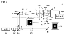
- FIG. 1 is a schematic diagram showing a configuration example of an optical measurement system 1 according to the first embodiment.
- FIG. 1A shows an optical system for recording in-line reference light
- FIG. 1B shows an optical system for recording object light.
- the optical measurement system 1 can configure the optical system shown in FIGS. 1(A) and 1(B).
- the optical system shown in FIG. 1A corresponds to an optical system for recording an off-axis hologram ILR obtained by modulating an in-line reference beam L, which serves as a reference for recording, with an off-axis reference beam R.
- FIG. 1A corresponds to an optical system for recording an off-axis hologram ILR obtained by modulating an in-line reference beam L, which serves as a reference for recording, with an off-axis reference beam R.
- the optical system shown in FIG. 1(B) modulates object light O obtained by illuminating a sample S with illumination light Q with off-axis reference light R, which is divergent light, to record an off-axis hologram IOR .
- the optical system shown in FIG. 1B generates an off-axis hologram I OR (object beam hologram: first hologram) from transmitted light obtained by illuminating the sample S with illumination light Q. .
- An illumination light profile is also acquired using the optical system shown in FIG. In this case, sample S is not placed.
- the processing device 100 measures the surface shape, internal structure, etc. of the sample S based on the off-axis hologram ILR and the off-axis hologram IOR .
- optical measurement system 1 includes a light source 10, a beam expander BE, beam splitters BS1 and BS2, mirrors M1 and M1, as an optical system for recording off-axis hologram ILR .
- M2 an objective lens MO, a pinhole P, a lens L1, a mask A1, and an image sensor D.
- the light source 10 is composed of a laser or the like, and generates coherent light.
- the wavelength band of the light generated by light source 10 may be varied according to the content of measurement (measurement of surface shape or measurement of internal structure).
- the light source 10 that generates visible light when measuring the surface shape of the sample S, the light source 10 that generates visible light may be used.
- a light source 10 that generates light having components in at least part of the wavelength range of 380 to 780 nm is used.
- a visible light source with a peak wavelength at 532 nm may be used.
- the light source 10 that emits near-infrared rays may be used.
- a light source 10 is used that generates light having components in at least part of the wavelength range of 1000 to 1200 nm.
- a near-infrared light source with a peak wavelength at 1030 nm may be used.
- the optical measurement system according to the present embodiment is configured so that the type of light source 10 can be arbitrarily changed.
- the image sensor D records a hologram generated by the optical system shown in FIGS. 1(A) and 1(B).
- a general CCD (Charge-Coupled Device) image sensor or CMOS (Complementary MOS) image sensor is used as the image sensor D.
- These image sensors are semiconductor integrated circuits consisting of electronic circuits formed on silicon substrates. That is, a silicon-based image sensor is used in the optical measurement system according to this embodiment.
- a silicon-based image sensor has photosensitivity mainly in the visible light band, and also has photosensitivity to near-infrared light in addition to visible light.
- the beam expander BE expands the cross-sectional diameter of light from the light source 10 to a predetermined size.
- the beam splitter BS1 splits the light expanded by the beam expander BE into two.
- One light split by the beam splitter BS1 corresponds to the in-line reference light L (first light), and the other light corresponds to the off-axis reference light R (second light).
- the in-line reference light L is reflected by the mirror M2 and guided to the beam splitter BS2. Furthermore, the in-line reference light L is guided to the image sensor D through the half mirror HM2 of the beam splitter BS2.
- An objective lens MO and a pinhole P are arranged between the mirror M2 and the beam splitter BS2.
- the in-line reference light L is condensed by the objective lens MO and narrowed by the pinhole P in cross-sectional diameter.
- a pinhole P corresponds to the position of the point light source of the in-line reference light L.
- FIG. An objective lens MO and a pinhole P realize a point source of in-line reference light L.
- the off-axis reference beam R is reflected by the mirror M1 and guided to the beam splitter BS2. Furthermore, the off-axis reference beam R is guided to the image sensor D by being reflected by the half mirror HM2 of the beam splitter BS2. A mask A1 and a lens L1 are arranged between the mirror M1 and the beam splitter BS2. After passing through the mask A1, the off-axis reference beam R is condensed by the lens L1.
- the mask A1 has an aperture pattern SP1 in the region through which the off-axis reference beam R passes.
- An image corresponding to the aperture pattern SP1 of the mask A1 is formed on the image sensor D.
- the size of the aperture pattern SP1 of the mask A1 is determined so that the off-axis reference light R that has passed through the mask A1 does not illuminate a range beyond the surface of the beam splitter BS2 on the image sensor D side. Determining the size of the aperture pattern SP1 of the mask A1 in this manner suppresses the generation of noise due to unnecessary interference.
- the off-axis reference beam R is adjusted so that the in-line reference beam L can be recorded as a hologram.
- the in-line reference beam L and the off-axis reference beam R are superimposed by the beam splitter BS2 placed in front of the image sensor D through the optical path as described above. That is, the image sensor D obtains an off-axis hologram ILR obtained by modulating the in-line reference light L with the off-axis reference light R, which is divergent light.
- the beam splitter BS2 is preferably configured in a cube shape so that it can be easily arranged in front of the image sensor D.
- the point source of the in-line reference beam L and the point source of the off-axis reference beam R are brought into optical proximity by the beam splitter BS2.
- optical measurement system 1 includes measurement optical system 30 instead of mirror M2, objective lens MO and pinhole P as an optical system for recording off-axis hologram IOR . include.
- the measurement optical system 30 has a mechanism for changing the form of illumination light and a mechanism for limiting the illumination range. More specifically, the measurement optical system 30 includes a movable mirror MM, lenses L2, L31, L32 and a mask A2.
- a sample S to be measured is placed between the measurement optical system 30 and the beam splitter BS2.
- the distance required by the measurement optical system 30 is longer than the distance required by the objective lens MO and the pinhole P of the optical system shown in FIG. It is arranged at a position closer to the light source 10 side.
- the light output from one side of the beam splitter BS1 is used as illumination light Q (first light) for illuminating the sample S.
- the optical measurement system has a mechanism for changing the form of illumination with the illumination light Q.
- FIG. 1B shows a movable mirror MM. More specifically, the illuminating form of the illumination light Q is changed by rotating the movable mirror MM.
- a change in the form of illuminating the illumination light Q means a change in the angle at which the illumination light Q is illuminated. Below, the angle which illuminates the illumination light Q is also called an "illumination angle.”
- the off-axis reference light R (second light) output from the other beam splitter BS1 is guided to the image sensor D through the optical path common to that in FIG. 1(A).
- the object light O obtained by illuminating the sample S with the illumination light Q (that is, the light transmitted through the sample S) is transmitted through the half mirror HM2 of the beam splitter BS2 and guided to the image sensor D.
- a lens L3, a mask A2, and a lens L2 are arranged in this order between the movable mirror MM and the beam splitter BS2.
- Illumination light Q is condensed by lens L3 and passes through mask A2.
- the illumination light Q that has passed through the mask A2 is further condensed by the lens L2 and forms an image on the sample S.
- the mask A2 corresponds to a limiting portion that limits the range of illumination of the sample S with the illumination light Q to a predetermined range.
- a mask A2 in which an opening pattern SP2 corresponding to a predetermined range is formed in the shielding member may be used.
- the illumination light Q passes through the area corresponding to the aperture pattern SP2.
- the image of the aperture pattern SP2 of the mask A2 passes through the lens L2 and forms an image on the sample S. That is, of the light illuminating the mask A2, only the light corresponding to the aperture pattern SP2 passes through the mask A2.
- the range in which the illumination light Q that has passed through the mask A2 illuminates the sample S can be limited.
- unnecessary light can be reduced and measurement accuracy can be improved.
- the illumination range may vary depending on the thickness of the sample S.
- the aperture pattern SP2 of the mask A2 is changed as necessary, or the illumination range is changed.
- the position of the lens L2 for imaging the light Q onto the sample S is changed.
- the configuration for illuminating the mask A2 with the illumination light Q is not limited to the configuration shown in FIG. 1(B), and any configuration can be adopted.
- FIG. 2 is a schematic diagram showing a detailed configuration example of the measurement optical system 30 in the optical measurement system 1 according to the first embodiment.
- the illumination light Q passes through the movable mirror MM, the lens L31, the lens L32, the mask A2, and the lens L2 in this order, and forms an image on the sample S.
- the lens L31 and the lens L32 constitute an imaging optical system 20 such as a 4f optical system.
- the illumination light Q incident on the movable mirror MM is reflected in a direction corresponding to the angle (orientation) of the movable mirror MM and enters the imaging optical system 20 .
- the illumination light Q propagates in the direction reflected by the movable mirror MM, passes through the aperture pattern SP2 of the mask A2, and forms an image on the sample S in the same shape as the aperture pattern SP2.
- FIG. 2(B) shows an example of an optical system in which the illumination light Q that illuminates the sample S is parallel light. More specifically, in the optical system shown in FIG. 2B, lenses L21 and L22 are arranged instead of the lens L2 in the optical system shown in FIG. 2A. Both the lens L21 and the lens L22 are condenser lenses, and by combining them, the illumination light Q that has passed through the mask A2 illuminates the sample S as parallel light.
- the optical systems arranged before and after the mask A2 are not limited to the optical systems shown in FIGS. 2(A) and 2(B).
- any configuration may be adopted as long as the reflected light from the movable mirror MM can be projected so as to cover the aperture pattern SP2 of the mask A2.
- any configuration may be adopted as long as the image of the aperture pattern SP2 of the mask A2 can be formed on the sample S.
- the number and types of lenses can be arbitrarily designed.
- the lenses L31 and L32 may be omitted.
- the light-receiving surface of the image sensor D will be referred to as the "recording surface”
- the intersection of the recording surface and the central optical axis of the beam splitter BS2 will be referred to as the "origin”.
- the optical axis direction be the z-axis
- two axes orthogonal to the z-axis be the x-axis and the y-axis, respectively. That is, the optical axis is perpendicular to the recording surface of the image sensor D, and the x-axis and the y-axis are parallel to the recording surface of the image sensor D. It should be noted that the same applies to other embodiments.
- the distribution of the object light O, the off-axis reference light R, and the in-line reference light L on the recording surface of the image sensor D can be expressed by general formulas such as the following formulas (1) to (3).
- the in-line reference light L, the object light O, and the off-axis reference light R are lights having mutually coherent angular frequencies ⁇ .
- the off-axis hologram ILR recorded in the optical system shown in FIG. (4) It is calculated like the formula. Further, the off-axis hologram IOR recorded in the optical system shown in FIG. It is calculated as in the following (5) formula.
- the first term on the right side corresponds to the light intensity component of the object beam O or the in-line reference beam L
- the second term on the right side corresponds to the light intensity component of the off-axis reference beam R
- the third term on the right side corresponds to the direct image component generated by modulating the object light O with the off-axis reference light R
- the fourth term on the right side corresponds to the conjugate image component.
- the component of the inline reference beam L can be removed by multiplying the complex amplitude inline hologram JOL shown in equation (8) by the inline reference beam L.
- the method described in International Publication No. 2020/045584 Patent Document 3
- an object beam hologram U as shown in the following equation (9) is obtained.
- the object beam hologram U includes a frequency component that does not satisfy the sampling theorem
- the following correction processing is applied to a plane of interest that is a predetermined distance from the recording plane (hereinafter referred to as " A hologram having information capable of reproducing the state of the sample surface is generated.
- a hologram having information capable of reproducing the state of the sample surface is assumed to be a reproduction object beam hologram U ⁇ . If the sampling theorem is satisfied, the object light hologram U is used as it is as the reconstruction object light hologram U ⁇ .
- the number of sampling points forming the image output from the image sensor D may be increased by interpolation.
- the pixel pitch of the image sensor D may be subdivided by applying the division superposition process disclosed in International Publication No. 2020/045584 (Patent Document 3). The amount of calculation can be reduced by using the division superposition process.
- a light wave distribution on an arbitrary sample surface can be reconstructed by performing diffraction calculation by plane wave expansion on the reconstruction object light hologram U ⁇ .
- Ud be a hologram obtained by propagating the reconstruction object beam hologram U ⁇ by plane wave expansion by a distance d (on a sample plane separated by a distance d from the recording plane).
- T m,m+1 (k x , ky ) the transmission coefficient when incident from the medium m to the medium m+1 is expressed as T m,m+1 (k x , ky ).
- T M,M+1 (k x , ky ) is always considered to be 1.
- the optical measurement system records multiple off-axis holograms I OR (object beam holograms or illumination beam holograms depending on the presence or absence of the sample S) by changing the illuminating form of the illumination beam Q.
- FIG. As a form of illuminating the illumination light Q, for example, an illumination angle may be adopted.
- FIG. 3 is a diagram for explaining the effect obtained by changing the illumination form of the illumination light Q in the optical measurement system according to this embodiment.
- Object A is an object to be reproduced as an image
- object B is an object that exists outside the sample plane and causes scattering.
- the illumination light Q when the illumination light Q is illuminated from a single direction (single illumination angle), the diffracted light generated by scattering by the object B is reflected on the sample surface (the focal point of the illumination light). position), degrading the quality of the reconstructed image.
- multiple images are reproduced by changing the illumination angle, and the multiple reproduced images are added.
- object A whose signal amplitude and phase are substantially the same among multiple images, is emphasized, and the influence of object B is relatively reduced.
- a plurality of off-axis holograms I ORi are recorded by changing the illumination angle in i ways (where i is an integer equal to or greater than 2) (illumination light Q i ).
- Reconstruction object light holograms U ⁇ i are calculated from the off-axis holograms I ORi .
- a light wave distribution obtained by propagating the reproducing object light hologram U ⁇ i to the sample surface (the propagation distance is the same) by plane wave expansion is defined as an object light distribution U Si .
- the amplitude-phase distribution U Pi on the sample plane is calculated by dividing the complex amplitude object light distribution U Si by the illumination light distribution Q Si on the sample plane generated by the illumination light Q i .
- the amplitude-phase distribution U Pi on the sample plane consists of an object light hologram (first hologram) obtained by modulating the object light O obtained by illuminating the sample S with the illumination light Q with the off-axis reference light R, and the sample It is calculated based on an illumination light hologram (second hologram) obtained by modulating the illumination light Q with the off-axis reference light R in a state where S does not exist.
- the amplitude phase distribution U Pi is obtained by adding the phase change amount ⁇ i caused by the sample S to the phase distribution ⁇ Qi of the illumination light Q i .
- the composite amplitude-phase distribution USA is calculated by integrating the amplitude-phase distributions UPi calculated for each lighting mode (illumination angle) as complex numbers.
- phase components other than the sample plane it is preferable to set a sufficiently large number of illumination modes (for example, illumination angles) with the illumination light Q.
- the signal-to-noise ratio is proportional to the square root of the number of forms that illuminate the illumination light Q. SN ratio is doubled).
- the range in which the illumination angle can be changed is optically determined according to the size of the sample S, the resolution of the image sensor D, the width of the field of view of the image sensor D, and so on.
- the illumination angle is changed within the optically permissible range.
- changing the illumination angle means changing the azimuth angle while keeping the incident angle of the illumination light Q constant.
- the number of changes in the illumination angle is typically determined based on the required quality and allowable processing time.
- the spatial resolution (on the xy plane) may decrease, although the phase resolution does not decrease.
- the direct image component is combined with the light intensity component and the conjugate image component in the spatial frequency band.
- the range of the illumination light Q is restricted by a restricting portion such as the mask A2, thereby preventing image degradation due to overlapping of spatial frequency bands.
- the spatial frequency bandwidth included in the interference fringes can be adjusted appropriately while maintaining the degree of freedom of the illumination method.
- the control makes efficient use of the spatial frequency bandwidth that the image sensor D can record.
- mask A1 and lens L1 implement a point source of off-axis reference light R.
- FIG. 1 The spatial frequency f of the interference fringes at an arbitrary point on the recording surface is given by the following equation (13) using the incident angle ⁇ O of the object beam O and the incident angle ⁇ R of the off-axis reference beam R at that point: can be expressed as
- FIG. 4 is a diagram for explaining how the object light O and the off-axis reference light R are incident on the recording surface of the image sensor D.
- FIG. FIG. 4A shows a case where the off-axis reference beam R is a plane wave
- FIG. 4B shows a case where the off-axis reference beam R is a spherical wave.
- the angle formed by the object beam O and the off-axis reference beam R at an arbitrary point on the recording surface of the image sensor D is the image It depends on the position of the sensor D on the recording surface.
- the angle ⁇ formed by the object beam O and the off-axis reference beam R at the upper end of the recording surface of the image sensor D differs greatly from the angle ⁇ formed by the lower end of the recording surface.
- the object beam O and the off-axis reference beam R form one point on the recording surface of the image sensor D.
- the angle does not depend on the position on the recording surface and has almost the same value.
- the angle ⁇ formed by the object beam O and the off-axis reference beam R at the upper end of the recording surface of the image sensor D is substantially the same as the angle ⁇ formed at the lower end of the recording surface.
- the angle formed by the ray (object beam O) generated from an arbitrary point on the sample S and the ray generated from the point source of the off-axis reference beam R is defined as It can be made substantially constant at any point.
- zL is the distance in the z-axis direction from the point source of the off-axis reference beam R to the recording surface
- ⁇ is the wavelength.
- u be the spatial frequency in the x direction
- v be the spatial frequency in the y direction.
- the "region where the wave source exists” means the range in which the sample S is illuminated. That is, by optimizing the aperture pattern SP2 of the mask A2, the illumination range can be restricted, thereby appropriately controlling the spatial frequency band. Since the mask A2 merely limits the range of illumination of the sample S, the reproduced image is not distorted as long as the complex amplitude of the object beam O is correctly recorded.
- the off-axis hologram IOR recorded in the optical system shown in FIG. 1(B) is calculated by the formula (5).
- the component necessary for image reproduction is the direct image component of the third term, and the other terms are superimposed as noise components and must be removed by a bandpass filter.
- FIG. 5 is a diagram for explaining the relationship between the sample S and the off-axis reference beam R in the optical measurement system according to this embodiment.
- the bandwidth Wy in the x and v directions can be approximately expressed as in the following equation (15), and the center frequency u c in the u direction and the center frequency v c in the v direction are expressed by the following equation (16) can be approximately expressed as
- the u-direction bandwidth W x and the v-direction bandwidth W y of the conjugate image component (fourth term) can be approximately expressed as in the above equation (15).
- the center frequency u c in the u direction and the center frequency v c in the v direction of the conjugate image component (fourth term) are obtained by inverting the sign of the above equation (16).
- the bandwidth of the combined component of the light intensity component of the first term and the light intensity component of the second term spreads around the origin by twice the size of equation (15).
- FIG. 6 is a diagram for explaining the relationship of spatial frequency bands for off-axis holograms in the optical measurement system according to this embodiment.
- the sample S exists with a size of a ⁇ b around the coordinates of (0, 0, z L ).
- a point source of off-axis reference light R is located at a distance of x R in the x direction and y R in the y direction from coordinates (0, 0, z L ).
- the direct image component of the third term including the information of the object light O spreads in the size of the bandwidth W x ⁇ W y , and the direct image component is determined depending on the coordinates (x R , y R ) of the point source of the off-axis reference light.
- the component of the third term should be brought close to the limit where it does not overlap with the components of the other terms (first, second, and fourth terms). There is a need.
- the spatial frequency bandwidth is limited to an appropriate range.
- the off-axis reference light is divergent light (point light source)
- the relationship of the above equation (5) holds. Therefore, by limiting the illumination range of the illumination light Q, the spatial frequency bandwidth of each component is can be restricted to an appropriate range.
- the component corresponding to the illumination light Q (the third term) and the components other than the component corresponding to the illumination light Q (the first term and The size of the range in which the sample S is illuminated with the illumination light Q (that is, the aperture pattern SP2 of the mask A2, which is the limiting portion) is determined so that the second term) does not overlap.
- the spatial frequency band of the image sensor D can be efficiently used, and noise caused by overlapping spatial frequency bands can be suppressed.
- the mask A2 described above is another holography optical system that uses divergent light (that is, a point light source or a light source that can be regarded as a point light source) as reference light. Also, it is effective to limit the spatial frequency bandwidth of the direct image component to a range that can be recorded by the image sensor D, for example.
- the mask A2 used in the optical measurement system according to the present embodiment can be similar in appearance to the field stop used in an optical microscope.
- the field stop is used for the purpose of suppressing stray light caused by extra light (light outside the field of view) hitting a wall in the optical path.
- the noise level can be reduced by the field diaphragm, the amount of stray light that is suppressed is very small, and unless the purpose is to detect weak light, no serious problem will arise even if no active countermeasures are taken.
- limiting the illumination range in digital holography using divergent light as reference light has the effect of limiting the spatial frequency bandwidth included in the interference fringes to the range that can be recorded by the image sensor D.
- the mask A2 used in the optical metrology system according to this embodiment is used for this purpose.
- the mask A2 used in the optical measurement system according to the present embodiment exerts an effect different from the effect exerted by the field stop used in the optical microscope.
- the size of the aperture pattern (the cross-sectional area through which the illumination light passes) may be arbitrarily changed by using an optical element capable of controlling light transmittance, such as a polarizing mirror or liquid crystal.
- an optical element capable of controlling light transmittance such as a polarizing mirror or liquid crystal.
- An optical measurement system requires an illumination light profile for calculation of the composite amplitude-phase distribution USA , and the like.
- diffraction calculations can be used to calculate the illumination light profile at another distance based on the illumination light profile at a sample surface at a certain distance from the recording surface. Therefore, it is not necessary to record the illumination light profile each time the distance of the sample surface from the recording surface changes.
- the illumination light profile of the illumination light transmitted through the substrate can be calculated by performing propagation calculation in the medium using plane wave expansion for the illumination light profile.
- the approximate thickness and refractive index of the substrate are known, there is no need to prepare a sample of the substrate alone (a sample different from the sample S to be measured) and record the illumination light profile.
- Layers other than the substrate of the sample S can be measured using the illumination light profile transmitted through the substrate. Further, when recording can be performed only with the substrate, the propagation calculation in the medium of the substrate can be omitted by recording the profile of the illumination light transmitted through the substrate with only the substrate placed.
- the illumination light profile recorded without the sample S is used to subtract the phase distribution ⁇ Q of the illumination light from the phase distribution of the combined amplitude-phase distribution USA .
- the phase change amount ⁇ i caused by the sample S is calculated.
- the surface shape of the sample S is determined using the relational expression between the phase change amount ⁇ caused by the sample S and the thickness ⁇ d of the sample S, which is shown in Equation (17) below. to measure.
- kz1 is the z-direction wavenumber in the sample S
- kz2 is the z-direction wavenumber in the medium in which the sample S exists
- ⁇ is the phase correction term
- ⁇ is the light source wavelength.
- Wavenumbers kz1 and kz2 can be calculated according to the following equations (18) and (19), respectively.
- n1 in the formula is the refractive index of the medium in which the sample S exists
- the wave number k x in the x direction and the wave number k y in the y direction in the equations are the amount of phase change per unit length in the x direction and the y direction, so as in the following equations (20) and (21) , can be calculated by differentiating the phase distribution ⁇ Q of the illumination light Q on the sample surface.
- phase correction term ⁇ in the equation (17) is used to correct the phase change due to the complex transmittance when the transmittance is a complex number due to light absorption in the sample S or the like.
- the phase correction term ⁇ may be omitted when the phase change due to the complex transmittance can be regarded as uniform over the entire sample S because the samples S are all made of the same material.
- the illumination light Qi may be corrected by parallel movement of the pixels on the image sensor D.
- the amount of translation is typically determined to maximize the correlation between the object light distribution U s and the illumination light Q i .
- the amount of information may be reduced by using a low-pass filter or polynomial approximation.
- FIG. 7 is a flow chart showing the processing procedure of the surface profile measuring method using the optical measuring system 1 according to the first embodiment.
- a visible light source may be used as the light source 10 in the procedure shown in FIG.
- a process of acquiring inline reference light L is performed. More specifically, the optical system shown in FIG. 1A is constructed (step S2). Then, by generating coherent light from the light source 10, the processing device 100 acquires an off-axis hologram ILR obtained by modulating the in-line reference light L recorded on the image sensor D with the off-axis reference light R (step S4). Steps S2 and S4 need only be performed once unless the optical system related to the off-axis reference beam R is changed. Further, the processing of steps S2 and S4 is for improving the accuracy of the reproduced image, and depending on the required accuracy, the processing of steps S2 and S4 may be omitted.
- step S6 the optical system shown in FIG. 1B is constructed.
- a substrate having the same thickness as the substrate of the sample S may be placed at the position where the sample S is placed (sample position), or nothing may be placed at the sample position. This state corresponds to the measurement reference.
- the movable mirror MM is driven to set one of a plurality of illumination angles (step S8). Then, by generating coherent light from the light source 10, the processing device 100 acquires the illumination light hologram Qi (x,y) (second hologram) recorded on the image sensor D (step S10).
- the processing device 100 records a hologram with the image sensor D in which the light obtained by illuminating with the illumination light Q is modulated with the off-axis reference light R in a state where the sample S does not exist.
- the processing device 100 instead of the sample S, causes the image sensor D to record a hologram of transmitted light obtained by illuminating only the substrate included in the sample S and not to be measured with the illumination light Q.
- the processing device 100 calculates an illumination light profile Q ⁇ i (x, y) from the illumination light hologram Q i (x, y) (step S12).
- steps S8 to S12 are repeated by a predetermined number (N) of illumination angles (1 ⁇ i ⁇ N).
- a process of acquiring the amplitude-phase distribution of the sample S is performed. More specifically, the sample S is placed at its original position in the optical system shown in FIG. 1(B) (step S14). Subsequently, the movable mirror MM is driven to set one of the plurality of illumination angles (step S16). Then, the light source 10 generates coherent light, and the processing device 100 acquires the object light hologram U i (x, y) recorded on the image sensor D (step S18).
- the processing device 100 calculates a reproduction object beam hologram U ⁇ i (x, y) from the object beam hologram U i (x, y) (step S20). Then, the processing device 100 propagates the reconstruction object light hologram U ⁇ i (x, y) and the corresponding illumination light profile Q ⁇ i (x, y) to the position of the sample surface by plane wave expansion, and the object light hologram U ⁇ i (x, y) on the sample surface. A light distribution U Si (x, y) and an illumination light distribution Q Si (x, y) are calculated (step S22). Further, the processing device 100 divides the object light distribution U Si (x, y) by the corresponding illumination light distribution Q Si (x, y) to calculate the amplitude-phase distribution U Pi (x, y) on the sample plane. (step S24).
- steps S16 to S24 are repeated by a predetermined number (N) of illumination angles (1 ⁇ i ⁇ N).
- the processing device 100 calculates the surface shape of the sample S.
- the processing device 100 calculates the phase change amount ⁇ (x, y) from the argument of the composite amplitude-phase distribution U SA (x, y) on the sample plane (step S28). Then, the processing device 100 calculates the thickness ⁇ d(x, y) of the sample S using the phase change amount ⁇ (x, y) (step S30). For calculating the thickness ⁇ d of the sample S, the relational expression shown in the above equation (17) is used.
- the processing device 100 aggregates the thickness ⁇ d(x, y) at each coordinate of the sample surface to calculate the shape profile of the sample S (step S32).
- the surface shape of the sample S can be calculated by the above processing. Note that the refractive index and refractive index profile of the sample S can also be measured. In this case, in step S30, the refractive index n 2 (x, y) of the sample S is calculated, and in step S32, by collecting the refractive indices n 2 (x, y) at each coordinate of the sample surface, A refractive index profile of the sample S is calculated.
- FIG. 8 is a flow chart showing a processing procedure of an internal structure measuring method using the optical measuring system 1 according to the first embodiment.
- a near-infrared light source may be used as the light source 10 in the procedure shown in FIG.
- the procedure shown in the flowchart of FIG. 8 is a process of imaging the intensity distribution and/or phase distribution of the composite amplitude-phase distribution U SA (x, y) instead of the processes of steps S28 to S32 shown in the flowchart of FIG. (Step S34) is adopted.
- the processing device 100 calculates the composite amplitude-phase distribution U SA (x, y) by accumulating the amplitude-phase distribution U Pi (x, y) as complex numbers (step S26), and calculates the composite amplitude-phase distribution U Pi (x, y).
- the internal structure of the sample S is visualized by imaging the distribution U SA (x,y).
- FIG. 9 is a schematic diagram showing a configuration example of the optical measurement system 2 according to the second embodiment.
- FIG. 9A shows an optical system for recording in-line reference light
- FIG. 9B shows an optical system for recording object light.
- the optical measurement system 2 can configure the optical system shown in FIGS. 9(A) and 9(B).
- the optical system shown in FIG. 9A is the same as the optical system for recording in-line reference light in optical measurement system 1 according to Embodiment 1 shown in FIG. 1A, so detailed description will not be repeated. .
- the optical system shown in FIG. 9B corresponds to an optical system for recording an off-axis hologram IOR obtained by modulating an object light O obtained by illuminating a sample S with an illumination light Q with an off-axis reference light R. . More specifically, the optical system shown in FIG. 9B generates an off-axis hologram I OR (object beam hologram: first hologram) from the reflected light obtained by illuminating the sample S with the illumination light Q. . An illumination light profile is also acquired using the optical system shown in FIG. 9B. In this case, a standard reference surface is arranged instead of the sample S, as will be described later.
- the optical system shown in FIG. 9B illuminates the sample S with the illumination light Q compared with the optical system for recording the object light in the optical measurement system 1 according to the first embodiment shown in FIG. configuration is different. Therefore, the off-axis reference beam R output from the other beam splitter BS1 is guided to the image sensor D through the optical path common to FIGS. 1(A), 1(B) and 9(A).
- the light output from one side of the beam splitter BS1 is used as illumination light Q for illuminating the sample S.
- the illumination light Q split by the beam splitter BS2 is reflected by the mirror M2, passes through the measurement optical system 32, and is guided to the beam splitter BS2.
- the illumination light Q is further reflected by the half mirror HM2 of the beam splitter BS2 to illuminate the sample S.
- Object light O obtained by illuminating the sample S with the illumination light Q (that is, light reflected by the sample S) is guided to the image sensor D through the half mirror HM2 of the beam splitter BS2.
- the measurement optical system 32 includes a movable mirror MM, a lens L3, a mask A2, and a lens L4.
- the illumination light Q reflected by the movable mirror MM is condensed by the lens L3 and passes through the mask A2.
- the illumination light Q that has passed through the mask A2 is further condensed by the lens L4 and formed on the sample S as an image. That is, the image of the aperture pattern SP2 of the mask A2 is formed on the sample S through the lens L4.
- the range in which the illumination light Q that has passed through the mask A2 illuminates the sample S can be limited.
- unnecessary light can be reduced and measurement accuracy can be improved.
- the form of illuminating the illumination light Q is changed by rotating the movable mirror MM.
- the illumination range may vary depending on the thickness of the sample S.
- the aperture pattern SP2 of the mask A2 is changed as necessary, or the illumination range is changed.
- the position of the lens L2 for imaging the light Q onto the sample S is changed.
- the lens L3 may be omitted when the mirror M2 and the mask A2 are arranged optically close to each other.
- FIG. 9B acquires the illumination light profile from the reflected light obtained by illuminating the reference reference surface with the illumination light Q instead of the sample S.
- the illumination light Q By propagating the recorded illumination light Q, it is possible to calculate the illumination light distribution QS on the sample surface at different distances. It is not necessary to record the illumination light Q every time. Further, when the coordinates of the point light source of the illumination light are displaced due to disturbance, the illumination light Q may be corrected by moving the pixels on the image sensor D in parallel.
- a plurality of illumination light profiles are recorded while the standard reference plane is translated in the x and y directions, and the average value of the recorded multiple illumination profiles is actually calculated. It may be an illumination light profile to be used.
- phase change amount caused by the sample S is used for measuring the surface shape of the sample S.
- FIG. it is preferable to use visible light as the illumination light Q.
- kx is the wave number in the x direction
- ky is the wave number in the y direction
- ⁇ is the phase correction term
- Wavenumber kx and wavenumber ky can be calculated according to the above equations (20) and (21).
- the phase correction term ⁇ may also be omitted if the phase change due to the complex reflectance can be considered uniform over the entire sample S for the reason that all the samples S are made of the same material.
- an optical system in which the illumination light Q is parallel light may be employed.
- the illumination light Q is a spherical wave
- defocusing with respect to the sample surface can be detected as a concave or convex false shape.
- Such a false shape is caused by the fact that the illumination light is a spherical wave. Therefore, when measuring the shape (in-plane profile) of the entire sample surface, an optical system is adopted in which the illumination light Q is parallel light. preferably.
- FIG. 10 is a flow chart showing the processing procedure of the surface profile measuring method using the optical measuring system 2 according to the second embodiment.
- a visible light source may be used as the light source 10 in the procedure shown in FIG.
- a process of acquiring inline reference light L is performed. More specifically, the optical system shown in FIG. 9A is constructed (step S52). Then, by generating coherent light from the light source 10, the processing device 100 obtains an off-axis hologram ILR obtained by modulating the in-line reference light L recorded on the image sensor D with the off-axis reference light R (step S54). Steps S52 and S54 need only be executed once unless the optical system related to the off-axis reference beam R is changed. Further, the processing of steps S2 and S4 is for improving the accuracy of the reproduced image, and depending on the required accuracy, the processing of steps S2 and S4 may be omitted.
- step S56 the optical system shown in FIG. 9B is constructed (step S56).
- the sample S is not placed, and the standard reference plane is placed at the position where the sample S is placed (sample position). This state corresponds to the measurement reference.
- the movable mirror MM is driven to set one of the plurality of illumination angles (step S58). Then, by generating coherent light from the light source 10, the processing device 100 acquires the illumination light hologram Qi (x,y) (second hologram) recorded on the image sensor D (step S60).
- the processing device 100 calculates an illumination light profile Q ⁇ i (x, y) from the illumination light hologram Q i (x, y) (step S62).
- steps S58 to S62 are repeated by a predetermined number (N) of illumination angles (1 ⁇ i ⁇ N).
- step S64 a process of acquiring the amplitude-phase distribution of the sample S is executed. More specifically, the sample S is placed at its original position in the optical system shown in FIG. 9B (step S64). Subsequently, the movable mirror MM is driven to set one of the plurality of illumination angles (step S66). Then, by generating coherent light from the light source 10, the processing device 100 acquires the object light hologram Ui (x,y) recorded on the image sensor D (step S68).
- the processing device 100 calculates a reproduction object beam hologram U ⁇ i (x, y) from the object beam hologram U i (x, y) (step S70). Then, the processing device 100 propagates the reconstruction object light hologram U ⁇ i (x, y) and the corresponding illumination light profile Q ⁇ i (x, y) to the position of the sample surface by plane wave expansion, and the object light hologram U ⁇ i (x, y) on the sample surface. A light distribution U Si (x, y) and an illumination light distribution Q Si (x, y) are calculated (step S72). Further, the processing device 100 divides the object light distribution U Si (x, y) by the corresponding illumination light distribution Q Si (x, y) to calculate the amplitude-phase distribution U Pi (x, y) on the sample plane. (step S74).
- steps S66 to S74 are repeated by a predetermined number (N) of illumination angles (1 ⁇ i ⁇ N).
- the processing device 100 calculates the surface shape of the sample S.
- the processing device 100 calculates the phase change amount ⁇ (x, y) from the argument of the composite amplitude-phase distribution U SA (x, y) on the sample plane (step S78). Then, the processing device 100 uses the phase change amount ⁇ (x, y) to calculate the height h(x, y) of the sample S (step S80). For calculating the height h of the sample S, the relational expression shown in the above equation (22) is used.
- the processing device 100 aggregates the thickness ⁇ d(x, y) at each coordinate of the sample surface to calculate the shape profile of the sample S (step S82).
- the surface shape of the sample S can be calculated by the above processing. (c4: measurement of internal structure of sample) It is preferable to use near-infrared light as the illumination light Q for measuring the internal structure of the sample S.
- the illumination light Q By using near-infrared light as the illumination light Q, the object light hologram U obtained by illuminating the sample S with the illumination light Q shows the internal structure of the sample S.
- FIG. The internal structure of the sample S can be measured by setting the sample surface at an arbitrary position (at an arbitrary distance from the recording surface) with respect to the sample S.
- FIG. 11 is a flow chart showing a processing procedure of an internal structure measuring method using the optical measuring system 2 according to the second embodiment.
- a near-infrared light source may be used as the light source 10 in the procedure shown in FIG.
- Step S84 The procedure shown in the flowchart of FIG. 11 replaces the processing of steps S78 to S82 shown in the flowchart of FIG. (Step S84) is adopted.
- the processing device 100 calculates the composite amplitude-phase distribution U SA (x, y) by accumulating the amplitude-phase distribution U Pi (x, y) as complex numbers (step S76), and calculates the composite amplitude-phase distribution U Pi (x, y).
- the internal structure of the sample S is visualized by imaging the distribution U SA (x,y).
- FIG. 12 is a schematic diagram showing a hardware configuration example of the processing device 100 included in the optical measurement system according to this embodiment.
- processing device 100 includes, as main hardware elements, processor 102, main memory 104, input unit 106, display unit 108, storage 110, interface 120, and network interface 122. , and the media drive 124 .
- the processor 102 is typically an arithmetic processing unit such as a CPU (Central Processing Unit) or GPU (Graphics Processing Unit), and reads one or more programs stored in the storage 110 to the main memory 104 for execution. do.
- the main memory 104 is a volatile memory such as DRAM (Dynamic Random Access Memory) or SRAM (Static Random Access Memory), and functions as a working memory for the processor 102 to execute programs.
- the input unit 106 includes a keyboard, mouse, etc., and receives operations from the user.
- the display unit 108 outputs results of program execution by the processor 102 to the user.
- the storage 110 consists of a non-volatile memory such as a hard disk or flash memory, and stores various programs and data. More specifically, the storage 110 holds an operating system 112 (OS: Operating System), a measurement program 114 , hologram data 116 and measurement results 118 .
- OS Operating System
- measurement program 114 hologram data 116 and measurement results 118 .
- the operating system 112 provides an environment in which the processor 102 executes programs.
- Measurement program 114 is executed by processor 102 to implement the optical measurement method and the like according to the present embodiment.
- the hologram data 116 corresponds to image data output from the image sensor D.
- FIG. Measurement results 118 include measurement results obtained by execution of measurement program 114 .
- the interface 120 mediates data transmission between the processing device 100 and the image sensor D.
- Network interface 122 mediates data transmission between processing device 100 and an external server device.
- the media drive 124 reads necessary data from a recording medium 126 (such as an optical disc) that stores programs to be executed by the processor 102 and stores it in the storage 110 .
- a recording medium 126 such as an optical disc
- the measurement program 114 and the like executed in the processing device 100 may be installed via the recording medium 126 or the like, or may be downloaded from the server device via the network interface 122 or the like.
- the measurement program 114 may call necessary modules out of the program modules provided as part of the operating system 112 in a predetermined sequence at a predetermined timing to execute processing. In such a case, the technical scope of the present invention also includes the measurement program 114 that does not include the module. The measurement program 114 may be provided as part of another program.
- processor 102 of the processing device 100 executing the program can be implemented in a hardwired logic circuit (for example, FPGA (Field-Programmable Gate Array), ASIC (Application Specific Integrated Circuit), etc.).
- a hardwired logic circuit for example, FPGA (Field-Programmable Gate Array), ASIC (Application Specific Integrated Circuit), etc.
- the hardware configuration example of the processing device 100 is the same in other embodiments, so detailed description will not be repeated.
- FIG. 13 is a schematic diagram showing a functional configuration example of the processing device 100 included in the optical measurement system according to this embodiment.
- Each functional element shown in FIG. 13 may typically be implemented by the processor 102 of the processing device 100 executing the measurement program 114 .
- Appropriate hardware for realizing the functional configuration shown in FIG. 13 is selected according to each era.
- processing device 100 includes, as main functional elements, off-axis hologram acquisition module 150, illumination light hologram acquisition module 152, object light hologram acquisition module 154, hologram reconstruction module 156, amplitude phase It includes a distribution calculation module 158 , an integration module 160 , an object beam phase calculation module 162 , an object shape calculation module 164 , an imaging module 166 and an illumination angle control module 168 .
- the off-axis hologram acquisition module 150 records the hologram recorded on the image sensor D as the off-axis hologram ILR in a state in which the optical system for recording the in-line reference light is configured.
- the illumination light hologram acquisition module 152 acquires the illumination light hologram Q i (x, y) recorded on the image sensor D with the optical system configured for recording object light.
- the object light hologram acquisition module 154 acquires the object light hologram U i (x, y) recorded on the image sensor D in a state where the optical system for recording the object light is configured.
- Both the illumination light hologram acquisition module 152 and the object light hologram acquisition module 154 are configured to be able to record the detection signal of the image sensor D, and one of them is set according to a manually or automatically set state signal. Activated.
- the hologram reproduction module 156 calculates a reproduction illumination light hologram (illumination light profile Q ⁇ i (x, y)) from the illumination light hologram Q i (x, y) acquired by the illumination light hologram acquisition module 152, and also calculates the object light
- a reproduction object beam hologram U ⁇ i (x, y) is calculated from the object beam hologram U i (x, y) obtained by the hologram obtaining module 154 .
- the hologram reproduction module 156 propagates the illumination light profile Q ⁇ i (x, y) and the object light hologram for reproduction U ⁇ i (x, y) to the position of the sample surface by plane wave expansion to obtain the illumination light distribution Q Si on the sample surface. (x,y) and the object light distribution U Si (x,y) are calculated.
- the amplitude-phase distribution calculation module 158 divides the object light distribution U Si (x,y) by the corresponding illumination light distribution Q Si (x,y) to obtain the amplitude-phase distribution U Pi (x,y) at the sample plane. calculate.
- the integration module 160 calculates the composite amplitude-phase distribution USA by integrating the amplitude-phase distributions UPi as they are as complex numbers.
- the object light phase calculation module 162 calculates the phase change amount ⁇ (x, y) from the argument of the composite amplitude phase distribution U SA (x, y).
- the object shape calculation module 164 uses the phase change amount ⁇ (x, y) to calculate information (thickness, refractive index, etc.) specifying the surface shape of the sample S.
- the object shape calculation module 164 outputs the calculation result as sample S shape information.
- Imaging module 166 images the intensity and/or phase distributions of the composite amplitude-phase distribution U SA (x,y).
- the illumination angle control module 168 determines the types and number of illumination angles to be realized by the movable mirror MM according to the settings.
- the illumination angle control module 168 in cooperation with the hologram reproduction module 156 and the like, drives the movable mirror MM so as to achieve a desired illumination angle.
- FIG. 14 is a schematic diagram showing an example of a user interface screen provided in the optical measurement system according to this embodiment.
- User interface screen 170 shown in FIG. 14 is typically displayed on display 108 of processing device 100 .
- the processing device 100 provides a user interface screen 170 for accepting the setting of the number of forms to be illuminated with the illumination light Q (first light).
- the user interface screen 170 includes an input field 172 for inputting the number of illumination angles, a display field 174 for indicating the degree of improvement in the SN ratio, and a display field 176 for indicating the time required for measurement.
- the input field 172 accepts the setting of the number of illumination angles to be changed (the i number described above). Based on the set number of illumination angles, the processing device 100 calculates the degree of improvement in the SN ratio and displays it in the display field 174, and also calculates the time required for measurement and displays it in the display field 176. .
- the user sets the number of illumination angles in consideration of the quality of the measurement results (SN ratio) and the allowable takt time displayed on the user interface screen 170 .
- An appropriate number of illumination angles may be suggested by inputting the required quality and allowable takt time.
- the number of illumination angles may be set via a user interface screen 170 as shown in FIG.
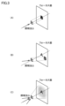
- FIG. 15 is a diagram showing an example of surface shape measurement by the optical measurement system according to this embodiment.
- FIG. 15 shows an example of the amplitude-phase distribution of the USAF 1951 test target surface (sample surface) recorded using the optical measurement system 2 employing the reflective optics shown in FIG.
- the light source 10 a visible light source having a peak wavelength of 532 nm was used.
- FIGS. 15(A) and 15(C) show the intensity distribution of the amplitude phase distribution
- FIGS. 15(B) and 15(D) show the phase distribution of the amplitude phase distribution.
- FIGS. 15(A) and 15(B) show amplitude-phase distributions UP1 recorded at a single illumination angle of the illumination light.
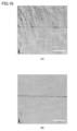
- FIG. 16 is a diagram showing an example of internal structure measurement by the optical measurement system according to this embodiment.
- FIG. 16 shows an example of the amplitude-phase distribution of the sample surface set at 600 ⁇ m from the silicon wafer surface recorded using the optical measurement system 1 employing the reflective optical system shown in FIG.
- the light source 10 a near-infrared light source having a peak wavelength of 1030 nm was used. It should be noted that there are internal cracks on the sample surface.
- FIG. 16A shows the phase distribution of the amplitude phase distribution UP1 recorded at a single illumination angle of the illumination light.
- the composite amplitude-phase distribution USA is calculated by accumulating a plurality of amplitude-phase distributions UPi as complex numbers, thereby reducing noise and improving the quality of the reproduced image. can.
- FIG. 17 is a schematic diagram showing an example of a composite configuration of an optical measurement system according to this embodiment.
- the optical measurement system according to the present embodiment has a first configuration (see FIG. 17) for generating an object light hologram (first hologram) from transmitted light obtained by illuminating sample S with illumination light Q. 17 (B)) and a second configuration (see FIG. 17 (A)) that generates an object light hologram (first hologram) from the reflected light obtained by illuminating the sample S with the illumination light Q.
- a first configuration see FIG. 17
- FIG. 17 (A) for generating an object light hologram from transmitted light obtained by illuminating sample S with illumination light Q.
- a visible light source is used as the light source 10 in the reflective optical measurement system 2 to measure the surface shape. That is, the processing device 100 measures the surface shape of the sample S based on the object light hologram recorded when the visible light source that generates visible light and FIG. 17A are combined.
- a near-infrared light source is used as the light source 10 in the transmissive optical measurement system 1 to measure the internal structure. That is, the processing device 100 measures the internal structure of the sample S based on the object light hologram recorded when the near-infrared light source that generates near-infrared rays and FIG. 17(B) are combined.
- a reflection optical measurement system 2 and a transmission optical measurement system 1 can be used to measure the surface shape and internal structure of a silicon wafer.
- the process of acquiring the off-axis hologram I LR depends on the accuracy of the reconstructed image. and may be omitted if relatively high accuracy is not required.
- the object beam hologram U(x, y) good too.
- the complex amplitude off-axis hologram JOR shown in equation (7) is divided by the complex conjugate of the off-axis reference beam R.
- the distribution of the off-axis reference beam R is determined based on the physical arrangement of the point light sources of the off-axis reference beam R, such as by calculating from analytical solutions of spherical waves.
- equations (4), (6), and (9) are not used in addition to equation (8) above.
- the processing device 100 executes arithmetic processing related to measurement of the surface shape and/or internal structure of the sample S is illustrated, but any implementation form can be adopted without being limited to this.
- some or all of the processing handled by the processing device 100 may be performed using computing resources on the cloud.
- the sample S to be measured is not limited. That is, the above-described process of calculating the composite amplitude-phase distribution USA by accumulating the amplitude-phase distribution UPi as it is as a complex number is applied to the measurement of an arbitrary sample S for which an improvement in the SN ratio is required. can.
- the optical measurement system can select light for illuminating the sample from near-infrared light and visible light depending on the type of sample and the purpose of measurement.
- the silicon-based image sensor D it has sensitivity to near-infrared rays in addition to visible light, so replacement is unnecessary.
- surface topography and internal structure can be measured for samples such as silicon wafers.
- the optical measurement system uses the phase information of the object light to measure the surface shape and internal structure of the sample. , nm order.
- the internal structure of the sample can be observed with high resolution by diffraction calculation that takes into account the refractive index of the medium. As a result, it is also possible to detect nm-order defects in the sample.
- the optical measurement system according to the present embodiment can reproduce an image at an arbitrary distance from the light wave distribution obtained by digital holography, eliminating the need for a vertical scanning mechanism.
- the optical measurement system calculates a combined amplitude-phase distribution by integrating the amplitude-phase distributions calculated for each lighting mode (illumination angle) with the illumination light in the form of complex numbers. By accumulating the amplitude phase distribution as a complex number while changing the illumination form (illumination angle) with the illumination light, noise can be reduced and the SN ratio can be improved.
- the optical measurement apparatus by limiting the range in which the sample is illuminated with the illumination light to a predetermined range, the Fourier Eq. Overlap in space (spatial frequency domain) can be avoided. As a result, noise due to overlap between components can be suppressed, and more accurate measurement can be achieved.
Abstract
This optical measurement system includes a first light source that generates infrared rays, an image sensor having a silicon base, and an optical system including a beam splitter that splits light from the first light source into a first light and a second light. The optical system is configured to record, using the image sensor, a first hologram obtained by illuminating a sample with the first light and modulating the resulting light with the second light, which is divergent light.
Description
本発明は、デジタルホログラフィを利用する光学測定システムおよび光学測定方法に関する。
The present invention relates to an optical measurement system and an optical measurement method using digital holography.
従来より、シリコンウェーハなどのサンプルに生じ得る欠陥を検査する技術が存在する。
Conventionally, there are technologies for inspecting defects that can occur in samples such as silicon wafers.
例えば、特開2011-033449号(特許文献1)は、ウェーハに赤外光を照射して得られた透過画像を用いてウェーハの内部及び表裏面の欠陥を検査する技術を開示する。また、赤外光によるウェーハ内部欠陥検査を実現する装置が公知である(非特許文献1など参照)。
For example, Japanese Patent Application Laid-Open No. 2011-033449 (Patent Document 1) discloses a technique for inspecting defects inside and on the front and back surfaces of a wafer using a transmission image obtained by irradiating the wafer with infrared light. Also, there is a well-known device that implements wafer internal defect inspection using infrared light (see Non-Patent Document 1, etc.).
また、サンプルの形状をより高い精度で測定する方法として、デジタルホログラフィが提案および実用化されている。デジタルホログラフィは、参照光とサンプルに光を照明して生じる物体光とを重ね合わせて生じる干渉縞を観測することで、物体光の波面の形状を取得して、サンプルの形状などを測定する技術である。
In addition, digital holography has been proposed and put into practical use as a method of measuring the shape of samples with higher accuracy. Digital holography is a technology that acquires the shape of the wavefront of the object light and measures the shape of the sample, etc. is.
例えば、国際公開第2012/005315号(特許文献2)は、反射型の光学系を採用することによりサンプルの形状を測定することができる構成を開示する。また、国際公開第2020/045584号(特許文献3)は、キューブ型ビーム結合器を使用するものであり、大開口数の記録および反射型照明を容易に実現できる構成を開示する。
For example, International Publication No. 2012/005315 (Patent Document 2) discloses a configuration capable of measuring the shape of a sample by adopting a reflective optical system. Also, WO2020/045584 (Patent Document 3) uses a cube-shaped beam combiner and discloses a configuration that can easily realize large numerical aperture recording and reflective illumination.
上述の特開2011-033449号(特許文献1)に開示される技術は、赤外光の透過率の差に基づく測定方法を採用しており、nmオーダの欠陥を検出することが難しい。また、上述のウェーハ内部欠陥検査(非特許文献1)についても、赤外光の透過率の差に基づく測定方法を採用しており、nmオーダの欠陥を検出することが難しい。
The technique disclosed in JP-A-2011-033449 (Patent Document 1) described above employs a measurement method based on the difference in transmittance of infrared light, and it is difficult to detect nm-order defects. In addition, the wafer internal defect inspection described above (Non-Patent Document 1) also employs a measurement method based on the difference in transmittance of infrared light, and it is difficult to detect nm-order defects.
また、公知のデジタルホログラフィ(特許文献2および特許文献3など参照)において、赤外線をサンプルに照明して像を再生しようとすると、SN比(signal-to-noise ratio)を大きくすることが難しい。
Also, in known digital holography (see Patent Documents 2 and 3, etc.), it is difficult to increase the SN ratio (signal-to-noise ratio) when trying to reproduce an image by illuminating a sample with infrared rays.
本発明の一つの目的は、近赤外線を照射してサンプルを測定できる技術を提供することである。本発明の別の目的は、測定のSN比を高めることができる技術を提供することである。
One object of the present invention is to provide a technique that can measure a sample by irradiating it with near-infrared rays. Another object of the present invention is to provide a technique that can increase the signal-to-noise ratio of measurements.
本発明のある局面に従う光学測定システムは、近赤外線を発生する第1の光源と、シリコンベースのイメージセンサと、第1の光源からの光を第1の光および第2の光に分岐するビームスプリッタを含む光学系とを含む。光学系は、サンプルを第1の光で照明して得られる光を、発散光である第2の光で変調した第1のホログラムをイメージセンサで記録するように構成されている。
An optical measurement system according to one aspect of the invention includes a first light source that produces near-infrared radiation, a silicon-based image sensor, and a beam that splits light from the first light source into first and second light beams. and an optical system including a splitter. The optical system is configured to record, with the image sensor, a first hologram obtained by illuminating the sample with the first light and modulating the light with the second light, which is divergent light.
光学系は、サンプルを第1の光で照明して得られる透過光から第1のホログラムを生成するようにしてもよい。光学系において、サンプルに代えて、サンプルに含まれる測定対象外である基板を第1の光で照明して得られる透過光から第2のホログラムが記録されてもよい。
The optical system may generate the first hologram from transmitted light obtained by illuminating the sample with the first light. In the optical system, instead of the sample, the second hologram may be recorded from transmitted light obtained by illuminating a substrate included in the sample and not to be measured with the first light.
光学系は、サンプルを第1の光で照明して得られる反射光から第1のホログラムを生成するようにしてもよい。光学系において、サンプルに代えて、基準参照面を第1の光で照明して得られる反射光から第2のホログラムが記録されてもよい。
The optical system may generate the first hologram from reflected light obtained by illuminating the sample with the first light. In the optical system, instead of the sample, the second hologram may be recorded from reflected light obtained by illuminating the reference reference surface with the first light.
光学測定システムは、可視光を発生する第2の光源と、処理装置とをさらに含んでいてもよい。光学系は、サンプルを第1の光で照明して得られる透過光から第1のホログラムを生成する第1の構成と、サンプルを第1の光で照明して得られる反射光から第1のホログラムを生成する第2の構成との間で変更可能であってもよい。処理装置は、第1の光源と光学系の第1の構成とを組み合わせたときに記録される第1のホログラムに基づいてサンプルの内部構造を測定し、第2の光源と光学系の第2の構成とを組み合わせたときに記録される第1のホログラムに基づいてサンプルの表面形状を測定するようにしてもよい。
The optical measurement system may further include a second light source that generates visible light and a processor. The optical system has a first configuration for generating a first hologram from transmitted light obtained by illuminating the sample with the first light, and a first configuration for generating the first hologram from reflected light obtained by illuminating the sample with the first light. It may be changeable between a second configuration for generating a hologram. A processor measures the internal structure of the sample based on a first hologram recorded when the first light source and first configuration of the optical system are combined, and measures the internal structure of the sample using a second light source and a second configuration of the optical system. The surface shape of the sample may be measured based on the first hologram recorded when the configuration of (1) is combined.
光学系は、オフアクシスホログラフィの光学系であってもよい。
光学系は、イメージセンサで記録されるホログラムの空間周波数領域において、第1の光に対応する成分と第1の光に対応する成分以外の成分とが重複しないように、サンプルを第1の光で照明する範囲の大きさを制限する制限部を含んでいてもよい。 The optical system may be an off-axis holographic optical system.
The optical system converts the sample into the first light so that the component corresponding to the first light and the component other than the component corresponding to the first light do not overlap in the spatial frequency domain of the hologram recorded by the image sensor. may include a limiter that limits the size of the area illuminated by .
本発明の別の局面に従えば、近赤外線を発生する第1の光源からの光を第1の光および第2の光に分岐するビームスプリッタを含む光学系を用いた光学測定方法が提供される。光学測定方法は、サンプルを第1の光で照明して得られる光を、発散光である第2の光で変調した第1のホログラムをシリコンベースのイメージセンサで記録するステップと、サンプルが存在しない状態で、第1の光を第2の光で変調した第2のホログラムをイメージセンサで記録するステップとを含む。
According to another aspect of the present invention, there is provided an optical measurement method using an optical system including a beam splitter that splits light from a first light source that generates near-infrared rays into first light and second light. be. The optical measurement method includes the steps of: recording a first hologram obtained by illuminating a sample with a first light and modulating the light with a second light that is divergent light with a silicon-based image sensor; recording, with the image sensor, a second hologram in which the first light is modulated with the second light.
本発明のさらに別の局面に従う光学測定システムは、光源と、光源からの光を第1の光および第2の光に分岐するビームスプリッタを含む光学系と、光学系により生成されるホログラムを記録するイメージセンサと、サンプルを第1の光で照明して得られる光を、第2の光で変調した第1のホログラムと、サンプルが存在しない状態で、第1の光を第2の光で変調した第2のホログラムとに基づいて、サンプルの注目している面であるサンプル面における振幅位相分布を算出する処理装置とを含む。光学系は、第1の光で照明する形態を変化させる機構を含む。処理装置は、第1の光で照明する形態毎に算出された振幅位相分布を複素数のまま積算することで合成振幅位相分布を算出するように構成されている。
An optical measurement system according to yet another aspect of the present invention includes a light source, an optical system including a beam splitter for splitting light from the light source into first light and second light, and recording a hologram generated by the optical system. a first hologram obtained by illuminating a sample with the first light and modulating the light with the second light; and a processor for calculating, based on the modulated second hologram, an amplitude-phase distribution in the sample plane, which is the plane of interest of the sample. The optical system includes a mechanism for changing the form of illumination with the first light. The processing device is configured to calculate a synthetic amplitude-phase distribution by integrating the amplitude-phase distributions calculated for each form of illumination with the first light as they are as complex numbers.
機構は、第1の光を照明する角度を変化させるようにしてもよい。
機構は、第1の光の入射角度を一定としつつ、方位角を変化させるようにしてもよい。 The mechanism may change the angle of illumination of the first light.
The mechanism may change the azimuth angle while keeping the incident angle of the first light constant.
機構は、第1の光の入射角度を一定としつつ、方位角を変化させるようにしてもよい。 The mechanism may change the angle of illumination of the first light.
The mechanism may change the azimuth angle while keeping the incident angle of the first light constant.
光学系は、イメージセンサで記録されるホログラムの空間周波数領域において、第1の光に対応する成分と第1の光に対応する成分以外の成分とが重複しないように、サンプルを第1の光で照明する範囲の大きさを制限する制限部を含んでいてもよい。
The optical system converts the sample into the first light so that the component corresponding to the first light and the component other than the component corresponding to the first light do not overlap in the spatial frequency domain of the hologram recorded by the image sensor. may include a limiter that limits the size of the area illuminated by .
処理装置は、第1の光で照明する形態の数の設定を受け付けるユーザインターフェイス画面を提供するようにしてもよい。
The processing device may provide a user interface screen for accepting the setting of the number of forms illuminated with the first light.
本発明のさらに別の局面に従えば、光源からの光を第1の光および第2の光に分岐するビームスプリッタを含む光学系を用いた光学測定方法が提供される。光学測定方法は、サンプルを第1の光で照明して得られる光を、第2の光で変調した第1のホログラムをイメージセンサで記録するステップと、サンプルが存在しない状態で、第1の光を第2の光で変調した第2のホログラムをイメージセンサで記録するステップと、第1の光で照明する形態を変化させるステップと、第1の光で照明する形態毎に、第1のホログラムと第2のホログラムとに基づいて、サンプルの注目している面であるサンプル面における振幅位相分布を算出するステップと、第1の光で照明する形態のそれぞれについて算出された振幅位相分布を複素数のまま積算することで合成振幅位相分布を算出するステップとを含む。
According to still another aspect of the present invention, there is provided an optical measurement method using an optical system including a beam splitter that splits light from a light source into first light and second light. The optical measurement method includes the step of recording, with an image sensor, a first hologram obtained by illuminating a sample with a first light and modulating the light with a second light; a step of recording a second hologram obtained by modulating light with a second light with an image sensor; a step of changing a form of illumination with the first light; a step of calculating an amplitude-phase distribution on a sample surface, which is a surface of interest of the sample, based on the hologram and the second hologram; and calculating a composite amplitude-phase distribution by accumulating complex numbers as they are.
本発明のある実施の形態によれば、近赤外線を照明してサンプルを測定できる技術を実現できる。本発明の別の実施の形態によれば、測定のSN比を高めることができる技術を実現できる。
According to an embodiment of the present invention, it is possible to implement a technique that can measure a sample by illuminating it with near-infrared rays. According to another embodiment of the present invention, techniques can be implemented that can increase the signal-to-noise ratio of measurements.
本発明の実施の形態について、図面を参照しながら詳細に説明する。なお、図中の同一または相当部分については、同一符号を付してその説明は繰り返さない。
Embodiments of the present invention will be described in detail with reference to the drawings. The same or corresponding parts in the drawings are given the same reference numerals, and the description thereof will not be repeated.
<A.光学測定システム>
まず、本実施の形態に従う光学測定システムは、点光源のような発散光を参照光として使用するデジタルホログラフィを利用する。本実施の形態においては、サンプルとイメージセンサとの間にレンズが存在しない、レンズレスディジタルホログラフィの構成例について説明する。 <A. Optical measurement system>
First, the optical measurement system according to the present embodiment utilizes digital holography using divergent light, such as a point light source, as reference light. In this embodiment, a configuration example of lensless digital holography in which no lens exists between the sample and the image sensor will be described.
以下の説明では、主として、オフアクシスホログラフィの光学系を採用する光学測定システムについて説明する。実施の形態1においては、透過型光学系について例示し、実施の形態2においては、反射型光学系について例示する。なお、「本実施の形態」は、実施の形態1および実施の形態2を包含し得る。
In the following description, we will mainly describe an optical measurement system that employs an off-axis holographic optical system. In Embodiment 1, a transmissive optical system is exemplified, and in Embodiment 2, a reflective optical system is exemplified. In addition, "the present embodiment" can include the first embodiment and the second embodiment.
本実施の形態に従う光学測定システムは、サンプルの表面形状および内部構造を測定する。さらに、本実施の形態に従う光学測定システムは、サンプルの屈折率を測定することもできる。任意のサンプルを測定可能ではあるが、例えば、半導体の表面検査、フィルム製品の厚さや屈折率分布の測定、精密加工面の面粗さやうねりの評価、生体細胞の観察や形状評価などに用いることができる。
The optical measurement system according to this embodiment measures the surface shape and internal structure of a sample. Furthermore, the optical measurement system according to this embodiment can also measure the refractive index of the sample. Although any sample can be measured, for example, it can be used for surface inspection of semiconductors, measurement of thickness and refractive index distribution of film products, evaluation of surface roughness and undulation of precision processed surfaces, observation and shape evaluation of living cells, etc. can be done.
<B.実施の形態1:透過型光学系>
(b1:光学系)
図1は、実施の形態1に従う光学測定システム1の構成例を示す模式図である。図1(A)には、インライン参照光を記録する場合の光学系を示し、図1(B)には、物体光を記録する場合の光学系を示す。光学測定システム1は、図1(A)および図1(B)に示す光学系を構成可能になっている。 <B. Embodiment 1: Transmissive Optical System>
(b1: optical system)
FIG. 1 is a schematic diagram showing a configuration example of anoptical measurement system 1 according to the first embodiment. FIG. 1A shows an optical system for recording in-line reference light, and FIG. 1B shows an optical system for recording object light. The optical measurement system 1 can configure the optical system shown in FIGS. 1(A) and 1(B).
(b1:光学系)
図1は、実施の形態1に従う光学測定システム1の構成例を示す模式図である。図1(A)には、インライン参照光を記録する場合の光学系を示し、図1(B)には、物体光を記録する場合の光学系を示す。光学測定システム1は、図1(A)および図1(B)に示す光学系を構成可能になっている。 <B. Embodiment 1: Transmissive Optical System>
(b1: optical system)
FIG. 1 is a schematic diagram showing a configuration example of an
図1(A)に示す光学系は、記録の基準となるインライン参照光Lをオフアクシス参照光Rで変調したオフアクシスホログラムILRを記録するための光学系に相当する。
The optical system shown in FIG. 1A corresponds to an optical system for recording an off-axis hologram ILR obtained by modulating an in-line reference beam L, which serves as a reference for recording, with an off-axis reference beam R. FIG.
図1(B)に示す光学系は、サンプルSを照明光Qで照明して得られる物体光Oを、発散光であるオフアクシス参照光Rで変調したオフアクシスホログラムIORを記録するための光学系に相当する。より具体的には、図1(B)に示す光学系は、サンプルSを照明光Qで照明して得られる透過光からオフアクシスホログラムIOR(物体光ホログラム:第1のホログラム)を生成する。なお、図1(B)に示す光学系を用いて、照明光プロファイルも取得される。この場合には、サンプルSは配置されない。
The optical system shown in FIG. 1(B) modulates object light O obtained by illuminating a sample S with illumination light Q with off-axis reference light R, which is divergent light, to record an off-axis hologram IOR . Corresponds to an optical system. More specifically, the optical system shown in FIG. 1B generates an off-axis hologram I OR (object beam hologram: first hologram) from transmitted light obtained by illuminating the sample S with illumination light Q. . An illumination light profile is also acquired using the optical system shown in FIG. In this case, sample S is not placed.
処理装置100は、オフアクシスホログラムILRおよびオフアクシスホログラムIORに基づいて、サンプルSの表面形状および内部構造などを測定する。
The processing device 100 measures the surface shape, internal structure, etc. of the sample S based on the off-axis hologram ILR and the off-axis hologram IOR .
図1(A)を参照して、光学測定システム1は、オフアクシスホログラムILRを記録するための光学系として、光源10と、ビームエキスパンダBEと、ビームスプリッタBS1,BS2と、ミラーM1,M2と、対物レンズMOと、ピンホールPと、レンズL1と、マスクA1と、イメージセンサDとを含む。
Referring to FIG. 1A, optical measurement system 1 includes a light source 10, a beam expander BE, beam splitters BS1 and BS2, mirrors M1 and M1, as an optical system for recording off-axis hologram ILR . M2, an objective lens MO, a pinhole P, a lens L1, a mask A1, and an image sensor D.
光源10は、レーザなどで構成され、コヒーレント光を発生する。本実施の形態に従う光学測定システムにおいては、光源10が発生する光の波長帯域を測定内容(表面形状の測定または内部構造の測定)に応じて、異ならせてもよい。
The light source 10 is composed of a laser or the like, and generates coherent light. In the optical measurement system according to the present embodiment, the wavelength band of the light generated by light source 10 may be varied according to the content of measurement (measurement of surface shape or measurement of internal structure).
より具体的には、サンプルSの表面形状を測定する場合には、可視光を発生する光源10が用いられてもよい。具体的には、380~780nmの少なくとも一部の波長領域の成分をもつ光を発生する光源10が用いられる。例えば、532nmにピーク波長をもつ可視光源が用いられてもよい。
More specifically, when measuring the surface shape of the sample S, the light source 10 that generates visible light may be used. Specifically, a light source 10 that generates light having components in at least part of the wavelength range of 380 to 780 nm is used. For example, a visible light source with a peak wavelength at 532 nm may be used.
一方、サンプルSの内部構造を測定する場合には、近赤外線を発生する光源10が用いられてもよい。具体的には、1000~1200nmの少なくとも一部の波長領域の成分をもつ光を発生する光源10が用いられる。例えば、1030nmにピーク波長をもつ近赤外光源が用いられてもよい。
On the other hand, when measuring the internal structure of the sample S, the light source 10 that emits near-infrared rays may be used. Specifically, a light source 10 is used that generates light having components in at least part of the wavelength range of 1000 to 1200 nm. For example, a near-infrared light source with a peak wavelength at 1030 nm may be used.
本実施の形態に従う光学測定システムにおいては、光源10の種類を任意に変更可能に構成されている。
The optical measurement system according to the present embodiment is configured so that the type of light source 10 can be arbitrarily changed.
イメージセンサDは、図1(A)および図1(B)に示す光学系により生成されるホログラムを記録する。イメージセンサDは、一般的なCCD(Charge-Coupled Device)イメージセンサまたはCMOS(Complementary MOS)イメージセンサが用いられる。これらのイメージセンサは、シリコン基板上に形成された電子回路からなる半導体集積回路である。すなわち、本実施の形態に従う光学測定システムにおいては、シリコンベースのイメージセンサが用いられる。シリコンベースのイメージセンサは、主として可視光帯域に受光感度を有しているが、可視光に加えて近赤外線にも受光感度を有している。
The image sensor D records a hologram generated by the optical system shown in FIGS. 1(A) and 1(B). As the image sensor D, a general CCD (Charge-Coupled Device) image sensor or CMOS (Complementary MOS) image sensor is used. These image sensors are semiconductor integrated circuits consisting of electronic circuits formed on silicon substrates. That is, a silicon-based image sensor is used in the optical measurement system according to this embodiment. A silicon-based image sensor has photosensitivity mainly in the visible light band, and also has photosensitivity to near-infrared light in addition to visible light.
ビームエキスパンダBEは、光源10からの光の断面径を所定サイズに拡大する。ビームスプリッタBS1は、ビームエキスパンダBEにより拡大された光を2つに分岐する。ビームスプリッタBS1により分岐される一方の光がインライン参照光L(第1の光)に相当し、他方の光がオフアクシス参照光R(第2の光)に相当する。
The beam expander BE expands the cross-sectional diameter of light from the light source 10 to a predetermined size. The beam splitter BS1 splits the light expanded by the beam expander BE into two. One light split by the beam splitter BS1 corresponds to the in-line reference light L (first light), and the other light corresponds to the off-axis reference light R (second light).
インライン参照光Lは、ミラーM2により反射されて、ビームスプリッタBS2へ導かれる。さらに、インライン参照光Lは、ビームスプリッタBS2のハーフミラーHM2を透過して、イメージセンサDへ導かれる。ミラーM2とビームスプリッタBS2との間には、対物レンズMOおよびピンホールPが配置される。インライン参照光Lは、対物レンズMOによって集光されるとともに、ピンホールPにより断面径が絞られる。ピンホールPがインライン参照光Lの点光源の位置に相当する。対物レンズMOおよびピンホールPがインライン参照光Lの点光源を実現する。
The in-line reference light L is reflected by the mirror M2 and guided to the beam splitter BS2. Furthermore, the in-line reference light L is guided to the image sensor D through the half mirror HM2 of the beam splitter BS2. An objective lens MO and a pinhole P are arranged between the mirror M2 and the beam splitter BS2. The in-line reference light L is condensed by the objective lens MO and narrowed by the pinhole P in cross-sectional diameter. A pinhole P corresponds to the position of the point light source of the in-line reference light L. FIG. An objective lens MO and a pinhole P realize a point source of in-line reference light L. FIG.
一方、オフアクシス参照光Rは、ミラーM1により反射されて、ビームスプリッタBS2へ導かれる。さらに、オフアクシス参照光Rは、ビームスプリッタBS2のハーフミラーHM2で反射されて、イメージセンサDへ導かれる。ミラーM1とビームスプリッタBS2との間には、マスクA1およびレンズL1が配置される。オフアクシス参照光Rは、マスクA1を通過した後に、レンズL1によって集光され、集光される位置である集光点FP1がオフアクシス参照光Rの点光源の位置に相当する。
On the other hand, the off-axis reference beam R is reflected by the mirror M1 and guided to the beam splitter BS2. Furthermore, the off-axis reference beam R is guided to the image sensor D by being reflected by the half mirror HM2 of the beam splitter BS2. A mask A1 and a lens L1 are arranged between the mirror M1 and the beam splitter BS2. After passing through the mask A1, the off-axis reference beam R is condensed by the lens L1.
マスクA1は、オフアクシス参照光Rが通過する領域に開口パターンSP1を有している。マスクA1の開口パターンSP1に相当する像は、イメージセンサDに結像する。マスクA1を通過したオフアクシス参照光RがビームスプリッタBS2のイメージセンサD側の面を超える範囲に照明されないように、マスクA1の開口パターンSP1の大きさが決定される。マスクA1の開口パターンSP1の大きさをこのように決定することで、不要な干渉によるノイズの発生を抑制する。
The mask A1 has an aperture pattern SP1 in the region through which the off-axis reference beam R passes. An image corresponding to the aperture pattern SP1 of the mask A1 is formed on the image sensor D. As shown in FIG. The size of the aperture pattern SP1 of the mask A1 is determined so that the off-axis reference light R that has passed through the mask A1 does not illuminate a range beyond the surface of the beam splitter BS2 on the image sensor D side. Determining the size of the aperture pattern SP1 of the mask A1 in this manner suppresses the generation of noise due to unnecessary interference.
また、オフアクシス参照光Rは、インライン参照光Lをホログラムとして記録できるように調整される。
Also, the off-axis reference beam R is adjusted so that the in-line reference beam L can be recorded as a hologram.
インライン参照光Lおよびオフアクシス参照光Rは、上述したような光学経路によって、イメージセンサDの前段に配置されたビームスプリッタBS2によって重ね合わされることになる。すなわち、イメージセンサDでは、インライン参照光Lを発散光であるオフアクシス参照光Rで変調したオフアクシスホログラムILRが取得される。
The in-line reference beam L and the off-axis reference beam R are superimposed by the beam splitter BS2 placed in front of the image sensor D through the optical path as described above. That is, the image sensor D obtains an off-axis hologram ILR obtained by modulating the in-line reference light L with the off-axis reference light R, which is divergent light.
ビームスプリッタBS2は、イメージセンサDの前段に配置し易いようにするために、キューブ型に構成することが好ましい。インライン参照光Lの点光源、および、オフアクシス参照光Rの点光源は、ビームスプリッタBS2によって光学的に近接して配置されることになる。
The beam splitter BS2 is preferably configured in a cube shape so that it can be easily arranged in front of the image sensor D. The point source of the in-line reference beam L and the point source of the off-axis reference beam R are brought into optical proximity by the beam splitter BS2.
図1(B)を参照して、光学測定システム1は、オフアクシスホログラムIORを記録するための光学系として、ミラーM2、対物レンズMOおよびピンホールPに代えて、測定用光学系30を含む。
Referring to FIG. 1B, optical measurement system 1 includes measurement optical system 30 instead of mirror M2, objective lens MO and pinhole P as an optical system for recording off-axis hologram IOR . include.
測定用光学系30は、照明光を照明する形態を変化させる機構、および、照明する範囲を制限する機構を有している。より具体的には、測定用光学系30は、可動ミラーMM、レンズL2,L31,L32およびマスクA2を含む。
The measurement optical system 30 has a mechanism for changing the form of illumination light and a mechanism for limiting the illumination range. More specifically, the measurement optical system 30 includes a movable mirror MM, lenses L2, L31, L32 and a mask A2.
測定用光学系30とビームスプリッタBS2との間に、測定対象のサンプルSが配置される。
A sample S to be measured is placed between the measurement optical system 30 and the beam splitter BS2.
なお、図1(A)に示す光学系の対物レンズMOおよびピンホールPが必要とする距離に比較して、測定用光学系30が必要とする距離が長い場合には、ビームスプリッタBS1は、より光源10側に近い位置に配置される。
When the distance required by the measurement optical system 30 is longer than the distance required by the objective lens MO and the pinhole P of the optical system shown in FIG. It is arranged at a position closer to the light source 10 side.
ビームスプリッタBS1の一方から出力される光は、サンプルSを照明するための照明光Q(第1の光)として用いられる。
The light output from one side of the beam splitter BS1 is used as illumination light Q (first light) for illuminating the sample S.
本実施の形態に従う光学測定システムは、照明光Qで照明する形態を変化させる機構を有している。このような機構の一例として、図1(B)には、可動ミラーMMを示す。より具体的には、可動ミラーMMが回転することで、照明光Qを照明する形態を変化させる。この場合には、照明光Qを照明する形態の変化は、照明光Qを照明する角度の変化を意味する。以下では、照明光Qを照明する角度を「照明角度」とも称す。
The optical measurement system according to this embodiment has a mechanism for changing the form of illumination with the illumination light Q. As an example of such a mechanism, FIG. 1B shows a movable mirror MM. More specifically, the illuminating form of the illumination light Q is changed by rotating the movable mirror MM. In this case, a change in the form of illuminating the illumination light Q means a change in the angle at which the illumination light Q is illuminated. Below, the angle which illuminates the illumination light Q is also called an "illumination angle."
一方、ビームスプリッタBS1の他方から出力されるオフアクシス参照光R(第2の光)については、図1(A)と共通の光学経路で、イメージセンサDへ導かれる。
On the other hand, the off-axis reference light R (second light) output from the other beam splitter BS1 is guided to the image sensor D through the optical path common to that in FIG. 1(A).
サンプルSを照明光Qで照明して得られる物体光O(すなわち、サンプルSを透過した光)は、ビームスプリッタBS2のハーフミラーHM2を透過して、イメージセンサDへ導かれる。可動ミラーMMとビームスプリッタBS2との間には、レンズL3、マスクA2、レンズL2の順で配置される。
The object light O obtained by illuminating the sample S with the illumination light Q (that is, the light transmitted through the sample S) is transmitted through the half mirror HM2 of the beam splitter BS2 and guided to the image sensor D. A lens L3, a mask A2, and a lens L2 are arranged in this order between the movable mirror MM and the beam splitter BS2.
照明光Qは、レンズL3によって集光されて、マスクA2を通過する。マスクA2を通過した照明光Qは、さらにレンズL2によって集光されて、サンプルSに結像する。
Illumination light Q is condensed by lens L3 and passes through mask A2. The illumination light Q that has passed through the mask A2 is further condensed by the lens L2 and forms an image on the sample S. FIG.
マスクA2は、サンプルSを照明光Qで照明する範囲を所定範囲に制限する制限部に相当する。制限部の一例として、遮蔽部材に所定範囲に対応する開口パターンSP2が形成されているマスクA2を用いてもよい。照明光Qは、開口パターンSP2に対応する領域を通過する。
The mask A2 corresponds to a limiting portion that limits the range of illumination of the sample S with the illumination light Q to a predetermined range. As an example of the restricting portion, a mask A2 in which an opening pattern SP2 corresponding to a predetermined range is formed in the shielding member may be used. The illumination light Q passes through the area corresponding to the aperture pattern SP2.
マスクA2の開口パターンSP2の像は、レンズL2を通過して、サンプルSに結像する。すなわち、マスクA2を照明する光のうち、開口パターンSP2に対応する部分の光のみがマスクA2を通過することになる。これにより、マスクA2を通過した照明光QがサンプルSを照明する範囲を制限できる。照明光Qの照明範囲を制限することで、不要光を低減して、測定精度を高めることができる。
The image of the aperture pattern SP2 of the mask A2 passes through the lens L2 and forms an image on the sample S. That is, of the light illuminating the mask A2, only the light corresponding to the aperture pattern SP2 passes through the mask A2. Thereby, the range in which the illumination light Q that has passed through the mask A2 illuminates the sample S can be limited. By limiting the illumination range of the illumination light Q, unnecessary light can be reduced and measurement accuracy can be improved.
光学測定システム1においては、サンプルSの厚さによって照明範囲が変動する場合があるので、このように変動する場合には、必要に応じて、マスクA2の開口パターンSP2を変更する、あるいは、照明光QをサンプルSに結像するためのレンズL2の位置を変更する、などが行われる。
In the optical measurement system 1, the illumination range may vary depending on the thickness of the sample S. In the case of such variation, the aperture pattern SP2 of the mask A2 is changed as necessary, or the illumination range is changed. For example, the position of the lens L2 for imaging the light Q onto the sample S is changed.
また、照明光QをマスクA2に照明する構成は、図1(B)に示される構成に限らず、任意の構成を採用できる。
Further, the configuration for illuminating the mask A2 with the illumination light Q is not limited to the configuration shown in FIG. 1(B), and any configuration can be adopted.
図2は、実施の形態1に従う光学測定システム1における測定用光学系30の詳細構成例を示す模式図である。
FIG. 2 is a schematic diagram showing a detailed configuration example of the measurement optical system 30 in the optical measurement system 1 according to the first embodiment.
図2(A)を参照して、照明光Qは、可動ミラーMM、レンズL31、レンズL32、マスクA2、レンズL2の順に通過して、サンプルSに結像する。レンズL31とレンズL32とは、4f光学系などの結像光学系20を構成する。
With reference to FIG. 2(A), the illumination light Q passes through the movable mirror MM, the lens L31, the lens L32, the mask A2, and the lens L2 in this order, and forms an image on the sample S. The lens L31 and the lens L32 constitute an imaging optical system 20 such as a 4f optical system.
可動ミラーMMに入射した照明光Qは、可動ミラーMMの角度(向き)に対応する方向に反射して、結像光学系20に入射する。そして、照明光Qは、可動ミラーMMで反射された方向に伝搬し、マスクA2の開口パターンSP2を通過した後に、開口パターンSP2と同じ形状でサンプルS上に結像される。
The illumination light Q incident on the movable mirror MM is reflected in a direction corresponding to the angle (orientation) of the movable mirror MM and enters the imaging optical system 20 . The illumination light Q propagates in the direction reflected by the movable mirror MM, passes through the aperture pattern SP2 of the mask A2, and forms an image on the sample S in the same shape as the aperture pattern SP2.
図2(B)には、サンプルSを照明する照明光Qを平行光とする場合の光学系の一例を示す。より具体的には、図2(B)に示す光学系においては、図2(A)に示す光学系のレンズL2に代えて、レンズL21およびレンズL22が配置されている。レンズL21およびレンズL22は、いずれも集光レンズであり、組み合わせることで、マスクA2を通過した照明光Qは、平行光のままサンプルSを照明する。
FIG. 2(B) shows an example of an optical system in which the illumination light Q that illuminates the sample S is parallel light. More specifically, in the optical system shown in FIG. 2B, lenses L21 and L22 are arranged instead of the lens L2 in the optical system shown in FIG. 2A. Both the lens L21 and the lens L22 are condenser lenses, and by combining them, the illumination light Q that has passed through the mask A2 illuminates the sample S as parallel light.
マスクA2の前後に配置される光学系は、図2(A)および図2(B)に示される光学系に限定されるものではない。マスクA2の前段に配置される光学系としては、可動ミラーMMからの反射光をマスクA2の開口パターンSP2を覆うように投影できればどのような構成を採用してもよい。また、マスクA2の後段に配置される光学系としては、マスクA2の開口パターンSP2の像をサンプルSに結像できればどのような構成を採用してもよい。これらの要件を充足する限りにおいて、レンズの枚数および種類は任意に設計できる。また、レンズに限らず、任意の光学デバイスを利用して実現すればよい。
The optical systems arranged before and after the mask A2 are not limited to the optical systems shown in FIGS. 2(A) and 2(B). As the optical system arranged in front of the mask A2, any configuration may be adopted as long as the reflected light from the movable mirror MM can be projected so as to cover the aperture pattern SP2 of the mask A2. Further, as the optical system arranged after the mask A2, any configuration may be adopted as long as the image of the aperture pattern SP2 of the mask A2 can be formed on the sample S. As long as these requirements are satisfied, the number and types of lenses can be arbitrarily designed. In addition, it may be realized by using any optical device, not limited to the lens.
なお、可動ミラーMMとマスクA2とが光学的に近接して配置される場合には、レンズL31,L32を省略してもよい。
Incidentally, when the movable mirror MM and the mask A2 are arranged optically close to each other, the lenses L31 and L32 may be omitted.
(b2:測定処理)
次に、実施の形態1に従う光学測定システム1におけるサンプルSの形状を測定する基本的な処理について説明する。以下の説明においては、イメージセンサDの受光面を「記録面」とし、記録面とビームスプリッタBS2の中心光軸との交点を「原点」とする。光軸方向をz軸とし、z軸に直交する2つの軸をそれぞれx軸およびy軸とする。すなわち、光軸は、イメージセンサDの記録面に対して垂直となり、x軸およびy軸は、イメージセンサDの記録面に対して平行となる。なお、他の実施の形態においても同様である。 (b2: measurement processing)
Next, basic processing for measuring the shape of the sample S in theoptical measurement system 1 according to Embodiment 1 will be described. In the following description, the light-receiving surface of the image sensor D will be referred to as the "recording surface", and the intersection of the recording surface and the central optical axis of the beam splitter BS2 will be referred to as the "origin". Let the optical axis direction be the z-axis, and two axes orthogonal to the z-axis be the x-axis and the y-axis, respectively. That is, the optical axis is perpendicular to the recording surface of the image sensor D, and the x-axis and the y-axis are parallel to the recording surface of the image sensor D. It should be noted that the same applies to other embodiments.
次に、実施の形態1に従う光学測定システム1におけるサンプルSの形状を測定する基本的な処理について説明する。以下の説明においては、イメージセンサDの受光面を「記録面」とし、記録面とビームスプリッタBS2の中心光軸との交点を「原点」とする。光軸方向をz軸とし、z軸に直交する2つの軸をそれぞれx軸およびy軸とする。すなわち、光軸は、イメージセンサDの記録面に対して垂直となり、x軸およびy軸は、イメージセンサDの記録面に対して平行となる。なお、他の実施の形態においても同様である。 (b2: measurement processing)
Next, basic processing for measuring the shape of the sample S in the
イメージセンサDの記録面における物体光O、オフアクシス参照光R、インライン参照光Lの分布は、以下の(1)~(3)式のような一般式で表現できる。
The distribution of the object light O, the off-axis reference light R, and the in-line reference light L on the recording surface of the image sensor D can be expressed by general formulas such as the following formulas (1) to (3).

インライン参照光L、物体光O、オフアクシス参照光Rは、互いにコヒーレントな角周波数ωをもつ光である。図1(A)に示す光学系において記録されるオフアクシスホログラムILRは、(3)式で表現される光と(1)式で表現される光との合成光の光強度として、以下の(4)式のように算出される。また、図1(B)に示す光学系において記録されるオフアクシスホログラムIORは、(2)式で表現される光と(3)式で表現される光との合成光の光強度として、以下の(5)式のように算出される。
The in-line reference light L, the object light O, and the off-axis reference light R are lights having mutually coherent angular frequencies ω. The off-axis hologram ILR recorded in the optical system shown in FIG. (4) It is calculated like the formula. Further, the off-axis hologram IOR recorded in the optical system shown in FIG. It is calculated as in the following (5) formula.

なお、オフアクシスホログラムILRは、物体光Oの状態によらず不変であるので、少なくとも一度だけ記録すればよい。
Since the off-axis hologram ILR is unchanged regardless of the state of the object beam O, it needs to be recorded at least once.
(4)式および(5)式において、右辺の第1項は物体光Oまたはインライン参照光Lの光強度成分に相当し、右辺の第2項はオフアクシス参照光Rの光強度成分に相当し、右辺の第3項は物体光Oがオフアクシス参照光Rにより変調して生じる直接像成分に相当し、右辺の第4項は共役像成分に相当する。
In equations (4) and (5), the first term on the right side corresponds to the light intensity component of the object beam O or the in-line reference beam L, and the second term on the right side corresponds to the light intensity component of the off-axis reference beam R. The third term on the right side corresponds to the direct image component generated by modulating the object light O with the off-axis reference light R, and the fourth term on the right side corresponds to the conjugate image component.
(4)式および(5)式に対してバンドパスフィルタを適用し、第3項の直接像成分を抽出すると、インライン参照光Lを記録した複素振幅オフアクシスホログラムJLRおよび物体光Oを記録した複素振幅オフアクシスホログラムJORは、以下の(6)式および(7)式のようにそれぞれ算出される。
Applying a bandpass filter to Eqs. (4) and (5) and extracting the direct image component of the third term results in the complex amplitude off-axis hologram J LR recording the inline reference beam L and the object beam O The complex-amplitude off-axis hologram JOR is calculated by the following equations (6) and (7), respectively.

ここで、(7)式を(6)式で除算すると、オフアクシス参照光Rの成分が除去され、インライン参照光Lを基準とした複素振幅インラインホログラムJOLが以下の(8)式のように算出される。
Here, when the equation (7) is divided by the equation (6), the component of the off-axis reference beam R is removed, and the complex amplitude inline hologram J OL based on the inline reference beam L is expressed by the following equation (8). calculated to
インライン参照光Lの成分は、(8)式に示される複素振幅インラインホログラムJOLにインライン参照光Lを乗算することで除去できる。インライン参照光Lの算出方法は、国際公開第2020/045584号(特許文献3)に記載の方法を採用できる。以上の処理により、以下の(9)式に示すような物体光ホログラムUが得られる。
The component of the inline reference beam L can be removed by multiplying the complex amplitude inline hologram JOL shown in equation (8) by the inline reference beam L. As a method for calculating the in-line reference light L, the method described in International Publication No. 2020/045584 (Patent Document 3) can be adopted. By the above processing, an object beam hologram U as shown in the following equation (9) is obtained.
ここで、物体光ホログラムUが標本化定理を満たさない周波数成分を含む場合には、以下のような補正処理を適用して、記録面から所定距離だけ離れた注目している面(以下、「サンプル面」とも称す。)の状態を再生可能な情報をもつホログラムを生成する。サンプル面の状態を再生可能な情報をもつホログラムを再生用物体光ホログラムUΣとする。なお、標本化定理を満たしている場合には、物体光ホログラムUをそのまま再生用物体光ホログラムUΣとする。
Here, if the object beam hologram U includes a frequency component that does not satisfy the sampling theorem, the following correction processing is applied to a plane of interest that is a predetermined distance from the recording plane (hereinafter referred to as " A hologram having information capable of reproducing the state of the sample surface is generated. A hologram having information capable of reproducing the state of the sample surface is assumed to be a reproduction object beam hologram UΣ . If the sampling theorem is satisfied, the object light hologram U is used as it is as the reconstruction object light hologram UΣ .
補正処理の一例として、インライン参照光Lを除去する前に、イメージセンサDから出力される画像を構成するサンプリング点数を補間により増加させてもよい。あるいは、国際公開第2020/045584号(特許文献3)に開示される分割重ね合わせ工程を適用して、イメージセンサDの画素ピッチを細分化してもよい。分割重ね合わせ工程を用いることで、演算量を低減できる。
As an example of correction processing, before removing the inline reference light L, the number of sampling points forming the image output from the image sensor D may be increased by interpolation. Alternatively, the pixel pitch of the image sensor D may be subdivided by applying the division superposition process disclosed in International Publication No. 2020/045584 (Patent Document 3). The amount of calculation can be reduced by using the division superposition process.
再生用物体光ホログラムUΣに対して、平面波展開による回折計算を行なうことで、任意のサンプル面における光波分布を再生できる。平面波展開によって再生用物体光ホログラムUΣを距離dだけ伝搬させた(記録面から距離dだけ離れたサンプル面における)ホログラムをUdとする。
A light wave distribution on an arbitrary sample surface can be reconstructed by performing diffraction calculation by plane wave expansion on the reconstruction object light hologram UΣ . Let Ud be a hologram obtained by propagating the reconstruction object beam hologram UΣ by plane wave expansion by a distance d (on a sample plane separated by a distance d from the recording plane).
イメージセンサDの受光面(記録面)から再生したい距離dまでに含まれるM個の媒質(m=1,2,・・・,M)の距離をdm、屈折率をnmとすれば、ホログラムUdは、以下の(10)式のように一般化できる。但し、式中のkzmは(11)式に従って算出される。
Let d m be the distance of M media (m=1, 2 , . , hologram U d can be generalized as shown in the following equation (10). However, kzm in the formula is calculated according to formula (11).

なお、複数の媒質が存在する場合には、媒質間の境界面は記録面に対して平行であるとする。また、媒質mから媒質m+1に入射するときの透過係数をTm,m+1(kx,ky)と表現する。但し、TM,M+1(kx,ky)については常に1であるとみなす。
It should be noted that when a plurality of media exist, it is assumed that the interface between the media is parallel to the recording surface. Also, the transmission coefficient when incident from the medium m to the medium m+1 is expressed as T m,m+1 (k x , ky ). However, T M,M+1 (k x , ky ) is always considered to be 1.
例えば、空気中のみを距離dだけ伝搬させる場合には、M=1で、d1=d,nm=1となる。
For example, when propagating only in the air for a distance d, M=1 and d 1 =d, nm =1.
なお、媒質mから媒質m+1に入射するときの透過係数が波数kx,kyに依存せずにほぼ一様とみなせる場合には、Tm,m+1≡1として計算を簡略化してもよい。
Note that if the transmission coefficient when incident from the medium m into the medium m+1 can be considered to be substantially uniform without depending on the wavenumbers kx and ky , the calculation may be simplified by setting Tm ,m+1 =1.
(b3:照明光を照明する形態を変化させる機構)
次に、照明光Qを照明する形態を変化させる機構について説明する。 (b3: Mechanism for changing the form of illuminating illumination light)
Next, a mechanism for changing the form of illuminating the illumination light Q will be described.
次に、照明光Qを照明する形態を変化させる機構について説明する。 (b3: Mechanism for changing the form of illuminating illumination light)
Next, a mechanism for changing the form of illuminating the illumination light Q will be described.
本実施の形態に従う光学測定システムは、照明光Qを照明する形態を変化させて複数のオフアクシスホログラムIOR(サンプルSの有無によって、物体光ホログラムまたは照明光ホログラムになる)を記録する。照明光Qを照明する形態として、例えば、照明角度を採用してもよい。
The optical measurement system according to this embodiment records multiple off-axis holograms I OR (object beam holograms or illumination beam holograms depending on the presence or absence of the sample S) by changing the illuminating form of the illumination beam Q. FIG. As a form of illuminating the illumination light Q, for example, an illumination angle may be adopted.
図3は、本実施の形態に従う光学測定システムにおいて、照明光Qを照明する形態を変化させることにより得られる効果を説明するための図である。
FIG. 3 is a diagram for explaining the effect obtained by changing the illumination form of the illumination light Q in the optical measurement system according to this embodiment.
図3(A)~(C)を参照して、サンプル面に存在する物体Aと、サンプル面から離れた位置にある物体Bとが存在する場合を想定する。物体Aは、像として再生すべき対象であり、物体Bは、サンプル面以外に存在して、散乱を生じさせる物体である。
With reference to FIGS. 3(A) to 3(C), it is assumed that an object A existing on the sample surface and an object B located away from the sample surface exist. Object A is an object to be reproduced as an image, and object B is an object that exists outside the sample plane and causes scattering.
図3(A)に示すように、照明光Qを単一方向から照明する場合(照明角度が単一の場合)には、物体Bでの散乱によって生じる回折光がサンプル面(照明光の焦点位置)に影響を与えて、再生した像の品質を悪化させる。
As shown in FIG. 3A, when the illumination light Q is illuminated from a single direction (single illumination angle), the diffracted light generated by scattering by the object B is reflected on the sample surface (the focal point of the illumination light). position), degrading the quality of the reconstructed image.
ここで、照明角度を変化させると、図3(B)に示すように、サンプル面上にある物体Aの像の位置は変化しない一方で、物体Bでの散乱によって生じる回折光のサンプル面上の位置は、照明角度に依存して位置が変化する。
Here, when the illumination angle is changed, as shown in FIG. position changes depending on the illumination angle.
そこで、図3(C)に示すように、照明角度を変化させて複数の像を再生し、再生した複数の像を足し合わせる。このような複数の像の足し合わせによって、信号の振幅および位相が複数の像の間でほぼ同一である物体Aについては強調され、物体Bの影響は相対的に小さくなっていく。
Therefore, as shown in FIG. 3(C), multiple images are reproduced by changing the illumination angle, and the multiple reproduced images are added. By adding such multiple images, object A, whose signal amplitude and phase are substantially the same among multiple images, is emphasized, and the influence of object B is relatively reduced.
照明角度をi通り(iは2以上の整数)に変化させて(照明光Qi)、複数のオフアクシスホログラムIORiを記録する。オフアクシスホログラムIORiから再生用物体光ホログラムUΣiをそれぞれ算出する。そして、再生用物体光ホログラムUΣiを平面波展開によりサンプル面(伝搬させる距離は同一)まで伝搬させて得られる光波分布を物体光分布USiとする。さらに、照明光Qiにより生じるサンプル面における照明光分布QSiで複素振幅の物体光分布USiを除算することでサンプル面における振幅位相分布UPiを算出する。
A plurality of off-axis holograms I ORi are recorded by changing the illumination angle in i ways (where i is an integer equal to or greater than 2) (illumination light Q i ). Reconstruction object light holograms U Σi are calculated from the off-axis holograms I ORi . A light wave distribution obtained by propagating the reproducing object light hologram U Σi to the sample surface (the propagation distance is the same) by plane wave expansion is defined as an object light distribution U Si . Further, the amplitude-phase distribution U Pi on the sample plane is calculated by dividing the complex amplitude object light distribution U Si by the illumination light distribution Q Si on the sample plane generated by the illumination light Q i .
このように、サンプル面における振幅位相分布UPiは、サンプルSを照明光Qで照明して得られる物体光Oをオフアクシス参照光Rで変調した物体光ホログラム(第1のホログラム)と、サンプルSが存在しない状態で、照明光Qをオフアクシス参照光Rで変調した照明光ホログラム(第2のホログラム)とに基づいて算出される。振幅位相分布UPiは、照明光Qiの位相分布θQiにサンプルSにより生じた位相変化量Δθiが加算されたものとなる。
Thus, the amplitude-phase distribution U Pi on the sample plane consists of an object light hologram (first hologram) obtained by modulating the object light O obtained by illuminating the sample S with the illumination light Q with the off-axis reference light R, and the sample It is calculated based on an illumination light hologram (second hologram) obtained by modulating the illumination light Q with the off-axis reference light R in a state where S does not exist. The amplitude phase distribution U Pi is obtained by adding the phase change amount Δθ i caused by the sample S to the phase distribution θ Qi of the illumination light Q i .
最終的に、以下の(12)式に従って、照明光で照明する形態(照明角度)毎に算出された振幅位相分布UPiを複素数のまま積算することで合成振幅位相分布USAを算出する。
Finally, according to the following equation (12), the composite amplitude-phase distribution USA is calculated by integrating the amplitude-phase distributions UPi calculated for each lighting mode (illumination angle) as complex numbers.

上述の(12)式に示すように、振幅位相分布UPiを強度(絶対値)に変換することなく、複素数のまま積算することで、ベクトルのような方向性をもつ情報として取り扱うことができる。その結果、サンプル面以外の位相成分を十分にランダムとみなせれば、互いに打ち消し合って平均値であるゼロに収束することが期待できる。この結果、物体Bでの散乱によって生じる回折光の影響を抑制できる。これによって、再生した像のSN比を高めることができる。
As shown in the above equation (12), by accumulating complex numbers without converting the amplitude-phase distribution U Pi into intensity (absolute value), it can be handled as directional information like a vector. . As a result, if the phase components other than the sample plane can be regarded as sufficiently random, it can be expected that they will cancel each other out and converge to zero, which is the average value. As a result, the influence of diffracted light caused by scattering by the object B can be suppressed. This makes it possible to increase the SN ratio of the reproduced image.
なお、振幅位相分布UPiを強度(絶対値)に変換した上で積算した場合には、強度は常に正の値であるため、物体Bでの散乱によって生じる回折光の影響が残り続けることになる。
Note that when the amplitude-phase distribution U Pi is converted to intensity (absolute value) and then integrated, the intensity is always a positive value, so the influence of the diffracted light caused by scattering by the object B continues to remain. Become.
サンプル面以外の位相成分を十分にランダムとみなせるようにするためには、照明光Qを照明する形態(例えば、照明角度)を十分に多く設定することが好ましい。SN比は、照明光Qを照明する形態の数の平方根に比例することになる(例えば、4種類の照明角度で測定した場合には、1種類の照明角度で測定した場合に比較して、SN比は2倍になる)。
In order to allow the phase components other than the sample plane to be considered sufficiently random, it is preferable to set a sufficiently large number of illumination modes (for example, illumination angles) with the illumination light Q. The signal-to-noise ratio is proportional to the square root of the number of forms that illuminate the illumination light Q. SN ratio is doubled).
照明角度を変化させることができる範囲は、サンプルSの大きさ、イメージセンサDの分解能、イメージセンサDの視野の広さなどに応じて光学的に定まる。光学的に許容される範囲において、照明角度を変化させることになる。ここで、照明角度を変化させることは、照明光Qの入射角度を一定としつつ、方位角を変化させることを意味する。
The range in which the illumination angle can be changed is optically determined according to the size of the sample S, the resolution of the image sensor D, the width of the field of view of the image sensor D, and so on. The illumination angle is changed within the optically permissible range. Here, changing the illumination angle means changing the azimuth angle while keeping the incident angle of the illumination light Q constant.
後述するように、照明角度を変化させる数は、典型的には、要求される品質および許容される処理時間などに基づいて決定される。
As will be described later, the number of changes in the illumination angle is typically determined based on the required quality and allowable processing time.
なお、外乱により再生用物体光ホログラムUΣiから再生される像の座標に位置ずれが生じる場合には、位相分解能は低下しないが、空間分解能(xy平面上)が低下し得る。この場合には、再生像またはサンプルSのずれを修正した上で積算することが好ましい。より具体的には、物体光間の相間が最大となる座標を算出し、当該算出された座標を基準として、再生像またはサンプルSのずれを算出する。すなわち、基準となる座標からのずれを算出および補正した上で、積算処理を実行する。
Note that when the coordinates of the image reconstructed from the reconstruction object beam hologram U Σi are displaced due to disturbance, the spatial resolution (on the xy plane) may decrease, although the phase resolution does not decrease. In this case, it is preferable to correct the displacement of the reproduced image or the sample S before performing integration. More specifically, the coordinates at which the correlation between the object lights is maximized are calculated, and the deviation of the reproduced image or the sample S is calculated based on the calculated coordinates. That is, after calculating and correcting the deviation from the reference coordinates, the integration process is executed.
(b4:照明する範囲を制限する機構)
次に、照明する範囲を制限する機構について説明する。 (b4: Mechanism for limiting the illuminated range)
Next, a mechanism for limiting the illuminated range will be described.
次に、照明する範囲を制限する機構について説明する。 (b4: Mechanism for limiting the illuminated range)
Next, a mechanism for limiting the illuminated range will be described.
(5)式および(4)式に対してバンドパスフィルタを適用し、第3項の直接像成分を抽出するためには、空間周波数帯域において、直接像成分が光強度成分および共役像成分と重複しないようにする必要がある。そこで、本実施の形態においては、マスクA2などの制限部により照明光Qの範囲を制限することで、空間周波数帯域の重複による像劣化などを防止する。
In order to apply a band-pass filter to the equations (5) and (4) and extract the direct image component of the third term, the direct image component is combined with the light intensity component and the conjugate image component in the spatial frequency band. There should be no duplication. Therefore, in the present embodiment, the range of the illumination light Q is restricted by a restricting portion such as the mask A2, thereby preventing image degradation due to overlapping of spatial frequency bands.
サンプルSから離れた位置に配置されたマスクA2の開口パターンSP2の像をサンプルSに結像させることで、照明方法の自由度を維持したまま、干渉縞に含まれる空間周波数帯域幅を適切に制御することで、イメージセンサDが記録可能な空間周波数帯域幅を効率的に利用する。
By forming an image of the aperture pattern SP2 of the mask A2 placed at a position away from the sample S on the sample S, the spatial frequency bandwidth included in the interference fringes can be adjusted appropriately while maintaining the degree of freedom of the illumination method. The control makes efficient use of the spatial frequency bandwidth that the image sensor D can record.
光学測定システム1においては、マスクA1およびレンズL1がオフアクシス参照光Rの点光源を実現する。記録面上の任意の点における干渉縞の空間周波数fは、当該点における物体光Oの入射角度θOとオフアクシス参照光Rの入射角度θRとを用いて、以下の(13)式のように表現できる。
In the optical measurement system 1, mask A1 and lens L1 implement a point source of off-axis reference light R. FIG. The spatial frequency f of the interference fringes at an arbitrary point on the recording surface is given by the following equation (13) using the incident angle θ O of the object beam O and the incident angle θ R of the off-axis reference beam R at that point: can be expressed as
図4は、物体光Oおよびオフアクシス参照光RのイメージセンサDの記録面に入射する状態を説明するための図である。図4(A)には、オフアクシス参照光Rが平面波である場合を示し、図4(B)には、オフアクシス参照光Rが球面波である場合を示す。
FIG. 4 is a diagram for explaining how the object light O and the off-axis reference light R are incident on the recording surface of the image sensor D. FIG. FIG. 4A shows a case where the off-axis reference beam R is a plane wave, and FIG. 4B shows a case where the off-axis reference beam R is a spherical wave.
図4(A)を参照して、オフアクシス参照光Rが平面波である場合には、物体光Oとオフアクシス参照光RとがイメージセンサDの記録面の任意の点でなす角度は、イメージセンサDの記録面上の位置に依存することになる。例えば、物体光Oとオフアクシス参照光RとがイメージセンサDの記録面の上端でなす角度αと、記録面の下端でなす角度βとは、大きく異なっている。
Referring to FIG. 4A, when the off-axis reference beam R is a plane wave, the angle formed by the object beam O and the off-axis reference beam R at an arbitrary point on the recording surface of the image sensor D is the image It depends on the position of the sensor D on the recording surface. For example, the angle α formed by the object beam O and the off-axis reference beam R at the upper end of the recording surface of the image sensor D differs greatly from the angle β formed by the lower end of the recording surface.
これに対して、図4(B)を参照して、オフアクシス参照光Rが球面波である場合には、物体光Oとオフアクシス参照光RがイメージセンサDの記録面の1点でなす角度は記録面上の位置に依存せず、ほぼ同じ値になる。例えば、物体光Oとオフアクシス参照光RがイメージセンサDの記録面の上端でなす角度αと、記録面の下端でなす角度βとは、ほぼ同じである。
On the other hand, referring to FIG. 4B, when the off-axis reference beam R is a spherical wave, the object beam O and the off-axis reference beam R form one point on the recording surface of the image sensor D. The angle does not depend on the position on the recording surface and has almost the same value. For example, the angle α formed by the object beam O and the off-axis reference beam R at the upper end of the recording surface of the image sensor D is substantially the same as the angle β formed at the lower end of the recording surface.
すなわち、オフアクシス参照光Rを点光源にすれば、サンプルSの任意の点から生じる光線(物体光O)とオフアクシス参照光Rの点光源から生じる光線とがなす角を、記録面上のいずれの点においてもほぼ一定にできる。
That is, if the off-axis reference beam R is a point light source, the angle formed by the ray (object beam O) generated from an arbitrary point on the sample S and the ray generated from the point source of the off-axis reference beam R is defined as It can be made substantially constant at any point.
物体光Oをオフアクシス参照光Rの点光源と同じz面上にある波源の集まりとみなすと、当該z面上の波源の位置(xs,ys)と対応する空間周波数(us,vs)との間には、以下の(14)式に示す関係が近似的に成立する。
Considering the object light O as a collection of wave sources on the same z-plane as the point light source of the off-axis reference light R, the position (x s , y s ) of the wave source on the z-plane and the corresponding spatial frequency (u s , v s ), the relationship represented by the following equation (14) approximately holds.
式中のzLは、オフアクシス参照光Rの点光源から記録面までのz軸方向の距離であり、λは波長である。また、x方向の空間周波数をuとして、y方向の空間周波数をvとする。
In the formula, zL is the distance in the z-axis direction from the point source of the off-axis reference beam R to the recording surface, and λ is the wavelength. Let u be the spatial frequency in the x direction, and v be the spatial frequency in the y direction.
(14)式に示すように、波源(物体光O)のz面上の位置と空間周波数(スペクトル成分の座標)とは、近似的に線形の関係にあることが分かる。そのため、波源(物体光O)が存在する領域を制限することで、直接像成分の空間周波数帯域の広がりを制御できる。これによって、空間周波数帯域を効率的に利用できる。
(14), it can be seen that the position of the wave source (object light O) on the z-plane and the spatial frequency (coordinates of spectral components) are in an approximately linear relationship. Therefore, by limiting the region where the wave source (object light O) exists, the spread of the spatial frequency band of the direct image component can be controlled. This allows efficient utilization of the spatial frequency band.
ここで、「波源が存在する領域」は、サンプルSが照明されている範囲を意味する。すなわち、マスクA2の開口パターンSP2を最適化することで照明範囲を制限し、これによって、空間周波数帯域を適切に制御できる。なお、マスクA2は、単にサンプルSを照明する範囲を制限するものであるので、物体光Oの複素振幅が正しく記録されている限り、再生する像に歪みを生じさせることはない。
Here, the "region where the wave source exists" means the range in which the sample S is illuminated. That is, by optimizing the aperture pattern SP2 of the mask A2, the illumination range can be restricted, thereby appropriately controlling the spatial frequency band. Since the mask A2 merely limits the range of illumination of the sample S, the reproduced image is not distorted as long as the complex amplitude of the object beam O is correctly recorded.
次に、マスクA2の開口パターンSP2の大きさを決定する方法について説明する。
上述したように、図1(B)に示す光学系において記録されるオフアクシスホログラムIORは(5)式のように算出される。(5)式において、像再生に必要な成分は第3項の直接像成分であり、他の項はノイズ成分として重畳するため、バンドパスフィルタによって除去する必要がある。 Next, a method for determining the size of the opening pattern SP2 of the mask A2 will be described.
As described above, the off-axis hologram IOR recorded in the optical system shown in FIG. 1(B) is calculated by the formula (5). In the equation (5), the component necessary for image reproduction is the direct image component of the third term, and the other terms are superimposed as noise components and must be removed by a bandpass filter.
イメージセンサDの原点の座標を(0,0,0)とし、サンプルSの中心の座標を(0,0,zL)とする。
Let the coordinates of the origin of the image sensor D be (0, 0, 0) and the coordinates of the center of the sample S be (0, 0, z L ).
図5は、本実施の形態に従う光学測定システムにおけるサンプルSとオフアクシス参照光Rとの関係を説明するための図である。図5を参照して、オフアクシス参照光Rの点光源(集光点FP1)を、ビームスプリッタBS2のハーフミラーHM2についてサンプルS側に展開した点光源(集光点FP1’)の座標を(xR,yR,zR=zL)とし、サンプルSの照明範囲をx方向がa、y方向がbのサイズの矩形とすると、第3項の直接像成分について、u方向の帯域幅Wxおよびv方向の帯域幅Wyは、以下の(15)式のように近似的に表現でき、u方向の中心周波数ucおよびv方向の中心周波数vcは、以下の(16)式のように近似的に表現できる。
FIG. 5 is a diagram for explaining the relationship between the sample S and the off-axis reference beam R in the optical measurement system according to this embodiment. Referring to FIG. 5, the coordinates of the point light source (focusing point FP1′) obtained by developing the point light source (focusing point FP1) of the off-axis reference beam R on the sample S side with respect to the half mirror HM2 of the beam splitter BS2 are ( x R , y R , z R =z L ), and the illumination range of the sample S is a rectangle of size a in the x direction and b in the y direction. The bandwidth Wy in the x and v directions can be approximately expressed as in the following equation (15), and the center frequency u c in the u direction and the center frequency v c in the v direction are expressed by the following equation (16) can be approximately expressed as

また、共役像成分(第4項)のu方向の帯域幅Wxおよびv方向の帯域幅Wyについても、上述の(15)式のように近似的に表現できる。一方、共役像成分(第4項)のu方向の中心周波数ucおよびv方向の中心周波数vcは、上述の(16)式の符号を反転させたものとなる。
Also, the u-direction bandwidth W x and the v-direction bandwidth W y of the conjugate image component (fourth term) can be approximately expressed as in the above equation (15). On the other hand, the center frequency u c in the u direction and the center frequency v c in the v direction of the conjugate image component (fourth term) are obtained by inverting the sign of the above equation (16).
また、第1項の光強度成分および第2項の光強度成分を合わせた成分の帯域幅は、原点を中心に(15)式の2倍のサイズで広がることになる。
Also, the bandwidth of the combined component of the light intensity component of the first term and the light intensity component of the second term spreads around the origin by twice the size of equation (15).
以上の関係は、図6のように示すことができる。
図6は、本実施の形態に従う光学測定システムにおけるオフアクシスホログラムに関する空間周波数帯域の関係を説明するための図である。図6(A)には、実空間のz=zL面上における、オフアクシス参照光Rの位置およびサンプルSの照明範囲を示す。図6(B)には、記録面(z=0)上で記録されたホログラムを2次元フーリエ変換したスペクトルを示す。 The above relationship can be shown as in FIG.
FIG. 6 is a diagram for explaining the relationship of spatial frequency bands for off-axis holograms in the optical measurement system according to this embodiment. FIG. 6A shows the position of the off-axis reference beam R and the illumination range of the sample S on the z= zL plane in real space. FIG. 6B shows a two-dimensional Fourier-transformed spectrum of the hologram recorded on the recording plane (z=0).
図6(A)を参照して、実空間においては、サンプルSは、(0,0,zL)の座標を中心にa×bのサイズで存在する。オフアクシス参照光Rの点光源は、(0,0,zL)の座標からx方向にxRおよびy方向にyRだけ離れた位置に存在する。
Referring to FIG. 6(A), in the real space, the sample S exists with a size of a×b around the coordinates of (0, 0, z L ). A point source of off-axis reference light R is located at a distance of x R in the x direction and y R in the y direction from coordinates (0, 0, z L ).
図6(B)を参照して、フーリエ空間(空間周波数領域)においては、物体光Oの情報を含む第3項の直接像成分が帯域幅Wx×Wyのサイズで広がり、直接像成分の中心周波数は、オフアクシス参照光の点光源の座標(xR,yR)に依存して決まる。
Referring to FIG. 6B, in the Fourier space (spatial frequency domain), the direct image component of the third term including the information of the object light O spreads in the size of the bandwidth W x ×W y , and the direct image component is determined depending on the coordinates (x R , y R ) of the point source of the off-axis reference light.
図6(B)に示すフーリエ空間のスペクトルから物体光Oの情報を含む第3項(直接像成分)のみをバンドパスフィルタで抽出するには、他の項(第1項、第2項、第4項)の成分と重複しないようにする必要がある。
In order to extract only the third term (direct image component) containing the information of the object light O from the spectrum of the Fourier space shown in FIG. Item 4) must not be duplicated.
一方で、イメージセンサDの空間周波数帯域は有限であるので、中心周波数ucおよびvcを過剰に大きくすることも好ましくない。そのため、イメージセンサDがもつ空間周波数帯域を効率的に利用するためには、第3項の成分を他の項(第1項、第2項、第4項)の成分と重複しない限界まで近づける必要がある。
On the other hand, since the spatial frequency band of the image sensor D is finite, it is not preferable to excessively increase the center frequencies uc and vc . Therefore, in order to efficiently use the spatial frequency band of the image sensor D, the component of the third term should be brought close to the limit where it does not overlap with the components of the other terms (first, second, and fourth terms). There is a need.
各々の帯域を近接させて配置するために、空間周波数帯域幅を適切な範囲に制限する。ここで、オフアクシス参照光が発散光(点光源)であれば、上述の(5)式の関係が成立するので、照明光Qの照明範囲を制限することによって、各成分の空間周波数帯域幅を適切な範囲に制限できる。
In order to place each band close to each other, the spatial frequency bandwidth is limited to an appropriate range. Here, if the off-axis reference light is divergent light (point light source), the relationship of the above equation (5) holds. Therefore, by limiting the illumination range of the illumination light Q, the spatial frequency bandwidth of each component is can be restricted to an appropriate range.
このように、イメージセンサDで記録されるホログラムのフーリエ空間(空間周波数領域)において、照明光Qに対応する成分(第3項)と照明光Qに対応する成分以外の成分(第1項および第2項)とが重複しないように、サンプルSを照明光Qで照明する範囲の大きさ(すなわち、制限部であるマスクA2の開口パターンSP2)が決定される。
Thus, in the Fourier space (spatial frequency domain) of the hologram recorded by the image sensor D, the component corresponding to the illumination light Q (the third term) and the components other than the component corresponding to the illumination light Q (the first term and The size of the range in which the sample S is illuminated with the illumination light Q (that is, the aperture pattern SP2 of the mask A2, which is the limiting portion) is determined so that the second term) does not overlap.
各成分の空間周波数帯域幅を適切な範囲に制限することで、イメージセンサDがもつ空間周波数帯域を効率的に利用することができ、空間周波数帯域の重複により生じるノイズも抑制できる。
By limiting the spatial frequency bandwidth of each component to an appropriate range, the spatial frequency band of the image sensor D can be efficiently used, and noise caused by overlapping spatial frequency bands can be suppressed.
なお、オフアクシスホログラフィの光学系に適用する場合について説明したが、上述したマスクA2は、発散光(すなわち、点光源、あるいは、点光源とみなせる光源)を参照光とする他のホログラフィの光学系においても、直接像成分の空間周波数帯域幅をイメージセンサDで記録可能な範囲に制限する場合などにも有効である。
Although the case of applying to the optical system of off-axis holography has been described, the mask A2 described above is another holography optical system that uses divergent light (that is, a point light source or a light source that can be regarded as a point light source) as reference light. Also, it is effective to limit the spatial frequency bandwidth of the direct image component to a range that can be recorded by the image sensor D, for example.
なお、本実施の形態に従う光学測定システムで使用されるマスクA2は、光学顕微鏡で使用される視野絞りに外形上類似し得る。しかしながら、視野絞りは、光路の途中の壁に余計な光(視野外の光)が当たることで生じる迷光を抑制する目的で使用される。視野絞りにより、ノイズレベルの低減は可能だが、抑制される迷光はわずかであり、微弱な光を検出する目的でなければ積極的な対策を行なわなくても大きな問題とはならない。
It should be noted that the mask A2 used in the optical measurement system according to the present embodiment can be similar in appearance to the field stop used in an optical microscope. However, the field stop is used for the purpose of suppressing stray light caused by extra light (light outside the field of view) hitting a wall in the optical path. Although the noise level can be reduced by the field diaphragm, the amount of stray light that is suppressed is very small, and unless the purpose is to detect weak light, no serious problem will arise even if no active countermeasures are taken.
これに対して、発散光を参照光とするデジタルホログラフィにおける照明範囲の制限は、干渉縞に含まれる空間周波数帯域幅をイメージセンサDで記録可能な範囲に制限する効果をもたらす。本実施の形態に従う光学測定システムで使用されるマスクA2は、この目的で使用される。
On the other hand, limiting the illumination range in digital holography using divergent light as reference light has the effect of limiting the spatial frequency bandwidth included in the interference fringes to the range that can be recorded by the image sensor D. The mask A2 used in the optical metrology system according to this embodiment is used for this purpose.
このように、本実施の形態に従う光学測定システムで使用されるマスクA2は、光学顕微鏡で使用される視野絞りが発揮する効果とは異質の効果を発揮するものである。
Thus, the mask A2 used in the optical measurement system according to the present embodiment exerts an effect different from the effect exerted by the field stop used in the optical microscope.
上述の説明においては、制限部の一例として、予め定められた大きさの開口パターンSP2が形成されたマスクA2を用いる場合について説明したが、これに限らず、任意の光学素子を用いて制限部を実現してもよい。
In the above description, as an example of the limiting section, the case of using the mask A2 in which the opening pattern SP2 having a predetermined size is formed has been described. may be realized.
例えば、偏光ミラーや液晶などの光の透過率を制御できる光学素子を用いることで、開口パターン(照明光が通過する断面積)の大きさを任意に変更できるようにしてもよい。開口パターンの大きさを任意に変更可能に構成することで、サンプルSとイメージセンサDとの距離が変更されたり、オフアクシス参照光の点光源の位置が変更されたりしたときでも、容易に対応できる。
For example, the size of the aperture pattern (the cross-sectional area through which the illumination light passes) may be arbitrarily changed by using an optical element capable of controlling light transmittance, such as a polarizing mirror or liquid crystal. By arbitrarily changing the size of the aperture pattern, even when the distance between the sample S and the image sensor D is changed, or when the position of the point light source of the off-axis reference light is changed, it can be easily handled. can.
(b5:照明光プロファイル)
本実施の形態に従う光学測定システムは、合成振幅位相分布USAなどの算出に照明光プロファイルを必要とする。 (b5: illumination light profile)
An optical measurement system according to this embodiment requires an illumination light profile for calculation of the composite amplitude-phase distribution USA , and the like.
本実施の形態に従う光学測定システムは、合成振幅位相分布USAなどの算出に照明光プロファイルを必要とする。 (b5: illumination light profile)
An optical measurement system according to this embodiment requires an illumination light profile for calculation of the composite amplitude-phase distribution USA , and the like.
例えば、サンプルSを順次交換して測定する場合などには、記録面からサンプル面までの距離が変化することも想定される。この場合には、回折計算により、記録面からある距離だけ離れたサンプル面における照明光プロファイルに基づいて、別の距離における照明光プロファイルを算出できる。そのため、記録面からサンプル面の距離が変化する毎に照明光プロファイルを記録する必要はない。
For example, when the samples S are sequentially exchanged and measured, it is assumed that the distance from the recording surface to the sample surface will change. In this case, diffraction calculations can be used to calculate the illumination light profile at another distance based on the illumination light profile at a sample surface at a certain distance from the recording surface. Therefore, it is not necessary to record the illumination light profile each time the distance of the sample surface from the recording surface changes.
サンプルSが測定対象ではない基板を含む場合には、照明光プロファイルに対して平面波展開を用いた媒質内の伝搬計算を行なうことで、基板を透過した照明光についての照明光プロファイルを算出できる。この場合、基板のおおよその厚さおよび屈折率が既知であれば、基板のみのサンプル(測定対象のサンプルSとは別のサンプル)を用意して照明光プロファイルを記録する必要はない。
When the sample S includes a substrate that is not to be measured, the illumination light profile of the illumination light transmitted through the substrate can be calculated by performing propagation calculation in the medium using plane wave expansion for the illumination light profile. In this case, if the approximate thickness and refractive index of the substrate are known, there is no need to prepare a sample of the substrate alone (a sample different from the sample S to be measured) and record the illumination light profile.
基板を透過した照明光プロファイルを用いて、サンプルSの基板以外の層を測定できる。また、基板のみでの記録ができる場合には、基板のみを配置した状態で、基板を透過した照明光プロファイルを記録することで、基板の媒質内の伝搬計算を省略することもできる。
Layers other than the substrate of the sample S can be measured using the illumination light profile transmitted through the substrate. Further, when recording can be performed only with the substrate, the propagation calculation in the medium of the substrate can be omitted by recording the profile of the illumination light transmitted through the substrate with only the substrate placed.
(b6:サンプルの表面形状の測定)
次に、実施の形態1に従う光学測定システム1を用いたサンプルSの表面形状を測定する方法について説明する。サンプルSの表面形状の測定には、サンプルにより生じる位相変化量を用いる。この場合、照明光Qとして可視光を用いることが好ましい。 (b6: measurement of surface shape of sample)
Next, a method for measuring the surface shape of sample S usingoptical measurement system 1 according to the first embodiment will be described. For measuring the surface shape of the sample S, the amount of phase change caused by the sample is used. In this case, it is preferable to use visible light as the illumination light Q. FIG.
次に、実施の形態1に従う光学測定システム1を用いたサンプルSの表面形状を測定する方法について説明する。サンプルSの表面形状の測定には、サンプルにより生じる位相変化量を用いる。この場合、照明光Qとして可視光を用いることが好ましい。 (b6: measurement of surface shape of sample)
Next, a method for measuring the surface shape of sample S using
本実施の形態に従う光学測定システムでは、サンプルSが配置されていない状態で記録された照明光プロファイルを用いて、照明光の位相分布θQを合成振幅位相分布USAの位相分布から減算することで、サンプルSにより生じた位相変化量Δθiを算出する。
In the optical measurement system according to the present embodiment, the illumination light profile recorded without the sample S is used to subtract the phase distribution θQ of the illumination light from the phase distribution of the combined amplitude-phase distribution USA . , the phase change amount Δθ i caused by the sample S is calculated.
実施の形態1に従う光学測定システム1においては、以下の(17)式に示す、サンプルSにより生じた位相変化量ΔθとサンプルSの厚さΔdとの関係式を用いて、サンプルSの表面形状を測定する。
In the optical measurement system 1 according to the first embodiment, the surface shape of the sample S is determined using the relational expression between the phase change amount Δθ caused by the sample S and the thickness Δd of the sample S, which is shown in Equation (17) below. to measure.
式中のkz1はサンプルS中のz方向の波数であり、kz2はサンプルSが存在する媒質中のz方向の波数であり、δは位相補正項であり、λは光源波長である。波数kz1およびkz2は、以下の(18)式および(19)式に従ってそれぞれ算出できる。
In the equation, kz1 is the z-direction wavenumber in the sample S, kz2 is the z-direction wavenumber in the medium in which the sample S exists, δ is the phase correction term, and λ is the light source wavelength. Wavenumbers kz1 and kz2 can be calculated according to the following equations (18) and (19), respectively.

式中のn1はサンプルSが存在する媒質の屈折率であり、n2はサンプルSの屈折率である。例えば、サンプルSが真空中に存在する場合には、屈折率n1=1となる。
n1 in the formula is the refractive index of the medium in which the sample S exists, and n2 is the refractive index of the sample S. For example, if the sample S exists in a vacuum, the refractive index n 1 =1.
式中のx方向の波数kxおよびy方向の波数kyは、x方向およびy方向の単位長さ当たりの位相変化量であるので、以下の(20)式および(21)式のように、サンプル面における照明光Qの位相分布θQを微分することで算出できる。
The wave number k x in the x direction and the wave number k y in the y direction in the equations are the amount of phase change per unit length in the x direction and the y direction, so as in the following equations (20) and (21) , can be calculated by differentiating the phase distribution θ Q of the illumination light Q on the sample surface.

(17)式中の位相補正項δは、サンプルSに光吸収があるなどの理由で、透過率が複素数となる場合に、複素透過率による位相変化を補正するために用いられる。サンプルSがすべて同じ材質であるなどの理由で、複素透過率による位相変化がサンプルS全体で一様であるとみなせる場合には、位相補正項δを省略してもよい。
The phase correction term δ in the equation (17) is used to correct the phase change due to the complex transmittance when the transmittance is a complex number due to light absorption in the sample S or the like. The phase correction term δ may be omitted when the phase change due to the complex transmittance can be regarded as uniform over the entire sample S because the samples S are all made of the same material.
外乱により照明光の点光源の座標に位置ずれが生じる場合には、照明光QiについてイメージセンサD上の画素の平行移動により補正してもよい。平行移動の量は、典型的には、物体光分布USと照明光Qiとの相関が最大になるように決定される。
If a positional deviation occurs in the coordinates of the point light source of the illumination light due to disturbance, the illumination light Qi may be corrected by parallel movement of the pixels on the image sensor D. FIG. The amount of translation is typically determined to maximize the correlation between the object light distribution U s and the illumination light Q i .
照明光の波面の形状がなめらかである場合には、ローパスフィルタや多項式近似によって情報量を削減してもよい。
If the shape of the wavefront of the illumination light is smooth, the amount of information may be reduced by using a low-pass filter or polynomial approximation.
図7は、実施の形態1に従う光学測定システム1を用いた表面形状の測定方法の処理手順を示すフローチャートである。図7に示す処理手順は、光源10として可視光源が用いられてもよい。
FIG. 7 is a flow chart showing the processing procedure of the surface profile measuring method using the optical measuring system 1 according to the first embodiment. A visible light source may be used as the light source 10 in the procedure shown in FIG.
図7を参照して、まず、インライン参照光Lを取得する処理が実行される。より具体的には、図1(A)に示す光学系が構成される(ステップS2)。そして、光源10からコヒーレント光を発生させて、処理装置100は、イメージセンサDに記録されるインライン参照光Lをオフアクシス参照光Rで変調したオフアクシスホログラムILRを取得する(ステップS4)。なお、ステップS2およびS4は、オフアクシス参照光Rに関係する光学系を変更しない限り、1回のみ実行すればよい。また、ステップS2およびS4の処理は、再生像の正確さを向上させるためのものであり、要求される正確さによっては、ステップS2およびS4の処理を省略してもよい。
Referring to FIG. 7, first, a process of acquiring inline reference light L is performed. More specifically, the optical system shown in FIG. 1A is constructed (step S2). Then, by generating coherent light from the light source 10, the processing device 100 acquires an off-axis hologram ILR obtained by modulating the in-line reference light L recorded on the image sensor D with the off-axis reference light R (step S4). Steps S2 and S4 need only be performed once unless the optical system related to the off-axis reference beam R is changed. Further, the processing of steps S2 and S4 is for improving the accuracy of the reproduced image, and depending on the required accuracy, the processing of steps S2 and S4 may be omitted.
続いて、照明光プロファイルを取得する処理が実行される。より具体的には、図1(B)に示す光学系が構成される(ステップS6)。このとき、サンプルSが存在しない状態に維持される。サンプルSの基板と同じ厚さをもつ基板をサンプルSが配置される位置(サンプル位置)に配置してもよいし、サンプル位置には何も配置しないこともできる。この状態が測定のリファレンスに相当する。
Subsequently, the process of acquiring the illumination light profile is executed. More specifically, the optical system shown in FIG. 1B is constructed (step S6). At this time, the state in which the sample S does not exist is maintained. A substrate having the same thickness as the substrate of the sample S may be placed at the position where the sample S is placed (sample position), or nothing may be placed at the sample position. This state corresponds to the measurement reference.
続いて、可動ミラーMMを駆動して複数の照明角度のいずれかの照明角度に設定する(ステップS8)。そして、光源10からコヒーレント光を発生させて、処理装置100は、イメージセンサDに記録される照明光ホログラムQi(x,y)(第2のホログラム)を取得する(ステップS10)。
Subsequently, the movable mirror MM is driven to set one of a plurality of illumination angles (step S8). Then, by generating coherent light from the light source 10, the processing device 100 acquires the illumination light hologram Qi (x,y) (second hologram) recorded on the image sensor D (step S10).
このように、処理装置100は、サンプルSが存在しない状態で、照明光Qで照明して得られる光をオフアクシス参照光Rで変調したホログラムをイメージセンサDで記録する。あるいは、処理装置100は、サンプルSに代えて、サンプルSに含まれる測定対象とされない基板のみを照明光Qで照明して得られる透過光のホログラムをイメージセンサDで記録する。
In this way, the processing device 100 records a hologram with the image sensor D in which the light obtained by illuminating with the illumination light Q is modulated with the off-axis reference light R in a state where the sample S does not exist. Alternatively, instead of the sample S, the processing device 100 causes the image sensor D to record a hologram of transmitted light obtained by illuminating only the substrate included in the sample S and not to be measured with the illumination light Q. FIG.
処理装置100は、照明光ホログラムQi(x,y)から照明光プロファイルQΣi(x,y)を算出する(ステップS12)。
The processing device 100 calculates an illumination light profile Q Σi (x, y) from the illumination light hologram Q i (x, y) (step S12).
ステップS8~S12の処理は、予め定められた照明角度の数(N)だけ繰り返される(1≦i≦N)。
The processing of steps S8 to S12 is repeated by a predetermined number (N) of illumination angles (1≤i≤N).
次に、サンプルSの振幅位相分布を取得する処理が実行される。より具体的には、サンプルSが図1(B)に示す光学系の本来の位置に配置される(ステップS14)。続いて、可動ミラーMMを駆動して複数の照明角度のいずれかの照明角度に設定する(ステップS16)。そして、光源10からコヒーレント光を発生させて、処理装置100は、イメージセンサDに記録される物体光ホログラムUi(x,y)を取得する(ステップS18)。
Next, a process of acquiring the amplitude-phase distribution of the sample S is performed. More specifically, the sample S is placed at its original position in the optical system shown in FIG. 1(B) (step S14). Subsequently, the movable mirror MM is driven to set one of the plurality of illumination angles (step S16). Then, the light source 10 generates coherent light, and the processing device 100 acquires the object light hologram U i (x, y) recorded on the image sensor D (step S18).
続いて、処理装置100は、物体光ホログラムUi(x,y)から再生用物体光ホログラムUΣi(x,y)を算出する(ステップS20)。そして、処理装置100は、再生用物体光ホログラムUΣi(x,y)および対応する照明光プロファイルQΣi(x,y)を平面波展開によってサンプル面の位置まで伝搬させて、サンプル面における、物体光分布USi(x,y)および照明光分布QSi(x,y)を算出する(ステップS22)。さらに、処理装置100は、物体光分布USi(x,y)を対応する照明光分布QSi(x,y)で除算して、サンプル面における振幅位相分布UPi(x,y)を算出する(ステップS24)。
Subsequently, the processing device 100 calculates a reproduction object beam hologram U Σi (x, y) from the object beam hologram U i (x, y) (step S20). Then, the processing device 100 propagates the reconstruction object light hologram U Σi (x, y) and the corresponding illumination light profile Q Σi (x, y) to the position of the sample surface by plane wave expansion, and the object light hologram U Σi (x, y) on the sample surface. A light distribution U Si (x, y) and an illumination light distribution Q Si (x, y) are calculated (step S22). Further, the processing device 100 divides the object light distribution U Si (x, y) by the corresponding illumination light distribution Q Si (x, y) to calculate the amplitude-phase distribution U Pi (x, y) on the sample plane. (step S24).
ステップS16~S24の処理は、予め定められた照明角度の数(N)だけ繰り返される(1≦i≦N)。
The processing of steps S16 to S24 is repeated by a predetermined number (N) of illumination angles (1≤i≤N).
次に、処理装置100は、サンプルSの表面形状を算出する。より具体的には、処理装置100は、振幅位相分布UPi(x,y)を複素数のまま積算することで、合成振幅位相分布USA(x,y)を算出する(ステップS26)。
Next, the processing device 100 calculates the surface shape of the sample S. FIG. More specifically, the processing device 100 calculates the combined amplitude-phase distribution U SA (x, y) by accumulating the amplitude-phase distributions U Pi (x, y) as complex numbers (step S26).
続いて、処理装置100は、サンプル面における合成振幅位相分布USA(x,y)の偏角から位相変化量Δθ(x,y)を算出する(ステップS28)。そして、処理装置100は、位相変化量Δθ(x,y)を用いて、サンプルSの厚さΔd(x,y)を算出する(ステップS30)。サンプルSの厚さΔdの算出には、上述の(17)式に示す関係式が用いられる。
Subsequently, the processing device 100 calculates the phase change amount Δθ(x, y) from the argument of the composite amplitude-phase distribution U SA (x, y) on the sample plane (step S28). Then, the processing device 100 calculates the thickness Δd(x, y) of the sample S using the phase change amount Δθ(x, y) (step S30). For calculating the thickness Δd of the sample S, the relational expression shown in the above equation (17) is used.
最終的に、処理装置100は、サンプル面の各座標における厚さΔd(x,y)を集合させて、サンプルSの形状プロファイルを算出する(ステップS32)。
Finally, the processing device 100 aggregates the thickness Δd(x, y) at each coordinate of the sample surface to calculate the shape profile of the sample S (step S32).
以上のような処理によって、サンプルSの表面形状を算出できる。
なお、サンプルSの屈折率および屈折率プロファイルを測定することもできる。この場合には、ステップS30において、サンプルSの屈折率n2(x,y)が算出され、ステップS32において、サンプル面の各座標における屈折率n2(x,y)を集合させることで、サンプルSの屈折率プロファイルが算出される。 The surface shape of the sample S can be calculated by the above processing.
Note that the refractive index and refractive index profile of the sample S can also be measured. In this case, in step S30, the refractive index n 2 (x, y) of the sample S is calculated, and in step S32, by collecting the refractive indices n 2 (x, y) at each coordinate of the sample surface, A refractive index profile of the sample S is calculated.
(b7:サンプルの内部構造の測定)
次に、実施の形態1に従う光学測定システム1を用いたサンプルSの内部構造を測定する方法について説明する。サンプルSの内部構造の測定には、照明光Qとして近赤外線を用いることが好ましい。照明光Qとして近赤外線を用いることで、サンプルSを照明光Qで照明して得られる物体光ホログラムUは、サンプルSの内部構造を示す。サンプルSに対して任意の位置(記録面から任意の距離だけ離れた位置)にサンプル面を設定することで、サンプルSの内部構造を測定できる。 (b7: measurement of internal structure of sample)
Next, a method for measuring the internal structure of sample S usingoptical measurement system 1 according to the first embodiment will be described. It is preferable to use near-infrared light as the illumination light Q for measuring the internal structure of the sample S. By using near-infrared light as the illumination light Q, the object light hologram U obtained by illuminating the sample S with the illumination light Q shows the internal structure of the sample S. FIG. The internal structure of the sample S can be measured by setting the sample surface at an arbitrary position (at an arbitrary distance from the recording surface) with respect to the sample S.
次に、実施の形態1に従う光学測定システム1を用いたサンプルSの内部構造を測定する方法について説明する。サンプルSの内部構造の測定には、照明光Qとして近赤外線を用いることが好ましい。照明光Qとして近赤外線を用いることで、サンプルSを照明光Qで照明して得られる物体光ホログラムUは、サンプルSの内部構造を示す。サンプルSに対して任意の位置(記録面から任意の距離だけ離れた位置)にサンプル面を設定することで、サンプルSの内部構造を測定できる。 (b7: measurement of internal structure of sample)
Next, a method for measuring the internal structure of sample S using
図8は、実施の形態1に従う光学測定システム1を用いた内部構造の測定方法の処理手順を示すフローチャートである。図8に示す処理手順は、光源10として近赤外光源が用いられてもよい。
FIG. 8 is a flow chart showing a processing procedure of an internal structure measuring method using the optical measuring system 1 according to the first embodiment. A near-infrared light source may be used as the light source 10 in the procedure shown in FIG.
図8のフローチャートに示す手順は、図7に示すフローチャートに示すステップS28~S32の処理に代えて、合成振幅位相分布USA(x,y)の強度分布および/または位相分布を画像化する処理(ステップS34)を採用したものである。
The procedure shown in the flowchart of FIG. 8 is a process of imaging the intensity distribution and/or phase distribution of the composite amplitude-phase distribution U SA (x, y) instead of the processes of steps S28 to S32 shown in the flowchart of FIG. (Step S34) is adopted.
すなわち、処理装置100は、振幅位相分布UPi(x,y)を複素数のまま積算することで、合成振幅位相分布USA(x,y)を算出し(ステップS26)、算出した合成振幅位相分布USA(x,y)を画像化することで、サンプルSの内部構造を可視化する。
That is, the processing device 100 calculates the composite amplitude-phase distribution U SA (x, y) by accumulating the amplitude-phase distribution U Pi (x, y) as complex numbers (step S26), and calculates the composite amplitude-phase distribution U Pi (x, y). The internal structure of the sample S is visualized by imaging the distribution U SA (x,y).
<C.実施の形態2:反射型光学系>
(c1:光学系)
図9は、実施の形態2に従う光学測定システム2の構成例を示す模式図である。図9(A)には、インライン参照光を記録する場合の光学系を示し、図9(B)には、物体光を記録する場合の光学系を示す。光学測定システム2は、図9(A)および図9(B)に示す光学系を構成可能になっている。 <C. Second Embodiment: Reflective Optical System>
(c1: optical system)
FIG. 9 is a schematic diagram showing a configuration example of theoptical measurement system 2 according to the second embodiment. FIG. 9A shows an optical system for recording in-line reference light, and FIG. 9B shows an optical system for recording object light. The optical measurement system 2 can configure the optical system shown in FIGS. 9(A) and 9(B).
(c1:光学系)
図9は、実施の形態2に従う光学測定システム2の構成例を示す模式図である。図9(A)には、インライン参照光を記録する場合の光学系を示し、図9(B)には、物体光を記録する場合の光学系を示す。光学測定システム2は、図9(A)および図9(B)に示す光学系を構成可能になっている。 <C. Second Embodiment: Reflective Optical System>
(c1: optical system)
FIG. 9 is a schematic diagram showing a configuration example of the
図9(A)に示す光学系は、図1(A)に示す実施の形態1に従う光学測定システム1においてインライン参照光を記録する場合の光学系と同じであるので、詳細な説明は繰り返さない。
The optical system shown in FIG. 9A is the same as the optical system for recording in-line reference light in optical measurement system 1 according to Embodiment 1 shown in FIG. 1A, so detailed description will not be repeated. .
図9(B)に示す光学系は、サンプルSを照明光Qで照明して得られる物体光Oをオフアクシス参照光Rで変調したオフアクシスホログラムIORを記録するための光学系に相当する。より具体的には、図9(B)に示す光学系は、サンプルSを照明光Qで照明して得られる反射光からオフアクシスホログラムIOR(物体光ホログラム:第1のホログラム)を生成する。なお、図9(B)に示す光学系を用いて、照明光プロファイルも取得される。この場合には、後述するように、サンプルSに代えて基準参照面が配置される。
The optical system shown in FIG. 9B corresponds to an optical system for recording an off-axis hologram IOR obtained by modulating an object light O obtained by illuminating a sample S with an illumination light Q with an off-axis reference light R. . More specifically, the optical system shown in FIG. 9B generates an off-axis hologram I OR (object beam hologram: first hologram) from the reflected light obtained by illuminating the sample S with the illumination light Q. . An illumination light profile is also acquired using the optical system shown in FIG. 9B. In this case, a standard reference surface is arranged instead of the sample S, as will be described later.
図9(B)に示す光学系は、図1(B)に示す実施の形態1に従う光学測定システム1において物体光を記録する場合の光学系と比較して、サンプルSを照明光Qで照明する構成が異なっている。そのため、ビームスプリッタBS1の他方から出力されるオフアクシス参照光Rについては、図1(A)、図1(B)および図9(A)と共通の光学経路で、イメージセンサDへ導かれる。
The optical system shown in FIG. 9B illuminates the sample S with the illumination light Q compared with the optical system for recording the object light in the optical measurement system 1 according to the first embodiment shown in FIG. configuration is different. Therefore, the off-axis reference beam R output from the other beam splitter BS1 is guided to the image sensor D through the optical path common to FIGS. 1(A), 1(B) and 9(A).
ビームスプリッタBS1の一方から出力される光は、サンプルSを照明するための照明光Qとして用いられる。
The light output from one side of the beam splitter BS1 is used as illumination light Q for illuminating the sample S.
より具体的には、ビームスプリッタBS2で分岐された照明光Qは、ミラーM2により反射された後、測定用光学系32を通過して、ビームスプリッタBS2へ導かれる。照明光Qは、さらに、ビームスプリッタBS2のハーフミラーHM2で反射されてサンプルSを照明する。サンプルSを照明光Qで照明して得られる物体光O(すなわち、サンプルSで反射された光)は、ビームスプリッタBS2のハーフミラーHM2を透過して、イメージセンサDへ導かれる。
More specifically, the illumination light Q split by the beam splitter BS2 is reflected by the mirror M2, passes through the measurement optical system 32, and is guided to the beam splitter BS2. The illumination light Q is further reflected by the half mirror HM2 of the beam splitter BS2 to illuminate the sample S. Object light O obtained by illuminating the sample S with the illumination light Q (that is, light reflected by the sample S) is guided to the image sensor D through the half mirror HM2 of the beam splitter BS2.
測定用光学系32は、可動ミラーMM、レンズL3、マスクA2、レンズL4を含む。実施の形態1と同様に、可動ミラーMMによって反射された照明光Qは、レンズL3によって集光されて、マスクA2を通過する。マスクA2を通過した照明光Qは、さらにレンズL4によって集光されて、サンプルSに結像する。すなわち、マスクA2の開口パターンSP2の像は、レンズL4を通過して、サンプルSに結像する。これにより、マスクA2を通過した照明光QがサンプルSを照明する範囲を制限できる。照明光Qの照明範囲を制限することで、不要光を低減して、測定精度を高めることができる。また、可動ミラーMMが回転することで、照明光Qを照明する形態を変化させる。
The measurement optical system 32 includes a movable mirror MM, a lens L3, a mask A2, and a lens L4. As in the first embodiment, the illumination light Q reflected by the movable mirror MM is condensed by the lens L3 and passes through the mask A2. The illumination light Q that has passed through the mask A2 is further condensed by the lens L4 and formed on the sample S as an image. That is, the image of the aperture pattern SP2 of the mask A2 is formed on the sample S through the lens L4. Thereby, the range in which the illumination light Q that has passed through the mask A2 illuminates the sample S can be limited. By limiting the illumination range of the illumination light Q, unnecessary light can be reduced and measurement accuracy can be improved. In addition, the form of illuminating the illumination light Q is changed by rotating the movable mirror MM.
光学測定システム1においても、サンプルSの厚さによって照明範囲が変動する場合があるので、このように変動する場合には、必要に応じて、マスクA2の開口パターンSP2を変更する、あるいは、照明光QをサンプルSに結像するためのレンズL2の位置を変更する、などが行われる。
Also in the optical measurement system 1, the illumination range may vary depending on the thickness of the sample S. In the case of such variation, the aperture pattern SP2 of the mask A2 is changed as necessary, or the illumination range is changed. For example, the position of the lens L2 for imaging the light Q onto the sample S is changed.
なお、ミラーM2とマスクA2とが光学的に近接して配置される場合には、レンズL3を省略してもよい。
Note that the lens L3 may be omitted when the mirror M2 and the mask A2 are arranged optically close to each other.
(c2:照明光プロファイル)
次に、光学測定システム2における照明光プロファイルについて説明する。光学測定システム2が採用する反射型光学系においては、サンプルSを配置すべき位置(サンプル位置)に基準参照面を配置し、当該基準参照面からの反射光を照明光Qとして用いる。基準参照面は、平面であることが好ましく、例えば、オプティカルフラットを用いることができる。すなわち、図9(B)に示す光学系は、サンプルSに代えて、基準参照面を照明光Qで照明して得られる反射光から照明光プロファイルを取得する。 (c2: illumination light profile)
Next, the illumination light profile in theoptical measurement system 2 will be explained. In the reflective optical system employed by the optical measurement system 2, a standard reference surface is placed at the position where the sample S should be placed (sample position), and reflected light from the standard reference surface is used as the illumination light Q. FIG. The reference reference surface is preferably a plane, and for example an optical flat can be used. That is, the optical system shown in FIG. 9B acquires the illumination light profile from the reflected light obtained by illuminating the reference reference surface with the illumination light Q instead of the sample S.
次に、光学測定システム2における照明光プロファイルについて説明する。光学測定システム2が採用する反射型光学系においては、サンプルSを配置すべき位置(サンプル位置)に基準参照面を配置し、当該基準参照面からの反射光を照明光Qとして用いる。基準参照面は、平面であることが好ましく、例えば、オプティカルフラットを用いることができる。すなわち、図9(B)に示す光学系は、サンプルSに代えて、基準参照面を照明光Qで照明して得られる反射光から照明光プロファイルを取得する。 (c2: illumination light profile)
Next, the illumination light profile in the
記録された照明光Qを伝搬させることで、距離の異なるサンプル面における照明光分布QSを算出できるため、実施の形態1(透過型光学系)と同様に、記録面からの距離が変化する毎に照明光Qを記録する必要はない。また、外乱により照明光の点光源の座標に位置ずれが生じた場合には、照明光QについてイメージセンサD上の画素の平行移動により補正してもよい。
By propagating the recorded illumination light Q, it is possible to calculate the illumination light distribution QS on the sample surface at different distances. It is not necessary to record the illumination light Q every time. Further, when the coordinates of the point light source of the illumination light are displaced due to disturbance, the illumination light Q may be corrected by moving the pixels on the image sensor D in parallel.
基準参照面に含まれる形状誤差を除去する目的で、基準参照面をx方向およびy方向に平行移動させつつ複数の照明光プロファイルを記録して、記録した複数の照明プロファイルの平均値を実際に用いる照明光プロファイルとしてもよい。
For the purpose of removing the shape error included in the standard reference plane, a plurality of illumination light profiles are recorded while the standard reference plane is translated in the x and y directions, and the average value of the recorded multiple illumination profiles is actually calculated. It may be an illumination light profile to be used.
(c3:サンプルの表面形状の測定)
次に、実施の形態2に従う光学測定システム2を用いたサンプルSの表面形状を測定する方法について説明する。サンプルSの表面形状の測定には、サンプルSにより生じる位相変化量を用いる。この場合、照明光Qとして可視光を用いることが好ましい。 (c3: measurement of surface shape of sample)
Next, a method for measuring the surface shape of sample S usingoptical measurement system 2 according to the second embodiment will be described. The phase change amount caused by the sample S is used for measuring the surface shape of the sample S. FIG. In this case, it is preferable to use visible light as the illumination light Q. FIG.
次に、実施の形態2に従う光学測定システム2を用いたサンプルSの表面形状を測定する方法について説明する。サンプルSの表面形状の測定には、サンプルSにより生じる位相変化量を用いる。この場合、照明光Qとして可視光を用いることが好ましい。 (c3: measurement of surface shape of sample)
Next, a method for measuring the surface shape of sample S using
サンプルSにより生じた位相変化量Δθと、サンプルSの高さΔhの関係は、以下の(22)式のようになる。
The relationship between the phase change amount Δθ caused by the sample S and the height Δh of the sample S is expressed by the following equation (22).
式中のkxはx方向の波数であり、kyはy方向の波数であり、δは位相補正項である。
where kx is the wave number in the x direction, ky is the wave number in the y direction, and δ is the phase correction term.
波数kxおよび波数kyは上述の(20)式および(21)式に従って算出できる。位相補正項δについても、サンプルSがすべて同じ材質であるなどの理由で、複素反射率による位相変化がサンプルS全体で一様であるとみなせる場合には、省略してもよい。
Wavenumber kx and wavenumber ky can be calculated according to the above equations (20) and (21). The phase correction term δ may also be omitted if the phase change due to the complex reflectance can be considered uniform over the entire sample S for the reason that all the samples S are made of the same material.
なお、サンプル面全体にわたる形状(面内プロファイル)を測定する場合には、照明光Qを平行光とする光学系を採用してもよい。照明光Qが球面波である場合には、サンプル面に対するフォーカスずれが凹面状または凸面状の偽形状となって検出され得る。このような偽形状は、照明光が球面波であることによって生じるので、サンプル面全体にわたる形状(面内プロファイル)を測定する場合には、照明光Qが平行光となるような光学系を採用することが好ましい。
In addition, when measuring the shape (in-plane profile) over the entire sample surface, an optical system in which the illumination light Q is parallel light may be employed. When the illumination light Q is a spherical wave, defocusing with respect to the sample surface can be detected as a concave or convex false shape. Such a false shape is caused by the fact that the illumination light is a spherical wave. Therefore, when measuring the shape (in-plane profile) of the entire sample surface, an optical system is adopted in which the illumination light Q is parallel light. preferably.
図10は、実施の形態2に従う光学測定システム2を用いた表面形状の測定方法の処理手順を示すフローチャートである。図10に示す処理手順は、光源10として可視光源が用いられてもよい。
FIG. 10 is a flow chart showing the processing procedure of the surface profile measuring method using the optical measuring system 2 according to the second embodiment. A visible light source may be used as the light source 10 in the procedure shown in FIG.
図10を参照して、まず、インライン参照光Lを取得する処理が実行される。より具体的には、図9(A)に示す光学系が構成される(ステップS52)。そして、光源10からコヒーレント光を発生させて、処理装置100は、イメージセンサDに記録されるインライン参照光Lをオフアクシス参照光Rで変調したオフアクシスホログラムILRを取得する(ステップS54)。なお、ステップS52およびS54は、オフアクシス参照光Rに関係する光学系を変更しない限り、1回のみ実行すればよい。また、ステップS2およびS4の処理は、再生像の正確さを向上させるためのものであり、要求される正確さによっては、ステップS2およびS4の処理を省略してもよい。
Referring to FIG. 10, first, a process of acquiring inline reference light L is performed. More specifically, the optical system shown in FIG. 9A is constructed (step S52). Then, by generating coherent light from the light source 10, the processing device 100 obtains an off-axis hologram ILR obtained by modulating the in-line reference light L recorded on the image sensor D with the off-axis reference light R (step S54). Steps S52 and S54 need only be executed once unless the optical system related to the off-axis reference beam R is changed. Further, the processing of steps S2 and S4 is for improving the accuracy of the reproduced image, and depending on the required accuracy, the processing of steps S2 and S4 may be omitted.
続いて、照明光プロファイルを取得する処理が実行される。より具体的には、図9(B)に示す光学系が構成される(ステップS56)。このとき、サンプルSは配置されず、サンプルSが配置される位置(サンプル位置)には、基準参照面が配置される。この状態が測定のリファレンスに相当する。
Subsequently, the process of acquiring the illumination light profile is executed. More specifically, the optical system shown in FIG. 9B is constructed (step S56). At this time, the sample S is not placed, and the standard reference plane is placed at the position where the sample S is placed (sample position). This state corresponds to the measurement reference.
続いて、可動ミラーMMを駆動して複数の照明角度のいずれかの照明角度に設定する(ステップS58)。そして、光源10からコヒーレント光を発生させて、処理装置100は、イメージセンサDに記録される照明光ホログラムQi(x,y)(第2のホログラム)を取得する(ステップS60)。
Subsequently, the movable mirror MM is driven to set one of the plurality of illumination angles (step S58). Then, by generating coherent light from the light source 10, the processing device 100 acquires the illumination light hologram Qi (x,y) (second hologram) recorded on the image sensor D (step S60).
処理装置100は、照明光ホログラムQi(x,y)から照明光プロファイルQΣi(x,y)を算出する(ステップS62)。
The processing device 100 calculates an illumination light profile Q Σi (x, y) from the illumination light hologram Q i (x, y) (step S62).
ステップS58~S62の処理は、予め定められた照明角度の数(N)だけ繰り返される(1≦i≦N)。
The processing of steps S58 to S62 is repeated by a predetermined number (N) of illumination angles (1≤i≤N).
次に、サンプルSの振幅位相分布を取得する処理が実行される。より具体的には、サンプルSが図9(B)に示す光学系の本来の位置に配置される(ステップS64)。続いて、可動ミラーMMを駆動して複数の照明角度のいずれかの照明角度に設定する(ステップS66)。そして、光源10からコヒーレント光を発生させて、処理装置100は、イメージセンサDに記録される物体光ホログラムUi(x,y)を取得する(ステップS68)。
Next, a process of acquiring the amplitude-phase distribution of the sample S is executed. More specifically, the sample S is placed at its original position in the optical system shown in FIG. 9B (step S64). Subsequently, the movable mirror MM is driven to set one of the plurality of illumination angles (step S66). Then, by generating coherent light from the light source 10, the processing device 100 acquires the object light hologram Ui (x,y) recorded on the image sensor D (step S68).
続いて、処理装置100は、物体光ホログラムUi(x,y)から再生用物体光ホログラムUΣi(x,y)を算出する(ステップS70)。そして、処理装置100は、再生用物体光ホログラムUΣi(x,y)および対応する照明光プロファイルQΣi(x,y)を平面波展開によってサンプル面の位置まで伝搬させて、サンプル面における、物体光分布USi(x,y)および照明光分布QSi(x,y)を算出する(ステップS72)。さらに、処理装置100は、物体光分布USi(x,y)を対応する照明光分布QSi(x,y)で除算して、サンプル面における振幅位相分布UPi(x,y)を算出する(ステップS74)。
Subsequently, the processing device 100 calculates a reproduction object beam hologram U Σi (x, y) from the object beam hologram U i (x, y) (step S70). Then, the processing device 100 propagates the reconstruction object light hologram U Σi (x, y) and the corresponding illumination light profile Q Σi (x, y) to the position of the sample surface by plane wave expansion, and the object light hologram U Σi (x, y) on the sample surface. A light distribution U Si (x, y) and an illumination light distribution Q Si (x, y) are calculated (step S72). Further, the processing device 100 divides the object light distribution U Si (x, y) by the corresponding illumination light distribution Q Si (x, y) to calculate the amplitude-phase distribution U Pi (x, y) on the sample plane. (step S74).
ステップS66~S74の処理は、予め定められた照明角度の数(N)だけ繰り返される(1≦i≦N)。
The processing of steps S66 to S74 is repeated by a predetermined number (N) of illumination angles (1≤i≤N).
次に、処理装置100は、サンプルSの表面形状を算出する。より具体的には、処理装置100は、振幅位相分布UPi(x,y)を複素数のまま積算することで、合成振幅位相分布USA(x,y)を算出する(ステップS76)。
Next, the processing device 100 calculates the surface shape of the sample S. FIG. More specifically, the processing device 100 calculates the combined amplitude-phase distribution U SA (x, y) by integrating the amplitude-phase distributions U Pi (x, y) as complex numbers (step S76).
続いて、処理装置100は、サンプル面における合成振幅位相分布USA(x,y)の偏角から位相変化量Δθ(x,y)を算出する(ステップS78)。そして、処理装置100は、位相変化量Δθ(x,y)を用いて、サンプルSの高さh(x,y)を算出する(ステップS80)。サンプルSの高さhの算出には、上述の(22)式に示す関係式が用いられる。
Subsequently, the processing device 100 calculates the phase change amount Δθ(x, y) from the argument of the composite amplitude-phase distribution U SA (x, y) on the sample plane (step S78). Then, the processing device 100 uses the phase change amount Δθ(x, y) to calculate the height h(x, y) of the sample S (step S80). For calculating the height h of the sample S, the relational expression shown in the above equation (22) is used.
最終的に、処理装置100は、サンプル面の各座標における厚さΔd(x,y)を集合させて、サンプルSの形状プロファイルを算出する(ステップS82)。
Finally, the processing device 100 aggregates the thickness Δd(x, y) at each coordinate of the sample surface to calculate the shape profile of the sample S (step S82).
以上のような処理によって、サンプルSの表面形状を算出できる。
(c4:サンプルの内部構造の測定)
サンプルSの内部構造の測定には、照明光Qとして近赤外線を用いることが好ましい。照明光Qとして近赤外線を用いることで、サンプルSを照明光Qで照明して得られる物体光ホログラムUは、サンプルSの内部構造を示す。サンプルSに対して任意の位置(記録面から任意の距離だけ離れた位置)にサンプル面を設定することで、サンプルSの内部構造を測定できる。 The surface shape of the sample S can be calculated by the above processing.
(c4: measurement of internal structure of sample)
It is preferable to use near-infrared light as the illumination light Q for measuring the internal structure of the sample S. By using near-infrared light as the illumination light Q, the object light hologram U obtained by illuminating the sample S with the illumination light Q shows the internal structure of the sample S. FIG. The internal structure of the sample S can be measured by setting the sample surface at an arbitrary position (at an arbitrary distance from the recording surface) with respect to the sample S.
図11は、実施の形態2に従う光学測定システム2を用いた内部構造の測定方法の処理手順を示すフローチャートである。図11に示す処理手順は、光源10として近赤外光源が用いられてもよい。
FIG. 11 is a flow chart showing a processing procedure of an internal structure measuring method using the optical measuring system 2 according to the second embodiment. A near-infrared light source may be used as the light source 10 in the procedure shown in FIG.
図11のフローチャートに示す手順は、図10に示すフローチャートに示すステップS78~S82の処理に代えて、合成振幅位相分布USA(x,y)の強度分布および/または位相分布を画像化する処理(ステップS84)を採用したものである。
The procedure shown in the flowchart of FIG. 11 replaces the processing of steps S78 to S82 shown in the flowchart of FIG. (Step S84) is adopted.
すなわち、処理装置100は、振幅位相分布UPi(x,y)を複素数のまま積算することで、合成振幅位相分布USA(x,y)を算出し(ステップS76)、算出した合成振幅位相分布USA(x,y)を画像化することで、サンプルSの内部構造を可視化する。
That is, the processing device 100 calculates the composite amplitude-phase distribution U SA (x, y) by accumulating the amplitude-phase distribution U Pi (x, y) as complex numbers (step S76), and calculates the composite amplitude-phase distribution U Pi (x, y). The internal structure of the sample S is visualized by imaging the distribution U SA (x,y).
<D.処理装置100>
(d1:ハードウェア構成例)
図12は、本実施の形態に従う光学測定システムに含まれる処理装置100のハードウェア構成例を示す模式図である。図12を参照して、処理装置100は、主要なハードウェア要素として、プロセッサ102と、主メモリ104と、入力部106と、表示部108と、ストレージ110と、インターフェイス120と、ネットワークインターフェイス122と、メディアドライブ124とを含む。 <D. Processing device 100>
(d1: hardware configuration example)
FIG. 12 is a schematic diagram showing a hardware configuration example of theprocessing device 100 included in the optical measurement system according to this embodiment. Referring to FIG. 12, processing device 100 includes, as main hardware elements, processor 102, main memory 104, input unit 106, display unit 108, storage 110, interface 120, and network interface 122. , and the media drive 124 .
(d1:ハードウェア構成例)
図12は、本実施の形態に従う光学測定システムに含まれる処理装置100のハードウェア構成例を示す模式図である。図12を参照して、処理装置100は、主要なハードウェア要素として、プロセッサ102と、主メモリ104と、入力部106と、表示部108と、ストレージ110と、インターフェイス120と、ネットワークインターフェイス122と、メディアドライブ124とを含む。 <
(d1: hardware configuration example)
FIG. 12 is a schematic diagram showing a hardware configuration example of the
プロセッサ102は、典型的には、CPU(Central Processing Unit)やGPU(Graphics Processing Unit)などの演算処理部であり、ストレージ110に格納されている1または複数のプログラムを主メモリ104に読み出して実行する。主メモリ104は、DRAM(Dynamic Random Access Memory)またはSRAM(Static Random Access Memory)といった揮発性メモリであり、プロセッサ102がプログラムを実行するためのワーキングメモリとして機能する。
The processor 102 is typically an arithmetic processing unit such as a CPU (Central Processing Unit) or GPU (Graphics Processing Unit), and reads one or more programs stored in the storage 110 to the main memory 104 for execution. do. The main memory 104 is a volatile memory such as DRAM (Dynamic Random Access Memory) or SRAM (Static Random Access Memory), and functions as a working memory for the processor 102 to execute programs.
入力部106は、キーボードやマウスなどを含み、ユーザからの操作を受け付ける。表示部108は、プロセッサ102によるプログラムの実行結果などをユーザへ出力する。
The input unit 106 includes a keyboard, mouse, etc., and receives operations from the user. The display unit 108 outputs results of program execution by the processor 102 to the user.
ストレージ110は、ハードディスクやフラッシュメモリなどの不揮発性メモリからなり、各種プログラムやデータを格納する。より具体的には、ストレージ110は、オペレーティングシステム112(OS:Operating System)と、測定プログラム114と、ホログラムデータ116と、測定結果118とを保持する。
The storage 110 consists of a non-volatile memory such as a hard disk or flash memory, and stores various programs and data. More specifically, the storage 110 holds an operating system 112 (OS: Operating System), a measurement program 114 , hologram data 116 and measurement results 118 .
オペレーティングシステム112は、プロセッサ102がプログラムを実行する環境を提供する。測定プログラム114は、プロセッサ102によって実行されることで、本実施の形態に従う光学測定方法などを実現する。ホログラムデータ116は、イメージセンサDから出力されるイメージデータに相当する。測定結果118は、測定プログラム114の実行によって得られる測定結果を含む。
The operating system 112 provides an environment in which the processor 102 executes programs. Measurement program 114 is executed by processor 102 to implement the optical measurement method and the like according to the present embodiment. The hologram data 116 corresponds to image data output from the image sensor D. FIG. Measurement results 118 include measurement results obtained by execution of measurement program 114 .
インターフェイス120は、処理装置100とイメージセンサDとの間でのデータ伝送を仲介する。ネットワークインターフェイス122は、処理装置100と外部のサーバ装置との間でのデータ伝送を仲介する。
The interface 120 mediates data transmission between the processing device 100 and the image sensor D. Network interface 122 mediates data transmission between processing device 100 and an external server device.
メディアドライブ124は、プロセッサ102で実行されるプログラムなどを格納した記録媒体126(例えば、光学ディスクなど)から必要なデータを読出して、ストレージ110に格納する。なお、処理装置100において実行される測定プログラム114などは、記録媒体126などを介してインストールされてもよいし、ネットワークインターフェイス122などを介してサーバ装置からダウンロードされてもよい。
The media drive 124 reads necessary data from a recording medium 126 (such as an optical disc) that stores programs to be executed by the processor 102 and stores it in the storage 110 . Note that the measurement program 114 and the like executed in the processing device 100 may be installed via the recording medium 126 or the like, or may be downloaded from the server device via the network interface 122 or the like.
測定プログラム114は、オペレーティングシステム112の一部として提供されるプログラムモジュールのうち、必要なモジュールを所定の配列で所定のタイミングで呼び出して処理を実行させるものであってもよい。そのような場合、当該モジュールを含まない測定プログラム114についても本発明の技術的範囲に含まれる。測定プログラム114は、他のプログラムの一部に組み込まれて提供されるものであってもよい。
The measurement program 114 may call necessary modules out of the program modules provided as part of the operating system 112 in a predetermined sequence at a predetermined timing to execute processing. In such a case, the technical scope of the present invention also includes the measurement program 114 that does not include the module. The measurement program 114 may be provided as part of another program.
なお、処理装置100のプロセッサ102がプログラムを実行することで提供される機能の全部または一部をハードワイヤードロジック回路(例えば、FPGA(Field-Programmable Gate Array)やASIC(Application Specific Integrated Circuit)など)によって実現してもよい。
It should be noted that all or part of the functions provided by the processor 102 of the processing device 100 executing the program can be implemented in a hardwired logic circuit (for example, FPGA (Field-Programmable Gate Array), ASIC (Application Specific Integrated Circuit), etc.). may be realized by
処理装置100のハードウェア構成例については、他の実施の形態においても同様であるので、詳細な説明は繰り返さない。
The hardware configuration example of the processing device 100 is the same in other embodiments, so detailed description will not be repeated.
(d2:機能構成例)
図13は、本実施の形態に従う光学測定システムに含まれる処理装置100の機能構成例を示す模式図である。図13に示す各機能要素は、典型的には、処理装置100のプロセッサ102が測定プログラム114を実行することで実現されてもよい。なお、図13に示す機能構成を実現するハードウェアは各時代に応じて適切なものが選択される。 (d2: functional configuration example)
FIG. 13 is a schematic diagram showing a functional configuration example of theprocessing device 100 included in the optical measurement system according to this embodiment. Each functional element shown in FIG. 13 may typically be implemented by the processor 102 of the processing device 100 executing the measurement program 114 . Appropriate hardware for realizing the functional configuration shown in FIG. 13 is selected according to each era.
図13は、本実施の形態に従う光学測定システムに含まれる処理装置100の機能構成例を示す模式図である。図13に示す各機能要素は、典型的には、処理装置100のプロセッサ102が測定プログラム114を実行することで実現されてもよい。なお、図13に示す機能構成を実現するハードウェアは各時代に応じて適切なものが選択される。 (d2: functional configuration example)
FIG. 13 is a schematic diagram showing a functional configuration example of the
図13を参照して、処理装置100は、主要な機能要素として、オフアクシスホログラム取得モジュール150と、照明光ホログラム取得モジュール152と、物体光ホログラム取得モジュール154と、ホログラム再生モジュール156と、振幅位相分布算出モジュール158と、積算モジュール160と、物体光位相算出モジュール162と、物体形状算出モジュール164と、画像化モジュール166と、照明角度制御モジュール168とを含む。
Referring to FIG. 13, processing device 100 includes, as main functional elements, off-axis hologram acquisition module 150, illumination light hologram acquisition module 152, object light hologram acquisition module 154, hologram reconstruction module 156, amplitude phase It includes a distribution calculation module 158 , an integration module 160 , an object beam phase calculation module 162 , an object shape calculation module 164 , an imaging module 166 and an illumination angle control module 168 .
オフアクシスホログラム取得モジュール150は、インライン参照光を記録する場合の光学系が構成された状態で、イメージセンサDに記録されるホログラムをオフアクシスホログラムILRとして記録する。
The off-axis hologram acquisition module 150 records the hologram recorded on the image sensor D as the off-axis hologram ILR in a state in which the optical system for recording the in-line reference light is configured.
照明光ホログラム取得モジュール152は、物体光を記録する場合の光学系が構成された状態で、イメージセンサDに記録される照明光ホログラムQi(x,y)を取得する。
The illumination light hologram acquisition module 152 acquires the illumination light hologram Q i (x, y) recorded on the image sensor D with the optical system configured for recording object light.
物体光ホログラム取得モジュール154は、物体光を記録する場合の光学系が構成された状態で、イメージセンサDに記録される物体光ホログラムUi(x,y)を取得する。
The object light hologram acquisition module 154 acquires the object light hologram U i (x, y) recorded on the image sensor D in a state where the optical system for recording the object light is configured.
照明光ホログラム取得モジュール152および物体光ホログラム取得モジュール154は、いずれもイメージセンサDの検出信号を記録できるように構成されており、手動または自動で設定される状態信号に応じて、いずれか一方が有効化される。
Both the illumination light hologram acquisition module 152 and the object light hologram acquisition module 154 are configured to be able to record the detection signal of the image sensor D, and one of them is set according to a manually or automatically set state signal. Activated.
ホログラム再生モジュール156は、照明光ホログラム取得モジュール152が取得した照明光ホログラムQi(x,y)から再生用照明光ホログラム(照明光プロファイルQΣi(x,y))を算出するとともに、物体光ホログラム取得モジュール154が取得した物体光ホログラムUi(x,y)から再生用物体光ホログラムUΣi(x,y)を算出する。
The hologram reproduction module 156 calculates a reproduction illumination light hologram (illumination light profile Q Σi (x, y)) from the illumination light hologram Q i (x, y) acquired by the illumination light hologram acquisition module 152, and also calculates the object light A reproduction object beam hologram U Σi (x, y) is calculated from the object beam hologram U i (x, y) obtained by the hologram obtaining module 154 .
ホログラム再生モジュール156は、照明光プロファイルQΣi(x,y)および再生用物体光ホログラムUΣi(x,y)を平面波展開によってサンプル面の位置まで伝搬させて、サンプル面における照明光分布QSi(x,y)および物体光分布USi(x,y)を算出する。
The hologram reproduction module 156 propagates the illumination light profile Q Σi (x, y) and the object light hologram for reproduction U Σi (x, y) to the position of the sample surface by plane wave expansion to obtain the illumination light distribution Q Si on the sample surface. (x,y) and the object light distribution U Si (x,y) are calculated.
振幅位相分布算出モジュール158は、物体光分布USi(x,y)を対応する照明光分布QSi(x,y)で除算して、サンプル面における振幅位相分布UPi(x,y)を算出する。
The amplitude-phase distribution calculation module 158 divides the object light distribution U Si (x,y) by the corresponding illumination light distribution Q Si (x,y) to obtain the amplitude-phase distribution U Pi (x,y) at the sample plane. calculate.
積算モジュール160は、振幅位相分布UPiを複素数のまま積算することで、合成振幅位相分布USAを算出する。
The integration module 160 calculates the composite amplitude-phase distribution USA by integrating the amplitude-phase distributions UPi as they are as complex numbers.
物体光位相算出モジュール162は、合成振幅位相分布USA(x,y)の偏角から位相変化量Δθ(x,y)を算出する。
The object light phase calculation module 162 calculates the phase change amount Δθ(x, y) from the argument of the composite amplitude phase distribution U SA (x, y).
物体形状算出モジュール164は、位相変化量Δθ(x,y)を用いて、サンプルSの表面形状を特定する情報(厚さや屈折率など)を算出する。物体形状算出モジュール164は、算出結果をサンプルSの形状情報として出力する。
The object shape calculation module 164 uses the phase change amount Δθ(x, y) to calculate information (thickness, refractive index, etc.) specifying the surface shape of the sample S. The object shape calculation module 164 outputs the calculation result as sample S shape information.
画像化モジュール166は、合成振幅位相分布USA(x,y)の強度分布および/または位相分布を画像化する。
Imaging module 166 images the intensity and/or phase distributions of the composite amplitude-phase distribution U SA (x,y).
照明角度制御モジュール168は、設定に従って、可動ミラーMMが実現すべき照明角度の種類および数を決定する。照明角度制御モジュール168は、ホログラム再生モジュール156などと連係して、目的の照明角度が実現できるように、可動ミラーMMを駆動する。
The illumination angle control module 168 determines the types and number of illumination angles to be realized by the movable mirror MM according to the settings. The illumination angle control module 168, in cooperation with the hologram reproduction module 156 and the like, drives the movable mirror MM so as to achieve a desired illumination angle.
(d3:ユーザインターフェイス)
次に、本実施の形態に従う光学測定システムが実現する照明角度の設定に係るユーザインターフェイスの一例について説明する。 (d3: user interface)
Next, an example of a user interface for setting an illumination angle realized by the optical measurement system according to this embodiment will be described.
次に、本実施の形態に従う光学測定システムが実現する照明角度の設定に係るユーザインターフェイスの一例について説明する。 (d3: user interface)
Next, an example of a user interface for setting an illumination angle realized by the optical measurement system according to this embodiment will be described.
図14は、本実施の形態に従う光学測定システムにおいて提供されるユーザインターフェイス画面の一例を示す模式図である。図14に示すユーザインターフェイス画面170は、典型的には、処理装置100の表示部108上に表示される。すなわち、処理装置100は、照明光Q(第1の光)で照明する形態の数の設定を受け付けるユーザインターフェイス画面170を提供する。
FIG. 14 is a schematic diagram showing an example of a user interface screen provided in the optical measurement system according to this embodiment. User interface screen 170 shown in FIG. 14 is typically displayed on display 108 of processing device 100 . In other words, the processing device 100 provides a user interface screen 170 for accepting the setting of the number of forms to be illuminated with the illumination light Q (first light).
ユーザインターフェイス画面170は、照明角度の数を入力する入力欄172と、SN比の向上の度合いを示す表示欄174と、測定に要する時間を示す表示欄176とを含む。
The user interface screen 170 includes an input field 172 for inputting the number of illumination angles, a display field 174 for indicating the degree of improvement in the SN ratio, and a display field 176 for indicating the time required for measurement.
入力欄172には、変化させる照明角度の数(上述のi通り)の設定を受け付ける。処理装置100は、設定された照明角度の数に基づいて、SN比の向上の度合いを算出して、表示欄174に表示するとともに、測定に要する時間を算出して、表示欄176に表示する。
The input field 172 accepts the setting of the number of illumination angles to be changed (the i number described above). Based on the set number of illumination angles, the processing device 100 calculates the degree of improvement in the SN ratio and displays it in the display field 174, and also calculates the time required for measurement and displays it in the display field 176. .
ユーザは、ユーザインターフェイス画面170に表示される、測定結果の品質(SN比)および許容されるタクトタイムなどを考慮して、照明角度の数を設定する。なお、要求される品質および許容されるタクトタイムなどを入力すると、適切な照明角度の数をサジェストするようにしてもよい。
The user sets the number of illumination angles in consideration of the quality of the measurement results (SN ratio) and the allowable takt time displayed on the user interface screen 170 . An appropriate number of illumination angles may be suggested by inputting the required quality and allowable takt time.
図14に示すようなユーザインターフェイス画面170を介して、照明角度の数が設定されてもよい。
The number of illumination angles may be set via a user interface screen 170 as shown in FIG.
<E.測定例>
次に、本実施の形態に従う光学測定システムによる測定例を示す。 <E. Measurement example>
Next, an example of measurement by the optical measurement system according to this embodiment will be shown.
次に、本実施の形態に従う光学測定システムによる測定例を示す。 <E. Measurement example>
Next, an example of measurement by the optical measurement system according to this embodiment will be shown.
図15は、本実施の形態に従う光学測定システムによる表面形状の測定例を示す図である。図15には、図9に示す反射型光学系を採用する光学測定システム2を用いて記録したUSAF 1951テストターゲット表面(サンプル面)の振幅位相分布の例を示す。光源10としては、532nmにピーク波長をもつ可視光源を用いた。
FIG. 15 is a diagram showing an example of surface shape measurement by the optical measurement system according to this embodiment. FIG. 15 shows an example of the amplitude-phase distribution of the USAF 1951 test target surface (sample surface) recorded using the optical measurement system 2 employing the reflective optics shown in FIG. As the light source 10, a visible light source having a peak wavelength of 532 nm was used.
図15(A)および図15(C)には、振幅位相分布の強度分布を示し、図15(B)および図15(D)には、振幅位相分布の位相分布を示す。
FIGS. 15(A) and 15(C) show the intensity distribution of the amplitude phase distribution, and FIGS. 15(B) and 15(D) show the phase distribution of the amplitude phase distribution.
図15(A)および図15(B)には、照明光の照明角度を単一にして記録した振幅位相分布UP1を示す。一方、図15(C)および図15(D)には、照明光の照明角度を500種類に変化させて記録した振幅位相分布(合成振幅位相分布USA)を示す。すなわち、図15(C)および図15(D)には、上述したような振幅位相分布UPi(i=500)を複素数のまま積算することで算出された合成振幅位相分布USAの例を示す。
FIGS. 15(A) and 15(B) show amplitude-phase distributions UP1 recorded at a single illumination angle of the illumination light. On the other hand, FIGS. 15(C) and 15(D) show amplitude-phase distributions (composite amplitude-phase distribution U SA ) recorded by changing the illumination angle of the illumination light to 500 types. That is, FIGS. 15(C) and 15(D) show an example of the combined amplitude-phase distribution USA calculated by integrating the above-described amplitude-phase distribution U Pi (i=500) as complex numbers. show.
図15(A)および図15(B)に示す測定例においては、照明光に含まれる回折光の影響を受けて、再生した像が劣化していることが分かる。特に、図15(B)に位相分布においては、テストターゲットに含まれるパターンの形状が不明瞭になっている。
In the measurement examples shown in FIGS. 15A and 15B, it can be seen that the reproduced image is degraded due to the influence of the diffracted light contained in the illumination light. In particular, in the phase distribution shown in FIG. 15B, the shape of the pattern included in the test target is unclear.
これに対して、複数の振幅位相分布UPiを複素数のまま積算することで、照明光に含まれる回折光の影響を抑制でき、パターンの形状のみならず、テストターゲット表面に付着した汚れも含めて明瞭に可視化されていることが分かる。
On the other hand, by accumulating multiple amplitude-phase distributions UPi as complex numbers, the influence of diffracted light contained in the illumination light can be suppressed, and not only the shape of the pattern but also the dirt adhering to the surface of the test target can be suppressed. It can be seen that it is clearly visualized at
図16は、本実施の形態に従う光学測定システムによる内部構造状の測定例を示す図である。図16には、図1に示す反射型光学系を採用する光学測定システム1を用いて記録したシリコンウェーハ表面から600μmに設定したサンプル面の振幅位相分布の例を示す。光源10としては、1030nmにピーク波長をもつ近赤外光源を用いた。なお、サンプル面には、内部クラックが存在している。
FIG. 16 is a diagram showing an example of internal structure measurement by the optical measurement system according to this embodiment. FIG. 16 shows an example of the amplitude-phase distribution of the sample surface set at 600 μm from the silicon wafer surface recorded using the optical measurement system 1 employing the reflective optical system shown in FIG. As the light source 10, a near-infrared light source having a peak wavelength of 1030 nm was used. It should be noted that there are internal cracks on the sample surface.
図16(A)には、照明光の照明角度を単一にして記録した振幅位相分布UP1の位相分布を示す。一方、図16(B)には、照明光の照明角度を32種類に変化させて記録した振幅位相分布(合成振幅位相分布USA)の位相分布を示す。すなわち、図16(B)には、上述したような振幅位相分布UPi(i=32)を複素数のまま積算することで算出された合成振幅位相分布USAの例を示す。
FIG. 16A shows the phase distribution of the amplitude phase distribution UP1 recorded at a single illumination angle of the illumination light. On the other hand, FIG. 16B shows phase distributions of amplitude-phase distributions (composite amplitude-phase distribution U SA ) recorded by changing the illumination angle of the illumination light to 32 types. That is, FIG. 16(B) shows an example of the composite amplitude-phase distribution USA calculated by integrating the amplitude-phase distributions U Pi (i=32) as described above as complex numbers.
図16(A)に示す測定例においては、照明光に含まれる回折光によるスペクトルノイズの影響を受けて再生した像が劣化していることが分かる。これに対して、図16(B)に示すように、複数の振幅位相分布UPiを複素数のまま積算することで、照明光に含まれる回折光によるスペクトルノイズの影響を抑制でき、クラックの存在が明瞭に可視化されるだけではなく、クラックの形状も明瞭に可視化されていることが分かる。
In the measurement example shown in FIG. 16A, it can be seen that the reproduced image is degraded under the influence of spectral noise due to the diffracted light contained in the illumination light. On the other hand, as shown in FIG. 16B, by accumulating a plurality of amplitude-phase distributions U Pi as complex numbers, the influence of spectral noise due to diffracted light contained in the illumination light can be suppressed, and the presence of cracks can be suppressed. It can be seen that not only is clearly visualized, but also the shape of the crack is clearly visualized.
図15および図16に示すように、複数の振幅位相分布UPiを複素数のまま積算して合成振幅位相分布USAを算出することで、ノイズを低減して、再生される像の品質を向上できる。
As shown in FIGS. 15 and 16, the composite amplitude-phase distribution USA is calculated by accumulating a plurality of amplitude-phase distributions UPi as complex numbers, thereby reducing noise and improving the quality of the reproduced image. can.
<F.複合構成>
サンプルSとしてシリコンウェーハを想定した場合において、表面形状および内部構造の両方を測定するためには、反射型の光学測定システム2(図9(B)参照)と透過型の光学測定システム1(図1(B)参照)とを組み合わせた複合構成を採用することができる。 <F. Composite configuration>
Assuming a silicon wafer as the sample S, in order to measure both the surface shape and the internal structure, a reflection type optical measurement system 2 (see FIG. 9B) and a transmission type optical measurement system 1 (see FIG. 1(B)) can be employed.
図17は、本実施の形態に従う光学測定システムの複合構成の一例を示す模式図である。図17を参照して、本実施の形態に従う光学測定システムは、サンプルSを照明光Qで照明して得られる透過光から物体光ホログラム(第1のホログラム)を生成する第1の構成(図17(B)参照)と、サンプルSを照明光Qで照明して得られる反射光から物体光ホログラム(第1のホログラム)を生成する第2の構成(図17(A)参照)との間で変更可能になっている。
FIG. 17 is a schematic diagram showing an example of a composite configuration of an optical measurement system according to this embodiment. Referring to FIG. 17, the optical measurement system according to the present embodiment has a first configuration (see FIG. 17) for generating an object light hologram (first hologram) from transmitted light obtained by illuminating sample S with illumination light Q. 17 (B)) and a second configuration (see FIG. 17 (A)) that generates an object light hologram (first hologram) from the reflected light obtained by illuminating the sample S with the illumination light Q. can be changed with
図17(A)を参照して、可視光は、シリコンウェーハを透過しないので、反射型の光学測定システム2に光源10として可視光源を用いて、表面形状を測定する。すなわち、処理装置100は、可視光を発生する可視光源と図17(A)とを組み合わせたときに記録される物体光ホログラムに基づいてサンプルSの表面形状を測定する。
With reference to FIG. 17(A), since visible light does not pass through a silicon wafer, a visible light source is used as the light source 10 in the reflective optical measurement system 2 to measure the surface shape. That is, the processing device 100 measures the surface shape of the sample S based on the object light hologram recorded when the visible light source that generates visible light and FIG. 17A are combined.
図17(B)を参照して、近赤外線は、シリコンウェーハを透過するので、透過型の光学測定システム1に光源10として近赤外光源を用いて、内部構造を測定する。すなわち、処理装置100は、近赤外線を発生する近赤外光源と図17(B)とを組み合わせたときに記録される物体光ホログラムに基づいてサンプルSの内部構造を測定する。
With reference to FIG. 17(B), since near-infrared rays pass through a silicon wafer, a near-infrared light source is used as the light source 10 in the transmissive optical measurement system 1 to measure the internal structure. That is, the processing device 100 measures the internal structure of the sample S based on the object light hologram recorded when the near-infrared light source that generates near-infrared rays and FIG. 17(B) are combined.
図17に示すように、反射型の光学測定システム2および透過型の光学測定システム1を用いて、シリコンウェーハの表面形状および内部構造を測定できる。
As shown in FIG. 17, a reflection optical measurement system 2 and a transmission optical measurement system 1 can be used to measure the surface shape and internal structure of a silicon wafer.
<G.他の実施の形態>
上述したように、オフアクシスホログラムILRを取得する処理(図7および図8のステップS2およびS4の処理、ならびに、図10および図11のステップS52およびS54の処理)は、再生像の正確さを向上させるためのものであり、相対的に高い正確さが要求されない場合には、省略してもよい。 <G. Other Embodiments>
As described above, the process of acquiring the off-axis hologram I LR (the process of steps S2 and S4 in FIGS. 7 and 8 and the process of steps S52 and S54 in FIGS. 10 and 11) depends on the accuracy of the reconstructed image. and may be omitted if relatively high accuracy is not required.
オフアクシスホログラムILRを取得しない場合には、上述の(8)式に従う算出処理は行われず、(7)式に示される複素振幅オフアクシスホログラムJORをそのまま物体光ホログラムU(x,y)とすればよい。
When the off-axis hologram I LR is not acquired, the calculation process according to the above equation (8) is not performed, and the complex amplitude off-axis hologram J OR shown in equation (7) is directly used as the object beam hologram U(x, y). And it is sufficient.
あるいは、(7)式に示される複素振幅オフアクシスホログラムJORをオフアクシス参照光Rの成分(=R0exp(iφR))を除去した上で、物体光ホログラムU(x,y)としてもよい。オフアクシス参照光Rを除去する場合には、(7)式に示される複素振幅オフアクシスホログラムJORをオフアクシス参照光Rの複素共役で除算すればよい。オフアクシス参照光Rの分布は、オフアクシス参照光Rの点光源の物理的配置に基づいて、球面波の解析解から計算する等の方法で求められる。
Alternatively, after removing the component of the off-axis reference beam R (=R 0 exp(iφ R )) from the complex amplitude off-axis hologram J OR shown in equation (7), the object beam hologram U(x, y) good too. When the off-axis reference beam R is removed, the complex amplitude off-axis hologram JOR shown in equation (7) is divided by the complex conjugate of the off-axis reference beam R. The distribution of the off-axis reference beam R is determined based on the physical arrangement of the point light sources of the off-axis reference beam R, such as by calculating from analytical solutions of spherical waves.
なお、オフアクシスホログラムILRを取得しない場合には、上述の(8)式に加えて、(4)式、(6)式、(9)式は使用されない。
Note that when the off-axis hologram ILR is not acquired, equations (4), (6), and (9) are not used in addition to equation (8) above.
<H.変形例>
上述した光学系は一例であり、要求される仕様やスペースなどの制約に応じて、光学的に等価な任意の変更を行なうことができる。例えば、単一のレンズを組レンズに変更してもよいし、ミラーに代えて任意の反射部材を用いることができる。 <H. Variation>
The optical system described above is an example, and any optically equivalent modifications can be made according to the required specifications and space restrictions. For example, a single lens may be replaced by a set of lenses, and any reflective member may be used in place of the mirror.
また、上述の説明においては、処理装置100がサンプルSの表面形状および/または内部構造に測定に係る演算処理を実行する実装例について例示したが、これに限らず任意の実装形態を採用できる。例えば、処理装置100が担当する処理の一部または全部をクラウド上のコンピューティングリソースを用いるようにしてもよい。
Also, in the above description, an implementation example in which the processing device 100 executes arithmetic processing related to measurement of the surface shape and/or internal structure of the sample S is illustrated, but any implementation form can be adopted without being limited to this. For example, some or all of the processing handled by the processing device 100 may be performed using computing resources on the cloud.
また、上述の説明においては、シリコンウェーハなどのサンプルSを測定する場合について主として説明したが、測定対象のサンプルSは限定されることはない。すなわち、SN比の向上が要求される任意のサンプルSの測定に対して、上述したような、振幅位相分布UPiを複素数のまま積算することで合成振幅位相分布USAを算出する処理を適用できる。
Also, in the above description, the case of measuring the sample S such as a silicon wafer has been mainly described, but the sample S to be measured is not limited. That is, the above-described process of calculating the composite amplitude-phase distribution USA by accumulating the amplitude-phase distribution UPi as it is as a complex number is applied to the measurement of an arbitrary sample S for which an improvement in the SN ratio is required. can.
<I.まとめ>
本実施の形態に従う光学測定システムは、サンプルの種類および測定目的に応じて、サンプルを照明する光を近赤外線および可視光から選択できる。なお、シリコンベースのイメージセンサDを採用することで、可視光に加えて近赤外線にも受光感度を有しているため、交換などは不要である。このような光源およびイメージセンサの組み合わせを採用することで、シリコンウェーハなどのサンプルについて、表面形状および内部構造を測定できる。 <I. Summary>
The optical measurement system according to this embodiment can select light for illuminating the sample from near-infrared light and visible light depending on the type of sample and the purpose of measurement. By adopting the silicon-based image sensor D, it has sensitivity to near-infrared rays in addition to visible light, so replacement is unnecessary. By employing such a combination of light source and image sensor, surface topography and internal structure can be measured for samples such as silicon wafers.
本実施の形態に従う光学測定システムは、物体光の位相情報を用いて、サンプルの表面形状および内部構造を測定するので、奥行き分解能(z軸上の分解能)が焦点深度に制限されることがなく、nmオーダでサンプルを測定できる。このとき、媒質の屈折率を考慮した回折計算により、サンプルの内部構造を高分解能で観察できる。その結果、サンプル内のnmオーダの欠陥を検出することもできる。
The optical measurement system according to the present embodiment uses the phase information of the object light to measure the surface shape and internal structure of the sample. , nm order. At this time, the internal structure of the sample can be observed with high resolution by diffraction calculation that takes into account the refractive index of the medium. As a result, it is also possible to detect nm-order defects in the sample.
本実施の形態に従う光学測定システムは、デジタルホログラフィによって得られる光波分布から任意の距離にある像を再生できるので、垂直走査機構などが不要となる。
The optical measurement system according to the present embodiment can reproduce an image at an arbitrary distance from the light wave distribution obtained by digital holography, eliminating the need for a vertical scanning mechanism.
本実施の形態に従う光学測定システムは、照明光で照明する形態(照明角度)毎に算出された振幅位相分布を複素数のまま積算することで合成振幅位相分布を算出する。照明光で照明する形態(照明角度)を異ならせつつ、振幅位相分布を複素数のまま積算することで、ノイズを低減してSN比を向上できる。
The optical measurement system according to the present embodiment calculates a combined amplitude-phase distribution by integrating the amplitude-phase distributions calculated for each lighting mode (illumination angle) with the illumination light in the form of complex numbers. By accumulating the amplitude phase distribution as a complex number while changing the illumination form (illumination angle) with the illumination light, noise can be reduced and the SN ratio can be improved.
本実施の形態に従う光学測定装置においては、サンプルを照明光で照明する範囲を所定範囲に制限することで、物体光の情報を含む成分と、光強度成分および共役光成分との間で、フーリエ空間(空間周波数領域)における重複を回避できる。この結果、成分間の重複によるノイズを抑制でき、より高精度な測定を実現できる。
In the optical measurement apparatus according to the present embodiment, by limiting the range in which the sample is illuminated with the illumination light to a predetermined range, the Fourier Eq. Overlap in space (spatial frequency domain) can be avoided. As a result, noise due to overlap between components can be suppressed, and more accurate measurement can be achieved.
今回開示された実施の形態はすべての点で例示であって制限的なものではないと考えられるべきである。本発明の範囲は、上記した説明ではなく、請求の範囲によって示され、請求の範囲と均等の意味および範囲内でのすべての変更が含まれることが意図される。
The embodiments disclosed this time should be considered illustrative in all respects and not restrictive. The scope of the present invention is indicated by the scope of the claims rather than the above description, and is intended to include all modifications within the scope and meaning equivalent to the scope of the claims.
1,2 光学測定システム、10 光源、20 結像光学系、30,32 測定用光学系、100 処理装置、102 プロセッサ、104 主メモリ、106 入力部、108 表示部、110 ストレージ、112 オペレーティングシステム、114 測定プログラム、116 ホログラムデータ、118 測定結果、120 インターフェイス、122 ネットワークインターフェイス、124 メディアドライブ、126 記録媒体、150 オフアクシスホログラム取得モジュール、152 照明光ホログラム取得モジュール、154 物体光ホログラム取得モジュール、156 ホログラム再生モジュール、158 振幅位相分布算出モジュール、160 積算モジュール、162 物体光位相算出モジュール、164 物体形状算出モジュール、166 画像化モジュール、168 照明角度制御モジュール、170 ユーザインターフェイス画面、172 入力欄、174,176 表示欄、A1,A2 マスク、BE ビームエキスパンダ、BS1,BS2 ビームスプリッタ、D イメージセンサ、L インライン参照光、L1,L2,L3,L4,L21,L22,L31,L32 レンズ、M1 ミラー、MO 対物レンズ、P ピンホール、S サンプル、SP1,SP2 開口パターン。
1, 2 optical measurement system, 10 light source, 20 imaging optical system, 30, 32 measurement optical system, 100 processing device, 102 processor, 104 main memory, 106 input section, 108 display section, 110 storage, 112 operating system, 114 measurement program, 116 hologram data, 118 measurement result, 120 interface, 122 network interface, 124 media drive, 126 recording medium, 150 off-axis hologram acquisition module, 152 illumination light hologram acquisition module, 154 object light hologram acquisition module, 156 hologram Reproduction module 158 Amplitude phase distribution calculation module 160 Integration module 162 Object light phase calculation module 164 Object shape calculation module 166 Imaging module 168 Illumination angle control module 170 User interface screen 172 Input fields 174, 176 Display column, A1, A2: mask, BE: beam expander, BS1, BS2: beam splitter, D: image sensor, L: in-line reference light, L1, L2, L3, L4, L21, L22, L31, L32: lens, M1: mirror, MO: objective Lens, P pinhole, S sample, SP1, SP2 aperture pattern.
Claims (13)
- 近赤外線を発生する第1の光源と、
シリコンベースのイメージセンサと、
前記第1の光源からの光を第1の光および第2の光に分岐するビームスプリッタを含む光学系とを備え、
前記光学系は、サンプルを前記第1の光で照明して得られる光を、発散光である前記第2の光で変調した第1のホログラムを前記イメージセンサで記録するように構成されている、光学測定システム。 a first light source that generates near-infrared rays;
a silicon-based image sensor;
an optical system including a beam splitter that splits light from the first light source into first light and second light,
The optical system is configured to record, with the image sensor, a first hologram obtained by illuminating a sample with the first light and modulating the light with the second light that is divergent light. , an optical measurement system. - 前記光学系は、前記サンプルを前記第1の光で照明して得られる透過光から前記第1のホログラムを生成し、
前記光学系において、前記サンプルに代えて、前記サンプルに含まれる測定対象外である基板を前記第1の光で照明して得られる透過光から第2のホログラムが記録される、請求項1に記載の光学測定システム。 The optical system generates the first hologram from transmitted light obtained by illuminating the sample with the first light,
2. The optical system according to claim 1, wherein a second hologram is recorded from transmitted light obtained by illuminating, instead of the sample, a substrate included in the sample and not subject to measurement with the first light. An optical measurement system as described. - 前記光学系は、前記サンプルを前記第1の光で照明して得られる反射光から前記第1のホログラムを生成し、
前記光学系において、前記サンプルに代えて、基準参照面を前記第1の光で照明して得られる反射光から第2のホログラムが記録される、請求項1に記載の光学測定システム。 The optical system generates the first hologram from reflected light obtained by illuminating the sample with the first light,
2. The optical measurement system according to claim 1, wherein in said optical system, instead of said sample, a second hologram is recorded from reflected light obtained by illuminating a reference surface with said first light. - 前記光学測定システムは、
可視光を発生する第2の光源と、
処理装置とをさらに備え、
前記光学系は、前記サンプルを前記第1の光で照明して得られる透過光から前記第1のホログラムを生成する第1の構成と、前記サンプルを前記第1の光で照明して得られる反射光から前記第1のホログラムを生成する第2の構成との間で変更可能であり、
前記処理装置は、
前記第1の光源と前記光学系の前記第1の構成とを組み合わせたときに記録される前記第1のホログラムに基づいて前記サンプルの内部構造を測定し、
前記第2の光源と前記光学系の前記第2の構成とを組み合わせたときに記録される前記第1のホログラムに基づいて前記サンプルの表面形状を測定するように構成されている、請求項1~3のいずれか1項に記載の光学測定システム。 The optical measurement system comprises:
a second light source that produces visible light;
further comprising a processing device;
The optical system has a first configuration for generating the first hologram from transmitted light obtained by illuminating the sample with the first light, and a configuration obtained by illuminating the sample with the first light. convertible between a second configuration that generates the first hologram from reflected light;
The processing device is
measuring the internal structure of the sample based on the first hologram recorded when the first light source and the first configuration of the optical system are combined;
2. The method of claim 1, configured to measure the surface profile of the sample based on the first hologram recorded when the second light source and the second configuration of the optical system are combined. 4. The optical measurement system according to any one of items 1 to 3. - 前記光学系は、オフアクシスホログラフィの光学系である、請求項1~4のいずれか1項に記載の光学測定システム。 The optical measurement system according to any one of claims 1 to 4, wherein the optical system is an off-axis holographic optical system.
- 前記光学系は、前記イメージセンサで記録されるホログラムの空間周波数領域において、前記第1の光に対応する成分と前記第1の光に対応する成分以外の成分とが重複しないように、前記サンプルを前記第1の光で照明する範囲の大きさを制限する制限部を含む、請求項1~5のいずれか1項に記載の光学測定システム。 The optical system controls the sample so that a component corresponding to the first light and a component other than the component corresponding to the first light do not overlap in a spatial frequency domain of a hologram recorded by the image sensor. 6. The optical measurement system according to any one of claims 1 to 5, comprising a limiter that limits the size of the range illuminated with the first light.
- 近赤外線を発生する第1の光源からの光を第1の光および第2の光に分岐するビームスプリッタを含む光学系を用いた光学測定方法であって、
サンプルを前記第1の光で照明して得られる光を、発散光である前記第2の光で変調した第1のホログラムをシリコンベースのイメージセンサで記録するステップと、
前記サンプルが存在しない状態で、前記第1の光を前記第2の光で変調した第2のホログラムを前記イメージセンサで記録するステップとを備える、光学測定方法。 An optical measurement method using an optical system including a beam splitter that splits light from a first light source that generates near-infrared rays into first light and second light,
recording, with a silicon-based image sensor, a first hologram obtained by illuminating a sample with the first light and modulating the light with the second light, which is divergent light;
and recording a second hologram obtained by modulating the first light with the second light with the image sensor in the absence of the sample. - 光源と、
前記光源からの光を第1の光および第2の光に分岐するビームスプリッタを含む光学系と、
前記光学系により生成されるホログラムを記録するイメージセンサと、
サンプルを前記第1の光で照明して得られる光を、前記第2の光で変調した第1のホログラムと、前記サンプルが存在しない状態で、前記第1の光を前記第2の光で変調した第2のホログラムとに基づいて、前記サンプルの注目している面であるサンプル面における振幅位相分布を算出する処理装置とを備え、
前記光学系は、前記第1の光で照明する形態を変化させる機構を含み、
前記処理装置は、前記第1の光で照明する形態毎に算出された振幅位相分布を複素数のまま積算することで合成振幅位相分布を算出するように構成されている、光学測定システム。 a light source;
an optical system including a beam splitter that splits light from the light source into first light and second light;
an image sensor that records a hologram generated by the optical system;
A first hologram obtained by illuminating a sample with the first light and modulating the light with the second light, and irradiating the first light with the second light in the absence of the sample a processing device for calculating an amplitude-phase distribution on a sample plane, which is the plane of interest of the sample, based on the modulated second hologram;
The optical system includes a mechanism for changing the form of illumination with the first light,
The optical measurement system, wherein the processing device is configured to calculate a combined amplitude-phase distribution by integrating amplitude-phase distributions calculated for each form of illumination with the first light as complex numbers. - 前記機構は、前記第1の光を照明する角度を変化させる、請求項8に記載の光学測定システム。 The optical measurement system according to claim 8, wherein the mechanism changes the angle of illumination of the first light.
- 前記機構は、前記第1の光の入射角度を一定としつつ、方位角を変化させる、請求項9に記載の光学測定システム。 The optical measurement system according to claim 9, wherein the mechanism changes the azimuth angle while keeping the incident angle of the first light constant.
- 前記光学系は、前記イメージセンサで記録されるホログラムの空間周波数領域において、前記第1の光に対応する成分と前記第1の光に対応する成分以外の成分とが重複しないように、前記サンプルを前記第1の光で照明する範囲の大きさを制限する制限部を含む、請求項8~10のいずれか1項に記載の光学測定システム。 The optical system controls the sample so that a component corresponding to the first light and a component other than the component corresponding to the first light do not overlap in a spatial frequency domain of a hologram recorded by the image sensor. 11. The optical measurement system according to any one of claims 8 to 10, further comprising a limiter for limiting the size of the range illuminated with the first light.
- 前記処理装置は、前記第1の光で照明する形態の数の設定を受け付けるユーザインターフェイス画面を提供する、請求項8~11のいずれか1項に記載の光学測定システム。 The optical measurement system according to any one of claims 8 to 11, wherein the processing device provides a user interface screen for accepting setting of the number of forms illuminated with the first light.
- 光源からの光を第1の光および第2の光に分岐するビームスプリッタを含む光学系を用いた光学測定方法であって、
サンプルを前記第1の光で照明して得られる光を、前記第2の光で変調した第1のホログラムをイメージセンサで記録するステップと、
前記サンプルが存在しない状態で、前記第1の光を前記第2の光で変調した第2のホログラムをイメージセンサで記録するステップと、
前記第1の光で照明する形態を変化させるステップと、
前記第1の光で照明する形態毎に、前記第1のホログラムと前記第2のホログラムとに基づいて、前記サンプルの注目している面であるサンプル面における振幅位相分布を算出するステップと、
前記第1の光で照明する形態のそれぞれについて算出された前記振幅位相分布を複素数のまま積算することで合成振幅位相分布を算出するステップとを備える、光学測定方法。 An optical measurement method using an optical system including a beam splitter that splits light from a light source into first light and second light,
recording a first hologram obtained by illuminating a sample with the first light and modulating the light with the second light with an image sensor;
recording, with an image sensor, a second hologram obtained by modulating the first light with the second light in the absence of the sample;
changing the form of illumination with the first light;
calculating an amplitude-phase distribution on a sample plane, which is a plane of interest of the sample, based on the first hologram and the second hologram for each form illuminated with the first light;
and calculating a combined amplitude-phase distribution by accumulating the amplitude-phase distributions calculated for each of the forms illuminated by the first light as complex numbers.
Priority Applications (2)
| Application Number | Priority Date | Filing Date | Title |
|---|---|---|---|
| PCT/JP2021/034111 WO2023042339A1 (en) | 2021-09-16 | 2021-09-16 | Optical measurement system and optical measurement method |
| TW111129819A TW202334638A (en) | 2021-09-16 | 2022-08-09 | Optical measurement system and optical measurement method |
Applications Claiming Priority (1)
| Application Number | Priority Date | Filing Date | Title |
|---|---|---|---|
| PCT/JP2021/034111 WO2023042339A1 (en) | 2021-09-16 | 2021-09-16 | Optical measurement system and optical measurement method |
Publications (1)
| Publication Number | Publication Date |
|---|---|
| WO2023042339A1 true WO2023042339A1 (en) | 2023-03-23 |
Family
ID=85602597
Family Applications (1)
| Application Number | Title | Priority Date | Filing Date |
|---|---|---|---|
| PCT/JP2021/034111 WO2023042339A1 (en) | 2021-09-16 | 2021-09-16 | Optical measurement system and optical measurement method |
Country Status (2)
| Country | Link |
|---|---|
| TW (1) | TW202334638A (en) |
| WO (1) | WO2023042339A1 (en) |
Citations (10)
| Publication number | Priority date | Publication date | Assignee | Title |
|---|---|---|---|---|
| JP2007524075A (en) * | 2003-06-19 | 2007-08-23 | マサチユセツツ・インスチチユート・オブ・テクノロジイ | Phase measuring system and method |
| US20080137933A1 (en) * | 2005-06-29 | 2008-06-12 | University Of South Florida | Variable Tomographic Scanning with Wavelength Scanning Digital Interface Holography |
| JP2011033449A (en) | 2009-07-31 | 2011-02-17 | Sumco Corp | Method and apparatus for defect inspection of wafer |
| WO2012005315A1 (en) | 2010-07-07 | 2012-01-12 | 兵庫県 | Holographic microscope, microscopic subject hologram image recording method, method of creation of hologram for reproduction of high-resolution image, and method for reproduction of image |
| JP2012530929A (en) * | 2009-06-22 | 2012-12-06 | エーエスエムエル ネザーランズ ビー.ブイ. | Object inspection system and method |
| JP2013178484A (en) * | 2011-12-13 | 2013-09-09 | Canon Inc | Speckle noise elimination based on shift in optical axis direction of sample |
| WO2014054776A1 (en) * | 2012-10-05 | 2014-04-10 | 公立大学法人兵庫県立大学 | Holographic microscope, holographic image generation method, and method for acquiring data for holographic image |
| WO2015064088A1 (en) * | 2013-10-28 | 2015-05-07 | 公立大学法人兵庫県立大学 | Holographic microscope and data processing method for high-resolution hologram image |
| WO2019044336A1 (en) * | 2017-08-30 | 2019-03-07 | 公立大学法人兵庫県立大学 | Holographic imaging device and data processing method therefor |
| WO2020045584A1 (en) | 2018-08-29 | 2020-03-05 | 公立大学法人兵庫県立大学 | Holographic imaging device and holographic imaging method |
-
2021
- 2021-09-16 WO PCT/JP2021/034111 patent/WO2023042339A1/en active Application Filing
-
2022
- 2022-08-09 TW TW111129819A patent/TW202334638A/en unknown
Patent Citations (10)
| Publication number | Priority date | Publication date | Assignee | Title |
|---|---|---|---|---|
| JP2007524075A (en) * | 2003-06-19 | 2007-08-23 | マサチユセツツ・インスチチユート・オブ・テクノロジイ | Phase measuring system and method |
| US20080137933A1 (en) * | 2005-06-29 | 2008-06-12 | University Of South Florida | Variable Tomographic Scanning with Wavelength Scanning Digital Interface Holography |
| JP2012530929A (en) * | 2009-06-22 | 2012-12-06 | エーエスエムエル ネザーランズ ビー.ブイ. | Object inspection system and method |
| JP2011033449A (en) | 2009-07-31 | 2011-02-17 | Sumco Corp | Method and apparatus for defect inspection of wafer |
| WO2012005315A1 (en) | 2010-07-07 | 2012-01-12 | 兵庫県 | Holographic microscope, microscopic subject hologram image recording method, method of creation of hologram for reproduction of high-resolution image, and method for reproduction of image |
| JP2013178484A (en) * | 2011-12-13 | 2013-09-09 | Canon Inc | Speckle noise elimination based on shift in optical axis direction of sample |
| WO2014054776A1 (en) * | 2012-10-05 | 2014-04-10 | 公立大学法人兵庫県立大学 | Holographic microscope, holographic image generation method, and method for acquiring data for holographic image |
| WO2015064088A1 (en) * | 2013-10-28 | 2015-05-07 | 公立大学法人兵庫県立大学 | Holographic microscope and data processing method for high-resolution hologram image |
| WO2019044336A1 (en) * | 2017-08-30 | 2019-03-07 | 公立大学法人兵庫県立大学 | Holographic imaging device and data processing method therefor |
| WO2020045584A1 (en) | 2018-08-29 | 2020-03-05 | 公立大学法人兵庫県立大学 | Holographic imaging device and holographic imaging method |
Non-Patent Citations (1)
| Title |
|---|
| TORAY, WAFER INTERNAL DEFECT INSPECTION SYSTEM ''INSPECTRA® IR, 6 September 2021 (2021-09-06), Retrieved from the Internet <URL:https://www.toray-eng.com/tasmit/products/measuring/mea_020.html> |
Also Published As
| Publication number | Publication date |
|---|---|
| TW202334638A (en) | 2023-09-01 |
Similar Documents
| Publication | Publication Date | Title |
|---|---|---|
| US7609388B2 (en) | Spatial wavefront analysis and 3D measurement | |
| JP4772961B2 (en) | Method for simultaneously forming an amplitude contrast image and a quantitative phase contrast image by numerically reconstructing a digital hologram | |
| JP2013513823A (en) | Method and system for microscope imaging with high-speed three-dimensional structured illumination | |
| TWI671501B (en) | Method and white light interferometer for characterizing a sample, method for processing white light interferometric data from a sample with a patterned structure, and white light interferometer for measuring a sample with a patterned structure | |
| TWI797377B (en) | Surface shape measuring device and surface shape measuring method | |
| JP2009535609A (en) | Method and apparatus for image recording and surface inspection | |
| US10635049B2 (en) | Ellipsometry device and ellipsometry method | |
| JP4667965B2 (en) | Light beam measuring device | |
| US20220065617A1 (en) | Determination of a change of object's shape | |
| Morris et al. | Noise reduction in dynamic interferometry measurements | |
| KR20170023363A (en) | System and method for measuring high height by digital holography microscope | |
| WO2022138716A1 (en) | Optical measurement system and optical measurement method | |
| Vannoni et al. | Speckle interferometry experiments with a digital photocamera | |
| WO2023042339A1 (en) | Optical measurement system and optical measurement method | |
| Jayaswal et al. | Design and analysis of modified version of double aperture speckle interferometer consisting of holographic optical element: application to measurement of in plane displacement component | |
| JP2022162306A (en) | Surface shape measurement device and surface shape measurement method | |
| JP6670476B2 (en) | Detector | |
| JP6886124B2 (en) | Optical element characteristic measuring device | |
| JP3233723B2 (en) | Phase pattern difference discriminator | |
| Pérez et al. | Experimental results of an innovative dynamic low-coherent interferometer for characterizing a gravitational wave detector | |
| JP3871183B2 (en) | Method and apparatus for measuring three-dimensional shape of optical element | |
| JP7157505B1 (en) | Optical measuring method and optical measuring system | |
| WO2021117198A1 (en) | Sample structure measuring device and sample structure measuring method | |
| Liu et al. | Non-interferometric Quantitative Optical Phase Imaging | |
| JPH10111244A (en) | Method and apparatus for measuring distribution of refractive index |
Legal Events
| Date | Code | Title | Description |
|---|---|---|---|
| 121 | Ep: the epo has been informed by wipo that ep was designated in this application |
Ref document number: 21957520 Country of ref document: EP Kind code of ref document: A1 |
|
| WWE | Wipo information: entry into national phase |
Ref document number: 2023548029 Country of ref document: JP |