WO2023037573A1 - 半導体パッケージ、半導体装置、および、半導体パッケージの製造方法 - Google Patents
半導体パッケージ、半導体装置、および、半導体パッケージの製造方法 Download PDFInfo
- Publication number
- WO2023037573A1 WO2023037573A1 PCT/JP2022/003530 JP2022003530W WO2023037573A1 WO 2023037573 A1 WO2023037573 A1 WO 2023037573A1 JP 2022003530 W JP2022003530 W JP 2022003530W WO 2023037573 A1 WO2023037573 A1 WO 2023037573A1
- Authority
- WO
- WIPO (PCT)
- Prior art keywords
- semiconductor package
- multilayer film
- glass
- film
- absorption
- Prior art date
- Legal status (The legal status is an assumption and is not a legal conclusion. Google has not performed a legal analysis and makes no representation as to the accuracy of the status listed.)
- Ceased
Links
Images









Classifications
-
- H—ELECTRICITY
- H10—SEMICONDUCTOR DEVICES; ELECTRIC SOLID-STATE DEVICES NOT OTHERWISE PROVIDED FOR
- H10F—INORGANIC SEMICONDUCTOR DEVICES SENSITIVE TO INFRARED RADIATION, LIGHT, ELECTROMAGNETIC RADIATION OF SHORTER WAVELENGTH OR CORPUSCULAR RADIATION
- H10F39/00—Integrated devices, or assemblies of multiple devices, comprising at least one element covered by group H10F30/00, e.g. radiation detectors comprising photodiode arrays
- H10F39/80—Constructional details of image sensors
- H10F39/805—Coatings
- H10F39/8053—Colour filters
-
- G—PHYSICS
- G02—OPTICS
- G02B—OPTICAL ELEMENTS, SYSTEMS OR APPARATUS
- G02B5/00—Optical elements other than lenses
- G02B5/20—Filters
- G02B5/22—Absorbing filters
-
- G—PHYSICS
- G02—OPTICS
- G02B—OPTICAL ELEMENTS, SYSTEMS OR APPARATUS
- G02B5/00—Optical elements other than lenses
- G02B5/20—Filters
- G02B5/28—Interference filters
-
- H—ELECTRICITY
- H10—SEMICONDUCTOR DEVICES; ELECTRIC SOLID-STATE DEVICES NOT OTHERWISE PROVIDED FOR
- H10F—INORGANIC SEMICONDUCTOR DEVICES SENSITIVE TO INFRARED RADIATION, LIGHT, ELECTROMAGNETIC RADIATION OF SHORTER WAVELENGTH OR CORPUSCULAR RADIATION
- H10F39/00—Integrated devices, or assemblies of multiple devices, comprising at least one element covered by group H10F30/00, e.g. radiation detectors comprising photodiode arrays
- H10F39/011—Manufacture or treatment of image sensors covered by group H10F39/12
- H10F39/024—Manufacture or treatment of image sensors covered by group H10F39/12 of coatings or optical elements
-
- H—ELECTRICITY
- H10—SEMICONDUCTOR DEVICES; ELECTRIC SOLID-STATE DEVICES NOT OTHERWISE PROVIDED FOR
- H10F—INORGANIC SEMICONDUCTOR DEVICES SENSITIVE TO INFRARED RADIATION, LIGHT, ELECTROMAGNETIC RADIATION OF SHORTER WAVELENGTH OR CORPUSCULAR RADIATION
- H10F39/00—Integrated devices, or assemblies of multiple devices, comprising at least one element covered by group H10F30/00, e.g. radiation detectors comprising photodiode arrays
- H10F39/10—Integrated devices
- H10F39/12—Image sensors
-
- H—ELECTRICITY
- H10—SEMICONDUCTOR DEVICES; ELECTRIC SOLID-STATE DEVICES NOT OTHERWISE PROVIDED FOR
- H10F—INORGANIC SEMICONDUCTOR DEVICES SENSITIVE TO INFRARED RADIATION, LIGHT, ELECTROMAGNETIC RADIATION OF SHORTER WAVELENGTH OR CORPUSCULAR RADIATION
- H10F39/00—Integrated devices, or assemblies of multiple devices, comprising at least one element covered by group H10F30/00, e.g. radiation detectors comprising photodiode arrays
- H10F39/80—Constructional details of image sensors
- H10F39/804—Containers or encapsulations
-
- H—ELECTRICITY
- H10—SEMICONDUCTOR DEVICES; ELECTRIC SOLID-STATE DEVICES NOT OTHERWISE PROVIDED FOR
- H10F—INORGANIC SEMICONDUCTOR DEVICES SENSITIVE TO INFRARED RADIATION, LIGHT, ELECTROMAGNETIC RADIATION OF SHORTER WAVELENGTH OR CORPUSCULAR RADIATION
- H10F39/00—Integrated devices, or assemblies of multiple devices, comprising at least one element covered by group H10F30/00, e.g. radiation detectors comprising photodiode arrays
- H10F39/80—Constructional details of image sensors
- H10F39/805—Coatings
-
- H—ELECTRICITY
- H10—SEMICONDUCTOR DEVICES; ELECTRIC SOLID-STATE DEVICES NOT OTHERWISE PROVIDED FOR
- H10F—INORGANIC SEMICONDUCTOR DEVICES SENSITIVE TO INFRARED RADIATION, LIGHT, ELECTROMAGNETIC RADIATION OF SHORTER WAVELENGTH OR CORPUSCULAR RADIATION
- H10F39/00—Integrated devices, or assemblies of multiple devices, comprising at least one element covered by group H10F30/00, e.g. radiation detectors comprising photodiode arrays
- H10F39/80—Constructional details of image sensors
- H10F39/806—Optical elements or arrangements associated with the image sensors
-
- H—ELECTRICITY
- H10—SEMICONDUCTOR DEVICES; ELECTRIC SOLID-STATE DEVICES NOT OTHERWISE PROVIDED FOR
- H10F—INORGANIC SEMICONDUCTOR DEVICES SENSITIVE TO INFRARED RADIATION, LIGHT, ELECTROMAGNETIC RADIATION OF SHORTER WAVELENGTH OR CORPUSCULAR RADIATION
- H10F39/00—Integrated devices, or assemblies of multiple devices, comprising at least one element covered by group H10F30/00, e.g. radiation detectors comprising photodiode arrays
- H10F39/80—Constructional details of image sensors
- H10F39/806—Optical elements or arrangements associated with the image sensors
- H10F39/8063—Microlenses
-
- H—ELECTRICITY
- H10—SEMICONDUCTOR DEVICES; ELECTRIC SOLID-STATE DEVICES NOT OTHERWISE PROVIDED FOR
- H10F—INORGANIC SEMICONDUCTOR DEVICES SENSITIVE TO INFRARED RADIATION, LIGHT, ELECTROMAGNETIC RADIATION OF SHORTER WAVELENGTH OR CORPUSCULAR RADIATION
- H10F77/00—Constructional details of devices covered by this subclass
- H10F77/40—Optical elements or arrangements
Definitions
- This technology relates to semiconductor packages. More specifically, the present invention relates to a semiconductor package provided with a solid-state imaging device, a semiconductor device, and a method of manufacturing a semiconductor package.
- a cut filter for cutting invisible light components such as infrared light is used for the purpose of allowing the solid-state imaging device to receive only visible light components.
- a semiconductor package with a cavityless CSP (Chip Scale Package) structure in which a multilayer film that cuts near-infrared components of incident light is arranged as a cut filter (see, for example, Patent Document 1). Further, the multilayer film of this semiconductor package reflects high-order diffraction components of reflected light from the image plane.
- the cut wavelength of the multilayer film shifts to the short wavelength side as the incident angle of the incident light increases. Due to this wavelength shift, infrared light components with a high incident angle cannot be sufficiently cut, and there is a risk that the optical properties of the multilayer film will deteriorate.
- This technology was created in view of this situation, and aims to improve the optical characteristics of a semiconductor package provided with an optical filter.
- a semiconductor package comprising an absorption film that absorbs a component of light within a predetermined absorption range, and a sensor substrate that photoelectrically converts the light transmitted through the absorption film to generate image data, and a method of manufacturing the same. This brings about the effect of improving the optical characteristics.
- the first side surface may further include glass and sealing resin filled between the glass and the sensor substrate. This brings about the effect of sealing the sensor substrate.
- the multilayer film is formed on one of both surfaces of the glass, the absorption film is formed between the other of both surfaces of the glass and the sealing resin, and the sealing The resin may be filled without voids. This brings about the effect of suppressing deterioration in image quality due to dust in the multilayer film.
- the multilayer film covers one of both surfaces of the glass and the side surface of the glass, and the absorption film is between the other of both surfaces of the glass and the sealing resin. may be formed in This brings about the effect of sealing the sensor substrate.
- the multilayer film includes a first multilayer film and a second multilayer film
- the first multilayer film is formed on one of both surfaces of the glass
- the The second multilayer film may be formed between the other of both surfaces of the glass and the sealing resin. This brings about the effect of improving the optical characteristics.
- the multilayer film may be formed on one of both surfaces of the glass, and the sealing resin may be formed between the other of both surfaces of the glass and the absorption film. . This brings about the effect of improving the optical characteristics when the sealing resin is two layers.
- the multilayer film is formed on one of both surfaces of the glass, the absorption film is formed between the other of both surfaces of the glass and the sealing resin, and the sealing The resin may be filled with a gap. This brings about the effect of improving the optical characteristics of the CSP having a cavity.
- the difference between the refractive index of the absorbing film and the refractive index of the sealing resin does not have to exceed 0.3. This brings about the effect of reducing the optical loss.
- hardness of the glass may be higher than that of the absorption film, and hardness of the absorption film may be higher than that of the sealing resin. This brings about the effect of suppressing chipping and peeling of the glass.
- the side surface of the absorption film is concave when viewed from a predetermined axis parallel to the substrate surface of the sensor substrate, and the side surface of the sealing resin is convex when viewed from the predetermined axis. There may be. This brings about the effect of suppressing the underfill from reaching the glass.
- the multilayer film cuts off the infrared light component having a wavelength exceeding a smaller cutoff wavelength as the incident angle of the incident light increases, and the wavelength shift range of the cutoff wavelength is set to the above range.
- An absorption range may be included. This brings about the effect of sufficiently blocking the infrared light component.
- the absorption range is a range of wavelengths in which the transmittance does not exceed 3 percent, and the difference between the maximum and minimum wavelengths of the absorption range is 50 to 200 nanometers. good too. This brings about the effect that the absorption film can be made thinner.
- the absorption range may be within a wavelength range of 650 to 900 nanometers. This brings about the effect of absorbing the infrared light component.
- the wavelength shift range may be a range from a wavelength 100 nanometers shorter than the maximum wavelength to a predetermined wavelength. This brings about the effect of improving the optical characteristics.
- the multilayer film may further block ultraviolet light components. This brings about the effect of making CSP more highly resistant.
- the absorbing film may contain a cyanine-, phthalocyanine-, or squarylium-based dye having an absorption maximum within the range of 700 to 800 nanometers. This has the effect that the range of 700 to 800 nanometers is absorbed.
- a second aspect of the present technology includes an optical section, a multilayer film that blocks a predetermined infrared light component of incident light from the optical section, and a predetermined absorption of transmitted light transmitted through the multilayer film.
- a semiconductor device comprising an absorption film that absorbs a range of components and a sensor substrate that photoelectrically converts light transmitted through the absorption film to generate image data. This brings about the effect of improving the optical characteristics of the semiconductor device.
- FIG. 4 is a cross-sectional view showing one configuration example of a semiconductor package in a first comparative example; It is a figure for demonstrating the function of the IR cut multilayer film in 1st Embodiment of this technique. It is a sectional view showing an example of composition of a semiconductor package of a 1st embodiment of this art, and a 2nd comparative example. It is an example of an enlarged view of an end of a semiconductor package in a 1st embodiment of this art, and a 1st comparative example.
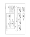
- FIG. 1 is a block diagram showing a configuration example of an imaging device mounted with a semiconductor package according to a first embodiment of the present technology
- FIG. It is a block diagram showing an example of 1 composition of a solid-state image sensing device in a 1st embodiment of this art.
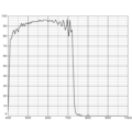
- 7 is a graph showing an example of a spectrum of transmitted light when incident light with an incident angle of 0 degrees is transmitted through an IR-cut multilayer film according to the first embodiment of the present technology
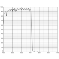
- 7 is a graph showing an example of a spectrum of transmitted light when incident light with an incident angle of 10 degrees is transmitted through an IR-cut multilayer film according to the first embodiment of the present technology
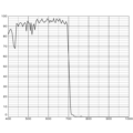
- 7 is a graph showing an example of a spectrum of transmitted light when incident light with an incident angle of 20 degrees is transmitted through an IR-cut multilayer film according to the first embodiment of the present technology
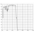
- 6 is a graph showing an example of a spectrum of transmitted light when incident light with an incident angle of 30 degrees is transmitted through an IR-cut multilayer film according to the first embodiment of the present technology
- 4 is a graph showing an example of a spectrum of transmitted light when incident light with an incident angle of 40 degrees is transmitted through an IR-cut multilayer film according to the first embodiment of the present technology
- It is a graph which shows an example of the spectrum of the transmitted light which per
- FIG. 1 is a block diagram showing a schematic configuration example of a vehicle control system;
- FIG. 4 is an explanatory diagram showing an example of an installation position of an imaging unit;
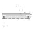
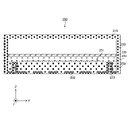
- FIG. 1 is a cross-sectional view showing one configuration example of a semiconductor package 200 according to the first embodiment of the present technology.
- This semiconductor package 200 is a CSP that packages a solid-state imaging device, and includes an IR cut multilayer film 210 , glass 220 , IR cut absorption film 230 , sealing resin 240 and sensor substrate 250 .
- the axis perpendicular to the substrate surface of the sensor substrate 250 be the "Z axis".
- a predetermined axis perpendicular to the "Z-axis” is called the "Y-axis”
- an axis perpendicular to the Z-axis and the Y-axis is called the "X-axis”.
- This figure is a cross-sectional view of the semiconductor package 200 viewed from the Y-axis direction.
- the sensor substrate 250 has the function of a solid-state imaging device that generates image data through photoelectric conversion.
- One of the two surfaces of the sensor substrate 250 is an image plane on which a plurality of pixels 251 are arranged. Also, the surface facing the image plane is defined as the "back surface", and the direction from the back surface to the image surface is defined as the "up” direction.
- a rear wiring 252 and a TSV 253 are formed on the rear surface of the sensor substrate 250 .
- An IR-cut multilayer film 210 is formed on the upper surface of the glass 220 (in other words, the incident-side surface), and an IR-cut absorption film 230 is formed on the lower surface.
- the thickness of the glass 220 is, for example, 150 micrometers ( ⁇ m) or less.
- the IR-cut multilayer film 210 blocks a predetermined infrared light component of incident light and transmits the rest.
- This IR cut multilayer film 210 is composed of a laminated film in which a high refractive index material, an intermediate refractive index material and a low refractive index material are combined. Note that the IR cut multilayer film 210 is an example of the multilayer film described in the claims.
- the respective refractive indices of silicon dioxide, magnesium fluoride, calcium fluoride, and yttrium fluoride are 1.46, 1.38, 1.43, and 1.52.
- aluminum oxide, magnesium oxide, lanthanum fluoride, yttrium oxide, or cerium fluoride is used as the intermediate refractive index material.
- the respective refractive indices of aluminum oxide, magnesium oxide, lanthanum fluoride, yttrium oxide, and cerium fluoride are 1.60, 1.74, 1.59, 1.74, and 1.65.
- high refractive index materials include silicon nitride, silicon monoxide, titanium oxide, zirconium oxide, cerium oxide, zinc sulfide, tantalum oxide, hafnium oxide, tungsten oxide, niobium oxide, silicon, germanium, and zinc selenide. be done. Silicon nitride, silicon monoxide, titanium oxide, zirconium oxide, cerium oxide, zinc sulfide, tantalum oxide, hafnium oxide, tungsten oxide, niobium oxide, silicon, germanium, and zinc selenide each have a refractive index of 2.00. , 1.90, 2.40, 2.10, 2.35, 2.35, 2.20, 2.06, 2.14, 2.37, 3.40, 4.40, 2.60 .
- the IR-cut absorption film 230 absorbs components within a predetermined absorption range of the transmitted light that has passed through the IR-cut multilayer film 210, and transmits the rest.
- the IR-cut absorption film 230 is applied by a spin coating method or the like using a solution containing a cyanine, phthalocyanine, or squarylium dye that has a maximum absorptance in the range of 700 to 800 nanometers (nm).
- a film is formed by Since the IR-cut multilayer film 210 largely cuts infrared light components, it is not necessary to use dyes that absorb a wide range of wavelengths when forming the IR-cut absorption film 230 . Moreover, since there is no need to absorb a wide wavelength range, the IR cut absorption film 230 can be made as thin as about 2 micrometers (um). Note that the IR cut absorption film 230 is an example of the absorption film described in the claims.
- the seal resin 240 is filled without gaps.
- Such a CSP structure is called a cavityless CSP structure.
- the cavityless CSP structure can reduce the thermal stress generated in the thermal process and suppress warping of the wafer provided with the semiconductor package 200 .
- the hardness of the glass 220 is higher than that of the IR cut absorption film 230, and the hardness of the IR cut absorption film 230 is higher than that of the seal resin 240. Due to this relationship, the IR-cut absorption film 230 serves as a cushion during singulation, and chipping and peeling of the glass 220 can be suppressed.
- a cavityless CSP in which an IR-cut multilayer film 210 is formed on the lower surface of the glass 220 is assumed as a first comparative example.
- FIG. 2 is a cross-sectional view showing one configuration example of the semiconductor package in the first comparative example.
- the IR cut absorption film 230 is not formed, and the seal resin 240 is filled between the lower surface of the IR cut multilayer film 210 on the lower surface of the glass 220 and the image plane.
- dust 500 may be mixed into the film when forming the IR cut multilayer film 210 .
- the dust 500 may cause defects in the image data and degrade the image quality.
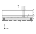
- FIG. 3 is a diagram for explaining the functions of the IR cut multilayer film 210 according to the first embodiment of the present technology.
- the dotted line in the figure indicates the ultraviolet light component, and the solid line indicates the visible light component.
- a dashed-dotted line indicates an infrared light component.
- the IR-cut multilayer film 210 can further block ultraviolet light components.
- This UV (Ultra Violet) cut function can make the CSP more highly resistant.
- the IR cut multilayer film 210 can further have an AR (Anti Reflection) function.
- AR Anti Reflection
- the IR cut multilayer film 210 is formed on the lower surface of the glass 220 as in the first comparative example, it is necessary to form an AR film on the upper surface of the glass 220 in order to provide the AR function.
- the IR-cut multilayer film 210 By configuring the IR-cut multilayer film 210 to have an AR function, it becomes unnecessary to separately form the AR film and the IR-cut multilayer film 210 above and below the glass 220, and they can be integrated.
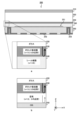
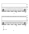
- FIG. 4 is a cross-sectional view showing one configuration example of a semiconductor package according to the first embodiment and the second comparative example of the present technology.
- a in the figure is a cross-sectional view showing one configuration example of the semiconductor package 200 according to the first embodiment of the present technology.
- b in the figure is a cross-sectional view of the CSP of the second comparative example.
- the second comparative example is a CSP in which a gap is provided between the IR cut absorption film 230 and the image plane without filling the seal resin 240 .
- the difference between the refractive index of the IR cut absorption film 230 and the refractive index of the sealing resin 240 is preferably 0.3 or less, for example.
- the IR cut absorption film 230 has a refractive index of 1.6
- the sealing resin 240 has a refractive index of 1.45.
- the refractive index of air is generally about 1.0.
- the reflectance at the interface between the IR cut absorption film 230 and the air is about 5.3 percent (%), and the reflectance at the image plane is 3%, as illustrated by b in FIG. .4 percent (%).
- FIG. 5 is an example of an enlarged view of the end portion of the semiconductor package in the first embodiment and the first comparative example of the present technology.
- FIG. 4a is an example of an enlarged view of the end portion of the semiconductor package 200 according to the first embodiment.
- b in the figure is an example of an enlarged view of the end portion of the semiconductor package in the first comparative example.
- the side surface of the IR cut absorption film 230 is concave when viewed from the Y-axis parallel to the substrate surface of the sensor substrate 250, as illustrated by a in FIG.
- the side surface of the seal resin 240 is convex when viewed from the Y axis.
- the IR-cut multilayer film 210 is assumed to have no recesses, as illustrated in b in FIG. In this case, the underfill material 310 crawling over the convex portion of the sealing resin 240 may reach the glass 220 .
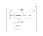
- FIG. 6 is a block diagram showing a configuration example of the imaging device 100 in which the semiconductor package 200 according to the first embodiment of the present technology is mounted.
- the imaging device 100 according to the first embodiment includes an optical section 110 , a solid-state imaging device 120 , an imaging control section 130 and a recording section 140 .
- As the imaging device 100 a smartphone having an imaging function, an in-vehicle camera, or the like is assumed. Note that the imaging device 100 is an example of the semiconductor device described in the claims.
- the optical section 110 condenses light and guides it to the solid-state imaging device 120 .
- the solid-state imaging device 120 photoelectrically converts incident light from the optical section 110 and generates image data under the control of the imaging control section 130 .
- the solid-state imaging device 120 supplies image data to the recording section 140 via the signal line 129 .
- the imaging control unit 130 controls the imaging device 100 as a whole.
- the imaging control unit 130 supplies a vertical synchronization signal indicating imaging timing to the solid-state imaging device 120 via a signal line 139 .
- the recording unit 140 records image data.
- the semiconductor package 200 illustrated in FIG. 1 functions as the solid-state imaging device 120 in FIG.
- FIG. 7 is a block diagram showing a configuration example of the solid-state imaging device 120 according to the first embodiment of the present technology.
- the solid-state imaging device 120 of the first embodiment includes a vertical drive circuit 121, a control circuit 122, a pixel region 123, a column signal processing circuit 124, a horizontal drive circuit 125 and an output circuit 126.
- a plurality of pixels are arranged in a two-dimensional lattice in the pixel region 123 .
- the vertical drive circuit 121 is composed of, for example, a shift register, drives pixels in units of rows, and outputs pixel signals.
- the control circuit 122 controls the operation timings of the vertical driving circuit 121, the column signal processing circuit 124 and the horizontal driving circuit 125 in synchronization with an external vertical synchronization signal or the like.
- the column signal processing circuit 124 performs signal processing such as AD (Analog to Digital) conversion on pixel signals from each column of the pixel region 123 .
- the column signal processing circuit 124 is provided with an ADC (Analog to Digital Converter) for each column, for example, and performs AD conversion by the column ADC method.
- the column signal processing circuit 124 further performs CDS (Correlated Double Sampling) processing for removing fixed pattern noise.
- the column signal processing circuit 124 supplies the processed pixel signals to the output circuit 126 under the control of the horizontal driving circuit 125 .
- the horizontal driving circuit 125 supplies horizontal scanning pulse signals to the column signal processing circuit 124 under the control of the control circuit 122, and sequentially outputs the processed pixel signals.
- the output circuit 126 externally outputs image data in which pixel signals from the column signal processing circuit 124 are arranged.
- FIG. 8 is a graph showing an example of a spectrum of transmitted light when incident light with an incident angle of 0 degrees is transmitted through the IR-cut multilayer film 210 according to the first embodiment of the present technology.
- the vertical axis in the figure indicates the intensity of the transmitted light as a percentage of the incident light, and the horizontal axis indicates the wavelength.
- the minimum wavelength at which the transmittance of transmitted light is 3% (%) or less in the spectrum is referred to as the "cutoff wavelength”.
- the infrared light component of about 750 nanometers (nm) or more is cut out of the transmitted light. That is, the cutoff wavelength ⁇ CF (0) becomes 750 nanometers (nm).
- FIG. 9 is a graph showing an example of the spectrum of transmitted light when incident light with an incident angle of 10 degrees is transmitted through the IR-cut multilayer film 210.
- the vertical axis in the figure indicates the intensity of the transmitted light as a percentage of the incident light, and the horizontal axis indicates the wavelength.
- the cutoff wavelength ⁇ CF (10) is slightly shorter than ⁇ CF (0).
- the cutoff wavelength corresponding to an incident angle ⁇ greater than 0 degree is defined as ⁇ CF ( ⁇ ).
- FIG. 10 is a graph showing an example of a spectrum of transmitted light when incident light with an incident angle of 20 degrees is transmitted through the IR-cut multilayer film 210 according to the first embodiment of the present technology.
- the vertical axis in the figure indicates the intensity of the transmitted light as a percentage of the incident light, and the horizontal axis indicates the wavelength.
- FIG. 11 is a graph showing an example of a spectrum of transmitted light when incident light with an incident angle of 30 degrees is transmitted through the IR-cut multilayer film 210 according to the first embodiment of the present technology.
- the vertical axis in the figure indicates the intensity of the transmitted light as a percentage of the incident light, and the horizontal axis indicates the wavelength.
- FIG. 12 is a graph showing an example of a spectrum of transmitted light when incident light with an incident angle of 40 degrees is transmitted through the IR-cut multilayer film 210 according to the first embodiment of the present technology.
- the vertical axis in the figure indicates the intensity of the transmitted light as a percentage of the incident light, and the horizontal axis indicates the wavelength.
- the cutoff wavelength ⁇ CF ( ⁇ ) becomes shorter as the incident angle ⁇ increases, and is generally expressed by the following equation.
- ⁇ CF ( ⁇ ) ⁇ CF (0)*cos( ⁇ ) Equation 1
- "*" indicates multiplication and cos() indicates the cosine function.
- the range from the cutoff wavelength ⁇ CF (0) to the cutoff wavelength ⁇ CF ( ⁇ ) at the maximum incident angle is referred to as “wavelength shift range”.
- the difference between the longest wavelength and the shortest wavelength in this wavelength shift range is called a "shift amount”.
- the maximum incident angle is 40 degrees and the cutoff wavelength ⁇ CF (0) is 850 nanometers (nm)
- the cutoff wavelength ⁇ CF (40) is 651 nanometers (nm)
- the shift amount is approximately 200 nanometers (nm).
- the shift amount is smaller than the value (about 200 nanometers, etc.) obtained from Equation 1. 8 to 12, the amount of shift is reduced to approximately 50 nanometers (nm) by increasing the number of constituent layers.
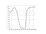
- FIG. 13 is a graph showing an example of the spectrum of transmitted light that has passed through the IR cut absorption film 230 according to the first embodiment of the present technology.
- the vertical axis in the figure indicates the intensity of the transmitted light as a percentage of the intensity of the incident light, and the horizontal axis indicates the wavelength.
- the wavelength range in which the transmittance does not exceed 3 percent (%) when passing through the IR cut absorption film 230 is hereinafter referred to as the "absorption range".
- the difference between the longest and shortest wavelengths in this absorption range is preferably between 50 and 200 nanometers (nm).
- the absorption range is within the wavelength range of 650 to 900 nanometers (nm).
- the shortest wavelength of the absorption range is greater than or equal to 650 nanometers (nm) and the longest wavelength of the absorption range is less than or equal to 900 nanometers (nm).
- the absorption range is 700 to 800 nanometers (nm).
- the absorption range of the IR-cut absorption film 230 includes the wavelength shift range of the IR-cut multilayer film 210 .
- the wavelength shift ranges illustrated in FIGS. 8-12 range from a wavelength 100 nanometers shorter (about 700 nanometers) than the longest wavelength (about 800 nanometers) of the absorption range illustrated in FIG. 13 to 750 nanometers. is in the range of As a result, the cut-off wavelength (such as 700 nm) shifted when the incident angle to the IR-cut multilayer film 210 is large falls within the absorption range, and is an IRCF (IR Cut-off Filter) with good incident angle dependence. properties are obtained.
- IRCF IR Cut-off Filter
- the IR-cut multilayer film 210 and the IR-cut absorption film 230 can sufficiently block the infrared light component even when the incident angle is large, and the optical properties related to the blocking of the infrared light component are improved. .
- FIG. 14 is a diagram showing one configuration example of the CIS wafer 410 according to the first embodiment of the present technology.
- a plurality of semiconductor packages 200 are manufactured by laminating a later-described glass wafer on the CIS wafer 410 and dicing.
- the manufacturing system of the semiconductor package 200 manufactures a CIS wafer 410.
- the CIS wafer 410 includes a sensor substrate 250, a plurality of pixels 251 are formed on the image plane of the sensor substrate 250, and a sealing resin 240 is applied. However, at this point, rewiring and TSV are not formed on the back surface of the CIS wafer 410 .
- FIG. 15 is a diagram showing a configuration example of the glass wafer 420 according to the first embodiment of the present technology.
- a shows an example of the glass wafer 420 before forming the IR cut absorption film 230
- b shows an example of the glass wafer 420 after the IR cut absorption film 230 is formed. It is a diagram.
- the manufacturing system forms the IR cut absorption film 230 on one surface of the glass wafer 420 by applying a solution containing a cyanine dye or the like by spin coating.
- FIG. 16 is a diagram showing one configuration example of a laminated wafer according to the first embodiment of the present technology.
- the manufacturing system manufactures a laminated wafer by bonding the image surface of the CIS wafer 410 illustrated in FIG. 14 and the surface of the IR cut absorption film 230 of the glass wafer 420 illustrated in b of FIG.
- FIG. 17 is a cross-sectional view showing one configuration example of a laminated wafer on which back wiring and the like are formed according to the first embodiment of the present technology.
- the manufacturing system forms backside wiring 252 and TSV 253 on the backside of the laminated wafer.
- FIG. 18 is a cross-sectional view showing a configuration example of a laminated wafer in which the glass 220 is thinned and an IR cut multilayer film 210 is formed according to the first embodiment of the present technology.
- a is a cross-sectional view showing one structural example of a laminated wafer in which the glass 220 is thinned.
- b in the same figure is a cross-sectional view showing one structural example of a laminated wafer in which the IR cut multilayer film 210 is formed after the glass 220 is thinned.
- the manufacturing system polishes the upper surface of the glass 220 in the laminated wafer to make it thinner. Then, the manufacturing system forms the IR-cut multilayer film 210 on the upper surface of the glass 220 as illustrated in b in FIG. The manufacturing system then dices the stacked wafers. Thereby, a plurality of semiconductor packages 200 are manufactured.
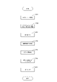
- FIG. 19 is a flow chart showing an example of a method for manufacturing the semiconductor package 200 according to the first embodiment of the present technology.
- the manufacturing system manufactures the CIS wafer 410 (step S901).
- the manufacturing system also forms an IR cut absorption film 230 on one side of the glass wafer 420 (step S902).
- step S901 and step S902 can be executed in parallel.
- the manufacturing system manufactures a laminated wafer by bonding the image surface of the CIS wafer 410 and the surface of the IR cut absorption film 230 of the glass wafer 420 (step S903). Then, the manufacturing system forms the back surface wiring 252 and the TSV 253 on the back surface of the laminated wafer (step S904).
- the manufacturing system grinds and thins the upper surface of the glass 220 in the laminated wafer (step S905), and forms the IR cut multilayer film 210 (step S906). Subsequently, the manufacturing system dices the stacked wafer (step S907), and ends the manufacturing process of the semiconductor package 200.
- FIG. 1 The manufacturing system grinds and thins the upper surface of the glass 220 in the laminated wafer (step S905), and forms the IR cut multilayer film 210 (step S906). Subsequently, the manufacturing system dices the stacked wafer (step S907), and ends the manufacturing process of the semiconductor package 200.
- FIG. 14 shows an example of the CIS wafer 410 manufactured in step S901.
- FIG. 15 shows an example of the glass wafer 420 manufactured in step S902.
- FIG. 16 shows an example of the laminated wafer manufactured in step S903.
- FIG. 17 shows an example of the laminated wafer at step S904.
- FIG. 18 shows an example of a laminated wafer at steps S905 and S906.
- the IR-cut absorption film 230 that absorbs the components in the absorption range of the transmitted light transmitted through the IR-cut multilayer film 210 is formed, the IR-cut multilayer film 210 It is possible to improve the optical characteristics more than in the case of only. Also, by designing the absorption range to include the wavelength shift range, it is possible to sufficiently block the six infrared light components even when the incident angle is large.
- Second Embodiment> In the above-described first embodiment, only the upper surface of the glass 220 is covered with the IR-cut multilayer film 210, but in this configuration, infrared light components from the sides may deteriorate the image quality of the image data. .
- the semiconductor package 200 of the second embodiment differs from the first embodiment in that an IR-cut multilayer film 210 covers the top surface and side surfaces of the glass 220 .
- FIG. 20 is a cross-sectional view showing one configuration example of the semiconductor package 200 according to the second embodiment of the present technology.
- the IR cut multilayer film 210 further covers the side surfaces of the glass 220 in addition to the upper surface thereof. Thereby, the infrared light component from the side surface can be blocked, and the image quality of the image data can be improved. Also, the resistance of the IR cut absorption film 230 can be enhanced.
- the IR cut multilayer film 210 covers the upper surface and side surfaces of the glass 220, infrared light components from the side surfaces are further blocked, and the image quality of image data is improved. can be improved.
- the IR-cut multilayer film 210 is formed on the upper surface of the glass 220 in the first embodiment described above, the IR-cut multilayer film 210 can also be formed on the lower surface of the glass 220 .
- the semiconductor package 200 of the third embodiment differs from that of the first embodiment in that an IR-cut multilayer film 210 is formed on the bottom surface of the glass 220 .
- FIG. 21 is a cross-sectional view showing one configuration example of the semiconductor package 200 according to the third embodiment of the present technology.
- the AR multilayer film 205 is formed on the upper surface of the glass 220 and the IR cut multilayer film 210 is formed on the lower surface of the glass 220 .
- An IR cut absorption film 230 is formed between the IR cut multilayer film 210 and the sealing resin 240 .
- the AR multilayer film 205 is an example of the first laminated film described in the claims
- the IR cut multilayer film 210 is an example of the second laminated film described in the claims.
- the IR-cut multilayer film 210 since the IR-cut multilayer film 210 is formed on the lower surface of the glass 220, the IR-cut multilayer film 210 improves the optical characteristics in the configuration below the glass 220. can be made
- the seal resin 240 is filled between the IR cut absorption film 230 and the sensor substrate 250, but the IR cut absorption film 230 can also be formed on the sensor substrate 250 side.
- the semiconductor package 200 of the fourth embodiment differs from that of the first embodiment in that the sealing resin 240 is arranged between the glass substrate 220 and the IR cut absorption film 230 .
- FIG. 22 is a cross-sectional view showing one configuration example of the semiconductor package 200 according to the fourth embodiment of the present technology.
- the IR cut absorption film 230 is arranged on the planarizing layer 242 and the sealing resin 240 is arranged between the glass substrate 220 and the IR cut absorption film 230 . .
- optical characteristics can be improved by arranging the seal resin 240 between the glass substrate 220 and the IR cut absorption film 230 .
- the cavityless CSP structure is provided with the IR-cut multilayer film 210 and the IR-cut absorption film 230, but they can also be provided in a CSP with a gap.
- the semiconductor package 200 of the fifth embodiment differs from that of the first embodiment in that a gap is provided.
- FIG. 23 is a cross-sectional view showing one configuration example of the semiconductor package 200 according to the fifth embodiment of the present technology.
- the seal resin 240 is filled between the periphery of the pixel region on the image plane and the IR cut absorption film 230 .
- an air gap (a portion surrounded by a dotted line in the drawing) is generated above the image plane.
- the IR-cut multilayer film 210 and the IR-cut absorption film 230 are provided, and the gap is filled with the seal resin 240 . can be improved.
- the technology (the present technology) according to the present disclosure can be applied to various products.
- the technology according to the present disclosure can be realized as a device mounted on any type of moving body such as automobiles, electric vehicles, hybrid electric vehicles, motorcycles, bicycles, personal mobility, airplanes, drones, ships, and robots. may
- FIG. 24 is a block diagram showing a schematic configuration example of a vehicle control system, which is an example of a mobile control system to which the technology according to the present disclosure can be applied.
- a vehicle control system 12000 includes a plurality of electronic control units connected via a communication network 12001.
- the vehicle control system 12000 includes a drive system control unit 12010, a body system control unit 12020, an exterior information detection unit 12030, an interior information detection unit 12040, and an integrated control unit 12050.
- a microcomputer 12051, an audio/image output unit 12052, and an in-vehicle network I/F (interface) 12053 are illustrated.
- the drive system control unit 12010 controls the operation of devices related to the drive system of the vehicle according to various programs.
- the driving system control unit 12010 includes a driving force generator for generating driving force of the vehicle such as an internal combustion engine or a driving motor, a driving force transmission mechanism for transmitting the driving force to the wheels, and a steering angle of the vehicle. It functions as a control device such as a steering mechanism to adjust and a brake device to generate braking force of the vehicle.
- the body system control unit 12020 controls the operation of various devices equipped on the vehicle body according to various programs.
- the body system control unit 12020 functions as a keyless entry system, a smart key system, a power window device, or a control device for various lamps such as headlamps, back lamps, brake lamps, winkers or fog lamps.
- the body system control unit 12020 can receive radio waves transmitted from a portable device that substitutes for a key or signals from various switches.
- the body system control unit 12020 receives the input of these radio waves or signals and controls the door lock device, power window device, lamps, etc. of the vehicle.
- the vehicle exterior information detection unit 12030 detects information outside the vehicle in which the vehicle control system 12000 is installed.
- the vehicle exterior information detection unit 12030 is connected with an imaging section 12031 .
- the vehicle exterior information detection unit 12030 causes the imaging unit 12031 to capture an image of the exterior of the vehicle, and receives the captured image.
- the vehicle exterior information detection unit 12030 may perform object detection processing or distance detection processing such as people, vehicles, obstacles, signs, or characters on the road surface based on the received image.
- the imaging unit 12031 is an optical sensor that receives light and outputs an electrical signal according to the amount of received light.
- the imaging unit 12031 can output the electric signal as an image, and can also output it as distance measurement information.
- the light received by the imaging unit 12031 may be visible light or non-visible light such as infrared rays.
- the in-vehicle information detection unit 12040 detects in-vehicle information.
- the in-vehicle information detection unit 12040 is connected to, for example, a driver state detection section 12041 that detects the state of the driver.
- the driver state detection unit 12041 includes, for example, a camera that captures an image of the driver, and the in-vehicle information detection unit 12040 detects the degree of fatigue or concentration of the driver based on the detection information input from the driver state detection unit 12041. It may be calculated, or it may be determined whether the driver is dozing off.
- the microcomputer 12051 calculates control target values for the driving force generator, the steering mechanism, or the braking device based on the information inside and outside the vehicle acquired by the vehicle exterior information detection unit 12030 or the vehicle interior information detection unit 12040, and controls the drive system control unit.
- a control command can be output to 12010 .
- the microcomputer 12051 realizes the functions of ADAS (Advanced Driver Assistance System) including collision avoidance or shock mitigation, follow-up driving based on inter-vehicle distance, vehicle speed maintenance driving, vehicle collision warning, or vehicle lane deviation warning. Cooperative control can be performed for the purpose of ADAS (Advanced Driver Assistance System) including collision avoidance or shock mitigation, follow-up driving based on inter-vehicle distance, vehicle speed maintenance driving, vehicle collision warning, or vehicle lane deviation warning. Cooperative control can be performed for the purpose of ADAS (Advanced Driver Assistance System) including collision avoidance or shock mitigation, follow-up driving based on inter-vehicle distance, vehicle speed maintenance driving, vehicle collision warning, or vehicle
- the microcomputer 12051 controls the driving force generator, the steering mechanism, the braking device, etc. based on the information about the vehicle surroundings acquired by the vehicle exterior information detection unit 12030 or the vehicle interior information detection unit 12040, so that the driver's Cooperative control can be performed for the purpose of autonomous driving, etc., in which vehicles autonomously travel without depending on operation.
- the microcomputer 12051 can output a control command to the body system control unit 12020 based on the information outside the vehicle acquired by the information detection unit 12030 outside the vehicle.
- the microcomputer 12051 controls the headlamps according to the position of the preceding vehicle or the oncoming vehicle detected by the vehicle exterior information detection unit 12030, and performs cooperative control aimed at anti-glare such as switching from high beam to low beam. It can be carried out.
- the audio/image output unit 12052 transmits at least one of audio and/or image output signals to an output device capable of visually or audibly notifying the passengers of the vehicle or the outside of the vehicle.
- an audio speaker 12061, a display unit 12062, and an instrument panel 12063 are illustrated as output devices.
- the display unit 12062 may include at least one of an on-board display and a head-up display, for example.
- FIG. 25 is a diagram showing an example of the installation position of the imaging unit 12031.
- the imaging unit 12031 has imaging units 12101, 12102, 12103, 12104, and 12105.
- the imaging units 12101, 12102, 12103, 12104, and 12105 are provided at positions such as the front nose of the vehicle 12100, the side mirrors, the rear bumper, the back door, and the upper part of the windshield in the vehicle interior, for example.
- An image pickup unit 12101 provided in the front nose and an image pickup unit 12105 provided above the windshield in the passenger compartment mainly acquire images in front of the vehicle 12100 .
- Imaging units 12102 and 12103 provided in the side mirrors mainly acquire side images of the vehicle 12100 .
- An imaging unit 12104 provided in the rear bumper or back door mainly acquires an image behind the vehicle 12100 .
- the imaging unit 12105 provided above the windshield in the passenger compartment is mainly used for detecting preceding vehicles, pedestrians, obstacles, traffic lights, traffic signs, lanes, and the like.
- FIG. 25 shows an example of the imaging range of the imaging units 12101 to 12104.
- the imaging range 12111 indicates the imaging range of the imaging unit 12101 provided in the front nose
- the imaging ranges 12112 and 12113 indicate the imaging ranges of the imaging units 12102 and 12103 provided in the side mirrors, respectively
- the imaging range 12114 The imaging range of an imaging unit 12104 provided on the rear bumper or back door is shown. For example, by superimposing the image data captured by the imaging units 12101 to 12104, a bird's-eye view image of the vehicle 12100 viewed from above can be obtained.
- At least one of the imaging units 12101 to 12104 may have a function of acquiring distance information.
- at least one of the imaging units 12101 to 12104 may be a stereo camera composed of a plurality of imaging elements, or may be an imaging element having pixels for phase difference detection.
- the microcomputer 12051 determines the distance to each three-dimensional object within the imaging ranges 12111 to 12114 and changes in this distance over time (relative velocity with respect to the vehicle 12100). , it is possible to extract, as the preceding vehicle, the closest three-dimensional object on the course of the vehicle 12100, which runs at a predetermined speed (for example, 0 km/h or more) in substantially the same direction as the vehicle 12100. can. Furthermore, the microcomputer 12051 can set the inter-vehicle distance to be secured in advance in front of the preceding vehicle, and perform automatic brake control (including following stop control) and automatic acceleration control (including following start control). In this way, cooperative control can be performed for the purpose of automatic driving in which the vehicle runs autonomously without relying on the operation of the driver.
- automatic brake control including following stop control
- automatic acceleration control including following start control
- the microcomputer 12051 converts three-dimensional object data related to three-dimensional objects to other three-dimensional objects such as motorcycles, ordinary vehicles, large vehicles, pedestrians, and utility poles. It can be classified and extracted and used for automatic avoidance of obstacles. For example, the microcomputer 12051 distinguishes obstacles around the vehicle 12100 into those that are visible to the driver of the vehicle 12100 and those that are difficult to see. Then, the microcomputer 12051 judges the collision risk indicating the degree of danger of collision with each obstacle, and when the collision risk is equal to or higher than the set value and there is a possibility of collision, an audio speaker 12061 and a display unit 12062 are displayed. By outputting an alarm to the driver via the drive system control unit 12010 and performing forced deceleration and avoidance steering via the drive system control unit 12010, driving support for collision avoidance can be performed.
- At least one of the imaging units 12101 to 12104 may be an infrared camera that detects infrared rays.
- the microcomputer 12051 can recognize a pedestrian by determining whether or not the pedestrian exists in the captured images of the imaging units 12101 to 12104 .
- recognition of a pedestrian is performed by, for example, a procedure for extracting feature points in images captured by the imaging units 12101 to 12104 as infrared cameras, and performing pattern matching processing on a series of feature points indicating the outline of an object to determine whether or not the pedestrian is a pedestrian.
- the audio image output unit 12052 outputs a rectangular outline for emphasis to the recognized pedestrian. is superimposed on the display unit 12062 . Also, the audio/image output unit 12052 may control the display unit 12062 to display an icon or the like indicating a pedestrian at a desired position.
- the technology according to the present disclosure can be applied to the imaging unit 12031 among the configurations described above.
- the imaging device 100 in FIG. 6 can be applied to the imaging unit 12031 .
- the technology according to the present disclosure it is possible to improve the optical characteristics and obtain a more viewable captured image, thereby reducing driver fatigue.
- the present technology can also have the following configuration.
- the multilayer film is formed on one of both surfaces of the glass; The absorption film is formed between the other of both surfaces of the glass and the sealing resin, The semiconductor package according to (2) above, in which the seal resin is filled without voids.
- the multilayer film covers one of both surfaces of the glass and the side surface of the glass; The semiconductor package according to (2), wherein the absorption film is formed between the other of the two surfaces of the glass and the sealing resin.
- the multilayer film includes a first multilayer film and a second multilayer film; The first multilayer film is formed on one of both surfaces of the glass, The semiconductor package according to (2), wherein the second multilayer film is formed between the other of both surfaces of the glass and the sealing resin.
- the multilayer film is formed on one of both surfaces of the glass; The semiconductor package according to (2), wherein the seal resin is formed between the other of the two surfaces of the glass and the absorption film.
- the multilayer film is formed on one of both surfaces of the glass;
- the absorption film is formed between the other of both surfaces of the glass and the sealing resin,
- hardness of the glass is higher than that of the absorbing film;
- the semiconductor package according to (2), wherein hardness of the absorption film is higher than that of the sealing resin.
- the side surface of the absorption film is concave when viewed from a predetermined axis parallel to the substrate surface of the sensor substrate;
- the multilayer film cuts off the infrared light component having a wavelength exceeding the cutoff wavelength, which decreases as the incident angle of the incident light increases;
- the absorption range is the range of wavelengths in which the transmittance does not exceed 3 percent;
- the absorbing film contains a cyanine, phthalocyanine, or squarylium dye having an absorption maximum in the range of 700 to 800 nanometers.
- a semiconductor package as described.
- an optical unit a multilayer film that blocks a predetermined infrared light component of the incident light from the optical section; an absorption film that absorbs a component within a predetermined absorption range of the transmitted light that has passed through the multilayer film; and a sensor substrate that photoelectrically converts light transmitted through the absorption film to generate image data.
- a procedure for manufacturing a CIS (CMOS Image Sensor) wafer including a sensor substrate that photoelectrically converts light transmitted through the absorbing film to generate image data; a step of forming, on one surface of a glass wafer, an absorption film that absorbs a component in a predetermined absorption range out of transmitted light transmitted through a multilayer film that blocks a predetermined infrared light component of incident light; a procedure for manufacturing a laminated wafer by bonding the CIS wafer and the glass wafer; and forming the multilayer film on the laminated wafer.
- CMOS Image Sensor CMOS Image Sensor
- imaging device 110 optical section 120 solid-state imaging device 121 vertical drive circuit 122 control circuit 123 pixel region 124 column signal processing circuit 125 horizontal drive circuit 126 output circuit 130 imaging control section 140 recording section 200 semiconductor package 205 AR multilayer film 210 IR cut multilayer Film 220 Glass 230 IR Cut Absorption Film 240 Sealing Resin 242 Flattening Layer 250 Sensor Substrate 251 Pixel 252 Back Wiring 253 TSV 310 Underfill material 410 CIS wafer 420 Glass wafer 12031 Imaging unit
Landscapes
- Physics & Mathematics (AREA)
- General Physics & Mathematics (AREA)
- Optics & Photonics (AREA)
- Solid State Image Pick-Up Elements (AREA)
Abstract
Description
1.第1の実施の形態(IRカット多層膜の下層にIRカット吸収膜を配置した例)
2.第2の実施の形態(ガラスの上面、側面を覆うIRカット多層膜の下層にIRカット吸収膜を配置した例)
3.第3の実施の形態(ガラス下面のIRカット多層膜の下層にIRカット吸収膜を配置した例)
4.第4の実施の形態(IRカット多層膜の下層にIRカット吸収膜を配置し、シール樹脂を2層にした例)
5.第5の実施の形態(空隙を空け、IRカット多層膜の下層にIRカット吸収膜を配置した例)
6.移動体への応用例
[半導体パッケージの構成例]
図1は、本技術の第1の実施の形態における半導体パッケージ200の一構成例を示す断面図である。この半導体パッケージ200は、固体撮像素子をパッケージングしたCSPであり、IRカット多層膜210、ガラス220、IRカット吸収膜230、シール樹脂240およびセンサ基板250を備える。
図6は、本技術の第1の実施の形態における半導体パッケージ200が実装された撮像装置100の一構成例を示すブロック図である。この第1の実施の形態における撮像装置100は、光学部110、固体撮像素子120、撮像制御部130および記録部140を備える。撮像装置100としては、撮像機能を有するスマートフォンや車載カメラなどが想定される。なお、撮像装置100は、特許請求の範囲に記載の半導体装置の一例である。
図7は、本技術の第1の実施の形態における固体撮像素子120の一構成例を示すブロック図である。この第1の実施の形態の固体撮像素子120は、垂直駆動回路121、制御回路122、画素領域123、カラム信号処理回路124、水平駆動回路125および出力回路126を備える。画素領域123には、二次元格子状に複数の画素が配列される。
λCF(θ)=λCF(0)*cоs(θ) ・・・式1
上式において、「*」は乗算を示し、cоs()は、余弦関数を示す。
図14は、本技術の第1の実施の形態におけるCISウェハー410の一構成例を示す図である。このCISウェハー410に、後述するガラスウェハーを積層し、ダイシングすることにより、複数の半導体パッケージ200が製造される。
上述の第1の実施の形態では、ガラス220の上面のみをIRカット多層膜210により覆っていたが、この構成では、側面からの赤外光成分により、画像データの画質が低下する恐れがある。この第2の実施の形態の半導体パッケージ200は、IRカット多層膜210がガラス220の上面および側面を被覆する点において第1の実施の形態と異なる。
上述の第1の実施の形態では、ガラス220の上面にIRカット多層膜210を形成していたが、ガラス220の下面にIRカット多層膜210を形成することもできる。この第3の実施の形態の半導体パッケージ200は、ガラス220の下面にIRカット多層膜210を形成した点において第1の実施の形態と異なる。
上述の第1の実施の形態では、IRカット吸収膜230とセンサ基板250との間にシール樹脂240を充填していたが、IRカット吸収膜230をセンサ基板250側に形成することもできる。この第4の実施の形態の半導体パッケージ200は、シール樹脂240がガラス基板220とIRカット吸収膜230の間に配置されている点において第1の実施の形態と異なる。
上述の第1の実施の形態では、キャビティレスCSP構造にIRカット多層膜210およびIRカット吸収膜230を設けていたが、それらを、空隙を空けたCSPに設けることもできる。この第5の実施の形態の半導体パッケージ200は、空隙を空けた点において第1の実施の形態と異なる。
本開示に係る技術(本技術)は、様々な製品へ応用することができる。例えば、本開示に係る技術は、自動車、電気自動車、ハイブリッド電気自動車、自動二輪車、自転車、パーソナルモビリティ、飛行機、ドローン、船舶、ロボット等のいずれかの種類の移動体に搭載される装置として実現されてもよい。
(1)入射光のうち所定の赤外光成分を遮断する多層膜と、
前記多層膜を透過した透過光のうち所定の吸収範囲の成分を吸収する吸収膜と、
前記吸収膜を透過した光を光電変換して画像データを生成するセンサ基板と
を具備する半導体パッケージ。
(2)ガラスと、
前記ガラスと前記センサ基板との間に充填されたシール樹脂と
をさらに具備する前記(1)記載の半導体パッケージ。
(3)前記多層膜は、前記ガラスの両面のうち一方に形成され、
前記吸収膜は、前記ガラスの両面のうち他方と前記シール樹脂との間に形成され、
前記シール樹脂は、空隙なく充填される
前記(2)記載の半導体パッケージ。
(4)前記多層膜は、前記ガラスの両面のうち一方と前記ガラスの側面とを被覆し、
前記吸収膜は、前記ガラスの両面のうち他方と前記シール樹脂との間に形成される
前記(2)記載の半導体パッケージ。
(5)前記多層膜は、第1の多層膜と第2の多層膜とを含み、
前記第1の多層膜は、前記ガラスの両面のうち一方に形成され、
前記第2の多層膜は、前記ガラスの両面のうち他方と前記シール樹脂との間に形成される
前記(2)記載の半導体パッケージ。
(6)前記多層膜は、前記ガラスの両面のうち一方に形成され、
前記シール樹脂は、前記ガラスの両面のうち他方と前記吸収膜との間に形成される
前記(2)記載の半導体パッケージ。
(7)前記多層膜は、前記ガラスの両面のうち一方に形成され、
前記吸収膜は、前記ガラスの両面のうち他方と前記シール樹脂との間に形成され、
前記シール樹脂は、空隙を空けて充填される
前記(2)記載の半導体パッケージ。
(8)前記吸収膜の屈折率と前記シール樹脂の屈折率との差は、0.3を超えない
前記(2)に記載の半導体パッケージ。
(9)前記ガラスの硬度は、前記吸収膜より高く、
前記吸収膜の硬度は、前記シール樹脂より高い
前記(2)に記載の半導体パッケージ。
(10)前記吸収膜の側面は、前記センサ基板の基板面に平行な所定軸から見て凹状であり、
前記シール樹脂の側面は、前記所定軸から見て凸状である
前記(2)から(9)のいずれかに記載の半導体パッケージ。
(11)前記多層膜は、前記入射光の入射角が高いほど小さなカットオフ波長を超える波長の前記赤外光成分を遮断し、
前記カットオフ波長の波長シフト範囲を前記吸収範囲が含む
前記(1)から(10)のいずれかに記載の半導体パッケージ。
(12)前記吸収範囲は、透過率が3パーセントを超えない波長の範囲であり、
前記吸収範囲の最大波長と最小波長との差は、50乃至200ナノメートルである
前記(11)記載の半導体パッケージ。
(13)前記吸収範囲は、650乃至900ナノメートルの波長域内の範囲である
前記(11)または(12)に記載の半導体パッケージ。
(14)前記波長シフト範囲は、前記最大波長よりも100ナノメートル短い波長から所定波長までの範囲である
前記(11)から(13)のいずれかに記載の半導体パッケージ。
(15)前記多層膜は、紫外光成分をさらに遮断する
前記(1)から(14)のいずれかに記載の半導体パッケージ。
(16)前記吸収膜は、700乃至800ナノメートルの範囲内に吸収率の極大値を有するシアニン系、フタロシアニン系、または、スクアリリウム系の色素を含む
前記(1)から(15)のいずれかに記載の半導体パッケージ。
(17)光学部と、
前記光学部からの入射光のうち所定の赤外光成分を遮断する多層膜と、
前記多層膜を透過した透過光のうち所定の吸収範囲の成分を吸収する吸収膜と、
前記吸収膜を透過した光を光電変換して画像データを生成するセンサ基板と
を具備する半導体装置。
(18)吸収膜を透過した光を光電変換して画像データを生成するセンサ基板を含むCIS(CMOS Image Sensor)ウェハーを製造する手順と、
入射光のうち所定の赤外光成分を遮断する多層膜を透過した透過光のうち所定の吸収範囲の成分を吸収する吸収膜をガラスウェハーの一方の面に形成する手順と、
前記CISウェハーと前記ガラスウェハーとを貼り合わせて積層ウェハーを製造する手順と、
前記積層ウェハーに前記多層膜を形成する手順と
を具備する半導体パッケージの製造方法。
110 光学部
120 固体撮像素子
121 垂直駆動回路
122 制御回路
123 画素領域
124 カラム信号処理回路
125 水平駆動回路
126 出力回路
130 撮像制御部
140 記録部
200 半導体パッケージ
205 AR多層膜
210 IRカット多層膜
220 ガラス
230 IRカット吸収膜
240 シール樹脂
242 平坦化層
250 センサ基板
251 画素
252 裏面配線
253 TSV
310 アンダーフィル材
410 CISウェハー
420 ガラスウェハー
12031 撮像部
Claims (18)
- 入射光のうち所定の赤外光成分を遮断する多層膜と、
前記多層膜を透過した透過光のうち所定の吸収範囲の成分を吸収する吸収膜と、
前記吸収膜を透過した光を光電変換して画像データを生成するセンサ基板と
を具備する半導体パッケージ。 - ガラスと、
前記ガラスと前記センサ基板との間に充填されたシール樹脂と
をさらに具備する請求項1記載の半導体パッケージ。 - 前記多層膜は、前記ガラスの両面のうち一方に形成され、
前記吸収膜は、前記ガラスの両面のうち他方と前記シール樹脂との間に形成され、
前記シール樹脂は、空隙なく充填される
請求項2記載の半導体パッケージ。 - 前記多層膜は、前記ガラスの両面のうち一方と前記ガラスの側面とを被覆し、
前記吸収膜は、前記ガラスの両面のうち他方と前記シール樹脂との間に形成される
請求項2記載の半導体パッケージ。 - 前記多層膜は、第1の多層膜と第2の多層膜とを含み、
前記第1の多層膜は、前記ガラスの両面のうち一方に形成され、
前記第2の多層膜は、前記ガラスの両面のうち他方と前記シール樹脂との間に形成される
請求項2記載の半導体パッケージ。 - 前記多層膜は、前記ガラスの両面のうち一方に形成され、
前記シール樹脂は、前記ガラスの両面のうち他方と前記吸収膜との間に形成される
請求項2記載の半導体パッケージ。 - 前記多層膜は、前記ガラスの両面のうち一方に形成され、
前記吸収膜は、前記ガラスの両面のうち他方と前記シール樹脂との間に形成され、
前記シール樹脂は、空隙を空けて充填される
請求項2記載の半導体パッケージ。 - 前記吸収膜の屈折率と前記シール樹脂の屈折率との差は、0.3を超えない
請求項2記載の半導体パッケージ。 - 前記ガラスの硬度は、前記吸収膜より高く、
前記吸収膜の硬度は、前記シール樹脂より高い
請求項2記載の半導体パッケージ。 - 前記吸収膜の側面は、前記センサ基板の基板面に平行な所定軸から見て凹状であり、
前記シール樹脂の側面は、前記所定軸から見て凸状である
請求項2記載の半導体パッケージ。 - 前記多層膜は、前記入射光の入射角が高いほど小さなカットオフ波長を超える波長の前記赤外光成分を遮断し、
前記カットオフ波長の波長シフト範囲を前記吸収範囲が含む
請求項1記載の半導体パッケージ。 - 前記吸収範囲は、透過率が3パーセントを超えない波長の範囲であり、
前記吸収範囲の最大波長と最小波長との差は、50乃至200ナノメートルである
請求項11記載の半導体パッケージ。 - 前記吸収範囲は、650乃至900ナノメートルの波長域内の範囲である
請求項11記載の半導体パッケージ。 - 前記波長シフト範囲は、前記最大波長よりも100ナノメートル短い波長から所定波長までの範囲である
請求項11記載の半導体パッケージ。 - 前記多層膜は、紫外光成分をさらに遮断する
請求項1記載の半導体パッケージ。 - 前記吸収膜は、700乃至800ナノメートルの範囲内に吸収率の極大値を有するシアニン系、フタロシアニン系、または、スクアリリウム系の色素を含む
請求項1記載の半導体パッケージ。 - 光学部と、
前記光学部からの入射光のうち所定の赤外光成分を遮断する多層膜と、
前記多層膜を透過した透過光のうち所定の吸収範囲の成分を吸収する吸収膜と、
前記吸収膜を透過した光を光電変換して画像データを生成するセンサ基板と
を具備する半導体装置。 - 吸収膜を透過した光を光電変換して画像データを生成するセンサ基板を含むCIS(CMOS Image Sensor)ウェハーを製造する手順と、
入射光のうち所定の赤外光成分を遮断する多層膜を透過した透過光のうち所定の吸収範囲の成分を吸収する吸収膜をガラスウェハーの一方の面に形成する手順と、
前記CISウェハーと前記ガラスウェハーとを貼り合わせて積層ウェハーを製造する手順と、
前記積層ウェハーに前記多層膜を形成する手順と
を具備する半導体パッケージの製造方法。
Priority Applications (2)
| Application Number | Priority Date | Filing Date | Title |
|---|---|---|---|
| CN202280059098.0A CN117897816A (zh) | 2021-09-07 | 2022-01-31 | 半导体封装、半导体设备以及半导体封装的制造方法 |
| US18/685,256 US20240355849A1 (en) | 2021-09-07 | 2022-01-31 | Semiconductor package, semiconductor device, and method for manufacturing semiconductor package |
Applications Claiming Priority (2)
| Application Number | Priority Date | Filing Date | Title |
|---|---|---|---|
| JP2021145161 | 2021-09-07 | ||
| JP2021-145161 | 2021-09-07 |
Publications (1)
| Publication Number | Publication Date |
|---|---|
| WO2023037573A1 true WO2023037573A1 (ja) | 2023-03-16 |
Family
ID=85507289
Family Applications (1)
| Application Number | Title | Priority Date | Filing Date |
|---|---|---|---|
| PCT/JP2022/003530 Ceased WO2023037573A1 (ja) | 2021-09-07 | 2022-01-31 | 半導体パッケージ、半導体装置、および、半導体パッケージの製造方法 |
Country Status (3)
| Country | Link |
|---|---|
| US (1) | US20240355849A1 (ja) |
| CN (1) | CN117897816A (ja) |
| WO (1) | WO2023037573A1 (ja) |
Citations (4)
| Publication number | Priority date | Publication date | Assignee | Title |
|---|---|---|---|---|
| JP2006194791A (ja) * | 2005-01-14 | 2006-07-27 | Denso Corp | 赤外線センサ装置 |
| JP2008070828A (ja) * | 2006-09-15 | 2008-03-27 | Agc Techno Glass Co Ltd | 赤外線遮蔽フィルタ |
| JP2012175461A (ja) * | 2011-02-22 | 2012-09-10 | Sony Corp | 撮像装置およびカメラモジュール |
| JP2014052482A (ja) * | 2012-09-06 | 2014-03-20 | Nippon Sheet Glass Co Ltd | 赤外線カットフィルタおよび撮像装置 |
-
2022
- 2022-01-31 US US18/685,256 patent/US20240355849A1/en active Pending
- 2022-01-31 WO PCT/JP2022/003530 patent/WO2023037573A1/ja not_active Ceased
- 2022-01-31 CN CN202280059098.0A patent/CN117897816A/zh not_active Withdrawn
Patent Citations (4)
| Publication number | Priority date | Publication date | Assignee | Title |
|---|---|---|---|---|
| JP2006194791A (ja) * | 2005-01-14 | 2006-07-27 | Denso Corp | 赤外線センサ装置 |
| JP2008070828A (ja) * | 2006-09-15 | 2008-03-27 | Agc Techno Glass Co Ltd | 赤外線遮蔽フィルタ |
| JP2012175461A (ja) * | 2011-02-22 | 2012-09-10 | Sony Corp | 撮像装置およびカメラモジュール |
| JP2014052482A (ja) * | 2012-09-06 | 2014-03-20 | Nippon Sheet Glass Co Ltd | 赤外線カットフィルタおよび撮像装置 |
Also Published As
| Publication number | Publication date |
|---|---|
| US20240355849A1 (en) | 2024-10-24 |
| CN117897816A (zh) | 2024-04-16 |
Similar Documents
| Publication | Publication Date | Title |
|---|---|---|
| JP2022113711A (ja) | 撮像素子および電子機器 | |
| KR102661039B1 (ko) | 촬상 소자 및 촬상 장치 | |
| WO2021192677A1 (ja) | センサ装置およびその製造方法 | |
| JP2018117027A (ja) | 固体撮像素子、電子装置、および、固体撮像素子の製造方法 | |
| WO2023195236A1 (ja) | パッケージおよびパッケージの製造方法 | |
| WO2023189130A1 (ja) | 光検出装置及び電子機器 | |
| WO2023119860A1 (ja) | 固体撮像装置 | |
| WO2023276240A1 (ja) | 撮像素子、電子機器 | |
| WO2019181222A1 (ja) | 撮像装置および電子機器 | |
| WO2023037573A1 (ja) | 半導体パッケージ、半導体装置、および、半導体パッケージの製造方法 | |
| EP3971947A1 (en) | Semiconductor package, semiconductor package manufacturing method, and electronic device | |
| US20250063839A1 (en) | Imaging device and electronic device | |
| WO2019198385A1 (ja) | 撮像装置およびその製造方法、電子機器 | |
| KR20250070062A (ko) | 촬상 장치 및 전자 기기 | |
| WO2023013493A1 (ja) | 撮像装置及び電子機器 | |
| WO2023053525A1 (ja) | 撮像素子、撮像装置、製造方法 | |
| WO2022181536A1 (ja) | 光検出装置及び電子機器 | |
| WO2019159561A1 (ja) | 固体撮像素子、電子装置、および、固体撮像素子の製造方法 | |
| WO2025100348A1 (ja) | 光検出素子 | |
| WO2026094424A1 (ja) | 半導体パッケージ、半導体チップ、および、半導体パッケージの製造方法 | |
| WO2025094649A1 (ja) | 撮像装置およびその製造方法、並びに電子機器 | |
| WO2024122177A1 (ja) | 半導体パッケージ、および、半導体パッケージの製造方法 | |
| WO2025191673A1 (ja) | 光検出素子 | |
| CN120202742A (zh) | 光检测装置 | |
| WO2025057805A1 (ja) | 撮像素子及び撮像装置 |
Legal Events
| Date | Code | Title | Description |
|---|---|---|---|
| 121 | Ep: the epo has been informed by wipo that ep was designated in this application |
Ref document number: 22866908 Country of ref document: EP Kind code of ref document: A1 |
|
| WWE | Wipo information: entry into national phase |
Ref document number: 18685256 Country of ref document: US |
|
| WWE | Wipo information: entry into national phase |
Ref document number: 202280059098.0 Country of ref document: CN |
|
| NENP | Non-entry into the national phase |
Ref country code: DE |
|
| 122 | Ep: pct application non-entry in european phase |
Ref document number: 22866908 Country of ref document: EP Kind code of ref document: A1 |
|
| NENP | Non-entry into the national phase |
Ref country code: JP |