WO2023026833A1 - Liquid crystal light control element and lighting device - Google Patents
Liquid crystal light control element and lighting device Download PDFInfo
- Publication number
- WO2023026833A1 WO2023026833A1 PCT/JP2022/030182 JP2022030182W WO2023026833A1 WO 2023026833 A1 WO2023026833 A1 WO 2023026833A1 JP 2022030182 W JP2022030182 W JP 2022030182W WO 2023026833 A1 WO2023026833 A1 WO 2023026833A1
- Authority
- WO
- WIPO (PCT)
- Prior art keywords
- liquid crystal
- crystal cell
- electrode
- substrate
- diffused
- Prior art date
Links
- 239000004973 liquid crystal related substance Substances 0.000 title claims abstract description 1088
- 210000002858 crystal cell Anatomy 0.000 claims abstract description 654
- 239000000758 substrate Substances 0.000 claims abstract description 268
- 230000005684 electric field Effects 0.000 claims abstract description 67
- 230000003287 optical effect Effects 0.000 claims description 35
- 230000010287 polarization Effects 0.000 description 190
- 239000010410 layer Substances 0.000 description 189
- ORQBXQOJMQIAOY-UHFFFAOYSA-N nobelium Chemical compound [No] ORQBXQOJMQIAOY-UHFFFAOYSA-N 0.000 description 94
- 238000009792 diffusion process Methods 0.000 description 62
- 102220502369 Golgin subfamily A member 1_E11A_mutation Human genes 0.000 description 47
- 102220096711 rs876659744 Human genes 0.000 description 36
- 238000000034 method Methods 0.000 description 20
- 230000008569 process Effects 0.000 description 20
- 239000007787 solid Substances 0.000 description 17
- 230000007704 transition Effects 0.000 description 15
- 230000007423 decrease Effects 0.000 description 13
- 238000005286 illumination Methods 0.000 description 12
- 102220215119 rs1060503548 Human genes 0.000 description 11
- 102220470363 Thymosin beta-10_E31A_mutation Human genes 0.000 description 10
- 102220554196 APC membrane recruitment protein 1_E41A_mutation Human genes 0.000 description 9
- 102220554136 APC membrane recruitment protein 1_E42A_mutation Human genes 0.000 description 8
- 101100522111 Oryza sativa subsp. japonica PHT1-11 gene Proteins 0.000 description 8
- 101100136064 Mycobacterium tuberculosis (strain ATCC 25618 / H37Rv) PE13 gene Proteins 0.000 description 7
- 101100522115 Oryza sativa subsp. japonica PHT1-13 gene Proteins 0.000 description 7
- 102220562136 Putative uncharacterized protein encoded by HEXA-AS1_E22A_mutation Human genes 0.000 description 7
- 102220554171 APC membrane recruitment protein 1_E32A_mutation Human genes 0.000 description 6
- 101100136063 Mycobacterium tuberculosis (strain ATCC 25618 / H37Rv) PE11 gene Proteins 0.000 description 6
- 101100029138 Mycobacterium tuberculosis (strain ATCC 25618 / H37Rv) PE16 gene Proteins 0.000 description 6
- 101100522114 Oryza sativa subsp. japonica PHT1-12 gene Proteins 0.000 description 6
- 101150032799 PE15 gene Proteins 0.000 description 6
- 230000005540 biological transmission Effects 0.000 description 6
- 230000008859 change Effects 0.000 description 5
- 230000001276 controlling effect Effects 0.000 description 5
- 238000010586 diagram Methods 0.000 description 5
- 239000003566 sealing material Substances 0.000 description 5
- 102220636508 ATPase inhibitor, mitochondrial_E51A_mutation Human genes 0.000 description 4
- 102220023083 rs387907438 Human genes 0.000 description 4
- 230000009471 action Effects 0.000 description 3
- 239000004020 conductor Substances 0.000 description 3
- 230000003247 decreasing effect Effects 0.000 description 3
- 230000004048 modification Effects 0.000 description 3
- 238000012986 modification Methods 0.000 description 3
- 102100031476 Cytochrome P450 1A1 Human genes 0.000 description 2
- 101000941690 Homo sapiens Cytochrome P450 1A1 Proteins 0.000 description 2
- 102220502125 Thioredoxin domain-containing protein 8_E61A_mutation Human genes 0.000 description 2
- 239000012790 adhesive layer Substances 0.000 description 2
- 239000000463 material Substances 0.000 description 2
- 239000007769 metal material Substances 0.000 description 2
- 230000005693 optoelectronics Effects 0.000 description 2
- 230000001105 regulatory effect Effects 0.000 description 2
- 102220553786 APC membrane recruitment protein 1_E62A_mutation Human genes 0.000 description 1
- OKTJSMMVPCPJKN-UHFFFAOYSA-N Carbon Chemical compound [C] OKTJSMMVPCPJKN-UHFFFAOYSA-N 0.000 description 1
- ZOKXTWBITQBERF-UHFFFAOYSA-N Molybdenum Chemical compound [Mo] ZOKXTWBITQBERF-UHFFFAOYSA-N 0.000 description 1
- BQCADISMDOOEFD-UHFFFAOYSA-N Silver Chemical compound [Ag] BQCADISMDOOEFD-UHFFFAOYSA-N 0.000 description 1
- RTAQQCXQSZGOHL-UHFFFAOYSA-N Titanium Chemical compound [Ti] RTAQQCXQSZGOHL-UHFFFAOYSA-N 0.000 description 1
- 229910052782 aluminium Inorganic materials 0.000 description 1
- XAGFODPZIPBFFR-UHFFFAOYSA-N aluminium Chemical compound [Al] XAGFODPZIPBFFR-UHFFFAOYSA-N 0.000 description 1
- 230000015572 biosynthetic process Effects 0.000 description 1
- 229910052799 carbon Inorganic materials 0.000 description 1
- 210000004027 cell Anatomy 0.000 description 1
- 230000000694 effects Effects 0.000 description 1
- 239000011521 glass Substances 0.000 description 1
- 230000012447 hatching Effects 0.000 description 1
- AMGQUBHHOARCQH-UHFFFAOYSA-N indium;oxotin Chemical compound [In].[Sn]=O AMGQUBHHOARCQH-UHFFFAOYSA-N 0.000 description 1
- 229910052750 molybdenum Inorganic materials 0.000 description 1
- 239000011733 molybdenum Substances 0.000 description 1
- 239000012466 permeate Substances 0.000 description 1
- 239000011347 resin Substances 0.000 description 1
- 229920005989 resin Polymers 0.000 description 1
- 229910052709 silver Inorganic materials 0.000 description 1
- 239000004332 silver Substances 0.000 description 1
- 125000006850 spacer group Chemical group 0.000 description 1
- 230000001360 synchronised effect Effects 0.000 description 1
- 229910052719 titanium Inorganic materials 0.000 description 1
- 239000010936 titanium Substances 0.000 description 1
- WFKWXMTUELFFGS-UHFFFAOYSA-N tungsten Chemical compound [W] WFKWXMTUELFFGS-UHFFFAOYSA-N 0.000 description 1
- 229910052721 tungsten Inorganic materials 0.000 description 1
- 239000010937 tungsten Substances 0.000 description 1
- YVTHLONGBIQYBO-UHFFFAOYSA-N zinc indium(3+) oxygen(2-) Chemical compound [O--].[Zn++].[In+3] YVTHLONGBIQYBO-UHFFFAOYSA-N 0.000 description 1
Images


Classifications
-
- G—PHYSICS
- G02—OPTICS
- G02F—OPTICAL DEVICES OR ARRANGEMENTS FOR THE CONTROL OF LIGHT BY MODIFICATION OF THE OPTICAL PROPERTIES OF THE MEDIA OF THE ELEMENTS INVOLVED THEREIN; NON-LINEAR OPTICS; FREQUENCY-CHANGING OF LIGHT; OPTICAL LOGIC ELEMENTS; OPTICAL ANALOGUE/DIGITAL CONVERTERS
- G02F1/00—Devices or arrangements for the control of the intensity, colour, phase, polarisation or direction of light arriving from an independent light source, e.g. switching, gating or modulating; Non-linear optics
- G02F1/01—Devices or arrangements for the control of the intensity, colour, phase, polarisation or direction of light arriving from an independent light source, e.g. switching, gating or modulating; Non-linear optics for the control of the intensity, phase, polarisation or colour
- G02F1/13—Devices or arrangements for the control of the intensity, colour, phase, polarisation or direction of light arriving from an independent light source, e.g. switching, gating or modulating; Non-linear optics for the control of the intensity, phase, polarisation or colour based on liquid crystals, e.g. single liquid crystal display cells
- G02F1/133—Constructional arrangements; Operation of liquid crystal cells; Circuit arrangements
- G02F1/1333—Constructional arrangements; Manufacturing methods
- G02F1/1335—Structural association of cells with optical devices, e.g. polarisers or reflectors
- G02F1/1336—Illuminating devices
-
- G—PHYSICS
- G02—OPTICS
- G02F—OPTICAL DEVICES OR ARRANGEMENTS FOR THE CONTROL OF LIGHT BY MODIFICATION OF THE OPTICAL PROPERTIES OF THE MEDIA OF THE ELEMENTS INVOLVED THEREIN; NON-LINEAR OPTICS; FREQUENCY-CHANGING OF LIGHT; OPTICAL LOGIC ELEMENTS; OPTICAL ANALOGUE/DIGITAL CONVERTERS
- G02F1/00—Devices or arrangements for the control of the intensity, colour, phase, polarisation or direction of light arriving from an independent light source, e.g. switching, gating or modulating; Non-linear optics
- G02F1/01—Devices or arrangements for the control of the intensity, colour, phase, polarisation or direction of light arriving from an independent light source, e.g. switching, gating or modulating; Non-linear optics for the control of the intensity, phase, polarisation or colour
- G02F1/13—Devices or arrangements for the control of the intensity, colour, phase, polarisation or direction of light arriving from an independent light source, e.g. switching, gating or modulating; Non-linear optics for the control of the intensity, phase, polarisation or colour based on liquid crystals, e.g. single liquid crystal display cells
- G02F1/133—Constructional arrangements; Operation of liquid crystal cells; Circuit arrangements
- G02F1/1333—Constructional arrangements; Manufacturing methods
- G02F1/1343—Electrodes
- G02F1/134309—Electrodes characterised by their geometrical arrangement
-
- G—PHYSICS
- G02—OPTICS
- G02F—OPTICAL DEVICES OR ARRANGEMENTS FOR THE CONTROL OF LIGHT BY MODIFICATION OF THE OPTICAL PROPERTIES OF THE MEDIA OF THE ELEMENTS INVOLVED THEREIN; NON-LINEAR OPTICS; FREQUENCY-CHANGING OF LIGHT; OPTICAL LOGIC ELEMENTS; OPTICAL ANALOGUE/DIGITAL CONVERTERS
- G02F1/00—Devices or arrangements for the control of the intensity, colour, phase, polarisation or direction of light arriving from an independent light source, e.g. switching, gating or modulating; Non-linear optics
- G02F1/01—Devices or arrangements for the control of the intensity, colour, phase, polarisation or direction of light arriving from an independent light source, e.g. switching, gating or modulating; Non-linear optics for the control of the intensity, phase, polarisation or colour
- G02F1/13—Devices or arrangements for the control of the intensity, colour, phase, polarisation or direction of light arriving from an independent light source, e.g. switching, gating or modulating; Non-linear optics for the control of the intensity, phase, polarisation or colour based on liquid crystals, e.g. single liquid crystal display cells
- G02F1/133—Constructional arrangements; Operation of liquid crystal cells; Circuit arrangements
- G02F1/1333—Constructional arrangements; Manufacturing methods
- G02F1/1347—Arrangement of liquid crystal layers or cells in which the final condition of one light beam is achieved by the addition of the effects of two or more layers or cells
Definitions
- One embodiment of the present invention relates to an element that utilizes the electro-optical effect of liquid crystals to control the light distribution of light emitted from a light source.
- Another embodiment of the invention relates to a device comprising an element for controlling the light distribution of light emitted from a light source using the electro-optical effect of liquid crystals.
- a lighting device with a liquid crystal lens is disclosed.
- a lighting device is disclosed in which two liquid crystal lenses are superimposed and the degree of overlapping of strip-shaped transparent electrodes provided on each liquid crystal lens is adjusted to eliminate uneven light irradiation (see Patent Document 1). ).
- a lighting device using a liquid crystal lens can control the diffusion of light in the horizontal and vertical directions.
- the light distribution in the polar angle direction cannot be precisely controlled.
- a lighting device using a conventional liquid crystal lens cannot precisely control the light distribution of the diffused light.
- a liquid crystal light control element has a plurality of liquid crystal cells, each of which includes a first substrate, a second substrate facing the first substrate, a first substrate and a a first electrode and a second electrode having strip-shaped patterns provided on at least one of a second substrate; a first alignment film provided on the first substrate; a second alignment film provided on the second substrate; a liquid crystal layer between the first substrate and the second substrate.
- a plurality of liquid crystal cells are stacked, strip patterns of the first electrodes and the second electrodes are alternately arranged, and a voltage is applied so as to form a horizontal electric field between the first electrodes and the second electrodes. , the alignment direction of the first alignment film intersects the extending direction of the strip pattern, and the alignment direction of the second alignment film intersects the alignment direction of the first alignment film.
- FIG. 1 is a perspective view showing the structure of a liquid crystal cell that constitutes a liquid crystal light control element according to an embodiment of the present invention
- FIG. FIG. 2 is a plan view showing electrodes provided on the first substrate of the liquid crystal cell that constitutes the liquid crystal light control element according to one embodiment of the present invention
- FIG. 4 is a plan view showing electrodes provided on the second substrate of the liquid crystal cell that constitutes the liquid crystal light control element according to one embodiment of the present invention.
- 1 shows an example of a cross-sectional structure of a liquid crystal cell that constitutes a liquid crystal light control element according to an embodiment of the present invention.
- FIG. 4 is a diagram for explaining the operation of the liquid crystal cell that constitutes the liquid crystal light control element according to one embodiment of the present invention, and shows the alignment state of the liquid crystal molecules when no voltage is applied.
- FIG. 4 is a diagram for explaining the operation of the liquid crystal cell that constitutes the liquid crystal light control element according to one embodiment of the present invention, and shows the alignment state of the liquid crystal molecules when a voltage is applied.
- FIG. 4 is a diagram for explaining the operation of the liquid crystal cell that constitutes the liquid crystal light control element according to one embodiment of the present invention, and shows the alignment state of the liquid crystal molecules when a voltage is applied.
- FIG. 4 is a diagram for explaining the operation of a liquid crystal cell that constitutes the liquid crystal light control element according to one embodiment of the present invention; FIG.
- 4 is a diagram for explaining a liquid crystal cell that constitutes a liquid crystal light control element according to an embodiment of the present invention, and shows an example of a profile of polarized waves emitted from the liquid crystal cell.
- 1 shows the configuration (first configuration) and diffusion state of a liquid crystal light control element according to a first embodiment of the present invention.
- 4 shows waveforms of control signals applied to a liquid crystal cell forming a liquid crystal light control element according to an embodiment of the present invention.
- 4 shows the configuration (modification of the first configuration) and the state of diffusion of the liquid crystal light control element according to the first embodiment of the present invention.
- 4 shows the configuration (modification of the first configuration) and the state of diffusion of the liquid crystal light control element according to the first embodiment of the present invention.
- 4 shows the configuration (second configuration) and diffusion state of the liquid crystal light control element according to the first embodiment of the present invention.
- 4 shows the configuration and diffusion state of a liquid crystal light control element according to a reference example.
- 4 shows a graph of luminance-angle characteristics of the liquid crystal light control element as characteristics of the liquid crystal light control element according to the first embodiment of the present invention.
- the profile of emitted light is shown as a characteristic of the liquid crystal light control element according to the first embodiment of the present invention.
- the profile of emitted light is shown as a characteristic of the liquid crystal light control element according to the first embodiment of the present invention.
- the profile of emitted light is shown as a characteristic of the liquid crystal light control element according to the first embodiment of the present invention.
- the profile of emitted light is shown as a characteristic of the liquid crystal light control element according to the first embodiment of the present invention.
- 3 shows the configuration (third configuration) and diffusion state of a liquid crystal light control element according to a second embodiment of the present invention.
- 4 shows the configuration (fourth configuration) and diffusion state of a liquid crystal light control element according to a second embodiment of the present invention.
- 4 shows the configuration and diffusion state of a liquid crystal light control element according to a reference example.
- FIG. 4 shows a graph of luminance-angle characteristics of a liquid crystal light control element according to a second embodiment of the present invention;
- FIG. FIG. 10 shows the configuration (fifth configuration) and the state of diffusion of a liquid crystal light control element according to a third embodiment of the present invention;
- FIG. 10 shows the configuration (fifth configuration) and the state of diffusion of a liquid crystal light control element according to a third embodiment of the present invention
- FIG. 4 shows the configuration and diffusion state of a liquid crystal light control element according to a reference example.
- FIG. 11 shows a graph of luminance-angle characteristics of the liquid crystal light control element according to the third embodiment of the present invention
- FIG. 1 shows a perspective view of a lighting device according to an embodiment of the present invention
- a member or region when a member or region is “above (or below)” another member or region, it means directly above (or directly below) the other member or region unless otherwise specified. Includes not only one case but also the case above (or below) another member or region, that is, the case where another component is included between above (or below) another member or region .
- optical rotation refers to a phenomenon in which a linearly polarized light component rotates its polarization axis when passing through the liquid crystal layer.
- the “alignment direction” of the alignment film means that when the alignment film is subjected to a treatment (for example, rubbing treatment) to impart an alignment regulating force to orient the liquid crystal molecules on the alignment film, the liquid crystal molecules are aligned. It refers to the orientation direction.
- a treatment for example, rubbing treatment
- the alignment direction of the alignment film is usually the rubbing direction.
- the “extending direction” of a strip pattern refers to the direction in which the long side of a pattern having a short side (width) and a long side (length) extends when the strip pattern is viewed in plan view.
- the band-like pattern includes a pattern that is rectangular in plan view, and also includes a pattern that is bent or curved at least once in the middle of the long side.
- polar angle refers to the angle formed by the direction normal to the main surface of the liquid crystal panel and the traveling direction of emitted light.
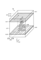
- FIG. 1 is a perspective view showing the configuration of the first liquid crystal cell 10.
- the first liquid crystal cell 10 includes a first substrate S11, a second substrate S12, and a first liquid crystal layer LC1 between the first substrate S11 and the second substrate S12.
- a first electrode E11 and a first alignment film AL11 are provided on the first substrate S11, and a second electrode E12 and a second alignment film AL12 are provided on the second substrate S12.
- the first alignment film AL11 covers the first electrode E11, and the second alignment film AL12 covers the second electrode E12.
- the first electrode E11 and the first alignment film AL11 are arranged on the first liquid crystal layer LC1 side of the first substrate S11, and the second electrode E12 and the second alignment film AL12 are arranged on the first liquid crystal layer LC1 side of the second substrate S12. be done.
- the first electrode E11 and the second electrode E12 face each other with the first liquid crystal layer LC1 interposed therebetween.
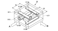
- the first electrode E11 includes a first strip-shaped electrode E11A and a second strip-shaped electrode E11B each having a strip-shaped pattern (or a comb pattern).
- the second electrode E12 includes a third strip-shaped electrode E12A and a fourth strip-shaped electrode E12B each having a strip-shaped pattern (or a comb-like pattern).
- a plurality of first strip electrodes E11A and second strip electrodes E11B are alternately arranged on the insulating surface of the first substrate S11, and a plurality of third strip electrodes E12A and fourth strip electrodes E12B are arranged on the insulating surface of the second substrate S12. are arranged alternately.
- FIG. 1 shows the X, Y, and Z axis directions for explanation.
- the extending direction of the first strip-shaped electrode E11A and the plurality of second strip-shaped electrodes E11B is arranged in a direction parallel to the X-axis direction, and the third strip-shaped electrode E12A and the plurality of fourth strip-shaped electrodes E12B are arranged.
- the extending direction is arranged in a direction parallel to the Y-axis direction.
- the third strip-shaped electrodes E12A and the fourth strip-shaped electrodes E12B are arranged so as to cross the first strip-shaped electrodes E11A and the second strip-shaped electrodes E11B.
- the extending direction of the first strip-shaped electrode E11A and the second strip-shaped electrode E11B and the extending direction of the third strip-shaped electrode E12A and the fourth strip-shaped electrode E12B intersect, for example, within a range of 90 ⁇ 10 degrees, preferably orthogonally. (90 degrees).
- the first alignment film AL11 and the second alignment film AL12 have an alignment regulating force substantially parallel to the main plane of each substrate.
- the alignment direction of the first alignment film AL11 is provided in the direction (Y-axis direction) intersecting with the extending direction of the first strip-shaped electrode E11A and the second strip-shaped electrode E11B, and the alignment direction of the second alignment film AL12 is set in the direction of the third strip-shaped electrode. It is provided in a direction (X-axis direction) intersecting with the extending direction of the E12A and the fourth strip-shaped electrode E12B.
- the angle at which the alignment direction of the first alignment film AL11 and the second alignment film AL12 intersects the extending direction of the strip electrodes can be set within a range of 90 ⁇ 10 degrees.
- twisted nematic (TN) liquid crystal is used for the first liquid crystal layer LC1.
- the first liquid crystal layer LC1 which is affected by the alignment control force of the first alignment film AL11 and the second alignment film AL12, is oriented along the longitudinal direction of the liquid crystal molecules LCM. orients in a direction parallel to the orientation direction. Since the alignment direction of the first alignment film AL11 and the alignment direction of the second alignment film AL12 intersect (perpendicularly), the long axis direction of the liquid crystal molecules LCM is twisted by 90 degrees from the first substrate S11 to the second substrate S12. The orientation direction changes gradually so that the Although not shown in FIG. 1, a spacer may be provided between the first substrate S11 and the second substrate S12 to keep the gap constant.
- the liquid crystal on the first substrate S11 side is The orientation state of the molecule LCM changes. Further, by applying a voltage so as to generate a potential difference between the third strip-shaped electrode E12A and the fourth strip-shaped electrode E12B, the alignment state of the liquid crystal molecules LCM on the second substrate S12 side is changed.
- FIG. 2A shows a plan view of the first substrate S11
- FIG. 2B shows a plan view of the second substrate S12.
- a first electrode E11 is provided on a first substrate S11.
- the first electrode E11 includes a plurality of first strip electrodes E11A and a plurality of second strip electrodes E11B.
- the plurality of first strip electrodes E11A and the plurality of second strip electrodes E11B have strip patterns.
- the strip-shaped patterns of the plurality of first strip-shaped electrodes E11A and the strip-shaped patterns of the plurality of second strip-shaped electrodes E11B are alternately arranged at predetermined intervals in a direction intersecting the extending direction.
- the plurality of first strip electrodes E11A are each connected to the first feed line PE11, and the plurality of second strip electrodes E11B are each connected to the second feed line PE12.
- the first power supply line PE11 is connected to the first connection terminal T11
- the second power supply line PE12 is connected to the second connection terminal T12.
- the first connection terminal T11 and the second connection terminal T12 are provided along one edge of the first substrate S11.
- the first substrate S11 is provided with a third connection terminal T13 adjacent to the first connection terminal T11 and a fourth connection terminal T14 adjacent to the second connection terminal T12.
- the third connection terminal T13 is connected to the fifth power supply line PE15.
- the fifth power supply line PE15 is connected to a first power supply terminal PT11 provided at a predetermined position on the surface of the first substrate S11.
- the fourth connection terminal T14 is connected to the sixth power supply line PE16.
- the sixth power supply line PE16 is connected to a second power supply terminal PT12 provided at a predetermined position in the plane of the first substrate S11.
- the same voltage is applied to the plurality of first strip electrodes E11A by being connected to the first feed line PE11.
- the same voltage is applied to the plurality of second strip-shaped electrodes E11B by being connected to the second feed line PE12.
- an electric field is generated between the electrodes due to the potential difference. That is, a horizontal electric field is generated by the plurality of first strip electrodes E11A and the plurality of second strip electrodes E11B.
- a second electrode E12 is provided on the second substrate S12.
- the second electrode E12 includes a plurality of third strip electrodes E12A and a plurality of fourth strip electrodes E12B.
- the plurality of third strip-shaped electrodes E12A and the plurality of fourth strip-shaped electrodes E12B have strip-shaped patterns.
- the strip patterns of the plurality of third strip electrodes E12A and the strip patterns of the plurality of fourth strip electrodes E12B are alternately arranged at predetermined intervals in a direction intersecting the extending direction.
- the third strip-shaped electrode E12A and the fourth strip-shaped electrode E12B are arranged at an angle of 90 ⁇ 10 degrees with respect to the extending direction of the first strip-shaped electrode E11A and the second strip-shaped electrode E11B.
- the plurality of third strip electrodes E12A are each connected to the third feed line PE13, and the plurality of fourth strip electrodes E12B are each connected to the fourth feed line PE14.
- the third power supply line PE13 is connected to the third power supply terminal PT13, and the fourth power supply line PE14 is connected to the fourth power supply terminal PT14.
- the third power supply terminal PT13 is provided at a position corresponding to the first power supply terminal PT11 of the first substrate S11, and the fourth power supply terminal PT14 is provided at a position corresponding to the second power supply terminal PT12 of the first substrate S11.
- the same voltage is applied to the plurality of third strip electrodes E12A by being connected to the third feed line PE13.
- the same voltage is applied to the plurality of fourth strip-shaped electrodes E12B by being connected to the fourth feed line PE14.
- an electric field is generated between the electrodes due to the potential difference. That is, a lateral electric field is generated by the plurality of third strip electrodes E12A and the plurality of fourth strip electrodes E12B.
- connection terminals T11 to T14 provided on the first substrate S11 are connected to the flexible wiring substrate.
- the first power supply terminal PT11 and the third power supply terminal PT13 are electrically connected by a conductive material
- the second power supply terminal PT12 and the fourth power supply terminal PT14 are electrically connected by a conductive material. Connected.
- FIG. 3 shows a cross-sectional view of the first liquid crystal cell 10.
- FIG. The cross-sectional structure of the first liquid crystal cell 10 shown in FIG. 3 shows the cross-sectional structure corresponding to the line A1-A2 of the first substrate S11 shown in FIG. 2A and the second substrate S12 shown in FIG. 2B.
- the first liquid crystal cell 10 has an effective area AA through which incident light is transmitted.
- the first electrode E11 and the second electrode E12 are arranged within the effective area AA.
- the first substrate S11 and the second substrate S12 are bonded together by a sealing material SE provided outside the effective area AA.
- the first liquid crystal layer LC1 is enclosed between the first substrate S11 and the second substrate S12 with a sealing material SE.
- the first power supply terminal PT11 has a structure continuous from the fifth power supply line PE15, and is arranged outside the sealing material SE.
- the third power supply terminal PT13 has a structure continuous from the third power supply line PE13, and is arranged outside the sealing material SE.
- the first power supply terminal PT11 and the third power supply terminal PT13 are arranged so as to face each other in a region outside the seal material SE.
- the first conductive member CP11 is arranged between the first power supply terminal PT11 and the third power supply terminal PT13 to electrically connect them.
- the first conductive member CP11 can be made of a conductive paste material, such as silver paste or carbon paste.
- the second power supply terminal PT12 and the fourth power supply terminal PT14 are similarly electrically connected by a conductive member.
- the first substrate S11 and the second substrate S12 are translucent substrates, such as glass substrates and resin substrates.
- the first electrode E11 and the second electrode E12 are transparent electrodes made of a transparent conductive material such as indium tin oxide (ITO) or indium zinc oxide (IZO).
- power supply lines (first power supply line PE11, second power supply line PE12, third power supply line PE13, fourth power supply line PE14, fifth power supply line PE15, sixth power supply line PE16), connection terminals (first connection terminal T11, 2 connection terminal T12, third connection terminal T13, fourth connection terminal T14) and power supply terminals (first power supply terminal PT11, second power supply terminal PT12, third power supply terminal PT13, fourth power supply terminal PT14) are made of aluminum, It is made of metal materials such as titanium, molybdenum, and tungsten.
- first power supply line PE11, second power supply line PE12, third power supply line PE13, fourth power supply line PE14, fifth power supply line PE15, sixth power supply line PE16 are connected to the first electrode E11 and the second power supply line PE16. It may be formed of the same transparent conductive film as the electrode E12. Of course, it is also possible to employ a configuration in which one or both of the first electrode E11 and the second electrode E12 are made of a metal material.
- FIG. 4A shows a partial perspective view of the first liquid crystal cell 10.
- FIG. 4A shows the arrangement of the first strip-shaped electrode E11A and the second strip-shaped electrode E11B, the third strip-shaped electrode E12A and the fourth strip-shaped electrode E12B, and the first liquid crystal layer LC1.
- 4B and 4C show schematic cross-sectional views of the first liquid crystal cell 10.
- FIG. 4B and 4C are schematic cross-sectional views of the first liquid crystal cell 10 shown in FIG. 4A as viewed from side A and side B shown in the figure. 4B and 4C show that the orientation treatment direction of the first orientation film AL11 and the orientation treatment direction of the second orientation film AL12 are different.
- the first strip-shaped electrode E11A and the second strip-shaped electrode E11B are arranged with a center-to-center distance W
- the third strip-shaped electrode E12A and the fourth strip-shaped electrode E12B are similarly arranged with a center-to-center distance W.
- the first substrate S11 and the second substrate S12 are arranged facing each other with a gap D therebetween.
- the distance D which is the distance between the substrates, substantially corresponds to the thickness of the first liquid crystal layer LC1.
- a first strip-shaped electrode E11A and a first alignment film AL11 are provided on the first substrate S11, and a third strip-shaped electrode E12A and a second alignment film AL12 are provided on the second substrate S12.
- the thickness of the alignment film is sufficiently smaller than the size of the gap D, the thickness of the first liquid crystal layer LC1 is substantially the same as the gap D.
- the distance D corresponding to the thickness of the first liquid crystal layer LC1 is preferably equal to or greater than the distance W between the centers of the strip electrodes (D ⁇ W).
- the interval D preferably has a length that is equal to or greater than the center-to-center distance W.
- the distance D corresponding to the thickness of the first liquid crystal layer LC1 is preferably twice or more the distance W between the centers of the strip electrodes.
- the width of the first strip-shaped electrode E11A is 5 ⁇ m
- the width a of the first strip-shaped electrode E11A and the second strip-shaped electrode E11B is 5 ⁇ m
- the end of the first strip-shaped electrode E11A is separated from the end of the second strip-shaped electrode E11B.
- the distance W between the centers of the strip electrodes is 10 ⁇ m.
- the distance D corresponding to the thickness of the first liquid crystal layer LC1 is preferably 10 ⁇ m or more.
- the relationship between the center-to-center distance W of the strip electrodes and the distance D corresponding to the thickness of the first liquid crystal layer LC1 allows the electric field generated between the first strip electrode E11A and the second strip electrode E11B. , the mutual interference of the electric field generated between the third strip electrode E12A and the fourth strip electrode E12B is suppressed.
- the refractive index of liquid crystals changes depending on the orientation state.
- the long axis direction of the liquid crystal molecules is aligned horizontally with the surface of the substrate, and the liquid crystal molecules are aligned horizontally from the first substrate S11 side.
- the two substrates S12 are oriented in a state of being twisted by 90 degrees.
- the first liquid crystal layer LC1 has a uniform refractive index distribution.
- the polarization component of the incident light changes its direction due to the twist of the liquid crystal molecules LCM.
- optical rotation such action of the liquid crystal layer
- the incident light passes through the first liquid crystal layer LC1 without being refracted (or scattered) while undergoing optical rotation.
- the first liquid crystal layer LC1 has a region in which the liquid crystal molecules LCM rise above the first strip-shaped electrode E11A and the second strip-shaped electrode E11B, and a region where the first strip-shaped electrode E11A and the second strip-shaped electrode E11A A region that is obliquely aligned along the electric field distribution between the electrode E11B and a region that maintains the initial alignment state are formed in a region away from the first substrate S11.
- liquid crystal molecules LCM are formed in the first liquid crystal layer LC1.
- the liquid crystal molecules LCM A region is formed in which the long axes of the molecules are oriented in a convex arc along the direction in which the electric field is generated. That is, as shown in FIGS. 4B and 4C, when an electric field is generated between the first strip-shaped electrode E11A and the second strip-shaped electrode E11B and between the third strip-shaped electrode E12A and the fourth strip-shaped electrode E12B, the liquid crystal molecules LCM A region is formed in which the long axes of the molecules are oriented in a convex arc along the direction in which the electric field is generated. That is, as shown in FIGS.
- the liquid crystal molecules The LCM is oriented in a normal direction (tilted) with respect to the surface of the first substrate S11 according to the intensity distribution of the electric field.
- a lateral electric field is formed by the strip electrodes, so that a convex arc-shaped permittivity distribution is formed in the first liquid crystal layer LC1.
- the polarized light component parallel to the initial alignment direction of the liquid crystal molecules LCM is radially diffused by the dielectric constant distribution.
- the alignment directions of the liquid crystal molecules LCM intersect (perpendicularly) on the first substrate S11 side and the second substrate S12 side. Diffuse light in different directions.
- FIG. 5A shows the first liquid crystal cell 10 in which the strip electrodes of the first electrodes E11 extend in the X-axis direction and the strip electrodes of the second electrodes E12 extend in the Y-axis direction.
- a voltage is applied to the first electrode E11 so as to generate a lateral electric field (Y-axis direction) between the first strip-shaped electrode E11A and the second strip-shaped electrode E11B, and a third strip-shaped electrode is applied to the second electrode E12.
- a voltage is applied to generate a horizontal electric field (in the X-axis direction) between E12A and the fourth strip-shaped electrode E12B.
- FIG. 5A shows that in such a bias state, light containing a first polarization component PL1 parallel to the X-axis direction and a second polarization component PL2 parallel to the Y-axis direction is incident on the first liquid crystal cell 10 from the first substrate S11. , and shows a state in which light is emitted from the second substrate S12.
- the first polarization component PL1 corresponds to the S wave
- the second polarization component PL2 corresponds to the P wave.
- the major axis of the liquid crystal molecules LCM on the first substrate S11 side faces the Y-axis direction
- the major axis direction of the liquid crystal molecules LCM on the second substrate S12 side faces the X-axis direction.
- the light of the first polarization component PL1 is transmitted as it is because the polarization direction intersects the long axis direction of the liquid crystal molecules LCM, and the light of the second polarization component PL2 is polarized in the direction of the liquid crystal molecules.
- the first polarization component PL1 Since it is parallel to the major axis direction of the molecules LCM, it diffuses in the Y-axis direction under the influence of the arc-shaped refractive index distribution formed by the orientation of the liquid crystal molecules LCM.
- the light of the first polarization component PL1 is optically rotated by 90 degrees as it travels through the first liquid crystal layer LC1 from the first substrate S11 side to the second substrate S12 side. , the light is transmitted as it is and emitted from the second substrate S12.
- the second polarization component PL2 is optically rotated by 90 degrees as it travels through the first liquid crystal layer LC1 from the first substrate S11 side to the second substrate S12 side. Since the direction is parallel to the alignment direction of the long axis, the light is diffused in the X-axis direction and emitted from the second substrate S12.
- the first polarization component PL1 (S wave) is not diffused, and the second polarization component PL2 (P wave) is diffused in the X-axis and Y-axis directions. spread to
- FIG. 5B shows the profile of the S wave (output light P wave).
- the first polarization component PL1 (S wave) should not be diffused in principle, but the profile in FIG. is confirmed.
- the reason for this suggests that the second polarized component PL2 (P wave) diffused in the Y-axis direction on the first substrate S11 side remains as a component that has not been optically rotated by the first liquid crystal layer LC1. .
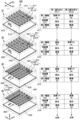
- a liquid crystal light control element 102 exemplified in the embodiments described below has a configuration capable of precisely controlling the profile of emitted light by arranging a plurality of liquid crystal cells in an overlapping manner.
- This embodiment shows an example in which the liquid crystal light control element is composed of four liquid crystal cells. Each liquid crystal cell is provided with a liquid crystal layer between a pair of substrates, and at least one of the substrates is provided with strip electrodes as shown in FIG.
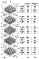
- FIG. 6 shows the electrode arrangement in each liquid crystal cell of the liquid crystal light control element 102 according to the first configuration and the state when the light incident on the liquid crystal light control element 102 passes through each liquid crystal cell.
- a first liquid crystal cell 10 a second liquid crystal cell 20, a third liquid crystal cell 30, and a fourth liquid crystal cell 40 are stacked from the light incident side to the light emitting side.
- FIG. 6 shows the X-, Y-, and Z-axes for explanation.
- the X-axis direction refers to the direction along the X-axis
- the Y-axis direction refers to the direction along the Y-axis
- the Z-axis direction refers to the direction along the Z-axis.
- the liquid crystal light control element 102 In the liquid crystal light control element 102 according to the first configuration, the first liquid crystal cell 10, the second liquid crystal cell 20, the third liquid crystal cell 30, and the fourth liquid crystal cell 40 are stacked in the Z-axis direction. Although the actual liquid crystal light control element 102 is arranged so that each liquid crystal cell is closely arranged, FIG. 6 shows the state in which each liquid crystal cell is expanded for explanation.
- first electrodes (first strip-shaped electrodes E11A and second strip-shaped electrodes E11B) are provided on a first substrate S11, and second electrodes E12 (planar (flat or solid) are provided on a second substrate S12. ) electrodes are provided, and a first liquid crystal layer LC1 is provided between a first substrate S11 and a second substrate S12.
- the first strip-shaped electrode E11A and the second strip-shaped electrode E11B are provided so as to extend in the Y-axis direction.
- the alignment film is omitted in FIG. 6, the alignment direction of the alignment film is indicated by an arrow.
- the alignment direction of the first alignment film AL11 (not shown) on the first substrate S11 side is directed in the X-axis direction
- the alignment direction of the second alignment film AL12 (not shown) on the second substrate S12 side. is oriented along the Y-axis.
- the crossing angle between the alignment direction of the first alignment film AL11 and the alignment direction of the second alignment film AL12 is preferably 90 ⁇ 10 degrees, more preferably 90 degrees (perpendicular).
- the second liquid crystal cell 20 includes a first substrate S21 and a second substrate S22, a first electrode E21 (a first strip-shaped electrode E21A and a second strip-shaped electrode E21B), and a second electrode E22 (planar (also referred to as a flat plate shape or solid shape)). .) electrodes), and a second liquid crystal layer LC2 between the first substrate S21 and the second substrate S22.
- the second liquid crystal cell 20 has a configuration similar to that of the first liquid crystal cell 10 . That is, the second liquid crystal cell 20 is arranged such that the extending direction of the first strip-shaped electrode E21A and the second strip-shaped electrode E21B extends in the Y-axis direction.
- the third liquid crystal cell 30 includes a first substrate S31 and a second substrate S32, a first electrode E31 (a first strip-shaped electrode E31A and a second strip-shaped electrode E31B), and a second electrode E32 (planar (also referred to as a flat plate shape or solid shape)). .) electrodes), and a third liquid crystal layer LC3 between the first substrate S31 and the second substrate S32.
- the third liquid crystal cell 30 has the same configuration as the first liquid crystal cell 10, but is arranged so that the extending direction of the first strip-shaped electrode E31A and the second strip-shaped electrode E31B extends in the X-axis direction.
- the alignment direction of the alignment film is oriented in the Y-axis direction on the first substrate S31 side and oriented in the X-axis direction on the second substrate S32 side.
- the fourth liquid crystal cell 40 includes a first substrate S41 and a second substrate S42, a first electrode E41 (a first strip-shaped electrode E41A and a second strip-shaped electrode E41B), and a second electrode E42 (planar (also referred to as a flat plate shape or solid shape)). .) electrodes), and a fourth liquid crystal layer LC4 between the first substrate S41 and the second substrate S42.
- the fourth liquid crystal cell 40 has a configuration similar to that of the third liquid crystal cell 30 . That is, the fourth liquid crystal cell 40 is arranged such that the extending direction of the first strip-shaped electrode E41A and the second strip-shaped electrode E41B extends in the X-axis direction. Also, the alignment direction of the alignment film is oriented in the Y-axis direction on the first substrate S41 side, and oriented in the X-axis direction on the second substrate S42 side.
- the alignment directions of the liquid crystals of the first liquid crystal cell 10 and the second liquid crystal cell 20 are the same, and the strip electrodes (E11A , E11B, E21A, E21B) are oriented in the same direction. Further, the liquid crystal alignment directions of the third liquid crystal cell 30 and the fourth liquid crystal cell 40 are the same, and the strip electrodes (E31A, E31B, E41A, E41B) of the first electrodes E31 and E41 extend in the same direction.
- FIG. 6 shows the arrangement of electrodes in the first liquid crystal cell 10, the second liquid crystal cell 20, the third liquid crystal cell 30, and the fourth liquid crystal cell 40, the orientation directions (arrows) of the orientation films, and the initial orientation of the liquid crystal molecules.
- the liquid crystal layer is formed of positive liquid crystal, and in the initial state in which no control signal is input to each liquid crystal cell, the long axis direction of the liquid crystal is oriented in the direction that intersects (perpendicular to) the strip electrodes.
- the alignment directions of the alignment films (first alignment films) on the sides of the first substrates S11, S21, S31, and S41 intersect each other.
- the alignment direction of the alignment films (not shown) on the first substrates S11 and S21 sides of the first liquid crystal cell 10 and the second liquid crystal cell 20 is parallel to the X-axis direction.
- the orientation direction of the orientation films (not shown) on the second substrates S12 and S22 is parallel to the Y-axis direction.
- the extending direction of the band-shaped patterns of the first electrodes E11 and E21 of the first liquid crystal cell 10 and the second liquid crystal cell 20 is parallel to the Y-axis direction, and the second electrodes E12 and E22 are at least in the effective area.
- the alignment direction of the alignment films (not shown) on the first substrate S31 and S41 side of the third liquid crystal cell 30 and the fourth liquid crystal cell 40 is parallel to the Y-axis direction, and the second substrate S32, The alignment direction of the alignment film (not shown) on the S42 side is parallel to the X-axis direction.
- the extending direction of the band-shaped patterns of the first electrodes E31 and E41 of the third liquid crystal cell 30 and the fourth liquid crystal cell 40 is parallel to the X-axis direction, and the second electrodes E32 and E42 are at least in the effective region.
- the alignment direction of the alignment film intersects the first substrate side and the second substrate side of each liquid crystal cell at an angle of 90 degrees. It can be set within a range of 90 ⁇ 10 degrees.
- the same direction as the polarization direction of the first polarization component PL1 is defined as the X-axis direction
- the same direction as the polarization direction of the second polarization component PL2 is defined as the Y-axis direction.
- the first polarization component PL1 is the S wave
- the second polarization component PL2 is the P wave.
- “diffusion (X)” shown in the table of FIG. 6 indicates that the polarization component is diffused in the X-axis direction
- “diffusion (Y)” indicates that the polarization component is diffused in the Y-axis direction. indicates that
- FIG. 6 the electrodes to which the control signal is applied and which form the transverse electric field are hatched.
- a table is inserted in FIG. 6, showing the respective polarizations when the light containing the first polarization component PL1 and the second polarization component PL2 passes through the first electrode, the liquid crystal layer, and the second electrode of each liquid crystal cell.
- the states of the components are indicated by the terms transmission, optical rotation, and diffusion.
- transmission means that the polarized light component passes through without being diffused or optically rotated.
- “Diffusion” means that the polarized component is diffused and transmitted under the influence of the refractive index distribution of the liquid crystal molecules.
- transmission indicates that the phenomenon of "transmission” occurs in the vicinity of the first electrode of the liquid crystal layer.
- optical rotation indicates that the polarization direction of the liquid crystal layer is shifted by 90 degrees in the process of moving the liquid crystal layer from the first substrate side to the second substrate side.
- the first liquid crystal cell 10 the second liquid crystal cell 20, the third liquid crystal cell 30, and the fourth liquid crystal cell 40 are arranged in this order from the light incident side to the light emitting side.
- Light incident on the liquid crystal light control element 102 includes a first polarization component PL1 and a second polarization component PL2 orthogonal to the first polarization component PL1.
- the first electrode E11 of the first liquid crystal cell 10 and the first electrode E21 of the second liquid crystal cell 20 are arranged in the same extending direction of the strip electrodes.
- the first polarization component PL1 can be diffused in the X-axis direction
- the second liquid crystal cell 20 can diffuse the second polarization component PL2 in the X-axis direction.
- the second electrode E32 of the third liquid crystal cell 30 and the second electrode E42 of the fourth liquid crystal cell 40 are arranged in the same extending direction, and in the third liquid crystal cell 30, the second polarization component PL2 is aligned with the Y axis.
- the first polarization component PL1 can be diffused in the Y-axis direction.
- a control signal is input to each liquid crystal cell in order to control the polarization state and diffusion state of light incident on the liquid crystal light control element 102 .
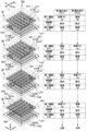
- FIG. 7 shows an example of the waveform of the control signal applied to the electrodes of each liquid crystal cell.
- One of control signal A, control signal B, and control signal E shown in FIG. 7 is input to each liquid crystal cell.
- VL1 means a low level voltage
- VH1 means a high level voltage.
- VL1 is a voltage of 0V or -15V and VH1 is 30V (relative to 0V) or 15V (relative to -15V).
- Control signal A and control signal B are synchronous.
- control signal A When control signal A is at VL1 level, control signal B is at VH1 level. When control signal A changes to VH1 level, control signal B is at VL1 level. change to The period of the control signals A and B is approximately 15 to 100 Hz.
- the liquid crystal light control element 102 can control the profile (intensity distribution) of the light distribution pattern of the light emitted from the light source (not shown) by selecting the control signal applied to each liquid crystal cell. Specifically, the polar angle profile of the illumination light can be controlled.
- Table 1 shows control signals applied to each liquid crystal cell of the liquid crystal light control element 102 shown in FIG.
- the control signals A, B, and E shown in Table 1 correspond to the control signals shown in FIG.
- a control signal is input to each liquid crystal cell of the liquid crystal light control element 102 as shown in Table 1.
- the control signal A is input to the first strip electrode E11A of the first liquid crystal cell 10
- the control signal B is input to the second strip electrode E11B
- the control signal E is input to the second electrode E12
- the first electrode E11 side A transverse electric field is generated only in As shown in Table 1, the same applies to the second liquid crystal cell 20, the third liquid crystal cell 30, and the fourth liquid crystal cell 40. That is, in the liquid crystal light control element 102 shown in FIG. 6, the control signals A and B are applied to the first electrodes of each liquid crystal cell, the control signal E is applied to the second electrodes, and the horizontal electric field is applied only on the first substrate side. It has occurred.
- control signals shown in Table 1 are input to each strip electrode of each liquid crystal cell.
- control signals shown in Table 1 are input to the first liquid crystal cell 10, the second liquid crystal cell 20, the third liquid crystal cell 30, and the fourth liquid crystal cell 40, each liquid crystal cell is displayed as shown in FIG. 4C.
- the liquid crystal molecules on the first substrate side are affected by the lateral electric field and change their alignment state.
- the incident light is assumed to contain two polarization components, a first polarization component PL1 and a second polarization component PL2.
- the first polarization component PL1 and the second polarization component PL2 are linearly polarized light components and have either s-polarized light or p-polarized light. These polarization states can transition from s-polarized light to p-polarized light or from p-polarized light to s-polarized light by optically rotating in the liquid crystal layer. It is assumed that the first polarization component PL1 is s-polarization and the second polarization component PL2 is p-polarization in the state immediately before entering the liquid crystal light control element 102 .
- the first polarized light component PL1 enters the first liquid crystal cell 10 in the state of s-polarized light.
- the polarization direction of the first polarization component PL1 (s-polarized light) is along the X-axis direction and parallel to the alignment direction of the long axis of the liquid crystal molecules on the first substrate S11 side of the first liquid crystal layer LC1. be.
- the liquid crystal molecules are oriented under the influence of the horizontal electric field generated by the first electrode E11, and an arcuate refractive index distribution is formed in the first liquid crystal layer LC1.
- the first polarized light component PL1 (s-polarized light) incident on the first liquid crystal layer LC1 from the first substrate S11 is diffused in the X-axis direction under the influence of the arc-shaped refractive index distribution of the first liquid crystal layer LC1.
- the first polarized light component PL1 (s-polarized light) is optically rotated by 90 degrees according to the twisted orientation of the liquid crystal molecules in the process of moving the first liquid crystal layer LC1 from the first substrate S11 side to the second substrate S12 side. This causes the first polarization component PL1 to transition from s-polarization to p-polarization.
- the second electrode E12 is a planar (also referred to as flat or solid) electrode, and the entire surface is at a constant potential.
- the first polarized light component PL1 (p-polarized light) is not diffused and is emitted from the second substrate S12 as it is.
- the first polarized light component PL1 enters the first liquid crystal cell 10 in the s-polarized state, is diffused in the X-axis direction, is optically rotated by 90 degrees, and is emitted from the first liquid crystal cell 10 in the p-polarized state.
- the first polarized light component PL1 that has passed through the first liquid crystal cell 10 enters the second liquid crystal cell 20 in a p-polarized state.
- the polarization direction of the first polarization component PL1 (p-polarized light) is the direction along the Y-axis direction, and the direction crossing the alignment direction of the long axis of the liquid crystal molecules on the first substrate S21 side of the second liquid crystal layer LC2. be.
- the liquid crystal molecules are aligned under the influence of the horizontal electric field generated by the first electrode E21, and an arc-shaped refractive index distribution is formed in the second liquid crystal layer LC2. (p-polarized light) is not diffused and goes to the second substrate S22 as it is.
- the first polarized light component PL1 (p-polarized light) is optically rotated by 90 degrees according to the twisted orientation of the liquid crystal molecules in the process of moving the second liquid crystal layer LC2 from the first substrate S21 side to the second substrate S22 side. This causes the first polarization component PL1 to transition from p-polarization to s-polarization.
- the second electrode E22 is a planar (also referred to as flat or solid) electrode, and the entire surface is at a constant potential. No distribution formed. Therefore, the first polarized light component PL1 (s-polarized light) is not diffused and is emitted from the second substrate S22 as it is. Thus, the first polarization component PL1 enters the second liquid crystal cell 20 in the p-polarized state, is not diffused, is optically rotated by 90 degrees, and exits the second liquid crystal cell 20 in the s-polarized state.
- the first polarized light component PL1 that has passed through the second liquid crystal cell 20 enters the third liquid crystal cell 30 in the s-polarized state.
- the extending direction of the strip electrodes (E31A, E31B) of the first electrode E31 is the same as that of the strip electrodes (E11A, E11B) of the first electrodes E11, E21 of the first liquid crystal cell 10 and the second liquid crystal cell 20. , E21A, E21B).
- the polarization direction of the first polarization component PL1 (s-polarized light) is the direction along the X-axis direction, and the direction crossing the alignment direction of the long axis of the liquid crystal molecules on the first substrate S31 side of the third liquid crystal layer LC3.
- the liquid crystal molecules are oriented under the influence of the horizontal electric field generated by the first electrode E31, and an arc-shaped refractive index distribution is formed in the third liquid crystal layer LC3. (s-polarized light) is not diffused and goes to the second substrate S32 as it is.
- the first polarized light component PL1 (s-polarized light) is optically rotated by 90 degrees according to the twisted orientation of the liquid crystal molecules in the process of moving the third liquid crystal layer LC3 from the first substrate S31 side to the second substrate S32 side. This causes the first polarization component PL1 to transition from s-polarization to p-polarization.
- the second electrode E32 is a planar (also referred to as flat or solid) electrode, and the entire surface is at a constant potential. No distribution formed. Therefore, the first polarized light component PL1 (p-polarized light) is not diffused and is emitted from the second substrate S32 as it is. Thus, the first polarization component PL1 enters the third liquid crystal cell 30 in the s-polarized state, is not diffused, is optically rotated by 90 degrees, and exits the third liquid crystal cell 30 in the p-polarized state.
- the first polarized light component PL1 that has passed through the third liquid crystal cell 30 enters the fourth liquid crystal cell 40 in a p-polarized state.
- the first electrode E41 of the fourth liquid crystal cell 40 faces in the same direction as the first electrode E31 of the third liquid crystal cell 30.
- the alignment direction of the long axis of the liquid crystal molecules on the first substrate S41 side of the fourth liquid crystal cell 40 is also the same as that of the third liquid crystal cell 30 .
- the polarization direction of the first polarization component PL1 (p-polarized light) is along the Y-axis direction and parallel to the alignment direction of the long axis of the liquid crystal molecules on the first substrate S41 side of the fourth liquid crystal layer LC4. be.
- the liquid crystal molecules are oriented under the influence of the lateral electric field generated by the first electrode E41, and an arcuate refractive index distribution is formed in the fourth liquid crystal layer LC4.
- the first polarized light component PL1 (p-polarized light) incident on the fourth liquid crystal layer LC4 from the first substrate S41 is diffused in the Y-axis direction under the influence of the arc-shaped refractive index distribution of the fourth liquid crystal layer LC4.
- the first polarized light component PL1 (p-polarized light) is optically rotated by 90 degrees according to the twisted orientation of the liquid crystal molecules in the process of moving the fourth liquid crystal layer LC4 from the first substrate S41 side to the second substrate S42 side.
- the second electrode E42 is a planar (also referred to as flat or solid) electrode, and the entire surface is at a constant potential. No distribution formed. Therefore, the first polarized light component PL1 (s-polarized light) is not diffused and is emitted from the second substrate S42 as it is. Thus, the first polarization component PL1 enters the fourth liquid crystal cell 40 in a p-polarized state, is diffused in the Y-axis direction, is optically rotated by 90 degrees, and is emitted from the fourth liquid crystal cell 40 in an s-polarized state. be.
- the first polarized light component PL1 entering the liquid crystal light control element 102 enters the first liquid crystal cell 10 and exits from the fourth liquid crystal cell 40 once in the X-axis direction and once in the Y direction.
- the light is diffused once in the axial direction, is incident in the state of s-polarized light, and is emitted in the state of s-polarized light by being rotated four times at an angle of 90 degrees.
- the second polarization component PL2 enters the first liquid crystal cell 10 in a p-polarized state.
- the polarization direction of the second polarization component PL2 (p-polarized light) is the direction along the Y-axis direction, and the direction crossing the orientation direction of the long axis of the liquid crystal molecules on the first substrate S11 side of the first liquid crystal layer LC1. be.
- an arc-shaped refractive index distribution is formed in the first liquid crystal layer LC1 on the first substrate S11 side, the second polarized light component PL2 (p-polarized light) is not diffused and goes straight to the second substrate S12.
- the first polarized light component PL1 (p-polarized light) is optically rotated by 90 degrees according to the twisted orientation of the liquid crystal molecules in the process of moving the first liquid crystal layer LC1 from the first substrate S11 side to the second substrate S12 side. This causes the first polarization component PL1 to transition from p-polarization to s-polarization.
- the planar (also referred to as flat or solid) second electrode E12 is at a constant potential, so that the arc-shaped refractive index distribution is not formed in the first liquid crystal layer LC1.
- the polarization component PL2 (s-polarized light) is emitted from the second substrate S12 without being diffused.
- the second polarization component PL2 enters the first liquid crystal cell 10 in the p-polarized state, is not diffused, is optically rotated by 90 degrees, and exits the first liquid crystal cell 10 in the s-polarized state.
- the second polarized light component PL2 that has passed through the first liquid crystal cell 10 enters the second liquid crystal cell 20 in the s-polarized state.
- the polarization direction of the second polarization component PL2 (s-polarized light) is along the X-axis direction, and parallel to the alignment direction of the long axis of the liquid crystal molecules on the first substrate S21 side of the second liquid crystal layer LC2. be.
- An arcuate refractive index distribution is formed in the second liquid crystal layer LC2 on the first substrate S21 side.
- the second polarized light component PL2 (s-polarized light) incident on the second liquid crystal layer LC2 from the first substrate S21 is diffused in the X-axis direction under the influence of the arc-shaped refractive index distribution of the second liquid crystal layer LC2.
- the second polarized light component PL2 (s-polarized light) is optically rotated by 90 degrees according to the twisted orientation of the liquid crystal molecules in the process of moving the second liquid crystal layer LC2 from the first substrate S21 side to the second substrate S22 side.
- the second polarization component PL2 transitions from s-polarization to p-polarization.
- the second electrode E22 is a planar (also referred to as flat or solid) electrode, and the entire surface is at a constant potential. No distribution formed. Therefore, the second polarized light component PL2 (p-polarized light) is not diffused and is emitted from the second substrate S22 as it is. Thus, the second polarized light component PL2 enters the second liquid crystal cell 20 in the s-polarized state, is diffused in the X-axis direction, is optically rotated by 90 degrees, and is emitted from the second liquid crystal cell 20 in the p-polarized state. be.
- the second polarized light component PL2 that has passed through the second liquid crystal cell 20 enters the third liquid crystal cell 30 in a p-polarized state.
- the polarization direction of the second polarization component PL2 (p-polarized light) is along the Y-axis direction and parallel to the alignment direction of the long axis of the liquid crystal molecules on the first substrate S31 side of the third liquid crystal layer LC3. be.
- An arcuate refractive index distribution is formed in the third liquid crystal layer LC3 on the first substrate S31 side.
- the second polarized light component PL2 (p-polarized light) incident on the third liquid crystal layer LC3 from the first substrate S31 is diffused in the Y-axis direction under the influence of the arc-shaped refractive index distribution of the third liquid crystal layer LC3.
- the second polarized light component PL2 (p-polarized light) is optically rotated by 90 degrees according to the twisted orientation of the liquid crystal molecules in the process of moving the third liquid crystal layer LC3 from the first substrate S31 side to the second substrate S32 side. This causes the second polarization component PL2 to transition from p-polarization to s-polarization.
- the second electrode E32 is a planar (also referred to as flat or solid) electrode, and the entire surface is at a constant potential.
- the second polarized light component PL2 (s-polarized light) is not diffused and is emitted from the second substrate S32 as it is.
- the second polarized light component PL2 enters the third liquid crystal cell 30 in the p-polarized state, is diffused in the Y-axis direction, is optically rotated by 90 degrees, and is emitted from the third liquid crystal cell 30 in the s-polarized state.
- the second polarization component PL2 that has passed through the third liquid crystal cell 30 enters the fourth liquid crystal cell 40 in the s-polarized state.
- the polarization direction of the second polarization component PL2 (s-polarized light) is the direction along the X-axis direction, and the direction crossing the alignment direction of the long axis of the liquid crystal molecules on the first substrate S31 side of the third liquid crystal layer LC3. be.
- an arcuate refractive index distribution is formed in the fourth liquid crystal layer LC4 on the first substrate S41 side, the second polarized light component PL2 (s-polarized light) is not diffused and goes straight to the second substrate S42.
- the second polarized light component PL2 (s-polarized light) is optically rotated by 90 degrees according to the twisted orientation of the liquid crystal molecules in the process of moving the fourth liquid crystal layer LC4 from the first substrate S41 side to the second substrate S42 side.
- the second electrode E42 is a planar (also referred to as flat or solid) electrode, and the entire surface is at a constant potential. No distribution formed. Therefore, the second polarized light component PL2 (p-polarized light) is not diffused and is emitted from the second substrate S42 as it is.
- the second polarization component PL2 enters the fourth liquid crystal cell 40 in the s-polarized state, is not diffused, is optically rotated by 90 degrees, and exits the fourth liquid crystal cell 40 in the p-polarized state.
- the second polarization component PL2 incident on the liquid crystal light control element 102 is incident on the first liquid crystal cell 10 and is emitted from the fourth liquid crystal cell 40 once in the X-axis direction and once in the Y-axis direction.
- the light is diffused in a p-polarized state and is emitted in a p-polarized state by being rotated four times at an angle of 90 degrees.
- the first polarization component PL1 is diffused in the X-axis direction before being rotated by the first liquid crystal cell 10, diffused in the Y-axis direction before being rotated by the fourth liquid crystal cell 40, and is diffused in the Y-axis direction before being rotated by the fourth liquid crystal cell 40.
- the two polarized light components PL2 are diffused in the X-axis direction before optically rotated by the second liquid crystal cell 20 and diffused in the Y-axis direction before optically rotated by the third liquid crystal cell 30 .
- the diffusion of the polarization component before optical rotation in each liquid crystal cell is called pre-diffusion
- the diffusion after optical rotation is called post-diffusion
- the X-axis direction of the first polarization component PL1 one time in the direction of the Y-axis
- one time in the direction of the X-axis of the second polarization component PL2 one time in the direction of the Y-axis.
- no post-diffusion occurs for any of the polarization components.
- FIG. 6 shows a configuration in which each liquid crystal cell is provided with planar (also referred to as flat or solid) second electrodes (E12, E22, E32, E42).
- Element 102 is not limited to such a configuration.
- the second substrates (S12, S22, S32, S42) of the first to fourth liquid crystal cells are configured such that the second electrodes are omitted and only an alignment film (not shown) is provided.
- may have The alignment direction of the alignment film on the second substrate side is provided so as to be orthogonal (90° ⁇ 10°) to the alignment direction of the alignment film on the first substrate side in each liquid crystal cell.
- the first polarization component PL1 and the second polarization component PL2 can be diffused in the same manner as the liquid crystal light control element 102 shown in FIG.
- the second electrodes (E12, E22, E32, E42) of the first to fourth liquid crystal cells are replaced with planar (also referred to as flat or solid) electrodes (third strip electrodes).
- E12A, E22A, E32A, E42A, and fourth strip electrodes E12B, E22B, E32B, E42B) are provided.
- a constant voltage such as the control signal E shown in FIG.
- a lateral electric field can be prevented from being generated, and light distribution characteristics similar to those of the liquid crystal light control element 102 shown in FIG. 6 can be obtained.
- the liquid crystal light control element does not diffuse the polarized component on the first electrode E11 and E41 side (light incident side) of the first liquid crystal cell 10 and the fourth liquid crystal cell 40, and the second The light is diffused on the side of the electrodes E12 and E42 (light emission side), diffused on the side of the first electrodes E21 and E31 (light incidence side) of the second liquid crystal cell 20 and the third liquid crystal cell 30, and is diffused on the side of the second electrodes E22 and E32. side (light emission side).
- FIG. 10 shows the liquid crystal light control element 102 according to the second configuration.
- the liquid crystal light control element 102 according to the second configuration has first to fourth liquid crystal cells.
- the first electrode E11 first strip electrode E11A, second strip electrode E11B
- the second electrode E12 third strip electrode E12A, second electrode E11B
- the second liquid crystal cell 20 is provided with a first electrode E21 (first strip electrode E21A, second strip electrode E21B) on the first substrate S21, and a second electrode E21 on the second substrate S22.
- E22 (third strip-shaped electrode E22A, fourth strip-shaped electrode E22B) is provided, and the third liquid crystal cell 30 is provided with first electrode E31 (first strip-shaped electrode E31A, second strip-shaped electrode E31B) on the first substrate S31.
- second electrodes E32 (third strip electrodes E32A, fourth strip electrodes E32B) are provided on the second substrate S32, and first electrodes E41 (first strip electrodes E41A, A second strip-shaped electrode E41B) is provided, and a second electrode E42 (a third strip-shaped electrode E42A and a fourth strip-shaped electrode E42B) is provided on the second substrate S42.
- Table 2 shows control signals applied to each liquid crystal cell of the liquid crystal light control element 102 shown in FIG.
- the strip electrodes to which the control signal is applied to generate the lateral electric field are indicated by hatching, and the strip electrodes to which the control signal is not applied and the lateral electric field is not generated are indicated by white.
- the control signals A and B shown in Table 3 correspond to the control signals shown in FIG.
- the control signal E is input to the first strip electrode E11A and the second strip electrode E11B of the first liquid crystal cell 10
- the control signal A is input to the third strip electrode E12A
- the fourth strip electrode E12B is input.
- a control signal B is input to .
- the control signal A is applied to the first strip electrode E21A
- the control signal B is input to the second strip electrode E21B
- the control signal E is input to the third strip electrode E22A and the fourth strip electrode E22B. be done.
- the first polarized light component PL1 enters the first liquid crystal cell 10 in the state of s-polarized light.
- the first electrode E11 of the first liquid crystal cell 10 does not generate a lateral electric field. Therefore, the first polarized light component PL1 is not diffused by the first electrode E11, and is optically rotated by 90 degrees according to the twisted orientation of the liquid crystal molecules in the process of moving the first liquid crystal layer LC1 from the first substrate S11 side to the second substrate S12 side. Transition to polarization.
- the control signal A is applied to the third strip-shaped electrode E12A, and the control signal B is applied to the fourth strip-shaped electrode E12B, so that a horizontal electric field is generated. Therefore, an arc-shaped refractive index distribution is formed on the second substrate S12 side of the first liquid crystal layer LC1.
- the first polarized light component PL1 (p-polarized light) has a polarization direction parallel to the long axis of the liquid crystal molecules, and is diffused in the Y-axis direction by the influence of the arc-shaped refractive index distribution and emitted from the second substrate S12. be.
- the first polarized light component PL1 enters the first liquid crystal cell 10 in the s-polarized state, is rotated 90 degrees into the p-polarized state, is diffused in the Y-axis direction, and exits the first liquid crystal cell 10. be done.
- the first polarized light component PL1 that has passed through the first liquid crystal cell 10 enters the second liquid crystal cell 20 in a p-polarized state.
- the first polarized light component (p-polarized light) incident on the second liquid crystal cell 20 is not diffused but is optically rotated by 90 degrees and is emitted from the second liquid crystal cell 20 in the state of s-polarized light, as in the first embodiment.
- the first polarized light component PL1 that has passed through the second liquid crystal cell 20 enters the third liquid crystal cell 30 in the s-polarized state.
- the first polarized light component (s-polarized light) incident on the third liquid crystal cell 30 is not diffused but is optically rotated by 90 degrees and is emitted from the third liquid crystal cell 30 in the state of p-polarized light, as in the first embodiment.
- the first polarized light component PL1 that has passed through the third liquid crystal cell 30 enters the fourth liquid crystal cell 40 in a p-polarized state.
- the first electrode E41 of the fourth liquid crystal cell 40 does not generate a lateral electric field. Therefore, the first polarization component PL1 is not diffused by the first electrode E41, and is optically rotated 90 degrees according to the twisted orientation of the liquid crystal molecules in the process of moving the fourth liquid crystal layer LC4 from the first substrate S41 side to the second substrate S42 side. Transition to polarization.
- the control signal A is applied to the third strip-shaped electrode E42A
- the control signal B is applied to the fourth strip-shaped electrode E42B, so that a lateral electric field is generated.
- an arc-shaped refractive index distribution is formed on the second substrate S42 side of the fourth liquid crystal layer LC4. Since the polarization direction of the first polarized light component PL1 (s-polarized light) is parallel to the long axis of the liquid crystal molecules, it is diffused in the X-axis direction by the influence of the arc-shaped refractive index distribution and emitted from the second substrate S42. be. In this way, the first polarized light component PL1 enters the fourth liquid crystal cell 40 in the p-polarized state, is rotated 90 degrees into the s-polarized state, diffused in the X-axis direction, and exits the fourth liquid crystal cell 40. be done.
- the first polarized light component PL1 incident on the liquid crystal light control element 102 enters the first liquid crystal cell 10 and exits from the fourth liquid crystal cell 40 once in the X-axis direction.
- the light is diffused once in the Y-axis direction, is incident in the s-polarized state, and is emitted in the s-polarized state by being rotated four times at an angle of 90 degrees.
- the second polarization component PL2 enters the first liquid crystal cell 10 in a p-polarized state.
- the first electrode E11 of the first liquid crystal cell 10 does not generate a lateral electric field. Therefore, the second polarized light component PL2 (p-polarized light) is not diffused by the first electrode E11, and is polarized by 90 degrees according to the twisted orientation of the liquid crystal molecules in the process of moving the first liquid crystal layer LC1 from the first substrate S11 side to the second substrate S12 side. It is optically rotated and transitions to s-polarized light.
- the second polarized light component PL2 (s-polarized light) is not diffused by the second electrode E12 and is emitted from the first liquid crystal cell 10 in the state of s-polarized light.
- the second polarized light component PL2 that has passed through the first liquid crystal cell 10 enters the second liquid crystal cell 20 in the s-polarized state.
- the second polarized light component PL2 (s-polarized light) is diffused in the X-axis direction on the first substrate S21 side.
- the second polarized light component PL2 (s-polarized light) is optically rotated by 90 degrees according to the twisted orientation of the liquid crystal molecules in the process of moving the second liquid crystal layer LC2 from the first substrate S21 side to the second substrate S22 side.
- the second polarization component PL2 transitions from s-polarization to p-polarization.
- the second electrode E22 of the second liquid crystal cell 20 does not generate a lateral electric field. Therefore, the second polarized light component PL2 is not diffused by the second electrode E22 and is emitted from the second liquid crystal cell 20 in a p-polarized state.
- the second polarized light component PL2 that has passed through the second liquid crystal cell 20 enters the third liquid crystal cell 30 in a p-polarized state.
- the second polarized light component PL2 p-polarized light
- the second polarized light component PL2 is optically rotated by 90 degrees according to the twisted orientation of the liquid crystal molecules in the process of moving the third liquid crystal layer LC3 from the first substrate S31 side to the second substrate S32 side. This causes the second polarization component PL2 to transition from p-polarization to s-polarization.
- the second electrode E32 of the third liquid crystal cell 30 does not generate a lateral electric field. Therefore, the second polarized light component PL2 is not diffused by the second electrode E32 and is emitted from the third liquid crystal cell 30 in the s-polarized state.
- the second polarization component PL2 that has passed through the third liquid crystal cell 30 enters the fourth liquid crystal cell 40 in the s-polarized state.
- the first electrode E41 of the fourth liquid crystal cell 40 does not generate a lateral electric field. Therefore, the second polarization component PL2 (s-polarized light) is not diffused by the first electrode E11, and is polarized by 90 degrees according to the twisted orientation of the liquid crystal molecules in the process of moving the first liquid crystal layer LC1 from the first substrate S11 side to the second substrate S12 side. It is optically rotated and transitions to p-polarized light.
- the second polarization component PL2 (p-polarized light) is emitted from the fourth liquid crystal cell 40 without being diffused by the second substrate S42.
- the second polarization component PL2 incident on the liquid crystal light control element 102 according to the second configuration is incident on the first liquid crystal cell 10 and exits from the fourth liquid crystal cell 40 once in the X-axis direction.
- the light is diffused once in the Y-axis direction, is incident in the state of p-polarized light, and is emitted in the state of p-polarized light by being rotated four times at an angle of 90 degrees.
- the first polarization component PL1 is diffused in the Y-axis direction after being optically rotated by the first liquid crystal cell 10, and is diffused in the X-axis direction after being optically rotated by the fourth liquid crystal cell 40, resulting in the second polarization.
- the component PL2 is diffused in the X-axis direction before optically rotated by the second liquid crystal cell 20 and diffused in the Y-axis direction before optically rotated by the third liquid crystal cell 30 .
- the first polarization component PL1 is pre-diffused 0 times in the X-axis direction, post-diffused once, pre-diffused 0 times in the Y-axis direction, and post-diffused once.
- the second polarization component PL2 is pre-spread once in the X-axis direction, post-spread 0 times, pre-spread once in the Y-axis direction, and post-spread 0 times.
- Reference example 1 11 shows a liquid crystal light control element according to Reference Example 1.
- FIG. 1 the control signal A is applied to the first strip electrode E11A on the first substrate S11 side of the first liquid crystal cell 10
- the control signal B is applied to the second strip electrode E11B
- the second strip electrode E11B on the second substrate S12 side of the first liquid crystal cell 10 is applied.
- a control signal A is applied to the third strip electrode E12A
- a control signal B is applied to the fourth strip electrode E12B.
- the first polarization component PL1 enters the first liquid crystal cell 10 in an s-polarized state.
- the first polarized light component PL1 is diffused in the X-axis direction on the first electrode E11 side of the first liquid crystal cell 10, rotated 90 degrees by the first liquid crystal layer LC1, and diffused in the Y-axis direction on the second electrode E12 side. be.
- the first polarized light component PL1 is transmitted through the second liquid crystal cell 20 and the third liquid crystal cell 30 while being optically rotated by 90 degrees, diffused in the Y-axis direction on the first electrode E41 side of the fourth liquid crystal cell 40, and transferred to the fourth liquid crystal.
- the light is optically rotated by 90 degrees in the layer LC4, diffused in the X-axis direction on the side of the second electrode E42, and emitted in an s-polarized state.
- the second polarization component PL2 enters the first liquid crystal cell 10 in a p-polarized state.
- the second polarized light component PL2 is optically rotated by 90 degrees in the first liquid crystal cell 10, is not diffused in the first liquid crystal cell 10, and enters the second liquid crystal cell 20 in an s-polarized state.
- the second polarized light component PL2 is diffused in the X-axis direction on the first electrode E21 side of the second liquid crystal cell 20, rotated 90 degrees by the second liquid crystal layer LC2, becomes p-polarized light, and becomes p-polarized light on the second electrode E22 side in the Y-axis direction.
- the second polarization component PL2 is diffused in the Y-axis direction on the first electrode E31 side of the third liquid crystal cell 30, rotated 90 degrees by the third liquid crystal layer LC3 to become s-polarized light, and becomes X-polarized light on the second electrode E22 side. Axially diffused. After that, the second polarized light component PL2 is optically rotated by 90 degrees in the fourth liquid crystal cell 40, is not diffused by the fourth liquid crystal cell 40, and is emitted in the state of p-polarized light.
- the first polarization component PL1 is diffused in the X-axis direction and the Y-axis direction by the first liquid crystal cell 10 and the fourth liquid crystal cell 40
- the second polarization component PL2 is diffused in the X-axis direction and the Y-axis direction in the second liquid crystal cell 20 and the third liquid crystal cell 30 .
- FIG. 12A shows graphs of luminance versus angular characteristics of the liquid crystal light control element 102 according to the first configuration and the second configuration.
- FIG. 12A also shows the characteristics of Reference Example 1 in the same graph.
- the horizontal axis of the graph shown in FIG. 12A indicates the polar angle.
- the polar angles shown in the graph are 0 degrees when the light emitting surface of the liquid crystal light control element 102 is viewed from the front, and angles when tilted in the positive and negative directions in the X-axis direction. indicates The vertical axis of the graph indicates the brightness normalized with the brightness at the center (0 degree polar angle) as 100%.
- the characteristics of the first configuration of the liquid crystal light control element 102 are such that the luminance in the polar angle ranges of +20 degrees to +40 degrees and -20 degrees to -40 degrees is about 20% lower than the central luminance. , a constant luminance distribution is obtained in the same range.
- each polarized component is diffused before being optically rotated by the liquid crystal layer, and is not diffused after being optically rotated. It shows that a similar intensity distribution can be obtained.
- the above-mentioned "diffuse each polarized component before being optically rotated by the liquid crystal layer and not diffuse after optically rotating” means that a certain polarized component is diffused before being optically rotated in a certain liquid crystal panel, and immediately after that, the same liquid crystal is diffused. It means that there is no further diffusion after optical rotation within the panel, and does not include diffusion of a certain polarization component in different liquid crystal panels in the process of passing through the liquid crystal light control element.
- the first polarized light component is diffused between the first liquid crystal cell and the fourth liquid crystal cell. In the fourth liquid crystal cell as well, the light diffuses before the optical rotation and does not diffuse after the optical rotation.
- the characteristic of the second configuration of the liquid crystal light control element 102 is that the brightness in the polar angle ranges of +20 degrees to +40 degrees and -20 degrees to -40 degrees is about 40% lower than the center brightness, but the brightness is constant in the same ranges. It can be seen that a distribution is obtained.
- the first polarization component PL1 is diffused after optical rotation in the liquid crystal layer, and the second polarization component PL2 is diffused before optical rotation.
- the characteristic according to the second configuration has a profile close to that according to the first configuration, albeit with reduced luminance in the polar angle ranges of +20 degrees to +40 degrees and -20 degrees to -40 degrees.
- both the first polarized component and the second polarized component travel once in the X-axis direction in the process of passing through the liquid crystal light control element 102.
- the first polarization component is diffused once in the X-axis direction
- the second polarization component is diffused once in the X-axis direction. It is shown that the polar angle range in which a constant luminance is maintained while suppressing the luminance decrease is wider than that of the post-diffusion.
- the characteristic of the liquid crystal light control element shown as Reference Example 1 is that the intensity distribution of luminance is the highest at the position of the polar angle of 0 degrees, and the polar angle increases in the positive and negative directions (that is, the horizontal direction). It shows a tendency to decrease linearly as it becomes larger.
- the change in luminance in the polar angle direction is different from the characteristics in the first configuration and the second configuration. I understand. That is, by diffusing the polarized component before and after the optical rotation in the liquid crystal cell, it can be seen that the luminance distribution linearly decreasing in the polar angle direction is obtained.
- the first polarized component is diffused once in the X-axis direction, but immediately after the first diffusion, it is diffused in the same liquid crystal cell (first liquid crystal cell) in the Y-axis direction. is diffused after
- the second polarization component is pre-diffused once in the X-axis direction, but post-diffuses in the Y-axis direction in the same liquid crystal cell (second liquid crystal cell) immediately before the post-diffuse.
- the first polarization component is diffused once in the Y-axis direction, but immediately after the pre-diffusion, it is post-diffused in the X-axis direction in the same liquid crystal cell (fourth liquid crystal cell).
- the second polarization component is pre-diffused once in the Y-axis direction, but post-diffuses in the X-axis direction in the same liquid crystal cell (third liquid crystal cell) immediately after the pre-diffuse. That is, in Reference Example 1, one pre-diffusion and one post-diffusion are performed in the X-axis direction for each polarization component, but in both cases diffusion in the Y-axis direction is performed within the same liquid crystal cell. It accompanies. According to FIG. 12A, when diffusion is involved before and after optical rotation in the same liquid crystal cell, even if the number of times of pre-diffusion is the same, it is different from the case where diffusion is performed only by pre-diffusion (first configuration). A comparison shows that the luminance decreases monotonically with increasing polar angle.
- the luminance is half of the polar angle of 0 degrees around the polar angle of 50 degrees, and after that, the luminance is the same. is declining.
- the half-value width Assuming that the region until this luminance is halved is called the half-value width, in the first configuration, while the half-value width is the same as that of Reference Example 1, the luminance within the half-value width is improved more than that of Reference Example 1.
- the half-value width is the same as in Reference Example 1, and the brightness within the half-value width is lower than that in Reference Example 1 and is maintained constant.
- FIG. 12B shows the output light profile in the first configuration.
- the first polarization component PL1 and the second polarization component PL2 are diffused once each in the X-axis direction and the Y-axis direction by the electrodes on the light incident side of each liquid crystal cell, resulting in a nearly square arrangement.
- a shaped profile is obtained.
- FIG. 12C shows the output light profile in the second configuration.
- the first polarization component PL1 is diffused by the second substrates (substrates on the light emission side) of the first liquid crystal cell 10 and the fourth liquid crystal cell 40, and the second polarization component PL2 is diffused by the second liquid crystal cell 20 and By being diffused by the first substrate (substrate on the light incident side) of the third liquid crystal cell 30, a nearly square profile is obtained as in the first configuration.
- FIG. 12D shows the profile of emitted light in Reference Example 1.
- the first polarization component PL1 is diffused twice in the X-axis direction and the Y-axis direction by the first liquid crystal cell 10 and the fourth liquid crystal cell 40
- the second polarization component PL2 is diffused by the second liquid crystal cell 20 and the third liquid crystal cell.
- some of the polarized light components remain in the process of passing through each liquid crystal cell.
- diffusing the corresponding polarized components in separate liquid crystal cells rather than diffusing in different directions forward and backward, the light distribution characteristics can be enhanced, and an irradiation profile with a regular shape can be obtained.
- the polar angle is kept constant.
- a substantially flat intensity distribution over range can be obtained and a well-shaped illumination profile can be obtained.
- each polarized component is diffused before or after the optical rotation in the liquid crystal layer, and is not diffused before and after the optical rotation in one liquid crystal cell, it is also extremely possible.
- a substantially flat intensity distribution can be obtained over a range of angles and a well-shaped illumination profile can be obtained.
- This embodiment shows an example in which the liquid crystal light control element is composed of five liquid crystal cells. Each liquid crystal cell is provided with a liquid crystal layer between a pair of substrates, and at least one of the substrates is provided with strip electrodes as shown in FIG.
- FIG. 13 shows the electrode arrangement in each liquid crystal cell of the liquid crystal light control element 102 according to the third configuration and the state when the light incident on the liquid crystal light control element 102 passes through each liquid crystal cell.
- the liquid crystal light control element 102 according to the third configuration has first to fifth liquid crystal cells.
- each liquid crystal cell is configured such that the first electrode on the first substrate side is a strip-shaped electrode, and the second electrode on the second substrate side is a strip-shaped electrode.
- the liquid crystal light control element 102 has a first liquid crystal cell 10, a second liquid crystal cell 20, a third liquid crystal cell 30, and a fourth liquid crystal cell 40 from the light incident side to the light emitting side. , and the fifth liquid crystal cell 50 are arranged so as to overlap each other.
- the first liquid crystal cell 10 is arranged so that the extending direction of the first strip-shaped electrode E11A and the second strip-shaped electrode E11B on the first substrate S11 side extends in the X-axis direction, and the third strip-shaped electrode on the second substrate S12 side is arranged.
- the electrodes E12A and the fourth strip-shaped electrodes E12B are arranged so that their extending directions extend in the Y-axis direction.
- the second liquid crystal cell 20 and the third liquid crystal cell 30 are arranged so that the extending direction of the first strip electrodes E21A, E31A and the second strip electrodes E21B, E31B on the first substrate S21, S31 side extends in the Y-axis direction.
- the extending direction of the third strip electrodes E22A, E32A and the fourth strip electrodes E22B, E32B on the second substrate S22, S32 side is arranged to extend in the X-axis direction.
- the fourth liquid crystal cell 40 and the fifth liquid crystal cell 50 are arranged such that the extending direction of the first strip electrodes E41A, E51A and the second strip electrodes E41B, E51B on the first substrate S41, S51 side extends in the X-axis direction.
- the extending direction of the third strip electrodes E42A, E52A and the fourth strip electrodes E42B, E52B on the second substrate S42, S52 side is arranged to extend in the Y-axis direction.
- the orientation direction of the orientation film of each liquid crystal cell is the same as in the first embodiment in that it is arranged in a direction intersecting with the direction in which the strip electrodes extend.
- This embodiment can also be said to have a structure in which one liquid crystal cell is added to the structure of the modified example of the first embodiment shown in FIGS. 9 and 10 and further laminated on the incident side. Further, it can be said that the added liquid crystal cell is the same liquid crystal cell as the third to fourth liquid crystal cells referred to in the modified example of the first embodiment and is arranged in the same direction as these liquid crystal cells.
- FIG. 13 as in the first embodiment, the electrodes to which the control signal is applied and which form the horizontal electric field are hatched.
- a table is inserted in FIG. 13, showing the respective polarizations when the light containing the first polarization component PL1 and the second polarization component PL2 passes through the first electrode, the liquid crystal layer, and the second electrode of each liquid crystal cell.
- the states of the components are indicated by the terms transmission, optical rotation, and diffusion.
- Table 3 shows control signals applied to each liquid crystal cell of the liquid crystal light control element 102 according to the third configuration shown in FIG.
- a rectangular electrode is attached to the first electrode (first strip electrode, second strip electrode) on the first substrate side (light incident side).
- Wave control signals A and B are applied, and a constant voltage control signal E is applied to the second electrodes (third and fourth strip electrodes) on the second substrate side (light emitting side). That is, in the liquid crystal light control element 102 according to the third configuration shown in FIG. 13, the control signals A and B are applied to the first electrodes of each liquid crystal cell, the control signal E is applied to the second electrodes, A transverse electric field is generated only on the side.
- the initial state of the first polarization component PL1 (the state immediately before entering the liquid crystal light control element 102) is s-polarization
- the initial state of the second polarization component PL2 is p-polarization.
- the first polarized light component PL1 enters the first liquid crystal cell 10 in the state of s-polarized light.
- the first polarized light component PL1 (s-polarized light) incident on the first liquid crystal cell 10 is not diffused by the first electrode E11, is rotated 90 degrees by the first liquid crystal layer LC1 to become p-polarized light, and is diffused by the second electrode E12. First, the light is emitted from the first liquid crystal cell 10 .
- the first polarized light component PL1 (p-polarized light) incident on the second liquid crystal cell 20 is not diffused by the first electrode E21, is rotated 90 degrees by the second liquid crystal layer LC2 to become s-polarized light, and is diffused by the second electrode E22. First, the light is emitted from the second liquid crystal cell 20 .
- the first polarized light component PL1 (s-polarized light) incident on the third liquid crystal cell 30 is diffused in the X-axis direction by the first electrode E31, rotated 90 degrees by the third liquid crystal layer LC3, becomes p-polarized light, and becomes p-polarized light by the second electrode E32. , and is emitted from the third liquid crystal cell 30 .
- the first polarized light component PL1 (p-polarized light) incident on the fourth liquid crystal cell 40 is diffused in the Y-axis direction by the first electrode E41, rotated 90 degrees by the fourth liquid crystal layer LC4, becomes s-polarized light, and becomes the second electrode E42.
- the light is not diffused at , and is emitted from the fourth liquid crystal cell 40 .
- the first polarized light component PL1 (s-polarized light) incident on the fifth liquid crystal cell 50 is not diffused by the first electrode E51, is rotated 90 degrees by the fifth liquid crystal layer LC5 to become p-polarized light, and is diffused by the second electrode E52. First, the light is emitted from the fifth liquid crystal cell 50 .
- the first polarized light component PL1 (s-polarized light) incident on the liquid crystal light control element 102 according to the third configuration is diffused once in the X-axis direction and once in the Y-axis direction, and is rotated five times in the liquid crystal layer. It is lighted and emitted in the state of p-polarization.
- the second polarization component PL2 enters the first liquid crystal cell 10 in a p-polarized state.
- the second polarized light component PL2 (p-polarized light) incident on the first liquid crystal cell 10 is diffused in the Y-axis direction by the first electrode E11, rotated 90 degrees by the first liquid crystal layer LC1, becomes s-polarized light, and becomes the second electrode E12. , and is emitted from the first liquid crystal cell 10 .
- the second polarized light component PL2 (s-polarized light) incident on the second liquid crystal cell 20 is diffused in the X-axis direction by the first electrode E21, optically rotated 90 degrees by the second liquid crystal layer LC2 to become p-polarized light, and then becomes the second electrode E22. , and is emitted from the second liquid crystal cell 20 .
- the second polarized light component PL2 (p-polarized light) incident on the third liquid crystal cell 30 is not diffused by the first electrode E31, is rotated 90 degrees by the third liquid crystal layer LC3 to become s-polarized light, and is diffused by the second electrode E32. First, the light is emitted from the third liquid crystal cell 30 .
- the second polarized light component PL2 (s-polarized light) incident on the fourth liquid crystal cell 40 is not diffused by the first electrode E41, is rotated 90 degrees by the fourth liquid crystal layer LC4 to become p-polarized light, and is diffused by the second electrode E42. First, the light is emitted from the fourth liquid crystal cell 40 .
- the second polarized light component PL2 (p-polarized light) incident on the fifth liquid crystal cell 50 is diffused in the Y-axis direction by the first electrode E51, rotated 90 degrees by the fifth liquid crystal layer LC5 to become s-polarized light, and then becomes the s-polarized light by the second electrode E52. , and is emitted from the fifth liquid crystal cell 50 .
- the second polarization component PL2 (p-polarized light) incident on the liquid crystal light control element 102 according to the third configuration is diffused once in the X-axis direction and twice in the Y-axis direction, and is rotated five times in the liquid crystal layer. The light is emitted in the state of s-polarized light.
- the first polarization component PL1 is diffused in the X-axis direction before being rotated by the third liquid crystal cell 30, diffused in the Y-axis direction before being rotated by the fourth liquid crystal cell 40, and is diffused in the Y-axis direction before being rotated by the fourth liquid crystal cell 40.
- the two polarized light components PL2 are diffused in the X-axis direction before being optically rotated by the second liquid crystal cell 20, diffused in the Y-axis direction before being optically rotated by the third liquid crystal cell 30, and further optically rotated by the fifth liquid crystal cell 50. diffused in the Y-axis direction before being applied.
- the second electrodes E12, E22, E32, R42, and E52 are planar (also referred to as flat or solid) electrodes as shown in FIG. 6, or electrodes as shown in FIG. A configuration in which the second electrode is not provided may be employed.
- the liquid crystal light control element transfers the polarized component to the first electrodes E11, E41, and E51 of the first liquid crystal cell 10, the second liquid crystal cell 20, and the fifth liquid crystal cell 50 (light incident side). side), the light is diffused on the side of the second electrodes E12, E42, and E52 (light emission side), and the light is diffused on the side of the first electrodes E21 and E31 of the third liquid crystal cell 30 and the fourth liquid crystal cell 40 (light incidence side). ), and is prevented from diffusing on the side of the second electrodes E22 and E32.
- FIG. 14 shows the electrode arrangement in each liquid crystal cell of the liquid crystal light control element 102 according to the fourth configuration and the state when the light incident on the liquid crystal light control element 102 passes through each liquid crystal cell.
- the arrangement of strip electrodes in each liquid crystal cell is the same as in the third configuration.
- Table 4 shows control signals applied to each liquid crystal cell of the liquid crystal light control element 102 according to the fourth configuration shown in FIG.
- the control signals A and B are applied to the first electrodes E31 and E41 (the first strip electrodes E31A and E41A and the second strip electrodes E31B and E41B) on the light incident side. is applied, and a constant voltage control signal E is applied to the second electrodes E32 and E42 (the third strip electrodes E32A and E42A and the fourth strip electrodes E32B and E42B). That is, the liquid crystal light control element 102 according to the fourth configuration shown in FIG.
- a horizontal electric field is generated on the side of the second substrates S12, S22, and S52 without generating an electric field, and a horizontal electric field is generated on the side of the first substrates S31 and S41 in the third liquid crystal cell 30 and the fourth liquid crystal cell 40, A lateral electric field is prevented from being generated on the side of the second substrates S32 and S42.
- the initial state of the first polarization component PL1 (the state immediately before entering the liquid crystal light control element 102) is s-polarization
- the initial state of the second polarization component PL2 is p-polarization.
- the first polarized light component PL1 enters the first liquid crystal cell 10 in the state of s-polarized light.
- the first polarized light component PL1 (s-polarized light) incident on the first liquid crystal cell 10 is not diffused by the first electrode E11, is rotated 90 degrees by the first liquid crystal layer LC1 to become p-polarized light, and is diffused by the second electrode E12. First, the light is emitted from the first liquid crystal cell 10 .
- the first polarized light component PL1 (p-polarized light) incident on the second liquid crystal cell 20 is not diffused by the first electrode E21, is rotated 90 degrees by the second liquid crystal layer LC2 to become s-polarized light, and is diffused by the second electrode E22. First, the light is emitted from the second liquid crystal cell 20 .
- the first polarized light component PL1 (s-polarized light) incident on the third liquid crystal cell 30 is diffused in the X-axis direction by the first electrode E31, rotated 90 degrees by the third liquid crystal layer LC3, becomes p-polarized light, and becomes p-polarized light by the second electrode E32. , and is emitted from the third liquid crystal cell 30 .
- the first polarized light component PL1 (p-polarized light) incident on the fourth liquid crystal cell 40 is diffused in the Y-axis direction by the first electrode E41, rotated 90 degrees by the fourth liquid crystal layer LC4, becomes s-polarized light, and becomes the second electrode E42.
- the light is not diffused at , and is emitted from the fourth liquid crystal cell 40 .
- the first polarized light component PL1 (s-polarized light) incident on the fifth liquid crystal cell 50 is not diffused by the first electrode E51, is rotated 90 degrees by the fifth liquid crystal layer LC5 to become p-polarized light, and is diffused by the second electrode E52. First, the light is emitted from the fifth liquid crystal cell 50 .
- the first polarization component PL1 (s-polarized light) incident on the liquid crystal light control element 102 according to the fourth configuration is diffused once in the X-axis direction and once in the Y-axis direction, and is rotated five times in the liquid crystal layer. It is lighted and emitted in the state of p-polarization.
- the second polarization component PL2 enters the first liquid crystal cell 10 in a p-polarized state.
- the second polarized light component PL2 (p-polarized light) incident on the first liquid crystal cell 10 is not diffused by the first electrode E11, is rotated by 90 degrees by the first liquid crystal layer LC1, becomes s-polarized light, and becomes X-axis polarized light by the second electrode E12. It is diffused in the direction and emitted from the first liquid crystal cell 10 .
- the second polarized light component PL2 (s-polarized light) incident on the second liquid crystal cell 20 is not diffused by the first electrode E21, is rotated 90 degrees by the second liquid crystal layer LC2, becomes p-polarized light, and becomes Y-axis polarized light by the second electrode E22. It is diffused in the direction and emitted from the second liquid crystal cell 20 .
- the second polarized light component PL2 (p-polarized light) incident on the third liquid crystal cell 30 is not diffused by the first electrode E31, is rotated 90 degrees by the third liquid crystal layer LC3 to become s-polarized light, and is diffused by the second electrode E32. First, the light is emitted from the third liquid crystal cell 30 .
- the second polarized light component PL2 (s-polarized light) incident on the fourth liquid crystal cell 40 is not diffused by the first electrode E41, is rotated 90 degrees by the fourth liquid crystal layer LC4 to become p-polarized light, and is diffused by the second electrode E42. First, the light is emitted from the fourth liquid crystal cell 40 .
- the second polarized light component PL2 (p-polarized light) incident on the fifth liquid crystal cell 50 is not diffused by the first electrode E51, is rotated 90 degrees by the fifth liquid crystal layer LC5 to become s-polarized light, and becomes X-axis polarized light by the second electrode E52. It is diffused in the direction and emitted from the fifth liquid crystal cell 50 .
- the second polarization component PL2 (p-polarized light) incident on the liquid crystal light control element 102 according to the fourth configuration is diffused twice in the X-axis direction and once in the Y-axis direction, and is rotated five times in the liquid crystal layer. The light is emitted in the state of s-polarized light.
- the first polarization component PL1 is diffused in the X-axis direction before being rotated by the third liquid crystal cell 30, diffused in the Y-axis direction before being rotated by the fourth liquid crystal cell 40, and is diffused in the Y-axis direction before being rotated by the fourth liquid crystal cell 40.
- the two polarization components PL2 are optically rotated by the first liquid crystal cell 10 and then diffused in the X-axis direction, optically rotated by the second liquid crystal cell 20 and then diffused in the Y-axis direction, and optically rotated by the fifth liquid crystal cell 50. Diffused in the X-axis direction.
- Reference example 2 15 shows a liquid crystal light control element according to Reference Example 2.
- the control signal A is applied to the first strip electrode E11A on the first substrate S11 side of the first liquid crystal cell 10
- the control signal B is applied to the second strip electrode E11B
- the second strip electrode on the second substrate S12 side of the first liquid crystal cell 10 is applied.
- a control signal A is applied to the third strip electrode E12A
- a control signal B is applied to the fourth strip electrode E12B.
- the first polarization component PL1 enters the first liquid crystal cell 10 in the state of s-polarization.
- the first polarized light component PL1 is not diffused by the first liquid crystal cell 10 and is optically rotated by 90 degrees in the first liquid crystal layer LC1 to become p-polarized.
- the first polarized light component PL1 is not diffused even in the second liquid crystal cell 20 and is optically rotated by 90 degrees in the second liquid crystal layer LC2 to become s-polarized light again.
- the first polarized light component PL1 enters the third liquid crystal cell 30 in the state of s-polarized light, is diffused in the X-axis direction by the first electrode E31, and is rotated by 90 degrees in the third liquid crystal layer LC3 to become p-polarized light. It is diffused in the Y-axis direction by the second electrode E32.
- the first polarized light component PL1 enters the fourth liquid crystal cell 40 in a p-polarized state, is diffused in the Y-axis direction by the first electrode E41, and is rotated 90 degrees by the fourth liquid crystal layer LC4 to become an s-polarized state. It diffuses in the X-axis direction at the second electrode E42.
- the first polarized light component PL1 is not diffused by the fifth liquid crystal cell 50, but is optically rotated by 90 degrees in the fifth liquid crystal layer LC5 and emitted in the state of p-polarized light.
- the second polarization component PL2 enters the first liquid crystal cell 10 in a p-polarized state.
- the second polarized light component PL2 is diffused in the Y-axis direction by the first electrode E11, rotated 90 degrees by the first liquid crystal layer LC1 to become s-polarized light, and diffused in the X-axis direction by the second electrode E12.
- the second polarized light component PL2 enters the second liquid crystal cell 20 in the s-polarized state, is diffused in the X-axis direction by the first electrode E21, and is rotated by 90 degrees in the second liquid crystal layer LC2 to become the p-polarized state.
- the second polarized light component PL2 is not diffused by the third liquid crystal cell 30 and is rotated 90 degrees by the third liquid crystal layer LC3 to become s-polarized light.
- the second polarized light component PL2 is not diffused even by the fourth liquid crystal cell, but is diffused by 90 degrees in the fourth liquid crystal layer LC4 and becomes p-polarized.
- the second polarized light component PL2 enters the fifth liquid crystal cell 50 in a p-polarized state, is diffused in the Y-axis direction by the first electrode E51, and is rotated by 90 degrees in the fifth liquid crystal layer LC5 to become an s-polarized state.
- the light is diffused in the X-axis direction by the second electrode E52 and emitted in an s-polarized state.
- the first polarization component PL1 is diffused in the X-axis direction and the Y-axis direction by the third liquid crystal cell 30 and the fourth liquid crystal cell 40
- the second polarization component PL2 is diffused in the X-axis direction and the Y-axis direction in the first liquid crystal cell 10, the second liquid crystal cell 20, and the fifth liquid crystal cell 50.
- FIG. 16 shows graphs of luminance versus angular characteristics of the liquid crystal light control element 102 according to the third and fourth configurations. Moreover, FIG. 16 shows the characteristics of Reference Example 2 in the same graph.
- the horizontal axis indicates the polar angle
- the vertical axis indicates the luminance normalized with the luminance at the center (polar angle of 0 degrees) as 100%.
- the characteristic of the third configuration of the liquid crystal light control element 102 is that the luminance in the polar angle ranges from +10 degrees to +45 degrees and from -10 degrees to -45 degrees from the central luminance. It can be seen that a constant luminance distribution is obtained in the same range, although it is about 5% lower.
- the third configuration by adopting a configuration in which each polarized component is diffused before it is optically rotated by the liquid crystal layer and is not diffused after optically rotated, a substantially flat intensity distribution can be obtained in a certain range of polar angles. Show what you get. Furthermore, it can be seen that the range of polar angles in which the luminance distribution is constant is widened as compared with the first configuration.
- the characteristic of the fourth configuration of the liquid crystal light control element 102 is that the luminance in the polar angle ranges from +20 degrees to +45 degrees and from -20 degrees to -45 degrees is reduced by about 45% from the center luminance, but is the same. It can be seen that a constant luminance distribution is obtained in the range.
- the first polarization component PL1 is diffused before optical rotation in the liquid crystal layer, and the second polarization component PL2 is diffused after optical rotation.
- a profile close to the characteristics of the fourth configuration is obtained, although the brightness decreases in the polar angle ranges of +20 degrees to +45 degrees and -20 degrees to -45 degrees.
- both the first polarized component and the second polarized component travel once in the X-axis direction in the process of passing through the liquid crystal light control element 102.
- the first polarization component is diffused once in the X-axis direction
- the second polarization component is diffused twice in the X-axis direction
- the diffusion is performed two times. It is shown that the polar angle range in which a constant luminance is maintained while suppressing the decrease in luminance is wider in the case of the one-time forward diffusion and the two-time post-diffusion.
- the luminance is relatively high, and the range of polar angles over which the luminance is constant is widened.
- a similar trend can be seen when comparing the fourth configuration with the second configuration.
- One of the causes of such a characteristic change is considered to be that the number of times the second polarization component PL2 is diffused is one more than in the first configuration.
- the characteristic of the liquid crystal light control element shown as Reference Example 2 is that the intensity distribution of luminance is the highest at a polar angle of 0 degrees, and becomes linear as the polar angle increases in the positive and negative directions (that is, the left-right direction). shows a decreasing trend.
- each polarized component is diffused before and after the liquid crystal layer, thereby obtaining a luminance distribution that linearly decreases in the polar angle direction. It turns out.
- the first polarized component is diffused once in the X-axis direction, but immediately after the first diffusion, it is diffused in the same liquid crystal cell (third liquid crystal cell) in the Y-axis direction. is diffused after
- the second polarization component is pre-diffused once in the X-axis direction, but post-diffuses in the Y-axis direction in the same liquid crystal cell (second liquid crystal cell) immediately before the post-diffuse.
- the first polarized light component is diffused once in the Y-axis direction, but is post-diffused in the X-axis direction in the same liquid crystal cell (fourth liquid crystal cell) immediately after the pre-diffusion.
- the second polarized light component is pre-diffused once in the Y-axis direction in the first liquid crystal cell and the fifth liquid crystal cell, and is post-diffused once in the X-axis direction in the same liquid crystal cell immediately after the pre-diffuse.
- the first polarized component undergoes one pre-diffusion and one post-diffusion in the X-axis direction.
- the second polarization component undergoes one pre-diffusion and two post-diffusions in the X-axis direction. is accompanied by According to FIG.
- the half-value width is the same as in Reference Example 2, and the brightness within the half-value width is improved and kept constant compared to Reference Example 2.
- the configuration of (2) while the half-value width is the same as that of Reference Example 2, the luminance within the half-value width is lowered more than that of Reference Example 2 while being kept constant.
- the polar angle is kept constant.
- a substantially flat intensity distribution over the range can be obtained.
- the liquid crystal cells arranged in five stages by adopting a configuration in which each polarized component is diffused before or after the optical rotation in the liquid crystal layer, and is not diffused before and after the optical rotation in one liquid crystal cell, the A substantially flat intensity distribution can be obtained over a range of angles.
- FIG. 17 shows the electrode arrangement in each liquid crystal cell of the liquid crystal light control element 102 according to the fifth configuration and the state when light incident on the liquid crystal light control element 102 passes through each liquid crystal cell.
- the liquid crystal light control element 102 according to the fifth configuration has first to sixth liquid crystal cells.
- each liquid crystal cell is configured such that the first electrode on the first substrate side is a strip-shaped electrode, and the second electrode on the second substrate side is a strip-shaped electrode.
- the liquid crystal light control element 102 has a first liquid crystal cell 10, a second liquid crystal cell 20, a third liquid crystal cell 30, and a fourth liquid crystal cell 40 from the light incident side to the light emitting side.
- the fifth liquid crystal cell 50, and the sixth liquid crystal cell 60 are arranged so as to overlap each other.
- the first liquid crystal cell 10 and the second liquid crystal cell 20 are arranged such that the extending directions of the first strip electrodes E11A and E21A and the second strip electrodes E11B and E21B on the first substrate S11 and S21 side extend in the X-axis direction. , and the extending direction of the third strip electrodes E12A, E22A and the fourth strip electrodes E12B, E22B on the second substrate S12, S22 side is arranged to extend in the Y-axis direction.
- the third liquid crystal cell 30 and the fourth liquid crystal cell 40 are arranged such that the extending direction of the first strip electrodes E31A and E41A and the second strip electrodes E31B and E41B on the side of the first substrates S31 and S41 extends in the Y-axis direction. , and the extending direction of the third strip-shaped electrodes E32A, E42A and the fourth strip-shaped electrodes E32B, E42B on the second substrate S32, S42 side is arranged to extend in the X-axis direction.
- the fifth liquid crystal cell 50 and the sixth liquid crystal cell 60 are arranged such that the extending directions of the first strip electrodes E51A and E61A and the second strip electrodes E51B and E61B on the first substrate S51 and S61 side extend in the X-axis direction.
- the extending direction of the third strip electrodes E52A, E62A and the fourth strip electrodes E52B, E62B on the second substrate S52, S62 side is arranged to extend in the Y-axis direction.
- the orientation direction of the orientation film of each liquid crystal cell is the same as in the first embodiment in that it is arranged in a direction intersecting with the direction in which the strip electrodes extend.
- the arrangement of the strip electrodes of the first liquid crystal cell 10 and the second liquid crystal cell 20 is the same as that of the fifth liquid crystal cell 50 and the sixth liquid crystal cell 60.
- the third liquid crystal cell 30 and the fourth liquid crystal cell 40 are arranged in a state in which the strip electrodes are rotated by 90 degrees with respect to these liquid crystal cells.
- This embodiment can also be said to have a configuration in which two liquid crystal cells are added to the incident side of the configuration of the modified example of the first embodiment shown in FIGS. 9 and 10 and stacked. Further, it can be said that the added liquid crystal cell is the same liquid crystal cell as the third to fourth liquid crystal cells referred to in the modified example of the first embodiment and is arranged in the same direction as these liquid crystal cells.
- FIG. 17 as in the first embodiment, the electrodes to which the control signal is applied and which form the lateral electric field are hatched.
- a table is inserted in FIG. 17, showing the respective polarizations when the light containing the first polarization component PL1 and the second polarization component PL2 passes through the first electrode, the liquid crystal layer, and the second electrode of each liquid crystal cell.
- the states of the components are indicated by the terms transmission, optical rotation, and diffusion.
- Table 5 shows control signals applied to each liquid crystal cell of the liquid crystal light control element 102 according to the fifth configuration shown in FIG.
- each liquid crystal cell of the liquid crystal light control element 102 according to the fifth configuration has a rectangular electrode on the first electrode (first strip electrode, second strip electrode) on the first substrate side (light incident side).
- Wave control signals A and B are applied, and a constant voltage control signal E is applied to the second electrodes (third and fourth strip electrodes) on the second substrate side (light emitting side). That is, in the liquid crystal light control element 102 according to the fifth configuration shown in FIG. 17, the control signals A and B are applied to the first electrode of each liquid crystal cell, the control signal E is applied to the second electrode, A transverse electric field is generated only on the side.
- the initial state of the first polarization component PL1 (the state immediately before entering the liquid crystal light control element 102) is s-polarization
- the initial state of the second polarization component PL2 is p-polarization.
- the first polarized light component PL1 enters the first liquid crystal cell 10 in the state of s-polarized light.
- the first polarized light component PL1 (s-polarized light) incident on the first liquid crystal cell 10 is not diffused by the first electrode E11, is rotated 90 degrees by the first liquid crystal layer LC1 to become p-polarized light, and is diffused by the second electrode E12. First, the light is emitted from the first liquid crystal cell 10 .
- the first polarized light component PL1 (p-polarized light) incident on the second liquid crystal cell 20 is diffused in the Y-axis direction by the first electrode E21, rotated 90 degrees by the second liquid crystal layer LC2, becomes s-polarized light, and becomes the second electrode E22. , and is emitted from the second liquid crystal cell 20 .
- the first polarized light component PL1 (s-polarized light) incident on the third liquid crystal cell 30 is diffused in the X-axis direction by the first electrode E31, rotated 90 degrees by the third liquid crystal layer LC3, becomes p-polarized light, and becomes p-polarized light by the second electrode E32. , and is emitted from the third liquid crystal cell 30 .
- the first polarized light component PL1 (p-polarized light) incident on the fourth liquid crystal cell 40 is not diffused by the first electrode E41, is rotated 90 degrees by the fourth liquid crystal layer LC4 to become s-polarized light, and is diffused by the second electrode E42. First, the light is emitted from the fourth liquid crystal cell 40 .
- the first polarized light component PL1 (s-polarized light) incident on the fifth liquid crystal cell 50 is not diffused by the first electrode E51, is rotated 90 degrees by the fifth liquid crystal layer LC5 to become p-polarized light, and is diffused by the second electrode E52. First, the light is emitted from the fifth liquid crystal cell 50 .
- the first polarized light component PL1 (p-polarized light) incident on the sixth liquid crystal cell 60 is diffused in the Y-axis direction by the first electrode E61, rotated 90 degrees by the sixth liquid crystal layer LC6 to become s-polarized light, and then becomes the s-polarized light by the second electrode E62. , and is emitted from the sixth liquid crystal cell 60 .
- the first polarized light component PL1 (s-polarized light) incident on the liquid crystal light control element 102 according to the fifth configuration is diffused once in the X-axis direction and twice in the Y-axis direction, and rotated six times in the liquid crystal layer. The light is emitted in the state of s-polarized light.
- the second polarization component PL2 enters the first liquid crystal cell 10 in a p-polarized state.
- the second polarized light component PL2 (p-polarized light) incident on the first liquid crystal cell 10 is diffused in the Y-axis direction by the first electrode E11, rotated 90 degrees by the first liquid crystal layer LC1, becomes s-polarized light, and becomes the second electrode E12. , and is emitted from the first liquid crystal cell 10 .
- the second polarized light component PL2 (s-polarized light) incident on the second liquid crystal cell 20 is not diffused by the first electrode E21, is rotated 90 degrees by the second liquid crystal layer LC2 to become p-polarized light, and is diffused by the second electrode E22. First, the light is emitted from the second liquid crystal cell 20 .
- the second polarized light component PL2 (p-polarized light) incident on the third liquid crystal cell 30 is not diffused by the first electrode E31, is rotated 90 degrees by the third liquid crystal layer LC3 to become s-polarized light, and is diffused by the second electrode E32. First, the light is emitted from the third liquid crystal cell 30 .
- the second polarized light component PL2 (s-polarized light) incident on the fourth liquid crystal cell 40 is diffused in the X-axis direction by the first electrode E41, optically rotated 90 degrees by the fourth liquid crystal layer LC4 to become p-polarized light, and becomes the second electrode E42.
- the light is not diffused at , and is emitted from the fourth liquid crystal cell 40 .
- the second polarized light component PL2 (p-polarized light) incident on the fifth liquid crystal cell 50 is diffused in the Y-axis direction by the first electrode E51, rotated 90 degrees by the fifth liquid crystal layer LC5 to become s-polarized light, and then becomes the s-polarized light by the second electrode E52.
- the second polarized light component PL2 (s-polarized light) incident on the sixth liquid crystal cell 60 is not diffused by the first electrode E61, is rotated 90 degrees by the sixth liquid crystal layer LC6 to become p-polarized light, and is diffused by the second electrode E62. First, the light is emitted from the sixth liquid crystal cell 60 .
- the second polarized light component PL2 (p-polarized light) incident on the liquid crystal light control element 102 according to the fifth configuration is diffused once in the X-axis direction and twice in the Y-axis direction, and rotated six times in the liquid crystal layer. The light is emitted in the state of s-polarized light.
- the first polarization component PL1 is diffused in the Y-axis direction before being optically rotated by the second liquid crystal cell 20 and the sixth liquid crystal cell 60, and is diffused in the X direction before being optically rotated by the third liquid crystal cell 30.
- the second polarization component PL2 is diffused in the Y-axis direction before being optically rotated by the first liquid crystal cell 10 and the fifth liquid crystal cell 50, and is diffused in the X direction before being optically rotated by the third liquid crystal cell 30; Axially diffused.
- the second electrodes E12, E22, E32, R42, E52, and E62 are planar (also referred to as flat or solid) electrodes as shown in FIG. A configuration in which the second electrode is not provided may also be adopted.
- the liquid crystal light control element transfers the polarized component to the first electrodes E11, E41, and E51 of the first liquid crystal cell 10, the fourth liquid crystal cell 40, and the fifth liquid crystal cell 50 (light incident side). side) and the second electrodes E12, E42, E52 (light emission side) are not diffused, the first electrode E21 of the second liquid crystal cell 20, the third liquid crystal cell 30, and the sixth liquid crystal cell 60, The light is not diffused on the E31 and E61 side (light incident side), and is diffused on the second electrode E22, E32 and E62 side (light emitting side).
- FIG. 18 shows the electrode arrangement in each liquid crystal cell of the liquid crystal light control element 102 according to the sixth configuration and the state when the light incident on the liquid crystal light control element 102 passes through each liquid crystal cell.
- the arrangement of strip electrodes in each liquid crystal cell is the same as in the fifth configuration.
- Table 6 shows control signals applied to each liquid crystal cell of the liquid crystal light control element 102 according to the sixth configuration shown in FIG.
- the light incident side first electrodes E11, E41, Control signals A and B are applied to E51 (first strip electrodes E11A, E41A, and E51A; second strip electrodes E11B, E41B, and E51B);
- a control signal E is applied to the electrodes E12A, E42A, E52A and the fourth strip electrodes E12B, E42B, E52B.
- the first electrodes E21, E31, and E61 are applied with control signal E, and control signals A, B are applied to second electrodes E22, E32, E42 (third strip electrodes E22A, E32A, E42A, fourth strip electrodes E22B, E32B, E42B). applied. That is, the liquid crystal light control element 102 according to the sixth configuration shown in FIG.
- An electric field is generated so that a lateral electric field is not generated on the side of the second substrates S12, S42, S52, and the first substrates S21, S31, S31, A horizontal electric field is not generated on the side of S61, and a horizontal electric field is generated on the side of the second substrates S22, S32, and S62.
- the initial state of the first polarization component PL1 (the state immediately before entering the liquid crystal light control element 102) is s-polarization
- the initial state of the second polarization component PL2 is p-polarization.
- the first polarized light component PL1 enters the first liquid crystal cell 10 in the state of s-polarized light.
- the first polarized light component PL1 (s-polarized light) incident on the first liquid crystal cell 10 is not diffused by the first electrode E11, is rotated 90 degrees by the first liquid crystal layer LC1 to become p-polarized light, and is diffused by the second electrode E12. First, the light is emitted from the first liquid crystal cell 10 .
- the first polarized light component PL1 (p-polarized light) incident on the second liquid crystal cell 20 is not diffused by the first electrode E21, is rotated 90 degrees by the second liquid crystal layer LC2 to become s-polarized light, and becomes X-axis polarized light by the second electrode E22. It is diffused in the direction and emitted from the second liquid crystal cell 20 .
- the first polarized light component PL1 (s-polarized light) incident on the third liquid crystal cell 30 is not diffused by the first electrode E31, is rotated 90 degrees by the third liquid crystal layer LC3 to become p-polarized light, and becomes Y-axis polarized light by the second electrode E32.
- the first polarized light component PL1 (p-polarized light) incident on the fourth liquid crystal cell 40 is not diffused by the first electrode E41, is rotated 90 degrees by the fourth liquid crystal layer LC4 to become s-polarized light, and is diffused by the second electrode E42. First, the light is emitted from the fourth liquid crystal cell 40 .
- the first polarized light component PL1 (s-polarized light) incident on the fifth liquid crystal cell 50 is not diffused by the first electrode E51, is rotated 90 degrees by the fifth liquid crystal layer LC5 to become p-polarized light, and is diffused by the second electrode E52.
- the light is emitted from the fifth liquid crystal cell 50 .
- the first polarized light component PL1 (p-polarized light) incident on the sixth liquid crystal cell 60 is not diffused by the first electrode E61, is rotated 90 degrees by the sixth liquid crystal layer LC6 to become s-polarized light, and becomes X-axis polarized light by the second electrode E62. It is diffused in the direction and emitted from the sixth liquid crystal cell 60 .
- the first polarized component PL1 (s-polarized light) incident on the liquid crystal light control element 102 according to the sixth configuration is diffused twice in the X-axis direction and once in the Y-axis direction after optical rotation, and is diffused in the liquid crystal layer.
- the light is rotated 6 times and emitted in the state of s-polarized light.
- the second polarization component PL2 enters the first liquid crystal cell 10 in a p-polarized state.
- the second polarized light component PL2 (p-polarized light) incident on the first liquid crystal cell 10 is diffused in the Y-axis direction by the first electrode E11, rotated 90 degrees by the first liquid crystal layer LC1, becomes s-polarized light, and becomes the second electrode E12. , and is emitted from the first liquid crystal cell 10 .
- the second polarized light component PL2 (s-polarized light) incident on the second liquid crystal cell 20 is not diffused by the first electrode E21, is rotated 90 degrees by the second liquid crystal layer LC2 to become p-polarized light, and is diffused by the second electrode E22. First, the light is emitted from the second liquid crystal cell 20 .
- the second polarized light component PL2 (p-polarized light) incident on the third liquid crystal cell 30 is not diffused by the first electrode E31, is rotated 90 degrees by the third liquid crystal layer LC3 to become s-polarized light, and is diffused by the second electrode E32. First, the light is emitted from the third liquid crystal cell 30 .
- the second polarized light component PL2 (s-polarized light) incident on the fourth liquid crystal cell 40 is diffused in the X-axis direction by the first electrode E41, optically rotated 90 degrees by the fourth liquid crystal layer LC4 to become p-polarized light, and becomes the second electrode E42.
- the light is not diffused at , and is emitted from the fourth liquid crystal cell 40 .
- the second polarized light component PL2 (p-polarized light) incident on the fifth liquid crystal cell 50 is diffused in the Y-axis direction by the first electrode E51, rotated 90 degrees by the fifth liquid crystal layer LC5 to become s-polarized light, and then becomes the s-polarized light by the second electrode E52.
- the second polarized light component PL2 (s-polarized light) incident on the sixth liquid crystal cell 60 is not diffused by the first electrode E61, is rotated 90 degrees by the second liquid crystal layer LC2 to become p-polarized light, and is diffused by the second electrode E62. First, the light is emitted from the sixth liquid crystal cell 60 .
- the second polarization component PL2 (p-polarized light) incident on the liquid crystal light control element 102 according to the sixth configuration is diffused once in the X-axis direction and twice in the Y-axis direction before being optically rotated. The light is optically rotated five times in the liquid crystal layer and emitted in a p-polarized state.
- the first polarization component PL1 is diffused in the X-axis direction after being optically rotated by the second liquid crystal cell 20 and the fifth liquid crystal cell 50, and is diffused in the Y-axis direction after being optically rotated by the third liquid crystal cell 30.
- the second polarization component PL2 is diffused in the Y-axis direction before being optically rotated by the first liquid crystal cell 10 and the fifth liquid crystal cell 50, and is diffused in the X-axis direction before being optically rotated by the third liquid crystal cell 30. be done.
- Reference example 3 19 shows a liquid crystal light control element according to Reference Example 3.
- the control signal A is applied to the first strip electrode E11A on the first substrate S11 side of the first liquid crystal cell 10
- the control signal B is applied to the second strip electrode E11B
- the second strip electrode E11B on the second substrate S12 side of the first liquid crystal cell 10 is applied.
- a control signal A is applied to the third strip electrode E12A
- a control signal B is applied to the fourth strip electrode E12B.
- the first polarization component PL1 enters the first liquid crystal cell 10 in an s-polarized state.
- the first polarized light component PL1 is not diffused by the first liquid crystal cell 10 and is optically rotated by 90 degrees in the first liquid crystal layer LC1 to become p-polarized.
- the first polarized light component PL1 enters the second liquid crystal cell 20 in a p-polarized state, is diffused in the Y-axis direction by the first electrode E21, and is rotated by 90 degrees in the second liquid crystal layer LC2 to become an s-polarized state. It diffuses in the X-axis direction at the second electrode E22.
- the first polarized light component PL1 enters the third liquid crystal cell 30 in the state of s-polarized light, is diffused in the X-axis direction by the first electrode E31, and is rotated by 90 degrees in the third liquid crystal layer LC3 to become p-polarized light. It is diffused in the Y-axis direction by the second electrode E32.
- the first polarized light component PL1 enters the fourth liquid crystal cell 40 in a p-polarized state, is not diffused, is optically rotated by 90 degrees in the fourth liquid crystal layer LC4, and is emitted in an s-polarized state.
- the first polarized light component PL1 enters the fifth liquid crystal cell 50 in the state of s-polarized light, is not diffused, is optically rotated by 90 degrees in the fifth liquid crystal layer LC5, and is emitted in the state of p-polarized light.
- the first polarized light component PL1 enters the sixth liquid crystal cell 60 in a p-polarized state, is diffused in the Y-axis direction by the first electrode E61, and is rotated by 90 degrees in the sixth liquid crystal layer LC6 to become an s-polarized state. It is diffused in the X-axis direction by the second electrode E62.
- the second polarization component PL2 enters the first liquid crystal cell 10 in a p-polarized state.
- the second polarized light component PL2 is diffused in the Y-axis direction by the first electrode E11, rotated 90 degrees by the first liquid crystal layer LC1 to become s-polarized light, and diffused in the X-axis direction by the second electrode E12.
- the second polarized light component PL2 enters the second liquid crystal cell 20 in the state of s-polarized light, is not diffused, is optically rotated by 90 degrees in the second liquid crystal layer LC2, and is emitted in the state of p-polarized light.
- the second polarized light component PL2 enters the third liquid crystal cell 30 in a p-polarized state, is not diffused, is optically rotated by 90 degrees in the third liquid crystal layer LC3, and is emitted in an s-polarized state.
- the second polarized light component PL2 enters the fourth liquid crystal cell 40 in the state of s-polarized light, is diffused in the X-axis direction by the first electrode E41, and is rotated by 90 degrees in the fourth liquid crystal layer LC4 to become p-polarized light. It is diffused in the Y-axis direction by the second electrode E42.
- the second polarized light component PL2 enters the fifth liquid crystal cell 50 in a p-polarized state, is diffused in the Y-axis direction by the first electrode E51, and is rotated by 90 degrees in the fifth liquid crystal layer LC5 to become an s-polarized state. It diffuses in the X-axis direction at the second electrode E52.
- the second polarized light component PL2 enters the sixth liquid crystal cell 60 in the state of s-polarized light, is not diffused, is optically rotated by 90 degrees in the sixth liquid crystal layer LC6, and is emitted in the state of p-polarized light.
- the first polarization component PL1 is polarized in the X-axis direction and the Y-axis direction in the second liquid crystal cell 20, the third liquid crystal cell 30, and the sixth liquid crystal cell 60, respectively.
- the diffused second polarization component PL2 is diffused in the X-axis direction and the Y-axis direction in the first liquid crystal cell 10, the fourth liquid crystal cell 40, and the fifth liquid crystal cell 50, respectively.
- FIG. 20 shows graphs of luminance-angle characteristics of the liquid crystal light control elements 102 according to the fifth and sixth configurations. Moreover, FIG. 20 shows the characteristics of Reference Example 3 in the same graph. In the graph shown in FIG. 20, similarly to FIG. 12A, the horizontal axis indicates the polar angle, and the vertical axis indicates the brightness normalized with the brightness at the center (0 degree polar angle) as 100%.
- the characteristic of the fifth configuration of the liquid crystal light control element 102 is that the same luminance (100%) as the center luminance (polar angle of 0 degree) is obtained in the range of the polar angle of ⁇ 30 degrees. In the range of ⁇ 30 to ⁇ 45 degrees of polar angle, although the luminance drops by about 5%, it can be seen that a constant luminance distribution is obtained in the same range.
- the fifth configuration by adopting a configuration in which each polarized component is diffused before being optically rotated by the liquid crystal layer and is not diffused after being optically rotated, a substantially flat intensity distribution can be obtained in a certain range of polar angles. Show what you get. Furthermore, compared with the first configuration and the third configuration, it can be seen that the luminance is high and the range of polar angles in which the luminance distribution is constant is widened.
- the characteristics of the sixth configuration of the liquid crystal light control element 102 show that the luminance tends to decrease as the polar angle widens in the positive and negative directions from the center (polar angle of 0 degrees). In the polar angle ranges of +30 to +45 degrees and -30 to -45 degrees, there is a tendency that the ratio of decrease in brightness becomes small.
- the first polarization component PL1 is diffused after optical rotation in the liquid crystal layer, and the second polarization component PL2 is diffused before optical rotation.
- the characteristic of the sixth configuration is that the brightness is generally lower than that of the fifth configuration, and a different profile is obtained in the angle characteristic of brightness.
- both the first polarized component and the second polarized component travel once in the X-axis direction in the process of passing through the liquid crystal light control element 102.
- the first polarized component is diffused twice in the X-axis direction
- the second polarized component is diffused once in the X-axis direction
- diffused twice in the X-axis direction It is shown that the polar angle range in which a constant luminance is maintained while suppressing the decrease in luminance is wider in the case of the one-time forward diffusion and the two-time post-diffusion.
- the luminance is relatively high and the range of polar angles over which the luminance is constant is widened.
- a similar trend is observed when comparing the sixth configuration with the second and fourth configurations.
- One of the causes of such a change in characteristics is considered to be that the number of times the first polarization component PL1 and the second polarization component PL2 are diffused is greater than in the first configuration and the second configuration.
- the characteristic of the liquid crystal light control element shown as Reference Example 3 is that the intensity distribution of luminance is the highest at a polar angle of 0 degrees, and linearly increases as the polar angle increases in the positive and negative directions (that is, the horizontal direction). shows a decreasing trend.
- each polarized component is diffused before and after the liquid crystal layer, so that the luminance distribution linearly decreases in the polar angle direction. It turns out that it is obtained.
- the first polarized component is diffused once in the X-axis direction, but immediately after the first diffusion, it is diffused in the same liquid crystal cell (third liquid crystal cell) in the Y-axis direction. is diffused after Also, the second polarization component is pre-diffused once in the X-axis direction, but post-diffuses in the Y-axis direction in the same liquid crystal cell (fourth liquid crystal cell) immediately before the post-diffuse. Furthermore, in Reference Example 3, the first polarization component is diffused once in the Y-axis direction in the second liquid crystal cell and the sixth liquid crystal cell.
- the second polarized light component is pre-diffused once in the Y-axis direction in the first liquid crystal cell and the fifth liquid crystal cell, and is post-diffused once in the X-axis direction in the same liquid crystal cell immediately after the pre-diffuse.
- the first polarization component undergoes one pre-diffusion and two post-diffusions in the X-axis direction.
- the second polarization component undergoes one pre-diffusion and two post-diffusions in the X-axis direction. is accompanied by According to FIG.
- the half-value width is the same as that of the reference example 3, and the brightness within the half-value width is improved and kept constant compared to the reference example 3.
- the configuration of (2) while the half-value width is the same as that of Reference Example 3, the brightness within the half-value width is lowered more than that of Reference Example 3 and kept constant.
- the polar angle is kept constant.
- a substantially flat intensity distribution over the range can be obtained.
- the liquid crystal cells arranged in six stages by adopting a configuration in which each polarized component is diffused before or after the optical rotation in the liquid crystal layer, and is not diffused before and after the optical rotation in one liquid crystal cell, it is also extremely possible. A substantially flat intensity distribution can be obtained over a range of angles.
- FIG. 21 shows a perspective view of a lighting device 100 according to one embodiment of the invention.
- Illumination device 100 includes a liquid crystal light control element 102 and a circuit board 104 .
- the configuration shown in the first to fourth embodiments is applied to the liquid crystal light control element 102 .
- 21 shows an example in which the liquid crystal light control element 102 is composed of a first liquid crystal cell 10, a second liquid crystal cell 20, a third liquid crystal cell 30, and a fourth liquid crystal cell 40.
- Transparent adhesive layers are provided between the first liquid crystal cell 10 and the second liquid crystal cell 20, between the second liquid crystal cell 20 and the third liquid crystal cell 30, and between the third liquid crystal cell 30 and the fourth liquid crystal cell 40.
- the liquid crystal light control element 102 has a structure in which liquid crystal cells arranged adjacent to each other in the front and rear are adhered with a transparent adhesive layer.
- the circuit board 104 includes circuits for driving the liquid crystal light control element 102 .
- the first liquid crystal cell 10 is connected to the circuit board 104 through the first flexible wiring board F1
- the second liquid crystal cell 20 is connected to the circuit board 104 through the second flexible wiring board F2
- the third liquid crystal cell 30 is connected to the third flexible wiring.
- the substrate F3 is connected to the circuit board 104
- the fourth liquid crystal cell 40 is connected to the circuit board 104 by the fourth flexible wiring board F4.
- the circuit board 104 outputs a control signal for controlling the alignment state of the liquid crystal to each liquid crystal cell through the flexible wiring board.
- the illumination device 100 shown in FIG. 1 has a light source 106 arranged behind the liquid crystal light control element 102 .
- Illumination device 100 is configured such that light emitted from light source 106 is emitted to the front side of the drawing through liquid crystal light control element 102 .
- the first liquid crystal cell 10 the second liquid crystal cell 20, the third liquid crystal cell 30, and the fourth liquid crystal cell 40 are arranged in this order from the light source 106 side.
- the light source 106 includes a white light source, and an optical element such as a lens may be arranged between the white light source and the liquid crystal light control element 102 as necessary.
- the white light source is a light source that emits light close to natural light, and may emit dimmed light such as daylight white or incandescent light.
- the light source 106 is desirably composed of a light source with a narrow light distribution range.
- the intensity distribution of light emitted from the light source 106 can be controlled by the liquid crystal light control element 102 as shown in the first to fourth embodiments. That is, the control signal input to the liquid crystal light control element 102 can control the intensity distribution of the illumination light in the polar angle direction.
- the illumination device 100 according to the present embodiment can perform illumination with adjusted illuminance within the irradiation plane.
Landscapes
- Physics & Mathematics (AREA)
- Nonlinear Science (AREA)
- Chemical & Material Sciences (AREA)
- Crystallography & Structural Chemistry (AREA)
- General Physics & Mathematics (AREA)
- Optics & Photonics (AREA)
- Mathematical Physics (AREA)
- Geometry (AREA)
- Liquid Crystal (AREA)
Abstract
Description
本実施形態は、液晶光制御素子が4つの液晶セルで構成される例を示す。各液晶セルは、一対の基板間の液晶層が設けられ、少なくとも一方の基板に図1に示すような帯状電極が設けられている。 [First embodiment]
This embodiment shows an example in which the liquid crystal light control element is composed of four liquid crystal cells. Each liquid crystal cell is provided with a liquid crystal layer between a pair of substrates, and at least one of the substrates is provided with strip electrodes as shown in FIG.
図6は、第1の構成に係る液晶光制御素子102の各液晶セルにおける電極配置と、液晶光制御素子102に入射した光が各液晶セルを透過するときの状態を示す。第1の構成に係る液晶光制御素子102は光の入射側から出射側にかけて、第1液晶セル10、第2液晶セル20、第3液晶セル30、第4液晶セル40が重ねられている。図6は、説明のため、X軸、Y軸、及びZ軸を示す。以下の説明において、X軸方向とはX軸に沿った方向を示し、Y軸方向とはY軸に沿った方向を示し、Z軸方向とはZ軸に沿った方向を指すものとする。 1-1. First Configuration FIG. 6 shows the electrode arrangement in each liquid crystal cell of the liquid crystal

Table 1 shows control signals applied to each liquid crystal cell of the liquid crystal
図6は、各液晶セルに面状(平板状又はベタ状ともいう。)の第2電極(E12、E22、E32、E42)が設けられる構成を示すが、第1の構成に係る液晶光制御素子102はこのような構成に限定されない。例えば、図8に示すように、第1乃至第4液晶セルの第2基板(S12、S22、S32、S42)において第2電極が省略され、配向膜(図示されず)のみが設けられた構成を有していてもよい。第2基板側の配向膜の配向方向は、各液晶セルにおいて第1基板側の配向膜の配向方向と直交(90度±10度)するように設けられている。各液晶セルの第2電極が省略された構成によっても、第1偏光成分PL1及び第2偏光成分PL2を図6に示す液晶光制御素子102と同様に拡散させることができる。 1-1-1. Modified example (1) of the first configuration
FIG. 6 shows a configuration in which each liquid crystal cell is provided with planar (also referred to as flat or solid) second electrodes (E12, E22, E32, E42).
図9は、第1乃至第4液晶セルの第2電極(E12、E22、E32、E42)が面状(平板状又はベタ状ともいう。)の電極に代えて、帯状電極(第3帯状電極E12A、E22A、E32A、E42A、及び第4帯状電極E12B、E22B、E32B、E42B)が設けられた構成を示す。この場合、第3帯状電極E12A、E22A、E32A、E42A、及び第4帯状電極E12B、E22B、E32B、E42Bに、例えば、図7に示す制御信号Eのような一定電圧が印加されることで、横電界を発生しないようにすることができ、図6に示す液晶光制御素子102と同様の配光特性を得ることができる。 1-1-2. Modification (2) of the first configuration
In FIG. 9, the second electrodes (E12, E22, E32, E42) of the first to fourth liquid crystal cells are replaced with planar (also referred to as flat or solid) electrodes (third strip electrodes). E12A, E22A, E32A, E42A, and fourth strip electrodes E12B, E22B, E32B, E42B) are provided. In this case, by applying a constant voltage such as the control signal E shown in FIG. A lateral electric field can be prevented from being generated, and light distribution characteristics similar to those of the liquid crystal
第2の構成は、液晶光制御素子が偏光成分を、第1液晶セル10及び第4液晶セル40の第1電極E11、E41側(光入射側)で拡散させず、第2電極E12、E42側(光出射側)で拡散させるようにし、第2液晶セル20及び第3液晶セル30の第1電極E21、E31側(光入射側)で拡散させ、第2電極E22、E32側(光出射側)で拡散させないようにしている。 1-2. Second Configuration In the second configuration, the liquid crystal light control element does not diffuse the polarized component on the first electrode E11 and E41 side (light incident side) of the first

Table 2 shows control signals applied to each liquid crystal cell of the liquid crystal
図11は、参考例1に係る液晶光制御素子を示す。参考例1では、第1液晶セル10の第1基板S11側の第1帯状電極E11Aに制御信号Aが印加され、第2帯状電極E11Bに制御信号Bが印加され、第2基板S12側の第3帯状電極E12Aに制御信号Aが印加され、第4帯状電極E12Bに制御信号Bが印加される。第2液晶セル20、第3液晶セル30、及び第4液晶セル40についても同様である。すなわち、いずれの液晶セルにおいても、第1基板(S11、S21、S31、S41)側及び第2基板(S12、S22、S32、S42)側の両方で横電界を発生させている。 1-3. Reference example 1
11 shows a liquid crystal light control element according to Reference Example 1. FIG. In Reference Example 1, the control signal A is applied to the first strip electrode E11A on the first substrate S11 side of the first
図12Aは、第1の構成及び第2の構成に係る液晶光制御素子102の輝度-角度特性のグラフを示す。また、図12Aは、参考例1の特性を同グラフ中に示す。なお、図12Aに示すグラフの横軸は極角を示す。図12Eに示すように、グラフに示す極角は、0度が液晶光制御素子102の光出射面を真正面から見たときを示し、X軸方向にプラス方向とマイナス方向に傾けたときの角度を示す。グラフの縦軸は中心(極角0度)の輝度を100%として規格化したときの輝度を示す。 1-4. Angular Characteristics FIG. 12A shows graphs of luminance versus angular characteristics of the liquid crystal
本実施形態は、液晶光制御素子が5つの液晶セルで構成される例を示す。各液晶セルは、一対の基板間の液晶層が設けられ、少なくとも一方の基板に図1に示すような帯状電極が設けられている。 [Second embodiment]
This embodiment shows an example in which the liquid crystal light control element is composed of five liquid crystal cells. Each liquid crystal cell is provided with a liquid crystal layer between a pair of substrates, and at least one of the substrates is provided with strip electrodes as shown in FIG.
図13は、第3の構成に係る液晶光制御素子102の各液晶セルにおける電極配置と、液晶光制御素子102に入射した光が各液晶セルを透過するときの状態を示す。第3の構成に係る液晶光制御素子102は、第1乃至第5液晶セルを有する。各液晶セルの構成は、第1実施形態において説明したように、第1基板側の第1電極が帯状電極で構成され、第2基板側の第2電極が帯状電極で構成されている。 2-1. Third Configuration FIG. 13 shows the electrode arrangement in each liquid crystal cell of the liquid crystal

第4の構成は、液晶光制御素子が偏光成分を、第1液晶セル10、第2液晶セル20、及び第5液晶セル50の第1電極E11、E41、E51側(光入射側)で拡散させず、第2電極E12、E42、E52側(光出射側)で拡散させるようにし、第3液晶セル30及び第4液晶セル40の第1電極E21、E31側(光入射側)で拡散させ、第2電極E22、E32側で拡散させないようにしている。 2-2. Fourth Configuration In a fourth configuration, the liquid crystal light control element transfers the polarized component to the first electrodes E11, E41, and E51 of the first

Table 4 shows control signals applied to each liquid crystal cell of the liquid crystal
図15は、参考例2に係る液晶光制御素子を示す。参考例2は、第1液晶セル10の第1基板S11側の第1帯状電極E11Aに制御信号Aが印加され、第2帯状電極E11Bに制御信号Bが印加され、第2基板S12側の第3帯状電極E12Aに制御信号Aが印加され、第4帯状電極E12Bに制御信号Bが印加される。第2液晶セル20、第3液晶セル30、第4液晶セル40、及び第5液晶セル50についても同様である。すなわち、第1乃至第5液晶セルの全てにおいて両基板側で横電界が発生している。 2-3. Reference example 2
15 shows a liquid crystal light control element according to Reference Example 2. FIG. In Reference Example 2, the control signal A is applied to the first strip electrode E11A on the first substrate S11 side of the first
図16は、第3の構成及び第4の構成に係る液晶光制御素子102の輝度-角度特性のグラフを示す。また、図16は、参考例2の特性を同グラフ中に示す。なお、図16に示すグラフは、図12Aと同様に、の横軸は極角を示し、縦軸は中心(極角0度)の輝度を100%として規格化したときの輝度を示す。 2-4. Angular Characteristics FIG. 16 shows graphs of luminance versus angular characteristics of the liquid crystal
3-1.第5の構成
図17は、第5の構成に係る液晶光制御素子102の各液晶セルにおける電極配置と、液晶光制御素子102に入射した光が各液晶セルを透過するときの状態を示す。第5の構成に係る液晶光制御素子102は、第1乃至第6の液晶セルを有する。各液晶セルの構成は、第1実施形態において説明したように、第1基板側の第1電極が帯状電極で構成され、第2基板側の第2電極が帯状電極で構成されている。 [Third Embodiment]
3-1. Fifth Configuration FIG. 17 shows the electrode arrangement in each liquid crystal cell of the liquid crystal

Table 5 shows control signals applied to each liquid crystal cell of the liquid crystal
第6の構成は、液晶光制御素子が偏光成分を、第1液晶セル10、第4液晶セル40、及び第5液晶セル50の第1電極E11、E41、E51側(光入射側)で拡散させ、第2電極E12、E42、E52側(光出射側)で拡散させないようにし、第2液晶セル20、第3液晶セル30、及び第6液晶セル60の第1電極E21、E31、E61側(光入射側)で拡散させないようにし、第2電極E22、E32、E62側(光出射側)で拡散させている。 3-2. Sixth Configuration In a sixth configuration, the liquid crystal light control element transfers the polarized component to the first electrodes E11, E41, and E51 of the first

Table 6 shows control signals applied to each liquid crystal cell of the liquid crystal
図19は、参考例3に係る液晶光制御素子を示す。参考例3は、第1液晶セル10の第1基板S11側の第1帯状電極E11Aに制御信号Aが印加され、第2帯状電極E11Bに制御信号Bが印加され、第2基板S12側の第3帯状電極E12Aに制御信号Aが印加され、第4帯状電極E12Bに制御信号Bが印加される。第2液晶セル20、第3液晶セル30、第4液晶セル40、第5液晶セル50、及び第6液晶セル60についても同様である。 3-3. Reference example 3
19 shows a liquid crystal light control element according to Reference Example 3. FIG. In Reference Example 3, the control signal A is applied to the first strip electrode E11A on the first substrate S11 side of the first
図20は、第5の構成及び第6の構成に係る液晶光制御素子102の輝度-角度特性のグラフを示す。また、図20は、参考例3の特性を同グラフ中に示す。なお、図20に示すグラフは、図12Aと同様に、の横軸は極角を示し、縦軸は中心(極角0度)の輝度を100%として規格化したときの輝度を示す。 3-4. Angular Characteristics FIG. 20 shows graphs of luminance-angle characteristics of the liquid crystal
図21は、本発明の一実施形態に係る照明装置100の斜視図を示す。照明装置100は、液晶光制御素子102及び回路基板104を含む。液晶光制御素子102は、第1乃至第4実施形態に示す構成が適用される。図21は、液晶光制御素子102が、第1液晶セル10、第2液晶セル20、第3液晶セル30、及び第4液晶セル40で構成される一例を示す。第1液晶セル10と第2液晶セル20の間、第2液晶セル20と第3液晶セル
30の間、第3液晶セル30と第4液晶セル40の間には図示されない透明接着層が設けられている。液晶光制御素子102は、前後に隣接して配置される液晶セル同士が透明接着層で接着された構造を有する。 [Fourth Embodiment]
FIG. 21 shows a perspective view of a
Claims (12)
- 積層して設けられる複数の液晶セルを有し、
前記複数の液晶セルのそれぞれは、
第1基板と、前記第1基板に対向する第2基板と、
前記第1基板及び前記第2基板の少なくとも一方に設けられた帯状パターンを有する第1電極及び第2電極と、
前記第1基板に設けられた第1配向膜と、前記第2基板に設けられた第2配向膜と、
前記第1基板と前記第2基板との間の液晶層と、を含み、
前記複数の液晶セルが重ねて配置され、
前記第1電極と前記第2電極との前記帯状パターンが交互に配置され、前記第1電極と前記第2電極との間に横電界が形成されるように電圧が印加され、
前記第1配向膜の配向方向が前記帯状パターンの延在方向と交差するように設けられ、
前記第2配向膜の配向方向が、前記第1配向膜の配向方向と交差するように設けられている、ことを特徴とする液晶光制御素子。 Having a plurality of liquid crystal cells provided in layers,
Each of the plurality of liquid crystal cells,
a first substrate; a second substrate facing the first substrate;
a first electrode and a second electrode having strip-shaped patterns provided on at least one of the first substrate and the second substrate;
a first alignment film provided on the first substrate; a second alignment film provided on the second substrate;
a liquid crystal layer between the first substrate and the second substrate;
The plurality of liquid crystal cells are arranged in an overlapping manner,
the strip patterns of the first electrodes and the second electrodes are alternately arranged, and a voltage is applied such that a lateral electric field is formed between the first electrodes and the second electrodes;
provided so that the orientation direction of the first orientation film intersects with the extending direction of the strip pattern,
A liquid crystal light control element, wherein the alignment direction of the second alignment film is provided so as to cross the alignment direction of the first alignment film. - 前記第1電極及び前記第2電極が前記第1基板に設けられ、
前記第2基板に平板状電極が設けられ、前記平板状電極が一定電位に保持され、
前記複数の液晶セルのそれぞれは、前記第1基板側から光が入射するように配置される、請求項1に記載の液晶光制御素子。 The first electrode and the second electrode are provided on the first substrate,
A plate-like electrode is provided on the second substrate, and the plate-like electrode is held at a constant potential;
2. The liquid crystal light control element according to claim 1, wherein each of said plurality of liquid crystal cells is arranged such that light is incident from said first substrate side. - 前記第1基板に前記第1電極及び前記第2電極が設けられ、
前記第2基板に帯状パターンを有する第3電極及び第4電極が設けられ、前記第3電極と前記第4電極との前記帯状パターンが交互に配置され、
前記第1電極及び前記第2電極における前記帯状パターンの延在方向と、前記第3電極及び前記第4電極の前記帯状パターンの延在方向と、が交差するように配置され、
前記第3電極及び前記第4電極が一定電位に保持されており、
前記複数の液晶セルのそれぞれは、前記第1基板側から光が入射するように配置される、請求項1に記載の液晶光制御素子。 The first electrode and the second electrode are provided on the first substrate,
a third electrode and a fourth electrode having strip-shaped patterns are provided on the second substrate, and the strip-shaped patterns of the third electrode and the fourth electrode are arranged alternately;
arranged so that the extending direction of the strip-shaped patterns of the first electrode and the second electrode and the extending direction of the strip-shaped patterns of the third electrode and the fourth electrode intersect;
The third electrode and the fourth electrode are held at a constant potential,
2. The liquid crystal light control element according to claim 1, wherein each of said plurality of liquid crystal cells is arranged such that light is incident from said first substrate side. - 前記複数の液晶セルのうち、隣接する一組の液晶セルと、他の一組の液晶セルとは、前記第1電極及び前記第2電極の前記延在方向が同じ方向に配置され、
前記一組の液晶セルの前記第1電極及び前記第2電極の延在方向と、前記他の一組の液晶セルの前記第1電極及び前記第2電極の延在方向と、が交差するように配置されている、請求項2又は3に記載の液晶光制御素子。 Among the plurality of liquid crystal cells, one set of adjacent liquid crystal cells and another set of liquid crystal cells are arranged such that the extending directions of the first electrodes and the second electrodes are the same,
The extending direction of the first electrode and the second electrode of the one set of liquid crystal cells intersects with the extending direction of the first electrode and the second electrode of the other set of liquid crystal cells. 4. The liquid crystal light control element according to claim 2, wherein the liquid crystal light control element is arranged in the - 前記複数の液晶セルが、光の入射側から出射側に向けて第1液晶セル、第2液晶セル、第3液晶セル、及び第4液晶セルの順で積層され、
前記第1液晶セル及び前記第2液晶セルの前記第1電極及び前記第2電極の前記延在方向が第1方向と平行に配置され、
前記第3液晶セル及び前記第4液晶セルの前記第1電極及び前記第2電極の前記延在方向が前記第1方向と交差する第2方向と平行に配置されている、請求項3に記載の液晶光制御素子。 The plurality of liquid crystal cells are stacked in order of a first liquid crystal cell, a second liquid crystal cell, a third liquid crystal cell, and a fourth liquid crystal cell from the light incident side to the light emitting side,
the extending directions of the first electrodes and the second electrodes of the first liquid crystal cell and the second liquid crystal cell are arranged parallel to the first direction;
4. The liquid crystal cell according to claim 3, wherein said extending direction of said first electrode and said second electrode of said third liquid crystal cell and said fourth liquid crystal cell are arranged parallel to a second direction crossing said first direction. liquid crystal light control element. - 前記第1液晶セル及び前記第4液晶セルは、前記第1電極及び前記第2電極が同電位となり、第3電極及び前記第4電極との間に横電界が形成されるように電圧が印加され、
前記第2液晶セル及び前記第3液晶セルは、前記第1電極及び前記第2電極との間に横電界が形成されるように電圧が印加され、第3電極及び前記第4電極が同電位とされる、請求項5に記載の液晶光制御素子。 A voltage is applied to the first liquid crystal cell and the fourth liquid crystal cell so that the first electrode and the second electrode have the same potential and a horizontal electric field is formed between the third electrode and the fourth electrode. is,
A voltage is applied to the second liquid crystal cell and the third liquid crystal cell so that a horizontal electric field is formed between the first electrode and the second electrode, and the third electrode and the fourth electrode are at the same potential. 6. A liquid crystal light control element according to claim 5, wherein: - 前記複数の液晶セルが、光の入射側から出射側に向けて第1液晶セル、第2液晶セル、第3液晶セル、第4液晶セル、及び第5液晶セルの順で積層され、
前記第2液晶セル及び前記第3液晶セルの前記第1電極及び前記第2電極の前記延在方向が第1方向と平行に配置され、
前記第1液晶セル、前記第4液晶セル及び前記第5液晶セルの前記第1電極及び前記第2電極の前記延在方向が前記第1方向と交差する第2方向と平行に配置されている、請求項3に記載の液晶光制御素子。 the plurality of liquid crystal cells are stacked in the order of a first liquid crystal cell, a second liquid crystal cell, a third liquid crystal cell, a fourth liquid crystal cell, and a fifth liquid crystal cell from the light incident side to the light emitting side;
the extending directions of the first electrodes and the second electrodes of the second liquid crystal cell and the third liquid crystal cell are arranged parallel to the first direction;
The extending directions of the first electrodes and the second electrodes of the first liquid crystal cell, the fourth liquid crystal cell, and the fifth liquid crystal cell are arranged parallel to a second direction crossing the first direction. 4. A liquid crystal light control device according to claim 3. - 前記第1液晶セル、前記第2液晶セル、及び前記第5液晶セルは、前記第1電極及び前記第2電極が同電位となり、第3電極及び前記第4電極との間に横電界が形成されるように電圧が印加され、
前記第3液晶セル及び前記第4液晶セルは、前記第1電極及び前記第2電極との間に横電界が形成されるように電圧が印加され、第3電極及び前記第4電極が同電位とされる、請求項7に記載の液晶光制御素子。 In the first liquid crystal cell, the second liquid crystal cell, and the fifth liquid crystal cell, the first electrode and the second electrode have the same potential, and a horizontal electric field is formed between the third electrode and the fourth electrode. A voltage is applied such that
A voltage is applied to the third liquid crystal cell and the fourth liquid crystal cell so that a horizontal electric field is formed between the first electrode and the second electrode, and the third electrode and the fourth electrode are at the same potential. 8. The liquid crystal light control element according to claim 7, wherein - 前記複数の液晶セルが、光の入射側から出射側に向けて第1液晶セル、第2液晶セル、第3液晶セル、第4液晶セル、第5液晶セル、及び第6液晶セルの順で積層され、
前記第1液晶セル及び前記第2液晶セルの前記第1電極及び前記第2電極の前記延在方向が第2方向と平行に配置され、
前記第3液晶セル及び前記第4液晶セルの前記第1電極及び前記第2電極の前記延在方向が前記第2方向と交差する第1方向と平行に配置され、
前記第5液晶セル及び前記第6液晶セルの前記第1電極及び前記第2電極の前記延在方向が前記第2方向と平行に配置されている、請求項3に記載の液晶光制御素子。 The plurality of liquid crystal cells are arranged in the order of the first liquid crystal cell, the second liquid crystal cell, the third liquid crystal cell, the fourth liquid crystal cell, the fifth liquid crystal cell, and the sixth liquid crystal cell from the light incident side to the light emitting side. laminated,
the extending directions of the first electrodes and the second electrodes of the first liquid crystal cell and the second liquid crystal cell are arranged parallel to the second direction;
the extending directions of the first and second electrodes of the third liquid crystal cell and the fourth liquid crystal cell are arranged parallel to a first direction crossing the second direction;
4. The liquid crystal light control element according to claim 3, wherein said extending directions of said first electrodes and said second electrodes of said fifth liquid crystal cell and said sixth liquid crystal cell are arranged parallel to said second direction. - 前記第1液晶セル、前記第4液晶セル、及び前記第5液晶セルは、前記第3電極及び前記第4電極が同電位となり、第1電極及び前記第2電極との間に横電界が形成されるように電圧が印加され、
前記第2液晶セル、前記第3液晶セル、及び前記第6液晶セルは、前記第1電極及び前記第2電極との間に横電界が形成されるように電圧が印加され、第3電極及び前記第4電極が同電位とされる、請求項9に記載の液晶光制御素子。 In the first liquid crystal cell, the fourth liquid crystal cell, and the fifth liquid crystal cell, the third electrode and the fourth electrode have the same potential, and a lateral electric field is formed between the first electrode and the second electrode. A voltage is applied such that
A voltage is applied to the second liquid crystal cell, the third liquid crystal cell, and the sixth liquid crystal cell so that a horizontal electric field is formed between the first electrode and the second electrode, and the third electrode and 10. The liquid crystal light control element according to claim 9, wherein said fourth electrodes are at the same potential. - 前記液晶層が、TN(ねじれネマチック)液晶である、請求項1乃至10のいずれか一項に記載の液晶光制御素子。 The liquid crystal light control element according to any one of claims 1 to 10, wherein the liquid crystal layer is TN (twisted nematic) liquid crystal.
- 請求項1乃至11のいずれか一項に記載の液晶光制御素子と、光源と、を含み、前記液晶光制御素子は前記光源から出射される光の光路上に設けられていることを特徴とする照明装置。 12. A liquid crystal light control device comprising the liquid crystal light control device according to claim 1 and a light source, wherein the liquid crystal light control device is provided on an optical path of light emitted from the light source. lighting equipment.
Priority Applications (4)
| Application Number | Priority Date | Filing Date | Title |
|---|---|---|---|
| CN202280057196.0A CN117836706A (en) | 2021-08-23 | 2022-08-05 | Liquid crystal light control element and lighting device |
| KR1020247005583A KR20240035860A (en) | 2021-08-23 | 2022-08-05 | Liquid crystal light control elements and lighting devices |
| JP2023543793A JPWO2023026833A1 (en) | 2021-08-23 | 2022-08-05 | |
| CA3229329A CA3229329A1 (en) | 2021-08-23 | 2022-08-05 | Liquid crystal light control device and lighting device |
Applications Claiming Priority (2)
| Application Number | Priority Date | Filing Date | Title |
|---|---|---|---|
| JP2021-135953 | 2021-08-23 | ||
| JP2021135953 | 2021-08-23 |
Publications (1)
| Publication Number | Publication Date |
|---|---|
| WO2023026833A1 true WO2023026833A1 (en) | 2023-03-02 |
Family
ID=85323171
Family Applications (1)
| Application Number | Title | Priority Date | Filing Date |
|---|---|---|---|
| PCT/JP2022/030182 WO2023026833A1 (en) | 2021-08-23 | 2022-08-05 | Liquid crystal light control element and lighting device |
Country Status (5)
| Country | Link |
|---|---|
| JP (1) | JPWO2023026833A1 (en) |
| KR (1) | KR20240035860A (en) |
| CN (1) | CN117836706A (en) |
| CA (1) | CA3229329A1 (en) |
| WO (1) | WO2023026833A1 (en) |
Citations (4)
| Publication number | Priority date | Publication date | Assignee | Title |
|---|---|---|---|---|
| JP2010525388A (en) * | 2007-04-17 | 2010-07-22 | コーニンクレッカ フィリップス エレクトロニクス エヌ ヴィ | Beam shaping device |
| JP2010230887A (en) | 2009-03-26 | 2010-10-14 | Panasonic Electric Works Co Ltd | Illuminating device |
| US20180196318A1 (en) * | 2015-09-12 | 2018-07-12 | Lensvector Inc. | Liquid crystal beam control device |
| WO2021157225A1 (en) * | 2020-02-07 | 2021-08-12 | 株式会社ジャパンディスプレイ | Light control device and illumination device |
-
2022
- 2022-08-05 WO PCT/JP2022/030182 patent/WO2023026833A1/en active Application Filing
- 2022-08-05 CN CN202280057196.0A patent/CN117836706A/en active Pending
- 2022-08-05 JP JP2023543793A patent/JPWO2023026833A1/ja active Pending
- 2022-08-05 CA CA3229329A patent/CA3229329A1/en active Pending
- 2022-08-05 KR KR1020247005583A patent/KR20240035860A/en unknown
Patent Citations (4)
| Publication number | Priority date | Publication date | Assignee | Title |
|---|---|---|---|---|
| JP2010525388A (en) * | 2007-04-17 | 2010-07-22 | コーニンクレッカ フィリップス エレクトロニクス エヌ ヴィ | Beam shaping device |
| JP2010230887A (en) | 2009-03-26 | 2010-10-14 | Panasonic Electric Works Co Ltd | Illuminating device |
| US20180196318A1 (en) * | 2015-09-12 | 2018-07-12 | Lensvector Inc. | Liquid crystal beam control device |
| WO2021157225A1 (en) * | 2020-02-07 | 2021-08-12 | 株式会社ジャパンディスプレイ | Light control device and illumination device |
Also Published As
| Publication number | Publication date |
|---|---|
| KR20240035860A (en) | 2024-03-18 |
| CA3229329A1 (en) | 2023-03-02 |
| CN117836706A (en) | 2024-04-05 |
| JPWO2023026833A1 (en) | 2023-03-02 |
Similar Documents
| Publication | Publication Date | Title |
|---|---|---|
| WO2022176684A1 (en) | Liquid crystal light control device | |
| US20230147664A1 (en) | Liquid crystal device | |
| US10732448B2 (en) | Display panel and display device | |
| JP2006140126A (en) | Planar light source, display device, mobile terminal device, and light direction changing element | |
| JP2020118965A (en) | Display device and light source module of the same | |
| US20200201088A1 (en) | Viewing angle control film and display device using the same | |
| WO2021157225A1 (en) | Light control device and illumination device | |
| US20240004243A1 (en) | Liquid crystal light control device | |
| WO2018021571A1 (en) | Light control film, light control member, vehicle, and electricity supply method for light control film | |
| US20230375159A1 (en) | Optical element and lighting device | |
| JP2018025786A (en) | Lighting control film, lighting control member and power supply method for vehicle and lighting control film | |
| WO2023026833A1 (en) | Liquid crystal light control element and lighting device | |
| WO2022190785A1 (en) | Liquid crystal device | |
| WO2022202299A1 (en) | Liquid crystal light control device | |
| WO2022230958A1 (en) | Optical device | |
| US11442215B2 (en) | Light emitting device including a plurality of first and second protrusions | |
| WO2022190786A1 (en) | Liquid crystal device | |
| WO2024095561A1 (en) | Lighting device | |
| WO2023157508A1 (en) | Lighting device | |
| US20240102633A1 (en) | Lighting device | |
| WO2023234109A1 (en) | Optical element and illumination apparatus including optical element | |
| US11175557B1 (en) | Transmittable lighting device | |
| US20240077769A1 (en) | Liquid crystal optical element and lighting device | |
| JP2023004661A (en) | Dimming sheet | |
| CA3236383A1 (en) | Lighting device |
Legal Events
| Date | Code | Title | Description |
|---|---|---|---|
| 121 | Ep: the epo has been informed by wipo that ep was designated in this application |
Ref document number: 22861123 Country of ref document: EP Kind code of ref document: A1 |
|
| WWE | Wipo information: entry into national phase |
Ref document number: 2023543793 Country of ref document: JP |
|
| WWE | Wipo information: entry into national phase |
Ref document number: 3229329 Country of ref document: CA |
|
| ENP | Entry into the national phase |
Ref document number: 20247005583 Country of ref document: KR Kind code of ref document: A |
|
| WWE | Wipo information: entry into national phase |
Ref document number: 1020247005583 Country of ref document: KR |
|
| WWE | Wipo information: entry into national phase |
Ref document number: 202280057196.0 Country of ref document: CN |
|
| REG | Reference to national code |
Ref country code: BR Ref legal event code: B01A Ref document number: 112024003447 Country of ref document: BR |
|
| WWE | Wipo information: entry into national phase |
Ref document number: 2022861123 Country of ref document: EP |
|
| NENP | Non-entry into the national phase |
Ref country code: DE |
|
| ENP | Entry into the national phase |
Ref document number: 2022861123 Country of ref document: EP Effective date: 20240325 |