WO2023021920A1 - Piezoelectric film and laminated piezoelectric element - Google Patents
Piezoelectric film and laminated piezoelectric element Download PDFInfo
- Publication number
- WO2023021920A1 WO2023021920A1 PCT/JP2022/028362 JP2022028362W WO2023021920A1 WO 2023021920 A1 WO2023021920 A1 WO 2023021920A1 JP 2022028362 W JP2022028362 W JP 2022028362W WO 2023021920 A1 WO2023021920 A1 WO 2023021920A1
- Authority
- WO
- WIPO (PCT)
- Prior art keywords
- piezoelectric
- layer
- piezoelectric film
- film
- electrode layer
- Prior art date
Links
- 239000002245 particle Substances 0.000 claims abstract description 50
- 239000011159 matrix material Substances 0.000 claims abstract description 37
- 239000002861 polymer material Substances 0.000 claims abstract description 34
- 238000007373 indentation Methods 0.000 claims abstract description 14
- 238000010030 laminating Methods 0.000 claims abstract description 8
- 239000010410 layer Substances 0.000 claims description 390
- 239000011241 protective layer Substances 0.000 claims description 94
- 239000000463 material Substances 0.000 claims description 52
- 238000005259 measurement Methods 0.000 claims description 28
- 238000009826 distribution Methods 0.000 claims description 24
- 230000010287 polarization Effects 0.000 claims description 23
- 230000003746 surface roughness Effects 0.000 claims description 18
- 125000001731 2-cyanoethyl group Chemical group [H]C([H])(*)C([H])([H])C#N 0.000 claims description 6
- 239000004372 Polyvinyl alcohol Substances 0.000 claims description 4
- 229920002451 polyvinyl alcohol Polymers 0.000 claims description 4
- 239000010408 film Substances 0.000 description 255
- 238000000034 method Methods 0.000 description 40
- 238000003490 calendering Methods 0.000 description 30
- 238000010438 heat treatment Methods 0.000 description 30
- 239000002131 composite material Substances 0.000 description 25
- 229920000642 polymer Polymers 0.000 description 25
- 239000003973 paint Substances 0.000 description 21
- 230000008569 process Effects 0.000 description 17
- ZMXDDKWLCZADIW-UHFFFAOYSA-N N,N-Dimethylformamide Chemical compound CN(C)C=O ZMXDDKWLCZADIW-UHFFFAOYSA-N 0.000 description 16
- 238000003825 pressing Methods 0.000 description 16
- HEMHJVSKTPXQMS-UHFFFAOYSA-M Sodium hydroxide Chemical compound [OH-].[Na+] HEMHJVSKTPXQMS-UHFFFAOYSA-M 0.000 description 15
- RYGMFSIKBFXOCR-UHFFFAOYSA-N Copper Chemical compound [Cu] RYGMFSIKBFXOCR-UHFFFAOYSA-N 0.000 description 13
- 229910052802 copper Inorganic materials 0.000 description 12
- 239000010949 copper Substances 0.000 description 12
- 238000010586 diagram Methods 0.000 description 12
- 238000004519 manufacturing process Methods 0.000 description 11
- 239000012790 adhesive layer Substances 0.000 description 10
- 229920000139 polyethylene terephthalate Polymers 0.000 description 10
- 239000005020 polyethylene terephthalate Substances 0.000 description 10
- 238000012545 processing Methods 0.000 description 10
- 239000010409 thin film Substances 0.000 description 10
- 238000000576 coating method Methods 0.000 description 9
- 230000008602 contraction Effects 0.000 description 9
- 239000007864 aqueous solution Substances 0.000 description 8
- 239000011248 coating agent Substances 0.000 description 8
- 239000000853 adhesive Substances 0.000 description 6
- 230000001070 adhesive effect Effects 0.000 description 6
- 238000005452 bending Methods 0.000 description 6
- 230000007423 decrease Effects 0.000 description 6
- 238000001035 drying Methods 0.000 description 6
- 229910052451 lead zirconate titanate Inorganic materials 0.000 description 6
- 230000008859 change Effects 0.000 description 5
- 229920001577 copolymer Polymers 0.000 description 5
- 230000005684 electric field Effects 0.000 description 5
- 230000002349 favourable effect Effects 0.000 description 5
- 230000033001 locomotion Effects 0.000 description 5
- -1 polyethylene Polymers 0.000 description 5
- 229920005989 resin Polymers 0.000 description 5
- 239000011347 resin Substances 0.000 description 5
- 238000003860 storage Methods 0.000 description 5
- 238000001771 vacuum deposition Methods 0.000 description 5
- XLYOFNOQVPJJNP-UHFFFAOYSA-N water Substances O XLYOFNOQVPJJNP-UHFFFAOYSA-N 0.000 description 5
- 229910021578 Iron(III) chloride Inorganic materials 0.000 description 4
- 238000006243 chemical reaction Methods 0.000 description 4
- 239000004020 conductor Substances 0.000 description 4
- 239000006185 dispersion Substances 0.000 description 4
- 230000009477 glass transition Effects 0.000 description 4
- RBTARNINKXHZNM-UHFFFAOYSA-K iron trichloride Chemical compound Cl[Fe](Cl)Cl RBTARNINKXHZNM-UHFFFAOYSA-K 0.000 description 4
- 239000003960 organic solvent Substances 0.000 description 4
- BASFCYQUMIYNBI-UHFFFAOYSA-N platinum Chemical compound [Pt] BASFCYQUMIYNBI-UHFFFAOYSA-N 0.000 description 4
- 230000000630 rising effect Effects 0.000 description 4
- 239000003190 viscoelastic substance Substances 0.000 description 4
- ZWEHNKRNPOVVGH-UHFFFAOYSA-N 2-Butanone Chemical compound CCC(C)=O ZWEHNKRNPOVVGH-UHFFFAOYSA-N 0.000 description 3
- 229910052782 aluminium Inorganic materials 0.000 description 3
- XAGFODPZIPBFFR-UHFFFAOYSA-N aluminium Chemical compound [Al] XAGFODPZIPBFFR-UHFFFAOYSA-N 0.000 description 3
- 230000008901 benefit Effects 0.000 description 3
- 230000015572 biosynthetic process Effects 0.000 description 3
- 230000000052 comparative effect Effects 0.000 description 3
- 239000000470 constituent Substances 0.000 description 3
- 238000004090 dissolution Methods 0.000 description 3
- 239000011491 glass wool Substances 0.000 description 3
- 238000003475 lamination Methods 0.000 description 3
- 230000007246 mechanism Effects 0.000 description 3
- 239000000203 mixture Substances 0.000 description 3
- 229920003023 plastic Polymers 0.000 description 3
- 239000004033 plastic Substances 0.000 description 3
- 238000007747 plating Methods 0.000 description 3
- 239000000243 solution Substances 0.000 description 3
- 238000004544 sputter deposition Methods 0.000 description 3
- 239000010936 titanium Substances 0.000 description 3
- RSWGJHLUYNHPMX-UHFFFAOYSA-N Abietic-Saeure Natural products C12CCC(C(C)C)=CC2=CCC2C1(C)CCCC2(C)C(O)=O RSWGJHLUYNHPMX-UHFFFAOYSA-N 0.000 description 2
- 229920002799 BoPET Polymers 0.000 description 2
- 229920002284 Cellulose triacetate Polymers 0.000 description 2
- XEEYBQQBJWHFJM-UHFFFAOYSA-N Iron Chemical compound [Fe] XEEYBQQBJWHFJM-UHFFFAOYSA-N 0.000 description 2
- PXHVJJICTQNCMI-UHFFFAOYSA-N Nickel Chemical compound [Ni] PXHVJJICTQNCMI-UHFFFAOYSA-N 0.000 description 2
- 239000002033 PVDF binder Substances 0.000 description 2
- KDLHZDBZIXYQEI-UHFFFAOYSA-N Palladium Chemical compound [Pd] KDLHZDBZIXYQEI-UHFFFAOYSA-N 0.000 description 2
- 239000004697 Polyetherimide Substances 0.000 description 2
- 239000004642 Polyimide Substances 0.000 description 2
- 239000004743 Polypropylene Substances 0.000 description 2
- 239000004793 Polystyrene Substances 0.000 description 2
- 239000004820 Pressure-sensitive adhesive Substances 0.000 description 2
- KHPCPRHQVVSZAH-HUOMCSJISA-N Rosin Natural products O(C/C=C/c1ccccc1)[C@H]1[C@H](O)[C@@H](O)[C@@H](O)[C@@H](CO)O1 KHPCPRHQVVSZAH-HUOMCSJISA-N 0.000 description 2
- BQCADISMDOOEFD-UHFFFAOYSA-N Silver Chemical compound [Ag] BQCADISMDOOEFD-UHFFFAOYSA-N 0.000 description 2
- RTAQQCXQSZGOHL-UHFFFAOYSA-N Titanium Chemical compound [Ti] RTAQQCXQSZGOHL-UHFFFAOYSA-N 0.000 description 2
- NNLVGZFZQQXQNW-ADJNRHBOSA-N [(2r,3r,4s,5r,6s)-4,5-diacetyloxy-3-[(2s,3r,4s,5r,6r)-3,4,5-triacetyloxy-6-(acetyloxymethyl)oxan-2-yl]oxy-6-[(2r,3r,4s,5r,6s)-4,5,6-triacetyloxy-2-(acetyloxymethyl)oxan-3-yl]oxyoxan-2-yl]methyl acetate Chemical compound O([C@@H]1O[C@@H]([C@H]([C@H](OC(C)=O)[C@H]1OC(C)=O)O[C@H]1[C@@H]([C@@H](OC(C)=O)[C@H](OC(C)=O)[C@@H](COC(C)=O)O1)OC(C)=O)COC(=O)C)[C@@H]1[C@@H](COC(C)=O)O[C@@H](OC(C)=O)[C@H](OC(C)=O)[C@H]1OC(C)=O NNLVGZFZQQXQNW-ADJNRHBOSA-N 0.000 description 2
- 230000009471 action Effects 0.000 description 2
- 229910045601 alloy Inorganic materials 0.000 description 2
- 239000000956 alloy Substances 0.000 description 2
- 229910002113 barium titanate Inorganic materials 0.000 description 2
- JRPBQTZRNDNNOP-UHFFFAOYSA-N barium titanate Chemical compound [Ba+2].[Ba+2].[O-][Ti]([O-])([O-])[O-] JRPBQTZRNDNNOP-UHFFFAOYSA-N 0.000 description 2
- 239000000919 ceramic Substances 0.000 description 2
- JHIVVAPYMSGYDF-UHFFFAOYSA-N cyclohexanone Chemical compound O=C1CCCCC1 JHIVVAPYMSGYDF-UHFFFAOYSA-N 0.000 description 2
- 238000001514 detection method Methods 0.000 description 2
- 230000000694 effects Effects 0.000 description 2
- 238000005401 electroluminescence Methods 0.000 description 2
- 238000011156 evaluation Methods 0.000 description 2
- PCHJSUWPFVWCPO-UHFFFAOYSA-N gold Chemical compound [Au] PCHJSUWPFVWCPO-UHFFFAOYSA-N 0.000 description 2
- 229910052737 gold Inorganic materials 0.000 description 2
- 239000010931 gold Substances 0.000 description 2
- 230000001771 impaired effect Effects 0.000 description 2
- AMGQUBHHOARCQH-UHFFFAOYSA-N indium;oxotin Chemical compound [In].[Sn]=O AMGQUBHHOARCQH-UHFFFAOYSA-N 0.000 description 2
- 238000007689 inspection Methods 0.000 description 2
- HFGPZNIAWCZYJU-UHFFFAOYSA-N lead zirconate titanate Chemical compound [O-2].[O-2].[O-2].[O-2].[O-2].[Ti+4].[Zr+4].[Pb+2] HFGPZNIAWCZYJU-UHFFFAOYSA-N 0.000 description 2
- 239000004973 liquid crystal related substance Substances 0.000 description 2
- 229910052751 metal Inorganic materials 0.000 description 2
- 239000002184 metal Substances 0.000 description 2
- 150000002739 metals Chemical class 0.000 description 2
- 229910052697 platinum Inorganic materials 0.000 description 2
- 229920003229 poly(methyl methacrylate) Polymers 0.000 description 2
- 229920001601 polyetherimide Polymers 0.000 description 2
- 229920001721 polyimide Polymers 0.000 description 2
- 239000004926 polymethyl methacrylate Substances 0.000 description 2
- 229920001155 polypropylene Polymers 0.000 description 2
- 229920000131 polyvinylidene Polymers 0.000 description 2
- 229920002981 polyvinylidene fluoride Polymers 0.000 description 2
- 238000005070 sampling Methods 0.000 description 2
- 229910052709 silver Inorganic materials 0.000 description 2
- 239000004332 silver Substances 0.000 description 2
- 239000007787 solid Substances 0.000 description 2
- 238000003756 stirring Methods 0.000 description 2
- 239000000758 substrate Substances 0.000 description 2
- 150000003505 terpenes Chemical class 0.000 description 2
- 235000007586 terpenes Nutrition 0.000 description 2
- 238000012360 testing method Methods 0.000 description 2
- KHPCPRHQVVSZAH-UHFFFAOYSA-N trans-cinnamyl beta-D-glucopyranoside Natural products OC1C(O)C(O)C(CO)OC1OCC=CC1=CC=CC=C1 KHPCPRHQVVSZAH-UHFFFAOYSA-N 0.000 description 2
- 210000002268 wool Anatomy 0.000 description 2
- KXJGSNRAQWDDJT-UHFFFAOYSA-N 1-acetyl-5-bromo-2h-indol-3-one Chemical compound BrC1=CC=C2N(C(=O)C)CC(=O)C2=C1 KXJGSNRAQWDDJT-UHFFFAOYSA-N 0.000 description 1
- VKNASXZDGZNEDA-UHFFFAOYSA-N 2-cyanoethyl 2-methylprop-2-enoate Chemical compound CC(=C)C(=O)OCCC#N VKNASXZDGZNEDA-UHFFFAOYSA-N 0.000 description 1
- AEPWOCLBLLCOGZ-UHFFFAOYSA-N 2-cyanoethyl prop-2-enoate Chemical compound C=CC(=O)OCCC#N AEPWOCLBLLCOGZ-UHFFFAOYSA-N 0.000 description 1
- KXGFMDJXCMQABM-UHFFFAOYSA-N 2-methoxy-6-methylphenol Chemical compound [CH]OC1=CC=CC([CH])=C1O KXGFMDJXCMQABM-UHFFFAOYSA-N 0.000 description 1
- CSCPPACGZOOCGX-UHFFFAOYSA-N Acetone Chemical compound CC(C)=O CSCPPACGZOOCGX-UHFFFAOYSA-N 0.000 description 1
- NLHHRLWOUZZQLW-UHFFFAOYSA-N Acrylonitrile Chemical compound C=CC#N NLHHRLWOUZZQLW-UHFFFAOYSA-N 0.000 description 1
- UZELHCAPQBLLSH-HFYYSOHNSA-N C(#N)CCC(O)[C@H](O)[C@@H](O)[C@H](O)[C@H](O)CO Chemical compound C(#N)CCC(O)[C@H](O)[C@@H](O)[C@H](O)[C@H](O)CO UZELHCAPQBLLSH-HFYYSOHNSA-N 0.000 description 1
- OKTJSMMVPCPJKN-UHFFFAOYSA-N Carbon Chemical compound [C] OKTJSMMVPCPJKN-UHFFFAOYSA-N 0.000 description 1
- VYZAMTAEIAYCRO-UHFFFAOYSA-N Chromium Chemical compound [Cr] VYZAMTAEIAYCRO-UHFFFAOYSA-N 0.000 description 1
- YCKRFDGAMUMZLT-UHFFFAOYSA-N Fluorine atom Chemical compound [F] YCKRFDGAMUMZLT-UHFFFAOYSA-N 0.000 description 1
- 241000238631 Hexapoda Species 0.000 description 1
- VEXZGXHMUGYJMC-UHFFFAOYSA-N Hydrochloric acid Chemical group Cl VEXZGXHMUGYJMC-UHFFFAOYSA-N 0.000 description 1
- 239000004354 Hydroxyethyl cellulose Substances 0.000 description 1
- 229920000663 Hydroxyethyl cellulose Polymers 0.000 description 1
- VQTUBCCKSQIDNK-UHFFFAOYSA-N Isobutene Chemical group CC(C)=C VQTUBCCKSQIDNK-UHFFFAOYSA-N 0.000 description 1
- 229920000877 Melamine resin Polymers 0.000 description 1
- ZOKXTWBITQBERF-UHFFFAOYSA-N Molybdenum Chemical compound [Mo] ZOKXTWBITQBERF-UHFFFAOYSA-N 0.000 description 1
- 229920000459 Nitrile rubber Polymers 0.000 description 1
- ISWSIDIOOBJBQZ-UHFFFAOYSA-N Phenol Chemical compound OC1=CC=CC=C1 ISWSIDIOOBJBQZ-UHFFFAOYSA-N 0.000 description 1
- 239000004698 Polyethylene Substances 0.000 description 1
- 229920001328 Polyvinylidene chloride Polymers 0.000 description 1
- ATJFFYVFTNAWJD-UHFFFAOYSA-N Tin Chemical compound [Sn] ATJFFYVFTNAWJD-UHFFFAOYSA-N 0.000 description 1
- 229920001807 Urea-formaldehyde Polymers 0.000 description 1
- BZHJMEDXRYGGRV-UHFFFAOYSA-N Vinyl chloride Chemical compound ClC=C BZHJMEDXRYGGRV-UHFFFAOYSA-N 0.000 description 1
- XLOMVQKBTHCTTD-UHFFFAOYSA-N Zinc monoxide Chemical compound [Zn]=O XLOMVQKBTHCTTD-UHFFFAOYSA-N 0.000 description 1
- 238000010521 absorption reaction Methods 0.000 description 1
- 229920000180 alkyd Polymers 0.000 description 1
- 230000005540 biological transmission Effects 0.000 description 1
- 229910052797 bismuth Inorganic materials 0.000 description 1
- JCXGWMGPZLAOME-UHFFFAOYSA-N bismuth atom Chemical compound [Bi] JCXGWMGPZLAOME-UHFFFAOYSA-N 0.000 description 1
- 229920001400 block copolymer Polymers 0.000 description 1
- 238000009530 blood pressure measurement Methods 0.000 description 1
- 238000005537 brownian motion Methods 0.000 description 1
- 229910052799 carbon Inorganic materials 0.000 description 1
- 238000005266 casting Methods 0.000 description 1
- 229910052804 chromium Inorganic materials 0.000 description 1
- 239000011651 chromium Substances 0.000 description 1
- 238000011109 contamination Methods 0.000 description 1
- 239000011889 copper foil Substances 0.000 description 1
- 238000012937 correction Methods 0.000 description 1
- 238000002788 crimping Methods 0.000 description 1
- 239000013078 crystal Substances 0.000 description 1
- 125000004093 cyano group Chemical group *C#N 0.000 description 1
- 125000004122 cyclic group Chemical group 0.000 description 1
- 230000006378 damage Effects 0.000 description 1
- 238000013016 damping Methods 0.000 description 1
- 230000003247 decreasing effect Effects 0.000 description 1
- 238000000151 deposition Methods 0.000 description 1
- 238000011161 development Methods 0.000 description 1
- 229910003460 diamond Inorganic materials 0.000 description 1
- 239000010432 diamond Substances 0.000 description 1
- 238000006073 displacement reaction Methods 0.000 description 1
- 230000005611 electricity Effects 0.000 description 1
- 150000002148 esters Chemical class 0.000 description 1
- 238000001704 evaporation Methods 0.000 description 1
- 238000011049 filling Methods 0.000 description 1
- 229920005570 flexible polymer Polymers 0.000 description 1
- 239000011737 fluorine Substances 0.000 description 1
- 229910052731 fluorine Inorganic materials 0.000 description 1
- 239000011888 foil Substances 0.000 description 1
- 239000011521 glass Substances 0.000 description 1
- 235000019447 hydroxyethyl cellulose Nutrition 0.000 description 1
- 238000009434 installation Methods 0.000 description 1
- 229910052742 iron Inorganic materials 0.000 description 1
- 239000000155 melt Substances 0.000 description 1
- 239000000113 methacrylic resin Substances 0.000 description 1
- 239000010445 mica Substances 0.000 description 1
- 229910052618 mica group Inorganic materials 0.000 description 1
- 239000011812 mixed powder Substances 0.000 description 1
- 238000002156 mixing Methods 0.000 description 1
- 238000012986 modification Methods 0.000 description 1
- 230000004048 modification Effects 0.000 description 1
- 229910052750 molybdenum Inorganic materials 0.000 description 1
- 239000011733 molybdenum Substances 0.000 description 1
- 238000000465 moulding Methods 0.000 description 1
- 229910052759 nickel Inorganic materials 0.000 description 1
- 239000004745 nonwoven fabric Substances 0.000 description 1
- 229910052763 palladium Inorganic materials 0.000 description 1
- 239000000123 paper Substances 0.000 description 1
- 230000002093 peripheral effect Effects 0.000 description 1
- 239000003208 petroleum Substances 0.000 description 1
- 229920001568 phenolic resin Polymers 0.000 description 1
- 239000005011 phenolic resin Substances 0.000 description 1
- 238000005498 polishing Methods 0.000 description 1
- 229920001490 poly(butyl methacrylate) polymer Polymers 0.000 description 1
- 229920001084 poly(chloroprene) Polymers 0.000 description 1
- 229920001083 polybutene Polymers 0.000 description 1
- 239000004417 polycarbonate Substances 0.000 description 1
- 229920000515 polycarbonate Polymers 0.000 description 1
- 229920000573 polyethylene Polymers 0.000 description 1
- 239000011112 polyethylene naphthalate Substances 0.000 description 1
- 229920005672 polyolefin resin Polymers 0.000 description 1
- 229920002223 polystyrene Polymers 0.000 description 1
- 229920006327 polystyrene foam Polymers 0.000 description 1
- 239000011118 polyvinyl acetate Substances 0.000 description 1
- 229920002689 polyvinyl acetate Polymers 0.000 description 1
- 239000005033 polyvinylidene chloride Substances 0.000 description 1
- 239000000843 powder Substances 0.000 description 1
- 230000002265 prevention Effects 0.000 description 1
- 230000004044 response Effects 0.000 description 1
- 239000000523 sample Substances 0.000 description 1
- 238000000926 separation method Methods 0.000 description 1
- 238000004904 shortening Methods 0.000 description 1
- 239000006104 solid solution Substances 0.000 description 1
- 239000002904 solvent Substances 0.000 description 1
- 229920003051 synthetic elastomer Polymers 0.000 description 1
- 239000005061 synthetic rubber Substances 0.000 description 1
- 229920005992 thermoplastic resin Polymers 0.000 description 1
- 229920001187 thermosetting polymer Polymers 0.000 description 1
- 239000011135 tin Substances 0.000 description 1
- 229910052718 tin Inorganic materials 0.000 description 1
- 229910052719 titanium Inorganic materials 0.000 description 1
- 238000001947 vapour-phase growth Methods 0.000 description 1
- 229920002554 vinyl polymer Polymers 0.000 description 1
- 210000001260 vocal cord Anatomy 0.000 description 1
- 238000005406 washing Methods 0.000 description 1
- 239000002699 waste material Substances 0.000 description 1
- 239000002023 wood Substances 0.000 description 1
- 229910052984 zinc sulfide Inorganic materials 0.000 description 1
- 229910000859 α-Fe Inorganic materials 0.000 description 1
Images


Classifications
-
- H—ELECTRICITY
- H04—ELECTRIC COMMUNICATION TECHNIQUE
- H04R—LOUDSPEAKERS, MICROPHONES, GRAMOPHONE PICK-UPS OR LIKE ACOUSTIC ELECTROMECHANICAL TRANSDUCERS; DEAF-AID SETS; PUBLIC ADDRESS SYSTEMS
- H04R17/00—Piezoelectric transducers; Electrostrictive transducers
Definitions
- the present invention relates to a piezoelectric film used for an electroacoustic conversion film, etc., and a laminated piezoelectric element obtained by laminating this piezoelectric film.
- a flexible piezoelectric film has been proposed as a speaker that can be integrated into a flexible display without impairing its lightness and flexibility.
- a piezoelectric layer (polymer composite piezoelectric body) formed by dispersing piezoelectric particles in a viscoelastic matrix made of a polymer material having viscoelasticity at room temperature, and a piezoelectric layer provided on both sides of the piezoelectric layer describes a piezoelectric film (electroacoustic conversion film) having an electrode layer (thin film electrode) coated with a thin film and a protective layer provided on the surface of the electrode layer.
- the piezoelectric layer described in Patent Document 1 has excellent piezoelectric properties. Moreover, since this piezoelectric layer is made by dispersing piezoelectric particles such as lead zirconate titanate particles in a polymer material such as cyanoethylated polyvinyl alcohol, it has good flexibility. Therefore, according to the piezoelectric film using this piezoelectric layer, for example, an electroacoustic transducer that can be used as a piezoelectric speaker or the like, which has flexibility and good piezoelectric characteristics that can be used for a flexible speaker or the like. Films, etc. can be obtained.
- the piezoelectric layer (piezoelectric film) expands and contracts due to the action of the piezoelectric particles.
- the electrode and the piezoelectric layer are in close contact with each other over the entire surface without air bubbles or voids between the electrode and the piezoelectric layer. If there is a gap or the like between the electrode and the piezoelectric layer, a loss occurs when transmitting the vibration of the piezoelectric layer. As a result, for example, in audio output, problems such as a decrease in sound pressure occur.
- the present invention has the following configurations.
- a piezoelectric film in which electrode layers are provided on both sides of a piezoelectric layer containing piezoelectric particles in a matrix containing a polymer material, high sound pressure can be obtained, for example, when used as a piezoelectric speaker.
- FIG. 1 is a conceptual diagram of an example of the piezoelectric film of the present invention.
- FIG. 2 is a conceptual diagram for explaining nanoindentation measurement.
- FIG. 3 is a conceptual diagram for explaining an example of a method for producing a piezoelectric film.
- FIG. 4 is a conceptual diagram for explaining an example of a method for producing a piezoelectric film.
- FIG. 5 is a conceptual diagram for explaining an example of a method for producing a piezoelectric film.
- FIG. 6 is a conceptual diagram for explaining an example of a method for producing a piezoelectric film.
- FIG. 7 is a conceptual diagram for explaining an example of a method for producing a piezoelectric film.
- FIG. 1 is a conceptual diagram of an example of the piezoelectric film of the present invention.
- FIG. 2 is a conceptual diagram for explaining nanoindentation measurement.
- FIG. 3 is a conceptual diagram for explaining an example of a method for producing a piezoelectric film.
- FIG. 8 is a conceptual diagram for explaining an example of a method for producing a piezoelectric film.
- FIG. 9 is a conceptual diagram of an example of a piezoelectric speaker using the piezoelectric film shown in FIG.
- FIG. 10 is a conceptual diagram for explaining the sound pressure measuring method in the example.
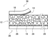
- FIG. 1 conceptually shows an example of the piezoelectric film of the present invention.
- the piezoelectric film 10 includes a piezoelectric layer 12 , a first electrode layer 14 laminated on one surface of the piezoelectric layer 12 , and a first electrode layer 14 laminated on the surface of the first electrode layer 14 . It has a protective layer 18 , a second electrode layer 16 laminated on the other surface of the piezoelectric layer 12 , and a second protective layer 20 laminated on the surface of the second electrode layer 16 .
- the piezoelectric layer 12 contains piezoelectric particles 26 in a matrix 24 containing a polymeric material, as conceptually shown in FIG.
- the piezoelectric layer 12 has a maximum indentation amount (maximum indentation depth) d max by nanoindentation measurement that satisfies “100 nm ⁇ d max ⁇ 600 nm”.
- the piezoelectric film 10 of the present invention exists between the first electrode layer 14 and the piezoelectric layer 12 and/or between the second electrode layer 16 and the piezoelectric layer 12. It is possible to greatly reduce air bubbles, voids, and the like. This point will be described in detail later.
- the first and second in the first electrode layer 14 and the second electrode layer 16 and in the first protective layer 18 and the second protective layer 20 refer to two similar members that the piezoelectric film 10 has. are attached for convenience in order to distinguish between That is, the first and second marks attached to the constituent elements of the piezoelectric film 10 have no technical significance, and their positions may be reversed. may be the second protective layer.
- the piezoelectric layer 12 is formed by dispersing the piezoelectric particles 26 in the matrix 24 containing the polymeric material. That is, the piezoelectric layer 12 is a polymer composite piezoelectric.
- the polymer composite piezoelectric body (piezoelectric layer 12) preferably satisfies the following requirements.
- normal temperature is 0 to 50°C.
- Flexibility For example, when gripping a loosely bent state like a document like a newspaper or magazine for portable use, it is constantly subjected to a relatively slow and large bending deformation of several Hz or less from the outside. become.
- the polymer composite piezoelectric body is required to have appropriate hardness in order to increase the transmission efficiency of vibration energy. Also, if the frequency characteristics of the speaker are smooth, the amount of change in sound quality when the lowest resonance frequency f 0 changes as the curvature changes becomes small. Therefore, the loss tangent of the polymer composite piezoelectric body is required to be moderately large.
- the lowest resonance frequency f 0 of the speaker diaphragm is given by the following equation.
- s is the stiffness of the vibration system and m is the mass.
- the flexible polymer composite piezoelectric material used for the electroacoustic conversion film is required to behave hard against vibrations of 20 Hz to 20 kHz and softly against vibrations of several Hz or less. Also, the loss tangent of the polymer composite piezoelectric body is required to be moderately large with respect to vibrations of all frequencies of 20 kHz or less.
- polymer solids have a viscoelastic relaxation mechanism, and as temperature rises or frequency falls, large-scale molecular motion causes a decrease (relaxation) in storage elastic modulus (Young's modulus) or a maximum loss elastic modulus (absorption). is observed as Among them, the relaxation caused by the micro-Brownian motion of the molecular chains in the amorphous region is called principal dispersion, and a very large relaxation phenomenon is observed.
- the temperature at which this primary dispersion occurs is the glass transition point (Tg), and the viscoelastic relaxation mechanism appears most prominently.
- the polymer composite piezoelectric body (piezoelectric layer 12), by using a polymer material having a glass transition point at room temperature, in other words, a polymer material having viscoelasticity at room temperature as a matrix, it is possible to suppress vibrations of 20 Hz to 20 kHz. This realizes a polymer composite piezoelectric material that is hard at first and behaves softly with respect to slow vibrations of several Hz or less.
- a polymer material having a glass transition point at room temperature ie, 0 to 50° C. at a frequency of 1 Hz, for the matrix of the polymer composite piezoelectric material, because this behavior is favorably expressed.
- the polymer material having viscoelasticity at room temperature can be used as the polymer material having viscoelasticity at room temperature. It is preferable to use a polymeric material having a maximum value of loss tangent Tan ⁇ at a frequency of 1 Hz in a dynamic viscoelasticity test at normal temperature, ie, 0 to 50° C., of 0.5 or more. As a result, when the polymer composite piezoelectric body is slowly bent by an external force, the stress concentration at the interface between the polymer matrix and the piezoelectric particles at the maximum bending moment is relaxed, and high flexibility can be expected.
- the polymer material having viscoelasticity at room temperature preferably has a storage elastic modulus (E') at a frequency of 1 Hz measured by dynamic viscoelasticity of 100 MPa or more at 0°C and 10 MPa or less at 50°C.
- E' storage elastic modulus
- the polymer material having viscoelasticity at room temperature has a dielectric constant of 10 or more at 25°C.
- a voltage is applied to the polymer composite piezoelectric material, a higher electric field is applied to the piezoelectric particles in the polymer matrix, so a large amount of deformation can be expected.
- the polymer material in consideration of ensuring good moisture resistance and the like, it is also suitable for the polymer material to have a dielectric constant of 10 or less at 25°C.
- cyanoethylated polyvinyl alcohol cyanoethylated PVA
- polyvinyl acetate polyvinylidene chloride core acrylonitrile
- polystyrene-vinylpolyisoprene block copolymer examples include methyl ketone and polybutyl methacrylate.
- Commercially available products such as Hybler 5127 (manu
- the polymer material it is preferable to use a material having a cyanoethyl group, and it is particularly preferable to use cyanoethylated PVA.
- the matrix 24 only one type of these polymer materials having viscoelasticity at room temperature may be used, or a plurality of types may be used together (mixed).
- a polymer material having no viscoelasticity at room temperature may be added to the matrix 24, if necessary.
- the matrix 24 contains a polymer material having viscoelasticity at room temperature such as cyanoethylated PVA for the purpose of adjusting dielectric properties and mechanical properties, and if necessary, other dielectric polymer materials. You may add.
- dielectric polymer materials examples include polyvinylidene fluoride, vinylidene fluoride-tetrafluoroethylene copolymer, vinylidene fluoride-trifluoroethylene copolymer, and polyvinylidene fluoride-trifluoroethylene copolymer.
- fluorine-based polymers such as polyvinylidene fluoride-tetrafluoroethylene copolymer, vinylidene cyanide-vinyl acetate copolymer, cyanoethylcellulose, cyanoethylhydroxysaccharose, cyanoethylhydroxycellulose, cyanoethylhydroxypullulan, cyanoethylmethacrylate, cyanoethylacrylate, cyanoethyl Cyano groups such as hydroxyethylcellulose, cyanoethylamylose, cyanoethylhydroxypropylcellulose, cyanoethyldihydroxypropylcellulose, cyanoethylhydroxypropylamylose, cyanoethylpolyacrylamide, cyanoethylpolyacrylate, cyanoethylpullulan, cyanoethylpolyhydroxymethylene, cyanoethylglycidolpullul
- the dielectric polymer material added in addition to the polymer material having viscoelasticity at room temperature such as cyanoethylated PVA is not limited to one type, and a plurality of types may be added. You may
- the matrix 24 may also include thermoplastic resins such as vinyl chloride resin, polyethylene, polystyrene, methacrylic resin, polybutene and isobutylene, and phenolic resin for the purpose of adjusting the glass transition point Tg.
- thermoplastic resins such as vinyl chloride resin, polyethylene, polystyrene, methacrylic resin, polybutene and isobutylene
- phenolic resin for the purpose of adjusting the glass transition point Tg.
- thermosetting resins such as urea resins, melamine resins, alkyd resins and mica
- a tackifier such as rosin ester, rosin, terpene, terpene phenol, and petroleum resin may be added to the matrix 24 for the purpose of improving adhesiveness.
- the addition amount of the material other than the polymer material having viscoelasticity at room temperature such as cyanoethylated PVA is not particularly limited, but the proportion of the matrix 24 is 30 mass. % or less.
- the characteristics of the polymer material to be added can be expressed without impairing the viscoelastic relaxation mechanism in the matrix 24, so that the dielectric constant can be increased, the heat resistance can be improved, and the adhesion between the piezoelectric particles 26 and the electrode layer can be improved.
- favorable results can be obtained in terms of
- the piezoelectric layer 12 contains piezoelectric particles 26 in such a matrix 24 .
- the piezoelectric layer 12 is a polymeric composite piezoelectric body in which piezoelectric particles 26 are dispersed in such a matrix 24 .
- the piezoelectric particles 26 are made of ceramic particles having a perovskite or wurtzite crystal structure.
- Ceramic particles forming the piezoelectric particles 26 include lead zirconate titanate (PZT), lead zirconate lanthanate titanate (PLZT), barium titanate (BaTiO 3 ), zinc oxide (ZnO), and A solid solution (BFBT) of barium titanate and bismuth ferrite (BiFe 3 ) is exemplified. Only one kind of these piezoelectric particles 26 may be used, or a plurality of kinds thereof may be used together (mixed).
- the particle diameter of the piezoelectric particles 26 is not limited, and may be selected as appropriate according to the size and application of the piezoelectric film 10 .
- the particle size of the piezoelectric particles 26 is preferably 1 to 10 ⁇ m. By setting the particle size of the piezoelectric particles 26 within this range, favorable results can be obtained in that the piezoelectric film 10 can achieve both high piezoelectric characteristics and flexibility.
- the piezoelectric particles 26 in the piezoelectric layer 12 are irregularly dispersed in the matrix 24 in FIG. 1, the present invention is not limited to this. That is, the piezoelectric particles 26 in the piezoelectric layer 12 may be dispersed with regularity in the matrix 24 as long as they are preferably uniformly dispersed. Furthermore, the piezoelectric particles 26 may or may not have uniform particle diameters.
- the quantitative ratio of the matrix 24 and the piezoelectric particles 26 in the piezoelectric layer 12 is not limited, and the size and thickness of the piezoelectric film 10 in the plane direction, the application of the piezoelectric film 10, and It may be appropriately set according to the properties required for the piezoelectric film 10 .
- the volume fraction of the piezoelectric particles 26 in the piezoelectric layer 12 is preferably 30% to 80%, more preferably 50% or more, and therefore 50% to 80% is even more preferable.
- the thickness of the piezoelectric layer 12 is not particularly limited, and may be appropriately set according to the application of the piezoelectric film 10, the properties required of the piezoelectric film 10, and the like.
- the thickness of the piezoelectric layer 12 is preferably 8-300 ⁇ m, more preferably 8-200 ⁇ m, still more preferably 10-150 ⁇ m, particularly preferably 15-100 ⁇ m.
- the piezoelectric layer 12, that is, the piezoelectric film 10, is preferably polarized (poled) in the thickness direction.
- the polarization treatment will be detailed later.
- the illustrated piezoelectric film 10 has a first electrode layer 14 on one surface of the piezoelectric layer 12 and a first protective layer 18 on the surface thereof. 12 has a second electrode layer 16 on the other surface thereof, and a second protective layer 20 on the surface thereof.
- the first electrode layer 14 and the second electrode layer 16 form an electrode pair.
- the piezoelectric film 10 has a configuration in which both surfaces of the piezoelectric layer 12 are sandwiched between electrode pairs, and this laminate is sandwiched between the first protective layer 18 and the second protective layer 20 .
- the region sandwiched between the first electrode layer 14 and the second electrode layer 16 expands and contracts according to the applied voltage.
- the first protective layer 18 and the second protective layer 20 cover the first electrode layer 14 and the second electrode layer 16, and provide the piezoelectric layer 12 with appropriate rigidity and mechanical strength. is responsible for That is, in the piezoelectric film 10, the piezoelectric layer 12 made up of the matrix 24 and the piezoelectric particles 26 exhibits excellent flexibility against slow bending deformation, but depending on the application, the rigidity may increase. and mechanical strength may be insufficient.
- the piezoelectric film 10 is preferably provided with a first protective layer 18 and a second protective layer 20 to compensate for this.
- the laminate of the piezoelectric layer 12 and the electrode layer is sandwiched so as to correspond to both the first electrode layer 14 and the second electrode layer 16.
- a first protective layer 18 and a second protective layer 20 are provided.
- the first protective layer 18 and the second protective layer 20 are provided as preferred embodiments. Therefore, the piezoelectric film of the present invention may have neither the first protective layer 18 nor the second protective layer 20 , or may have only one of the first protective layer 18 and the second protective layer 20 . However, in consideration of the mechanical strength, rigidity, durability, etc.
- a laminate of the piezoelectric layer 12 and the electrode layer is sandwiched.
- a first protective layer 18 and a second protective layer 20 are preferably provided on the substrate.
- Various sheet materials can be used for the first protective layer 18 and the second protective layer 20 without limitation, and various resin films are preferably exemplified as examples.
- various resin films are preferably exemplified as examples.
- PET polyethylene terephthalate
- PP polypropylene
- PS polystyrene
- PC polycarbonate
- PPS polyphenylene sulfite
- PMMA polymethyl methacrylate
- PET polyethylene terephthalate
- PEI polyetherimide
- PI polyimide
- PEN polyethylene naphthalate
- TAC triacetyl cellulose
- cyclic olefin resins and the like are preferably used.
- the thicknesses of the first protective layer 18 and the second protective layer 20 are also not limited. Also, the thicknesses of the first protective layer 18 and the second protective layer 20 are basically the same, but may be different. Here, if the rigidity of the first protective layer 18 and the second protective layer 20 is too high, not only will the expansion and contraction of the piezoelectric layer 12 be restricted, but also the flexibility will be impaired. Therefore, the thinner the first protective layer 18 and the second protective layer 20, the better, except for the case where mechanical strength and good handling property as a sheet-like article are required.
- the thickness of the first protective layer 18 and the second protective layer 20 is less than twice the thickness of the piezoelectric layer 12, it is possible to ensure both rigidity and appropriate flexibility. favorable results can be obtained.
- the thickness of the first protective layer 18 and the second protective layer 20 is preferably 100 ⁇ m or less. 50 ⁇ m or less is more preferable, and 25 ⁇ m or less is even more preferable.
- a first electrode layer 14 is formed between the piezoelectric layer 12 and the first protective layer 18 in the piezoelectric film 10 .
- a second electrode layer 16 is formed between the piezoelectric layer 12 and the second protective layer 20 .
- the first electrode layer 14 and the second electrode layer 16 are provided for applying voltage to the piezoelectric layer 12 (piezoelectric film 10).
- the materials for forming the first electrode layer 14 and the second electrode layer 16 are not limited, and various conductors can be used. Specifically, metals such as carbon, palladium, iron, tin, aluminum, nickel, platinum, gold, silver, copper, titanium, chromium and molybdenum, alloys thereof, laminates and composites of these metals and alloys, Also, indium tin oxide and the like are exemplified. Among them, copper, aluminum, gold, silver, platinum, and indium tin oxide are preferably exemplified as the first electrode layer 14 and the second electrode layer 16 .
- the method of forming the first electrode layer 14 and the second electrode layer 16 is not limited, and known methods can be used. Examples include film formation by a vapor phase deposition method (vacuum film formation method) such as vacuum deposition and sputtering, film formation by plating, and a method of adhering a foil formed of the materials described above. Among them, thin films of copper, aluminum, or the like formed by vacuum deposition are particularly preferably used as the first electrode layer 14 and the second electrode layer 16 because the flexibility of the piezoelectric film 10 can be ensured. be. Among them, a copper thin film formed by vacuum deposition is particularly preferably used.
- the thicknesses of the first electrode layer 14 and the second electrode layer 16 are not limited. Also, the thicknesses of the first electrode layer 14 and the second electrode layer 16 are basically the same, but may be different.
- the first protective layer 18 and the second protective layer 20 described above if the rigidity of the first electrode layer 14 and the second electrode layer 16 is too high, not only will the expansion and contraction of the piezoelectric layer 12 be restricted, Flexibility is also impaired. Therefore, the thinner the first electrode layer 14 and the second electrode layer 16, the better, as long as the electrical resistance does not become too high.
- the product of the thickness of the first electrode layer 14 and the second electrode layer 16 and the Young's modulus is less than the product of the thickness of the first protective layer 18 and the second protective layer 20 and the Young's modulus , is preferred because it does not significantly impair flexibility.
- a combination of PET for the first protective layer 18 and the second protective layer 20 and copper for the first electrode layer 14 and the second electrode layer 16 is illustrated.
- PET has a Young's modulus of about 6.2 GPa and copper has a Young's modulus of about 130 GPa.
- the thickness of the first protective layer 18 and the second protective layer 20 is 10 ⁇ m
- the thickness of the first electrode layer 14 and the second electrode layer 16 is preferably 0.5 ⁇ m or less, more preferably 0.3 ⁇ m or less. , is more preferably 0.1 ⁇ m or less.
- a piezoelectric layer may be provided between the piezoelectric layer 12 and the first electrode layer 14 and/or between the piezoelectric layer 12 and the second electrode layer 16, if necessary. It may have an adhesive layer for increasing the adhesion between 12 and the electrode layer.
- the adhesive layer is not limited, and any known adhesive (adhesive, pressure-sensitive adhesive) can be used as long as it can adhere the piezoelectric layer 12 and the electrode layer according to the materials forming the piezoelectric layer 12 and the electrode layer. is.
- the polymer material used as the matrix 24 of the piezoelectric layer 12 may be used as the adhesive layer.
- the thickness of the adhesive layer There is no limitation on the thickness of the adhesive layer, and the thickness may be appropriately set so as to obtain sufficient adhesive strength.
- the adhesive layer is preferably thin as long as the required adhesive strength can be obtained.
- the piezoelectric film 10 of the present invention has the first electrode layer 14 on one side of the piezoelectric layer 12 and the second electrode layer 16 on the other side.
- the illustrated piezoelectric film 10 preferably has a first protective layer 18 covering the first electrode layer 14 and a second protective layer 20 covering the second electrode layer 16 .
- the piezoelectric layer 12 is a polymeric composite piezoelectric body, and is formed by dispersing piezoelectric particles 26 in a matrix 24 containing a polymeric material.
- the piezoelectric layer 12 made of such a polymeric composite piezoelectric material satisfies "100 nm ⁇ d max ⁇ 600 nm" in the maximum indentation amount d max measured by nanoindentation measurement.
- the maximum load holding time is 10 sec
- the unloading time is 10 sec.
- the piezoelectric film 10 of the present invention satisfies "100 nm ⁇ d max ⁇ 600 nm" in the maximum indentation amount d max of the piezoelectric layer 12 in the nanoindentation measurement, that is, the maximum displacement amount. Since the piezoelectric film 10 of the present invention has such a structure, air bubbles and gaps existing between the first electrode layer 14 and the piezoelectric layer 12 or between the second electrode layer 16 and the piezoelectric layer 12 are eliminated. , can be significantly reduced.
- the piezoelectric film 10 having electrode layers on both sides of the piezoelectric layer 12 and having a protective layer covering the electrode layers is manufactured as follows, as an example.
- a sheet 34 in which the second protective layer 20 and the second electrode layer 16 are laminated, and a sheet 38 in which the first protective layer 18 and the first electrode layer 14 are laminated are prepared (FIGS. 4 and 7). reference).
- a coating material is prepared by dissolving a material for the matrix 24 in a solvent and dispersing the piezoelectric particles 26 in this solution. This coating material is applied to the second electrode layer 16 of the sheet material 34 and dried to form the piezoelectric layer 12 (see FIG. 5).
- the piezoelectric multilayer body 36 having the second electrode layer 16 on the second protective layer 20 and the piezoelectric layer 12 on the second electrode layer 16 is produced.
- calendering see FIG. 6
- polarization etc.
- the first electrode layer 14 is directed to the piezoelectric layer 12, and the sheet-like material 38 in which the first protective layer 18 and the first electrode layer 14 are laminated is laminated and heat-pressed.
- the piezoelectric film 10 is produced (see FIG. 8).
- the bonding between the piezoelectric layer 12 and the first electrode layer 14 is performed, for example, by thermocompression bonding using a heating roller pair 60 as conceptually shown in FIG. Specifically, as described above, after manufacturing the piezoelectric multilayer body 36 in which the piezoelectric layer 12 is formed on the second electrode layer 16 of the sheet 34 (see FIG. 5), the first electrode layer 14 is formed. A sheet-like material 38 is laminated on the piezoelectric multilayer body 36 facing the piezoelectric layer 12 (see FIG. 8). The laminate of the piezoelectric multilayer body 36 and the sheet material 38 is nipped and conveyed by the pair of heating rollers 60, so that the piezoelectric layer 12 and the first electrode layer 14 are heat-pressed and adhered. Although this thermocompression bonding is usually performed by pinching and conveying the laminate by the pair of heating rollers 60, conversely, the laminate may be fixed and the pair of heating rollers 60 may be moved.
- a conventional piezoelectric film having a piezoelectric layer 12 made of a polymer composite piezoelectric material air and/or foreign matter F entrained during lamination may cause a problem between the first electrode layer 14 and the piezoelectric layer 12. , air bubbles and/or voids are often unavoidable.
- the piezoelectric layer 12 made of a polymeric composite piezoelectric material satisfies "100 nm ⁇ d max ⁇ 600 nm" in terms of the maximum indentation amount d max measured by nanoindentation. That is, in the piezoelectric film 10 of the present invention, the maximum indentation amount d max of the piezoelectric layer 12 measured by nanoindentation is 100 to 600 nm. In the following description, the maximum pushing amount d max of the piezoelectric layer 12 obtained by nanoindentation measurement is also simply referred to as "the maximum pushing amount d max of the piezoelectric layer 12". Since the piezoelectric film 10 of the present invention has such a structure, as conceptually shown in the lower center of FIG. can be significantly reduced.
- the piezoelectric layer 12 and the first electrode layer 14 are heated by the heating roller pair 60 by setting the maximum pressing amount d max of the piezoelectric layer 12 to 100 to 600 nm.
- the air trapped between the piezoelectric layer 12 and the first electrode layer 14 during lamination can be preferably pushed out.
- the maximum pressing amount d max of the piezoelectric layer 12 is set to 100 to 600 nm, when the piezoelectric layer 12 and the first electrode layer 14 are heat-pressed by the heating roller pair 60, the foreign matter F is removed from the piezoelectric layer. 12 to embed the foreign matter F, preventing air from remaining around the foreign matter F.
- the piezoelectric film 10 of the present invention can greatly reduce the amount of air and voids existing between the piezoelectric layer 12 and the electrode layer, as conceptually shown in the lower center of FIG. Therefore, the piezoelectric film 10 of the present invention can efficiently transmit the vibration of the piezoelectric layer 12, and can output sound with high sound pressure when used as a piezoelectric speaker, for example.
- the maximum push-in amount d max of the piezoelectric layer 12 is less than 100 nm, as conceptually shown on the lower left side of FIG.
- the body layer 12 cannot be fully embedded.
- air bubbles B exist around the foreign matter F between the piezoelectric layer 12 and the first electrode layer 14 .
- the maximum pressing amount d max of the piezoelectric layer 12 exceeds 600 nm, the pressing force during thermocompression bonding between the piezoelectric layer 12 and the first electrode layer 14 becomes insufficient.
- the air trapped between the piezoelectric layer 12 and the first electrode layer 14 during lamination cannot be pushed out, and the gap V (the separation portion) between the piezoelectric layer 12 and the first electrode layer 14 cannot be pushed out.
- the maximum pressing amount d max of the piezoelectric layer 12 is preferably 150 to 550 nm, more preferably 180 to 500 nm.
- the piezoelectric layer 12 is formed by coating the second electrode layer 16 of 34 with a paint that will become the piezoelectric layer 12 and drying it. Therefore, air can be prevented from entering between the second electrode layer 16 and the piezoelectric layer 12 . Also, even if the foreign matter F adheres to the second electrode layer 16 , the foreign matter F is completely embedded in the paint, that is, the piezoelectric layer 12 . The presence of air around the is also avoided.
- the nanoindentation measurement of the piezoelectric layer 12 is performed by removing the protective layer and the electrode layer from the piezoelectric film 10 to expose the piezoelectric layer 12 .
- the surface roughness Ra of the piezoelectric layer 12 and the film thickness distribution of the piezoelectric layer 12, which will be described later, are also preferably measured at the exposed portion of the piezoelectric layer 12 from which the protective layer and the electrode layer are removed.
- the method for removing the protective layer and the electrode layer from the piezoelectric film 10 is not limited, but the following method is exemplified. First, a 5 mol/L (liter) NaOH aqueous solution with a temperature of 15 to 25° C.
- the piezoelectric film 10 is dropped onto the protective layer of the piezoelectric film 10, and left to stand still to dissolve the protective layer and expose the electrode layer. do. At this time, a portion of the electrode layer may be dissolved, but the stationary time is set so that the NaOH aqueous solution does not come into contact with the piezoelectric layer 12 . After dropping the aqueous NaOH solution, the piezoelectric film 10 is left to stand for a predetermined time, and when the electrode layer is exposed, the piezoelectric film 10 is washed with pure water. After washing, the exposed electrode layer is dissolved in a 0.01 mol/L ferric chloride aqueous solution.
- the dissolution of the electrode layer with the ferric chloride aqueous solution is continued until the piezoelectric layer 12 having an area required for nanoindentation measurement is exposed, but not longer than 5 minutes after the piezoelectric layer 12 is exposed.
- the piezoelectric film 10 with the exposed piezoelectric layer 12 is washed with pure water and dried at 30° C. or less.
- the nanoindentation measurement conceptually shown in FIG. Measure the maximum pushing amount d max .
- the maximum push-in amount d max of the piezoelectric layer 12 may be measured on either the first electrode layer 14 side or the second electrode layer 16 side (principal surface) of the piezoelectric layer 12. good.
- the maximum pressing amount d max of the piezoelectric layer 12 is measured at 30 arbitrarily selected points on the surface of the piezoelectric layer 12, and the average value is obtained from the piezoelectric layer 10 in the piezoelectric film 10 to be measured. 12 maximum pushing amount d max .
- the piezoelectric layer 12 preferably has a smooth surface.
- the piezoelectric layer 12 preferably has a surface roughness Ra (arithmetic mean roughness Ra) of 800 nm or less, more preferably 700 nm or less, and even more preferably 600 nm or less.
- Ra arithmetic mean roughness Ra
- the surface roughness Ra (arithmetic mean roughness Ra) of the piezoelectric layer 12 is obtained, for example, by measuring the surface roughness Ra of the surface of the exposed piezoelectric layer using a non-contact three-dimensional surface profile roughness meter manufactured by Bruker. Under the conditions of white LED light source (green filter), objective lens 10x, internal lens 0.55x, CCD: 1280 x 960 pixels, VSI/VXI, observation field of view 825.7 ⁇ m x 619.3 ⁇ m, cross-sectional sampling 0.645 ⁇ m After the measurement, the slope is corrected with 0 as the average, and the measurement is performed by fitting with Gaussian process regression. The surface roughness Ra is measured at 30 arbitrarily selected points, and the average value is taken as the surface roughness Ra of the piezoelectric layer 12 in the piezoelectric film 10 to be measured.
- the piezoelectric layer 12 preferably has a uniform thickness.
- the thickness distribution (film thickness distribution) of the piezoelectric layer 12 is preferably 30% or less, more preferably 25% or less, and even more preferably 20% or less. By setting the thickness distribution of the piezoelectric layer 12 to 30% or less, it is preferable in that high sound pressure can be obtained when used as a piezoelectric speaker.
- the thickness distribution [%] of the piezoelectric layer 12 is obtained by measuring the exposed surface of the piezoelectric layer with a digital indicator (ID-F125 manufactured by Mitutoyo Co., Ltd.). (maximum value ⁇ minimum value)/average of maximum value and minimum value] ⁇ 100”. Such thickness distribution measurements are performed at 30 arbitrarily selected locations, and the average value is used as the thickness distribution of the piezoelectric layer 12 in the piezoelectric film 10 to be measured.
- a digital indicator ID-F125 manufactured by Mitutoyo Co., Ltd.
- the piezoelectric film 10 includes the piezoelectric layer 12 having the piezoelectric particles 26 in the matrix 24 containing a polymer material sandwiched between the first electrode layer 14 and the second electrode layer 16, and furthermore, this laminate is sandwiched between the first protective layer 18 and the second protective layer 20 .
- the maximum value of the loss tangent (Tan ⁇ ) at a frequency of 1 Hz by dynamic viscoelasticity measurement preferably exists at room temperature, and the maximum value of 0.1 or more exists at room temperature. is more preferable.
- the piezoelectric film 10 of the present invention preferably has a storage elastic modulus (E') at a frequency of 1 Hz measured by dynamic viscoelasticity measurement of 10 to 30 GPa at 0°C and 1 to 10 GPa at 50°C. Accordingly, the piezoelectric film 10 can have a large frequency dispersion in the storage elastic modulus (E') at room temperature. That is, it can act hard against vibrations of 20 Hz to 20 kHz and soft against vibrations of several Hz or less.
- E' storage elastic modulus
- the product of the thickness and the storage elastic modulus (E') at a frequency of 1 Hz measured by dynamic viscoelasticity measurement is 1.0 ⁇ 10 6 to 2.0 ⁇ 10 6 at 0° C. It is preferably 1.0 ⁇ 10 5 to 1.0 ⁇ 10 6 N/m at 50° C. N/m.
- the piezoelectric film 10 can have appropriate rigidity and mechanical strength within a range that does not impair flexibility and acoustic properties.
- the piezoelectric film 10 preferably has a loss tangent (Tan ⁇ ) of 0.05 or more at 25° C. and a frequency of 1 kHz in a master curve obtained from dynamic viscoelasticity measurement.
- Ton ⁇ loss tangent
- the frequency characteristics of the speaker using the piezoelectric film 10 are smoothed, and the amount of change in sound quality when the lowest resonance frequency f 0 changes as the curvature of the speaker changes can be reduced.
- the piezoelectric film 10 of the present invention covers the electrode lead-out portions for leading the electrodes from the first electrode layer 14 and the second electrode layer 16 and the area where the piezoelectric layer 12 is exposed.
- it may have an insulating layer or the like for preventing short circuits or the like.
- a method of connecting the conductors and drawing out the electrodes to the outside, and forming through holes in the first protective layer 18 and the second protective layer 20 by a laser or the like, filling the through holes with a conductive material, and , and the like are exemplified.
- suitable methods for extracting electrodes include the method described in Japanese Patent Application Laid-Open No. 2014-209724 and the method described in Japanese Patent Application Laid-Open No. 2016-015354.
- each electrode layer is not limited to one electrode lead-out portion, and may have two or more electrode lead-out portions.
- three or more electrode lead-out portions are provided in order to ensure more reliable conduction of electricity. is preferred.
- a sheet-like object 34 having a second electrode layer 16 formed on a second protective layer 20 is prepared.
- This sheet-like material 34 may be produced by forming a copper thin film or the like as the second electrode layer 16 on the surface of the second protective layer 20 by vacuum deposition, sputtering, plating, or the like.
- the second protective layer 20 with a separator temporary support
- PET or the like having a thickness of 25 to 100 ⁇ m can be used. The separator may be removed after the second electrode layer 16 and the second protective layer 20 are thermally compressed and before laminating any member on the second protective layer 20 .
- a polymer material having viscoelasticity at room temperature such as cyanoethylated PVA
- an organic solvent such as dimethylformamide (DMF), methyl ethyl ketone and cyclohexanone can be used.
- DMF dimethylformamide
- the paint is cast (applied) on the second electrode layer 16 of the sheet 34 and dried by evaporating the organic solvent.
- the thickness distribution of the piezoelectric layer 12 can be adjusted by controlling the coating conditions of the paint at this time.
- the surface roughness of the piezoelectric layer 12 can be adjusted by controlling the drying temperature of the paint at this time.
- the conditions for applying the paint when the application is performed using a slide coater, control of the gap distribution between the slide coater and the backup roller that supports the sheet-like material 34 is exemplified.
- a piezoelectric multilayer body 36 having the second electrode layer 16 on the second protective layer 20 and the piezoelectric layer 12 formed on the second electrode layer 16 is produced. do.
- the method of casting this paint is not particularly limited, and all known coating methods (coating devices) such as slide coaters and doctor knives can be used.
- the viscoelastic material is heat-meltable, such as cyanoethylated PVA
- the viscoelastic material is heated and melted, and the piezoelectric particles 26 are added/dispersed to prepare a melt, which is then extruded.
- the sheet is extruded onto the sheet-like material 34 shown in FIG. 4 and cooled to form the first electrode layer 14 on the first protective layer 18 as shown in FIG.
- a piezoelectric multilayer body 36 may be produced by forming the piezoelectric layer 12 on one electrode layer 14 .
- the matrix 24 may be added with a dielectric polymer material such as polyvinylidene fluoride in addition to the viscoelastic material such as cyanoethylated PVA.
- a dielectric polymer material such as polyvinylidene fluoride
- the polymeric piezoelectric materials to be added to the above-described paint may be dissolved.
- the polymer piezoelectric material to be added may be added to the viscoelastic material melted by heating as described above and melted by heating.
- Calendering is performed by pressing the surface of the piezoelectric layer 12 with a heating roller or the like.
- the method of calendering is not particularly limited, and known methods such as nip-conveyance by a pair of heating rollers, pressing by heating rollers, and treatment by a heating press may be used.
- the maximum pressing amount d max of the piezoelectric layer 12 of the piezoelectric film 10 to be manufactured can be controlled by adjusting the calendering conditions. Specifically, the maximum pressing amount d max of the piezoelectric layer 12 of the piezoelectric film 10 to be manufactured can be suitably You can control it.
- the heating roller pair 62 may be moved while holding the piezoelectric multilayer body 36 at a predetermined position.
- the pushing amount d max can be preferably controlled with good controllability. Specifically, by shortening the nip time, that is, by increasing the conveying speed of the piezoelectric multilayer body 36, the maximum pushing amount d max of the piezoelectric layer 12 can be increased. Conversely, by increasing the nip time, that is, by decreasing the conveying speed of the piezoelectric multilayer body 36, the maximum pressing amount d max of the piezoelectric layer 12 can be reduced.
- the maximum pressing amount d max of the piezoelectric layer 12 can be controlled by various methods other than adjusting the nip time in the calendering process.
- the maximum pushing amount d max of the piezoelectric layer 12 may be controlled by adjusting the composition of the matrix 24 of the piezoelectric layer 12 or the like.
- the calendering treatment may be performed after the polarization treatment described later. However, if the calendering process is performed after the polarization process, the piezoelectric particles 26 pushed in by the pressure will rotate, which may reduce the effect of the polarization process. Considering this point, the calendering treatment is preferably performed before the polarization treatment.
- the piezoelectric layer 12 is preferably calendered. After the treatment, the piezoelectric layer 12 is subjected to polarization treatment (poling).
- the method of polarization treatment of the piezoelectric layer 12 is not limited, and known methods can be used.
- electric field poling in which a DC electric field is directly applied to an object to be polarized, is exemplified.
- the first electrode layer 14 may be formed before the polarization treatment, and the electric field poling treatment may be performed using the first electrode layer 14 and the second electrode layer 16. .
- a sheet-like object 38 having a first electrode layer 14 formed on a first protective layer 18 is prepared.
- This sheet-like material 38 may be produced by forming a copper thin film or the like as the first electrode layer 14 on the surface of the first protective layer 18 by vacuum deposition, sputtering, plating, or the like. That is, the sheet-like material 38 may be the same as the sheet-like material 34 described above.
- the sheet-like material 38 is laminated on the piezoelectric multilayer body 36 with the first electrode layer 14 facing the piezoelectric layer 12 . Furthermore, as shown in FIG. 3, the piezoelectric multilayer body 36 and the sheet-like material 38 are thermo-compressed while being nipped and conveyed by the pair of heating rollers 60 to fabricate the piezoelectric film 10 .
- the piezoelectric film 10 may be produced by thermocompression bonding the laminate of the piezoelectric multilayer body 36 and the sheet-like material 38 using a hot press device.
- the piezoelectric film 10 produced in this manner is polarized in the thickness direction rather than in the plane direction, and excellent piezoelectric properties can be obtained without stretching after the polarization treatment. Therefore, the piezoelectric film 10 has no in-plane anisotropy in piezoelectric properties, and expands and contracts isotropically in all directions in the plane direction when a drive voltage is applied.
- Such a piezoelectric film 10 may be manufactured using a cut-sheet-like sheet-like material 34 and a sheet-like material 38 or the like, or may be manufactured using a roll-to-roll process. good too.
- FIG. 9 conceptually shows an example of a flat plate-type piezoelectric speaker using the piezoelectric film 10 of the present invention.
- This piezoelectric speaker 40 is a flat plate-type piezoelectric speaker that uses the piezoelectric film 10 as a diaphragm that converts an electrical signal into vibrational energy. Note that the piezoelectric speaker 40 can also be used as a microphone, a sensor, and the like. Furthermore, this piezoelectric speaker can also be used as a vibration sensor.
- the piezoelectric speaker 40 includes a piezoelectric film 10 , a case 42 , a viscoelastic support 46 and a frame 48 .
- the case 42 is a thin housing made of plastic or the like and having one side open. Examples of the shape of the housing include rectangular parallelepiped, cubic, and cylindrical.
- the frame 48 is a frame material that engages with the open surface side of the case 42 , having a through hole having the same shape as the open surface of the case 42 in the center.
- the viscoelastic support 46 has appropriate viscosity and elasticity, supports the piezoelectric film 10, and provides a constant mechanical bias at any location on the piezoelectric film, thereby allowing the piezoelectric film 10 to move back and forth without waste.
- Back-and-forth motion of the piezoelectric film 10 is motion in a direction perpendicular to the plane of the film.
- the viscoelastic support 46 include wool felt, non-woven fabric such as wool felt containing PET and the like, glass wool, and the like.
- the piezoelectric speaker 40 accommodates a viscoelastic support 46 in a case 42 , covers the case 42 and the viscoelastic support 46 with the piezoelectric film 10 , and surrounds the piezoelectric film 10 with a frame 48 to form an upper end surface of the case 42 .
- the frame body 48 is fixed to the case 42 in a state of being pressed to.
- the height (thickness) of the viscoelastic support 46 is greater than the height of the inner surface of the case 42 . Therefore, in the piezoelectric speaker 40 , the viscoelastic support 46 is pressed downward by the piezoelectric film 10 and held in a reduced thickness at the periphery of the viscoelastic support 46 . Similarly, the curvature of the piezoelectric film 10 changes sharply at the periphery of the viscoelastic support 46 , forming a rising portion in the piezoelectric film 10 that becomes lower toward the periphery of the viscoelastic support 46 . Further, the central region of the piezoelectric film 10 is pressed by the square prism-shaped viscoelastic support 46 to form a (substantially) planar shape.
- the piezoelectric film 10 when the piezoelectric film 10 expands in the plane direction due to the application of the drive voltage to the first electrode layer 14 and the second electrode layer 16, the action of the viscoelastic support 46 absorbs this expansion. Thus, the rising portion of the piezoelectric film 10 changes its angle in the rising direction. As a result, the piezoelectric film 10 having planar portions moves upward. Conversely, when the piezoelectric film 10 shrinks in the plane direction due to the application of the drive voltage to the second electrode layer 16 and the first electrode layer 14, the rising portion of the piezoelectric film 10 collapses in order to absorb this contraction. Change the angle in the direction (direction closer to the plane). As a result, the piezoelectric film 10 having planar portions moves downward. The piezoelectric speaker 40 generates sound by vibrating the piezoelectric film 10 .
- the piezoelectric film 10 of the present invention conversion from stretching motion to vibration can also be achieved by holding the piezoelectric film 10 in a curved state. Therefore, the piezoelectric film 10 of the present invention is not a flat piezoelectric speaker 40 having rigidity as shown in FIG. can function as
- a piezoelectric speaker using such a piezoelectric film 10 can take advantage of its good flexibility and can be rolled up or folded and accommodated in a bag or the like. Therefore, according to the piezoelectric film 10, it is possible to realize an easily portable piezoelectric speaker even if it has a certain size. Moreover, as described above, the piezoelectric film 10 is excellent in softness and flexibility, and has no in-plane anisotropy of piezoelectric properties. Therefore, the piezoelectric film 10 has little change in sound quality when bent in any direction, and also has little change in sound quality with respect to changes in curvature.
- the piezoelectric speaker using the piezoelectric film 10 has a high degree of freedom in installation location, and can be attached to various articles as described above.
- a so-called wearable speaker can be realized by attaching the piezoelectric film 10 to clothing such as clothes and portable items such as bags in a curved state.
- the piezoelectric film of the present invention by attaching the piezoelectric film of the present invention to a flexible display device such as a flexible organic electroluminescence display and a flexible liquid crystal display, the display device It can also be used as a speaker.
- a flexible display device such as a flexible organic electroluminescence display and a flexible liquid crystal display
- the piezoelectric film 10 expands and contracts in the plane direction when a voltage is applied, and this expansion and contraction in the plane direction suitably vibrates in the thickness direction. It expresses good acoustic characteristics that can output sound.
- the piezoelectric film 10, which exhibits good acoustic properties, that is, high expansion and contraction performance due to piezoelectricity, works well as a piezoelectric vibrating element for vibrating a vibrating body such as a diaphragm by forming a laminated piezoelectric element in which a plurality of sheets are laminated. do.
- the piezoelectric film 10 When the piezoelectric film 10 is laminated, the piezoelectric film may not have the first protective layer 18 and/or the second protective layer 20 if there is no possibility of short circuit. Alternatively, piezoelectric films without the first protective layer 18 and/or the second protective layer 20 may be laminated via an insulating layer.
- a laminated piezoelectric element in which piezoelectric films 10 are laminated may be attached to a diaphragm, and the laminated body of piezoelectric films 10 may vibrate the diaphragm to produce a speaker that outputs sound. That is, in this case, the laminated piezoelectric element in which the piezoelectric film 10 is laminated acts as a so-called exciter that outputs sound by vibrating the diaphragm.
- the individual piezoelectric films 10 expand and contract in the plane direction, and the expansion and contraction of each piezoelectric film 10 causes the entire laminate of the piezoelectric films 10 to expand and contract in the plane direction. do.
- the expansion and contraction of the laminated piezoelectric element in the planar direction bends the diaphragm to which the laminate is attached, and as a result, the diaphragm vibrates in the thickness direction. This vibration in the thickness direction causes the diaphragm to generate sound.
- the diaphragm vibrates according to the magnitude of the driving voltage applied to the piezoelectric film 10 and generates sound according to the driving voltage applied to the piezoelectric film 10 . Therefore, at this time, the piezoelectric film 10 itself does not output sound.
- the laminated piezoelectric element in which the piezoelectric films 10 are laminated has high rigidity, and the expansion/contraction force of the laminate as a whole is large.
- the laminated piezoelectric element in which the piezoelectric film 10 is laminated can sufficiently flex the diaphragm with a large force and sufficiently vibrate the diaphragm in the thickness direction. to make the diaphragm generate sound.
- the number of laminated piezoelectric films 10 is not limited. Just do it. It should be noted that one sheet of piezoelectric film 10 can also be used as a similar exciter (piezoelectric vibrating element) as long as it has sufficient stretching force.
- the vibration plate that is vibrated by the laminated piezoelectric element in which the piezoelectric film 10 is laminated there are no restrictions on the vibration plate that is vibrated by the laminated piezoelectric element in which the piezoelectric film 10 is laminated, and various sheet-like objects (plate-like objects and films) can be used.
- sheet-like objects plate-like objects and films
- resin films such as polyethylene terephthalate (PET)
- foamed plastics such as polystyrene foam
- paper materials such as cardboard, glass plates, and wood.
- various devices such as display devices such as organic electroluminescence displays and liquid crystal displays may be used as the diaphragm as long as they can be bent sufficiently.
- the adjacent piezoelectric films 10 are adhered to each other with an adhesive layer (adhesive).
- both the laminated piezoelectric element and the diaphragm are adhered with an adhesion layer.
- the adhesive layer may be made of a pressure-sensitive adhesive or an adhesive.
- an adhesive layer is used which, after application, results in a solid and hard adhesive layer. The above points are the same for a laminated body formed by folding a long piezoelectric film 10 described later.
- the polarization direction of each laminated piezoelectric film 10 is not limited.
- the piezoelectric film 10 of the present invention is preferably polarized in the thickness direction. Accordingly, the polarization direction of the piezoelectric film 10 referred to herein is the polarization direction in the thickness direction. Therefore, in the laminated piezoelectric element, all the piezoelectric films 10 may have the same polarization direction, or there may be piezoelectric films having different polarization directions.
- the piezoelectric films 10 are preferably laminated so that the polarization directions of the adjacent piezoelectric films 10 are opposite to each other.
- the polarity of the voltage applied to the piezoelectric layer 12 depends on the polarization direction of the piezoelectric layer 12 . Therefore, regardless of whether the polarization direction is from the first electrode layer 14 to the second electrode layer 16 or from the second electrode layer 16 to the first electrode layer 14, the first electrode is The polarity of layer 14 and the polarity of second electrode layer 16 are made the same.
- the laminated piezoelectric element in which the piezoelectric films 10 are laminated may have a configuration in which a plurality of piezoelectric films 10 are laminated by folding the piezoelectric films 10 one or more times, preferably a plurality of times.
- the configuration in which the piezoelectric film 10 is folded and laminated has the following advantages. That is, in a laminate in which a plurality of cut-sheet piezoelectric films 10 are laminated, it is necessary to connect the first electrode layer 14 and the second electrode layer 16 to the drive power source for each piezoelectric film. On the other hand, in the structure in which the long piezoelectric film 10 is folded and laminated, the laminated piezoelectric element can be configured with only one long piezoelectric film 10 .
- the long piezoelectric film 10 is folded and laminated, only one power source is required for applying the driving voltage, and the electrode may be led out from the piezoelectric film 10 at one point. Furthermore, in the structure in which the long piezoelectric films 10 are folded and laminated, the polarization directions of adjacent piezoelectric films 10 are inevitably opposite to each other.
- the laminated piezoelectric element in which electrode layers are provided on both sides of a piezoelectric layer made of a polymer composite piezoelectric body, and preferably a protective layer is provided on the surface of the electrode layer, the laminated piezoelectric element is laminated with a piezoelectric film. 2020/095812 and International Publication No. 2020/179353.
- piezoelectric films and laminated piezoelectric elements of the present invention are used in various applications such as various sensors, acoustic devices, haptics, ultrasonic transducers, actuators, dampers, and vibration power generators. It is preferably used.
- sensors using the piezoelectric film and laminated piezoelectric element of the present invention include sonic sensors, ultrasonic sensors, pressure sensors, tactile sensors, strain sensors, vibration sensors, and the like. Sensors using the piezoelectric film and laminated piezoelectric element of the present invention are particularly useful for inspections at manufacturing sites, such as infrastructure inspections such as crack detection, and foreign matter contamination detection.
- Examples of acoustic devices using the piezoelectric film and laminated piezoelectric element of the present invention include microphones, pickups, speakers, and exciters.
- Specific applications of the acoustic device using the piezoelectric film and laminated piezoelectric element of the present invention include noise cancellers used in cars, trains, airplanes, robots, etc., artificial vocal cords, buzzers for preventing insects from entering, and Examples include furniture, wallpaper, photographs, helmets, goggles, headrests, signage, robots, and the like that have an audio output function.
- Examples of applications of haptics using the piezoelectric film and laminated piezoelectric element of the present invention include automobiles, smart phones, smart watches, and game machines.
- Examples of ultrasonic transducers using the piezoelectric film and laminated piezoelectric element of the present invention include ultrasonic probes and hydrophones.
- Examples of applications of the actuator using the piezoelectric film and laminated piezoelectric element of the present invention include prevention of adhesion of water droplets, transportation, stirring, dispersion, polishing, and the like.
- Application examples of the damping material using the piezoelectric film and laminated piezoelectric element of the present invention include containers, vehicles, buildings, and sports equipment such as skis and rackets.
- application examples of the vibration power generator using the piezoelectric film and laminated piezoelectric element of the present invention include roads, floors, mattresses, chairs, shoes, tires, wheels, and personal computer keyboards.
- Example 1 A piezoelectric film as shown in FIG. 1 was produced by the method shown in FIGS. First, cyanoethylated PVA (CR-V, manufactured by Shin-Etsu Chemical Co., Ltd.) was dissolved in dimethylformamide (DMF) at the following compositional ratio. After that, PZT particles as piezoelectric particles were added to this solution at the following composition ratio, and the mixture was stirred with a propeller mixer (rotation speed: 2000 rpm) to prepare a paint for forming a piezoelectric layer.
- CR-V cyanoethylated PVA
- DMF dimethylformamide
- ⁇ PZT particles ⁇ 300 parts by mass ⁇ Cyanoethylated PVA ⁇ 30 parts by mass ⁇ DMF ⁇ 70 parts by mass
- Mixed powder obtained by wet-mixing in a ball mill was fired at 800° C. for 5 hours and then pulverized.
- two sheets were prepared by vacuum-depositing a copper thin film with a thickness of 0.1 ⁇ m on a PET film with a thickness of 4 ⁇ m. That is, in this example, the first electrode layer and the second electrode layer are 0.1 ⁇ m thick copper-deposited thin films, and the first protective layer and the second protective layer are 4 ⁇ m thick PET films.
- a slide coater was used to apply the previously prepared paint for forming the piezoelectric layer onto the copper thin film (second electrode layer) of one sheet. The gap distribution between the slide coater and the backup roller that supports the sheet was set to 30%.
- the sheet-like material coated with the paint was dried by heating on a hot plate at 120° C. to evaporate the DMF.
- a piezoelectric multilayer body having a second electrode layer made of copper on a second protective layer made of PET and a piezoelectric layer (polymer composite piezoelectric layer) having a thickness of 50 ⁇ m thereon is produced. bottom.
- the produced piezoelectric layer (piezoelectric multilayer) was calendered using a pair of heating rollers.
- heating roller pair heating rollers having a roll diameter of 300 mm were used, and the nip pressure was set to 200 MPa.
- the nip width of the heating roller pair was 0.07 mm.
- the temperature of the heating roller pair was set to 100.degree.
- the conveying speed of the piezoelectric multilayer body was 0.5 m/min (minute).
- the nip time under this condition that is, the processing time of calendering is 0.00840 sec (seconds).
- the produced piezoelectric layer was subjected to a polarization treatment in the thickness direction.
- first electrode layer Another sheet of copper thin film (first electrode layer) was laminated on the piezoelectric multilayer body facing the piezoelectric layer.
- the laminate of the piezoelectric multilayer body and the sheet-like material is thermocompression bonded at a temperature of 120° C. using a pair of heating rollers to bond the piezoelectric layer and the first electrode layer, as shown in FIG. A piezoelectric film like this was produced.
- Example 2 A piezoelectric film was produced in the same manner as in Example 1, except that the conveying speed of the piezoelectric multilayer body in the calendering process was set to 1 m/min. The nip time at this time, that is, the processing time of the calendering process is 0.00420 sec.
- Example 3 A piezoelectric film was produced in the same manner as in Example 1, except that the conveying speed of the piezoelectric multilayer body in the calendering process was set to 1.5 m/min. The nip time at this time, that is, the calendering processing time is 0.00280 sec.
- Example 4 A piezoelectric film was produced in the same manner as in Example 1, except that the conveying speed of the piezoelectric multilayer body in the calendering process was set to 5 m/min. The nip time at this time, that is, the calendering processing time is 0.00084 sec.
- Example 5 A piezoelectric film was produced in the same manner as in Example 1, except that the conveying speed of the piezoelectric multilayer body in the calendering process was set to 8 m/min. The nip time at this time, that is, the calendering processing time is 0.00053 sec.
- Example 6 A piezoelectric film was produced in the same manner as in Example 1, except that the conveying speed of the piezoelectric multilayer body in the calendering process was set to 9 m/min. The nip time at this time, that is, the calendering processing time is 0.00047 sec.
- Example 7 A piezoelectric film was produced in the same manner as in Example 1, except that the conveying speed of the piezoelectric multilayer body in the calendering process was set to 10 m/min. The nip time at this time, that is, the calendering processing time is 0.00042 sec.
- Example 8 A piezoelectric film was produced in the same manner as in Example 7, except that the heating and drying temperature (hot plate temperature) of the paint for forming the piezoelectric layer was changed from 120°C to 115°C.
- Example 9 A piezoelectric film was produced in the same manner as in Example 7, except that the heating and drying temperature (hot plate temperature) of the paint for forming the piezoelectric layer was changed from 120°C to 110°C.
- Example 10 In the coating of the paint for forming the piezoelectric layer, the gap distribution between the slide coater and the backup roller that supports the sheet was changed from 30% to 25% in the same manner as in Example 7. A piezoelectric film was produced.
- Example 11 In the coating of the paint for forming the piezoelectric layer, the gap distribution between the slide coater and the backup roller that supports the sheet was changed from 30% to 20% in the same manner as in Example 7. A piezoelectric film was produced.
- Example 12 A piezoelectric film was produced in the same manner as in Example 4, except that the heating and drying temperature (hot plate temperature) of the paint for forming the piezoelectric layer was changed from 120°C to 130°C.
- Example 13 In the coating of the paint for forming the piezoelectric layer, the gap distribution between the slide coater and the backup roller supporting the sheet was changed from 30% to 40% in the same manner as in Example 4. A piezoelectric film was produced.
- Example 14 changing the gap distribution between a slide coater and a backup roller that supports a sheet-like object from 30% to 40% in applying paint for forming a piezoelectric layer;
- a piezoelectric film was produced in the same manner as in Example 4, except that the heating and drying temperature (hot plate temperature) of the paint for forming the piezoelectric layer was changed from 120°C to 130°C.
- Example 1 A piezoelectric film was produced in the same manner as in Example 1, except that the conveying speed of the piezoelectric multilayer body in the calendering process was set to 0.1 m/min. The nip time at this time, that is, the calendering processing time is 0.04200 sec.
- Example 2 A piezoelectric film was produced in the same manner as in Example 1, except that the conveying speed of the piezoelectric multilayer body in the calendering process was set to 20 m/min. The nip time at this time, that is, the calendering processing time is 0.00021 sec.
- the piezoelectric film in which the first protective layer was dissolved was washed with pure water. After that, the exposed first electrode layer was dissolved in a 0.01 mol/L ferric chloride aqueous solution. The dissolution of the first electrode layer with the ferric chloride aqueous solution did not exceed 5 minutes after the piezoelectric layer was exposed.
- the piezoelectric film with the piezoelectric layer 12 exposed was washed with pure water and dried at 30° C. or less.
- ⁇ Measurement of maximum pushing amount d max >> The exposed piezoelectric layer was subjected to conditions of a maximum load of 200 ⁇ N, a load time of 10 sec, a maximum load holding time of 10 sec, and an unload time of 10 sec using a Bruker nanotriboindenter TI950 and a diamond Berkovich indenter as an indenter. (See FIG. 2), the nanoindentation measurement of the piezoelectric layer was performed to measure the maximum indentation amount d max . The maximum pushing amount d max was measured at 30 arbitrarily selected points, and the average value was taken as the maximum pushing amount d max of the piezoelectric layer.
- the surface roughness Ra (arithmetic mean roughness Ra) of the exposed piezoelectric layer was measured using a non-contact three-dimensional surface profile roughness meter manufactured by Bruker, with a white LED light source (green filter), a 10x objective lens, Internal lens 0.55 times, CCD: 1280 ⁇ 960 pixels, VSI / VXI, observation field of view 825.7 ⁇ m ⁇ 619.3 ⁇ m, cross-sectional sampling 0.645 ⁇ m After measurement, tilt correction with 0 as the average, Gaussian process regression By fitting with , the surface roughness Ra [nm] of the piezoelectric layer was measured. The surface roughness Ra [nm] of the piezoelectric layer was measured at 30 arbitrarily selected points, and the average value was taken as the surface roughness Ra of the piezoelectric layer.
- a piezoelectric speaker shown in FIG. 9 was produced. First, a rectangular test piece of 210 ⁇ 300 mm (A4 size) was cut out from the produced piezoelectric film. As shown in FIG. 9, the cut piezoelectric film was placed on a 210 ⁇ 300 mm case containing glass wool as a viscoelastic support in advance, and then the peripheral portion was pressed with a frame to apply an appropriate tension to the piezoelectric film. By giving curvature, a piezoelectric speaker as shown in FIG. 9 was produced. The depth of the case was 9 mm, the density of the glass wool was 32 kg/m 3 , and the thickness before assembly was 25 mm.
- a sine wave of 1 kHz was input as an input signal to the manufactured piezoelectric speaker through a power amplifier, and as conceptually shown in FIG. was measured.
- the sound pressure (initial sound pressure) after 30 seconds from the start of sound output from the piezoelectric speaker was taken as the sound pressure measurement result of the target piezoelectric speaker. Results are shown in the table below.
- the piezoelectric film of the present invention which has an indentation amount of the piezoelectric layer in the range of 100 to 600 nm by nanoindentation measurement, has a high sound pressure exceeding 75 dB when used as a speaker. have been obtained.
- a higher sound pressure exceeding 80 dB can be obtained by setting the pressing amount of the piezoelectric layer to the preferred range of 150 to 550 nm.
- a higher sound pressure can be obtained by setting the pressing amount of the piezoelectric layer to a more preferable range of 180 to 500 nm.
- Example 13 and Example 14 the sound pressure can be increased by setting the surface roughness Ra of the piezoelectric layer to 800 nm or less, which is a preferable range. Furthermore, as shown in Examples 7 to 9, by setting the surface roughness Ra of the piezoelectric layer to 700 nm or less, which is a more preferable range, or to 600 nm or less, which is a more preferable range, the sound pressure can be further increased. is obtained. In addition, a comparison between Example 12 and Example 14 shows that the sound pressure can be increased by setting the thickness distribution of the piezoelectric layer to 30% or less, which is a preferable range.
- the thickness distribution of the piezoelectric layer is set to 25% or less, which is a more preferable range, or to 20% or less, which is a more preferable range. , resulting in higher sound pressure.
- the amount of indentation of the piezoelectric layer by nanoindentation measurement was less than 100 nm or greater than 600 nm, it is considered that air bubbles and voids were generated between the piezoelectric layer and the electrode layer.
- the sound pressure when used as a speaker is 75 dB or less. is also low. From the above results, the effect of the present invention is clear.
- electroacoustic transducers such as speakers, and vibration sensors.
Abstract
The present invention addresses the problem of providing: a piezoelectric film from which high sound pressure can be obtained when used in a piezoelectric speaker; and a laminated piezoelectric element formed by laminating this piezoelectric film. Said problem is solved by: comprising a piezoelectric layer which includes piezoelectric particles in a matrix containing a polymer material, and electrode layers provided on both surfaces of the piezoelectric layer; and configuring the piezoelectric layer to have a maximum indentation amount dmax, as measured through nano indentation, satisfying "100 nm ≤ dmax ≤ 600 nm".
Description
本発明は、電気音響変換フィルムなどに用いられる圧電フィルム、および、この圧電フィルムを積層した積層圧電素子に関する。
The present invention relates to a piezoelectric film used for an electroacoustic conversion film, etc., and a laminated piezoelectric element obtained by laminating this piezoelectric film.
有機ELディスプレイなど、プラスチック等の可撓性基板を用いたフレキシブルディスプレイの開発が進められている。
このようなフレキシブルディスプレイを、テレビジョン受像機等のように画像と共に音声を再生する画像表示装置兼音声発生装置として使用する場合、音声を発生するための音響装置であるスピーカーが必要である。
従来のスピーカーの形状としては、漏斗状のいわゆるコーン型、および、球面状のドーム型等が一般的である。しかしながら、これらのスピーカーを上述のフレキシブルディスプレイに内蔵しようとすると、フレキシブルディスプレイの長所である軽量性や可撓性を損なう虞れがある。また、スピーカーを外付けにした場合、持ち運び等が面倒であり、曲面状の壁に設置することが難しくなり美観を損ねる虞れもある。 Development of flexible displays using flexible substrates such as plastics, such as organic EL displays, is underway.
When such a flexible display is used as an image display device and sound generator that reproduces sound together with an image, such as a television receiver, a speaker, which is an acoustic device for generating sound, is required.
Conventional speakers generally have a funnel-like cone shape, a spherical dome shape, and the like. However, when it is attempted to incorporate these speakers into the flexible display described above, there is a risk of impairing the lightness and flexibility, which are advantages of the flexible display. In addition, when the speaker is externally mounted, it is troublesome to carry, and it is difficult to install it on a curved wall, which may spoil the aesthetic appearance.
これに対して、軽量性および可撓性を損なうことなくフレキシブルディスプレイに一体化可能なスピーカーとして、可撓性を有する圧電フィルムが提案されている。
例えば、特許文献1には、常温で粘弾性を有する高分子材料からなる粘弾性マトリックス中に圧電体粒子を分散してなる圧電体層(高分子複合圧電体)、圧電体層の両面に設けられた電極層(薄膜電極)、および、電極層の表面に設けられる保護層、を有する圧電フィルム(電気音響変換フィルム)が記載されている。 In response to this, a flexible piezoelectric film has been proposed as a speaker that can be integrated into a flexible display without impairing its lightness and flexibility.
For example, in Patent Document 1, a piezoelectric layer (polymer composite piezoelectric body) formed by dispersing piezoelectric particles in a viscoelastic matrix made of a polymer material having viscoelasticity at room temperature, and a piezoelectric layer provided on both sides of the piezoelectric layer describes a piezoelectric film (electroacoustic conversion film) having an electrode layer (thin film electrode) coated with a thin film and a protective layer provided on the surface of the electrode layer.
特許文献1に記載された圧電体層は、優れた圧電特性を有する。また、この圧電体層は、シアノエチル化ポリビニルアルコールなどの高分子材料に、チタン酸ジルコン酸鉛粒子等の圧電体粒子を分散させたものであるので、良好な可撓性を有する。
そのため、この圧電体層を用いる圧電フィルムによれば、例えば、フレキシブルスピーカー等に利用可能な、可撓性を有し、かつ、良好な圧電特性を有する、圧電スピーカー等として利用可能な電気音響変換フィルム等を得られる。 The piezoelectric layer described in Patent Document 1 has excellent piezoelectric properties. Moreover, since this piezoelectric layer is made by dispersing piezoelectric particles such as lead zirconate titanate particles in a polymer material such as cyanoethylated polyvinyl alcohol, it has good flexibility.
Therefore, according to the piezoelectric film using this piezoelectric layer, for example, an electroacoustic transducer that can be used as a piezoelectric speaker or the like, which has flexibility and good piezoelectric characteristics that can be used for a flexible speaker or the like. Films, etc. can be obtained.
このような圧電フィルムは、電極層に通電して圧電体層に電圧を印加することにより、圧電体粒子の作用によって圧電体層(圧電フィルム)を伸縮させ、この伸縮を厚さ方向の振動に変換することによって、例えば、音声を出力する。
従って、圧電フィルムが適正に作動するためには、電極と圧電体層との間に気泡および空隙等が存在せずに、電極と圧電体層とが全面的に密着しているのが好ましい。電極と圧電体層との間に空隙等が存在すると、圧電体層の振動を伝達する際にロスが生じる。その結果、例えば音声出力において、音圧が低下する等の不都合が生じる。 In such a piezoelectric film, when a voltage is applied to the piezoelectric layer by energizing the electrode layer, the piezoelectric layer (piezoelectric film) expands and contracts due to the action of the piezoelectric particles. By converting, for example, audio is output.
Therefore, in order for the piezoelectric film to operate properly, it is preferable that the electrode and the piezoelectric layer are in close contact with each other over the entire surface without air bubbles or voids between the electrode and the piezoelectric layer. If there is a gap or the like between the electrode and the piezoelectric layer, a loss occurs when transmitting the vibration of the piezoelectric layer. As a result, for example, in audio output, problems such as a decrease in sound pressure occur.
しかしながら、従来の圧電フィルムでは、圧電体層と電極との間に気泡および空隙等が多く存在することを避けられない場合も多く、さらなる改良が望まれている。
However, in many cases, conventional piezoelectric films cannot avoid the presence of many bubbles and voids between the piezoelectric layer and the electrodes, and further improvements are desired.
本発明の目的は、このような従来技術の問題点を解決することにあり、高分子材料を含むマトリックス中に圧電体粒子を含む圧電体層の両面に電極層を設けた圧電フィルムであって、例えば、圧電スピーカーとした際に、高い音圧が得られる圧電フィルム、および、この圧電フィルムを積層した積層圧電素子を提供することにある。
SUMMARY OF THE INVENTION An object of the present invention is to solve the problems of the prior art, and it is an object of the present invention to provide a piezoelectric film in which electrode layers are provided on both sides of a piezoelectric layer containing piezoelectric particles in a matrix containing a polymer material. Another object of the present invention is to provide a piezoelectric film capable of producing a high sound pressure when used as a piezoelectric speaker, and a laminated piezoelectric element obtained by laminating the piezoelectric film.
上述した目的を達成するために、本発明は、以下の構成を有する。
[1] 高分子材料を含むマトリックス中に圧電体粒子を含む圧電体層と、圧電体層の両面に設けられる電極層と、を有し、
圧電体層は、ナノインデンテーション測定による最大押し込み量dmaxが、
100nm≦dmax≦600nm
を満たすことを特徴とする圧電フィルム。
[2] 圧電体層の表面粗さRaが、800nm以下である、[1]に記載の圧電フィルム。
[3] 圧電体層の厚さ分布が、30%以下である、[1]または[2]に記載の圧電フィルム。
[4] 少なくとも一方の電極層の表面に設けられた保護層を有する、[1]~[3]のいずれかに記載の圧電フィルム。
[5] 厚さ方向に分極されている、[1]~[4]のいずれかに記載の圧電フィルム。
[6] 高分子材料がシアノエチル基を有するものである、[1]~[5]のいずれかに記載の圧電フィルム。
[7] 高分子材料がシアノエチル化ポリビニルアルコールである、[6]に記載の圧電フィルム。
[8] [1]~[7]のいずれかに記載の圧電フィルムを、複数層、積層してなる積層圧電素子。
[9] 圧電フィルムが、厚さ方向に分極されたものであり、かつ、隣接する圧電フィルムの分極方向が逆である、[8]に記載の積層圧電素子。
[10] 圧電フィルムを、1回以上、折り返すことにより、圧電フィルムを、複数層、積層したものである、[8]または[9]に記載の積層圧電素子。
[11] 隣接する圧電フィルムを貼着する貼着層を有する、[8]~[10]のいずれかに記載の積層圧電素子。 In order to achieve the above object, the present invention has the following configurations.
[1] A piezoelectric layer containing piezoelectric particles in a matrix containing a polymer material, and electrode layers provided on both sides of the piezoelectric layer,
The piezoelectric layer has a maximum indentation amount d max by nanoindentation measurement of
100 nm≦d max ≦600 nm
A piezoelectric film characterized by satisfying
[2] The piezoelectric film according to [1], wherein the piezoelectric layer has a surface roughness Ra of 800 nm or less.
[3] The piezoelectric film according to [1] or [2], wherein the piezoelectric layer has a thickness distribution of 30% or less.
[4] The piezoelectric film according to any one of [1] to [3], which has a protective layer provided on the surface of at least one of the electrode layers.
[5] The piezoelectric film according to any one of [1] to [4], which is polarized in the thickness direction.
[6] The piezoelectric film according to any one of [1] to [5], wherein the polymeric material has a cyanoethyl group.
[7] The piezoelectric film of [6], wherein the polymeric material is cyanoethylated polyvinyl alcohol.
[8] A laminated piezoelectric element obtained by laminating a plurality of layers of the piezoelectric film according to any one of [1] to [7].
[9] The laminated piezoelectric element according to [8], wherein the piezoelectric film is polarized in the thickness direction, and the polarization directions of adjacent piezoelectric films are opposite to each other.
[10] The laminated piezoelectric element according to [8] or [9], which is obtained by laminating a plurality of piezoelectric films by folding the piezoelectric film once or more.
[11] The laminated piezoelectric element according to any one of [8] to [10], which has an adhesive layer for adhering adjacent piezoelectric films.
本発明によれば、高分子材料を含むマトリックス中に圧電体粒子を含む圧電体層の両面に電極層を設けた圧電フィルムにおいて、例えば、圧電スピーカーとした際に、高い音圧が得られる。
According to the present invention, in a piezoelectric film in which electrode layers are provided on both sides of a piezoelectric layer containing piezoelectric particles in a matrix containing a polymer material, high sound pressure can be obtained, for example, when used as a piezoelectric speaker.
以下、本発明の圧電フィルムおよび積層圧電素子について、添付の図面に示される好適実施例を基に、詳細に説明する。
The piezoelectric film and laminated piezoelectric element of the present invention will be described in detail below based on preferred embodiments shown in the accompanying drawings.
以下に記載する構成要件の説明は、本発明の代表的な実施態様に基づいてなされることがあるが、本発明はそのような実施態様に制限されるものではない。
本明細書において、「~」を用いて表される数値範囲は、「~」の前後に記載される数値を下限値および上限値として含む範囲を意味する。
また、以下に示す図は、いずれも、本発明を説明するための概念的な図であって、各層の厚さ、圧電体粒子の大きさ、および、構成部材の大きさ等は、実際の物とは異なる。 The description of the constituent elements described below may be made based on representative embodiments of the present invention, but the present invention is not limited to such embodiments.
In the present specification, a numerical range represented by "to" means a range including the numerical values before and after "to" as lower and upper limits.
Further, the drawings shown below are all conceptual diagrams for explaining the present invention, and the thickness of each layer, the size of the piezoelectric particles, the size of the constituent members, etc. different from things.
図1に、本発明の圧電フィルムの一例を概念的に示す。
図1に示すように、圧電フィルム10は、圧電体層12と、圧電体層12の一方の面に積層される第1電極層14と、第1電極層14の表面に積層される第1保護層18と、圧電体層12の他方の面に積層される第2電極層16と、第2電極層16の表面に積層される第2保護層20とを有する。 FIG. 1 conceptually shows an example of the piezoelectric film of the present invention.
As shown in FIG. 1 , thepiezoelectric film 10 includes a piezoelectric layer 12 , a first electrode layer 14 laminated on one surface of the piezoelectric layer 12 , and a first electrode layer 14 laminated on the surface of the first electrode layer 14 . It has a protective layer 18 , a second electrode layer 16 laminated on the other surface of the piezoelectric layer 12 , and a second protective layer 20 laminated on the surface of the second electrode layer 16 .
図1に示すように、圧電フィルム10は、圧電体層12と、圧電体層12の一方の面に積層される第1電極層14と、第1電極層14の表面に積層される第1保護層18と、圧電体層12の他方の面に積層される第2電極層16と、第2電極層16の表面に積層される第2保護層20とを有する。 FIG. 1 conceptually shows an example of the piezoelectric film of the present invention.
As shown in FIG. 1 , the
圧電フィルム10において、圧電体層12は、図1に概念的に示すように、高分子材料を含むマトリックス24中に、圧電体粒子26を含むものである。
本発明の圧電フィルム10において、圧電体層12は、ナノインデンテーション測定による最大押し込み量(最大押し込み深さ)dmaxが『100nm≦dmax≦600nm』を満たす。本発明の圧電フィルム10は、このような構成を有することにより、第1電極層14と圧電体層12との間、および/または、第2電極層16と圧電体層12との間に存在する気泡および空隙等を、大幅に低減できる。この点に関しては、後に詳述する。 In thepiezoelectric film 10, the piezoelectric layer 12 contains piezoelectric particles 26 in a matrix 24 containing a polymeric material, as conceptually shown in FIG.
In thepiezoelectric film 10 of the present invention, the piezoelectric layer 12 has a maximum indentation amount (maximum indentation depth) d max by nanoindentation measurement that satisfies “100 nm≦d max ≦600 nm”. By having such a configuration, the piezoelectric film 10 of the present invention exists between the first electrode layer 14 and the piezoelectric layer 12 and/or between the second electrode layer 16 and the piezoelectric layer 12. It is possible to greatly reduce air bubbles, voids, and the like. This point will be described in detail later.
本発明の圧電フィルム10において、圧電体層12は、ナノインデンテーション測定による最大押し込み量(最大押し込み深さ)dmaxが『100nm≦dmax≦600nm』を満たす。本発明の圧電フィルム10は、このような構成を有することにより、第1電極層14と圧電体層12との間、および/または、第2電極層16と圧電体層12との間に存在する気泡および空隙等を、大幅に低減できる。この点に関しては、後に詳述する。 In the
In the
なお、本発明において、第1電極層14および第2電極層16、ならびに、第1保護層18および第2保護層20における第1および第2とは、圧電フィルム10が有する2つの同様な部材を区別するために、便宜的に付しているものである。
すなわち、圧電フィルム10の構成要素に付されている第1および第2には、技術的な意味は無く、両者の位置は逆であってもよく、また、第1電極層に積層されるのが第2保護層であってもよい。 In the present invention, the first and second in thefirst electrode layer 14 and the second electrode layer 16 and in the first protective layer 18 and the second protective layer 20 refer to two similar members that the piezoelectric film 10 has. are attached for convenience in order to distinguish between
That is, the first and second marks attached to the constituent elements of thepiezoelectric film 10 have no technical significance, and their positions may be reversed. may be the second protective layer.
すなわち、圧電フィルム10の構成要素に付されている第1および第2には、技術的な意味は無く、両者の位置は逆であってもよく、また、第1電極層に積層されるのが第2保護層であってもよい。 In the present invention, the first and second in the
That is, the first and second marks attached to the constituent elements of the
上述のように、本発明の圧電フィルム10において、圧電体層12は、高分子材料を含むマトリックス24中に、圧電体粒子26を分散してなるものである。すなわち、圧電体層12は、高分子複合圧電体である。
ここで、高分子複合圧電体(圧電体層12)は、次の用件を具備したものであるのが好ましい。なお、本発明において、常温とは、0~50℃である。
(i) 可撓性
例えば、携帯用として新聞や雑誌のように書類感覚で緩く撓めた状態で把持する場合、絶えず外部から、数Hz以下の比較的ゆっくりとした、大きな曲げ変形を受けることになる。この時、高分子複合圧電体が硬いと、その分大きな曲げ応力が発生し、高分子マトリックスと圧電体粒子との界面で亀裂が発生し、やがて破壊に繋がる恐れがある。従って、高分子複合圧電体には適度な柔らかさが求められる。また、歪みエネルギーを熱として外部へ拡散できれば応力を緩和することができる。従って、高分子複合圧電体の損失正接が適度に大きいことが求められる。
(ii) 音質
スピーカーは、20Hz~20kHzのオーディオ帯域の周波数で圧電体粒子を振動させ、その振動エネルギーによって振動板(高分子複合圧電体)全体が一体となって振動することで音が再生される。従って、振動エネルギーの伝達効率を高めるために高分子複合圧電体には適度な硬さが求められる。また、スピーカーの周波数特性が平滑であれば、曲率の変化に伴い最低共振周波数f0が変化した際の音質の変化量も小さくなる。従って、高分子複合圧電体の損失正接は適度に大きいことが求められる。 As described above, in thepiezoelectric film 10 of the present invention, the piezoelectric layer 12 is formed by dispersing the piezoelectric particles 26 in the matrix 24 containing the polymeric material. That is, the piezoelectric layer 12 is a polymer composite piezoelectric.
Here, the polymer composite piezoelectric body (piezoelectric layer 12) preferably satisfies the following requirements. In the present invention, normal temperature is 0 to 50°C.
(i) Flexibility For example, when gripping a loosely bent state like a document like a newspaper or magazine for portable use, it is constantly subjected to a relatively slow and large bending deformation of several Hz or less from the outside. become. At this time, if the polymer composite piezoelectric material is hard, a correspondingly large bending stress is generated, and cracks occur at the interface between the polymer matrix and the piezoelectric particles, which may eventually lead to destruction. Therefore, the polymer composite piezoelectric body is required to have appropriate softness. Moreover, stress can be relieved if strain energy can be diffused to the outside as heat. Therefore, it is required that the loss tangent of the polymer composite piezoelectric material is appropriately large.
(ii) Sound quality A speaker vibrates piezoelectric particles at frequencies in the audio band of 20 Hz to 20 kHz, and the vibration energy causes the entire diaphragm (polymer composite piezoelectric body) to vibrate as one to reproduce sound. be. Therefore, the polymer composite piezoelectric body is required to have appropriate hardness in order to increase the transmission efficiency of vibration energy. Also, if the frequency characteristics of the speaker are smooth, the amount of change in sound quality when the lowest resonance frequency f 0 changes as the curvature changes becomes small. Therefore, the loss tangent of the polymer composite piezoelectric body is required to be moderately large.
ここで、高分子複合圧電体(圧電体層12)は、次の用件を具備したものであるのが好ましい。なお、本発明において、常温とは、0~50℃である。
(i) 可撓性
例えば、携帯用として新聞や雑誌のように書類感覚で緩く撓めた状態で把持する場合、絶えず外部から、数Hz以下の比較的ゆっくりとした、大きな曲げ変形を受けることになる。この時、高分子複合圧電体が硬いと、その分大きな曲げ応力が発生し、高分子マトリックスと圧電体粒子との界面で亀裂が発生し、やがて破壊に繋がる恐れがある。従って、高分子複合圧電体には適度な柔らかさが求められる。また、歪みエネルギーを熱として外部へ拡散できれば応力を緩和することができる。従って、高分子複合圧電体の損失正接が適度に大きいことが求められる。
(ii) 音質
スピーカーは、20Hz~20kHzのオーディオ帯域の周波数で圧電体粒子を振動させ、その振動エネルギーによって振動板(高分子複合圧電体)全体が一体となって振動することで音が再生される。従って、振動エネルギーの伝達効率を高めるために高分子複合圧電体には適度な硬さが求められる。また、スピーカーの周波数特性が平滑であれば、曲率の変化に伴い最低共振周波数f0が変化した際の音質の変化量も小さくなる。従って、高分子複合圧電体の損失正接は適度に大きいことが求められる。 As described above, in the
Here, the polymer composite piezoelectric body (piezoelectric layer 12) preferably satisfies the following requirements. In the present invention, normal temperature is 0 to 50°C.
(i) Flexibility For example, when gripping a loosely bent state like a document like a newspaper or magazine for portable use, it is constantly subjected to a relatively slow and large bending deformation of several Hz or less from the outside. become. At this time, if the polymer composite piezoelectric material is hard, a correspondingly large bending stress is generated, and cracks occur at the interface between the polymer matrix and the piezoelectric particles, which may eventually lead to destruction. Therefore, the polymer composite piezoelectric body is required to have appropriate softness. Moreover, stress can be relieved if strain energy can be diffused to the outside as heat. Therefore, it is required that the loss tangent of the polymer composite piezoelectric material is appropriately large.
(ii) Sound quality A speaker vibrates piezoelectric particles at frequencies in the audio band of 20 Hz to 20 kHz, and the vibration energy causes the entire diaphragm (polymer composite piezoelectric body) to vibrate as one to reproduce sound. be. Therefore, the polymer composite piezoelectric body is required to have appropriate hardness in order to increase the transmission efficiency of vibration energy. Also, if the frequency characteristics of the speaker are smooth, the amount of change in sound quality when the lowest resonance frequency f 0 changes as the curvature changes becomes small. Therefore, the loss tangent of the polymer composite piezoelectric body is required to be moderately large.
スピーカー用振動板の最低共振周波数f0は、下記式で与えられるのは周知である。ここで、sは振動系のスチフネス、mは質量である。

このとき、圧電フィルムの湾曲程度すなわち湾曲部の曲率半径が大きくなるほど機械的なスチフネスsが下がるため、最低共振周波数f0は小さくなる。すなわち、圧電フィルムの曲率半径によってスピーカーの音質(音量、周波数特性)が変わることになる。 It is well known that the lowest resonance frequency f 0 of the speaker diaphragm is given by the following equation. where s is the stiffness of the vibration system and m is the mass.
At this time, as the degree of curvature of the piezoelectric film, that is, the radius of curvature of the curved portion increases, the mechanical stiffness s decreases, so the minimum resonance frequency f 0 decreases. That is, the sound quality (volume and frequency characteristics) of the speaker changes depending on the radius of curvature of the piezoelectric film.
以上をまとめると、電気音響変換フィルムに用いるフレキシブルな高分子複合圧電体は、20Hz~20kHzの振動に対しては硬く、数Hz以下の振動に対しては柔らかく振る舞うことが求められる。また、高分子複合圧電体の損失正接は、20kHz以下の全ての周波数の振動に対して、適度に大きいことが求められる。
In summary, the flexible polymer composite piezoelectric material used for the electroacoustic conversion film is required to behave hard against vibrations of 20 Hz to 20 kHz and softly against vibrations of several Hz or less. Also, the loss tangent of the polymer composite piezoelectric body is required to be moderately large with respect to vibrations of all frequencies of 20 kHz or less.
一般に、高分子固体は粘弾性緩和機構を有しており、温度上昇あるいは周波数の低下と共に大きなスケールの分子運動が貯蔵弾性率(ヤング率)の低下(緩和)あるいは損失弾性率の極大(吸収)として観測される。その中でも、非晶質領域の分子鎖のミクロブラウン運動によって引き起こされる緩和は、主分散と呼ばれ、非常に大きな緩和現象が見られる。この主分散が起きる温度がガラス転移点(Tg)であり、最も粘弾性緩和機構が顕著に現れる。
高分子複合圧電体(圧電体層12)において、ガラス転移点が常温にある高分子材料、言い換えると、常温で粘弾性を有する高分子材料をマトリックスに用いることで、20Hz~20kHzの振動に対しては硬く、数Hz以下の遅い振動に対しては柔らかく振舞う高分子複合圧電体が実現する。特に、この振舞いが好適に発現する等の点で、周波数1Hzでのガラス転移点が常温、すなわち、0~50℃にある高分子材料を、高分子複合圧電体のマトリックスに用いるのが好ましい。 In general, polymer solids have a viscoelastic relaxation mechanism, and as temperature rises or frequency falls, large-scale molecular motion causes a decrease (relaxation) in storage elastic modulus (Young's modulus) or a maximum loss elastic modulus (absorption). is observed as Among them, the relaxation caused by the micro-Brownian motion of the molecular chains in the amorphous region is called principal dispersion, and a very large relaxation phenomenon is observed. The temperature at which this primary dispersion occurs is the glass transition point (Tg), and the viscoelastic relaxation mechanism appears most prominently.
In the polymer composite piezoelectric body (piezoelectric layer 12), by using a polymer material having a glass transition point at room temperature, in other words, a polymer material having viscoelasticity at room temperature as a matrix, it is possible to suppress vibrations of 20 Hz to 20 kHz. This realizes a polymer composite piezoelectric material that is hard at first and behaves softly with respect to slow vibrations of several Hz or less. In particular, it is preferable to use a polymer material having a glass transition point at room temperature, ie, 0 to 50° C. at a frequency of 1 Hz, for the matrix of the polymer composite piezoelectric material, because this behavior is favorably expressed.
常温で粘弾性を有する高分子材料としては、公知の各種のものが利用可能である。好ましくは、常温、すなわち0~50℃において、動的粘弾性試験による周波数1Hzにおける損失正接Tanδの極大値が、0.5以上有る高分子材料を用いるのが好ましい。
これにより、高分子複合圧電体が外力によってゆっくりと曲げられた際に、最大曲げモーメント部における高分子マトリックスと圧電体粒子との界面の応力集中が緩和され、高い可撓性が期待できる。 Various known materials can be used as the polymer material having viscoelasticity at room temperature. It is preferable to use a polymeric material having a maximum value of loss tangent Tan δ at a frequency of 1 Hz in a dynamic viscoelasticity test at normal temperature, ie, 0 to 50° C., of 0.5 or more.
As a result, when the polymer composite piezoelectric body is slowly bent by an external force, the stress concentration at the interface between the polymer matrix and the piezoelectric particles at the maximum bending moment is relaxed, and high flexibility can be expected.
また、常温で粘弾性を有する高分子材料は、動的粘弾性測定による周波数1Hzでの貯蔵弾性率(E’)が、0℃において100MPa以上、50℃において10MPa以下、であるのが好ましい。
これにより、高分子複合圧電体が外力によってゆっくりと曲げられた際に発生する曲げモーメントが低減できると同時に、20Hz~20kHzの音響振動に対しては硬く振る舞うことができる。 The polymer material having viscoelasticity at room temperature preferably has a storage elastic modulus (E') at a frequency of 1 Hz measured by dynamic viscoelasticity of 100 MPa or more at 0°C and 10 MPa or less at 50°C.
As a result, the bending moment generated when the polymeric composite piezoelectric body is slowly bent by an external force can be reduced, and at the same time, it can behave rigidly against acoustic vibrations of 20 Hz to 20 kHz.
また、常温で粘弾性を有する高分子材料は、比誘電率が25℃において10以上有ると、より好適である。これにより、高分子複合圧電体に電圧を印加した際に、高分子マトリックス中の圧電体粒子にはより高い電界が掛かるため、大きな変形量が期待できる。
しかしながら、その反面、良好な耐湿性の確保等を考慮すると、高分子材料は、比誘電率が25℃において10以下であるのも、好適である。 Further, it is more preferable that the polymer material having viscoelasticity at room temperature has a dielectric constant of 10 or more at 25°C. As a result, when a voltage is applied to the polymer composite piezoelectric material, a higher electric field is applied to the piezoelectric particles in the polymer matrix, so a large amount of deformation can be expected.
On the other hand, however, in consideration of ensuring good moisture resistance and the like, it is also suitable for the polymer material to have a dielectric constant of 10 or less at 25°C.
このような条件を満たす、常温で粘弾性を有する高分子材料としては、シアノエチル化ポリビニルアルコール(シアノエチル化PVA)、ポリ酢酸ビニル、ポリビニリデンクロライドコアクリロニトリル、ポリスチレン-ビニルポリイソプレンブロック共重合体、ポリビニルメチルケトン、および、ポリブチルメタクリレート等が例示される。また、これらの高分子材料としては、ハイブラー5127(クラレ社製)などの市販品も、好適に利用可能である。なかでも、高分子材料としては,シアノエチル基を有する材料を用いるのが好ましく、シアノエチル化PVAを用いるのが特に好ましい。
なお、マトリックス24において、これらの常温で粘弾性を有する高分子材料は、1種のみを用いてもよく、複数種を併用(混合)して用いてもよい。 Examples of polymer materials that satisfy these conditions and have viscoelasticity at room temperature include cyanoethylated polyvinyl alcohol (cyanoethylated PVA), polyvinyl acetate, polyvinylidene chloride core acrylonitrile, polystyrene-vinylpolyisoprene block copolymer, and polyvinyl. Examples include methyl ketone and polybutyl methacrylate. Commercially available products such as Hybler 5127 (manufactured by Kuraray Co., Ltd.) can also be suitably used as these polymer materials. Among them, as the polymer material, it is preferable to use a material having a cyanoethyl group, and it is particularly preferable to use cyanoethylated PVA.
In addition, in thematrix 24, only one type of these polymer materials having viscoelasticity at room temperature may be used, or a plurality of types may be used together (mixed).
なお、マトリックス24において、これらの常温で粘弾性を有する高分子材料は、1種のみを用いてもよく、複数種を併用(混合)して用いてもよい。 Examples of polymer materials that satisfy these conditions and have viscoelasticity at room temperature include cyanoethylated polyvinyl alcohol (cyanoethylated PVA), polyvinyl acetate, polyvinylidene chloride core acrylonitrile, polystyrene-vinylpolyisoprene block copolymer, and polyvinyl. Examples include methyl ketone and polybutyl methacrylate. Commercially available products such as Hybler 5127 (manufactured by Kuraray Co., Ltd.) can also be suitably used as these polymer materials. Among them, as the polymer material, it is preferable to use a material having a cyanoethyl group, and it is particularly preferable to use cyanoethylated PVA.
In addition, in the
マトリックス24には、このような常温で粘弾性を有する高分子材料を用いる高分子材料に加え、必要に応じて、常温で粘弾性を有さない高分子材料を添加してもよい。
すなわち、マトリックス24には、誘電特性や機械的特性の調節等を目的として、シアノエチル化PVA等の常温で粘弾性を有する高分子材料に加え、必要に応じて、その他の誘電性高分子材料を添加しても良い。 In addition to the polymer material using such a polymer material having viscoelasticity at room temperature, a polymer material having no viscoelasticity at room temperature may be added to thematrix 24, if necessary.
In other words, thematrix 24 contains a polymer material having viscoelasticity at room temperature such as cyanoethylated PVA for the purpose of adjusting dielectric properties and mechanical properties, and if necessary, other dielectric polymer materials. You may add.
すなわち、マトリックス24には、誘電特性や機械的特性の調節等を目的として、シアノエチル化PVA等の常温で粘弾性を有する高分子材料に加え、必要に応じて、その他の誘電性高分子材料を添加しても良い。 In addition to the polymer material using such a polymer material having viscoelasticity at room temperature, a polymer material having no viscoelasticity at room temperature may be added to the
In other words, the
添加可能な誘電性高分子材料としては、一例として、ポリフッ化ビニリデン、フッ化ビニリデン-テトラフルオロエチレン共重合体、フッ化ビニリデン-トリフルオロエチレン共重合体、ポリフッ化ビニリデン-トリフルオロエチレン共重合体およびポリフッ化ビニリデン-テトラフルオロエチレン共重合体などのフッ素系高分子、シアン化ビニリデン-酢酸ビニル共重合体、シアノエチルセルロース、シアノエチルヒドロキシサッカロース、シアノエチルヒドロキシセルロース、シアノエチルヒドロキシプルラン、シアノエチルメタクリレート、シアノエチルアクリレート、シアノエチルヒドロキシエチルセルロース、シアノエチルアミロース、シアノエチルヒドロキシプロピルセルロース、シアノエチルジヒドロキシプロピルセルロース、シアノエチルヒドロキシプロピルアミロース、シアノエチルポリアクリルアミド、シアノエチルポリアクリレート、シアノエチルプルラン、シアノエチルポリヒドロキシメチレン、シアノエチルグリシドールプルラン、シアノエチルサッカロースおよびシアノエチルソルビトールなどのシアノ基またはシアノエチル基を有するポリマー、ならびに、ニトリルゴムおよびクロロプレンゴムなどの合成ゴム等が例示される。中でも、シアノエチル基を有する高分子材料は、好適に利用される。
また、圧電体層12のマトリックス24において、シアノエチル化PVA等の常温で粘弾性を有する高分子材料に加えて添加される誘電性高分子材料は、1種に制限はされず、複数種を添加してもよい。 Examples of dielectric polymer materials that can be added include polyvinylidene fluoride, vinylidene fluoride-tetrafluoroethylene copolymer, vinylidene fluoride-trifluoroethylene copolymer, and polyvinylidene fluoride-trifluoroethylene copolymer. and fluorine-based polymers such as polyvinylidene fluoride-tetrafluoroethylene copolymer, vinylidene cyanide-vinyl acetate copolymer, cyanoethylcellulose, cyanoethylhydroxysaccharose, cyanoethylhydroxycellulose, cyanoethylhydroxypullulan, cyanoethylmethacrylate, cyanoethylacrylate, cyanoethyl Cyano groups such as hydroxyethylcellulose, cyanoethylamylose, cyanoethylhydroxypropylcellulose, cyanoethyldihydroxypropylcellulose, cyanoethylhydroxypropylamylose, cyanoethylpolyacrylamide, cyanoethylpolyacrylate, cyanoethylpullulan, cyanoethylpolyhydroxymethylene, cyanoethylglycidolpullulan, cyanoethylsaccharose and cyanoethylsorbitol Alternatively, polymers having cyanoethyl groups, and synthetic rubbers such as nitrile rubbers and chloroprene rubbers are exemplified. Among them, polymer materials having cyanoethyl groups are preferably used.
Further, in thematrix 24 of the piezoelectric layer 12, the dielectric polymer material added in addition to the polymer material having viscoelasticity at room temperature such as cyanoethylated PVA is not limited to one type, and a plurality of types may be added. You may
また、圧電体層12のマトリックス24において、シアノエチル化PVA等の常温で粘弾性を有する高分子材料に加えて添加される誘電性高分子材料は、1種に制限はされず、複数種を添加してもよい。 Examples of dielectric polymer materials that can be added include polyvinylidene fluoride, vinylidene fluoride-tetrafluoroethylene copolymer, vinylidene fluoride-trifluoroethylene copolymer, and polyvinylidene fluoride-trifluoroethylene copolymer. and fluorine-based polymers such as polyvinylidene fluoride-tetrafluoroethylene copolymer, vinylidene cyanide-vinyl acetate copolymer, cyanoethylcellulose, cyanoethylhydroxysaccharose, cyanoethylhydroxycellulose, cyanoethylhydroxypullulan, cyanoethylmethacrylate, cyanoethylacrylate, cyanoethyl Cyano groups such as hydroxyethylcellulose, cyanoethylamylose, cyanoethylhydroxypropylcellulose, cyanoethyldihydroxypropylcellulose, cyanoethylhydroxypropylamylose, cyanoethylpolyacrylamide, cyanoethylpolyacrylate, cyanoethylpullulan, cyanoethylpolyhydroxymethylene, cyanoethylglycidolpullulan, cyanoethylsaccharose and cyanoethylsorbitol Alternatively, polymers having cyanoethyl groups, and synthetic rubbers such as nitrile rubbers and chloroprene rubbers are exemplified. Among them, polymer materials having cyanoethyl groups are preferably used.
Further, in the
また、マトリックス24には、誘電性高分子材料以外にも、ガラス転移点Tgを調節する目的で、塩化ビニル樹脂、ポリエチレン、ポリスチレン、メタクリル樹脂、ポリブテンおよびイソブチレンなどの熱可塑性樹脂、ならびに、フェノール樹脂、尿素樹脂、メラミン樹脂、アルキド樹脂およびマイカなどの熱硬化性樹脂等を添加しても良い。
さらに、マトリックス24には、粘着性を向上する目的で、ロジンエステル、ロジン、テルペン、テルペンフェノール、および、石油樹脂等の粘着付与剤を添加しても良い。 In addition to the dielectric polymer material, thematrix 24 may also include thermoplastic resins such as vinyl chloride resin, polyethylene, polystyrene, methacrylic resin, polybutene and isobutylene, and phenolic resin for the purpose of adjusting the glass transition point Tg. , thermosetting resins such as urea resins, melamine resins, alkyd resins and mica may be added.
Furthermore, a tackifier such as rosin ester, rosin, terpene, terpene phenol, and petroleum resin may be added to thematrix 24 for the purpose of improving adhesiveness.
さらに、マトリックス24には、粘着性を向上する目的で、ロジンエステル、ロジン、テルペン、テルペンフェノール、および、石油樹脂等の粘着付与剤を添加しても良い。 In addition to the dielectric polymer material, the
Furthermore, a tackifier such as rosin ester, rosin, terpene, terpene phenol, and petroleum resin may be added to the
圧電体層12のマトリックス24において、シアノエチル化PVA等の常温で粘弾性を有する高分子材料以外の材料を添加する際の添加量には、特に限定は無いが、マトリックス24に占める割合で30質量%以下とするのが好ましい。
これにより、マトリックス24における粘弾性緩和機構を損なうことなく、添加する高分子材料の特性を発現できるため、高誘電率化、耐熱性の向上、圧電体粒子26および電極層との密着性向上等の点で好ましい結果を得ることができる。 In thematrix 24 of the piezoelectric layer 12, the addition amount of the material other than the polymer material having viscoelasticity at room temperature such as cyanoethylated PVA is not particularly limited, but the proportion of the matrix 24 is 30 mass. % or less.
As a result, the characteristics of the polymer material to be added can be expressed without impairing the viscoelastic relaxation mechanism in thematrix 24, so that the dielectric constant can be increased, the heat resistance can be improved, and the adhesion between the piezoelectric particles 26 and the electrode layer can be improved. favorable results can be obtained in terms of
これにより、マトリックス24における粘弾性緩和機構を損なうことなく、添加する高分子材料の特性を発現できるため、高誘電率化、耐熱性の向上、圧電体粒子26および電極層との密着性向上等の点で好ましい結果を得ることができる。 In the
As a result, the characteristics of the polymer material to be added can be expressed without impairing the viscoelastic relaxation mechanism in the
本発明の圧電フィルム10において、圧電体層12は、このようなマトリックス24に、圧電体粒子26を含むものである。具体的には、圧電体層12は、このようなマトリックス24に、圧電体粒子26を分散してなる、高分子複合圧電体である。
圧電体粒子26は、ペロブスカイト型またはウルツ鉱型の結晶構造を有するセラミックス粒子からなるものである。
圧電体粒子26を構成するセラミックス粒子としては、例えば、チタン酸ジルコン酸鉛(PZT)、チタン酸ジルコン酸ランタン酸鉛(PLZT)、チタン酸バリウム(BaTiO3)、酸化亜鉛(ZnO)、および、チタン酸バリウムとビスマスフェライト(BiFe3)との固溶体(BFBT)等が例示される。
これらの圧電体粒子26は、1種のみを用いてもよく、複数種を併用(混合)して用いてもよい。 In thepiezoelectric film 10 of the present invention, the piezoelectric layer 12 contains piezoelectric particles 26 in such a matrix 24 . Specifically, the piezoelectric layer 12 is a polymeric composite piezoelectric body in which piezoelectric particles 26 are dispersed in such a matrix 24 .
Thepiezoelectric particles 26 are made of ceramic particles having a perovskite or wurtzite crystal structure.
Examples of ceramic particles forming thepiezoelectric particles 26 include lead zirconate titanate (PZT), lead zirconate lanthanate titanate (PLZT), barium titanate (BaTiO 3 ), zinc oxide (ZnO), and A solid solution (BFBT) of barium titanate and bismuth ferrite (BiFe 3 ) is exemplified.
Only one kind of thesepiezoelectric particles 26 may be used, or a plurality of kinds thereof may be used together (mixed).
圧電体粒子26は、ペロブスカイト型またはウルツ鉱型の結晶構造を有するセラミックス粒子からなるものである。
圧電体粒子26を構成するセラミックス粒子としては、例えば、チタン酸ジルコン酸鉛(PZT)、チタン酸ジルコン酸ランタン酸鉛(PLZT)、チタン酸バリウム(BaTiO3)、酸化亜鉛(ZnO)、および、チタン酸バリウムとビスマスフェライト(BiFe3)との固溶体(BFBT)等が例示される。
これらの圧電体粒子26は、1種のみを用いてもよく、複数種を併用(混合)して用いてもよい。 In the
The
Examples of ceramic particles forming the
Only one kind of these
圧電体粒子26の粒径には制限はなく、圧電フィルム10のサイズおよび用途等に応じて、適宜、選択すれば良い。
圧電体粒子26の粒径は、1~10μmが好ましい。圧電体粒子26の粒径をこの範囲とすることにより、圧電フィルム10が高い圧電特性とフレキシビリティとを両立できる等の点で好ましい結果を得ることができる。 The particle diameter of thepiezoelectric particles 26 is not limited, and may be selected as appropriate according to the size and application of the piezoelectric film 10 .
The particle size of thepiezoelectric particles 26 is preferably 1 to 10 μm. By setting the particle size of the piezoelectric particles 26 within this range, favorable results can be obtained in that the piezoelectric film 10 can achieve both high piezoelectric characteristics and flexibility.
圧電体粒子26の粒径は、1~10μmが好ましい。圧電体粒子26の粒径をこの範囲とすることにより、圧電フィルム10が高い圧電特性とフレキシビリティとを両立できる等の点で好ましい結果を得ることができる。 The particle diameter of the
The particle size of the
なお、図1においては、圧電体層12中の圧電体粒子26は、マトリックス24中に、不規則に分散されているが、本発明は、これに制限はされない。
すなわち、圧電体層12中の圧電体粒子26は、好ましくは均一に分散されていれば、マトリックス24中に規則性を持って分散されていてもよい。
さらに、圧電体粒子26は、粒径が揃っていても、揃っていなくてもよい。 Although thepiezoelectric particles 26 in the piezoelectric layer 12 are irregularly dispersed in the matrix 24 in FIG. 1, the present invention is not limited to this.
That is, thepiezoelectric particles 26 in the piezoelectric layer 12 may be dispersed with regularity in the matrix 24 as long as they are preferably uniformly dispersed.
Furthermore, thepiezoelectric particles 26 may or may not have uniform particle diameters.
すなわち、圧電体層12中の圧電体粒子26は、好ましくは均一に分散されていれば、マトリックス24中に規則性を持って分散されていてもよい。
さらに、圧電体粒子26は、粒径が揃っていても、揃っていなくてもよい。 Although the
That is, the
Furthermore, the
圧電フィルム10において、圧電体層12中におけるマトリックス24と圧電体粒子26との量比には、制限はなく、圧電フィルム10の面方向の大きさおよび厚さ、圧電フィルム10の用途、ならびに、圧電フィルム10に要求される特性等に応じて、適宜、設定すればよい。
圧電体層12中における圧電体粒子26の体積分率は、30~80%が好ましく、50%以上がより好ましく、従って、50~80%がさらに好ましい。
マトリックス24と圧電体粒子26との量比を上記範囲とすることにより、高い圧電特性とフレキシビリティとを両立できる等の点で好ましい結果を得ることができる。 In thepiezoelectric film 10, the quantitative ratio of the matrix 24 and the piezoelectric particles 26 in the piezoelectric layer 12 is not limited, and the size and thickness of the piezoelectric film 10 in the plane direction, the application of the piezoelectric film 10, and It may be appropriately set according to the properties required for the piezoelectric film 10 .
The volume fraction of thepiezoelectric particles 26 in the piezoelectric layer 12 is preferably 30% to 80%, more preferably 50% or more, and therefore 50% to 80% is even more preferable.
By setting the amount ratio between thematrix 24 and the piezoelectric particles 26 within the above range, favorable results can be obtained in terms of achieving both high piezoelectric characteristics and flexibility.
圧電体層12中における圧電体粒子26の体積分率は、30~80%が好ましく、50%以上がより好ましく、従って、50~80%がさらに好ましい。
マトリックス24と圧電体粒子26との量比を上記範囲とすることにより、高い圧電特性とフレキシビリティとを両立できる等の点で好ましい結果を得ることができる。 In the
The volume fraction of the
By setting the amount ratio between the
圧電フィルム10において、圧電体層12の厚さには、特に限定はなく、圧電フィルム10の用途、圧電フィルム10に要求される特性等に応じて、適宜、設定すればよい。
圧電体層12が厚いほど、いわゆるシート状物のコシの強さなどの剛性等の点では有利であるが、同じ量だけ圧電フィルム10を伸縮させるために必要な電圧(電位差)は大きくなる。
圧電体層12の厚さは、8~300μmが好ましく、8~200μmがより好ましく、10~150μmがさらに好ましく、15~100μmが特に好ましい。
圧電体層12の厚さを、上記範囲とすることにより、剛性の確保と適度な柔軟性との両立等の点で好ましい結果を得ることができる。 In thepiezoelectric film 10, the thickness of the piezoelectric layer 12 is not particularly limited, and may be appropriately set according to the application of the piezoelectric film 10, the properties required of the piezoelectric film 10, and the like.
The thicker thepiezoelectric layer 12 is, the more advantageous it is in terms of rigidity such as stiffness of the so-called sheet-like material, but the voltage (potential difference) required to expand and contract the piezoelectric film 10 by the same amount is increased.
The thickness of thepiezoelectric layer 12 is preferably 8-300 μm, more preferably 8-200 μm, still more preferably 10-150 μm, particularly preferably 15-100 μm.
By setting the thickness of thepiezoelectric layer 12 within the above range, favorable results can be obtained in terms of ensuring both rigidity and appropriate flexibility.
圧電体層12が厚いほど、いわゆるシート状物のコシの強さなどの剛性等の点では有利であるが、同じ量だけ圧電フィルム10を伸縮させるために必要な電圧(電位差)は大きくなる。
圧電体層12の厚さは、8~300μmが好ましく、8~200μmがより好ましく、10~150μmがさらに好ましく、15~100μmが特に好ましい。
圧電体層12の厚さを、上記範囲とすることにより、剛性の確保と適度な柔軟性との両立等の点で好ましい結果を得ることができる。 In the
The thicker the
The thickness of the
By setting the thickness of the
圧電体層12すなわち圧電フィルム10は、厚さ方向に分極処理(ポーリング)されているのが好ましい。分極処理に関しては、後に詳述する。
The piezoelectric layer 12, that is, the piezoelectric film 10, is preferably polarized (poled) in the thickness direction. The polarization treatment will be detailed later.
図1に示すように、図示例の圧電フィルム10は、このような圧電体層12の一面に、第1電極層14を有し、その表面に第1保護層18を有し、圧電体層12の他方の面に、第2電極層16を有し、その表面に第2保護層20を有してなる構成を有する。
ここで、第1電極層14と第2電極層16とは、電極対を形成する。すなわち、圧電フィルム10は、圧電体層12の両面を電極対で挟持し、この積層体を、第1保護層18および第2保護層20で挟持してなる構成を有する。
このような圧電フィルム10において、第1電極層14および第2電極層16で挾持された領域は、印加された電圧に応じて伸縮される。 As shown in FIG. 1, the illustratedpiezoelectric film 10 has a first electrode layer 14 on one surface of the piezoelectric layer 12 and a first protective layer 18 on the surface thereof. 12 has a second electrode layer 16 on the other surface thereof, and a second protective layer 20 on the surface thereof.
Here, thefirst electrode layer 14 and the second electrode layer 16 form an electrode pair. In other words, the piezoelectric film 10 has a configuration in which both surfaces of the piezoelectric layer 12 are sandwiched between electrode pairs, and this laminate is sandwiched between the first protective layer 18 and the second protective layer 20 .
In such apiezoelectric film 10, the region sandwiched between the first electrode layer 14 and the second electrode layer 16 expands and contracts according to the applied voltage.
ここで、第1電極層14と第2電極層16とは、電極対を形成する。すなわち、圧電フィルム10は、圧電体層12の両面を電極対で挟持し、この積層体を、第1保護層18および第2保護層20で挟持してなる構成を有する。
このような圧電フィルム10において、第1電極層14および第2電極層16で挾持された領域は、印加された電圧に応じて伸縮される。 As shown in FIG. 1, the illustrated
Here, the
In such a
圧電フィルム10において、第1保護層18および第2保護層20は、第1電極層14および第2電極層16を被覆すると共に、圧電体層12に適度な剛性と機械的強度を付与する役目を担っている。すなわち、圧電フィルム10において、マトリックス24と圧電体粒子26とからなる圧電体層12は、ゆっくりとした曲げ変形に対しては、非常に優れた可撓性を示す一方で、用途によっては、剛性や機械的強度が不足する場合がある。圧電フィルム10には、それを補うために、第1保護層18および第2保護層20を設けるのが好ましい。
In the piezoelectric film 10, the first protective layer 18 and the second protective layer 20 cover the first electrode layer 14 and the second electrode layer 16, and provide the piezoelectric layer 12 with appropriate rigidity and mechanical strength. is responsible for That is, in the piezoelectric film 10, the piezoelectric layer 12 made up of the matrix 24 and the piezoelectric particles 26 exhibits excellent flexibility against slow bending deformation, but depending on the application, the rigidity may increase. and mechanical strength may be insufficient. The piezoelectric film 10 is preferably provided with a first protective layer 18 and a second protective layer 20 to compensate for this.
なお、図示例の圧電フィルム10においては、好ましい態様として、第1電極層14および第2電極層16の両方に対応して、圧電体層12と電極層との積層体を挟持するように、第1保護層18および第2保護層20が設けられている。
本発明の圧電フィルム10において、第1保護層18および第2保護層20は、好ましい態様として設けられるものである。従って、本発明の圧電フィルムは、第1保護層18および第2保護層20を有さないものでも、第1保護層18および第2保護層20の一方のみを有するものでもよい。
しかしながら、圧電フィルムの機械的強度、剛性、および、耐久性等を考慮すると、本発明においては、図示例の圧電フィルム10のように、圧電体層12と電極層との積層体を挟持するように、第1保護層18および第2保護層20を設けるのが好ましい。 In thepiezoelectric film 10 of the illustrated example, as a preferred embodiment, the laminate of the piezoelectric layer 12 and the electrode layer is sandwiched so as to correspond to both the first electrode layer 14 and the second electrode layer 16. A first protective layer 18 and a second protective layer 20 are provided.
In thepiezoelectric film 10 of the present invention, the first protective layer 18 and the second protective layer 20 are provided as preferred embodiments. Therefore, the piezoelectric film of the present invention may have neither the first protective layer 18 nor the second protective layer 20 , or may have only one of the first protective layer 18 and the second protective layer 20 .
However, in consideration of the mechanical strength, rigidity, durability, etc. of the piezoelectric film, in the present invention, like thepiezoelectric film 10 in the illustrated example, a laminate of the piezoelectric layer 12 and the electrode layer is sandwiched. A first protective layer 18 and a second protective layer 20 are preferably provided on the substrate.
本発明の圧電フィルム10において、第1保護層18および第2保護層20は、好ましい態様として設けられるものである。従って、本発明の圧電フィルムは、第1保護層18および第2保護層20を有さないものでも、第1保護層18および第2保護層20の一方のみを有するものでもよい。
しかしながら、圧電フィルムの機械的強度、剛性、および、耐久性等を考慮すると、本発明においては、図示例の圧電フィルム10のように、圧電体層12と電極層との積層体を挟持するように、第1保護層18および第2保護層20を設けるのが好ましい。 In the
In the
However, in consideration of the mechanical strength, rigidity, durability, etc. of the piezoelectric film, in the present invention, like the
第1保護層18および第2保護層20には、制限はなく、各種のシート状物が利用可能であり、一例として、各種の樹脂フィルムが好適に例示される。
中でも、優れた機械的特性および耐熱性を有するなどの理由により、ポリエチレンテレフタレート(PET)、ポリプロピレン(PP)、ポリスチレン(PS)、ポリカーボネート(PC)、ポリフェニレンサルファイト(PPS)、ポリメチルメタクリレート(PMMA)、ポリエーテルイミド(PEI)、ポリイミド(PI)、ポリエチレンナフタレート(PEN)、トリアセチルセルロース(TAC)、および、環状オレフィン系樹脂等からなる樹脂フィルムが、好適に利用される。 Various sheet materials can be used for the firstprotective layer 18 and the second protective layer 20 without limitation, and various resin films are preferably exemplified as examples.
Among them, polyethylene terephthalate (PET), polypropylene (PP), polystyrene (PS), polycarbonate (PC), polyphenylene sulfite (PPS), polymethyl methacrylate (PMMA), due to their excellent mechanical properties and heat resistance. ), polyetherimide (PEI), polyimide (PI), polyethylene naphthalate (PEN), triacetyl cellulose (TAC), cyclic olefin resins, and the like are preferably used.
中でも、優れた機械的特性および耐熱性を有するなどの理由により、ポリエチレンテレフタレート(PET)、ポリプロピレン(PP)、ポリスチレン(PS)、ポリカーボネート(PC)、ポリフェニレンサルファイト(PPS)、ポリメチルメタクリレート(PMMA)、ポリエーテルイミド(PEI)、ポリイミド(PI)、ポリエチレンナフタレート(PEN)、トリアセチルセルロース(TAC)、および、環状オレフィン系樹脂等からなる樹脂フィルムが、好適に利用される。 Various sheet materials can be used for the first
Among them, polyethylene terephthalate (PET), polypropylene (PP), polystyrene (PS), polycarbonate (PC), polyphenylene sulfite (PPS), polymethyl methacrylate (PMMA), due to their excellent mechanical properties and heat resistance. ), polyetherimide (PEI), polyimide (PI), polyethylene naphthalate (PEN), triacetyl cellulose (TAC), cyclic olefin resins, and the like are preferably used.
第1保護層18および第2保護層20の厚さにも、制限はない。また、第1保護層18および第2保護層20の厚さは、基本的に同じであるが、異なってもよい。
ここで、第1保護層18および第2保護層20の剛性が高過ぎると、圧電体層12の伸縮を拘束するばかりか、可撓性も損なわれる。そのため、機械的強度やシート状物としての良好なハンドリング性が要求される場合を除けば、第1保護層18および第2保護層20は、薄いほど有利である。 The thicknesses of the firstprotective layer 18 and the second protective layer 20 are also not limited. Also, the thicknesses of the first protective layer 18 and the second protective layer 20 are basically the same, but may be different.
Here, if the rigidity of the firstprotective layer 18 and the second protective layer 20 is too high, not only will the expansion and contraction of the piezoelectric layer 12 be restricted, but also the flexibility will be impaired. Therefore, the thinner the first protective layer 18 and the second protective layer 20, the better, except for the case where mechanical strength and good handling property as a sheet-like article are required.
ここで、第1保護層18および第2保護層20の剛性が高過ぎると、圧電体層12の伸縮を拘束するばかりか、可撓性も損なわれる。そのため、機械的強度やシート状物としての良好なハンドリング性が要求される場合を除けば、第1保護層18および第2保護層20は、薄いほど有利である。 The thicknesses of the first
Here, if the rigidity of the first
圧電フィルム10においては、第1保護層18および第2保護層20の厚さが、圧電体層12の厚さの2倍以下であれば、剛性の確保と適度な柔軟性との両立等の点で好ましい結果を得ることができる。
例えば、圧電体層12の厚さが50μmで第1保護層18および第2保護層20がPETからなる場合、第1保護層18および第2保護層20の厚さは、100μm以下が好ましく、50μm以下がより好ましく、25μm以下がさらに好ましい。 In thepiezoelectric film 10, if the thickness of the first protective layer 18 and the second protective layer 20 is less than twice the thickness of the piezoelectric layer 12, it is possible to ensure both rigidity and appropriate flexibility. favorable results can be obtained.
For example, when the thickness of thepiezoelectric layer 12 is 50 μm and the first protective layer 18 and the second protective layer 20 are made of PET, the thickness of the first protective layer 18 and the second protective layer 20 is preferably 100 μm or less. 50 μm or less is more preferable, and 25 μm or less is even more preferable.
例えば、圧電体層12の厚さが50μmで第1保護層18および第2保護層20がPETからなる場合、第1保護層18および第2保護層20の厚さは、100μm以下が好ましく、50μm以下がより好ましく、25μm以下がさらに好ましい。 In the
For example, when the thickness of the
圧電フィルム10において、圧電体層12と第1保護層18との間には、第1電極層14が形成される。また、圧電体層12と第2保護層20との間には、第2電極層16が形成される。
第1電極層14および第2電極層16は、圧電体層12(圧電フィルム10)に電圧を印加するために設けられる。 Afirst electrode layer 14 is formed between the piezoelectric layer 12 and the first protective layer 18 in the piezoelectric film 10 . A second electrode layer 16 is formed between the piezoelectric layer 12 and the second protective layer 20 .
Thefirst electrode layer 14 and the second electrode layer 16 are provided for applying voltage to the piezoelectric layer 12 (piezoelectric film 10).
第1電極層14および第2電極層16は、圧電体層12(圧電フィルム10)に電圧を印加するために設けられる。 A
The
本発明において、第1電極層14および第2電極層16の形成材料には制限はなく、各種の導電体が利用可能である。具体的には、炭素、パラジウム、鉄、錫、アルミニウム、ニッケル、白金、金、銀、銅、チタン、クロムおよびモリブデン等の金属、これらの合金、これらの金属および合金の積層体および複合体、ならびに、酸化インジウムスズ等が例示される。中でも、銅、アルミニウム、金、銀、白金、および、酸化インジウムスズは、第1電極層14および第2電極層16として好適に例示される。
In the present invention, the materials for forming the first electrode layer 14 and the second electrode layer 16 are not limited, and various conductors can be used. Specifically, metals such as carbon, palladium, iron, tin, aluminum, nickel, platinum, gold, silver, copper, titanium, chromium and molybdenum, alloys thereof, laminates and composites of these metals and alloys, Also, indium tin oxide and the like are exemplified. Among them, copper, aluminum, gold, silver, platinum, and indium tin oxide are preferably exemplified as the first electrode layer 14 and the second electrode layer 16 .
また、第1電極層14および第2電極層16の形成方法にも制限はなく、公知の方法が利用可能である。一例として、真空蒸着およびスパッタリング等の気相堆積法(真空成膜法)による成膜、めっきによる成膜、および、上述した材料で形成された箔を貼着する方法等が例示される。
中でも特に、圧電フィルム10の可撓性が確保できる等の理由で、真空蒸着によって成膜された銅およびアルミニウム等の薄膜は、第1電極層14および第2電極層16として、好適に利用される。中でも特に、真空蒸着による銅の薄膜は、好適に利用される。 Also, the method of forming thefirst electrode layer 14 and the second electrode layer 16 is not limited, and known methods can be used. Examples include film formation by a vapor phase deposition method (vacuum film formation method) such as vacuum deposition and sputtering, film formation by plating, and a method of adhering a foil formed of the materials described above.
Among them, thin films of copper, aluminum, or the like formed by vacuum deposition are particularly preferably used as thefirst electrode layer 14 and the second electrode layer 16 because the flexibility of the piezoelectric film 10 can be ensured. be. Among them, a copper thin film formed by vacuum deposition is particularly preferably used.
中でも特に、圧電フィルム10の可撓性が確保できる等の理由で、真空蒸着によって成膜された銅およびアルミニウム等の薄膜は、第1電極層14および第2電極層16として、好適に利用される。中でも特に、真空蒸着による銅の薄膜は、好適に利用される。 Also, the method of forming the
Among them, thin films of copper, aluminum, or the like formed by vacuum deposition are particularly preferably used as the
第1電極層14および第2電極層16の厚さには、制限はない。また、第1電極層14および第2電極層16の厚さは、基本的に同じであるが、異なってもよい。
ここで、前述の第1保護層18および第2保護層20と同様に、第1電極層14および第2電極層16の剛性が高過ぎると、圧電体層12の伸縮を拘束するばかりか、可撓性も損なわれる。そのため、第1電極層14および第2電極層16は、電気抵抗が高くなり過ぎない範囲であれば、薄いほど有利である。 The thicknesses of thefirst electrode layer 14 and the second electrode layer 16 are not limited. Also, the thicknesses of the first electrode layer 14 and the second electrode layer 16 are basically the same, but may be different.
Here, as with the firstprotective layer 18 and the second protective layer 20 described above, if the rigidity of the first electrode layer 14 and the second electrode layer 16 is too high, not only will the expansion and contraction of the piezoelectric layer 12 be restricted, Flexibility is also impaired. Therefore, the thinner the first electrode layer 14 and the second electrode layer 16, the better, as long as the electrical resistance does not become too high.
ここで、前述の第1保護層18および第2保護層20と同様に、第1電極層14および第2電極層16の剛性が高過ぎると、圧電体層12の伸縮を拘束するばかりか、可撓性も損なわれる。そのため、第1電極層14および第2電極層16は、電気抵抗が高くなり過ぎない範囲であれば、薄いほど有利である。 The thicknesses of the
Here, as with the first
圧電フィルム10においては、第1電極層14および第2電極層16の厚さと、ヤング率との積が、第1保護層18および第2保護層20の厚さとヤング率との積を下回れば、可撓性を大きく損なうことがないため、好適である。
一例として、第1保護層18および第2保護層20がPETで、第1電極層14および第2電極層16が銅からなる組み合わせの場合を例示する。この組み合わせでは、PETのヤング率が約6.2GPaで、銅のヤング率が約130GPaである。従って、第1保護層18および第2保護層20の厚さが10μmだとすると、第1電極層14および第2電極層16の厚さは、0.5μm以下が好ましく、0.3μm以下がより好ましく、0.1μm以下がさらに好ましい。 In thepiezoelectric film 10, if the product of the thickness of the first electrode layer 14 and the second electrode layer 16 and the Young's modulus is less than the product of the thickness of the first protective layer 18 and the second protective layer 20 and the Young's modulus , is preferred because it does not significantly impair flexibility.
As an example, a combination of PET for the firstprotective layer 18 and the second protective layer 20 and copper for the first electrode layer 14 and the second electrode layer 16 is illustrated. In this combination, PET has a Young's modulus of about 6.2 GPa and copper has a Young's modulus of about 130 GPa. Therefore, if the thickness of the first protective layer 18 and the second protective layer 20 is 10 μm, the thickness of the first electrode layer 14 and the second electrode layer 16 is preferably 0.5 μm or less, more preferably 0.3 μm or less. , is more preferably 0.1 μm or less.
一例として、第1保護層18および第2保護層20がPETで、第1電極層14および第2電極層16が銅からなる組み合わせの場合を例示する。この組み合わせでは、PETのヤング率が約6.2GPaで、銅のヤング率が約130GPaである。従って、第1保護層18および第2保護層20の厚さが10μmだとすると、第1電極層14および第2電極層16の厚さは、0.5μm以下が好ましく、0.3μm以下がより好ましく、0.1μm以下がさらに好ましい。 In the
As an example, a combination of PET for the first
本発明の圧電フィルム10においては、必要に応じて、圧電体層12と第1電極層14との間、および/または、圧電体層12と第2電極層16との間に、圧電体層12と電極層との密着性を上げるための貼着層を有してもよい。
貼着層には、制限はなく、圧電体層12と電極層の形成材料に応じて、両者を貼着可能な物であれば、公知の貼着剤(接着剤、粘着剤)が利用可能である。また、圧電体層12のマトリックス24として用いた高分子材料を、貼着層として用いてもよい。
貼着層の厚さには、制限はなく、十分な貼着力が得られる厚さを、適宜、設定すればよい。また、必要な貼着力が得られれば、貼着層は、薄い方が好ましい。 In thepiezoelectric film 10 of the present invention, a piezoelectric layer may be provided between the piezoelectric layer 12 and the first electrode layer 14 and/or between the piezoelectric layer 12 and the second electrode layer 16, if necessary. It may have an adhesive layer for increasing the adhesion between 12 and the electrode layer.
The adhesive layer is not limited, and any known adhesive (adhesive, pressure-sensitive adhesive) can be used as long as it can adhere thepiezoelectric layer 12 and the electrode layer according to the materials forming the piezoelectric layer 12 and the electrode layer. is. Also, the polymer material used as the matrix 24 of the piezoelectric layer 12 may be used as the adhesive layer.
There is no limitation on the thickness of the adhesive layer, and the thickness may be appropriately set so as to obtain sufficient adhesive strength. In addition, the adhesive layer is preferably thin as long as the required adhesive strength can be obtained.
貼着層には、制限はなく、圧電体層12と電極層の形成材料に応じて、両者を貼着可能な物であれば、公知の貼着剤(接着剤、粘着剤)が利用可能である。また、圧電体層12のマトリックス24として用いた高分子材料を、貼着層として用いてもよい。
貼着層の厚さには、制限はなく、十分な貼着力が得られる厚さを、適宜、設定すればよい。また、必要な貼着力が得られれば、貼着層は、薄い方が好ましい。 In the
The adhesive layer is not limited, and any known adhesive (adhesive, pressure-sensitive adhesive) can be used as long as it can adhere the
There is no limitation on the thickness of the adhesive layer, and the thickness may be appropriately set so as to obtain sufficient adhesive strength. In addition, the adhesive layer is preferably thin as long as the required adhesive strength can be obtained.
本発明の圧電フィルム10は、圧電体層12の一方の面に第1電極層14を、他方の面に第2電極層16を、それぞれ有する。また、図示例の圧電フィルム10は、好ましい態様として、第1電極層14を覆って第1保護層18を、第2電極層16を覆って第2保護層20を、それぞれ有する。
さらに、本発明の圧電フィルム10において、圧電体層12は高分子複合圧電体であって、高分子材料を含むマトリックス24に圧電体粒子26を分散してなるものである。 Thepiezoelectric film 10 of the present invention has the first electrode layer 14 on one side of the piezoelectric layer 12 and the second electrode layer 16 on the other side. The illustrated piezoelectric film 10 preferably has a first protective layer 18 covering the first electrode layer 14 and a second protective layer 20 covering the second electrode layer 16 .
Furthermore, in thepiezoelectric film 10 of the present invention, the piezoelectric layer 12 is a polymeric composite piezoelectric body, and is formed by dispersing piezoelectric particles 26 in a matrix 24 containing a polymeric material.
さらに、本発明の圧電フィルム10において、圧電体層12は高分子複合圧電体であって、高分子材料を含むマトリックス24に圧電体粒子26を分散してなるものである。 The
Furthermore, in the
ここで、本発明の圧電フィルム10において、このような高分子複合圧電体からなる圧電体層12は、ナノインデンテーション測定による最大押し込み量dmaxが『100nm≦dmax≦600nm』を満たす。
具体的には、本発明においては、Bruker社製のナノトライボインデンターTI950、および、圧子としてダイヤモンド製のBerkovich圧子を用いて、図2に概念的に示すように、最大荷重200μN、荷重時間10sec(秒)、最大荷重保持時間10sec、除荷時間10secの条件で、圧電体層12のナノインデンテーション測定を行う。本発明の圧電フィルム10は、このナノインデンテーション測定における圧電体層12の最大押し込み量dmaxすなわち最大変位量が『100nm≦dmax≦600nm』を満たす。
本発明の圧電フィルム10は、このような構成を有することにより第1電極層14と圧電体層12、または、第2電極層16と圧電体層12との間に存在する気泡および空隙等を、大幅に低減できる。 Here, in thepiezoelectric film 10 of the present invention, the piezoelectric layer 12 made of such a polymeric composite piezoelectric material satisfies "100 nm≦d max ≦600 nm" in the maximum indentation amount d max measured by nanoindentation measurement.
Specifically, in the present invention, as conceptually shown in FIG. (seconds), the maximum load holding time is 10 sec, and the unloading time is 10 sec. Thepiezoelectric film 10 of the present invention satisfies "100 nm ≤ d max ≤ 600 nm" in the maximum indentation amount d max of the piezoelectric layer 12 in the nanoindentation measurement, that is, the maximum displacement amount.
Since thepiezoelectric film 10 of the present invention has such a structure, air bubbles and gaps existing between the first electrode layer 14 and the piezoelectric layer 12 or between the second electrode layer 16 and the piezoelectric layer 12 are eliminated. , can be significantly reduced.
具体的には、本発明においては、Bruker社製のナノトライボインデンターTI950、および、圧子としてダイヤモンド製のBerkovich圧子を用いて、図2に概念的に示すように、最大荷重200μN、荷重時間10sec(秒)、最大荷重保持時間10sec、除荷時間10secの条件で、圧電体層12のナノインデンテーション測定を行う。本発明の圧電フィルム10は、このナノインデンテーション測定における圧電体層12の最大押し込み量dmaxすなわち最大変位量が『100nm≦dmax≦600nm』を満たす。
本発明の圧電フィルム10は、このような構成を有することにより第1電極層14と圧電体層12、または、第2電極層16と圧電体層12との間に存在する気泡および空隙等を、大幅に低減できる。 Here, in the
Specifically, in the present invention, as conceptually shown in FIG. (seconds), the maximum load holding time is 10 sec, and the unloading time is 10 sec. The
Since the
後述するが、圧電体層12の両面に電極層を有し、電極層を覆って保護層を有する圧電フィルム10は、一例として、以下のように作製する。
第2保護層20と第2電極層16とを積層したシート状物34、および、第1保護層18と第1電極層14とを積層したシート状物38を用意する(図4および図7参照)。他方で、マトリックス24となる材料を溶剤に溶解し、この溶液に圧電体粒子26を分散した塗料を調製する。
この塗料をシート状物34の第2電極層16に塗布し、乾燥することで、圧電体層12を形成する(図5参照)。これにより、第2保護層20の上に第2電極層16を有し、第2電極層16の上に圧電体層12を有する、圧電多層体36を作製する。
次いで、必要に応じて、カレンダー処理(図6参照)および分極等を行う。
その後、圧電体層12の上に、第1電極層14を圧電体層12に向けて、第1保護層18と第1電極層14とを積層したシート状物38を積層し、加熱圧着することにより、圧電フィルム10を作製する(図8参照)。 As will be described later, thepiezoelectric film 10 having electrode layers on both sides of the piezoelectric layer 12 and having a protective layer covering the electrode layers is manufactured as follows, as an example.
Asheet 34 in which the second protective layer 20 and the second electrode layer 16 are laminated, and a sheet 38 in which the first protective layer 18 and the first electrode layer 14 are laminated are prepared (FIGS. 4 and 7). reference). On the other hand, a coating material is prepared by dissolving a material for the matrix 24 in a solvent and dispersing the piezoelectric particles 26 in this solution.
This coating material is applied to thesecond electrode layer 16 of the sheet material 34 and dried to form the piezoelectric layer 12 (see FIG. 5). Thus, the piezoelectric multilayer body 36 having the second electrode layer 16 on the second protective layer 20 and the piezoelectric layer 12 on the second electrode layer 16 is produced.
Next, calendering (see FIG. 6), polarization, etc. are performed as necessary.
Then, on thepiezoelectric layer 12, the first electrode layer 14 is directed to the piezoelectric layer 12, and the sheet-like material 38 in which the first protective layer 18 and the first electrode layer 14 are laminated is laminated and heat-pressed. Thus, the piezoelectric film 10 is produced (see FIG. 8).
第2保護層20と第2電極層16とを積層したシート状物34、および、第1保護層18と第1電極層14とを積層したシート状物38を用意する(図4および図7参照)。他方で、マトリックス24となる材料を溶剤に溶解し、この溶液に圧電体粒子26を分散した塗料を調製する。
この塗料をシート状物34の第2電極層16に塗布し、乾燥することで、圧電体層12を形成する(図5参照)。これにより、第2保護層20の上に第2電極層16を有し、第2電極層16の上に圧電体層12を有する、圧電多層体36を作製する。
次いで、必要に応じて、カレンダー処理(図6参照)および分極等を行う。
その後、圧電体層12の上に、第1電極層14を圧電体層12に向けて、第1保護層18と第1電極層14とを積層したシート状物38を積層し、加熱圧着することにより、圧電フィルム10を作製する(図8参照)。 As will be described later, the
A
This coating material is applied to the
Next, calendering (see FIG. 6), polarization, etc. are performed as necessary.
Then, on the
圧電体層12と第1電極層14との貼着は、一例として、図3に概念的に示すように、加熱ローラ対60を用いる加熱圧着によって行う。
具体的には、上述のように、シート状物34の第2電極層16の上に圧電体層12を形成した圧電多層体36を作製した後に(図5参照)、第1電極層14を圧電体層12に向けて、シート状物38を圧電多層体36に積層する(図8参照)。
この圧電多層体36とシート状物38との積層体を、加熱ローラ対60によって挟持搬送することにより、圧電体層12と第1電極層14とを加熱圧着して、貼着する。なお、この加熱圧着は、通常は加熱ローラ対60による積層体の挟持搬送で行うが、逆に、積層体を固定して、加熱ローラ対60を移動することで行ってもよい。 The bonding between thepiezoelectric layer 12 and the first electrode layer 14 is performed, for example, by thermocompression bonding using a heating roller pair 60 as conceptually shown in FIG.
Specifically, as described above, after manufacturing thepiezoelectric multilayer body 36 in which the piezoelectric layer 12 is formed on the second electrode layer 16 of the sheet 34 (see FIG. 5), the first electrode layer 14 is formed. A sheet-like material 38 is laminated on the piezoelectric multilayer body 36 facing the piezoelectric layer 12 (see FIG. 8).
The laminate of thepiezoelectric multilayer body 36 and the sheet material 38 is nipped and conveyed by the pair of heating rollers 60, so that the piezoelectric layer 12 and the first electrode layer 14 are heat-pressed and adhered. Although this thermocompression bonding is usually performed by pinching and conveying the laminate by the pair of heating rollers 60, conversely, the laminate may be fixed and the pair of heating rollers 60 may be moved.
具体的には、上述のように、シート状物34の第2電極層16の上に圧電体層12を形成した圧電多層体36を作製した後に(図5参照)、第1電極層14を圧電体層12に向けて、シート状物38を圧電多層体36に積層する(図8参照)。
この圧電多層体36とシート状物38との積層体を、加熱ローラ対60によって挟持搬送することにより、圧電体層12と第1電極層14とを加熱圧着して、貼着する。なお、この加熱圧着は、通常は加熱ローラ対60による積層体の挟持搬送で行うが、逆に、積層体を固定して、加熱ローラ対60を移動することで行ってもよい。 The bonding between the
Specifically, as described above, after manufacturing the
The laminate of the
ここで、上述のように、圧電フィルム10において、電極と圧電体層12との間に空隙等が存在すると、圧電体層12の振動を伝達する際にロスが生じてしまう。その結果、例えば音声出力において、音圧が低下する等の不都合が生じる。
しかしながら、圧電体層12(圧電多層体36)にシート状物38を積層する際には、十分な注意を払っても、第1電極層14と圧電体層12との間に空気が巻き込むことを防ぐのは困難である。また、十分な注意を払っても、圧電体層12および第1電極層14の表面に、異物Fが付着することを防ぐのも、困難である。
従来の高分子複合圧電体からなる圧電体層12を有する圧電フィルムでは、積層時に巻き込んだ空気、および/または、異物Fに起因して、第1電極層14と圧電体層12との間に、気泡および/または空隙が残存することを避けられない場合が多い。 Here, as described above, in thepiezoelectric film 10 , if there is a gap or the like between the electrode and the piezoelectric layer 12 , loss occurs when transmitting the vibration of the piezoelectric layer 12 . As a result, for example, in audio output, problems such as a decrease in sound pressure occur.
However, when laminating thesheet material 38 on the piezoelectric layer 12 (piezoelectric multilayer body 36), air may be trapped between the first electrode layer 14 and the piezoelectric layer 12 even if sufficient care is taken. is difficult to prevent. Moreover, even if sufficient care is taken, it is difficult to prevent foreign matter F from adhering to the surfaces of the piezoelectric layer 12 and the first electrode layer 14 .
In a conventional piezoelectric film having apiezoelectric layer 12 made of a polymer composite piezoelectric material, air and/or foreign matter F entrained during lamination may cause a problem between the first electrode layer 14 and the piezoelectric layer 12. , air bubbles and/or voids are often unavoidable.
しかしながら、圧電体層12(圧電多層体36)にシート状物38を積層する際には、十分な注意を払っても、第1電極層14と圧電体層12との間に空気が巻き込むことを防ぐのは困難である。また、十分な注意を払っても、圧電体層12および第1電極層14の表面に、異物Fが付着することを防ぐのも、困難である。
従来の高分子複合圧電体からなる圧電体層12を有する圧電フィルムでは、積層時に巻き込んだ空気、および/または、異物Fに起因して、第1電極層14と圧電体層12との間に、気泡および/または空隙が残存することを避けられない場合が多い。 Here, as described above, in the
However, when laminating the
In a conventional piezoelectric film having a
これに対して、本発明の圧電フィルム10において、高分子複合圧電体からなる圧電体層12は、ナノインデンテーション測定による最大押し込み量dmaxが『100nm≦dmax≦600nm』を満たす。すなわち、本発明の圧電フィルム10は、ナノインデンテーション測定による圧電体層12の最大押し込み量dmaxを100~600nmとする。
なお、以下の説明では、ナノインデンテーション測定による圧電体層12の最大押し込み量dmaxを、単に、『圧電体層12の最大押し込み量dmax』ともいう。
本発明の圧電フィルム10は、このような構成を有することにより、図3下段の中央に概念的に示すように、圧電体層12と電極層との間に存在する空気および空隙の量を、大幅に低減できる。 On the other hand, in thepiezoelectric film 10 of the present invention, the piezoelectric layer 12 made of a polymeric composite piezoelectric material satisfies "100 nm ≤ d max ≤ 600 nm" in terms of the maximum indentation amount d max measured by nanoindentation. That is, in the piezoelectric film 10 of the present invention, the maximum indentation amount d max of the piezoelectric layer 12 measured by nanoindentation is 100 to 600 nm.
In the following description, the maximum pushing amount d max of thepiezoelectric layer 12 obtained by nanoindentation measurement is also simply referred to as "the maximum pushing amount d max of the piezoelectric layer 12".
Since thepiezoelectric film 10 of the present invention has such a structure, as conceptually shown in the lower center of FIG. can be significantly reduced.
なお、以下の説明では、ナノインデンテーション測定による圧電体層12の最大押し込み量dmaxを、単に、『圧電体層12の最大押し込み量dmax』ともいう。
本発明の圧電フィルム10は、このような構成を有することにより、図3下段の中央に概念的に示すように、圧電体層12と電極層との間に存在する空気および空隙の量を、大幅に低減できる。 On the other hand, in the
In the following description, the maximum pushing amount d max of the
Since the
具体的には、本発明の圧電フィルム10は、圧電体層12の最大押し込み量dmaxを100~600nmとすることにより、加熱ローラ対60による圧電体層12と第1電極層14との加熱圧着の際に、積層の際に巻き込んだ圧電体層12と第1電極層14との間の空気を好適に外部に押し出すことができる。また、圧電体層12の最大押し込み量dmaxを100~600nmとすることにより、加熱ローラ対60による圧電体層12と第1電極層14との加熱圧着の際に、異物Fを圧電体層12に好適に押し込んで包埋し、異物F周囲に空気が残ることを防止できる。
その結果、本発明の圧電フィルム10は、図3下段の中央に概念的に示すように、圧電体層12と電極層との間に存在する空気および空隙の量を、大幅に低減できる。そのため、本発明の圧電フィルム10は、圧電体層12の振動を効率良く伝達でき、例えば圧電スピーカーとして用いた際に、高い音圧の音声を出力することが可能になる。 Specifically, in thepiezoelectric film 10 of the present invention, the piezoelectric layer 12 and the first electrode layer 14 are heated by the heating roller pair 60 by setting the maximum pressing amount d max of the piezoelectric layer 12 to 100 to 600 nm. At the time of crimping, the air trapped between the piezoelectric layer 12 and the first electrode layer 14 during lamination can be preferably pushed out. Further, by setting the maximum pressing amount d max of the piezoelectric layer 12 to 100 to 600 nm, when the piezoelectric layer 12 and the first electrode layer 14 are heat-pressed by the heating roller pair 60, the foreign matter F is removed from the piezoelectric layer. 12 to embed the foreign matter F, preventing air from remaining around the foreign matter F.
As a result, thepiezoelectric film 10 of the present invention can greatly reduce the amount of air and voids existing between the piezoelectric layer 12 and the electrode layer, as conceptually shown in the lower center of FIG. Therefore, the piezoelectric film 10 of the present invention can efficiently transmit the vibration of the piezoelectric layer 12, and can output sound with high sound pressure when used as a piezoelectric speaker, for example.
その結果、本発明の圧電フィルム10は、図3下段の中央に概念的に示すように、圧電体層12と電極層との間に存在する空気および空隙の量を、大幅に低減できる。そのため、本発明の圧電フィルム10は、圧電体層12の振動を効率良く伝達でき、例えば圧電スピーカーとして用いた際に、高い音圧の音声を出力することが可能になる。 Specifically, in the
As a result, the
圧電体層12の最大押し込み量dmaxが100nm未満では、図3下段の左側に概念的に示すように、圧電体層12と第1電極層14との加熱圧着の際に、異物Fを圧電体層12を十分に包埋できない。その結果、圧電体層12と第1電極層14との間で、異物Fの周囲に気泡Bが存在してしまう。
圧電体層12の最大押し込み量dmaxが600nmを超えると、圧電体層12と第1電極層14との加熱圧着の際の押圧力が不十分になってしまう。その結果、積層の際に巻き込んだ圧電体層12と第1電極層14との間の空気を押し出すことができず、圧電体層12と第1電極層14との間に空隙V(剥離部)が生じてしまう。
圧電体層12の最大押し込み量dmaxは、150~550nmが好ましく、180~500nmがより好ましい。 When the maximum push-in amount d max of thepiezoelectric layer 12 is less than 100 nm, as conceptually shown on the lower left side of FIG. The body layer 12 cannot be fully embedded. As a result, air bubbles B exist around the foreign matter F between the piezoelectric layer 12 and the first electrode layer 14 .
If the maximum pressing amount d max of thepiezoelectric layer 12 exceeds 600 nm, the pressing force during thermocompression bonding between the piezoelectric layer 12 and the first electrode layer 14 becomes insufficient. As a result, the air trapped between the piezoelectric layer 12 and the first electrode layer 14 during lamination cannot be pushed out, and the gap V (the separation portion) between the piezoelectric layer 12 and the first electrode layer 14 cannot be pushed out. ) occurs.
The maximum pressing amount d max of thepiezoelectric layer 12 is preferably 150 to 550 nm, more preferably 180 to 500 nm.
圧電体層12の最大押し込み量dmaxが600nmを超えると、圧電体層12と第1電極層14との加熱圧着の際の押圧力が不十分になってしまう。その結果、積層の際に巻き込んだ圧電体層12と第1電極層14との間の空気を押し出すことができず、圧電体層12と第1電極層14との間に空隙V(剥離部)が生じてしまう。
圧電体層12の最大押し込み量dmaxは、150~550nmが好ましく、180~500nmがより好ましい。 When the maximum push-in amount d max of the
If the maximum pressing amount d max of the
The maximum pressing amount d max of the
なお、上述のように、圧電体層12は、34の第2電極層16に、圧電体層12となる塗料を塗布して乾燥することで形成する。
そのため、第2電極層16と圧電体層12との間は、空気の混入は避けられる。また、第2電極層16に異物Fが付着しても、異物Fは、完全に塗料すなわち圧電体層12に包埋されるので、第2電極層16と圧電体層12との間の異物の周囲に空気が存在することも避けられる。 Note that, as described above, thepiezoelectric layer 12 is formed by coating the second electrode layer 16 of 34 with a paint that will become the piezoelectric layer 12 and drying it.
Therefore, air can be prevented from entering between thesecond electrode layer 16 and the piezoelectric layer 12 . Also, even if the foreign matter F adheres to the second electrode layer 16 , the foreign matter F is completely embedded in the paint, that is, the piezoelectric layer 12 . The presence of air around the is also avoided.
そのため、第2電極層16と圧電体層12との間は、空気の混入は避けられる。また、第2電極層16に異物Fが付着しても、異物Fは、完全に塗料すなわち圧電体層12に包埋されるので、第2電極層16と圧電体層12との間の異物の周囲に空気が存在することも避けられる。 Note that, as described above, the
Therefore, air can be prevented from entering between the
圧電体層12のナノインデンテーション測定は、圧電フィルム10から、保護層および電極層を除去して、圧電体層12を露出して行う。後述する圧電体層12の表面粗さRaの測定、および、圧電体層12の膜厚分布の測定も、保護層および電極層を除去した、圧電体層12の露出部で行うのが好ましい。
圧電フィルム10から、保護層および電極層を除去する方法には、制限はないが、一例として、下記の方法が例示される。
まず、で、圧電フィルム10の保護層に、温度が15~25℃である5mol/L(リットル)のNaOH水溶液を滴下し、静置することで、保護層を溶解して、電極層を露出する。この際に、電極層の一部は溶解しても構わないが、圧電体層12にNaOH水溶液が接触しないように、静置時間を設定する。
NaOH水溶液の滴下後、所定時間、静置して、電極層を露出したら、圧電フィルム10を純水で洗浄する。洗浄後、露出した電極層を0.01mol/Lの塩化第二鉄水溶液で溶解する。塩化第二鉄水溶液による電極層の溶解は、ナノインデンテーション測定に必要な面積の圧電体層12が露出するまで行うが、圧電体層12が露出した後、5分を超えないようにする。
電極層の溶解が終了したら、圧電体層12が露出した圧電フィルム10を純水で洗浄して、30℃以下で乾燥する。
このようにして露出した圧電体層12において、上述したように、ナノトライボインデンターTI950およびダイヤモンド製のBerkovich圧子を用いて、図2に概念的に示すナノインデンテーション測定を行い、圧電体層12の最大押し込み量dmaxを測定する。 The nanoindentation measurement of thepiezoelectric layer 12 is performed by removing the protective layer and the electrode layer from the piezoelectric film 10 to expose the piezoelectric layer 12 . The surface roughness Ra of the piezoelectric layer 12 and the film thickness distribution of the piezoelectric layer 12, which will be described later, are also preferably measured at the exposed portion of the piezoelectric layer 12 from which the protective layer and the electrode layer are removed.
The method for removing the protective layer and the electrode layer from thepiezoelectric film 10 is not limited, but the following method is exemplified.
First, a 5 mol/L (liter) NaOH aqueous solution with a temperature of 15 to 25° C. is dropped onto the protective layer of thepiezoelectric film 10, and left to stand still to dissolve the protective layer and expose the electrode layer. do. At this time, a portion of the electrode layer may be dissolved, but the stationary time is set so that the NaOH aqueous solution does not come into contact with the piezoelectric layer 12 .
After dropping the aqueous NaOH solution, thepiezoelectric film 10 is left to stand for a predetermined time, and when the electrode layer is exposed, the piezoelectric film 10 is washed with pure water. After washing, the exposed electrode layer is dissolved in a 0.01 mol/L ferric chloride aqueous solution. The dissolution of the electrode layer with the ferric chloride aqueous solution is continued until the piezoelectric layer 12 having an area required for nanoindentation measurement is exposed, but not longer than 5 minutes after the piezoelectric layer 12 is exposed.
After the dissolution of the electrode layer is completed, thepiezoelectric film 10 with the exposed piezoelectric layer 12 is washed with pure water and dried at 30° C. or less.
In thepiezoelectric layer 12 exposed in this manner, the nanoindentation measurement conceptually shown in FIG. Measure the maximum pushing amount d max .
圧電フィルム10から、保護層および電極層を除去する方法には、制限はないが、一例として、下記の方法が例示される。
まず、で、圧電フィルム10の保護層に、温度が15~25℃である5mol/L(リットル)のNaOH水溶液を滴下し、静置することで、保護層を溶解して、電極層を露出する。この際に、電極層の一部は溶解しても構わないが、圧電体層12にNaOH水溶液が接触しないように、静置時間を設定する。
NaOH水溶液の滴下後、所定時間、静置して、電極層を露出したら、圧電フィルム10を純水で洗浄する。洗浄後、露出した電極層を0.01mol/Lの塩化第二鉄水溶液で溶解する。塩化第二鉄水溶液による電極層の溶解は、ナノインデンテーション測定に必要な面積の圧電体層12が露出するまで行うが、圧電体層12が露出した後、5分を超えないようにする。
電極層の溶解が終了したら、圧電体層12が露出した圧電フィルム10を純水で洗浄して、30℃以下で乾燥する。
このようにして露出した圧電体層12において、上述したように、ナノトライボインデンターTI950およびダイヤモンド製のBerkovich圧子を用いて、図2に概念的に示すナノインデンテーション測定を行い、圧電体層12の最大押し込み量dmaxを測定する。 The nanoindentation measurement of the
The method for removing the protective layer and the electrode layer from the
First, a 5 mol/L (liter) NaOH aqueous solution with a temperature of 15 to 25° C. is dropped onto the protective layer of the
After dropping the aqueous NaOH solution, the
After the dissolution of the electrode layer is completed, the
In the
なお、本発明において、圧電体層12の最大押し込み量dmaxの測定は、圧電体層12の第1電極層14側および第2電極層16側のいずれの表面(主面)で行ってもよい。
また、圧電体層12の最大押し込み量dmaxの測定は、圧電体層12の表面において、任意に選択した30箇所で行い、その平均値を、測定対象とする圧電フィルム10における、圧電体層12の最大押し込み量dmaxとする。 In the present invention, the maximum push-in amount d max of thepiezoelectric layer 12 may be measured on either the first electrode layer 14 side or the second electrode layer 16 side (principal surface) of the piezoelectric layer 12. good.
In addition, the maximum pressing amount d max of thepiezoelectric layer 12 is measured at 30 arbitrarily selected points on the surface of the piezoelectric layer 12, and the average value is obtained from the piezoelectric layer 10 in the piezoelectric film 10 to be measured. 12 maximum pushing amount d max .
また、圧電体層12の最大押し込み量dmaxの測定は、圧電体層12の表面において、任意に選択した30箇所で行い、その平均値を、測定対象とする圧電フィルム10における、圧電体層12の最大押し込み量dmaxとする。 In the present invention, the maximum push-in amount d max of the
In addition, the maximum pressing amount d max of the
本発明の圧電フィルム10において、圧電体層12は表面が平滑であるのが好ましい。圧電体層12は、表面粗さRa(算術平均粗さRa)が、800nm以下であるのが好ましく、700nm以下であるのがより好ましく、600nm以下であるのがさらに好ましい。
圧電体層の表面粗さRaを800nm以下とすることにより、圧電スピーカーとして用いた際に高い音圧が得られる等の点で好ましい。 In thepiezoelectric film 10 of the present invention, the piezoelectric layer 12 preferably has a smooth surface. The piezoelectric layer 12 preferably has a surface roughness Ra (arithmetic mean roughness Ra) of 800 nm or less, more preferably 700 nm or less, and even more preferably 600 nm or less.
By setting the surface roughness Ra of the piezoelectric layer to 800 nm or less, it is preferable in terms of obtaining high sound pressure when used as a piezoelectric speaker.
圧電体層の表面粗さRaを800nm以下とすることにより、圧電スピーカーとして用いた際に高い音圧が得られる等の点で好ましい。 In the
By setting the surface roughness Ra of the piezoelectric layer to 800 nm or less, it is preferable in terms of obtaining high sound pressure when used as a piezoelectric speaker.
圧電体層12の表面粗さRa(算術平均粗さRa)は、一例として、露出した圧電体層の表面の表面粗さRaを、Bruker社製の非接触三次元表面形状粗さ計を用いて、白色LED光源(緑色フィルター)、対物レンズ10倍、内部レンズ0.55倍、CCD:1280×960pixel、VSI/VXI、観察視野825.7μm×619.3μm、断面サンプリング0.645μmの条件で測定した後、0を平均として傾き補正し、ガウス過程回帰でフィッティングすることで、測定すればよい。
このような表面粗さRaの測定を、任意に選択した30箇所で行い、その平均値を、測定対象とする圧電フィルム10における、圧電体層12の表面粗さRaとする。 The surface roughness Ra (arithmetic mean roughness Ra) of thepiezoelectric layer 12 is obtained, for example, by measuring the surface roughness Ra of the surface of the exposed piezoelectric layer using a non-contact three-dimensional surface profile roughness meter manufactured by Bruker. Under the conditions of white LED light source (green filter), objective lens 10x, internal lens 0.55x, CCD: 1280 x 960 pixels, VSI/VXI, observation field of view 825.7 µm x 619.3 µm, cross-sectional sampling 0.645 µm After the measurement, the slope is corrected with 0 as the average, and the measurement is performed by fitting with Gaussian process regression.
The surface roughness Ra is measured at 30 arbitrarily selected points, and the average value is taken as the surface roughness Ra of thepiezoelectric layer 12 in the piezoelectric film 10 to be measured.
このような表面粗さRaの測定を、任意に選択した30箇所で行い、その平均値を、測定対象とする圧電フィルム10における、圧電体層12の表面粗さRaとする。 The surface roughness Ra (arithmetic mean roughness Ra) of the
The surface roughness Ra is measured at 30 arbitrarily selected points, and the average value is taken as the surface roughness Ra of the
また、本発明の圧電フィルム10において、圧電体層12は、膜厚が均一であるのが好ましい。圧電体層12は、厚さ分布(膜厚分布)が30%以下であるのが好ましく、25%以下であるのがより好ましく、20%以下であるのがさらに好ましい。
圧電体層12の厚さ分布を30%以下とすることにより、圧電スピーカーとして用いた際に高い音圧が得られる等の点で好ましい。 In thepiezoelectric film 10 of the present invention, the piezoelectric layer 12 preferably has a uniform thickness. The thickness distribution (film thickness distribution) of the piezoelectric layer 12 is preferably 30% or less, more preferably 25% or less, and even more preferably 20% or less.
By setting the thickness distribution of thepiezoelectric layer 12 to 30% or less, it is preferable in that high sound pressure can be obtained when used as a piezoelectric speaker.
圧電体層12の厚さ分布を30%以下とすることにより、圧電スピーカーとして用いた際に高い音圧が得られる等の点で好ましい。 In the
By setting the thickness distribution of the
圧電体層12の厚さ分布[%]は、一例として、露出した圧電体層の表面を、デジタルインジケータ(Mitutoyo社製、ID-F125)で測定して、『厚さ分布[%]=[(最大値-最小値)/最大値と最小値との平均]×100』で算出すればよい。
このような厚さ分布の測定を、任意に選択した30箇所で行い、その平均値を、測定対象とする圧電フィルム10における圧電体層12の厚さ分布とする。 As an example, the thickness distribution [%] of thepiezoelectric layer 12 is obtained by measuring the exposed surface of the piezoelectric layer with a digital indicator (ID-F125 manufactured by Mitutoyo Co., Ltd.). (maximum value−minimum value)/average of maximum value and minimum value]×100”.
Such thickness distribution measurements are performed at 30 arbitrarily selected locations, and the average value is used as the thickness distribution of thepiezoelectric layer 12 in the piezoelectric film 10 to be measured.
このような厚さ分布の測定を、任意に選択した30箇所で行い、その平均値を、測定対象とする圧電フィルム10における圧電体層12の厚さ分布とする。 As an example, the thickness distribution [%] of the
Such thickness distribution measurements are performed at 30 arbitrarily selected locations, and the average value is used as the thickness distribution of the
上述したように、圧電フィルム10は、高分子材料を含むマトリックス24に圧電体粒子26を有する圧電体層12を、第1電極層14および第2電極層16で挟持し、さらに、この積層体を、第1保護層18および第2保護層20を挟持してなる構成を有する。
このような本発明の圧電フィルム10は、動的粘弾性測定による周波数1Hzでの損失正接(Tanδ)の極大値が常温に存在するのが好ましく、0.1以上となる極大値が常温に存在するのがより好ましい。
これにより、圧電フィルム10が外部から数Hz以下の比較的ゆっくりとした、大きな曲げ変形を受けたとしても、歪みエネルギーを効果的に熱として外部へ拡散できるため、高分子マトリックスと圧電体粒子との界面で亀裂が発生するのを防ぐことができる。 As described above, thepiezoelectric film 10 includes the piezoelectric layer 12 having the piezoelectric particles 26 in the matrix 24 containing a polymer material sandwiched between the first electrode layer 14 and the second electrode layer 16, and furthermore, this laminate is sandwiched between the first protective layer 18 and the second protective layer 20 .
In such apiezoelectric film 10 of the present invention, the maximum value of the loss tangent (Tan δ) at a frequency of 1 Hz by dynamic viscoelasticity measurement preferably exists at room temperature, and the maximum value of 0.1 or more exists at room temperature. is more preferable.
As a result, even if thepiezoelectric film 10 is subjected to a relatively slow and large bending deformation of several Hz or less from the outside, the strain energy can be effectively diffused to the outside as heat. It is possible to prevent cracks from occurring at the interface of
このような本発明の圧電フィルム10は、動的粘弾性測定による周波数1Hzでの損失正接(Tanδ)の極大値が常温に存在するのが好ましく、0.1以上となる極大値が常温に存在するのがより好ましい。
これにより、圧電フィルム10が外部から数Hz以下の比較的ゆっくりとした、大きな曲げ変形を受けたとしても、歪みエネルギーを効果的に熱として外部へ拡散できるため、高分子マトリックスと圧電体粒子との界面で亀裂が発生するのを防ぐことができる。 As described above, the
In such a
As a result, even if the
また、本発明の圧電フィルム10は、動的粘弾性測定による周波数1Hzでの貯蔵弾性率(E’)が、0℃において10~30GPa、50℃において1~10GPaであるのが好ましい。
これにより、常温で圧電フィルム10が貯蔵弾性率(E’)に大きな周波数分散を有することができる。すなわち、20Hz~20kHzの振動に対しては硬く、数Hz以下の振動に対しては柔らかく振る舞うことができる。 Thepiezoelectric film 10 of the present invention preferably has a storage elastic modulus (E') at a frequency of 1 Hz measured by dynamic viscoelasticity measurement of 10 to 30 GPa at 0°C and 1 to 10 GPa at 50°C.
Accordingly, thepiezoelectric film 10 can have a large frequency dispersion in the storage elastic modulus (E') at room temperature. That is, it can act hard against vibrations of 20 Hz to 20 kHz and soft against vibrations of several Hz or less.
これにより、常温で圧電フィルム10が貯蔵弾性率(E’)に大きな周波数分散を有することができる。すなわち、20Hz~20kHzの振動に対しては硬く、数Hz以下の振動に対しては柔らかく振る舞うことができる。 The
Accordingly, the
また、本発明の圧電フィルム10は、厚さと動的粘弾性測定による周波数1Hzでの貯蔵弾性率(E’)との積が、0℃において1.0×10⁶~2.0×10⁶N/m、50℃において1.0×105~1.0×106N/mであるのが好ましい。
これにより、圧電フィルム10が可撓性および音響特性を損なわない範囲で、適度な剛性と機械的強度を備えることができる。 In thepiezoelectric film 10 of the present invention, the product of the thickness and the storage elastic modulus (E') at a frequency of 1 Hz measured by dynamic viscoelasticity measurement is 1.0×10 6 to 2.0×10 6 at 0° C. It is preferably 1.0×10 5 to 1.0×10 6 N/m at 50° C. N/m.
As a result, thepiezoelectric film 10 can have appropriate rigidity and mechanical strength within a range that does not impair flexibility and acoustic properties.
これにより、圧電フィルム10が可撓性および音響特性を損なわない範囲で、適度な剛性と機械的強度を備えることができる。 In the
As a result, the
さらに、圧電フィルム10は、動的粘弾性測定から得られたマスターカーブにおいて、25℃、周波数1kHzにおける損失正接(Tanδ)が、0.05以上であるのが好ましい。
これにより、圧電フィルム10を用いたスピーカーの周波数特性が平滑になり、スピーカーの曲率の変化に伴って最低共振周波数f0が変化した際における音質の変化量も小さくできる。 Furthermore, thepiezoelectric film 10 preferably has a loss tangent (Tan δ) of 0.05 or more at 25° C. and a frequency of 1 kHz in a master curve obtained from dynamic viscoelasticity measurement.
As a result, the frequency characteristics of the speaker using thepiezoelectric film 10 are smoothed, and the amount of change in sound quality when the lowest resonance frequency f 0 changes as the curvature of the speaker changes can be reduced.
これにより、圧電フィルム10を用いたスピーカーの周波数特性が平滑になり、スピーカーの曲率の変化に伴って最低共振周波数f0が変化した際における音質の変化量も小さくできる。 Furthermore, the
As a result, the frequency characteristics of the speaker using the
さらに、本発明の圧電フィルム10は、これらの層に加え、第1電極層14および第2電極層16からの電極の引出しを行う電極引出し部、ならびに、圧電体層12が露出する領域を覆って、ショート等を防止する絶縁層等を有していてもよい。
第1電極層14および第2電極層16から電極の引き出し方法には、制限はなく、公知の各種の方法が利用可能である。
一例として、電極層および保護層に、圧電体層12の面方向外部に突出する部位を設けて、此処から外部に電極を引き出す方法、第1電極層14および第2電極層16に銅箔等の導電体を接続して外部に電極を引き出す方法、ならびに、レーザ等によって第1保護層18および第2保護層20に貫通孔を形成して、この貫通孔に導電性材料を充填して外部に電極を引き出す方法、等が例示される。
好適な電極の引き出し方法として、特開2014-209724号公報に記載される方法、および、特開2016-015354号公報に記載される方法等が例示される。
なお、各電極層において、電極引出し部は1つには制限されず、2以上の電極引出し部を有していてもよい。特に、保護層の一部を除去して孔部に導電性材料を挿入して電極引出し部とする構成の場合には、より確実に通電を確保するために、電極引出し部を3以上有するのが好ましい。 Furthermore, in addition to these layers, thepiezoelectric film 10 of the present invention covers the electrode lead-out portions for leading the electrodes from the first electrode layer 14 and the second electrode layer 16 and the area where the piezoelectric layer 12 is exposed. In addition, it may have an insulating layer or the like for preventing short circuits or the like.
There are no restrictions on the method of extracting electrodes from thefirst electrode layer 14 and the second electrode layer 16, and various known methods can be used.
As an example, a method of providing the electrode layer and the protective layer with a portion protruding to the outside in the plane direction of thepiezoelectric layer 12 and extracting the electrode from this portion to the outside, a method of using copper foil or the like on the first electrode layer 14 and the second electrode layer 16 A method of connecting the conductors and drawing out the electrodes to the outside, and forming through holes in the first protective layer 18 and the second protective layer 20 by a laser or the like, filling the through holes with a conductive material, and , and the like are exemplified.
Examples of suitable methods for extracting electrodes include the method described in Japanese Patent Application Laid-Open No. 2014-209724 and the method described in Japanese Patent Application Laid-Open No. 2016-015354.
Note that each electrode layer is not limited to one electrode lead-out portion, and may have two or more electrode lead-out portions. In particular, in the case of a configuration in which a part of the protective layer is removed and a conductive material is inserted into the hole to form the electrode lead-out portion, three or more electrode lead-out portions are provided in order to ensure more reliable conduction of electricity. is preferred.
第1電極層14および第2電極層16から電極の引き出し方法には、制限はなく、公知の各種の方法が利用可能である。
一例として、電極層および保護層に、圧電体層12の面方向外部に突出する部位を設けて、此処から外部に電極を引き出す方法、第1電極層14および第2電極層16に銅箔等の導電体を接続して外部に電極を引き出す方法、ならびに、レーザ等によって第1保護層18および第2保護層20に貫通孔を形成して、この貫通孔に導電性材料を充填して外部に電極を引き出す方法、等が例示される。
好適な電極の引き出し方法として、特開2014-209724号公報に記載される方法、および、特開2016-015354号公報に記載される方法等が例示される。
なお、各電極層において、電極引出し部は1つには制限されず、2以上の電極引出し部を有していてもよい。特に、保護層の一部を除去して孔部に導電性材料を挿入して電極引出し部とする構成の場合には、より確実に通電を確保するために、電極引出し部を3以上有するのが好ましい。 Furthermore, in addition to these layers, the
There are no restrictions on the method of extracting electrodes from the
As an example, a method of providing the electrode layer and the protective layer with a portion protruding to the outside in the plane direction of the
Examples of suitable methods for extracting electrodes include the method described in Japanese Patent Application Laid-Open No. 2014-209724 and the method described in Japanese Patent Application Laid-Open No. 2016-015354.
Note that each electrode layer is not limited to one electrode lead-out portion, and may have two or more electrode lead-out portions. In particular, in the case of a configuration in which a part of the protective layer is removed and a conductive material is inserted into the hole to form the electrode lead-out portion, three or more electrode lead-out portions are provided in order to ensure more reliable conduction of electricity. is preferred.
以下、図4~図8の概念図を参照して、図1に示す圧電フィルム10の製造方法の一例を説明する。
An example of a method for manufacturing the piezoelectric film 10 shown in FIG. 1 will be described below with reference to conceptual diagrams of FIGS.
まず、図4に示すように、第2保護層20の上に第2電極層16が形成されたシート状物34を準備する。このシート状物34は、第2保護層20の表面に、真空蒸着、スパッタリング、および、めっき等によって、第2電極層16として銅薄膜等を形成して作製すればよい。
第2保護層20が非常に薄く、ハンドリング性が悪い時などは、必要に応じて、セパレータ(仮支持体)付きの第2保護層20を用いても良い。なお、セパレータとしては、厚さ25~100μmのPET等を用いることができる。セパレータは、第2電極層16および第2保護層20を熱圧着した後、第2保護層20に何らかの部材を積層する前に、取り除けばよい。 First, as shown in FIG. 4, a sheet-like object 34 having a second electrode layer 16 formed on a second protective layer 20 is prepared. This sheet-like material 34 may be produced by forming a copper thin film or the like as the second electrode layer 16 on the surface of the second protective layer 20 by vacuum deposition, sputtering, plating, or the like.
When the secondprotective layer 20 is very thin and has poor handling properties, the second protective layer 20 with a separator (temporary support) may be used as necessary. As the separator, PET or the like having a thickness of 25 to 100 μm can be used. The separator may be removed after the second electrode layer 16 and the second protective layer 20 are thermally compressed and before laminating any member on the second protective layer 20 .
第2保護層20が非常に薄く、ハンドリング性が悪い時などは、必要に応じて、セパレータ(仮支持体)付きの第2保護層20を用いても良い。なお、セパレータとしては、厚さ25~100μmのPET等を用いることができる。セパレータは、第2電極層16および第2保護層20を熱圧着した後、第2保護層20に何らかの部材を積層する前に、取り除けばよい。 First, as shown in FIG. 4, a sheet-
When the second
一方で、有機溶剤に、シアノエチル化PVA等の常温で粘弾性を有する高分子材料を溶解し、さらに、圧電体粒子26を添加し、攪拌して分散してなる塗料を調製する。
有機溶剤には制限はなく、ジメチルホルムアミド(DMF)、メチルエチルケトン、シクロヘキサノン等の各種の有機溶剤が利用可能である。
シート状物34を準備し、かつ、塗料を調製したら、この塗料をシート状物34の第2電極層16にキャスティング(塗布)して、有機溶剤を蒸発して乾燥する。なお、一例として、この際における塗料の塗布条件を制御することで、圧電体層12の厚さ分布を調節できる。また、一例として、この際における塗料の乾燥温度を制御することで、圧電体層12の表面粗さを調節できる。塗料の塗布条件としては、一例として、塗布をスライドコーターで行う場合には、スライドコーターと、シート状物34を支持するバックアップローラとの隙間分布の制御が例示される。
これにより、図5に示すように、第2保護層20の上に第2電極層16を有し、第2電極層16の上に圧電体層12を形成してなる圧電多層体36を作製する。 On the other hand, a polymer material having viscoelasticity at room temperature, such as cyanoethylated PVA, is dissolved in an organic solvent, and thepiezoelectric particles 26 are added and dispersed by stirring to prepare a paint.
There are no restrictions on the organic solvent, and various organic solvents such as dimethylformamide (DMF), methyl ethyl ketone and cyclohexanone can be used.
After thesheet 34 is prepared and the paint is prepared, the paint is cast (applied) on the second electrode layer 16 of the sheet 34 and dried by evaporating the organic solvent. As an example, the thickness distribution of the piezoelectric layer 12 can be adjusted by controlling the coating conditions of the paint at this time. Further, as an example, the surface roughness of the piezoelectric layer 12 can be adjusted by controlling the drying temperature of the paint at this time. As an example of the conditions for applying the paint, when the application is performed using a slide coater, control of the gap distribution between the slide coater and the backup roller that supports the sheet-like material 34 is exemplified.
As a result, as shown in FIG. 5, apiezoelectric multilayer body 36 having the second electrode layer 16 on the second protective layer 20 and the piezoelectric layer 12 formed on the second electrode layer 16 is produced. do.
有機溶剤には制限はなく、ジメチルホルムアミド(DMF)、メチルエチルケトン、シクロヘキサノン等の各種の有機溶剤が利用可能である。
シート状物34を準備し、かつ、塗料を調製したら、この塗料をシート状物34の第2電極層16にキャスティング(塗布)して、有機溶剤を蒸発して乾燥する。なお、一例として、この際における塗料の塗布条件を制御することで、圧電体層12の厚さ分布を調節できる。また、一例として、この際における塗料の乾燥温度を制御することで、圧電体層12の表面粗さを調節できる。塗料の塗布条件としては、一例として、塗布をスライドコーターで行う場合には、スライドコーターと、シート状物34を支持するバックアップローラとの隙間分布の制御が例示される。
これにより、図5に示すように、第2保護層20の上に第2電極層16を有し、第2電極層16の上に圧電体層12を形成してなる圧電多層体36を作製する。 On the other hand, a polymer material having viscoelasticity at room temperature, such as cyanoethylated PVA, is dissolved in an organic solvent, and the
There are no restrictions on the organic solvent, and various organic solvents such as dimethylformamide (DMF), methyl ethyl ketone and cyclohexanone can be used.
After the
As a result, as shown in FIG. 5, a
この塗料のキャスティング方法には、特に、限定はなく、スライドコーターおよびドクターナイフ等の公知の塗布方法(塗布装置)が、全て、利用可能である。
なお、粘弾性材料がシアノエチル化PVAのように加熱溶融可能な物であれば、粘弾性材料を加熱溶融して、これに圧電体粒子26を添加/分散してなる溶融物を作製し、押し出し成形等によって、図4に示すシート状物34の上にシート状に押し出し、冷却することにより、図5に示すような、第1保護層18の上に第1電極層14を有し、第1電極層14の上に圧電体層12を形成してなる圧電多層体36を作製してもよい。 The method of casting this paint is not particularly limited, and all known coating methods (coating devices) such as slide coaters and doctor knives can be used.
If the viscoelastic material is heat-meltable, such as cyanoethylated PVA, the viscoelastic material is heated and melted, and thepiezoelectric particles 26 are added/dispersed to prepare a melt, which is then extruded. By molding or the like, the sheet is extruded onto the sheet-like material 34 shown in FIG. 4 and cooled to form the first electrode layer 14 on the first protective layer 18 as shown in FIG. A piezoelectric multilayer body 36 may be produced by forming the piezoelectric layer 12 on one electrode layer 14 .
なお、粘弾性材料がシアノエチル化PVAのように加熱溶融可能な物であれば、粘弾性材料を加熱溶融して、これに圧電体粒子26を添加/分散してなる溶融物を作製し、押し出し成形等によって、図4に示すシート状物34の上にシート状に押し出し、冷却することにより、図5に示すような、第1保護層18の上に第1電極層14を有し、第1電極層14の上に圧電体層12を形成してなる圧電多層体36を作製してもよい。 The method of casting this paint is not particularly limited, and all known coating methods (coating devices) such as slide coaters and doctor knives can be used.
If the viscoelastic material is heat-meltable, such as cyanoethylated PVA, the viscoelastic material is heated and melted, and the
上述したように、圧電フィルム10において、マトリックス24には、シアノエチル化PVA等の粘弾性材料以外にも、ポリフッ化ビニリデン等の誘電性高分子材料を添加しても良い。
マトリックス24に、これらの高分子圧電材料を添加する際には、上述した塗料に添加する高分子圧電材料を溶解すればよい。または、上述した加熱溶融した粘弾性材料に、添加する高分子圧電材料を添加して加熱溶融すればよい。 As described above, in thepiezoelectric film 10, the matrix 24 may be added with a dielectric polymer material such as polyvinylidene fluoride in addition to the viscoelastic material such as cyanoethylated PVA.
When these polymeric piezoelectric materials are added to thematrix 24, the polymeric piezoelectric materials to be added to the above-described paint may be dissolved. Alternatively, the polymer piezoelectric material to be added may be added to the viscoelastic material melted by heating as described above and melted by heating.
マトリックス24に、これらの高分子圧電材料を添加する際には、上述した塗料に添加する高分子圧電材料を溶解すればよい。または、上述した加熱溶融した粘弾性材料に、添加する高分子圧電材料を添加して加熱溶融すればよい。 As described above, in the
When these polymeric piezoelectric materials are added to the
圧電多層体36を作製したら、好ましくは、圧電体層12の表面の平坦化、圧電体層12の厚さの調節、および、圧電体層12における圧電体粒子26の密度向上等を目的として、圧電体層12の表面を加熱ローラ等によって押圧する、カレンダー処理を施す。
カレンダー処理の方法には、制限はなく、加熱ローラ対による挟持搬送、加熱ローラによる押圧、および、加熱プレス機による処理等の公知の方法で行えばよい。 After thepiezoelectric multilayer body 36 is produced, preferably, for the purposes of flattening the surface of the piezoelectric layer 12, adjusting the thickness of the piezoelectric layer 12, and improving the density of the piezoelectric particles 26 in the piezoelectric layer 12, Calendering is performed by pressing the surface of the piezoelectric layer 12 with a heating roller or the like.
The method of calendering is not particularly limited, and known methods such as nip-conveyance by a pair of heating rollers, pressing by heating rollers, and treatment by a heating press may be used.
カレンダー処理の方法には、制限はなく、加熱ローラ対による挟持搬送、加熱ローラによる押圧、および、加熱プレス機による処理等の公知の方法で行えばよい。 After the
The method of calendering is not particularly limited, and known methods such as nip-conveyance by a pair of heating rollers, pressing by heating rollers, and treatment by a heating press may be used.
ここで、一例として、カレンダー処理の条件を調節することにより、作製する圧電フィルム10の圧電体層12の最大押し込み量dmaxを制御できる。
具体的には、その他の条件は一定にして、カレンダー処理の処理時間を調節することにより、作製する圧電フィルム10の圧電体層12の最大押し込み量dmaxを、良好な制御性で、好適に制御できる。 Here, as an example, the maximum pressing amount d max of thepiezoelectric layer 12 of the piezoelectric film 10 to be manufactured can be controlled by adjusting the calendering conditions.
Specifically, the maximum pressing amount d max of thepiezoelectric layer 12 of the piezoelectric film 10 to be manufactured can be suitably You can control it.
具体的には、その他の条件は一定にして、カレンダー処理の処理時間を調節することにより、作製する圧電フィルム10の圧電体層12の最大押し込み量dmaxを、良好な制御性で、好適に制御できる。 Here, as an example, the maximum pressing amount d max of the
Specifically, the maximum pressing amount d max of the
カレンダー処理は、一例として、図6に概念的に示すように、シート状物34の第2電極層16上に、圧電体層12を形成した圧電多層体36を、加熱ローラ対62で挟持搬送して加熱押圧することによって行う。あるいは、圧電多層体36を所定位置に保持して、加熱ローラ対62を移動してもよい。
この際において、カレンダー処理の処理時間は、加熱ローラ対62による圧電多層体36のニップ時間(挟持時間)である。従って、加熱ローラ対62によるニップ圧(挟持圧=押圧力)、ニップ幅および加熱温度等を一定にして、ニップ時間すなわち圧電多層体36の搬送速度を調節することにより、圧電体層12の最大押し込み量dmaxを、良好な制御性で好適に制御できる。
具体的には、ニップ時間を短く、すなわち、圧電多層体36の搬送速度を速くすることにより、圧電体層12の最大押し込み量dmaxを大きくできる。逆に、ニップ時間を長く、すなわち、圧電多層体36の搬送速度を遅くすることにより、圧電体層12の最大押し込み量dmaxを小さくできる。 As an example of calendering, as conceptually shown in FIG. It is carried out by heating and pressing. Alternatively, theheating roller pair 62 may be moved while holding the piezoelectric multilayer body 36 at a predetermined position.
In this case, the processing time of the calendering process is the nipping time (holding time) of thepiezoelectric multilayer body 36 by the heating roller pair 62 . Therefore, by fixing the nip pressure (nipping pressure=pressing force), nip width, heating temperature, etc. of the heating roller pair 62 and adjusting the nip time, that is, the conveying speed of the piezoelectric multilayer body 36, the maximum thickness of the piezoelectric layer 12 can be adjusted. The pushing amount d max can be preferably controlled with good controllability.
Specifically, by shortening the nip time, that is, by increasing the conveying speed of thepiezoelectric multilayer body 36, the maximum pushing amount d max of the piezoelectric layer 12 can be increased. Conversely, by increasing the nip time, that is, by decreasing the conveying speed of the piezoelectric multilayer body 36, the maximum pressing amount d max of the piezoelectric layer 12 can be reduced.
この際において、カレンダー処理の処理時間は、加熱ローラ対62による圧電多層体36のニップ時間(挟持時間)である。従って、加熱ローラ対62によるニップ圧(挟持圧=押圧力)、ニップ幅および加熱温度等を一定にして、ニップ時間すなわち圧電多層体36の搬送速度を調節することにより、圧電体層12の最大押し込み量dmaxを、良好な制御性で好適に制御できる。
具体的には、ニップ時間を短く、すなわち、圧電多層体36の搬送速度を速くすることにより、圧電体層12の最大押し込み量dmaxを大きくできる。逆に、ニップ時間を長く、すなわち、圧電多層体36の搬送速度を遅くすることにより、圧電体層12の最大押し込み量dmaxを小さくできる。 As an example of calendering, as conceptually shown in FIG. It is carried out by heating and pressing. Alternatively, the
In this case, the processing time of the calendering process is the nipping time (holding time) of the
Specifically, by shortening the nip time, that is, by increasing the conveying speed of the
なお、本発明の圧電フィルム10において、圧電体層12の最大押し込み量dmaxは、カレンダー処理におけるニップ時間の調節以外にも、各種の方法で制御可能である。
例えば、圧電体層12の最大押し込み量dmaxの制御を、圧電体層12のマトリックス24の組成の調節等によって行ってもよい。 In thepiezoelectric film 10 of the present invention, the maximum pressing amount d max of the piezoelectric layer 12 can be controlled by various methods other than adjusting the nip time in the calendering process.
For example, the maximum pushing amount d max of thepiezoelectric layer 12 may be controlled by adjusting the composition of the matrix 24 of the piezoelectric layer 12 or the like.
例えば、圧電体層12の最大押し込み量dmaxの制御を、圧電体層12のマトリックス24の組成の調節等によって行ってもよい。 In the
For example, the maximum pushing amount d max of the
なお、カレンダー処理は、後述する分極処理の後に行ってもよい。しかしながら、分極処理を行った後にカレンダー処理を行うと、押圧によって押し込まれた圧電体粒子26が回転してしまい、分極処理の効果が低下する可能性がある。この点を考慮すると、カレンダー処理は、分極処理の前に行うのが好ましい。
Note that the calendering treatment may be performed after the polarization treatment described later. However, if the calendering process is performed after the polarization process, the piezoelectric particles 26 pushed in by the pressure will rotate, which may reduce the effect of the polarization process. Considering this point, the calendering treatment is preferably performed before the polarization treatment.
第2保護層20の上に第2電極層16を有し、第2電極層16の上に圧電体層12を形成してなる圧電多層体36を作製したら、好ましくは圧電体層12のカレンダー処理を行った後に、圧電体層12の分極処理(ポーリング)を行う。
After the piezoelectric multilayer body 36 having the second electrode layer 16 on the second protective layer 20 and the piezoelectric layer 12 formed on the second electrode layer 16 is fabricated, the piezoelectric layer 12 is preferably calendered. After the treatment, the piezoelectric layer 12 is subjected to polarization treatment (poling).
圧電体層12の分極処理の方法には、制限はなく、公知の方法が利用可能である。例えば、分極処理を行う対象に、直接、直流電界を印加する、電界ポーリングが例示される。なお、電界ポーリングを行う場合には、分極処理の前に、第1電極層14を形成して、第1電極層14および第2電極層16を利用して、電界ポーリング処理を行ってもよい。
また、本発明の圧電フィルム10を製造する際には、分極処理は、圧電体層12の面方向ではなく、厚さ方向に分極を行うのが好ましい。 The method of polarization treatment of thepiezoelectric layer 12 is not limited, and known methods can be used. For example, electric field poling, in which a DC electric field is directly applied to an object to be polarized, is exemplified. When electric field poling is performed, the first electrode layer 14 may be formed before the polarization treatment, and the electric field poling treatment may be performed using the first electrode layer 14 and the second electrode layer 16. .
Further, when manufacturing thepiezoelectric film 10 of the present invention, it is preferable to polarize the piezoelectric layer 12 not in the plane direction but in the thickness direction.
また、本発明の圧電フィルム10を製造する際には、分極処理は、圧電体層12の面方向ではなく、厚さ方向に分極を行うのが好ましい。 The method of polarization treatment of the
Further, when manufacturing the
一方で、図7に示すように、第1保護層18の上に第1電極層14が形成された、シート状物38を準備する。このシート状物38は、第1保護層18の表面に、真空蒸着、スパッタリング、めっき等によって第1電極層14として銅薄膜等を形成して、作製すればよい。すなわち、シート状物38は、上述したシート状物34と同じ物でよい。
On the other hand, as shown in FIG. 7, a sheet-like object 38 having a first electrode layer 14 formed on a first protective layer 18 is prepared. This sheet-like material 38 may be produced by forming a copper thin film or the like as the first electrode layer 14 on the surface of the first protective layer 18 by vacuum deposition, sputtering, plating, or the like. That is, the sheet-like material 38 may be the same as the sheet-like material 34 described above.
次いで、図8に示すように、第1電極層14を圧電体層12に向けて、シート状物38を圧電多層体36に積層する。
さらに、この圧電多層体36とシート状物38との積層体を、上述した図3に示すように、加熱ローラ対60による挟持搬送で熱圧着して、圧電フィルム10を作製する。あるいは、加熱プレス装置を用いて圧電多層体36とシート状物38との積層体を熱圧着して、圧電フィルム10を作製してもよい。 Next, as shown in FIG. 8, the sheet-like material 38 is laminated on the piezoelectric multilayer body 36 with the first electrode layer 14 facing the piezoelectric layer 12 .
Furthermore, as shown in FIG. 3, thepiezoelectric multilayer body 36 and the sheet-like material 38 are thermo-compressed while being nipped and conveyed by the pair of heating rollers 60 to fabricate the piezoelectric film 10 . Alternatively, the piezoelectric film 10 may be produced by thermocompression bonding the laminate of the piezoelectric multilayer body 36 and the sheet-like material 38 using a hot press device.
さらに、この圧電多層体36とシート状物38との積層体を、上述した図3に示すように、加熱ローラ対60による挟持搬送で熱圧着して、圧電フィルム10を作製する。あるいは、加熱プレス装置を用いて圧電多層体36とシート状物38との積層体を熱圧着して、圧電フィルム10を作製してもよい。 Next, as shown in FIG. 8, the sheet-
Furthermore, as shown in FIG. 3, the
このようにして作製される圧電フィルム10は、面方向ではなく厚さ方向に分極されており、かつ、分極処理後に延伸処理をしなくても大きな圧電特性が得られる。そのため、圧電フィルム10は、圧電特性に面内異方性がなく、駆動電圧を印加すると、面方向では全方向に等方的に伸縮する。
The piezoelectric film 10 produced in this manner is polarized in the thickness direction rather than in the plane direction, and excellent piezoelectric properties can be obtained without stretching after the polarization treatment. Therefore, the piezoelectric film 10 has no in-plane anisotropy in piezoelectric properties, and expands and contracts isotropically in all directions in the plane direction when a drive voltage is applied.
このような圧電フィルム10は、カットシート状のシート状物34およびシート状物38等を用いて製造してもよく、あるいは、ロール・トゥ・ロール(Roll to Roll)を利用して製造してもよい。
Such a piezoelectric film 10 may be manufactured using a cut-sheet-like sheet-like material 34 and a sheet-like material 38 or the like, or may be manufactured using a roll-to-roll process. good too.
図9に、本発明の圧電フィルム10を利用する、平板型の圧電スピーカーの一例を概念的に示す。
この圧電スピーカー40は、圧電フィルム10を、電気信号を振動エネルギーに変換する振動板として用いる、平板型の圧電スピーカーである。なお、圧電スピーカー40は、マイクロフォンおよびセンサー等として使用することも可能である。さらに、この圧電スピーカーは、振動センサーとしても利用可能である。 FIG. 9 conceptually shows an example of a flat plate-type piezoelectric speaker using thepiezoelectric film 10 of the present invention.
Thispiezoelectric speaker 40 is a flat plate-type piezoelectric speaker that uses the piezoelectric film 10 as a diaphragm that converts an electrical signal into vibrational energy. Note that the piezoelectric speaker 40 can also be used as a microphone, a sensor, and the like. Furthermore, this piezoelectric speaker can also be used as a vibration sensor.
この圧電スピーカー40は、圧電フィルム10を、電気信号を振動エネルギーに変換する振動板として用いる、平板型の圧電スピーカーである。なお、圧電スピーカー40は、マイクロフォンおよびセンサー等として使用することも可能である。さらに、この圧電スピーカーは、振動センサーとしても利用可能である。 FIG. 9 conceptually shows an example of a flat plate-type piezoelectric speaker using the
This
圧電スピーカー40は、圧電フィルム10と、ケース42と、粘弾性支持体46と、枠体48とを有して構成される。
ケース42は、プラスチック等で形成される、一面が開放する薄い筐体である。筐体の形状としては、直方体状、立方体状、および、円筒状とが例示される。
また、枠体48は、中央にケース42の開放面と同形状の貫通孔を有する、ケース42の開放面側に係合する枠材である。
粘弾性支持体46は、適度な粘性と弾性を有し、圧電フィルム10を支持すると共に、圧電フィルムのどの場所でも一定の機械的バイアスを与えることによって、圧電フィルム10の伸縮運動を無駄なく前後運動に変換させるためのものである。圧電フィルム10の前後運動とは、フィルムの面に垂直な方向の運動である。
粘弾性支持体46としては、一例として、羊毛のフェルトおよびPET等を含んだ羊毛のフェルトなどの不織布、ならびに、グラスウール等が例示される。 Thepiezoelectric speaker 40 includes a piezoelectric film 10 , a case 42 , a viscoelastic support 46 and a frame 48 .
Thecase 42 is a thin housing made of plastic or the like and having one side open. Examples of the shape of the housing include rectangular parallelepiped, cubic, and cylindrical.
Moreover, theframe 48 is a frame material that engages with the open surface side of the case 42 , having a through hole having the same shape as the open surface of the case 42 in the center.
Theviscoelastic support 46 has appropriate viscosity and elasticity, supports the piezoelectric film 10, and provides a constant mechanical bias at any location on the piezoelectric film, thereby allowing the piezoelectric film 10 to move back and forth without waste. It is for converting into movement. Back-and-forth motion of the piezoelectric film 10 is motion in a direction perpendicular to the plane of the film.
Examples of theviscoelastic support 46 include wool felt, non-woven fabric such as wool felt containing PET and the like, glass wool, and the like.
ケース42は、プラスチック等で形成される、一面が開放する薄い筐体である。筐体の形状としては、直方体状、立方体状、および、円筒状とが例示される。
また、枠体48は、中央にケース42の開放面と同形状の貫通孔を有する、ケース42の開放面側に係合する枠材である。
粘弾性支持体46は、適度な粘性と弾性を有し、圧電フィルム10を支持すると共に、圧電フィルムのどの場所でも一定の機械的バイアスを与えることによって、圧電フィルム10の伸縮運動を無駄なく前後運動に変換させるためのものである。圧電フィルム10の前後運動とは、フィルムの面に垂直な方向の運動である。
粘弾性支持体46としては、一例として、羊毛のフェルトおよびPET等を含んだ羊毛のフェルトなどの不織布、ならびに、グラスウール等が例示される。 The
The
Moreover, the
The
Examples of the
圧電スピーカー40は、ケース42の中に粘弾性支持体46を収容して、圧電フィルム10によってケース42および粘弾性支持体46を覆い、圧電フィルム10の周辺を枠体48によってケース42の上端面に押圧した状態で、枠体48をケース42に固定して、構成される。
The piezoelectric speaker 40 accommodates a viscoelastic support 46 in a case 42 , covers the case 42 and the viscoelastic support 46 with the piezoelectric film 10 , and surrounds the piezoelectric film 10 with a frame 48 to form an upper end surface of the case 42 . The frame body 48 is fixed to the case 42 in a state of being pressed to.
ここで、圧電スピーカー40においては、粘弾性支持体46は、高さ(厚さ)がケース42の内面の高さよりも厚い。
そのため、圧電スピーカー40では、粘弾性支持体46の周辺部では、粘弾性支持体46が圧電フィルム10によって下方に押圧されて厚さが薄くなった状態で、保持される。また、同じく粘弾性支持体46の周辺部において、圧電フィルム10の曲率が急激に変動し、圧電フィルム10に、粘弾性支持体46の周辺に向かって低くなる立上がり部が形成される。さらに、圧電フィルム10の中央領域は四角柱状の粘弾性支持体46に押圧されて、(略)平面状になっている。 Here, in thepiezoelectric speaker 40 , the height (thickness) of the viscoelastic support 46 is greater than the height of the inner surface of the case 42 .
Therefore, in thepiezoelectric speaker 40 , the viscoelastic support 46 is pressed downward by the piezoelectric film 10 and held in a reduced thickness at the periphery of the viscoelastic support 46 . Similarly, the curvature of the piezoelectric film 10 changes sharply at the periphery of the viscoelastic support 46 , forming a rising portion in the piezoelectric film 10 that becomes lower toward the periphery of the viscoelastic support 46 . Further, the central region of the piezoelectric film 10 is pressed by the square prism-shaped viscoelastic support 46 to form a (substantially) planar shape.
そのため、圧電スピーカー40では、粘弾性支持体46の周辺部では、粘弾性支持体46が圧電フィルム10によって下方に押圧されて厚さが薄くなった状態で、保持される。また、同じく粘弾性支持体46の周辺部において、圧電フィルム10の曲率が急激に変動し、圧電フィルム10に、粘弾性支持体46の周辺に向かって低くなる立上がり部が形成される。さらに、圧電フィルム10の中央領域は四角柱状の粘弾性支持体46に押圧されて、(略)平面状になっている。 Here, in the
Therefore, in the
圧電スピーカー40は、第1電極層14および第2電極層16への駆動電圧の印加によって、圧電フィルム10が面方向に伸長すると、この伸長分を吸収するために、粘弾性支持体46の作用によって、圧電フィルム10の立上がり部が、立ち上がる方向に角度を変える。その結果、平面状の部分を有する圧電フィルム10は、上方に移動する。
逆に、第2電極層16および第1電極層14への駆動電圧の印加によって、圧電フィルム10が面方向に収縮すると、この収縮分を吸収するために、圧電フィルム10の立上がり部が、倒れる方向(平面に近くなる方向)に角度を変える。その結果、平面状の部分を有する圧電フィルム10は、下方に移動する。
圧電スピーカー40は、この圧電フィルム10の振動によって、音を発生する。 In thepiezoelectric speaker 40, when the piezoelectric film 10 expands in the plane direction due to the application of the drive voltage to the first electrode layer 14 and the second electrode layer 16, the action of the viscoelastic support 46 absorbs this expansion. Thus, the rising portion of the piezoelectric film 10 changes its angle in the rising direction. As a result, the piezoelectric film 10 having planar portions moves upward.
Conversely, when thepiezoelectric film 10 shrinks in the plane direction due to the application of the drive voltage to the second electrode layer 16 and the first electrode layer 14, the rising portion of the piezoelectric film 10 collapses in order to absorb this contraction. Change the angle in the direction (direction closer to the plane). As a result, the piezoelectric film 10 having planar portions moves downward.
Thepiezoelectric speaker 40 generates sound by vibrating the piezoelectric film 10 .
逆に、第2電極層16および第1電極層14への駆動電圧の印加によって、圧電フィルム10が面方向に収縮すると、この収縮分を吸収するために、圧電フィルム10の立上がり部が、倒れる方向(平面に近くなる方向)に角度を変える。その結果、平面状の部分を有する圧電フィルム10は、下方に移動する。
圧電スピーカー40は、この圧電フィルム10の振動によって、音を発生する。 In the
Conversely, when the
The
なお、本発明の圧電フィルム10において、伸縮運動から振動への変換は、圧電フィルム10を湾曲させた状態で保持することでも達成できる。
従って、本発明の圧電フィルム10は、図9に示すような剛性を有する平板状の圧電スピーカー40ではなく、単に湾曲状態で保持することでも、可撓性を有する圧電スピーカー、および、振動センサー等として機能させることができる。 In addition, in thepiezoelectric film 10 of the present invention, conversion from stretching motion to vibration can also be achieved by holding the piezoelectric film 10 in a curved state.
Therefore, thepiezoelectric film 10 of the present invention is not a flat piezoelectric speaker 40 having rigidity as shown in FIG. can function as
従って、本発明の圧電フィルム10は、図9に示すような剛性を有する平板状の圧電スピーカー40ではなく、単に湾曲状態で保持することでも、可撓性を有する圧電スピーカー、および、振動センサー等として機能させることができる。 In addition, in the
Therefore, the
このような圧電フィルム10を利用する圧電スピーカーは、良好な可撓性を生かして、例えば丸めて、または、折り畳んで、カバン等に収容することが可能である。そのため、圧電フィルム10によれば、ある程度の大きさであっても、容易に持ち運び可能な圧電スピーカーを実現できる。
また、上述のように、圧電フィルム10は、柔軟性および可撓性に優れ、しかも、面内に圧電特性の異方性が無い。そのため、圧電フィルム10は、どの方向に屈曲させても音質の変化が少なく、しかも、曲率の変化に対する音質変化も少ない。従って、圧電フィルム10を利用する圧電スピーカーは、設置場所の自由度が高く、また、上述したように、様々な物品に取り付けることが可能である。例えば、圧電フィルム10を、湾曲状態で洋服など衣料品およびカバンなどの携帯品等に装着することで、いわゆるウエアラブルなスピーカーを実現できる。 A piezoelectric speaker using such apiezoelectric film 10 can take advantage of its good flexibility and can be rolled up or folded and accommodated in a bag or the like. Therefore, according to the piezoelectric film 10, it is possible to realize an easily portable piezoelectric speaker even if it has a certain size.
Moreover, as described above, thepiezoelectric film 10 is excellent in softness and flexibility, and has no in-plane anisotropy of piezoelectric properties. Therefore, the piezoelectric film 10 has little change in sound quality when bent in any direction, and also has little change in sound quality with respect to changes in curvature. Therefore, the piezoelectric speaker using the piezoelectric film 10 has a high degree of freedom in installation location, and can be attached to various articles as described above. For example, a so-called wearable speaker can be realized by attaching the piezoelectric film 10 to clothing such as clothes and portable items such as bags in a curved state.
また、上述のように、圧電フィルム10は、柔軟性および可撓性に優れ、しかも、面内に圧電特性の異方性が無い。そのため、圧電フィルム10は、どの方向に屈曲させても音質の変化が少なく、しかも、曲率の変化に対する音質変化も少ない。従って、圧電フィルム10を利用する圧電スピーカーは、設置場所の自由度が高く、また、上述したように、様々な物品に取り付けることが可能である。例えば、圧電フィルム10を、湾曲状態で洋服など衣料品およびカバンなどの携帯品等に装着することで、いわゆるウエアラブルなスピーカーを実現できる。 A piezoelectric speaker using such a
Moreover, as described above, the
さらに、上述したように、本発明の圧電フィルムを可撓性を有する有機エレクトロルミネセンスディスプレイおよび可撓性を有する液晶ディスプレイ等の可撓性を有する表示デバイスに貼着することで、表示デバイスのスピーカーとして用いることも可能である。
Furthermore, as described above, by attaching the piezoelectric film of the present invention to a flexible display device such as a flexible organic electroluminescence display and a flexible liquid crystal display, the display device It can also be used as a speaker.
上述したように、圧電フィルム10は、電圧の印加によって面方向に伸縮し、この面方向の伸縮によって厚さ方向に好適に振動するので、例えば圧電スピーカー等に利用した際に、高い音圧の音を出力できる、良好な音響特性を発現する。
良好な音響特性すなわち圧電による高い伸縮性能を発現する圧電フィルム10は、複数枚を積層した積層圧電素子とすることにより、振動板等の被振動体を振動させる圧電振動素子としても、良好に作用する。
なお、圧電フィルム10を積層する際には、短絡(ショート)の可能性が無ければ、圧電フィルムは第1保護層18および/または第2保護層20を有さなくてもよい。または、第1保護層18および/または第2保護層20を有さない圧電フィルムを、絶縁層を介して積層してもよい。 As described above, thepiezoelectric film 10 expands and contracts in the plane direction when a voltage is applied, and this expansion and contraction in the plane direction suitably vibrates in the thickness direction. It expresses good acoustic characteristics that can output sound.
Thepiezoelectric film 10, which exhibits good acoustic properties, that is, high expansion and contraction performance due to piezoelectricity, works well as a piezoelectric vibrating element for vibrating a vibrating body such as a diaphragm by forming a laminated piezoelectric element in which a plurality of sheets are laminated. do.
When thepiezoelectric film 10 is laminated, the piezoelectric film may not have the first protective layer 18 and/or the second protective layer 20 if there is no possibility of short circuit. Alternatively, piezoelectric films without the first protective layer 18 and/or the second protective layer 20 may be laminated via an insulating layer.
良好な音響特性すなわち圧電による高い伸縮性能を発現する圧電フィルム10は、複数枚を積層した積層圧電素子とすることにより、振動板等の被振動体を振動させる圧電振動素子としても、良好に作用する。
なお、圧電フィルム10を積層する際には、短絡(ショート)の可能性が無ければ、圧電フィルムは第1保護層18および/または第2保護層20を有さなくてもよい。または、第1保護層18および/または第2保護層20を有さない圧電フィルムを、絶縁層を介して積層してもよい。 As described above, the
The
When the
一例として、圧電フィルム10を積層した積層圧電素子を振動板に貼着して、圧電フィルム10の積層体によって振動板を振動させて音を出力するスピーカーとしてもよい。すなわち、この場合には、圧電フィルム10を積層した積層圧電素子を、振動板を振動させることで音を出力する、いわゆるエキサイターとして作用させる。
圧電フィルム10を積層した積層圧電素子に駆動電圧を印加することで、個々の圧電フィルム10が面方向に伸縮し、各圧電フィルム10の伸縮によって、圧電フィルム10の積層体全体が面方向に伸縮する。積層圧電素子の面方向の伸縮によって、積層体が貼着された振動板が撓み、その結果、振動板が、厚さ方向に振動する。この厚さ方向の振動によって、振動板は、音を発生する。振動板は、圧電フィルム10に印加した駆動電圧の大きさに応じて振動して、圧電フィルム10に印加した駆動電圧に応じた音を発生する。
従って、この際には、圧電フィルム10自身は、音を出力しない。 As an example, a laminated piezoelectric element in whichpiezoelectric films 10 are laminated may be attached to a diaphragm, and the laminated body of piezoelectric films 10 may vibrate the diaphragm to produce a speaker that outputs sound. That is, in this case, the laminated piezoelectric element in which the piezoelectric film 10 is laminated acts as a so-called exciter that outputs sound by vibrating the diaphragm.
By applying a driving voltage to the laminated piezoelectric element in which thepiezoelectric films 10 are laminated, the individual piezoelectric films 10 expand and contract in the plane direction, and the expansion and contraction of each piezoelectric film 10 causes the entire laminate of the piezoelectric films 10 to expand and contract in the plane direction. do. The expansion and contraction of the laminated piezoelectric element in the planar direction bends the diaphragm to which the laminate is attached, and as a result, the diaphragm vibrates in the thickness direction. This vibration in the thickness direction causes the diaphragm to generate sound. The diaphragm vibrates according to the magnitude of the driving voltage applied to the piezoelectric film 10 and generates sound according to the driving voltage applied to the piezoelectric film 10 .
Therefore, at this time, thepiezoelectric film 10 itself does not output sound.
圧電フィルム10を積層した積層圧電素子に駆動電圧を印加することで、個々の圧電フィルム10が面方向に伸縮し、各圧電フィルム10の伸縮によって、圧電フィルム10の積層体全体が面方向に伸縮する。積層圧電素子の面方向の伸縮によって、積層体が貼着された振動板が撓み、その結果、振動板が、厚さ方向に振動する。この厚さ方向の振動によって、振動板は、音を発生する。振動板は、圧電フィルム10に印加した駆動電圧の大きさに応じて振動して、圧電フィルム10に印加した駆動電圧に応じた音を発生する。
従って、この際には、圧電フィルム10自身は、音を出力しない。 As an example, a laminated piezoelectric element in which
By applying a driving voltage to the laminated piezoelectric element in which the
Therefore, at this time, the
1枚毎の圧電フィルム10の剛性が低く、伸縮力は小さくても、圧電フィルム10を積層した積層圧電素子は、剛性が高くなり、積層体全体としては伸縮力は大きくなる。その結果、圧電フィルム10を積層した積層圧電素子は、振動板がある程度の剛性を有するものであっても、大きな力で振動板を十分に撓ませて、厚さ方向に振動板を十分に振動させて、振動板に音を発生させることができる。
Even if the rigidity of each piezoelectric film 10 is low and the expansion/contraction force is small, the laminated piezoelectric element in which the piezoelectric films 10 are laminated has high rigidity, and the expansion/contraction force of the laminate as a whole is large. As a result, even if the diaphragm has a certain degree of rigidity, the laminated piezoelectric element in which the piezoelectric film 10 is laminated can sufficiently flex the diaphragm with a large force and sufficiently vibrate the diaphragm in the thickness direction. to make the diaphragm generate sound.
圧電フィルム10を積層した積層圧電素子において、圧電フィルム10の積層枚数には、制限はなく、例えば振動させる振動板の剛性等に応じて、十分な振動量が得られる枚数を、適宜、設定すればよい。
なお、十分な伸縮力を有するものであれば、1枚の圧電フィルム10を、同様のエキサイター(圧電振動素子)として用いることも可能である。 In the laminated piezoelectric element in which thepiezoelectric films 10 are laminated, the number of laminated piezoelectric films 10 is not limited. Just do it.
It should be noted that one sheet ofpiezoelectric film 10 can also be used as a similar exciter (piezoelectric vibrating element) as long as it has sufficient stretching force.
なお、十分な伸縮力を有するものであれば、1枚の圧電フィルム10を、同様のエキサイター(圧電振動素子)として用いることも可能である。 In the laminated piezoelectric element in which the
It should be noted that one sheet of
圧電フィルム10を積層した積層圧電素子で振動させる振動板にも、制限はなく、各種のシート状物(板状物、フィルム)が利用可能である。
一例として、ポリエチレンテレフタレート(PET)等からなる樹脂フィルム、発泡ポリスチレン等からなる発泡プラスチック、段ボール材等の紙材、ガラス板、および、木材等が例示される。さらに、十分に撓ませることができるものであれば、振動板として、有機エレクトロルミネセンスディスプレイおよび液晶ディスプレイなどの表示デバイス等の各種の機器(デバイス)を用いてもよい。 There are no restrictions on the vibration plate that is vibrated by the laminated piezoelectric element in which thepiezoelectric film 10 is laminated, and various sheet-like objects (plate-like objects and films) can be used.
Examples include resin films such as polyethylene terephthalate (PET), foamed plastics such as polystyrene foam, paper materials such as cardboard, glass plates, and wood. Furthermore, various devices such as display devices such as organic electroluminescence displays and liquid crystal displays may be used as the diaphragm as long as they can be bent sufficiently.
一例として、ポリエチレンテレフタレート(PET)等からなる樹脂フィルム、発泡ポリスチレン等からなる発泡プラスチック、段ボール材等の紙材、ガラス板、および、木材等が例示される。さらに、十分に撓ませることができるものであれば、振動板として、有機エレクトロルミネセンスディスプレイおよび液晶ディスプレイなどの表示デバイス等の各種の機器(デバイス)を用いてもよい。 There are no restrictions on the vibration plate that is vibrated by the laminated piezoelectric element in which the
Examples include resin films such as polyethylene terephthalate (PET), foamed plastics such as polystyrene foam, paper materials such as cardboard, glass plates, and wood. Furthermore, various devices such as display devices such as organic electroluminescence displays and liquid crystal displays may be used as the diaphragm as long as they can be bent sufficiently.
圧電フィルム10を積層した積層圧電素子は、隣接する圧電フィルム10同士を、貼着層(貼着剤)で貼着するのが好ましい。また、積層圧電素子と振動板とも、貼着層で貼着するのが好ましい。
貼着層には制限はなく、貼着対象となる物同士を貼着できるものが、各種、利用可能である。従って、貼着層は、粘着剤からなるものでも接着剤からなるものでもよい。好ましくは、貼着後に固体で硬い貼着層が得られる、接着剤からなる接着層を用いる。
以上の点に関しては、後述する長尺な圧電フィルム10を折り返してなる積層体でも、同様である。 In the laminated piezoelectric element in which thepiezoelectric films 10 are laminated, it is preferable that the adjacent piezoelectric films 10 are adhered to each other with an adhesive layer (adhesive). Moreover, it is preferable that both the laminated piezoelectric element and the diaphragm are adhered with an adhesion layer.
There are no restrictions on the adhesive layer, and various layers that can be used to attach objects to be attached to each other can be used. Therefore, the sticking layer may be made of a pressure-sensitive adhesive or an adhesive. Preferably, an adhesive layer is used which, after application, results in a solid and hard adhesive layer.
The above points are the same for a laminated body formed by folding along piezoelectric film 10 described later.
貼着層には制限はなく、貼着対象となる物同士を貼着できるものが、各種、利用可能である。従って、貼着層は、粘着剤からなるものでも接着剤からなるものでもよい。好ましくは、貼着後に固体で硬い貼着層が得られる、接着剤からなる接着層を用いる。
以上の点に関しては、後述する長尺な圧電フィルム10を折り返してなる積層体でも、同様である。 In the laminated piezoelectric element in which the
There are no restrictions on the adhesive layer, and various layers that can be used to attach objects to be attached to each other can be used. Therefore, the sticking layer may be made of a pressure-sensitive adhesive or an adhesive. Preferably, an adhesive layer is used which, after application, results in a solid and hard adhesive layer.
The above points are the same for a laminated body formed by folding a
圧電フィルム10を積層した積層圧電素子において、積層する各圧電フィルム10の分極方向には、制限はない。なお、上述のように、本発明の圧電フィルム10は、好ましくは厚さ方向に分極される。これに応じて、此処で言う圧電フィルム10の分極方向とは、厚さ方向の分極方向である。
従って、積層圧電素子において、分極方向は、全ての圧電フィルム10で同方向であってもよく、分極方向が異なる圧電フィルムが存在してもよい。 In the laminated piezoelectric element in which thepiezoelectric films 10 are laminated, the polarization direction of each laminated piezoelectric film 10 is not limited. In addition, as described above, the piezoelectric film 10 of the present invention is preferably polarized in the thickness direction. Accordingly, the polarization direction of the piezoelectric film 10 referred to herein is the polarization direction in the thickness direction.
Therefore, in the laminated piezoelectric element, all thepiezoelectric films 10 may have the same polarization direction, or there may be piezoelectric films having different polarization directions.
従って、積層圧電素子において、分極方向は、全ての圧電フィルム10で同方向であってもよく、分極方向が異なる圧電フィルムが存在してもよい。 In the laminated piezoelectric element in which the
Therefore, in the laminated piezoelectric element, all the
圧電フィルム10を積層した積層圧電素子においては、隣接する圧電フィルム10同士で、分極方向が互いに逆になるように、圧電フィルム10を積層するのが好ましい。
圧電フィルム10において、圧電体層12に印加する電圧の極性は、圧電体層12の分極方向に応じたものとなる。従って、分極方向が第1電極層14から第2電極層16に向かう場合でも、第2電極層16から第1電極層14に向かう場合でも、積層される全ての圧電フィルム10において、第1電極層14の極性および第2電極層16の極性を、同極性にする。
従って、隣接する圧電フィルム10同士で、分極方向を互いに逆にすることで、隣接する圧電フィルム10の電極層同士が接触しても、接触する電極層は同極性であるので、ショート(短絡)する恐れがない。 In the laminated piezoelectric element in which thepiezoelectric films 10 are laminated, the piezoelectric films 10 are preferably laminated so that the polarization directions of the adjacent piezoelectric films 10 are opposite to each other.
In thepiezoelectric film 10 , the polarity of the voltage applied to the piezoelectric layer 12 depends on the polarization direction of the piezoelectric layer 12 . Therefore, regardless of whether the polarization direction is from the first electrode layer 14 to the second electrode layer 16 or from the second electrode layer 16 to the first electrode layer 14, the first electrode is The polarity of layer 14 and the polarity of second electrode layer 16 are made the same.
Therefore, by reversing the polarization directions of the adjacentpiezoelectric films 10, even if the electrode layers of the adjacent piezoelectric films 10 are in contact with each other, the contacting electrode layers have the same polarity, so a short circuit occurs. there is no fear of
圧電フィルム10において、圧電体層12に印加する電圧の極性は、圧電体層12の分極方向に応じたものとなる。従って、分極方向が第1電極層14から第2電極層16に向かう場合でも、第2電極層16から第1電極層14に向かう場合でも、積層される全ての圧電フィルム10において、第1電極層14の極性および第2電極層16の極性を、同極性にする。
従って、隣接する圧電フィルム10同士で、分極方向を互いに逆にすることで、隣接する圧電フィルム10の電極層同士が接触しても、接触する電極層は同極性であるので、ショート(短絡)する恐れがない。 In the laminated piezoelectric element in which the
In the
Therefore, by reversing the polarization directions of the adjacent
圧電フィルム10を積層した積層圧電素子は、圧電フィルム10を、1回以上、好ましくは複数回、折り返すことで、複数の圧電フィルム10を積層した構成でもよい。
圧電フィルム10を折り返して積層した構成は、以下のような利点を有する。
すなわち、カットシート状の圧電フィルム10を、複数枚、積層した積層体では、1枚の圧電フィルム毎に、第1電極層14および第2電極層16を、駆動電源に接続する必要がある。これに対して、長尺な圧電フィルム10を折り返して積層した構成では、一枚の長尺な圧電フィルム10のみで積層圧電素子を構成できる。そのため、長尺な圧電フィルム10を折り返して積層した構成では、駆動電圧を印加するための電源が1個で済み、さらに、圧電フィルム10からの電極の引き出しも、1か所でよい。
さらに、長尺な圧電フィルム10を折り返して積層した構成では、必然的に、隣接する圧電フィルム10同士で、分極方向が互いに逆になる。 The laminated piezoelectric element in which thepiezoelectric films 10 are laminated may have a configuration in which a plurality of piezoelectric films 10 are laminated by folding the piezoelectric films 10 one or more times, preferably a plurality of times.
The configuration in which thepiezoelectric film 10 is folded and laminated has the following advantages.
That is, in a laminate in which a plurality of cut-sheetpiezoelectric films 10 are laminated, it is necessary to connect the first electrode layer 14 and the second electrode layer 16 to the drive power source for each piezoelectric film. On the other hand, in the structure in which the long piezoelectric film 10 is folded and laminated, the laminated piezoelectric element can be configured with only one long piezoelectric film 10 . Therefore, in the configuration in which the long piezoelectric film 10 is folded and laminated, only one power source is required for applying the driving voltage, and the electrode may be led out from the piezoelectric film 10 at one point.
Furthermore, in the structure in which the longpiezoelectric films 10 are folded and laminated, the polarization directions of adjacent piezoelectric films 10 are inevitably opposite to each other.
圧電フィルム10を折り返して積層した構成は、以下のような利点を有する。
すなわち、カットシート状の圧電フィルム10を、複数枚、積層した積層体では、1枚の圧電フィルム毎に、第1電極層14および第2電極層16を、駆動電源に接続する必要がある。これに対して、長尺な圧電フィルム10を折り返して積層した構成では、一枚の長尺な圧電フィルム10のみで積層圧電素子を構成できる。そのため、長尺な圧電フィルム10を折り返して積層した構成では、駆動電圧を印加するための電源が1個で済み、さらに、圧電フィルム10からの電極の引き出しも、1か所でよい。
さらに、長尺な圧電フィルム10を折り返して積層した構成では、必然的に、隣接する圧電フィルム10同士で、分極方向が互いに逆になる。 The laminated piezoelectric element in which the
The configuration in which the
That is, in a laminate in which a plurality of cut-sheet
Furthermore, in the structure in which the long
なお、このような、高分子複合圧電体からなる圧電体層の両面に電極層を設け、好ましくは電極層の表面に保護層を設けた圧電フィルムを積層した積層圧電素子に関しては、国際公開第2020/095812号および国際公開第2020/179353号等に記載されている。
Regarding such a laminated piezoelectric element in which electrode layers are provided on both sides of a piezoelectric layer made of a polymer composite piezoelectric body, and preferably a protective layer is provided on the surface of the electrode layer, the laminated piezoelectric element is laminated with a piezoelectric film. 2020/095812 and International Publication No. 2020/179353.
このような本発明の圧電フィルムおよび積層圧電素子は、例えば、各種のセンサー、音響デバイス、ハプティクス、超音波トランスデューサー、アクチュエータ、制振材(ダンパー)、および、振動発電装置等、各種の用途に好適に利用される。
具体的には、本発明の圧電フィルムおよび積層圧電素子を用いるセンサーとしては、音波センサー、超音波センサー、圧力センサー、触覚センサー、歪みセンサー、および、振動センサー等が例示される。本発明の圧電フィルムおよび積層圧電素子を用いるセンサーは、特に、ひび検知等のインフラ点検、および、異物混入検知など、製造現場における検査に有用である。
本発明の圧電フィルムおよび積層圧電素子を用いる音響デバイスとしては、マイクロフォン、ピックアップ、スピーカー、および、エキサイター等が例示される。本発明の圧電フィルムおよび積層圧電素子を用いる音響デバイスの具体的な用途としては、車、電車、飛行機およびロボット等に使用されるノイズキャンセラー、人工声帯、害虫・害獣侵入防止用ブザー、ならびに、音声出力機能を有する家具、壁紙、写真、ヘルメット、ゴーグル、ヘッドレスト、サイネージおよびロボットなどが例示される。
本発明の圧電フィルムおよび積層圧電素子を用いるハプティクスの適用例としては、自動車、スマートフォン、スマートウォッチ、および、ゲーム機等が例示される。
本発明の圧電フィルムおよび積層圧電素子を用いる超音波トランスデューサーとしては、超音波探触子、および、ハイドロホン等が例示される。
本発明の圧電フィルムおよび積層圧電素子を用いるアクチュエータの用途としては、水滴付着防止、輸送、攪拌、分散、および、研磨等が例示される。
本発明の圧電フィルムおよび積層圧電素子を用いる制振材の適用例としては、容器、乗り物、建物、ならびに、スキーおよびラケット等のスポーツ用具などが例示される。
さらに、本発明の圧電フィルムおよび積層圧電素子を用いる振動発電装置の適用例としては、道路、床、マットレス、椅子、靴、タイヤ、車輪、および、パソコンキーボード等が例示される。 Such piezoelectric films and laminated piezoelectric elements of the present invention are used in various applications such as various sensors, acoustic devices, haptics, ultrasonic transducers, actuators, dampers, and vibration power generators. It is preferably used.
Specifically, sensors using the piezoelectric film and laminated piezoelectric element of the present invention include sonic sensors, ultrasonic sensors, pressure sensors, tactile sensors, strain sensors, vibration sensors, and the like. Sensors using the piezoelectric film and laminated piezoelectric element of the present invention are particularly useful for inspections at manufacturing sites, such as infrastructure inspections such as crack detection, and foreign matter contamination detection.
Examples of acoustic devices using the piezoelectric film and laminated piezoelectric element of the present invention include microphones, pickups, speakers, and exciters. Specific applications of the acoustic device using the piezoelectric film and laminated piezoelectric element of the present invention include noise cancellers used in cars, trains, airplanes, robots, etc., artificial vocal cords, buzzers for preventing insects from entering, and Examples include furniture, wallpaper, photographs, helmets, goggles, headrests, signage, robots, and the like that have an audio output function.
Examples of applications of haptics using the piezoelectric film and laminated piezoelectric element of the present invention include automobiles, smart phones, smart watches, and game machines.
Examples of ultrasonic transducers using the piezoelectric film and laminated piezoelectric element of the present invention include ultrasonic probes and hydrophones.
Examples of applications of the actuator using the piezoelectric film and laminated piezoelectric element of the present invention include prevention of adhesion of water droplets, transportation, stirring, dispersion, polishing, and the like.
Application examples of the damping material using the piezoelectric film and laminated piezoelectric element of the present invention include containers, vehicles, buildings, and sports equipment such as skis and rackets.
Furthermore, application examples of the vibration power generator using the piezoelectric film and laminated piezoelectric element of the present invention include roads, floors, mattresses, chairs, shoes, tires, wheels, and personal computer keyboards.
以上、本発明の圧電フィルムおよび積層圧電素子について詳細に説明したが、本発明は上述の例に限定はされず、本発明の要旨を逸脱しない範囲において、各種の改良や変更を行ってもよいのは、もちろんである。
Although the piezoelectric film and laminated piezoelectric element of the present invention have been described in detail above, the present invention is not limited to the above examples, and various improvements and modifications may be made without departing from the gist of the present invention. Of course.
以下、本発明の具体的な実施例を挙げ、本発明について、より詳細に説明する。
Hereinafter, the present invention will be described in more detail by giving specific examples of the present invention.
[実施例1]
図4~図8に示す方法で、図1に示すような圧電フィルムを作製した。
まず、下記の組成比で、シアノエチル化PVA(CR-V、信越化学工業社製)をジメチルホルムアミド(DMF)に溶解した。その後、この溶液に、圧電体粒子としてPZT粒子を下記の組成比で添加して、プロペラミキサー(回転数2000rpm)で攪拌して、圧電体層を形成するための塗料を調製した。
・PZT粒子・・・・・・・・・・・300質量部
・シアノエチル化PVA・・・・・・・30質量部
・DMF・・・・・・・・・・・・・・70質量部
なお、PZT粒子は、主成分となるPb酸化物、Zr酸化物およびTi酸化物の粉末を、Pb=1モルに対し、Zr=0.52モル、Ti=0.48モルとなるように、ボールミルで湿式混合してなる混合粉を、800℃で5時間、焼成した後、解砕処理したものを用いた。 [Example 1]
A piezoelectric film as shown in FIG. 1 was produced by the method shown in FIGS.
First, cyanoethylated PVA (CR-V, manufactured by Shin-Etsu Chemical Co., Ltd.) was dissolved in dimethylformamide (DMF) at the following compositional ratio. After that, PZT particles as piezoelectric particles were added to this solution at the following composition ratio, and the mixture was stirred with a propeller mixer (rotation speed: 2000 rpm) to prepare a paint for forming a piezoelectric layer.
・PZT particles・・・・・・・・・・300 parts by mass ・Cyanoethylated PVA・・・・・・・・30 parts by mass ・DMF・・・・・・・・・・・・70 parts by mass The PZT particles are composed of powders of Pb oxide, Zr oxide and Ti oxide, which are the main components, so that Zr = 0.52 mol and Ti = 0.48 mol with respect to Pb = 1 mol. Mixed powder obtained by wet-mixing in a ball mill was fired at 800° C. for 5 hours and then pulverized.
一方、厚さ4μmのPETフィルムに、厚さ0.1μmの銅薄膜を真空蒸着してなるシート状物を、2枚、用意した。すなわち、本例においては、第1電極層および第2電極層は、厚さ0.1μmの銅蒸着薄膜であり、第1保護層および第2保護層は、厚さ4μmのPETフィルムとなる。
1枚のシート状物の銅薄膜(第2電極層)の上に、スライドコーターを用いて、先に調製した圧電体層を形成するための塗料を塗布した。なお、スライドコーターとシート状物を支持するバックアップローラとの間の隙間分布は30%とした。
次いで、シート状物に塗料を塗布した物を、120℃のホットプレート上で加熱乾燥することでDMFを蒸発させた。これにより、PET製の第2保護層の上に銅製の第2電極層を有し、その上に、厚さが50μmの圧電体層(高分子複合圧電体層)を有する圧電多層体を作製した。 On the other hand, two sheets were prepared by vacuum-depositing a copper thin film with a thickness of 0.1 μm on a PET film with a thickness of 4 μm. That is, in this example, the first electrode layer and the second electrode layer are 0.1 μm thick copper-deposited thin films, and the first protective layer and the second protective layer are 4 μm thick PET films.
A slide coater was used to apply the previously prepared paint for forming the piezoelectric layer onto the copper thin film (second electrode layer) of one sheet. The gap distribution between the slide coater and the backup roller that supports the sheet was set to 30%.
Next, the sheet-like material coated with the paint was dried by heating on a hot plate at 120° C. to evaporate the DMF. As a result, a piezoelectric multilayer body having a second electrode layer made of copper on a second protective layer made of PET and a piezoelectric layer (polymer composite piezoelectric layer) having a thickness of 50 μm thereon is produced. bottom.
作製した圧電体層(圧電多層体)に対して、加熱ローラ対を用いてカレンダー処理を施した。
加熱ローラ対は、ロール径300mmの加熱ローラを用い、ニップ圧を200MPaとした。加熱ローラ対のニップ幅は0.07mmであった。加熱ローラ対の温度は100℃とした。
圧電多層体の搬送速度は、0.5m/min(分)とした。この条件下におけるニップ時間すなわちカレンダー処理の処理時間は、0.00840sec(秒)である。
カレンダー処理を行った後、作製した圧電体層を、厚さ方向に分極処理した。 The produced piezoelectric layer (piezoelectric multilayer) was calendered using a pair of heating rollers.
As the heating roller pair, heating rollers having a roll diameter of 300 mm were used, and the nip pressure was set to 200 MPa. The nip width of the heating roller pair was 0.07 mm. The temperature of the heating roller pair was set to 100.degree.
The conveying speed of the piezoelectric multilayer body was 0.5 m/min (minute). The nip time under this condition, that is, the processing time of calendering is 0.00840 sec (seconds).
After the calendering treatment, the produced piezoelectric layer was subjected to a polarization treatment in the thickness direction.
もう一枚のシート状物の銅薄膜(第1電極層)を圧電体層に向けて、圧電多層体に積層した。
次いで、圧電多層体とシート状物との積層体を、加熱ローラ対を用いて、温度120℃で熱圧着することで、圧電体層と第1電極層とを接着して、図1に示すような圧電フィルムを作製した。 Another sheet of copper thin film (first electrode layer) was laminated on the piezoelectric multilayer body facing the piezoelectric layer.
Next, the laminate of the piezoelectric multilayer body and the sheet-like material is thermocompression bonded at a temperature of 120° C. using a pair of heating rollers to bond the piezoelectric layer and the first electrode layer, as shown in FIG. A piezoelectric film like this was produced.
[実施例2]
カレンダー処理における圧電多層体の搬送速度を1m/minとした以外は、実施例1と同様にして、圧電フィルムを作製した。この際におけるニップ時間すなわちカレンダー処理の処理時間は、0.00420secである。
[実施例3]
カレンダー処理における圧電多層体の搬送速度を1.5m/minとした以外は、実施例1と同様にして、圧電フィルムを作製した。この際におけるニップ時間すなわちカレンダー処理の処理時間は、0.00280secである。
[実施例4]
カレンダー処理における圧電多層体の搬送速度を5m/minとした以外は、実施例1と同様にして、圧電フィルムを作製した。この際におけるニップ時間すなわちカレンダー処理の処理時間は、0.00084secである。
[実施例5]
カレンダー処理における圧電多層体の搬送速度を8m/minとした以外は、実施例1と同様にして、圧電フィルムを作製した。この際におけるニップ時間すなわちカレンダー処理の処理時間は、0.00053secである。
[実施例6]
カレンダー処理における圧電多層体の搬送速度を9m/minとした以外は、実施例1と同様にして、圧電フィルムを作製した。この際におけるニップ時間すなわちカレンダー処理の処理時間は、0.00047secである。 [Example 2]
A piezoelectric film was produced in the same manner as in Example 1, except that the conveying speed of the piezoelectric multilayer body in the calendering process was set to 1 m/min. The nip time at this time, that is, the processing time of the calendering process is 0.00420 sec.
[Example 3]
A piezoelectric film was produced in the same manner as in Example 1, except that the conveying speed of the piezoelectric multilayer body in the calendering process was set to 1.5 m/min. The nip time at this time, that is, the calendering processing time is 0.00280 sec.
[Example 4]
A piezoelectric film was produced in the same manner as in Example 1, except that the conveying speed of the piezoelectric multilayer body in the calendering process was set to 5 m/min. The nip time at this time, that is, the calendering processing time is 0.00084 sec.
[Example 5]
A piezoelectric film was produced in the same manner as in Example 1, except that the conveying speed of the piezoelectric multilayer body in the calendering process was set to 8 m/min. The nip time at this time, that is, the calendering processing time is 0.00053 sec.
[Example 6]
A piezoelectric film was produced in the same manner as in Example 1, except that the conveying speed of the piezoelectric multilayer body in the calendering process was set to 9 m/min. The nip time at this time, that is, the calendering processing time is 0.00047 sec.
[実施例7]
カレンダー処理における圧電多層体の搬送速度を10m/minとした以外は、実施例1と同様にして、圧電フィルムを作製した。この際におけるニップ時間すなわちカレンダー処理の処理時間は、0.00042secである。
[実施例8]
圧電体層を形成するための塗料の加熱乾燥温度(ホットプレートの温度)を120℃から115℃に変更した以外は、実施例7と同様にして、圧電フィルムを作製した。
[実施例9]
圧電体層を形成するための塗料の加熱乾燥温度(ホットプレートの温度)を120℃から110℃に変更した以外は、実施例7と同様にして、圧電フィルムを作製した。
[実施例10]
圧電体層を形成するための塗料の塗布において、スライドコーターとシート状物を支持するバックアップローラとの間の隙間分布を30%から25%に変更した以外は、実施例7と同様にして、圧電フィルムを作製した。
[実施例11]
圧電体層を形成するための塗料の塗布において、スライドコーターとシート状物を支持するバックアップローラとの間の隙間分布を30%から20%に変更した以外は、実施例7と同様にして、圧電フィルムを作製した。 [Example 7]
A piezoelectric film was produced in the same manner as in Example 1, except that the conveying speed of the piezoelectric multilayer body in the calendering process was set to 10 m/min. The nip time at this time, that is, the calendering processing time is 0.00042 sec.
[Example 8]
A piezoelectric film was produced in the same manner as in Example 7, except that the heating and drying temperature (hot plate temperature) of the paint for forming the piezoelectric layer was changed from 120°C to 115°C.
[Example 9]
A piezoelectric film was produced in the same manner as in Example 7, except that the heating and drying temperature (hot plate temperature) of the paint for forming the piezoelectric layer was changed from 120°C to 110°C.
[Example 10]
In the coating of the paint for forming the piezoelectric layer, the gap distribution between the slide coater and the backup roller that supports the sheet was changed from 30% to 25% in the same manner as in Example 7. A piezoelectric film was produced.
[Example 11]
In the coating of the paint for forming the piezoelectric layer, the gap distribution between the slide coater and the backup roller that supports the sheet was changed from 30% to 20% in the same manner as in Example 7. A piezoelectric film was produced.
[実施例12]
圧電体層を形成するための塗料の加熱乾燥温度(ホットプレートの温度)を120℃から130℃に変更した以外は、実施例4と同様にして、圧電フィルムを作製した。
[実施例13]
圧電体層を形成するための塗料の塗布において、スライドコーターとシート状物を支持するバックアップローラとの間の隙間分布を30%から40%に変更した以外は、実施例4と同様にして、圧電フィルムを作製した。
[実施例14]
圧電体層を形成するための塗料の塗布において、スライドコーターとシート状物を支持するバックアップローラとの間の隙間分布を30%から40%に変更し、さらに、
圧電体層を形成するための塗料の加熱乾燥温度(ホットプレートの温度)を120℃から130℃に変更した以外は、実施例4と同様にして、圧電フィルムを作製した。 [Example 12]
A piezoelectric film was produced in the same manner as in Example 4, except that the heating and drying temperature (hot plate temperature) of the paint for forming the piezoelectric layer was changed from 120°C to 130°C.
[Example 13]
In the coating of the paint for forming the piezoelectric layer, the gap distribution between the slide coater and the backup roller supporting the sheet was changed from 30% to 40% in the same manner as in Example 4. A piezoelectric film was produced.
[Example 14]
changing the gap distribution between a slide coater and a backup roller that supports a sheet-like object from 30% to 40% in applying paint for forming a piezoelectric layer;
A piezoelectric film was produced in the same manner as in Example 4, except that the heating and drying temperature (hot plate temperature) of the paint for forming the piezoelectric layer was changed from 120°C to 130°C.
[比較例1]
カレンダー処理における圧電多層体の搬送速度を0.1m/minとした以外は、実施例1と同様にして、圧電フィルムを作製した。この際におけるニップ時間すなわちカレンダー処理の処理時間は、0.04200secである。
[比較例2]
カレンダー処理における圧電多層体の搬送速度を20m/minとした以外は、実施例1と同様にして、圧電フィルムを作製した。この際におけるニップ時間すなわちカレンダー処理の処理時間は、0.00021secである。 [Comparative Example 1]
A piezoelectric film was produced in the same manner as in Example 1, except that the conveying speed of the piezoelectric multilayer body in the calendering process was set to 0.1 m/min. The nip time at this time, that is, the calendering processing time is 0.04200 sec.
[Comparative Example 2]
A piezoelectric film was produced in the same manner as in Example 1, except that the conveying speed of the piezoelectric multilayer body in the calendering process was set to 20 m/min. The nip time at this time, that is, the calendering processing time is 0.00021 sec.
[圧電体層の測定]
以下のようにして、作製した圧電フィルムに関して、圧電体層の最大押し込み量dmax、圧電体層の表面粗さRa、および、圧電体層の厚さ分布を測定した。 [Measurement of piezoelectric layer]
The maximum pushing amount d max of the piezoelectric layer, the surface roughness Ra of the piezoelectric layer, and the thickness distribution of the piezoelectric layer were measured in the following manner for the produced piezoelectric film.
<最大押し込み量dmaxの測定>
作製した各圧電フィルムに関して、以下のようにして、ナノインデンテーション測定を行い、圧電体層の最大押し込み量dmaxを測定した。
<<圧電体層の露出>>
まず、作製した圧電フィルムの第1保護層に、温度15~25℃、濃度5mol/LのNaOH水溶液を滴下して、所定時間、静置することにより、第1保護層を溶解し、第1電極層を露出した。この際に、第1電極層の一部は溶解しても、圧電体層にはNaOH水溶液が接触しないように、静置時間を制御した。
第1保護層を溶解した圧電フィルムを純水で洗浄した。その後、露出した第1電極層を0.01mol/Lの塩化第二鉄水溶液で溶解した。塩化第二鉄水溶液による第1電極層の溶解は、圧電体層が露出した後、5分を超えないようにした。
圧電体層12を露出した圧電フィルムを純水で洗浄し、30℃以下で乾燥させた。 <Measurement of maximum pushing amount d max >
For each piezoelectric film produced, nanoindentation measurement was performed as follows to measure the maximum indentation amount d max of the piezoelectric layer.
<<Exposed Piezoelectric Layer>>
First, an NaOH aqueous solution having a temperature of 15 to 25° C. and a concentration of 5 mol/L is dripped onto the first protective layer of the piezoelectric film produced, and left to stand still for a predetermined time to dissolve the first protective layer. The electrode layer was exposed. At this time, the stationary time was controlled so that the NaOH aqueous solution did not come into contact with the piezoelectric layer even if a part of the first electrode layer was dissolved.
The piezoelectric film in which the first protective layer was dissolved was washed with pure water. After that, the exposed first electrode layer was dissolved in a 0.01 mol/L ferric chloride aqueous solution. The dissolution of the first electrode layer with the ferric chloride aqueous solution did not exceed 5 minutes after the piezoelectric layer was exposed.
The piezoelectric film with thepiezoelectric layer 12 exposed was washed with pure water and dried at 30° C. or less.
作製した各圧電フィルムに関して、以下のようにして、ナノインデンテーション測定を行い、圧電体層の最大押し込み量dmaxを測定した。
<<圧電体層の露出>>
まず、作製した圧電フィルムの第1保護層に、温度15~25℃、濃度5mol/LのNaOH水溶液を滴下して、所定時間、静置することにより、第1保護層を溶解し、第1電極層を露出した。この際に、第1電極層の一部は溶解しても、圧電体層にはNaOH水溶液が接触しないように、静置時間を制御した。
第1保護層を溶解した圧電フィルムを純水で洗浄した。その後、露出した第1電極層を0.01mol/Lの塩化第二鉄水溶液で溶解した。塩化第二鉄水溶液による第1電極層の溶解は、圧電体層が露出した後、5分を超えないようにした。
圧電体層12を露出した圧電フィルムを純水で洗浄し、30℃以下で乾燥させた。 <Measurement of maximum pushing amount d max >
For each piezoelectric film produced, nanoindentation measurement was performed as follows to measure the maximum indentation amount d max of the piezoelectric layer.
<<Exposed Piezoelectric Layer>>
First, an NaOH aqueous solution having a temperature of 15 to 25° C. and a concentration of 5 mol/L is dripped onto the first protective layer of the piezoelectric film produced, and left to stand still for a predetermined time to dissolve the first protective layer. The electrode layer was exposed. At this time, the stationary time was controlled so that the NaOH aqueous solution did not come into contact with the piezoelectric layer even if a part of the first electrode layer was dissolved.
The piezoelectric film in which the first protective layer was dissolved was washed with pure water. After that, the exposed first electrode layer was dissolved in a 0.01 mol/L ferric chloride aqueous solution. The dissolution of the first electrode layer with the ferric chloride aqueous solution did not exceed 5 minutes after the piezoelectric layer was exposed.
The piezoelectric film with the
<<最大押し込み量dmaxの測定>>
露出した圧電体層について、Bruker社製のナノトライボインデンターTI950、および、圧子としてダイヤモンド製のBerkovich圧子を用いて、最大荷重200μN、荷重時間10sec、最大荷重保持時間10sec、除荷時間10secの条件(図2参照)で、圧電体層のナノインデンテーション測定を行い、最大押し込み量dmaxを測定した。
なお、最大押し込み量dmaxの測定は、任意に選択した30箇所で行い、その平均値を、圧電体層の最大押し込み量とdmaxした。 <<Measurement of maximum pushing amount d max >>
The exposed piezoelectric layer was subjected to conditions of a maximum load of 200 μN, a load time of 10 sec, a maximum load holding time of 10 sec, and an unload time of 10 sec using a Bruker nanotriboindenter TI950 and a diamond Berkovich indenter as an indenter. (See FIG. 2), the nanoindentation measurement of the piezoelectric layer was performed to measure the maximum indentation amount d max .
The maximum pushing amount d max was measured at 30 arbitrarily selected points, and the average value was taken as the maximum pushing amount d max of the piezoelectric layer.
<圧電体層の表面粗さRaの測定>
露出した圧電体層について、表面粗さRa(算術平均粗さRa)を、Bruker社製の非接触三次元表面形状粗さ計を用いて、白色LED光源(緑色フィルター)、対物レンズ10倍、内部レンズ0.55倍、CCD:1280×960pixel、VSI/VXI、観察視野825.7μm×619.3μm、断面サンプリング0.645μmの条件で測定した後、0を平均として傾き補正し、ガウス過程回帰でフィッティングすることで、圧電体層の表面粗さRa[nm]を測定した。
圧電体層の表面粗さRa[nm]は、任意に選択した30箇所で測定し、その平均値を圧電体層の表面粗さRaとした。 <Measurement of Surface Roughness Ra of Piezoelectric Layer>
The surface roughness Ra (arithmetic mean roughness Ra) of the exposed piezoelectric layer was measured using a non-contact three-dimensional surface profile roughness meter manufactured by Bruker, with a white LED light source (green filter), a 10x objective lens, Internal lens 0.55 times, CCD: 1280 × 960 pixels, VSI / VXI, observation field of view 825.7 μm × 619.3 μm, cross-sectional sampling 0.645 μm After measurement, tilt correction with 0 as the average, Gaussian process regression By fitting with , the surface roughness Ra [nm] of the piezoelectric layer was measured.
The surface roughness Ra [nm] of the piezoelectric layer was measured at 30 arbitrarily selected points, and the average value was taken as the surface roughness Ra of the piezoelectric layer.
<圧電体層の厚さ分布の測定>
露出した圧電体層の表面を、デジタルインジケータ(Mitutoyo社製、ID-F125)で測定して、『厚さ分布[%]=[(最大値-最小値)/最大値と最小値との平均]×100』によって、圧電体層の厚さ分布[%]を測定した。
圧電体層の膜厚分布は、任意に選択した30箇所で測定し、その平均値を圧電体層の厚さ分布とした。 <Measurement of Thickness Distribution of Piezoelectric Layer>
The surface of the exposed piezoelectric layer is measured with a digital indicator (ID-F125, manufactured by Mitutoyo), and "thickness distribution [%] = [(maximum value - minimum value) / average of maximum and minimum values ]×100”, the thickness distribution [%] of the piezoelectric layer was measured.
The thickness distribution of the piezoelectric layer was measured at 30 arbitrarily selected points, and the average value was used as the thickness distribution of the piezoelectric layer.
[評価]
圧電フィルムを用いて圧電スピーカーを作製した際に、圧電体層と電極層との間に気泡および空隙が生じた場合には、音圧が下がるため、評価として圧電スピーカーの音圧を測定した。 [evaluation]
When a piezoelectric speaker was manufactured using a piezoelectric film, if air bubbles or voids were generated between the piezoelectric layer and the electrode layer, the sound pressure would decrease, so the sound pressure of the piezoelectric speaker was measured for evaluation.
<圧電スピーカーの作製、および、音圧の測定>
作製した圧電フィルムを用いて、図9に示す圧電スピーカーを作製した。
まず、作製した圧電フィルムから、210×300mm(A4サイズ)の矩形試験片を切り出した。切り出した圧電フィルムを、図9に示すように、予め粘弾性支持体としてグラスウールを収納した210×300mmのケース上に載せた後、周辺部を枠体で押さえて、圧電フィルムに適度な張力と曲率を与えることで、図9に示すような圧電スピーカーを作製した。
なお、ケースの深さは9mmとし、グラスウールの密度は32kg/m3で、組立前の厚さは25mmとした。 <Production of piezoelectric speaker and measurement of sound pressure>
Using the produced piezoelectric film, a piezoelectric speaker shown in FIG. 9 was produced.
First, a rectangular test piece of 210×300 mm (A4 size) was cut out from the produced piezoelectric film. As shown in FIG. 9, the cut piezoelectric film was placed on a 210×300 mm case containing glass wool as a viscoelastic support in advance, and then the peripheral portion was pressed with a frame to apply an appropriate tension to the piezoelectric film. By giving curvature, a piezoelectric speaker as shown in FIG. 9 was produced.
The depth of the case was 9 mm, the density of the glass wool was 32 kg/m 3 , and the thickness before assembly was 25 mm.
作製した圧電スピーカーに、入力信号として1kHzのサイン波をパワーアンプを通して入力し、図10に概念的に示すように、スピーカーの中心から50cm離れた距離に置かれたマイクロフォン50で音圧[dB]を測定した。
圧電スピーカーから音声の出力を開始して、30秒後の音圧(初期音圧)を、対象とする圧電スピーカーの音圧測定結果とした。
結果を下記の表に示す。 A sine wave of 1 kHz was input as an input signal to the manufactured piezoelectric speaker through a power amplifier, and as conceptually shown in FIG. was measured.
The sound pressure (initial sound pressure) after 30 seconds from the start of sound output from the piezoelectric speaker was taken as the sound pressure measurement result of the target piezoelectric speaker.
Results are shown in the table below.

上記の表に示されるように、ナノインデンテーション測定による圧電体層の押し込み量が100~600nmの範囲である本発明の圧電フィルムは、スピーカーとした際の音圧も75dBを超える高い音圧が得られている。
中でも、実施例2および実施例6に示されるように、圧電体層の押し込み量を、好ましい範囲である150~550nmとすることにより、80dBを超える、より高い音圧が得られる。特に、実施例3~5に示されるように、圧電体層の押し込み量を、より好ましい範囲である180~500nmとすることにより、さらに高い音圧が得られる。
また、実施例13と実施例14との比較より、圧電体層の表面粗さRaを好ましい範囲である800nm以下とすることにより、より音圧を高くできる。さらに、実施例7~9に示されるように、圧電体層の表面粗さRaを、より好ましい範囲である700nm以下とし、あるいは、さらに好ましい範囲である600nm以下とすることにより、さらに高い音圧が得られる。
加えて、実施例12と実施例14との比較より、圧電体層の厚さ分布を好ましい範囲である30%以下とすることにより、より音圧を高くできる。さらに、実施例7および実施例10~11に示されるように、圧電体層の厚さ分布を、より好ましい範囲である25%以下とし、あるいは、さらに好ましい範囲である20%以下とすることにより、さらに高い音圧が得られる。
これに対して、ナノインデンテーション測定による圧電体層の押し込み量が100nm未満、または、600nmを超える比較例は、圧電体層と電極層との間に気泡および空隙が生じたと考えられ、いずれも、スピーカーとした際の音圧が75dB以下である。
も低い。
以上の結果より、本発明の効果は明らかである。 As shown in the above table, the piezoelectric film of the present invention, which has an indentation amount of the piezoelectric layer in the range of 100 to 600 nm by nanoindentation measurement, has a high sound pressure exceeding 75 dB when used as a speaker. have been obtained.
Above all, as shown in Examples 2 and 6, a higher sound pressure exceeding 80 dB can be obtained by setting the pressing amount of the piezoelectric layer to the preferred range of 150 to 550 nm. In particular, as shown in Examples 3 to 5, a higher sound pressure can be obtained by setting the pressing amount of the piezoelectric layer to a more preferable range of 180 to 500 nm.
Further, by comparing Example 13 and Example 14, the sound pressure can be increased by setting the surface roughness Ra of the piezoelectric layer to 800 nm or less, which is a preferable range. Furthermore, as shown in Examples 7 to 9, by setting the surface roughness Ra of the piezoelectric layer to 700 nm or less, which is a more preferable range, or to 600 nm or less, which is a more preferable range, the sound pressure can be further increased. is obtained.
In addition, a comparison between Example 12 and Example 14 shows that the sound pressure can be increased by setting the thickness distribution of the piezoelectric layer to 30% or less, which is a preferable range. Furthermore, as shown in Examples 7 and 10 to 11, the thickness distribution of the piezoelectric layer is set to 25% or less, which is a more preferable range, or to 20% or less, which is a more preferable range. , resulting in higher sound pressure.
On the other hand, in the comparative examples in which the amount of indentation of the piezoelectric layer by nanoindentation measurement was less than 100 nm or greater than 600 nm, it is considered that air bubbles and voids were generated between the piezoelectric layer and the electrode layer. , The sound pressure when used as a speaker is 75 dB or less.
is also low.
From the above results, the effect of the present invention is clear.
スピーカー等の電気音響変換器、および、振動センサー等に、好適に利用可能である。
It can be suitably used for electroacoustic transducers such as speakers, and vibration sensors.
10 圧電フィルム
12 圧電体層
14 第1電極層
16 第2電極層
18 第1保護層
20 第2保護層
24 マトリックス
26 圧電体粒子
34,38 シート状物
36 圧電多層体
40 圧電スピーカー
42 ケース
46 粘弾性支持体
48 枠体
50 マイクロフォン
60,62 加熱ローラ対 REFERENCE SIGNSLIST 10 piezoelectric film 12 piezoelectric layer 14 first electrode layer 16 second electrode layer 18 first protective layer 20 second protective layer 24 matrix 26 piezoelectric particles 34, 38 sheet 36 piezoelectric multilayer 40 piezoelectric speaker 42 case 46 viscosity Elastic support 48 Frame 50 Microphone 60, 62 Heating roller pair
12 圧電体層
14 第1電極層
16 第2電極層
18 第1保護層
20 第2保護層
24 マトリックス
26 圧電体粒子
34,38 シート状物
36 圧電多層体
40 圧電スピーカー
42 ケース
46 粘弾性支持体
48 枠体
50 マイクロフォン
60,62 加熱ローラ対 REFERENCE SIGNS
Claims (11)
- 高分子材料を含むマトリックス中に圧電体粒子を含む圧電体層と、前記圧電体層の両面に設けられる電極層と、を有し、
前記圧電体層は、ナノインデンテーション測定による最大押し込み量dmaxが、
100nm≦dmax≦600nm
を満たすことを特徴とする圧電フィルム。 a piezoelectric layer containing piezoelectric particles in a matrix containing a polymer material; and electrode layers provided on both sides of the piezoelectric layer,
The piezoelectric layer has a maximum indentation amount d max by nanoindentation measurement of
100 nm≦d max ≦600 nm
A piezoelectric film characterized by satisfying - 前記圧電体層の表面粗さRaが、800nm以下である、請求項1に記載の圧電フィルム。 The piezoelectric film according to claim 1, wherein the piezoelectric layer has a surface roughness Ra of 800 nm or less.
- 前記圧電体層の厚さ分布が、30%以下である、請求項1または2に記載の圧電フィルム。 The piezoelectric film according to claim 1 or 2, wherein the piezoelectric layer has a thickness distribution of 30% or less.
- 少なくとも一方の前記電極層の表面に設けられた保護層を有する、請求項1または2に記載の圧電フィルム。 The piezoelectric film according to claim 1 or 2, having a protective layer provided on the surface of at least one of said electrode layers.
- 厚さ方向に分極されている、請求項1または2に記載の圧電フィルム。 The piezoelectric film according to claim 1 or 2, which is polarized in the thickness direction.
- 前記高分子材料がシアノエチル基を有するものである、請求項1または2に記載の圧電フィルム。 The piezoelectric film according to claim 1 or 2, wherein the polymeric material has a cyanoethyl group.
- 前記高分子材料がシアノエチル化ポリビニルアルコールである、請求項6に記載の圧電フィルム。 The piezoelectric film according to claim 6, wherein the polymeric material is cyanoethylated polyvinyl alcohol.
- 請求項1または2に記載の圧電フィルムを、複数層、積層してなる積層圧電素子。 A laminated piezoelectric element obtained by laminating a plurality of layers of the piezoelectric film according to claim 1 or 2.
- 前記圧電フィルムが、厚さ方向に分極されたものであり、かつ、隣接する前記圧電フィルムの分極方向が逆である、請求項8に記載の積層圧電素子。 The laminated piezoelectric element according to claim 8, wherein the piezoelectric film is polarized in the thickness direction, and the polarization directions of adjacent piezoelectric films are opposite to each other.
- 前記圧電フィルムを、1回以上、折り返すことにより、前記圧電フィルムを、複数層、積層したものである、請求項8に記載の積層圧電素子。 The laminated piezoelectric element according to claim 8, wherein the piezoelectric film is laminated in multiple layers by folding the piezoelectric film once or more.
- 隣接する前記圧電フィルムを貼着する貼着層を有する、請求項8に記載の積層圧電素子。 The laminated piezoelectric element according to claim 8, having an adhesion layer for adhering the adjacent piezoelectric films.
Priority Applications (1)
| Application Number | Priority Date | Filing Date | Title |
|---|---|---|---|
| CN202280054830.5A CN117813842A (en) | 2021-08-18 | 2022-07-21 | Piezoelectric film and laminated piezoelectric element |
Applications Claiming Priority (2)
| Application Number | Priority Date | Filing Date | Title |
|---|---|---|---|
| JP2021-133268 | 2021-08-18 | ||
| JP2021133268 | 2021-08-18 |
Publications (1)
| Publication Number | Publication Date |
|---|---|
| WO2023021920A1 true WO2023021920A1 (en) | 2023-02-23 |
Family
ID=85240569
Family Applications (1)
| Application Number | Title | Priority Date | Filing Date |
|---|---|---|---|
| PCT/JP2022/028362 WO2023021920A1 (en) | 2021-08-18 | 2022-07-21 | Piezoelectric film and laminated piezoelectric element |
Country Status (2)
| Country | Link |
|---|---|
| CN (1) | CN117813842A (en) |
| WO (1) | WO2023021920A1 (en) |
Citations (4)
| Publication number | Priority date | Publication date | Assignee | Title |
|---|---|---|---|---|
| JP2004274014A (en) * | 2002-06-21 | 2004-09-30 | Ngk Insulators Ltd | Piezoelectric/electrostrictive film type element |
| JP4986486B2 (en) * | 2005-09-29 | 2012-07-25 | 京セラ株式会社 | Multilayer piezoelectric element and jetting apparatus using the same |
| JP2014212307A (en) * | 2013-04-01 | 2014-11-13 | 富士フイルム株式会社 | Electroacoustic conversion film |
| WO2020095812A1 (en) * | 2018-11-08 | 2020-05-14 | 富士フイルム株式会社 | Laminated piezoelectric element and electro-acoustic transducer |
-
2022
- 2022-07-21 CN CN202280054830.5A patent/CN117813842A/en active Pending
- 2022-07-21 WO PCT/JP2022/028362 patent/WO2023021920A1/en active Application Filing
Patent Citations (4)
| Publication number | Priority date | Publication date | Assignee | Title |
|---|---|---|---|---|
| JP2004274014A (en) * | 2002-06-21 | 2004-09-30 | Ngk Insulators Ltd | Piezoelectric/electrostrictive film type element |
| JP4986486B2 (en) * | 2005-09-29 | 2012-07-25 | 京セラ株式会社 | Multilayer piezoelectric element and jetting apparatus using the same |
| JP2014212307A (en) * | 2013-04-01 | 2014-11-13 | 富士フイルム株式会社 | Electroacoustic conversion film |
| WO2020095812A1 (en) * | 2018-11-08 | 2020-05-14 | 富士フイルム株式会社 | Laminated piezoelectric element and electro-acoustic transducer |
Also Published As
| Publication number | Publication date |
|---|---|
| CN117813842A (en) | 2024-04-02 |
Similar Documents
| Publication | Publication Date | Title |
|---|---|---|
| KR102599704B1 (en) | Piezoelectric films, laminated piezoelectric elements and electroacoustic transducers | |
| JP7355819B2 (en) | piezoelectric film | |
| KR102617510B1 (en) | Polymer composite piezoelectric material and piezoelectric film | |
| KR102600731B1 (en) | Piezoelectric films, laminated piezoelectric elements and electroacoustic transducers | |
| JP7350102B2 (en) | piezoelectric film | |
| KR20230010710A (en) | piezoelectric element | |
| TW202108377A (en) | Polymer composite piezoelectric body, and piezoelectric film | |
| JP7288508B2 (en) | piezoelectric film | |
| JP7331143B2 (en) | Polymer composite piezoelectric film | |
| WO2023021920A1 (en) | Piezoelectric film and laminated piezoelectric element | |
| WO2023021905A1 (en) | Piezoelectric film and laminated piezoelectric element | |
| WO2023153173A1 (en) | Piezoelectric film and laminated piezoelectric element | |
| WO2023053758A1 (en) | Piezoelectric film and laminated piezoelectric element | |
| WO2023286544A1 (en) | Piezoelectric film | |
| WO2022209854A1 (en) | Piezoelectric film | |
| WO2023053931A1 (en) | Piezoelectric element and piezoelectric speaker | |
| WO2023188966A1 (en) | Piezoelectric film, piezoelectric element, and electroacoustic transducer | |
| WO2023157636A1 (en) | Piezoelectric film and laminated piezoelectric element | |
| WO2023188929A1 (en) | Piezoelectric film, piezoelectric element, and electroacoustic transducer | |
| WO2022190807A1 (en) | Piezoelectric film and laminated piezoelectric element | |
| WO2023053750A1 (en) | Piezoelectric element, and electro-acoustic converter | |
| WO2024062863A1 (en) | Piezoelectric film | |
| WO2022210092A1 (en) | Piezoelectric film | |
| WO2023149073A1 (en) | Piezoelectric device | |
| WO2023047958A1 (en) | Multilayer piezoelectric element and electroacoustic transducer |
Legal Events
| Date | Code | Title | Description |
|---|---|---|---|
| 121 | Ep: the epo has been informed by wipo that ep was designated in this application |
Ref document number: 22858242 Country of ref document: EP Kind code of ref document: A1 |
|
| WWE | Wipo information: entry into national phase |
Ref document number: 2023542284 Country of ref document: JP |
|
| NENP | Non-entry into the national phase |
Ref country code: DE |