WO2022270411A1 - Substrate processing method and substrate processing system - Google Patents
Substrate processing method and substrate processing system Download PDFInfo
- Publication number
- WO2022270411A1 WO2022270411A1 PCT/JP2022/024182 JP2022024182W WO2022270411A1 WO 2022270411 A1 WO2022270411 A1 WO 2022270411A1 JP 2022024182 W JP2022024182 W JP 2022024182W WO 2022270411 A1 WO2022270411 A1 WO 2022270411A1
- Authority
- WO
- WIPO (PCT)
- Prior art keywords
- resist pattern
- wafer
- substrate processing
- resist
- phosphoric acid
- Prior art date
Links
- 238000012545 processing Methods 0.000 title claims abstract description 84
- 239000000758 substrate Substances 0.000 title claims abstract description 49
- 238000003672 processing method Methods 0.000 title claims abstract description 13
- NBIIXXVUZAFLBC-UHFFFAOYSA-N Phosphoric acid Chemical compound OP(O)(O)=O NBIIXXVUZAFLBC-UHFFFAOYSA-N 0.000 claims abstract description 108
- 229910000147 aluminium phosphate Inorganic materials 0.000 claims abstract description 54
- 125000000123 silicon containing inorganic group Chemical group 0.000 claims abstract description 21
- 238000005530 etching Methods 0.000 claims abstract description 16
- 230000001678 irradiating effect Effects 0.000 claims abstract description 4
- 238000012546 transfer Methods 0.000 claims description 43
- 238000001039 wet etching Methods 0.000 claims description 37
- 238000000034 method Methods 0.000 claims description 14
- 239000000470 constituent Substances 0.000 claims description 2
- 238000002407 reforming Methods 0.000 claims description 2
- 239000007788 liquid Substances 0.000 abstract description 20
- 235000012431 wafers Nutrition 0.000 description 133
- 238000000576 coating method Methods 0.000 description 31
- 239000011248 coating agent Substances 0.000 description 30
- 238000001312 dry etching Methods 0.000 description 17
- 239000007789 gas Substances 0.000 description 11
- 238000010438 heat treatment Methods 0.000 description 9
- 229910052760 oxygen Inorganic materials 0.000 description 9
- 239000001301 oxygen Substances 0.000 description 9
- 238000010586 diagram Methods 0.000 description 8
- 238000001878 scanning electron micrograph Methods 0.000 description 6
- VYPSYNLAJGMNEJ-UHFFFAOYSA-N Silicium dioxide Chemical compound O=[Si]=O VYPSYNLAJGMNEJ-UHFFFAOYSA-N 0.000 description 5
- QVGXLLKOCUKJST-UHFFFAOYSA-N atomic oxygen Chemical compound [O] QVGXLLKOCUKJST-UHFFFAOYSA-N 0.000 description 5
- 239000008367 deionised water Substances 0.000 description 5
- 229910021641 deionized water Inorganic materials 0.000 description 5
- 238000011161 development Methods 0.000 description 5
- 230000018109 developmental process Effects 0.000 description 5
- 238000007599 discharging Methods 0.000 description 5
- XLYOFNOQVPJJNP-UHFFFAOYSA-N water Chemical compound O XLYOFNOQVPJJNP-UHFFFAOYSA-N 0.000 description 5
- 238000004380 ashing Methods 0.000 description 4
- 230000000694 effects Effects 0.000 description 4
- 238000011068 loading method Methods 0.000 description 4
- 239000004065 semiconductor Substances 0.000 description 4
- MYMOFIZGZYHOMD-UHFFFAOYSA-N Dioxygen Chemical compound O=O MYMOFIZGZYHOMD-UHFFFAOYSA-N 0.000 description 3
- 230000015572 biosynthetic process Effects 0.000 description 3
- 229910001882 dioxygen Inorganic materials 0.000 description 3
- 230000003028 elevating effect Effects 0.000 description 3
- GRYLNZFGIOXLOG-UHFFFAOYSA-N Nitric acid Chemical compound O[N+]([O-])=O GRYLNZFGIOXLOG-UHFFFAOYSA-N 0.000 description 2
- CBENFWSGALASAD-UHFFFAOYSA-N Ozone Chemical compound [O-][O+]=O CBENFWSGALASAD-UHFFFAOYSA-N 0.000 description 2
- 229910004298 SiO 2 Inorganic materials 0.000 description 2
- XUIMIQQOPSSXEZ-UHFFFAOYSA-N Silicon Chemical compound [Si] XUIMIQQOPSSXEZ-UHFFFAOYSA-N 0.000 description 2
- 229910052681 coesite Inorganic materials 0.000 description 2
- 229910052906 cristobalite Inorganic materials 0.000 description 2
- 238000005516 engineering process Methods 0.000 description 2
- 239000000463 material Substances 0.000 description 2
- 229910017604 nitric acid Inorganic materials 0.000 description 2
- 238000001020 plasma etching Methods 0.000 description 2
- 230000035945 sensitivity Effects 0.000 description 2
- 229910052710 silicon Inorganic materials 0.000 description 2
- 239000010703 silicon Substances 0.000 description 2
- 239000000377 silicon dioxide Substances 0.000 description 2
- 235000012239 silicon dioxide Nutrition 0.000 description 2
- 238000004528 spin coating Methods 0.000 description 2
- 229910052682 stishovite Inorganic materials 0.000 description 2
- 229910052905 tridymite Inorganic materials 0.000 description 2
- OKTJSMMVPCPJKN-UHFFFAOYSA-N Carbon Chemical compound [C] OKTJSMMVPCPJKN-UHFFFAOYSA-N 0.000 description 1
- YZCKVEUIGOORGS-OUBTZVSYSA-N Deuterium Chemical compound [2H] YZCKVEUIGOORGS-OUBTZVSYSA-N 0.000 description 1
- 239000002253 acid Substances 0.000 description 1
- 229910052799 carbon Inorganic materials 0.000 description 1
- 238000010276 construction Methods 0.000 description 1
- 238000001816 cooling Methods 0.000 description 1
- 230000002950 deficient Effects 0.000 description 1
- 229910052805 deuterium Inorganic materials 0.000 description 1
- KPUWHANPEXNPJT-UHFFFAOYSA-N disiloxane Chemical class [SiH3]O[SiH3] KPUWHANPEXNPJT-UHFFFAOYSA-N 0.000 description 1
- 238000001035 drying Methods 0.000 description 1
- 238000007654 immersion Methods 0.000 description 1
- 239000011261 inert gas Substances 0.000 description 1
- 238000004519 manufacturing process Methods 0.000 description 1
- 238000012986 modification Methods 0.000 description 1
- 230000004048 modification Effects 0.000 description 1
- 230000001151 other effect Effects 0.000 description 1
- 238000000206 photolithography Methods 0.000 description 1
- 229920002120 photoresistant polymer Polymers 0.000 description 1
- 230000007261 regionalization Effects 0.000 description 1
- 229910052814 silicon oxide Inorganic materials 0.000 description 1
- 238000005245 sintering Methods 0.000 description 1
- 238000009751 slip forming Methods 0.000 description 1
Images


Classifications
-
- H—ELECTRICITY
- H01—ELECTRIC ELEMENTS
- H01L—SEMICONDUCTOR DEVICES NOT COVERED BY CLASS H10
- H01L21/00—Processes or apparatus adapted for the manufacture or treatment of semiconductor or solid state devices or of parts thereof
- H01L21/02—Manufacture or treatment of semiconductor devices or of parts thereof
- H01L21/027—Making masks on semiconductor bodies for further photolithographic processing not provided for in group H01L21/18 or H01L21/34
- H01L21/033—Making masks on semiconductor bodies for further photolithographic processing not provided for in group H01L21/18 or H01L21/34 comprising inorganic layers
- H01L21/0334—Making masks on semiconductor bodies for further photolithographic processing not provided for in group H01L21/18 or H01L21/34 comprising inorganic layers characterised by their size, orientation, disposition, behaviour, shape, in horizontal or vertical plane
- H01L21/0337—Making masks on semiconductor bodies for further photolithographic processing not provided for in group H01L21/18 or H01L21/34 comprising inorganic layers characterised by their size, orientation, disposition, behaviour, shape, in horizontal or vertical plane characterised by the process involved to create the mask, e.g. lift-off masks, sidewalls, or to modify the mask, e.g. pre-treatment, post-treatment
-
- G—PHYSICS
- G03—PHOTOGRAPHY; CINEMATOGRAPHY; ANALOGOUS TECHNIQUES USING WAVES OTHER THAN OPTICAL WAVES; ELECTROGRAPHY; HOLOGRAPHY
- G03F—PHOTOMECHANICAL PRODUCTION OF TEXTURED OR PATTERNED SURFACES, e.g. FOR PRINTING, FOR PROCESSING OF SEMICONDUCTOR DEVICES; MATERIALS THEREFOR; ORIGINALS THEREFOR; APPARATUS SPECIALLY ADAPTED THEREFOR
- G03F7/00—Photomechanical, e.g. photolithographic, production of textured or patterned surfaces, e.g. printing surfaces; Materials therefor, e.g. comprising photoresists; Apparatus specially adapted therefor
- G03F7/26—Processing photosensitive materials; Apparatus therefor
- G03F7/40—Treatment after imagewise removal, e.g. baking
-
- H—ELECTRICITY
- H01—ELECTRIC ELEMENTS
- H01L—SEMICONDUCTOR DEVICES NOT COVERED BY CLASS H10
- H01L21/00—Processes or apparatus adapted for the manufacture or treatment of semiconductor or solid state devices or of parts thereof
- H01L21/02—Manufacture or treatment of semiconductor devices or of parts thereof
- H01L21/027—Making masks on semiconductor bodies for further photolithographic processing not provided for in group H01L21/18 or H01L21/34
- H01L21/0271—Making masks on semiconductor bodies for further photolithographic processing not provided for in group H01L21/18 or H01L21/34 comprising organic layers
- H01L21/0273—Making masks on semiconductor bodies for further photolithographic processing not provided for in group H01L21/18 or H01L21/34 comprising organic layers characterised by the treatment of photoresist layers
- H01L21/0274—Photolithographic processes
-
- H—ELECTRICITY
- H01—ELECTRIC ELEMENTS
- H01L—SEMICONDUCTOR DEVICES NOT COVERED BY CLASS H10
- H01L21/00—Processes or apparatus adapted for the manufacture or treatment of semiconductor or solid state devices or of parts thereof
- H01L21/02—Manufacture or treatment of semiconductor devices or of parts thereof
- H01L21/027—Making masks on semiconductor bodies for further photolithographic processing not provided for in group H01L21/18 or H01L21/34
- H01L21/033—Making masks on semiconductor bodies for further photolithographic processing not provided for in group H01L21/18 or H01L21/34 comprising inorganic layers
- H01L21/0332—Making masks on semiconductor bodies for further photolithographic processing not provided for in group H01L21/18 or H01L21/34 comprising inorganic layers characterised by their composition, e.g. multilayer masks, materials
-
- H—ELECTRICITY
- H01—ELECTRIC ELEMENTS
- H01L—SEMICONDUCTOR DEVICES NOT COVERED BY CLASS H10
- H01L21/00—Processes or apparatus adapted for the manufacture or treatment of semiconductor or solid state devices or of parts thereof
- H01L21/02—Manufacture or treatment of semiconductor devices or of parts thereof
- H01L21/04—Manufacture or treatment of semiconductor devices or of parts thereof the devices having at least one potential-jump barrier or surface barrier, e.g. PN junction, depletion layer or carrier concentration layer
- H01L21/18—Manufacture or treatment of semiconductor devices or of parts thereof the devices having at least one potential-jump barrier or surface barrier, e.g. PN junction, depletion layer or carrier concentration layer the devices having semiconductor bodies comprising elements of Group IV of the Periodic System or AIIIBV compounds with or without impurities, e.g. doping materials
- H01L21/30—Treatment of semiconductor bodies using processes or apparatus not provided for in groups H01L21/20 - H01L21/26
- H01L21/302—Treatment of semiconductor bodies using processes or apparatus not provided for in groups H01L21/20 - H01L21/26 to change their surface-physical characteristics or shape, e.g. etching, polishing, cutting
- H01L21/306—Chemical or electrical treatment, e.g. electrolytic etching
- H01L21/3065—Plasma etching; Reactive-ion etching
-
- H—ELECTRICITY
- H01—ELECTRIC ELEMENTS
- H01L—SEMICONDUCTOR DEVICES NOT COVERED BY CLASS H10
- H01L21/00—Processes or apparatus adapted for the manufacture or treatment of semiconductor or solid state devices or of parts thereof
- H01L21/02—Manufacture or treatment of semiconductor devices or of parts thereof
- H01L21/04—Manufacture or treatment of semiconductor devices or of parts thereof the devices having at least one potential-jump barrier or surface barrier, e.g. PN junction, depletion layer or carrier concentration layer
- H01L21/18—Manufacture or treatment of semiconductor devices or of parts thereof the devices having at least one potential-jump barrier or surface barrier, e.g. PN junction, depletion layer or carrier concentration layer the devices having semiconductor bodies comprising elements of Group IV of the Periodic System or AIIIBV compounds with or without impurities, e.g. doping materials
- H01L21/30—Treatment of semiconductor bodies using processes or apparatus not provided for in groups H01L21/20 - H01L21/26
- H01L21/302—Treatment of semiconductor bodies using processes or apparatus not provided for in groups H01L21/20 - H01L21/26 to change their surface-physical characteristics or shape, e.g. etching, polishing, cutting
- H01L21/306—Chemical or electrical treatment, e.g. electrolytic etching
- H01L21/308—Chemical or electrical treatment, e.g. electrolytic etching using masks
-
- H—ELECTRICITY
- H01—ELECTRIC ELEMENTS
- H01L—SEMICONDUCTOR DEVICES NOT COVERED BY CLASS H10
- H01L21/00—Processes or apparatus adapted for the manufacture or treatment of semiconductor or solid state devices or of parts thereof
- H01L21/02—Manufacture or treatment of semiconductor devices or of parts thereof
- H01L21/04—Manufacture or treatment of semiconductor devices or of parts thereof the devices having at least one potential-jump barrier or surface barrier, e.g. PN junction, depletion layer or carrier concentration layer
- H01L21/18—Manufacture or treatment of semiconductor devices or of parts thereof the devices having at least one potential-jump barrier or surface barrier, e.g. PN junction, depletion layer or carrier concentration layer the devices having semiconductor bodies comprising elements of Group IV of the Periodic System or AIIIBV compounds with or without impurities, e.g. doping materials
- H01L21/30—Treatment of semiconductor bodies using processes or apparatus not provided for in groups H01L21/20 - H01L21/26
- H01L21/31—Treatment of semiconductor bodies using processes or apparatus not provided for in groups H01L21/20 - H01L21/26 to form insulating layers thereon, e.g. for masking or by using photolithographic techniques; After treatment of these layers; Selection of materials for these layers
- H01L21/3105—After-treatment
- H01L21/311—Etching the insulating layers by chemical or physical means
- H01L21/31144—Etching the insulating layers by chemical or physical means using masks
-
- H—ELECTRICITY
- H01—ELECTRIC ELEMENTS
- H01L—SEMICONDUCTOR DEVICES NOT COVERED BY CLASS H10
- H01L21/00—Processes or apparatus adapted for the manufacture or treatment of semiconductor or solid state devices or of parts thereof
- H01L21/67—Apparatus specially adapted for handling semiconductor or electric solid state devices during manufacture or treatment thereof; Apparatus specially adapted for handling wafers during manufacture or treatment of semiconductor or electric solid state devices or components ; Apparatus not specifically provided for elsewhere
- H01L21/67005—Apparatus not specifically provided for elsewhere
- H01L21/67011—Apparatus for manufacture or treatment
- H01L21/67017—Apparatus for fluid treatment
- H01L21/67063—Apparatus for fluid treatment for etching
- H01L21/67075—Apparatus for fluid treatment for etching for wet etching
- H01L21/6708—Apparatus for fluid treatment for etching for wet etching using mainly spraying means, e.g. nozzles
Definitions
- the present disclosure relates to a substrate processing method and a substrate processing system.
- Patent Document 1 discloses a technique of forming an organic underlayer film to which a thermal acid generator (TAG) is added, an inorganic intermediate film, and a photoresist film on a substrate to be processed, and etching the substrate to be processed. .
- TAG thermal acid generator
- the technique according to the present disclosure makes it possible to appropriately transfer the resist pattern to the organic film when the organic film, the silicon-containing inorganic film, and the resist pattern are stacked in this order from below.
- One aspect of the present disclosure includes a step of irradiating a substrate on which an organic film, a silicon-containing inorganic film, and a resist pattern are laminated in this order from below with ultraviolet rays to make the resist pattern insoluble in a phosphoric acid solution; after the step, supplying the phosphoric acid solution to the substrate to remove the silicon-containing inorganic film exposed from the resist pattern; and after the removing step, etching the substrate to remove the resist pattern. and transferring to the organic film.
- the resist pattern can be appropriately transferred to the organic film.
- FIG. 1 is an explanatory view showing the outline of the configuration of a wafer processing system as a substrate processing system having a coating and developing apparatus as a substrate processing apparatus according to this embodiment;
- FIG. 2A and 2B are diagrams schematically showing the internal configuration of the back side and the back side of the coating and developing treatment apparatus;
- FIG. FIG. 3 is a vertical cross-sectional view showing an outline of the configuration of a wet etching unit;
- FIG. 3 is a cross-sectional view showing an outline of the configuration of a wet etching unit; It is a longitudinal cross-sectional view which shows the outline of a structure of an irradiation unit.
- 4 is a flow chart showing the main steps of an example of wafer processing.
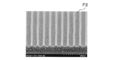
- 4A and 4B are schematic partial cross-sectional views showing the state of a wafer in each step of wafer processing; A wafer in which an SoC film, a SiC film, and a resist pattern (thickness of about 50 nm, line width of about 20 nm) are laminated in this order on a Si bare wafer, and irradiated with ultraviolet rays at an exposure dose of 2000 mJ/cm 2 .
- FIG. 12 shows an SEM image of the wafer after the sintering
- FIG. 10 is a SEM image of a UV-irradiated wafer after being immersed in a phosphoric acid solution with a concentration of 85 wt % and a temperature of 150° C. for 90 seconds
- FIG. 10 is a SEM image of a wet etched wafer after an ashing process
- FIG. 10 is a vertical cross-sectional view schematically showing another example of a wet etching unit;
- a developing process for developing the resist film and the like are sequentially performed to form a resist pattern on the substrate.
- the layer to be processed is etched using the resist pattern as a mask, and a predetermined pattern is formed in the layer to be processed. Dry etching is conventionally used for etching.
- miniaturization of resist patterns is required, and thinning of resist patterns is also required so that pattern collapse does not occur even with fine resist patterns.
- an organic film, a silicon-containing inorganic film, and a resist pattern may be sequentially laminated on the layer to be processed. .
- dry etching is performed on the laminated substrate, the pattern of the resist pattern is transferred in the order of the silicon-containing inorganic film, the organic film, and the film to be etched.
- the miniaturization of semiconductor devices and the miniaturization of resist patterns have progressed further, and the demand for thinner resist patterns has also progressed.
- the film thickness of the resist pattern is required to be 50 nm or less.
- the resist pattern disappears during etching, and the pattern of the resist pattern cannot be transferred to the silicon-containing inorganic film. be. In this case, of course, the transfer to the organic film and the transfer to the film to be etched are also defective.
- the technology according to the present disclosure appropriately transfers the resist pattern to the organic film and the underlying layer to be processed when the organic film, the silicon-containing inorganic film, and the resist pattern are stacked in this order from below. make it possible.
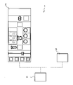
- FIG. 1 is an explanatory diagram showing the outline of the configuration of a wafer processing system as a substrate processing system having a coating and developing apparatus as a substrate processing apparatus according to this embodiment.
- a wafer processing system 1 in FIG. 1 A wafer processing system 1 in FIG. 1
- the coating and developing treatment apparatus 2 performs photolithography on a wafer as a substrate. In this coating and developing apparatus 2, formation of a resist film and the like are performed.
- the etching processing device 3 performs dry etching processing on the wafer.
- the etching processing device 3 for example, an RIE (Reactive Ion Etching) device that performs dry etching processing on a wafer by plasma processing, or the like is used.
- the etching apparatus 3 performs, for example, etching of a silicon inorganic film using a resist pattern and a SoC (spin-on carbon film) pattern as a mask, as will be described later.
- the control device 4 controls the operation of each device.
- the control device 4 is, for example, a computer equipped with a CPU, memory, etc., and has a program storage unit (not shown).
- the program storage unit stores a program for controlling the operation of drive systems such as the above-described various processing devices and transfer devices (not shown) to realize wafer processing, which will be described later, in the wafer processing system 1.
- the program may be recorded in a computer-readable storage medium H and installed in the control device 4 from the storage medium H.
- the storage medium H may be temporary or non-temporary. Part or all of the program may be realized by dedicated hardware (circuit board).
- FIG. 2 is an explanatory diagram showing the outline of the internal configuration of the coating and developing treatment apparatus 2.
- FIG. 3 and 4 are diagrams schematically showing the internal construction of the coating and developing treatment apparatus 2 on the front side and the rear side, respectively.
- the coating and developing treatment apparatus 2 includes a cassette station 10 into which a cassette C containing a plurality of wafers W is loaded and unloaded, and a plurality of various processing units for performing predetermined processing on the wafers W. a station 11;
- the coating and developing treatment apparatus 2 has a configuration in which a cassette station 10, a treatment station 11, and an interface station 13 for transferring wafers W between an exposure apparatus 12 adjacent to the treatment station 11 are connected integrally. have.
- a cassette mounting table 20 is provided in the cassette station 10 .
- the cassette mounting table 20 is provided with a plurality of cassette mounting plates 21 on which the cassettes C are mounted when the cassettes C are carried in and out of the coating and developing treatment apparatus 2 .
- the cassette station 10 is provided with a wafer transfer unit 23 that is movable on a transfer path 22 extending in the X direction in the drawing.
- the wafer transfer unit 23 is movable in the vertical direction and around the vertical axis (the direction of .theta.). The wafer W can be transported between
- the processing station 11 is provided with a plurality of, for example, four blocks G1, G2, G3, and G4 each having various units.
- a first block G1 is provided on the front side of the processing station 11 (negative direction in the X direction in FIG. 2), and a second block G1 is provided on the back side of the processing station 11 (positive direction in the X direction in FIG. 2).
- a block G2 of is provided.
- a third block G3 is provided on the cassette station 10 side of the processing station 11 (negative Y direction side in FIG. 2), and the interface station 13 side of the processing station 11 (positive Y direction side in FIG. 2). is provided with a fourth block G4.
- the first block G1 includes a plurality of liquid processing units, for example, a developing processing unit 30 as a developing section, an SoC film forming unit 31 as an organic film forming section, and a SiC film forming section as an inorganic film forming section.
- a forming unit 32, a resist coating unit 33, and a wet etching unit 34 as a wet etching section are arranged in this order from the bottom.
- the developing unit 30 develops the wafer W. Specifically, the development processing unit 30 supplies a developer to the wafer W on which the resist film is formed to form a resist pattern.
- the SoC film forming unit 31 directly applies an SoC film material (coating liquid) as an organic film onto a layer to be processed, that is, a layer to be etched (for example, a silicon oxide film) formed on the wafer W. An SoC film is formed.
- an SoC film material coating liquid
- a layer to be processed that is, a layer to be etched (for example, a silicon oxide film) formed on the wafer W.
- An SoC film is formed.
- the SiC film forming unit 32 forms a SiC film by applying a SiC film material as a silicon-containing inorganic film directly onto the SoC film formed on the wafer W.
- the resist coating unit 33 directly coats a chemically amplified resist on the SiC film formed on the wafer W to form a resist film.
- the chemically amplified resist is, for example, an EUV resist having sensitivity to EUV, and an ArF or KrF resist having sensitivity to an ArF excimer laser or a KrF excimer laser used for immersion exposure. There may be.
- the wet etching unit 34 supplies a phosphoric acid solution to the wafer W on which a resist pattern is formed by the development processing unit 30 and is irradiated with ultraviolet rays by an irradiation unit 41, which will be described later, to etch or remove the SiC film exposed from the resist pattern. .
- three developing units 30, SoC film forming units 31, SiC film forming units 32, resist coating units 33, and wet etching units 34 are arranged horizontally.
- the number and arrangement of these developing units 30, SoC film forming units 31, SiC film forming units 32, resist coating units 33, and wet etching units 34 can be arbitrarily selected.
- a spin coating method also referred to as a spin coating method
- a spin coating method is used to supply developer, form the SoC film, and form the SiC film. Film formation, resist film formation, and phosphoric acid solution supply are performed.
- the second block G2 is provided with a heat treatment unit 40 and an irradiation unit 41 as a reforming section.
- the thermal processing unit 40 performs thermal processing such as heating and cooling of the wafer W.
- the irradiation unit 41 irradiates the wafer W, in which the SoC film, the SiC film, and the resist pattern are laminated in this order from below on the layer to be etched, with ultraviolet rays to make the resist pattern insoluble in the phosphoric acid solution.
- the ultraviolet rays are supplied, for example, in a low-oxygen atmosphere with an oxygen concentration of 0.1% or less.
- These heat treatment units 40 and irradiation units 41 are arranged vertically and horizontally, and the number and arrangement thereof can be arbitrarily selected.
- a plurality of delivery units 50, 51, 52, 53, 54, 55, and 56 are provided in order from the bottom.
- a plurality of transfer units 60, 61, 62 are provided in order from the bottom in the fourth block G4.
- a wafer transfer area D is formed in the area surrounded by the first block G1 to the fourth block G4.
- a wafer transfer unit 70 is arranged in the wafer transfer area D. As shown in FIG. 2,
- the wafer transfer unit 70 has a transfer arm 70a that is movable in, for example, the Y direction, the X direction, the ⁇ direction, and the vertical direction.
- the wafer transfer unit 70 can move within the wafer transfer area D and transfer the wafer W between units in the surrounding first block G1, second block G2, third block G3 and fourth block G4. .
- a plurality of wafer transfer units 70 are arranged vertically, and wafers W can be transferred between units having approximately the same height in blocks G1 to G4, for example.
- a shuttle transfer unit 80 is provided for transferring the wafer W linearly between the third block G3 and the fourth block G4.
- the shuttle transport unit 80 is linearly movable, for example, in the Y direction in FIG.
- the shuttle transport unit 80 moves in the Y direction while supporting the wafer W, and can transport the wafer W between the transfer unit 52 of the third block G3 and the transfer unit 62 of the fourth block G4.
- a wafer transfer unit 90 is provided next to the third block G3 on the positive side in the X direction.
- the wafer transfer unit 90 has a transfer arm 90a movable in, for example, the X direction, the ⁇ direction, and the vertical direction.
- the wafer transfer unit 90 can move up and down while supporting the wafer W to transfer the wafer W to each transfer unit in the third block G3.
- a wafer transfer unit 100 and a transfer unit 101 are provided in the interface station 13 .
- the wafer transfer unit 100 has a transfer arm 100a movable in, for example, the Y direction, the ⁇ direction, and the vertical direction.
- the wafer transfer unit 100 supports the wafer W on, for example, a transfer arm 100a, and can transfer the wafer W between the transfer units, the transfer unit 101, and the exposure apparatus 12 in the fourth block G4.
- each processing unit and each transport unit described above are controlled by the control device 4, for example.
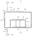
- FIG. 5 and 6 are vertical and horizontal cross-sectional views, respectively, showing an outline of the configuration of the wet etching unit 34. As shown in FIG.
- the wet etching unit 34 has a processing container 120 whose inside can be closed, as shown in FIG. As shown in FIG. 6, a loading/unloading port 121 for the wafer W is formed on the surface of the processing container 120 facing the wafer transfer area D, and the loading/unloading port 121 is provided with an open/close shutter 122 .
- a spin chuck 130 that holds and rotates the wafer W is provided in the center of the processing container 120 as shown in FIG.
- the spin chuck 130 has a horizontal upper surface, and the upper surface is provided with a suction port (not shown) for sucking the wafer W, for example.
- the wafer W can be sucked and held on the spin chuck 130 by suction from this suction port.
- the spin chuck 130 is connected to a chuck drive mechanism 131 and can be rotated at a desired speed by the chuck drive mechanism 131 .
- the chuck drive mechanism 131 has a rotation drive source (not shown) such as a motor that generates drive force for rotating the spin chuck 130 .
- the chuck driving mechanism 131 is provided with a vertical driving source such as a cylinder, and the spin chuck 130 can move vertically.
- a cup 132 is provided around the spin chuck 130 to receive and collect the liquid that scatters or drops from the wafer W.
- a discharge pipe 133 for discharging the collected liquid and an exhaust pipe 134 for discharging the atmosphere in the cup 132 are connected to the lower surface of the cup 132 .
- a rail 140 extending along the Y direction is formed on the negative side of the cup 132 in the X direction (downward in FIG. 6).
- the rail 140 is formed, for example, from the outside of the cup 132 in the negative direction in the Y direction (left direction in FIG. 6) to the outside in the positive direction in the Y direction (right direction in FIG. 6). Arms 141 and 145 are attached to the rail 140 .
- a discharge nozzle 142 is supported on the arm 141 as shown in FIGS.
- the ejection nozzle 142 ejects the phosphoric acid liquid.
- the arm 141 is movable on the rail 140 by a nozzle driving section 143 shown in FIG.
- the discharge nozzle 142 can move from a standby portion 144 installed outside the cup 132 on the positive side in the Y direction to above the central portion of the wafer W in the cup 132, and furthermore, can move the wafer W on the surface of the wafer W. It can move in the radial direction of W.
- the arm 141 can be moved up and down by a nozzle driving section 143, and the height of the discharge nozzle 142 can be adjusted.
- the ejection nozzle 142 is connected to a supply unit (not shown) that supplies the phosphoric acid solution to the ejection nozzle 142 .
- a discharge nozzle 146 is supported on the arm 145 as shown in FIGS.
- the ejection nozzle 146 ejects the rinse liquid.
- the rinse liquid is, for example, DIW (Deionized Water).
- the arm 145 is movable on the rail 140 by the nozzle driving section 147 shown in FIG. As a result, the discharge nozzle 146 can move from the standby part 148 installed outside the cup 132 on the Y direction negative direction side to above the center part of the wafer W in the cup 132, It can move in the radial direction of W. Further, the arm 145 can be moved up and down by a nozzle driving section 147, and the height of the ejection nozzle 146 can be adjusted.
- the ejection nozzle 146 is connected to a supply section (not shown) that supplies the rinse liquid to the ejection nozzle 146 .
- the configurations of the developing processing unit 30, the SoC film forming unit 31, the SiC film forming unit 32, and the resist coating unit 33 are the same as those of the wet etching unit .
- FIG. 7 is a longitudinal sectional view showing the outline of the configuration of the irradiation unit 41. As shown in FIG.
- the irradiation unit 41 has a processing container 150 whose inside can be sealed as shown in FIG.
- a loading/unloading port 151 for the wafer W is formed on the surface of the processing container 150 facing the wafer transfer region D, and the loading/unloading port 151 is provided with an open/close shutter 152 .
- a gas supply port 160 for supplying a gas other than oxygen gas, for example, an inert gas such as N 2 gas is formed in the upper surface of the processing container 150 toward the inside of the processing container 150 .
- a gas supply mechanism 162 is connected to the port 160 via a gas supply pipe 161 .
- the gas supply mechanism 162 has, for example, a flow control valve (not shown) for adjusting the gas supply flow rate into the processing container 150 .
- an exhaust port 163 for exhausting the atmosphere inside the processing container 150 is formed in the lower surface of the processing container 150 .
- An exhaust mechanism 165 for exhausting is connected.
- the exhaust mechanism 165 has an exhaust pump (not shown) and the like.
- a cylindrical support 170 on which the wafer W is placed horizontally is provided inside the processing container 150 .
- Elevating pins 171 for transferring the wafer W are installed inside the supporting body 170 while being supported by supporting members 172 .
- the elevating pins 171 are provided so as to penetrate through holes 173 formed in the upper surface 170a of the support 170.
- three elevating pins 171 are provided.
- a drive mechanism 174 is provided at the base end of the support member 172 to raise and lower the support member 172 and raise and lower the lifting pin 171 .
- the drive mechanism 174 has a drive source (not shown) such as a motor that generates drive force for raising and lowering the support member 172 .
- a light source 180 such as a deuterium lamp or an excimer lamp is provided above the processing container 150 to irradiate the wafer W on the support 170 with ultraviolet rays having a wavelength of 172 nm, for example.
- the light source 180 can irradiate the entire surface of the wafer W with ultraviolet rays.
- a top plate of the processing container 150 is provided with a window 181 through which ultraviolet rays from the light source 180 are transmitted.
- the wavelength of the ultraviolet rays is not limited to 172 nm, and is, for example, 150 nm to 250 nm.
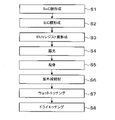
- FIG. 8 is a flow chart showing the main steps of one example of wafer processing.
- 9 and 10 are schematic partial cross-sectional views showing the state of the wafer W in each step of wafer processing. As shown in FIG. 9A, a SiO 2 film F1 to be etched is formed in advance on the surface of the wafer W on which the above wafer processing is performed.
- a cassette C containing a plurality of wafers W is carried into the cassette station 10 of the coating and developing treatment apparatus 2 . Then, the wafers W in the cassette C are transported to the processing station 11 and temperature-controlled by the thermal processing unit 40 .
- Step S1 After that, the SoC film F2 is formed directly on the SiO2 film F1 formed on the wafer W, as shown in FIGS. 8 and 9A.
- the wafer W is transported to the SoC film forming unit 31, and the surface of the wafer W is spin-coated with a coating liquid for the SoC film to form the SoC film F2 so as to cover the SiO2 film F1. be.
- the wafer W is then transported to the thermal processing unit 40 and thermally processed.
- the film thickness of the SoC film F2 is, for example, 50 to 100 nm after the heat treatment by the heat treatment unit 40.
- Step S2 Subsequently, on the SoC film F2 formed on the wafer W, the SiC film F3 is directly formed.
- the wafer W is transported to the SiC film forming unit 32, and the coating liquid for the SiC film is spin-coated on the surface of the wafer W to cover the SoC film F2 as shown in FIG. 9B.
- the SiC film F3 is formed.
- the wafer W is then transported to the thermal processing unit 40 and thermally processed.
- the film thickness of the SiC film F3 after the heat treatment by the heat treatment unit 40 is, for example, 7 to 15 nm.
- Step S3 Thereafter, a chemically amplified resist film F4 is formed directly on the SiC film formed on the wafer W as shown in FIG. 9(C).
- the wafer W is transported to the resist coating unit 33, a chemically amplified resist is spin-coated on the surface of the wafer W, and a chemically amplified resist film F4 is formed so as to cover the SiC film F3. be done.
- the wafer W is then transported to the thermal processing unit 40 and pre-baked.
- the film thickness of the resist film F4 is 30 to 100 nm after pre-baking.
- Step S4 Next, the resist film F4 formed on the wafer W is exposed.
- the wafer W is transported to the exposure device 12 via the interface station 13, and as shown in FIG. is exposed in the desired pattern.
- Step S5 the exposed resist film formed on the wafer W is developed to form a resist pattern F5 as shown in FIG. 9(E).
- the wafer W is transported to the heat treatment unit 40 and subjected to post-exposure baking.
- the wafer W is transported to the development processing unit 30 and subjected to development processing to form, for example, a line-and-space resist pattern F5.
- the wafer W is transported to the heat treatment unit 40 and post-baked.
- steps S1 to S5 the SoC film F2, the SiC film F3, and the resist pattern F5 are continuously formed on the wafer W in this order from the bottom (that is, so that there is no other film between the films).
- Step S6 Subsequently, as shown in FIG. 9F, the wafer W is irradiated with ultraviolet rays to make the resist pattern F5 insoluble in the phosphoric acid solution.
- the wafer W is transferred to the irradiation unit 41 . Then, in a low-oxygen atmosphere with an oxygen concentration of 0.1% or less, the entire wafer W placed on the support 170, that is, the entire resist pattern F5, is irradiated with ultraviolet rays from the light source 180.
- FIG. The exposure amount at this time is, for example, 2000 mJ/cm 2 or more.
- the reason why the ultraviolet irradiation is performed in a low-oxygen atmosphere is that if the oxygen concentration is not low, ozone is generated by the ultraviolet irradiation, and the resist pattern F5 is removed by the ozone.
- Step S7 Subsequently, a phosphoric acid solution is supplied to the wafer W, and the SiC film F3 exposed from the resist pattern F6 insolubilized with respect to the phosphoric acid solution is removed. That is, the wet etching process is performed using the resist pattern F6 insolubilized with respect to the phosphoric acid solution as a mask.
- the wafer W is transferred to the wet etching unit 34 .
- the phosphoric acid solution P from the ejection nozzle 142 is spin-coated, for example, on the surface of the wafer W held by the spin chuck 130, and the SiC film F3 is formed using the resist pattern F6 as a mask. is removed.
- the SiC film F3 is removed until the SoC film F2 is exposed, for example, as shown in FIG. 9(H). Thereby, the pattern F7 of the laminated film of the resist film and the SiC film is formed.
- the phosphoric acid solution supplied to the wafer W has, for example, a mass percent concentration of 85-95 wt % and a temperature of 150° C. or higher.
- the rinse liquid from the ejection nozzle 146 is spin-coated, for example, on the surface of the wafer W held by the spin chuck 130, and the phosphoric acid liquid is removed from the wafer W.
- the supply of the rinsing liquid is stopped, and in this state, the wafer W held by the spin chuck 130 is rotated, thereby drying the wafer W.
- the wafers W are successively accommodated in the cassette C and transported to the etching processing apparatus 3 .
- the SiC film F3 can be wet-etched with a phosphoric acid solution.
- the inventors of the present application have investigated and found that resist patterns for EUV and the like are soluble in a phosphoric acid solution under normal conditions. Therefore, the inventors of the present invention made extensive studies and found that the phosphoric acid solution is not required by irradiating the resist pattern with ultraviolet rays as in the above-described step S7. The present disclosure is based on this finding.
- Step S8 Thereafter, in the etching processing apparatus 3, dry etching is performed on the wafer W, and the resist pattern F6 is transferred to the SoC film.
- dry etching (first dry etching) of the SoC film F2 is performed using the pattern F7 of the laminated film of the resist film and the SiC film as a mask.
- dry etching (second dry etching) of the SiO 2 film F1 to be etched is performed using the SoC film F2 to which (the pattern of) the resist pattern F6 has been transferred by the first dry etching as a mask. Note that the first and second dry etchings are performed in processing vessels different from each other.
- Wafer processing using the wafer processing system 1 is now complete.
- the rest of the SoC film may be removed by dry etching using the resist pattern as a mask in the etching processing apparatus 3 . That is, both wet etching and dry etching using a phosphoric acid solution may be performed using the insolubilized resist pattern as a mask. Also in this case, if the thickness of the SiC film and the amount of wet etching of the SiC film using nitric acid solution are appropriately set, the resist pattern will not disappear while the resist pattern is being transferred to the SiC film F3. .
- the wafer W on which the SoC film, the SiC film, and the resist pattern are laminated in this order from below is irradiated with ultraviolet rays to make the resist pattern insoluble in the phosphoric acid solution.
- the resist pattern when transferring the resist pattern to the SiC film. Only wet etching using a phosphoric acid solution is performed using the insolubilized resist pattern as a mask, or both wet etching and dry etching using a phosphoric acid solution are performed using the insolubilized resist pattern as a mask.
- the resist pattern when the resist pattern is transferred to the SiC film, unlike the conventional case where only dry etching is performed, even if the resist pattern is thin, pattern collapse does not occur. Since the resist pattern does not disappear during transfer, transfer can be properly performed.
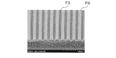
- FIG. 10 shows a wafer in which an SoC film, a SiC film, and a resist pattern (thickness of about 50 nm, line width of about 20 nm) are laminated in this order on a Si bare wafer.
- FIG. 10 shows an SEM image of the wafer after irradiation with cm2.
- FIG. 11 is a diagram showing a SEM image of the wafer irradiated with ultraviolet rays after being immersed in a phosphoric acid solution having a concentration of 85 wt % and a temperature of 150° C. for 90 seconds, that is, after wet etching under the above conditions. be.
- FIG. 12 is a diagram showing an SEM image of the wafer wet-etched under the above conditions and after ashing.
- the SiC film F3 is exposed from the resist pattern F6. Further, as shown in FIGS. 10 and 11, the wet etching causes a change in the portion not covered with the resist pattern F6. As shown in FIG. 12, the portion of the SoC film F2 not covered with the resist pattern is removed by the ashing process. From this, it can be seen that in FIG. 11 showing the state before the ashing process, the portion exposed from the resist pattern F6 is not the SiC film F3 but the SoC film F2. 10 to 12 that the resist pattern F6 can be transferred to the SiC film F3 without pattern collapse by performing wet etching using ultraviolet irradiation and a phosphoric acid solution under the above conditions. shows.
- FIG. 13 is a vertical sectional view schematically showing another example of the wet etching unit.
- the wet etching unit 34a of FIG. 13 is integrally constructed of the same module as the developing unit, and shares the components with the developing unit.
- the wet etching unit 34a includes a discharge nozzle 142 for discharging nitric acid, a discharge nozzle 146 for discharging rinse liquid, and a discharge nozzle 200 for discharging developer.
- the ejection nozzle 142 and the ejection nozzle 200 share the spin chuck 130, the cup 210, and the like. As a result, an increase in size of the device can be suppressed.
- the cup 210 has a cup body 211 and a movable cup 213 that can be moved up and down with respect to the cup body 211 by a lifting mechanism 212 .
- a lifting mechanism 212 For example, by raising the movable cup 213 during wet etching, the phosphoric acid solution and the rinse solution scattered from the rotating wafer W are passed under the movable cup 213 and introduced into the inner channel 220 of the cup body 211.
- the developer and rinse liquid scattered from the rotating wafer W are passed through the upper side of the movable cup 213 and introduced into the outer flow path 221 of the cup main body 211. Let Thereby, the discharged phosphoric acid solution and the discharged developer solution can be collected separately without being mixed.
- the SoC film is used as the organic film in the above examples, other organic films may be used.
- the organic film is formed by the coating and developing treatment apparatus 2, it may be formed by a film forming apparatus that forms a film by CVD or ALD outside the coating and developing treatment apparatus 2, for example.
- the SiC film is used as the silicon-containing inorganic film, but other silicon-containing organic films (for example, siloxane-based films used as SiARC films) may be used.
- the silicon-containing inorganic film may also be formed by a film forming apparatus that forms a film by, for example, CVD or ALD outside the coating and developing treatment apparatus 2, similarly to the organic film.
- wet etching may be performed as follows. That is, before supplying the phosphoric acid solution, DIW, which is also used as a rinse solution, may be supplied to the wafer W on which the resist pattern is formed, and a puddle of DIW may be formed to cover the resist pattern. Next, a normal temperature (room temperature) phosphoric acid solution may be supplied to the wafer W to replace the DIW on the wafer W with the phosphoric acid solution to form a puddle of the phosphoric acid solution. After that, the paddle of the phosphoric acid solution may be heated to a predetermined temperature by a heater provided in the spin chuck 130, and the SiC film may be removed with the phosphoric acid solution using the resist pattern as a mask. Then, the rinse liquid is supplied to the wafer W, the phosphoric acid liquid on the wafer W is removed, and then the wafer W may be dried.
- DIW which is also used as a rinse solution
Abstract
Description
また、レジストパターンが薄く、且つ、レジストパターンに対する、処理対象層のドライエッチング時の選択比が低い場合、処理対象層上に、有機膜、シリコン含有無機膜及びレジストパターンを順に積層することがある。このように積層された基板に対しドライエッチングを行うときは、レジストパターンが有するパターンが、シリコン含有無機膜、有機膜、エッチング対象膜の順に転写されていく。 By the way, along with the miniaturization of semiconductor devices, etc., miniaturization of resist patterns is required, and thinning of resist patterns is also required so that pattern collapse does not occur even with fine resist patterns.
Further, when the resist pattern is thin and the dry etching selectivity of the layer to be processed with respect to the resist pattern is low, an organic film, a silicon-containing inorganic film, and a resist pattern may be sequentially laminated on the layer to be processed. . When dry etching is performed on the laminated substrate, the pattern of the resist pattern is transferred in the order of the silicon-containing inorganic film, the organic film, and the film to be etched.
しかし、このように薄いレジストパターンをマスクとして、シリコン含有無機膜のドライエッチングを行うと、エッチング中にレジストパターンが消失してしまい、レジストパターンが有するパターンを、シリコン含有無機膜に転写できないことがある。この場合、当然、有機膜への転写及びエッチング対象膜への転写も不良となる。 In recent years, the miniaturization of semiconductor devices and the miniaturization of resist patterns have progressed further, and the demand for thinner resist patterns has also progressed. For example, there are cases where the film thickness of the resist pattern is required to be 50 nm or less.
However, when the silicon-containing inorganic film is dry-etched using such a thin resist pattern as a mask, the resist pattern disappears during etching, and the pattern of the resist pattern cannot be transferred to the silicon-containing inorganic film. be. In this case, of course, the transfer to the organic film and the transfer to the film to be etched are also defective.
図1は、本実施形態にかかる基板処理装置としての塗布現像処理装置を有する、基板処理システムとしてのウェハ処理システムの構成の概略を示す説明図である。 <Wafer processing system>
FIG. 1 is an explanatory diagram showing the outline of the configuration of a wafer processing system as a substrate processing system having a coating and developing apparatus as a substrate processing apparatus according to this embodiment.
図2は、塗布現像処理装置2の内部構成の概略を示す説明図である。図3及び図4は、各々塗布現像処理装置2の正面側と背面側の内部構成の概略を示す図である。 <Coating and developing device>
FIG. 2 is an explanatory diagram showing the outline of the internal configuration of the coating and developing
また、SoC膜形成ユニット31、SiC膜形成ユニット32、レジスト塗布ユニット33、ウェットエッチングユニット34では、スピン塗布法(スピンコーティング法ともいう。)により、現像液の供給や、SoC膜の形成、SiC膜の形成、レジスト膜の形成、燐酸液の供給が行われる。 For example, three developing
In the SoC
照射ユニット41は、エッチング対象層上に、SoC膜、SiC膜、レジストパターンが下方からこの順で積層されたウェハWに紫外線を照射し、レジストパターンを燐酸液に対して不溶化させる。紫外線の供給は、例えば酸素濃度が0.1%以下の低酸素雰囲気下で行われる。 The
The
続いて、上述のウェットエッチングユニット34の構成について説明する。図5及び図6はそれぞれ、ウェットエッチングユニット34の構成の概略を示す縦断面図及び横断面図である。 <Wet etching unit>
Next, the configuration of the
次に、上述の照射ユニット41の構成について説明する。図7は、照射ユニット41の構成の概略を示す縦断面図である。 <Irradiation unit>
Next, the configuration of the
このようなガスの供給機構によって、処理容器150内へ酸素ガス以外のガスを導入することにより、処理容器150内を酸素濃度が0.1ppm以下の低酸素雰囲気にすることができる。 A
By introducing a gas other than oxygen gas into the
ガス供給口160から酸素ガス以外のガスを導入し、排気口163から排気することにより、処理容器150内の雰囲気を、0.1ppm以下の低酸素雰囲気に、迅速に置換することができる。 For example, an
By introducing a gas other than oxygen gas from the
次に、以上のように構成されたウェハ処理システム1を用いて行われるウェハ処理について説明する。図8は、ウェハ処理の一例の主な工程を示すフローチャートである。図9及び図10は、ウェハ処理の各工程におけるウェハWの状態を示す模式部分断面図である。なお、上記ウェハ処理が行われるウェハWの表面には、図9(A)に示すように、エッチング対象としてのSiO2膜F1が予め形成されている。 <Wafer processing>
Next, wafer processing performed using the
その後、図8及び図9(A)に示すように、ウェハWに形成されているSi02膜F1上に、直接、SoC膜F2が形成される。 (Step S1)
After that, the SoC film F2 is formed directly on the SiO2 film F1 formed on the wafer W, as shown in FIGS. 8 and 9A.
次いで、ウェハWが、熱処理ユニット40に搬送され、熱処理される。
SoC膜F2の膜厚は、熱処理ユニット40による熱処理後において、例えば50~100nmである。 Specifically, the wafer W is transported to the SoC
The wafer W is then transported to the
The film thickness of the SoC film F2 is, for example, 50 to 100 nm after the heat treatment by the
続いて、ウェハWに形成されているSoC膜F2上に、直接、SiC膜F3が形成される。 (Step S2)
Subsequently, on the SoC film F2 formed on the wafer W, the SiC film F3 is directly formed.
次いで、ウェハWが、熱処理ユニット40に搬送され、熱処理される。
SiC膜F3の膜厚は、熱処理ユニット40による熱処理後において、例えば7~15nmである。 Specifically, the wafer W is transported to the SiC
The wafer W is then transported to the
The film thickness of the SiC film F3 after the heat treatment by the
その後、図9(C)に示すようにウェハWに形成されているSiC膜上に、直接、化学増幅型のレジスト膜F4が形成される。 (Step S3)
Thereafter, a chemically amplified resist film F4 is formed directly on the SiC film formed on the wafer W as shown in FIG. 9(C).
次いで、ウェハWが、熱処理ユニット40に搬送され、プリベーク処理される。
レジスト膜F4の膜厚は、プリベーク処理後において、30~100nmである。 Specifically, the wafer W is transported to the resist
The wafer W is then transported to the
The film thickness of the resist film F4 is 30 to 100 nm after pre-baking.
次に、ウェハWに形成されているレジスト膜F4が露光される。 (Step S4)
Next, the resist film F4 formed on the wafer W is exposed.
次いで、ウェハWに形成されている露光後のレジスト膜が現像され、図9(E)に示すように、レジストパターンF5が形成される。 (Step S5)
Next, the exposed resist film formed on the wafer W is developed to form a resist pattern F5 as shown in FIG. 9(E).
次いで、ウェハWが、現像処理ユニット30に搬送され、現像処理が行われ、例えばラインアンドスペースのレジストパターンF5が形成される。パターン形成後、ウェハWが、熱処理ユニット40に搬送され、ポストベーク処理される。 Specifically, after exposure, the wafer W is transported to the
Next, the wafer W is transported to the
続いて、図9(F)に示すように、ウェハWに対し紫外線が照射され、レジストパターンF5が燐酸液に対して不溶化される。 (Step S6)
Subsequently, as shown in FIG. 9F, the wafer W is irradiated with ultraviolet rays to make the resist pattern F5 insoluble in the phosphoric acid solution.
続いて、ウェハWに対し燐酸液が供給され、燐酸液に対し不溶化されたレジストパターンF6から露出したSiC膜F3が除去される。つまり、燐酸液に対し不溶化されたレジストパターンF6をマスクとして、ウェットエッチング処理が行われる。 (Step S7)
Subsequently, a phosphoric acid solution is supplied to the wafer W, and the SiC film F3 exposed from the resist pattern F6 insolubilized with respect to the phosphoric acid solution is removed. That is, the wet etching process is performed using the resist pattern F6 insolubilized with respect to the phosphoric acid solution as a mask.
その後、リンス液の供給が停止され、その状態で、スピンチャック130に保持されたウェハWが回転され、これにより、ウェハWが乾燥する。 After the phosphoric acid liquid is supplied from the
After that, the supply of the rinsing liquid is stopped, and in this state, the wafer W held by the
その後、エッチング処理装置3において、ウェハWに対し、ドライエッチングが行われ、レジストパターンF6がSoC膜に転写される。 (Step S8)
Thereafter, in the
以上の例では、燐酸液を用いたウェットエッチングにより、レジストパターンF6をマスクとして、SiC膜F3を除去する際、その下層のSoC膜F2が露出するまで除去するようにしている。ただし、SiC膜をマスクとしたSiC膜のドライエッチングのためにSiC膜を15nmより厚くした場合は、燐酸液を用いたウェットエッチングの際、ウェットエッチングによりパターン倒れが生じないように、SiC膜の上側の一部のみを除去するようにしてもよい。そして、エッチング処理装置3にて、レジストパターンをマスクとしたドライエッチングで、SoC膜の残りを除去するようにしてもよい。つまり、不溶化されたレジストパターンをマスクとした、燐酸液を用いたウェットエッチングとドライエッチングとの両方を行うようにしてもよい。この場合も、SiC膜の厚さ及び硝酸液を用いたSiC膜のウェットエッチング量を適切に設定すれば、レジストパターンをSiC膜F3に転写している間に、レジストパターンが消失することがない。 <Another example of wafer processing>
In the above example, when the SiC film F3 is removed by wet etching using a phosphoric acid solution using the resist pattern F6 as a mask, the SiC film F3 is removed until the underlying SoC film F2 is exposed. However, if the SiC film is made thicker than 15 nm for dry etching of the SiC film using the SiC film as a mask, during wet etching using a phosphoric acid solution, the thickness of the SiC film should be reduced so as not to cause pattern collapse due to wet etching. You may make it remove only a part of upper side. Then, the rest of the SoC film may be removed by dry etching using the resist pattern as a mask in the
以上のように、本実施形態では、SoC膜、SiC膜、レジストパターンが下方からこの順で積層されたウェハWに紫外線を照射し、レジストパターンを燐酸液に対して不溶化させている。そして、本実施形態では、レジストパターンをSiC膜に転写する際に。不溶化されたレジストパターンをマスクとした、燐酸液を用いたウェットエッチングのみを行い、または、不溶化されたレジストパターンをマスクとした、燐酸液を用いたウェットエッチングとドライエッチングの両方を行っている。したがって、本実施形態によれば、レジストパターンをSiC膜に転写する際に、従来のように、ドライエッチングのみを行う場合と異なり、レジストパターンが薄くても、パターン倒れ等が生じることがなく、転写中にレジストパターンが消失することがないため、適切に転写を行うことができる。 <Main effects>
As described above, in this embodiment, the wafer W on which the SoC film, the SiC film, and the resist pattern are laminated in this order from below is irradiated with ultraviolet rays to make the resist pattern insoluble in the phosphoric acid solution. In this embodiment, when transferring the resist pattern to the SiC film. Only wet etching using a phosphoric acid solution is performed using the insolubilized resist pattern as a mask, or both wet etching and dry etching using a phosphoric acid solution are performed using the insolubilized resist pattern as a mask. Therefore, according to the present embodiment, when the resist pattern is transferred to the SiC film, unlike the conventional case where only dry etching is performed, even if the resist pattern is thin, pattern collapse does not occur. Since the resist pattern does not disappear during transfer, transfer can be properly performed.
また、図10及び図11に示すように、ウェットエッチングにより、レジストパターンF6に被覆されていなかった部分に変化が生じている。
図12に示すように、アッシング処理により、SoC膜F2における、レジストパターンに被覆されていなかった部分が除去されている。このことから、アッシング処理前の状態を示す図11において、レジストパターンF6から露出している部分は、SiC膜F3ではなく、SoC膜F2であることが分かる。
つまり、上述の条件で、紫外線照射及び燐酸液を用いたウェットエッチングを行うことにより、パターン倒れを生じさせずに、レジストパターンF6をSiC膜F3に転写することができることを、図10~図12は示している。 After the ultraviolet irradiation, as shown in FIG. 10, the SiC film F3 is exposed from the resist pattern F6.
Further, as shown in FIGS. 10 and 11, the wet etching causes a change in the portion not covered with the resist pattern F6.
As shown in FIG. 12, the portion of the SoC film F2 not covered with the resist pattern is removed by the ashing process. From this, it can be seen that in FIG. 11 showing the state before the ashing process, the portion exposed from the resist pattern F6 is not the SiC film F3 but the SoC film F2.
10 to 12 that the resist pattern F6 can be transferred to the SiC film F3 without pattern collapse by performing wet etching using ultraviolet irradiation and a phosphoric acid solution under the above conditions. shows.
図13は、ウェットエッチングユニットの他の例の概略を示す縦断面図である。
図13のウェットエッチングユニット34aは、現像ユニットと一体に同一のモジュールにより構成され、構成部材を現像ユニットと共有する。 <Modified example of wet etching unit>
FIG. 13 is a vertical sectional view schematically showing another example of the wet etching unit.
The
そして、吐出ノズル142と、吐出ノズル200とで、スピンチャック130や、カップ210等を共有している。
これにより、装置の大型化を抑制することができる。 Specifically, the
The
As a result, an increase in size of the device can be suppressed.
以上の例では、有機膜としてSoC膜が用いられていたが、それ以外の有機膜であってもよい。また、有機膜は、塗布現像処理装置2で形成しているが、塗布現像処理装置2の外部で例えばCVDやALDにより成膜を行う成膜装置で形成してもよい。
以上の例では、シリコン含有無機膜としてSiC膜が用いられていたが、それ以外のシリコン含有有機膜(例えばSiARC膜として用いられるシロキサン系の膜)であってもよい。また、シリコン含有無機膜も、有機膜と同様、塗布現像処理装置2の外部で例えばCVDやALDにより成膜を行う成膜装置で形成してもよい。 <Other Modifications>
Although the SoC film is used as the organic film in the above examples, other organic films may be used. Moreover, although the organic film is formed by the coating and developing
In the above examples, the SiC film is used as the silicon-containing inorganic film, but other silicon-containing organic films (for example, siloxane-based films used as SiARC films) may be used. Further, the silicon-containing inorganic film may also be formed by a film forming apparatus that forms a film by, for example, CVD or ALD outside the coating and developing
すなわち、燐酸液の供給前に、リンス液としても用いられるDIWが、レジストパターンが形成されたウェハWに供給され、レジストパターンを覆うDIWのパドルが形成されるようにしてもよい。次いで、ウェハWに常温(室温)の燐酸液が供給され、ウェハW上のDIWが燐酸液によって置換され、燐酸液のパドルが形成されるようにしてもよい。
その後、スピンチャック130に設けられたヒータにより、燐酸液のパドルを所定の温度まで加熱させ、レジストパターンをマスクとして、燐酸液により、SiC膜が除去されるようにしてもよい。
そして、リンス液がウェハWに供給され、ウェハW上の燐酸液が除去され、その後、ウェハWの乾燥が行われるようにしてもよい。 Also, wet etching may be performed as follows.
That is, before supplying the phosphoric acid solution, DIW, which is also used as a rinse solution, may be supplied to the wafer W on which the resist pattern is formed, and a puddle of DIW may be formed to cover the resist pattern. Next, a normal temperature (room temperature) phosphoric acid solution may be supplied to the wafer W to replace the DIW on the wafer W with the phosphoric acid solution to form a puddle of the phosphoric acid solution.
After that, the paddle of the phosphoric acid solution may be heated to a predetermined temperature by a heater provided in the
Then, the rinse liquid is supplied to the wafer W, the phosphoric acid liquid on the wafer W is removed, and then the wafer W may be dried.
34、34a ウェットエッチングユニット
41 照射ユニット
F2 SoC膜
F3 SiC膜
F5 レジストパターン
F6 燐酸液に対し不溶化されたレジストパターン
P 燐酸液
W ウェハ 2 Coating and developing
Claims (20)
- 有機膜、シリコン含有無機膜、レジストパターンが下方からこの順で積層された基板に紫外線を照射し、前記レジストパターンを燐酸液に対して不溶化させる工程と、
前記不溶化させる工程後、前記基板に対し前記燐酸液を供給し、前記レジストパターンから露出した前記シリコン含有無機膜を除去する工程と、
前記除去する工程後、前記基板に対しエッチング処理を行い、前記レジストパターンを前記有機膜に転写する工程と、を含む、基板処理方法。 a step of irradiating a substrate on which an organic film, a silicon-containing inorganic film, and a resist pattern are laminated in this order from below with ultraviolet rays to make the resist pattern insoluble in a phosphoric acid solution;
after the insolubilizing step, supplying the phosphoric acid solution to the substrate to remove the silicon-containing inorganic film exposed from the resist pattern;
After the step of removing, a step of etching the substrate to transfer the resist pattern to the organic film. - 前記レジストパターンは、化学増幅型レジストで形成されている、請求項1に記載の基板処理方法。 2. The substrate processing method according to claim 1, wherein said resist pattern is formed of a chemically amplified resist.
- 前記化学増幅型レジストは、ArFレジスト、KrFレジストまたはEUVレジストである、請求項2に記載の基板処理方法。 3. The substrate processing method according to claim 2, wherein said chemically amplified resist is ArF resist, KrF resist or EUV resist.
- 前記紫外線の照射量は、2000mJ/cm2以上である、請求項1に記載の基板処理方法。 2. The substrate processing method according to claim 1, wherein the irradiation amount of said ultraviolet rays is 2000 mJ/cm< 2 > or more.
- 前記紫外線の照射量は、2000mJ/cm2以上である、請求項2に記載の基板処理方法。 3. The substrate processing method according to claim 2, wherein the irradiation amount of said ultraviolet rays is 2000 mJ/cm< 2 > or more.
- 前記紫外線の照射量は、2000mJ/cm2以上である、請求項3に記載の基板処理方法。 4. The substrate processing method according to claim 3, wherein the irradiation amount of said ultraviolet rays is 2000 mJ/cm< 2 > or more.
- 前記燐酸液の温度は、150℃以上である、請求項1に記載の基板処理方法。 2. The substrate processing method according to claim 1, wherein the temperature of said phosphoric acid solution is 150[deg.] C. or higher.
- 前記燐酸液の温度は、150℃以上である、請求項2に記載の基板処理方法。 3. The substrate processing method according to claim 2, wherein the temperature of said phosphoric acid solution is 150[deg.] C. or higher.
- 前記燐酸液の温度は、150℃以上である、請求項3に記載の基板処理方法。 4. The substrate processing method according to claim 3, wherein the temperature of said phosphoric acid solution is 150[deg.] C. or higher.
- 前記燐酸液の温度は、150℃以上である、請求項4に記載の基板処理方法。 5. The substrate processing method according to claim 4, wherein the phosphoric acid solution has a temperature of 150[deg.] C. or higher.
- 有機膜、シリコン含有無機膜、レジストパターンが下方からこの順で積層された基板に紫外線を照射し、前記レジストパターンを燐酸液に対して不溶化させる改質部と、
前記レジストパターンが不溶化された前記基板に対し前記燐酸液を供給し、前記レジストパターンから露出した前記シリコン含有無機膜を除去するウェットエッチング部と、を備える、基板処理装置。 a modifying unit that irradiates a substrate on which an organic film, a silicon-containing inorganic film, and a resist pattern are laminated in this order from below with ultraviolet rays to make the resist pattern insoluble in a phosphoric acid solution;
and a wet etching unit that supplies the phosphoric acid solution to the substrate on which the resist pattern is insolubilized, and removes the silicon-containing inorganic film exposed from the resist pattern. - 前記レジストパターンは、化学増幅型レジストで形成されている、請求項11に記載の基板処理装置。 12. The substrate processing apparatus according to claim 11, wherein said resist pattern is formed of a chemically amplified resist.
- 前記化学増幅型レジストは、ArFレジスト、KrFレジストまたはEUVレジストである、請求項12に記載の基板処理装置。 13. The substrate processing apparatus according to claim 12, wherein said chemically amplified resist is ArF resist, KrF resist or EUV resist.
- 前記紫外線の照射量は、2000mJ/cm2以上である、請求項11に記載の基板処理装置。 12. The substrate processing apparatus according to claim 11, wherein the irradiation amount of said ultraviolet rays is 2000 mJ/cm< 2 > or more.
- 前記燐酸液の温度は、150℃以上である、請求項11に記載の基板処理装置。 12. The substrate processing apparatus according to claim 11, wherein the phosphoric acid solution has a temperature of 150[deg.] C. or higher.
- 現像処理を行い、前記レジストパターンを形成する現像部と、
前記ウェットエッチング部と前記現像部とは、同一のモジュールにより構成され、構成部材の一部を共有する、請求項11に記載の基板処理装置。 a developing unit that performs a developing process to form the resist pattern;
12. The substrate processing apparatus according to claim 11, wherein said wet etching section and said developing section are configured by the same module and share a part of constituent members. - 有機膜、シリコン含有無機膜、レジストパターンが下方からこの順で積層された基板に紫外線を照射し、前記レジストパターンを燐酸液に対して不溶化させる改質部と、前記レジストパターンが不溶化された前記基板に対し前記燐酸液を供給し、前記レジストパターンから露出した前記シリコン含有無機膜を除去するウェットエッチング部と、を備える、基板処理装置と、
前記シリコン含有無機膜における前記レジストパターンから露出した部分が除去された前記基板に対し、エッチング処理を行い、前記レジストパターンを前記有機膜に転写するエッチング装置と、を備える、基板処理システム。 A reforming unit that irradiates a substrate on which an organic film, a silicon-containing inorganic film, and a resist pattern are laminated in this order from below with ultraviolet rays to make the resist pattern insoluble in a phosphoric acid solution; a substrate processing apparatus comprising a wet etching unit that supplies the phosphoric acid solution to the substrate and removes the silicon-containing inorganic film exposed from the resist pattern;
and an etching apparatus that performs an etching process on the substrate from which a portion of the silicon-containing inorganic film exposed from the resist pattern is removed, and transfers the resist pattern to the organic film. - 前記レジストパターンは、化学増幅型レジストで形成されている、請求項17に記載の基板処理システム。 18. The substrate processing system according to claim 17, wherein said resist pattern is formed of a chemically amplified resist.
- 前記紫外線の照射量は、2000mJ/cm2以上である、請求項17に記載の基板処理システム。 18. The substrate processing system according to claim 17, wherein the irradiation amount of said ultraviolet rays is 2000 mJ/cm< 2 > or more.
- 前記燐酸液の温度は、150℃以上である、請求項17に記載の基板処理システム。 18. The substrate processing system according to claim 17, wherein the temperature of said phosphoric acid solution is 150[deg.] C. or higher.
Priority Applications (3)
| Application Number | Priority Date | Filing Date | Title |
|---|---|---|---|
| KR1020247001319A KR20240026997A (en) | 2021-06-24 | 2022-06-16 | Substrate processing method and substrate processing system |
| JP2023530410A JPWO2022270411A1 (en) | 2021-06-24 | 2022-06-16 | |
| CN202280042692.9A CN117501416A (en) | 2021-06-24 | 2022-06-16 | Substrate processing method and substrate processing system |
Applications Claiming Priority (2)
| Application Number | Priority Date | Filing Date | Title |
|---|---|---|---|
| JP2021104878 | 2021-06-24 | ||
| JP2021-104878 | 2021-06-24 |
Publications (1)
| Publication Number | Publication Date |
|---|---|
| WO2022270411A1 true WO2022270411A1 (en) | 2022-12-29 |
Family
ID=84544874
Family Applications (1)
| Application Number | Title | Priority Date | Filing Date |
|---|---|---|---|
| PCT/JP2022/024182 WO2022270411A1 (en) | 2021-06-24 | 2022-06-16 | Substrate processing method and substrate processing system |
Country Status (5)
| Country | Link |
|---|---|
| JP (1) | JPWO2022270411A1 (en) |
| KR (1) | KR20240026997A (en) |
| CN (1) | CN117501416A (en) |
| TW (1) | TW202305924A (en) |
| WO (1) | WO2022270411A1 (en) |
Citations (6)
| Publication number | Priority date | Publication date | Assignee | Title |
|---|---|---|---|---|
| JPS58106841A (en) * | 1981-12-18 | 1983-06-25 | Hitachi Ltd | Semiconductor device |
| JPH07273084A (en) * | 1994-02-10 | 1995-10-20 | Hikari Gijutsu Kenkyu Kaihatsu Kk | Manufacture of quantum fine wire structure |
| JP2009020510A (en) * | 2007-06-15 | 2009-01-29 | Fujifilm Corp | Surface treatment agent for forming pattern, and pattern forming method using treatment agent |
| JP2011008237A (en) * | 2009-05-26 | 2011-01-13 | Shin-Etsu Chemical Co Ltd | Resist material and pattern forming method |
| JP2011014835A (en) * | 2009-07-06 | 2011-01-20 | Sony Corp | Method of manufacturing semiconductor device and method of forming pattern |
| WO2011065207A1 (en) * | 2009-11-30 | 2011-06-03 | Jsr株式会社 | Radiation-sensitive composition and method for forming resist pattern |
Family Cites Families (1)
| Publication number | Priority date | Publication date | Assignee | Title |
|---|---|---|---|---|
| JP2009109768A (en) | 2007-10-30 | 2009-05-21 | Toshiba Corp | Resist pattern forming method |
-
2022
- 2022-06-14 TW TW111121971A patent/TW202305924A/en unknown
- 2022-06-16 KR KR1020247001319A patent/KR20240026997A/en unknown
- 2022-06-16 CN CN202280042692.9A patent/CN117501416A/en active Pending
- 2022-06-16 WO PCT/JP2022/024182 patent/WO2022270411A1/en active Application Filing
- 2022-06-16 JP JP2023530410A patent/JPWO2022270411A1/ja active Pending
Patent Citations (6)
| Publication number | Priority date | Publication date | Assignee | Title |
|---|---|---|---|---|
| JPS58106841A (en) * | 1981-12-18 | 1983-06-25 | Hitachi Ltd | Semiconductor device |
| JPH07273084A (en) * | 1994-02-10 | 1995-10-20 | Hikari Gijutsu Kenkyu Kaihatsu Kk | Manufacture of quantum fine wire structure |
| JP2009020510A (en) * | 2007-06-15 | 2009-01-29 | Fujifilm Corp | Surface treatment agent for forming pattern, and pattern forming method using treatment agent |
| JP2011008237A (en) * | 2009-05-26 | 2011-01-13 | Shin-Etsu Chemical Co Ltd | Resist material and pattern forming method |
| JP2011014835A (en) * | 2009-07-06 | 2011-01-20 | Sony Corp | Method of manufacturing semiconductor device and method of forming pattern |
| WO2011065207A1 (en) * | 2009-11-30 | 2011-06-03 | Jsr株式会社 | Radiation-sensitive composition and method for forming resist pattern |
Also Published As
| Publication number | Publication date |
|---|---|
| KR20240026997A (en) | 2024-02-29 |
| CN117501416A (en) | 2024-02-02 |
| JPWO2022270411A1 (en) | 2022-12-29 |
| TW202305924A (en) | 2023-02-01 |
Similar Documents
| Publication | Publication Date | Title |
|---|---|---|
| JP4853536B2 (en) | Coating, developing device, coating, developing method and storage medium | |
| US8133663B2 (en) | Pattern forming method and apparatus | |
| JP2009135169A (en) | Substrate processing system, and substrate processing method | |
| TWI540615B (en) | Substrate treatment method, computer storage medium and substrate treatment system | |
| JP5919210B2 (en) | Substrate processing method, program, computer storage medium, and substrate processing system | |
| US20230042982A1 (en) | Method for forming mask pattern, storage medium, and apparatus for processing substrate | |
| JP5827939B2 (en) | Film forming method, program, computer storage medium, and film forming apparatus | |
| JP2010219168A (en) | Substrate treatment apparatus, substrate treatment method, coating and developing apparatus, coating and developing method, and storage medium | |
| JP6007141B2 (en) | Substrate processing apparatus, substrate processing method, program, and computer storage medium | |
| WO2022270411A1 (en) | Substrate processing method and substrate processing system | |
| JP4343022B2 (en) | Substrate processing method and substrate processing apparatus | |
| JP2007188925A (en) | Substrate processing method | |
| JP2011124352A (en) | Development processing method, program, and computer storage medium | |
| WO2022196259A1 (en) | Substrate processing method and substrate processing apparatus | |
| WO2020100633A1 (en) | Substrate processing method and substrate processing device | |
| WO2014046241A1 (en) | Substrate treatment system | |
| WO2019159761A1 (en) | Substrate processing system, substrate processing apparatus, and substrate processing method | |
| US20230305389A1 (en) | Substrate treatment method, storage medium, and substrate treatment apparatus | |
| CN116964715A (en) | Substrate processing method and substrate processing apparatus | |
| CN117476443A (en) | Substrate processing method, storage medium, and substrate processing apparatus | |
| JP2011095484A (en) | Substrate processing method, program, and computer storage medium | |
| JPWO2017069203A1 (en) | Substrate processing method and computer storage medium | |
| JP2013251316A (en) | Development processing method, development processor, program, and computer storage medium |
Legal Events
| Date | Code | Title | Description |
|---|---|---|---|
| 121 | Ep: the epo has been informed by wipo that ep was designated in this application |
Ref document number: 22828328 Country of ref document: EP Kind code of ref document: A1 |
|
| WWE | Wipo information: entry into national phase |
Ref document number: 2023530410 Country of ref document: JP |
|
| ENP | Entry into the national phase |
Ref document number: 20247001319 Country of ref document: KR Kind code of ref document: A |
|
| WWE | Wipo information: entry into national phase |
Ref document number: 1020247001319 Country of ref document: KR |
|
| NENP | Non-entry into the national phase |
Ref country code: DE |