WO2022264832A1 - Reflective photomask and method for manufacturing reflective photomask - Google Patents
Reflective photomask and method for manufacturing reflective photomask Download PDFInfo
- Publication number
- WO2022264832A1 WO2022264832A1 PCT/JP2022/022523 JP2022022523W WO2022264832A1 WO 2022264832 A1 WO2022264832 A1 WO 2022264832A1 JP 2022022523 W JP2022022523 W JP 2022022523W WO 2022264832 A1 WO2022264832 A1 WO 2022264832A1
- Authority
- WO
- WIPO (PCT)
- Prior art keywords
- layer
- reflective
- absorption
- reflective photomask
- pattern layer
- Prior art date
Links
- 238000004519 manufacturing process Methods 0.000 title claims abstract description 15
- 238000000034 method Methods 0.000 title abstract description 8
- 238000010521 absorption reaction Methods 0.000 claims abstract description 104
- 239000000463 material Substances 0.000 claims abstract description 57
- 239000000758 substrate Substances 0.000 claims abstract description 32
- 230000008033 biological extinction Effects 0.000 claims abstract description 11
- 239000010410 layer Substances 0.000 claims description 183
- 239000011241 protective layer Substances 0.000 claims description 20
- 150000004767 nitrides Chemical class 0.000 claims description 9
- 230000003287 optical effect Effects 0.000 claims description 9
- 238000001312 dry etching Methods 0.000 claims description 6
- 229910052738 indium Inorganic materials 0.000 claims description 6
- ZAMOUSCENKQFHK-UHFFFAOYSA-N Chlorine atom Chemical compound [Cl] ZAMOUSCENKQFHK-UHFFFAOYSA-N 0.000 claims description 4
- 229910052801 chlorine Inorganic materials 0.000 claims description 4
- 239000000460 chlorine Substances 0.000 claims description 4
- 229910052714 tellurium Inorganic materials 0.000 claims description 3
- YCKRFDGAMUMZLT-UHFFFAOYSA-N Fluorine atom Chemical compound [F] YCKRFDGAMUMZLT-UHFFFAOYSA-N 0.000 claims description 2
- 239000011737 fluorine Substances 0.000 claims description 2
- 229910052731 fluorine Inorganic materials 0.000 claims description 2
- 230000000694 effects Effects 0.000 abstract description 20
- 230000000052 comparative effect Effects 0.000 description 19
- 238000012546 transfer Methods 0.000 description 13
- 238000011156 evaluation Methods 0.000 description 12
- XOLBLPGZBRYERU-UHFFFAOYSA-N tin dioxide Chemical compound O=[Sn]=O XOLBLPGZBRYERU-UHFFFAOYSA-N 0.000 description 12
- 229910001887 tin oxide Inorganic materials 0.000 description 12
- XUIMIQQOPSSXEZ-UHFFFAOYSA-N Silicon Chemical compound [Si] XUIMIQQOPSSXEZ-UHFFFAOYSA-N 0.000 description 10
- 229910052710 silicon Inorganic materials 0.000 description 10
- 239000010703 silicon Substances 0.000 description 10
- BQCADISMDOOEFD-UHFFFAOYSA-N Silver Chemical compound [Ag] BQCADISMDOOEFD-UHFFFAOYSA-N 0.000 description 8
- 229910052709 silver Inorganic materials 0.000 description 8
- 239000004332 silver Substances 0.000 description 8
- 229910052715 tantalum Inorganic materials 0.000 description 8
- GUVRBAGPIYLISA-UHFFFAOYSA-N tantalum atom Chemical compound [Ta] GUVRBAGPIYLISA-UHFFFAOYSA-N 0.000 description 8
- 239000004065 semiconductor Substances 0.000 description 7
- ATJFFYVFTNAWJD-UHFFFAOYSA-N Tin Chemical compound [Sn] ATJFFYVFTNAWJD-UHFFFAOYSA-N 0.000 description 6
- 238000005530 etching Methods 0.000 description 6
- APFVFJFRJDLVQX-UHFFFAOYSA-N indium atom Chemical compound [In] APFVFJFRJDLVQX-UHFFFAOYSA-N 0.000 description 5
- ZOKXTWBITQBERF-UHFFFAOYSA-N Molybdenum Chemical compound [Mo] ZOKXTWBITQBERF-UHFFFAOYSA-N 0.000 description 3
- 238000011161 development Methods 0.000 description 3
- 230000018109 developmental process Effects 0.000 description 3
- 230000004048 modification Effects 0.000 description 3
- 238000012986 modification Methods 0.000 description 3
- 229910052750 molybdenum Inorganic materials 0.000 description 3
- 239000011733 molybdenum Substances 0.000 description 3
- 238000002441 X-ray diffraction Methods 0.000 description 2
- 238000004833 X-ray photoelectron spectroscopy Methods 0.000 description 2
- 239000006096 absorbing agent Substances 0.000 description 2
- 229910017052 cobalt Inorganic materials 0.000 description 2
- 239000010941 cobalt Substances 0.000 description 2
- GUTLYIVDDKVIGB-UHFFFAOYSA-N cobalt atom Chemical compound [Co] GUTLYIVDDKVIGB-UHFFFAOYSA-N 0.000 description 2
- 238000010894 electron beam technology Methods 0.000 description 2
- 238000001900 extreme ultraviolet lithography Methods 0.000 description 2
- 230000006872 improvement Effects 0.000 description 2
- 238000000206 photolithography Methods 0.000 description 2
- 239000010453 quartz Substances 0.000 description 2
- 230000009467 reduction Effects 0.000 description 2
- VYPSYNLAJGMNEJ-UHFFFAOYSA-N silicon dioxide Inorganic materials O=[Si]=O VYPSYNLAJGMNEJ-UHFFFAOYSA-N 0.000 description 2
- 239000007921 spray Substances 0.000 description 2
- 238000004544 sputter deposition Methods 0.000 description 2
- PORWMNRCUJJQNO-UHFFFAOYSA-N tellurium atom Chemical compound [Te] PORWMNRCUJJQNO-UHFFFAOYSA-N 0.000 description 2
- KJTLSVCANCCWHF-UHFFFAOYSA-N Ruthenium Chemical compound [Ru] KJTLSVCANCCWHF-UHFFFAOYSA-N 0.000 description 1
- 229910005790 SnSiO Inorganic materials 0.000 description 1
- 238000002835 absorbance Methods 0.000 description 1
- CXOWYMLTGOFURZ-UHFFFAOYSA-N azanylidynechromium Chemical compound [Cr]#N CXOWYMLTGOFURZ-UHFFFAOYSA-N 0.000 description 1
- 229910052790 beryllium Inorganic materials 0.000 description 1
- ATBAMAFKBVZNFJ-UHFFFAOYSA-N beryllium atom Chemical compound [Be] ATBAMAFKBVZNFJ-UHFFFAOYSA-N 0.000 description 1
- 230000005540 biological transmission Effects 0.000 description 1
- 230000008859 change Effects 0.000 description 1
- 150000001875 compounds Chemical class 0.000 description 1
- 230000003247 decreasing effect Effects 0.000 description 1
- 238000013461 design Methods 0.000 description 1
- 230000006866 deterioration Effects 0.000 description 1
- 238000000609 electron-beam lithography Methods 0.000 description 1
- 238000005516 engineering process Methods 0.000 description 1
- 239000011521 glass Substances 0.000 description 1
- 230000001678 irradiating effect Effects 0.000 description 1
- 238000010030 laminating Methods 0.000 description 1
- 230000031700 light absorption Effects 0.000 description 1
- 238000002844 melting Methods 0.000 description 1
- 230000008018 melting Effects 0.000 description 1
- 229910052751 metal Inorganic materials 0.000 description 1
- 239000002184 metal Substances 0.000 description 1
- 239000007769 metal material Substances 0.000 description 1
- JMOHEPRYPIIZQU-UHFFFAOYSA-N oxygen(2-);tantalum(2+) Chemical compound [O-2].[Ta+2] JMOHEPRYPIIZQU-UHFFFAOYSA-N 0.000 description 1
- 238000000059 patterning Methods 0.000 description 1
- 230000008569 process Effects 0.000 description 1
- 230000007261 regionalization Effects 0.000 description 1
- 229910052707 ruthenium Inorganic materials 0.000 description 1
- 238000004528 spin coating Methods 0.000 description 1
- 239000000126 substance Substances 0.000 description 1
- MZLGASXMSKOWSE-UHFFFAOYSA-N tantalum nitride Chemical compound [Ta]#N MZLGASXMSKOWSE-UHFFFAOYSA-N 0.000 description 1
Images


Classifications
-
- G—PHYSICS
- G03—PHOTOGRAPHY; CINEMATOGRAPHY; ANALOGOUS TECHNIQUES USING WAVES OTHER THAN OPTICAL WAVES; ELECTROGRAPHY; HOLOGRAPHY
- G03F—PHOTOMECHANICAL PRODUCTION OF TEXTURED OR PATTERNED SURFACES, e.g. FOR PRINTING, FOR PROCESSING OF SEMICONDUCTOR DEVICES; MATERIALS THEREFOR; ORIGINALS THEREFOR; APPARATUS SPECIALLY ADAPTED THEREFOR
- G03F1/00—Originals for photomechanical production of textured or patterned surfaces, e.g., masks, photo-masks, reticles; Mask blanks or pellicles therefor; Containers specially adapted therefor; Preparation thereof
- G03F1/22—Masks or mask blanks for imaging by radiation of 100nm or shorter wavelength, e.g. X-ray masks, extreme ultraviolet [EUV] masks; Preparation thereof
- G03F1/24—Reflection masks; Preparation thereof
-
- G—PHYSICS
- G03—PHOTOGRAPHY; CINEMATOGRAPHY; ANALOGOUS TECHNIQUES USING WAVES OTHER THAN OPTICAL WAVES; ELECTROGRAPHY; HOLOGRAPHY
- G03F—PHOTOMECHANICAL PRODUCTION OF TEXTURED OR PATTERNED SURFACES, e.g. FOR PRINTING, FOR PROCESSING OF SEMICONDUCTOR DEVICES; MATERIALS THEREFOR; ORIGINALS THEREFOR; APPARATUS SPECIALLY ADAPTED THEREFOR
- G03F1/00—Originals for photomechanical production of textured or patterned surfaces, e.g., masks, photo-masks, reticles; Mask blanks or pellicles therefor; Containers specially adapted therefor; Preparation thereof
- G03F1/54—Absorbers, e.g. of opaque materials
Definitions
- the present disclosure relates to a reflective photomask and a method for manufacturing a reflective photomask.
- EUV Extreme Ultraviolet
- the photomask also changes from the conventional transmissive type to the reflective EUV photomask. Since the incident light and the reflected light to the EUV photomask cannot be designed to be coaxial, normally in EUV lithography, the optical axis is tilted 6° from the vertical direction of the EUV photomask, and the EUV light is incident at an angle of -6°. A method of irradiating a semiconductor substrate with reflected light is adopted.
- An object of the present disclosure is to provide a reflective photomask and a method of manufacturing the reflective photomask that can reduce the projection effect.
- a reflective photomask includes a substrate, a reflective layer that reflects EUV light and has a multilayer structure formed on the substrate, and on the reflective layer: a protective layer for protecting the reflective layer; and an absorbing patterned layer formed on the protective layer and patterned to absorb EUV light, wherein the absorbing patterned layer is resistant to EUV light. It is characterized by being made of a material having an extinction coefficient k greater than 0.041, and having a sidewall angle ⁇ formed between the sidewall of the patterned absorption layer and the substrate less than 90°.
- FIG. 1 is a cross-sectional view schematically showing one configuration example of a reflective photomask according to the present embodiment
- FIG. 4 is a graph showing the optical constants of each metal at the wavelength of EUV light
- 1 is a cross-sectional view schematically showing one configuration example of a reflective photomask according to the present embodiment
- 1A to 1D are schematic cross-sectional views showing manufacturing steps of a reflective photomask according to the present embodiment
- 1A to 1D are schematic cross-sectional views showing manufacturing steps of a reflective photomask according to the present embodiment
- 1A to 1D are schematic cross-sectional views showing manufacturing steps of a reflective photomask according to the present embodiment
- 1A to 1D are schematic cross-sectional views showing manufacturing steps of a reflective photomask according to the present embodiment
- 1 is schematic cross-sectional views showing manufacturing steps of a reflective photomask according to the present embodiment
- 1 is schematic plan view showing a design pattern of a reflective photomask according to an example of the present invention
- FIG. 4 is a graph showing NILS of a reflective photomask according to an embodiment of the present invention
- FIG. 10 is a cross-sectional view schematically showing the structure of a reflective photomask according to a modification of the embodiment
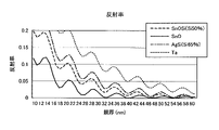
- 5 is a graph showing the reflectance of a reflective photomask according to an example of the present invention
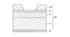
- FIG. 1 is a schematic cross-sectional view showing the structure of a reflective photomask 100 according to an embodiment of the invention.
- a reflective photomask 100 according to an embodiment of the present invention includes a substrate 11, a reflective layer 12 formed on the substrate 11, and a protective layer 13 formed on the reflective layer 12. , and an absorbing pattern layer 14 a formed on the protective layer 13 .
- a reflective photomask 100 includes a substrate 11, a reflective layer 12 formed on the substrate 11, and a protective layer 13 formed on the reflective layer 12.
- an absorbing pattern layer 14 a formed on the protective layer 13 .
- the substrate 11 may be made of titanium-added low thermal expansion glass, but the present invention is not limited to this as long as the material has a low thermal expansion coefficient.
- a back conductive film 15 can be formed on the surface of the substrate 11 on which the reflective layer 12 is not formed.
- the back conductive film 15 is a film for fixing the reflective photomask 100 using the principle of an electrostatic chuck when it is installed in an exposure machine.
- the reflective layer 12 only needs to reflect EUV light (extreme ultraviolet light), which is exposure light, and is a multilayer reflective film (that is, a It may be an EUV light reflective film) having a multilayer film structure.
- the reflective layer 12 including a multi-layer reflective film is formed by repeatedly laminating a combination of Mo (molybdenum) and Si (silicon), or Mo (molybdenum) and Be (beryllium), for example, about 40 cycles.
- the protective layer 13 is a layer that functions as an etching stopper that prevents damage to the reflective layer 12 when forming the absorbing pattern layer 14a by etching. Depending on the material of the reflective layer 12 and etching conditions, the protective layer 13 may be omitted.
- the protective layer 13 is made of a material that is resistant to dry etching performed during pattern formation of the absorption layer 14 shown in FIG. 4, which will be described later.
- the absorption layer 14 is a layer formed on the protective layer 13 and a layer that absorbs EUV light, which is exposure light, in the reflective photomask 100 .
- the absorption layer 14 is a layer forming an absorption pattern layer (transfer pattern) 14a, which is a fine pattern for transfer. That is, by removing part of the absorption layer 14 of the reflective photomask blank 200, that is, by patterning the absorption layer 14, the absorption pattern (absorption pattern layer 14a) of the reflective photomask 100 shown in FIG. It is formed.
- EUV lithography EUV light is obliquely incident and reflected by the reflective layer 12, but the projection effect in which the absorption pattern layer 14a obstructs the optical path may degrade the transfer performance onto the wafer (semiconductor substrate). be. It is known that this deterioration in transfer performance can be reduced by reducing the thickness of the absorption pattern layer 14a that absorbs EUV light. be done.
- a material having a higher absorption of EUV light than conventional materials that is, a material having a high extinction coefficient k for a wavelength of 13.5 nm.
- the extinction coefficient k of tantalum (Ta) which is the main material of the conventional absorption pattern layer 14a, is 0.041. If the main material of the patterned absorption layer 14a is a compound material having an extinction coefficient k larger than that of tantalum (Ta), the thickness of the patterned absorption layer 14a can be made thinner than in the prior art, and the projection effect can be improved. can be reduced.
- FIG. 2 is a graph showing the optical constants of each metal material with respect to the EUV light wavelength of 13.5 nm.
- the horizontal axis of the graph in FIG. 2 represents the refractive index n, and the vertical axis represents the extinction coefficient k.
- the first material group can be used. It can be seen that the projection effect can be reduced by Note that the first material group is tin (Sn), indium (In), tellurium (Te), cobalt (Co), and their oxides, nitrides, and oxynitrides.
- an optical density (OD) value which is an index representing the contrast of light intensity between the reflective layer 12 and the absorbing layer 14 (absorption pattern layer 14a).
- the OD value is defined by the following formula (1).
- OD -log(Ra/Rm) Formula (1)
- pattern transfer requires an OD value of 1 or more, more preferably OD>1. is more preferably 1.5 or more.
- main material refers to a material (component) containing 50 at % or more of the total number of atoms in the absorption layer 14 (absorption pattern layer 14a).
- the film thickness of the absorption layer 14 is preferably 50 nm or less.
- the thickness of the absorption layer 14 (absorption pattern layer 14a) is 50 nm or less, the projection effect can be sufficiently reduced and the transfer performance can be improved as compared with the conventional Ta-based absorption film.
- the film thickness of the absorption layer 14 (absorption pattern layer 14a) is preferably 17 nm or more.
- a material that constitutes the first material group has a higher extinction coefficient k for EUV light than the conventional material tantalum (Ta), and can be applied to the absorption layer 14 .
- the absorbing layer 14 can be made thinner, the projection effect can be reduced, and an improvement in transferability can be expected.
- the absorption layer 14 is composed of one or more elements selected from the first material group and oxides thereof. , nitride and oxynitride in total of 50 atomic % or more.
- the material contains at least one of tin (Sn), indium (In), tellurium (Te), and cobalt (Co), which constitute the first material group, fluorine-based gas or chlorine, which is a corrosive gas, A dry etching process using a system gas is possible.
- tin (Sn) oxide or indium (In) oxide, tin (Sn) nitride or indium (In) nitride, tin (Sn) oxynitride or indium Oxynitride of (In) has a high melting point and is preferable.
- oxides of tin (Sn) are most preferable because of ease of handling.
- the absorption layer 14 is composed of at least one layer
- at least one layer of the absorption layer 14 is selected from the first material group described above. 50 atomic % or more in total of one or more elements and their oxides, nitrides, and oxynitrides.
- any layer contains one or more elements selected from the first material group described above and oxides and nitrides thereof.
- oxynitride in total of 50 atomic % or more.
- a total of 50 atomic % or more of one or more selected elements and their oxides, nitrides and oxynitrides may be included.
- the absorption layer 14 (absorption pattern layer 14a) is composed of three layers, one material selected from the first material group described above is added to the bottom layer of the absorption layer 14 (absorption pattern layer 14a).
- the above elements and their oxides, nitrides, and oxynitrides are contained in a total of 50 atomic % or more, and the first The content of one or more elements selected from the group of materials may be reduced.
- FIG. 3 is a schematic cross-sectional view showing the structure of a reflective photomask 100 according to an embodiment of the invention. More specifically, FIG. 3(a) is a schematic cross-sectional view showing the overall structure of a reflective photomask 100 according to an embodiment of the invention, and FIG. 3(b) is a reflective photomask according to an embodiment of the invention. 3 is a schematic cross-sectional view showing an enlarged part of the structure of the photomask 100.
- the projection effect can be reduced by setting the side wall angle ⁇ between the side wall of the absorbing pattern layer 14a and the protective layer 13 (hereinafter simply referred to as the side wall angle ⁇ ) to be smaller than 90°. .
- the sidewall angle ⁇ will be described below. As shown in FIGS. 3A and 3B, when the film thickness of the absorption pattern layer 14a is h, the point at the side wall height h/3 and the side wall height 2h/3 in the cross-sectional view. Virtually draw a straight line connecting the points of 3. The angle formed by this straight line (virtual straight line L1) and a straight line parallel to the substrate (virtual straight line L2) is the sidewall angle ⁇ .
- the sidewall angle ⁇ can be defined even when the bottom and top of the absorbing pattern layer 14a are rounded and the sidewalls of the absorbing pattern layer 14a are not coplanar.
- the sidewall angles ⁇ of the opposing sidewalls of the absorbing pattern layers 14a may be the same.
- the sidewall angle ⁇ of at least one layer should be smaller than 90°.
- all layers may have the same side wall angle ⁇ , or a layer having a side wall angle ⁇ of 90° (upper layer) may be formed on a layer having a side wall angle ⁇ of less than 90°.
- It may be a structure with a film).
- the film thickness is desirably 20 nm or less so as not to hinder the effect of reducing the projection effect by adjusting the sidewall angle ⁇ . , 10 nm or less. However, this is not the case when the upper layer film has high transparency.
- the x-direction parallel to the incident surface of EUV light and the y-direction perpendicular to the plane of incidence are defined. It is the y direction that is affected by the projection effect, resulting in a reduction in contrast at the edges of the transfer pattern and a reduction in line width in the y direction.
- the sidewall angle ⁇ By reducing the sidewall angle ⁇ , the projection effect is reduced.
- the sidewall angle ⁇ 90° the left-right symmetry of the energy latent image of the reflected light is improved, so that the dimensional change caused by the distortion of the energy latent image is reduced. Therefore, the HV bias value, which is the difference between the dimensions in the x direction and the y direction shown in FIG. 8, is reduced.
- the film thickness h there are structural limitations on the film thickness h, the sidewall angle ⁇ , and the line width of the sidewall portion, which will be described later. This point will be described below.
- the line width w (nm) at the lower portion of the absorption pattern layer 14a is structurally larger than twice the line width a at the side wall portion. w>2 ⁇ a Expression (3) An inequality holds.
- the "line width w of the lower portion of the absorbing pattern layer 14a” means the width (line width) of the portion of the absorbing pattern layer 14a in contact with the protective layer 13. As shown in FIG.
- FIG. 9 is a graph of NILS.
- NILS Normalized Aerial Image Logarithmic Slope
- NILS w ⁇ dln(I)/dx Expression (5) and is an index of the resolution of the reflective photomask 100 .
- w represents the line width (that is, the width of the portion of the absorbing pattern layer 14a in contact with the protective layer 13)
- I represents the intensity of the latent energy image.
- the NILS value is 1.76 when the film thickness is 40 nm and the sidewall angle ⁇ of the absorbing pattern layer 14a made of tin oxide (SnO) is 90°.
- the NILS value is 1.46 when the sidewall angle ⁇ is 65°, which is about 20% lower than when the sidewall angle ⁇ is 90°.
- the NILS value when the sidewall angle ⁇ is set to 65° is lower than that when the sidewall angle ⁇ is set to 90°. It is reduced by about 20% compared to the NILS value.
- the NILS value when the sidewall angle ⁇ is set to 65° is lower than that when the sidewall angle ⁇ is set to 90°. It is reduced by about 20% compared to the NILS value.
- the sidewall angle ⁇ is 65° or more in order to maintain sufficient contrast.
- the sidewall angle ⁇ is preferably 65° or more and less than 90° in the present embodiment. is more preferable, and the range of 82° or more and 88° or less is even more preferable.
- FIG. A reflective photomask blank 200 according to an embodiment of the present invention which is used to fabricate a reflective photomask 100 according to an embodiment of the present invention, is formed on a substrate 11 and on the substrate 11, as shown in FIG. , a protective layer 13 formed on the reflective layer 12 , and an absorbing layer 14 formed on the protective layer 13 .
- a positive chemically amplified resist (SEBP9012: manufactured by Shin-Etsu Chemical Co., Ltd.) is formed to a thickness of 120 nm by spin coating. After that, baking is performed at 110° C. for 10 minutes to form a resist film 16 .
- an electron beam lithography machine JBX3030, manufactured by JEOL Ltd.
- baking treatment is performed at 110° C. for 10 minutes, followed by spray development (SFG3000: manufactured by Sigma Meltec Co., Ltd.). Thereby, as shown in FIG. 5, a resist pattern 16a is formed.
- the absorption layer 14 is patterned by dry etching mainly using a chlorine-based gas to form an absorption pattern layer 14a.
- the pressure and bias (applied voltage) are adjusted so that isotropic etching is performed, and the side wall angle ⁇ of the absorption pattern layer 14a is controlled.
- the side wall angle ⁇ of the absorption pattern layer 14a is controlled by adjusting the dry etching conditions, for example, by forming a hard mask on the absorption layer 14, or by changing the type of resist and film thickness. The angle ⁇ may be adjusted.
- the remaining resist pattern 16a is removed to expose the absorption pattern layer 14a.
- the absorption pattern layer 14a formed on the absorption layer 14 was an LS (line and space) pattern with a line width of 64 nm.
- This line width 64 nm LS pattern is designed in each of the x direction and the y direction as shown in FIG. 8 so that the influence of the projection effect due to EUV irradiation can be easily seen.
- the sidewall angles .theta. of the sidewalls of the absorbing pattern layers 14a facing each other are set to be the same angle.
- the present invention is not limited to this. No.
- the side wall angle ⁇ 1 of one side wall of the opposing side walls of the absorption pattern layer 14a may be made larger than the side wall angle ⁇ 2 of the other side wall. That is, the sidewall angles ⁇ of the opposing sidewalls of the absorbing pattern layer 14a may be set to different angles.
- the sidewall angle ⁇ at the side wall of the absorption pattern layer 14a on the reflected light side smaller than the sidewall angle ⁇ at the sidewall of the absorption pattern layer 14a on the incident light side, because the projection effect can be further reduced.
- the sidewalls of the absorbing pattern layer 14a are formed in the same plane.
- the present invention is not limited to this.
- the sidewalls of the absorbing pattern layer 14a are formed so that the sidewall angle .theta. may That is, the sidewall angle ⁇ at the sidewall of the absorption pattern layer 14a may satisfy ⁇ 1> ⁇ 2> ⁇ 3 as shown in FIG. 10(b).
- the sidewalls of the absorbing pattern layer 14a are formed such that the sidewall angle .theta. may That is, the sidewall angle ⁇ of the sidewall of the absorption pattern layer 14a may be ⁇ 1 ⁇ 2 ⁇ 3 as shown in FIG. 10(c).
- Example 1 A synthetic quartz substrate having low thermal expansion was used as the substrate.
- 40 laminated films each made of a pair of silicon (Si) and molybdenum (Mo) were laminated as multilayer reflective films.
- the film thickness of the multilayer reflective film was set to 280 nm.
- a capping layer was formed on the multilayer reflective film using ruthenium (Ru) so as to have a thickness of 3.5 nm.
- Ru ruthenium
- An absorption layer containing silver (Ag) and silicon (Si) was formed on the capping layer to a thickness of 52 nm.
- the atomic number ratio of silver (Ag) and silicon (Si) in the absorption layer was measured by XPS (X-ray photoelectron spectroscopy) and found to be 35:65.
- XPS X-ray photoelectron spectroscopy
- crystallinity of the absorption layer was measured by XRD (X-ray diffraction device), it was found to be amorphous although slight crystallinity was observed.
- a back conductive film was formed to a thickness of 100 nm using chromium nitride (CrN).
- CrN chromium nitride
- a multi-source sputtering apparatus was used to form each film on the substrate. The film thickness of each film was controlled by the sputtering time.
- a positive chemically amplified resist SEBP9012: manufactured by Shin-Etsu Chemical Co., Ltd.
- a predetermined pattern was drawn on the positive chemically amplified resist using an electron beam drawing machine (JBX3030: manufactured by JEOL Ltd.). Thereafter, baking treatment was performed at 110° C. for 10 minutes, and development treatment was then performed using a spray developing machine (SFG3000: manufactured by Sigma Meltec Co., Ltd.). A resist pattern was thus formed.
- the absorption layer was patterned by dry etching mainly using a chlorine-based gas to form an absorption pattern layer. At that time, the gas pressure and bias (applied voltage) were adjusted so that the side wall angle was 80°. Next, the remaining resist pattern was removed. As described above, a reflective photomask of Example 1 was produced.
- Example 2> The material of the absorption layer was changed to a homogeneous mixed material (SnSiO) of tin oxide (SnO) and silicon (Si) at an atomic ratio of 50:50.
- a reflective photomask of Example 2 was produced in the same manner as in Example 1 except for the above.
- Example 3> The film thickness of the absorption layer was changed to 41 nm.
- a reflective photomask of Example 3 was produced in the same manner as in Example 2 except for the above.
- Example 4> The material of the absorption layer was changed to tin oxide (SnO) only. Also, the film thickness of the absorption layer was changed to 33 nm.
- a reflective photomask of Example 4 was produced in the same manner as in Example 1 except for the above.
- Example 5> The sidewall angle of the absorbing pattern layer was changed to 70°.
- a reflective photomask of Example 5 was produced in the same manner as in Example 4 except for the above.
- Example 6> The sidewall angle of the absorbing pattern layer was changed to 60°.
- a reflective photomask of Example 6 was produced in the same manner as in Example 1 except for the above.
- Example 7> The film thickness of the absorption layer was changed to 46 nm.
- a reflective photomask of Example 7 was produced in the same manner as in Example 6 except for the above.
- Comparative Example 1 a conventional photomask having an existing film containing tantalum (Ta) as a main material was used.
- tantalum nitride (TaN) was used to form an absorption layer with a thickness of 58 nm
- tantalum oxide (TaO) was used to form an outermost layer with a thickness of 2 nm to form a reflective photomask. made.
- the sidewall angle of the absorbing pattern layer is 90°.
- a reflective photomask of Comparative Example 1 was produced in the same manner as in Example 1 except for the above.
- Comparative Example 2 The material of the absorption layer was changed to tin oxide (SnO) only. Also, the film thickness of the absorption layer was changed to 33 nm. The sidewall angle of the absorbing pattern layer is 90°. A reflective photomask of Comparative Example 2 was produced in the same manner as in Example 1 except for the above.
- FIG. 11 shows the EUV light reflectance of the reflective photomasks of each example and each comparative example.
- the reflectance of the absorption layer formed of a material containing 35% silver (Ag), ie, the reflective photomask of Example 7, was 0.009 (OD 1.86), which was equally good. there were.
- OD value if it is 2.0 or more, it is marked as “ ⁇ ”, if it is 1.5 or more, it is marked as “ ⁇ ”, if it is 1.0 or more, it is marked as “ ⁇ ”, and if it is less than 1.0 It was evaluated as "x”. In addition, regarding the OD value, if the evaluation was " ⁇ " or higher, there was no problem in use, so it was judged as acceptable.
- the results of comparing the HV bias values of each example and each comparative example will be specifically described below.
- the HV bias value of Comparative Example 1 which has a conventional tantalum (Ta)-based absorption layer with a thickness of 60 nm, is 5.2 nm, is made of tin oxide (SnO) with a thickness of 33 nm, and has a sidewall angle of 90°.
- the HV bias value of Comparative Example 2 was 3.7 nm.
- the H- of Example 1 is formed of a material containing silver (Ag) and silicon (Si) with a film thickness of 52 nm so that the atomic ratio is 35:65, and the side wall angle is 80°. It has a V bias value of 3.6 nm, is made of a material containing tin oxide (SnO) and silicon (Si) with a film thickness of 52 nm and has an atomic ratio of 50:50, and has a sidewall angle of 80°.
- the HV bias value of Example 2 is 3.6 nm, and the film is made of a material containing tin oxide (SnO) and silicon (Si) with a film thickness of 41 nm so that the atomic ratio is 50:50,
- the HV bias value of Example 3 with a sidewall angle of 80° is 3.1 nm, and the HV of Example 4 with a sidewall angle of 80° formed only of tin oxide (SnO) with a thickness of 33 nm.
- the bias value is 3.0 nm
- the HV bias value is 2.6 nm
- the film thickness is 52 nm in Example 5, which is formed only of tin oxide (SnO) with a film thickness of 33 nm and has a sidewall angle of 70°.
- the HV bias value of Example 6, which is formed of a material containing silver (Ag) and silicon (Si) at an atomic ratio of 35:65 and has a sidewall angle of 60° is 2.3 nm.
- HV bias of Example 7 which is formed of a material containing silver (Ag) and silicon (Si) in an atomic ratio of 35:65, has a thickness of 46 nm, and has a sidewall angle of 60°.
- the reflective photomask and the method for manufacturing a reflective photomask of the present disclosure are not limited to the above-described embodiments and examples, and various modifications are possible within the scope that does not impair the features of the invention.
- the reflective photomask blank and reflective photomask according to the present invention can be suitably used for forming fine patterns by EUV exposure in the manufacturing process of semiconductor integrated circuits and the like.
Abstract
Description
しかし、特許文献1では、材料の光学定数と膜厚とによる性能向上だけに着目しており、パターン形状が転写性に与える影響を考慮していない。 To solve this problem, the EUV reflectance is suppressed by using a material with a high extinction coefficient k for the absorption layer. Masks have been proposed [see, for example, US Pat.
However, in
ここで、図面に示す構成は模式的なものであり、厚さと平面寸法との関係、各層の厚さの比率などは現実のものとは異なる。また、以下に示す実施形態は、本開示の技術的思想を具体化するための構成を例示するものであって、本開示の技術的思想は、構成部品の材質、形状、構造などが下記のものに限定されるものでない。本開示の技術的思想は、特許請求の範囲に記載された請求項が規定する技術的範囲内において、種々の変更を加えることができる。 An embodiment of the present disclosure will be described with reference to the drawings.
Here, the configurations shown in the drawings are schematic, and the relationship between the thickness and the planar dimensions, the ratio of the thickness of each layer, and the like are different from the actual ones. Further, the embodiments shown below are examples of configurations for embodying the technical idea of the present disclosure. It is not limited to things. Various modifications can be made to the technical idea of the present disclosure within the technical scope defined by the claims.
図1は、本発明の実施形態に係る反射型フォトマスク100の構造を示す概略断面図である。図1に示すように、本発明の実施形態に係る反射型フォトマスク100は、基板11と、基板11上に形成された反射層12と、反射層12の上に形成された保護層13と、保護層13の上に形成された吸収パターン層14aと、を備えている。以下、各層について詳細に説明する。 (Structure of Reflective Photomask)
FIG. 1 is a schematic cross-sectional view showing the structure of a
本発明の実施形態に係る基板11には、例えば、平坦なSi基板や合成石英基板等を用いることができる。また、基板11には、チタンを添加した低熱膨張ガラスを用いることができるが、熱膨張率の小さい材料であれば、本発明はこれらに限定されるものではない。
また、後述する図6に示すように、基板11の反射層12を形成していない面に裏面導電膜15を形成することができる。裏面導電膜15は、反射型フォトマスク100を露光機に設置するときに静電チャックの原理を利用して固定するための膜である。 (substrate)
A flat Si substrate, a synthetic quartz substrate, or the like, for example, can be used as the
Further, as shown in FIG. 6, which will be described later, a back
本発明の実施形態に係る反射層12は、露光光であるEUV光(極端紫外光)を反射するものであればよく、EUV光に対する屈折率の大きく異なる材料の組み合わせによる多層反射膜(つまり、多層膜構造を有するEUV光反射膜)であってもよい。多層反射膜を含む反射層12は、例えば、Mo(モリブデン)とSi(シリコン)、またはMo(モリブデン)とBe(ベリリウム)といった組み合わせの層を40周期程度繰り返し積層することにより形成したものであってもよい。 (reflective layer)
The
本発明の実施形態に係る保護層13は、吸収パターン層14aをエッチングにより形成する際に、反射層12へのダメージを防ぐエッチングストッパとして機能する層である。なお、反射層12の材質やエッチング条件により、保護層13はなくてもかまわない。保護層13は、後述する図4に示す吸収層14のパターン形成の際に行われるドライエッチングに対して耐性を有する材質で形成されている。 (protective layer)
The
図4に示すように、吸収層14は、保護層13上に形成される層であり、反射型フォトマスク100において露光光であるEUV光を吸収する層である。また、吸収層14は、転写するための微細パターンである吸収パターン層(転写パターン)14aを形成する層である。つまり、反射型フォトマスクブランク200の吸収層14の一部を除去することにより、即ち吸収層14をパターニングすることにより、図1に示す反射型フォトマスク100の吸収パターン(吸収パターン層14a)が形成される。 (Absorbing layer and absorbing pattern layer)
As shown in FIG. 4, the
この転写性能の悪化は、EUV光を吸収する吸収パターン層14aの厚さを薄くすることで低減できることが知られているが、吸収パターン層14aの側壁角の大きさを小さくすることで更に低減される。 In EUV lithography, EUV light is obliquely incident and reflected by the
It is known that this deterioration in transfer performance can be reduced by reducing the thickness of the
吸収パターン層14aの厚さを薄くするためには、従来の材料よりEUV光に対する吸収性の高い材料、つまり波長13.5nmに対する消衰係数kの高い材料を適用することが好ましい。
従来の吸収パターン層14aの主材料であるタンタル(Ta)の消衰係数kは0.041である。吸収パターン層14aの主材料が、タンタル(Ta)より大きい消衰係数kを有する化合物材料であれば、従来に比べて吸収パターン層14aの厚さを薄くすることが可能であり、射影効果を低減できる。 Materials for reducing the thickness of the
In order to reduce the thickness of the
The extinction coefficient k of tantalum (Ta), which is the main material of the conventional
OD=-log(Ra/Rm) ・・・式(1)
OD値は大きいほうがコントラストはよく、高い転写性が得られる。反射型フォトマスク100においてパターン転写にはOD値が1以上、より好ましくはOD>1が必要であるが、タンタル(Ta)を主材料として含む従来膜より高い転写性能を得るために、OD値は1.5以上であると、更に好ましい。ここで、上記「主材料」とは、吸収層14(吸収パターン層14a)全体の原子数に対して50at%以上含んでいる材料(成分)をいう。 Here, an optical density (OD) value, which is an index representing the contrast of light intensity between the
OD=-log(Ra/Rm) Formula (1)
The larger the OD value, the better the contrast and the higher the transferability. In the
また、OD>1を得るために、吸収層14(吸収パターン層14a)の膜厚は、17nm以上であることが好ましい。 The film thickness of the absorption layer 14 (
In order to obtain OD>1, the film thickness of the absorption layer 14 (
吸収層14(吸収パターン層14a)が2層以上で構成されている場合には、どの層にでも、上述した第1の材料群から選択される1種類以上の元素並びにその酸化物、窒化物、及び酸窒化物を合計して50原子%以上含めてよく、例えば、吸収層14(吸収パターン層14a)の最下層(保護層13に最も近い層)に、上述した第1の材料群から選択される1種類以上の元素並びにその酸化物、窒化物、及び酸窒化物を合計して50原子%以上含めてもよい。 Further, when the absorption layer 14 (
When the absorption layer 14 (
以下、吸収パターン層14aの側壁角について説明する。
図3は、本発明の実施形態に係る反射型フォトマスク100の構造を示す概略断面図である。より詳しくは、図3(a)は、本発明の実施形態に係る反射型フォトマスク100の全体構造を示す概略断面図であり、図3(b)は、本発明の実施形態に係る反射型フォトマスク100の構造の一部分を拡大して示す概略断面図である。図3に示すように、吸収パターン層14aの側壁と保護層13とのなす側壁角度の大きさθ(以下、単に側壁角θと称する)を90°より小さくすることにより、射影効果を低減できる。 (Sidewall angle)
The sidewall angle of the absorbing
FIG. 3 is a schematic cross-sectional view showing the structure of a
上記規定により、例えば、吸収パターン層14aの下部や上部がラウンディングしていて、吸収パターン層14aの側壁が同一平面上にない場合にも、側壁角θを定義することができる。
なお、本実施形態では、図3(a)に示すように、対向する吸収パターン層14aの側壁における側壁角θは互いに同じ角度であってもよい。 The definition of the sidewall angle θ will be described below. As shown in FIGS. 3A and 3B, when the film thickness of the
According to the above definition, for example, the sidewall angle θ can be defined even when the bottom and top of the absorbing
In this embodiment, as shown in FIG. 3A, the sidewall angles θ of the opposing sidewalls of the absorbing
また、吸収パターン層14aは、例えば、全ての層の側壁角θが同じ角度であってもよいし、側壁角θが90°より小さい層の上に、側壁角θが90°の層(上層膜)があるような構造であってもよい。この場合、側壁角θの調整による射影効果低減の効果を阻害しないよう、上層膜が、EUV光に対して透明性が低い膜である場合には、その膜厚は20nm以下であることが望ましく、10nm以下であることがより望ましい。ただし、上層膜の透明性が高い場合はその限りではない。 If the
In the
射影効果により影響を受けるのは、y方向であり、転写パターンのエッジ部におけるコントラストの低下やy方向の線幅の減少が生じる。側壁角θを小さくすることにより、射影効果は低減する。
側壁角θ<90°であると、反射光のエネルギー潜像の左右対称性が向上するため、エネルギー潜像の歪みに起因する寸法の変化が軽減される。したがって、図8に示すx方向とy方向の寸法の違いであるH-Vバイアス値が小さくなる。 Here, as shown in FIG. 8, the x-direction parallel to the incident surface of EUV light and the y-direction perpendicular to the plane of incidence are defined.
It is the y direction that is affected by the projection effect, resulting in a reduction in contrast at the edges of the transfer pattern and a reduction in line width in the y direction. By reducing the sidewall angle θ, the projection effect is reduced.
When the sidewall angle θ<90°, the left-right symmetry of the energy latent image of the reflected light is improved, so that the dimensional change caused by the distortion of the energy latent image is reduced. Therefore, the HV bias value, which is the difference between the dimensions in the x direction and the y direction shown in FIG. 8, is reduced.
図3(a)に示すように、吸収パターン層14aの膜厚がh(nm)であるとき、吸収パターン層14aにおいて側壁のテーパー角(側壁角θ)を形成している部分(側壁部分)の線幅a(nm)は、
a=h/tanθ ・・・ 式(2)
で示され、吸収パターン層14aの膜厚hと側壁角θとで表すことができる。 In this embodiment, there are structural limitations on the film thickness h, the sidewall angle θ, and the line width of the sidewall portion, which will be described later. This point will be described below.
As shown in FIG. 3A, when the thickness of the absorbing
a=h/tan θ Expression (2)
and can be expressed by the film thickness h of the
w>2×a ・・・ 式(3)
という不等式が成り立つ。
ここで、「吸収パターン層14aの下部の線幅w」とは、吸収パターン層14aにおける保護層13と接する部分の幅(線幅)を意味する。 As shown in FIG. 3(a), the line width w (nm) at the lower portion of the
w>2×a Expression (3)
An inequality holds.
Here, the "line width w of the lower portion of the absorbing
tanθ>2×h/w ・・・式(4)
が導出される。
このようにして、吸収パターン層14aの側壁角θの下限は、式(4)により規定される。 By substituting the above formula (2) into the above formula (3),
tan θ>2×h/w Expression (4)
is derived.
Thus, the lower limit of the sidewall angle θ of the absorbing
図9はNILSのグラフである。NILS(規格化空間像対数傾斜)は、
NILS=w×dln(I)/dx ・・・式(5)
で求められ、反射型フォトマスク100の解像性の指標になる。ここで「w」は線幅(つまり、吸収パターン層14aにおける保護層13と接する部分の幅)を表し、「I」はエネルギー潜像の強度を表す。 Here, the x direction shown in FIG. 8 is hardly affected by the projection effect, but when the side wall angle θ is decreased, the forward tapered portion has a smaller thickness of the absorbing portion (that is, the line width a (the thickness of the
FIG. 9 is a graph of NILS. NILS (Normalized Aerial Image Logarithmic Slope) is
NILS=w×dln(I)/dx Expression (5)
and is an index of the resolution of the
また、図9に示すように、吸収パターン層14aの膜厚が33nmである場合も、側壁角θを65°に設定した場合のNILSの値は、側壁角θを90°に設定した場合のNILSの値に比べて約2割低減している。 As shown in FIG. 9, the NILS value is 1.76 when the film thickness is 40 nm and the sidewall angle θ of the absorbing
Further, as shown in FIG. 9, even when the thickness of the
これらのことから、十分なコントラストを維持するために、側壁角θが65°以上であると好ましい。
以上より、本実施形態において側壁角θは65°以上90°未満が好ましいが、射影効果を低減しつつ、十分なコントラストを得るためには、側壁角θは80°以上90°未満の範囲内がより好ましく、82°以上88°以下の範囲内がさらに好ましい。 Further, as shown in FIG. 9, even when the film thickness of the
For these reasons, it is preferable that the sidewall angle θ is 65° or more in order to maintain sufficient contrast.
As described above, the sidewall angle θ is preferably 65° or more and less than 90° in the present embodiment. is more preferable, and the range of 82° or more and 88° or less is even more preferable.
次に、反射型フォトマスクの製造方法について図4から図8を用いて説明する。
本発明の実施形態に係る反射型フォトマスク100を作製するために用いる、本発明の実施形態に係る反射型フォトマスクブランク200は、図4に示すように、基板11と、基板11上に形成された反射層12と、反射層12の上に形成された保護層13と、保護層13の上に形成された吸収層14と、を備えている。 (Manufacturing method of reflective photomask)
Next, a method for manufacturing a reflective photomask will be described with reference to FIGS. 4 to 8. FIG.
A reflective photomask blank 200 according to an embodiment of the present invention, which is used to fabricate a
次いで、電子線描画機(JBX3030:日本電子株式会社製)によってポジ型化学増幅型レジストで形成されたレジスト膜16に所定のパターンを描画する。その後、110℃、10分間ベーク処理を施し、次いでスプレー現像(SFG3000:シグマメルテック株式会社製)する。これにより、図5に示すように、レジストパターン16aを形成する。 First, on the
Next, an electron beam lithography machine (JBX3030, manufactured by JEOL Ltd.) is used to draw a predetermined pattern on the resist
次に、図7に示すように残存したレジストパターン16aの剥離を行い、吸収パターン層14aを露出させる。 Next, as shown in FIG. 6, using the resist
Next, as shown in FIG. 7, the remaining resist
本実施形態では、図3(a)に示すように、対向する吸収パターン層14aの側壁における側壁角θを互いに同じ角度に設定した場合について説明したが、本発明はこれに限定されるものではない。例えば、図10(a)に示すように、対向する吸収パターン層14aの側壁のうち、一方の側壁の側壁角θ1を他方の側壁の側壁角θ2よりも大きくしてもよい。つまり、対向する吸収パターン層14aの側壁における側壁角θを互いに異なる角度に設定してもよい。この場合、反射光側の吸収パターン層14aの側壁における側壁角θを、入射光側の吸収パターン層14aの側壁における側壁角θよりも小さくした方が射影効果をより低減することができるため好ましい。 (Modified example of reflective photomask)
In the present embodiment, as shown in FIG. 3A, the sidewall angles .theta. of the sidewalls of the absorbing
また、図10(c)に示すように、吸収パターン層14aの側壁は、保護層13側から吸収パターン層14aの最表面側に向かって側壁角θが段階的に大きくなるように形成されていてもよい。つまり、吸収パターン層14aの側壁における側壁角θが、図10(c)に示すように、θ1<θ2<θ3となっていてもよい。 Further, in this embodiment, as shown in FIG. 3A, the sidewalls of the absorbing
Further, as shown in FIG. 10(c), the sidewalls of the absorbing
以下、本開示を実施例によりさらに詳しく説明するが、本開示は実施例により何ら限定されるものではない。
<実施例1>
基板として低熱膨張性を有する合成石英基板を用いた。基板の上に、多層反射膜としてシリコン(Si)とモリブデン(Mo)とを一対とする積層膜を40枚積層して形成した。多層反射膜の膜厚は280nmとした。
次に、多層反射膜上に、ルテニウム(Ru)を用いて膜厚が3.5nmになるようにキャッピング層(保護層)を成膜した。これにより、基板上には多層反射膜及びキャッピング層を有する反射部が形成された。 [Example]
EXAMPLES The present disclosure will be described in more detail below with reference to Examples, but the present disclosure is not limited by the Examples.
<Example 1>
A synthetic quartz substrate having low thermal expansion was used as the substrate. On the substrate, 40 laminated films each made of a pair of silicon (Si) and molybdenum (Mo) were laminated as multilayer reflective films. The film thickness of the multilayer reflective film was set to 280 nm.
Next, a capping layer (protective layer) was formed on the multilayer reflective film using ruthenium (Ru) so as to have a thickness of 3.5 nm. As a result, a reflective portion having a multilayer reflective film and a capping layer was formed on the substrate.
基板上へのそれぞれの膜の成膜は、多元スパッタリング装置を用いた。各々の膜の膜厚は、スパッタリング時間で制御した。
次に、吸収層上にポジ型化学増幅型レジスト(SEBP9012:信越化学工業株式会社製)を120nmの膜厚にスピンコートで成膜し、110℃で10分間ベークし、レジスト膜を形成した。 Next, on the side of the substrate where the multilayer reflective film was not formed, a back conductive film was formed to a thickness of 100 nm using chromium nitride (CrN).
A multi-source sputtering apparatus was used to form each film on the substrate. The film thickness of each film was controlled by the sputtering time.
Next, a positive chemically amplified resist (SEBP9012: manufactured by Shin-Etsu Chemical Co., Ltd.) was spin-coated on the absorption layer to a thickness of 120 nm and baked at 110° C. for 10 minutes to form a resist film.
その後、110℃で10分間ベーク処理を施し、次いでスプレー現像機(SFG3000:シグマメルテック株式会社製)を用いて現像処理した。これによりレジストパターンを形成した。
次に、レジストパターンをエッチングマスクとして、塩素系ガスを主体としたドライエッチングにより吸収層のパターニングを行い、吸収パターン層を形成した。その際、側壁角が80°になるように、ガスの圧力やバイアス(印加電圧)の調整を行った。
次に、残ったレジストパターンの剥離を行った。
以上により、実施例1の反射型フォトマスクを作製した。 Next, a predetermined pattern was drawn on the positive chemically amplified resist using an electron beam drawing machine (JBX3030: manufactured by JEOL Ltd.).
Thereafter, baking treatment was performed at 110° C. for 10 minutes, and development treatment was then performed using a spray developing machine (SFG3000: manufactured by Sigma Meltec Co., Ltd.). A resist pattern was thus formed.
Next, using the resist pattern as an etching mask, the absorption layer was patterned by dry etching mainly using a chlorine-based gas to form an absorption pattern layer. At that time, the gas pressure and bias (applied voltage) were adjusted so that the side wall angle was 80°.
Next, the remaining resist pattern was removed.
As described above, a reflective photomask of Example 1 was produced.
吸収層の材料を酸化錫(SnO)とシリコン(Si)が50:50の原子数比率で均質となる混合材料(SnSiO)に変更した。それ以外は実施例1と同様の方法で、実施例2の反射型フォトマスクを作製した。
<実施例3>
吸収層の膜厚を41nmに変更した。それ以外は実施例2と同様の方法で、実施例3の反射型フォトマスクを作製した。
<実施例4>
吸収層の材料を酸化錫(SnO)のみに変更した。また、吸収層の膜厚を33nmに変更した。それ以外は実施例1と同様の方法で、実施例4の反射型フォトマスクを作製した。 <Example 2>
The material of the absorption layer was changed to a homogeneous mixed material (SnSiO) of tin oxide (SnO) and silicon (Si) at an atomic ratio of 50:50. A reflective photomask of Example 2 was produced in the same manner as in Example 1 except for the above.
<Example 3>
The film thickness of the absorption layer was changed to 41 nm. A reflective photomask of Example 3 was produced in the same manner as in Example 2 except for the above.
<Example 4>
The material of the absorption layer was changed to tin oxide (SnO) only. Also, the film thickness of the absorption layer was changed to 33 nm. A reflective photomask of Example 4 was produced in the same manner as in Example 1 except for the above.
吸収パターン層の側壁角を70°に変更した。それ以外は実施例4と同様の方法で、実施例5の反射型フォトマスクを作製した。
<実施例6>
吸収パターン層の側壁角を60°に変更した。それ以外は実施例1と同様の方法で、実施例6の反射型フォトマスクを作製した。
<実施例7>
吸収層の膜厚を46nmに変更した。それ以外は実施例6と同様の方法で、実施例7の反射型フォトマスクを作製した。 <Example 5>
The sidewall angle of the absorbing pattern layer was changed to 70°. A reflective photomask of Example 5 was produced in the same manner as in Example 4 except for the above.
<Example 6>
The sidewall angle of the absorbing pattern layer was changed to 60°. A reflective photomask of Example 6 was produced in the same manner as in Example 1 except for the above.
<Example 7>
The film thickness of the absorption layer was changed to 46 nm. A reflective photomask of Example 7 was produced in the same manner as in Example 6 except for the above.
比較例1では、従来のタンタル(Ta)を主材料とした既存膜を備えたフォトマスクを用いた。比較例1では、窒化タンタル(TaN)を用いて膜厚58nmになるよう吸収層を形成し、酸化タンタル(TaO)を用いて膜厚2nmになるよう最表層を形成して反射型フォトマスクを作製した。吸収パターン層の側壁角は90°である。それ以外は、実施例1と同様の方法で比較例1の反射型フォトマスクを作製した。 <Comparative Example 1>
In Comparative Example 1, a conventional photomask having an existing film containing tantalum (Ta) as a main material was used. In Comparative Example 1, tantalum nitride (TaN) was used to form an absorption layer with a thickness of 58 nm, and tantalum oxide (TaO) was used to form an outermost layer with a thickness of 2 nm to form a reflective photomask. made. The sidewall angle of the absorbing pattern layer is 90°. A reflective photomask of Comparative Example 1 was produced in the same manner as in Example 1 except for the above.
吸収層の材料を酸化錫(SnO)のみに変更した。また、吸収層の膜厚を33nmに変更した。吸収パターン層の側壁角は90°である。それ以外は、実施例1と同様の方法で比較例2の反射型フォトマスクを作製した。 <Comparative Example 2>
The material of the absorption layer was changed to tin oxide (SnO) only. Also, the film thickness of the absorption layer was changed to 33 nm. The sidewall angle of the absorbing pattern layer is 90°. A reflective photomask of Comparative Example 2 was produced in the same manner as in Example 1 except for the above.
なお、OD値については、2.0以上であれば「◎」とし、1.5以上であれば「○」とし、1.0以上であれば「△」とし、1.0未満であれば「×」と評価した。
また、OD値については、「△」以上の評価であれば、使用上何ら問題はないため、合格とした。 In addition, the reflectance of the absorption layer having a film thickness of 52 nm and formed of a material containing 50% tin oxide (SnO), that is, the reflective photomask of Example 2 was 0.005 (OD=2.11). , and the reflectance of the absorption layer formed of a material containing 100% tin oxide (SnO) and having a thickness of 33 nm, that is, the reflective photomasks of Examples 4 and 5 and Comparative Example 2 are 0.001 (OD=2.67), which was even better.
Regarding the OD value, if it is 2.0 or more, it is marked as “◎”, if it is 1.5 or more, it is marked as “○”, if it is 1.0 or more, it is marked as “△”, and if it is less than 1.0 It was evaluated as "x".
In addition, regarding the OD value, if the evaluation was "Δ" or higher, there was no problem in use, so it was judged as acceptable.
上述した実施例1~7、比較例1~2で得られた反射型フォトマスクについて、以下の方法で転写性能の評価を行った。転写性能はウェハ露光評価により確認した。また、解像性は、NILS(Normalized Image Log-Slope:規格化空間像対数傾斜)値により評価した。 <Evaluation>
The transfer performance of the reflective photomasks obtained in Examples 1 to 7 and Comparative Examples 1 and 2 was evaluated by the following method. Transfer performance was confirmed by wafer exposure evaluation. Further, the resolution was evaluated by NILS (Normalized Image Log-Slope) value.
EUV露光装置(NXE3300B:ASML社製)を用いて、EUVポジ型化学増幅型レジストを塗布した半導体ウェハ上に、各実施例、比較例2及び参考例(比較例1)で作製した反射型フォトマスクの吸収層パターンを転写露光した。このとき、露光量は、x方向のLSパターンが設計通りに転写するように調節した。その後、電子線寸法測定機により転写されたレジストパターンの観察及び線幅測定を実施し、解像性とH-Vバイアス値を確認し、以下の「◎」、「○」、「△」、「×」の4段階で評価した。
<評価基準>
◎:H-Vバイアス値が3.2nmより小さい場合
○:H-Vバイアス値が3.2nm以上であり、3.7nmより小さい場合
△:H-Vバイアス値が3.7nm以上であり、5.0nm以下である場合
×:H-Vバイアス値が5.0nmを超える場合
以上の評価結果を表1に示す。
なお、HV-バイアス値については、「○」以上の評価であれば、使用上何ら問題はないため、合格とした。 [Wafer exposure evaluation]
Using an EUV exposure apparatus (NXE3300B: manufactured by ASML), on a semiconductor wafer coated with an EUV positive chemically amplified resist, the reflective photo produced in each example, Comparative Example 2 and Reference Example (Comparative Example 1) The absorber layer pattern of the mask was transfer exposed. At this time, the exposure amount was adjusted so that the LS pattern in the x direction was transferred as designed. After that, the transferred resist pattern was observed and the line width was measured by an electron beam dimension measuring machine, and the resolution and HV bias value were confirmed. It was evaluated in four grades of "x".
<Evaluation Criteria>
◎: When the HV bias value is less than 3.2 nm ○: When the HV bias value is 3.2 nm or more and less than 3.7 nm △: When the HV bias value is 3.7 nm or more, When the thickness is 5.0 nm or less ×: When the HV bias value exceeds 5.0 nm Table 1 shows the above evaluation results.
Regarding the HV-bias value, if the evaluation was "O" or higher, it was regarded as acceptable because there was no problem in use.
各実施例、比較例2及び参考例(比較例1)で作製した反射型フォトマスクの吸収層パターンの解像性を、NILS値を用いて評価した。解像性は、以下の「○」、「△」、「×」の3段階で評価した。
<評価基準>
○:1.4以上である場合
△:1.0以上1.4未満である場合
×:1.0未満である場合
以上の評価結果を表1に示す。
なお、NILS値については、「△」以上の評価であれば、使用上何ら問題はないため、合格とした。 [Resolution evaluation]
The resolution of the absorption layer pattern of the reflective photomasks produced in each example, comparative example 2, and reference example (comparative example 1) was evaluated using the NILS value. The resolution was evaluated in the following three grades of "○", "Δ", and "×".
<Evaluation Criteria>
○: 1.4 or more Δ: 1.0 or more and less than 1.4 ×: less than 1.0 Table 1 shows the above evaluation results.
As for the NILS value, if the evaluation was "Δ" or higher, it was regarded as acceptable because there was no problem in use.
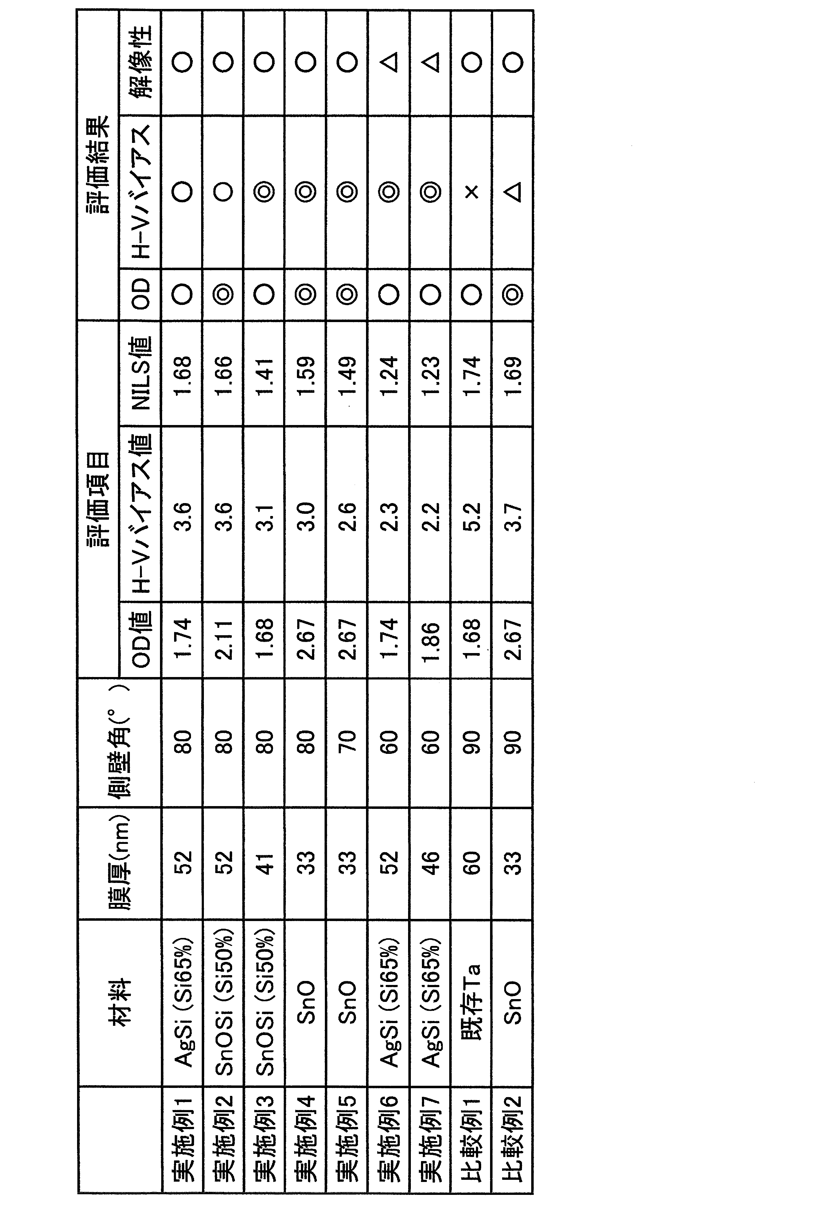
従来の膜厚60nmのタンタル(Ta)系吸収層を備えた比較例1のH-Vバイアス値は5.2nmであり、膜厚33nmの酸化錫(SnO)で形成され、側壁角が90°の比較例2のH-Vバイアス値は3.7nmであった。 The results of comparing the HV bias values of each example and each comparative example will be specifically described below.
The HV bias value of Comparative Example 1, which has a conventional tantalum (Ta)-based absorption layer with a thickness of 60 nm, is 5.2 nm, is made of tin oxide (SnO) with a thickness of 33 nm, and has a sidewall angle of 90°. The HV bias value of Comparative Example 2 was 3.7 nm.
12…反射層
13…保護層
14…吸収層
14a…吸収パターン(吸収パターン層)
15…裏面導電膜
16…レジスト膜
16a…レジストパターン
100…反射型フォトマスク
200…反射型フォトマスクブランク DESCRIPTION OF
Claims (7)
- 基板と、
前記基板上に形成された多層膜構造を有するEUV光を反射する反射層と、
前記反射層上に形成され、該反射層を保護する保護層と、
前記保護層上に形成され、パターンが形成されているEUV光を吸収する吸収パターン層と、を備え、
前記吸収パターン層は、EUV光に対する消衰係数kが0.041より大きい材料で構成され、
前記吸収パターン層の側壁と前記基板とのなす側壁角の大きさθが90°未満であることを特徴とする反射型フォトマスク。 a substrate;
a reflective layer that reflects EUV light and has a multilayer film structure formed on the substrate;
a protective layer formed on the reflective layer to protect the reflective layer;
an absorbing patterned layer formed on the protective layer and absorbing patterned EUV light;
The patterned absorption layer is made of a material with an extinction coefficient k greater than 0.041 for EUV light,
A reflective photomask, wherein a side wall angle θ formed between a side wall of the absorption pattern layer and the substrate is less than 90°. - 前記吸収パターン層は、少なくとも1層以上で構成され、
前記吸収パターン層の少なくとも1層は、第1の材料群から選択される1種類以上の元素並びにその酸化物、窒化物、及び酸窒化物を合計して50原子%以上含み、
前記第1の材料群は、Sn、In、Te、及びCoであることを特徴とする請求項1に記載の反射型フォトマスク。 The absorption pattern layer is composed of at least one layer,
At least one layer of the absorption pattern layer contains at least 50 atomic percent in total of one or more elements selected from the first material group and oxides, nitrides, and oxynitrides thereof,
2. The reflective photomask of claim 1, wherein the first material group is Sn, In, Te, and Co. - 前記吸収パターン層の膜厚は、50nm以下であり、
OD値(Optical Density:光学濃度)は、1.0以上であることを特徴とする請求項1または請求項2に記載の反射型フォトマスク。 The film thickness of the absorption pattern layer is 50 nm or less,
3. The reflective photomask according to claim 1, wherein an OD value (Optical Density) is 1.0 or more. - 前記吸収パターン層の下部の線幅をw(nm)、前記吸収パターン層の膜厚をh(nm)とした場合、
前記側壁角の大きさθは
tanθ>2×h/w
に示す関係を満たすことを特徴とする請求項1から請求項3のいずれか1項に記載の反射型フォトマスク。 When the line width at the bottom of the absorption pattern layer is w (nm) and the thickness of the absorption pattern layer is h (nm),
The side wall angle θ is tan θ>2×h/w
4. The reflective photomask according to any one of claims 1 to 3, wherein the relationship shown in is satisfied. - 前記側壁角の大きさθは
65°≦θ<90°
を満たすことを特徴とする請求項1から請求項4のいずれか1項に記載の反射型フォトマスク。 The side wall angle θ is 65°≦θ<90°
5. The reflective photomask according to any one of claims 1 to 4, wherein: - 前記吸収パターン層は、フッ素系ガスまたは塩素系ガスを用いたドライエッチングにより形成可能であることを特徴とする請求項1から請求項5のいずれか1項に記載の反射型フォトマスク。 The reflective photomask according to any one of claims 1 to 5, wherein the absorption pattern layer can be formed by dry etching using a fluorine-based gas or a chlorine-based gas.
- 基板と、
前記基板上に形成された多層膜構造を有するEUV光を反射する反射層と、
前記反射層上に形成され、該反射層を保護する保護層と、
前記保護層上に形成され、パターンが形成されているEUV光を吸収する吸収パターン層と、を形成する工程を備え、
前記吸収パターン層は、EUV光の消衰係数kが0.041より大きい材料で形成し、
前記吸収パターン層の側壁と前記基板とのなす側壁角の大きさθが90°未満であることを特徴とする反射型フォトマスクの製造方法。 a substrate;
a reflective layer that reflects EUV light and has a multilayer film structure formed on the substrate;
a protective layer formed on the reflective layer to protect the reflective layer;
forming an absorbing patterned layer that absorbs patterned EUV light formed on the protective layer;
The absorption pattern layer is formed of a material having an extinction coefficient k of EUV light greater than 0.041,
A method of manufacturing a reflective photomask, wherein a side wall angle θ formed between a side wall of the absorption pattern layer and the substrate is less than 90°.
Priority Applications (3)
| Application Number | Priority Date | Filing Date | Title |
|---|---|---|---|
| EP22824824.1A EP4357850A1 (en) | 2021-06-17 | 2022-06-02 | Reflective photomask and method for manufacturing reflective photomask |
| CN202280042215.2A CN117480448A (en) | 2021-06-17 | 2022-06-02 | Reflective photomask and method for manufacturing reflective photomask |
| KR1020237043043A KR20240008896A (en) | 2021-06-17 | 2022-06-02 | Reflective photomask and method of manufacturing reflective photomask |
Applications Claiming Priority (2)
| Application Number | Priority Date | Filing Date | Title |
|---|---|---|---|
| JP2021100675A JP2023000073A (en) | 2021-06-17 | 2021-06-17 | Reflective type photomask and method for manufacturing reflective type photomask |
| JP2021-100675 | 2021-06-17 |
Publications (1)
| Publication Number | Publication Date |
|---|---|
| WO2022264832A1 true WO2022264832A1 (en) | 2022-12-22 |
Family
ID=84526423
Family Applications (1)
| Application Number | Title | Priority Date | Filing Date |
|---|---|---|---|
| PCT/JP2022/022523 WO2022264832A1 (en) | 2021-06-17 | 2022-06-02 | Reflective photomask and method for manufacturing reflective photomask |
Country Status (6)
| Country | Link |
|---|---|
| EP (1) | EP4357850A1 (en) |
| JP (1) | JP2023000073A (en) |
| KR (1) | KR20240008896A (en) |
| CN (1) | CN117480448A (en) |
| TW (1) | TW202305497A (en) |
| WO (1) | WO2022264832A1 (en) |
Citations (6)
| Publication number | Priority date | Publication date | Assignee | Title |
|---|---|---|---|---|
| JP2006148113A (en) * | 2004-11-16 | 2006-06-08 | Samsung Electronics Co Ltd | Mask for reflecting electromagnetic wave and method for manufacturing same |
| JP2009147200A (en) * | 2007-12-17 | 2009-07-02 | Toppan Printing Co Ltd | Reflective photomask and reflective photomask manufacturing method |
| JP2011166039A (en) * | 2010-02-15 | 2011-08-25 | Dainippon Printing Co Ltd | Method of manufacturing reflection type mask |
| JP2013532381A (en) * | 2010-06-15 | 2013-08-15 | カール・ツァイス・エスエムティー・ゲーエムベーハー | Mask for EUV lithography, EUV lithography system, and method for optimizing mask imaging |
| JP2020034666A (en) * | 2018-08-29 | 2020-03-05 | Hoya株式会社 | Reflective mask blank, reflective mask and method of manufacturing the same, and method of manufacturing semiconductor device |
| JP2021085998A (en) * | 2019-11-28 | 2021-06-03 | 凸版印刷株式会社 | Reflection type photomask blank and reflection type photomask |
Family Cites Families (1)
| Publication number | Priority date | Publication date | Assignee | Title |
|---|---|---|---|---|
| US11237472B2 (en) | 2017-03-02 | 2022-02-01 | Hoya Corporation | Reflective mask blank, reflective mask and manufacturing method thereof, and semiconductor device manufacturing method |
-
2021
- 2021-06-17 JP JP2021100675A patent/JP2023000073A/en active Pending
-
2022
- 2022-06-02 EP EP22824824.1A patent/EP4357850A1/en active Pending
- 2022-06-02 WO PCT/JP2022/022523 patent/WO2022264832A1/en active Application Filing
- 2022-06-02 CN CN202280042215.2A patent/CN117480448A/en active Pending
- 2022-06-02 KR KR1020237043043A patent/KR20240008896A/en unknown
- 2022-06-16 TW TW111122353A patent/TW202305497A/en unknown
Patent Citations (6)
| Publication number | Priority date | Publication date | Assignee | Title |
|---|---|---|---|---|
| JP2006148113A (en) * | 2004-11-16 | 2006-06-08 | Samsung Electronics Co Ltd | Mask for reflecting electromagnetic wave and method for manufacturing same |
| JP2009147200A (en) * | 2007-12-17 | 2009-07-02 | Toppan Printing Co Ltd | Reflective photomask and reflective photomask manufacturing method |
| JP2011166039A (en) * | 2010-02-15 | 2011-08-25 | Dainippon Printing Co Ltd | Method of manufacturing reflection type mask |
| JP2013532381A (en) * | 2010-06-15 | 2013-08-15 | カール・ツァイス・エスエムティー・ゲーエムベーハー | Mask for EUV lithography, EUV lithography system, and method for optimizing mask imaging |
| JP2020034666A (en) * | 2018-08-29 | 2020-03-05 | Hoya株式会社 | Reflective mask blank, reflective mask and method of manufacturing the same, and method of manufacturing semiconductor device |
| JP2021085998A (en) * | 2019-11-28 | 2021-06-03 | 凸版印刷株式会社 | Reflection type photomask blank and reflection type photomask |
Also Published As
| Publication number | Publication date |
|---|---|
| TW202305497A (en) | 2023-02-01 |
| KR20240008896A (en) | 2024-01-19 |
| EP4357850A1 (en) | 2024-04-24 |
| JP2023000073A (en) | 2023-01-04 |
| CN117480448A (en) | 2024-01-30 |
Similar Documents
| Publication | Publication Date | Title |
|---|---|---|
| US8372564B2 (en) | Reflective mask, reflective mask blank and method of manufacturing reflective mask | |
| CN110785703B (en) | Reflective photomask blank and reflective photomask | |
| WO2023095769A1 (en) | Reflective photomask blank and reflective photomask | |
| WO2022050156A1 (en) | Reflection-type mask, reflection-type mask blank, and method for manufacturing reflection-type mask | |
| JP2019139085A (en) | Reflective photomask blank and reflective photomask | |
| JP7169970B2 (en) | Reflective photomask blanks and reflective photomasks | |
| WO2021085192A1 (en) | Reflective mask and production method for reflective mask | |
| WO2022264832A1 (en) | Reflective photomask and method for manufacturing reflective photomask | |
| CN112166376A (en) | Mask blank, phase shift mask and method for manufacturing semiconductor device | |
| WO2021106954A1 (en) | Reflective photomask blank and reflective photomask | |
| JP2019144357A (en) | Reflective photomask blank and reflective photomask | |
| WO2022153657A1 (en) | Reflective photomask blank and reflective photomask | |
| WO2022172916A1 (en) | Reflective photomask blank and reflective photomask | |
| JP7421411B2 (en) | Reflective photomask blank and reflective photomask | |
| WO2022172878A1 (en) | Reflective photomask blank and reflective photomask | |
| JP7117445B1 (en) | Reflective photomask blanks and reflective photomasks | |
| JP2019138971A (en) | Reflective photomask blank and reflective photomask | |
| WO2023190696A1 (en) | Reflective photomask blank and reflective photomask | |
| JP7409861B2 (en) | Reflective mask blank, reflective mask, reflective mask manufacturing method, and reflective mask repair method | |
| WO2022065494A1 (en) | Reflective photomask blank and reflective photomask | |
| TW202201110A (en) | Phase shift mask for extreme ultraviolet lithography |
Legal Events
| Date | Code | Title | Description |
|---|---|---|---|
| 121 | Ep: the epo has been informed by wipo that ep was designated in this application |
Ref document number: 22824824 Country of ref document: EP Kind code of ref document: A1 |
|
| ENP | Entry into the national phase |
Ref document number: 20237043043 Country of ref document: KR Kind code of ref document: A |
|
| WWE | Wipo information: entry into national phase |
Ref document number: 1020237043043 Country of ref document: KR |
|
| WWE | Wipo information: entry into national phase |
Ref document number: 2022824824 Country of ref document: EP |
|
| NENP | Non-entry into the national phase |
Ref country code: DE |
|
| ENP | Entry into the national phase |
Ref document number: 2022824824 Country of ref document: EP Effective date: 20240117 |