WO2022260109A1 - 熱放射体、光スペクトル変換素子、光電変換装置、及び熱放射方法 - Google Patents
熱放射体、光スペクトル変換素子、光電変換装置、及び熱放射方法 Download PDFInfo
- Publication number
- WO2022260109A1 WO2022260109A1 PCT/JP2022/023198 JP2022023198W WO2022260109A1 WO 2022260109 A1 WO2022260109 A1 WO 2022260109A1 JP 2022023198 W JP2022023198 W JP 2022023198W WO 2022260109 A1 WO2022260109 A1 WO 2022260109A1
- Authority
- WO
- WIPO (PCT)
- Prior art keywords
- energy
- cnt
- light
- thermal
- layer
- Prior art date
- Legal status (The legal status is an assumption and is not a legal conclusion. Google has not performed a legal analysis and makes no representation as to the accuracy of the status listed.)
- Ceased
Links
Images




Classifications
-
- H—ELECTRICITY
- H02—GENERATION; CONVERSION OR DISTRIBUTION OF ELECTRIC POWER
- H02S—GENERATION OF ELECTRIC POWER BY CONVERSION OF INFRARED RADIATION, VISIBLE LIGHT OR ULTRAVIOLET LIGHT, e.g. USING PHOTOVOLTAIC [PV] MODULES
- H02S10/00—PV power plants; Combinations of PV energy systems with other systems for the generation of electric power
- H02S10/30—Thermophotovoltaic systems
-
- B—PERFORMING OPERATIONS; TRANSPORTING
- B82—NANOTECHNOLOGY
- B82Y—SPECIFIC USES OR APPLICATIONS OF NANOSTRUCTURES; MEASUREMENT OR ANALYSIS OF NANOSTRUCTURES; MANUFACTURE OR TREATMENT OF NANOSTRUCTURES
- B82Y30/00—Nanotechnology for materials or surface science, e.g. nanocomposites
-
- H—ELECTRICITY
- H02—GENERATION; CONVERSION OR DISTRIBUTION OF ELECTRIC POWER
- H02S—GENERATION OF ELECTRIC POWER BY CONVERSION OF INFRARED RADIATION, VISIBLE LIGHT OR ULTRAVIOLET LIGHT, e.g. USING PHOTOVOLTAIC [PV] MODULES
- H02S40/00—Components or accessories in combination with PV modules, not provided for in groups H02S10/00 - H02S30/00
- H02S40/20—Optical components
-
- F—MECHANICAL ENGINEERING; LIGHTING; HEATING; WEAPONS; BLASTING
- F28—HEAT EXCHANGE IN GENERAL
- F28F—DETAILS OF HEAT-EXCHANGE AND HEAT-TRANSFER APPARATUS, OF GENERAL APPLICATION
- F28F2245/00—Coatings; Surface treatments
- F28F2245/06—Coatings; Surface treatments having particular radiating, reflecting or absorbing features, e.g. for improving heat transfer by radiation
Definitions
- the present disclosure relates to heat radiators, optical spectrum conversion elements, photoelectric conversion devices, and heat radiation methods.
- STPV Solar thermo-photovoltaics
- TPV Thermo-photovoltaics
- STPV the sun's light energy is stored in thermal radiators.
- Sunlight which has a broadband spectrum, is converted in the thermal radiator into equilibrium thermal radiation, which has a narrowband spectrum, in the wavelength range in which the solar cell has a high power generation efficiency.
- Photovoltaic cells absorb such equilibrium thermal radiation to generate electrical power.
- the thermal radiator is heated, for example by combustion of gas.
- Patent Document 1 describes a heat-light conversion element using a film containing a semiconducting carbon nanotube (CNT) as a heat radiator.
- CNT semiconducting carbon nanotube
- An object of the present disclosure is to provide a thermal radiator, an optical spectrum conversion element, a photoelectric conversion device, and a thermal radiation method that improve the intensity of radiation based on energy from an energy source.
- Excitons generated based on energy from an energy source include a first carbon nanotube (CNT) having an energy matching a wavelength range from the visible to the near-infrared range, and the chemical potential of the exciton. is maintained above zero, a thermal radiator, is.
- CNT carbon nanotube
- the first CNTs include semiconducting CNTs, Said wavelength range may correspond to the sensitivity range of the photovoltaic cell.
- a diameter d of the first CNT may satisfy a condition of 0.6 nm ⁇ d ⁇ 3.5 nm.
- the diameter d may satisfy the condition of 0.6 nm ⁇ d ⁇ 2.5 nm.
- Energy from the energy source may include light energy from the sun.
- the first CNTs may include metallic CNTs.
- a diameter d of the first CNT may satisfy a condition of 1.2 nm ⁇ d ⁇ 3.5 nm.
- This disclosure is (8) a thermal radiator according to any one of (2) to (5) above; a light receiver attached to the thermal radiator for transmitting optical energy from the energy source to the thermal radiator; comprising optical spectrum conversion element, is.
- the thermal radiator includes a radiation layer formed of a single type of the first CNT;
- the light receiving part may include at least one absorption layer formed of second CNTs of a semiconductor type different from the first CNTs and stacked on the emission layer.
- the second CNT may be specified with a diameter and chiral index such that the energy of excitons produced by absorption of light energy from the energy source is higher than the energy of excitons in the first CNT.
- Diameters of the first CNT and the second CNT may be smaller in a layer located closer to the energy source.
- the diameter d satisfies the condition of 0.6 nm ⁇ d ⁇ 3.0 nm, and the chiral index (n, m) is 5 ⁇ n ⁇ 50 and 0 ⁇ m It may include a set of integers where ⁇ n.
- the light receiving unit has a hole for receiving light from the energy source, and a confinement structure for confining the light incident from the hole and propagating the light inside,
- the surface of the thermal radiator may constitute one side of the confinement structure.
- This disclosure is (15) a thermal radiator according to any one of (2) to (5) above; a light-receiving part formed as the same layer as the heat radiator and including a second CNT of a semiconductor type different from the first CNT, wherein the second CNT absorbs light energy from the energy source and transmits the light energy to the first CNT; comprising optical spectrum conversion element, is.
- This disclosure is (16) the thermal radiator according to any one of (2) to (5) above, or the optical spectrum conversion element according to any one of (8) to (15) above; the photovoltaic cell converting light energy emitted by annihilation of excitons in the first CNT into electrical energy; comprising photoelectric conversion device, is.
- a thermal emitter that annihilates excitons generated based on energy from an energy source to generate non-equilibrium thermal radiation having energy matching a wavelength region included in the range from the visible region to the near-infrared region; is.
- This disclosure is (18) an emissive layer formed by a single type of first semiconducting CNTs whose excitons generated based on light energy from the energy source have energies matching the sensitive region of the photovoltaic cell; at least one absorption layer each formed by a second semiconducting-type CNT different from the first semiconducting-type CNTs and laminated to the emissive layer for transmitting optical energy from the energy source to the emissive layer; the absorbent layer; comprising optical spectrum conversion element, is.
- thermo emitter comprising a first semiconducting CNT having an energy in which excitons generated based on light energy from the energy source match the sensitive region of the photovoltaic cell; a light receiver attached to the thermal radiator for transmitting optical energy from the energy source to the thermal radiator; with The light receiving unit has a hole for receiving light from the energy source, and a confinement structure for confining the light incident from the hole and propagating the light inside, the surface of the thermal radiator constitutes one side of the confinement structure; optical spectrum conversion element, is.
- This disclosure is (20) Operating a thermal emitter comprising a first CNT having an energy matching a wavelength range in which excitons generated based on energy from an energy source are in the visible to near-infrared range at an operating temperature of 800 K or higher a thermal radiation method comprising the step of causing is.
- the radiation intensity based on the energy from the energy source is improved.
- FIG. 1 is a schematic configuration diagram of a photoelectric conversion device according to a first embodiment of the present disclosure
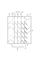
- FIG. FIG. 2 is a schematic diagram showing a laminated structure of the optical spectrum conversion element of FIG. 1
- FIG. 3 is a conceptual diagram for explaining spectral characteristics of the optical spectrum conversion element of FIG. 2
- FIG. 4 shows experimental results of non-equilibrium heat radiation from a heat radiator
- FIG. 4 is a diagram showing an absorptance spectrum of first semiconducting CNTs contained in a heat radiator
- 5 is a diagram showing temperature dependence of radiation intensity based on non-equilibrium thermal radiation of FIG. 4
- FIG. FIG. 3 is a diagram showing temperature dependence of radiation intensity based on radiation from a single first semiconducting CNT.
- FIG. 8 is a diagram showing temperature dependence of chemical potential estimated based on the experimental results of FIG. 7.
- FIG. 4 is a schematic configuration diagram of a photoelectric conversion device according to a second embodiment of the present disclosure
- 12 is a diagram showing trial calculation results of conversion efficiency based on the photoelectric conversion device of FIG. 11
- FIG. 5 is a schematic configuration diagram of a thermal radiator according to a third embodiment of the present disclosure
- FIG. 14 is a diagram showing temperature dependence of radiation intensity based on non-equilibrium thermal radiation from one metallic CNT in FIG.
- FIG. 13; 14 is a diagram showing the applied voltage dependence of the non-equilibrium thermal radiation spectrum of the thermal radiator in FIG. 13.
- FIG. FIG. 3 is a schematic view corresponding to FIG. 2 showing a modification of the laminated structure of the optical spectrum conversion element of FIG. 1;
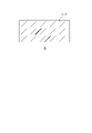
- FIG. 3 is a schematic diagram corresponding to FIG. 2 showing a modification of the optical spectrum conversion element of FIG. 1;
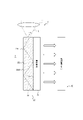
- FIG. 1 is a schematic configuration diagram of a photoelectric conversion device 1 according to the first embodiment of the present disclosure.
- the configuration and functions of the photoelectric conversion device 1 according to the first embodiment will be mainly described with reference to FIG.
- the photoelectric conversion device 1 has a condensing section 10, an optical spectrum conversion element 20, and a photovoltaic cell 30 as major components.
- the photoelectric conversion device 1 is used for STPV, for example.
- the photoelectric conversion device 1 obtains electric power using energy from an energy source.
- energy from an energy source includes, for example, light energy from the sun. That is, the photoelectric conversion device 1 includes a solar cell device that absorbs sunlight L and obtains electric power.
- the sunlight L having a broadband spectrum has a narrow band spectrum in the wavelength region where the photovoltaic cell 30 has high power generation efficiency. is converted into non-equilibrium thermal radiation with The definition of "non-equilibrium thermal radiation” is given below.
- Such a wavelength region is included in the range from the visible region to the near-infrared region.
- the "visible range” includes, for example, a wavelength range of 400 nm or more and less than 800 nm.
- the “near-infrared region” includes, for example, a wavelength region of 800 nm or more and 3000 nm or less.
- the condensing unit 10 condenses the sunlight L and guides it to the optical spectrum conversion element 20 .
- the condensing unit 10 includes a lens 11 that guides, for example, the sunlight L incident from the outside to the light spectrum conversion element 20 .
- the condensing unit 10 may include an optical system configured by other optical components such as mirrors instead of or in addition to the lens 11 .
- the condensing section 10 has a shield 12 surrounding the optical spectrum conversion element 20 and the photovoltaic cell 30 on the opposite side of the lens 11 with the surface of the optical spectrum conversion element 20 exposed to the lens 11 side. .
- the condensing unit 10 condenses the sunlight L incident from the outside at a predetermined magnification.
- the "predetermined magnification” is included in the range of, for example, 10 times or more and 2000 times or less. That is, the condensing unit 10 reduces the area of the sunlight L so that the light intensity corresponding to the light energy per unit area of the sunlight L increases by a predetermined magnification in the optical spectrum conversion element 20 after passing through the lens 11. do.
- the optical spectrum conversion element 20 includes a heat radiator 21 arranged on the side of the photovoltaic cell 30, and a light receiving portion attached to the heat radiator 21 and transmitting energy absorbed by the absorber from the energy source to the heat radiator 21. 22 and.
- the light receiving section 22 is attached to the thermal radiator 21 so as to be positioned on the condensing section 10 side with respect to the thermal radiator 21 .
- FIG. 2 is a schematic diagram showing the laminated structure of the optical spectrum conversion element 20 of FIG.
- the configuration and function of the optical spectrum conversion element 20 will be mainly described with reference to FIGS. 1 and 2.
- FIG. In a first embodiment, the optical spectrum conversion element 20 comprises multiple stacked layers. Each layer contains a single type of semiconducting CNTs. The types of semiconducting CNTs contained in each layer are different for each layer.
- the thermal radiator 21 includes a radiation layer 23 formed of a single type of first semiconducting CNT (first CNT).
- the light-receiving section 22 includes at least one absorption layer 24 formed of a second semiconducting CNT (second CNT) different from the first semiconducting CNT and stacked on the emitting layer 23 .
- the number of absorbing layers 24 is, for example, four, but is not limited to this.
- the number of absorbent layers 24 may be any value greater than or equal to one.
- the emitting layer 23 is arranged closest to the photovoltaic cell 30 among the multiple layers included in the optical spectrum conversion element 20 .
- Emissive layer 23 constitutes the lowest layer of the plurality of layers included in optical spectrum conversion element 20 .
- Four absorbing layers 241 , 242 , 243 and 244 are stacked in sequence on the emitting layer 23 .
- the absorption layer 244 is arranged closest to the energy source among the plurality of layers included in the optical spectrum conversion element 20 .
- the absorption layer 244 constitutes the uppermost layer among the layers included in the optical spectrum conversion element 20 .
- the second semiconducting CNTs contained in the absorption layer 24 have exciton energy generated by absorption of light energy from the energy source, and the exciton energy in the first semiconducting CNTs contained in the emission layer 23 is It may be specified by a diameter and a chiral index that are higher than .
- the diameter d of the first semiconducting CNT and the second semiconducting CNT may be smaller in a layer located closer to the energy source. That is, among the plurality of layers included in the optical spectrum conversion element 20, the diameter d of the first semiconducting CNTs included in the emissive layer 23 may be the largest.
- the diameter d of the second semiconducting CNTs included in each of the four absorption layers 24 may gradually decrease in order of the absorption layers 241 , 242 , 243 and 244 .
- the diameter d of the first semiconducting CNT and the second semiconducting CNT may be 0.6 nm or more and 3.5 nm or less.
- the diameter d satisfies the condition of 0.6 nm ⁇ d ⁇ 3.0 nm, and the chiral index (n, m) is 5 ⁇ n It may also include the set of integers where ⁇ 50 and 0 ⁇ m ⁇ n.
- the absorption layer 24 absorbs the sunlight L condensed by the condensing section 10, for example, and generates excitons and heat.
- the second semiconducting CNTs included in the absorption layer 24 absorb sunlight L, excitons are generated based on light energy from the sun.
- the energy of such excitons varies depending on the chiral index of the second semiconducting CNT.
- the “chiral index” is a parameter that determines, for example, the diameter d and helix angle of semiconducting CNTs.
- the second semiconducting CNTs included in the absorption layer 24 mainly absorb light with a wavelength corresponding to the energy of excitons determined according to their chiral index.
- the absorption layer 24 also absorbs light having a wavelength shorter than the wavelength corresponding to the energy of the excitons of the second semiconducting CNTs, generating higher-order subband excitons in the second semiconducting CNTs or It absorbs directly through hole pair generation. Thereby, heat is generated in the absorption layer 24 .
- a defined chemical potential gradient is formed with respect to the excitons of the semiconducting CNT.
- the exciton chemical potential becomes progressively lower from the absorption layer 244 on the energy source side toward the emission layer 23 . Thereby, light energy from the sun absorbed in the absorbing layer 24 is transmitted to the emitting layer 23 via excitons.
- the second semiconducting CNTs of the absorption layer 244 absorb sunlight L
- excitons are generated in the absorption layer 244 .
- the energy retained as excitons in the absorption layer 244 is transmitted to the adjacent absorption layer 243 by annihilation of the excitons and emission of photons.
- the emitted photon energy corresponds to the exciton energy determined according to the chiral index of the second semiconducting CNTs of the absorption layer 244 .
- New excitons are generated in the absorbing layer 243 based on the photons emitted in the absorbing layer 244 .
- the energy retained as excitons in the absorption layer 243 is transmitted to the adjacent absorption layer 242 by annihilation of the excitons and emission of photons. Such a process is repeated until excitons are similarly generated in emissive layer 23 based on the energy from the energy source.
- the light receiving section 22 including the absorption layer 24 transmits the light energy from the sun to the thermal radiator 21 including the radiation layer 23 by excitons as energy carriers.
- the excitons generated based on the energy from the energy source have energy matching the sensitivity region of the photovoltaic cell 30 .
- the sensitivity region of the photovoltaic cell 30 corresponds to the wavelength region included in the range from the visible region to the near-infrared region.
- the diameter d of the first semiconducting CNTs may satisfy the condition of 0.6 nm ⁇ d ⁇ 3.5 nm.
- the chiral indices (n, m) of the first semiconducting-type CNTs may include a set of integers excluding combinations where nm is a multiple of 0 or 3.
- the diameter d of the first semiconducting CNT is 0.6 nm ⁇ d ⁇ 1.0 nm, 1.0 nm ⁇ d ⁇ 2.0 nm, 2.0 nm ⁇ d ⁇ 3.0 nm, 0.6 nm ⁇ d ⁇ 2. 0 nm, and 0.6 nm ⁇ d ⁇ 2.5 nm
- the chiral index (n, m) includes a set of integers excluding combinations where nm is a multiple of 0 or 3 It's okay.
- the first semiconducting CNT may have a diameter of 0.936 nm and a chiral index of (10,3).
- the exciton chemical potential in emissive layer 23 is kept above zero.
- the thermal radiator 21 including the emissive layer 23 produces non-equilibrium thermal radiation having energy matching the sensitivity region of the photovoltaic cell 30 due to the annihilation of the excitons generated based on the energy from the energy source. generate That is, the thermal radiator 21 generates non-equilibrium thermal radiation having a narrow band spectrum in the wavelength region where the photovoltaic cell 30 has high power generation efficiency. Thermal radiator 21 generates non-equilibrium thermal radiation having a narrow band spectrum in the absorption wavelength band of photovoltaic cell 30 .
- the heat emitter 21 receives light energy from the sun transmitted from the light receiving unit 22 using excitons as energy carriers, and generates excitons.
- excitons For the first semiconducting CNTs contained in the emissive layer 23 of the thermal radiator 21 , such excitons have energies that match the sensitive region of the photovoltaic cell 30 .
- the energy of such excitons is contained in a wavelength range in which the power generation efficiency of the photovoltaic cell 30 is high, that is, in an energy range corresponding to an absorption wavelength band exhibiting high absorptance. Therefore, the light energy obtained by annihilation of such excitons is also included in the energy range corresponding to the wavelength range in which the photovoltaic cell 30 has high power generation efficiency. That is, thermal radiator 21 generates non-equilibrium thermal radiation having an energy that matches the sensitive area of photovoltaic cell 30 .
- a CNT having a diameter and a chiral index capable of retaining excitons having an energy matching the sensitivity region of the photovoltaic cell 30 is selected and utilized as the first semiconducting CNT. This allows the generation of photons having energies that match the sensitive area of the photovoltaic cell 30 .
- non-equilibrium thermal radiation includes, for example, thermal radiation light generated by annihilation of excitons, electrons, or hole pairs in the non-equilibrium state. Such non-equilibrium thermal radiation obeys a generalized Planck's law involving chemical potentials above zero.
- the photovoltaic cell 30 absorbs non-equilibrium thermal radiation generated in the thermal radiator 21 to generate electric power.
- the photovoltaic cell 30 converts light energy emitted by annihilation of excitons in the first semiconducting CNTs contained in the thermal radiator 21 into electrical energy.
- the photovoltaic cell 30 includes, for example, InxGa1-xAsySb1-y (0 ⁇ x ⁇ 100, 0 ⁇ y ⁇ 100) layers. Photovoltaic cell 30 is not limited to this and may include any layer capable of absorbing thermal radiation from thermal radiator 21 and generating electrical power.
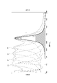
- FIG. 3 is a conceptual diagram for explaining spectral characteristics of the optical spectrum conversion element 20 of FIG. An example of the absorption and emission spectral characteristics of the optical spectrum conversion element 20 will be mainly described with reference to FIG.
- each graph indicated by a dashed line shows the absorption spectrum of the second semiconducting CNTs contained in the corresponding absorption layer 24.
- graph G1 shows the absorption spectrum of the second semiconducting CNTs included in the absorption layer 244 .
- graph G2 shows the absorption spectrum of the second semiconducting CNTs included in the absorption layer 243 .
- graph G3 shows the absorption spectrum of the second semiconducting CNTs included in the absorption layer 242 .
- graph G4 shows the absorptance spectrum of the second semiconducting CNTs included in the absorption layer 241 .
- a graph indicated by a dashed-dotted line indicates an absorptance spectrum of the first semiconducting CNTs contained in the emissive layer 23 .
- the more the absorption layer 24 that is located on the side of the emission layer 23 away from the energy source the more the absorption layer 24 included.
- the absorption peak of the two-semiconductor-type CNT is located on the long wavelength side.
- the absorption peak of the first semiconducting CNTs contained in the emissive layer 23 is positioned at the longest wavelength. That is, the energy of the excitons generated in the semiconducting CNTs decreases from the absorption layer 244 toward the emission layer 23 .
- the absorption peaks of the second semiconducting CNTs and the first semiconducting CNTs change stepwise for each layer, as indicated by the thin solid line in FIG.
- the absorption spectrum over the five layers becomes very broadband.
- such an absorptance spectrum encompasses the entire visible region with a wavelength of 400 nm or more and reaches the near-infrared region with a wavelength of around 1300 nm.
- the thermal radiator 21 Since the absorption peak of the first semiconducting CNTs contained in the emissive layer 23 is located near the wavelength of 1300 nm, the thermal radiator 21 has a non-radiation spectrum having a peak near the wavelength of 1300 nm as indicated by the thick solid line in FIG. Generates equilibrium thermal radiation. That is, non-equilibrium thermal radiation is generated at lower energies (longer wavelengths) relative to the solar light energy absorbed in the absorbing layer 24 . The difference in energy at this time is converted into the energy of excitons having a non-equilibrium distribution in the optical spectrum conversion element 20 while energy is transmitted from the absorption layer 24 to the emission layer 23 by repeating the generation and annihilation of excitons, for example. be.
- FIG. 4A and 4B are diagrams showing experimental results of non-equilibrium heat radiation from the heat radiator 21.
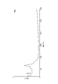
- FIG. FIG. 4 shows a radiation spectrum of narrow-band radiated light based on non-equilibrium thermal radiation from the thermal radiator 21.
- FIG. The experimental results shown in FIG. 4 are based on the conditions that the first semiconducting CNTs have a diameter d of 0.936 nm, a chiral index of (10,3), and an operating temperature of about 1000K.
- the heat radiator 21 can operate at an operating temperature of 800 K or higher, depending on the value of the diameter d of the first semiconducting CNTs.
- the thermal radiator 21 is constructed as a free-standing film of about 1 g/cm 3 containing first semiconducting CNTs. Such a thermal radiator 21 is heated by a laser, and simulates sunlight heating.
- the radiated light from the thermal radiator 21 based on non-equilibrium thermal radiation exhibits a radiation spectrum with a peak around a wavelength of 1300 nm. Its spectral width is sufficiently narrow compared to the broadband solar spectrum, which extends over parts of the ultraviolet, visible, and near-infrared regions. In addition, its spectral width is sufficiently narrow compared to the radiation spectrum based on blackbody radiation at, for example, 1000K. A radiation spectrum based on blackbody radiation at 1000 K has a peak at a wavelength of about 3000 nm and spreads over a wide band from the near-infrared region to the far-infrared region.
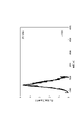
- FIG. 5 is a diagram showing an absorptance spectrum of the first semiconducting CNTs contained in the thermal radiator 21. As shown in FIG. The absorptance spectrum shown in FIG. 5 is based on the conditions that the diameter d of the first semiconducting CNT is 0.936 nm, the chiral index is (10, 3), and the temperature is about room temperature.
- the thermal radiator 21 is constructed by forming a film of about 1 g/cm 3 containing first semiconducting CNTs on sapphire.
- the first semiconducting CNTs contained in the thermal radiator 21 have the largest absorption peak near a wavelength of 1300 nm.
- the absorptance is close to zero, and the first semiconducting CNTs contained in the thermal radiator 21 hardly absorb light.
- the thermal radiator 21 generates narrow-band thermal radiation having a radiation peak in the vicinity of a wavelength of 1300 nm.
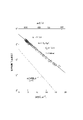
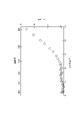
- FIG. 6 is a diagram showing temperature dependence of radiation intensity based on non-equilibrium thermal radiation in FIG.
- circles indicate experimental results.
- a solid line that overlaps the circles indicates the fitting result based on the generalized Planck's law.
- the dashed line shows the temperature dependence of the radiation intensity based on equilibrium thermal radiation when the chemical potential ⁇ is zero according to Planck's law.
- a non-equilibrium heat radiator to be measured is placed in a vacuum chamber with a degree of vacuum of 10 ⁇ 7 atmospheres or less, and light is irradiated to the non-equilibrium heat radiator from a light source such as a solar simulator or a laser.
- the temperature of a non-equilibrium thermal radiator under illumination is measured by a calibrated thermocouple and its radiant intensity is compared with the thermal radiant intensity at the same temperature of an object of known emissivity, such as a pseudo-black body.
- a metal mask with a high reflectance is placed between the light source and the thermocouple so that the incident light does not directly hit the thermocouple.
- a heat-resistant substrate (sapphire substrate) coated with black body paint JSC-3 (Japan Sensor Co., Ltd., emissivity of about 0.94) was prepared, and a ceramic heater (Sakaguchi Electric Heat Co., Ltd., 1000 ° C.) was prepared. Heat with a corresponding 5 mm square micro ceramic heater MS-M1000).
- JSC-3 Japanese Sensor Co., Ltd., emissivity of about 0.94
- JSC-3 Japanese Sensor Co., Ltd., emissivity of about 0.94
- the radiant intensity at the exciton resonance wavelength of the CNT from the non-equilibrium thermal radiator is greater than the radiant intensity of the quasi-blackbody multiplied by the reciprocal of the quasi-blackbody emissivity, It can be determined that the chemical potential is maintained higher than zero.
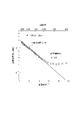
- FIG. 7 is a diagram showing temperature dependence of radiation intensity based on radiation from a single first semiconducting CNT.
- circles indicate experimental results.
- the experimental results shown in FIG. 7 are based on the conditions that the first semiconducting CNTs have a diameter d of 1.20 nm and a chiral index of (12, 5). Additionally, one first semiconducting CNT is crosslinked in a vacuum chamber and heated by a laser.
- the radiation from the single first semiconducting CNT changes from equilibrium thermal radiation to non-equilibrium thermal radiation as it shifts from the high temperature side of about 1400K to the low temperature side of about 1000K.
- radiation from a single first semiconducting CNT becomes equilibrium thermal radiation in a temperature range from 1400K to around 1100K, and the chemical potential ⁇ becomes zero and follows Planck's law.
- radiation from a single first semiconducting CNT becomes non-equilibrium thermal radiation on the lower temperature side than around 1100K, and the chemical potential ⁇ r becomes higher than zero and deviates from Planck's law.
- FIG. 8 is a diagram showing the temperature dependence of the chemical potential ⁇ r estimated based on the experimental results of FIG. As shown in FIG. 8, the chemical potential .mu.r is higher than zero on the lower temperature side than around 1100K.
- a chemical potential ⁇ r of about 50 meV is obtained at an operating temperature of about 1000K, for example.
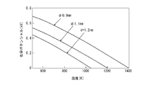
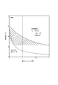
- FIG. 9A is a diagram showing results based on theoretical calculation.
- FIG. 9A shows the results of calculating the temperature dependence of the chemical potential for different diameters d of the first semiconducting CNTs. As shown in FIG. 9A, the smaller the diameter d of the first semiconducting CNT, the higher the chemical potential. In addition, the smaller the diameter d of the first semiconducting CNT, the higher the temperature at which the chemical potential rises from zero.
- the chemical potential becomes higher than 0 on the lower temperature side than 1400K.
- the chemical potential becomes higher than 0 at temperatures lower than 1200K.
- the chemical potential becomes higher than 0 on the lower temperature side than around 1050K.
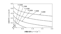
- FIG. 9B is a diagram showing results based on theoretical calculation.
- FIG. 9B shows the calculated non-radiative relaxation rate dependence of the chemical potential at different temperatures.
- the diameter d of the first semiconducting CNTs is 0.9 nm.
- the chemical potential tends to decrease as the non-radiative relaxation rate increases.
- the chemical potential remains high even for high non-radiative relaxation rates at lower temperatures.
- the manufacturing method of the single layer film of the emissive layer 23 includes, for example, a step of filtering a solution in which the raw material first semiconducting CNTs are dispersed using a membrane filter.
- a solution in which first semiconducting CNTs having a diameter of 0.936 nm and a chiral index (10, 3) are dispersed is filtered through a membrane filter.
- first semiconducting CNTs having a diameter of 0.936 nm and specified by chiral indices (10, 3) are accumulated to form a film.
- the same process is performed on the solution in which the second semiconducting CNTs are dispersed to form the absorption layer 24 .
- a laminated film in which the radiation layer 23 and the absorption layer 24 are overlapped is formed.
- FIG. 10 is a diagram showing an example of manufacturing the laminated film of the absorption layer 24.
- a method for producing a laminated film includes, for example, a step of filtering a solution in which second semiconducting CNTs as a raw material are dispersed, using a membrane filter.
- a solution in which second semiconducting CNTs having a diameter of 0.757 nm and specified by chiral indices (6, 5) are dispersed is filtered through a membrane filter.
- second semiconducting CNTs having a diameter of 0.757 nm and specified by chiral indices (6, 5) are accumulated to form a film.
- the absorbent layer 24 has two layers.
- the absorption layer 24 is located on the side of the emission layer 23 and is laminated on the first layer and the first layer containing second semiconducting CNTs specified by a diameter of 0.916 nm and a chiral index (9, 4), and a second layer comprising second semiconducting-type CNTs identified by chiral indices (6,5) with a diameter of 0.757 nm.
- the inserts in the graph of FIG. 10 show the absorptance spectra of the second semiconducting CNTs contained in the first and second layers of the absorption layer 24, respectively.
- the second semiconducting CNTs contained in the first layer have the largest absorption peak near a wavelength of 1300 nm.
- the second semiconducting CNTs contained in the second layer have the largest absorption peak on the shorter wavelength side than the absorption peak in the first layer.
- the absorption peak of the second semiconducting CNTs changes stepwise for each layer, and as shown in the graph of FIG. It has an off wavelength.
- the absorbing layer 24 has a very broadband absorption. For example, such an absorption spectrum encompasses the visible range and extends into the near-infrared range around wavelength 1300 nm.
- FIG. 11 is a schematic configuration diagram of the photoelectric conversion device 1 according to the second embodiment of the present disclosure.
- the configuration and functions of the photoelectric conversion device 1 according to the second embodiment will be mainly described with reference to FIG.
- the photoelectric conversion device 1 according to the second embodiment differs from the first embodiment in that the configuration of the light receiving section 22 of the optical spectrum conversion element 20 is different.
- Other configurations, functions, effects, modifications, and the like are the same as those of the first embodiment, and the corresponding description also applies to the photoelectric conversion device 1 according to the second embodiment.
- the same reference numerals are given to the same components as in the first embodiment, and the description thereof will be omitted. Differences from the first embodiment will be mainly described.
- the surface of the heat radiator 21 including a layer formed of a single type of first semiconducting CNT It has a structure in which the light receiving part 22 is attached to the heat radiator 21 so as to cover the heat radiator 21a.
- the light receiving section 22 has a hole 22a that receives light from the energy source, and a confinement structure 22b that confines and propagates the light incident from the hole 22a.
- the surface 21a of the thermal radiator 21 constitutes one surface of the confinement structure 22b.
- the containment structure 22b includes an enclosing member 22b1, a transparent solid 22b2 disposed within the enclosing member 22b1, a surface 21a of the thermal radiator 21 opposite the photovoltaic cell 30, Consists of Without being limited to this, the confinement structure 22b may have cavities instead of the transparent solid 22b2. That is, the containment structure 22b may consist of the enclosing member 22b1 and the surface 21a and the cavity enclosed by them.
- the surrounding member 22b1 may be made of low-emissivity metal such as gold, silver, platinum, and copper.
- the enclosing member 22b1 is formed in a concave shape as a whole and covers the surface of the transparent solid 22b2.
- a hole 22a is formed in the upper surface of the surrounding member 22b1.
- the transparent solid 22b2 includes, for example, any medium capable of propagating sunlight L with high transmittance.
- transparent solid 22b2 may comprise transparent solid sapphire.
- the sunlight L is condensed by the condensing section 10 and enters the confinement structure 22b through the hole 22a.
- the energy of the sunlight L incident on the confinement structure 22b through the hole 22a is transmitted to the thermal radiator 21 including the first semiconducting CNTs via a near field or a far field generated by internal light scattering.
- most of the sunlight L is absorbed by the first semiconducting CNTs through the near-field generated on the surface 21a of the thermal radiator 21 while propagating inside the transparent solid 22b2.
- excitons are generated in the thermal radiator 21 as in the first embodiment.
- the light receiving section 22 is attached to the thermal radiator 21 and directly transmits the light energy from the energy source to the thermal radiator 21 .
- FIG. 12 is a diagram showing trial calculation results of conversion efficiency based on the photoelectric conversion device 1 of FIG.
- the horizontally drawn dashed line indicates the so-called Shockley-Queisser limit of a photoelectric conversion cell with a bandgap of 0.67 eV.
- the thermal radiation leakage from the solid sapphire used as the transparent solid 22b2 is estimated to be 5 W at maximum with an area of the thermal radiator 21 of 1 cm 2 and an operating temperature of 1200K.
- FIG. 13 is a schematic configuration diagram of the thermal radiator 21 according to the third embodiment of the present disclosure.
- the configuration and function of the thermal radiator 21 according to the third embodiment will be mainly described with reference to FIG.
- the thermal radiator 21 according to the third embodiment differs from the first and second embodiments in that the CNTs contained in the thermal radiator 21 are not semiconductor type but metal type.
- Non-equilibrium heat radiation can be generated not only when the CNT is a semiconductor type, but also when it is a metal type.
- Non-equilibrium thermal radiation is generated from the metallic CNTs by applying a constant voltage of about 0.1 V/ ⁇ m or more to flow an electric current through the metallic CNTs.
- non-equilibrium heat of metallic CNTs that can be applied to, for example, high-intensity near-infrared light sources other than power generation applications using the photovoltaic cells 30 in the first and second embodiments Radiation is mainly explained.
- a non-equilibrium distribution of optical phonons can be generated by colliding electrons accelerated by an electric field with phonons.
- the interaction of such non-equilibrium optical phonons with the electronic system produces excitons with chemical potentials higher than zero. Therefore, the radiation produced by the radiative recombination of the excitons is non-equilibrium thermal radiation with a chemical potential higher than zero.
- the method for confirming that the chemical potential is maintained higher than zero is the same as for the semiconducting CNTs in the first and second embodiments.
- the thermal radiator 21 includes a first CNT having energy matching a wavelength range in which excitons generated based on energy from the energy source are included in the range from the visible range to the near-infrared range.
- the chemical potential of the exciton is kept above zero.
- the first CNTs include metallic CNTs.
- the diameter d of the metallic CNTs contained in the heat radiator 21 may satisfy the condition of 1.2 nm ⁇ d ⁇ 3.5 nm.
- the chiral indices (n, m) of metallic CNTs may include a set of integers where nm is a multiple of 0 or 3.
- the diameter d satisfies either condition of 1.2 nm ⁇ d ⁇ 2.5 nm and 2.5 nm ⁇ d ⁇ 3.5 nm
- the chiral index (n, m) is , nm may include a set of integers that are multiples of 0 or 3.
- the thermal radiator 21 has a plurality of elongated rod-shaped metallic CNTs that generate non-equilibrium thermal radiation when heated by current injection.
- a plurality of such metallic CNTs are arranged along one direction. The distance between one metallic CNT and another metallic CNT adjacent to one metallic CNT is substantially constant.
- the heat radiator 21 is a unit in which a plurality of metallic CNTs are bridged with a pair of electrodes 25 .
- a power supply 26 is connected to the pair of electrodes 25 .
- a current is injected into the metallic CNTs by the power supply 26 and the pair of electrodes 25 to heat the metallic CNTs.
- the thermal radiator 21 may have only one set of such units, or may have a plurality of sets.
- the heat radiator 21 has, for example, a plurality of sets of such units, and by stacking or stacking the units, it is possible to increase the strength of the device.
- the diameter of the metallic CNTs contained in the thermal radiator 21 is, for example, 1 nm or more and 4 nm or less, but is not limited to this.
- the diameter of the metallic CNT may be 0.6 nm or more and 3.0 nm or less, like the diameter d of the first semiconducting CNT and the second semiconducting CNT in the first embodiment.
- the number density of metallic CNTs per unit is, for example, about 500,000/d (lines/mm 2 ) when using CNTs with a diameter of d nm, but is not limited to this.
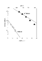
- FIG. 14 is a diagram showing the temperature dependence of radiation intensity based on non-equilibrium thermal radiation from one metallic CNT in FIG.
- triangles indicate experimental results of measuring the temperature dependence of the radiation intensity of non-equilibrium thermal radiation generated when a single metallic CNT is heated by injecting current into it. show.
- a solid line that overlaps the triangle mark indicates the fitting result based on the generalized Planck's law.
- circles indicate experimental results of measuring the temperature dependence of the radiation intensity of equilibrium thermal radiation generated when one metallic CNT is heated by a laser. Circles indicate the temperature dependence of the radiation intensity based on equilibrium thermal radiation when the chemical potential ⁇ is zero. A solid line overlapping with circles indicates a fitting result based on Planck's law.
- the structure of metallic CNTs is represented by chiral indices of (24, 15).
- the diameter of metallic CNTs is 2.67 nm.
- the length of metallic CNTs is about 20 ⁇ m.
- the applied voltage is 1.5-1.9 V and the current is about 4 ⁇ A.
- the experimental results shown in FIG. 14 completely deviate from the temperature dependence of radiation intensity based on equilibrium thermal radiation, and show the temperature dependence of non-equilibrium thermal radiation with higher radiation intensity.
- the radiation intensity based on non-equilibrium thermal radiation is two orders of magnitude higher than the radiation intensity based on balanced thermal radiation.
- the light emitted as non-equilibrium heat radiation has an intensity two orders of magnitude higher than that for equilibrium heat radiation.
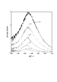
- FIG. 15 is a diagram showing applied voltage dependence of the non-equilibrium thermal emission spectrum of the thermal radiator 21 in FIG.
- the radiation intensity of non-equilibrium thermal radiation generated when a current is injected into the metallic CNTs contained in the thermal radiator 21 to heat the metallic CNTs increases as the applied voltage increases. That is, the radiation intensity of non-equilibrium thermal radiation increases as the applied voltage increases, the current injected into the metallic CNT increases, and the heating amount of the metallic CNT increases. This corresponds to the point in FIG. 14 that the radiation intensity based on non-equilibrium thermal radiation increases as the temperature of the metallic CNT increases.
- the conversion efficiency is improved when the photovoltaic cell 30 obtains electric power based on the energy from the energy source at a constant heat leak rate.
- the chemical potential of the excitons of the first CNTs contained in the thermal radiator 21 is maintained above zero so that the thermal radiator 21 generates non-equilibrium thermal radiation.
- the energy transmission rate which was conventionally rate-determined by Planck's law, can be made sufficiently larger than the heat leak rate in the light receiving section 22 and the heat radiator 21 .
- non-equilibrium STPV provides sufficient conversion efficiency even when the heat leak rate is high.
- the optical spectrum conversion device 20 can also reduce the operating temperature when attempting to obtain the same thermal radiation intensity as the equilibrium STPV. Therefore, safety, durability, and heat leak saving are improved by lowering the operating temperature.
- the optical spectrum conversion element 20 is attached to a thermal radiator 21 and has a light receiving part 22 that transmits light energy from an energy source to the thermal radiator 21, so that light energy from the sun, etc. is efficiently transferred to the first CNT. It becomes possible to convert to excitons.
- the optical spectrum conversion element 20 has a laminated structure including semiconducting CNTs as in the first embodiment, so that part of the light energy from the sun is converted into thermal energy, and the rest is converted into chemical potential. is converted to an exciton higher than zero.
- the optical spectrum conversion element 20 can transmit the energy retained as excitons in the light receiving section 22 and the thermal radiator 21 to the photovoltaic cell 30 before it is released as heat to the outside. This allows the energy transfer rate to be sufficiently higher than the heat leak rate, improving conversion efficiency.
- the second semiconducting CNT has a diameter and a chiral index such that the energy of excitons produced by absorption of light energy from the energy source is higher than the energy of excitons in the first semiconducting CNT. and are specified.
- the optical spectrum conversion element 20 can absorb most wavelength components of sunlight by having spectral characteristics as shown in FIG.
- the optical spectrum conversion element 20 does not absorb light energy on the longer wavelength side than the emission peak wavelength of non-equilibrium thermal radiation. Therefore, energy loss due to thermal radiation is suppressed.
- the exciton energies of the first semiconducting CNT and the second semiconducting CNT are higher in the layer located closer to the energy source side, thereby forming a chemical potential gradient in the light receiving section 22 and the thermal radiator 21. It becomes possible to The exciton energy tends to increase as the diameter of the semiconducting CNT becomes smaller, and is determined by the chiral index. This enables the light receiving section 22 to rapidly and unilaterally transmit energy to the thermal radiator 21 via excitons generated by light energy from the sun. This allows the energy transfer rate to be sufficiently higher than the heat leak rate, improving conversion efficiency.
- the optical spectrum conversion element 20 has the configuration of the light receiving section 22 as in the second embodiment, so that the structure can be simplified more than the laminated structure as in the first embodiment.
- the optical spectrum conversion element 20 is capable of allowing sunlight to interact directly with the thermal radiator 21 even if the sunlight leaks slightly out of the confinement structure 22b through the hole 22a of the light receiver 22. Therefore, the efficiency of interaction with sunlight can be improved.
- the shape, arrangement, orientation, number, etc. of each component described above are not limited to the contents shown in the above description and drawings.
- the shape, arrangement, orientation, number, etc. of each component may be arbitrarily configured as long as the function can be realized.
- the semiconductor material used for the optical spectrum conversion element 20 is CNT, but it is not limited to this.
- the optical spectrum conversion element 20 is capable of generating non-equilibrium thermal radiation having an energy matching the sensitive region of the photovoltaic cell 30 due to the annihilation of the excitons generated based on the energy from the energy source. It may be made of any semiconductor material, if any.
- the semiconductor material may include other materials such as SiC, atomic layer semiconductors (transition metal dichalcogenides), and the like.
- the chiral index of the first semiconducting CNTs contained in the emissive layer 23 was (10, 3), but it is not limited to this.
- the chiral index of the first semiconducting CNT has an energy such that the excitons produced based on the energy from the energy source match the sensitive region of the photovoltaic cell 30, and the chemical potential of the excitons is greater than zero. It can be any value that is maintained.
- the thermal radiator 21 is used for STPV, but it is not limited to this.
- the thermal radiator 21 may be used in TPVs. That is, the energy from the energy source is not limited to light energy from the sun.
- the thermal radiator 21 includes a single radiation layer 23 in the above embodiment, it is not limited to this.
- the heat radiator 21 may include multiple radiation layers 23 .
- the radiation layer 23 of the thermal radiation body 21 is formed of a single type of first CNT, but it is not limited to this.
- the emitting layer 23 may be formed of multiple types of first CNTs.
- the emitting layer 23 may be formed such that a single layer contains a plurality of types of first CNTs, or a plurality of layers may be formed such that each layer contains different types of first CNTs. good.
- the first semiconducting CNT and the second semiconducting CNT are of different types, but the present invention is not limited to this.
- the first semiconducting CNT and the second semiconducting CNT may be of the same type. That is, the emitting layer 23 and the absorbing layer 24 may contain the same kind of semiconducting CNTs.
- each of the absorption layers 24 of the light receiving section 22 is formed of a single type of second semiconducting CNT, but it is not limited to this.
- Each absorption layer 24 may be formed of a plurality of types of second semiconductor-type CNTs.
- each of the absorption layers 24 of the light receiving section 22 has been described as including different types of second semiconductor-type CNTs, the present invention is not limited to this.
- Each of the absorption layers 24 may contain the same type of second semiconducting CNTs.
- the second semiconducting CNT has a diameter and chirality such that the energy of excitons generated by absorption of light energy from the energy source is higher than the energy of excitons in the first semiconducting CNT.
- the exciton energy in the second semiconducting CNT and the exciton energy in the first semiconducting CNT may be the same.
- a second semiconducting CNT may be identified by a diameter and a chiral index that achieve such exciton energies.
- the diameters of the first semiconducting CNTs and the second semiconducting CNTs are described as being smaller in layers closer to the energy source side, but the present invention is not limited to this.
- the diameters of the first semiconducting-type CNTs and the second semiconducting-type CNTs may be determined based on any relationship capable of realizing the above non-equilibrium thermal radiation in the optical spectrum conversion element 20 . That is, the emitting layer 23 and the absorbing layer 24 may contain any type of semiconducting CNT based on such relationship.
- the diameters of the first semiconducting CNTs and the second semiconducting CNTs are 0.6 nm or more and 3.0 nm or less, but are not limited to this.
- the diameters of the first semiconducting-type CNTs and the second semiconducting-type CNTs may be any value capable of realizing the above non-equilibrium thermal radiation in the optical spectrum conversion element 20 .
- the light receiving section 22 is described as having a laminated structure including the second semiconducting CNTs, but it is not limited to this.
- the light receiving section 22 may be made of a photonic crystal instead of or in addition to a laminated structure including semiconducting CNTs.
- FIG. 16 is a schematic diagram corresponding to FIG. 2 showing a modification of the laminated structure of the optical spectrum conversion element 20 of FIG.
- the optical spectrum conversion element 20 may further have a low refractive index layer 27 .
- the low refractive index layer 27 is laminated on at least one of both surfaces in the lamination direction of the laminate including the radiation layer 23 and at least one absorption layer 24 .
- the low refractive index layer 27 is laminated on the upper surface of the absorption layer 244 that is arranged closest to the energy source in the absorption layers 24 .
- a low refractive index layer 27 is laminated on the lower surface of the emissive layer 23 .
- the low refractive index layer 27 is made of a material having a lower refractive index than the first semiconducting CNTs contained in the emitting layer 23 and the second semiconducting CNTs contained in the absorbing layer 24 .
- Such materials may include, for example, any material having an index of refraction lower than that of CNTs and closer to the index of refraction 1 of air compared to CNTs.
- the low refractive index layer 27 may be made of boron nitride nanotubes having insulating properties and high heat resistance. The refractive index of boron nitride nanotubes is about 1.4.
- the low refractive index layer 27 When forming the low refractive index layer 27 from boron nitride nanotubes, it can be formed by the same manufacturing process as that for forming the emitting layer 23 and the absorbing layer 24 .
- the low refractive index layer 27 formed by boron nitride nanotubes is transparent at the wavelengths of non-equilibrium thermal radiation by the thermal radiator 21 .
- the low refractive index layer 27 serves as a support and the physical strength of the laminate is improved. .
- Such a reinforcing effect becomes more pronounced by providing low refractive index layers 27 on both sides of the laminate in the lamination direction, as shown in FIG.
- the low refractive index layer 27 is made of a material having a refractive index closer to 1 than that of air compared to CNT, it also has the function of suppressing light reflection. If the low refractive index layer 27 were not formed, the difference in refractive index between the air and the CNT would be large, and light would enter the absorption layer 24 from the air and would exit from the emission layer 23 into the air. , the reflection of light increases. This reduces the radiant intensity of non-equilibrium thermal radiation from the optical spectrum conversion element 20 .
- the optical spectrum conversion element 20 can reduce the refractive index difference between the air and the CNT, thereby suppressing the reflection of light. Therefore, the optical spectrum conversion device 20 can improve the absorption efficiency in the absorption layer 24 and the emission efficiency in the emissive layer 23 to improve the overall efficiency of interaction with sunlight. As a result, the optical spectrum conversion element 20 can increase the radiant intensity of non-equilibrium thermal radiation.
- the optical spectrum conversion element 20 can increase the absorption of light in the absorption layer 24 to further increase the radiant intensity of non-equilibrium thermal radiation.
- FIG. 17 is a schematic diagram corresponding to FIG. 2 showing a modification of the optical spectrum conversion element 20 of FIG.
- the thermal radiator 21 and the light receiving section 22 are formed as different layers, but the present invention is not limited to this.
- the light receiving section 22 may be formed as the same layer as the thermal radiator 21, as shown in FIG.
- the light receiving section 22 includes a second semiconducting CNT different from the first semiconducting CNT, and the second semiconducting CNT absorbs light energy from the energy source and transmits the light energy to the first semiconducting CNT.
- the chemical potential of excitons is higher than that in the first semiconducting CNT forming the thermal radiator 21 .
- the ratio of the second semiconducting CNTs with a high exciton chemical potential is increased, and the ratio of the first semiconducting CNTs with a low exciton chemical potential is decreased. It is formed in a state where In the layers constituting the optical spectrum conversion element 20, the first semiconducting CNTs are locally present, while the second semiconducting CNTs are present throughout.
- the optical spectrum conversion element 20 having the configuration shown in FIG. 17 can be manufactured more easily than the laminated structure shown in FIG.
- the optical spectrum conversion element 20 can convert light energy from an energy source into non-equilibrium thermal radiation with a simpler structure.
- the light receiving section 22 is attached only to the surface 21a of the thermal radiator 21, but it is not limited to this.
- the light receiving part 22 may be attached to another surface of the thermal radiator 21 instead of or in addition to the surface 21a.
- the light receiving section 22 has only one hole 22a formed in the upper surface of the enclosing member 22b1, but it is not limited to this.
- the shape, size, arrangement, orientation, number, etc. of the holes 22a formed in the light receiving section 22 may be arbitrarily configured as long as the function of receiving light from the energy source can be realized.
- the holes 22a may be formed in at least one of the side surface and the bottom surface of the enclosing member 22b1 instead of or in addition to the upper surface of the enclosing member 22b1.
- a plurality of holes 22a may be formed on one surface of the enclosing member 22b1.
- the light receiving section 22 has a hole 22a for receiving light from the energy source, but it is not limited to this.
- the light-receiving part 22 is an arbitrary optical element that transmits the sunlight L with a predetermined transmittance through one surface of the enclosing member 22b1 and guides it into the confinement structure 22b instead of or in addition to the hole 22a. may have Such optical elements, like the holes 22a, may be configured in any shape, size, arrangement, orientation, number, etc. that can achieve the function of receiving light from the energy source.
- the enclosing member 22b1 is formed in a concave shape as a whole, but it is not limited to this.
- the enclosing member 22b1 may be formed in any shape capable of confining and propagating the light incident through the hole 22a.
- the surrounding member 22b1 may be spherical like an integrating sphere.
- the enclosing member 22b1 covers the entire surface 21a of the thermal radiator 21 together with the transparent solid 22b2, but it is not limited to this.
- the enclosing member 22b1 may cover only part of the surface 21a of the heat radiator 21 together with the transparent solid 22b2. That is, the containment structure 22b is formed by an enclosing member 22b1, a transparent solid 22b2 disposed within the enclosing member 22b1, and a portion of the surface 21a of the thermal radiator 21 opposite the photovoltaic cell 30. may be configured.
- the optical spectrum conversion element 20 may be realized by either one of the first embodiment and the second embodiment described above, or may be realized by combining both the first embodiment and the second embodiment. .
- the optical spectrum conversion element 20 may be realized in such a way that the transparent solid 22b2 is arranged on top of the layered structure of the emitting layer 23 and the absorbing layer 24.
- FIG. The containment structure 22b then consists of the enclosing member 22b1, the transparent solid 22b2 and the absorbing layer 24 disposed within the enclosing member 22b1, the surface 21a of the emissive layer 23 opposite the photovoltaic cell 30, It may be configured by
Landscapes
- Chemical & Material Sciences (AREA)
- Engineering & Computer Science (AREA)
- Nanotechnology (AREA)
- Physics & Mathematics (AREA)
- Composite Materials (AREA)
- Condensed Matter Physics & Semiconductors (AREA)
- General Physics & Mathematics (AREA)
- Materials Engineering (AREA)
- Crystallography & Structural Chemistry (AREA)
- Photovoltaic Devices (AREA)
- Light Receiving Elements (AREA)
- Carbon And Carbon Compounds (AREA)
Abstract
Description
(1)
エネルギー源からのエネルギーに基づいて生成された励起子が可視域から近赤外域までの範囲に含まれる波長領域に整合するエネルギーを有する第1カーボンナノチューブ(CNT)を含み、前記励起子の化学ポテンシャルがゼロよりも高く維持される、熱放射体、
である。
上記(1)に記載の熱放射体では、
前記第1CNTは、半導体型CNTを含み、
前記波長領域は、光起電力セルの感度領域に対応してもよい。
上記(2)に記載の熱放射体では、
前記第1CNTの直径dは、0.6nm≦ d ≦ 3.5nmの条件を満たしてもよい。
上記(3)に記載の熱放射体では、
前記直径dは、0.6nm≦ d ≦ 2.5nmの条件を満たしてもよい。
上記(2)乃至(4)のいずれか1つに記載の熱放射体では、
前記エネルギー源からのエネルギーは、太陽からの光エネルギーを含んでもよい。
上記(1)に記載の熱放射体では、
前記第1CNTは、金属型CNTを含んでもよい。
上記(6)に記載の熱放射体では、
前記第1CNTの直径dは、1.2nm≦ d ≦ 3.5nmの条件を満たしてもよい。
(8)
上記(2)乃至(5)のいずれか1つに記載の熱放射体と、
前記熱放射体に取り付けられ、前記エネルギー源からの光エネルギーを前記熱放射体に伝送する受光部と、
を備える、
光スペクトル変換素子、
である。
上記(8)に記載の光スペクトル変換素子では、
前記熱放射体は、単一種類の前記第1CNTにより形成される放射層を含み、
前記受光部は、前記第1CNTとは異なる半導体型の第2CNTによりそれぞれ形成され、かつ前記放射層に積層される少なくとも1つの吸収層を含んでもよい。
上記(9)に記載の光スペクトル変換素子では、
前記第2CNTは、前記エネルギー源からの光エネルギーの吸収によって生成される励起子のエネルギーが前記第1CNTにおける励起子のエネルギーよりも高くなるような直径とカイラル指数とで特定されてもよい。
上記(9)又は(10)に記載の光スペクトル変換素子では、
前記第1CNT及び前記第2CNTの直径は、前記エネルギー源側に位置する層ほど小さくなってもよい。
上記(9)乃至(11)のいずれか1つに記載の光スペクトル変換素子では、
前記第1CNT及び前記第2CNTの各々に対して、直径dは、0.6nm≦ d ≦ 3.0nmの条件を満たし、かつカイラル指数(n,m)は、5≦n≦50及び0≦m≦nである整数の組を含んでもよい。
上記(9)乃至(12)のいずれか1つに記載の光スペクトル変換素子は、
前記放射層及び前記少なくとも1つの吸収層を含む積層体の積層方向における両面の少なくとも一方に積層され、前記第1CNT及び前記第2CNTよりも屈折率が低い材料から形成されている低屈折率層をさらに備えてもよい。
上記(8)乃至(13)のいずれか1つに記載の光スペクトル変換素子では、
前記受光部は、前記エネルギー源からの光を受け入れる孔と、前記孔から入射した前記光を閉じ込めて内部を伝搬させる閉じ込め構造と、を有し、
前記熱放射体の表面は、前記閉じ込め構造の一の面を構成してもよい。
(15)
上記(2)乃至(5)のいずれか1つに記載の熱放射体と、
前記熱放射体と同一層として形成され、前記第1CNTとは異なる半導体型の第2CNTを含み、前記エネルギー源からの光エネルギーを前記第2CNTが吸収して前記第1CNTに伝送する受光部と、
を備える、
光スペクトル変換素子、
である。
(16)
上記(2)乃至(5)のいずれか1つに記載の熱放射体、又は上記(8)乃至(15)のいずれか1つに記載の光スペクトル変換素子と、
前記第1CNTにおける励起子の消滅によって放出された光エネルギーを電気エネルギーに変換する前記光起電力セルと、
を備える、
光電変換装置、
である。
(17)
エネルギー源からのエネルギーに基づいて生成された励起子が消滅することで可視域から近赤外域までの範囲に含まれる波長領域に整合するエネルギーを有する非平衡熱放射を発生させる熱放射体、
である。
(18)
エネルギー源からの光エネルギーに基づいて生成された励起子が光起電力セルの感度領域に整合するエネルギーを有する単一種類の第1半導体型CNTにより形成される放射層と、
前記第1半導体型CNTとは異なる第2半導体型CNTによりそれぞれ形成され、かつ前記放射層に積層される少なくとも1つの吸収層であって、前記エネルギー源からの光エネルギーを前記放射層に伝送する前記吸収層と、
を備える、
光スペクトル変換素子、
である。
(19)
エネルギー源からの光エネルギーに基づいて生成された励起子が光起電力セルの感度領域に整合するエネルギーを有する第1半導体型CNTを含む熱放射体と、
前記熱放射体に取り付けられ、前記エネルギー源からの光エネルギーを前記熱放射体に伝送する受光部と、
を備え、
前記受光部は、前記エネルギー源からの光を受け入れる孔と、前記孔から入射した前記光を閉じ込めて内部を伝搬させる閉じ込め構造と、を有し、
前記熱放射体の表面は、前記閉じ込め構造の一の面を構成する、
光スペクトル変換素子、
である。
(20)
エネルギー源からのエネルギーに基づいて生成された励起子が可視域から近赤外域までの範囲に含まれる波長領域に整合するエネルギーを有する第1CNTを含む熱放射体を、800K以上の動作温度で動作させるステップを含む、熱放射方法、
である。
図1は、本開示の第1実施形態に係る光電変換装置1の概略構成図である。図1を参照しながら、第1実施形態に係る光電変換装置1の構成及び機能について主に説明する。光電変換装置1は、大きな構成要素として集光部10と、光スペクトル変換素子20と、光起電力セル30と、を有する。
図11は、本開示の第2実施形態に係る光電変換装置1の概略構成図である。図11を参照しながら、第2実施形態に係る光電変換装置1の構成及び機能について主に説明する。第2実施形態に係る光電変換装置1は、光スペクトル変換素子20の受光部22の構成が異なる点で第1実施形態と相違する。その他の構成、機能、効果、変形例などについては、第1実施形態と同様であり、対応する説明が第2実施形態に係る光電変換装置1においても当てはまる。以下では、第1実施形態と同様の構成部については同一の符号を付し、その説明を省略する。第1実施形態と異なる点について主に説明する。
図13は、本開示の第3実施形態に係る熱放射体21の概略構成図である。図13を参照しながら、第3実施形態に係る熱放射体21の構成及び機能について主に説明する。第3実施形態に係る熱放射体21は、熱放射体21に含まれるCNTが半導体型ではなく金属型である点で第1実施形態及び第2実施形態と相違する。
以上のような一実施形態によれば、一定の熱リークレートのもとで、エネルギー源からのエネルギーに基づいて光起電力セル30で電力を得るときの変換効率が向上する。例えば、熱放射体21に含まれる第1CNTの励起子の化学ポテンシャルがゼロよりも高く維持されることで、熱放射体21は、非平衡熱放射を発生させる。これにより、従来はプランク則で律速されていたエネルギー伝送レートを、受光部22及び熱放射体21における熱リークレートよりも十分に大きくすることが可能となる。
本開示は、その精神又はその本質的な特徴から離れることなく、上述した実施形態以外の他の所定の形態で実現できることは当業者にとって明白である。したがって、先の記述は例示的であり、これに限定されない。開示の範囲は、先の記述によってではなく、付加した請求項によって定義される。あらゆる変更のうちその均等の範囲内にあるいくつかの変更は、その中に包含されるとする。
10 集光部
11 レンズ
12 シールド
20 光スペクトル変換素子
21 熱放射体
21a 表面
22 受光部
22a 孔
22b 閉じ込め構造
22b1 囲み部材
22b2 透明固体
23 放射層
24 吸収層
241 吸収層
242 吸収層
243 吸収層
244 吸収層
25 電極
26 電源
27 低屈折率層
30 光起電力セル
L 太陽光
Claims (20)
- エネルギー源からのエネルギーに基づいて生成された励起子が可視域から近赤外域までの範囲に含まれる波長領域に整合するエネルギーを有する第1カーボンナノチューブ(CNT)を含み、前記励起子の化学ポテンシャルがゼロよりも高く維持される、熱放射体。
- 前記第1CNTは、半導体型CNTを含み、
前記波長領域は、光起電力セルの感度領域に対応する、
請求項1に記載の熱放射体。 - 前記第1CNTの直径dは、0.6nm≦ d ≦ 3.5nmの条件を満たす、
請求項2に記載の熱放射体。 - 前記直径dは、0.6nm≦ d ≦ 2.5nmの条件を満たす、
請求項3に記載の熱放射体。 - 前記エネルギー源からのエネルギーは、太陽からの光エネルギーを含む、
請求項2乃至4のいずれか1項に記載の熱放射体。 - 前記第1CNTは、金属型CNTを含む、
請求項1に記載の熱放射体。 - 前記第1CNTの直径dは、1.2nm≦ d ≦ 3.5nmの条件を満たす、
請求項6に記載の熱放射体。 - 請求項2に記載の熱放射体と、
前記熱放射体に取り付けられ、前記エネルギー源からの光エネルギーを前記熱放射体に伝送する受光部と、
を備える、
光スペクトル変換素子。 - 前記熱放射体は、単一種類の前記第1CNTにより形成される放射層を含み、
前記受光部は、前記第1CNTとは異なる半導体型の第2CNTによりそれぞれ形成され、かつ前記放射層に積層される少なくとも1つの吸収層を含む、
請求項8に記載の光スペクトル変換素子。 - 前記第2CNTは、前記エネルギー源からの光エネルギーの吸収によって生成される励起子のエネルギーが前記第1CNTにおける励起子のエネルギーよりも高くなるような直径とカイラル指数とで特定される、
請求項9に記載の光スペクトル変換素子。 - 前記第1CNT及び前記第2CNTの直径は、前記エネルギー源側に位置する層ほど小さくなる、
請求項9又は10に記載の光スペクトル変換素子。 - 前記第1CNT及び前記第2CNTの各々に対して、直径dは、0.6nm≦ d ≦ 3.0nmの条件を満たし、かつカイラル指数(n,m)は、5≦n≦50及び0≦m≦nである整数の組を含む、
請求項9又は10に記載の光スペクトル変換素子。 - 前記放射層及び前記少なくとも1つの吸収層を含む積層体の積層方向における両面の少なくとも一方に積層され、前記第1CNT及び前記第2CNTよりも屈折率が低い材料から形成されている低屈折率層をさらに備える、
請求項9に記載の光スペクトル変換素子。 - 前記受光部は、前記エネルギー源からの光を受け入れる孔と、前記孔から入射した前記光を閉じ込めて内部を伝搬させる閉じ込め構造と、を有し、
前記熱放射体の表面は、前記閉じ込め構造の一の面を構成する、
請求項8に記載の光スペクトル変換素子。 - 請求項2乃至4のいずれか1項に記載の熱放射体と、
前記熱放射体と同一層として形成され、前記第1CNTとは異なる半導体型の第2CNTを含み、前記エネルギー源からの光エネルギーを前記第2CNTが吸収して前記第1CNTに伝送する受光部と、
を備える、
光スペクトル変換素子。 - 請求項2乃至4のいずれか1項に記載の熱放射体、又は請求項7に記載の光スペクトル変換素子と、
前記第1CNTにおける励起子の消滅によって放出された光エネルギーを電気エネルギーに変換する前記光起電力セルと、
を備える、
光電変換装置。 - エネルギー源からのエネルギーに基づいて生成された励起子が消滅することで可視域から近赤外域までの範囲に含まれる波長領域に整合するエネルギーを有する非平衡熱放射を発生させる熱放射体。
- エネルギー源からの光エネルギーに基づいて生成された励起子が光起電力セルの感度領域に整合するエネルギーを有する単一種類の第1半導体型CNTにより形成される放射層と、
前記第1半導体型CNTとは異なる第2半導体型CNTによりそれぞれ形成され、かつ前記放射層に積層される少なくとも1つの吸収層であって、前記エネルギー源からの光エネルギーを前記放射層に伝送する前記吸収層と、
を備える、
光スペクトル変換素子。 - エネルギー源からの光エネルギーに基づいて生成された励起子が光起電力セルの感度領域に整合するエネルギーを有する第1半導体型CNTを含む熱放射体と、
前記熱放射体に取り付けられ、前記エネルギー源からの光エネルギーを前記熱放射体に伝送する受光部と、
を備え、
前記受光部は、前記エネルギー源からの光を受け入れる孔と、前記孔から入射した前記光を閉じ込めて内部を伝搬させる閉じ込め構造と、を有し、
前記熱放射体の表面は、前記閉じ込め構造の一の面を構成する、
光スペクトル変換素子。 - エネルギー源からのエネルギーに基づいて生成された励起子が可視域から近赤外域までの範囲に含まれる波長領域に整合するエネルギーを有する第1CNTを含む熱放射体を、800K以上の動作温度で動作させるステップを含む、熱放射方法。
Priority Applications (2)
| Application Number | Priority Date | Filing Date | Title |
|---|---|---|---|
| US18/566,746 US12519417B2 (en) | 2021-06-08 | 2022-06-08 | Thermal radiator, light spectrum conversion element, photoelectric conversion device, and thermal radiation method |
| AU2022288898A AU2022288898B2 (en) | 2021-06-08 | 2022-06-08 | Thermal radiator, light spectrum conversion element, photoelectric conversion device, and thermal radiation method |
Applications Claiming Priority (2)
| Application Number | Priority Date | Filing Date | Title |
|---|---|---|---|
| JP2021-096124 | 2021-06-08 | ||
| JP2021096124 | 2021-06-08 |
Publications (1)
| Publication Number | Publication Date |
|---|---|
| WO2022260109A1 true WO2022260109A1 (ja) | 2022-12-15 |
Family
ID=84425120
Family Applications (1)
| Application Number | Title | Priority Date | Filing Date |
|---|---|---|---|
| PCT/JP2022/023198 Ceased WO2022260109A1 (ja) | 2021-06-08 | 2022-06-08 | 熱放射体、光スペクトル変換素子、光電変換装置、及び熱放射方法 |
Country Status (4)
| Country | Link |
|---|---|
| US (1) | US12519417B2 (ja) |
| JP (1) | JP2022188011A (ja) |
| AU (1) | AU2022288898B2 (ja) |
| WO (1) | WO2022260109A1 (ja) |
Families Citing this family (2)
| Publication number | Priority date | Publication date | Assignee | Title |
|---|---|---|---|---|
| WO2026092860A1 (en) * | 2024-11-04 | 2026-05-07 | Ecole Polytechnique Federale De Lausanne (Epfl) | Solar thermophotovoltaic device |
| WO2026122689A1 (en) * | 2024-12-04 | 2026-06-11 | Rory Korathu-Larson, LLC | Assembly with visible light radiator |
Citations (6)
| Publication number | Priority date | Publication date | Assignee | Title |
|---|---|---|---|---|
| US20090126783A1 (en) * | 2007-11-15 | 2009-05-21 | Rensselaer Polytechnic Institute | Use of vertical aligned carbon nanotube as a super dark absorber for pv, tpv, radar and infrared absorber application |
| JP2010138015A (ja) * | 2008-12-10 | 2010-06-24 | Toshiba Corp | カーボンナノチューブの製造装置及びカーボンナノチューブを分別する方法 |
| US20140060604A1 (en) * | 2012-09-06 | 2014-03-06 | Massachusetts Institute Of Technology | Solar Power Conversion System with Directionally - And Spectrally - Selective Properties Based on a Reflective Cavity |
| US20160164451A1 (en) * | 2013-10-31 | 2016-06-09 | Massachusetts Institute Of Technology | Spectrally-Engineered Solar Thermal Photovoltaic Devices |
| US20200212840A1 (en) * | 2017-04-02 | 2020-07-02 | Technion Research And Developement Foundation Ltd. | Non-thermal candoluminescence for generating electricity |
| US20200362236A1 (en) * | 2016-11-28 | 2020-11-19 | Massachusetts Institute Of Technology | Optical devices for efficient emission and/or absorption of electromagnetic radiation, and associated systems and methods |
Family Cites Families (1)
| Publication number | Priority date | Publication date | Assignee | Title |
|---|---|---|---|---|
| JP2019193418A (ja) * | 2018-04-24 | 2019-10-31 | 国立大学法人名古屋大学 | 熱光変換素子 |
-
2022
- 2022-06-08 US US18/566,746 patent/US12519417B2/en active Active
- 2022-06-08 WO PCT/JP2022/023198 patent/WO2022260109A1/ja not_active Ceased
- 2022-06-08 AU AU2022288898A patent/AU2022288898B2/en active Active
- 2022-06-08 JP JP2022093277A patent/JP2022188011A/ja active Pending
Patent Citations (6)
| Publication number | Priority date | Publication date | Assignee | Title |
|---|---|---|---|---|
| US20090126783A1 (en) * | 2007-11-15 | 2009-05-21 | Rensselaer Polytechnic Institute | Use of vertical aligned carbon nanotube as a super dark absorber for pv, tpv, radar and infrared absorber application |
| JP2010138015A (ja) * | 2008-12-10 | 2010-06-24 | Toshiba Corp | カーボンナノチューブの製造装置及びカーボンナノチューブを分別する方法 |
| US20140060604A1 (en) * | 2012-09-06 | 2014-03-06 | Massachusetts Institute Of Technology | Solar Power Conversion System with Directionally - And Spectrally - Selective Properties Based on a Reflective Cavity |
| US20160164451A1 (en) * | 2013-10-31 | 2016-06-09 | Massachusetts Institute Of Technology | Spectrally-Engineered Solar Thermal Photovoltaic Devices |
| US20200362236A1 (en) * | 2016-11-28 | 2020-11-19 | Massachusetts Institute Of Technology | Optical devices for efficient emission and/or absorption of electromagnetic radiation, and associated systems and methods |
| US20200212840A1 (en) * | 2017-04-02 | 2020-07-02 | Technion Research And Developement Foundation Ltd. | Non-thermal candoluminescence for generating electricity |
Also Published As
| Publication number | Publication date |
|---|---|
| JP2022188011A (ja) | 2022-12-20 |
| AU2022288898A1 (en) | 2024-01-18 |
| US12519417B2 (en) | 2026-01-06 |
| US20240258955A1 (en) | 2024-08-01 |
| AU2022288898B2 (en) | 2025-01-09 |
Similar Documents
| Publication | Publication Date | Title |
|---|---|---|
| Lin et al. | Three-dimensional photonic-crystal emitter for thermal photovoltaic power generation | |
| Wang et al. | Solar thermophotovoltaics: Progress, challenges, and opportunities | |
| US5861226A (en) | Method of fabricating a resonant micromesh filter | |
| US9927188B2 (en) | Metamaterials-enhanced passive radiative cooling panel | |
| JP2022188011A (ja) | 熱放射体、光スペクトル変換素子、光電変換装置、及び熱放射方法 | |
| Manor et al. | Thermally enhanced photoluminescence for heat harvesting in photovoltaics | |
| JP5506514B2 (ja) | 赤外光源 | |
| CN113804408B (zh) | 一种微结构辐射器及制作方法 | |
| Jiang et al. | Theoretical study of multilayer ring metamaterial emitter for a low bandgap TPV cell | |
| JP6880225B2 (ja) | 熱光起電力エネルギー変換器及び熱光起電力エネルギー変換器を製造する方法 | |
| Tanyi et al. | Thermal radiation of Er doped dielectric crystals: Probing the range of applicability of the Kirchhoff’s law | |
| JP2016021810A (ja) | 熱光発電装置 | |
| US20200203914A1 (en) | Molybdenum silicide / silicon nitride composite infrared emitter apparatus and method of use thereof | |
| Liu et al. | High-temperature plasmonic thermal emitter for thermo-photovoltaics | |
| Walsh et al. | Power Density and Efficiency of Thermophotovoltaic Energy Conversion Using a Photonic-Crystal Emitter and a $\hbox {2} $-D Metal-Grid Filter | |
| CN114914317A (zh) | 一种二碲化钼外尔半金属室温柔性太赫兹光电探测器及制备方法 | |
| CN106229372A (zh) | 一种氧化镱光子晶体选择性辐射器 | |
| Maurya et al. | Solar Energy Harvesting Using Nickel-Based Superwideband Absorber With Nearly Perfect Blackbody Emission | |
| Atak et al. | Suppressed narrowband reflectance of nanopatterned silicon photovoltaic cells | |
| Yeng | Photonic crystals for high temperature applications | |
| Zhu et al. | Fundamentals of Sunlight–Materials Interactions | |
| KR101968624B1 (ko) | 공극 패턴을 포함하는 광학 소자 및 이의 제조 방법 | |
| IT202300015504A1 (it) | Dispositivo di isolamento termico | |
| Kubo | Nonradiative Cooling | |
| Rabhine et al. | Numerical Analysis of Thermal Effects and Thermal Management in Thermophotovoltaic Systems |
Legal Events
| Date | Code | Title | Description |
|---|---|---|---|
| 121 | Ep: the epo has been informed by wipo that ep was designated in this application |
Ref document number: 22820288 Country of ref document: EP Kind code of ref document: A1 |
|
| WWE | Wipo information: entry into national phase |
Ref document number: 18566746 Country of ref document: US |
|
| WWE | Wipo information: entry into national phase |
Ref document number: 2022288898 Country of ref document: AU Ref document number: AU2022288898 Country of ref document: AU |
|
| NENP | Non-entry into the national phase |
Ref country code: DE |
|
| ENP | Entry into the national phase |
Ref document number: 2022288898 Country of ref document: AU Date of ref document: 20220608 Kind code of ref document: A |
|
| 122 | Ep: pct application non-entry in european phase |
Ref document number: 22820288 Country of ref document: EP Kind code of ref document: A1 |
|
| WWG | Wipo information: grant in national office |
Ref document number: 18566746 Country of ref document: US |