WO2022249575A1 - Élément d'imagerie à semi-conducteurs, procédé de production d'élément d'imagerie à semi-conducteurs et dispositif électronique - Google Patents
Élément d'imagerie à semi-conducteurs, procédé de production d'élément d'imagerie à semi-conducteurs et dispositif électronique Download PDFInfo
- Publication number
- WO2022249575A1 WO2022249575A1 PCT/JP2022/005561 JP2022005561W WO2022249575A1 WO 2022249575 A1 WO2022249575 A1 WO 2022249575A1 JP 2022005561 W JP2022005561 W JP 2022005561W WO 2022249575 A1 WO2022249575 A1 WO 2022249575A1
- Authority
- WO
- WIPO (PCT)
- Prior art keywords
- region
- wall
- light
- solid
- state imaging
- Prior art date
Links
- 238000003384 imaging method Methods 0.000 title claims abstract description 117
- 238000004519 manufacturing process Methods 0.000 title claims description 35
- 238000010521 absorption reaction Methods 0.000 claims abstract description 86
- 239000004065 semiconductor Substances 0.000 claims abstract description 80
- 238000002955 isolation Methods 0.000 claims abstract description 44
- 238000006243 chemical reaction Methods 0.000 claims abstract description 43
- 230000003287 optical effect Effects 0.000 claims abstract description 10
- 239000011159 matrix material Substances 0.000 claims abstract description 8
- 238000000926 separation method Methods 0.000 claims description 45
- 238000012545 processing Methods 0.000 claims description 37
- 239000012535 impurity Substances 0.000 claims description 32
- 238000000034 method Methods 0.000 claims description 27
- 239000000758 substrate Substances 0.000 claims description 23
- VYPSYNLAJGMNEJ-UHFFFAOYSA-N Silicium dioxide Chemical compound O=[Si]=O VYPSYNLAJGMNEJ-UHFFFAOYSA-N 0.000 claims description 11
- 229910052814 silicon oxide Inorganic materials 0.000 claims description 11
- 229910052782 aluminium Inorganic materials 0.000 claims description 9
- XAGFODPZIPBFFR-UHFFFAOYSA-N aluminium Chemical compound [Al] XAGFODPZIPBFFR-UHFFFAOYSA-N 0.000 claims description 9
- 230000031700 light absorption Effects 0.000 claims description 9
- TWNQGVIAIRXVLR-UHFFFAOYSA-N oxo(oxoalumanyloxy)alumane Chemical compound O=[Al]O[Al]=O TWNQGVIAIRXVLR-UHFFFAOYSA-N 0.000 claims description 9
- GWEVSGVZZGPLCZ-UHFFFAOYSA-N Titan oxide Chemical compound O=[Ti]=O GWEVSGVZZGPLCZ-UHFFFAOYSA-N 0.000 claims description 8
- 238000011049 filling Methods 0.000 claims description 8
- WFKWXMTUELFFGS-UHFFFAOYSA-N tungsten Chemical compound [W] WFKWXMTUELFFGS-UHFFFAOYSA-N 0.000 claims description 8
- 229910052721 tungsten Inorganic materials 0.000 claims description 8
- 239000010937 tungsten Substances 0.000 claims description 8
- 229910000449 hafnium oxide Inorganic materials 0.000 claims description 7
- WIHZLLGSGQNAGK-UHFFFAOYSA-N hafnium(4+);oxygen(2-) Chemical compound [O-2].[O-2].[Hf+4] WIHZLLGSGQNAGK-UHFFFAOYSA-N 0.000 claims description 7
- 229910021420 polycrystalline silicon Inorganic materials 0.000 claims description 7
- 229920005591 polysilicon Polymers 0.000 claims description 7
- OGIDPMRJRNCKJF-UHFFFAOYSA-N titanium oxide Inorganic materials [Ti]=O OGIDPMRJRNCKJF-UHFFFAOYSA-N 0.000 claims description 7
- 239000000463 material Substances 0.000 claims description 6
- 238000012986 modification Methods 0.000 description 70
- 230000004048 modification Effects 0.000 description 70
- 239000010410 layer Substances 0.000 description 66
- 238000010586 diagram Methods 0.000 description 28
- 238000001514 detection method Methods 0.000 description 23
- 230000006866 deterioration Effects 0.000 description 14
- 238000005516 engineering process Methods 0.000 description 12
- 230000006870 function Effects 0.000 description 11
- 241000519995 Stachys sylvatica Species 0.000 description 10
- 230000000875 corresponding effect Effects 0.000 description 9
- 239000002250 absorbent Substances 0.000 description 6
- 238000010408 sweeping Methods 0.000 description 5
- 229910052581 Si3N4 Inorganic materials 0.000 description 3
- 238000009825 accumulation Methods 0.000 description 3
- 238000013500 data storage Methods 0.000 description 3
- 230000007547 defect Effects 0.000 description 3
- 239000011229 interlayer Substances 0.000 description 3
- 229920006395 saturated elastomer Polymers 0.000 description 3
- 229910052710 silicon Inorganic materials 0.000 description 3
- 239000010703 silicon Substances 0.000 description 3
- HQVNEWCFYHHQES-UHFFFAOYSA-N silicon nitride Chemical compound N12[Si]34N5[Si]62N3[Si]51N64 HQVNEWCFYHHQES-UHFFFAOYSA-N 0.000 description 3
- 238000012546 transfer Methods 0.000 description 3
- 239000004925 Acrylic resin Substances 0.000 description 2
- 229920000178 Acrylic resin Polymers 0.000 description 2
- 230000002159 abnormal effect Effects 0.000 description 2
- 239000004020 conductor Substances 0.000 description 2
- 230000000694 effects Effects 0.000 description 2
- 238000005401 electroluminescence Methods 0.000 description 2
- 238000005530 etching Methods 0.000 description 2
- 238000009434 installation Methods 0.000 description 2
- 239000011810 insulating material Substances 0.000 description 2
- CPLXHLVBOLITMK-UHFFFAOYSA-N magnesium oxide Inorganic materials [Mg]=O CPLXHLVBOLITMK-UHFFFAOYSA-N 0.000 description 2
- 239000000395 magnesium oxide Substances 0.000 description 2
- 239000011368 organic material Substances 0.000 description 2
- BPUBBGLMJRNUCC-UHFFFAOYSA-N oxygen(2-);tantalum(5+) Chemical compound [O-2].[O-2].[O-2].[O-2].[O-2].[Ta+5].[Ta+5] BPUBBGLMJRNUCC-UHFFFAOYSA-N 0.000 description 2
- 229910001936 tantalum oxide Inorganic materials 0.000 description 2
- 229910018072 Al 2 O 3 Inorganic materials 0.000 description 1
- 229910017109 AlON Inorganic materials 0.000 description 1
- PIGFYZPCRLYGLF-UHFFFAOYSA-N Aluminum nitride Chemical compound [Al]#N PIGFYZPCRLYGLF-UHFFFAOYSA-N 0.000 description 1
- 240000004050 Pentaglottis sempervirens Species 0.000 description 1
- 235000004522 Pentaglottis sempervirens Nutrition 0.000 description 1
- 229910004298 SiO 2 Inorganic materials 0.000 description 1
- UPEMFLOMQVFMCZ-UHFFFAOYSA-N [O--].[O--].[O--].[Pm+3].[Pm+3] Chemical compound [O--].[O--].[O--].[Pm+3].[Pm+3] UPEMFLOMQVFMCZ-UHFFFAOYSA-N 0.000 description 1
- 230000005856 abnormality Effects 0.000 description 1
- 230000001133 acceleration Effects 0.000 description 1
- 230000003321 amplification Effects 0.000 description 1
- 230000005540 biological transmission Effects 0.000 description 1
- 230000015572 biosynthetic process Effects 0.000 description 1
- 229910000420 cerium oxide Inorganic materials 0.000 description 1
- 238000002485 combustion reaction Methods 0.000 description 1
- 238000004891 communication Methods 0.000 description 1
- 230000002596 correlated effect Effects 0.000 description 1
- 239000003989 dielectric material Substances 0.000 description 1
- 238000007599 discharging Methods 0.000 description 1
- 238000006073 displacement reaction Methods 0.000 description 1
- 229910003440 dysprosium oxide Inorganic materials 0.000 description 1
- NLQFUUYNQFMIJW-UHFFFAOYSA-N dysprosium(iii) oxide Chemical compound O=[Dy]O[Dy]=O NLQFUUYNQFMIJW-UHFFFAOYSA-N 0.000 description 1
- ZXGIFJXRQHZCGJ-UHFFFAOYSA-N erbium(3+);oxygen(2-) Chemical compound [O-2].[O-2].[O-2].[Er+3].[Er+3] ZXGIFJXRQHZCGJ-UHFFFAOYSA-N 0.000 description 1
- 229910001940 europium oxide Inorganic materials 0.000 description 1
- AEBZCFFCDTZXHP-UHFFFAOYSA-N europium(3+);oxygen(2-) Chemical compound [O-2].[O-2].[O-2].[Eu+3].[Eu+3] AEBZCFFCDTZXHP-UHFFFAOYSA-N 0.000 description 1
- CMIHHWBVHJVIGI-UHFFFAOYSA-N gadolinium(iii) oxide Chemical compound [O-2].[O-2].[O-2].[Gd+3].[Gd+3] CMIHHWBVHJVIGI-UHFFFAOYSA-N 0.000 description 1
- 229910052735 hafnium Inorganic materials 0.000 description 1
- VBJZVLUMGGDVMO-UHFFFAOYSA-N hafnium atom Chemical compound [Hf] VBJZVLUMGGDVMO-UHFFFAOYSA-N 0.000 description 1
- CJNBYAVZURUTKZ-UHFFFAOYSA-N hafnium(iv) oxide Chemical compound O=[Hf]=O CJNBYAVZURUTKZ-UHFFFAOYSA-N 0.000 description 1
- OWCYYNSBGXMRQN-UHFFFAOYSA-N holmium(3+);oxygen(2-) Chemical compound [O-2].[O-2].[O-2].[Ho+3].[Ho+3] OWCYYNSBGXMRQN-UHFFFAOYSA-N 0.000 description 1
- MRELNEQAGSRDBK-UHFFFAOYSA-N lanthanum(3+);oxygen(2-) Chemical compound [O-2].[O-2].[O-2].[La+3].[La+3] MRELNEQAGSRDBK-UHFFFAOYSA-N 0.000 description 1
- 239000004973 liquid crystal related substance Substances 0.000 description 1
- 229910003443 lutetium oxide Inorganic materials 0.000 description 1
- AXZKOIWUVFPNLO-UHFFFAOYSA-N magnesium;oxygen(2-) Chemical compound [O-2].[Mg+2] AXZKOIWUVFPNLO-UHFFFAOYSA-N 0.000 description 1
- 238000012423 maintenance Methods 0.000 description 1
- 238000005259 measurement Methods 0.000 description 1
- 230000000116 mitigating effect Effects 0.000 description 1
- PLDDOISOJJCEMH-UHFFFAOYSA-N neodymium(3+);oxygen(2-) Chemical compound [O-2].[O-2].[O-2].[Nd+3].[Nd+3] PLDDOISOJJCEMH-UHFFFAOYSA-N 0.000 description 1
- 238000003199 nucleic acid amplification method Methods 0.000 description 1
- 230000001151 other effect Effects 0.000 description 1
- BMMGVYCKOGBVEV-UHFFFAOYSA-N oxo(oxoceriooxy)cerium Chemical compound [Ce]=O.O=[Ce]=O BMMGVYCKOGBVEV-UHFFFAOYSA-N 0.000 description 1
- MPARYNQUYZOBJM-UHFFFAOYSA-N oxo(oxolutetiooxy)lutetium Chemical compound O=[Lu]O[Lu]=O MPARYNQUYZOBJM-UHFFFAOYSA-N 0.000 description 1
- SIWVEOZUMHYXCS-UHFFFAOYSA-N oxo(oxoyttriooxy)yttrium Chemical compound O=[Y]O[Y]=O SIWVEOZUMHYXCS-UHFFFAOYSA-N 0.000 description 1
- MMKQUGHLEMYQSG-UHFFFAOYSA-N oxygen(2-);praseodymium(3+) Chemical compound [O-2].[O-2].[O-2].[Pr+3].[Pr+3] MMKQUGHLEMYQSG-UHFFFAOYSA-N 0.000 description 1
- UZLYXNNZYFBAQO-UHFFFAOYSA-N oxygen(2-);ytterbium(3+) Chemical compound [O-2].[O-2].[O-2].[Yb+3].[Yb+3] UZLYXNNZYFBAQO-UHFFFAOYSA-N 0.000 description 1
- RVTZCBVAJQQJTK-UHFFFAOYSA-N oxygen(2-);zirconium(4+) Chemical compound [O-2].[O-2].[Zr+4] RVTZCBVAJQQJTK-UHFFFAOYSA-N 0.000 description 1
- 238000005096 rolling process Methods 0.000 description 1
- FKTOIHSPIPYAPE-UHFFFAOYSA-N samarium(iii) oxide Chemical compound [O-2].[O-2].[O-2].[Sm+3].[Sm+3] FKTOIHSPIPYAPE-UHFFFAOYSA-N 0.000 description 1
- 238000005070 sampling Methods 0.000 description 1
- 230000035939 shock Effects 0.000 description 1
- 238000004088 simulation Methods 0.000 description 1
- 238000004528 spin coating Methods 0.000 description 1
- SCRZPWWVSXWCMC-UHFFFAOYSA-N terbium(iii) oxide Chemical compound [O-2].[O-2].[O-2].[Tb+3].[Tb+3] SCRZPWWVSXWCMC-UHFFFAOYSA-N 0.000 description 1
- ZIKATJAYWZUJPY-UHFFFAOYSA-N thulium(iii) oxide Chemical compound [O-2].[O-2].[O-2].[Tm+3].[Tm+3] ZIKATJAYWZUJPY-UHFFFAOYSA-N 0.000 description 1
- 229910001928 zirconium oxide Inorganic materials 0.000 description 1
Images


Classifications
-
- H—ELECTRICITY
- H01—ELECTRIC ELEMENTS
- H01L—SEMICONDUCTOR DEVICES NOT COVERED BY CLASS H10
- H01L27/00—Devices consisting of a plurality of semiconductor or other solid-state components formed in or on a common substrate
- H01L27/14—Devices consisting of a plurality of semiconductor or other solid-state components formed in or on a common substrate including semiconductor components sensitive to infrared radiation, light, electromagnetic radiation of shorter wavelength or corpuscular radiation and specially adapted either for the conversion of the energy of such radiation into electrical energy or for the control of electrical energy by such radiation
- H01L27/144—Devices controlled by radiation
- H01L27/146—Imager structures
- H01L27/14601—Structural or functional details thereof
- H01L27/1464—Back illuminated imager structures
-
- H—ELECTRICITY
- H01—ELECTRIC ELEMENTS
- H01L—SEMICONDUCTOR DEVICES NOT COVERED BY CLASS H10
- H01L21/00—Processes or apparatus adapted for the manufacture or treatment of semiconductor or solid state devices or of parts thereof
- H01L21/02—Manufacture or treatment of semiconductor devices or of parts thereof
- H01L21/04—Manufacture or treatment of semiconductor devices or of parts thereof the devices having potential barriers, e.g. a PN junction, depletion layer or carrier concentration layer
- H01L21/18—Manufacture or treatment of semiconductor devices or of parts thereof the devices having potential barriers, e.g. a PN junction, depletion layer or carrier concentration layer the devices having semiconductor bodies comprising elements of Group IV of the Periodic Table or AIIIBV compounds with or without impurities, e.g. doping materials
- H01L21/30—Treatment of semiconductor bodies using processes or apparatus not provided for in groups H01L21/20 - H01L21/26
- H01L21/31—Treatment of semiconductor bodies using processes or apparatus not provided for in groups H01L21/20 - H01L21/26 to form insulating layers thereon, e.g. for masking or by using photolithographic techniques; After treatment of these layers; Selection of materials for these layers
- H01L21/3205—Deposition of non-insulating-, e.g. conductive- or resistive-, layers on insulating layers; After-treatment of these layers
-
- H—ELECTRICITY
- H01—ELECTRIC ELEMENTS
- H01L—SEMICONDUCTOR DEVICES NOT COVERED BY CLASS H10
- H01L21/00—Processes or apparatus adapted for the manufacture or treatment of semiconductor or solid state devices or of parts thereof
- H01L21/70—Manufacture or treatment of devices consisting of a plurality of solid state components formed in or on a common substrate or of parts thereof; Manufacture of integrated circuit devices or of parts thereof
- H01L21/71—Manufacture of specific parts of devices defined in group H01L21/70
- H01L21/768—Applying interconnections to be used for carrying current between separate components within a device comprising conductors and dielectrics
-
- H—ELECTRICITY
- H01—ELECTRIC ELEMENTS
- H01L—SEMICONDUCTOR DEVICES NOT COVERED BY CLASS H10
- H01L23/00—Details of semiconductor or other solid state devices
- H01L23/52—Arrangements for conducting electric current within the device in operation from one component to another, i.e. interconnections, e.g. wires, lead frames
- H01L23/522—Arrangements for conducting electric current within the device in operation from one component to another, i.e. interconnections, e.g. wires, lead frames including external interconnections consisting of a multilayer structure of conductive and insulating layers inseparably formed on the semiconductor body
-
- H—ELECTRICITY
- H01—ELECTRIC ELEMENTS
- H01L—SEMICONDUCTOR DEVICES NOT COVERED BY CLASS H10
- H01L27/00—Devices consisting of a plurality of semiconductor or other solid-state components formed in or on a common substrate
- H01L27/14—Devices consisting of a plurality of semiconductor or other solid-state components formed in or on a common substrate including semiconductor components sensitive to infrared radiation, light, electromagnetic radiation of shorter wavelength or corpuscular radiation and specially adapted either for the conversion of the energy of such radiation into electrical energy or for the control of electrical energy by such radiation
- H01L27/144—Devices controlled by radiation
- H01L27/146—Imager structures
- H01L27/14601—Structural or functional details thereof
- H01L27/1462—Coatings
- H01L27/14621—Colour filter arrangements
-
- H—ELECTRICITY
- H01—ELECTRIC ELEMENTS
- H01L—SEMICONDUCTOR DEVICES NOT COVERED BY CLASS H10
- H01L27/00—Devices consisting of a plurality of semiconductor or other solid-state components formed in or on a common substrate
- H01L27/14—Devices consisting of a plurality of semiconductor or other solid-state components formed in or on a common substrate including semiconductor components sensitive to infrared radiation, light, electromagnetic radiation of shorter wavelength or corpuscular radiation and specially adapted either for the conversion of the energy of such radiation into electrical energy or for the control of electrical energy by such radiation
- H01L27/144—Devices controlled by radiation
- H01L27/146—Imager structures
- H01L27/14601—Structural or functional details thereof
- H01L27/1462—Coatings
- H01L27/14623—Optical shielding
-
- H—ELECTRICITY
- H01—ELECTRIC ELEMENTS
- H01L—SEMICONDUCTOR DEVICES NOT COVERED BY CLASS H10
- H01L27/00—Devices consisting of a plurality of semiconductor or other solid-state components formed in or on a common substrate
- H01L27/14—Devices consisting of a plurality of semiconductor or other solid-state components formed in or on a common substrate including semiconductor components sensitive to infrared radiation, light, electromagnetic radiation of shorter wavelength or corpuscular radiation and specially adapted either for the conversion of the energy of such radiation into electrical energy or for the control of electrical energy by such radiation
- H01L27/144—Devices controlled by radiation
- H01L27/146—Imager structures
- H01L27/14601—Structural or functional details thereof
- H01L27/1463—Pixel isolation structures
-
- H—ELECTRICITY
- H01—ELECTRIC ELEMENTS
- H01L—SEMICONDUCTOR DEVICES NOT COVERED BY CLASS H10
- H01L27/00—Devices consisting of a plurality of semiconductor or other solid-state components formed in or on a common substrate
- H01L27/14—Devices consisting of a plurality of semiconductor or other solid-state components formed in or on a common substrate including semiconductor components sensitive to infrared radiation, light, electromagnetic radiation of shorter wavelength or corpuscular radiation and specially adapted either for the conversion of the energy of such radiation into electrical energy or for the control of electrical energy by such radiation
- H01L27/144—Devices controlled by radiation
- H01L27/146—Imager structures
- H01L27/14601—Structural or functional details thereof
- H01L27/14625—Optical elements or arrangements associated with the device
- H01L27/14627—Microlenses
-
- H—ELECTRICITY
- H01—ELECTRIC ELEMENTS
- H01L—SEMICONDUCTOR DEVICES NOT COVERED BY CLASS H10
- H01L27/00—Devices consisting of a plurality of semiconductor or other solid-state components formed in or on a common substrate
- H01L27/14—Devices consisting of a plurality of semiconductor or other solid-state components formed in or on a common substrate including semiconductor components sensitive to infrared radiation, light, electromagnetic radiation of shorter wavelength or corpuscular radiation and specially adapted either for the conversion of the energy of such radiation into electrical energy or for the control of electrical energy by such radiation
- H01L27/144—Devices controlled by radiation
- H01L27/146—Imager structures
- H01L27/14643—Photodiode arrays; MOS imagers
Definitions
- the present disclosure relates to solid-state imaging devices, solid-state imaging device manufacturing methods, and electronic devices.
- a solid-state imaging device has, for example, a plurality of photoelectric conversion units arranged along the surface of the semiconductor layer on the light incident side.
- a technique of forming a conductive light-shielding wall in a separation region located between adjacent photoelectric conversion units see, for example, Patent Document 1.
- This disclosure proposes a solid-state imaging device, a method for manufacturing the solid-state imaging device, and an electronic device that can suppress the deterioration of the light collection characteristics of the photoelectric conversion unit.
- a solid-state imaging device includes a semiconductor layer and an isolation region.
- the semiconductor layer has a plurality of photoelectric conversion units arranged in a matrix.
- the separation region separates the photoelectric conversion units adjacent to each other in the semiconductor layer.
- the separation region has a wall-shaped electrode and a low absorption member.
- the wall-like electrodes are arranged like walls and are applied with a negative bias voltage.
- the low-absorption member is arranged closer to the light incident side than the wall-shaped electrode, and has a lower light absorption rate than the wall-shaped electrode.
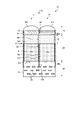
- FIG. 1 is a system configuration diagram showing a schematic configuration example of a solid-state imaging device according to an embodiment of the present disclosure
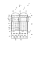
- FIG. 4 is a cross-sectional view schematically showing the structure of a pixel array section according to the embodiment of the present disclosure
- FIG. 4 is a diagram for explaining a manufacturing process of the pixel array section according to the embodiment of the present disclosure
- FIG. 4 is a diagram for explaining a manufacturing process of the pixel array section according to the embodiment of the present disclosure
- FIG. 4 is a diagram for explaining a manufacturing process of the pixel array section according to the embodiment of the present disclosure
- FIG. 4 is a diagram for explaining a manufacturing process of the pixel array section according to the embodiment of the present disclosure
- FIG. 4 is a diagram for explaining a manufacturing process of the pixel array section according to the embodiment of the present disclosure
- FIG. 4 is a diagram for explaining a manufacturing process of the pixel array section according to the embodiment of the present disclosure
- FIG. 4 is a diagram for explaining a manufacturing process of
- FIG. 4 is a diagram for explaining a manufacturing process of the pixel array section according to the embodiment of the present disclosure
- FIG. 4 is a diagram for explaining a manufacturing process of the pixel array section according to the embodiment of the present disclosure
- FIG. 5 is a cross-sectional view schematically showing the structure of a pixel array section according to Modification 1 of the embodiment of the present disclosure
- FIG. 10 is a diagram showing the relationship between the depth at which the low-absorption member is arranged and the saturated charge amount of the light-receiving pixel in Modification 1 of the embodiment of the present disclosure
- FIG. 10 is a diagram for explaining a manufacturing process of a pixel array section according to Modification 1 of the embodiment of the present disclosure
- FIG. 10 is a diagram for explaining a manufacturing process of a pixel array section according to Modification 1 of the embodiment of the present disclosure
- FIG. 10 is a diagram for explaining a manufacturing process of a pixel array section according to Modification 1 of the embodiment of the present disclosure
- FIG. 10 is a diagram for explaining a manufacturing process of a pixel array section according to Modification 1 of the embodiment of the present disclosure
- FIG. 10 is a diagram for explaining a manufacturing process of a pixel array section according to Modification 1 of the embodiment of the present disclosure
- FIG. 10 is a diagram for explaining a manufacturing process of a pixel array section according to Modification 1 of the embodiment of the present disclosure
- FIG. 10 is a diagram for explaining a manufacturing process of a pixel array section according to Modification 1 of the embodiment of the present disclosure
- FIG. 10 is a diagram for explaining a manufacturing process of a pixel array section according to Modification 1 of the embodiment of the present disclosure
- FIG. 10 is a diagram for explaining a manufacturing process of a
- FIG. 10 is a diagram for explaining a manufacturing process of a pixel array section according to Modification 1 of the embodiment of the present disclosure
- FIG. 7 is a cross-sectional view schematically showing the structure of a pixel array section according to Modification 2 of the embodiment of the present disclosure
- FIG. 7 is a cross-sectional view schematically showing the structure of a pixel array section according to Modification 3 of the embodiment of the present disclosure
- FIG. 10 is a cross-sectional view schematically showing the structure of a pixel array section according to Modification 4 of the embodiment of the present disclosure
- FIG. 11 is a diagram showing a planar configuration of a pixel array section according to Modification 5 of the embodiment of the present disclosure
- FIG. 11 is a diagram showing a planar configuration of a pixel array section according to Modification 6 of the embodiment of the present disclosure
- 23 is a cross-sectional view taken along line AA shown in FIG. 22
- FIG. 23 is a cross-sectional view taken along the line BB shown in FIG. 22
- FIG. 1 is a block diagram showing a configuration example of an imaging device as an electronic device to which technology according to the present disclosure is applied
- FIG. 1 is a block diagram showing an example of a schematic configuration of a vehicle control system
- FIG. FIG. 4 is an explanatory diagram showing an example of installation positions of an outside information detection unit and an imaging unit;
- a solid-state imaging device has, for example, a plurality of photoelectric conversion units arranged along the surface of the semiconductor layer on the light incident side. Also, in such a solid-state imaging device, a technique is known in which a conductive light shielding wall is formed in a separation region positioned between adjacent photoelectric conversion units.
- holes can be collected in the vicinity of the interface between the photoelectric conversion section and the isolation region, thereby suppressing the occurrence of dark current and white spots in the photoelectric conversion section. can be done.
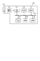
- FIG. 1 is a system configuration diagram showing a schematic configuration example of a solid-state imaging device 1 according to an embodiment of the present disclosure.
- the solid-state imaging device 1 which is a CMOS image sensor, includes a pixel array section 10, a system control section 12, a vertical drive section 13, a column readout circuit section 14, a column signal processing section 15, A horizontal driving unit 16 and a signal processing unit 17 are provided.
- pixel array section 10 system control section 12, vertical drive section 13, column readout circuit section 14, column signal processing section 15, horizontal drive section 16 and signal processing section 17 are on the same semiconductor substrate or are electrically connected. provided on a plurality of stacked semiconductor substrates.
- the pixel array section 10 includes light-receiving pixels 11 each having a photoelectric conversion element (photodiode PD (see FIG. 2)) capable of photoelectrically converting the amount of charge corresponding to the amount of incident light, accumulating the charge, and outputting the signal as a signal.
- a photoelectric conversion element photodiode PD (see FIG. 2)
- photoelectric conversion element capable of photoelectrically converting the amount of charge corresponding to the amount of incident light, accumulating the charge, and outputting the signal as a signal.
- the pixel array section 10 includes dummy pixels having no photodiodes PD, and light-shielding pixels whose light-receiving surface is shielded from external light. /or may include regions arranged in columns.
- the light-shielding pixel may have the same configuration as the light-receiving pixel 11 except that the light-receiving surface is light-shielded. Further, hereinafter, the photocharge having the amount of charge corresponding to the amount of incident light may be simply referred to as "charge”, and the light-receiving pixel 11 may be simply referred to as "pixel".
- a pixel driving line LD is formed along the left-right direction in the drawing (pixel arrangement direction of the pixel row) for each row with respect to the matrix-like pixel arrangement, and a vertical pixel wiring is formed for each column.
- the LV is formed along the vertical direction in the drawing (the pixel arrangement direction of the pixel column).
- One end of the pixel drive line LD is connected to an output terminal corresponding to each row of the vertical drive section 13 .
- the column readout circuit section 14 includes at least a circuit that supplies a constant current for each column to the light receiving pixels 11 in the selected row in the pixel array section 10, a current mirror circuit, a changeover switch for the light receiving pixels 11 to be read, and the like.
- the column readout circuit section 14 forms an amplifier together with the transistors in the selected pixels in the pixel array section 10, converts the photoelectric charge signal into a voltage signal, and outputs the voltage signal to the vertical pixel wiring LV.
- the vertical driving section 13 includes a shift register, an address decoder, etc., and drives each light receiving pixel 11 of the pixel array section 10 simultaneously or in units of rows.
- the vertical drive section 13 has a readout scanning system and a sweeping scanning system or a batch sweeping and batch transfer system, although the specific configuration thereof is not shown.
- the readout scanning system sequentially selectively scans the light receiving pixels 11 of the pixel array section 10 row by row in order to read out pixel signals from the light receiving pixels 11 .
- sweep scanning is performed ahead of the readout scanning by the time of the shutter speed for the readout rows to be readout scanned by the readout scanning system.
- batch sweeping is performed ahead of batch transfer by the time of the shutter speed.
- unnecessary charges are swept (reset) from the photodiodes PD of the light-receiving pixels 11 in the readout row.
- a so-called electronic shutter operation is performed by discharging (resetting) unnecessary charges.
- the electronic shutter operation is an operation of discarding unnecessary photocharge accumulated in the photodiode PD until just before and starting new exposure (starting accumulation of photocharge).
- the signal read out by the readout operation by the readout scanning system corresponds to the amount of incident light after the immediately preceding readout operation or the electronic shutter operation.
- the period from the readout timing of the previous readout operation or the sweep timing of the electronic shutter operation to the readout timing of the current readout operation is the accumulation time (exposure time) of the photoelectric charges in the light receiving pixels 11.
- the time from batch sweeping to batch transfer is accumulation time (exposure time).
- a pixel signal output from each light-receiving pixel 11 in a pixel row selectively scanned by the vertical driving section 13 is supplied to the column signal processing section 15 through each vertical pixel wiring LV.
- the column signal processing unit 15 performs predetermined signal processing on pixel signals output from the light-receiving pixels 11 of the selected row through the vertical pixel wiring LV for each pixel column of the pixel array unit 10, and performs a predetermined signal processing on the pixel signals after the signal processing. Temporarily holds the pixel signal.
- the column signal processing unit 15 performs at least noise removal processing, such as CDS (Correlated Double Sampling) processing, as signal processing.
- CDS Correlated Double Sampling
- the CDS processing by the column signal processing unit 15 removes pixel-specific fixed pattern noise such as reset noise and variations in the threshold value of the amplification transistor AMP.
- the column signal processing unit 15 may be configured to have, for example, an AD conversion function other than noise removal processing, so that pixel signals are output as digital signals.
- the horizontal driving section 16 includes a shift register, an address decoder, etc., and sequentially selects unit circuits corresponding to the pixel columns of the column signal processing section 15 . Pixel signals processed by the column signal processing unit 15 are sequentially output to the signal processing unit 17 by selective scanning by the horizontal driving unit 16 .
- the system control unit 12 includes a timing generator that generates various timing signals, and controls the vertical driving unit 13, the column signal processing unit 15, the horizontal driving unit 16, etc. based on the various timing signals generated by the timing generator. Drive control.
- the solid-state imaging device 1 further includes a signal processing section 17 and a data storage section (not shown).
- the signal processing unit 17 has at least an addition processing function, and performs various signal processing such as addition processing on the pixel signals output from the column signal processing unit 15 .
- the data storage unit temporarily stores data required for signal processing in the signal processing unit 17 .
- the signal processing unit 17 and the data storage unit may be processed by an external signal processing unit provided on a substrate different from the solid-state imaging device 1, such as a DSP (Digital Signal Processor) or software. 1 may be mounted on the same substrate.
- DSP Digital Signal Processor
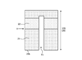
- FIG. 2 is a cross-sectional view schematically showing the structure of the pixel array section 10 according to the embodiment of the present disclosure.
- the pixel array section 10 includes a semiconductor layer 20, a wiring layer 30, and an optical layer 40.
- an optical layer 40, a semiconductor layer 20, and a wiring layer 30 are laminated in order from the side on which light L from the outside is incident (hereinafter also referred to as the light incident side).
- the semiconductor layer 20 includes a first region 21 which is a semiconductor region of a first conductivity type (eg, N type) and a semiconductor region (not shown) of a second conductivity type (eg, P type) adjacent to the first region 21 .
- the photodiode PD is formed.
- Such a photodiode PD is an example of a photoelectric conversion unit.
- an isolation region 23 is provided between the photodiodes PD adjacent to each other.
- the isolation region 23 electrically and optically isolates the photodiodes PD adjacent to each other.
- the separation regions 23 are arranged, for example, in a grid pattern in the pixel array section 10 in plan view.
- the isolation region 23 has a wall-like electrode 24, an insulating film 25, and a low absorption member 26.
- the wall-shaped electrode 24 is a wall-shaped electrode made of a conductive material and provided along the isolation region 23 in plan view.
- the wall-shaped electrode 24 is mainly composed of, for example, one selected from polysilicon, tungsten, and aluminum.
- the wall-shaped electrode 24 is arranged to a given depth X in the semiconductor layer 20 from the surface 20b opposite to the light incident side (hereinafter also referred to as the opposite surface 20b). Also, the wall-like electrode 24 is arranged adjacent to the first region 21 . That is, the first region 21 is arranged between the opposite surface 20b and the given depth X in the semiconductor layer 20 .
- the insulating film 25 is arranged between the wall-shaped electrode 24 and the first region 21 .
- the insulating film 25 is made of an insulating material (for example, silicon oxide (SiO 2 ) or the like).
- a wiring 32a located in the wiring layer 30 is connected to the wall-like electrode 24, and a negative bias voltage is applied via the wiring 32a.
- a negative bias voltage is applied to the wall-like electrode 24 .
- the wall-shaped electrode 24 since the wall-shaped electrode 24 has a relatively high absorption rate for the light L, when the wall-shaped electrode 24 is arranged up to the vicinity of the light incident side surface 20a (hereinafter also referred to as the light incident surface 20a) of the semiconductor layer 20, , the wall-shaped electrode 24 may absorb the light L in the vicinity of the light incident surface 20a.
- a low-absorption member 26 is arranged at a portion of the isolation region 23 closer to the light incident side than the wall-shaped electrode 24 .
- the low absorption member 26 has, for example, a thickness substantially equal to that of the wall-shaped portion composed of the wall-shaped electrode 24 and the insulating film 25 .
- the low-absorption member 26 is made of a material (for example, silicon oxide, hafnium oxide (HfO 2 ), aluminum oxide (Al 2 O 3 ), and titanium oxide (TiO 2 )) that has a lower absorption rate for the light L than the wall-like electrode 24 . etc.).
- the second region 22 having an impurity concentration lower than that of the first region 21 may be arranged adjacent to the low absorption member 26 .
- the second region 22 having an impurity concentration lower than that of the first region 21 may be arranged adjacent to the low absorption member 26 .
- the second region 22 is a semiconductor region of the second conductivity type
- the second region 22 is not limited to a semiconductor region of the second conductivity type.
- the first conductivity type impurity region having an impurity concentration lower than that of 21 may be used.
- the wall-like electrode 24 is preferably composed mainly of one selected from polysilicon, tungsten, and aluminum. As a result, holes can be stably collected in the vicinity of the interface between the photodiode PD and the separation region 23 .
- the wall-like electrode 24 is preferably made of polysilicon. As a result, even when the wall-like electrodes 24 are exposed to a high-temperature environment in the manufacturing process of the pixel array section 10, which will be described later, the deterioration of the wall-like electrodes 24 can be suppressed.
- the low absorption member 26 is preferably composed mainly of one selected from silicon oxide, hafnium oxide, aluminum oxide and titanium oxide.
- the low absorption member 26 can be easily formed.
- the low-absorption member 26 by forming the low-absorption member 26 from hafnium oxide, aluminum oxide, or titanium oxide, it is possible to reduce the difference in refractive index between the low-absorption member 26 and the second region 22 formed from silicon.
- scattering of the light L can be suppressed at the end of the low-absorption member 26 on the light incident side, so deterioration of the light-condensing characteristics for the photodiode PD can be further suppressed.
- a wiring layer 30 is arranged on the opposite surface 20 b of the semiconductor layer 20 .
- the wiring layer 30 is configured by forming a plurality of layers of wiring 32 and a plurality of pixel transistors 33 in an interlayer insulating film 31 .
- the wiring 32 includes a wiring 32a electrically connected to the wall-shaped electrode 24. Also, the plurality of pixel transistors 33 perform reading of charges accumulated in the photodiode PD.
- An optical layer 40 is arranged on the light incident surface 20 a of the semiconductor layer 20 .
- the optical layer 40 has a planarizing film 41 , a color filter 42 , a light shielding wall 43 and an OCL (On-Chip Lens) 44 .
- the planarizing film 41 is provided to planarize the surface on which the color filter 42 and the OCL 44 are formed and to avoid unevenness that occurs in the spin coating process when forming the color filter 42 and the OCL 44 .
- the planarizing film 41 is made of, for example, an organic material (for example, acrylic resin). Note that the planarizing film 41 is not limited to being formed of an organic material, and may be formed of silicon oxide, silicon nitride (SiN), or the like.
- the color filter 42 is an optical filter that transmits light of a predetermined wavelength out of the light L condensed by the OCL 44 .
- the color filter 42 is arranged on the surface of the flattening film 41 on the light incident side.
- the color filter 42 includes, for example, a color filter that transmits red light, a color filter that transmits green light, and a color filter that transmits blue light.
- the light shielding walls 43 are arranged, for example, between adjacent color filters 42 .
- the light-shielding wall 43 is a wall-like film that shields light obliquely incident from the adjacent color filter 42 .
- the light shielding wall 43 is made of, for example, aluminum or tungsten.
- the OCL 44 is a lens that is provided for each light-receiving pixel 11 and condenses the light L onto the photodiode PD of each light-receiving pixel 11 .
- the OCL 44 is made of, for example, an acrylic resin or the like.
- FIG. 3 to 8 are diagrams for explaining the manufacturing process of the pixel array section 10 according to the embodiment of the present disclosure.
- the second region 22 is formed in a region deeper than the given depth X with respect to the opposite surface 20b.
- the region of the semiconductor substrate 120 (semiconductor layer 20) closer to the opposite surface 20b than the second region 22 becomes the first conductivity type first region 21.
- a trench T1 is formed on the opposite surface 20b side of the semiconductor substrate 120 (semiconductor layer 20) by a conventionally known technique.
- the trench T1 is formed so as to penetrate the first region 21 and reach halfway through the second region 22, and is formed at a portion where the isolation region 23 is provided in plan view.
- a low absorption member 26 is filled from the bottom of the trench T1 to a given depth X by a conventionally known method.
- an insulating film 25 is formed on the side surface T1a of the trench T1 from the given depth X to the opening by a conventionally known method, and further fills the remaining space of the trench T1.
- a wall-like electrode 24 is formed by a conventionally known technique.
- the wiring layer 30 is formed on the opposite surface 20b of the semiconductor substrate 120 (semiconductor layer 20).
- the wiring layer 30 is configured by providing a plurality of layers of wiring 32 and a plurality of pixel transistors 33 in an interlayer insulating film 31, and is formed by a conventionally known method.
- the surface of the semiconductor substrate 120 opposite to the opposite surface 20b is ground and thinned so that the second region 22 and the low absorption member 26 are exposed. Thereby, the semiconductor layer 20 and the light incident surface 20a are formed.
- a flattening film 41, a plurality of color filters 42, a plurality of light shielding walls 43, and a plurality of OCLs 44 are sequentially formed on the surface of the light incident surface 20a of the semiconductor layer 20. .
- the trench T1 formed from the opposite surface 20b of the semiconductor layer 20 is filled with the low absorption member 26, the insulating film 25, and the wall-like electrode 24.
- isolation regions 23 are formed.
- the low absorption member 26, the insulating film 25, and the wall-shaped electrode 24 can be formed in a simple process, and positional displacement between the low absorption member 26 and the wall-shaped electrode 24 can be prevented.
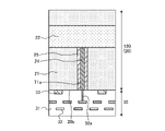
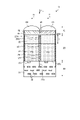
- FIG. 9 is a cross-sectional view schematically showing the structure of the pixel array section 10 according to Modification 1 of the embodiment of the present disclosure.
- the configuration of the low-absorbent member 26 and its periphery is different from that of the above-described embodiment.
- a fixed charge film 27 is arranged between the low absorption member 26 and the second region 22 and the wall-like electrode 24 .
- the fixed charge film 27 has a function of fixing charges (here, holes) at the interface between the isolation region 23 and the second region 22 .
- Fixed charge film 27 is made of, for example, hafnium oxide, aluminum oxide, tantalum oxide, zirconium oxide (ZrO 2 ), titanium oxide, magnesium oxide (MgO 2 ), lanthanum oxide (La 2 O 3 ), or the like.
- the fixed charge film 27 is composed of praseodymium oxide (Pr 2 O 3 ), cerium oxide (CeO 2 ), neodymium oxide (Nd 2 O 3 ), promethium oxide (Pm 2 O 3 ), and samarium oxide (Sm 2 O 3 ). , europium oxide (Eu 2 O 3 ), or the like.
- the fixed charge film 27 is made of gadolinium oxide (Gd 2 O 3 ), terbium oxide (Tb 2 O 3 ), dysprosium oxide (Dy 2 O 3 ), holmium oxide (Ho 2 O 3 ), erbium oxide (Er 2 O 3 ). 3 ), thulium oxide (Tm 2 O 3 ), or the like.
- the fixed charge film 27 is made of ytterbium oxide (Yb 2 O 3 ), lutetium oxide (Lu 2 O 3 ), yttrium oxide (Y 2 O 3 ), aluminum nitride (AlN), hafnium oxynitride (HfON), oxynitride It may be composed of an aluminum film (AlON) or the like.
- Modification 1 it is possible to further suppress the occurrence of white spots in the photodiode PD.
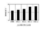
- FIG. 10 is a diagram showing the relationship between the depth D at which the low absorption member 26 is arranged and the saturated charge amount of the light receiving pixel 11 in Modification 1 of the embodiment of the present disclosure.
- the results shown in FIG. 10 are data obtained by simulation, and are data when the fixed charge film 27 is composed of a multilayer film of aluminum oxide and tantalum oxide, and the low absorption member 26 is composed of silicon oxide. .
- the reference example shown in FIG. 10 is data in the case where the low absorption member 26 and the fixed charge film 27 are not arranged and the wall-like electrode 24 penetrates the entire isolation region 23 .
- Modification 1 it is even better if the low absorption member 26 is arranged from the light incident surface 20a of the semiconductor layer 20 to a depth D of 800 (nm) or more. As a result, the saturated charge amount can be greatly increased compared to the reference example. That is, in Modification 1, by arranging the low-absorption member 26 to a depth D of 800 (nm) or more, it is possible to further improve the light-collecting characteristics.
- the data in FIG. 10 are the results of simulating the configuration of Modification 1
- the results of simulating the configuration of the above embodiment are also the same as in FIG. That is, in the above-described embodiment as well, by arranging the low-absorption member 26 to a depth D of 800 (nm) or more, it is possible to further improve the light-condensing characteristics.
- FIGS. 11 to 17 are diagrams for explaining the manufacturing process of the pixel array section 10 according to Modification 1 of the embodiment of the present disclosure.
- the region of the semiconductor substrate 120 (semiconductor layer 20) closer to the opposite surface 20b than the second region 22 becomes the first conductivity type first region 21.
- a trench T1 is formed on the opposite surface 20b side of the semiconductor substrate 120 (semiconductor layer 20) by a conventionally known technique.
- the trench T1 is formed so as to penetrate the first region 21 and is formed at a portion where the isolation region 23 is provided in plan view.
- an insulating film 25 is formed on the side surface T1a from the bottom of the trench T1 to the opening by a conventionally known method, and a wall-like electrode 24 is formed so as to fill the remaining space of the trench T1. It is formed by a conventionally known method.
- the wiring layer 30 is formed on the opposite surface 20b of the semiconductor substrate 120 (semiconductor layer 20).
- the wiring layer 30 is configured by providing a plurality of layers of wiring 32 and a plurality of pixel transistors 33 in an interlayer insulating film 31, and is formed by a conventionally known method.
- the surface of the semiconductor substrate 120 opposite to the opposite surface 20b is ground and thinned so that the second region 22 is exposed. Thereby, the semiconductor layer 20 and the light incident surface 20a are formed.
- a trench T2 is formed on the side of the light incident surface 20a of the semiconductor layer 20 by a conventionally known technique.
- the trench T2 is formed so as to penetrate the second region 22 and is formed in a portion where the separation region 23 is provided in plan view. That is, this trench T2 is formed so as to expose the wall-like electrode 24 and the insulating film 25 at the bottom.
- a fixed charge film 27 is formed on the side surface T2a and the bottom surface T2b of the trench T2 by a conventionally known method, and a low absorption member 26 is conventionally known so as to fill the remaining space of the trench T2. It is formed by the method of
- a flattening film 41, a plurality of color filters 42, a plurality of light shielding walls 43, and a plurality of OCLs 44 are sequentially formed on the surface of the light incident surface 20a of the semiconductor layer 20. .
- the trenches T1 formed from the opposite surface 20b are filled with the insulating film 25 and the wall-shaped electrodes 24, and the trenches T2 formed from the light incident surface 20a are filled with the fixed charge film 27. and the low absorption member 26 to form the isolation region 23 .
- the first region 21 and the second region 22 are formed by ion-implanting impurities of the second conductivity type into the semiconductor substrate 120 of the first conductivity type with high energy.
- the present disclosure is not limited to such an example.
- first region 21 and second region 22 are formed by ion-implanting impurities of the first conductivity type with relatively low energy from the opposite surface 20b side of semiconductor substrate 120 of the second conductivity type. may be formed.
- FIG. 18 is a cross-sectional view schematically showing the structure of the pixel array section 10 according to Modification 2 of the embodiment of the present disclosure.
- the configuration of the second region 22 is different from Modification 1 described above.
- the second region 22 includes a first portion 22a arranged on the side of the first region 21 and a second portion 22a arranged on the side of the light incident surface 20a. 22b.
- the first portion 22 a is a region with an impurity concentration lower than that of the first region 21 , for example, an impurity region of the first conductivity type with an impurity concentration lower than that of the first region 21 .
- the second portion 22b is a region having an impurity concentration lower than that of the first portion 22a, and is, for example, an impurity region of the second conductivity type.
- FIG. 19 is a cross-sectional view schematically showing the structure of the pixel array section 10 according to Modification 3 of the embodiment of the present disclosure. Modification 3 is different from Modification 1 in the configuration around the low-absorbent member 26 .
- a stopper film 28 is arranged between the low absorption member 26 and the fixed charge film 27 and the wall-like electrode 24 and the insulating film 25 .
- the stopper film 28 is formed so as to fill the bottom of the trench T1 after the formation of the trench T1 and before the insulating film 25 and the wall-shaped electrode 24 are formed in the manufacturing process shown in FIG. .
- the stopper film 28 is made of a material (eg, silicon oxide, silicon nitride, etc.) having a high etching selectivity with respect to the material of the semiconductor layer 20 (eg, silicon).
- the stopper film 28 can be used as an etching stopper in the step of forming the trench T2 shown in FIG. 15 by arranging the stopper film 28 as described above. Therefore, according to Modification 3, the trenches T2 can be formed with high accuracy.
- FIG. 20 is a cross-sectional view schematically showing the structure of the pixel array section 10 according to Modification 4 of the embodiment of the present disclosure.
- the sizes of the low absorption member 26 and the fixed charge film 27 are different from those in Modification 1 described above.
- the wall-like portion composed of the low-absorption member 26 and the fixed charge film 27 can be replaced by the wall-like electrode 24 and the insulating film. 25 can be connected to a wall-like portion.
- FIG. 21 is a cross-sectional view schematically showing the structure of the pixel array section 10 according to Modification 5 of the embodiment of the present disclosure. Modification 5 differs from Modification 1 in the structures of the low absorption member 26 and the fixed charge film 27 .
- the low absorption member 26A is made of a conductive material (for example, tungsten or aluminum), and the fixed charge film 27A is made of an insulating material (for example, oxide). silicon). Further, in Modification 5, the low absorption member 26A and the wall-like electrode 24 are electrically connected.
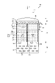
- FIG. 22 is a diagram showing a planar configuration of the pixel array section 10 according to Modification 6 of the embodiment of the present disclosure.
- 23 is a cross-sectional view taken along the line AA shown in FIG. 22, and
- FIG. 24 is a cross-sectional view taken along the line BB shown in FIG.
- one light receiving pixel 11 is provided with a pair of photodiodes PD (hereinafter also referred to as photodiodes PD1 and PD2).
- the light receiving pixel 11 has a substantially square shape in plan view
- the photodiode PD has a substantially rectangular shape in plan view.
- the light receiving pixel 11 has, as the isolation regions 23, a first isolation region 23a, a second isolation region 23b, and an impurity region 23c.
- the first isolation region 23a is arranged to surround the pair of photodiodes PD1 and PD2 in one light receiving pixel 11, as shown in FIG.
- the second separation region 23b is arranged between a pair of photodiodes PD1 and PD2 adjacent to each other in one light receiving pixel 11.
- the second isolation region 23b optically and electrically isolates the pair of adjacent photodiodes PD1 and PD2.
- the first separation region 23a separates the plurality of photodiodes PD into which the light L is incident via different OCLs 44 . Also, the second separation region 23b separates the pair of photodiodes PD1 and PD2 into which the light L is incident via the same OCL 44.
- the pair of photodiodes PD1 and PD2 can be separated from each other using the second separation region 23b. can be detected.
- the impurity region 23c is arranged between the pair of photodiodes PD1 and PD2 at a position different from that of the second isolation region 23b in plan view, and contains second conductivity type impurities.
- the impurity region 23c functions as an overflow path between the photodiode PD1 and the photodiode PD2.
- the amount of charge accumulated in both photodiodes PD1 and PD2 can be equalized.
- the first isolation region 23a and the second isolation region 23b are composed of the wall-shaped electrode 24, the insulating film 25, and the low absorption member. 26 and a fixed charge film 27 .
- Modification 6 it is possible to impart good isolation characteristics to the first isolation region 23a and the second isolation region 23b, and at the light incident side portion of the first isolation region 23a and the second isolation region 23b, Absorption of the light L can be suppressed.
- the depth D2 at which the low absorption member 26 and the fixed charge film 27 are arranged in the second separation region 23b is greater than the depth D2 where the low absorption member 26 and the fixed charge film 27 are arranged in the first separation region 23a. It is preferably deeper than the depth D1 at which the charge film 27 is arranged.
- the light L is absorbed at the portion on the light incident side in the second separation region 23b where more light L is collected than in the first separation region 23a. can be effectively suppressed.
- FIGS. 22 to 24 show phase difference pixels in which an overflow path (impurity region 23c) is arranged between a pair of photodiodes PD1 and PD2, the present disclosure is not limited to such examples.
- the first separation region 23a and the second separation region 23b are formed by the wall-like electrode 24 and the insulating film 25.
- a low absorption member 26 and a fixed charge film 27 are formed by the wall-like electrode 24 and the insulating film 25.
- the light-receiving pixel 11 capable of detecting the phase difference of the light L, it is possible to suppress the deterioration of the light collection characteristics with respect to the pair of photodiodes PD1 and PD2.
- the depth D2 at which the low absorption member 26 and the fixed charge film 27 are arranged in the second separation region 23b is equal to the depth D2 at which the low absorption member 26 and the fixed charge film 27 are arranged in the first separation region 23a. It may be deeper than the depth D1. As a result, it is possible to further suppress the deterioration of the light-condensing characteristics of the pair of photodiodes PD1 and PD2.
- a solid-state imaging device 1 includes a semiconductor layer 20 and an isolation region 23 .
- the semiconductor layer 20 has a plurality of photoelectric conversion units (photodiodes PD) arranged in a matrix.
- the separation region 23 separates adjacent photoelectric conversion units (photodiodes PD) in the semiconductor layer 20 .
- the separation region 23 has a wall-like electrode 24 and a low absorption member 26 .
- the wall-like electrode 24 is arranged like a wall and is applied with a negative bias voltage.
- the low-absorption member 26 is arranged closer to the light incident side than the wall-shaped electrode 24 and has a lower light absorption rate than the wall-shaped electrode 24 .
- the photoelectric conversion portion (photodiode PD) has the first region 21 adjacent to the wall-shaped electrode 24 and the second region 22 adjacent to the low absorption member 26. . Also, the impurity concentration of the second region 22 is lower than the impurity concentration of the first region 21 .
- the low absorption member 26 is arranged from the surface 20a of the semiconductor layer 20 on the light incident side to a depth D of 800 (nm) or more.
- the wall-shaped electrode 24 is mainly composed of one selected from polysilicon, tungsten, and aluminum.
- the low absorption member 26 is mainly composed of one selected from silicon oxide, hafnium oxide, aluminum oxide and titanium oxide.
- the low-absorption member 26 can be formed easily, or the scattering of the light L can be suppressed at the end of the low-absorption member 26 on the light incident side.
- the solid-state imaging device 1 further includes a plurality of on-chip lenses (OCLs 44) that allow light L to enter corresponding photoelectric conversion units (photodiodes PD).
- the isolation region 23 has a first isolation region 23a and a second isolation region 23b.
- the first separation region 23a separates a plurality of photoelectric conversion units (photodiodes PD) into which light L is incident via different on-chip lenses (OCL 44).
- the second separation region 23b separates a plurality of photoelectric conversion units (photodiodes PD) into which light L is incident via the same on-chip lens (OCL 44).
- the low absorbency member 26 positioned in the second separation region 23b is arranged to a deeper position than the low absorption member 26 positioned in the first separation region 23a.
- the light-receiving pixel 11 capable of detecting the phase difference of the light L, it is possible to further suppress the deterioration of the light collection characteristics with respect to the pair of photodiodes PD1 and PD2.
- the method for manufacturing the solid-state imaging device 1 includes a step of forming the trench T1, a step of filling with the low absorption member 26, a step of forming the insulating film 25, a step of filling with the wall-like electrode 24, including.
- the trenches T1 are formed in the surface 20b of the semiconductor substrate 120 opposite to the light incident side.
- the low absorption member 26 is filled up to a given depth X from the bottom of the trench T1.
- the insulating film 25 is formed on the side surface T1a from the given depth X of the trench T1 to the opening.
- the remaining portion of the trench T1 is filled with the conductive wall-like electrode 24.
- the wiring 32 a formed on the wiring layer 30 is connected to the wall-shaped electrode 24 , and the low absorption member 26 has a lower light absorption rate than the wall-shaped electrode 24 .
- the method for manufacturing the solid-state imaging device 1 according to the embodiment further includes a step of reducing the impurity concentration.
- a region from a depth corresponding to the bottom of the trench T1 to a given depth X is removed from the given depth X to the surface 20b of the semiconductor substrate 120 on the side opposite to the light incident side.
- the impurity concentration is made smaller than the region up to.
- the present disclosure is not limited to application to solid-state imaging devices. That is, the present disclosure applies to general electronic devices having a solid-state imaging device, such as a camera module, an imaging device, a mobile terminal device having an imaging function, or a copier using a solid-state imaging device as an image reading unit, in addition to the solid-state imaging device. applicable.
- a solid-state imaging device such as a camera module, an imaging device, a mobile terminal device having an imaging function, or a copier using a solid-state imaging device as an image reading unit, in addition to the solid-state imaging device.
- imaging devices examples include digital still cameras and video cameras.
- Mobile terminal devices having such an imaging function include, for example, smartphones and tablet terminals.
- FIG. 25 is a block diagram showing a configuration example of an imaging device as the electronic device 1000 to which the technology according to the present disclosure is applied.
- An electronic device 1000 in FIG. 25 is, for example, an imaging device such as a digital still camera or a video camera, or an electronic device such as a mobile terminal device such as a smart phone or a tablet terminal.
- an electronic device 1000 includes a lens group 1001, a solid-state image sensor 1002, a DSP circuit 1003, a frame memory 1004, a display unit 1005, a recording unit 1006, an operation unit 1007, and a power supply unit 1008. Configured.
- the DSP circuit 1003 , frame memory 1004 , display section 1005 , recording section 1006 , operation section 1007 and power supply section 1008 are interconnected via a bus line 1009 .
- a lens group 1001 captures incident light (image light) from a subject and forms an image on the imaging surface of the solid-state imaging device 1002 .
- the solid-state imaging device 1002 corresponds to the solid-state imaging device 1 according to the above-described embodiment, and converts the amount of incident light imaged on the imaging surface by the lens group 1001 into an electric signal for each pixel and outputs the electric signal as a pixel signal. do.
- the DSP circuit 1003 is a camera signal processing circuit that processes signals supplied from the solid-state imaging device 1002 .
- a frame memory 1004 temporarily holds the image data processed by the DSP circuit 1003 in frame units.
- a display unit 1005 is composed of a panel-type display device such as a liquid crystal panel or an organic EL (Electro Luminescence) panel, and displays moving images or still images captured by the solid-state imaging device 1002 .
- a recording unit 1006 records image data of a moving image or a still image captured by the solid-state imaging device 1002 in a recording medium such as a semiconductor memory or a hard disk.
- the operation unit 1007 issues operation commands for various functions of the electronic device 1000 in accordance with user's operations.
- a power supply unit 1008 appropriately supplies various power supplies as operating power supplies for the DSP circuit 1003, frame memory 1004, display unit 1005, recording unit 1006, and operation unit 1007 to these supply targets.
- the solid-state imaging device 1 of each of the above-described embodiments as the solid-state imaging device 1002, it is possible to suppress the deterioration of the light collection characteristics for the photodiode PD.
- the technology (the present technology) according to the present disclosure can be applied to various products.
- the technology according to the present disclosure can be realized as a device mounted on any type of moving body such as automobiles, electric vehicles, hybrid electric vehicles, motorcycles, bicycles, personal mobility, airplanes, drones, ships, and robots. may
- FIG. 26 is a block diagram showing a schematic configuration example of a vehicle control system, which is an example of a mobile control system to which the technology according to the present disclosure can be applied.
- a vehicle control system 12000 includes a plurality of electronic control units connected via a communication network 12001.
- the vehicle control system 12000 includes a drive system control unit 12010, a body system control unit 12020, an exterior information detection unit 12030, an interior information detection unit 12040, and an integrated control unit 12050.
- a microcomputer 12051, an audio/image output unit 12052, and an in-vehicle network I/F (Interface) 12053 are illustrated.
- the drive system control unit 12010 controls the operation of devices related to the drive system of the vehicle according to various programs.
- the driving system control unit 12010 includes a driving force generator for generating driving force of the vehicle such as an internal combustion engine or a driving motor, a driving force transmission mechanism for transmitting the driving force to the wheels, and a steering angle of the vehicle. It functions as a control device such as a steering mechanism to adjust and a brake device to generate braking force of the vehicle.
- the body system control unit 12020 controls the operation of various devices equipped on the vehicle body according to various programs.
- the body system control unit 12020 functions as a keyless entry system, a smart key system, a power window device, or a control device for various lamps such as headlamps, back lamps, brake lamps, winkers or fog lamps.
- the body system control unit 12020 can receive radio waves transmitted from a portable device that substitutes for a key or signals from various switches.
- the body system control unit 12020 receives the input of these radio waves or signals and controls the door lock device, power window device, lamps, etc. of the vehicle.
- the vehicle exterior information detection unit 12030 detects information outside the vehicle in which the vehicle control system 12000 is installed.
- the vehicle exterior information detection unit 12030 is connected with an imaging section 12031 .
- the vehicle exterior information detection unit 12030 causes the imaging unit 12031 to capture an image of the exterior of the vehicle, and receives the captured image.
- the vehicle exterior information detection unit 12030 may perform object detection processing or distance detection processing such as people, vehicles, obstacles, signs, or characters on the road surface based on the received image.
- the imaging unit 12031 is an optical sensor that receives light and outputs an electrical signal according to the amount of received light.
- the imaging unit 12031 can output the electric signal as an image, and can also output it as distance measurement information.
- the light received by the imaging unit 12031 may be visible light or non-visible light such as infrared rays.
- the in-vehicle information detection unit 12040 detects in-vehicle information.
- the in-vehicle information detection unit 12040 is connected to, for example, a driver state detection section 12041 that detects the state of the driver.
- the driver state detection unit 12041 includes, for example, a camera that captures an image of the driver, and the in-vehicle information detection unit 12040 detects the degree of fatigue or concentration of the driver based on the detection information input from the driver state detection unit 12041. It may be calculated, or it may be determined whether the driver is dozing off.
- the microcomputer 12051 calculates control target values for the driving force generator, the steering mechanism, or the braking device based on the information inside and outside the vehicle acquired by the vehicle exterior information detection unit 12030 or the vehicle interior information detection unit 12040, and controls the drive system control unit.
- a control command can be output to 12010 .
- the microcomputer 12051 realizes ADAS (Advanced Driver Assistance System) functions including collision avoidance or shock mitigation, follow-up driving based on inter-vehicle distance, vehicle speed maintenance driving, vehicle collision warning, or vehicle lane deviation warning. Cooperative control can be performed for the purpose of ADAS (Advanced Driver Assistance System) functions including collision avoidance or shock mitigation, follow-up driving based on inter-vehicle distance, vehicle speed maintenance driving, vehicle collision warning, or vehicle lane deviation warning. Cooperative control can be performed for the purpose of ADAS (Advanced Driver Assistance System) functions including collision avoidance or shock mitigation, follow-up driving based on inter-vehicle distance, vehicle speed maintenance driving, vehicle collision warning, or vehicle
- the microcomputer 12051 controls the driving force generator, the steering mechanism, the braking device, etc. based on the information about the vehicle surroundings acquired by the vehicle exterior information detection unit 12030 or the vehicle interior information detection unit 12040, so that the driver's Cooperative control can be performed for the purpose of autonomous driving, etc., in which vehicles autonomously travel without depending on operation.
- the microcomputer 12051 can output a control command to the body system control unit 12020 based on the information outside the vehicle acquired by the information detection unit 12030 outside the vehicle.
- the microcomputer 12051 controls the headlamps according to the position of the preceding vehicle or the oncoming vehicle detected by the vehicle exterior information detection unit 12030, and performs cooperative control aimed at anti-glare such as switching from high beam to low beam. It can be carried out.
- the audio/image output unit 12052 transmits at least one of audio and/or image output signals to an output device capable of visually or audibly notifying the passengers of the vehicle or the outside of the vehicle.
- an audio speaker 12061, a display unit 12062 and an instrument panel 12063 are illustrated as output devices.
- the display unit 12062 may include at least one of an on-board display and a head-up display, for example.
- FIG. 27 is a diagram showing an example of the installation position of the imaging unit 12031.
- the imaging unit 12031 has imaging units 12101, 12102, 12103, 12104, and 12105.
- the imaging units 12101, 12102, 12103, 12104, and 12105 are provided at positions such as the front nose, side mirrors, rear bumper, back door, and windshield of the vehicle 12100, for example.
- An image pickup unit 12101 provided in the front nose and an image pickup unit 12105 provided above the windshield in the passenger compartment mainly acquire images in front of the vehicle 12100 .
- Imaging units 12102 and 12103 provided in the side mirrors mainly acquire side images of the vehicle 12100 .
- An imaging unit 12104 provided in the rear bumper or back door mainly acquires an image behind the vehicle 12100 .
- the imaging unit 12105 provided above the windshield in the passenger compartment is mainly used for detecting preceding vehicles, pedestrians, obstacles, traffic lights, traffic signs, lanes, and the like.
- FIG. 27 shows an example of the imaging range of the imaging units 12101 to 12104.
- the imaging range 12111 indicates the imaging range of the imaging unit 12101 provided in the front nose
- the imaging ranges 12112 and 12113 indicate the imaging ranges of the imaging units 12102 and 12103 provided in the side mirrors, respectively
- the imaging range 12114 The imaging range of an imaging unit 12104 provided on the rear bumper or back door is shown. For example, by superimposing the image data captured by the imaging units 12101 to 12104, a bird's-eye view image of the vehicle 12100 viewed from above can be obtained.
- At least one of the imaging units 12101 to 12104 may have a function of acquiring distance information.
- at least one of the imaging units 12101 to 12104 may be a stereo camera composed of a plurality of imaging elements, or may be an imaging element having pixels for phase difference detection.
- the microcomputer 12051 determines the distance to each three-dimensional object within the imaging ranges 12111 to 12114 and changes in this distance over time (relative velocity with respect to the vehicle 12100). , it is possible to extract, as the preceding vehicle, the closest three-dimensional object on the traveling path of the vehicle 12100, which runs at a predetermined speed (for example, 0 km/h or more) in substantially the same direction as the vehicle 12100. can. Furthermore, the microcomputer 12051 can set the inter-vehicle distance to be secured in advance in front of the preceding vehicle, and perform automatic brake control (including following stop control) and automatic acceleration control (including following start control). In this way, cooperative control can be performed for the purpose of automatic driving in which the vehicle runs autonomously without relying on the operation of the driver.
- automatic brake control including following stop control
- automatic acceleration control including following start control
- the microcomputer 12051 converts three-dimensional object data related to three-dimensional objects to other three-dimensional objects such as motorcycles, ordinary vehicles, large vehicles, pedestrians, and utility poles. It can be classified and extracted and used for automatic avoidance of obstacles. For example, the microcomputer 12051 distinguishes obstacles around the vehicle 12100 into those that are visible to the driver of the vehicle 12100 and those that are difficult to see. Then, the microcomputer 12051 judges the collision risk indicating the degree of danger of collision with each obstacle, and when the collision risk is equal to or higher than the set value and there is a possibility of collision, an audio speaker 12061 and a display unit 12062 are displayed. By outputting an alarm to the driver via the drive system control unit 12010 and performing forced deceleration and avoidance steering via the drive system control unit 12010, driving support for collision avoidance can be performed.
- At least one of the imaging units 12101 to 12104 may be an infrared camera that detects infrared rays.
- the microcomputer 12051 can recognize a pedestrian by determining whether or not the pedestrian exists in the captured images of the imaging units 12101 to 12104 .
- recognition of a pedestrian is performed by, for example, a procedure for extracting feature points in images captured by the imaging units 12101 to 12104 as infrared cameras, and performing pattern matching processing on a series of feature points indicating the outline of an object to determine whether or not the pedestrian is a pedestrian.
- the audio image output unit 12052 outputs a rectangular outline for emphasis to the recognized pedestrian. is superimposed on the display unit 12062 . Also, the audio/image output unit 12052 may control the display unit 12062 to display an icon or the like indicating a pedestrian at a desired position.
- the technology according to the present disclosure can be applied to the imaging unit 12031 among the configurations described above.
- the solid-state imaging device 1 in FIG. 1 can be applied to the imaging section 12031 .
- a high-quality image can be acquired from the imaging unit 12031.
- the present technology can also take the following configuration.
- a semiconductor layer having a plurality of photoelectric conversion units arranged in a matrix; a separation region that separates the photoelectric conversion units adjacent to each other in the semiconductor layer; with The isolation region is a wall-shaped electrode to which a negative bias voltage is applied; a low absorption member disposed on the light incident side of the wall-shaped electrode and having a lower light absorption rate than the wall-shaped electrode;
- a solid-state imaging device having (2) The photoelectric conversion part has a first region adjacent to the wall-shaped electrode and a second region adjacent to the low absorption member, The solid-state imaging device according to (1), wherein the impurity concentration of the second region is lower than the impurity concentration of the first region.
- the wall-shaped electrode is mainly composed of one selected from polysilicon, tungsten, and aluminum.
- the low absorption member is mainly composed of one selected from silicon oxide, hafnium oxide, aluminum oxide and titanium oxide.
- (6) a plurality of on-chip lenses that allow light to enter the corresponding photoelectric conversion units; further comprising
- the isolation region is a first separation region separating a plurality of photoelectric conversion units into which light is incident via different on-chip lenses; a second separation region for separating the plurality of photoelectric conversion units to which light is incident via the same on-chip lens; has According to any one of (1) to (5), the low-absorbent member positioned in the second separation region is arranged to a deeper position than the low-absorbent member positioned in the first separation region.
- Solid-state image sensor Solid-state image sensor.
- a region from a depth corresponding to the bottom of the trench to the given depth has a lower impurity concentration than a region from the given depth to the surface of the semiconductor substrate opposite to the light incident side.
- the solid-state imaging device is a semiconductor layer having a plurality of photoelectric conversion units arranged in a matrix; a separation region that separates the photoelectric conversion units adjacent to each other in the semiconductor layer; has The isolation region is a wall-shaped electrode to which a negative bias voltage is applied; a low absorption member disposed on the light incident side of the wall-shaped electrode and having a lower light absorption rate than the wall-shaped electrode; electronic equipment.
- the photoelectric conversion part has a first region adjacent to the wall-shaped electrode and a second region adjacent to the low absorption member, The electronic device according to (9), wherein the impurity concentration of the second region is lower than the impurity concentration of the first region.
- the wall-shaped electrode is mainly composed of one selected from polysilicon, tungsten, and aluminum.
- the electronic device according to any one of (9) to (12), wherein the low absorption member is mainly composed of one selected from silicon oxide, hafnium oxide, aluminum oxide and titanium oxide.
- a plurality of on-chip lenses that allow light to enter the corresponding photoelectric conversion units; further comprising The isolation region is a first separation region separating a plurality of photoelectric conversion units into which light is incident via different on-chip lenses; a second separation region for separating the plurality of photoelectric conversion units to which light is incident via the same on-chip lens; has According to any one of (9) to (13), the low-absorbent member positioned in the second separation region is arranged to a deeper position than the low-absorbent member positioned in the first separation region. Electronics.
Landscapes
- Engineering & Computer Science (AREA)
- Physics & Mathematics (AREA)
- Power Engineering (AREA)
- Condensed Matter Physics & Semiconductors (AREA)
- General Physics & Mathematics (AREA)
- Computer Hardware Design (AREA)
- Microelectronics & Electronic Packaging (AREA)
- Electromagnetism (AREA)
- Manufacturing & Machinery (AREA)
- Solid State Image Pick-Up Elements (AREA)
- Element Separation (AREA)
Abstract
Priority Applications (3)
| Application Number | Priority Date | Filing Date | Title |
|---|---|---|---|
| EP22810859.3A EP4350770A1 (fr) | 2021-05-27 | 2022-02-14 | Élément d'imagerie à semi-conducteurs, procédé de production d'élément d'imagerie à semi-conducteurs et dispositif électronique |
| CN202280035623.5A CN117321772A (zh) | 2021-05-27 | 2022-02-14 | 固态摄像元件、固态摄像元件的制造方法以及电子设备 |
| JP2023523985A JPWO2022249575A1 (fr) | 2021-05-27 | 2022-02-14 |
Applications Claiming Priority (2)
| Application Number | Priority Date | Filing Date | Title |
|---|---|---|---|
| JP2021-089185 | 2021-05-27 | ||
| JP2021089185 | 2021-05-27 |
Publications (1)
| Publication Number | Publication Date |
|---|---|
| WO2022249575A1 true WO2022249575A1 (fr) | 2022-12-01 |
Family
ID=84229793
Family Applications (1)
| Application Number | Title | Priority Date | Filing Date |
|---|---|---|---|
| PCT/JP2022/005561 WO2022249575A1 (fr) | 2021-05-27 | 2022-02-14 | Élément d'imagerie à semi-conducteurs, procédé de production d'élément d'imagerie à semi-conducteurs et dispositif électronique |
Country Status (5)
| Country | Link |
|---|---|
| EP (1) | EP4350770A1 (fr) |
| JP (1) | JPWO2022249575A1 (fr) |
| CN (1) | CN117321772A (fr) |
| TW (1) | TW202247445A (fr) |
| WO (1) | WO2022249575A1 (fr) |
Citations (5)
| Publication number | Priority date | Publication date | Assignee | Title |
|---|---|---|---|---|
| JP2009088030A (ja) | 2007-09-27 | 2009-04-23 | Fujifilm Corp | 裏面照射型撮像素子 |
| US20170373108A1 (en) * | 2016-06-24 | 2017-12-28 | SK Hynix Inc. | Image sensor including transfer gates in deep trenches |
| US20190296060A1 (en) * | 2018-03-21 | 2019-09-26 | SK Hynix Inc. | Image sensor having pd bias patterns |
| WO2019220945A1 (fr) * | 2018-05-18 | 2019-11-21 | ソニーセミコンダクタソリューションズ株式会社 | Élément d'imagerie et dispositif électronique |
| WO2020262131A1 (fr) * | 2019-06-26 | 2020-12-30 | ソニーセミコンダクタソリューションズ株式会社 | Dispositif d'imagerie |
-
2022
- 2022-02-14 CN CN202280035623.5A patent/CN117321772A/zh active Pending
- 2022-02-14 EP EP22810859.3A patent/EP4350770A1/fr active Pending
- 2022-02-14 JP JP2023523985A patent/JPWO2022249575A1/ja active Pending
- 2022-02-14 WO PCT/JP2022/005561 patent/WO2022249575A1/fr active Application Filing
- 2022-05-20 TW TW111118960A patent/TW202247445A/zh unknown
Patent Citations (5)
| Publication number | Priority date | Publication date | Assignee | Title |
|---|---|---|---|---|
| JP2009088030A (ja) | 2007-09-27 | 2009-04-23 | Fujifilm Corp | 裏面照射型撮像素子 |
| US20170373108A1 (en) * | 2016-06-24 | 2017-12-28 | SK Hynix Inc. | Image sensor including transfer gates in deep trenches |
| US20190296060A1 (en) * | 2018-03-21 | 2019-09-26 | SK Hynix Inc. | Image sensor having pd bias patterns |
| WO2019220945A1 (fr) * | 2018-05-18 | 2019-11-21 | ソニーセミコンダクタソリューションズ株式会社 | Élément d'imagerie et dispositif électronique |
| WO2020262131A1 (fr) * | 2019-06-26 | 2020-12-30 | ソニーセミコンダクタソリューションズ株式会社 | Dispositif d'imagerie |
Also Published As
| Publication number | Publication date |
|---|---|
| TW202247445A (zh) | 2022-12-01 |
| JPWO2022249575A1 (fr) | 2022-12-01 |
| CN117321772A (zh) | 2023-12-29 |
| EP4350770A1 (fr) | 2024-04-10 |
Similar Documents
| Publication | Publication Date | Title |
|---|---|---|
| JP7125345B2 (ja) | 撮像素子、撮像素子の製造方法、及び、電子機器 | |
| US11240452B2 (en) | Solid-state imaging device and electronic device including light-shielding film for suppression of light leakage to memory | |
| WO2019093150A1 (fr) | Élément de capture d'image et appareil électronique | |
| US11863892B2 (en) | Imaging unit and electronic apparatus with first and second light blocking films | |
| WO2019188043A1 (fr) | Dispositif d'imagerie et procédé de fabrication de dispositif d'imagerie | |
| CN112740410A (zh) | 固体摄像装置和电子设备 | |
| US20220013557A1 (en) | Solid-state imaging device and electronic apparatus | |
| WO2020085085A1 (fr) | Dispositif d'imagerie à semi-conducteurs | |
| WO2020045142A1 (fr) | Dispositif d'imagerie et instrument électronique | |
| WO2021095668A1 (fr) | Élément d'imagerie à semi-conducteur et son procédé de fabrication | |
| US20230013149A1 (en) | Solid-state image pickup device and electronic apparatus | |
| US20220159208A1 (en) | Imaging device and electronic apparatus | |
| WO2022249575A1 (fr) | Élément d'imagerie à semi-conducteurs, procédé de production d'élément d'imagerie à semi-conducteurs et dispositif électronique | |
| CN114008783A (zh) | 摄像装置 | |
| WO2023127512A1 (fr) | Dispositif d'imagerie et appareil électronique | |
| WO2023053525A1 (fr) | Élément d'imagerie, dispositif d'imagerie et procédé de production | |
| WO2022080124A1 (fr) | Dispositif d'imagerie et son procédé de fabrication | |
| US20220103775A1 (en) | Imaging device | |
| WO2022269997A1 (fr) | Dispositif d'imagerie à semi-conducteurs et appareil électronique | |
| WO2023189130A1 (fr) | Dispositif de détection de lumière et appareil électronique | |
| WO2023079840A1 (fr) | Dispositif d'imagerie et appareil électronique | |
| WO2023276240A1 (fr) | Élément de capture d'image et dispositif électronique | |
| WO2023286391A1 (fr) | Dispositif de réception de lumière, équipement électronique et procédé de réception de lumière | |
| KR20240068644A (ko) | 촬상 소자, 촬상 장치, 제조 방법 | |
| TW202416726A (zh) | 光檢測裝置及電子機器 |
Legal Events
| Date | Code | Title | Description |
|---|---|---|---|
| 121 | Ep: the epo has been informed by wipo that ep was designated in this application |
Ref document number: 22810859 Country of ref document: EP Kind code of ref document: A1 |
|
| WWE | Wipo information: entry into national phase |
Ref document number: 2023523985 Country of ref document: JP |
|
| WWE | Wipo information: entry into national phase |
Ref document number: 18560858 Country of ref document: US |
|
| WWE | Wipo information: entry into national phase |
Ref document number: 202280035623.5 Country of ref document: CN |
|
| NENP | Non-entry into the national phase |
Ref country code: DE |
|
| WWE | Wipo information: entry into national phase |
Ref document number: 2022810859 Country of ref document: EP |
|
| ENP | Entry into the national phase |
Ref document number: 2022810859 Country of ref document: EP Effective date: 20240102 |