WO2022219964A1 - 光検出装置および電子機器 - Google Patents
光検出装置および電子機器 Download PDFInfo
- Publication number
- WO2022219964A1 WO2022219964A1 PCT/JP2022/009423 JP2022009423W WO2022219964A1 WO 2022219964 A1 WO2022219964 A1 WO 2022219964A1 JP 2022009423 W JP2022009423 W JP 2022009423W WO 2022219964 A1 WO2022219964 A1 WO 2022219964A1
- Authority
- WO
- WIPO (PCT)
- Prior art keywords
- photoelectric conversion
- region
- conversion region
- photodetector
- grooves
- Prior art date
- Legal status (The legal status is an assumption and is not a legal conclusion. Google has not performed a legal analysis and makes no representation as to the accuracy of the status listed.)
- Ceased
Links
Images















Classifications
-
- G—PHYSICS
- G02—OPTICS
- G02B—OPTICAL ELEMENTS, SYSTEMS OR APPARATUS
- G02B5/00—Optical elements other than lenses
- G02B5/20—Filters
-
- G—PHYSICS
- G02—OPTICS
- G02B—OPTICAL ELEMENTS, SYSTEMS OR APPARATUS
- G02B5/00—Optical elements other than lenses
- G02B5/30—Polarising elements
-
- G—PHYSICS
- G02—OPTICS
- G02B—OPTICAL ELEMENTS, SYSTEMS OR APPARATUS
- G02B5/00—Optical elements other than lenses
- G02B5/30—Polarising elements
- G02B5/3025—Polarisers, i.e. arrangements capable of producing a definite output polarisation state from an unpolarised input state
- G02B5/3058—Polarisers, i.e. arrangements capable of producing a definite output polarisation state from an unpolarised input state comprising electrically conductive elements, e.g. wire grids, conductive particles
-
- G—PHYSICS
- G03—PHOTOGRAPHY; CINEMATOGRAPHY; ANALOGOUS TECHNIQUES USING WAVES OTHER THAN OPTICAL WAVES; ELECTROGRAPHY; HOLOGRAPHY
- G03B—APPARATUS OR ARRANGEMENTS FOR TAKING PHOTOGRAPHS OR FOR PROJECTING OR VIEWING THEM; APPARATUS OR ARRANGEMENTS EMPLOYING ANALOGOUS TECHNIQUES USING WAVES OTHER THAN OPTICAL WAVES; ACCESSORIES THEREFOR
- G03B11/00—Filters or other obturators specially adapted for photographic purposes
-
- H—ELECTRICITY
- H04—ELECTRIC COMMUNICATION TECHNIQUE
- H04N—PICTORIAL COMMUNICATION, e.g. TELEVISION
- H04N25/00—Circuitry of solid-state image sensors [SSIS]; Control thereof
- H04N25/70—SSIS architectures; Circuits associated therewith
-
- H—ELECTRICITY
- H10—SEMICONDUCTOR DEVICES; ELECTRIC SOLID-STATE DEVICES NOT OTHERWISE PROVIDED FOR
- H10F—INORGANIC SEMICONDUCTOR DEVICES SENSITIVE TO INFRARED RADIATION, LIGHT, ELECTROMAGNETIC RADIATION OF SHORTER WAVELENGTH OR CORPUSCULAR RADIATION
- H10F39/00—Integrated devices, or assemblies of multiple devices, comprising at least one element covered by group H10F30/00, e.g. radiation detectors comprising photodiode arrays
- H10F39/10—Integrated devices
- H10F39/12—Image sensors
-
- H—ELECTRICITY
- H10—SEMICONDUCTOR DEVICES; ELECTRIC SOLID-STATE DEVICES NOT OTHERWISE PROVIDED FOR
- H10F—INORGANIC SEMICONDUCTOR DEVICES SENSITIVE TO INFRARED RADIATION, LIGHT, ELECTROMAGNETIC RADIATION OF SHORTER WAVELENGTH OR CORPUSCULAR RADIATION
- H10F39/00—Integrated devices, or assemblies of multiple devices, comprising at least one element covered by group H10F30/00, e.g. radiation detectors comprising photodiode arrays
- H10F39/80—Constructional details of image sensors
- H10F39/803—Pixels having integrated switching, control, storage or amplification elements
- H10F39/8033—Photosensitive area
-
- H—ELECTRICITY
- H10—SEMICONDUCTOR DEVICES; ELECTRIC SOLID-STATE DEVICES NOT OTHERWISE PROVIDED FOR
- H10F—INORGANIC SEMICONDUCTOR DEVICES SENSITIVE TO INFRARED RADIATION, LIGHT, ELECTROMAGNETIC RADIATION OF SHORTER WAVELENGTH OR CORPUSCULAR RADIATION
- H10F39/00—Integrated devices, or assemblies of multiple devices, comprising at least one element covered by group H10F30/00, e.g. radiation detectors comprising photodiode arrays
- H10F39/80—Constructional details of image sensors
- H10F39/803—Pixels having integrated switching, control, storage or amplification elements
- H10F39/8037—Pixels having integrated switching, control, storage or amplification elements the integrated elements comprising a transistor
-
- H—ELECTRICITY
- H10—SEMICONDUCTOR DEVICES; ELECTRIC SOLID-STATE DEVICES NOT OTHERWISE PROVIDED FOR
- H10F—INORGANIC SEMICONDUCTOR DEVICES SENSITIVE TO INFRARED RADIATION, LIGHT, ELECTROMAGNETIC RADIATION OF SHORTER WAVELENGTH OR CORPUSCULAR RADIATION
- H10F39/00—Integrated devices, or assemblies of multiple devices, comprising at least one element covered by group H10F30/00, e.g. radiation detectors comprising photodiode arrays
- H10F39/80—Constructional details of image sensors
- H10F39/805—Coatings
- H10F39/8053—Colour filters
-
- H—ELECTRICITY
- H10—SEMICONDUCTOR DEVICES; ELECTRIC SOLID-STATE DEVICES NOT OTHERWISE PROVIDED FOR
- H10F—INORGANIC SEMICONDUCTOR DEVICES SENSITIVE TO INFRARED RADIATION, LIGHT, ELECTROMAGNETIC RADIATION OF SHORTER WAVELENGTH OR CORPUSCULAR RADIATION
- H10F39/00—Integrated devices, or assemblies of multiple devices, comprising at least one element covered by group H10F30/00, e.g. radiation detectors comprising photodiode arrays
- H10F39/80—Constructional details of image sensors
- H10F39/806—Optical elements or arrangements associated with the image sensors
- H10F39/8063—Microlenses
-
- H—ELECTRICITY
- H10—SEMICONDUCTOR DEVICES; ELECTRIC SOLID-STATE DEVICES NOT OTHERWISE PROVIDED FOR
- H10F—INORGANIC SEMICONDUCTOR DEVICES SENSITIVE TO INFRARED RADIATION, LIGHT, ELECTROMAGNETIC RADIATION OF SHORTER WAVELENGTH OR CORPUSCULAR RADIATION
- H10F39/00—Integrated devices, or assemblies of multiple devices, comprising at least one element covered by group H10F30/00, e.g. radiation detectors comprising photodiode arrays
- H10F39/80—Constructional details of image sensors
- H10F39/806—Optical elements or arrangements associated with the image sensors
- H10F39/8067—Reflectors
Definitions
- the present technology (technology according to the present disclosure) relates to a photodetector and an electronic device, and more particularly to a photodetector and an electronic device having an optical element such as a wire grid polarizer.
- An imaging device having a plurality of imaging elements provided with wire grid polarizers is known from Patent Document 1, for example.
- a photoelectric conversion region that is included in a photoelectric conversion unit provided in an imaging device and generates current based on incident light is, for example, a CCD device (Charge Coupled Device) or a CMOS (Complementary Metal Oxide Semiconductor). consists of a metal oxide semiconductor) image sensor.
- the wire grid polarizer is disposed on the light incident surface side of the photoelectric conversion section, and is composed of, for example, a plurality of belt-shaped light reflecting layers, insulating layers, and light absorbing layers arranged side by side with a space therebetween.
- a wire grid polarizer transmits only the polarized light that is the transmission axis light out of the polarized light that is the extinction axis light and the polarized light that is the transmission axis light. Therefore, when the photodetector includes a wire grid polarizer, only the polarized light that is the transmission axis light of the light incident on the photodetector is supplied to the photoelectric conversion region. Therefore, a photodetector having a wire grid polarizer inevitably suffers a decrease in sensitivity due to the reduced amount of light compared to a photodetector without a wire grid polarizer.
- the purpose of this technology is to provide a photodetector and an electronic device that can compensate for the decrease in sensitivity.
- a photodetector includes a semiconductor layer having a photoelectric conversion region, a base material, and a plurality of groove-shaped openings arranged in the base material and penetrating the base material in a thickness direction, an optical element that selects light having a plane of polarization along the arrangement direction of the apertures, supplies the selected light to the photoelectric conversion region, and is arranged so as to overlap the photoelectric conversion region in plan view;
- the openings are aligned in the longitudinal direction and spaced apart in the width direction, and the optical element includes a first region in which the openings are arranged in the first direction, and a second region arranged in a second direction different from the one direction, wherein the light incident surface of the semiconductor layer has a plurality of uneven portions and overlaps the first region in plan view.
- the first concave-convex portion which is the concave-convex portion of the first photoelectric conversion region, which is the conversion region, is a plurality of concave portions arranged along a direction forming a first angle with the first direction, or extends along the direction.
- the second concave-convex portion which is the concave-convex portion included in the second photoelectric conversion region, which is the photoelectric conversion region overlapping the second region in a plan view, includes a groove that forms the first angle with the second direction. It includes a plurality of recesses arranged along the forming direction or grooves extending along the direction.
- An electronic device includes the photodetector and an optical system that causes image light from a subject to form an image on the photodetector.
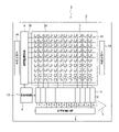
- FIG. 1 is a chip layout diagram showing a configuration example of a photodetector according to a first embodiment of the present technology
- FIG. 1 is a block diagram showing a configuration example of a photodetector according to a first embodiment of the present technology
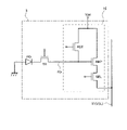
- FIG. 1 is an equivalent circuit diagram of a pixel of a photodetector according to a first embodiment of the present technology
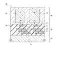
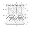
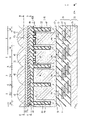
- FIG. It is a longitudinal section showing a section structure of a pixel of a photodetector concerning a 1st embodiment of this art.
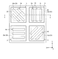
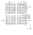
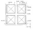
- 5 is a cross-sectional view showing the arrangement of four photoelectric conversion regions and the relative relationship between the photoelectric conversion regions and the wire grid polarizer when viewed along the BB section line of FIG. 4;
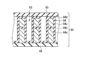
- FIG. 5B is a vertical cross-sectional view showing part of the wire grid polarizer when cross-sectionally viewed along the CC section line of FIG. 5A.
- FIG. 3 is a conceptual diagram for explaining light and the like passing through a wire grid polarizer of the photodetector according to the first embodiment of the present technology;
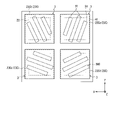
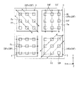
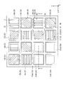
- FIG. 5 is a cross-sectional view showing the arrangement of four photoelectric conversion regions and the relative relationship between the photoelectric conversion regions and the uneven portion when viewed along the AA section line in FIG. 4; It is a figure which shows the comparative example of the extending direction of the groove
- FIG. 9B is a process cross-sectional view following FIG. 9A;
- FIG. 9C is a cross-sectional view of the process following FIG. 9B;
- FIG. 9C is a process cross-sectional view subsequent to FIG. 9C;
- FIG. 9C is a cross-sectional view of the process following FIG. 9D;
- FIG. 9E is a process cross-sectional view subsequent to FIG. 9E;
- FIG. 9F is a process cross-sectional view subsequent to FIG. 9F;
- FIG. 9G is a process cross-sectional view subsequent to FIG. 9G;
- FIG. 9H is a process cross-sectional view subsequent to FIG.
- FIG. 9H is a process cross-sectional view subsequent to FIG. 9I.
- FIG. FIG. 9J is a process cross-sectional view subsequent to FIG. 9J;
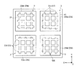
- FIG. 7 is a plan view of an uneven portion included in a photodetector according to Modification 1 of the first embodiment of the present technology;
- FIG. 9 is a plan view of an uneven portion included in a photodetector according to Modification 2 of the first embodiment of the present technology;
- FIG. 11 is a plan view of an uneven portion included in a photodetector according to Modification 3 of the first embodiment of the present technology;
- FIG. 11 is a plan view of an uneven portion included in a photodetector according to Modification 4 of the first embodiment of the present technology;
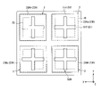
- FIG. 7 is a plan view of an uneven portion included in a photodetector according to a second embodiment of the present technology
- FIG. 10 is a plan view of an uneven portion included in a photodetector according to Modification 1 of the second embodiment of the present technology
- FIG. 10 is a plan view of an uneven portion included in a photodetector according to Modification 2 of the second embodiment of the present technology
- FIG. 11 is a plan view of an uneven portion included in a photodetector according to Modification 3 of the second embodiment of the present technology
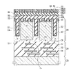
- FIG. 11 is a vertical cross-sectional view showing a cross-sectional structure of a pixel included in a photodetector according to Modification 4 of the second embodiment of the present technology
- FIG. 18B is a cross-sectional view showing the arrangement of four photoelectric conversion regions and the relative relationship between the photoelectric conversion regions and the uneven portion when viewed along the AA section line of FIG. 18A.
- FIG. 16 is a cross-sectional view showing a relative relationship between an uneven portion and a photoelectric conversion region included in a photodetector according to another form of Modification 4 of the second embodiment of the present technology; It is a longitudinal section showing a section structure of a pixel of a photodetection device concerning a 3rd embodiment of this art.
- 21 is a cross-sectional view showing the relative relationship between the photoelectric conversion region and the wire grid polarizer when viewed along the BB section line of FIG. 20;
- FIG. FIG. 21 is a cross-sectional view showing the relative relationship between the photoelectric conversion region and the uneven portion when viewed along the AA section line in FIG. 20; It is a figure showing a schematic structure of electronic equipment concerning a 4th embodiment of this art.
- first to fourth embodiments are examples of devices and methods for embodying the technical idea of the present technology, and the technical idea of the present technology is The material, shape, structure, arrangement, etc. are not specified as follows. Various modifications can be made to the technical idea of the present technology within the technical scope defined by the claims.
- CMOS complementary metal oxide semiconductor
- the photodetector 1 As shown in FIG. 1, the photodetector 1 according to the first embodiment of the present technology mainly includes a semiconductor chip 2 having a square two-dimensional planar shape when viewed from above. That is, the photodetector 1 is mounted on the semiconductor chip 2 . As shown in FIG. 23, the photodetector 1 takes in image light (incident light 106) from a subject through an optical system (optical lens) 102, and the amount of incident light 106 formed on an imaging plane is is converted into an electric signal for each pixel and output as a pixel signal.
- image light incident light 106
- optical system optical lens
- a semiconductor chip 2 on which a photodetector 1 is mounted has a rectangular pixel region 2A provided in the center and a rectangular pixel region 2A in a two-dimensional plane including X and Y directions that intersect with each other.
- a peripheral region 2B is provided outside the pixel region 2A so as to surround the pixel region 2A.
- the pixel area 2A is a light receiving surface that receives light condensed by the optical system 102 shown in FIG. 23, for example.
- a plurality of pixels 3 are arranged in a matrix on a two-dimensional plane including the X direction and the Y direction.
- the pixels 3 are arranged repeatedly in each of the X and Y directions that intersect each other within a two-dimensional plane.
- the X direction and the Y direction are orthogonal to each other as an example.
- a direction orthogonal to both the X direction and the Y direction is the Z direction (thickness direction).
- a plurality of bonding pads 14 are arranged in the peripheral region 2B.
- Each of the plurality of bonding pads 14 is arranged, for example, along each of four sides in the two-dimensional plane of the semiconductor chip 2 .
- Each of the plurality of bonding pads 14 is an input/output terminal used when electrically connecting the semiconductor chip 2 to an external device.
- the semiconductor chip 2 includes a logic circuit 13 including a vertical drive circuit 4, a column signal processing circuit 5, a horizontal drive circuit 6, an output circuit 7, a control circuit 8, and the like.
- the logic circuit 13 is composed of a CMOS (Complementary MOS) circuit having, for example, an n-channel conductivity type MOSFET (Metal Oxide Semiconductor Field Effect Transistor) and a p-channel conductivity type MOSFET as field effect transistors.
- CMOS Complementary MOS
- the vertical driving circuit 4 is composed of, for example, a shift register.
- the vertical drive circuit 4 sequentially selects desired pixel drive lines 10, supplies pulses for driving the pixels 3 to the selected pixel drive lines 10, and drives the pixels 3 in row units. That is, the vertical drive circuit 4 sequentially selectively scans the pixels 3 in the pixel region 2A in the vertical direction row by row, and outputs signals from the pixels 3 based on the signal charges generated by the photoelectric conversion elements of the pixels 3 according to the amount of received light.
- a pixel signal is supplied to the column signal processing circuit 5 through the vertical signal line 11 .
- the column signal processing circuit 5 is arranged, for example, for each column of the pixels 3, and performs signal processing such as noise removal on the signals output from the pixels 3 of one row for each pixel column.
- the column signal processing circuit 5 performs signal processing such as CDS (Correlated Double Sampling) and AD (Analog Digital) conversion for removing pixel-specific fixed pattern noise.
- a horizontal selection switch (not shown) is connected between the output stage of the column signal processing circuit 5 and the horizontal signal line 12 .
- the horizontal driving circuit 6 is composed of, for example, a shift register.
- the horizontal driving circuit 6 sequentially outputs a horizontal scanning pulse to the column signal processing circuit 5 to select each of the column signal processing circuits 5 in order, and the pixels subjected to the signal processing from each of the column signal processing circuits 5 are selected.
- a signal is output to the horizontal signal line 12 .
- the output circuit 7 performs signal processing on pixel signals sequentially supplied from each of the column signal processing circuits 5 through the horizontal signal line 12 and outputs the processed signal.
- signal processing for example, buffering, black level adjustment, column variation correction, and various digital signal processing can be used.
- the control circuit 8 generates a clock signal and a control signal that serve as references for the operation of the vertical drive circuit 4, the column signal processing circuit 5, the horizontal drive circuit 6, etc. based on the vertical synchronization signal, the horizontal synchronization signal, and the master clock signal. Generate. The control circuit 8 then outputs the generated clock signal and control signal to the vertical drive circuit 4, the column signal processing circuit 5, the horizontal drive circuit 6, and the like.
- FIG. 3 is an equivalent circuit diagram showing a configuration example of the pixel 3.
- the pixel 3 includes a photoelectric conversion element PD, a charge accumulation region (floating diffusion) FD for accumulating (holding) signal charges photoelectrically converted by the photoelectric conversion element PD, and photoelectrically converted by the photoelectric conversion element PD. and a transfer transistor TR for transferring the signal charge to the charge accumulation region FD.
- the pixel 3 also includes a readout circuit 15 electrically connected to the charge accumulation region FD.
- the photoelectric conversion element PD generates signal charges according to the amount of light received.
- the photoelectric conversion element PD also temporarily accumulates (holds) the generated signal charges.
- the photoelectric conversion element PD has a cathode side electrically connected to the source region of the transfer transistor TR, and an anode side electrically connected to a reference potential line (for example, ground).
- a photodiode for example, is used as the photoelectric conversion element PD.
- the drain region of the transfer transistor TR is electrically connected to the charge storage region FD.
- a gate electrode of the transfer transistor TR is electrically connected to a transfer transistor drive line among the pixel drive lines 10 (see FIG. 2).
- the charge accumulation region FD temporarily accumulates and holds signal charges transferred from the photoelectric conversion element PD via the transfer transistor TR.
- the readout circuit 15 reads out the signal charge accumulated in the charge accumulation region FD and outputs a pixel signal based on the signal charge.
- the readout circuit 15 includes, but is not limited to, pixel transistors such as an amplification transistor AMP, a selection transistor SEL, and a reset transistor RST. These transistors (AMP, SEL, RST) have a gate insulating film made of, for example, a silicon oxide film ( SiO2 film), a gate electrode, and a pair of main electrode regions functioning as a source region and a drain region. It consists of MOSFETs.
- These transistors may be MISFETs (Metal Insulator Semiconductor FETs) whose gate insulating film is a silicon nitride film (Si 3 N 4 film), or a laminated film of a silicon nitride film and a silicon oxide film.
- MISFETs Metal Insulator Semiconductor FETs
- the amplification transistor AMP has a source region electrically connected to the drain region of the selection transistor SEL, and a drain region electrically connected to the power supply line Vdd and the drain region of the reset transistor.
- a gate electrode of the amplification transistor AMP is electrically connected to the charge storage region FD and the source region of the reset transistor RST.
- the selection transistor SEL has a source region electrically connected to the vertical signal line 11 (VSL) and a drain electrically connected to the source region of the amplification transistor AMP.
- a gate electrode of the select transistor SEL is electrically connected to a select transistor drive line among the pixel drive lines 10 (see FIG. 2).
- the reset transistor RST has a source region electrically connected to the charge storage region FD and the gate electrode of the amplification transistor AMP, and a drain region electrically connected to the power supply line Vdd and the drain region of the amplification transistor AMP.
- a gate electrode of the reset transistor RST is electrically connected to a reset transistor drive line among the pixel drive lines 10 (see FIG. 2).
- the photodetector 1 includes a semiconductor layer 20 having a first surface S1 and a second surface S2 located opposite to each other.
- the semiconductor layer 20 is composed of a single-crystal silicon substrate of a first conductivity type, eg, p-type.
- the photodetector 1 also includes a multilayer wiring layer 30 including an interlayer insulating film 31 and a wiring layer 32 and a support substrate 33, which are sequentially laminated on the first surface S1 side of the semiconductor layer 20.
- the photodetector 1 includes a pinning layer 41, an insulating film 42A, a light shielding layer 43, a planarization film 44, and a wire grid polarizer 60, which is an optical element, which are sequentially laminated on the second surface S2 side of the semiconductor layer 20. and members such as a microlens (on-chip lens) 45 and the like.
- the photodetector 1 also has an uneven portion 50 provided in a photoelectric conversion region 23, which will be described later.
- At least part of the incident light incident on the photodetector 1 is, among the components described above, the microlens 45, the wire grid polarizer 60, the planarizing film 44, the insulating film 42A, the pinning layer 41, and the semiconductor layer 20. pass in that order.
- the first surface S1 of the semiconductor layer 20 is sometimes called an element forming surface or main surface
- the second surface S2 side is sometimes called a light incident surface or a rear surface.
- ⁇ Wire grid polarizer> 5A is a cross-sectional view showing the cross-sectional structure taken along line BB of FIG. 4, and FIG. 4 is a vertical cross-sectional view showing the cross-sectional structure taken along line CC of FIG. 5A.
- the wire grid polarizer 60 has a base material 61 and a plurality of grooves 63 arranged in the base material 61 and penetrating the base material 61 in the thickness direction. , supplies the selected light to the photoelectric conversion region 23, and is arranged so as to overlap the photoelectric conversion region 23 in plan view.
- the groove 63 is a groove-shaped opening.
- the grooves 63 are formed in the groove forming region 62 of the base material 61 . That is, the groove forming region 62 of the base material 61 has a plurality of grooves 63 arranged at equal pitches. In the groove forming region 62, the grooves 63 are aligned in the longitudinal direction and spaced apart in the lateral direction.
- the groove forming region 62 has a strip conductor 64 made of the base material 61 between two adjacent grooves 63 .
- the belt-like conductors 64 are aligned in the longitudinal direction and spaced apart in the lateral direction at equal pitches.
- the wire grid polarizer 60 has a plurality of types of groove forming regions 62 in which grooves 63 (strip conductors 64) are arranged in different directions.
- wire grid polarizer 60 includes a first region in which grooves 63 are arranged in a first direction and a second region in which grooves 63 are arranged in a second direction different from the first direction.
- FIG. 5A shows an example in which the wire grid polarizer 60 has four types of groove forming regions 62 (groove forming regions 62a, 62b, 62c, 62d).
- the arrangement direction of the grooves 63 (strip conductors 64) in the groove forming region 62a is along the X direction.
- the arrangement direction of the grooves 63 (strip-shaped conductors 64) in the groove forming region 62b is the direction along the direction at 45 degrees to the X direction.
- the arrangement direction of the grooves 63 (strip-shaped conductors 64) in the groove forming region 62c is along the direction 90 degrees to the X direction.
- the arrangement direction of the grooves 63 (strip-shaped conductors 64) in the groove forming region 62d is the direction along the direction 135 degrees with respect to the X direction.
- the first region is the groove forming region 62a and the second region is the groove forming region 62b. As shown in FIG.
- the arrangement direction (second direction) of the grooves 63 provided in the groove forming region 62b is different from the arrangement direction (first direction) of the grooves 63 provided in the groove forming region 62a. is the direction.
- the groove forming regions 62a, 62b, 62c, and 62d are simply referred to as the groove forming regions 62 without distinction.
- the wire grid polarizer 60 is arranged so as to overlap the photoelectric conversion region 23 in plan view. More specifically, the wire grid polarizer 60 is arranged such that the grooved regions 62 overlap the photoelectric conversion regions 23 in plan view. Moreover, as shown in FIG. 4, the wire grid polarizer 60 does not overlap the semiconductor layer 20 in the thickness direction (Z direction).
- the arrangement pitch P0 of the grooves 63 is set significantly smaller than the effective wavelength of the incident electromagnetic wave.
- the wire grid polarizer 60 reflects polarized light La (extinction axis light) parallel to the strip conductor 64 and transmits polarized light Lb (transmission axis light) perpendicular to the strip conductor 64 . Therefore, it functions as a polarizer that transmits only light in a specific direction.
- the four types of groove forming regions 62a, 62b, 62c, and 62d described above have grooves 63 arranged in different directions, and transmit polarized light in different directions.
- the wire grid polarizer 60 has features such as a high extinction ratio, high heat resistance, and compatibility with a wide wavelength range, compared to resin polarizers.
- the wire grid polarizer 60 contains a highly reflective metallic material to reduce transmission polarization loss.
- the base material 61 includes a material that forms a light reflecting layer 64a, a material that forms an insulating layer 64b, and a material that forms a light absorbing layer 64c, which will be described later. More specifically, the base material 61 includes a laminate of films made of these materials. Among these materials, the material constituting the light reflecting layer 64 a is provided closest to the photoelectric conversion region 23 . The material forming the light reflecting layer 64a and the material forming the light absorbing layer 64c are made of metal.
- the strip conductor 64 has a configuration in which a light reflecting layer 64a, an insulating layer 64b, and a light absorbing layer 64c are laminated in that order.
- the light reflecting layer 64a is laminated on the surface of the flattening film 44 opposite to the insulating film 42A side.
- the strip conductor 64 has a protective layer 64d around the laminated light reflecting layer 64a, insulating layer 64b, and light absorbing layer 64c.
- the light reflecting layer 64a reflects incident light.
- the light reflecting layer 64a can be made of a conductive metal.
- metals constituting the light reflecting layer 64a aluminum (Al), silver (Ag), gold (Au), copper (Cu), platinum (Pt), molybdenum (Mo), chromium (Cr), titanium ( Ti), nickel (Ni), tungsten (W), iron (Fe), silicon (Si), germanium (Ge), tellurium (Te), tantalum (Ta) and other metal materials, and alloy materials containing these metals can be mentioned.
- the light absorption layer 64c absorbs incident light.
- a metal material or an alloy material having a non-zero extinction coefficient k that is, having a light absorbing action, specifically, aluminum (Al), silver (Ag), or gold (Au). , Copper (Cu), Molybdenum (Mo), Chromium (Cr), Titanium (Ti), Nickel (Ni), Tungsten (W), Iron (Fe), Silicon (Si), Germanium (Ge), Tellurium (Te) , tin (Sn), and alloy materials containing these metals.
- Silicide-based materials such as FeSi 2 (particularly ⁇ -FeSi 2 ), MgSi 2 , NiSi 2 , BaSi 2 , CrSi 2 and CoSi 2 can also be used.
- a high contrast appropriate extinction ratio
- a high contrast can be achieved in the visible light region.
- silver (Ag), copper (Cu), gold (Au), or the like may be used as the material constituting the light absorption layer 64c. is preferred. This is because the resonance wavelengths of these metals are in the vicinity of the infrared region.
- the insulating layer 64b is an insulator composed of, for example, a silicon oxide film.
- the insulating layer 64b is arranged between the light reflecting layer 64a and the light absorbing layer 64c.
- the protective layer 64d protects the light reflecting layer 64a, the insulating layer 64b and the light absorbing layer 64c which are laminated in this order.
- This protective layer 64d can be composed of, for example, a silicon oxide film.
- the wire grid polarizer 60 also includes a flattening film 65 laminated on the end of the strip conductor 64 opposite to the end on the flattening film 44 side.
- the planarizing film 65 can be composed of, for example, a silicon oxide film.
- ⁇ Photoelectric conversion region> 6 is a cross-sectional view showing the cross-sectional structure along the AA section line in FIG. 4, and the portion of the semiconductor layer 20 in FIG. 4 is a longitudinal section showing the cross-sectional structure along the CC section line in FIG. It is a diagram.
- the semiconductor layer 20 has island-like photoelectric conversion regions (element forming regions) 23 partitioned by isolation regions 42 . This photoelectric conversion region 23 is provided for each pixel 3 . Note that the number of pixels 3 is not limited to that shown in FIG.
- the isolation region 42 has, but is not limited to, a trench structure in which, for example, an isolation trench 24 is formed in the semiconductor layer 20 and an insulating film is embedded in the isolation trench 24 .
- the photoelectric conversion region 23 includes a semiconductor region (well region) 21 of a first conductivity type, eg, p-type, and a semiconductor region (well region) 21 of a second conductivity type, eg, n-type, embedded in the well region 21 . and a semiconductor region (photoelectric conversion unit) 22 .
- the photoelectric conversion element PD shown in FIG. 3 is configured in the photoelectric conversion region 23 .
- the photoelectric conversion region 23 photoelectrically converts incident light to generate signal charges.
- the photoelectric conversion region overlapping the groove forming region 62a in plan view is called a photoelectric conversion region 23a in order to distinguish it from other photoelectric conversion regions.
- a photoelectric conversion region overlapping the groove forming region 62b in plan view is called a photoelectric conversion region 23b
- a photoelectric conversion region overlapping the groove forming region 62c in plan view is called a photoelectric conversion region 23c.
- a photoelectric conversion region overlapping the groove forming region 62d in plan view is called a photoelectric conversion region 23d.
- the wire grid polarizer 60 side of the photoelectric conversion region 23 has an uneven portion 50 .
- the optical element side of the photoelectric conversion region 23 forms the uneven portion 50 .
- the uneven portion 50 has grooves 51 . More specifically, groove 51 is a groove recessed in the thickness direction of semiconductor layer 20 from second surface S2.
- the uneven portion 50 has a plurality of such grooves 51 . 4 and 6 show an example in which the uneven portion 50 has three grooves 51.
- the wire grid polarizer 60 does not overlap the uneven portion 50 in the thickness direction (Z direction). A portion of the transmission axis light that has passed through the wire grid polarizer 60 is diffracted by the uneven portion 50 when entering the photoelectric conversion region 23 and travels obliquely through the photoelectric conversion region 23 . Therefore, the optical path length of the diffracted light becomes longer, and more light is absorbed in the photoelectric conversion region 23 .
- the uneven portion 50 of the photoelectric conversion region 23a includes grooves 51 extending along a direction forming 90 degrees with the arrangement direction of the grooves 63 provided in the groove forming region 62a (that is, the extending direction of the grooves 63).
- the uneven portion 50 of the photoelectric conversion region 23b includes grooves 51 extending along a direction forming 90 degrees with the arrangement direction of the grooves 63 provided in the groove forming region 62b (that is, the extending direction of the grooves 63).
- the uneven portion 50 of the photoelectric conversion region 23c includes grooves 51 extending along a direction forming 90 degrees with the arrangement direction of the grooves 63 provided in the groove forming region 62c (that is, the extending direction of the grooves 63).
- the uneven portion 50 of the photoelectric conversion region 23d includes grooves 51 extending along a direction forming 90 degrees with the arrangement direction of the grooves 63 provided in the groove forming region 62d (that is, the extending direction of the grooves 63).
- FIG. 7 shows that the grooves 51 included in the uneven portion 50 of the photoelectric conversion region 23a form a direction that forms 0 degrees with the arrangement direction of the grooves 63 provided in the groove forming region 62a (that is, the extending direction of the grooves 63 and 90 degrees). direction).
- Quantum efficiencies indicating the absorption of light by the semiconductor layer in the three cases of the photoelectric conversion region 23a shown in FIG. 6, the photoelectric conversion region 23a shown in FIG. Obtained by simulation.
- the quantum efficiency of photoelectric conversion region 23a shown in FIG. Further, the quantum efficiency of the photoelectric conversion region 23a shown in FIG. 7 was about 8% higher than the quantum efficiency of the photoelectric conversion region 23 without the uneven portion 50.
- the quantum efficiency is higher when the concave-convex portion 50 is provided than when it is not provided, that is, the amount of light absorbed increases. Also, it can be seen that the quantum efficiency depends on the relative positional relationship between the grooves 51 of the uneven portion 50 and the grooves 63 of the wire grid polarizer 60 . More specifically, when the grooves 51 extend along a direction forming 90 degrees with the arrangement direction of the grooves 63 (that is, a direction forming 0 degrees with the extending direction of the grooves 63), the grooves The quantum efficiency is higher than in the case of extending along the direction forming 0 degrees with the arrangement direction of grooves 63 (that is, the direction forming 90 degrees with the extending direction of grooves 63).
- the extending direction of the grooves 51 is always at a constant angle (first angle) with respect to the arrangement direction of the grooves 63 of the wire grid polarizer 60, so that the sensitivity difference between the pixels is You can prevent what is happening.
- the groove 51 was formed in a direction forming 90 degrees with the arrangement direction of the grooves 63 (that is, a direction forming 0 degrees with the extending direction of the grooves 63). Quantum efficiency was highest when extending along
- FIG. 8 is a diagram showing changes in quantum efficiency (QE) when the angle ⁇ (deg) between the extending direction of the groove 63 and the extending direction of the groove 51 is changed.
- Quantum efficiency, that is, QE/QE 0deg In the range of ⁇ 10 degrees ⁇ +10 degrees, the rate of decrease in quantum efficiency is within 0.24 percent. Further, in the range of ⁇ 5 degrees ⁇ +5 degrees, the rate of decrease in quantum efficiency is within 0.06 percent.
- a pinning layer 41 is deposited on the surface (second surface S2) of the semiconductor layer 20 opposite to the surface on the multilayer wiring layer 30 side. More specifically, the pinning layer 41 is deposited in a region including the second surface S2 and the inner walls of the separation grooves 24. As shown in FIG.
- the pinning layer 41 deposited on the uneven portion 50 has a shape that follows the shape of the uneven portion 50 . More specifically, the pinning layer 41 deposited on the uneven portion 50 has a shape that follows the shape of the groove 51 .
- the pinning layer 41 is formed using a high dielectric material having negative fixed charges so that a positive charge (hole) accumulation region is formed at the interface with the semiconductor layer 20 to suppress the generation of dark current. there is By forming the pinning layer 41 so as to have negative fixed charges, the negative fixed charges apply an electric field to the interface with the semiconductor layer 20, forming a positive charge accumulation region.
- the pinning layer 41 is formed using hafnium oxide (HfO 2 ), for example.
- the pinning layer 41 may be formed using zirconium dioxide (ZrO 2 ), tantalum oxide (Ta 2 O 5 ), or the like.
- An insulating film 42A is deposited on the surface of the pinning layer 41 opposite to the semiconductor layer 20 side by, for example, the CVD method.
- the insulating film 42A is, for example, a silicon oxide film.
- the insulating film 42A deposited on the concave-convex portion 50 via the pinning layer 41 is deposited so as to fill the recesses of the concave-convex portion 50, for example, the recesses of the grooves 51 and planarize it.
- the insulating film 42A deposited in the separation groove 24 via the pinning layer 41 is deposited so as to fill the separation groove 24 and planarize it.
- a portion of the insulating film 42A deposited in the isolation trench 24 via the pinning layer 41 forms an isolation region 42 that partitions the adjacent photoelectric conversion regions 23 .
- the isolation region 42 has a DTI (Deep Trench Isolation) structure in which the isolation trench 24 is filled with an insulating film 42A.
- the isolation region 42 may be provided so as to penetrate the semiconductor layer 20 .
- the light shielding layer 43 is laminated on the surface of the insulating film 42A opposite to the surface on the pinning layer 41 side. More specifically, the light shielding layer 43 is provided in a region overlapping the separation region 42 in plan view.
- any material that shields light may be used, such as tungsten (W), aluminum (Al), copper (Cu), or the like.
- a flattening film 44 is formed to cover the surface of the insulating film 42 ⁇ /b>A opposite to the pinning layer 41 side and the light shielding layer 43 .
- Silicon oxide for example, can be used as the material of the planarization film 44 .
- a method for manufacturing the photodetector 1 will be described below with reference to FIGS. 9A to 9K.
- a semiconductor layer 20 is prepared. More specifically, an n-type semiconductor region 22 is formed in the semiconductor layer 20 . The n-type semiconductor region 22 is formed within the p-type semiconductor region 21 of the semiconductor layer 20 .
- the transfer transistor TR, the readout circuit 15, the logic circuit 13, and the like are formed in the region near the first surface S1 in the semiconductor layer 20 shown in FIG. 9A. Constituent transistors, charge storage regions FD, and the like are formed.
- a multilayer wiring layer 30 including an interlayer insulating film 31 and a wiring layer 32 is laminated on the first surface S1 side of the semiconductor layer 20 . Furthermore, a supporting substrate 33 is bonded to the surface of the multilayer wiring layer 30 opposite to the surface facing the semiconductor layer 20 .
- a mask for forming uneven portions 50 is laminated on the second surface S2 side of the semiconductor layer 20 .
- a hard mask film 71A is formed on the second surface S2 side of the semiconductor layer 20 .
- the film 71A is, for example, a silicon oxide film.
- a resist pattern 72 is formed on the film 71A using well-known lithography technology and etching technology. Thereafter, the film 71A is etched using the resist pattern 72 as a mask to form the hard mask 71 shown in FIG. 9C.
- the semiconductor layer 20 exposed from the opening 71B of the hard mask 71 is etched to form a groove 51.
- these grooves 51 are formed in portions of the semiconductor layer 20 that will later become the photoelectric conversion regions 23 .
- the groove 51 is formed in the semiconductor layer 20 in the portion corresponding to the photoelectric conversion region 23 .
- the uneven portion 50 is formed on the second surface S2 side of the photoelectric conversion region 23 .
- separation grooves 24 are formed in the p-type semiconductor regions 21 between the adjacent n-type semiconductor regions 22 using known lithography and etching techniques. Through this process, the photoelectric conversion regions 23 are partitioned into islands.
- a pinning layer 41 is deposited on the second surface S2 of the semiconductor layer 20 and heat-treated. Before this step, the etching mask is removed. After that, an insulating film 42A is deposited on the pinning layer 41, as shown in FIG. 9F. At this time, the insides of the grooves 51 of the uneven portion 50 and the separation grooves 24 are also filled with the insulating film 42A. Thus, isolation regions 42 are formed.
- a light shielding layer 43 is formed on the insulating film 42A, and a planarization film 44 is deposited so as to cover the light shielding layer 43 and the insulating film 42A.
- the light shielding layer 43 is formed by depositing a film made of the material constituting the light shielding layer 43 on the insulating film 42A and using known lithography and etching techniques.
- the planarizing film 44 is formed by depositing a material constituting the planarizing film 44 and then grinding the surface of the deposited material by a CMP (Chemical Mechanical Polishing) method or the like, although illustration is omitted here. It is formed by flattening with CMP (Chemical Mechanical Polishing) method or the like, although illustration is omitted here. It is formed by flattening with
- a mask for forming the strip conductors 64 of the wire grid polarizer 60 is formed on the film 64cA. More specifically, as shown in FIG. 9I, a hard mask film 73A is formed on the film 64cA, and a resist pattern 74 is formed thereon using known lithography and etching techniques. Using the resist pattern 74 as a mask, the film 73A is etched to form a hard mask 73 shown in FIG. 9J.
- the film 73A is, for example, a silicon oxide film.
- the film 64aA, the film 64bA, and the film 64cA are etched using a hard mask 73 to form the grooves 63, and for each strip conductor 64, the light reflecting layer 64a, the insulating layer 64b, and the light
- the absorbent layer 64c is cut out.
- the hard mask 73 is removed, and a protective layer 64d is formed so as to cover the light reflecting layer 64a, the insulating layer 64b, and the light absorbing layer 64c cut out.
- a flattening film 65 is formed on the strip conductor 64 . This completes the formation of the wire grid polarizer 60 .
- the microlenses 45 are formed on the wire grid polarizer 60, and the photodetector 1 shown in FIG. 4 is almost completed.
- the photodetector 1 is formed in each of a plurality of chip forming regions partitioned by scribe lines (dicing lines) on a semiconductor substrate. By dividing the plurality of chip forming regions along scribe lines, the semiconductor chips 2 on which the photodetecting device 1 is mounted are formed.
- the wire grid polarizer 60 transmits only the polarized light Lb of polarized light La (extinction axis light) and polarized light Lb (transmission axis light). Therefore, when the photodetector 1 includes the wire grid polarizer 60 , only the transmission axis light of the light incident on the photodetector 1 is supplied to the photoelectric conversion region 23 . That is, the light incident on the photoelectric conversion region 23 is limited to light in one polarization direction. Therefore, the photodetector 1 having the wire grid polarizer 60 inevitably has lower sensitivity than the photodetector 1 which does not have the wire grid polarizer 60 because the amount of light is reduced.
- the photodetector 1 Since the photodetector 1 according to the first embodiment of the present technology has the uneven portion 50 on the second surface S2 side of the photoelectric conversion region 23, part of the transmission axis light that has passed through the wire grid polarizer 60 is converted into a photoelectric When incident on the conversion region 23 , the light is diffracted by the uneven portion 50 and travels obliquely in the photoelectric conversion region 23 . Therefore, the optical path length of the diffracted light becomes longer, and more light is absorbed in the photoelectric conversion region 23 . As a result, the photodetector 1 can efficiently absorb the transmission axis light even when the wire grid polarizer 60 is provided, and the decrease in sensitivity of the photodetector 1 can be compensated for.
- the wire grid polarizer 60 has a plurality of types of groove forming regions 62 in which the grooves 63 are arranged in different directions, even if the types of the groove forming regions 62 differ between pixels, the grooves of the uneven portion 50 Since the uneven portions 50 (grooves 51) are provided so that the extending direction of the grooves 51 always forms a constant angle (first angle) with the arrangement direction of the grooves 63, pixels having different types of groove forming regions 62 It is possible to suppress the occurrence of a sensitivity difference between them.
- the uneven portion 50 extends in a direction forming 90 degrees with the arrangement direction of the grooves 63, that is, along the extending direction of the grooves 63. , the quantum efficiency is highest. This shortens the time required for the photoelectric conversion region 23 to accumulate signal charges, which is effective when the photodetector 1 is desired to operate at a high frame rate.
- the arrangement pitch of the grooves 51 may be determined according to the wavelength of light incident on the photodetector 1, for example. Also, the number of grooves 51 included in the uneven portion 50 may be determined according to the pixel area.
- the belt-like conductor 64 has the light reflecting layer 64a, the insulating layer 64b, the light absorbing layer 64c, and the protective layer 64d, but it should have at least the light reflecting layer 64a.
- the wire grid polarizer 60 has an air gap structure, it may have a structure other than that.
- an insulating film may be embedded in the trench 63 .
- the separation grooves 24 are formed after the grooves 51 are formed, but the grooves 51 may be formed after the separation grooves 24 are formed. Note that when the photoelectric conversion region 23 is viewed from above, the unevenness of the uneven portion 50 (this embodiment) is in the central portion of the photoelectric conversion region 23 between the central portion and the end portion (portion near the separation groove 24). Then, it is desirable that there is a groove 51).
- Modification 1 of the first embodiment of the present technology shown in FIG. 10 will be described below.
- the photodetector 1 according to Modification 1 of the first embodiment differs from the photodetector 1 according to the above-described first embodiment in that it has a photoelectric conversion region 23A instead of the photoelectric conversion region 23, and
- the grooves 51 of the grooves 50A of the grooves 50A are arranged in a direction forming 0 degrees with the arrangement direction of the grooves 63 provided in the groove forming region 62 (that is, with the extending direction of the grooves 63 at 90 degrees).
- the configuration of the photodetector 1 is basically the same as that of the photodetector 1 of the first embodiment described above.
- symbol is attached
- the photodetector 1 according to Modification 1 of the first embodiment has a photoelectric conversion region 23A.
- the relationship between the photoelectric conversion regions 23A and the wire grid polarizer 60 is the same as in the case of the first embodiment, and the photoelectric conversion regions 23A, 23Aa, 23Aa, 23D shown in FIG. 23Ab, 23Ac, and 23Ad should be replaced.
- the wire grid polarizer 60 side of the photoelectric conversion region 23A has an uneven portion 50A.
- the optical element side of the photoelectric conversion region 23A forms an uneven portion 50A.
- the uneven portion 50A has grooves 51 .
- FIG. 10 shows an example in which the uneven portion 50 has three grooves 51 .
- the uneven portion 50A of the photoelectric conversion region 23Aa extends along a direction forming 0 degrees with the arrangement direction of the grooves 63 provided in the groove forming region 62a (that is, a direction forming 90 degrees with the extending direction of the grooves 63). Includes groove 51 .
- the uneven portion 50A of the photoelectric conversion region 23Ab extends along a direction forming 0 degrees with the arrangement direction of the grooves 63 provided in the groove forming region 62b (that is, a direction forming 90 degrees with the extending direction of the grooves 63). including existing grooves 51 .
- the uneven portion 50A of the photoelectric conversion region 23Ac extends along a direction forming 0 degrees with the arrangement direction of the grooves 63 provided in the groove forming region 62c (that is, a direction forming 90 degrees with the extending direction of the grooves 63). including existing grooves 51 .
- the uneven portion 50A of the photoelectric conversion region 23Ad extends along a direction forming 0 degrees with the arrangement direction of the grooves 63 provided in the groove forming region 62d (that is, a direction forming 90 degrees with the extending direction of the grooves 63). including existing grooves 51 .
- the grooves 51 of the concave-convex portion 50A form 0 degrees with the arrangement direction of the grooves 63 (that is, form 90 degrees with the extending direction of the grooves 63). direction), the quantum efficiency of the photoelectric conversion region 23A is about 8% higher than the quantum efficiency of the photoelectric conversion region 23 without the uneven portion 50 .
- the quantum efficiency of the photoelectric conversion region 23A is lower than the quantum efficiency of the photoelectric conversion region 23A.
- a simple comparison of quantum efficiency shows that the photoelectric conversion region 23 can absorb the transmission axis light more efficiently than the photoelectric conversion region 23A. This is probably because the amount of light diffracted by the grooves 51 and traveling obliquely is greater in the photoelectric conversion region 23 than in the photoelectric conversion region 23A.
- the photoelectric conversion region 23A is considered to have a smaller amount of light that is diffracted and travels obliquely than the photoelectric conversion region 23, crosstalk to adjacent pixels is considered to be less than that of the photoelectric conversion region 23.
- the photoelectric conversion region 23A of the photodetector 1 according to Modification 1 of the first embodiment has a higher extinction ratio than the photoelectric conversion region 23, when the extinction ratio is emphasized more than the quantum efficiency and the extinction ratio, , the configuration of the photoelectric conversion region 23A may be applied to the photodetector 1.
- FIG. 1 the photoelectric conversion region 23A of the photodetector 1 according to Modification 1 of the first embodiment has a higher extinction ratio than the photoelectric conversion region 23, when the extinction ratio is emphasized more than the quantum efficiency and the extinction ratio, the configuration of the photoelectric conversion region 23A may be applied to the photodetector 1.
- Modification 2 of the first embodiment Modification 2 of the first embodiment of the present technology shown in FIG. 11 will be described below.
- the photodetector 1 according to Modification 2 of the first embodiment differs from the photodetector 1 according to the above-described first embodiment in that the grooves 51 are arranged in the groove forming region 62 in the direction in which the grooves 63 are arranged. and 45 degrees (that is, a direction forming 45 degrees with the extending direction of the grooves 63). It has the same configuration as the photodetector 1 of one embodiment.
- symbol is attached
- the photodetector 1 according to Modification 2 of the first embodiment has a photoelectric conversion region 23B.
- the relationship between the photoelectric conversion regions 23B and the wire grid polarizer 60 is the same as in the first embodiment, and the photoelectric conversion regions 23, 23a, 23b, 23c, and 23d shown in FIG. 23Bb, 23Bc, and 23Bd should be replaced.
- the wire grid polarizer 60 side of the photoelectric conversion region 23B has an uneven portion 50B.
- the optical element side of the photoelectric conversion region 23B forms an uneven portion 50B.
- the uneven portion 50B has grooves 51 .
- FIG. 11 shows an example in which the uneven portion 50 has three grooves 51 .
- the uneven portion 50B of the photoelectric conversion region 23Ba extends along a direction forming 45 degrees with the arrangement direction of the grooves 63 provided in the groove forming region 62a (that is, a direction forming 45 degrees with the extending direction of the grooves 63). Includes groove 51 .
- the uneven portion 50B of the photoelectric conversion region 23Bb extends along a direction forming 45 degrees with the arrangement direction of the grooves 63 provided in the groove forming region 62b (that is, a direction forming 45 degrees with the extending direction of the grooves 63). including existing grooves 51 .
- the uneven portion 50B of the photoelectric conversion region 23Bc extends along a direction forming 45 degrees with the arrangement direction of the grooves 63 provided in the groove forming region 62c (that is, a direction forming 45 degrees with the extending direction of the grooves 63). including existing grooves 51 .
- the uneven portion 50B of the photoelectric conversion region 23Bd extends along a direction forming 45 degrees with the arrangement direction of the grooves 63 provided in the groove forming region 62d (that is, a direction forming 45 degrees with the extending direction of the grooves 63). including existing grooves 51 .
- the photoelectric conversion region 23B of the photodetector 1 according to Modification 2 of the first embodiment has a quantum efficiency similar to that of the photoelectric conversion region 23 according to the first embodiment and Modification 1 of the first embodiment.
- the quantum efficiency of the photoelectric conversion region 23A has an extinction ratio between the extinction ratio of the photoelectric conversion region 23 according to the first embodiment and the extinction ratio of the photoelectric conversion region 23A according to Modification 1 of the first embodiment. . Therefore, when emphasizing the balance between the quantum efficiency and the extinction ratio, the configuration of the photoelectric conversion region 23B may be applied to the photodetector 1 .
- the first angle is not limited to 45 degrees, and may be 135 degrees.
- the grooves 51 of the photoelectric conversion region 23Ba extend along a direction forming 135 degrees with the arrangement direction of the grooves 63 provided in the groove forming region 62a (that is, a direction forming 45 degrees with the extending direction of the grooves 63). exist.
- the grooves 51 of the photoelectric conversion region 23Bb extend along a direction forming 135 degrees with the arrangement direction of the grooves 63 provided in the groove forming region 62b (that is, a direction forming 45 degrees with the extending direction of the grooves 63). do.
- the grooves 51 of the photoelectric conversion region 23Bc extend along a direction forming 135 degrees with the arrangement direction of the grooves 63 provided in the groove forming region 62c (that is, a direction forming 45 degrees with the extending direction of the grooves 63). do.
- the grooves 51 of the photoelectric conversion region 23Bd extend along a direction forming 135 degrees with the arrangement direction of the grooves 63 provided in the groove forming region 62d (that is, a direction forming 45 degrees with the extending direction of the grooves 63). do. Even if the first angle is 135 degrees, the same effect as when the first angle is 45 degrees can be obtained.
- Modification 3 of the first embodiment of the present technology shown in FIG. 12 will be described below.
- the photodetector 1 according to Modification 3 of the first embodiment differs from the photodetector 1 according to the above-described first embodiment in that the grooves 51 are arranged in the groove forming region 62 in the direction in which the grooves 63 are arranged.
- the configuration of the photodetector 1 is basically the same as that of the photodetector 1 of the first embodiment described above except that it extends along a direction forming an angle other than the angle described above. It is configured.
- symbol is attached
- the photodetector 1 according to Modification 3 of the first embodiment has a photoelectric conversion region 23C.
- the relationship between the photoelectric conversion regions 23C and the wire grid polarizer 60 is the same as in the first embodiment, and the photoelectric conversion regions 23, 23a, 23b, 23c, and 23d shown in FIG. 23Cb, 23Cc, and 23Cd should be replaced.
- the wire grid polarizer 60 side of the photoelectric conversion region 23C has an uneven portion 50C.
- the optical element side of the photoelectric conversion region 23C forms an uneven portion 50C.
- the uneven portion 50 ⁇ /b>C has grooves 51 .
- FIG. 12 shows an example in which the uneven portion 50 has three grooves 51 .
- the first angle has any angle other than 90 degrees, 0 degrees, and 45 degrees described above.
- the uneven portion 50C of the photoelectric conversion region 23Ca extends along a direction forming 70 degrees with the arrangement direction of the grooves 63 provided in the groove forming region 62a (that is, a direction forming 20 degrees with the extending direction of the grooves 63). Includes groove 51 . Further, the uneven portion 50C of the photoelectric conversion region 23Cb extends along a direction forming 70 degrees with the arrangement direction of the grooves 63 provided in the groove forming region 62b (that is, a direction forming 20 degrees with the extending direction of the grooves 63). including existing grooves 51 .
- the uneven portion 50C of the photoelectric conversion region 23Cc extends along a direction forming 70 degrees with the arrangement direction of the grooves 63 provided in the groove forming region 62c (that is, a direction forming 20 degrees with the extending direction of the grooves 63). including existing grooves 51 .
- the uneven portion 50C of the photoelectric conversion region 23Cd extends along a direction forming 70 degrees with the arrangement direction of the grooves 63 provided in the groove forming region 62d (that is, a direction forming 20 degrees with the extending direction of the grooves 63). including existing grooves 51 .
- the uneven portion 50C is provided so that the extending direction of the groove 51 always forms a constant angle (first angle) with respect to the arrangement direction of the grooves 63. As shown in FIG.
- the first angle is an arbitrary angle in Modification 3 of the first embodiment, the optimum first angle can be selected according to the design of the photodetector 1 .
- Modification 4 of the first embodiment of the present technology shown in FIG. 13 will be described below.
- the photodetector 1 according to Modification 4 of the first embodiment differs from the photodetector 1 according to the above-described first embodiment in that it has a group of concave portions 51D instead of the grooves 51.
- the configuration of the photodetector 1 is basically the same as that of the photodetector 1 of the first embodiment described above.
- symbol is attached
- the photodetector 1 according to Modification 4 of the first embodiment has a photoelectric conversion region 23D.
- the relationship between the photoelectric conversion region 23D and the wire grid polarizer 60 is the same as in the first embodiment, and the photoelectric conversion regions 23, 23a, 23b, 23c, and 23d shown in FIG. 23Db, 23Dc, and 23Dd can be read.
- the wire grid polarizer 60 side of the photoelectric conversion region 23D has an uneven portion 50D.
- the optical element side of the photoelectric conversion region 23D forms an uneven portion 50D.
- the concave-convex portion 50D has a group of concave portions 51D.
- FIG. 13 shows an example in which the concave-convex portion 50D has three groups of concave portions 51D.
- the recess group 51D includes a plurality of recesses (first recesses) 51Da arranged in a row. The arrangement direction of the plurality of recesses 51Da corresponds to the extending direction of the recess group 51D.
- the concave-convex portion 50D of the photoelectric conversion region 23Da includes a group of concave portions 51D extending along a direction forming 90 degrees with the arrangement direction of the grooves 63 provided in the groove forming region 62a (that is, the extending direction of the grooves 63).
- the concave-convex portion 50D of the photoelectric conversion region 23Db includes a group of concave portions 51D extending along a direction forming 90 degrees with the arrangement direction of the grooves 63 provided in the groove forming region 62b (that is, the extending direction of the grooves 63). include.
- the concave-convex portion 50D of the photoelectric conversion region 23Dc includes a group of concave portions 51D extending along a direction forming 90 degrees with the arrangement direction of the grooves 63 provided in the groove forming region 62c (that is, the extending direction of the grooves 63).
- the concave-convex portion 50D of the photoelectric conversion region 23Dd includes a group of concave portions 51D extending along a direction forming 90 degrees with the arrangement direction of the grooves 63 provided in the groove forming region 62d (that is, the extending direction of the grooves 63). include.
- the wire grid polarizer 60 has a plurality of types of groove forming regions 62 in which the grooves 63 are arranged in different directions, even if the types of the groove forming regions 62 differ between pixels, the uneven portion 50D
- each of the concave portions 51Da is square in the example shown in FIG. 13, it is not limited thereto, and may be rectangular or circular. Furthermore, in the example shown in FIG. 13, the plurality of recesses 51Da have the same shape, but the shape is not limited to this, and they may have different shapes.
- the photodetector 1 according to the second embodiment differs from the photodetector 1 according to the above-described first embodiment in that it has a photoelectric conversion region 23E instead of the photoelectric conversion region 23, and the photoelectric conversion regions 23Ea, 23Eb, 23Ec, and 23Ed have uneven portions 50E of the same shape, and the uneven portions 50E have grooves 51 extending along different directions.
- it has the same configuration as the photodetector 1 of the above-described first embodiment.
- symbol is attached
- the photodetector 1 has a photoelectric conversion region 23E.
- the relationship between the photoelectric conversion region 23E and the wire grid polarizer 60 is the same as in the first embodiment, and the photoelectric conversion regions 23, 23a, 23b, 23c, and 23d shown in FIG. 23Eb, 23Ec, and 23Ed can be read.
- the photoelectric conversion regions 23Ea, 23Eb, 23Ec, and 23Ed all have the same shape of the uneven portion 50E.
- the wire grid polarizer 60 side of the photoelectric conversion region 23E has an uneven portion 50E.
- the optical element side of the photoelectric conversion region 23E forms an uneven portion 50E.
- the uneven portion 50E has grooves 51 extending along different directions.
- the uneven portion 50E of the photoelectric conversion region 23Ea extends along a direction forming 90 degrees with the arrangement direction of the grooves 63 provided in the groove forming region 62a (that is, the extending direction of the grooves 63).
- Grooves 51a, grooves 51b extending along a direction forming 90 degrees with the arrangement direction of the grooves 63 provided in the groove forming region 62b (that is, the extending direction of the grooves 63), and grooves 51b provided in the groove forming region 62c The grooves 51c extending along the direction forming 90 degrees with the arrangement direction of the grooves 63 (that is, the extending direction of the grooves 63) and the direction forming 90 degrees with the arrangement direction of the grooves 63 provided in the groove forming region 62d (that is, the groove 51d extending along the extending direction of the groove 63).
- each of the uneven portion 50E of the photoelectric conversion region 23Eb, the uneven portion 50E of the photoelectric conversion region 23Ec, and the uneven portion 50E of the photoelectric conversion region 23Ed has grooves 51a to 51d.
- the uneven portion 50E of the photoelectric conversion region 23Ea, the uneven portion 50E of the photoelectric conversion region 23Eb, the uneven portion 50E of the photoelectric conversion region 23Ec, and the uneven portion 50E of the photoelectric conversion region 23Ed have the same shape. ing. Note that these grooves 51a, 51b, 51c, and 51d are simply referred to as grooves 51 when there is no need to distinguish between them.
- each of the uneven portions 50E includes grooves 51a to 51d extending along different directions, the uneven portion 50E corresponds to any of the groove forming regions 62a, 62b, 62c, and 62d. Even if they overlap, the occurrence of sensitivity differences between pixels having different types of groove forming regions 62 can be suppressed with the uneven portion 50E having the same shape (one type).
- the photodetector 1 according to the second embodiment can adopt the common concave-convex portion 50E in all the pixels 3, it is possible to easily create mask data. In addition, manufacturing processes such as etching can be made uniform for all the pixels 3 .
- Modification 1 of the second embodiment of the present technology shown in FIG. 15 will be described below.
- the photodetector 1 according to Modification 1 of the second embodiment differs from the photodetector 1 according to the above-described second embodiment in that the concave and convex portions 50F have concave portions 51F arranged in a matrix.
- the configuration of the photodetector 1 is basically the same as that of the photodetector 1 of the above-described second embodiment.
- symbol is attached
- the photodetector 1 according to Modification 1 of the second embodiment has a photoelectric conversion region 23F.
- the relationship between the photoelectric conversion regions 23F and the wire grid polarizer 60 is the same as in the first embodiment, and the photoelectric conversion regions 23, 23a, 23b, 23c, and 23d shown in FIG. 23Fb, 23Fc, and 23Fd should be replaced.
- the photoelectric conversion regions 23Fa, 23Fb, 23Fc, and 23Fd all have the same shape of uneven portions 50F.
- the wire grid polarizer 60 side of the photoelectric conversion region 23F has an uneven portion 50F.
- the optical element side of the photoelectric conversion region 23F forms an uneven portion 50F.
- the uneven portion 50F of the photoelectric conversion region 23Fa has a plurality of recesses (second recesses) 51F arranged in a matrix along the X direction and the Y direction.
- the plurality of recesses 51F are arranged in a matrix at regular intervals along the X and Y directions, for example.
- each of the uneven portion 50F of the photoelectric conversion region 23Fb, the uneven portion 50F of the photoelectric conversion region 23Fc, and the uneven portion 50F of the photoelectric conversion region 23Fd has recesses arranged in a matrix along the X direction and the Y direction. 51F.
- the uneven portion 50F of the photoelectric conversion region 23Fa, the uneven portion 50F of the photoelectric conversion region 23Fb, the uneven portion 50F of the photoelectric conversion region 23Fc, and the uneven portion 50F of the photoelectric conversion region 23Fd have the same shape.
- FIG. 15 shows an example in which the concave portions 51F are arranged in 3 rows and 3 columns, the arrangement is not limited to this.
- FIG. 15 shows an example in which the concave portion 51F is square, the shape is not limited to this.
- the recesses 51F arranged in a matrix can be considered to be arranged along the arrows Fa, Fb, Fc, and Fd.
- the arrow Fa extends along a direction (that is, the extending direction of the grooves 63) forming 90 degrees with the arrangement direction of the grooves 63 provided in the groove forming region 62a, and the recesses 51F extend along the arrow Fa. can be considered to be arrayed.
- the arrow Fb is along the direction forming 90 degrees with the arrangement direction of the grooves 63 provided in the groove forming region 62b (that is, the extending direction of the grooves 63), and the concave portions 51F are arranged along the arrow Fb.
- the arrow Fc is along the direction forming 90 degrees with the arrangement direction of the grooves 63 provided in the groove forming region 62c (that is, the extending direction of the grooves 63), and the concave portions 51F are arranged along the arrow Fc.
- the arrow Fd is along the direction forming 90 degrees with the arrangement direction of the grooves 63 provided in the groove forming region 62d (that is, the extending direction of the grooves 63), and the concave portions 51F are arranged along the arrow Fd.
- the plurality of concave portions 51F can be regarded as extending along a plurality of directions, even if the uneven portion 50F overlaps with any of the groove forming regions 62a, 62b, 62c, and 62d, It is possible to suppress the occurrence of sensitivity differences between pixels having different types of groove formation regions 62 with the uneven portions 50F having the same shape (one type).
- Modification 2 of Second Embodiment Modification 2 of the second embodiment of the present technology shown in FIG. 16 will be described below.
- the difference between the photodetector 1 according to Modification 2 of the present second embodiment and the photodetector 1 according to the above-described second embodiment is that the concave and convex portions 50G extend along different directions.
- the configuration of the photodetector 1 is basically the same as that of the photodetector 1 of the above-described second embodiment.
- symbol is attached
- the photodetector 1 according to Modification 2 of the second embodiment has a photoelectric conversion region 23G.
- the relationship between the photoelectric conversion region 23G and the wire grid polarizer 60 is the same as in the first embodiment, and the photoelectric conversion regions 23, 23a, 23b, 23c, and 23d shown in FIG. 23Gb, 23Gc, and 23Gd should be read.
- the photoelectric conversion regions 23Ga, 23Gb, 23Gc, and 23Gd all have the same shape of the uneven portion 50G.
- the wire grid polarizer 60 side of the photoelectric conversion region 23G has an uneven portion 50G.
- the optical element side of the photoelectric conversion region 23G forms an uneven portion 50G.
- the uneven portion 50G has grooves 51 extending along different directions. More specifically, the uneven portion 50G has a plurality of grooves 51e extending along the Y direction and a plurality of grooves 51f extending along the X direction.
- the uneven portion 50G of the photoelectric conversion region 23Ga, the uneven portion 50G of the photoelectric conversion region 23Gb, the uneven portion 50G of the photoelectric conversion region 23Gc, and the uneven portion 50G of the photoelectric conversion region 23Gd have both the plurality of grooves 51e and the plurality of grooves 51f. have.
- the groove 51e extends along a direction forming 90 degrees with the arrangement direction of the grooves 63 provided in the groove forming region 62a (that is, the extending direction of the grooves 63).
- the grooves 51f extend along a direction forming 90 degrees with the arrangement direction of the grooves 63 provided in the groove forming region 62c (that is, the extending direction of the grooves 63). Note that these grooves 51e and 51f are simply referred to as grooves 51 when there is no need to distinguish between them.
- each of the uneven portions 50G includes two types of grooves 51e and 51f extending along different directions.
- each of the uneven portions 50G should include at least two types of grooves 51 extending along different directions.
- Modification 3 of Second Embodiment Modification 3 of the second embodiment of the present technology shown in FIG. 17 will be described below.
- the photodetector 1 according to Modification 3 of the second embodiment differs from the photodetector 1 according to Modification 2 of the above-described second embodiment and the second embodiment in that the concave-convex portion 50H is arranged in a different direction.
- the configuration of the photodetector 1 is basically the same as that of the above-described second embodiment except that it has two types of grooves 51 extending along it and one each of the two types of grooves 51 . It has the same configuration as that of the photodetector 1 of Modified Example 2 of the second embodiment.
- symbol is attached
- the photodetector 1 according to Modification 3 of the second embodiment has a photoelectric conversion region 23H.
- the relationship between the photoelectric conversion regions 23H and the wire grid polarizer 60 is the same as in the first embodiment, and the photoelectric conversion regions 23, 23a, 23b, 23c, and 23d shown in FIG. 23Hb, 23Hc, and 23Hd may be read. Further, as shown in FIG. 17, the photoelectric conversion regions 23Ha, 23Hb, 23Hc, and 23Hd all have the same shape of uneven portions 50H.
- the wire grid polarizer 60 side of the photoelectric conversion region 23H has an uneven portion 50H.
- the optical element side of the photoelectric conversion region 23H forms an uneven portion 50H.
- the uneven portion 50H has grooves 51 extending along different directions. More specifically, the uneven portion 50H has one groove 51e and one groove 51f described in Modification 2 of the second embodiment.
- the uneven portion 50H of the photoelectric conversion region 23Ha, the uneven portion 50H of the photoelectric conversion region 23Hb, the uneven portion 50H of the photoelectric conversion region 23Hc, and the uneven portion 50H of the photoelectric conversion region 23Hd have both the grooves 51e and 51f. have.
- each of the uneven portions 50H includes two types of grooves 51e and 51f extending along different directions.
- each of the uneven portions 50H may include at least one each of at least two types of grooves 51e and 51f extending along different directions.
- Modification 4 of the second embodiment of the present technology shown in FIGS. 18A and 18B will be described below.
- the photodetector 1 according to Modification 4 of the second embodiment differs from the photodetector 1 according to the above-described second embodiment in that the concave-convex portion 50I has concave portions 51g instead of grooves.
- the rest of the configuration of the photodetector 1 is basically the same as that of the photodetector 1 of the second embodiment.
- symbol is attached
- FIG. 18B is a cross-sectional view showing the cross-sectional structure taken along line AA of FIG. 18A.
- FIG. 18A is a vertical cross-sectional view showing the cross-sectional structure along the CC section line of FIG. 18B.
- the photodetector 1 according to Modification 4 of the second embodiment has a photoelectric conversion region 23I.
- the relationship between the photoelectric conversion regions 23I and the wire grid polarizer 60 is the same as in the case of the first embodiment, and the photoelectric conversion regions 23, 23a, 23b, 23c, and 23d shown in FIG. 23Ib, 23Ic, and 23Id can be read. Further, as shown in FIG. 18B, photoelectric conversion regions 23Ia, 23Ib, 23Ic, and 23Id all have uneven portions 50I of the same shape.
- the wire grid polarizer 60 side of the photoelectric conversion region 23I has an uneven portion 50I.
- the optical element side of the photoelectric conversion region 23I forms an uneven portion 50I.
- the uneven portion 50I has a plurality of recesses (third recesses) 51g.
- the uneven portion 50I of the photoelectric conversion region 23Ia, the photoelectric conversion region 23Ib, the photoelectric conversion region 23Ic, and the photoelectric conversion region 23Id has a plurality of recesses 51g provided on the second surface S2. That is, the second surface S2 has an uneven shape due to the concave portions 51g.
- FIG. 18B shows an example in which the concave-convex portion 50I has a total of nine concave portions 51g arranged three each in the X direction and the Y direction.
- the recesses 51g are arranged in a matrix along the X direction and the Y direction.
- the uneven portion 50I of the photoelectric conversion region 23Ia, the uneven portion 50I of the photoelectric conversion region 23Ib, the uneven portion 50I of the photoelectric conversion region 23Ic, and the uneven portion 50I of the photoelectric conversion region 23Id have the same shape. ing.
- each of the concave portions 51g has a shape of a square pyramid turned upside down, and has four triangular slopes 52a, 52b, 52c, and 52d.
- Each of the slopes 52 a , 52 b , 52 c , 52 d is a plane oblique to the thickness direction of the semiconductor layer 20 .
- the slopes 52a, 52b, 52c, and 52d are simply referred to as slopes 52 without distinction.
- the uneven portion 50I has a plurality of recessed portions 51g, it may have only one recessed portion 51g as shown in FIG. In that case, the size of the concave portion 51g may be larger than when a plurality of concave portions 51g are provided.
- the photodetector 1 according to the third embodiment differs from the photodetector 1 according to the above-described first embodiment in that the photoelectric conversion region 23 and the photoelectric conversion region 23J having a lower quantum efficiency than the photoelectric conversion region 23 are Other than that, the configuration of the photodetector 1 is basically the same as that of the photodetector 1 of the first embodiment described above.
- symbol is attached
- the wire grid polarizer 60 has a plurality of sets of groove forming regions 62a, 62b, 62c and 62d.
- the photodetector 1 according to the third embodiment includes photoelectric conversion regions 23 and 23J. As shown in FIG. 21, the photoelectric conversion regions 23 and 23J respectively overlap different sets of the wire grid polarizer 60 in plan view. As shown in FIGS. 20 and 22, the photoelectric conversion region 23 has the uneven portion 50, whereas the photoelectric conversion region 23J does not have the uneven portion 50. FIG.
- the photoelectric conversion region 23J is an example of a third photoelectric conversion region having a lower quantum efficiency than the first photoelectric conversion region and the second photoelectric conversion region.
- the photoelectric conversion regions overlapping the groove forming regions 62a in plan view are called photoelectric conversion regions 23Ja to distinguish them from other photoelectric conversion regions.
- a photoelectric conversion region overlapping the groove forming region 62b in plan view is called a photoelectric conversion region 23Jb
- a photoelectric conversion region overlapping the groove forming region 62c in plan view is called a photoelectric conversion region 23Jc
- a photoelectric conversion region overlapping the groove forming region 62d in plan view is called a photoelectric conversion region 23Jd. None of the photoelectric conversion regions 23Ja, 23Jb, 23Jc, and 23Jd have the uneven portion 50. FIG. When there is no need to distinguish between the photoelectric conversion regions 23Ja, 23Jb, 23Jc, and 23Jd, they are simply referred to as the photoelectric conversion regions 23J.
- the photoelectric conversion region 23J does not have the uneven portion 50, its quantum efficiency is lower than the quantum efficiency of the photoelectric conversion region 23J. That is, the sensitivity of the photoelectric conversion area 23J is lower than the sensitivity of the photoelectric conversion area 23J.
- the semiconductor layer 20 has the photoelectric conversion region 23J that overlaps the wire grid polarizer 60 in plan view and has a lower quantum efficiency than the photoelectric conversion region 23 .
- the photodetector 1 according to the third embodiment includes both the photoelectric conversion region 23 and the photoelectric conversion region 23J whose quantum efficiency is lower than that of the photoelectric conversion region 23, the dynamic range of the photodetector 1 can be widened. can be done. More specifically, the dynamic range of the photodetector 1 can be widened by performing arithmetic processing based on the sensitivity difference between the photoelectric conversion regions 23 and 23J.
- the photoelectric conversion region 23J does not have the uneven portion 50, but the present invention is not limited to this.
- the photoelectric conversion region 23J may have an uneven portion whose quantum efficiency (sensitivity) is lower than that of the uneven portion 50 described above, such as an uneven portion 50A.
- An electronic device 100 according to the fourth embodiment includes a photodetector (solid-state imaging device) 101 , an optical lens 102 , a shutter device 103 , a drive circuit 104 and a signal processing circuit 105 .
- An electronic device 100 according to the fourth embodiment is an electronic device (for example, a camera) in which any one of the photodetector devices 1 described above is used as the photodetector device 101 .
- An optical lens (optical system) 102 forms an image of image light (incident light 106 ) from a subject on the imaging surface of the photodetector 101 .
- image light incident light 106
- the shutter device 103 controls a light irradiation period and a light shielding period for the photodetector 101 .
- a drive circuit 104 supplies drive signals for controlling the transfer operation of the photodetector 101 and the shutter operation of the shutter device 103 .
- a drive signal (timing signal) supplied from the drive circuit 104 is used to perform signal transfer of the photodetector 101 .
- the signal processing circuit 105 performs various signal processing on the signal (pixel signal) output from the photodetector 101 .
- the video signal that has undergone signal processing is stored in a storage medium such as a memory, or output to a monitor.
- the electronic device 100 to which the photodetector 1 according to any one of the first to third embodiments and modifications thereof can be applied is not limited to cameras, and can be applied to other electronic devices.
- the present invention may be applied to imaging devices such as camera modules for mobile devices such as mobile phones.
- the photodetector 1 according to a combination of at least two of the first to third embodiments and their modifications can be used in electronic equipment.
- the concave portion group 51D is provided in place of the grooves 51, but this technical idea can be applied to other modifications of the first embodiment, Various combinations are possible according to their respective technical ideas, such as application to the second embodiment, its modifications, and the photodetector 1 according to the third embodiment.
- the wire grid polarizer 60 has four types of groove forming regions 62a, 62b, 62c, and 62d, but is not limited to this. It suffices if at least two types of groove forming regions are provided. Also, the arrangement direction of the grooves 63 in the groove forming region 62 is not limited to the directions shown in the above-described embodiment and its modifications. Furthermore, in the above-described embodiment and its modification, the first region is the groove forming region 62a and the second region is the groove forming region 62b, but the present invention is not limited to this.
- the first region and the second region may be different types of groove forming regions, and may be groove forming regions other than the groove forming regions 62a and 62b.
- the first direction and the second direction may also be different directions, and are not limited to the directions shown in the above embodiments.
- the first angle is an angle that advances counterclockwise from the arrangement direction of the grooves 63 provided in the groove forming region 62, but may be an angle that advances clockwise. .
- the first angle may be an angle proceeding counterclockwise or clockwise as long as it is an angle proceeding in the same direction with respect to the first direction and the second direction. Also good.
- the photodetector 1 may be a laminated CIS (CMOS Image Sensor) in which two or more semiconductor substrates are superimposed and laminated.
- CMOS Image Sensor CMOS Image Sensor
- at least one of the logic circuit 13 and the readout circuit 15 may be provided on a substrate different from the semiconductor substrate on which the photoelectric conversion region 23 is provided among those semiconductor substrates.
- this technology can be applied not only to solid-state imaging devices as image sensors, but also to light detection devices in general, including ranging sensors that measure distance, also known as ToF (Time of Flight) sensors.
- a ranging sensor emits irradiation light toward an object, detects the reflected light that is reflected from the surface of the object, and then detects the reflected light from the irradiation light until the reflected light is received. It is a sensor that calculates the distance to an object based on time.
- the light-receiving pixel structure of this distance measuring sensor the structure of the pixel 3 described above can be adopted.
- the present technology may be configured as follows. (1) a semiconductor layer having a photoelectric conversion region; A base material and a plurality of groove-shaped openings arranged in the base material and penetrating the base material in the thickness direction, and selecting light having a plane of polarization along the arrangement direction of the openings, and an optical element supplied to the photoelectric conversion region and arranged so as to overlap the photoelectric conversion region in plan view; The openings are aligned in the longitudinal direction and spaced apart in the lateral direction, The optical element includes a first region in which the openings are arranged in a first direction and a second region in which the openings are arranged in a second direction different from the first direction, The optical element side of the photoelectric conversion region has an uneven portion, The uneven portion of the first photoelectric conversion region, which is the photoelectric conversion region overlapping the first region in plan view, is a plurality of recesses arranged along a direction forming a first angle with the first direction, or including grooves extending along a direction;
- the photodetector according to (1), wherein the first angle is 90 degrees.
- the photodetector according to (1), wherein the first angle is 0 degrees.
- the photodetector according to (1), wherein the first angle is 45 degrees or 135 degrees.
- the photodetector according to (1), wherein the first angle is in the range of plus or minus 5 degrees around 90 degrees.
- the photodetector according to (1), wherein the first angle is in the range of plus or minus 5 degrees around 0 degrees.
- the photodetector according to (1), wherein the first angle is in the range of plus or minus 5 degrees around 45 degrees or in the range of plus or minus 5 degrees around 135 degrees.
- the first concave-convex portion and the second concave-convex portion include the plurality of concave portions arranged along the direction forming the first angle with the first direction or the grooves extending along the direction, and the The method according to any one of (1) to (7), including both the plurality of recesses arranged along a direction forming the first angle with two directions or the groove extending along the direction.
- Photodetector (9) The photodetector according to (8), wherein the first uneven portion and the second uneven portion have the same shape. (10) Any one of (1) to (9), wherein the semiconductor layer has a third photoelectric conversion region that overlaps the optical element in plan view and has a lower quantum efficiency than the first photoelectric conversion region and the second photoelectric conversion region. 3.
- (11) The photodetector according to (10), wherein the third photoelectric conversion region does not have the uneven portion.
- the photodetector is a semiconductor layer having a photoelectric conversion region; A base material and a plurality of groove-shaped openings arranged in the base material and penetrating the base material in the thickness direction, and selecting light having a plane of polarization along the arrangement direction of the openings, and an optical element supplied to the photoelectric conversion region and arranged so as to overlap the photoelectric conversion region in plan view; The openings are aligned in the longitudinal direction and spaced apart in the lateral direction,
- the optical element includes a first region in which the openings are arranged in a first direction and a second region in which the openings are arranged in a second direction different from the first direction,
- the light incident surface of the semiconductor layer has a plurality of uneven portions, The first uneven portion, which is the uneven portion, of the first photoelectric conversion region, which is the photoelectric conversion region overlapping the first region in plan view, is arranged along
- the second uneven portion which is the uneven portion, included in the second photoelectric conversion region, which is the photoelectric conversion region overlapping the second region in plan view, extends along the direction forming the first angle with the second direction. including a plurality of arranged recesses or grooves extending along the direction, Electronics.
Landscapes
- Physics & Mathematics (AREA)
- General Physics & Mathematics (AREA)
- Optics & Photonics (AREA)
- Engineering & Computer Science (AREA)
- Multimedia (AREA)
- Signal Processing (AREA)
- Solid State Image Pick-Up Elements (AREA)
Abstract
Description
1.第1実施形態
2.第2実施形態
3.第3実施形態
4.第4実施形態
この第1実施形態では、裏面照射型のCMOS(Complementary Metal Oxide Semiconductor)イメージセンサである光検出装置に本技術を適用した一例について説明する。
まず、光検出装置1の全体構成について説明する。図1に示すように、本技術の第1実施形態に係る光検出装置1は、平面視したときの二次元平面形状が方形状の半導体チップ2を主体に構成されている。すなわち、光検出装置1は、半導体チップ2に搭載されている。この光検出装置1は、図23に示すように、光学系(光学レンズ)102を介して被写体からの像光(入射光106)を取り込み、撮像面上に結像された入射光106の光量を画素単位で電気信号に変換して画素信号として出力する。
図2に示すように、半導体チップ2は、垂直駆動回路4、カラム信号処理回路5、水平駆動回路6、出力回路7及び制御回路8などを含むロジック回路13を備えている。ロジック回路13は、電界効果トランジスタとして、例えば、nチャネル導電型のMOSFET(Metal Oxide Semiconductor Field Effect Transistor)及びpチャネル導電型のMOSFETを有するCMOS(Complenentary MOS)回路で構成されている。
図3は、画素3の一構成例を示す等価回路図である。画素3は、光電変換素子PDと、この光電変換素子PDで光電変換された信号電荷を蓄積(保持)する電荷蓄積領域(フローティングディフュージョン:Floating Diffusion)FDと、この光電変換素子PDで光電変換された信号電荷を電荷蓄積領域FDに転送する転送トランジスタTRと、を備えている。また、画素3は、電荷蓄積領域FDに電気的に接続された読出し回路15を備えている。
次に、光検出装置1の具体的な構成について、図4を用いて説明する。
図4に示すように、光検出装置1は、互いに反対側に位置する第1の面S1及び第2の面S2を有する半導体層20を備えている。半導体層20は、第1導電型、例えばp型の、単結晶シリコン基板で構成されている。また、光検出装置1は、半導体層20の第1の面S1側に順次積層された、層間絶縁膜31及び配線層32を含む多層配線層30と、支持基板33とを備えている。また、光検出装置1は、半導体層20の第2の面S2側に順次積層された、ピニング層41、絶縁膜42A、遮光層43、平坦化膜44、光学素子であるワイヤグリッド偏光子60及びマイクロレンズ(オンチップレンズ)45等の部材を備えている。また、光検出装置1は、後述の光電変換領域23に設けられた凹凸部50を有する。光検出装置1に入射した入射光のうち少なくとも一部は、上述の構成要素のうちでは、マイクロレンズ45、ワイヤグリッド偏光子60、平坦化膜44、絶縁膜42A、ピニング層41、半導体層20の順番で通過する。また、半導体層20の第1の面S1を素子形成面又は主面、第2の面S2側を光入射面又は裏面と呼ぶこともある。
図5Aは図4のB-B切断線に沿った断面構造を示す横断面図であり、図4は、図5AのC-C切断線に沿った断面構造を示す縦断面図である。図5Aに示すように、ワイヤグリッド偏光子60は、母材61及び母材61に複数配列され母材61を厚み方向に貫通する溝63を有し、溝63の配列方向に沿った偏光面を有する光を選択し、選択した光を光電変換領域23に供給し、平面視で光電変換領域23に重なるように配置された光学素子である。溝63は、溝状の開口部である。
図6は図4のA-A切断線に沿った断面構造を示す横断面図であり、図4の半導体層20の部分は図6のC-C切断線に沿った断面構造を示す縦断面図である。図4及び図6に示すように、半導体層20は、分離領域42で区画された島状の光電変換領域(素子形成領域)23を有している。この光電変換領域23は、画素3毎に設けられている。なお、画素3の数は、図6に限定されるものではない。分離領域42は、これに限定されないが、例えば、半導体層20に分離溝24を形成し、この分離溝24内に絶縁膜を埋め込んだトレンチ構造である。
光電変換領域23のワイヤグリッド偏光子60側は、凹凸部50を有する。換言すると、光電変換領域23の光学素子側は、凹凸部50をなしている。凹凸部50は、溝51を有する。より具体的には、溝51は、第2の面S2から半導体層20の厚み方向に凹んだ溝である。凹凸部50は、このような溝51を複数有している。図4及び図6は、凹凸部50が溝51を3つ有する例を示している。
半導体層20の多層配線層30側の面とは反対側の面(第2の面S2)には、ピニング層41が堆積されている。より具体的には、ピニング層41は、第2の面S2と分離溝24の内壁とを含む領域に堆積されている。凹凸部50に堆積されたピニング層41は、凹凸部50の形状に沿った形状をしている。より具体的には、凹凸部50に堆積されたピニング層41は、溝51の形状に沿った形状をしている。
ピニング層41の半導体層20側の面とは反対側の面には、例えばCVD法等により、絶縁膜42Aが堆積されている。絶縁膜42Aは、例えば酸化シリコン膜である。ピニング層41を介して凹凸部50に堆積された絶縁膜42Aは、凹凸部50の窪み、例えば溝51の窪みを埋めて平坦化するように堆積されている。
遮光層43は、絶縁膜42Aのピニング層41側の面とは反対側の面に積層されている。より具体的には、遮光層43は、平面視で分離領域42と重なる領域に設けられている。遮光層43の材料としては、光を遮光する材料であればよく、例えば、タングステン(W)、アルミニウム(Al)又は銅(Cu)などを用いることができる。
絶縁膜42Aのピニング層41側の面とは反対側の面及び遮光層43を覆うように、平坦化膜44が形成されている。平坦化膜44の材料としては、例えば、酸化シリコンを用いることができる。
以下、図9Aから図9Kまでを参照して、光検出装置1の製造方法について説明する。まず、図9Aに示すように、半導体層20を準備する。より具体的には、半導体層20にn型の半導体領域22を形成する。n型の半導体領域22は、半導体層20のp型の半導体領域21内に形成される。
第1実施形態の主な効果を説明する。すでに図5Cを参照して説明したように、ワイヤグリッド偏光子60は、偏光La(消光軸光)と偏光Lb(透過軸光)とのうちの偏光Lbのみを透過する。そのため、光検出装置1がワイヤグリッド偏光子60を備える場合、光検出装置1に入射した光のうちの透過軸光のみが光電変換領域23に供給されていた。すなわち、光電変換領域23に入射される光が、一方の偏光方向の光に制限されていた。そのため、ワイヤグリッド偏光子60を有する光検出装置1は、ワイヤグリッド偏光子60を有さない光検出装置1と比べて、光量が減る分、感度の低下は避けられなかった。
なお、光電変換領域23を平面視した場合において、光電変換領域23の中央部分と端部寄りの部分(分離溝24寄りの部分)とのうち、中央部分に凹凸部50の凹凸(本実施形態では溝51)があることが望ましい。
図10に示す本技術の第1実施形態の変形例1について、以下に説明する。本第1実施形態の変形例1に係る光検出装置1が上述の第1実施形態に係る光検出装置1と相違するのは、光電変換領域23に代えて光電変換領域23Aを有する点、凹凸部50に代えて凹凸部50Aを有する点、凹凸部50Aの溝51が、溝形成領域62に設けられた溝63の配列方向と0度をなす方向(すなわち溝63の延在方向と90度をなす方向)に沿って延在している点であり、それ以外の光検出装置1の構成は、基本的に上述の第1実施形態の光検出装置1と同様の構成になっている。なお、すでに説明した構成要素については、同じ符号を付してその説明を省略する。
第1実施形態の変形例1に係る光検出装置1は、光電変換領域23Aを有する。光電変換領域23Aとワイヤグリッド偏光子60との関係は第1実施形態の場合と同様であり、図5Aに示す光電変換領域23,23a,23b,23c,23dを、光電変換領域23A,23Aa,23Ab,23Ac,23Adと読み替えれば良い。
光電変換領域23Aのワイヤグリッド偏光子60側は、凹凸部50Aを有する。換言すると、光電変換領域23Aの光学素子側は、凹凸部50Aをなしている。凹凸部50Aは、溝51を有する。図10は、凹凸部50が溝51を3つ有する例を示している。
この第1実施形態の変形例1に係る光検出装置1であっても、上述の第1実施形態に係る光検出装置1と同様の効果が得られる。
図11に示す本技術の第1実施形態の変形例2について、以下に説明する。本第1実施形態の変形例2に係る光検出装置1が上述の第1実施形態に係る光検出装置1と相違するのは、溝51が溝形成領域62に設けられた溝63の配列方向と45度をなす方向(すなわち溝63の延在方向と45度をなす方向)に沿って延在している点であり、それ以外の光検出装置1の構成は、基本的に上述の第1実施形態の光検出装置1と同様の構成になっている。なお、すでに説明した構成要素については、同じ符号を付してその説明を省略する。
第1実施形態の変形例2に係る光検出装置1は、光電変換領域23Bを有する。光電変換領域23Bとワイヤグリッド偏光子60との関係は第1実施形態の場合と同様であり、図5Aに示す光電変換領域23,23a,23b,23c,23dを、光電変換領域23B,23Ba,23Bb,23Bc,23Bdと読み替えれば良い。
光電変換領域23Bのワイヤグリッド偏光子60側は、凹凸部50Bを有する。換言すると、光電変換領域23Bの光学素子側は、凹凸部50Bをなしている。凹凸部50Bは、溝51を有する。図11は、凹凸部50が溝51を3つ有する例を示している。
この第1実施形態の変形例2に係る光検出装置1であっても、上述の第1実施形態に係る光検出装置1と同様の効果が得られる。
図12に示す本技術の第1実施形態の変形例3について、以下に説明する。本第1実施形態の変形例3に係る光検出装置1が上述の第1実施形態に係る光検出装置1と相違するのは、溝51が溝形成領域62に設けられた溝63の配列方向と上述した角度以外の角度をなす方向に沿って延在している点であり、それ以外の光検出装置1の構成は、基本的に上述の第1実施形態の光検出装置1と同様の構成になっている。なお、すでに説明した構成要素については、同じ符号を付してその説明を省略する。
第1実施形態の変形例3に係る光検出装置1は、光電変換領域23Cを有する。光電変換領域23Cとワイヤグリッド偏光子60との関係は第1実施形態の場合と同様であり、図5Aに示す光電変換領域23,23a,23b,23c,23dを、光電変換領域23C,23Ca,23Cb,23Cc,23Cdと読み替えれば良い。
光電変換領域23Cのワイヤグリッド偏光子60側は、凹凸部50Cを有する。換言すると、光電変換領域23Cの光学素子側は、凹凸部50Cをなしている。凹凸部50Cは、溝51を有する。図12は、凹凸部50が溝51を3つ有する例を示している。この第1実施形態の変形例3では、第1角度は、上述の90度、0度、45度以外の任意の角度を有する。ここでは、任意の角度として、第1角度=70度の場合について説明するが、この角度に限定されるわけではない。
この第1実施形態の変形例3に係る光検出装置1であっても、上述の第1実施形態に係る光検出装置1と同様の効果が得られる。
図13に示す本技術の第1実施形態の変形例4について、以下に説明する。本第1実施形態の変形例4に係る光検出装置1が上述の第1実施形態に係る光検出装置1と相違するのは、溝51に代えて凹部群51Dを有する点であり、それ以外の光検出装置1の構成は、基本的に上述の第1実施形態の光検出装置1と同様の構成になっている。なお、すでに説明した構成要素については、同じ符号を付してその説明を省略する。
第1実施形態の変形例4に係る光検出装置1は、光電変換領域23Dを有する。光電変換領域23Dとワイヤグリッド偏光子60との関係は第1実施形態の場合と同様であり、図5Aに示す光電変換領域23,23a,23b,23c,23dを、光電変換領域23D,23Da,23Db,23Dc,23Ddと読み替えれば良い。
光電変換領域23Dのワイヤグリッド偏光子60側は、凹凸部50Dを有する。換言すると、光電変換領域23Dの光学素子側は、凹凸部50Dをなしている。凹凸部50Dは、凹部群51Dを有する。図13は、凹凸部50Dが凹部群51Dを3つ有する例を示している。凹部群51Dは、一列に配列された複数の凹部(第1凹部)51Daを含む。複数の凹部51Daの配列方向が、凹部群51Dの延在方向に相当する。
この第1実施形態の変形例4に係る光検出装置1であっても、上述の第1実施形態に係る光検出装置1と同様の効果が得られる。
図14に示す本技術の第2実施形態について、以下に説明する。本第2実施形態に係る光検出装置1が上述の第1実施形態に係る光検出装置1と相違するのは、光電変換領域23に代えて光電変換領域23Eを有する点、光電変換領域23Ea,23Eb,23Ec,23Edが同じ形状の凹凸部50Eを有する点、凹凸部50Eが異なる方向に沿って延在している溝51を有する点であり、それ以外の光検出装置1の構成は、基本的に上述の第1実施形態の光検出装置1と同様の構成になっている。なお、すでに説明した構成要素については、同じ符号を付してその説明を省略する。
第2実施形態に係る光検出装置1は、光電変換領域23Eを有する。光電変換領域23Eとワイヤグリッド偏光子60との関係は第1実施形態の場合と同様であり、図5Aに示す光電変換領域23,23a,23b,23c,23dを、光電変換領域23E,23Ea,23Eb,23Ec,23Edと読み替えれば良い。また、図14に示すように、光電変換領域23Ea,23Eb,23Ec,23Edはすべて同じ形状の凹凸部50Eを有する。
光電変換領域23Eのワイヤグリッド偏光子60側は、凹凸部50Eを有する。換言すると、光電変換領域23Eの光学素子側は、凹凸部50Eをなしている。凹凸部50Eは、異なる方向に沿って延在している溝51を有する。
この第2実施形態に係る光検出装置1であっても、上述の第1実施形態に係る光検出装置1と同様の効果が得られる。
図15に示す本技術の第2実施形態の変形例1について、以下に説明する。本第2実施形態の変形例1に係る光検出装置1が上述の第2実施形態に係る光検出装置1と相違するのは、凹凸部50Fが行列状に配列された凹部51Fを有する点であり、それ以外の光検出装置1の構成は、基本的に上述の第2実施形態の光検出装置1と同様の構成になっている。なお、すでに説明した構成要素については、同じ符号を付してその説明を省略する。
第2実施形態の変形例1に係る光検出装置1は、光電変換領域23Fを有する。光電変換領域23Fとワイヤグリッド偏光子60との関係は第1実施形態の場合と同様であり、図5Aに示す光電変換領域23,23a,23b,23c,23dを、光電変換領域23F,23Fa,23Fb,23Fc,23Fdと読み替えれば良い。また、図15に示すように、光電変換領域23Fa,23Fb,23Fc,23Fdはすべて同じ形状の凹凸部50Fを有する。
光電変換領域23Fのワイヤグリッド偏光子60側は、凹凸部50Fを有する。換言すると、光電変換領域23Fの光学素子側は、凹凸部50Fをなしている。光電変換領域23Faの凹凸部50Fは、X方向及びY方向に沿って行列状に配列された凹部(第2凹部)51Fを複数有する。複数の凹部51Fは、例えば、X方向及びY方向に沿って等間隔に行列状に配列されている。光電変換領域23Fbの凹凸部50F、光電変換領域23Fcの凹凸部50F、及び光電変換領域23Fdの凹凸部50Fの各々についても、同様に、X方向及びY方向に沿って行列状に配列された凹部51Fを複数有する。このように、光電変換領域23Faの凹凸部50Fと、光電変換領域23Fbの凹凸部50Fと、光電変換領域23Fcの凹凸部50Fと、光電変換領域23Fdの凹凸部50Fとは、同じ形状を有している。図15は、凹部51Fが3行3列に配列された例を示しているが、これに限定されない。また、図15は、凹部51Fが正方形である例を示しているが、これに限定されない。
この第2実施形態の変形例1に係る光検出装置1であっても、上述の第2実施形態に係る光検出装置1と同様の効果が得られる。
図16に示す本技術の第2実施形態の変形例2について、以下に説明する。本第2実施形態の変形例2に係る光検出装置1が上述の第2実施形態に係る光検出装置1と相違するのは、凹凸部50Gが異なる方向に沿って延在している2種類の溝51を有する点であり、それ以外の光検出装置1の構成は、基本的に上述の第2実施形態の光検出装置1と同様の構成になっている。なお、すでに説明した構成要素については、同じ符号を付してその説明を省略する。
第2実施形態の変形例2に係る光検出装置1は、光電変換領域23Gを有する。光電変換領域23Gとワイヤグリッド偏光子60との関係は第1実施形態の場合と同様であり、図5Aに示す光電変換領域23,23a,23b,23c,23dを、光電変換領域23G,23Ga,23Gb,23Gc,23Gdと読み替えれば良い。また、図16に示すように、光電変換領域23Ga,23Gb,23Gc,23Gdはすべて同じ形状の凹凸部50Gを有する。
光電変換領域23Gのワイヤグリッド偏光子60側は、凹凸部50Gを有する。換言すると、光電変換領域23Gの光学素子側は、凹凸部50Gをなしている。凹凸部50Gは、異なる方向に沿って延在している溝51を有する。より具体的には、凹凸部50Gは、Y方向に沿って延在する溝51eを複数有し、X方向に沿って延在する溝51fを複数有している。光電変換領域23Gaの凹凸部50G、光電変換領域23Gbの凹凸部50G、光電変換領域23Gcの凹凸部50G、及び光電変換領域23Gdの凹凸部50Gは、複数の溝51eと複数の溝51fとの両方を有している。
この第2実施形態の変形例2に係る光検出装置1であっても、上述の第2実施形態に係る光検出装置1と同様の効果が得られる。
図17に示す本技術の第2実施形態の変形例3について、以下に説明する。本第2実施形態の変形例3に係る光検出装置1が上述の第2実施形態及び第2実施形態の変形例2に係る光検出装置1と相違するのは、凹凸部50Hが異なる方向に沿って延在している2種類の溝51を有する点、及び2種類の溝51を1本ずつ有する点であり、それ以外の光検出装置1の構成は、基本的に上述の第2実施形態及び第2実施形態の変形例2の光検出装置1と同様の構成になっている。なお、すでに説明した構成要素については、同じ符号を付してその説明を省略する。
第2実施形態の変形例3に係る光検出装置1は、光電変換領域23Hを有する。光電変換領域23Hとワイヤグリッド偏光子60との関係は第1実施形態の場合と同様であり、図5Aに示す光電変換領域23,23a,23b,23c,23dを、光電変換領域23H,23Ha,23Hb,23Hc,23Hdと読み替えれば良い。また、図17に示すように、光電変換領域23Ha,23Hb,23Hc,23Hdはすべて同じ形状の凹凸部50Hを有する。
光電変換領域23Hのワイヤグリッド偏光子60側は、凹凸部50Hを有する。換言すると、光電変換領域23Hの光学素子側は、凹凸部50Hをなしている。凹凸部50Hは、異なる方向に沿って延在している溝51を有する。より具体的には、凹凸部50Hは、上述の第2実施形態の変形例2で説明した溝51eと溝51fとを1本ずつ有している。光電変換領域23Haの凹凸部50H、光電変換領域23Hbの凹凸部50H、光電変換領域23Hcの凹凸部50H、及び光電変換領域23Hdの凹凸部50Hは、溝51eと溝51fとの両方を1本ずつ有している。
この第2実施形態の変形例3に係る光検出装置1であっても、上述の第2実施形態及び第2実施形態の変形例2に係る光検出装置1と同様の効果が得られる。
図18A及び図18Bに示す本技術の第2実施形態の変形例4について、以下に説明する。本第2実施形態の変形例4に係る光検出装置1が上述の第2実施形態に係る光検出装置1と相違するのは、凹凸部50Iが、溝に代えて凹部51gを有する点であり、それ以外の光検出装置1の構成は、基本的に上述の第2実施形態の光検出装置1と同様の構成になっている。なお、すでに説明した構成要素については、同じ符号を付してその説明を省略する。
図18Bは図18AのA-A切断線に沿った断面構造を示す横断面図である。図18Aは図18BのC-C切断線に沿った断面構造を示す縦断面図である。第2実施形態の変形例4に係る光検出装置1は、光電変換領域23Iを有する。光電変換領域23Iとワイヤグリッド偏光子60との関係は第1実施形態の場合と同様であり、図5Aに示す光電変換領域23,23a,23b,23c,23dを、光電変換領域23I,23Ia,23Ib,23Ic,23Idと読み替えれば良い。また、図18Bに示すように、光電変換領域23Ia,23Ib,23Ic,23Idはすべて同じ形状の凹凸部50Iを有する。
光電変換領域23Iのワイヤグリッド偏光子60側は、凹凸部50Iを有する。換言すると、光電変換領域23Iの光学素子側は、凹凸部50Iをなしている。凹凸部50Iは凹部(第3凹部)51gを複数有する。
この第2実施形態の変形例4に係る光検出装置1であっても、上述の第2実施形態に係る光検出装置1と同様の効果が得られる。
図20から図22までに示す本技術の第3実施形態について、以下に説明する。本第3実施形態に係る光検出装置1が上述の第1実施形態に係る光検出装置1と相違するのは、光電変換領域23と光電変換領域23より量子効率が低い光電変換領域23Jとを備える点であり、それ以外の光検出装置1の構成は、基本的に上述の第1実施形態の光検出装置1と同様の構成になっている。なお、すでに説明した構成要素については、同じ符号を付してその説明を省略する。
図21に示すように、ワイヤグリッド偏光子60は、溝形成領域62a,62b,62c,62dの組を複数組有している。
第3実施形態に係る光検出装置1は、光電変換領域23,23Jを備えている。図21に示すように、光電変換領域23,23Jは、それぞれ平面視でワイヤグリッド偏光子60の異なる組に重なっている。そして、図20及び図22に示すように、光電変換領域23が凹凸部50を有しているのに対して、光電変換領域23Jは凹凸部50を有していない。光電変換領域23Jは、第1光電変換領域及び第2光電変換領域より量子効率が低い第3光電変換領域の一例である。
この第3実施形態に係る光検出装置1であっても、上述の第1実施形態に係る光検出装置1と同様の効果が得られる。
<電子機器への応用例>
次に、図23に示す本技術の第4実施形態に係る電子機器について説明する。第4実施形態に係る電子機器100は、光検出装置(固体撮像装置)101と、光学レンズ102と、シャッタ装置103と、駆動回路104と、信号処理回路105とを備えている。第4実施形態の電子機器100は、光検出装置101として、上述の光検出装置1のいずれかを電子機器(例えば、カメラ)に用いた場合の実施形態を示す。
上記のように、本技術は第1実施形態から第4実施形態までによって記載したが、この開示の一部をなす論述及び図面は本技術を限定するものであると理解すべきではない。この開示から当業者には様々な代替実施の形態、実施例及び運用技術が明らかとなろう。
(1)
光電変換領域を有する半導体層と、
母材及び前記母材に複数配列され前記母材を厚み方向に貫通する溝状の開口部を有し、前記開口部の配列方向に沿った偏光面を有する光を選択し、選択した光を前記光電変換領域に供給し、平面視で前記光電変換領域に重なるように配置された光学素子と、を備え、
前記開口部同士は長手方向を揃えて且つ短手方向に離間して配列されていて、
前記光学素子は、前記開口部が第1方向に配列された第1領域と、前記開口部が前記第1方向とは異なる第2方向に配列された第2領域と、を含み、
前記光電変換領域の前記光学素子側は、凹凸部を有し、
平面視で前記第1領域に重なっている前記光電変換領域である第1光電変換領域の前記凹凸部は、前記第1方向と第1角度をなす方向に沿って配列された複数の凹部又は当該方向に沿って延在する溝を含み、
平面視で前記第2領域に重なっている前記光電変換領域である第2光電変換領域の前記凹凸部は、前記第2方向と前記第1角度をなす方向に沿って配列された複数の凹部又は当該方向に沿って延在する溝を含む、
光検出装置。
(2)
前記第1角度は、90度である、(1)に記載の光検出装置。
(3)
前記第1角度は、0度である、(1)に記載の光検出装置。
(4)
前記第1角度は、45度又は135度である、(1)に記載の光検出装置。
(5)
前記第1角度は、90度を中心にプラスマイナス5度の範囲である、(1)に記載の光検出装置。
(6)
前記第1角度は、0度を中心にプラスマイナス5度の範囲である、(1)に記載の光検出装置。
(7)
前記第1角度は、45度を中心にプラスマイナス5度の範囲、または135度を中心にプラスマイナス5度の範囲である、(1)に記載の光検出装置。
(8)
前記第1凹凸部及び前記第2凹凸部は、前記第1方向と前記第1角度をなす方向に沿って配列された前記複数の凹部又は当該方向に沿って延在する前記溝と、前記第2方向と前記第1角度をなす方向に沿って配列された前記複数の凹部又は当該方向に沿って延在する前記溝との両方を含む、(1)から(7)のいずれかに記載の光検出装置。
(9)
前記第1凹凸部と前記第2凹凸部とは、同じ形状を有している、(8)に記載の光検出装置。
(10)
前記半導体層は、平面視で前記光学素子に重なり且つ量子効率が前記第1光電変換領域及び前記第2光電変換領域より低い第3光電変換領域を有する、(1)から(9)のいずれかに記載の光検出装置。
(11)
前記第3光電変換領域は、前記凹凸部を有していない、(10)に記載の光検出装置。(12)
前記光学素子は金属を含む、(1)から(11)のいずれかに記載の光検出装置。
(13)
前記光学素子はワイヤグリッド偏光子である、(12)に記載の光検出装置。
(14)
前記光電変換領域の前記光学素子側は、前記凹凸部を有する、(1)から(13)のいずれかに記載の光検出装置。
(15)
光検出装置と、前記光検出装置に被写体からの像光を結像させる光学系と、を備え、
前記光検出装置は、
光電変換領域を有する半導体層と、
母材及び前記母材に複数配列され前記母材を厚み方向に貫通する溝状の開口部を有し、前記開口部の配列方向に沿った偏光面を有する光を選択し、選択した光を前記光電変換領域に供給し、平面視で前記光電変換領域に重なるように配置された光学素子と、を備え、
前記開口部同士は長手方向を揃えて且つ短手方向に離間して配列されていて、
前記光学素子は、前記開口部が第1方向に配列された第1領域と、前記開口部が前記第1方向とは異なる第2方向に配列された第2領域と、を含み、
前記半導体層の前記光入射面は、凹凸部を複数有し、
平面視で前記第1領域に重なっている前記光電変換領域である第1光電変換領域が有する前記凹凸部である第1凹凸部は、前記第1方向と第1角度をなす方向に沿って配列された複数の凹部又は当該方向に沿って延在する溝を含み、
平面視で前記第2領域に重なっている前記光電変換領域である第2光電変換領域が有する前記凹凸部である第2凹凸部は、前記第2方向と前記第1角度をなす方向に沿って配列された複数の凹部又は当該方向に沿って延在する溝を含む、
電子機器。
2 半導体チップ
2A 画素領域
2B 周辺領域
3 画素
4 垂直駆動回路
5 カラム信号処理回路
6 水平駆動回路
7 出力回路
8 制御回路
10 画素駆動線
11 垂直信号線
12 水平信号線
13 ロジック回路
15 読出し回路
20 半導体層
23 光電変換領域
24 分離溝
21 ウエル領域
1 光検出装置
2 半導体チップ
2A 画素領域
2B 周辺領域
3 画素
4 垂直駆動回路
5 カラム信号処理回路
6 水平駆動回路
7 出力回路
8 制御回路
10 画素駆動線
11 垂直信号線
12 水平信号線
13 ロジック回路
14 ボンディングパッド
15 読出し回路
20 半導体層
23 光電変換領域
24 分離溝
21 ウエル領域
22 光電変換部
23,23A,23B,23C,23D,23E,23F,23G,23H,23I,23J 光電変換領域
24 分離溝
30 多層配線層
31 層間絶縁膜
32 配線層
33 支持基板
41 ピニング層
42 分離領域
43 遮光層
44 平坦化膜
45 マイクロレンズ
50,50A,50B,50C,50D,50E,50F,50G,50H,50I 凹凸部
51,51a,51b,51c,51d,51e,51f 溝
51F,51g 凹部
51D 凹部群
51Da 凹部
60 ワイヤグリッド偏光子
61 母材
62,62a,62b,62c,62d 溝形成領域
63 溝
64 帯状導体
65 平坦化膜
100 電子機器
101 光検出装置
102 光学系(光学レンズ)
102 光学系
102 光学レンズ(光学系)
102 光学レンズ
103 シャッタ装置
104 駆動回路
105 信号処理回路
106 入射光
Claims (15)
- 光電変換領域を有する半導体層と、
母材及び前記母材に複数配列され前記母材を厚み方向に貫通する溝状の開口部を有し、前記開口部の配列方向に沿った偏光面を有する光を選択し、選択した光を前記光電変換領域に供給し、平面視で前記光電変換領域に重なるように配置された光学素子と、を備え、
前記開口部同士は長手方向を揃えて且つ短手方向に離間して配列されていて、
前記光学素子は、前記開口部が第1方向に配列された第1領域と、前記開口部が前記第1方向とは異なる第2方向に配列された第2領域と、を含み、
前記半導体層の前記光入射面は、凹凸部を複数有し、
平面視で前記第1領域に重なっている前記光電変換領域である第1光電変換領域が有する前記凹凸部である第1凹凸部は、前記第1方向と第1角度をなす方向に沿って配列された複数の凹部又は当該方向に沿って延在する溝を含み、
平面視で前記第2領域に重なっている前記光電変換領域である第2光電変換領域が有する前記凹凸部である第2凹凸部は、前記第2方向と前記第1角度をなす方向に沿って配列された複数の凹部又は当該方向に沿って延在する溝を含む、
光検出装置。 - 前記第1角度は、90度である、請求項1に記載の光検出装置。
- 前記第1角度は、0度である、請求項1に記載の光検出装置。
- 前記第1角度は、45度又は135度である、請求項1に記載の光検出装置。
- 前記第1角度は、90度を中心にプラスマイナス5度の範囲である、請求項1に記載の光検出装置。
- 前記第1角度は、0度を中心にプラスマイナス5度の範囲である、請求項1に記載の光検出装置。
- 前記第1角度は、45度を中心にプラスマイナス5度の範囲、または135度を中心にプラスマイナス5度の範囲である、請求項1に記載の光検出装置。
- 前記第1凹凸部及び前記第2凹凸部は、前記第1方向と前記第1角度をなす方向に沿って配列された前記複数の凹部又は当該方向に沿って延在する前記溝と、前記第2方向と前記第1角度をなす方向に沿って配列された前記複数の凹部又は当該方向に沿って延在する前記溝との両方を含む、請求項1に記載の光検出装置。
- 前記第1凹凸部と前記第2凹凸部とは、同じ形状を有している、請求項8に記載の光検出装置。
- 前記半導体層は、平面視で前記光学素子に重なり且つ量子効率が前記第1光電変換領域及び前記第2光電変換領域より低い第3光電変換領域を有する、請求項1に記載の光検出装置。
- 前記第3光電変換領域は、前記凹凸部を有していない、請求項10に記載の光検出装置。
- 前記光学素子は金属を含む、請求項1に記載の光検出装置。
- 前記光学素子はワイヤグリッド偏光子である、請求項12に記載の光検出装置。
- 前記光電変換領域の前記光学素子側は、前記凹凸部を有する、請求項1に記載の光検出装置。
- 光検出装置と、前記光検出装置に被写体からの像光を結像させる光学系と、を備え、
前記光検出装置は、
光電変換領域を有する半導体層と、
母材及び前記母材に複数配列され前記母材を厚み方向に貫通する溝状の開口部を有し、前記開口部の配列方向に沿った偏光面を有する光を選択し、選択した光を前記光電変換領域に供給し、平面視で前記光電変換領域に重なるように配置された光学素子と、を備え、
前記開口部同士は長手方向を揃えて且つ短手方向に離間して配列されていて、
前記光学素子は、前記開口部が第1方向に配列された第1領域と、前記開口部が前記第1方向とは異なる第2方向に配列された第2領域と、を含み、
前記半導体層の前記光入射面は、凹凸部を複数有し、
平面視で前記第1領域に重なっている前記光電変換領域である第1光電変換領域が有する前記凹凸部である第1凹凸部は、前記第1方向と第1角度をなす方向に沿って配列された複数の凹部又は当該方向に沿って延在する溝を含み、
平面視で前記第2領域に重なっている前記光電変換領域である第2光電変換領域が有する前記凹凸部である第2凹凸部は、前記第2方向と前記第1角度をなす方向に沿って配列された複数の凹部又は当該方向に沿って延在する溝を含む、
電子機器。
Priority Applications (2)
| Application Number | Priority Date | Filing Date | Title |
|---|---|---|---|
| JP2023514511A JPWO2022219964A1 (ja) | 2021-04-15 | 2022-03-04 | |
| US18/554,040 US20240213282A1 (en) | 2021-04-15 | 2022-03-04 | Light detection device and electronic apparatus |
Applications Claiming Priority (2)
| Application Number | Priority Date | Filing Date | Title |
|---|---|---|---|
| JP2021-069278 | 2021-04-15 | ||
| JP2021069278 | 2021-04-15 |
Publications (1)
| Publication Number | Publication Date |
|---|---|
| WO2022219964A1 true WO2022219964A1 (ja) | 2022-10-20 |
Family
ID=83640280
Family Applications (1)
| Application Number | Title | Priority Date | Filing Date |
|---|---|---|---|
| PCT/JP2022/009423 Ceased WO2022219964A1 (ja) | 2021-04-15 | 2022-03-04 | 光検出装置および電子機器 |
Country Status (3)
| Country | Link |
|---|---|
| US (1) | US20240213282A1 (ja) |
| JP (1) | JPWO2022219964A1 (ja) |
| WO (1) | WO2022219964A1 (ja) |
Families Citing this family (1)
| Publication number | Priority date | Publication date | Assignee | Title |
|---|---|---|---|---|
| FR3155298A1 (fr) * | 2023-11-13 | 2025-05-16 | Commissariat à l'Energie Atomique et aux Energies Alternatives | Camera polarimétrique |
Citations (4)
| Publication number | Priority date | Publication date | Assignee | Title |
|---|---|---|---|---|
| WO2012032939A1 (ja) * | 2010-09-07 | 2012-03-15 | ソニー株式会社 | 固体撮像素子、固体撮像装置、撮像機器、及び、偏光素子の製造方法 |
| WO2015001987A1 (ja) * | 2013-07-03 | 2015-01-08 | ソニー株式会社 | 固体撮像装置およびその製造方法、並びに電子機器 |
| JP2019046960A (ja) * | 2017-09-01 | 2019-03-22 | ソニーセミコンダクタソリューションズ株式会社 | 固体撮像装置および電子機器 |
| WO2021029130A1 (ja) * | 2019-08-15 | 2021-02-18 | ソニーセミコンダクタソリューションズ株式会社 | 撮像素子、撮像装置および撮像方法 |
Family Cites Families (3)
| Publication number | Priority date | Publication date | Assignee | Title |
|---|---|---|---|---|
| US10319768B2 (en) * | 2017-08-28 | 2019-06-11 | Taiwan Semiconductor Manufacturing Co., Ltd. | Image sensor scheme for optical and electrical improvement |
| KR102708011B1 (ko) * | 2018-09-03 | 2024-09-24 | 삼성전자주식회사 | 이미지 센서 |
| US12046615B2 (en) * | 2020-05-22 | 2024-07-23 | Taiwan Semiconductor Manufacturing Company Limited | Semiconductor device including deep trench isolation structure comprising dielectric structure and copper structure and method of making the same |
-
2022
- 2022-03-04 US US18/554,040 patent/US20240213282A1/en active Pending
- 2022-03-04 JP JP2023514511A patent/JPWO2022219964A1/ja not_active Abandoned
- 2022-03-04 WO PCT/JP2022/009423 patent/WO2022219964A1/ja not_active Ceased
Patent Citations (4)
| Publication number | Priority date | Publication date | Assignee | Title |
|---|---|---|---|---|
| WO2012032939A1 (ja) * | 2010-09-07 | 2012-03-15 | ソニー株式会社 | 固体撮像素子、固体撮像装置、撮像機器、及び、偏光素子の製造方法 |
| WO2015001987A1 (ja) * | 2013-07-03 | 2015-01-08 | ソニー株式会社 | 固体撮像装置およびその製造方法、並びに電子機器 |
| JP2019046960A (ja) * | 2017-09-01 | 2019-03-22 | ソニーセミコンダクタソリューションズ株式会社 | 固体撮像装置および電子機器 |
| WO2021029130A1 (ja) * | 2019-08-15 | 2021-02-18 | ソニーセミコンダクタソリューションズ株式会社 | 撮像素子、撮像装置および撮像方法 |
Also Published As
| Publication number | Publication date |
|---|---|
| US20240213282A1 (en) | 2024-06-27 |
| JPWO2022219964A1 (ja) | 2022-10-20 |
Similar Documents
| Publication | Publication Date | Title |
|---|---|---|
| US12520614B2 (en) | Solid-state image sensor, method for producing solid-state image sensor, and electronic device | |
| KR102115649B1 (ko) | 고체 촬상 장치 및 전자 기기 | |
| TWI773736B (zh) | 固態成像裝置 | |
| CN110678984B (zh) | 成像器件和电子装置 | |
| US8098312B2 (en) | Back-illuminated type solid-state image pickup apparatus with peripheral circuit unit | |
| US9123609B2 (en) | Solid-state imaging device, manufacturing method of solid-state imaging device and electronic apparatus | |
| US12261187B2 (en) | Semiconductor device | |
| JP2011204797A (ja) | 固体撮像装置とその製造方法、及び電子機器 | |
| JP2015119154A (ja) | 固体撮像素子、固体撮像素子の製造方法、及び電子機器 | |
| US20240170515A1 (en) | Photodetection device and electronic device | |
| US20100225774A1 (en) | Solid-state image pickup element, a method of manufacturing the same and electronic apparatus using the same | |
| WO2022219964A1 (ja) | 光検出装置および電子機器 | |
| TW202244480A (zh) | 光檢測裝置及電子機器 | |
| US20240021631A1 (en) | Solid-state imaging device and electronic device | |
| WO2023013138A1 (ja) | 光検出装置、光検出装置の製造方法、及び電子機器 | |
| US20250386614A1 (en) | Semiconductor device and electronic device | |
| US20250169214A1 (en) | Light detection device, method of manufacturing the same, and electronic device | |
| WO2023188891A1 (ja) | 光検出装置及び電子機器 | |
| US20250056907A1 (en) | Light detection device and electronic device | |
| US20260123074A1 (en) | Image sensor and manufacturing method of the same | |
| US20240162263A1 (en) | Imaging device | |
| WO2025028042A1 (ja) | 光検出装置及び電子機器 | |
| WO2024209821A1 (ja) | 光検出装置及び電子機器 | |
| JP2025003335A (ja) | イメージセンサ | |
| JP2023116098A (ja) | 半導体装置及び電子機器 |
Legal Events
| Date | Code | Title | Description |
|---|---|---|---|
| 121 | Ep: the epo has been informed by wipo that ep was designated in this application |
Ref document number: 22787892 Country of ref document: EP Kind code of ref document: A1 |
|
| WWE | Wipo information: entry into national phase |
Ref document number: 2023514511 Country of ref document: JP |
|
| WWE | Wipo information: entry into national phase |
Ref document number: 18554040 Country of ref document: US |
|
| NENP | Non-entry into the national phase |
Ref country code: DE |
|
| 122 | Ep: pct application non-entry in european phase |
Ref document number: 22787892 Country of ref document: EP Kind code of ref document: A1 |