WO2022215385A1 - Exposure device and wiring pattern formation method - Google Patents
Exposure device and wiring pattern formation method Download PDFInfo
- Publication number
- WO2022215385A1 WO2022215385A1 PCT/JP2022/008212 JP2022008212W WO2022215385A1 WO 2022215385 A1 WO2022215385 A1 WO 2022215385A1 JP 2022008212 W JP2022008212 W JP 2022008212W WO 2022215385 A1 WO2022215385 A1 WO 2022215385A1
- Authority
- WO
- WIPO (PCT)
- Prior art keywords
- substrate
- wiring pattern
- control data
- measurement
- wafer
- Prior art date
Links
- 230000007261 regionalization Effects 0.000 title claims abstract description 4
- 238000000034 method Methods 0.000 title claims description 12
- 239000000758 substrate Substances 0.000 claims abstract description 156
- 238000005259 measurement Methods 0.000 claims abstract description 75
- 238000003860 storage Methods 0.000 claims abstract description 60
- 239000004065 semiconductor Substances 0.000 claims abstract description 38
- 238000012545 processing Methods 0.000 claims abstract description 23
- 238000004519 manufacturing process Methods 0.000 abstract description 4
- 235000012431 wafers Nutrition 0.000 description 133
- 238000010586 diagram Methods 0.000 description 18
- 238000005286 illumination Methods 0.000 description 18
- 238000012546 transfer Methods 0.000 description 13
- 238000013461 design Methods 0.000 description 8
- 238000012986 modification Methods 0.000 description 7
- 230000004048 modification Effects 0.000 description 7
- 230000003287 optical effect Effects 0.000 description 6
- 230000015572 biosynthetic process Effects 0.000 description 3
- 238000012937 correction Methods 0.000 description 2
- 239000012778 molding material Substances 0.000 description 2
- 230000007935 neutral effect Effects 0.000 description 2
- 239000011347 resin Substances 0.000 description 2
- 229920005989 resin Polymers 0.000 description 2
- 239000000470 constituent Substances 0.000 description 1
- 230000006866 deterioration Effects 0.000 description 1
- 239000000835 fiber Substances 0.000 description 1
- 230000012447 hatching Effects 0.000 description 1
- 238000003384 imaging method Methods 0.000 description 1
- 238000007689 inspection Methods 0.000 description 1
- 230000031700 light absorption Effects 0.000 description 1
- 239000004973 liquid crystal related substance Substances 0.000 description 1
- 238000002360 preparation method Methods 0.000 description 1
- 239000007787 solid Substances 0.000 description 1
Images


Classifications
-
- G—PHYSICS
- G03—PHOTOGRAPHY; CINEMATOGRAPHY; ANALOGOUS TECHNIQUES USING WAVES OTHER THAN OPTICAL WAVES; ELECTROGRAPHY; HOLOGRAPHY
- G03F—PHOTOMECHANICAL PRODUCTION OF TEXTURED OR PATTERNED SURFACES, e.g. FOR PRINTING, FOR PROCESSING OF SEMICONDUCTOR DEVICES; MATERIALS THEREFOR; ORIGINALS THEREFOR; APPARATUS SPECIALLY ADAPTED THEREFOR
- G03F7/00—Photomechanical, e.g. photolithographic, production of textured or patterned surfaces, e.g. printing surfaces; Materials therefor, e.g. comprising photoresists; Apparatus specially adapted therefor
- G03F7/70—Microphotolithographic exposure; Apparatus therefor
- G03F7/70216—Mask projection systems
- G03F7/70283—Mask effects on the imaging process
- G03F7/70291—Addressable masks, e.g. spatial light modulators [SLMs], digital micro-mirror devices [DMDs] or liquid crystal display [LCD] patterning devices
-
- G—PHYSICS
- G03—PHOTOGRAPHY; CINEMATOGRAPHY; ANALOGOUS TECHNIQUES USING WAVES OTHER THAN OPTICAL WAVES; ELECTROGRAPHY; HOLOGRAPHY
- G03F—PHOTOMECHANICAL PRODUCTION OF TEXTURED OR PATTERNED SURFACES, e.g. FOR PRINTING, FOR PROCESSING OF SEMICONDUCTOR DEVICES; MATERIALS THEREFOR; ORIGINALS THEREFOR; APPARATUS SPECIALLY ADAPTED THEREFOR
- G03F7/00—Photomechanical, e.g. photolithographic, production of textured or patterned surfaces, e.g. printing surfaces; Materials therefor, e.g. comprising photoresists; Apparatus specially adapted therefor
- G03F7/20—Exposure; Apparatus therefor
-
- G—PHYSICS
- G03—PHOTOGRAPHY; CINEMATOGRAPHY; ANALOGOUS TECHNIQUES USING WAVES OTHER THAN OPTICAL WAVES; ELECTROGRAPHY; HOLOGRAPHY
- G03F—PHOTOMECHANICAL PRODUCTION OF TEXTURED OR PATTERNED SURFACES, e.g. FOR PRINTING, FOR PROCESSING OF SEMICONDUCTOR DEVICES; MATERIALS THEREFOR; ORIGINALS THEREFOR; APPARATUS SPECIALLY ADAPTED THEREFOR
- G03F7/00—Photomechanical, e.g. photolithographic, production of textured or patterned surfaces, e.g. printing surfaces; Materials therefor, e.g. comprising photoresists; Apparatus specially adapted therefor
- G03F7/70—Microphotolithographic exposure; Apparatus therefor
- G03F7/70483—Information management; Active and passive control; Testing; Wafer monitoring, e.g. pattern monitoring
- G03F7/70491—Information management, e.g. software; Active and passive control, e.g. details of controlling exposure processes or exposure tool monitoring processes
- G03F7/70508—Data handling in all parts of the microlithographic apparatus, e.g. handling pattern data for addressable masks or data transfer to or from different components within the exposure apparatus
-
- G—PHYSICS
- G03—PHOTOGRAPHY; CINEMATOGRAPHY; ANALOGOUS TECHNIQUES USING WAVES OTHER THAN OPTICAL WAVES; ELECTROGRAPHY; HOLOGRAPHY
- G03F—PHOTOMECHANICAL PRODUCTION OF TEXTURED OR PATTERNED SURFACES, e.g. FOR PRINTING, FOR PROCESSING OF SEMICONDUCTOR DEVICES; MATERIALS THEREFOR; ORIGINALS THEREFOR; APPARATUS SPECIALLY ADAPTED THEREFOR
- G03F7/00—Photomechanical, e.g. photolithographic, production of textured or patterned surfaces, e.g. printing surfaces; Materials therefor, e.g. comprising photoresists; Apparatus specially adapted therefor
- G03F7/70—Microphotolithographic exposure; Apparatus therefor
- G03F7/70483—Information management; Active and passive control; Testing; Wafer monitoring, e.g. pattern monitoring
- G03F7/70605—Workpiece metrology
-
- G—PHYSICS
- G03—PHOTOGRAPHY; CINEMATOGRAPHY; ANALOGOUS TECHNIQUES USING WAVES OTHER THAN OPTICAL WAVES; ELECTROGRAPHY; HOLOGRAPHY
- G03F—PHOTOMECHANICAL PRODUCTION OF TEXTURED OR PATTERNED SURFACES, e.g. FOR PRINTING, FOR PROCESSING OF SEMICONDUCTOR DEVICES; MATERIALS THEREFOR; ORIGINALS THEREFOR; APPARATUS SPECIALLY ADAPTED THEREFOR
- G03F7/00—Photomechanical, e.g. photolithographic, production of textured or patterned surfaces, e.g. printing surfaces; Materials therefor, e.g. comprising photoresists; Apparatus specially adapted therefor
- G03F7/70—Microphotolithographic exposure; Apparatus therefor
- G03F7/70691—Handling of masks or workpieces
- G03F7/70716—Stages
-
- G—PHYSICS
- G03—PHOTOGRAPHY; CINEMATOGRAPHY; ANALOGOUS TECHNIQUES USING WAVES OTHER THAN OPTICAL WAVES; ELECTROGRAPHY; HOLOGRAPHY
- G03F—PHOTOMECHANICAL PRODUCTION OF TEXTURED OR PATTERNED SURFACES, e.g. FOR PRINTING, FOR PROCESSING OF SEMICONDUCTOR DEVICES; MATERIALS THEREFOR; ORIGINALS THEREFOR; APPARATUS SPECIALLY ADAPTED THEREFOR
- G03F7/00—Photomechanical, e.g. photolithographic, production of textured or patterned surfaces, e.g. printing surfaces; Materials therefor, e.g. comprising photoresists; Apparatus specially adapted therefor
- G03F7/70—Microphotolithographic exposure; Apparatus therefor
- G03F7/708—Construction of apparatus, e.g. environment aspects, hygiene aspects or materials
- G03F7/70808—Construction details, e.g. housing, load-lock, seals or windows for passing light in or out of apparatus
- G03F7/70825—Mounting of individual elements, e.g. mounts, holders or supports
-
- H—ELECTRICITY
- H01—ELECTRIC ELEMENTS
- H01L—SEMICONDUCTOR DEVICES NOT COVERED BY CLASS H10
- H01L24/00—Arrangements for connecting or disconnecting semiconductor or solid-state bodies; Methods or apparatus related thereto
- H01L24/01—Means for bonding being attached to, or being formed on, the surface to be connected, e.g. chip-to-package, die-attach, "first-level" interconnects; Manufacturing methods related thereto
- H01L24/18—High density interconnect [HDI] connectors; Manufacturing methods related thereto
- H01L24/19—Manufacturing methods of high density interconnect preforms
-
- H—ELECTRICITY
- H01—ELECTRIC ELEMENTS
- H01L—SEMICONDUCTOR DEVICES NOT COVERED BY CLASS H10
- H01L2224/00—Indexing scheme for arrangements for connecting or disconnecting semiconductor or solid-state bodies and methods related thereto as covered by H01L24/00
- H01L2224/01—Means for bonding being attached to, or being formed on, the surface to be connected, e.g. chip-to-package, die-attach, "first-level" interconnects; Manufacturing methods related thereto
- H01L2224/18—High density interconnect [HDI] connectors; Manufacturing methods related thereto
- H01L2224/19—Manufacturing methods of high density interconnect preforms
Definitions
- It relates to an exposure apparatus and a wiring pattern forming method.
- FO-WLP Full Wafer Level Package
- FO-PLP Full Out Plate Level Package
- a plurality of semiconductor chips are arranged on a wafer-like support substrate and hardened with a molding material such as resin to form a pseudo-wafer, and the pads of the semiconductor chips are connected using an exposure apparatus.
- a rewiring layer is formed.
- a measurement result is obtained from a spatial light modulator and a measurement system that measures the positions of the semiconductor chips included in each set of a plurality of semiconductor chips arranged on the first substrate, and the measurement Based on the results, a wiring pattern for connecting the semiconductor chips included in each of the sets is determined, and first control data used for controlling the spatial light modulator when generating the determined wiring pattern is generated.
- a creating unit for creating and storing in a first storage unit; and controlling the spatial light modulator using the first control data stored in the first storage unit to be included in each of the sets.
- an exposure processing unit that exposes a wiring pattern connecting between the semiconductor chips, wherein the first substrate is exposed while the exposure processing unit is performing exposure processing on a second substrate different from the first substrate. measurement of the position of the semiconductor chip on the substrate, acquisition of the measurement result, determination of the wiring pattern, creation of the first control data, and storage of the first control data in the first storage unit;
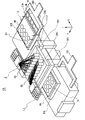
- FIG. 1 is a top view showing an overview of an FO-WLP wiring pattern forming system including an exposure apparatus according to the first embodiment.
- FIG. 2 is a perspective view schematically showing the configuration of the exposure apparatus according to the first embodiment.
- 3A and 3B are diagrams for explaining wiring patterns formed by the wiring pattern forming system.
- FIG. 4 is a diagram for explaining the modules arranged on the optical surface plate.
- FIG. 5A is a diagram showing the optical system of the illumination/projection module
- FIG. 5B is a diagram schematically showing the DMD
- FIG. 5D is a diagram illustrating a DMD
- FIG. 5D is a diagram for explaining a mirror in an ON state
- FIG. 5E is a diagram for explaining a mirror in an OFF state.
- FIG. 5A is a diagram showing the optical system of the illumination/projection module
- FIG. 5B is a diagram schematically showing the DMD
- FIG. 5D is a diagram illustrating a DMD
- FIG. 5D is
- FIG. 6 is an enlarged view of the vicinity of the illumination/projection module.
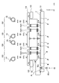
- FIG. 7 is a block diagram showing the control system of the exposure apparatus according to the first embodiment.
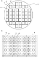
- FIG. 8A is a schematic diagram showing the wafer WF with all the chips arranged at the design positions, and FIG. It is a diagram.
- FIG. 9 is a conceptual diagram showing the FO-WLP wiring pattern forming procedure in the exposure apparatus.
- FIG. 10 is a top view showing the outline of the wiring pattern forming system according to the second embodiment.
- FIG. 11 is a conceptual diagram of the FO-WLP manufacturing procedure in the second embodiment.
- FIG. 12 is a top view showing the outline of the wiring pattern forming system according to the third embodiment.
- FIG. 1 when simply referred to as a substrate P, a rectangular substrate is indicated, and a wafer-shaped substrate is referred to as a wafer WF.
- the normal direction of the substrate P or wafer WF placed on a substrate stage 30 is the Z-axis direction, and the substrate P or wafer WF is applied to a spatial light modulator (SLM) in a plane perpendicular to the Z-axis direction.
- SLM spatial light modulator
- the direction in which the wafer WF is relatively scanned is the X-axis direction
- the direction orthogonal to the Z-axis and the Y-axis is the Y-axis direction
- the rotation (inclination) directions about the X-axis, Y-axis, and Z-axis are ⁇ x, ⁇ y, and ⁇ y, respectively. and .theta.z direction.
- Examples of spatial light modulators include liquid crystal devices, digital mirror devices (digital micromirror devices, DMD), magneto-optical spatial light modulators (MOSLMs), and the like.
- the exposure apparatus EX according to the first embodiment includes the DMD 204 as a spatial light modulator, but may include other spatial light modulators.
- FIG. 1 is a top view showing an overview of an FO-WLP and FO-PLP wiring pattern forming system 500 including an exposure apparatus EX according to one embodiment.
- FIG. 2 is a perspective view schematically showing the configuration of the exposure apparatus EX.
- the wiring pattern forming system 500 is arranged between semiconductor chips (hereinafter referred to as chips) arranged on a wafer WF as shown in FIG. 3A or on a substrate P as shown in FIG. 3B. This is a system for forming a wiring pattern that connects chips arranged on the same plane.
- a wiring pattern is formed to connect chips C1 and C2 included in each set of chips (indicated by two-dot chain lines) arranged on the wafer WF or substrate P.
- the wiring pattern forming system 500 includes a coater/developer device CD and an exposure device EX.
- the coater/developer device CD applies a photosensitive resist to the wafer WF.
- the resist-coated wafer WF is carried into the buffer section PB in which a plurality of wafers WF can be stocked.
- the buffer part PB also serves as a transfer port for the wafer WF.
- the buffer section PB is composed of a carry-in section and a carry-out section. Wafers WF coated with a resist are loaded one by one from the coater/developer apparatus CD into the loading section. The resist-coated wafers WF are loaded one by one from the coater/developer apparatus CD into the loading unit at predetermined time intervals. It functions as a buffer to store.
- the unloading unit functions as a buffer when unloading the exposed wafer WF to the coater/developer apparatus CD.
- the coater/developer apparatus CD can take out the exposed wafers WF only one by one. Therefore, a tray TR on which a plurality of exposed wafers WF are mounted is placed in the unloading section. Thereby, the coater/developer apparatus CD can take out the exposed wafers WF one by one from the tray TR.
- the exposure apparatus EX is composed of a main unit 1 and a substrate exchange unit 2.
- a robot RB is installed in the board exchange section 2 as shown in FIG.
- the robot RB arranges a plurality of wafers WF placed in the buffer part PB on one tray TR.
- the tray TR is a lattice-shaped tray that can sequentially place wafers WF of 4 wafers in a row on the substrate stages 30R and 30L.
- the tray TR may be a tray that can place the wafers WF on the entire surfaces of the substrate stages 30R and 30L at once (that is, a tray that can place wafers WF in 4 ⁇ 3 rows).
- the substrate replacement section 2 includes replacement arms 20R and 20L.
- the exchange arm 20R carries in/out a wafer WF (more specifically, a tray TR on which a plurality of wafers WF are placed) to/from the substrate holder PH of the substrate stage 30R.
- the wafer WF is loaded into and unloaded from the holder PH.
- the replacement arms 20R and 20L will be referred to as replacement arms 20 when there is no particular need to distinguish between them.
- illustration of the substrate holder PH is omitted except for FIG.
- two exchange arms 20R and 20L are arranged: a loading arm for loading the tray TR and a loading arm for loading the tray TR.
- the tray TR can be exchanged at high speed.
- the substrate exchange pins 10 support the grid-shaped tray TR.
- the tray TR sinks into grooves (not shown) formed in the substrate stage 30 , and the wafer WF is attracted and held by the substrate holder PH on the substrate stage 30 .
- FIG. 2 when a row of substrates is placed on the tray TR, the positions of the substrate stages 30R and 30L or The positions of the replacement arms 20R and 20L are changed.
- the positions of the alignment marks or wiring pads of the wafer WF are measured by the alignment system ALG-R or ALG-L mounted on the optical surface plate 110 .
- the measurement of the position of each wafer WF is performed by X-direction shift (X), Y-direction shift (Y), rotation (Rot), X-direction magnification (X_Mag),
- the number of measurement points and the arrangement of the measurement points are determined so that the six parameters of Y-direction magnification (Y_Mag) and orthogonality (Oth) can be calculated.
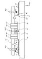
- a plurality of illumination/projection modules 200, an autofocus system AF, and alignment systems ALG_R, ALG_L, and ALG_C are arranged on the optical surface plate 110 kinematically supported on the column 100, as shown in FIG.
- FIG. 2 in this embodiment, a plurality of rows (four rows in FIG. 2) each including a plurality of illumination/projection modules 200 are arranged.
- FIG. 1 shows only one row including a plurality of illumination/projection modules 200 for simplification.
- illustration of alignment systems ALG_R and ALG_L is omitted for simplification.
- a plurality of illumination/projection modules 200 may be provided so that wiring patterns in different sets can be exposed at once, and the number of columns of the illumination/projection modules 200 may be 1 to 3, or 5. There may be more columns. Also, the number of illumination/projection modules 200 included in each row may be two or more. Further, when a plurality of wafers WF are placed on the substrate holder, different sets exposed at once by the illumination/projection module 200 may be different sets within the same wafer WF, or different sets within different wafers WF. may be a set of
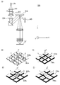
- FIG. 5A is a diagram showing the optical system of the illumination/projection module 200.
- the illumination/projection module 200 includes a collimator lens 201, a fly-eye lens 202, a main condenser lens 203, a DMD 204, and the like.
- the laser light emitted from the light source LS is taken into the illumination/projection module 200 through the delivery fiber FB.
- the laser light passes through a collimator lens 201, a fly-eye lens 202, and a main condenser lens 203, and illuminates the DMD 204 substantially uniformly.
- FIG. 5(B) is a diagram schematically showing the DMD 204
- FIG. 5(C) shows the DMD 204 when the power is off.
- mirrors in the ON state are indicated by hatching.
- the DMD 204 has a plurality of micromirrors 204a whose reflection angle can be changed and controlled. Each micromirror 204a is turned on by tilting around the Y axis.
- FIG. 5D shows the case where only the central micromirror 204a is in the ON state, and the other micromirrors 204a are in the neutral state (neither ON nor OFF state). Each micromirror 204a is turned off by tilting around the X axis.
- FIG. 5(E) shows a case where only the central micromirror 204a is in the OFF state and the other micromirrors 204a are in the neutral state.
- the DMD 204 switches between ON and OFF states of the micromirrors 204a to generate an exposure pattern of wiring connecting chips (hereinafter referred to as a wiring pattern).
- the illumination light reflected by the mirror in the OFF state is absorbed by the OFF light absorption plate 205 as shown in FIG. 5(A).
- the illumination/projection module 200 has a magnification for projecting one pixel of the DMD 204 with a predetermined size, and the magnification is slightly corrected by focusing by driving the lens on the Z-axis and by driving some lenses. It is possible. Further, the DMD 204 itself can be driven in the X direction, the Y direction, and the ⁇ z direction, and corrects the deviation of the substrate stage 30 from the target value, for example.
- the DMD 204 has been described as an example of the spatial light modulator, it is described as a reflective type that reflects laser light. A diffractive type may also be used.
- a spatial light modulator can spatially and temporally modulate laser light.
- the autofocus system AF is arranged so as to sandwich the illumination/projection module 200 .
- the measurement can be performed by the autofocus system AF before the exposure operation for forming the wiring pattern connecting the chips arranged on the wafer WF.
- FIG. 6 is an enlarged view of the vicinity of the illumination/projection module 200.
- a fixed mirror 54 for measuring the position of the substrate stage 30 is provided near the illumination/projection module 200 .
- the substrate stage 30 is provided with an alignment device 60 .
- the alignment device 60 includes a reference mark 60a, a two-dimensional imaging element 60e, and the like. Alignment device 60 is used to measure and calibrate the positions of various modules, and is also used to calibrate alignment systems ALG_R, ALG_L, and ALG_C arranged on optical surface plate 110 .
- each module is measured and calibrated by projecting the DMD pattern for calibration onto the reference mark 60a of the alignment device 60 with the illumination/projection module 200 and measuring the relative position between the reference mark 60a and the DMD pattern. Measure the position of each module.
- the alignment systems ALG_R, ALG_L, and ALG_C can be calibrated by measuring the reference mark 60a of the alignment device 60 with the alignment systems ALG_R, ALG_L, and ALG_C. That is, the positions of alignment systems ALG_R, ALG_L, and ALG_C can be obtained by measuring reference marks 60a of alignment device 60 in alignment systems ALG_R, ALG_L, and ALG_C. Furthermore, using the reference mark 60a, it is possible to determine the relative position with respect to the position of the module.
- the substrate stage 30 is provided with a movable mirror MR, a DM monitor 70, and the like, which are used to measure the position of the substrate stage 30.
- FIG. 1 a movable mirror MR, a DM monitor 70, and the like, which are used to measure the position of the substrate stage 30.
- Alignment systems ALG_R and ALG_L are equipped with a plurality of measuring microscopes, and align the positions of the chips arranged on each wafer WF placed on the substrate holder of the substrate stage 30 or the positions of the pads of the chips to be wired. 60 is measured with reference to the reference mark 60a. More specifically, alignment systems ALG_R and ALG_L measure the position of each chip based on the design position of each chip with reference to reference mark 60a. The measurement result is output to the data generation device 300, which will be described later.
- Alignment system ALG_C measures the position of wafer WF placed on the substrate holder of substrate stage 30 with reference to reference mark 60a of alignment device 60 before the start of exposure. Based on the measurement result of alignment system ALG_C, the positional deviation of wafer WF with respect to substrate stage 30 is detected, and the exposure start position and the like are changed.
- FIG. 7 is a block diagram showing the control system 600 of the exposure apparatus EX according to this embodiment.
- the control system 600 includes a data creation device 300, a first storage device 310R, a second storage device 310L, and an exposure control device 400.
- FIG. 7 is a block diagram showing the control system 600 of the exposure apparatus EX according to this embodiment.
- the control system 600 includes a data creation device 300, a first storage device 310R, a second storage device 310L, and an exposure control device 400.
- FIG. 7 is a block diagram showing the control system 600 of the exposure apparatus EX according to this embodiment.
- the control system 600 includes a data creation device 300, a first storage device 310R, a second storage device 310L, and an exposure control device 400.
- the data generation device 300 receives the measurement results of the position of each chip provided on the wafer WF placed on the substrate holder of the substrate stage 30 or the positions of the pads of each chip from the alignment systems ALG_R and ALG_L.
- the data creation device 300 determines a wiring pattern for connecting chips based on the measurement result of the position of each chip, and creates control data used to control the DMD 204 when generating the determined wiring pattern. Next, creation of control data will be described in more detail.
- FIG. 8(A) is a schematic diagram showing the wafer WF in which all the chips are arranged at the design position (hereinafter referred to as the design position).
- the wiring pattern WL connecting the chip C1 and the chip C2 is exposed (formed) by the exposure apparatus EX.
- the position of each chip may deviate from the designed position.
- the DMD 204 is controlled to expose the wiring pattern using data indicating the wiring pattern connecting the chips at the design position (hereinafter referred to as design value data)
- the wiring pattern shifts from the position of the pad. Bad connections and shorts can occur.
- the positions of the chips included in each set of multiple chips arranged on the wafer WF are measured by the alignment system ALG_R or ALG_L. Based on the measurement results obtained from alignment system ALG_R or ALG_L, data creation device 300 creates wiring pattern data by partially correcting the design value data.
- the created wiring pattern data is stored in the first storage device 310R or the second storage device 310L.
- the first storage device 310R and the second storage device 310L are, for example, SSDs (Solid State Drives).
- the first storage device 310R stores wiring pattern data used for controlling the DMD 204 when exposing the wafer WF placed on the substrate stage 30R.
- the second storage device 310L stores wiring pattern data used for controlling the DMD 204 when exposing the wafer WF placed on the substrate stage 30L.
- the wiring pattern data stored in the first storage device 310R or the second storage device 310L is transferred to the exposure control device 400.
- FIG. 9 is a conceptual diagram of the FO-WLP wiring pattern forming procedure in the exposure apparatus EX.
- the wafer WF on the substrate stage 30R is being exposed, the wafer WF is loaded onto the substrate stage 30L, and the chip position is determined by the alignment system ALG_L. Measurements are taken. Based on the chip position measurement results, the data creation device 300 sequentially creates wiring pattern data, and stores (transfers) the created wiring pattern data to the second storage device 310L. The wiring pattern data stored in the second storage device 310L are sequentially transferred to the exposure control device 400 in synchronization with the start of exposure of the wafer WF on the substrate stage 30L.
- the tray TR is placed on the substrate stage 30L after the four wafers WF have been placed on one tray TR.
- measurement of the chip position may be started with alignment system ALG_L.
- the measurement of the chip position by the alignment system ALG_L and the process of placing another wafer WF on the next tray TR can be performed in parallel.
- the wiring pattern data of the wafer WF whose chip positions have already been measured is obtained based on the measurement result of the alignment system ALG_L. can be created and stored in the second storage device 310L.
- Such parallel processing is particularly effective when it takes time to create, transfer and store wiring pattern data. If the time required to measure the chip positions and to create and store the wiring pattern data is shorter than the exposure time, for example, after placing the wafers WF of, for example, 4 ⁇ 3 rows on one tray TR, It may be loaded onto the substrate stage 30L and measured by the alignment system ALG_L. In the mounting process, either a mounting operation of mounting the wafer WF on the tray TR or a mounting preparation operation of preparing to mount the wafer WF on the tray TR may be performed.
- the exposure of the wafer WF on the substrate stage 30L is started, the exposed wafer WF on the substrate stage 30R is unloaded, and then a new wafer WF is loaded onto the substrate stage 30R. Thereafter, the chip position is measured by alignment system ALG_R. Based on the chip position measurement results, the data creation device 300 sequentially creates wiring pattern data and transfers the created wiring pattern data to the first storage device 310R. The wiring pattern data stored in the first storage device 310R are sequentially transferred to the exposure control device 400 in synchronization with the start of exposure of the wafer WF on the substrate stage 30R.
- the other substrate stage carries out the exposed wafer, carries in a new wafer, and changes the chip position. are measured, and wiring pattern data is created and transferred.
- the exposure processing includes a series of operations from driving the substrate stage for performing exposure to driving the substrate stage to the substrate exchange position after the exposure is completed.
- the exposure apparatus EX includes a spatial light modulator (the DMD 204 in the first embodiment), the data creation device 300, and the exposure control device 400.
- the exposure apparatus EX also includes a plurality of substrate stages 30R, 30L and alignment systems ALG_R, ALG_L.
- Alignment system ALG_L is included in each set of a plurality of semiconductor chips arranged on wafer WF mounted on substrate stage 30L while the wiring pattern is being exposed on wafer WF mounted on substrate stage 30R. Measure the positions of the chips C1 and C2 where they are placed.
- Data generation device 300 acquires the measurement result from alignment system ALG_L, and based on the measurement result, determines the distance between chip C1 and chip C2 included in each of a plurality of sets of chips arranged on wafer WF on substrate stage 30L. determine the wiring pattern WL for connecting the . Then, the data creation device 300 creates wiring pattern data used for controlling the DMD 204 when generating the determined wiring pattern WL, and stores the wiring pattern data in the second storage device 310L. When the exposure processing on the substrate stage 30R is completed, the exposure control device 400 controls the DMD 204 using the wiring pattern data stored in the second storage device 310L, and the wafer WF placed on the substrate stage 30L. Wiring patterns WL connecting chips C1 and C2 included in each set are exposed.
- the chip positions on the substrate placed on the substrate stage 30L can be measured, and the wiring pattern data can be created and transferred based on the measurement results. can be done.
- the time can be used effectively, and the throughput in forming the wiring pattern of the FO-WLP can be improved.
- a plurality of wafers WF are arranged on the substrate stages 30R and 30L provided in the exposure apparatus EX.
- the exposure apparatus EX includes a plurality of exchange arms 20R, 20L for exchanging wafers WF held by the substrate stages 30R, 30L, respectively. Then, for example, while the wafer WF on the substrate stage 30R is being exposed, the exchange arm 20L exchanges the wafer WF on the substrate stage 30L. As a result, the time can be used effectively, and the throughput in forming the wiring pattern of the FO-WLP can be improved.
- the exposure apparatus EX includes a plurality of DMDs 204, and each of the plurality of DMDs 204 forms wiring patterns that connect semiconductor chips in different sets.
- wiring patterns connecting semiconductor chips in different sets can be formed at the same time, so that throughput in forming wiring patterns of FO-WLP can be improved.
- the other substrate stage carries out the exposed wafer, carries in a new wafer, and changes the position of the chip. measurement, and creation and transfer of wiring pattern data, but the present invention is not limited to this. While exposure processing is being performed using one of the two substrate stages 30R and 30L, the other substrate stage carries out an exposed wafer, loads a new wafer, measures chip positions, and transfers wiring pattern data. At least one of creation and transfer should be performed.
- the data creation device 300 may create drive data defining the drive amount of the DMD 204 and the drive amount of the lens actuator instead of the wiring pattern data. That is, the DMD 204 generates a wiring pattern using the design value data, and changes the driving amount of the DMD 204 and the driving amount of the lens actuator to change the position of the projection image of the wiring pattern projected onto the wafer WF.
- the shape of the wiring pattern formed on the wafer WF may be changed.
- the shape of the wiring pattern may be changed by optically correcting the image of the wiring pattern.
- the data creation device 300 uses the measurement data acquired in the inspection step of inspecting the position of each chip with respect to the wafer WF. may be used to create wiring pattern data or drive data.
- FIG. 10 is a top view showing an outline of a wiring pattern forming system 500A according to the second embodiment.
- a wiring pattern forming system 500A according to the second embodiment includes a chip measurement station CMS that measures the positions of the chips on the wafer WF.
- the chip measuring station CMS has a plurality of measuring microscopes 61 and measures the positions of chips in different sets.
- the positions of chips in different sets measured by the plurality of measuring microscopes 61 may be the positions of chips in different sets on the same wafer WF, or the positions of chips in each set on different wafers WF. It's okay.
- a plurality of measurement microscopes 61 measure the positions of chips in each set on different wafers WF.
- the measurement result of the chip position is transmitted to the data generation device 300.
- the data creation device 300 creates wiring pattern data (or drive data) based on the chip position measurement results received from the chip measurement station CMS.
- the wiring pattern data created by the data creating device 300 is stored in a storage device different from the storage device in which the wiring pattern data used for exposure control of the substrate currently being exposed is stored. That is, when the wiring pattern data used for exposure control of the wafer WF currently being exposed is stored in the first storage device 310R, the data creation device 300 stores the created wiring pattern data in the second storage device 310L. Store (transfer).
- the main body 1A has one substrate stage 30. As shown in FIG. In the second embodiment, since the chip position is measured by the chip measurement station CMS, the alignment systems ALG_L and ALG_R can be omitted.
- the wafer WF whose chip positions have been measured is coated with a photosensitive resist by the coater/developer apparatus CD, and then carried into the buffer section PB.
- a plurality of wafers WF (in the second embodiment, 4 wafers ⁇ 3 rows) are arranged on one tray TR by the robot RB installed in the substrate exchange section 2A, and the wafers WF placed on the buffer section PB are arranged on one tray TR. , and placed on the substrate holder of the substrate stage 30 .
- Alignment system ALG_C measures the position of each wafer WF with respect to the substrate holder, and corrects the exposure start position and the like.
- the wafer WF is placed on the substrate holder and the wafer WF rotates around the Z axis, for example, when the position of the chip deviates from the position of the wiring pattern data created by the data creating device 300, the wiring pattern may be shifted. If wiring is formed using data, the chips may not be properly connected.
- the data creation device 300 creates wiring pattern data or drive data as described in the first embodiment and its modification, thereby changing the shape of the wiring pattern so that the chips are connected. Correction should be made. For example, based on the position of each wafer WF with respect to the position of each wafer WF measured by the chip measurement station CMS, the data generation device 300 calculates the distance from the position of each wafer WF measured by the alignment system ALG_C to the position of the wiring pattern data. Positional deviation of each chip is detected. The data creation device 300 corrects the wiring pattern data or creates drive data based on the deviation. As a result, even if the wafer WF is rotated around the Z-axis when the wafer WF is placed on the substrate holder, it is possible to form the wiring that connects the chips.
- Alignment system ALG_C may use the alignment mark of the chip for the position measurement of wafer WF.
- FIG. 11 is a conceptual diagram of the FO-WLP wiring pattern formation procedure in the second embodiment.
- the throughput in forming the wiring pattern of the FO-WLP can be improved.
- the exposure apparatus EX includes a spatial light modulator (DMD 204), a data creation device 300, and an exposure control device 400.
- the data generation device 300 acquires measurement results from the chip measurement station CMS that measures the positions of the chips C1 and C2 included in each of a plurality of sets of semiconductor chips arranged on the wafer WF. determines the wiring pattern WL connecting the chip C1 and the chip C2 included in the first storage device 310R or It is stored in the second storage device 310L.
- the exposure control device 400 controls the DMD 204 using the wiring pattern data stored in the first storage device 310R or the second storage device 310L to connect the chips C1 and C2 included in each set.
- the wiring pattern WL is exposed.
- the measurement of the positions of the chips on the wafer WF is performed while a set of wafers WF different from the set of wafers WF whose chip positions are to be measured together with the wafer WF is being exposed.
- a set of wafers WF different from the set of wafers WF whose chip positions are to be measured together with the wafer WF is being exposed.
- the wafer WF may be attached to the base substrate B, and the position of each chip with respect to the base substrate B may be measured at the chip measurement station CMS.
- FIG. 12 is a top view showing an outline of a wiring pattern forming system 500B according to the third embodiment.
- a wiring pattern forming system 500B according to the third embodiment has a wafer arranging apparatus WA for attaching a plurality of wafers WF on which chips are arranged to a base substrate B.
- the wafer placement device WA prevents the position of the wafer WF with respect to the base substrate B from being changed.
- the base substrate B to which a plurality of wafers WF are attached by the wafer placement device WA is carried into the chip measurement station CMS.
- the chip measuring station CMS has a plurality of measuring microscopes 61 and measures the position of each chip with respect to the base substrate B.
- a plurality of metrology microscopes 61 measure the positions of chips in different sets.
- a measurement result of the position of the chip is transmitted to the data generation device 300 .
- the data creation device 300 creates wiring pattern data (or drive data) based on the chip position measurement results received from the chip measurement station CMS.
- the wiring pattern data created by the data creating device 300 is stored in a storage device different from the storage device in which the wiring pattern data used for exposure control of the wafer WF on the base substrate B currently being exposed is stored. be done. That is, when the wiring pattern data used for exposure control of the wafer WF on the base substrate B which is currently being exposed is stored in the first storage device 310R, the data generation device 300 transfers the generated wiring pattern data to the first storage device 310R. 2 is stored (transferred) to the storage device 310L.
- the wafer WF whose chip positions have been measured is carried into the coater/developer apparatus CD together with the base substrate B, coated with a photosensitive resist, and then carried into the port PT of the substrate exchange section 2B. After that, the wafer WF is placed on the substrate holder of the substrate stage 30 together with the base substrate B. As shown in FIG.
- the position of the base substrate B on which the wafer WF is mounted and fixed can be used to manage and expose everything.
- EGA measurement and correction for the base substrate B may be performed during alignment as well.
- the wafer WF is placed and fixed on the base substrate B, when the base substrate B is placed on the substrate holder of the substrate stage 30, alignment for each wafer WF/chip is not required, and the base substrate Alignment of only B may be performed.
- the wafer WF is attached to the base substrate B in the wafer arranging apparatus WA, the wafer WF may be directly placed and fixed on the tray TR.
- the formation of the rewiring layer of the FO-WLP Throughput can be improved.
- the wafer placement apparatus WA and the chip measurement station CMS are separate apparatuses, but the configuration is not limited to this.
- the measurement microscope 61 may start measuring the chip positions from the wafer WF attached to the base substrate B in the wafer placement apparatus WA. In other words, the measurement operation is performed by the measurement microscope 61 in parallel with the operation of attaching the plurality of wafers WF to the base substrate B.
- the measuring microscope 61 may start the measurement operation after one wafer WF is attached to the base substrate B, or may start the measurement operation after a plurality of wafers WF are attached to the base substrate B. You can start working.
- the measurement operation of the measurement microscope 61 may be temporarily interrupted at the timing when the wafer WF is placed on the base substrate B. FIG. This is to prevent vibrations generated when the wafer WF is placed on the base substrate B from affecting the measurement results of the measuring microscope 61 .
- the first storage device 310R and the second storage device 310L are separate storage devices.
- data (at least one of wiring pattern data and drive data) used for exposure processing of the wafer WF placed on the substrate stage 30L (at least one of wiring pattern data and drive data); may be stored in different storage areas of one storage device.
- the deterioration of the SSD progresses with each writing, and the usage time also affects its lifespan. Therefore, since the number of data writes to the storage device in the first embodiment is relatively large, if one SSD is used, there is a possibility that the SSD will need to be replaced in a short period of time. Therefore, it is preferable to use two storage devices.
- first to third embodiments and their modifications can also be applied to the formation of wiring patterns connecting chips on the substrate P shown in FIG. 3(B).
- EX, EX-A, EX-B Exposure device 204 DMD 204a micromirror 300 data creation device 310R first storage device 310L second storage device 400 exposure control devices C1, C2 semiconductor chip WF wafer P substrate
Abstract
Description
第1実施形態に係る露光装置について、図1~図9に基づいて説明する。なお、以後の説明において、単に基板Pと記載した場合には、矩形状の基板を示し、ウエハ状の基板についてはウエハWFと記載する。また、後述する基板ステージ30に載置された基板PまたはウエハWFの法線方向をZ軸方向、これに直交する面内で空間光変調器(SLM:Spatial Light Modulator)に対して基板PまたはウエハWFが相対走査される方向をX軸方向、Z軸及びY軸に直交する方向をY軸方向とし、X軸、Y軸、及びZ軸周りの回転(傾斜)方向をそれぞれθx、θy、及びθz方向として説明を行なう。空間光変調器の例としては、液晶素子、デジタルミラーデバイス(デジタルマイクロミラーデバイス、DMD)、磁気光学空間光変調器(MOSLM:Magneto Optic Spatial Light Modulator)等が挙げられる。第1実施形態に係る露光装置EXは、空間光変調器としてDMD204を備えるが、他の空間光変調器を備えていてもよい。 <<1st Embodiment>>
An exposure apparatus according to the first embodiment will be described with reference to FIGS. 1 to 9. FIG. In the following description, when simply referred to as a substrate P, a rectangular substrate is indicated, and a wafer-shaped substrate is referred to as a wafer WF. The normal direction of the substrate P or wafer WF placed on a substrate stage 30 (to be described later) is the Z-axis direction, and the substrate P or wafer WF is applied to a spatial light modulator (SLM) in a plane perpendicular to the Z-axis direction. The direction in which the wafer WF is relatively scanned is the X-axis direction, the direction orthogonal to the Z-axis and the Y-axis is the Y-axis direction, and the rotation (inclination) directions about the X-axis, Y-axis, and Z-axis are θx, θy, and θy, respectively. and .theta.z direction. Examples of spatial light modulators include liquid crystal devices, digital mirror devices (digital micromirror devices, DMD), magneto-optical spatial light modulators (MOSLMs), and the like. The exposure apparatus EX according to the first embodiment includes the
なお、データ作成装置300は、配線パターンデータではなく、DMD204の駆動量及びレンズアクチュエータの駆動量を規定した駆動データを作成してもよい。すなわち、DMD204は設計値データを用いて配線パターンを生成し、DMD204の駆動量及びレンズアクチュエータの駆動量を変更することで、ウエハWF上に投影される配線パターンの投影像の位置を変更し、ウエハWF上に形成される配線パターンの形状を変化させてもよい。なお、光学的に配線パターンの像を補正することによって、配線パターンの形状を変更してもよい。 (Modification)
Note that the
ウエハWFにチップを貼り付ける工程は、露光装置EXでの配線パターンの形成前に行われるため、データ作成装置300は、ウエハWFに対する各チップの位置を検査する検査工程にて取得した計測データを用いて、配線パターンデータまたは駆動データを作成してもよい。 <<Second embodiment>>
Since the step of attaching the chips to the wafer WF is performed before the wiring pattern is formed in the exposure apparatus EX, the
ウエハWFをベース基板Bに貼り付け、ベース基板Bに対する各チップの位置を、チップ計測ステーションCMSにおいて計測してもよい。 <<Third embodiment>>
The wafer WF may be attached to the base substrate B, and the position of each chip with respect to the base substrate B may be measured at the chip measurement station CMS.
第3実施形態では、ウエハ配置装置WAとチップ計測ステーションCMSとが別の装置としたが、この構成に限られない。計測顕微鏡61は、ウエハ配置装置WAにて、ベース基板Bに貼り付けられたウエハWFからチップ位置の計測を開始しても良い。換言すると、複数のウエハWFのベース基板Bへの貼り付け動作と並行して、計測顕微鏡61により計測動作を行う。なお、計測顕微鏡61は、1枚のウエハWFがベース基板Bに貼り付けられてから、計測動作を開始しても良いし、複数枚のウエハWFがベース基板Bに貼り付けられてから、計測動作を開始しても良い。なお、計測顕微鏡61は、ウエハWFがベース基板Bに載置されるタイミングでは、一旦計測動作を中断しても良い。これは、ウエハWFをベース基板Bへ載置する際に発生する振動が、計測顕微鏡61の計測結果に影響を与えることを防止するためである。 (Modification)
In the third embodiment, the wafer placement apparatus WA and the chip measurement station CMS are separate apparatuses, but the configuration is not limited to this. The
204 DMD
204a マイクロミラー
300 データ作成装置
310R 第1記憶装置
310L 第2記憶装置
400 露光制御装置
C1,C2 半導体チップ
WF ウエハ
P 基板
EX, EX-A,
Claims (9)
- 空間光変調器と、
第1の基板上に複数配置された半導体チップのセットそれぞれに含まれる前記半導体チップの位置を計測する計測系から計測結果を取得し、前記計測結果に基づいて、前記セットそれぞれに含まれる前記半導体チップ間を接続する配線パターンを決定し、決定した前記配線パターンを生成するときに前記空間光変調器の制御に利用する第1の制御データを作成し、第1の記憶部に記憶させる作成部と、
前記第1の記憶部に記憶された前記第1の制御データを用いて前記空間光変調器を制御して、前記セットそれぞれに含まれる前記半導体チップ間を接続する配線パターンを露光する露光処理部と、
を備え、
前記露光処理部が前記第1の基板とは異なる第2の基板を露光処理している間に、前記第1の基板上の前記半導体チップの位置の計測、前記計測結果の取得、前記配線パターンの決定、前記第1の制御データの作成、及び前記第1の制御データの前記第1の記憶部への記憶、の少なくとも1つが実行される、
露光装置。 a spatial light modulator;
acquiring measurement results from a measurement system that measures the positions of the semiconductor chips included in each of a plurality of sets of semiconductor chips arranged on a first substrate; and based on the measurement results, the semiconductors included in each of the sets A creation unit that determines a wiring pattern for connecting chips, creates first control data used for controlling the spatial light modulator when generating the determined wiring pattern, and stores the first control data in a first storage unit. When,
An exposure processing unit that controls the spatial light modulator using the first control data stored in the first storage unit to expose wiring patterns that connect the semiconductor chips included in each of the sets. When,
with
measurement of the position of the semiconductor chip on the first substrate, acquisition of the measurement result, and the wiring pattern while the exposure processing unit is exposing a second substrate different from the first substrate. At least one of the determination of, creation of the first control data, and storage of the first control data in the first storage unit is performed.
Exposure equipment. - 前記第1の基板は、前記露光装置が備える基板ホルダ上に複数配置される、
請求項1に記載の露光装置。 A plurality of the first substrates are arranged on a substrate holder provided in the exposure apparatus.
The exposure apparatus according to claim 1. - 複数の基板ホルダと、
前記計測系と、
を備え、
前記複数の基板ホルダのうちの第1の基板ホルダには前記第1の基板が載置され、
前記露光処理部が、前記第1の基板上に前記配線パターンを露光処理している間に、前記計測系による前記第1の基板ホルダとは異なる第2の基板ホルダに載置された基板上に複数配置された半導体チップのセットそれぞれに含まれる前記半導体チップの位置の計測、前記作成部による、前記半導体チップの位置の計測結果の取得、前記作成部による、前記計測結果に基づく前記第2の基板ホルダに載置された基板上の前記セットそれぞれに含まれる前記半導体チップ間を接続する配線パターンの決定、前記作成部による、決定した前記配線パターンを生成するときに前記空間光変調器の制御に利用する第2の制御データの作成、及び前記作成部による、前記第2の制御データの前記第1の記憶部とは異なる第2の記憶部への記憶、の少なくとも1つが実行される、
請求項1または請求項2に記載の露光装置。 a plurality of substrate holders;
the measurement system;
with
The first substrate is mounted on a first substrate holder among the plurality of substrate holders,
On the substrate placed on the second substrate holder different from the first substrate holder by the measurement system while the exposure processing unit is exposing the wiring pattern on the first substrate measurement of the positions of the semiconductor chips included in each set of a plurality of semiconductor chips arranged in the second determination of a wiring pattern connecting between the semiconductor chips included in each of the sets on the substrate placed on the substrate holder of the spatial light modulator when the determined wiring pattern is generated by the creation unit; At least one of creating second control data used for control and storing the second control data in a second storage unit different from the first storage unit by the creating unit is executed. ,
3. An exposure apparatus according to claim 1 or 2. - 前記複数の基板ホルダそれぞれが保持する基板を交換する複数の交換手段を備え、
前記第1の基板の露光処理中に、前記複数の交換手段の1つが前記第2の基板ホルダが保持する基板の交換を行う、
請求項3に記載の露光装置。 comprising a plurality of exchanging means for exchanging the substrates held by each of the plurality of substrate holders;
During exposure processing of the first substrate, one of the plurality of exchange means exchanges the substrate held by the second substrate holder;
The exposure apparatus according to claim 3. - 前記計測系は、複数の計測装置を備え、
前記複数の計測装置は、異なる半導体チップの位置を略同時に計測する、
請求項1から請求項4のいずれか1項記載の露光装置。 The measurement system includes a plurality of measurement devices,
The plurality of measurement devices measure positions of different semiconductor chips substantially simultaneously,
An exposure apparatus according to any one of claims 1 to 4. - 前記空間光変調器を複数備え、
複数の前記空間光変調器はそれぞれ、異なるセット内の前記半導体チップ間を接続する配線パターンを形成する、
請求項1から請求項5のいずれか1項記載の露光装置。 comprising a plurality of spatial light modulators,
each of the plurality of spatial light modulators forms a wiring pattern connecting between the semiconductor chips in different sets;
An exposure apparatus according to any one of claims 1 to 5. - 複数の前記第1の基板のうち、前記基板ホルダ上に載置された載置済み基板の前記半導体チップの位置の計測を行うとともに、前記基板ホルダに載置されていない未載置基板の前記基板ホルダへの載置処理を行う、
請求項2に記載の露光装置。 Among the plurality of first substrates, the positions of the semiconductor chips of the placed substrate placed on the substrate holder are measured, and the position of the semiconductor chip of the non-placed substrate not placed on the substrate holder is measured. Place the substrate on the holder,
3. An exposure apparatus according to claim 2. - 前記作成部は、前記半導体チップの位置の計測が終わった前記載置済み基板から順番に、前記第1の制御データを作成し、前記第1の制御データを前記第1の記憶部へ記憶させる、
請求項7に記載の露光装置。 The creation unit creates the first control data in order from the mounted substrate for which measurement of the position of the semiconductor chip is completed, and stores the first control data in the first storage unit. ,
The exposure apparatus according to claim 7. - 第1の基板上に複数配置された半導体チップのセットそれぞれに含まれる前記半導体チップの位置を計測する計測系から計測結果を取得し、前記計測結果に基づいて、前記セットそれぞれに含まれる前記半導体チップ間を接続する配線パターンを決定し、決定した前記配線パターンを生成するときに空間光変調器の制御に利用する第1の制御データを作成し、第1の記憶部に記憶させることと、
前記第1の記憶部に記憶された前記第1の制御データを用いて前記空間光変調器を制御して、前記セットそれぞれに含まれる前記半導体チップ間を接続する配線パターンを露光することと、
を含み、
前記第1の基板とは異なる第2の基板を露光処理している間に、前記第1の基板上の前記半導体チップの位置を計測することと、前記計測結果を取得することと、前記配線パターンを決定することと、前記第1の制御データを作成することと、前記第1の制御データを前記第1の記憶部に記憶させることと、の少なくとも1つを実行する、
配線パターン形成方法。
acquiring measurement results from a measurement system that measures the positions of the semiconductor chips included in each of a plurality of sets of semiconductor chips arranged on a first substrate; and based on the measurement results, the semiconductors included in each of the sets determining a wiring pattern for connecting chips, creating first control data used for controlling a spatial light modulator when generating the determined wiring pattern, and storing the first control data in a first storage unit;
exposing a wiring pattern connecting between the semiconductor chips included in each of the sets by controlling the spatial light modulator using the first control data stored in the first storage unit;
including
measuring the position of the semiconductor chip on the first substrate, obtaining the measurement result, and the wiring while performing exposure processing on a second substrate different from the first substrate; performing at least one of determining a pattern, creating the first control data, and storing the first control data in the first storage unit;
Wiring pattern formation method.
Priority Applications (4)
| Application Number | Priority Date | Filing Date | Title |
|---|---|---|---|
| KR1020237032331A KR20230148231A (en) | 2021-04-09 | 2022-02-28 | Exposure device and wiring pattern formation method |
| CN202280027047.XA CN117120934A (en) | 2021-04-09 | 2022-02-28 | Exposure apparatus and wiring pattern forming method |
| JP2023512859A JPWO2022215385A1 (en) | 2021-04-09 | 2022-02-28 | |
| US18/238,027 US20230400773A1 (en) | 2021-04-09 | 2023-08-25 | Exposure apparatus and wiring pattern forming method |
Applications Claiming Priority (2)
| Application Number | Priority Date | Filing Date | Title |
|---|---|---|---|
| JP2021-066770 | 2021-04-09 | ||
| JP2021066770 | 2021-04-09 |
Related Child Applications (1)
| Application Number | Title | Priority Date | Filing Date |
|---|---|---|---|
| US18/238,027 Continuation US20230400773A1 (en) | 2021-04-09 | 2023-08-25 | Exposure apparatus and wiring pattern forming method |
Publications (1)
| Publication Number | Publication Date |
|---|---|
| WO2022215385A1 true WO2022215385A1 (en) | 2022-10-13 |
Family
ID=83545839
Family Applications (1)
| Application Number | Title | Priority Date | Filing Date |
|---|---|---|---|
| PCT/JP2022/008212 WO2022215385A1 (en) | 2021-04-09 | 2022-02-28 | Exposure device and wiring pattern formation method |
Country Status (6)
| Country | Link |
|---|---|
| US (1) | US20230400773A1 (en) |
| JP (1) | JPWO2022215385A1 (en) |
| KR (1) | KR20230148231A (en) |
| CN (1) | CN117120934A (en) |
| TW (1) | TW202240314A (en) |
| WO (1) | WO2022215385A1 (en) |
Citations (6)
| Publication number | Priority date | Publication date | Assignee | Title |
|---|---|---|---|---|
| JP2009282497A (en) * | 2008-04-22 | 2009-12-03 | Fujifilm Corp | Laser exposure method, photoresist layer working method, and pattern molding manufacturing method |
| JP2013058520A (en) * | 2011-09-07 | 2013-03-28 | Dainippon Screen Mfg Co Ltd | Lithography apparatus, data correction apparatus, method for forming re-wiring layer, and method for correcting data |
| JP3200372U (en) * | 2014-08-01 | 2015-10-15 | アプライド マテリアルズ インコーポレイテッドApplied Materials,Incorporated | Dual stage / dual chuck for maskless lithography |
| JP2016071022A (en) * | 2014-09-29 | 2016-05-09 | 株式会社Screenホールディングス | Wiring data creation device, creation method and drawing system |
| WO2019231518A1 (en) * | 2018-05-31 | 2019-12-05 | Applied Materials, Inc. | Multi-substrate processing on digital lithography systems |
| US20200159132A1 (en) * | 2018-11-15 | 2020-05-21 | Applied Materials, Inc. | Dynamic generation of layout adaptive packaging |
Family Cites Families (1)
| Publication number | Priority date | Publication date | Assignee | Title |
|---|---|---|---|---|
| JP6364059B2 (en) | 2016-11-18 | 2018-07-25 | キヤノン株式会社 | Exposure apparatus, exposure method, and article manufacturing method |
-
2022
- 2022-02-28 WO PCT/JP2022/008212 patent/WO2022215385A1/en active Application Filing
- 2022-02-28 KR KR1020237032331A patent/KR20230148231A/en active Search and Examination
- 2022-02-28 JP JP2023512859A patent/JPWO2022215385A1/ja active Pending
- 2022-02-28 CN CN202280027047.XA patent/CN117120934A/en active Pending
- 2022-03-01 TW TW111107297A patent/TW202240314A/en unknown
-
2023
- 2023-08-25 US US18/238,027 patent/US20230400773A1/en active Pending
Patent Citations (6)
| Publication number | Priority date | Publication date | Assignee | Title |
|---|---|---|---|---|
| JP2009282497A (en) * | 2008-04-22 | 2009-12-03 | Fujifilm Corp | Laser exposure method, photoresist layer working method, and pattern molding manufacturing method |
| JP2013058520A (en) * | 2011-09-07 | 2013-03-28 | Dainippon Screen Mfg Co Ltd | Lithography apparatus, data correction apparatus, method for forming re-wiring layer, and method for correcting data |
| JP3200372U (en) * | 2014-08-01 | 2015-10-15 | アプライド マテリアルズ インコーポレイテッドApplied Materials,Incorporated | Dual stage / dual chuck for maskless lithography |
| JP2016071022A (en) * | 2014-09-29 | 2016-05-09 | 株式会社Screenホールディングス | Wiring data creation device, creation method and drawing system |
| WO2019231518A1 (en) * | 2018-05-31 | 2019-12-05 | Applied Materials, Inc. | Multi-substrate processing on digital lithography systems |
| US20200159132A1 (en) * | 2018-11-15 | 2020-05-21 | Applied Materials, Inc. | Dynamic generation of layout adaptive packaging |
Also Published As
| Publication number | Publication date |
|---|---|
| TW202240314A (en) | 2022-10-16 |
| CN117120934A (en) | 2023-11-24 |
| JPWO2022215385A1 (en) | 2022-10-13 |
| US20230400773A1 (en) | 2023-12-14 |
| KR20230148231A (en) | 2023-10-24 |
Similar Documents
| Publication | Publication Date | Title |
|---|---|---|
| KR100975256B1 (en) | Exposure method, exposure apparatus, and method of manufacturing a device | |
| US7593100B2 (en) | Measuring method, measuring system, inspecting method, inspecting system, exposure method and exposure system, in which information as to the degree of the flatness of an object is pre-obtained | |
| JPH0945608A (en) | Surface position detection method | |
| KR20100028560A (en) | Exposure method and electronic device manufacturing method | |
| KR100882046B1 (en) | Exposure apparatus and device manufacturing method | |
| JP2006186372A (en) | Method and system for automated process correction using model parameters, and lithographic apparatus using such method and system | |
| WO2022215385A1 (en) | Exposure device and wiring pattern formation method | |
| JP2010087310A (en) | Exposure apparatus, and method of manufacturing device | |
| WO2023286732A1 (en) | Exposure device and measurement system | |
| WO2023286726A1 (en) | Exposure device and wiring pattern forming method | |
| JP3381313B2 (en) | Exposure apparatus, exposure method, and element manufacturing method | |
| JP2020140070A (en) | Exposure apparatus and exposure method | |
| WO2023286724A1 (en) | Exposure apparatus | |
| US20240142877A1 (en) | Exposure apparatus and measurement system | |
| JP4078683B2 (en) | Projection exposure apparatus, projection exposure method, and scanning exposure method | |
| US11392038B2 (en) | Maskless exposure apparatus and method, and manufacturing method of a semiconductor device including the maskless exposure method | |
| JP5379638B2 (en) | Exposure apparatus, exposure method, and device manufacturing method | |
| JPH10284393A (en) | Aligner and fabrication of device | |
| KR20080018684A (en) | Equipment for manufacturing semiconductor device and wafer align methode used the same | |
| JP5415842B2 (en) | Drawing system and pattern forming system | |
| JP4961717B2 (en) | Device manufacturing processing system, exposure apparatus and exposure method, measurement inspection apparatus and measurement inspection method, and device manufacturing method | |
| WO2022215692A1 (en) | Exposure apparatus, method for manufacturing device, method for manufacturing flat panel display, and exposure method | |
| JPH11233430A (en) | Method for evaluating flatness of substrate holder of projection aligner | |
| KR20230113145A (en) | Exposure method, exposure apparatus, and method of manufacturing article | |
| JP2008131018A (en) | Exposure apparatus, object carrying device, and method of carrying mask |
Legal Events
| Date | Code | Title | Description |
|---|---|---|---|
| 121 | Ep: the epo has been informed by wipo that ep was designated in this application |
Ref document number: 22784370 Country of ref document: EP Kind code of ref document: A1 |
|
| WWE | Wipo information: entry into national phase |
Ref document number: 2023512859 Country of ref document: JP |
|
| ENP | Entry into the national phase |
Ref document number: 20237032331 Country of ref document: KR Kind code of ref document: A |
|
| WWE | Wipo information: entry into national phase |
Ref document number: 1020237032331 Country of ref document: KR |
|
| NENP | Non-entry into the national phase |
Ref country code: DE |
|
| 122 | Ep: pct application non-entry in european phase |
Ref document number: 22784370 Country of ref document: EP Kind code of ref document: A1 |