WO2022202418A1 - Antenna and antenna device - Google Patents
Antenna and antenna device Download PDFInfo
- Publication number
- WO2022202418A1 WO2022202418A1 PCT/JP2022/011082 JP2022011082W WO2022202418A1 WO 2022202418 A1 WO2022202418 A1 WO 2022202418A1 JP 2022011082 W JP2022011082 W JP 2022011082W WO 2022202418 A1 WO2022202418 A1 WO 2022202418A1
- Authority
- WO
- WIPO (PCT)
- Prior art keywords
- conductor
- antenna
- ground
- legs
- ground plane
- Prior art date
Links
- 239000004020 conductor Substances 0.000 claims abstract description 246
- 239000012212 insulator Substances 0.000 claims description 7
- 230000003071 parasitic effect Effects 0.000 claims 1
- 238000010586 diagram Methods 0.000 description 15
- 239000002184 metal Substances 0.000 description 10
- 238000012986 modification Methods 0.000 description 8
- 230000004048 modification Effects 0.000 description 8
- 238000005452 bending Methods 0.000 description 6
- 238000000034 method Methods 0.000 description 6
- 230000008878 coupling Effects 0.000 description 5
- 238000010168 coupling process Methods 0.000 description 5
- 238000005859 coupling reaction Methods 0.000 description 5
- 238000004891 communication Methods 0.000 description 4
- 239000000919 ceramic Substances 0.000 description 3
- 230000000694 effects Effects 0.000 description 3
- 238000002955 isolation Methods 0.000 description 3
- 238000004904 shortening Methods 0.000 description 3
- 239000003990 capacitor Substances 0.000 description 2
- 230000006866 deterioration Effects 0.000 description 2
- 239000000463 material Substances 0.000 description 2
- 230000005855 radiation Effects 0.000 description 2
- 239000000725 suspension Substances 0.000 description 2
- 238000012795 verification Methods 0.000 description 2
- 241000251730 Chondrichthyes Species 0.000 description 1
- 230000005540 biological transmission Effects 0.000 description 1
- 239000000470 constituent Substances 0.000 description 1
- 238000010276 construction Methods 0.000 description 1
- 238000013461 design Methods 0.000 description 1
- 239000003989 dielectric material Substances 0.000 description 1
- 230000005684 electric field Effects 0.000 description 1
- 230000005611 electricity Effects 0.000 description 1
- 230000005672 electromagnetic field Effects 0.000 description 1
- 238000004519 manufacturing process Methods 0.000 description 1
- 239000011347 resin Substances 0.000 description 1
- 229920005989 resin Polymers 0.000 description 1
- 239000000523 sample Substances 0.000 description 1
- 238000004088 simulation Methods 0.000 description 1
- 239000000758 substrate Substances 0.000 description 1
Images


Classifications
-
- H—ELECTRICITY
- H01—ELECTRIC ELEMENTS
- H01Q—ANTENNAS, i.e. RADIO AERIALS
- H01Q13/00—Waveguide horns or mouths; Slot antennas; Leaky-waveguide antennas; Equivalent structures causing radiation along the transmission path of a guided wave
- H01Q13/08—Radiating ends of two-conductor microwave transmission lines, e.g. of coaxial lines, of microstrip lines
-
- H—ELECTRICITY
- H01—ELECTRIC ELEMENTS
- H01Q—ANTENNAS, i.e. RADIO AERIALS
- H01Q15/00—Devices for reflection, refraction, diffraction or polarisation of waves radiated from an antenna, e.g. quasi-optical devices
- H01Q15/14—Reflecting surfaces; Equivalent structures
-
- H—ELECTRICITY
- H01—ELECTRIC ELEMENTS
- H01Q—ANTENNAS, i.e. RADIO AERIALS
- H01Q5/00—Arrangements for simultaneous operation of antennas on two or more different wavebands, e.g. dual-band or multi-band arrangements
- H01Q5/30—Arrangements for providing operation on different wavebands
- H01Q5/378—Combination of fed elements with parasitic elements
Landscapes
- Physics & Mathematics (AREA)
- Electromagnetism (AREA)
- Waveguide Aerials (AREA)
- Aerials With Secondary Devices (AREA)
Abstract
This antenna is provided with: a ground part; an electric conductor disposed so as to face the ground part; and a support part for supporting the electric conductor so that the electric conductor is physically separated by a specific distance from the ground part. Moreover, the electric conductor has a body part and a leg part, the body part being disposed so as to face the ground part, and the leg part extending from the body part and being disposed between the ground part and the body part.
Description
本発明は、アンテナ及びアンテナ装置に関する。
The present invention relates to antennas and antenna devices.
特許文献1には、金属板部と、金属板部から回路基板のおもて面に向かって延びるとともに、回路基板に固定される脚部と、を有するアンテナ装置が開示されている。
Patent Document 1 discloses an antenna device having a metal plate portion and leg portions extending from the metal plate portion toward the front surface of the circuit board and fixed to the circuit board.
ところで、アンテナ装置における共振周波数を低くすることを要求されることがある。例えば、特許文献1のアンテナ装置では、コンデンサを付加し素子間の容量を大きくすることで、共振周波数を低くすることができる。しかし、コンデンサを付加するため、アンテナ装置としての構成が複雑となる。
By the way, it is sometimes required to lower the resonance frequency of the antenna device. For example, in the antenna device of Patent Document 1, the resonance frequency can be lowered by adding a capacitor to increase the capacitance between elements. However, the addition of the capacitor complicates the configuration of the antenna device.
本発明の目的の一例は、簡易な構成で低い共振周波数のアンテナを実現することである。本発明の他の目的は、本明細書の記載から明らかになるであろう。
An example of the object of the present invention is to realize an antenna with a low resonance frequency with a simple configuration. Other objects of the present invention will become clear from the description herein.
本発明の一態様は、グランド部と、前記グランド部に対向するように位置する導電体と、前記グランド部に対して物理的に所定距離離間させるように前記導電体を支持する支持部と、を備えるアンテナである。
In one aspect of the present invention, a ground portion, a conductor positioned to face the ground portion, a support portion that supports the conductor so as to be physically separated from the ground portion by a predetermined distance, An antenna comprising
本発明の一態様によれば、簡易な構成で低い共振周波数のアンテナを実現できる。
According to one aspect of the present invention, an antenna with a low resonance frequency can be realized with a simple configuration.
本明細書及び添付図面の記載により、少なくとも以下の事項が明らかとなる。
At least the following matters become clear from the description of this specification and the attached drawings.
以下、図面を参照しながら本発明の好適な実施の形態を説明する。各図面に示される同一又は同等の構成要素、部材等には同一の符号を付し、適宜重複した説明は省略する。
Preferred embodiments of the present invention will be described below with reference to the drawings. The same or equivalent constituent elements, members, etc. shown in each drawing are denoted by the same reference numerals, and overlapping explanations will be omitted as appropriate.
<<<第1アンテナ20>>>
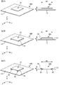
まず、図1及び図2を参照しつつ、第1アンテナ20の構成の概要を説明する。図1は、第1アンテナ20の斜視図である。図2は、第1アンテナ20の分解斜視図である。 <<<first antenna 20>>>
First, an overview of the configuration of thefirst antenna 20 will be described with reference to FIGS. 1 and 2. FIG. FIG. 1 is a perspective view of the first antenna 20. FIG. FIG. 2 is an exploded perspective view of the first antenna 20. FIG.
まず、図1及び図2を参照しつつ、第1アンテナ20の構成の概要を説明する。図1は、第1アンテナ20の斜視図である。図2は、第1アンテナ20の分解斜視図である。 <<<
First, an overview of the configuration of the
以下の説明では、第1アンテナ20の導電体30の中心部31Dと、2つある給電点36Aのうちの一方の給電点36Aとを結ぶ線分に沿った方向をX方向とする。また、他方の給電点36Aと、中心部31Dとを結ぶ線分に沿った方向をY方向とする。また、X方向とY方向とに垂直な鉛直方向をZ方向とする。そして、図1及び図2に示す方向を+X方向、+Y方向とし、天頂方向(上方向)を+Z方向とする。なお、中心部31Dの詳細については、後述する。また、不図示であるが、第1アンテナ20が有する給電点36Aが1つ(1給電方式)の場合、中心部31Dと、給電点36Aとを結ぶ線分に沿った方向をX方向とし、X方向と垂直な方向をY方向とする。
In the following description, the direction along the line connecting the central portion 31D of the conductor 30 of the first antenna 20 and one of the two feeding points 36A is defined as the X direction. Also, the direction along the line connecting the other feeding point 36A and the central portion 31D is defined as the Y direction. A vertical direction perpendicular to the X direction and the Y direction is defined as the Z direction. The directions shown in FIGS. 1 and 2 are the +X direction and the +Y direction, and the zenith direction (upward direction) is the +Z direction. Details of the central portion 31D will be described later. Further, although not shown, when the first antenna 20 has one feeding point 36A (single feeding method), the direction along the line segment connecting the central portion 31D and the feeding point 36A is defined as the X direction, A direction perpendicular to the X direction is defined as a Y direction.
第1アンテナ20は、例えば、不図示の車両に搭載される車載用アンテナ装置に設けられる。車載用アンテナ装置は、例えば、車両のルーフパネルと、車室内の天井面のルーフライニングとの間の空洞に収納される。但し、第1アンテナ20は、一般的なシャークフィンアンテナの筐体の中に設けられても良い。また、第1アンテナ20は、インストルメントパネルに装着されるアンテナ装置内に設けられても良い。
The first antenna 20 is provided, for example, in an in-vehicle antenna device mounted in a vehicle (not shown). An in-vehicle antenna device is housed, for example, in a cavity between a roof panel of a vehicle and a roof lining on the ceiling surface of the vehicle interior. However, the first antenna 20 may be provided in the housing of a general shark fin antenna. Also, the first antenna 20 may be provided in an antenna device attached to the instrument panel.
第1アンテナ20は、例えば、GNSS(Global Navigation Satellite System)の方式に利用される平面アンテナである。第1アンテナ20は、例えば、人工衛星からの1.5GHz帯の電波を受信する。但し、第1アンテナ20は、例えば、1.2GHz帯及び1.6GHz帯など、複数の周波数帯の電波を受信しても良い。なお、第1アンテナ20の受信可能な通信規格及び周波数帯は、上述のものに限定するものではなく、他の通信規格及び周波数帯域であっても良い。例えば、第1アンテナ20は、衛星デジタル音声ラジオサービス(SDARS:Satellite Digital Audio Radio Service)の方式に利用され、2.3GHz帯の左旋円偏波(衛星信号)を受信しても良い。
The first antenna 20 is, for example, a planar antenna used in the GNSS (Global Navigation Satellite System) system. The first antenna 20 receives, for example, 1.5 GHz band radio waves from an artificial satellite. However, the first antenna 20 may receive radio waves in a plurality of frequency bands such as 1.2 GHz band and 1.6 GHz band. The communication standard and frequency band that can be received by the first antenna 20 are not limited to those described above, and other communication standards and frequency bands may be used. For example, the first antenna 20 may be used in a satellite digital audio radio service (SDARS) system to receive left-hand circularly polarized waves (satellite signals) in the 2.3 GHz band.
第1アンテナ20は、地板10と、導電体30と、支持部40とを有する。
The first antenna 20 has a ground plane 10 , a conductor 30 and a support portion 40 .
<地板10>
地板10は、第1アンテナ20のグランドとして利用される素子である。地板10は、略四辺形の金属板である。以下の説明において、「略四辺形」とは、例えば、正方形や長方形を含む、4つの辺からなる形状をいい、例えば、少なくとも一部の角が辺に対して斜めに切り欠かれていても良い。また、「略四辺形」の形状では、辺の一部に切り込み(凹部)や出っ張り(凸部)が設けられていても良い。但し、地板10は、例えば円形や楕円形の板状部材であっても良い。さらに、地板10は、グランドとして機能する金属製の部材であれば板状以外の形状を有していても良い。 <Main plate 10>
Theground plane 10 is an element used as the ground of the first antenna 20 . The base plate 10 is a substantially rectangular metal plate. In the following description, "substantially quadrilateral" refers to a shape consisting of four sides, including squares and rectangles. good. In addition, in the shape of the "substantially quadrilateral", a notch (concave portion) or protrusion (convex portion) may be provided on a part of the sides. However, the base plate 10 may be, for example, a circular or elliptical plate-like member. Furthermore, the base plate 10 may have a shape other than a plate shape as long as it is a metal member that functions as a ground.
地板10は、第1アンテナ20のグランドとして利用される素子である。地板10は、略四辺形の金属板である。以下の説明において、「略四辺形」とは、例えば、正方形や長方形を含む、4つの辺からなる形状をいい、例えば、少なくとも一部の角が辺に対して斜めに切り欠かれていても良い。また、「略四辺形」の形状では、辺の一部に切り込み(凹部)や出っ張り(凸部)が設けられていても良い。但し、地板10は、例えば円形や楕円形の板状部材であっても良い。さらに、地板10は、グランドとして機能する金属製の部材であれば板状以外の形状を有していても良い。 <
The
また、地板10は、例えば金属製のベース1上に設置される。なお、第1アンテナ20は、地板10を有さず、導電体30と、支持部40とが、ベース1上に直接設置されても良い。そして、ベース1がグランドとして利用されても良い。以下、地板10を含む、グランドとして利用される素子を「グランド部」と称することがある。本実施形態では、後述するように導電体30とグランド部との間を近接させつつ、導電体30とグランド部とを接触させないことを目的の一つとしている。このため、地板10のような板状部材を導電体30の下に配置することで、導電体30とグランド部との離間距離を容易に設計することができる。
Also, the base plate 10 is installed on the base 1 made of metal, for example. Note that the first antenna 20 may not have the ground plane 10 and the conductor 30 and the support portion 40 may be directly installed on the base 1 . And the base 1 may be used as a ground. Hereinafter, an element used as a ground, including the ground plane 10, may be referred to as a "ground portion". As will be described later, one object of the present embodiment is to bring the conductor 30 closer to the ground while preventing the conductor 30 from coming into contact with the ground. Therefore, by disposing a plate-like member such as the ground plane 10 under the conductor 30, the distance between the conductor 30 and the ground portion can be easily designed.
<導電体30>
導電体30は、所望の周波数帯の信号(電波)を受信可能な素子である。また、導電体30は、地板10(グランド部)と電気的に結合する導電性の素子である。本実施形態では、導電体30は、地板10と容量結合する素子である。但し、導電体30は、地板10と容量結合することに限られず、静電結合、電磁界共振結合、電界結合など、その他の電気的結合をする素子であっても良い。 <Conductor 30>
Theconductor 30 is an element capable of receiving signals (radio waves) in a desired frequency band. Also, the conductor 30 is a conductive element electrically coupled to the ground plane 10 (ground portion). In this embodiment, the conductor 30 is an element capacitively coupled with the ground plane 10 . However, the conductor 30 is not limited to being capacitively coupled with the ground plane 10, and may be an element for other electrical coupling such as electrostatic coupling, electromagnetic resonance coupling, or electric field coupling.
導電体30は、所望の周波数帯の信号(電波)を受信可能な素子である。また、導電体30は、地板10(グランド部)と電気的に結合する導電性の素子である。本実施形態では、導電体30は、地板10と容量結合する素子である。但し、導電体30は、地板10と容量結合することに限られず、静電結合、電磁界共振結合、電界結合など、その他の電気的結合をする素子であっても良い。 <
The
本実施形態では、導電体30は、地板10に対向するように位置している。また、導電体30は、地板10に対して物理的に所定距離離間している。以下の説明において、例えば2つの素子(例えば素子A及び素子B)が「物理的に所定距離離間している」とは、素子Aと素子Bとの間に隙間を有することをいう。具体的には、素子Aにおける最も素子B側の端と、素子Bにおける最も素子A側の端との間に、所定量の隙間を有することをいう。図1、及び後述する図2~図4に示される例でいえば、導電体30の延出部33の対向面34(後述)と、地板10のおもて面との間に、Z方向に所定量の隙間を有する。但し、導電体30と地板10との隙間に、他の部材が設けられる場合がある。導電体30が地板10に対して物理的に所定距離離間していることにより、導電体30は、地板10に対して+Z方向に浮いていることになる。すなわち、導電体30は、地板10と物理的に接触していない。言い換えると、導電体30と地板10とは、物理的に非接触である。
In this embodiment, the conductor 30 is positioned so as to face the ground plane 10 . Also, the conductor 30 is physically separated from the ground plane 10 by a predetermined distance. In the following description, for example, two elements (for example, element A and element B) that are "physically separated by a predetermined distance" means that there is a gap between element A and element B. Specifically, it means that there is a predetermined gap between the end of the element A closest to the element B side and the end of the element B closest to the element A side. In the example shown in FIG. 1 and FIGS. 2 to 4 which will be described later, a Z-direction have a predetermined amount of gap between them. However, another member may be provided in the gap between the conductor 30 and the ground plane 10 . Since the conductor 30 is physically separated from the ground plane 10 by a predetermined distance, the conductor 30 floats in the +Z direction with respect to the ground plane 10 . That is, the conductor 30 is not in physical contact with the ground plane 10 . In other words, the conductor 30 and the ground plane 10 are physically out of contact.
なお、本実施形態では、+Z方向からみたX-Y平面の平面視において、導電体30の大きさと、地板10の大きさとは略同じである。但し、導電体30の大きさと地板10の大きさとが異なっても良く、例えば、導電体30の大きさよりも地板10の大きさの方が大きくても良い。
It should be noted that in the present embodiment, the size of the conductor 30 and the size of the ground plane 10 are substantially the same when viewed from the +Z direction on the XY plane. However, the size of the conductor 30 and the size of the ground plane 10 may be different. For example, the size of the ground plane 10 may be larger than the size of the conductor 30 .
図3は、導電体30の本体部31のうら面31C側から見た斜視図である。図4は、導電体30の展開図である。
FIG. 3 is a perspective view of the body portion 31 of the conductor 30 viewed from the back surface 31C side. FIG. 4 is an exploded view of the conductor 30. FIG.
導電体30は、本体部31と、脚部32とを有する。
The conductor 30 has a body portion 31 and leg portions 32 .
本体部31は、導電体30において、地板10に対向するように位置する部位である。本体部31は、略四辺形である。但し、本体部31は、円形及び楕円形であっても良いし、略四辺形以外の多角形であっても良い。つまり、本体部31は、脚部32とともに、導電体30として所望の周波数帯の信号(電波)を受信可能な形状であれば良い。
The body portion 31 is a portion of the conductor 30 that is positioned so as to face the ground plane 10 . The body portion 31 is substantially quadrilateral. However, the main body portion 31 may be circular or elliptical, or polygonal other than a substantially quadrilateral. In other words, the main body portion 31 and the leg portion 32 may have any shape as long as the conductor 30 can receive signals (radio waves) in a desired frequency band.
本体部31には、給電点36Aが設けられている。給電点36Aは、給電線36が本体部31に電気的に接続される点である。本実施形態では、給電点36Aが2つ設けられている。一方の給電点36Aは、本体部31の中心部31Dから+X方向にずれた位置に設けられている。他方の給電点36Aは、本体部31の中心部31Dから-Y方向にずれた位置に設けられている。但し、給電点36Aの位置はこれに限られない。なお、「本体部31の中心部31D」とは、本体部31の外縁形状における中心点、つまり幾何中心をいう。
A feeding point 36A is provided on the main body 31. A feeding point 36A is a point where the feeding line 36 is electrically connected to the main body portion 31 . In this embodiment, two feeding points 36A are provided. One feeding point 36A is provided at a position shifted in the +X direction from the central portion 31D of the main body portion 31 . The other feeding point 36A is provided at a position displaced from the central portion 31D of the main body portion 31 in the -Y direction. However, the position of the feeding point 36A is not limited to this. The “center portion 31D of the body portion 31” refers to the center point of the outer edge shape of the body portion 31, that is, the geometric center.
本実施形態では、本体部31に接続される給電線36が2本設けられている構成、すなわち、2給電方式が採用されている。2給電方式が採用される場合、本体部31は、例えば、所望の円偏波を送受信できるよう、縦、横の長さが等しい略正方形の形状を有する。なお、「略正方形」は、上述した「略四辺形」に含まれる形状である。
In this embodiment, a configuration in which two power supply lines 36 are provided to be connected to the main body 31, that is, a two-power supply system is adopted. When the two-feed system is employed, the main body 31 has, for example, a substantially square shape with equal vertical and horizontal lengths so that desired circularly polarized waves can be transmitted and received. The “substantially square” is a shape included in the above-described “substantially quadrilateral”.
なお、本実施形態では、本体部31に接続される給電線36が1本のみの構成、すなわち、1給電方式が採用されても良い。1給電方式の本体部31では、例えば、所望の円偏波を送受信できるよう、縦、横の長さが異なる略長方形の形状を有する。なお、「略長方形」は、上述した「略四辺形」に含まれる形状である。本体部31が略長方形の形状を有する場合、「本体部31の中心部31D」は、本体部31の対角線が交わる点となる。
In addition, in the present embodiment, a configuration in which only one power supply line 36 is connected to the main body 31, that is, a single power supply system may be adopted. The main body 31 of the single feeding system has, for example, a substantially rectangular shape with different lengths and widths so that desired circularly polarized waves can be transmitted and received. The “substantially rectangular” is a shape included in the above-described “substantially quadrilateral”. When the body portion 31 has a substantially rectangular shape, the “central portion 31D of the body portion 31” is the point where the diagonal lines of the body portion 31 intersect.
さらに、本実施形態では、2給電方式や1給電方式以外の給電方式が採用されても良く、例えば、4給電方式(4点給電)が採用されても良い。
Furthermore, in the present embodiment, a power feeding system other than the two power feeding system or the one power feeding system may be adopted, for example, a four power feeding system (four-point power feeding) may be adopted.
脚部32は、本体部31から延在する部位である。図3に示されるように、4つの脚部32A~32Dが本体部31から延在している。但し、導電体30が有する脚部32は4つに限られず、4つ以外の複数であっても良い。例えば、2つの脚部32が本体部31から延在しても良い。なお、導電体30が有する脚部32が2つの場合、脚部32Aと脚部32Cのみの場合や、脚部32Bと脚部32Dのみの場合など、各々の脚部32が本体部31の対角の位置に設けられる。これにより、給電点36Aの配置の設計が容易となる。但し、2つの脚部32が設けられる位置についてはこれに限られない。さらに、導電体30が有する脚部32が1つであっても良いし、導電体30が脚部32を有さなくても良い。
The leg portion 32 is a portion extending from the main body portion 31 . As shown in FIG. 3, four legs 32A-32D extend from body portion 31. As shown in FIG. However, the number of legs 32 of the conductor 30 is not limited to four, and may be any number other than four. For example, two legs 32 may extend from body 31 . When the conductor 30 has two legs 32, only the legs 32A and 32C, or only the legs 32B and 32D, each leg 32 is paired with the main body 31. It is provided at a corner position. This facilitates the design of the layout of the feed point 36A. However, the positions where the two legs 32 are provided are not limited to this. Furthermore, the conductor 30 may have one leg portion 32 , or the conductor 30 may have no leg portion 32 .
図3及び図4に示されるように、本実施形態では、4つの脚部32A~32Dは、本体部31の外縁部31Aに回転対称となるように位置している。ここで、4つの脚部32A~32Dについて「回転対称となるように位置」するとは、+Z方向からみたX-Y平面の平面視において、導電体30を中心部31D周りに所定角度回転すると、脚部32の位置が一致することをいう。なお、所定角度は、360°を導電体30が有する脚部32の個数で割ったときの角度である。したがって、本実施形態では、導電体30が4つの脚部32A~32Dを有する場合、導電体30を中心部31D周りに90°(360°/4)回転すると、脚部32の位置が一致する。4つの脚部32A~32Dを回転対称となるように位置することで、円偏波の電波を受信する導電体30の場合、電波の損失を抑制することができ、特に有利である。
As shown in FIGS. 3 and 4, in this embodiment, the four legs 32A to 32D are positioned rotationally symmetrical to the outer edge 31A of the main body 31. As shown in FIGS. Here, to say that the four legs 32A to 32D are "positioned so as to be rotationally symmetrical" means that when the conductor 30 is rotated by a predetermined angle around the central portion 31D in a plan view of the XY plane viewed from the +Z direction, It means that the positions of the legs 32 are matched. The predetermined angle is an angle obtained by dividing 360° by the number of legs 32 that the conductor 30 has. Therefore, in this embodiment, if the conductor 30 has four legs 32A to 32D, the positions of the legs 32 are aligned when the conductor 30 is rotated 90° (360°/4) around the center 31D. . Positioning the four legs 32A to 32D so as to be rotationally symmetrical is particularly advantageous in that the loss of radio waves can be suppressed in the case of the conductor 30 that receives circularly polarized radio waves.
なお、脚部32について、「回転対称となるように位置」とは、導電体30を中心部31D周りに所定角度回転すると、脚部32の位置が完全に一致する場合に限られず、所定範囲以内でずれている場合を含むこととする。これは、脚部32の位置や大きさが、公差など、様々な要因により変化するためである。所定範囲以内の「ずれ」は、円偏波の電波を受信する導電体30について、電波の損失を抑制できる程度であればよい。例えば、脚部32の位置が実際に一致する角度が、所定角度に対して±30%程度の範囲内でずれていても良い。また、4つの脚部32A~32Dは、本体部31の外縁部31Aに回転対称となるように位置しなくても良い。
Regarding the leg portions 32, “rotationally symmetrical positions” is not limited to the case where the positions of the leg portions 32 are completely matched when the conductor 30 is rotated around the central portion 31D by a predetermined angle, and is not limited to a predetermined range. This includes cases where the deviation is within the range. This is because the position and size of the legs 32 change due to various factors such as tolerance. The "deviation" within a predetermined range may be a degree that can suppress the loss of radio waves for the conductor 30 that receives circularly polarized radio waves. For example, the angle at which the leg portions 32 actually match may deviate from the predetermined angle within a range of about ±30%. Also, the four legs 32A to 32D do not have to be positioned rotationally symmetrically with respect to the outer edge 31A of the main body 31. As shown in FIG.
また、例えば、給電点36Aの配置を最適化する場合や、第1アンテナ20がBluetooth(登録商標)などの直線偏波の電波で受信する場合など、導電体30が有する脚部32を1つとしても良い。
Further, for example, when optimizing the placement of the feeding point 36A, or when the first antenna 20 receives linearly polarized radio waves such as Bluetooth (registered trademark), the conductor 30 has one leg 32. It is good as
なお、「脚部32が本体部31から延在する」とは、同一の金属板で本体部31と、本体部31から延在するように構成された脚部32とを構成する場合に限られない。本体部31と脚部32とが別体であり、本体部31から延びるように脚部32が本体部31に接続(接合)される場合も含む。また、本体部31と脚部32とは同一の金属部材であっても良いし、異なる金属部材であっても良い。
Note that “the leg portion 32 extends from the main body portion 31” is limited to the case where the main body portion 31 and the leg portion 32 configured to extend from the main body portion 31 are made of the same metal plate. can't A case in which the body portion 31 and the leg portion 32 are separate bodies and the leg portion 32 is connected (joined) to the body portion 31 so as to extend from the body portion 31 is also included. Further, the body portion 31 and the leg portion 32 may be made of the same metal member, or may be made of different metal members.
以下の説明では、脚部32A~32Dの各々において、脚部32を構成する部位には、符号に添え字「A」~「D」を付けている。例えば、脚部32Aが有する延出部33のことを「延出部33A」と称する。また、4つの脚部32A~32Dに共通して説明する場合や、4つの脚部32A~32Dのいずれかの脚部32を代表して説明する場合は、添え字を付けないことがある。例えば、4つの脚部32A~32Dの全てのことを指して単に「脚部32」と称することがある。また、延出部33A~32Dの全てのことを指して単に「延出部33」と称することがある。
In the following description, in each of the leg portions 32A to 32D, the parts constituting the leg portion 32 are indicated with suffixes "A" to "D". For example, the extending portion 33 of the leg portion 32A is referred to as "extending portion 33A". Also, when describing the four legs 32A to 32D in common, or when describing one leg 32 of the four legs 32A to 32D as a representative, the suffix may not be added. For example, all four legs 32A to 32D may be simply referred to as "legs 32". Also, all of the extensions 33A to 32D may be simply referred to as "extensions 33".
本実施形態では、図4に示されるように、本体部31と脚部32との接続部分には、屈曲部35(35A~35D)が設けられている。つまり、図3に示されるように、導電体30を全体として見たときに、本体部31から折り曲げられて脚部32が設けられている。また、脚部32は、地板10(グランド部)のおもて面に向かって延びる。したがって、本実施形態では、脚部32は、地板10と本体部31との間に位置する。また、屈曲部35は、本体部31の外縁部31Aに設けられている。つまり、脚部32は、本体部31の外縁部31Aに設けられる。但し、屈曲部35は、本体部31の外縁部31Aよりも内側(中心部31D側)に設けられても良い。すなわち、脚部32は、本体部31の外縁部31A以外に設けられても良い。
In the present embodiment, as shown in FIG. 4, bent portions 35 (35A to 35D) are provided at the connecting portions between the body portion 31 and the leg portions 32. As shown in FIG. That is, as shown in FIG. 3, when the conductor 30 is viewed as a whole, the legs 32 are provided by bending from the main body 31 . Also, the leg portion 32 extends toward the front surface of the base plate 10 (ground portion). Therefore, in this embodiment, the leg portion 32 is positioned between the base plate 10 and the main body portion 31 . Further, the bent portion 35 is provided on the outer edge portion 31A of the body portion 31 . That is, the leg portion 32 is provided on the outer edge portion 31A of the body portion 31 . However, the bent portion 35 may be provided inside the outer edge portion 31A of the body portion 31 (on the center portion 31D side). That is, the leg portion 32 may be provided on a portion other than the outer edge portion 31A of the main body portion 31 .
脚部32は、図3及び図4に示されるように、延出部33を有する。延出部33は、図3に示されるように、脚部32において、地板10(グランド部)に対向する対向面34を有する部材である。延出部33は、脚部32の地板10側の端部にさらに設けられた屈曲部38(38A~38D)により、脚部32の地板10側の端部から折り曲げられるように設けられている。なお、延出部33は、脚部32と別体であり、脚部32の地板10側の端部から延びるように接続(接合)されても良い。さらに、延出部33と脚部32とが別体である場合、脚部32の地板10側の端部以外から延びるように接続(接合)されても良い。また、脚部32は、延出部33を有さなくても良い。さらに、複数の脚部32のうち屈曲部38を有するものと、屈曲部38を有さないものと、が混在していても良い。
The leg portion 32 has an extension portion 33 as shown in FIGS. As shown in FIG. 3, the extending portion 33 is a member having a facing surface 34 facing the base plate 10 (ground portion) at the leg portion 32 . The extending portion 33 is provided so as to be bent from the end portion of the leg portion 32 on the side of the main plate 10 by a bending portion 38 (38A to 38D) further provided at the end portion of the leg portion 32 on the side of the main plate 10. . The extending portion 33 may be separate from the leg portion 32 and may be connected (joined) so as to extend from the end portion of the leg portion 32 on the side of the base plate 10 . Furthermore, when the extending portion 33 and the leg portion 32 are separate members, they may be connected (joined) so as to extend from a portion other than the end portion of the leg portion 32 on the side of the main plate 10 . Also, the leg portion 32 may not have the extending portion 33 . Furthermore, among the plurality of legs 32, those having the bent portion 38 and those having no bent portion 38 may be mixed.
本実施形態では、延出部33は、本体部31の外縁部31Aの内側に位置している。すなわち、延出部33が外縁部31Aから中心部31Dに向かうように延在している。但し、延出部33は、本体部31の外縁部31Aの外側に位置しても良い。つまり、延出部33は、本体部31の外縁部31Aの外側、すなわち中心部31Dから離れる方向に向かって延びても良い。また、延出部33は、地板10(グランド部)に対向する対向面34を有するように、地板10のおもて面に略平行になるように延びている。但し、延出部33は、対向面34を有していれば、地板10のおもて面に略平行になるように延びていなくても良い。
In the present embodiment, the extending portion 33 is positioned inside the outer edge portion 31A of the main body portion 31 . That is, the extending portion 33 extends from the outer edge portion 31A toward the central portion 31D. However, the extending portion 33 may be positioned outside the outer edge portion 31A of the body portion 31 . That is, the extending portion 33 may extend outside the outer edge portion 31A of the body portion 31, that is, in a direction away from the central portion 31D. The extending portion 33 extends substantially parallel to the front surface of the base plate 10 so as to have a facing surface 34 facing the base plate 10 (ground portion). However, as long as the extending portion 33 has the facing surface 34 , the extending portion 33 does not have to extend substantially parallel to the front surface of the base plate 10 .
本実施形態では、導電体30は、板金からなっている。具体的には、図4に示されるように、本体部31と、脚部32A~32Dは、一体となっている。さらに、導電体30は、屈曲部35や屈曲部38を有することにより、折り曲げられて、上述した脚部32や延出部33が設けられることになる。したがって、導電体30は立体的な形状となっている。
In this embodiment, the conductor 30 is made of sheet metal. Specifically, as shown in FIG. 4, the body portion 31 and the leg portions 32A to 32D are integrated. Further, the conductor 30 is bent by having the bent portion 35 and the bent portion 38 to provide the leg portion 32 and the extension portion 33 described above. Therefore, the conductor 30 has a three-dimensional shape.
上述した脚部32の特徴は、図3及び図4に示されるように、4つの脚部32A~32Dに共通しているものとして説明した。しかし、上述した脚部32の特徴は、4つの脚部32A~32Dのうち少なくとも一つの脚部32に該当するものであっても良い。例えば、脚部32A及び脚部32Cのみに延出部33が設けられ、脚部32B及び脚部32Dには延出部33が設けられなくても良い。したがって、4つの脚部32A~32Dにおいて、上述した脚部32の特徴を自由に組み合わせることができる。
The features of the leg 32 described above have been described as being common to the four legs 32A to 32D, as shown in FIGS. However, the features of the legs 32 described above may apply to at least one leg 32 out of the four legs 32A-32D. For example, only the leg portions 32A and 32C may be provided with the extending portions 33, and the leg portions 32B and 32D may not be provided with the extending portions 33. Therefore, in the four legs 32A to 32D, the features of the legs 32 described above can be freely combined.
<支持部40>
支持部40は、導電体30と、地板10(グランド部)との間で所望の容量が形成されるよう、地板10に対して物理的に所定距離離間させるように導電体30を支持する部材である。図2に示されるように、本実施形態では、支持部40は、円柱状である。但し、支持部40の形状はこれに限られず、導電体30を支持することができれば、円柱状以外であっても良く、例えば直方体であっても良い。支持部40は、例えば樹脂等の誘電体により形成される。但し、支持部40は、導電性を有しない材料であれば、誘電体以外の材料で形成されて良い。 <Support portion 40>
Thesupport part 40 is a member that supports the conductor 30 so as to physically separate it from the ground plane 10 by a predetermined distance so that a desired capacitance is formed between the conductor 30 and the ground plane 10 (ground part). is. As shown in FIG. 2, in this embodiment, the support portion 40 has a cylindrical shape. However, the shape of the support portion 40 is not limited to this, and may be any shape other than a columnar shape as long as it can support the conductor 30, and may be, for example, a rectangular parallelepiped shape. The support portion 40 is made of a dielectric such as resin, for example. However, the supporting portion 40 may be formed of a material other than the dielectric as long as the material does not have conductivity.
支持部40は、導電体30と、地板10(グランド部)との間で所望の容量が形成されるよう、地板10に対して物理的に所定距離離間させるように導電体30を支持する部材である。図2に示されるように、本実施形態では、支持部40は、円柱状である。但し、支持部40の形状はこれに限られず、導電体30を支持することができれば、円柱状以外であっても良く、例えば直方体であっても良い。支持部40は、例えば樹脂等の誘電体により形成される。但し、支持部40は、導電性を有しない材料であれば、誘電体以外の材料で形成されて良い。 <
The
支持部40は、地板10(グランド部)と導電体30の本体部31との間に位置する。上述のように、支持部40は、導電体30と、地板10との間に所望の容量が形成されるよう、物理的に離間させる部材である。したがって、支持部40は、地板10に対して物理的に所定距離離間させるように導電体30を支持することができれば、地板10(グランド部)と導電体30の本体部31との間に位置しなくても良く、例えば、後述する図13に示されるように、カバー部6が導電体30を支持しても良い。
The support portion 40 is positioned between the ground plate 10 (ground portion) and the main body portion 31 of the conductor 30 . As described above, the support part 40 is a member that physically separates the conductor 30 and the ground plane 10 so that a desired capacitance is formed between them. Therefore, if the support portion 40 can support the conductor 30 so as to physically separate it from the ground plane 10 by a predetermined distance, the support portion 40 can be positioned between the ground plane 10 (ground portion) and the body portion 31 of the conductor 30 . For example, the cover portion 6 may support the conductor 30 as shown in FIG. 13, which will be described later.
支持部40は、+Z方向からみたX-Y平面の平面視において、本体部31の大きさよりも小さい。さらに、支持部40は、本体部31(導電体30)の略中央に位置している。本体部31の略中央は、地板10(グランド部)との間の電位差が0で一定となるため、支持部40が本体部31の略中央に位置することにより、電波の損失や波長短縮の影響を抑制することができる。望ましくは、+Z方向からみたX-Y平面の平面視における支持部40の大きさは、本体部31の大きさの50%以内とすれば、より電波の損失や波長短縮の影響を抑制することができる。但し、+Z方向からみたX-Y平面の平面視において、支持部40の大きさは、本体部31の大きさより大きくてもよい。また、支持部40は、本体部31の略中央に位置しなくても良い。例えば、+Z方向からみたX-Y平面の平面視において、支持部40は、本体部31の外縁部31Aに位置しても良い。
The support portion 40 is smaller than the main body portion 31 in a plan view of the XY plane seen from the +Z direction. Further, the support portion 40 is positioned substantially in the center of the body portion 31 (conductor 30). Since the potential difference between the substantially center of the body portion 31 and the ground plane 10 (ground portion) is constant at 0, the position of the support portion 40 substantially at the center of the body portion 31 reduces the loss of radio waves and shortens the wavelength. The impact can be suppressed. Desirably, if the size of the support portion 40 in plan view on the XY plane seen from the +Z direction is within 50% of the size of the main body portion 31, the effects of radio wave loss and wavelength shortening can be further suppressed. can be done. However, the size of the support portion 40 may be larger than the size of the main body portion 31 in a plan view of the XY plane viewed from the +Z direction. Also, the support portion 40 does not have to be positioned substantially in the center of the body portion 31 . For example, the support portion 40 may be positioned at the outer edge portion 31A of the main body portion 31 in a plan view of the XY plane viewed from the +Z direction.
本実施形態では、第1アンテナ20が支持部40を有することにより、導電体30と地板10とをより近接させることが可能となり、導電体30と地板10との間の容量を大きくすることができる。例えば、導電体30と地板10との間に、セラミックの誘電体を設けることで容量を大きくすることもできるが、セラミックを使用することによる製造コストが大きくなってしまう。そこで、本実施形態のような支持部40を有する構成により、簡易な構成で導電体30と地板10との間の容量を大きくすることができる。したがって、簡易な構成で低い共振周波数のアンテナを実現することができる。
In this embodiment, since the first antenna 20 has the support portion 40, the conductor 30 and the ground plane 10 can be brought closer to each other, and the capacitance between the conductor 30 and the ground plane 10 can be increased. can. For example, the capacitance can be increased by providing a ceramic dielectric between the conductor 30 and the ground plane 10, but the use of ceramic increases the manufacturing cost. Therefore, the configuration having the support portion 40 as in the present embodiment can increase the capacitance between the conductor 30 and the ground plane 10 with a simple configuration. Therefore, an antenna with a low resonance frequency can be realized with a simple configuration.
本実施形態では、脚部32の地板10に近接する部分は、地板10と電気的に結合する。言い換えれば、脚部32の地板10に近接する部分は、地板10と容量結合する。ここで、脚部32の地板10に近接する部分とは、脚部32の延出部33である。また、脚部32が延出部33を有さない場合、脚部32の地板10に近接する部分とは、脚部32の地板10(グランド部)側の端部である。これにより、導電体30と地板10との間の容量をより大きくすることができる。
In this embodiment, the portion of the leg portion 32 close to the base plate 10 is electrically coupled to the base plate 10 . In other words, the portion of the leg 32 close to the ground plane 10 is capacitively coupled with the ground plane 10 . Here, the portion of the leg portion 32 close to the base plate 10 is the extending portion 33 of the leg portion 32 . Further, when the leg portion 32 does not have the extending portion 33, the portion of the leg portion 32 close to the base plate 10 is the end portion of the leg portion 32 on the side of the base plate 10 (ground portion). Thereby, the capacitance between the conductor 30 and the ground plane 10 can be increased.
また、本実施形態では、図3及び図4に示すように、導電体30は、複数(ここでは、4つ)の脚部32A~32Dを有し、複数の脚部32A~32Dの各々が対向面34を有する延出部33を有する。これにより、脚部32の地板10に近接する部分を大きくすることができ、導電体30と地板10との間の容量をより大きくすることができる。
Further, in the present embodiment, as shown in FIGS. 3 and 4, the conductor 30 has a plurality of (here, four) legs 32A to 32D, and each of the legs 32A to 32D It has an extension 33 with a facing surface 34 . As a result, the portion of the leg portion 32 close to the ground plane 10 can be increased, and the capacitance between the conductor 30 and the ground plane 10 can be increased.
<脚部32の地板10に近接する部分による容量変化>
上述したように、本実施形態の導電体30の一例として、板金を折り曲げることによって、脚部32の地板10に近接する部分が設けられている。以下では、脚部32の地板10に近接する部分の有無に関して、図5A~図5Cに示される異なる導電体30のモデルを用いて、導電体30と地板10との間の容量の変化を検証する。 <Capacitance change due to the portion of theleg portion 32 close to the base plate 10>
As described above, as an example of theconductor 30 of the present embodiment, a portion of the leg portion 32 close to the ground plane 10 is provided by bending a sheet metal. In the following, regarding the presence or absence of a portion of the leg 32 close to the ground plane 10, using different models of the conductor 30 shown in FIGS. do.
上述したように、本実施形態の導電体30の一例として、板金を折り曲げることによって、脚部32の地板10に近接する部分が設けられている。以下では、脚部32の地板10に近接する部分の有無に関して、図5A~図5Cに示される異なる導電体30のモデルを用いて、導電体30と地板10との間の容量の変化を検証する。 <Capacitance change due to the portion of the
As described above, as an example of the
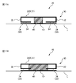
図5Aは、導電体30Aの斜視図及び側面図であり、図5Bは、導電体30Bの斜視図及び側面図であり、図5Cは、導電体30Cの斜視図及び側面図である。なお、図5A~図5Cの各々において、左側に斜視図を示し、右側に側面図を示している。また、各図において、導電体30が地板10に対して物理的に所定距離離間していることを簡易に示すために、支持部40や給電点36A、給電線36の図示を省略している。
5A is a perspective view and a side view of the conductor 30A, FIG. 5B is a perspective view and a side view of the conductor 30B, and FIG. 5C is a perspective view and a side view of the conductor 30C. In each of FIGS. 5A to 5C, a perspective view is shown on the left side and a side view is shown on the right side. In addition, in each drawing, in order to simply show that the conductor 30 is physically separated from the ground plane 10 by a predetermined distance, the illustration of the supporting portion 40, the feeding point 36A, and the feeding line 36 is omitted. .
図5Aに示されるように、導電体30Aは、脚部32が設けられておらず、本体部31のみの構成である。また、図5Bに示されるように、導電体30Bは、延出部33が設けられていない脚部32を本体部31の両側に有する。また、図5Cに示されるように、導電体30Cは、延出部33が設けられている脚部32を本体部31の両側に有する。導電体30A~30Cの各々の幅は、幅W1で共通している。また、導電体30A~30Cの各々は、本体部31の上面が高さHに位置するように、地板10に対して物理的に離間している。図5Bにおける脚部32の地板10側の端部及び地板10の距離と、図5Cにおける延出部33及び地板10の距離と、は同等である。また、導電体30A~30Cと、地板10と、は物理的に接触していない。
As shown in FIG. 5A, the conductor 30A is not provided with the legs 32, and is composed only of the main body 31. As shown in FIG. In addition, as shown in FIG. 5B, the conductor 30B has leg portions 32 on both sides of the body portion 31 where the extension portions 33 are not provided. In addition, as shown in FIG. 5C, the conductor 30C has leg portions 32 on both sides of the body portion 31 on which the extension portions 33 are provided. Each of the conductors 30A to 30C has a width W1 in common. Further, each of the conductors 30A to 30C is physically separated from the ground plane 10 so that the upper surface of the body portion 31 is positioned at the height H. The distance between the end of the leg portion 32 on the side of the base plate 10 and the base plate 10 in FIG. 5B is equivalent to the distance between the extending portion 33 and the base plate 10 in FIG. 5C. Also, the conductors 30A to 30C and the ground plane 10 are not in physical contact.
本実施形態において、本体部31と地板10との高さHとは、導電体30が地板10に対して物理的に離間する所定距離を示している。例えば、図5B及び図5Cに示すように導電体30に脚部32が設けられている場合の高さHは、導電体30が支持部40に支持された状態において、脚部32の地板10側の端部が地板10に物理的に接触しない高さを示している。なお、後述するが、物理的に接触しない高さであっても、可能な限り脚部32の地板10側の端部が地板10に近い高さとすることが望ましい。
In this embodiment, the height H between the main body portion 31 and the ground plane 10 indicates a predetermined distance by which the conductor 30 is physically separated from the ground plane 10 . For example, as shown in FIGS. 5B and 5C, when the conductor 30 is provided with the legs 32, the height H is the same as the ground plane 10 of the legs 32 when the conductor 30 is supported by the support 40. The height at which the side edge does not physically contact the base plate 10 is shown. As will be described later, it is desirable that the end portion of the leg portion 32 on the side of the base plate 10 be as close to the base plate 10 as possible, even if the height does not allow physical contact.
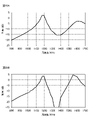
図6は、導電体30A~導電体30Cの各々における周波数特性の一例を示すグラフである。この図において、横軸は周波数を表し、縦軸は電圧定在波比(VSWR)を表す。図6に示されるように、導電体30A~導電体30Cの各々について、電圧定在波比が最も低い周波数の値は、導電体30Aでは、3619MHz、導電体30Bでは、2755MHz、導電体30Cでは、2133MHzである。
FIG. 6 is a graph showing an example of frequency characteristics of each of the conductors 30A to 30C. In this figure, the horizontal axis represents frequency, and the vertical axis represents voltage standing wave ratio (VSWR). As shown in FIG. 6, for each of the conductors 30A to 30C, the value of the frequency with the lowest voltage standing wave ratio is 3619 MHz for the conductor 30A, 2755 MHz for the conductor 30B, and 2755 MHz for the conductor 30C. , 2133 MHz.
図6の結果に基づき、導電体30Aと導電体30Bとを比較すると、導電体30が本体部31から地板10に向かって延びる脚部32を有することにより、脚部32の地板10により近接する部分が設けられる。これにより、導電体30と地板10との間の容量がより大きくなり、第1アンテナ20の共振周波数が低域側にずれることがわかる。また、導電体30Bと導電体30Cとを比較すると、脚部32が地板10に対向する対向面34を有する延出部33を有することにより、脚部32の地板10に近接する部分の面積が大きくなる。これにより、導電体30と地板10との間の容量がさらに大きくなり、第1アンテナ20の共振周波数がさらに低域側にずれることがわかる。
Comparing the conductor 30A and the conductor 30B based on the results of FIG. part is provided. It can be seen that this increases the capacitance between the conductor 30 and the ground plane 10 and shifts the resonance frequency of the first antenna 20 to the low frequency side. Further, when the conductor 30B and the conductor 30C are compared, the area of the portion of the leg 32 close to the ground plane 10 is increased by having the extension 33 having the facing surface 34 facing the ground plane 10. growing. As a result, the capacitance between the conductor 30 and the ground plane 10 is further increased, and the resonance frequency of the first antenna 20 is further shifted to the low frequency side.
なお、ここでは検証を省略したが、脚部32の地板10に近接する部分を地板10側により近づけた場合も、導電体30と地板10との間の容量がさらに大きくなり、第1アンテナ20の共振周波数がさらに低域側にずれることになる。
Although the verification is omitted here, if the portion of the leg portion 32 that is close to the ground plane 10 is brought closer to the ground plane 10 side, the capacitance between the conductor 30 and the ground plane 10 is further increased, and the first antenna 20 The resonance frequency of is further shifted to the low frequency side.
また、上述の図5Cに示される導電体30Cのように、脚部32が延出部33を有する場合、延出部33の長さや幅を調整することにより、第1アンテナ20の共振周波数を調整することができる。つまり、図5Cに示される延出部33のX方向やY方向の大きさを調整することにより、第1アンテナ20の共振周波数を所望の周波数に調整することができる。したがって、例えば、第1アンテナ20の基板(不図示)の大きさの変化や構成物の影響により、第1アンテナ20の共振周波数が所望の周波数からずれる場合であっても、容易に所望の周波数に調整することができる。
Further, when the leg portion 32 has the extension portion 33 like the conductor 30C shown in FIG. 5C described above, the resonance frequency of the first antenna 20 can be adjusted by adjusting the length and width of the extension portion 33. can be adjusted. That is, the resonance frequency of the first antenna 20 can be adjusted to a desired frequency by adjusting the size of the extending portion 33 shown in FIG. 5C in the X direction and the Y direction. Therefore, for example, even if the resonance frequency of the first antenna 20 deviates from the desired frequency due to a change in the size of the substrate (not shown) of the first antenna 20 or the influence of the structure, the desired frequency can be easily obtained. can be adjusted to
上述では、一定の長さ(ここではW1)を有する本体部31に対して、脚部32及び延出部33を付け加えるモデルによって第1アンテナ20の周波数特性を検証した。しかし、脚部32及び延出部33の長さの分だけ導電体30のインダクタンスが増えることになる。以下では、このような導電体30のインダクタンスの増加分の影響を取り除いたモデルによって第1アンテナ20の周波数特性を検証する。
In the above description, the frequency characteristics of the first antenna 20 were verified using a model in which the leg portion 32 and the extension portion 33 are added to the body portion 31 having a certain length (here, W1). However, the inductance of the conductor 30 is increased by the length of the leg 32 and extension 33 . In the following, the frequency characteristics of the first antenna 20 will be verified using a model in which the influence of the increase in the inductance of the conductor 30 is removed.
図7Aは、導電体30Dの斜視図及び側面図であり、図7Bは、導電体30Eの斜視図及び側面図である。なお、図7A及び図7Bの各々において、左側に斜視図を示し、右側に側面図を示している。また、各図において、導電体30が地板10に対して物理的に所定距離離間していることを簡易に示すために、支持部40や給電点36A、給電線36の図示を省略している。
7A is a perspective view and a side view of the conductor 30D, and FIG. 7B is a perspective view and a side view of the conductor 30E. In each of FIGS. 7A and 7B, a perspective view is shown on the left side and a side view is shown on the right side. In addition, in each drawing, in order to simply show that the conductor 30 is physically separated from the ground plane 10 by a predetermined distance, the illustration of the supporting portion 40, the feeding point 36A, and the feeding line 36 is omitted. .
図7Aに示されるように、導電体30Dは、脚部32が設けられておらず、本体部31のみの構成である。また、図7Bに示されるように、導電体30Eは、延出部33が設けられている脚部32を本体部31の両側に有する。導電体30Dの幅は、幅W2であり、導電体30Eは、このような幅W2の導電体を折り曲げて脚部32及び延出部33が設けられている。したがって、導電体30Dのインダクタンスと導電体30Eのインダクタンスとを略同一にするようなモデルを用いている。また、導電体30D及び導電体30Eの各々は、本体部31の上面が高さHに位置するように、地板10に対して物理的に離間している。また、図7Bにおける延出部33及び地板10は物理的に離間している。導電体30D~30Eと、地板10と、は物理的に接触していない。
As shown in FIG. 7A, the conductor 30D is not provided with the legs 32, and is composed only of the main body 31. As shown in FIG. In addition, as shown in FIG. 7B, the conductor 30E has leg portions 32 on both sides of the body portion 31 on which the extension portions 33 are provided. The width of the conductor 30D is the width W2, and the conductor 30E is provided with the leg portion 32 and the extension portion 33 by bending the conductor having the width W2. Therefore, a model is used in which the inductance of the conductor 30D and the inductance of the conductor 30E are substantially the same. In addition, each of the conductors 30D and 30E is physically separated from the ground plane 10 so that the upper surface of the body portion 31 is positioned at the height H. Also, the extending portion 33 and the base plate 10 in FIG. 7B are physically separated. The conductors 30D-30E and the ground plane 10 are not in physical contact.
図8は、導電体30D及び導電体30Eの各々における周波数特性の一例を示すグラフである。この図において、横軸は周波数を表し、縦軸は電圧定在波比(VSWR)を表す。図8に示されるように、導電体30D及び導電体30Eの各々について、電圧定在波比が最も低い周波数の値は、導電体30Dでは、2584MHz、導電体30Eでは、2133MHzである。
FIG. 8 is a graph showing an example of frequency characteristics of each of the conductors 30D and 30E. In this figure, the horizontal axis represents frequency, and the vertical axis represents voltage standing wave ratio (VSWR). As shown in FIG. 8, for each of the conductors 30D and 30E, the value of the frequency with the lowest voltage standing wave ratio is 2584 MHz for the conductor 30D and 2133 MHz for the conductor 30E.
図8の結果に基づき、導電体30Dと導電体30Eとを比較すると、導電体30が本体部31から地板10に向かう向きに延びる脚部32を有することにより、脚部32の地板10により近接する部分が設けられる。さらに、脚部32が地板10に対向する対向面34を有する延出部33を有することにより、脚部32の地板10に近接する部分の面積が大きくなる。これにより、導電体30と地板10との間の容量がさらに大きくなり、第1アンテナ20の共振周波数がさらに低域側にずれることがわかる。
Comparing the conductor 30D and the conductor 30E based on the results of FIG. There is a section for Furthermore, since the leg portion 32 has the extending portion 33 having the facing surface 34 facing the base plate 10, the area of the portion of the leg portion 32 close to the base plate 10 is increased. As a result, the capacitance between the conductor 30 and the ground plane 10 is further increased, and the resonance frequency of the first antenna 20 is further shifted to the low frequency side.
<導電体30の仮想体積の変化による周波数帯域の変化>
ところで、本実施形態の第1アンテナ20では、導電体30がZ方向に厚くなることで、周波数帯域が広くなる傾向がある。以下では、導電体30の仮想体積を定義し、仮想体積の変化による周波数帯域の変化を検証する。 <Change in frequency band due to change in virtual volume ofconductor 30>
By the way, in thefirst antenna 20 of the present embodiment, the frequency band tends to widen as the conductor 30 becomes thicker in the Z direction. Below, the virtual volume of the conductor 30 is defined, and changes in the frequency band due to changes in the virtual volume are verified.
ところで、本実施形態の第1アンテナ20では、導電体30がZ方向に厚くなることで、周波数帯域が広くなる傾向がある。以下では、導電体30の仮想体積を定義し、仮想体積の変化による周波数帯域の変化を検証する。 <Change in frequency band due to change in virtual volume of
By the way, in the
図9Aは、導電体30の仮想体積を説明する図である。脚部32及び延出部33を有する導電体30の場合、図9Aに示されるように、導電体30をX方向、Y方向及びZ方向に隙間なく収容する仮想的な柱体の空間を考え、この仮想的な柱体の空間の体積を仮想体積とする。なお、脚部32が設けられていない導電体30の場合(すなわち、導電体30が板状に形成されている場合)、導電体30の仮想体積は、導電体30の底面積に地板10から導電体30の本体部31の裏面31Cまでの距離を掛けた体積に等しい。なお、本実施形態では、支持部40の体積は、仮想体積より小さい。
FIG. 9A is a diagram explaining the virtual volume of the conductor 30. FIG. In the case of the conductor 30 having the leg portion 32 and the extension portion 33, as shown in FIG. 9A, a virtual columnar space that accommodates the conductor 30 in the X, Y and Z directions without gaps is considered. , the volume of this virtual columnar space is assumed to be a virtual volume. In the case of the conductor 30 without the legs 32 (that is, when the conductor 30 is formed in a plate shape), the virtual volume of the conductor 30 is the base area of the conductor 30 from the ground plane 10 It is equal to the volume multiplied by the distance to the back surface 31C of the body portion 31 of the conductor 30 . Note that in the present embodiment, the volume of the support portion 40 is smaller than the virtual volume.
図9Bは、導電体30の仮想体積を変化させたときの周波数特性の一例を示すグラフである。図9Bは、仮想体積の底面積を共通とし、高さをt1、t2、t4と変化させたときの周波数特性を示すグラフである。なお、t2は、t1の2倍の値であり、t4は、t1の4倍の値である。この図において、横軸は周波数を表し、縦軸は電圧定在波比(VSWR)を表す。図9Bに示されるように、高さt1、高さt2、高さt4の場合を比較すると、高さtが高くなるにつれて(すなわち、仮想体積が大きくなるにつれて)周波数帯域が広くなることがわかる。したがって、導電体30に地板10(グランド部)に延びる脚部32を設けることにより、脚部32を設けない場合と比べて、周波数帯域を広くすることができる。
FIG. 9B is a graph showing an example of frequency characteristics when the virtual volume of the conductor 30 is changed. FIG. 9B is a graph showing frequency characteristics when the virtual volume has a common bottom area and the height is changed to t1, t2, and t4. Note that t2 is twice the value of t1, and t4 is four times the value of t1. In this figure, the horizontal axis represents frequency, and the vertical axis represents voltage standing wave ratio (VSWR). As shown in FIG. 9B, comparing the cases of height t1, height t2, and height t4, it can be seen that the higher the height t (that is, the larger the virtual volume), the wider the frequency band. . Therefore, by providing the conductor 30 with the leg portion 32 extending to the ground plane 10 (ground portion), the frequency band can be broadened compared to the case where the leg portion 32 is not provided.
なお、図9Bの結果は、脚部32が設けられていない導電体30の場合でのシミュレーション結果である。ここでは検証を省略したが、脚部32を有する導電体30の場合であっても、仮想体積が大きくなるにつれて周波数帯域が広くなる。
It should be noted that the results of FIG. 9B are simulation results in the case of the conductor 30 without the leg portion 32 . Although verification is omitted here, even in the case of the conductor 30 having the legs 32, the frequency band widens as the virtual volume increases.
<脚部32の変形例>
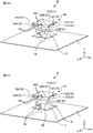
図10は、中心部31Dに向かう方向に延びる延出部33を有する、変形例の導電体30F及び導電体30Gの斜視図である。 <Modified Example ofLeg 32>
FIG. 10 is a perspective view of a modifiedconductor 30F and conductor 30G having extensions 33 extending toward the central portion 31D.
図10は、中心部31Dに向かう方向に延びる延出部33を有する、変形例の導電体30F及び導電体30Gの斜視図である。 <Modified Example of
FIG. 10 is a perspective view of a modified
上述した実施形態では、導電体30の4つの脚部32A~32Dが、本体部31の角部から外縁部31Aに沿う方向に延びていた。しかし、脚部32A~32Dの位置や延びる方向についてはこれに限られない。図10Aに示される導電体30Fでは、脚部32A~32Dは、本体部31の角部から中心部31Dに向かう方向に延びている。また、図10Bに示される導電体30Gでは、脚部32A~32Dは、本体部31の外縁部31Aの辺の中央から中心部31Dに向かう方向に延びている。導電体30F及び導電体30Gのいずれにおいても、4つの脚部32A~32Dは、本体部31の外縁部31Aに回転対称となるように位置している。これにより、円偏波の電磁波を受信する第1アンテナ20の場合に、導電体30と地板10との間の容量を大きくすることができる。
In the above-described embodiment, the four legs 32A-32D of the conductor 30 extend from the corners of the main body 31 along the outer edge 31A. However, the positions and extending directions of the legs 32A to 32D are not limited to this. In the conductor 30F shown in FIG. 10A, the legs 32A-32D extend from the corners of the main body 31 toward the center 31D. In the conductor 30G shown in FIG. 10B, the leg portions 32A to 32D extend from the center of the side of the outer edge portion 31A of the body portion 31 toward the central portion 31D. In both the conductor 30F and the conductor 30G, the four legs 32A to 32D are positioned rotationally symmetrical to the outer edge 31A of the main body 31. As shown in FIG. Thereby, in the case of the first antenna 20 that receives circularly polarized electromagnetic waves, the capacitance between the conductor 30 and the ground plane 10 can be increased.
<導電体30の支持構造の変形例>
上述した実施形態では、支持部40は、+Z方向からみたX-Y平面の平面視において、本体部31(導電体30)の略中央に位置し、導電体30を支持していた。しかし、支持部40による導電体30の支持構造はこれに限られない。 <Modified Example of Support Structure forConductor 30>
In the above-described embodiment, the supportingportion 40 is positioned substantially in the center of the main body portion 31 (the conductor 30) and supports the conductor 30 in a plan view of the XY plane viewed from the +Z direction. However, the supporting structure of the conductor 30 by the supporting portion 40 is not limited to this.
上述した実施形態では、支持部40は、+Z方向からみたX-Y平面の平面視において、本体部31(導電体30)の略中央に位置し、導電体30を支持していた。しかし、支持部40による導電体30の支持構造はこれに限られない。 <Modified Example of Support Structure for
In the above-described embodiment, the supporting
図11A及び図11Aは、導電体30の支持構造の変形例を示す図である。
11A and 11A are diagrams showing modifications of the supporting structure of the conductor 30. FIG.
<絶縁体50を有する場合>
図11Aに示される変形例における第1アンテナ20は、地板10(グランド部)のおもて面と、延出部33の対向面34との間に絶縁体50を有する。支持部40が本体部31(導電体30)の略中央に位置する上述の第1アンテナ20の場合、導電体30の略中央のみを支持することになるため、導電体30全体の支持状態を一定に保つことが困難な場合がある。この場合、本体部31(導電体30)の外縁部31A側に位置する延出部33が地板10に接触してしまうことがある。そこで、図11Aに示される変形例における第1アンテナ20は、地板10のおもて面と、延出部33の対向面34との間に絶縁体50を有することにより、延出部33が地板10に接触することを抑制することができる。 <When theinsulator 50 is included>
Thefirst antenna 20 in the modification shown in FIG. 11A has an insulator 50 between the front surface of the base plate 10 (ground portion) and the facing surface 34 of the extension portion 33 . In the case of the above-described first antenna 20 in which the support portion 40 is positioned substantially in the center of the main body portion 31 (the conductor 30), only the substantially center of the conductor 30 is supported. It can be difficult to keep constant. In this case, the extending portion 33 located on the outer edge portion 31A side of the main body portion 31 (conductor 30) may come into contact with the ground plane 10 in some cases. 11A, the first antenna 20 in the modification shown in FIG. Contact with the base plate 10 can be suppressed.
図11Aに示される変形例における第1アンテナ20は、地板10(グランド部)のおもて面と、延出部33の対向面34との間に絶縁体50を有する。支持部40が本体部31(導電体30)の略中央に位置する上述の第1アンテナ20の場合、導電体30の略中央のみを支持することになるため、導電体30全体の支持状態を一定に保つことが困難な場合がある。この場合、本体部31(導電体30)の外縁部31A側に位置する延出部33が地板10に接触してしまうことがある。そこで、図11Aに示される変形例における第1アンテナ20は、地板10のおもて面と、延出部33の対向面34との間に絶縁体50を有することにより、延出部33が地板10に接触することを抑制することができる。 <When the
The
<支持部40が本体部31に加え延出部33を支持する場合>
また、図11Bに示される変形例における第1アンテナ20は、支持部40が、地板10(グランド部)と本体部31との間に位置し、かつ、地板10と延出部33の対向面34とが離間するように延出部33を支持している。これによっても、延出部33が地板10に接触することを抑制することができる。 <When thesupport portion 40 supports the extension portion 33 in addition to the main body portion 31>
Further, in thefirst antenna 20 in the modification shown in FIG. 11B, the support portion 40 is positioned between the base plate 10 (ground portion) and the main body portion 31, and the facing surfaces of the base plate 10 and the extension portion 33 34 are spaced apart from each other to support the extending portion 33 . This can also prevent the extending portion 33 from coming into contact with the base plate 10 .
また、図11Bに示される変形例における第1アンテナ20は、支持部40が、地板10(グランド部)と本体部31との間に位置し、かつ、地板10と延出部33の対向面34とが離間するように延出部33を支持している。これによっても、延出部33が地板10に接触することを抑制することができる。 <When the
Further, in the
なお、延出部33と地板10との間に絶縁体50又は支持部40が配置されることによる損失の発生を許容できる場合、図11A又は図11Bに示される導電体30の支持構造を採用することができる。図11A又は図11Bに示される導電体30の支持構造によれば、導電体30全体の支持状態を強化することができる。
Note that if the occurrence of loss due to the insulator 50 or the support portion 40 being arranged between the extension portion 33 and the ground plane 10 can be tolerated, the support structure for the conductor 30 shown in FIG. 11A or 11B is adopted. can do. According to the supporting structure of the conductor 30 shown in FIG. 11A or 11B, the supporting state of the conductor 30 as a whole can be strengthened.
また、不図示であるが、支持部40は、中空形状で形成されても良い。これにより、支持部40による電波の損失の発生を軽減することができる。
Also, although not shown, the support portion 40 may be formed in a hollow shape. As a result, the occurrence of radio wave loss due to the supporting portion 40 can be reduced.
図12A及び図12Bは、導電体30の支持構造の変形例を示す図である。
12A and 12B are diagrams showing modifications of the support structure of the conductor 30. FIG.
<支持部40が十字形状である場合>
図12Aに示される変形例における第1アンテナ20では、支持部40は、+Z方向からみたX-Y平面の平面視において、本体部31(導電体30)の略中央から、外縁部31Aの辺の中央に向けて四方に延びる十字形状を有している。図12Aに示されるように支持部40が外縁部31Aの辺の中央に向けて延びる場合、支持部40が外縁部31Aの角部に延びる場合と比べると、電波の損失の発生を軽減することができる。さらに、図12Aに示される導電体30の支持構造によれば、導電体30全体の支持状態を強化することができる。 <When thesupport portion 40 is cross-shaped>
In thefirst antenna 20 in the modified example shown in FIG. 12A, the support portion 40 extends from the approximate center of the body portion 31 (conductor 30) to the side of the outer edge portion 31A in a plan view of the XY plane viewed from the +Z direction. It has a cross shape extending in all directions toward the center of the. When the support portion 40 extends toward the center of the side of the outer edge portion 31A as shown in FIG. 12A, the occurrence of radio wave loss is reduced compared to when the support portion 40 extends to the corner portion of the outer edge portion 31A. can be done. Furthermore, according to the supporting structure of the conductor 30 shown in FIG. 12A, the supporting state of the conductor 30 as a whole can be strengthened.
図12Aに示される変形例における第1アンテナ20では、支持部40は、+Z方向からみたX-Y平面の平面視において、本体部31(導電体30)の略中央から、外縁部31Aの辺の中央に向けて四方に延びる十字形状を有している。図12Aに示されるように支持部40が外縁部31Aの辺の中央に向けて延びる場合、支持部40が外縁部31Aの角部に延びる場合と比べると、電波の損失の発生を軽減することができる。さらに、図12Aに示される導電体30の支持構造によれば、導電体30全体の支持状態を強化することができる。 <When the
In the
<複数の支持部40が本体部30を支持する場合>
図12Bに示される変形例における第1アンテナ20では、+Z方向からみたX-Y平面の平面視において、外縁部31Aのみに複数の支持部40が位置している。図12Bに示される導電体30の支持構造によっても、導電体30全体の支持状態を強化することができる。 <Case in which a plurality ofsupport portions 40 support main body portion 30>
In thefirst antenna 20 in the modified example shown in FIG. 12B, a plurality of support portions 40 are positioned only on the outer edge portion 31A in a plan view of the XY plane viewed from the +Z direction. The supporting structure of the conductor 30 shown in FIG. 12B can also strengthen the supporting state of the conductor 30 as a whole.
図12Bに示される変形例における第1アンテナ20では、+Z方向からみたX-Y平面の平面視において、外縁部31Aのみに複数の支持部40が位置している。図12Bに示される導電体30の支持構造によっても、導電体30全体の支持状態を強化することができる。 <Case in which a plurality of
In the
上述した実施形態では、支持部40は、地板10(グランド部)と導電体30の本体部31との間に位置していた。しかし、支持部40は、地板10と導電体30の本体部31との間以外に位置しても良い。
In the above-described embodiment, the support portion 40 is positioned between the ground plane 10 (ground portion) and the main body portion 31 of the conductor 30 . However, the support portion 40 may be positioned other than between the ground plane 10 and the body portion 31 of the conductor 30 .
図13は、導電体30の支持構造の変形例を示す図である。
13A and 13B are diagrams showing a modification of the supporting structure of the conductor 30. FIG.
<カバー部6が導電体30を支持する場合>
図13に示される変形例における第1アンテナ20では、第1アンテナ20のカバー部6に突起6Aが設けられている。そして、地板10に対して物理的に所定距離離間するように、導電体30が突起6Aに引っ掛けられている。したがって、図13に示される変形例における第1アンテナ20においては、突起6Aが支持部40としての機能を果たす。 <WhenCover Part 6 Supports Conductor 30>
In thefirst antenna 20 in the modified example shown in FIG. 13, the cover portion 6 of the first antenna 20 is provided with a protrusion 6A. A conductor 30 is hooked on the protrusion 6A so as to be physically separated from the ground plane 10 by a predetermined distance. Therefore, in the first antenna 20 in the modified example shown in FIG. 13, the projection 6A functions as the support portion 40.
図13に示される変形例における第1アンテナ20では、第1アンテナ20のカバー部6に突起6Aが設けられている。そして、地板10に対して物理的に所定距離離間するように、導電体30が突起6Aに引っ掛けられている。したがって、図13に示される変形例における第1アンテナ20においては、突起6Aが支持部40としての機能を果たす。 <When
In the
また、不図示であるが、本変形例の第1アンテナ20では、突起6Aが設けられず、導電体30がカバー部6に接着されても良い。この場合、カバー部6が支持部40としての機能を果たす。また、導電体30がカバー部6から吊り下げ部材によって吊り下げられる構造であっても良い。この場合、吊り下げ部材が支持部40としての機能を果たす。さらに、導電体30がカバー部6にネジ止めで固定されても良い。この場合、ネジが支持部40としての機能を果たす。
Although not shown, the first antenna 20 of this modified example may not have the projection 6A and the conductor 30 may be adhered to the cover portion 6 . In this case, the cover portion 6 functions as the support portion 40 . Alternatively, the structure may be such that the conductor 30 is suspended from the cover portion 6 by a suspension member. In this case, the suspension member functions as the support portion 40 . Furthermore, the conductor 30 may be fixed to the cover portion 6 by screwing. In this case, the screw serves as the support 40 .
<複数の受信帯域を有する第1アンテナ20>
上述した実施形態では、第1アンテナ20は、一つの周波数帯(例えば、1.5GHz帯)の電波を受信するアンテナであった。しかし、第1アンテナ20は、複数(例えば、ここでは2つ)の周波数帯の電波を受信しても良い。 <First Antenna 20 Having Multiple Receiving Bands>
In the above-described embodiment, thefirst antenna 20 is an antenna that receives radio waves in one frequency band (eg, 1.5 GHz band). However, the first antenna 20 may receive radio waves in multiple (for example, two here) frequency bands.
上述した実施形態では、第1アンテナ20は、一つの周波数帯(例えば、1.5GHz帯)の電波を受信するアンテナであった。しかし、第1アンテナ20は、複数(例えば、ここでは2つ)の周波数帯の電波を受信しても良い。 <
In the above-described embodiment, the
図14Aは、スロット37付きの導電体30の平面図である。図14Bは、ミアンダ部を有するスロット37付きの導電体30の平面図である。
14A is a plan view of conductor 30 with slot 37. FIG. FIG. 14B is a plan view of conductor 30 with slot 37 having a meander.
図14Aに示される導電体30では、本体部31において、外縁部31Aに沿って4つのスロット37が設けられている。スロット37は、第1アンテナ20が受信する所望の周波数帯の電波を放射(または、反射)するために、導電体30に形成された開口(または、孔)である。スロット37付きの第1アンテナ20が受信する周波数帯は、導電体30の外形寸法から定まる周波数帯と、導電体30に形成されたスロット37の長さで定まる周波数帯との2つの周波数帯を有することになる。これにより、第1アンテナ20は、複数の周波数帯の電波を受信することができる。また、例えば、図5B、図5C、図7B、図9Aにおける脚部32にスロット37、スリットなどを設ける構成としても良い。
In the conductor 30 shown in FIG. 14A, the main body 31 is provided with four slots 37 along the outer edge 31A. The slot 37 is an opening (or hole) formed in the conductor 30 to radiate (or reflect) radio waves of a desired frequency band to be received by the first antenna 20 . The frequency band received by the first antenna 20 with the slot 37 includes two frequency bands: a frequency band determined by the outer dimensions of the conductor 30 and a frequency band determined by the length of the slot 37 formed in the conductor 30. will have. This allows the first antenna 20 to receive radio waves in multiple frequency bands. Further, for example, a configuration in which a slot 37, a slit, or the like is provided in the leg portion 32 in FIGS. 5B, 5C, 7B, and 9A may be adopted.
なお、スロット37のような導電体30に形成された開口ではなく、切れ込み(スリット)であっても良い。また、図14Aに示される導電体30では、本体部31にスロット37が設けられていたが、脚部32にスロット37が設けられても良い。これらによっても、第1アンテナ20は、複数の周波数帯の電波を受信することができる。
A notch (slit) instead of an opening formed in the conductor 30 such as the slot 37 may be used. 14A, the slot 37 is provided in the body portion 31, but the slot 37 may be provided in the leg portion 32. FIG. These also allow the first antenna 20 to receive radio waves in a plurality of frequency bands.
また、スロット37の形状は図14Aに示す場合に限られない。図14Bに示される導電体30では、本体部31において、ミアンダ部を有するスロット37が設けられている。これにより、図14Aに示すミアンダ部を有しないスロット37と比べて、スロット37の全長が長くなり、電気長も増大する。このため、図14Bに示すミアンダ部を有するスロット37の場合の導電体30から定まる共振周波数を低下させることができ、第1アンテナ20が受信する2つの周波数帯の設定の自由度を向上させることができる。
Also, the shape of the slot 37 is not limited to that shown in FIG. 14A. In the conductor 30 shown in FIG. 14B, a slot 37 having a meander portion is provided in the body portion 31 . As a result, the slot 37 has a longer overall length and an increased electrical length compared to the slot 37 having no meander portion shown in FIG. 14A. For this reason, the resonance frequency determined by the conductor 30 in the case of the slot 37 having the meander portion shown in FIG. can be done.
<<<アンテナ装置100>>>
上述した実施形態では、第1アンテナ20のみを有する場合について述べた。しかし、第1アンテナ20とは別のアンテナ(第2アンテナ70)をさらに有していても良い。以下では、第1アンテナ20と、第2アンテナ70とを有するアンテナ装置100について説明する。 <<<antenna device 100>>>
In the embodiment described above, the case of having only thefirst antenna 20 was described. However, an antenna (second antenna 70) different from the first antenna 20 may be further provided. An antenna device 100 having a first antenna 20 and a second antenna 70 will be described below.
上述した実施形態では、第1アンテナ20のみを有する場合について述べた。しかし、第1アンテナ20とは別のアンテナ(第2アンテナ70)をさらに有していても良い。以下では、第1アンテナ20と、第2アンテナ70とを有するアンテナ装置100について説明する。 <<<
In the embodiment described above, the case of having only the
図15は、アンテナ装置100の斜視図である。図16は、アンテナ装置100の分解斜視図である。
15 is a perspective view of the antenna device 100. FIG. FIG. 16 is an exploded perspective view of the antenna device 100. FIG.
アンテナ装置100は、上述した特徴を有する第1アンテナ20と、第1アンテナ20とは別の第2アンテナ70とを有する。
The antenna device 100 has a first antenna 20 having the characteristics described above and a second antenna 70 different from the first antenna 20 .
第2アンテナ70は、例えば、第1アンテナ20と同様に、GNSS(Global Navigation Satellite System)に利用される平面アンテナである。また、第2アンテナ70は、第1アンテナ20の受信可能な周波数帯(例えば、1.6GHz帯)の電波とは異なる周波数帯(例えば、1.2GHz帯)の電波を受信する。なお、第2アンテナ70の受信可能な通信規格及び周波数帯は、上述のものに限定するものではなく、他の通信規格及び周波数帯域であっても良い。また、第1アンテナ及び第2アンテナともに信号を受信するだけでなく、信号を送信しても良いし、信号の送受信を行っても良い。また、第2アンテナ70は、第1アンテナ20の上部に位置している。
The second antenna 70, like the first antenna 20, is, for example, a planar antenna used for GNSS (Global Navigation Satellite System). Also, the second antenna 70 receives radio waves in a frequency band (eg, 1.2 GHz band) different from radio waves in a frequency band (eg, 1.6 GHz band) receivable by the first antenna 20 . The communication standard and frequency band that can be received by the second antenna 70 are not limited to those described above, and other communication standards and frequency bands may be used. Further, both the first antenna and the second antenna may not only receive signals, but may transmit signals or may transmit and receive signals. Also, the second antenna 70 is positioned above the first antenna 20 .
第2アンテナ70は、誘電体80と、放射素子90とを有する。
The second antenna 70 has a dielectric 80 and a radiating element 90 .
誘電体80は、セラミック等の誘電体材料で形成されている、略四辺形の板状の部材である。誘電体80は、第1アンテナ20の導電体30に対して+Z方向側(導電体30の地板10(グランド部)に対向する側とは反対側)に位置している。誘電体80のおもて面及びうら面は、X方向及びY方向に対して平行であり、誘電体80のおもて面が+Z方向に向けられ、誘電体80のうら面は、-Z方向に向けられている。なお、不図示であるが、誘電体80のうら面側には、地導体(地導体板又は地導体膜)が設けられている。
The dielectric 80 is a substantially rectangular plate-like member made of a dielectric material such as ceramic. The dielectric 80 is located on the +Z direction side of the conductor 30 of the first antenna 20 (the side opposite to the side of the conductor 30 facing the ground plane 10 (ground portion)). The front and back surfaces of the dielectric 80 are parallel to the X and Y directions, the front surface of the dielectric 80 is oriented in the +Z direction, and the back surface of the dielectric 80 is oriented in the -Z direction. directed in the direction. Although not shown, a ground conductor (ground conductor plate or ground conductor film) is provided on the back surface side of the dielectric 80 .
放射素子90は、誘電体80のおもて面の面積より小さい、略四辺形の導電性の素子である。放射素子90は、誘電体80のおもて面に形成されている。つまり、放射素子90は、誘電体80に対して+Z方向側(誘電体80の導電体30に対向する側とは反対側)に位置する。なお、本実施形態では、放射素子90の放射面の法線方向が、Z軸正方向となっている。さらに、放射素子90には、図14A及び図14Bに示されるようなスロット37が設けられても良い。
The radiating element 90 is a substantially quadrilateral conductive element that is smaller than the front surface area of the dielectric 80 . A radiating element 90 is formed on the front surface of the dielectric 80 . In other words, the radiating element 90 is located on the +Z direction side of the dielectric 80 (the side opposite to the side of the dielectric 80 facing the conductor 30). In this embodiment, the normal direction of the radiation surface of the radiation element 90 is the positive direction of the Z axis. Further, the radiating element 90 may be provided with slots 37 as shown in Figures 14A and 14B.
本実施形態のアンテナ装置100では、第1アンテナ20の受信する電波の周波数帯(1.6GHz帯)は、第2アンテナ70の受信する電波の周波数帯(1.2GHz帯)よりも高くなっている。この場合において、第1アンテナ20の受信する電波の周波数帯を低くするように要求される場合がある。例えば、第1アンテナ20の受信する電波の周波数帯を、第2アンテナ70の受信する電波の周波数帯に近づく方向に移行させるように要求される場合がある。
In the antenna device 100 of the present embodiment, the frequency band (1.6 GHz band) of radio waves received by the first antenna 20 is higher than the frequency band (1.2 GHz band) of radio waves received by the second antenna 70. there is In this case, it may be requested to lower the frequency band of the radio waves received by the first antenna 20 . For example, it may be requested to shift the frequency band of the radio wave received by the first antenna 20 toward the frequency band of the radio wave received by the second antenna 70 .
ここで、本実施形態の第1アンテナ20であれば、容易に低い共振周波数の構成に変更することができる。ここで、第1アンテナ20ではなく第2アンテナ70の共振周波数を低くする場合、例えば誘電体80を変更することが必要である。しかし、第1アンテナ20は、第2アンテナ70と比較すると、簡易な構成で低い共振周波数のアンテナを実現することができる。例えば、第1アンテナ20の共振周波数を低くする場合、延出部33と地板10(グランド部)との離間距離を調整するだけで済む。したがって、第1アンテナ20の受信する電波の周波数帯が、第2アンテナ70の受信する電波の周波数帯よりも高くなっていることにより、第1アンテナ20の受信する電波の周波数帯を、容易に第2アンテナ70の受信する周波数帯に近づく方向に移行させることができる。
Here, with the first antenna 20 of the present embodiment, it is possible to easily change to a configuration with a low resonance frequency. Here, in order to lower the resonance frequency of the second antenna 70 instead of the first antenna 20, it is necessary to change the dielectric 80, for example. However, compared with the second antenna 70, the first antenna 20 can realize an antenna with a low resonance frequency with a simple configuration. For example, in order to lower the resonance frequency of the first antenna 20, it is sufficient to adjust the distance between the extending portion 33 and the ground plane 10 (ground portion). Therefore, since the frequency band of the radio waves received by the first antenna 20 is higher than the frequency band of the radio waves received by the second antenna 70, the frequency band of the radio waves received by the first antenna 20 can be easily It can be shifted in a direction closer to the frequency band received by the second antenna 70 .
本実施形態では、+Z方向からみたX-Y平面の平面視において、第1アンテナ20の大きさと、第2アンテナ70の大きさとは略同じである。但し、第1アンテナ20の大きさと第2アンテナ70の大きさとが異なっても良く、第2アンテナ70の大きさよりも第1アンテナ20の大きさの方が大きくても良い。
In this embodiment, the size of the first antenna 20 and the size of the second antenna 70 are substantially the same when viewed from the +Z direction on the XY plane. However, the size of the first antenna 20 and the size of the second antenna 70 may be different, and the size of the first antenna 20 may be larger than the size of the second antenna 70 .
<アンテナ装置100の特性>
<Characteristics of Antenna Device 100>
以下では、図15及び図16に示されるアンテナ装置100において、リターンロス及び天頂方向の利得を計算した結果を説明する。図17は、アンテナ装置100におけるリターンロスの一例を示すグラフである。図18は、アンテナ装置100における天頂方向の利得の一例を示すグラフである。
Below, the results of calculating the return loss and the gain in the zenith direction in the antenna device 100 shown in FIGS. 15 and 16 will be described. FIG. 17 is a graph showing an example of return loss in the antenna device 100. FIG. FIG. 18 is a graph showing an example of the gain in the zenith direction in the antenna device 100. In FIG.
図17に示されるように、本実施形態のアンテナ装置100では、1188.2MHzと、1568MHzとの2つの周波数帯において、リターンロスが大きくなっており、信号(電波)の伝送効率が高くなっている。また、図18に示されるように、天頂方向の利得についても、1188.2MHzと、1568MHzとの2つの周波数帯においてピークを有している。このように、本実施形態のアンテナ装置100では、異なる2つの周波数帯の電波を良好に受信することができる。
As shown in FIG. 17, in the antenna device 100 of the present embodiment, the return loss is large in the two frequency bands of 1188.2 MHz and 1568 MHz, and the signal (radio wave) transmission efficiency is high. there is Moreover, as shown in FIG. 18, the gain in the zenith direction also has peaks in two frequency bands of 1188.2 MHz and 1568 MHz. As described above, the antenna device 100 of the present embodiment can satisfactorily receive radio waves in two different frequency bands.
<アンテナ装置100における給電方式>
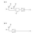
本実施形態のアンテナ装置100では、給電線36を含む給電部により、第2アンテナ70に給電されている。しかし、第1アンテナ20は無給電である。このため、第2アンテナ70は、給電により動作し、第1アンテナ20は、第2アンテナ70の動作に関連して電磁界結合により動作する。 <Feeding Method inAntenna Device 100>
In theantenna device 100 of the present embodiment, power is supplied to the second antenna 70 by the power supply unit including the power supply line 36 . However, the first antenna 20 is unpowered. Therefore, the second antenna 70 operates by power feeding, and the first antenna 20 operates by electromagnetic field coupling in relation to the operation of the second antenna 70 .
本実施形態のアンテナ装置100では、給電線36を含む給電部により、第2アンテナ70に給電されている。しかし、第1アンテナ20は無給電である。このため、第2アンテナ70は、給電により動作し、第1アンテナ20は、第2アンテナ70の動作に関連して電磁界結合により動作する。 <Feeding Method in
In the
なお、本実施形態のアンテナ装置100は、第1アンテナ20と第2アンテナ70との両方が給電されても良い。但し、第1アンテナ20と第2アンテナ70との両方が給電される場合、例えば、第2アンテナ70において放射する電波により、第1アンテナ20の給電線に電気が流れてしまい、第1アンテナ20の放射する電波に損失が発生することがある。
In addition, in the antenna device 100 of the present embodiment, both the first antenna 20 and the second antenna 70 may be fed. However, when both the first antenna 20 and the second antenna 70 are fed, for example, the electric wave radiated from the second antenna 70 causes electricity to flow in the feed line of the first antenna 20, causing the first antenna 20 to loss may occur in the radio waves radiated by the
図19A及び図19Bは、アンテナ装置100における給電方式の説明図である。
19A and 19B are explanatory diagrams of the feeding method in the antenna device 100. FIG.
図19Aは、第1アンテナ20と、第2アンテナ70との両方に給電する参考例のアンテナ装置100のブロック図である。また、図19Bは、第2アンテナ70のみに給電し、第1アンテナ20は無給電であるアンテナ装置100のブロック図である。
FIG. 19A is a block diagram of an antenna device 100 of a reference example that supplies power to both the first antenna 20 and the second antenna 70. FIG. Also, FIG. 19B is a block diagram of the antenna device 100 in which only the second antenna 70 is fed and the first antenna 20 is not fed.
図19Aに示される給電方式では、第1アンテナ20と、第2アンテナ70との両方に給電するため、給電ポート間のアイソレーションの劣化により、利得が低下する場合がある。そこで、第1アンテナ20が受信する周波数帯と、第2アンテナ70が受信する周波数帯とのアイソレーションを実現するため、図19Aに示されるように、2つの周波数帯を分離するダイプレクサ16が必要となってしまう。
In the feeding method shown in FIG. 19A, since power is fed to both the first antenna 20 and the second antenna 70, the gain may decrease due to deterioration of isolation between feeding ports. Therefore, in order to achieve isolation between the frequency band received by the first antenna 20 and the frequency band received by the second antenna 70, a diplexer 16 that separates the two frequency bands is required as shown in FIG. 19A. becomes.
一方、図19Bに示される給電方式では、第2アンテナ70に給電され、第1アンテナ20は無給電であるため、ダイプレクサ16を必要とせず、上述のアイソレーションの劣化の問題を回避することができる。したがって、第1アンテナ20と、第2アンテナ70との両方に給電する場合と比較すると、ダイプレクサ16等の別途の機器を必要とせずに利得の低下を抑制することができる。すなわち、アンテナ装置100における部品点数を少なくすることができる。
On the other hand, in the power feeding method shown in FIG. 19B, power is fed to the second antenna 70 and the first antenna 20 is not fed. Therefore, the diplexer 16 is not required, and the problem of deterioration of isolation described above can be avoided. can. Therefore, compared to the case where both the first antenna 20 and the second antenna 70 are fed, the decrease in gain can be suppressed without requiring a separate device such as the diplexer 16 or the like. That is, the number of parts in the antenna device 100 can be reduced.
図20A及び図20Bは、アンテナ装置100における天頂方向の利得の一例を示すグラフである。図20Aは、第1アンテナ20と、第2アンテナ70との両方に給電するアンテナ装置100の結果を表し、図20Bは、第2アンテナ70に給電され、第1アンテナ20は無給電であるアンテナ装置100の結果を表す。
20A and 20B are graphs showing an example of gain in the zenith direction in the antenna device 100. FIG. FIG. 20A shows the result of an antenna device 100 feeding both the first antenna 20 and the second antenna 70, and FIG. 20B shows the antenna with the second antenna 70 fed and the first antenna 20 unfed. Figure 10 shows the results of device 100;
図20A及び図20Bに示すように、第2アンテナ70に給電され、第1アンテナ20は無給電であるアンテナ装置100の場合、特に高い周波数帯において、利得が低下することを抑制することができる。
As shown in FIGS. 20A and 20B , in the case of the antenna device 100 in which the second antenna 70 is fed and the first antenna 20 is non-fed, it is possible to suppress a decrease in gain particularly in a high frequency band. .
本実施形態では、第2アンテナ70に給電し、第1アンテナ20は無給電にて動作させる構成を説明したが、逆の場合であってもよい。すなわち、第1アンテナ20に給電し、第2アンテナ70は無給電にて動作させてもよい。
In the present embodiment, a configuration has been described in which power is supplied to the second antenna 70 and the first antenna 20 is operated without power supply, but the reverse may be possible. That is, power may be supplied to the first antenna 20 and the second antenna 70 may be operated without power supply.
<<<<まとめ>>>>
以上、本実施形態の第1アンテナ20及びアンテナ装置100について説明した。例えば、第1アンテナ20は、地板10(グランド部)と、地板10に対向するように位置する導電体30と、地板10に対して物理的に所定距離離間させるように導電体30を支持する支持部40とを備える。本実施形態の第1アンテナ20によれば、導電体30と地板10とを物理的に接触させることなく、導電体30を地板10に対してより近接させることができ、導電体30と地板10との間の容量を大きくすることができる。したがって、簡易な構成で低い共振周波数のアンテナを実現することができる。 <<<<Summary>>>>
Thefirst antenna 20 and the antenna device 100 of this embodiment have been described above. For example, the first antenna 20 includes a ground plane 10 (ground portion), a conductor 30 positioned to face the ground plane 10, and a conductor 30 that is physically separated from the ground plane 10 by a predetermined distance. and a support portion 40 . According to the first antenna 20 of the present embodiment, the conductor 30 can be brought closer to the ground plane 10 without bringing the conductor 30 and the ground plane 10 into physical contact with each other. can increase the capacity between Therefore, an antenna with a low resonance frequency can be realized with a simple configuration.
以上、本実施形態の第1アンテナ20及びアンテナ装置100について説明した。例えば、第1アンテナ20は、地板10(グランド部)と、地板10に対向するように位置する導電体30と、地板10に対して物理的に所定距離離間させるように導電体30を支持する支持部40とを備える。本実施形態の第1アンテナ20によれば、導電体30と地板10とを物理的に接触させることなく、導電体30を地板10に対してより近接させることができ、導電体30と地板10との間の容量を大きくすることができる。したがって、簡易な構成で低い共振周波数のアンテナを実現することができる。 <<<<Summary>>>>
The
また、導電体30は、本体部31と、脚部32とを有する。さらに、本体部31は、地板10(グランド部)に対向するように位置する。また、脚部32は、本体部31から延在し、地板10と本体部31との間に位置する。これにより、導電体30の脚部32と地板10とを物理的に接触させることなく、導電体30の脚部32を地板10に対してより近接させることができ、導電体30と地板10との間の容量を大きくすることができる。したがって、より低い共振周波数のアンテナを実現することができる。
Also, the conductor 30 has a body portion 31 and leg portions 32 . Further, the body portion 31 is positioned so as to face the base plate 10 (ground portion). Further, the leg portion 32 extends from the body portion 31 and is positioned between the base plate 10 and the body portion 31 . As a result, the legs 32 of the conductors 30 can be brought closer to the ground plane 10 without physical contact between the legs 32 of the conductors 30 and the ground plane 10, and the conductors 30 and the ground plane 10 can be brought closer together. can increase the capacity between Therefore, an antenna with a lower resonance frequency can be realized.
また、脚部32の地板10(グランド部)に近接する部分は、地板10と電気的に結合する。これにより、導電体30と地板10との間の容量を大きくすることができる。したがって、より低い共振周波数のアンテナを実現することができる。
Also, the portion of the leg portion 32 close to the ground plane 10 (ground portion) is electrically coupled to the ground plane 10 . Thereby, the capacitance between the conductor 30 and the ground plane 10 can be increased. Therefore, an antenna with a lower resonance frequency can be realized.
また、脚部32は、本体部31の外縁部31Aに設けられる。これにより、導電体30と地板10との間の容量を大きくすることができる。したがって、より低い共振周波数のアンテナを実現することができる。
Also, the leg portion 32 is provided on the outer edge portion 31A of the body portion 31 . Thereby, the capacitance between the conductor 30 and the ground plane 10 can be increased. Therefore, an antenna with a lower resonance frequency can be realized.
また、本体部31又は脚部32は屈曲部35及び屈曲部38の少なくとも一方を有する。これにより、導電体30の脚部32と地板10とが近接する部分を設けることができる。したがって、導電体30と地板10との間の容量を大きくすることができ、より低い共振周波数のアンテナを実現することができる。
Also, the main body portion 31 or the leg portion 32 has at least one of the bent portion 35 and the bent portion 38 . Thereby, it is possible to provide a portion where the leg portion 32 of the conductor 30 and the ground plane 10 are close to each other. Therefore, the capacitance between the conductor 30 and the ground plane 10 can be increased, and an antenna with a lower resonant frequency can be realized.
また、導電体30は、円偏波の電磁波を受信し、かつ、複数の脚部32A~32Dを有する。さらに、複数の脚部32A~32Dは、本体部31の外縁部31Aに回転対称となるように位置している。これにより、円偏波の電磁波を受信する第1アンテナ20の場合に、導電体30と地板10との間の容量を大きくすることができる。したがって、より低い共振周波数のアンテナを実現することができる。
In addition, the conductor 30 receives circularly polarized electromagnetic waves and has a plurality of legs 32A to 32D. Furthermore, the plurality of leg portions 32A to 32D are positioned rotationally symmetrical to the outer edge portion 31A of the main body portion 31. As shown in FIG. Thereby, in the case of the first antenna 20 that receives circularly polarized electromagnetic waves, the capacitance between the conductor 30 and the ground plane 10 can be increased. Therefore, an antenna with a lower resonance frequency can be realized.
また、脚部32は、地板10(グランド部)に対向する対向面34を有する延出部33を有する。これにより、導電体30と地板10との間の容量をより大きくすることができる。したがって、より低い共振周波数のアンテナを実現することができる。
In addition, the leg portion 32 has an extension portion 33 having a facing surface 34 facing the base plate 10 (ground portion). Thereby, the capacitance between the conductor 30 and the ground plane 10 can be increased. Therefore, an antenna with a lower resonance frequency can be realized.
また、導電体30は、複数の脚部32A~32Dを有する。さらに、複数の脚部32A~32Dの各々は、対向面34A~34Dを有する延出部33A~33Dを有する。これにより、導電体30と地板10との間の容量をより大きくすることができる。したがって、より低い共振周波数のアンテナを実現することができる。
Also, the conductor 30 has a plurality of legs 32A to 32D. Further, each of the plurality of legs 32A-32D has extensions 33A-33D with facing surfaces 34A-34D. Thereby, the capacitance between the conductor 30 and the ground plane 10 can be increased. Therefore, an antenna with a lower resonance frequency can be realized.
また、地板10(グランド部)と延出部33の対向面34との間に絶縁体50を備える。これにより、延出部33が地板10に接触することを抑制することができる。
Also, an insulator 50 is provided between the base plate 10 (ground portion) and the facing surface 34 of the extension portion 33 . Thereby, it is possible to prevent the extending portion 33 from coming into contact with the base plate 10 .
また、支持部40は、地板10(グランド部)と本体部31との間に位置し、かつ、地板10と延出部33の対向面34とが離間するように延出部33を支持する。これにより、導電体30の脚部32を地板10に対してより近接させることができるとともに、延出部33が地板10に接触することを抑制することができる。
Further, the support portion 40 is positioned between the base plate 10 (ground portion) and the main body portion 31, and supports the extension portion 33 so that the base plate 10 and the facing surface 34 of the extension portion 33 are separated from each other. . As a result, the leg portion 32 of the conductor 30 can be brought closer to the ground plane 10 and the contact of the extending portion 33 with the ground plane 10 can be suppressed.
また、支持部40は、地板10(グランド部)と本体部31との間に位置する。これにより、導電体30と地板10とを物理的に接触させることなく、導電体30を地板10に対してより近接させることができる。
Also, the support portion 40 is positioned between the base plate 10 (ground portion) and the main body portion 31 . Thereby, the conductor 30 can be brought closer to the ground plane 10 without bringing the conductor 30 and the ground plane 10 into physical contact with each other.
また、導電体30は、複数の脚部32A~32Dを有し、支持部40は、隣接する二つの脚部32の間に位置する。これにより、電波の損失や波長短縮の影響を抑制しつつ、導電体30と地板10とを物理的に接触させることなく、導電体30を地板10に対してより近接させることができる。
Also, the conductor 30 has a plurality of legs 32A to 32D, and the support 40 is positioned between two adjacent legs 32. As shown in FIG. As a result, the conductor 30 can be brought closer to the ground plane 10 without physical contact between the conductor 30 and the ground plane 10 while suppressing the effects of radio wave loss and wavelength shortening.
また、支持部40は、地板10(グランド部)に直交する方向(Z方向、鉛直方向)から見た平面視において、導電体30の形状における中心部31D及び導電体30の外縁部31Aの少なくとも一方を支持する。これにより、電波の損失や波長短縮の影響を抑制しつつ、導電体30と地板10とを物理的に接触させることなく、導電体30を地板10に対してより近接させることができる。
In addition, the supporting portion 40 has at least a center portion 31D in the shape of the conductor 30 and an outer edge portion 31A of the conductor 30 in a plan view seen from a direction (Z direction, vertical direction) perpendicular to the ground plane 10 (ground portion). support one side. As a result, the conductor 30 can be brought closer to the ground plane 10 without physical contact between the conductor 30 and the ground plane 10 while suppressing the effects of radio wave loss and wavelength shortening.
また、導電体30は、少なくとも一つのスロット37(又はスリット)を有する。これにより、複数の周波数帯に対応することができる。
Also, the conductor 30 has at least one slot 37 (or slit). This makes it possible to support multiple frequency bands.
例えば、アンテナ装置100は、上述した特徴を有する第1アンテナ20と、第1アンテナ20とは別のアンテナ(第2アンテナ70)と、を備える。さらに、第2アンテナ70は、導電体30の地板10(グランド部)に対向する側とは反対側(+Z方向側)に位置する誘電体80及び誘電体80の導電体30に対向する側とは反対側(+Z方向側)に位置する放射素子90を有する。これにより、複数の周波数帯に対応することができる。
For example, the antenna device 100 includes the first antenna 20 having the characteristics described above and an antenna (second antenna 70) different from the first antenna 20. Furthermore, the second antenna 70 is positioned on the side (+Z direction side) opposite to the side of the conductor 30 facing the ground plane 10 (ground portion), and the side of the dielectric 80 facing the conductor 30 has a radiating element 90 located on the opposite side (+Z direction side). This makes it possible to support multiple frequency bands.
例えば、アンテナ装置100は、地板10(グランド部)と、地板10に対向するように位置する導電体30を有する第1アンテナ20と、地板10に対して物理的に所定距離離間するように導電体30を支持する支持部40と、導電体30の地板10に対向する側とは反対側(+Z方向側)に位置する誘電体80及び誘電体80の導電体30に対向する側とは反対側(+Z方向側)に位置する放射素子90を有する第2アンテナ70と、を備える。本実施形態のアンテナ装置100によれば、導電体30と地板10とを物理的に接触させることなく、導電体30を地板に対してより近接させることができ、導電体30と地板10との間の容量を大きくすることができる。したがって、簡易な構成で低い共振周波数のアンテナを実現することができる。さらに、複数の周波数帯に対応することができる。
For example, the antenna device 100 includes a ground plane 10 (ground portion), a first antenna 20 having a conductor 30 positioned to face the ground plane 10 , and a conductive antenna 20 physically separated from the ground plane 10 by a predetermined distance. A supporting portion 40 that supports the body 30, a dielectric 80 located on the side (+Z direction side) opposite to the side of the conductor 30 facing the ground plane 10, and a side of the dielectric 80 opposite to the side facing the conductor 30 a second antenna 70 having a radiating element 90 located on the side (+Z direction side). According to the antenna device 100 of the present embodiment, the conductor 30 can be brought closer to the ground plane without bringing the conductor 30 and the ground plane 10 into physical contact with each other. You can increase the capacity between Therefore, an antenna with a low resonance frequency can be realized with a simple configuration. Furthermore, it can support multiple frequency bands.
また、給電部をさらに備える。さらに、給電部は、第2アンテナ70に給電し、第1アンテナ20は無給電である。これにより、電波の損失を抑制することができ、かつ、部品点数を少なくすることができ、さらに簡易な構成とすることができる。
In addition, it is equipped with a power supply unit. Further, the feeding section feeds the second antenna 70 and the first antenna 20 is non-feeding. As a result, the loss of radio waves can be suppressed, the number of parts can be reduced, and the configuration can be simplified.
また、放射素子90は、少なくとも一つのスロット37(又はスリット)を有する。
Also, the radiating element 90 has at least one slot 37 (or slit).
本実施形態で「車載」とは、車両にのせることができるとの意味であるため、車両に取り付けられているものに限らず、車両に持ち込まれ、車両内で用いられるものも含まれる。また、本実施形態のアンテナ装置は、車輪のついた乗り物である「車両」に用いられることとしたが、これに限られず、例えばドローン等の飛行体、探査機、車輪を有さない建機、農機、船舶等の移動体に用いられても良い。
"In-vehicle" in this embodiment means that it can be mounted on a vehicle, so it is not limited to those attached to the vehicle, but also includes those that are brought into the vehicle and used inside the vehicle. In addition, although the antenna device of the present embodiment is used in a "vehicle" which is a vehicle with wheels, it is not limited to this, and can be used for flying objects such as drones, probes, and construction machines without wheels. , agricultural machinery, ships, and other moving bodies.
上記の実施形態は、本発明の理解を容易にするためのものであり、本発明を限定して解釈するためのものではない。また、本発明は、その趣旨を逸脱することなく、変更や改良され得るとともに、本発明にはその等価物が含まれるのはいうまでもない。
The above embodiments are intended to facilitate understanding of the present invention, and are not intended to limit and interpret the present invention. Further, the present invention can be modified and improved without departing from its spirit, and it goes without saying that the present invention includes equivalents thereof.
1 ベース
6 カバー部
6A 突起
10 地板
16 ダイプレクサ
20 第1アンテナ
30、30A~30H 導電体
31 本体部
31A 外縁部
31B おもて面
31C うら面
31D 中心部
32、32A~32D 脚部
33、33A~33D 延出部
34、34A~34D 対向面
35、35A~35D 屈曲部
36 給電線
36A 給電点
37 スロット
38、38A~38D 屈曲部
40 支持部
50 絶縁体
70 第2アンテナ
80 誘電体
90 放射素子
100 アンテナ装置
1Base 6 Cover Part 6A Projection 10 Base Plate 16 Diplexer 20 First Antenna 30, 30A to 30H Conductor 31 Body Part 31A Outer Edge Part 31B Front Surface 31C Back Surface 31D Center Part 32, 32A to 32D Legs 33, 33A to 33D extending portion 34, 34A to 34D facing surface 35, 35A to 35D bending portion 36 feeding line 36A feeding point 37 slot 38, 38A to 38D bending portion 40 support portion 50 insulator 70 second antenna 80 dielectric 90 radiating element 100 antenna device
6 カバー部
6A 突起
10 地板
16 ダイプレクサ
20 第1アンテナ
30、30A~30H 導電体
31 本体部
31A 外縁部
31B おもて面
31C うら面
31D 中心部
32、32A~32D 脚部
33、33A~33D 延出部
34、34A~34D 対向面
35、35A~35D 屈曲部
36 給電線
36A 給電点
37 スロット
38、38A~38D 屈曲部
40 支持部
50 絶縁体
70 第2アンテナ
80 誘電体
90 放射素子
100 アンテナ装置
1
Claims (18)
- グランド部と、
前記グランド部に対向するように位置する導電体と、
前記グランド部に対して物理的に所定距離離間させるように前記導電体を支持する支持部と、
を備えるアンテナ。 a ground section;
a conductor positioned to face the ground portion;
a support portion that supports the conductor so as to be physically separated from the ground portion by a predetermined distance;
Antenna with - 前記導電体は、本体部と、脚部と、を有し、
前記本体部は、前記グランド部に対向するように位置し、
前記脚部は、前記本体部から延在し、前記グランド部と前記本体部との間に位置する、
請求項1に記載のアンテナ。 The conductor has a main body and legs,
The body portion is positioned so as to face the ground portion,
the leg portion extends from the body portion and is positioned between the ground portion and the body portion;
Antenna according to claim 1. - 前記脚部の前記グランド部に近接する部分は、前記グランド部と電気的に結合する、
請求項2に記載のアンテナ。 a portion of the leg adjacent to the ground portion is electrically coupled to the ground portion;
Antenna according to claim 2. - 前記脚部は、前記本体部の外縁部に設けられる、
請求項2又は3に記載のアンテナ。 The legs are provided on the outer edge of the main body,
An antenna according to claim 2 or 3. - 前記本体部又は前記脚部は屈曲部を有する、
請求項2から4のいずれか一項に記載のアンテナ。 the main body portion or the leg portion has a bent portion,
Antenna according to any one of claims 2 to 4. - 前記導電体は、円偏波の電磁波を受信し、かつ、複数の前記脚部を有し、
前記複数の脚部は、前記本体部の外縁部に回転対称となるように位置している、
請求項2から5のいずれか一項に記載のアンテナ。 the conductor receives a circularly polarized electromagnetic wave and has a plurality of the legs,
The plurality of legs are positioned so as to be rotationally symmetrical on the outer edge of the main body,
Antenna according to any one of claims 2 to 5. - 前記脚部は、前記グランド部に対向する対向面を有する延出部を有する、
請求項2から6のいずれか一項に記載のアンテナ。 the leg portion has an extension portion having a facing surface facing the ground portion;
Antenna according to any one of claims 2 to 6. - 前記導電体は、複数の前記脚部を有し、
前記複数の脚部の各々は、前記対向面を有する前記延出部を有する、
請求項7に記載のアンテナ。 The conductor has a plurality of legs,
each of the plurality of legs has the extension with the facing surface;
Antenna according to claim 7. - 前記グランド部と前記延出部の前記対向面との間に絶縁体を備える、
請求項7又は8に記載のアンテナ。 An insulator is provided between the ground portion and the facing surface of the extension portion,
An antenna according to claim 7 or 8. - 前記支持部は、前記グランド部と前記本体部との間に位置し、かつ、前記グランド部と前記延出部の前記対向面とが離間するように前記延出部を支持する、
請求項7から9のいずれか一項に記載のアンテナ。 The support portion is positioned between the ground portion and the body portion, and supports the extension portion such that the ground portion and the facing surface of the extension portion are separated from each other.
Antenna according to any one of claims 7 to 9. - 前記支持部は、前記グランド部と前記本体部との間に位置する、
請求項2から10のいずれか一項に記載のアンテナ。 The support portion is positioned between the ground portion and the body portion,
Antenna according to any one of claims 2 to 10. - 前記導電体は、複数の前記脚部を有し、
前記支持部は、隣接する二つの前記脚部の間に位置する、
請求項2から11のいずれか一項に記載のアンテナ。 The conductor has a plurality of legs,
The support is located between two adjacent legs,
Antenna according to any one of claims 2 to 11. - 前記支持部は、前記グランド部に直交する方向から見た平面視において、前記導電体の形状における中心部及び前記導電体の外縁部の少なくとも一方を支持する、
請求項1から12のいずれか一項に記載のアンテナ。 The support portion supports at least one of a central portion of the shape of the conductor and an outer edge portion of the conductor in a plan view viewed in a direction orthogonal to the ground portion.
Antenna according to any one of claims 1 to 12. - 前記導電体は、少なくとも一つのスロット又はスリットを有する、
請求項1から13のいずれか一項に記載のアンテナ。 the conductor has at least one slot or slit,
Antenna according to any one of claims 1 to 13. - 請求項1から14のいずれか一項に記載のアンテナと、
前記導電体の前記グランド部に対向する側とは反対側に位置する誘電体及び前記誘電体の前記導電体に対向する側とは反対側に位置する放射素子を有する別のアンテナと、
を備える、アンテナ装置。 An antenna according to any one of claims 1 to 14;
another antenna having a dielectric located on the side opposite to the side of the conductor facing the ground portion and a radiating element located on the side of the dielectric opposite to the side facing the conductor;
An antenna device comprising: - グランド部と、
前記グランド部に対向するように位置する導電体を有する第1アンテナと、
前記グランド部に対して物理的に所定距離離間するように前記導電体を支持する支持部と、
前記導電体の前記グランド部に対向する側とは反対側に位置する誘電体及び前記誘電体の前記導電体に対向する側とは反対側に位置する放射素子を有する第2アンテナと、
を備える、アンテナ装置。 a ground section;
a first antenna having a conductor positioned to face the ground portion;
a support portion that supports the conductor so as to be physically separated from the ground portion by a predetermined distance;
a second antenna having a dielectric located on the side opposite to the side of the conductor facing the ground portion and a radiating element located on the side of the dielectric opposite to the side facing the conductor;
An antenna device comprising: - 給電部をさらに備え、
前記給電部は、前記第2アンテナに給電し、
前記第1アンテナは無給電である、
請求項16に記載のアンテナ装置。 further equipped with a power supply,
The feeding unit feeds the second antenna,
wherein the first antenna is parasitic;
17. Antenna device according to claim 16. - 前記放射素子は、少なくとも一つのスロット又はスリットを有する、
請求項16又は17に記載のアンテナ装置。
the radiating element has at least one slot or slit,
The antenna device according to claim 16 or 17.
Applications Claiming Priority (2)
| Application Number | Priority Date | Filing Date | Title |
|---|---|---|---|
| JP2021-052943 | 2021-03-26 | ||
| JP2021052943A JP2022150365A (en) | 2021-03-26 | 2021-03-26 | Antenna and antenna device |
Publications (1)
| Publication Number | Publication Date |
|---|---|
| WO2022202418A1 true WO2022202418A1 (en) | 2022-09-29 |
Family
ID=83397145
Family Applications (1)
| Application Number | Title | Priority Date | Filing Date |
|---|---|---|---|
| PCT/JP2022/011082 WO2022202418A1 (en) | 2021-03-26 | 2022-03-11 | Antenna and antenna device |
Country Status (2)
| Country | Link |
|---|---|
| JP (1) | JP2022150365A (en) |
| WO (1) | WO2022202418A1 (en) |
Families Citing this family (1)
| Publication number | Priority date | Publication date | Assignee | Title |
|---|---|---|---|---|
| WO2024043241A1 (en) * | 2022-08-22 | 2024-02-29 | 原田工業株式会社 | Antenna module |
Citations (5)
| Publication number | Priority date | Publication date | Assignee | Title |
|---|---|---|---|---|
| KR100836001B1 (en) * | 2007-03-05 | 2008-06-09 | 충남대학교산학협력단 | Folded microstrip antenna attached to a plate |
| KR20100020577A (en) * | 2008-08-13 | 2010-02-23 | 충남대학교산학협력단 | Tunable circular polarization microstrip antenna using plates loading |
| KR20100030025A (en) * | 2008-09-09 | 2010-03-18 | 엘에스엠트론 주식회사 | Small-sized patch antenna |
| KR100981664B1 (en) * | 2008-06-16 | 2010-09-10 | 충남대학교산학협력단 | Dual band circularly polarized microstrip antenna |
| WO2018164018A1 (en) * | 2017-03-08 | 2018-09-13 | 株式会社ヨコオ | Slotted patch antenna |
-
2021
- 2021-03-26 JP JP2021052943A patent/JP2022150365A/en active Pending
-
2022
- 2022-03-11 WO PCT/JP2022/011082 patent/WO2022202418A1/en active Application Filing
Patent Citations (5)
| Publication number | Priority date | Publication date | Assignee | Title |
|---|---|---|---|---|
| KR100836001B1 (en) * | 2007-03-05 | 2008-06-09 | 충남대학교산학협력단 | Folded microstrip antenna attached to a plate |
| KR100981664B1 (en) * | 2008-06-16 | 2010-09-10 | 충남대학교산학협력단 | Dual band circularly polarized microstrip antenna |
| KR20100020577A (en) * | 2008-08-13 | 2010-02-23 | 충남대학교산학협력단 | Tunable circular polarization microstrip antenna using plates loading |
| KR20100030025A (en) * | 2008-09-09 | 2010-03-18 | 엘에스엠트론 주식회사 | Small-sized patch antenna |
| WO2018164018A1 (en) * | 2017-03-08 | 2018-09-13 | 株式会社ヨコオ | Slotted patch antenna |
Also Published As
| Publication number | Publication date |
|---|---|
| JP2022150365A (en) | 2022-10-07 |
Similar Documents
| Publication | Publication Date | Title |
|---|---|---|
| US10862198B2 (en) | Wideband, low profile, small area, circular polarized uhf antenna | |
| CN107210541B (en) | Mobile base station antenna | |
| US10186778B2 (en) | Wideband dual-polarized patch antenna array and methods useful in conjunction therewith | |
| US20150303576A1 (en) | Miniaturized Patch Antenna | |
| US20150130673A1 (en) | Beam-Steered Wide Bandwidth Electromagnetic Band Gap Antenna | |
| JP7168752B2 (en) | slotted patch antenna | |
| CN111656612A (en) | Dipole antenna | |
| CN106486741B (en) | Air patch microstrip antenna | |
| JP6923490B2 (en) | Antenna device | |
| US20180123236A1 (en) | Antenna System and Antenna Module With a Parasitic Element For Radiation Pattern Improvements | |
| US11177578B2 (en) | Antenna device for vehicle | |
| JP2002359515A (en) | M-shaped antenna apparatus | |
| EP1033782B1 (en) | Monopole antenna | |
| JP2015111763A (en) | Polarization diversity antenna and radio communication apparatus | |
| WO2022202418A1 (en) | Antenna and antenna device | |
| US20200127388A1 (en) | Antenna structure and electronic device | |
| US20200388923A1 (en) | Multi-band antenna | |
| JP6299505B2 (en) | Antenna device | |
| WO2022138785A1 (en) | Antenna device | |
| JP2002252515A (en) | Antenna device | |
| JP2002094323A (en) | Circularly polarized wave antenna system | |
| WO2019064683A1 (en) | Array antenna device | |
| US10804609B1 (en) | Circular polarization antenna array | |
| EP3280006A1 (en) | A dual polarized antenna | |
| US20240047880A1 (en) | Patch antenna and vehicular antenna device |
Legal Events
| Date | Code | Title | Description |
|---|---|---|---|
| 121 | Ep: the epo has been informed by wipo that ep was designated in this application |
Ref document number: 22775210 Country of ref document: EP Kind code of ref document: A1 |
|
| NENP | Non-entry into the national phase |
Ref country code: DE |
|
| 122 | Ep: pct application non-entry in european phase |
Ref document number: 22775210 Country of ref document: EP Kind code of ref document: A1 |