WO2022202048A1 - High-frequency circuit - Google Patents
High-frequency circuit Download PDFInfo
- Publication number
- WO2022202048A1 WO2022202048A1 PCT/JP2022/007116 JP2022007116W WO2022202048A1 WO 2022202048 A1 WO2022202048 A1 WO 2022202048A1 JP 2022007116 W JP2022007116 W JP 2022007116W WO 2022202048 A1 WO2022202048 A1 WO 2022202048A1
- Authority
- WO
- WIPO (PCT)
- Prior art keywords
- band
- terminal
- switch
- circuit
- power amplifier
- Prior art date
Links
- 230000005540 biological transmission Effects 0.000 claims abstract description 108
- 238000004891 communication Methods 0.000 claims abstract description 82
- 239000003990 capacitor Substances 0.000 claims description 13
- 238000010586 diagram Methods 0.000 description 18
- 238000012986 modification Methods 0.000 description 14
- 230000004048 modification Effects 0.000 description 14
- 230000000694 effects Effects 0.000 description 8
- 239000004065 semiconductor Substances 0.000 description 8
- 230000006866 deterioration Effects 0.000 description 7
- 230000003321 amplification Effects 0.000 description 6
- 238000003199 nucleic acid amplification method Methods 0.000 description 6
- 239000000463 material Substances 0.000 description 5
- 238000000034 method Methods 0.000 description 5
- 238000012545 processing Methods 0.000 description 5
- 239000000758 substrate Substances 0.000 description 4
- 238000005516 engineering process Methods 0.000 description 3
- 238000010897 surface acoustic wave method Methods 0.000 description 2
- JMASRVWKEDWRBT-UHFFFAOYSA-N Gallium nitride Chemical compound [Ga]#N JMASRVWKEDWRBT-UHFFFAOYSA-N 0.000 description 1
- 230000002776 aggregation Effects 0.000 description 1
- 238000004220 aggregation Methods 0.000 description 1
- 230000015556 catabolic process Effects 0.000 description 1
- 238000006243 chemical reaction Methods 0.000 description 1
- 239000004020 conductor Substances 0.000 description 1
- 239000000470 constituent Substances 0.000 description 1
- 238000006731 degradation reaction Methods 0.000 description 1
- 230000005669 field effect Effects 0.000 description 1
- 230000007774 longterm Effects 0.000 description 1
- 238000005259 measurement Methods 0.000 description 1
- 230000005855 radiation Effects 0.000 description 1
- HBMJWWWQQXIZIP-UHFFFAOYSA-N silicon carbide Chemical compound [Si+]#[C-] HBMJWWWQQXIZIP-UHFFFAOYSA-N 0.000 description 1
- 230000005236 sound signal Effects 0.000 description 1
- 238000001228 spectrum Methods 0.000 description 1
Images


Classifications
-
- H—ELECTRICITY
- H04—ELECTRIC COMMUNICATION TECHNIQUE
- H04B—TRANSMISSION
- H04B1/00—Details of transmission systems, not covered by a single one of groups H04B3/00 - H04B13/00; Details of transmission systems not characterised by the medium used for transmission
- H04B1/38—Transceivers, i.e. devices in which transmitter and receiver form a structural unit and in which at least one part is used for functions of transmitting and receiving
- H04B1/40—Circuits
- H04B1/44—Transmit/receive switching
-
- H—ELECTRICITY
- H03—ELECTRONIC CIRCUITRY
- H03H—IMPEDANCE NETWORKS, e.g. RESONANT CIRCUITS; RESONATORS
- H03H5/00—One-port networks comprising only passive electrical elements as network components
- H03H5/02—One-port networks comprising only passive electrical elements as network components without voltage- or current-dependent elements
-
- H—ELECTRICITY
- H03—ELECTRONIC CIRCUITRY
- H03H—IMPEDANCE NETWORKS, e.g. RESONANT CIRCUITS; RESONATORS
- H03H7/00—Multiple-port networks comprising only passive electrical elements as network components
- H03H7/38—Impedance-matching networks
-
- H—ELECTRICITY
- H04—ELECTRIC COMMUNICATION TECHNIQUE
- H04B—TRANSMISSION
- H04B1/00—Details of transmission systems, not covered by a single one of groups H04B3/00 - H04B13/00; Details of transmission systems not characterised by the medium used for transmission
-
- H—ELECTRICITY
- H04—ELECTRIC COMMUNICATION TECHNIQUE
- H04B—TRANSMISSION
- H04B1/00—Details of transmission systems, not covered by a single one of groups H04B3/00 - H04B13/00; Details of transmission systems not characterised by the medium used for transmission
- H04B1/38—Transceivers, i.e. devices in which transmitter and receiver form a structural unit and in which at least one part is used for functions of transmitting and receiving
Definitions
- the present invention relates to high frequency circuits.
- Patent Literature 1 discloses a front-end module that supports carrier aggregation (CA).
- the 3GPP (3rd Generation Partnership Project) has established a power class that allows a higher maximum output power (hereinafter simply referred to as the high power class), mainly for vehicle communication systems or fixed wireless access (FWA: Fixed Wireless Access). ) are being discussed.
- the present invention provides a high-frequency circuit capable of suppressing degradation of signal quality when high power class is used in simultaneous communication in multiple bands.
- a high-frequency circuit has a first power amplifier corresponding to a first power class that allows a maximum output power higher than power class 3, and a passband including a first band, the first power amplifier and a first filter connected between antenna connection terminals; a second filter having a passband including a second band capable of simultaneous communication with the first band and connected to the antenna connection terminals; a first power amplifier; an attenuation circuit and a switch connected in series between a transmission path connecting between the antenna connection terminals and a ground, the attenuation circuit having an attenuation band including at least part of the second band; a switch having a first terminal connected to the attenuation circuit and a second terminal connected to the transmission path or ground; The first terminal is connected to the second terminal when simultaneous communication is performed, and the first terminal is not connected to the second terminal when simultaneous communication of the first band and the second band is not performed.
- a high-frequency circuit has a passband including a first power amplifier corresponding to a first power class that allows a maximum output power higher than power class 3, a second power amplifier, and a first band. , a first filter connected between the antenna connection terminal and the first power amplifier, a passband including a second band capable of simultaneous communication with the first band, and between the antenna connection terminal and the second power amplifier an attenuation circuit and a switch connected in series between a transmission path connecting between the second power amplifier and the antenna connection terminal and a ground;
- the switch includes an inductor connected between a transmission path and ground and having an attenuation band including a portion, the switch having a first terminal connected to the attenuation circuit and a second terminal connected to the transmission path or ground.
- the first terminal is connected to the second terminal in a state in which simultaneous communication of the first band and the second band is performed, and the first terminal is connected in a state in which simultaneous communication of the first band and the second band is not performed; is not connected to the second terminal.
- deterioration of signal quality can be suppressed when a high power class is used in simultaneous communication in multiple bands.
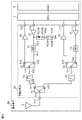
- FIG. 1 is a circuit configuration diagram of a high-frequency circuit and a communication device according to Embodiment 1.
- FIG. FIG. 2 is a diagram showing signal flow in the first connection state of the high-frequency circuit according to the first embodiment.
- FIG. 3 is a diagram showing signal flow in the second connection state of the high-frequency circuit according to the first embodiment.
- FIG. 4 is a diagram showing signal flow in the third connection state of the high-frequency circuit according to the first embodiment.
- FIG. 5 is a circuit configuration diagram around the power amplifier in Modification 1.
- FIG. 6 is a circuit configuration diagram around the power amplifier in Modification 2.
- FIG. FIG. 7 is a circuit configuration diagram of a high-frequency circuit and a communication device according to Embodiment 2.
- FIG. 8 is a circuit configuration diagram of a high-frequency circuit and a communication device according to the third embodiment.
- FIG. 9 is a diagram showing signal flows in the first connection state of the high-frequency circuit and the communication device according to the third embodiment.
- FIG. 10 is a diagram showing signal flows in the second connection state of the high-frequency circuit and the communication device according to the third embodiment.
- each drawing is a schematic diagram that has been appropriately emphasized, omitted, or adjusted in proportion to show the present invention, and is not necessarily strictly illustrated, and the actual shape, positional relationship, and ratio may differ.
- substantially the same configurations are denoted by the same reference numerals, and redundant description may be omitted or simplified.
- connection includes not only direct connection with connection terminals and/or wiring conductors, but also electrical connection via other circuit elements.
- Connected between A and B means connected to both A and B between A and B, in addition to being connected in series with the path connecting A and B , is connected between the path and ground.
- FIG. 1 is a circuit configuration diagram of a high-frequency circuit 1 and a communication device 5 according to this embodiment.
- a communication device 5 includes a high frequency circuit 1, an antenna 2, an RFIC (Radio Frequency Integrated Circuit) 3, and a BBIC (Baseband Integrated Circuit) 4.
- RFIC Radio Frequency Integrated Circuit
- BBIC Baseband Integrated Circuit
- the high-frequency circuit 1 transmits high-frequency signals between the antenna 2 and the RFIC 3.
- the internal configuration of the high frequency circuit 1 will be described later.
- the antenna 2 is connected to the antenna connection terminal 100 of the high frequency circuit 1 .
- the antenna 2 receives a high frequency signal from the high frequency circuit 1 and outputs it to the outside, and receives a high frequency signal from the outside and outputs it to the high frequency circuit 1 .
- the RFIC 3 is an example of a signal processing circuit that processes high frequency signals. Specifically, the RFIC 3 performs signal processing such as down-conversion on the high-frequency received signal input via the receiving path of the high-frequency circuit 1 , and outputs the received signal generated by the signal processing to the BBIC 4 .
- the RFIC 3 also has a control section that controls the switch circuit, amplifier circuit, and the like of the high-frequency circuit 1 . A part or all of the functions of the RFIC 3 as a control unit may be configured outside the RFIC 3 , for example, in the BBIC 4 or the high frequency circuit 1 .
- the BBIC 4 is a baseband signal processing circuit that performs signal processing using an intermediate frequency band that is lower in frequency than the high frequency signal transmitted by the high frequency circuit 1 .
- Signals processed by the BBIC 4 include, for example, image signals for image display and/or audio signals for calling through a speaker.
- the antenna 2 and the BBIC 4 are not essential components in the communication device 5 according to the present embodiment.
- the high frequency circuit 1 includes power amplifiers 11 and 12, low noise amplifiers 21 and 22, matching circuits (MN) 41 and 42, switches 51 to 53 and 82, and filters 61 and 62. , an attenuation circuit 81 , an antenna connection terminal 100 , high frequency input terminals 111 and 112 , and high frequency output terminals 121 and 122 .
- MN matching circuits
- the antenna connection terminal 100 is connected to the antenna 2 outside the high frequency circuit 1 .
- Each of the high frequency input terminals 111 and 112 is a terminal for receiving a high frequency transmission signal from the outside of the high frequency circuit 1 .
- the high frequency input terminals 111 and 112 are connected to the RFIC 3 outside the high frequency circuit 1 .
- Each of the high-frequency output terminals 121 and 122 is a terminal for providing a high-frequency received signal to the outside of the high-frequency circuit 1 .
- the high frequency output terminals 121 and 122 are connected to the RFIC 3 outside the high frequency circuit 1 .
- the power amplifier 11 is an example of a first power amplifier, and corresponds to a first power class (so-called high power class, for example, power class 2, 1.5, 1, etc.) that allows a maximum output power higher than power class 3. .
- Power amplifier 11 is connected between high frequency input terminal 111 and filter 61 . Specifically, the input terminal of the power amplifier 11 is connected to the high frequency input terminal 111 .
- the output terminal of the power amplifier 11 is connected to the filter 61 via the matching circuit 41 and switch 52 .
- the power amplifier 11 can amplify the transmission signal of band A to power that satisfies the maximum output power of the first power class.
- the power amplifier 12 is an example of a second power amplifier, and corresponds to a second power class that allows a maximum output power equal to or lower than power class 3 (a so-called non-high power class, such as power classes 3, 4, etc.).
- Power amplifier 12 is connected between high frequency input terminal 112 and filter 62 . Specifically, the input end of the power amplifier 12 is connected to the high frequency input terminal 112 .
- the output terminal of the power amplifier 12 is connected to the filter 62 via the matching circuit 42 and switch 53 .
- the power amplifier 12 can amplify the transmission signal of band B to the power that satisfies the maximum output power of the second power class, but cannot amplify the transmission signal of band B to the power that satisfies the maximum output power of the first power class. Can not.
- the power amplifiers 11 and 12 are electronic components that obtain an output signal with greater energy than the input signal (transmission signal) based on the power supplied from the power supply.
- Each of power amplifiers 11 and 12 includes an amplification transistor and may further include an inductor and/or capacitor.
- the internal configurations of power amplifiers 11 and 12 are not particularly limited.
- each of power amplifiers 11 and 12 may be a multi-stage amplifier, a differential amplification type amplifier, or a Doherty amplifier.
- a power class is a classification of terminal output power defined by maximum output power, etc.
- a smaller power class value indicates a higher power output.
- the maximum output power for power class 1 is 31 dBm
- the maximum output power for power class 1.5 is 29 dBm
- the maximum output power for power class 2 is 26 dBm
- the maximum output power for power class 3 is 23 dBm. .
- the terminal's maximum output power is defined as the output power at the terminal's antenna end. Measurement of the maximum output power of the terminal is performed, for example, by a method defined by 3GPP or the like. For example, in FIG. 1 the maximum output power is measured by measuring the radiated power at antenna 2 . Instead of measuring the radiation power, it is also possible to measure the output power of the antenna 2 by providing a terminal near the antenna 2 and connecting a measuring instrument (such as a spectrum analyzer) to the terminal.
- a measuring instrument such as a spectrum analyzer
- the power class that the power amplifier supports can be specified by the maximum output power of the power amplifier.
- the maximum output power of a power amplifier corresponding to power class 1 is greater than 31 dBm.
- the maximum output power of a power amplifier depends on the size and material of the semiconductor devices that make up the power amplifier. For example, the higher the maximum output power, the larger the size of the semiconductor device. Therefore, by comparing the semiconductor device sizes for two power amplifiers constructed of the same semiconductor material, it may be possible to make a relative comparison of the power classes supported by the two power amplifiers.
- a semiconductor device that constitutes a power amplifier with a high maximum output power may use a special semiconductor material for high power (eg, gallium nitride (GaN), silicon carbide (SiC), etc.). Therefore, by comparing the semiconductor materials used in the two semiconductor devices, it may be possible to make a relative comparison of the power classes supported by the two power amplifiers.
- a semiconductor material for high power eg, gallium nitride (GaN), silicon carbide (SiC), etc.
- the low noise amplifier 21 is connected between the filter 61 and the high frequency output terminal 121 . Specifically, the input terminal of the low noise amplifier 21 is connected to the filter 61 via the switch 52 . On the other hand, the output end of the low noise amplifier 21 is connected to the high frequency output terminal 121 .
- the low noise amplifier 21 can amplify the band A received signal.
- the low noise amplifier 22 is connected between the filter 62 and the high frequency output terminal 122 . Specifically, the input end of low noise amplifier 22 is connected to filter 62 via switch 53 . On the other hand, the output end of the low noise amplifier 22 is connected to the high frequency output terminal 122 .
- the low-noise amplifier 22 can amplify the received band B signal.
- a matching circuit 41 is connected between the power amplifier 11 and the filter 61 .
- matching circuit 41 is connected to power amplifier 11 and to filter 61 via switch 52 .
- the matching circuit 41 is an impedance matching circuit, and can match the output impedance (low impedance, eg, 4 ohms) of the power amplifier 11 and the input impedance (reference impedance, eg, 50 ohms) of the switch 52 .
- the matching circuit 41 can be composed of inductors and/or capacitors, for example.
- a matching circuit 42 is connected between the power amplifier 12 and the filter 62 .
- matching circuit 42 is connected to power amplifier 12 and to filter 62 via switch 53 .
- the matching circuit 42 is an impedance matching circuit and can match the output impedance (low impedance) of the power amplifier 12 and the input impedance (reference impedance) of the switch 53 .
- the matching circuit 42 can be composed of inductors and/or capacitors, for example.
- the switch 51 is connected between the antenna connection terminal 100 and the filters 61 and 62 .
- the switch 51 has terminals 511-513.
- Terminal 511 is connected to antenna connection terminal 100 .
- Terminal 512 is connected to filter 61 .
- Terminal 513 is connected to filter 62 .
- the switch 51 can connect the terminal 511 to the terminals 512 and/or 513 based on a control signal from the RFIC 3, for example. That is, the switch 51 can independently switch between connection and non-connection between the antenna connection terminal 100 and the filter 61 and between connection and non-connection between the antenna connection terminal 100 and the filter 62 .
- the switch 51 is composed of, for example, a multi-connection switch circuit.
- a switch 52 is connected between the filter 61 and the power amplifier 11 and the low noise amplifier 21 .
- the switch 52 has terminals 521-523.
- Terminal 521 is connected to filter 61 .
- Terminal 522 is connected to power amplifier 11 via matching circuit 41 .
- Terminal 523 is connected to low noise amplifier 21 .
- the switch 52 can connect the terminal 521 to either of the terminals 522 and 523 based on a control signal from the RFIC 3, for example. That is, the switch 52 can switch the connection of the filter 61 between the power amplifier 11 and the low noise amplifier 21 .
- the switch 52 is configured by, for example, an SPDT (Single-Pole Double-Throw) type switch circuit.
- a switch 53 is connected between the filter 62 and the power amplifier 12 and the low noise amplifier 22 .
- the switch 53 has terminals 531-533.
- Terminal 531 is connected to filter 62 .
- Terminal 532 is connected to power amplifier 12 via matching circuit 42 .
- Terminal 533 is connected to low noise amplifier 22 .
- the switch 53 can connect the terminal 531 to either of the terminals 532 and 533 based on a control signal from the RFIC 3, for example. That is, the switch 53 can switch the connection of the filter 62 between the power amplifier 12 and the low noise amplifier 22 .
- the switch 53 is composed of, for example, an SPDT type switch circuit.
- the filter 61 is an example of a first filter, has a passband including band A, and is connected between the power amplifier 11 and the antenna connection terminal 100 . Specifically, one end of the filter 61 is connected to the power amplifier 11 and the low noise amplifier 21 via the switch 52 . On the other hand, the other end of filter 61 is connected to antenna connection terminal 100 via switch 51 .
- the filter 61 can pass the band A transmission signal amplified by the power amplifier 11 to the antenna connection terminal 100 . Further, the filter 61 can pass the received signal of band A received via the antenna connection terminal 100 to the low noise amplifier 21 .
- the filter 62 is an example of a second filter, has a passband including band B, and is connected between the power amplifier 12 and the antenna connection terminal 100 . Specifically, one end of the filter 62 is connected to the power amplifier 12 and the low noise amplifier 22 via the switch 53 . On the other hand, the other end of filter 62 is connected to antenna connection terminal 100 via switch 51 .
- the filter 62 can pass the band B transmission signal amplified by the power amplifier 12 to the antenna connection terminal 100 . Further, the filter 62 can pass the received signal of band B received via the antenna connection terminal 100 to the low noise amplifier 22 .
- the filters 61 and 62 may be configured using, for example, a surface acoustic wave (SAW) filter, a bulk acoustic wave (BAW) filter, an LC resonance filter, or a dielectric filter. , and are not limited to these.
- SAW surface acoustic wave
- BAW bulk acoustic wave
- LC resonance filter an LC resonance filter
- dielectric filter a dielectric filter
- the attenuation circuit 81 has an attenuation band including at least part of band B, and has an inductor 811 and a capacitor 812 connected in series between a transmission path connecting between the power amplifier 11 and the antenna connection terminal 100 and the ground. .
- the attenuation circuit 81 is connected between the transmission path P11 between the power amplifier 11 and the matching circuit 41 and the ground, and arranged in a low-impedance path. Note that the attenuation circuit 81 may not include the capacitor 812 .
- the switch 82 can switch between conduction and non-conduction of the parallel arm path in which the attenuation circuit 81 is arranged. Specifically, switch 82 is connected in series with attenuation circuit 81 in the parallel arm path and has terminals 821 and 822 .
- a terminal 821 is an example of a first terminal and is connected to the attenuation circuit 81 .
- Terminal 822 is an example of a second terminal and is connected to the ground.
- the switch 82 connects the terminal 821 to the terminal 822 in a state in which simultaneous communication of the bands A and B is performed based on a control signal from the RFIC 3, for example, so that simultaneous communication of the bands A and B is performed.
- Terminal 821 is not connected to terminal 822 in the absence state.
- the switch 82 is configured by, for example, an SPST (Single-Pole Single-Throw) type switch circuit.
- switch 82 is connected between the attenuation circuit 81 and the ground here, the position of the switch 82 is not limited to this.
- switch 82 may be connected between attenuation circuit 81 and transmit path P11.
- terminal 821 is connected to attenuation circuit 81 and terminal 822 is connected to transmission path P11.
- the attenuation circuit 81 and the switch 82 are connected between the transmission path P11 and the ground, but the positions of the attenuation circuit 81 and the switch 82 are not limited to this.
- the attenuation circuit 81 and the switch 82 may be connected to a transmission path P12 between the matching circuit 41 and the switch 52, a transmission path P13 between the switch 52 and the filter 61, or a transmission path P14 between the filter 61 and the switch 51 and ground. may be connected between
- the high frequency circuit 1 may not include at least one of the power amplifier 12, the low noise amplifiers 21 and 22, the matching circuits 41 and 42, and the switches 51-53.
- the high-frequency circuit 1 may be mounted on one module substrate, but is not limited to this.
- the high-frequency circuit 1 may be divided and mounted on a plurality of module substrates.
- the modules may be connected to different antennas.
- the first module substrate includes a power amplifier 11, a low noise amplifier 21, a matching circuit 41, a switch 52, a filter 61, an attenuation circuit 81, an antenna connection terminal, a high frequency input A terminal 111 and a high frequency output terminal 121 are mounted
- the second module substrate includes a power amplifier 12, a low noise amplifier 22, a matching circuit 42, a switch 53, a filter 62, an antenna connection terminal, and a high frequency output terminal.
- An input terminal 112 and a high frequency output terminal 122 may be implemented.
- the antenna connection terminals of the first module board and the antenna connection terminals of the second module board may be connected to different antennas.
- Band A is an example of the first band, and is constructed using a radio access technology (RAT: Radio Access Technology) predefined by standardization organizations (for example, 3GPP and IEEE (Institute of Electrical and Electronics Engineers), etc.) It is a frequency band for a communication system that uses Band A corresponds to the first power class.
- RAT Radio Access Technology
- band A a band for time division duplex (TDD) is used.
- TDD time division duplex
- Band A for example, n77, n78, n79 or n41 for 5GNR (5th Generation New Radio) can be used.
- Band B is an example of a second band, and is a frequency band for communication systems capable of simultaneous communication with band A. That is, the band B transmit signal and/or receive signal can be used simultaneously with the band A transmit signal. Band B does not correspond to the first power class, but corresponds to the second power class.
- band A for TDD is used as the band A in the present embodiment.
- band B for example, n46 or n96 for 5GNR can be used.
- band B Band42 or Band48 for LTE (Long Term Evolution) can also be used as band B.
- bands A and B are not limited to TDD bands.
- bands for frequency division duplex FDD: Frequency Division Duplex
- FDD Frequency Division Duplex
- bands A and B bands for frequency division duplex (FDD: Frequency Division Duplex) (for example, Band 1-5, 12, 14, 30 or 66 for LTE, or n1-n3, n5 for 5GNR , n12, n14, n30 or n66) may be used.
- FDD Frequency Division Duplex
- bands A and B are not limited to frequency bands for 5GNR and/or LTE.
- bands or channels for WLAN can be used as bands A and/or B.
- FIG. 2 to 4 are diagrams showing signal flows in the first to third connection states of the high-frequency circuit 1 according to the present embodiment.
- FIG. 2 shows a first connection state in which band A transmission and band B reception occur simultaneously.
- FIG. 2 shows a state in which simultaneous communication of bands A and B is performed.
- the RFIC 3 can realize this first connection state by controlling each switch circuit of the high frequency circuit 1 .
- switch 51 connects terminal 511 to both terminals 512 and 513
- switch 52 connects terminal 521 to terminal 522
- switch 53 connects terminal 531 to terminal 533 .
- the switch 82 connects the terminal 821 to the terminal 822 .
- the transmission signal of band A flows from the high frequency input terminal 111 to the antenna connection terminal 100 via the power amplifier 11, the matching circuit 41, the switch 52, the filter 61 and the switch 51.
- the band B component (spurious) contained in the transmission signal amplified by the power amplifier 11 flows through the attenuation circuit 81 and the switch 82 to the ground.
- a received signal of band B flows from the antenna connection terminal 100 to the high frequency output terminal 122 via the switch 51 , the filter 62 , the switch 53 and the low noise amplifier 22 .
- FIG. 3 shows a second connection state in which band A transmission and band B transmission are performed simultaneously.
- FIG. 3 shows a state in which simultaneous communication of bands A and B is performed.
- the RFIC 3 can realize this second connection state by controlling each switch circuit of the high frequency circuit 1 .
- switch 51 connects terminal 511 to both terminals 512 and 513
- switch 52 connects terminal 521 to terminal 522
- switch 53 connects terminal 531 to terminal 532 .
- the switch 82 connects the terminal 821 to the terminal 822 .
- the transmission signal of band A flows from the high frequency input terminal 111 to the antenna connection terminal 100 via the power amplifier 11, the matching circuit 41, the switch 52, the filter 61 and the switch 51.
- the band B component (spurious) contained in the transmission signal amplified by the power amplifier 11 flows through the attenuation circuit 81 and the switch 82 to the ground.
- a transmission signal of band B flows from the high frequency input terminal 112 to the antenna connection terminal 100 via the power amplifier 12 , the matching circuit 42 , the switch 53 , the filter 62 and the switch 51 .
- FIG. 4 shows a third connection state in which band A transmission is performed and band B transmission and reception are not performed.
- FIG. 4 shows a state in which simultaneous communication of bands A and B is not performed.
- the RFIC 3 can realize this third connection state by controlling each switch circuit of the high frequency circuit 1 .
- switch 51 connects terminal 511 to terminal 512 and switch 52 connects terminal 521 to terminal 522 .
- the switch 82 does not connect the terminal 821 to the terminal 822 .
- the transmission signal of band A flows from the high frequency input terminal 111 to the antenna connection terminal 100 via the power amplifier 11, the matching circuit 41, the switch 52, the filter 61 and the switch 51. At this time, no signal flows through the attenuation circuit 81 .
- the high-frequency circuit 1 has the power amplifier 11 corresponding to the first power class that allows a maximum output power higher than the power class 3, and the passband including the band A. 11 and the antenna connection terminal 100, a filter 62 having a passband including band A and band B capable of simultaneous communication, and connected to the antenna connection terminal 100, the power amplifier 11 and the antenna.
- An attenuation circuit 81 and a switch 82 are connected in series between a transmission path connecting between the connection terminals 100 and the ground, and the attenuation circuit 81 has an attenuation band including at least part of band B, Containing an inductor 811 between the path and ground, a switch 82 has a terminal 821 connected to the attenuation circuit 81 and a terminal 822 connected to the transmit path or ground to allow simultaneous communication of bands A and B.
- Terminal 821 is connected to terminal 822 in a state in which simultaneous communication of bands A and B is performed, and terminal 821 is not connected to terminal 822 in a state in which simultaneous communication of bands A and B is not performed.
- the attenuation circuit 81 can be connected to the transmission path of the band A signal in a state where simultaneous communication of the bands A and B is performed. Therefore, it is possible to attenuate the band B component (spurious) contained in the high-power transmission signal amplified by the power amplifier 11, and the band B transmission signal and/or reception signal simultaneously communicated with the band A transmission signal. Signal quality deterioration (for example, an increase in error vector magnitude (EVM) or an increase in noise figure (NF)) can be suppressed.
- EVM error vector magnitude
- NF noise figure
- the attenuation circuit 81 is not connected to the transmission path of the band A signal when simultaneous communication of the bands A and B is not performed. Therefore, in the state of non-simultaneous communication, the electrical characteristics of the high-frequency circuit 1 can be improved by reducing the loss and mismatch loss due to the attenuation circuit 81 .
- the attenuation circuit 81 may include a capacitor 812 connected in series with the inductor 811 between the transmission path and the ground.
- the high-frequency circuit 1 can achieve the same effects as described above.
- the high-frequency circuit 1 may include a matching circuit 41 connected between the power amplifier 11 and the filter 61, and the attenuation circuit 81 is connected between the power amplifier 11 and the matching circuit 41. may be connected.
- the LC series circuit is arranged in the parallel arm path of the output impedance (that is, low impedance) system of the power amplifier 11, the LC series circuit can function as an attenuation pole having a low Q value. Therefore, the attenuation circuit 81 can achieve broadband attenuation.
- the terminal 822 of the switch 82 may be connected to the ground.
- the switch 82 when the switch 82 is composed of a field-effect transistor (FET), the source of the FET can be connected to the ground. Therefore, when a voltage is applied to the gate of the FET to turn on the switch 82, the potential difference between the gate and the source can be increased, and the impedance between the drain and the source can be reduced.
- FET field-effect transistor
- the high-frequency circuit 1 may include a power amplifier 12, and the filter 62 may be connected between the antenna connection terminal 100 and the power amplifier 12.
- the transmission signal of band B can be transmitted simultaneously with the transmission signal of band A corresponding to the first power class, and the quality deterioration of the transmission signal of band B can be suppressed at this time.
- the power amplifier 12 may correspond to a second power class that allows a maximum output power equal to or lower than power class 3.
- the transmission signal of band B corresponding to the second power class can be transmitted simultaneously with the transmission signal of band A corresponding to the first power class, and at that time, the quality deterioration of the transmission signal of band B is suppressed. can do.
- the high-frequency circuit 1 may include a low-noise amplifier 22
- the filter 62 may be connected between the antenna connection terminal 100 and the low-noise amplifier 22 .
- the received signal of band B can be transmitted and received simultaneously with the transmitted signal of band A corresponding to the first power class, and deterioration of the received signal quality of band B can be suppressed at this time.
- band A may be n77, n78, n79 or n41 for 5GNR
- band B may be n46 or n96 for 5GNR. good.
- the high frequency circuit 1 can be used for simultaneous transmission and/or simultaneous transmission/reception of the n77, n78, n79 or n41 signal for 5GNR and the n46 or n96 signal for 5GNR.
- band A may be n79 for 5GNR
- band B may be Band42 or Band48 for LTE.
- the high-frequency circuit 1 can be used for simultaneous transmission and/or simultaneous transmission/reception of n79 signals for 5GNR and Band 42 or Band 48 signals for LTE.
- the communication device 5 includes an RFIC 3 that processes high frequency signals, and a high frequency circuit 1 that transmits high frequency signals between the RFIC 3 and the antenna 2 .
- the effect of the high-frequency circuit 1 can be realized in the communication device 5.
- Modification 1 Modification 1
- the power amplifier corresponding to the first power class and the power amplifier corresponding to the second power class can be switched and used for amplifying the transmission signal of band A, which is the same as in the first embodiment. differ mainly from A circuit configuration around the power amplifier in this modified example will be specifically described below with reference to FIG.
- FIG. 5 is a circuit configuration diagram around power amplifiers 11A and 13A in this modification.
- a high-frequency circuit 1 according to this modification includes power amplifiers 11A and 13A and switches 14A and 15A instead of the power amplifier 11 .
- the power amplifier 11A is an example of a first power amplifier and corresponds to the first power class.
- the power amplifier 11 A is connected between the high frequency input terminal 111 and the matching circuit 41 .
- the input terminal of the power amplifier 11A is connected to the high frequency input terminal 111 via the switch 14A.
- the output end of power amplifier 11A is connected to matching circuit 41 via switch 15A.
- the power amplifier 11A can amplify the transmission signal of band A to power that satisfies the maximum output power of the first power class.
- the power amplifier 13A corresponds to the second power class.
- the power amplifier 13 A is connected between the high frequency input terminal 111 and the matching circuit 41 .
- the input end of the power amplifier 13A is connected to the high frequency input terminal 111 via the switch 14A.
- the output end of power amplifier 13A is connected to matching circuit 41 via switch 15A.
- the power amplifier 13A can amplify the transmission signal of band A to power that satisfies the maximum output power of the first power class.
- the switch 14A can switch the connection of the high frequency input terminal 111 between the power amplifiers 11A and 13A.
- the switch 14A is composed of, for example, an SPDT type switch circuit.
- the switch 15A can switch the connection of the matching circuit 41 between the power amplifiers 11A and 13A.
- the switch 15A is composed of, for example, an SPDT type switch circuit.
- switches 14A and 15A connect the power amplifier 11A to the high frequency input terminal 111 and the matching circuit 41.
- switches 14 A and 15 A connect power amplifier 13 A to high frequency input terminal 111 and matching circuit 41 .
- the switch 82 connects the terminal 821 to the terminal 822 in a state in which simultaneous communication of bands A and B is performed.
- the switch 82 does not connect the terminal 821 to the terminal 822 when the simultaneous communication of the bands A and B is not performed.
- switch 82 does not need to connect terminal 821 to terminal 822 regardless of band B.
- Modification 2 Next, modification 2 will be described.
- This modification is different from the first embodiment mainly in that a differential amplification type amplifier circuit is used as the power amplifier corresponding to the first power class.
- a circuit configuration around the power amplifier in this modified example will be specifically described below with reference to FIG.
- FIG. 6 is a circuit configuration diagram around power amplifiers 11B and 13B in this modification.
- the high-frequency circuit 1 according to this modification includes power amplifiers 11B and 13B and transformers 14B and 15B instead of the power amplifier 11.
- FIG. 6 is a circuit configuration diagram around power amplifiers 11B and 13B in this modification.
- the high-frequency circuit 1 according to this modification includes power amplifiers 11B and 13B and transformers 14B and 15B instead of the power amplifier 11.
- the transformer 14B can divide one signal into two signals having phases opposite to each other. That is, the transformer 14B can convert a single-ended signal into a differential signal. Transformer 14B has two coils.
- the transformer 15B can synthesize two signals having phases opposite to each other into one signal. That is, the transformer 15B can convert differential signals into single-ended signals. Transformer 15B has two coils.
- the power amplifier 11B can amplify one of the two signals distributed by the transformer 14B.
- An input end of the power amplifier 11B is connected to one end of a coil included in the transformer 14B.
- An output end of the power amplifier 11B is connected to one end of a coil included in the transformer 15B.
- the power amplifier 13B can amplify the other of the two signals distributed by the transformer 14B.
- the input end of power amplifier 13B is connected to the other end of the coil included in transformer 14B.
- the output end of power amplifier 13B is connected to the other end of the coil included in transformer 15B.
- the circuit configuration shown in FIG. 6 is an example of a differential amplification type amplifier circuit, and the differential amplification type amplifier circuit is not limited to this.
- the differential amplification type amplifier circuit may include another power amplifier between the high frequency input terminal 111 and the transformer 14B.
- a Wilkinson amplifier circuit may be used instead of the differential amplifier circuit.
- the amplifier circuit may include a Wilkinson divider and a Wilkinson combiner instead of the transformers 14B and 15B.
- Embodiment 2 Next, Embodiment 2 will be described.
- This embodiment is different from the above-described first embodiment mainly in that a signal of band C can be transmitted in addition to bands A and B.
- the present embodiment will be described below with reference to the drawings, focusing on the differences from the first embodiment.
- FIG. 7 is a circuit configuration diagram of a high frequency circuit 1A and a communication device 5A according to this embodiment. Note that the circuit configuration of the communication device 5A is the same as that of the communication device 5 according to the first embodiment except that the high frequency circuit 1A is provided instead of the high frequency circuit 1, so the description is omitted.
- a high-frequency circuit 1A according to the present embodiment as shown in FIG. 63, an attenuation circuit 81, an antenna connection terminal 100, high frequency input terminals 111 and 112, and a high frequency output terminal 122.
- the switch 51A is connected between the antenna connection terminal 100 and the filters 61-63.
- the switch 51A has terminals 511-514. Terminal 514 is connected to filter 63 .
- the switch 51A can connect the terminal 511 to one or any combination of the terminals 512-514 based on a control signal from the RFIC 3, for example. That is, the switch 51A switches between connection and non-connection between the antenna connection terminal 100 and the filter 61, switches between connection and non-connection between the antenna connection terminal 100 and the filter 62, and switches between the antenna connection terminal 100 and the filter 63. switching between connection and non-connection can be performed independently.
- the switch 51A is composed of, for example, a multi-connection switch circuit.
- the switch 52A is connected between the filters 61 and 63 and the power amplifier 11.
- Switch 52A has terminals 521 , 522 and 524 .
- Terminal 524 is connected to filter 63 .
- the switch 52A can connect the terminal 522 to the terminals 521 and/or 524 based on a control signal from the RFIC 3, for example. That is, the switch 52A can independently switch between connection and non-connection between the filter 61 and the power amplifier 11 and between connection and non-connection between the filter 63 and the power amplifier 11 .
- the switch 52A is configured by, for example, a multi-connection switch circuit.
- the filter 63 is an example of a third filter, has a passband including band C, and is connected between the power amplifier 11 and the antenna connection terminal 100 . Specifically, one end of the filter 63 is connected to the power amplifier 11 via the switch 52A and the matching circuit 41 . On the other hand, the other end of filter 63 is connected to antenna connection terminal 100 via switch 51A. The filter 63 can pass the band C transmission signal amplified by the power amplifier 11 to the antenna connection terminal 100 .
- the switch 82 connects the terminal 821 to the terminal 822 in a state in which simultaneous communication of bands A and B is performed based on a control signal from the RFIC 3, for example.
- the terminal 821 is not connected to the terminal 822 when simultaneous communication of the bands A and B is not performed.
- Band C is an example of a third band, which is higher than band A and lower than band B.
- the power class applied to band C is not particularly limited. Also, band C may or may not be capable of simultaneous communication with bands A and/or B.
- band A For example, if n77 for 5GNR is used as band A and n46 or n96 for 5GNR is used as band B, then n78 or n79 for 5GNR or Band42 for LTE as band C Alternatively, Band 48 can be used.
- n79 for 5GNR is used as band A and Band42 or Band48 for LTE is used as band B
- n46 for 5GNR can be used as band C.
- n77, n78 or n79 for 5GNR is used as band A and n96 for 5GNR is used as band B, n46 for 5GNR can be used as band C.
- the passband includes the band C which is higher than the band A and lower than the band B, and between the power amplifier 11 and the antenna connection terminal 100 A connected filter 63 may be provided.
- the high frequency circuit 1A can share the power amplifier 11 between the bands A and C, and the number of parts of the high frequency circuit 1A can be reduced.
- band A may be n77 for 5GNR
- band B may be n46 or n96 for 5GNR
- band C may be It may be n78 or n79 for 5GNR, or Band42 or Band48 for LTE.
- the high-frequency circuit 1A can be used for transmission of Band 42 or Band 48 signals.
- band A may be n79 for 5GNR
- band B may be Band42 or Band48 for LTE
- band C may be It may be n46 for 5GNR.
- the high frequency circuit 1A is used to transmit the n46 signal for 5GNR. can be used.
- band A may be n77, n78 or n79 for 5GNR
- band B may be n96 for 5GNR
- band C may be n46 for 5GNR.
- the high frequency circuit is used to transmit the n46 signal for 5GNR. 1A can be used.
- the communication device 5A includes an RFIC 3 that processes high frequency signals, and a high frequency circuit 1A that transmits high frequency signals between the RFIC 3 and the antenna 2.
- the effect of the high-frequency circuit 1A can be realized in the communication device 5A.
- the attenuation circuit is connected to the transmission path between the power amplifier and the antenna connection terminal corresponding to the second power class, not the transmission path between the power amplifier and the antenna connection terminal corresponding to the first power class. It differs from each of the above-described embodiments mainly in that The present embodiment will be described below with reference to the drawings, focusing on the differences from the above embodiments.
- FIG. 8 is a circuit configuration diagram of a high frequency circuit 1B and a communication device 5B according to this embodiment. Note that the circuit configuration of the communication device 5B is the same as that of the communication device 5 according to the first embodiment except that the high frequency circuit 1B is provided instead of the high frequency circuit 1, so the description is omitted.
- the high frequency circuit 1B includes power amplifiers 11 and 12, low noise amplifiers 21 and 22, matching circuits 41 and 42, switches 51 to 53 and 82B, a filter 61 and 62, an attenuation circuit 81B, an antenna connection terminal 100, high frequency input terminals 111 and 112, and high frequency output terminals 121 and 122.
- the attenuation circuit 81B has an attenuation band including at least part of band A, and has an inductor 811B and a capacitor 812B connected in series between a transmission path connecting between the power amplifier 12 and the antenna connection terminal 100 and the ground. .
- the attenuation circuit 81B is connected between the transmission path P21 between the power amplifier 12 and the matching circuit 42 and the ground, and arranged in a low-impedance path. Note that the attenuation circuit 81B may not include the capacitor 812B.
- the switch 82B can switch between conduction and non-conduction of the parallel arm path in which the attenuation circuit 81B is arranged.
- switch 82B has terminals 821B and 822B.
- a terminal 821B is an example of a first terminal and is connected to the attenuation circuit 81B.
- Terminal 822B is an example of a second terminal and is connected to the ground.
- the switch 82B connects the terminal 821B to the terminal 822B in a state in which simultaneous communication of the bands A and B is performed based on a control signal from the RFIC 3, for example, so that simultaneous communication of the bands A and B is performed. In this state, terminal 821B is not connected to terminal 822B.
- the switch 82B is composed of, for example, an SPST type switch circuit.
- switch 82B is connected between the attenuation circuit 81B and the ground here, the position of the switch 82B is not limited to this.
- switch 82B may be connected between attenuation circuit 81B and transmit path P21.
- terminal 821B is connected to attenuation circuit 81B and terminal 822B is connected to transmission path P21.
- the attenuation circuit 81B and the switch 82B are connected between the transmission path P21 and the ground, but the positions of the attenuation circuit 81B and the switch 82B are not limited to this.
- the attenuation circuit 81B and the switch 82B are connected to the transmission path P22 between the matching circuit 42 and the switch 53, the transmission path P23 between the switch 53 and the filter 62, or the transmission path P24 between the filter 62 and the switch 51 and ground. may be connected between
- FIG. 9 and 10 are diagrams showing signal flows in the first and second connection states of the high-frequency circuit 1B according to the present embodiment.
- FIG. 9 shows a first connection state in which band A transmission and band B transmission are performed simultaneously.
- FIG. 9 shows a state in which simultaneous communication of bands A and B is performed.
- the RFIC 3 can realize this first connection state by controlling each switch circuit of the high frequency circuit 1B.
- switch 51 connects terminal 511 to both terminals 512 and 513
- switch 52 connects terminal 521 to terminal 522
- switch 53 connects terminal 531 to terminal 532 .
- the switch 82B connects the terminal 821B to the terminal 822B.
- the transmission signal of band A flows from the high frequency input terminal 111 to the antenna connection terminal 100 via the power amplifier 11, the matching circuit 41, the switch 52, the filter 61 and the switch 51.
- the band A transmission signal that has flowed into the transmission paths P21 to P24 flows to the ground via the attenuation circuit 81B and the switch 82B.
- a transmission signal of band B flows from the high frequency input terminal 112 to the antenna connection terminal 100 via the power amplifier 12 , the matching circuit 42 , the switch 53 , the filter 62 and the switch 51 .
- FIG. 10 shows a second connection state in which band A transmission is not performed and band B transmission is performed.
- FIG. 10 shows a state in which simultaneous communication of bands A and B is not performed.
- the RFIC 3 can realize this second connection state by controlling each switch circuit of the high frequency circuit 1B.
- switch 51 connects terminal 511 to terminal 513 and switch 53 connects terminal 531 to terminal 532 .
- the switch 82B does not connect the terminal 821B to the terminal 822B.
- the transmission signal of band B flows from the high frequency input terminal 111 to the antenna connection terminal 100 via the power amplifier 11 , matching circuit 41 , switch 52 , filter 61 and switch 51 . At this time, no signal flows through the attenuation circuit 81B.
- the high-frequency circuit 1B has the power amplifier 11 and the power amplifier 12 corresponding to the first power class that allows a maximum output power higher than the power class 3, and the passband including the band A. has a filter 61 connected between the antenna connection terminal 100 and the power amplifier 11; and an attenuation circuit 81B and a switch 82B connected in series between a transmission path connecting between the power amplifier 12 and the antenna connection terminal 100 and the ground.
- a switch 82B includes an inductor 811B connected between the transmit path and ground, having an attenuation band that includes a portion of A terminal 822B is provided, and the terminal 821B is connected to the terminal 822B when simultaneous communication of the bands A and B is performed, and the terminal 821B is not connected to the terminal 822B when the simultaneous communication of the bands A and B is not performed.
- the attenuation circuit 81B can be connected to the transmission path of the signal of band B in a state where simultaneous communication of bands A and B is performed. Therefore, it is possible to attenuate the band A transmission signal that has flowed into the band B transmission path. As a result, it is possible to suppress the distortion caused by the nonlinear element (for example, the power amplifier 12, etc.) due to the transmission signal of the band A, and suppress the quality deterioration of the transmission signal of the band B that is simultaneously communicated with the transmission signal of the band A. can be done. Further, in a state where simultaneous communication of bands A and B is not performed, attenuation circuit 81B is not connected to the transmission path of band B signals. Therefore, in the state of non-simultaneous communication, the electrical characteristics of the high-frequency circuit 1B can be improved by reducing the loss and mismatch loss caused by the attenuation circuit 81B.
- the nonlinear element for example, the power amplifier 12, etc.
- the attenuation circuit 81B may include a capacitor 812B connected in series with the inductor 811B between the transmission path and the ground.
- the high-frequency circuit 1B can achieve the same effects as described above.
- the high-frequency circuit 1B includes a matching circuit 42 connected between the power amplifier 12 and the filter 62, and the attenuation circuit 81B is connected between the power amplifier 12 and the matching circuit 42. good too.
- the LC series circuit is arranged in the parallel arm path of the output impedance (that is, low impedance) system of the power amplifier 12, the LC series circuit can function as an attenuation pole having a low Q value. Therefore, the attenuation circuit 81B can achieve broadband attenuation.
- the terminal 822B of the switch 82B may be grounded.
- the switch 82B when the switch 82B is composed of an FET, the source of the FET can be connected to the ground. Therefore, when a voltage is applied to the gate of the FET to turn on the switch 82B, the potential difference between the gate and the source can be increased, and the impedance between the drain and the source can be reduced.
- the power amplifier 12 may support a second power class that allows a maximum output power equal to or lower than power class 3.
- the transmission signal of band B corresponding to the second power class can be transmitted simultaneously with the transmission signal of band A corresponding to the first power class, and at that time, the quality deterioration of the transmission signal of band B is suppressed. can do.
- band A may be n77, n78, n79 or n41 for 5GNR
- band B may be n46 or n96 for 5GNR. good.
- the high-frequency circuit 1B can be used for simultaneous transmission and/or simultaneous transmission/reception of the n77, n78, n79 or n41 signal for 5GNR and the n46 or n96 signal for 5GNR.
- band A may be n79 for 5GNR
- band B may be Band42 or Band48 for LTE.
- the high-frequency circuit 1B can be used for simultaneous transmission and/or simultaneous transmission and reception of the n79 signal for 5GNR and the Band 42 or Band 48 signal for LTE.
- the communication device 5B includes an RFIC 3 that processes high frequency signals, and a high frequency circuit 1B that transmits high frequency signals between the RFIC 3 and the antenna 2 .
- the effect of the high-frequency circuit 1B can be realized in the communication device 5B.
- the high-frequency circuit and communication device according to the present invention have been described above based on the embodiments, the high-frequency circuit and communication device according to the present invention are not limited to the above-described embodiments. Another embodiment realized by combining arbitrary constituent elements in the above embodiment, and a modification obtained by applying various modifications that a person skilled in the art can think of without departing from the scope of the present invention to the above embodiment, the present invention also includes various devices incorporating the high-frequency circuit.
- an impedance matching circuit may be inserted between filter 61 and low noise amplifier 21 and/or between filter 62 and low noise amplifier 22 .
- the impedance matching circuit can be composed of, for example, inductors and/or capacitors.
- the communication device has one antenna, but the present invention is not limited to this.
- a communication device may be equipped with multiple antennas.
- the signal path for band A and the signal path for band B may be connected to different antennas.
- the band B and the power amplifier 12 do not correspond to the first power class, but they may correspond to the first power class. That is, both bands A and B may correspond to the first power class, and both power amplifiers 11 and 12 may correspond to the first power class.
- the number of attenuation circuits included in the high-frequency circuit was one, but the present invention is not limited to this. That is, the high-frequency circuit may include multiple attenuation circuits. In this case, the multiple attenuation circuits may be connected to any combination of the transmission paths P11-P14 and may be connected to any combination of the transmission paths P21-P24. Also, a plurality of attenuation circuits may be connected to at least one of the transmission paths P11-P14 and at least one of the transmission paths P21-P24.
- the present invention can be widely used in communication equipment such as mobile phones as a high-frequency circuit arranged in the front end section.
Abstract
A high-frequency circuit (1) comprises: a power amplifier (11) corresponding to a high power class; a filter (61) than has a pass band including band A and that is connected between the power amplifier (11) and an antenna connection terminal (100); and an attenuation circuit (81) and a switch (82) serially connected between ground and a transmission path connecting the power amplifier (11) and the antenna connection terminal (100). The attenuation circuit (81) includes an inductor (811) that has an attenuation band including at least a part of band B and that is connected between the transmission path and the ground. The switch (82) has a terminal (821) connected to the attenuation circuit (81), and a terminal (822) connected to the transmission path or the ground. The terminal (821) is connected to the terminal (822) in a state where simultaneous communication in the bands A and B is carried out. The terminal (821) is not connected to the terminal (822) in a state where the simultaneous communication of the bands A and B is not carried out.
Description
本発明は、高周波回路に関する。
The present invention relates to high frequency circuits.
近年の携帯電話では、1つの端末で複数の通信システムに対応するマルチモード化及び複数のバンドに対応するマルチバンド化に加えて、複数の通信システム及び/又は複数のバンドでの同時通信が要求される。例えば、特許文献1には、キャリアアグリゲーション(CA:Carrier Aggregation)に対応するフロントエンドモジュールが開示されている。
In recent mobile phones, in addition to multi-mode support for multiple communication systems and multi-band support for multiple bands in one terminal, simultaneous communication in multiple communication systems and/or multiple bands is required. be done. For example, Patent Literature 1 discloses a front-end module that supports carrier aggregation (CA).
また、3GPP(3rd Generation Partnership Project)では、主に車両通信システム又は固定無線アクセス(FWA:Fixed Wireless Access)のために、従来よりも高い最大出力パワーを許容するパワークラス(以下、単にハイパワークラスともいう)に関する議論が行われている。
In addition, the 3GPP (3rd Generation Partnership Project) has established a power class that allows a higher maximum output power (hereinafter simply referred to as the high power class), mainly for vehicle communication systems or fixed wireless access (FWA: Fixed Wireless Access). ) are being discussed.
しかしながら、上記従来の技術では、複数のバンドでの同時通信においてハイパワークラスが用いられると信号品質の劣化が懸念される。
However, with the conventional technology described above, there is concern that signal quality may deteriorate when a high power class is used in simultaneous communication on multiple bands.
そこで、本発明は、複数のバンドでの同時通信においてハイパワークラスが用いられる場合に信号品質の劣化を抑制することができる高周波回路を提供する。
Therefore, the present invention provides a high-frequency circuit capable of suppressing degradation of signal quality when high power class is used in simultaneous communication in multiple bands.
本発明の一態様に係る高周波回路は、パワークラス3よりも高い最大出力パワーを許容する第1パワークラスに対応する第1電力増幅器と、第1バンドを含む通過帯域を有し、第1電力増幅器及びアンテナ接続端子の間に接続される第1フィルタと、第1バンドと同時通信可能な第2バンドを含む通過帯域を有し、アンテナ接続端子に接続される第2フィルタと、第1電力増幅器及びアンテナ接続端子の間を結ぶ送信経路とグランドとの間に直列接続された減衰回路及びスイッチと、を備え、減衰回路は、第2バンドの少なくとも一部を含む減衰帯域を有し、送信経路とグランドとの間に接続されたインダクタを含み、スイッチは、減衰回路に接続された第1端子、及び、送信経路又はグランドに接続された第2端子を有し、第1バンド及び第2バンドの同時通信が行われる状態において第1端子を第2端子に接続し、第1バンド及び第2バンドの同時通信が行われない状態において第1端子を第2端子に接続しない。
A high-frequency circuit according to an aspect of the present invention has a first power amplifier corresponding to a first power class that allows a maximum output power higher than power class 3, and a passband including a first band, the first power amplifier and a first filter connected between antenna connection terminals; a second filter having a passband including a second band capable of simultaneous communication with the first band and connected to the antenna connection terminals; a first power amplifier; an attenuation circuit and a switch connected in series between a transmission path connecting between the antenna connection terminals and a ground, the attenuation circuit having an attenuation band including at least part of the second band; a switch having a first terminal connected to the attenuation circuit and a second terminal connected to the transmission path or ground; The first terminal is connected to the second terminal when simultaneous communication is performed, and the first terminal is not connected to the second terminal when simultaneous communication of the first band and the second band is not performed.
本発明の一態様に係る高周波回路は、パワークラス3よりも高い最大出力パワーを許容する第1パワークラスに対応する第1電力増幅器と、第2電力増幅器と、第1バンドを含む通過帯域を有し、アンテナ接続端子及び第1電力増幅器の間に接続される第1フィルタと、第1バンドと同時通信可能な第2バンドを含む通過帯域を有し、アンテナ接続端子及び第2電力増幅器の間に接続される第2フィルタと、第2電力増幅器及びアンテナ接続端子の間を結ぶ送信経路とグランドとの間に直列接続された減衰回路及びスイッチと、を備え、減衰回路は、第1バンドの少なくとも一部を含む減衰帯域を有し、送信経路とグランドとの間に接続されたインダクタを含み、スイッチは、減衰回路に接続された第1端子、及び、送信経路又はグランドに接続された第2端子を有し、第1バンド及び第2バンドの同時通信が行われる状態において第1端子を第2端子に接続し、第1バンド及び第2バンドの同時通信が行われない状態において第1端子を第2端子に接続しない。
A high-frequency circuit according to an aspect of the present invention has a passband including a first power amplifier corresponding to a first power class that allows a maximum output power higher than power class 3, a second power amplifier, and a first band. , a first filter connected between the antenna connection terminal and the first power amplifier, a passband including a second band capable of simultaneous communication with the first band, and between the antenna connection terminal and the second power amplifier an attenuation circuit and a switch connected in series between a transmission path connecting between the second power amplifier and the antenna connection terminal and a ground; The switch includes an inductor connected between a transmission path and ground and having an attenuation band including a portion, the switch having a first terminal connected to the attenuation circuit and a second terminal connected to the transmission path or ground. a terminal, wherein the first terminal is connected to the second terminal in a state in which simultaneous communication of the first band and the second band is performed, and the first terminal is connected in a state in which simultaneous communication of the first band and the second band is not performed; is not connected to the second terminal.
本発明の一態様に係る高周波回路によれば、複数のバンドでの同時通信においてハイパワークラスが用いられる場合に信号品質の劣化を抑制することができる。
According to the high-frequency circuit according to one aspect of the present invention, deterioration of signal quality can be suppressed when a high power class is used in simultaneous communication in multiple bands.
以下、本発明の実施の形態について、図面を用いて詳細に説明する。なお、以下で説明する実施の形態は、いずれも包括的又は具体的な例を示すものである。以下の実施の形態で示される数値、形状、材料、構成要素、構成要素の配置及び接続形態などは、一例であり、本発明を限定する主旨ではない。
Hereinafter, embodiments of the present invention will be described in detail with reference to the drawings. It should be noted that the embodiments described below are all comprehensive or specific examples. Numerical values, shapes, materials, components, arrangement of components, connection forms, and the like shown in the following embodiments are examples, and are not intended to limit the present invention.
なお、各図は、本発明を示すために適宜強調、省略、又は比率の調整を行った模式図であり、必ずしも厳密に図示されたものではなく、実際の形状、位置関係、及び比率とは異なる場合がある。各図において、実質的に同一の構成に対しては同一の符号を付しており、重複する説明は省略又は簡素化される場合がある。
In addition, each drawing is a schematic diagram that has been appropriately emphasized, omitted, or adjusted in proportion to show the present invention, and is not necessarily strictly illustrated, and the actual shape, positional relationship, and ratio may differ. In each figure, substantially the same configurations are denoted by the same reference numerals, and redundant description may be omitted or simplified.
本発明の回路構成において、「接続される」とは、接続端子及び/又は配線導体で直接接続される場合だけでなく、他の回路素子を介して電気的に接続される場合も含む。「A及びBの間に接続される」とは、A及びBの間でA及びBの両方に接続されることを意味し、A及びBを結ぶ経路に直列に接続されることに加えて、当該経路とグランドとの間に接続されることを含む。
In the circuit configuration of the present invention, "connected" includes not only direct connection with connection terminals and/or wiring conductors, but also electrical connection via other circuit elements. "Connected between A and B" means connected to both A and B between A and B, in addition to being connected in series with the path connecting A and B , is connected between the path and ground.
(実施の形態1)
[1.1 高周波回路1及び通信装置5の回路構成]
実施の形態1に係る高周波回路1及びそれを備える通信装置5の回路構成について、図1を参照しながら説明する。図1は、本実施の形態に係る高周波回路1及び通信装置5の回路構成図である。 (Embodiment 1)
[1.1 Circuit configuration of high-frequency circuit 1 and communication device 5]
A circuit configuration of a high-frequency circuit 1 according to Embodiment 1 and a communication device 5 including the same will be described with reference to FIG. FIG. 1 is a circuit configuration diagram of a high-frequency circuit 1 and a communication device 5 according to this embodiment.
[1.1 高周波回路1及び通信装置5の回路構成]
実施の形態1に係る高周波回路1及びそれを備える通信装置5の回路構成について、図1を参照しながら説明する。図1は、本実施の形態に係る高周波回路1及び通信装置5の回路構成図である。 (Embodiment 1)
[1.1 Circuit configuration of high-
A circuit configuration of a high-
[1.1.1 通信装置5の回路構成]
まず、通信装置5の回路構成について説明する。図1に示すように、本実施の形態に係る通信装置5は、高周波回路1と、アンテナ2と、RFIC(Radio Frequency Integrated Circuit)3と、BBIC(Baseband Integrated Circuit)4と、を備える。 [1.1.1 Circuit Configuration of Communication Device 5]
First, the circuit configuration of thecommunication device 5 will be described. As shown in FIG. 1, a communication device 5 according to the present embodiment includes a high frequency circuit 1, an antenna 2, an RFIC (Radio Frequency Integrated Circuit) 3, and a BBIC (Baseband Integrated Circuit) 4.
まず、通信装置5の回路構成について説明する。図1に示すように、本実施の形態に係る通信装置5は、高周波回路1と、アンテナ2と、RFIC(Radio Frequency Integrated Circuit)3と、BBIC(Baseband Integrated Circuit)4と、を備える。 [1.1.1 Circuit Configuration of Communication Device 5]
First, the circuit configuration of the
高周波回路1は、アンテナ2及びRFIC3の間で高周波信号を伝送する。高周波回路1の内部構成については後述する。
The high-frequency circuit 1 transmits high-frequency signals between the antenna 2 and the RFIC 3. The internal configuration of the high frequency circuit 1 will be described later.
アンテナ2は、高周波回路1のアンテナ接続端子100に接続されている。アンテナ2は、高周波回路1から高周波信号を受信して外部に出力し、外部から高周波信号を受信して高周波回路1へ出力する。
The antenna 2 is connected to the antenna connection terminal 100 of the high frequency circuit 1 . The antenna 2 receives a high frequency signal from the high frequency circuit 1 and outputs it to the outside, and receives a high frequency signal from the outside and outputs it to the high frequency circuit 1 .
RFIC3は、高周波信号を処理する信号処理回路の一例である。具体的には、RFIC3は、高周波回路1の受信経路を介して入力された高周波受信信号を、ダウンコンバート等により信号処理し、当該信号処理して生成された受信信号をBBIC4へ出力する。また、RFIC3は、高周波回路1が有するスイッチ回路及び増幅回路等を制御する制御部を有する。なお、RFIC3の制御部としての機能の一部又は全部は、RFIC3の外部に構成されてもよく、例えば、BBIC4又は高周波回路1に構成されてもよい。
The RFIC 3 is an example of a signal processing circuit that processes high frequency signals. Specifically, the RFIC 3 performs signal processing such as down-conversion on the high-frequency received signal input via the receiving path of the high-frequency circuit 1 , and outputs the received signal generated by the signal processing to the BBIC 4 . The RFIC 3 also has a control section that controls the switch circuit, amplifier circuit, and the like of the high-frequency circuit 1 . A part or all of the functions of the RFIC 3 as a control unit may be configured outside the RFIC 3 , for example, in the BBIC 4 or the high frequency circuit 1 .
BBIC4は、高周波回路1が伝送する高周波信号よりも低周波の中間周波数帯域を用いて信号処理するベースバンド信号処理回路である。BBIC4で処理される信号としては、例えば、画像表示のための画像信号、及び/又は、スピーカを介した通話のために音声信号が用いられる。
The BBIC 4 is a baseband signal processing circuit that performs signal processing using an intermediate frequency band that is lower in frequency than the high frequency signal transmitted by the high frequency circuit 1 . Signals processed by the BBIC 4 include, for example, image signals for image display and/or audio signals for calling through a speaker.
なお、本実施の形態に係る通信装置5において、アンテナ2とBBIC4とは、必須の構成要素ではない。
Note that the antenna 2 and the BBIC 4 are not essential components in the communication device 5 according to the present embodiment.
[1.1.2 高周波回路1の回路構成]
次に、高周波回路1の回路構成について説明する。図1に示すように、高周波回路1は、電力増幅器11及び12と、低雑音増幅器21及び22と、整合回路(MN)41及び42と、スイッチ51~53及び82と、フィルタ61及び62と、減衰回路81と、アンテナ接続端子100と、高周波入力端子111及び112と、高周波出力端子121及び122と、を備える。 [1.1.2 Circuit configuration of high-frequency circuit 1]
Next, the circuit configuration of thehigh frequency circuit 1 will be described. As shown in FIG. 1, the high frequency circuit 1 includes power amplifiers 11 and 12, low noise amplifiers 21 and 22, matching circuits (MN) 41 and 42, switches 51 to 53 and 82, and filters 61 and 62. , an attenuation circuit 81 , an antenna connection terminal 100 , high frequency input terminals 111 and 112 , and high frequency output terminals 121 and 122 .
次に、高周波回路1の回路構成について説明する。図1に示すように、高周波回路1は、電力増幅器11及び12と、低雑音増幅器21及び22と、整合回路(MN)41及び42と、スイッチ51~53及び82と、フィルタ61及び62と、減衰回路81と、アンテナ接続端子100と、高周波入力端子111及び112と、高周波出力端子121及び122と、を備える。 [1.1.2 Circuit configuration of high-frequency circuit 1]
Next, the circuit configuration of the
アンテナ接続端子100は、高周波回路1の外部でアンテナ2に接続されている。
The antenna connection terminal 100 is connected to the antenna 2 outside the high frequency circuit 1 .
高周波入力端子111及び112の各々は、高周波回路1の外部から高周波送信信号を受けるための端子である。本実施の形態では、高周波入力端子111及び112は、高周波回路1の外部のRFIC3に接続されている。
Each of the high frequency input terminals 111 and 112 is a terminal for receiving a high frequency transmission signal from the outside of the high frequency circuit 1 . In this embodiment, the high frequency input terminals 111 and 112 are connected to the RFIC 3 outside the high frequency circuit 1 .
高周波出力端子121及び122の各々は、高周波回路1の外部に高周波受信信号を提供するための端子である。本実施の形態では、高周波出力端子121及び122は、高周波回路1の外部のRFIC3に接続されている。
Each of the high- frequency output terminals 121 and 122 is a terminal for providing a high-frequency received signal to the outside of the high-frequency circuit 1 . In this embodiment, the high frequency output terminals 121 and 122 are connected to the RFIC 3 outside the high frequency circuit 1 .
電力増幅器11は、第1電力増幅器の一例であり、パワークラス3よりも高い最大出力パワーを許容する第1パワークラス(いわゆるハイパワークラス、例えば、パワークラス2、1.5、1等)に対応している。電力増幅器11は、高周波入力端子111及びフィルタ61の間に接続される。具体的には、電力増幅器11の入力端は、高周波入力端子111に接続されている。一方、電力増幅器11の出力端は、整合回路41及びスイッチ52を介してフィルタ61に接続される。電力増幅器11は、第1パワークラスの最大出力パワーを満たすパワーまでバンドAの送信信号を増幅することができる。
The power amplifier 11 is an example of a first power amplifier, and corresponds to a first power class (so-called high power class, for example, power class 2, 1.5, 1, etc.) that allows a maximum output power higher than power class 3. . Power amplifier 11 is connected between high frequency input terminal 111 and filter 61 . Specifically, the input terminal of the power amplifier 11 is connected to the high frequency input terminal 111 . On the other hand, the output terminal of the power amplifier 11 is connected to the filter 61 via the matching circuit 41 and switch 52 . The power amplifier 11 can amplify the transmission signal of band A to power that satisfies the maximum output power of the first power class.
電力増幅器12は、第2電力増幅器の一例であり、パワークラス3と等しい又はより低い最大出力パワーを許容する第2パワークラス(いわゆる非ハイパワークラス、例えば、パワークラス3、4等)に対応している。電力増幅器12は、高周波入力端子112及びフィルタ62の間に接続される。具体的には、電力増幅器12の入力端は、高周波入力端子112に接続されている。一方、電力増幅器12の出力端は、整合回路42及びスイッチ53を介してフィルタ62に接続される。電力増幅器12は、第2パワークラスの最大出力パワーを満たすパワーまでバンドBの送信信号を増幅することができるが、第1パワークラスの最大出力パワーを満たすパワーまでバンドBの送信信号を増幅することができない。
The power amplifier 12 is an example of a second power amplifier, and corresponds to a second power class that allows a maximum output power equal to or lower than power class 3 (a so-called non-high power class, such as power classes 3, 4, etc.). Power amplifier 12 is connected between high frequency input terminal 112 and filter 62 . Specifically, the input end of the power amplifier 12 is connected to the high frequency input terminal 112 . On the other hand, the output terminal of the power amplifier 12 is connected to the filter 62 via the matching circuit 42 and switch 53 . The power amplifier 12 can amplify the transmission signal of band B to the power that satisfies the maximum output power of the second power class, but cannot amplify the transmission signal of band B to the power that satisfies the maximum output power of the first power class. Can not.
電力増幅器11及び12は、電源から供給される電力を基に入力信号(送信信号)よりも大きなエネルギーの出力信号を得る電子部品である。電力増幅器11及び12の各々は、増幅トランジスタを含み、さらにインダクタ及び/又はキャパシタを含んでもよい。本実施の形態では、電力増幅器11及び12の内部構成は、特に限定されない。例えば、電力増幅器11及び12の各々は、多段増幅器であってもよく、差動増幅型の増幅器又はドハティ増幅器であってもよい。
The power amplifiers 11 and 12 are electronic components that obtain an output signal with greater energy than the input signal (transmission signal) based on the power supplied from the power supply. Each of power amplifiers 11 and 12 includes an amplification transistor and may further include an inductor and/or capacitor. In this embodiment, the internal configurations of power amplifiers 11 and 12 are not particularly limited. For example, each of power amplifiers 11 and 12 may be a multi-stage amplifier, a differential amplification type amplifier, or a Doherty amplifier.
パワークラスとは、最大出力パワーなどで定義される端末の出力パワーの分類であり、パワークラスの値が小さいほど高いパワーの出力に対応することを示す。例えば、3GPPでは、パワークラス1の最大出力パワーは31dBmであり、パワークラス1.5の最大出力パワーは29dBmであり、パワークラス2の最大出力パワーは26dBmであり、パワークラス3の最大出力パワーは23dBmである。
A power class is a classification of terminal output power defined by maximum output power, etc. A smaller power class value indicates a higher power output. For example, in 3GPP, the maximum output power for power class 1 is 31 dBm, the maximum output power for power class 1.5 is 29 dBm, the maximum output power for power class 2 is 26 dBm, and the maximum output power for power class 3 is 23 dBm. .
端末の最大出力パワーは、端末のアンテナ端における出力パワーで定義される。端末の最大出力パワーの測定は、例えば、3GPP等によって定義された方法で行われる。例えば、図1において、アンテナ2における放射パワーを測定することで最大出力パワーが測定される。なお、放射パワーの測定の代わりに、アンテナ2の近傍に端子を設けて、その端子に計測器(例えばスペクトルアナライザなど)を接続することで、アンテナ2の出力パワーを測定することもできる。
The terminal's maximum output power is defined as the output power at the terminal's antenna end. Measurement of the maximum output power of the terminal is performed, for example, by a method defined by 3GPP or the like. For example, in FIG. 1 the maximum output power is measured by measuring the radiated power at antenna 2 . Instead of measuring the radiation power, it is also possible to measure the output power of the antenna 2 by providing a terminal near the antenna 2 and connecting a measuring instrument (such as a spectrum analyzer) to the terminal.
なお、電力増幅器が対応するパワークラスは、電力増幅器の最大出力パワーにより特定することができる。例えば、パワークラス1に対応する電力増幅器の最大出力パワーは31dBmよりも大きい。一般的に、電力増幅器の最大出力パワーは、電力増幅器を構成する半導体デバイスのサイズ及び半導体材料に依存する。例えば、最大出力パワーが高いほど半導体デバイスのサイズが増大する。したがって、同じ半導体材料で構成された2つの電力増幅器のための半導体デバイスのサイズを比較することで、2つの電力増幅器が対応するパワークラスの相対的な比較を行うことができる場合もある。また、例えば、最大出力パワーが高い電力増幅器を構成する半導体デバイスには、ハイパワー用の特別な半導体材料(例えば、窒化ガリウム(GaN)、炭化ケイ素(SiC)等)が用いられる場合がある。したがって、2つの半導体デバイスに用いられた半導体材料を比較することで、2つの電力増幅器が対応するパワークラスの相対的な比較を行うことができる場合もある。
The power class that the power amplifier supports can be specified by the maximum output power of the power amplifier. For example, the maximum output power of a power amplifier corresponding to power class 1 is greater than 31 dBm. In general, the maximum output power of a power amplifier depends on the size and material of the semiconductor devices that make up the power amplifier. For example, the higher the maximum output power, the larger the size of the semiconductor device. Therefore, by comparing the semiconductor device sizes for two power amplifiers constructed of the same semiconductor material, it may be possible to make a relative comparison of the power classes supported by the two power amplifiers. Further, for example, a semiconductor device that constitutes a power amplifier with a high maximum output power may use a special semiconductor material for high power (eg, gallium nitride (GaN), silicon carbide (SiC), etc.). Therefore, by comparing the semiconductor materials used in the two semiconductor devices, it may be possible to make a relative comparison of the power classes supported by the two power amplifiers.
低雑音増幅器21は、フィルタ61及び高周波出力端子121の間に接続される。具体的には、低雑音増幅器21の入力端は、スイッチ52を介してフィルタ61に接続される。一方、低雑音増幅器21の出力端は、高周波出力端子121に接続されている。低雑音増幅器21は、バンドAの受信信号を増幅することができる。
The low noise amplifier 21 is connected between the filter 61 and the high frequency output terminal 121 . Specifically, the input terminal of the low noise amplifier 21 is connected to the filter 61 via the switch 52 . On the other hand, the output end of the low noise amplifier 21 is connected to the high frequency output terminal 121 . The low noise amplifier 21 can amplify the band A received signal.
低雑音増幅器22は、フィルタ62及び高周波出力端子122の間に接続される。具体的には、低雑音増幅器22の入力端は、スイッチ53を介してフィルタ62に接続される。一方、低雑音増幅器22の出力端は、高周波出力端子122に接続されている。低雑音増幅器22は、バンドBの受信信号を増幅することができる。
The low noise amplifier 22 is connected between the filter 62 and the high frequency output terminal 122 . Specifically, the input end of low noise amplifier 22 is connected to filter 62 via switch 53 . On the other hand, the output end of the low noise amplifier 22 is connected to the high frequency output terminal 122 . The low-noise amplifier 22 can amplify the received band B signal.
整合回路41は、電力増幅器11及びフィルタ61の間に接続される。具体的には、整合回路41は、電力増幅器11に接続され、かつ、スイッチ52を介してフィルタ61に接続される。整合回路41は、インピーダンス整合回路であり、電力増幅器11の出力インピーダンス(低インピーダンス、例えば4オーム)とスイッチ52の入力インピーダンス(基準インピーダンス、例えば50オーム)との間で整合をとることができる。整合回路41は、例えばインダクタ及び/又はキャパシタで構成することができる。
A matching circuit 41 is connected between the power amplifier 11 and the filter 61 . Specifically, matching circuit 41 is connected to power amplifier 11 and to filter 61 via switch 52 . The matching circuit 41 is an impedance matching circuit, and can match the output impedance (low impedance, eg, 4 ohms) of the power amplifier 11 and the input impedance (reference impedance, eg, 50 ohms) of the switch 52 . The matching circuit 41 can be composed of inductors and/or capacitors, for example.
整合回路42は、電力増幅器12及びフィルタ62の間に接続される。具体的には、整合回路42は、電力増幅器12に接続され、かつ、スイッチ53を介してフィルタ62に接続される。整合回路42は、インピーダンス整合回路であり、電力増幅器12の出力インピーダンス(低インピーダンス)とスイッチ53の入力インピーダンス(基準インピーダンス)との間で整合をとることができる。整合回路42は、例えばインダクタ及び/又はキャパシタで構成することができる。
A matching circuit 42 is connected between the power amplifier 12 and the filter 62 . Specifically, matching circuit 42 is connected to power amplifier 12 and to filter 62 via switch 53 . The matching circuit 42 is an impedance matching circuit and can match the output impedance (low impedance) of the power amplifier 12 and the input impedance (reference impedance) of the switch 53 . The matching circuit 42 can be composed of inductors and/or capacitors, for example.
スイッチ51は、アンテナ接続端子100とフィルタ61及び62との間に接続されている。スイッチ51は、端子511~513を有する。端子511は、アンテナ接続端子100に接続されている。端子512は、フィルタ61に接続されている。端子513は、フィルタ62に接続されている。
The switch 51 is connected between the antenna connection terminal 100 and the filters 61 and 62 . The switch 51 has terminals 511-513. Terminal 511 is connected to antenna connection terminal 100 . Terminal 512 is connected to filter 61 . Terminal 513 is connected to filter 62 .
この接続構成において、スイッチ51は、例えばRFIC3からの制御信号に基づいて、端子511を端子512及び/又は513に接続することができる。つまり、スイッチ51は、アンテナ接続端子100及びフィルタ61の間の接続及び非接続の切り替えと、アンテナ接続端子100及びフィルタ62の間の接続及び非接続の切り替えとを独立して行うことができる。スイッチ51は、例えばマルチ接続型のスイッチ回路で構成される。
In this connection configuration, the switch 51 can connect the terminal 511 to the terminals 512 and/or 513 based on a control signal from the RFIC 3, for example. That is, the switch 51 can independently switch between connection and non-connection between the antenna connection terminal 100 and the filter 61 and between connection and non-connection between the antenna connection terminal 100 and the filter 62 . The switch 51 is composed of, for example, a multi-connection switch circuit.
スイッチ52は、フィルタ61と電力増幅器11及び低雑音増幅器21との間に接続されている。スイッチ52は、端子521~523を有する。端子521は、フィルタ61に接続されている。端子522は、整合回路41を介して電力増幅器11に接続されている。端子523は、低雑音増幅器21に接続されている。
A switch 52 is connected between the filter 61 and the power amplifier 11 and the low noise amplifier 21 . The switch 52 has terminals 521-523. Terminal 521 is connected to filter 61 . Terminal 522 is connected to power amplifier 11 via matching circuit 41 . Terminal 523 is connected to low noise amplifier 21 .
この接続構成において、スイッチ52は、例えばRFIC3からの制御信号に基づいて、端子521を端子522及び523のいずれかに接続することができる。つまり、スイッチ52は、フィルタ61の接続を電力増幅器11及び低雑音増幅器21の間で切り替えることができる。スイッチ52は、例えばSPDT(Single-Pole Double-Throw)型のスイッチ回路で構成される。
In this connection configuration, the switch 52 can connect the terminal 521 to either of the terminals 522 and 523 based on a control signal from the RFIC 3, for example. That is, the switch 52 can switch the connection of the filter 61 between the power amplifier 11 and the low noise amplifier 21 . The switch 52 is configured by, for example, an SPDT (Single-Pole Double-Throw) type switch circuit.
スイッチ53は、フィルタ62と電力増幅器12及び低雑音増幅器22との間に接続されている。スイッチ53は、端子531~533を有する。端子531は、フィルタ62に接続されている。端子532は、整合回路42を介して電力増幅器12に接続されている。端子533は、低雑音増幅器22に接続されている。
A switch 53 is connected between the filter 62 and the power amplifier 12 and the low noise amplifier 22 . The switch 53 has terminals 531-533. Terminal 531 is connected to filter 62 . Terminal 532 is connected to power amplifier 12 via matching circuit 42 . Terminal 533 is connected to low noise amplifier 22 .
この接続構成において、スイッチ53は、例えばRFIC3からの制御信号に基づいて、端子531を端子532及び533のいずれかに接続することができる。つまり、スイッチ53は、フィルタ62の接続を電力増幅器12及び低雑音増幅器22の間で切り替えることができる。スイッチ53は、例えばSPDT型のスイッチ回路で構成される。
In this connection configuration, the switch 53 can connect the terminal 531 to either of the terminals 532 and 533 based on a control signal from the RFIC 3, for example. That is, the switch 53 can switch the connection of the filter 62 between the power amplifier 12 and the low noise amplifier 22 . The switch 53 is composed of, for example, an SPDT type switch circuit.
フィルタ61は、第1フィルタの一例であり、バンドAを含む通過帯域を有し、電力増幅器11及びアンテナ接続端子100の間に接続される。具体的には、フィルタ61の一端は、スイッチ52を介して電力増幅器11及び低雑音増幅器21に接続される。一方、フィルタ61の他端は、スイッチ51を介してアンテナ接続端子100に接続される。フィルタ61は、電力増幅器11で増幅されたバンドAの送信信号をアンテナ接続端子100に通過させることができる。また、フィルタ61は、アンテナ接続端子100を介して受けたバンドAの受信信号を低雑音増幅器21に通過させることができる。
The filter 61 is an example of a first filter, has a passband including band A, and is connected between the power amplifier 11 and the antenna connection terminal 100 . Specifically, one end of the filter 61 is connected to the power amplifier 11 and the low noise amplifier 21 via the switch 52 . On the other hand, the other end of filter 61 is connected to antenna connection terminal 100 via switch 51 . The filter 61 can pass the band A transmission signal amplified by the power amplifier 11 to the antenna connection terminal 100 . Further, the filter 61 can pass the received signal of band A received via the antenna connection terminal 100 to the low noise amplifier 21 .
フィルタ62は、第2フィルタの一例であり、バンドBを含む通過帯域を有し、電力増幅器12及びアンテナ接続端子100の間に接続される。具体的には、フィルタ62の一端は、スイッチ53を介して電力増幅器12及び低雑音増幅器22に接続される。一方、フィルタ62の他端は、スイッチ51を介してアンテナ接続端子100に接続される。フィルタ62は、電力増幅器12で増幅されたバンドBの送信信号をアンテナ接続端子100に通過させることができる。また、フィルタ62は、アンテナ接続端子100を介して受けたバンドBの受信信号を低雑音増幅器22に通過させることができる。
The filter 62 is an example of a second filter, has a passband including band B, and is connected between the power amplifier 12 and the antenna connection terminal 100 . Specifically, one end of the filter 62 is connected to the power amplifier 12 and the low noise amplifier 22 via the switch 53 . On the other hand, the other end of filter 62 is connected to antenna connection terminal 100 via switch 51 . The filter 62 can pass the band B transmission signal amplified by the power amplifier 12 to the antenna connection terminal 100 . Further, the filter 62 can pass the received signal of band B received via the antenna connection terminal 100 to the low noise amplifier 22 .
フィルタ61及び62は、例えば、弾性表面波(SAW:Surface Acoustic Wave)フィルタ、バルク弾性波(BAW:Bulk Acoustic Wave)フィルタ、LC共振フィルタ、及び誘電体フィルタのいずれを用いて構成されてもよく、さらには、これらには限定されない。
The filters 61 and 62 may be configured using, for example, a surface acoustic wave (SAW) filter, a bulk acoustic wave (BAW) filter, an LC resonance filter, or a dielectric filter. , and are not limited to these.
減衰回路81は、バンドBの少なくとも一部を含む減衰帯域を有し、電力増幅器11及びアンテナ接続端子100の間を結ぶ送信経路とグランドとの間に直列接続されたインダクタ811及びキャパシタ812を有する。ここでは、減衰回路81は、電力増幅器11及び整合回路41の間の送信経路P11とグランドとの間に接続されており、低インピーダンス系の経路に配置されている。なお、減衰回路81は、キャパシタ812を含まなくてもよい。
The attenuation circuit 81 has an attenuation band including at least part of band B, and has an inductor 811 and a capacitor 812 connected in series between a transmission path connecting between the power amplifier 11 and the antenna connection terminal 100 and the ground. . Here, the attenuation circuit 81 is connected between the transmission path P11 between the power amplifier 11 and the matching circuit 41 and the ground, and arranged in a low-impedance path. Note that the attenuation circuit 81 may not include the capacitor 812 .
スイッチ82は、減衰回路81が配置された並列腕経路の導通及び非導通を切り替えることができる。具体的には、スイッチ82は、並列腕経路に減衰回路81と直列に接続され、端子821及び822を有する。端子821は、第1端子の一例であり、減衰回路81に接続されている。端子822は、第2端子の一例であり、グランドに接続される。
The switch 82 can switch between conduction and non-conduction of the parallel arm path in which the attenuation circuit 81 is arranged. Specifically, switch 82 is connected in series with attenuation circuit 81 in the parallel arm path and has terminals 821 and 822 . A terminal 821 is an example of a first terminal and is connected to the attenuation circuit 81 . Terminal 822 is an example of a second terminal and is connected to the ground.
この接続構成において、スイッチ82は、例えばRFIC3からの制御信号に基づいて、バンドA及びBの同時通信が行われる状態において端子821を端子822に接続し、バンドA及びBの同時通信が行われない状態において端子821を端子822に接続しない。スイッチ82は、例えばSPST(Single-Pole Single-Throw)型のスイッチ回路で構成される。
In this connection configuration, the switch 82 connects the terminal 821 to the terminal 822 in a state in which simultaneous communication of the bands A and B is performed based on a control signal from the RFIC 3, for example, so that simultaneous communication of the bands A and B is performed. Terminal 821 is not connected to terminal 822 in the absence state. The switch 82 is configured by, for example, an SPST (Single-Pole Single-Throw) type switch circuit.
なお、ここでは、スイッチ82は、減衰回路81及びグランドの間に接続されているが、スイッチ82の位置はこれに限定されない。例えば、スイッチ82は、減衰回路81及び送信経路P11の間に接続されてもよい。この場合、端子821は減衰回路81に接続され、端子822は送信経路P11に接続される。
Although the switch 82 is connected between the attenuation circuit 81 and the ground here, the position of the switch 82 is not limited to this. For example, switch 82 may be connected between attenuation circuit 81 and transmit path P11. In this case, terminal 821 is connected to attenuation circuit 81 and terminal 822 is connected to transmission path P11.
また、減衰回路81及びスイッチ82は、送信経路P11及びグランドの間に接続されているが、減衰回路81及びスイッチ82の位置はこれに限定されない。例えば、減衰回路81及びスイッチ82は、整合回路41及びスイッチ52の間の送信経路P12、スイッチ52及びフィルタ61の間の送信経路P13、又は、フィルタ61及びスイッチ51の間の送信経路P14とグランドとの間に接続されてもよい。
Also, the attenuation circuit 81 and the switch 82 are connected between the transmission path P11 and the ground, but the positions of the attenuation circuit 81 and the switch 82 are not limited to this. For example, the attenuation circuit 81 and the switch 82 may be connected to a transmission path P12 between the matching circuit 41 and the switch 52, a transmission path P13 between the switch 52 and the filter 61, or a transmission path P14 between the filter 61 and the switch 51 and ground. may be connected between
なお、図1に表された回路素子のうちの1以上の回路素子は、高周波回路1に含まれなくてもよい。例えば、高周波回路1は、電力増幅器12、低雑音増幅器21及び22、整合回路41及び42、並びに、スイッチ51~53のうちの少なくとも1つを備えなくてもよい。
Note that one or more circuit elements among the circuit elements shown in FIG. 1 may not be included in the high-frequency circuit 1 . For example, the high frequency circuit 1 may not include at least one of the power amplifier 12, the low noise amplifiers 21 and 22, the matching circuits 41 and 42, and the switches 51-53.
なお、本実施の形態に係る高周波回路1は、1つのモジュール基板に実装されてもよいが、これに限定されない。例えば、高周波回路1は、複数のモジュール基板に分かれて実装されてもよい。この場合、複数のモジュールは、互いに異なるアンテナに接続されてもよい。具体的には、例えば、第1モジュール基板には、電力増幅器11と、低雑音増幅器21と、整合回路41と、スイッチ52と、フィルタ61と、減衰回路81と、アンテナ接続端子と、高周波入力端子111と、高周波出力端子121と、が実装され、第2モジュール基板には、電力増幅器12と、低雑音増幅器22と、整合回路42、スイッチ53と、フィルタ62と、アンテナ接続端子と、高周波入力端子112と、高周波出力端子122と、が実装されてもよい。このとき、第1モジュール基板のアンテナ接続端子と第2モジュール基板のアンテナ接続端子とは、互いに異なるアンテナに接続されてもよい。
The high-frequency circuit 1 according to the present embodiment may be mounted on one module substrate, but is not limited to this. For example, the high-frequency circuit 1 may be divided and mounted on a plurality of module substrates. In this case, the modules may be connected to different antennas. Specifically, for example, the first module substrate includes a power amplifier 11, a low noise amplifier 21, a matching circuit 41, a switch 52, a filter 61, an attenuation circuit 81, an antenna connection terminal, a high frequency input A terminal 111 and a high frequency output terminal 121 are mounted, and the second module substrate includes a power amplifier 12, a low noise amplifier 22, a matching circuit 42, a switch 53, a filter 62, an antenna connection terminal, and a high frequency output terminal. An input terminal 112 and a high frequency output terminal 122 may be implemented. At this time, the antenna connection terminals of the first module board and the antenna connection terminals of the second module board may be connected to different antennas.
[1.2 バンドA及びBの具体例]
次に、本実施の形態で利用可能なバンドA及びBのいくつかの具体例について説明する。 [1.2 Specific examples of bands A and B]
Next, some specific examples of bands A and B that can be used in this embodiment will be described.
次に、本実施の形態で利用可能なバンドA及びBのいくつかの具体例について説明する。 [1.2 Specific examples of bands A and B]
Next, some specific examples of bands A and B that can be used in this embodiment will be described.
バンドAは、第1バンドの一例であり、標準化団体など(例えば3GPP及びIEEE(Institute of Electrical and Electronics Engineers)等)によって予め定義された無線アクセス技術(RAT:Radio Access Technology)を用いて構築される通信システムのための周波数バンドである。バンドAは、第1パワークラスに対応している。
Band A is an example of the first band, and is constructed using a radio access technology (RAT: Radio Access Technology) predefined by standardization organizations (for example, 3GPP and IEEE (Institute of Electrical and Electronics Engineers), etc.) It is a frequency band for a communication system that uses Band A corresponds to the first power class.
本実施の形態では、バンドAとして、時分割複信(TDD:Time Division Duplex)用バンドが用いられている。具体的には、バンドAとしては、例えば、5GNR(5th Generation New Radio)のためのn77、n78、n79又はn41を用いることができる。
In this embodiment, as band A, a band for time division duplex (TDD) is used. Specifically, as Band A, for example, n77, n78, n79 or n41 for 5GNR (5th Generation New Radio) can be used.
バンドBは、第2バンドの一例であり、バンドAと同時通信可能な、通信システムのための周波数バンドである。つまり、バンドBの送信信号及び/又は受信信号は、バンドAの送信信号と同時に利用することができる。バンドBは、第1パワークラスには対応せず、第2パワークラスに対応している。
Band B is an example of a second band, and is a frequency band for communication systems capable of simultaneous communication with band A. That is, the band B transmit signal and/or receive signal can be used simultaneously with the band A transmit signal. Band B does not correspond to the first power class, but corresponds to the second power class.
本実施の形態では、バンドAとして、TDD用バンドが用いられている。具体的には、バンドBとしては、例えば、5GNRのためのn46又はn96を用いることができる。また、バンドAとして5GNRのためのn79が用いられる場合には、バンドBとして、LTE(Long Term Evolution)のためのBand42又はBand48を用いることもできる。
A band for TDD is used as the band A in the present embodiment. Specifically, for band B, for example, n46 or n96 for 5GNR can be used. Also, when n79 for 5GNR is used as band A, Band42 or Band48 for LTE (Long Term Evolution) can also be used as band B.
なお、バンドA及びBは、TDD用バンドに限定されない。バンドA及び/又はBとして、周波数分割複信(FDD:Frequency Division Duplex)用バンド(例えばLTEのためのBand1-5、12、14、30若しくは66、又は、5GNRのためのn1-n3、n5、n12、n14、n30若しくはn66)が用いられてもよい。例えば、バンドA及びBとして、それぞれTDD用バンド及びFDD用バンドが用いられる場合、第1パワークラスに対応するTDD用バンドと第2パワークラスに対応するFDD用バンドとの同時通信を行うことが可能となる。また、バンドA及びBは、5GNR及び/又はLTEのための周波数バンドに限定されない。例えば、バンドA及び/又はBとして、WLAN(Wireless Local Area Network)のためのバンド又はチャネルを用いることもできる。
Note that the bands A and B are not limited to TDD bands. As bands A and / or B, bands for frequency division duplex (FDD: Frequency Division Duplex) (for example, Band 1-5, 12, 14, 30 or 66 for LTE, or n1-n3, n5 for 5GNR , n12, n14, n30 or n66) may be used. For example, when a TDD band and an FDD band are used as bands A and B, respectively, it is possible to perform simultaneous communication in the TDD band corresponding to the first power class and the FDD band corresponding to the second power class. Become. Also, bands A and B are not limited to frequency bands for 5GNR and/or LTE. For example, bands or channels for WLAN (Wireless Local Area Network) can be used as bands A and/or B.
[1.3 高周波回路1の各接続状態における信号の流れ]
次に、本実施の形態に係る高周波回路1の接続状態及び各接続状態における信号の流れの具体例について図2~図4を参照しながら説明する。図2~図4は、本実施の形態に係る高周波回路1の第1~第3接続状態における信号の流れを示す図である。 [1.3 Signal flow in each connection state of the high-frequency circuit 1]
Next, specific examples of the connection state of the high-frequency circuit 1 according to the present embodiment and the flow of signals in each connection state will be described with reference to FIGS. 2 to 4. FIG. 2 to 4 are diagrams showing signal flows in the first to third connection states of the high-frequency circuit 1 according to the present embodiment.
次に、本実施の形態に係る高周波回路1の接続状態及び各接続状態における信号の流れの具体例について図2~図4を参照しながら説明する。図2~図4は、本実施の形態に係る高周波回路1の第1~第3接続状態における信号の流れを示す図である。 [1.3 Signal flow in each connection state of the high-frequency circuit 1]
Next, specific examples of the connection state of the high-
図2には、バンドAの送信とバンドBの受信とが同時に行われる第1接続状態が示されている。つまり、図2には、バンドA及びBの同時通信が行われる状態が示されている。RFIC3は、高周波回路1の各スイッチ回路を制御することで、この第1接続状態を実現することができる。第1接続状態では、スイッチ51は端子511を端子512及び513の両方に接続し、スイッチ52は端子521を端子522に接続し、スイッチ53は、端子531を端子533に接続する。このとき、スイッチ82は、端子821を端子822に接続する。
FIG. 2 shows a first connection state in which band A transmission and band B reception occur simultaneously. In other words, FIG. 2 shows a state in which simultaneous communication of bands A and B is performed. The RFIC 3 can realize this first connection state by controlling each switch circuit of the high frequency circuit 1 . In the first connection state, switch 51 connects terminal 511 to both terminals 512 and 513 , switch 52 connects terminal 521 to terminal 522 , and switch 53 connects terminal 531 to terminal 533 . At this time, the switch 82 connects the terminal 821 to the terminal 822 .
その結果、バンドAの送信信号は、高周波入力端子111から、電力増幅器11、整合回路41、スイッチ52、フィルタ61及びスイッチ51を介して、アンテナ接続端子100に流れる。このとき、電力増幅器11で増幅された送信信号に含まれるバンドBの成分(スプリアス)は、減衰回路81及びスイッチ82を介してグランドに流れる。また、バンドBの受信信号は、アンテナ接続端子100から、スイッチ51、フィルタ62、スイッチ53及び低雑音増幅器22を介して、高周波出力端子122に流れる。
As a result, the transmission signal of band A flows from the high frequency input terminal 111 to the antenna connection terminal 100 via the power amplifier 11, the matching circuit 41, the switch 52, the filter 61 and the switch 51. At this time, the band B component (spurious) contained in the transmission signal amplified by the power amplifier 11 flows through the attenuation circuit 81 and the switch 82 to the ground. A received signal of band B flows from the antenna connection terminal 100 to the high frequency output terminal 122 via the switch 51 , the filter 62 , the switch 53 and the low noise amplifier 22 .
図3には、バンドAの送信とバンドBの送信とが同時に行われる第2接続状態が示されている。つまり、図3には、バンドA及びBの同時通信が行われる状態が示されている。RFIC3は、高周波回路1の各スイッチ回路を制御することで、この第2接続状態を実現することができる。第2接続状態では、スイッチ51は端子511を端子512及び513の両方に接続し、スイッチ52は端子521を端子522に接続し、スイッチ53は、端子531を端子532に接続する。このとき、スイッチ82は、端子821を端子822に接続する。
FIG. 3 shows a second connection state in which band A transmission and band B transmission are performed simultaneously. In other words, FIG. 3 shows a state in which simultaneous communication of bands A and B is performed. The RFIC 3 can realize this second connection state by controlling each switch circuit of the high frequency circuit 1 . In the second connection state, switch 51 connects terminal 511 to both terminals 512 and 513 , switch 52 connects terminal 521 to terminal 522 , and switch 53 connects terminal 531 to terminal 532 . At this time, the switch 82 connects the terminal 821 to the terminal 822 .
その結果、バンドAの送信信号は、高周波入力端子111から、電力増幅器11、整合回路41、スイッチ52、フィルタ61及びスイッチ51を介して、アンテナ接続端子100に流れる。このとき、電力増幅器11で増幅された送信信号に含まれるバンドBの成分(スプリアス)は、減衰回路81及びスイッチ82を介してグランドに流れる。また、バンドBの送信信号は、高周波入力端子112から、電力増幅器12、整合回路42、スイッチ53、フィルタ62及びスイッチ51を介して、アンテナ接続端子100に流れる。
As a result, the transmission signal of band A flows from the high frequency input terminal 111 to the antenna connection terminal 100 via the power amplifier 11, the matching circuit 41, the switch 52, the filter 61 and the switch 51. At this time, the band B component (spurious) contained in the transmission signal amplified by the power amplifier 11 flows through the attenuation circuit 81 and the switch 82 to the ground. A transmission signal of band B flows from the high frequency input terminal 112 to the antenna connection terminal 100 via the power amplifier 12 , the matching circuit 42 , the switch 53 , the filter 62 and the switch 51 .
図4には、バンドAの送信が行われ、バンドBの送信及び受信が行われない第3接続状態が示されている。つまり、図4には、バンドA及びBの同時通信が行われない状態が示されている。RFIC3は、高周波回路1の各スイッチ回路を制御することで、この第3接続状態を実現することができる。第3接続状態では、スイッチ51は端子511を端子512に接続し、スイッチ52は端子521を端子522に接続する。このとき、スイッチ82は、端子821を端子822に接続しない。
FIG. 4 shows a third connection state in which band A transmission is performed and band B transmission and reception are not performed. In other words, FIG. 4 shows a state in which simultaneous communication of bands A and B is not performed. The RFIC 3 can realize this third connection state by controlling each switch circuit of the high frequency circuit 1 . In the third connection state, switch 51 connects terminal 511 to terminal 512 and switch 52 connects terminal 521 to terminal 522 . At this time, the switch 82 does not connect the terminal 821 to the terminal 822 .
その結果、バンドAの送信信号は、高周波入力端子111から、電力増幅器11、整合回路41、スイッチ52、フィルタ61及びスイッチ51を介して、アンテナ接続端子100に流れる。このとき、減衰回路81に信号は流れない。
As a result, the transmission signal of band A flows from the high frequency input terminal 111 to the antenna connection terminal 100 via the power amplifier 11, the matching circuit 41, the switch 52, the filter 61 and the switch 51. At this time, no signal flows through the attenuation circuit 81 .
[1.4 効果など]
以上のように、本実施の形態に係る高周波回路1は、パワークラス3よりも高い最大出力パワーを許容する第1パワークラスに対応する電力増幅器11と、バンドAを含む通過帯域を有し、電力増幅器11及びアンテナ接続端子100の間に接続されるフィルタ61と、バンドAと同時通信可能なバンドBを含む通過帯域を有し、アンテナ接続端子100に接続されるフィルタ62と、電力増幅器11及びアンテナ接続端子100の間を結ぶ送信経路とグランドとの間に直列接続された減衰回路81及びスイッチ82と、を備え、減衰回路81は、バンドBの少なくとも一部を含む減衰帯域を有し、送信経路とグランドとの間にインダクタ811を含み、スイッチ82は、減衰回路81に接続された端子821、及び、送信経路又はグランドに接続された端子822を有し、バンドA及びBの同時通信が行われる状態において端子821を端子822に接続し、バンドA及びBの同時通信が行われない状態において端子821を端子822に接続しない。 [1.4 Effect etc.]
As described above, the high-frequency circuit 1 according to the present embodiment has the power amplifier 11 corresponding to the first power class that allows a maximum output power higher than the power class 3, and the passband including the band A. 11 and the antenna connection terminal 100, a filter 62 having a passband including band A and band B capable of simultaneous communication, and connected to the antenna connection terminal 100, the power amplifier 11 and the antenna. An attenuation circuit 81 and a switch 82 are connected in series between a transmission path connecting between the connection terminals 100 and the ground, and the attenuation circuit 81 has an attenuation band including at least part of band B, Containing an inductor 811 between the path and ground, a switch 82 has a terminal 821 connected to the attenuation circuit 81 and a terminal 822 connected to the transmit path or ground to allow simultaneous communication of bands A and B. Terminal 821 is connected to terminal 822 in a state in which simultaneous communication of bands A and B is performed, and terminal 821 is not connected to terminal 822 in a state in which simultaneous communication of bands A and B is not performed.
以上のように、本実施の形態に係る高周波回路1は、パワークラス3よりも高い最大出力パワーを許容する第1パワークラスに対応する電力増幅器11と、バンドAを含む通過帯域を有し、電力増幅器11及びアンテナ接続端子100の間に接続されるフィルタ61と、バンドAと同時通信可能なバンドBを含む通過帯域を有し、アンテナ接続端子100に接続されるフィルタ62と、電力増幅器11及びアンテナ接続端子100の間を結ぶ送信経路とグランドとの間に直列接続された減衰回路81及びスイッチ82と、を備え、減衰回路81は、バンドBの少なくとも一部を含む減衰帯域を有し、送信経路とグランドとの間にインダクタ811を含み、スイッチ82は、減衰回路81に接続された端子821、及び、送信経路又はグランドに接続された端子822を有し、バンドA及びBの同時通信が行われる状態において端子821を端子822に接続し、バンドA及びBの同時通信が行われない状態において端子821を端子822に接続しない。 [1.4 Effect etc.]
As described above, the high-
これによれば、バンドA及びBの同時通信が行われる状態において、減衰回路81をバンドAの信号の送信経路に接続することができる。したがって、電力増幅器11で増幅されたハイパワーな送信信号に含まれるバンドBの成分(スプリアス)を減衰することができ、バンドAの送信信号と同時通信されるバンドBの送信信号及び/又は受信信号の品質劣化(例えばエラーベクトル振幅(EVM:Error Vector Magnitude)の増加又は雑音指数(NF:Noise Figure)の増加等)を抑制することができる。また、バンドA及びBの同時通信が行われない状態において、減衰回路81は、バンドAの信号の送信経路に接続されない。したがって、非同時通信状態において、減衰回路81によるロス及び不整合損等を低減して高周波回路1の電気特性を改善することができる。
According to this, the attenuation circuit 81 can be connected to the transmission path of the band A signal in a state where simultaneous communication of the bands A and B is performed. Therefore, it is possible to attenuate the band B component (spurious) contained in the high-power transmission signal amplified by the power amplifier 11, and the band B transmission signal and/or reception signal simultaneously communicated with the band A transmission signal. Signal quality deterioration (for example, an increase in error vector magnitude (EVM) or an increase in noise figure (NF)) can be suppressed. In addition, the attenuation circuit 81 is not connected to the transmission path of the band A signal when simultaneous communication of the bands A and B is not performed. Therefore, in the state of non-simultaneous communication, the electrical characteristics of the high-frequency circuit 1 can be improved by reducing the loss and mismatch loss due to the attenuation circuit 81 .
また例えば、本実施の形態に係る高周波回路1において、減衰回路81は、送信経路とグランドとの間にインダクタ811と直列接続されたキャパシタ812を含んでもよい。
Also, for example, in the high-frequency circuit 1 according to the present embodiment, the attenuation circuit 81 may include a capacitor 812 connected in series with the inductor 811 between the transmission path and the ground.
この場合であっても、高周波回路1は、上記と同様の効果を奏することができる。
Even in this case, the high-frequency circuit 1 can achieve the same effects as described above.
また例えば、本実施の形態に係る高周波回路1は、電力増幅器11及びフィルタ61の間に接続される整合回路41を備えてもよく、減衰回路81は、電力増幅器11及び整合回路41の間に接続されてもよい。
Further, for example, the high-frequency circuit 1 according to the present embodiment may include a matching circuit 41 connected between the power amplifier 11 and the filter 61, and the attenuation circuit 81 is connected between the power amplifier 11 and the matching circuit 41. may be connected.
これによれば、電力増幅器11の出力インピーダンス(つまり低インピーダンス)系の並列腕経路にLC直列回路が配置されるので、LC直列回路を低いQ値を有する減衰極として機能させることができる。したがって、減衰回路81は、広帯域の減衰を実現することができる。
According to this, since the LC series circuit is arranged in the parallel arm path of the output impedance (that is, low impedance) system of the power amplifier 11, the LC series circuit can function as an attenuation pole having a low Q value. Therefore, the attenuation circuit 81 can achieve broadband attenuation.
また例えば、本実施の形態に係る高周波回路1において、スイッチ82の端子822は、グランドに接続されてもよい。
Further, for example, in the high-frequency circuit 1 according to the present embodiment, the terminal 822 of the switch 82 may be connected to the ground.
これによれば、スイッチ82が電界効果トランジスタ(FET:Field-Effect Transistor)で構成される場合に、FETのソースをグランドに接続することができる。したがって、FETのゲートに電圧を印加してスイッチ82をオンにするときに、ゲート-ソース間の電位差を大きくすることができ、ドレイン-ソース間のインピーダンスを低減することができる。
According to this, when the switch 82 is composed of a field-effect transistor (FET), the source of the FET can be connected to the ground. Therefore, when a voltage is applied to the gate of the FET to turn on the switch 82, the potential difference between the gate and the source can be increased, and the impedance between the drain and the source can be reduced.
また例えば、本実施の形態に係る高周波回路1は、電力増幅器12を備えてもよく、フィルタ62は、アンテナ接続端子100及び電力増幅器12の間に接続されてもよい。
Also, for example, the high-frequency circuit 1 according to the present embodiment may include a power amplifier 12, and the filter 62 may be connected between the antenna connection terminal 100 and the power amplifier 12.
これによれば、バンドBの送信信号を、第1パワークラスに対応するバンドAの送信信号と同時に送信することができ、そのときにバンドBの送信信号の品質劣化を抑制することができる。
According to this, the transmission signal of band B can be transmitted simultaneously with the transmission signal of band A corresponding to the first power class, and the quality deterioration of the transmission signal of band B can be suppressed at this time.
また例えば、本実施の形態に係る高周波回路1において、電力増幅器12は、パワークラス3と等しい又はより低い最大出力パワーを許容する第2パワークラスに対応してもよい。
Also, for example, in the high-frequency circuit 1 according to the present embodiment, the power amplifier 12 may correspond to a second power class that allows a maximum output power equal to or lower than power class 3.
これによれば、第2パワークラスに対応するバンドBの送信信号を、第1パワークラスに対応するバンドAの送信信号と同時に送信することができ、そのときにバンドBの送信信号の品質劣化を抑制することができる。
According to this, the transmission signal of band B corresponding to the second power class can be transmitted simultaneously with the transmission signal of band A corresponding to the first power class, and at that time, the quality deterioration of the transmission signal of band B is suppressed. can do.
また例えば、本実施の形態に係る高周波回路1は、低雑音増幅器22を備えてもよく、フィルタ62は、アンテナ接続端子100及び低雑音増幅器22の間に接続されてもよい。
Also, for example, the high-frequency circuit 1 according to the present embodiment may include a low-noise amplifier 22 , and the filter 62 may be connected between the antenna connection terminal 100 and the low-noise amplifier 22 .
これによれば、バンドBの受信信号を、第1パワークラスに対応するバンドAの送信信号と同時に送受信することができ、そのときにバンドBの受信信号品質の劣化を抑制することができる。
According to this, the received signal of band B can be transmitted and received simultaneously with the transmitted signal of band A corresponding to the first power class, and deterioration of the received signal quality of band B can be suppressed at this time.
また例えば、本実施の形態に係る高周波回路1において、バンドAは、5GNRのためのn77、n78、n79又はn41であってもよく、バンドBは、5GNRのためのn46又はn96であってもよい。
Further, for example, in the high-frequency circuit 1 according to the present embodiment, band A may be n77, n78, n79 or n41 for 5GNR, and band B may be n46 or n96 for 5GNR. good.
これによれば、5GNRのためのn77、n78、n79又はn41の信号と、5GNRのためのn46又はn96の信号との同時送信及び/又は同時送受信に高周波回路1を用いることができる。
According to this, the high frequency circuit 1 can be used for simultaneous transmission and/or simultaneous transmission/reception of the n77, n78, n79 or n41 signal for 5GNR and the n46 or n96 signal for 5GNR.
また例えば、本実施の形態に係る高周波回路1において、バンドAは、5GNRのためのn79であってもよく、バンドBは、LTEのためのBand42又はBand48であってもよい。
Further, for example, in the high-frequency circuit 1 according to the present embodiment, band A may be n79 for 5GNR, and band B may be Band42 or Band48 for LTE.
これによれば、5GNRのためのn79の信号と、LTEのためのBand42又はBand48の信号との同時送信及び/又は同時送受信に高周波回路1を用いることができる。
According to this, the high-frequency circuit 1 can be used for simultaneous transmission and/or simultaneous transmission/reception of n79 signals for 5GNR and Band 42 or Band 48 signals for LTE.
また、本実施の形態に係る通信装置5は、高周波信号を処理するRFIC3と、RFIC3及びアンテナ2の間で高周波信号を伝送する高周波回路1と、を備える。
Further, the communication device 5 according to the present embodiment includes an RFIC 3 that processes high frequency signals, and a high frequency circuit 1 that transmits high frequency signals between the RFIC 3 and the antenna 2 .
これによれば、上記高周波回路1の効果を通信装置5で実現することができる。
According to this, the effect of the high-frequency circuit 1 can be realized in the communication device 5.
(変形例1)
次に、変形例1について説明する。本変形例では、バンドAの送信信号の増幅のために、第1パワークラスに対応する電力増幅器と、第2パワークラスに対応する電力増幅器とを切り替えて用いることができる点が、上記実施の形態1と主として異なる。以下に、本変形例における電力増幅器周辺の回路構成について図5を参照しながら具体的に説明する。 (Modification 1)
Next,modification 1 will be described. In this modification, the power amplifier corresponding to the first power class and the power amplifier corresponding to the second power class can be switched and used for amplifying the transmission signal of band A, which is the same as in the first embodiment. differ mainly from A circuit configuration around the power amplifier in this modified example will be specifically described below with reference to FIG.
次に、変形例1について説明する。本変形例では、バンドAの送信信号の増幅のために、第1パワークラスに対応する電力増幅器と、第2パワークラスに対応する電力増幅器とを切り替えて用いることができる点が、上記実施の形態1と主として異なる。以下に、本変形例における電力増幅器周辺の回路構成について図5を参照しながら具体的に説明する。 (Modification 1)
Next,
図5は、本変形例における電力増幅器11A及び13A周辺の回路構成図である。本変形例に係る高周波回路1は、電力増幅器11の代わりに、電力増幅器11A及び13Aとスイッチ14A及び15Aとを備える。
FIG. 5 is a circuit configuration diagram around power amplifiers 11A and 13A in this modification. A high-frequency circuit 1 according to this modification includes power amplifiers 11A and 13A and switches 14A and 15A instead of the power amplifier 11 .
電力増幅器11Aは、電力増幅器11と同様に、第1電力増幅器の一例であり、第1パワークラスに対応している。電力増幅器11Aは、高周波入力端子111及び整合回路41の間に接続される。具体的には、電力増幅器11Aの入力端は、スイッチ14Aを介して高周波入力端子111に接続される。一方、電力増幅器11Aの出力端は、スイッチ15Aを介して整合回路41に接続される。電力増幅器11Aは、第1パワークラスの最大出力パワーを満たすパワーまでバンドAの送信信号を増幅することができる。
The power amplifier 11A, like the power amplifier 11, is an example of a first power amplifier and corresponds to the first power class. The power amplifier 11 A is connected between the high frequency input terminal 111 and the matching circuit 41 . Specifically, the input terminal of the power amplifier 11A is connected to the high frequency input terminal 111 via the switch 14A. On the other hand, the output end of power amplifier 11A is connected to matching circuit 41 via switch 15A. The power amplifier 11A can amplify the transmission signal of band A to power that satisfies the maximum output power of the first power class.
電力増幅器13Aは、第2パワークラスに対応している。電力増幅器13Aは、高周波入力端子111及び整合回路41の間に接続される。具体的には、電力増幅器13Aの入力端は、スイッチ14Aを介して高周波入力端子111に接続される。一方、電力増幅器13Aの出力端は、スイッチ15Aを介して整合回路41に接続される。電力増幅器13Aは、第1パワークラスの最大出力パワーを満たすパワーまでバンドAの送信信号を増幅することができる。
The power amplifier 13A corresponds to the second power class. The power amplifier 13 A is connected between the high frequency input terminal 111 and the matching circuit 41 . Specifically, the input end of the power amplifier 13A is connected to the high frequency input terminal 111 via the switch 14A. On the other hand, the output end of power amplifier 13A is connected to matching circuit 41 via switch 15A. The power amplifier 13A can amplify the transmission signal of band A to power that satisfies the maximum output power of the first power class.
スイッチ14Aは、高周波入力端子111の接続を電力増幅器11A及び13Aの間で切り替えることができる。スイッチ14Aは、例えばSPDT型のスイッチ回路で構成される。
The switch 14A can switch the connection of the high frequency input terminal 111 between the power amplifiers 11A and 13A. The switch 14A is composed of, for example, an SPDT type switch circuit.
スイッチ15Aは、整合回路41の接続を電力増幅器11A及び13Aの間で切り替えることができる。スイッチ15Aは、例えばSPDT型のスイッチ回路で構成される。
The switch 15A can switch the connection of the matching circuit 41 between the power amplifiers 11A and 13A. The switch 15A is composed of, for example, an SPDT type switch circuit.
例えば、バンドAに第1パワークラスが適用される場合には、スイッチ14A及び15Aは、電力増幅器11Aを高周波入力端子111及び整合回路41に接続する。一方、バンドAに第2パワークラスが適用される場合には、スイッチ14A及び15Aは、電力増幅器13Aを高周波入力端子111及び整合回路41に接続する。
For example, when the first power class is applied to band A, the switches 14A and 15A connect the power amplifier 11A to the high frequency input terminal 111 and the matching circuit 41. On the other hand, when the second power class is applied to band A, switches 14 A and 15 A connect power amplifier 13 A to high frequency input terminal 111 and matching circuit 41 .
このとき、スイッチ82は、バンドA及びBの同時通信が行われる状態において、端子821を端子822に接続する。一方、スイッチ82は、バンドA及びBの同時通信が行われない状態において、端子821を端子822に接続しない。ただし、バンドAに、第1パワークラスが適用されず、第2パワークラスが適用されている場合には、スイッチ82は、バンドBに関わらず、端子821を端子822に接続しなくてもよい。
At this time, the switch 82 connects the terminal 821 to the terminal 822 in a state in which simultaneous communication of bands A and B is performed. On the other hand, the switch 82 does not connect the terminal 821 to the terminal 822 when the simultaneous communication of the bands A and B is not performed. However, when the first power class is not applied to band A and the second power class is applied to band A, switch 82 does not need to connect terminal 821 to terminal 822 regardless of band B.
(変形例2)
次に、変形例2について説明する。本変形例では、第1パワークラスに対応する電力増幅器として、差動増幅型の増幅回路が用いられる点が、上記実施の形態1と主として異なる。以下に、本変形例における電力増幅器周辺の回路構成について図6を参照しながら具体的に説明する。 (Modification 2)
Next,modification 2 will be described. This modification is different from the first embodiment mainly in that a differential amplification type amplifier circuit is used as the power amplifier corresponding to the first power class. A circuit configuration around the power amplifier in this modified example will be specifically described below with reference to FIG.
次に、変形例2について説明する。本変形例では、第1パワークラスに対応する電力増幅器として、差動増幅型の増幅回路が用いられる点が、上記実施の形態1と主として異なる。以下に、本変形例における電力増幅器周辺の回路構成について図6を参照しながら具体的に説明する。 (Modification 2)
Next,
図6は、本変形例における電力増幅器11B及び13B周辺の回路構成図である。本変形例に係る高周波回路1は、電力増幅器11の代わりに、電力増幅器11B及び13Bとトランスフォーマ14B及び15Bとを備える。
FIG. 6 is a circuit configuration diagram around power amplifiers 11B and 13B in this modification. The high-frequency circuit 1 according to this modification includes power amplifiers 11B and 13B and transformers 14B and 15B instead of the power amplifier 11. FIG.
トランスフォーマ14Bは、1つの信号を互いに逆相の2つの信号に分配することができる。つまり、トランスフォーマ14Bは、シングルエンド信号を差動信号に変換することができる。トランスフォーマ14Bは、2つのコイルを備える。
The transformer 14B can divide one signal into two signals having phases opposite to each other. That is, the transformer 14B can convert a single-ended signal into a differential signal. Transformer 14B has two coils.
トランスフォーマ15Bは、互いに逆相の2つの信号を1つの信号に合成することができる。つまり、トランスフォーマ15Bは、差動信号をシングルエンド信号に変換することができる。トランスフォーマ15Bは、2つのコイルを備える。
The transformer 15B can synthesize two signals having phases opposite to each other into one signal. That is, the transformer 15B can convert differential signals into single-ended signals. Transformer 15B has two coils.
電力増幅器11Bは、トランスフォーマ14Bによって分配された2つの信号の一方を増幅することができる。電力増幅器11Bの入力端は、トランスフォーマ14Bに含まれるコイルの一端に接続されている。電力増幅器11Bの出力端は、トランスフォーマ15Bに含まれるコイルの一端に接続されている。
The power amplifier 11B can amplify one of the two signals distributed by the transformer 14B. An input end of the power amplifier 11B is connected to one end of a coil included in the transformer 14B. An output end of the power amplifier 11B is connected to one end of a coil included in the transformer 15B.
電力増幅器13Bは、トランスフォーマ14Bによって分配された2つの信号の他方を増幅することができる。電力増幅器13Bの入力端は、トランスフォーマ14Bに含まれるコイルの他端に接続されている。電力増幅器13Bの出力端は、トランスフォーマ15Bに含まれるコイルの他端に接続されている。
The power amplifier 13B can amplify the other of the two signals distributed by the transformer 14B. The input end of power amplifier 13B is connected to the other end of the coil included in transformer 14B. The output end of power amplifier 13B is connected to the other end of the coil included in transformer 15B.
なお、図6に示す回路構成は、差動増幅型の増幅回路の例示であり、差動増幅型の増幅回路は、これに限定されない。例えば、差動増幅型の増幅回路は、高周波入力端子111及びトランスフォーマ14Bの間に別の電力増幅器を備えてもよい。
Note that the circuit configuration shown in FIG. 6 is an example of a differential amplification type amplifier circuit, and the differential amplification type amplifier circuit is not limited to this. For example, the differential amplification type amplifier circuit may include another power amplifier between the high frequency input terminal 111 and the transformer 14B.
また、差動増幅型の増幅回路の代わりに、ウィルキンソン型の増幅回路が用いられてもよい。この場合、増幅回路は、トランスフォーマ14B及び15Bの代わりに、ウィルキンソン分配器及びウィルキンソン合成器を備えればよい。
Also, a Wilkinson amplifier circuit may be used instead of the differential amplifier circuit. In this case, the amplifier circuit may include a Wilkinson divider and a Wilkinson combiner instead of the transformers 14B and 15B.
(実施の形態2)
次に、実施の形態2について説明する。本実施の形態では、バンドA及びBに加えて、バンドCの信号を送信可能な点が上記実施の形態1と主として異なる。以下に、上記実施の形態1と異なる点を中心に、本実施の形態について図面を参照しながら説明する。 (Embodiment 2)
Next,Embodiment 2 will be described. This embodiment is different from the above-described first embodiment mainly in that a signal of band C can be transmitted in addition to bands A and B. The present embodiment will be described below with reference to the drawings, focusing on the differences from the first embodiment.
次に、実施の形態2について説明する。本実施の形態では、バンドA及びBに加えて、バンドCの信号を送信可能な点が上記実施の形態1と主として異なる。以下に、上記実施の形態1と異なる点を中心に、本実施の形態について図面を参照しながら説明する。 (Embodiment 2)
Next,
[2.1 高周波回路1Aの回路構成]
本実施の形態に係る高周波回路1Aの回路構成について、図7を参照しながら説明する。図7は、本実施の形態に係る高周波回路1A及び通信装置5Aの回路構成図である。なお、通信装置5Aの回路構成は、高周波回路1の代わりに高周波回路1Aを備える点を除いて実施の形態1に係る通信装置5と同様であるので説明を省略する。 [2.1 Circuit Configuration ofHigh Frequency Circuit 1A]
A circuit configuration of thehigh frequency circuit 1A according to the present embodiment will be described with reference to FIG. FIG. 7 is a circuit configuration diagram of a high frequency circuit 1A and a communication device 5A according to this embodiment. Note that the circuit configuration of the communication device 5A is the same as that of the communication device 5 according to the first embodiment except that the high frequency circuit 1A is provided instead of the high frequency circuit 1, so the description is omitted.
本実施の形態に係る高周波回路1Aの回路構成について、図7を参照しながら説明する。図7は、本実施の形態に係る高周波回路1A及び通信装置5Aの回路構成図である。なお、通信装置5Aの回路構成は、高周波回路1の代わりに高周波回路1Aを備える点を除いて実施の形態1に係る通信装置5と同様であるので説明を省略する。 [2.1 Circuit Configuration of
A circuit configuration of the
本実施の形態に係る高周波回路1Aは、図7に示すように、電力増幅器11及び12と、低雑音増幅器22と、整合回路41及び42と、スイッチ51A、52A、53及び82と、フィルタ61~63と、減衰回路81と、アンテナ接続端子100と、高周波入力端子111及び112と、高周波出力端子122と、を備える。
A high-frequency circuit 1A according to the present embodiment, as shown in FIG. 63, an attenuation circuit 81, an antenna connection terminal 100, high frequency input terminals 111 and 112, and a high frequency output terminal 122.
スイッチ51Aは、アンテナ接続端子100とフィルタ61~63との間に接続されている。スイッチ51Aは、端子511~514を有する。端子514は、フィルタ63に接続されている。
The switch 51A is connected between the antenna connection terminal 100 and the filters 61-63. The switch 51A has terminals 511-514. Terminal 514 is connected to filter 63 .
この接続構成において、スイッチ51Aは、例えばRFIC3からの制御信号に基づいて、端子511を端子512~514の1つ又は任意の組み合わせに接続することができる。つまり、スイッチ51Aは、アンテナ接続端子100及びフィルタ61の間の接続及び非接続の切り替えと、アンテナ接続端子100及びフィルタ62の間の接続及び非接続の切り替えと、アンテナ接続端子100及びフィルタ63の間の接続及び非接続の切り替えと、を独立して行うことができる。スイッチ51Aは、例えばマルチ接続型のスイッチ回路で構成される。
In this connection configuration, the switch 51A can connect the terminal 511 to one or any combination of the terminals 512-514 based on a control signal from the RFIC 3, for example. That is, the switch 51A switches between connection and non-connection between the antenna connection terminal 100 and the filter 61, switches between connection and non-connection between the antenna connection terminal 100 and the filter 62, and switches between the antenna connection terminal 100 and the filter 63. switching between connection and non-connection can be performed independently. The switch 51A is composed of, for example, a multi-connection switch circuit.
スイッチ52Aは、フィルタ61及び63と電力増幅器11との間に接続されている。スイッチ52Aは、端子521、522及び524を有する。端子524は、フィルタ63に接続されている。
The switch 52A is connected between the filters 61 and 63 and the power amplifier 11. Switch 52A has terminals 521 , 522 and 524 . Terminal 524 is connected to filter 63 .
この接続構成において、スイッチ52Aは、例えばRFIC3からの制御信号に基づいて、端子522を端子521及び/又は524に接続することができる。つまり、スイッチ52Aは、フィルタ61及び電力増幅器11の間の接続及び非接続の切り替えと、フィルタ63及び電力増幅器11の間の接続及び非接続の切り替えと、を独立して行うことができる。スイッチ52Aは、例えばマルチ接続型のスイッチ回路で構成される。
In this connection configuration, the switch 52A can connect the terminal 522 to the terminals 521 and/or 524 based on a control signal from the RFIC 3, for example. That is, the switch 52A can independently switch between connection and non-connection between the filter 61 and the power amplifier 11 and between connection and non-connection between the filter 63 and the power amplifier 11 . The switch 52A is configured by, for example, a multi-connection switch circuit.
フィルタ63は、第3フィルタの一例であり、バンドCを含む通過帯域を有し、電力増幅器11及びアンテナ接続端子100の間に接続される。具体的には、フィルタ63の一端は、スイッチ52A及び整合回路41を介して電力増幅器11に接続される。一方、フィルタ63の他端は、スイッチ51Aを介してアンテナ接続端子100に接続される。フィルタ63は、電力増幅器11で増幅されたバンドCの送信信号をアンテナ接続端子100に通過させることができる。
The filter 63 is an example of a third filter, has a passband including band C, and is connected between the power amplifier 11 and the antenna connection terminal 100 . Specifically, one end of the filter 63 is connected to the power amplifier 11 via the switch 52A and the matching circuit 41 . On the other hand, the other end of filter 63 is connected to antenna connection terminal 100 via switch 51A. The filter 63 can pass the band C transmission signal amplified by the power amplifier 11 to the antenna connection terminal 100 .
なお、本実施の形態でも、上記実施の形態1と同様に、スイッチ82は、例えばRFIC3からの制御信号に基づいて、バンドA及びBの同時通信が行われる状態において端子821を端子822に接続し、バンドA及びBの同時通信が行われない状態において端子821を端子822に接続しない。
In this embodiment, as in the first embodiment, the switch 82 connects the terminal 821 to the terminal 822 in a state in which simultaneous communication of bands A and B is performed based on a control signal from the RFIC 3, for example. However, the terminal 821 is not connected to the terminal 822 when simultaneous communication of the bands A and B is not performed.
[2.2 バンドA~Cの具体例]
次に、本実施の形態で利用可能なバンドA~Cのいくつかの具体例について説明する。 [2.2 Specific examples of bands A to C]
Next, some specific examples of bands A to C that can be used in this embodiment will be described.
次に、本実施の形態で利用可能なバンドA~Cのいくつかの具体例について説明する。 [2.2 Specific examples of bands A to C]
Next, some specific examples of bands A to C that can be used in this embodiment will be described.
バンドCは、第3バンドの一例であり、バンドAよりも高く、かつ、バンドBよりも低い。バンドCに適用されるパワークラスは、特に限定されない。また、バンドCは、バンドA及び/又はBと同時通信可能であってもよく、同時通信不可能であってもよい。
Band C is an example of a third band, which is higher than band A and lower than band B. The power class applied to band C is not particularly limited. Also, band C may or may not be capable of simultaneous communication with bands A and/or B.
例えば、バンドAとして5GNRのためのn77が用いられ、かつ、バンドBとして5GNRのためのn46又はn96が用いられる場合、バンドCとして、5GNRのためのn78若しくはn79、又は、LTEのためのBand42若しくはBand48を用いることができる。
For example, if n77 for 5GNR is used as band A and n46 or n96 for 5GNR is used as band B, then n78 or n79 for 5GNR or Band42 for LTE as band C Alternatively, Band 48 can be used.
また例えば、バンドAとして5GNRのためのn79が用いられ、かつ、バンドBとしてLTEのためのBand42又はBand48が用いられる場合、バンドCとして、5GNRのためのn46を用いることができる。
Also, for example, when n79 for 5GNR is used as band A and Band42 or Band48 for LTE is used as band B, n46 for 5GNR can be used as band C.
また例えば、バンドAとして5GNRのためのn77、n78又はn79が用いられ、かつ、バンドBとして5GNRのためのn96が用いられる場合、バンドCとして、5GNRのためのn46を用いることができる。
Also, for example, when n77, n78 or n79 for 5GNR is used as band A and n96 for 5GNR is used as band B, n46 for 5GNR can be used as band C.
[2.3 効果など]
以上のように、本実施の形態に係る高周波回路1Aにおいて、バンドAよりも高く、かつ、バンドBよりも低いバンドCを含む通過帯域を有し、電力増幅器11及びアンテナ接続端子100の間に接続されるフィルタ63を備えてもよい。 [2.3 Effects, etc.]
As described above, in the high-frequency circuit 1A according to the present embodiment, the passband includes the band C which is higher than the band A and lower than the band B, and between the power amplifier 11 and the antenna connection terminal 100 A connected filter 63 may be provided.
以上のように、本実施の形態に係る高周波回路1Aにおいて、バンドAよりも高く、かつ、バンドBよりも低いバンドCを含む通過帯域を有し、電力増幅器11及びアンテナ接続端子100の間に接続されるフィルタ63を備えてもよい。 [2.3 Effects, etc.]
As described above, in the high-
これによれば、高周波回路1Aは、バンドA及びCで電力増幅器11を共用することができ、高周波回路1Aの部品点数を削減することができる。
According to this, the high frequency circuit 1A can share the power amplifier 11 between the bands A and C, and the number of parts of the high frequency circuit 1A can be reduced.
また例えば、本実施の形態に係る高周波回路1Aにおいて、バンドAは、5GNRのためのn77であってもよく、バンドBは、5GNRのためのn46又はn96であってもよく、バンドCは、5GNRのためのn78若しくはn79、又は、LTEのためのBand42又はBand48であってもよい。
Further, for example, in the high-frequency circuit 1A according to the present embodiment, band A may be n77 for 5GNR, band B may be n46 or n96 for 5GNR, and band C may be It may be n78 or n79 for 5GNR, or Band42 or Band48 for LTE.
これによれば、5GNRのためのn77の信号と、5GNRのためのn46又はn96の信号との同時送信及び/又は同時送受信に加えて、5GNRのためのn78若しくはn79、又は、LTEのためのBand42又はBand48の信号の送信に高周波回路1Aを用いることができる。
According to this, in addition to simultaneous transmission and/or simultaneous transmission and reception of n77 signals for 5GNR and n46 or n96 signals for 5GNR, n78 or n79 for 5GNR or n78 for LTE The high-frequency circuit 1A can be used for transmission of Band 42 or Band 48 signals.
また例えば、本実施の形態に係る高周波回路1Aにおいて、バンドAは、5GNRのためのn79であってもよく、バンドBは、LTEのためのBand42又はBand48であってもよく、バンドCは、5GNRのためのn46であってもよい。
Further, for example, in the high-frequency circuit 1A according to the present embodiment, band A may be n79 for 5GNR, band B may be Band42 or Band48 for LTE, and band C may be It may be n46 for 5GNR.
これによれば、5GNRのためのn79の信号と、LTEのためのBand42又はBand48の信号との同時送信及び/又は同時送受信に加えて、5GNRのためのn46の信号の送信に高周波回路1Aを用いることができる。
According to this, in addition to simultaneous transmission and/or simultaneous transmission and reception of the n79 signal for 5GNR and the Band 42 or Band 48 signal for LTE, the high frequency circuit 1A is used to transmit the n46 signal for 5GNR. can be used.
また例えば、本実施の形態に係る高周波回路1Aにおいて、バンドAは、5GNRのためのn77、n78又はn79であってもよく、バンドBは、5GNRのためのn96であってもよく、バンドCは、5GNRのためのn46であってもよい。
Further, for example, in the high-frequency circuit 1A according to the present embodiment, band A may be n77, n78 or n79 for 5GNR, band B may be n96 for 5GNR, band C may be n46 for 5GNR.
これによれば、5GNRのためのn77、n78又はn79の信号と、5GNRのためのn96の信号との同時送信及び/又は同時送受信に加えて、5GNRのためのn46の信号の送信に高周波回路1Aを用いることができる。
According to this, in addition to simultaneous transmission and/or simultaneous transmission and reception of the n77, n78 or n79 signal for 5GNR and the n96 signal for 5GNR, the high frequency circuit is used to transmit the n46 signal for 5GNR. 1A can be used.
また、本実施の形態に係る通信装置5Aは、高周波信号を処理するRFIC3と、RFIC3及びアンテナ2の間で高周波信号を伝送する高周波回路1Aと、を備える。
Further, the communication device 5A according to the present embodiment includes an RFIC 3 that processes high frequency signals, and a high frequency circuit 1A that transmits high frequency signals between the RFIC 3 and the antenna 2.
これによれば、上記高周波回路1Aの効果を通信装置5Aで実現することができる。
According to this, the effect of the high-frequency circuit 1A can be realized in the communication device 5A.
(実施の形態3)
次に、実施の形態3について説明する。本実施の形態では、減衰回路が、第1パワークラスに対応する電力増幅器及びアンテナ接続端子の間の送信経路ではなく、第2パワークラスに対応する電力増幅器及びアンテナ接続端子の間の送信経路に接続される点が上記各実施の形態と主として異なる。以下に、上記各実施の形態と異なる点を中心に、本実施の形態について図面を参照しながら説明する。 (Embodiment 3)
Next,Embodiment 3 will be described. In the present embodiment, the attenuation circuit is connected to the transmission path between the power amplifier and the antenna connection terminal corresponding to the second power class, not the transmission path between the power amplifier and the antenna connection terminal corresponding to the first power class. It differs from each of the above-described embodiments mainly in that The present embodiment will be described below with reference to the drawings, focusing on the differences from the above embodiments.
次に、実施の形態3について説明する。本実施の形態では、減衰回路が、第1パワークラスに対応する電力増幅器及びアンテナ接続端子の間の送信経路ではなく、第2パワークラスに対応する電力増幅器及びアンテナ接続端子の間の送信経路に接続される点が上記各実施の形態と主として異なる。以下に、上記各実施の形態と異なる点を中心に、本実施の形態について図面を参照しながら説明する。 (Embodiment 3)
Next,
[3.1 高周波回路1Bの回路構成]
本実施の形態に係る高周波回路1Bの回路構成について、図8を参照しながら説明する。図8は、本実施の形態に係る高周波回路1B及び通信装置5Bの回路構成図である。なお、通信装置5Bの回路構成は、高周波回路1の代わりに高周波回路1Bを備える点を除いて実施の形態1に係る通信装置5と同様であるので説明を省略する。 [3.1 Circuit Configuration ofHigh Frequency Circuit 1B]
A circuit configuration of thehigh frequency circuit 1B according to the present embodiment will be described with reference to FIG. FIG. 8 is a circuit configuration diagram of a high frequency circuit 1B and a communication device 5B according to this embodiment. Note that the circuit configuration of the communication device 5B is the same as that of the communication device 5 according to the first embodiment except that the high frequency circuit 1B is provided instead of the high frequency circuit 1, so the description is omitted.
本実施の形態に係る高周波回路1Bの回路構成について、図8を参照しながら説明する。図8は、本実施の形態に係る高周波回路1B及び通信装置5Bの回路構成図である。なお、通信装置5Bの回路構成は、高周波回路1の代わりに高周波回路1Bを備える点を除いて実施の形態1に係る通信装置5と同様であるので説明を省略する。 [3.1 Circuit Configuration of
A circuit configuration of the
本実施の形態に係る高周波回路1Bは、図8に示すように、電力増幅器11及び12と、低雑音増幅器21及び22と、整合回路41及び42と、スイッチ51~53及び82Bと、フィルタ61及び62と、減衰回路81Bと、アンテナ接続端子100と、高周波入力端子111及び112と、高周波出力端子121及び122と、を備える。
As shown in FIG. 8, the high frequency circuit 1B according to the present embodiment includes power amplifiers 11 and 12, low noise amplifiers 21 and 22, matching circuits 41 and 42, switches 51 to 53 and 82B, a filter 61 and 62, an attenuation circuit 81B, an antenna connection terminal 100, high frequency input terminals 111 and 112, and high frequency output terminals 121 and 122.
減衰回路81Bは、バンドAの少なくとも一部を含む減衰帯域を有し、電力増幅器12及びアンテナ接続端子100の間を結ぶ送信経路とグランドとの間に直列接続されたインダクタ811B及びキャパシタ812Bを有する。ここでは、減衰回路81Bは、電力増幅器12及び整合回路42の間の送信経路P21とグランドとの間に接続されており、低インピーダンス系の経路に配置されている。なお、減衰回路81Bは、キャパシタ812Bを含まなくてもよい。
The attenuation circuit 81B has an attenuation band including at least part of band A, and has an inductor 811B and a capacitor 812B connected in series between a transmission path connecting between the power amplifier 12 and the antenna connection terminal 100 and the ground. . Here, the attenuation circuit 81B is connected between the transmission path P21 between the power amplifier 12 and the matching circuit 42 and the ground, and arranged in a low-impedance path. Note that the attenuation circuit 81B may not include the capacitor 812B.
スイッチ82Bは、減衰回路81Bが配置された並列腕経路の導通及び非導通を切り替えることができる。具体的には、スイッチ82Bは、端子821B及び822Bを有する。端子821Bは、第1端子の一例であり、減衰回路81Bに接続されている。端子822Bは、第2端子の一例であり、グランドに接続される。
The switch 82B can switch between conduction and non-conduction of the parallel arm path in which the attenuation circuit 81B is arranged. Specifically, switch 82B has terminals 821B and 822B. A terminal 821B is an example of a first terminal and is connected to the attenuation circuit 81B. Terminal 822B is an example of a second terminal and is connected to the ground.
この接続構成において、スイッチ82Bは、例えばRFIC3からの制御信号に基づいて、バンドA及びBの同時通信が行われる状態において端子821Bを端子822Bに接続し、バンドA及びBの同時通信が行われない状態において端子821Bを端子822Bに接続しない。スイッチ82Bは、例えばSPST型のスイッチ回路で構成される。
In this connection configuration, the switch 82B connects the terminal 821B to the terminal 822B in a state in which simultaneous communication of the bands A and B is performed based on a control signal from the RFIC 3, for example, so that simultaneous communication of the bands A and B is performed. In this state, terminal 821B is not connected to terminal 822B. The switch 82B is composed of, for example, an SPST type switch circuit.
なお、ここでは、スイッチ82Bは、減衰回路81B及びグランドの間に接続されているが、スイッチ82Bの位置はこれに限定されない。例えば、スイッチ82Bは、減衰回路81B及び送信経路P21の間に接続されてもよい。この場合、端子821Bは減衰回路81Bに接続され、端子822Bは送信経路P21に接続される。
Although the switch 82B is connected between the attenuation circuit 81B and the ground here, the position of the switch 82B is not limited to this. For example, switch 82B may be connected between attenuation circuit 81B and transmit path P21. In this case, terminal 821B is connected to attenuation circuit 81B and terminal 822B is connected to transmission path P21.
また、減衰回路81B及びスイッチ82Bは、送信経路P21及びグランドの間に接続されているが、減衰回路81B及びスイッチ82Bの位置はこれに限定されない。例えば、減衰回路81B及びスイッチ82Bは、整合回路42及びスイッチ53の間の送信経路P22、スイッチ53及びフィルタ62の間の送信経路P23、又は、フィルタ62及びスイッチ51の間の送信経路P24とグランドとの間に接続されてもよい。
Also, the attenuation circuit 81B and the switch 82B are connected between the transmission path P21 and the ground, but the positions of the attenuation circuit 81B and the switch 82B are not limited to this. For example, the attenuation circuit 81B and the switch 82B are connected to the transmission path P22 between the matching circuit 42 and the switch 53, the transmission path P23 between the switch 53 and the filter 62, or the transmission path P24 between the filter 62 and the switch 51 and ground. may be connected between
[3.2 高周波回路1Bの各接続状態における信号の流れ]
次に、本実施の形態に係る高周波回路1Bの接続状態及び各接続状態における信号の流れの具体例について図9及び図10を参照しながら説明する。図9及び図10は、本実施の形態に係る高周波回路1Bの第1及び第2接続状態における信号の流れを示す図である。 [3.2 Signal flow in each connection state of high-frequency circuit 1B]
Next, specific examples of the connection state of the high-frequency circuit 1B according to the present embodiment and the flow of signals in each connection state will be described with reference to FIGS. 9 and 10. FIG. 9 and 10 are diagrams showing signal flows in the first and second connection states of the high-frequency circuit 1B according to the present embodiment.
次に、本実施の形態に係る高周波回路1Bの接続状態及び各接続状態における信号の流れの具体例について図9及び図10を参照しながら説明する。図9及び図10は、本実施の形態に係る高周波回路1Bの第1及び第2接続状態における信号の流れを示す図である。 [3.2 Signal flow in each connection state of high-
Next, specific examples of the connection state of the high-
図9には、バンドAの送信とバンドBの送信とが同時に行われる第1接続状態が示されている。つまり、図9には、バンドA及びBの同時通信が行われる状態が示されている。RFIC3は、高周波回路1Bの各スイッチ回路を制御することで、この第1接続状態を実現することができる。第1接続状態では、スイッチ51は端子511を端子512及び513の両方に接続し、スイッチ52は端子521を端子522に接続し、スイッチ53は、端子531を端子532に接続する。このとき、スイッチ82Bは、端子821Bを端子822Bに接続する。
FIG. 9 shows a first connection state in which band A transmission and band B transmission are performed simultaneously. In other words, FIG. 9 shows a state in which simultaneous communication of bands A and B is performed. The RFIC 3 can realize this first connection state by controlling each switch circuit of the high frequency circuit 1B. In the first connection state, switch 51 connects terminal 511 to both terminals 512 and 513 , switch 52 connects terminal 521 to terminal 522 , and switch 53 connects terminal 531 to terminal 532 . At this time, the switch 82B connects the terminal 821B to the terminal 822B.
その結果、バンドAの送信信号は、高周波入力端子111から、電力増幅器11、整合回路41、スイッチ52、フィルタ61及びスイッチ51を介して、アンテナ接続端子100に流れる。このとき、送信経路P21~P24に流入したバンドAの送信信号は、減衰回路81B及びスイッチ82Bを介してグランドに流れる。また、バンドBの送信信号は、高周波入力端子112から、電力増幅器12、整合回路42、スイッチ53、フィルタ62及びスイッチ51を介して、アンテナ接続端子100に流れる。
As a result, the transmission signal of band A flows from the high frequency input terminal 111 to the antenna connection terminal 100 via the power amplifier 11, the matching circuit 41, the switch 52, the filter 61 and the switch 51. At this time, the band A transmission signal that has flowed into the transmission paths P21 to P24 flows to the ground via the attenuation circuit 81B and the switch 82B. A transmission signal of band B flows from the high frequency input terminal 112 to the antenna connection terminal 100 via the power amplifier 12 , the matching circuit 42 , the switch 53 , the filter 62 and the switch 51 .
図10には、バンドAの送信が行われず、バンドBの送信が行われる第2接続状態が示されている。つまり、図10には、バンドA及びBの同時通信が行われない状態が示されている。RFIC3は、高周波回路1Bの各スイッチ回路を制御することで、この第2接続状態を実現することができる。第2接続状態では、スイッチ51は端子511を端子513に接続し、スイッチ53は端子531を端子532に接続する。このとき、スイッチ82Bは、端子821Bを端子822Bに接続しない。
FIG. 10 shows a second connection state in which band A transmission is not performed and band B transmission is performed. In other words, FIG. 10 shows a state in which simultaneous communication of bands A and B is not performed. The RFIC 3 can realize this second connection state by controlling each switch circuit of the high frequency circuit 1B. In the second connection state, switch 51 connects terminal 511 to terminal 513 and switch 53 connects terminal 531 to terminal 532 . At this time, the switch 82B does not connect the terminal 821B to the terminal 822B.
その結果、バンドBの送信信号は、高周波入力端子111から、電力増幅器11、整合回路41、スイッチ52、フィルタ61及びスイッチ51を介して、アンテナ接続端子100に流れる。このとき、減衰回路81Bに信号は流れない。
As a result, the transmission signal of band B flows from the high frequency input terminal 111 to the antenna connection terminal 100 via the power amplifier 11 , matching circuit 41 , switch 52 , filter 61 and switch 51 . At this time, no signal flows through the attenuation circuit 81B.
[3.3 効果など]
以上のように、本実施の形態に係る高周波回路1Bは、パワークラス3よりも高い最大出力パワーを許容する第1パワークラスに対応する電力増幅器11と、電力増幅器12と、バンドAを含む通過帯域を有し、アンテナ接続端子100及び電力増幅器11の間に接続されるフィルタ61と、バンドAと同時通信可能なバンドBを含む通過帯域を有し、アンテナ接続端子100及び電力増幅器12の間に接続されるフィルタ62と、電力増幅器12及びアンテナ接続端子100の間を結ぶ送信経路とグランドとの間に直列接続された減衰回路81B及びスイッチ82Bと、を備え、減衰回路81Bは、バンドAの少なくとも一部を含む減衰帯域を有し、送信経路とグランドとの間に接続されたインダクタ811Bを含み、スイッチ82Bは、減衰回路81Bに接続された端子821B、及び、送信経路又はグランドに接続された端子822Bを有し、バンドA及びBの同時通信が行われる状態において端子821Bを端子822Bに接続し、バンドA及びBの同時通信が行われない状態において端子821Bを端子822Bに接続しない。 [3.3 Effects, etc.]
As described above, the high-frequency circuit 1B according to the present embodiment has the power amplifier 11 and the power amplifier 12 corresponding to the first power class that allows a maximum output power higher than the power class 3, and the passband including the band A. has a filter 61 connected between the antenna connection terminal 100 and the power amplifier 11; and an attenuation circuit 81B and a switch 82B connected in series between a transmission path connecting between the power amplifier 12 and the antenna connection terminal 100 and the ground. A switch 82B includes an inductor 811B connected between the transmit path and ground, having an attenuation band that includes a portion of A terminal 822B is provided, and the terminal 821B is connected to the terminal 822B when simultaneous communication of the bands A and B is performed, and the terminal 821B is not connected to the terminal 822B when the simultaneous communication of the bands A and B is not performed.
以上のように、本実施の形態に係る高周波回路1Bは、パワークラス3よりも高い最大出力パワーを許容する第1パワークラスに対応する電力増幅器11と、電力増幅器12と、バンドAを含む通過帯域を有し、アンテナ接続端子100及び電力増幅器11の間に接続されるフィルタ61と、バンドAと同時通信可能なバンドBを含む通過帯域を有し、アンテナ接続端子100及び電力増幅器12の間に接続されるフィルタ62と、電力増幅器12及びアンテナ接続端子100の間を結ぶ送信経路とグランドとの間に直列接続された減衰回路81B及びスイッチ82Bと、を備え、減衰回路81Bは、バンドAの少なくとも一部を含む減衰帯域を有し、送信経路とグランドとの間に接続されたインダクタ811Bを含み、スイッチ82Bは、減衰回路81Bに接続された端子821B、及び、送信経路又はグランドに接続された端子822Bを有し、バンドA及びBの同時通信が行われる状態において端子821Bを端子822Bに接続し、バンドA及びBの同時通信が行われない状態において端子821Bを端子822Bに接続しない。 [3.3 Effects, etc.]
As described above, the high-
これによれば、バンドA及びBの同時通信が行われる状態において、減衰回路81BをバンドBの信号の送信経路に接続することができる。したがって、バンドBの送信経路に流入したバンドAの送信信号を減衰することができる。その結果、バンドAの送信信号によって非線形素子(例えば電力増幅器12など)で生じる歪みを抑制することができ、バンドAの送信信号と同時通信されるバンドBの送信信号の品質劣化を抑制することができる。また、バンドA及びBの同時通信が行われない状態において、減衰回路81Bは、バンドBの信号の送信経路に接続されない。したがって、非同時通信状態において、減衰回路81Bによるロス及び不整合損等を低減して高周波回路1Bの電気特性を改善することができる。
According to this, the attenuation circuit 81B can be connected to the transmission path of the signal of band B in a state where simultaneous communication of bands A and B is performed. Therefore, it is possible to attenuate the band A transmission signal that has flowed into the band B transmission path. As a result, it is possible to suppress the distortion caused by the nonlinear element (for example, the power amplifier 12, etc.) due to the transmission signal of the band A, and suppress the quality deterioration of the transmission signal of the band B that is simultaneously communicated with the transmission signal of the band A. can be done. Further, in a state where simultaneous communication of bands A and B is not performed, attenuation circuit 81B is not connected to the transmission path of band B signals. Therefore, in the state of non-simultaneous communication, the electrical characteristics of the high-frequency circuit 1B can be improved by reducing the loss and mismatch loss caused by the attenuation circuit 81B.
また例えば、本実施の形態に係る高周波回路1Bにおいて、減衰回路81Bは、送信経路とグランドとの間にインダクタ811Bと直列接続されたキャパシタ812Bを含んでもよい。
Further, for example, in the high-frequency circuit 1B according to the present embodiment, the attenuation circuit 81B may include a capacitor 812B connected in series with the inductor 811B between the transmission path and the ground.
この場合であっても、高周波回路1Bは、上記と同様の効果を奏することができる。
Even in this case, the high-frequency circuit 1B can achieve the same effects as described above.
また例えば、本実施の形態に係る高周波回路1Bは、電力増幅器12及びフィルタ62の間に接続される整合回路42を備え、減衰回路81Bは、電力増幅器12及び整合回路42の間に接続されてもよい。
Further, for example, the high-frequency circuit 1B according to the present embodiment includes a matching circuit 42 connected between the power amplifier 12 and the filter 62, and the attenuation circuit 81B is connected between the power amplifier 12 and the matching circuit 42. good too.
これによれば、電力増幅器12の出力インピーダンス(つまり低インピーダンス)系の並列腕経路にLC直列回路が配置されるので、LC直列回路を低いQ値を有する減衰極として機能させることができる。したがって、減衰回路81Bは、広帯域の減衰を実現することができる。
According to this, since the LC series circuit is arranged in the parallel arm path of the output impedance (that is, low impedance) system of the power amplifier 12, the LC series circuit can function as an attenuation pole having a low Q value. Therefore, the attenuation circuit 81B can achieve broadband attenuation.
また例えば、本実施の形態に係る高周波回路1Bにおいて、スイッチ82Bの端子822Bは、グランドに接続されてもよい。
Further, for example, in the high frequency circuit 1B according to the present embodiment, the terminal 822B of the switch 82B may be grounded.
これによれば、スイッチ82BがFETで構成される場合に、FETのソースをグランドに接続することができる。したがって、FETのゲートに電圧を印加してスイッチ82Bをオンにするときに、ゲート-ソース間の電位差を大きくすることができ、ドレイン-ソース間のインピーダンスを低減することができる。
According to this, when the switch 82B is composed of an FET, the source of the FET can be connected to the ground. Therefore, when a voltage is applied to the gate of the FET to turn on the switch 82B, the potential difference between the gate and the source can be increased, and the impedance between the drain and the source can be reduced.
また例えば、本実施の形態に係る高周波回路1Bにおいて、電力増幅器12は、パワークラス3と等しい又はより低い最大出力パワーを許容する第2パワークラスに対応してもよい。
Further, for example, in the high-frequency circuit 1B according to the present embodiment, the power amplifier 12 may support a second power class that allows a maximum output power equal to or lower than power class 3.
これによれば、第2パワークラスに対応するバンドBの送信信号を、第1パワークラスに対応するバンドAの送信信号と同時に送信することができ、そのときにバンドBの送信信号の品質劣化を抑制することができる。
According to this, the transmission signal of band B corresponding to the second power class can be transmitted simultaneously with the transmission signal of band A corresponding to the first power class, and at that time, the quality deterioration of the transmission signal of band B is suppressed. can do.
また例えば、本実施の形態に係る高周波回路1Bにおいて、バンドAは、5GNRのためのn77、n78、n79又はn41であってもよく、バンドBは、5GNRのためのn46又はn96であってもよい。
Further, for example, in the high-frequency circuit 1B according to the present embodiment, band A may be n77, n78, n79 or n41 for 5GNR, and band B may be n46 or n96 for 5GNR. good.
これによれば、5GNRのためのn77、n78、n79又はn41の信号と、5GNRのためのn46又はn96の信号との同時送信及び/又は同時送受信に高周波回路1Bを用いることができる。
According to this, the high-frequency circuit 1B can be used for simultaneous transmission and/or simultaneous transmission/reception of the n77, n78, n79 or n41 signal for 5GNR and the n46 or n96 signal for 5GNR.
また例えば、本実施の形態に係る高周波回路1Bにおいて、バンドAは、5GNRのためのn79であってもよく、バンドBは、LTEのためのBand42又はBand48であってもよい。
Further, for example, in the high-frequency circuit 1B according to the present embodiment, band A may be n79 for 5GNR, and band B may be Band42 or Band48 for LTE.
これによれば、5GNRのためのn79の信号と、LTEのためのBand42又はBand48の信号との同時送信及び/又は同時送受信に高周波回路1Bを用いることができる。
According to this, the high-frequency circuit 1B can be used for simultaneous transmission and/or simultaneous transmission and reception of the n79 signal for 5GNR and the Band 42 or Band 48 signal for LTE.
また、本実施の形態に係る通信装置5Bは、高周波信号を処理するRFIC3と、RFIC3及びアンテナ2の間で高周波信号を伝送する高周波回路1Bと、を備える。
Further, the communication device 5B according to the present embodiment includes an RFIC 3 that processes high frequency signals, and a high frequency circuit 1B that transmits high frequency signals between the RFIC 3 and the antenna 2 .
これによれば、上記高周波回路1Bの効果を通信装置5Bで実現することができる。
According to this, the effect of the high-frequency circuit 1B can be realized in the communication device 5B.
(他の実施の形態)
以上、本発明に係る高周波回路及び通信装置について、実施の形態に基づいて説明したが、本発明に係る高周波回路及び通信装置は、上記実施の形態に限定されるものではない。上記実施の形態における任意の構成要素を組み合わせて実現される別の実施の形態や、上記実施の形態に対して本発明の主旨を逸脱しない範囲で当業者が思いつく各種変形を施して得られる変形例や、上記高周波回路を内蔵した各種機器も本発明に含まれる。 (Other embodiments)
Although the high-frequency circuit and communication device according to the present invention have been described above based on the embodiments, the high-frequency circuit and communication device according to the present invention are not limited to the above-described embodiments. Another embodiment realized by combining arbitrary constituent elements in the above embodiment, and a modification obtained by applying various modifications that a person skilled in the art can think of without departing from the scope of the present invention to the above embodiment For example, the present invention also includes various devices incorporating the high-frequency circuit.
例えば、上記各実施の形態に係る高周波回路及び通信装置の回路構成において、図面に開示された各回路素子及び信号経路を接続する経路の間に、別の回路素子及び配線などが挿入されてもよい。例えば、フィルタ61と低雑音増幅器21との間、及び/又は、フィルタ62と低雑音増幅器22との間にインピーダンス整合回路が挿入されてもよい。このとき、インピーダンス整合回路は、例えば、インダクタ及び/又はキャパシタで構成することができる。
For example, in the circuit configuration of the high-frequency circuit and the communication device according to each of the above-described embodiments, even if another circuit element and wiring are inserted between the paths connecting the circuit elements and signal paths disclosed in the drawings. good. For example, an impedance matching circuit may be inserted between filter 61 and low noise amplifier 21 and/or between filter 62 and low noise amplifier 22 . At this time, the impedance matching circuit can be composed of, for example, inductors and/or capacitors.
また、上記各実施の形態では、通信装置は、1つのアンテナを備えていたが、これに限定されない。例えば、通信装置は、複数のアンテナを備えてもよい。この場合、バンドAの信号経路及びバンドBの信号経路で互いに異なるアンテナに接続されてもよい。
Also, in each of the above embodiments, the communication device has one antenna, but the present invention is not limited to this. For example, a communication device may be equipped with multiple antennas. In this case, the signal path for band A and the signal path for band B may be connected to different antennas.
また、上記各実施の形態では、バンドB及び電力増幅器12は、第1パワークラスに対応していなかったが、第1パワークラスに対応してもよい。つまり、バンドA及びBの両方が第1パワークラスに対応し、電力増幅器11及び12の両方が第1パワークラスに対応してもよい。
Also, in each of the above embodiments, the band B and the power amplifier 12 do not correspond to the first power class, but they may correspond to the first power class. That is, both bands A and B may correspond to the first power class, and both power amplifiers 11 and 12 may correspond to the first power class.
また、上記各実施の形態では、高周波回路に含まれる減衰回路の数は、1つであったが、これに限定されない。つまり、高周波回路は、複数の減衰回路を備えてもよい。この場合、複数の減衰回路は、送信経路P11~P14の任意の組み合わせに接続されてもよく、送信経路P21~P24の任意の組み合わせに接続されてもよい。また、複数の減衰回路は、送信経路P11~P14の少なくとも1つと、送信経路P21~P24の少なくとも1つと、に接続されてもよい。
Also, in each of the above embodiments, the number of attenuation circuits included in the high-frequency circuit was one, but the present invention is not limited to this. That is, the high-frequency circuit may include multiple attenuation circuits. In this case, the multiple attenuation circuits may be connected to any combination of the transmission paths P11-P14 and may be connected to any combination of the transmission paths P21-P24. Also, a plurality of attenuation circuits may be connected to at least one of the transmission paths P11-P14 and at least one of the transmission paths P21-P24.
本発明は、フロントエンド部に配置される高周波回路として、携帯電話などの通信機器に広く利用できる。
The present invention can be widely used in communication equipment such as mobile phones as a high-frequency circuit arranged in the front end section.
1、1A、1B 高周波回路
2 アンテナ
3 RFIC
4 BBIC
5、5A、5B 通信装置
11、11A、11B、12、13A、13B 電力増幅器
14A、15A、51、51A、52、52A、53、82、82B スイッチ
14B、15B トランスフォーマ
21、22 低雑音増幅器
41、42 整合回路
61、62、63 フィルタ
81、81B 減衰回路
100 アンテナ接続端子
111、112 高周波入力端子
121、122 高周波出力端子
511、512、513、514、521、522、523、524、531、532、533、821、821B、822、822B 端子
811、811B インダクタ
812、812B キャパシタ
P11、P12、P13、P14、P21、P22、P23、P24 送信経路 1, 1A, 1Bhigh frequency circuit 2 antenna 3 RFIC
4 BBIC
5, 5A, 5B communication device 11, 11A, 11B, 12, 13A, 13B power amplifier 14A, 15A, 51, 51A, 52, 52A, 53, 82, 82B switch 14B, 15B transformer 21, 22 low noise amplifier 41, 42 matching circuits 61, 62, 63 filters 81, 81B attenuation circuit 100 antenna connection terminals 111, 112 high frequency input terminals 121, 122 high frequency output terminals 511, 512, 513, 514, 521, 522, 523, 524, 531, 532, 533, 821, 821B, 822, 822B Terminals 811, 811B Inductors 812, 812B Capacitors P11, P12, P13, P14, P21, P22, P23, P24 Transmission path
2 アンテナ
3 RFIC
4 BBIC
5、5A、5B 通信装置
11、11A、11B、12、13A、13B 電力増幅器
14A、15A、51、51A、52、52A、53、82、82B スイッチ
14B、15B トランスフォーマ
21、22 低雑音増幅器
41、42 整合回路
61、62、63 フィルタ
81、81B 減衰回路
100 アンテナ接続端子
111、112 高周波入力端子
121、122 高周波出力端子
511、512、513、514、521、522、523、524、531、532、533、821、821B、822、822B 端子
811、811B インダクタ
812、812B キャパシタ
P11、P12、P13、P14、P21、P22、P23、P24 送信経路 1, 1A, 1B
4 BBIC
5, 5A,
Claims (20)
- パワークラス3よりも高い最大出力パワーを許容する第1パワークラスに対応する第1電力増幅器と、
第1バンドを含む通過帯域を有し、前記第1電力増幅器及びアンテナ接続端子の間に接続される第1フィルタと、
前記第1バンドと同時通信可能な第2バンドを含む通過帯域を有し、前記アンテナ接続端子に接続される第2フィルタと、
前記第1電力増幅器及び前記アンテナ接続端子の間を結ぶ送信経路とグランドとの間に直列接続された減衰回路及びスイッチと、を備え、
前記減衰回路は、前記第2バンドの少なくとも一部を含む減衰帯域を有し、前記送信経路と前記グランドとの間に接続されたインダクタを含み、
前記スイッチは、前記減衰回路に接続された第1端子、及び、前記送信経路又は前記グランドに接続された第2端子を有し、前記第1バンド及び前記第2バンドの同時通信が行われる状態において前記第1端子を前記第2端子に接続し、前記第1バンド及び前記第2バンドの同時通信が行われない状態において前記第1端子を前記第2端子に接続しない、
高周波回路。 a first power amplifier corresponding to a first power class that allows a maximum output power higher than power class 3;
a first filter having a passband including a first band and connected between the first power amplifier and an antenna connection terminal;
a second filter having a passband including a second band capable of simultaneous communication with the first band and connected to the antenna connection terminal;
an attenuation circuit and a switch connected in series between a transmission path connecting between the first power amplifier and the antenna connection terminal and a ground;
the attenuation circuit has an attenuation band that includes at least a portion of the second band and includes an inductor connected between the transmission path and the ground;
The switch has a first terminal connected to the attenuation circuit and a second terminal connected to the transmission path or the ground, and simultaneous communication of the first band and the second band is performed. wherein the first terminal is connected to the second terminal, and the first terminal is not connected to the second terminal in a state where simultaneous communication of the first band and the second band is not performed;
high frequency circuit. - 前記減衰回路は、さらに、前記送信経路と前記グランドとの間に前記インダクタと直列接続されたキャパシタを含む、
請求項1に記載の高周波回路。 the attenuation circuit further includes a capacitor connected in series with the inductor between the transmission path and the ground;
A high-frequency circuit according to claim 1. - 前記高周波回路は、前記第1電力増幅器及び前記第1フィルタの間に接続されるインピーダンス整合回路を備え、
前記減衰回路は、前記第1電力増幅器及び前記インピーダンス整合回路の間に接続される、
請求項1又は2に記載の高周波回路。 The high-frequency circuit includes an impedance matching circuit connected between the first power amplifier and the first filter,
the attenuation circuit is connected between the first power amplifier and the impedance matching circuit;
3. The high-frequency circuit according to claim 1 or 2. - 前記スイッチの前記第2端子は、前記グランドに接続される、
請求項1~3のいずれか1項に記載の高周波回路。 the second terminal of the switch is connected to the ground;
A high-frequency circuit according to any one of claims 1 to 3. - 前記高周波回路は、第2電力増幅器を備え、
前記第2フィルタは、前記アンテナ接続端子及び前記第2電力増幅器の間に接続される、
請求項1~4のいずれか1項に記載の高周波回路。 The high-frequency circuit includes a second power amplifier,
The second filter is connected between the antenna connection terminal and the second power amplifier,
A high-frequency circuit according to any one of claims 1 to 4. - 前記第2電力増幅器は、前記パワークラス3と等しい又はより低い最大出力パワーを許容する第2パワークラスに対応している、
請求項5に記載の高周波回路。 The second power amplifier corresponds to a second power class that allows a maximum output power equal to or lower than power class 3.
The high frequency circuit according to claim 5. - 前記高周波回路は、低雑音増幅器を備え、
前記第2フィルタは、前記アンテナ接続端子及び前記低雑音増幅器の間に接続される、
請求項1~6のいずれか1項に記載の高周波回路。 The high frequency circuit includes a low noise amplifier,
The second filter is connected between the antenna connection terminal and the low noise amplifier,
A high-frequency circuit according to any one of claims 1 to 6. - 前記高周波回路は、前記第1バンドよりも高く、かつ、前記第2バンドよりも低い第3バンドを含む通過帯域を有し、前記第1電力増幅器及び前記アンテナ接続端子の間に接続される第3フィルタを備える、
請求項1~7のいずれか1項に記載の高周波回路。 The high-frequency circuit has a passband including a third band that is higher than the first band and lower than the second band, and is connected between the first power amplifier and the antenna connection terminal. with 3 filters,
A high-frequency circuit according to any one of claims 1 to 7. - 前記第1バンドは、5GNRのためのn77、n78、n79又はn41であり、
前記第2バンドは、5GNRのためのn46又はn96である、
請求項1~8のいずれか1項に記載の高周波回路。 said first band is n77, n78, n79 or n41 for 5GNR;
the second band is n46 or n96 for 5GNR;
A high-frequency circuit according to any one of claims 1 to 8. - 前記第1バンドは、5GNRのためのn79であり、
前記第2バンドは、LTEのためのBand42又はBand48である、
請求項1~8のいずれか1項に記載の高周波回路。 said first band is n79 for 5GNR;
The second band is Band42 or Band48 for LTE,
A high-frequency circuit according to any one of claims 1 to 8. - 前記第1バンドは、5GNRのためのn77であり、
前記第2バンドは、5GNRのためのn46又はn96であり、
前記第3バンドは、5GNRのためのn78若しくはn79、又は、LTEのためのBand42若しくはBand48である、
請求項8に記載の高周波回路。 said first band is n77 for 5GNR;
said second band is n46 or n96 for 5GNR;
the third band is n78 or n79 for 5GNR or Band42 or Band48 for LTE;
The high frequency circuit according to claim 8. - 前記第1バンドは、5GNRのためのn79であり、
前記第2バンドは、LTEのためのBand42又はBand48であり、
前記第3バンドは、5GNRのためのn46である、
請求項8に記載の高周波回路。 said first band is n79 for 5GNR;
the second band is Band42 or Band48 for LTE;
the third band is n46 for 5GNR;
The high frequency circuit according to claim 8. - 前記第1バンドは、5GNRのためのn77、n78又はn79であり、
前記第2バンドは、5GNRのためのn96であり、
前記第3バンドは、5GNRのためのn46である、
請求項8に記載の高周波回路。 said first band is n77, n78 or n79 for 5GNR;
said second band is n96 for 5GNR;
the third band is n46 for 5GNR;
The high frequency circuit according to claim 8. - パワークラス3よりも高い最大出力パワーを許容する第1パワークラスに対応する第1電力増幅器と、
第2電力増幅器と、
第1バンドを含む通過帯域を有し、アンテナ接続端子及び前記第1電力増幅器の間に接続される第1フィルタと、
前記第1バンドと同時通信可能な第2バンドを含む通過帯域を有し、前記アンテナ接続端子及び前記第2電力増幅器の間に接続される第2フィルタと、
前記第2電力増幅器及び前記アンテナ接続端子の間を結ぶ送信経路とグランドとの間に直列接続された減衰回路及びスイッチと、を備え、
前記減衰回路は、前記第1バンドの少なくとも一部を含む減衰帯域を有し、前記送信経路と前記グランドとの間に接続されたインダクタを含み、
前記スイッチは、前記減衰回路に接続された第1端子、及び、前記送信経路又は前記グランドに接続された第2端子を有し、前記第1バンド及び前記第2バンドの同時通信が行われる状態において前記第1端子を前記第2端子に接続し、前記第1バンド及び前記第2バンドの同時通信が行われない状態において前記第1端子を前記第2端子に接続しない、
高周波回路。 a first power amplifier corresponding to a first power class that allows a maximum output power higher than power class 3;
a second power amplifier;
a first filter having a passband including the first band and connected between the antenna connection terminal and the first power amplifier;
a second filter having a passband including a second band capable of simultaneous communication with the first band and connected between the antenna connection terminal and the second power amplifier;
an attenuation circuit and a switch connected in series between a transmission path connecting the second power amplifier and the antenna connection terminal and a ground;
the attenuation circuit has an attenuation band that includes at least a portion of the first band and includes an inductor connected between the transmission path and the ground;
The switch has a first terminal connected to the attenuation circuit and a second terminal connected to the transmission path or the ground, and simultaneous communication of the first band and the second band is performed. wherein the first terminal is connected to the second terminal, and the first terminal is not connected to the second terminal in a state where simultaneous communication of the first band and the second band is not performed;
high frequency circuit. - 前記減衰回路は、さらに、前記送信経路と前記グランドとの間に前記インダクタと直列接続されたキャパシタを含む、
請求項14に記載の高周波回路。 the attenuation circuit further includes a capacitor connected in series with the inductor between the transmission path and the ground;
15. A high frequency circuit according to claim 14. - 前記高周波回路は、前記第2電力増幅器及び前記第2フィルタの間に接続されるインピーダンス整合回路を備え、
前記減衰回路は、前記第2電力増幅器及び前記インピーダンス整合回路の間に接続される、
請求項14又は15に記載の高周波回路。 The high-frequency circuit comprises an impedance matching circuit connected between the second power amplifier and the second filter,
the attenuation circuit is connected between the second power amplifier and the impedance matching circuit;
A high-frequency circuit according to claim 14 or 15. - 前記スイッチの前記第2端子は、前記グランドに接続される、
請求項14~16のいずれか1項に記載の高周波回路。 the second terminal of the switch is connected to the ground;
The high-frequency circuit according to any one of claims 14-16. - 前記第2電力増幅器は、前記パワークラス3と等しい又はより低い最大出力パワーを許容する第2パワークラスに対応している、
請求項14~17のいずれか1項に記載の高周波回路。 The second power amplifier corresponds to a second power class that allows a maximum output power equal to or lower than power class 3.
The high-frequency circuit according to any one of claims 14-17. - 前記第1バンドは、5GNRのためのn77、n78、n79又はn41であり、
前記第2バンドは、5GNRのためのn46又はn96である、
請求項14~18のいずれか1項に記載の高周波回路。 said first band is n77, n78, n79 or n41 for 5GNR;
the second band is n46 or n96 for 5GNR;
The high-frequency circuit according to any one of claims 14-18. - 前記第1バンドは、5GNRのためのn79であり、
前記第2バンドは、LTEのためのBand42又はBand48である、
請求項14~18のいずれか1項に記載の高周波回路。 said first band is n79 for 5GNR;
The second band is Band42 or Band48 for LTE,
The high-frequency circuit according to any one of claims 14-18.
Priority Applications (1)
| Application Number | Priority Date | Filing Date | Title |
|---|---|---|---|
| US18/470,464 US20240014845A1 (en) | 2021-03-24 | 2023-09-20 | Radio-frequency circuit |
Applications Claiming Priority (2)
| Application Number | Priority Date | Filing Date | Title |
|---|---|---|---|
| JP2021-050179 | 2021-03-24 | ||
| JP2021050179 | 2021-03-24 |
Related Child Applications (1)
| Application Number | Title | Priority Date | Filing Date |
|---|---|---|---|
| US18/470,464 Continuation US20240014845A1 (en) | 2021-03-24 | 2023-09-20 | Radio-frequency circuit |
Publications (1)
| Publication Number | Publication Date |
|---|---|
| WO2022202048A1 true WO2022202048A1 (en) | 2022-09-29 |
Family
ID=83397071
Family Applications (1)
| Application Number | Title | Priority Date | Filing Date |
|---|---|---|---|
| PCT/JP2022/007116 WO2022202048A1 (en) | 2021-03-24 | 2022-02-22 | High-frequency circuit |
Country Status (2)
| Country | Link |
|---|---|
| US (1) | US20240014845A1 (en) |
| WO (1) | WO2022202048A1 (en) |
Citations (5)
| Publication number | Priority date | Publication date | Assignee | Title |
|---|---|---|---|---|
| JPH10145147A (en) * | 1996-11-15 | 1998-05-29 | Oki Electric Ind Co Ltd | Low-distortion amplifier circuit |
| JP2004173243A (en) * | 2002-11-08 | 2004-06-17 | Tdk Corp | Front-end module and communication terminal |
| JP2008085775A (en) * | 2006-09-28 | 2008-04-10 | Matsushita Electric Ind Co Ltd | High frequency circuit and semiconductor device |
| US20150133067A1 (en) * | 2013-09-17 | 2015-05-14 | Skyworks Solutions, Inc. | Systems and methods related to carrier aggregation front-end module applications |
| WO2020090382A1 (en) * | 2018-10-29 | 2020-05-07 | 株式会社村田製作所 | Multiplexor, filter, and communication device |
-
2022
- 2022-02-22 WO PCT/JP2022/007116 patent/WO2022202048A1/en active Application Filing
-
2023
- 2023-09-20 US US18/470,464 patent/US20240014845A1/en active Pending
Patent Citations (5)
| Publication number | Priority date | Publication date | Assignee | Title |
|---|---|---|---|---|
| JPH10145147A (en) * | 1996-11-15 | 1998-05-29 | Oki Electric Ind Co Ltd | Low-distortion amplifier circuit |
| JP2004173243A (en) * | 2002-11-08 | 2004-06-17 | Tdk Corp | Front-end module and communication terminal |
| JP2008085775A (en) * | 2006-09-28 | 2008-04-10 | Matsushita Electric Ind Co Ltd | High frequency circuit and semiconductor device |
| US20150133067A1 (en) * | 2013-09-17 | 2015-05-14 | Skyworks Solutions, Inc. | Systems and methods related to carrier aggregation front-end module applications |
| WO2020090382A1 (en) * | 2018-10-29 | 2020-05-07 | 株式会社村田製作所 | Multiplexor, filter, and communication device |
Also Published As
| Publication number | Publication date |
|---|---|
| US20240014845A1 (en) | 2024-01-11 |
Similar Documents
| Publication | Publication Date | Title |
|---|---|---|
| US10469033B2 (en) | Power amplification module | |
| EP1569353A2 (en) | High frequency circuit device | |
| US11336310B2 (en) | Radio frequency circuit and communication device | |
| US11201632B2 (en) | High-frequency front-end module and communication device | |
| US10505702B2 (en) | Transmission/reception module | |
| US11239873B2 (en) | Front-end circuit and communication device | |
| US11757415B2 (en) | High frequency amplifier circuit and communication device | |
| WO2020129882A1 (en) | Front end module and communication device | |
| WO2020162072A1 (en) | High frequency module and communication device | |
| US20210336640A1 (en) | Radio frequency circuit and communication device | |
| US20230163796A1 (en) | High-frequency circuit and communication device | |
| CN220210432U (en) | High-frequency circuit, high-frequency module, and communication device | |
| WO2022075253A1 (en) | High frequency circuit and communication device | |
| WO2022202048A1 (en) | High-frequency circuit | |
| WO2023189178A1 (en) | High-frequency module | |
| WO2023243175A1 (en) | High-frequency circuit and communication device | |
| WO2023058414A1 (en) | High-frequency circuit and communication device | |
| WO2024042910A1 (en) | High-frequency module and communication device | |
| WO2024079964A1 (en) | High frequency circuit | |
| WO2023007996A1 (en) | Power amplification circuit and communication apparatus | |
| WO2020226119A1 (en) | High-frequency circuit and communication device | |
| WO2023120073A1 (en) | High frequency circuit and communication device | |
| WO2024042807A1 (en) | High-frequency circuit | |
| WO2022264862A1 (en) | High-frequency circuit and communication device | |
| WO2023008255A1 (en) | High frequency circuit and communication apparatus |
Legal Events
| Date | Code | Title | Description |
|---|---|---|---|
| 121 | Ep: the epo has been informed by wipo that ep was designated in this application |
Ref document number: 22774848 Country of ref document: EP Kind code of ref document: A1 |
|
| NENP | Non-entry into the national phase |
Ref country code: DE |
|
| 122 | Ep: pct application non-entry in european phase |
Ref document number: 22774848 Country of ref document: EP Kind code of ref document: A1 |