WO2022201670A1 - デジタルアナログ変換回路及びアナログデジタル変換回路 - Google Patents
デジタルアナログ変換回路及びアナログデジタル変換回路 Download PDFInfo
- Publication number
- WO2022201670A1 WO2022201670A1 PCT/JP2021/046238 JP2021046238W WO2022201670A1 WO 2022201670 A1 WO2022201670 A1 WO 2022201670A1 JP 2021046238 W JP2021046238 W JP 2021046238W WO 2022201670 A1 WO2022201670 A1 WO 2022201670A1
- Authority
- WO
- WIPO (PCT)
- Prior art keywords
- current
- circuit
- digital
- generation circuit
- voltage
- Prior art date
- Legal status (The legal status is an assumption and is not a legal conclusion. Google has not performed a legal analysis and makes no representation as to the accuracy of the status listed.)
- Ceased
Links
Images






Classifications
-
- H—ELECTRICITY
- H03—ELECTRONIC CIRCUITRY
- H03F—AMPLIFIERS
- H03F3/00—Amplifiers with only discharge tubes or only semiconductor devices as amplifying elements
- H03F3/34—DC amplifiers in which all stages are DC-coupled
- H03F3/343—DC amplifiers in which all stages are DC-coupled with semiconductor devices only
-
- H—ELECTRICITY
- H03—ELECTRONIC CIRCUITRY
- H03M—CODING; DECODING; CODE CONVERSION IN GENERAL
- H03M1/00—Analogue/digital conversion; Digital/analogue conversion
- H03M1/66—Digital/analogue converters
- H03M1/74—Simultaneous conversion
-
- H—ELECTRICITY
- H03—ELECTRONIC CIRCUITRY
- H03M—CODING; DECODING; CODE CONVERSION IN GENERAL
- H03M3/00—Conversion of analogue values to or from differential modulation
- H03M3/02—Delta modulation, i.e. one-bit differential modulation
Definitions
- the present invention relates to a digital-analog conversion circuit and an analog-digital conversion circuit using the digital-analog conversion circuit.
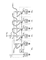
- FIG. 1 shows a circuit equivalent to the digital-analog conversion circuit disclosed in Non-Patent Document 1, for example.
- This circuit is a 2-bit unary differential DAC (Digital-to-Analog Converter).
- DAC Digital-to-Analog Converter
- a 2 -bit input is converted to "000", “100", “110” or "111” in a sequence of b0b1b2 , and the corresponding MOSFET (Metal-Oxide-Semiconductor Field Effect Transistor) on and off.
- MOSFET Metal-Oxide-Semiconductor Field Effect Transistor
- the MOSFET corresponding to b0 is turned on, the MOSFET corresponding to b0 is turned off, so that Vx ,0 , which is produced according to the output voltage Vout-, and the reference current Iref, which is produced according to An op amp generates a bias voltage Vb to match Vx .
- the current flowing through the current source circuit CS0 is the same as the reference current Iref even when the output Vout- fluctuates. That is, the current source circuit CS0 is implemented by a current mirror circuit with Iref as a reference.
- either of the output voltages Vout+ and Vout- is referenced by bits b0 and b0 -bar associated with current source circuit CS0 , which includes an op amp, to measure its variation. Controlled to suppress.
- the current source circuits CS1 and CS2 without operational amplifiers receive the bias voltage control for the current source circuits CS0 with operational amplifiers as they are, if the same bit values as b0 and b0 bar are input, Appropriately controlled to suppress the current error via the output voltage Vout+ or Vout-.
- the other output voltage Vout- or Vout + is not referenced, so the bias voltage is properly controlled for the current errors in the current source circuits CS1 and CS2 that do not have operational amplifiers. It can not be said. That is, output distortion occurs.
- this digital-to-analog conversion circuit has one operational amplifier corresponding to the control function, the bit values of the bits associated with the current source circuit CS 0 including the operational amplifier cause the current source circuits CS 1 and CS 1 not including the operational amplifier to A case arises in which the CS2 current error cannot be controlled.
- the circuit scale becomes large.
- an object of the present invention is to provide a new digital-analog conversion circuit capable of suppressing output distortion.
- Another object of the present invention is to provide an analog-to-digital conversion circuit using the digital-to-analog conversion circuit capable of suppressing output distortion.
- a digital-to-analog conversion circuit includes (A) a first current generating circuit and a first transistor for controlling a first current flowing through the first current generating circuit, and (B) a control circuit; and (B) a control circuit.
- the control circuit includes (b1) a second current generating circuit, (b2) a second transistor to which the first output voltage from the load is transmitted and which controls the current flowing through the second current generating circuit, (b3) a third current generation circuit for passing a reference current; and (b4) a first voltage generated in the third current generation circuit and a second voltage generated in the second current generation circuit according to the first output voltage.
- a bias generation circuit for generating a bias voltage for the first transistor in the second transistor and each current source circuit so as to suppress fluctuations in the first output voltage based on the relationship with the voltage.
- the analog-to-digital conversion circuit includes (C) the above-described digital-to-analog conversion circuit, (D) a loop filter whose input is the difference between the output of the digital-to-analog conversion circuit and the input analog signal, and (E) a loop filter and a quantization circuit for quantizing the output of. Then, the output of the quantization circuit is input as an input digital signal to the digital-analog conversion circuit.
- FIG. 1 is a diagram showing an example of a conventional digital-analog conversion circuit.
- FIG. 2 is a diagram illustrating an example of a digital-analog conversion circuit according to the first embodiment;
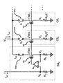
- FIG. 3 is a diagram showing a specific configuration example 1 of the first embodiment.
- FIG. 4 is a diagram showing the effect of the specific configuration example 1 of the first embodiment.
- FIG. 5 is a diagram showing a specific configuration example 2 of the first embodiment.
- FIG. 6 is a diagram showing Modification 1 of the first embodiment.
- FIG. 7 is a diagram showing Modification 2 of the first embodiment.
- FIG. 8 is a diagram showing an example of a differential analog-to-digital conversion circuit according to the second embodiment.
- FIG. 9 is a diagram showing an example of a differential analog-to-digital conversion circuit according to the third embodiment.
- FIG. 10 is a diagram showing an example of an analog-to-digital conversion circuit according to the fourth embodiment.
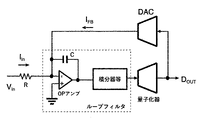
- FIG. 11 is a diagram showing a specific example of an analog-to-digital conversion circuit according to the fourth embodiment.
- FIG. 12 is a diagram showing an example of an analog-to-digital conversion circuit according to the fifth embodiment.
- FIG. 2 shows a digital-analog conversion circuit according to the first embodiment.
- This digital-to-analog conversion circuit is a binary-type digital-to-analog conversion circuit, and is connected to a bias generator BG 0 and current source circuits CS 0 to CS N-1 , which are responsible for each of the N-bit input digital signals.
- switches Sw1 to SwN - 1 for switching current conduction and non-conduction by the current source circuit according to each bit of the N-bit input digital signal, and a load RL .
- Each of the switches Sw1 through SwN -1 may be included in a connected current source circuit.
- the current source circuit CS0 responsible for bit b0 of the input digital signal is connected to a switch Sw0 that turns on or off according to b0
- the current source circuit CS1 responsible for bit b1 of the input digital signal. is connected to a switch Sw1 that is turned on or off according to b1
- the current source circuit CS2 responsible for bit b2 of the input digital signal is connected to a switch Sw2 that is turned on or off according to b2
- a current source circuit CS N-1 that takes charge of bit b N-1 of the input digital signal is connected to a switch Sw N-1 that turns on and off according to b N-1 .
- These switches Sw0 to SwN -1 are connected to one end of the load RL, and the other end of the load RL is connected to the power supply VDD .
- An output voltage Vout is generated according to the current Iout flowing through the load RL.
- Each of the current source circuits CS 0 to CS N ⁇ 1 includes a MOSFET (more specifically, an NMOSFET) that adjusts the current according to the bias voltage Vb supplied from the bias generator BG 0 , and a weighted current. and a current generating circuit to flow.
- This MOSFET functions as a cascode transistor for increasing the output impedance of the associated current source circuit.
- the current source circuit CS0 includes a MOSFET S0 whose gate is connected to the bias generator BG0 and whose drain is connected to the switch Sw0 , and a current generator circuit whose one end is connected to the source of the MOSFET S0 and whose other end is grounded.
- the current generating circuit CG 0 is adapted to flow a unit current IU .
- the current source circuit CS1 includes a MOSFET S1 whose gate is connected to the bias generator BG0 and whose drain is connected to the switch Sw1, and a current generator circuit CG whose one end is connected to the source of the MOSFET S1 and whose other end is grounded. 1 and The current generation circuit CG 1 is designed to pass a current of 2 ⁇ IU .
- the current source circuit CS2 includes a MOSFET S2 whose gate is connected to the bias generator BG0 and whose drain is connected to the switch Sw2, and a current generator circuit whose one end is connected to the source of the MOSFET S2 and whose other end is grounded. CG 2 and.
- the current generation circuit CG2 is designed to pass a current of 4 * IU .
- the current source circuit CS N-1 includes a MOSFET S N-1 having a gate connected to the bias generator BG 0 and a drain connected to the switch Sw N-1 , and one end connected to the source of the MOSFET S N-1 . and a current generating circuit CG N ⁇ 1 whose other end is grounded.
- the current generation circuit CG N-1 is designed to pass a current of 2 N-1 ⁇ I U.
- the bias generation unit BG0 includes a switch Swb connected to the load RL and always turned on, a bias generation circuit BG1 generating a bias voltage Vb , and a gate connected to the bias generation circuit BG1 and a drain connected to the bias generation circuit BG1.
- a MOSFET Sb connected to the switch Swb, a current generation circuit CG B having one end connected to the source of the MOSFET Sb and the input of the bias generation circuit BG1 and the other end grounded, and one end to the input of the bias generation circuit BG1 and a current generating circuit CG A connected to and grounded at the other end.
- a current generation circuit CG A supplies a reference current Iref.
- the bias generator BG 0 has the same configuration as the current path consisting of the switch Sw, the MOSFET S, and the current generator circuit CG for each current source circuit. included as B. By doing so, the output voltage Vout can be monitored without being affected by the state of the input digital signal.
- the channel width/channel length of the MOSFET S1 is 2 1 W/L
- the channel width/channel length of the MOSFET S2 is 2 2 W/L
- the channel width/channel length of MOSFET S N-1 is 2 N-1 W/L.
- the switches Sw 0 to Sw N-1 are turned on or off according to the input digital signal. will flow through the load RL , resulting in an output voltage Vout. If the output voltage Vout fluctuates here, an error occurs in the current flowing through the current source circuit CS connected to the turned-on switch Sw.
- the output voltage Vout is input to the bias generator BG0 , and the current IrefB flows. also fluctuate.
- the bias generation circuit BG1 generates a first voltage V A generated in the current generation circuit CGA by the reference current Iref and a second voltage V A generated in the current generation circuit CBB by the current IrefB flowing through the MOSFET Sb.
- the bias generator BG 0 has the same configuration as the current path for each current source circuit, so even if the common bias voltage Vb is used, each current source circuit CS 0 to CS N-1 are also appropriately adjusted.
- Such a digital-analog conversion circuit monitors the output voltage Vout and operates to suppress variations in the output voltage Vout corresponding to the same input digital signal. That is, output distortion is suppressed.
- a MOSFET Mb2 is provided as the current generation circuit CGA
- a MOSFET Mb3 is provided as the current generation circuit CGB
- an operational amplifier A2 is provided as the bias generation circuit BG1.
- the gates of the MOSFETs Mb2 and Mb3 and the MOSFETs also provided in each current source circuit CS are connected to each other, and these gates are connected to the drain of the newly provided MOSFET Mb1.
- a reference current Iref is input to the drain of the MOSFET Mb1, and a voltage V bias is applied to its gate.
- the source of the MOSFET Mb1 is connected to the drain of the MOSFET Mb2 and the positive input of the operational amplifier A2 , and the source of the MOSFET Mb2 is grounded.
- the drain of MOSFET Mb3 is connected to the source of MOSFET Sb and the negative input of operational amplifier A2 , and the source of MOSFET Mb3 is grounded. Note that the resistance r0 shown between the source and the drain of the MOSFET Mb3 does not represent the actual circuit, but represents the output resistance of the MOSFET that occurs virtually.
- MOSFETs M0 to M N-1 are also provided in the current source circuits CS 0 to CS N-1 .
- current source circuit CS0 the source of MOSFET S0 is connected to the drain of MOSFET M0, and the source of MOSFET M0 is grounded.
- the source of MOSFET S1 is connected to the drain of MOSFET M1, and the source of MOSFET M1 is grounded.
- the resistances r 0 /2 0 and r 0 /2 1 shown between the source and drain of the MOSFETs M0 and M1 represent virtual resistances rather than actual circuits. Such resistance also changes according to the weight of the current.
- the channel width/channel length of the MOSFET M0 is 2 0 W/L
- the channel width/channel length of the MOSFET M1 is 2 1 W/L
- the channel width/channel length of MOSFET M2 is 2 2 W/L
- the channel width/channel length of MOSFET M N-1 is 2 N-1 W/L.
- the measurement result (black line) of SFDR (Spurious Free Dynamic Range: ratio to distortion component when single frequency signal component is applied) when simulating a 10-bit digital analog circuit according to this configuration example is shown in FIG. shown in In this configuration example, the SFDR (dotted line) is about 77.8 dB.
- the measurement result (gray line, only a part of which is visible) in the case of a digital-analog conversion circuit using a current mirror of a specific conventional example for example, Japanese Unexamined Patent Publication No. 8-88521
- SFDR one point Chain line
- a resistor R S is provided as the current generation circuit CG A
- a resistor R S is provided as the current generation circuit CG B. These resistors have the same resistance value.
- the voltage VA generated across the resistor RS through which the reference current Iref flows is applied to the positive input of the operational amplifier A2
- the voltage VB generated across the other resistor RS is applied to the negative input of the operational amplifier A2 .
- Resistors are also provided in the current source circuits CS 0 to CS N-1 .
- IrefB which flows to the bias generator BG0 , also flows through the load RL, so an offset occurs in the output voltage Vout.
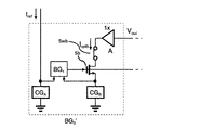
- the switch Swb is not directly connected to the load RL, but an amplifier A with a magnification of 1 is introduced between the switch Swb so that the current IrefB does not flow through the load RL and the output An offset of the voltage Vout may be removed.
- FIG. 2 shows a binary type digital-analog conversion circuit, but according to this embodiment, a unary type digital-analog conversion circuit can be similarly constructed.
- the resolution of this unary type digital-to-analog conversion circuit is (log 2 N) bits, and a configuration example is shown in FIG.
- the currents flowing in the current source circuits CS 0 to CS N ⁇ 1 are all the same IU . Therefore, the channel width/channel length of MOSFET Sb and MOSFETs S0 to S N-1 are all the same.
- resistors with the same resistance value may be used.
- the same MOSFET may be used when the current generation circuit is configured with a MOSFET.
- a bias generator BG0 including a current path for detecting the output voltage Vout regardless of the state of the input digital signal is provided.
- the bias generation unit BG0 in the differential digital-analog conversion circuit includes current generation circuits CG A and CG B that perform control based on the output voltage Voutp, a bias generation circuit BG1, a MOSFET Sb1, and a switch. Swb1, and a combination of the current generation circuits CG A and CG C that perform control based on the output voltage Voutn, the bias generation circuit BG2 , the MOSFET Sb2, and the switch Swb2.
- One input of the bias generation circuits BG1 and BG2 is common for the voltage generated in the current generation circuit CGA through which the reference current Iref flows.
- the bias generation unit BG0 refers to the output voltage Voutp in the system that generates the bias voltage Vb1 , and generates the bias voltage Vb1 so as to suppress the fluctuation thereof.
- This bias voltage Vb1 is also transmitted to the MOSFET S0 and the like connected to the load RL for the output voltage Voutp to perform similar adjustments.
- the system that generates the bias voltage Vb2 refers to the output voltage Voutn and generates the bias voltage Vb2 so as to suppress the fluctuation thereof.
- This bias voltage Vb2 is also transmitted to the MOSFET S0 and the like connected to the load RL for the output voltage Voutn to perform similar adjustments.
- each current source circuit CS includes a MOSFET S, a current generating circuit CG, and two switches T2 that switch the bias voltage applied to the MOSFETs according to the value of the assigned bit of the input digital signal.
- switches T2 that switch the bias voltage applied to the MOSFETs according to the value of the assigned bit of the input digital signal.
- T1 is also provided, but these may also be included in the current source circuit CS.
- the current of the current generation circuit CG is divided between the load RL for the output voltage Voutp and the load RL for the output voltage Voutn according to the assigned bit of the input digital signal.
- Voutp and the output voltage Voutn are complementarily oscillated, and the difference between them is output as the output signal Vout.
- switch T1 (N-1)1 is turned on to connect the drain of MOSFET S N-1 to the load R L for the output Voutp
- switch T1 (N-1)0 is turned on to connect the drain of MOSFET S N-1 to the load R L for the output Voutn.
- each current source circuit CS may be connected to the load RL for the output voltage Voutp, or may be connected to the load RL for the output voltage Voutn. In some cases. Therefore, by adopting such a configuration and separately detecting and independently controlling the output voltage Voutp and the output voltage Voutn, fluctuations in the output voltage Voutp and fluctuations in the output voltage Voutn can be detected independently. can be suppressed.
- the path related to the output voltage Voutp and the path related to the output voltage Voutn are separated. It has the advantage of being able to remove the noise that is generated. Further, if the current of the current generation circuit CG is of a type that distributes the current to the output voltage Voutp side and the output voltage Voutn side in this way, the speed can be increased by the differential configuration.
- the current flowing through the current source circuit CS is weighted according to the assigned bit of the input digital signal. That is, the reference current IU flows through the current source circuit CS0 . A current of 2 N ⁇ 1 IU flows through the current source circuit CS N ⁇ 1 . If the channel width W/channel length L of the MOSFETs Sb1 and Sb2 and the MOSFET S0 is taken as a reference, the channel width/channel length of the MOSFET S N-1 is 2 N-1 W/L.
- This embodiment also employs a bias generation unit BG0 similar to the differential analog-to-digital conversion circuit in the second embodiment, and independently refers to the output voltage Voutp and the output voltage Voutn to generate a bias voltage Vb1 . and Vb2 are output independently.
- the bias voltage Vb1 is applied or the voltage Voff (for example, ground voltage) for turning off is applied.
- Voff for example, ground voltage
- MOSFETs S00 and S01 may also be included in current source circuit CS0 .
- the sources of the MOSFETs S00 and S01 are connected to the current generation circuit CG0 .
- the MOSFET S01 not only performs control according to the bias voltage Vb1 , but also has the function of switching between conduction and non-conduction with the current generation circuit CG0 .
- the MOSFET S00 not only performs control according to the bias voltage Vb2 , but also has the function of switching between conduction and non-conduction with the current generating circuit CG0 .
- MOSFETS (N-1)0 and S (N-1)1 may also be included in the current source circuit CS N-1 .
- the sources of the MOSFETs S (N-1)0 and S (N-1)1 are connected to the current generating circuit CG N-1 .
- the MOSFET S (N-1)1 not only performs control according to the bias voltage V b1 but also has the function of switching between conduction and non-conduction with the current generation circuit CG N-1 .
- the MOSFET S (N-1)0 not only performs control according to the bias voltage V b2 but also has the function of switching between conduction and non-conduction with the current generation circuit CG N-1 .
- the current flowing through the current source circuit CS is weighted according to the assigned bit of the input digital signal. That is, the reference current IU flows through the current source circuit CS0 . Also, 2 N ⁇ 1 IU flows through the current source circuit CS N ⁇ 1 .
- the channel width/channel length of MOSFETs S (N-1)0 and S (N-1)1 is 2 N-1 W/L.
- the amplitude when the MOSFETs S00 and S01 to S (N-1)0 and S (N-1)1 are turned on or off is between Vb1 or Vb2 and Voff, and the second Since it is smaller than the embodiment, the influence of switching noise is reduced, and as a result the linearity of the digital-to-analog conversion circuit is improved.
- FIG. 10 shows an analog-to-digital conversion circuit according to this embodiment.
- This analog-to-digital conversion circuit includes the digital-to-analog conversion circuit (DAC) in the first embodiment, and a loop filter whose input is the difference between the output current Iout (that is, the feedback current IFB ) of the DAC and the input current Iin. and a quantizer for quantizing the output of the loop filter.
- the output D out of the quantizer is the output of the analog-to-digital conversion circuit and also the input to the DAC.
- the analog-to-digital conversion circuit shown in FIG. 10 can be seen as a current input, it can also be seen as a voltage input if it is expressed as shown in FIG.
- the input voltage V in is applied to the resistor R so that the current I in flows, and the other end of the resistor R is the negative input of an operational amplifier (OP amp) included in the loop filter. connected to the terminal.
- a loop filter includes this operational amplifier, a capacitor C, an integrator connected in multiple stages, and the like. The positive input terminal of the operational amplifier is grounded, one end of the capacitor C and the output of the DAC are connected to the negative input terminal of the operational amplifier, and the other end of the capacitor C is connected to the output terminal of the operational amplifier and the input of the integrator.
- An integrator or the like is introduced for noise reduction, and increases the order (that is, the number of stages) of the loop filter. Specifically, it can be obtained by providing multiple stages of integrators composed of resistors, operational amplifiers, and capacitors shown in FIG. However, there may be cases where an integrator or the like does not exist, in which case the ⁇ ADC becomes a first-order ⁇ ADC.
- Such an analog-to-digital conversion circuit is generally called a continuous-time ⁇ ADC (Analog-to-Digital Converter), and is often used to realize a high-resolution ADC.
- the quantization noise generated by the quantizer can be greatly attenuated within the desired band defined by the loop filter, and a high-resolution output Dout can be obtained.
- a highly accurate DAC is used.
- the distortion characteristics (ie, linearity) of the DAC are brought about by increasing the output impedance of the current source circuit used, as described above. Therefore, the effect of using the DAC according to the first embodiment for the continuous time ⁇ ADC is great.
- the DAC used in FIG. 12 is the differential digital-analog conversion circuit shown in the second and third embodiments.
- the output current Ioutp of the DAC is the feedback current IFBP and the output current Ioutn is the feedback current IFBN .
- the current Iinp flows through the resistor R1 and the current Iinn flows through the resistor R2.
- the loop filter includes a differential amplifier Amp, capacitors C1 and C2, integrators connected in multiple stages, and the like.
- the other end of the resistor R1, the negative-side output of the DAC (that is, the feedback current IFBN ), and one end of the capacitor C1 are connected to the negative-side input terminal of the differential amplifier Amp. , to the positive output terminal of the differential amplifier Amp.
- the other end of the resistor R2, the positive output of the DAC (that is, the feedback current IFBP ), and one end of the capacitor C2 are connected to the positive input terminal of the differential amplifier Amp.
- the other end of the capacitor C2 is connected to the negative output terminal of the differential amplifier Amp.
- a positive side output and a negative side output of the differential amplifier Amp are input to inputs of an integrator or the like.
- the input side of the quantizer is also differential.
- Differentialization doubles the dynamic range and has effects such as the ability to eliminate common-mode noise.
- the present invention is not limited to these.
- a PMOSFET may be used.
- a bipolar transistor may be used.
- the specific configuration examples and modifications described in the first embodiment can also be applied to a differential digital-to-analog conversion circuit and an analog-to-digital conversion circuit using the same.
- the elements described in each embodiment can be combined arbitrarily, and in that case, unnecessary elements may be deleted from the gist.
- the digital-analog conversion circuit includes (A) a first current generating circuit (eg, CG 0 to CG N ⁇ 1 ) and a first current generating circuit for controlling a first current flowing through the first current generating circuit.
- transistors for example, S0 to S N ⁇ 1
- conducts and de-conducts the first current to the first load for example, R L
- It has a plurality of switching current source circuits (eg CS 0 to CS N ⁇ 1 ) and (B) a control circuit (eg BG 0 ).
- the control circuit (b1) controls a second current generation circuit (for example, CG B ) and (b2) a current supplied to the second current generation circuit to which the first output voltage from the load is transmitted.
- a third current generation circuit eg, CG A
- a bias generation circuit eg, BG 1
- a variation of the output voltage as a non-ideal error occurs according to the error of the current flowing through the first current generating circuit in each current source circuit.
- This output voltage variation indirectly causes a second voltage variation occurring in the second current generating circuit.
- the bias generation circuit monitors the relationship between the first voltage generated in the third current generation circuit through which the reference current flows and the second voltage, and A bias voltage is generated so as to suppress fluctuations in the output voltage corresponding to the input digital signal, and the bias voltage controls the second transistor and the first transistor.
- first current generation circuit, the second current generation circuit, and the third current generation circuit described above may be resistors. 1/f noise can be reduced. Also, the first current generation circuit, the second current generation circuit, and the third current generation circuit described above may be third transistors to which the same voltage is applied. High output impedance.
- bias generation circuit mentioned above may be an operational amplifier.
- a suitable bias voltage can be generated with a simple configuration.
- a differential digital-analog conversion circuit includes (A) the digital-analog conversion circuit described above. Further, each of the plurality of current source circuits further provides the above-described first current supply to the second load (for example, R L ) according to the value of the assigned bit of the second input digital signal, which is the inverted signal of the input digital signal. To switch between energization and non-energization of current.
- a fourth current generation circuit for example, CG C
- a third transistor for example, Sb2
- a second bias generation circuit eg, BG 2
- BG 2 second bias generation circuit
- switches for example, T2 00 and T2 01 to T2 (N- 1)0 and T2 (N-1)1 (FIG. 8)).
- the configuration is as in the second embodiment.
- the first transistor in each of the plurality of current source circuits may switch between energization and non-energization of the first current to the load according to the value of the assigned bit in the input digital signal.
- each of the plurality of current source circuits further has a fourth transistor for controlling the first current to flow through the first current generating circuit according to the second bias voltage.
- Transistors for example, S00 to S (N-1)0
- the third embodiment FIG. 9
- the switching by the first transistor is, for example, a switch (for example, T101 to T1 (N-1)1) for applying a first bias voltage to the first transistor to conduct the first current. ) and a switch (eg, T100 to T1 (N-1) 0 ) may be used.
- switching by the second transistor is, for example, a switch (eg, T2 00 to T1 (N ⁇ 1) ) for applying a second bias voltage to the fourth transistor to conduct the first current. 0 ) and a switch (eg, T2 01 to T2 (N-1 ) and 1 ) may be used.
- the analog-to-digital conversion circuit includes (A) the above-described digital-to-analog conversion circuit, (B) a loop filter whose input is the difference between the output of the digital-to-analog conversion circuit and the input analog signal, (C) a quantization circuit for quantizing the output of the loop filter; Then, the output of the quantization circuit is input as an input digital signal to the digital-analog conversion circuit.
- A the above-described digital-to-analog conversion circuit
- B a loop filter whose input is the difference between the output of the digital-to-analog conversion circuit and the input analog signal
- C a quantization circuit for quantizing the output of the loop filter
- circuit example shown in the diagram is only an example, and is not limited to the circuit example, and various modifications are possible.
Landscapes
- Engineering & Computer Science (AREA)
- Theoretical Computer Science (AREA)
- Power Engineering (AREA)
- Analogue/Digital Conversion (AREA)
Abstract
出力歪みを抑制する本デジタルアナログ変換回路は、第1電流生成回路と当該第1電流生成回路に流す第1電流を制御する第1トランジスタとを各々含み、負荷に対する当該第1電流の通電と非通電とを入力デジタル信号における担当ビットの値に応じて各々切り替える複数の電流源回路と、制御回路とを有する。制御回路は、第2電流生成回路と、負荷による出力電圧が伝えられ、第2電流生成回路に流す電流を制御する第2トランジスタと、基準電流を流す第3電流生成回路と、第3電流生成回路に生ずる第1電圧と出力電圧に応じて第2電流生成回路に生ずる第2電圧との関係に基づき、出力電圧の変動を抑制するように、第1及び第2トランジスタに対するバイアス電圧を生成するバイアス生成回路とを有する。
Description
本発明は、デジタルアナログ変換回路と当該デジタルアナログ変換回路を用いたアナログデジタル変換回路に関する。
図1に、例えば非特許文献1に開示されているデジタルアナログ変換回路と同等の回路を示す。この回路は、2ビットのユーナリ型の差動DAC(Digital-to-Analog Converter)である。このDACでは、2ビット入力を、b0b1b2の並びで、「000」「100」「110」又は「111」に変換して、対応するMOSFET(Metal-Oxide-Semiconductor Field Effect Transistor)のオン及びオフを制御する。一方、b0b1b2の反転(バー)の場合には、「111」「011」「001」又は「000」に変換して、対応するMOSFETのオン及びオフを制御する。
このような差動DACに用いられる電流源回路CS0においては、b0に対応するMOSFETがオンになれば、出力電圧Vout+に応じて生ずるVx,0と、基準電流Irefに応じて生ずるVxとを一致させるようにオペアンプがバイアス電圧Vbを生成する。結果として、電流源回路CS0に流れる電流は、出力電圧Vout+が変動した場合においてもIrefと同じになる。一方、b0バーに対応するMOSFETがオンになる場合には、b0に対応するMOSFETはオフになるため、出力電圧Vout-に応じて生ずるVx,0と、基準電流Irefに応じて生ずるVxとを一致させるようにオペアンプがバイアス電圧Vbを生成する。結果として、電流源回路CS0に流れる電流は、出力Vout-が変動した場合においても基準電流Irefと同じになる。つまり、電流源回路CS0はIrefを基準としたカレントミラー回路により実現される。このように、このカレントミラー回路では、オペアンプが含まれる電流源回路CS0に関連付けられたビットb0及びb0バーによって、出力電圧Vout+とVout-とのいずれかが参照されて、その変動を抑制するように制御される。
しかしながら、オペアンプを有しない電流源回路CS1及びCS2については、オペアンプを有する電流源回路CS0に対するバイアス電圧の制御をそのまま受けるため、b0及びb0バーと同じビット値が入力されれば出力電圧Vout+又はVout-を介してその電流誤差を抑制するように適切に制御される。一方、異なるビット値が入力されると他方の出力電圧Vout-又はVout+は参照されないので、オペアンプを有しない電流源回路CS1及びCS2における電流誤差に対して、バイアス電圧が適切に制御されるとは言えない。すなわち、出力歪みが生じてしまう。
このように、このデジタルアナログ変換回路は、制御機能に対応するオペアンプが1つなので、オペアンプを含む電流源回路CS0に関連付けられたビットのビット値によって、オペアンプを含まない電流源回路CS1及びCS2の電流誤差を抑制するように制御することが出来ないケースが生ずる。これは、ユーナリ型だけではなくバイナリ型であっても同様である。当然、全ての電流源回路にオペアンプを設けるようにすれば、回路規模が大きくなってしまう。
仁木 義規、小林 春夫,「高性能CMOSカレントミラー回路の設計とその応用」,電気学会研究会資料,ECT,電子回路研究会 2005(19),19-24,2005-03-11
従って、本発明の目的は、一側面によれば、出力歪みを抑制できる新たなデジタルアナログ変換回路を提供することである。
また、本発明の別の目的は、他の一側面によれば、出力歪みを抑制できる当該デジタルアナログ変換回路を用いたアナログデジタル変換回路を提供することである。
本発明に係るデジタルアナログ変換回路は、(A)第1の電流生成回路と当該第1の電流生成回路に流す第1の電流を制御する第1のトランジスタとを各々含み、第1の負荷に対する当該第1の電流の通電と非通電とを入力デジタル信号における担当ビットの値に応じて各々切り替える複数の電流源回路と、(B)制御回路とを有する。そして、この制御回路が、(b1)第2の電流生成回路と、(b2)負荷による第1の出力電圧が伝えられ、第2の電流生成回路に流す電流を制御する第2のトランジスタと、(b3)基準電流を流す第3の電流生成回路と、(b4)第3の電流生成回路に生ずる第1の電圧と第1の出力電圧に応じて第2の電流生成回路に生ずる第2の電圧との関係に基づき、第1の出力電圧の変動を抑制するように、第2のトランジスタ及び各電流源回路内における第1のトランジスタに対するバイアス電圧を生成するバイアス生成回路とを有する。
本発明に係るアナログデジタル変換回路は、(C)上記のデジタルアナログ変換回路と、(D)デジタルアナログ変換回路の出力と入力アナログ信号との差を入力とするループフィルタと、(E)ループフィルタの出力を量子化する量子化回路とを有する。そして、デジタルアナログ変換回路には、量子化回路の出力が入力デジタル信号として入力される。
[実施の形態1]
図2に第1の実施の形態に係るデジタルアナログ変換回路を示す。本デジタルアナログ変換回路は、バイナリ型のデジタルアナログ変換回路であって、バイアス生成部BG0と、Nビットの入力デジタル信号の各々を担当する電流源回路CS0乃至CSN-1と、接続された電流源回路による電流の通電と非通電をNビットの入力デジタル信号の各ビットに応じて切り替えるスイッチSw1乃至SwN-1と、負荷RLとを含む。スイッチSw1乃至SwN-1は、それぞれ、接続された電流源回路に含むものとされる場合もある。
図2に第1の実施の形態に係るデジタルアナログ変換回路を示す。本デジタルアナログ変換回路は、バイナリ型のデジタルアナログ変換回路であって、バイアス生成部BG0と、Nビットの入力デジタル信号の各々を担当する電流源回路CS0乃至CSN-1と、接続された電流源回路による電流の通電と非通電をNビットの入力デジタル信号の各ビットに応じて切り替えるスイッチSw1乃至SwN-1と、負荷RLとを含む。スイッチSw1乃至SwN-1は、それぞれ、接続された電流源回路に含むものとされる場合もある。
入力デジタル信号のビットb0を担当する電流源回路CS0は、b0に応じてオン又はオフするスイッチSw0に接続されており、入力デジタル信号のビットb1を担当する電流源回路CS1は、b1に応じてオンまたはオフするスイッチSw1に接続されており、入力デジタル信号のビットb2を担当する電流源回路CS2は、b2に応じてオンオフするスイッチSw2に接続されており、入力デジタル信号のビットbN-1を担当する電流源回路CSN-1は、bN-1に応じてオンオフするスイッチSwN-1に接続されている。そして、これらのスイッチSw0乃至SwN-1は、負荷RLの一端に接続されており、負荷RLの他端は電源VDDに接続されている。この負荷RLに流れる電流Ioutに応じて出力電圧Voutが生ずる。
電流源回路CS0乃至CSN-1の各々は、バイアス生成部BG0から与えられるバイアス電圧Vbに応じて電流を調整するMOSFET(より具体的にはNMOSFET)と、各々重み付けされた電流を流す電流生成回路とを含む。このMOSFETは、所属する電流源回路の出力インピーダンスを増加させるためのカスコードトランジスタとして機能する。電流源回路CS0は、ゲートがバイアス生成部BG0に接続され且つドレインがスイッチSw0に接続されたMOSFET S0と、MOSFET S0のソースに一端が接続され他端が接地されている電流生成回路CG0とを含む。電流生成回路CG0は、単位電流IUを流すようになっている。電流源回路CS1は、ゲートがバイアス生成部BG0に接続され且つドレインがスイッチSw1に接続されたMOSFET S1と、MOSFETS1のソースに一端が接続され他端が接地されている電流生成回路CG1とを含む。電流生成回路CG1は、2×IUの電流を流すようになっている。
電流源回路CS2は、ゲートがバイアス生成部BG0に接続され且つドレインがスイッチSw2に接続されたMOSFET S2と、MOSFET S2のソースに一端が接続され他端が接地されている電流生成回路CG2とを含む。電流生成回路CG2は、4×IUの電流を流すようになっている。電流源回路CSN-1は、ゲートがバイアス生成部BG0に接続され且つドレインがスイッチSwN-1に接続されたMOSFET SN-1と、MOSFET SN-1のソースに一端が接続され他端が接地されている電流生成回路CGN-1とを含む。電流生成回路CGN-1は、2N-1×IUの電流を流すようになっている。
バイアス生成部BG0は、負荷RLに接続され且つ常にオンにされるスイッチSwbと、バイアス電圧Vbを生成するバイアス生成回路BG1と、ゲートがバイアス生成回路BG1に接続され且つドレインがスイッチSwbに接続されたMOSFET Sbと、MOSFET Sbのソースとバイアス生成回路BG1の入力とが一端に接続され他端が接地された電流生成回路CGBと、一端がバイアス生成回路BG1の入力に接続され他端が接地される電流生成回路CGAとを含む。電流生成回路CGAは、基準電流Irefを流す。
本実施の形態では、バイアス生成部BG0が、各電流源回路についてのスイッチSwとMOSFET Sと電流生成回路CGとからなる電流パスと同様の構成を、スイッチSwbとMOSFET Sbと電流生成回路CGBとして含んでいる。このようにすることで、入力デジタル信号の状態に影響を受けることなく、出力電圧Voutをモニタすることができる。
なお、MOSFET S0及びSbのチャネル幅W/チャネル長Lを基準に、MOSFET S1のチャネル幅/チャネル長は、21W/Lとなっており、MOSFET S2のチャネル幅/チャネル長は、22W/Lとなっており、MOSFET SN-1のチャネル幅/チャネル長は、2N-1W/Lとなる。このようにすることで、バイナリ型デジタルアナログ変換回路において、入力デジタル信号の各ビットの桁iに対応する電流2i-1IUを可能とする。
このようなデジタルアナログ変換回路では、入力デジタル信号に応じてスイッチSw0乃至SwN-1をオンまたはオフさせるので、オンとなったスイッチSwに接続された電流源回路CSに流れる電流の総和Ioutが負荷RLに流れ、出力電圧Voutが生ずることになる。ここで出力電圧Voutが変動すると、オンとなったスイッチSwに接続された電流源回路CSに流れる電流に誤差が生ずる。バイアス生成部BG0には、出力電圧Voutが入力され、電流IrefBが流れるようになっているが、この電流IrefBについても出力電圧Voutの変動に応じて変動し、電流生成回路CBB上端における電圧も変動する。これに対して、バイアス生成回路BG1は、基準電流Irefにより電流生成回路CGAに生ずる第1の電圧VAと、MOSFET Sbに流れる電流IrefBにより電流生成回路CBBに生ずる第2の電圧VBとの関係をモニタしており、第1の電圧VAと第2の電圧VBとが所定の関係(例えば等電圧)となるように、補正信号であるバイアス電圧Vbを生成してMOSFET Sbのゲートに出力する。そうすると、MOSFET Sbは、バイアス電圧Vbに応じて電流IrefBを調整する。一方、同じバイアス電圧Vbが、各電流源回路CS0乃至CSN-1のMOSFET S0乃至SN-1のゲートにも入力され、それらのMOSFET S0乃至SN-1が、共通のバイアス電圧Vbで、同じように、流れる電流を調整する。上でも述べたように、バイアス生成部BG0は、各電流源回路についての電流パスと同様の構成を有しているので、共通のバイアス電圧Vbを用いても、各電流源回路CS0乃至CSN-1においても適切に調整がなされる。
このようなデジタルアナログ変換回路においては、出力電圧Voutをモニタして、同一の入力デジタル信号に対応する出力電圧Voutの変動を抑制するように動作する。すなわち、出力歪みが抑制されるようになる。
[実施の形態1の具体的構成例1]
本構成例では、図3に示すように、電流生成回路の一例としてMOSFETを用いる。
本構成例では、図3に示すように、電流生成回路の一例としてMOSFETを用いる。
本構成例では、バイアス生成部BG0において、電流生成回路CGAとしてMOSFET Mb2が設けられ、電流生成回路CGBとしてMOSFET Mb3が設けられ、バイアス生成回路BG1としてオペアンプA2が設けられる。MOSFET Mb2及びMb3と各電流源回路CSにおいても設けられるMOSFETとのゲートは互いに接続されており、これらのゲートは、新たに設けられたMOSFET Mb1のドレインに接続されている。MOSFET Mb1のドレインには基準電流Irefが入力されており、そのゲートには電圧Vbiasが印加されている。また、MOSFET Mb1のソースは、MOSFET Mb2のドレイン及びオペアンプA2の正極側入力に接続されており、MOSFET Mb2のソースは接地されている。MOSFET Mb3のドレインはMOSFET Sbのソース及びオペアンプA2の負極側入力に接続されており、MOSFET Mb3のソースは接地されている。なお、MOSFET Mb3のソースドレイン間に示されている抵抗r0は、実際の回路ではなく、仮想的に生じてしまうMOSFETの出力抵抗を表している。
また、電流源回路CS0乃至CSN-1においても、MOSFET M0乃至MN-1が設けられる。電流源回路CS0であれば、MOSFET S0のソースは、MOSFET M0のドレインに接続されており、MOSFET M0のソースは接地されている。また、電流源回路CS1であれば、MOSFET S1のソースは、MOSFET M1のドレインに接続されており、MOSFET M1のソースは接地されている。他の電流源回路CSも同様である。MOSFET M0及びM1のソースドレイン間に示されている抵抗r0/20,r0/21については、実際の回路ではなく、仮想的に生じてしまう抵抗を表している。このような抵抗も、電流の重みに応じて変化する。
なお、MOSFET Mb2及びMb3のチャネル幅W/チャネル長Lを基準に、MOSFET M0のチャネル幅/チャネル長は、20W/Lとなっており、MOSFET M1のチャネル幅/チャネル長は、21W/Lとなっており、MOSFET M2のチャネル幅/チャネル長は、22W/Lとなっており、MOSFET MN-1のチャネル幅/チャネル長は、2N-1W/Lとなる。このようにすることで、バイナリ型デジタルアナログ変換回路において、入力デジタル信号の各ビットの桁iに対応する電流2i-1IUを可能とする。
このような構成例では、MOSFET M0のドレイン側電圧V0やMOSFET M1のドレイン側電圧V1の変動が、出力電圧Voutの変動となって、間接的にMOSFET Mb3のドレイン側電圧VBの変動をもたらす。一方、MOSFET Mb2のドレイン側電圧VAは変動しないので、オペアンプA2で電圧VBが電圧VAと一致するようにバイアス電圧Vbを生成する。これにより、電圧V0及びV1等も適切に調整されて、電圧Voutの変動が抑制される。
本構成例では、MOSFETを電流生成回路に用いているので、出力インピーダンスが高く、より出力歪みを抑制できるようになる。
例えば、本構成例に従って10ビットのデジタルアナログ回路をシミュレートした場合のSFDR(Spurious Free Dynamic Range:単周波信号成分を印加した場合における歪成分との比)の測定結果(黒線)を図4に示す。本構成例では、SFDR(点線)は77.8dB程度である。一方、特定の従来例(例えば特開平8-88521号公報)のカレントミラーを用いたデジタルアナログ変換回路の場合の測定結果(灰色線。但し、一部のみしか見えない)の場合、SFDR(一点鎖線)は67.6dB程度であり、本構成の方が改善されていることが分かる。
[実施の形態1の具体的構成例2]
本構成例では、図5に示すように、電流生成回路の一例として抵抗を用いる。また、バイアス生成回路BG1には、オペアンプA2が用いられる。
本構成例では、図5に示すように、電流生成回路の一例として抵抗を用いる。また、バイアス生成回路BG1には、オペアンプA2が用いられる。
本構成例では、バイアス生成部BG0において、電流生成回路CGAとして抵抗RSが設けられ、電流生成回路CGBとして抵抗RSが設けられる。これらの抵抗については同じ抵抗値の抵抗である。基準電流Irefが流れる抵抗RSに生ずる電圧VAが、オペアンプA2の正極側入力に印加され、他方の抵抗RSに生ずる電圧VBが、オペアンプA2の負極側入力に印加される。
また、電流源回路CS0乃至CSN-1においても、抵抗が設けられる。電流源回路CS0であれば、電流生成回路CG0としてRS(=RS/20)と同じ抵抗が設けられ、電流源回路CS1であれば、電流生成回路CG1としてRS/21の抵抗が設けられ、電流源回路CSN-1であれば、電流生成回路CGN-1としてRS/2N-1の抵抗が設けられる。
このような構成例では、MOSFET S0のソース側電圧V0やMOSFET S1のソース側電圧V1の変動が、出力電圧Voutの変動となって、間接的にMOSFET Sbのソース側電圧VBの変動をもたらす。一方、基準電流Irefが流れる抵抗に生ずる電圧VAは変動しないので、オペアンプA2で電圧VBが電圧VAと一致するようにバイアス電圧Vbを生成する。これにより、電圧V0及びV1等も適切に調整されて、電圧Voutの変動が抑制される。
本構成例では、抵抗を電流生成回路に用いているので、MOSFETによる1/fノイズの低減が可能であるが、MOSFETの場合よりも出力インピーダンスが低くなる。
[実施の形態1の変形例1]
図2の例では、負荷RLには、バイアス生成部BG0に流れるIrefBも流れるので、出力電圧Voutにオフセットが生じてしまう。例えば、図6に示すように、スイッチSwbを負荷RLに直接接続せずに、間に倍率1倍のアンプAを導入することで、電流IrefBが負荷RLが流れないようにして、出力電圧Voutのオフセットを除去するようにしても良い。
図2の例では、負荷RLには、バイアス生成部BG0に流れるIrefBも流れるので、出力電圧Voutにオフセットが生じてしまう。例えば、図6に示すように、スイッチSwbを負荷RLに直接接続せずに、間に倍率1倍のアンプAを導入することで、電流IrefBが負荷RLが流れないようにして、出力電圧Voutのオフセットを除去するようにしても良い。
[実施の形態1の変形例2]
図2には、バイナリ型のデジタルアナログ変換回路を示したが、本実施の形態に従えば、ユーナリ型のデジタルアナログ変換回路も同様に構成できる。このユーナリ型のデジタルアナログ変換回路の分解能は(log2N)ビットであり、構成例を図7に示す。
図2には、バイナリ型のデジタルアナログ変換回路を示したが、本実施の形態に従えば、ユーナリ型のデジタルアナログ変換回路も同様に構成できる。このユーナリ型のデジタルアナログ変換回路の分解能は(log2N)ビットであり、構成例を図7に示す。
ユーナリ型の場合、電流源回路CS0乃至CSN-1で流す電流は全て同じIUとなる。よって、MOSFET Sb、MOSFET S0乃至SN-1のチャネル幅/チャネル長は、全て同じになる。
電流生成回路を抵抗で構成する場合も同じ抵抗値の抵抗で良い。また、電流生成回路をMOSFETで構成する場合も同じMOSFETで良い。
このように、ユーナリ型でも、入力デジタル信号の状態とは無関係に出力電圧Voutを検出する電流パスを含むバイアス生成部BG0が設けられる。
[実施の形態2]
第1の実施の形態を差動方式に変形すると、例えば図8のようになる。
第1の実施の形態を差動方式に変形すると、例えば図8のようになる。
本実施の形態に係る差動式のデジタルアナログ変換回路におけるバイアス生成部BG0は、出力電圧Voutpを基に制御を行う電流生成回路CGA及びCGBとバイアス生成回路BG1とMOSFET Sb1とスイッチSwb1との組み合わせと、出力電圧Voutnに基づき制御を行う電流生成回路CGA及びCGCとバイアス生成回路BG2とMOSFET Sb2とスイッチSwb2との組み合わせとを含む。バイアス生成回路BG1及びBG2の1つの入力は、基準電流Irefが流れる電流生成回路CGAに生ずる電圧で共通している。
バイアス生成部BG0は、バイアス電圧Vb1を生成する系統では出力電圧Voutpを参照して、その変動を抑制するようにバイアス電圧Vb1を生成する。このバイアス電圧Vb1は、出力電圧Voutpのための負荷RLに接続されるMOSFET S0等にも伝えられ、同様の調整を行う。また、バイアス電圧Vb2を生成する系統では出力電圧Voutnを参照して、その変動を抑制するようにバイアス電圧Vb2を生成する。このバイアス電圧Vb2は、出力電圧Voutnのための負荷RLに接続されるMOSFET S0等にも伝えられ、同様の調整を行う。
本実施の形態では、各電流源回路CSは、MOSFET Sと、電流生成回路CGと、MOSFETに対して印加するバイアス電圧を入力デジタル信号の担当ビットの値に応じて切り替える2つのスイッチT2とを含む。なお、出力電圧Voutpのための負荷RLにMOSFET Sを接続するか、出力電圧Voutnのための負荷RLにMOSFET Sを接続するかを、入力デジタル信号の担当ビットに応じて切り替える2つのスイッチT1も設けられるが、これらも電流源回路CSに含めるようにする場合もある。
このように、電流生成回路CGの電流を、入力デジタル信号の担当ビットに応じて、出力電圧Voutpのための負荷RLと、出力電圧Voutnのための負荷RLとに振り分けることで、出力電圧Voutpと出力電圧Voutnとが相補的に振幅し、その差分を出力信号Voutとして出力するものである。
より具体的には、電流源回路CS0において、b0=1(b0バーが0)で、バイアス生成回路BG1のバイアス電圧Vb1をMOSFET S0のゲートに印加する場合には、スイッチT201がオンになり、b0=0(b0バーが1)で、バイアス生成回路BG2のバイアス電圧Vb2をMOSFET S0のゲートに印加する場合には、スイッチT200がオンになる。また、b0=1(b0バーが0)となると、出力Voutpのための負荷RLにMOSFET S0のドレインを接続させるためにスイッチT101がオンになり、b0=0(b0バーが1)となると、出力Voutnのための負荷RLにMOSFETS0のドレインを接続させるためにスイッチT100がオンになる。
また、電流源回路CSN-1において、bN-1=1(bN-1バーが0)で、バイアス生成回路BG1のバイアス電圧Vb1をMOSFET SN-1のゲートに印加する場合には、スイッチT2(N-1)1がオンになり、b0=0(b0バーが1)で、バイアス生成回路BG2のバイアス電圧Vb2をMOSFET SN-1のゲートに印加する場合には、スイッチT2(N-1)0がオンになる。また、b0=1(b0バーが0)となると、出力Voutpのための負荷RLにMOSFET SN-1のドレインを接続させるためにスイッチT1(N-1)1がオンになり、b0=0(b0バーが1)となると、出力Voutnのための負荷RLにMOSFET SN-1のドレインを接続させるためにスイッチT1(N-1)0がオンになる。
このように各電流源回路CSにおけるMOSFET Sと電流生成回路CGとは、出力電圧Voutpのための負荷RLに接続される場合もあれば、出力電圧Voutnのための負荷RLに接続される場合もある。よって、このような構成を採用して、出力電圧Voutpと出力電圧Voutnとを別々に検知して独立して制御することで、出力電圧Voutpの変動と出力電圧Voutnの変動とをそれぞれ独立して抑制できるようになる。
差動構成を採用することで、出力電圧Voutpに関連するパスと出力電圧Voutnに関連するパスとを分けているため、実効的にダイナミックレンジが2倍に拡大し、両方のパスに同相で重畳される雑音は除去できるといったメリットがある。また、このように、電流生成回路CGの電流を、出力電圧Voutp側とVoutn側に振り分けるようなタイプであれば、差動構成により高速化が可能になる。
なお、バイナリ型であるから、入力デジタル信号の担当ビットに応じて電流源回路CSに流す電流には重みが付けられる。すなわち、電流源回路CS0は、基準電流IUが流れる。また、電流源回路CSN-1は、2N-1IUの電流が流れる。また、MOSFET Sb1及びSb2とMOSFET S0とのチャネル幅W/チャネル長Lを基準にすると、MOSFET SN-1のチャネル幅/チャネル長は、2N-1W/Lとなる。
[実施の形態3]
第1の実施の形態を差動方式に変形する場合には、図9のような構成を採用してもよい。
第1の実施の形態を差動方式に変形する場合には、図9のような構成を採用してもよい。
本実施の形態でも、第2の実施の形態における差動アナログデジタル変換回路と同様のバイアス生成部BG0が採用され、出力電圧Voutpと出力電圧Voutnとを独立して参照してバイアス電圧Vb1及びVb2を独立に出力するようになっている。
一方、本実施の形態に係る電流源回路CSについては、第2の実施の形態における電流源回路CSとは異なり、バイアス電圧Vb1が印加されるか又はオフにさせるための電圧Voff(例えばグランド電位)が印加されるMOSFETと、バイアス電圧Vb2が印加されるかオフにさせるための電圧Voffが印加されるMOSFETとを分けるようになっている。
具体的には、電流源回路CS0については、電流生成回路CG0と、出力電圧Voutpのための負荷RLにドレインが接続されるMOSFET S01のゲートにb0=1であればバイアス電圧Vb1を印加させるスイッチT101と、MOSFET S01のゲートにb0=0であれば電圧Voffを印加させるスイッチT100と、出力電圧Voutnのための負荷RLにドレインが接続されるMOSFET S00のゲートにb0=0であればバイアス電圧Vb2を印加させるスイッチT200と、MOSFET S00のゲートにb0=1であれば電圧Voffを印加させるスイッチT201とを含む。MOSFET S00及びS01についても、電流源回路CS0に含める場合もある。また、MOSFET S00及びS01のソースは電流生成回路CG0に接続されている。このように、MOSFET S01は、バイアス電圧Vb1に応じた制御を行うだけではなく、電流生成回路CG0との導通と非導通を切り替える機能を有する。同様に、MOSFET S00は、バイアス電圧Vb2に応じた制御を行うだけではなく、電流生成回路CG0との導通と非導通を切り替える機能を有する。
また、電流源回路CSN-1については、電流生成回路CGN-1と、出力電圧Voutpのための負荷RLにドレインが接続されるMOSFET S(N-1)1のゲートにbN-1=1であればバイアス電圧Vb1を印加させるスイッチT1(N-1)1と、MOSFET S(N-1)1のゲートにbN-1=0であれば電圧Voffを印加させるスイッチT1(N-1)0と、出力電圧Voutnのための負荷RLにドレインが接続されるMOSFET S(N-1)0のゲートにbN-1=0であればバイアス電圧Vb2を印加させるスイッチT2(N-1)0と、MOSFET S(N-1)0のゲートにbN-1=1であれば電圧Voffを印加させるスイッチT2(N-1)1とを含む。MOSFET S(N-1)0及びS(N-1)1についても、電流源回路CSN-1に含める場合もある。また、MOSFET S(N-1)0及びS(N-1)1のソースは電流生成回路CGN-1に接続されている。このように、MOSFET S(N-1)1は、バイアス電圧Vb1に応じた制御を行うだけではなく、電流生成回路CGN-1との導通と非導通を切り替える機能を有する。同様に、MOSFET S(N-1)0は、バイアス電圧Vb2に応じた制御を行うだけではなく、電流生成回路CGN-1との導通と非導通を切り替える機能を有する。
また、バイナリ型であるから、入力デジタル信号の担当ビットに応じて電流源回路CSに流す電流には重みが付けられる。すなわち、電流源回路CS0は、基準電流IUが流れる。また、電流源回路CSN-1は、2N-1IUが流れる。また、MOSFET Sb1及びSb2とMOSFET S00及びS01とのチャネル幅W/チャネル長Lを基準にすると、MOSFET S(N-1)0及びS(N-1)1のチャネル幅/チャネル長は、2N-1W/Lとなる。
本実施の形態では、MOSFET S00及びS01乃至S(N-1)0及びS(N-1)1がオン又はオフするときの振幅がVb1又はVb2からVoff間となって、第2の実施の形態より小さくなるので、スイッチング雑音の影響が小さくなり、結果としてデジタルアナログ変換回路の線形性が改善する。
[実施の形態4]
上で述べたデジタルアナログ変換回路は、アナログデジタル変換回路に応用できる。図10に本実施の形態に係るアナログデジタル変換回路を示す。本アナログデジタル変換回路は、第1の実施の形態におけるデジタルアナログ変換回路(DAC)と、当該DACの出力電流Iout(すなわちフィードバック電流IFB)と入力電流Iinとの差を入力とするループフィルタと、当該ループフィルタの出力を量子化する量子化器とを有する。量子化器の出力Doutは、アナログデジタル変換回路の出力であり、DACに対する入力でもある。
上で述べたデジタルアナログ変換回路は、アナログデジタル変換回路に応用できる。図10に本実施の形態に係るアナログデジタル変換回路を示す。本アナログデジタル変換回路は、第1の実施の形態におけるデジタルアナログ変換回路(DAC)と、当該DACの出力電流Iout(すなわちフィードバック電流IFB)と入力電流Iinとの差を入力とするループフィルタと、当該ループフィルタの出力を量子化する量子化器とを有する。量子化器の出力Doutは、アナログデジタル変換回路の出力であり、DACに対する入力でもある。
なお、図10に示したアナログデジタル変換回路は電流入力とも見えるが、図11のように表せば、電圧入力とも見えるので、電圧入力であるか電流入力であるかは本質的ではない。図11では、入力電圧Vinが抵抗Rに対して印加されて、電流Iinが流れるようになっており、抵抗Rの他端は、ループフィルタに含まれるオペアンプ(OPアンプ)の負極側入力端子に接続される。ループフィルタは、このオペアンプと、キャパシタCと、多段接続された積分器等とを含む。オペアンプの正極側入力端子は接地されており、キャパシタCの一端及びDACの出力は、オペアンプの負極側入力端子に接続されており、キャパシタCの他端はオペアンプの出力端子及び積分器等の入力に接続される。積分器等は、低ノイズ化のために導入されるものであり、ループフィルタの次数(すなわち段数)を大きくする。具体的には、図11に示されている抵抗とオペアンプとキャパシタからなる積分器を多段で設けること等で得られる。但し、積分器等は存在しない場合もあり、その場合には1次のΣΔADCとなる。
このようなアナログデジタル変換回路は、一般的に連続時間(Continuous Time)ΣΔADC(Analog-to-Digital Converter)と呼ばれ、高分解能なADCを実現したい場合に度々用いられる。本アナログデジタル変換回路においては、量子化器で発生する量子化雑音をループフィルタで定義した所望帯域内において大幅に減衰させることができ、高分解能な出力Doutが得られる。ただし、負帰還パスにあるDACにおける雑音や歪は、原理的に出力Doutにおいて取り除くことができないため、高精度なDACを用いる。DACの歪特性(すなわち線形性)については、上で述べたように、用いられる電流源回路の高出力インピーダンス化によってもたらされる。よって、第1の実施の形態に係るDACを連続時間ΣΔADCに用いることの効果は大きい。
[実施の形態5]
第4の実施の形態を差動化すると、図12に示すようになる。図12で用いられるDACは、第2及び第3の実施の形態で示した差動式のデジタルアナログ変換回路である。DACの出力電流Ioutpが、フィードバック電流IFBPであり、出力電流Ioutnが、フィードバック電流IFBNである。また、抵抗R1と抵抗R2の間に印加された入力電圧Vinに応じて、抵抗R1には電流Iinpが流れ、抵抗R2には電流Iinnが流れる。ループフィルタは、差動アンプAmpと、キャパシタC1及びC2と、多段接続された積分器等とを含む。抵抗R1の他端と、DACの負極側の出力(すなわちフィードバック電流IFBNの方)と、キャパシタC1の一端とは、差動アンプAmpの負極側入力端子に接続され、キャパシタC1の他端は、差動アンプAmpの正極側出力端子に接続される。また、抵抗R2の他端と、DACの正側の出力(すなわちフィードバック電流IFBPの方)と、キャパシタC2の一端とは、差動アンプAmpの正極側入力端子に接続される。キャパシタC2の他端は、差動アンプAmpの負極側出力端子に接続される。差動アンプAmpの正極側出力及び負極側出力は、積分器等の入力にそれぞれ入力される。量子化器についても入力側は差動となっている。
第4の実施の形態を差動化すると、図12に示すようになる。図12で用いられるDACは、第2及び第3の実施の形態で示した差動式のデジタルアナログ変換回路である。DACの出力電流Ioutpが、フィードバック電流IFBPであり、出力電流Ioutnが、フィードバック電流IFBNである。また、抵抗R1と抵抗R2の間に印加された入力電圧Vinに応じて、抵抗R1には電流Iinpが流れ、抵抗R2には電流Iinnが流れる。ループフィルタは、差動アンプAmpと、キャパシタC1及びC2と、多段接続された積分器等とを含む。抵抗R1の他端と、DACの負極側の出力(すなわちフィードバック電流IFBNの方)と、キャパシタC1の一端とは、差動アンプAmpの負極側入力端子に接続され、キャパシタC1の他端は、差動アンプAmpの正極側出力端子に接続される。また、抵抗R2の他端と、DACの正側の出力(すなわちフィードバック電流IFBPの方)と、キャパシタC2の一端とは、差動アンプAmpの正極側入力端子に接続される。キャパシタC2の他端は、差動アンプAmpの負極側出力端子に接続される。差動アンプAmpの正極側出力及び負極側出力は、積分器等の入力にそれぞれ入力される。量子化器についても入力側は差動となっている。
差動化により、ダイナミックレンジが倍増し、同相雑音を除去できるようになるなどの効果を得られる。
以上、本発明の実施の形態について説明したが、本発明はこれらに限定されるものではない。例えば、NMOSFETを用いる例を示したが、PMOSFETを用いるようにしても良い。また、バイポーラトランジスタを用いるようにしても良い。また、上でも述べたように、本実施の形態によれば、バイナリ型のデジタルアナログ変換回路を、ユーナリ型に変更するのは容易である。第1の実施の形態について述べた具体的構成例や変形例については、差動式のデジタルアナログ変換回路及びそれを用いるアナログデジタル変換回路においても適用可能である。各実施の形態に記載された要素を任意に組み合わせることができ、その際にはその主旨から不要となる要素を削除するようにしても良い。
以上述べた実施の形態をまとめると以下のようになる。
本実施の形態に係るデジタルアナログ変換回路は、(A)第1の電流生成回路(例えばCG0乃至CGN-1)と当該第1の電流生成回路に流す第1の電流を制御する第1のトランジスタ(例えばS0乃至SN-1)とを各々含み、第1の負荷(例えばRL)に対する当該第1の電流の通電と非通電とを入力デジタル信号における担当ビットの値に応じて各々切り替える複数の電流源回路(例えばCS0乃至CSN-1)と、(B)制御回路(例えばBG0)とを有する。そして、上記制御回路が、(b1)第2の電流生成回路(例えばCGB)と、(b2)上記負荷による第1の出力電圧が伝えられ、第2の電流生成回路に流す電流を制御する第2のトランジスタ(例えばSb)と、(b3)基準電流を流す第3の電流生成回路(例えばCGA)と、(b4)第3の電流生成回路に生ずる第1の電圧と第1の出力電圧に応じて第2の電流生成回路に生ずる第2の電圧との関係に基づき、第1の出力電圧の変動を抑制するように、第2のトランジスタ及び各電流源回路内における第1のトランジスタに対するバイアス電圧を生成するバイアス生成回路(例えばBG1)とを有する。
出力電圧の非理想的な誤差としての変動は、各電流源回路における第1の電流生成回路に流れる電流の誤差に応じて生ずる。この出力電圧の変動は、第2の電流生成回路に生ずる第2の電圧の変動を間接的にもたらす。バイアス生成回路は、基準電流が流れる第3の電流生成回路に生ずる第1の電圧と上記第2の電圧との関係をモニタして、このような非理想的な誤差としての変動(すなわち同一の入力デジタル信号に対応する出力電圧の変動)を抑制するようにバイアス電圧を生成し、このバイアス電圧により第2のトランジスタ及び第1のトランジスタを制御する。特に、第2の電流生成回路と第2のトランジスタとによるパスを各電流源回路とは独立に設けて出力電圧に応じた第2の電圧を検出できるようにすることで、バイナリ型、ユーナリ型といった方式の違いや入力デジタル信号によって出力電圧の変動を適切に対応できないというような従来技術における問題を解決できるようになる。
なお、上で述べた第1の電流生成回路と、第2の電流生成回路と、第3の電流生成回路とが、抵抗である場合もある。1/fノイズの低減ができる。また、上で述べた第1の電流生成回路と、第2の電流生成回路と、第3の電流生成回路とが、同一の電圧が印加される第3のトランジスタである場合もある。高出力インピーダンスとなる。
さらに、上で述べたバイアス生成回路が、オペアンプである場合もある。簡易な構成で、適切なバイアス電圧を生成できる。
実施の形態に係る差動式のデジタルアナログ変換回路は、(A)上で述べたデジタルアナログ変換回路を含む。そして、複数の電流源回路の各々が、さらに、入力デジタル信号の反転信号である第2の入力デジタル信号の担当ビットの値に応じて、第2の負荷(例えばRL)に対する上記第1の電流の通電と非通電とを切り替える。また、上で述べた制御回路が、(b5)第4の電流生成回路(例えばCGC)と、(b6)第2の負荷による第2の出力電圧が伝えられ、第4の電流生成回路に流す電流を制御する第3のトランジスタ(例えばSb2)と、(b7)第3の電流生成回路に生ずる第1の電圧と第2の出力電圧に応じて第4の電流生成回路に生ずる第3の電圧との関係に基づき、第2の出力電圧の変動を抑制するように、第3のトランジスタ及び各電流源回路に対する第2のバイアス電圧を出力する第2のバイアス生成回路(例えばBG2)とをさらに有する。
このように、正側の出力電圧(第1の出力電圧)と負側の出力電圧(第2の出力電圧)とを別々に検出して制御するので、精度良く出力歪みを抑制できるようになる。
さらに、複数の電流源回路の各々において、第1のトランジスタに、入力デジタル信号に応じてバイアス電圧又は第2のバイアス電圧を印加するためのスイッチ(例えば、T200及びT201乃至T2(N-1)0及びT2(N-1)1(図8))をさらに有するようにしても良い。例えば、第2の実施の形態のような構成になる。
また、複数の電流源回路の各々における第1のトランジスタにより、負荷に対する上記第1の電流の通電と非通電とを入力デジタル信号における担当ビットの値に応じて切り替えるようにしてもよい。この場合、複数の電流源回路の各々が、第2のバイアス電圧に応じて第1の電流生成回路に流す第1の電流を制御する第4のトランジスタをさらに有しており、当該第4のトランジスタ(例えばS00乃至S(N-1)0)により、入力デジタル信号の反転信号である第2の入力デジタル信号の担当ビットの値に応じて、第2の負荷に対する上記第1の電流の通電と非通電とを切り替えるようにしても良い。例えば、第3の実施の形態(図9)のような構成になるので、スイッチング雑音の影響を抑制できるようになる。なお、第1のトランジスタによる切替は、例えば、第1の電流を導通させるために第1のトランジスタに第1のバイアス電圧を印加するためのスイッチ(例えば、T101乃至T1(N-1)1)と、上記第1の電流を非導通にさせるために第1のトランジスタに対してオフのためのバイアス電圧(例えばVoff)を印加するためのスイッチ(例えば、T100乃至T1(N-1)0)とを用いるようにしても良い。同様に、第2のトランジスタによる切替は、例えば、第1の電流を導通させるために第4のトランジスタに第2のバイアス電圧を印加するためのスイッチ(例えば、T200乃至T1(N-1)0)と、上記第1の電流を非導通にさせるために第4のトランジスタに対してオフのためのバイアス電圧(例えばVoff)を印加するためのスイッチ(例えば、T201乃至T2(N-1)1)とを用いるようにしても良い。
また、実施の形態に係るアナログデジタル変換回路は、(A)上で述べたデジタルアナログ変換回路と、(B)デジタルアナログ変換回路の出力と入力アナログ信号との差を入力とするループフィルタと、(C)ループフィルタの出力を量子化する量子化回路とを有する。そして、デジタルアナログ変換回路には、量子化回路の出力が入力デジタル信号として入力される。このようにすれば、高精度なアナログデジタル変換回路が構成できる。なお、差動式のアナログデジタル変換回路でも同様である。
図に示した回路例は、一例に過ぎず、その回路例に限定されるものではなく、様々な変形が可能である。
Claims (8)
- 第1の電流生成回路と当該第1の電流生成回路に流す第1の電流を制御する第1のトランジスタとを各々含み、第1の負荷に対する当該第1の電流の通電と非通電とを入力デジタル信号における担当ビットの値に応じて各々切り替える複数の電流源回路と、
制御回路と、
を有し、
前記制御回路が、
第2の電流生成回路と、
前記負荷による第1の出力電圧が伝えられ、前記第2の電流生成回路に流す電流を制御する第2のトランジスタと、
基準電流を流す第3の電流生成回路と、
前記第3の電流生成回路に生ずる第1の電圧と前記第1の出力電圧に応じて前記第2の電流生成回路に生ずる第2の電圧との関係に基づき、前記第1の出力電圧の変動を抑制するように、前記第2のトランジスタ及び各前記電流源回路内における前記第1のトランジスタに対する第1のバイアス電圧を生成するバイアス生成回路と、
を有するデジタルアナログ変換回路。 - 前記第1の電流生成回路と、前記第2の電流生成回路と、前記第3の電流生成回路とが、抵抗である
ことを特徴とする請求項1記載のデジタルアナログ変換回路。 - 前記第1の電流生成回路と、前記第2の電流生成回路と、前記第3の電流生成回路とが、同一の電圧が印加される第3のトランジスタである
ことを特徴とする請求項1記載のデジタルアナログ変換回路。 - 前記バイアス生成回路が、オペアンプである
請求項1乃至3のいずれか1つ記載のデジタルアナログ変換回路。 - 請求項1乃至4のいずれか1つ記載のデジタルアナログ変換回路を有し、
前記複数の電流源回路の各々が、さらに、
前記入力デジタル信号の反転信号である第2の入力デジタル信号の担当ビットの値に応じて、第2の負荷に対する前記第1の電流の通電と非通電とを切り替え、
前記制御回路が、
第4の電流生成回路と、
前記第2の負荷による第2の出力電圧が伝えられ、前記第4の電流生成回路に流す電流を制御する第3のトランジスタと、
前記第3の電流生成回路に生ずる第1の電圧と前記第2の出力電圧に応じて前記第4の電流生成回路に生ずる第3の電圧との関係に基づき、前記第2の出力電圧の変動を抑制するように、前記第3のトランジスタ及び各前記電流源回路に対する第2のバイアス電圧を生成する第2のバイアス生成回路と、
をさらに有する
デジタルアナログ変換回路。 - 前記複数の電流源回路の各々において、
前記第1のトランジスタに、前記入力デジタル信号に応じて前記第1のバイアス電圧又は前記第2のバイアス電圧を印加するためのスイッチをさらに有する
請求項5記載のデジタルアナログ変換回路。 - 前記複数の電流源回路の各々における前記第1のトランジスタにより、
前記第1の負荷に対する前記第1の電流の通電と非通電とを前記入力デジタル信号における担当ビットの値に応じて切り替えるようになっており、
前記複数の電流源回路の各々が、
前記第2のバイアス電圧に応じて前記第1の電流生成回路に流す前記第1の電流を制御する第4のトランジスタをさらに有しており、
前記第4のトランジスタにより、前記入力デジタル信号の反転信号である第2の入力デジタル信号の担当ビットの値に応じて、前記第2の負荷に対する前記第1の電流の通電と非通電とを切り替える
請求項5記載のデジタルアナログ変換回路。 - 請求項1乃至7のいずれか1つ記載のデジタルアナログ変換回路と、
前記デジタルアナログ変換回路の出力と入力アナログ信号との差を入力とするループフィルタと、
前記ループフィルタの出力を量子化する量子化回路と、
を有し、
前記デジタルアナログ変換回路には、前記量子化回路の出力が前記入力デジタル信号として入力される
アナログデジタル変換回路。
Applications Claiming Priority (2)
| Application Number | Priority Date | Filing Date | Title |
|---|---|---|---|
| JP2021-047260 | 2021-03-22 | ||
| JP2021047260 | 2021-03-22 |
Publications (1)
| Publication Number | Publication Date |
|---|---|
| WO2022201670A1 true WO2022201670A1 (ja) | 2022-09-29 |
Family
ID=83396591
Family Applications (1)
| Application Number | Title | Priority Date | Filing Date |
|---|---|---|---|
| PCT/JP2021/046238 Ceased WO2022201670A1 (ja) | 2021-03-22 | 2021-12-15 | デジタルアナログ変換回路及びアナログデジタル変換回路 |
Country Status (1)
| Country | Link |
|---|---|
| WO (1) | WO2022201670A1 (ja) |
Cited By (2)
| Publication number | Priority date | Publication date | Assignee | Title |
|---|---|---|---|---|
| CN117938131A (zh) * | 2024-03-25 | 2024-04-26 | 深圳市云天数字能源有限公司 | Da转换电路、pwm移相控制方法及相关产品 |
| JP7763977B1 (ja) * | 2024-11-26 | 2025-11-04 | 創意電子股▲ふん▼有限公司 | デジタルアナログ変換器 |
Citations (5)
| Publication number | Priority date | Publication date | Assignee | Title |
|---|---|---|---|---|
| JPH10112654A (ja) * | 1996-10-07 | 1998-04-28 | Toshiba Corp | 電流セグメント方式ディジタル・アナログ変換器 |
| US5798723A (en) * | 1996-07-19 | 1998-08-25 | National Semiconductor Corporation | Accurate and precise current matching for low voltage CMOS digital to analog converters |
| US6967609B1 (en) * | 2004-11-12 | 2005-11-22 | Lsi Logic Corporation | Method and apparatus for dynamically biasing switching elements in current-steering DAC |
| WO2009028130A1 (ja) * | 2007-08-28 | 2009-03-05 | Panasonic Corporation | D/aコンバータ、差動スイッチ、半導体集積回路、映像機器、及び通信機器 |
| WO2010079539A1 (ja) * | 2009-01-08 | 2010-07-15 | パナソニック株式会社 | 積分器回路およびこれを備えたδς変調器 |
-
2021
- 2021-12-15 WO PCT/JP2021/046238 patent/WO2022201670A1/ja not_active Ceased
Patent Citations (5)
| Publication number | Priority date | Publication date | Assignee | Title |
|---|---|---|---|---|
| US5798723A (en) * | 1996-07-19 | 1998-08-25 | National Semiconductor Corporation | Accurate and precise current matching for low voltage CMOS digital to analog converters |
| JPH10112654A (ja) * | 1996-10-07 | 1998-04-28 | Toshiba Corp | 電流セグメント方式ディジタル・アナログ変換器 |
| US6967609B1 (en) * | 2004-11-12 | 2005-11-22 | Lsi Logic Corporation | Method and apparatus for dynamically biasing switching elements in current-steering DAC |
| WO2009028130A1 (ja) * | 2007-08-28 | 2009-03-05 | Panasonic Corporation | D/aコンバータ、差動スイッチ、半導体集積回路、映像機器、及び通信機器 |
| WO2010079539A1 (ja) * | 2009-01-08 | 2010-07-15 | パナソニック株式会社 | 積分器回路およびこれを備えたδς変調器 |
Cited By (2)
| Publication number | Priority date | Publication date | Assignee | Title |
|---|---|---|---|---|
| CN117938131A (zh) * | 2024-03-25 | 2024-04-26 | 深圳市云天数字能源有限公司 | Da转换电路、pwm移相控制方法及相关产品 |
| JP7763977B1 (ja) * | 2024-11-26 | 2025-11-04 | 創意電子股▲ふん▼有限公司 | デジタルアナログ変換器 |
Similar Documents
| Publication | Publication Date | Title |
|---|---|---|
| CN102282768B (zh) | 加有抖动的放大器 | |
| US10797720B2 (en) | Apparatus and method for measuring current source mismatches in current-steering DAC by re-using R2R network | |
| US11545996B1 (en) | Low-noise, high-accuracy single-ended input stage for continuous-time sigma delta (CTSD) analog-to-digital converter (ADC) | |
| JP4330644B2 (ja) | 差動増幅器およびそれを用いたスイッチドキャパシタ回路 | |
| US9513651B2 (en) | Delta-sigma modulator | |
| CN115514331B (zh) | 使用sccmfb消除尾电流源以提升增益的差分残差放大器 | |
| KR102488324B1 (ko) | 고선형 입력 및 출력 레일-투-레일 증폭기 | |
| WO2016172565A1 (en) | Apparatus and method for temperature compensated gain and mismatch trim in subranging quantizers and analog to digital converters | |
| CN102273079A (zh) | 积分器电路及具备该积分器电路的δς调制器 | |
| US7764214B2 (en) | Analog-to-digital converter for converting input analog signal into digital signal through multiple conversion processings | |
| EP4258554B1 (en) | Discrete-time offset correction circuit embedded in a residue amplifier in a pipelined analog-to-digital converter (adc) | |
| US7830291B2 (en) | Flexible analog-to-digital converter | |
| JP2024511397A (ja) | 補償されたデジタル・アナログ変換器(dac) | |
| JP2005505183A (ja) | アナログデジタル変換器 | |
| US11757459B2 (en) | Cascode Class-A differential reference buffer using source followers for a multi-channel interleaved Analog-to-Digital Converter (ADC) | |
| US8350739B2 (en) | Reference current compensation circuit for D/A converter | |
| US12176925B2 (en) | Sigma-delta analogue-to-digital converter with gmC-VDAC | |
| Singh et al. | Design of low-power 16-Bit R-2R digital-to-analog converter for effective biomedical signal processing | |
| US11996855B2 (en) | Resistor DAC gain correction | |
| US20060244643A1 (en) | Quantizer in a Multilevel Sigma-Delta Analogue/Digital Converter | |
| US20050038846A1 (en) | Substraction circuit with a dummy digital to analog converter | |
| CN107852167B (zh) | 用于可编程电压范围的电压放大器 | |
| CN114503428B (zh) | 具有可编程电阻的可编程增益放大器 | |
| Bommireddipalli | Design of a Precision Low Voltage Resistor Multiplying Digital-to-Analog Converter | |
| JP2025031182A (ja) | A/d変換装置及び電池監視用集積回路装置 |
Legal Events
| Date | Code | Title | Description |
|---|---|---|---|
| 121 | Ep: the epo has been informed by wipo that ep was designated in this application |
Ref document number: 21933262 Country of ref document: EP Kind code of ref document: A1 |
|
| NENP | Non-entry into the national phase |
Ref country code: DE |
|
| 122 | Ep: pct application non-entry in european phase |
Ref document number: 21933262 Country of ref document: EP Kind code of ref document: A1 |
|
| NENP | Non-entry into the national phase |
Ref country code: JP |