WO2022196557A1 - Wiring module - Google Patents
Wiring module Download PDFInfo
- Publication number
- WO2022196557A1 WO2022196557A1 PCT/JP2022/010858 JP2022010858W WO2022196557A1 WO 2022196557 A1 WO2022196557 A1 WO 2022196557A1 JP 2022010858 W JP2022010858 W JP 2022010858W WO 2022196557 A1 WO2022196557 A1 WO 2022196557A1
- Authority
- WO
- WIPO (PCT)
- Prior art keywords
- voltage detection
- detection line
- substrate
- connector
- terminals
- Prior art date
Links
- 238000001514 detection method Methods 0.000 claims abstract description 164
- 239000000758 substrate Substances 0.000 claims abstract description 105
- 238000003860 storage Methods 0.000 claims abstract description 61
- 238000000926 separation method Methods 0.000 claims abstract description 20
- 230000001012 protector Effects 0.000 claims description 12
- 229910052751 metal Inorganic materials 0.000 description 11
- 239000002184 metal Substances 0.000 description 11
- 230000000694 effects Effects 0.000 description 8
- 238000005476 soldering Methods 0.000 description 6
- 238000004519 manufacturing process Methods 0.000 description 5
- PXHVJJICTQNCMI-UHFFFAOYSA-N Nickel Chemical compound [Ni] PXHVJJICTQNCMI-UHFFFAOYSA-N 0.000 description 4
- 230000003247 decreasing effect Effects 0.000 description 3
- 238000005516 engineering process Methods 0.000 description 3
- 238000000034 method Methods 0.000 description 3
- 238000003466 welding Methods 0.000 description 3
- 238000009529 body temperature measurement Methods 0.000 description 2
- 238000010586 diagram Methods 0.000 description 2
- 230000005611 electricity Effects 0.000 description 2
- 229910052759 nickel Inorganic materials 0.000 description 2
- 230000003014 reinforcing effect Effects 0.000 description 2
- 229910000838 Al alloy Inorganic materials 0.000 description 1
- RYGMFSIKBFXOCR-UHFFFAOYSA-N Copper Chemical compound [Cu] RYGMFSIKBFXOCR-UHFFFAOYSA-N 0.000 description 1
- 229910000881 Cu alloy Inorganic materials 0.000 description 1
- ATJFFYVFTNAWJD-UHFFFAOYSA-N Tin Chemical compound [Sn] ATJFFYVFTNAWJD-UHFFFAOYSA-N 0.000 description 1
- 229910052782 aluminium Inorganic materials 0.000 description 1
- XAGFODPZIPBFFR-UHFFFAOYSA-N aluminium Chemical compound [Al] XAGFODPZIPBFFR-UHFFFAOYSA-N 0.000 description 1
- 239000003990 capacitor Substances 0.000 description 1
- 229910052802 copper Inorganic materials 0.000 description 1
- 239000010949 copper Substances 0.000 description 1
- 238000004146 energy storage Methods 0.000 description 1
- 230000013011 mating Effects 0.000 description 1
- 238000012986 modification Methods 0.000 description 1
- 230000004048 modification Effects 0.000 description 1
- 238000003825 pressing Methods 0.000 description 1
- 229910000679 solder Inorganic materials 0.000 description 1
- 229920003002 synthetic resin Polymers 0.000 description 1
- 239000000057 synthetic resin Substances 0.000 description 1
- 229910052718 tin Inorganic materials 0.000 description 1
Images


Classifications
-
- H—ELECTRICITY
- H01—ELECTRIC ELEMENTS
- H01G—CAPACITORS; CAPACITORS, RECTIFIERS, DETECTORS, SWITCHING DEVICES OR LIGHT-SENSITIVE DEVICES, OF THE ELECTROLYTIC TYPE
- H01G11/00—Hybrid capacitors, i.e. capacitors having different positive and negative electrodes; Electric double-layer [EDL] capacitors; Processes for the manufacture thereof or of parts thereof
- H01G11/10—Multiple hybrid or EDL capacitors, e.g. arrays or modules
-
- H—ELECTRICITY
- H01—ELECTRIC ELEMENTS
- H01G—CAPACITORS; CAPACITORS, RECTIFIERS, DETECTORS, SWITCHING DEVICES OR LIGHT-SENSITIVE DEVICES, OF THE ELECTROLYTIC TYPE
- H01G11/00—Hybrid capacitors, i.e. capacitors having different positive and negative electrodes; Electric double-layer [EDL] capacitors; Processes for the manufacture thereof or of parts thereof
- H01G11/14—Arrangements or processes for adjusting or protecting hybrid or EDL capacitors
-
- H—ELECTRICITY
- H01—ELECTRIC ELEMENTS
- H01G—CAPACITORS; CAPACITORS, RECTIFIERS, DETECTORS, SWITCHING DEVICES OR LIGHT-SENSITIVE DEVICES, OF THE ELECTROLYTIC TYPE
- H01G11/00—Hybrid capacitors, i.e. capacitors having different positive and negative electrodes; Electric double-layer [EDL] capacitors; Processes for the manufacture thereof or of parts thereof
- H01G11/74—Terminals, e.g. extensions of current collectors
- H01G11/76—Terminals, e.g. extensions of current collectors specially adapted for integration in multiple or stacked hybrid or EDL capacitors
-
- H—ELECTRICITY
- H01—ELECTRIC ELEMENTS
- H01G—CAPACITORS; CAPACITORS, RECTIFIERS, DETECTORS, SWITCHING DEVICES OR LIGHT-SENSITIVE DEVICES, OF THE ELECTROLYTIC TYPE
- H01G4/00—Fixed capacitors; Processes of their manufacture
- H01G4/002—Details
- H01G4/228—Terminals
-
- H—ELECTRICITY
- H01—ELECTRIC ELEMENTS
- H01G—CAPACITORS; CAPACITORS, RECTIFIERS, DETECTORS, SWITCHING DEVICES OR LIGHT-SENSITIVE DEVICES, OF THE ELECTROLYTIC TYPE
- H01G4/00—Fixed capacitors; Processes of their manufacture
- H01G4/38—Multiple capacitors, i.e. structural combinations of fixed capacitors
-
- H—ELECTRICITY
- H01—ELECTRIC ELEMENTS
- H01M—PROCESSES OR MEANS, e.g. BATTERIES, FOR THE DIRECT CONVERSION OF CHEMICAL ENERGY INTO ELECTRICAL ENERGY
- H01M10/00—Secondary cells; Manufacture thereof
- H01M10/42—Methods or arrangements for servicing or maintenance of secondary cells or secondary half-cells
- H01M10/48—Accumulators combined with arrangements for measuring, testing or indicating the condition of cells, e.g. the level or density of the electrolyte
-
- H—ELECTRICITY
- H01—ELECTRIC ELEMENTS
- H01M—PROCESSES OR MEANS, e.g. BATTERIES, FOR THE DIRECT CONVERSION OF CHEMICAL ENERGY INTO ELECTRICAL ENERGY
- H01M50/00—Constructional details or processes of manufacture of the non-active parts of electrochemical cells other than fuel cells, e.g. hybrid cells
- H01M50/20—Mountings; Secondary casings or frames; Racks, modules or packs; Suspension devices; Shock absorbers; Transport or carrying devices; Holders
- H01M50/204—Racks, modules or packs for multiple batteries or multiple cells
-
- H—ELECTRICITY
- H01—ELECTRIC ELEMENTS
- H01M—PROCESSES OR MEANS, e.g. BATTERIES, FOR THE DIRECT CONVERSION OF CHEMICAL ENERGY INTO ELECTRICAL ENERGY
- H01M50/00—Constructional details or processes of manufacture of the non-active parts of electrochemical cells other than fuel cells, e.g. hybrid cells
- H01M50/20—Mountings; Secondary casings or frames; Racks, modules or packs; Suspension devices; Shock absorbers; Transport or carrying devices; Holders
- H01M50/298—Mountings; Secondary casings or frames; Racks, modules or packs; Suspension devices; Shock absorbers; Transport or carrying devices; Holders characterised by the wiring of battery packs
-
- H—ELECTRICITY
- H01—ELECTRIC ELEMENTS
- H01M—PROCESSES OR MEANS, e.g. BATTERIES, FOR THE DIRECT CONVERSION OF CHEMICAL ENERGY INTO ELECTRICAL ENERGY
- H01M50/00—Constructional details or processes of manufacture of the non-active parts of electrochemical cells other than fuel cells, e.g. hybrid cells
- H01M50/50—Current conducting connections for cells or batteries
- H01M50/569—Constructional details of current conducting connections for detecting conditions inside cells or batteries, e.g. details of voltage sensing terminals
-
- Y—GENERAL TAGGING OF NEW TECHNOLOGICAL DEVELOPMENTS; GENERAL TAGGING OF CROSS-SECTIONAL TECHNOLOGIES SPANNING OVER SEVERAL SECTIONS OF THE IPC; TECHNICAL SUBJECTS COVERED BY FORMER USPC CROSS-REFERENCE ART COLLECTIONS [XRACs] AND DIGESTS
- Y02—TECHNOLOGIES OR APPLICATIONS FOR MITIGATION OR ADAPTATION AGAINST CLIMATE CHANGE
- Y02E—REDUCTION OF GREENHOUSE GAS [GHG] EMISSIONS, RELATED TO ENERGY GENERATION, TRANSMISSION OR DISTRIBUTION
- Y02E60/00—Enabling technologies; Technologies with a potential or indirect contribution to GHG emissions mitigation
- Y02E60/10—Energy storage using batteries
Definitions
- the present disclosure relates to wiring modules.
- a wiring module that can be attached to multiple power storage elements.
- the wiring module has a plurality of voltage detection lines formed on a flexible substrate.
- the plurality of voltage detection lines are electrically connected to electrode terminals of the storage elements.
- the plurality of voltage detection lines are connected to equipment, and the equipment detects the voltage of the storage element.
- Patent Document 1 one described in International Publication No. 2014/024452 (Patent Document 1 below) is known.
- the positive electrode terminal and the negative electrode terminal may be formed apart from each other at both ends in the width direction.
- the electric potential of the electrode terminals may be complicatedly different for each storage element due to the series connection or parallel connection of a plurality of storage elements.
- the voltage detection lines connected to the electrode terminals may be arranged in an order different from the order of the potentials of the electrode terminals to which the voltage detection lines are connected (Patent See Fig. 4 of Document 1).
- the terminals of the circuit that detects the voltage or the microcomputer may be formed in order of potential. Therefore, it is conceivable to rearrange the voltage detection lines arranged independently of potentials in the order of potentials.
- the electrode terminals of a plurality of storage elements are arranged in two rows in the direction in which the plurality of storage elements are arranged, and the two rows of electrode terminals are arranged in a separation direction perpendicular to the arrangement direction.
- a wiring module attached to the plurality of spaced-apart energy storage elements comprising: a flexible first substrate provided with a plurality of first voltage detection lines only on one side; and a flexible first substrate on one side.
- the electrode terminals are electrically connected to the electrode terminals forming one row of the electrode terminals in the row, and the other end of the first voltage sensing line is electrically connected via the first voltage sensing line.
- the plurality of second voltage detection lines are arranged in order of potential of the electrode terminals in the separation direction and electrically connected to the connector, and the plurality of second voltage detection lines are not folded or are folded by an even number of times, and the second One end of the voltage detection line is electrically connected to the electrode terminals forming the other row, and the other end of the second voltage detection line is electrically connected via the second voltage detection line.
- the first voltage detection line and the second voltage detection line are arranged in the separation direction in order of potential of the electrode terminals and are electrically connected to the connector, and the first voltage detection line and the second voltage detection line are arranged on the same side of the connector in the arrangement direction. It is a wiring module that is connected from
- a wiring module in which voltage detection lines are arranged in order of potential can be provided at low cost.
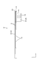
- FIG. 1 is a plan view of a power storage module according to Embodiment 1.
- FIG. FIG. 2 is a plan view of the second substrate that is not folded at the second folding portion.
- FIG. 3 is a plan view of the second substrate in a state of being mountain-folded at one second folding portion.
- FIG. 4 is a plan view showing connection between the second substrate and a plurality of storage elements.
- FIG. 5 is a plan view of the first substrate that is not folded at the first folding portion.
- FIG. 6 is a plan view showing connection between the first substrate and a plurality of storage elements.
- FIG. 7 is an enlarged plan view of the electricity storage module showing the periphery of the temperature measuring piece arranged in the intermediate portion of the plurality of electricity storage elements.
- FIG. 8 is a schematic diagram of the AA section of FIG.
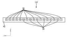
- FIG. 9 is a schematic diagram of the connector as viewed from the rear.
- FIG. 10 is a schematic rear view of the connector according to the second embodiment.
- 11 is a plan view of a power storage module according to Embodiment 3.
- FIG. 8 is a schematic diagram of the AA section of FIG.
- FIG. 9 is a schematic diagram of the connector as viewed from the rear.
- FIG. 10 is a schematic rear view of the connector according to the second embodiment.
- 11 is a plan view of a power storage module according to Embodiment 3.
- the electrode terminals of a plurality of storage elements are arranged in two rows in the direction in which the plurality of storage elements are arranged, and the two rows of electrode terminals are orthogonal to the arrangement direction.
- the plurality of second voltage detection lines are arranged in the separation direction in order of potential of the connected electrode terminals and electrically connected to the connector, and the plurality of second voltage detection lines are not folded or are folded evenly, One end of the second voltage detection line is electrical
- the first substrate has a plurality of first voltage detection lines only on one side
- the second substrate has a plurality of second voltage detection lines only on one side.
- a flexible substrate having conductive paths formed only on one side can be used, and the manufacturing cost of the wiring module can be reduced.
- the plurality of first voltage sensing lines is odd-folded
- the plurality of second voltage-sensing lines is unfolded or even-folded, so that the other end of the first voltage sensing line and the second voltage sensing line can be arranged in order of the potential of the electrode terminals to which they are connected in the separation direction.
- the surface of the first substrate on which the other end of the first voltage detection line is arranged and the surface of the second substrate on which the other end of the second voltage detection line is arranged are arranged to face each other. preferably.
- the first substrate includes a plurality of thermistor circuits on a surface on which the first voltage detection line is arranged, one ends of the plurality of thermistor circuits are connected to a common ground potential, and the plurality of thermistor circuits are connected to a common ground potential.
- the other end of the thermistor circuit is preferably connected to the connector and arranged between the ground potential and the other end of the first voltage detection line connected to the electrode terminal with the lowest potential. .
- the plurality of thermistor circuits are arranged on the same surface as the first voltage detection line, a flexible substrate having a conductive path formed only on one surface can be used as the first substrate.
- the manufacturing cost of the module can be reduced.
- the potential of the other end of the plurality of thermistor circuits is relatively close to the potential of the first voltage detection line, which has the lowest potential, short-circuiting between the plurality of thermistor circuits and the first voltage detection line can be suppressed. .
- the connector includes a first terminal connected to the other end of the first voltage detection line and a second terminal connected to the other end of the second voltage detection line, and the first terminal are arranged in a row in the separating direction, and the second terminals are arranged in a different position from the first terminals in the facing direction of the first substrate and the second substrate, and are arranged in a row in the separating direction. preferably.
- the connector can be miniaturized in the separation direction.
- the connector includes a first terminal connected to the other end of the first voltage detection line and a second terminal connected to the other end of the second voltage detection line, and the first terminal and the second terminals are arranged in a line in the separation direction, and the first terminals and the second terminals are preferably arranged alternately in the separation direction and arranged in order of potential.
- the connector can be miniaturized in the facing direction of the first board and the second board.
- the wiring module preferably includes a protector that protects the first substrate and the second substrate.
- Embodiment 1 of the present disclosure will be described with reference to FIGS. 1 to 9.
- FIG. The power storage module 10 including the wiring module 20 of the present embodiment is mounted on a vehicle as a power source for driving the vehicle, such as an electric vehicle or a hybrid vehicle.
- the direction indicated by arrow Z is upward
- the direction indicated by arrow X is forward
- the direction indicated by arrow Y is leftward.
- a plurality of identical members only some members may be given reference numerals, and the reference numerals of other members may be omitted.
- a plurality of (12 in this embodiment) power storage elements 11 are arranged in the front-rear direction (an example of the alignment direction).
- the storage element 11 has a rectangular shape.
- a storage element (not shown) is accommodated inside the storage element 11 .
- the storage element 11 is not particularly limited, and may be a secondary battery or a capacitor.
- the storage element 11 according to this embodiment is a secondary battery.
- electrode terminals 12 are formed on both left and right ends of the upper surface of the storage element 11 .
- One of the electrode terminals 12 is a positive electrode and the other is a negative electrode.
- the electrode terminals 12 are arranged in two rows in the front-rear direction, and the two rows of electrode terminals 12 are spaced apart in the left-right direction (an example of the separation direction).
- One of the two rows of electrode terminals 12 forms a first electrode terminal 12 ⁇ /b>A, which is arranged on the left side of the plurality of storage elements 11 .
- the second electrode terminal 12 ⁇ /b>B of the two rows of electrode terminals 12 is arranged on the right side of the plurality of storage elements 11 .
- a connection bus bar 13 or an output bus bar 14 is electrically connected to the first electrode terminal 12A.
- a connection bus bar 13 is electrically connected to the second electrode terminal 12B.
- connection bus bar 13 and the output bus bar 14 are formed by pressing a metal plate into a predetermined shape. Any metal such as copper, copper alloy, aluminum, or aluminum alloy can be selected as the metal forming the metal plate. A plated layer (not shown) may be formed on the surfaces of the connection bus bar 13 and the output bus bar 14 . Any metal such as tin, nickel, or solder can be selected as the metal forming the plated layer.
- connection bus bar 13 is connected to the electrode terminals 12 while straddling the electrode terminals 12 adjacent to each other in the front-rear direction.
- the output bus bar 14 is connected to one electrode terminal 12 and outputs power to an external device.
- five connection bus bars 13 connect adjacent first electrode terminals 12A
- six connection bus bars 13 connect adjacent second electrode terminals 12B.
- a plurality of storage elements 11 are connected in series by these connection bus bars 13 .
- the output bus bar 14 and the connection bus bar 13, and the electrode terminals 12 can be electrically connected by known methods such as soldering, welding, and bolting.
- the numbers 1 to 13 attached to the connection bus bar 13 and the output bus bar 14 indicate the order of potentials of the electrode terminals 12 of the storage elements 11 to which the connection bus bar 13 and the output bus bar 14 are connected.
- the potential of the electrode terminal 12 connected to the output bus bar 14 denoted by 1 is the highest, and the potential of the electrode terminal 12 connected to the output bus bar 14 denoted by 13 is the highest. low.
- the order of the potentials of the first electrode terminals 12A connected to the output bus bar 14 and the connection bus bar 13 arranged at the left ends of the plurality of storage elements 11 arranged in the front-rear direction is 1, 3, 5, 7, 9, 11, 13.
- the order of potentials of the second electrode terminals 12B connected to the connection bus bars 13 arranged at the right ends of the plurality of storage elements 11 is 2, 4, 6, 8, 10, and 12 from the highest.
- the power storage module 10 is connected to an external ECU (Electronic Control Unit) or the like via a connector 37 (not shown).
- the ECU is equipped with a microcomputer, elements, etc., and has functions for detecting the voltage, current, temperature, etc., of each storage element 11 and for performing charge/discharge control of each storage element 11. It has a well-known configuration.
- the wiring module 20 includes a flexible first substrate 21 having a plurality of first voltage detection lines 23 only on one side, and a flexible first substrate 21 having a plurality of second voltage detection lines 23 only on one side.
- a second substrate 22 having a voltage detection line 24 and a connector 37 to which the first substrate 21 and the second substrate 22 are connected are provided.
- the second substrate 22 is configured by forming a plurality of second voltage detection lines 24 only on a surface 22A of a flexible insulating sheet by printed wiring technology. As shown in FIG. 3, the conductive path is not provided on the rear surface 22B of the second substrate 22. As shown in FIG. The second voltage detection line 24 arranged on the front surface 22A of the second substrate 22 on the rear surface 22B of the second substrate 22 is indicated by a dashed line (the same applies to the first substrate 21).
- the second board 22 of this embodiment is a flexible printed board.
- a plurality of (six in this embodiment) second voltage detection lines 24 are formed on the second substrate 22 .
- One end 24A of the second voltage detection line 24 is the rear end of the second voltage detection line 24 .
- One end 24A of the second voltage detection line 24 is arranged on the right side of the second substrate 22 with an interval in the front-rear direction, and is electrically connected to the connection bus bar 13 connected to the second electrode terminal 12B.
- the second voltage detection line 24 and the connection bus bar 13 can be electrically connected by any method such as soldering or welding.
- the second voltage detection line 24 and the connection bus bar 13 are connected via a metal piece 15 such as nickel.
- One end 24A of the second voltage detection line 24 and the metal piece 15 are connected by soldering, and the connection bus bar 13 and the metal piece 15 are connected by welding.
- the front end of the second voltage detection line 24 is the other end 24B of the second voltage detection line 24 .
- the other end 24B of the second voltage detection line 24 is electrically connected to the connector 37 (see FIG. 8).
- the second voltage detection line 24 and the connector 37 are connected by soldering.
- the second board 22 has an elongated shape in the front-rear direction as a whole. It includes second folded portions 27A and 27B in which the plurality of second voltage detection lines 24 are folded. Most of the wiring portion 25 is placed on the upper surfaces of the plurality of power storage elements 11, and one end 24A of the second voltage detection line 24 connected to the second electrode terminal 12B among the second voltage detection lines 24 is connected to the second electrode terminal 12B. Prepare. In the wiring portion 25 on the rear side of the second folded portions 27A and 27B, the plurality of second voltage detection lines 24 extend generally in the front-rear direction and are arranged side by side in the left-right direction at intervals.
- the plurality of second voltage detection lines 24 arranged in the connector mounting portion 26 generally extend in the left-right direction and are arranged in a line in the front-rear direction at intervals.
- the other end 24B of the second voltage detection line 24 is arranged at the right end of the connector mounting portion 26 .
- a portion of the wiring portion 25 near the connector mounting portion 26 is provided with two second folded portions 27A and 27B over the entire width of the wiring portion 25 in the left-right direction.
- the second folded portion 27A is a fold that forms an angle of 90° with respect to the direction in which the wiring portion 25 extends
- the second folded portion 27B is a fold that forms an angle of 45° with respect to the direction in which the wiring portion 25 extends.
- the wiring portion 25 is mountain-folded at the second folded portion 27A (see FIGS. 2 and 3) and valley-folded at the second folded portion 27B (see FIGS. 3 and 4).
- the mountain fold is to fold the wiring portion 25 so that the folding line is on the outside of the folded wiring portion 25, and the valley fold is to fold the folding portion to the inside of the folded wiring portion 25. It is to fold the wiring part 25 so as to come down.
- the plurality of second voltage detection lines 24 are folded back at two second folded portions 27A and 27B, and the second voltage detection lines 24 as a whole are folded twice.
- the surface (surface 22A of the second substrate 22) on which the other ends 24B of the second voltage detection lines 24 are arranged is the upper side (the front side in the direction perpendicular to the paper surface).
- the second folded portion 27B is a fold that forms an angle of 45° with respect to the direction in which the wiring portion 25 extends
- the second voltage detection line 24 in the connector mounting portion 26 extends generally in the front-rear direction, They are lined up with a space in the left and right direction.
- the numbers attached to the other ends 24B of the second voltage detection lines 24 indicate the potentials of the connection bus bars 13 (second electrode terminals 12B) to which the respective second voltage detection lines 24 are connected.
- the other ends 24B of the second voltage detection lines 24 are arranged side by side in the left-right direction in the order of decreasing potential to 2, 4, 6, 8, 10, and 12 toward the left.
- the first substrate 21 is configured in substantially the same manner as the second substrate 22, and includes a plurality of first voltage detection lines 23, a wiring portion 28, a connector mounting portion 29, and a first folded portion 30. Prepare. However, the configuration of the first folded portion 30 is different from that of the second folded portions 27A and 27B. Also, the first substrate 21 further includes a plurality of thermistor circuits 31 that are not provided on the second substrate 22 . A plurality of thermistor circuits 31 are circuits for measuring the temperature of the storage element 11, and are formed only on the surface 21A of the first substrate 21 by printed wiring technology, like the first voltage detection line 23. FIG. The first substrate 21 of this embodiment is a flexible printed circuit board.
- first voltage detection line one end of first voltage detection line, other end of first voltage detection line
- a plurality of (seven in this embodiment) first voltage detection lines 23 are formed on the first substrate 21 .
- One end 23A of the first voltage detection line 23 is the rear end of the first voltage detection line 23 .
- One end 23A of the first voltage detection line 23 is arranged on the left side of the first substrate 21 with an interval in the front-rear direction, and the metal piece 15 is attached to the connection bus bar 13 or the output bus bar 14 connected to the first electrode terminal 12A. are electrically connected via
- the other end 23B of the first voltage detection line 23 is the front end of the first voltage detection line 23 .
- the other end 23B of the first voltage detection line 23 is electrically connected to the connector 37 (see FIG. 8).
- the thermistor circuit 31 includes a thermistor 32, a ground conductive path 33 led to a common ground potential from the thermistor 32, and a temperature measurement conductive path led from the thermistor 32 and different from the ground conductive path 33. 34 and.
- the front end of the ground conductive path 33 serves as one end 31A of the thermistor circuit 31, and the front end of the temperature measurement conductive path 34 serves as the other end 31B of the thermistor circuit 31.
- FIG. 6 the front end of the ground conductive path 33 serves as one end 31A of the thermistor circuit 31, and the front end of the temperature measurement conductive path 34 serves as the other end 31B of the thermistor circuit 31.
- part of the thermistor circuit 31 including the thermistor 32 is arranged on the temperature measuring piece 35 provided on the first substrate 21 .
- the temperature measuring pieces 35 are provided at the rear portion, front portion, and intermediate portion of the wiring portion 28 .
- the temperature measuring piece 35 is formed by making a cut in the wiring portion 28 and is folded back toward the left-right central portion of the electric storage element 11 .
- the temperature measuring piece 35 has two temperature measuring piece folded portions 36A and 36B. It is mountain-folded at 36B. By configuring in this way, as shown in FIG. The temperature in the vicinity of the part can be measured.
- first substrate 21 that is not folded back at the first folding portion 30 shown in FIG. They are spaced apart in the front-rear direction.
- the other end 23B of the first voltage detection line 23, one end 31A of the thermistor circuit 31, and the other end 31B of the thermistor circuit 31 are arranged at the right end of the connector mounting portion 29. As shown in FIG.
- one first folded portion 30 is provided over the entire width of the wiring portion 28 in the left-right direction at a portion of the wiring portion 28 near the connector mounting portion 29 .
- the first folded portion 30 is a fold that forms an angle of 45° with respect to the direction in which the wiring portion 28 extends.
- the wiring portion 28 is mountain-folded at the first folded portion 30 .
- the plurality of first voltage detection lines 23 are folded at the first folding portion 30, and the first voltage detection lines 23 as a whole are folded once.
- the surface (surface 21A of the first substrate 21) on which the other ends 23B of the first voltage detection lines 23 are arranged is the lower side (back side in the direction perpendicular to the paper surface).
- the connector mounting portion 29 illustrated in FIG. 6 faces the rear surface 21B of the first substrate 21 upward (front side in the direction perpendicular to the plane of the paper).
- a plurality of thermistor circuits 31 are similarly arranged on the lower surface of the connector mounting portion 29 .
- the first folded portion 30 is a fold that forms an angle of 45° with respect to the direction in which the wiring portion 28 extends, the first voltage detection line 23 and the thermistor circuit 31 in the connector mounting portion 29 are substantially forward and backward. It stretches out and is lined up at intervals in the left and right direction.
- the other end 23B of the first voltage detection line 23 is arranged close to the right end of the connector mounting portion 29, and 1, 3, 5, 7, 9, 11, 13 as it goes to the left. They are arranged side by side in the horizontal direction in order of decreasing potential.
- the potential of the first voltage detection line 23 labeled 13 is the lowest compared to the potentials of the other first voltage detection line 23 and the second voltage detection line 24 .
- the potential of the first voltage detection line 23 denoted by 13 is a reference potential in the power storage module 10 according to the present embodiment, and may be 0V.
- the potential of the first voltage detection line 23 denoted by 13 is relative to the other power storage module 10. Since it is based on the potential difference, it can be greater than 0V.
- one end 31A of the thermistor circuit 31 connected to the ground potential is arranged at the left end of the connector mounting portion 29.
- One end 31A of the thermistor circuit 31 is labeled GND (G in FIG. 9) indicating a ground potential.
- the potential of one end 31A of the thermistor circuit 31 is the ground potential, that is, 0V.
- the other end 31B of the thermistor circuit 31 is arranged on the right side of one end 31A of the thermistor circuit 31, the other end 31B of the thermistor circuit 31 is arranged.
- the other end 31B of the thermistor circuit 31 is denoted by C, B, and A in order from the left. corresponds to
- the potential of the other end 31B of the thermistor circuit 31 is determined based on the resistance value of the thermistor 32 .
- the other ends 31B of the plurality of thermistor circuits 31 labeled A, B, and C are connected to one end 31A (grounded) of the thermistor circuits 31 labeled GND. potential) and the other end 23B of the first voltage detection line 23 with the lowest potential 13 . Since the potential of the other end 31B of the thermistor circuit 31 and the other end 23B of the first voltage detection line 23 having the lowest potential are relatively close to each other, the thermistor circuit 31 and the first voltage detection line 23 are short-circuited. can be suppressed.
- the connector mounting portion 29 of the first substrate 21 and the connector mounting portion 26 of the second substrate 22 are connected to the connector 37 from the rear side (an example of the same side in the row direction).
- the surface 21A of the first substrate 21 on which the other end 23B of the first voltage detection line 23 is formed and the surface 22A of the second substrate 22 on which the other end 24B of the second voltage detection line 24 is formed are vertically ( An example of the facing direction) are arranged to face each other.
- the connector 37 of the present embodiment is a flexible printed circuit board connector, and includes first terminals 38 connected to the first board 21 and second terminals 39 connected to the second board 22. and a housing 42 that accommodates the first terminal 38 and the second terminal 39 .
- the first terminal 38 and the second terminal 39 are female terminals.
- Each of the first terminal 38 and the second terminal 39 includes a connection tube portion 40 connected to a male terminal of a mating connector (not shown), and a board connection portion 41 connected to the rear of the connection tube portion 40 .
- the board connection portion 41 of the first terminal 38 is connected to the other end 23B of the first voltage detection line 23, one end 31A of the thermistor circuit 31, or the other end 31B of the thermistor circuit 31 by soldering.
- the board connection portion 41 of the second terminal 39 is connected to the other end 24B of the second voltage detection line 24 by soldering.
- the housing 42 comprises a separate upper housing 43, a lower housing 45, and an intermediate housing 44 arranged therebetween.
- the upper housing 43 constitutes the upper outer surface of the housing 42
- the lower housing 45 constitutes the lower outer surface of the housing 42 .
- the intermediate housing 44 locks the first terminal 38 and the second terminal 39 inside the housing 42 to prevent them from coming off.
- the connector 37 includes, for example, an upper housing 43, a first board 21 to which first terminals 38 are soldered in advance, an intermediate housing 44, and a second board 21 to which second terminals 39 are soldered in advance. It can be configured by stacking and assembling the substrate 22 and the lower housing 45 in the vertical direction.
- FIG. 9 is a rear view of the connector 37 schematically showing the arrangement of the first terminals 38 and the second terminals 39 in the connector 37.
- FIG. The numbers 1 to 13 attached inside the square frames indicating the first terminal 38 and the second terminal 39 indicate the order of the potential of the first terminal 38 or the second terminal 39, and in FIG. It corresponds to the number attached to the output bus bar 14 .
- the symbols G, C, B, and A attached to the first terminal 38 in FIG. Corresponds to the codes of B and A.
- the first terminals 38 are arranged in a line in the left-right direction on the upper side of the connector 37 according to the order of potential.
- the second terminals 39 are arranged in a row in the horizontal direction on the lower side of the connector 37 in accordance with the order of potential.
- the size of the connector 37 can be reduced in the horizontal direction.
- the number of storage elements 11 to which the wiring module 20 is applied is large, the number of the first voltage detection lines 23 and the second voltage detection lines 24 is large, so a two-stage configuration like the connector 37 is required. may be preferred.
- a second terminal 39 connected to an intermediate potential is arranged at an intermediate position between the first terminals 38 adjacent in the left-right direction.
- a second terminal 39 denoted by 6 is arranged in the middle position in the left-right direction of the first terminals 38 denoted by 5 and 7 .
- the positions in the horizontal direction where the first terminals 38 and the second terminals 39 are arranged may be aligned (not shown).
- a first terminal 38 denoted by 1 and a second terminal 39 denoted by 2 are arranged at the same position in the horizontal direction
- a first terminal 38 denoted by 3 and a second terminal 38 denoted by 4 are arranged at the same position in the horizontal direction.
- the terminal 39 may be arranged at the same position in the left-right direction.
- the electrode terminals 12 of a plurality of storage elements 11 are arranged in two rows in the front-rear direction, and the two rows of electrode terminals 12 are spaced apart in the left-right direction.
- the electric potentials of the connected first electrode terminals 12A are arranged in the left-right direction and are electrically connected to the connector 37.
- One end 24A is electrically connected to the second electrode terminal 12B forming the other row, and the other end 24B of the second voltage detection line 24 is electrically connected via the second voltage detection line 24.
- the first substrate 21 has a plurality of first voltage detection lines 23 only on one side
- the second substrate 22 has a plurality of second voltage detection lines 24 only on one side.
- a flexible substrate (flexible printed circuit board) having a conductive path formed only on one side can be used as the second substrate 22, and the manufacturing cost of the wiring module 20 can be reduced. Since the plurality of first voltage detection lines 23 are folded once and the plurality of second voltage detection lines 24 are folded twice, the other end 23B of the first voltage detection line 23 and the other end of the second voltage detection line 24 The ends 24B can be arranged in the horizontal direction in the order of the potentials of the electrode terminals 12 to which they are connected.
- the surface of the first substrate 21 on which the other end 23B of the first voltage detection line 23 is arranged and the surface of the second substrate 22 on which the other end 24B of the second voltage detection line 24 is arranged face each other. and distributed.
- the first substrate 21 includes a plurality of thermistor circuits 31 on the surface on which the first voltage detection lines 23 are arranged, and one ends 31A of the plurality of thermistor circuits 31 are connected to a common ground potential. , the other end 31B of the plurality of thermistor circuits 31 are connected to a connector 37 and arranged between the ground potential and the other end 23B of the first voltage detection line 23 connected to the electrode terminal 12 with the lowest potential. ing.
- the plurality of thermistor circuits 31 are arranged on the same surface as the first voltage detection line 23, a flexible substrate (flexible printed circuit board) having conductive paths formed only on one side as the first substrate 21 can be used as the first substrate 21. ) can be used, and the manufacturing cost of the wiring module 20 can be reduced.
- the potential of the other end 31B of the plurality of thermistor circuits 31 is relatively close to the potential of the first voltage detection line 23, which has the lowest potential, a short circuit between the plurality of thermistor circuits 31 and the first voltage detection line 23 can be prevented. can be suppressed.
- the connector 37 has a first terminal 38 connected to the other end 23B of the first voltage detection line 23 and a second terminal 39 connected to the other end 24B of the second voltage detection line 24.
- the first terminals 38 are arranged in a line in the left-right direction
- the second terminals 39 are arranged in a line in the left-right direction at a position different from that of the first terminals 38 in the vertical direction.
- the size of the connector 37 can be reduced in the horizontal direction.
- Embodiment 2 of the present disclosure will be described with reference to FIG.
- the configuration according to the second embodiment is similar to that of the first embodiment, except that the connector 137 is of a single-stage type.
- members that are the same as those of the first embodiment are assigned the same reference numerals as those of the first embodiment, and descriptions of the same configurations and effects as those of the first embodiment are omitted.
- FIG. 10 is a rear view of the connector 137 schematically showing the arrangement of the first terminals 38 and the second terminals 39 in the connector 137 according to the second embodiment.
- the connector 137 is configured by arranging the first terminals 38 and the second terminals 39 in a row in the horizontal direction. That is, the connector 137 is of a single-stage type. By adopting the single-stage arrangement, the size of the connector 137 can be reduced in the vertical direction. In particular, when the number of storage elements 11 to which the wiring module 20 is applied is small, the number of the first voltage detection lines 23 and the second voltage detection lines 24 is small. may be adopted.
- the first terminals 38 and the second terminals 39 are arranged alternately in the left-right direction, and the first terminals 38 and the second terminals 39 are arranged in the order of potential in the left-right direction.
- the first terminal 38 and the second terminal 39 are arranged in decreasing order of potential as 1, 2, 3, 4, 5, 6, 7, 8, 9, 10, 11, 12, 13 toward the left. are lined up.
- the connector 137 has a first terminal 38 connected to the other end 23B of the first voltage detection line 23 and a second terminal 39 connected to the other end 24B of the second voltage detection line 24.
- the first terminals 38 and the second terminals 39 are arranged in a line in the left-right direction, and the first terminals 38 and the second terminals 39 are alternately arranged in the left-right direction and arranged in order of potential.
- the connector 137 can be miniaturized in the vertical direction.
- Embodiment 3 of the present disclosure will be described with reference to FIG. 11 .
- the wiring module 120 of the power storage module 110 according to the third embodiment is configured similarly to the wiring module 20 according to the first embodiment, except that the protector 50 is provided.
- members that are the same as those of the first embodiment are assigned the same reference numerals as those of the first embodiment, and descriptions of the same configurations and effects as those of the first embodiment are omitted.
- the protector 50 is a plate-like member made of insulating synthetic resin.
- the protector 50 holds the first board 21 , the second board 22 and the connector 37 .
- the first substrate 21, the second substrate 22, and the connector 37 are held by the protector 50;
- the wiring module 120 includes the protector 50, it is possible to protect each member.
- Embodiment 1 that does not include the protector 50, as shown in FIG.
- the extended portion 22E is protected by the protector 50 and is not exposed to the outside. Therefore, damage to the extension portion 22E due to external force can be suppressed.
- assembly and transportation of the wiring module 120 are facilitated.
- a wiring module 120 according to the third embodiment includes a protector 50 that protects the first substrate 21 and the second substrate 22 .
- the first substrate 21 and the second substrate 22 can be protected.
- first terminals 38 and the second terminals 39 are female terminals, but the present invention is not limited to this, and the first terminals and the second terminals may be male terminals.
- the surface (surface 21A) on which the other end 23B of the first voltage detection line 23 is arranged on the first substrate 21 and the other end 24B of the second voltage detection line 24 on the second substrate 22 are arranged.
- the surface to be coated front surface 22A
- the back surface of the first substrate and the back surface of the second substrate may be opposed.
- the present invention is not limited to this, and the thermistor circuit may not be provided.
- the connectors 37 and 137 are composed of the separate upper housing 43, intermediate housing 44, and lower housing 45, the first substrate 21 to which the first terminals 38 are connected, and the second terminals 39.
- the second substrate 22 to which is connected is configured to be laminated and assembled, the present invention is not limited to this.
- the connector may be mounted on the first board and the second board after the connector is configured by assembling the first terminals and the second terminals into the integrally molded housing.
- the present invention is not limited to this, and a reinforcing plate may be attached to the back surface of the connector mounting portion.
- the first substrate 21 and the second substrate 22 are flexible printed substrates, but the present invention is not limited to this. It's okay.
- connection bus bar 14 output bus bar 15: metal piece 20, 120: wiring module 21: first substrate 21A : Front surface 22: Second substrate 22A: Front surface 22B: Back surface 22E: Extension part 23: First voltage detection line 23A: One end 23B: Other end 24: Second voltage detection line 24A: One end 24B: Other end 25: Wiring part 26: Connector mounting portions 27A, 27B: Second folded portion 28: Cable portion 29: Connector mounting portion 30: First folded portion 31: Thermistor circuit 31A: One end 31B: The other end 32: Thermistor 33: Ground conductive path 34: Temperature measuring conducting path 35: Temperature measuring pieces 36A, 36B: Temperature measuring piece folded portions 37, 137: Connector 38: First terminal 39: Second terminal 40: Connection tube portion 41: Board connection portion 42: Housing 43: Upper housing 44: Intermediate housing 45: Lower housing 50: Protector
Abstract
Description
最初に本開示の実施態様を列挙して説明する。 [Description of Embodiments of the Present Disclosure]
First, embodiments of the present disclosure are enumerated and described.
以下に、本開示の実施形態について説明する。本開示はこれらの例示に限定されるものではなく、特許請求の範囲によって示され、特許請求の範囲と均等の意味及び範囲内での全ての変更が含まれることが意図される。 [Details of the embodiment of the present disclosure]
Embodiments of the present disclosure will be described below. The present disclosure is not limited to these examples, but is indicated by the scope of the claims, and is intended to include all modifications within the meaning and scope of equivalents to the scope of the claims.
本開示の実施形態1について、図1から図9を参照しつつ説明する。本実施形態の配線モジュール20を備えた蓄電モジュール10は、例えば、電気自動車またはハイブリッド自動車などの車両を駆動するための電源として車両に搭載されるものである。以下の説明においては、矢線Zの示す方向を上方、矢線Xの示す方向を前方、矢線Yの示す方向を左方として説明する。なお、複数の同一部材については、一部の部材にのみ符号を付し、他の部材の符号を省略する場合がある。 <
図1に示すように、蓄電モジュール10においては、複数(本実施形態では12個)の蓄電素子11が前後方向(並び方向の一例)に並んでいる。蓄電素子11は長方形状をしている。蓄電素子11の内部には図示しない蓄電要素が収容されている。蓄電素子11は特に限定されず、二次電池でもよく、またキャパシタでもよい。本実施形態にかかる蓄電素子11は二次電池とされる。 [Storage element]
As shown in FIG. 1 , in the
図1に示すように、蓄電素子11の上面の左右両端部には、電極端子12が形成されている。電極端子12の一方は正極で、他方は負極である。複数の蓄電素子11において、電極端子12は、前後方向に連なって二列に配列されており、二列の電極端子12は、左右方向(離間方向の一例)に離間している。二列の電極端子12のうち一方の列をなすものは第1電極端子12Aとされ、複数の蓄電素子11の左側に配されている。二列の電極端子12のうち他方の列をなすものは第2電極端子12Bとされ、複数の蓄電素子11の右側に配されている。第1電極端子12Aには、接続バスバー13または出力バスバー14が電気的に接続されている。第2電極端子12Bには、接続バスバー13が電気的に接続されている。 [Electrode terminal]
As shown in FIG. 1 ,
図1に示すように、複数の蓄電素子11の上面には、配線モジュール20が載置されている。本実施形態にかかる配線モジュール20は、可撓性を有し、片面にのみ複数の第1電圧検知線23を備える第1基板21と、可撓性を有し、片面にのみ複数の第2電圧検知線24を備える第2基板22と、第1基板21及び第2基板22が接続されるコネクタ37と、を備える。以下では、ほぼ同様とされる第1基板21及び第2基板22の構成のうち、より簡素な第2基板22の構成についてまず説明し、その後、第1基板21の構成について説明する。 [Wiring module]
As shown in FIG. 1 ,
図2に示すように、第2基板22は、可撓性を有する絶縁性のシートの表面22Aにのみプリント配線技術により複数の第2電圧検知線24が形成されて構成されている。図3に示すように、第2基板22の裏面22Bには、導電路は設けられていない。なお、第2基板22の裏面22Bにおいて、第2基板22の表面22Aに配された第2電圧検知線24は破線で示している(第1基板21についても同様)。本実施形態の第2基板22は、フレキシブルプリント基板とされている。 [Second substrate]
As shown in FIG. 2, the
図4に示すように、第2基板22には、複数(本実施形態では6つ)の第2電圧検知線24が形成されている。第2電圧検知線24の一端24Aは、第2電圧検知線24の後側の端部とされている。第2電圧検知線24の一端24Aは、前後方向に間隔を空けて第2基板22の右側に配されており、第2電極端子12Bに接続された接続バスバー13に電気的に接続されている。第2電圧検知線24と接続バスバー13とは、半田付け、溶接等、任意の手法により、電気的に接続することができる。本実施形態では、第2電圧検知線24と接続バスバー13とは、ニッケル等の金属小片15を介して接続されている。第2電圧検知線24の一端24Aと金属小片15とは半田付けにより接続され、接続バスバー13と金属小片15とは溶接により接続されている。 [Second voltage detection line, one end of the second voltage detection line]
As shown in FIG. 4 , a plurality of (six in this embodiment) second
図4に示すように、この第2電圧検知線24の前側の端部は、第2電圧検知線24の他端24Bとされている。第2電圧検知線24の他端24Bは、コネクタ37に電気的に接続されるようになっている(図8参照)。本実施形態においては、第2電圧検知線24とコネクタ37とは、半田付けにより接続されている。 [The other end of the second voltage detection line]
As shown in FIG. 4 , the front end of the second
図6に示すように、第1基板21は、第2基板22とほぼ同様に構成され、複数の第1電圧検知線23、配索部28、コネクタ装着部29、及び第1折り返し部30を備える。ただし、第1折り返し部30の構成は、第2折り返し部27A,27Bとは異なっている。また、第1基板21は、第2基板22に設けられない複数のサーミスタ回路31をさらに備える。複数のサーミスタ回路31は、蓄電素子11の温度を測定するための回路であって、第1電圧検知線23と同様に、第1基板21の表面21Aにのみプリント配線技術により形成されている。本実施形態の第1基板21は、フレキシブルプリント基板とされている。 [First substrate]
As shown in FIG. 6, the
図6に示すように、第1基板21には、複数(本実施形態では7つ)の第1電圧検知線23が形成されている。第1電圧検知線23の一端23Aは、第1電圧検知線23の後側の端部とされている。第1電圧検知線23の一端23Aは、前後方向に間隔を空けて第1基板21の左側に配されており、第1電極端子12Aに接続された接続バスバー13または出力バスバー14に金属小片15を介して電気的に接続されている。第1電圧検知線23の他端23Bは、第1電圧検知線23の前側の端部とされている。第1電圧検知線23の他端23Bは、コネクタ37に電気的に接続されるようになっている(図8参照)。 [First voltage detection line, one end of first voltage detection line, other end of first voltage detection line]
As shown in FIG. 6 , a plurality of (seven in this embodiment) first
図6に示すように、第1基板21の表面21Aには、プリント配線技術により、複数(本実施形態では3つ)のサーミスタ回路31が形成されている。複数のサーミスタ回路31は、配索部28の右側に配されている。図7に示すように、サーミスタ回路31は、サーミスタ32と、サーミスタ32から共通のグランド電位に導出されるグランド導電路33と、サーミスタ32から導出され、グランド導電路33とは異なる測温導電路34と、を備える。図6に示すように、グランド導電路33の前側の端部はサーミスタ回路31の一端31Aとされ、測温導電路34の前側の端部はサーミスタ回路31の他端31Bとされている。 [Thermistor circuit, one end of the thermistor circuit, the other end of the thermistor circuit]
As shown in FIG. 6, a plurality of (three in this embodiment)
図8に示すように、第1基板21のコネクタ装着部29と第2基板22のコネクタ装着部26とは、コネクタ37に対して後側(並び方向における同じ側の一例)から接続されている。第1電圧検知線23の他端23Bが形成された第1基板21の表面21Aと、第2電圧検知線24の他端24Bが形成された第2基板22の表面22Aとは、上下方向(対向方向の一例)について互いに対向する配置とされている。 [connector]
As shown in FIG. 8, the
実施形態1によれば、以下の作用、効果を奏する。
実施形態1にかかる配線モジュール20は、複数の蓄電素子11の電極端子12が前後方向に連なって二列に配列されており、二列の電極端子12は左右方向に離間している複数の蓄電素子11に取り付けられる配線モジュール20であって、可撓性を有し、片面にのみ複数の第1電圧検知線23を備える第1基板21と、可撓性を有し、片面にのみ複数の第2電圧検知線24を備える第2基板22と、コネクタ37と、を備え、複数の第1電圧検知線23は、1回折り返されており、第1電圧検知線23の一端23Aは、二列の電極端子12のうち一方の列をなす第1電極端子12Aに電気的に接続されており、第1電圧検知線23の他端23Bは、第1電圧検知線23を介して電気的に接続された第1電極端子12Aの電位順に左右方向に並び、コネクタ37に電気的に接続されており、複数の第2電圧検知線24は、2回折り返されており、第2電圧検知線24の一端24Aは、同他方の列をなす第2電極端子12Bに電気的に接続されており、第2電圧検知線24の他端24Bは、第2電圧検知線24を介して電気的に接続された第2電極端子12Bの電位順に左右方向に並び、コネクタ37に電気的に接続されており、第1電圧検知線23及び第2電圧検知線24は、コネクタ37に対して後側から接続されている。 [Effects of Embodiment 1]
According to
In the
本開示の実施形態2について、図10を参照しつつ説明する。実施形態2にかかる構成は、コネクタ137が一段型である点を除いて、実施形態1の構成と同様に構成されている。以下、実施形態1と同一の部材には実施形態1で用いた符号を付し、実施形態1と同一の構成、作用効果については説明を省略する。 <
実施形態2によれば、以下の作用、効果を奏する。
実施形態2では、コネクタ137は、第1電圧検知線23の他端23Bに接続される第1端子38と、第2電圧検知線24の他端24Bに接続される第2端子39と、を備え、第1端子38と第2端子39とは、左右方向に一列に並んでおり、第1端子38と第2端子39とは、左右方向について交互に配され、電位順に並んでいる。 [Effects of Embodiment 2]
According to the second embodiment, the following actions and effects are obtained.
In the second embodiment, the
本開示の実施形態3について、図11を参照しつつ説明する。実施形態3にかかる蓄電モジュール110の配線モジュール120は、プロテクタ50が設けられる点を除いて、実施形態1にかかる配線モジュール20と同様に構成されている。以下、実施形態1と同一の部材には実施形態1で用いた符号を付し、実施形態1と同一の構成、作用効果については説明を省略する。 <
実施形態3によれば、以下の作用、効果を奏する。
実施形態3にかかる配線モジュール120は、第1基板21及び第2基板22を保護するプロテクタ50を備える。 [Effects of Embodiment 3]
According to the third embodiment, the following functions and effects are obtained.
A
(1)上記実施形態では、第1端子38及び第2端子39は雌端子であったが、これに限られることはなく、第1端子及び第2端子は雄端子でよい。
(2)上記実施形態では、第1基板21における第1電圧検知線23の他端23Bが配される面(表面21A)と第2基板22における第2電圧検知線24の他端24Bが配される面(表面22A)とが対向していたが、これに限られることはなく、第1基板の裏面と第2基板の裏面とが対向していてもよい。
(3)上記実施形態では、サーミスタ回路31が設けられたが、これに限られることはなく、サーミスタ回路は設けられなくてもよい。
(4)上記実施形態では、コネクタ37,137は、別体の上側ハウジング43、中間ハウジング44、及び下側ハウジング45と、第1端子38が接続された第1基板21と、第2端子39が接続された第2基板22と、を積層して組み付けられる構成としたが、これに限られることはない。例えば、一体成形されたハウジングに第1端子及び第2端子を組み付けてコネクタを構成した後、コネクタを第1基板及び第2基板に実装してもよい。
(5)上記実施形態では、第1基板21のコネクタ装着部29において第1端子38が接続される面と反対側の面(裏面21B)及び第2基板22のコネクタ装着部26において第2端子39が接続される面と反対側の面(裏面22B)には、補強板が貼り付けられなかったが、これに限られることはなく、コネクタ装着部の裏面に補強板を貼り付けてもよい。
(6)上記実施形態では、第1基板21及び第2基板22はフレキシブルプリント基板とされたが、これに限られることはなく、第1基板及び第2基板の、双方または一方はフレキシブルフラットケーブルでもよい。 <Other embodiments>
(1) In the above embodiment, the
(2) In the above embodiment, the surface (
(3) Although the
(4) In the above embodiment, the
(5) In the above-described embodiment, in the
(6) In the above embodiment, the
11: 蓄電素子
12: 電極端子
12A: 第1電極端子
12B: 第2電極端子
13: 接続バスバー
14: 出力バスバー
15: 金属小片
20,120: 配線モジュール
21: 第1基板
21A: 表面
22: 第2基板
22A: 表面
22B: 裏面
22E: 延長部
23: 第1電圧検知線
23A: 一端
23B: 他端
24: 第2電圧検知線
24A: 一端
24B: 他端
25: 配索部
26: コネクタ装着部
27A,27B: 第2折り返し部
28: 配索部
29: コネクタ装着部
30: 第1折り返し部
31: サーミスタ回路
31A: 一端
31B: 他端
32: サーミスタ
33: グランド導電路
34: 測温導電路
35: 測温片
36A,36B: 測温片折り返し部
37,137: コネクタ
38: 第1端子
39: 第2端子
40: 接続筒部
41: 基板接続部
42: ハウジング
43: 上側ハウジング
44: 中間ハウジング
45: 下側ハウジング
50: プロテクタ 10, 110: power storage module 11: power storage element 12:
Claims (6)
- 複数の蓄電素子の電極端子が前記複数の蓄電素子の並び方向に連なって二列に配列されており、二列の前記電極端子は前記並び方向に直交する離間方向に離間している前記複数の蓄電素子に取り付けられる配線モジュールであって、
可撓性を有し、片面にのみ複数の第1電圧検知線を備える第1基板と、
可撓性を有し、片面にのみ複数の第2電圧検知線を備える第2基板と、
コネクタと、を備え、
前記複数の第1電圧検知線は、奇数回折り返されており、
前記第1電圧検知線の一端は、二列の前記電極端子のうち一方の列をなす前記電極端子に電気的に接続されており、
前記第1電圧検知線の他端は、前記第1電圧検知線を介して電気的に接続された前記電極端子の電位順に前記離間方向に並び、前記コネクタに電気的に接続されており、
前記複数の第2電圧検知線は、折り返されていないか、もしくは偶数回折り返されており、
前記第2電圧検知線の一端は、同他方の列をなす前記電極端子に電気的に接続されており、
前記第2電圧検知線の他端は、前記第2電圧検知線を介して電気的に接続された前記電極端子の電位順に前記離間方向に並び、前記コネクタに電気的に接続されており、
前記第1電圧検知線及び前記第2電圧検知線は、前記コネクタに対して前記並び方向における同じ側から接続されている、配線モジュール。 The electrode terminals of the plurality of storage elements are arranged in two rows in a row direction of the plurality of storage devices, and the two rows of electrode terminals are spaced apart in a separation direction orthogonal to the row direction. A wiring module attached to a power storage element,
a flexible first substrate provided with a plurality of first voltage sensing lines only on one side;
a second substrate having flexibility and having a plurality of second voltage sensing lines only on one side;
a connector and a
the plurality of first voltage sensing lines are oddly folded;
one end of the first voltage detection line is electrically connected to one of the two rows of electrode terminals,
the other end of the first voltage detection line is arranged in order of potential of the electrode terminals electrically connected via the first voltage detection line in the separation direction and electrically connected to the connector;
the plurality of second voltage sensing lines are unfolded or even-folded;
one end of the second voltage detection line is electrically connected to the electrode terminals forming the other row,
the other end of the second voltage detection line is arranged in order of potential of the electrode terminals electrically connected via the second voltage detection line in the separation direction and electrically connected to the connector;
The wiring module, wherein the first voltage detection line and the second voltage detection line are connected to the connector from the same side in the arrangement direction. - 前記第1基板における前記第1電圧検知線の他端が配される面と前記第2基板における前記第2電圧検知線の他端が配される面とが、対向して配されている、請求項1に記載の配線モジュール。 a surface of the first substrate on which the other end of the first voltage detection line is arranged and a surface of the second substrate on which the other end of the second voltage detection line is arranged are arranged to face each other; The wiring module according to claim 1.
- 前記第1基板は、前記第1電圧検知線が配される面に複数のサーミスタ回路を備え、
前記複数のサーミスタ回路の一端は、共通のグランド電位に接続されており、
前記複数のサーミスタ回路の他端は、前記コネクタに接続され、前記グランド電位と、最も電位の低い前記電極端子に接続された前記第1電圧検知線の他端と、の間に配されている、請求項1または請求項2に記載の配線モジュール。 the first substrate includes a plurality of thermistor circuits on a surface on which the first voltage detection line is arranged;
one end of the plurality of thermistor circuits is connected to a common ground potential;
The other ends of the plurality of thermistor circuits are connected to the connector and arranged between the ground potential and the other end of the first voltage detection line connected to the electrode terminal with the lowest potential. The wiring module according to claim 1 or 2. - 前記コネクタは、前記第1電圧検知線の他端に接続される第1端子と、前記第2電圧検知線の他端に接続される第2端子と、を備え、
前記第1端子は、前記離間方向に一列に並んでおり、
前記第2端子は、前記第1基板及び前記第2基板の対向方向について前記第1端子と異なる位置に配され、前記離間方向に一列に並んでいる、請求項1から請求項3のいずれか一項に記載の配線モジュール。 The connector includes a first terminal connected to the other end of the first voltage detection line and a second terminal connected to the other end of the second voltage detection line,
The first terminals are arranged in a line in the separation direction,
4. The second terminals according to any one of claims 1 to 3, wherein the second terminals are arranged at positions different from the first terminals with respect to the facing direction of the first substrate and the second substrate, and are arranged in a line in the separating direction. A wiring module according to claim 1. - 前記コネクタは、前記第1電圧検知線の他端に接続される第1端子と、前記第2電圧検知線の他端に接続される第2端子と、を備え、
前記第1端子と前記第2端子とは、前記離間方向に一列に並んでおり、
前記第1端子と前記第2端子とは、前記離間方向について交互に配され、電位順に並んでいる、請求項1から請求項3のいずれか一項に記載の配線モジュール。 The connector includes a first terminal connected to the other end of the first voltage detection line and a second terminal connected to the other end of the second voltage detection line,
the first terminal and the second terminal are arranged in a row in the separation direction;
The wiring module according to any one of claims 1 to 3, wherein the first terminals and the second terminals are alternately arranged in the separation direction and arranged in order of potential. - 前記第1基板及び前記第2基板を保護するプロテクタを備える、請求項1から請求項5のいずれか一項に記載の配線モジュール。 The wiring module according to any one of claims 1 to 5, comprising a protector that protects the first substrate and the second substrate.
Priority Applications (1)
| Application Number | Priority Date | Filing Date | Title |
|---|---|---|---|
| CN202280017021.7A CN116918165A (en) | 2021-03-19 | 2022-03-11 | wiring module |
Applications Claiming Priority (2)
| Application Number | Priority Date | Filing Date | Title |
|---|---|---|---|
| JP2021-046125 | 2021-03-19 | ||
| JP2021046125A JP2022144921A (en) | 2021-03-19 | 2021-03-19 | wiring module |
Publications (1)
| Publication Number | Publication Date |
|---|---|
| WO2022196557A1 true WO2022196557A1 (en) | 2022-09-22 |
Family
ID=83320339
Family Applications (1)
| Application Number | Title | Priority Date | Filing Date |
|---|---|---|---|
| PCT/JP2022/010858 WO2022196557A1 (en) | 2021-03-19 | 2022-03-11 | Wiring module |
Country Status (3)
| Country | Link |
|---|---|
| JP (1) | JP2022144921A (en) |
| CN (1) | CN116918165A (en) |
| WO (1) | WO2022196557A1 (en) |
Citations (5)
| Publication number | Priority date | Publication date | Assignee | Title |
|---|---|---|---|---|
| JP2016219218A (en) * | 2015-05-19 | 2016-12-22 | 矢崎総業株式会社 | Coated conductive member |
| US20170271642A1 (en) * | 2014-12-09 | 2017-09-21 | Elringklinger Ag | Cell contact-making system for an electrochemical device |
| JP2020013655A (en) * | 2018-07-13 | 2020-01-23 | 矢崎総業株式会社 | Circuit body and battery module |
| JP2020013829A (en) * | 2018-07-13 | 2020-01-23 | 矢崎総業株式会社 | Circuit body and battery module |
| JP2020057700A (en) * | 2018-10-02 | 2020-04-09 | 株式会社オートネットワーク技術研究所 | Flexible printed circuit board and wiring module |
-
2021
- 2021-03-19 JP JP2021046125A patent/JP2022144921A/en active Pending
-
2022
- 2022-03-11 CN CN202280017021.7A patent/CN116918165A/en active Pending
- 2022-03-11 WO PCT/JP2022/010858 patent/WO2022196557A1/en active Application Filing
Patent Citations (5)
| Publication number | Priority date | Publication date | Assignee | Title |
|---|---|---|---|---|
| US20170271642A1 (en) * | 2014-12-09 | 2017-09-21 | Elringklinger Ag | Cell contact-making system for an electrochemical device |
| JP2016219218A (en) * | 2015-05-19 | 2016-12-22 | 矢崎総業株式会社 | Coated conductive member |
| JP2020013655A (en) * | 2018-07-13 | 2020-01-23 | 矢崎総業株式会社 | Circuit body and battery module |
| JP2020013829A (en) * | 2018-07-13 | 2020-01-23 | 矢崎総業株式会社 | Circuit body and battery module |
| JP2020057700A (en) * | 2018-10-02 | 2020-04-09 | 株式会社オートネットワーク技術研究所 | Flexible printed circuit board and wiring module |
Also Published As
| Publication number | Publication date |
|---|---|
| CN116918165A (en) | 2023-10-20 |
| JP2022144921A (en) | 2022-10-03 |
Similar Documents
| Publication | Publication Date | Title |
|---|---|---|
| CN110718660B (en) | Circuit body and battery module | |
| JP7025297B2 (en) | Circuit body and battery module | |
| US9024572B2 (en) | Battery module, battery system and electric vehicle | |
| JP6745036B2 (en) | Battery wiring module | |
| JP6151476B2 (en) | Power supply | |
| JP6227082B1 (en) | Connection module | |
| US20180248167A1 (en) | Conductive module and battery pack | |
| JP6044505B2 (en) | Battery pack unit | |
| US20190386282A1 (en) | Connection module | |
| JP6940452B2 (en) | Wiring module | |
| CN110707277B (en) | Connection structure between circuit body, bus bar and electronic component | |
| WO2022196557A1 (en) | Wiring module | |
| WO2022196319A1 (en) | Wiring module | |
| WO2022153871A1 (en) | External connection busbar and wiring module | |
| WO2022107567A1 (en) | Wiring module | |
| CN116235351A (en) | Battery wiring module | |
| JP7188599B2 (en) | wiring module | |
| US11757159B2 (en) | Conductive module | |
| CN116670891A (en) | Wiring module | |
| CN115997319A (en) | Wiring module | |
| WO2016194545A1 (en) | Battery pack |
Legal Events
| Date | Code | Title | Description |
|---|---|---|---|
| 121 | Ep: the epo has been informed by wipo that ep was designated in this application |
Ref document number: 22771305 Country of ref document: EP Kind code of ref document: A1 |
|
| WWE | Wipo information: entry into national phase |
Ref document number: 202280017021.7 Country of ref document: CN |
|
| WWE | Wipo information: entry into national phase |
Ref document number: 18279284 Country of ref document: US |
|
| NENP | Non-entry into the national phase |
Ref country code: DE |
|
| 122 | Ep: pct application non-entry in european phase |
Ref document number: 22771305 Country of ref document: EP Kind code of ref document: A1 |