WO2022190826A1 - 撮像装置及び電子機器 - Google Patents
撮像装置及び電子機器 Download PDFInfo
- Publication number
- WO2022190826A1 WO2022190826A1 PCT/JP2022/006793 JP2022006793W WO2022190826A1 WO 2022190826 A1 WO2022190826 A1 WO 2022190826A1 JP 2022006793 W JP2022006793 W JP 2022006793W WO 2022190826 A1 WO2022190826 A1 WO 2022190826A1
- Authority
- WO
- WIPO (PCT)
- Prior art keywords
- pixels
- pixel
- unit
- imaging device
- light
- Prior art date
Links
- 238000003384 imaging method Methods 0.000 title claims abstract description 55
- 230000003595 spectral effect Effects 0.000 claims abstract description 55
- 238000012545 processing Methods 0.000 claims description 151
- 238000002156 mixing Methods 0.000 claims description 17
- 238000007499 fusion processing Methods 0.000 claims description 13
- 238000004458 analytical method Methods 0.000 claims description 11
- 238000001914 filtration Methods 0.000 claims description 9
- 238000011156 evaluation Methods 0.000 claims description 4
- 238000000034 method Methods 0.000 description 60
- 238000010586 diagram Methods 0.000 description 30
- 239000004065 semiconductor Substances 0.000 description 26
- 238000004891 communication Methods 0.000 description 21
- 238000003860 storage Methods 0.000 description 19
- 238000005516 engineering process Methods 0.000 description 12
- 230000006870 function Effects 0.000 description 12
- 238000012546 transfer Methods 0.000 description 12
- RZVHIXYEVGDQDX-UHFFFAOYSA-N 9,10-anthraquinone Chemical compound C1=CC=C2C(=O)C3=CC=CC=C3C(=O)C2=C1 RZVHIXYEVGDQDX-UHFFFAOYSA-N 0.000 description 11
- 239000000758 substrate Substances 0.000 description 11
- 230000000052 comparative effect Effects 0.000 description 9
- 238000009792 diffusion process Methods 0.000 description 9
- 238000007667 floating Methods 0.000 description 9
- 230000003287 optical effect Effects 0.000 description 9
- 238000007781 pre-processing Methods 0.000 description 9
- 230000008569 process Effects 0.000 description 8
- 238000006243 chemical reaction Methods 0.000 description 7
- 238000001514 detection method Methods 0.000 description 7
- 230000003321 amplification Effects 0.000 description 6
- 230000000694 effects Effects 0.000 description 6
- 238000003199 nucleic acid amplification method Methods 0.000 description 6
- 238000005229 chemical vapour deposition Methods 0.000 description 5
- 230000007246 mechanism Effects 0.000 description 5
- 238000004544 sputter deposition Methods 0.000 description 5
- 230000001133 acceleration Effects 0.000 description 4
- 230000005540 biological transmission Effects 0.000 description 4
- 230000000295 complement effect Effects 0.000 description 4
- 238000012937 correction Methods 0.000 description 4
- 238000007405 data analysis Methods 0.000 description 4
- 239000010410 layer Substances 0.000 description 4
- 239000000203 mixture Substances 0.000 description 4
- VYPSYNLAJGMNEJ-UHFFFAOYSA-N Silicium dioxide Chemical compound O=[Si]=O VYPSYNLAJGMNEJ-UHFFFAOYSA-N 0.000 description 3
- 238000004364 calculation method Methods 0.000 description 3
- 239000003086 colorant Substances 0.000 description 3
- 239000010949 copper Substances 0.000 description 3
- 238000004519 manufacturing process Methods 0.000 description 3
- 239000011159 matrix material Substances 0.000 description 3
- 229910052751 metal Inorganic materials 0.000 description 3
- 239000002184 metal Substances 0.000 description 3
- 238000001451 molecular beam epitaxy Methods 0.000 description 3
- 230000002093 peripheral effect Effects 0.000 description 3
- 238000005240 physical vapour deposition Methods 0.000 description 3
- 238000007639 printing Methods 0.000 description 3
- 230000009467 reduction Effects 0.000 description 3
- 229920005989 resin Polymers 0.000 description 3
- 239000011347 resin Substances 0.000 description 3
- 239000013589 supplement Substances 0.000 description 3
- 229910004298 SiO 2 Inorganic materials 0.000 description 2
- PPBRXRYQALVLMV-UHFFFAOYSA-N Styrene Chemical compound C=CC1=CC=CC=C1 PPBRXRYQALVLMV-UHFFFAOYSA-N 0.000 description 2
- 230000002159 abnormal effect Effects 0.000 description 2
- 229910052782 aluminium Inorganic materials 0.000 description 2
- 238000000231 atomic layer deposition Methods 0.000 description 2
- 230000003139 buffering effect Effects 0.000 description 2
- 238000005266 casting Methods 0.000 description 2
- 230000008859 change Effects 0.000 description 2
- 229910052802 copper Inorganic materials 0.000 description 2
- 230000000875 corresponding effect Effects 0.000 description 2
- 230000007547 defect Effects 0.000 description 2
- 238000010894 electron beam technology Methods 0.000 description 2
- 239000011229 interlayer Substances 0.000 description 2
- 238000005259 measurement Methods 0.000 description 2
- 238000012986 modification Methods 0.000 description 2
- 230000004048 modification Effects 0.000 description 2
- 238000003672 processing method Methods 0.000 description 2
- 239000000047 product Substances 0.000 description 2
- 229910052710 silicon Inorganic materials 0.000 description 2
- 239000010703 silicon Substances 0.000 description 2
- 229910052814 silicon oxide Inorganic materials 0.000 description 2
- 239000007921 spray Substances 0.000 description 2
- 229910052721 tungsten Inorganic materials 0.000 description 2
- 239000004925 Acrylic resin Substances 0.000 description 1
- 229920000178 Acrylic resin Polymers 0.000 description 1
- RYGMFSIKBFXOCR-UHFFFAOYSA-N Copper Chemical compound [Cu] RYGMFSIKBFXOCR-UHFFFAOYSA-N 0.000 description 1
- KJTLSVCANCCWHF-UHFFFAOYSA-N Ruthenium Chemical compound [Ru] KJTLSVCANCCWHF-UHFFFAOYSA-N 0.000 description 1
- XAGFODPZIPBFFR-UHFFFAOYSA-N aluminium Chemical compound [Al] XAGFODPZIPBFFR-UHFFFAOYSA-N 0.000 description 1
- 230000002547 anomalous effect Effects 0.000 description 1
- 238000003705 background correction Methods 0.000 description 1
- 230000015572 biosynthetic process Effects 0.000 description 1
- 238000003486 chemical etching Methods 0.000 description 1
- 229920006026 co-polymeric resin Polymers 0.000 description 1
- 229910017052 cobalt Inorganic materials 0.000 description 1
- 239000010941 cobalt Substances 0.000 description 1
- GUTLYIVDDKVIGB-UHFFFAOYSA-N cobalt atom Chemical compound [Co] GUTLYIVDDKVIGB-UHFFFAOYSA-N 0.000 description 1
- 239000000470 constituent Substances 0.000 description 1
- 230000001276 controlling effect Effects 0.000 description 1
- 230000002596 correlated effect Effects 0.000 description 1
- 239000002537 cosmetic Substances 0.000 description 1
- 238000012217 deletion Methods 0.000 description 1
- 230000037430 deletion Effects 0.000 description 1
- 238000000151 deposition Methods 0.000 description 1
- 230000008021 deposition Effects 0.000 description 1
- 238000013461 design Methods 0.000 description 1
- KPUWHANPEXNPJT-UHFFFAOYSA-N disiloxane Chemical class [SiH3]O[SiH3] KPUWHANPEXNPJT-UHFFFAOYSA-N 0.000 description 1
- 239000006185 dispersion Substances 0.000 description 1
- 238000009826 distribution Methods 0.000 description 1
- 238000007772 electroless plating Methods 0.000 description 1
- 238000009713 electroplating Methods 0.000 description 1
- 238000005530 etching Methods 0.000 description 1
- 230000005284 excitation Effects 0.000 description 1
- 235000013305 food Nutrition 0.000 description 1
- 238000007646 gravure printing Methods 0.000 description 1
- 230000036541 health Effects 0.000 description 1
- 238000005286 illumination Methods 0.000 description 1
- 238000007654 immersion Methods 0.000 description 1
- 238000007641 inkjet printing Methods 0.000 description 1
- 238000007689 inspection Methods 0.000 description 1
- 230000010354 integration Effects 0.000 description 1
- 238000007733 ion plating Methods 0.000 description 1
- 238000000608 laser ablation Methods 0.000 description 1
- 239000004973 liquid crystal related substance Substances 0.000 description 1
- 230000007774 longterm Effects 0.000 description 1
- 238000001755 magnetron sputter deposition Methods 0.000 description 1
- 230000000873 masking effect Effects 0.000 description 1
- 239000000463 material Substances 0.000 description 1
- 238000002558 medical inspection Methods 0.000 description 1
- 238000000813 microcontact printing Methods 0.000 description 1
- 238000007645 offset printing Methods 0.000 description 1
- 230000001151 other effect Effects 0.000 description 1
- 238000000059 patterning Methods 0.000 description 1
- 230000000737 periodic effect Effects 0.000 description 1
- 238000000206 photolithography Methods 0.000 description 1
- 238000005268 plasma chemical vapour deposition Methods 0.000 description 1
- 238000005498 polishing Methods 0.000 description 1
- 230000002441 reversible effect Effects 0.000 description 1
- 229910052707 ruthenium Inorganic materials 0.000 description 1
- 238000005070 sampling Methods 0.000 description 1
- 238000007650 screen-printing Methods 0.000 description 1
- 230000035945 sensitivity Effects 0.000 description 1
- 238000004528 spin coating Methods 0.000 description 1
- 229920001909 styrene-acrylic polymer Polymers 0.000 description 1
- 239000000126 substance Substances 0.000 description 1
- 230000001629 suppression Effects 0.000 description 1
- 238000003786 synthesis reaction Methods 0.000 description 1
- 238000002230 thermal chemical vapour deposition Methods 0.000 description 1
- WFKWXMTUELFFGS-UHFFFAOYSA-N tungsten Chemical compound [W] WFKWXMTUELFFGS-UHFFFAOYSA-N 0.000 description 1
- 239000010937 tungsten Substances 0.000 description 1
- 238000001771 vacuum deposition Methods 0.000 description 1
Images


Classifications
-
- H—ELECTRICITY
- H04—ELECTRIC COMMUNICATION TECHNIQUE
- H04N—PICTORIAL COMMUNICATION, e.g. TELEVISION
- H04N23/00—Cameras or camera modules comprising electronic image sensors; Control thereof
- H04N23/10—Cameras or camera modules comprising electronic image sensors; Control thereof for generating image signals from different wavelengths
- H04N23/12—Cameras or camera modules comprising electronic image sensors; Control thereof for generating image signals from different wavelengths with one sensor only
Definitions
- the present disclosure relates to imaging devices and electronic devices.
- RGB cameras visible light cameras
- RGB cameras visible light cameras
- the present disclosure proposes an imaging device and an electronic device capable of obtaining a color image with high resolution.
- a pixel array section configured by arranging a plurality of pixels of five or more types with different detectable light wavelength bands in stages along a row direction and a column direction, the pixel array At each point having any spatial phase on the part, the plurality of pixels are arranged such that the mixed spectral characteristics obtained by mixing the spectral characteristics of a predetermined number of pixels around the point are substantially the same.
- An imaging device for arraying is provided.
- an electronic device equipped with an imaging device, wherein the imaging device includes a plurality of pixels of five or more types that differ stepwise in wavelength bands of detectable light in the row direction and the column direction. At each point having any spatial phase on the pixel array section, spectral characteristics of a predetermined number of pixels around the point are obtained by mixing the spectral characteristics of the pixels.
- An electronic device is provided in which the plurality of pixels are arranged such that the mixed spectral characteristics obtained are substantially the same.
- FIG. 5 is an explanatory diagram showing a planar configuration example of an image sensor 130 according to a comparative example
- FIG. 1 is an explanatory diagram for explaining an outline of a first embodiment of the present disclosure
- 1 is a system diagram showing a schematic configuration of an image processing system 10 according to a first embodiment of the present disclosure
- FIG. 1 is an explanatory diagram showing an example of a functional configuration of a camera 100 according to the first embodiment of the present disclosure
- FIG. 1 is an explanatory diagram showing a planar configuration example of an image sensor 130 according to the first embodiment of the present disclosure
- FIG. 3 is an equivalent circuit diagram of a pixel 304 according to the first embodiment of the present disclosure
- FIG. 3A is a cross-sectional view of a pixel 304 according to the first embodiment of the present disclosure
- FIG. 3 is an explanatory diagram (part 1) showing an example of a planar configuration of a unit 302 of the pixel array section 300 of the image sensor 130 according to the first embodiment of the present disclosure
- FIG. 2 is an explanatory diagram (part 2) showing an example of a planar configuration of a unit 302 of the pixel array section 300 of the image sensor 130 according to the first embodiment of the present disclosure
- FIG. FIG. 4 is an explanatory diagram illustrating an example of mixed spectral characteristics according to the first embodiment of the present disclosure
- 3 is a block diagram showing an example of a functional configuration of a signal processing section 140 according to the first embodiment of the present disclosure
- FIG. 2 is a block diagram showing an example of a functional configuration of an image processing device 500 according to the first embodiment of the present disclosure
- FIG. 4 is a flowchart showing an example of image processing according to the first embodiment of the present disclosure
- FIG. 10 is an explanatory diagram showing an example of a planar configuration of a unit 302 of a pixel array section 300 of an image sensor 130 according to the second embodiment of the present disclosure
- 3 is a schematic diagram of the appearance of an unmanned air vehicle 920.
- FIG. FIG. 3 is a block diagram showing an example of a schematic functional configuration of an unmanned flying object 920
- 3 is a block diagram showing an example of hardware configuration;
- the drawings referred to in the following description are drawings for describing one embodiment of the present disclosure and for facilitating understanding thereof. may differ from Furthermore, the imaging device shown in the drawings can be appropriately modified in design in consideration of the following description and known techniques. Further, in the description using the cross-sectional view of the imaging device, the vertical direction of the cross-sectional structure of the imaging device corresponds to the relative direction when the light-receiving surface on which the incident light enters the imaging device faces upward. It may differ from the vertical direction according to the actual gravitational acceleration.
- electrically connecting means connecting multiple elements directly or indirectly through other elements.
- spectral characteristics means the detection sensitivity of each pixel mounted on the image sensor to light of each wavelength.
- mixed spectral characteristics refer to the “spectral characteristics” obtained by mixing the “spectral characteristics” of each pixel in a plurality of predetermined pixels adjacent to each other on the light receiving surface (pixel array section) of the image sensor. shall mean the sum or average value of “characteristics”.
- a plurality of types of pixels that detect light in each wavelength band are arranged so that a predetermined pattern (unit unit) is repeated. I'm in.
- the pattern (unit unit) is defined as one period
- the relative position with respect to the pattern is expressed as a position within the period. .
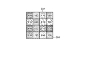
- FIG. 1 is an explanatory diagram showing a planar configuration example of an image sensor 130 according to a comparative example, which is used in a multispectral camera.
- the comparative example means the image sensor 130 that the present inventor repeatedly studied before making the embodiment of the present disclosure.
- 1 also shows a light receiving surface (pixel array portion) 300 of the image sensor 130 and an enlarged view of unit units 302a arranged in a matrix (along the row direction and the column direction) on the light receiving surface 300.
- each pixel 304 of the unit 302a indicates the median wavelength of the wavelength band of light detectable by each pixel 304, and each pixel 304 has substantially the same width. It is assumed that the light of each wavelength band can be detected.
- RGB cameras which can detect light with a wide range of wavelengths as the three RGB primary colors.
- RGB cameras it is difficult to capture subtle color differences that are invisible to the human eye, and there is a limit to accurately detecting and reproducing the colors of a subject.
- a high-resolution multispectral camera that can detect light by dividing it into a plurality of fine wavelengths.
- a multispectral camera may be, for example, a conventional R (red), G (green), B (blue) or Y (yellow), M (magenta) camera based on color primaries or color-matching functions. ) and C (cyan), which are five or more wavelength bands (five bands or more), which is more than the three wavelength bands (three bands) of C (cyan) (multispectrum).
- the example image sensor 130 shown in FIG. 1 is an image sensor for a multispectral camera capable of detecting light in 16 wavelength bands.
- the example shown in FIG. 1 is an image sensor 130 composed of 16 types of pixels 304 that detect light in different wavelength bands.
- each pixel 304 can only detect light in one wavelength band, so each pixel 304 can only obtain color information in one wavelength band. Therefore, a color image is generated by complementing the color information of one pixel 304 using pixel signals from other pixels 304 adjacent to the one pixel 304 and capable of detecting light in different wavelength bands. do. By doing so, it is possible to obtain a color image with high luminance and spectral spatial resolution. Such processing is called demosaic processing.
- the multispectral camera detects light in five or more wavelength bands. It has been found that due to the arrangement of the pixels 304, it may be difficult to obtain a color image with desired luminance and spectral spatial resolutions even with demosaicing.
- the light receiving surface (pixel array portion) 300 of the image sensor 130 according to the comparative example is configured by arranging a plurality of unit units 302a along the column direction and the row direction.
- the unit 302a is composed of 16 pixels 304 arranged in 4 rows and 4 columns as shown in FIG. 1, and the 16 pixels 304 detect light in different wavelength bands.
- the arrangement of the pixels 304 in the unit 302a is arranged in order of the wavelength of light to be detected. In such a case, it can be said that the pixels 304 that detect long-wavelength light in the unit 302a are biased toward the lower side in the figure. Due to such a bias, in other words, the pixels 304 of different types are not uniformly arranged in the entire unit 302a. Therefore, it is difficult to obtain a color image with the desired luminance and spectral spatial resolution.
- the present inventors focused on the planar arrangement of the pixels 304 of the image sensor 130 for a multispectral camera capable of detecting light in five or more wavelength bands, and the present inventors described below.
- the disclosed embodiments have been created.
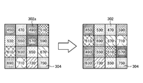
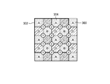
- FIG. 2 is an explanatory diagram for explaining the outline of the first embodiment of the present disclosure. More specifically, the unit 302a of the comparative example is shown on the left side of FIG. The unit 302 of this embodiment is shown on the right side. 2 indicates the median wavelength of the wavelength band of light detectable by each pixel 304. Each pixel 304 is It is assumed that light in each wavelength band having approximately the same width can be detected.
- the pixels 304 that detect long-wavelength light are biased toward the lower side of the drawing, as described above.
- the pixels 304 are not arranged in the order of the wavelengths of light to be detected. Different types of pixels 304 are arranged uniformly throughout the unit 302 without being separated from each other. By doing so, in the present embodiment, it is possible to interpolate with color information that does not have close wavelengths during demosaic processing, in other words, it is possible to interpolate with unbiased color information. and a color image with spectral spatial resolution.
- the unit units 302 are repeated on the light receiving surface (pixel array portion) 300 of the image sensor 130, the unit units 302 are regarded as one cycle, and the relative position of any point in the unit units 302 is the spatial phase.
- the mixed spectral characteristics obtained by mixing the spectral characteristics of the pixels 304 around the point are uniform (substantially the same). It can be said that the pixels 304 of different types are arranged as shown.
- the unit 302 is composed of 16 types of pixels 304 that detect light in 16 different wavelength bands in stages.
- the pixels 304 that detect light in wavelength bands that are not adjacent to each other are arranged so as to be adjacent in the row direction and the column direction, and detect light in wavelength bands that are adjacent to each other.
- the adjacent pixels 304 are arranged so as not to be adjacent to each other in the row direction and the column direction.
- the light of each wavelength is evenly detected by each region of the light receiving surface (pixel array portion) 300 of the image sensor 130. Therefore, the demosaicing process can be performed. In this case, it becomes possible to complement with color information that does not have a close wavelength. Therefore, in this embodiment, color information can be complemented with unbiased color information, so that a color image with high luminance and spectral spatial resolution can be obtained.
- the pixels 304 are not arranged in the order of the wavelengths of detectable light, so the influence of light from the adjacent pixels 304 is less likely to occur, thereby suppressing the occurrence of color mixture. be able to.
- FIG. 3 is a system diagram showing a schematic configuration of the image processing system 10 according to the first embodiment of the present disclosure.
- the image processing system 10 can mainly include, for example, a camera 100, an image processing device 500, and a server 600, which are interconnected via a network (not shown). communicatively connected. Specifically, the camera 100, the image processing device 500, and the server 600 are connected via, for example, a base station (not shown) (for example, a mobile phone base station, a wireless LAN (Local Area network) access point, etc.). Connected to the above network.
- the communication method used in the network can be any method regardless of whether it is wired or wireless (e.g., WiFi (registered trademark), Bluetooth (registered trademark), etc.), but stable operation must be maintained. It is desirable to use a communication method that allows An outline of each device included in the image processing system 10 according to the present embodiment will be described below.
- the camera 100 includes the image sensor 130 having the light-receiving surface (pixel array section) 300 as described above, captures an image of a subject, and can output the image obtained by the capture to the image processing device 500 .
- a detailed configuration of the camera 100 will be described later.
- the image processing apparatus 500 can perform various processes on the image acquired from the camera 100 described above, and can output the data obtained by the process to the server 600 described later.
- the image processing device 500 can be hardware such as a desktop PC (Personal Computer), a laptop PC, a tablet, a smart phone, or a mobile phone.
- some functions of the image processing device 500 may be performed by the camera 100 described above. Details of the image processing apparatus 500 will be described later.
- the server 600 can accumulate and analyze data obtained from the image processing apparatus 500, and distribute the analysis results.
- the server 600 can be configured by a computer or the like, for example.
- FIG. 3 shows the image processing system 10 according to the present embodiment as including one camera 100, an image processing device 500, and a server 600, the present embodiment is limited to this. not something.
- the image processing system 10 according to this embodiment may include multiple cameras 100 or may not include the server 600 .
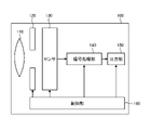
- FIG. 4 is an explanatory diagram showing an example of the functional configuration of the camera 100 according to the first embodiment of the present disclosure.
- the camera 100 mainly has an optical lens 110, a shutter mechanism 120, an image sensor 130, a signal processing section 140, an output section 150, and a control section 160. Each element included in the camera 100 will be sequentially described below.
- the optical lens 110 can form an image of image light (incident light) from a subject on a light receiving surface (pixel array section) 300 of the image sensor 130, which will be described later. As a result, an electric charge is generated in each pixel 304 of the image sensor 130 and taken out as a pixel signal.
- the shutter mechanism 120 can control the light irradiation period and the light shielding period of the image sensor 130 by opening and closing.
- the image sensor 130 can receive image light (incident light) from a subject, generate charges, and output pixel signals based on the generated charges to the signal processing unit 140 described later. A detailed configuration of the image sensor 130 will be described later.
- the signal processing unit 140 is composed of various electronic circuits, acquires a pixel signal from each pixel 304 of the image sensor 130, and performs various signal processing on the acquired pixel signal to generate image data. Furthermore, the signal processing unit 140 can output the generated image data to the output unit 150 . Note that the functional configuration of the signal processing unit 140 will be described later.
- the output unit 150 can output the image data obtained from the signal processing unit 140 described above to, for example, the image processing device 500, a storage medium such as a memory (not shown), a display device (not shown), or the like.
- control unit 160 can supply drive signals for controlling the transfer operation of pixel signals of the image sensor 130, the shutter operation of the shutter mechanism 120, and the like.
- the image sensor 130 performs signal transfer based on a drive signal (timing signal) supplied from the control section 160 .
- the configuration of the camera 100 is not limited to the configuration shown in FIG. 4, and may be integrated with the image processing device 500, for example.
- FIG. 5 is an explanatory diagram showing a planar configuration example of the image sensor 130 according to this embodiment.
- the image sensor 130 is a pixel array in which a plurality of pixels 304 are arranged in a matrix along the row and column directions on a semiconductor substrate 310 made of silicon, for example. It has a portion (light receiving surface) 300 and a peripheral circuit portion provided so as to surround the pixel array portion 300 . Further, the image sensor 130 includes a vertical drive circuit section 332, a column signal processing circuit section 334, a horizontal drive circuit section 336, an output circuit section 338, a control circuit section 340, etc. as the peripheral circuit section. Details of each block of the image sensor 130 are described below.
- the pixel array section (light receiving surface) 300 has a plurality of pixels 304 two-dimensionally arranged in a matrix along the row and column directions on a semiconductor substrate 310 .
- the pixel array section 300 is configured by arranging unit units (unit regions) 302 each including a plurality of different types of pixels 304 along the column and row directions.
- each pixel 304 has a size of about 2.9 ⁇ m ⁇ 2.9 ⁇ m. of pixels 304 are arranged. Details of the arrangement of the pixels 304 in this embodiment will be described later.
- Each pixel 304 is an element that performs photoelectric conversion on incident light, and includes a photoelectric conversion unit (not shown) and a plurality of pixel transistors (for example, MOS (Metal-Oxide-Semiconductor) transistors) (not shown). omitted).
- the pixel transistor includes four MOS transistors, for example, a transfer transistor, a selection transistor, a reset transistor, and an amplification transistor. Note that the equivalent circuit and detailed structure of the pixel 304 will be described later.
- the vertical drive circuit section 332 is formed of, for example, a shift register, selects a pixel drive wiring 342, supplies a pulse for driving the pixels 304 to the selected pixel drive wiring 342, and drives the pixels 304 row by row. . That is, the vertical drive circuit unit 332 sequentially selectively scans the pixels 304 of the pixel array unit 300 in units of rows in the vertical direction, and generates a signal according to the amount of light received by a photoelectric conversion unit (not shown) of each pixel 304. A pixel signal based on the charge is supplied to the column signal processing circuit section 334 to be described later through the vertical signal line 344 .
- the column signal processing circuit unit 334 is arranged for each column of the pixels 304 and performs signal processing such as noise removal on pixel signals output from the pixels 304 of one row for each column of the pixels 304 .
- the column signal processing circuit unit 334 performs signal processing such as CDS (Correlated Double Sampling) and AD (Analog-Digital) conversion to remove fixed pattern noise unique to the pixels 304 .
- the horizontal drive circuit section 336 is formed of, for example, a shift register, and sequentially outputs horizontal scanning pulses to sequentially select each of the column signal processing circuit sections 334 described above, and to output pixels from each of the column signal processing circuit sections 334 .
- a signal is output on the horizontal signal line 346 .
- the output circuit section 338 performs signal processing on pixel signals sequentially supplied from each of the column signal processing circuit sections 334 described above through the horizontal signal line 346 and outputs the processed signal.
- the output circuit section 338 may function, for example, as a functional section that performs buffering, or may perform processing such as black level adjustment, column variation correction, and various digital signal processing. Note that buffering refers to temporarily storing pixel signals in order to compensate for differences in processing speed and transfer speed when exchanging pixel signals.
- the input/output terminal 348 is a terminal for exchanging signals with an external device.
- Control circuit unit 340 receives an input clock and data instructing an operation mode and the like, and outputs data such as internal information of the image sensor 130 . That is, the control circuit unit 340 generates a clock signal and a clock signal that serve as a reference for the operation of the vertical drive circuit unit 332, the column signal processing circuit unit 334, the horizontal drive circuit unit 336, and the like based on the vertical synchronization signal, the horizontal synchronization signal, and the master clock. Generate control signals. The control circuit section 340 then outputs the generated clock signal and control signal to the vertical drive circuit section 332, the column signal processing circuit section 334, the horizontal drive circuit section 336, and the like.
- the configuration of the image sensor 130 is not limited to the configuration shown in FIG.
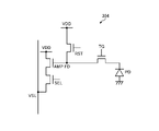
- FIG. 6 is an equivalent circuit diagram of the pixel 304 according to this embodiment.
- the pixel 304 includes a photodiode PD as a photoelectric conversion element (photoelectric conversion unit) that converts light into charge, a transfer transistor TG, a floating diffusion region FD, a reset transistor RST, an amplification transistor AMP, and a selection transistor AMP. It has a transistor SEL.
- one of the source/drain of the transfer transistor TG is electrically connected to a photodiode PD that receives light and generates charges, and the transfer transistor TG is electrically connected to the floating diffusion region FD.
- the transfer transistor TG becomes conductive in accordance with the voltage applied to its gate, and can transfer the charge generated in the photodiode PD to the floating diffusion region FD.
- the floating diffusion region FD is electrically connected to the gate of the amplification transistor AMP that converts charge into voltage and outputs it as a pixel signal.
- one of the source/drain of the amplification transistor AMP is electrically connected to one of the source/drain of the selection transistor for outputting the pixel signal obtained by the conversion to the signal line VSL according to the selection signal.
- the other of the source/drain of the amplification transistor AMP is electrically connected to the power supply circuit (power supply potential VDD).
- the other of the source/drain of the selection transistor SEL is electrically connected to the signal line VSL that transmits the converted voltage as a pixel signal, and is further electrically connected to the column signal processing circuit section 334 described above.
- the gate of the selection transistor SEL is electrically connected to a selection line (not shown) that selects a row for outputting a signal, and is further electrically connected to the vertical drive circuit section 332 described above. That is, the charge accumulated in the floating diffusion region FD is converted into a voltage by the amplification transistor AMP under the control of the selection transistor SEL, and is output to the signal line.
- the floating diffusion region FD is electrically connected to one of the drain/source of the reset transistor RST for resetting the accumulated charges.
- a gate of the reset transistor RST is electrically connected to a reset signal line (not shown) and further electrically connected to the above-described vertical driving circuit section 332 .
- the other drain/source of the reset transistor RST is electrically connected to a power supply circuit (power supply potential VDD).
- the reset transistor RST becomes conductive in accordance with the voltage applied to its gate, and can reset (discharge to the power supply circuit (power supply potential VDD)) the charge accumulated in the floating diffusion region FD.
- FIG. 7 is a cross-sectional view of the pixel 304 according to this embodiment, and for the sake of clarity, part of the cross-sectional configuration of the actual pixel 304 is omitted in FIG.
- the cross section of the pixel 304 is illustrated so that the light receiving surface on which light is incident on the pixel 304 faces upward.
- a semiconductor region 430 having a is provided.
- a photodiode PD that converts light into electric charge is formed in the semiconductor substrate 310 by the PN junction of the semiconductor region 430 .
- a wiring layer 400 including a wiring 440 formed of, for example, silicon oxide (SiO 2 ) and an interlayer insulating film 450 formed of silicon oxide (SiO 2 ) or the like is provided. Furthermore, the wiring layer 400 is provided with a plurality of electrodes (not shown) made of W, Al, Cu, etc., as gate electrodes of a plurality of pixel transistors for reading out charges generated in the photodiode PD.
- the electrode is provided so as to face a semiconductor region having a first conductivity type (for example, P-type) in the semiconductor substrate 310 via an insulating film (not shown). Furthermore, in the semiconductor substrate 310, a semiconductor region having a second conductivity type (for example, N type) is provided so as to be adjacent to the semiconductor region having the first conductivity type.
- the shaped semiconductor regions function as the source/drain regions of the pixel transistor.
- a floating diffusion portion (common charge storage portion) (not shown), which is a semiconductor region having a second conductivity type (for example, N type), is provided.
- the floating diffusion portion can temporarily store the charge generated by the photodiode PD.
- a filter 410 is provided for each pixel 304 on the incident surface of the semiconductor substrate 310 .
- the filter 410 is a narrow band filter that transmits light of wavelengths within a predetermined range (wavelength band). can be formed.
- the filter 410 may be a plasmon filter.
- an electromagnetic wave called surface plasmon which is a combination of light and electron compressional waves, is excited on the metal surface.
- Such excitation of surface plasmons can cause an anomalous transmission phenomenon of plasmons that transmit light having a specific wavelength in a metal having a periodic microstructure on its surface. Therefore, by utilizing such a phenomenon, it is possible to obtain a filter that transmits light of a specific wavelength, that is, a plasmon filter.
- an on-chip lens 420 is provided for each pixel 304 on the incident surface of the semiconductor substrate 310, as shown in FIG.
- the on-chip lens 420 can be made of, for example, Si 3 N 4 or a resin material such as styrene resin, acrylic resin, styrene-acrylic copolymer resin, or siloxane resin.
- cross-sectional structure of the pixel 304 according to the present embodiment is not limited to the example shown in FIG. 7, and may include, for example, an antireflection layer or the like, and is not particularly limited.
- FIG. 8 and 9 are explanatory diagrams showing an example of the planar configuration of the unit 302 of the pixel array section 300 of the image sensor 130 according to this embodiment.
- 8 indicates the median wavelength of the wavelength band of light detectable by each pixel 304.
- the character shown on each pixel 304 indicates the type of pixel 304 .
- each pixel 304 shall be capable of detecting light of each wavelength band having approximately the same width.
- FIG. 10 is an explanatory diagram for explaining an example of mixed spectral characteristics in this embodiment.
- the unit 302 is composed of 16 different types of pixels 304 arranged in 4 rows and 4 columns (m rows and n columns), for example, as shown in FIG. That is, each pixel 304 can detect light in different wavelength bands in stages.
- the types of pixels 304 included in the unit 302 are not limited to 16 types as shown in FIG. not something.
- the number of rows and columns (m rows and n columns) of the pixels 304 in the unit 302 is not limited to the example in FIG.
- the unit 302 since the unit 302 is repeated in the pixel array section 300, the unit 302 is regarded as one period, and the relative position of an arbitrary point in the unit 302 is expressed in spatial phase. can be expressed. Therefore, in the present embodiment, at each point having any spatial phase on the pixel array section 300, the mixed spectral characteristics obtained by mixing the spectral characteristics of the pixels 304 around the point are uniform (substantially the same). Different types of pixels 304 are arranged so that
- the pixels 304 that detect light in wavelength bands that are not adjacent to each other are arranged adjacent to each other in the row direction and the column direction, Furthermore, the pixels 304 that detect light in wavelength bands that are adjacent to each other are arranged so as not to be adjacent in the row direction and the column direction.
- the image sensor 130 According to the image sensor 130 according to the present embodiment having such unitary units 302, light of each wavelength is evenly detected by each region of the pixel array section 300 of the image sensor 130. Therefore, during demosaicing, It becomes possible to complement with color information that does not have a close wavelength. Therefore, in this embodiment, color information can be complemented with unbiased color information, so that a color image with high luminance and spectral spatial resolution can be obtained. In addition, in this embodiment, since the pixels 304 that detect light of similar wavelengths are not adjacent to each other, the influence of light from the adjacent pixels 304 is reduced, and the occurrence of color mixture can be suppressed.
- the arrangement of the pixels 304 is not limited to the example in FIG. Therefore, another example will be described with reference to FIG.
- a plurality of points are set that are separated from each other by a predetermined number of pixels 304 on the pixel array section 300 .
- the plurality of points (points indicated by Y in the drawing) are separated from each other by one pixel 304 .
- the plurality of points are not limited to being separated from each other by one pixel 304 , and are particularly limited as long as they are separated by a certain number of pixels 304 . not to be
- the unit 302 since the unit 302 is repeated in the pixel array section 300, the unit 302 is regarded as one cycle, and the relative position of an arbitrary point in the unit 302 is defined in space. It can be expressed in terms of phase. Therefore, it can be said that the respective Y points in FIG. 9 are out of phase with each other by 1/16 period.
- the mixed spectral characteristics obtained by mixing the spectral characteristics of a predetermined number of pixels 304 surrounding each Y point are uniform (substantially the same) at all the Y points.
- the pixels 304 are arranged so as to be uniform (substantially the same) at each point having any spatial phase on the pixel array section 300 .
- the mixed spectral characteristics obtained by mixing the spectral characteristics of the four pixels 304 surrounding each Y point are uniform (substantially the same) at all the Y points. , to arrange the pixels 304 .
- the mixed spectral characteristics are not limited to the mixture of the spectral characteristics of the four pixels 304 surrounding each Y point. There is no particular limitation as long as the spectral characteristics of a predetermined number of pixels 304 in positional relationship are mixed. Then, for example, the array of pixels 304 as described above can be searched as follows.
- an evaluation function eval using Root Mean Squared Error (RMSE), which is the square root of the average squared value of the difference (error) between the predicted value and the correct value, is used to determine the arrangement of the pixels 304. to explore. Specifically, each pixel 304 is applied to the unit 302 in a round-robin fashion, and an array that minimizes the evaluation function eval represented by the following formula (1) among all spatial phases is searched.
- RMSE Root Mean Squared Error
- color information can be complemented with unbiased color information, so that a color image with high luminance and spectral spatial resolution can be obtained.
- color information can be complemented with unbiased color information, making it possible to obtain a color image with high luminance and spectral spatial resolution.
- the pixels 304 that detect light of similar wavelengths are not adjacent to each other, the influence of light from the adjacent pixels 304 is reduced, and the occurrence of color mixture can be suppressed.
- FIG. 11 is a block diagram showing an example of the functional configuration of the signal processing section 140 according to the first embodiment of the present disclosure.
- the signal processing unit 140 mainly includes a preprocessing unit 142, a demosaicing processing unit 144, a noise reduction (NR) unit 146, and an output unit 148. Each functional unit of the signal processing unit 140 will be sequentially described below.
- the preprocessing unit 142 preprocesses pixel signals (raw data) from each pixel 304 of the pixel array unit 300 of the image sensor 130, and outputs the preprocessed pixel signals to the demosaic processing unit 144, which will be described later. can be done.
- the preprocessing unit 142 may perform OPB (Optical Black) subtraction to remove noise components caused by dark current generated in the pixels 304 . Further, for example, the preprocessing unit 142 may perform defect position detection to detect the position of the pixel 304 that outputs the abnormal value pixel signal, or may perform defect correction to correct the abnormal value pixel signal. good. Furthermore, for example, the preprocessing unit 142 may perform HDR (High Dynamic Range) synthesis that synthesizes a plurality of pixel signals to expand the dynamic range of luminance, or the preprocessing unit 142 may perform a predetermined noise You may perform the noise suppression process which suppresses . In addition, in the present embodiment, the processing performed by the preprocessing unit 142 is not limited to the processing described above.
- the demosaicing unit 144 can perform the demosaic processing as described above. Specifically, the demosaicing unit 144 demosaicizes the color information of one pixel 304 by using pixel signals from other pixels 304 adjacent to the one pixel 304 and capable of detecting light in different wavelength bands. Complementary processing can be performed. In the present embodiment, as described above, light of each wavelength is equally detected by each region of the pixel array section 300 of the image sensor 130. Therefore, it is possible to supplement with color information that does not have a similar wavelength. becomes possible. Therefore, in this embodiment, it is possible to obtain a color image with high resolution because it can be complemented with unbiased color information. Furthermore, the demosaicing unit 144 can output the processed image data to the NR unit, which will be described later.
- the demosaicing unit 144 sets a plurality of points (Y points) separated from each other by one pixel 304 on the pixel array unit 300 as shown in FIG.
- the demosaicing unit 144 then mixes the pixel signals of the four pixels 304 surrounding each Y point.
- the pixel signals obtained by mixing contain luminance information of light with a wide range of wavelengths linked to the positional information of each Y point. Based on such pixel signals, a color image with high color resolution can be obtained. can be done.
- the present embodiment is not limited to mixing pixel signals from four pixels 304 surrounding each Y point as shown in FIG. There is no particular limitation as long as pixel signals of a predetermined number of related pixels 304 are mixed.
- the demosaic processing unit 144 when the mixed spectral characteristics of each Y point are different, the demosaic processing unit 144 generates pixel signals from a predetermined number of pixels 304 surrounding each Y point based on the difference. You may adjust the mixing ratio of Furthermore, in the present embodiment, if the mixed spectral characteristics of the Y points are different, the demosaicing unit 144 changes the number and positions of the pixels 304 based on the difference, and from these pixels 304 of pixel signals may be mixed.
- the demosaic processing unit 144 may perform spatial filtering (low-pass filter, high-pass filter, band-pass filter) to correct the difference in signal level at each Y point. For example, the demosaic processing unit 144 may adjust the filtering characteristics/strength according to the spatial frequency characteristics (edges, etc.) of the image. Filtering characteristics/strength may be adjusted.
- the demosaic processing unit 144 may adjust the gain of the mixed pixel signal at each Y point based on the difference in signal level at each Y point. For example, the demosaic processing unit 144 may adjust the gain according to the light source that irradiates the subject with light or the spectral characteristics of the subject.
- the NR unit 146 can perform processing for removing noise from the image data from the demosaicing unit 144 and output it to the output unit 148 described later. Also, the NR unit 146 may perform correction such as shading correction and false color correction on the image data from the demosaicing unit 144 . In addition, in the present embodiment, the processing performed by the NR unit 146 is not limited to the processing described above.
- the output unit 148 can output image data obtained through various processes to an external device such as the image processing device 500 .
- the configuration of the signal processing section 140 is not limited to the configuration shown in FIG.
- FIG. 12 is a block diagram showing an example of the functional configuration of the image processing apparatus 500 according to this embodiment.
- the image processing apparatus 500 mainly includes an image recognition section/data analysis section 510 , a stitching processing section 520 , a fusion processing section 530 and an output section 540 .
- Each functional unit of the image processing apparatus 500 will be described below.
- the image recognition unit/data analysis unit 510 can perform image recognition processing and analysis processing on image data obtained from the camera 100 using various techniques. In this embodiment, image recognition processing and analysis processing can be performed using high-resolution image data, so that highly accurate recognition and analysis can be performed.
- the stitching processing unit 520 can perform stitching processing for stitching together a plurality of images having a positional relationship adjacent to each other to generate image data of a wider area. In this embodiment, it is possible to accurately recognize the position based on the high-resolution luminance image, and the stitching process is performed using the recognition result. It can be performed.
- the fusion processing unit 530 can acquire image data from the camera 100 and image data from another sensor and perform fusion processing.
- the fusion processing unit 530 can perform fusion processing for superimposing image data from an RGB camera as another sensor and image data from the camera 100 .
- the image data from the RGB camera and the image data from the camera 100 can be aligned with high accuracy.
- the output unit 540 can output images and data obtained through various processes to an external device such as the server 600 .
- the image processing apparatus 500 is not limited to performing the above-described processing. Noise reduction (noise removal) can be performed. Furthermore, the image processing apparatus 500 can perform motion vector search with high precision using a high-resolution luminance image, and can also perform noise reduction in the time direction with high precision.
- image recognition processing, analysis processing, stitching processing, fusion processing, etc. can be performed using color images with high resolution, so the accuracy of each processing is improved. can be made
- the configuration of the image processing device 500 is not limited to the configuration shown in FIG. 530 may be configured to cooperate with each other.
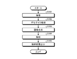
- FIG. 13 is a flowchart illustrating an example of image processing according to the first embodiment of the present disclosure. As shown in FIG. 13, the image processing according to this embodiment includes a plurality of steps from step S101 to step S105. Details of each step included in the image processing according to the present embodiment will be described below.
- the subject is imaged by the camera 100 (step S101).
- the camera 100 performs demosaic processing using pixel signals (Raw data) from the pixels 304 of the image sensor 130 (step S102). Further, the camera 100 generates image data based on the demosaic-processed pixel signals, and outputs the image data to the image processing device 500 (step S103).
- the image processing device 500 performs analysis using the high-resolution image from the camera 100 (step S104).
- the image processing apparatus 500 then outputs the analysis result obtained in step S104 to the server 600 (step S105).
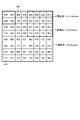
- FIG. 14 is an explanatory diagram showing an example of the planar configuration of the unit 302 of the pixel array section 300 of the image sensor 130 according to this embodiment. 14 indicates the median wavelength of the wavelength band of light detectable by each pixel 304. In FIG. Furthermore, in FIG. 14, each pixel 304 shall be capable of detecting light in each wavelength band having approximately the same width.
- the pixels 304 to be used can be selected according to the subject, imaging conditions (state of illumination light, etc.), and the resolution required depending on the application.
- the unit 302 is composed of 64 types of pixels 304 of 48 rows and 8 columns (m rows and n columns), for example, as shown in FIG. That is, each pixel 304 can detect light in different wavelength bands in stages.
- the types of pixels 304 included in the unit 302 are not limited to 64 types as shown in FIG. not something.
- the number of rows and columns (m rows and n columns) of the pixels 304 in the unit 302 is not limited to the example in FIG.
- the unit units 302 are repeated in the pixel array section 300, the unit units 302 are taken as one cycle, and the relative positions of arbitrary points in the unit units 302 are can be expressed in spatial phase. Therefore, also in this embodiment, at each point having any spatial phase on the pixel array section 300, the mixed spectral characteristics obtained by mixing the spectral characteristics of the pixels 304 around the point are uniform (substantially the same). Different types of pixels 304 are arranged so that
- the range of pixels 304 to be used in the pixel array section 300 is selected according to the spatial resolution and wavelength resolution required for each application.
- the spatial resolution is 1/4, and light in four wavelength bands can be detected.
- the 16 pixels 304 at the upper right end of FIG. 14 are selected, the spatial resolution is 1/16, and light in 16 wavelength bands can be detected.
- the spatial resolution is 1/64, and light in 64 wavelength bands can be detected. Note that, in the present embodiment, the mixing ratio and the like described above may be adjusted for each application.
- the mixed spectral characteristics obtained by mixing the spectral characteristics of the pixels 304 around the point are uniform ( Different types of pixels 304 are arranged so as to be substantially identical). Therefore, according to this embodiment, by selecting the range of pixels 304 to be used from such an array of pixels 304, suitable spatial resolution and wavelength resolution can be obtained according to the application.
- the image sensor 130 according to the embodiment of the present disclosure can be manufactured by using the method, apparatus, and conditions used for manufacturing general semiconductor devices. That is, the image sensor 130 according to the present embodiment can be manufactured using the existing manufacturing process of semiconductor devices.
- PVD Physical Vapor Deposition
- CVD Chemical Vapor Deposition
- ALD Atomic Layer Deposition
- PVD methods include vacuum deposition, EB (electron beam) deposition, various sputtering methods (magnetron sputtering, RF (Radio Frequency)-DC (Direct Current) combined bias sputtering, and ECR (Electron Cyclotron Resonance) sputtering.
- CVD methods include plasma CVD, thermal CVD, metal-organic (MO) CVD, and optical CVD.
- other methods include electrolytic plating method, electroless plating method, spin coating method; immersion method; casting method; microcontact printing method; drop casting method; screen printing method, inkjet printing method, offset printing method, gravure printing.
- Various printing methods such as printing method, flexographic printing method; stamp method; spray method; air doctor coater method, blade coater method, rod coater method, knife coater method, squeeze coater method, reverse roll coater method, transfer roll coater method, gravure coater method , kiss coater method, cast coater method, spray coater method, slit orifice coater method and calendar coater method.
- patterning methods include shadow masking, laser transfer, chemical etching such as photolithography, and physical etching using ultraviolet rays, lasers, and the like.
- planarization techniques include a CMP (Chemical Mechanical Polishing) method, a laser planarization method, a reflow method, and the like.
- Such NDVI calculation processing requires highly accurate analysis of the color components contained in the plant, which is the subject. Therefore, by applying the technology of the present disclosure, an image with high resolution can be obtained, so highly accurate NDVI calculation is possible, and the activity level of plants in the captured image can be accurately estimated.
- the technology of the present disclosure can be applied to quality inspections of industrial products (eg, food products, precision instruments), medical inspections, and the like. Furthermore, since the technology of the present disclosure can accurately detect the skin color of the user's face, it is possible to propose, for example, cosmetics and makeup methods, color coordination of clothes, etc., according to the detection result of the skin color. can provide services to do. Furthermore, the technology of the present disclosure can analyze the skin color detection results, recognize the user's physiological and psychological conditions, and make suggestions for treatment and health promotion, as well as products and services.
- industrial products eg, food products, precision instruments
- the technology of the present disclosure can accurately detect the skin color of the user's face, it is possible to propose, for example, cosmetics and makeup methods, color coordination of clothes, etc., according to the detection result of the skin color. can provide services to do. Furthermore, the technology of the present disclosure can analyze the skin color detection results, recognize the user's physiological and psychological conditions, and make suggestions for treatment and health promotion, as well as products and services.
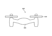
- FIG. 15 is a schematic diagram of the appearance of the unmanned flying object 920, and more specifically, a schematic diagram of the unmanned flying object 920 viewed from the front 960 thereof.
- FIG. 16 is a block diagram showing an example of a schematic functional configuration of the unmanned flying object 920. As shown in FIG.
- the unmanned flying object 920 is an unmanned small airplane, and can fly with an autonomous flight function, an independent attitude control function, and the like.
- the unmanned flying object 920 mainly has a propeller 930 , a propeller drive section 932 , a flight control section 934 , a positioning unit 940 and a flight control communication section 950 .
- Each functional unit of the unmanned air vehicle 920 will be described below.
- a plurality of propellers 930 are provided above unmanned flying object 920 , and are rotated by power transmitted from a propeller drive unit 932 provided inside unmanned flying object 920 . , and maintains the attitude of the unmanned flying object 920 horizontally.
- a propeller driving section 932 is provided inside the unmanned flying object 920 and rotates each propeller 930 according to control from a flight control section 934, which will be described later.
- the positioning unit 940 is provided inside the unmanned flying object 920, and obtains two-dimensional position information (longitude information, latitude information) and altitude information, which are positional information of the unmanned flying object 920, and attitude information and acceleration information of the unmanned flying object 920. and output to the flight control unit 934, which will be described later.
- the output position information, attitude information, and the like are used to fly the unmanned flying object 920 to a desired location and to maintain the unmanned flying object 920 in a horizontal attitude.
- the positioning unit 940 mainly has an attitude detection section 942, a GPS (Global Positioning System) unit 944, and an altimeter 946, as shown in FIG.
- the attitude detection unit 942 includes, for example, a gyro sensor or the like that is a combination of an acceleration sensor and an angular velocity sensor, and detects the attitude (inclination, orientation, etc.) and acceleration of the unmanned flying object 920 .
- the GPS unit 944 is composed of a current position measurement device that performs measurement using GPS signals from GPS satellites, and can obtain two-dimensional position information (latitude information and longitude information) of the unmanned flying object 920 on the ground surface.
- the altimeter 946 can acquire altitude information (height above the ground) of the unmanned air vehicle 920 .
- the positioning unit 940 may not include the altimeter 946 if the GPS unit 944 can acquire altitude information with sufficient accuracy. However, the altitude information obtained by the GPS unit 944 may have low accuracy depending on the positioning state. . Therefore, the positioning unit 940 preferably includes an altimeter 946 to obtain altitude information with sufficient accuracy.
- the flight control unit 934 When the flight control unit 934 receives a control signal from a control device (not shown) owned by the pilot, the flight control unit 934 utilizes the position information and the attitude information acquired by the positioning unit 940 described above, and generates the control signal. It controls the propeller driver 932 according to the flight instructions.
- the flight control communication unit 950 wirelessly communicates with a control device (not shown) owned by the operator, and transmits and receives control signals and the like used for flight of the unmanned flying object 920 .
- the flight control communication unit 950 receives a control signal from the control device at predetermined time intervals, and outputs the received control signal to the flight control unit 934 described above.
- the camera 100 mounted on the unmanned flying object 920 captures an image of the grain field from the sky, and analyzes the color of the image of the grain field at high resolution. This makes it possible to recognize the growing condition of the grain.
- the technology according to the present disclosure (this technology) can be applied to various electronic devices such as smartphones and industrial cameras installed in production lines.
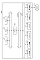
- FIG. 17 is a block diagram showing an example of hardware configuration.
- the image processing apparatus 500 will be described below as an example, the server 600 can also be described in the same manner.
- the image processing apparatus 500 can be configured with hardware 900 described below, and various processes by the image processing apparatus 500 are realized by cooperation between software and the hardware 900 .
- the hardware 900 has a CPU (Central Processing Unit) 901, a ROM (Read Only Memory) 902, a RAM (Random Access Memory) 903, and a host bus 904a.
- the hardware 900 also has a bridge 904 , an external bus 904 b , an interface 905 , an input device 906 , an output device 907 , a storage 908 , a drive 909 , a connection port 911 and a communication device 913 .
- the hardware 900 may have a processing circuit such as a DSP (Digital Signal Processor) or an ASIC (Application Specific Integrated Circuit) instead of or in addition to the CPU 901 .
- DSP Digital Signal Processor
- ASIC Application Specific Integrated Circuit
- the CPU 901 functions as an arithmetic processing device and a control device, and controls overall operations within the hardware 900 according to various programs.
- the CPU 901 may be a microprocessor.
- the ROM 902 stores programs, calculation parameters, and the like used by the CPU 901 .
- the RAM 903 temporarily stores programs used in the execution of the CPU 901, parameters that change as appropriate during the execution, and the like.
- the CPU 901 can embody the stitching processing unit 520 of the image processing apparatus 500, for example.
- the CPU 901, ROM 902 and RAM 903 are interconnected by a host bus 904a including a CPU bus and the like.
- the host bus 904a is connected via a bridge 904 to an external bus 904b such as a PCI (Peripheral Component Interconnect/Interface) bus.
- PCI Peripheral Component Interconnect/Interface
- host bus 904a, bridge 904 and external bus 904b need not necessarily have separate configurations from each other and may be implemented in a single configuration (eg, one bus).
- the input device 906 is implemented by a device such as a mouse, keyboard, touch panel, button, microphone, switch, lever, etc., through which information is input by the practitioner.
- the input device 906 may be, for example, a remote control device using infrared rays or other radio waves, or may be an external connection device such as a mobile phone or PDA (Personal Digital Assistant) compatible with the operation of the hardware 900. There may be.
- the input device 906 may include, for example, an input control circuit that generates an input signal based on information input by the practitioner using the above input means and outputs the signal to the CPU 901 . By operating the input device 906, the practitioner can input various data to the hardware 900 and instruct processing operations.
- the output device 907 is formed by a device capable of visually or audibly notifying the practitioner of the acquired information.
- Such devices include display devices such as CRT (Cathode Ray Tube) display devices, liquid crystal display devices, plasma display devices, EL (Electro Luminescent) display devices and lamps, sound output devices such as speakers and headphones, and printer devices. etc.
- the storage 908 is a device for storing data.
- the storage 908 is implemented by, for example, a magnetic storage device such as a HDD (Hard Disk Drive), a semiconductor storage device, an optical storage device, a magneto-optical storage device, or the like.
- the storage 908 may include a storage medium, a recording device that records data on the storage medium, a reading device that reads data from the storage medium, a deletion device that deletes data recorded on the storage medium, and the like.
- the storage 908 stores programs to be executed by the CPU 901, various data, various data acquired from the outside, and the like.
- the drive 909 is a reader/writer for storage media, and is either built into the hardware 900 or externally attached.
- the drive 909 reads out information recorded on a mounted magnetic disk, optical disk, magneto-optical disk, or removable storage medium such as a semiconductor memory, and outputs the information to the RAM 903 .
- Drive 909 can also write information to a removable storage medium.
- connection port 911 is an interface connected to an external device, and is a connection port with an external device capable of data transmission by, for example, USB (Universal Serial Bus).
- USB Universal Serial Bus
- the communication device 913 is, for example, a communication interface formed by a communication device or the like for connecting to the network 915 .
- the communication device 913 is, for example, a communication card for wired or wireless LAN (Local Area Network), LTE (Long Term Evolution), Bluetooth (registered trademark), or WUSB (Wireless USB).
- the communication device 913 may be a router for optical communication, a router for ADSL (Asymmetric Digital Subscriber Line), a modem for various types of communication, or the like.
- the communication device 913 can transmit and receive signals to and from the Internet and other communication devices in accordance with a predetermined protocol such as TCP/IP (Transmission Control Protocol/Internet Protocol).
- TCP/IP Transmission Control Protocol/Internet Protocol
- the network 915 is a wired or wireless transmission path for information transmitted from devices connected to the network 915 .
- the network 915 may include a public line network such as the Internet, a telephone line network, a satellite communication network, various LANs (Local Area Networks) including Ethernet (registered trademark), WANs (Wide Area Networks), and the like.
- the network 915 may also include a dedicated line network such as IP-VPN (Internet Protocol-Virtual Private Network).
- a hardware configuration example capable of realizing the functions of the image processing apparatus 500 has been shown above.
- Each component described above may be implemented using general-purpose members, or may be implemented by hardware specialized for the function of each component. Therefore, it is possible to appropriately change the hardware configuration to be used according to the technical level at which the present disclosure is implemented.
- the above-described embodiments of the present disclosure use the image processing method executed by the camera 100 (more specifically, the signal processing unit 140), the image processing device 500, or the server 600 as described above. It may include a program to execute and a non-transitory tangible medium on which the program is recorded. Also, the program may be distributed via a communication line (including wireless communication) such as the Internet.
- each step in the image processing method according to the embodiment of the present disclosure described above does not necessarily have to be processed in the described order.
- each step may be processed in an appropriately changed order.
- each step may be partially processed in parallel or individually instead of being processed in chronological order.
- the processing of each step does not necessarily have to be processed in accordance with the described method, and may be processed by another method by another functional unit, for example.
- each component of each device illustrated is functionally conceptual and does not necessarily need to be physically configured as illustrated.
- the specific form of distribution and integration of each device is not limited to the one shown in the figure, and all or part of them can be functionally or physically distributed and integrated in arbitrary units according to various loads and usage conditions. Can be integrated and configured.
- a pixel array unit configured by arranging a plurality of pixels of five or more types with different detectable wavelength bands of light in stages along the row direction and the column direction, At each point having any spatial phase on the pixel array section, the plurality of pixels are arranged, Imaging device.
- the pixels that detect light in wavelength bands that are not adjacent to each other are arranged so as to be adjacent in the row direction and the column direction, The imaging device according to (1) or (2) above.
- the pixels that detect light in wavelength bands that are adjacent to each other are arranged so as not to be adjacent in the row direction and the column direction.
- the imaging device according to any one of (1) to (3) above.
- the imaging device according to (1) or (2) above, wherein in the pixel array section, the plurality of pixels are arranged such that an evaluation function represented by the following formula (1) is minimized.
- (6) (1) to (5) above, wherein the pixel array section is formed by arranging the unit regions each composed of the plurality of pixels arranged in m rows and n columns along the row direction and the column direction.
- each of the points is separated from each other by one pixel on the pixel array section;
- the mixed spectral characteristics are obtained by mixing the spectral characteristics of the four pixels surrounding each point.
- (8) further comprising a signal processing unit that acquires a pixel signal from each of the plurality of pixels and generates image data based on the acquired pixel signal;
- the signal processing unit mixes the pixel signals obtained from each of the predetermined number of pixels surrounding each point, and generates the image data from the mixed pixel signals.
- the signal processing unit adjusts the mixing ratio of the pixel signals obtained from each of the predetermined number of pixels surrounding each point, based on the difference in the mixed spectral characteristics of each point.
- the imaging device (13) above, wherein the signal processing unit adjusts the gain according to a light source that irradiates a subject with light or a spectral characteristic of the subject.
- the signal processing unit selects the plurality of pixels to be used when generating the image data based on a subject, imaging conditions, or desired resolution.
- the image capturing apparatus according to any one of (8) to (15) above, further comprising a stitching processing unit that acquires a plurality of the image data and performs processing to join them together.
- a fusion processing unit that acquires the image data and image data from another sensor and performs fusion processing.
- the imaging apparatus according to any one of (8) to (17) above, further comprising an image recognition unit that acquires the image data and performs image recognition.
- the imaging apparatus according to any one of (8) to (18) above, further comprising an analysis unit that acquires and analyzes the image data.
- An electronic device equipped with an imaging device The imaging device is A pixel array unit configured by arranging a plurality of pixels of five or more types with different detectable wavelength bands of light in stages along the row direction and the column direction, At each point having any spatial phase on the pixel array section, the plurality of pixels are arranged, Electronics.
- REFERENCE SIGNS LIST 10 image processing system 100 camera 110 optical lens 120 shutter mechanism 130 image sensor 140 signal processing unit 142 preprocessing unit 144 demosaicing processing unit 146 NR unit 148, 150, 540 output unit 160 control unit 300 light receiving surface (pixel array unit) 302, 302a unit unit 304 pixel 310 semiconductor substrate 332 vertical drive circuit 334 column signal processing circuit 336 horizontal drive circuit 338 output circuit 340 control circuit 342 pixel drive wiring 344 vertical signal line 346 horizontal signal line 348 input/output terminal 400 wiring layer 410 filter 420 on-chip lens 430 semiconductor region 440 wiring 450 interlayer insulating film 500 image processing device 510 image recognition unit/data analysis unit 520 stitching processing unit 530 fusion processing unit 600 server 900 hardware 901 CPU 902 ROMs 903 RAM 904 bridge 904a host bus 904b external bus 905 interface 906 input device 907 output device 908 storage 909 drive 911 connection port 913 communication device 915 network 920 unmanned flying object 930 propeller 932 propeller drive section
Landscapes
- Engineering & Computer Science (AREA)
- Multimedia (AREA)
- Signal Processing (AREA)
- Color Television Image Signal Generators (AREA)
- Solid State Image Pick-Up Elements (AREA)
- Spectrometry And Color Measurement (AREA)
Abstract
Description
1. 本開示の実施形態を創作するに至る背景
2. 第1の実施形態
2.1 システム構成の概略
2.2 カメラの詳細構成
2.3 イメージセンサの詳細構成
2.4 画素の等価回路
2.5 画素の断面構成
2.6 画素の配列
2.7 信号処理部の構成
2.8 画像処理装置の構成
2.9 画像処理
3. 第2の実施形態
4. まとめ
5. 応用例
5.1 用途
5.2 無人飛行体への応用例
6. ハードウェア構成の例
7. 補足
まずは、本開示の実施形態を説明する前に、図1を参照して、本発明者が本開示の実施形態を創作するに至る背景について説明する。図1は、マルチスペクトルカメラに用いられる、比較例に係るイメージセンサ130の平面構成例を示す説明図である。なお、ここで、比較例とは、本発明者が本開示の実施形態をなす前に検討を重ねていたイメージセンサ130のことを意味するものとする。また、図1においては、イメージセンサ130の受光面(画素アレイ部)300と、受光面300上にマトリックス状(行方向及び列方向に沿って)に配列する単位ユニット302aの拡大図とが示されている。さらに、単位ユニット302aの各画素304上に示される数字は、各画素304で検出可能な光の波長帯域の中央値の波長が示されているものとし、各画素304は、略同一の幅を持つ各波長帯域の光を検出することができるものとする。
<2.1 システム構成の概略>
まずは、本開示の第1の実施形態に係る画像処理システム10の構成の一例について、図3を参照して説明する。図3は、本開示の第1の実施形態に係る画像処理システム10の概略的な構成を示したシステム図である。
カメラ100は、上述したような受光面(画素アレイ部)300を持つイメージセンサ130を含み、被写体を撮像し、撮像によって得られた画像を画像処理装置500へ出力することができる。なお、カメラ100の詳細構成については後述する。
画像処理装置500は、上述したカメラ100から取得した画像に対して、様々な処理を行うことができ、処理により得られたデータを後述するサーバ600に出力することができる。例えば、画像処理装置500は、デスクトップ型PC(Personal Computer)、ラップトップ型PC、タブレット、スマートフォン、携帯電話等のハードウェアであることができる。さらに、画像処理装置500の一部の機能は、上述したカメラ100で実行されてもよい。なお、画像処理装置500の詳細については後述する。
サーバ600は、画像処理装置500から得られたデータを、集積したり、解析したり、解析した結果等を配信したりすることができる。サーバ600は、例えば、コンピュータ等により構成することができる。
次に、図4を参照して、カメラ100の構成の一例について説明する。図4は、本開示の第1の実施形態に係るカメラ100の機能構成の一例を示す説明図である。
光学レンズ110は、被写体からの像光(入射光)を後述するイメージセンサ130の受光面(画素アレイ部)300上に結像させることができる。これにより、イメージセンサ130の各画素304で、電荷が発生し、画素信号として取り出されることとなる。
シャッタ機構120は、開閉することにより、イメージセンサ130への光照射期間及び遮光期間を制御することができる。
イメージセンサ130は、被写体からの像光(入射光)を受光して、電荷を生成し、生成した電荷に基づく画素信号を、後述する信号処理部140へ出力することができる。なお、イメージセンサ130の詳細構成については後述する。
信号処理部140は、各種の電子回路から構成され、イメージセンサ130の各画素304からの画素信号を取得し、取得した画素信号に各種の信号処理を行って画像データを生成することができる。さらに、信号処理部140は、生成した画像データを出力部150へ出力することができる。なお、信号処理部140の機能構成については後述する。
出力部150は、上述した信号処理部140から得られた画像データを、例えば、画像処理装置500、メモリ等の記憶媒体(図示省略)、表示装置(図示省略)等に出力することができる。
制御部160は、イメージセンサ130の画素信号の転送動作やシャッタ機構120のシャッタ動作等を制御する駆動信号をこれらに供給することができる。例えば、イメージセンサ130は、制御部160から供給される駆動信号(タイミング信号)に基づいて信号転送を行うこととなる。
次に、図5を参照して、本実施形態に係るイメージセンサ130の概略構成について説明する。図5は、本実施形態に係るイメージセンサ130の平面構成例を示す説明図である。
画素アレイ部(受光面)300は、半導体基板310上に、行方向及び列方向に沿ってマトリックス状に、2次元配置された複数の画素304を有する。具体的には、先に説明したように、画素アレイ部300は、異なる種類の複数の画素304を含む単位ユニット(単位領域)302が列方向及び行方向に沿って配列することにより構成される。例えば、各画素304は、2.9μm×2.9μm程度のサイズを有し、例えば、画素アレイ部300においては、列方向に沿って1945個の画素304が並び、行方向に沿って1109個の画素304が並んでいる。なお、本実施形態における画素304の配列の詳細については、後述する。
垂直駆動回路部332は、例えばシフトレジスタによって形成され、画素駆動配線342を選択し、選択された画素駆動配線342に画素304を駆動するためのパルスを供給し、行単位で画素304を駆動する。すなわち、垂直駆動回路部332は、画素アレイ部300の各画素304を行単位で順次垂直方向に選択走査し、各画素304の光電変換部(図示省略)の受光量に応じて生成された信号電荷に基づく画素信号を、垂直信号線344を通して後述するカラム信号処理回路部334に供給する。
カラム信号処理回路部334は、画素304の列ごとに配置されており、1行分の画素304から出力される画素信号に対して画素304の列ごとにノイズ除去等の信号処理を行う。例えば、カラム信号処理回路部334は、画素304の固有の固定パターンノイズを除去するためにCDS(Correlated Double Sampling:相関2重サンプリング)およびAD(Analog-Degital)変換等の信号処理を行う。
水平駆動回路部336は、例えばシフトレジスタによって形成され、水平走査パルスを順次出力することによって、上述したカラム信号処理回路部334の各々を順番に選択し、カラム信号処理回路部334の各々から画素信号を水平信号線346に出力させる。
出力回路部338は、上述したカラム信号処理回路部334の各々から水平信号線346を通して順次に供給される画素信号に対し、信号処理を行って出力する。出力回路部338は、例えば、バッファリング(buffering)を行う機能部として機能してもよく、もしくは、黒レベル調整、列ばらつき補正、各種デジタル信号処理等の処理を行ってもよい。なお、バッファリングとは、画素信号のやり取りの際に、処理速度や転送速度の差を補うために、一時的に画素信号を保存することをいう。さらに、入出力端子348は、外部装置との間で信号のやり取りを行うための端子である。
制御回路部340は、入力クロックと、動作モード等を指令するデータを受け取り、イメージセンサ130の内部情報等のデータを出力する。すなわち、制御回路部340は、垂直同期信号、水平同期信号及びマスタクロックに基づいて、垂直駆動回路部332、カラム信号処理回路部334及び水平駆動回路部336等の動作の基準となるクロック信号や制御信号を生成する。そして、制御回路部340は、生成したクロック信号や制御信号を、垂直駆動回路部332、カラム信号処理回路部334及び水平駆動回路部336等に出力する。
次に、図6を参照して、本実施形態に係る画素304の等価回路の一例を説明する。図6は、本実施形態に係る画素304の等価回路図である。
次に、図7を参照して、本実施形態に係る画素304の積層構造について説明する。図7は、本実施形態に係る画素304の断面図であって、わかりやすくするために、図7においては、実際の画素304の断面構成の一部の図示を省略している。また、図7においては、画素304に対して光が入射する受光面が上となるように画素304の断面が図示されている。
次に、図8から図10を参照して、本実施形態における画素304の配列について説明する。図8及び図9は、本実施形態に係るイメージセンサ130の画素アレイ部300の単位ユニット302の平面構成の一例を示す説明図である。なお、図8の単位ユニット302の各画素304上に示される数字は、各画素304で検出可能な光の波長帯域の中央値の波長が示されているものとし、図9の単位ユニット302の各画素304上に示される文字は、画素304の種類を示すものとする。さらに、図8及び図9においては、各画素304は、略同一の幅を持つ各波長帯域の光を検出することができるものとする。また、図10は、本実施形態における混合分光特性の一例を説明する説明図である。

次に、図11を参照して、信号処理部140の詳細構成を説明する。図11は、本開示の第1の実施形態に係る信号処理部140の機能構成の一例を示すブロック図である。
前処理部142は、イメージセンサ130の画素アレイ部300の各画素304からの画素信号(Rawデータ)に対して前処理を行い、後述するデモザイク処理部144へ前処理した画素信号を出力することができる。
デモザイク処理部144は、先に説明したようなデモザイク処理を行うことができる。詳細には、デモザイク処理部144は、一の画素304に隣接する、異なる波長帯域の光を検出することができる他の複数の画素304からの画素信号を用いて、一の画素304の色情報を補完する処理を行うことができる。本実施形態においては、先に説明したように、各波長の光が均等にイメージセンサ130の画素アレイ部300の各領域によって検出されることから、近い波長を持たない色の情報で補完することが可能となる。従って、本実施形態においては、偏りのない色情報で補完できるため、高い解像度を持つカラー画像を得ることが可能となる。さらに、デモザイク処理部144は、処理した画像データを後述するNR部へ出力することができる。
NR部146は、デモザイク処理部144からの画像データに対して、ノイズを除去する処理を行い、後述する出力部148へ出力することができる。また、NR部146は、デモザイク処理部144からの画像データに対して、シェーディング補正や偽色補正等の補正を行ってもよい。なお、本実施形態においては、NR部146で行われる処理は、上述のような処理に限定されるものではない。
出力部148は、各種の処理を経て得られた画像データを、画像処理装置500等の外部装置へ出力することができる。
次に、図12を参照して、本実施形態に係る画像処理装置500の詳細構成を説明する。図12は、本実施形態に係る画像処理装置500の機能構成の一例を示すブロック図である。図12に示すように、画像処理装置500は、画像認識部/データ解析部510と、スティッチング処理部520と、フュージョン処理部530と、出力部540とを主に有する。以下に、画像処理装置500の各機能部について順次説明する。
画像認識部/データ解析部510は、様々な手法を用いて、カメラ100から得られた画像データに対して画像認識処理及び解析処理を行うことができる。本実施形態においては、高解像度の画像データを用いて、画像認識処理及び解析処理を行うことができることから、精度の高い認識及び解析を行うことができる。
スティッチング処理部520は、隣り合う位置関係にある複数の画像を互いにつなぎ合わせるスティッチング処理を行い、より広い領域の画像データを生成することができる。本実施形態においては、高解像度の輝度画像に基づいて位置を精度よく認識することが可能であり、その認識結果を利用してスティッチング処理を行うことから、精度の高い位置合わせでスティッチング処理を行うことができる。
フュージョン処理部530は、カメラ100からの画像データと、他のセンサからの画像データとを取得して、フュージョン処理を行うことができる。例えば、フュージョン処理部530は、他のセンサとしてのRGBカメラからの画像データとカメラ100からの画像データとを重畳するフュージョン処理を行うことができる。この場合、高解像度の輝度画像に基づいて位置を精度よく認識することが可能であることから、RGBカメラからの画像データとカメラ100からの画像データとの位置合わせを精度よく行うことができる。
出力部540は、各種の処理を経て得られた画像やデータを、サーバ600等の外部装置へ出力することができる。
次に、図13を参照して、本実施形態に係る画像処理の一例を説明する。図13は、本開示の第1の実施形態に係る画像処理の一例を示すフローチャートである。図13に示すように、本実施形態に係る画像処理には、ステップS101からステップS105までの複数のステップが含まれている。以下に、本実施形態に係る画像処理に含まれる各ステップの詳細を説明する。
次に、図14を参照して、本開示の第2の実施形態を説明する。図14は、本実施形態に係るイメージセンサ130の画素アレイ部300の単位ユニット302の平面構成の一例を示す説明図である。なお、図14の単位ユニット302の各画素304上に示される数字は、各画素304で検出可能な光の波長帯域の中央値の波長が示されているものとする。さらに、図14においては、各画素304は、略同一の幅を持つ各波長帯域の光を検出することができるものとする。
以上のように、本開示の実施形態に係る画素304の配列や処理によれば、各波長の光が均等にイメージセンサ130の画素アレイ部300の各領域によって検出されることから、近い波長を持たない色の情報で補完(デモザイク処理)することが可能となる。従って、本実施形態においては、偏りのない色情報で補完できるため、高い解像度を持つカラー画像を得ることが可能となる。さらに、本実施形態においては、高い解像度を持つカラー画像を用いて、画像認識処理、解析処理、スティッチング処理、及び、フュージョン処理等を行うことができることから、各処理の精度を向上させることができる。
例えば、本開示に係る技術は、様々な用途に適用したり、様々な電子機器に搭載したりすることができる。そこで、以下、本技術を適用することができる用途や電子機器の例について説明する。
昨今、例えばカメラを用いて農作物や、花、木等の様々な植物を撮影し、撮影画像を解析することで植物の活性度を計測する技術が求められている。例えば、植物の活性度を示す植生指標として、例えばNDVI(Normalized Difference Vegetation Index)がある。画像を解析することにより、画像内に撮影された植物のNDVIを算出することで、撮影された画像内の植物の活性度を推定することができる。
本開示に係る技術は、無人飛行体に搭載するカメラに適用することができる。そこで、図15及び図16を参照して、本開示の実施形態に係るカメラ100を搭載し得る無人飛行体について説明する。図15は、無人飛行体920の外観の模式図であり、詳細には、無人飛行体920をその正面960から見た場合の模式図である。また、図16は、無人飛行体920の概略的な機能構成の一例を示すブロック図である。
図17は、ハードウェア構成の例を示すブロック図である。以下では、画像処理装置500を例に挙げて説明するが、サーバ600についても同様の説明が可能である。画像処理装置500は、以下に説明するハードウェア900で構成することができ、画像処理装置500による各種処理は、ソフトウェアと、ハードウェア900との協働により実現される。
なお、先に説明した本開示の実施形態は、例えば、上記で説明したようなカメラ100(詳細には、信号処理部140)、画像処理装置500又はサーバ600等で実行される画像処理方法を実行するプログラム、及び、当該プログラムが記録された一時的でない有形の媒体を含みうる。また、当該プログラムをインターネット等の通信回線(無線通信も含む)を介して頒布してもよい。
(1)
検出可能な光の波長帯域が段階的に異なる5種類以上の複数の画素が行方向及び列方向に沿って配列することにより構成される画素アレイ部を備え、
前記画素アレイ部上のいずれかの空間位相を持つ各点において、当該点の周囲の所定の数の画素の分光特性を混合して得られる混合分光特性が互いに略同一になるように、前記複数の画素が配列する、
撮像装置。
(2)
前記画素アレイ部上で所定の数の画素分だけ互いに離隔する前記各点において、前記混合分光特性は略同一である、上記(1)に記載の撮像装置。
(3)
前記画素アレイ部においては、互いに隣り合わない波長帯域の光を検出する前記画素同士が、前記行方向及び前記列方向において隣接するように、配置される、
上記(1)又は(2)に記載の撮像装置。
(4)
前記画素アレイ部においては、互いに隣り合う波長帯域の光を検出する前記画素同士が、前記行方向及び前記列方向において隣接しないように、配置される、
上記(1)~(3)のいずれか1つに記載の撮像装置。
(5)
前記画素アレイ部においては、下記の数式(1)で示される評価関数が最小となるように、前記複数の画素が配置される、上記(1)又は(2)に記載の撮像装置。

前記画素アレイ部は、m行及びn列で配列する前記複数の画素からなる単位領域が、前記行方向及び前記列方向に沿って配列することにより構成される、上記(1)~(5)のいずれか1つに記載の撮像装置。
(7)
前記各点は、前記画素アレイ部上で1つの前記画素分だけ互いに離隔し、
前記混合分光特性は、前記各点を囲む4つの前記画素の前記分光特性を混合して得られる、
上記(2)に記載の撮像装置。
(8)
前記複数の画素のそれぞれから画素信号を取得し、取得した前記画素信号に基づいて、画像データを生成する信号処理部をさらに備え、
前記信号処理部は、前記各点を囲む前記所定の数の前記画素のそれぞれから得られる前記画素信号を混合し、混合した前記画素信号から前記画像データを生成する、
上記(1)に記載の撮像装置。
(9)
前記信号処理部は、前記各点の前記混合分光特性の差分に基づいて、前記各点を囲む前記所定の数の画素のそれぞれから得られる前記画素信号の混合比を調整する、
上記(8)に記載の撮像装置。
(10)
前記信号処理部は、前記各点に対応させて混合された前記画素信号の信号レベルの差に応じて、空間フィルタリングを行う、上記(9)に記載の撮像装置。
(11)
前記信号処理部は、前記画像データの空間周波数特性に応じて、前記空間フィルタリングの特性・強度を調整する、上記(10)に記載の撮像装置。
(12)
前記信号処理部は、被写体に光を照射する光源又は当該被写体の分光特性に応じて、前記空間フィルタリングの特性・強度を調整する、上記(10)に記載の撮像装置。
(13)
前記信号処理部は、前記各点に対応させて混合された前記画素信号の信号レベルの差に応じて、前記混合された画素信号のゲインを調整する、上記(9)に記載の撮像装置。
(14)
前記信号処理部は、被写体に光を照射する光源又は当該被写体の分光特性に応じて、前記ゲインを調整する、上記(13)に記載の撮像装置。
(15)
前記信号処理部は、被写体、撮像条件又は所望の解像度に基づいて、前記画像データの生成の際に使用する前記複数の画素を選択する、上記(8)に記載の撮像装置。
(16)
複数の前記画像データを取得し、互いにつなぎ合わせる処理を行うスティッチング処理部をさらに備える、上記(8)~(15)のいずれか1つに記載の撮像装置。
(17)
前記画像データ及び他のセンサからの画像データを取得して、フュージョン処理を行うフュージョン処理部をさらに備える、上記(8)~(16)のいずれか1つに記載の撮像装置。
(18)
前記画像データを取得し、画像認識を行う画像認識部をさらに備える、上記(8)~(17)のいずれか1つに記載の撮像装置。
(19)
前記画像データを取得し、解析を行う解析部をさらに備える、上記(8)~(18)のいずれか1つに記載の撮像装置。
(20)
撮像装置を搭載する電子機器であって、
前記撮像装置は、
検出可能な光の波長帯域が段階的に異なる5種類以上の複数の画素が行方向及び列方向に沿って配列することにより構成される画素アレイ部を備え、
前記画素アレイ部上のいずれかの空間位相を持つ各点において、当該点の周囲の所定の数の画素の分光特性を混合して得られる混合分光特性が互いに略同一になるように、前記複数の画素が配列する、
電子機器。
100 カメラ
110 光学レンズ
120 シャッタ機構
130 イメージセンサ
140 信号処理部
142 前処理部
144 デモザイク処理部
146 NR部
148、150、540 出力部
160 制御部
300 受光面(画素アレイ部)
302、302a 単位ユニット
304 画素
310 半導体基板
332 垂直駆動回路部
334 カラム信号処理回路部
336 水平駆動回路部
338 出力回路部
340 制御回路部
342 画素駆動配線
344 垂直信号線
346 水平信号線
348 入出力端子
400 配線層
410 フィルタ
420 オンチップレンズ
430 半導体領域
440 配線
450 層間絶縁膜
500 画像処理装置
510 画像認識部/データ解析部
520 スティッチング処理部
530 フュージョン処理部
600 サーバ
900 ハードウェア
901 CPU
902 ROM
903 RAM
904 ブリッジ
904a ホストバス
904b 外部バス
905 インタフェース
906 入力装置
907 出力装置
908 ストレージ
909 ドライブ
911 接続ポート
913 通信装置
915 ネットワーク
920 無人飛行体
930 プロペラ
932 プロペラ駆動部
934 飛行制御部
940 測位ユニット
942 姿勢検出部
944 GPSユニット
946 高度計
950 飛行制御用通信部
960 正面
Claims (20)
- 検出可能な光の波長帯域が段階的に異なる5種類以上の複数の画素が行方向及び列方向に沿って配列することにより構成される画素アレイ部を備え、
前記画素アレイ部上のいずれかの空間位相を持つ各点において、当該点の周囲の所定の数の画素の分光特性を混合して得られる混合分光特性が互いに略同一になるように、前記複数の画素が配列する、
撮像装置。 - 前記画素アレイ部上で所定の数の画素分だけ互いに離隔する前記各点において、前記混合分光特性は略同一である、請求項1に記載の撮像装置。
- 前記画素アレイ部においては、互いに隣り合わない波長帯域の光を検出する前記画素同士が、前記行方向及び前記列方向において隣接するように、配置される、
請求項1に記載の撮像装置。 - 前記画素アレイ部においては、互いに隣り合う波長帯域の光を検出する前記画素同士が、前記行方向及び前記列方向において隣接しないように、配置される、
請求項1に記載の撮像装置。 - 前記画素アレイ部においては、下記の数式(1)で示される評価関数が最小となるように、前記複数の画素が配置される、請求項1に記載の撮像装置。

- 前記画素アレイ部は、m行及びn列で配列する前記複数の画素からなる単位領域が、前記行方向及び前記列方向に沿って配列することにより構成される、請求項1に記載の撮像装置。
- 前記各点は、前記画素アレイ部上で1つの前記画素分だけ互いに離隔し、
前記混合分光特性は、前記各点を囲む4つの前記画素の前記分光特性を混合して得られる、
請求項2に記載の撮像装置。 - 前記複数の画素のそれぞれから画素信号を取得し、取得した前記画素信号に基づいて、画像データを生成する信号処理部をさらに備え、
前記信号処理部は、前記各点を囲む前記所定の数の前記画素のそれぞれから得られる前記画素信号を混合し、混合した前記画素信号から前記画像データを生成する、
請求項1に記載の撮像装置。 - 前記信号処理部は、前記各点の前記混合分光特性の差分に基づいて、前記各点を囲む前記所定の数の画素のそれぞれから得られる前記画素信号の混合比を調整する、
請求項8に記載の撮像装置。 - 前記信号処理部は、前記各点に対応させて混合された前記画素信号の信号レベルの差に応じて、空間フィルタリングを行う、請求項9に記載の撮像装置。
- 前記信号処理部は、前記画像データの空間周波数特性に応じて、前記空間フィルタリングの特性・強度を調整する、請求項10に記載の撮像装置。
- 前記信号処理部は、被写体に光を照射する光源又は当該被写体の分光特性に応じて、前記空間フィルタリングの特性・強度を調整する、請求項10に記載の撮像装置。
- 前記信号処理部は、前記各点に対応させて混合された前記画素信号の信号レベルの差に応じて、前記混合された画素信号のゲインを調整する、請求項9に記載の撮像装置。
- 前記信号処理部は、被写体に光を照射する光源又は当該被写体の分光特性に応じて、前記ゲインを調整する、請求項13に記載の撮像装置。
- 前記信号処理部は、被写体、撮像条件又は所望の解像度に基づいて、前記画像データの生成の際に使用する前記複数の画素を選択する、請求項8に記載の撮像装置。
- 複数の前記画像データを取得し、互いにつなぎ合わせる処理を行うスティッチング処理部をさらに備える、請求項8に記載の撮像装置。
- 前記画像データ及び他のセンサからの画像データを取得して、フュージョン処理を行うフュージョン処理部をさらに備える、請求項8に記載の撮像装置。
- 前記画像データを取得し、画像認識を行う画像認識部をさらに備える、請求項8に記載の撮像装置。
- 前記画像データを取得し、解析を行う解析部をさらに備える、請求項8に記載の撮像装置。
- 撮像装置を搭載する電子機器であって、
前記撮像装置は、
検出可能な光の波長帯域が段階的に異なる5種類以上の複数の画素が行方向及び列方向に沿って配列することにより構成される画素アレイ部を備え、
前記画素アレイ部上のいずれかの空間位相を持つ各点において、当該点の周囲の所定の数の画素の分光特性を混合して得られる混合分光特性が互いに略同一になるように、前記複数の画素が配列する、
電子機器。
Priority Applications (3)
| Application Number | Priority Date | Filing Date | Title |
|---|---|---|---|
| US18/263,662 US20240089567A1 (en) | 2021-03-09 | 2022-02-18 | Imaging device and electronic equipment |
| CN202280018768.4A CN116941247A (zh) | 2021-03-09 | 2022-02-18 | 成像装置和电子设备 |
| JP2023505261A JPWO2022190826A1 (ja) | 2021-03-09 | 2022-02-18 |
Applications Claiming Priority (2)
| Application Number | Priority Date | Filing Date | Title |
|---|---|---|---|
| US202163158447P | 2021-03-09 | 2021-03-09 | |
| US63/158,447 | 2021-03-09 |
Publications (1)
| Publication Number | Publication Date |
|---|---|
| WO2022190826A1 true WO2022190826A1 (ja) | 2022-09-15 |
Family
ID=83227711
Family Applications (1)
| Application Number | Title | Priority Date | Filing Date |
|---|---|---|---|
| PCT/JP2022/006793 WO2022190826A1 (ja) | 2021-03-09 | 2022-02-18 | 撮像装置及び電子機器 |
Country Status (5)
| Country | Link |
|---|---|
| US (1) | US20240089567A1 (ja) |
| JP (1) | JPWO2022190826A1 (ja) |
| CN (1) | CN116941247A (ja) |
| TW (1) | TW202241118A (ja) |
| WO (1) | WO2022190826A1 (ja) |
Citations (4)
| Publication number | Priority date | Publication date | Assignee | Title |
|---|---|---|---|---|
| JP2008227697A (ja) * | 2007-03-09 | 2008-09-25 | Sony Corp | 画像処理装置、撮像装置、および画像処理方法、並びにコンピュータ・プログラム |
| WO2018179671A1 (ja) * | 2017-03-27 | 2018-10-04 | ソニー株式会社 | 画像処理装置と画像処理方法および撮像装置 |
| WO2019026619A1 (ja) * | 2017-08-01 | 2019-02-07 | ソニー株式会社 | 画像処理装置、画像処理方法、並びにプログラム |
| JP2019080245A (ja) * | 2017-10-26 | 2019-05-23 | ソニーセミコンダクタソリューションズ株式会社 | 画像処理装置、画像処理方法、及び撮像装置 |
-
2022
- 2022-02-18 US US18/263,662 patent/US20240089567A1/en active Pending
- 2022-02-18 CN CN202280018768.4A patent/CN116941247A/zh active Pending
- 2022-02-18 WO PCT/JP2022/006793 patent/WO2022190826A1/ja active Application Filing
- 2022-02-18 JP JP2023505261A patent/JPWO2022190826A1/ja active Pending
- 2022-02-23 TW TW111106473A patent/TW202241118A/zh unknown
Patent Citations (4)
| Publication number | Priority date | Publication date | Assignee | Title |
|---|---|---|---|---|
| JP2008227697A (ja) * | 2007-03-09 | 2008-09-25 | Sony Corp | 画像処理装置、撮像装置、および画像処理方法、並びにコンピュータ・プログラム |
| WO2018179671A1 (ja) * | 2017-03-27 | 2018-10-04 | ソニー株式会社 | 画像処理装置と画像処理方法および撮像装置 |
| WO2019026619A1 (ja) * | 2017-08-01 | 2019-02-07 | ソニー株式会社 | 画像処理装置、画像処理方法、並びにプログラム |
| JP2019080245A (ja) * | 2017-10-26 | 2019-05-23 | ソニーセミコンダクタソリューションズ株式会社 | 画像処理装置、画像処理方法、及び撮像装置 |
Also Published As
| Publication number | Publication date |
|---|---|
| CN116941247A (zh) | 2023-10-24 |
| US20240089567A1 (en) | 2024-03-14 |
| TW202241118A (zh) | 2022-10-16 |
| JPWO2022190826A1 (ja) | 2022-09-15 |
Similar Documents
| Publication | Publication Date | Title |
|---|---|---|
| US20240047502A1 (en) | Solid-state imaging device, driving method therefor, and electronic apparatus | |
| CN108650497B (zh) | 具有透明滤波器像素的成像系统 | |
| US11678063B2 (en) | System and method for visible and infrared high dynamic range sensing | |
| TWI500319B (zh) | 影像感測器之延伸景深 | |
| CN111757006B (zh) | 图像获取方法、摄像头组件及移动终端 | |
| CN102687502B (zh) | 减少彩色图像中的噪声 | |
| US10136107B2 (en) | Imaging systems with visible light sensitive pixels and infrared light sensitive pixels | |
| US11659289B2 (en) | Imaging apparatus and method, and image processing apparatus and method | |
| CN110463197B (zh) | 增强立体相机成像系统中的空间分辨率 | |
| JP2016213715A (ja) | 撮像装置、撮像システム、信号処理方法 | |
| JPWO2017138370A1 (ja) | 固体撮像素子およびその製造方法、並びに電子機器 | |
| US20110310278A1 (en) | Systems and methods for adaptive control and dynamic range extension of image sensors | |
| US11460666B2 (en) | Imaging apparatus and method, and image processing apparatus and method | |
| WO2021103818A1 (zh) | 图像传感器、控制方法、摄像头组件及移动终端 | |
| CN104272727A (zh) | 成像装置、成像方法、电子设备和程序 | |
| US11451715B2 (en) | Imaging apparatus, exposure controlling method, and imaging device | |
| WO2022190826A1 (ja) | 撮像装置及び電子機器 | |
| EP3780580B1 (en) | Image capture element and image processing method | |
| US20130308021A1 (en) | Systems and methods for adaptive control and dynamic range extension of image sensors | |
| EP3780594B1 (en) | Imaging device and method, image processing device and method, and imaging element | |
| WO2021046691A1 (zh) | 图像采集方法、摄像头组件及移动终端 | |
| CN112543271A (zh) | 双模态紫外仿生视觉传感器 | |
| US20220279108A1 (en) | Image sensor and mobile terminal |
Legal Events
| Date | Code | Title | Description |
|---|---|---|---|
| 121 | Ep: the epo has been informed by wipo that ep was designated in this application |
Ref document number: 22766789 Country of ref document: EP Kind code of ref document: A1 |
|
| ENP | Entry into the national phase |
Ref document number: 2023505261 Country of ref document: JP Kind code of ref document: A |
|
| WWE | Wipo information: entry into national phase |
Ref document number: 18263662 Country of ref document: US |
|
| WWE | Wipo information: entry into national phase |
Ref document number: 202280018768.4 Country of ref document: CN |
|
| NENP | Non-entry into the national phase |
Ref country code: DE |
|
| 122 | Ep: pct application non-entry in european phase |
Ref document number: 22766789 Country of ref document: EP Kind code of ref document: A1 |