WO2022190621A1 - Drive control device, drive control method, and information processing system - Google Patents
Drive control device, drive control method, and information processing system Download PDFInfo
- Publication number
- WO2022190621A1 WO2022190621A1 PCT/JP2022/001099 JP2022001099W WO2022190621A1 WO 2022190621 A1 WO2022190621 A1 WO 2022190621A1 JP 2022001099 W JP2022001099 W JP 2022001099W WO 2022190621 A1 WO2022190621 A1 WO 2022190621A1
- Authority
- WO
- WIPO (PCT)
- Prior art keywords
- led
- current value
- current
- luminance
- control unit
- Prior art date
Links
- 238000000034 method Methods 0.000 title claims abstract description 45
- 230000010365 information processing Effects 0.000 title claims abstract description 9
- 238000012545 processing Methods 0.000 claims description 47
- 238000009826 distribution Methods 0.000 claims description 7
- 238000003860 storage Methods 0.000 claims description 4
- 238000004364 calculation method Methods 0.000 claims description 3
- 230000001965 increasing effect Effects 0.000 description 12
- 239000011159 matrix material Substances 0.000 description 7
- 238000010586 diagram Methods 0.000 description 6
- 238000003491 array Methods 0.000 description 5
- 230000003247 decreasing effect Effects 0.000 description 5
- 238000005516 engineering process Methods 0.000 description 3
- 230000020169 heat generation Effects 0.000 description 3
- 238000004020 luminiscence type Methods 0.000 description 3
- 230000007423 decrease Effects 0.000 description 2
- 230000003071 parasitic effect Effects 0.000 description 2
- 238000004891 communication Methods 0.000 description 1
- 239000000470 constituent Substances 0.000 description 1
- 238000012937 correction Methods 0.000 description 1
- 238000013461 design Methods 0.000 description 1
- 230000002708 enhancing effect Effects 0.000 description 1
- 239000004973 liquid crystal related substance Substances 0.000 description 1
- 238000004519 manufacturing process Methods 0.000 description 1
- 238000013139 quantization Methods 0.000 description 1
- 239000000758 substrate Substances 0.000 description 1
- 230000000007 visual effect Effects 0.000 description 1
Images


Classifications
-
- G—PHYSICS
- G09—EDUCATION; CRYPTOGRAPHY; DISPLAY; ADVERTISING; SEALS
- G09G—ARRANGEMENTS OR CIRCUITS FOR CONTROL OF INDICATING DEVICES USING STATIC MEANS TO PRESENT VARIABLE INFORMATION
- G09G3/00—Control arrangements or circuits, of interest only in connection with visual indicators other than cathode-ray tubes
- G09G3/20—Control arrangements or circuits, of interest only in connection with visual indicators other than cathode-ray tubes for presentation of an assembly of a number of characters, e.g. a page, by composing the assembly by combination of individual elements arranged in a matrix no fixed position being assigned to or needed to be assigned to the individual characters or partial characters
- G09G3/22—Control arrangements or circuits, of interest only in connection with visual indicators other than cathode-ray tubes for presentation of an assembly of a number of characters, e.g. a page, by composing the assembly by combination of individual elements arranged in a matrix no fixed position being assigned to or needed to be assigned to the individual characters or partial characters using controlled light sources
- G09G3/30—Control arrangements or circuits, of interest only in connection with visual indicators other than cathode-ray tubes for presentation of an assembly of a number of characters, e.g. a page, by composing the assembly by combination of individual elements arranged in a matrix no fixed position being assigned to or needed to be assigned to the individual characters or partial characters using controlled light sources using electroluminescent panels
- G09G3/32—Control arrangements or circuits, of interest only in connection with visual indicators other than cathode-ray tubes for presentation of an assembly of a number of characters, e.g. a page, by composing the assembly by combination of individual elements arranged in a matrix no fixed position being assigned to or needed to be assigned to the individual characters or partial characters using controlled light sources using electroluminescent panels semiconductive, e.g. using light-emitting diodes [LED]
- G09G3/3208—Control arrangements or circuits, of interest only in connection with visual indicators other than cathode-ray tubes for presentation of an assembly of a number of characters, e.g. a page, by composing the assembly by combination of individual elements arranged in a matrix no fixed position being assigned to or needed to be assigned to the individual characters or partial characters using controlled light sources using electroluminescent panels semiconductive, e.g. using light-emitting diodes [LED] organic, e.g. using organic light-emitting diodes [OLED]
- G09G3/3216—Control arrangements or circuits, of interest only in connection with visual indicators other than cathode-ray tubes for presentation of an assembly of a number of characters, e.g. a page, by composing the assembly by combination of individual elements arranged in a matrix no fixed position being assigned to or needed to be assigned to the individual characters or partial characters using controlled light sources using electroluminescent panels semiconductive, e.g. using light-emitting diodes [LED] organic, e.g. using organic light-emitting diodes [OLED] using a passive matrix
-
- G—PHYSICS
- G09—EDUCATION; CRYPTOGRAPHY; DISPLAY; ADVERTISING; SEALS
- G09G—ARRANGEMENTS OR CIRCUITS FOR CONTROL OF INDICATING DEVICES USING STATIC MEANS TO PRESENT VARIABLE INFORMATION
- G09G3/00—Control arrangements or circuits, of interest only in connection with visual indicators other than cathode-ray tubes
- G09G3/20—Control arrangements or circuits, of interest only in connection with visual indicators other than cathode-ray tubes for presentation of an assembly of a number of characters, e.g. a page, by composing the assembly by combination of individual elements arranged in a matrix no fixed position being assigned to or needed to be assigned to the individual characters or partial characters
- G09G3/34—Control arrangements or circuits, of interest only in connection with visual indicators other than cathode-ray tubes for presentation of an assembly of a number of characters, e.g. a page, by composing the assembly by combination of individual elements arranged in a matrix no fixed position being assigned to or needed to be assigned to the individual characters or partial characters by control of light from an independent source
- G09G3/3406—Control of illumination source
- G09G3/342—Control of illumination source using several illumination sources separately controlled corresponding to different display panel areas, e.g. along one dimension such as lines
- G09G3/3426—Control of illumination source using several illumination sources separately controlled corresponding to different display panel areas, e.g. along one dimension such as lines the different display panel areas being distributed in two dimensions, e.g. matrix
-
- G—PHYSICS
- G09—EDUCATION; CRYPTOGRAPHY; DISPLAY; ADVERTISING; SEALS
- G09G—ARRANGEMENTS OR CIRCUITS FOR CONTROL OF INDICATING DEVICES USING STATIC MEANS TO PRESENT VARIABLE INFORMATION
- G09G3/00—Control arrangements or circuits, of interest only in connection with visual indicators other than cathode-ray tubes
- G09G3/20—Control arrangements or circuits, of interest only in connection with visual indicators other than cathode-ray tubes for presentation of an assembly of a number of characters, e.g. a page, by composing the assembly by combination of individual elements arranged in a matrix no fixed position being assigned to or needed to be assigned to the individual characters or partial characters
- G09G3/22—Control arrangements or circuits, of interest only in connection with visual indicators other than cathode-ray tubes for presentation of an assembly of a number of characters, e.g. a page, by composing the assembly by combination of individual elements arranged in a matrix no fixed position being assigned to or needed to be assigned to the individual characters or partial characters using controlled light sources
- G09G3/30—Control arrangements or circuits, of interest only in connection with visual indicators other than cathode-ray tubes for presentation of an assembly of a number of characters, e.g. a page, by composing the assembly by combination of individual elements arranged in a matrix no fixed position being assigned to or needed to be assigned to the individual characters or partial characters using controlled light sources using electroluminescent panels
- G09G3/32—Control arrangements or circuits, of interest only in connection with visual indicators other than cathode-ray tubes for presentation of an assembly of a number of characters, e.g. a page, by composing the assembly by combination of individual elements arranged in a matrix no fixed position being assigned to or needed to be assigned to the individual characters or partial characters using controlled light sources using electroluminescent panels semiconductive, e.g. using light-emitting diodes [LED]
-
- G—PHYSICS
- G09—EDUCATION; CRYPTOGRAPHY; DISPLAY; ADVERTISING; SEALS
- G09G—ARRANGEMENTS OR CIRCUITS FOR CONTROL OF INDICATING DEVICES USING STATIC MEANS TO PRESENT VARIABLE INFORMATION
- G09G3/00—Control arrangements or circuits, of interest only in connection with visual indicators other than cathode-ray tubes
- G09G3/20—Control arrangements or circuits, of interest only in connection with visual indicators other than cathode-ray tubes for presentation of an assembly of a number of characters, e.g. a page, by composing the assembly by combination of individual elements arranged in a matrix no fixed position being assigned to or needed to be assigned to the individual characters or partial characters
- G09G3/2007—Display of intermediate tones
- G09G3/2014—Display of intermediate tones by modulation of the duration of a single pulse during which the logic level remains constant
-
- G—PHYSICS
- G09—EDUCATION; CRYPTOGRAPHY; DISPLAY; ADVERTISING; SEALS
- G09G—ARRANGEMENTS OR CIRCUITS FOR CONTROL OF INDICATING DEVICES USING STATIC MEANS TO PRESENT VARIABLE INFORMATION
- G09G3/00—Control arrangements or circuits, of interest only in connection with visual indicators other than cathode-ray tubes
- G09G3/20—Control arrangements or circuits, of interest only in connection with visual indicators other than cathode-ray tubes for presentation of an assembly of a number of characters, e.g. a page, by composing the assembly by combination of individual elements arranged in a matrix no fixed position being assigned to or needed to be assigned to the individual characters or partial characters
- G09G3/22—Control arrangements or circuits, of interest only in connection with visual indicators other than cathode-ray tubes for presentation of an assembly of a number of characters, e.g. a page, by composing the assembly by combination of individual elements arranged in a matrix no fixed position being assigned to or needed to be assigned to the individual characters or partial characters using controlled light sources
- G09G3/30—Control arrangements or circuits, of interest only in connection with visual indicators other than cathode-ray tubes for presentation of an assembly of a number of characters, e.g. a page, by composing the assembly by combination of individual elements arranged in a matrix no fixed position being assigned to or needed to be assigned to the individual characters or partial characters using controlled light sources using electroluminescent panels
- G09G3/32—Control arrangements or circuits, of interest only in connection with visual indicators other than cathode-ray tubes for presentation of an assembly of a number of characters, e.g. a page, by composing the assembly by combination of individual elements arranged in a matrix no fixed position being assigned to or needed to be assigned to the individual characters or partial characters using controlled light sources using electroluminescent panels semiconductive, e.g. using light-emitting diodes [LED]
- G09G3/3208—Control arrangements or circuits, of interest only in connection with visual indicators other than cathode-ray tubes for presentation of an assembly of a number of characters, e.g. a page, by composing the assembly by combination of individual elements arranged in a matrix no fixed position being assigned to or needed to be assigned to the individual characters or partial characters using controlled light sources using electroluminescent panels semiconductive, e.g. using light-emitting diodes [LED] organic, e.g. using organic light-emitting diodes [OLED]
- G09G3/3266—Details of drivers for scan electrodes
-
- G—PHYSICS
- G09—EDUCATION; CRYPTOGRAPHY; DISPLAY; ADVERTISING; SEALS
- G09G—ARRANGEMENTS OR CIRCUITS FOR CONTROL OF INDICATING DEVICES USING STATIC MEANS TO PRESENT VARIABLE INFORMATION
- G09G3/00—Control arrangements or circuits, of interest only in connection with visual indicators other than cathode-ray tubes
- G09G3/20—Control arrangements or circuits, of interest only in connection with visual indicators other than cathode-ray tubes for presentation of an assembly of a number of characters, e.g. a page, by composing the assembly by combination of individual elements arranged in a matrix no fixed position being assigned to or needed to be assigned to the individual characters or partial characters
- G09G3/22—Control arrangements or circuits, of interest only in connection with visual indicators other than cathode-ray tubes for presentation of an assembly of a number of characters, e.g. a page, by composing the assembly by combination of individual elements arranged in a matrix no fixed position being assigned to or needed to be assigned to the individual characters or partial characters using controlled light sources
- G09G3/30—Control arrangements or circuits, of interest only in connection with visual indicators other than cathode-ray tubes for presentation of an assembly of a number of characters, e.g. a page, by composing the assembly by combination of individual elements arranged in a matrix no fixed position being assigned to or needed to be assigned to the individual characters or partial characters using controlled light sources using electroluminescent panels
- G09G3/32—Control arrangements or circuits, of interest only in connection with visual indicators other than cathode-ray tubes for presentation of an assembly of a number of characters, e.g. a page, by composing the assembly by combination of individual elements arranged in a matrix no fixed position being assigned to or needed to be assigned to the individual characters or partial characters using controlled light sources using electroluminescent panels semiconductive, e.g. using light-emitting diodes [LED]
- G09G3/3208—Control arrangements or circuits, of interest only in connection with visual indicators other than cathode-ray tubes for presentation of an assembly of a number of characters, e.g. a page, by composing the assembly by combination of individual elements arranged in a matrix no fixed position being assigned to or needed to be assigned to the individual characters or partial characters using controlled light sources using electroluminescent panels semiconductive, e.g. using light-emitting diodes [LED] organic, e.g. using organic light-emitting diodes [OLED]
- G09G3/3275—Details of drivers for data electrodes
-
- G—PHYSICS
- G09—EDUCATION; CRYPTOGRAPHY; DISPLAY; ADVERTISING; SEALS
- G09G—ARRANGEMENTS OR CIRCUITS FOR CONTROL OF INDICATING DEVICES USING STATIC MEANS TO PRESENT VARIABLE INFORMATION
- G09G3/00—Control arrangements or circuits, of interest only in connection with visual indicators other than cathode-ray tubes
- G09G3/20—Control arrangements or circuits, of interest only in connection with visual indicators other than cathode-ray tubes for presentation of an assembly of a number of characters, e.g. a page, by composing the assembly by combination of individual elements arranged in a matrix no fixed position being assigned to or needed to be assigned to the individual characters or partial characters
- G09G3/34—Control arrangements or circuits, of interest only in connection with visual indicators other than cathode-ray tubes for presentation of an assembly of a number of characters, e.g. a page, by composing the assembly by combination of individual elements arranged in a matrix no fixed position being assigned to or needed to be assigned to the individual characters or partial characters by control of light from an independent source
- G09G3/36—Control arrangements or circuits, of interest only in connection with visual indicators other than cathode-ray tubes for presentation of an assembly of a number of characters, e.g. a page, by composing the assembly by combination of individual elements arranged in a matrix no fixed position being assigned to or needed to be assigned to the individual characters or partial characters by control of light from an independent source using liquid crystals
-
- H—ELECTRICITY
- H04—ELECTRIC COMMUNICATION TECHNIQUE
- H04N—PICTORIAL COMMUNICATION, e.g. TELEVISION
- H04N5/00—Details of television systems
- H04N5/66—Transforming electric information into light information
-
- H—ELECTRICITY
- H05—ELECTRIC TECHNIQUES NOT OTHERWISE PROVIDED FOR
- H05B—ELECTRIC HEATING; ELECTRIC LIGHT SOURCES NOT OTHERWISE PROVIDED FOR; CIRCUIT ARRANGEMENTS FOR ELECTRIC LIGHT SOURCES, IN GENERAL
- H05B47/00—Circuit arrangements for operating light sources in general, i.e. where the type of light source is not relevant
- H05B47/10—Controlling the light source
- H05B47/165—Controlling the light source following a pre-assigned programmed sequence; Logic control [LC]
-
- G—PHYSICS
- G09—EDUCATION; CRYPTOGRAPHY; DISPLAY; ADVERTISING; SEALS
- G09G—ARRANGEMENTS OR CIRCUITS FOR CONTROL OF INDICATING DEVICES USING STATIC MEANS TO PRESENT VARIABLE INFORMATION
- G09G2300/00—Aspects of the constitution of display devices
- G09G2300/02—Composition of display devices
- G09G2300/026—Video wall, i.e. juxtaposition of a plurality of screens to create a display screen of bigger dimensions
-
- G—PHYSICS
- G09—EDUCATION; CRYPTOGRAPHY; DISPLAY; ADVERTISING; SEALS
- G09G—ARRANGEMENTS OR CIRCUITS FOR CONTROL OF INDICATING DEVICES USING STATIC MEANS TO PRESENT VARIABLE INFORMATION
- G09G2310/00—Command of the display device
- G09G2310/06—Details of flat display driving waveforms
- G09G2310/067—Special waveforms for scanning, where no circuit details of the gate driver are given
-
- G—PHYSICS
- G09—EDUCATION; CRYPTOGRAPHY; DISPLAY; ADVERTISING; SEALS
- G09G—ARRANGEMENTS OR CIRCUITS FOR CONTROL OF INDICATING DEVICES USING STATIC MEANS TO PRESENT VARIABLE INFORMATION
- G09G2320/00—Control of display operating conditions
- G09G2320/06—Adjustment of display parameters
- G09G2320/0626—Adjustment of display parameters for control of overall brightness
- G09G2320/064—Adjustment of display parameters for control of overall brightness by time modulation of the brightness of the illumination source
-
- G—PHYSICS
- G09—EDUCATION; CRYPTOGRAPHY; DISPLAY; ADVERTISING; SEALS
- G09G—ARRANGEMENTS OR CIRCUITS FOR CONTROL OF INDICATING DEVICES USING STATIC MEANS TO PRESENT VARIABLE INFORMATION
- G09G2320/00—Control of display operating conditions
- G09G2320/06—Adjustment of display parameters
- G09G2320/0673—Adjustment of display parameters for control of gamma adjustment, e.g. selecting another gamma curve
-
- G—PHYSICS
- G09—EDUCATION; CRYPTOGRAPHY; DISPLAY; ADVERTISING; SEALS
- G09G—ARRANGEMENTS OR CIRCUITS FOR CONTROL OF INDICATING DEVICES USING STATIC MEANS TO PRESENT VARIABLE INFORMATION
- G09G2340/00—Aspects of display data processing
- G09G2340/04—Changes in size, position or resolution of an image
- G09G2340/0407—Resolution change, inclusive of the use of different resolutions for different screen areas
- G09G2340/0428—Gradation resolution change
-
- H—ELECTRICITY
- H05—ELECTRIC TECHNIQUES NOT OTHERWISE PROVIDED FOR
- H05B—ELECTRIC HEATING; ELECTRIC LIGHT SOURCES NOT OTHERWISE PROVIDED FOR; CIRCUIT ARRANGEMENTS FOR ELECTRIC LIGHT SOURCES, IN GENERAL
- H05B45/00—Circuit arrangements for operating light-emitting diodes [LED]
- H05B45/10—Controlling the intensity of the light
-
- H—ELECTRICITY
- H05—ELECTRIC TECHNIQUES NOT OTHERWISE PROVIDED FOR
- H05B—ELECTRIC HEATING; ELECTRIC LIGHT SOURCES NOT OTHERWISE PROVIDED FOR; CIRCUIT ARRANGEMENTS FOR ELECTRIC LIGHT SOURCES, IN GENERAL
- H05B45/00—Circuit arrangements for operating light-emitting diodes [LED]
- H05B45/40—Details of LED load circuits
- H05B45/44—Details of LED load circuits with an active control inside an LED matrix
-
- H—ELECTRICITY
- H05—ELECTRIC TECHNIQUES NOT OTHERWISE PROVIDED FOR
- H05B—ELECTRIC HEATING; ELECTRIC LIGHT SOURCES NOT OTHERWISE PROVIDED FOR; CIRCUIT ARRANGEMENTS FOR ELECTRIC LIGHT SOURCES, IN GENERAL
- H05B47/00—Circuit arrangements for operating light sources in general, i.e. where the type of light source is not relevant
- H05B47/10—Controlling the light source
- H05B47/175—Controlling the light source by remote control
- H05B47/18—Controlling the light source by remote control via data-bus transmission
-
- Y—GENERAL TAGGING OF NEW TECHNOLOGICAL DEVELOPMENTS; GENERAL TAGGING OF CROSS-SECTIONAL TECHNOLOGIES SPANNING OVER SEVERAL SECTIONS OF THE IPC; TECHNICAL SUBJECTS COVERED BY FORMER USPC CROSS-REFERENCE ART COLLECTIONS [XRACs] AND DIGESTS
- Y02—TECHNOLOGIES OR APPLICATIONS FOR MITIGATION OR ADAPTATION AGAINST CLIMATE CHANGE
- Y02B—CLIMATE CHANGE MITIGATION TECHNOLOGIES RELATED TO BUILDINGS, e.g. HOUSING, HOUSE APPLIANCES OR RELATED END-USER APPLICATIONS
- Y02B20/00—Energy efficient lighting technologies, e.g. halogen lamps or gas discharge lamps
- Y02B20/40—Control techniques providing energy savings, e.g. smart controller or presence detection
Definitions
- the present disclosure relates to a drive control device, a drive control method, and an information processing system, and in particular, drive control that enables a display (backlight) with high brightness and high gradation to be realized inexpensively and easily.
- the present invention relates to an apparatus, a drive control method, and an information processing system.
- the first control method is the PWM (Pulse Width Modulation) control method, which fixes the current value and modulates the light emission time. (Pulse Current Amplitude Modulation) control method.
- the PWM control method is mainly used in large LED display devices (LED displays), and the PAM control method is mainly used in OLEDs (Organic Light Emitting Diodes).
- the PWM control method does not change the LED drive current once it is set by default. This is because the wavelength of the light emitted by the LED changes according to the current value.
- the LED drive current is always a fixed current value, and the brightness is controlled by the PWM control method. suppresses the change in the emission wavelength of the LED according to the change in the current value.
- circuit scale of the PWM control method is large, so IC (Integrated Circuit) circuits are often mounted on the opposite side of the pixel substrate from the display side where the LEDs are provided.
- the accuracy of the gradation control depends on the step size (bit accuracy).
- the minimum luminance (Off is black, but at the 1st step) is 0.153cd/ m2 . shortage.
- a simple solution is to increase the bit precision and set the LED current that can produce high brightness (eg 10000cd/m 2 ) from the beginning, but the LED used is a high current compatible type. Considering that the size of the LED is expected to increase, the cost will be high.
- the drive system, wiring resistance, power supply, etc. also need to have a large reserve capacity in consideration of the current value, and there are many disadvantages such as high cost and unnecessary heat generation. become.
- the drive system, wiring resistance, power supply, etc. must have a large amount of spare capacity in consideration of the current value, which increases costs and increases unnecessary heat generation. I was afraid.
- the present disclosure has been made in view of such circumstances, and in particular, enables a high-luminance, high-gradation display (backlight) to be realized inexpensively and easily.
- a drive control device includes an energization time control unit that controls an energization time for energizing an LED (Light Emitting Diode) to control the emission luminance of the LED; and a current value control unit that controls the current value of the current to control the emission luminance of the LED.
- an energization time control unit that controls an energization time for energizing an LED (Light Emitting Diode) to control the emission luminance of the LED
- a current value control unit that controls the current value of the current to control the emission luminance of the LED.
- a drive control method is a drive control method for a drive control device including an energization time control unit and a current value control unit, wherein the energization time control unit includes an LED (Light Emitting Diode ) to control the luminescence brightness of the LED, and the current value control unit controls the current value of the current energized to the LED to control the luminescence brightness of the LED. It is a drive control method including the step of controlling.
- an energization time for energizing an LED is controlled, the emission brightness of the LED is controlled, and the current value of the current energized to the LED is controlled. Then, the light emission brightness of the LED is controlled.
- An information processing system includes a display unit including LEDs (Light Emitting Diodes) arranged in an array and a drive control device for controlling driving of the LEDs; and a distribution unit that receives the input of the video signal, performs predetermined signal processing on the video signal, and distributes the video signal to the display unit.
- the information processing system includes an energization time control section that controls the light emission brightness of an LED, and a current value control section that controls the light emission brightness of the LED by controlling the current value of the current that is passed through the LED.
- the input of a video signal is received, the video signal is subjected to predetermined signal processing, and the LED (Light Emitting Diode) arranged in the array is driven.
- the LED Light Emitting Diode
- the energization time for energizing the LED is controlled, the emission brightness of the LED is controlled, the current value of the current energized to the LED is controlled, and the LED is controlled.
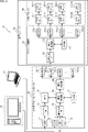
- FIG. 2 is a diagram illustrating a configuration example of a video wall controller and a display unit in FIG. 1;
- FIG. It is a figure explaining the structural example of an LED array.
- FIG. 4 is a diagram illustrating a configuration example of an LED driver; 6 is a timing chart for explaining a driving method of the drive circuit of FIG. 5; 6 is a timing chart for explaining a driving method of the drive circuit of FIG. 5; 4 is a timing chart for explaining a method of driving LEDs in units of rows; 4 is a timing chart for explaining a method of driving LEDs in units of LEDs; It is a figure explaining the additional capacitance of LED.
- FIG. 4 is a diagram illustrating a configuration example of an LED driver
- 6 is a timing chart for explaining a driving method of the drive circuit of FIG. 5
- 6 is a timing chart for explaining a driving method of the drive circuit of FIG. 5
- 4 is a timing chart for explaining a method of driving LEDs in units of rows
- 4 is a
- FIG. 10 is a diagram for explaining that an LED does not emit light when the current is supplied for a short period of time in PWM control;
- FIG. 5 is a diagram for explaining control of an LED current value when a current is passed for a short time in PWM control;
- FIG. 1 shows a configuration example of a display system to which the technology of the present disclosure is applied.
- the display system 11 in FIG. 1 displays video content on a large display configured by arranging a plurality of display units in tiles.
- the display system 11 is composed of a PC (personal computer) 30 , a video server 31 , a video wall controller 32 and a video wall 33 .
- the PC (personal computer) 30 is a general general-purpose computer that accepts user's operation inputs and supplies commands to the video wall controller 32 according to the operation details.
- the video server 31 is composed of, for example, a server computer, and supplies video signal data such as video content to the video wall controller 32 .
- the video wall controller 32 operates according to commands supplied from the PC 30, and distributes data consisting of video signals of video content to the display units 51-1 to 51-n constituting the video wall 33 for display.
- the display units 51-1 to 51-n are simply referred to as the display unit 51 when there is no need to distinguish them individually.
- the video wall 33 as shown in the upper right part of FIG. A single image is displayed on the video wall 33 as a whole by tiling the images displayed by the units 51 .
- the video wall controller 32 performs predetermined signal processing on the data consisting of video signals of the video content supplied from the video server 31, distributes and supplies the data according to the arrangement of the display units 51-1 to 51-n, The individual displays of the display units 51-1 to 51-n are controlled, and the video wall 33 as a whole is controlled to display one image.
- the video wall controller 32 and the video wall 33 may be integrated, or may be a display device (information processing device) in which they are integrated.
- the video wall controller 32 includes a LAN (Local Area Network) terminal 71, an HDMI (registered trademark) (High Definition Multimedia Interface) terminal 72, a DP (Display Port) terminal 73, a DVI (Digital Visual Interface) terminal 74, a network IF (Interface ) 75, MPU (Micro Processor Unit) 76, signal input IF 77, signal processing section 78, DRAM (Dynamic Random Access Memory) 79, signal distribution section 80, and output IFs 81-1 to 81-n.
- LAN Local Area Network
- HDMI registered trademark
- DP Display Port
- DVI Digital Visual Interface
- MPU Micro Processor Unit
- signal input IF 77 signal processing section 78
- DRAM Dynamic Random Access Memory
- a LAN (Local Area Network) terminal 71 is, for example, a connection terminal for a LAN cable or the like, and is operated by a user to supply a control command or the like according to the operation content to the video wall controller 32. , and supplies input control commands and the like to the MPU 76 via the network IF 75 .
- the LAN terminal 71 may be configured to be physically connected with a wired LAN cable, or may be configured to be connected by a so-called wireless LAN realized by wireless communication.
- the MPU 76 receives input of control commands supplied from the PC 30 via the LAN terminal 71 and the network IF 75 and supplies control signals corresponding to the received control commands to the signal processing section 76 .
- the HDMI terminal 72, the DP terminal 73, and the DVI terminal 74 are input terminals for data consisting of video signals.
- the processing unit 78 accepts supply of data consisting of a video signal.
- FIG. 2 shows an example in which the video server 31 and the HDMI terminal 72 are connected, the HDMI terminal 72, the DP terminal 73, and the DVI terminal 74 all differ only in their standards. Since they have practically similar functions, one of them is selected and connected as required.
- the signal processing unit 78 adjusts the color temperature, contrast, brightness, etc. of the video signal data supplied via the signal input IF 77 based on the control signal supplied from the MPU 76, and supplies the data to the signal distribution unit 80. do. At this time, the signal processing unit 78 uses the connected DRAM 78 as necessary to expand the data of the video signal, execute signal processing based on the control signal, and send the signal processing result to the signal distribution unit. 80.
- the signal distribution unit 80 distributes the data consisting of the signal-processed video signal supplied from the signal processing unit 78, and distributes the data to the display units 51-1 to 51-n via the output IFs 81-1 to 81-n. n are individually distributed and transmitted.
- the display unit 51 includes a driver control section 91 and an LED block 92.
- the driver control unit 91 supplies the plurality of LED drivers 121-1 to 121-N forming the LED block 92 with data consisting of video signals for controlling the light emission of the LEDs forming the LED arrays 122-1 to 122-N. supply.
- the driver control section 91 includes a signal input IF 111, a signal processing section 112, a DRAM 113, and output IFs 114-1 to 114-N.
- the signal input IF 111 receives input of video signal data supplied from the video wall controller 32 and supplies it to the signal processing unit 112 .
- the signal processing unit 112 corrects the color and luminance of each display unit 51 based on the data of the video signal supplied from the signal input IF 111, and corrects the LEDs constituting the LED arrays 122-1 to 122-N. Data for setting the emission intensity is generated and distributed to the LED drivers 121-1 to 121-N of the LED block 92 via the output IFs 114-1 to 114-N.
- the LED block 92 includes LED drivers 121-1 to 121-N and LED arrays 122-1 to 122-N.
- the LED drivers 121-1 to 121-N configure the corresponding LED arrays 122-1 to 122-N based on the data for setting the emission intensity of the LED 141, which is composed of the video signal supplied from the driver control unit 91. Controls the light emission of LEDs arranged in an array.
- FIG. 3 shows a configuration example of the LED array 122 in passive matrix drive type LED drive connections.
- each LED 141 has a Sig line (brightness control wiring) wired in the vertical direction and a Scan line wired in the horizontal direction. (row selection wiring) and are connected to.
- the luminescence intensity is controlled by controlling the energization time of a predetermined current value energized to the LED 141 .
- the emission intensity of the LEDs 141 is controlled by controlling the current value of the current supplied to the LEDs 141 .
- the emission intensity of the LEDs 141 arranged in a matrix changes according to the change in the control value (energization time or current value) of the Sig line for each of the scan lines 1 to N sequentially.
- a display that can be recognized as an image as a whole is performed.
- the scanning line switching is performed multiple times within the frame interval (eg 60 Hz) so that the image does not look unsightly.
- the reference current value Ii is, for example, a reference current value in selecting and designing various configurations constituting the display system 11 such as the LED 141, drive system, wiring resistance, and power supply.
- the current value energized to the LED 141 is fixed at the current value Ii, which is the initial value. Assuming that the current value is changed, the current value will be changed regardless of the light emission timing. It is necessary to change to the current value.
- the PWM Pulse Density Modulation (fixing the pulse width and expressing the strength of the signal with its generation density (total amount))
- PWM Pulse Density Modulation
- LED driver 121 includes FiFo 201, PWM generators 202-1 to 202-N, synchronization control section 203, ghost precharge control section 204, current adjustment section 205, row scan control section 206, switch transistors 207-1 to 207-M, and a constant current source block 208 .
- FiFo (First In First Out) 201 acquires data (Data) for setting the emission intensity of LED 141 supplied via a luminance control signal interface (Sig data I/F), and temporarily stores it as luminance setting data.
- Data data for setting the emission intensity of LED 141 supplied via a luminance control signal interface (Sig data I/F), and temporarily stores it as luminance setting data.
- the data are stored in the same manner and output to the PWM generators 202-1 to 202-N based on the clock signal (CLK).
- the brightness setting data which is data for setting the emission intensity of the LED 141, is, for example, 18-bit data, of which the upper two bits control the current value adjusted in the current adjustment unit 205.
- the remaining 16 bits are data for controlling the energization time of the current controlled by the PWM generator 202 .
- the number of bits of the brightness setting data which is data for setting the light emission intensity of the LED 141, is not limited to 18 bits. As for the number of bits, other numbers of bits may be used.
- the PWM generators 202-1 to 202-N set the emission intensity supplied from the FiFo 201 for each of the 1 to N channels corresponding to the columns in the array of the LED 141, based on the synchronization signal supplied from the synchronization control unit 203.
- the current sources 212-1 to 212-N are controlled to turn on or off the switch transistors 211-1 to 211-N in the corresponding constant current source block 208 based on the luminance setting data, which is data to be used. N each on or off.
- PWM generators 202-1 to 202-N control ON or OFF of current sources 212-1 to 212-N, respectively, thereby controlling the energization time of LED 141, resulting in emission intensity (luminance ) is controlled.
- Synchronization control unit 203 PWM generators 202-1 to 202-N, ghost precharge control unit 204, and A synchronization signal is supplied to the row scan control unit 206 to control synchronization.
- the ghost precharge control unit 204 controls energization of the constant current sources 212-1 to 212-N to precharge the LED 141 or control discharge for suppressing ghosts.
- the ghost precharge control unit 204 controls the energization of the constant current sources 212-1 to 212-N to precharge (forcibly charge) the LED 141, or Discharge.
- the current adjustment unit 205 Based on the luminance setting data, which is data stored in the FiFo 201, the current adjustment unit 205 synchronizes with the timing of supplying current controlled by the PWM generator 202, and the current source 212- in the current source block 208. Set the current value (R/G/B Current control) for each of 1 to 212-N.
- the brightness setting data which is data stored in the FiFo 201, is brightness setting information for each LED 141 based on the video signal, and information on the timing of energizing the LED 141 (information on the energization time). ) and the information on the current value to be energized to the LED.
- the brightness setting data may be, for example, 18-bit data, with the upper 2 bits as information for setting the current value, and the remaining 16 bits as information indicating the timing of energizing the LED 141 with current.
- the current adjustment unit 205 adjusts the current value Ii as a reference, the current value
- Three types of current values a current value Iu larger than Ii by a predetermined value and a current value Id smaller than the reference current value Ii by a predetermined value, may be set by switching.
- the PWM generators 202-1 to 202-N are the data stored in the FiFo 201, which is the lower 16-bit data of the brightness setting data, which is the data for controlling the timing of applying current, and the LED 141 By controlling the on or off of the switch transistors 211-1 to 211-N in the corresponding constant current source block 208, the current sources 212-1 to 212- N each on or off.
- the row scan control unit 206 operates based on the synchronization signal supplied from the synchronization control unit 203, and turns on or off the switch transistors 207-1 to 207-M provided for each of the M rows Scanlines Scan0 to ScanM. Light emission or extinguishing of the LED 141 is controlled in row units by controlling off.
- the current source block 208 includes constant current sources 212-1 to 212-N for each column of the LEDs 141 defined by ch0 to chN, and switch transistors 211-1 to 211- that connect power supplies (VDD G, B) respectively. It has N.
- the switch transistors 211-1 to 211-N are controlled by the corresponding PWM generators 202-1 to 202-N, respectively, and turned on when the corresponding constant current sources 212-1 to 212-N are energized. It is controlled to be off at other times.
- the switch transistors 211-1 to 211-N are controlled to be ON for a length corresponding to the emission intensity of the LED 141 at predetermined time intervals by the PWM generators 202-1 to 202-N. 212-1 through 212-N are energized.
- the constant current sources 212-1 to 212-N have current values controlled by the current adjustment unit 205. For example, a reference current value Ii, a current value Iu larger than the reference current value Ii by a predetermined value, and a current value Id that is smaller than the reference current value Ii by a predetermined value.
- the switching transistors 207-1 to 207-M controlled by the row scan control unit 206 are turned on and off, and the switching transistors 211-1 to 211-N controlled by the PWM generators 202-1 to 202-N are turned on and off.
- a control matrix of the LEDs 141 constituting the LED array 122 consisting of the number of ScanLines (Scan0 to M) ⁇ the number of current sources (ch0 to N) is formed, and the light emission of each of the LEDs 141 is controlled. .
- FIG. 6 The upper part of FIG. 6 is a waveform diagram showing the time change of the LED current value when controlling the light emission of the LED 141 by the PWM control method.
- the current adjustment unit 205 changes the current value in addition to the energization time for energizing the LED 141 of the constant current source 212 .
- the current value is increased by a predetermined value with respect to the reference current value Ii. Iu is shown to be energized.
- the current value to be energized in addition to controlling the energization time for energizing the LED 141, the current value to be energized can be changed as necessary, so that a higher luminance emission intensity can be set. is required, it is possible to change the LED current value so as to increase the energization. As a result, for example, it is possible to emit light appropriately even if a high emission intensity that expresses sparkle is required.
- the current adjustment unit 205 changes the current value of the current to be supplied to the LED 141 by the constant current source 212 .
- the current value Id obtained by decreasing the reference current value Ii by a predetermined value is shown by the diagonal grid portions in scan3 of Frame N and scans1 and 3 of Frame N+1. Power is shown.
- the value of the current applied to the LED 141 can be changed as necessary, so the value of the current applied to the LED 141 is reduced at the timing when detailed setting of the light emission intensity of low luminance is required. becomes possible.
- light emission control of the LED 141 is basically controlled by the energization time, and if it is difficult to control the energization time, it is desirable to add control by the current value.
- the current value used for normal control may be the reference current value Ii.
- a corresponding configuration may be used, and it is possible to suppress an unnecessary increase in cost, and also to suppress heat generation due to energization.
- the brightness setting data basically consists of information for controlling the energization time of the LED 141 according to the brightness value. , is preferably set so as to be controlled by the current value.
- the light emission of the LED 141 may be controlled by changing a combination of the power supply time to the LED 141 by PWM control and the current value to be energized to the LED 141 multiple times, with one scan being a unit of multiple lines.
- FIG. 8 shows changes in the current value when light emission is controlled by changing the energization time and the current value for energizing the LED 141 five times with one scan being a unit of four rows.
- Frame N+1 is also controlled in the same way.
- the LED current value is set to a current value Iu that is higher than the reference current value Ii, and the luminance is increased.
- the LED current value is set to a current value Id that is less than the reference current value Ii, and the luminance is reduced.
- the same row within the same frame is controlled to cyclically repeat light emission five times, making it possible to express a smooth luminance change for each row.
- the current value to be supplied with respect to the reference current value Ii it becomes possible to appropriately reproduce the brightness from the highest brightness to the lowest brightness.
- a plurality of rows are used as a unit, and in each row, a plurality of LEDs 141 are used as a unit, and the energization time by PWM control and the current value to be energized to the LED 141 are controlled a plurality of times to control the light emission intensity.
- FIG. 9 shows waveforms showing changes in the current value when controlling the light emission of the LEDs 141 in units of 8 LEDs 141 for each row, in units of 5 rows in one scan.
- Scan N+1 is controlled in the same way.
- the LED current value is set to the current value Iu that is higher than the reference current value Ii.
- the LED current value is set to a current value Id that is lower than the reference current value Ii, and the brightness is reduced.
- the LED current value is increased when the emission intensity is high and the brightness is increased.
- the LED current value may also be increased when the brightness is decreased.
- the LED 141 includes, as additional capacitance, a capacitance related to the junction of the LED 141 (junction capacitance) and a capacitance related to wiring (wiring capacitance).
- the value of the current conducted from the constant current source 212 to the LED 141 is defined as the current value I
- the energization time during which the current is supplied from the constant current source 212 is defined as time t
- the additional capacity of the LED 141 is defined as Assuming that the capacitance is C, in order for the LED 141 to emit light, a voltage equal to or higher than the light emission voltage Vf, which is the threshold value, must be applied to the additional capacitance C.
- Vf the light emission voltage
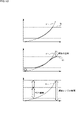
- FIG. 11 This relationship is expressed as the upper graph in FIG.
- the upper part of FIG. 11 is a graph showing the relationship between the time t during which the constant current source 212 is turned on and the LED current is conducted to the LED 141 and the charging voltage V charged in the additional capacitance C.
- the charging voltage to the additional capacity C is represented by a straight line Li, for example. Therefore, in FIG. 11, the time t at which the light emission voltage Vf, which is the threshold for causing the LED 141 to emit light, is reached is time tbp.
- the time during which the reference current value Ii is supplied from the current source 212 to the LED 141 by PWM control that is, as shown in the lower part of FIG.
- the capacitance C is charged by the current value Ii from the current source 212, but even if the charging is performed for the time tw, the charging voltage is only up to the voltage Ve ( ⁇ Vf), so the LED 141 emits light.
- the battery cannot be sufficiently charged to allow the LED 141 to emit light.
- the slope of the straight line Li indicating the charging voltage when charging the capacitance C with the current value Ii is the current value Ii itself.
- the current value Ii is increased by a predetermined value.
- the current value I is set as shown in the upper left part of FIG.
- the upper left part of FIG. 12 is a graph showing the relationship between the PWM control width (PWM pulse width) (energization time by current source 212) in PWM control and the current value at which LED 141 can emit light.
- the LED 141 when the energization time is longer than the threshold time tbp, the LED 141 emits light even if the current value energized to the LED 141 is the reference current value Ii. It is necessary to increase the current value I by that much.
- the current adjustment unit 205 adjusts the current value output by the constant current source 212 in consideration of the additional capacitance C included in the LED 141 as described above.
- the luminance beyond the boundary between the SDR and the original luminance curve Ir is By compressing , even in low-contrast images in SDR, gradation expression of images in which blown-out highlights and blocked-up shadows are not conspicuous has been performed.
- the SDR luminance curve Ip is determined based on a narrow luminance range of about 0.05 to 100 cd/m 2 , a display device that supports a wider luminance range may not have sufficient gradation compared to the performance of the device. I have a problem of not being able to express myself. Therefore, as shown in the lower part of FIG.
- image signals and display devices that support HDR (High Dynamic Range), which supports a wider luminance range than SDR, are becoming widespread.
- HDR High Dynamic Range
- a PQ (Perceptual Quantization) luminance curve corresponding to a maximum luminance of 10000 cd/m 2 is specified, and images exceeding 100 cd/m 2 and corresponding to a maximum luminance of 1000 to 10000 cd/m 2 are defined. Signals, etc. exist.
- the LED driver 121 of the present disclosure may support brightness levels specified by the HDR image signal (video signal), and as an example, energize the LED 141 for brightness levels above 0.05 to 100 cd/m 2
- the LED driver 121 may support brightness levels specified by the HDR image signal (video signal), and as an example, energize the LED 141 for brightness levels above 0.05 to 100 cd/m 2
- PWM control of the current by controlling the value of the current energized to the LED 141, it is possible to express a high-contrast image.
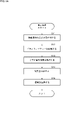
- step S11 the signal processing unit 78 receives a video signal including content data supplied from the video server 31 via one of the HDMI terminal 72, DP terminal 73, and DVI terminal 74 and the signal input IF 77. accept.
- step S12 the signal processing unit 78 converts the video format of the received video signal.
- step S13 the signal processing unit 78 receives the input of the control signal supplied from the MPU 76 according to the operation content of the PC 30, and executes signal processing such as color temperature, contrast, and brightness.
- step S14 the signal processing unit 78 allocates and distributes the signal-processed video signals to the display units 51-1 to 51-n of the video wall 33.
- step S15 the signal processing section 78 transmits and outputs the distributed video signal to each of the corresponding display units 51-1 to 51-n.
- the video signal read out from the video server 31 is subjected to signal processing, distributed to each of the display units 51-1 to 51-n constituting the video wall 33, and transmitted.
- signal processing distributed to each of the display units 51-1 to 51-n constituting the video wall 33, and transmitted.
- individual images are displayed by the display units 51-1 to 51-n, so that the video wall 33 can display the image of the video content as a whole.
- driver control processing by the display unit 51 will be described with reference to the flowchart of FIG.
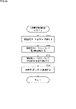
- step S31 the signal processing section 112 in the driver control section 91 of the display unit 51 receives the input of the video signal distributed and supplied from the video wall controller 32 via the signal input IF 111.
- step S32 the signal processing unit 112 executes video signal processing for applying color and luminance correction corresponding to each display unit 51 to the video signal distributed as the display unit 51.
- step S33 the signal processing unit 112 allocates the video signals that have undergone video signal processing to the LED drivers 121-1 to 121-N in the LED block 92, and outputs them via the corresponding output IFs 114-1 to 114-N. to be transmitted.
- step S34 the LED drivers 121-1 to 121-N in the LED block 92 execute LED drive control processing to adjust the LED current values in addition to PWM control in the respective LED arrays 122-1 to 122-N. By doing so, an image is displayed with appropriate brightness.
- each of the display units 51 that make up the video wall 33 can appropriately adjust the brightness and output to the LED block 92 to display the video.
- LED drive control processing for controlling the driving of the individual LEDs 141 provided in the LED array 122 by the LED driver 121 in the LED block 92 will be described with reference to the flowchart of FIG.
- FiFo (First In First Out) 201 acquires a video signal that has undergone video signal processing via a brightness control signal interface (Sig data I/F), and sets the emission intensity of LED 141. is temporarily stored as luminance control data, which is the data of .
- information for setting the timing (energization time) of energizing each LED 141 and information for setting the current value of the current energized to the LED 141 are associated with the luminance information included in the video signal. is stored as luminance setting data.
- step S52 the current adjustment unit 205 synchronizes with the timing of energizing the current controlled by the PWM generator 202 based on the brightness setting data stored in the FiFo 201, and the current source block 208 A current value (R/G/B Current control) is set when conducting each of the current sources 212-1 to 212-N.
- step S53 the PWM generators 202-1 to 202-N generate data for setting the emission intensity stored in the FiFo 201 based on the synchronization signal supplied from the synchronization control unit 203 for each of the 1st to N channels. ), the switch transistors 211-1 through 211-N in the corresponding constant current source block 208 are controlled to be turned on or off at timing (energization time) based on the brightness setting data.
- the current values of the constant current sources 212-1 to 212-N are controlled by the current adjustment unit 205, and for example, the reference current value Ii or the current value larger than the reference current value Ii by a predetermined value. On or off is controlled by a current value set to either Iu or a current value Id that is smaller than the reference current value Ii by a predetermined value, and current is supplied to the LED 141 for the ON-controlled energization time. .
- step S54 the row scan control unit 206 operates based on the synchronization signal supplied from the synchronization control unit 203, and the switch transistors 207-1 to 207- provided for each of M rows Scanlines Scan0 to M are switched. By controlling the on or off of M, the light emission or extinguishment of the LED is controlled in row units.
- the switch transistors 211-1 to 211-N are controlled to be in the ON state by the PWM generators 202-1 to 202-N at predetermined time intervals for a length corresponding to the emission intensity of the LED 141.
- the corresponding current sources 212-1 through 212-N are energized for a corresponding time.
- the current values supplied to the current sources 212-1 to 212-N are controlled by the current adjusting unit 205.
- a current is applied to the LED 141 at a current value set to either Iu or a current value Id that is smaller than the reference current value Ii by a predetermined value.
- light emission control of the LED 141 may be performed by controlling the time and current value for energizing only the video signal with the maximum brightness exceeding the brightness level of HDR or the SDR, or the input of the image signal.
- the light emission of the LED 141 may be controlled by expanding the dynamic range for a video signal or image signal with a luminance level of , and controlling the energizing time and current value for the expanded high luminance region.
- the LED driver 121 performs light emission control of the LED 141 using both PWM control and PAM control when an image with a brightness level exceeding 0.05 to 100 cd/m 2 is displayed regardless of the input signal.
- both PWM and PAM control can be used to control the brightness of the LEDs 141 when images with brightness levels exceeding the 1000 cd/ m2 brightness level supported by the reference display used in high brightness video production are displayed.
- Light emission control may be performed.
- application of the technology of the present disclosure is not limited to these cases, and can be applied regardless of the input signal or specific luminance level.
- the video wall 33 in which the plurality of display units 51 are arranged in tiles displays one image as a whole has been described. Therefore, for example, it may be applied to a backlight realized by arranging a plurality of display units 51 in a tile form.
- the technique of the present disclosure controls the luminance of the LED 141 by the energization time and the current value of the energization of the LED 141. It can be said that it was made to be controlled.
- the LED driver 121 of the present disclosure basically controls the light emission of the LED 141 by PWM control. It can be said that the control is performed by adding assistance by PAM control as necessary.
- information on the energization time that corrects the wavelength change of the LED 141 corresponding to the change in the LED current value is stored in advance in a LUT (Look Up Table), or an arithmetic circuit that calculates the energization time according to the wavelength change of the LED 141. may be provided to suppress the change in wavelength caused by the LED current value.
- FIG. 17 shows a configuration example of an LED driver 121 provided with a color matrix processing section 251 that stores in advance information on the energization time for suppressing the change in wavelength caused by the current value that energizes the LED 141 .
- the color matrix processing unit 251 is composed of, for example, a LUT (Look Up Table) and the like, and is a constant current in PWM control so as to suppress the wavelength change of the light emitted by the LED 141 caused by the change in the current value applied to the LED 141.
- Information for correcting the energization time of the source 212 is stored.
- the PWM generator 202 controls on/off of the current source 212 based on information on the energization time corrected according to the current value by the color matrix processing unit 251 .
- the color matrix processing unit 251 needs only to obtain the energization time so as to suppress the wavelength change of the light emitted by the LED 141 caused by the change in the current value applied to the LED 141.
- it may be a linear arithmetic device capable of calculating the energization time corrected according to the current value.
- An energization time control unit that controls the energization time for energizing an LED (Light Emitting Diode) to control the emission luminance of the LED;
- a drive control device comprising: a current value control unit that controls the current value of the current that flows through the LED to control the emission luminance of the LED.
- the current value control unit controls the current value of the current supplied to the LED based on the luminance of the input video signal, thereby controlling the emission luminance of the LED.
- Drive controller controls the current value of the current supplied to the LED based on the luminance of the input video signal, thereby controlling the emission luminance of the LED.
- the current value control unit selects one of a plurality of predetermined current values related to the current to be applied to the LED based on the luminance of the input video signal, and energizes the LED.
- the drive control device according to ⁇ 2> which controls the emission luminance of the LED.
- the current value control unit controls a reference current value, a current value greater than the reference current value, and a current value smaller than the reference current value.
- the drive control device according to ⁇ 3> wherein the light emission luminance of the LED is controlled by energizing the LED with one of the values.
- the current value control unit controls the light emission brightness of the LED based on the control of the current value of the current supplied to the LED.
- the current value control unit causes the current to flow through the LED at a current value larger than a reference current value.
- the drive control device according to ⁇ 5> which controls the emission luminance of the LED.
- the current value control unit controls the light emission brightness of the LED based on the control of the current value of the current supplied to the LED.
- the drive control device according to ⁇ 1>.
- the current value control unit causes the current to flow through the LED at a current value smaller than a reference current value.
- the drive control device which controls the emission luminance of the LED.
- the current value control unit considers the additional capacity of the LED and calculates the ,
- the drive control device which controls the emission luminance of the LED.
- the current value control unit When the luminance of the input video signal is lower than a predetermined luminance value, the current value control unit considers the additional capacity of the LED, and within the energization time controlled by the energization time control unit, The drive control device according to ⁇ 9>, wherein the light emission luminance of the LED is controlled by energizing the LED with a current value that exceeds a threshold value of the charging voltage according to the additional capacity of the LED.
- the current value control unit energizes the LED with a current value that is not a reference current value
- the energization time control unit energizes the LED with a current value that is not the reference current value.
- the drive control device wherein the energization time is controlled so as to correct the wavelength change of the light emitted from the LED caused by the switching, and the light emission luminance of the LED is controlled.
- ⁇ 12> further comprising a storage unit that stores information on the energization time for correcting a wavelength change that occurs when the LED is energized with a current value that is not the reference current value;
- the energization time control unit controls the energization time for correcting the wavelength change stored in the storage unit.
- the drive control device according to ⁇ 11>, which controls the light emission brightness of the LED based on the information of ⁇ 11>.
- ⁇ 13> further comprising a computing unit that computes the energization time for correcting a wavelength change that occurs when the LED is energized with a current value that is not the reference current value;
- the energization time control unit controls the energization time for correcting the wavelength change calculated by the calculation unit.
- the drive control device which controls the light emission brightness of the LED based on the information of ⁇ 11>.
- ⁇ 14> further comprising a constant current source that supplies current to the LED;
- the energization time control unit controls the emission luminance of the LED based on the energization time during which the constant current source energizes the LED,
- the drive control device according to any one of ⁇ 1> to ⁇ 13>, wherein the current value control section controls the emission brightness of the LED based on the current value of the current that the constant current source supplies to the LED.
- the current value control unit controls the current value of the current supplied to the LED when the emission brightness of the LED is out of the range of 0.05 to 100 cd/m 2 , and the LED
- the drive control device according to any one of ⁇ 1> to ⁇ 14>, which controls the emission luminance of the.
- ⁇ 16> The drive control device according to ⁇ 2>, wherein the video signal is a video signal compatible with HDR (High Dynamic Range).
- the current value control unit controls the light emission luminance of the LED based on control of the current value of the current supplied to the LED.
- the current value control unit controls the light emission luminance of the LED based on control of the current value of the current supplied to the LED.
- an energization time control unit ⁇ 19> an energization time control unit;
- a drive control method for a drive control device comprising a current value control unit, The energization time control unit controls the energization time for energizing the LED (Light Emitting Diode) to control the light emission brightness of the LED,
- a drive control method comprising the step of controlling the current value of the current applied to the LED by the current value control unit to control the emission luminance of the LED.
- a display section comprising a display unit having LEDs (Light Emitting Diodes) arranged in an array and a drive control device for controlling the driving of the LEDs; a distribution unit that receives input of a video signal, performs predetermined signal processing on the video signal, and distributes the video signal to the display unit;
- the drive control device is an energization time control unit that controls the energization time for energizing the LED to control the emission luminance of the LED;
- An information processing system comprising: a current value control unit that controls a current value of the current that flows through the LED to control light emission luminance of the LED.
- 11 Display System 30 PC, 31 Video Server, 32 Video Wall Controller, 33 Video Wall, 51, 51-1 to 51-n Display Unit, 78 Signal Processing Unit, 91 Driver Control Unit, 92 Driver Block, 112 Signal Processing Unit , 121, 121-1 to 121-N drive circuit, 122 pixel array, 141 pixel (LED), 201 FiFo, 202, 202-1 to 202-N PWM generator, 203 synchronization control unit, 204 ghost precharge control unit, 205 current adjustment unit, 206 row scan control unit, 207, 207-1 to 207-M switch transistor, 208 current source block, 211, 211-1 to 211-N constant current source, 212, 212-1 to 212-N switching transistor, 251 LUT
Abstract
Description
1.好適な実施の形態
2.応用例 Embodiments for implementing the present technology will be described below. The explanation is given in the following order.
1. Preferred
<表示システムの構成例>
本開示は、特に、高輝度で、かつ、高階調精度のディスプレイ(バックライト)を安価で、かつ、容易に実現できるようにするものである。 <<1. Preferred Embodiment>>
<Display system configuration example>
In particular, the present disclosure makes it possible to inexpensively and easily realize a display (backlight) with high brightness and high gradation accuracy.
次に、図2を参照して、ビデオウォールコントローラ32および表示ユニット51の詳細な構成例について説明する。 <Detailed configuration of video wall controller and display unit>
Next, a detailed configuration example of the
次に、図3を参照して、LEDアレイ122の構成例について説明する。図3は、パッシブマトリックス駆動型LED駆動結線におけるLEDアレイ122の構成例を示している。 <Configuration example of LED array>
Next, a configuration example of the
次に、図3のLEDアレイ122の駆動方式について説明する。図3のLEDアレイ122は、PWM制御方式で制御される場合、LED141に通電される所定の電流値の通電時間が制御されることにより、発光強度が制御される。また、図3のLEDアレイ122は、PAM制御方式で制御される場合、LED141に通電される電流の電流値が制御されることでLED141の発光強度が制御される。 <Drive method of LED array>
Next, a method of driving the
次に、図5を参照して、本開示のLEDドライバ121の構成例について説明する。 <Configuration example of LED driver>
Next, a configuration example of the
(高輝度の発光強度の設定が必要な場合)
次に、図6,図7を参照して、本開示のLEDドライバ121によるLEDの駆動制御について説明する。 <LED drive control in the LED driver of the present disclosure>
(When high luminance intensity setting is required)
Next, drive control of LEDs by the
また、同様の手法でLED電流値を低減させて、最低輝度の再現性を向上させることもできる。 (When low luminance emission intensity setting is required)
Also, it is possible to reduce the LED current value by a similar method to improve the reproducibility of the minimum luminance.
1回のスキャンを複数行単位とし、複数回ずつ、PWM制御によるLED141への通電時間と、LED141に通電する電流値とを組み合わせて変化させることでLED141の発光を制御するようにしてもよい。 <Example of changing the current applied to LEDs for each row>
The light emission of the
以上においては、1回のスキャンで複数行を単位として、複数回ずつPWM制御によるLED141への通電時間と、LED141へと通電する電流値とを変化させて、LED141の発光を制御する例について説明してきた。 <Example of controlling by LED unit>
In the above, an example of controlling the light emission of the
以上においては、発光強度が大きく、高輝度化する際にLED電流値を増大させるように制御する例について説明してきたが、低輝度化する際にもLED電流値を増大させることがある。 <Increase in current at low luminance>
In the above, an example has been described in which the LED current value is increased when the emission intensity is high and the brightness is increased. However, the LED current value may also be increased when the brightness is decreased.
従来のCRTディスプレイのような十分な最大輝度を有しないディスプレイでは、図13の上段で示されるように、本来の輝度曲線(ガンマカーブ)Irに対して、2本の点線の間のバンドとして示されるSDR(Standard Dynamic Range)内において、太線の輝度曲線Icで示されるように上限と下限とがカットされることで、白飛びや黒つぶれが目立つような低コントラスト画像しか表現できなかった。 <Extension to HDR>
In a display that does not have sufficient maximum luminance, such as a conventional CRT display, the original luminance curve (gamma curve) Ir is shown as a band between two dashed lines, as shown in the upper part of FIG. Within the standard dynamic range (SDR), the upper and lower limits are cut as indicated by the thick luminance curve Ic, so only low-contrast images with conspicuous blown-out highlights and blocked-up shadows could be expressed.
次に、図14のフローチャートを参照して、図1の表示システム11による表示処理について説明する。 <Display processing>
Next, display processing by the
次に、図15のフローチャートを参照して、表示ユニット51によるドライバ制御処理について説明する。 <Driver control processing by display unit>
Next, driver control processing by the
次に、図16のフローチャートを参照して、LEDブロック92におけるLEDドライバ121によるLEDアレイ122に設けられた個々のLED141の駆動を制御するLED駆動制御処理について説明する。 <LED drive control processing>
Next, LED drive control processing for controlling the driving of the
以上においては、PWM制御に加えて、PWM制御の制御タイミングに合わせて、LED141に通電する電流値を増減させることで、必要なダイナミックレンジを拡大させる例について説明してきたが、LED141に通電する電流の電流値が変化することによりLED141が発する光の波長に変化が生じてしまう恐れがある。 <<2. Application example >>
In the above, in addition to PWM control, an example in which the necessary dynamic range is expanded by increasing or decreasing the current value energized to the
<1> LED(Light Emitting Diode)に電流を通電する通電時間を制御して、前記LEDの発光輝度を制御する通電時間制御部と、
前記LEDに通電する前記電流の電流値を制御して、前記LEDの発光輝度を制御する電流値制御部と
を備えた駆動制御装置。
<2> 前記電流値制御部は、入力された映像信号の輝度に基づいて、前記LEDに通電する前記電流の電流値を制御して、前記LEDの発光輝度を制御する
<1>に記載の駆動制御装置。
<3> 前記電流値制御部は、入力された映像信号の輝度に基づいて、前記LEDに通電する前記電流に係る複数の所定の電流値のいずれかを選択して前記LEDに通電させることにより、前記LEDの発光輝度を制御する
<2>に記載の駆動制御装置。
<4> 前記電流値制御部は、入力された映像信号の輝度に基づいて、基準となる電流値、前記基準となる電流値よりも大きな電流値、および前記基準となる電流値よりも小さな電流値のうちのいずれかを前記LEDに通電させることで、前記LEDの発光輝度を制御する
<3>に記載の駆動制御装置。
<5> 前記電流値制御部は、入力された映像信号の輝度が所定の輝度値より高い場合、前記LEDに通電する前記電流の電流値の制御に基づいて、前記LEDの発光輝度を制御する
<1>に記載の駆動制御装置。
<6> 前記電流値制御部は、入力された映像信号の輝度が所定の輝度値より高い場合、前記LEDに通電する前記電流を、基準となる電流値よりも大きな電流値で通電させることで、前記LEDの発光輝度を制御する
<5>に記載の駆動制御装置。
<7> 前記電流値制御部は、入力された映像信号の輝度が所定の輝度値より低い場合、前記LEDに通電する前記電流の電流値の制御に基づいて、前記LEDの発光輝度を制御する
<1>に記載の駆動制御装置。
<8> 前記電流値制御部は、入力された映像信号の輝度が所定の輝度値より低い場合、前記LEDに通電する前記電流を、基準となる電流値よりも小さな電流値で通電させることで、前記LEDの発光輝度を制御する
<7>に記載の駆動制御装置。
<9> 前記電流値制御部は、入力された映像信号の輝度が所定の輝度値より低い場合、前記LEDの付加容量を考慮した上で、前記LEDに通電する前記電流の電流値に基づいて、前記LEDの発光輝度を制御する
<7>に記載の駆動制御装置。
<10> 前記電流値制御部は、入力された映像信号の輝度が所定の輝度値より低い場合、前記LEDの付加容量を考慮して、前記通電時間制御部により制御された通電時間内において、前記LEDの付加容量に応じた充電電圧が閾値を超える電流値で、前記LEDに通電させることで、前記LEDの発光輝度を制御する
<9>に記載の駆動制御装置。
<11> 前記電流値制御部が、基準となる電流値ではない電流値で前記LEDに電流を通電させる場合、前記通電時間制御部は、前記基準となる電流値ではない電流が前記LEDに通電されることで生じる前記LEDにより発せられる光の波長変化を補正するように、前記通電時間を制御して、前記LEDの発光輝度を制御する
<1>に記載の駆動制御装置。
<12> 前記基準となる電流値ではない電流値で前記LEDに電流が通電されるときに生じる波長変化を補正する前記通電時間の情報を記憶する記憶部をさらに含み、
前記電流値制御部が、前記基準となる電流値ではない電流値で前記LEDに電流を通電させる場合、前記通電時間制御部は、前記記憶部に記憶された前記波長変化を補正する前記通電時間の情報に基づいて、前記LEDの発光輝度を制御する
<11>に記載の駆動制御装置。
<13> 前記基準となる電流値ではない電流値で前記LEDに電流が通電されるときに生じる波長変化を補正する前記通電時間を演算する演算部をさらに含み、
前記電流値制御部が、前記基準となる電流値ではない電流値で前記LEDに電流を通電させる場合、前記通電時間制御部は、前記演算部により演算された前記波長変化を補正する前記通電時間の情報に基づいて、前記LEDの発光輝度を制御する
<11>に記載の駆動制御装置。
<14> 前記LEDに電流を通電する定電流源をさらに含み、
前記通電時間制御部は、前記定電流源が前記LEDに電流を通電する通電時間に基づいて、前記LEDの発光輝度を制御し、
前記電流値制御部は、前記定電流源が前記LEDに通電する電流の電流値に基づいて、前記LEDの発光輝度を制御する
<1>乃至<13>のいずれかに記載の駆動制御装置。
<15> 前記電流値制御部は、前記LEDの発光輝度が0.05乃至100 cd/m2の範囲外の輝度である場合に、前記LEDに通電する前記電流の電流値を制御して、前記LEDの発光輝度を制御する
<1>乃至<14>のいずれかに記載の駆動制御装置。
<16> 前記映像信号はHDR(High Dynamic Range)に対応した映像信号である
<2>に記載の駆動制御装置。
<17> 前記電流値制御部は、前記映像信号の輝度が100 cd/m2を超える場合に、前記LEDに通電する前記電流の電流値の制御に基づいて、前記LEDの発光輝度を制御する
<2>に記載の駆動制御装置。
<18> 前記電流値制御部は、前記映像信号の輝度が1000 cd/m2を超える場合に、前記LEDに通電する前記電流の電流値の制御に基づいて、前記LEDの発光輝度を制御する
<2>に記載の駆動制御装置。
<19> 通電時間制御部と、
電流値制御部とを備えた駆動制御装置の駆動制御方法であって、
前記通電時間制御部が、LED(Light Emitting Diode)に電流を通電する通電時間を制御して、前記LEDの発光輝度を制御し、
前記電流値制御部が、前記LEDに通電する前記電流の電流値を制御して、前記LEDの発光輝度を制御する
ステップを含む駆動制御方法。
<20> アレイ状に配置されたLED(Light Emitting Diode)と、前記LEDの駆動を制御する駆動制御装置とを有する表示ユニットからなる表示部と、
映像信号の入力を受け付け、前記映像信号に所定の信号処理を施して、前記表示ユニットに分配する分配部とを備え、
前記駆動制御装置は、
前記LEDに電流を通電する通電時間を制御して、前記LEDの発光輝度を制御する通電時間制御部と、
前記LEDに通電する前記電流の電流値を制御して、前記LEDの発光輝度を制御する電流値制御部とを備える
情報処理システム。 It should be noted that the present disclosure can also take the following configurations.
<1> An energization time control unit that controls the energization time for energizing an LED (Light Emitting Diode) to control the emission luminance of the LED;
A drive control device comprising: a current value control unit that controls the current value of the current that flows through the LED to control the emission luminance of the LED.
<2> The current value control unit controls the current value of the current supplied to the LED based on the luminance of the input video signal, thereby controlling the emission luminance of the LED. Drive controller.
<3> The current value control unit selects one of a plurality of predetermined current values related to the current to be applied to the LED based on the luminance of the input video signal, and energizes the LED. , The drive control device according to <2>, which controls the emission luminance of the LED.
<4> Based on the brightness of the input video signal, the current value control unit controls a reference current value, a current value greater than the reference current value, and a current value smaller than the reference current value. The drive control device according to <3>, wherein the light emission luminance of the LED is controlled by energizing the LED with one of the values.
<5> When the brightness of the input video signal is higher than a predetermined brightness value, the current value control unit controls the light emission brightness of the LED based on the control of the current value of the current supplied to the LED. The drive control device according to <1>.
<6> When the brightness of the input video signal is higher than a predetermined brightness value, the current value control unit causes the current to flow through the LED at a current value larger than a reference current value. , The drive control device according to <5>, which controls the emission luminance of the LED.
<7> When the brightness of the input video signal is lower than a predetermined brightness value, the current value control unit controls the light emission brightness of the LED based on the control of the current value of the current supplied to the LED. The drive control device according to <1>.
<8> When the brightness of the input video signal is lower than a predetermined brightness value, the current value control unit causes the current to flow through the LED at a current value smaller than a reference current value. , The drive control device according to <7>, which controls the emission luminance of the LED.
<9> When the luminance of the input video signal is lower than a predetermined luminance value, the current value control unit considers the additional capacity of the LED and calculates the , The drive control device according to <7>, which controls the emission luminance of the LED.
<10> When the luminance of the input video signal is lower than a predetermined luminance value, the current value control unit considers the additional capacity of the LED, and within the energization time controlled by the energization time control unit, The drive control device according to <9>, wherein the light emission luminance of the LED is controlled by energizing the LED with a current value that exceeds a threshold value of the charging voltage according to the additional capacity of the LED.
<11> When the current value control unit energizes the LED with a current value that is not a reference current value, the energization time control unit energizes the LED with a current value that is not the reference current value. The drive control device according to <1>, wherein the energization time is controlled so as to correct the wavelength change of the light emitted from the LED caused by the switching, and the light emission luminance of the LED is controlled.
<12> further comprising a storage unit that stores information on the energization time for correcting a wavelength change that occurs when the LED is energized with a current value that is not the reference current value;
When the current value control unit energizes the LED with a current value that is not the reference current value, the energization time control unit controls the energization time for correcting the wavelength change stored in the storage unit. The drive control device according to <11>, which controls the light emission brightness of the LED based on the information of <11>.
<13> further comprising a computing unit that computes the energization time for correcting a wavelength change that occurs when the LED is energized with a current value that is not the reference current value;
When the current value control unit energizes the LED with a current value that is not the reference current value, the energization time control unit controls the energization time for correcting the wavelength change calculated by the calculation unit. The drive control device according to <11>, which controls the light emission brightness of the LED based on the information of <11>.
<14> further comprising a constant current source that supplies current to the LED;
The energization time control unit controls the emission luminance of the LED based on the energization time during which the constant current source energizes the LED,
The drive control device according to any one of <1> to <13>, wherein the current value control section controls the emission brightness of the LED based on the current value of the current that the constant current source supplies to the LED.
<15> The current value control unit controls the current value of the current supplied to the LED when the emission brightness of the LED is out of the range of 0.05 to 100 cd/m 2 , and the LED The drive control device according to any one of <1> to <14>, which controls the emission luminance of the.
<16> The drive control device according to <2>, wherein the video signal is a video signal compatible with HDR (High Dynamic Range).
<17> When the luminance of the video signal exceeds 100 cd/m 2 , the current value control unit controls the light emission luminance of the LED based on control of the current value of the current supplied to the LED. The drive control device according to <2>.
<18> When the luminance of the video signal exceeds 1000 cd/m 2 , the current value control unit controls the light emission luminance of the LED based on control of the current value of the current supplied to the LED. The drive control device according to <2>.
<19> an energization time control unit;
A drive control method for a drive control device comprising a current value control unit,
The energization time control unit controls the energization time for energizing the LED (Light Emitting Diode) to control the light emission brightness of the LED,
A drive control method, comprising the step of controlling the current value of the current applied to the LED by the current value control unit to control the emission luminance of the LED.
<20> A display section comprising a display unit having LEDs (Light Emitting Diodes) arranged in an array and a drive control device for controlling the driving of the LEDs;
a distribution unit that receives input of a video signal, performs predetermined signal processing on the video signal, and distributes the video signal to the display unit;
The drive control device is
an energization time control unit that controls the energization time for energizing the LED to control the emission luminance of the LED;
An information processing system, comprising: a current value control unit that controls a current value of the current that flows through the LED to control light emission luminance of the LED.
Claims (20)
- LED(Light Emitting Diode)に電流を通電する通電時間を制御して、前記LEDの発光輝度を制御する通電時間制御部と、
前記LEDに通電する前記電流の電流値を制御して、前記LEDの発光輝度を制御する電流値制御部と
を備えた駆動制御装置。 an energization time control unit that controls the energization time for energizing an LED (Light Emitting Diode) to control the emission luminance of the LED;
A drive control device comprising: a current value control unit that controls the current value of the current that flows through the LED to control the emission luminance of the LED. - 前記電流値制御部は、入力された映像信号の輝度に基づいて、前記LEDに通電する前記電流の電流値を制御して、前記LEDの発光輝度を制御する
請求項1に記載の駆動制御装置。 2. The drive control device according to claim 1, wherein the current value control section controls the current value of the current supplied to the LED based on the luminance of the input video signal, thereby controlling the emission luminance of the LED. . - 前記電流値制御部は、入力された映像信号の輝度に基づいて、前記LEDに通電する前記電流に係る複数の所定の電流値のいずれかを選択して前記LEDに通電させることにより、前記LEDの発光輝度を制御する
請求項2に記載の駆動制御装置。 The current value control unit selects one of a plurality of predetermined current values related to the current to be applied to the LED based on the luminance of the input video signal, and energizes the LED to control the LED. 3. The drive control device according to claim 2, which controls the emission luminance of the. - 前記電流値制御部は、入力された映像信号の輝度に基づいて、基準となる電流値、前記基準となる電流値よりも大きな電流値、および前記基準となる電流値よりも小さな電流値のうちのいずれかを前記LEDに通電させることで、前記LEDの発光輝度を制御する
請求項2に記載の駆動制御装置。 Based on the brightness of the input video signal, the current value control unit selects a reference current value, a current value greater than the reference current value, or a current value smaller than the reference current value. 3. The drive control device according to claim 2, wherein the light emission luminance of the LED is controlled by energizing the LED with either of - 前記電流値制御部は、入力された映像信号の輝度が所定の輝度値より高い場合、前記LEDに通電する前記電流の電流値の制御に基づいて、前記LEDの発光輝度を制御する
請求項1に記載の駆動制御装置。 2. When the luminance of the input video signal is higher than a predetermined luminance value, the current value control unit controls the light emission luminance of the LED based on control of the current value of the current flowing through the LED. The drive control device according to . - 前記電流値制御部は、入力された映像信号の輝度が所定の輝度値より高い場合、前記LEDに通電する前記電流を、基準となる電流値よりも大きな電流値で通電させることで、前記LEDの発光輝度を制御する
請求項5に記載の駆動制御装置。 When the luminance of the input video signal is higher than a predetermined luminance value, the current value control unit causes the current to flow through the LED with a current value larger than a reference current value, so that the LED 6. The drive control device according to claim 5, which controls the emission luminance of the. - 前記電流値制御部は、入力された映像信号の輝度が所定の輝度値より低い場合、前記LEDに通電する前記電流の電流値の制御に基づいて、前記LEDの発光輝度を制御する
請求項1に記載の駆動制御装置。 2. When the luminance of the input video signal is lower than a predetermined luminance value, the current value control unit controls the light emission luminance of the LED based on control of the current value of the current flowing through the LED. The drive control device according to . - 前記電流値制御部は、入力された映像信号の輝度が所定の輝度値より低い場合、前記LEDに通電する前記電流を、基準となる電流値よりも小さな電流値で通電させることで、前記LEDの発光輝度を制御する
請求項7に記載の駆動制御装置。 When the luminance of the input video signal is lower than a predetermined luminance value, the current value control unit energizes the LED with a current value smaller than a reference current value, so that the LED The drive control device according to claim 7, which controls the light emission luminance of the. - 前記電流値制御部は、入力された映像信号の輝度が所定の輝度値より低い場合、前記LEDの付加容量を考慮した上で、前記LEDに通電する前記電流の電流値に基づいて、前記LEDの発光輝度を制御する
請求項7に記載の駆動制御装置。 When the luminance of the input video signal is lower than a predetermined luminance value, the current value control unit controls the LED based on the current value of the current to be applied to the LED, taking into consideration the additional capacitance of the LED. The drive control device according to claim 7, which controls the light emission luminance of the. - 前記電流値制御部は、入力された映像信号の輝度が所定の輝度値より低い場合、前記LEDの付加容量を考慮して、前記通電時間制御部により制御された通電時間内において、前記LEDの付加容量に応じた充電電圧が閾値を超える電流値で、前記LEDに通電させることで、前記LEDの発光輝度を制御する
請求項9に記載の駆動制御装置。 When the luminance of the input video signal is lower than a predetermined luminance value, the current value control unit reduces the power consumption of the LED within the energization time controlled by the energization time control unit in consideration of the additional capacity of the LED. 10. The drive control device according to claim 9, wherein the LED is energized with a current value in which the charging voltage corresponding to the additional capacity exceeds a threshold value, thereby controlling the emission brightness of the LED. - 前記電流値制御部が、基準となる電流値ではない電流値で前記LEDに電流を通電させる場合、前記通電時間制御部は、前記基準となる電流値ではない電流が前記LEDに通電されることで生じる前記LEDにより発せられる光の波長変化を補正するように、前記通電時間を制御して、前記LEDの発光輝度を制御する
請求項1に記載の駆動制御装置。 When the current value control unit energizes the LED with a current value that is not the reference current value, the energization time control unit energizes the LED with the current value that is not the reference current value. 2. The drive control device according to claim 1, wherein the energization time is controlled so as to correct the wavelength change of the light emitted from the LED caused in the above, and the emission brightness of the LED is controlled. - 前記基準となる電流値ではない電流値で前記LEDに電流が通電されるときに生じる波長変化を補正する前記通電時間の情報を記憶する記憶部をさらに含み、
前記電流値制御部が、前記基準となる電流値ではない電流値で前記LEDに電流を通電させる場合、前記通電時間制御部は、前記記憶部に記憶された前記波長変化を補正する前記通電時間の情報に基づいて、前記LEDの発光輝度を制御する
請求項11に記載の駆動制御装置。 further comprising a storage unit that stores information on the energization time for correcting a wavelength change that occurs when the current is energized to the LED with a current value that is not the reference current value;
When the current value control unit energizes the LED with a current value that is not the reference current value, the energization time control unit controls the energization time for correcting the wavelength change stored in the storage unit. 12. The drive control device according to claim 11, wherein the light emission luminance of the LED is controlled based on the information of. - 前記基準となる電流値ではない電流値で前記LEDに電流が通電されるときに生じる波長変化を補正する前記通電時間を演算する演算部をさらに含み、
前記電流値制御部が、前記基準となる電流値ではない電流値で前記LEDに電流を通電させる場合、前記通電時間制御部は、前記演算部により演算された前記波長変化を補正する前記通電時間の情報に基づいて、前記LEDの発光輝度を制御する
請求項11に記載の駆動制御装置。 further comprising a calculation unit for calculating the energization time for correcting a wavelength change that occurs when a current is applied to the LED with a current value that is not the reference current value;
When the current value control unit energizes the LED with a current value that is not the reference current value, the energization time control unit controls the energization time for correcting the wavelength change calculated by the calculation unit. 12. The drive control device according to claim 11, wherein the light emission luminance of the LED is controlled based on the information of. - 前記LEDに電流を通電する定電流源をさらに含み、
前記通電時間制御部は、前記定電流源が前記LEDに電流を通電する通電時間に基づいて、前記LEDの発光輝度を制御し、
前記電流値制御部は、前記定電流源が前記LEDに通電する電流の電流値に基づいて、前記LEDの発光輝度を制御する
請求項1に記載の駆動制御装置。 further comprising a constant current source that energizes the LED;
The energization time control unit controls the emission luminance of the LED based on the energization time during which the constant current source energizes the LED,
2. The drive control device according to claim 1, wherein the current value control section controls the emission brightness of the LED based on the current value of the current that the constant current source supplies to the LED. - 前記電流値制御部は、前記LEDの発光輝度が0.05乃至100 cd/m2の範囲外の輝度である場合に、前記LEDに通電する前記電流の電流値を制御して、前記LEDの発光輝度を制御する
請求項1に記載の駆動制御装置。 The current value control unit controls the current value of the current supplied to the LED when the light emission luminance of the LED is out of the range of 0.05 to 100 cd/m 2 to reduce the light emission luminance of the LED. The drive control device according to claim 1, which controls the . - 前記映像信号はHDR(High Dynamic Range)に対応した映像信号である
請求項2に記載の駆動制御装置。 The drive control device according to claim 2, wherein the video signal is a video signal compatible with HDR (High Dynamic Range). - 前記電流値制御部は、前記映像信号の輝度が100 cd/m2を超える場合に、前記LEDに通電する前記電流の電流値の制御に基づいて、前記LEDの発光輝度を制御する
請求項2に記載の駆動制御装置。 2. When the luminance of the video signal exceeds 100 cd/m 2 , the current value control unit controls the light emission luminance of the LED based on the control of the current value of the current supplied to the LED. The drive control device according to . - 前記電流値制御部は、前記映像信号の輝度が1000 cd/m2を超える場合に、前記LEDに通電する前記電流の電流値の制御に基づいて、前記LEDの発光輝度を制御する
請求項2に記載の駆動制御装置。 2. When the luminance of the video signal exceeds 1000 cd/m 2 , the current value control unit controls the light emission luminance of the LED based on control of the current value of the current flowing through the LED. The drive control device according to . - 通電時間制御部と、
電流値制御部とを備えた駆動制御装置の駆動制御方法であって、
前記通電時間制御部が、LED(Light Emitting Diode)に電流を通電する通電時間を制御して、前記LEDの発光輝度を制御し、
前記電流値制御部が、前記LEDに通電する前記電流の電流値を制御して、前記LEDの発光輝度を制御する
ステップを含む駆動制御方法。 an energization time control unit;
A drive control method for a drive control device comprising a current value control unit,
The energization time control unit controls the energization time for energizing the LED (Light Emitting Diode) to control the light emission brightness of the LED,
A drive control method, comprising the step of controlling the current value of the current applied to the LED by the current value control unit to control the emission luminance of the LED. - アレイ状に配置されたLED(Light Emitting Diode)と、前記LEDの駆動を制御する駆動制御装置とを有する表示ユニットからなる表示部と、
映像信号の入力を受け付け、前記映像信号に所定の信号処理を施して、前記表示ユニットに分配する分配部とを備え、
前記駆動制御装置は、
前記LEDに電流を通電する通電時間を制御して、前記LEDの発光輝度を制御する通電時間制御部と、
前記LEDに通電する前記電流の電流値を制御して、前記LEDの発光輝度を制御する電流値制御部とを備える
情報処理システム。 a display unit comprising a display unit having LEDs (Light Emitting Diodes) arranged in an array and a drive control device for controlling the driving of the LEDs;
a distribution unit that receives input of a video signal, performs predetermined signal processing on the video signal, and distributes the video signal to the display unit;
The drive control device is
an energization time control unit that controls the energization time for energizing the LED to control the emission luminance of the LED;
An information processing system, comprising: a current value control unit that controls the current value of the current that flows through the LED to control the light emission luminance of the LED.
Priority Applications (4)
| Application Number | Priority Date | Filing Date | Title |
|---|---|---|---|
| KR1020237028760A KR20230150964A (en) | 2021-03-08 | 2022-01-14 | Drive control device and drive control method, and information processing system |
| JP2023505154A JPWO2022190621A1 (en) | 2021-03-08 | 2022-01-14 | |
| CN202280017813.4A CN116940977A (en) | 2021-03-08 | 2022-01-14 | Drive control device, drive control method, and information processing system |
| EP22766589.0A EP4307282A1 (en) | 2021-03-08 | 2022-01-14 | Drive control device, drive control method, and information processing system |
Applications Claiming Priority (2)
| Application Number | Priority Date | Filing Date | Title |
|---|---|---|---|
| JP2021036354 | 2021-03-08 | ||
| JP2021-036354 | 2021-03-08 |
Publications (1)
| Publication Number | Publication Date |
|---|---|
| WO2022190621A1 true WO2022190621A1 (en) | 2022-09-15 |
Family
ID=83227221
Family Applications (1)
| Application Number | Title | Priority Date | Filing Date |
|---|---|---|---|
| PCT/JP2022/001099 WO2022190621A1 (en) | 2021-03-08 | 2022-01-14 | Drive control device, drive control method, and information processing system |
Country Status (5)
| Country | Link |
|---|---|
| EP (1) | EP4307282A1 (en) |
| JP (1) | JPWO2022190621A1 (en) |
| KR (1) | KR20230150964A (en) |
| CN (1) | CN116940977A (en) |
| WO (1) | WO2022190621A1 (en) |
Citations (6)
| Publication number | Priority date | Publication date | Assignee | Title |
|---|---|---|---|---|
| JP2000056727A (en) | 1998-06-05 | 2000-02-25 | Matsushita Electric Ind Co Ltd | Gradation driving device for display panel |
| JP2001188513A (en) * | 1999-12-28 | 2001-07-10 | Matsushita Electric Ind Co Ltd | Display device |
| JP2005300990A (en) * | 2004-04-13 | 2005-10-27 | Fuji Electric Holdings Co Ltd | Circuit and method for driving data line |
| JP2019102184A (en) * | 2017-11-29 | 2019-06-24 | キヤノン株式会社 | Image display device and control method thereof |
| JP2020183998A (en) * | 2019-05-07 | 2020-11-12 | ソニー株式会社 | Display device, driving method of display device, and electronic apparatus |
| US20200394953A1 (en) * | 2019-06-17 | 2020-12-17 | Samsung Electronics Co., Ltd. | Display module and driving method thereof |
-
2022
- 2022-01-14 EP EP22766589.0A patent/EP4307282A1/en active Pending
- 2022-01-14 JP JP2023505154A patent/JPWO2022190621A1/ja active Pending
- 2022-01-14 CN CN202280017813.4A patent/CN116940977A/en active Pending
- 2022-01-14 KR KR1020237028760A patent/KR20230150964A/en unknown
- 2022-01-14 WO PCT/JP2022/001099 patent/WO2022190621A1/en active Application Filing
Patent Citations (6)
| Publication number | Priority date | Publication date | Assignee | Title |
|---|---|---|---|---|
| JP2000056727A (en) | 1998-06-05 | 2000-02-25 | Matsushita Electric Ind Co Ltd | Gradation driving device for display panel |
| JP2001188513A (en) * | 1999-12-28 | 2001-07-10 | Matsushita Electric Ind Co Ltd | Display device |
| JP2005300990A (en) * | 2004-04-13 | 2005-10-27 | Fuji Electric Holdings Co Ltd | Circuit and method for driving data line |
| JP2019102184A (en) * | 2017-11-29 | 2019-06-24 | キヤノン株式会社 | Image display device and control method thereof |
| JP2020183998A (en) * | 2019-05-07 | 2020-11-12 | ソニー株式会社 | Display device, driving method of display device, and electronic apparatus |
| US20200394953A1 (en) * | 2019-06-17 | 2020-12-17 | Samsung Electronics Co., Ltd. | Display module and driving method thereof |
Also Published As
| Publication number | Publication date |
|---|---|
| JPWO2022190621A1 (en) | 2022-09-15 |
| KR20230150964A (en) | 2023-10-31 |
| EP4307282A1 (en) | 2024-01-17 |
| CN116940977A (en) | 2023-10-24 |
Similar Documents
| Publication | Publication Date | Title |
|---|---|---|
| US9460657B2 (en) | Display device and method of driving the same | |
| KR100858614B1 (en) | Organic light emitting display and driving method the same | |
| US20070146394A1 (en) | Display and driving method thereof | |
| KR102197632B1 (en) | Display device and method for driving the same | |
| KR100857672B1 (en) | Organic light emitting display and driving method the same | |
| JP4437110B2 (en) | Organic light emitting display device, driving method of organic light emitting display device, and driving method of pixel circuit | |
| KR20090058694A (en) | Driving apparatus and driving method for organic light emitting device | |
| JP2010286840A (en) | Organic light emitting flat panel display device and control method of the same | |
| CN102402941A (en) | Organic light emitting display device and driving method thereof | |
| KR20170132401A (en) | Display apparatus and method of driving the same | |
| KR20150117357A (en) | Organic light emitting display panel and Organic light emitting display apparatus | |
| US8154482B2 (en) | Organic light emitting display and method for driving the same | |
| KR20160072344A (en) | Organic light emitting display apparatus and driving method thereof | |
| EP3767616A1 (en) | Display apparatus and method of driving display panel using the same | |
| KR20150101035A (en) | Organic light emitting display device | |
| JP2005134724A (en) | Liquid crystal display device | |
| JPWO2007099600A1 (en) | Image display device and image display method | |
| KR20120133431A (en) | Organic Light Emitting Display Device and Driving Method Thereof | |
| KR20210024359A (en) | Display apparatus, method of driving display panel using the same | |
| WO2007004155A2 (en) | Oled display with extended grey scale capability | |
| WO2022190621A1 (en) | Drive control device, drive control method, and information processing system | |
| KR20170126084A (en) | Display apparatus and method of driving the same | |
| US20050035928A1 (en) | Method of an apparatus for driving a plasma display panel | |
| KR20150033213A (en) | Back light unit and liquid crystal display device using the same and driving method thereof | |
| KR102530009B1 (en) | Display device and driving method of the display device |
Legal Events
| Date | Code | Title | Description |
|---|---|---|---|
| 121 | Ep: the epo has been informed by wipo that ep was designated in this application |
Ref document number: 22766589 Country of ref document: EP Kind code of ref document: A1 |
|
| ENP | Entry into the national phase |
Ref document number: 2023505154 Country of ref document: JP Kind code of ref document: A |
|
| WWE | Wipo information: entry into national phase |
Ref document number: 18278703 Country of ref document: US |
|
| WWE | Wipo information: entry into national phase |
Ref document number: 202280017813.4 Country of ref document: CN |
|
| WWE | Wipo information: entry into national phase |
Ref document number: 2022766589 Country of ref document: EP |
|
| NENP | Non-entry into the national phase |
Ref country code: DE |
|
| ENP | Entry into the national phase |
Ref document number: 2022766589 Country of ref document: EP Effective date: 20231009 |