WO2022189644A1 - Method for increasing adhesion strength between copper and an organic material and reducing halo and wedge void formation by modifying the copper surface and/or by using heteroaromatic silane compounds - Google Patents
Method for increasing adhesion strength between copper and an organic material and reducing halo and wedge void formation by modifying the copper surface and/or by using heteroaromatic silane compounds Download PDFInfo
- Publication number
- WO2022189644A1 WO2022189644A1 PCT/EP2022/056360 EP2022056360W WO2022189644A1 WO 2022189644 A1 WO2022189644 A1 WO 2022189644A1 EP 2022056360 W EP2022056360 W EP 2022056360W WO 2022189644 A1 WO2022189644 A1 WO 2022189644A1
- Authority
- WO
- WIPO (PCT)
- Prior art keywords
- copper
- range
- present
- oxide
- copper oxide
- Prior art date
- Legal status (The legal status is an assumption and is not a legal conclusion. Google has not performed a legal analysis and makes no representation as to the accuracy of the status listed.)
- Ceased
Links
Classifications
-
- H—ELECTRICITY
- H05—ELECTRIC TECHNIQUES NOT OTHERWISE PROVIDED FOR
- H05K—PRINTED CIRCUITS; CASINGS OR CONSTRUCTIONAL DETAILS OF ELECTRIC APPARATUS; MANUFACTURE OF ASSEMBLAGES OF ELECTRICAL COMPONENTS
- H05K3/00—Apparatus or processes for manufacturing printed circuits
- H05K3/38—Improvement of the adhesion between the insulating substrate and the metal
- H05K3/389—Improvement of the adhesion between the insulating substrate and the metal by the use of a coupling agent, e.g. silane
-
- H—ELECTRICITY
- H05—ELECTRIC TECHNIQUES NOT OTHERWISE PROVIDED FOR
- H05K—PRINTED CIRCUITS; CASINGS OR CONSTRUCTIONAL DETAILS OF ELECTRIC APPARATUS; MANUFACTURE OF ASSEMBLAGES OF ELECTRICAL COMPONENTS
- H05K3/00—Apparatus or processes for manufacturing printed circuits
- H05K3/0058—Laminating printed circuit boards onto other substrates, e.g. metallic substrates
- H05K3/0064—Laminating printed circuit boards onto other substrates, e.g. metallic substrates onto a polymeric substrate
-
- H—ELECTRICITY
- H05—ELECTRIC TECHNIQUES NOT OTHERWISE PROVIDED FOR
- H05K—PRINTED CIRCUITS; CASINGS OR CONSTRUCTIONAL DETAILS OF ELECTRIC APPARATUS; MANUFACTURE OF ASSEMBLAGES OF ELECTRICAL COMPONENTS
- H05K3/00—Apparatus or processes for manufacturing printed circuits
- H05K3/22—Secondary treatment of printed circuits
- H05K3/227—Drying of printed circuits
-
- H—ELECTRICITY
- H05—ELECTRIC TECHNIQUES NOT OTHERWISE PROVIDED FOR
- H05K—PRINTED CIRCUITS; CASINGS OR CONSTRUCTIONAL DETAILS OF ELECTRIC APPARATUS; MANUFACTURE OF ASSEMBLAGES OF ELECTRICAL COMPONENTS
- H05K3/00—Apparatus or processes for manufacturing printed circuits
- H05K3/22—Secondary treatment of printed circuits
- H05K3/26—Cleaning or polishing of the conductive pattern
-
- H—ELECTRICITY
- H05—ELECTRIC TECHNIQUES NOT OTHERWISE PROVIDED FOR
- H05K—PRINTED CIRCUITS; CASINGS OR CONSTRUCTIONAL DETAILS OF ELECTRIC APPARATUS; MANUFACTURE OF ASSEMBLAGES OF ELECTRICAL COMPONENTS
- H05K3/00—Apparatus or processes for manufacturing printed circuits
- H05K3/38—Improvement of the adhesion between the insulating substrate and the metal
- H05K3/382—Improvement of the adhesion between the insulating substrate and the metal by special treatment of the metal
- H05K3/385—Improvement of the adhesion between the insulating substrate and the metal by special treatment of the metal by conversion of the surface of the metal, e.g. by oxidation, whether or not followed by reaction or removal of the converted layer
-
- H—ELECTRICITY
- H05—ELECTRIC TECHNIQUES NOT OTHERWISE PROVIDED FOR
- H05K—PRINTED CIRCUITS; CASINGS OR CONSTRUCTIONAL DETAILS OF ELECTRIC APPARATUS; MANUFACTURE OF ASSEMBLAGES OF ELECTRICAL COMPONENTS
- H05K2203/00—Indexing scheme relating to apparatus or processes for manufacturing printed circuits covered by H05K3/00
- H05K2203/03—Metal processing
- H05K2203/0315—Oxidising metal
-
- H—ELECTRICITY
- H05—ELECTRIC TECHNIQUES NOT OTHERWISE PROVIDED FOR
- H05K—PRINTED CIRCUITS; CASINGS OR CONSTRUCTIONAL DETAILS OF ELECTRIC APPARATUS; MANUFACTURE OF ASSEMBLAGES OF ELECTRICAL COMPONENTS
- H05K2203/00—Indexing scheme relating to apparatus or processes for manufacturing printed circuits covered by H05K3/00
- H05K2203/03—Metal processing
- H05K2203/0392—Pretreatment of metal, e.g. before finish plating, etching
-
- H—ELECTRICITY
- H05—ELECTRIC TECHNIQUES NOT OTHERWISE PROVIDED FOR
- H05K—PRINTED CIRCUITS; CASINGS OR CONSTRUCTIONAL DETAILS OF ELECTRIC APPARATUS; MANUFACTURE OF ASSEMBLAGES OF ELECTRICAL COMPONENTS
- H05K2203/00—Indexing scheme relating to apparatus or processes for manufacturing printed circuits covered by H05K3/00
- H05K2203/07—Treatments involving liquids, e.g. plating, rinsing
- H05K2203/0756—Uses of liquids, e.g. rinsing, coating, dissolving
- H05K2203/0766—Rinsing, e.g. after cleaning or polishing a conductive pattern
-
- H—ELECTRICITY
- H05—ELECTRIC TECHNIQUES NOT OTHERWISE PROVIDED FOR
- H05K—PRINTED CIRCUITS; CASINGS OR CONSTRUCTIONAL DETAILS OF ELECTRIC APPARATUS; MANUFACTURE OF ASSEMBLAGES OF ELECTRICAL COMPONENTS
- H05K2203/00—Indexing scheme relating to apparatus or processes for manufacturing printed circuits covered by H05K3/00
- H05K2203/07—Treatments involving liquids, e.g. plating, rinsing
- H05K2203/0779—Treatments involving liquids, e.g. plating, rinsing characterised by the specific liquids involved
- H05K2203/0786—Using an aqueous solution, e.g. for cleaning or during drilling of holes
- H05K2203/0789—Aqueous acid solution, e.g. for cleaning or etching
-
- H—ELECTRICITY
- H05—ELECTRIC TECHNIQUES NOT OTHERWISE PROVIDED FOR
- H05K—PRINTED CIRCUITS; CASINGS OR CONSTRUCTIONAL DETAILS OF ELECTRIC APPARATUS; MANUFACTURE OF ASSEMBLAGES OF ELECTRICAL COMPONENTS
- H05K2203/00—Indexing scheme relating to apparatus or processes for manufacturing printed circuits covered by H05K3/00
- H05K2203/07—Treatments involving liquids, e.g. plating, rinsing
- H05K2203/0779—Treatments involving liquids, e.g. plating, rinsing characterised by the specific liquids involved
- H05K2203/0786—Using an aqueous solution, e.g. for cleaning or during drilling of holes
- H05K2203/0793—Aqueous alkaline solution, e.g. for cleaning or etching
-
- H—ELECTRICITY
- H05—ELECTRIC TECHNIQUES NOT OTHERWISE PROVIDED FOR
- H05K—PRINTED CIRCUITS; CASINGS OR CONSTRUCTIONAL DETAILS OF ELECTRIC APPARATUS; MANUFACTURE OF ASSEMBLAGES OF ELECTRICAL COMPONENTS
- H05K2203/00—Indexing scheme relating to apparatus or processes for manufacturing printed circuits covered by H05K3/00
- H05K2203/07—Treatments involving liquids, e.g. plating, rinsing
- H05K2203/0779—Treatments involving liquids, e.g. plating, rinsing characterised by the specific liquids involved
- H05K2203/0786—Using an aqueous solution, e.g. for cleaning or during drilling of holes
- H05K2203/0796—Oxidant in aqueous solution, e.g. permanganate
-
- H—ELECTRICITY
- H05—ELECTRIC TECHNIQUES NOT OTHERWISE PROVIDED FOR
- H05K—PRINTED CIRCUITS; CASINGS OR CONSTRUCTIONAL DETAILS OF ELECTRIC APPARATUS; MANUFACTURE OF ASSEMBLAGES OF ELECTRICAL COMPONENTS
- H05K2203/00—Indexing scheme relating to apparatus or processes for manufacturing printed circuits covered by H05K3/00
- H05K2203/12—Using specific substances
- H05K2203/122—Organic non-polymeric compounds, e.g. oil, wax or thiol
- H05K2203/124—Heterocyclic organic compounds, e.g. azole, furan
Definitions
- the present invention relates to a method for increasing adhesion strength between a surface of a copper, a copper alloy or a copper oxide and a surface of an organic material and reducing halo and wedge void formation.
- adhesion promotor systems provided a high de gree of roughening of the copper surface; this roughened surface can then act as a key to form mechanical bonds with the dielectric materials (e.g. organic resin systems) and the copper traces.
- this type of system which is based upon a maximum increase in copper surface area for a minimum amount of copper removed is now no longer accepta ble.
- conductor features become smaller and smaller it is ever more challenging to form reliable structures to the desired line and space tolerance, therefore it is totally undesirable to introduce an adhesion promotor step based upon a high degree of surface roughening.
- Heteroaromatic silane compounds are frequently utilized in the manufacturing of electronic components, in particular in surface treatment solutions, e.g. for the treatment of copper surfaces and surfaces of organic materials as a preparation for further processing steps.
- US 2016/0368935 A1 relates to an azole silane compound, and a surface treatment solu tion using the azole silane compound, a surface treatment method and use thereof.
- JR 2018016865 A discloses a tri azole surface treatment agent containing a silane com pound.
- JR 2014240522 A refers to a copper surface treatment liquid, a surface treatment method, and its utilization.
- JR H 06279461 A refers to a surface-treating agent for copper foils used for copper-clad laminate boards for printed circuits.
- WO2019/243180 discloses azole silane compounds, the synthesis thereof as well as re spective solution and the use in surface treatment.
- W02020/178146 discloses the use of azole silane compounds in a method for increasing adhesion strength between a surface of a metal, a metal alloy or a metal oxide and a surface of an organic material.
- WO 2019/058773 A discloses tetrazole silanes, a method for synthesizing and use of the tetrazole silanes in surface treatment.
- JP2016169300A JP6436819B2 discloses 2,4-Diamine-substituted triazines which do not comprise silicon.
- 2,4,6-T riamine-substituted triazines are disclosed in Chem. Eur.J. 2009, 15, 6279-6288 and JR 2017002402 A (JP6370836B2).
- the use thereof in epoxy resins is disclosed in JP6392273.
- the bonding is dependent on the reaction of copper oxide with sulfur.
- Adhesion strength is related to the physical and chemical strength by which the adhesion layer is bound to the surface of a copper, a copper alloy or a copper oxide. Another aspect related to adhesion strength is the avoidance of wedge void formation. This means that after the typical process steps of lamination, curing and, lasering, the wedge-like structures form after desmear and reducing steps at the interface between sub strate and laminate. These so-called wedge voids are unwanted since they facilitate the peel off of the laminate. The wedge voids are often already seen as halo ring around the drilled hole (blind micro-via) indicating the chemical propagation to the substrate.
- the copper oxide comprises copper (I) and copper (II) in a ratio of 90:10 or higher (mol/mol), preferably in a ratio of 95:5 or higher (mol/mol), even more preferably in a ratio of 98:2 or higher (mol/mol), most preferably the copper oxide essentially consists of copper (I) oxide; and/or
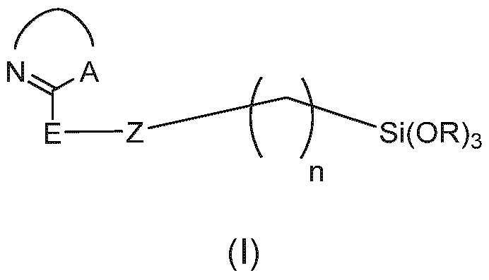
- I is selected from the group consisting of mixtures thereof; X and Y are independently selected from the group consisting of NH 2 ,
- E is selected from the group consisting of -S- , -NH- and -NH-(CH 2 ) m -NH-;
- A is selected from the group consisting of NH, N(NH 2 ) and S;
- Z is selected from the group consisting of m is an integer in the range from 2 to 12, n is an integer in the range from 1 to 12, o is an integer in the range from 2 to 12,
- R independently denotes (CH 2 -CH 2 -0) P -T, wherein independently p is 0, 1, 2, 3, or 4, and T denotes H or C1 to C5 alkyl; or
- step (1-c) is performed prior to step
- the adhesion strength between the copper, copper alloy or copper oxide and an organic material can be increased without etching or a noticeable removal of copper, copper alloy or copper oxide. It can be shown that whereas the relative surface area (RSAI) of the copper, copper alloy or copper oxide is increased, the average surface roughness (Ra) is not increased. In other words, after step (i) the average surface roughness of the copper, copper alloy or copper oxide is substantially the same compared to the start of step (i). This differentiates the method of the present inven tion over a number of known methods, in particular etching methods, which have the goal to increase the total surface area by roughening. Therefore, the method of the present invention is preferably a non-etching method.
- the copper, copper alloy or copper oxide comprises a copper, copper alloy or copper oxide circuitry, preferably is a copper, copper alloy or copper oxide circuitry.
- the copper, copper alloy or copper oxide circuitry is structured. It preferably means that the organic material simulta neously exposes on the same side non-conductive (preferably organic) areas as well as conductive copper, copper alloy or copper oxide areas. This is most preferred in the con- text of the method of the present invention.
- step (i) the copper, copper alloy or copper oxide forms at least one layer on the substrate.
- this layer or these layers can be structured and can form or be a circuitry.
- step (i) and/or preferably after step (ii)
- the copper, copper alloy or copper oxide circuitry comprises lines with a line width of 100 pm or less, preferably 75 pm or less, more preferably 55 pm or less.
- a method of the present invention is preferred, wherein in step (i) (and/or preferably after step (ii)) the copper, copper alloy or copper oxide circuitry comprises lines with a line width of 30 pm or less, preferably of 20 pm or less, most preferably of 10 pm or less.
- the substrate comprises copper (I) and copper (II) in a ratio of 90:10 or higher (mol/mol), preferably in a ratio of 95:5 or higher (mol/mol), even more preferably in a ratio of 98:2 or higher (mol/mol), most preferably the copper oxide essentially consists of copper (I) oxide; (iii) applying the organic material.
- step (i-c) is performed by means of contacting the at least one section of said copper, copper alloy or copper oxide with an aqueous alkaline solution comprising one or more than one complexing agent.
- step (i-c) comprises contacting at least one section of said copper, cop per alloy or copper oxide with an aqueous alkaline solution comprising one or more than one complexing agent.
- the alkaline solution of the method of the present invention is an aqueous alkaline solution.
- aqueous denotes that the solution comprises wa ter.
- Preferred is a solution utilized in the method of the present invention, wherein more than 50 vol% of the total volume of the oxidizing solution is water, preferably 70 vol% or more, more preferably 80 vol% or more, even more preferably 90 vol% or more, most preferably 95 vol% or more. Most preferably, the solution comprises water with the proviso that water is the only solvent.
- alkaline means that the solution has a pH of more than 7, preferably of 9 or more, even more preferably of 11 or more, most preferably of 12.5 or more.
- a solution in step (i-c) of the method of the present invention wherein the pH is in a range from 8 to 14, more preferably in a range from 9 to 14, even more preferably in a range from 10 to 14, yet even more preferably in a range from 11 to 14, most preferably in a range from 12 to 14.
- the solution comprises hydroxide ions, preferably in a concentration in a range from 0.1 mol/L to 2.0 mol/L, based on the total volume of the solution, preferably in a range from 0.2 mol/L to 1.8 mol/L, even more preferably in a range from 0.3 mol/L to 1.6 mol/L, yet even more preferably in a range from 0.4 mol/L to 1.5 mol/L, most preferably in a range from 0.5 mol/L to 1.2 mol/L.
- concentrations result in a preferably strong alkaline oxidizing solution, e.g. pH 13 or higher.
- Preferred is a solution comprising one or more than one source of hydroxide ions, prefer ably one source of hydroxide ions.
- a preferred source of hydroxide ions is an inorganic hydroxide, an organic hydroxide, or mixtures thereof.
- An inorganic hydroxide is preferably selected from the group consisting of ammonium hydroxide and alkaline hydroxides, is preferably selected from the group consisting of ammonium hydroxide, sodium hydroxide, and potassium hydroxide.
- a pre ferred organic hydroxide is an alkyl ammonium hydroxide, preferably tetra alkyl ammonium hydroxide, more preferably tetra methyl ammonium hydroxide.
- the aqueous alkaline solution comprises one or more than one copper complexing agent.
- the complexing agent typically serves to complex copper ions that are solubilized when applying the alkaline solution on the copper surface, which avoids formation of insoluble copper hydroxides.
- a complexing agent for copper ions prevents or at least sig nificantly reduces such hydroxide formation.
- the alkaline solution additionally comprises one or more than one com plexing agent for complexing copper ions, preferably one or more than one complexing agent comprising at least one carboxylic group and at least one hydroxyl group.
- the one or more than one complexing agent comprises a sugar, preferably a monomeric sugar.
- the one or more than one complexing agent for complexing copper ions comprises gluconic acid and/or salts thereof, most preferably the only complexing agent for complexing copper ions in the al kaline solution is gluconic acid and/or salts thereof.
- the one or more than one complexing agent has a total concentration in a range from 5 mmol/L to 400 mmol/L, based on the total volume of the alkaline solution, preferably in a range from 10 mmol/L to 300 mmol/L, more preferably in a range from 15 mmol/L to 200 mmol/L, even more preferably in a range from 20 mmol/L to 100 mmol/L, yet even more preferably in a range from 25 mmol/L to 80 mmol/L, most preferably in a range from 30 mmol/L to 60 mmol/L.
- the aforementioned concentrations are preferably applicable to aforementioned preferred complexing agents, most preferably to gluconic acid and salts thereof.
- step i-c the temperature of the aqueous alkaline solution is in a range from 20°C to 80°C, preferably in a range from 25°C to 75°C, more preferably in a range from 30°C to 70°C, even more preferably in a range from 35°C to 65°C, most preferably in a range from 40°C to 60°C.
- step (i) additionally contains sodium chlorite or oxidising agent.
- step (i-c) can be applied as dip application. Dip application means that the solution is provided in form of a bath into which the copper, copper alloy or copper oxide are dipped. It has been further found that contact times of 40 s or longer are pre ferred.
- the contact time in step (i-c) is of from 40s to 900 s, more preferably the contact time in step (i-c) is of from 60 s to 500 s, even more preferably the contact time in step (i-c) is of from 90 s to 450 s.
- step (i-c) can be applied as spray application.
- Spray application means that the solution is transferred into a spray dispenser and then sprayed onto the copper, copper alloy or copper oxide. It has been further found that con- tact times of 10 s already yields good results. Hence, contact times of 10 s or longer are preferred.
- the contact time in step (i-c) is of from 20s to 200 s, more preferably the contact time in step (i-c) is of from 30 s to 150 s.
- X and Y are independently selected from the group consisting of NH 2 , NH(NH 2 ), NH(CH 2 ) O NH 2 , SH, SCHS, and OCH 3 ;
- E is selected from the group consisting of -S- , -NH- and -NH-(CH 2 ) m -NH-;
- A is selected from the group consisting of NH, N(NH 2 ) and S;
- Z is selected from the group consisting of m is an integer in the range from 2 to 12, n is an integer in the range from 1 to 12, o is an integer in the range from 2 to 12,
- R independently denotes (CH 2 -CH 2 -0) P -T, wherein independently p is 0, 1, 2, 3, or 4, and T denotes H or C1 to C5 alkyl; or
- step (1-c) is performed prior to step
- step (iii) applying the organic material.
- the contacting in step (ii) can be applied as dip application.
- Dip application means that the solution is provided in form of a bath into which the copper, copper alloy or copper oxide are dipped.
- step (ii) can be applied as spray application.
- Spray application means that the solution is transferred into a spray dispenser and then sprayed onto the copper, copper alloy or copper oxide.
- step (ii) can be applied as coating application such as bar coating, spin coating and curtain coating.
- the method according to the invention is preferably performed at temperatures of from 5°C to 60°C, more preferably from 10°C to 40°C, even more preferably from 20°C to 30°C.
- Triazine silane compounds One embodiment of the inventive method refers to a specific triazine silane compound as defined above. In many cases a triazine silane compound of the present invention is pre ferred, wherein Y denotes NH and N(NH2), preferably NH. In other cases a triazine silane compound of the present invention is preferred, wherein Y denotes S. Among both, a Y comprising a nitrogen is preferred compared to a Y being S.
- a triazine silane compound of the present invention is preferred, wherein X denotes NH2, NH(NH2), NH(CH2) O NH2, SH, SCH3, or OCH3, wherein o is an integer in the range from 2 to 12; preferably NH2, NH(NH2), NH(CH2) 0 NH2, SH, orSCHs, wherein o is an integer in the range from 2 to 12; more preferably NH2.
- a triazine silane compound of the present invention being a compound of formula (II) wherein m is an integer in the range from 2 to 10, n is an integer in the range from 1 to 10,
- R independently denotes (CH 2 -CH 2 -O) P -T, wherein independently p is 0, 1, 2, 3, or 4, and T denotes H or C1 to C5 alkyl.
- a triazine silane compound of the present invention being a compound of formula (III) wherein m is an integer in the range from 2 to 10, n is an integer in the range from 1 to 10,
- R independently denotes (CH 2 -CH 2 -O) P -T, wherein independently p is 0, 1, 2, 3, or 4, and T denotes H or C1 to C5 alkyl.
- Particularly preferred is a compound of formula (Ilia).
- the term “independently being” (or similar expres sions) in combination with a certain variable denotes that a selected feature for such a variable in a first compound is independent from a selected feature of the same variable in a second compound and, if one compound contains the same variable at least twice, it is independently selected from each other, and thus can be different. This principle likewise applies to other “independently” terms.
- One embodiment of the inventive method refers to a specific tetrazole silane compound as defined above.
- a tetrazole silane compound of the present invention of formula (IV) is preferred, wherein n is an integer in the range from 1 to 10,
- R independently denotes (CH 2 -CH 2 -O) P -T, wherein independently p is 0, 1, 2, 3, or 4, and
- T denotes H or C1 to C5 alkyl.
- tetrazole silane compound of the present invention being a compound of formula (IVa) Triazole / Thiodiazole silane compounds
- One embodiment of the inventive method refers to a specific tri azole or a thiodiazole silane compound as defined above. In many cases a triazole or a thiodiazole silane compound of formula (V) is preferred, wherein
- X denotes NH 2 , NH(NH 2 ), NH(NHU), NH(CH 2 ) 0 NH 2 , SH, SCH 3 , OCH 3 , NHU, or SU,
- Y denotes NH, N(NH 2 ), N(NHU), or S
- U independently denotes CH 2 -CH(0H)-CH 2 -0-(CH 2 ) n -Si(0R) 3 , with R independently being (CH 2 -CH 2 -0) p -Z, wherein independently n is an integer in the range from 1 to 10, o is an integer in the range from 2 to 12, p is 0, 1, 2, 3, or 4, and
- Z denotes H or C1 to C5 alkyl.
- X denotes NH 2 , NH(NH 2 ), NH(CH 2 ) 0 NH 2 , SH, SCH 3 , or OCH 3 , wherein o is an integer in the range from 2 to 12; preferably NH 2 , NH(NH 2 ), NH(CH 2 ) 0 NH 2 , SH, or SCH 3 , wherein o is an integer in the range from 2 to 12; more preferably NH 2 .
- thiodiazole or tri azole silane compound of the present invention being a compound of formula (Va) or (Vb)
- the present invention also relates to a synthesis method for a tetrazole silane compound of formula (IV):
- R independently denotes (CH 2 -CH 2 -0) P -T, wherein independently p is 0, 1, 2, 3, or 4, and T denotes H or C1 to C5 alkyl, the synthesis method comprising the steps of
- R independently denotes (CH 2 -CH 2 -0) P -T, wherein independently p is 0, 1, 2, 3, or 4, and T denotes H or C1 to C5 alkyl,
- step (iii) the solvent is one or more than one solvent selected from the group consisting of glycol ethers, and mixtures thereof, preferably selected from the group consisting of
- T denotes C1 to C5 alkyl, preferably C3 to C5 alkyl, and mixtures thereof, more preferably selected from the group consisting of diethylene glycol monobutyl ether, ethylene glycol monobutyl ether, and mixtures thereof, even more preferably selected from the group consisting of diethylene glycol monobutyl ether, ethylene glycol monobutyl ether, and mixtures thereof.
- glycol ethers are more preferred than above defined alcohols (for reasons see text above).
- a respective synthesis method of the present invention is preferred.
- step (iii) is substantially free of, preferably does not comprise, water.
- the solvent in step (iii) is one or more than one organic solvent and after step (iii) of the method of the present invention a mixture according to the present invention is obtained (for the mixture see text above).
- a mixture according to the present invention is obtained (for the mixture see text above).
- the aforementioned regarding the mixture of the present invention applies likewise to the synthesis method of the present invention.
- step (iii) the tempera ture is in the range from 50°C to 100°C, preferably in the range from 60°C to 90°C.
- step (i) the tetrazole compound of formula (III) is provided as a suspension. This means that it is preferred to suspend the tetrazole compound of formula (III) in at least one solvent such that said te trazole compound and said at least one solvent form said suspension.
- the at least one solvent is one or more than one organic solvent, preferably is one or more than one water miscible organic solvent.
- the at least one solvent utilized to form said suspension is identical to the solvent utilized in step (iii).
- the tetrazole compound of formula (III) is suspended in one or more than one solvent selected from the group consisting of C1 to C4 alcohols, glycol ethers, and mix- tures thereof, preferably selected from the group consisting of
- - cyclic and non-cyclic ethers such as diethyl ether, tetrahydrofuran, 1,4-dioxane, and mixtures thereof, preferably 1 ,4-dioxane, tetrahydrofuran and mixtures thereof,
- T denotes C1 to C5 alkyl, preferably C3 to C5 alkyl, and mixtures thereof, more preferably selected from the group consisting of methanol, diethylene glycol monobutyl ether, ethylene glycol monobutyl ether, and mixtures thereof, most preferably selected from the group consisting of diethylene glycol monobutyl ether, ethylene glycol monobutyl ether, and mixtures thereof.
- step (iii) is a synthesis method of the present invention, wherein in step (iii) the reacting is carried out for 1 hour to 48 hours, preferably for 3 hours to 30 hours, more preferably for 5 hours to 24 hours.
- the silane compound and, where applicable, the silane oligomer can be present as a mixture.
- more than one compound can be present as a mixture.
- an organic solvent facilitates solu bility.
- the present invention also refers to a mixture comprising, preferably consisting of,
- the method according to the invention is preferred, wherein the mixture of the present invention is substantially free of, preferably does not comprise, halide ions.
- the term “substantially free” of a subject-matter denotes that said subject-matter is not present at all or is present only in (to) a very little and undisturbing amount (extent) without affecting the in tended purpose of the invention.
- a subject-matter e.g. a compound, a material, etc.
- such a subject-matter might be added or utilized unintentionally, e.g. as unavoidable impurity.
- “Substantially free” preferably de notes 0 (zero) ppm to 50 ppm, based on the total weight of the mixture (if defined for said mixture), preferably 0 ppm to 25 ppm, more preferably 0 ppm to 10 ppm, even more pref erably 0 ppm to 5 ppm, most preferably 0 ppm to 1 ppm.
- Zero ppm denotes that a respec tive subject-matter is not comprised at all, which is most preferred. This principle applies likewise to other aspects of the present invention, e.g. the storage solution of the present invention (see text below) and the working solution of the present invention (see also text below).
- the one or more than one organic solvent of the mixture comprises a solvent selected from the group consisting of acetone, 1,3-dioxolane, acetonitrile, 1 ,4-dioxane, methanol, ethanol, 1 -propanol, 2-propanol, /-bu tanol, prop-2-en-1-ol, ethyl lactate, ethylene glycol monomethyl ether acetate, N,N-dime- thylformamide, 2-butoxyethanol, di(propylene glycol) methyl ether, tetrahydrofurfuryl alco hol, N-methyl-2-pyrrolidone, 2- (2- m eth oxy eth oxy) eth an ol , gamma- butyrolactone, eth ylene glycol, propylene glycol, dipropylene glycol, eps/Von-caprolactone,
- the one or more than one organic solvent of the mixture comprises a solvent selected from the group consisting of methanol, ethanol, 1 -propanol, 2-propanol, f-butanol, di(propylene glycol) methyl ether, ethylene glycol, propylene glycol, dipropylene glycol, diethylene glycol monobutyl ether, ethylene glycol monobutyl ether, and mixtures thereof.
- the one or more than one organic solvent of the mixture comprises a solvent selected from the group consisting of glycol ethers, preferably selected from the group consisting of di (pro pylene glycol) methyl ether, diethylene glycol monobutyl ether, ethylene glycol monobutyl ether, and mixtures thereof.
- the present invention also refers to a storage solution comprising
- the storage solution of the present invention is substantially free of, preferably does not comprise, halide ions. Only in a few cases it is preferred that halide ions are present by intentionally adding halide ions, preferably by intentionally adding chloride ions.
- Above described storage solution optionally contains water.
- a storage solution of the present invention wherein in the storage solution is alkaline and water is present in a total amount in the range from 10 wt.-% to 80 wt.-%, based on the total weight of the storage solution, preferably in the range from 15 wt.-% to 78 wt.-%, more preferably in the range from 20 wt-% to 76 wt-%, even more preferably in the range from 33 wt-% to 74 wt-%, most preferably in the range from 38.6 wt-% to 70 wt.-%.
- the storage solution contains one or more than one water miscible organic solvent.
- Such an organic solvent facilitates the needed solubility of the respective silane compounds and its oligomers, particular if they are present at comparatively higher concentrations (e.g. up to and around 15 wt.-%, see text above).
- a storage solution of the pre sent invention wherein in said solution the one or more than one water miscible organic solvent is present in a total amount in the range from 5 wt.-% to 89.5 wt.-%, based on the total weight of the storage solution, preferably in the range from 10 wt.-% to 84.2 wt.-%, more preferably in the range from 14 wt.-% to 79 wt.-%, even more preferably in the range from 18 wt.-% to 65.5 wt.-%, most preferably in the range from 24 wt.-% to 59 wt.-%.
- a storage solution of the present invention is preferred, wherein the total weight of water is lower than the total weight of all water miscible organic solvents.
- said storage solution is alkaline, if water is present.
- An acidic pH is not suitable for storage purposes because at such a pH precipitation has been observed in many cases with comparatively high concentra tions of silane compounds of the present invention and its corresponding oligomers.
- the instant silanes solutions exhibit a good stability, i.e. no phase separation and no degradation, in a broad temperature window.
- those solutions are sta ble from -5°C to 50°C.
- the pH is referenced to a temperature of 25°C.
- the alkaline pH is obtained by pref erably utilizing at least one alkaline hydroxide, most preferably by utilizing sodium hydrox ide.
- An alkaline pH does not only allow comparatively high concentrations of said silane com pounds and its oligomers, respectively, in the storage solution. It furthermore strongly maintains the silane compounds of the present invention in its monomeric state and sig nificantly reduces the formation of silane oligomers of the present invention. However, if such an oligomer is formed in the alkaline storage solution of the present invention, it is typically quickly hydrolyzed to form its monomeric forms due to the alkaline pH. In the storage solution of the present invention this is desired.
- a storage solution of the present invention is preferred, wherein for at least 80 wt.-% of the total weight of all silane compounds according to the present invention Z is H and p is zero, preferably for at least 90 wt.-%, most preferably for at least 95 wt.-%. This means that in the storage solution the silane compound is mostly present in its hydro lyzed form comprising SiOH-groups.
- storage solution is in particular suitable in order to transport and/or stor- age the one or more than one silane compound of the present invention.
- a respective working solution is preferred.
- the present invention further relates to a working solution having a pH in the range from 2 to 14, the solution comprising
- 10 wt.-% or less does not include zero wt.-%. This means that said total amount is always > 0 wt.-%, preferably at least 0.1 wt.-%.
- a working solution of the present invention wherein in said working solution the total amount of all silane compounds according to the present invention (as described throughout the present text, preferably as described as being preferred) and all silane oligomers according to the present invention (as described throughout the present text, preferably as described as being preferred) together is in the range from 0.1 wt.-% to 6 wt.-%, based on the total weight of the working solution, preferably is in the range from 0.2 wt.-% to 5 wt.-%, more preferably is in the range from 0.3 wt.-% to 4 wt.-%, even more preferably in the range from 0.4 wt.-% to 3.7 wt.-%, most preferably is in the range from 0.5 wt.-% to 3.5 wt.-%.
- the working solution of the present invention comprises
- a respec tive working solution comprising at least one compound and at least one oligomer is most preferred.
- the working solution of the present invention has a pH in the range from 2 to 14.
- Preferred is a working solution of the present invention, wherein the pH is in the range from 3.5 to 14, more preferably in the range from 4.0 to 13.5.
- a working solution of the present invention wherein in said solution water is present in a total amount in the range from 5 wt.-% to 90 wt.-%, based on the total weight of the working solution, preferably in a total amount in the range from 10 wt.-% to 85 wt- %, more preferably in a total amount in the range from 15 wt.-% to 80 wt.-%.
- one or more than one water miscible organic solvent is present.
- silane compounds of the pre sent invention as well as silane oligomers of the present invention are initially free of hal ides.
- said compounds and oligomers, respectively are in itself free of halide atoms because no educts containing halogen atoms are utilized, and on the other hand no halide ions are present in the immediate synthesis environment.
- the working solution of the present invention comprises a precisely defined amount of halide ions. Therefore, in some cases a working solution of the present invention is preferred further comprising
- the working solution of the present invention is substantially free of, preferably does not comprise, chloride ions, more preferably is sub stantially free of, preferably does not comprise, halide ions.
- One or more than one water miscible organic solvent is present in both the storage solution of the present invention and the working solution of the present invention.
- Preferred is an storage solution according to the present invention (as described throughout the present text, preferably as described as being preferred), or a working solution according to the present invention (as described throughout the present text, preferably as described as being preferred), wherein the one or more than one water miscible organic solvent com prises a water-miscible organic solvent selected from the group consisting of C1 to C4 alcohols, ethers, glycol ethers, and mixtures thereof, preferably selected from the group consisting of
- - cyclic and non-cyclic ethers such as diethyl ether, tetrahydrofuran, 1 ,4-dioxane, and mixtures thereof, preferably 1 ,4-dioxane, tetrahydrofuran and mixtures thereof,
- T denotes C1 to C5 alkyl, preferably C3 to C5 alkyl, and mixtures thereof, more preferably selected from the group consisting of methanol, diethylene glycol monobutyl ether, ethylene glycol monobutyl ether, and mixtures thereof, even more preferably selected from the group consisting of diethylene glycol monobutyl ether, ethylene glycol monobutyl ether, and mixtures thereof.
- glycol ethers are more preferred than alcohols. Glycol ethers typically pro vide an improved stabilization compared to said alcohols. Furthermore, alcohols in general exhibit a low flash point compared to glycol ethers, which makes alcohols potentially dan gerous in terms of fire hazard. A comparatively high flash point is usually desired in order to prevent an ignition. Thus, glycol ethers typically provide the desired solubility, stability and security. This principle preferably applies likewise to the mixture of the present inven tion, the storage solution of the present invention, and the synthesis method of the present invention (see text below).
- a storage solution according to the present invention (as described throughout the present text, preferably as described as being preferred), or a working solution ac cording to the present invention (as described throughout the present text, preferably as described as being preferred), wherein all silane compounds according to the present in vention (as described throughout the present text, preferably as described as being pre ferred) and all silane oligomers according to the present invention (as described through out the present text, preferably as described as being preferred) represent at least 70 wt- % of the total weight of all silane compounds and oligomers in said storage solution and said working solution, respectively, preferably represent at least 80 wt.-%, more preferably represent at least 90 wt-%, even more preferably represent at least 93 wt-%, most pref erably represent at least 95 wt.-%, even most preferably represent at least 98 wt.-%.
- silane compounds or oligomers are present, except those according to the present invention.
- the absolute total amounts of silane compounds and silane oligomers together very preferably apply with the proviso that no other silane compounds and silane oligomers are present in the storage solution of the present invention and working solution of the present invention, respectively.
- a storage solution according to the present invention (as de- scribed throughout the present text, preferably as described as being preferred), or a working solution according to the present invention (as described throughout the present text, preferably as described as being preferred), wherein all silane compounds according to the present invention (as described throughout the present text, preferably as described as being preferred) and all silane oligomers according to the present invention (as de scribed throughout the present text, preferably as described as being preferred) represent at least 51 mol-% of all compounds comprising at least one silicon atom in said storage solution and said working solution, respectively, preferably represent at least 60 mol-%, more preferably represent at least 70 mol-%, most preferably represent at least 80 mol-%, even most preferably represent at least 90 mol-%.
- the adhesion strength (e.g. peel strength) between a copper and an organic material can be increased without using any etch-clean ing steps. But some cases - especially cases where a surface roughness of the copper surface does not affect the quality of the circuits - a further etch-cleaning step can be performed. In this case the adhesion strength between a copper and an organic material can be increased even further.
- the method according to the invention is preferred, additionally comprising the following step before conducting step (ii): (i-a) contacting the at least one section of said copper, copper alloy or copper oxide with an etch-cleaning solution, preferably an etch-cleaning solution containing one or more than one acid and/or one or more than one oxidizing agent, more preferably an etch-cleaning solution containing a mixture of an inorganic acid and a peroxide (preferably a mixture of sulfuric acid and hydrogen peroxide).
- an etch-cleaning solution preferably an etch-cleaning solution containing one or more than one acid and/or one or more than one oxidizing agent, more preferably an etch-cleaning solution containing a mixture of an inorganic acid and a peroxide (preferably a mixture of sulfuric acid and hydrogen peroxide).
- the oxidizing agent is a peroxide, more preferably when the peroxide is hydrogen peroxide.
- the etch-cleaning solution com prises in addition to the acid and/or to the one or more than one oxidizing agent a corrosion inhibitor.
- the method according to the invention is preferred, additionally comprising the following step before conducting step (ii): (i-b) contacting the at least one section of said copper, copper alloy or copper oxide with a (preferably second) etch-cleaning solution.
- step (i-b) is carried out after step (i-a) the used etch-cleaning solution is the second etch cleaning solution.
- step i-b is carried out without a previous etch-cleaning step, the used etch-cleaning solution is the first etch-cleaning solution.
- the second etch-cleaning solution comprises an iron (III) salt or an iron (III) complex, more preferably the second etch-cleaning solution com prises ferric sulfate (Fe2(SC>4)3), ferric chloride (FeCh), bromide, ferric (FeBrs), ferric nitrate (Fe(NC>3)3), ferric acetate (Fe(0C(0)CH3)3), (Fe(OH)3), or mixtures thereof, even more preferably the second etch-cleaning solution comprises ferric sulfate (Fe2(SC>4)3).
- the Fer ric ion is preferably contained at a concentration in the range of 1 to 100 g/l, preferably from 1 to 50 g/l, and more preferably from 1 to 30 g/l.
- the second etch-cleaning solution comprises an inorganic acid, more preferably the second etch-cleaning solution comprises sulfuric acid, hydrochloric acid or mixtures thereof, even more preferably the second etch cleaning solution comprises sulfuric acid.
- a typical copper, copper alloy or copper oxide removal during step i-a is less than 2 pm, preferably, the removal is of from 0.1 pm to 1.5 pm, more preferably, the removal is of from 0.2 pm to 1.2 pm, even more preferably, the removal is of from 0.4 pm to 1.1 pm, most preferably, the removal is of from 0.5 pm to 1.0 pm; and resulting average surface roughness Ra is a maximum of 100 nm.
- a typical copper, copper alloy or copper oxide removal during step i-b is less than 20 nm and resulting average surface roughness Ra is a maxi mum of 10 nm, preferably, a maximum of 5 nm.
- the method according to the invention is preferred, additionally comprising the following step before conducting step (ii): (i-c) contacting the at least one section of said copper, copper alloy or copper oxide with a solution, preferably a sodium hydroxide solution. It is preferred if the solution contain copper complexing agents.
- the solution used in step i- c additionally contains sodium chlorite or oxidising agent.
- the use of sodium chlorite or oxidising agent in the solution used in step i-c is especially preferred if in step i-b no iron (III) salt or an iron (III) complex is used or if step i-b is not performed during the method according to the present invention.
- the order of the steps (i-a), (i-b), and (i-c) may vary.
- the method according to the invention can be carried out in the following order: (i-a), (i-b), (i-c), or (i-a), (i-c), (i-b), or (i-b), (i-a), (i-c), or (i-b), (i-c), (i-a), or (i-c), (i-a), (i-b), or (i-c), (i-b), (i-a).
- the order (i-a), (i-b), (i-c) is preferred. It is also possible that none, one or two of the steps (i-a), (i-b), (i-c) are performed in the method according to the invention.
- step (iii) is an organic polymer.
- step (iii) by laminating the organic material onto at least the contacted section of the copper, copper alloy or copper oxide.
- the method according to the invention is preferred, comprising after step (iii) the additional step: (iv) subjecting the substrate and the organic material to a heat treatment with a tem perature in the range from 142°C to 420°C, preferably in the range from 145°C to 300°C, more preferably in the range from 150°C to 220°C.
- the water that is used during rinsing after step (ii) has a pH-value in the range from 2 to 14, preferably 4 to 10, more preferably in the range from 5 to 9, even more preferably in the range from 6 to 8, most preferably in the range from 6.5 to 7.5.
- step (ii) no baking of the at least one section of copper, copper alloy or copper oxide is per formed. It could be shown (Table 4 below) that samples that were yielded by avoiding of the baking step leads to improved halo formation when compared to samples that were subjected to baking.
- a method according to the present invention is especially preferred comprising the follow ing steps in this order: (i) providing a substrate, comprising the copper, copper alloy or copper oxide on at least one side of the substrate,
- etch-cleaning solution optionally contacting at least one section of said copper, copper alloy or copper oxide with an etch-cleaning solution, preferably an etch-cleaning solution containing one or more than one acid and/or one or more than one oxidizing agent, more preferably an etch-cleaning solution containing a mixture of an inorganic acid and a peroxide, and optionally followed by rinsing of the at least one section of the copper, copper alloy or copper oxide (preferably with water),
- an etch-cleaning solution preferably an etch-cleaning solution containing one or more than one acid and/or one or more than one oxidizing agent, more preferably an etch-cleaning solution containing a mixture of an inorganic acid and a peroxide
- E is selected from the group consisting of -S- , -NH- and -NH-(CH 2 ) m -NH-;
- A is selected from the group consisting of NH, N(NH 2 ) and S;
- Z is selected from the group consisting of m is an integer in the range from 2 to 12, n is an integer in the range from 1 to 12, o is an integer in the range from 2 to 12, R independently denotes (CH 2 -CH 2 -0) P -T, wherein independently p is 0, 1, 2, 3, or 4, and T denotes H or C1 to C5 alkyl; or
- step (i-c) and (ii) are performed, and optionally followed by rinsing of the at least one section of the copper, copper alloy or copper oxide (preferably with water), (iii) applying the organic material such that the at least one section of the copper, copper alloy or copper oxide contacted with the triazine silane compound and/or the triazine silane oligomer during step (ii) is in contact with the applied organic material, and (iv) optionally subjecting the substrate and the organic material to a heat treatment with a temperature in the range from 142°C to 420°C, preferably in the range from 145°C to 300°C, more preferably in the range from 150°C to 220°C.
- a method according to the present invention is preferred, wherein the substrate is a non- conductive substrate and/or the organic material is a non-conductive organic material, preferably a non-conductive organic polymer.
- the method according to the invention is preferred, wherein the method comprises both steps (i-c) and (ii).
- the method comprises both steps (i-c) and (ii).
- a method for increasing adhesion strength and/or improved wedge void behavior between a surface of copper, a copper alloy or a copper oxide and a surface of an organic material comprising
- the substrate comprises copper (I) and copper (II) in a ratio of 90:10 or higher (mol/mol), preferably in a ratio of 95:5 or higher (mol/mol), even more preferably in a ratio of 98:2 or higher (mol/mol), most preferably the copper oxide essentially consists of copper (I) oxide; and
- X and Y are independently selected from the group consisting of NH 2 , NH(NH 2 ), NH(CH 2 ) O NH 2 , SH, SCHS, and OCH 3 ;
- E is selected from the group consisting of -S- , -NH- and -NH-(CH 2 ) m -NH-;
- A is selected from the group consisting of NH, N(NH 2 ) and S;
- Z is selected from the group consisting of m is an integer in the range from 2 to 12, n is an integer in the range from 1 to 12, o is an integer in the range from 2 to 12,
- R independently denotes (CH 2 -CH 2 -0) P -T, wherein independently p is 0, 1, 2, 3, or 4, and T denotes H or C1 to C5 alkyl; or (b) at least one amino acid; or a mixture of (a) and (b), wherein, step (1-c-) is performed prior to step (ii);
- step (iii) applying the organic material.
- step (ii) the at least one section of the substrate is contacted with both (a) a silane of formula (I) and (b) at least one amino acid.
- a method for increasing adhesion strength and/or improved wedge void behavior between a surface of copper, a copper alloy or a copper oxide and a surface of an organic material comprising (i) providing a substrate, comprising the copper, copper alloy or copper oxide on at least one side of the substrate, followed by at least one of the steps of
- the copper oxide comprises copper (I) and copper (II) in a ratio of 90:10 or higher (mol/mol), preferably in a ratio of 95:5 or higher (mol/mol), even more preferably in a ratio of 98:2 or higher (mol/mol), most preferably the copper oxide essentially consists of copper (I) oxide; and/or
- N V A ! is selected from the group consisting of mixtures thereof;
- X and Y are independently selected from the group consisting of NH 2 , NH(NH 2 ), NH(CH 2 ) O NH 2 , SH, SCH S , and OCH 3 ;
- E is selected from the group consisting of -S- , -NH- and -NH-(CH 2 ) m -NH-;
- A is selected from the group consisting of NH, N(NH 2 ) and S;
- Z is selected from the group consisting of m is an integer in the range from 2 to 12, n is an integer in the range from 1 to 12, o is an integer in the range from 2 to 12, R independently denotes (CH 2 -CH 2 -0) P -T, wherein independently p is 0, 1, 2, 3, or 4, and T denotes H or C1 to C5 alkyl; or (b) at least one amino acid; or a mixture of (a) and (b), wherein, if both steps (i-c) and (ii) are performed, step (1-c-) is performed prior to step (ii);
- step (i-c) comprises contacting at least one section of said copper, copper alloy or copper oxide with an aqueous alkaline solution comprising one or more than one complexing agent; preferably the one or more than one complexing agent com prising at least one carboxylic group and at least one hydroxyl group; more preferred, the one or more than one complexing agent comprising a sugar, preferably a mono meric sugar; even more preferred the one or more than one complexing agent for complexing copper ions comprising gluconic acid and/or salts thereof; most prefera bly the only complexing agent for complexing copper ions in the alkaline solution is gluconic acid and/or salts thereof.
- C The method according to embodiment B, wherein the aqueous alkaline solution in step (i-c) has a pH in the range of from
- step (i-c) is applied as dip application and the contact time is 40 s or longer, preferably the contact time in step (i-c) is of from 40s to 900 s, more preferably the contact time in step (i-c) is of from 60 s to 500 s, even more preferably the contact time in step (i-c) is of from 90 s to 450 s.
- step (i-c) is applied as spray application and the contact time is 10 s or longer, preferably the contact time in step (i-c) is of from 20s to 200 s, more preferably the contact time in step (i-c) is of from 30 s to 150 s.
- X and Y are independently selected from the group consisting of NH 2 , NH(NH 2 ), NH(CH 2 ) O NH 2 , SH, SCH S , and OCH 3 ;
- E is selected from the group consisting of -S- , -NH- and -NH-(CH 2 ) m -NH-;
- Z is selected from the group consisting of m is an integer in the range from 2 to 12, n is an integer in the range from 1 to 12, o is an integer in the range from 2 to 12,
- R independently denotes (CH 2 -CH 2 -0) P -T, wherein independently p is 0, 1, 2, 3, or 4, and T denotes H or C1 to C5 alkyl; or
- step (iii) is an organic polymer.
- step (iii) by laminating the organic material onto at least the contacted section of the copper, copper alloy or copper oxide.
- step (ii) if a step (ii) is per formed, additionally comprising the following step before conducting step (ii): (i-a) contacting the at least one section of said copper, copper alloy or copper oxide with an etch-cleaning solution, preferably an etch-cleaning solution containing one or more than one acid and/or one or more than one oxidizing agent, more preferably an etch-cleaning solution containing a mixture of an inorganic acid and a peroxide.
- an etch-cleaning solution preferably an etch-cleaning solution containing one or more than one acid and/or one or more than one oxidizing agent, more preferably an etch-cleaning solution containing a mixture of an inorganic acid and a peroxide.
- step (ii) is per formed, additionally comprising the following step before conducting step (ii):
- K The method according to any of the preceding embodiments, wherein after step (ii), after step (i-a), after step (i-b) and/or after step (i-c), a rinsing of the at least one section of the copper, copper alloy or copper oxide is performed, wherein the copper, copper alloy or copper oxide is preferably rinsed with water.
- L The method according to any of the preceding embodiments A to K, wherein after step (ii), after step (i-a), after step (i-b) and/or after step (i-c), a drying of the at least one section of copper, copper alloy or copper oxide is performed.
- the contacting time in step (ii) is from 5 seconds to 30 minutes, preferably from 7 seconds to 20 minutes, more preferably from 10 seconds to 10 minutes, even more preferably from 12 seconds to 5 minutes, most preferably from 15 seconds to 120 seconds.
- Figure 1 Top view SEM images (at different magnifications 2500x and 5000x) of cop per foils treated after different immersion time in the alkaline treatment so lution.
- Figure 2 Ra and RSAI values obtained from AFM investigations of the copper foils after different process steps: initial, after Differential Etch DE, after alkaline treatment and after alkaline treatment +Silane coating.
- Figure 3 Determined copper oxide thickness in nm formed on copper foils after dif ferent alkaline treatment time by integration of respective potential ranges with DSCV.
- Figure 4 FTIR grazing incidence measurement-Peak integration of CU2O signal by alkaline surface treatment time on copper foil. Integration performed over 683-616 cm- 1 .
- Figure 5 STEM image of Cu panel treated with an alkaline solution (300s dip) and coated with Silane a) EDS analysis of oxide particles performed at three different areas. The small amounts of some elements are coming from the microscope: Mo TEM-sample holder; Al, Zr EDX detector, Ft, Ga FIB Preparation, Fe, Co, Pb TEM column. b) STEM images at 200 mV, Nano-beam diffraction (NBD) line scan.
- Figure 6 Example of halo measurement
- ESI-MS confirms the formation of a compound comprising three methoxy groups con nected to the silicon atom.
- compounds comprising one, two, or three DEGBE moieties instead of respective methoxy groups also have been identified.
- Samples (each comprising several identical specimens) were prepared as follows.
- Copper foils having a copper surface were used. Under simplified laboratory conditions, copper foils without substrates are used for the examples.
- the preparation conditions are as follows:
- Electrolytically plated Copper type foil (adhesion test) panels (wedge void)
- the copper surfaces of the copper foils were treated by 25ml/l Hyperflash 25, 50ml/l H2SO4 50% and 65ml/l H2O235% at 30°C to achieve 0.5 or 1 pm etch depth. After the etch-clean ing the etch-cleaned copper surfaces were rinsed with water for approximately 30 seconds and optionally dried. As a result, etch-cleaned and rinsed copper surfaces were obtained.
- Copper surfaces of the substrates were immersed for 60 sec at 25°C into a coating solution containing a triazine silane compound and solvents. If water is present, the pH of the coat ing solution was 7 (triazole and tetrazole silanes) (adjusted with sulfuric acid, if needed) or up to 13.5 (triazine silanes). Details are given in Table 2.
- Copper foils were then annealed for 30 minutes at 130°C to remove remaining moisture from the surface. Note: this thermal treatment step is also known as baking. These sub- strates containing copper surfaces were subsequently subjected to laminating a build-up film (see text below).
- an insulating film (see Table 2) was vacuum laminated onto the cop- per foils of all samples in a clean room with a room temperature in the range from 20 to 25°C and with a relative humidity of 50 to 60% by using a vacuum laminator.
- the surface morphology was measured by means of Field Emission Scanning Electron Microscopy (FESEM).
- FEI NOVA Nanolab 600 and FEI Helios Nanolab 660 Microscopes were used to investigate surface as well as FIB prepared cross-sections.
- Atomic Force Microscopy was used to measure the surface roughness: for each sample, the surface was imaged on 5 measuring windows of 20 pm c 20 pm The average roughness R A , and the relative surface area increase RSAI were calculated.
- Figure 2 de picts how the roughness increases by alkaline treatment and remains unchanged after application of silane.
- the characterization of copper oxide was performed by means of Double- Sweep- Cyclic- Voltammetry (DSCV). Applied method used for Cu oxide quantification. During the first scan, cupric and cuprous oxides are reduced to Cu providing corresponding cathodic cur rents. Background currents are measured during the third scan in the same cathodic di- rections as the first scan. They are subtracted from the cathodic currents of the first scan in order to calculate the quantity of electrical charge required for the reduction of corre sponding Cu oxide species. Experiments were performed il LiCI (4 M) solution at RT, po tential range: -0.5 to -1.6 V (vs Ag/AgCI (3M KCI), Scan rates 100 mV/s, # of scans 3. o For scan rate 100 mV/s: ⁇ CuO: -0.5 to -1.08 V(vs Ag/AgCI (3M KCI))
- Elemental analysis of samples was carried out using Energy-dispersive X-ray spectros copy (EDS).
- EDS Energy-dispersive X-ray spectros copy
- STEM scanning transmission electron microscopy
- the ratio of Cu to O is 2 to 1 , indicating that the oxide particles formed by alkaline solution are of CU2O nature.
- NBD nano-beam diffraction
- HRTEM transmission elec tron microscopy
- HAST HAST conditions: 130°C, 85 % rh, HAST chamber: EHS-221M.
- the obtained copper surfaces with structurally enforced insulating films were then cured in an oven: copper surfaces with GL102 material at 200°C for 90 minutes and copper sur faces with GX-T31 material at 190 C for 90 min.
- each copper surfaces with structurally enforced insulating films was sliced into said strip-type fragments (10x100 mm, Bugard drilling/routing).
- the strip-type fragments were subjected to a peel force measuring machine (Roell Zwick Z010) to individually evaluate the peel strength (angle: 90°, speed: 50 mm/min) which is needed to delaminate the copper surface from its respective structurally enforced insulat ing films.
- the peel strength angle: 90°, speed: 50 mm/min
- the copper samples have been prepared by adhering the respective insulating films to copper panels. As a result, copper surfaces with structurally enforced insulating films were obtained.
- the obtained copper surfaces with structurally enforced insulating films were then semi- cured in two steps in the ovens: copper surfaces with GL102 material at 130°C for 30 minutes followed by 175°C for 30 minutes; and copper surfaces with GX-T31 material at 100°C for 30 minutes followed by 170°C for 30 minutes.
- the copper panels were lasered with UV-laser to drill the blind micro vias (BMV). Thereafter, the substrates were subjected to the desmear and reduction condition steps.
- the lamination material exhibits a thickness of ca. 10 pm for wedge void and halo and 35 pm in case of adhesion investigations, respectively. Measurements:
- the substrates were measured by light microscope (200x magnification; see Table 4). Pictures depicting the halo measurement can be found in Figure 6.
- the investigated test Blind Micro Via ' s are manufactured as a test grid on surface treated and Ajinomoto Build up Film (ABF) laminated test vehicles by utilizing Laser Drilling technology.
- the halo data is obtainable after sending the prepared test vehicles through entire Desmear process (Sweller, Permanganate, Reduction Conditioner) as described above.
- Halo measurement is performed by camera (CCD) supported light microscopy.
- CCD camera
- DF Darkfield
- the fully processed test vehicles are firmly installed on the measurement table and the BMV capture pad must be set as optical focus.
- CCD exposure time must be adjusted to the maximum possible contrast of halo boundaries.
- the capture pad should appear as bright as possible.
- Outer Halo( j um) (Outermost Diameter(jum) - Diameter of Via Hole(jum))/2 2.
- Inner Halo( j um) (Inner Diameter of Halo( j um) - Diameter of Via Hole(jum))/2
- this process is iterated at least three times at random test vias to enable minimal statistical statements.
- step (i-c) with step (ii) comprising T-E silane
- FIB Focused Ion Beam
- SEM Scanning Electron Microscopy
Landscapes
- Engineering & Computer Science (AREA)
- Manufacturing & Machinery (AREA)
- Microelectronics & Electronic Packaging (AREA)
- Chemical & Material Sciences (AREA)
- Chemical Kinetics & Catalysis (AREA)
- Manufacturing Of Printed Wiring (AREA)
- Chemical Treatment Of Metals (AREA)
- Other Surface Treatments For Metallic Materials (AREA)
Abstract
Description




Claims


Priority Applications (4)
| Application Number | Priority Date | Filing Date | Title |
|---|---|---|---|
| KR1020237034633A KR20230156114A (en) | 2021-03-12 | 2022-03-11 | Method for increasing adhesion strength between copper and organic materials and reducing halo and wedge void formation by modifying the copper surface and/or using heteroaromatic silane compounds |
| US18/550,145 US20240179851A1 (en) | 2021-03-12 | 2022-03-11 | Modified copper surface, heteroaromatic silane compounds and their usage for increasing adhesion strength between copper and an organic material and reducing halo and wedge void formation |
| CN202280027311.XA CN117121645A (en) | 2021-03-12 | 2022-03-11 | Methods to improve the adhesion strength between copper and organic materials and reduce the formation of halos and wedge-shaped pores by modifying the copper surface and/or by using heteroaromatic silane compounds |
| JP2023555629A JP2024510986A (en) | 2021-03-12 | 2022-03-11 | Method for increasing adhesive strength and reducing halo and wedge space formation between copper and organic materials by modifying copper surfaces and/or using heteroaromatic silane compounds |
Applications Claiming Priority (2)
| Application Number | Priority Date | Filing Date | Title |
|---|---|---|---|
| EP21162439.0 | 2021-03-12 | ||
| EP21162439.0A EP4057782A1 (en) | 2021-03-12 | 2021-03-12 | Method for increasing adhesion strength between copper and an organic material and reducing halo and wedge void formation by modifying the copper surface and/or by using heteroaromatic silane compounds |
Publications (1)
| Publication Number | Publication Date |
|---|---|
| WO2022189644A1 true WO2022189644A1 (en) | 2022-09-15 |
Family
ID=74874642
Family Applications (1)
| Application Number | Title | Priority Date | Filing Date |
|---|---|---|---|
| PCT/EP2022/056360 Ceased WO2022189644A1 (en) | 2021-03-12 | 2022-03-11 | Method for increasing adhesion strength between copper and an organic material and reducing halo and wedge void formation by modifying the copper surface and/or by using heteroaromatic silane compounds |
Country Status (7)
| Country | Link |
|---|---|
| US (1) | US20240179851A1 (en) |
| EP (1) | EP4057782A1 (en) |
| JP (1) | JP2024510986A (en) |
| KR (1) | KR20230156114A (en) |
| CN (1) | CN117121645A (en) |
| TW (1) | TW202302614A (en) |
| WO (1) | WO2022189644A1 (en) |
Families Citing this family (1)
| Publication number | Priority date | Publication date | Assignee | Title |
|---|---|---|---|---|
| EP4056285A1 (en) * | 2021-03-12 | 2022-09-14 | Atotech Deutschland GmbH & Co. KG | Triazine silane compound and its usage as adhesion promotor |
Citations (17)
| Publication number | Priority date | Publication date | Assignee | Title |
|---|---|---|---|---|
| JPH0136819B2 (en) | 1982-12-27 | 1989-08-02 | Eisai Co Ltd | |
| JPH06279461A (en) | 1993-03-29 | 1994-10-04 | Japan Energy Corp | Novel azole silane compound, method for producing the same, and metal surface treating agent using the same |
| JP2007131556A (en) * | 2005-11-09 | 2007-05-31 | Iwate Univ | Functional triazine dithiol and method for producing the same |
| JP2014240522A (en) | 2013-05-17 | 2014-12-25 | 四国化成工業株式会社 | Copper surface treatment liquid, surface treatment method and use thereof |
| JP2015092020A (en) * | 2013-10-02 | 2015-05-14 | 四国化成工業株式会社 | Surface treatment liquid of metal, surface treatment method and its utilization |
| JP2016169300A (en) | 2015-03-12 | 2016-09-23 | 四国化成工業株式会社 | Surface treatment agent, resin composition and use thereof |
| US20160368935A1 (en) | 2013-07-02 | 2016-12-22 | Shikoku Chemicals Corporation | Azole silane compound, surface treatment solution, surface treatment method, and use thereof |
| JP2017002402A (en) | 2015-06-04 | 2017-01-05 | 四国化成工業株式会社 | Surface preparation agent, resin composition, and utilization of them |
| JP2017048467A (en) * | 2013-09-20 | 2017-03-09 | 三井金属鉱業株式会社 | Copper foil, copper foil with carrier foil and copper clad laminate |
| CN107190254A (en) * | 2017-05-22 | 2017-09-22 | 博敏电子股份有限公司 | A kind of new brown treatment fluid of printed circuit board |
| JP2018016865A (en) | 2016-07-29 | 2018-02-01 | 四国化成工業株式会社 | Surface treatment agent, resin composition, and utilization of them |
| WO2019058773A1 (en) | 2017-09-22 | 2019-03-28 | 四国化成工業株式会社 | Tetrazole silane compound, method for synthesizing said compound and use thereof |
| WO2019243180A1 (en) | 2018-06-18 | 2019-12-26 | Atotech Deutschland Gmbh | Azole silane compound |
| WO2020148308A1 (en) * | 2019-01-15 | 2020-07-23 | Atotech Deutschland Gmbh | Method of forming copper oxide on a copper surface |
| WO2020178146A1 (en) | 2019-03-01 | 2020-09-10 | Atotech Deutschland Gmbh | Method for increasing adhesion strength between a metal and an organic material |
| JP6779557B1 (en) * | 2020-07-20 | 2020-11-04 | メック株式会社 | A composition for forming a film, a method for producing a surface-treated metal member, and a method for producing a metal-resin composite. |
| US20200399290A1 (en) | 2019-06-21 | 2020-12-24 | Imam Abdulrahman Bin Faisal University | Nanocomposite containing hollow silica spheres functionalized with azole silanes |
-
2021
- 2021-03-12 EP EP21162439.0A patent/EP4057782A1/en active Pending
-
2022
- 2022-03-11 TW TW111109117A patent/TW202302614A/en unknown
- 2022-03-11 WO PCT/EP2022/056360 patent/WO2022189644A1/en not_active Ceased
- 2022-03-11 JP JP2023555629A patent/JP2024510986A/en active Pending
- 2022-03-11 CN CN202280027311.XA patent/CN117121645A/en active Pending
- 2022-03-11 KR KR1020237034633A patent/KR20230156114A/en active Pending
- 2022-03-11 US US18/550,145 patent/US20240179851A1/en active Pending
Patent Citations (19)
| Publication number | Priority date | Publication date | Assignee | Title |
|---|---|---|---|---|
| JPH0136819B2 (en) | 1982-12-27 | 1989-08-02 | Eisai Co Ltd | |
| JPH06279461A (en) | 1993-03-29 | 1994-10-04 | Japan Energy Corp | Novel azole silane compound, method for producing the same, and metal surface treating agent using the same |
| JP2007131556A (en) * | 2005-11-09 | 2007-05-31 | Iwate Univ | Functional triazine dithiol and method for producing the same |
| JP2014240522A (en) | 2013-05-17 | 2014-12-25 | 四国化成工業株式会社 | Copper surface treatment liquid, surface treatment method and use thereof |
| US20160368935A1 (en) | 2013-07-02 | 2016-12-22 | Shikoku Chemicals Corporation | Azole silane compound, surface treatment solution, surface treatment method, and use thereof |
| JP2017048467A (en) * | 2013-09-20 | 2017-03-09 | 三井金属鉱業株式会社 | Copper foil, copper foil with carrier foil and copper clad laminate |
| JP2015092020A (en) * | 2013-10-02 | 2015-05-14 | 四国化成工業株式会社 | Surface treatment liquid of metal, surface treatment method and its utilization |
| JP2016169300A (en) | 2015-03-12 | 2016-09-23 | 四国化成工業株式会社 | Surface treatment agent, resin composition and use thereof |
| JP2017002402A (en) | 2015-06-04 | 2017-01-05 | 四国化成工業株式会社 | Surface preparation agent, resin composition, and utilization of them |
| JP6370836B2 (en) | 2015-06-04 | 2018-08-08 | 四国化成工業株式会社 | Surface treatment agent, resin composition and use thereof |
| JP6392273B2 (en) | 2015-06-04 | 2018-09-19 | 四国化成工業株式会社 | Epoxy resin composition and use thereof |
| JP2018016865A (en) | 2016-07-29 | 2018-02-01 | 四国化成工業株式会社 | Surface treatment agent, resin composition, and utilization of them |
| CN107190254A (en) * | 2017-05-22 | 2017-09-22 | 博敏电子股份有限公司 | A kind of new brown treatment fluid of printed circuit board |
| WO2019058773A1 (en) | 2017-09-22 | 2019-03-28 | 四国化成工業株式会社 | Tetrazole silane compound, method for synthesizing said compound and use thereof |
| WO2019243180A1 (en) | 2018-06-18 | 2019-12-26 | Atotech Deutschland Gmbh | Azole silane compound |
| WO2020148308A1 (en) * | 2019-01-15 | 2020-07-23 | Atotech Deutschland Gmbh | Method of forming copper oxide on a copper surface |
| WO2020178146A1 (en) | 2019-03-01 | 2020-09-10 | Atotech Deutschland Gmbh | Method for increasing adhesion strength between a metal and an organic material |
| US20200399290A1 (en) | 2019-06-21 | 2020-12-24 | Imam Abdulrahman Bin Faisal University | Nanocomposite containing hollow silica spheres functionalized with azole silanes |
| JP6779557B1 (en) * | 2020-07-20 | 2020-11-04 | メック株式会社 | A composition for forming a film, a method for producing a surface-treated metal member, and a method for producing a metal-resin composite. |
Non-Patent Citations (4)
| Title |
|---|
| "Corrosion protection of copper with 3-glycidoxypropyltrimethoxysilane-based sol-gel coating through 3-amino-5-mercapto-1,2,4-triazole doping", JOURNAL OF RESEARCH ON CHEMICAL INTERMEDIATES, vol. 42, 2015, pages 1315 - 1328 |
| "Reliability prediction in electronic packages using molecular simulation", ELECTRONIC COMPONENTS AND TECHNOLOGY CONFERENCE, 2005, pages 1314 - 1317 |
| "The role of oxide structure on copper wire to the rubber adhesion", APPLIED SURFACE SCIENCE, vol. 161, 2000, pages 355 - 364 |
| CHEM. EUR.J., vol. 15, 2009, pages 6279 - 6288 |
Also Published As
| Publication number | Publication date |
|---|---|
| JP2024510986A (en) | 2024-03-12 |
| US20240179851A1 (en) | 2024-05-30 |
| EP4057782A1 (en) | 2022-09-14 |
| CN117121645A (en) | 2023-11-24 |
| TW202302614A (en) | 2023-01-16 |
| KR20230156114A (en) | 2023-11-13 |
Similar Documents
| Publication | Publication Date | Title |
|---|---|---|
| DE60128364T2 (en) | IMPROVED LIABILITY OF POLYMER MATERIALS TO METAL SURFACES | |
| EP2341167B1 (en) | Method for surface treatment of copper and copper material | |
| KR101632450B1 (en) | Adhesion promotion of metal to laminate with a multi-functional compound | |
| EP2823084B1 (en) | Method for promoting adhesion between dielectric substrates and metal layers | |
| JP5663739B2 (en) | Copper surface conditioning composition and surface treatment method | |
| TWI732045B (en) | Manufacturing method of printed wiring board | |
| WO2009110364A1 (en) | Copper surface treatment agent and surface treatment method | |
| KR20190039093A (en) | A pretreatment liquid for electroless plating used simultaneously with a reduction treatment, and a method for manufacturing a printed wiring board | |
| WO2022189644A1 (en) | Method for increasing adhesion strength between copper and an organic material and reducing halo and wedge void formation by modifying the copper surface and/or by using heteroaromatic silane compounds | |
| JP3192431B2 (en) | Electroless copper plating solution and electroless copper plating method | |
| EP4459006A1 (en) | Surface treatment liquid for metal | |
| JP6846952B2 (en) | Rust preventive liquid and its use | |
| EP3932154A1 (en) | Method for increasing adhesion strength between a metal and an organic material | |
| JP2010150613A (en) | Surface treatment agent and surface treatment method for copper, and film for copper surface | |
| JP2009117637A (en) | Connection terminal and semiconductor chip mounting substrate using the same, semiconductor chip mounting substrate manufacturing method, electroless plating pretreatment method, and electroless plating method | |
| EP4459007A1 (en) | Organic coating and method for producing same | |
| JP7804690B2 (en) | Triazine silane compounds and their use as adhesion promoters | |
| KR20210006938A (en) | Method of increasing the adhesion strength between the surface of copper or copper alloy and the organic layer | |
| JP2007134525A (en) | Surface reactive solid, method for producing surface reactive solid, wiring board using surface reactive solid, and method for producing wiring board | |
| TWI913437B (en) | Triazine silane compound and its usage as adhesion promotor | |
| JP7734622B2 (en) | Solder-preventing coating on metal surfaces, surface treatment solution for forming the same, and use of the solder-preventing coating | |
| JP4797777B2 (en) | Pretreatment liquid for electroless nickel plating, pretreatment method for electroless nickel plating, electroless nickel plating method, and method for producing printed wiring board and semiconductor chip mounting substrate | |
| WO2010007755A1 (en) | Copper surface processing agent, surface processing method, and copper surface film |
Legal Events
| Date | Code | Title | Description |
|---|---|---|---|
| 121 | Ep: the epo has been informed by wipo that ep was designated in this application |
Ref document number: 22714171 Country of ref document: EP Kind code of ref document: A1 |
|
| WWE | Wipo information: entry into national phase |
Ref document number: 2023555629 Country of ref document: JP |
|
| WWE | Wipo information: entry into national phase |
Ref document number: 18550145 Country of ref document: US |
|
| ENP | Entry into the national phase |
Ref document number: 20237034633 Country of ref document: KR Kind code of ref document: A |
|
| WWE | Wipo information: entry into national phase |
Ref document number: 1020237034633 Country of ref document: KR |
|
| NENP | Non-entry into the national phase |
Ref country code: DE |
|
| 122 | Ep: pct application non-entry in european phase |
Ref document number: 22714171 Country of ref document: EP Kind code of ref document: A1 |