WO2022181099A1 - Solid-state imaging element and imaging device - Google Patents
Solid-state imaging element and imaging device Download PDFInfo
- Publication number
- WO2022181099A1 WO2022181099A1 PCT/JP2022/000861 JP2022000861W WO2022181099A1 WO 2022181099 A1 WO2022181099 A1 WO 2022181099A1 JP 2022000861 W JP2022000861 W JP 2022000861W WO 2022181099 A1 WO2022181099 A1 WO 2022181099A1
- Authority
- WO
- WIPO (PCT)
- Prior art keywords
- stage
- node
- selection
- transistor
- pixels
- Prior art date
Links
- 238000003384 imaging method Methods 0.000 title claims abstract description 148
- 238000012546 transfer Methods 0.000 claims description 67
- 238000009792 diffusion process Methods 0.000 claims description 44
- 238000007667 floating Methods 0.000 claims description 44
- 238000012545 processing Methods 0.000 claims description 41
- 238000006243 chemical reaction Methods 0.000 claims description 37
- 238000003199 nucleic acid amplification method Methods 0.000 claims description 36
- 230000003321 amplification Effects 0.000 claims description 35
- 239000003990 capacitor Substances 0.000 claims description 30
- 238000005516 engineering process Methods 0.000 description 75
- 238000010586 diagram Methods 0.000 description 41
- 238000012986 modification Methods 0.000 description 40
- 230000004048 modification Effects 0.000 description 40
- 238000001514 detection method Methods 0.000 description 22
- 230000000694 effects Effects 0.000 description 19
- 238000000034 method Methods 0.000 description 19
- 230000000875 corresponding effect Effects 0.000 description 18
- 230000003071 parasitic effect Effects 0.000 description 13
- 101100365384 Mus musculus Eefsec gene Proteins 0.000 description 9
- 101100041128 Schizosaccharomyces pombe (strain 972 / ATCC 24843) rst2 gene Proteins 0.000 description 8
- 239000004065 semiconductor Substances 0.000 description 8
- 230000006866 deterioration Effects 0.000 description 7
- 239000000203 mixture Substances 0.000 description 7
- 230000000052 comparative effect Effects 0.000 description 6
- 101150018075 sel-2 gene Proteins 0.000 description 5
- 101150082606 VSIG1 gene Proteins 0.000 description 4
- 239000000654 additive Substances 0.000 description 4
- 230000000996 additive effect Effects 0.000 description 4
- 230000007246 mechanism Effects 0.000 description 4
- 239000002184 metal Substances 0.000 description 4
- 230000008569 process Effects 0.000 description 4
- 239000000284 extract Substances 0.000 description 3
- 238000005070 sampling Methods 0.000 description 3
- 230000035945 sensitivity Effects 0.000 description 3
- 206010034960 Photophobia Diseases 0.000 description 2
- 238000009434 installation Methods 0.000 description 2
- 238000003475 lamination Methods 0.000 description 2
- 208000013469 light sensitivity Diseases 0.000 description 2
- 230000002093 peripheral effect Effects 0.000 description 2
- 238000005096 rolling process Methods 0.000 description 2
- 240000004050 Pentaglottis sempervirens Species 0.000 description 1
- 235000004522 Pentaglottis sempervirens Nutrition 0.000 description 1
- 230000001133 acceleration Effects 0.000 description 1
- 230000005540 biological transmission Effects 0.000 description 1
- 238000002485 combustion reaction Methods 0.000 description 1
- 238000004891 communication Methods 0.000 description 1
- 230000000295 complement effect Effects 0.000 description 1
- 230000002596 correlated effect Effects 0.000 description 1
- 238000012423 maintenance Methods 0.000 description 1
- 238000005259 measurement Methods 0.000 description 1
- 229910044991 metal oxide Inorganic materials 0.000 description 1
- 150000004706 metal oxides Chemical class 0.000 description 1
- 230000000116 mitigating effect Effects 0.000 description 1
- 230000003287 optical effect Effects 0.000 description 1
- 230000001151 other effect Effects 0.000 description 1
- 230000000737 periodic effect Effects 0.000 description 1
- 230000009467 reduction Effects 0.000 description 1
- 230000035939 shock Effects 0.000 description 1
Images


Classifications
-
- H—ELECTRICITY
- H04—ELECTRIC COMMUNICATION TECHNIQUE
- H04N—PICTORIAL COMMUNICATION, e.g. TELEVISION
- H04N25/00—Circuitry of solid-state image sensors [SSIS]; Control thereof
- H04N25/70—SSIS architectures; Circuits associated therewith
- H04N25/76—Addressed sensors, e.g. MOS or CMOS sensors
- H04N25/77—Pixel circuitry, e.g. memories, A/D converters, pixel amplifiers, shared circuits or shared components
- H04N25/771—Pixel circuitry, e.g. memories, A/D converters, pixel amplifiers, shared circuits or shared components comprising storage means other than floating diffusion
-
- H—ELECTRICITY
- H04—ELECTRIC COMMUNICATION TECHNIQUE
- H04N—PICTORIAL COMMUNICATION, e.g. TELEVISION
- H04N25/00—Circuitry of solid-state image sensors [SSIS]; Control thereof
- H04N25/40—Extracting pixel data from image sensors by controlling scanning circuits, e.g. by modifying the number of pixels sampled or to be sampled
- H04N25/46—Extracting pixel data from image sensors by controlling scanning circuits, e.g. by modifying the number of pixels sampled or to be sampled by combining or binning pixels
-
- H—ELECTRICITY
- H04—ELECTRIC COMMUNICATION TECHNIQUE
- H04N—PICTORIAL COMMUNICATION, e.g. TELEVISION
- H04N25/00—Circuitry of solid-state image sensors [SSIS]; Control thereof
- H04N25/50—Control of the SSIS exposure
- H04N25/53—Control of the integration time
- H04N25/532—Control of the integration time by controlling global shutters in CMOS SSIS
-
- H—ELECTRICITY
- H04—ELECTRIC COMMUNICATION TECHNIQUE
- H04N—PICTORIAL COMMUNICATION, e.g. TELEVISION
- H04N25/00—Circuitry of solid-state image sensors [SSIS]; Control thereof
- H04N25/60—Noise processing, e.g. detecting, correcting, reducing or removing noise
- H04N25/62—Detection or reduction of noise due to excess charges produced by the exposure, e.g. smear, blooming, ghost image, crosstalk or leakage between pixels
-
- H—ELECTRICITY
- H04—ELECTRIC COMMUNICATION TECHNIQUE
- H04N—PICTORIAL COMMUNICATION, e.g. TELEVISION
- H04N25/00—Circuitry of solid-state image sensors [SSIS]; Control thereof
- H04N25/60—Noise processing, e.g. detecting, correcting, reducing or removing noise
- H04N25/65—Noise processing, e.g. detecting, correcting, reducing or removing noise applied to reset noise, e.g. KTC noise related to CMOS structures by techniques other than CDS
-
- H—ELECTRICITY
- H04—ELECTRIC COMMUNICATION TECHNIQUE
- H04N—PICTORIAL COMMUNICATION, e.g. TELEVISION
- H04N25/00—Circuitry of solid-state image sensors [SSIS]; Control thereof
- H04N25/60—Noise processing, e.g. detecting, correcting, reducing or removing noise
- H04N25/67—Noise processing, e.g. detecting, correcting, reducing or removing noise applied to fixed-pattern noise, e.g. non-uniformity of response
- H04N25/671—Noise processing, e.g. detecting, correcting, reducing or removing noise applied to fixed-pattern noise, e.g. non-uniformity of response for non-uniformity detection or correction
-
- H—ELECTRICITY
- H04—ELECTRIC COMMUNICATION TECHNIQUE
- H04N—PICTORIAL COMMUNICATION, e.g. TELEVISION
- H04N25/00—Circuitry of solid-state image sensors [SSIS]; Control thereof
- H04N25/70—SSIS architectures; Circuits associated therewith
- H04N25/76—Addressed sensors, e.g. MOS or CMOS sensors
- H04N25/77—Pixel circuitry, e.g. memories, A/D converters, pixel amplifiers, shared circuits or shared components
- H04N25/778—Pixel circuitry, e.g. memories, A/D converters, pixel amplifiers, shared circuits or shared components comprising amplifiers shared between a plurality of pixels, i.e. at least one part of the amplifier must be on the sensor array itself
-
- H—ELECTRICITY
- H04—ELECTRIC COMMUNICATION TECHNIQUE
- H04N—PICTORIAL COMMUNICATION, e.g. TELEVISION
- H04N25/00—Circuitry of solid-state image sensors [SSIS]; Control thereof
- H04N25/70—SSIS architectures; Circuits associated therewith
- H04N25/76—Addressed sensors, e.g. MOS or CMOS sensors
- H04N25/78—Readout circuits for addressed sensors, e.g. output amplifiers or A/D converters
-
- H—ELECTRICITY
- H04—ELECTRIC COMMUNICATION TECHNIQUE
- H04N—PICTORIAL COMMUNICATION, e.g. TELEVISION
- H04N25/00—Circuitry of solid-state image sensors [SSIS]; Control thereof
- H04N25/70—SSIS architectures; Circuits associated therewith
- H04N25/79—Arrangements of circuitry being divided between different or multiple substrates, chips or circuit boards, e.g. stacked image sensors
Definitions
- This technology relates to solid-state imaging devices. More specifically, the present invention relates to a solid-state imaging device and an imaging device that perform AD (Analog to Digital) conversion for each column.
- AD Analog to Digital
- solid-state imaging devices use a column ADC (Analog to Digital Converter) method, in which an ADC is arranged for each column outside the pixel array section and pixel signals are sequentially read out row by row, with the aim of miniaturizing the pixels. It is In this column ADC method, rolling shutter distortion may occur if exposure is performed by a rolling shutter method in which exposure is started row by row. Therefore, in order to realize a global shutter method in which exposure is started simultaneously for all pixels, a solid-state imaging device has been proposed in which a pair of capacitors are provided for each pixel and the reset level and signal level are held in those capacitors (for example, , Non-Patent Document 1). A pair of transistors is arranged between the pair of capacitors and the preceding circuit, and a reset level and a signal level are supplied to the capacitors via these transistors.
- a pair of transistors is arranged between the pair of capacitors and the preceding circuit, and a reset level and a signal level are supplied to the capacitors via these transistors.
- a reset level and a signal level are held in a pair of capacitors for each pixel, thereby realizing a global shutter method in a column ADC method.
- noise may occur due to stray light at the pn junctions of the pair of transistors connected to the pair of capacitors.
- the amount of noise for each pixel does not always match, and PLS (Parasitic Light Sensitivity) may deteriorate due to the mismatch of the amount of noise.
- the quality of the image data deteriorates due to the deterioration of the PLS.
- This technology was created in view of this situation, and aims to improve image quality in solid-state imaging devices that expose all pixels simultaneously.
- the present technology has been made to solve the above-described problems, and a first aspect thereof is to open and close a path between a first capacitive element holding a predetermined reset level and a predetermined node.
- a first selection transistor is arranged at a specific relative position, and a second selection transistor for opening and closing a path between the node and a second capacitive element holding a signal level corresponding to the exposure amount is positioned at the specific relative position.
- a third selection transistor that opens and closes a path between a first pixel arranged at a relative position different from the position and a third capacitive element holding a predetermined reset level and a predetermined node is located at the specific relative position.
- a fourth select transistor for opening and closing a path between the node and a fourth capacitive element which is arranged and holds a signal level corresponding to the exposure amount is arranged at a relative position different from the specific relative position.
- a solid-state imaging device comprising a pixel. This brings about the effect of improving the image quality.
- the second pixel may be adjacent to the first pixel. This has the effect of making noise between adjacent pixels less noticeable.
- the pixels in the pixel array section including the first pixels and the second pixels may be arranged in a Bayer arrangement. This brings about the effect of improving the image quality of the color image.
- the pixel array section includes a first area in which four first pixels are arranged in two rows and two columns, and four second pixels adjacent to the first area. and a second area arranged in two rows and two columns. This brings about the effect of improving the image quality of the color image.
- the pixel array section includes: a first area in which the first pixels and three second pixels are arranged in 2 rows ⁇ 2 columns; It may include a second area in which the second pixels and the three first pixels are arranged in 2 rows ⁇ 2 columns. This brings about the effect of improving the image quality of the color image.
- the pixels in the pixel array section including the first pixels and the second pixels are arranged in a quadra-Bayer array, and the pixel array section has the same color as the first pixels and the first pixels. a first area in which three second pixels are arranged in two rows and two columns; and a second area arranged in rows by two columns. This brings about the effect of improving the image quality of the color image.
- the node is a subsequent node, and the pixel block in which the first pixels and the second pixels are arranged sequentially generates a first reset level and a first signal level. and a first pre-stage circuit that sequentially generates a second reset level and a second signal level that are held in the first and second capacitive elements, and a third circuit that is held in the third and fourth capacitive elements.
- a first selection circuit provided with the first, second, third and fourth capacitive elements, the first and second selection transistors, and the third and fourth front stages.
- a selection unit including a second selection circuit provided with a selection transistor; and a post-stage circuit for sequentially reading the first and second reset levels and the first and second signal levels via the post-stage node. and may be provided. This brings about the effect of reducing the kTC noise.
- the first pre-stage circuit includes a first photoelectric conversion element and a first pre-stage transfer transistor for transferring charges from the first photoelectric conversion element to the first floating diffusion layer. and a first reset transistor for initializing the first floating diffusion layer, and a first pre-amplification transistor for amplifying the voltage of the first floating diffusion layer
- the second pre-stage circuit comprising: a second photoelectric conversion element; a second pre-stage transfer transistor for transferring charges from the second photoelectric conversion element to the second floating diffusion layer; and a second reset for initializing the second floating diffusion layer. and a second pre-amplifying transistor for amplifying the voltage of the second floating diffusion layer. This brings about the effect of holding the level according to the voltage of the floating diffusion layer.
- the first pre-stage circuit further includes a first current source transistor connected to the first pre-stage node, and the second pre-stage circuit is connected to the second pre-stage node.
- a connected second current source transistor is further provided, wherein the first pre-stage amplifying transistor amplifies the voltage of the first floating diffusion layer and outputs the amplified voltage to the first pre-stage node, and the second pre-stage amplifying transistor amplifies the voltage.
- the amplifying transistor amplifies the voltage of the second floating diffusion layer and outputs the voltage to the second pre-stage node, and one end of each of the first and second capacitive elements is commonly connected to the first pre-stage node.
- each is connected to the first selection circuit, one end of each of the third and fourth capacitive elements is commonly connected to the second preceding node, and the other end of each of the It may be connected to a second selection circuit. This brings about the effect of supplying a constant current to each pixel.
- the first and second pre-stage transfer transistors transfer the charge to the first and second floating diffusion layers, and the first and second transfer transistors transfer the charges to the first and second floating diffusion layers.
- the reset transistor initializes the first and second photoelectric conversion elements together with the first and second floating diffusion layers, and the first and second pre-stage transfer transistors reset the first and second transfer transistors at a predetermined exposure end timing.
- the charge may be transferred to the second floating diffusion layer. This brings about the effect that all the pixels are exposed at the same time.
- the selection unit controls connecting one of the first and second capacitive elements to the post-stage node and connecting the other of the first and second capacitive elements to the post-stage node.
- the control for connecting, the control for connecting one of the third and fourth capacitive elements to the post-stage node, and the control for connecting the other of the third and fourth capacitive elements to the post-stage node may be sequentially performed. . This brings about the effect that the reset level and signal level of each of the two pixels are read in order.
- the selection unit connects both one of the first and second capacitive elements and one of the third and fourth capacitive elements to the latter node in a predetermined addition mode.
- the connection control and the control of connecting both the other of the first and second capacitive elements and the other of the third and fourth capacitive elements to the post-stage node may be sequentially performed. This brings about the effect that the signal added to the pixels is read out.
- the first pre-stage circuit provides a first pre-stage selection for outputting the voltage amplified by the first pre-amplification transistor to a predetermined pre-stage node in accordance with a predetermined first selection signal.
- the second pre-stage circuit includes: a second pre-stage selection transistor for outputting a voltage amplified by the second pre-amplification transistor to the pre-stage node in accordance with a predetermined second selection signal; and a current source transistor connected to the node, wherein one end of each of the first and second capacitive elements is commonly connected to the preceding node, and the other end of each is connected to the first selection circuit. , one end of each of the third and fourth capacitive elements may be commonly connected to the preceding node, and the other end of each may be connected to the second selection circuit. This brings about the effect that the current source transistor is shared by two pixels.
- the first and second pre-selection transistors are sequentially closed immediately before a predetermined exposure end timing and after the exposure end timing, and the first stage selection transistor is closed.
- the reset transistor initializes the first floating diffusion layer when the first pre-stage selection transistor is in the closed state
- the second reset transistor initializes the first floating diffusion layer when the second pre-stage selection transistor is in the closed state.
- the second floating diffusion layer is initialized immediately after the timing of the end of the exposure
- the first and second pre-stage selection transistors are sequentially closed
- the first and second pre-stage transfer transistors are , the charge may be transferred at a predetermined timing of completion of exposure.
- the node includes first and second succeeding nodes, and a pixel block in which four pixels including the first pixel and the second pixel are arranged includes the first succeeding node. and the second subsequent node, the first, second, third and fourth capacitive elements, and the third, fourth, fifth and sixth capacitive elements a first selection circuit provided with the first and second selection transistors; a second selection circuit provided with the third and fourth pre-stage selection transistors; and the fifth and sixth capacitive elements. to the second subsequent node, and a fourth selection circuit connecting any one of the seventh and eight capacitive elements to the second subsequent node.
- a selection unit may be provided. This brings about an effect that the first subsequent node and the second subsequent node are short-circuited.
- the short-circuiting transistor is in an open state in a predetermined non-addition mode, and the selection section sequentially switches the first and second capacitive elements in the non-addition mode.
- the control for connecting to the subsequent node and the control for sequentially connecting the seventh and eighth capacitive elements to the second subsequent node may be performed in a predetermined order. This brings about the effect that the reset level and signal level of each of the four pixels are read in order.
- the short-circuiting transistor in a predetermined addition mode, is in a closed state, and in the addition mode, the selection section is configured to connect one of the first and second capacitive elements and the third and third capacitive elements. 4 is connected to the first subsequent node, and one of the fifth and sixth capacitance elements and one of the seventh and eighth capacitance elements are connected to the second subsequent node. and connecting the other of the first and second capacitive elements and the other of the third and fourth capacitive elements to the first post-stage node while connecting the other of the fifth and sixth capacitive elements.
- the control for connecting the other of the seventh and eighth capacitive elements to the second subsequent node may be sequentially performed. This brings about the effect that four pixels are added in the pixel addition mode.
- a first selection transistor that opens and closes a path between a first capacitive element holding a predetermined reset level and a predetermined node is arranged at a specific relative position.
- a first pixel in which a second selection transistor that opens and closes a path between a second capacitive element holding a signal level corresponding to the amount and the node is arranged at a relative position different from the specific relative position;
- a third selection transistor for opening and closing a path between a predetermined node and a third capacitor holding the reset level of is arranged at the specific relative position, and a fourth selection transistor holding a signal level corresponding to the exposure amount.
- a second pixel in which a fourth selection transistor for opening and closing a path between the capacitor and the node is arranged at a relative position different from the specific relative position; and a signal processing circuit that converts and processes the image.
- FIG. 4 is a circuit diagram showing a configuration example of a pixel in a comparative example; It is a figure which shows an example of the state of each pixel at the time of read-out of the reset level in 1st Embodiment of this technique, and at the time of initialization of a succeeding node.
- 9 is a timing chart showing an example of readout operation of the first pixel in the pixel block according to the second embodiment of the present technology
- 9 is a timing chart showing an example of readout operation of the second pixel in the pixel block according to the second embodiment of the present technology
- It is a flow chart which shows an example of operation of a solid-state image sensing device in a 2nd embodiment of this art.
- It is a timing chart which shows an example of read-out operation
- It is a figure showing an example of lamination structure of a solid-state image sensor in the 2nd modification of a 2nd embodiment of this art.
- FIG. 1 is a block diagram showing a schematic configuration example of a vehicle control system
- FIG. 4 is an explanatory diagram showing an example of an installation position of an imaging unit
- First Embodiment Example of Interchanging Selection Transistor Positions in Two Adjacent Pixels
- Second Embodiment Example of Holding Reset Level and Signal Level in Multiple Capacitors
- Third Embodiment Example of holding reset level and signal level in a plurality of capacitors and short-circuiting subsequent nodes
- Fourth Embodiment Example of holding a reset level and a signal level in a plurality of capacitors and sharing a current source
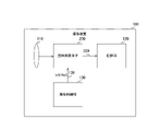
- FIG. 1 is a block diagram showing a configuration example of an imaging device 100 according to the first embodiment of the present technology.
- This imaging device 100 is a device for capturing image data, and includes an imaging lens 110 , a solid-state imaging device 200 , a recording section 120 and an imaging control section 130 .
- As the imaging device 100 a digital camera or an electronic device (smartphone, personal computer, etc.) having an imaging function is assumed.
- the solid-state imaging device 200 captures image data under the control of the imaging control section 130 .
- the solid-state imaging device 200 supplies image data to the recording section 120 via the signal line 209 .
- the imaging lens 110 collects light and guides it to the solid-state imaging device 200 .
- the imaging control unit 130 controls the solid-state imaging device 200 to capture image data.
- the imaging control unit 130 supplies an imaging control signal including, for example, a vertical synchronization signal VSYNC to the solid-state imaging device 200 via the signal line 139 .
- the recording unit 120 records image data.
- the vertical synchronization signal VSYNC is a signal that indicates the timing of imaging, and a periodic signal with a constant frequency (such as 60 Hz) is used as the vertical synchronization signal VSYNC.
- the imaging device 100 records image data
- the image data may be transmitted to the outside of the imaging device 100.
- an external interface is further provided for transmitting image data.
- the imaging device 100 may further display image data.
- a display section is further provided.
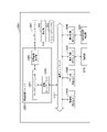
- FIG. 2 is a block diagram showing a configuration example of the solid-state imaging device 200 according to the first embodiment of the present technology.
- This solid-state imaging device 200 includes a vertical scanning circuit 211 , a pixel array section 220 , a timing control circuit 212 , a DAC (Digital to Analog Converter) 213 , a load MOS circuit block 250 and a column signal processing circuit 260 .
- a pixel array section 220 a plurality of pixels such as the pixels 301 and 302 are arranged in a two-dimensional lattice.
- each circuit in the solid-state imaging device 200 is provided on, for example, a single semiconductor chip.
- the timing control circuit 212 controls the operation timings of the vertical scanning circuit 211, the DAC 213, and the column signal processing circuit 260 in synchronization with the vertical synchronization signal VSYNC from the imaging control section 130.
- the DAC 213 generates a sawtooth ramp signal by DA (Digital to Analog) conversion.
- the DAC 213 supplies the generated ramp signal to the column signal processing circuit 260 .
- the vertical scanning circuit 211 sequentially selects and drives rows to output analog pixel signals.
- a pixel photoelectrically converts incident light to generate an analog pixel signal. This pixel supplies a pixel signal to the column signal processing circuit 260 through the load MOS circuit block 250 .
- the load MOS circuit block 250 is provided with a MOS transistor for supplying a constant current for each column.
- the column signal processing circuit 260 executes signal processing such as AD conversion processing and CDS (Correlated Double Sampling) processing on pixel signals for each column.
- the column signal processing circuit 260 supplies the image data made up of the processed signals to the recording section 120 . Note that the column signal processing circuit 260 is an example of the signal processing circuit described in the claims.
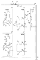
- FIG. 3 is a circuit diagram showing one configuration example of the pixel 301 according to the first embodiment of the present technology.
- a pre-stage circuit 310 In this pixel 301, a pre-stage circuit 310, capacitive elements 331 and 332, a selection circuit 350, a post-stage reset transistor 361, and a post-stage circuit 370 are arranged.
- the capacitive elements 331 and 332 for example, capacitors of MIM (Metal-Insulator-Metal) structure are used. Note that the capacitive elements 331 and 332 are examples of the first and second capacitive elements described in the claims.
- MIM Metal-Insulator-Metal
- the pre-stage circuit 310 sequentially generates a reset level and a signal level and causes capacitive elements 331 and 332 to hold them.
- This pre-stage circuit 310 includes a photoelectric conversion element 311 , a transfer transistor 312 , an FD (Floating Diffusion) reset transistor 313 , an FD 314 , a pre-stage amplification transistor 315 and a current source transistor 316 .
- the photoelectric conversion element 311 generates charges by photoelectric conversion.
- the transfer transistor 312 transfers charges from the photoelectric conversion element 311 to the FD 314 according to the transfer signal trg from the vertical scanning circuit 211 .
- the FD reset transistor 313 extracts electric charge from the FD 314 according to the FD reset signal rst from the vertical scanning circuit 211 and initializes it.
- the FD 314 accumulates charges and generates a voltage corresponding to the amount of charges.
- the front-stage amplification transistor 315 amplifies the voltage level of the FD 314 and outputs it to the front-stage node 330 .
- the respective drains of the FD reset transistor 313 and the pre-amplification transistor 315 are connected to the power supply voltage VDD.
- Current source transistor 316 is connected to the source of pre-amplification transistor 315 . This current source transistor 316 supplies the current id1 under the control of the vertical scanning circuit 211 .
- One ends of the capacitive elements 331 and 332 are commonly connected to the preceding node 330 , and the other ends are connected to the selection circuit 350 .
- the selection circuit 350 includes selection transistors 351 and 352 .
- the selection transistor 351 opens and closes the path between the capacitive element 331 and the post-stage node 360 according to the selection signal ⁇ r from the vertical scanning circuit 211 .
- the selection transistor 352 opens and closes the path between the capacitive element 332 and the subsequent node 360 according to the selection signal ⁇ s from the vertical scanning circuit 211 .
- the post-stage reset transistor 361 initializes the level of the post-stage node 360 to a predetermined potential Vreg according to the post-stage reset signal rstb from the vertical scanning circuit 211 .
- a potential different from the power supply voltage VDD (for example, a potential lower than VDD) is set to the potential Vreg.
- the post-stage circuit 370 includes a post-stage amplification transistor 371 and a post-stage selection transistor 372 .
- the rear-stage amplification transistor 371 amplifies the level of the rear-stage node 360 .
- the post-stage selection transistor 372 outputs a signal of a level amplified by the post-stage amplification transistor 371 to the vertical signal line 308 as a pixel signal in accordance with the post-stage selection signal selb from the vertical scanning circuit 211 .
- nMOS n-channel Metal Oxide Semiconductor
- FIG. 4 is a circuit diagram showing a configuration example of a pixel 302 adjacent to the pixel 301 in FIG. 3 according to the first embodiment of the present technology.
- a pre-stage circuit 320 capacitive elements 336 and 337, a selection circuit 355, a post-stage reset transistor 366, and a post-stage circuit 380 are arranged.
- the capacitive elements 336 and 337 for example, capacitors of MIM structure are used. Note that the capacitive elements 336 and 337 are examples of the third and fourth capacitive elements described in the claims.
- the pre-stage circuit 320 sequentially generates a reset level and a signal level and causes capacitive elements 336 and 337 to hold them.
- the pre-stage circuit 320 includes a photoelectric conversion element 321 , a transfer transistor 322 , an FD reset transistor 323 , an FD 324 , a pre-stage amplification transistor 325 and a current source transistor 326 .
- the circuit configuration of the pre-stage circuit 320 is the same as that of the pre-stage circuit 310 .
- One ends of the capacitive elements 336 and 337 are commonly connected to the preceding node 335 , and the other ends are connected to the selection circuit 355 .
- the selection circuit 355 includes selection transistors 356 and 357 .
- the circuit configuration of the selection circuit 350 is similar to that of the selection circuit 350 .
- the post-stage reset transistor 366 initializes the level of the post-stage node 365 to a predetermined potential Vreg according to the post-stage reset signal rstb from the vertical scanning circuit 211 .
- the post-stage circuit 380 includes a post-stage amplification transistor 381 and a post-stage selection transistor 382 .
- the circuit configuration of the post-stage circuit 380 is the same as that of the post-stage circuit 370 .
- a pixel signal of the pixel 302 is output to the vertical signal line 309 .
- the vertical scanning circuit 211 supplies a high level FD reset signal rst and a high level transfer signal trg to all rows at the start of exposure. Thereby, the photoelectric conversion elements (311 and 321) are initialized. Hereinafter, this control will be referred to as "PD reset".
- the vertical scanning circuit 211 supplies the high level FD reset signal rst over the pulse period while setting the post-stage reset signal rstb and the selection signal ⁇ r to high level for all rows.
- FDs 314 and 324 are initialized, and capacitive elements 331 and 336 hold levels corresponding to the levels of FDs 314 and 324 at that time. This control is hereinafter referred to as "FD reset".
- the levels of the FDs 314 and 324 at the time of FD reset and the levels corresponding to the levels (the holding levels of the capacitive elements 331 and 336 and the levels of the vertical signal lines) are collectively referred to as “P phase” or “reset level.” ”.
- the vertical scanning circuit 211 supplies a high-level transfer signal trg over the pulse period while setting the post-stage reset signal rstb and the selection signal ⁇ s to a high level for all rows.
- signal charges corresponding to the amount of exposure are transferred to the FDs 314 and 324 , and levels corresponding to the levels of the FDs 314 and 324 at that time are held in the capacitive elements 332 and 337 .
- phase D The levels of the FDs 314 and 324 during signal charge transfer and the levels corresponding to the levels (holding levels of the capacitive elements 332 and 337 and levels of the vertical signal lines) are collectively referred to as "phase D" or " signal level”.
- Exposure control that simultaneously starts and ends exposure for all pixels in this way is called a global shutter method.
- the pre-stage circuits 310 and 320 of all pixels sequentially generate a reset level and a signal level.
- the reset level is held in capacitive elements 331 and 336 and the signal level is held in capacitive elements 332 and 337 .
- the vertical scanning circuit 211 sequentially selects rows and sequentially outputs the reset level and signal level of the rows.
- the vertical scanning circuit 211 supplies the high-level selection signal ⁇ r for a predetermined period while setting the FD reset signal rst of the selected row and the subsequent stage selection signal selb to high level.
- capacitive elements 331 and 336 are connected to subsequent nodes 360 and 365, and the reset level is read.
- the vertical scanning circuit 211 After reading the reset level, the vertical scanning circuit 211 supplies the high-level post-stage reset signal rstb over the pulse period while keeping the FD reset signal rst of the selected row and the post-stage selection signal selb at high level. As a result, the levels of subsequent nodes 360 and 365 are initialized. At this time, selection transistors 351 , 352 , 356 and 357 are in an open state, and capacitive elements 331 , 332 , 336 and 337 are disconnected from subsequent nodes 360 and 365 .
- the vertical scanning circuit 211 supplies the high-level selection signal ⁇ s for a predetermined period while keeping the FD reset signal rst and the rear-stage selection signal selb of the selected row at high level. do. Thereby, capacitive elements 332 and 337 are connected to subsequent nodes 360 and 365, and the signal level is read out.
- the selection circuit 350 of the selected row performs control to connect the capacitive element 331 to the post-stage node 360, to disconnect the capacitive elements 331 and 332 from the post-stage node 360, and to connect the capacitive element 332 to the post-node 360. and control to connect to .
- the selection circuit 355 of the selected row provides control for connecting the capacitive element 336 to the subsequent node 365, control for disconnecting the capacitive elements 336 and 337 from the subsequent node 365, and control for connecting the capacitive element 337 to the subsequent node 365. and in order.
- the rear reset transistor 361 of the selected row initializes the levels of the rear nodes 360 and 365 .
- the post-stage circuits 370 and 380 of the selected row sequentially read out the reset level and signal level from the capacitive elements 331 and 332 (or capacitive elements 336 and 337) via the post-stage nodes 360 and 365, and the vertical signal line 309 is read out. Output to
- circuit configurations of the pixels 301 and 302 are not limited to those illustrated in FIGS. Pixels other than those shown in FIGS. 3 and 4 may be used as long as the pixels are provided with a pair of capacitive elements and a pair of selection transistors for opening and closing a path between them and a node.
- Pixels described in Non-Patent Document 1 can be used.
- FIG. 5 is a circuit diagram showing a connection example of respective elements of two adjacent pixels according to the first embodiment of the present technology.
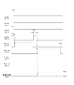
- a plurality of signal lines for transmitting control signals from the vertical scanning circuit 211 are wired in the pixel array section 220 along the horizontal direction.
- Six control signals, a transfer signal trg, an FD reset signal rst, a selection signal ⁇ r, a selection signal ⁇ s, a post-stage reset signal rstb, and a post-stage selection signal selb, are transmitted for each row. Therefore, six signal lines are arranged in the horizontal direction for each row.
- the signal line for transmitting the selection signal ⁇ r is designated as the selection line 223 and the signal line for transmitting the selection signal ⁇ s is designated as the selection line 224 .
- the roles of the selection transistors arranged on the upper and lower sides in the pixel 301 are reversed from the roles of the selection transistors arranged on the upper and lower sides in the pixel 302 .
- Such a configuration can be easily realized by reversing the selection lines to which the upper and lower selection transistors in the pixel 302 are connected to the pixels 301 .
- the selection transistor 351 arranged on the upper side is connected to the selection line 223 on the reset side
- the selection transistor 352 arranged on the lower side is connected to the selection line 224 on the signal side.
- the upper selection transistor 357 is connected to the signal-side selection line 224
- the lower selection transistor 356 is connected to the reset-side selection line 223 .
- each pixel in the row needs to hold charge for a period from the end of exposure to readout. If the period for holding this charge is long, noise charges may be generated at the pn junctions of the selection transistors 351 and 352 due to photoelectric conversion of stray light that is incident light during that period. In the figure, fan-shaped marks indicate pn junctions where noise charges are generated.
- ⁇ ′ (q1′)/C ⁇ (q2′)/C Formula 2
- Equations 1 and 2 do not always match due to differences in the layout of the junction pn of the selection transistors 351 and 352 in the pixel and the difference in the amount of stray light in each pn junction.
- Equations 1 and 2 residual components due to stray light remain even after CDS processing.
- the residual component causes deterioration of PLS. This PLS deterioration may degrade the image quality of the image data.
- the noise amounts due to stray light of the adjacent pixels 301 and 302 have substantially the same absolute value and opposite signs.
- FIG. 6 is a diagram showing an example layout of select transistors in a pixel according to the first embodiment of the present technology.
- the horizontal direction is the x direction and the vertical direction is the y direction.
- the position of a transistor within a pixel is represented by a relative position from a predetermined reference position (for example, the upper left vertex) of the pixel.
- gray portions in the figure indicate metal wiring (selection lines 223 and 224, etc.).
- the cross marks indicate the positions of vias that connect metal wires to other metal wires and transistors.
- the selection transistor 351 connected to the selection line 223 on the reset side is arranged at a relative position (x1, y1) of x1 from the reference position in the horizontal direction and y1 from the reference position in the vertical direction.
- the selection transistor 352 connected to the selection line 224 on the signal side is arranged at the relative position (x2, y2).
- the selection transistor 356 connected to the selection line 223 on the reset side is arranged at the relative position (x2, y2).
- the select transistors connected to the select line 224 on the signal side are arranged at relative positions (x1, y1).
- the pixels 301 and 302 are examples of the first pixel and the second pixel described in the claims.
- the selection transistor 351 is an example of the first selection transistor described in the claims, and the selection transistor 351 is an example of the second selection transistor described in the claims.
- the select transistor 356 is an example of a third select transistor recited in the claims, and the select transistor 357 is an example of a fourth select transistor recited in the claims.
- FIG. 7 is a diagram showing an example of the pixel array section 220 according to the first embodiment of the present technology.
- white squares indicate the positions of the selection transistors (351 and 356) on the reset side.
- Black squares indicate the positions of signal-side select transistors (352 and 357).
- each pixel is not provided with a color filter. Therefore, the image data becomes a monochrome image.
- pixels 301 and pixels 302 are arranged adjacent to each other in the row direction. Pixels with the same layout as the pixel 301 and pixels with the same layout as the pixel 302 are alternately arranged in the row direction. Also in the column direction, pixels with the same layout as the pixel 301 and pixels with the same layout as the pixel 302 are alternately arranged. This arrangement makes it possible to reverse the sign of the noise produced in any two adjacent pixels. Therefore, when the entire image data in which these pixels are arranged is observed, the noise of two adjacent pixels cancels each other, and the noise due to stray light becomes inconspicuous. As a result, deterioration in image quality due to deterioration of PLS can be suppressed.
- FIG. 8 is a block diagram showing a configuration example of the column signal processing circuit 260 according to the first embodiment of the present technology.
- a vertical signal line 309 is wired to the load MOS circuit block 250 for each column. Assuming that the number of columns is I (I is an integer), I vertical signal lines 309 are wired. A load MOS transistor 251 that supplies a constant current id2 is connected to each of the vertical signal lines 309 .
- a plurality of ADCs 261 and a digital signal processing unit 262 are arranged in the column signal processing circuit 260 .
- ADC 261 is arranged for each column. Assuming that the number of columns is I, I ADCs 261 are arranged.
- the ADC 261 uses the ramp signal Rmp from the DAC 213 to convert analog pixel signals from the corresponding column into digital signals.
- This ADC 261 supplies a digital signal to the digital signal processing section 262 .
- the ADC 261 is a single-slope ADC that includes a comparator and a counter.
- the digital signal processing unit 262 performs predetermined signal processing such as CDS processing on each digital signal for each column.
- the digital signal processing unit 262 supplies image data made up of processed digital signals to the recording unit 120 .
- FIG. 9 is a timing chart showing an example of global shutter operation according to the first embodiment of the present technology.
- the vertical scanning circuit 211 applies the high-level FD reset signal rst and transfer signal trg to all rows (in other words, all pixels) from timing T0 immediately before the start of exposure to timing T1 after the pulse period has elapsed. supply. As a result, all pixels are PD-reset, and exposure is started simultaneously for all rows.
- rst_[n] and trg_[n] in the same figure indicate signals to pixels in the nth row among the N rows.
- N is an integer indicating the total number of rows in which the pixel blocks 300 are arranged, and n is an integer from 1 to N.
- the vertical scanning circuit 211 supplies the high-level FD reset signal rst over the pulse period while setting the post-stage reset signal rstb and the selection signal ⁇ r to high level in all rows. As a result, all pixels are FD-reset, and the reset level is sample-held.
- rstb_[n] and ⁇ r_[n] in the same figure indicate signals to pixels in the n-th row.
- the vertical scanning circuit 211 returns the selection signal ⁇ r to low level.
- the vertical scanning circuit 211 supplies the high-level transfer signal trg over the pulse period while setting the post-stage reset signal rstb and the selection signal ⁇ s to high level in all rows. This samples and holds the signal level. Also, ⁇ s_[n] in the figure indicates a signal to the n-th pixel.
- the vertical scanning circuit 211 returns the selection signal ⁇ s to low level.
- FIG. 10 is a timing chart showing an example of a pixel readout operation according to the first embodiment of the present technology.
- the vertical scanning circuit 211 sets the n-th row FD reset signal rst and the subsequent stage selection signal selb to high level.
- the post-stage reset signal rstb for all rows is controlled to low level.
- selb_[n] in the figure indicates a signal to the n-th row pixel.
- the vertical scanning circuit 211 supplies a high-level selection signal ⁇ r to the n-th row over a period from timing T11 immediately after timing T10 to timing T12.
- the potentials of the subsequent nodes 360 and 365 become the reset level Vrst.
- the ADC 261 AD-converts this reset level.
- the vertical scanning circuit 211 supplies the high-level post-stage reset signal rstb to the n-th row over the pulse period from timing T13 immediately after timing T12. As a result, when a parasitic capacitance exists in the subsequent node 360 or the like, the history of the previous signal held in the parasitic capacitance can be erased.
- the vertical scanning circuit 211 supplies a high-level selection signal ⁇ s to the n-th row over a period from timing T14 to timing T15 immediately after initialization of the subsequent node 360 and the like.
- the potentials of the subsequent nodes 360 and 365 are at the signal level Vsig.
- the ADC 261 AD-converts this signal level.
- the difference between the reset level Vrst and the signal level Vsig corresponds to the net signal level after removing the FD reset noise and offset noise.
- the solid-state imaging device 200 reads the signal level after the reset level, the order is not limited to this.
- the solid-state imaging device 200 can also read the reset level after the signal level.
- the vertical scanning circuit 211 supplies the high-level selection signal ⁇ r after the high-level selection signal ⁇ s. Also, in this case, it is necessary to reverse the slope of the ramp signal.
- FIG. 11 is a circuit diagram showing a configuration example of a pixel in a comparative example.
- the selection circuit 350 is not provided, and a transfer transistor is inserted between the pre-stage node 330 and the pre-stage circuit.
- Capacitors C1 and C2 are inserted instead of capacitive elements 331 and 332, respectively.
- Capacitor C 1 is inserted between pre-stage node 330 and the ground terminal, and capacity C 2 is inserted between pre-stage node 330 and post-stage node 360 .
- Exposure control and readout control of pixels in this comparative example are described, for example, in "Jae-kyu Lee, et al., A 2.1e-Temporal Noise and -105dB Parasitic Light Sensitivity Backside-Illuminated 2.3 ⁇ m-Pixel Voltage-Domain Global Shutter CMOS Image Sensor Using High-Capacity DRAM Capacitor Technology, ISSCC 2020”, Figure 5.5.2.
- the capacitance value of each of capacitors C1 and C2 is C
- kTC noise level Vn during exposure and reading is expressed by the following equation.
- Vn (3*kT/C) 1/2
- k is the Boltzmann's constant, and the unit is, for example, Joules per Kelvin (J/K).
- T is the absolute temperature, and the unit is, for example, Kelvin (K).
- the unit of Vn is, for example, volts (V), and the unit of C is, for example, farads (F).
- FIG. 12 is a diagram showing an example of the states of the pixels 301 at the time of reading the reset level and at the time of initializing the subsequent node according to the first embodiment of the present technology.
- a indicates the state of the pixel 301 when the reset level is read
- b indicates the state of the pixel 301 when the subsequent node 360 is initialized.
- the selection transistor 351, the selection transistor 352, and the post-stage reset transistor 361 are represented by the symbol of a switch for convenience of explanation.
- the vertical scanning circuit 211 closes the selection transistor 351 and opens the selection transistor 352 and the post-stage reset transistor 361 .
- the reset level of the first pixel is read out via the post-stage circuit 370 .
- the vertical scanning circuit 211 After reading the reset level, the vertical scanning circuit 211 opens the selection transistor 351 and the selection transistor 352 and closes the post-stage reset transistor 361, as illustrated in b in FIG. Thereby, capacitive elements 331 and 332 are disconnected from post-stage node 360, and the level of post-stage node 360 is initialized.
- the capacitance value of the parasitic capacitance Cp of the post-stage node 360 disconnected from the capacitive elements 331 and 332 is much smaller than that of the capacitive elements 331 and 332 .
- the parasitic capacitance Cp is several femtofarads (fF)
- the capacitive elements 331 and 332 are on the order of several tens of femtofarads.
- FIG. 13 is a diagram showing an example of the state of the pixel 301 when reading the signal level according to the first embodiment of the present technology.
- the vertical scanning circuit 211 closes the selection transistor 352 and opens the selection transistor 351 and the post-stage reset transistor 361 . As a result, the signal level of the first pixel is read out via the post-stage circuit 370 .
- the post-stage reset transistor 361 is driven during reading, so kTC noise is generated at that time.
- the capacitive elements 331 and 332 are disconnected when the post-stage reset transistor 361 is driven, and the parasitic capacitance Cp at that time is small. Therefore, the kTC noise during readout can be ignored compared to the kTC noise during exposure. Therefore, the kTC noise during exposure and readout is expressed by Equation 7.
- kTC noise is smaller in the pixel block 300 in which the capacitance is separated during reading than in the comparative example in which the capacitance is not separated during reading. Thereby, the image quality of image data can be improved.
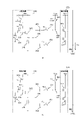
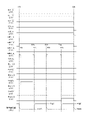
- FIG. 14 is a diagram showing an example of image data according to the first embodiment of the present technology.
- each of image data 501 to 506 includes an area pls1 surrounded by a dashed line and an area pls2 surrounded by a dotted line.
- areas other than areas pls1 and pls2 are referred to as area ref.
- the arrangement of the reset-side selection transistors and the signal-side selection transistors in two adjacent pixels is reversed. In other words, noise countermeasures are taken by the layout. Also, it is assumed that noise similar to that in the area pls1 is generated in this area pls2.
- the amount of random noise RN when PLS is zero is the same value.
- the image data 501 to 506 have different PLS, and the PLS/RN value of the image data 501 is 1/10.
- the PLS/RN values for each of the remaining 502-506 are 2/10, 3/10, 4/10, 5/10 and 6/10.
- the ratio ⁇ /AVE between the standard deviation ⁇ and the average value AVE of the output in the area when the uniform light of 50% saturation is applied is used.
- FIG. 15 is a diagram showing an example of an average value and standard deviation within an area according to the first embodiment of the present technology. As described above, noise is not generated in the area ref, and noise countermeasures are not taken. Area pls1 has noise and is not subjected to noise countermeasures. Noise occurs in the area pls2, and noise countermeasures are taken by the layout.
- REF be the average value of the pixel signals in the area ref in LSB conversion
- 30 be the standard deviation.
- the average value of the pixel signals in the area pls1 is REF+18, and the standard deviation is 30.
- the average value of the pixel signals in the area pls2 is REF, and the standard deviation is 35.
- FIG. 16 is a diagram for explaining the influence of PLS in the first embodiment of the present technology.
- the random noise RN when the PLS of each of the image data 501 to 505 is zero is the same value.
- the image data 501 to 505 have different PLS, and the PLS values for RN are "0.1", “0.2", “0.3”, “0.4”, and "0.5". is.
- RN′ (RN 2 +PLS 2 ) 1/2 Equation 8
- the increase rate of random noise is only about 2 percent (%), which can be ignored.
- PLS/RN is about 0.5
- the increase rate of random noise increases to 11.2 percent (%).
- the noise countermeasure area pls2 is in a state where it is difficult to visually distinguish it from the noise-free area ref despite the increase in random noise.
- the image quality can be improved by making the noise in the image data inconspicuous.
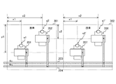
- a solid-state imaging device 200 according to a first modification of the first embodiment differs from the first embodiment in that pixels are arranged in a Bayer array.
- FIG. 17 is a diagram showing an example of the pixel array section 220 in the first modified example of the first embodiment of the present technology.
- a color filter is provided for each pixel in the pixel array section 220 of the first modification of the first embodiment.
- the red color filter pixels be R pixels
- the green color filter pixels be Gr pixels or Gb pixels
- the blue color filter pixels be B pixels. These pixels are arranged in a Bayer array.
- An area 226 is defined as 2 rows ⁇ 2 columns adjacent to a predetermined area 225 of 2 rows ⁇ 2 columns.
- area 225 four pixels with the same layout as the pixel 301 are arranged.
- the image quality of the color image can be improved.
- any pixel (eg, Gr pixel) in the area 225 can be laid out in the same layout as the pixel 302, and the remaining three pixels can be laid out in the same layout as the pixel 301.
- pixels having the same layout as the pixel 301 are arranged as Gr pixels, and the remaining three pixels having the same layout as the pixel 302 are arranged.
- the pixels having the same layout as the pixels 301 and 302 are arranged in the Bayer array, so that the image quality of the color image can be improved.
- FIG. 19 is a diagram showing an example of the pixel array section 220 in the second modified example of the first embodiment of the present technology.
- R pixels, Gr pixels, Gb pixels and B pixels are arranged in a quadra-bayer arrangement.
- quadra Bayer array four pixels of the same color are arranged in an area of 2 rows ⁇ 2 columns.
- An area 226 is an area 226 of 2 rows ⁇ 2 columns of green adjacent to an area 225 of 2 rows ⁇ 2 columns of red.
- a pixel with the same layout as the pixel 302 is arranged at any position (for example, upper right) in the area 225, and three pixels with the same layout as the pixel 301 are arranged at the rest.
- the pixels having the same layout as the pixels 301 and 302 are arranged in a quadra-Bayer array, so that the image quality of the color image can be improved.
- Second Embodiment> In the first embodiment described above, the post-stage reset transistor and selection circuit are arranged for each pixel, but in this configuration, it is difficult to reduce the circuit scale.
- the solid-state imaging device 200 of the second embodiment differs from that of the first embodiment in that two adjacent pixels share a post-stage reset transistor and a selection circuit.
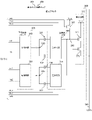
- FIG. 20 is a circuit diagram showing one configuration example of the pixel block 300 according to the second embodiment of the present technology.
- a plurality of pixel blocks 300 are arranged in the pixel array section 220 of the second embodiment.
- Pixels 301 and 302 are arranged in each pixel block 300 .
- a front-stage circuit block 305 In the pixel block 300, a front-stage circuit block 305, capacitive elements 331, 332, 336 and 337, a selection section 340, a rear-stage reset transistor 361, and a rear-stage circuit 370 are arranged.
- Pre-stage circuits 310 and 320 are arranged in the pre-stage circuit block 305 .
- Selection circuits 350 and 355 are arranged in the selection unit 340 .
- the post-stage circuit 370 includes a post-stage amplification transistor 371 and a post-stage selection transistor 372 .
- the selection circuit 350 connects one of the capacitive elements 331 and 332 to the subsequent node 360 .
- Selection circuit 355 connects one of capacitive elements 336 and 337 to post-stage node 360 .
- the selection circuit 350 is an example of the first selection circuit described in the claims, and the selection circuit 355 is an example of the second selection circuit described in the claims.
- FIG. 21 is a circuit diagram showing a configuration example of pre-stage circuits 310 and 320 and selection circuits 350 and 355 according to the second embodiment of the present technology.
- the pre-stage circuit 310 includes a photoelectric conversion element 311 , a transfer transistor 312 , an FD reset transistor 313 , an FD 314 , a pre-stage amplification transistor 315 and a current source transistor 316 .
- the pre-stage circuit 320 includes a photoelectric conversion element 321 , a transfer transistor 322 , an FD reset transistor 323 , an FD 324 , a pre-stage amplification transistor 325 and a current source transistor 326 .
- the photoelectric conversion elements 311 and 321 generate charges by photoelectric conversion.
- the transfer transistor 312 transfers charges from the photoelectric conversion element 311 to the FD 314 according to the transfer signal trg1 from the vertical scanning circuit 211 .
- the transfer transistor 322 transfers charges from the photoelectric conversion element 321 to the FD 324 according to the transfer signal trg2 from the vertical scanning circuit 211 .
- the photoelectric conversion elements 311 and 321 are examples of the first and second photoelectric conversion elements described in the claims.
- Transfer transistors 312 and 322 are examples of the first and second transfer transistors described in the claims.
- the FD reset transistor 313 extracts electric charge from the FD 314 according to the FD reset signal rst1 from the vertical scanning circuit 211 and initializes it.
- the FD reset transistor 323 extracts charge from the FD 324 and initializes it according to the FD reset signal rst2 from the vertical scanning circuit 211 .
- the FDs 314 and 324 accumulate charges and generate voltages according to the amount of charges.
- the FD reset transistors 313 and 323 are examples of the first and second reset transistors described in the claims.
- FDs 314 and 324 are examples of the first and second floating diffusion layers described in the claims.
- the front-stage amplification transistor 315 amplifies the voltage level of the FD 314 and outputs it to the front-stage node 330 .
- the front-stage amplification transistor 325 amplifies the voltage level of the FD 324 and outputs it to the front-stage node 335 .
- the pre-amplification transistors 315 and 325 are examples of the first and second pre-amplification transistors described in the claims.
- the respective drains of the FD reset transistors 313 and 323 and the pre-amplification transistors 315 and 325 are connected to the power supply voltage VDD.
- Current source transistor 316 is connected to the source of pre-amplification transistor 315 . This current source transistor 316 supplies the current id11 under the control of the vertical scanning circuit 211 .
- Current source transistor 326 is connected to the source of pre-amplification transistor 325 . This current source transistor 326 supplies the current id12 under the control of the vertical scanning circuit 211 .
- the current source transistors 316 and 326 are examples of the first and second current source transistors described in the claims.
- each of the capacitive elements 331 and 332 is commonly connected to the preceding node 330 , and the other end of each is connected to the selection circuit 350 .
- One end of each of capacitive elements 336 and 337 is commonly connected to previous node 335 , and the other end of each is connected to selection circuit 355 .
- the selection circuit 350 includes selection transistors 351 and 352 .
- the selection transistor 351 opens and closes the path between the capacitive element 331 and the subsequent node 360 according to the selection signal ⁇ r1 from the vertical scanning circuit 211 .
- the selection transistor 352 opens and closes the path between the capacitive element 332 and the subsequent node 360 according to the selection signal ⁇ s1 from the vertical scanning circuit 211 .
- the selection circuit 355 includes selection transistors 356 and 357 .
- the selection transistor 356 opens and closes the path between the capacitive element 336 and the post-stage node 360 according to the selection signal ⁇ r2 from the vertical scanning circuit 211 .
- the selection transistor 357 opens and closes the path between the capacitive element 337 and the post-stage node 360 according to the selection signal ⁇ s2 from the vertical scanning circuit 211 .
- nMOS transistors for example, are used as various transistors (transfer transistors 312 and the like) in the pixel block 300 .
- a circuit composed of the above-described front-stage circuit 310, capacitive elements 331 and 332, selection circuit 350, rear-stage reset transistor 361, and rear-stage circuit 370 functions as one pixel.
- a circuit including the front-stage circuit 320, the capacitive elements 336 and 337, the selection circuit 355, the rear-stage reset transistor 361, and the rear-stage circuit 370 also functions as one pixel. These two pixels share the post-stage reset transistor 361 and the post-stage circuit 370 .
- two pixels in the pixel block 300 are arranged in the column direction, for example. In other words, these two pixels are placed in odd and even rows. Note that the positional relationship between the two pixels in the pixel block 300 is not limited to odd-numbered rows and even-numbered rows. For example, two pixels can be arranged in odd and even columns. Alternatively, one of the two pixels can be arranged diagonally above the other.
- FIG. 22 is a timing chart showing an example of global shutter operation according to the second embodiment of the present technology.
- the vertical scanning circuit 211 supplies high-level FD reset signals rst1 and rst2 and a transfer signal trg1 to all rows (in other words, all pixels) from timing T0 immediately before the start of exposure to timing T1 after the pulse period has elapsed. and trg2.
- all pixels are PD-reset, and exposure is started simultaneously for all rows.
- rst1_[n], rst2_[n], trg1_[n], and trg2_[n] in the same figure indicate signals to pixels in the n-th row among the N rows.
- N is an integer indicating the total number of rows in which the pixel blocks 300 are arranged, and n is an integer from 1 to N. If the two pixels in pixel block 300 are even and odd rows of pixels, the nth row of pixel block 300 includes two rows of odd and even rows.
- the vertical scanning circuit 211 sets the post-stage reset signal rstb and the selection signals ⁇ r1 and ⁇ r2 to high level in all rows, and keeps the FD reset signals rst1 and rst2 at high level over the pulse period. supply. As a result, all pixels are FD-reset, and the reset level is sample-held.
- the vertical scanning circuit 211 returns the selection signals ⁇ r1 and ⁇ r2 to low level.
- the vertical scanning circuit 211 supplies high-level transfer signals trg1 and trg2 over the pulse period while setting the post-stage reset signal rstb and the selection signals ⁇ s1 and ⁇ s2 to high levels in all rows. This samples and holds the signal level. Also, ⁇ s1_[n] and ⁇ s2_[n] in the same figure indicate signals to pixels in the n-th row.
- the vertical scanning circuit 211 returns the selection signals ⁇ s1 and ⁇ s2 to low level.
- FIG. 23 is a timing chart showing an example of readout operation of the first pixel in the pixel block 300 according to the second embodiment of the present technology.
- the vertical scanning circuit 211 sets the n-th row FD reset signals rst1 and rst2 and the subsequent stage selection signal selb to high level.
- the post-stage reset signal rstb for all rows is controlled to low level.
- selb_[n] in the figure indicates a signal to the n-th row pixel.
- the vertical scanning circuit 211 supplies a high-level selection signal ⁇ r1 to the n-th row over a period from timing T11 immediately after timing T10 to timing T12.
- the potential of the post-stage node 360 becomes the reset level Vrst1.
- the ADC 261 AD-converts this reset level.
- the vertical scanning circuit 211 supplies the high-level post-stage reset signal rstb to the n-th row over the pulse period from timing T13 immediately after timing T12. As a result, when a parasitic capacitance exists in the post-stage node 360, the history of the previous signal held in the parasitic capacitance can be erased.
- the vertical scanning circuit 211 supplies a high-level selection signal ⁇ s1 to the n-th row over a period from timing T14 to timing T15 immediately after initialization of the subsequent node 360 .
- the potential of the post-stage node 360 becomes the signal level Vsig1.
- the ADC 261 AD-converts this signal level.
- the difference between the reset level Vrst1 and the signal level Vsig1 corresponds to the net signal level after removing the FD reset noise and offset noise.
- FIG. 24 is a timing chart showing an example of readout operation of the second pixel in the pixel block 300 according to the second embodiment of the present technology.
- the vertical scanning circuit 211 supplies the high-level post-stage reset signal rstb to the n-th row over the pulse period from timing T16 immediately after timing T15.
- the vertical scanning circuit 211 supplies a high-level selection signal ⁇ r2 to the n-th row over a period from timing T17 to timing T18 immediately after initialization of the subsequent node 360 .
- the potential of the post-stage node 360 becomes the reset level Vrst2.
- the ADC 261 AD-converts this reset level.
- the vertical scanning circuit 211 supplies the high-level post-stage reset signal rstb to the n-th row over the pulse period from timing T19 immediately after timing T18.
- the vertical scanning circuit 211 supplies a high-level selection signal ⁇ s2 to the n-th row over a period from timing T20 to timing T21 immediately after initialization of the subsequent node 360 .
- the potential of the post-stage node 360 becomes the signal level Vsig2.
- the ADC 261 AD-converts this signal level.
- the vertical scanning circuit 211 returns the n-th row FD reset signals rst1 and rst2 and the subsequent stage selection signal selb to low level.
- High-level selection signals ⁇ r1, ⁇ s1, ⁇ r2 and ⁇ s2 are supplied in order.
- Selecting section 340 connects capacitive elements 331 , 332 , 336 and 337 to subsequent node 360 in order according to these selection signals. Then, the reset level Vrst1 and signal level Vsig1 of the first pixel in the pixel block 300 and the reset level Vrst2 and signal level Vsig2 of the second pixel are read in order.
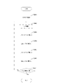
- FIG. 25 is a flow chart showing an example of the operation of the solid-state imaging device 200 according to the second embodiment of the present technology. This operation is started, for example, when a predetermined application for capturing image data is executed.
- the vertical scanning circuit 211 exposes all pixels (step S901). Then, the vertical scanning circuit 211 selects a row of the pixel block 300 to be read (step S902). The column signal processing circuit 260 reads the reset level of the first pixel in the pixel block 300 of that row (step S903), and then reads the signal level of that pixel (step S904). Subsequently, the column signal processing circuit 260 reads the reset level of the second pixel (step S905), and then reads the signal level of that pixel (step S906).
- the solid-state imaging device 200 determines whether reading of all rows has been completed (step S907). If readout of all rows has not been completed (step S907: No), the solid-state imaging device 200 repeats step S902 and subsequent steps. On the other hand, when reading of all rows is completed (step S907: Yes), the solid-state imaging device 200 executes CDS processing and the like, and ends the operation for imaging. When image data of a plurality of images are continuously captured, steps S901 to S907 are repeatedly executed in synchronization with the vertical synchronization signal.
- the circuit scale of the pixel array section 220 is reduced compared to the case where they are not shared. can do.
- the solid-state imaging device 200 sequentially reads the pixel signals of the two pixels in the pixel block 300, but this configuration may result in insufficient readout speed.
- the solid-state imaging device 200 of the first modification of the second embodiment differs from that of the second embodiment in that pixel addition is performed.
- FIG. 26 is a timing chart showing an example of the read operation of the reset level and signal level in the first modified example of the second embodiment of the present technology.
- One of a plurality of modes including a non-addition mode in which pixel addition is not performed and an addition mode in which pixel addition is performed is set in the solid-state imaging device 200 of the first modification of the second embodiment.
- the global shutter operation and readout operation in non-addition mode are the same as in the second embodiment.
- Global shutter operation in additive mode is similar to non-additive mode.
- the vertical scanning circuit 211 When reading is performed in the addition mode, as illustrated in the figure, at timing T10 when reading of the n-th row is started, the vertical scanning circuit 211 supplies high-level FD reset signals rst1 and rst2 over the pulse period. . Further, the vertical scanning circuit 211 sets the subsequent stage selection signal selb to high level during the readout period from timing T10 to timing T15.
- the vertical scanning circuit 211 supplies high-level selection signals ⁇ r1 and ⁇ s2 to the n-th row over a period from timing T11 immediately after timing T10 to timing T12. As a result, the potential of the post-stage node 360 becomes the reset level Vrst.
- This reset level Vrst is the sum of the reset levels of the two pixels in the pixel block 300 .
- the vertical scanning circuit 211 supplies the high-level post-stage reset signal rstb to the n-th row over the pulse period from timing T13 immediately after timing T12.
- the vertical scanning circuit 211 supplies high-level selection signals ⁇ r2 and ⁇ s2 to the n-th row over a period from timing T14 to timing T15 immediately after initialization of the subsequent node 360 .
- the potential of the post-stage node 360 becomes the signal level Vsig.
- This signal level Vsig is a value obtained by adding the signal levels of two pixels in the pixel block 300 .
- high-level selection signals ⁇ r1 and ⁇ s1 are supplied, and the selection section 340 connects the capacitive elements 331 and 336 to the subsequent node 360 according to these selection signals. In other words, the capacitive element 331 and the capacitive element 336 are short-circuited. Thereby, the reset levels of two pixels are added. Also, high-level selection signals ⁇ r2 and ⁇ s2 are supplied, and the selection section 340 connects the capacitive elements 332 and 337 to the post-stage node 360 according to these selection signals. In other words, capacitive element 332 and capacitive element 337 are short-circuited. As a result, the signal levels of the two pixels are added. By adding these pixels, sensitivity and readout speed can be improved as compared with the case where they are not added. In addition, since the number of rows to be read out is reduced by pixel addition, power consumption can be reduced.
- the solid-state imaging device 200 reads the signal level after the reset level
- the order is not limited to this, and the reset level can also be read after the signal level.
- first and second modifications of the first embodiment can also be applied to the first modification of the second embodiment.
- the selector 340 connects the capacitive elements 331 and 336 to the subsequent node 360 and connects the capacitive elements 332 and 337 to the subsequent node 360.
- the respective pixel signals of the two pixels can be added.
- sensitivity and read speed can be improved and power consumption can be reduced as compared with the case where the addition is not performed.
- the circuits in the solid-state imaging device 200 are provided on a single semiconductor chip. be.
- the solid-state imaging device 200 of the second modification of the second embodiment differs from the second embodiment in that the circuits in the solid-state imaging device 200 are distributed over two semiconductor chips.
- FIG. 27 is a diagram showing an example of the laminated structure of the solid-state imaging device 200 in the second modified example of the second embodiment of the present technology.
- a solid-state imaging device 200 of a second modification of the second embodiment includes a lower pixel chip 202 and an upper pixel chip 201 stacked on the lower pixel chip 202 . These chips are electrically connected, for example, by Cu--Cu bonding. In addition to Cu--Cu bonding, vias and bumps can also be used for connection.
- An upper pixel array section 221 is arranged in the upper pixel chip 201 .
- a lower pixel array section 222 and a column signal processing circuit 260 are arranged in the lower pixel chip 202 .
- Some of the pixels in the pixel array section 220 are arranged in the upper pixel array section 221 and the rest are arranged in the lower pixel array section 222 .
- a vertical scanning circuit 211 , a timing control circuit 212 , a DAC 213 and a load MOS circuit block 250 are also arranged in the lower pixel chip 202 . These circuits are omitted in the figure.
- the upper pixel chip 201 is manufactured by, for example, a process dedicated to pixels
- the lower pixel chip 202 is manufactured by, for example, a CMOS (Complementary MOS) process.
- the upper pixel chip 201 is an example of the first chip described in the claims
- the lower pixel chip 202 is an example of the second chip described in the claims.
- FIG. 28 is a circuit diagram showing a configuration example of the pixel block 300 in the second modified example of the second embodiment of the present technology.
- the front-stage circuit block 305 is arranged on the upper pixel chip 201
- the other circuits and elements (such as capacitive elements 331 and 332 ) are arranged on the lower pixel chip 202 .
- the current source transistors 316 and 326 can also be arranged in the lower pixel chip 202 .
- the elements in the pixel block 300 are distributed over the stacked upper pixel chip 201 and the lower pixel chip 202, so that the pixel area can be reduced. easier to convert.
- the first and second modifications of the first embodiment can also be applied to the second modification of the second embodiment.
- the circuits and elements in the pixel block 300 are distributed over two semiconductor chips, which facilitates miniaturization of pixels. become.
- FIG. 29 is a diagram showing an example of the layered structure of the solid-state imaging device 200 according to the third modification of the second embodiment of the present technology.
- a solid-state imaging device 200 of the third modification of the second embodiment includes an upper pixel chip 201, a lower pixel chip 202 and a circuit chip 203. FIG. These chips are stacked and electrically connected, for example, by Cu--Cu bonding. In addition to Cu--Cu bonding, vias and bumps can also be used for connection.
- An upper pixel array section 221 is arranged in the upper pixel chip 201 .
- a lower pixel array section 222 is arranged in the lower pixel chip 202 .
- Some of the pixels in the pixel array section 220 are arranged in the upper pixel array section 221 and the rest are arranged in the lower pixel array section 222 .
- a column signal processing circuit 260 In the circuit chip 203, a column signal processing circuit 260, a vertical scanning circuit 211, a timing control circuit 212, a DAC 213 and a load MOS circuit block 250 are arranged. Circuits other than the column signal processing circuit 260 are omitted in the figure.
- the upper pixel chip 201 is an example of the first chip described in the claims
- the lower pixel chip 202 is an example of the second chip described in the claims
- the circuit chip 202 is an example of the third chip described in the claims.
- the lower pixel chip 204 of the second layer can be manufactured by a dedicated process for capacitors and switches.
- the first and second modifications of the first embodiment can also be applied to the third modification of the second embodiment.
- the circuits in the solid-state imaging device 200 are distributed over the three semiconductor chips, so that the circuits are distributed over the two semiconductor chips. Pixels can be further miniaturized as compared with the case where
- the solid-state imaging device 200 sequentially reads the pixel signals of the two pixels in the pixel block 300, but this configuration may result in insufficient readout speed.
- the solid-state imaging device 200 of the third embodiment differs from that of the second embodiment in that pixel addition is performed.
- FIG. 30 is a plan view showing one configuration example of the pixel array section 220 according to the third embodiment of the present technology.
- a is a plan view showing an example of the pixel array section 220 in the Bayer arrangement.
- b in the figure is a plan view showing an example of the pixel array section 220 in a quadra-bayer arrangement.
- the layouts of the first and second modifications of the first embodiment are applied to the pixel array section 220 of FIG.
- R (Red), G (Green), and B (Blue) pixels are arranged in a Bayer array, as illustrated by a in FIG.
- the solid-state imaging device 200 can add the pixel signals of the R pixel 301 and the neighboring R pixels 302 to 304 .
- the solid-state imaging device 200 can add the respective pixel signals of four neighboring pixels.
- the pixels can also be arrayed in a quadra-Bayer array as exemplified by b in the figure.
- the Quadra Bayer array four pixels of the same color are arranged adjacently in 2 rows ⁇ 2 columns. Focusing on the 4 pixels of R, the 4 pixels of B are arranged on the lower right of them, and the 4 pixels of G are arranged on the right and lower sides thereof.
- the solid-state imaging device 200 can add respective pixel signals of four adjacent pixels of the same color (pixels 301 to 304, etc.) among these pixels.
- the pixel array is not limited to the Bayer array or quadra Bayer array.
- pixels of R, G, B and W can be arranged.
- FIG. 31 is a circuit diagram showing one configuration example of the pixel block 300 according to the third embodiment of the present technology.
- the pixel block 300 of the third embodiment four pixels to be added when pixel addition is performed are arranged.
- pixels 301 through 304 in FIG. 30 are arranged within pixel block 300 .
- the pixel block 300 of the third embodiment is further provided with capacitive elements 431 , 432 , 436 and 437 , a short-circuit transistor 480 , a post-stage reset transistor 461 , and a post-stage circuit 470 .
- pre-stage circuits 410 and 420 are further arranged in pre-stage circuit block 305
- selection circuits 450 and 455 are further arranged in selection section 340 .
- the vertical scanning circuit 211 supplies the post-stage reset signal rstb1 to the post-stage reset transistor 361 and supplies the post-stage reset signal rstb2 to the post-stage reset transistor 461 .
- a post-amplification transistor 471 and a post-selection transistor 472 are arranged in the post-stage circuit 470 .
- nMOS transistors are used as these transistors.
- the circuit configurations of the post-stage reset transistor 461 and the post-stage circuit 470 are the same as those of the post-stage reset transistor 361 and the post-stage circuit 370 .
- Post-stage circuits 370 and 470 are connected to the same vertical signal line 309 .
- the vertical scanning circuit 211 supplies the rear-stage selection signal selb1 to the rear-stage selection transistor 372 and the rear-stage selection signal selb2 to the rear-stage selection transistor 472 .
- the pre-stage circuit 410 sequentially generates a reset level and a signal level and causes the capacitive elements 431 and 432 to hold them.
- Pre-stage circuit 420 sequentially generates a reset level and a signal level and causes capacitive elements 436 and 437 to hold them.
- the capacitors 431 and 432 are examples of the fifth and sixth capacitors described in the claims, and the capacitors 436 and 437 are examples of the seventh and eighth capacitors described in the claims. It is an example of an element.
- the selection circuit 450 connects one of the capacitive elements 431 and 432 to the subsequent node 460
- the selection circuit 455 connects one of the capacitive elements 436 and 437 to the subsequent node 460 .
- the selection circuit 450 is an example of the third selection circuit described in the claims
- the selection circuit 455 is an example of the fourth selection circuit described in the claims.
- the subsequent node 360 is an example of the first subsequent node described in the claims
- the subsequent node 460 is an example of the second subsequent node described in the claims.
- the short-circuit transistor 480 opens and closes the path between the rear-stage node 360 and the rear-stage node 460 according to the short-circuit signal sht from the vertical scanning circuit 211 .
- An nMOS transistor for example, is used as the short-circuit transistor 480 .
- FIG. 32 is a circuit diagram showing a configuration example of pre-stage circuits 410 and 420 and selection circuits 450 and 455 according to the third embodiment of the present technology.
- the front-stage circuit 410 includes a photoelectric conversion element 411 , a transfer transistor 412 , an FD reset transistor 413 , an FD 414 , a front-stage amplification transistor 415 and a current source transistor 416 .
- the vertical scanning circuit 211 supplies a transfer signal trg3 and an FD reset signal rst3 to the transfer transistor 412 and the FD reset transistor 413 .
- the pre-stage circuit 420 also includes a photoelectric conversion element 421 , a transfer transistor 422 , an FD reset transistor 423 , an FD 424 , a pre-stage amplification transistor 425 and a current source transistor 426 .
- the vertical scanning circuit 211 supplies a transfer signal trg4 and an FD reset signal rst4 to the transfer transistor 422 and the FD reset transistor 423, respectively.
- the selection circuit 450 includes selection transistors 451 and 452
- the selection circuit 455 includes selection transistors 456 and 457 .
- the vertical scanning circuit 211 supplies selection signals ⁇ r3 and ⁇ s3 to the selection transistors 451 and 452 and supplies selection signals ⁇ r4 and ⁇ s4 to the selection transistors 456 and 457 .
- the circuit configurations of the pre-stage circuits 410 and 420 are similar to those of the pre-stage circuits 310 and 320.
- the circuit configurations of select circuits 450 and 455 are similar to those of select circuits 350 and 355, respectively.
- FIG. 33 is a timing chart showing an example of readout operations for the first and second pixels in the pixel block 300 according to the third embodiment of the present technology.
- One of a plurality of modes including a non-addition mode in which pixel addition is not performed and an addition mode in which pixel addition is performed is set in the solid-state imaging device 200 of the third embodiment.
- the global shutter operation and readout operation in non-addition mode are the same as in the second embodiment.
- Global shutter operation in additive mode is similar to non-additive mode.
- the vertical scanning circuit 211 sets the short-circuit signal sht to low level. Also, at the timing T10 to start reading out the rows of the n-th pixel block 300, the vertical scanning circuit 211 sets the FD reset signals rst1 to rst4 to high level. Further, the vertical scanning circuit 211 sets the post-selection signal selb1 to high level and the post-selection signal selb2 to low level during the period from timings T10 to T18.
- the vertical scanning circuit 211 supplies a high-level post-stage reset signal rstb1 during the pulse period from timings T10 to T11, and supplies a high-level selection signal ⁇ r1 during the period from timings T11 to T12. During this period, the reset level Vrst1 of the first pixel is read out via the vertical signal line 309 .
- the vertical scanning circuit 211 supplies a high-level post-stage reset signal rstb1 during the pulse period from timings T12 to T13, and supplies a high-level selection signal ⁇ s1 during the period from timings T13 to T14. During this period, the signal level Vsig1 of the first pixel is read out via the vertical signal line 309 .
- the vertical scanning circuit 211 supplies a high-level post-stage reset signal rstb1 during the pulse period from timings T14 to T15, and supplies a high-level selection signal ⁇ r2 during the period from timings T15 to T16. During this period, the reset level Vrst2 of the second pixel is read out via the vertical signal line 309 .
- the vertical scanning circuit 211 supplies a high-level post-stage reset signal rstb1 during the pulse period from timings T16 to T17, and supplies a high-level selection signal ⁇ s2 during the period from timings T17 to T18.
- the signal level Vsig2 of the second pixel is read out through the vertical signal line 309 during this period.
- FIG. 34 is a timing chart showing an example of readout operations for the third and fourth pixels in the pixel block 300 according to the third embodiment of the present technology.
- the vertical scanning circuit 211 sets the rear selection signal selb1 to low level and the rear selection signal selb2 to high level.
- the vertical scanning circuit 211 supplies a high-level post-stage reset signal rstb2 during the pulse period from timings T18 to T19, and supplies a high-level selection signal ⁇ r3 during the period from timings T19 to T20. During this period, the reset level Vrst3 of the third pixel is read through the vertical signal line 309 .
- the vertical scanning circuit 211 supplies a high-level post-stage reset signal rstb2 during the pulse period from timings T20 to T21, and supplies a high-level selection signal ⁇ s3 during the period from timings T21 to T22. During this period, the signal level Vsig3 of the third pixel is read out via the vertical signal line 309 .
- the vertical scanning circuit 211 supplies a high-level post-stage reset signal rstb2 during the pulse period from timings T22 to T23, and supplies a high-level selection signal ⁇ r4 during the period from timings T23 to T24. During this period, the reset level Vrst4 of the fourth pixel is read through the vertical signal line 309. FIG.
- the vertical scanning circuit 211 supplies a high-level post-stage reset signal rstb2 during the pulse period from timings T24 to T25, and supplies a high-level selection signal ⁇ s4 during the period from timings T25 to T26.
- the signal level Vsig4 of the fourth pixel is read through the vertical signal line 309 during this period.
- the vertical scanning circuit 211 sets the FD reset signals rst1 to rst4 to low level.
- shorting transistor 480 is controlled to an open state.
- the capacitive elements 331 and 332 are connected in order to the post-stage node 360, and the reset level and signal level of the first pixel are read out in order.
- Capacitive elements 336 and 337 are connected in order to post-stage node 360, and the reset level and signal level of the second pixel are read out in order.
- capacitive elements 431 and 432 are connected in order to post-stage node 460, and the reset level and signal level of the third pixel are read out in order.
- Capacitive elements 436 and 437 are connected in order to post-stage node 460, and the reset level and signal level of the fourth pixel are read out in order. Thus, the reset level and signal level of each of the four pixels in the pixel block 300 are read in order.
- FIG. 35 is a timing chart showing an example of the addition mode read operation in the third embodiment of the present technology.
- the vertical scanning circuit 211 makes the short-circuit signal sht high.
- T10 to T14 which is the row readout period of the n-th pixel block 300
- the vertical scanning circuit 211 sets the FD reset signals rst1 to rst4 and the subsequent stage selection signals selb1 and selb2 to high level.
- the vertical scanning circuit 211 supplies high-level post-stage reset signals rstb1 and rstb2 during the pulse period from timing T10 to T11, and supplies high-level selection signals ⁇ r1 to ⁇ r4 during the period from timing T11 to T12. .
- the reset level Vrst is read through the vertical signal line 309 during this period. This reset level Vrst is a value obtained by adding the reset levels of the four pixels in the pixel block 300 .
- the vertical scanning circuit 211 supplies high-level post-stage reset signals rstb1 and rstb2 during the pulse period from timings T12 to T13, and supplies high-level selection signals ⁇ s1 to ⁇ s4 during the period from timings T13 to T14. do.
- the signal level Vsig is read through the vertical signal line 309 during this period. This signal level Vsig is a value obtained by adding the signal levels of the four pixels in the pixel block 300 .
- four pixels can also be added by increasing the number of pixels sharing the post-stage circuit 370 to four.
- the number of pixels sharing the post-stage circuit 370 increases, a problem arises. If the number of pixels sharing the post-stage circuit 370 is four, the wiring of the post-stage node 360 straddles four pixels, and the parasitic capacitance of the post-stage node 360 increases. Due to this increase in parasitic capacitance, the gain of the signal is reduced when pixel addition is not performed. This is because the voltages held in the capacitive elements 331 and 332 are reduced by parasitic capacitance when connecting to the subsequent node 360 . This reduction in gain reduces the SN (Signal-Noise) ratio.
- the short-circuit transistor 480 is provided, the number of pixels shared by each of the subsequent circuits 370 and 470 is reduced to two by opening the short-circuit transistor 480 in the non-addition mode. can do.
- the number of pixels shared by each of the subsequent circuits 370 and 470 is reduced to two by opening the short-circuit transistor 480 in the non-addition mode. can do.
- one vertical signal line 309 is shared by the post-stage circuits 370 and 470, but the configuration is not limited to this. It is also possible to wire vertical signal lines 309-1 and 309-2, connect post-stage circuit 370 to vertical signal line 309-1, and post-stage circuit 470 to vertical signal line 309-2. In this case, it is necessary to double the number of load MOS transistors 251 and the number of ADCs 261 in the latter stage as well as the number of vertical signal lines. Instead, in the non-addition mode, one of the two pixels sharing the post-stage circuit 370 and one of the two pixels sharing the post-stage circuit 470 can be read simultaneously, thereby improving the readout speed. Also, in addition mode, only one of the vertical signal lines 309-1 and 309-2 is used, and the load MOS transistor 251 corresponding to the other is controlled to be off.
- the short-circuiting transistor 480 short-circuits the subsequent node 360 and the subsequent node 460, so that the pixel block 300 can add the pixel signals of the four pixels. can be done. As a result, sensitivity and read speed can be improved and power consumption can be reduced as compared with the case where the addition is not performed.
- the current source transistors (316 and 326) are arranged for each pixel, but with this configuration, there is a possibility that miniaturization of the pixels becomes difficult.
- the solid-state imaging device 200 of the fourth embodiment differs from that of the first embodiment in that a plurality of pixels share a current source transistor.
- FIG. 36 is a circuit diagram showing one configuration example of the pixel block 300 according to the fourth embodiment of the present technology.
- the pixel block 300 of the fourth embodiment is different from the second embodiment in that it further includes pre-selection transistors 317 and 327 and does not include the current source transistor 316 .
- the front-stage selection transistor 317 outputs the voltage amplified by the front-stage amplification transistor 315 to the front-stage node 338 according to the front-stage selection signal sel1 from the vertical scanning circuit 211 .
- the front selection transistor 327 outputs the voltage amplified by the front amplification transistor 325 to the front node 338 according to the front selection signal sel2 from the vertical scanning circuit 211 .
- Current source transistor 326 is also connected to previous node 338 .
- one ends of the capacitive elements 331 , 332 , 336 and 337 are commonly connected to the preceding node 339 , and the other ends are connected to the selection circuits 350 and 355 .
- the preceding node 339 is connected to the preceding node 338 .
- the circuits and elements in the solid-state imaging device 200 are distributed and arranged in the upper pixel chip 201 and the lower pixel chip 202 .
- the front-stage circuits 310 and 320 are located on the upper pixel chip 201 and their rear-stage circuits are located on the circuit chip 202 .
- the preceding node 338 and the preceding node 339 are connected by a Cu--Cu connection or the like.
- the number of Cu--Cu connections can be reduced. This facilitates miniaturization of pixels. Also, the current can be reduced during global shutter operation.
- the current source transistor 326 generally has a cascade configuration in order to suppress current fluctuations due to the channel length modulation effect of the transistor. By sharing the relatively large size current source transistor 326, the area of the transistor can be reduced.
- the number of pixels to share is not limited to two pixels, and may be three pixels or more.
- FIG. 37 is a timing chart showing an example of global shutter operation according to the fourth embodiment of the present technology.
- the vertical scanning circuit 211 supplies high-level FD reset signals rst1 and rst2 and transfer signals trg1 and trg2 to all rows from timing T0 immediately before the start of exposure to timing T1 after the pulse period has elapsed. As a result, all pixels are PD-reset, and exposure is started simultaneously for all rows.
- the vertical scanning circuit 211 sets the previous stage selection signal sel1 of all rows to high level during the period from timing T2 to timing T5 immediately before the end of exposure. At timing T3 within that period, the vertical scanning circuit 211 supplies the high-level FD reset signal rst1 over the pulse period while setting the post-stage reset signal rstb and the selection signal ⁇ r1 to high level in all rows. As a result, the first pixel in the pixel block 300 is FD reset, and the reset level is sample-held.
- the vertical scanning circuit 211 returns the selection signal ⁇ r1 to low level.
- the vertical scanning circuit 211 sets the front selection signal sel1 of all rows to low level and the front selection signal sel2 to high level during the period from timing T5 to timing T8.
- the vertical scanning circuit 211 supplies the high-level FD reset signal rst2 over the pulse period while setting the post-stage reset signal rstb and the selection signal ⁇ r2 to high level in all rows.
- the second pixel in the pixel block 300 is FD reset, and the reset level is sampled and held.
- the vertical scanning circuit 211 returns the selection signal ⁇ r2 for all rows to low level at timing T7, and sets the front selection signal sel2 to low level and the front selection signal sel1 to high level at timing T8.
- sel1_[n] and sel2_[n] in the figure indicate signals to the n-th row pixels.
- the vertical scanning circuit 211 sequentially closes the pre-stage selection transistors 317 and 327 immediately before the end of exposure.
- the FD reset transistor 313 performs FD reset when the pre-stage selection transistor 317 is closed, and the FD reset transistor 323 performs FD reset when the pre-stage selection transistor 327 is closed.
- FIG. 38 is a timing chart showing an example of control immediately after exposure ends in the fourth embodiment of the present technology.
- the vertical scanning circuit 211 supplies high-level transfer signals trg1 and trg2 over the pulse period in all rows.
- the vertical scanning circuit 211 sets the selection signal ⁇ s1 to high level in all rows during the period from timings T10 to T11. This causes the signal level of the first pixel in the pixel block 300 to be sampled and held.
- the vertical scanning circuit 211 sets the front selection signal sel1 of all rows to low level, and sets the front selection signal sel2 to high level.
- the vertical scanning circuit 211 sets the selection signal ⁇ s2 to high level in all rows during the period from timing T13 to timing T14. As a result, the signal level of the second pixel in pixel block 300 is sample-held.
- the vertical scanning circuit 211 returns the previous stage selection signal sel2 of all rows to low level.
- the vertical scanning circuit 211 sequentially closes the pre-stage selection transistors 317 and 327 at the end of exposure. Then, the vertical scanning circuit 211 causes the transfer transistors 312 and 322 to transfer charges at the end of exposure, and then sequentially closes the pre-stage selection transistors 317 and 327 .
- the technology (the present technology) according to the present disclosure can be applied to various products.
- the technology according to the present disclosure can be realized as a device mounted on any type of moving body such as automobiles, electric vehicles, hybrid electric vehicles, motorcycles, bicycles, personal mobility, airplanes, drones, ships, and robots. may
- FIG. 39 is a block diagram showing a schematic configuration example of a vehicle control system, which is an example of a mobile control system to which the technology according to the present disclosure can be applied.
- a vehicle control system 12000 includes a plurality of electronic control units connected via a communication network 12001.
- the vehicle control system 12000 includes a drive system control unit 12010, a body system control unit 12020, an exterior information detection unit 12030, an interior information detection unit 12040, and an integrated control unit 12050.
- a microcomputer 12051, an audio/image output unit 12052, and an in-vehicle network I/F (interface) 12053 are illustrated.
- the drive system control unit 12010 controls the operation of devices related to the drive system of the vehicle according to various programs.
- the driving system control unit 12010 includes a driving force generator for generating driving force of the vehicle such as an internal combustion engine or a driving motor, a driving force transmission mechanism for transmitting the driving force to the wheels, and a steering angle of the vehicle. It functions as a control device such as a steering mechanism to adjust and a brake device to generate braking force of the vehicle.
- the body system control unit 12020 controls the operation of various devices equipped on the vehicle body according to various programs.
- the body system control unit 12020 functions as a keyless entry system, a smart key system, a power window device, or a control device for various lamps such as headlamps, back lamps, brake lamps, winkers or fog lamps.
- the body system control unit 12020 can receive radio waves transmitted from a portable device that substitutes for a key or signals from various switches.
- the body system control unit 12020 receives the input of these radio waves or signals and controls the door lock device, power window device, lamps, etc. of the vehicle.
- the vehicle exterior information detection unit 12030 detects information outside the vehicle in which the vehicle control system 12000 is installed.
- the vehicle exterior information detection unit 12030 is connected with an imaging section 12031 .
- the vehicle exterior information detection unit 12030 causes the imaging unit 12031 to capture an image of the exterior of the vehicle, and receives the captured image.
- the vehicle exterior information detection unit 12030 may perform object detection processing or distance detection processing such as people, vehicles, obstacles, signs, or characters on the road surface based on the received image.
- the imaging unit 12031 is an optical sensor that receives light and outputs an electrical signal according to the amount of received light.
- the imaging unit 12031 can output the electric signal as an image, and can also output it as distance measurement information.
- the light received by the imaging unit 12031 may be visible light or non-visible light such as infrared rays.
- the in-vehicle information detection unit 12040 detects in-vehicle information.
- the in-vehicle information detection unit 12040 is connected to, for example, a driver state detection section 12041 that detects the state of the driver.
- the driver state detection unit 12041 includes, for example, a camera that captures an image of the driver, and the in-vehicle information detection unit 12040 detects the degree of fatigue or concentration of the driver based on the detection information input from the driver state detection unit 12041. It may be calculated, or it may be determined whether the driver is dozing off.
- the microcomputer 12051 calculates control target values for the driving force generator, the steering mechanism, or the braking device based on the information inside and outside the vehicle acquired by the vehicle exterior information detection unit 12030 or the vehicle interior information detection unit 12040, and controls the drive system control unit.
- a control command can be output to 12010 .
- the microcomputer 12051 realizes the functions of ADAS (Advanced Driver Assistance System) including collision avoidance or shock mitigation, follow-up driving based on inter-vehicle distance, vehicle speed maintenance driving, vehicle collision warning, or vehicle lane deviation warning. Cooperative control can be performed for the purpose of ADAS (Advanced Driver Assistance System) including collision avoidance or shock mitigation, follow-up driving based on inter-vehicle distance, vehicle speed maintenance driving, vehicle collision warning, or vehicle lane deviation warning. Cooperative control can be performed for the purpose of ADAS (Advanced Driver Assistance System) including collision avoidance or shock mitigation, follow-up driving based on inter-vehicle distance, vehicle speed maintenance driving, vehicle collision warning, or vehicle
- the microcomputer 12051 controls the driving force generator, the steering mechanism, the braking device, etc. based on the information about the vehicle surroundings acquired by the vehicle exterior information detection unit 12030 or the vehicle interior information detection unit 12040, so that the driver's Cooperative control can be performed for the purpose of autonomous driving, etc., in which vehicles autonomously travel without depending on operation.
- the microcomputer 12051 can output a control command to the body system control unit 12020 based on the information outside the vehicle acquired by the information detection unit 12030 outside the vehicle.
- the microcomputer 12051 controls the headlamps according to the position of the preceding vehicle or the oncoming vehicle detected by the vehicle exterior information detection unit 12030, and performs cooperative control aimed at anti-glare such as switching from high beam to low beam. It can be carried out.
- the audio/image output unit 12052 transmits at least one of audio and/or image output signals to an output device capable of visually or audibly notifying the passengers of the vehicle or the outside of the vehicle.
- an audio speaker 12061, a display unit 12062, and an instrument panel 12063 are illustrated as output devices.
- the display unit 12062 may include at least one of an on-board display and a head-up display, for example.
- FIG. 40 is a diagram showing an example of the installation position of the imaging unit 12031.
- the imaging unit 12031 has imaging units 12101, 12102, 12103, 12104, and 12105.
- the imaging units 12101, 12102, 12103, 12104, and 12105 are provided at positions such as the front nose of the vehicle 12100, the side mirrors, the rear bumper, the back door, and the upper part of the windshield in the vehicle interior, for example.
- An image pickup unit 12101 provided in the front nose and an image pickup unit 12105 provided above the windshield in the passenger compartment mainly acquire images in front of the vehicle 12100 .
- Imaging units 12102 and 12103 provided in the side mirrors mainly acquire side images of the vehicle 12100 .
- An imaging unit 12104 provided in the rear bumper or back door mainly acquires an image behind the vehicle 12100 .
- the imaging unit 12105 provided above the windshield in the passenger compartment is mainly used for detecting preceding vehicles, pedestrians, obstacles, traffic lights, traffic signs, lanes, and the like.
- FIG. 40 shows an example of the imaging range of the imaging units 12101 to 12104.
- the imaging range 12111 indicates the imaging range of the imaging unit 12101 provided in the front nose
- the imaging ranges 12112 and 12113 indicate the imaging ranges of the imaging units 12102 and 12103 provided in the side mirrors, respectively
- the imaging range 12114 The imaging range of an imaging unit 12104 provided on the rear bumper or back door is shown. For example, by superimposing the image data captured by the imaging units 12101 to 12104, a bird's-eye view image of the vehicle 12100 viewed from above can be obtained.
- At least one of the imaging units 12101 to 12104 may have a function of acquiring distance information.
- at least one of the imaging units 12101 to 12104 may be a stereo camera composed of a plurality of imaging elements, or may be an imaging element having pixels for phase difference detection.
- the microcomputer 12051 determines the distance to each three-dimensional object within the imaging ranges 12111 to 12114 and changes in this distance over time (relative velocity with respect to the vehicle 12100). , it is possible to extract, as the preceding vehicle, the closest three-dimensional object on the course of the vehicle 12100, which runs at a predetermined speed (for example, 0 km/h or more) in substantially the same direction as the vehicle 12100. can. Furthermore, the microcomputer 12051 can set the inter-vehicle distance to be secured in advance in front of the preceding vehicle, and perform automatic brake control (including following stop control) and automatic acceleration control (including following start control). In this way, cooperative control can be performed for the purpose of automatic driving in which the vehicle runs autonomously without relying on the operation of the driver.
- automatic brake control including following stop control
- automatic acceleration control including following start control
- the microcomputer 12051 converts three-dimensional object data related to three-dimensional objects to other three-dimensional objects such as motorcycles, ordinary vehicles, large vehicles, pedestrians, and utility poles. It can be classified and extracted and used for automatic avoidance of obstacles. For example, the microcomputer 12051 distinguishes obstacles around the vehicle 12100 into those that are visible to the driver of the vehicle 12100 and those that are difficult to see. Then, the microcomputer 12051 judges the collision risk indicating the degree of danger of collision with each obstacle, and when the collision risk is equal to or higher than the set value and there is a possibility of collision, an audio speaker 12061 and a display unit 12062 are displayed. By outputting an alarm to the driver via the drive system control unit 12010 and performing forced deceleration and avoidance steering via the drive system control unit 12010, driving support for collision avoidance can be performed.
- At least one of the imaging units 12101 to 12104 may be an infrared camera that detects infrared rays.
- the microcomputer 12051 can recognize a pedestrian by determining whether or not the pedestrian exists in the captured images of the imaging units 12101 to 12104 .
- recognition of a pedestrian is performed by, for example, a procedure for extracting feature points in images captured by the imaging units 12101 to 12104 as infrared cameras, and performing pattern matching processing on a series of feature points indicating the outline of an object to determine whether or not the pedestrian is a pedestrian.
- the audio image output unit 12052 outputs a rectangular outline for emphasis to the recognized pedestrian. is superimposed on the display unit 12062 . Also, the audio/image output unit 12052 may control the display unit 12062 to display an icon or the like indicating a pedestrian at a desired position.
- the technology according to the present disclosure can be applied to the imaging unit 12031 among the configurations described above.
- the imaging device 100 in FIG. 1 can be applied to the imaging unit 12031 .
- the technology according to the present disclosure it is possible to make noise less conspicuous and obtain a more viewable captured image, thereby reducing driver fatigue.
- a first select transistor that opens and closes a path between a first capacitive element holding a predetermined reset level and a predetermined node is arranged at a specific relative position to hold a signal level corresponding to the amount of exposure.
- a third select transistor for opening/closing a path between a third capacitor holding a predetermined reset level and a predetermined node is arranged at the specific relative position, and holds a signal level corresponding to the exposure amount.
- the pixel array section a first area in which the first pixels and three of the second pixels are arranged in 2 rows ⁇ 2 columns;
- the solid-state imaging device according to (3) above which is adjacent to the first area and includes a second area in which the second pixels and three of the first pixels are arranged in 2 rows ⁇ 2 columns.
- pixels in a pixel array section including the first pixel and the second pixel are arranged in a quadra Bayer arrangement;
- the pixel array section a first area in which the first pixels and the three second pixels having the same color as the first pixels are arranged in 2 rows ⁇ 2 columns;
- the solid-state imaging device according to (1) above which includes a second area adjacent to the first area and in which the second pixels and three of the first pixels having the same color as the second pixels are arranged in 2 rows ⁇ 2 columns. element.
- the node is a subsequent node;
- a pixel block in which the first pixels and the second pixels are arranged, a first pre-stage circuit that sequentially generates a first reset level and a first signal level and causes the first and second capacitive elements to hold the first reset level and the first signal level;
- a second pre-stage circuit that sequentially generates a second reset level and a second signal level and causes the third and fourth capacitive elements to hold the second pre-stage circuit; the first, second, third and fourth capacitive elements;
- a selection unit including a first selection circuit provided with the first and second selection transistors and a second selection circuit provided with the third and fourth pre-selection transistors; and a post-stage circuit that sequentially reads out the first and second reset levels and the first and second signal levels through the post-stage node.
- Solid-state image sensor (8) the first pre-stage circuit, a first photoelectric conversion element; a first pre-stage transfer transistor that transfers charges from the first photoelectric conversion element to the first floating diffusion layer; a first reset transistor that initializes the first floating diffusion layer; a first pre-amplification transistor that amplifies the voltage of the first floating diffusion layer;
- the second pre-stage circuit is a second photoelectric conversion element; a second pre-stage transfer transistor that transfers charges from the second photoelectric conversion element to the second floating diffusion layer; a second reset transistor that initializes the second floating diffusion layer;
- the solid-state imaging device according to (7) above, further comprising a second pre-amplification transistor for amplifying the voltage of the second floating diffusion layer.
- the first pre-stage circuit further includes a first current source transistor connected to the first pre-stage node; the second pre-stage circuit further comprising a second current source transistor connected to the second pre-stage node; the first pre-amplifying transistor amplifies the voltage of the first floating diffusion layer and outputs the amplified voltage to the first pre-stage node; the second pre-amplifying transistor amplifies the voltage of the second floating diffusion layer and outputs the amplified voltage to the second pre-stage node; one end of each of the first and second capacitive elements is commonly connected to the first pre-stage node, and the other end of each is connected to the first selection circuit;
- the first and second pre-stage transfer transistors transfer the charge to the first and second floating diffusion layers, and the first and second reset transistors and initializing the first and second photoelectric conversion elements together with the second floating diffusion layer;
- the selection unit performs control to connect one of the first and second capacitive elements to the post-stage node, control to connect the other of the first and second capacitive elements to the post-stage node, and control to connect the other of the first and second capacitive elements to the post-stage node.
- control for connecting one of the third and fourth capacitive elements to the latter node and control for connecting the other of the third and fourth capacitive elements to the latter node are performed in this order;
- the solid-state imaging device according to any one of the above.
- the selection unit controls to connect both one of the first and second capacitive elements and one of the third and fourth capacitive elements to the post-stage node in a predetermined addition mode; According to any one of (8) to (11), the control is sequentially performed to connect both the other of the first and second capacitive elements and the other of the third and fourth capacitive elements to the post-stage node.
- the first pre-stage circuit further includes a first pre-stage selection transistor that outputs the voltage amplified by the first pre-stage amplification transistor to a predetermined pre-stage node according to a predetermined first selection signal
- the second pre-stage circuit is a second pre-stage selection transistor for outputting the voltage amplified by the second pre-stage amplification transistor to the pre-stage node according to a predetermined second selection signal; a current source transistor connected to the preceding node; one end of each of the first and second capacitive elements is commonly connected to the preceding node, and the other end of each is connected to the first selection circuit;
- the solid-state imaging device according to (8), wherein one end of each of the third and fourth capacitive elements is commonly connected to the preceding node, and the other end of each is connected to the second selection circuit.
- the nodes include first and second subsequent nodes; A pixel block in which four pixels including the first pixel and the second pixel are arranged, a shorting transistor that opens and closes a path between the first subsequent node and the second subsequent node; the first, second, third and fourth capacitive elements; third, fourth, fifth and sixth capacitive elements; any one of a first selection circuit provided with the first and second selection transistors, a second selection circuit provided with the third and fourth pre-stage selection transistors, and the fifth and sixth capacitive elements a third selection circuit for connecting either to the second subsequent node; and a fourth selection circuit for connecting one of the seventh and eight capacitive elements to the second subsequent node.
- the solid-state imaging device comprising: (16) the shorting transistor is open in a predetermined non-adding mode; In the non-addition mode, the selection unit sequentially connects the first and second capacitive elements to the first subsequent node, and sequentially connects the third and fourth capacitive elements to the first node. a control for connecting to the latter stage node, a control for connecting each of the fifth and sixth capacitive elements to the second latter node, and a control for sequentially connecting each of the seventh and eighth capacitive elements to the second latter stage;
- the solid-state imaging device according to (15) above, in which control of connecting to a node is performed in a predetermined order.
- the shorting transistor is closed in a predetermined addition mode;
- the selection unit connects one of the first and second capacitive elements and one of the third and fourth capacitive elements to the first subsequent node, while connecting the fifth and sixth capacitive elements to the first subsequent node. and one of the seventh and eighth capacitive elements to the second subsequent node, and the other of the first and second capacitive elements and the third and fourth capacities control to connect the other of the fifth and sixth capacitive elements and the other of the seventh and eight capacitive elements to the second subsequent node while connecting the other of the elements to the first subsequent node;
- the solid-state imaging device according to (15) or (16), wherein the steps are performed in order.
- a first selection transistor that opens and closes a path between a first capacitive element holding a predetermined reset level and a predetermined node is arranged at a specific relative position, and holds a signal level corresponding to the amount of exposure.
- a first pixel in which a second selection transistor that opens and closes a path between a second capacitive element and the node is arranged at a relative position different from the specific relative position;
- a third select transistor for opening/closing a path between a third capacitor holding a predetermined reset level and a predetermined node is arranged at the specific relative position, and holds a signal level corresponding to the exposure amount.
- a second pixel in which a fourth selection transistor that opens and closes a path between the 4 capacitive elements and the node is arranged at a relative position different from the specific relative position; and a signal processing circuit that sequentially converts the reset level and the signal level into digital signals for processing.
- imaging device 110 imaging lens 120 recording unit 130 imaging control unit 200 solid-state imaging device 201 upper pixel chip 202 lower pixel chip 203 circuit chip 211 vertical scanning circuit 212 timing control circuit 213 DAC 220 pixel array section 221 upper pixel array section 222 lower pixel array section 250 load MOS circuit block 251 load MOS transistor 260 column signal processing circuit 261
- ADC 262 digital signal processor 300 pixel block 301-304 pixel 305 pre-circuit block 310, 320, 410, 420 pre-circuit 311, 321, 411, 421, 511-513 photoelectric conversion element 312, 322, 412, 422, 514-516 Transfer transistors 313, 323, 413, 423 FD reset transistors 314, 324, 414, 424 FD 315, 325, 415, 425 front-stage amplification transistor 316, 326, 416, 426 current source transistor 317, 327 front-stage selection transistor 331, 332, 336, 337, 431, 432, 436, 437
Landscapes
- Engineering & Computer Science (AREA)
- Multimedia (AREA)
- Signal Processing (AREA)
- Transforming Light Signals Into Electric Signals (AREA)
- Solid State Image Pick-Up Elements (AREA)
Abstract
Description
1.第1の実施の形態(隣接する2画素で選択トランジスタの位置を入れ替える例)
2.第2の実施の形態(複数の容量にリセットレベルおよび信号レベルを保持させる例)
3.第3の実施の形態(複数の容量にリセットレベルおよび信号レベルを保持させ、後段ノード間を短絡する例)
4.第4の実施の形態(複数の容量にリセットレベルおよび信号レベルを保持させ、電流源を共有する例)
5.移動体への応用例 Hereinafter, a form for carrying out the present technology (hereinafter referred to as an embodiment) will be described. Explanation will be given in the following order.
1. First Embodiment (Example of Interchanging Selection Transistor Positions in Two Adjacent Pixels)
2. Second Embodiment (Example of Holding Reset Level and Signal Level in Multiple Capacitors)
3. Third Embodiment (Example of holding reset level and signal level in a plurality of capacitors and short-circuiting subsequent nodes)
4. Fourth Embodiment (Example of holding a reset level and a signal level in a plurality of capacitors and sharing a current source)
5. Example of application to mobile objects
[撮像装置の構成例]
図1は、本技術の第1の実施の形態における撮像装置100の一構成例を示すブロック図である。この撮像装置100は、画像データを撮像する装置であり、撮像レンズ110、固体撮像素子200、記録部120および撮像制御部130を備える。撮像装置100としては、デジタルカメラや、撮像機能を持つ電子装置(スマートフォンやパーソナルコンピュータなど)が想定される。 <1. First Embodiment>
[Configuration example of imaging device]
FIG. 1 is a block diagram showing a configuration example of an
図2は、本技術の第1の実施の形態における固体撮像素子200の一構成例を示すブロック図である。この固体撮像素子200は、垂直走査回路211、画素アレイ部220、タイミング制御回路212、DAC(Digital to Analog Converter)213、負荷MOS回路ブロック250、カラム信号処理回路260を備える。画素アレイ部220には、二次元格子状に、画素301および302などの複数の画素が配列される。また、固体撮像素子200内の各回路は、例えば、単一の半導体チップに設けられる。 [Configuration example of solid-state imaging device]
FIG. 2 is a block diagram showing a configuration example of the solid-
図3は、本技術の第1の実施の形態における画素301の一構成例を示す回路図である。この画素301には、前段回路310と、容量素子331および332と、選択回路350と、後段リセットトランジスタ361と、後段回路370とが配置される。容量素子331および332として、例えば、MIM(Metal-Insulator-Metal)構造の容量が用いられる。なお、容量素子331および332は、特許請求の範囲に記載の第1および第2の容量素子の一例である。 [Example of pixel configuration]
FIG. 3 is a circuit diagram showing one configuration example of the
Δ=(q1)/C-(q2)/C ・・・式1 Let p1 and p2 denote noise charges generated in the
Δ=(q1)/C−(q2)/
Δ'=(q1')/C-(q2')/C ・・・式2 Let p1′ and p2′ denote noise charges generated in the
Δ′=(q1′)/C−(q2′)/
q1≒q2' ・・・式3
q2≒q1' ・・・式4 Therefore, as described above, in
q1≈q2' Expression 3
q2≈q1′
Δ'≒(q2)/C-(q1)/C=-Δ ・・・式5 Substituting
Δ'≈(q2)/C-(q1)/C=-Δ Equation 5
図8は、本技術の第1の実施の形態におけるカラム信号処理回路260の一構成例を示すブロック図である。 [Configuration example of column signal processing circuit]
FIG. 8 is a block diagram showing a configuration example of the column
図9は、本技術の第1の実施の形態におけるグローバルシャッター動作の一例を示すタイミングチャートである。垂直走査回路211は、露光開始の直前のタイミングT0から、パルス期間経過後のタイミングT1に亘って、全ての行(言い換えれば、全画素)にハイレベルのFDリセット信号rstと転送信号trgとを供給する。これにより、全画素がPDリセットされ、全行で同時に露光が開始される。 [Operation example of solid-state imaging device]
FIG. 9 is a timing chart showing an example of global shutter operation according to the first embodiment of the present technology. The
Vn=(3*kT/C)1/2 ・・・式6
上式において、kは、ボルツマン定数であり、単位は、例えば、ジュール毎ケルビン(J/K)である。Tは絶対温度であり、単位は、例えば、ケルビン(K)である。また、Vnの単位は、例えば、ボルト(V)であり、Cの単位は、例えば、ファラッド(F)である。 Exposure control and readout control of pixels in this comparative example are described, for example, in "Jae-kyu Lee, et al., A 2.1e-Temporal Noise and -105dB Parasitic Light Sensitivity Backside-Illuminated 2.3 μm-Pixel Voltage-Domain Global Shutter CMOS Image Sensor Using High-Capacity DRAM Capacitor Technology, ISSCC 2020”, Figure 5.5.2. In this comparative example, assuming that the capacitance value of each of capacitors C1 and C2 is C, kTC noise level Vn during exposure and reading is expressed by the following equation.
Vn=(3*kT/C) 1/2 Expression 6
In the above equation, k is the Boltzmann's constant, and the unit is, for example, Joules per Kelvin (J/K). T is the absolute temperature, and the unit is, for example, Kelvin (K). The unit of Vn is, for example, volts (V), and the unit of C is, for example, farads (F).
Vn=(2*kT/C)1/2 ・・・式7 Now consider the kTC noise at the time of pixel exposure. During exposure, kTC noise occurs in each of the reset level sampling and the signal level sampling immediately before the end of exposure. Assuming that the capacitance value of each of the
Vn=(2*kT/C) 1/2 Expression 7
RN'=(RN2+PLS2)1/2 ・・・式8 Here, random noise RN' when PLS occurs is obtained by the following equation.
RN′=(RN 2 +PLS 2 ) 1/2
r=(RN'―RN)×100 ・・・式9 The degree of deterioration of random noise due to deterioration of PLS is expressed by the following equation.
r=(RN′−RN)×100 Formula 9
上述の第1の実施の形態では、画素にカラーフィルタを設けていなかったが、画素ごとにカラーフィルタを設け、カラー画像を撮像することもできる。この第1の実施の形態の第1の変形例の固体撮像素子200は、画素をベイヤー配列した点において第1の実施の形態と異なる。 [First modification]
In the first embodiment described above, no color filter is provided for each pixel, but a color filter may be provided for each pixel to pick up a color image. A solid-
上述の第1の実施の形態では、画素にカラーフィルタを設けていなかったが、画素ごとにカラーフィルタを設け、カラー画像を撮像することもできる。この第1の実施の形態の第2の変形例の固体撮像素子200は、画素をクアドラベイヤー配列した点において第1の実施の形態と異なる。 [Second modification]
In the first embodiment described above, no color filter is provided for each pixel, but a color filter may be provided for each pixel to pick up a color image. The solid-
上述の第1の実施の形態では、画素ごとに後段リセットトランジスタおよび選択回路を配置していたが、この構成では、回路規模の削減が困難である。この第2の実施の形態の固体撮像素子200は、隣接する2画素で、後段リセットトランジスタおよび選択回路を共有する点において第1の実施の形態と異なる。 <2. Second Embodiment>
In the first embodiment described above, the post-stage reset transistor and selection circuit are arranged for each pixel, but in this configuration, it is difficult to reduce the circuit scale. The solid-
上述の第2の実施の形態では、固体撮像素子200は、画素ブロック300内の2画素のそれぞれの画素信号を順に読み出していたが、この構成では、読出し速度が不足するおそれがある。この第2の実施の形態の第1の変形例の固体撮像素子200は、画素加算を行う点において第2の実施の形態と異なる。 [First modification]
In the second embodiment described above, the solid-
上述の第2の実施の形態では、固体撮像素子200内の回路を単一の半導体チップに設けていたが、この構成では、画素を微細化した際に半導体チップ内に素子が収まらなくなるおそれがある。この第2の実施の形態の第2の変形例の固体撮像素子200は、固体撮像素子200内の回路を2つの半導体チップに分散して配置した点において第2の実施の形態と異なる。 [Second modification]
In the above-described second embodiment, the circuits in the solid-
上述の第2の実施の形態の第2の変形例では、画素ブロック300の一部と周辺回路(カラム信号処理回路260など)とを下側の下側画素チップ202に設けていた。しかし、この構成では、周辺回路の分、下側画素チップ202側の回路や素子の配置面積が上側画素チップ201より大きくなり、上側画素チップ201に、回路や素子の無い無駄なスペースが生じるおそれがある。この第2の実施の形態の第3の変形例の固体撮像素子200は、固体撮像素子200内の回路を3つの半導体チップに分散して配置した点において第2の実施の形態の第2の変形例と異なる。 [Third Modification]
In the second modified example of the second embodiment described above, part of the
上述の第2の実施の形態では、固体撮像素子200は、画素ブロック300内の2画素のそれぞれの画素信号を順に読み出していたが、この構成では、読出し速度が不足するおそれがある。この第3の実施の形態の固体撮像素子200は、画素加算を行う点において第2の実施の形態と異なる。 <3. Third Embodiment>
In the second embodiment described above, the solid-
上述の第1の実施の形態では、画素ごとに電流源トランジスタ(316や326)を配置していたが、この構成では、画素の微細化が困難になるおそれがある。この第4の実施の形態の固体撮像素子200は、複数の画素で電流源トランジスタを共有する点において第1の実施の形態と異なる。 <4. Fourth Embodiment>
In the first embodiment described above, the current source transistors (316 and 326) are arranged for each pixel, but with this configuration, there is a possibility that miniaturization of the pixels becomes difficult. The solid-
本開示に係る技術(本技術)は、様々な製品へ応用することができる。例えば、本開示に係る技術は、自動車、電気自動車、ハイブリッド電気自動車、自動二輪車、自転車、パーソナルモビリティ、飛行機、ドローン、船舶、ロボット等のいずれかの種類の移動体に搭載される装置として実現されてもよい。 <5. Example of application to moving objects>
The technology (the present technology) according to the present disclosure can be applied to various products. For example, the technology according to the present disclosure can be realized as a device mounted on any type of moving body such as automobiles, electric vehicles, hybrid electric vehicles, motorcycles, bicycles, personal mobility, airplanes, drones, ships, and robots. may
(1)所定のリセットレベルを保持する第1の容量素子と所定のノードとの間の経路を開閉する第1の選択トランジスタが特定の相対位置に配置され、露光量に応じた信号レベルを保持する第2の容量素子と前記ノードとの間の経路を開閉する第2の選択トランジスタが前記特定の相対位置と異なる相対位置に配置された第1画素と、
所定のリセットレベルを保持する第3の容量素子と所定のノードとの間の経路を開閉する第3の選択トランジスタが前記特定の相対位置に配置され、露光量に応じた信号レベルを保持する第4の容量素子と前記ノードとの間の経路を開閉する第4の選択トランジスタが前記特定の相対位置と異なる相対位置に配置された第2画素と
を具備する固体撮像素子。
(2)前記第2画素は、前記第1画素に隣接する
前記(1)記載の固体撮像素子。
(3)前記第1画素および前記第2画素を含む画素アレイ部内の画素は、ベイヤー配列される
前記(1)記載の個体撮像素子。
(4)前記画素アレイ部は、
4つの前記第1画素を2行×2列に配列した第1エリアと、
前記第1エリアに隣接し、4つの前記第2画素を2行×2列に配列した第2エリアとを含む
前記(3)記載の固体撮像素子。
(5)前記画素アレイ部は、
前記第1画素と3つの前記第2画素とを2行×2列に配列した第1エリアと、
前記第1エリアに隣接し、前記第2画素と3つの前記第1画素とを2行×2列に配列した第2エリアとを含む
前記(3)記載の固体撮像素子。
(6)前記第1画素および前記第2画素を含む画素アレイ部内の画素は、クアドラベイヤー配列され、
前記画素アレイ部は、
前記第1画素と前記第1画素と同色の3つの前記第2画素とを2行×2列に配列した第1エリアと、
前記第1エリアに隣接し、前記第2画素と前記第2画素と同色の3つの前記第1画素とを2行×2列に配列した第2エリアとを含む
前記(1)記載の固体撮像素子。
(7)前記ノードは、後段ノードであり、
前記第1画素および前記第2画素を配列した画素ブロックは、
第1のリセットレベルと第1の信号レベルとを順に生成して前記第1および第2の容量素子に保持させる第1の前段回路と、
第2のリセットレベルと第2の信号レベルとを順に生成して前記第3および第4の容量素子に保持させる第2の前段回路と、
前記第1、第2、第3および第4の容量素子と、
前記第1および第2の選択トランジスタを設けた第1の選択回路と、前記第3および第4の前段選択トランジスタを設けた第2の選択回路とを含む選択部と、
前記後段ノードを介して前記第1および第2のリセットレベルと前記第1および第2の信号レベルとのそれぞれを順に読み出す後段回路と
を備える前記(1)から(6)のいずれかに記載の固体撮像素子。
(8)前記第1の前段回路は、
第1の光電変換素子と、
前記第1の光電変換素子から第1の浮遊拡散層へ電荷を転送する第1の前段転送トランジスタと、
前記第1の浮遊拡散層を初期化する第1のリセットトランジスタと、
前記第1の浮遊拡散層の電圧を増幅する第1の前段増幅トランジスタと
を備え、
前記第2の前段回路は、
第2の光電変換素子と、
前記第2の光電変換素子から第2の浮遊拡散層へ電荷を転送する第2の前段転送トランジスタと、
前記第2の浮遊拡散層を初期化する第2のリセットトランジスタと、
前記第2の浮遊拡散層の電圧を増幅する第2の前段増幅トランジスタと
を備える
前記(7)記載の固体撮像素子。
(9)前記第1の前段回路は、第1の前段ノードに接続された第1の電流源トランジスタをさらに備え、
前記第2の前段回路は、第2の前段ノードに接続された第2の電流源トランジスタをさらに備え、
前記第1の前段増幅トランジスタは、前記第1の浮遊拡散層の電圧を増幅して前記第1の前段ノードへ出力し、
前記第2の前段増幅トランジスタは、前記第2の浮遊拡散層の電圧を増幅して前記第2の前段ノードへ出力し、
前記第1および第2の容量素子のそれぞれの一端は前記第1の前段ノードに共通に接続され、それぞれの他端は前記第1の選択回路に接続され、
前記第3および第4の容量素子のそれぞれの一端は前記第2の前段ノードに共通に接続され、それぞれの他端は前記第2の選択回路に接続される
前記(8)記載の固体撮像素子。
(10)所定の露光開始タイミングにおいて前記第1および第2の前段転送トランジスタが前記第1および第2の浮遊拡散層へ前記電荷を転送するとともに前記第1および第2のリセットトランジスタが前記第1および第2の浮遊拡散層とともに前記第1および第2の光電変換素子を初期化し、
所定の露光終了タイミングにおいて前記第1および第2の前段転送トランジスタが前記第1および第2の浮遊拡散層へ前記電荷を転送する
前記(8)または(9)に記載の固体撮像素子。
(11)前記選択部は、前記第1および第2の容量素子の一方を前記後段ノードに接続する制御と前記第1および第2の容量素子の他方を前記後段ノードに接続する制御と前記第3および第4の容量素子の一方を前記後段ノードに接続する制御と前記第3および第4の容量素子の他方を前記後段ノードに接続する制御とを順に行う
前記(8)から(10)のいずれかに記載の固体撮像素子。
(12)前記選択部は、所定の加算モードにおいて前記第1および第2の容量素子の一方と前記第3および第4の容量素子の一方との両方を前記後段ノードに接続する制御と、前記第1および第2の容量素子の他方と前記第3および第4の容量素子の他方との両方を前記後段ノードに接続する制御とを順に行う
前記(8)から(11)のいずれかに記載の固体撮像素子。
(13)前記第1の前段回路は、所定の第1の選択信号に従って前記第1の前段増幅トランジスタにより増幅された電圧を所定の前段ノードに出力する第1の前段選択トランジスタをさらに備え、
前記第2の前段回路は、
所定の第2の選択信号に従って前記第2の前段増幅トランジスタにより増幅された電圧を前記前段ノードに出力する第2の前段選択トランジスタと、
前記前段ノードに接続された電流源トランジスタと
をさらに備え、
前記第1および第2の容量素子のそれぞれの一端は前記前段ノードに共通に接続され、それぞれの他端は前記第1の選択回路に接続され、
前記第3および第4の容量素子のそれぞれの一端は前記前段ノードに共通に接続され、それぞれの他端は前記第2の選択回路に接続される
前記(8)記載の固体撮像素子。
(14)所定の露光終了のタイミングの直前と前記露光終了のタイミングの後とに前記第1および第2の前段選択トランジスタは、順に閉状態に移行し、
前記第1のリセットトランジスタは、前記第1の前段選択トランジスタが前記閉状態のときに前記第1の浮遊拡散層を初期化し、
前記第2のリセットトランジスタは、前記第2の前段選択トランジスタが前記閉状態のときに前記第2の浮遊拡散層を初期化し、
前記露光終了のタイミングの直後に前記第1および第2の前段選択トランジスタは、順に閉状態に移行し、
前記第1および第2の前段転送トランジスタは、所定の露光終了のタイミングで前記電荷を転送する
前記(13)記載の固体撮像素子。
(15)前記ノードは、第1および第2の後段ノードを含み、
前記第1画素および前記第2画素を含む4画素を配列した画素ブロックは、
前記第1の後段ノードと前記第2の後段ノードとの間の経路を開閉する短絡トランジスタと、
前記第1、第2、第3および第4の容量素子と、
第3、第4、第5および第6の容量素子と、
前記第1および第2の選択トランジスタを設けた第1の選択回路と、前記第3および第4の前段選択トランジスタを設けた第2の選択回路と、前記第5および第6の容量素子のいずれかを前記第2の後段ノードに接続する第3の選択回路と、前記第7および第8の容量素子のいずれかを前記第2の後段ノードに接続する第4の選択回路とを含む選択部と
を備える前記(1)記載の固体撮像素子。
(16)所定の非加算モードにおいて前記短絡トランジスタは、開状態であり、
前記非加算モードにおいて前記選択部は、前記第1および第2の容量素子のそれぞれを順に前記第1の後段ノードに接続する制御と前記第3および第4の容量素子のそれぞれを順に前記第1の後段ノードに接続する制御と前記第5および第6の容量素子のそれぞれを順に前記第2の後段ノードに接続する制御と前記第7および第8の容量素子のそれぞれを順に前記第2の後段ノードに接続する制御とを所定の順序で行う
前記(15)記載の固体撮像素子。
(17)所定の加算モードにおいて前記短絡トランジスタは、閉状態であり、
前記加算モードにおいて前記選択部は、前記第1および第2の容量素子の一方と前記第3および第4の容量素子の一方とを前記第1の後段ノードに接続しつつ前記第5および第6の容量素子の一方と前記7および第8の容量素子の一方とを前記第2の後段ノードに接続する制御と、前記第1および第2の容量素子の他方と前記第3および第4の容量素子の他方とを前記第1の後段ノードに接続しつつ前記5および第6の容量素子の他方と前記第7および第8の容量素子の他方とを前記第2の後段ノードに接続する制御とを順に行う
前記(15)または(16)に記載の固体撮像素子。
(18)所定のリセットレベルを保持する第1の容量素子と所定のノードとの間の経路を開閉する第1の選択トランジスタが特定の相対位置に配置され、露光量に応じた信号レベルを保持する第2の容量素子と前記ノードとの間の経路を開閉する第2の選択トランジスタが前記特定の相対位置と異なる相対位置に配置された第1画素と、
所定のリセットレベルを保持する第3の容量素子と所定のノードとの間の経路を開閉する第3の選択トランジスタが前記特定の相対位置に配置され、露光量に応じた信号レベルを保持する第4の容量素子と前記ノードとの間の経路を開閉する第4の選択トランジスタが前記特定の相対位置と異なる相対位置に配置された第2画素と、
前記リセットレベルと前記信号レベルとを順にデジタル信号に変換して処理する信号処理回路と
を具備する撮像装置。 Note that the present technology can also have the following configuration.
(1) A first select transistor that opens and closes a path between a first capacitive element holding a predetermined reset level and a predetermined node is arranged at a specific relative position to hold a signal level corresponding to the amount of exposure. a first pixel in which a second selection transistor for opening and closing a path between a second capacitive element and the node is arranged at a relative position different from the specific relative position;
A third select transistor for opening/closing a path between a third capacitor holding a predetermined reset level and a predetermined node is arranged at the specific relative position, and holds a signal level corresponding to the exposure amount. 4 capacitive elements and a second pixel in which a fourth selection transistor for opening and closing a path between said node is arranged at a relative position different from said specific relative position.
(2) The solid-state imaging device according to (1), wherein the second pixel is adjacent to the first pixel.
(3) The solid-state imaging device according to (1), wherein the pixels in the pixel array section including the first pixels and the second pixels are arranged in a Bayer array.
(4) The pixel array section
a first area in which the four first pixels are arranged in 2 rows×2 columns;
The solid-state imaging device according to (3) above, including a second area adjacent to the first area and having the four second pixels arranged in 2 rows×2 columns.
(5) The pixel array section
a first area in which the first pixels and three of the second pixels are arranged in 2 rows×2 columns;
The solid-state imaging device according to (3) above, which is adjacent to the first area and includes a second area in which the second pixels and three of the first pixels are arranged in 2 rows×2 columns.
(6) pixels in a pixel array section including the first pixel and the second pixel are arranged in a quadra Bayer arrangement;
The pixel array section
a first area in which the first pixels and the three second pixels having the same color as the first pixels are arranged in 2 rows×2 columns;
The solid-state imaging device according to (1) above, which includes a second area adjacent to the first area and in which the second pixels and three of the first pixels having the same color as the second pixels are arranged in 2 rows×2 columns. element.
(7) the node is a subsequent node;
A pixel block in which the first pixels and the second pixels are arranged,
a first pre-stage circuit that sequentially generates a first reset level and a first signal level and causes the first and second capacitive elements to hold the first reset level and the first signal level;
a second pre-stage circuit that sequentially generates a second reset level and a second signal level and causes the third and fourth capacitive elements to hold the second pre-stage circuit;
the first, second, third and fourth capacitive elements;
a selection unit including a first selection circuit provided with the first and second selection transistors and a second selection circuit provided with the third and fourth pre-selection transistors;
and a post-stage circuit that sequentially reads out the first and second reset levels and the first and second signal levels through the post-stage node. Solid-state image sensor.
(8) the first pre-stage circuit,
a first photoelectric conversion element;
a first pre-stage transfer transistor that transfers charges from the first photoelectric conversion element to the first floating diffusion layer;
a first reset transistor that initializes the first floating diffusion layer;
a first pre-amplification transistor that amplifies the voltage of the first floating diffusion layer;
The second pre-stage circuit is
a second photoelectric conversion element;
a second pre-stage transfer transistor that transfers charges from the second photoelectric conversion element to the second floating diffusion layer;
a second reset transistor that initializes the second floating diffusion layer;
The solid-state imaging device according to (7) above, further comprising a second pre-amplification transistor for amplifying the voltage of the second floating diffusion layer.
(9) the first pre-stage circuit further includes a first current source transistor connected to the first pre-stage node;
the second pre-stage circuit further comprising a second current source transistor connected to the second pre-stage node;
the first pre-amplifying transistor amplifies the voltage of the first floating diffusion layer and outputs the amplified voltage to the first pre-stage node;
the second pre-amplifying transistor amplifies the voltage of the second floating diffusion layer and outputs the amplified voltage to the second pre-stage node;
one end of each of the first and second capacitive elements is commonly connected to the first pre-stage node, and the other end of each is connected to the first selection circuit;
The solid-state imaging device according to (8), wherein one end of each of the third and fourth capacitive elements is commonly connected to the second preceding node, and the other end of each is connected to the second selection circuit. .
(10) At a predetermined exposure start timing, the first and second pre-stage transfer transistors transfer the charge to the first and second floating diffusion layers, and the first and second reset transistors and initializing the first and second photoelectric conversion elements together with the second floating diffusion layer;
The solid-state imaging device according to (8) or (9), wherein the first and second pre-stage transfer transistors transfer the charges to the first and second floating diffusion layers at a predetermined exposure end timing.
(11) The selection unit performs control to connect one of the first and second capacitive elements to the post-stage node, control to connect the other of the first and second capacitive elements to the post-stage node, and control to connect the other of the first and second capacitive elements to the post-stage node. (8) to (10), wherein control for connecting one of the third and fourth capacitive elements to the latter node and control for connecting the other of the third and fourth capacitive elements to the latter node are performed in this order; The solid-state imaging device according to any one of the above.
(12) The selection unit controls to connect both one of the first and second capacitive elements and one of the third and fourth capacitive elements to the post-stage node in a predetermined addition mode; According to any one of (8) to (11), the control is sequentially performed to connect both the other of the first and second capacitive elements and the other of the third and fourth capacitive elements to the post-stage node. solid-state image sensor.
(13) The first pre-stage circuit further includes a first pre-stage selection transistor that outputs the voltage amplified by the first pre-stage amplification transistor to a predetermined pre-stage node according to a predetermined first selection signal,
The second pre-stage circuit is
a second pre-stage selection transistor for outputting the voltage amplified by the second pre-stage amplification transistor to the pre-stage node according to a predetermined second selection signal;
a current source transistor connected to the preceding node;
one end of each of the first and second capacitive elements is commonly connected to the preceding node, and the other end of each is connected to the first selection circuit;
The solid-state imaging device according to (8), wherein one end of each of the third and fourth capacitive elements is commonly connected to the preceding node, and the other end of each is connected to the second selection circuit.
(14) immediately before a predetermined exposure end timing and after the exposure end timing, the first and second pre-selection transistors are sequentially closed;
the first reset transistor initializes the first floating diffusion layer when the first pre-selection transistor is in the closed state;
the second reset transistor initializes the second floating diffusion layer when the second pre-stage selection transistor is in the closed state;
Immediately after the timing of the end of the exposure, the first and second pre-selection transistors are sequentially closed,
The solid-state imaging device according to (13), wherein the first and second pre-stage transfer transistors transfer the charge at a predetermined exposure end timing.
(15) the nodes include first and second subsequent nodes;
A pixel block in which four pixels including the first pixel and the second pixel are arranged,
a shorting transistor that opens and closes a path between the first subsequent node and the second subsequent node;
the first, second, third and fourth capacitive elements;
third, fourth, fifth and sixth capacitive elements;
any one of a first selection circuit provided with the first and second selection transistors, a second selection circuit provided with the third and fourth pre-stage selection transistors, and the fifth and sixth capacitive elements a third selection circuit for connecting either to the second subsequent node; and a fourth selection circuit for connecting one of the seventh and eight capacitive elements to the second subsequent node. The solid-state imaging device according to (1) above, comprising:
(16) the shorting transistor is open in a predetermined non-adding mode;
In the non-addition mode, the selection unit sequentially connects the first and second capacitive elements to the first subsequent node, and sequentially connects the third and fourth capacitive elements to the first node. a control for connecting to the latter stage node, a control for connecting each of the fifth and sixth capacitive elements to the second latter node, and a control for sequentially connecting each of the seventh and eighth capacitive elements to the second latter stage; The solid-state imaging device according to (15) above, in which control of connecting to a node is performed in a predetermined order.
(17) the shorting transistor is closed in a predetermined addition mode;
In the addition mode, the selection unit connects one of the first and second capacitive elements and one of the third and fourth capacitive elements to the first subsequent node, while connecting the fifth and sixth capacitive elements to the first subsequent node. and one of the seventh and eighth capacitive elements to the second subsequent node, and the other of the first and second capacitive elements and the third and fourth capacities control to connect the other of the fifth and sixth capacitive elements and the other of the seventh and eight capacitive elements to the second subsequent node while connecting the other of the elements to the first subsequent node; The solid-state imaging device according to (15) or (16), wherein the steps are performed in order.
(18) A first selection transistor that opens and closes a path between a first capacitive element holding a predetermined reset level and a predetermined node is arranged at a specific relative position, and holds a signal level corresponding to the amount of exposure. a first pixel in which a second selection transistor that opens and closes a path between a second capacitive element and the node is arranged at a relative position different from the specific relative position;
A third select transistor for opening/closing a path between a third capacitor holding a predetermined reset level and a predetermined node is arranged at the specific relative position, and holds a signal level corresponding to the exposure amount. a second pixel in which a fourth selection transistor that opens and closes a path between the 4 capacitive elements and the node is arranged at a relative position different from the specific relative position;
and a signal processing circuit that sequentially converts the reset level and the signal level into digital signals for processing.
110 撮像レンズ
120 記録部
130 撮像制御部
200 固体撮像素子
201 上側画素チップ
202 下側画素チップ
203 回路チップ
211 垂直走査回路
212 タイミング制御回路
213 DAC
220 画素アレイ部
221 上側画素アレイ部
222 下側画素アレイ部
250 負荷MOS回路ブロック
251 負荷MOSトランジスタ
260 カラム信号処理回路
261 ADC
262 デジタル信号処理部
300 画素ブロック
301~304 画素
305 前段回路ブロック
310、320、410、420 前段回路
311、321、411、421、511~513 光電変換素子
312、322、412、422、514~516 転送トランジスタ
313、323、413、423 FDリセットトランジスタ
314、324、414、424 FD
315、325、415、425 前段増幅トランジスタ
316、326、416、426 電流源トランジスタ
317、327 前段選択トランジスタ
331、332、336、337、431、432、436、437、531~533 容量素子
340 選択部
350、355、450、455 選択回路
351、352、356、357、451、452、456、457、551~553 選択トランジスタ
361、366、461 後段リセットトランジスタ
370、380、470 後段回路
371、381、471 後段増幅トランジスタ
372、382、472 後段選択トランジスタ
480 短絡トランジスタ
12031 撮像部 REFERENCE SIGNS
220
262
315, 325, 415, 425 front-
Claims (18)
- 所定のリセットレベルを保持する第1の容量素子と所定のノードとの間の経路を開閉する第1の選択トランジスタが特定の相対位置に配置され、露光量に応じた信号レベルを保持する第2の容量素子と前記ノードとの間の経路を開閉する第2の選択トランジスタが前記特定の相対位置と異なる相対位置に配置された第1画素と、
所定のリセットレベルを保持する第3の容量素子と所定のノードとの間の経路を開閉する第3の選択トランジスタが前記特定の相対位置に配置され、露光量に応じた信号レベルを保持する第4の容量素子と前記ノードとの間の経路を開閉する第4の選択トランジスタが前記特定の相対位置と異なる相対位置に配置された第2画素と
を具備する固体撮像素子。 A first selection transistor for opening and closing a path between a first capacitor holding a predetermined reset level and a predetermined node is arranged at a specific relative position, and a second selection transistor for holding a signal level corresponding to the exposure amount. a first pixel in which a second selection transistor that opens and closes a path between the capacitive element of and the node is arranged at a relative position different from the specific relative position;
A third select transistor for opening/closing a path between a third capacitor holding a predetermined reset level and a predetermined node is arranged at the specific relative position, and holds a signal level corresponding to the exposure amount. 4 capacitive elements and a second pixel in which a fourth selection transistor for opening and closing a path between said node is arranged at a relative position different from said specific relative position. - 前記第2画素は、前記第1画素に隣接する
請求項1記載の固体撮像素子。 2. The solid-state imaging device according to claim 1, wherein said second pixel is adjacent to said first pixel. - 前記第1画素および前記第2画素を含む画素アレイ部内の画素は、ベイヤー配列される
請求項1記載の個体撮像素子。 2. The solid-state imaging device according to claim 1, wherein pixels in a pixel array section including said first pixels and said second pixels are arranged in a Bayer array. - 前記画素アレイ部は、
4つの前記第1画素を2行×2列に配列した第1エリアと、
前記第1エリアに隣接し、4つの前記第2画素を2行×2列に配列した第2エリアとを含む
請求項3記載の固体撮像素子。 The pixel array section
a first area in which the four first pixels are arranged in 2 rows×2 columns;
4. The solid-state imaging device according to claim 3, further comprising a second area adjacent to said first area and having said four second pixels arranged in two rows and two columns. - 前記画素アレイ部は、
前記第1画素と3つの前記第2画素とを2行×2列に配列した第1エリアと、
前記第1エリアに隣接し、前記第2画素と3つの前記第1画素とを2行×2列に配列した第2エリアとを含む
請求項3記載の固体撮像素子。 The pixel array section
a first area in which the first pixels and three of the second pixels are arranged in 2 rows×2 columns;
4. The solid-state imaging device according to claim 3, comprising a second area adjacent to said first area and having said second pixels and three said first pixels arranged in two rows and two columns. - 前記第1画素および前記第2画素を含む画素アレイ部内の画素は、クアドラベイヤー配列され、
前記画素アレイ部は、
前記第1画素と前記第1画素と同色の3つの前記第2画素とを2行×2列に配列した第1エリアと、
前記第1エリアに隣接し、前記第2画素と前記第2画素と同色の3つの前記第1画素とを2行×2列に配列した第2エリアとを含む
請求項1記載の固体撮像素子。 pixels in a pixel array section including the first pixels and the second pixels are arranged in a quadra-bayer arrangement;
The pixel array section
a first area in which the first pixels and the three second pixels having the same color as the first pixels are arranged in 2 rows×2 columns;
2. The solid-state imaging device according to claim 1, further comprising a second area adjacent to said first area and having said second pixels and three said first pixels of the same color as said second pixels arranged in 2 rows×2 columns. . - 前記ノードは、後段ノードであり、
前記第1画素および前記第2画素を配列した画素ブロックは、
第1のリセットレベルと第1の信号レベルとを順に生成して前記第1および第2の容量素子に保持させる第1の前段回路と、
第2のリセットレベルと第2の信号レベルとを順に生成して前記第3および第4の容量素子に保持させる第2の前段回路と、
前記第1、第2、第3および第4の容量素子と、
前記第1および第2の選択トランジスタを設けた第1の選択回路と、前記第3および第4の前段選択トランジスタを設けた第2の選択回路とを含む選択部と、
前記後段ノードを介して前記第1および第2のリセットレベルと前記第1および第2の信号レベルとのそれぞれを順に読み出す後段回路と
を備える請求項1記載の固体撮像素子。 the node is a subsequent node,
A pixel block in which the first pixels and the second pixels are arranged,
a first pre-stage circuit that sequentially generates a first reset level and a first signal level and causes the first and second capacitive elements to hold the first reset level and the first signal level;
a second pre-stage circuit that sequentially generates a second reset level and a second signal level and causes the third and fourth capacitive elements to hold the second pre-stage circuit;
the first, second, third and fourth capacitive elements;
a selection unit including a first selection circuit provided with the first and second selection transistors and a second selection circuit provided with the third and fourth pre-selection transistors;
2. The solid-state imaging device according to claim 1, further comprising a post-stage circuit for sequentially reading said first and second reset levels and said first and second signal levels via said post-stage node. - 前記第1の前段回路は、
第1の光電変換素子と、
前記第1の光電変換素子から第1の浮遊拡散層へ電荷を転送する第1の前段転送トランジスタと、
前記第1の浮遊拡散層を初期化する第1のリセットトランジスタと、
前記第1の浮遊拡散層の電圧を増幅する第1の前段増幅トランジスタと
を備え、
前記第2の前段回路は、
第2の光電変換素子と、
前記第2の光電変換素子から第2の浮遊拡散層へ電荷を転送する第2の前段転送トランジスタと、
前記第2の浮遊拡散層を初期化する第2のリセットトランジスタと、
前記第2の浮遊拡散層の電圧を増幅する第2の前段増幅トランジスタと
を備える
請求項7記載の固体撮像素子。 The first pre-stage circuit,
a first photoelectric conversion element;
a first pre-stage transfer transistor that transfers charges from the first photoelectric conversion element to the first floating diffusion layer;
a first reset transistor that initializes the first floating diffusion layer;
a first pre-amplification transistor that amplifies the voltage of the first floating diffusion layer;
The second pre-stage circuit is
a second photoelectric conversion element;
a second pre-stage transfer transistor that transfers charges from the second photoelectric conversion element to the second floating diffusion layer;
a second reset transistor that initializes the second floating diffusion layer;
8. A solid-state imaging device according to claim 7, further comprising a second pre-amplifying transistor for amplifying the voltage of said second floating diffusion layer. - 前記第1の前段回路は、第1の前段ノードに接続された第1の電流源トランジスタをさらに備え、
前記第2の前段回路は、第2の前段ノードに接続された第2の電流源トランジスタをさらに備え、
前記第1の前段増幅トランジスタは、前記第1の浮遊拡散層の電圧を増幅して前記第1の前段ノードへ出力し、
前記第2の前段増幅トランジスタは、前記第2の浮遊拡散層の電圧を増幅して前記第2の前段ノードへ出力し、
前記第1および第2の容量素子のそれぞれの一端は前記第1の前段ノードに共通に接続され、それぞれの他端は前記第1の選択回路に接続され、
前記第3および第4の容量素子のそれぞれの一端は前記第2の前段ノードに共通に接続され、それぞれの他端は前記第2の選択回路に接続される
請求項8記載の固体撮像素子。 the first pre-stage circuit further comprising a first current source transistor connected to the first pre-stage node;
the second pre-stage circuit further comprising a second current source transistor connected to the second pre-stage node;
the first pre-amplifying transistor amplifies the voltage of the first floating diffusion layer and outputs the amplified voltage to the first pre-stage node;
the second pre-amplifying transistor amplifies the voltage of the second floating diffusion layer and outputs the amplified voltage to the second pre-stage node;
one end of each of the first and second capacitive elements is commonly connected to the first pre-stage node, and the other end of each is connected to the first selection circuit;
9. A solid-state imaging device according to claim 8, wherein one end of each of said third and fourth capacitive elements is commonly connected to said second pre-stage node, and the other end of each is connected to said second selection circuit. - 所定の露光開始タイミングにおいて前記第1および第2の前段転送トランジスタが前記第1および第2の浮遊拡散層へ前記電荷を転送するとともに前記第1および第2のリセットトランジスタが前記第1および第2の浮遊拡散層とともに前記第1および第2の光電変換素子を初期化し、
所定の露光終了タイミングにおいて前記第1および第2の前段転送トランジスタが前記第1および第2の浮遊拡散層へ前記電荷を転送する
請求項8記載の固体撮像素子。 At a predetermined exposure start timing, the first and second pre-stage transfer transistors transfer the electric charges to the first and second floating diffusion layers, and the first and second reset transistors transfer the charges to the first and second initializing the first and second photoelectric conversion elements together with the floating diffusion layer of
9. A solid-state imaging device according to claim 8, wherein said first and second pre-stage transfer transistors transfer said charges to said first and second floating diffusion layers at a predetermined exposure end timing. - 前記選択部は、前記第1および第2の容量素子の一方を前記後段ノードに接続する制御と前記第1および第2の容量素子の他方を前記後段ノードに接続する制御と前記第3および第4の容量素子の一方を前記後段ノードに接続する制御と前記第3および第4の容量素子の他方を前記後段ノードに接続する制御とを順に行う
請求項7記載の固体撮像素子。 The selection unit controls connecting one of the first and second capacitive elements to the subsequent node, controls connecting the other of the first and second capacitive elements to the subsequent node, and controls the third and second capacitive elements to connect to the subsequent node. 8. The solid-state imaging device according to claim 7, wherein control for connecting one of the 4 capacitive elements to said rear node and control for connecting the other of said third and fourth capacitive elements to said rear node are performed in sequence. - 前記選択部は、所定の加算モードにおいて前記第1および第2の容量素子の一方と前記第3および第4の容量素子の一方との両方を前記後段ノードに接続する制御と、前記第1および第2の容量素子の他方と前記第3および第4の容量素子の他方との両方を前記後段ノードに接続する制御とを順に行う
請求項7記載の固体撮像素子。 The selection unit controls to connect both one of the first and second capacitive elements and one of the third and fourth capacitive elements to the post-stage node in a predetermined addition mode; 8. A solid-state imaging device according to claim 7, wherein control for connecting both the other of the second capacitive elements and the other of said third and fourth capacitive elements to said subsequent node is performed in sequence. - 前記第1の前段回路は、所定の第1の選択信号に従って前記第1の前段増幅トランジスタにより増幅された電圧を所定の前段ノードに出力する第1の前段選択トランジスタをさらに備え、
前記第2の前段回路は、
所定の第2の選択信号に従って前記第2の前段増幅トランジスタにより増幅された電圧を前記前段ノードに出力する第2の前段選択トランジスタと、
前記前段ノードに接続された電流源トランジスタと
をさらに備え、
前記第1および第2の容量素子のそれぞれの一端は前記前段ノードに共通に接続され、それぞれの他端は前記第1の選択回路に接続され、
前記第3および第4の容量素子のそれぞれの一端は前記前段ノードに共通に接続され、それぞれの他端は前記第2の選択回路に接続される
請求項8記載の固体撮像素子。 The first pre-stage circuit further includes a first pre-stage selection transistor that outputs a voltage amplified by the first pre-stage amplification transistor to a predetermined pre-stage node according to a predetermined first selection signal,
The second pre-stage circuit is
a second pre-stage selection transistor for outputting the voltage amplified by the second pre-stage amplification transistor to the pre-stage node according to a predetermined second selection signal;
a current source transistor connected to the preceding node;
one end of each of the first and second capacitive elements is commonly connected to the preceding node, and the other end of each is connected to the first selection circuit;
9. A solid-state imaging device according to claim 8, wherein one end of each of said third and fourth capacitive elements is commonly connected to said preceding node, and the other end of each is connected to said second selection circuit. - 所定の露光終了のタイミングの直前と前記露光終了のタイミングの後とに前記第1および第2の前段選択トランジスタは、順に閉状態に移行し、
前記第1のリセットトランジスタは、前記第1の前段選択トランジスタが前記閉状態のときに前記第1の浮遊拡散層を初期化し、
前記第2のリセットトランジスタは、前記第2の前段選択トランジスタが前記閉状態のときに前記第2の浮遊拡散層を初期化し、
前記露光終了のタイミングの直後に前記第1および第2の前段選択トランジスタは、順に閉状態に移行し、
前記第1および第2の前段転送トランジスタは、所定の露光終了のタイミングで前記電荷を転送する
請求項13記載の固体撮像素子。 The first and second pre-stage selection transistors are sequentially closed immediately before a predetermined exposure end timing and after the exposure end timing,
the first reset transistor initializes the first floating diffusion layer when the first pre-selection transistor is in the closed state;
the second reset transistor initializes the second floating diffusion layer when the second pre-stage selection transistor is in the closed state;
Immediately after the timing of the end of the exposure, the first and second pre-selection transistors are sequentially closed,
14. The solid-state imaging device according to claim 13, wherein said first and second pre-stage transfer transistors transfer said charge at a predetermined timing of completion of exposure. - 前記ノードは、第1および第2の後段ノードを含み、
前記第1画素および前記第2画素を含む4画素を配列した画素ブロックは、
前記第1の後段ノードと前記第2の後段ノードとの間の経路を開閉する短絡トランジスタと、
前記第1、第2、第3および第4の容量素子と、
第3、第4、第5および第6の容量素子と、
前記第1および第2の選択トランジスタを設けた第1の選択回路と、前記第3および第4の前段選択トランジスタを設けた第2の選択回路と、前記第5および第6の容量素子のいずれかを前記第2の後段ノードに接続する第3の選択回路と、前記第7および第8の容量素子のいずれかを前記第2の後段ノードに接続する第4の選択回路とを含む選択部と
を備える請求項1記載の固体撮像素子。 the nodes include first and second subsequent nodes;
A pixel block in which four pixels including the first pixel and the second pixel are arranged,
a shorting transistor that opens and closes a path between the first subsequent node and the second subsequent node;
the first, second, third and fourth capacitive elements;
third, fourth, fifth and sixth capacitive elements;
any one of a first selection circuit provided with the first and second selection transistors, a second selection circuit provided with the third and fourth pre-stage selection transistors, and the fifth and sixth capacitive elements a third selection circuit for connecting either to the second subsequent node; and a fourth selection circuit for connecting one of the seventh and eight capacitive elements to the second subsequent node. The solid-state imaging device according to claim 1, comprising: - 所定の非加算モードにおいて前記短絡トランジスタは、開状態であり、
前記非加算モードにおいて前記選択部は、前記第1および第2の容量素子のそれぞれを順に前記第1の後段ノードに接続する制御と前記第3および第4の容量素子のそれぞれを順に前記第1の後段ノードに接続する制御と前記第5および第6の容量素子のそれぞれを順に前記第2の後段ノードに接続する制御と前記第7および第8の容量素子のそれぞれを順に前記第2の後段ノードに接続する制御とを所定の順序で行う
請求項15記載の固体撮像素子。 the shorting transistor is open in a predetermined non-summing mode;
In the non-addition mode, the selection unit sequentially connects the first and second capacitive elements to the first subsequent node, and sequentially connects the third and fourth capacitive elements to the first node. a control for connecting to the latter stage node, a control for connecting each of the fifth and sixth capacitive elements to the second latter node, and a control for sequentially connecting each of the seventh and eighth capacitive elements to the second latter stage; 16. The solid-state imaging device according to claim 15, wherein the control for connecting to the node is performed in a predetermined order. - 所定の加算モードにおいて前記短絡トランジスタは、閉状態であり、
前記加算モードにおいて前記選択部は、前記第1および第2の容量素子の一方と前記第3および第4の容量素子の一方とを前記第1の後段ノードに接続しつつ前記第5および第6の容量素子の一方と前記7および第8の容量素子の一方とを前記第2の後段ノードに接続する制御と、前記第1および第2の容量素子の他方と前記第3および第4の容量素子の他方とを前記第1の後段ノードに接続しつつ前記5および第6の容量素子の他方と前記第7および第8の容量素子の他方とを前記第2の後段ノードに接続する制御とを順に行う
請求項15記載の固体撮像素子。 in a given addition mode the shorting transistor is closed;
In the addition mode, the selection unit connects one of the first and second capacitive elements and one of the third and fourth capacitive elements to the first subsequent node, while connecting the fifth and sixth capacitive elements to the first subsequent node. and one of the seventh and eighth capacitive elements to the second subsequent node, and the other of the first and second capacitive elements and the third and fourth capacities control to connect the other of the fifth and sixth capacitive elements and the other of the seventh and eight capacitive elements to the second subsequent node while connecting the other of the elements to the first subsequent node; 16. The solid-state imaging device according to claim 15, wherein the steps are performed in order. - 所定のリセットレベルを保持する第1の容量素子と所定のノードとの間の経路を開閉する第1の選択トランジスタが特定の相対位置に配置され、露光量に応じた信号レベルを保持する第2の容量素子と前記ノードとの間の経路を開閉する第2の選択トランジスタが前記特定の相対位置と異なる相対位置に配置された第1画素と、
所定のリセットレベルを保持する第3の容量素子と所定のノードとの間の経路を開閉する第3の選択トランジスタが前記特定の相対位置に配置され、露光量に応じた信号レベルを保持する第4の容量素子と前記ノードとの間の経路を開閉する第4の選択トランジスタが前記特定の相対位置と異なる相対位置に配置された第2画素と、
前記リセットレベルと前記信号レベルとを順にデジタル信号に変換して処理する信号処理回路と
を具備する撮像装置。 A first selection transistor for opening and closing a path between a first capacitor holding a predetermined reset level and a predetermined node is arranged at a specific relative position, and a second selection transistor for holding a signal level corresponding to the exposure amount. a first pixel in which a second selection transistor that opens and closes a path between the capacitive element of and the node is arranged at a relative position different from the specific relative position;
A third select transistor for opening/closing a path between a third capacitor holding a predetermined reset level and a predetermined node is arranged at the specific relative position, and holds a signal level corresponding to the exposure amount. a second pixel in which a fourth selection transistor that opens and closes a path between the 4 capacitive elements and the node is arranged at a relative position different from the specific relative position;
and a signal processing circuit that sequentially converts the reset level and the signal level into digital signals for processing.
Priority Applications (5)
| Application Number | Priority Date | Filing Date | Title |
|---|---|---|---|
| US18/260,204 US20240073553A1 (en) | 2021-02-25 | 2022-01-13 | Solid-state imaging element and imaging device |
| EP22759142.7A EP4300944A4 (en) | 2021-02-25 | 2022-01-13 | Solid-state imaging element and imaging device |
| JP2023502155A JPWO2022181099A1 (en) | 2021-02-25 | 2022-01-13 | |
| CN202280010390.3A CN116724565A (en) | 2021-02-25 | 2022-01-13 | Solid-state imaging element and imaging device |
| KR1020237026459A KR20230147604A (en) | 2021-02-25 | 2022-01-13 | Solid-state imaging device and imaging device |
Applications Claiming Priority (2)
| Application Number | Priority Date | Filing Date | Title |
|---|---|---|---|
| JP2021028062 | 2021-02-25 | ||
| JP2021-028062 | 2021-02-25 |
Publications (1)
| Publication Number | Publication Date |
|---|---|
| WO2022181099A1 true WO2022181099A1 (en) | 2022-09-01 |
Family
ID=83048815
Family Applications (1)
| Application Number | Title | Priority Date | Filing Date |
|---|---|---|---|
| PCT/JP2022/000861 WO2022181099A1 (en) | 2021-02-25 | 2022-01-13 | Solid-state imaging element and imaging device |
Country Status (7)
| Country | Link |
|---|---|
| US (1) | US20240073553A1 (en) |
| EP (1) | EP4300944A4 (en) |
| JP (1) | JPWO2022181099A1 (en) |
| KR (1) | KR20230147604A (en) |
| CN (1) | CN116724565A (en) |
| TW (1) | TW202301656A (en) |
| WO (1) | WO2022181099A1 (en) |
Cited By (1)
| Publication number | Priority date | Publication date | Assignee | Title |
|---|---|---|---|---|
| WO2023063024A1 (en) * | 2021-10-15 | 2023-04-20 | ソニーセミコンダクタソリューションズ株式会社 | Solid-state imaging element, imaging device, and control method for solid-state imaging element |
Citations (3)
| Publication number | Priority date | Publication date | Assignee | Title |
|---|---|---|---|---|
| JP2011078104A (en) * | 2010-10-22 | 2011-04-14 | Canon Inc | Imaging apparatus, radiation imaging apparatus and radiation imaging system using the same |
| JP2019057873A (en) * | 2017-09-22 | 2019-04-11 | ソニーセミコンダクタソリューションズ株式会社 | Solid-state imaging element and electronic device |
| JP2020057949A (en) * | 2018-10-02 | 2020-04-09 | ソニーセミコンダクタソリューションズ株式会社 | Solid-state imaging apparatus and imaging apparatus |
Family Cites Families (2)
| Publication number | Priority date | Publication date | Assignee | Title |
|---|---|---|---|---|
| US9565375B1 (en) * | 2015-11-03 | 2017-02-07 | Stmicroelectronics (Grenoble 2) Sas | Pixel and an array of pixels |
| CN107333074B (en) * | 2016-04-29 | 2020-03-27 | 思特威(上海)电子科技有限公司 | Imaging device, imaging method, and image sensor reading method |
-
2022
- 2022-01-13 JP JP2023502155A patent/JPWO2022181099A1/ja active Pending
- 2022-01-13 KR KR1020237026459A patent/KR20230147604A/en unknown
- 2022-01-13 CN CN202280010390.3A patent/CN116724565A/en active Pending
- 2022-01-13 US US18/260,204 patent/US20240073553A1/en active Pending
- 2022-01-13 EP EP22759142.7A patent/EP4300944A4/en active Pending
- 2022-01-13 WO PCT/JP2022/000861 patent/WO2022181099A1/en active Application Filing
- 2022-02-11 TW TW111105043A patent/TW202301656A/en unknown
Patent Citations (3)
| Publication number | Priority date | Publication date | Assignee | Title |
|---|---|---|---|---|
| JP2011078104A (en) * | 2010-10-22 | 2011-04-14 | Canon Inc | Imaging apparatus, radiation imaging apparatus and radiation imaging system using the same |
| JP2019057873A (en) * | 2017-09-22 | 2019-04-11 | ソニーセミコンダクタソリューションズ株式会社 | Solid-state imaging element and electronic device |
| JP2020057949A (en) * | 2018-10-02 | 2020-04-09 | ソニーセミコンダクタソリューションズ株式会社 | Solid-state imaging apparatus and imaging apparatus |
Non-Patent Citations (3)
| Title |
|---|
| JAE-KYU LEE ET AL.: "A 2.1e-Temporal Noise and -105dB Parasitic Light Sensitivity Backside-Illuminated 2.3 pm-Pixel Voltage-Domain Global Shutter CMOS Image Sensor Using High-Capacity DRAM Capacitor Technology", ISSCC 2020 |
| KAZUAKI NAKAMURA: "141st Keywords you should know: Model Inversion Attack", THE JOURNAL OF THE INSTITUTE OF IMAGE INFORMATION AND TELEVISION ENGINEERS, EIZO JOHO MEDIA GAKKA, JP, vol. 75, no. 3, 1 May 2021 (2021-05-01), JP , pages 384 - 386, XP009548882, ISSN: 1342-6907 |
| See also references of EP4300944A4 |
Cited By (1)
| Publication number | Priority date | Publication date | Assignee | Title |
|---|---|---|---|---|
| WO2023063024A1 (en) * | 2021-10-15 | 2023-04-20 | ソニーセミコンダクタソリューションズ株式会社 | Solid-state imaging element, imaging device, and control method for solid-state imaging element |
Also Published As
| Publication number | Publication date |
|---|---|
| JPWO2022181099A1 (en) | 2022-09-01 |
| EP4300944A4 (en) | 2024-07-17 |
| KR20230147604A (en) | 2023-10-23 |
| EP4300944A1 (en) | 2024-01-03 |
| CN116724565A (en) | 2023-09-08 |
| US20240073553A1 (en) | 2024-02-29 |
| TW202301656A (en) | 2023-01-01 |
Similar Documents
| Publication | Publication Date | Title |
|---|---|---|
| WO2020110679A1 (en) | Solid-state imaging element, imaging device, and method for controlling solid-state imaging element | |
| WO2021215093A1 (en) | Solid-state image capturing element, and image capturing device | |
| US12047701B2 (en) | Solid-state imaging element | |
| WO2022181099A1 (en) | Solid-state imaging element and imaging device | |
| WO2022196057A1 (en) | Solid-state imaging element | |
| WO2022209126A1 (en) | Solid-state imaging element, imaging device, and method for controlling solid-state imaging element | |
| WO2020137198A1 (en) | Solid-state image capturing element and image capturing device | |
| WO2021261070A1 (en) | Solid-state imaging device, and imaging device | |
| WO2024116605A1 (en) | Solid-state imaging element, imaging device, and method for controlling solid-state imaging element | |
| WO2023062935A1 (en) | Solid-state imaging element, imaging device, and method for controlling solid-state imaging element | |
| WO2023062940A1 (en) | Solid-state image sensor, imaging device, and method for controlling solid-state image sensor | |
| WO2023162471A1 (en) | Solid-state imaging element, imaging device, and method for controlling solid-state imaging element | |
| WO2023067961A1 (en) | Solid-state imaging element, imaging device, and method for controlling solid-state imaging element | |
| WO2024004377A1 (en) | Solid-state imaging element, imaging device, and method for controlling solid-state imaging element | |
| WO2023157489A1 (en) | Solid-state imaging element, imaging device, and method for controlling solid-state imaging element | |
| WO2024042849A1 (en) | Solid-state imaging element and method for controlling solid-state imaging element | |
| WO2023166848A1 (en) | Imaging device, image processing device, and imaging device control method | |
| WO2023007772A1 (en) | Solid-state imaging element | |
| WO2023042415A1 (en) | Solid-state imaging element, control method for solid-state imaging element, and electronic device | |
| WO2023166854A1 (en) | Solid-state imaging element, imaging device, and method for controlling solid-state imaging element | |
| TW202205645A (en) | Solid-state imaging device | |
| JP2023033710A (en) | Solid-state imaging element | |
| CN117957854A (en) | Solid-state image sensor, imaging apparatus, and control method of solid-state image sensor | |
| CN116195268A (en) | Solid-state image pickup device |
Legal Events
| Date | Code | Title | Description |
|---|---|---|---|
| 121 | Ep: the epo has been informed by wipo that ep was designated in this application |
Ref document number: 22759142 Country of ref document: EP Kind code of ref document: A1 |
|
| ENP | Entry into the national phase |
Ref document number: 2023502155 Country of ref document: JP Kind code of ref document: A |
|
| WWE | Wipo information: entry into national phase |
Ref document number: 18260204 Country of ref document: US |
|
| WWE | Wipo information: entry into national phase |
Ref document number: 202280010390.3 Country of ref document: CN |
|
| WWE | Wipo information: entry into national phase |
Ref document number: 2022759142 Country of ref document: EP |
|
| NENP | Non-entry into the national phase |
Ref country code: DE |
|
| ENP | Entry into the national phase |
Ref document number: 2022759142 Country of ref document: EP Effective date: 20230925 |