WO2022180977A1 - Imaging element unit and imaging device - Google Patents
Imaging element unit and imaging device Download PDFInfo
- Publication number
- WO2022180977A1 WO2022180977A1 PCT/JP2021/044149 JP2021044149W WO2022180977A1 WO 2022180977 A1 WO2022180977 A1 WO 2022180977A1 JP 2021044149 W JP2021044149 W JP 2021044149W WO 2022180977 A1 WO2022180977 A1 WO 2022180977A1
- Authority
- WO
- WIPO (PCT)
- Prior art keywords
- thermally conductive
- conductive member
- imaging
- heat
- imaging element
- Prior art date
Links
- 238000003384 imaging method Methods 0.000 title claims abstract description 179
- OKTJSMMVPCPJKN-UHFFFAOYSA-N Carbon Chemical compound [C] OKTJSMMVPCPJKN-UHFFFAOYSA-N 0.000 claims description 18
- 229910002804 graphite Inorganic materials 0.000 claims description 18
- 239000010439 graphite Substances 0.000 claims description 18
- 230000003014 reinforcing effect Effects 0.000 claims description 14
- 229910052751 metal Inorganic materials 0.000 claims description 10
- 239000002184 metal Substances 0.000 claims description 10
- 239000000463 material Substances 0.000 claims description 6
- 238000005452 bending Methods 0.000 claims description 3
- 230000006870 function Effects 0.000 description 33
- 238000005516 engineering process Methods 0.000 description 14
- 239000000758 substrate Substances 0.000 description 11
- 230000033228 biological regulation Effects 0.000 description 10
- 230000003287 optical effect Effects 0.000 description 8
- 238000010586 diagram Methods 0.000 description 6
- XEEYBQQBJWHFJM-UHFFFAOYSA-N Iron Chemical compound [Fe] XEEYBQQBJWHFJM-UHFFFAOYSA-N 0.000 description 4
- 239000000853 adhesive Substances 0.000 description 4
- 230000001070 adhesive effect Effects 0.000 description 4
- 239000011347 resin Substances 0.000 description 4
- 229920005989 resin Polymers 0.000 description 4
- RYGMFSIKBFXOCR-UHFFFAOYSA-N Copper Chemical compound [Cu] RYGMFSIKBFXOCR-UHFFFAOYSA-N 0.000 description 3
- 230000009471 action Effects 0.000 description 3
- 229910052802 copper Inorganic materials 0.000 description 3
- 239000010949 copper Substances 0.000 description 3
- 238000012937 correction Methods 0.000 description 3
- 238000006073 displacement reaction Methods 0.000 description 3
- 230000000694 effects Effects 0.000 description 3
- 238000003780 insertion Methods 0.000 description 3
- 230000037431 insertion Effects 0.000 description 3
- 238000004519 manufacturing process Methods 0.000 description 3
- 238000013461 design Methods 0.000 description 2
- 230000017525 heat dissipation Effects 0.000 description 2
- 229910052742 iron Inorganic materials 0.000 description 2
- 238000002955 isolation Methods 0.000 description 2
- 229920000139 polyethylene terephthalate Polymers 0.000 description 2
- 239000005020 polyethylene terephthalate Substances 0.000 description 2
- 238000012545 processing Methods 0.000 description 2
- 229920002799 BoPET Polymers 0.000 description 1
- 239000004593 Epoxy Substances 0.000 description 1
- FYYHWMGAXLPEAU-UHFFFAOYSA-N Magnesium Chemical compound [Mg] FYYHWMGAXLPEAU-UHFFFAOYSA-N 0.000 description 1
- 229910052782 aluminium Inorganic materials 0.000 description 1
- XAGFODPZIPBFFR-UHFFFAOYSA-N aluminium Chemical compound [Al] XAGFODPZIPBFFR-UHFFFAOYSA-N 0.000 description 1
- 210000000078 claw Anatomy 0.000 description 1
- 230000000295 complement effect Effects 0.000 description 1
- 238000010276 construction Methods 0.000 description 1
- 230000008030 elimination Effects 0.000 description 1
- 238000003379 elimination reaction Methods 0.000 description 1
- 230000004907 flux Effects 0.000 description 1
- 238000009434 installation Methods 0.000 description 1
- 229910052749 magnesium Inorganic materials 0.000 description 1
- 239000011777 magnesium Substances 0.000 description 1
- 239000000696 magnetic material Substances 0.000 description 1
- 229910044991 metal oxide Inorganic materials 0.000 description 1
- 150000004706 metal oxides Chemical class 0.000 description 1
- 238000012986 modification Methods 0.000 description 1
- 230000004048 modification Effects 0.000 description 1
- 229910001172 neodymium magnet Inorganic materials 0.000 description 1
- -1 polyethylene terephthalate Polymers 0.000 description 1
- 230000005855 radiation Effects 0.000 description 1
- 230000009467 reduction Effects 0.000 description 1
- 230000002787 reinforcement Effects 0.000 description 1
- 239000004065 semiconductor Substances 0.000 description 1
- 125000006850 spacer group Chemical group 0.000 description 1
Images


Classifications
-
- H—ELECTRICITY
- H04—ELECTRIC COMMUNICATION TECHNIQUE
- H04N—PICTORIAL COMMUNICATION, e.g. TELEVISION
- H04N23/00—Cameras or camera modules comprising electronic image sensors; Control thereof
- H04N23/50—Constructional details
- H04N23/52—Elements optimising image sensor operation, e.g. for electromagnetic interference [EMI] protection or temperature control by heat transfer or cooling elements
-
- H—ELECTRICITY
- H01—ELECTRIC ELEMENTS
- H01L—SEMICONDUCTOR DEVICES NOT COVERED BY CLASS H10
- H01L23/00—Details of semiconductor or other solid state devices
- H01L23/34—Arrangements for cooling, heating, ventilating or temperature compensation ; Temperature sensing arrangements
- H01L23/36—Selection of materials, or shaping, to facilitate cooling or heating, e.g. heatsinks
-
- H—ELECTRICITY
- H04—ELECTRIC COMMUNICATION TECHNIQUE
- H04N—PICTORIAL COMMUNICATION, e.g. TELEVISION
- H04N23/00—Cameras or camera modules comprising electronic image sensors; Control thereof
-
- H—ELECTRICITY
- H04—ELECTRIC COMMUNICATION TECHNIQUE
- H04N—PICTORIAL COMMUNICATION, e.g. TELEVISION
- H04N23/00—Cameras or camera modules comprising electronic image sensors; Control thereof
- H04N23/50—Constructional details
- H04N23/51—Housings
-
- H—ELECTRICITY
- H04—ELECTRIC COMMUNICATION TECHNIQUE
- H04N—PICTORIAL COMMUNICATION, e.g. TELEVISION
- H04N23/00—Cameras or camera modules comprising electronic image sensors; Control thereof
- H04N23/50—Constructional details
- H04N23/54—Mounting of pick-up tubes, electronic image sensors, deviation or focusing coils
-
- H—ELECTRICITY
- H04—ELECTRIC COMMUNICATION TECHNIQUE
- H04N—PICTORIAL COMMUNICATION, e.g. TELEVISION
- H04N23/00—Cameras or camera modules comprising electronic image sensors; Control thereof
- H04N23/60—Control of cameras or camera modules
- H04N23/68—Control of cameras or camera modules for stable pick-up of the scene, e.g. compensating for camera body vibrations
- H04N23/682—Vibration or motion blur correction
- H04N23/685—Vibration or motion blur correction performed by mechanical compensation
- H04N23/687—Vibration or motion blur correction performed by mechanical compensation by shifting the lens or sensor position
Definitions
- the technology of the present disclosure relates to imaging element units and imaging devices.
- Japanese Patent No. 5168047 describes a heat dissipation structure for an image pickup device mounted on a camera shake correction unit, in which a heat dissipation member is provided near the camera shake correction unit, and a metal member positioned near the image pickup device in the camera shake correction unit heats the heat. and a thermally conductive flexible member, wherein the heat radiation member is ring-shaped and surrounds the metal member.
- a camera characterized in that a plurality of extensions are formed and the plurality of extensions are fixed to a lens barrel or frame of the camera.
- Japanese Patent Application Laid-Open No. 2020-067632 discloses an imaging device including an imaging sensor, a sensor substrate on which the imaging sensor is mounted, and a metal holder having an external shape larger than that of the imaging sensor.
- An imaging device is described in which an opening is provided to expose an exposed portion that is a part of the main surface of the sensor, and the metal holder is configured to directly abut the exposed portion through the opening.
- An embodiment according to the technology of the present disclosure provides an image pickup device unit and an image pickup device that can more efficiently dissipate driving heat of the image pickup device.
- An imaging device unit of the present disclosure is an imaging device unit built into a housing of an imaging device, and includes an imaging device having an imaging surface for imaging a subject and a back surface facing the imaging surface, and and a first thermally conductive member to which driving heat of the imaging element is conducted from the rear surface, the first thermally conductive member deforming so as to follow the movement of the imaging element by the antivibration function.
- the first heat conducting member has an outer layer and at least one inner layer connected to the outer layer and arranged in a space surrounded by the outer layer, and each of the outer layer and the inner layer is deformable. It has a bend that allows
- the first heat conducting member is preferably formed by folding a single sheet-like material.
- the outer layer portion and the inner layer portion preferably consist of a first sheet portion, a second sheet portion facing the first sheet portion, and a connecting portion connecting the first sheet portion and the second sheet portion.
- bent portions of the outer layer portion and the inner layer portion protrude outward.
- the first heat-conducting member has a reinforcing layer in a portion other than the bent portion, and the portion having the reinforcing layer is thicker than the bent portion due to the thickness of the reinforcing layer.
- the first heat conducting member is connected to the imaging device via the second heat conducting member and connected to the housing via the third heat conducting member, and the second heat conducting member and the third heat conducting member is preferably sandwiched between the outer layer portion and the inner layer portion.
- the first heat conducting member is made of a graphite sheet
- the second heat conducting member and the third heat conducting member are made of metal.
- a fourth thermally conductive member formed of a graphite sheet is connected between the third thermally conductive member and the housing, and the fourth thermally conductive member is preferably thicker than the first thermally conductive member. .
- a fifth heat conduction member is provided at a position facing the side surface of the image pickup device that connects the image pickup surface and the back surface, and conducts driving heat from the side surface. It is preferable to have a bent portion that deforms so as to be able to follow.
- the first heat-conducting member and the fifth heat-conducting member are a first sheet portion, a second sheet portion facing the first sheet portion, and a connecting portion that connects the first sheet portion and the second sheet portion. and the angle formed by the bent portion of the fifth heat conducting member is preferably sharper than the angle formed by the bent portion of the first heat conducting member.
- the fifth heat conducting member is preferably made of a graphite sheet.
- An imaging device includes a housing, and any one of the imaging device units described above that is incorporated in the housing.
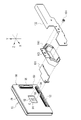
- FIG. 1 is a diagram showing a digital camera
- FIG. 2 is a front exploded perspective view of the imaging device unit
- FIG. 4 is a rear exploded perspective view of the imaging element unit
- FIG. 4 is a rear exploded perspective view of the essential parts of the imaging element unit
- It is a perspective view of a 1st thermally-conductive member, a 2nd thermally-conductive member, and a 3rd thermally-conductive member.
- FIG. 1 is a diagram showing a digital camera
- FIG. 2 is a front exploded perspective view of the imaging device unit
- FIG. 4 is a rear exploded perspective view of the imaging element unit
- FIG. 4 is a rear exploded perspective view of the essential parts of the imaging element unit
- It is a perspective view of a 1st thermally-conductive member, a 2nd thermally-conductive member
- FIG. 3 is a cross-sectional view of the main part of the imaging element unit; It is a perspective view of a 3rd thermally-conductive member, a 4th thermally-conductive member, and a connection member. It is a simple top view of a 1st thermally-conductive member. It is a figure which shows before bending of a 1st heat-conduction member, and after bending. It is a figure which shows a mode that a 1st thermally-conductive member deform
- FIG. 3 is a diagram showing a conduction path of driving heat of an image pickup device; FIG.
- FIG. 4 is a diagram showing a first thermally conductive member with a triple structure
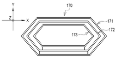
- FIG. 10 illustrates an octagonal first heat-conducting member
- FIG. 10 is a view showing the first heat conducting member in which the corners of the connection portion of the outer layer portion and the corners of the connection portion of the inner layer portion are recessed inward
- FIG. 10 is a diagram showing an imaging element unit having a fifth heat conducting member
- FIG. 10 is a diagram showing an imaging element unit having a fifth heat conducting member
- It is a simple top view of a 5th thermally-conductive member.
- FIG. 10 is a diagram showing an example of connecting a second heat-conducting member to a central region of the back surface of a circuit board that does not have openings;
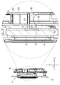
- the digital camera 2 has a camera body 10 .
- a lens mount 11 is provided on the front of the camera body 10 .
- a lens mount 11 has a circular imaging aperture 12 .
- An interchangeable imaging lens (not shown) is detachably attached to the lens mount 11 .
- the digital camera 2 is an example of an “imaging device” according to the technology of the present disclosure.
- the camera body 10 is an example of a “housing” according to the technology of the present disclosure.
- An imaging device unit 15 is built into the camera body 10 .
- a rectangular plate-shaped image sensor 16 is mounted on the image sensor unit 15 .
- the imaging element 16 is, for example, a CMOS (Complementary Metal Oxide Semiconductor) image sensor or a CCD (Charge Coupled Device) image sensor.
- the imaging device 16 has a rectangular imaging surface 17 for imaging a subject.
- the imaging surface 17 receives subject light that indicates the subject.
- pixels that photoelectrically convert received subject light and output electric signals are arranged two-dimensionally. The entire imaging surface 17 is exposed to the outside through the imaging aperture 12 .
- a CPU 18 is connected to the imaging element unit 15 .
- a CPU 18 controls the operation of the imaging element unit 15 .
- the CPU 18 is connected to a ROM (Read Only Memory) and/or a RAM (Random Access Memory) via a bus line.
- a computer is configured by these CPU 18, memory, and bus line.
- the imaging element unit 15 has a vibration isolation function.
- the anti-vibration function is a function for suppressing relative positional displacement between subject light incident on the imaging surface 17 and the digital camera 2 , which is caused by vibrations applied to the camera body 10 .
- Vibrations applied to the camera body 10 include camera shake of a user who shoots an object while holding the camera body 10 .
- the imaging element 16 is moved by the anti-vibration function in the direction to cancel the positional deviation by the amount that cancels out the positional deviation. More specifically, the anti-vibration function allows the X-axis direction parallel to the side 19 of the imaging surface 17 of the image sensor 16 and/or the side 20 perpendicular to the side 19, that is, to intersect the side 19 at an angle of 90°.
- the imaging element 16 is moved in the parallel Y-axis direction.
- the X-axis direction and the Y-axis direction are examples of the "plane direction" according to the technology of the present disclosure.
- the terms “perpendicular” and “90°” mean not only perfect orthogonality and 90°, but also substantially orthogonal and approximately 90° including errors allowed in design and manufacturing. also includes the meaning of Further, in this specification, the term “parallel” includes not only the meaning of perfect parallelism but also the meaning of substantially parallelism including an error allowed in terms of design and manufacturing.
- the side 19 is expressed as “lower”, and the side opposite to the side 19 in the Y-axis direction is expressed as "upper”.
- the side 20 is expressed as "left”, and the side opposite to side 20 in the X-axis direction is expressed as "right”.
- positional deviation refers to a phenomenon that occurs when the optical axis OA fluctuates with respect to the subject due to vibration.
- Optical axis OA refers to the optical axis of subject light incident on the imaging surface 17 through the imaging lens. Fluctuation of the optical axis OA means that the optical axis OA is tilted due to the positional deviation with respect to the reference axis (for example, the optical axis OA before the positional deviation occurs).
- canceling the positional deviation includes not only the elimination of the positional deviation but also the reduction of the positional deviation.
- the imaging device unit 15 includes a fixed member 30, a movable member 31, a yoke 32, and the like.
- the fixing member 30 is arranged on the rear side of the camera body 10
- the yoke 32 is arranged on the front side of the camera body 10 .
- the fixing member 30 is fixed to the camera body 10 .
- the fixed member 30 and the yoke 32 are fixed with a space therebetween in the Z-axis direction orthogonal to the X-axis and the Y-axis.
- the movable member 31 is arranged between the fixed member 30 and the yoke 32 via three balls 35, 36 and 37 of the same size.
- the movable member 31 can move in the X-axis direction and the Y-axis direction (rotate around the Z-axis) with respect to the fixed member 30 and the yoke 32 by the balls 35 to 37 .
- the Z axis is parallel to the optical axis OA before the positional deviation occurs.
- the fixing member 30 holds magnets 40 , 41 and 42 .
- Magnets 40 to 42 are attached to the front face of fixed member 30 facing movable member 31 .
- Each of the magnets 40 to 42 is a set of an elongated plate-shaped magnet with its N pole directed toward the movable member 31 and an elongated plate-shaped magnet with its S pole directed toward the movable member 31 side.
- the magnet 40 is arranged in the lower center of the fixing member 30 so that its long side extends along the X-axis direction.
- the magnets 41 and 42 are arranged along the Y-axis direction.
- the magnet 41 is arranged at the upper left corner of the fixed member 30 so that its long side extends along the Y-axis direction.
- the magnet 42 is arranged at the lower left corner of the fixed member 30 so that its long side extends along the Y-axis direction.
- a plate 45, a plate 46, and a plate 47 are attached to the front of the fixed member 30 in addition to the magnets 40-42.
- the plate 45 is arranged at the lower right corner of the fixing member 30 and above the magnet 40 .
- the plate 46 is arranged on the left side of the fixed member 30 and between the magnets 41 and 42 .
- the plate 47 is arranged at the upper right corner of the fixed member 30 .
- the plate 45 rotatably supports the ball 35
- the plate 46 rotatably supports the ball 36
- the plate 47 rotatably supports the ball 37 .
- the fixed member 30 is formed with square regulation openings 50 and 51 that regulate the movement range of the movable member 31 in the XY plane.
- the regulation opening 50 and the regulation opening 51 have substantially the same size when viewed from above in the Z-axis direction.
- a restriction opening 50 is formed between the magnet 42 and the plate 45 at the lower left corner of the fixed member 30 .
- the regulation opening 51 is formed to the left of the plate 47 at the upper right corner of the fixing member 30 . That is, the regulation opening 50 and the regulation opening 51 are arranged at substantially diagonal positions in the fixing member 30 .
- a female screw 55, a female screw 56, a female screw 57, and a female screw 58 are provided on the fixing member 30 via spacers.
- a female screw 55 is provided at the lower right corner of the fixing member 30 .
- a female thread 56 is provided at the upper left corner of the fixing member 30 .
- a female screw 57 is provided at the lower left corner of the fixing member 30 .
- a female screw 58 is provided at the upper right corner of the fixing member 30 .
- a relatively large rectangular access opening 59 is formed in the center of the fixing member 30 .
- the access opening 59 is provided for accessing the back surface of the movable member 31 from the back surface of the fixed member 30 .
- the movable member 31 holds the imaging element 16 and holds the coils 60 , 61 and 62 .
- the imaging element 16 is arranged in the central portion of the movable member 31 .
- the coil 60 is arranged at the center of the lower portion of the movable member 31 and at a position facing the magnet 40 in the Z-axis direction.
- the coil 61 is arranged at the upper left corner of the movable member 31 and at a position facing the magnet 41 in the Z-axis direction.
- the coil 62 is arranged at the lower left corner of the movable member 31 and at a position facing the magnet 42 in the Z-axis direction.
- the coil 60 is arranged such that its long side extends along the X-axis direction.
- the coils 61 and 62 are arranged along the Y-axis direction. Each of the coils 61 and 62 is arranged such that its long side extends along the Y-axis direction.
- a magnet 65 is held in the yoke 32 .
- a magnetic body 66 is attached to the coil 61 and a magnetic body 67 is attached to the coil 62 .
- Magnet 65 is, for example, a neodymium magnet.
- the magnetic bodies 66 and 67 are thin plate pieces made of iron, for example.
- a magnet 65 is arranged to cover the coil 60 and increases the driving force of the coil 60 .
- the magnetic bodies 66 and 67 are arranged along the Y-axis direction.
- the magnetic body 66 is arranged on the upper end side of the coil 61, and the magnetic body 67 is arranged on the lower end side of the coil 62, respectively.
- the magnet 65 Since the coil 60 is arranged at a position facing the magnet 40 in the Z-axis direction as described above, the magnet 65 is also arranged at a position facing the magnet 40 in the Z-axis direction. Therefore, the magnet 65 is attracted to the magnet 40 while being fixed to the yoke 32 .
- the magnetic body 66 is also arranged at a position facing the magnet 41 in the Z-axis direction. Therefore, the magnetic body 66 is attracted to the magnet 41 .
- the magnetic body 67 is also arranged at a position facing the magnet 42 in the Z-axis direction. Therefore, the magnetic body 67 is attracted to the magnet 42 .
- a concave portion 70 , a concave portion 71 , and a concave portion 72 are formed on the back surface of the movable member 31 facing the fixed member 30 .
- the concave portion 70 is arranged at the lower right corner of the movable member 31 and at a position facing the plate 45 in the Z-axis direction.
- the concave portion 71 is arranged between the coils 61 and 62 on the left side of the movable member 31 and at a position facing the plate 46 in the Z-axis direction.
- the concave portion 72 is arranged at the upper right corner of the movable member 31 and at a position facing the plate 47 in the Z-axis direction.
- the recess 70 rotatably accommodates the ball 35
- the recess 71 rotatably accommodates the ball 36
- the recess 72 rotatably accommodates the ball 37 .
- the size of the concave portions 70 to 72 when viewed from above in the Z-axis direction is slightly larger than the diameter of the balls 35 to 37 .
- the depth of the recesses 70-72 in the Z-axis direction is slightly smaller than the diameter of the balls 35-37.
- a cylindrical projection 80 projecting toward the fixed member 30 is provided on the rear surface of the movable member 31 at a position facing the regulation opening 50 in the Z-axis direction. Further, on the rear surface of the movable member 31, a cylindrical protrusion 81 protruding toward the fixed member 30 is provided at a position facing the regulation opening 51 in the Z-axis direction.
- the protrusion 80 is inserted through the regulation opening 50 . Also, the projection 81 is inserted through the regulation opening 51 . Therefore, the protrusions 80 and 81 work as restricting pins that restrict the movement of the movable member 31 in the XY plane.
- the yoke 32 is a magnetic material such as a thin iron plate, and has a substantially C shape. Yoke 32 forms a magnetic circuit with magnets 40-42 to increase the magnetic flux received by coils 60-62.
- a male screw 85 , a male screw 86 , a male screw 87 and a male screw 88 are attached to the yoke 32 .
- the male screws 85 - 88 are fastened and fixed to the female screws 55 - 58 of the fixing member 30 .
- the fixed member 30 and the yoke 32 are fixed, and the movable member 31 is movably held between the fixed member 30 and the yoke 32 .
- the imaging device unit 15 includes a pair of voice coil motors (VCM; Voice Coil Motor).
- VCM voice coil motors
- a pair of VCMs is a pair of a first VCM and a second VCM.
- the first VCM includes a pair of magnets 40 and coils 60 and a yoke 32, and generates power to move the movable member 31 in the Y-axis direction.
- the second VCM includes a pair of magnet 41 and coil 61, a pair of magnet 42 and coil 62, and yoke 32, and generates power to move movable member 31 in the X-axis direction.
- the first VCM generates power for moving the movable member 31 in the Y-axis direction by the magnetic force of the magnet 40 and the current flowing through the coil 60 .
- the second VCM also generates power for moving the movable member 31 in the X-axis direction by the magnetic force of the magnet 41 and the current flowing through the coil 61 and the magnetic force of the magnet 42 and the current flowing through the coil 62 .
- the movable member 31 is provided with a Hall element for detecting the position of the movable member 31, a temperature sensor for measuring the temperature around the Hall element, and the like.
- the CPU 18 finds the difference between the position of the movable member 31 detected by the Hall element and the target position of the movable member 31 for correcting the positional deviation, and performs feedback control to drive the VCM so as to eliminate the difference.
- the difference is large, the power generated by the VCM becomes relatively large, and conversely, when the difference is small, the power generated by the VCM becomes relatively small.
- the CPU 18 corrects the temperature drift of the Hall element using the temperature measured by the temperature sensor.
- a rectangular plate-shaped circuit board 90 having substantially the same size as the imaging element 16 is attached to the rear surface 89 of the imaging element 16 facing the imaging surface 17 .
- the circuit board 90 is made of resin such as epoxy, for example.
- a rectangular opening 91 is formed in the circuit board 90 .
- the opening 91 is formed in the center of the circuit board 90 and exposes the central region 92 of the back surface 89 of the imaging device 16 .
- the central region 92 is a region of a preset size that surrounds the center point C of the back surface 89 of the imaging device 16 .
- Identification information 98 of the imaging element 16 is written in the central area 92 .
- the opening 91 is formed for viewing this identification information 98 .
- the identification information 98 is, for example, a two-dimensional bar code for moving to an Internet page on which management numbers and management information are described.
- the circuit board 90 is mounted with electric circuits such as a control circuit, a drive circuit, and a power supply circuit for the imaging device 16 .
- a connector 93 and a connector 94 are provided at the lower end of the back surface 89 of the circuit board 90 .
- a connector 95 is provided at the left end of the rear surface 89 of the circuit board 90 .
- One end of a flexible substrate 96 is connected to the connector 93 and the connector 94 .
- the other end of the flexible board 96 is pulled out to the back side of the fixing member 30 through the access opening 59 (see FIG. 7).
- the other end of the flexible substrate 96 is connected to the CPU 18, a power supply circuit (not shown) that supplies power from the battery, and the like.
- One end of a flexible substrate 97 (see FIG. 1) is connected to the connector 95 .
- the other end of the flexible substrate 97 wraps around the front of the movable member 31 and is connected to the imaging element 16 .
- the imaging device 16 is connected to the other end of the flexible substrate 97
- the connector 95 is connected to one end of the flexible substrate 97 .
- a flexible board 96 is connected to the connectors 93 and 94 , and the CPU 18 and the like are connected to the other end of the flexible board 96 . Therefore, the imaging device 16 , the circuit board 90 , the CPU 18 and the like are connected via a flexible board 97 , a connector 95 , a connector 93 and a connector 94 , and a flexible board 96 .
- the imaging element unit 15 further has a first thermally conductive member 100, a second thermally conductive member 101, and a third thermally conductive member 102 to which driving heat of the imaging element 16 is conducted.
- a second heat conduction member 101 and a third heat conduction member 102 are connected to the first heat conduction member 100 . Driving heat is conducted to the first heat conducting member 100 from the second heat conducting member 101 . In addition, the first heat conducting member 100 conducts driving heat to the third heat conducting member 102 .
- the second heat conducting member 101 is connected to the central region 92 of the rear surface 89 of the imaging element 16 exposed through the opening 91 . Driving heat is conducted from the central region 92 to the second heat conducting member 101 .
- the first thermally conductive member 100 and the second thermally conductive member 101 are fixed with an adhesive.
- a female screw 68 is formed in the fixing member 30 .
- An insertion hole 103 is formed in the first heat conducting member 100 .
- a male screw 104 is attached to the third heat conducting member 102 .
- the male screw 104 is passed through the insertion hole 103 of the first heat conducting member 100 and fastened to the female screw 68 of the fixing member 30 . Thereby, the first heat conducting member 100 and the third heat conducting member 102 are fixed.
- the first heat conducting member 100 is made of a graphite sheet.
- the graphite sheet has a configuration in which a graphite sheet main body is pouched with a resin film such as a PET (polyethylene terephthalate) film.
- the thickness of the graphite sheet body is, for example, 70 ⁇ m, and the thickness of the resin film is, for example, 5 ⁇ m.
- the second heat conducting member 101 and the third heat conducting member 102 are metal plates, such as copper plates. Therefore, the second heat conduction member 101 and the third heat conduction member 102 have higher rigidity than the first heat conduction member 100 made of a graphite sheet. In other words, the first heat-conducting member 100 has higher elasticity than the second heat-conducting member 101 and the third heat-conducting member 102 .
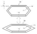
- the first heat conducting member 100 has a double structure having an outer layer portion 110 and an inner layer portion 111 .
- the inner layer portion 111 is connected to the outer layer portion 110 via a connection portion 112 (see also FIG. 9 and the like) and is arranged in a space surrounded by the outer layer portion 110 .
- a mounting portion 113 in which an insertion hole 103 is formed is provided on the upper portion of the outer layer portion 110 .
- Both the outer layer portion 110 and the inner layer portion 111 are hexagonal.
- the outer layer portion 110 includes a first sheet portion 115, a second sheet portion 116 having the same length as the first sheet portion 115 and facing the first sheet portion 115, and the first sheet portion 115 and the second sheet portion. 116 and a pair of V-shaped connecting portions 117 that connect the connecting portions 116 .
- the inner layer portion 111 includes a first sheet portion 118 , a second sheet portion 119 having the same length as the first sheet portion 118 and facing the first sheet portion 118 , and a first sheet portion 118 and a second sheet portion 119 . It is composed of a pair of V-shaped connecting portions 120 connecting two sheet portions 119 .
- the first sheet portion 115 and the second sheet portion 116, and the first sheet portion 118 and the second sheet portion 119 are planar.
- the second heat conducting member 101 has a first piece 125 and a second piece 126 .
- the first piece 125 is parallel to the imaging surface 17 and the rear surface 89 of the imaging device 16 and faces the rear surface 89 of the imaging device 16 .
- the first piece 125 is connected to the central region 92 of the back surface 89 .
- the second piece 126 is bent 90° from the first piece 125 and extends in the direction normal to the imaging surface 17 and the back surface 89 of the imaging device 16 .
- the normal direction of the imaging surface 17 and the back surface 89 of the imaging element 16 is the Z-axis direction (the direction of the optical axis OA before the positional deviation occurs).
- the second piece 126 has approximately the same size as the space between the first sheet portion 115 of the outer layer portion 110 and the first sheet portion 118 of the inner layer portion 111 .
- the second heat conducting member 101 is connected to the first heat conducting member 100 through the second piece 126 . More specifically, the second piece 126 is inserted into the space between the first sheet portion 115 of the outer layer portion 110 and the first sheet portion 118 of the inner layer portion 111 and sandwiched between the first sheet portions 115 and 118. is held in place. Double-sided tape is attached to the portions of the first sheet portion 115 and the first sheet portion 118 that are in contact with the second piece 126 . The adhesive of the double-sided tape fixes the first sheet portion 115, the first sheet portion 118 and the second piece 126, as well as the first heat conducting member 100 and the second heat conducting member 101 together.
- the third heat conducting member 102 has a first piece 127 and a second piece 128 .
- the first piece 127 is parallel to the imaging surface 17 and the back surface 89 of the imaging device 16 and has a wing shape elongated in the X-axis direction.
- the second piece 128 is bent 90° from the first piece 127 and extends in the direction normal to the imaging surface 17 and the back surface 89 of the imaging device 16 , similarly to the second piece 126 of the second thermally conductive member 101 .
- the third heat conducting member 102 is connected to the first heat conducting member 100 through the second piece 128 . More specifically, the second piece 128 is inserted into the space between the second sheet portion 116 of the outer layer portion 110 and the second sheet portion 119 of the inner layer portion 111 and sandwiched between the second sheet portions 116 and 119 . is held in place. The second piece 128 is provided with a claw 129 hooked on the edge of the second sheet portion 119 .
- the thickness TH2 of the second heat conduction member 101 is thicker than the thickness TH1 of the first heat conduction member 100.
- the thickness TH1 of the first thermally conductive member 100 is, for example, 80 ⁇ m, and the thickness of the second thermally conductive member 101 is, for example, 1 mm.
- the thickness of the third thermally conductive member 102 is also greater than the thickness TH1 of the first thermally conductive member 100, for example 1 mm.
- the flexible substrate 96 pulled out through the access opening 59 is arranged on the opposite side of the first heat conducting member 100 with the second piece 126 of the second heat conducting member 101 interposed therebetween. .
- a fourth heat conduction member 135 is attached to the third heat conduction member 102 with an adhesive.
- the fourth heat-conducting member 135 is made of a graphite sheet, like the first heat-conducting member 100 .
- the thickness TH4 of the fourth thermally conductive member 135 is thicker than the thickness TH1 of the first thermally conductive member 100 (see FIG. 6).
- a thickness TH4 of the fourth thermally conductive member 135 is, for example, 500 ⁇ m.
- a connecting member 136 is further attached to the fourth heat conducting member 135 with an adhesive.
- the connecting member 136 is a metal plate, such as a copper plate, like the second heat-conducting member 101 and the third heat-conducting member 102 .
- the connection member 136 is connected to the top plate 137 of the camera body 10 .
- the top plate 137 of the camera body 10 is, for example, a magnesium plate or an aluminum plate.
- the outer layer portion 110 of the first thermally conductive member 100 is hexagonal as described above, so that it has six corners 140, 141, 142, 143, 144, and 6 corners. 145.
- Inner layer portion 111 is also hexagonal and thus has six corners 146 , 147 , 148 , 149 , 150 and 151 .
- the corners 140 to 145 and the corners 146 to 151 function as bent portions that enable deformation following the movement of the imaging device 16 due to the anti-vibration function. Corners 140-145 flare outward. Similarly, corners 146-151 are also flared outward. That is, the first heat conducting member 100 has a shape like a pantograph.
- the first heat conducting member 100 is simplified by omitting the illustration of the mounting portion 113 . The same applies to FIGS. 11 and 12 and the like.
- the first thermally conductive member 100 is formed by folding a piece of sheet-like material 160 along the broken line. Specifically, first, the connection portion 112 is bent so that the portion that will become the outer layer portion 110 and the portion that will become the inner layer portion 111 face each other. Then, after the corners 146 to 151 are bent to form the inner layer portion 111, the corners 140 to 145 are bent to form the outer layer portion 110. FIG. Finally, the portion that will become the mounting portion 113 is bent to complete the first heat conducting member 100 .
- the first thermally conductive member 100 has a reinforcing layer 161 .
- the reinforcing layer 161 is a resin film such as a 40 ⁇ m thick PET film.
- the reinforcing layer 161 is provided on the two sides forming the connecting portion 117 and the connecting portion 120, and is not provided on the corners 144, 145, 150, and 151 that function as bent portions.
- the two sides forming the connecting portion 117 and the connecting portion 120 are thicker than the corners 144, 145, 150, and 151 functioning as bent portions due to the reinforcement layer 161.
- the two sides forming connection portion 117 and connection portion 120 are an example of a “portion having a reinforcing layer” according to the technology of the present disclosure.
- the first thermally conductive member 100 deforms so as to follow the movement of the imaging device 16 due to the anti-vibration function.
- FIG. 11 shows how the first thermal conductive member 100 expands and contracts in the vertical direction and deforms following the movement of the imaging device 16 along the Y-axis direction due to the anti-vibration function.
- FIG. 12 shows how the first heat conducting member 100 tilts and deforms in the left-right direction following the movement of the imaging element 16 along the X-axis direction due to the anti-vibration function.
- the drive heat of the imaging element 16 follows the conduction path shown in FIG. That is, the drive heat of the imaging element 16 is first conducted from the rear surface 89 of the imaging element 16 to the second heat conducting member 101 connected to the central region 92 of the rear surface 89 . The driving heat is then conducted from the second heat-conducting member 101 to the first heat-conducting member 100 connected through the second piece 126 of the second heat-conducting member 101 .
- the driving heat conducted to the first heat conducting member 100 is conducted to the third heat conducting member 102 connected through the second piece 128 . Furthermore, the driving heat is conducted from the third heat conducting member 102 to the fourth heat conducting member 135 and from the fourth heat conducting member 135 to the connecting member 136 . Then, the heat is conducted to the top plate 137 of the camera body 10 through the connection member 136 and radiated to the outside through the top plate 137 .
- the imaging element unit 15 is made such that the movable member 31 is movable with respect to the fixed member 30 and the yoke 32 .
- the movable member 31 holds the imaging device 16 . Therefore, the imaging element 16 also moves along with the movement of the movable member 31 .
- the movable member 31 and, in turn, the imaging element 16 are moved under the control of the CPU 18 in the direction of canceling the positional displacement by the amount to cancel the positional displacement. be moved.
- the first thermally conductive member 100 is deformed following the movement of the imaging device 16 due to this anti-vibration function.
- the imaging device unit 15 includes the imaging device 16 having the imaging surface 17 for imaging a subject and the back surface 89 facing the imaging surface 17 , the circuit board 90 attached to the back surface 89 , and the imaging device 16 . It comprises a first heat conducting member 100 and a second heat conducting member 101 to which driving heat is conducted.
- the circuit board 90 is formed with an opening 91 that exposes a central region 92 of the back surface 89 of the imaging element 16 .
- the first heat-conducting member 100 is connected to the second heat-conducting member 101 and has higher elasticity than the second heat-conducting member 101 .
- a second thermally conductive member 101 is connected to the rear surface 89 through the opening 91 .
- the second thermally conductive member 101 which has a relatively high rigidity and is difficult to deform, is directly connected to the imaging device 16, compared to the case where the first thermally conductive member 100, which has a relatively high elasticity and is easily deformed, is directly connected to the imaging device 16, It is possible to make it difficult for the thermally conductive member to peel off from the imaging element 16 .
- the imaging device unit 15 has a vibration isolation function that moves the imaging device 16 in the planar direction. As shown in FIGS. 11 and 12, the first thermally conductive member 100 deforms so as to follow the movement of the imaging device 16 due to the anti-vibration function. Therefore, by directly connecting the second heat-conducting member 101, which has relatively high rigidity and is difficult to deform, to the imaging device 16, the effect that the heat-conducting member is difficult to peel off can be further exhibited.
- the first thermally conductive member 100 when the first thermally conductive member 100 is directly connected to the imaging element 16, it is necessary to increase the thickness TH1 of the first thermally conductive member 100 in order to increase the conduction efficiency. If the thickness TH1 is thicker, the repulsive force of the first heat conducting member 100 is increased accordingly, and the deformation following the movement of the imaging device 16 due to the anti-vibration function becomes difficult. However, in this example, it is not necessary to increase the thickness TH1 of the first heat conducting member 100 so much. Therefore, the first thermally conductive member 100 can follow the movement of the imaging element 16 due to the anti-vibration function and deform without much resistance, as compared with the case where the first thermally conductive member 100 is directly connected to the imaging element 16 .
- the second heat conducting member 101 is connected to the central region 92 and has a first piece 125 facing the back surface 89 and a second piece 126 bent from the first piece 125. .
- the first heat conducting member 100 is connected to the second piece 126 . Therefore, the first thermally conductive member 100 deforms so as to follow the movement of the second piece 126 rather than the movement of the imaging element 16 itself. When deformed so as to follow the movement of the imaging element 16 itself, the first heat conduction member 100 needs to have a complicated structure. 100 can be of simple construction.
- the second piece 126 extends in the normal direction of the imaging surface 17 and the back surface 89 . Therefore, the first heat conducting member 100 can have a simpler configuration.
- the angle at which the second piece 126 is bent from the first piece 125 may be less than 90° or greater than 90°.
- the imaging device unit 15 includes a flexible board 96 attached to the circuit board 90 . As shown in FIG. 7, the flexible board 96 is arranged on the side opposite to the first heat conducting member 100 with the second piece 126 of the second heat conducting member 101 interposed therebetween. Therefore, there is no possibility that the flexible substrate 96 and the first thermally conductive member 100 will come into contact with each other and the signals to and/or from the imaging element 16 will be disturbed.
- the thickness TH2 of the second heat conduction member 101 is thicker than the thickness TH1 of the first heat conduction member 100. Therefore, the heat conduction efficiency of the second heat conduction member 101 can be enhanced.
- the thermal conductivity of the graphite sheet forming the first thermally conductive member 100 is 1600 w/m ⁇ K.
- the thermal conductivity of copper forming the second thermally conductive member 101 is 390 W/m ⁇ K, which is lower than that of the graphite sheet.
- the thickness TH2 of the second thermally conductive member 101 is larger than the thickness TH1 of the first thermally conductive member 100 as described above, the low thermal conductivity can be compensated for. Thereby, the heat conduction efficiency of the second heat conduction member 101 can be made higher than that of the first heat conduction member 100 . If the thermal conductivity of the second heat conducting member 101 is higher than that of the first heat conducting member 100 , the driving heat can be smoothly conducted from the second heat conducting member 101 to the first heat conducting member 100 .
- the thermal conductivity of the second thermally conductive member 101 is made higher than that of the first thermally conductive member 100, but the present invention is not limited to this. Instead of increasing the thickness TH2 of the second heat conduction member 101, or in addition, by forming the second heat conduction member 101 with a material having a higher thermal conductivity than the first heat conduction member 100, the The thermal conductivity of the second thermally conductive member 101 may be higher than that of the first thermally conductive member 100 .
- the opening 91 of the circuit board 90 exposes the central region 92 of the back surface 89 of the imaging device 16 .
- a center region 92 is a portion of the rear surface 89 of the imaging device 16 where the driving heat of the imaging device 16 is the highest. For this reason, the drive heat of the imaging device 16 can be more effectively radiated.
- the central area 92 is an area in which the identification information 98 of the imaging device 16 is described. Therefore, the opening 91 formed for visually recognizing the identification information 98 can be effectively used to radiate driving heat of the imaging device 16 .
- the first thermally conductive member 100 is made of a graphite sheet, and the second thermally conductive member 101 and the third thermally conductive member 102 are made of metal. Therefore, the first heat conducting member 100 can be given appropriate elasticity, and the second heat conducting member 101 and the third heat conducting member 102 can be given appropriate rigidity.
- the first heat conducting member 100 has an outer layer portion 110 and an inner layer portion 111 connected to the outer layer portion 110 and arranged in a space surrounded by the outer layer portion 110 .
- Each of the outer layer portion 110 and the inner layer portion 111 has bent portions (corners 140 to 145 and corners 146 to 151) that enable deformation following the movement of the imaging device 16 due to the anti-vibration function. Therefore, compared to the case where only the outer layer portion 110 is provided, it is possible to dissipate the driving heat of the imaging device 16 more efficiently. As a result, shooting such as 4K/120p moving image shooting that imposes a relatively large load on the image sensor 16 can be performed for a longer time than before.
- the installation space for the thermally conductive member can be saved.
- the first thermally conductive member 100 is formed by folding one sheet-like material 160 . Therefore, the first thermally conductive member 100 can be formed more easily than when the outer layer portion 110 and the inner layer portion 111 are formed from different materials and then connected.
- the first heat conducting member 100 includes a first sheet portion 115 and a first sheet portion 118, a second sheet portion 116 facing the first sheet portion 115 and the first sheet portion 118, and a It is composed of a second sheet portion 119 , a connecting portion 117 connecting the first sheet portions 115 and 118 , and a connecting portion 120 connecting the second sheet portions 116 and 119 .
- the first thermally conductive member 100 can be deformed naturally by following the movement of the imaging device 16 due to the anti-vibration function.
- the outer layer portion 110 and the inner layer portion 111 have corners 140 to 145 and corners 146 to 151 that function as bent portions projecting outward. Therefore, a large space surrounded by the outer layer portion 110 can be secured, and the inner layer portion 111 can be easily formed.
- the first thermally conductive member 100 is a portion other than the corners 144, 145, 150, and 151 functioning as bent portions, and constitutes the connection portion 117 and the connection portion 120. It has reinforcing layers 161 on two sides.
- the two sides forming the connecting portion 117 and the connecting portion 120 are thicker than the corners 140 to 145 and the corners 146 to 151 functioning as bent portions due to the reinforcing layer 161 . Therefore, unintended deformation of the two sides forming connection portion 117 and connection portion 120 can be prevented.
- the reinforcing layer 161 is not provided at the corners 140 to 145 and the corners 146 to 151 that function as bent portions, the first heat conducting member 100 follows the movement of the imaging element 16 by the anti-vibration function, resulting in large resistance. can be transformed without
- the reinforcing layer 161 may be provided on the first sheet portion 115 and the first sheet portion 118 and the second sheet portion 116 and the second sheet portion 119 .
- the first thermally conductive member 100 is connected to the imaging element 16 via the second thermally conductive member 101 and is connected to the camera body 10 via the third thermally conductive member 102 .
- the second thermally conductive member 101 and the third thermally conductive member 102 are sandwiched between the outer layer portion 110 and the inner layer portion 111 . Therefore, the driving heat conduction efficiency from the second heat conduction member 101 to the first heat conduction member 100 and the driving heat conduction efficiency from the first heat conduction member 100 to the third heat conduction member 102 can be improved. can.
- the holding force of the second heat conduction member 101 and the third heat conduction member 102 by the first heat conduction member 100 can be increased.
- the third heat conducting member 102 may constitute a part of the camera body 10 .
- a fourth heat conduction member 135 made of a graphite sheet is connected between the third heat conduction member 102 and the top plate 137 of the camera body 10.
- the thickness TH4 of the fourth thermally conductive member 135 is thicker than the thickness TH1 of the first thermally conductive member 100 .
- the fourth heat conduction member 135 does not deform so as to follow the movement of the imaging element 16 due to the anti-vibration function. Therefore, unlike the first heat conducting member 100, it is not necessary to make the thickness TH1 comparatively thin in order to realize smooth deformation at the expense of the conduction efficiency of driving heat. high conduction efficiency.
- the number of inner layer parts 111 is not limited to one.
- a triple structure having one outer layer portion 171 and two inner layer portions 172 and 173 arranged in a space surrounded by the outer layer portion 171 may be employed.
- the shape of the first heat conducting member is not limited to a hexagon.
- the outer layer portion 181 and the inner layer portion 182 may be octagonal. Further, as shown in FIG.
- a first heat conducting member 190 in which corners 195 and 196 of a connecting portion 193 of an outer layer portion 191 and corners 197 and 198 of a connecting portion 194 of an inner layer portion 192 are recessed inward.
- the first heat-conducting member 190 has a shape that is, so to speak, a combination of " ⁇ " and its mirror image.
- an imaging element unit 200 of the second embodiment has a fifth heat conducting member 201.
- the fifth heat-conducting member 201 is a flexible substrate 97 connected to the imaging element 16 and wrapped around the front surface of the movable member 31 at a position facing the side surface 202 of the imaging element 16 that connects the imaging surface 17 and the back surface 89 . It is arranged in the space to be formed.
- Driving heat of the imaging element 16 is conducted to the fifth heat conducting member 201 from the side surface 202 .
- a sixth heat conduction member 203 made of a metal plate is connected to the fifth heat conduction member 201 .
- the sixth heat conducting member 203 is connected to the side plate of the camera body 10 or the like.
- Driving heat from the fifth heat-conducting member 201 is conducted to the camera body 10 through the sixth heat-conducting member 203 .
- the fifth heat-conducting member 201 is made of a graphite sheet like the first heat-conducting member 100 and has high elasticity. Like the first heat conduction member 100 and the like, the fifth heat conduction member 201 deforms so as to be able to follow the movement of the imaging device 16 due to the anti-vibration function. However, unlike the first heat conducting member 100 and the like, the fifth heat conducting member 201 has no inner layer portion.
- the fifth heat conduction member 201 is a hexagon having six corners 205 , 206 , 207 , 208 , 209 , and 210 like the first heat conduction member 100 . It is rectangular. The corners 205 to 210 function as bent portions that enable deformation following the movement of the imaging device 16 due to the anti-vibration function.
- the fifth heat conduction member 201 has a first sheet portion 211 and a second sheet portion 211 having the same length as the first sheet portion 211 and facing the first sheet portion 211 , similarly to the first heat conduction member 100 .
- Angle ⁇ 5 of corners 209 and 210 functioning as bent portions of connecting portion 213 is equal to angles 144 and 145 functioning as bent portions of connecting portion 117 and connecting portion 120 of first heat conducting member 100, and angle 150 and angle It is sharper than the angle ⁇ 1 of 151 (see FIG. 9).
- the imaging device unit 200 of the second embodiment includes the fifth thermally conductive member 201.
- the fifth heat-conducting member 201 is arranged at a position facing a side surface 202 of the imaging element 16 that connects the imaging surface 17 and the back surface 89 .
- Driving heat is conducted to the fifth heat conducting member 201 from the side surface 202 .
- the fifth thermally conductive member 201 deforms so as to follow the movement of the imaging device 16 due to the anti-vibration function.
- the fifth heat-conducting member 201 has a bent portion that enables deformation following the movement of the imaging device 16 due to the anti-vibration function. Therefore, the drive heat can be more effectively radiated without hindering the movement of the imaging device 16 by the anti-vibration function.
- the fifth heat conducting member 201 is composed of a first sheet portion 211, a second sheet portion 212 facing the first sheet portion 211, and a connecting portion 213 connecting the first sheet portion 211 and the second sheet portion 212. be. For this reason, the fifth heat conducting member 201 can be deformed without difficulty by following the movement of the imaging element 16 due to the anti-vibration function, while securing the connecting portion with the sixth heat conducting member 203 and the like.
- the angle ⁇ 5 formed by the bent portion of the connecting portion 213 of the fifth heat conducting member is sharper than the angle ⁇ 1 formed between the connecting portion 117 of the first heat conducting member 100 and the bent portion of the connecting portion 120 . Therefore, the repulsive force of the fifth thermally conductive member 201 can be reduced, and the fifth thermally conductive member 201 can follow the movement of the imaging element 16 due to the anti-vibration function, and can be deformed without much resistance.
- the fifth heat conduction member 201 becomes more compact than the first heat conduction member 100 because the distance between the first sheet portion 211 and the second sheet portion 212 is reduced. Therefore, it can be arranged in a relatively narrow space such as a space formed by the flexible substrate 97 at a position facing the side surface 202 of the image sensor 16 .
- the fifth heat conducting member 201 is made of a graphite sheet. Therefore, the fifth thermally conductive member 201 can have appropriate elasticity.
- the fifth heat conducting member 201 may have a multi-layer structure. Further, as in the example shown in FIG. 15, the fifth heat conducting member 201 may be octagonal. Furthermore, as in the example shown in FIG. 16, the fifth heat conducting member 201 may have a structure in which the corners of the connecting portion are recessed inward.
- the circuit board 90 is formed with the opening 91 that exposes the central region 92 of the back surface 89 of the imaging device 16 , and the first piece 125 of the second thermally conductive member 101 extends through the opening 91 to the central region. 92 has been shown, but the present invention is not limited to this.
- the second heat conducting member 101 may be connected to the central region 222 of the back surface 221 of the circuit board 220 that does not have the opening 91 .
- circuit board without the opening 91 and the second thermally conductive member 101 may be connected via thermally conductive gel or the like.
- the CPU 18 has been exemplified as a processor that controls the operation of the imaging element unit 15, it is not limited to this.
- a programmable logic device which is a processor whose circuit configuration can be changed after manufacture, such as an FPGA (Field Programmable Gate Array), and/or an ASIC (Application Specific Integrated Circuit)
- FPGA Field Programmable Gate Array
- ASIC Application Specific Integrated Circuit
- the plates 45 to 47 are provided on the fixed member 30 and the recesses 70 to 72 are provided on the movable member 31, but this is not the only option.
- the plates 45-47 may be provided on the movable member 31, and the recesses 70-72 may be provided on the fixed member 30, respectively.
- the magnets 40 to 42 are provided on the fixed member 30 and the coils 60 to 62 are provided on the movable member 31, respectively, but the present invention is not limited to this.
- the magnets 40-42 may be provided on the movable member 31, and the coils 60-62 may be provided on the fixed member 30, respectively.
- the number of sets of balls 35-37, plates 45-47, and recesses 70-72 is not limited to three, and may be four or more.
- the imaging device unit of the present disclosure can also be applied to imaging devices other than the illustrated digital camera 2, such as smartphones, tablet terminals, or surveillance cameras.
- a and/or B is synonymous with “at least one of A and B.” That is, “A and/or B” means that only A, only B, or a combination of A and B may be used.
- a and/or B means that only A, only B, or a combination of A and B may be used.
Landscapes
- Engineering & Computer Science (AREA)
- Multimedia (AREA)
- Signal Processing (AREA)
- Physics & Mathematics (AREA)
- Electromagnetism (AREA)
- Materials Engineering (AREA)
- Chemical & Material Sciences (AREA)
- Condensed Matter Physics & Semiconductors (AREA)
- General Physics & Mathematics (AREA)
- Computer Hardware Design (AREA)
- Microelectronics & Electronic Packaging (AREA)
- Power Engineering (AREA)
- Studio Devices (AREA)
Abstract
Description
一例として図1に示すように、デジタルカメラ2はカメラボディ10を備える。カメラボディ10の正面にはレンズマウント11が設けられている。レンズマウント11は円形状の撮像開口12を有する。レンズマウント11には、交換式の撮像レンズ(図示省略)が着脱可能に装着される。デジタルカメラ2は、本開示の技術に係る「撮像装置」の一例である。また、カメラボディ10は、本開示の技術に係る「筐体」の一例である。 [First embodiment]
As shown in FIG. 1 as an example, the digital camera 2 has a
一例として図17および図18に示すように、第2実施形態の撮像素子ユニット200は、第5熱伝導部材201を有する。第5熱伝導部材201は、撮像面17および裏面89を繋ぐ撮像素子16の側面202と対向する位置であって、撮像素子16に接続されて可動部材31の正面に回り込んだフレキシブル基板97で形成される空間内に配されている。第5熱伝導部材201には、側面202から撮像素子16の駆動熱が伝導される。また、第5熱伝導部材201には、金属板で形成された第6熱伝導部材203が接続されている。第6熱伝導部材203は、カメラボディ10の側板等に接続されている。第5熱伝導部材201からの駆動熱は、第6熱伝導部材203を通じてカメラボディ10に伝導される。 [Second embodiment]
As an example, as shown in FIGS. 17 and 18, an
Claims (12)
- 撮像装置の筐体に内蔵される撮像素子ユニットであり、
被写体を撮像する撮像面および前記撮像面と対向する裏面を有する撮像素子と、
前記撮像素子を前記撮像面の面方向に移動させる防振機能と、
前記裏面から前記撮像素子の駆動熱が伝導される第1熱伝導部材であって、前記防振機能による前記撮像素子の移動に追従可能に変形する第1熱伝導部材と、
を備え、
前記第1熱伝導部材は、
外層部と、
前記外層部に接続され、前記外層部で取り囲まれる空間に配された少なくとも1つの内層部とを有し、
前記外層部および前記内層部のそれぞれは、前記変形を可能とする屈曲部を有する、
撮像素子ユニット。 An imaging element unit built into the casing of an imaging device,
an imaging device having an imaging surface for imaging a subject and a back surface facing the imaging surface;
an anti-vibration function of moving the imaging element in the planar direction of the imaging surface;
a first thermally conductive member to which driving heat of the imaging element is conducted from the back surface, the first thermally conductive member deforming so as to follow the movement of the imaging element due to the anti-vibration function;
with
The first thermally conductive member is
an outer layer;
at least one inner layer connected to the outer layer and arranged in a space surrounded by the outer layer;
Each of the outer layer portion and the inner layer portion has a bending portion that enables the deformation,
Image sensor unit. - 前記第1熱伝導部材は、シート状の1枚の素材を折り曲げることで形成されている請求項1に記載の撮像素子ユニット。 The imaging element unit according to claim 1, wherein the first thermally conductive member is formed by folding one sheet of material.
- 前記外層部および前記内層部は、
第1シート部と、
前記第1シート部に対向する第2シート部と、
前記第1シート部および前記第2シート部を繋ぐ接続部とで構成される請求項1または請求項2に記載の撮像素子ユニット。 The outer layer portion and the inner layer portion are
a first seat portion;
a second seat portion facing the first seat portion;
3. The imaging device unit according to claim 1, further comprising a connecting portion that connects the first sheet portion and the second sheet portion. - 前記外層部および前記内層部の前記屈曲部は外側に張り出している請求項1から請求項3のいずれか1項に記載の撮像素子ユニット。 The imaging element unit according to any one of claims 1 to 3, wherein the bent portions of the outer layer portion and the inner layer portion protrude outward.
- 前記第1熱伝導部材は、前記屈曲部を除く部分に補強層を有し、
前記補強層を有する部分は、前記補強層の分、前記屈曲部よりも厚みが厚い請求項1から請求項4のいずれか1項に記載の撮像素子ユニット。 The first thermally conductive member has a reinforcing layer in a portion other than the bent portion,
5. The imaging element unit according to claim 1, wherein the portion having the reinforcing layer is thicker than the bent portion due to the reinforcing layer. - 前記第1熱伝導部材は、第2熱伝導部材を介して前記撮像素子に接続され、かつ、第3熱伝導部材を介して前記筐体に接続されており、
前記第2熱伝導部材および前記第3熱伝導部材は、前記外層部および前記内層部に挟まれている請求項1から請求項5のいずれか1項に記載の撮像素子ユニット。 The first thermally conductive member is connected to the imaging element via a second thermally conductive member, and is connected to the housing via a third thermally conductive member,
The imaging element unit according to any one of claims 1 to 5, wherein the second thermally conductive member and the third thermally conductive member are sandwiched between the outer layer portion and the inner layer portion. - 前記第1熱伝導部材はグラファイトシートにより形成され、
前記第2熱伝導部材および前記第3熱伝導部材は金属により形成される請求項6に記載の撮像素子ユニット。 The first thermally conductive member is formed of a graphite sheet,
7. The imaging device unit according to claim 6, wherein the second heat conducting member and the third heat conducting member are made of metal. - 前記第3熱伝導部材と前記筐体との間に、グラファイトシートにより形成された第4熱伝導部材が接続されており、
前記第4熱伝導部材は、前記第1熱伝導部材よりも厚みが厚い請求項7に記載の撮像素子ユニット。 A fourth heat conduction member formed of a graphite sheet is connected between the third heat conduction member and the housing,
8. The imaging device unit according to claim 7, wherein the fourth thermally conductive member is thicker than the first thermally conductive member. - 前記撮像面および前記裏面を繋ぐ前記撮像素子の側面と対向する位置に配され、前記側面から前記駆動熱が伝導される第5熱伝導部材を備え、
前記第5熱伝導部材は、前記防振機能による前記撮像素子の移動に追従可能に変形する屈曲部を有する請求項1から請求項8のいずれか1項に記載の撮像素子ユニット。 a fifth heat conduction member arranged at a position facing a side surface of the image pickup device connecting the image pickup surface and the back surface, and conducting the driving heat from the side surface;
The imaging device unit according to any one of claims 1 to 8, wherein the fifth thermally conductive member has a bent portion that deforms so as to follow the movement of the imaging device due to the anti-vibration function. - 前記第1熱伝導部材および前記第5熱伝導部材は、
第1シート部と、
前記第1シート部に対向する第2シート部と、
前記第1シート部および前記第2シート部を繋ぐ接続部であり、屈曲部を有する接続部とで構成され、
前記第5熱伝導部材の前記屈曲部のなす角度は、前記第1熱伝導部材の前記屈曲部のなす角度よりも鋭角である請求項9に記載の撮像素子ユニット。 The first thermally conductive member and the fifth thermally conductive member are
a first seat portion;
a second seat portion facing the first seat portion;
A connecting portion that connects the first sheet portion and the second sheet portion, and is composed of a connecting portion having a bent portion,
10. The imaging element unit according to claim 9, wherein the angle formed by the bent portion of the fifth heat conductive member is acuter than the angle formed by the bent portion of the first heat conductive member. - 前記第5熱伝導部材はグラファイトシートにより形成される請求項9または請求項10に記載の撮像素子ユニット。 The imaging element unit according to claim 9 or 10, wherein the fifth thermally conductive member is made of a graphite sheet.
- 筐体と、
前記筐体に内蔵され、請求項1から請求項11のいずれか1項に記載の撮像素子ユニットと、
を備える撮像装置。 a housing;
an imaging device unit according to any one of claims 1 to 11, which is incorporated in the housing;
An imaging device comprising:
Priority Applications (4)
| Application Number | Priority Date | Filing Date | Title |
|---|---|---|---|
| JP2023502082A JP7411140B2 (en) | 2021-02-24 | 2021-12-01 | Image sensor unit and imaging device |
| CN202180094012.3A CN116868576A (en) | 2021-02-24 | 2021-12-01 | Imaging element unit and imaging device |
| US18/451,123 US20230396864A1 (en) | 2021-02-24 | 2023-08-17 | Imaging element unit and imaging device |
| JP2023217367A JP2024038063A (en) | 2021-02-24 | 2023-12-22 | Image sensor unit and imaging device |
Applications Claiming Priority (2)
| Application Number | Priority Date | Filing Date | Title |
|---|---|---|---|
| JP2021027338 | 2021-02-24 | ||
| JP2021-027338 | 2021-02-24 |
Related Child Applications (1)
| Application Number | Title | Priority Date | Filing Date |
|---|---|---|---|
| US18/451,123 Continuation US20230396864A1 (en) | 2021-02-24 | 2023-08-17 | Imaging element unit and imaging device |
Publications (1)
| Publication Number | Publication Date |
|---|---|
| WO2022180977A1 true WO2022180977A1 (en) | 2022-09-01 |
Family
ID=83047970
Family Applications (1)
| Application Number | Title | Priority Date | Filing Date |
|---|---|---|---|
| PCT/JP2021/044149 WO2022180977A1 (en) | 2021-02-24 | 2021-12-01 | Imaging element unit and imaging device |
Country Status (4)
| Country | Link |
|---|---|
| US (1) | US20230396864A1 (en) |
| JP (2) | JP7411140B2 (en) |
| CN (1) | CN116868576A (en) |
| WO (1) | WO2022180977A1 (en) |
Citations (1)
| Publication number | Priority date | Publication date | Assignee | Title |
|---|---|---|---|---|
| WO2020202811A1 (en) * | 2019-03-29 | 2020-10-08 | ソニー株式会社 | Image stabilizing device and imaging device |
-
2021
- 2021-12-01 CN CN202180094012.3A patent/CN116868576A/en active Pending
- 2021-12-01 WO PCT/JP2021/044149 patent/WO2022180977A1/en active Application Filing
- 2021-12-01 JP JP2023502082A patent/JP7411140B2/en active Active
-
2023
- 2023-08-17 US US18/451,123 patent/US20230396864A1/en active Pending
- 2023-12-22 JP JP2023217367A patent/JP2024038063A/en active Pending
Patent Citations (1)
| Publication number | Priority date | Publication date | Assignee | Title |
|---|---|---|---|---|
| WO2020202811A1 (en) * | 2019-03-29 | 2020-10-08 | ソニー株式会社 | Image stabilizing device and imaging device |
Also Published As
| Publication number | Publication date |
|---|---|
| JP7411140B2 (en) | 2024-01-10 |
| JPWO2022180977A1 (en) | 2022-09-01 |
| US20230396864A1 (en) | 2023-12-07 |
| JP2024038063A (en) | 2024-03-19 |
| CN116868576A (en) | 2023-10-10 |
Similar Documents
| Publication | Publication Date | Title |
|---|---|---|
| US20230056716A1 (en) | Lens driving apparatus and camera module including the same | |
| JP6876568B2 (en) | Lens drive device | |
| JP6960983B2 (en) | Imaging device with image stabilization function | |
| TWI416240B (en) | Photographing module | |
| JP5327478B2 (en) | Lens drive device | |
| JP5411691B2 (en) | Lens drive device | |
| JP5995106B2 (en) | Imaging unit | |
| JP2012109923A (en) | Heat radiation structure of imaging unit | |
| WO2013046816A1 (en) | Image-deblurring device and imaging device provided with same | |
| JP2012120303A (en) | Actuator, and driving device and imaging apparatus including the same | |
| JP7250458B2 (en) | Optical unit with anti-shake function | |
| JPWO2016009558A1 (en) | Imaging device | |
| WO2022180977A1 (en) | Imaging element unit and imaging device | |
| WO2022180976A1 (en) | Imaging element unit and imaging device | |
| JP6316000B2 (en) | Image sensor unit and optical device | |
| JP7216853B1 (en) | Imaging devices and portable electronic devices | |
| CN216817067U (en) | Optical element driving mechanism | |
| US20230317340A1 (en) | Camera device and portable electronic device | |
| JP2013073201A (en) | Image shake correcting device and imaging device provided with the same | |
| JP7371131B2 (en) | Anti-vibration device and imaging device | |
| CN215340478U (en) | Optical system | |
| WO2024043140A1 (en) | Imaging element unit and imaging device | |
| WO2024043141A1 (en) | Imaging element unit and imaging device | |
| JP5788280B2 (en) | Image blur correction apparatus and imaging apparatus including the same | |
| JP2011085675A (en) | Optical element-driving device and imaging device |
Legal Events
| Date | Code | Title | Description |
|---|---|---|---|
| 121 | Ep: the epo has been informed by wipo that ep was designated in this application |
Ref document number: 21928070 Country of ref document: EP Kind code of ref document: A1 |
|
| WWE | Wipo information: entry into national phase |
Ref document number: 2023502082 Country of ref document: JP |
|
| WWE | Wipo information: entry into national phase |
Ref document number: 202180094012.3 Country of ref document: CN |
|
| NENP | Non-entry into the national phase |
Ref country code: DE |
|
| 122 | Ep: pct application non-entry in european phase |
Ref document number: 21928070 Country of ref document: EP Kind code of ref document: A1 |