WO2022176115A1 - 電圧設定回路、半導体集積回路および電圧設定方法 - Google Patents
電圧設定回路、半導体集積回路および電圧設定方法 Download PDFInfo
- Publication number
- WO2022176115A1 WO2022176115A1 PCT/JP2021/006157 JP2021006157W WO2022176115A1 WO 2022176115 A1 WO2022176115 A1 WO 2022176115A1 JP 2021006157 W JP2021006157 W JP 2021006157W WO 2022176115 A1 WO2022176115 A1 WO 2022176115A1
- Authority
- WO
- WIPO (PCT)
- Prior art keywords
- controlled oscillator
- bias
- voltage controlled
- distributed voltage
- distributed
- Prior art date
- Legal status (The legal status is an assumption and is not a legal conclusion. Google has not performed a legal analysis and makes no representation as to the accuracy of the status listed.)
- Ceased
Links
Images





Classifications
-
- H—ELECTRICITY
- H03—ELECTRONIC CIRCUITRY
- H03L—AUTOMATIC CONTROL, STARTING, SYNCHRONISATION OR STABILISATION OF GENERATORS OF ELECTRONIC OSCILLATIONS OR PULSES
- H03L7/00—Automatic control of frequency or phase; Synchronisation
- H03L7/02—Automatic control of frequency or phase; Synchronisation using a frequency discriminator comprising a passive frequency-determining element
-
- H—ELECTRICITY
- H03—ELECTRONIC CIRCUITRY
- H03B—GENERATION OF OSCILLATIONS, DIRECTLY OR BY FREQUENCY-CHANGING, BY CIRCUITS EMPLOYING ACTIVE ELEMENTS WHICH OPERATE IN A NON-SWITCHING MANNER; GENERATION OF NOISE BY SUCH CIRCUITS
- H03B5/00—Generation of oscillations using amplifier with regenerative feedback from output to input
- H03B5/02—Details
- H03B5/04—Modifications of generator to compensate for variations in physical values, e.g. power supply, load, temperature
-
- H—ELECTRICITY
- H03—ELECTRONIC CIRCUITRY
- H03F—AMPLIFIERS
- H03F1/00—Details of amplifiers with only discharge tubes, only semiconductor devices or only unspecified devices as amplifying elements
- H03F1/30—Modifications of amplifiers to reduce influence of variations of temperature or supply voltage or other physical parameters
-
- H—ELECTRICITY
- H03—ELECTRONIC CIRCUITRY
- H03L—AUTOMATIC CONTROL, STARTING, SYNCHRONISATION OR STABILISATION OF GENERATORS OF ELECTRONIC OSCILLATIONS OR PULSES
- H03L7/00—Automatic control of frequency or phase; Synchronisation
- H03L7/06—Automatic control of frequency or phase; Synchronisation using a reference signal applied to a frequency- or phase-locked loop
- H03L7/08—Details of the phase-locked loop
- H03L7/0805—Details of the phase-locked loop the loop being adapted to provide an additional control signal for use outside the loop
-
- H—ELECTRICITY
- H03—ELECTRONIC CIRCUITRY
- H03L—AUTOMATIC CONTROL, STARTING, SYNCHRONISATION OR STABILISATION OF GENERATORS OF ELECTRONIC OSCILLATIONS OR PULSES
- H03L7/00—Automatic control of frequency or phase; Synchronisation
- H03L7/06—Automatic control of frequency or phase; Synchronisation using a reference signal applied to a frequency- or phase-locked loop
- H03L7/08—Details of the phase-locked loop
- H03L7/099—Details of the phase-locked loop concerning mainly the controlled oscillator of the loop
-
- H—ELECTRICITY
- H03—ELECTRONIC CIRCUITRY
- H03B—GENERATION OF OSCILLATIONS, DIRECTLY OR BY FREQUENCY-CHANGING, BY CIRCUITS EMPLOYING ACTIVE ELEMENTS WHICH OPERATE IN A NON-SWITCHING MANNER; GENERATION OF NOISE BY SUCH CIRCUITS
- H03B2200/00—Indexing scheme relating to details of oscillators covered by H03B
- H03B2200/006—Functional aspects of oscillators
- H03B2200/0062—Bias and operating point
-
- H—ELECTRICITY
- H03—ELECTRONIC CIRCUITRY
- H03B—GENERATION OF OSCILLATIONS, DIRECTLY OR BY FREQUENCY-CHANGING, BY CIRCUITS EMPLOYING ACTIVE ELEMENTS WHICH OPERATE IN A NON-SWITCHING MANNER; GENERATION OF NOISE BY SUCH CIRCUITS
- H03B2200/00—Indexing scheme relating to details of oscillators covered by H03B
- H03B2200/006—Functional aspects of oscillators
- H03B2200/0068—Frequency or FM detection
-
- H—ELECTRICITY
- H03—ELECTRONIC CIRCUITRY
- H03B—GENERATION OF OSCILLATIONS, DIRECTLY OR BY FREQUENCY-CHANGING, BY CIRCUITS EMPLOYING ACTIVE ELEMENTS WHICH OPERATE IN A NON-SWITCHING MANNER; GENERATION OF NOISE BY SUCH CIRCUITS
- H03B2200/00—Indexing scheme relating to details of oscillators covered by H03B
- H03B2200/006—Functional aspects of oscillators
- H03B2200/008—Functional aspects of oscillators making use of a reference frequency
-
- H—ELECTRICITY
- H03—ELECTRONIC CIRCUITRY
- H03B—GENERATION OF OSCILLATIONS, DIRECTLY OR BY FREQUENCY-CHANGING, BY CIRCUITS EMPLOYING ACTIVE ELEMENTS WHICH OPERATE IN A NON-SWITCHING MANNER; GENERATION OF NOISE BY SUCH CIRCUITS
- H03B2200/00—Indexing scheme relating to details of oscillators covered by H03B
- H03B2200/006—Functional aspects of oscillators
- H03B2200/0088—Reduction of noise
Definitions
- the present invention relates to a voltage setting circuit, a semiconductor integrated circuit, and a voltage setting method for controlling electronic circuits.
- Broadband electronic circuits eg, amplifier circuits, mixer circuits, etc.
- a bias voltage hereinafter referred to as “bias”
- optimum current the highest speed
- the distributed amplifier circuit 51 Non-Patent Document 1
- the bias dependence FIG. 9 of the transmission characteristic (S21) is obtained.
- the current flowing through the transistor of each unit cell changes depending on the bias of Vb.
- T. Jyo et al. "A 241-GHz-Bandwidth Distributed Amplifier with 10-dBm P1dB in 0.25- ⁇ m InP DHBT Technology," 2019 IEEE/MTT-S International Microwave Symposium (IMS), Boston, MA, USA, 2019 , pp. 1430-1433, doi: 10.1109/MWSYM.2019.8700975.
- T. Jyo et al. "A DC to 194-GHz Distributed Mixer in 250-nm InP DHBT Technology," 2020 IEEE/MTT-S International Microwave Symposium (IMS), Los Angeles, CA, USA, 2020, pp. 771 -774, doi: 10.1109/IMS30576.2020.9223832.
- the frequency sweep type measuring instrument required in the conventional method is generally expensive, so there is the problem of high introduction costs.
- it is necessary to set the optimum bias for all circuits so there is a problem that it takes a long time to start using.
- the optimal bias will also change, so there is the problem that the optimal bias must be reset each time the operating environment (temperature, etc.) of the core circuit changes. be.
- a voltage setting circuit is a voltage setting circuit that supplies an optimum bias to a core circuit, comprising a first distributed voltage controlled oscillator and a second distributed voltage controlled oscillator. a voltage controlled oscillator; a frequency comparator for comparing oscillation frequencies of the first distributed voltage controlled oscillator and the second distributed voltage controlled oscillator; a frequency determination circuit for determining whether the oscillation frequency of the distributed voltage controlled oscillator is high or low; and a bias supplied to the first distributed voltage controlled oscillator and the second distributed voltage controlled oscillator according to the determination result.
- a bias generator control circuit that determines the bias to be supplied and determines the bias when the oscillation frequency is inverted in level as the optimum bias; and the first distributed voltage controlled oscillator that generates the bias.
- a bias generator for supplying the second distributed voltage controlled oscillator and for supplying the optimum bias to the core circuit, wherein the unit cell of the first distributed voltage controlled oscillator and the second distribution;
- the configuration of the unit cell of the type voltage controlled oscillator is the same as that of the unit cell of the core circuit.
- a voltage setting circuit is a voltage setting circuit that supplies an optimum bias to a core circuit, comprising a first distributed voltage controlled oscillator, a second distributed voltage controlled oscillator, and the first distributed voltage controlled oscillator.
- a first current monitor that monitors current flowing through the power supply voltage of the distributed voltage controlled oscillator
- a second current monitor that monitors current flowing through the power supply voltage of the second distributed voltage controlled oscillator
- a third current monitor for monitoring the current flowing in the power supply voltage
- a frequency comparator for comparing oscillation frequencies of the first distributed voltage controlled oscillator and the second distributed voltage controlled oscillator
- a frequency determination circuit that determines whether the oscillation frequencies of the distributed voltage controlled oscillator and the second distributed voltage controlled oscillator are high or low
- a bias that is supplied to the first distributed voltage controlled oscillator according to the determination result.
- a bias generator control circuit that determines a bias to be supplied to the second distributed voltage controlled oscillator and controls the optimum bias to be supplied to the core circuit; and a bias generator control circuit that generates the bias and performs the first distributed voltage control.
- a bias generator that supplies the oscillator and the second distributed voltage controlled oscillator, generates the optimum bias, and supplies the optimum bias to the core circuit; The optimum bias is adjusted based on the current value of the current monitor and the current value monitored by the second current monitor, and the unit cell of the first distributed voltage controlled oscillator and the second distributed voltage control unit cell.
- the unit cell of the oscillator and the unit cell of the core circuit have the same transistor size.
- a voltage setting method sets an optimum bias to the core circuit in a semiconductor integrated circuit comprising a first distributed voltage controlled oscillator, a second distributed voltage controlled oscillator, and a core circuit.
- a voltage setting method comprising the step of supplying a first bias to the first distributed voltage controlled oscillator, and applying a second bias having a predetermined voltage difference from the bias to the second distributed voltage controlled oscillator. comparing the oscillation frequency of the first distributed voltage controlled oscillator with the oscillation frequency of the second distributed voltage controlled oscillator; and the oscillation frequency of the first distributed voltage controlled oscillator.
- the oscillation frequency of the second distributed voltage controlled oscillator is higher than the oscillation frequency of the second distributed voltage controlled oscillator, increasing or decreasing a predetermined voltage to each of the first bias and the second bias; and increasing or decreasing the increased or decreased first bias. and the second bias to the first distributed voltage controlled oscillator and the second distributed voltage controlled oscillator, respectively; comparing the oscillation frequency of the first distributed voltage controlled oscillator and the oscillation frequency of the second distributed voltage controlled oscillator for each bias; and the increased or decreased first bias and second bias.
- the oscillation frequency of the first distributed voltage controlled oscillator and the oscillation frequency of the second distributed voltage controlled oscillator are reversed, the voltage supplied to the second distributed voltage controlled oscillator determining a bias as said optimal bias.
- a voltage setting method sets an optimum bias to the core circuit in a semiconductor integrated circuit comprising a first distributed voltage controlled oscillator, a second distributed voltage controlled oscillator, and a core circuit.
- a voltage setting method comprising the step of supplying a first bias to the first distributed voltage controlled oscillator, and applying a second bias having a predetermined voltage difference from the bias to the second distributed voltage controlled oscillator. comparing the oscillation frequency of the first distributed voltage controlled oscillator with the oscillation frequency of the second distributed voltage controlled oscillator; and the oscillation frequency of the first distributed voltage controlled oscillator.
- the oscillation frequency of the second distributed voltage controlled oscillator is higher than the oscillation frequency of the second distributed voltage controlled oscillator, increasing or decreasing a predetermined voltage to each of the first bias and the second bias; and increasing or decreasing the increased or decreased first bias. and the second bias to the first distributed voltage controlled oscillator and the second distributed voltage controlled oscillator, respectively; comparing the oscillation frequency of the first distributed voltage controlled oscillator and the oscillation frequency of the second distributed voltage controlled oscillator for each bias; and the increased or decreased first bias and second bias. a current flowing through the first distributed voltage controlled oscillator when the oscillation frequency of the first distributed voltage controlled oscillator and the oscillation frequency of the second distributed voltage controlled oscillator are reversed in each case; , a current flowing through the second distributed voltage-controlled oscillator; and determining a bias.
- the present invention it is possible to provide a voltage setting circuit, a semiconductor integrated circuit, and a voltage setting method that can easily control the wideband operation of the core circuit.
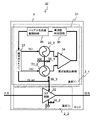
- FIG. 1 is a block diagram showing the configuration of a semiconductor integrated circuit according to the first embodiment of the invention.
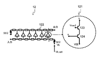
- FIG. 2A is a block diagram showing the configuration of the core circuit in the semiconductor integrated circuit according to the first embodiment of the invention.
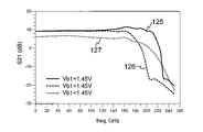
- FIG. 2B is a diagram showing element characteristics of a core circuit in the semiconductor integrated circuit according to the first embodiment of the present invention;
- FIG. 3A is a block diagram showing the configuration of the distributed voltage controlled oscillator in the voltage setting circuit according to the first embodiment of the present invention.
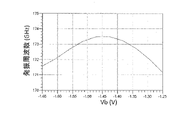
- FIG. 3B is a diagram showing element characteristics of the distributed voltage controlled oscillator in the voltage setting circuit according to the first embodiment of the present invention;
- FIG. 4 is a flowchart for explaining the operation of the voltage setting circuit according to the first embodiment of the invention.
- FIG. 5 is a block diagram showing an example of the configuration of the semiconductor integrated circuit according to the first embodiment of the invention.
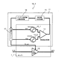
- FIG. 6 is a block diagram showing the configuration of a semiconductor integrated circuit according to the second embodiment of the invention.
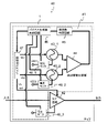
- FIG. 7 is a block diagram showing the configuration of a semiconductor integrated circuit according to the third embodiment of the invention.
- FIG. 8 is a block diagram showing the configuration of a conventional distributed amplifier circuit.
- FIG. 9 is a diagram showing element characteristics of a conventional distributed amplifier circuit.
- FIG. 10 is a diagram for explaining a conventional voltage setting method.
- FIG. 1 A voltage setting circuit and a semiconductor integrated circuit according to a first embodiment of the present invention will be described with reference to FIGS. 1 to 5.
- FIG. 1 A voltage setting circuit and a semiconductor integrated circuit according to a first embodiment of the present invention will be described with reference to FIGS. 1 to 5.
- FIG. 1 A voltage setting circuit and a semiconductor integrated circuit according to a first embodiment of the present invention will be described with reference to FIGS. 1 to 5.
- FIG. 1 to 5 A voltage setting circuit and a semiconductor integrated circuit according to a first embodiment of the present invention will be described with reference to FIGS. 1 to 5.
- a semiconductor integrated circuit 10 includes a voltage setting circuit 11 and a core circuit 12 to which the voltage setting circuit 11 is connected on the same chip 1, as shown in FIG.
- the voltage setting circuit 11 includes two distributed voltage-controlled oscillators (hereinafter referred to as "VCOs”) 13_1 and 13_2, a frequency comparator 14, a frequency determination circuit 15, and a bias generator.
- VCOs distributed voltage-controlled oscillators
- a control circuit 16 and a bias generator 17 are provided.
- a distributed amplifier circuit is used for the core circuit 12, as shown in FIG. 2A.
- unit cells composed of transistor circuits are connected in parallel via transmission lines and terminated with 50 ⁇ .
- a voltage Vb is applied to one of the terminated terminals, and in the semiconductor integrated circuit 10, a voltage Vb_opt optimized by the voltage setting circuit 11 is applied.
- two transistors 123 and 124 are connected in series and connected to transmission line 122 .
- One transistor (first transistor) 123 of the two transistors has a collector connected to the transmission line 122 at a contact point b on the output side, and Vcas1 is input to the base.
- the other transistor (second transistor) 124 is connected to the transmission line 122 at the contact a on the side to which Vb is applied to the base, and the voltage VEE is supplied to the emitter.
- the transmission line 122 has L, C, and R as an equivalent circuit.
- FIG. 2B shows the bias dependence of the transmission characteristic (S21) in the core circuit (distributed amplifier circuit) 12.
- FIG. 1 In the core circuit (distributed amplifier circuit) 12, the current flowing through the transistor of each unit cell changes due to the bias of Vb, and the frequency characteristic changes.
- the bias (Vb) when the optimum current flows is hereinafter referred to as "optimum bias”.
- the bias (Vb) is higher (126 in the figure) or lower (127 in the figure) than the optimum bias, the band becomes narrower and the frequency characteristic deteriorates.
- the distributed VCO (1) 13_1 and VCO (2) 13_2 have the configuration shown in FIG. 3A, and unit cells and capacitors are connected in parallel via transmission lines.
- the unit cells of the distributed VCO(1) 13_1 and VCO(2) 13_2 have the same configuration as the unit cell of the core circuit 12.
- two transistors are connected in series in each unit cell and connected to a transmission line.
- the collector is connected to the transmission lines 132_1 and 132_2 at a contact point b on the output side, and Vcas1 is input to the base.
- the other transistors (second transistors) 134_1 and 134_2 are connected to the transmission lines 132_1 and 132_2 at the contacts a on the side to which Vb is applied to the bases, and the voltage VEE is supplied to the emitters.
- the biases Vb1 and Vb2 are input to the distributed VCO (1) 13_1 and VCO (2) 13_2, and there is a voltage difference between the biases Vb1 and Vb2.
- the frequency comparator 14 is composed of, for example, a Gilbert cell circuit. Outputs a signal that indicates the high or low frequency. For example, if the frequency of the VCO(1) 13_1 is high, the high voltage signal H is output, and if the frequency of the VCO(2) 13_2 is high, the low voltage signal L is output.
- the frequency determination circuit 15 is composed of a digital processing circuit and determines whether the output of the frequency comparator 14 is H level or L level. As a result, it is determined whether the frequencies of the two signals input to the frequency comparator 14 are high or low.
- the bias generator control circuit 16 determines the bias value generated by the bias generator 17 based on the determination result of the frequency determination circuit 15 and controls the bias generator 17 .
- the bias generator 17 generates a bias and inputs it to each of the distributed VCO (1) 13_1 and VCO (2) 13_2. Also, an optimum bias is generated and supplied to the core circuit 12 .
- the oscillation frequency of the distributed VCO (1) 13_1 and VCO (2) 13_2 is the highest when the optimum current flows through the transistors used in the distributed VCO (1) 13_1 and VCO (2) 13_2.
- Optimal bias is detected using the following property.
- the core circuit 12 can be operated in the widest band.
- the present invention uses two distributed VCOs (VCO (1) 13_1 and VCO (2) 13_2) of the same configuration. However, a predetermined voltage difference is provided for the bias supplied to the two distributed VCO (1) 13_1 and VCO (2) 13_2. For example, when the bias Vb1 is set for the distributed VCO (1) 13_1 and the bias Vb2 is set for the distributed VCO (2) 13_2, a bias higher by 10 mV is set for Vb1.
- biases Vb1 and Vb2 are supplied to two distributed VCOs, VCO(1) 13_1 and VCO(2) 13_2, respectively (step 201).
- the frequency comparator 14 and the frequency determination circuit 15 compare the oscillation frequencies of the VCO(1) 13_1 and the VCO(2) 13_2 to determine whether or not the oscillation frequency of the VCO(1) 13_1 is higher. (step 202).
- the bias generator control circuit 16 determines a voltage value obtained by adding a predetermined voltage (for example, 10 mV) to each of Vb1 and Vb2. 17 is controlled (step 203).
- a predetermined voltage for example, 10 mV
- the bias generator 17 supplies Vb1 and Vb2 to the VCO(1) 13_1 and VCO(2) 13_2 (step 204).
- the frequency comparator 14 and the frequency determination circuit 15 again compare the oscillation frequencies of the VCO(1) 13_1 and the VCO(2) 13_2 to determine whether the oscillation frequency of the VCO(1) 13_1 is higher. is determined (step 205)
- Vb2 determines Vb2 to be the optimum bias Vb_opt.
- the bias when the oscillation frequencies of VCO(1) 13_1 and VCO(2) 13_2 are reversed is determined as the optimum bias Vb_opt (step 206).
- step 202 if the frequency of VCO(1) 13_1 is not higher (if the frequency of VCO(1) 13_1 is lower, or if the oscillation frequency of VCO(1) 13_1 and VCO(2) 13_2 are equal), the bias generator control circuit 16 determines voltage values obtained by decreasing the predetermined voltages (for example, 10 mV) of Vb1 and Vb2, respectively, and controls the bias generator 17 (step 207).
- the predetermined voltages for example, 10 mV
- the bias generator 17 supplies Vb1 and Vb2 to the VCO(1) 13_1 and VCO(2) 13_2 (step 208).
- the frequency comparator 14 and the frequency determination circuit 15 again compare the oscillation frequencies of the VCO(1) 13_1 and the VCO(2) 13_2 to determine whether the oscillation frequency of the VCO(1) 13_1 is higher. is determined (step 209).
- Vb1 when the frequency of VCO (1) 13_1 is higher, Vb1 is determined as the optimum bias Vb_opt. In this way, the bias when the oscillation frequencies of VCO(1) 13_1 and VCO(2) 13_2 are reversed is determined as the optimum bias Vb_opt (step 210).
- the VCO (1) 13_1 is supplied with a bias higher than that of the VCO (2) 13_2. good. Also, in step 202, the oscillation frequency of VCO (2) 13_2 may be used for determination.
- the two distributed VCO(1) 13_1 and VCO(2) 13_2 are supplied with voltages with a predetermined voltage difference, and the output frequency is is determined, Vb1 and Vb2 are increased or decreased stepwise according to the determination result, and the bias that maximizes the oscillation frequency is detected.
- This bias is determined as the optimum bias Vb_opt and supplied to the core circuit 12 .
- the optimum voltage (bias) for the oscillator is obtained based on the difference in the output (frequency) of the two oscillators that are oscillated by applying different voltages. 12 can be controlled.
- the voltage setting circuit it is possible to detect and set the optimum bias within the chip. , the core circuit can be operated in a wide band and the cost can be reduced.
- the voltage setting circuit determines and controls the optimal bias of the core circuit by determining the optimal bias of the distributed voltage controlled oscillator (VCO) having the same unit cell as that of the core circuit. do.
- VCO distributed voltage controlled oscillator
- the distributed VCO it is desirable to place the distributed VCO at a position close to the core circuit. Since the element characteristics are non-uniform within the chip surface, shortening the distance between the elements can suppress the influence of the non-uniform distribution of the characteristics. As a result, it is possible to improve the setting accuracy of the optimum bias.
- two distributed VCO (1) 13_1, VCO (2) 13_2, frequency comparator 14, frequency determination circuit 15, and bias generator are provided on same chip 1.
- the present invention is not limited to this.
- the frequency determination circuit 15, the bias generator control circuit 16, and the bias generator 17 do not have to be arranged on the same chip 1.
- DC direct current
- the semiconductor integrated circuit 30 includes a voltage setting circuit 31 and a voltage setting circuit 31 on different substrates, substrate (1) 2_1 and substrate (2) 2_2 on the same chip 1. and a core circuit 32 to which 31 connects.
- a voltage setting circuit 31 and a voltage setting circuit 31 on different substrates substrate (1) 2_1 and substrate (2) 2_2 on the same chip 1.
- a core circuit 32 to which 31 connects are the same as those of the first embodiment.
- the decoupling capacitors 38_1 and 38_2 are desirably arranged near their respective power supply voltages (VEE). can.
- the decoupling capacitor 38_3 is preferably arranged near the core circuit 32, and the shorter the distance between the decoupling capacitor 38_3 and the core circuit 32, the more noise can be reduced.
- the voltage setting circuit 31 operates in the same manner as the operating process (FIG. 4) in the first embodiment.
- the optimum bias can be easily detected and set, the core circuit can be operated in a wide band, cost and time can be reduced, and the influence of oscillator noise can be suppressed.
- a voltage setting circuit and a semiconductor integrated circuit according to a third embodiment of the present invention will be described with reference to FIG.
- a unit cell having the same configuration as that of the core circuit is used for the distributed VCO.
- the voltage setting circuit 41 according to the present embodiment can cope with a case where it is difficult to use unit cells having the same configuration as the core circuit 42 for the distributed VCO(1) 43_1 and VCO(2) 43_2.
- a semiconductor integrated circuit 40 includes a voltage setting circuit 41 and a core circuit to which the voltage setting circuit 41 is connected on the same chip 1, as in the first embodiment. 42, the voltage setting circuit 41 includes two distributed VCO (1) 43_1, VCO (2) 43_2, a frequency comparator 44, a frequency determination circuit 45, a bias generator control circuit 46, and a bias generation and a vessel 47 .
- the semiconductor integrated circuit 40 includes current monitors 48_1, 48_2, and 48_3 having circuits for monitoring currents flowing in the power supply voltages of the VCO(1) 43_1, the VCO(2) 43_2, and the core circuit 42, respectively.
- the transistor size (emitter length) in the VCO (1) 43_1 and the VCO (2) 43_2 and the transistor size (emitter length) in the core circuit 42 are the same.
- the biases of Vb1 and Vb2 are increased or decreased stepwise, and the oscillation frequencies of VCO(1) 43_1 and VCO(2) 43_2 are compared to determine whether the oscillation frequencies of the two are higher or lower.
- the bias when is reversed is determined as the optimum bias.
- the bias that maximizes the oscillation frequency is detected as the optimum bias.
- current monitors 48_1 and 48_2 monitor the currents (optimum currents) at the optimum biases in VCO(1) 43_1 and VCO(2) 43_2.
- the optimum current in the core circuit 42 is determined based on the optimum currents in the VCO(1) 43_1 and VCO(2) 43_2.
- the optimum current in the core circuit 42 for example, either one of the optimum currents in the VCO(1) 43_1 and the VCO(2) 43_2 may be used, or the average current value of both may be used.
- the optimum current of the core circuit N ⁇ VCO(1) 43_1 or VCO(2 ) 43_2.
- the optimum current of the core circuit 6 ⁇ VCO(1) 43_1 or VCO(2 ) 43_2.
- the current flowing through the core circuit 42 is monitored by the current monitor 48_3 of the core circuit 42, and the bias is adjusted so that the above-mentioned optimum current of the core circuit 42 flows through the core circuit 42 (the bias that provides the optimum current is is the optimum bias Vb_opt).
- the optimum current of the core circuit can be easily set without using a unit cell having the same configuration as that of the core circuit in the distributed VCO, and the core circuit can be operated in a wide band. It is possible.
- the distributed VCO at a position close to the core circuit.
- the frequency determination circuit, the bias generator control circuit, and the bias generator need not be arranged on the same chip as in the first embodiment.
- different substrates, substrate (1) and substrate (2), on the same chip each have a voltage setting circuit and a voltage setting circuit.
- a connecting core circuit may also be provided.
- the power consumption of the two distributed VCOs, the frequency comparator, and the frequency magnitude determination circuit is turned off. Power reduction and core circuit noise reduction are possible.
- a unit cell may have a configuration using one transistor or a configuration using a plurality of transistors, an oscillator circuit may be configured, and the distributed VCO of the voltage setting circuit and the core circuit may have the same configuration.
- the present invention in the configuration of the voltage setting circuit and the semiconductor integrated circuit, the voltage setting method, and the like, examples of the structure, dimensions, materials, etc. of each component are shown, but the present invention is not limited to this. Any effective voltage setting circuit, semiconductor integrated circuit, and voltage setting method may be used.
- the present invention can be applied to electronic circuits of equipment and devices used for optical communication, wireless communication, radar sensing, etc.
Landscapes
- Engineering & Computer Science (AREA)
- Power Engineering (AREA)
- Inductance-Capacitance Distribution Constants And Capacitance-Resistance Oscillators (AREA)
Abstract
Description
本発明の第1の実施の形態に係る電圧設定回路および半導体集積回路について、図1~図5を参照して説明する。
本実施の形態に係る半導体集積回路10は、図1に示すように、同一チップ1上に、電圧設定回路11と、電圧設定回路11が接続するコア回路12とを備える。
本実施の形態に係る電圧設定回路11の動作を、以下に説明する。
本発明の第2の実施の形態に係る電圧設定回路および半導体集積回路について、図6を参照して説明する。
本発明の第3の実施の形態に係る電圧設定回路および半導体集積回路について、図7を参照して説明する。第1、2の実施の形態では、分布型VCOにコア回路と同じ構成の単位セルを用いる。本実施の形態に係る電圧設定回路41は、分布型VCO(1)43_1、VCO(2)43_2にコア回路42と同じ構成の単位セルを用いることが困難である場合に対応できる。
本実施の形態に係る半導体集積回路40は、図7に示すように、第1の実施の形態と同様に、同一チップ1上に、電圧設定回路41と、電圧設定回路41が接続するコア回路42とを備え、電圧設定回路41は、2つの分布型VCO(1)43_1、VCO(2)43_2と、周波数比較器44と、周波数判定回路45と、バイアス生成器制御回路46と、バイアス生成器47とを備える。
本実施の形態に係る電圧設定回路41の動作を、以下に説明する。
12 コア回路
13_1、13_2 分布型電圧制御発振器
14 周波数比較器
15 周波数判定回路
16 バイアス生成器制御回路
17 バイアス生成器
121、131_1、131_2 単位セル
Claims (8)
- コア回路に最適バイアスを供給する電圧設定回路であって、
第1の分布型電圧制御発振器と、
第2の分布型電圧制御発振器と、
前記第1の分布型電圧制御発振器と前記第2の分布型電圧制御発振器との発振周波数を比較する周波数比較器と、
前記第1の分布型電圧制御発振器と前記第2の分布型電圧制御発振器との発振周波数の高低を判定する周波数判定回路と、
前記判定結果に応じて、前記第1の分布型電圧制御発振器に供給するバイアスと前記第2の分布型電圧制御発振器に供給するバイアスを決定し、前記発振周波数の高低が反転するときの前記バイアスを前記最適バイアスとして決定するバイアス生成器制御回路と、
前記バイアスを生成して、前記第1の分布型電圧制御発振器と前記第2の分布型電圧制御発振器とに供給し、前記最適バイアスを前記コア回路に供給するバイアス生成器とを備え、
前記第1の分布型電圧制御発振器の単位セルと、前記第2の分布型電圧制御発振器の単位セルとの構成が、前記コア回路の単位セルの構成と同じであることを特徴とする電圧設定回路。 - コア回路に最適バイアスを供給する電圧設定回路であって、
第1の分布型電圧制御発振器と、
第2の分布型電圧制御発振器と、
前記第1の分布型電圧制御発振器の電源電圧に流れる電流をモニタリングする第1の電流モニタと、
前記第2の分布型電圧制御発振器の電源電圧に流れる電流をモニタリングする第2の電流モニタと、
前記コア回路の電源電圧に流れる電流をモニタリングする第3の電流モニタと、
前記第1の分布型電圧制御発振器と前記第2の分布型電圧制御発振器との発振周波数を比較する周波数比較器と、
前記第1の分布型電圧制御発振器と前記第2の分布型電圧制御発振器との発振周波数の高低を判定する周波数判定回路と、
前記判定結果に応じて、前記第1の分布型電圧制御発振器に供給するバイアスと前記第2の分布型電圧制御発振器に供給するバイアスを決定し、前記コア回路に供給する前記最適バイアスを制御するバイアス生成器制御回路と、
前記バイアスを生成して前記第1の分布型電圧制御発振器と前記第2の分布型電圧制御発振器とに供給し、前記最適バイアスを生成して前記コア回路に供給するバイアス生成器とを備え、
前記発振周波数の高低が反転するときの前記第1の電流モニタの電流値と前記第2の電流モニタでモニタリングされる電流値に基づき、前記最適バイアスが調整され、
前記第1の分布型電圧制御発振器の単位セルと、前記第2の分布型電圧制御発振器の単位セルと、前記コア回路の単位セルにおけるトランジスタのサイズが同じであることを特徴とする電圧設定回路。 - 請求項1又は請求項2に記載の電圧設定回路と、
前記コア回路と
を備える半導体集積回路。 - 前記電圧設定回路と、前記コア回路とを同一チップ上に備えることを特徴とする請求項3に記載の半導体集積回路。
- 前記電圧設定回路が第1の基板に配置され、
前記コア回路が第2の基板に配置され、
前記第1の分布型電圧制御発振器と前記第2の分布型電圧制御発振器との電源電圧用端子と、前記コア回路の電源電圧用端子と、前記バイアス生成器から前記コア回路に前記最適バイアスが供給される配線それぞれに、デカップリングコンデンサが接続されることを特徴とする請求項3又は請求項4に記載の半導体集積回路。 - 第1の分布型電圧制御発振器と、第2の分布型電圧制御発振器と、コア回路と、周波数比較器と、周波数判定回路とを備える半導体集積回路において、前記コア回路に最適バイアスを設定する電圧設定方法であって、
前記第1の分布型電圧制御発振器に第1のバイアスを供給するステップと、
前記第2の分布型電圧制御発振器に前記第1のバイアスと所定の電圧差を有する第2のバイアスを供給するステップと、
前記第1の分布型電圧制御発振器の発振周波数と前記第2の分布型電圧制御発振器の発振周波数とを比較するステップと、
前記第1の分布型電圧制御発振器の発振周波数が、前記第2の分布型電圧制御発振器の発振周波数より高い場合に、前記第1のバイアスと前記第2のバイアスそれぞれに所定の電圧を増減するステップと、
前記増減された前記第1のバイアスと前記第2のバイアスそれぞれを、前記第1の分布型電圧制御発振器と、前記第2の分布型電圧制御発振器それぞれに供給するステップと、
前記増減された前記第1のバイアスと前記第2のバイアスそれぞれにおける前記第1の分布型電圧制御発振器の発振周波数と前記第2の分布型電圧制御発振器の発振周波数とを比較するステップと、
前記増減された前記第1のバイアスと前記第2のバイアスそれぞれにおける前記第1の分布型電圧制御発振器の発振周波数と、前記第2の分布型電圧制御発振器の発振周波数との高低が反転するときに、前記第2の分布型電圧制御発振器に供給された第2のバイアスを前記最適バイアスと決定するステップと
を備える電圧設定方法。 - 第1の分布型電圧制御発振器と、第2の分布型電圧制御発振器と、コア回路と、周波数比較器と、周波数判定回路とを備える半導体集積回路において、前記コア回路に最適バイアスを設定する電圧設定方法であって、
前記第1の分布型電圧制御発振器に第1のバイアスを供給するステップと、
前記第2の分布型電圧制御発振器に前記第1のバイアスと所定の電圧差を有する第2のバイアスを供給するステップと、
前記第1の分布型電圧制御発振器の発振周波数と前記第2の分布型電圧制御発振器の発振周波数とを比較するステップと、
前記第1の分布型電圧制御発振器の発振周波数が、前記第2の分布型電圧制御発振器の発振周波数より高い場合に、前記第1のバイアスと前記第2のバイアスそれぞれに所定の電圧を増減するステップと、
前記増減された前記第1のバイアスと前記第2のバイアスそれぞれを、前記第1の分布型電圧制御発振器と、前記第2の分布型電圧制御発振器それぞれに供給するステップと、
前記増減された前記第1のバイアスと前記第2のバイアスそれぞれにおける前記第1の分布型電圧制御発振器の発振周波数と前記第2の分布型電圧制御発振器の発振周波数とを比較するステップと、
前記増減された前記第1のバイアスと前記第2のバイアスそれぞれにおける前記第1の分布型電圧制御発振器の発振周波数と、前記第2の分布型電圧制御発振器の発振周波数との高低が反転するときに、前記第1の分布型電圧制御発振器に流れる電流と、前記第2の分布型電圧制御発振器に流れる電流とをモニタリングするステップと、
前記モニタリングされる電流値に基づき決定される電流値が前記コア回路に流れるように、前記コア回路に供給する前記最適バイアスを決定するステップと
を備える電圧設定方法。 - 前記コア回路に前記最適バイアスを設定した後、前記第1の分布型電圧制御発振器と、前記第2の分布型電圧制御発振器と、前記周波数比較器と、前記周波数判定回路との電源をオフにするステップ
を備える請求項6又は請求項7に記載の電圧設定方法。
Priority Applications (3)
| Application Number | Priority Date | Filing Date | Title |
|---|---|---|---|
| US18/264,567 US12176852B2 (en) | 2021-02-18 | 2021-02-18 | Voltage setting circuit, semiconductor integrated circuit and voltage setting method |
| PCT/JP2021/006157 WO2022176115A1 (ja) | 2021-02-18 | 2021-02-18 | 電圧設定回路、半導体集積回路および電圧設定方法 |
| JP2023500229A JP7616340B2 (ja) | 2021-02-18 | 2021-02-18 | 電圧設定回路、半導体集積回路および電圧設定方法 |
Applications Claiming Priority (1)
| Application Number | Priority Date | Filing Date | Title |
|---|---|---|---|
| PCT/JP2021/006157 WO2022176115A1 (ja) | 2021-02-18 | 2021-02-18 | 電圧設定回路、半導体集積回路および電圧設定方法 |
Publications (1)
| Publication Number | Publication Date |
|---|---|
| WO2022176115A1 true WO2022176115A1 (ja) | 2022-08-25 |
Family
ID=82930332
Family Applications (1)
| Application Number | Title | Priority Date | Filing Date |
|---|---|---|---|
| PCT/JP2021/006157 Ceased WO2022176115A1 (ja) | 2021-02-18 | 2021-02-18 | 電圧設定回路、半導体集積回路および電圧設定方法 |
Country Status (3)
| Country | Link |
|---|---|
| US (1) | US12176852B2 (ja) |
| JP (1) | JP7616340B2 (ja) |
| WO (1) | WO2022176115A1 (ja) |
Citations (5)
| Publication number | Priority date | Publication date | Assignee | Title |
|---|---|---|---|---|
| JPH0758556A (ja) * | 1993-08-19 | 1995-03-03 | Nec Eng Ltd | アイソレ−ションアンプ |
| JP2008053784A (ja) * | 2006-08-22 | 2008-03-06 | Toshiba Corp | 電圧制御発振器、電圧制御発振器用のバイアス装置、電圧制御発振器のバイアス調整プログラム |
| US20090072916A1 (en) * | 2006-12-27 | 2009-03-19 | Analogies S.A. | Integrated Circuit Distributed Oscillator |
| JP2012015602A (ja) * | 2010-06-29 | 2012-01-19 | Fujitsu Ltd | 増幅装置 |
| JP2015522225A (ja) * | 2012-07-02 | 2015-08-03 | エスアイ−ウェアー システムズSi−Ware Systems | 一定の高調波成分を有する自己バイアス振幅制御発振器 |
Family Cites Families (4)
| Publication number | Priority date | Publication date | Assignee | Title |
|---|---|---|---|---|
| JPS6359108A (ja) * | 1986-08-28 | 1988-03-15 | Mitsubishi Electric Corp | バイアス回路 |
| JP2009288509A (ja) * | 2008-05-29 | 2009-12-10 | Fujitsu Ltd | 光変調装置 |
| US11515850B2 (en) * | 2018-09-04 | 2022-11-29 | Nippon Telegraph And Telephone Corporation | Distributed amplifier |
| US10955691B2 (en) * | 2019-06-13 | 2021-03-23 | Elenion Technologies, Llc | Dual loop bias circuit with offset compensation |
-
2021
- 2021-02-18 WO PCT/JP2021/006157 patent/WO2022176115A1/ja not_active Ceased
- 2021-02-18 US US18/264,567 patent/US12176852B2/en active Active
- 2021-02-18 JP JP2023500229A patent/JP7616340B2/ja active Active
Patent Citations (5)
| Publication number | Priority date | Publication date | Assignee | Title |
|---|---|---|---|---|
| JPH0758556A (ja) * | 1993-08-19 | 1995-03-03 | Nec Eng Ltd | アイソレ−ションアンプ |
| JP2008053784A (ja) * | 2006-08-22 | 2008-03-06 | Toshiba Corp | 電圧制御発振器、電圧制御発振器用のバイアス装置、電圧制御発振器のバイアス調整プログラム |
| US20090072916A1 (en) * | 2006-12-27 | 2009-03-19 | Analogies S.A. | Integrated Circuit Distributed Oscillator |
| JP2012015602A (ja) * | 2010-06-29 | 2012-01-19 | Fujitsu Ltd | 増幅装置 |
| JP2015522225A (ja) * | 2012-07-02 | 2015-08-03 | エスアイ−ウェアー システムズSi−Ware Systems | 一定の高調波成分を有する自己バイアス振幅制御発振器 |
Also Published As
| Publication number | Publication date |
|---|---|
| US12176852B2 (en) | 2024-12-24 |
| JP7616340B2 (ja) | 2025-01-17 |
| JPWO2022176115A1 (ja) | 2022-08-25 |
| US20240056029A1 (en) | 2024-02-15 |
Similar Documents
| Publication | Publication Date | Title |
|---|---|---|
| US8816786B2 (en) | Method and apparatus of a crystal oscillator with a noiseless and amplitude based start up control loop | |
| Li et al. | Design of W-band VCOs with high output power for potential application in 77 GHz automotive radar systems | |
| RU2108654C1 (ru) | Полупроводниковый интегральный кольцевой генератор | |
| CN106656122B (zh) | 用于调节时钟信号中的占空比的装置和方法 | |
| CA1303679C (en) | Modulator and transmitter | |
| US20100237956A1 (en) | Bias generation circuit and voltage controlled oscillator | |
| US10374550B2 (en) | Architecture for voltage sharing between two oscillators | |
| US20100093303A1 (en) | Circuit current generation apparatus and method thereof, and signal processing apparatus | |
| US8446228B2 (en) | Oscillator circuit | |
| JP7616340B2 (ja) | 電圧設定回路、半導体集積回路および電圧設定方法 | |
| Fritsche et al. | Design and characterization of a 190-GHz voltage-controlled oscillator | |
| US20080036510A1 (en) | Signal generating apparatus capable of measuring trip point of power-up signal and method of measuring trip point of power-up signal using the same | |
| US20240088847A1 (en) | Amplification circuit and communication device | |
| KR940007972B1 (ko) | 가변 주파수 발진 회로 | |
| EP3742608A1 (en) | Programmable gain amplifier | |
| US20230221191A1 (en) | Temperature sensing device and calibration method thereof | |
| Ramirez-Angulo et al. | Applications of composite BiCMOS transistors | |
| JP2006134963A (ja) | 受信装置および試験装置 | |
| Ansari et al. | Frequency domain phase shift measurement technique applied to a multiphase rotary travelling-wave VCO | |
| US20030071647A1 (en) | Method and arrangement for determining the high-frequency behavior of active circuit elements | |
| US20240120883A1 (en) | Voltage-controlled oscillator and bias generation circuit | |
| US6903591B2 (en) | Phase shifter circuit | |
| JP6049817B1 (ja) | パワー制御可能な無線通信装置 | |
| Rizzini et al. | A 28-38 GHz Digitally-Assisted Frequency Tripler with Background Calibration in 55nm SiGe BiCMOS | |
| CN223872260U (zh) | 具有温度补偿的放大器和平衡式电路结构 |
Legal Events
| Date | Code | Title | Description |
|---|---|---|---|
| 121 | Ep: the epo has been informed by wipo that ep was designated in this application |
Ref document number: 21926550 Country of ref document: EP Kind code of ref document: A1 |
|
| ENP | Entry into the national phase |
Ref document number: 2023500229 Country of ref document: JP Kind code of ref document: A |
|
| WWE | Wipo information: entry into national phase |
Ref document number: 18264567 Country of ref document: US |
|
| NENP | Non-entry into the national phase |
Ref country code: DE |
|
| 122 | Ep: pct application non-entry in european phase |
Ref document number: 21926550 Country of ref document: EP Kind code of ref document: A1 |