WO2022158587A1 - 電磁波吸収体の製造方法 - Google Patents
電磁波吸収体の製造方法 Download PDFInfo
- Publication number
- WO2022158587A1 WO2022158587A1 PCT/JP2022/002352 JP2022002352W WO2022158587A1 WO 2022158587 A1 WO2022158587 A1 WO 2022158587A1 JP 2022002352 W JP2022002352 W JP 2022002352W WO 2022158587 A1 WO2022158587 A1 WO 2022158587A1
- Authority
- WO
- WIPO (PCT)
- Prior art keywords
- dielectric
- electromagnetic wave
- frequency
- magnetic
- resonance
- Prior art date
- Legal status (The legal status is an assumption and is not a legal conclusion. Google has not performed a legal analysis and makes no representation as to the accuracy of the status listed.)
- Ceased
Links
Images





Classifications
-
- H—ELECTRICITY
- H05—ELECTRIC TECHNIQUES NOT OTHERWISE PROVIDED FOR
- H05K—PRINTED CIRCUITS; CASINGS OR CONSTRUCTIONAL DETAILS OF ELECTRIC APPARATUS; MANUFACTURE OF ASSEMBLAGES OF ELECTRICAL COMPONENTS
- H05K9/00—Screening of apparatus or components against electric or magnetic fields
Definitions
- the present invention relates to a method for manufacturing an electromagnetic wave absorber.
- Metamaterials are artificial substances whose size is smaller than the wavelength of the target electromagnetic wave, and they have attracted attention in recent years because they exhibit characteristics that are not found in substances in nature.
- materials called left-handed metamaterials exhibit a negative refractive index in a specific frequency range. Therefore, intensive research and development is being carried out with the aim of applying it to new optical applications such as perfect lenses and transparent cloaks.
- Non-Patent Document 1 British physicist J. B. Pendry proposed a nanometal structure having a periodic structure smaller than the wavelength of electromagnetic waves, and theoretically showed that the refractive index of this structure is negative (Non-Patent Document 1).
- This nano-metal structure has a structure in which nano-units composed of minute split ring resonators (SRR) and metal wires are arranged three-dimensionally. By reducing the size of the nanounits, the nanometal structure acts as a homogeneous medium for electromagnetic waves and exhibits an electromagnetic wave response that depends on the functions of the SRR and metal wires.
- the SRR acts as an LC resonator for electromagnetic waves and exhibits negative permeability above the resonance frequency.
- Conductive metal wires also exhibit a negative dielectric constant.
- Non-Patent Document 2 The combination of SRR and metal wire makes both the effective permittivity and the effective permeability negative, resulting in a negative refractive index, which is the product of the square root of the permittivity and the square root of the permeability. Furthermore, Pendry theoretically showed that by using a left-handed metamaterial that exhibits a negative refractive index, it is possible to realize a perfect lens that can observe as many fine structures as possible beyond the diffraction limit of light (Non-Patent Document 2). ).
- dielectric metamaterials using dielectrics instead of nanometal structures have been proposed.
- a nanometal structure has the disadvantage that it has a large conductor loss and requires a precise and fine processing technology for manufacturing.
- dielectric metamaterials have the advantages of low non-resonant loss and easy manufacturing.
- Non-Patent Document 4 a structure in which dielectric resonators composed of high-permittivity TiO 2 ceramic discs are two-dimensionally periodically arranged.
- Mie resonance occurs when the size of the dielectric resonator is made as small as the wavelength of the electromagnetic wave. Therefore, it is possible to use either the TE resonance mode or the TM resonance mode.
- Dielectric resonators exhibit a negative effective permeability above the resonance frequency in the TE resonance mode.
- it exhibits a negative effective dielectric constant above the resonance frequency in the TM resonance mode.
- the TE resonance mode corresponds to the SRR of the nanometal structure
- the TM resonance mode corresponds to the metal wire.
- metamaterials such as dielectric metamaterials
- most of them are targeted at substances that exhibit a negative refractive index, that is, left-handed metamaterials, and optical systems such as perfect lenses and transparent cloaks. Aiming for application.
- nanometal structures to antennas and transmission lines in the microwave region
- dielectric metamaterials to electronic devices other than optical components.
- the inventor of the present invention has diligently studied in view of such circumstances. As a result, even in a dielectric material that does not contain a magnetic element, if its characteristics and shape are controlled, the Mie resonance mode will appear and magnetic resonance will occur. It has been found that absorption properties can be obtained.
- the present invention has been completed based on such knowledge, and aims to provide a method for manufacturing an electromagnetic wave absorber using magnetic loss based on Mie resonance of dielectrics.
- the present invention includes the following aspects (a) to (e).
- the expression "-" includes both numerical values. That is, “X to Y” is synonymous with “X or more and Y or less”.
- a method for manufacturing an electromagnetic wave absorber comprising the following steps; a step of making a dielectric element; determining a target frequency f T (Hz); and processing the dielectric element to fabricate a planar dielectric, the planar dielectric has a relative permittivity real part ⁇ r ' of 50 or more at 500 MHz;
- the maximum length L (mm) and thickness d (mm) of the planar dielectric, the relative permittivity real part ⁇ r ', and the target frequency f T (Hz) A method in which processing is performed so as to satisfy the following formulas (1) and (2).
- a method for manufacturing an electromagnetic wave absorber using magnetic loss based on dielectric Mie resonance is provided.
- Figure 2 shows the frequency dispersion of the dielectric constant obtained for BaTiO 3 (Example 1).
- Fig. 4 shows the frequency dispersion of the dielectric constant obtained for Bi0.5K0.5TiO3 ( Example 4 ).
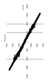
- Magnetic susceptibility measurements obtained for BaTiO 3 are shown (Example 1).
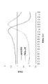
- Figure 3 shows the frequency distribution of the permeability obtained for BaTiO 3 (Example 1).
- Figure 2 shows the frequency distribution of the permeability obtained for BaTiO 3 (Example 2).
- Figure 3 shows the frequency distribution of the permeability obtained for BaTiO 3 (Example 3).
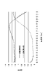
- Figure 4 shows the frequency distribution of the permeability obtained for Bi0.5K0.5TiO3 ( Example 4).
- Figure 2 shows the frequency distribution of the permeability obtained for Bi0.5K0.5TiO3 ( Example 5).
- Figure 2 shows the frequency distribution of the permeability obtained for Bi0.5K0.5TiO3 ( Example 6).
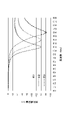
- the electromagnetic wave absorption properties obtained for BaTiO 3 are shown (Examples 1 to 3).
- the electromagnetic wave absorption properties obtained for Bi 0.5 K 0.5 TiO 3 are shown (Examples 4 to 6).
- Electromagnetic Wave Absorber Before describing the manufacturing method of the present embodiment, the electromagnetic wave absorber will be described first.
- the electromagnetic wave absorber of this embodiment includes a plate-shaped dielectric (hereinafter sometimes referred to as "dielectric").
- dielectric acts as a dielectric metamaterial and exhibits a resonance mode called Mie resonance. Therefore, the magnetic loss based on magnetic resonance is shown in a predetermined frequency range, and the electromagnetic wave absorption characteristic is shown in this frequency range.
- the size of the dielectric is about the same as or smaller than the wavelength of the incident electromagnetic wave, a steady state of electric and magnetic fields is generated inside the dielectric at a certain frequency (first Mie resonance frequency), which causes a resonance phenomenon.
- This resonance phenomenon is called Mie resonance.
- the source of electromagnetic radiation is in the far field
- the electromagnetic waves are incident on the dielectric as plane waves.
- the electromagnetic wave is incident so that both the tangential component and the vertical component of the electromagnetic wave electric field component satisfy the boundary conditions at the interface between the dielectric and the air.
- a different electromagnetic field distribution occurs in the dielectric than in the previous propagation medium.
- a swirling electric field and displacement current distribution occurs inside the dielectric.
- a spiral displacement current (electric field) is generated in the dielectric, resulting in an oscillating magnetic field perpendicular to the displacement current (electric field) inside the dielectric.
- the spiral displacement current (electric field) distribution in the dielectric can be regarded as a magnetic dipole.
- This oscillating magnetic dipole interacts with the magnetic field component of the incident electromagnetic wave and magnetically resonates at a specific frequency (first Mie resonance frequency).
- first Mie resonance frequency the electric field component of the incident electromagnetic wave produces a magnetic dipole in the dielectric, and the interaction between the magnetic dipole and the electromagnetic wave magnetic field component causes magnetic resonance.
- the present inventor calculated the effective permittivity ( ⁇ eff ) and the effective permeability ( ⁇ eff ) of the dielectric based on the scattering model (Lewin model) of matter in electromagnetic waves, and further calculated the total The magnitude of the magnetic loss (Q M ) was estimated based on the law.
- v is the volume ratio of spherical particles in the matrix
- f is the frequency
- ⁇ is the angular frequency
- c is the speed of light (3.0 ⁇ 10 8 m/sec).
- ⁇ ′′ is the imaginary part of the effective permeability ⁇ eff .
- the method of manufacturing the electromagnetic wave absorber of the present embodiment includes the following steps; determination step), and a step of processing the dielectric element to fabricate a planar dielectric (dielectric fabricating step).
- the relative dielectric constant real part ⁇ r ' at 500 MHz of the planar dielectric is 50 or more.
- the maximum length L (mm) and thickness d (mm) of the planar dielectric, the relative permittivity real part ⁇ r ', and the target frequency f T (Hz) are Processing is performed so as to satisfy a specific relationship. Details of each step are described below.
- ⁇ Dielectric body manufacturing process In the dielectric body manufacturing process, a dielectric body is manufactured.
- a dielectric element a dielectric having a dielectric constant real part ⁇ r' of 50 or more at 500 MHz is selected.
- the dielectric constant hardly changes in the processing process.
- the real part of the dielectric constant of the dielectric element is preferably 50 or more, more preferably 100 or more. 300 or more is more preferable.
- the upper limit of the real part of the dielectric constant is not particularly limited. However, it is typically 1000 or less.
- the material of the dielectric body is not limited as long as it is composed of a high dielectric constant material.
- the dielectric body may contain only one of these materials, or may contain a plurality of them. When multiple kinds of materials are contained, they may be contained in the form of mixed crystals or may be contained in the form of solid solutions.
- the dielectric body may contain at least one of barium titanate (BaTiO 3 ) and bismuth potassium titanate (Bi 0.5 K 0.5 TiO 3 ).
- the dielectric may also be polycrystalline or monocrystalline.
- the dielectric body is a sintered ceramic body which is easy to manufacture.
- the dielectric element may be produced by a known method.
- a dielectric body which is a ceramic sintered body, may be produced by molding and firing a dielectric raw material.
- Dielectric raw materials may be synthesized by known methods such as solid phase reaction method, complex polymerization method, coprecipitation method, hydrothermal synthesis method, sol-gel method, and vapor phase method.
- Additives such as molding aids and sintering aids may be added in addition to the dielectric material.
- a single crystal dielectric material can be produced by the aqueous solution method, hydrothermal synthesis method, flux method, Bernoulli method, Czochralski cell, Bridgman method, floating zone melting method, skymelt method, sublimation recrystallization method, chemical transport method, and a known technique such as a chemical vapor deposition method.
- a target frequency f T (Hz) is determined.
- the target frequency f T is the frequency of the electromagnetic wave to be absorbed.
- the target frequency fT is preferably 1 GHz or more and 10 THz or less. If the frequency is too low, the contribution of magnetic loss based on Mie resonance may not occur sufficiently. On the other hand, if the frequency is too high, the permittivity of the dielectric will decrease and the magnetic loss may not be sufficiently high.
- f T is more preferably 3 GHz or more and 5 THz or less, further preferably 10 GHz or more and 3 THz or less, particularly preferably 10 GHz or more and 300 GHz, and particularly preferably 10 GHz or more and 30 GHz or less.
- f T may be greater than or equal to 500 MHz and less than or equal to 18 GHz.
- the determination of the target frequency may be performed at any timing as long as it is before obtaining the dielectric by processing in the steps described later. It may be performed before or after the dielectric element manufacturing process. Alternatively, it may be performed at the same time as the dielectric element manufacturing process. Furthermore, it may be carried out during the process of processing the dielectric body in the dielectric body manufacturing process. In any case, it may be performed at any timing as long as it is before determining the required dimensions of the dielectric obtained by processing.
- the dielectric base is processed to fabricate a planar dielectric.
- the processing method is not limited as long as it is possible to obtain a planar dielectric with a predetermined size.
- known techniques such as cutting, grinding, polishing, ultrasonic machining, and electrical discharge machining can be used.
- the relative permittivity real part ⁇ r ' at 500 MHz of the planar dielectric is 50 or more.
- the relative permittivity real part ⁇ r ′ is preferably 100 or more, more preferably 300 or more.
- the upper limit of the relative permittivity real part ⁇ r ′ is not particularly limited. However, it is typically 2000 or less, more typically 1000 or less. The reason why the measurement frequency is set to 500 MHz is that it is difficult to accurately measure the dielectric constant of a high dielectric constant material due to the problem of the measurement method when the frequency exceeds 500 GHz.
- the maximum length L (mm) and thickness d (mm) of the planar dielectric, the relative permittivity real part ⁇ r ′, and the target frequency f T (Hz) are as follows: Processing is performed so as to satisfy the formulas (1) and (2). This makes it possible to obtain a dielectric with a large magnetic loss.
- c is the speed of light (3.0 ⁇ 10 8 m/sec, ie 3.0 ⁇ 10 11 mm/sec).
- magnetic resonance occurs at a frequency close to the target frequency fT when the thickness d of the dielectric satisfies the relationship of the above formula (1). It is understood that this causes magnetic losses. More preferably, the thickness d of the planar dielectric, the real part of relative permittivity ⁇ r ′, and the target frequency f T satisfy the relationship of the following equation (8), and the relationship of the following equation (9). More preferably, it satisfies the following formula (10).
- the reason why the upper limit of d is set wider than the above formula (7) is that the dielectric constant at fR is generally smaller than the value of 500 MHz. However, from the viewpoint of suppressing the change in the absorption frequency due to temperature, it is preferable that the change of ⁇ with respect to the frequency be small. In other words, it is preferable that the relationship close to the above formula (7) is maintained.
- the dielectric satisfies the above formula (2). That is, the dielectric has a flat shape in which the ratio (L/d) of the maximum length L to the thickness d is 2 or more. This is because, as a result of repeated studies by the inventors, it was found that a flat-shaped dielectric can realize a thinner absorber.
- the maximum length L is the maximum length on the plate surface of the flat plate-shaped dielectric. That is, when the dielectric is disk-shaped, it is the diameter of the circle forming the disk surface. Also, when the dielectric is in the shape of a square plate, it is the diagonal length of the square forming the plate surface.
- L/d is preferably 3 or more, more preferably 5 or more, and even more preferably 10 or more.
- the maximum length L is preferably 0.5 mm or more and 20 mm or less, more preferably 1 mm or more and 10 mm or less. Further, the thickness d is preferably 0.03 mm or more and 3 mm or less, more preferably 0.05 mm or more and 2 mm or less.
- the shape of the dielectric is not limited as long as it is in the shape of a flat plate. It may be disc-shaped, rectangular-plate-shaped, or toroidal-shaped.
- the electromagnetic wave absorber of this embodiment can be manufactured. It is possible to use the dielectric as it is as an electromagnetic wave absorber. Alternatively, the obtained dielectric may be post-treated to produce an electromagnetic wave absorber. As a post-processing step, there is a step of providing a metal member such as a metal plate or metal foil on the back surface of the dielectric. Metal members have the effect of reflecting electromagnetic waves. Therefore, by providing the metal member, the absorption efficiency of the electromagnetic wave absorber can be enhanced. Another example is the step of providing a dielectric impedance matching layer on the surface of the dielectric. By providing the impedance matching layer, reflection of electromagnetic waves on the surface of the dielectric is suppressed, and it becomes possible to efficiently absorb electromagnetic waves inside the dielectric.
- the dielectric surface is the surface on which electromagnetic waves are incident, and the back surface is the surface facing the front surface.
- the electromagnetic wave absorber of the present embodiment has a dielectric material that functions as a dielectric metamaterial, thereby generating magnetic loss based on Mie resonance and exhibiting electromagnetic wave absorption characteristics using this magnetic loss.
- the electromagnetic wave absorber of the present embodiment is excellent in electromagnetic wave absorption characteristics in high frequency regions such as GHz band and THz band, so it can be made thinner.
- Mie resonance has the advantage that the incidence angle dependence of the resonance frequency is small, especially in high refractive index materials.
- Such an electromagnetic wave absorber is particularly suitable for fields such as mobile phones, high-speed data transmission systems, wireless LAN, ETC, satellite broadcasting, in-vehicle radar, and millimeter wave communication.
- Non-Patent Documents 1 to 3 propose metamaterials composed of nanometal structures, but the nanometal structures have the drawback of requiring precision and microfabrication techniques for their production. In addition, these nanometal structures focus on the development of left-handed metamaterials that exhibit a negative refractive index, and do not focus on magnetic loss, much less for use as electromagnetic wave absorbers. .
- Non-Patent Document 4 proposes a dielectric metamaterial consisting of a TiO 2 disk, but this document also focuses on the development of a left-handed metamaterial and does not target its use as an electromagnetic wave absorber.
- a magnetic material with high magnetic permeability such as soft ferrite has been widely used.
- soft ferrite has small magnetic anisotropy, it is theoretically difficult to improve electromagnetic wave absorption characteristics in a high frequency region of GHz band or higher. That is, according to the theory known as Snake's limit, the product of the resonant frequency and the magnetic permeability is a constant. Therefore, if an attempt is made to increase the resonance frequency using soft ferrite, the magnetic permeability will decrease and sufficient absorption characteristics cannot be obtained.
- the electromagnetic wave absorber using a magnetic material has the drawback that the absorption characteristics are likely to change according to the incident angle, and therefore the absorption characteristics are degraded at oblique incidence.
- Example 1 a barium titanate (BaTiO 3 ) sintered body having a predetermined thickness was produced and used to produce an electromagnetic wave absorber. Specifically, samples were produced in the following procedure.
- barium titanate powder (BaTiO 3 , T-BTO-060RF manufactured by Toda Kogyo Co., Ltd., catalog value average particle diameter 60 nm) was prepared. This barium titanate powder was synthesized by a wet synthesis method. Next, the prepared barium titanate powder was press-molded at a pressure of 150 MPa, and the obtained molded body was fired under the conditions of 1000° C. for 12 hours to obtain a sintered body as a dielectric body.
- a sample for evaluation was produced from the obtained sintered body.
- the sintered body was processed into a toroidal shape (outer diameter 7 mm, inner diameter 3 mm, thickness 0.65 mm) to produce a dielectric.
- the obtained dielectric was used as an electromagnetic wave absorber.
- Example 2 In Example 2, the sintered body was processed into a toroidal shape (outer diameter 7 mm, inner diameter 3 mm, thickness 0.58 mm) to produce a dielectric. An electromagnetic wave absorber was produced in the same manner as in Example 1 except for the above.
- Example 3 In Example 3, a dielectric was produced by processing the sintered body into a toroidal shape (7 mm outer diameter, 3 mm inner diameter, 0.45 mm thickness). An electromagnetic wave absorber was produced in the same manner as in Example 1 except for the above.
- Example 4 a sintered body of bismuth potassium titanate (Bi 0.5 K 0.5 TiO 3 ) having a predetermined thickness was produced and used to produce an electromagnetic wave absorber. Specifically, samples were produced in the following procedure.
- the obtained product was press-molded at a pressure of 150 MPa, and the obtained molded body was fired at 820°C for 3 hours to obtain a sintered body as a dielectric body.
- the obtained sintered body was processed into a toroidal shape (outer diameter 7 mm, inner diameter 3 mm, thickness 1.30 mm) to produce a dielectric.
- the obtained dielectric was used as an electromagnetic wave absorber.
- Example 5 In Example 5, a dielectric was produced by processing the sintered body into a toroidal shape (7 mm outer diameter, 3 mm inner diameter, 1.09 mm thickness). An electromagnetic wave absorber was produced in the same manner as in Example 4 except for the above.
- Example 6 (Comparison)
- a dielectric was produced by processing the sintered body into a toroidal shape (7 mm outer diameter, 3 mm inner diameter, 0.50 mm thickness).
- An electromagnetic wave absorber was produced in the same manner as in Example 4 except for the above.
- the dielectric properties of the electromagnetic wave absorbers were evaluated by the following procedures. First, the sintered body before toroidal processing was processed into a disk shape (outer diameter 16 mm, thickness 1 mm), and an upper electrode (10 mm diameter) and a lower electrode (7 mm diameter) were formed on the obtained disk-shaped sample. , a sample for permittivity measurement was produced. Electrodes were formed by applying a silver paste to the upper and lower surfaces of the disc-shaped sample and then heat-treating the sample at 600° C. for 1 hour to volatilize and remove the organic matter.
- ⁇ ' and ⁇ '' are the real and imaginary parts of the complex dielectric constant, respectively.
- the magnetization of the electromagnetic wave absorber was evaluated by the following procedure. First, a sintered body before being processed into a toroidal shape was pulverized to prepare a sample for magnetization measurement. The magnetization of the sample was then measured using a vibrating sample magnetometer (VSM).
- VSM vibrating sample magnetometer
- the electromagnetic wave absorption characteristics of the electromagnetic wave absorber were evaluated by the following procedure. A metal plate having a thickness of 1 mm was placed behind the electromagnetic wave absorber in order to sufficiently reduce the transmission component of the electromagnetic wave. In this state, the reflection characteristics and transmission characteristics in the frequency range of 500 MHz to 18 GHz were obtained by the same method as the magnetic permeability measurement. Then, the ratio of the incident wave to the reflected wave was obtained to calculate the return loss.
- Example 1 using BaTiO 3 which is a ferroelectric and non-magnetic material, had a high relative permittivity real part ( ⁇ r ′) of about 500 (FIG. 1).
- Example 4 using Bi 0.5 K 0.5 TiO 3 which is a ferroelectric and non-magnetic material the real part of relative permittivity ( ⁇ r ′) was about 90 (FIG. 2).
- the samples of Examples 1 and 4 were found to have high dielectric constants and exhibit a large dielectric response compared to vacuum.
- Example 1 The magnetic susceptibility measurement results obtained for Example 1 are shown in FIG. Since BaTiO 3 is a non-magnetic material, it has a small response to a DC magnetic field and exhibits weak diamagnetic properties.
- Example 1 using a BaTiO 3 sintered body with a thickness of 0.65 mm, resonant behavior was observed in the vicinity of 10 GHz, and the imaginary part ( ⁇ '') increased along with the real part ( ⁇ ') of magnetic permeability ( Figure 4).
- Example 2 using a BaTiO 3 sintered body having a thickness of 0.58 mm, a resonance phenomenon was observed as in Example 1, but the resonance frequency was increased (FIG. 5).
- Example 3 using a BaTiO 3 sintered body having a thickness of 0.45 mm the resonance frequency was further increased (Fig. 6).
- Example 4 using a Bi 0.5 K 0.5 TiO 3 sintered body with a thickness of 1.30 mm, resonant behavior was observed as in Examples 1 to 3 using BaTiO 3 , and the imaginary part of the magnetic permeability was ( ⁇ '') increased (FIG. 7).
- Example 5 using a Bi 0.5 K 0.5 TiO 3 sintered body with a thickness of 1.09 mm, the resonance frequency was higher than in Example 4 (FIG. 8).
- Example 6 using a Bi 0.5 K 0.5 TiO 3 sintered body with a thickness of 0.50 mm, the resonant behavior disappeared (FIG. 9).
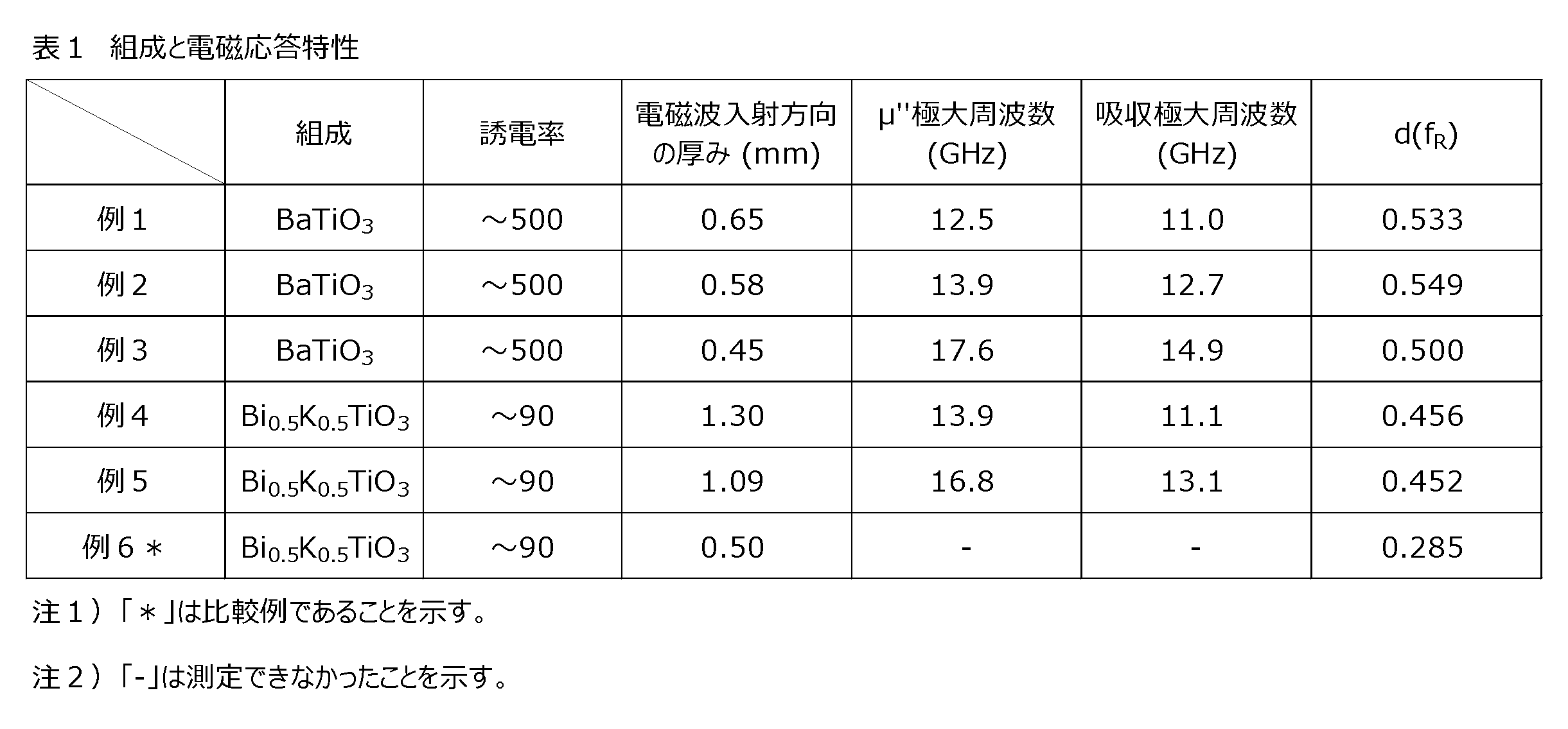
- Table 1 shows the frequency at which the absorption is maximum (maximum absorption frequency). All samples had a frequency region showing absorption, and the attenuation amount during absorption exceeded -10 dB (Fig. 10).
- Table 1 shows the relationship (d(f R )) between the thickness d and the maximum absorption frequency f R .
- d(f R ) is a value calculated according to the following equation (11) using d and f R .
- Example 1 shows the maximum absorption frequency.
- Example 4 and 5 as in Examples 1 to 3 using the BaTiO 3 sintered body, there was a frequency region showing absorption, and the attenuation during absorption was over ⁇ 10 dB. At this time, d(f R ) was about 0.4 as shown in Table 1.
- Example 6 although there was a slight absorption near 18 GHz, no absorption that caused an attenuation of more than -10 dB was observed. In Example 6, even if f R is set to 18 GHz, which is the upper limit frequency for measurement, d(f R ) is 0.3 or less, so it was considered that Mie resonance did not occur within this measurement frequency.
Landscapes
- Engineering & Computer Science (AREA)
- Microelectronics & Electronic Packaging (AREA)
- Shielding Devices Or Components To Electric Or Magnetic Fields (AREA)
- Hard Magnetic Materials (AREA)
- Soft Magnetic Materials (AREA)
Abstract
誘電体のMie共鳴に基づく磁気損失を利用した電磁波吸収体の製造方法が提供される。この電磁波吸収体の製造方法は、以下の工程;誘電素体を作製する工程、目標周波数fT(Hz)を決定する工程、及び前記誘電素体を加工して平板状誘電体を作製する工程を備える。また前記平板状誘電体の500MHzにおける比誘電率実部εr'が50以上であり、前記誘電素体を加工する際に、平板状誘電体の最大長L(mm)及び厚さd(mm)と、前記比誘電率実部εr'と、前記目標周波数fT(Hz)とが、下記(1)式及び(2)式を満足するように加工を行う。
Description
本発明は、電磁波吸収体の製造方法に関する。
メタマテリアルは、そのサイズが対象とする電磁波の波長に比べて小さい人工物質であり、自然界の物質には無い特性を示すことから、近年、注目を浴びている。特に、左手系メタマテリアルと呼ばれる物質は、特定の周波数領域で負の屈折率を示す。そのため、完全レンズや透明マントといった新規な光学用途での応用を目指して、研究開発が盛んにおこなわれている。
1999年に英国の物理学者J.B.Pendryは、電磁波の波長に比べて小さい周期構造を有するナノメタル構造体を提案し、この構造体の屈折率が負になることを理論的に示した(非特許文献1)。このナノメタル構造体は、微小なスプリットリング共振器(SRR)とメタルワイヤからなるナノユニットを3次元的に配列した構造を備えている。ナノユニットのサイズを小さくすることで、電磁波に対してナノメタル構造体は均質な媒質として働き、SRRとメタルワイヤの機能に依存する電磁波応答を示す。SRRは電磁波に対してLC共振器として働き、共振周波数の上側で負の透磁率を示す。また導電性メタルワイヤは負の誘電率を示す。SRRとメタルワイヤを組み合わせることで、実効誘電率と実効透磁率の両方が負になり、その結果、誘電率の平方根と透磁率の平方根との積で表される屈折率が負になる。さらにPendryは、負の屈折率を示す左手系メタマテリアルを用いることで、光の回折限界を超えて、いくらでも細かな構造を観察できる完全レンズが実現できることを理論的に示した(非特許文献2)。
Pendryの発表を受けて、米国の物理学者D.R.Smithらは、SRRとメタルワイヤからなるナノメタル構造体を実際に作製し、この構造物の誘電率と透磁率とがマイクロ波領域で負になることを実証した(非特許文献3)。これらの発表を受けて、メタマテリアルは一気に注目を浴びるようになった。
一方で、ナノメタル構造体の代わりに誘電体を用いた誘電体メタマテリアルが提案されている。ナノメタル構造物は、導体損が大きく、また製造のために精密微細な加工技術が必要との欠点がある。これに対して、誘電体メタマテリアルは、非共振時の損失が小さく、製造が容易という利点がある。
例えば、R.Yahiaouiらは、高誘電率TiO2セラミックディスクからなる誘電体共振器を2次元的に周期配列した構造を提案している(非特許文献4)。誘電体共振器のサイズを電磁波の波長程度に小さくすると、Mie共鳴が起こる。そのためTE共振とTM共振のいずれの共振モードを利用することが可能になる。誘電体共振器は、TE共振モードにおいて共振周波数の上側で負の実効透磁率を示す。またTM共振モードにおいて共振周波数の上側で負の実効誘電率を示す。この点、TE共振モードが、ナノメタル構造のSRRに相当し、TM共振モードがメタルワイヤに相当すると言うことができる。
J.B.Pendry et al., Magnetism from Conductors, and Enhanced Non-linear Phenomena, IEEE Transactions on Microwave Theory and Techniques, November 1999, volume 47, Issue 11, page 2075-2084
J.B.Pendry, Negative Refraction Makes a Perfect Lens, PYSICAL REVIEW LETTERS, 30 October, 2000, Volume 85, Number 18, page 3966-3969
R.A.Shelby et al, Experimental Verification of a Negative Index of Refraction, Science, 6 April, 2001, Volume 292, Issue 5514, page 77-79
R.Yahiaoui et al., Towards left-handed metamaterials using single-size dielectric resonators: The case of TiO2-disks at millimeter wavelengths, APPLIED PHYSICS LETTERS, Volume 101, 042909 (2012)
このように、誘電体メタマテリアルなどのメタマテリアルに関する開発が盛んに行われるものの、その殆どが、負の屈折率を示す物質、即ち左手系メタマテリアルを対象とし、また完全レンズや透明マントといった光学用途での応用を目指している。ナノメタル構造体を、マイクロ波領域におけるアンテナや伝送線路に適用する技術が僅かに知られるものの、誘電体メタマテリアルを光学部品以外の電子デバイスに適用することを目指した技術は知られていない。
本発明者は、このような実情に鑑みて鋭意検討を行った。その結果、磁性元素を含まない誘電体であっても、その特性及び形状を制御すれば、Mie共鳴モードが発現して磁気共鳴が起こること、この磁気共鳴に基づく磁気損失を利用すれば、電磁波吸収特性を得られることを知見した。
本発明は、このような知見に基づき完成されたものであり、誘電体のMie共鳴に基づく磁気損失を利用した電磁波吸収体の製造方法の提供を課題とする。
本発明は、下記(a)~(e)の態様を包含する。なお本明細書において「~」なる表現は、その両端の数値を含む。すなわち「X~Y」は「X以上Y以下」と同義である。
(a)電磁波吸収体の製造方法であって、以下の工程;
誘電素体を作製する工程、
目標周波数fT(Hz)を決定する工程、及び
前記誘電素体を加工して平板状誘電体を作製する工程を備え、
前記平板状誘電体の500MHzにおける比誘電率実部εr’が50以上であり、
前記誘電素体を加工する際に、平板状誘電体の最大長L(mm)及び厚さd(mm)と、前記比誘電率実部εr’と、前記目標周波数fT(Hz)とが、下記(1)式及び(2)式を満足するように加工を行う、方法。
誘電素体を作製する工程、
目標周波数fT(Hz)を決定する工程、及び
前記誘電素体を加工して平板状誘電体を作製する工程を備え、
前記平板状誘電体の500MHzにおける比誘電率実部εr’が50以上であり、
前記誘電素体を加工する際に、平板状誘電体の最大長L(mm)及び厚さd(mm)と、前記比誘電率実部εr’と、前記目標周波数fT(Hz)とが、下記(1)式及び(2)式を満足するように加工を行う、方法。


(b)前記誘電素体が、セラミックス焼結体である、上記(a)の方法。
(c)前記誘電素体が、チタン酸バリウム(BaTiO3)及びチタン酸ビスマスカリウム(Bi0.5K0.5TiO3)の少なくとも一方を含む、上記(a)又は(b)の方法。
(d)前記平板状誘電体がトロイダル形状を有する、上記(a)~(c)のいずれかの方法。
(e)前記目標周波数fTが1GHz以上10THz以下である、上記(a)~(d)のいずれかの方法。
本発明によれば、誘電体のMie共鳴に基づく磁気損失を利用した電磁波吸収体の製造方法が提供される。
1.電磁波吸収体
本実施形態の製造方法を説明するにあたり、まず電磁波吸収体について説明する。
本実施形態の製造方法を説明するにあたり、まず電磁波吸収体について説明する。
本実施形態の電磁波吸収体は、板状誘電体(以下、「誘電体」と称する場合がある)を備える。この誘電体は、誘電体メタマテリアルとして働き、Mie共鳴と呼ばれる共鳴モードを示す。そのため、磁気共鳴に基づく磁気損失を所定の周波数領域で示し、この周波数領域で電磁波吸収特性を示す。
誘電体のサイズが入射電磁波の波長と同程度、またはそれよりも小さいとき、ある周波数(第1Mie共鳴周波数)で誘電体内部に電場と磁場の定常状態が生まれ、これにより共鳴現象が発現する。この共鳴現象をMie共鳴と呼ぶ。より詳細に説明するに、電磁波放射源が遠方界にある場合、電磁波は平面波として誘電体に入射する。この際、誘電体と空気との界面で電磁波電界成分の接線成分と垂直成分の両方が境界条件を満足するように電磁波が入射する。その結果、誘電体内ではそれまでの伝搬媒体と異なる電磁界分布が生じる。この中でも磁気的なMie共鳴に対応するモードでは,誘電体内部に渦をまくような電界および変位電流の分布が生じる。
誘電体内で渦状の変位電流(電界)が生じる結果、誘電体内部には変位電流(電界)と垂直に振動磁界が発生する。この点、誘電体内の渦状の変位電流(電界)分布を磁気双極子と見なすことができる。この振動する磁気双極子は、入射電磁波の磁界成分と相互作用を起こし、特定の周波数(第1Mie共鳴周波数)で磁気共鳴する。要するに、入射電磁波の電界成分が誘電体内に磁気双極子を生じさせ、この磁気双極子と電磁波磁界成分が作用し合うことで磁気共鳴が引き起こされる。
同様にして、電気共鳴も引き起こされる。すなわち、入射電磁波の磁界成分が誘電体内に電気双極子を生じさせ、この電気双極子と電磁波電界成分とが特定の周波数(第2Mie共鳴周波数)で電気共鳴する。
本発明者が調べたところ、Mie共鳴に基づく磁気共鳴により磁気損失が生じ、その大きさは電磁波を十分に吸収する程度に大きいことが分かった。より詳細に説明するに、本発明者は、電磁波中の物質の散乱モデル(Lewinモデル)に基づき、誘電体の実効誘電率(εeff)及び実効透磁率(μeff)を算出し、さらに合計則に基づき、磁気損失(QM)の大きさを見積もった。
ここで、Lewinモデルは、多数の球状粒子(粒径a、誘電率ε2、透磁率ε2)がマトリックス(誘電率ε1、透磁率μ1)中に周期間隔pを保ちながら分散している複合体について、電磁波応答を理論的に考察したモデルである。複合体の実効誘電率(εeff)と実効透磁率(μeff)は下記(3)~(5)式にしたがって求められる。また、磁気損失(QM)は下記(6)式に示す合計則にしたがって求められる。なお下記(3)~(6)式において、vはマトリックス中球状粒子の体積割合、fは周波数、ωは角周波数、cは光速(3.0×10⁸m/秒)である。またμ’’は実効透磁率μeffの虚部である。
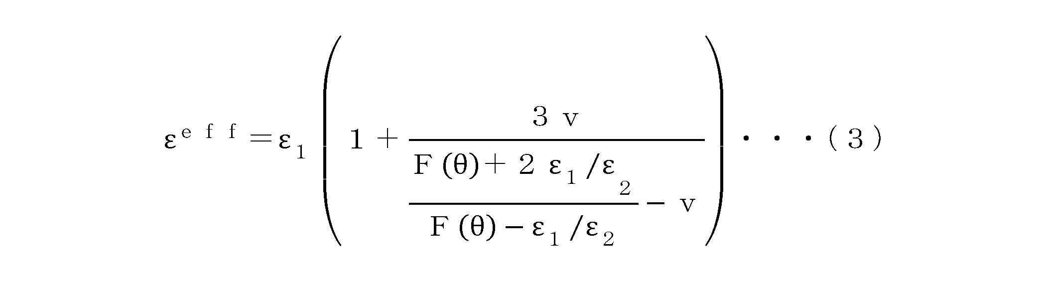



上記(3)~(6)式を用いて、シミュレーションにより磁気損失(QM)を求めたところ、球状粒子及びマトリックスが磁性成分を持たない場合、即ちμ1=μ2=1の場合であっても、磁気損失(QM)が生じることが分かった。また、この磁気損失(QM)は、球状粒子とマトリックスの誘電率(ε1、ε2)に大きく依存することが分かった。さらに電磁波の周波数(f)が大きくなるにつれ、磁気損失(QM)は急増することが分かった。
このように、誘電率の高い誘電体を用いることで、Mie共鳴に基づく大きな磁気損失が高周波領域で生じることが分かった。またこの磁気損失を電磁波吸収の用途に適用できることが期待された。
2.電磁波吸収体の製造
本実施形態の電磁波吸収体の製造方法は、以下の工程;誘電素体を作製する工程(誘電素体作製工程)、目標周波数fT(Hz)を決定する工程(目標周波数決定工程)、及び誘電素体を加工して平板状誘電体を作製する工程(誘電体作製工程)を備える。ここで、平板状誘電体の500MHzにおける比誘電率実部εr’は50以上である。また誘電素体を加工する際に、平板状誘電体の最大長L(mm)及び厚さd(mm)と、比誘電率実部εr’と、目標周波数fT(Hz)とが、特定の関係を満足するように加工を行う。各工程の詳細について、以下に説明する。
本実施形態の電磁波吸収体の製造方法は、以下の工程;誘電素体を作製する工程(誘電素体作製工程)、目標周波数fT(Hz)を決定する工程(目標周波数決定工程)、及び誘電素体を加工して平板状誘電体を作製する工程(誘電体作製工程)を備える。ここで、平板状誘電体の500MHzにおける比誘電率実部εr’は50以上である。また誘電素体を加工する際に、平板状誘電体の最大長L(mm)及び厚さd(mm)と、比誘電率実部εr’と、目標周波数fT(Hz)とが、特定の関係を満足するように加工を行う。各工程の詳細について、以下に説明する。
<誘電素体作製工程>
誘電素体作製工程では誘電素体を作製する。誘電素体として、これを加工して作製される誘電体の500MHzにおける比誘電率実部εr’が50以上になるものを選択する。加工工程で誘電率は殆ど変化しない。誘電素体の比誘電率実部は50以上が好ましく、100以上が好ましく。300以上がさらに好ましい。比誘電率実部の上限は特に限定されない。しかしながら、典型的には1000以下である。
誘電素体作製工程では誘電素体を作製する。誘電素体として、これを加工して作製される誘電体の500MHzにおける比誘電率実部εr’が50以上になるものを選択する。加工工程で誘電率は殆ど変化しない。誘電素体の比誘電率実部は50以上が好ましく、100以上が好ましく。300以上がさらに好ましい。比誘電率実部の上限は特に限定されない。しかしながら、典型的には1000以下である。
誘電素体は、高誘電率材料から構成される限り、材質は限定されない。例えば、チタン酸バリウム(BaTiO3)、チタン酸ストロンチウム(SrTiO3)、チタン酸カルシウム(CaTiO3)、チタン酸ビスマスアルカリ(Bi0.5K0.5TiO3、Bi0.5Na0.5TiO3)、鉛系材料(PZT、PMN-PT等)、ビスマス層状化合物(SBT等)などの高誘電率材料を挙げることができる。誘電素体は、これらの材料を1種のみ含んでもよく、あるいは複数種で含んでもよい。複数種の材料を含む場合には、混晶の形態で含んでもよく、あるいは固溶体の形態で含んでもよい。誘電素体は、チタン酸バリウム(BaTiO3)及びチタン酸ビスマスカリウム(Bi0.5K0.5TiO3)の少なくとも一方を含んでもよい。また誘電体は、多結晶でよく、あるいは単結晶であってもよい。しかしながら、好適には、誘電素体は、製造が容易なセラミック焼結体である。
誘電素体は、公知の手法で作製すればよい。例えば、セラミック焼結体である誘電素体は、誘電体原料を成形及び焼成して作製すればよい。誘電体原料は、固相反応法、錯体重合法、共沈法、水熱合成法、ゾルゲル法、及び気相法などの公知の手法で合成すればよい。また誘電体原料以外に、成形助材や焼結助材などの添加材を加えてもよい。単結晶である誘電素体は、水溶液法、水熱合成法、フラックス法、ベルヌーイ法、チョクラルスキー胞、ブリッジマン法、浮遊帯溶融法、スカイメルト法、昇華再結晶法、化学輸送法、及び化学気相成長法などの公知の手法で作製すればよい。
<目標周波数決定工程>
目標周波数決定工程では、目標周波数fT(Hz)を決定する。目標周波数fTは、吸収したい電磁波の周波数である。目標周波数fTは、1GHz以上10THz以下が好ましい。周波数が過度に低いと、Mie共鳴に基づく磁気損失の寄与が十分に生じない恐れがある。一方で周波数が過度に高いと、誘電体の誘電率が低下して、磁気損失が十分に高くならない恐れがある。fTは、3GHz以上5THz以下がより好ましく、10GHz以上3THz以下がさらに好ましく、10GHz以上300GHzが特に好ましく、10GHz以上30GHz以下が特に好ましい。fTは500MHz以上18GHz以下であってもよい。なお目標周波数の決定は、後述する工程で加工して誘電体を得る前であれば、いずれのタイミングで行ってよい。誘電体素体作製工程の前に行ってもよく、後に行ってもよい。あるいは誘電体素体作製工程と同時に行ってもよい。さらには誘電体素体作製工程で誘電素体を加工する途中で行ってもよい。いずれにしても、加工により得られる誘電体の必要寸法を決定する前であれば、いずれのタイミングで行ってもよい。
目標周波数決定工程では、目標周波数fT(Hz)を決定する。目標周波数fTは、吸収したい電磁波の周波数である。目標周波数fTは、1GHz以上10THz以下が好ましい。周波数が過度に低いと、Mie共鳴に基づく磁気損失の寄与が十分に生じない恐れがある。一方で周波数が過度に高いと、誘電体の誘電率が低下して、磁気損失が十分に高くならない恐れがある。fTは、3GHz以上5THz以下がより好ましく、10GHz以上3THz以下がさらに好ましく、10GHz以上300GHzが特に好ましく、10GHz以上30GHz以下が特に好ましい。fTは500MHz以上18GHz以下であってもよい。なお目標周波数の決定は、後述する工程で加工して誘電体を得る前であれば、いずれのタイミングで行ってよい。誘電体素体作製工程の前に行ってもよく、後に行ってもよい。あるいは誘電体素体作製工程と同時に行ってもよい。さらには誘電体素体作製工程で誘電素体を加工する途中で行ってもよい。いずれにしても、加工により得られる誘電体の必要寸法を決定する前であれば、いずれのタイミングで行ってもよい。
<誘電体作製工程>
誘電体作製工程では、誘電素体を加工して平板状誘電体を作製する。加工手法は、所定寸法の平板状誘電体を得ることができる限り、限定されない。例えば、切削加工、研削加工、研磨加工、超音波加工、及び放電加工など公知の手法が挙げられる。
誘電体作製工程では、誘電素体を加工して平板状誘電体を作製する。加工手法は、所定寸法の平板状誘電体を得ることができる限り、限定されない。例えば、切削加工、研削加工、研磨加工、超音波加工、及び放電加工など公知の手法が挙げられる。
平板状誘電体の500MHzにおける比誘電率実部εr’は50以上である。高誘電率誘電体を用いることで、この誘電体を備える電磁波吸収体に高い電磁波吸収特性を付与することが可能になる。すなわち、誘電体の誘電率が高いほど、屈折率増大に基づく波長短縮効果が大きくなり、より小さな吸収体でMie共鳴が実現するためである。誘電体の誘電率は高いほど好ましい。比誘電率実部εr’は、100以上が好ましく、300以上がより好ましい。比誘電率実部εr’の上限は特に限定されない。しかしながら、典型的には2000以下、より典型的には1000以下である。なお測定周波数を500MHzにしたのは、GHz超では測定手法上の問題で高誘電率材料の誘電率を精度良く測定することが困難になるためである。
誘電素体を加工する際に、平板状誘電体の最大長L(mm)及び厚さd(mm)と、比誘電率実部εr’と、目標周波数fT(Hz)とが、下記(1)式及び(2)式を満足するように加工を行う。これにより磁気損失の大きい誘電体を得ることができる。なお、下記(1)式において、cは光速(3.0×10⁸m/秒、即ち3.0×1011mm/秒)である。


この点について説明するに、Mie共鳴時の物質はFabry-Perot共振と類似の挙動を示すことが知られている。またFabry-Perot共振において、物質の厚さd’は、共振時の波長λR’及び共振周波数fRと下記(7)式に示す関係を満足することが知られている。なお下記(7)式において、cは光速であり、ε’は物質の比誘電率実部である。

Fabry-Perot共振の結果から推論するに、Mie共鳴においても、誘電体の厚さdが上記(1)式の関係を満足することで、目標周波数fTに近くの周波数で磁気共鳴が起こり、それにより磁気損失が生じることが理解される。平板状誘電体の厚さdと、比誘電率実部εr’と、目標周波数fTとは、下記(8)式の関係を満足することがより好ましく、下記(9)式の関係を満足することがさらに好ましく、下記(10)式の関係を満足することが特に好ましい。ここでdの上限を上記(7)式に対して広くとっている理由はfRにおける誘電率は一般に500MHzの値より小さくなるためである。ただし、温度における吸収周波数の変化を抑える観点では、εの周波数に対する変化は小さいほうが好ましい。つまり上記(7)式に近い関係が保たれていることが好ましい。



また、誘電体は、上記(2)式を満足する。すなわち、厚さdに対する最大長Lの比(L/d)が2以上の扁平形状を誘電体が有する。これは、発明者が検討を重ねた結果、扁平形状の誘電体の方が、厚みのより薄い吸収体を実現できることが分かったためである。なお最大長Lは、平板状である誘電体の板面における最大長さである。すなわち誘電体が円板状であるときは、板面を形づくる円の直径である。また誘電体が四角板状であるときは、板面を形づくる四角形の対角長である。L/dは、3以上が好ましく、5以上がより好ましく、10以上がさらに好ましい。また最大長Lは、0.5mm以上20mm以下が好ましく、1mm以上10mm以下がより好ましい。さらに厚さdは、0.03mm以上3mm以下が好ましく、0.05mm以上2mm以下がより好ましい。
誘電体は、扁平板状であるかぎり、その形状は限定されない。円板状であってよく、角板状であってよく、あるいはトロイダル形状であってもよい。
このようにして本実施形態の電磁波吸収体を製造することができる。誘電体をそのまま電磁波吸収体として用いることは可能である。あるいは、得られた誘電体に後処理を施して電磁波吸収体を作製してもよい。後処理工程として、金属板又は金属箔などの金属部材を誘電体裏面に設ける工程が挙げられる。金属部材は電磁波を反射する作用がある。そのため、金属部材を設けることで、電磁波吸収体の吸収効率を高めることができる。また誘インピーダンス整合層を誘電体表面に設ける工程が挙げられる。インピーダンス整合層を設けることで、誘電体表面での電磁波反射が抑制され、誘電体内部での電磁波吸収を効率よく進めることが可能になる。なお誘電体表面とは、電磁波が入射する面のことであり、裏面とは表面に対向する面のことである。
本実施形態の電磁波吸収体は、誘電体メタマテリアルとして機能する誘電体を備えることで、Mie共鳴に基づく磁気損失が発現し、この磁気損失を利用した電磁波吸収特性を示す。特に本実施形態の電磁波吸収体は、GHz帯域及びTHz帯域といった高周波領域での電磁波吸収特性に優れるため、薄型化が可能である。またMie共鳴は特に高屈折率材料においては、共鳴周波数の入射角依存性が小さいという利点がある。このような電磁波吸収体は、携帯電話、高速データ伝送システム、無線LAN、ETC、衛星放送、車載用レーダ、及びミリ波通信などの分野で特に好適である。
本発明者の知る限り、誘電体メタマテリアルの磁気損失を利用した電磁波吸収体は知られていない。非特許文献1~3にはナノメタル構造体からなるメタマテリアルが提案されているが、ナノメタル構造体は、その製造時に精密微細な加工技術が必要という欠点がある。またこれらのナノメタル構造体は、負の屈折率を示す左手系メタマテリアルの開発に着目したものであり、磁気損失に着目するものでなく、ましてや電磁波吸収体としての用途を目的とするものではない。非特許文献4にはTiO2ディスクからなる誘電体メタマテリアルが提案されているが、この文献も左手系メタマテリアルの開発を主眼としており、電磁波吸収体としての用途を対象としていない。
ところで、磁気損失を利用した電磁波吸収体として、ソフトフェライトなどの高透磁率磁性体が従来から多用されている。しかしながら、ソフトフェライトは磁気異方性が小さいため、理論上、GHz帯域以上の高周波領域での電磁波吸収特性を高めることが困難である。すなわち、スネークの限界として知られる理論によれば、共鳴周波数と透磁率の積は一定である。そのため、ソフトフェライトを用いて共鳴周波数を高めようとすれば、透磁率が低下し、十分な吸収特性を得ることができない。フェロックスプラナーなどの磁気異方性を有する材料を用いてスネークスの限界を打ち破る試みもなされているが、GHz帯域以上の高周波で実用に耐えうる材料が未だ見いだせていないのが現状である。さらに、磁性体を用いた電磁波吸収体は入射角に応じて吸収特性が変化しやすいため、斜入射時に吸収特性が低下するという欠点がある。
本発明を、以下の実施例及び比較例を用いて更に詳細に説明する。しかしながら、本発明は以下の実施例に限定されるものではない。
(1)電磁波吸収体の作製
[例1]
例1では、所定厚さを有するチタン酸バリウム(BaTiO3)焼結体を作製し、これを用いて電磁波吸収体を作製した。具体的には以下の手順でサンプルを作製した。
[例1]
例1では、所定厚さを有するチタン酸バリウム(BaTiO3)焼結体を作製し、これを用いて電磁波吸収体を作製した。具体的には以下の手順でサンプルを作製した。
原料として、市販のチタン酸バリウム粉末(BaTiO3、戸田工業製T-BTO-060RF、カタログ値平均粒径60nm)を準備した。このチタン酸バリウム粉末は湿式合成法で合成されたものである。次いで、準備したチタン酸バリウム粉末を150MPaの圧力でプレス成型し、得られた成形体を1000℃×12時間の条件で焼成して、誘電素体としての焼結体を得た。
得られた焼結体から評価用サンプルを作製した。まず焼結体をトロイダル形状(外径7mm、内径3mm、厚み0.65mm)になるように加工して誘電体を作製した。そして、得られた誘電体を電磁波吸収体として用いた。
[例2]
例2では、焼結体をトロイダル形状(外径7mm、内径3mm、厚み0.58mm)になるように加工して誘電体を作製した。それ以外は例1と同様にして電磁波吸収体を作製した。
例2では、焼結体をトロイダル形状(外径7mm、内径3mm、厚み0.58mm)になるように加工して誘電体を作製した。それ以外は例1と同様にして電磁波吸収体を作製した。
[例3]
例3では、焼結体をトロイダル形状(外径7mm、内径3mm、厚み0.45mm)になるように加工して誘電体を作製した。それ以外は例1と同様にして電磁波吸収体を作製した。
例3では、焼結体をトロイダル形状(外径7mm、内径3mm、厚み0.45mm)になるように加工して誘電体を作製した。それ以外は例1と同様にして電磁波吸収体を作製した。
[例4]
例4では、所定厚さを有するチタン酸ビスマスカリウム(Bi0.5K0.5TiO3)焼結体を作製し、これを用いて電磁波吸収体を作製した。具体的には以下の手順でサンプルを作製した。
例4では、所定厚さを有するチタン酸ビスマスカリウム(Bi0.5K0.5TiO3)焼結体を作製し、これを用いて電磁波吸収体を作製した。具体的には以下の手順でサンプルを作製した。
原料として、硝酸ビスマス5水和物(Bi(NO3)3・5H2O)、硝酸カリウム(KNO3)、チタン(IV)ブトキシド(Ti(OC4H9)4)を準備し、最終的に得られる生成物の組成がBi0.5K0.5TiO3になるように秤量した。秤量した原料を、クエン酸及びエチレンジアミン4酢酸とともに水に加えて混合し、NH4OHを用いて水溶液のpHを6程度にまで高めた。これにより透明な水溶液を得た。得られた水溶液にエチレングリコールを添加して、140℃で加熱撹拌して重合反応を起こし、ゲル状の物質を得た。得られたゲル状の物質を400℃で熱分解して、生成物を得た。
次いで、得られた生成物を150MPaの圧力でプレス成型し、得られた成形体を820℃×3時間の条件で焼成して、誘電素体としての焼結体を得た。
得られた焼結体をトロイダル形状(外径7mm、内径3mm、厚み1.30mm)になるように加工して誘電体を作製した。そして、得られた誘電体を電磁波吸収体として用いた。
[例5]
例5では、焼結体をトロイダル形状(外径7mm、内径3mm、厚み1.09mm)になるように加工して誘電体を作製した。それ以外は例4と同様にして電磁波吸収体を作製した。
例5では、焼結体をトロイダル形状(外径7mm、内径3mm、厚み1.09mm)になるように加工して誘電体を作製した。それ以外は例4と同様にして電磁波吸収体を作製した。
[例6(比較)]
例6では、焼結体をトロイダル形状(外径7mm、内径3mm、厚み0.50mm)になるように加工して誘電体を作製した。それ以外は例4と同様にして電磁波吸収体を作製した。
例6では、焼結体をトロイダル形状(外径7mm、内径3mm、厚み0.50mm)になるように加工して誘電体を作製した。それ以外は例4と同様にして電磁波吸収体を作製した。
(2)評価
例1~例6で得られた電磁波吸収体について、各種特性の評価を以下のとおり行った。
例1~例6で得られた電磁波吸収体について、各種特性の評価を以下のとおり行った。
<誘電率>
電磁波吸収体の誘電特性を以下の手順で評価した。まずトロイダル加工前の焼結体を、円板状(外径16mm、厚み1mm)に加工し、得られた円板状サンプルに上部電極(直径10mm)及び下部電極(直径7mm)を形成して、誘電率測定用サンプルを作製した。電極の形成は、円板状サンプルの上面及び下面に銀ペーストを塗布した後に、有機分を揮発除去してするために600℃×1時間の条件で熱処理を施して行った。
電磁波吸収体の誘電特性を以下の手順で評価した。まずトロイダル加工前の焼結体を、円板状(外径16mm、厚み1mm)に加工し、得られた円板状サンプルに上部電極(直径10mm)及び下部電極(直径7mm)を形成して、誘電率測定用サンプルを作製した。電極の形成は、円板状サンプルの上面及び下面に銀ペーストを塗布した後に、有機分を揮発除去してするために600℃×1時間の条件で熱処理を施して行った。
次いで、100MHz~1GHzの周波数領域における誘電率を評価した。具体的には、インピーダンスアナライザ(キーサイト・テクノロジー社製4291B)を用い、サンプルのインピーダンスを電圧-電流法で求めた。得られたインピーダンスを解析して、キャパシタ成分及び抵抗成分を求め、サンプル形状及び電極形状を加味して複素誘電率(ε=ε’-jε’’)を算出した。ここで、ε’及びε’’は、それぞれ複素比誘電率の実部及び虚部である。
<磁化>
電磁波吸収体の磁化を以下の手順で評価した。まずトロイダル形状に加工する前の焼結体を粉砕して、磁化測定用サンプルを作製した。そして、振動試料型磁力計(VSM)を用いてサンプルの磁化を測定した。
電磁波吸収体の磁化を以下の手順で評価した。まずトロイダル形状に加工する前の焼結体を粉砕して、磁化測定用サンプルを作製した。そして、振動試料型磁力計(VSM)を用いてサンプルの磁化を測定した。
<透磁率>
電磁波吸収体の透磁率を以下の手順で評価した。具体的には、ベクトルネットワークアナライザ(キーサイト・テクノロジー社製85071E)を用い、500MHz~18GHzの周波数領域における反射特性及び透過特性を同軸管透過法で求めた。次いで、得られた反射特性及び透過特性を用いて、複素比透磁率(μ=μ’-jμ’’)を算出した。ここで、μ’及びμ’’は、それぞれ複素比透磁率の実部及び虚部である。
電磁波吸収体の透磁率を以下の手順で評価した。具体的には、ベクトルネットワークアナライザ(キーサイト・テクノロジー社製85071E)を用い、500MHz~18GHzの周波数領域における反射特性及び透過特性を同軸管透過法で求めた。次いで、得られた反射特性及び透過特性を用いて、複素比透磁率(μ=μ’-jμ’’)を算出した。ここで、μ’及びμ’’は、それぞれ複素比透磁率の実部及び虚部である。
<電磁波吸収特性>
電磁波吸収体の電磁波吸収特性を以下の手順で評価した。電磁波の透過成分を十分に低減させるため、電磁波吸収体の背後に厚さ1mmの金属板を設置した。その状態で500MHz~18GHzの周波数領域における反射特性及び透過特性を、透磁率測定と同様の手法で求めた。そして、入射波と反射波の比を求めて、反射減衰量を算出した。
電磁波吸収体の電磁波吸収特性を以下の手順で評価した。電磁波の透過成分を十分に低減させるため、電磁波吸収体の背後に厚さ1mmの金属板を設置した。その状態で500MHz~18GHzの周波数領域における反射特性及び透過特性を、透磁率測定と同様の手法で求めた。そして、入射波と反射波の比を求めて、反射減衰量を算出した。
(3)評価結果
<誘電率>
例1及び例4について、1~500MHzにおける比誘電率(実部εr’、虚部εr’’)の周波数分散を、図1及び図2のそれぞれに示す。
<誘電率>
例1及び例4について、1~500MHzにおける比誘電率(実部εr’、虚部εr’’)の周波数分散を、図1及び図2のそれぞれに示す。
強誘電体且つ非磁性体であるBaTiO3を用いた例1は、比誘電率実部(εr’)が500程度と高かった(図1)。また強誘電体であり且つ非磁性体のBi0.5K0.5TiO3を用いた例4は、比誘電率実部(εr’)が90程度であった(図2)。例1及び例4のサンプルは、誘電率が高く、真空に比べて大きな誘電応答を示すことが分かった。
<磁化>
例1について得られた磁化率の測定結果を図3に示す。BaTiO3は非磁性体であるため、直流磁場に対する応答が小さく、弱い反磁性的な性質を示した。
例1について得られた磁化率の測定結果を図3に示す。BaTiO3は非磁性体であるため、直流磁場に対する応答が小さく、弱い反磁性的な性質を示した。
<透磁率>
例1~例3について得られた透磁率(実部μ’、虚部μ’’)の周波数分散を図4~図6のそれぞれに示す。また透磁率虚部(μ’’)が極大となる周波数(μ’’極大周波数)を表1にまとめて示す。
例1~例3について得られた透磁率(実部μ’、虚部μ’’)の周波数分散を図4~図6のそれぞれに示す。また透磁率虚部(μ’’)が極大となる周波数(μ’’極大周波数)を表1にまとめて示す。
厚み0.65mmのBaTiO3焼結体を用いた例1では、10GHz近傍で共鳴的な挙動が見られ、透磁率実部(μ’)とともに虚部(μ’’)が増大していた(図4)。また厚み0.58mmのBaTiO3焼結体を用いた例2では、例1と同様に共鳴現象が観察されるものの、共鳴周波数が高周波化していた(図5)。さらに厚み0.45mmのBaTiO3焼結体を用いた例3では、共鳴周波数がさらに高周波化していた(図6)。
例4~例6について得られた透磁率(μ’、μ’’)の周波数分散を図7~図9のそれぞれに示す。またμ’’極大周波数を表1にまとめて示す。厚み1.30mmのBi0.5K0.5TiO3焼結体を用いた例4では、BaTiO3を用いた例1~例3と同様に共鳴的な挙動が見られ、透磁率虚部(μ’’)が大きくなっていた(図7)。厚み1.09mmのBi0.5K0.5TiO3焼結体を用いた例5では、例4に比べて共鳴周波数が高周波化していた(図8)。一方で、厚み0.50mmのBi0.5K0.5TiO3焼結体を用いた例6では、共鳴的な挙動が消滅していた(図9)。
<電磁波吸収特性>
例1~例3について得られた電磁波吸収特性を図10にまとめて示す。また吸収が極大となった周波数(吸収極大周波数)を表1に示す。いずれのサンプルでも、吸収を示す周波数領域があり、吸収時の減衰量は-10dB超であった(図10)。厚みdと吸収極大周波数fRの関係(d(fR))を表1に示す。ここでd(fR)は、dとfRとを用いて、下記(11)式にしたがって求められる値である。
例1~例3について得られた電磁波吸収特性を図10にまとめて示す。また吸収が極大となった周波数(吸収極大周波数)を表1に示す。いずれのサンプルでも、吸収を示す周波数領域があり、吸収時の減衰量は-10dB超であった(図10)。厚みdと吸収極大周波数fRの関係(d(fR))を表1に示す。ここでd(fR)は、dとfRとを用いて、下記(11)式にしたがって求められる値である。

例1~例3について、d(fR)として、上記(7)式に近い0.5程度の値が得られた。さらに、共鳴周波数と同様に、誘電体の厚みを薄くすることで、吸収周波数が高周波化していた。なお、-10dB超の減衰量は、90%超の電磁波が吸収されたことを意味する。
例4~例6について得られた電磁波吸収特性を図11にまとめて示す。また吸収極大周波数を表1に示す。例4及び例5では、BaTiO3焼結体を用いた例1~例3と同様に、吸収を示す周波数領域があり、吸収時の減衰量は-10dB超であった。この際、d(fR)は表1に示す通り0.4程度であった。一方で、例6では、18GHz近傍に僅かな吸収が存在するものの、-10dB超の減衰量をもたらす吸収は見られなかった。例6においてはfRを測定上限周波数である18GHzにしても、d(fR)は0.3以下であるため、本測定周波数内ではMie共鳴が生じなかったと考えられた。
以上の結果より、目標周波数fTをfR近傍に設定し、且つ上記(1)及び(2)式を満足するように誘電体を加工することで、Mie共鳴に基づく電磁波吸収特性を得られることが確認された。
(4)考察
BaTiO3又はBi0.5K0.5TiO3焼結体を備えた電磁波吸収体(例1~例5)で、磁気損失、及びそれに起因する電磁波吸収特性が観察された。強磁性体でない例1及び例4のBaTiO3やBi0.5K0.5TiO3で大きな磁気損失が得られた原因として、誘電体内で電磁波の共鳴が生じ、誘電応答及び磁気応答が特定の共鳴モードをもったためと考えられる。また例2、例3、及び例5で共鳴周波数が高周波化したのは、厚みを薄くすることで、共鳴を起こす条件が高周波側に移ったためと理解される。さらに例4及び例5では、例1~例3に比べて、同じ周波数帯域を起こすために必要な厚みが大きくなっていた。これは、Bi0.5K0.5TiO3の誘電率がBaTiO3に比べて小さく、その結果、誘電体内での波長短縮効果が小さくなったからと推察される。
BaTiO3又はBi0.5K0.5TiO3焼結体を備えた電磁波吸収体(例1~例5)で、磁気損失、及びそれに起因する電磁波吸収特性が観察された。強磁性体でない例1及び例4のBaTiO3やBi0.5K0.5TiO3で大きな磁気損失が得られた原因として、誘電体内で電磁波の共鳴が生じ、誘電応答及び磁気応答が特定の共鳴モードをもったためと考えられる。また例2、例3、及び例5で共鳴周波数が高周波化したのは、厚みを薄くすることで、共鳴を起こす条件が高周波側に移ったためと理解される。さらに例4及び例5では、例1~例3に比べて、同じ周波数帯域を起こすために必要な厚みが大きくなっていた。これは、Bi0.5K0.5TiO3の誘電率がBaTiO3に比べて小さく、その結果、誘電体内での波長短縮効果が小さくなったからと推察される。
一方で、厚みを過度に小さくした電磁波吸収体(例6)では、共鳴現象及び吸収が見られなかった。厚みを過度に小さくすることで、本実施形態で特定される(1)式の関係を満足しないものになり、その結果、測定周波数内で共鳴条件を満足しなくなったと考えられる。
これらの結果から、誘電体における電磁波の共鳴モードを活用することで、非磁性体においても電磁波に対する大きな磁気損失を得られることが分かった。また誘電体の厚みを薄くすることで磁気損失を起こす周波数を制御できることが分かった。磁性体の磁気応答では、厚みを変えても共鳴周波数を制御することはできない。厚みによる共鳴周波数変化は、誘電体における特異な挙動である。
Claims (5)
- 電磁波吸収体の製造方法であって、以下の工程;
誘電素体を作製する工程、
目標周波数fT(Hz)を決定する工程、及び
前記誘電素体を加工して平板状誘電体を作製する工程を備え、
前記平板状誘電体の500MHzにおける比誘電率実部εr’が50以上であり、
前記誘電素体を加工する際に、平板状誘電体の最大長L(mm)及び厚さd(mm)と、前記比誘電率実部εr’と、前記目標周波数fT(Hz)とが、下記(1)式及び(2)式を満足するように加工を行う、方法。


- 前記誘電素体が、セラミック焼結体である、請求項1に記載の方法。
- 前記誘電素体が、チタン酸バリウム(BaTiO3)及びチタン酸ビスマスカリウム(Bi0.5K0.5TiO3)の少なくとも一方を含む、請求項1又は2に記載の方法。
- 前記平板状誘電体がトロイダル形状を有する、請求項1~3のいずれか一項に記載の方法。
- 前記目標周波数fTが1GHz以上10THz以下である、請求項1~4のいずれか一項に記載の方法。
Applications Claiming Priority (2)
| Application Number | Priority Date | Filing Date | Title |
|---|---|---|---|
| JP2021-009877 | 2021-01-25 | ||
| JP2021009877A JP2022113561A (ja) | 2021-01-25 | 2021-01-25 | 電磁波吸収体の製造方法 |
Publications (1)
| Publication Number | Publication Date |
|---|---|
| WO2022158587A1 true WO2022158587A1 (ja) | 2022-07-28 |
Family
ID=82548825
Family Applications (1)
| Application Number | Title | Priority Date | Filing Date |
|---|---|---|---|
| PCT/JP2022/002352 Ceased WO2022158587A1 (ja) | 2021-01-25 | 2022-01-24 | 電磁波吸収体の製造方法 |
Country Status (2)
| Country | Link |
|---|---|
| JP (1) | JP2022113561A (ja) |
| WO (1) | WO2022158587A1 (ja) |
Citations (3)
| Publication number | Priority date | Publication date | Assignee | Title |
|---|---|---|---|---|
| CN106772706A (zh) * | 2017-03-03 | 2017-05-31 | 电子科技大学 | 一种双介质宽带红外吸波超材料及其设计方法 |
| CN207967319U (zh) * | 2018-01-10 | 2018-10-12 | 中国计量大学 | 一种宽带超材料太赫兹吸波器 |
| JP2020182107A (ja) * | 2019-04-25 | 2020-11-05 | 地方独立行政法人大阪産業技術研究所 | 電子部材およびその製造方法 |
-
2021
- 2021-01-25 JP JP2021009877A patent/JP2022113561A/ja active Pending
-
2022
- 2022-01-24 WO PCT/JP2022/002352 patent/WO2022158587A1/ja not_active Ceased
Patent Citations (3)
| Publication number | Priority date | Publication date | Assignee | Title |
|---|---|---|---|---|
| CN106772706A (zh) * | 2017-03-03 | 2017-05-31 | 电子科技大学 | 一种双介质宽带红外吸波超材料及其设计方法 |
| CN207967319U (zh) * | 2018-01-10 | 2018-10-12 | 中国计量大学 | 一种宽带超材料太赫兹吸波器 |
| JP2020182107A (ja) * | 2019-04-25 | 2020-11-05 | 地方独立行政法人大阪産業技術研究所 | 電子部材およびその製造方法 |
Also Published As
| Publication number | Publication date |
|---|---|
| JP2022113561A (ja) | 2022-08-04 |
Similar Documents
| Publication | Publication Date | Title |
|---|---|---|
| Huang et al. | Broadband microwave absorption of Fe3O4BaTiO3 composites enhanced by interfacial polarization and impedance matching | |
| Kong et al. | Recent progress in some composite materials and structures for specific electromagnetic applications | |
| Stergiou et al. | Y-type hexagonal ferrites for microwave absorber and antenna applications | |
| CN100553030C (zh) | 基于铁电陶瓷颗粒的电场可调谐负磁导率器件及制备方法 | |
| Zhou et al. | Directivity enhancement to Vivaldi antennas using compactly anisotropic zero-index metamaterials | |
| CN101459270B (zh) | 可调谐全介质多频段各向同性零折射平板透镜及其制备方法 | |
| CN105541315B (zh) | 具有增强谐振频率改进的z型六方铁氧体材料 | |
| CN100507606C (zh) | 基于介电颗粒和金属线的温度可调负折射器件及制备方法 | |
| CN103102867A (zh) | 一种金属离子掺杂的钡铁氧体吸波粉体及其制备方法 | |
| Petrov et al. | Miniature antenna based on magnetoelectric composites | |
| Khani | Influence of Ho substitution on structural, magnetic and microwave absorption properties of PbM-type hexaferrites nanoparticles | |
| JP7608865B2 (ja) | 電磁波吸収体を備えたシステム、及び電磁波吸収体を用いた電磁波の吸収方法 | |
| Gao et al. | A novel radar‐absorbing‐material based on EBG structure | |
| CN100553031C (zh) | 基于铁电陶瓷颗粒的温度可调谐负磁导率器件及制备方法 | |
| Xu et al. | Co ion-substituted dielectric–magnetic properties of BaZn2− x Co x Fe16O27 for high-frequency and miniature antennas | |
| JP2022113561A (ja) | 電磁波吸収体の製造方法 | |
| CN110707422B (zh) | 一种双曲超材料平面天线 | |
| Kamada et al. | Metamaterial lens antenna using dielectric resonators for wide angle beam scanning | |
| Zhang et al. | Preparation of low-temperature sintered (Mg0. 4Zn0. 6) 2SiO4 ceramics with CuO addition and simulation for application in microwave antennas | |
| Wang et al. | Wide-angle polarization-independent planar left-handed metamaterials based on dielectric resonators | |
| JP7600750B2 (ja) | 電磁波吸収体、電磁波吸収体を備えたシステム、及び電磁波吸収体を用いた電磁波の吸収方法 | |
| Aggarwal et al. | Synthesis of Ni-Zn-Mg-Zr spinel ferrites as high-performance electromagnetic wave absorber in Ku band | |
| Munir et al. | Tailoring structural, magnetic, and dielectric parameters of Mg-doped CoFe2O4 ceramics using microwave plasma treatment for high-frequency and energy storage applications | |
| Zhang et al. | Innovative synthesis technique for high-performance dielectric resonator antennas: laser-induced shockwave sintering of potassium sodium niobate (KNN) | |
| Genovesi et al. | Miniaturized high impedance surfaces with angular stability by using zirconium tin titanate substrates and convoluted FSS elements |
Legal Events
| Date | Code | Title | Description |
|---|---|---|---|
| 121 | Ep: the epo has been informed by wipo that ep was designated in this application |
Ref document number: 22742706 Country of ref document: EP Kind code of ref document: A1 |
|
| NENP | Non-entry into the national phase |
Ref country code: DE |
|
| 122 | Ep: pct application non-entry in european phase |
Ref document number: 22742706 Country of ref document: EP Kind code of ref document: A1 |