WO2022158372A1 - 受発光装置および電子機器 - Google Patents
受発光装置および電子機器 Download PDFInfo
- Publication number
- WO2022158372A1 WO2022158372A1 PCT/JP2022/000948 JP2022000948W WO2022158372A1 WO 2022158372 A1 WO2022158372 A1 WO 2022158372A1 JP 2022000948 W JP2022000948 W JP 2022000948W WO 2022158372 A1 WO2022158372 A1 WO 2022158372A1
- Authority
- WO
- WIPO (PCT)
- Prior art keywords
- light
- light emitting
- receiving
- layer
- elements
- Prior art date
- Legal status (The legal status is an assumption and is not a legal conclusion. Google has not performed a legal analysis and makes no representation as to the accuracy of the status listed.)
- Ceased
Links
Images








Classifications
-
- H—ELECTRICITY
- H10—SEMICONDUCTOR DEVICES; ELECTRIC SOLID-STATE DEVICES NOT OTHERWISE PROVIDED FOR
- H10F—INORGANIC SEMICONDUCTOR DEVICES SENSITIVE TO INFRARED RADIATION, LIGHT, ELECTROMAGNETIC RADIATION OF SHORTER WAVELENGTH OR CORPUSCULAR RADIATION
- H10F39/00—Integrated devices, or assemblies of multiple devices, comprising at least one element covered by group H10F30/00, e.g. radiation detectors comprising photodiode arrays
- H10F39/10—Integrated devices
- H10F39/12—Image sensors
- H10F39/18—Complementary metal-oxide-semiconductor [CMOS] image sensors; Photodiode array image sensors
- H10F39/184—Infrared image sensors
-
- G—PHYSICS
- G02—OPTICS
- G02B—OPTICAL ELEMENTS, SYSTEMS OR APPARATUS
- G02B5/00—Optical elements other than lenses
- G02B5/20—Filters
-
- G—PHYSICS
- G09—EDUCATION; CRYPTOGRAPHY; DISPLAY; ADVERTISING; SEALS
- G09F—DISPLAYING; ADVERTISING; SIGNS; LABELS OR NAME-PLATES; SEALS
- G09F9/00—Indicating arrangements for variable information in which the information is built-up on a support by selection or combination of individual elements
-
- G—PHYSICS
- G09—EDUCATION; CRYPTOGRAPHY; DISPLAY; ADVERTISING; SEALS
- G09F—DISPLAYING; ADVERTISING; SIGNS; LABELS OR NAME-PLATES; SEALS
- G09F9/00—Indicating arrangements for variable information in which the information is built-up on a support by selection or combination of individual elements
- G09F9/30—Indicating arrangements for variable information in which the information is built-up on a support by selection or combination of individual elements in which the desired character or characters are formed by combining individual elements
-
- G—PHYSICS
- G09—EDUCATION; CRYPTOGRAPHY; DISPLAY; ADVERTISING; SEALS
- G09F—DISPLAYING; ADVERTISING; SIGNS; LABELS OR NAME-PLATES; SEALS
- G09F9/00—Indicating arrangements for variable information in which the information is built-up on a support by selection or combination of individual elements
- G09F9/30—Indicating arrangements for variable information in which the information is built-up on a support by selection or combination of individual elements in which the desired character or characters are formed by combining individual elements
- G09F9/302—Indicating arrangements for variable information in which the information is built-up on a support by selection or combination of individual elements in which the desired character or characters are formed by combining individual elements characterised by the form or geometrical disposition of the individual elements
-
- H—ELECTRICITY
- H05—ELECTRIC TECHNIQUES NOT OTHERWISE PROVIDED FOR
- H05B—ELECTRIC HEATING; ELECTRIC LIGHT SOURCES NOT OTHERWISE PROVIDED FOR; CIRCUIT ARRANGEMENTS FOR ELECTRIC LIGHT SOURCES, IN GENERAL
- H05B33/00—Electroluminescent light sources
- H05B33/12—Light sources with substantially two-dimensional [2D] radiating surfaces
-
- H—ELECTRICITY
- H05—ELECTRIC TECHNIQUES NOT OTHERWISE PROVIDED FOR
- H05B—ELECTRIC HEATING; ELECTRIC LIGHT SOURCES NOT OTHERWISE PROVIDED FOR; CIRCUIT ARRANGEMENTS FOR ELECTRIC LIGHT SOURCES, IN GENERAL
- H05B33/00—Electroluminescent light sources
- H05B33/12—Light sources with substantially two-dimensional [2D] radiating surfaces
- H05B33/22—Light sources with substantially two-dimensional [2D] radiating surfaces characterised by the chemical or physical composition or the arrangement of auxiliary dielectric or reflective layers
-
- H—ELECTRICITY
- H10—SEMICONDUCTOR DEVICES; ELECTRIC SOLID-STATE DEVICES NOT OTHERWISE PROVIDED FOR
- H10F—INORGANIC SEMICONDUCTOR DEVICES SENSITIVE TO INFRARED RADIATION, LIGHT, ELECTROMAGNETIC RADIATION OF SHORTER WAVELENGTH OR CORPUSCULAR RADIATION
- H10F39/00—Integrated devices, or assemblies of multiple devices, comprising at least one element covered by group H10F30/00, e.g. radiation detectors comprising photodiode arrays
- H10F39/10—Integrated devices
- H10F39/12—Image sensors
- H10F39/18—Complementary metal-oxide-semiconductor [CMOS] image sensors; Photodiode array image sensors
- H10F39/182—Colour image sensors
-
- H—ELECTRICITY
- H10—SEMICONDUCTOR DEVICES; ELECTRIC SOLID-STATE DEVICES NOT OTHERWISE PROVIDED FOR
- H10F—INORGANIC SEMICONDUCTOR DEVICES SENSITIVE TO INFRARED RADIATION, LIGHT, ELECTROMAGNETIC RADIATION OF SHORTER WAVELENGTH OR CORPUSCULAR RADIATION
- H10F39/00—Integrated devices, or assemblies of multiple devices, comprising at least one element covered by group H10F30/00, e.g. radiation detectors comprising photodiode arrays
- H10F39/80—Constructional details of image sensors
- H10F39/805—Coatings
- H10F39/8053—Colour filters
-
- H—ELECTRICITY
- H10—SEMICONDUCTOR DEVICES; ELECTRIC SOLID-STATE DEVICES NOT OTHERWISE PROVIDED FOR
- H10K—ORGANIC ELECTRIC SOLID-STATE DEVICES
- H10K59/00—Integrated devices, or assemblies of multiple devices, comprising at least one organic light-emitting element covered by group H10K50/00
- H10K59/30—Devices specially adapted for multicolour light emission
- H10K59/35—Devices specially adapted for multicolour light emission comprising red-green-blue [RGB] subpixels
- H10K59/351—Devices specially adapted for multicolour light emission comprising red-green-blue [RGB] subpixels comprising more than three subpixels, e.g. red-green-blue-white [RGBW]
-
- H—ELECTRICITY
- H10—SEMICONDUCTOR DEVICES; ELECTRIC SOLID-STATE DEVICES NOT OTHERWISE PROVIDED FOR
- H10K—ORGANIC ELECTRIC SOLID-STATE DEVICES
- H10K59/00—Integrated devices, or assemblies of multiple devices, comprising at least one organic light-emitting element covered by group H10K50/00
- H10K59/30—Devices specially adapted for multicolour light emission
- H10K59/38—Devices specially adapted for multicolour light emission comprising colour filters or colour changing media [CCM]
-
- H—ELECTRICITY
- H10—SEMICONDUCTOR DEVICES; ELECTRIC SOLID-STATE DEVICES NOT OTHERWISE PROVIDED FOR
- H10K—ORGANIC ELECTRIC SOLID-STATE DEVICES
- H10K59/00—Integrated devices, or assemblies of multiple devices, comprising at least one organic light-emitting element covered by group H10K50/00
- H10K59/60—OLEDs integrated with inorganic light-sensitive elements, e.g. with inorganic solar cells or inorganic photodiodes
- H10K59/65—OLEDs integrated with inorganic image sensors
-
- H—ELECTRICITY
- H10—SEMICONDUCTOR DEVICES; ELECTRIC SOLID-STATE DEVICES NOT OTHERWISE PROVIDED FOR
- H10K—ORGANIC ELECTRIC SOLID-STATE DEVICES
- H10K59/00—Integrated devices, or assemblies of multiple devices, comprising at least one organic light-emitting element covered by group H10K50/00
- H10K59/80—Constructional details
- H10K59/87—Passivation; Containers; Encapsulations
- H10K59/873—Encapsulations
Definitions
- the present disclosure relates to a light emitting/receiving device and an electronic device including the same.
- Patent Documents 1 and 2 propose techniques for detecting the degree of deterioration of the light emitting element and correcting the luminance by arranging a light receiving element facing the light emitting element and receiving light emitted from the light emitting element by the light receiving element. ing.
- Patent Documents 1 and 2 discuss a configuration in which a light-receiving element receives light emitted from a light-emitting element, but do not discuss a configuration in which a light-receiving element receives external light.
- An object of the present disclosure is to provide a light emitting/receiving device capable of emitting light to the outside and receiving light from the outside, and an electronic device including the same.
- the first disclosure is a plurality of light emitting elements; comprising a plurality of light receiving elements and The plurality of light emitting elements are separated and two-dimensionally arranged, The plurality of light receiving elements are two-dimensionally arranged at a height different from that of the plurality of light emitting elements, and each light receiving element is a light emitting/receiving device facing the inter-element separation section between adjacent light emitting elements.
- a second disclosure is an electronic device comprising the light receiving and emitting device of the first disclosure.
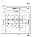
- FIG. 1 is a plan view showing an example of a configuration of a light emitting/receiving device according to a first embodiment of the present disclosure
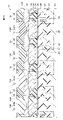
- FIG. 2 is a cross-sectional view taken along line II-II of FIG. 1
- FIG. 1 is a schematic diagram showing an example of a circuit configuration of a light emitting/receiving device according to a first embodiment of the present disclosure
- FIG. It is a block diagram which shows an example of a structure of a light reception/emission processing apparatus.
- 4 is a time chart for explaining an example of the operation of the light receiving/emitting processing device
- FIG. 4 is a cross-sectional view for explaining a first operation mode
- FIG. 5 is a cross-sectional view for explaining a second operation mode
- FIG. 10 is a cross-sectional view showing an example of a configuration of a light emitting/receiving device according to a second embodiment of the present disclosure
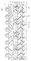
- FIG. 10 is a cross-sectional view showing an example of a configuration of a light emitting/receiving device according to Modification 1
- FIG. 11 is a cross-sectional view showing an example of a configuration of a light emitting/receiving device according to Modification 2
- FIG. 11 is a cross-sectional view showing an example of a configuration of a light emitting/receiving device according to Modification 3
- FIG. 12 is a cross-sectional view showing an example of a configuration of a light receiving and emitting device according to Modification 4
- FIG. 11 is a cross-sectional view showing an example of a configuration of a light emitting/receiving device according to Modification 5;
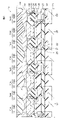
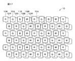
- FIG. 21 is a plan view showing an example of a configuration of a light emitting/receiving device according to Modification 6;
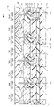
- 19 is a plan view showing an example of the configuration of a light emitting/receiving device according to Modification 7.
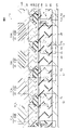
- FIG. 19 is a plan view showing an example of the configuration of a light emitting/receiving device according to Modification 7.
- FIG. 19 is a plan view showing an example of the configuration of a light emitting/receiving device according to Modification 7.
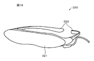
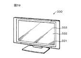
- FIG. It is a perspective view of an example of the appearance of a head mounted display. It is a perspective view showing an example of the appearance of a display.
- FIG. 1 is a plan view showing an example of the configuration of a light emitting/receiving device 10 according to the first embodiment of the present disclosure.
- FIG. 2 is a cross-sectional view taken along line II--II of FIG.
- the light emitting/receiving device 10 includes a plurality of light emitting portions 11B, a plurality of light emitting portions 11G, a plurality of light emitting portions 11R, a plurality of light emitting portions 11IR, a plurality of light receiving portions 12B, and a plurality of light receiving portions 11B, 11G, 11R and 11IR. It includes a portion 12G, a plurality of light receiving portions 12R, and a plurality of light receiving portions 12IR.
- the light emitting/receiving device 10 can perform both image display and image pickup.
- the light emitting/receiving device 10 may be a microdisplay with an imaging function.
- the light receiving and emitting device 10 may be provided in a VR (Virtual Reality) device, an MR (Mixed Reality) device, an AR (Augmented Reality) device, or the like.
- the drive substrate 21 side of the light emitting/receiving device 10 is the bottom side, and the side opposite to the driving substrate 21 side of the light emitting/receiving device 10 is the top side.
- the light emitting/receiving device 10 has a surface for emitting and receiving light (hereinafter referred to as “light receiving/emitting surface”) on the top side.
- the light receiving/emitting surface has a rectangular shape.
- the longitudinal direction of the light emitting/receiving surface is called the horizontal direction
- the short direction of the light emitting/receiving surface is called the vertical direction.
- the top surface of the light emitting/receiving device 10 is referred to as a first surface, and the surface opposite to the bottom side of the light emitting/receiving device 10 is referred to as a second surface.
- Each of the light emitting portion 11B, the light emitting portion 11G, and the light emitting portion 11R constitutes a sub-pixel for image display.
- the light emitting unit 11IR constitutes an infrared light emitting unit that emits infrared light.
- the light emitting unit 11IR is used, for example, for line-of-sight detection or distance measurement (distance measurement between the light emitting/receiving device 10 and an object).
- the light emitting portions 11B, 11G, 11R, and 11IR have different peak emission wavelengths. Specifically, the light emitting units 11B, 11G, 11R, and 11IR emit blue light, green light, red light, and infrared light, respectively.
- the light emitting units 11B, 11G, 11R, and 11IR are collectively referred to as the light emitting units 11 without any particular distinction.
- the plurality of light-emitting units 11 are two-dimensionally arranged in a predetermined arrangement pattern separated in the in-plane direction of the light-receiving and emitting surface.
- a combination of three adjacent light emitting portions 11B, 11G, and 11R constitutes one pixel (one pixel) 11A.
- the light emitting unit 11IR is arranged adjacent to each pixel 11A at a rate of one for one pixel 11A.
- the arrangement of the light emitting unit 11IR is not limited to this example, and may be arranged adjacent to a block of the two or more pixels 11A at a rate of one for two or more pixels 11A.
- the plurality of light-emitting portions 11B, 11G, and 11R constituting the plurality of sub-pixels may be arranged in stripes, as shown in FIG. 1, for example.
- the plurality of light emitting units 11IR are arranged at regular intervals in the horizontal direction.
- the light-emitting portion 11B is composed of the light-emitting element 13 and a blue colored layer 34B facing the light-emitting element 13 .
- the light-emitting portion 11G is composed of the light-emitting element 13 and a green colored layer 34G facing the light-emitting element 13 .
- the light emitting section 11R is composed of a light emitting element 13 and a red colored layer 34R facing the light emitting element 13. As shown in FIG.
- the light-emitting portion 11IR is composed of the light-emitting element 13 facing the light-emitting element 13 and the infrared light transmission layer 34IR.
- the light emitting element 13 is configured to emit at least white light and infrared light.
- the plurality of light emitting elements 13 are two-dimensionally arranged separated in the in-plane direction of the light emitting/receiving surface in a prescribed arrangement pattern.
- An element separation portion 13A is provided between adjacent light emitting elements 13 .
- the light emitting element 13 is composed of a first electrode 29 , an organic EL layer 31 and a second electrode 32 .
- the light receiving sections 12B, 12G, and 12R respectively constitute sub-pixels for imaging.
- the light receiving section 12IR constitutes an infrared light receiving section that receives infrared light.
- the light receiving unit 12IR is used, for example, together with the light emitting unit 11IR for line-of-sight detection or distance measurement (distance measurement between the light emitting/receiving device 10 and an object).
- the light receiving section 12IR may constitute a sub-pixel for imaging an infrared image.
- the light receiving sections 12B, 12G, 12R, and 12IR have different peak sensitivity wavelengths.
- the light receiving units 12B, 12G, 12R, and 12IR are configured to detect blue light, green light, red light, and infrared light, respectively.
- the light receiving sections 12B, 12G, 12R, and 12IR are collectively referred to as the light receiving section 12 without any particular distinction.
- the plurality of light receiving units 12 are two-dimensionally arranged in the in-plane direction of the light receiving/emitting surface in a prescribed arrangement pattern.
- the plurality of light receiving sections 12 may be arranged in the same two-dimensional arrangement pattern as the plurality of light emitting sections 11 .
- a combination of three adjacent light receiving portions 12B, 12G, and 12R constitutes one pixel.
- the light receiving section 12IR is arranged adjacent to each pixel at a rate of one per one pixel.
- the arrangement of the light receiving sections 12IR is not limited to this example, and may be arranged adjacent to a block of two or more pixels at a rate of one for two or more pixels.
- a plurality of light-receiving portions 12B, 12G, and 12R forming a plurality of sub-pixels are arranged, for example, in a stripe shape as shown in FIG.
- the plurality of light emitting units 11IR are arranged at regular intervals in the horizontal direction.
- the light receiving section 12B is composed of the light receiving element 14 and a blue colored layer 34B covering the light receiving element 14.
- the light receiving section 12G is composed of a light receiving element 14 and a green colored layer 34G covering the light receiving element 14.
- the light-receiving section 12R is composed of a light-receiving element 14 and a red colored layer 34R covering the light-receiving element 14.
- the light receiving section 12IR is composed of a light receiving element 14 and an infrared light transmission layer 34IR covering the light receiving element 14. As shown in FIG.
- the light receiving element 14 is configured to detect at least white light and infrared light. Further, the light receiving element 14 is configured to be capable of receiving light emitted from the light emitting element 13 positioned near the light receiving element 14 and external light. The light-emitting element 13 positioned near the light-receiving element 14 may be one of the light-emitting elements 13 positioned closest to the light-receiving element 14 .
- the light receiving element 14 is composed of, for example, a MOS (Metal Oxide Semiconductor) structure transistor (MOS-TFT, etc.).
- MOS-TFT Metal Oxide Semiconductor
- the plurality of light receiving elements 14 are two-dimensionally arranged in the in-plane direction of the light receiving/emitting surface in a prescribed arrangement pattern.
- Each light-receiving element 14 faces an inter-element isolation portion 13A between two adjacent light-emitting elements 13 .
- the light-receiving element 14 Assuming a plane that divides the light-receiving element 14 into two adjacent light-emitting elements 13, one element-side portion, and the other element-side portion of the two adjacent light-emitting elements 13, the light-receiving element 14 is: As shown in FIG. 2, it may have symmetry with respect to the plane.
- each light receiving element 14 in the in-plane direction of the light receiving/emitting surface may be shifted in at least one of the horizontal direction and the vertical direction from the arrangement position of each light emitting element 13 in the in-plane direction of the light emitting/receiving surface.
- the light receiving element 14 is composed of a gate electrode 22 , a gate insulating layer 23 , a semiconductor layer 24 , a source electrode 25 and a drain electrode 26 .
- Layer structure An example of the layer configuration of the light emitting and receiving device 10 according to the first embodiment of the present disclosure will be described below with reference to FIG. 2 .
- the light emitting/receiving device 10 includes a driving substrate 21, a plurality of gate electrodes 22, a gate insulating layer 23, a plurality of semiconductor layers 24, a plurality of source electrodes 25, a plurality of drain electrodes 26, an interlayer insulating layer 27, A planarization layer 28 , a plurality of first electrodes 29 , an insulating layer 30 , an organic EL layer 31 , a second electrode 32 , a protective layer 33 and a color filter 34 are provided. Note that the planarization layer 28 is provided as necessary, and may not be provided.
- the drive board 21 is a so-called backplane.
- the drive substrate 21 includes, for example, a substrate, various circuits, an insulating layer, and the like (none of which are shown).
- the substrate is for arranging a plurality of light emitting elements 13, a plurality of light receiving elements 14, various circuits, and the like.
- the substrate may be made of, for example, a semiconductor that facilitates the formation of transistors or the like, or may be made of glass or resin with low permeability to moisture and oxygen.
- the substrate may be a semiconductor substrate, a glass substrate, a resin substrate, or the like.
- Semiconductor substrates include, for example, amorphous silicon, polycrystalline silicon, monocrystalline silicon, or the like.
- Glass substrates include, for example, high strain point glass, soda glass, borosilicate glass, forsterite, lead glass, or quartz glass.
- the resin substrate contains, for example, at least one selected from the group consisting of polymethyl methacrylate, polyvinyl alcohol, polyvinyl phenol, polyethersulfone, polyimide, polycarbonate, polyethylene terephthalate and polyethylene naphthalate.
- Various circuits are provided on the first surface of the substrate.
- Various circuits include, for example, a drive circuit and a power supply circuit.
- the driving circuit drives the plurality of light emitting elements 13 and the plurality of light receiving elements 14 .
- the power supply circuit supplies power to the plurality of light emitting elements 13 and the plurality of light receiving elements 14 .
- the insulating layer is provided on the first surface of the substrate so as to cover various circuits.
- the insulating layer provides insulation between various circuits and the plurality of light receiving elements 14 .
- the insulating layer also planarizes the first surface of the substrate on which various circuits are provided.
- the plurality of gate electrodes 22 are two-dimensionally arranged on the first surface of the driving substrate 21 in a prescribed arrangement pattern such as a matrix.
- the gate electrode 22 is connected to a drive circuit.
- the gate electrode 22 contains, for example, a metal material such as molybdenum.
- a gate insulating layer 23 is provided on the first surface of the driving substrate 21 so as to cover the plurality of gate electrodes 22 .
- the gate insulating layer 23 provides insulation between the gate electrode 22 and the semiconductor layer 24 .
- the gate insulating layer 23 contains, for example, at least one selected from the group consisting of silicon oxide (SiO x ), silicon nitride (SiN x ), silicon oxynitride (SiO x N y ), and the like.
- the semiconductor layer 24 is provided on the first surface of the gate insulating layer 23 and faces the gate electrode 22 .
- Semiconductor layer 24 has a source region, a drain region, and a channel region. A channel region is sandwiched between the source and drain regions. The channel region is, for example, a photoactive layer that generates electron-hole pairs upon incidence (irradiation) of light.
- the source region and the drain region are each formed, for example, by introducing (implanting) impurities.
- Semiconductor layer 24 includes, for example, silicon or an oxide semiconductor. Silicon includes, for example, amorphous silicon (a-Si), polycrystalline silicon (p-Si) or microcrystalline silicon ( ⁇ -Si).
- the oxide semiconductor includes, for example, indium gallium zinc oxide (InGaZnO (IGZO)).
- the source electrode 25 is provided on the source region of the semiconductor layer 24 .
- a drain electrode 26 is provided on the drain region of the semiconductor layer 24 .
- a space is provided between the source electrode 25 and the drain electrode 26 .
- the source electrode 25 and drain electrode 26 are connected to a drive circuit.
- the source electrode 25 and the drain electrode 26 contain, for example, a metal material such as aluminum (Al).
- the interlayer insulating layer 27 is provided on the first surface of the gate insulating layer 23 so as to cover the plurality of semiconductor layers 24 .
- the interlayer insulating layer 27 provides insulation between the light emitting element 13 and the light receiving element 14 .
- the interlayer insulating layer 27 may have, for example, a single layer structure or a laminated structure.
- the interlayer insulating layer 27 may be an organic insulating layer, an inorganic insulating layer, or a laminate of these layers.
- the organic insulating layer contains, for example, at least one selected from the group consisting of polyimide-based resins, acrylic-based resins, novolak-based resins, and the like.
- the inorganic insulating layer contains, for example, at least one selected from the group consisting of silicon oxide (SiO 2 ), silicon nitride (SiN), silicon oxynitride (SiON), and the like.
- the planarization layer 28 is provided on the first surface of the interlayer insulating layer 27 .
- the planarizing layer 28 covers the source electrode 25 and the drain electrode 26 projecting from the first surface of the interlayer insulating layer 27 and planarizes the first surface of the interlayer insulating layer 27 .
- the planarizing layer 28 may be, for example, an organic insulating layer or an inorganic insulating layer.
- the organic insulating layer the same material as the organic insulating layer of the interlayer insulating layer 27 can be exemplified.
- As the inorganic insulating layer the same material as the inorganic insulating layer of the interlayer insulating layer 27 can be exemplified.
- the plurality of first electrodes 29 are two-dimensionally arranged on the first surface of the planarization layer 28 in a prescribed arrangement pattern such as a matrix.
- the first electrode 29 is the anode.
- a voltage is applied between the first electrode 29 and the second electrode 32 , holes are injected from the first electrode 29 into the organic EL layer 31 .
- Adjacent first electrodes 29 are electrically separated by an insulating layer 30 .
- the first electrode 29 may be composed of, for example, a metal layer, or may be composed of a metal layer and a transparent conductive oxide layer.
- the transparent conductive oxide layer is an organic layer. It is preferably provided on the EL layer 31 side.
- the metal layer also functions as a reflective layer that reflects light generated in the organic EL layer 31 .
- the metal layer is, for example, chromium (Cr), gold (Au), platinum (Pt), nickel (Ni), copper (Cu), molybdenum (Mo), titanium (Ti), tantalum (Ta), aluminum (Al). , magnesium (Mg), iron (Fe), tungsten (W) and silver (Ag).
- the metal layer may contain the at least one metal element as a constituent element of an alloy. Specific examples of alloys include aluminum alloys and silver alloys. Specific examples of aluminum alloys include AlNd and AlCu.
- a base layer may be provided adjacent to the second surface side of the metal layer.
- the underlayer is for improving the crystal orientation of the metal layer when the metal layer is formed.
- the underlayer contains, for example, at least one metal element selected from the group consisting of titanium (Ti) and tantalum (Ta).
- the underlayer may contain the at least one metal element as a constituent element of the alloy.
- the transparent conductive oxide layer contains a transparent conductive oxide.
- Transparent conductive oxides include, for example, transparent conductive oxides containing indium (hereinafter referred to as “indium-based transparent conductive oxides”) and transparent conductive oxides containing tin (hereinafter referred to as “tin-based transparent conductive oxides”). ”) and transparent conductive oxides containing zinc (hereinafter referred to as “zinc-based transparent conductive oxides”).
- Indium-based transparent conductive oxides include, for example, indium tin oxide (ITO), indium zinc oxide (IZO), indium gallium oxide (IGO), indium gallium zinc oxide (IGZO), or fluorine-doped indium oxide (IFO).
- ITO indium tin oxide
- ITO indium tin oxide
- Tin-based transparent conductive oxides include, for example, tin oxide, antimony-doped tin oxide (ATO), or fluorine-doped tin oxide (FTO).
- Zinc-based transparent conductive oxides include, for example, zinc oxide, aluminum-doped zinc oxide (AZO), boron-doped zinc oxide, or gallium-doped zinc oxide (GZO).
- the insulating layer 30 is provided on the first surface of the drive substrate 21 in a portion between the adjacent first electrodes 29 (that is, the element isolation portion 13A).
- the insulating layer 30 provides insulation between adjacent first electrodes 29 .
- the insulating layer 30 has a plurality of openings 30A.
- a plurality of openings 30 ⁇ /b>A are provided corresponding to each light emitting section 11 . More specifically, each of the plurality of openings 30A is provided on the first surface (surface on the organic EL layer 31 side) of each first electrode 29 .
- the first electrode 29 and the organic EL layer 31 are in contact with each other through the opening 30A.
- the insulating layer 30 may cover the first electrode 29 from the peripheral portion of the first surface of the first electrode 29 to the side surface (end surface).
- the peripheral portion of the first surface refers to a region having a predetermined width inward from the peripheral edge of the first surface.
- the insulating layer 30 may be an organic insulating layer, an inorganic insulating layer, or a laminate of these layers.
- the organic insulating layer contains, for example, at least one selected from the group consisting of polyimide-based resins, acrylic-based resins, novolak-based resins, and the like.
- the inorganic insulating layer contains, for example, at least one selected from the group consisting of silicon oxide (SiO x ), silicon nitride (SiN x ), silicon oxynitride (SiO x N y ), and the like.
- the organic EL layer 31 is provided between the first electrode 29 and the second electrode 32 .
- the organic EL layer 31 is provided continuously over all the light emitting elements 13 within the light receiving and emitting region, and is a layer common to all the light emitting portions 11 within the light receiving and emitting region.
- the organic EL layer 31 is an example of an organic layer including a light-emitting layer.
- the organic EL layer 31 is configured to emit at least white light and infrared light.
- the organic EL layer 31 includes single-layer light-emitting units. It may be an organic EL layer with a 1-stack structure, an organic EL layer with a 2-stack structure including two layers of light-emitting units, or an organic EL layer with a structure other than these.
- the organic EL layer 31 may include a blue light emitting layer, a green light emitting layer, a red light emitting layer and an infrared light emitting layer as light emitting layers, or may include a blue light emitting layer, a green light emitting layer and a red/infrared light emitting layer. or a blue light-emitting layer, a yellow light-emitting layer and an infrared light-emitting layer.
- the blue light-emitting layer, the green light-emitting layer, the red light-emitting layer, the yellow light-emitting layer, and the infrared light-emitting layer each emit holes injected from the first electrode 29 and holes injected from the second electrode 32 by applying an electric field. Recombination with the electrons that have been removed occurs, and blue light, green light, red light, yellow light, and infrared light are generated. In the red/infrared light emitting layer, when an electric field is applied, recombination of holes injected from the first electrode 29 and electrons injected from the second electrode 32 occurs, and red light and infrared light are emitted. It occurs.
- the second electrode 32 is provided facing the plurality of first electrodes 29 .
- the second electrode 32 is provided continuously over all the light emitting portions 11 within the light receiving/emitting region, and serves as a common electrode for all the light emitting portions 11 within the light emitting/receiving region.
- the second electrode 32 is the cathode.
- When a voltage is applied between the first electrode 29 and the second electrode 32 electrons are injected from the second electrode 32 into the organic EL layer 31 .
- the second electrode 32 is a transparent electrode that transmits light generated in the organic EL layer 31 . It is preferable that the second electrode 32 is made of a material having a high transmittance and a small work function as much as possible in order to increase the luminous efficiency.
- the second electrode 32 is composed of, for example, at least one layer of a metal layer and a transparent conductive oxide layer. More specifically, the second electrode 32 is composed of a single layer film of a metal layer or a transparent conductive oxide layer, or a laminated film of a metal layer and a transparent conductive oxide layer.
- the metal layer may be provided on the organic EL layer 31 side, or the transparent conductive oxide layer may be provided on the organic EL layer 31 side. From the viewpoint of placing a layer having a low work function adjacent to the organic EL layer 31, the metal layer is preferably provided on the organic EL layer 31 side.
- the metal layer contains, for example, at least one metal element selected from the group consisting of magnesium (Mg), aluminum (Al), silver (Ag), calcium (Ca) and sodium (Na).
- the metal layer may contain the at least one metal element as a constituent element of an alloy. Specific examples of alloys include MgAg alloys, MgAl alloys, AlLi alloys, and the like.
- the transparent conductive oxide layer includes a transparent conductive oxide. As the transparent conductive oxide, the same material as the transparent conductive oxide of the first electrode 29 can be exemplified.
- a protective layer 33 is provided on the first surface of the second electrode 32 and covers the plurality of light emitting elements 13 .
- the protective layer 33 shields the plurality of light-emitting elements 13 and the plurality of light-receiving elements 14 from the outside air, and suppresses the entry of moisture into the plurality of light-emitting elements 13 from the external environment.
- the protective layer 33 may have a function of suppressing oxidation of this metal layer.
- the protective layer 33 contains, for example, a low hygroscopic inorganic material or polymer resin.
- the protective layer 33 may have a single layer structure or a multilayer structure. When the thickness of the protective layer 33 is to be increased, it is preferable to have a multilayer structure. This is for alleviating the internal stress in the protective layer 33 .
- the inorganic material is, for example, selected from the group consisting of silicon oxide (SiO x ), silicon nitride (SiN x ), silicon oxynitride (SiO x N y ), titanium oxide (TiO x ) and aluminum oxide (AlO x ). contains at least one Polymer resins include, for example, at least one selected from the group consisting of thermosetting resins, ultraviolet-curable resins, and the like.
- a color filter 34 is provided on the first surface of the protective layer 33 .
- the color filter 34 is an on-chip color filter (OCCF).
- the color filter 34 includes, for example, a plurality of blue colored layers 34B, a plurality of green colored layers 34G, a plurality of red colored layers 34R, and a plurality of infrared light transmission layers 34IR. Blue, green, and red are examples of first, second, and third colors, respectively.
- Each of the plurality of colored layers 34B, 34G, and 34R faces a portion of the plurality of light emitting elements 13. As shown in FIG.
- Each of the multiple infrared light transmission layers 34IR faces the rest of the multiple light emitting elements 13 .
- the blue colored layer 34B is provided facing the light emitting element 13 that constitutes the light emitting section 11B.
- the colored layer 34B covers the light receiving element 14 located near the light emitting element 13 facing the colored layer 34B.
- the colored layer 34B may cover one of the light receiving elements 14 closest to the light emitting element 13 facing the colored layer 34B.
- the green colored layer 34G is provided facing the light emitting element 13 that constitutes the light emitting section 11G.
- the colored layer 34G covers the light receiving element 14 located near the light emitting element 13 facing the colored layer 34G.
- the colored layer 34G may cover one of the light receiving elements 14 closest to the light emitting element 13 facing the colored layer 34G.
- the red colored layer 34R is provided facing the light emitting element 13 that constitutes the light emitting section 11R.
- the colored layer 34R covers the light receiving element 14 located near the light emitting element 13 facing the colored layer 34R.
- the colored layer 34R may cover one of the light receiving elements 14 closest to the light emitting element 13 facing the colored layer 34R.
- the infrared light transmission layer 34IR is provided facing the light emitting element 13 that constitutes the light emitting section 11IR.
- the infrared light transmission layer 34IR covers the light receiving element 14 located near the light emitting element 13 facing the infrared light transmission layer 34IR.
- the infrared light transmission layer 34IR may cover one of the light receiving elements 14 closest to the light emitting element 13 facing the infrared light transmission layer 34IR.
- the blue colored layer 34B transmits blue light contained in light emitted from the light emitting element 13 or outside light, and absorbs light other than blue light.
- the green colored layer 34G transmits green light contained in light emitted from the light emitting element 13 or outside light, and absorbs light other than green light.
- the red colored layer 34R transmits red light contained in light emitted from the light emitting element 13 or outside light, and absorbs light other than red light.
- the infrared light transmission layer 34IR transmits infrared light contained in the light emitted from the light emitting element 13 or outside light, and absorbs light other than infrared light.
- FIG. 3 is a schematic diagram showing an example of the circuit configuration of the light emitting/receiving device 10 according to the first embodiment of the present disclosure.
- the light emitting/receiving device 10 has a light emitting/receiving region 40A and a peripheral region 40B provided around the periphery of the light emitting/receiving region 40A.
- a plurality of light emitting units 11 and a plurality of light receiving units 12 are two-dimensionally arranged in the light receiving/emitting region 40A.
- a signal line driving circuit 41 and a scanning line driving circuit 42, which are drivers for image display, are provided in the peripheral region 40B.
- a light receiving signal reading circuit 43 and a light receiving driving circuit 44 which are drivers for imaging, are provided in the peripheral region 40B.
- the signal line driving circuit 41 and the scanning line driving circuit 42 are circuits for driving light emission. Specifically, the plurality of light emitting units 11 are sequentially selected and a video signal voltage based on the video signal is written to the selected light emitting units 11, thereby driving the plurality of light emitting units 11 to emit light.
- the signal line driving circuit 41 supplies the signal voltage of the video signal corresponding to the luminance information supplied from the signal supply source (not shown) to the selected light emitting section 11 via the signal line 41A.
- the scanning line drive circuit 42 is composed of a shift register or the like that sequentially shifts (transfers) start pulses in synchronization with input clock pulses.
- the scanning line drive circuit 42 scans each row when writing video signals to the light emitting portions 11, and sequentially supplies scanning signals to the scanning lines 42A.
- the light receiving signal readout circuit 43 and the light receiving drive circuit 44 are circuits for performing light receiving drive.
- the light reception driving circuit 44 sequentially applies light reception control pulses to the plurality of scanning lines 44A, the plurality of power lines 44B, and the plurality of gate lines 44C. Thereby, the light receiving operation (light detection operation) of each light receiving unit 112 is controlled.
- the scanning line 44A, the power supply line 44B and the gate line 44C are simply shown as one line.
- the light-receiving signal readout circuit 43 is a circuit for reading out each light-receiving signal output from a plurality of signal lines 43A as light-receiving signal lines.
- FIG. 4 is a block diagram showing an example of the configuration of the light receiving/emitting processing device 50.
- the light receiving and emitting device 10 further includes a light receiving and emitting processing device 50 .
- the light receiving/emitting processing device 50 includes a controller 51 , a calculator 52 and a luminance corrector 53 .
- the control unit 51 controls the operation of light emission and light reception of the light emitting/receiving device 10 .
- the control unit 51 controls driving of the plurality of light emitting elements 13 (that is, the plurality of light emitting units 11) by controlling the signal line driving circuit 41 and the scanning line driving circuit 42.
- the control unit 51 controls driving of the plurality of light receiving elements 14 (that is, the plurality of light receiving units 12) by controlling the light receiving signal readout circuit 43 and the light receiving drive circuit 44.
- Table 1 shows an operation example of the control unit 51 .
- “light emission ON” means that the light emitting element 13 is driven to emit light from the light emitting element 13 .
- light receiving ON means that the light receiving element 14 is driven and the light receiving signal is read out.
- the control unit 51 has, for example, a first operation mode, a second operation mode, and a third operation mode, and performs control according to each operation mode.
- first operation mode luminance correction of the light emitting element 13 is performed based on the deterioration amount of the light emitting element 13 .
- second operation mode luminance correction of the light emitting element 13 is performed based on the amount of external light.
- third mode of operation imaging is performed.
- the controller 51 may further have a fourth operation mode. In a fourth mode of operation, user gaze detection is performed.
- the calculation unit 52 calculates the amount of deterioration of the light emitting element 13 or the amount of external light under the control of the control unit 51 and outputs the calculation result to the luminance correction unit 53 .
- the calculator 52 includes a deterioration amount calculator 52A and an external light amount calculator 52B.
- the operation of the calculator 52 differs depending on the operation mode.
- the deterioration amount calculator 52A calculates the deterioration amount of the light emitting element 13 based on the control of the controller 51, and controls the luminance corrector 53 based on the calculation result.
- the outside light amount calculator 52B calculates the outside light amount based on the control of the control unit 51, and controls the brightness correction unit 53 based on the calculation result.
- neither the deterioration amount calculator 52A nor the external light amount calculator 52B performs the calculation operation.
- the luminance correction unit 53 adjusts the luminance level of the video signal based on the calculation result output from the calculation unit 52 and outputs the video signal to the signal line driving circuit 41 .
- the correction control of the luminance corrector 53 may be feedback control.
- FIG. 5 is a time chart for explaining an example of the operation of the light receiving/emitting processing device 50.
- the control unit 51 controls driving of the plurality of light emitting elements 13 so as to alternately repeat the effective display period and the blanking period.
- the control unit 51 sets the operation mode to the first operation mode, displays an image using the plurality of light emitting units 11, and based on the calculation results of the deterioration amounts of the plurality of light emitting elements 13, sets the plurality of light emitting elements 13.
- brightness correction of the light emitting unit 11 that is, brightness correction of the plurality of light emitting elements 13
- the control unit 51 sets the operation mode to the third operation mode, and the multiple light receiving units 12 perform imaging.
- control unit 51 sets the operation mode to the second operation mode, and corrects the luminance of the plurality of light emitting units 11 (that is, corrects the luminance of the plurality of light emitting elements 13) based on the calculation result of the amount of external light. ) may be performed.
- FIG. 6 An example of the operation of the light receiving/emitting processing device 50 in each operation mode will be described below with reference to FIGS. 6 and 7.
- FIG. 6 An example of the operation of the light receiving/emitting processing device 50 in each operation mode will be described below with reference to FIGS. 6 and 7.
- the light receiving/emitting processing device 50 operates as follows.
- the control unit 51 controls the signal line driving circuit 41 and the scanning line driving circuit 42 to drive the plurality of light emitting elements 13 to emit light.
- emitted light L1 emitted from the plurality of light emitting elements 13 is received by the plurality of light receiving elements 14 as shown in FIG.
- the control unit 51 drives the light receiving signal readout circuit 43 and the light receiving drive circuit 44, and reads light receiving signals corresponding to the received light amount of the emitted light L1 from the plurality of light receiving elements 14 via the light receiving signal readout circuit 43.
- the deterioration amount calculator 52A calculates the deterioration amounts of the plurality of light emitting elements 13 based on the light receiving signals supplied from the plurality of light receiving elements 14 via the light receiving signal readout circuit 43, and outputs the calculation results to the brightness correction section 53. do.
- the luminance correction unit 53 increases the luminance level of the video signal based on the calculation result output from the deterioration amount calculation unit 52A so that the level of the received light signal supplied from the light receiving element 14 falls within a specified range, Output to the signal line drive circuit 41 .
- the correction control of the luminance corrector 53 may be feedback control.
- the light receiving/emitting processing device 50 operates as follows.
- the plurality of light receiving elements 14 receive external light L2 as shown in FIG.
- the control unit 51 drives the light reception signal readout circuit 43 and the light reception drive circuit 44 to read light reception signals corresponding to the amount of received external light L2 from the plurality of light receiving elements 14 via the light reception signal readout circuit 43 .
- the external light amount calculation unit 52B calculates the amount of external light based on the received light signal supplied via the light receiving signal readout circuit 43, and outputs the calculation result to the luminance correction unit 53.
- the luminance correction unit 53 adjusts the luminance level of the video signal based on the calculation result output from the external light amount calculation unit 52B, and outputs the video signal to the signal line driving circuit 41 .
- the light receiving/emitting processing device 50 operates as follows.
- the plurality of light receiving elements 14 receive external light L2 as shown in FIG.
- the control unit 51 drives the light reception signal readout circuit 43 and the light reception drive circuit 44 to read light reception signals corresponding to the amount of received external light L2 from the plurality of light receiving elements 14 via the light reception signal readout circuit 43 .
- the deterioration amount calculation unit 52A and the external light amount calculation unit 52B output the received light signal supplied from the received light signal reading circuit 43 to an external device without performing the above described deterioration amount calculation operation and the above described external light amount calculation operation. do.
- the light receiving/emitting processing device 50 operates as follows.
- the control unit 51 controls the signal line driving circuit 41 and the scanning line driving circuit 42 to drive the plurality of light emitting elements 13 to cause the plurality of light emitting portions 11 to emit light.
- a pupil is irradiated with this emitted light, and the reflected light is received by a plurality of light receiving elements 14 .
- the control unit 51 drives the received light signal readout circuit 43 and the received light drive circuit 44, reads received light signals corresponding to the amount of received light from the plurality of light receiving elements 14 via the received light signal readout circuit 43, and acquires an image of the pupil.
- the control unit 51 detects the line of sight of the user based on the acquired image.
- the image acquired by the control unit 51 may be output to an external device, and the external device receiving the image may detect the line of sight.
- a known method can be used as a method for detecting the line of sight from the image.
- a metal layer is formed on the first surface of the driving substrate 21 by, for example, sputtering, and then the metal layer is patterned by, for example, photolithography technology and etching technology. Thereby, a plurality of gate electrodes 22 are formed.
- a gate insulating layer 23 is formed on the first surface of the driving substrate 21 so as to cover the plurality of gate electrodes 22 by, for example, CVD (Chemical Vapor Deposition).
- a plurality of source regions, a plurality of drain regions, and a plurality of channel regions are formed in the semiconductor layer by, for example, doping.
- the semiconductor layer is patterned by, for example, photolithography technology and etching technology.
- a plurality of semiconductor layers 24 are obtained.
- the metal layer is patterned by, for example, photolithography technology and etching technology.
- a plurality of source electrodes 25 and a plurality of drain electrodes 26 are formed.
- an interlayer insulating layer 27 is formed on the first surface of the gate insulating layer 23 so as to cover the plurality of semiconductor layers 24 by, for example, CVD (Chemical Vapor Deposition).
- CVD Chemical Vapor Deposition
- the surface of the inorganic insulating layer is polished and planarized by, for example, CMP (Chemical Mechanical Polishing). Thereby, a planarization layer 28 is formed.
- the metal layer is patterned by, for example, photolithography technology and etching technology. Thereby, a plurality of first electrodes 29 are formed.
- an insulating layer 30 is formed on the first surface of the planarization layer 28 so as to cover the plurality of first electrodes 29 by, eg, CVD.
- openings 30A are formed in portions of the insulating layer 30 located on the first surfaces of the first electrodes 29 by photolithography and dry etching, for example.
- the organic EL layer 31 is formed on the first surfaces of the plurality of first electrodes 29 and the insulating layer 30 by, for example, vapor deposition.
- the second electrode 32 is formed on the first surface of the organic EL layer 31 by vapor deposition or sputtering, for example. Thereby, a plurality of light emitting elements 13 are formed on the first surface of the planarization layer 28 .
- a color filter 34 is formed on the first surface of the protective layer 33 by, for example, photolithography. Form. As described above, the light emitting/receiving device 10 shown in FIG. 2 is obtained.
- the light emitting/receiving device 10 includes multiple light emitting elements 13 and multiple light receiving elements 14 .
- the plurality of light emitting elements 13 are separated and two-dimensionally arranged.
- the plurality of light-receiving elements 14 are two-dimensionally arranged at different heights from the plurality of light-emitting elements 13 , and each light-receiving element 14 faces the element separation section 13 ⁇ /b>A between the light-emitting elements 13 . Accordingly, the light emitted from the light emitting element 13 can be emitted to the outside without being blocked by the light receiving element 14, and the light from the outside can be received without being blocked by the light emitting element 13. .
- both the emission of light to the outside by the light emitting element 13 and the reception of light from the outside by the light receiving element 14 can be performed. That is, both display and imaging can be performed.
- light emitted from the light emitting element 13 can also be received by the light receiving element 14 . That is, the deterioration amount of the light emitting element 13 can be detected.
- the blue colored layer 34B covers the light-emitting element 13 and the light-receiving element 14 located near the light-emitting element 13 .
- the green colored layer 34G covers the light emitting element 13 and the light receiving element 14 located near the light emitting element 13 .
- the red colored layer 34G covers the light emitting element 13 and the light receiving element 14 located near the light emitting element 13 .
- the infrared light transmission layer 34IR covers the light emitting element 13 and the light receiving element 14 positioned in the vicinity of the light emitting element 13 . This makes it possible to irradiate the pupil with infrared light and receive the reflected light. Therefore, line-of-sight detection can be performed using infrared light.
- each light receiving element 14 is arranged so as to face the inter-element isolation portion 13A between the light emitting elements 13, thereby detecting characteristics of the light emitting elements 13 (brightness correction). Both the function and the external light detection (imaging) function can be realized.
- the line of sight is detected by using the light receiving element 14 as a camera during a period in which the light emitting element 13 is inactive (a period in which the light emitting element 13 is not used for display such as blanking). can be done.
- the plurality of light emitting units 11 for displaying images and the plurality of light receiving units 12 for capturing images are arranged in the same region.
- a space for separately arranging a camera or the like becomes unnecessary. Therefore, the device can be miniaturized.
- the display optical axis optical axis perpendicular to the display surface
- the imaging optical axis optical axis perpendicular to the imaging surface
- the plurality of light emitting units 11 can also serve as light sources for the plurality of light receiving units 12 (imaging elements).
- imaging elements For example, when a plurality of light emitting units 11IR are used as light sources, the infrared light emitted from the plurality of light emitting units 11IR is invisible to humans, does not interfere with the field of view, and penetrates the melanin pigment of the eye. Therefore, a clearer image can be captured.
- the light emitting/receiving device 10 can use RGB images (the plurality of light emitting units 11R, 11G, and 11B) and IR images (the plurality of light emitting units 11IR) for line of sight detection, which is advantageous in terms of detection accuracy. .
- RGB images the plurality of light emitting units 11R, 11G, and 11B
- IR images the plurality of light emitting units 11IR
- FIG. 8 is a cross-sectional view showing an example of the configuration of the light emitting/receiving device 110 according to the second embodiment of the present disclosure.
- Light receiving/emitting device 110 includes a plurality of light emitting units 111B, 111G, 111R, 111IR and a plurality of light emitting units 111B, 111G, 111R, 111IR and A plurality of light receiving portions 112 are provided.
- the organic EL layer 31 and the second electrode 32 instead of the insulating layer 30, the organic EL layer 31 and the second electrode 32 (see FIG. 2), the insulating layer 130, the plurality of organic EL layers 131B, 131G, 131R and 131IR and the plurality of A second electrode 132 is provided.
- An electrode 32 may be provided.
- the light emitting/receiving device 110 may include the protective layer 33 and the color filters 34 as in the first embodiment, or may not include the protective layer 33 and the color filters 34 as shown in FIG. good.
- symbol is attached
- the light emitting section 111B is composed of a light emitting element 113B.
- the light emitting element 113B is configured to emit blue light.
- the light emitting element 113B includes a first electrode 29, an organic EL layer 131B, and a second electrode 132 in this order.
- the light emitting section 111G is composed of a light emitting element 113G.
- the light emitting element 113G is configured to emit green light.
- 113 G of light emitting elements are provided with the 1st electrode 29, 131 G of organic EL layers, and the 2nd electrode 132 in this order.
- the light emitting section 111R is composed of a light emitting element 113R.
- the light emitting element 113R is configured to emit red light.
- 113 R of light emitting elements are equipped with the 1st electrode 29, 131 R of organic EL layers, and the 2nd electrode 132 in this order.
- the light emitting section 11IR is composed of a light emitting element 113IR.
- the light emitting element 113IR is configured to be capable of emitting infrared light.
- the light emitting element 113IR includes a first electrode 29, an organic EL layer 131IR, and a second electrode 132 in this order.
- the light emitting elements 113B, 113G, and 113R are examples of visible light emitting elements that emit visible light.
- the light emitting element 113IR is an example of an infrared light emitting element that emits infrared light.
- the light-emitting element 113B, the light-emitting element 113G, the light-emitting element 113R, and the light-emitting element 113IR are collectively referred to as the light-emitting element 113 without particular distinction.
- the organic EL layers 131B, 131G, 131R, and 131IR are collectively referred to as the organic EL layers 131 without particular distinction.
- the arrangement of the plurality of light emitting elements 113 is the same as the arrangement of the plurality of light emitting elements 13 in the first embodiment.
- the light receiving section 112 is composed of the light receiving element 14 .
- the plurality of light receiving portions 112 includes a plurality of light receiving portions configured to be capable of receiving blue light, a plurality of light receiving portions configured to be capable of receiving green light, and a plurality of light receiving portions configured to be capable of receiving red light. and a plurality of light receiving units configured to receive infrared light.
- the insulating layer 130 is provided between adjacent light emitting elements 113 to separate the adjacent light emitting elements 113 .
- the material of the insulating layer 130 is the same as the material of the insulating layer 30 in the first embodiment.
- the organic EL layer 131B is provided between the first electrode 29 and the second electrode 132 of the light emitting section 111B.
- the organic EL layer 131B is configured to emit blue light.
- the organic EL layer 131B is an example of an organic layer including a blue light emitting layer.
- the organic EL layer 131B has, for example, a hole injection layer, a hole transport layer, a blue light emitting layer, an electron transport layer, and an electron injection layer stacked in this order from the first electrode 29 toward the second electrode 132. configuration.
- the organic EL layer 131G is provided between the first electrode 29 and the second electrode 132 of the light emitting section 111G.
- the organic EL layer 131G is configured to emit green light.
- the organic EL layer 131G is an example of an organic layer including a green light emitting layer.
- the organic EL layer 131G has, for example, a hole injection layer, a hole transport layer, a green light emitting layer, an electron transport layer, and an electron injection layer stacked in this order from the first electrode 29 toward the second electrode 132. configuration.
- the organic EL layer 131R is provided between the first electrode 29 and the second electrode 132 of the light emitting section 111R.
- the organic EL layer 131R is configured to emit red light.
- the organic EL layer 131R is an example of an organic layer including a red light emitting layer.
- the organic EL layer 131R has, for example, a hole injection layer, a hole transport layer, a red light emitting layer, an electron transport layer, and an electron injection layer laminated in this order from the first electrode 29 toward the second electrode 132. configuration.
- the organic EL layer 131IR is provided between the first electrode 29 and the second electrode 132 included in the light emitting section 111IR.
- the organic EL layer 131IR is configured to emit infrared light.
- the organic EL layer 131IR is an example of an organic layer including an infrared light emitting layer.
- the organic EL layer 131IR includes, for example, a hole injection layer, a hole transport layer, an infrared light emitting layer, an electron transport layer, and an electron injection layer in this order from the first electrode 29 toward the second electrode 132. It has a laminated construction.
- the plurality of second electrodes 132 are two-dimensionally arranged in the in-plane direction of the light receiving/emitting surface in a prescribed arrangement pattern.
- the second electrode 132 faces the first electrode 29 with the organic EL layer 131 interposed therebetween.
- the function, layer structure, materials, etc. of the second electrode 132 are the same as those of the second electrode 32 in the first embodiment.
- the light emitting/receiving device 110 includes multiple light emitting elements 113 and multiple light receiving elements 14 .
- the plurality of light-emitting elements 113 are two-dimensionally arranged
- the plurality of light-receiving elements 14 are two-dimensionally arranged at different heights from the plurality of light-emitting elements 13, and each light-receiving element 14 is positioned between the light-emitting elements 113. It faces the separating portion 13A. Therefore, similarly to the light emitting/receiving device 10 according to the first embodiment, both the emission of light to the outside by the light emitting element 113 and the reception of light from the outside by the light receiving element 14 can be performed. That is, both display and imaging can be performed. In addition, light emitted from the light emitting element 113 can also be received by the light receiving element 14 . That is, the deterioration amount of the light emitting element 113 can be detected.
- the colored layers 34B, 34G, 34R and the infrared light transmission layer 34IR cover the light emitting element 13 and the light receiving element 14 located near the light emitting element 13.
- the configuration of the color filter 34 is not limited to this.
- the colored layers 34B, 34G, 34R and the infrared light transmission layer 34IR may not cover the light receiving element 14 located near the light emitting element 13 as shown in FIG.
- the color filter 34 may have a plurality of openings 34A, and the plurality of openings 34A may be provided facing each light receiving element 14, respectively.
- the light receiving section 12 is composed of the light receiving element 14 .
- a monochromatic image can be captured by receiving external light with the plurality of light receiving units 12 . Further, since the light receiving elements 14 are not covered with the colored layers 34B, 34G, 34R and the infrared light transmission layer 34IR, the detection sensitivity of the light receiving and emitting device 10 can be improved.
- each of the plurality of light-splitting layers 35 is provided facing each light-receiving element 14 .
- the light-receiving element 14 and the light-splitting layer 35 constitute the light-receiving section 12 .
- the plurality of spectral layers 35 have spectral characteristics suitable for the light receiving section 12 .
- the light-splitting layer 35 may be a colored layer of a predetermined color, or an infrared transmitting layer that transmits infrared light and absorbs light other than infrared light.
- a plurality of spectral layers may include a plurality of colored layers and a plurality of infrared transmission layers.
- the plurality of colored layers may include a plurality of blue colored layers, a plurality of green colored layers, and a plurality of red colored layers, or may include a plurality of monochromatic colored layers.
- the plurality of colored layers may be those used in color filters of image sensors.
- the color filter 34 includes a plurality of monochromatic colored layers (for example, a plurality of colored layers 34G) instead of the plurality of colored layers 34B, 34G, and 34R, and the plurality of spectral layers includes a plurality of blue colored layers and a plurality of blue colored layers.
- a green colored layer and a plurality of red colored layers may be included.
- an image can be displayed in a single color (for example, green), and an image can be captured in full colors of blue, green, and red.
- the color filter 34 includes a plurality of monochromatic colored layers, the color resolution of the monochromatic colored layers can be improved.
- the color filter 34 may include a plurality of colored layers 34B, 34G, and 34R, and the plurality of spectral layers may include a plurality of monochromatic colored layers (eg, a plurality of colored layers 34G).
- an image can be displayed in full colors of blue, green, and red, and an image can be captured in a single color (for example, green).
- the color resolution of the monochromatic colored layers can be improved.
- the center position of the light receiving element 14 coincides with the midpoint between two adjacent light emitting elements 13 in the in-plane direction of the light receiving/emitting surface.
- the center position of the light receiving element 14 may be displaced from the midpoint between the two adjacent light emitting elements 13 in the in-plane direction of the light receiving/emitting surface. That is, the light-receiving element 14 may be arranged so as to be biased toward one side of the two adjacent light-emitting elements 13 in the in-plane direction of the light-receiving and emitting surface. In this case, from the viewpoint of improving the sensitivity of the light receiving element 14, it is preferable that part of the light receiving region of the light receiving element 14 is positioned directly below the light emitting element 13 on the one side.
- the controller 51 can determine from which one of the two light-emitting elements 13 the light is incident based on the amount of light received (light-receiving signal).
- the light receiving element 14 is divided into two parts, one on one side of the two adjacent light emitting elements 13 and the other on the other side of the two adjacent light emitting elements 13. Assuming a plane, the light receiving element 14 is asymmetric with respect to the plane, but may be asymmetric with respect to the plane. Asymmetry is, for example, the asymmetry of the structure of the light receiving element 14 . Examples of structural asymmetry include at least one selected from the group consisting of electrode asymmetry, wiring density asymmetry, doping concentration asymmetry in the photodetector, electrode arrangement asymmetry, and the like. . FIG. 12 shows an example in which the heights of the source electrode 25 and the drain electrode 26 are asymmetric with respect to the plane.
- the light receiving sensitivity differs between the portion on one side of the two adjacent light emitting elements 13 and the portion on the other side of the two adjacent light emitting elements 13 . Therefore, based on the signal level output from the light receiving element 14, the control section 51 can determine from which one of the two light emitting elements 13 the light is incident.
- the organic EL layer 31 is provided continuously over all the light emitting elements 13 within the light receiving and emitting region, and is a layer common to all the light emitting units 11 within the light receiving and emitting region (see FIG. 2) has been described, but as shown in FIG. 13, the organic EL layer 31 may be divided between the adjacent light emitting elements 13 .
- the control unit 51 may sequentially change the lighting positions of the plurality of light emitting units 11IR to detect the line of sight. Specifically, the control unit 51 may control driving of the plurality of light emitting units 11 and the plurality of light receiving units 12 to detect the line of sight as described below. As shown in FIG. 14, the control unit 51 causes some of the plurality of light emitting units 11IR arranged in the light receiving/emitting region to emit light when an image is displayed by the plurality of light emitting units 11B, 11G, and 11R. The unit 11IR is turned on (light emission drive) to emit infrared light (illumination) invisible to the user. In FIG.
- the light-emitting units 11 shaded with slanted lines indicate the light-emitting units 11 that are lit (driving light emission), and the light-emitting units 11 that are not shaded are not lit (driving light emission).
- a light emitting portion 11 is shown.
- the part of the light-emitting units 11R that are lit is, for example, a prescribed number of light-emitting units 11IR arranged in the vertical direction or the horizontal direction.
- the control unit 51 captures an image of the line of sight using a plurality of light receiving units 12IR arranged outside the vicinity of the light emitting units 11IR (for example, other than the closest to the light emitting units 11IR).
- the light receiving sections 12IR with diagonal lines indicate the light receiving sections 12IR that are driven to receive light
- the light receiving sections 12IR that are not with diagonal lines indicate the light receiving sections 12IR that are not driven to receive light.
- the control unit 51 sequentially changes the part of the light-emitting units 11IR to be lit, and controls the light-receiving units 12IR arranged outside the part of the light-emitting units 11IR to receive the reflected light. , to control driving of the plurality of light emitting units 11IR and the plurality of light receiving units 12IR.
- the light receiving units 12B, 12G, and 12IR may be driven to receive light.
- the deterioration amount calculation unit 52A calculates the deterioration amount of the light emitting elements 13 included in the light receiving units 12B, 12G, and 12IR based on the light receiving signals output from the light receiving units 12B, 12G, and 12IR, and the calculation result is used as the luminance. You may output to the correction
- the control unit 51 may drive a plurality of light receiving units 12IR arranged in the vicinity of the lighted part of the light emitting units 11IR.
- the deterioration amount calculation unit 52A calculates the deterioration amount of the light emitting element 13 included in the light emitting unit 11IR based on the received light signals output from the plurality of light receiving units 12IR, and outputs the calculation result to the luminance correction unit 53.
- the lighting positions of the plurality of light emitting units 11IR are sequentially changed.
- the light emitting/receiving device 10 according to the first embodiment has been described as an example, but the above configuration can also be applied to the light emitting/receiving device 110 according to the second embodiment.
- the heights of the plurality of light emitting elements 13 and 113 from the first surface of the driving substrate 21 are equal to the heights of the plurality of light receiving elements 14 from the first surface of the driving substrate 21.
- the height of the plurality of light receiving elements 14 from the first surface of the drive substrate 21 is higher than the height of the plurality of light emitting elements 13, 113 from the first surface of the drive substrate 21.
- the light emitting/receiving device 110 may further include a protective layer and a color filter on the first surfaces of the plurality of second electrodes 132 and the insulating layer 130 .
- the color filter includes a plurality of blue colored layers, a plurality of green colored layers, a plurality of red colored layers and a plurality of infrared transmitting layers.
- the functions of the colored layers and the infrared transmission layer are the same as the functions of the colored layers 34B, 34G, 34R and the infrared transmission layer 34IR in the first embodiment.
- Each colored layer is provided to face the light receiving element 14 . Thereby, a full-color image can be captured.
- the infrared transmission layer is provided facing the light receiving element 14 .
- infrared light can be received by the light receiving element 14 .
- a colored layer of each color may be provided so as to face both the light emitting element 13 and the light receiving element 14 positioned closest to the light emitting element 13 .
- the infrared transmission layer may be provided so as to face both the light receiving element 14 and the light receiving element 14 located closest to the light emitting element 13 .
- the light emitting/receiving device 10 includes four types of light emitting units 11B, 11G, 11R, and 11IR each having a different peak emission wavelength.
- a light-emitting portion may be provided, or two or more types of light-emitting portions having different peak emission wavelengths may be provided.
- the light emitting/receiving device 10 may include any one of the light emitting units 11B, 11G, 11R, and 11IR. You may make it provide two or more types of light emission parts.
- the light emitting/receiving device 10 according to the first embodiment has been described as an example, but the above configuration can also be applied to the light emitting/receiving device 110 according to the second embodiment.
- the pixels for image display emit light of three colors: the light emitting portion 11B that emits blue light, the light emitting portion 11G that emits green light, and the light emitting portion 11R that emits red light.
- the combination of colors of the light emitting portions that configure the pixels for image display is not limited to this.
- pixels for image display emit light of three colors: a light emitting portion that emits cyan light, a light emitting portion that emits magenta light, and a light emitting portion that emits yellow light. It may be composed of parts.
- the light emitting/receiving device 10 according to the first embodiment has been described as an example, but the above configuration can also be applied to the light emitting/receiving device 110 according to the second embodiment.
- the plurality of light receiving elements 14 included in the light receiving and emitting device 10 all have the same configuration, and are capable of detecting at least white light and infrared light, that is, the light emitting units 11B, 11G, 11R, and 11IR.
- white light and infrared light that is, the light emitting units 11B, 11G, 11R, and 11IR.
- An example has been described in which blue light, green light, red light, and infrared light emitted from the light receiving and emitting device 10 can all be detected. not something.
- the light-receiving element 14 included in one of the light-receiving units 12B closest to the light-emitting unit 11B has a configuration capable of detecting only blue light emitted from the light-emitting unit 11B, and the light-receiving unit 12G closest to the light-emitting unit 11G
- the light receiving element 14 included in one of has a configuration capable of detecting only the green light emitted from the light emitting unit 11G
- the light receiving element 14 included in one of the light receiving units 12R closest to the light emitting unit 11R is
- the light-receiving element 14 included in one of the light-receiving units 12IR closest to the light-emitting unit 11IR detects only the infrared light emitted from the light-emitting unit 11IR.
- the colored layers 34B, 34G, 34R and the infrared light transmission layer 34IR may not cover the light receiving sections included in the light receiving sections 12B, 12G, 12R, 12IR.
- the light emitting/receiving device 10 according to the first embodiment has been described as an example, but the above configuration can also be applied to the light emitting/receiving device 110 according to the second embodiment.
- At least one layer selected from the group consisting of the interlayer insulating layer 27, the planarizing layer 28, the insulating layer 30 and the protective layer 33 has a specific wavelength range. , and have a spectral characteristic of blocking or reducing light outside the specific wavelength range.
- the layer provided with the above spectral characteristics is referred to as a spectral layer.
- the light in the specific wavelength range is, for example, blue light, blue light, red light, or infrared light.
- the spectral characteristics of the light-splitting layer may differ depending on the in-plane position of the light receiving/emitting surface.
- the spectral layer may have the following spectral characteristics.
- the spectral characteristics similar to those of the blue colored layer 34B may be imparted to portions of the spectral layer corresponding to the light emitting section 11B and the light receiving section 12B.
- the spectral characteristics similar to those of the green colored layer 34G may be imparted to portions of the spectral layer corresponding to the light-emitting portion 11G and the light-receiving portion 12G.
- the spectral characteristics similar to those of the red colored layer 34R may be imparted to portions of the spectral layer corresponding to the light emitting section 11R and the light receiving section 12R.
- portions corresponding to the light emitting section 11IR and the light receiving section 12IR may be provided with spectral characteristics similar to those of the infrared light transmission layer 34IR.
- the color filter 34 may or may not be provided.
- predetermined spectral characteristics may be imparted to portions of the spectral layer corresponding to the light emitting unit 11 and the light receiving unit 12 .
- Predetermined spectral characteristics may be imparted to locations corresponding to .
- the light emitting/receiving device 10 according to the first embodiment has been described as an example, but the above configuration can also be applied to the light emitting/receiving device 110 according to the second embodiment.
- the example in which the light extraction method of the light receiving and emitting device 10 is the top emission method has been described, but the light extraction method may be the bottom emission method.
- the light extraction direction may be different for each of the light emitting portions 11B, 11G, 11R, and 11IR.
- the light extraction directions of the light emitting portions 11B, 11G, and 11R and the light emitting portion 11IR may be different.
- the light emitting/receiving device 10 according to the first embodiment has been described as an example, but the above configuration can also be applied to the light emitting/receiving device 110 according to the second embodiment.
- the method of receiving external light from the top side of the light receiving and emitting devices 10 and 110 has been described as an example. good. Further, the direction in which external light is received may be different for each of the light receiving sections 12B, 12G, 12R, and 12IR. For example, the light receiving portions 12B, 12G, 12R and the light emitting portion 11IR may receive external light in different directions.
- the light emitting/receiving device 10 according to the first embodiment has been described as an example, but the above configuration can also be applied to the light emitting/receiving device 110 according to the second embodiment.
- the light emitting/receiving device 10 may further include a filled resin layer and a counter substrate in this order on the first surface of the color filter 34 .
- the filled resin layer functions as an adhesive layer that bonds the color filter 34 and the counter substrate.
- the filled resin layer contains, for example, at least one selected from the group consisting of thermosetting resins and UV-curable resins.
- the counter substrate is provided facing the driving substrate 21 .
- the counter substrate seals the plurality of light emitting units 11, the plurality of light receiving units 12, and the like.
- the counter substrate includes a material such as glass that is transparent to each color light emitted from the color filter 34 and infrared light.
- the light emitting/receiving device 110 according to the second embodiment may further include a filled resin layer and a counter substrate in this order on the first surface of the plurality of second electrodes 132 and the insulating layer 130. .
- the light emitting/receiving devices 10 and 110 (hereinafter referred to as “light emitting/receiving devices 10 and the like”) according to the first and second embodiments and modifications thereof can be provided in various electronic devices.
- the light emitting/receiving device 10 and the like are particularly suitable for head-mounted displays, etc., which require high resolution and are used in a magnified manner near the eyes.
- FIG. 18 shows an example of the appearance of the head mounted display 320.
- the head-mounted display 320 has, for example, ear hooks 322 on both sides of an eyeglass-shaped display 321 to be worn on the user's head.
- the display unit 321 any one of the light emitting/receiving device 10 and the like can be used.
- FIG. 19 shows an example of the appearance of the display device 330.
- the display device 330 has, for example, an image display screen portion 331 including a front panel 332 and a filter glass 333, and the image display screen portion 331 is configured by one of the light emitting/receiving device 10 and the like.
- the present disclosure can also employ the following configuration.
- a plurality of light emitting elements comprising a plurality of light receiving elements and The plurality of light emitting elements are separated and two-dimensionally arranged,
- a light emitting/receiving device in which the plurality of light receiving elements are two-dimensionally arranged at a height different from that of the plurality of light emitting elements, and each of the light receiving elements faces an inter-element separation portion between the adjacent light emitting elements.
- the filter includes a plurality of colored layers and a plurality of infrared light transmission layers, each of the plurality of colored layers faces a part of the plurality of light emitting elements, Each of the plurality of infrared transmission layers faces the rest of the plurality of light emitting elements,
- the plurality of colored layers includes a plurality of colored layers of a first color, a plurality of colored layers of a second color, and a plurality of colored layers of a third color. .
- the colored layer covers the light-receiving element located near the light-emitting element facing the colored layer;
- the colored layer and the light-emitting element facing the colored layer constitute sub-pixels for image display,
- the colored layer and the light-receiving element covered with the colored layer constitute a sub-pixel for imaging
- the infrared transmitting layer and the light emitting element facing the infrared transmitting layer constitute a light emitting section that emits infrared light
- (6) further comprising a control unit that controls driving of the plurality of light emitting elements and the plurality of light receiving elements, The light emitting/receiving device according to any one of (2) to (5), wherein the control unit sequentially changes lighting positions of the plurality of light emitting elements facing the plurality of infrared transmission layers.
- the filter has a plurality of apertures, The light emitting/receiving device according to any one of (2) to (6), wherein each of the plurality of openings faces each of the light receiving elements.
- the filter further comprises a plurality of spectral layers;
- the light emitting element includes a first electrode, an organic layer including a light emitting layer, and a second electrode.
- the plurality of visible light emitting elements include: a plurality of first visible light emitting elements that emit light of a first color; a plurality of second visible light emitting elements that emit light of a second color; The light emitting/receiving device according to (10), including a plurality of third visible light emitting elements that emit three colors of light. (12) The light emitting/receiving device according to any one of (1) to (11), wherein the light receiving element is arranged on one side of the adjacent light emitting elements.
- the light receiving and emitting device according to any one of (1) to (14), wherein the light receiving element is configured to be capable of receiving light emitted from the light emitting element located near the light receiving element and external light.
- An electronic device comprising the light emitting/receiving device according to any one of (1) to (15).
Landscapes
- Chemical & Material Sciences (AREA)
- Inorganic Chemistry (AREA)
- Physics & Mathematics (AREA)
- General Physics & Mathematics (AREA)
- Engineering & Computer Science (AREA)
- Theoretical Computer Science (AREA)
- Life Sciences & Earth Sciences (AREA)
- Sustainable Development (AREA)
- Optics & Photonics (AREA)
- Electroluminescent Light Sources (AREA)
- Photo Coupler, Interrupter, Optical-To-Optical Conversion Devices (AREA)
Abstract
外部への光の出射と、外部からの光の受光とを行うことができる受発光装置を提供する。 受発光装置は、複数の発光素子と、複数の受光素子とを備える。複数の発光素子は、分離して2次元配置されている。複数の受光素子は、複数の発光素子とは異なる高さに2次元配置されると共に、各受光素子は、隣接する発光素子間の素子間分離部に対向している。
Description
本開示は、受発光装置およびこれを備える電子機器に関する。
近年、複数の発光素子と複数の受光素子とを備える受発光装置が研究されている。例えば特許文献1、2では、発光素子に対向して受光素子を配置し、受光素子により発光素子の出射光を受光することで、発光素子の劣化度合いを検出し輝度を補正する技術が提案されている。
近年では、外部への光の出射と、外部からの光の受光とを行うことできる受発光装置が望まれている。特許文献1、2では、受光素子により発光素子の出射光を受光する構成については検討されているが、受光素子により外光を受光する構成については検討されていない。
本開示の目的は、外部への光の出射と、外部からの光の受光とを行うことができる受発光装置およびこれを備える電子機器を提供することにある。
上記の課題を解決するために、第1の開示は、
複数の発光素子と、
複数の受光素子と
を備え、
複数の発光素子は、分離して2次元配置され、
複数の受光素子は、複数の発光素子とは異なる高さに2次元配置されると共に、各受光素子は、隣接する発光素子間の素子間分離部に対向している受発光装置である。
複数の発光素子と、
複数の受光素子と
を備え、
複数の発光素子は、分離して2次元配置され、
複数の受光素子は、複数の発光素子とは異なる高さに2次元配置されると共に、各受光素子は、隣接する発光素子間の素子間分離部に対向している受発光装置である。
第2の開示は、第1の開示の受発光装置を備える電子機器である。
本開示の実施形態について以下の順序で説明する。なお、以下の実施形態の全図においては、同一または対応する部分には同一の符号を付す。
1 第1の実施形態(受発光装置の例)
2 第2の実施形態(受発光装置の例)
3 変形例(受発光装置の変形例)
4 応用例(電子機器の例)
1 第1の実施形態(受発光装置の例)
2 第2の実施形態(受発光装置の例)
3 変形例(受発光装置の変形例)
4 応用例(電子機器の例)
<1 第1の実施形態>
[受発光装置の構成]
図1は、本開示の第1の実施形態に係る受発光装置10の構成の一例を示す平面図である。図2は、図1のII-II線に沿った断面図である。受発光装置10は、駆動基板21上に、複数の発光部11Bと、複数の発光部11Gと、複数の発光部11Rと、複数の発光部11IRと、複数の受光部12Bと、複数の受光部12Gと、複数の受光部12Rと、複数の受光部12IRとを備える。
[受発光装置の構成]
図1は、本開示の第1の実施形態に係る受発光装置10の構成の一例を示す平面図である。図2は、図1のII-II線に沿った断面図である。受発光装置10は、駆動基板21上に、複数の発光部11Bと、複数の発光部11Gと、複数の発光部11Rと、複数の発光部11IRと、複数の受光部12Bと、複数の受光部12Gと、複数の受光部12Rと、複数の受光部12IRとを備える。
受発光装置10は、画像の表示および画像の撮像の両方を行うことができる。受発光装置10は、撮像機能を有するマイクロディスプレイであってもよい。受発光装置10は、VR(Virtual Reality)装置、MR(Mixed Reality)装置またはAR(Augmented Reality)装置等に備えられてもよい。
受発光装置10の駆動基板21側がボトム側となり、受発光装置10の駆動基板21側とは反対側がトップ側となる。受発光装置10は、トップ側に光を放出および受光する面(以下「受発光面」という。)を有する。受発光面は、長方形状を有する。以下の説明において、受発光面の長手方向を水平方向、受発光面の短手方向を垂直方向という。また、受発光装置10を構成する各層において、受発光装置10のトップ側となる面を第1の面といい、受発光装置10のボトム側とは反対側なる面を第2の面という。
(発光部)
発光部11B、発光部11Gおよび発光部11Rはそれぞれ、画像表示用のサブ画素を構成する。発光部11IRは、赤外光を出射する赤外発光部を構成する。発光部11IRは、例えば、視線検出または距離測定(受発光装置10と物体との距離測定)の際に用いられる。発光部11B、11G、11R、11IRはそれぞれ、ピーク発光波長が異なる。具体的には、発光部11B、11G、11R、11IRはそれぞれ、青色光、緑色光、赤色光、赤外光を出射する。以下の説明において、発光部11B、11G、11R、11IRを特に区別せず総称する場合には、発光部11という。
発光部11B、発光部11Gおよび発光部11Rはそれぞれ、画像表示用のサブ画素を構成する。発光部11IRは、赤外光を出射する赤外発光部を構成する。発光部11IRは、例えば、視線検出または距離測定(受発光装置10と物体との距離測定)の際に用いられる。発光部11B、11G、11R、11IRはそれぞれ、ピーク発光波長が異なる。具体的には、発光部11B、11G、11R、11IRはそれぞれ、青色光、緑色光、赤色光、赤外光を出射する。以下の説明において、発光部11B、11G、11R、11IRを特に区別せず総称する場合には、発光部11という。
複数の発光部11は、規定の配置パターンで受発光面の面内方向に分離して2次元配置されている。近接する3つの発光部11B、11G、11Rの組み合わせが1画素(1ピクセル)11Aを構成している。発光部11IRは、1つの画素11Aに1つの割合で、各画素11Aに隣接して配置されている。但し、発光部11IRの配置は、この例に限定されるものではなく、2以上の画素11Aに1つの割合で、当該2以上の画素11Aのブロックに隣接して配置されていてもよい。複数のサブ画素を構成する複数の発光部11B、11G、11Rは、例えば、図1に示すように、ストライプ型に配置されていてもよい。複数の発光部11IRは、水平方向に規定の周期で配置される。
発光部11Bは、発光素子13と、当該発光素子13に対向する青色の着色層34Bとにより構成される。発光部11Gは、発光素子13と、当該発光素子13に対向する緑色の着色層34Gとにより構成される。発光部11Rは、発光素子13と、当該発光素子13に対向する赤色の着色層34Rとにより構成される。発光部11IRは、当該発光素子13に対向する発光素子13と、赤外光透過層34IRとにより構成される。
(発光素子)
発光素子13は、少なくとも白色光および赤外光を出射可能に構成されている。複数の発光素子13は、規定の配置パターンで受発光面の面内方向に分離して2次元配置されている。隣接する発光素子13間には、素子間分離部13Aが設けられている。発光素子13は、第1の電極29と、有機EL層31と、第2の電極32とにより構成されている。
発光素子13は、少なくとも白色光および赤外光を出射可能に構成されている。複数の発光素子13は、規定の配置パターンで受発光面の面内方向に分離して2次元配置されている。隣接する発光素子13間には、素子間分離部13Aが設けられている。発光素子13は、第1の電極29と、有機EL層31と、第2の電極32とにより構成されている。
(受光部)
受光部12B、12G、12Rはそれぞれ、画像撮像用のサブ画素を構成する。受光部12IRは、赤外光を受光する赤外受光部を構成する。受光部12IRは、例えば、発光部11IRと共に、視線検出または距離測定(受発光装置10と物体との距離測定)の際に用いられる。受光部12IRが、赤外画像の撮像用のサブ画素を構成していてもよい。受光部12B、12G、12R、12IRはそれぞれ、ピーク感度波長が異なる。具体的には、受光部12B、12G、12R、12IRはそれぞれ、青色光、緑色光、赤色光、赤外光を検出可能に構成されている。以下の説明において、受光部12B、12G、12R、12IRを特に区別せず総称する場合には、受光部12という。
受光部12B、12G、12Rはそれぞれ、画像撮像用のサブ画素を構成する。受光部12IRは、赤外光を受光する赤外受光部を構成する。受光部12IRは、例えば、発光部11IRと共に、視線検出または距離測定(受発光装置10と物体との距離測定)の際に用いられる。受光部12IRが、赤外画像の撮像用のサブ画素を構成していてもよい。受光部12B、12G、12R、12IRはそれぞれ、ピーク感度波長が異なる。具体的には、受光部12B、12G、12R、12IRはそれぞれ、青色光、緑色光、赤色光、赤外光を検出可能に構成されている。以下の説明において、受光部12B、12G、12R、12IRを特に区別せず総称する場合には、受光部12という。
複数の受光部12は、規定の配置パターンで受発光面の面内方向に2次元配置されている。複数の受光部12は、複数の発光部11と同様の2次元配置パターンで配置されていてもよい。近接する3つの受光部12B、12G、12Rの組み合わせが1画素(1ピクセル)を構成している。受光部12IRは、1画素に1つの割合で、各画素に隣接して配置されている。但し、受光部12IRの配置は、この例に限定されるものではなく、2以上の画素に1つの割合で、当該2以上の画素のブロックに隣接して配置されていてもよい。複数のサブ画素を構成する複数の受光部12B、12G、12Rは、例えば、図1に示すように、ストライプ型に配置される。複数の発光部11IRは、水平方向に規定の周期で配置される。
受光部12Bは、受光素子14と、当該受光素子14上を覆う青色の着色層34Bとにより構成される。受光部12Gは、受光素子14と、当該受光素子14上を覆う緑色の着色層34Gとにより構成される。受光部12Rは、受光素子14と、当該受光素子14上を覆う赤色の着色層34Rとにより構成される。受光部12IRは、受光素子14と、当該受光素子14上を覆う赤外光透過層34IRとにより構成される。
(受光素子)
受光素子14は、少なくとも白色光および赤外光を検出可能に構成されている。また、受光素子14は、当該受光素子14の近傍に位置する発光素子13から出射光と、外光とを受光可能に構成されている。受光素子14の近傍に位置する発光素子13は、受光素子14の最も近くに位置する発光素子13の1つであってもよい。受光素子14は、例えば、MOS(Metal Oxide Semiconductor)型構造のトランジスタ(MOS-TFT等)により構成されている。複数の受光素子14は、受発光装置10の厚さ方向に複数の発光素子13とは異なる高さに位置する。また、複数の受光素子14は、規定の配置パターンで受発光面の面内方向に2次元配置されている。各受光素子14は、隣接する2つの発光素子13間の素子間分離部13Aに対向している。
受光素子14は、少なくとも白色光および赤外光を検出可能に構成されている。また、受光素子14は、当該受光素子14の近傍に位置する発光素子13から出射光と、外光とを受光可能に構成されている。受光素子14の近傍に位置する発光素子13は、受光素子14の最も近くに位置する発光素子13の1つであってもよい。受光素子14は、例えば、MOS(Metal Oxide Semiconductor)型構造のトランジスタ(MOS-TFT等)により構成されている。複数の受光素子14は、受発光装置10の厚さ方向に複数の発光素子13とは異なる高さに位置する。また、複数の受光素子14は、規定の配置パターンで受発光面の面内方向に2次元配置されている。各受光素子14は、隣接する2つの発光素子13間の素子間分離部13Aに対向している。
隣接する2つの発光素子13の一方の素子側の部分と、隣接する2つの発光素子13の他方の素子側の部分とに受光素子14を2分割する平面を仮定した場合、受光素子14は、図2に示すように、上記平面に対して対称性を有していてもよい。
受発光面の面内方向における各受光素子14の配置位置は、受発光面の面内方向における各発光素子13の配置位置から、水平方向および垂直方向の少なくとも一方の方向にずれていてもよい。受光素子14は、ゲート電極22と、ゲート絶縁層23と、半導体層24と、ソース電極25と、ドレイン電極26とにより構成されている。
(層構成)
以下、図2を参照して、本開示の第1の実施形態に係る受発光装置10の層構成の一例について説明する。
以下、図2を参照して、本開示の第1の実施形態に係る受発光装置10の層構成の一例について説明する。
受発光装置10は、駆動基板21と、複数のゲート電極22と、ゲート絶縁層23と、複数の半導体層24と、複数のソース電極25と、複数のドレイン電極26と、層間絶縁層27、平坦化層28、複数の第1の電極29と、絶縁層30と、有機EL層31と、第2の電極32と、保護層33と、カラーフィルタ34とを備える。なお、平坦化層28は、必要に応じて備えられるものであり、備えられていなくてもよい。
(駆動基板)
駆動基板21は、いわゆるバックプレーンである。駆動基板21は、例えば、基板、各種の回路および絶縁層等(いずれも図示せず)を備える。
駆動基板21は、いわゆるバックプレーンである。駆動基板21は、例えば、基板、各種の回路および絶縁層等(いずれも図示せず)を備える。
基板は、複数の発光素子13、複数の受光素子14および各種の回路等を配置するためのものである。基板は、例えば、トランジスタ等の形成が容易な半導体で構成されていてもよいし、水分および酸素の透過性が低いガラスまたは樹脂で構成されていてもよい。具体的には、基板は、半導体基板、ガラス基板または樹脂基板等であってもよい。半導体基板は、例えば、アモルファスシリコン、多結晶シリコンまたは単結晶シリコン等を含む。ガラス基板は、例えば、高歪点ガラス、ソーダガラス、ホウケイ酸ガラス、フォルステライト、鉛ガラスまたは石英ガラス等を含む。樹脂基板は、例えば、ポリメチルメタクリレート、ポリビニルアルコール、ポリビニルフェノール、ポリエーテルスルホン、ポリイミド、ポリカーボネート、ポリエチレンテレフタラートおよびポリエチレンナフタレート等からなる群より選ばれた少なくとも1種を含む。
各種の回路は、基板の第1の面に設けられている。各種の回路は、例えば、駆動回路および電源回路等を含む。駆動回路は、複数の発光素子13および複数の受光素子14を駆動する。電源回路は、複数の発光素子13および複数の受光素子14に電力を供給する。
絶縁層は、各種の回路を覆うように、基板の第1の面に設けられている。絶縁層は、各種の回路と複数の受光素子14の間を絶縁する。また、絶縁層は、各種回路が設けられた基板の第1の面を平坦化する。
(ゲート電極)
複数のゲート電極22は、マトリクス状等の規定の配置パターンで駆動基板21の第1の面に2次元配置されている。ゲート電極22は、駆動回路に接続されている。ゲート電極22は、例えば、モリブデン等の金属材料を含む。
複数のゲート電極22は、マトリクス状等の規定の配置パターンで駆動基板21の第1の面に2次元配置されている。ゲート電極22は、駆動回路に接続されている。ゲート電極22は、例えば、モリブデン等の金属材料を含む。
(ゲート絶縁層)
ゲート絶縁層23は、複数のゲート電極22を覆うように、駆動基板21の第1の面に設けられている。ゲート絶縁層23は、ゲート電極22と半導体層24の間を絶縁する。
ゲート絶縁層23は、例えば、酸化シリコン(SiOx)、窒化シリコン(SiNx)および酸窒化シリコン(SiOxNy)等からなる群より選ばれた少なくとも1種を含む。
ゲート絶縁層23は、複数のゲート電極22を覆うように、駆動基板21の第1の面に設けられている。ゲート絶縁層23は、ゲート電極22と半導体層24の間を絶縁する。
ゲート絶縁層23は、例えば、酸化シリコン(SiOx)、窒化シリコン(SiNx)および酸窒化シリコン(SiOxNy)等からなる群より選ばれた少なくとも1種を含む。
(半導体層)
半導体層24は、ゲート絶縁層23の第1の面に設けられ、ゲート電極22に対向する。半導体層24は、ソース領域と、ドレイン領域と、チャネル領域とを有する。チャネル領域は、ソース領域とドレイン領域の間に挟まれている。チャネル領域は、例えば、光の入射(照射)によって電子正孔対を発生する光活性層となるものである。ソース領域およびドレイン領域は、例えば、それぞれ不純物の導入(注入)によって形成されるものである。半導体層24は、例えば、ケイ素または酸化物半導体を含む。ケイ素は、例えば、アモルファス(非晶質)シリコン(a-Si)、多結晶シリコン(p-Si)または微結晶シリコン(μ-Si)を含む。酸化物半導体は、例えば、酸化インジウムガリウム亜鉛(InGaZnO(IGZO))を含む。
半導体層24は、ゲート絶縁層23の第1の面に設けられ、ゲート電極22に対向する。半導体層24は、ソース領域と、ドレイン領域と、チャネル領域とを有する。チャネル領域は、ソース領域とドレイン領域の間に挟まれている。チャネル領域は、例えば、光の入射(照射)によって電子正孔対を発生する光活性層となるものである。ソース領域およびドレイン領域は、例えば、それぞれ不純物の導入(注入)によって形成されるものである。半導体層24は、例えば、ケイ素または酸化物半導体を含む。ケイ素は、例えば、アモルファス(非晶質)シリコン(a-Si)、多結晶シリコン(p-Si)または微結晶シリコン(μ-Si)を含む。酸化物半導体は、例えば、酸化インジウムガリウム亜鉛(InGaZnO(IGZO))を含む。
(ソース電極、ドレイン電極)
ソース電極25は、半導体層24のソース領域上に設けられている。ドレイン電極26は、半導体層24のドレイン領域上に設けられている。ソース電極25とドレイン電極26の間は、離隔されている。ソース電極25およびドレイン電極26は、駆動回路に接続されている。ソース電極25およびドレイン電極26は、例えば、アルミニウム(Al)等の金属材料を含む。
ソース電極25は、半導体層24のソース領域上に設けられている。ドレイン電極26は、半導体層24のドレイン領域上に設けられている。ソース電極25とドレイン電極26の間は、離隔されている。ソース電極25およびドレイン電極26は、駆動回路に接続されている。ソース電極25およびドレイン電極26は、例えば、アルミニウム(Al)等の金属材料を含む。
(層間絶縁層)
層間絶縁層27は、複数の半導体層24を覆うように、ゲート絶縁層23の第1の面に設けられている。層間絶縁層27は、発光素子13と受光素子14の間を絶縁する。層間絶縁層27は、例えば、単層構造を有していてもよいし、積層構造を有していてもよい。層間絶縁層27は、有機絶縁層であってもよいし、無機絶縁層であってもよいし、これらの積層体であってもよい。有機絶縁層は、例えば、ポリイミド系樹脂、アクリル系樹脂およびノボラック系樹脂等からなる群より選ばれた少なくとも1種を含む。無機絶縁層は、例えば、酸化シリコン(SiO2)、窒化シリコン(SiN)および酸窒化シリコン(SiON)等からなる群より選ばれた少なくとも1種を含む。
層間絶縁層27は、複数の半導体層24を覆うように、ゲート絶縁層23の第1の面に設けられている。層間絶縁層27は、発光素子13と受光素子14の間を絶縁する。層間絶縁層27は、例えば、単層構造を有していてもよいし、積層構造を有していてもよい。層間絶縁層27は、有機絶縁層であってもよいし、無機絶縁層であってもよいし、これらの積層体であってもよい。有機絶縁層は、例えば、ポリイミド系樹脂、アクリル系樹脂およびノボラック系樹脂等からなる群より選ばれた少なくとも1種を含む。無機絶縁層は、例えば、酸化シリコン(SiO2)、窒化シリコン(SiN)および酸窒化シリコン(SiON)等からなる群より選ばれた少なくとも1種を含む。
(平坦化層)
平坦化層28は、層間絶縁層27の第1の面に設けられている。平坦化層28は、層間絶縁層27の第1の面から突出したソース電極25およびドレイン電極26を覆い、層間絶縁層27の第1の面を平坦化する。平坦化層28は、例えば、有機絶縁層であってもよいし、無機絶縁層であってもよい。有機絶縁層としては、層間絶縁層27の有機絶縁層と同様の材料を例示することができる。無機絶縁層としては、層間絶縁層27の無機絶縁層と同様の材料を例示することができる。
平坦化層28は、層間絶縁層27の第1の面に設けられている。平坦化層28は、層間絶縁層27の第1の面から突出したソース電極25およびドレイン電極26を覆い、層間絶縁層27の第1の面を平坦化する。平坦化層28は、例えば、有機絶縁層であってもよいし、無機絶縁層であってもよい。有機絶縁層としては、層間絶縁層27の有機絶縁層と同様の材料を例示することができる。無機絶縁層としては、層間絶縁層27の無機絶縁層と同様の材料を例示することができる。
(第1の電極)
複数の第1の電極29は、マトリクス状等の規定の配置パターンで平坦化層28の第1の面に2次元配置されている。第1の電極29は、アノードである。第1の電極29と第2の電極32の間に電圧が加えられると、第1の電極29から有機EL層31にホールが注入される。隣接する第1の電極29の間は、絶縁層30により電気的に分離されている。
複数の第1の電極29は、マトリクス状等の規定の配置パターンで平坦化層28の第1の面に2次元配置されている。第1の電極29は、アノードである。第1の電極29と第2の電極32の間に電圧が加えられると、第1の電極29から有機EL層31にホールが注入される。隣接する第1の電極29の間は、絶縁層30により電気的に分離されている。
第1の電極29は、例えば、金属層により構成されていてもよいし、金属層と透明導電性酸化物層により構成されていてもよい。第1の電極29が金属層と透明導電性酸化物層により構成されている場合には、高い仕事関数を有する層を有機EL層31に隣接させる観点からすると、透明導電性酸化物層が有機EL層31側に設けられることが好ましい。
金属層は、有機EL層31で発生した光を反射する反射層としての機能も有している。金属層は、例えば、クロム(Cr)、金(Au)、白金(Pt)、ニッケル(Ni)、銅(Cu)、モリブデン(Mo)、チタン(Ti)、タンタル(Ta)、アルミニウム(Al)、マグネシウム(Mg)、鉄(Fe)、タングステン(W)および銀(Ag)からなる群より選ばれる少なくとも1種の金属元素を含む。金属層は、上記少なくとも1種の金属元素を合金の構成元素として含んでいてもよい。合金の具体例としては、アルミニウム合金または銀合金が挙げられる。アルミニウム合金の具体例としては、例えば、AlNdまたはAlCuが挙げられる。
下地層(図示せず)が、金属層の第2の面側に隣接して設けられていてもよい。下地層は、金属層の成膜時に、金属層の結晶配向性を向上するためのものである。下地層は、例えば、チタン(Ti)およびタンタル(Ta)からなる群より選ばれた少なくとも1種の金属元素を含む。下地層は、上記少なくとも1種の金属元素を合金の構成元素として含んでいてもよい。
透明導電性酸化物層は、透明導電性酸化物を含む。透明導電性酸化物は、例えば、インジウムを含む透明導電性酸化物(以下「インジウム系透明導電性酸化物」という。)、錫を含む透明導電性酸化物(以下「錫系透明導電性酸化物」という。)および亜鉛を含む透明導電性酸化物(以下「亜鉛系透明導電性酸化物」という。)からなる群より選ばれた少なくとも1種を含む。
インジウム系透明導電性酸化物は、例えば、酸化インジウム錫(ITO)、酸化インジウム亜鉛(IZO)、酸化インジウムガリウム(IGO)、酸化インジウムガリウム亜鉛(IGZO)またはフッ素ドープ酸化インジウム(IFO)を含む。これらの透明導電性酸化物のうちでも酸化インジウム錫(ITO)が特に好ましい。酸化インジウム錫(ITO)は、仕事関数的に有機EL層31へのホール注入障壁が特に低いため、受発光装置10の駆動電圧を特に低電圧化することができるからである。錫系透明導電性酸化物は、例えば、酸化錫、アンチモンドープ酸化錫(ATO)またはフッ素ドープ酸化錫(FTO)を含む。亜鉛系透明導電性酸化物は、例えば、酸化亜鉛、アルミニウムドープ酸化亜鉛(AZO)、ホウ素ドープ酸化亜鉛またはガリウムドープ酸化亜鉛(GZO)を含む。
(絶縁層)
絶縁層30は、駆動基板21の第1の面のうち、隣接する第1の電極29の間の部分(すなわち素子間分離部13A)に設けられている。絶縁層30は、隣接する第1の電極29の間を絶縁する。絶縁層30は、複数の開口30Aを有する。複数の開口30Aはそれぞれ、各発光部11に対応して設けられている。より具体的には、複数の開口30Aはそれぞれ、各第1の電極29の第1の面(有機EL層31側の面)上に設けられている。開口30Aを介して、第1の電極29と有機EL層31とが接触する。絶縁層30が、第1の電極29を当該第1の電極29の第1の面の周縁部から側面(端面)にかけて覆っていてもよい。本明細書において、第1の面の周縁部とは、第1の面の周縁から内側に向かって、所定の幅を有する領域のことをいう。
絶縁層30は、駆動基板21の第1の面のうち、隣接する第1の電極29の間の部分(すなわち素子間分離部13A)に設けられている。絶縁層30は、隣接する第1の電極29の間を絶縁する。絶縁層30は、複数の開口30Aを有する。複数の開口30Aはそれぞれ、各発光部11に対応して設けられている。より具体的には、複数の開口30Aはそれぞれ、各第1の電極29の第1の面(有機EL層31側の面)上に設けられている。開口30Aを介して、第1の電極29と有機EL層31とが接触する。絶縁層30が、第1の電極29を当該第1の電極29の第1の面の周縁部から側面(端面)にかけて覆っていてもよい。本明細書において、第1の面の周縁部とは、第1の面の周縁から内側に向かって、所定の幅を有する領域のことをいう。
絶縁層30は、有機絶縁層であってもよいし、無機絶縁層であってもよいし、これらの積層体であってもよい。有機絶縁層は、例えば、ポリイミド系樹脂、アクリル系樹脂およびノボラック系樹脂等からなる群より選ばれた少なくとも1種を含む。無機絶縁層は、例えば、酸化シリコン(SiOx)、窒化シリコン(SiNx)および酸窒化シリコン(SiOxNy)等からなる群より選ばれた少なくとも1種を含む。
(有機EL層)
有機EL層31は、第1の電極29と第2の電極32の間に設けられている。有機EL層31は、受発光領域内においてすべての発光素子13に亘って連続して設けられ、受発光領域内においてすべての発光部11に共通の層となっている。
有機EL層31は、第1の電極29と第2の電極32の間に設けられている。有機EL層31は、受発光領域内においてすべての発光素子13に亘って連続して設けられ、受発光領域内においてすべての発光部11に共通の層となっている。
有機EL層31は、発光層を含む有機層の一例である。有機EL層31は、少なくとも白色光および赤外光を出射可能に構成されている。有機EL層31は、単層の発光ユニットを備える。1stack構造の有機EL層であってもよいし、2層の発光ユニットを備える、2stack構造の有機EL層であってもよいし、これら以外の構造の有機EL層であってもよい。
有機EL層31は、発光層として、青色発光層、緑色発光層、赤色発光層および赤外発光層を含むものであってもよいし、青色発光層、緑色発光層および赤色/赤外発光層を含むものであってもよいし、青色発光層、黄色発光層および赤外発光層を含むものであってもよい。
青色発光層、緑色発光層、赤色発光層、黄色発光層、赤外光発光層はそれぞれ、電界をかけることにより、第1の電極29から注入された正孔と第2の電極32から注入された電子との再結合が起こり、青色光、緑色光、赤色光、黄色光、赤外光を発生するものである。赤色/赤外発光層は、電界をかけることにより、第1の電極29から注入された正孔と第2の電極32から注入された電子との再結合が起こり、赤色光および赤外光を発生するものである。
(第2の電極)
第2の電極32は、複数の第1の電極29に対向して設けられている。第2の電極32は、受発光領域内においてすべての発光部11に亘って連続して設けられ、受発光領域内においてすべての発光部11に共通の電極となっている。第2の電極32は、カソードである。第1の電極29と第2の電極32の間に電圧が加えられると、第2の電極32から有機EL層31に電子が注入される。第2の電極32は、有機EL層31で発生した光に対して透過性を有する透明電極である。第2の電極32は、できるだけ透過性が高く、かつ仕事関数が小さい材料によって構成されることが、発光効率を高める上で好ましい。
第2の電極32は、複数の第1の電極29に対向して設けられている。第2の電極32は、受発光領域内においてすべての発光部11に亘って連続して設けられ、受発光領域内においてすべての発光部11に共通の電極となっている。第2の電極32は、カソードである。第1の電極29と第2の電極32の間に電圧が加えられると、第2の電極32から有機EL層31に電子が注入される。第2の電極32は、有機EL層31で発生した光に対して透過性を有する透明電極である。第2の電極32は、できるだけ透過性が高く、かつ仕事関数が小さい材料によって構成されることが、発光効率を高める上で好ましい。
第2の電極32は、例えば、金属層および透明導電性酸化物層のうちの少なくとも一層により構成されている。より具体的には、第2の電極32は、金属層もしくは透明導電性酸化物層の単層膜、または金属層と透明導電性酸化物層の積層膜により構成されている。第2の電極32が積層膜により構成されている場合、金属層が有機EL層31側に設けられてもよいし、透明導電性酸化物層が有機EL層31側に設けられてもよいが、低い仕事関数を有する層を有機EL層31に隣接させる観点からすると、金属層が有機EL層31側に設けられていることが好ましい。
金属層は、例えば、マグネシウム(Mg)、アルミニウム(Al)、銀(Ag)、カルシウム(Ca)およびナトリウム(Na)からなる群より選ばれた少なくとも1種の金属元素を含む。金属層は、上記少なくとも1種の金属元素を合金の構成元素として含んでいてもよい。合金の具体例としては、MgAg合金、MgAl合金またはAlLi合金等が挙げられる。透明導電性酸化物層は、透明導電性酸化物を含む。透明導電性酸化物としては、上記の第1の電極29の透明導電性酸化物と同様の材料を例示することができる。
(保護層)
保護層33は、第2の電極32の第1の面上に設けられ、複数の発光素子13を覆う。保護層33は、複数の発光素子13および複数の受光素子14を外気と遮断し、外部環境から複数の発光素子13内部への水分浸入を抑制する。また、第2の電極32が金属層により構成されている場合には、保護層33は、この金属層の酸化を抑制する機能を有していてもよい。
保護層33は、第2の電極32の第1の面上に設けられ、複数の発光素子13を覆う。保護層33は、複数の発光素子13および複数の受光素子14を外気と遮断し、外部環境から複数の発光素子13内部への水分浸入を抑制する。また、第2の電極32が金属層により構成されている場合には、保護層33は、この金属層の酸化を抑制する機能を有していてもよい。
保護層33は、例えば、吸湿性が低い無機材料または高分子樹脂を含む。保護層33は、単層構造であってもよいし、多層構造であってもよい。保護層33の厚さを厚くする場合には、多層構造とすることが好ましい。保護層33における内部応力を緩和するためである。無機材料は、例えば、酸化シリコン(SiOx)、窒化シリコン(SiNx)、酸化窒化シリコン(SiOxNy)、酸化チタン(TiOx)および酸化アルミニウム(AlOx)等からなる群より選ばれた少なくとも1種を含む。高分子樹脂は、例えば、熱硬化型樹脂および紫外線硬化型樹脂等からなる群より選ばれた少なくとも1種を含む。
(カラーフィルタ)
カラーフィルタ34は、保護層33の第1の面上に設けられている。カラーフィルタ34は、オンチップカラーフィルタ(On Chip Color Filter:OCCF)である。カラーフィルタ34は、例えば、複数の青色の着色層34Bと、複数の緑色の着色層34Gと、複数の赤色の着色層34Rと、複数の赤外光透過層34IRとを備える。青色、緑色、赤色はそれぞれ、第1の色、第2の色、第3の色の一例である。複数の着色層34B、34G、34Rはそれぞれ、複数の発光素子13のうちの一部に対向している。複数の赤外光透過層34IRはそれぞれ、複数の発光素子13のうちの残りに対向している。
カラーフィルタ34は、保護層33の第1の面上に設けられている。カラーフィルタ34は、オンチップカラーフィルタ(On Chip Color Filter:OCCF)である。カラーフィルタ34は、例えば、複数の青色の着色層34Bと、複数の緑色の着色層34Gと、複数の赤色の着色層34Rと、複数の赤外光透過層34IRとを備える。青色、緑色、赤色はそれぞれ、第1の色、第2の色、第3の色の一例である。複数の着色層34B、34G、34Rはそれぞれ、複数の発光素子13のうちの一部に対向している。複数の赤外光透過層34IRはそれぞれ、複数の発光素子13のうちの残りに対向している。
青色の着色層34Bは、発光部11Bを構成する発光素子13に対向して設けられている。着色層34Bは、当該着色層34Bが対向する発光素子13の近傍に位置する受光素子14上を覆っている。例えば、着色層34Bは、当該着色層34Bが対向する発光素子13に最も近い受光素子14の一つを覆っていてもよい。
緑色の着色層34Gは、発光部11Gを構成する発光素子13に対向して設けられている。着色層34Gは、当該着色層34Gが対向する発光素子13の近傍に位置する受光素子14上を覆っている。例えば、着色層34Gは、当該着色層34Gが対向する発光素子13に最も近い受光素子14の一つを覆っていてもよい。
赤色の着色層34Rは、発光部11Rを構成する発光素子13に対向して設けられている。着色層34Rは、当該着色層34Rが対向する発光素子13の近傍に位置する受光素子14上を覆っている。例えば、着色層34Rは、当該着色層34Rが対向する発光素子13に最も近い受光素子14の一つを覆っていてもよい。
赤外光透過層34IRは、発光部11IRを構成する発光素子13に対向して設けられている。赤外光透過層34IRは、当該赤外光透過層34IRが対向する発光素子13の近傍に位置する受光素子14上を覆っている。例えば、赤外光透過層34IRは、当該赤外光透過層34IRが対向する発光素子13に最も近い受光素子14の一つを覆っていてもよい。
青色の着色層34Bは、発光素子13からの出射光または外光に含まれる青色光を透過し、青色光以外の光を吸収する。緑色の着色層34Gは、発光素子13からの出射光または外光に含まれる緑色光を透過し、緑色光以外の光を吸収する。赤色の着色層34Rは、発光素子13からの出射光または外光に含まれる赤色光を透過し、赤色光以外の光を吸収する。赤外光透過層34IRは、発光素子13からの出射光または外光に含まれる赤外光を透過し、赤外光以外の光を吸収する。
[受発光装置の回路構成]
図3は、本開示の第1の実施形態に係る受発光装置10の回路構成の一例を示す概略図である。受発光装置10は、受発光領域40Aと、受発光領域40Aの周縁に設けられた周辺領域40Bとを有している。受発光領域40Aには、複数の発光部11および複数の受光部12が2次元配置されている。周辺領域40Bには、映像表示用のドライバである信号線駆動回路41および走査線駆動回路42が設けられている。また、周辺領域40Bには、撮像用のドライバである受光信号読み出し回路43および受光駆動回路44が設けられている。
図3は、本開示の第1の実施形態に係る受発光装置10の回路構成の一例を示す概略図である。受発光装置10は、受発光領域40Aと、受発光領域40Aの周縁に設けられた周辺領域40Bとを有している。受発光領域40Aには、複数の発光部11および複数の受光部12が2次元配置されている。周辺領域40Bには、映像表示用のドライバである信号線駆動回路41および走査線駆動回路42が設けられている。また、周辺領域40Bには、撮像用のドライバである受光信号読み出し回路43および受光駆動回路44が設けられている。
信号線駆動回路41および走査線駆動回路42は、発光駆動を行うための回路である。具体的には、複数の発光部11を順次選択しつつ、選択された発光部11に対して映像信号に基づく映像信号電圧を書き込むことにより、複数の発光部11に対する発光駆動を行っている。
信号線駆動回路41は、信号供給源(図示せず)から供給される輝度情報に応じた映像信号の信号電圧を、信号線41Aを介して選択された発光部11に供給するものである。走査線駆動回路42は、入力されるクロックパルスに同期してスタートパルスを順にシフト(転送)するシフトレジスタ等によって構成される。走査線駆動回路42は、各発光部11への映像信号の書き込みに際し行単位でそれらを走査し、各走査線42Aに走査信号を順次供給するものである。
受光信号読み出し回路43および受光駆動回路44は、受光駆動を行うための回路である。受光駆動回路44は、複数の走査線44A、複数の電源線44Bおよび複数のゲート線44Cに対してそれぞれ、受光制御用のパルスを順次印加するものである。これにより、各受光部112の受光動作(光検出動作)の制御を行うようになっている。なお、図3では、走査線44A、電源線44Bおよびゲート線44Cを一本の線にて簡略化して示している。受光信号読み出し回路43は、受光信号線としての複数の信号線43Aから出力される各受光信号を読み出すための回路である。
[受発光処理装置の構成]
図4は、受発光処理装置50の構成の一例を示すブロック図である。受発光装置10は、受発光処理装置50をさらに備えている。受発光処理装置50は、制御部51と、算出部52と、輝度補正部53とを備える。
図4は、受発光処理装置50の構成の一例を示すブロック図である。受発光装置10は、受発光処理装置50をさらに備えている。受発光処理装置50は、制御部51と、算出部52と、輝度補正部53とを備える。
(制御部)
制御部51は、受発光装置10の発光および受光の動作を制御する。制御部51は、信号線駆動回路41および走査線駆動回路42を制御することにより、複数の発光素子13(すなわち複数の発光部11)の駆動を制御する。制御部51は、受光信号読み出し回路43および受光駆動回路44を制御することにより、複数の受光素子14(すなわち複数の受光部12)の駆動を制御する。
制御部51は、受発光装置10の発光および受光の動作を制御する。制御部51は、信号線駆動回路41および走査線駆動回路42を制御することにより、複数の発光素子13(すなわち複数の発光部11)の駆動を制御する。制御部51は、受光信号読み出し回路43および受光駆動回路44を制御することにより、複数の受光素子14(すなわち複数の受光部12)の駆動を制御する。
表1に、制御部51の動作例を示す。

表1において、「発光ON」とは、発光素子13を駆動し、発光素子13から光を出射させる動作を行うことを意味する。また、「受光ON」とは、受光素子14を駆動し、受光信号を読み出す動作を行うことを意味する。
制御部51は、例えば、第1の動作モード、第2の動作モードおよび第3の動作モードを有し、各動作モードに応じた制御を行う。第1の動作モードでは、発光素子13の劣化量に基づき、発光素子13の輝度補正が行われる。第2の動作モードでは、外光量に基づき、発光素子13の輝度補正が行われる。第3の動作モードでは、撮像が行われる。制御部51が、第4の動作モードをさらに有していてもよい。第4の動作モードでは、ユーザの視線検出が行われる。
(算出部)
算出部52は、制御部51の制御に基づき、発光素子13の劣化量または外光量を算出し、その算出結果を輝度補正部53に出力する。算出部52は、劣化量算出部52Aと外光量算出部52Bとを備える。算出部52の動作は、動作モードにより異なる。第1の動作モードでは、劣化量算出部52Aは、制御部51の制御に基づき、発光素子13の劣化量を算出し、その算出結果に基づき輝度補正部53を制御する。第2の動作モードでは、外光量算出部52Bは、制御部51の制御に基づき、外光量を算出し、その算出結果に基づき輝度補正部53を制御する。第3のモードでは、劣化量算出部52Aおよび外光量算出部52Bのいずれも算出動作を行わない。
算出部52は、制御部51の制御に基づき、発光素子13の劣化量または外光量を算出し、その算出結果を輝度補正部53に出力する。算出部52は、劣化量算出部52Aと外光量算出部52Bとを備える。算出部52の動作は、動作モードにより異なる。第1の動作モードでは、劣化量算出部52Aは、制御部51の制御に基づき、発光素子13の劣化量を算出し、その算出結果に基づき輝度補正部53を制御する。第2の動作モードでは、外光量算出部52Bは、制御部51の制御に基づき、外光量を算出し、その算出結果に基づき輝度補正部53を制御する。第3のモードでは、劣化量算出部52Aおよび外光量算出部52Bのいずれも算出動作を行わない。
(輝度補正部)
輝度補正部53は、算出部52から出力された算出結果に基づき、映像信号の輝度レベルを調整し、信号線駆動回路41に出力する。輝度補正部53の補正制御は、フィードバック制御であってもよい。
輝度補正部53は、算出部52から出力された算出結果に基づき、映像信号の輝度レベルを調整し、信号線駆動回路41に出力する。輝度補正部53の補正制御は、フィードバック制御であってもよい。
[受発光装置の動作]
図5は、受発光処理装置50の動作の一例を説明するためのタイムチャートである。制御部51は、表示有効期間とブランキング期間とを交互に繰り返すように、複数の発光素子13の駆動を制御する。表示有効期間では、制御部51は、動作モードを第1の動作モードに設定し、複数の発光部11により画像の表示を行うと共に、複数の発光素子13の劣化量の算出結果に基づき、複数の発光部11の輝度補正(すなわち複数の発光素子13の輝度補正)を行う。一方、ブランキング期間では、制御部51は、動作モードを第3の動作モードに設定し、複数の受光部12により撮像を行う。
図5は、受発光処理装置50の動作の一例を説明するためのタイムチャートである。制御部51は、表示有効期間とブランキング期間とを交互に繰り返すように、複数の発光素子13の駆動を制御する。表示有効期間では、制御部51は、動作モードを第1の動作モードに設定し、複数の発光部11により画像の表示を行うと共に、複数の発光素子13の劣化量の算出結果に基づき、複数の発光部11の輝度補正(すなわち複数の発光素子13の輝度補正)を行う。一方、ブランキング期間では、制御部51は、動作モードを第3の動作モードに設定し、複数の受光部12により撮像を行う。
なお、ブランキング期間において、制御部51が、動作モードを第2の動作モードに設定し、外光量の算出結果に基づき、複数の発光部11の輝度補正(すなわち複数の発光素子13の輝度補正)を行うようにしてもよい。
以下、図6および図7を参照して、各動作モードにおける受発光処理装置50の動作の一例について説明する。
(第1の動作モード)
動作モードが第1の動作モードに設定された場合には、受発光処理装置50は以下のように動作する。制御部51が、信号線駆動回路41および走査線駆動回路42を制御し、複数の発光素子13を駆動し発光させる。この際、複数の発光素子13から出射された出射光L1が、図6に示すように、複数の受光素子14により受光される。
動作モードが第1の動作モードに設定された場合には、受発光処理装置50は以下のように動作する。制御部51が、信号線駆動回路41および走査線駆動回路42を制御し、複数の発光素子13を駆動し発光させる。この際、複数の発光素子13から出射された出射光L1が、図6に示すように、複数の受光素子14により受光される。
制御部51が、受光信号読み出し回路43および受光駆動回路44を駆動し、出射光L1の受光量に応じた受光信号を受光信号読み出し回路43を介して複数の受光素子14から読み出す。劣化量算出部52Aは、受光信号読み出し回路43を介して複数の受光素子14から供給された受光信号に基づき、複数の発光素子13の劣化量を算出し、算出結果を輝度補正部53に出力する。輝度補正部53は、劣化量算出部52Aから出力された算出結果に基づき、受光素子14から供給される受光信号のレベルが規定の範囲内に収まるように、映像信号の輝度レベルを高めて、信号線駆動回路41に出力する。輝度補正部53の補正制御は、フィードバック制御であってもよい。
(第2の動作モード)
動作モードが第2の動作モードに設定されている場合には、受発光処理装置50は以下のように動作する。複数の受光素子14は、図7に示すように、外光L2を受光する。制御部51が、受光信号読み出し回路43および受光駆動回路44を駆動し、外光L2の受光量に応じた受光信号を受光信号読み出し回路43を介して複数の受光素子14から読み出す。外光量算出部52Bが、受光信号読み出し回路43を介して供給された受光信号に基づき、外光量を算出し、算出結果を輝度補正部53に出力する。輝度補正部53は、外光量算出部52Bから出力された算出結果に基づき、映像信号の輝度レベルを調整して、信号線駆動回路41に出力する。
動作モードが第2の動作モードに設定されている場合には、受発光処理装置50は以下のように動作する。複数の受光素子14は、図7に示すように、外光L2を受光する。制御部51が、受光信号読み出し回路43および受光駆動回路44を駆動し、外光L2の受光量に応じた受光信号を受光信号読み出し回路43を介して複数の受光素子14から読み出す。外光量算出部52Bが、受光信号読み出し回路43を介して供給された受光信号に基づき、外光量を算出し、算出結果を輝度補正部53に出力する。輝度補正部53は、外光量算出部52Bから出力された算出結果に基づき、映像信号の輝度レベルを調整して、信号線駆動回路41に出力する。
(第3の動作モード)
動作モードが第3の動作モードに設定されている場合には、受発光処理装置50は以下のように動作する。複数の受光素子14は、図7に示すように、外光L2を受光する。制御部51が、受光信号読み出し回路43および受光駆動回路44を駆動し、外光L2の受光量に応じた受光信号を受光信号読み出し回路43を介して複数の受光素子14から読み出す。劣化量算出部52Aおよび外光量算出部52Bは、上記の劣化量算出動作および上記の外光量の算出動作のいずれも行わずに、受光信号読み出し回路43から供給された受光信号を外部機器に出力する。
動作モードが第3の動作モードに設定されている場合には、受発光処理装置50は以下のように動作する。複数の受光素子14は、図7に示すように、外光L2を受光する。制御部51が、受光信号読み出し回路43および受光駆動回路44を駆動し、外光L2の受光量に応じた受光信号を受光信号読み出し回路43を介して複数の受光素子14から読み出す。劣化量算出部52Aおよび外光量算出部52Bは、上記の劣化量算出動作および上記の外光量の算出動作のいずれも行わずに、受光信号読み出し回路43から供給された受光信号を外部機器に出力する。
(第4のモード)
動作モードが第4の動作モードに設定されている場合には、受発光処理装置50は以下のように動作する。制御部51が、信号線駆動回路41および走査線駆動回路42を制御し、複数の発光素子13を駆動することにより、複数の発光部11から出射光を出射させる。この出射光が瞳に照射され、反射光が複数の受光素子14により受光される。
動作モードが第4の動作モードに設定されている場合には、受発光処理装置50は以下のように動作する。制御部51が、信号線駆動回路41および走査線駆動回路42を制御し、複数の発光素子13を駆動することにより、複数の発光部11から出射光を出射させる。この出射光が瞳に照射され、反射光が複数の受光素子14により受光される。
制御部51が、受光信号読み出し回路43および受光駆動回路44を駆動し、受光量に応じた受光信号を受光信号読み出し回路43を介して複数の受光素子14から読み出し、瞳の画像を取得する。制御部51は、取得した画像に基づき、ユーザの視線検出を行う。なお、制御部51が取得した画像を外部機器に出力し、画像を受け取った外部機器が視線検出を行うようにしてもよい。画像から視線を検出する方法としては、公知の方法を用いることができる。
[受発光装置の製造方法]
以下、本開示の第1の実施形態に係る受発光装置10の製造方法の一例について説明する。
以下、本開示の第1の実施形態に係る受発光装置10の製造方法の一例について説明する。
まず、例えばスパッタリング法により、金属層を駆動基板21の第1の面上に形成したのち、例えばフォトリソグラフィ技術およびエッチング技術により、金属層をパターニングする。これにより、複数のゲート電極22が形成される。次に、例えばCVD(Chemical Vapor Deposition)法により、複数のゲート電極22を覆うように駆動基板21の第1の面上にゲート絶縁層23を形成する。
次に、例えばCVD法またはスパッタリング法により、半導体層をゲート絶縁層23の第1の面上に形成したのち、例えばドーピング等により半導体層に複数のソース領域、複数のドレイン領域および複数のチャネル領域を形成する。次に、例えばフォトリソグラフィ技術およびエッチング技術により、半導体層をパターニングする。これにより、複数の半導体層24が得られる。次に、例えばスパッタリング法により、複数の半導体層24を覆うように金属層をゲート絶縁層23の第1の面上に形成したのち、例えばフォトリソグラフィ技術およびエッチング技術により、金属層をパターニングする。これにより、複数のソース電極25および複数のドレイン電極26が形成される。
次に、例えばCVD(Chemical Vapor Deposition)法により、複数の半導体層24を覆うようにゲート絶縁層23の第1の面上に層間絶縁層27を形成する。次に、例えばCVD法により、層間絶縁層27の第1の面上に無機絶縁層を形成したのち、例えばCMP(Chemical Mechanical Polishing)等により無機絶縁層の表面を研磨し、平坦化する。これにより、平坦化層28が形成される。
次に、例えばスパッタリング法により、金属層を平坦化層28の第1の面上に形成したのち、例えばフォトリソグラフィ技術およびエッチング技術を用いて金属層をパターニングする。これにより、複数の第1の電極29が形成される。次に、例えばCVD法により、複数の第1の電極29を覆うように平坦化層28の第1の面上に絶縁層30を形成する。次に、例えばフォトリソグラフィ技術およびドライエッチング技術により、絶縁層30のうち、各第1の電極29の第1の面上に位置する部分に開口30Aをそれぞれ形成する。
次に、例えば蒸着法により、有機EL層31を、複数の第1の電極29および絶縁層30の第1の面上に形成する。次に、例えば蒸着法またはスパッタリング法により、第2の電極32を有機EL層31の第1の面上に形成する。これにより、複数の発光素子13が平坦化層28の第1の面上に形成される。次に、例えばCVD法または蒸着法により、保護層33を第2の電極32の第1の面上に形成したのち、例えばフォトリソグラフィにより、保護層33の第1の面上にカラーフィルタ34を形成する。以上により、図2に示す受発光装置10が得られる。
[作用効果]
上述したように、第1の実施形態に係る受発光装置10は、複数の発光素子13と、複数の受光素子14とを備える。複数の発光素子13は、分離して2次元配置されている。複数の受光素子14は、複数の発光素子13とは異なる高さに2次元配置されると共に、各受光素子14は、発光素子13間の素子間分離部13Aに対向している。これにより、発光素子13から出射された光を、受光素子14に妨げられずに外部に出射することができ、かつ、外部からの光を、発光素子13に妨げられずに受光することができる。したがって、発光素子13による外部への光の出射と、受光素子14による外部からの光の受光との両方を行うことができる。すなわち、表示と、撮像との両方を行うことができる。また、受光素子14による発光素子13からの出射光の受光も行うことができる。すなわち、発光素子13の劣化量を検出することができる。
上述したように、第1の実施形態に係る受発光装置10は、複数の発光素子13と、複数の受光素子14とを備える。複数の発光素子13は、分離して2次元配置されている。複数の受光素子14は、複数の発光素子13とは異なる高さに2次元配置されると共に、各受光素子14は、発光素子13間の素子間分離部13Aに対向している。これにより、発光素子13から出射された光を、受光素子14に妨げられずに外部に出射することができ、かつ、外部からの光を、発光素子13に妨げられずに受光することができる。したがって、発光素子13による外部への光の出射と、受光素子14による外部からの光の受光との両方を行うことができる。すなわち、表示と、撮像との両方を行うことができる。また、受光素子14による発光素子13からの出射光の受光も行うことができる。すなわち、発光素子13の劣化量を検出することができる。
青色の着色層34Bは、発光素子13と、当該発光素子13の近傍に位置する受光素子14とを覆っている。緑色の着色層34Gは、発光素子13と、当該発光素子13の近傍に位置する受光素子14とを覆っている。赤色の着色層34Gは、発光素子13と、当該発光素子13の近傍に位置する受光素子14とを覆っている。これにより、青色光、緑色光および赤色光を出射することができると共に、青色光、緑色光および赤色光を受光することができる。したがって、フルカラー画像を表示することができると共に、フルカラー画像を撮像することができる。
第1の実施形態に係る受発光装置10では、赤外光透過層34IRは、発光素子13と、当該発光素子13の近傍に位置する受光素子14とを覆っている。これにより、赤外光を瞳に照射し、反射光を受光することができる。したがって、赤外光を用いて視線検出を行うことができる。
第1の実施形態に係る受発光装置10では、各受光素子14が、発光素子13間の素子間分離部13Aに対向して配置されていることで、発光素子13の特性検出(輝度補正)機能と外光検出(撮像)機能の両機能を実現することができる。
第1の実施形態に係る受発光装置10では、発光素子13が非アクティブな期間(ブランキング等の表示用に用いない期間)に受光素子14をカメラとして利用することにより、視線検出を行うことができる。
第1の実施形態に係る受発光装置10では、画像を表示するための複数の発光部11と、画像を撮像するための複数の受光部12とが同一領域に配置されているため、撮像素子またはカメラ等を別途配置するスペースが不要となる。したがって、機器を小型化することができる。
第1の実施形態に係る受発光装置10では、表示光軸(表示面に垂直な光軸)と撮像光軸(撮像面に垂直な光軸)が一致するため、撮像素子またはカメラ等の配置に応じたシステム設計をする必要性がない。
第1の実施形態に係る受発光装置10では、複数の発光部11が、複数の受光部12(撮像素子)の光源を兼ねることができる。例えば、複数の発光部11IRを光源とした場合には、複数の発光部11IRから出射される赤外光は、人間にとって不可視であり、視界の邪魔とならず、また目のメラニン色素を透過するため、より明瞭が画像を撮像することができる。
第1の実施形態に係る受発光装置10では、視線検出にRGB画像(複数の発光部11R、11G、11B)およびIR画像(複数の発光部11IR)を利用できるため、検出精度に有利である。光源としての複数の発光部11が目に映り視線検出精度を下げる場合には、光を出射する複数の発光部11の発光位置を変えることができる。
<2 第2の実施形態>
[受発光装置の構成]
上記の第1の実施形態では、カラー化の方式として、白色光を発光する有機EL層31とカラーフィルタ34とを組み合わせる方式が用いられた受発光装置10について説明した。第2の実施形態では、カラー化の方式として、RGBの塗り分け方式が用いられた受発光装置について説明する。
[受発光装置の構成]
上記の第1の実施形態では、カラー化の方式として、白色光を発光する有機EL層31とカラーフィルタ34とを組み合わせる方式が用いられた受発光装置10について説明した。第2の実施形態では、カラー化の方式として、RGBの塗り分け方式が用いられた受発光装置について説明する。
図8は、本開示の第2の実施形態に係る受発光装置110の構成の一例を示す断面図である。受発光装置110は、複数の発光部11B、11G、11R、11IRおよび複数の受光部12B、12G、12R、12IR(図2参照)に代えて、複数の発光部111B、111G、111R、111IRおよび複数の受光部112を備える。また、受発光装置110は、絶縁層30、有機EL層31および第2の電極32(図2参照)に代えて、絶縁層130、複数の有機EL層131B、131G、131R、131IRおよび複数の第2の電極132を備える。第2の実施形態では、受発光装置110が、1つの第2の電極32に代えて、複数の第2の電極132を備える例について説明するが、受発光装置110が、1つの第2の電極32を備えていてもよい。
受発光装置110は、第1の実施形態と同様に、保護層33およびカラーフィルタ34を備えていてもよいし、図8に示すように、保護層33およびカラーフィルタ34を備えていなくてもよい。なお、第2の実施形態において、第1の実施形態と同様の箇所には同一の符号を付して説明を省略する。
(発光部)
発光部111Bは、発光素子113Bにより構成されている。発光素子113Bは、青色光を出射可能に構成されている。発光素子113Bは、第1の電極29と、有機EL層131Bと、第2の電極132とをこの順序で備える。
発光部111Bは、発光素子113Bにより構成されている。発光素子113Bは、青色光を出射可能に構成されている。発光素子113Bは、第1の電極29と、有機EL層131Bと、第2の電極132とをこの順序で備える。
発光部111Gは、発光素子113Gにより構成されている。発光素子113Gは、緑色光を出射可能に構成されている。発光素子113Gは、第1の電極29と、有機EL層131Gと、第2の電極132とをこの順序で備える。
発光部111Rは、発光素子113Rにより構成されている。発光素子113Rは、赤色光を出射可能に構成されている。発光素子113Rは、第1の電極29と、有機EL層131Rと、第2の電極132とをこの順序で備える。
発光部11IRは、発光素子113IRにより構成されている。発光素子113IRは、赤外光を出射可能に構成されている。発光素子113IRは、第1の電極29と、有機EL層131IRと、第2の電極132とをこの順序で備える。
発光素子113B、113G、113Rは、可視光を出射する可視光発光素子の一例である。発光素子113IRは、赤外光を出射する赤外光発光素子の一例である。以下の説明において、発光素子113B、発光素子113G、発光素子113R、発光素子113IRを特に区別せず総称する場合には、発光素子113という。同様に、有機EL層131B、131G、131R、131IRを特に区別せず総称する場合には、有機EL層131という。
複数の発光素子113の配置は、第1の実施形態における複数の発光素子13の配置と同様である。
(受光部)
受光部112は、受光素子14により構成されている。複数の受光部112が、青色光を受光可能に構成された複数の受光部と、緑色光を受光可能に構成された複数の受光部と、赤色光を受光可能に構成された複数の受光部と、赤外光を受光可能に構成された複数の受光部とを含んでいてもよい。
受光部112は、受光素子14により構成されている。複数の受光部112が、青色光を受光可能に構成された複数の受光部と、緑色光を受光可能に構成された複数の受光部と、赤色光を受光可能に構成された複数の受光部と、赤外光を受光可能に構成された複数の受光部とを含んでいてもよい。
(絶縁層)
絶縁層130は、隣接する発光素子113の間に設けられ、隣接する発光素子113の間を分離する。絶縁層130の材料は、第1の実施形態における絶縁層30の材料と同様である。
絶縁層130は、隣接する発光素子113の間に設けられ、隣接する発光素子113の間を分離する。絶縁層130の材料は、第1の実施形態における絶縁層30の材料と同様である。
(有機EL層)
有機EL層131Bは、発光部111Bが備える第1の電極29と第2の電極132との間に設けられている。有機EL層131Bは、青色光を発光可能に構成されている。有機EL層131Bは、青色発光層を含む有機層の一例である。有機EL層131Bは、例えば、第1の電極29から第2の電極132に向かって、正孔注入層、正孔輸送層、青色発光層、電子輸送層、電子注入層がこの順序で積層された構成を有する。
有機EL層131Bは、発光部111Bが備える第1の電極29と第2の電極132との間に設けられている。有機EL層131Bは、青色光を発光可能に構成されている。有機EL層131Bは、青色発光層を含む有機層の一例である。有機EL層131Bは、例えば、第1の電極29から第2の電極132に向かって、正孔注入層、正孔輸送層、青色発光層、電子輸送層、電子注入層がこの順序で積層された構成を有する。
有機EL層131Gは、発光部111Gが備える第1の電極29と第2の電極132との間に設けられている。有機EL層131Gは、緑色光を発光可能に構成されている。有機EL層131Gは、緑色発光層を含む有機層の一例である。有機EL層131Gは、例えば、第1の電極29から第2の電極132に向かって、正孔注入層、正孔輸送層、緑色発光層、電子輸送層、電子注入層がこの順序で積層された構成を有する。
有機EL層131Rは、発光部111Rが備える第1の電極29と第2の電極132との間に設けられている。有機EL層131Rは、赤色光を発光可能に構成されている。有機EL層131Rは、赤色発光層を含む有機層の一例である。有機EL層131Rは、例えば、第1の電極29から第2の電極132に向かって、正孔注入層、正孔輸送層、赤色発光層、電子輸送層、電子注入層がこの順序で積層された構成を有する。
有機EL層131IRは、発光部111IRが備える第1の電極29と第2の電極132との間に設けられている。有機EL層131IRは、赤外光を発光可能に構成されている。有機EL層131IRは、赤外光発光層を含む有機層の一例である。有機EL層131IRは、例えば、第1の電極29から第2の電極132に向かって、正孔注入層、正孔輸送層、赤外光発光層、電子輸送層、電子注入層がこの順序で積層された構成を有する。
(第2の電極)
複数の第2の電極132は、規定の配置パターンで受発光面の面内方向に2次元配置されている。第2の電極132は、有機EL層131を間に挟んで第1の電極29に対向している。第2の電極132の機能、層構成および材料等は、第1の実施形態における第2の電極32の機能、層構成および材料等と同様である。
複数の第2の電極132は、規定の配置パターンで受発光面の面内方向に2次元配置されている。第2の電極132は、有機EL層131を間に挟んで第1の電極29に対向している。第2の電極132の機能、層構成および材料等は、第1の実施形態における第2の電極32の機能、層構成および材料等と同様である。
[作用効果]
上述したように、第2の実施形態に係る受発光装置110は、複数の発光素子113と、複数の受光素子14とを備える。複数の発光素子113は、2次元配置され、複数の受光素子14は、複数の発光素子13とは異なる高さに2次元配置されると共に、各受光素子14は、発光素子113間の素子間分離部13Aに対向している。したがって、第1の実施形態に係る受発光装置10と同様に、発光素子113による外部への光の出射と、受光素子14による外部からの光の受光との両方を行うことができる。すなわち、表示と、撮像との両方を行うことができる。また、受光素子14による発光素子113からの出射光の受光も行うことができる。すなわち、発光素子113の劣化量を検出することができる。
上述したように、第2の実施形態に係る受発光装置110は、複数の発光素子113と、複数の受光素子14とを備える。複数の発光素子113は、2次元配置され、複数の受光素子14は、複数の発光素子13とは異なる高さに2次元配置されると共に、各受光素子14は、発光素子113間の素子間分離部13Aに対向している。したがって、第1の実施形態に係る受発光装置10と同様に、発光素子113による外部への光の出射と、受光素子14による外部からの光の受光との両方を行うことができる。すなわち、表示と、撮像との両方を行うことができる。また、受光素子14による発光素子113からの出射光の受光も行うことができる。すなわち、発光素子113の劣化量を検出することができる。
<3 変形例>
[変形例1]
上記の第1の実施形態では、各着色層34B、34G、34Rおよび赤外光透過層34IRが、発光素子13と、当該発光素子13の近傍に位置する受光素子14とを覆っている例について説明したが、カラーフィルタ34の構成はこれに限定されるものではない。例えば、各着色層34B、34G、34Rおよび赤外光透過層34IRが、図9に示すように、発光素子13の近傍に位置する受光素子14上を覆わないようにしてもよい。より具体的には、カラーフィルタ34が複数の開口34Aを有し、複数の開口34Aはそれぞれ、各受光素子14に対向して設けられているようにしてもよい。この場合、受光部12が、受光素子14により構成される。
[変形例1]
上記の第1の実施形態では、各着色層34B、34G、34Rおよび赤外光透過層34IRが、発光素子13と、当該発光素子13の近傍に位置する受光素子14とを覆っている例について説明したが、カラーフィルタ34の構成はこれに限定されるものではない。例えば、各着色層34B、34G、34Rおよび赤外光透過層34IRが、図9に示すように、発光素子13の近傍に位置する受光素子14上を覆わないようにしてもよい。より具体的には、カラーフィルタ34が複数の開口34Aを有し、複数の開口34Aはそれぞれ、各受光素子14に対向して設けられているようにしてもよい。この場合、受光部12が、受光素子14により構成される。
変形例1に係る受発光装置10では、複数の受光部12により外光を受光することにより、単色の画像を撮像することができる。また、各受光素子14上が着色層34B、34G、34Rおよび赤外光透過層34IRにより覆われていないため、受発光装置10の検出感度を向上することができる。
[変形例2]
上記の変形例1では、カラーフィルタ34が複数の開口34Aを有する例について説明したが、図10に示すように、複数の開口34Aにそれぞれ設けられた複数の分光層35をさらに備えるようにしてもよい。この場合、複数の分光層35はそれぞれ、各受光素子14に対向して設けられる。受光素子14と分光層35により受光部12が構成される。複数の分光層35は、受光部12に適した分光特性を有していることが好ましい。分光層35は、所定の色の着色層であってもよいし、赤外光を透過し、赤外光以外の光を吸収する赤外線透過層であってもよい。複数の分光層が、複数の着色層と複数の赤外線透過層とを含んでいてもよい。複数の着色層は、複数の青色の着色層と、複数の緑色の着色層と、複数の赤色の着色層とを含んでいてもよいし、複数の単色の着色層を含んでいてもよい。複数の着色層は、イメージセンサのカラーフィルタで用いられているものであってもよい。
カラーフィルタ34が複数の着色層34B、34G、34Rに代えて複数の単色の着色層(例えば複数の着色層34G)を備え、かつ、複数の分光層が複数の青色の着色層と、複数の緑色の着色層と、複数の赤色の着色層とを含んでもよい。この場合、画像の表示を単色(例えば緑色)で行い、画像の撮像を青色、緑色、赤色のフルカラーで行うことができる。また、カラーフィルタ34が複数の単色の着色層を含むことで、その単色の着色層の色の解像度を向上することができる。
カラーフィルタ34が複数の着色層34B、34G、34Rを備え、かつ、複数の分光層が複数の単色の着色層(例えば複数の着色層34G)を含んでもよい。この場合、画像の表示を青色、緑色、赤色のフルカラーで行い、画像の撮像を単色(例えば緑色)で行うことができる。また、複数の分光層が複数の単色の着色層を含むことで、その単色の着色層の色の解像度を向上することができる。
上記の変形例1では、カラーフィルタ34が複数の開口34Aを有する例について説明したが、図10に示すように、複数の開口34Aにそれぞれ設けられた複数の分光層35をさらに備えるようにしてもよい。この場合、複数の分光層35はそれぞれ、各受光素子14に対向して設けられる。受光素子14と分光層35により受光部12が構成される。複数の分光層35は、受光部12に適した分光特性を有していることが好ましい。分光層35は、所定の色の着色層であってもよいし、赤外光を透過し、赤外光以外の光を吸収する赤外線透過層であってもよい。複数の分光層が、複数の着色層と複数の赤外線透過層とを含んでいてもよい。複数の着色層は、複数の青色の着色層と、複数の緑色の着色層と、複数の赤色の着色層とを含んでいてもよいし、複数の単色の着色層を含んでいてもよい。複数の着色層は、イメージセンサのカラーフィルタで用いられているものであってもよい。
カラーフィルタ34が複数の着色層34B、34G、34Rに代えて複数の単色の着色層(例えば複数の着色層34G)を備え、かつ、複数の分光層が複数の青色の着色層と、複数の緑色の着色層と、複数の赤色の着色層とを含んでもよい。この場合、画像の表示を単色(例えば緑色)で行い、画像の撮像を青色、緑色、赤色のフルカラーで行うことができる。また、カラーフィルタ34が複数の単色の着色層を含むことで、その単色の着色層の色の解像度を向上することができる。
カラーフィルタ34が複数の着色層34B、34G、34Rを備え、かつ、複数の分光層が複数の単色の着色層(例えば複数の着色層34G)を含んでもよい。この場合、画像の表示を青色、緑色、赤色のフルカラーで行い、画像の撮像を単色(例えば緑色)で行うことができる。また、複数の分光層が複数の単色の着色層を含むことで、その単色の着色層の色の解像度を向上することができる。
[変形例3]
上記の第1、第2の実施形態では、受光素子14の中心位置が、受発光面の面内方向において、隣接する2つの発光素子13間の中点と一致する例について説明したが、図11に示すように、受光素子14の中心位置が、受発光面の面内方向において、隣接する2つの発光素子13間の中点からずれていてもよい。すなわち、受光素子14は、受発光面の面内方向において、隣接する2つの発光素子13のうちの一方の側に偏って配置されていてもよい。この場合、受光素子14の感度向上の観点からすると、受光素子14の受光領域の一部が、上記一方の側の発光素子13の直下に位置することが好ましい。
上記の第1、第2の実施形態では、受光素子14の中心位置が、受発光面の面内方向において、隣接する2つの発光素子13間の中点と一致する例について説明したが、図11に示すように、受光素子14の中心位置が、受発光面の面内方向において、隣接する2つの発光素子13間の中点からずれていてもよい。すなわち、受光素子14は、受発光面の面内方向において、隣接する2つの発光素子13のうちの一方の側に偏って配置されていてもよい。この場合、受光素子14の感度向上の観点からすると、受光素子14の受光領域の一部が、上記一方の側の発光素子13の直下に位置することが好ましい。
変形例3に係る受発光装置10では、隣接する2つの発光素子13の出射光の光量が同一である場合、上記2つの発光素子13のうちの一方から受光される光量が、上記2つの発光素子13のうちの他方から受光される光量に比べて多くなる。したがって、制御部51は、受光量(受光信号)に基づき、上記2つの発光素子13のうちのいずれから入射した光であるかを判断することができる。
[変形例4]
上記の第1、第2の実施形態では、受光素子14が、隣接する2つの発光素子13の一方の側の部分と、隣接する2つの発光素子13の他方の側の部分とに2分割する平面を仮定した場合、受光素子14は、上記平面に対して非対称性を有している例について説明したが、上記平面に対して非対称性を有していてもよい。非対称性は、例えば、受光素子14の構造の非対称性である。構造の非対称性としては、例えば、電極の非対称性、配線密度の非対称性、光検出部のドーピング濃度の非対称性および電極の配置の非対称性等からなる群より選ばれた少なくとも1種が挙げられる。図12では、ソース電極25とドレイン電極26の高さが、上記平面に対して非対称である例が示されている。
上記の第1、第2の実施形態では、受光素子14が、隣接する2つの発光素子13の一方の側の部分と、隣接する2つの発光素子13の他方の側の部分とに2分割する平面を仮定した場合、受光素子14は、上記平面に対して非対称性を有している例について説明したが、上記平面に対して非対称性を有していてもよい。非対称性は、例えば、受光素子14の構造の非対称性である。構造の非対称性としては、例えば、電極の非対称性、配線密度の非対称性、光検出部のドーピング濃度の非対称性および電極の配置の非対称性等からなる群より選ばれた少なくとも1種が挙げられる。図12では、ソース電極25とドレイン電極26の高さが、上記平面に対して非対称である例が示されている。
変形例4に係る受発光装置10では、隣接する2つの発光素子13の一方の側の部分と、隣接する2つの発光素子13の他方の側の部分とで受光感度が異なる。したがって、制御部51は、受光素子14から出力された信号レベルに基づき、上記2つの発光素子13のうちのいずれから入射した光であるかを判断することができる。
[変形例5]
上記の第1の実施形態では、有機EL層31は、受発光領域内においてすべての発光素子13に亘って連続して設けられ、受発光領域内においてすべての発光部11に共通の層(図2参照)なっている例について説明したが、図13に示すように、有機EL層31が隣接する発光素子13間にて分断されていてもよい。
上記の第1の実施形態では、有機EL層31は、受発光領域内においてすべての発光素子13に亘って連続して設けられ、受発光領域内においてすべての発光部11に共通の層(図2参照)なっている例について説明したが、図13に示すように、有機EL層31が隣接する発光素子13間にて分断されていてもよい。
[変形例6]
第1の実施形態において、制御部51が、複数の発光部11IRの点灯位置を逐次変えて、視線検出を行うようにしてもよい。具体的には、制御部51が、以下のように複数の発光部11および複数の受光部12の駆動を制御して視線検出を行うようにしてもよい。制御部51は、図14に示すように、複数の発光部11B、11G、11Rにより画像を表示させているときに、受発光領域に配置された複数の発光部11IRのうちの一部の発光部11IRを点灯(発光駆動)し、ユーザに不可視な赤外光(照明)を出射する。なお、図14において、斜線が付されている発光部11は、点灯(発光駆動)している発光部11を示し、斜線が付されていない発光部11は、点灯(発光駆動)していない発光部11を示している。点灯された上記一部の発光部11Rは、例えば、垂直方向または水平方向に並ぶ規定数の発光部11IRである。
第1の実施形態において、制御部51が、複数の発光部11IRの点灯位置を逐次変えて、視線検出を行うようにしてもよい。具体的には、制御部51が、以下のように複数の発光部11および複数の受光部12の駆動を制御して視線検出を行うようにしてもよい。制御部51は、図14に示すように、複数の発光部11B、11G、11Rにより画像を表示させているときに、受発光領域に配置された複数の発光部11IRのうちの一部の発光部11IRを点灯(発光駆動)し、ユーザに不可視な赤外光(照明)を出射する。なお、図14において、斜線が付されている発光部11は、点灯(発光駆動)している発光部11を示し、斜線が付されていない発光部11は、点灯(発光駆動)していない発光部11を示している。点灯された上記一部の発光部11Rは、例えば、垂直方向または水平方向に並ぶ規定数の発光部11IRである。
制御部51は、点灯された上記一部の発光部11IRの近傍以外(例えば点灯された上記一部の発光部の最も近く以外)に配置された複数の受光部12IRにより視線を撮像する。なお、図14において、斜線が付されている受光部12IRは、受光駆動している受光部12IRを示し、斜線が付されていない受光部12IRは、受光駆動していない受光部12IRを示している。制御部51は、点灯される一部の発光部11IRが逐次変えられると共に、点灯される一部の発光部11IRの周辺以外に配置された複数の受光部12IRで反射光が受光されるように、複数の発光部11IRおよび複数の受光部12IRの駆動を制御する。
受光部12B、12G、12IRは、受光駆動されていてもよい。この場合、劣化量算出部52Aは、受光部12B、12G、12IRから出力された受光信号に基づき、受光部12B、12G、12IRがそれぞれ備える発光素子13の劣化量を算出し、算出結果を輝度補正部53に出力してもよい。
制御部51は、点灯された上記一部の発光部11IRの近傍に配置された複数の受光部12IRを駆動してもよい。この場合、劣化量算出部52Aは、当該複数の受光部12IRから出力された受光信号に基づき、発光部11IRが備える発光素子13の劣化量を算出し、算出結果を輝度補正部53に出力してもよい。
変形例6に係る受発光装置10では、上記のように、複数の発光部11IRの点灯位置が逐次変えられるので、照明の輝点により視線の検出精度が低下することを抑制することができる。ここでは、第1の実施形態に係る受発光装置10を例として説明したが、第2の実施形態に係る受発光装置110に対しても上記構成を適用することが可能である。
[変形例7]
上記の第1、第2の実施形態では、複数のサブ画素を構成する複数の発光部11B、11G、11Rが、ストライプ型に配置される例(図1参照)について説明したが、複数の発光部11B、11G、11Rが、図15示すように、モザイク型に配置されてもよいし、図16に示すように、正方格子型に配置されていてもよいし、図17に示すように、デルタ型に配置されていてもよい。
上記の第1、第2の実施形態では、複数のサブ画素を構成する複数の発光部11B、11G、11Rが、ストライプ型に配置される例(図1参照)について説明したが、複数の発光部11B、11G、11Rが、図15示すように、モザイク型に配置されてもよいし、図16に示すように、正方格子型に配置されていてもよいし、図17に示すように、デルタ型に配置されていてもよい。
[変形例8]
上記の第1、第2の実施形態では、駆動基板21の第1の面からの複数の発光素子13、113の高さが、駆動基板21の第1の面からの複数の受光素子14に比べて高い例について説明したが、駆動基板21の第1の面からの複数の受光素子14の高さが、駆動基板21の第1の面からの複数の発光素子13、113に比べて高くてもよい。
上記の第1、第2の実施形態では、駆動基板21の第1の面からの複数の発光素子13、113の高さが、駆動基板21の第1の面からの複数の受光素子14に比べて高い例について説明したが、駆動基板21の第1の面からの複数の受光素子14の高さが、駆動基板21の第1の面からの複数の発光素子13、113に比べて高くてもよい。
[変形例9]
上記の第1、第2の実施形態では、複数の受光素子14の配置パターンが、複数の発光素子13、113の配置パターンと同一である例について説明したが、複数の受光素子14の配置パターンが、複数の発光素子13の配置パターンと異なっていてもよい。
上記の第1、第2の実施形態では、複数の受光素子14の配置パターンが、複数の発光素子13、113の配置パターンと同一である例について説明したが、複数の受光素子14の配置パターンが、複数の発光素子13の配置パターンと異なっていてもよい。
[変形例10]
上記の第2の実施形態に係る受発光装置110が、複数の第2の電極132および絶縁層130の第1の面に保護層およびカラーフィルタをさらに備えていてもよい。カラーフィルタは、複数の青色の着色層、複数の緑色の着色層、複数の赤色の着色層および複数の赤外線透過層を備える。各色の着色層および赤外線透過層の機能は、第1の実施形態における各色の着色層34B、34G、34Rおよび赤外光透過層34IRの機能と同様である。各色の着色層はそれぞれ、受光素子14に対向して設けられている。これにより、フルカラー画像を撮像することができる。赤外線透過層は、受光素子14に対向して設けられている。これにより、受光素子14により赤外光を受光することができる。各色の着色層はそれぞれ、発光素子13と当該発光素子13の最も近くに位置する受光素子14との両方に対向して設けられていてもよい。赤外線透過層は、受光素子14と当該発光素子13の最も近くに位置する受光素子14との両方に対向して設けられていてもよい。
上記の第2の実施形態に係る受発光装置110が、複数の第2の電極132および絶縁層130の第1の面に保護層およびカラーフィルタをさらに備えていてもよい。カラーフィルタは、複数の青色の着色層、複数の緑色の着色層、複数の赤色の着色層および複数の赤外線透過層を備える。各色の着色層および赤外線透過層の機能は、第1の実施形態における各色の着色層34B、34G、34Rおよび赤外光透過層34IRの機能と同様である。各色の着色層はそれぞれ、受光素子14に対向して設けられている。これにより、フルカラー画像を撮像することができる。赤外線透過層は、受光素子14に対向して設けられている。これにより、受光素子14により赤外光を受光することができる。各色の着色層はそれぞれ、発光素子13と当該発光素子13の最も近くに位置する受光素子14との両方に対向して設けられていてもよい。赤外線透過層は、受光素子14と当該発光素子13の最も近くに位置する受光素子14との両方に対向して設けられていてもよい。
[変形例11]
上記の第1の実施形態では、受発光装置10が、ピーク発光波長がそれぞれ異なる4種の発光部11B、11G、11R、11IRを備える例について説明したが、ピーク発光波長が同一の1種の発光部を備えるようにしてもよいし、ピーク発光波長がそれぞれ異なる2種以上の発光部を備えるようにしてもよい。具体的には例えば、受発光装置10が、発光部11B、11G、11R、11IRのいずれか1種の発光部を備えるようにしてもよいし、発光部11B、11G、11R、11IRのうちの2種以上の発光部を備えるようにしてもよい。ここでは、第1の実施形態に係る受発光装置10を例として説明したが、第2の実施形態に係る受発光装置110に対しても上記構成を適用することが可能である。
上記の第1の実施形態では、受発光装置10が、ピーク発光波長がそれぞれ異なる4種の発光部11B、11G、11R、11IRを備える例について説明したが、ピーク発光波長が同一の1種の発光部を備えるようにしてもよいし、ピーク発光波長がそれぞれ異なる2種以上の発光部を備えるようにしてもよい。具体的には例えば、受発光装置10が、発光部11B、11G、11R、11IRのいずれか1種の発光部を備えるようにしてもよいし、発光部11B、11G、11R、11IRのうちの2種以上の発光部を備えるようにしてもよい。ここでは、第1の実施形態に係る受発光装置10を例として説明したが、第2の実施形態に係る受発光装置110に対しても上記構成を適用することが可能である。
[変形例12]
上記の第1の実施形態では、画像表示用の画素が、青色光を出射する発光部11Bと、緑色光を出射する発光部11Gと、赤色光を出射する発光部11Rとの3色の発光部11により構成される例について説明したが、画像表示用の画素を構成する発光部の色の組み合わせはこれに限定されるものではない。例えば、受発光装置10が、画像表示用の画素が、シアン色の光を出射する発光部と、マゼンタ色の光を出射する発光部と、黄色の光を出射する発光部の3色の発光部により構成されていてもよい。ここでは、第1の実施形態に係る受発光装置10を例として説明したが、第2の実施形態に係る受発光装置110に対しても上記構成を適用することが可能である。
上記の第1の実施形態では、画像表示用の画素が、青色光を出射する発光部11Bと、緑色光を出射する発光部11Gと、赤色光を出射する発光部11Rとの3色の発光部11により構成される例について説明したが、画像表示用の画素を構成する発光部の色の組み合わせはこれに限定されるものではない。例えば、受発光装置10が、画像表示用の画素が、シアン色の光を出射する発光部と、マゼンタ色の光を出射する発光部と、黄色の光を出射する発光部の3色の発光部により構成されていてもよい。ここでは、第1の実施形態に係る受発光装置10を例として説明したが、第2の実施形態に係る受発光装置110に対しても上記構成を適用することが可能である。
[変形例13]
上記の第1の実施形態では、受発光装置10が備える複数の受光素子14がすべて同一の構成を有し、少なくとも白色光および赤外光を検出可能、すなわち発光部11B、11G、11R、11IRからそれぞれ出射される青色光、緑色光、赤色光、赤外光のいずれも検出可能である例について説明したが、受発光装置10が備える複数の受光素子14の構成は、この例に限定されるものではない。
上記の第1の実施形態では、受発光装置10が備える複数の受光素子14がすべて同一の構成を有し、少なくとも白色光および赤外光を検出可能、すなわち発光部11B、11G、11R、11IRからそれぞれ出射される青色光、緑色光、赤色光、赤外光のいずれも検出可能である例について説明したが、受発光装置10が備える複数の受光素子14の構成は、この例に限定されるものではない。
例えば、発光部11Bに最も近い受光部12Bの1つに含まれる受光素子14が、発光部11Bから出射された青色光のみを検出可能な構成を有し、発光部11Gに最も近い受光部12Gの1つに含まれる受光素子14が、発光部11Gから出射された緑色光のみを検出可能な構成を有し、発光部11Rに最も近い受光部12Rの1つに含まれる受光素子14が、発光部11Rから出射された赤色光のみを検出可能な構成を有し、発光部11IRに最も近い受光部12IRの1つに含まれる受光素子14が、発光部11IRから出射された赤外光のみを検出可能な構成を有していてもよい。この場合、着色層34B、34G、34Rおよび赤外光透過層34IRは、受光部12B、12G、12R、12IRに含まれる受光部を覆っていなくてもよい。ここでは、第1の実施形態に係る受発光装置10を例として説明したが、第2の実施形態に係る受発光装置110に対しても上記構成を適用することが可能である。
[変形例14]
上記の第1の実施形態に係る受発光装置10において、層間絶縁層27、平坦化層28、絶縁層30および保護層33からなる群より選ばれた少なくとも1種の層が、特定の波長域の光を透過し、上記特定の波長域以外の光を遮光または低減する分光特性を有していてもよい。以下、上記分光特性が付与された層を分光層という。上記特定の波長域の光は、例えば、青色光、青色光、赤色光または赤外光である。分光層の分光特性が、受発光面の面内方向の位置によって異なっていてもよい。
上記の第1の実施形態に係る受発光装置10において、層間絶縁層27、平坦化層28、絶縁層30および保護層33からなる群より選ばれた少なくとも1種の層が、特定の波長域の光を透過し、上記特定の波長域以外の光を遮光または低減する分光特性を有していてもよい。以下、上記分光特性が付与された層を分光層という。上記特定の波長域の光は、例えば、青色光、青色光、赤色光または赤外光である。分光層の分光特性が、受発光面の面内方向の位置によって異なっていてもよい。
例えば、分光層が、以下のような分光特性を有していてもよい。分光層のうち、発光部11Bおよび受光部12Bに対応する箇所には、青色の着色層34Bと同様の分光特性が付与されていていてもよい。分光層のうち、発光部11Gおよび受光部12Gに対応する箇所には、緑色の着色層34Gと同様の分光特性が付与されていていてもよい。分光層のうち、発光部11Rおよび受光部12Rに対応する箇所には、赤色の着色層34Rと同様の分光特性が付与されていていてもよい。分光層のうち、発光部11IRおよび受光部12IRに対応する箇所には、赤外光透過層34IRと同様の分光特性が付与されていていてもよい。この場合、カラーフィルタ34は備えられていてもよいし、備えられていなくてもよい。上記の例では、分光層のうち、発光部11および受光部12に対応する箇所に、所定の分光特性が付与されている例について説明したが、分光層のうち、発光部11または受光部12に対応する箇所に、所定の分光特性が付与されていてもよい。ここでは、第1の実施形態に係る受発光装置10を例として説明したが、第2の実施形態に係る受発光装置110に対しても上記構成を適用することが可能である。
[変形例15]
上記の第1の実施形態では、受発光装置10の光の取り出し方式が、トップエミッション方式である例について説明したが、ボトムエミッション方式であってもよい。また、発光部11B、11G、11R、11IRごとに光の取り出し方向が異なっていてもよい。例えば、発光部11B、11G、11Rと発光部11IRとで光の取り出し方向が異なっていてもよい。ここでは、第1の実施形態に係る受発光装置10を例として説明したが、第2の実施形態に係る受発光装置110に対しても上記構成を適用することが可能である。
上記の第1の実施形態では、受発光装置10の光の取り出し方式が、トップエミッション方式である例について説明したが、ボトムエミッション方式であってもよい。また、発光部11B、11G、11R、11IRごとに光の取り出し方向が異なっていてもよい。例えば、発光部11B、11G、11Rと発光部11IRとで光の取り出し方向が異なっていてもよい。ここでは、第1の実施形態に係る受発光装置10を例として説明したが、第2の実施形態に係る受発光装置110に対しても上記構成を適用することが可能である。
[変形例16]
上記の第1、第2の実施形態では、受発光装置10、110のトップ側からの外光を受光する方式を例として説明したが、ボトム側から外光を受光する方式が用いられてもよい。また、受光部12B、12G、12R、12IRごとに外光を受光する方向が異なっていてもよい。例えば、受光部12B、12G、12Rと発光部11IRとで外光を受光する方向が異なっていてもよい。ここでは、第1の実施形態に係る受発光装置10を例として説明したが、第2の実施形態に係る受発光装置110に対しても上記構成を適用することが可能である。
上記の第1、第2の実施形態では、受発光装置10、110のトップ側からの外光を受光する方式を例として説明したが、ボトム側から外光を受光する方式が用いられてもよい。また、受光部12B、12G、12R、12IRごとに外光を受光する方向が異なっていてもよい。例えば、受光部12B、12G、12Rと発光部11IRとで外光を受光する方向が異なっていてもよい。ここでは、第1の実施形態に係る受発光装置10を例として説明したが、第2の実施形態に係る受発光装置110に対しても上記構成を適用することが可能である。
[変形例17]
上記の第1および第2の実施形態では、トップ側から光の取り出しと光の受光が行われる方式を例として説明したが、光の取り出しと光の受光の方向が異なっていてもよい。すなわし、光の取り出しがトップ側およびボトム側のうちの一方の側であるのに対して、光の受光がトップ側およびボトム側のうちの他方の側であってもよい。
上記の第1および第2の実施形態では、トップ側から光の取り出しと光の受光が行われる方式を例として説明したが、光の取り出しと光の受光の方向が異なっていてもよい。すなわし、光の取り出しがトップ側およびボトム側のうちの一方の側であるのに対して、光の受光がトップ側およびボトム側のうちの他方の側であってもよい。
[変形例18]
上記の第1の実施形態では、カラー化の方式として、発光素子13と着色層34B、34G、34Rとを組み合わせる方式について説明したが、カラー化の方式はこれに限定されるものではない。例えば、着色層34B、34G、34Rに代えて、共振器構造により3色光(赤色光、緑色光、青色光)を取り出す方式が用いられてもよいし、着色層34B、34G、34Rと共振器構造とを併用することにより、色純度を高める方式が用いられてもよい。また、赤外光透過層34IRに代えて、共振器構造により赤外光を取り出す方式が用いられてもよいし、赤外光透過層34IRと共振器構造とを併用することにより、赤外光の純度を高める方式が用いられてもよい。
上記の第1の実施形態では、カラー化の方式として、発光素子13と着色層34B、34G、34Rとを組み合わせる方式について説明したが、カラー化の方式はこれに限定されるものではない。例えば、着色層34B、34G、34Rに代えて、共振器構造により3色光(赤色光、緑色光、青色光)を取り出す方式が用いられてもよいし、着色層34B、34G、34Rと共振器構造とを併用することにより、色純度を高める方式が用いられてもよい。また、赤外光透過層34IRに代えて、共振器構造により赤外光を取り出す方式が用いられてもよいし、赤外光透過層34IRと共振器構造とを併用することにより、赤外光の純度を高める方式が用いられてもよい。
[変形例19]
上記の第1の実施形態に係る受発光装置10が、カラーフィルタ34の第1の面上に充填樹脂層と対向基板とをこの順序でさらに備えていてもよい。充填樹脂層は、カラーフィルタ34と対向基板とを接着する接着層としての機能を有している。充填樹脂層は、例えば、熱硬化型樹脂および紫外線硬化型樹脂等からなる群より選ばれた少なくとも1種を含む。対向基板は、駆動基板21に対向して設けられている。対向基板は、複数の発光部11および複数の受光部12等を封止する。対向基板は、カラーフィルタ34から出射される各色光および赤外光に対して透明なガラス等の材料を含む。上記の第2の実施形態に係る受発光装置110が、複数の第2の電極132および絶縁層130の第1の面上に充填樹脂層と対向基板とをこの順序でさらに備えていてもよい。
上記の第1の実施形態に係る受発光装置10が、カラーフィルタ34の第1の面上に充填樹脂層と対向基板とをこの順序でさらに備えていてもよい。充填樹脂層は、カラーフィルタ34と対向基板とを接着する接着層としての機能を有している。充填樹脂層は、例えば、熱硬化型樹脂および紫外線硬化型樹脂等からなる群より選ばれた少なくとも1種を含む。対向基板は、駆動基板21に対向して設けられている。対向基板は、複数の発光部11および複数の受光部12等を封止する。対向基板は、カラーフィルタ34から出射される各色光および赤外光に対して透明なガラス等の材料を含む。上記の第2の実施形態に係る受発光装置110が、複数の第2の電極132および絶縁層130の第1の面上に充填樹脂層と対向基板とをこの順序でさらに備えていてもよい。
[変形例20]
上記の第1の実施形態では、カラーフィルタ34が、オンチップカラーフィルタである例について説明したが、カラーフィルタ34の配置はこれに限定されるものではない。例えば、カラーフィルタ34が、対向基板の第2の面に設けられたものであってもよい。
上記の第1の実施形態では、カラーフィルタ34が、オンチップカラーフィルタである例について説明したが、カラーフィルタ34の配置はこれに限定されるものではない。例えば、カラーフィルタ34が、対向基板の第2の面に設けられたものであってもよい。
<4 応用例>
(電子機器)
上記の第1、第2の実施形態およびそれらの変形例に係る受発光装置10、110(以下「受発光装置10等」という。)は、各種の電子機器に備えられることが可能である。受発光装置10等は、ヘッドマウント型ディスプレイ等の高解像度が要求され、目の近くで拡大して使用されるものに特に適する。
(電子機器)
上記の第1、第2の実施形態およびそれらの変形例に係る受発光装置10、110(以下「受発光装置10等」という。)は、各種の電子機器に備えられることが可能である。受発光装置10等は、ヘッドマウント型ディスプレイ等の高解像度が要求され、目の近くで拡大して使用されるものに特に適する。
(具体例1)
図18は、ヘッドマウントディスプレイ320の外観の一例を示す。ヘッドマウントディスプレイ320は、例えば、眼鏡形の表示部321の両側に、使用者の頭部に装着するための耳掛け部322を有している。表示部321としては、受発光装置10等のいずれかを用いることができる。
図18は、ヘッドマウントディスプレイ320の外観の一例を示す。ヘッドマウントディスプレイ320は、例えば、眼鏡形の表示部321の両側に、使用者の頭部に装着するための耳掛け部322を有している。表示部321としては、受発光装置10等のいずれかを用いることができる。
(具体例2)
図19は、表示装置330の外観の一例を示す。この表示装置330は、例えば、フロントパネル332およびフィルターガラス333を含む映像表示画面部331を有しており、この映像表示画面部331は、受発光装置10等のいずれかにより構成されている。
図19は、表示装置330の外観の一例を示す。この表示装置330は、例えば、フロントパネル332およびフィルターガラス333を含む映像表示画面部331を有しており、この映像表示画面部331は、受発光装置10等のいずれかにより構成されている。
以上、本開示の第1、第2の実施形態およびそれらの変形例について具体的に説明したが、本開示は、上記の第1、第2の実施形態およびそれらの変形例に限定されるものではなく、本開示の技術的思想に基づく各種の変形が可能である。
例えば、上記の第1、第2の実施形態およびそれらの変形例において挙げた構成、方法、工程、形状、材料および数値等はあくまでも例に過ぎず、必要に応じてこれと異なる構成、方法、工程、形状、材料および数値等を用いてもよい。
上記の第1、第2の実施形態およびそれらの変形例の構成、方法、工程、形状、材料および数値等は、本開示の主旨を逸脱しない限り、互いに組み合わせることが可能である。
上記の第1、第2の実施形態およびそれらの変形例に例示した材料は、特に断らない限り、1種を単独でまたは2種以上を組み合わせて用いることができる。
また、本開示は以下の構成を採用することもできる。
(1)
複数の発光素子と、
複数の受光素子と
を備え、
前記複数の発光素子は、分離して2次元配置され、
前記複数の受光素子は、前記複数の発光素子とは異なる高さに2次元配置されると共に、各前記受光素子は、隣接する前記発光素子間の素子間分離部に対向している受発光装置。
(2)
フィルタをさらに備え、
前記フィルタは、複数の着色層および複数の赤外光透過層を含み、
前記複数の着色層はそれぞれ、前記複数の発光素子のうちの一部に対向し、
前記複数の赤外線透過層はそれぞれ、前記複数の発光素子のうちの残りに対向し、
前記複数の発光素子は、少なくとも白色光および赤外光を出射可能に構成されている(1)に記載の受発光装置。
(3)
前記複数の着色層は、複数の第1の色の着色層と、複数の第2の色の着色層と、複数の第3の色の着色層とを含む(2)に記載の受発光装置。
(4)
前記着色層は、該着色層が対向する前記発光素子の近傍に位置する前記受光素子を覆い、
前記赤外光透過層は、該赤外光透過層が対向する前記発光素子の近傍に位置する前記受光素子を覆う(2)または(3)に記載の受発光装置。
(5)
前記着色層と該着色層に対向する前記発光素子とは、画像表示用のサブ画素を構成し、
前記着色層と該着色層により覆われた前記受光素子とは、画像撮像用のサブ画素を構成し、
前記赤外線透過層と該赤外線透過層に対向する前記発光素子とは、赤外光を発光する発光部を構成し、
前記赤外線透過層と該赤外線透過層により覆われた前記受光素子とは、赤外光を受光する受光部を構成する(4)に記載の受発光装置。
(6)
前記複数の発光素子および前記複数の受光素子の駆動を制御する制御部をさらに備え、
前記制御部は、前記複数の赤外線透過層それぞれに対向する前記複数の発光素子の点灯位置を逐次変える(2)から(5)のいずれかに記載の受発光装置。
(7)
前記フィルタは、複数の開口を有し、
前記複数の開口はそれぞれ、各前記受光素子に対向する(2)から(6)のいずれかに記載の受発光装置。
(8)
前記フィルタは、複数の分光層をさらに含み、
前記複数の分光層はそれぞれ、各前記受光素子に対向する(2)から(6)のいずれかに記載の受発光装置。
(9)
前記発光素子は、第1の電極と、発光層を含む有機層と、第2の電極とにより構成されている(2)から(8)のいずれかに記載の受発光装置。
(10)
前記複数の発光素子は、可視光を出射する複数の可視光発光素子と、赤外光を出射する複数の赤外光発光素子とを含む(1)に記載の受発光装置。
(11)
前記複数の可視光発光素子は、第1の色の光を出射する複数の第1の可視光発光素子と、第2の色の光を出射する複数の第2の可視光発光素子と、第3の色の光を出射する複数の第3の可視光発光素子とを含む(10)に記載の受発光装置。
(12)
前記受光素子は、隣接する前記発光素子のうちの一方の側に偏って配置されている(1)から(11)のいずれかに記載の受発光装置。
(13)
隣接する前記発光素子の一方の素子側の部分と、隣接する前記発光素子の他方の素子側の部分とに前記受光素子を2分割する平面を仮定した場合、
前記受光素子は、前記平面に対して非対称性を有している(1)から(12)のいずれかに記載の受発光装置。
(14)
前記素子間分離部に設けられた絶縁層をさらに備え、
前記絶縁層は、規定の波長域の光を透過可能に構成されている(1)から(13)のいずれかに記載の受発光装置。
(15)
前記受光素子は、該受光素子の近傍に位置する前記発光素子からの出射光と、外光とを受光可能に構成されている(1)から(14)のいずれかに記載の受発光装置。
(16)
(1)から(15)のいずれかに記載の受発光装置を備える電子機器。
(1)
複数の発光素子と、
複数の受光素子と
を備え、
前記複数の発光素子は、分離して2次元配置され、
前記複数の受光素子は、前記複数の発光素子とは異なる高さに2次元配置されると共に、各前記受光素子は、隣接する前記発光素子間の素子間分離部に対向している受発光装置。
(2)
フィルタをさらに備え、
前記フィルタは、複数の着色層および複数の赤外光透過層を含み、
前記複数の着色層はそれぞれ、前記複数の発光素子のうちの一部に対向し、
前記複数の赤外線透過層はそれぞれ、前記複数の発光素子のうちの残りに対向し、
前記複数の発光素子は、少なくとも白色光および赤外光を出射可能に構成されている(1)に記載の受発光装置。
(3)
前記複数の着色層は、複数の第1の色の着色層と、複数の第2の色の着色層と、複数の第3の色の着色層とを含む(2)に記載の受発光装置。
(4)
前記着色層は、該着色層が対向する前記発光素子の近傍に位置する前記受光素子を覆い、
前記赤外光透過層は、該赤外光透過層が対向する前記発光素子の近傍に位置する前記受光素子を覆う(2)または(3)に記載の受発光装置。
(5)
前記着色層と該着色層に対向する前記発光素子とは、画像表示用のサブ画素を構成し、
前記着色層と該着色層により覆われた前記受光素子とは、画像撮像用のサブ画素を構成し、
前記赤外線透過層と該赤外線透過層に対向する前記発光素子とは、赤外光を発光する発光部を構成し、
前記赤外線透過層と該赤外線透過層により覆われた前記受光素子とは、赤外光を受光する受光部を構成する(4)に記載の受発光装置。
(6)
前記複数の発光素子および前記複数の受光素子の駆動を制御する制御部をさらに備え、
前記制御部は、前記複数の赤外線透過層それぞれに対向する前記複数の発光素子の点灯位置を逐次変える(2)から(5)のいずれかに記載の受発光装置。
(7)
前記フィルタは、複数の開口を有し、
前記複数の開口はそれぞれ、各前記受光素子に対向する(2)から(6)のいずれかに記載の受発光装置。
(8)
前記フィルタは、複数の分光層をさらに含み、
前記複数の分光層はそれぞれ、各前記受光素子に対向する(2)から(6)のいずれかに記載の受発光装置。
(9)
前記発光素子は、第1の電極と、発光層を含む有機層と、第2の電極とにより構成されている(2)から(8)のいずれかに記載の受発光装置。
(10)
前記複数の発光素子は、可視光を出射する複数の可視光発光素子と、赤外光を出射する複数の赤外光発光素子とを含む(1)に記載の受発光装置。
(11)
前記複数の可視光発光素子は、第1の色の光を出射する複数の第1の可視光発光素子と、第2の色の光を出射する複数の第2の可視光発光素子と、第3の色の光を出射する複数の第3の可視光発光素子とを含む(10)に記載の受発光装置。
(12)
前記受光素子は、隣接する前記発光素子のうちの一方の側に偏って配置されている(1)から(11)のいずれかに記載の受発光装置。
(13)
隣接する前記発光素子の一方の素子側の部分と、隣接する前記発光素子の他方の素子側の部分とに前記受光素子を2分割する平面を仮定した場合、
前記受光素子は、前記平面に対して非対称性を有している(1)から(12)のいずれかに記載の受発光装置。
(14)
前記素子間分離部に設けられた絶縁層をさらに備え、
前記絶縁層は、規定の波長域の光を透過可能に構成されている(1)から(13)のいずれかに記載の受発光装置。
(15)
前記受光素子は、該受光素子の近傍に位置する前記発光素子からの出射光と、外光とを受光可能に構成されている(1)から(14)のいずれかに記載の受発光装置。
(16)
(1)から(15)のいずれかに記載の受発光装置を備える電子機器。
10、110 表示装置
11A 画素
11B、11G、11R、11IR、111B、111G、111R、111IR 発光部
12、12B、12G、12R、12IR、112 受光部
13、113 発光素子
14 受光素子
21 駆動基板
22 ゲート電極
23 ゲート絶縁層
24 半導体層
25 ソース電極
26 ドレイン電極
27 層間絶縁層
28 平坦化層
29 第1の電極
30 絶縁層
30A 開口
31、131B、131G、131R、131IR 有機エレクトロルミネッセンス層
32、132 第2の電極
33 保護層
34 カラーフィルタ
34A 開口
34B、34G、34R 着色層
34IR 赤外線透過層
35 分光層
40A 表示領域
40B 周辺領域
41 信号線駆動回路
41A 信号線
42 走査線駆動回路
42A 走査線
43 受光信号読み出し回路
43A 信号線
44 受光駆動回路
44A 走査線
44B 電源線
44C ゲート線
50 受発光処理装置
51 制御部
52 算出部
52A 劣化量算出部
52B 外光量算出部
53 輝度補正部
320 ヘッドマウントディスプレイ(電子機器)
330 表示装置(電子機器)
11A 画素
11B、11G、11R、11IR、111B、111G、111R、111IR 発光部
12、12B、12G、12R、12IR、112 受光部
13、113 発光素子
14 受光素子
21 駆動基板
22 ゲート電極
23 ゲート絶縁層
24 半導体層
25 ソース電極
26 ドレイン電極
27 層間絶縁層
28 平坦化層
29 第1の電極
30 絶縁層
30A 開口
31、131B、131G、131R、131IR 有機エレクトロルミネッセンス層
32、132 第2の電極
33 保護層
34 カラーフィルタ
34A 開口
34B、34G、34R 着色層
34IR 赤外線透過層
35 分光層
40A 表示領域
40B 周辺領域
41 信号線駆動回路
41A 信号線
42 走査線駆動回路
42A 走査線
43 受光信号読み出し回路
43A 信号線
44 受光駆動回路
44A 走査線
44B 電源線
44C ゲート線
50 受発光処理装置
51 制御部
52 算出部
52A 劣化量算出部
52B 外光量算出部
53 輝度補正部
320 ヘッドマウントディスプレイ(電子機器)
330 表示装置(電子機器)
Claims (16)
- 複数の発光素子と、
複数の受光素子と
を備え、
前記複数の発光素子は、分離して2次元配置され、
前記複数の受光素子は、前記複数の発光素子とは異なる高さに2次元配置されると共に、各前記受光素子は、隣接する前記発光素子間の素子間分離部に対向している受発光装置。 - フィルタをさらに備え、
前記フィルタは、複数の着色層および複数の赤外光透過層を含み、
前記複数の着色層はそれぞれ、前記複数の発光素子のうちの一部に対向し、
前記複数の赤外線透過層はそれぞれ、前記複数の発光素子のうちの残りに対向し、
前記複数の発光素子は、少なくとも白色光および赤外光を出射可能に構成されている請求項1に記載の受発光装置。 - 前記複数の着色層は、複数の第1の色の着色層と、複数の第2の色の着色層と、複数の第3の色の着色層とを含む請求項2に記載の受発光装置。
- 前記着色層は、該着色層が対向する前記発光素子の近傍に位置する前記受光素子を覆い、
前記赤外光透過層は、該赤外光透過層が対向する前記発光素子の近傍に位置する前記受光素子を覆う請求項2に記載の受発光装置。 - 前記着色層と該着色層に対向する前記発光素子とは、画像表示用のサブ画素を構成し、
前記着色層と該着色層により覆われた前記受光素子とは、画像撮像用のサブ画素を構成し、
前記赤外線透過層と該赤外線透過層に対向する前記発光素子とは、赤外光を発光する発光部を構成し、
前記赤外線透過層と該赤外線透過層により覆われた前記受光素子とは、赤外光を受光する受光部を構成する請求項4に記載の受発光装置。 - 前記複数の発光素子および前記複数の受光素子の駆動を制御する制御部をさらに備え、
前記制御部は、前記複数の赤外線透過層それぞれに対向する前記複数の発光素子の点灯位置を逐次変える請求項2に記載の受発光装置。 - 前記フィルタは、複数の開口を有し、
前記複数の開口はそれぞれ、各前記受光素子に対向する請求項2に記載の受発光装置。 - 前記フィルタは、複数の分光層をさらに含み、
前記複数の分光層はそれぞれ、各前記受光素子に対向する請求項2に記載の受発光装置。 - 前記発光素子は、第1の電極と、発光層を含む有機層と、第2の電極とにより構成されている請求項1に記載の受発光装置。
- 前記複数の発光素子は、可視光を出射する複数の可視光発光素子と、赤外光を出射する複数の赤外光発光素子とを含む請求項1に記載の受発光装置。
- 前記複数の可視光発光素子は、第1の色の光を出射する複数の第1の可視光発光素子と、第2の色の光を出射する複数の第2の可視光発光素子と、第3の色の光を出射する複数の第3の可視光発光素子とを含む請求項10に記載の受発光装置。
- 前記受光素子は、隣接する前記発光素子のうちの一方の側に偏って配置されている請求項1に記載の受発光装置。
- 隣接する前記発光素子の一方の素子側の部分と、隣接する前記発光素子の他方の素子側の部分とに前記受光素子を2分割する平面を仮定した場合、
前記受光素子は、前記平面に対して非対称性を有している請求項1に記載の受発光装置。 - 前記素子間分離部に設けられた絶縁層をさらに備え、
前記絶縁層は、規定の波長域の光を透過可能に構成されている請求項1に記載の受発光装置。 - 前記受光素子は、該受光素子の近傍に位置する前記発光素子からの出射光と、外光とを受光可能に構成されている請求項1に記載の受発光装置。
- 請求項1に記載の受発光装置を備える電子機器。
Priority Applications (1)
| Application Number | Priority Date | Filing Date | Title |
|---|---|---|---|
| US18/261,178 US20240074283A1 (en) | 2021-01-22 | 2022-01-13 | Light emitting and receiving device and electronic device |
Applications Claiming Priority (2)
| Application Number | Priority Date | Filing Date | Title |
|---|---|---|---|
| JP2021-008993 | 2021-01-22 | ||
| JP2021008993 | 2021-01-22 |
Publications (1)
| Publication Number | Publication Date |
|---|---|
| WO2022158372A1 true WO2022158372A1 (ja) | 2022-07-28 |
Family
ID=82549002
Family Applications (1)
| Application Number | Title | Priority Date | Filing Date |
|---|---|---|---|
| PCT/JP2022/000948 Ceased WO2022158372A1 (ja) | 2021-01-22 | 2022-01-13 | 受発光装置および電子機器 |
Country Status (2)
| Country | Link |
|---|---|
| US (1) | US20240074283A1 (ja) |
| WO (1) | WO2022158372A1 (ja) |
Families Citing this family (2)
| Publication number | Priority date | Publication date | Assignee | Title |
|---|---|---|---|---|
| CN108900772A (zh) * | 2018-07-19 | 2018-11-27 | 维沃移动通信有限公司 | 一种移动终端及图像拍摄方法 |
| EP4138140B1 (fr) * | 2021-08-19 | 2025-10-29 | Commissariat à l'Energie Atomique et aux Energies Alternatives | Procédé de fabrication d'un dispositif optoélectronique |
Citations (5)
| Publication number | Priority date | Publication date | Assignee | Title |
|---|---|---|---|---|
| JP2006301864A (ja) * | 2005-04-19 | 2006-11-02 | Sony Corp | 画像表示装置および物体の検出方法 |
| JP2008091037A (ja) * | 2006-09-29 | 2008-04-17 | Seiko Epson Corp | 有機エレクトロルミネッセンス装置 |
| JP2011215353A (ja) * | 2010-03-31 | 2011-10-27 | Sony Corp | 表示装置および電子機器 |
| US20150220760A1 (en) * | 2013-10-31 | 2015-08-06 | Richard Foote | Enhanced security display technology |
| US20200105828A1 (en) * | 2018-09-28 | 2020-04-02 | Lg Display Co., Ltd. | Display apparatus including light-receiving device |
-
2022
- 2022-01-13 WO PCT/JP2022/000948 patent/WO2022158372A1/ja not_active Ceased
- 2022-01-13 US US18/261,178 patent/US20240074283A1/en active Pending
Patent Citations (5)
| Publication number | Priority date | Publication date | Assignee | Title |
|---|---|---|---|---|
| JP2006301864A (ja) * | 2005-04-19 | 2006-11-02 | Sony Corp | 画像表示装置および物体の検出方法 |
| JP2008091037A (ja) * | 2006-09-29 | 2008-04-17 | Seiko Epson Corp | 有機エレクトロルミネッセンス装置 |
| JP2011215353A (ja) * | 2010-03-31 | 2011-10-27 | Sony Corp | 表示装置および電子機器 |
| US20150220760A1 (en) * | 2013-10-31 | 2015-08-06 | Richard Foote | Enhanced security display technology |
| US20200105828A1 (en) * | 2018-09-28 | 2020-04-02 | Lg Display Co., Ltd. | Display apparatus including light-receiving device |
Also Published As
| Publication number | Publication date |
|---|---|
| US20240074283A1 (en) | 2024-02-29 |
Similar Documents
| Publication | Publication Date | Title |
|---|---|---|
| US12402511B2 (en) | Organic light-emitting display device | |
| EP3333895B1 (en) | Organic light emitting display device | |
| TWI688090B (zh) | 電光裝置及其製造方法、電子機器 | |
| KR102670355B1 (ko) | 터치 스크린 일체형 표시장치 | |
| JP6496365B2 (ja) | 発光装置 | |
| JP5864846B2 (ja) | 有機発光表示装置 | |
| KR102626690B1 (ko) | 표시장치, 그의 제조방법, 및 그를 포함한 헤드 장착형 디스플레이 | |
| US8040052B2 (en) | Light-emitting device, method for manufacturing the same, and electronic apparatus | |
| US11081531B2 (en) | Organic light emitting diode display device | |
| US8994763B2 (en) | Display device and driving method of the same | |
| US9184416B2 (en) | Organic electro luminescent display device | |
| KR20200080729A (ko) | 표시장치 | |
| KR102884867B1 (ko) | 표시 장치 | |
| US12406968B2 (en) | Display device | |
| TW201624692A (zh) | 電光裝置及電子機器 | |
| KR102955229B1 (ko) | 표시 장치 | |
| KR20200080923A (ko) | 표시장치 | |
| KR20200072745A (ko) | 전계발광 표시장치 및 그를 포함한 개인 몰입형 표시장치 | |
| JP7111793B2 (ja) | 画素アレイ基板およびこれを備えるディスプレイ装置 | |
| KR20200072740A (ko) | 전계발광 표시장치 및 그를 포함한 개인 몰입형 표시장치 | |
| US20240074283A1 (en) | Light emitting and receiving device and electronic device | |
| US12520663B2 (en) | Transparent display apparatus | |
| KR102413199B1 (ko) | 유기 발광 표시 장치 | |
| US20260123226A1 (en) | Display device | |
| US20250241134A1 (en) | Display Device and Head-Mounted Display Apparatus |
Legal Events
| Date | Code | Title | Description |
|---|---|---|---|
| 121 | Ep: the epo has been informed by wipo that ep was designated in this application |
Ref document number: 22742494 Country of ref document: EP Kind code of ref document: A1 |
|
| WWE | Wipo information: entry into national phase |
Ref document number: 18261178 Country of ref document: US |
|
| NENP | Non-entry into the national phase |
Ref country code: DE |
|
| 122 | Ep: pct application non-entry in european phase |
Ref document number: 22742494 Country of ref document: EP Kind code of ref document: A1 |
|
| NENP | Non-entry into the national phase |
Ref country code: JP |