WO2022138558A1 - Electron source, method for manufacturing same, and device provided with electron source - Google Patents
Electron source, method for manufacturing same, and device provided with electron source Download PDFInfo
- Publication number
- WO2022138558A1 WO2022138558A1 PCT/JP2021/047021 JP2021047021W WO2022138558A1 WO 2022138558 A1 WO2022138558 A1 WO 2022138558A1 JP 2021047021 W JP2021047021 W JP 2021047021W WO 2022138558 A1 WO2022138558 A1 WO 2022138558A1
- Authority
- WO
- WIPO (PCT)
- Prior art keywords
- tungsten filament
- chip
- electron source
- welded
- electron
- Prior art date
Links
- 238000004519 manufacturing process Methods 0.000 title claims abstract description 17
- 238000000034 method Methods 0.000 title claims abstract description 10
- 229910052721 tungsten Inorganic materials 0.000 claims abstract description 93
- 239000010937 tungsten Substances 0.000 claims abstract description 93
- WFKWXMTUELFFGS-UHFFFAOYSA-N tungsten Chemical compound [W] WFKWXMTUELFFGS-UHFFFAOYSA-N 0.000 claims abstract description 89
- 238000003466 welding Methods 0.000 claims abstract description 36
- 239000000463 material Substances 0.000 claims abstract description 18
- 238000003825 pressing Methods 0.000 claims abstract description 8
- 150000001875 compounds Chemical class 0.000 claims description 10
- 229910052702 rhenium Inorganic materials 0.000 claims description 7
- WUAPFZMCVAUBPE-UHFFFAOYSA-N rhenium atom Chemical compound [Re] WUAPFZMCVAUBPE-UHFFFAOYSA-N 0.000 claims description 7
- 239000013078 crystal Substances 0.000 description 12
- 238000002844 melting Methods 0.000 description 7
- 230000008018 melting Effects 0.000 description 7
- 238000010438 heat treatment Methods 0.000 description 6
- 229910052715 tantalum Inorganic materials 0.000 description 5
- GUVRBAGPIYLISA-UHFFFAOYSA-N tantalum atom Chemical compound [Ta] GUVRBAGPIYLISA-UHFFFAOYSA-N 0.000 description 5
- 229910052684 Cerium Inorganic materials 0.000 description 3
- ZLMJMSJWJFRBEC-UHFFFAOYSA-N Potassium Chemical compound [K] ZLMJMSJWJFRBEC-UHFFFAOYSA-N 0.000 description 3
- 230000006866 deterioration Effects 0.000 description 3
- 238000007689 inspection Methods 0.000 description 3
- 229910052741 iridium Inorganic materials 0.000 description 3
- 229910052700 potassium Inorganic materials 0.000 description 3
- 239000011591 potassium Substances 0.000 description 3
- 239000004065 semiconductor Substances 0.000 description 3
- XUIMIQQOPSSXEZ-UHFFFAOYSA-N Silicon Chemical compound [Si] XUIMIQQOPSSXEZ-UHFFFAOYSA-N 0.000 description 2
- 229910052782 aluminium Inorganic materials 0.000 description 2
- XAGFODPZIPBFFR-UHFFFAOYSA-N aluminium Chemical compound [Al] XAGFODPZIPBFFR-UHFFFAOYSA-N 0.000 description 2
- 230000000052 comparative effect Effects 0.000 description 2
- 229910052751 metal Inorganic materials 0.000 description 2
- 239000002184 metal Substances 0.000 description 2
- 238000000926 separation method Methods 0.000 description 2
- 229910052710 silicon Inorganic materials 0.000 description 2
- 239000010703 silicon Substances 0.000 description 2
- 229910052783 alkali metal Inorganic materials 0.000 description 1
- 150000001340 alkali metals Chemical class 0.000 description 1
- ZMIGMASIKSOYAM-UHFFFAOYSA-N cerium Chemical compound [Ce][Ce][Ce][Ce][Ce][Ce][Ce][Ce][Ce][Ce][Ce][Ce][Ce][Ce][Ce][Ce][Ce][Ce][Ce][Ce][Ce][Ce][Ce][Ce][Ce][Ce][Ce][Ce][Ce][Ce][Ce][Ce][Ce][Ce][Ce][Ce][Ce][Ce] ZMIGMASIKSOYAM-UHFFFAOYSA-N 0.000 description 1
- 230000000694 effects Effects 0.000 description 1
- 238000010894 electron beam technology Methods 0.000 description 1
- 230000008020 evaporation Effects 0.000 description 1
- 238000001704 evaporation Methods 0.000 description 1
- 239000011888 foil Substances 0.000 description 1
- GKOZUEZYRPOHIO-UHFFFAOYSA-N iridium atom Chemical compound [Ir] GKOZUEZYRPOHIO-UHFFFAOYSA-N 0.000 description 1
- 229910052746 lanthanum Inorganic materials 0.000 description 1
- FZLIPJUXYLNCLC-UHFFFAOYSA-N lanthanum atom Chemical compound [La] FZLIPJUXYLNCLC-UHFFFAOYSA-N 0.000 description 1
- 238000003754 machining Methods 0.000 description 1
- 239000000843 powder Substances 0.000 description 1
- 230000006641 stabilisation Effects 0.000 description 1
- 238000011105 stabilization Methods 0.000 description 1
Images


Classifications
-
- H—ELECTRICITY
- H01—ELECTRIC ELEMENTS
- H01J—ELECTRIC DISCHARGE TUBES OR DISCHARGE LAMPS
- H01J1/00—Details of electrodes, of magnetic control means, of screens, or of the mounting or spacing thereof, common to two or more basic types of discharge tubes or lamps
- H01J1/02—Main electrodes
- H01J1/13—Solid thermionic cathodes
- H01J1/14—Solid thermionic cathodes characterised by the material
- H01J1/146—Solid thermionic cathodes characterised by the material with metals or alloys as an emissive material
-
- H—ELECTRICITY
- H01—ELECTRIC ELEMENTS
- H01J—ELECTRIC DISCHARGE TUBES OR DISCHARGE LAMPS
- H01J37/00—Discharge tubes with provision for introducing objects or material to be exposed to the discharge, e.g. for the purpose of examination or processing thereof
- H01J37/02—Details
- H01J37/04—Arrangements of electrodes and associated parts for generating or controlling the discharge, e.g. electron-optical arrangement, ion-optical arrangement
- H01J37/06—Electron sources; Electron guns
- H01J37/065—Construction of guns or parts thereof
-
- H—ELECTRICITY
- H01—ELECTRIC ELEMENTS
- H01J—ELECTRIC DISCHARGE TUBES OR DISCHARGE LAMPS
- H01J1/00—Details of electrodes, of magnetic control means, of screens, or of the mounting or spacing thereof, common to two or more basic types of discharge tubes or lamps
- H01J1/02—Main electrodes
- H01J1/13—Solid thermionic cathodes
- H01J1/14—Solid thermionic cathodes characterised by the material
- H01J1/148—Solid thermionic cathodes characterised by the material with compounds having metallic conductive properties, e.g. lanthanum boride, as an emissive material
-
- H—ELECTRICITY
- H01—ELECTRIC ELEMENTS
- H01J—ELECTRIC DISCHARGE TUBES OR DISCHARGE LAMPS
- H01J1/00—Details of electrodes, of magnetic control means, of screens, or of the mounting or spacing thereof, common to two or more basic types of discharge tubes or lamps
- H01J1/02—Main electrodes
- H01J1/13—Solid thermionic cathodes
- H01J1/15—Cathodes heated directly by an electric current
- H01J1/16—Cathodes heated directly by an electric current characterised by the shape
-
- H—ELECTRICITY
- H01—ELECTRIC ELEMENTS
- H01J—ELECTRIC DISCHARGE TUBES OR DISCHARGE LAMPS
- H01J1/00—Details of electrodes, of magnetic control means, of screens, or of the mounting or spacing thereof, common to two or more basic types of discharge tubes or lamps
- H01J1/02—Main electrodes
- H01J1/13—Solid thermionic cathodes
- H01J1/15—Cathodes heated directly by an electric current
- H01J1/18—Supports; Vibration-damping arrangements
-
- H—ELECTRICITY
- H01—ELECTRIC ELEMENTS
- H01J—ELECTRIC DISCHARGE TUBES OR DISCHARGE LAMPS
- H01J2201/00—Electrodes common to discharge tubes
- H01J2201/19—Thermionic cathodes
- H01J2201/196—Emission assisted by other physical processes, e.g. field- or photo emission
-
- H—ELECTRICITY
- H01—ELECTRIC ELEMENTS
- H01J—ELECTRIC DISCHARGE TUBES OR DISCHARGE LAMPS
- H01J2237/00—Discharge tubes exposing object to beam, e.g. for analysis treatment, etching, imaging
- H01J2237/06—Sources
- H01J2237/063—Electron sources
- H01J2237/06308—Thermionic sources
-
- H—ELECTRICITY
- H01—ELECTRIC ELEMENTS
- H01J—ELECTRIC DISCHARGE TUBES OR DISCHARGE LAMPS
- H01J9/00—Apparatus or processes specially adapted for the manufacture, installation, removal, maintenance of electric discharge tubes, discharge lamps, or parts thereof; Recovery of material from discharge tubes or lamps
- H01J9/02—Manufacture of electrodes or electrode systems
- H01J9/04—Manufacture of electrodes or electrode systems of thermionic cathodes
Definitions
- the present disclosure relates to an electron source, a method for manufacturing the electron source, and an apparatus provided with the electron source.
- Electron sources are used, for example, in electron microscopes and semiconductor inspection equipment.
- the electron source comprises a chip composed of an electron emitting material.
- Specific examples of the electron emitting material include a single crystal of LaB 6 (lanthanum hexaboride), a single crystal of HfC, and an IrCe compound.
- the electron source using the LaB 6 single crystal is composed of, for example, a chip of the LaB 6 single crystal, a tungsten filament for heating the chip by energization, and a bonding material for fixing the chip to the tungsten filament. Will be done.
- Production Example 1 of Patent Document 1 describes that an intermediate layer is provided on the lower side surface of a chip of a LaB 6 single crystal using a paste containing TaC powder, and a supporting metal layer is provided using Ta foil. ing.
- a thermionic emission cathode is assembled by spot welding a W wire having a diameter of 150 ⁇ m to the supporting metal layer.
- Patent Document 2 describes a sintered material for an electron beam generating cathode member containing 90% by mass or more of a compound composed of iridium and cerium.
- the present disclosure provides a method for manufacturing an electron source having a structure in which a chip of an electron emitting material is directly bonded to a tungsten filament. Further, the present disclosure provides an electron source capable of suppressing deterioration of the degree of vacuum as compared with a conventional electron source using tantalum for fixing a chip, and capable of obtaining a stable emission current, and an apparatus including the same.
- the method for manufacturing an electron source includes a step of sandwiching an object to be welded, which is overlapped so that a chip of an electron emitting material and a tungsten filament are in direct contact with each other, between a pair of weld electrodes, and a pair of objects to be welded.
- the thickness of the object to be welded is in the range of 50 to 500 ⁇ m, including the step of welding the chip and the tungsten filament by passing a current while applying a pressing force by the welding electrode of the above.
- the electron emitting material include a single crystal of LaB 6 , a single crystal of HfC, and an IrCe compound.
- the IrCe compounds are, for example, Ir2Ce , Ir3Ce , Ir7Ce2 , and Ir5Ce .
- the present inventors directly weld a chip of an electron emitting material (single crystal of LaB 6 ) and a tungsten filament by using a resistance welder having the configurations shown in FIGS. 3 (a) and 3 (b). I tried.
- the thickness of the object to be welded (the total thickness of the tip and the tungsten filament) is in the range of 50 to 500 ⁇ m
- the object to be welded can be locally heated to a high temperature by energization by a pair of welding electrodes.
- the chip and the tungsten filament can be firmly joined by welding.
- the cross-sectional shape of the portion of the chip welded to the tungsten filament is, for example, a square shape or a rectangular shape having a side length of 10 to 300 ⁇ m.
- the electron source according to one aspect of the present disclosure includes a chip of an electron emitting material, a tungsten filament, and a welded portion in which the chip and the tungsten filament are directly bonded, and the thickness of the welded portion is 50 to 500 ⁇ m. Since the chip and the tungsten filament are directly bonded, deterioration of the degree of vacuum can be suppressed and stable emission current can be obtained as compared with the conventional electron source in which a layer containing tantalum is interposed between them. ..
- the tungsten filament in the present disclosure may contain elements other than tungsten (for example, rhenium, aluminum, silicon and potassium) depending on the required performance.
- the device according to one aspect of the present disclosure includes the above electronic source.
- Devices equipped with an electron source include, for example, an electron microscope, a semiconductor manufacturing device, and an inspection device.
- an electron source having a structure in which a chip of an electron emitting material is directly bonded to a tungsten filament. Further, according to the present disclosure, there is provided an electron source capable of suppressing deterioration of the degree of vacuum as compared with a conventional electron source using tantalum for fixing a chip and obtaining a stable emission current, and a device provided with the electron source. do.
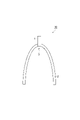
- FIG. 1 is a plan view schematically showing an embodiment of an electron source according to the present disclosure.
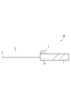
- FIG. 2 is a cross-sectional view schematically showing a welded portion in the electron source shown in FIG.
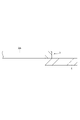
- FIG. 3A is a sectional view schematically showing a state in which an object to be welded, which is overlapped so that a chip and a tungsten filament are in direct contact with each other, is sandwiched between a pair of welding electrodes
- FIG. 3B is a sectional view schematically showing the object to be welded. It is a cross-sectional view schematically showing a state in which a chip and a tungsten filament are welded by passing an electric current while applying a pressing force with a pair of welding electrodes.
- FIG. 1 is a plan view schematically showing an embodiment of an electron source according to the present disclosure.
- FIG. 2 is a cross-sectional view schematically showing a welded portion in the electron source shown in FIG.
- FIG. 3A is a sectional view schematic
- FIG. 4 is a cross-sectional view schematically showing another aspect of the welded portion in the electron source.
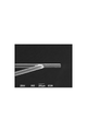
- FIG. 5 is an SEM photograph showing an electron source according to the first embodiment.
- FIG. 6 is an SEM photograph showing an electron source according to the second embodiment.
- FIG. 7 is an SEM photograph showing an electron source according to the third embodiment.
- FIG. 1 is a plan view schematically showing an electron source according to the present embodiment.
- the electron source 10 shown in FIG. 1 includes a chip 1 of LaB 6 , a tungsten filament 2, and a welded portion 3 to which the chip 1 and the tungsten filament 2 are directly bonded.
- the chip 1 is fixed to the top of the tungsten filament 2 bent in a loop shape by welding.
- Examples of the device provided with the electron source 10 include an electron microscope, a semiconductor manufacturing device, an inspection device, and a processing device.
- the chip 1 emits electrons by heating the tungsten filament 2 by energization.
- the chip 1 is preferably a single crystal of LaB 6 and is processed so that the ⁇ 100> direction in which electrons are easily emitted coincides with the electron emission direction.
- the side surface of the chip 1 is preferably a crystal plane of the (100) plane because it is considered that the evaporation rate is slowed down.
- the chip 1 has a substantially rectangular parallelepiped shape.
- the tip of the chip 1 may be processed into a conical shape or a quadrangular pyramid shape. Further, the shape of the chip 1 is not particularly limited, and can be made into a desired shape by electric discharge machining or the like.
- the tungsten filament 2 is for heating the chip 1 by energization.
- the tungsten filament 2 may contain an element other than tungsten (for example, rhenium, aluminum, silicon and potassium) depending on the required performance.
- the tungsten filament 2 may be doped with an alkali metal (for example, potassium) for tissue stabilization.
- the rhenium content of the tungsten filament 2 is, for example, 2 to 30% by mass, and may be 2 to 10% by mass or 2 to 5% by mass. Rhenium has the effect of increasing the electrical resistivity of the tungsten filament 2.
- the welded portion 3 is a portion where the chip 1 and the tungsten filament 2 are joined by welding.
- the welded portion 3 is formed by melting at least one of the chip 1 and the tungsten filament 2 by heating and then solidifying the welded portion 3.
- the thickness of the welded portion 3 (thickness T3 in FIG. 2) is, for example, 50 to 500 ⁇ m, and may be 50 to 400 ⁇ m or 110 to 250 ⁇ m.
- the melting point of the chip 1 is, for example, about 2210 ° C.
- the melting point of the tungsten filament 2 is, for example, about 3422 ° C.
- the electron source 10 is manufactured through the following steps.
- B A step of welding the chip 1 and the tungsten filament 2 by applying an electric current to the object to be welded 5 while applying a pressing force with a pair of welding electrodes 6a and 6b (see FIG. 3B).
- the thickness of the workpiece 5 (the total thickness of the chip 1 and the tungsten filament 2; the thickness T5 in FIG. 3A) is in the range of 50 to 500 ⁇ m, preferably 170 to 400 ⁇ m. It may be 180 to 350 ⁇ m or 180 to 280 ⁇ m.
- the thickness of the work piece 5 is the same as the separation distance between the pair of weld electrodes 6a and 6b in the state where the work piece 5 is sandwiched in the step (A).
- the object to be welded 5 can be locally heated to a high temperature by energization by the pair of weld electrodes 6a and 6b.
- the chip 1 and the tungsten filament 2 can be firmly joined by welding.
- the cross-sectional shape of the portion of the chip 1 to be welded to the tungsten filament 2 is, for example, a square shape or a rectangular shape having a side length of 10 to 300 ⁇ m.
- the length of one side is preferably 60 to 250 ⁇ m, and may be 60 to 200 ⁇ m or 70 to 150 ⁇ m.
- the cross-sectional shape of the portion of the chip 1 to be welded to the tungsten filament 2 may be, for example, a circular shape or an elliptical shape.
- the thickness of the chip 1 in the welding direction is preferably 60 to 250 ⁇ m, and may be 60 to 200 ⁇ m or 70 to 150 ⁇ m.
- the arrow A in FIG. 3A indicates the “welding direction”.
- the cross-sectional shape of the portion of the tungsten filament 2 welded to the chip 1 is, for example, a circular shape or an elliptical shape.
- the thickness of the tungsten filament 2 in the welding direction is preferably 60 to 250 ⁇ m, and may be 60 to 200 ⁇ m or 70 to 150 ⁇ m.
- the cross-sectional shape of the portion of the tungsten filament 2 to be welded to the chip 1 may be, for example, a square shape or a rectangular shape. In this case, the thickness of the tungsten filament 2 in the welding direction is preferably 60 to 250 ⁇ m, and may be 60 to 200 ⁇ m or 70 to 150 ⁇ m.
- the ratio T1 / T2 of the thickness T1 of the chip 1 and the thickness T2 of the tungsten filament 2 is preferably 0.6 to 1.4, and more preferably 0.8 to 1.3.
- the ratio T1 / T2 is within the above range, the region of the workpiece 5 including the interface between the chip 1 and the tungsten filament 2 can be efficiently heated to a high temperature.
- the heating temperature can be adjusted by adjusting the current flowing from the pair of welding electrodes 6a and 6b to the object to be welded 5. At least one of the chip 1 and the tungsten filament 2 may be locally melted by heating by energization, and it is preferable that both the chip 1 and the tungsten filament 2 are locally melted.
- the pressing force applied to the object to be welded 5 from the pair of welding electrodes 6a and 6b may be set to a strength and time sufficient for the chip 1 and the tungsten filament 2 to be firmly bonded.
- the arrow E in FIG. 3B indicates the direction in which the current flows, and the arrow F indicates the direction of the pressing force.
- the electron source manufactured by obtaining the step (B) may be in the form in which the chip 1 is embedded in the tungsten filament 2 as shown in FIG. 2, or as shown in FIG.
- the chip 1 may be bonded to the surface of the tungsten filament 2A.
- the tungsten filament 2A shown in FIG. 4 has a rectangular cross section.
- the chip 1 may be composed of a single crystal of HfC (melting point: 3890 ° C.) or an IrCe compound (IrCe compound).
- the chip 1 may be composed of Ir 2 Ce, Ir 3 Ce, Ir 7 Ce 2 , Ir 5 Ce). Even when these electron emitting materials are used as the chip 1, the chip and the tungsten filament can be firmly bonded by welding.
- LaB 6 chips and tungsten filaments of the following sizes were prepared.
- the tip and tungsten filament were directly welded as follows. First, the chips and the tungsten filaments were superposed so as to be in direct contact with each other, and these were sandwiched between a pair of welding electrodes (see FIG. 3A). Both were welded by applying an electric current to the chip and the tungsten filament while applying a pressing force with a pair of welding electrodes (see FIG. 3 (b)). The welding current was set so that the temperature at the interface between the chip and the tungsten filament exceeded 3422 ° C. (the melting point of tungsten). As a result, as shown in the SEM photograph of FIG. 5, an electron source was obtained in which the chip was firmly bonded to the tungsten filament with the chip embedded in the tungsten filament.
- LaB 6 chips and tungsten filaments of the following sizes were prepared.
- Example 2 HfC chips and tungsten filaments of the following sizes were prepared.
- Example 3 Chips and tungsten filaments of IrCe compound (Ir 7 Ce 2 ) having the following sizes were prepared.
Abstract
This method for manufacturing an electron source comprises: a step for putting, between a pair of welding electrodes, an object to be welded in which a chip of an electron emission material and a tungsten filament are superposed so as to be in direct contact with each other; and a step for welding the chip and the tungsten filament by passing an electric current while applying pressing force to the object to be welded by the pair of welding electrodes, and the thickness of the object to be welded falls within the range of 50-500 μm.
Description
本開示は、電子源及びその製造方法、並びに電子源を備える装置に関する。
The present disclosure relates to an electron source, a method for manufacturing the electron source, and an apparatus provided with the electron source.
電子源は、例えば、電子顕微鏡及び半導体検査装置に使用されている。電子源は電子放出材料で構成されるチップを備える。電子放出材料の具体例として、LaB6(六ホウ化ランタン)の単結晶、HfCの単結晶及びIrCe化合物が挙げられる。
Electron sources are used, for example, in electron microscopes and semiconductor inspection equipment. The electron source comprises a chip composed of an electron emitting material. Specific examples of the electron emitting material include a single crystal of LaB 6 (lanthanum hexaboride), a single crystal of HfC, and an IrCe compound.
LaB6単結晶を用いた電子源は、例えば、LaB6単結晶のチップと、このチップを通電によって加熱するためのタングステンフィラメントと、タングステンフィラメントに対してチップを固定するための接合材料とによって構成される。特許文献1の製造例1には、LaB6単結晶のチップの下部側面にTaC粉末を含むペーストを使用して中間層を設けるとともに、Ta箔を使用して支持金属層を設けることが記載されている。この製造例1では支持金属層に径150μmのW線をスポット溶接して熱電子放射陰極を組み立てている。特許文献2にはイリジウムとセリウムからなる化合物を90質量%以上含む電子ビーム生成用カソード部材用の焼結材が記載されている。
The electron source using the LaB 6 single crystal is composed of, for example, a chip of the LaB 6 single crystal, a tungsten filament for heating the chip by energization, and a bonding material for fixing the chip to the tungsten filament. Will be done. Production Example 1 of Patent Document 1 describes that an intermediate layer is provided on the lower side surface of a chip of a LaB 6 single crystal using a paste containing TaC powder, and a supporting metal layer is provided using Ta foil. ing. In Production Example 1, a thermionic emission cathode is assembled by spot welding a W wire having a diameter of 150 μm to the supporting metal layer. Patent Document 2 describes a sintered material for an electron beam generating cathode member containing 90% by mass or more of a compound composed of iridium and cerium.
特許文献1の製造例1のように、LaB6のチップとタングステンフィラメント(W線)との間にタンタル(Ta)を含む層が介在している場合、通電加熱時にタンタルとLaB6が反応することで、真空度が劣化し、カソードのエミッション不安定性の原因となる。そのため、タングステンフィラメントに電子放出材料のチップが直接接合された構造であることが望ましい。しかし、従来、電子放出材料のチップとタングステンフィラメントを溶接によって強固に接合することができず、チップが落下するリスクがあった。このため、かかる構造の電子源は実用化に至っていない。
When a layer containing tantalum (Ta) is interposed between the chip of LaB 6 and the tungsten filament (W line) as in Production Example 1 of Patent Document 1, the tantalum and LaB 6 react with each other when energized and heated. As a result, the degree of vacuum deteriorates, which causes the emission instability of the cathode. Therefore, it is desirable that the structure is such that the chip of the electron emission material is directly bonded to the tungsten filament. However, conventionally, the chip of the electron emission material and the tungsten filament could not be firmly bonded by welding, and there was a risk that the chip would fall. Therefore, an electron source having such a structure has not been put into practical use.
本開示は、電子放出材料のチップがタングステンフィラメントに直接接合された構造の電子源の製造方法を提供する。また、本開示は、チップの固定にタンタルを用いた従来の電子源と比較して真空度の劣化を抑制でき、安定したエミッション電流を得ることができる電子源及びこれを備える装置を提供する。
The present disclosure provides a method for manufacturing an electron source having a structure in which a chip of an electron emitting material is directly bonded to a tungsten filament. Further, the present disclosure provides an electron source capable of suppressing deterioration of the degree of vacuum as compared with a conventional electron source using tantalum for fixing a chip, and capable of obtaining a stable emission current, and an apparatus including the same.
本開示の一側面に係る電子源の製造方法は、電子放出材料のチップとタングステンフィラメントが直接接するように重ね合わせた被溶接物を一対の溶接電極で挟み込む工程と、被溶接物に対して一対の溶接電極によって押圧力を加えながら電流を流すことによってチップとタングステンフィラメントを溶接する工程とを含み、被溶接物の厚さが50~500μmの範囲である。電子放出材料として、例えば、LaB6の単結晶、HfCの単結晶及びIrCe化合物が挙げられる。IrCe化合物は、例えば、Ir2Ce、Ir3Ce、Ir7Ce2、Ir5Ceである。
The method for manufacturing an electron source according to one aspect of the present disclosure includes a step of sandwiching an object to be welded, which is overlapped so that a chip of an electron emitting material and a tungsten filament are in direct contact with each other, between a pair of weld electrodes, and a pair of objects to be welded. The thickness of the object to be welded is in the range of 50 to 500 μm, including the step of welding the chip and the tungsten filament by passing a current while applying a pressing force by the welding electrode of the above. Examples of the electron emitting material include a single crystal of LaB 6 , a single crystal of HfC, and an IrCe compound. The IrCe compounds are, for example, Ir2Ce , Ir3Ce , Ir7Ce2 , and Ir5Ce .
本発明者らは、図3(a)及び図3(b)に示す構成の抵抗溶接機を使用して電子放出材料(LaB6の単結晶)のチップとタングステンフィラメントとを直接溶接することを試みた。その結果、被溶接物の厚さ(チップとタングステンフィラメントの厚さの合計)が50~500μmの範囲であれば、一対の溶接電極による通電によって被溶接物を局所的に高温にすることができ、チップとタングステンフィラメントを溶接によって強固に接合することができる。
The present inventors directly weld a chip of an electron emitting material (single crystal of LaB 6 ) and a tungsten filament by using a resistance welder having the configurations shown in FIGS. 3 (a) and 3 (b). I tried. As a result, if the thickness of the object to be welded (the total thickness of the tip and the tungsten filament) is in the range of 50 to 500 μm, the object to be welded can be locally heated to a high temperature by energization by a pair of welding electrodes. , The chip and the tungsten filament can be firmly joined by welding.
チップにおけるタングステンフィラメントに対して溶接される部分の断面形状は、例えば、一辺の長さが10~300μmの正方形状又は長方形状である。
The cross-sectional shape of the portion of the chip welded to the tungsten filament is, for example, a square shape or a rectangular shape having a side length of 10 to 300 μm.
本開示の一側面に係る電子源は、電子放出材料のチップと、タングステンフィラメントと、チップとタングステンフィラメントが直接接合している溶接部とを備え、溶接部の厚さが50~500μmである。チップとタングステンフィラメントが直接接合しているため、両者の間にタンタルを含む層が介在している従来の電子源と比較して真空度の劣化を抑制でき、安定したエミッション電流を得ることができる。
The electron source according to one aspect of the present disclosure includes a chip of an electron emitting material, a tungsten filament, and a welded portion in which the chip and the tungsten filament are directly bonded, and the thickness of the welded portion is 50 to 500 μm. Since the chip and the tungsten filament are directly bonded, deterioration of the degree of vacuum can be suppressed and stable emission current can be obtained as compared with the conventional electron source in which a layer containing tantalum is interposed between them. ..
本開示におけるタングステンフィラメントは、要求性能に応じて、タングステン以外の元素(例えば、レニウム、アルミニウム、ケイ素及びカリウム)を含んでもよい。
The tungsten filament in the present disclosure may contain elements other than tungsten (for example, rhenium, aluminum, silicon and potassium) depending on the required performance.
本開示の一側面に係る装置は上記電子源を備える。電子源を備える装置として、例えば、電子顕微鏡及び半導体製造装置及び検査装置が挙げられる。
The device according to one aspect of the present disclosure includes the above electronic source. Devices equipped with an electron source include, for example, an electron microscope, a semiconductor manufacturing device, and an inspection device.
本開示によれば、電子放出材料のチップがタングステンフィラメントに直接接合された構造の電子源の製造方法が提供される。また、本開示によれば、チップの固定にタンタルを用いた従来の電子源と比較して真空度の劣化を抑制でき、安定したエミッション電流を得ることができる電子源及びこれを備える装置を提供する。
According to the present disclosure, there is provided a method for manufacturing an electron source having a structure in which a chip of an electron emitting material is directly bonded to a tungsten filament. Further, according to the present disclosure, there is provided an electron source capable of suppressing deterioration of the degree of vacuum as compared with a conventional electron source using tantalum for fixing a chip and obtaining a stable emission current, and a device provided with the electron source. do.
以下、図面を参照しながら、本開示の実施形態について説明する。以下の説明において、同一要素又は同一機能を有する要素には同一符号を用いることとし、重複する説明は省略する。なお、本発明は以下の実施形態に限定されるものではない。
Hereinafter, embodiments of the present disclosure will be described with reference to the drawings. In the following description, the same reference numerals will be used for the same elements or elements having the same function, and duplicate description will be omitted. The present invention is not limited to the following embodiments.
<電子源>
図1は本実施形態に係る電子源を模式的に示す平面図である。図1に示された電子源10は、LaB6のチップ1と、タングステンフィラメント2と、チップ1とタングステンフィラメント2が直接接合している溶接部3とを備える。ループ状に曲げられたタングステンフィラメント2の頂部にチップ1が溶接によって固定されている。電子源10を備える装置として、電子顕微鏡、半導体製造装置、検査装置及び加工装置が挙げられる。 <Electron source>
FIG. 1 is a plan view schematically showing an electron source according to the present embodiment. Theelectron source 10 shown in FIG. 1 includes a chip 1 of LaB 6 , a tungsten filament 2, and a welded portion 3 to which the chip 1 and the tungsten filament 2 are directly bonded. The chip 1 is fixed to the top of the tungsten filament 2 bent in a loop shape by welding. Examples of the device provided with the electron source 10 include an electron microscope, a semiconductor manufacturing device, an inspection device, and a processing device.
図1は本実施形態に係る電子源を模式的に示す平面図である。図1に示された電子源10は、LaB6のチップ1と、タングステンフィラメント2と、チップ1とタングステンフィラメント2が直接接合している溶接部3とを備える。ループ状に曲げられたタングステンフィラメント2の頂部にチップ1が溶接によって固定されている。電子源10を備える装置として、電子顕微鏡、半導体製造装置、検査装置及び加工装置が挙げられる。 <Electron source>
FIG. 1 is a plan view schematically showing an electron source according to the present embodiment. The
チップ1は、タングステンフィラメント2の通電による加熱により電子を放出する。チップ1は、LaB6の単結晶体からなり、電子を放出しやすい<100>方位が電子放出方向に一致するよう加工された単結晶体であることが好ましい。チップ1の側面は、蒸発速度が遅くなると考えられることから、(100)面の結晶面であることが好ましい。チップ1は略直方体形状を有している。なお、チップ1の先端部は円錐状又は四角錐状に加工されていてもよい。また、チップ1の形状は特に制限はなく、放電加工などによって所望の形状にすることができる。
The chip 1 emits electrons by heating the tungsten filament 2 by energization. The chip 1 is preferably a single crystal of LaB 6 and is processed so that the <100> direction in which electrons are easily emitted coincides with the electron emission direction. The side surface of the chip 1 is preferably a crystal plane of the (100) plane because it is considered that the evaporation rate is slowed down. The chip 1 has a substantially rectangular parallelepiped shape. The tip of the chip 1 may be processed into a conical shape or a quadrangular pyramid shape. Further, the shape of the chip 1 is not particularly limited, and can be made into a desired shape by electric discharge machining or the like.
タングステンフィラメント2は通電によってチップ1を加熱するためのものである。タングステンフィラメント2は、要求性能に応じて、タングステン以外の元素(例えば、レニウム、アルミニウム、ケイ素及びカリウム)を含んでもよい。タングステンフィラメント2は組織安定化のためのアルカリ金属(例えば、カリウム)がドープされたものであってもよい。タングステンフィラメント2がレニウムを含む場合、タングステンフィラメント2のレニウム含有率は、例えば、2~30質量%であり、2~10質量%又は2~5質量%であってもよい。レニウムはタングステンフィラメント2の電気比抵抗を大きくする効果を奏する。
The tungsten filament 2 is for heating the chip 1 by energization. The tungsten filament 2 may contain an element other than tungsten (for example, rhenium, aluminum, silicon and potassium) depending on the required performance. The tungsten filament 2 may be doped with an alkali metal (for example, potassium) for tissue stabilization. When the tungsten filament 2 contains rhenium, the rhenium content of the tungsten filament 2 is, for example, 2 to 30% by mass, and may be 2 to 10% by mass or 2 to 5% by mass. Rhenium has the effect of increasing the electrical resistivity of the tungsten filament 2.
溶接部3は、チップ1とタングステンフィラメント2が溶接によって接合されている部分である。溶接部3は、チップ1及びタングステンフィラメント2の少なくとも一方が加熱によって一旦融解した後、固化することによって形成される。溶接部3の厚さ(図2における厚さT3)は、例えば、50~500μmであり、50~400μm又は110~250μmであってもよい。チップ1の融点は、例えば、2210℃程度である。タングステンフィラメント2の融点は、例えば、3422℃程度である。
The welded portion 3 is a portion where the chip 1 and the tungsten filament 2 are joined by welding. The welded portion 3 is formed by melting at least one of the chip 1 and the tungsten filament 2 by heating and then solidifying the welded portion 3. The thickness of the welded portion 3 (thickness T3 in FIG. 2) is, for example, 50 to 500 μm, and may be 50 to 400 μm or 110 to 250 μm. The melting point of the chip 1 is, for example, about 2210 ° C. The melting point of the tungsten filament 2 is, for example, about 3422 ° C.
<電子源の製造方法>
次に、電子源10の製造方法について説明する。電子源10は以下の工程を経て製造される。
(A)チップ1とタングステンフィラメント2が直接接するように重ね合わせた被溶接物5を一対の溶接電極6a,6bで挟み込む工程(図3(a)参照)。
(B)被溶接物5に対して一対の溶接電極6a,6bによって押圧力を加えながら電流を流すことによってチップ1とタングステンフィラメント2を溶接する工程(図3(b)参照)。 <Manufacturing method of electron source>
Next, a method for manufacturing theelectron source 10 will be described. The electron source 10 is manufactured through the following steps.
(A) A step of sandwiching an object to be welded 5 which is overlapped so that thechip 1 and the tungsten filament 2 are in direct contact with a pair of welding electrodes 6a and 6b (see FIG. 3A).
(B) A step of welding thechip 1 and the tungsten filament 2 by applying an electric current to the object to be welded 5 while applying a pressing force with a pair of welding electrodes 6a and 6b (see FIG. 3B).
次に、電子源10の製造方法について説明する。電子源10は以下の工程を経て製造される。
(A)チップ1とタングステンフィラメント2が直接接するように重ね合わせた被溶接物5を一対の溶接電極6a,6bで挟み込む工程(図3(a)参照)。
(B)被溶接物5に対して一対の溶接電極6a,6bによって押圧力を加えながら電流を流すことによってチップ1とタングステンフィラメント2を溶接する工程(図3(b)参照)。 <Manufacturing method of electron source>
Next, a method for manufacturing the
(A) A step of sandwiching an object to be welded 5 which is overlapped so that the
(B) A step of welding the
(A)工程において、被溶接物5の厚さ(チップ1とタングステンフィラメント2の厚さの合計、図3(a)における厚さT5)は50~500μmの範囲であり、好ましくは170~400μmであり、180~350μm又は180~280μmであってもよい。被溶接物5の厚さは、(A)工程において、被溶接物5を挟み込んだ状態の一対の溶接電極6a,6bの離間距離と同じである。被溶接物5の厚さ(一対の溶接電極6a,6bの離間距離)が上記範囲であることで、一対の溶接電極6a,6bによる通電によって被溶接物5を局所的に高温にすることができ、チップ1とタングステンフィラメント2を溶接によって強固に接合することができる。
In the step (A), the thickness of the workpiece 5 (the total thickness of the chip 1 and the tungsten filament 2; the thickness T5 in FIG. 3A) is in the range of 50 to 500 μm, preferably 170 to 400 μm. It may be 180 to 350 μm or 180 to 280 μm. The thickness of the work piece 5 is the same as the separation distance between the pair of weld electrodes 6a and 6b in the state where the work piece 5 is sandwiched in the step (A). When the thickness of the object to be welded 5 (the separation distance between the pair of weld electrodes 6a and 6b) is within the above range, the object to be welded 5 can be locally heated to a high temperature by energization by the pair of weld electrodes 6a and 6b. The chip 1 and the tungsten filament 2 can be firmly joined by welding.
チップ1におけるタングステンフィラメント2に対して溶接される部分の断面形状は、例えば、一辺の長さが10~300μmの正方形状又は長方形状である。一辺の長さは、好ましくは60~250μmであり、60~200μm又は70~150μmであってもよい。なお、チップ1におけるタングステンフィラメント2に対して溶接される部分の断面形状は、例えば、円形状又は楕円形状であってもよい。この場合、チップ1の溶接方向の厚さ(図3(a)における厚さT1)は、好ましくは60~250μmであり、60~200μm又は70~150μmであってもよい。なお、図3(a)における矢印Aは「溶接方向」を示す。
The cross-sectional shape of the portion of the chip 1 to be welded to the tungsten filament 2 is, for example, a square shape or a rectangular shape having a side length of 10 to 300 μm. The length of one side is preferably 60 to 250 μm, and may be 60 to 200 μm or 70 to 150 μm. The cross-sectional shape of the portion of the chip 1 to be welded to the tungsten filament 2 may be, for example, a circular shape or an elliptical shape. In this case, the thickness of the chip 1 in the welding direction (thickness T1 in FIG. 3A) is preferably 60 to 250 μm, and may be 60 to 200 μm or 70 to 150 μm. The arrow A in FIG. 3A indicates the “welding direction”.
タングステンフィラメント2におけるチップ1に対して溶接される部分の断面形状は、例えば、円形状又は楕円形状である。タングステンフィラメント2の溶接方向の厚さ(図3(a)における厚さT2)は、好ましくは60~250μmであり、60~200μm又は70~150μmであってもよい。なお、タングステンフィラメント2におけるチップ1に対して溶接される部分の断面形状は、例えば、正方形状又は長方形状であってもよい。この場合、タングステンフィラメント2の溶接方向の厚さは、好ましくは60~250μmであり、60~200μm又は70~150μmであってもよい。
The cross-sectional shape of the portion of the tungsten filament 2 welded to the chip 1 is, for example, a circular shape or an elliptical shape. The thickness of the tungsten filament 2 in the welding direction (thickness T2 in FIG. 3A) is preferably 60 to 250 μm, and may be 60 to 200 μm or 70 to 150 μm. The cross-sectional shape of the portion of the tungsten filament 2 to be welded to the chip 1 may be, for example, a square shape or a rectangular shape. In this case, the thickness of the tungsten filament 2 in the welding direction is preferably 60 to 250 μm, and may be 60 to 200 μm or 70 to 150 μm.
チップ1の厚さT1とタングステンフィラメント2の厚さT2の比T1/T2は、好ましくは0.6~1.4であり、より好ましくは0.8~1.3である。比T1/T2が上記範囲内であることで、被溶接物5におけるチップ1とタングステンフィラメント2の界面を含む領域を効率的に高温にすることができる。
The ratio T1 / T2 of the thickness T1 of the chip 1 and the thickness T2 of the tungsten filament 2 is preferably 0.6 to 1.4, and more preferably 0.8 to 1.3. When the ratio T1 / T2 is within the above range, the region of the workpiece 5 including the interface between the chip 1 and the tungsten filament 2 can be efficiently heated to a high temperature.
(B)工程において、被溶接物5に対して一対の溶接電極6a,6bから流す電流を調整することで、加熱温度を調整することができる。通電による加熱によって、チップ1及びタングステンフィラメント2の少なくとも一方を局所的に融解させればよく、チップ1及びタングステンフィラメント2の両方を局所的に融解させることが好ましい。一対の溶接電極6a,6bから被溶接物5に加える押圧力は、チップ1及びタングステンフィラメント2が強固に接合されるのに十分な強度及び時間に設定すればよい。図3(b)における矢印Eは電流が流れる方向を示し、矢印Fは押圧力の方向を示す。
In the step (B), the heating temperature can be adjusted by adjusting the current flowing from the pair of welding electrodes 6a and 6b to the object to be welded 5. At least one of the chip 1 and the tungsten filament 2 may be locally melted by heating by energization, and it is preferable that both the chip 1 and the tungsten filament 2 are locally melted. The pressing force applied to the object to be welded 5 from the pair of welding electrodes 6a and 6b may be set to a strength and time sufficient for the chip 1 and the tungsten filament 2 to be firmly bonded. The arrow E in FIG. 3B indicates the direction in which the current flows, and the arrow F indicates the direction of the pressing force.
(B)工程を得て製造される電子源は、図2に示されたように、タングステンフィラメント2にチップ1が埋め込まれた態様であってもよいし、図4に示されたように、タングステンフィラメント2Aの表面にチップ1が接合している態様であってもよい。なお、図4に示すタングステンフィラメント2Aは断面が四角形状である。
The electron source manufactured by obtaining the step (B) may be in the form in which the chip 1 is embedded in the tungsten filament 2 as shown in FIG. 2, or as shown in FIG. The chip 1 may be bonded to the surface of the tungsten filament 2A. The tungsten filament 2A shown in FIG. 4 has a rectangular cross section.
上記実施形態においては、チップ1がLaB6の単結晶体で構成された態様を例示したが、チップ1はHfCの単結晶(融点:3890℃)で構成されていてもよいし、IrCe化合物(例えば、Ir2Ce、Ir3Ce、Ir7Ce2、Ir5Ce)で構成されていてもよい。チップ1として、これらの電子放出材料を使用した場合も、チップとタングステンフィラメントを溶接によって強固に接合することができる。
In the above embodiment, the embodiment in which the chip 1 is composed of a single crystal of LaB 6 is exemplified, but the chip 1 may be composed of a single crystal of HfC (melting point: 3890 ° C.) or an IrCe compound (IrCe compound). For example, it may be composed of Ir 2 Ce, Ir 3 Ce, Ir 7 Ce 2 , Ir 5 Ce). Even when these electron emitting materials are used as the chip 1, the chip and the tungsten filament can be firmly bonded by welding.
以下、本開示について実施例及び比較例に基づいて説明する。なお、本発明は以下の実施例に限定されるものではない。
Hereinafter, the present disclosure will be described based on Examples and Comparative Examples. The present invention is not limited to the following examples.
(実施例1)
以下のサイズのLaB6のチップ及びタングステンフィラメントを準備した。
<LaB6のチップ>
・厚さT1:90μm
・幅:90μm
・長さ:1000μm
<タングステンフィラメント>
・径(厚さT2):127μm
・タングステン純度:99.999質量%以上 (Example 1)
LaB 6 chips and tungsten filaments of the following sizes were prepared.
<LaB 6 chip>
-Thickness T1: 90 μm
・ Width: 90 μm
・ Length: 1000 μm
<Tungsten filament>
-Diameter (thickness T2): 127 μm
-Tungsten purity: 99.999% by mass or more
次のようにしてチップとタングステンフィラメントを直接溶接した。まず、チップとタングステンフィラメントが直接接するように重ね合わせた状態でこれらを一対の溶接電極で挟み込んだ(図3(a)参照)。チップとタングステンフィラメントに対して一対の溶接電極によって押圧力を加えながら電流を流すことによって両者を溶接した(図3(b)参照)。チップとタングステンフィラメントの界面の温度が3422℃(タングステンの融点)を超えるように、溶接電流を設定した。その結果、図5のSEM写真に示されたように、タングステンフィラメントに対してチップが埋め込まれた状態で両者が強固に接合された電子源が得られた。
The tip and tungsten filament were directly welded as follows. First, the chips and the tungsten filaments were superposed so as to be in direct contact with each other, and these were sandwiched between a pair of welding electrodes (see FIG. 3A). Both were welded by applying an electric current to the chip and the tungsten filament while applying a pressing force with a pair of welding electrodes (see FIG. 3 (b)). The welding current was set so that the temperature at the interface between the chip and the tungsten filament exceeded 3422 ° C. (the melting point of tungsten). As a result, as shown in the SEM photograph of FIG. 5, an electron source was obtained in which the chip was firmly bonded to the tungsten filament with the chip embedded in the tungsten filament.
(比較例)
以下のサイズのLaB6のチップ及びタングステンフィラメントを準備した。
<LaB6のチップ>
・厚さT1:500μm
・幅:750μm
・長さ:1500μm
<タングステンフィラメント>
・径(厚さT2):127μm
・タングステン純度:99.999質量%以上 (Comparative example)
LaB 6 chips and tungsten filaments of the following sizes were prepared.
<LaB 6 chip>
・ Thickness T1: 500 μm
-Width: 750 μm
・ Length: 1500 μm
<Tungsten filament>
-Diameter (thickness T2): 127 μm
-Tungsten purity: 99.999% by mass or more
実施例1と同様にしてチップとタングステンフィラメントの溶接を試みた。溶接電流の設定を種々変更してチップとタングステンフィラメントを加熱したものの、両者を溶接することができなかった。
Welding of the tip and the tungsten filament was attempted in the same manner as in Example 1. Although the chips and the tungsten filament were heated by changing the welding current settings in various ways, they could not be welded.
(実施例2)
以下のサイズのHfCのチップ及びタングステンフィラメントを準備した。
<HfCのチップ>
・厚さT1:90μm
・幅:90μm
・長さ:1000μm
<タングステンフィラメント>
・径(厚さT2):127μm
・タングステン純度:99.999質量%以上 (Example 2)
HfC chips and tungsten filaments of the following sizes were prepared.
<HfC chip>
-Thickness T1: 90 μm
・ Width: 90 μm
・ Length: 1000 μm
<Tungsten filament>
-Diameter (thickness T2): 127 μm
-Tungsten purity: 99.999% by mass or more
実施例1と同様にしてチップとタングステンフィラメントの溶接を試みた。チップとタングステンフィラメントの界面の温度が3422℃(タングステンの融点)を超えるように、溶接電流を設定した。その結果、図6のSEM写真に示されたように、タングステンフィラメントに対してチップの一部が埋め込まれた状態で両者が強固に接合された電子源が得られた。
Welding of the tip and the tungsten filament was attempted in the same manner as in Example 1. The welding current was set so that the temperature at the interface between the chip and the tungsten filament exceeded 3422 ° C. (the melting point of tungsten). As a result, as shown in the SEM photograph of FIG. 6, an electron source was obtained in which a part of the chip was embedded in the tungsten filament and the two were firmly bonded to each other.
(実施例3)
以下のサイズのIrCe化合物(Ir7Ce2)のチップ及びタングステンフィラメントを準備した。
<IrCe化合物のチップ>
・厚さT1:90μm
・幅:90μm
・長さ:1000μm
<タングステンフィラメント>
・径(厚さT2):127μm
・タングステン純度:99.999質量%以上 (Example 3)
Chips and tungsten filaments of IrCe compound (Ir 7 Ce 2 ) having the following sizes were prepared.
<IrCe compound chip>
-Thickness T1: 90 μm
・ Width: 90 μm
・ Length: 1000 μm
<Tungsten filament>
-Diameter (thickness T2): 127 μm
-Tungsten purity: 99.999% by mass or more
実施例1と同様にしてチップとタングステンフィラメントの溶接を試みた。チップとタングステンフィラメントの界面の温度が3422℃(タングステンの融点)を超えるように、溶接電流を設定した。その結果、図7のSEM写真に示されたように、タングステンフィラメントに対してチップが埋め込まれた状態で両者が強固に接合された電子源が得られた。
Welding of the tip and the tungsten filament was attempted in the same manner as in Example 1. The welding current was set so that the temperature at the interface between the chip and the tungsten filament exceeded 3422 ° C. (the melting point of tungsten). As a result, as shown in the SEM photograph of FIG. 7, an electron source was obtained in which the chip was firmly bonded to the tungsten filament with the chip embedded in the tungsten filament.
1…チップ、2,2A…タングステンフィラメント、3…溶接部、5…被溶接物、6a,6b…一対の溶接電極、10…電子源。
1 ... Chip, 2, 2A ... Tungsten filament, 3 ... Welded part, 5 ... Welded object, 6a, 6b ... Pair of weld electrodes, 10 ... Electron source.
Claims (8)
- 電子放出材料のチップとタングステンフィラメントが直接接するように重ね合わせた被溶接物を一対の溶接電極で挟み込む工程と、
前記被溶接物に対して前記一対の溶接電極によって押圧力を加えながら電流を流すことによって前記チップと前記タングステンフィラメントを溶接する工程と、
を含み、
前記被溶接物の厚さが50~500μmの範囲である、電子源の製造方法。 The process of sandwiching the object to be welded, which is overlapped so that the chip of the electron emission material and the tungsten filament are in direct contact, with a pair of welding electrodes.
A step of welding the tip and the tungsten filament by applying an electric current to the object to be welded while applying a pressing force with the pair of welding electrodes.
Including
A method for manufacturing an electron source, wherein the thickness of the object to be welded is in the range of 50 to 500 μm. - 前記チップにおける前記タングステンフィラメントに対して溶接される部分の断面形状は、一辺の長さが10~300μmの正方形状又は長方形状である、請求項1に記載の電子源の製造方法。 The method for manufacturing an electron source according to claim 1, wherein the cross-sectional shape of the portion of the chip welded to the tungsten filament is a square shape or a rectangular shape having a side length of 10 to 300 μm.
- 前記電子放出材料がLaB6、HfC及びIrCe化合物からなる群から選ばれる一種である、請求項1又は2に記載の電子源の製造方法。 The method for producing an electron source according to claim 1 or 2, wherein the electron emitting material is one selected from the group consisting of LaB 6 , HfC and IrCe compounds.
- 前記タングステンフィラメントがレニウムを含有する、請求項1~3のいずれか一項に記載の電子源の製造方法。 The method for producing an electron source according to any one of claims 1 to 3, wherein the tungsten filament contains rhenium.
- 電子放出材料のチップと、
タングステンフィラメントと、
前記チップと前記タングステンフィラメントが直接接合している溶接部と、
を備え、
前記溶接部の厚さが50~500μmである、電子源。 Chips of electron emission material and
Tungsten filament and
A welded portion to which the tip and the tungsten filament are directly bonded,
Equipped with
An electron source having a welded portion having a thickness of 50 to 500 μm. - 前記電子放出材料がLaB6、HfC及びIrCe化合物からなる群から選ばれる一種である、請求項5に記載の電子源。 The electron source according to claim 5, wherein the electron emitting material is one selected from the group consisting of LaB 6 , HfC and IrCe compounds.
- 前記タングステンフィラメントがレニウムを含有する、請求項5又は6に記載の電子源。 The electron source according to claim 5 or 6, wherein the tungsten filament contains rhenium.
- 請求項5~7のいずれか一項に記載の電子源を備える装置。 A device including the electronic source according to any one of claims 5 to 7.
Priority Applications (5)
| Application Number | Priority Date | Filing Date | Title |
|---|---|---|---|
| US18/258,461 US20240029989A1 (en) | 2020-12-25 | 2021-12-20 | Electron source, method for manufacturing same, and device provided with electron source |
| JP2022522320A JPWO2022138558A1 (en) | 2020-12-25 | 2021-12-20 | |
| CN202180068505.XA CN116325060A (en) | 2020-12-25 | 2021-12-20 | Electron source, method for manufacturing the same, and device provided with the electron source |
| EP21910702.6A EP4270441A1 (en) | 2020-12-25 | 2021-12-20 | Electron source, method for manufacturing same, and device provided with electron source |
| JP2022207163A JP2023036830A (en) | 2020-12-25 | 2022-12-23 | Electron source and manufacturing method for the same and device including electron source |
Applications Claiming Priority (2)
| Application Number | Priority Date | Filing Date | Title |
|---|---|---|---|
| JP2020-217530 | 2020-12-25 | ||
| JP2020217530 | 2020-12-25 |
Publications (1)
| Publication Number | Publication Date |
|---|---|
| WO2022138558A1 true WO2022138558A1 (en) | 2022-06-30 |
Family
ID=82157950
Family Applications (1)
| Application Number | Title | Priority Date | Filing Date |
|---|---|---|---|
| PCT/JP2021/047021 WO2022138558A1 (en) | 2020-12-25 | 2021-12-20 | Electron source, method for manufacturing same, and device provided with electron source |
Country Status (6)
| Country | Link |
|---|---|
| US (1) | US20240029989A1 (en) |
| EP (1) | EP4270441A1 (en) |
| JP (2) | JPWO2022138558A1 (en) |
| CN (1) | CN116325060A (en) |
| TW (1) | TW202230422A (en) |
| WO (1) | WO2022138558A1 (en) |
Citations (6)
| Publication number | Priority date | Publication date | Assignee | Title |
|---|---|---|---|---|
| JPS5046477A (en) * | 1973-08-31 | 1975-04-25 | ||
| JPS647450A (en) | 1987-06-30 | 1989-01-11 | Ube Industries | Pointed thermionic emission cathode |
| JPH055306B2 (en) | 1984-12-28 | 1993-01-22 | Nippon Koden Kogyo Kk | |
| JP2000246451A (en) * | 1999-03-04 | 2000-09-12 | Noritake Co Ltd | Welding machine for oxide-covered filament |
| JP2002358922A (en) * | 2001-05-31 | 2002-12-13 | Sanken Electric Co Ltd | Cold cathode discharge tube and manufacturing method of same |
| JP2008262794A (en) * | 2007-04-12 | 2008-10-30 | National Institute For Materials Science | Rare earths hexaboride nanowire thermion electron emitter |
Family Cites Families (6)
| Publication number | Priority date | Publication date | Assignee | Title |
|---|---|---|---|---|
| US6771013B2 (en) * | 2000-10-17 | 2004-08-03 | Fei Company | Low power schottky emitter |
| WO2009044564A1 (en) * | 2007-10-05 | 2009-04-09 | Denki Kagaku Kogyo Kabushiki Kaisha | Electron source and electron beam device |
| JP2010015966A (en) * | 2008-06-06 | 2010-01-21 | Hitachi High-Technologies Corp | Electron-emitting element, electron gun, electron microscope device using it, and electron beam lithogrphy device |
| JP2010238384A (en) * | 2009-03-30 | 2010-10-21 | Denki Kagaku Kogyo Kk | Electron source and use application for the same |
| US9165737B2 (en) * | 2012-10-04 | 2015-10-20 | Nuflare Technology, Inc. | High-brightness, long life thermionic cathode and methods of its fabrication |
| JP6636472B2 (en) * | 2017-02-28 | 2020-01-29 | 株式会社日立ハイテクノロジーズ | Electron source and electron beam device using the same |
-
2021
- 2021-12-20 WO PCT/JP2021/047021 patent/WO2022138558A1/en unknown
- 2021-12-20 CN CN202180068505.XA patent/CN116325060A/en active Pending
- 2021-12-20 JP JP2022522320A patent/JPWO2022138558A1/ja active Pending
- 2021-12-20 EP EP21910702.6A patent/EP4270441A1/en active Pending
- 2021-12-20 US US18/258,461 patent/US20240029989A1/en active Granted
- 2021-12-21 TW TW110147833A patent/TW202230422A/en unknown
-
2022
- 2022-12-23 JP JP2022207163A patent/JP2023036830A/en active Pending
Patent Citations (6)
| Publication number | Priority date | Publication date | Assignee | Title |
|---|---|---|---|---|
| JPS5046477A (en) * | 1973-08-31 | 1975-04-25 | ||
| JPH055306B2 (en) | 1984-12-28 | 1993-01-22 | Nippon Koden Kogyo Kk | |
| JPS647450A (en) | 1987-06-30 | 1989-01-11 | Ube Industries | Pointed thermionic emission cathode |
| JP2000246451A (en) * | 1999-03-04 | 2000-09-12 | Noritake Co Ltd | Welding machine for oxide-covered filament |
| JP2002358922A (en) * | 2001-05-31 | 2002-12-13 | Sanken Electric Co Ltd | Cold cathode discharge tube and manufacturing method of same |
| JP2008262794A (en) * | 2007-04-12 | 2008-10-30 | National Institute For Materials Science | Rare earths hexaboride nanowire thermion electron emitter |
Also Published As
| Publication number | Publication date |
|---|---|
| EP4270441A1 (en) | 2023-11-01 |
| JP2023036830A (en) | 2023-03-14 |
| US20240029989A1 (en) | 2024-01-25 |
| JPWO2022138558A1 (en) | 2022-06-30 |
| TW202230422A (en) | 2022-08-01 |
| CN116325060A (en) | 2023-06-23 |
Similar Documents
| Publication | Publication Date | Title |
|---|---|---|
| WO2009081470A1 (en) | Laser light source module | |
| JP2011249027A (en) | Discharge lamp | |
| US8548124B2 (en) | Electron source and cathode cup thereof | |
| WO2022138558A1 (en) | Electron source, method for manufacturing same, and device provided with electron source | |
| US7880373B2 (en) | Field emission electron source and method for making the same | |
| CN108305823B (en) | X-ray tube device | |
| US4673842A (en) | Graphite cathode cup for gridded x-ray tubes | |
| JP2009146705A (en) | Electron emission element, electron source, electron beam device, and manufacturing method for electron emission element | |
| CN100495633C (en) | Electronic tube | |
| WO2023013282A1 (en) | Electron source, manufacturing method therefor, and device comprising electron source | |
| JP5047062B2 (en) | Thermionic emission cathode | |
| JP7313791B2 (en) | Discharge lamp and method for manufacturing discharge lamp electrode | |
| US7002288B2 (en) | Electron tube and method for producing the same | |
| EP2847780B1 (en) | An electrically heated planar cathode | |
| US11915921B2 (en) | Electron source, method for manufacturing same, emitter, and device including same | |
| JP2023036830A5 (en) | ||
| JP2020030992A (en) | Discharge lamp | |
| JP5907522B2 (en) | Filament manufacturing method | |
| JP2011044254A (en) | Electron emitting element and method of fabricating the same | |
| KR20230130534A (en) | Feeder member and wafer placement table | |
| JP2006031976A (en) | Field emission electron source and electron gun using the same | |
| JPS607335B2 (en) | thermionic emission cathode | |
| US1900100A (en) | Method of welding metals | |
| EP4309203A1 (en) | Systems and methods for fabricating silicon die stacks for electron emitter array chips | |
| JPH04248233A (en) | Cathode body structure for x-ray tube |
Legal Events
| Date | Code | Title | Description |
|---|---|---|---|
| ENP | Entry into the national phase |
Ref document number: 2022522320 Country of ref document: JP Kind code of ref document: A |
|
| 121 | Ep: the epo has been informed by wipo that ep was designated in this application |
Ref document number: 21910702 Country of ref document: EP Kind code of ref document: A1 |
|
| NENP | Non-entry into the national phase |
Ref country code: DE |
|
| ENP | Entry into the national phase |
Ref document number: 2021910702 Country of ref document: EP Effective date: 20230725 |