WO2022137864A1 - 撮像装置及び電子機器 - Google Patents
撮像装置及び電子機器 Download PDFInfo
- Publication number
- WO2022137864A1 WO2022137864A1 PCT/JP2021/041467 JP2021041467W WO2022137864A1 WO 2022137864 A1 WO2022137864 A1 WO 2022137864A1 JP 2021041467 W JP2021041467 W JP 2021041467W WO 2022137864 A1 WO2022137864 A1 WO 2022137864A1
- Authority
- WO
- WIPO (PCT)
- Prior art keywords
- gate electrode
- image pickup
- semiconductor substrate
- conductive type
- unit
- Prior art date
- Legal status (The legal status is an assumption and is not a legal conclusion. Google has not performed a legal analysis and makes no representation as to the accuracy of the status listed.)
- Ceased
Links
Images









Classifications
-
- H—ELECTRICITY
- H10—SEMICONDUCTOR DEVICES; ELECTRIC SOLID-STATE DEVICES NOT OTHERWISE PROVIDED FOR
- H10F—INORGANIC SEMICONDUCTOR DEVICES SENSITIVE TO INFRARED RADIATION, LIGHT, ELECTROMAGNETIC RADIATION OF SHORTER WAVELENGTH OR CORPUSCULAR RADIATION
- H10F39/00—Integrated devices, or assemblies of multiple devices, comprising at least one element covered by group H10F30/00, e.g. radiation detectors comprising photodiode arrays
- H10F39/80—Constructional details of image sensors
- H10F39/803—Pixels having integrated switching, control, storage or amplification elements
- H10F39/8037—Pixels having integrated switching, control, storage or amplification elements the integrated elements comprising a transistor
- H10F39/80373—Pixels having integrated switching, control, storage or amplification elements the integrated elements comprising a transistor characterised by the gate of the transistor
-
- H—ELECTRICITY
- H10—SEMICONDUCTOR DEVICES; ELECTRIC SOLID-STATE DEVICES NOT OTHERWISE PROVIDED FOR
- H10D—INORGANIC ELECTRIC SEMICONDUCTOR DEVICES
- H10D30/00—Field-effect transistors [FET]
- H10D30/01—Manufacture or treatment
- H10D30/021—Manufacture or treatment of FETs having insulated gates [IGFET]
-
- H—ELECTRICITY
- H10—SEMICONDUCTOR DEVICES; ELECTRIC SOLID-STATE DEVICES NOT OTHERWISE PROVIDED FOR
- H10D—INORGANIC ELECTRIC SEMICONDUCTOR DEVICES
- H10D30/00—Field-effect transistors [FET]
- H10D30/60—Insulated-gate field-effect transistors [IGFET]
-
- H—ELECTRICITY
- H10—SEMICONDUCTOR DEVICES; ELECTRIC SOLID-STATE DEVICES NOT OTHERWISE PROVIDED FOR
- H10D—INORGANIC ELECTRIC SEMICONDUCTOR DEVICES
- H10D84/00—Integrated devices formed in or on semiconductor substrates that comprise only semiconducting layers, e.g. on Si wafers or on GaAs-on-Si wafers
-
- H—ELECTRICITY
- H10—SEMICONDUCTOR DEVICES; ELECTRIC SOLID-STATE DEVICES NOT OTHERWISE PROVIDED FOR
- H10D—INORGANIC ELECTRIC SEMICONDUCTOR DEVICES
- H10D84/00—Integrated devices formed in or on semiconductor substrates that comprise only semiconducting layers, e.g. on Si wafers or on GaAs-on-Si wafers
- H10D84/01—Manufacture or treatment
- H10D84/0123—Integrating together multiple components covered by H10D12/00 or H10D30/00, e.g. integrating multiple IGBTs
- H10D84/0126—Integrating together multiple components covered by H10D12/00 or H10D30/00, e.g. integrating multiple IGBTs the components including insulated gates, e.g. IGFETs
-
- H—ELECTRICITY
- H10—SEMICONDUCTOR DEVICES; ELECTRIC SOLID-STATE DEVICES NOT OTHERWISE PROVIDED FOR
- H10D—INORGANIC ELECTRIC SEMICONDUCTOR DEVICES
- H10D84/00—Integrated devices formed in or on semiconductor substrates that comprise only semiconducting layers, e.g. on Si wafers or on GaAs-on-Si wafers
- H10D84/01—Manufacture or treatment
- H10D84/02—Manufacture or treatment characterised by using material-based technologies
- H10D84/03—Manufacture or treatment characterised by using material-based technologies using Group IV technology, e.g. silicon technology or silicon-carbide [SiC] technology
- H10D84/038—Manufacture or treatment characterised by using material-based technologies using Group IV technology, e.g. silicon technology or silicon-carbide [SiC] technology using silicon technology, e.g. SiGe
-
- H—ELECTRICITY
- H10—SEMICONDUCTOR DEVICES; ELECTRIC SOLID-STATE DEVICES NOT OTHERWISE PROVIDED FOR
- H10F—INORGANIC SEMICONDUCTOR DEVICES SENSITIVE TO INFRARED RADIATION, LIGHT, ELECTROMAGNETIC RADIATION OF SHORTER WAVELENGTH OR CORPUSCULAR RADIATION
- H10F39/00—Integrated devices, or assemblies of multiple devices, comprising at least one element covered by group H10F30/00, e.g. radiation detectors comprising photodiode arrays
- H10F39/10—Integrated devices
- H10F39/12—Image sensors
-
- H—ELECTRICITY
- H10—SEMICONDUCTOR DEVICES; ELECTRIC SOLID-STATE DEVICES NOT OTHERWISE PROVIDED FOR
- H10F—INORGANIC SEMICONDUCTOR DEVICES SENSITIVE TO INFRARED RADIATION, LIGHT, ELECTROMAGNETIC RADIATION OF SHORTER WAVELENGTH OR CORPUSCULAR RADIATION
- H10F39/00—Integrated devices, or assemblies of multiple devices, comprising at least one element covered by group H10F30/00, e.g. radiation detectors comprising photodiode arrays
- H10F39/10—Integrated devices
- H10F39/12—Image sensors
- H10F39/18—Complementary metal-oxide-semiconductor [CMOS] image sensors; Photodiode array image sensors
-
- H—ELECTRICITY
- H10—SEMICONDUCTOR DEVICES; ELECTRIC SOLID-STATE DEVICES NOT OTHERWISE PROVIDED FOR
- H10F—INORGANIC SEMICONDUCTOR DEVICES SENSITIVE TO INFRARED RADIATION, LIGHT, ELECTROMAGNETIC RADIATION OF SHORTER WAVELENGTH OR CORPUSCULAR RADIATION
- H10F39/00—Integrated devices, or assemblies of multiple devices, comprising at least one element covered by group H10F30/00, e.g. radiation detectors comprising photodiode arrays
- H10F39/80—Constructional details of image sensors
- H10F39/802—Geometry or disposition of elements in pixels, e.g. address-lines or gate electrodes
-
- H—ELECTRICITY
- H10—SEMICONDUCTOR DEVICES; ELECTRIC SOLID-STATE DEVICES NOT OTHERWISE PROVIDED FOR
- H10F—INORGANIC SEMICONDUCTOR DEVICES SENSITIVE TO INFRARED RADIATION, LIGHT, ELECTROMAGNETIC RADIATION OF SHORTER WAVELENGTH OR CORPUSCULAR RADIATION
- H10F39/00—Integrated devices, or assemblies of multiple devices, comprising at least one element covered by group H10F30/00, e.g. radiation detectors comprising photodiode arrays
- H10F39/80—Constructional details of image sensors
- H10F39/803—Pixels having integrated switching, control, storage or amplification elements
- H10F39/8033—Photosensitive area
-
- H—ELECTRICITY
- H10—SEMICONDUCTOR DEVICES; ELECTRIC SOLID-STATE DEVICES NOT OTHERWISE PROVIDED FOR
- H10F—INORGANIC SEMICONDUCTOR DEVICES SENSITIVE TO INFRARED RADIATION, LIGHT, ELECTROMAGNETIC RADIATION OF SHORTER WAVELENGTH OR CORPUSCULAR RADIATION
- H10F39/00—Integrated devices, or assemblies of multiple devices, comprising at least one element covered by group H10F30/00, e.g. radiation detectors comprising photodiode arrays
- H10F39/80—Constructional details of image sensors
- H10F39/803—Pixels having integrated switching, control, storage or amplification elements
- H10F39/8037—Pixels having integrated switching, control, storage or amplification elements the integrated elements comprising a transistor
Definitions
- This disclosure relates to an image pickup device and an electronic device.
- a CMOS image sensor is known as an image pickup device equipped with a photodiode and a transistor that reads out the charge photoelectrically converted by the photodiode. Further, in a CMOS image sensor, it is known to use a vertical transistor as a transfer transistor for transferring charges from a photodiode to a floating diffusion in order to increase the saturation signal amount of the photodiode (for example, Patent Document 1). reference).
- the vertical transistor includes a hole formed in a semiconductor substrate, a gate insulating film formed so as to cover the inner wall of the hole, and a vertical gate electrode formed so as to embed the inside of the hole via the gate insulating film. , Equipped with.
- the vertical gate electrode is long in the depth direction from the surface of the semiconductor substrate. Therefore, in a transfer transistor having a vertical gate electrode, the charge transfer path is long in the depth direction of the semiconductor substrate, and when the gate of the transfer transistor is switched from on to off, the charge in the middle of transfer returns to the photodiode side. It tends to be easy (that is, it is easy for electric charge to be pumped up). Due to the pumping of electric charge, the transfer characteristic of electric charge by the transfer transistor may be deteriorated.
- the present disclosure has been made in view of such circumstances, and an object of the present disclosure is to provide an image pickup device and an electronic device capable of improving charge transfer characteristics.
- the image pickup apparatus includes a semiconductor substrate and a vertical transistor provided on the semiconductor substrate.
- the semiconductor substrate is provided with a hole that opens on the first main surface side.
- the vertical transistor has a first gate electrode provided inside the hole and a second gate electrode provided outside the hole and connected to the first gate electrode.
- the first gate electrode has a first portion and a second portion made of a material having a conductivity different from that of the first portion.
- the electronic device includes an optical component, the image pickup device in which light transmitted through the optical component is incident, and a signal processing circuit for processing a signal output from the image pickup device. According to this, since it is possible to improve the charge transfer characteristics in the image pickup apparatus, it is possible to improve the performance of the electronic device.
- FIG. 1 is a diagram showing a configuration example of an image pickup apparatus according to the first embodiment of the present disclosure.
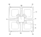
- FIG. 2 is a plan view showing an example of a pixel sharing structure of the image pickup apparatus according to the first embodiment of the present disclosure.
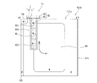
- FIG. 3 is a plan view showing a configuration example of a pixel according to the first embodiment of the present disclosure.
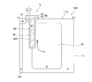
- FIG. 4 is a cross-sectional view showing a configuration example of a pixel according to the first embodiment of the present disclosure.
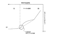
- FIG. 5 is a graph schematically showing the potential distribution in the charge transfer path when the transfer transistor is in the ON state.
- FIG. 6 is a cross-sectional view showing a configuration example of a pixel according to the second embodiment of the present disclosure.
- FIG. 1 is a diagram showing a configuration example of an image pickup apparatus according to the first embodiment of the present disclosure.
- FIG. 2 is a plan view showing an example of a pixel sharing structure of the image pickup apparatus according to the first embodiment of the present disclosure.
- FIG. 7 is a cross-sectional view showing a configuration example of a pixel according to the third embodiment of the present disclosure.
- FIG. 8 is a cross-sectional view showing a configuration example of a pixel according to the fourth embodiment of the present disclosure.
- FIG. 9 is a cross-sectional view showing a configuration example of a pixel according to the fifth embodiment of the present disclosure.
- FIG. 10 is a cross-sectional view showing a configuration example of a pixel according to the sixth embodiment of the present disclosure.
- FIG. 11 is a block diagram showing a configuration example of an image pickup device mounted on an electronic device.
- FIG. 12 is a diagram showing an example of a schematic configuration of an endoscopic surgery system to which the technique according to the present disclosure (the present technique) can be applied.
- FIG. 13 is a block diagram showing an example of the functional configuration of the camera head and the CCU shown in FIG.
- FIG. 14 is a block diagram showing a schematic configuration example of a vehicle control system, which is an example of a mobile control system to which the technique according to the present disclosure can be applied.
- FIG. 15 is a diagram showing an example of the installation position of the image pickup unit.
- the first conductive type is N type and the second conductive type is P type
- the conductive type may be selected in the reverse relationship
- the first conductive type may be P type
- the second conductive type may be N type.
- + and-attached to N and P mean that the impurity concentration is relatively high or low, respectively, as compared with the semiconductor regions to which + and-are not added.
- the semiconductor regions have the same N and N (or the same P and P), it does not mean that the impurity concentrations in the respective semiconductor regions are exactly the same.
- FIG. 1 is a diagram showing a configuration example of the image pickup apparatus 100 according to the first embodiment of the present disclosure.
- the image pickup device 100 shown in FIG. 1 is, for example, a CMOS solid-state image pickup device.
- the image pickup apparatus 100 has a pixel region (so-called image pickup region) in which pixels 102 including a plurality of photoelectric conversion elements are regularly arranged two-dimensionally on a semiconductor substrate 111 (for example, a silicon substrate). ) 103 and a peripheral circuit unit.
- the pixel 102 has a photodiode that serves as a photoelectric conversion element, and a plurality of pixel transistors (so-called MOS transistors).
- the plurality of pixel transistors can be composed of three transistors, a transfer transistor, a reset transistor, and an amplification transistor.
- the plurality of pixel transistors may be composed of four transistors by adding a selection transistor to the above three transistors. Since the equivalent circuit of a unit pixel is the same as usual, detailed description thereof will be omitted.
- the pixel 102 can also have a shared pixel structure.
- the shared pixel structure is composed of a plurality of photodiodes, a plurality of transfer transistors, one shared floating diffusion, and one shared other pixel transistor. That is, in the shared pixel structure, the photodiode and the transfer transistor constituting the plurality of unit pixels share the other pixel transistor other than the transfer transistor.
- the peripheral circuit unit includes a vertical drive circuit 104, a column signal processing circuit 105, a horizontal drive circuit 106, an output circuit 107, a control circuit 108, and the like.
- the control circuit 108 receives the input clock and data instructing the operation mode, etc., and outputs data such as internal information of the image pickup device. That is, the control circuit 108 generates a clock signal or a control signal that serves as a reference for the operation of the vertical drive circuit 104, the column signal processing circuit 105, the horizontal drive circuit 106, etc., based on the vertical sync signal, the horizontal sync signal, and the master clock. do. Then, the control circuit 108 inputs these signals to the vertical drive circuit 104, the column signal processing circuit 105, the horizontal drive circuit 106, and the like.
- the vertical drive circuit 104 is composed of, for example, a shift register, selects a pixel drive wiring, supplies a pulse for driving the pixel to the selected pixel drive wiring, and drives the pixel in row units. That is, the vertical drive circuit 104 sequentially selectively scans each pixel 102 of the pixel region 103 in a row unit in the vertical direction, passes through the vertical signal line 109, and generates a signal charge in the photoelectric conversion element of each pixel 102 according to the amount of light received. The pixel signal based on the above is supplied to the column signal processing circuit 105.
- the column signal processing circuit 105 is arranged for each column of the pixel 102, for example, and performs signal processing such as noise removal for each pixel string of the signal output from the pixel 102 for one row. That is, the column signal processing circuit 105 performs signal processing such as CDS for removing fixed pattern noise peculiar to the pixel 102, signal amplification, and AD conversion.
- a horizontal selection switch (not shown) is provided in the output stage of the column signal processing circuit 105 so as to be connected to the horizontal signal line 110.
- the horizontal drive circuit 106 is composed of, for example, a shift register, and by sequentially outputting horizontal scanning pulses, each of the column signal processing circuits 105 is sequentially selected, and a pixel signal is output from each of the column signal processing circuits 105 as a horizontal signal line. Output to 110.
- the output circuit 107 performs signal processing on signals sequentially supplied from each of the column signal processing circuits 105 through the horizontal signal line 110 and outputs the signals.
- the output circuit 107 may only perform buffering, or may perform black level adjustment, column variation correction, various digital signal processing, and the like.
- the input / output terminal 112 exchanges signals with the outside.
- FIG. 2 is a plan view showing an example of a pixel sharing structure of the image pickup apparatus 100 according to the first embodiment of the present disclosure.
- a total of four pixels 102 arranged two in each of the vertical direction and the horizontal direction constitute one shared pixel structure.
- One shared pixel structure is shared by four photodiode PDs (an example of the "photoelectric conversion unit” of the present disclosure) and four transfer transistors Tr (an example of the "vertical transistor” of the present disclosure).
- Floating diffusion FD an example of the "electric field holding unit” of the present disclosure
- one shared selection transistor not shown
- one shared reset transistor not shown
- one shared Includes an amplification transistor (not shown).
- the floating diffusion FD is arranged in the center of the four pixels 102 constituting one shared pixel structure.
- the gate electrode TG of the transfer transistor Tr is arranged in the vicinity of the floating diffusion FD.
- Each gate electrode TG of the four pixels 102 is arranged so as to surround one floating diffusion FD in a plan view.
- a pixel separation unit 120 is provided on the outer periphery of each pixel 102.
- the pixel separation unit 120 is composed of, for example, a conductive type impurity diffusion layer different from the semiconductor substrate 111, deep trench isolation, or the like.
- the upper side in the vertical direction of the paper surface is the surface 111a side of the semiconductor substrate 111, and a multilayer wiring layer (none of which is shown) composed of a plurality of wiring layers and an interlayer insulating film is provided.
- the lower side in the vertical direction of the paper surface is the back surface side of the semiconductor substrate 111, which is the light incident surface on which light is incident, and is provided with an on-chip lens, a color filter, and the like (none of which are shown).
- the image pickup apparatus 100 is a back-illuminated CMOS image sensor that photoelectrically converts light incident from the back surface side of the semiconductor substrate 111.
- FIG. 3 is a plan view showing a configuration example of the pixel 102 according to the first embodiment of the present disclosure.
- FIG. 4 is a cross-sectional view showing a configuration example of the pixel 102 according to the first embodiment of the present disclosure.
- FIG. 4 schematically shows a cross section of FIG. 3 cut along the A3-A'3 line.
- the A3-A'3 line passes through the central PDC of the photodiode PD, the central VGC of the first gate electrode VG, and the central FDC of the floating diffusion FD shared by the four pixels 102 in plan view. It is a virtual line.
- the semiconductor substrate 111 is, for example, a single crystal silicon substrate or a single crystal silicon layer formed by an epitaxial growth method on a substrate (not shown).
- the conductive type of the semiconductor substrate 111 is, for example, a P type.
- the photodiode PD is provided inside the P-type semiconductor substrate 111.
- the photodiode PD is composed of, for example, an N-type impurity diffusion layer.
- the photodiode PD photoelectrically converts the incident light incident from the back surface side of the semiconductor substrate 111, and accumulates the obtained charge e ⁇ .
- the transfer transistor Tr is provided from the inside of the semiconductor substrate 111 to the surface 111a (an example of the "first main surface” of the present disclosure).
- the transfer transistor Tr has, for example, a gate electrode TG and a gate insulating film 1 provided between the gate electrode TG and the semiconductor substrate 111, and has a photodiode PD as a source and a floating diffusion FD as a drain. It is an N-type vertical transistor.
- the transfer transistor Tr transfers the charge e ⁇ generated by the photodiode PD from the photodiode PD to the floating diffusion FD.
- the floating diffusion FD is provided on the surface 111a side of the semiconductor substrate 111, and is composed of, for example, an N-type impurity diffusion layer.
- the floating diffusion FD holds the electric charge e ⁇ transferred from the transfer transistor Tr.
- the structure of the transfer transistor Tr will be explained in more detail.
- the semiconductor substrate 111 is provided with a hole H1 that is open on the surface 111a side and is adjacent to the photodiode PD.
- the gate electrode TG is arranged in the hole H1 via the first gate insulating film 11, and is vertically extended on the first gate electrode VG and horizontally extended on the second gate insulating film 12. , A second gate electrode HG connected to the first gate electrode VG.
- the vertical direction is the depth direction from the surface 111a of the semiconductor substrate 111, in other words, the direction perpendicular to the surface 111a.
- the lateral direction is a direction orthogonal to the depth direction of the semiconductor substrate 111, in other words, a direction parallel to the surface 111a of the semiconductor substrate 111. Since the first gate electrode VG is extended in the vertical direction, it may be referred to as a vertical gate electrode or a vertical gate electrode. Since the second gate electrode HG is extended in the lateral direction, it may be referred to as a lateral gate electrode or a horizontal gate electrode.
- the gate insulating film 1 is provided with the first gate insulating film 11 provided between the inner wall of the hole H1 and the first gate electrode VG, and the first gate insulating film 11 provided on the surface 111a side of the semiconductor substrate 111. It has a second gate insulating film 12 in contact with it.
- the second gate insulating film 12 is located between the surface 111a of the semiconductor substrate 111 and the second gate electrode HG.
- the first gate insulating film 11 and the second gate insulating film 12 are, for example, silicon oxide films formed by thermally oxidizing the semiconductor substrate 111.
- the first gate insulating film 11 and the second gate insulating film 12 are integrally formed.
- the first gate electrode VG and the second gate electrode HG are composed of, for example, polyvinyl silicon doped with N-type impurities.
- N-type impurities are, for example, phosphorus or arsenic.
- the first gate electrode VG and the second gate electrode HG are integrally formed.
- the first gate electrode VG has an N + type first site VG1 and an N-type second site VG2 having a lower N-type impurity concentration than the first site VG1.
- the N-type impurity concentration (N ⁇ concentration) in the second site VG2 is about 1/10 of the N-type impurity concentration (N + concentration) in the first site VG1.
- the N + concentration is 1 ⁇ 10 19 cm -3 or more and less than 1 ⁇ 10 20 cm -3
- the N ⁇ concentration is 1 ⁇ 10 18 cm -3 or more and less than 1 ⁇ 10 19 cm -3 .
- the first site VG1 is located between the second site VG2 and the second gate electrode HG.
- the first portion VG1 and the second portion VG2 are connected to each other.
- the first site VG1 and the second site VG2 are formed by, for example, multi-stage ion implantation of N-type impurities into the polysilicon embedded in the pore H1.
- Multi-stage ion implantation is a method of continuously performing ion implantation with different acceleration energies. The acceleration energy and dose amount were adjusted so that the concentration of the N-type impurities implanted in the region of the first site VG1 was higher than that of the N-type impurities implanted in the region of the second site VG2.
- the first site VG1 and the second site VG2 can be separately formed in the polysilicon in the hole H1.
- the second gate electrode HG is formed by ion-implanting an N-type impurity into polysilicon.
- the N-type impurity concentration (N + concentration) in the second gate electrode HG is, for example, about the same as that of the first site VG1 of the first gate electrode VG. For example, 1 ⁇ 10 19 cm ⁇ or more 1 ⁇ 10 20 It is less than cm -3 .
- the charge e - generated by photoelectric conversion in the photodiode PD is transferred vertically along the first gate electrode VG of the transfer transistor Tr, and then transferred horizontally along the second gate electrode HG, resulting in floating diffusion. Reach the FD.
- the charge e- is transferred from the photodiode PD to the floating diffusion FD, the charge e - move along the side surface of the first gate electrode VG so as to wrap around the first gate electrode VG.
- a charge transfer channel may be provided in the region of the semiconductor substrate 111 facing the first gate electrode VG with the first gate insulating film 11 interposed therebetween. Further, in the semiconductor substrate 111, a charge transfer channel may be provided also in a region facing the second gate electrode HG with the second gate insulating film 12 interposed therebetween.
- the charge transfer channel is composed of, for example, a P-type impurity diffusion layer.
- FIG. 5 is a graph schematically showing the potential distribution in the transfer path of the charge e ⁇ when the transfer transistor Tr is in the on state.
- the vertical axis shows the potential energy
- the horizontal axis shows the transfer path of the charge e ⁇ .
- the broken line in FIG. 5 shows the potential distribution of an embodiment (hereinafter referred to as a comparative example) in which the first gate electrode (vertical gate electrode) is composed of only N + type polysilicon.
- the charge e-generated by the photoelectric conversion in the photodiode PD moves from the photodiode PD to the floating diffusion FD through the channel region formed along the gate electrode TG.
- the gate electrode TG has a first gate electrode VG extending in the vertical direction and a second gate electrode HG extending in the horizontal direction. Further, the first gate electrode VG has an N + type first portion VG1 and an N ⁇ type second portion VG2 vertically connected to the first portion VG1. Of the charges e-transferred from the photodiode PD to the floating diffusion FD, the charge e- that moves in the vertical direction (from the lower side to the upper side in FIG. 4) along the first gate electrode VG is the second N-type. The channel region formed in the vicinity of the site VG2 and the channel region formed in the vicinity of the N + type first site VG1 pass in this order.
- the N-type second portion VG2 is located on the photodiode PD side, and the N + type first portion VG1 is located on the floating diffusion FD side.
- the potential gradient in the channel region becomes smaller on the photodiode PD side and larger on the floating diffusion FD side, as shown in FIG.
- the floating diffusion FD side of the channel region there is a fermi level Ef in which the existence probability of electrons is 50%.
- the potential gradient near the Fermi level Ef where many electrons are present becomes large.
- the increase in the potential gradient near the Fermi level Ef promotes the movement of the charge e-existing in this vicinity to the floating diffusion FD side. Further, the movement of the charge e-existing near the Fermi level Ef to the photodiode PD side is suppressed because the potential gradient near the Fermi level Ef becomes a large and high barrier. As a result, when the gate of the transfer transistor Tr is switched from on to off, it is possible to suppress the charge e- during transfer in the vertical direction from returning to the photodiode PD side (that is, pumping up the charge e-). .. It is possible to improve the transfer characteristics of the charge e ⁇ in the vertical direction.
- the image pickup apparatus 100 includes a semiconductor substrate 111 and a transfer transistor Tr provided on the semiconductor substrate 111.
- the semiconductor substrate 111 is provided with a hole H1 that opens on the surface 111a side.
- the transfer transistor Tr is a vertical transistor, and has a first gate electrode VG provided inside the hole H1 and a second gate electrode HG provided outside the hole H1 and connected to the first gate electrode VG. , Have.
- the first gate electrode VG has a first part VG1 and a second part VG2 made of a material having a conductivity different from that of the first part VG1.
- the first site VG1 can be N + type and the second site VG2 can be N ⁇ type.
- the potential gradient of the channel region that is, the transfer path of the charge e ⁇
- the transfer path of the charge e- is long in the vertical direction like the transfer transistor Tr, it is possible to suppress the pumping of the charge e- by adjusting the potential gradient of the transfer path. It is possible to improve the transfer characteristics of.
- the first gate electrode VG of the transfer transistor Tr has an N + type first portion VG1 and an N ⁇ type second portion VG2.
- the configuration of the first gate electrode is not limited to this.
- the first gate electrode may have a third portion having a conductivity different from that of the first portion and the second portion.
- FIG. 6 is a cross-sectional view showing a configuration example of the pixel 102A according to the second embodiment of the present disclosure.
- FIG. 6 schematically shows a cross section when FIG. 3 is cut along the A3-A'3 line, similarly to FIG. 4.
- the difference between the pixel 102A shown in FIG. 6 and the pixel 102 shown in FIG. 4 lies in the configuration of the first gate electrode VG.
- the first gate electrode VG is the opposite of the first site VG1 of the N + type, the second site VG2 of the N ⁇ type, and the second site VG2. It is located on the side and has an N-type third moiety VG3 composed of an N-type semiconductor (for example, posilicon). From the surface 111a of the semiconductor substrate 111 toward the depth direction, the N + type first portion VG1, the N ⁇ type second portion VG2, and the N ⁇ type third portion VG3 are arranged in this order.
- the N-type impurity concentration (N-concentration) in the third site VG3 is lower than the N-type impurity concentration (N-concentration) in the second site VG2.
- the N ⁇ concentration is 1 ⁇ 10 17 cm -3 or more and less than 1 ⁇ 10 18 cm -3 .
- the concentration of N-type impurities in the first gate electrode VG gradually decreases in the depth direction of the semiconductor substrate 111, such as N +, N ⁇ , and N ⁇ .
- the strength of the potential gradient is adjusted in more stages, and the curve showing the potential gradient is adjusted more smoothly. Is possible. This may further improve the transfer characteristics of the charge e ⁇ .
- the N + type first portion VG1 is located between the N ⁇ type second portion VG2 and the second gate electrode HG, and the N + type first portion VG1 is located in the depth direction (that is, the vertical direction) of the semiconductor substrate 111.
- the first site VG1 and the second site VG2 are connected to each other.
- the configuration of the first gate electrode is not limited to this.
- the first portion and the second portion of the first gate electrode may be connected to each other in a direction intersecting the depth direction of the semiconductor substrate, not in the depth direction of the semiconductor substrate.
- FIG. 7 is a cross-sectional view showing a configuration example of the pixel 102B according to the third embodiment of the present disclosure.
- FIG. 7 schematically shows the cut surface of FIG. 3 along the line A3-A'3, as in FIG. 4.
- the first portion VG1 and the second portion VG2 face each other in a direction orthogonal to the depth direction of the semiconductor substrate 111 (that is, a direction parallel to the surface 111a of the semiconductor substrate 111; a lateral direction). And are connected to each other in the horizontal direction.
- the charge e-transferred from the photodiode PD to the floating diffusion FD is N-.
- the channel region formed in the vicinity of the second site VG2 of the type and the channel region formed in the vicinity of the first site VG1 of the N + type pass in this order.
- the N-type second portion VG2 is located on the photodiode PD side, and the N + type first portion VG1 is located on the floating diffusion FD side.
- the potential gradient in the channel region becomes smaller on the photodiode PD side and larger on the floating diffusion FD side, as shown in FIG.
- the gate of the transfer transistor Tr when the gate of the transfer transistor Tr is switched from on to off, it is possible to prevent the charge e- during transfer in the lateral direction from returning to the photodiode PD side (that is, pumping up the charge e-). It is possible. It is possible to improve the transfer characteristics of the charge e ⁇ in the lateral direction.
- the second portion VG2 of the first gate electrode VG is composed of N-type polysilicon.
- the second portion of the first gate electrode is not limited to N-type polysilicon.
- the second moiety may be composed of non-doped polysilicon.
- FIG. 8 is a cross-sectional view showing a configuration example of the pixel 102C according to the fourth embodiment of the present disclosure.
- FIG. 8 schematically shows the cut surface of FIG. 3 along the line A3-A'3, as in FIG. 4.
- the first gate electrode VG has an N + type first site VG1 and a non-doped second site VG2C.
- the second site VG2C is composed of non-doped polysilicon.
- the first portion VG1 is located between the second portion VG2C and the second gate electrode HG.
- the first part VG1 and the second part VG2C are connected to each other in the vertical direction.
- the non-doped second site VG2C is located on the photodiode PD side, and the N + type first site VG1 is located on the floating diffusion FD side. do.
- the potential gradient in the channel region becomes smaller on the photodiode PD side and larger on the floating diffusion FD side, as shown in FIG. Therefore, also in the fourth embodiment, it is possible to suppress the pumping of the electric charge e- during the transfer in the vertical direction, as in the first embodiment. It is possible to improve the transfer characteristics of the charge e ⁇ in the vertical direction.
- the second moiety may be composed of P-type polysilicon.
- FIG. 9 is a cross-sectional view showing a configuration example of the pixel 102D according to the fifth embodiment of the present disclosure.
- FIG. 9 schematically shows the cut surface of FIG. 3 along the line A3-A'3, as in FIG. 4.
- the first gate electrode VG has an N + type first portion VG1 and a P-type second portion VG2D.
- the second site VG2D is composed of P-type polysilicon.
- the P-type impurity is phosphorus or arsenic.
- the first portion VG1 is located between the second portion VG2D and the second gate electrode HG.
- the first part VG1 and the second part VG2D are connected to each other in the vertical direction.
- the P-type second portion VG2D is located on the photodiode PD side, and the N + type first portion VG1 is located on the floating diffusion FD side.
- the potential gradient in the channel region becomes smaller on the photodiode PD side and larger on the floating diffusion FD side, as shown in FIG. Therefore, also in the fifth embodiment, as in the first embodiment, it is possible to suppress the pumping of the electric charge e- during transfer in the vertical direction. It is possible to improve the transfer characteristics of the charge e ⁇ in the vertical direction.
- FIG. 10 is a cross-sectional view showing a configuration example of the pixel 102E according to the sixth embodiment of the present disclosure.
- FIG. 10 schematically shows the cut surface of FIG. 3 along the line A3-A'3, as in FIG. 4.
- the first gate electrode VG has an N + type first portion VG1 and a second portion VG2E made of metal.
- the second moiety VG2E is aluminum (Al), tungsten silicide (WSi), titanium silicide (TiSi), cobalt silicide (CoSi), nickel silicide (NiSi), or a laminated metal obtained by laminating one or more of these. It is configured.
- the first portion VG1 is located between the second portion VG2E and the second gate electrode HG.
- the first portion VG1 and the second portion VG2E are connected to each other.
- the second portion VG2E made of metal is located on the photodiode PD side, and the N + type first portion is located on the floating diffusion FD side. VG1 is located.
- one gate electrode GE has one first gate electrode VG extending in the vertical direction.
- the number of the first gate electrode VG contained in one gate electrode GE is not limited to one, and may be a plurality.
- at least one or more of the plurality of first gate electrodes VG is composed of the first portion VG1 and the second portion VG2 (or VG2C) whose conductivity is different from that of the first portion VG1. , VG2D, VG2E), it is possible to suppress the pumping of the electric charge e ⁇ , and it is possible to improve the transfer characteristics of the electric charge e ⁇ .
- the configuration of the above-mentioned embodiment 3 may be applied to the above-mentioned embodiments 2, 4 to 6, respectively.
- the first gate electrode VG of the pixel 102B shown in FIG. 7 is composed of an N-type semiconductor from the photodiode PD to the floating diffusion FD side (from the right side to the left side in FIG. 7).
- the three-site VG3, the second site VG2 composed of the N ⁇ type semiconductor, and the first site VG1 composed of the N + type semiconductor may be arranged side by side in this order.
- the second moiety VG2 shown in FIG. 7 is a second moiety VG2C composed of a non-doped semiconductor (see FIG.
- a second moiety VG2D composed of a P-type semiconductor (see FIG. 9), or It may be replaced with any one of the second site VG2E composed of metal.
- the present technique can perform at least one of various omissions, substitutions and changes of the components without departing from the gist of the above-described embodiment. Further, the effects described in the present specification are merely exemplary and not limited, and other effects may be obtained.
- the technique according to the present disclosure is applied to various electronic devices such as an image pickup system such as a digital still camera or a digital video camera, a mobile phone having an image pickup function, or another device having an image pickup function. can do.
- an image pickup system such as a digital still camera or a digital video camera
- a mobile phone having an image pickup function or another device having an image pickup function. can do.
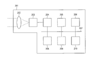
- FIG. 11 is a block diagram showing a configuration example of an image pickup device mounted on an electronic device.
- the electronic device 201 includes an optical system (an example of the “optical component” of the present disclosure) 202, an image pickup element 203, and a DSP (Digital Signal Processor; an example of the “signal processing circuit” of the present disclosure) 204.
- the DSP 204, the display device 205, the operation system 206, the memory 208, the recording device 209, and the power supply system 210 are connected and configured via the bus 207, and still images and moving images can be captured.
- the optical system 202 is configured to have one or a plurality of lenses, and guides the image light (incident light) from the subject to the image pickup element 203 to form an image on the light receiving surface (sensor unit) of the image pickup element 203.
- an image pickup device 100 having one or more of the above-mentioned pixels 102, 102A, 102B, 102C, 102D, and 102E in the pixel area 103 is applied. Electrons are accumulated in the image pickup device 203 for a certain period of time according to the image formed on the light receiving surface via the optical system 202. Then, a signal corresponding to the electrons stored in the image sensor 203 is supplied to the DSP 204.
- the DSP 204 performs various signal processing on the signal from the image sensor 203 to acquire an image, and temporarily stores the image data in the memory 208.
- the image data stored in the memory 208 is recorded in the recording device 209, or is supplied to the display device 205 to display the image.
- the operation system 206 accepts various operations by the user and supplies an operation signal to each block of the electronic device 201.
- the power supply system 210 supplies the electric power required to drive each block of the electronic device 201.
- the above-mentioned image pickup device 100 is applied as the image pickup element 203.
- the image pickup element 203 it is possible to improve the transfer characteristics of the electric charge e-in the image pickup device 203, and thus it is possible to improve the performance of the electronic device 201.
- the technique according to the present disclosure can be applied to various products.
- the techniques according to the present disclosure may be applied to an endoscopic surgery system.
- FIG. 12 is a diagram showing an example of a schematic configuration of an endoscopic surgery system to which the technique according to the present disclosure (the present technique) can be applied.
- FIG. 12 illustrates how the surgeon (doctor) 11131 is performing surgery on patient 11132 on patient bed 11133 using the endoscopic surgery system 11000.
- the endoscopic surgery system 11000 includes an endoscope 11100, other surgical tools 11110 such as an abdominal tube 11111 and an energy treatment tool 11112, and a support arm device 11120 that supports the endoscope 11100.
- a cart 11200 equipped with various devices for endoscopic surgery.
- the endoscope 11100 is composed of a lens barrel 11101 in which a region having a predetermined length from the tip is inserted into the body cavity of the patient 11132, and a camera head 11102 connected to the base end of the lens barrel 11101.
- the endoscope 11100 configured as a so-called rigid mirror having a rigid barrel 11101 is illustrated, but the endoscope 11100 may be configured as a so-called flexible mirror having a flexible barrel. good.
- An opening in which an objective lens is fitted is provided at the tip of the lens barrel 11101.
- a light source device 11203 is connected to the endoscope 11100, and the light generated by the light source device 11203 is guided to the tip of the lens barrel by a light guide extending inside the lens barrel 11101, and is an objective. It is irradiated toward the observation target in the body cavity of the patient 11132 through the lens.
- the endoscope 11100 may be a direct endoscope, a perspective mirror, or a side endoscope.
- An optical system and an image pickup element are provided inside the camera head 11102, and the reflected light (observation light) from the observation target is focused on the image pickup element by the optical system.
- the observation light is photoelectrically converted by the image pickup device, and an electric signal corresponding to the observation light, that is, an image signal corresponding to the observation image is generated.
- the image signal is transmitted as RAW data to the camera control unit (CCU: Camera Control Unit) 11201.
- the CCU11201 is composed of a CPU (Central Processing Unit), a GPU (Graphics Processing Unit), and the like, and comprehensively controls the operations of the endoscope 11100 and the display device 11202. Further, the CCU11201 receives an image signal from the camera head 11102, and performs various image processing on the image signal for displaying an image based on the image signal, such as development processing (demosaic processing).
- a CPU Central Processing Unit
- GPU Graphics Processing Unit
- the display device 11202 displays an image based on the image signal processed by the CCU 11201 under the control of the CCU 11201.
- the light source device 11203 is composed of, for example, a light source such as an LED (Light Emitting Diode), and supplies irradiation light for photographing an operating part or the like to the endoscope 11100.
- a light source such as an LED (Light Emitting Diode)
- LED Light Emitting Diode
- the input device 11204 is an input interface for the endoscopic surgery system 11000.
- the user can input various information and input instructions to the endoscopic surgery system 11000 via the input device 11204.
- the user inputs an instruction to change the imaging conditions (type of irradiation light, magnification, focal length, etc.) by the endoscope 11100.
- the treatment tool control device 11205 controls the drive of the energy treatment tool 11112 for cauterizing, incising, sealing a blood vessel, or the like.
- the pneumoperitoneum device 11206 uses a gas in the pneumoperitoneum tube 11111 to inflate the body cavity of the patient 11132 for the purpose of securing the field of view by the endoscope 11100 and securing the work space of the operator. Is sent.
- the recorder 11207 is a device capable of recording various information related to surgery.
- the printer 11208 is a device capable of printing various information related to surgery in various formats such as text, images, and graphs.
- the light source device 11203 that supplies the irradiation light to the endoscope 11100 when photographing the surgical site can be composed of, for example, an LED, a laser light source, or a white light source composed of a combination thereof.
- a white light source is configured by a combination of RGB laser light sources, the output intensity and output timing of each color (each wavelength) can be controlled with high accuracy. Therefore, the light source device 11203 adjusts the white balance of the captured image. It can be carried out.
- the laser light from each of the RGB laser light sources is irradiated to the observation target in a time-division manner, and the drive of the image sensor of the camera head 11102 is controlled in synchronization with the irradiation timing to correspond to each of RGB. It is also possible to capture the image in a time-division manner. According to this method, a color image can be obtained without providing a color filter in the image pickup device.
- the drive of the light source device 11203 may be controlled so as to change the intensity of the output light at predetermined time intervals.
- the drive of the image sensor of the camera head 11102 in synchronization with the timing of the change of the light intensity to acquire an image in time division and synthesizing the image, so-called high dynamic without blackout and overexposure. Range images can be generated.
- the light source device 11203 may be configured to be able to supply light in a predetermined wavelength band corresponding to special light observation.
- special light observation for example, by utilizing the wavelength dependence of light absorption in body tissue, the surface layer of the mucous membrane is irradiated with light in a narrower band than the irradiation light (that is, white light) during normal observation.
- a so-called narrow band imaging is performed in which a predetermined tissue such as a blood vessel is photographed with high contrast.
- fluorescence observation may be performed in which an image is obtained by fluorescence generated by irradiating with excitation light.
- the body tissue is irradiated with excitation light to observe the fluorescence from the body tissue (autofluorescence observation), or a reagent such as indocyanine green (ICG) is locally injected into the body tissue and the body tissue is injected. It is possible to obtain a fluorescence image by irradiating the excitation light corresponding to the fluorescence wavelength of the reagent.
- the light source device 11203 may be configured to be capable of supplying narrowband light and / or excitation light corresponding to such special light observation.
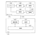
- FIG. 13 is a block diagram showing an example of the functional configuration of the camera head 11102 and CCU11201 shown in FIG.
- the camera head 11102 includes a lens unit 11401, an image pickup unit 11402, a drive unit 11403, a communication unit 11404, and a camera head control unit 11405.
- CCU11201 has a communication unit 11411, an image processing unit 11412, and a control unit 11413.
- the camera head 11102 and CCU11201 are communicably connected to each other by a transmission cable 11400.
- the lens unit 11401 is an optical system provided at a connection portion with the lens barrel 11101.
- the observation light taken in from the tip of the lens barrel 11101 is guided to the camera head 11102 and incident on the lens unit 11401.
- the lens unit 11401 is configured by combining a plurality of lenses including a zoom lens and a focus lens.
- the image pickup unit 11402 is composed of an image pickup element.
- the image pickup element constituting the image pickup unit 11402 may be one (so-called single plate type) or a plurality (so-called multi-plate type).
- each image pickup element may generate an image signal corresponding to each of RGB, and a color image may be obtained by synthesizing them.
- the image pickup unit 11402 may be configured to have a pair of image pickup elements for acquiring image signals for the right eye and the left eye corresponding to 3D (Dimensional) display, respectively.
- the 3D display enables the operator 11131 to more accurately grasp the depth of the living tissue in the surgical site.
- a plurality of lens units 11401 may be provided corresponding to each image pickup element.
- the image pickup unit 11402 does not necessarily have to be provided on the camera head 11102.
- the image pickup unit 11402 may be provided inside the lens barrel 11101 immediately after the objective lens.
- the drive unit 11403 is composed of an actuator, and the zoom lens and the focus lens of the lens unit 11401 are moved by a predetermined distance along the optical axis under the control of the camera head control unit 11405. As a result, the magnification and focus of the image captured by the image pickup unit 11402 can be adjusted as appropriate.
- the communication unit 11404 is configured by a communication device for transmitting and receiving various information to and from the CCU11201.
- the communication unit 11404 transmits the image signal obtained from the image pickup unit 11402 as RAW data to the CCU 11201 via the transmission cable 11400.
- the communication unit 11404 receives a control signal for controlling the drive of the camera head 11102 from the CCU 11201 and supplies the control signal to the camera head control unit 11405.
- the control signal includes, for example, information to specify the frame rate of the captured image, information to specify the exposure value at the time of imaging, and / or information to specify the magnification and focus of the captured image. Contains information about the condition.
- the image pickup conditions such as the frame rate, exposure value, magnification, and focus may be appropriately specified by the user, or may be automatically set by the control unit 11413 of the CCU11201 based on the acquired image signal. good.
- the endoscope 11100 is equipped with a so-called AE (Auto Exposure) function, an AF (Auto Focus) function, and an AWB (Auto White Balance) function.
- the camera head control unit 11405 controls the drive of the camera head 11102 based on the control signal from the CCU 11201 received via the communication unit 11404.
- the communication unit 11411 is configured by a communication device for transmitting and receiving various information to and from the camera head 11102.
- the communication unit 11411 receives an image signal transmitted from the camera head 11102 via the transmission cable 11400.
- the communication unit 11411 transmits a control signal for controlling the drive of the camera head 11102 to the camera head 11102.
- Image signals and control signals can be transmitted by telecommunications, optical communication, or the like.
- the image processing unit 11412 performs various image processing on the image signal which is the RAW data transmitted from the camera head 11102.
- the control unit 11413 performs various controls related to the imaging of the surgical site and the like by the endoscope 11100 and the display of the captured image obtained by the imaging of the surgical site and the like. For example, the control unit 11413 generates a control signal for controlling the drive of the camera head 11102.
- control unit 11413 causes the display device 11202 to display an image captured by the surgical unit or the like based on the image signal processed by the image processing unit 11412.
- the control unit 11413 may recognize various objects in the captured image by using various image recognition techniques.
- the control unit 11413 detects a surgical tool such as forceps, a specific biological part, bleeding, mist when using the energy treatment tool 11112, etc. by detecting the shape, color, etc. of the edge of the object included in the captured image. Can be recognized.
- the control unit 11413 may superimpose and display various surgical support information on the image of the surgical unit by using the recognition result. By superimposing and displaying the surgical support information and presenting it to the surgeon 11131, the burden on the surgeon 11131 can be reduced and the surgeon 11131 can surely proceed with the surgery.
- the transmission cable 11400 connecting the camera head 11102 and CCU11201 is an electric signal cable corresponding to electric signal communication, an optical fiber corresponding to optical communication, or a composite cable thereof.
- the communication is performed by wire using the transmission cable 11400, but the communication between the camera head 11102 and the CCU11201 may be performed wirelessly.
- the above is an example of an endoscopic surgery system to which the technique according to the present disclosure can be applied.
- the technique according to the present disclosure can be applied to the endoscope 11100, the image pickup unit 11402 of the camera head 11102, the image processing unit 11412 of the CCU 11201, and the like among the configurations described above.
- the above-mentioned imaging device 100 can be applied to the imaging unit 10402.
- a clearer surgical site image can be obtained, so that the operator can perform the operation. It becomes possible to confirm the part reliably.
- the surgical site image can be obtained with lower latency. It becomes possible to perform the treatment with the same feeling as when the person is observing the surgical site by touch.
- the technique according to the present disclosure may be applied to other, for example, a microscopic surgery system.
- the technique according to the present disclosure can be applied to various products.
- the technology according to the present disclosure is realized as a device mounted on a moving body of any kind such as an automobile, an electric vehicle, a hybrid electric vehicle, a motorcycle, a bicycle, a personal mobility, an airplane, a drone, a ship, and a robot. You may.
- FIG. 14 is a block diagram showing a schematic configuration example of a vehicle control system, which is an example of a mobile control system to which the technique according to the present disclosure can be applied.
- the vehicle control system 12000 includes a plurality of electronic control units connected via the communication network 12001.
- the vehicle control system 12000 includes a drive system control unit 12010, a body system control unit 12020, an outside information detection unit 12030, an in-vehicle information detection unit 12040, and an integrated control unit 12050.
- a microcomputer 12051, an audio image output unit 12052, and an in-vehicle network I / F (interface) 12053 are shown as a functional configuration of the integrated control unit 12050.
- the drive system control unit 12010 controls the operation of the device related to the drive system of the vehicle according to various programs.
- the drive system control unit 12010 has a driving force generator for generating a driving force of a vehicle such as an internal combustion engine or a driving motor, a driving force transmission mechanism for transmitting the driving force to the wheels, and a steering angle of the vehicle. It functions as a control device such as a steering mechanism for adjusting and a braking device for generating braking force of the vehicle.
- the body system control unit 12020 controls the operation of various devices mounted on the vehicle body according to various programs.
- the body system control unit 12020 functions as a keyless entry system, a smart key system, a power window device, or a control device for various lamps such as headlamps, back lamps, brake lamps, turn signals or fog lamps.
- the body system control unit 12020 may be input with radio waves transmitted from a portable device that substitutes for the key or signals of various switches.
- the body system control unit 12020 receives inputs of these radio waves or signals and controls a vehicle door lock device, a power window device, a lamp, and the like.
- the outside information detection unit 12030 detects information outside the vehicle equipped with the vehicle control system 12000.
- the image pickup unit 12031 is connected to the vehicle outside information detection unit 12030.
- the vehicle outside information detection unit 12030 causes the image pickup unit 12031 to capture an image of the outside of the vehicle and receives the captured image.
- the out-of-vehicle information detection unit 12030 may perform object detection processing or distance detection processing such as a person, a vehicle, an obstacle, a sign, or a character on the road surface based on the received image.
- the image pickup unit 12031 is an optical sensor that receives light and outputs an electric signal according to the amount of the light received.
- the image pickup unit 12031 can output an electric signal as an image or can output it as distance measurement information. Further, the light received by the image pickup unit 12031 may be visible light or invisible light such as infrared light.
- the in-vehicle information detection unit 12040 detects the in-vehicle information.
- a driver state detection unit 12041 that detects a driver's state is connected to the vehicle interior information detection unit 12040.
- the driver state detection unit 12041 includes, for example, a camera that images the driver, and the in-vehicle information detection unit 12040 determines the degree of fatigue or concentration of the driver based on the detection information input from the driver state detection unit 12041. It may be calculated, or it may be determined whether or not the driver has fallen asleep.
- the microcomputer 12051 calculates the control target value of the driving force generator, the steering mechanism, or the braking device based on the information inside and outside the vehicle acquired by the vehicle exterior information detection unit 12030 or the vehicle interior information detection unit 12040, and the drive system control unit.
- a control command can be output to 12010.
- the microcomputer 12051 realizes ADAS (Advanced Driver Assistance System) functions including vehicle collision avoidance or impact mitigation, follow-up driving based on inter-vehicle distance, vehicle speed maintenance driving, vehicle collision warning, vehicle lane deviation warning, and the like. It is possible to perform cooperative control for the purpose of.
- ADAS Advanced Driver Assistance System
- the microcomputer 12051 controls the driving force generating device, the steering mechanism, the braking device, and the like based on the information around the vehicle acquired by the outside information detection unit 12030 or the inside information detection unit 12040, so that the driver can control the driver. It is possible to perform coordinated control for the purpose of automatic driving that runs autonomously without depending on the operation.
- the microcomputer 12051 can output a control command to the body system control unit 12020 based on the information outside the vehicle acquired by the vehicle outside information detection unit 12030.
- the microcomputer 12051 controls the headlamps according to the position of the preceding vehicle or the oncoming vehicle detected by the outside information detection unit 12030, and performs cooperative control for the purpose of anti-glare such as switching the high beam to the low beam. It can be carried out.
- the audio image output unit 12052 transmits an output signal of at least one of audio and image to an output device capable of visually or audibly notifying information to the passenger or the outside of the vehicle.
- an audio speaker 12061, a display unit 12062, and an instrument panel 12063 are exemplified as output devices.
- the display unit 12062 may include, for example, at least one of an onboard display and a head-up display.
- FIG. 15 is a diagram showing an example of the installation position of the image pickup unit 12031.
- the vehicle 12100 has an imaging unit 12101, 12102, 12103, 12104, 12105 as an imaging unit 12031.
- the image pickup units 12101, 12102, 12103, 12104, 12105 are provided, for example, at positions such as the front nose, side mirrors, rear bumpers, back doors, and the upper part of the windshield in the vehicle interior of the vehicle 12100.
- the image pickup unit 12101 provided in the front nose and the image pickup section 12105 provided in the upper part of the windshield in the vehicle interior mainly acquire an image in front of the vehicle 12100.
- the image pickup units 12102 and 12103 provided in the side mirror mainly acquire images of the side of the vehicle 12100.
- the image pickup unit 12104 provided in the rear bumper or the back door mainly acquires an image of the rear of the vehicle 12100.
- the images in front acquired by the image pickup units 12101 and 12105 are mainly used for detecting a preceding vehicle, a pedestrian, an obstacle, a traffic light, a traffic sign, a lane, or the like.
- FIG. 15 shows an example of the shooting range of the imaging units 12101 to 12104.
- the imaging range 12111 indicates the imaging range of the imaging unit 12101 provided on the front nose
- the imaging ranges 12112 and 12113 indicate the imaging range of the imaging units 12102 and 12103 provided on the side mirrors, respectively
- the imaging range 12114 indicates the imaging range.
- the imaging range of the imaging unit 12104 provided on the rear bumper or the back door is shown. For example, by superimposing the image data captured by the imaging units 12101 to 12104, a bird's-eye view image of the vehicle 12100 can be obtained.
- At least one of the image pickup units 12101 to 12104 may have a function of acquiring distance information.
- at least one of the image pickup units 12101 to 12104 may be a stereo camera including a plurality of image pickup elements, or may be an image pickup element having pixels for phase difference detection.
- the microcomputer 12051 has a distance to each three-dimensional object in the image pickup range 12111 to 12114 based on the distance information obtained from the image pickup unit 12101 to 12104, and a temporal change of this distance (relative speed with respect to the vehicle 12100). By obtaining can. Further, the microcomputer 12051 can set an inter-vehicle distance to be secured in advance in front of the preceding vehicle, and can perform automatic brake control (including follow-up stop control), automatic acceleration control (including follow-up start control), and the like. In this way, it is possible to perform coordinated control for the purpose of automatic driving or the like that autonomously travels without relying on the driver's operation.
- automatic brake control including follow-up stop control
- automatic acceleration control including follow-up start control
- the microcomputer 12051 converts three-dimensional object data related to a three-dimensional object into two-wheeled vehicles, ordinary vehicles, large vehicles, pedestrians, electric poles, and other three-dimensional objects based on the distance information obtained from the image pickup units 12101 to 12104. It can be classified and extracted and used for automatic avoidance of obstacles. For example, the microcomputer 12051 distinguishes obstacles around the vehicle 12100 into obstacles that are visible to the driver of the vehicle 12100 and obstacles that are difficult to see. Then, the microcomputer 12051 determines the collision risk indicating the risk of collision with each obstacle, and when the collision risk is equal to or higher than the set value and there is a possibility of collision, the microcomputer 12051 via the audio speaker 12061 or the display unit 12062. By outputting an alarm to the driver and performing forced deceleration and avoidance steering via the drive system control unit 12010, driving support for collision avoidance can be provided.
- At least one of the image pickup units 12101 to 12104 may be an infrared camera that detects infrared rays.
- the microcomputer 12051 can recognize a pedestrian by determining whether or not a pedestrian is present in the captured image of the imaging unit 12101 to 12104.
- recognition of a pedestrian is, for example, a procedure for extracting feature points in an image captured by an image pickup unit 12101 to 12104 as an infrared camera, and pattern matching processing is performed on a series of feature points indicating the outline of an object to determine whether or not the pedestrian is a pedestrian. It is done by the procedure to determine.
- the audio image output unit 12052 determines the square contour line for emphasizing the recognized pedestrian.
- the display unit 12062 is controlled so as to superimpose and display. Further, the audio image output unit 12052 may control the display unit 12062 so as to display an icon or the like indicating a pedestrian at a desired position.
- the above is an example of a vehicle control system to which the technique according to the present disclosure can be applied.
- the technique according to the present disclosure can be applied to the image pickup unit 12031 or the like among the configurations described above.
- the above-mentioned imaging device 100 can be applied to the imaging unit 12031.
- the present disclosure may also have the following structure.
- a vertical transistor provided on the semiconductor substrate is provided.
- the semiconductor substrate is provided with a hole that opens on the first main surface side.
- the vertical transistor is The first gate electrode provided inside the hole and It has a second gate electrode provided on the outside of the hole and connected to the first gate electrode.
- the first gate electrode is The first part and An image pickup apparatus having a second portion made of a material having a conductivity different from that of the first portion.
- the image pickup apparatus according to (1) wherein the first portion is located between the second portion and the second gate electrode.
- the first portion and the second portion are each composed of a first conductive type semiconductor.
- the image pickup apparatus according to any one of (1) to (3), wherein the concentration of the first conductive type impurities in the second portion is lower than the concentration of the first conductive type impurities in the first portion.
- the first gate electrode is It further has a third portion, which is located on the opposite side of the first portion with the second portion in between and is composed of a first conductive type semiconductor.
- the image pickup apparatus according to (4), wherein the concentration of the first conductive type impurities in the third portion is lower than the concentration of the first conductive type impurities in the second portion.
- the first part is composed of a first conductive type semiconductor, and is composed of a first conductive type semiconductor.
- the image pickup apparatus according to any one of (1) to (3) above, wherein the second portion is composed of a non-doped semiconductor.
- the first part is composed of a first conductive type semiconductor, and is composed of a first conductive type semiconductor.
- the image pickup apparatus according to any one of (1) to (3) above, wherein the second portion is composed of a second conductive type semiconductor.
- the first part is composed of a first conductive type semiconductor, and is composed of a first conductive type semiconductor.
- the imaging device according to any one of (1) to (3) above, wherein the second portion is made of metal.
- the photoelectric conversion unit provided on the semiconductor substrate and Further, a charge holding unit provided on the semiconductor substrate and holding a charge generated by the photoelectric conversion unit is provided.
- the image pickup apparatus according to any one of (1) to (8), wherein the vertical transistor is used as a transfer transistor for transferring charges from the photoelectric conversion unit to the charge holding unit.
- Optical parts and An image pickup device in which light transmitted through the optical component is incident, and A signal processing circuit for processing a signal output from the image pickup apparatus is provided.
- the image pickup device With a semiconductor substrate, A vertical transistor provided on the semiconductor substrate is provided.
- the semiconductor substrate is provided with a hole that opens on the first main surface side.
- the vertical transistor is The first gate electrode provided inside the hole and It has a second gate electrode provided on the outside of the hole and connected to the first gate electrode.
- the first gate electrode is The first part and An electronic device having a second portion made of a material having a conductivity different from that of the first portion.
Landscapes
- Solid State Image Pick-Up Elements (AREA)
Priority Applications (4)
| Application Number | Priority Date | Filing Date | Title |
|---|---|---|---|
| CN202180084234.7A CN116670815A (zh) | 2020-12-21 | 2021-11-11 | 成像设备和电子设备 |
| KR1020237017421A KR20230121727A (ko) | 2020-12-21 | 2021-11-11 | 촬상 장치 및 전자 기기 |
| US18/256,901 US20240030246A1 (en) | 2020-12-21 | 2021-11-11 | Imaging device and electronic device |
| JP2022571948A JPWO2022137864A1 (https=) | 2020-12-21 | 2021-11-11 |
Applications Claiming Priority (2)
| Application Number | Priority Date | Filing Date | Title |
|---|---|---|---|
| JP2020-211800 | 2020-12-21 | ||
| JP2020211800 | 2020-12-21 |
Publications (1)
| Publication Number | Publication Date |
|---|---|
| WO2022137864A1 true WO2022137864A1 (ja) | 2022-06-30 |
Family
ID=82157592
Family Applications (1)
| Application Number | Title | Priority Date | Filing Date |
|---|---|---|---|
| PCT/JP2021/041467 Ceased WO2022137864A1 (ja) | 2020-12-21 | 2021-11-11 | 撮像装置及び電子機器 |
Country Status (5)
| Country | Link |
|---|---|
| US (1) | US20240030246A1 (https=) |
| JP (1) | JPWO2022137864A1 (https=) |
| KR (1) | KR20230121727A (https=) |
| CN (1) | CN116670815A (https=) |
| WO (1) | WO2022137864A1 (https=) |
Citations (6)
| Publication number | Priority date | Publication date | Assignee | Title |
|---|---|---|---|---|
| US20060118835A1 (en) * | 2004-12-03 | 2006-06-08 | International Business Machines Corporation | Predoped transfer gate for an image sensor |
| US20060124976A1 (en) * | 2004-12-15 | 2006-06-15 | International Business Machines Corporation | Recessed gate for an image sensor |
| JP2008078489A (ja) * | 2006-09-22 | 2008-04-03 | Asahi Kasei Electronics Co Ltd | Cmosイメージセンサおよびその製造方法 |
| JP2010512004A (ja) * | 2006-12-01 | 2010-04-15 | イーストマン コダック カンパニー | 撮像素子トランスファゲートデバイスにおけるシリサイドストラップ |
| JP2013084834A (ja) * | 2011-10-12 | 2013-05-09 | Sharp Corp | 固体撮像素子及び固体撮像素子の製造方法 |
| JP2016162788A (ja) * | 2015-02-27 | 2016-09-05 | ソニー株式会社 | 撮像素子、撮像装置、並びに、製造装置および方法 |
Family Cites Families (1)
| Publication number | Priority date | Publication date | Assignee | Title |
|---|---|---|---|---|
| JP2013026264A (ja) | 2011-07-15 | 2013-02-04 | Sony Corp | 固体撮像素子、固体撮像素子の製造方法、及び、電子機器 |
-
2021
- 2021-11-11 CN CN202180084234.7A patent/CN116670815A/zh not_active Withdrawn
- 2021-11-11 US US18/256,901 patent/US20240030246A1/en active Pending
- 2021-11-11 WO PCT/JP2021/041467 patent/WO2022137864A1/ja not_active Ceased
- 2021-11-11 JP JP2022571948A patent/JPWO2022137864A1/ja not_active Abandoned
- 2021-11-11 KR KR1020237017421A patent/KR20230121727A/ko active Pending
Patent Citations (6)
| Publication number | Priority date | Publication date | Assignee | Title |
|---|---|---|---|---|
| US20060118835A1 (en) * | 2004-12-03 | 2006-06-08 | International Business Machines Corporation | Predoped transfer gate for an image sensor |
| US20060124976A1 (en) * | 2004-12-15 | 2006-06-15 | International Business Machines Corporation | Recessed gate for an image sensor |
| JP2008078489A (ja) * | 2006-09-22 | 2008-04-03 | Asahi Kasei Electronics Co Ltd | Cmosイメージセンサおよびその製造方法 |
| JP2010512004A (ja) * | 2006-12-01 | 2010-04-15 | イーストマン コダック カンパニー | 撮像素子トランスファゲートデバイスにおけるシリサイドストラップ |
| JP2013084834A (ja) * | 2011-10-12 | 2013-05-09 | Sharp Corp | 固体撮像素子及び固体撮像素子の製造方法 |
| JP2016162788A (ja) * | 2015-02-27 | 2016-09-05 | ソニー株式会社 | 撮像素子、撮像装置、並びに、製造装置および方法 |
Also Published As
| Publication number | Publication date |
|---|---|
| CN116670815A (zh) | 2023-08-29 |
| JPWO2022137864A1 (https=) | 2022-06-30 |
| US20240030246A1 (en) | 2024-01-25 |
| KR20230121727A (ko) | 2023-08-21 |
Similar Documents
| Publication | Publication Date | Title |
|---|---|---|
| US12414390B2 (en) | Solid-state imaging device and solid-state imaging apparatus | |
| US12464845B2 (en) | Solid-state imaging element and electronic apparatus | |
| JP7558164B2 (ja) | 固体撮像素子、固体撮像素子の製造方法 | |
| US20230170360A1 (en) | Imaging apparatus and electronic device | |
| JPWO2018180575A1 (ja) | 固体撮像素子、電子機器、並びに製造方法 | |
| WO2022131034A1 (ja) | 撮像装置 | |
| US20220254823A1 (en) | Imaging device | |
| WO2021124974A1 (ja) | 撮像装置 | |
| US20240194706A1 (en) | Solid-state imaging device | |
| WO2019181466A1 (ja) | 撮像素子、電子機器 | |
| US20250113530A1 (en) | Vertical transistor, light detection apparatus, and electronic device | |
| US20240313014A1 (en) | Imaging apparatus and electronic device | |
| TW202345371A (zh) | 光檢測裝置 | |
| WO2022158170A1 (ja) | 光検出素子および電子機器 | |
| WO2022137864A1 (ja) | 撮像装置及び電子機器 | |
| WO2021140958A1 (ja) | 撮像素子、製造方法、並びに電子機器 | |
| US20250006753A1 (en) | Semiconductor device and imaging apparatus | |
| US20250081643A1 (en) | Solid-state imaging device and electronic device | |
| WO2025100321A1 (ja) | 光検出装置 | |
| WO2024057805A1 (ja) | 撮像素子および電子機器 | |
| EP4654264A1 (en) | Semiconductor device | |
| WO2021172176A1 (ja) | 固体撮像装置及び電子機器 | |
| CN119631598A (zh) | 半导体装置和半导体装置的制造方法 |
Legal Events
| Date | Code | Title | Description |
|---|---|---|---|
| 121 | Ep: the epo has been informed by wipo that ep was designated in this application |
Ref document number: 21910018 Country of ref document: EP Kind code of ref document: A1 |
|
| ENP | Entry into the national phase |
Ref document number: 2022571948 Country of ref document: JP Kind code of ref document: A |
|
| WWE | Wipo information: entry into national phase |
Ref document number: 18256901 Country of ref document: US |
|
| WWE | Wipo information: entry into national phase |
Ref document number: 202180084234.7 Country of ref document: CN |
|
| NENP | Non-entry into the national phase |
Ref country code: DE |
|
| 122 | Ep: pct application non-entry in european phase |
Ref document number: 21910018 Country of ref document: EP Kind code of ref document: A1 |
|
| WWW | Wipo information: withdrawn in national office |
Ref document number: 1020237017421 Country of ref document: KR |