WO2022131341A1 - Switch drive circuit - Google Patents
Switch drive circuit Download PDFInfo
- Publication number
- WO2022131341A1 WO2022131341A1 PCT/JP2021/046586 JP2021046586W WO2022131341A1 WO 2022131341 A1 WO2022131341 A1 WO 2022131341A1 JP 2021046586 W JP2021046586 W JP 2021046586W WO 2022131341 A1 WO2022131341 A1 WO 2022131341A1
- Authority
- WO
- WIPO (PCT)
- Prior art keywords
- circuit
- voltage
- battery
- switch drive
- drive circuit
- Prior art date
Links
- 230000002265 prevention Effects 0.000 claims description 9
- 230000004044 response Effects 0.000 description 3
- 238000010586 diagram Methods 0.000 description 2
- 230000006870 function Effects 0.000 description 1
- 238000012986 modification Methods 0.000 description 1
- 230000004048 modification Effects 0.000 description 1
Images

Classifications
-
- H—ELECTRICITY
- H02—GENERATION; CONVERSION OR DISTRIBUTION OF ELECTRIC POWER
- H02J—CIRCUIT ARRANGEMENTS OR SYSTEMS FOR SUPPLYING OR DISTRIBUTING ELECTRIC POWER; SYSTEMS FOR STORING ELECTRIC ENERGY
- H02J1/00—Circuit arrangements for dc mains or dc distribution networks
-
- H—ELECTRICITY
- H02—GENERATION; CONVERSION OR DISTRIBUTION OF ELECTRIC POWER
- H02J—CIRCUIT ARRANGEMENTS OR SYSTEMS FOR SUPPLYING OR DISTRIBUTING ELECTRIC POWER; SYSTEMS FOR STORING ELECTRIC ENERGY
- H02J7/00—Circuit arrangements for charging or depolarising batteries or for supplying loads from batteries
-
- H—ELECTRICITY
- H03—ELECTRONIC CIRCUITRY
- H03K—PULSE TECHNIQUE
- H03K17/00—Electronic switching or gating, i.e. not by contact-making and –breaking
- H03K17/51—Electronic switching or gating, i.e. not by contact-making and –breaking characterised by the components used
- H03K17/56—Electronic switching or gating, i.e. not by contact-making and –breaking characterised by the components used by the use, as active elements, of semiconductor devices
- H03K17/687—Electronic switching or gating, i.e. not by contact-making and –breaking characterised by the components used by the use, as active elements, of semiconductor devices the devices being field-effect transistors
Definitions
- the present invention relates to a switch drive circuit.
- the vehicle control device disclosed in Patent Document 1 has a first power input unit connected to a first power supply system to which power is supplied in conjunction with the ignition state of the vehicle, and a power source regardless of the ignition state.
- the first device control unit is supplied with operating power from both the first power input unit and the second power input unit.
- the power supply voltage is boosted by a charge pump to obtain a drive voltage for driving the high-side switch.
- the lower the power supply voltage the lower the drive voltage of the high-side switch. Therefore, if the battery voltage drops significantly in a battery-powered vehicle, the high-side switch may not be sufficiently driven. There is sex.
- the present invention has been made in view of the conventional circumstances, and an object thereof is a switch drive circuit capable of obtaining a drive voltage for driving a high-side switch even if there is a voltage fluctuation of a battery with a small number of parts. Is to provide.
- the switch drive circuit is, in one embodiment, a switch drive circuit for driving a high-side switch, which is a booster circuit for boosting an input voltage to a drive voltage for driving the high-side switch.
- a driver circuit that applies the drive voltage boosted by the booster circuit to the high-side switch based on a control signal, and a first voltage supply circuit that supplies a voltage from the battery to the booster circuit to prevent backflow of current.
- a first voltage supply circuit provided with one backflow prevention element, a second voltage supply circuit provided in parallel with the first voltage supply circuit, a buck-boost circuit for buckling the voltage of the battery, and a buck-boost. It has the second voltage supply circuit provided with a second backflow prevention element connected in series to the output side of the circuit.
- FIG. 1 is a circuit diagram of an ECU (Electronic Control Unit) for an automobile including a high-side switch drive circuit.
- ECU Electronic Control Unit
- the ECU 100 of FIG. 1 is mounted on an automobile 300 equipped with a battery 200 as a power source, and includes a high-side switch drive circuit 150 for controlling energization of a load 310.
- the load 310 is, for example, a solenoid valve that controls the flow of brake hydraulic pressure in a stability control system (ESC).
- ESC stability control system
- the battery 200 is charged by an alternator (not shown), and the electric power of the battery 200 is used for driving the automobile 300.
- the nominal voltage (rated voltage) of the battery 200 is 12 [V].
- the n-type MOSFET 320 constituting the high-side switch (high-side relay) that controls the energization of the load 310 is connected between the battery 200 and the load 310.
- the drain D of the MOSFET 320 is connected to the battery 200, the source S is connected to the load 310, and the gate G is connected to the output terminal of the driver IC 102. Then, the load 310 is connected between the source S of the MOSFET 320 and the ground GND.
- the cutoff circuit 101 (relay circuit) is connected to the battery 200 and switches between power output and cutoff of the battery 200 based on a wake-up signal from the outside.
- the cutoff circuit 101 acquires an on / off signal of the ignition switch (IGSW) 330 as a wake-up signal, and outputs the electric power of the battery 200 in the on state of the ignition switch 330.
- the ignition switch 330 is an engine switch that controls the operation and stop of the engine mounted on the automobile 300, and the engine drives an alternator for charging the battery 200.
- the driver IC 102 applies the charge pump 102a, which is a booster circuit that boosts the input voltage V4 to the drive voltage for driving the MOSFET 320, and the drive voltage boosted by the charge pump 102a to the gate G of the MOSFET 320 based on the control signal. It has a driver circuit 102b.
- the output terminal of the cutoff circuit 101 and the input terminal of the charge pump 102a are connected by the first voltage supply circuit 103. Then, the first voltage supply circuit 103 supplies the voltage VBATT of the battery 200 output from the cutoff circuit 101 to the charge pump 102a.
- the first voltage supply circuit 103 includes a first diode 103a as a first backflow prevention element for preventing backflow of current.
- the first diode 103a is a rectifying element that allows a current to flow from the cutoff circuit 101 toward the charge pump 102a and does not allow a current (reverse current) to flow from the charge pump 102a toward the cutoff circuit 101.
- the buck-boost circuit 104a is a circuit that acquires the voltage VBATT of the battery 200 output from the cutoff circuit 101 and performs step-up and step-down operations so that the output voltage becomes constant even if the voltage VBATT) fluctuates.
- V3 is set to 8 [V].
- a second diode 104b as a second backflow prevention element is connected in series to the output terminal of the buck-boost circuit 104a.
- the second voltage supply circuit 104 which is a circuit in which the buck-boost circuit 104a and the second diode 104b are connected in series, is provided in parallel with the first voltage supply circuit 103 (first diode 103a).
- the second diode 104b is a rectifying element in which a current flows from the buck-boost circuit 104a toward the charge pump 102a and no current (current in the reverse direction) flows from the charge pump 102a toward the buck-boost circuit 104a.
- driver IC 102 charge pump 102a, driver circuit 102b
- first voltage supply circuit 103 first diode 103a
- second voltage supply circuit 104 boost voltage circuit 104a, second diode 104b
- the high side switch drive circuit 150 is configured.
- the microcomputer 105 includes a microprocessor (MPU), a read-only memory (ROM), a random access memory (RAM), and the like. Then, the microcomputer 105 controls whether or not the drive voltage boosted by the charge pump 102a is applied to the gate G of the MOSFET 320, in other words, on / off of the MOSFET 320 by outputting a control signal to the driver circuit 102b. do. Further, the microcomputer 105 outputs a wake-up signal to the cutoff circuit 101, and outputs the power of the battery 200 from the cutoff circuit 101 even when the ignition switch 330 is in the off state.
- MPU microprocessor
- ROM read-only memory
- RAM random access memory
- the control circuit (including the control circuit) is stepped down to 3.3 [V], which is the operating power supply voltage, and output.
- the microcomputer 105 operates using the output voltage (3.3 [V]) of the step-down circuit 106 as the power supply voltage, and performs stability control through output processing of the control signal to the driver circuit 102b, in other words, on / off control of the MOSFET 320. implement.
- the step-down circuit 107 acquires a voltage V3 from between the step-up / down circuit 104a and the second diode 104b, and sets the output voltage (8 [V]) of the step-up / down circuit 104a as the operating power supply voltage of the CAN-IC 108.
- the voltage is stepped down to 5 [V] and output.
- a plurality of ECUs including the ECU 100 and the ECU 340 are connected to the CAN bus 350 as nodes to form an in-vehicle network.
- the in-vehicle network of the present embodiment adopts CAN (Controller Area Network) as a communication standard, but the communication standard of the in-vehicle network is not limited to CAN.
- CAN Controller Area Network
- the CAN-IC 108 acquires a voltage from the step-down circuit 107 and is connected to the battery 200 via the third diode 110, and the standby voltage V1 is constantly supplied from the battery 200. That is, even when the cutoff circuit 101 cuts off the power of the battery 200, the standby voltage V1 is directly supplied to the CAN-IC 108 from the battery 200.
- the third diode 110 is a rectifying element that allows a current to flow from the battery 200 toward the CAN-IC 108 and does not allow a current (reverse current) to flow from the CAN-IC 108 toward the battery 200.
- the voltage is stepped down to the power supply voltage of various sensors 360 and output to the sensor 360.
- the step-down circuit 109 is a voltage tracker IC having high resistance to external electromagnetic noise, and acquires the output voltage (5 [V]) of the step-down circuit 107 as a reference voltage.
- the step-down voltage is supplied to the microcomputer 105, the CAN-IC108, and the sensor 360, respectively.
- step-down circuits 106, 107, 109 acquire the constant voltage V3 output by the step-up / down circuit 104a, the load of the step-down operation in the step-down circuits 106, 107, 109 is reduced, and when the engine is started, etc.
- the voltage VBATT of the battery 200 drops, the power supply to the microcomputer 105 and the like is stabilized.
- the input / output interface 111 is a device for communicating with another ECU 370 mounted on the automobile 300.
- the input / output interface 111 acquires the voltage V2 from between the cutoff circuit 101 and the first diode 103a of the first voltage supply circuit 103 via the fourth diode 112.
- the input / output interface 111 is a circuit that needs to be supplied with power when the ECU 100 is operating, a wake-up signal such as a signal of the ignition switch 330 is supplied to the cutoff circuit 101, and the cutoff circuit 101 is the voltage of the battery 200.
- the voltage V2 is supplied to the input / output interface 111.
- the fourth diode 112 is a rectifying element in which a current flows from the cutoff circuit 101 toward the input / output interface 111 and no current (current in the opposite direction) flows from the input / output interface 111 toward the cutoff circuit 101.
- the driver IC 102 has a voltage equivalent to the voltage supplied to the input / output interface 111 via the first voltage supply circuit 103, that is, A voltage obtained by subtracting the voltage drop due to the diode from the voltage VBATT of the battery 200 is supplied.
- the voltage V4 supplied to the driver IC 102 becomes the second voltage supply circuit from the voltage supplied via the first voltage supply circuit 103. It automatically switches to the output voltage V3 of the buck-boost circuit 104a supplied from 104. That is, when the voltage VBATT of the battery 200 is equal to or higher than the output voltage V3 of the buck-boost circuit 104a, the voltage V4 supplied to the driver IC 102 is equivalent to the voltage BATT of the battery 200 and responds to fluctuations in the voltage BATT of the battery 200. Change.
- the voltage V4 supplied to the driver IC 102 is maintained at the output voltage V3 of the buck-boost circuit 104a.
- the current directed to the cutoff circuit 101 is cut off by the first diode 103a included in the first voltage supply circuit 103, and the current directed to the buck-boost circuit 104a by the second diode 104b included in the second voltage supply circuit 104.
- the input voltage V4 of the driver IC 102 becomes higher than the voltage BATT of the battery 200 and the output voltage V3 of the buck-boost circuit 104a.
- the input voltage V4 of the charge pump 102a of the driver IC 102 also needs to be increased following the voltage VBATT of the battery 200.
- a voltage equivalent to the voltage VBATT of the battery 200 is acquired by the charge pump 102a via the first voltage supply circuit 103, so that the MOSFET 320 can be driven by the driver IC 102.
- the MOSFET 320 can be sufficiently driven. It may disappear.
- the output voltage V3 of the buck-boost circuit 104a is used for the charge pump 102a instead of the voltage VBATT of the battery 200. Since it is input, the MOSFET 320 can be sufficiently driven even if the voltage VBATT of the battery 200 drops.
- the circuit is formed by the combination of the first voltage supply circuit 103 including the first diode 103a and the second voltage supply circuit 104 including the buck-boost circuit 104a and the second diode 104b.
- the MOSFET 320 can be stably driven even if the voltage VBATT of the battery 200 fluctuates while suppressing the increase in the number of parts.
- the output voltage of the buck-boost circuit 104a is always the input voltage V4 of the charge pump 102a, it is possible to prevent the input voltage V4 of the charge pump 102a from dropping when the voltage VBATT of the battery 200 becomes low, but the battery 200 Even if the voltage VBATT of the above becomes high, the input voltage V4 of the charge pump 102a does not change.
- the input of the charge pump 102a is input when the voltage VBATT of the battery 200 becomes low by using the step-up / down circuit 104a without using the step-up circuit and the step-down circuit in combination.
- the input voltage V4 of the charge pump 102a can also be increased when the voltage VBATT of the battery 200 becomes high while suppressing the decrease of the voltage V4. Therefore, compared to the case where the step-up circuit and the step-down circuit are used in combination, even if the voltage VBATT of the battery 200 fluctuates while suppressing the increase in the number of parts of the circuit, it becomes a half-on state and operates on and off. Is suppressed, and the MOSFET 320 can be driven stably.
- the output voltage V3 of the buck-boost circuit 104a needs to be equal to or higher than the minimum operating voltage of the driver IC 102. Further, since the step-down circuits 106, 107, 109 acquire the output voltage V3 of the step-down circuit 104a and perform the step-down operation, the output voltage V3 of the step-down circuit 104a is higher than the output voltage of the step-down circuits 106, 107, 109. The higher the value, the larger the loss in the step-down circuits 106, 107, 109.
- the output voltage V3 of the step-up / down circuit 104a is set to a voltage slightly higher than the minimum operating voltage or the minimum operating voltage of the driver IC 102.
- the output voltage of the buck-boost circuit 104a is set to 8 [V].
- the voltage VBATT of the battery 200 is generally 13 [V] or more.
- the step-down circuits 106, 107, 109 acquire the output voltage (8 [V]) of the step-up / down circuit 104a, the step-down is about 5 [V] in advance as compared with the case of directly acquiring the voltage VBATT of the battery 200.
- the loss in the step-down circuits 106, 107, 109 is reduced.
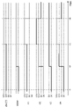
- the time chart of FIG. 2 shows the operation of the circuit shown in FIG.
- the voltages V1, V2, and V4 shown in the time chart of FIG. 2 are voltages when it is assumed that all the voltage drops in the diode are 1 [V].
- the cutoff circuit 101 starts outputting the voltage VBATT of the battery 200.
- the input voltage V2 of the input / output interface 111 is switched from 0 [V] to 11 [V]
- the output voltage V3 of the buck-boost circuit 104a is switched from 0 [V] to 8 [V].
- the input voltage V4 of the driver IC 102 is a voltage drop from 12 [V], which is the voltage VBATT of the battery 200, by the first diode 103a. It becomes 11 [V] after subtracting the minute.
- the standby voltage V1 applied to the CAN-IC 108 in response to the voltage rise increases from 11 [V] to 17 It rises to [V].
- the input voltage V2 of the input / output interface 111 also rises from 11 [V] to 17 [V].
- the output voltage V3 of the buck-boost circuit 104a is held at 8 [V] even if the voltage VBATT of the battery 200 rises.
- the input voltage V4 of the driver IC 102 is a voltage from 18 [V], which is the voltage VBATT of the battery 200, to the first diode 103a. It becomes 17 [V] after subtracting the amount of descent.
- the standby voltage V1 applied to the CAN-IC 108 in response to the voltage drop is 5 from 17 [V]. It descends to [V]. Further, the input voltage V2 of the input / output interface 111 also drops from 17 [V] to 5 [V]. On the other hand, the output voltage V3 of the buck-boost circuit 104a is held at 8 [V] even if the voltage VBATT of the battery 200 drops.
- the input voltage V4 of the driver IC 102 is from 8 [V] which is the output voltage V3 of the buck-boost circuit 104a to the second diode 104b. It becomes 7 [V] after subtracting the voltage drop due to.
- the input voltage V4 of the driver IC 102 holds 7 [V] or more even if the voltage VBATT of the battery 200 drops, and the voltage VBATT of the battery 200 keeps the output voltage V3 (8) of the step-up / down circuit 104a.
- the higher the voltage VBATT of the battery 200 the higher the voltage.
- the first voltage supply circuit 103 can be a circuit that directly supplies the voltage of the battery 200 to the driver IC 102 without going through the cutoff circuit 101. Further, in the high-side switch drive circuit 150 provided with the first voltage supply circuit 103, the driver IC 102 can have a function of outputting a wake-up signal to the cutoff circuit 101.
- the high-side switch is not limited to the configuration consisting of one MOSFET 320, and can be configured by, for example, two n-type MOSFETs in which drains D and gates G are connected to each other. Further, the configuration is not limited to the configuration in which the ECU 100 integrally includes the microcomputer 105 and the high-side switch drive circuit 150, and the high-side switch drive circuit 150 and the microcomputer 105 that outputs a control signal to the high-side switch drive circuit 150. Can be provided separately.
Landscapes
- Engineering & Computer Science (AREA)
- Power Engineering (AREA)
- Dc-Dc Converters (AREA)
Abstract
This switch drive circuit comprises: a step-up circuit for stepping-up an input voltage to a drive voltage for driving a high-side switch; a driver circuit for applying the drive voltage obtained by the stepping-up performed by the step-up circuit to the high-side switch on the basis of a control signal; a first voltage supply circuit for supplying a voltage from a battery to the step-up circuit, the first voltage supply circuit comprising a first backflow preventing element for preventing backflow of electric current; and a second voltage supply circuit provided in parallel to the first voltage supply circuit, the second voltage supply circuit comprising a step-up/down circuit for stepping-up/down the voltage of the battery, and a second backflow preventing element connected in series to the output side of the step-up/down circuit.
Description
本発明は、スイッチ駆動回路に関する。
The present invention relates to a switch drive circuit.
特許文献1に開示される車両用制御装置は、車両のイグニッション状態に連動して電源供給される第1の電源供給系統に接続される第1の電源入力部と、前記イグニッション状態に関わらず電源供給される第2の電源供給系統に接続される第2の電源入力部と、前記第1の電源供給系統と前記第2の電源供給系統の両方に接続される第1の車載機器の動作を制御する第1の機器制御部と、前記第1の電源供給系統に接続されないと共に前記第2の電源供給系統に接続される第2の車載機器の動作を制御する第2の機器制御部と、を備え、前記第1の機器制御部は、前記第1の電源入力部と前記第2の電源入力部の両方から動作電源が供給される。
The vehicle control device disclosed in Patent Document 1 has a first power input unit connected to a first power supply system to which power is supplied in conjunction with the ignition state of the vehicle, and a power source regardless of the ignition state. The operation of the second power input unit connected to the second power supply system to be supplied and the first in-vehicle device connected to both the first power supply system and the second power supply system. A first device control unit to be controlled, a second device control unit that controls the operation of a second vehicle-mounted device that is not connected to the first power supply system and is connected to the second power supply system, and a second device control unit. The first device control unit is supplied with operating power from both the first power input unit and the second power input unit.
従来、n型のMOSFETなどによるハイサイドスイッチを駆動するスイッチ駆動回路においては、チャージポンプによって電源電圧を昇圧して、ハイサイドスイッチを駆動するための駆動電圧を得ていた。
しかし、係る構成の駆動回路では、電源電圧が低いほどハイサイドスイッチの駆動電圧が低下するため、バッテリを電源とする車両においてバッテリの電圧が大きく低下すると、ハイサイドスイッチを十分に駆動できなくなる可能性がある。 Conventionally, in a switch drive circuit for driving a high-side switch using an n-type MOSFET or the like, the power supply voltage is boosted by a charge pump to obtain a drive voltage for driving the high-side switch.
However, in the drive circuit having such a configuration, the lower the power supply voltage, the lower the drive voltage of the high-side switch. Therefore, if the battery voltage drops significantly in a battery-powered vehicle, the high-side switch may not be sufficiently driven. There is sex.
このため、バッテリの電圧低下に対応するためには、チャージポンプの入力側に昇圧回路を設けることでスイッチング駆動を安定化図ることが可能となる。
また、電源回路として駆動回路への電源供給の他、マイクロコンピュータ等を含む制御回路への電源供給も行うことが望まれるが、一方でバッテリ高電圧時の損失を低減するための降圧回路も配置している。
このように、駆動回路及び制御回路にも電源供給を行う場合には、昇圧回路及び降圧回路の両方が必要となり、回路部品の点数が増加するという問題があった。
また、昇降圧回路を使用して部品点数の削減を図ることも考えられるが、チャージポンプの入力側に昇降圧回路を設けると、バッテリ電圧の変化に対して一定の電圧が出力されるため、負荷に供給される電源電圧との差が生じることで、適切なスイッチング作動が困難となるおそれがあり、駆動回路の動作安定性を確保しつつ回路の部品点数の低減を行うことが難しいという問題があった。 Therefore, in order to cope with the voltage drop of the battery, it is possible to stabilize the switching drive by providing a booster circuit on the input side of the charge pump.
In addition to supplying power to the drive circuit as a power supply circuit, it is desirable to supply power to control circuits including microcomputers, but on the other hand, a step-down circuit is also provided to reduce loss when the battery voltage is high. is doing.
As described above, when power is supplied to the drive circuit and the control circuit, both the step-up circuit and the step-down circuit are required, and there is a problem that the number of circuit parts increases.
It is also possible to reduce the number of parts by using a buck-boost circuit, but if a buck-boost circuit is provided on the input side of the charge pump, a constant voltage will be output in response to changes in the battery voltage. Due to the difference from the power supply voltage supplied to the load, proper switching operation may become difficult, and it is difficult to reduce the number of circuit parts while ensuring the operational stability of the drive circuit. was there.
本発明は、従来の実情に鑑みてなされたものであり、その目的は、少ない部品点数で、バッテリの電圧変動があってもハイサイドスイッチを駆動するための駆動電圧を得られる、スイッチ駆動回路を提供することにある。
The present invention has been made in view of the conventional circumstances, and an object thereof is a switch drive circuit capable of obtaining a drive voltage for driving a high-side switch even if there is a voltage fluctuation of a battery with a small number of parts. Is to provide.
本発明に係るスイッチ駆動回路は、その一態様において、ハイサイドスイッチを駆動するスイッチ駆動回路であって、入力電圧を、前記ハイサイドスイッチを駆動するための駆動電圧にまで昇圧する昇圧回路と、前記昇圧回路が昇圧した駆動電圧を制御信号に基づき前記ハイサイドスイッチに印加するドライバ回路と、バッテリから前記昇圧回路に電圧を供給する第1電圧供給回路であって、電流の逆流を防止する第1逆流防止素子を備えた前記第1電圧供給回路と、前記第1電圧供給回路と並列に設けられる第2電圧供給回路であって、前記バッテリの電圧を昇降圧する昇降圧回路と、前記昇降圧回路の出力側に直列に接続した第2逆流防止素子とを備えた前記第2電圧供給回路と、を有する。
The switch drive circuit according to the present invention is, in one embodiment, a switch drive circuit for driving a high-side switch, which is a booster circuit for boosting an input voltage to a drive voltage for driving the high-side switch. A driver circuit that applies the drive voltage boosted by the booster circuit to the high-side switch based on a control signal, and a first voltage supply circuit that supplies a voltage from the battery to the booster circuit to prevent backflow of current. A first voltage supply circuit provided with one backflow prevention element, a second voltage supply circuit provided in parallel with the first voltage supply circuit, a buck-boost circuit for buckling the voltage of the battery, and a buck-boost. It has the second voltage supply circuit provided with a second backflow prevention element connected in series to the output side of the circuit.
上記発明によると、少ない部品点数で、バッテリの電圧変動があってもハイサイドスイッチを駆動するための駆動電圧を得られる。
According to the above invention, it is possible to obtain a drive voltage for driving the high side switch even if the battery voltage fluctuates with a small number of parts.
以下に本発明の実施の形態を説明する。
図1は、ハイサイドスイッチ駆動回路を含む、自動車用のECU(Electronic Control Unit)の回路図である。 An embodiment of the present invention will be described below.
FIG. 1 is a circuit diagram of an ECU (Electronic Control Unit) for an automobile including a high-side switch drive circuit.
図1は、ハイサイドスイッチ駆動回路を含む、自動車用のECU(Electronic Control Unit)の回路図である。 An embodiment of the present invention will be described below.
FIG. 1 is a circuit diagram of an ECU (Electronic Control Unit) for an automobile including a high-side switch drive circuit.
図1のECU100は、電源としてのバッテリ200を備えた自動車300に搭載され、負荷310の通電を制御するためのハイサイドスイッチ駆動回路150を備える。
負荷310は、例えば、スタビリティコントロールシステム(ESC)においてブレーキ油圧の流れを制御するソレノイドバルブなどである。 The ECU 100 of FIG. 1 is mounted on anautomobile 300 equipped with a battery 200 as a power source, and includes a high-side switch drive circuit 150 for controlling energization of a load 310.
The load 310 is, for example, a solenoid valve that controls the flow of brake hydraulic pressure in a stability control system (ESC).
負荷310は、例えば、スタビリティコントロールシステム(ESC)においてブレーキ油圧の流れを制御するソレノイドバルブなどである。 The ECU 100 of FIG. 1 is mounted on an
The load 310 is, for example, a solenoid valve that controls the flow of brake hydraulic pressure in a stability control system (ESC).
バッテリ200は、図示を省略したオルタネータによって充電され、バッテリ200の電力は、自動車300の運転に用いられる。
なお、バッテリ200の公称電圧(定格電圧)は12[V]である。 Thebattery 200 is charged by an alternator (not shown), and the electric power of the battery 200 is used for driving the automobile 300.
The nominal voltage (rated voltage) of thebattery 200 is 12 [V].
なお、バッテリ200の公称電圧(定格電圧)は12[V]である。 The
The nominal voltage (rated voltage) of the
負荷310への通電を制御するハイサイドスイッチ(ハイサイドリレー)を構成するn型のMOSFET320は、バッテリ200と負荷310との間に接続される。
MOSFET320のドレインDはバッテリ200に接続され、ソースSは負荷310に接続され、ゲートGはドライバIC102の出力端子に接続される。
そして、負荷310は、MOSFET320のソースSとグランドGNDとの間に接続される。 The n-type MOSFET 320 constituting the high-side switch (high-side relay) that controls the energization of the load 310 is connected between the battery 200 and the load 310.
The drain D of theMOSFET 320 is connected to the battery 200, the source S is connected to the load 310, and the gate G is connected to the output terminal of the driver IC 102.
Then, the load 310 is connected between the source S of theMOSFET 320 and the ground GND.
MOSFET320のドレインDはバッテリ200に接続され、ソースSは負荷310に接続され、ゲートGはドライバIC102の出力端子に接続される。
そして、負荷310は、MOSFET320のソースSとグランドGNDとの間に接続される。 The n-
The drain D of the
Then, the load 310 is connected between the source S of the
以下では、ECU100の回路を詳細に説明する。
遮断回路101(リレー回路)は、バッテリ200に接続され、外部からのウェークアップ信号に基づき、バッテリ200の電力の出力、遮断を切り換える。 Hereinafter, the circuit of theECU 100 will be described in detail.
The cutoff circuit 101 (relay circuit) is connected to thebattery 200 and switches between power output and cutoff of the battery 200 based on a wake-up signal from the outside.
遮断回路101(リレー回路)は、バッテリ200に接続され、外部からのウェークアップ信号に基づき、バッテリ200の電力の出力、遮断を切り換える。 Hereinafter, the circuit of the
The cutoff circuit 101 (relay circuit) is connected to the
遮断回路101は、ウェークアップ信号として、イグニッションスイッチ(IGSW)330のオン・オフ信号を取得し、イグニッションスイッチ330のオン状態でバッテリ200の電力を出力する。
イグニッションスイッチ330は、自動車300に搭載されるエンジンの運転、停止を制御するエンジンスイッチであり、エンジンは、バッテリ200を充電するオルタネータを駆動する。 Thecutoff circuit 101 acquires an on / off signal of the ignition switch (IGSW) 330 as a wake-up signal, and outputs the electric power of the battery 200 in the on state of the ignition switch 330.
Theignition switch 330 is an engine switch that controls the operation and stop of the engine mounted on the automobile 300, and the engine drives an alternator for charging the battery 200.
イグニッションスイッチ330は、自動車300に搭載されるエンジンの運転、停止を制御するエンジンスイッチであり、エンジンは、バッテリ200を充電するオルタネータを駆動する。 The
The
ドライバIC102は、入力電圧V4を、MOSFET320を駆動するための駆動電圧にまで昇圧する昇圧回路であるチャージポンプ102aと、チャージポンプ102aが昇圧した駆動電圧を制御信号に基づきMOSFET320のゲートGに印加するドライバ回路102bとを有する。
遮断回路101の出力端子と、チャージポンプ102aの入力端子とは、第1電圧供給回路103によって接続される。
そして、第1電圧供給回路103は、遮断回路101から出力されるバッテリ200の電圧VBATTを、チャージポンプ102aに供給する。 Thedriver IC 102 applies the charge pump 102a, which is a booster circuit that boosts the input voltage V4 to the drive voltage for driving the MOSFET 320, and the drive voltage boosted by the charge pump 102a to the gate G of the MOSFET 320 based on the control signal. It has a driver circuit 102b.
The output terminal of thecutoff circuit 101 and the input terminal of the charge pump 102a are connected by the first voltage supply circuit 103.
Then, the firstvoltage supply circuit 103 supplies the voltage VBATT of the battery 200 output from the cutoff circuit 101 to the charge pump 102a.
遮断回路101の出力端子と、チャージポンプ102aの入力端子とは、第1電圧供給回路103によって接続される。
そして、第1電圧供給回路103は、遮断回路101から出力されるバッテリ200の電圧VBATTを、チャージポンプ102aに供給する。 The
The output terminal of the
Then, the first
第1電圧供給回路103は、電流の逆流を防止する第1逆流防止素子としての第1ダイオード103aを備える。
第1ダイオード103aは、遮断回路101からチャージポンプ102aに向けて電流を流し、チャージポンプ102aから遮断回路101に向かう電流(逆向きの電流)を流さない整流素子である。 The firstvoltage supply circuit 103 includes a first diode 103a as a first backflow prevention element for preventing backflow of current.
Thefirst diode 103a is a rectifying element that allows a current to flow from the cutoff circuit 101 toward the charge pump 102a and does not allow a current (reverse current) to flow from the charge pump 102a toward the cutoff circuit 101.
第1ダイオード103aは、遮断回路101からチャージポンプ102aに向けて電流を流し、チャージポンプ102aから遮断回路101に向かう電流(逆向きの電流)を流さない整流素子である。 The first
The
昇降圧回路104aは、遮断回路101から出力されるバッテリ200の電圧VBATTを取得し、電圧VBATT)が変動しても出力電圧が一定になるように昇圧及び降圧動作を行う回路であり、出力電圧V3は8[V]に設定されている。
昇降圧回路104aの出力端子には第2逆流防止素子としての第2ダイオード104bを直列に接続してある。 The buck-boost circuit 104a is a circuit that acquires the voltage VBATT of the battery 200 output from the cutoff circuit 101 and performs step-up and step-down operations so that the output voltage becomes constant even if the voltage VBATT) fluctuates. V3 is set to 8 [V].
Asecond diode 104b as a second backflow prevention element is connected in series to the output terminal of the buck-boost circuit 104a.
昇降圧回路104aの出力端子には第2逆流防止素子としての第2ダイオード104bを直列に接続してある。 The buck-
A
昇降圧回路104aと第2ダイオード104bとを直列に接続した回路である第2電圧供給回路104は、第1電圧供給回路103(第1ダイオード103a)と並列に設けられる。
そして、第2ダイオード104bは、昇降圧回路104aからチャージポンプ102aに向けて電流を流し、チャージポンプ102aから昇降圧回路104aに向かう電流(逆向きの電流)を流さない整流素子である。 The secondvoltage supply circuit 104, which is a circuit in which the buck-boost circuit 104a and the second diode 104b are connected in series, is provided in parallel with the first voltage supply circuit 103 (first diode 103a).
Thesecond diode 104b is a rectifying element in which a current flows from the buck-boost circuit 104a toward the charge pump 102a and no current (current in the reverse direction) flows from the charge pump 102a toward the buck-boost circuit 104a.
そして、第2ダイオード104bは、昇降圧回路104aからチャージポンプ102aに向けて電流を流し、チャージポンプ102aから昇降圧回路104aに向かう電流(逆向きの電流)を流さない整流素子である。 The second
The
上記の遮断回路101、ドライバIC102(チャージポンプ102a、ドライバ回路102b)、第1電圧供給回路103(第1ダイオード103a)、第2電圧供給回路104(昇降圧回路104a、第2ダイオード104b)によって、ハイサイドスイッチ駆動回路150が構成される。
By the above-mentioned cutoff circuit 101, driver IC 102 (charge pump 102a, driver circuit 102b), first voltage supply circuit 103 (first diode 103a), and second voltage supply circuit 104 (boost voltage circuit 104a, second diode 104b). The high side switch drive circuit 150 is configured.
マイクロコンピュータ105は、マイクロプロセッサ(MPU)、リードオンリーメモリ(ROM)、ランダムアクセスメモリ(RAM)などを備える。
そして、マイクロコンピュータ105は、ドライバ回路102bに制御信号を出力することで、チャージポンプ102aが昇圧した駆動電圧をMOSFET320のゲートGに印加するか否か、換言すれば、MOSFET320のオン・オフを制御する。
また、マイクロコンピュータ105は、遮断回路101にウェークアップ信号を出力し、イグニッションスイッチ330がオフ状態であっても、遮断回路101からバッテリ200の電力を出力させる。 Themicrocomputer 105 includes a microprocessor (MPU), a read-only memory (ROM), a random access memory (RAM), and the like.
Then, themicrocomputer 105 controls whether or not the drive voltage boosted by the charge pump 102a is applied to the gate G of the MOSFET 320, in other words, on / off of the MOSFET 320 by outputting a control signal to the driver circuit 102b. do.
Further, themicrocomputer 105 outputs a wake-up signal to the cutoff circuit 101, and outputs the power of the battery 200 from the cutoff circuit 101 even when the ignition switch 330 is in the off state.
そして、マイクロコンピュータ105は、ドライバ回路102bに制御信号を出力することで、チャージポンプ102aが昇圧した駆動電圧をMOSFET320のゲートGに印加するか否か、換言すれば、MOSFET320のオン・オフを制御する。
また、マイクロコンピュータ105は、遮断回路101にウェークアップ信号を出力し、イグニッションスイッチ330がオフ状態であっても、遮断回路101からバッテリ200の電力を出力させる。 The
Then, the
Further, the
降圧回路106は、昇降圧回路104aと第2ダイオード104bとの間から電圧V3を取得し、昇降圧回路104aの出力電圧V3(V3=8[V])を、マイクロコンピュータ105(マイクロコンピュータ105を含む制御回路)の動作電源電圧である3.3[V]に降圧して出力する。
マイクロコンピュータ105は、降圧回路106の出力電圧(3.3[V])を電源電圧として動作し、ドライバ回路102bへの制御信号の出力処理、換言すれば、MOSFET320のオン・オフ制御を通じてスタビリティコントロールを実施する。 The step-down circuit 106 acquires a voltage V3 from between the buck-boost circuit 104a and the second diode 104b, and applies the output voltage V3 (V3 = 8 [V]) of the buck-boost circuit 104a to the microcomputer 105 (microcomputer 105). The control circuit (including the control circuit) is stepped down to 3.3 [V], which is the operating power supply voltage, and output.
Themicrocomputer 105 operates using the output voltage (3.3 [V]) of the step-down circuit 106 as the power supply voltage, and performs stability control through output processing of the control signal to the driver circuit 102b, in other words, on / off control of the MOSFET 320. implement.
マイクロコンピュータ105は、降圧回路106の出力電圧(3.3[V])を電源電圧として動作し、ドライバ回路102bへの制御信号の出力処理、換言すれば、MOSFET320のオン・オフ制御を通じてスタビリティコントロールを実施する。 The step-
The
また、降圧回路107は、昇降圧回路104aと第2ダイオード104bとの間から電圧V3を取得し、昇降圧回路104aの出力電圧(8[V])を、CAN-IC108の動作電源電圧である5[V]に降圧して出力する。
ECU100及びECU340を含む複数のECUは、ノードとしてCANバス350に接続されて車載ネットワークを構成する。 Further, the step-downcircuit 107 acquires a voltage V3 from between the step-up / down circuit 104a and the second diode 104b, and sets the output voltage (8 [V]) of the step-up / down circuit 104a as the operating power supply voltage of the CAN-IC 108. The voltage is stepped down to 5 [V] and output.
A plurality of ECUs including theECU 100 and the ECU 340 are connected to the CAN bus 350 as nodes to form an in-vehicle network.
ECU100及びECU340を含む複数のECUは、ノードとしてCANバス350に接続されて車載ネットワークを構成する。 Further, the step-down
A plurality of ECUs including the
そして、ECU100は、CAN-IC108を介して、自動車300に搭載される他のECU340と相互通信する。
なお、本実施形態の車載ネットワークは、通信規格としてCAN(Controller Area Network)を採用するが、車載ネットワークの通信規格をCANに限定するものではない。 Then, the ECU 100 communicates with another ECU 340 mounted on theautomobile 300 via the CAN-IC 108.
The in-vehicle network of the present embodiment adopts CAN (Controller Area Network) as a communication standard, but the communication standard of the in-vehicle network is not limited to CAN.
なお、本実施形態の車載ネットワークは、通信規格としてCAN(Controller Area Network)を採用するが、車載ネットワークの通信規格をCANに限定するものではない。 Then, the ECU 100 communicates with another ECU 340 mounted on the
The in-vehicle network of the present embodiment adopts CAN (Controller Area Network) as a communication standard, but the communication standard of the in-vehicle network is not limited to CAN.
CAN-IC108は、降圧回路107から電圧を取得するとともに、第3ダイオード110を介してバッテリ200と接続され、バッテリ200からスタンバイ電圧V1が常時供給される。
つまり、遮断回路101がバッテリ200の電力を遮断している状態であっても、CAN-IC108には、バッテリ200から直接にスタンバイ電圧V1が供給される。 The CAN-IC 108 acquires a voltage from the step-down circuit 107 and is connected to the battery 200 via the third diode 110, and the standby voltage V1 is constantly supplied from the battery 200.
That is, even when thecutoff circuit 101 cuts off the power of the battery 200, the standby voltage V1 is directly supplied to the CAN-IC 108 from the battery 200.
つまり、遮断回路101がバッテリ200の電力を遮断している状態であっても、CAN-IC108には、バッテリ200から直接にスタンバイ電圧V1が供給される。 The CAN-
That is, even when the
そして、CAN-IC108は、ECU340などからウェークアップ信号を受けて起動すると、降圧回路107の動作を開始させ、また、遮断回路101にウェークアップ信号を出力してバッテリ200から昇降圧回路104aなどへの電圧供給を開始させる。
第3ダイオード110は、バッテリ200からCAN-IC108に向けて電流を流し、CAN-IC108からバッテリ200に向かう電流(逆向きの電流)を流さない整流素子である。 When the CAN-IC 108 receives a wake-up signal from the ECU 340 or the like and is started, the operation of the step-down circuit 107 is started, and the wake-up signal is output to the cutoff circuit 101 to supply a voltage from the battery 200 to the buck-boost circuit 104a or the like. Start supply.
Thethird diode 110 is a rectifying element that allows a current to flow from the battery 200 toward the CAN-IC 108 and does not allow a current (reverse current) to flow from the CAN-IC 108 toward the battery 200.
第3ダイオード110は、バッテリ200からCAN-IC108に向けて電流を流し、CAN-IC108からバッテリ200に向かう電流(逆向きの電流)を流さない整流素子である。 When the CAN-
The
また、降圧回路109は、昇降圧回路104aと第2ダイオード104bとの間から電圧V3を取得し、昇降圧回路104aの出力電圧V3(V3=8[V])を、自動車300に搭載される各種のセンサ360の電源電圧にまで降圧し、センサ360に出力する。
降圧回路109は、外来の電磁雑音に対して高い耐性を備えた電圧トラッカーICであり、降圧回路107の出力電圧(5[V])を基準電圧として取得する。 Further, the step-downcircuit 109 acquires a voltage V3 from between the buck-boost circuit 104a and the second diode 104b, and the output voltage V3 (V3 = 8 [V]) of the buck-boost circuit 104a is mounted on the automobile 300. The voltage is stepped down to the power supply voltage of various sensors 360 and output to the sensor 360.
The step-downcircuit 109 is a voltage tracker IC having high resistance to external electromagnetic noise, and acquires the output voltage (5 [V]) of the step-down circuit 107 as a reference voltage.
降圧回路109は、外来の電磁雑音に対して高い耐性を備えた電圧トラッカーICであり、降圧回路107の出力電圧(5[V])を基準電圧として取得する。 Further, the step-down
The step-down
イグニッションスイッチ330の信号などのウェークアップ信号が遮断回路101に供給され、遮断回路101がバッテリ200の電圧VBATTを出力するようになると、昇降圧回路104aはバッテリ電圧VBATTを取得する。
そして、昇降圧回路104aが電圧V3を出力するようになると、降圧回路106,107,109は、昇降圧回路104aが出力する一定の電圧V3(V3=8[V])を取得して所定電圧にまで降圧し、降圧させた電源電圧を、マイクロコンピュータ105、CAN-IC108、センサ360にそれぞれ供給する。 When a wake-up signal such as a signal of theignition switch 330 is supplied to the cutoff circuit 101 and the cutoff circuit 101 outputs the voltage VBATT of the battery 200, the buck-boost circuit 104a acquires the battery voltage VBATT.
Then, when the step-up / downcircuit 104a outputs the voltage V3, the step-down circuits 106, 107, 109 acquire a constant voltage V3 (V3 = 8 [V]) output by the step-up / down circuit 104a and obtain a predetermined voltage. The step-down voltage is supplied to the microcomputer 105, the CAN-IC108, and the sensor 360, respectively.
そして、昇降圧回路104aが電圧V3を出力するようになると、降圧回路106,107,109は、昇降圧回路104aが出力する一定の電圧V3(V3=8[V])を取得して所定電圧にまで降圧し、降圧させた電源電圧を、マイクロコンピュータ105、CAN-IC108、センサ360にそれぞれ供給する。 When a wake-up signal such as a signal of the
Then, when the step-up / down
ここで、降圧回路106,107,109は、昇降圧回路104aが出力する一定電圧V3を取得するから、降圧回路106,107,109における降圧動作の負荷が軽減され、また、エンジンの始動時などにおいてバッテリ200の電圧VBATTが低下したときに、マイクロコンピュータ105などへの電源供給が安定化する。
Here, since the step-down circuits 106, 107, 109 acquire the constant voltage V3 output by the step-up / down circuit 104a, the load of the step-down operation in the step-down circuits 106, 107, 109 is reduced, and when the engine is started, etc. When the voltage VBATT of the battery 200 drops, the power supply to the microcomputer 105 and the like is stabilized.
また、入出力インターフェース111は、自動車300に搭載される他のECU370との間で通信を行うためのデバイスである。
入出力インターフェース111は、遮断回路101と第1電圧供給回路103の第1ダイオード103aとの間から、第4ダイオード112を介して電圧V2を取得する。 Further, the input /output interface 111 is a device for communicating with another ECU 370 mounted on the automobile 300.
The input /output interface 111 acquires the voltage V2 from between the cutoff circuit 101 and the first diode 103a of the first voltage supply circuit 103 via the fourth diode 112.
入出力インターフェース111は、遮断回路101と第1電圧供給回路103の第1ダイオード103aとの間から、第4ダイオード112を介して電圧V2を取得する。 Further, the input /
The input /
つまり、入出力インターフェース111は、ECU100が動作中であるときに電源供給が必要な回路であり、イグニッションスイッチ330の信号などのウェークアップ信号が遮断回路101に供給され、遮断回路101がバッテリ200の電圧VBATTを出力するようになると、入出力インターフェース111に電圧V2が供給される。
第4ダイオード112は、遮断回路101から入出力インターフェース111に向けて電流を流し、入出力インターフェース111から遮断回路101に向かう電流(逆向きの電流)を流さない整流素子である。 That is, the input /output interface 111 is a circuit that needs to be supplied with power when the ECU 100 is operating, a wake-up signal such as a signal of the ignition switch 330 is supplied to the cutoff circuit 101, and the cutoff circuit 101 is the voltage of the battery 200. When the VBATT is output, the voltage V2 is supplied to the input / output interface 111.
Thefourth diode 112 is a rectifying element in which a current flows from the cutoff circuit 101 toward the input / output interface 111 and no current (current in the opposite direction) flows from the input / output interface 111 toward the cutoff circuit 101.
第4ダイオード112は、遮断回路101から入出力インターフェース111に向けて電流を流し、入出力インターフェース111から遮断回路101に向かう電流(逆向きの電流)を流さない整流素子である。 That is, the input /
The
ここで、ドライバIC102への電源電圧の供給動作を説明する。
バッテリ200の電圧VBATTが、昇降圧回路104aの出力電圧V3以上であれば、ドライバIC102には、第1電圧供給回路103を介して入出力インターフェース111に供給される電圧と同等の電圧、つまり、バッテリ200の電圧VBATTからダイオードによる電圧降下分などを引いた電圧が供給される。 Here, the operation of supplying the power supply voltage to thedriver IC 102 will be described.
If the voltage VBATT of thebattery 200 is equal to or higher than the output voltage V3 of the step-up / down circuit 104a, the driver IC 102 has a voltage equivalent to the voltage supplied to the input / output interface 111 via the first voltage supply circuit 103, that is, A voltage obtained by subtracting the voltage drop due to the diode from the voltage VBATT of the battery 200 is supplied.
バッテリ200の電圧VBATTが、昇降圧回路104aの出力電圧V3以上であれば、ドライバIC102には、第1電圧供給回路103を介して入出力インターフェース111に供給される電圧と同等の電圧、つまり、バッテリ200の電圧VBATTからダイオードによる電圧降下分などを引いた電圧が供給される。 Here, the operation of supplying the power supply voltage to the
If the voltage VBATT of the
一方、バッテリ200の電圧VBATTが、昇降圧回路104aの出力電圧V3を下回ると、ドライバIC102に供給される電圧V4は、第1電圧供給回路103を介して供給される電圧から第2電圧供給回路104から供給される昇降圧回路104aの出力電圧V3に自動的に切り替わる。
つまり、バッテリ200の電圧VBATTが昇降圧回路104aの出力電圧V3以上のとき、ドライバIC102に供給される電圧V4は、バッテリ200の電圧BATTと同等であって、バッテリ200の電圧BATTの変動に応じて変化する。 On the other hand, when the voltage VBATT of thebattery 200 falls below the output voltage V3 of the step-up / down circuit 104a, the voltage V4 supplied to the driver IC 102 becomes the second voltage supply circuit from the voltage supplied via the first voltage supply circuit 103. It automatically switches to the output voltage V3 of the buck-boost circuit 104a supplied from 104.
That is, when the voltage VBATT of thebattery 200 is equal to or higher than the output voltage V3 of the buck-boost circuit 104a, the voltage V4 supplied to the driver IC 102 is equivalent to the voltage BATT of the battery 200 and responds to fluctuations in the voltage BATT of the battery 200. Change.
つまり、バッテリ200の電圧VBATTが昇降圧回路104aの出力電圧V3以上のとき、ドライバIC102に供給される電圧V4は、バッテリ200の電圧BATTと同等であって、バッテリ200の電圧BATTの変動に応じて変化する。 On the other hand, when the voltage VBATT of the
That is, when the voltage VBATT of the
一方、バッテリ200の電圧VBATTが昇降圧回路104aの出力電圧V3を下回るとき、ドライバIC102に供給される電圧V4は、昇降圧回路104aの出力電圧V3に維持される。
換言すれば、第1電圧供給回路103が備える第1ダイオード103aによって遮断回路101に向かう電流が遮断され、また、第2電圧供給回路104が備える第2ダイオード104bとによって昇降圧回路104aに向かう電流が遮断されることで、ドライバIC102の入力電圧V4は、バッテリ200の電圧BATTと昇降圧回路104aの出力電圧V3との高い方になる。 On the other hand, when the voltage VBATT of thebattery 200 is lower than the output voltage V3 of the buck-boost circuit 104a, the voltage V4 supplied to the driver IC 102 is maintained at the output voltage V3 of the buck-boost circuit 104a.
In other words, the current directed to thecutoff circuit 101 is cut off by the first diode 103a included in the first voltage supply circuit 103, and the current directed to the buck-boost circuit 104a by the second diode 104b included in the second voltage supply circuit 104. The input voltage V4 of the driver IC 102 becomes higher than the voltage BATT of the battery 200 and the output voltage V3 of the buck-boost circuit 104a.
換言すれば、第1電圧供給回路103が備える第1ダイオード103aによって遮断回路101に向かう電流が遮断され、また、第2電圧供給回路104が備える第2ダイオード104bとによって昇降圧回路104aに向かう電流が遮断されることで、ドライバIC102の入力電圧V4は、バッテリ200の電圧BATTと昇降圧回路104aの出力電圧V3との高い方になる。 On the other hand, when the voltage VBATT of the
In other words, the current directed to the
バッテリ200の電圧VBATTが高いときには、ドライバIC102のチャージポンプ102aの入力電圧V4もバッテリ200の電圧VBATTに追従して上昇させる必要がある。
ここで、図1に示した回路では、第1電圧供給回路103を介してバッテリ200の電圧VBATTと同等の電圧がチャージポンプ102aに取得されるので、ドライバIC102によるMOSFET320の駆動を行える。 When the voltage VBATT of thebattery 200 is high, the input voltage V4 of the charge pump 102a of the driver IC 102 also needs to be increased following the voltage VBATT of the battery 200.
Here, in the circuit shown in FIG. 1, a voltage equivalent to the voltage VBATT of thebattery 200 is acquired by the charge pump 102a via the first voltage supply circuit 103, so that the MOSFET 320 can be driven by the driver IC 102.
ここで、図1に示した回路では、第1電圧供給回路103を介してバッテリ200の電圧VBATTと同等の電圧がチャージポンプ102aに取得されるので、ドライバIC102によるMOSFET320の駆動を行える。 When the voltage VBATT of the
Here, in the circuit shown in FIG. 1, a voltage equivalent to the voltage VBATT of the
一方、自動車300に搭載されるエンジンの始動時などにおいてバッテリ200の電圧VBATTが低下するときに、バッテリ200の電圧VBATTと同等の電圧がチャージポンプ102aに入力されると、MOSFET320を十分に駆動できなくなる可能性がある。
しかし、図1に示した回路では、バッテリ200の電圧VBATTが昇降圧回路104aの出力電圧V3よりも低くなると、バッテリ200の電圧VBATTに代えて昇降圧回路104aの出力電圧V3がチャージポンプ102aに入力されるので、バッテリ200の電圧VBATTが低下してもMOSFET320を十分に駆動できる。 On the other hand, when the voltage VBATT of thebattery 200 drops when the engine mounted on the automobile 300 is started, if a voltage equivalent to the voltage VBATT of the battery 200 is input to the charge pump 102a, the MOSFET 320 can be sufficiently driven. It may disappear.
However, in the circuit shown in FIG. 1, when the voltage VBATT of thebattery 200 becomes lower than the output voltage V3 of the buck-boost circuit 104a, the output voltage V3 of the buck-boost circuit 104a is used for the charge pump 102a instead of the voltage VBATT of the battery 200. Since it is input, the MOSFET 320 can be sufficiently driven even if the voltage VBATT of the battery 200 drops.
しかし、図1に示した回路では、バッテリ200の電圧VBATTが昇降圧回路104aの出力電圧V3よりも低くなると、バッテリ200の電圧VBATTに代えて昇降圧回路104aの出力電圧V3がチャージポンプ102aに入力されるので、バッテリ200の電圧VBATTが低下してもMOSFET320を十分に駆動できる。 On the other hand, when the voltage VBATT of the
However, in the circuit shown in FIG. 1, when the voltage VBATT of the
このように、図1に示した回路では、第1ダイオード103aを備える第1電圧供給回路103と、昇降圧回路104aと第2ダイオード104bとを備える第2電圧供給回路104との組み合わせによって、回路の部品点数の増加を抑制しながら、バッテリ200の電圧VBATTが変動してもMOSFET320の駆動を安定して行える。
昇降圧回路104aの出力電圧を、常時、チャージポンプ102aの入力電圧V4とすると、バッテリ200の電圧VBATTが低くなったときにチャージポンプ102aの入力電圧V4が低下することを抑止できるが、バッテリ200の電圧VBATTが高くなってもチャージポンプ102aの入力電圧V4が変わらなくなってしまう。 As described above, in the circuit shown in FIG. 1, the circuit is formed by the combination of the firstvoltage supply circuit 103 including the first diode 103a and the second voltage supply circuit 104 including the buck-boost circuit 104a and the second diode 104b. The MOSFET 320 can be stably driven even if the voltage VBATT of the battery 200 fluctuates while suppressing the increase in the number of parts.
If the output voltage of the buck-boost circuit 104a is always the input voltage V4 of the charge pump 102a, it is possible to prevent the input voltage V4 of the charge pump 102a from dropping when the voltage VBATT of the battery 200 becomes low, but the battery 200 Even if the voltage VBATT of the above becomes high, the input voltage V4 of the charge pump 102a does not change.
昇降圧回路104aの出力電圧を、常時、チャージポンプ102aの入力電圧V4とすると、バッテリ200の電圧VBATTが低くなったときにチャージポンプ102aの入力電圧V4が低下することを抑止できるが、バッテリ200の電圧VBATTが高くなってもチャージポンプ102aの入力電圧V4が変わらなくなってしまう。 As described above, in the circuit shown in FIG. 1, the circuit is formed by the combination of the first
If the output voltage of the buck-
これに対し、図1に示した回路では、昇圧回路と降圧回路とを組み合わせて使用することなく、昇降圧回路104aを用いて、バッテリ200の電圧VBATTが低くなったときにチャージポンプ102aの入力電圧V4が低下することを抑止しながら、バッテリ200の電圧VBATTが高くなったときにチャージポンプ102aの入力電圧V4も上昇させることができる。
したがって、昇圧回路と降圧回路とを組み合わせて使用する場合に比べて、回路の部品点数の増加を抑制しながら、バッテリ200の電圧VBATTが変動しても、ハーフオンのような状態になってオンオフ作動が困難になることが抑止され、MOSFET320の駆動を安定して行える。 On the other hand, in the circuit shown in FIG. 1, the input of thecharge pump 102a is input when the voltage VBATT of the battery 200 becomes low by using the step-up / down circuit 104a without using the step-up circuit and the step-down circuit in combination. The input voltage V4 of the charge pump 102a can also be increased when the voltage VBATT of the battery 200 becomes high while suppressing the decrease of the voltage V4.
Therefore, compared to the case where the step-up circuit and the step-down circuit are used in combination, even if the voltage VBATT of thebattery 200 fluctuates while suppressing the increase in the number of parts of the circuit, it becomes a half-on state and operates on and off. Is suppressed, and the MOSFET 320 can be driven stably.
したがって、昇圧回路と降圧回路とを組み合わせて使用する場合に比べて、回路の部品点数の増加を抑制しながら、バッテリ200の電圧VBATTが変動しても、ハーフオンのような状態になってオンオフ作動が困難になることが抑止され、MOSFET320の駆動を安定して行える。 On the other hand, in the circuit shown in FIG. 1, the input of the
Therefore, compared to the case where the step-up circuit and the step-down circuit are used in combination, even if the voltage VBATT of the
次に、昇降圧回路104aの出力電圧V3の設定について説明する。
まず、昇降圧回路104aの出力電圧V3は、ドライバIC102の最低作動電圧以上とする必要がある。
また、降圧回路106,107,109は、昇降圧回路104aの出力電圧V3を取得して降圧動作を実施するので、昇降圧回路104aの出力電圧V3が降圧回路106,107,109の出力電圧より高いほど、降圧回路106,107,109における損失が大きくなる。 Next, the setting of the output voltage V3 of the buck-boost circuit 104a will be described.
First, the output voltage V3 of the buck-boost circuit 104a needs to be equal to or higher than the minimum operating voltage of the driver IC 102.
Further, since the step-down circuits 106, 107, 109 acquire the output voltage V3 of the step-down circuit 104a and perform the step-down operation, the output voltage V3 of the step-down circuit 104a is higher than the output voltage of the step-down circuits 106, 107, 109. The higher the value, the larger the loss in the step-down circuits 106, 107, 109.
まず、昇降圧回路104aの出力電圧V3は、ドライバIC102の最低作動電圧以上とする必要がある。
また、降圧回路106,107,109は、昇降圧回路104aの出力電圧V3を取得して降圧動作を実施するので、昇降圧回路104aの出力電圧V3が降圧回路106,107,109の出力電圧より高いほど、降圧回路106,107,109における損失が大きくなる。 Next, the setting of the output voltage V3 of the buck-
First, the output voltage V3 of the buck-
Further, since the step-down
したがって、降圧回路106,107,109における損失を可及的に低減するために、昇降圧回路104aの出力電圧V3は、ドライバIC102の最低作動電圧若しくは最低作動電圧より僅かに高い電圧とする。
例えば、バッテリ200の電圧VBATTが6-18[V]の範囲で変動し、ドライバIC102の最低作動電圧が7[V]であるときに、昇降圧回路104aの出力電圧を8[V]に設定することで、ドライバIC102の入力電圧V4を最低作動電圧(7[V])以上に保持することができる。 Therefore, in order to reduce the loss in the step-down circuits 106, 107, 109 as much as possible, the output voltage V3 of the step-up / down circuit 104a is set to a voltage slightly higher than the minimum operating voltage or the minimum operating voltage of the driver IC 102.
For example, when the voltage VBATT of thebattery 200 fluctuates in the range of 6-18 [V] and the minimum operating voltage of the driver IC 102 is 7 [V], the output voltage of the buck-boost circuit 104a is set to 8 [V]. By doing so, the input voltage V4 of the driver IC 102 can be maintained at the minimum operating voltage (7 [V]) or higher.
例えば、バッテリ200の電圧VBATTが6-18[V]の範囲で変動し、ドライバIC102の最低作動電圧が7[V]であるときに、昇降圧回路104aの出力電圧を8[V]に設定することで、ドライバIC102の入力電圧V4を最低作動電圧(7[V])以上に保持することができる。 Therefore, in order to reduce the loss in the step-down
For example, when the voltage VBATT of the
また、自動車300の通常の走行状態においては、バッテリ200の電圧VBATTは一般的に13[V]以上になる。
ここで、降圧回路106,107,109は、昇降圧回路104aの出力電圧(8[V])を取得するから、直接バッテリ200の電圧VBATTを取得する場合に比べ、予め5[V]程度降圧された電圧を取得することになって、降圧回路106,107,109における損失が低減する。 Further, under normal running conditions of thevehicle 300, the voltage VBATT of the battery 200 is generally 13 [V] or more.
Here, since the step-down circuits 106, 107, 109 acquire the output voltage (8 [V]) of the step-up / down circuit 104a, the step-down is about 5 [V] in advance as compared with the case of directly acquiring the voltage VBATT of the battery 200. By acquiring the voltage, the loss in the step-down circuits 106, 107, 109 is reduced.
ここで、降圧回路106,107,109は、昇降圧回路104aの出力電圧(8[V])を取得するから、直接バッテリ200の電圧VBATTを取得する場合に比べ、予め5[V]程度降圧された電圧を取得することになって、降圧回路106,107,109における損失が低減する。 Further, under normal running conditions of the
Here, since the step-down
図2のタイムチャートは、図1に示した回路の動作を示す。
なお、図2のタイムチャートに示す電圧V1,V2,V4は、ダイオードでの電圧降下を全て1[V]と仮定したときの電圧である。 The time chart of FIG. 2 shows the operation of the circuit shown in FIG.
The voltages V1, V2, and V4 shown in the time chart of FIG. 2 are voltages when it is assumed that all the voltage drops in the diode are 1 [V].
なお、図2のタイムチャートに示す電圧V1,V2,V4は、ダイオードでの電圧降下を全て1[V]と仮定したときの電圧である。 The time chart of FIG. 2 shows the operation of the circuit shown in FIG.
The voltages V1, V2, and V4 shown in the time chart of FIG. 2 are voltages when it is assumed that all the voltage drops in the diode are 1 [V].
図2において、イグニッションスイッチ330がオフ状態であって、遮断回路101がバッテリ200の電圧VBATTの出力を遮断している時刻t1において、バッテリ200の電圧VBATTが12[V]であると、CAN-IC108に印加されるスタンバイ電圧V1は11[V]となる。
また、遮断回路101がバッテリ200の電圧VBATTの出力を遮断している状態では、入出力インターフェース111の入力電圧V2、昇降圧回路104aの出力電圧V3、ドライバIC102(チャージポンプ102a)の入力電圧V4は、全て0[V]を維持する。 In FIG. 2, when theignition switch 330 is in the off state and the cutoff circuit 101 cuts off the output of the voltage VBATT of the battery 200 at time t1, the voltage VBATT of the battery 200 is 12 [V]. The standby voltage V1 applied to the IC 108 is 11 [V].
Further, in a state where thecutoff circuit 101 cuts off the output of the voltage VBATT of the battery 200, the input voltage V2 of the input / output interface 111, the output voltage V3 of the step-up / down circuit 104a, and the input voltage V4 of the driver IC 102 (charge pump 102a). All maintain 0 [V].
また、遮断回路101がバッテリ200の電圧VBATTの出力を遮断している状態では、入出力インターフェース111の入力電圧V2、昇降圧回路104aの出力電圧V3、ドライバIC102(チャージポンプ102a)の入力電圧V4は、全て0[V]を維持する。 In FIG. 2, when the
Further, in a state where the
そして、時刻t2にて、イグニッションスイッチ330がオフからオンに切り換えられると、遮断回路101がバッテリ200の電圧VBATTの出力を開始する。
これにより、入出力インターフェース111の入力電圧V2は、0[V]から11[V]に切り換わり、昇降圧回路104aの出力電圧V3は0[V]から8[V]に切り換わる。
このとき、バッテリ200の電圧VBATTが昇降圧回路104aの出力電圧V3よりも高いことから、ドライバIC102の入力電圧V4は、バッテリ200の電圧VBATTである12[V]から第1ダイオード103aによる電圧降下分を引いた11[V]となる。 Then, at time t2, when theignition switch 330 is switched from off to on, the cutoff circuit 101 starts outputting the voltage VBATT of the battery 200.
As a result, the input voltage V2 of the input /output interface 111 is switched from 0 [V] to 11 [V], and the output voltage V3 of the buck-boost circuit 104a is switched from 0 [V] to 8 [V].
At this time, since the voltage VBATT of thebattery 200 is higher than the output voltage V3 of the buck-boost circuit 104a, the input voltage V4 of the driver IC 102 is a voltage drop from 12 [V], which is the voltage VBATT of the battery 200, by the first diode 103a. It becomes 11 [V] after subtracting the minute.
これにより、入出力インターフェース111の入力電圧V2は、0[V]から11[V]に切り換わり、昇降圧回路104aの出力電圧V3は0[V]から8[V]に切り換わる。
このとき、バッテリ200の電圧VBATTが昇降圧回路104aの出力電圧V3よりも高いことから、ドライバIC102の入力電圧V4は、バッテリ200の電圧VBATTである12[V]から第1ダイオード103aによる電圧降下分を引いた11[V]となる。 Then, at time t2, when the
As a result, the input voltage V2 of the input /
At this time, since the voltage VBATT of the
また、時刻t3にて、バッテリ200の電圧VBATTが12[V]から18[V]に上昇すると、係る電圧上昇に応じてCAN-IC108に印加されるスタンバイ電圧V1は、11[V]から17[V]に上昇する。
また、入出力インターフェース111の入力電圧V2も、11[V]から17[V]に上昇する。 Further, when the voltage VBATT of thebattery 200 rises from 12 [V] to 18 [V] at time t3, the standby voltage V1 applied to the CAN-IC 108 in response to the voltage rise increases from 11 [V] to 17 It rises to [V].
Further, the input voltage V2 of the input /output interface 111 also rises from 11 [V] to 17 [V].
また、入出力インターフェース111の入力電圧V2も、11[V]から17[V]に上昇する。 Further, when the voltage VBATT of the
Further, the input voltage V2 of the input /
一方、昇降圧回路104aの出力電圧V3は、バッテリ200の電圧VBATTの上昇があっても、8[V]に保持される。
このときに、バッテリ200の電圧VBATTが昇降圧回路104aの出力電圧V3よりも高いことから、ドライバIC102の入力電圧V4は、バッテリ200の電圧VBATTである18[V]から第1ダイオード103aによる電圧降下分を引いた17[V]となる。 On the other hand, the output voltage V3 of the buck-boost circuit 104a is held at 8 [V] even if the voltage VBATT of the battery 200 rises.
At this time, since the voltage VBATT of thebattery 200 is higher than the output voltage V3 of the buck-boost circuit 104a, the input voltage V4 of the driver IC 102 is a voltage from 18 [V], which is the voltage VBATT of the battery 200, to the first diode 103a. It becomes 17 [V] after subtracting the amount of descent.
このときに、バッテリ200の電圧VBATTが昇降圧回路104aの出力電圧V3よりも高いことから、ドライバIC102の入力電圧V4は、バッテリ200の電圧VBATTである18[V]から第1ダイオード103aによる電圧降下分を引いた17[V]となる。 On the other hand, the output voltage V3 of the buck-
At this time, since the voltage VBATT of the
また、時刻t4にて、バッテリ200の電圧VBATTが18[V]から6[V]に下降すると、係る電圧下降に応じてCAN-IC108に印加されるスタンバイ電圧V1は、17[V]から5[V]に下降する。
また、入出力インターフェース111の入力電圧V2も、17[V]から5[V]に下降する。
一方、昇降圧回路104aの出力電圧V3は、バッテリ200の電圧VBATTの下降があっても、8[V]に保持される。 Further, when the voltage VBATT of thebattery 200 drops from 18 [V] to 6 [V] at time t4, the standby voltage V1 applied to the CAN-IC 108 in response to the voltage drop is 5 from 17 [V]. It descends to [V].
Further, the input voltage V2 of the input /output interface 111 also drops from 17 [V] to 5 [V].
On the other hand, the output voltage V3 of the buck-boost circuit 104a is held at 8 [V] even if the voltage VBATT of the battery 200 drops.
また、入出力インターフェース111の入力電圧V2も、17[V]から5[V]に下降する。
一方、昇降圧回路104aの出力電圧V3は、バッテリ200の電圧VBATTの下降があっても、8[V]に保持される。 Further, when the voltage VBATT of the
Further, the input voltage V2 of the input /
On the other hand, the output voltage V3 of the buck-
このとき、バッテリ200の電圧VBATTが昇降圧回路104aの出力電圧V3よりも低いことから、ドライバIC102の入力電圧V4は、昇降圧回路104aの出力電圧V3である8[V]から第2ダイオード104bによる電圧降下分を引いた7[V]になる。
以上のように、ドライバIC102の入力電圧V4は、バッテリ200の電圧VBATTが降下しても7[V]以上を保持し、かつ、バッテリ200の電圧VBATTが昇降圧回路104aの出力電圧V3(8[V])より高いときには、バッテリ200の電圧VBATTが高いほどより高い電圧になる。 At this time, since the voltage VBATT of thebattery 200 is lower than the output voltage V3 of the buck-boost circuit 104a, the input voltage V4 of the driver IC 102 is from 8 [V] which is the output voltage V3 of the buck-boost circuit 104a to the second diode 104b. It becomes 7 [V] after subtracting the voltage drop due to.
As described above, the input voltage V4 of thedriver IC 102 holds 7 [V] or more even if the voltage VBATT of the battery 200 drops, and the voltage VBATT of the battery 200 keeps the output voltage V3 (8) of the step-up / down circuit 104a. When it is higher than [V]), the higher the voltage VBATT of the battery 200, the higher the voltage.
以上のように、ドライバIC102の入力電圧V4は、バッテリ200の電圧VBATTが降下しても7[V]以上を保持し、かつ、バッテリ200の電圧VBATTが昇降圧回路104aの出力電圧V3(8[V])より高いときには、バッテリ200の電圧VBATTが高いほどより高い電圧になる。 At this time, since the voltage VBATT of the
As described above, the input voltage V4 of the
上記実施形態で説明した各技術的思想は、矛盾が生じない限りにおいて、適宜組み合わせて使用することができる。
また、好ましい実施形態を参照して本発明の内容を具体的に説明したが、本発明の基本的技術思想及び教示に基づいて、当業者であれば、種々の変形態様を採り得ることは自明である。 The technical ideas described in the above embodiments can be used in combination as appropriate as long as there is no contradiction.
Further, although the content of the present invention has been specifically described with reference to a preferred embodiment, it is obvious that a person skilled in the art can adopt various modifications based on the basic technical idea and teaching of the present invention. Is.
例えば、第1電圧供給回路103を、遮断回路101を介さずに、バッテリ200の電圧を直接ドライバIC102に供給する回路とすることができる。
また、上記第1電圧供給回路103を備えたハイサイドスイッチ駆動回路150において、ドライバIC102は、遮断回路101にウェークアップ信号を出力する機能を有することができる。 For example, the firstvoltage supply circuit 103 can be a circuit that directly supplies the voltage of the battery 200 to the driver IC 102 without going through the cutoff circuit 101.
Further, in the high-sideswitch drive circuit 150 provided with the first voltage supply circuit 103, the driver IC 102 can have a function of outputting a wake-up signal to the cutoff circuit 101.
また、上記第1電圧供給回路103を備えたハイサイドスイッチ駆動回路150において、ドライバIC102は、遮断回路101にウェークアップ信号を出力する機能を有することができる。 For example, the first
Further, in the high-side
また、ハイサイドスイッチは、1つのMOSFET320からなる構成に限定されず、例えば、ドレインD同士及びゲートG同士が接続される2つのn型のMOSFETで構成することができる。
また、マイクロコンピュータ105やハイサイドスイッチ駆動回路150を、ECU100が一体的に備える構成に限定されず、ハイサイドスイッチ駆動回路150と、ハイサイドスイッチ駆動回路150に制御信号を出力するマイクロコンピュータ105とを別体に設けることができる。 Further, the high-side switch is not limited to the configuration consisting of oneMOSFET 320, and can be configured by, for example, two n-type MOSFETs in which drains D and gates G are connected to each other.
Further, the configuration is not limited to the configuration in which theECU 100 integrally includes the microcomputer 105 and the high-side switch drive circuit 150, and the high-side switch drive circuit 150 and the microcomputer 105 that outputs a control signal to the high-side switch drive circuit 150. Can be provided separately.
また、マイクロコンピュータ105やハイサイドスイッチ駆動回路150を、ECU100が一体的に備える構成に限定されず、ハイサイドスイッチ駆動回路150と、ハイサイドスイッチ駆動回路150に制御信号を出力するマイクロコンピュータ105とを別体に設けることができる。 Further, the high-side switch is not limited to the configuration consisting of one
Further, the configuration is not limited to the configuration in which the
100…ECU(第1のECU)、101…遮断回路、102…ドライバIC、102a…チャージポンプ(昇圧回路)、102b…ドライバ回路、103…第1電圧供給回路、103a…第1ダイオード(第1逆流防止素子)、104…第2電圧供給回路、104a…昇降圧回路、104b…第2ダイオード(第2逆流防止素子)、105…マイクロコンピュータ、106…降圧回路、150…ハイサイドスイッチ駆動回路(スイッチ駆動回路)、200…バッテリ、310…負荷、320…MOSFET(ハイサイドスイッチ)、330…イグニッションスイッチ、340…ECU(第2のECU)
100 ... ECU (first ECU), 101 ... cutoff circuit, 102 ... driver IC, 102a ... charge pump (boost circuit), 102b ... driver circuit, 103 ... first voltage supply circuit, 103a ... first diode (first Backflow prevention element), 104 ... second voltage supply circuit, 104a ... buck-boost circuit, 104b ... second diode (second backflow prevention element), 105 ... microcomputer, 106 ... step-down circuit, 150 ... high side switch drive circuit ( Switch drive circuit), 200 ... Battery, 310 ... Load, 320 ... MOSFET (high side switch), 330 ... Ignition switch, 340 ... ECU (second ECU)
Claims (9)
- ハイサイドスイッチを駆動するスイッチ駆動回路であって、
入力電圧を、前記ハイサイドスイッチを駆動するための駆動電圧にまで昇圧する昇圧回路と、
前記昇圧回路が昇圧した駆動電圧を制御信号に基づき前記ハイサイドスイッチに印加するドライバ回路と、
バッテリから前記昇圧回路に電圧を供給する第1電圧供給回路であって、電流の逆流を防止する第1逆流防止素子を備えた前記第1電圧供給回路と、
前記第1電圧供給回路と並列に設けられる第2電圧供給回路であって、前記バッテリの電圧を昇降圧する昇降圧回路と、前記昇降圧回路の出力側に直列に接続した第2逆流防止素子とを備えた前記第2電圧供給回路と、
を有する、スイッチ駆動回路。 It is a switch drive circuit that drives a high-side switch.
A booster circuit that boosts the input voltage to the drive voltage for driving the high-side switch,
A driver circuit that applies the drive voltage boosted by the booster circuit to the high-side switch based on the control signal.
A first voltage supply circuit for supplying voltage from a battery to the booster circuit, the first voltage supply circuit including a first backflow prevention element for preventing backflow of current.
A second voltage supply circuit provided in parallel with the first voltage supply circuit, the buck-boost circuit for raising and lowering the voltage of the battery, and the second backflow prevention element connected in series to the output side of the buck-boost circuit. The second voltage supply circuit provided with
Has a switch drive circuit. - 請求項1記載のスイッチ駆動回路であって、
前記ハイサイドスイッチは、前記バッテリと負荷との間に接続され、前記負荷をオン・オフ駆動する、
スイッチ駆動回路。 The switch drive circuit according to claim 1.
The high-side switch is connected between the battery and the load to drive the load on and off.
Switch drive circuit. - 請求項2記載のスイッチ駆動回路であって、
前記ハイサイドスイッチは、n型のMOSFETである、
スイッチ駆動回路。 The switch drive circuit according to claim 2.
The high-side switch is an n-type MOSFET.
Switch drive circuit. - 請求項1記載のスイッチ駆動回路であって、
前記昇降圧回路の出力電圧が前記バッテリの公称電圧よりも低く設定される、
スイッチ駆動回路。 The switch drive circuit according to claim 1.
The output voltage of the buck-boost circuit is set to be lower than the nominal voltage of the battery.
Switch drive circuit. - 請求項1記載のスイッチ駆動回路であって、
前記制御信号を出力するマイクロコンピュータを含む制御回路と、
降圧回路であって、前記昇降圧回路と前記第2逆流防止素子との間から電圧を取得し、出力を前記制御回路に電源電圧として供給する前記降圧回路と、
を更に有する、スイッチ駆動回路。 The switch drive circuit according to claim 1.
A control circuit including a microcomputer that outputs the control signal, and
A step-down circuit, which is a step-down circuit that acquires a voltage from between the step-up / down circuit and the second backflow prevention element and supplies an output to the control circuit as a power supply voltage.
Further has a switch drive circuit. - 請求項1記載のスイッチ駆動回路であって、
ウェークアップ信号に基づき前記バッテリから前記昇圧回路及び前記昇降圧回路への電圧の供給・遮断を切り換える遮断回路を更に有する、
スイッチ駆動回路。 The switch drive circuit according to claim 1.
Further having a cutoff circuit for switching the supply / cutoff of voltage from the battery to the booster circuit and the step-up / down circuit based on the wake-up signal.
Switch drive circuit. - 請求項6記載のスイッチ駆動回路であって、
前記バッテリ及び前記スイッチ駆動回路は車両に搭載され、
前記遮断回路は、前記車両のイグニッションスイッチのオン信号を前記ウェークアップ信号として取得する、
スイッチ駆動回路。 The switch drive circuit according to claim 6.
The battery and the switch drive circuit are mounted on the vehicle and
The cutoff circuit acquires the on signal of the ignition switch of the vehicle as the wake-up signal.
Switch drive circuit. - 請求項7記載のスイッチ駆動回路であって、
前記制御信号を出力するマイクロコンピュータを更に有し、
前記マイクロコンピュータは、前記遮断回路に前記ウェークアップ信号を出力する、
スイッチ駆動回路。 The switch drive circuit according to claim 7.
Further having a microcomputer for outputting the control signal,
The microcomputer outputs the wake-up signal to the cutoff circuit.
Switch drive circuit. - 請求項6記載のスイッチ駆動回路であって、
前記バッテリ及び前記スイッチ駆動回路は車両に搭載され、
前記スイッチ駆動回路を含む第1のECUと、第2のECUとが、車載ネットワークを介して接続され、
前記遮断回路は、前記第2のECUが出力する前記ウェークアップ信号を、前記車載ネットワークを介して取得する、
スイッチ駆動回路。 The switch drive circuit according to claim 6.
The battery and the switch drive circuit are mounted on the vehicle and
The first ECU including the switch drive circuit and the second ECU are connected via an in-vehicle network.
The cutoff circuit acquires the wake-up signal output by the second ECU via the vehicle-mounted network.
Switch drive circuit.
Priority Applications (1)
| Application Number | Priority Date | Filing Date | Title |
|---|---|---|---|
| JP2022570061A JPWO2022131341A1 (en) | 2020-12-17 | 2021-12-16 |
Applications Claiming Priority (2)
| Application Number | Priority Date | Filing Date | Title |
|---|---|---|---|
| JP2020208965 | 2020-12-17 | ||
| JP2020-208965 | 2020-12-17 |
Publications (1)
| Publication Number | Publication Date |
|---|---|
| WO2022131341A1 true WO2022131341A1 (en) | 2022-06-23 |
Family
ID=82059576
Family Applications (1)
| Application Number | Title | Priority Date | Filing Date |
|---|---|---|---|
| PCT/JP2021/046586 WO2022131341A1 (en) | 2020-12-17 | 2021-12-16 | Switch drive circuit |
Country Status (2)
| Country | Link |
|---|---|
| JP (1) | JPWO2022131341A1 (en) |
| WO (1) | WO2022131341A1 (en) |
Citations (6)
| Publication number | Priority date | Publication date | Assignee | Title |
|---|---|---|---|---|
| JP2001109526A (en) * | 1993-11-24 | 2001-04-20 | Yamatake Corp | Constant-current circuit |
| JP2010283944A (en) * | 2009-06-03 | 2010-12-16 | Fujitsu Ten Ltd | Controller and control method of plug-in vehicle |
| JP2012148707A (en) * | 2011-01-20 | 2012-08-09 | Toyota Motor Corp | Vehicle power control device |
| JP2014011841A (en) * | 2012-06-28 | 2014-01-20 | Denso Corp | Switching regulator |
| JP2018074874A (en) * | 2016-11-04 | 2018-05-10 | 株式会社デンソー | Electronic control device |
| JP2019018844A (en) * | 2017-07-19 | 2019-02-07 | 株式会社デンソー | Vehicular control device and electric power supply circuit |
-
2021
- 2021-12-16 JP JP2022570061A patent/JPWO2022131341A1/ja active Pending
- 2021-12-16 WO PCT/JP2021/046586 patent/WO2022131341A1/en active Application Filing
Patent Citations (6)
| Publication number | Priority date | Publication date | Assignee | Title |
|---|---|---|---|---|
| JP2001109526A (en) * | 1993-11-24 | 2001-04-20 | Yamatake Corp | Constant-current circuit |
| JP2010283944A (en) * | 2009-06-03 | 2010-12-16 | Fujitsu Ten Ltd | Controller and control method of plug-in vehicle |
| JP2012148707A (en) * | 2011-01-20 | 2012-08-09 | Toyota Motor Corp | Vehicle power control device |
| JP2014011841A (en) * | 2012-06-28 | 2014-01-20 | Denso Corp | Switching regulator |
| JP2018074874A (en) * | 2016-11-04 | 2018-05-10 | 株式会社デンソー | Electronic control device |
| JP2019018844A (en) * | 2017-07-19 | 2019-02-07 | 株式会社デンソー | Vehicular control device and electric power supply circuit |
Also Published As
| Publication number | Publication date |
|---|---|
| JPWO2022131341A1 (en) | 2022-06-23 |
Similar Documents
| Publication | Publication Date | Title |
|---|---|---|
| EP2083497B1 (en) | Electronic control system and power supply unit of the system | |
| JP4111109B2 (en) | Switching regulator and power supply device | |
| JP4461824B2 (en) | Vehicle, vehicle control method, and computer-readable recording medium recording a program for causing a computer to execute the control method | |
| CN109428483B (en) | Power control apparatus | |
| EP2736146A1 (en) | Vehicle power unit | |
| JP2001352751A (en) | Power source | |
| US20040051397A1 (en) | Intelligent power distribution system with a selectable output voltage | |
| EP2858223A1 (en) | Power supply circuit for vehicle | |
| JP4592642B2 (en) | Power module | |
| US7358690B2 (en) | Motor control apparatus | |
| CN111630763B (en) | Boost type switching power supply circuit | |
| JP5477189B2 (en) | Vehicle power control device | |
| CN112218788A (en) | In-vehicle power supply control device and in-vehicle power supply system | |
| WO2015190421A1 (en) | Electronic control device | |
| JP6112004B2 (en) | Auxiliary power supply | |
| WO2022131341A1 (en) | Switch drive circuit | |
| JP2006320130A (en) | Power supply circuit for on-vehicle electronic controller unit | |
| JP2005006467A (en) | Gate drive circuit of semiconductor device | |
| JP2013247823A (en) | Semiconductor device | |
| JPWO2020080029A1 (en) | Electronic control device | |
| WO2014104332A1 (en) | Power supply device | |
| CN112074430A (en) | Vehicle-mounted power supply device | |
| JP7340775B2 (en) | Vehicle power system | |
| JP6844318B2 (en) | In-vehicle control device | |
| CN111278687B (en) | Vehicle-mounted power supply device |
Legal Events
| Date | Code | Title | Description |
|---|---|---|---|
| 121 | Ep: the epo has been informed by wipo that ep was designated in this application |
Ref document number: 21906701 Country of ref document: EP Kind code of ref document: A1 |
|
| ENP | Entry into the national phase |
Ref document number: 2022570061 Country of ref document: JP Kind code of ref document: A |
|
| NENP | Non-entry into the national phase |
Ref country code: DE |
|
| 122 | Ep: pct application non-entry in european phase |
Ref document number: 21906701 Country of ref document: EP Kind code of ref document: A1 |