WO2022123721A1 - 転送処理装置 - Google Patents
転送処理装置 Download PDFInfo
- Publication number
- WO2022123721A1 WO2022123721A1 PCT/JP2020/046027 JP2020046027W WO2022123721A1 WO 2022123721 A1 WO2022123721 A1 WO 2022123721A1 JP 2020046027 W JP2020046027 W JP 2020046027W WO 2022123721 A1 WO2022123721 A1 WO 2022123721A1
- Authority
- WO
- WIPO (PCT)
- Prior art keywords
- operation instruction
- transfer information
- transfer
- acquisition circuit
- identifier
- Prior art date
- Legal status (The legal status is an assumption and is not a legal conclusion. Google has not performed a legal analysis and makes no representation as to the accuracy of the status listed.)
- Ceased
Links
Images


Classifications
-
- G—PHYSICS
- G06—COMPUTING OR CALCULATING; COUNTING
- G06F—ELECTRIC DIGITAL DATA PROCESSING
- G06F9/00—Arrangements for program control, e.g. control units
- G06F9/06—Arrangements for program control, e.g. control units using stored programs, i.e. using an internal store of processing equipment to receive or retain programs
- G06F9/30—Arrangements for executing machine instructions, e.g. instruction decode
- G06F9/30003—Arrangements for executing specific machine instructions
- G06F9/30007—Arrangements for executing specific machine instructions to perform operations on data operands
- G06F9/3001—Arithmetic instructions
-
- G—PHYSICS
- G06—COMPUTING OR CALCULATING; COUNTING
- G06F—ELECTRIC DIGITAL DATA PROCESSING
- G06F11/00—Error detection; Error correction; Monitoring
- G06F11/07—Responding to the occurrence of a fault, e.g. fault tolerance
- G06F11/08—Error detection or correction by redundancy in data representation, e.g. by using checking codes
- G06F11/10—Adding special bits or symbols to the coded information, e.g. parity check, casting out 9's or 11's
- G06F11/1008—Adding special bits or symbols to the coded information, e.g. parity check, casting out 9's or 11's in individual solid state devices
- G06F11/1044—Adding special bits or symbols to the coded information, e.g. parity check, casting out 9's or 11's in individual solid state devices with specific ECC/EDC distribution
-
- G—PHYSICS
- G06—COMPUTING OR CALCULATING; COUNTING
- G06F—ELECTRIC DIGITAL DATA PROCESSING
- G06F9/00—Arrangements for program control, e.g. control units
- G06F9/06—Arrangements for program control, e.g. control units using stored programs, i.e. using an internal store of processing equipment to receive or retain programs
- G06F9/46—Multiprogramming arrangements
- G06F9/50—Allocation of resources, e.g. of the central processing unit [CPU]
Definitions
- the present invention relates to a transfer processing device that performs processing for transferring an arithmetic instruction.
- Patent Document 1 a technique for configuring a virtual computer on software using a plurality of high-performance computer resources.
- a virtual computer a plurality of arithmetic instructions are distributed and executed by a plurality of physical machines (distributed computers). At this time, the arithmetic instruction is transferred from one physical machine to another physical machine.
- the arithmetic instruction is transferred by the transfer processing circuit so as to be transferred at high speed, but there are various arithmetic instructions transferred in the virtual computer, and software processing is required for the transfer processing circuit. In some cases. Examples of such software processing include recovery from soft errors in the table held by the transfer processing circuit, updating of the table held by the transfer processing circuit, and the like.
- the processing speed of the software processing is generally slower than the processing of the transfer processing circuit, the software processing may not catch up with the transfer processing of the arithmetic instruction. In this case, the operation instruction transfer process is not performed normally, and an erroneous transfer of the operation instruction occurs.
- An object of the present invention is to prevent erroneous transfer due to a timing difference between software processing and operation instruction transfer processing.
- the transfer processing apparatus acquires an operation instruction identifier that identifies an operation instruction to be transferred, and has an operation instruction identifier table having a plurality of combinations of an operation instruction identifier and an operation instruction number.
- An operation instruction number acquisition circuit configured to acquire the operation instruction number corresponding to the acquired operation instruction identifier and output the acquired operation instruction number together with the operation instruction, and the operation instruction number acquisition circuit. The operation instruction number and the operation instruction output from are acquired, and the transfer information corresponding to the input operation instruction number is acquired from the transfer information table having a plurality of combinations of the operation instruction number and the transfer information.
- the transfer information acquisition circuit configured to output the acquired transfer information together with the operation instruction, the software processing unit that executes software processing on the transfer information acquisition circuit, the operation instruction number acquisition circuit, and the above. It is a buffer circuit that is arranged between the transfer information acquisition circuit and relays the operation instruction number and the operation instruction, and holds the operation instruction number and the operation instruction while the software processing is being executed. It also includes a buffer circuit configured to output to the transfer information acquisition circuit after the software processing is completed.
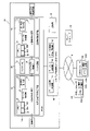
- FIG. 1 is a configuration diagram of a transfer processing device according to an embodiment of the present invention.
- FIG. 2 is a flowchart of an operation instruction acquisition process executed by the operation instruction number acquisition circuit of FIG.
- FIG. 3 is a flowchart of buffer memory processing executed by the memory buffer circuit of FIG.
- FIG. 4 is a flowchart of the transfer information acquisition process executed by the transfer information acquisition circuit of FIG.
- FIG. 5 is a flowchart of the table recovery process executed by the software processing unit of FIG.
- the transfer processing device 10 is connected to the network N.
- the transfer processing device 10 is configured as one of a plurality of distributed computers constituting the nodes of the virtual computer.
- the transfer processing device 10 is configured to be able to communicate with the server computer 110 that controls the predetermined calculation and the plurality of other distributed computers 120 via the network N.
- the transfer processing device 10, the server computer 110, and the plurality of other distributed computers 120 transmit and receive arithmetic instructions constituting the software components to be distributed, and execute the received arithmetic instructions.
- the transfer processing device 10 includes an operation instruction number acquisition circuit 20, a buffer circuit 30, a transfer information acquisition circuit 40, a software processing unit 50, and a storage unit 60.
- the circuits 20 to 40 included in the transfer processing device 10 constitute a transfer processing circuit 10A that performs processing for transferring an arithmetic instruction.
- the transfer processing circuit 10A is composed of an FPGA (Field Programmable Gate Array), and each of the circuits 20 to 40 is composed of a part of the FPGA.
- the transfer processing circuit 10A may be configured by a logic circuit or the like other than the FPGA.
- the software processing unit 50 includes a CPU that executes a program stored in the storage unit 60, and a RAM that is the main memory of the CPU.
- the arithmetic instruction received by the transfer processing apparatus 10 from the server computer 110 or another distributed computer 120 is input to the arithmetic instruction number acquisition circuit 20.
- the operation instruction number acquisition circuit 20 acquires a transfer instruction number corresponding to transfer information (for example, a port number for sending an operation instruction and / or a destination address of the operation instruction) which is information regarding the next transfer destination of the operation instruction. do.
- the buffer circuit 30 is arranged between the operation instruction number acquisition circuit 20 and the transfer information acquisition circuit 40, and temporarily stores the operation instruction and the operation instruction number supplied from the operation instruction number acquisition circuit 20 to the transfer information acquisition circuit 40. And relay.
- the transfer information acquisition circuit 40 acquires transfer information based on the operation instruction number, and adds the acquired transfer information to the operation instruction.
- the arithmetic instruction to which the transfer information is attached is transmitted to the transfer destination indicated by the transfer information by a communication device such as a network card (not shown) based on the transfer information.
- the transfer destination is the distributed computer 120
- the arithmetic instruction is stored in the memory 120A of the distributed computer 120 and executed by the arithmetic unit 120B.
- the arithmetic unit 120 may be included in a processor such as a CPU, and the memory 120A may be a cache memory or the like.
- a large number of arithmetic instructions are input to the transfer processing apparatus 10, and the circuits 20 to 40 sequentially process the arithmetic instructions.
- the operation instruction identifier table 29 having a plurality of combinations of the operation instruction identifier based on the operation instruction and the operation instruction number is referred to. ..
- the operation instruction identifier table 29 is stored in the memory 21 of the operation instruction number acquisition circuit 20.
- the transfer information acquisition circuit 40 acquires the transfer information
- the transfer information acquisition circuit 40 refers to the transfer information table 49 having a plurality of combinations of the operation instruction number and the transfer information.
- the transfer information table 49 is stored in the memory 41 of the transfer information acquisition circuit 40.
- the software processing unit 50 manages the updates and the like of the tables 29 and 49.
- Each of the above circuits 20 to 40 is not processed in the form of executing a program, but is processed by a logic circuit. Such processing can be said to be hardware processing.
- the software processing unit 50 executes a program (software) to perform processing.
- Such processing is software processing.
- the processing speed of the above hardware processing is faster than the processing speed of software processing.
- the buffer circuit 30 holds an arithmetic instruction or the like for a predetermined period so as to absorb the difference in processing speed between the hardware processing and the software processing.
- the buffer circuit 30 is configured not to output an arithmetic instruction or the like to the transfer information acquisition circuit 40 until the transfer information table 49 is updated by the software processing unit 50.
- the configuration of the operation instruction is arbitrary.
- the operation instruction includes an 8-byte internal processor composed of a header or the like at the beginning, and an operation instruction main body indicating the content (data) of the operation instruction.
- the internal processor shall include information such as the address of the computer from which the arithmetic instruction is sent and the length of the entire arithmetic instruction.
- the arithmetic instruction number acquisition circuit 20 includes a memory 21, an arithmetic instruction processing unit 22, a table processing unit 23, and an error detection and correction unit 24.
- the memory 21 stores the above-mentioned arithmetic instruction identifier table 29.
- the operation instruction identifier table 29 is made redundant in two tables having the same contents, the main first table 29A and the subordinate second table 29B, in order to prevent soft errors.
- the operation instruction numbers are associated with the plurality of operation instruction identifiers.
- the order of the rows of the operation instruction identifiers in the tables 29A and 29B is the operation instruction number.
- the operation instruction number corresponding to the operation instruction identifier on the 51st line is 51.
- the operation instruction number also corresponds to the row of the transfer information table 49. Therefore, the operation instruction number is also associated with the transfer information.
- the operation instruction identifier is acquired based on the operation instruction and identifies the operation instruction.
- the operation instruction number is set for each operation instruction identifier and corresponds to one transfer information.
- the memory 21 includes a CAM (Content Addressable Memory), and the operation instruction identifier table 29 may be stored in the CAM.
- the operation instruction number is the address of the memory 41 of the transfer information corresponding to the operation instruction number in the transfer information table 49 of the transfer information acquisition circuit 40.
- the arithmetic instruction processing unit 22, the table processing unit 23, and the error detection / correction unit 24 cooperate to execute the operational instruction number acquisition process for acquiring the operational instruction number shown in FIG. The process is started when an arithmetic instruction is input to the arithmetic instruction number acquisition circuit 20.
- the operation instruction processing unit 22 holds the input operation instruction in its own RAM, and reads the operation instruction only for a predetermined length from the beginning (step S101).
- the operation instruction consists of an 8-byte internal processor and a 32-bit RISC operation instruction.
- the arithmetic instruction processing unit 22 reads the information from the beginning to the 12th byte of the operational instruction, that is, the entire operational instruction. The information that can be read may be only a part of the information.
- the arithmetic instruction processing unit 22 determines whether the software processing unit 50 can execute the arithmetic instruction (step S102). It is assumed that the arithmetic instruction processing unit 22 periodically communicates with the software processing unit 50 and monitors whether the software processing unit 50 has a surplus of resources. When the software processing unit 50 has a surplus of resources, the calculation instruction processing unit 22 determines that the software processing unit 50 can execute the calculation instruction (step S102; Yes). In this case, the arithmetic instruction processing unit 22 outputs the arithmetic instruction to the software processing unit 50, and causes the software processing unit 50 to execute the arithmetic instruction (step S103).
- the arithmetic instruction processing unit 22 determines whether the software processing unit 50 can execute the arithmetic instruction based on "opcode" described later of the RISC arithmetic instruction. You may.
- the operation instruction processing unit 22 acquires an operation instruction identifier that identifies the operation instruction based on the information read in step S101 (step S104). ..
- the operation instruction identifier shall include information on the type of operation of the operation instruction and the address of the source of the operation instruction.
- a transfer destination of the operation instruction that is, another distributed computer that executes the operation instruction is assigned according to the type of operation and the address of the transmission source. Information on the type of operation of the operation instruction is acquired based on the operation instruction body.
- the information of the operation type of the operation instruction is a total of 17 bits in which funct7, funct3, and opcode are combined.
- the information on the operation type of the operation instruction may be information in which the lower 2 bits, the lower 2 bits, and the lower 5 bits of the funct7, the funct3, and the opcode that can specify the operation type are combined. For example, if funct7 is 00, funct3 is 00, and opcode is 10011, the information of the operation type is 00000011.
- the source address is extracted from the internal identifier of the operation instruction.
- Step S105 after step S104 is executed by the table processing unit 23 and the error detection / correction unit 24.
- the table processing unit 23 reads the entries (operation instruction identifiers) of the first table 29A, which is the main table of the operation instruction identifier table 29, one by one, and matches the operation instruction identifier acquired by the operation instruction processing unit 22. Search for entries to do.
- Each entry in the operation instruction identifier table 29 is managed in word units, and an error detection correction code is added to each entry.
- the error detection and correction unit 24 performs error detection and correction processing for the entry each time the entry is read by the table processing unit 23.
- the error detection and correction code is a soft error countermeasure by bit inversion caused by cosmic rays or the like.
- Possible cases of error detection results are (1) no error detection, (2) error detection and correction possible, and (3) error detection and correction impossible.
- the table processing unit 23 collates the entry read above with the operation instruction identifier acquired by the operation instruction processing unit 22. If they do not match, the table processing unit 23 reads the entry in the next row.
- the error detection and correction unit 24 corrects the error of the entry by the error detection and correction code, and the table processing unit 23 collates the corrected entry with the operation instruction identifier. If they do not match, the table processing unit 23 reads the entry in the next row.
- the table processing unit 23 reads the entry in the second table 29B, and the error detection / correction unit 24 detects the error in the entry.
- the case of the result of the detection is the same as the above (1) to (3).
- the entry or the corrected entry is matched with the operation instruction identifier.
- the table processing unit 23 stops the matching between the currently read entry and the operation instruction identifier, and reads the next entry.
- the error detection and correction unit 24 inputs the result of the error detection performed above into the RAM or the like provided in the error detection and correction unit 24 separately for each entry in the first table 29A and the second table 29B. Hold on.
- the above-mentioned results include the above-mentioned (1) to (3).
- step S105 when the operation instruction identifier acquired by the operation instruction processing unit 22 and the entry match, the table processing unit 23 acquires the operation instruction number corresponding to the entry (step S106). For example, in the 512th row of the first table, if the arithmetic instruction identifiers 000010011 match, the 512th is acquired as the operational instruction number. After that, the arithmetic instruction processing unit 22 outputs the operational instruction and the operational instruction number acquired in step S106 to the buffer circuit 30 (step S107).
- the operation instruction number may be output in a state of being put in a predetermined area of the internal processor.
- the error detection and correction unit 24 notifies the software processing unit 50 of the result of the error detection held in the RAM or the like (step S108).
- the software processing unit 50 updates the operation instruction identifier table and the like (details will be described later).
- the buffer circuit 30 includes a buffer memory control unit 31 and a buffer memory 32.
- the buffer memory control unit 31 transfers the operation instruction number and the operation instruction output by the operation instruction processing unit 22 to the buffer memory 32 until there is an output request from the transfer information acquisition circuit 40. Control to hold in.
- the buffer memory control unit 31 first acquires the attribute information of the operation instruction based on the operation instruction number and the operation instruction output by the operation instruction number acquisition circuit 20 (step S201).
- the attribute information is composed of the operation instruction number and the length of the operation instruction included in the internal processor at the beginning of the operation instruction.
- the operation instruction number is G1
- the length of the operation instruction is G2
- the operation instruction is F.
- the buffer memory control unit 31 calculates an error detection code for the entire operation instruction F so that the error can be detected when the error is superimposed on the operation instruction F, and the calculated error detection code is used as the operation instruction F. It is added to the end of (step S202).
- CRC8 CyclicRedundancyCheck8
- the error detection code is not limited to CRC8, and various similar error detection code formats can be applied.
- the error detection code may be an error detection correction code that can be corrected.
- the operation instruction F includes the error detection code.
- the length G2 of the arithmetic instruction in the internal processor is corrected to the length G2 to which the error detection code at the end is added.
- the buffer memory control unit 31 After that, the buffer memory control unit 31 generates an identifier for associating the attribute information (G1, G2) of the calculation instruction F obtained in step S201 with the calculation instruction F (step S203).
- This identifier is information that is arranged before the operation instruction F and identifies the operation instruction F.
- the buffer memory control unit 31 prepares a fixed-length identifier, and embeds attribute information (G1, G2) in this identifier. At this time, it is advisable to determine in advance the area in the identifier to which the attribute information (G1, G2) is assigned. By embedding the attribute information (G1, G2) of the input operation instruction in the identifier, the input operation instruction F and the attribute information (G1, G2) of the input operation instruction are associated with each other.
- the identifier generated in this step S203 will be referred to as S.
- the buffer memory control unit 31 calculates an error detection and correction code for the entire identifier S so that the generated identifier S can be detected and corrected, and the calculated error detection and correction code is used as a specific area in the identifier S. , For example, embedding in [23:16], which does not affect the length of the operation instruction and the operation instruction number (step S204). For example, if the SECDED code is applied as the error detection and correction code, it is possible to cover the error pattern of the soft error that actually occurs.
- the error detection / correction code may be intended only for the length of the operation instruction and the operation instruction number among the identifiers S. In this case, the error detection and correction of the identifier S, which will be described later, targets only the length of the operation instruction and the operation instruction number of the identifier S.
- the buffer memory control unit 31 starts buffering the operation instruction F to the buffer memory 32 (step S205).
- the buffering of the identifier S to the buffer memory 32 is performed more than the operation instruction F. It may be delayed.
- step S205 an area for buffering the identifier S is secured in the buffer memory 32 before buffering the operation instruction F. Then, the operation instruction F is stored in the buffer memory 32 while avoiding this reserved area.
- the area for the identifier S is an area in which the read order is higher than that of the operation instruction F.
- the buffer memory control unit 31 starts buffering the identifier S to the area secured above in the buffer memory 32 (step S206).
- the buffer memory control unit 31 monitors and controls the buffering state of the operation instruction F and the identifier S (step S207). More specifically, the buffer memory control unit 31 monitors whether the identifier S and the operation instruction F are all stored in the buffer memory 32. After storing the identifier S and the operation instruction F in the buffer memory, the buffer memory control unit 31 keeps the accumulated identifier S and the operation instruction F in the buffer memory 32 until there is an output instruction of the identifier S and the operation instruction F in the subsequent process. Keep inside.
- the transfer information acquisition circuit 40 issues an output command of a set of one identifier S and an operation instruction F to the buffer circuit 30 at an appropriate timing.
- the buffer memory control unit 31 waits until the output command is received, and when the output command is received, reads out a part of the set of the identifier S and the operation instruction F including at least the entire identifier S from the buffer memory 32 (the buffer memory control unit 31 waits until the output command is received.
- the buffer memory 32 is a FIFO (first in first out) method here, and when there is an output command, the buffer memory 32 is output from the identifier S first stored in the buffer memory 32. That is, when the operation instruction F is output, it is output from the identifier S held in the area before it.
- the bit width of the buffer memory 32 is larger than the number of bits of the identifier S and the identifier S is stored from the beginning of the first layer of the buffer memory 32, at least only the first layer of the buffer memory 32 is stored. If it is taken out, the read information will include all the identifiers S.
- the buffer memory control unit 31 After reading the identifier S, the buffer memory control unit 31 reads the error detection / correction code (SECED code) embedded in the identifier S, and uses the read error detection / correction code to determine whether the identifier S has an error. (Step S209). If there is no error (step S209; No), it is guaranteed that the identifier S is correct information. In this case, the buffer memory control unit 31 reads the rest of the operation instruction F from the buffer memory 32, and outputs the identifier S and the entire operation instruction F to the transfer information acquisition circuit 40 (step S210). The rest of the operation instruction F is specified by the information of the length of the operation instruction F included in the identifier S.
- SECED code error detection / correction code
- the buffer memory control unit 31 determines whether the detected error can be corrected (step S211). In this case, if there is one bit error in the identifier S due to a soft error or the like, the error can be corrected. If there are two or more bit errors in the identifier S due to a soft error or the like, the error cannot be corrected.
- the buffer memory control unit 31 corrects the error detection of the identifier S (step S212). By this error detection and correction, the identifier S read from the buffer memory 3 is guaranteed to be correct information without errors. After that, the buffer memory control unit 31 reads the rest of the operation instruction F from the buffer memory 32, and outputs the corrected identifier S and the operation instruction F to the transfer information acquisition circuit 40 (step S213).
- step S211 When the error of the identifier S cannot be corrected (step S211; No), the information of the operation instruction length G2 and the operation instruction number G1 in the identifier S is unreliable.
- the length G2 of the operation instruction is incorrect, when another operation instruction is stored in the buffer memory 32, the boundary between the end of the operation instruction F and the beginning of the identifier S of the other operation instruction is incomplete. It becomes clear, and all the arithmetic instructions F that are sequentially processed are processed incorrectly. Therefore, when the error of the identifier S cannot be corrected, the buffer memory control unit 31 clears (discards) all the arithmetic instructions and identifiers currently stored in the buffer memory 32 (step S214).
- the buffer memory control unit 31 may clear (discard) the arithmetic instruction being read from the buffer memory 32 and the arithmetic instruction being stored in the buffer memory 32.
- the operation instruction and the identifier have a fixed length, only the operation instruction corresponding to the identifier to be processed may be discarded.
- the buffer memory control unit 31 does not read from the buffer memory 32 to the end of the operation instruction F, but reads only the first layer of the buffer memory 32, which is a simple process and has a correct identifier. S and the operation instruction F can be acquired.
- the arithmetic instruction stored in the buffer memory 32 is only sacrificed, and the subsequent arithmetic instruction is performed. The effect on processing can be suppressed.
- the transfer information acquisition circuit 40 includes a memory 41, an arithmetic instruction processing unit 42, a table processing unit 43, and an error detection / correction unit 44.
- the memory 41 stores the transfer information table 49 described above.
- the transfer information table 49 is made redundant into two tables having the same contents, the main first table 49A and the subordinate second table 49B, in order to prevent soft errors.
- Each entry in the transfer information table 49 is managed word by word, and an error detection correction code is added to each entry.
- a plurality of operation instruction numbers are associated with the plurality of transfer information.
- the order of the rows of the transfer information in the master-slave first and second tables 49A and 49B is the operation instruction number.
- the operation instruction number corresponding to the transfer information on the 51st line is 51.
- the arithmetic instruction processing unit 42, the table processing unit 43, and the error detection / correction unit 44 cooperate to execute the transfer information acquisition process shown in FIG.
- the transfer information acquisition circuit 40 supplies an operation instruction output command to the buffer circuit 30 at an arbitrary timing when the software processing described later by the software processing unit 50 is not being executed.
- the transfer information acquisition process is started when the identifier S and the operation instruction F are input from the buffer circuit 30 to the transfer information acquisition circuit 40 in response to the output command.
- the operation instruction processing unit 42 holds the identifier S and the operation instruction F in its own RAM, and extracts the operation instruction number included in the identifier S (step S301).
- the arithmetic instruction processing unit 42 may first perform error detection and correction processing using the error detection and correction code included in the identifier S.
- the operation instruction processing unit 42 may perform error detection by the error detection code at the end of the operation instruction F.
- the table processing unit 43 acquires the transfer information stored in the row indicated by the operation instruction number from the first table 49A of the transfer information table 49 (step S302). For example, when the operation instruction number indicates line 512, the 512th transfer information is acquired.
- the error detection and correction unit 44 performs error detection and correction processing of the transfer information based on the error detection and correction code added to the acquired transfer information (step S303).
- the results of error detection include (1) no error detection, (2) error detection and correction possible, and (3) error detection and correction impossible.
- the transfer information is used as it is in step S304 and subsequent steps.
- the error detection and correction unit 44 corrects the error. In this case, after that, the corrected transfer information is used in step S304 and subsequent steps.
- the table processing unit 43 obtains the transfer information with reference to the second table 49B, and performs error detection and correction or the like in the same manner as described above. If the error detection / correction unit 44 detects an uncorrectable error in the transfer information read from the second table 49B, the transfer information acquisition process is stopped.
- the error detection / correction unit 44 inputs the result of the error detection performed above into the RAM or the like included in the error detection / correction unit 44 separately for each entry in the first table 49A and the second table 29B. Hold on.
- the above-mentioned results include the above-mentioned (1) to (3).
- the operation instruction processing unit 42 assigns the transfer information acquired by the table processing unit 43 or corrected by the error detection correction unit 44 to the operation instruction F as information indicating the transfer destination of the operation instruction F, and transfers the transfer information and the operation instruction. F and are output (step S304).
- the operation instruction processing unit 42 may output the identifier S in addition to the transfer information and the operation instruction F.
- the error detection and correction unit 44 notifies the software processing unit 50 of the result of the error detection held in the RAM or the like (step S305).
- the software processing unit 50 updates the operation instruction identifier table and the like (details will be described later).
- the software processing unit 50 includes a table recovery determination unit 51, a table update unit 52, and a table processing stop / restart unit 53. If an error is detected in the entries in the operation instruction identifier table 29 and the transfer information table 49, the entries are recorded in advance in each table, so that the error may be bit inversion due to a soft error. There is. Therefore, the software processing unit 50 performs processing for recovering the table by each of the above units 51 to 53.
- the table recovery determination unit 51 is based on the error detection result (step S108) notified from the error detection / correction unit 24 of the operation instruction number acquisition circuit 20 each time the operation instruction is processed, for each entry in the operation instruction identifier table 29. In addition, the number of times that the result with error detection (here, whether or not correction is possible) is obtained is counted. The count value is stored as a table for each entry. By such processing, the accuracy, that is, the quality of the entry in the operation instruction identifier table 29 is monitored.
- the table recovery determination unit 51 makes an error for each entry in the transfer information table 49 based on the transfer information (step S305) notified from the error detection / correction unit 44 of the transfer information acquisition circuit 40 each time an arithmetic instruction is processed. The number of times that the result with detection (here, whether or not correction is possible) is obtained is counted. The count value is stored as a table for each entry. By such processing, the accuracy, that is, the quality of the entries in the transfer information table 49 is monitored.
- the table recovery determination unit 51 determines whether or not the count value of a certain entry exceeds a predetermined threshold value each time the above notification (step S108 or S305) is given. When the table recovery determination unit 51 determines that the count value exceeds the threshold value, it determines that the table recovery process shown in FIG. 5 is performed on the table to which the entry belongs.
- the table process stop / restart unit 53 instructs the transfer information acquisition circuit 40 that handles the transfer information table 49, which is the target of the table recovery process this time, to stop the table process ().
- the table processing is a processing for referring to the transfer information table 49 here, and is step S302 in FIG.
- the transfer information acquisition circuit 40 receives the instruction, if the process of step S302 is being performed, the transfer information acquisition circuit 40 stops the process.
- the target of the table recovery processing is the operation instruction identifier table 29
- the table processing is steps S105 and S106 of FIG.
- the table update unit 52 updates the table to which the entry whose count value exceeds the predetermined threshold value belongs among the first table 49A and the second table 49B of the transfer information table 49 (step S402). ).
- the table update unit 52 may rewrite only the entries exceeding the threshold value with correct data, or may rewrite the entire first table 49A or the second table 49B.
- the table update unit 52 may update both the first table 49A and the second table 49B.
- the data required for updating may be acquired from, for example, the storage unit 60 or the server computer 110.
- the table processing stop / restart unit 53 instructs the transfer information acquisition circuit 40 to start the table processing (step S403).
- the transfer information acquisition circuit 40 receives the instruction and the process of step S302 is stopped, the transfer information acquisition circuit 40 restarts the process.
- the software processing unit 50 communicates with the operation instruction number acquisition circuit 20 or the transfer information acquisition circuit 40, and each time an error is detected as described above, the entry having an error, that is, the entry having bit inversion is converted into a normal entry. It can also be rewritten. However, in order to search each of the tables 29 or 49 at high speed, it is desired to reduce the rewriting process as much as possible. Therefore, in the operation instruction number acquisition circuit 20 or the transfer information acquisition circuit 40, once an error is detected for an entry, the table processing unit 23 or 43 holds this information in a table such as a RAM, and from the next time onward. In the search of, the search may be performed while avoiding the entry in which an error is detected. This makes it possible to improve the efficiency of the search, that is, to reduce the processing delay for the search.
- the arithmetic instruction number acquisition circuit 20 or the transfer information acquisition circuit 40 may be used. There may be an impact such as processing stopping.
- the table recovery determination unit 51 monitors the status of error detection of the entire entry and makes a table recovery determination based on the above threshold value, whereby adverse effects such as suspension of the above processing can be prevented.
- the target to be counted by the table recovery determination unit 51 may not be the result of error detection, but only when the error is detected and the error cannot be corrected. As a result, the processing delay can be reduced.
- the software processing unit 50 may appropriately change the transfer destination (transfer information) defined in the operation instruction identifier table 29 and the transfer information table 49.
- the server computer 110 monitors the transfer processing device 10 and the distributed computer 120 to manage which arithmetic instruction is transferred to which computer.
- the server computer 110 instructs the software processing unit 50 to update the contents of the tables 29 and 49 that define the transfer destination of the arithmetic instruction, depending on the situation.
- the software processing unit 50 updates the contents of the tables 29 and 49 by performing software processing on the operation instruction number acquisition circuit 20 or the transfer information acquisition circuit 40 by the table update unit 52 or the like. do.
- the table processing in the operation instruction number acquisition circuit 20 or the transfer information acquisition circuit 40 is appropriately stopped.
- the software processing unit 50 performs software processing on the operation instruction number acquisition circuit 20 or the transfer information acquisition circuit 40 in order to recover or update the table.
- the transfer process (step S302 in FIG. 4 with reference to the transfer information table 49), which is a hardware process for transferring the arithmetic instruction while the software process is being executed, etc. ) Will be stopped, and the transfer process will be delayed due to the software process.
- the buffer circuit 30 is not provided, the transfer information acquisition circuit 40 is calculated from the operation instruction number acquisition circuit 20 even while the transfer processing in the transfer information acquisition circuit 40 is stopped and the software processing is being performed. The instruction is input.
- a buffer circuit 30 is provided between the operation instruction number acquisition circuit 20 and the transfer information acquisition circuit 40. Then, the buffer circuit 30 does not output the arithmetic instruction held at that time until there is an output instruction from the transfer information acquisition circuit 40.
- the buffer circuit 30 is configured to output the operation instruction number and the operation instruction output by the operation instruction number acquisition circuit 20 after the software processing for the transfer information acquisition circuit 40 is completed. This prevents the inconvenience that the software processing cannot catch up with the transfer processing of the arithmetic instruction, so that the transfer processing of the arithmetic instruction is not performed normally and an erroneous transfer of the arithmetic instruction occurs. That is, according to this embodiment, erroneous transfer due to a timing difference between the software process and the transfer process of the arithmetic instruction is prevented. As a result, highly reliable transfer is realized.
- the transfer processing device 10 is resistant to soft errors.
- the software processing unit 50 can determine whether the entire table needs to be recovered, and the entire table can be rewritten after the soft errors have accumulated. This makes it possible to avoid updating the table during the search and speed up the table processing speed. , And the processing delay can be reduced.
- the buffer circuit 30 assigns information (identifier S) including an operation instruction number and an error detection correction code before the operation instruction F, and secures a storage area for the information when the operation instruction F is stored. Then memorize the operation instruction. Therefore, since the identifier S, which is the information, is read first when the operation instruction F is read, the error can be detected by the error detection correction code without reading all the operation instructions F. Therefore, the processing delay in the buffer circuit 30 can be reduced, and an extra buffer for writing the arithmetic instruction F becomes unnecessary, so that the circuit scale can be reduced.
- the software processing unit 50 of this embodiment acquires the arithmetic instruction when the arithmetic instruction input to the transfer processing circuit 10A, that is, the arithmetic instruction number acquisition circuit 20 can be executed, and executes the arithmetic instruction to execute the arithmetic instruction. It can also operate as a part. As a result, the transfer processing device 10 can perform distributed processing.
- the operation instruction number acquisition circuit 20 acquires the operation instruction number and outputs the acquired operation instruction number together with the operation instruction.
- the transfer processing apparatus 10 can transfer the arithmetic instruction to another distributed computer 120 or the like when the arithmetic instruction cannot be executed.
- the arithmetic instruction execution unit may be configured by a device other than the software processing unit 50.
- the arithmetic instruction execution unit may be configured by a processor or the like that executes a program.
- the internal processor of the arithmetic instruction may include the destination address of the distributed computer 120 that executes the arithmetic instruction.
- the operation instruction identifier may include the destination address.
- the transfer information may be information indicating the transfer destination by designating the port connected to the network to which the distributed computer 120 having the destination address is connected.
- the arithmetic instruction output from the transfer information acquisition circuit 40 is transmitted from the transfer processing apparatus 10 with the destination address included in the internal processor of the arithmetic instruction as the final destination.
- the destination address may be acquired by the buffer circuit 30 and may be included in the identifier S in place of or in addition to the operation instruction number.
- the operation instruction number may be separately transmitted together with the operation instruction F.
- the destination address may be assigned to the source of the operation instruction, the operation type of the operation instruction, or the like.
- the buffer circuit 30 refers to a table, for example, and acquires and uses the address of the source included in the internal processor of the arithmetic instruction and the destination address assigned to the combination of the opcode of the arithmetic instruction and the like.
- the identifier S is also output from the transfer information acquisition circuit 40, and the arithmetic instruction output from the transfer information acquisition circuit 40 is transmitted from the transfer processing device 10 with the destination address included in the identifier S as the final destination. Will be done.
- the internal processor of the arithmetic instruction may be appropriately deleted in the process of processing by the transfer processing device 10.
- the arithmetic unit 120B in the distributed computer 120 for executing the arithmetic instruction accesses the destination address included in the internal processor of the arithmetic instruction, the destination address included in the identifier S, the destination address indicated by the transfer information, and the like. It may be a memory address which is an address of various memories 120A such as a cache memory, an OnChip memory, or a DRAM memory.
- the arithmetic unit 120B is included in a processor such as a CPU of the distributed computer 120.
- the various memories may be provided inside or outside the processor.
- the transfer information or the operation instruction includes the memory address of the memory 120B accessed by the operation device that executes the operation instruction as the destination address, or the transfer information acquisition circuit 40 uses the address as the transfer information or the operation instruction. May be separately configured to be output as a destination address by an identifier S or the like. According to such a configuration, since the arithmetic instruction is once placed in the memory 120A, flexible and high-speed arithmetic processing becomes possible even when it is necessary to execute a large number of arithmetic instructions, for example. Further, since the address of the shared memory shared by the plurality of distributed computers 120 can be specified as the memory address, and the operation instruction (including the data used for the operation) can be used once in the shared memory, many of them can be used. Information processing, that is, execution of arithmetic instructions can be performed accurately.
- the above error detection and correction includes an aspect in which only error detection is performed. That is, an error detection code may be used as the error detection correction code. Any code type for error detection and correction may be used. For error detection, a parity code or a cyclic redundancy check code such as CRC may be used. In the case of error detection correction, a Reed-Solomon code may be used in addition to SECDED that performs single error correction and two error detection.
- the information included in the operation instruction identifier may be a combination of the destination or source address and header information such as priority.
- the operation instruction may have a configuration other than the configuration of the internal processor of 8 bytes at the beginning and the RISC operation instruction of 32 bits.
- One arithmetic instruction may be a series of a plurality of instructions following an 8-byte internal processor.
- the length of the internal processor and the arithmetic instruction is not limited to the above embodiment and is arbitrary.
- the internal processor may include not only information on the length of instructions but also the number of consecutive instructions, user ID information, and the like.
- the internal processor may directly include the operation instruction identifier.
- the various operations or calculations described above may use the value (priority) and length of the VLAN (Virtual LAN) tag, and which numerical value is used is arbitrary.
- the arithmetic instruction does not have to be a RISC arithmetic instruction, but may be an instruction having a large function such as an arithmetic instruction for image size conversion.
- the operation instruction may be a unique operation instruction that is not standardized.
- the arithmetic instruction may be stored in the request of the communication protocol, for example, http from the distributed computer 120.
- the arithmetic instruction may be input to the transfer processing apparatus 10 by various protocols such as MQTT, CoAP, QUIC, WebSocket, NATS, Kafka, REST, and original protocol.
- the arithmetic instructions transmitted from the transfer processing device 10 may also be transferred by various protocols as described above.
- the direction of transfer of the arithmetic instruction is not one-way but bidirectional.
- a plurality of distributed computers may be connected to the transfer processing device 10.
- the transfer processing device 10 may be various switches for relaying arithmetic instructions, a network card, or the like.
- the recovery of the first table 29A or 49A by the software processing unit 50 may be performed at the timing of access to the second table 29B or 49B. This allows the table to be healthy without affecting the search.
- Entry errors are not limited to soft errors, but may be detected by various factors such as noise.
- the error may occur simultaneously in multiple entries. For example, the error area may spread to a location physically close to the memory.
- the table update unit 52 may update the entire table.
- the table recovery determination unit 51 may recover the table immediately after detecting one error in one entry.
- the table may be rewritten in multiple steps. As a result, if the operation instruction is within the time that can be stored in the buffer, for example, if it is within 1 ms, if there is a buffer of about 1 KB in the case of video distribution of about 10 Mbps, even if real-time processing is required. , The calculation delay can be minimized.
- 10 ... Transfer processing device, 10A ... Transfer processing circuit, 20 ... Arithmetic instruction number acquisition circuit, 21 ... Memory, 22 ... Arithmetic instruction processing unit, 23 ... Table processing unit, 24 ... Error detection and correction unit, 29 ... Arithmetic instruction identifier table , 29A ... 1st table, 29B ... 2nd table, 30 ... buffer circuit, 31 ... buffer memory control unit, 32 ... buffer memory, 40 ... transfer information acquisition circuit, 41 ... memory, 42 ... arithmetic instruction processing unit, 43 ... Table processing unit, 44 ... error detection and correction unit, 49 ... transfer information table, 49A ... first table, 49B ... second table, 50 ... software processing unit, 51 ... table recovery determination unit, 52 ... table update unit, 53 ... Table processing stop / restart unit, 60 ... storage unit, 110 ... server computer, 120 ... distributed computer, 120A ... memory, 120B ... arithmetic unit, N ... network.
Landscapes
- Engineering & Computer Science (AREA)
- Theoretical Computer Science (AREA)
- Software Systems (AREA)
- Physics & Mathematics (AREA)
- General Physics & Mathematics (AREA)
- General Engineering & Computer Science (AREA)
- Quality & Reliability (AREA)
- Computational Mathematics (AREA)
- Mathematical Analysis (AREA)
- Mathematical Optimization (AREA)
- Pure & Applied Mathematics (AREA)
- Hardware Redundancy (AREA)
- Detection And Correction Of Errors (AREA)
- Debugging And Monitoring (AREA)
Abstract
Description
図1に示すように、本実施の形態に係る転送処理装置10は、ネットワークNに接続されている。転送処理装置10は、仮想コンピュータのノードを構成する複数の分散コンピュータの一つとして構成されている。転送処理装置10は、前記所定の計算を統括するサーバコンピュータ110と、複数の他の分散コンピュータ120と、ネットワークNを介して通信可能に構成されている。転送処理装置10、サーバコンピュータ110、及び、複数の他の分散コンピュータ120は、分散処理されるソフトウェアコンポーネントを構成する演算命令を送受信し、受信した演算命令を実行する。
演算命令の構成は任意である。演算命令は、ここでは、先頭のヘッダ等により構成される8バイトの内部処理子と、演算命令の内容(データ)を示す演算命令本体と、を含むものとする。内部処理子は、演算命令の送出元のコンピュータのアドレス、及び、演算命令全体の長さなどの情報を含むものとする。演算命令本体は、32ビット=4バイト等のRISC演算命令とする。
図1に示すように、演算命令番号取得回路20は、メモリ21と、演算命令処理部22と、テーブル処理部23と、誤り検出訂正部24と、を備える。
図1に示すように、バッファ回路30は、バッファメモリ制御部31と、バッファメモリ32と、を備える。バッファメモリ制御部31は、図3のバッファメモリ処理を実行することで、演算命令処理部22が出力した演算命令番号と演算命令とを転送情報取得回路40からの出力要求があるまでバッファメモリ32に保持する制御を行う。
図1に示すように、転送情報取得回路40は、メモリ41と、演算命令処理部42と、テーブル処理部43と、誤り検出訂正部44と、を備える。
図1に示すように、ソフトウェア処理部50は、テーブル回復判別部51、テーブル更新部52、及び、テーブル処理停止/再開部53を備える。上記の演算命令識別子テーブル29及び転送情報テーブル49のエントリに対して誤りが検出された場合、各テーブルにはあらかじめエントリが記録されていることから、この誤りは、ソフトエラーによるビット反転の可能性がある。そこで、ソフトウェア処理部50は、上記各部51~53によりテーブルを回復するための処理を行う。
以上のように、ソフトウェア処理部50は、テーブルの回復又は更新のため、演算命令番号取得回路20又は転送情報取得回路40に対してソフトウェア処理を行う。この際、特に、転送情報取得回路40では、ソフトウェア処理が実行されている間、演算命令を転送するためのハードウェア処理である転送処理(上記転送情報テーブル49を参照する図4のステップS302等)が停止することになり、転送処理がソフトウェア処理により遅延する。仮に、バッファ回路30を設けないとすると、転送情報取得回路40での転送処理が停止してソフトウェア処理が行われている間にも、当該転送情報取得回路40に演算命令番号取得回路20から演算命令が入力されてしまう。このような場合、現在転送情報取得回路40の処理対象となっている演算命令が、後から入力された演算命令と混ざってしまい、演算命令の転送処理が正常に行われず、演算命令が所望の宛先に意図しない他の演算命令とともに転送されてしまうといった演算命令の誤転送といった不都合が生じ得る。この実施の形態では、演算命令番号取得回路20と転送情報取得回路40との間にバッファ回路30を設けている。そして、当該バッファ回路30は、転送情報取得回路40からの出力指示があるまで、そのとき保持している演算命令を出力しない。このように、このバッファ回路30は、演算命令番号取得回路20が出力した演算命令番号と演算命令とを、転送情報取得回路40に対するソフトウェア処理が終了してから出力するように構成されている。これにより、ソフトウェア処理が演算命令の転送処理に追い付かないことにより演算命令の転送処理が正常に行われず演算命令の誤転送が生じてしまうといった不都合が防止される。つまり、この実施の形態によれば、ソフトウェア処理と演算命令の転送処理とのタイミングずれによる誤転送が防止される。これにより、信頼度の高い転送が実現される。
上記の実施形態を参照して本発明を説明したが、本発明は上記実施形態に限定されるものではない。上記実施形態について種々の変更を施してもよい。以下、変形例を列挙するが、下記の変形例の少なくとも一部同士を矛盾しない範囲で組み合わせてもよい。
Claims (7)
- 転送対象の演算命令を識別する演算命令識別子を取得し、演算命令識別子と演算命令番号との組み合わせを複数もつ演算命令識別子テーブルから、取得した前記演算命令識別子に対応する前記演算命令番号を取得し、取得した前記演算命令番号を前記演算命令とともに出力するように構成された演算命令番号取得回路と、
前記演算命令番号取得回路から出力された前記演算命令番号と前記演算命令とを取得し、演算命令番号と転送情報との組み合わせを複数もつ転送情報テーブルから、入力された前記演算命令番号に対応する前記転送情報を取得し、取得した前記転送情報を前記演算命令とともに出力するように構成された転送情報取得回路と、
前記転送情報取得回路に対してソフトウェア処理を実行するソフトウェア処理部と、
前記演算命令番号取得回路と前記転送情報取得回路との間に配置されて前記演算命令番号と前記演算命令とを中継するバッファ回路であり、前記演算命令番号と前記演算命令とを、前記ソフトウェア処理が実行されている間は保持し、前記ソフトウェア処理の終了後に前記転送情報取得回路に出力するように構成されたバッファ回路と、
を備える転送処理装置。 - 前記演算命令番号テーブルは、第1テーブル及び第2テーブルに冗長化され、
前記演算命令番号テーブルの前記演算命令識別子に誤り検出訂正符号が付与されており、
前記演算命令番号取得回路は、前記第1テーブルの前記演算命令識別子に誤りがあるかを前記誤り検出訂正符号により検出し、誤りがあったときに、前記第2テーブルを参照して前記演算命令番号を取得するように構成されている、
請求項1に記載の転送処理装置。 - 前記転送情報テーブルは、第1テーブル及び第2テーブルに冗長化され、
前記転送情報テーブルの前記転送情報に誤り検出訂正符号が付与されており、
前記転送情報取得回路は、前記第1テーブルの前記転送情報に誤りがあるかを前記誤り検出訂正符号により検出し、誤りがあったときに、前記第2テーブルを参照して前記転送情報を取得するように構成されている、
請求項1又は2に記載の転送処理装置。 - 前記バッファ回路は、
前記演算命令を記憶するときに、前記演算命令番号と誤り検出訂正符号とを含む情報を当該演算命令の前に付与するように構成されており、
前記演算命令を記憶する際に、前記情報の格納領域を確保してから前記演算命令を記憶するように構成されている、
ことを特徴とする請求項1から3のいずれか1項に記載の転送処理装置。 - 前記演算命令を実行可能なときに当該演算命令を取得し、当該演算命令を実行する演算命令実行部をさらに備える、
請求項1から4のいずれか1項に記載の転送処理装置。 - 前記演算命令番号取得回路は、前記演算命令実行部が前記演算命令を実行できないときに、前記演算命令番号を取得し、取得した前記演算命令番号を前記演算命令とともに出力するように構成されている、
請求項1から5のいずれか1項に記載の転送処理装置。 - 前記転送情報又は前記演算命令が宛先アドレスを含むか、前記転送情報取得回路が前記宛先アドレスを前記転送情報又は前記演算命令とは別に出力するように構成され、
前記宛先アドレスは、前記演算命令を実行する演算デバイスがアクセスするメモリのアドレスである、
請求項1から6のいずれか1項に記載の転送処理装置。
Priority Applications (3)
| Application Number | Priority Date | Filing Date | Title |
|---|---|---|---|
| JP2022567967A JP7597122B2 (ja) | 2020-12-10 | 2020-12-10 | 転送処理装置 |
| PCT/JP2020/046027 WO2022123721A1 (ja) | 2020-12-10 | 2020-12-10 | 転送処理装置 |
| US18/254,974 US12210410B2 (en) | 2020-12-10 | 2020-12-10 | Transfer processing device |
Applications Claiming Priority (1)
| Application Number | Priority Date | Filing Date | Title |
|---|---|---|---|
| PCT/JP2020/046027 WO2022123721A1 (ja) | 2020-12-10 | 2020-12-10 | 転送処理装置 |
Publications (1)
| Publication Number | Publication Date |
|---|---|
| WO2022123721A1 true WO2022123721A1 (ja) | 2022-06-16 |
Family
ID=81973476
Family Applications (1)
| Application Number | Title | Priority Date | Filing Date |
|---|---|---|---|
| PCT/JP2020/046027 Ceased WO2022123721A1 (ja) | 2020-12-10 | 2020-12-10 | 転送処理装置 |
Country Status (3)
| Country | Link |
|---|---|
| US (1) | US12210410B2 (ja) |
| JP (1) | JP7597122B2 (ja) |
| WO (1) | WO2022123721A1 (ja) |
Citations (3)
| Publication number | Priority date | Publication date | Assignee | Title |
|---|---|---|---|---|
| JPH08329003A (ja) * | 1995-05-29 | 1996-12-13 | Fuji Xerox Co Ltd | 資源管理装置 |
| JP2004199139A (ja) * | 2002-12-16 | 2004-07-15 | Matsushita Electric Ind Co Ltd | プロセッサシステム、命令列最適化装置、および命令列最適化プログラム |
| JP2017146685A (ja) * | 2016-02-16 | 2017-08-24 | 日本電信電話株式会社 | 分散システム、および、メッセージ転送方法 |
Family Cites Families (3)
| Publication number | Priority date | Publication date | Assignee | Title |
|---|---|---|---|---|
| US7412547B2 (en) * | 2003-12-23 | 2008-08-12 | Lenovo Pte Ltd | Apparatus, system, and method for distributed processing with a peripheral input/output channel based device |
| JP6617087B2 (ja) * | 2016-09-01 | 2019-12-04 | 日本電信電話株式会社 | 分散処理システム、分散処理方法および分散処理プログラム |
| US11281609B2 (en) * | 2019-03-12 | 2022-03-22 | Preferred Networks, Inc. | Arithmetic processor and control method for arithmetic processor |
-
2020
- 2020-12-10 JP JP2022567967A patent/JP7597122B2/ja active Active
- 2020-12-10 WO PCT/JP2020/046027 patent/WO2022123721A1/ja not_active Ceased
- 2020-12-10 US US18/254,974 patent/US12210410B2/en active Active
Patent Citations (3)
| Publication number | Priority date | Publication date | Assignee | Title |
|---|---|---|---|---|
| JPH08329003A (ja) * | 1995-05-29 | 1996-12-13 | Fuji Xerox Co Ltd | 資源管理装置 |
| JP2004199139A (ja) * | 2002-12-16 | 2004-07-15 | Matsushita Electric Ind Co Ltd | プロセッサシステム、命令列最適化装置、および命令列最適化プログラム |
| JP2017146685A (ja) * | 2016-02-16 | 2017-08-24 | 日本電信電話株式会社 | 分散システム、および、メッセージ転送方法 |
Also Published As
| Publication number | Publication date |
|---|---|
| JPWO2022123721A1 (ja) | 2022-06-16 |
| JP7597122B2 (ja) | 2024-12-10 |
| US12210410B2 (en) | 2025-01-28 |
| US20240045674A1 (en) | 2024-02-08 |
Similar Documents
| Publication | Publication Date | Title |
|---|---|---|
| US7522592B2 (en) | Packet transfer unit | |
| US7237031B2 (en) | Method and apparatus for caching protocol processing data | |
| US20110173514A1 (en) | Data protocol | |
| US7502876B1 (en) | Background memory manager that determines if data structures fits in memory with memory state transactions map | |
| US9594612B2 (en) | System and method of a hardware shadow for a network element | |
| JP6048505B2 (ja) | 並列計算機、ノード装置、及び並列計算機の制御方法 | |
| JP5621918B2 (ja) | 情報処理装置、並列計算機システムおよび演算処理装置の制御方法 | |
| JP3935885B2 (ja) | 境界ワード格納機構を用いた読み取り−修正−書き込み動作を回避する方法及びシステム | |
| US20060274787A1 (en) | Adaptive cache design for MPT/MTT tables and TCP context | |
| US20180337863A1 (en) | Modifying Carrier Packets based on Information in Tunneled Packets | |
| US7747897B2 (en) | Method and apparatus for lockstep processing on a fixed-latency interconnect | |
| US20090228630A1 (en) | Serial Buffer To Support Rapid I/O Logic Layer Out Of order Response With Data Retransmission | |
| US11561922B2 (en) | Communication apparatus, communication method, program, and communication system | |
| JP7597122B2 (ja) | 転送処理装置 | |
| US20200220952A1 (en) | System and method for accelerating iscsi command processing | |
| WO2018015984A1 (en) | Communication apparaus, system, rollback method, and program | |
| JP4019012B2 (ja) | Fpgaを具備するcpu装置とその初期化方法 | |
| US7324438B1 (en) | Technique for nondisruptively recovering from a processor failure in a multi-processor flow device | |
| US20070019661A1 (en) | Packet output buffer for semantic processor | |
| JP4807828B2 (ja) | ブロードバンド・エンジンのためのエンベロープ・パケット・アーキテクチュア | |
| JP7485086B2 (ja) | 命令処理方法及び命令処理回路 | |
| US11546260B1 (en) | Network device and media access control address learning method therefor | |
| CN112835822B (zh) | 用于缓冲地传输数据的装置和方法 | |
| JP2008252426A (ja) | 伝送装置,伝送システム、および、データ伝送方法 | |
| JP2008160705A (ja) | フレーム転送方法及び装置 |
Legal Events
| Date | Code | Title | Description |
|---|---|---|---|
| 121 | Ep: the epo has been informed by wipo that ep was designated in this application |
Ref document number: 20965103 Country of ref document: EP Kind code of ref document: A1 |
|
| ENP | Entry into the national phase |
Ref document number: 2022567967 Country of ref document: JP Kind code of ref document: A |
|
| WWE | Wipo information: entry into national phase |
Ref document number: 18254974 Country of ref document: US |
|
| NENP | Non-entry into the national phase |
Ref country code: DE |
|
| 122 | Ep: pct application non-entry in european phase |
Ref document number: 20965103 Country of ref document: EP Kind code of ref document: A1 |