WO2022113253A1 - 表示システムおよび表示方法 - Google Patents
表示システムおよび表示方法 Download PDFInfo
- Publication number
- WO2022113253A1 WO2022113253A1 PCT/JP2020/044162 JP2020044162W WO2022113253A1 WO 2022113253 A1 WO2022113253 A1 WO 2022113253A1 JP 2020044162 W JP2020044162 W JP 2020044162W WO 2022113253 A1 WO2022113253 A1 WO 2022113253A1
- Authority
- WO
- WIPO (PCT)
- Prior art keywords
- electrode group
- information
- display
- electrode
- input device
- Prior art date
- Legal status (The legal status is an assumption and is not a legal conclusion. Google has not performed a legal analysis and makes no representation as to the accuracy of the status listed.)
- Ceased
Links
Images



Classifications
-
- G—PHYSICS
- G06—COMPUTING OR CALCULATING; COUNTING
- G06F—ELECTRIC DIGITAL DATA PROCESSING
- G06F3/00—Input arrangements for transferring data to be processed into a form capable of being handled by the computer; Output arrangements for transferring data from processing unit to output unit, e.g. interface arrangements
- G06F3/01—Input arrangements or combined input and output arrangements for interaction between user and computer
- G06F3/03—Arrangements for converting the position or the displacement of a member into a coded form
-
- G—PHYSICS
- G06—COMPUTING OR CALCULATING; COUNTING
- G06F—ELECTRIC DIGITAL DATA PROCESSING
- G06F3/00—Input arrangements for transferring data to be processed into a form capable of being handled by the computer; Output arrangements for transferring data from processing unit to output unit, e.g. interface arrangements
- G06F3/01—Input arrangements or combined input and output arrangements for interaction between user and computer
- G06F3/03—Arrangements for converting the position or the displacement of a member into a coded form
- G06F3/041—Digitisers, e.g. for touch screens or touch pads, characterised by the transducing means
-
- G—PHYSICS
- G06—COMPUTING OR CALCULATING; COUNTING
- G06F—ELECTRIC DIGITAL DATA PROCESSING
- G06F3/00—Input arrangements for transferring data to be processed into a form capable of being handled by the computer; Output arrangements for transferring data from processing unit to output unit, e.g. interface arrangements
- G06F3/01—Input arrangements or combined input and output arrangements for interaction between user and computer
- G06F3/03—Arrangements for converting the position or the displacement of a member into a coded form
- G06F3/041—Digitisers, e.g. for touch screens or touch pads, characterised by the transducing means
- G06F3/044—Digitisers, e.g. for touch screens or touch pads, characterised by the transducing means by capacitive means
-
- G—PHYSICS
- G09—EDUCATION; CRYPTOGRAPHY; DISPLAY; ADVERTISING; SEALS
- G09G—ARRANGEMENTS OR CIRCUITS FOR CONTROL OF INDICATING DEVICES USING STATIC MEANS TO PRESENT VARIABLE INFORMATION
- G09G3/00—Control arrangements or circuits, of interest only in connection with visual indicators other than cathode-ray tubes
- G09G3/20—Control arrangements or circuits, of interest only in connection with visual indicators other than cathode-ray tubes for presentation of an assembly of a number of characters, e.g. a page, by composing the assembly by combination of individual elements arranged in a matrix no fixed position being assigned to or needed to be assigned to the individual characters or partial characters
Definitions
- the present disclosure relates to a display system and a display method for displaying input information using changes in capacitance.
- a projection type capacitance type touch panel that accepts operations on the input surface of the display device using changes in capacitance.
- this touch panel detects a change in capacitance in the electrodes arranged at the contact points among the electrodes arranged in a matrix. As a result, the touch panel detects the position where the capacitance has changed as the contact point of the human body.
- the input device that inputs a voltage pulse signal to the touch panel changes the electric field strength of the electric field that can reach the touch panel in chronological order so as to synchronize with the timing when the touch is detected on the touch panel. There is. As a result, the touch panel acquires the data corresponding to the voltage pulse signal.
- the present disclosure has been made in view of the above, and an object of the present disclosure is to obtain a display system capable of realizing bidirectional communication between an input device and a display device.
- the display system of the present disclosure has a first electrode group composed of a plurality of first electrodes, and the first electrode group is input to the first electrode group. It is provided with a projection type capacitance type display device that displays a display object corresponding to information and accepts a touch operation via the first electrode group. Further, the display system of the present disclosure has a second electrode group composed of a plurality of second electrodes, and the first information is transmitted from the second electrode group to the display device in a state of being in contact with the receiving surface for receiving the touch operation. Equipped with an input device to input.
- the input device transmits the first information from the second electrode group to the first electrode group, and receives the second information transmitted from the first electrode group in the second electrode group.
- the display device transmits the second information from the first electrode group to the second electrode group, and receives the first information transmitted from the second electrode group in the first electrode group.
- the display system according to the present disclosure has the effect of realizing bidirectional communication between the input device and the display device.
- the figure which shows the structure of the device electrode group when the input device which concerns on embodiment includes a suction part.
- FIG. 1 is a block diagram showing a configuration of a display system according to an embodiment.
- FIG. 2 is a perspective view showing the configuration of the display system according to the embodiment.
- the display system 1 includes an input device 20 and a display device 10. Two axes in a plane parallel to the upper surface of the display device 10 and orthogonal to each other are defined as an X axis and a Y axis. Further, the axis orthogonal to the X-axis and the Y-axis is defined as the Z-axis.
- the X direction, the Y direction, and the Z direction are all directions in the display device 10, and do not change even if the display device 10 moves.
- the display system 1 simultaneously executes a process of accepting a touch operation on the display device 10 and a capacitance communication between the input device 20 and the display device 10.
- Capacitance communication is communication that utilizes changes in capacitance between electrodes.
- the display system 1 simultaneously executes a process of receiving the information transmitted by the input device 20 by the display device 10 and a process of receiving the information transmitted by the display device 10 by the input device 20.
- the input device 20 is a device for inputting information to the display device 10.
- the input device 20 sends and receives information to and from the display device 10 by coming into contact with the display device 14, which is the display screen of the display device 10.
- the input device 20 executes a process corresponding to the received information.
- the input device 20 is superposed on the display device 14 by the operator 40 of the display system 1, so that the input device 20 comes into contact with the display device 14 and transmits information to and from the display device 10 in the contacted state. Receive incoming information.
- the input device 20 has a device electrode group 201 on the bottom surface side, and the bottom surface on which the device electrode group 201 is arranged is overlapped so as to be in parallel with the surface on which the display unit 14 is arranged. Information can be transmitted and received to and from the display device 10.
- the display 14 has a rectangular display screen.
- the rectangular area of the display screen will be described as an area surrounded by two sides parallel to the X direction and two sides parallel to the Y direction. Therefore, the display screen arranged on the upper surface of the display 14 is a plane parallel to the XY plane.
- the operator 40 brings the input device 20 into contact with the display screen of the display 14, that is, the information receiving surface, and performs an information input operation via the display device 10.
- the display device 10 displays various display objects according to the position of the input device 20 on the reception surface and the type of the input device 20. Further, in the display system 1, the display device 10 changes the display object according to the change in the orientation of the input device 20 on the reception surface.
- An example of a display object is Progress Circular 51.
- the progress circular 51 visually displays the progress of the operation.
- the progress circular 51 is displayed on the display screen of the display device 10 in an area outside the contact area between the bottom surface of the input device 20 and the upper surface of the display device 10 (hereinafter, may be referred to as an object display area).
- An example of the object display area is an annular area surrounding the contact area between the input device 20 and the display device 10.
- the display of the progress circular 51 changes depending on the operation on the input device 20.
- the input device 20 is operated by changing the position or rotation direction of the display 14 on the reception surface.
- the input device 20 When the input device 20 is operated by the operator 40, the input device 20 detects the operation content and sends information corresponding to the operation content to the display device 10.
- the input device 20 has a shape that can be grasped by the operator 40.
- the input device 20 has, for example, a cylinder, and the side surface of the cylinder is gripped by the operator 40. Further, the input device 20 is overlapped by the operator 40 so that the bottom surface of the input device 20 comes into contact with the display screen of the display device 14. Further, the input device 20 is rotated around the column axis on the display screen by the operator 40.
- the input device 20 is brought into contact with the display 14 and rotated in the contact surface so that the column axis is parallel to the Z-axis direction and the bottom surface is a surface parallel to the XY plane.
- the input device 20 detects the amount of rotation on the display device 10 as an operation content and sends it to the display device 10.
- the amount of rotation of the input device 20 on the display screen corresponds to an operation on a specific device (not shown) such as a machine tool. That is, by rotating the input device 20, the specific device connected to the display device 10 is operated.
- the display device 10 may be operated by rotating the input device 20.
- An example of the input device 20 is a dial that operates a specific device.
- the display device 10 is a projection type capacitance type touch panel.
- the display device 10 receives information from the input device 20 and displays a display object corresponding to the received information.
- the information received by the display device 10 from the input device 20 is the first information.
- An example of the first information is identification information described later.
- the information received by the input device 20 from the display device 10 is the second information.
- An example of the second information is a vibration instruction described later.
- the display device 10 displays information according to the movement. Specifically, when the input devices 20 are stacked, the display device 10 displays the progress circular 51 at the stacked positions. Further, when the input device 20 is rotated, the display device 10 sends a command corresponding to the rotation amount to the specific device, and changes the display of the progress circular 51 to the display corresponding to the rotation amount. For example, when the voltage value of the specific device is operated by the input device 20, the display device 10 notifies the specific device of the voltage value corresponding to the rotation amount which is the operation amount, and progresses so as to indicate the notified voltage value. The display of the circular 51 is changed. In this way, the display device 10 interacts with the progress circular 51 in response to the operation on the input device 20. Further, when the display device 10 is touch-operated, the display device 10 executes a process corresponding to the touch operation.
- the input device 20 has a waveform generation circuit 21, an input unit 22, a sensor 23, a vibration unit 24, and a device electrode group 201.
- the display device 10 includes a detection circuit 11, a data storage unit 12, a data processing unit 13, a display unit 14, and a display generation unit 15. Further, the display 14 includes a detection electrode group 101.
- the sensor 23 detects that the input device 20 has come into contact with the display device 10 and that the input device 20 operates.
- the input device 20 is a cylinder
- the sensor 23 detects that the bottom surface of the input device 20 touches the display screen and the amount of rotation of the input device 20 on the display screen.
- the sensor 23 in this case is a contact sensor and an angle sensor.
- the sensor 23 When the sensor 23 detects that the input device 20 has come into contact with the display device 10, it sends contact information indicating that the input device 20 has come into contact with the input unit 22. Further, the sensor 23 sends the detected rotation amount to the input unit 22.
- the input unit 22 inputs the contact information and the amount of rotation sent from the sensor 23 to the waveform generation circuit 21.
- the amount of rotation input to the waveform generation circuit 21 is device operation information described later.
- the waveform generation circuit 21 is connected to the device electrode group 201.
- the waveform generation circuit 21 is a circuit that generates a voltage pulse signal represented by a waveform having a specific pattern indicating specific information, that is, a voltage signal having a pulse waveform.
- the waveform generation circuit 21 may generate an 8-bit signal used in serial transmission instead of the voltage pulse signal represented by 0 and 1.
- the waveform generation circuit 21 Upon receiving the contact information, the waveform generation circuit 21 generates a voltage pulse signal indicating identification information and a voltage pulse signal indicating device operation information.
- the identification information is information that identifies the input device 20.
- the device operation information is information on the operation of the input device 20.
- the device operation information includes information such as the amount of rotation detected by the sensor 23.
- the waveform generation circuit 21 receives the contact information from the input unit 22, the waveform generation circuit 21 sends the identification information as a voltage pulse signal to the device electrode group 201. Further, when the waveform generation circuit 21 receives the rotation amount from the input unit 22, the waveform generation circuit 21 sends the device operation information indicating the rotation amount to the device electrode group 201 as a voltage pulse signal.
- the device electrode group 201 is arranged on the bottom surface side of the input device 20.
- the device electrode group 201 is an electrode used for capacitance communication with the display device 10.
- the device electrode group 201 is composed of a plurality of electrodes.
- the bottom surface of the input device 20 is a surface that is brought into contact with the upper surface of the display device 10.
- Each electrode of the device electrode group 201 transmits a voltage pulse signal generated by the waveform generation circuit 21. Further, each electrode of the device electrode group 201 can also receive a voltage pulse signal transmitted from the display device 10. Some of the electrodes of the device electrode group 201 transmit the voltage pulse signal to the display device 10, and the remaining electrodes receive the voltage pulse signal from the display device 10. As a result, the device electrode group 201 simultaneously executes transmission and reception of the voltage pulse signal. As described above, the device electrode group 201 has a function of a transmitting antenna and a function of a receiving antenna.
- a voltage pulse signal received by the device electrode group 201 from the display device 10 is a vibration instruction signal that vibrates the input device 20.
- the display device 10 receives information from the input device 20, the display device 10 transmits a vibration instruction to the input device 20.
- the display device 10 detects that the input device 20 has been operated, the display device 10 transmits a vibration instruction to the input device 20.
- the display device 10 detects that the bottom surface of the input device 20 has come into contact with the display device 14, the display device 10 may transmit a vibration instruction to the input device 20.
- the operator 40 can confirm that the information is transmitted from the input device 20 to the display device 10 or that the display device 10 has detected the contact of the input device 20. It becomes.
- the vibration unit 24 executes the vibration function according to the vibration instruction from the display device 10. That is, the vibrating unit 24 vibrates the input device 20 when the device electrode group 201 receives a vibration instruction.
- the bottom surface of the input device 20 and the portion vibrated by the vibrating portion 24 are connected via an elastic body such as a spring. Therefore, even if the vibrating unit 24 vibrates the input device 20, the contact position between the bottom surface of the input device 20 and the top surface of the display device 10 does not shift.
- the display 14 has a display screen for displaying information.
- the detection electrode group 101 is arranged in the display screen on the upper surface side of the display device 10.
- the detection electrode group 101 is an electrode used for touch operation and capacitive communication with the input device 20.
- the detection electrode group 101 is composed of a plurality of detection electrodes. In the detection electrode group 101, each detection electrode is arranged so that the adjacent detection electrodes have a specific capacitance. The capacitance changes between the detection electrodes of the detection electrode group 101 when the input device 20 is superposed on the display device 10. Further, the capacitance changes between the detection electrodes of the detection electrode group 101 when the display screen is touched by the operator 40.
- the detection circuit 11 is connected to the detection electrode group 101.
- the detection circuit 11 applies a voltage to adjacent detection electrodes and detects a change in capacitance when the voltage is applied.
- the capacitance of the detection electrode included in the detection electrode group 101 at the place where the input device 20 is superposed changes.
- the detection circuit 11 detects the position and shape information, which is the position and shape information of the input device 20, by detecting the change in the capacitance.
- the position and shape information includes information on the position on the display screen when the input device 20 is superimposed on the display screen, and information on the shape of the bottom surface of the input device 20.
- the detection circuit 11 stores the detected position and shape information in the data storage unit 12.
- the detection circuit 11 detects the touch operation to the display 14 by detecting the change in the capacitance.
- the detection circuit 11 sends touch operation information indicating the detected touch operation to the data processing unit 13.
- the electrodes in the region in contact with the input device 20 are used for capacitance communication.
- some of the electrodes are the electrodes for transmission, and the remaining electrodes are the electrodes for reception.
- Each electrode for transmitting capacitance communication included in the detection electrode group 101 (hereinafter, may be referred to as an electrostatic transmission electrode) transmits a voltage pulse signal generated by a data processing unit 13 or the like to an input device 20.
- Each electrode for receiving capacitance communication (hereinafter, may be referred to as an electrostatic receiving electrode) included in the detection electrode group 101 receives a voltage pulse signal sent from the input device 20. As a result, the detection electrode group 101 simultaneously executes transmission and reception of the voltage pulse signal.
- the detection electrode group 101 has a function of a transmitting antenna and a function of a receiving antenna.
- the detection circuit 11 detects the identification information and the device operation information based on the voltage pulse signal sent from the input device 20 via the detection electrode group 101.
- the detection circuit 11 sends identification information and device operation information to the data processing unit 13.
- the data processing unit 13 determines the progress circular 51 to be displayed based on the identification information.
- the display device 10 stores in advance correspondence information indicating the correspondence between the progress circular 51 and the identification information.
- the data processing unit 13 determines the progress circular 51 to be displayed based on the correspondence information and the identification information sent from the detection circuit 11.
- the data processing unit 13 sends the determined progress circular 51 to the display generation unit 15. Further, the data processing unit 13 reads the position shape information from the data storage unit 12 and sends it to the display generation unit 15.
- the data processing unit 13 generates a progress circular 51 whose display contents are changed based on the device operation information.
- the data processing unit 13 sends the generated progress circular 51 to the display generation unit 15. Further, the data processing unit 13 sends the touch operation information to the display generation unit 15.
- the display generation unit 15 generates a display image showing the progress circular 51 sent from the data processing unit 13.
- the display generation unit 15 causes the progress circular 51 to be displayed in the area corresponding to the position and shape information in the area on the display screen of the display unit 14, that is, the object display area. Further, the display generation unit 15 generates a display image corresponding to the touch operation information and displays it on the display screen.
- the display 14 displays a progress circular 51, a display screen corresponding to touch operation information, and the like.
- FIG. 3 is a diagram showing a configuration of a detection electrode group included in the display device according to the embodiment.
- the detection electrode group 101 which is the first electrode group, is arranged on the upper surface side of the display 14.
- FIG. 3 shows an example of arrangement of detection electrodes when the display 14 is viewed from the upper surface side.
- the detection electrode group 101 has an X electrode array in which a plurality of detection electrodes are arranged so that the X coordinates are common, and a Y electrode array in which a plurality of detection electrodes are arranged so that the Y coordinates are common. ing. Each detection electrode in the X electrode row is arranged in a direction parallel to the Y direction, and each detection electrode in the Y electrode row is arranged in a direction parallel to the X direction.
- the detection electrode included in the detection electrode group 101 is the first electrode.
- FIG. 3 shows a case where the detection electrode group 101 has 10 X electrode rows and 6 Y electrode rows.
- the X electrode train has X coordinates from X1 to X10, and the Y electrode train has Y coordinates from Y1 to Y6.
- each X electrode row whose X coordinate is X1 six detection electrodes are connected in series. Similarly, in each X electrode row having X coordinates X2 to X10, six detection electrodes are connected in series. Further, in the Y electrode row having the Y coordinate Y1, 11 detection electrodes are connected in series. Similarly, 11 detection electrodes are connected in series in each Y electrode row having Y coordinates Y2 to Y6.
- Each detection electrode in the X electrode row has the same Z coordinate. Further, each detection electrode in the Y electrode row has the same Z coordinate.
- the X electrode row and the Y electrode row are arranged in different layers. That is, the Z coordinate in which the X electrode array is arranged and the Z coordinate in which the Y electrode array is arranged are different coordinates.
- a dielectric layer having a specific dielectric constant is arranged between the surface on which the X electrode array is arranged and the surface on which the Y electrode array is arranged.
- the detection electrodes other than the region where the input device 20 is overlapped are used for detecting the touch operation.
- the capacitance at this position changes.
- the display device 10 detects the touch position by detecting the change in the capacitance.
- the display device 10 detects a change in capacitance in each Y electrode row when a voltage is applied to any X electrode row.
- the display device 10 applies a voltage to, for example, an X electrode array having an X coordinate of Xn (n is a natural number of any of 1 to 10). Then, the display device 10 determines whether or not the capacitance has changed in the Y electrode array whose Y coordinate is Ym (m is a natural number of any of 1 to 6).
- the capacitance of the display device 10 changes in order from the Y electrode row with the Y coordinate to the Y electrode row with the Y coordinate Y6 when a voltage is applied to the X electrode row with the X coordinate X1. Is determined. Similarly, when a voltage is applied to the X electrode array having the X coordinate X2, the display device 10 sequentially changes the capacitance from the Y electrode array having the Y coordinate Y1 to the Y electrode array having the Y coordinate Y6. Judge whether or not.
- the display device 10 sequentially applies a voltage to each X electrode train having X coordinates from X1 to X10, and when a voltage is applied to the X electrode train having Xn X coordinate, the Y coordinate has a Y coordinate. It is determined whether or not the capacitance has changed in order from the Y electrode row of Y1 to the Y electrode row whose Y coordinate is Y6. As a result, the display device 10 can detect which position of the display device 14 is touched.
- the order of applying the voltage to the X electrode row may be any order. Further, the determination of the change in capacitance in the Y electrode row may be performed in any order.
- the detection electrode in the region where the input device 20 is overlapped (hereinafter referred to as the electrostatic communication region) is used for capacitance communication.
- a part of the detection electrode in the electrostatic communication area becomes an electrostatic transmission electrode, and the rest becomes an electrostatic reception electrode.
- the detection electrode serving as the electrostatic transmission electrode transmits a voltage pulse signal to the input device 20, and the detection electrode serving as the electrostatic reception electrode receives the voltage pulse signal from the input device 20.
- the electrostatic communication region is the first region, and the touch detection region described later, which is a region other than the electrostatic communication region, is the second region.
- any detection electrode may be an electrostatic transmission electrode, and any detection electrode may be an electrostatic reception electrode. Further, among the detection electrodes in the electrostatic communication region, there may be an electrode that is not set as either the electrostatic transmission electrode or the electrostatic reception electrode.
- FIG. 4 is a diagram showing a configuration of a device electrode group included in the input device according to the embodiment.
- the device electrode group 201 which is the second electrode group, is arranged in a circular region on the bottom surface side of the input device 20.
- FIG. 4 shows an arrangement example of the device electrode group 201 when the input device 20 is viewed from the bottom surface side.
- two axes in a plane parallel to the bottom surface of the input device 20 and orthogonal to each other are referred to as an A axis and a B axis.
- the axis orthogonal to the A axis and the B axis is defined as the C axis.
- the A direction, the B direction, and the C direction are all directions in the input device 20, and do not change even if the input device 20 moves.
- the device electrode group 201 has an A electrode array in which a plurality of detection electrodes are arranged so that the A coordinate is common, and a B electrode array in which a plurality of detection electrodes are arranged so that the B coordinate is common. ing. Each detection electrode in the A electrode row is arranged in a direction parallel to the B direction, and each detection electrode in the B electrode row is arranged in a direction parallel to the A direction.
- the electrode included in the device electrode group 201 is the second electrode.
- FIG. 4 shows a case where the device electrode group 201 has two A electrode rows and two B electrode rows.
- the A electrode row has A coordinates A1 and A2
- the B electrode row has B coordinates B1 and B2.
- Each detection electrode in the A electrode row has the same C coordinate. Further, each detection electrode in the B electrode row has the same C coordinate.
- the A electrode row and the B electrode row are arranged in different layers. That is, the C coordinate in which the A electrode row is arranged and the C coordinate in which the B electrode row is arranged are different coordinates.
- a dielectric layer having a specific dielectric constant is arranged between the surface on which the A electrode row is arranged and the surface on which the B electrode row is arranged.
- Each electrode of the device electrode group 201 is used for capacitance communication.
- a part of the electrodes of the device electrode group 201 is a transmitting electrode, and the rest is a receiving electrode.
- the electrode that has become a transmitting electrode transmits a voltage pulse signal to the display device 10, and the electrode that has become a receiving electrode receives a voltage pulse signal from the display device 10.
- any electrode may be a transmitting electrode, and any detection electrode may be a receiving electrode. Further, among the electrodes included in the device electrode group 201, there may be an electrode that is not set as either a transmission electrode or a reception electrode.
- FIG. 5 is a flowchart showing a processing procedure of display processing by the display system according to the embodiment.
- the input device 20 is superimposed on the input screen of the display device 10 by the operator 40 (step S10). Specifically, the bottom surface side of the input device 20 in which the device electrode group 201 is arranged is overlapped with the top surface side of the display device 10 in which the detection electrode group 101 is arranged.
- the display device 10 detects the position and shape information indicating the position and shape of the input device 20 on the display device 10 (step S20).
- the detection electrode group 101 and the detection circuit 11 detect the position and shape information.
- the detection circuit 11 has the X coordinate of the X electrode row to which the voltage is applied in the X electrode row included in the detection electrode group 101 and the electrostatic capacity in the Y electrode row included in the detection electrode group 101.
- the position and shape information is detected based on the changed Y coordinate of the Y electrode array.
- the display device 10 stores the position and shape information (step S30). Specifically, the detection circuit 11 stores the position and shape information in the data storage unit 12.
- the display device 10 sets the electrostatic communication area based on the position and shape information (step S40). Specifically, the detection circuit 11 sets the electrostatic communication area based on the position and shape information stored in the data storage unit 12. The detection circuit 11 sends the position shape information to the data processing unit 13.
- the display device 10 sets the electrostatic transmission electrode and the electrostatic reception electrode for the electrostatic communication region (step S50). Specifically, the data processing unit 13 sets some of the detection electrodes included in the electrostatic communication region to the electrostatic transmission electrode, and sets the remaining detection electrodes to the electrostatic reception electrode.
- the device electrode group 201 transmits the identification information indicated by the voltage pulse signal to the display device 10 (step S60). Specifically, the sensor 23 detects that the input device 20 is superimposed on the display device 10, and sends contact information indicating that the input unit 22 has contacted the display device 10 to the waveform generation circuit 21.
- the waveform generation circuit 21 generates a voltage pulse signal indicating identification information.
- the device electrode group 201 transmits a voltage pulse signal indicating the identification information generated by the waveform generation circuit 21 to the display device 10. In this case, the device electrode group 201 transmits a voltage pulse signal indicating identification information from the detection electrode set as the electrostatic transmission electrode among the electrodes.
- the display device 10 receives the identification information indicated by the voltage pulse signal in the detection electrode group 101 (step S65). Specifically, the detection electrode group 101 receives a voltage pulse signal from the detection electrode set as the electrostatic reception electrode among the detection electrodes. The electrostatic receiving electrode that has received the voltage pulse signal sends the received voltage pulse signal to the detection circuit 11. The detection circuit 11 converts the voltage pulse signal into identification information.
- the display device 10 displays a display object corresponding to the identification information (step S70). Specifically, the data processing unit 13 determines a display object, for example, a progress circular 51, based on the correspondence information indicating the correspondence between the display object and the identification information and the identification information, and displays the determined display object. It is sent to the generation unit 15. Further, the data processing unit 13 calculates the display position of the display object based on the position shape information, and sends the calculated display position to the display generation unit 15.
- a display object for example, a progress circular 51
- the display generation unit 15 generates a display image for displaying the display object at the display position based on the display object and the display position sent from the data processing unit 13. For example, the display generation unit 15 generates a display image for displaying a display object such as the progress circular 51 in the object display area which is an area corresponding to the position and shape information. The display 14 displays the progress circular 51 in the object display area by displaying the display screen generated by the display generation unit 15.
- the input device 20 determines whether or not it has been operated (step S80). If the input device 20 is not operated by the operator 40 (step S80, No), the input device 20 waits for the operation by the operator 40.
- the input device 20 When the input device 20 is operated by the operator 40 (step S80, Yes), the input device 20 detects the operation content by the sensor 23, and transmits the operation information indicating the operation content from the device electrode group 201 to the display device 10. (Step S90).
- the operation information includes information such as the operation direction of the input device 20 and the amount of operation to the input device 20.
- the display device 10 receives the operation information at the electrostatic receiving electrode of the detection electrode group 101 (step S95).
- the detection circuit 11 transmits a vibration instruction from the electrostatic transmission electrode of the detection electrode group 101 (step S100). This vibration instruction is received by the device electrode group 201 of the input device 20.
- the vibrating unit 24 of the input device 20 vibrates the input device 20 according to the vibration instruction.
- the display device 10 determines the interaction expression of the display object based on the operation information, generates a display image, and displays the display image (step S110).
- This interaction expression is expressed by changing the display object being displayed into a display object corresponding to the operation information.
- the display device 10 changes the display mode of the displayed progress circular 51 to a display mode corresponding to the operation information. That is, the display device 10 displays the progress circular 51 in a display mode in which the operation information can be understood.
- the data processing unit 13 determines the display mode of the progress circular 51 after the operation, and sends the progress circular 51 of the determined display mode to the display generation unit 15.
- the display generation unit 15 generates a display image showing the progress circular 51 sent from the data processing unit 13.
- the display generation unit 15 displays the progress circular 51 after the operation in the object display area.
- the display device 10 sets an area other than the electrostatic communication area as the touch detection area (step S120).
- the display device 10 operates the detection electrode and the detection circuit 11 of the detection electrode group 101 corresponding to the touch detection region for touch detection.
- the display device 10 sets an offset value of the capacitance change in the electrostatic communication area (step S130). Specifically, the detection circuit 11 sets the offset value so as to cancel the influence of the detected value of the capacitance change due to the input device 20 coming into contact with the display device 10 in the electrostatic communication region. In this case, the detection circuit 11 sets the offset value based on the position and shape information stored in the data storage unit 12.
- the detection circuit 11 sets an offset value based on, for example, a change in capacitance detected while the input device 20 is in contact with the display device 10 in the electrostatic communication region.
- the detection circuit 11 may acquire an offset value from the input device 20. Further, the detection circuit 11 may set the offset value based on the correspondence between the offset value and the identification information. In this case, the display device 10 stores the correspondence between the offset value and the identification information, and the detection circuit 11 sets the offset value based on the correspondence and the identification information.
- the display device 10 determines whether or not a touch operation has been performed on the touch detection area (step S140). If the operator 40 has not executed the touch operation on the touch detection area (step S140, No), the display device 10 does not change the display on the touch detection area and waits for the touch operation.
- the display device 10 executes a process corresponding to the touch operation (step S150). Specifically, when the detection circuit 11 accepts the touch operation, the data processing unit 13 determines the information to be displayed in the touch detection area. The information displayed in the touch detection area is information indicating the content of the touch operation. The display generation unit 15 causes the touch detection area of the display 14 to display information indicating the content of the touch operation. Further, when the detection circuit 11 receives the touch operation, the detection circuit 11 sends an instruction corresponding to the touch operation to the specific device to be operated.
- the display system 1 may simultaneously execute the process of step S80 and the process of step S140 after the process of step S130. That is, after setting the electrostatic communication area and the touch detection area, the display system 1 executes a process of determining whether or not the input device 20 has been operated and a process of determining whether or not the input device 20 has been operated. .. Then, the display system 1 executes the process of steps S90 to S130 when the input device 20 is operated, and executes the process of step S150 when the input device 20 is touch-operated. The display system 1 executes the processes of steps S90 to S130 and the processes of steps S150 in parallel.
- the display system 1 may simultaneously execute the capacitance communication and the reception of the touch panel operation. In this case as well, the display system 1 simultaneously transmits information from the input device 20 to the display device 10 by capacitive communication and information from the display device 10 to the input device 20 by capacitive communication. Bidirectional communication may be executed by executing.
- steps S120 and S130 may be executed at any timing from after step S40 to before step S140.
- the detection circuit 11 calculates the position shape information based on the position of the center of gravity of the input device 20 on the display 14 and the information on the physical size of the bottom surface of the input device 20 (hereinafter referred to as bottom surface information). May be good. In this case, the detection circuit 11 roughly detects the position and shape information of the input device 20 on the display 14, and the center of gravity of the input device 20 on the display 14 from the rough position and shape information. Calculate the position (X, Y coordinates).
- the bottom surface information of the input device 20 is acquired by the detection circuit 11 from the input device 20.
- the waveform generation circuit 21 sends the bottom surface information of the input device 20 to the display device 10 together with the identification information.
- the bottom surface information of the input device 20 may be stored in advance in the display device 10.
- the display device 10 stores the correspondence information in which the bottom surface information of the input device 20 and the identification information are associated with each other.
- the detection circuit 11 acquires the bottom surface information based on this correspondence information and the identification information.
- the detection circuit 11 calculates the position shape information based on the acquired bottom surface information and the calculated center of gravity position.
- the input device 20 may include a suction unit that sucks on the display device 10.
- FIG. 6 is a diagram showing a configuration of a device electrode group when the input device according to the embodiment includes a suction portion.
- the same electrodes as the device electrode group 201 shown in FIG. 4 are arranged at the same positions.
- the electrode included in the suction unit 31 is an electrode arranged in the outer peripheral region of the circular region in the device electrode group 201.
- the electrodes included in the suction unit 31 are the electrodes 30a to 30h.
- the suction unit 31 is a suction mechanism in which the display device 10 sucks on the display screen by the electrostatic force generated by applying a voltage to the detection electrode arranged in the specific area in the electrostatic communication area.
- the display device 10 generates an electrostatic force in the suction portion 31 arranged on the bottom surface of the input device 20 by applying a voltage of opposite phase between the electrodes included in the detection electrode group 101. That is, the display device 10 applies a voltage of opposite phase between the electrodes of the detection electrodes overlapping the adsorption portion 31 among the detection electrodes overlapping the electrostatic communication region. Specifically, the display device 10 applies a voltage of opposite phase between the electrodes of the detection electrodes arranged at positions facing the electrodes 30a to 30h. As a result, the suction unit 31 sucks the input device 20 to the display device 10 due to the potential difference between the display device 10 and the display device 10.
- the display device 10 applies a positive voltage to the X electrode array whose X coordinate is X5, and applies a negative voltage to the Y electrode array whose Y coordinate is Y4, so that the X coordinate is X5.
- An electrostatic force is generated near the intersection of the electrode array and the Y electrode array whose Y coordinate is Y4 when viewed from the Z direction. The position of this intersection is a position in the region where the electrodes 30a to 30h are arranged.
- the electrodes other than the electrodes 30a to 30h that is, the electrodes arranged in the central region 32 of the device electrode group 201 are used as the electrostatic transmission electrode or the electrostatic reception electrode.
- the electrodes used for capacitance communication are four electrodes arranged in the central region 32.
- the outer peripheral region serving as the adsorption portion 31 has a higher dielectric constant than the central region 32.
- the input device 20 By sucking the input device 20 to the display device 10 by the suction unit 31, even when the display device 10 is erected in the vertical direction, that is, even when the display screen is parallel to the vertical direction, the input device 20 is attached to the input device 20. Operation becomes easy.
- the display device 10 applies a voltage opposite to that at the time of adsorption. This makes it easy to attach / detach the input device 20 to / from the display device 10.
- the display device 10 applies a voltage to the electrodes 30a to 30h in order for a specific time, for example.
- the electrode used for the capacitance communication and the electrode used as the adsorption unit 31 may be set separately, and the electrodes are shared for the capacitance communication and the adsorption in a time-division manner. You may.
- FIG. 7 is a diagram showing a hardware configuration example that realizes the display device according to the embodiment.
- the display device 10 can be realized by the processor 100, the memory 200, the output device 300, the display device 14, and the detection circuit 11.
- An example of the processor 100 is a CPU (Central Processing Unit, central processing unit, processing unit, arithmetic unit, microprocessor, microcomputer, DSP (Digital Signal Processor)) or system LSI (Large Scale Integration).
- Examples of the memory 200 are RAM (Random Access Memory) and ROM (Read Only Memory).
- the display device 10 is realized by the processor 100 reading and executing a display program that can be executed by a computer for executing the operation of the display device 10 stored in the memory 200. It can be said that the display program, which is a program for executing the operation of the display device 10, causes the computer to execute the procedure or method of the display device 10.
- the display program executed by the display device 10 has a modular configuration including a data processing unit 13 and a display generation unit 15, which are loaded on the main storage device and are generated on the main storage device. To.
- the display 14 is provided with an interface 301 that transmits / receives information to / from the input device 20 and accepts touch operations.
- the interface 301 is configured by using the detection electrode group 101.
- the memory 200 is used as a temporary memory when the processor 100 executes various processes.
- the memory 200 stores position shape information and the like.
- the output device 300 outputs a command or the like corresponding to the touch operation to a specific device which is an external device.
- the display program is a file in an installable format or an executable format, and may be stored in a computer-readable storage medium and provided as a computer program product. Further, the display program may be provided to the display device 10 via a network such as the Internet. It should be noted that some of the functions of the display device 10 may be realized by dedicated hardware such as a dedicated circuit, and some may be realized by software or firmware. Further, the input device 20 can also be realized by the same hardware configuration as the display device 10.
- the display device 10 may execute the processing of the detection circuit 11 by using the processor 100 and the memory 200 instead of the detection circuit 11.
- the input device 20 transmits information from the device electrode group 201 to the detection electrode group 101 as a voltage pulse signal, and the information transmitted from the detection electrode group 101 as a voltage pulse signal is transmitted to the device electrode. Received in group 201. Further, the display device 10 transmits information from the detection electrode group 101 to the device electrode group 201 as a voltage pulse signal, and receives the information transmitted from the device electrode group 201 as a voltage pulse signal in the detection electrode group 101. There is. As a result, the display system 1 can realize bidirectional communication between the input device 20 and the display device 10 which is a touch panel.
- the display device 10 sets the region in contact with the input device 20 in the region where the detection electrode group 101 is arranged as the electrostatic communication region. Further, the display device 10 sets the area other than the electrostatic communication area in the area where the detection electrode group 101 is arranged as the touch detection area for receiving the touch operation. As a result, the display device 10 can simultaneously execute the information reception process in the electrostatic communication area and the touch operation acceptance process in the touch detection area.
- the configuration shown in the above embodiments is an example, and can be combined with another known technique, can be combined with each other, and does not deviate from the gist. It is also possible to omit or change a part of the configuration.
- 1 display system 10 display device, 11 detection circuit, 12 data storage unit, 13 data processing unit, 14 display unit, 15 display generation unit, 20 input device, 21 waveform generation circuit, 22 input unit, 23 sensor, 24 vibration unit. , 30a-30h electrode, 31 suction part, 32 central area, 40 operator, 51 progress circular, 100 processor, 101 detection electrode group, 200 memory, 201 device electrode group, 300 output device, 301 interface.
Landscapes
- Engineering & Computer Science (AREA)
- Theoretical Computer Science (AREA)
- General Engineering & Computer Science (AREA)
- Physics & Mathematics (AREA)
- General Physics & Mathematics (AREA)
- Human Computer Interaction (AREA)
- Computer Hardware Design (AREA)
- Position Input By Displaying (AREA)
Abstract
表示システム(1)が、投影型静電容量方式の表示装置(10)と、入力デバイス(20)とを備え、表示装置(10)が、検出電極群(101)を有し且つ検出電極群(101)に入力された第1の情報に対応する表示オブジェクトを表示するとともに検出電極群(101)を介したタッチ操作を受付け、入力デバイス(20)が、デバイス電極群(201)を有し且つタッチ操作を受付ける受付面に接触した状態でデバイス電極群(201)から表示装置(10)に第1の情報を入力し、入力デバイス(20)は、デバイス電極群(201)から検出電極群(101)に第1の情報を送信するとともに、検出電極群(101)から送信されてくる第2の情報をデバイス電極群(201)で受信し、表示装置(10)は、検出電極群(101)から第2の情報を送信するとともに、第1の情報を検出電極群(101)で受信する。
Description
本開示は、静電容量の変化を利用して入力された情報を表示する表示システムおよび表示方法に関する。
静電容量の変化を利用して表示装置の入力面への操作を受付ける投影型静電容量方式のタッチパネルがある。このタッチパネルは、入力面に人体が接触することで、マトリクス状に配置された電極のうち接触箇所に配置された電極における静電容量の変化を検出する。これにより、タッチパネルは、静電容量が変化した位置を人体の接触箇所として検出する。
特許文献1のスタンプシステムは、電圧パルス信号をタッチパネルに入力する入力デバイスが、タッチパネルに到達可能な電界の電界強度を、タッチパネルにおいてタッチが検出されるタイミングに同期するように時系列で変化させている。これにより、タッチパネルが、電圧パルス信号に対応するデータを取得している。
しかしながら、上記特許文献1の技術では、入力デバイスからタッチパネルへの方向にしか情報を送信できない。このため、タッチパネルである表示装置と入力デバイスとの間で双方向通信を行うことができないという問題があった。双方向通信を行うことができない場合、例えば、表示装置が入力デバイスの接触を検知した際に、表示装置が入力デバイスへ振動指示などを送信できないので、入力デバイスの操作者は、表示装置が入力デバイスに接触したことを確認できない。
本開示は、上記に鑑みてなされたものであって、入力デバイスと表示装置との間で双方向通信を実現できる表示システムを得ることを目的とする。
上述した課題を解決し、目的を達成するために、本開示の表示システムは、複数の第1の電極からなる第1の電極群を有し且つ第1の電極群に入力された第1の情報に対応する表示オブジェクトを表示するとともに第1の電極群を介したタッチ操作を受付ける投影型静電容量方式の表示装置を備える。また、本開示の表示システムは、複数の第2の電極からなる第2の電極群を有し且つタッチ操作を受付ける受付面に接触した状態で第2の電極群から表示装置に第1の情報を入力する入力デバイスを備える。入力デバイスは、第2の電極群から第1の電極群に第1の情報を送信するとともに、第1の電極群から送信されてくる第2の情報を第2の電極群で受信する。表示装置は、第1の電極群から第2の電極群に第2の情報を送信するとともに、第2の電極群から送信されてくる第1の情報を第1の電極群で受信する。
本開示にかかる表示システムは、入力デバイスと表示装置との間で双方向通信を実現できるという効果を奏する。
以下に、本開示の実施の形態にかかる表示システムおよび表示方法を図面に基づいて詳細に説明する。
実施の形態.
図1は、実施の形態にかかる表示システムの構成を示すブロック図である。図2は、実施の形態にかかる表示システムの構成を示す斜視図である。表示システム1は、入力デバイス20と、表示装置10とを備えている。表示装置10の上面と平行な面内の2つの軸であって互いに直交する2つの軸をX軸およびY軸とする。また、X軸およびY軸に直交する軸をZ軸とする。本実施の形態では、X方向、Y方向、およびZ方向は、何れも表示装置10における方向であり、表示装置10が移動しても変化しない。
図1は、実施の形態にかかる表示システムの構成を示すブロック図である。図2は、実施の形態にかかる表示システムの構成を示す斜視図である。表示システム1は、入力デバイス20と、表示装置10とを備えている。表示装置10の上面と平行な面内の2つの軸であって互いに直交する2つの軸をX軸およびY軸とする。また、X軸およびY軸に直交する軸をZ軸とする。本実施の形態では、X方向、Y方向、およびZ方向は、何れも表示装置10における方向であり、表示装置10が移動しても変化しない。
表示システム1は、表示装置10へのタッチ操作の受付け処理と、入力デバイス20と表示装置10との間の静電容量通信とを同時に実行する。静電容量通信は、電極間の静電容量の変化を利用した通信である。
また、表示システム1は、入力デバイス20が送信した情報を表示装置10が受信する処理と、表示装置10が送信した情報を入力デバイス20が受信する処理とを同時に実行する。
入力デバイス20は、表示装置10に情報を入力するためのデバイスである。入力デバイス20は、表示装置10の表示画面である表示器14に接触することで、表示装置10との間で情報の送受信を行う。入力デバイス20は、表示装置10から情報を受信すると、受信した情報に対応する処理を実行する。
入力デバイス20は、表示システム1の操作者40によって、表示器14に重ねられることで、表示器14に接触し、接触した状態で表示装置10に情報を送信するとともに表示装置10から送られてくる情報を受信する。入力デバイス20は、底面側にデバイス電極群201を有しており、デバイス電極群201が配置されている底面が表示器14の配置されている面と平行に接触するように重ねられることで、表示装置10との間で情報の送受信を行うことが可能となる。
表示器14は、矩形状の表示画面を有している。以下の説明では、表示画面の矩形領域を、X方向に平行な2つの辺とY方向に平行な2つの辺とで囲まれた領域として説明する。したがって、表示器14の上面に配置された表示画面は、XY平面に平行な面となっている。
操作者40は、入力デバイス20を表示器14の表示画面、すなわち情報の受付面に接触させて、表示装置10を介した情報の入力操作を行う。表示システム1では、受付面上での入力デバイス20の位置、および入力デバイス20の種類に応じて、表示装置10が種々の表示オブジェクトを表示する。また、表示システム1では、受付面上での入力デバイス20の向きの変化に応じて、表示装置10が表示オブジェクトを変化させる。
表示オブジェクトの例は、プログレスサーキュラー51である。プログレスサーキュラー51は、動作の進行状況を視覚的に表示する。プログレスサーキュラー51は、表示装置10の表示画面上において、入力デバイス20の底面と、表示装置10の上面との接触領域の外側領域(以下、オブジェクト表示領域という場合がある)に表示される。
オブジェクト表示領域の例は、入力デバイス20と表示装置10との接触領域を囲う円環状領域である。プログレスサーキュラー51は、入力デバイス20への操作によって表示が変化する。入力デバイス20は、表示器14の受付面上での位置または回転方向が変更されることで操作される。
入力デバイス20は、操作者40によって操作されると、操作内容を検知し、操作内容に対応する情報を表示装置10に送る。入力デバイス20は、操作者40によって把持可能な形状を有している。入力デバイス20は、例えば、円柱状をなしており、円柱の側面が操作者40によって把持される。また、入力デバイス20は、操作者40によって、底面が表示器14の表示画面に接触するように重ねられる。また、入力デバイス20は、操作者40によって、表示画面上で柱軸を中心として回転させられる。すなわち、入力デバイス20は、柱軸がZ軸方向に平行となり、底面がXY平面に平行な面となるように、表示器14に接触させられ、この接触面内で回転させられる。入力デバイス20は、表示装置10上での回転量等を操作内容として検出し表示装置10に送る。
入力デバイス20の表示画面上での回転量は、例えば、工作機械といった特定装置(図示せず)への操作に対応している。すなわち、入力デバイス20が回転することで、表示装置10に接続された特定装置が操作される。なお、入力デバイス20が回転することで、表示装置10が操作されてもよい。入力デバイス20の例は、特定装置を操作するダイヤルである。
表示装置10は、投影型静電容量方式のタッチパネルである。表示装置10は、表示画面に入力デバイス20が重ねられると、入力デバイス20から情報を受信し、受信した情報に対応する表示オブジェクトを表示する。表示装置10が入力デバイス20から受信する情報が第1の情報である。第1の情報の例は、後述する識別情報などである。入力デバイス20が表示装置10から受信する情報が第2の情報である。第2の情報の例は、後述する振動指示である。
また、表示装置10は、入力デバイス20が移動すると、移動に応じた情報を表示する。具体的には、表示装置10は、入力デバイス20が重ねられると、重ねられた位置にプログレスサーキュラー51を表示する。また、表示装置10は、入力デバイス20が回転させられると、回転量に対応する指令を特定装置に送るとともに、プログレスサーキュラー51の表示を回転量に対応する表示に変化させる。例えば、入力デバイス20によって特定装置の電圧値が操作される場合、表示装置10は、操作量である回転量に対応する電圧値を特定装置に通知するとともに、通知した電圧値を示すようにプログレスサーキュラー51の表示を変化させる。このように、表示装置10は、入力デバイス20への操作に応じて、プログレスサーキュラー51をインタラクション表現する。また、表示装置10は、タッチ操作されるとタッチ操作に対応する処理を実行する。
入力デバイス20は、波形生成回路21、入力部22、センサ23、振動部24、およびデバイス電極群201を有している。表示装置10は、検出回路11、データ記憶部12、データ処理部13、表示器14、および表示生成部15を有している。また、表示器14は、検出電極群101を備えている。
センサ23は、入力デバイス20が表示装置10に接触したこと、および入力デバイス20の動作を検出する。入力デバイス20が円柱である場合、センサ23は、入力デバイス20の底面が表示画面に接触したことと、入力デバイス20の表示画面上での回転量とを検出する。この場合のセンサ23は、接触センサおよび角度センサである。
センサ23は、入力デバイス20が表示装置10に接触したことを検出すると、接触したことを示す接触情報を入力部22に送る。また、センサ23は、検出した回転量を入力部22に送る。入力部22は、センサ23から送られてくる接触情報および回転量を波形生成回路21に入力する。波形生成回路21に入力される回転量が、後述するデバイス操作情報である。
波形生成回路21は、デバイス電極群201に接続されている。波形生成回路21は、特定の情報を示す特定パターンの波形で示される電圧パルス信号、すなわちパルス波形の電圧信号を生成する回路である。なお、波形生成回路21は、0と1とで示される電圧パルス信号の代わりに、シリアル伝送で使われる8ビットの信号を生成してもよい。波形生成回路21は、接触情報を受信すると、識別情報を示す電圧パルス信号、およびデバイス操作情報を示す電圧パルス信号を生成する。
識別情報は、入力デバイス20を識別する情報である。デバイス操作情報は、入力デバイス20への操作の情報である。デバイス操作情報には、センサ23が検出した回転量などの情報が含まれている。波形生成回路21は、入力部22から接触情報を受信すると、識別情報を電圧パルス信号としてデバイス電極群201に送る。また、波形生成回路21は、入力部22から回転量を受信すると、回転量を示すデバイス操作情報を電圧パルス信号としてデバイス電極群201に送る。
デバイス電極群201は、入力デバイス20の底面側に配置されている。デバイス電極群201は、表示装置10との間の静電容量通信に用いられる電極である。デバイス電極群201は、複数の電極からなる。入力デバイス20の底面が、表示装置10の上面に接触させられる面である。
デバイス電極群201の各電極は、波形生成回路21が生成した電圧パルス信号を送信する。また、デバイス電極群201の各電極は、表示装置10から送信された電圧パルス信号を受信することも可能である。デバイス電極群201の一部の電極は、表示装置10に電圧パルス信号を送信し、残りの電極は、表示装置10から電圧パルス信号を受信する。これにより、デバイス電極群201は、電圧パルス信号の送信と受信とを同時に実行する。このようにデバイス電極群201は、送信アンテナの機能と、受信アンテナの機能とを有している。
デバイス電極群201が、表示装置10から受信する電圧パルス信号の例は、入力デバイス20を振動させる振動指示の信号である。表示装置10は、入力デバイス20から情報を受信した場合に、振動指示を入力デバイス20に送信する。例えば、表示装置10は、入力デバイス20が操作されたことを検知すると、振動指示を入力デバイス20に送信する。また、表示装置10は、入力デバイス20の底面が表示器14に接触したことを検知すると、振動指示を入力デバイス20に送信してもよい。入力デバイス20が振動することにより、操作者40は、入力デバイス20から表示装置10へ情報が送信されていること、または表示装置10が入力デバイス20の接触を検知したことを確認することが可能となる。
振動部24は、表示装置10からの振動指示に従ってバイブレーション機能を実行する。すなわち、振動部24は、デバイス電極群201が振動指示を受信すると、入力デバイス20を振動させる。
入力デバイス20の底面と、振動部24が振動させる箇所とは、ばね等の弾性体を介して接続されている。このため、振動部24が入力デバイス20を振動させても、入力デバイス20の底面と、表示装置10の上面との接触位置がずれることはない。
表示器14は、情報を表示する表示画面を有している。検出電極群101は、表示装置10の上面側で表示画面内に配置されている。検出電極群101は、タッチ操作および、入力デバイス20との間の静電容量通信に用いられる電極である。検出電極群101は、複数の検出電極からなる。検出電極群101では、隣接する検出電極間が特定の静電容量となるように各検出電極が配置されている。検出電極群101の検出電極間は、入力デバイス20が表示装置10に重ねられることによって静電容量が変化する。また、検出電極群101の検出電極間は、操作者40によって表示画面がタッチされることで静電容量が変化する。
検出回路11は、検出電極群101に接続されている。検出回路11は、隣り合う検出電極に電圧を印加し、電圧を印加した際の静電容量の変化を検出する。入力デバイス20が表示器14に重ねられると、検出電極群101に含まれる検出電極のうち入力デバイス20が重ねられた箇所の静電容量が変化する。検出回路11は、この静電容量の変化を検出することで、入力デバイス20の位置および形状の情報である位置形状情報を検出する。位置形状情報は、入力デバイス20が表示画面に重ねられた際の表示画面上の位置の情報、および入力デバイス20の底面の形状の情報を含んでいる。検出回路11は、検出した位置形状情報をデータ記憶部12に記憶させる。
また、操作者40が表示器14にタッチ操作を行うと、検出電極群101に含まれる検出電極のうちタッチされた箇所の静電容量が変化する。検出回路11は、この静電容量の変化を検出することで、表示器14へのタッチ操作を検出する。検出回路11は、検出したタッチ操作を示すタッチ操作情報をデータ処理部13に送る。
また、検出電極群101の電極のうち、入力デバイス20に接触した領域の電極は、静電容量通信に用いられる。静電容量通信に用いられる電極のうち、一部の電極が送信用の電極となり、残りの電極が受信用の電極となる。
検出電極群101が備える静電容量通信の送信用の各電極(以下、静電送信電極という場合がある)は、データ処理部13などが生成した電圧パルス信号を入力デバイス20に送信する。検出電極群101が備える静電容量通信の受信用の各電極(以下、静電受信電極という場合がある)は、入力デバイス20から送られてくる電圧パルス信号を受信する。これにより、検出電極群101は、電圧パルス信号の送信と受信とを同時に実行する。このように検出電極群101は、送信アンテナの機能と、受信アンテナの機能とを有している。
また、検出回路11は、入力デバイス20から検出電極群101を介して送られてくる電圧パルス信号に基づいて、識別情報およびデバイス操作情報を検出する。検出回路11は、識別情報およびデバイス操作情報をデータ処理部13に送る。
データ処理部13は、識別情報に基づいて、表示させるプログレスサーキュラー51を決定する。表示装置10へは、予めプログレスサーキュラー51と識別情報との対応関係を示す対応関係情報が格納されている。データ処理部13は、この対応関係情報と、検出回路11から送られてきた識別情報とに基づいて、表示させるプログレスサーキュラー51を決定する。データ処理部13は、決定したプログレスサーキュラー51を表示生成部15に送る。また、データ処理部13は、データ記憶部12から位置形状情報を読み出して表示生成部15に送る。
また、データ処理部13は、デバイス操作情報に基づいて、表示内容を変更させたプログレスサーキュラー51を生成する。データ処理部13は、生成したプログレスサーキュラー51を表示生成部15に送る。また、データ処理部13は、タッチ操作情報を表示生成部15に送る。
表示生成部15は、データ処理部13から送られてくるプログレスサーキュラー51を示す表示画像を生成する。表示生成部15は、表示器14の表示画面上の領域のうち位置形状情報に対応する領域、すなわちオブジェクト表示領域にプログレスサーキュラー51を表示させる。また、表示生成部15は、タッチ操作情報に対応する表示画像を生成して表示画面に表示させる。表示器14は、プログレスサーキュラー51、タッチ操作情報に対応する表示画面などを表示する。
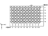
図3は、実施の形態にかかる表示装置が備える検出電極群の構成を示す図である。第1の電極群である検出電極群101は、表示器14の上面側に配置されている。図3では、表示器14を上面側から見た場合の検出電極の配置例を示している。
検出電極群101は、X座標が共通となるように複数の検出電極が配列されたX電極列と、Y座標が共通となるように複数の検出電極が配列されたY電極列とを有している。X電極列の各検出電極は、Y方向に平行な方向に並んでおり、Y電極列の各検出電極は、X方向に平行な方向に並んでいる。検出電極群101に含まれる検出電極が第1の電極である。
図3では、検出電極群101が、10本のX電極列と、6本のY電極列とを有している場合を示している。X電極列は、X座標がX1からX10であり、Y電極列は、Y座標がY1からY6である。
X座標がX1のX電極列は、6個の検出電極が直列に接続されている。同様に、X座標がX2からX10の各X電極列は、6個の検出電極が直列に接続されている。また、Y座標がY1のY電極列は、11個の検出電極が直列に接続されている。同様に、Y座標がY2からY6の各Y電極列は、11個の検出電極が直列に接続されている。
X電極列の各検出電極は、Z座標が同じである。また、Y電極列の各検出電極は、Z座標が同じである。X電極列とY電極列とは異なる層に配置されている。すなわち、X電極列が配置されているZ座標と、Y電極列が配置されているZ座標とは異なる座標である。X電極列が配置されている面と、Y電極列が配置されている面との間には、特定の誘電率を有した誘電体層が配置されている。
検出電極群101のうち、入力デバイス20が重ねられた領域以外の検出電極は、タッチ操作の検出に用いられる。例えば、検出電極群101を上面から見た場合に、(X,Y)=(X5,Y3)の位置がタッチされると、この位置の静電容量が変化する。表示装置10は、この静電容量の変化を検出することで、タッチ位置を検出する。表示装置10は、何れかのX電極列へ電圧を印加した際の各Y電極列での静電容量の変化を検出する。表示装置10は、例えば、X座標がXn(nは、1から10の何れかの自然数)のX電極列へ電圧を印加する。そして、表示装置10は、Y座標がYm(mは、1から6の何れかの自然数)であるY電極列で静電容量が変化したか否かを判定する。
表示装置10は、X座標がX1のX電極列へ電圧を印加した際に、Y座標がY1のY電極列からY座標がY6のY電極列まで順番に静電容量が変化したか否かを判定する。同様に、表示装置10は、X座標がX2のX電極列へ電圧を印加した際に、Y座標がY1のY電極列からY座標がY6のY電極列まで順番に静電容量が変化したか否かを判定する。このように、表示装置10は、X座標がX1からX10までの各X電極列へ、順番に電圧を印加するとともに、X座標がXnのX電極列へ電圧を印加した場合に、Y座標がY1のY電極列からY座標がY6のY電極列まで順番に静電容量が変化したか否かを判定する。これにより、表示装置10は、表示器14の何れの位置がタッチされたかを検出することができる。なお、X電極列への電圧の印加の順番は、何れの順番で行われてもよい。また、Y電極列における静電容量の変化の判定は何れの順番で行われてもよい。
また、検出電極群101のうち、入力デバイス20が重ねられた領域(以下、静電通信領域という)の検出電極は、静電容量通信に用いられる。静電通信領域の検出電極は、一部が静電送信電極となり、残りが静電受信電極となる。静電送信電極となった検出電極は、入力デバイス20に電圧パルス信号を送信し、静電受信電極となった検出電極は、入力デバイス20から電圧パルス信号を受信する。検出電極群101が配置されている領域のうち静電通信領域が第1の領域であり、静電通信領域以外の領域である後述のタッチ検出領域が第2の領域である。
検出電極群101では、何れの検出電極が静電送信電極になってもよく、何れの検出電極が静電受信電極になってもよい。また、静電通信領域の検出電極のうち、静電送信電極および静電受信電極の何れにも設定されない電極があってもよい。
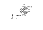
図4は、実施の形態にかかる入力デバイスが備えるデバイス電極群の構成を示す図である。第2の電極群であるデバイス電極群201は、入力デバイス20の底面側の円形領域に配置されている。図4では、入力デバイス20を底面側から見た場合のデバイス電極群201の配置例を示している。図4では、入力デバイス20の底面と平行な面内の2つの軸であって互いに直交する2つの軸をA軸およびB軸とする。また、A軸およびB軸に直交する軸をC軸とする。本実施の形態では、A方向、B方向、およびC方向は、何れも入力デバイス20における方向であり、入力デバイス20が移動しても変化しない。
デバイス電極群201は、A座標が共通となるように複数の検出電極が配列されたA電極列と、B座標が共通となるように複数の検出電極が配列されたB電極列とを有している。A電極列の各検出電極は、B方向に平行な方向に並んでおり、B電極列の各検出電極は、A方向に平行な方向に並んでいる。デバイス電極群201に含まれる電極が第2の電極である。
図4では、デバイス電極群201が、2本のA電極列と、2本のB電極列とを有している場合を示している。A電極列は、A座標がA1およびA2であり、B電極列は、B座標がB1およびB2である。
A座標がA1,A2のA電極列は、それぞれ3個の電極が直列に接続されている。また、B座標がB1,B2のB電極列は、それぞれ3個の電極が直列に接続されている。
A電極列の各検出電極は、C座標が同じである。また、B電極列の各検出電極は、C座標が同じである。A電極列とB電極列とは異なる層に配置されている。すなわち、A電極列が配置されているC座標と、B電極列が配置されているC座標とは異なる座標である。A電極列が配置されている面と、B電極列が配置されている面との間には、特定の誘電率を有した誘電体層が配置されている。
デバイス電極群201の各電極は、静電容量通信に用いられる。デバイス電極群201の電極は、一部が送信電極となり、残りが受信電極となる。送信電極となった電極は、表示装置10に電圧パルス信号を送信し、受信電極となった電極は、表示装置10から電圧パルス信号を受信する。
デバイス電極群201では、何れの電極が送信電極になってもよく、何れの検出電極が受信電極になってもよい。また、デバイス電極群201に含まれる電極のうち、送信電極および受信電極の何れにも設定されない電極があってもよい。
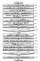
図5は、実施の形態にかかる表示システムによる表示処理の処理手順を示すフローチャートである。入力デバイス20が、操作者40によって表示装置10の入力画面に重ねられる(ステップS10)。具体的には、デバイス電極群201が配置されている入力デバイス20の底面側が、検出電極群101が配置されている表示装置10の上面側に重ねられる。
表示装置10は、入力デバイス20の表示装置10上での位置および形状を示す位置形状情報を検出する(ステップS20)。表示装置10では、検出電極群101および検出回路11が、位置形状情報を検出する。具体的には、検出回路11が、検出電極群101に含まれるX電極列のうち電圧を印加したX電極列のX座標と、検出電極群101に含まれるY電極列のうち静電容量が変化したY電極列のY座標とに基づいて、位置形状情報を検出する。
表示装置10は、位置形状情報を記憶する(ステップS30)。具体的には、検出回路11が、位置形状情報をデータ記憶部12に格納する。
表示装置10は、位置形状情報に基づいて、静電通信領域を設定する(ステップS40)。具体的には、検出回路11が、データ記憶部12に格納されている位置形状情報に基づいて、静電通信領域を設定する。検出回路11は、位置形状情報をデータ処理部13に送る。
表示装置10は、静電通信領域に対し、静電送信電極および静電受信電極を設定する(ステップS50)。具体的には、データ処理部13は、静電通信領域に含まれる検出電極のうち、一部の検出電極を静電送信電極に設定し、残りの検出電極を静電受信電極に設定する。
入力デバイス20は、表示装置10に重ねられて表示装置10との接触を検知すると、デバイス電極群201から電圧パルス信号で示される識別情報を表示装置10に送信する(ステップS60)。具体的には、入力デバイス20が表示装置10に重ねられたことをセンサ23が検知し、入力部22が表示装置10に接触したことを示す接触情報を波形生成回路21に送る。波形生成回路21は、識別情報を示す電圧パルス信号を生成する。デバイス電極群201は、波形生成回路21が生成した識別情報を示す電圧パルス信号を表示装置10に送信する。この場合において、デバイス電極群201は、電極のうち静電送信電極に設定されている検出電極から識別情報を示す電圧パルス信号を送信する。
表示装置10は、検出電極群101で、電圧パルス信号で示される識別情報を受信する(ステップS65)。具体的には、検出電極群101が、検出電極のうち静電受信電極に設定されている検出電極から電圧パルス信号を受信する。電圧パルス信号を受信した静電受信電極は、受信した電圧パルス信号を検出回路11に送る。検出回路11は、電圧パルス信号を識別情報に変換する。
表示装置10は、識別情報に対応する表示オブジェクトを表示する(ステップS70)。具体的には、データ処理部13は、表示オブジェクトと識別情報との対応関係を示す対応関係情報と、識別情報とに基づいて表示オブジェクト、例えばプログレスサーキュラー51を決定し、決定した表示オブジェクトを表示生成部15に送る。また、データ処理部13は、位置形状情報に基づいて、表示オブジェクトの表示位置を算出し、算出した表示位置を表示生成部15に送る。
表示生成部15は、データ処理部13から送られてくる表示オブジェクトおよび表示位置に基づいて、表示オブジェクトを表示位置に表示させるための表示画像を生成する。例えば、表示生成部15は、位置形状情報に対応する領域であるオブジェクト表示領域に、プログレスサーキュラー51といった表示オブジェクトを表示させるための表示画像を生成する。表示器14は、表示生成部15が生成した表示画面を表示することで、オブジェクト表示領域に、プログレスサーキュラー51を表示する。
入力デバイス20は、操作されたか否かを判定する(ステップS80)。操作者40によって入力デバイス20が操作されていなければ(ステップS80、No)、入力デバイス20は、操作者40による操作を待つ。
操作者40によって入力デバイス20が操作されると(ステップS80、Yes)、入力デバイス20が、操作内容をセンサ23で検出し、操作内容を示す操作情報をデバイス電極群201から表示装置10に送信する(ステップS90)。操作情報には、入力デバイス20の操作方向、入力デバイス20への操作量などの情報が含まれている。
表示装置10は、検出電極群101の静電受信電極で操作情報を受信する(ステップS95)。表示装置10は、操作情報を受信すると、検出回路11によって、検出電極群101の静電送信電極から振動指示を送信する(ステップS100)。この振動指示は、入力デバイス20のデバイス電極群201で受信される。入力デバイス20の振動部24は、振動指示に従って入力デバイス20を振動させる。
また、表示装置10は、操作情報を受信すると、操作情報に基づいて表示オブジェクトのインタラクション表現を決定し、表示画像を生成して表示する(ステップS110)。このインタラクション表現は、表示中の表示オブジェクトを操作情報に対応する表示オブジェクトに変化させることで表現される。表示装置10は、例えば、表示オブジェクトがプログレスサーキュラー51である場合、表示しているプログレスサーキュラー51の表示態様を、操作情報に対応する表示態様に変更させる。すなわち、表示装置10は、プログレスサーキュラー51を、操作情報が分かる表示態様で表示させる。
具体的には、データ処理部13は、操作後のプログレスサーキュラー51の表示態様を決定し、決定した表示態様のプログレスサーキュラー51を表示生成部15に送る。表示生成部15は、データ処理部13から送られてくるプログレスサーキュラー51を示す表示画像を生成する。表示生成部15は、オブジェクト表示領域に、操作後のプログレスサーキュラー51を表示させる。
表示装置10は、静電通信領域以外の領域をタッチ検出領域に設定する(ステップS120)。表示装置10は、タッチ検出領域に対応する検出電極群101の検出電極および検出回路11をタッチ検出用に動作させる。
表示装置10は、静電通信領域における容量変化のオフセット値を設定する(ステップS130)。具体的には、検出回路11が、入力デバイス20が静電通信領域で表示装置10に接触していることによる容量変化の検出値の影響を打ち消すようにオフセット値を設定する。この場合において、検出回路11は、データ記憶部12に格納されている位置形状情報に基づいて、オフセット値を設定する。
検出回路11は、例えば、入力デバイス20が静電通信領域で表示装置10に接触している状態で検出した静電容量の変化に基づいて、オフセット値を設定する。なお、検出回路11は、入力デバイス20からオフセット値を取得してもよい。また、検出回路11は、オフセット値と識別情報との対応関係に基づいて、オフセット値を設定してもよい。この場合、表示装置10は、オフセット値と識別情報との対応関係を記憶しておき、検出回路11が、この対応関係と、識別情報とに基づいて、オフセット値を設定する。
この後、表示装置10は、タッチ検出領域に対してタッチ操作されたか否かを判定する(ステップS140)。操作者40がタッチ検出領域に対してタッチ操作を実行していなければ(ステップS140、No)、表示装置10は、タッチ検出領域に対する表示を変化させず、タッチ操作を待つ。
操作者40がタッチ検出領域に対してタッチ操作を実行すると(ステップS140、Yes)、表示装置10は、タッチ操作に対応する処理を実行する(ステップS150)。具体的には、検出回路11がタッチ操作を受付けると、データ処理部13がタッチ検出領域に表示させる情報を決定する。タッチ検出領域に表示させる情報は、タッチ操作の内容を示す情報である。表示生成部15は、表示器14のタッチ検出領域に、タッチ操作の内容を示す情報を表示させる。また、検出回路11は、タッチ操作を受付けると、操作対象の特定装置にタッチ操作に対応する指示を送る。
なお、表示システム1は、ステップS130の処理の後、ステップS80の処理と、ステップS140の処理とを同時に実行してもよい。すなわち、表示システム1は、静電通信領域およびタッチ検出領域を設定した後は、入力デバイス20が操作されたか否かを判定する処理と、タッチ操作されたか否かを判定する処理とを実行する。そして、表示システム1は、入力デバイス20が操作された場合には、ステップS90からS130の処理を実行し、タッチ操作された場合には、ステップS150の処理を実行する。表示システム1は、ステップS90からS130の処理と、ステップS150の処理とを並行して実行する。
すなわち、表示システム1は、静電容量通信と、タッチパネル操作の受付とを同時に実行してもよい。この場合も、表示システム1は、静電容量通信による入力デバイス20から表示装置10への情報の送信と、静電容量通信による表示装置10から入力デバイス20への情報の送信とを並行して実行することで双方向通信を実行してもよい。
また、ステップS120およびS130の処理は、ステップS40の後からステップS140の前までの間であれば、何れのタイミングで実行されてもよい。
また、検出回路11は、入力デバイス20の表示器14上での重心位置と、入力デバイス20の底面の物理サイズの情報(以下、底面情報という)とに基づいて、位置形状情報を算出してもよい。この場合、検出回路11は、入力デバイス20の表示器14上での位置および形状の情報を大まかに検出しておき、大まかな位置および形状の情報から入力デバイス20の表示器14上での重心位置(X,Y座標)を算出する。
入力デバイス20の底面情報は、検出回路11が入力デバイス20から取得する。この場合、波形生成回路21は、入力デバイス20の底面情報を、識別情報とともに表示装置10に送る。
なお、入力デバイス20の底面情報は、表示装置10内に予め格納されていてもよい。この場合、表示装置10は、入力デバイス20の底面情報と、識別情報とが対応付けされた対応情報を記憶しておく。そして、検出回路11が、この対応情報と、識別情報とに基づいて、底面情報を取得する。検出回路11は、取得した底面情報と、算出した重心位置とに基づいて、位置形状情報を算出する。
入力デバイス20は、表示装置10に吸着する吸着部を備えていてもよい。図6は、実施の形態にかかる入力デバイスが吸着部を備える場合のデバイス電極群の構成を示す図である。
吸着部31を備える場合のデバイス電極群201は、図4に示したデバイス電極群201と同様の電極が同様の位置に配置されている。吸着部31に含まれる電極は、デバイス電極群201のうち円形領域の外周領域に配置されている電極である。図6に示すデバイス電極群201の場合、吸着部31に含まれる電極は、電極30a~30hである。吸着部31は、表示装置10が静電通信領域内の特定領域に配置された検出電極に電圧を印加することによって発生する静電気力で表示画面に吸着する吸着機構である。
表示装置10は、検出電極群101が備える電極間に逆位相の電圧を印加することによって、入力デバイス20の底面に配置された吸着部31に静電気力を発生させる。すなわち、表示装置10は、静電通信領域に重なっている検出電極のうち、吸着部31に重なっている検出電極の電極間に逆位相の電圧を印加する。具体的には、表示装置10は、電極30a~30hに対向する位置に配置されている検出電極の電極間に逆位相の電圧を印加する。これにより、吸着部31は、表示装置10との間の電位差によって、入力デバイス20を表示装置10に吸着させる。
例えば、表示装置10は、X座標がX5であるX電極列に正の電圧を印加し、Y座標がY4であるY電極列に負の電圧を印加することで、X座標がX5であるX電極列とY座標がY4であるY電極列とのZ方向から見た交点近傍に静電気力を発生させる。この交点の位置は、電極30a~30hが配置されている領域内の位置である。表示装置10は、例えば、X座標がX5であるX電極列に40Vを印加し、Y座標がY4であるY電極列に-40Vを印加することで、(X,Y)=(X5,Y4)の位置に80Vの電位差で静電気力を発生させる。このように、表示装置10は、吸着部31となる電極30a~30hの位置に電圧を印加することで入力デバイス20を表示器14に吸着させる。
デバイス電極群201の電極のうち電極30a~30h以外の電極、すなわちデバイス電極群201の中央領域32に配置されている電極が、静電送信電極または静電受信電極に用いられる。図6に示すデバイス電極群201の場合、静電容量通信に用いられる電極は中央領域32に配置された4つの電極である。
デバイス電極群201の静電通信領域のうち吸着部31となる外周領域は、中央領域32よりも誘電率が高い。
吸着部31によって入力デバイス20が表示装置10に吸着されることにより、表示装置10が鉛直方向に立てられた場合、すなわち表示画面が鉛直方向に平行な場合であっても、入力デバイス20への操作が容易になる。
また、表示装置10は、入力デバイス20を表示装置10から離す場合には、吸着時とは反対の電圧を印加する。これにより、入力デバイス20の表示装置10への着脱が容易となる。
表示装置10は、例えば、特定の時間ずつ順番に電極30a~30hに電圧を印加する。なお、表示システム1では、静電容量通信に用いる電極と、吸着部31として用いる電極とが別々に設定されてもよいし、電極を静電容量通信用と吸着用とで時分割で共用されてもよい。
ここで、表示装置10のハードウェア構成について説明する。図7は、実施の形態にかかる表示装置を実現するハードウェア構成例を示す図である。
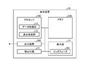
表示装置10は、プロセッサ100、メモリ200、出力装置300、表示器14、および検出回路11により実現することができる。プロセッサ100の例は、CPU(Central Processing Unit、中央処理装置、処理装置、演算装置、マイクロプロセッサ、マイクロコンピュータ、DSP(Digital Signal Processor)ともいう)またはシステムLSI(Large Scale Integration)である。メモリ200の例は、RAM(Random Access Memory)、ROM(Read Only Memory)である。
表示装置10は、プロセッサ100が、メモリ200で記憶されている表示装置10の動作を実行するための、コンピュータで実行可能な、表示プログラムを読み出して実行することにより実現される。表示装置10の動作を実行するためのプログラムである表示プログラムは、表示装置10の手順または方法をコンピュータに実行させるものであるともいえる。
表示装置10で実行される表示プログラムは、データ処理部13と、表示生成部15とを含むモジュール構成となっており、これらが主記憶装置上にロードされ、これらが主記憶装置上に生成される。
表示器14は、入力デバイス20との間で情報を送受信するとともに、タッチ操作を受付けるインタフェース301を備えている。インタフェース301は、検出電極群101を用いて構成されている。
メモリ200は、プロセッサ100が各種処理を実行する際の一時メモリに使用される。メモリ200は、位置形状情報などを記憶する。出力装置300は、タッチ操作に対応する指令などを外部装置である特定装置に出力する。
表示プログラムは、インストール可能な形式または実行可能な形式のファイルで、コンピュータが読み取り可能な記憶媒体に記憶されてコンピュータプログラムプロダクトとして提供されてもよい。また、表示プログラムは、インターネットなどのネットワーク経由で表示装置10に提供されてもよい。なお、表示装置10の機能について、一部を専用回路などの専用のハードウェアで実現し、一部をソフトウェアまたはファームウェアで実現するようにしてもよい。また、入力デバイス20についても、表示装置10と同様のハードウェア構成によって実現できる。
なお、表示装置10は、検出回路11の代わりに、プロセッサ100およびメモリ200を用いて検出回路11の処理を実行してもよい。
このように実施の形態では、入力デバイス20が、デバイス電極群201から検出電極群101に電圧パルス信号で情報を送信するとともに、検出電極群101から電圧パルス信号で送信されてくる情報をデバイス電極群201で受信している。また、表示装置10が、検出電極群101からデバイス電極群201に電圧パルス信号で情報を送信するとともに、デバイス電極群201から電圧パルス信号で送信されてくる情報を検出電極群101で受信している。これにより、表示システム1は、入力デバイス20とタッチパネルである表示装置10との間で双方向通信を実現できる。
また、表示装置10は、検出電極群101が配置されている領域のうち入力デバイス20と接触している領域を静電通信領域に設定している。また、表示装置10は、検出電極群101が配置されている領域のうち静電通信領域以外の領域をタッチ操作を受付けるタッチ検出領域に設定している。これにより、表示装置10は、静電通信領域での情報の受信処理と、タッチ検出領域でのタッチ操作の受付け処理と、を同時に実行することができる。
以上の実施の形態に示した構成は、一例を示すものであり、別の公知の技術と組み合わせることも可能であるし、実施の形態同士を組み合わせることも可能であるし、要旨を逸脱しない範囲で、構成の一部を省略、変更することも可能である。
1 表示システム、10 表示装置、11 検出回路、12 データ記憶部、13 データ処理部、14 表示器、15 表示生成部、20 入力デバイス、21 波形生成回路、22 入力部、23 センサ、24 振動部、30a~30h 電極、31 吸着部、32 中央領域、40 操作者、51 プログレスサーキュラー、100 プロセッサ、101 検出電極群、200 メモリ、201 デバイス電極群、300 出力装置、301 インタフェース。
Claims (6)
- 複数の第1の電極からなる第1の電極群を有し且つ前記第1の電極群に入力された第1の情報に対応する表示オブジェクトを表示するとともに前記第1の電極群を介したタッチ操作を受付ける投影型静電容量方式の表示装置と、
複数の第2の電極からなる第2の電極群を有し且つ前記タッチ操作を受付ける受付面に接触した状態で前記第2の電極群から前記表示装置に前記第1の情報を入力する入力デバイスと、
を備え、
前記入力デバイスは、前記第2の電極群から前記第1の電極群に前記第1の情報を送信するとともに、前記第1の電極群から送信されてくる第2の情報を前記第2の電極群で受信し、
前記表示装置は、前記第1の電極群から前記第2の電極群に前記第2の情報を送信するとともに、前記第2の電極群から送信されてくる前記第1の情報を前記第1の電極群で受信する、
ことを特徴とする表示システム。 - 前記複数の第1の電極は、前記第1の情報を受信する第1の受信電極と、前記第2の情報を送信する第1の送信電極とを含み、
前記複数の第2の電極は、前記第2の情報を受信する第2の受信電極と、前記第1の情報を送信する第2の送信電極とを含み、
前記表示装置は、前記第1の受信電極による前記第1の情報の受信処理と、前記第1の送信電極による前記第2の情報の送信処理とを実行し、
前記入力デバイスは、前記第2の受信電極による前記第2の情報の受信処理と、前記第2の送信電極による前記第1の情報の送信処理とを実行する、
ことを特徴とする請求項1に記載の表示システム。 - 前記表示装置は、前記第1の電極群が配置されている領域のうち前記入力デバイスと接触している領域を、前記第1の情報を受信するとともに前記第2の情報を送信する第1の領域に設定するとともに、前記第1の電極群が配置されている領域のうち前記第1の領域以外の領域を、前記タッチ操作を受付ける第2の領域に設定し、前記第1の領域での前記第1の情報の受信処理と、前記第2の領域での前記タッチ操作の受付け処理と、を実行する、
ことを特徴とする請求項1または2に記載の表示システム。 - 複数の第1の電極からなる第1の電極群を有し且つ前記第1の電極群に入力された第1の情報を表示するとともに前記第1の電極群を介したタッチ操作を受付ける投影型静電容量方式の表示装置と、
前記タッチ操作を受付ける受付面に接触した状態で前記表示装置に前記第1の情報を入力する入力デバイスと、
を備え、
前記入力デバイスは、前記第1の電極群に前記第1の情報を送信し、
前記表示装置は、前記第1の電極群が配置されている領域のうち前記入力デバイスと接触している領域を、前記第1の情報を受信する第1の領域に設定するとともに、前記第1の電極群が配置されている領域のうち前記第1の領域以外の領域を、前記第1の電極群を介したタッチ操作を受付ける第2の領域に設定し、前記第1の領域での前記第1の情報の受信処理と、前記第2の領域での前記タッチ操作の受付け処理と、を実行する、
ことを特徴とする表示システム。 - 前記表示装置は、前記入力デバイスと前記表示装置との接触領域のうちの一部の領域に電圧を印加することによって前記入力デバイスと前記表示装置とを吸着させる、
ことを特徴とする請求項1から4の何れか1つに記載の表示システム。 - 複数の第1の電極からなる第1の電極群を有し且つ前記第1の電極群に入力された第1の情報に対応する表示オブジェクトを表示するとともに前記第1の電極群を介したタッチ操作を受付ける投影型静電容量方式の表示装置と、複数の第2の電極からなる第2の電極群を有し且つ前記タッチ操作を受付ける受付面に接触した状態で前記第2の電極群から前記表示装置に前記第1の情報を入力する入力デバイスとを備えた表示ステムが前記表示オブジェクトを表示する表示方法であって、
前記入力デバイスが、前記第2の電極群から前記第1の電極群に前記第1の情報を送信した場合に、前記表示装置が、前記第1の情報を前記第1の電極群で受信する第1の送受信ステップと、
前記表示装置が、前記第1の電極群から前記第2の電極群に第2の情報を送信した場合に、前記入力デバイスが、前記第2の情報を前記第2の電極群で受信する第2の送受信ステップと、
を含む、
ことを特徴とする表示方法。
Priority Applications (3)
| Application Number | Priority Date | Filing Date | Title |
|---|---|---|---|
| PCT/JP2020/044162 WO2022113253A1 (ja) | 2020-11-27 | 2020-11-27 | 表示システムおよび表示方法 |
| CN202080102649.8A CN115867880B (zh) | 2020-11-27 | 2020-11-27 | 显示系统及显示方法 |
| JP2021506598A JP6921359B1 (ja) | 2020-11-27 | 2020-11-27 | 表示システムおよび表示方法 |
Applications Claiming Priority (1)
| Application Number | Priority Date | Filing Date | Title |
|---|---|---|---|
| PCT/JP2020/044162 WO2022113253A1 (ja) | 2020-11-27 | 2020-11-27 | 表示システムおよび表示方法 |
Publications (1)
| Publication Number | Publication Date |
|---|---|
| WO2022113253A1 true WO2022113253A1 (ja) | 2022-06-02 |
Family
ID=77269599
Family Applications (1)
| Application Number | Title | Priority Date | Filing Date |
|---|---|---|---|
| PCT/JP2020/044162 Ceased WO2022113253A1 (ja) | 2020-11-27 | 2020-11-27 | 表示システムおよび表示方法 |
Country Status (3)
| Country | Link |
|---|---|
| JP (1) | JP6921359B1 (ja) |
| CN (1) | CN115867880B (ja) |
| WO (1) | WO2022113253A1 (ja) |
Cited By (1)
| Publication number | Priority date | Publication date | Assignee | Title |
|---|---|---|---|---|
| EP4394564A1 (en) * | 2022-12-20 | 2024-07-03 | Alps Alpine Co., Ltd. | Input display device |
Citations (3)
| Publication number | Priority date | Publication date | Assignee | Title |
|---|---|---|---|---|
| JP2003248540A (ja) * | 2001-12-04 | 2003-09-05 | Japan Science & Technology Corp | 皮膚感覚提示装置 |
| JP2016071842A (ja) * | 2014-09-26 | 2016-05-09 | パナソニックIpマネジメント株式会社 | タッチパネル装置、入力装置、及びタッチパネルシステム |
| JP6739692B1 (ja) * | 2019-12-26 | 2020-08-12 | 三菱電機株式会社 | 触覚提示制御装置、触覚提示パネル、触覚提示タッチパネル、および触覚提示タッチディスプレイ |
Family Cites Families (6)
| Publication number | Priority date | Publication date | Assignee | Title |
|---|---|---|---|---|
| US9268413B2 (en) * | 2008-07-07 | 2016-02-23 | Rpx Clearinghouse Llc | Multi-touch touchscreen incorporating pen tracking |
| US9329708B2 (en) * | 2014-01-08 | 2016-05-03 | Microsoft Technology Licensing, Llc | Display system with electrostatic and radio links |
| US11263421B2 (en) * | 2016-03-16 | 2022-03-01 | Texas Instruments Incorporated | Dual touch sensor architecture with XY-position and Z-force sensing for touch-on-surface button |
| JP6923725B2 (ja) * | 2016-07-27 | 2021-08-25 | 株式会社ワコム | センサコントローラ |
| DE102018120575A1 (de) * | 2018-07-12 | 2020-01-16 | Preh Gmbh | Eingabevorrichtung mit beweglicher Handhabe auf kapazitiver Detektionsfläche und kapazitiven Koppeleinrichtungen |
| JP6758547B1 (ja) * | 2019-12-05 | 2020-09-23 | 三菱電機株式会社 | 触覚提示パネル、触覚提示タッチパネル、触覚提示タッチディスプレイ、および触覚提示つまみ |
-
2020
- 2020-11-27 JP JP2021506598A patent/JP6921359B1/ja active Active
- 2020-11-27 CN CN202080102649.8A patent/CN115867880B/zh active Active
- 2020-11-27 WO PCT/JP2020/044162 patent/WO2022113253A1/ja not_active Ceased
Patent Citations (3)
| Publication number | Priority date | Publication date | Assignee | Title |
|---|---|---|---|---|
| JP2003248540A (ja) * | 2001-12-04 | 2003-09-05 | Japan Science & Technology Corp | 皮膚感覚提示装置 |
| JP2016071842A (ja) * | 2014-09-26 | 2016-05-09 | パナソニックIpマネジメント株式会社 | タッチパネル装置、入力装置、及びタッチパネルシステム |
| JP6739692B1 (ja) * | 2019-12-26 | 2020-08-12 | 三菱電機株式会社 | 触覚提示制御装置、触覚提示パネル、触覚提示タッチパネル、および触覚提示タッチディスプレイ |
Cited By (2)
| Publication number | Priority date | Publication date | Assignee | Title |
|---|---|---|---|---|
| EP4394564A1 (en) * | 2022-12-20 | 2024-07-03 | Alps Alpine Co., Ltd. | Input display device |
| US12277280B2 (en) | 2022-12-20 | 2025-04-15 | Alps Alpine Co., Ltd. | Input display device |
Also Published As
| Publication number | Publication date |
|---|---|
| CN115867880B (zh) | 2023-08-25 |
| CN115867880A (zh) | 2023-03-28 |
| JP6921359B1 (ja) | 2021-08-18 |
| JPWO2022113253A1 (ja) | 2022-06-02 |
Similar Documents
| Publication | Publication Date | Title |
|---|---|---|
| EP1927916A1 (en) | Apparatus, method, and medium for outputting tactile feedback on display device | |
| JP5630119B2 (ja) | タッチパネル装置、これを含むタッチパネル付き表示装置、及びタッチパネル装置の制御方法 | |
| JP6086350B2 (ja) | タッチパネル式入力装置、およびタッチパネル式入力方法 | |
| US10884501B2 (en) | Display device including force sensor and method of manufacturing same | |
| JP7125588B2 (ja) | センサアッセンブリ、スタイラスペン、手書き入力システム、及び作品描画手法指導システム | |
| US10509489B2 (en) | Systems and related methods for facilitating pen input in a virtual reality environment | |
| JP2010286986A5 (ja) | ||
| US20160011708A1 (en) | Multi-axis input device and multi-axis input apparatus | |
| CN106164824B (zh) | 用于车辆的操作装置 | |
| JP2010286986A (ja) | 携帯端末装置 | |
| US20230095328A1 (en) | Information processing apparatus, information processing method, computer program, and augmented reality system | |
| US10540023B2 (en) | User interface devices for virtual reality system | |
| JP2010055614A (ja) | マルチタッチセンサー装置 | |
| CN103038730A (zh) | 触感提供装置和用于触感提供装置的控制方法 | |
| US20210184676A1 (en) | Multiple Controllers for a Capacitive Sensing Device | |
| JP6921359B1 (ja) | 表示システムおよび表示方法 | |
| JP2018106374A (ja) | 操作入力装置及び画像処理システム | |
| JPWO2016181469A1 (ja) | シミュレーションシステム | |
| CN107861653A (zh) | 显示控制设备、显示控制系统和显示控制方法 | |
| CN101868776A (zh) | 触觉输入/输出设备及其驱动方法 | |
| JP5865724B2 (ja) | 入力装置及び前記入力装置を用いた重心位置の補正方法 | |
| US9501189B2 (en) | Electronic device and method for controlling electronic device | |
| CN106557213A (zh) | 一种电容式三维侦测模块的侦测方法 | |
| JP7052782B2 (ja) | タッチパネル入力装置とタッチパネルの入力操作検出方法 | |
| JP2019082839A (ja) | 入力装置、制御装置、およびプログラム |
Legal Events
| Date | Code | Title | Description |
|---|---|---|---|
| ENP | Entry into the national phase |
Ref document number: 2021506598 Country of ref document: JP Kind code of ref document: A |
|
| 121 | Ep: the epo has been informed by wipo that ep was designated in this application |
Ref document number: 20963518 Country of ref document: EP Kind code of ref document: A1 |
|
| NENP | Non-entry into the national phase |
Ref country code: DE |
|
| 122 | Ep: pct application non-entry in european phase |
Ref document number: 20963518 Country of ref document: EP Kind code of ref document: A1 |