WO2022106949A1 - 表示パネル、情報処理装置、表示パネルの製造方法 - Google Patents
表示パネル、情報処理装置、表示パネルの製造方法 Download PDFInfo
- Publication number
- WO2022106949A1 WO2022106949A1 PCT/IB2021/060241 IB2021060241W WO2022106949A1 WO 2022106949 A1 WO2022106949 A1 WO 2022106949A1 IB 2021060241 W IB2021060241 W IB 2021060241W WO 2022106949 A1 WO2022106949 A1 WO 2022106949A1
- Authority
- WO
- WIPO (PCT)
- Prior art keywords
- layer
- electrode
- light emitting
- unit
- emitting device
- Prior art date
- Legal status (The legal status is an assumption and is not a legal conclusion. Google has not performed a legal analysis and makes no representation as to the accuracy of the status listed.)
- Ceased
Links
Images





























Classifications
-
- H—ELECTRICITY
- H10—SEMICONDUCTOR DEVICES; ELECTRIC SOLID-STATE DEVICES NOT OTHERWISE PROVIDED FOR
- H10K—ORGANIC ELECTRIC SOLID-STATE DEVICES
- H10K59/00—Integrated devices, or assemblies of multiple devices, comprising at least one organic light-emitting element covered by group H10K50/00
- H10K59/10—OLED displays
- H10K59/12—Active-matrix OLED [AMOLED] displays
- H10K59/121—Active-matrix OLED [AMOLED] displays characterised by the geometry or disposition of pixel elements
-
- G—PHYSICS
- G09—EDUCATION; CRYPTOGRAPHY; DISPLAY; ADVERTISING; SEALS
- G09F—DISPLAYING; ADVERTISING; SIGNS; LABELS OR NAME-PLATES; SEALS
- G09F9/00—Indicating arrangements for variable information in which the information is built-up on a support by selection or combination of individual elements
-
- G—PHYSICS
- G09—EDUCATION; CRYPTOGRAPHY; DISPLAY; ADVERTISING; SEALS
- G09F—DISPLAYING; ADVERTISING; SIGNS; LABELS OR NAME-PLATES; SEALS
- G09F9/00—Indicating arrangements for variable information in which the information is built-up on a support by selection or combination of individual elements
- G09F9/30—Indicating arrangements for variable information in which the information is built-up on a support by selection or combination of individual elements in which the desired character or characters are formed by combining individual elements
-
- G—PHYSICS
- G09—EDUCATION; CRYPTOGRAPHY; DISPLAY; ADVERTISING; SEALS
- G09F—DISPLAYING; ADVERTISING; SIGNS; LABELS OR NAME-PLATES; SEALS
- G09F9/00—Indicating arrangements for variable information in which the information is built-up on a support by selection or combination of individual elements
- G09F9/30—Indicating arrangements for variable information in which the information is built-up on a support by selection or combination of individual elements in which the desired character or characters are formed by combining individual elements
- G09F9/33—Indicating arrangements for variable information in which the information is built-up on a support by selection or combination of individual elements in which the desired character or characters are formed by combining individual elements being semiconductor devices, e.g. diodes
- G09F9/335—Indicating arrangements for variable information in which the information is built-up on a support by selection or combination of individual elements in which the desired character or characters are formed by combining individual elements being semiconductor devices, e.g. diodes being organic light emitting diodes [OLED]
-
- H—ELECTRICITY
- H05—ELECTRIC TECHNIQUES NOT OTHERWISE PROVIDED FOR
- H05B—ELECTRIC HEATING; ELECTRIC LIGHT SOURCES NOT OTHERWISE PROVIDED FOR; CIRCUIT ARRANGEMENTS FOR ELECTRIC LIGHT SOURCES, IN GENERAL
- H05B33/00—Electroluminescent light sources
- H05B33/02—Details
-
- H—ELECTRICITY
- H05—ELECTRIC TECHNIQUES NOT OTHERWISE PROVIDED FOR
- H05B—ELECTRIC HEATING; ELECTRIC LIGHT SOURCES NOT OTHERWISE PROVIDED FOR; CIRCUIT ARRANGEMENTS FOR ELECTRIC LIGHT SOURCES, IN GENERAL
- H05B33/00—Electroluminescent light sources
- H05B33/02—Details
- H05B33/06—Electrode terminals
-
- H—ELECTRICITY
- H05—ELECTRIC TECHNIQUES NOT OTHERWISE PROVIDED FOR
- H05B—ELECTRIC HEATING; ELECTRIC LIGHT SOURCES NOT OTHERWISE PROVIDED FOR; CIRCUIT ARRANGEMENTS FOR ELECTRIC LIGHT SOURCES, IN GENERAL
- H05B33/00—Electroluminescent light sources
- H05B33/12—Light sources with substantially two-dimensional [2D] radiating surfaces
-
- H—ELECTRICITY
- H05—ELECTRIC TECHNIQUES NOT OTHERWISE PROVIDED FOR
- H05B—ELECTRIC HEATING; ELECTRIC LIGHT SOURCES NOT OTHERWISE PROVIDED FOR; CIRCUIT ARRANGEMENTS FOR ELECTRIC LIGHT SOURCES, IN GENERAL
- H05B33/00—Electroluminescent light sources
- H05B33/12—Light sources with substantially two-dimensional [2D] radiating surfaces
- H05B33/14—Light sources with substantially two-dimensional [2D] radiating surfaces characterised by the chemical or physical composition or the arrangement of the electroluminescent material, or by the simultaneous addition of the electroluminescent material in or onto the light source
-
- H—ELECTRICITY
- H05—ELECTRIC TECHNIQUES NOT OTHERWISE PROVIDED FOR
- H05B—ELECTRIC HEATING; ELECTRIC LIGHT SOURCES NOT OTHERWISE PROVIDED FOR; CIRCUIT ARRANGEMENTS FOR ELECTRIC LIGHT SOURCES, IN GENERAL
- H05B33/00—Electroluminescent light sources
- H05B33/12—Light sources with substantially two-dimensional [2D] radiating surfaces
- H05B33/22—Light sources with substantially two-dimensional [2D] radiating surfaces characterised by the chemical or physical composition or the arrangement of auxiliary dielectric or reflective layers
-
- H—ELECTRICITY
- H10—SEMICONDUCTOR DEVICES; ELECTRIC SOLID-STATE DEVICES NOT OTHERWISE PROVIDED FOR
- H10K—ORGANIC ELECTRIC SOLID-STATE DEVICES
- H10K50/00—Organic light-emitting devices
- H10K50/10—OLEDs or polymer light-emitting diodes [PLED]
- H10K50/14—Carrier transporting layers
- H10K50/15—Hole transporting layers
-
- H—ELECTRICITY
- H10—SEMICONDUCTOR DEVICES; ELECTRIC SOLID-STATE DEVICES NOT OTHERWISE PROVIDED FOR
- H10K—ORGANIC ELECTRIC SOLID-STATE DEVICES
- H10K50/00—Organic light-emitting devices
- H10K50/10—OLEDs or polymer light-emitting diodes [PLED]
- H10K50/17—Carrier injection layers
-
- H—ELECTRICITY
- H10—SEMICONDUCTOR DEVICES; ELECTRIC SOLID-STATE DEVICES NOT OTHERWISE PROVIDED FOR
- H10K—ORGANIC ELECTRIC SOLID-STATE DEVICES
- H10K59/00—Integrated devices, or assemblies of multiple devices, comprising at least one organic light-emitting element covered by group H10K50/00
- H10K59/10—OLED displays
- H10K59/12—Active-matrix OLED [AMOLED] displays
- H10K59/1201—Manufacture or treatment
-
- H—ELECTRICITY
- H10—SEMICONDUCTOR DEVICES; ELECTRIC SOLID-STATE DEVICES NOT OTHERWISE PROVIDED FOR
- H10K—ORGANIC ELECTRIC SOLID-STATE DEVICES
- H10K59/00—Integrated devices, or assemblies of multiple devices, comprising at least one organic light-emitting element covered by group H10K50/00
- H10K59/10—OLED displays
- H10K59/12—Active-matrix OLED [AMOLED] displays
- H10K59/122—Pixel-defining structures or layers, e.g. banks
-
- H—ELECTRICITY
- H10—SEMICONDUCTOR DEVICES; ELECTRIC SOLID-STATE DEVICES NOT OTHERWISE PROVIDED FOR
- H10K—ORGANIC ELECTRIC SOLID-STATE DEVICES
- H10K59/00—Integrated devices, or assemblies of multiple devices, comprising at least one organic light-emitting element covered by group H10K50/00
- H10K59/30—Devices specially adapted for multicolour light emission
- H10K59/35—Devices specially adapted for multicolour light emission comprising red-green-blue [RGB] subpixels
-
- H—ELECTRICITY
- H10—SEMICONDUCTOR DEVICES; ELECTRIC SOLID-STATE DEVICES NOT OTHERWISE PROVIDED FOR
- H10K—ORGANIC ELECTRIC SOLID-STATE DEVICES
- H10K59/00—Integrated devices, or assemblies of multiple devices, comprising at least one organic light-emitting element covered by group H10K50/00
- H10K59/30—Devices specially adapted for multicolour light emission
- H10K59/38—Devices specially adapted for multicolour light emission comprising colour filters or colour changing media [CCM]
-
- H—ELECTRICITY
- H10—SEMICONDUCTOR DEVICES; ELECTRIC SOLID-STATE DEVICES NOT OTHERWISE PROVIDED FOR
- H10K—ORGANIC ELECTRIC SOLID-STATE DEVICES
- H10K59/00—Integrated devices, or assemblies of multiple devices, comprising at least one organic light-emitting element covered by group H10K50/00
- H10K59/80—Constructional details
- H10K59/805—Electrodes
- H10K59/8051—Anodes
-
- H—ELECTRICITY
- H10—SEMICONDUCTOR DEVICES; ELECTRIC SOLID-STATE DEVICES NOT OTHERWISE PROVIDED FOR
- H10K—ORGANIC ELECTRIC SOLID-STATE DEVICES
- H10K59/00—Integrated devices, or assemblies of multiple devices, comprising at least one organic light-emitting element covered by group H10K50/00
- H10K59/80—Constructional details
- H10K59/805—Electrodes
- H10K59/8052—Cathodes
-
- H—ELECTRICITY
- H10—SEMICONDUCTOR DEVICES; ELECTRIC SOLID-STATE DEVICES NOT OTHERWISE PROVIDED FOR
- H10K—ORGANIC ELECTRIC SOLID-STATE DEVICES
- H10K59/00—Integrated devices, or assemblies of multiple devices, comprising at least one organic light-emitting element covered by group H10K50/00
- H10K59/80—Constructional details
- H10K59/87—Passivation; Containers; Encapsulations
- H10K59/873—Encapsulations
-
- H—ELECTRICITY
- H10—SEMICONDUCTOR DEVICES; ELECTRIC SOLID-STATE DEVICES NOT OTHERWISE PROVIDED FOR
- H10K—ORGANIC ELECTRIC SOLID-STATE DEVICES
- H10K59/00—Integrated devices, or assemblies of multiple devices, comprising at least one organic light-emitting element covered by group H10K50/00
- H10K59/90—Assemblies of multiple devices comprising at least one organic light-emitting element
-
- H—ELECTRICITY
- H10—SEMICONDUCTOR DEVICES; ELECTRIC SOLID-STATE DEVICES NOT OTHERWISE PROVIDED FOR
- H10K—ORGANIC ELECTRIC SOLID-STATE DEVICES
- H10K71/00—Manufacture or treatment specially adapted for the organic devices covered by this subclass
- H10K71/60—Forming conductive regions or layers, e.g. electrodes
-
- H—ELECTRICITY
- H10—SEMICONDUCTOR DEVICES; ELECTRIC SOLID-STATE DEVICES NOT OTHERWISE PROVIDED FOR
- H10K—ORGANIC ELECTRIC SOLID-STATE DEVICES
- H10K2101/00—Properties of the organic materials covered by group H10K85/00
-
- H—ELECTRICITY
- H10—SEMICONDUCTOR DEVICES; ELECTRIC SOLID-STATE DEVICES NOT OTHERWISE PROVIDED FOR
- H10K—ORGANIC ELECTRIC SOLID-STATE DEVICES
- H10K59/00—Integrated devices, or assemblies of multiple devices, comprising at least one organic light-emitting element covered by group H10K50/00
- H10K59/80—Constructional details
- H10K59/875—Arrangements for extracting light from the devices
Definitions
- One aspect of the present invention relates to a display panel, a method for manufacturing a display panel, an information processing device, or a semiconductor device.
- one aspect of the present invention is not limited to the above technical fields.
- the technical field of one aspect of the invention disclosed in the present specification and the like relates to a product, a method, or a manufacturing method.
- one aspect of the invention relates to a process, machine, manufacture, or composition (composition of matter). Therefore, more specifically, the technical fields of one aspect of the present invention disclosed in the present specification include semiconductor devices, display devices, light emitting devices, power storage devices, storage devices, driving methods thereof, or manufacturing methods thereof. Can be given as an example.
- a method for manufacturing an organic EL display capable of forming a light emitting layer without using a fine metal mask is known.
- a first luminescent organic material containing a mixture of a host material and a dopant material is deposited above an electrode array containing the first and second pixel electrodes formed above the insulating substrate.
- the step of forming the first light emitting layer as a continuous film extending over the display region including the electrode array, and the portion of the first light emitting layer located above the first pixel electrode is not irradiated with ultraviolet light.
- One aspect of the present invention is to provide a novel display panel having excellent convenience, usefulness, or reliability.
- one of the challenges is to provide a new method for manufacturing a display panel, which is excellent in convenience, usefulness, or reliability.
- Another issue is to provide a new information processing device having excellent convenience, usefulness, or reliability.
- one of the problems is to provide a new display panel, a method for manufacturing a new display panel, a new information processing device, or a new semiconductor device.
- One aspect of the present invention is a display panel having a first light emitting device, a second light emitting device, and a partition wall.
- the first light emitting device comprises a first electrode, a second electrode and a first layer, the first layer comprising a region sandwiched between the second electrode and the first electrode.
- the first layer contains a material having a first hole transport property and a substance having a first acceptor property, and the first layer is 1 ⁇ 10 2 [ ⁇ ⁇ cm] or more and 1 ⁇ 10 8 [ ⁇ ]. -Cm] or less electrical resistivity.
- the second light emitting device comprises a third electrode, a fourth electrode and a second layer, the second layer comprising a region sandwiched between the fourth electrode and the third electrode.
- the second layer contains a material having a first hole transporting property and a substance having a first accepting property, and the second layer has a first gap with the first layer.
- the first gap comprises a region overlapping the bulkhead, the first gap interfering with electrical conduction between the first layer and the second layer.
- one aspect of the present invention is a display panel having a first light emitting device, a second light emitting device, and a partition wall.
- the first light emitting device comprises a first electrode, a second electrode, a first unit and a first layer, the second electrode overlaps the first electrode, and the first unit is a second. A region sandwiched between the electrode and the first electrode is provided. Also, the first layer comprises a region sandwiched between the first unit and the first electrode.
- the first layer contains a material having a first hole transport property and a substance having a first acceptor property, and the first layer is 1 ⁇ 10 2 [ ⁇ ⁇ cm] or more and 1 ⁇ 10 8 [ ⁇ ⁇ . It has an electrical resistivity of cm] or less.
- the second light emitting device comprises a third electrode, a fourth electrode, a second unit and a second layer, the fourth electrode overlaps the third electrode, and the second unit is the fourth.
- a region sandwiched between the electrode and the third electrode is provided.
- the second layer also comprises a region sandwiched between the second unit and the first electrode.
- the second layer contains a material having a first hole transport property and a substance having a first acceptor property, and the second layer has a first gap with the first layer.
- the partition wall comprises a first opening and a second opening, the first opening overlapping the first electrode and the second opening overlapping the third electrode. Further, the partition wall overlaps with the first gap between the first opening and the second opening.
- one aspect of the present invention is the above-mentioned display panel in which the first light emitting device includes a third unit and a first intermediate layer.
- the third unit comprises a region sandwiched between the second electrode and the first unit
- the first intermediate layer comprises a region sandwiched between the third unit and the first unit.
- the first intermediate layer contains a material having a second hole transport property and a substance having a second acceptor property, and the first intermediate layer is 1 ⁇ 10 2 [ ⁇ ⁇ cm] or more and 1 ⁇ 10 8 It has an electrical resistivity of [ ⁇ ⁇ cm] or less.
- the second light emitting device comprises a fourth unit and a second intermediate layer, the fourth unit comprising a region sandwiched between the fourth electrode and the second unit. Further, the second intermediate layer includes a region sandwiched between the fourth unit and the second unit.
- the second intermediate layer contains a material having a second hole transporting property and a substance having a second accepting property, and the second intermediate layer has a second gap between the material and the first intermediate layer. Be prepared.
- the partition wall overlaps the second gap between the first and second openings.
- the material having the first hole transporting property is an aromatic amine compound or an organic compound having a ⁇ -electron-rich heteroaromatic ring, and has the first accepting property.
- the substance is an organic compound containing a fluorine or a cyano group or a transition metal oxide.
- one aspect of the present invention is the above-mentioned display panel having a first insulating film.
- the first insulating film sandwiches the second electrode between the first electrode and the first insulating film sandwiches the fourth electrode between the first insulating film and the third electrode.
- one aspect of the present invention is the above-mentioned display panel in which the first layer has a first side wall and the second layer has a second side wall.
- the second side wall faces the first side wall, and the second side wall sandwiches the first gap between the second side wall and the first side wall.
- the first insulating film is in contact with the first side wall and the second side wall.
- one aspect of the present invention is the above-mentioned display panel in which the first insulating film is in contact with the partition wall.
- one aspect of the present invention is the above-mentioned display panel in which the first insulating film includes a second insulating film and a third insulating film.
- the second insulating film is sandwiched between the third insulating film and the second electrode, and the second insulating film is sandwiched between the third insulating film and the fourth electrode.
- the second insulating film contains oxygen and aluminum, and the third insulating film contains nitrogen and silicon.
- one aspect of the present invention is the above-mentioned display panel in which the partition wall is in contact with the second insulating film and the partition wall contains nitrogen and silicon.
- the above-mentioned display panel has an insulating layer, the insulating layer fills the first gap, and the insulating layer fills between the first unit and the second unit. Is.
- one aspect of the present invention is the above-mentioned display panel having a first colored layer and a second colored layer.
- the first colored layer overlaps the first light emitting device, and the second colored layer overlaps the second light emitting device.
- the second colored layer has a third gap between it and the first colored layer, and the second colored layer has a first side wall on the side of the first colored layer.
- the fourth unit has a second side wall that is continuous with the first side wall, and the second unit has a third side wall that is continuous with the second side wall.
- the light emitted by the second light emitting device can be efficiently guided to the second colored layer.
- one aspect of the present invention is the above-mentioned display panel having a functional layer, a first pixel, and a second pixel.
- the first pixel comprises a first light emitting device and a pixel circuit. Further, the second pixel includes a second light emitting device.
- the functional layer comprises a pixel circuit and a translucent region, the pixel circuit is electrically connected to the first light emitting device, and the translucent region is the light emitted from the first light emitting device. Is transparent.
- one aspect of the present invention includes one or more of a keyboard, a hardware button, a pointing device, a touch sensor, an illuminance sensor, an image pickup device, a voice input device, a line-of-sight input device, and an attitude detection device.
- An information processing device including a display panel.
- one aspect of the present invention is a method for manufacturing a display panel, which comprises the first step to the tenth step.
- the first electrode and the second electrode are formed.
- a partition wall is formed between the first electrode and the second electrode.
- a first layer is formed on the first electrode and the second electrode.
- the first unit is formed on the first layer.
- a third electrode is formed on the first unit.
- a photoetching method is used to remove the first layer, the first unit and the third electrode on the second electrode to form the first light emitting device.
- a second layer is formed on the third electrode and the second electrode.
- a second unit is formed on the second layer.
- a fourth electrode is formed on the second unit.
- a photoetching method is used to remove the second layer, the second unit and the fourth electrode on the third electrode and separate them from the first light emitting device to form a second. Form a light emitting device.
- one aspect of the present invention is a method for manufacturing a display panel, which comprises the first step to the eighth step.
- the first electrode and the second electrode are formed.
- a partition wall is formed between the first electrode and the second electrode.
- a layer is formed on the first electrode and the second electrode.
- a first unit is formed on the layer.
- an intermediate layer is formed on the first unit.
- a second unit is formed on the intermediate layer.
- a conductive film is formed on the second unit.
- a photoetching method is used to remove the layer, the first unit, the intermediate layer, the second unit and the conductive film on the partition wall to form a first light emitting device and a second light emitting device. do.
- the sources and drains of a transistor are referred to differently depending on the polarity of the transistor and the potential applied to each terminal.
- a terminal to which a low potential is given is called a source
- a terminal to which a high potential is given is called a drain.
- a terminal to which a low potential is given is called a drain
- a terminal to which a high potential is given is called a source.
- the connection relationship between transistors may be described on the assumption that the source and drain are fixed, but in reality, the names of source and drain are interchanged according to the above potential relationship. ..
- the source of a transistor means a source region that is a part of a semiconductor film that functions as an active layer, or a source electrode connected to the semiconductor film.
- the drain of a transistor means a drain region that is a part of the semiconductor film, or a drain electrode connected to the semiconductor film.
- the gate means a gate electrode.
- the state in which the transistors are connected in series means, for example, a state in which only one of the source or drain of the first transistor is connected to only one of the source or drain of the second transistor. do. Further, in the state where the transistors are connected in parallel, one of the source or drain of the first transistor is connected to one of the source or drain of the second transistor, and the other of the source or drain of the first transistor is connected. It means the state of being connected to the other of the source or drain of the second transistor.
- connection means an electrical connection, and corresponds to a state in which a current, a voltage, or a potential can be supplied or transmitted. Therefore, the connected state does not necessarily mean the directly connected state, and the wiring, resistance, diode, transistor, etc. so that the current, voltage, or potential can be supplied or transmitted.
- the state of being indirectly connected via a circuit element is also included in the category.
- one conductive film may be plural, for example, when a part of the wiring functions as an electrode. In some cases, it also has the functions of the components of.
- connection includes the case where one conductive film has the functions of a plurality of components in combination.
- one of the first electrode or the second electrode of the transistor refers to a source electrode, and the other refers to a drain electrode.
- a novel display panel having excellent convenience, usefulness or reliability.
- a new method for manufacturing a display panel which is excellent in convenience, usefulness or reliability.
- a new information processing apparatus having excellent convenience, usefulness or reliability.
- FIG. 1A to 1C are views for explaining the configuration of the display panel according to the embodiment.
- FIG. 2 is a circuit diagram illustrating pixels of a display panel according to an embodiment.
- 3A to 3D are diagrams illustrating the configuration of the display panel according to the embodiment.
- 4A to 4C are views for explaining the configuration of the display panel according to the embodiment.
- 5A to 5C are diagrams illustrating the configuration of the display panel according to the embodiment.
- FIG. 6 is a diagram illustrating a configuration of a display panel according to an embodiment.
- FIG. 7 is a diagram illustrating a part of FIG. 8A and 8B are diagrams illustrating the configuration of the display panel according to the embodiment.
- 9A to 9C are diagrams illustrating the configuration of the display panel according to the embodiment.
- FIG. 10A to 10C are diagrams illustrating the configuration of the display panel according to the embodiment.
- FIG. 11 is a diagram illustrating a part of FIG. 10A.
- FIG. 12 is a diagram illustrating a configuration of a display panel according to an embodiment.
- FIG. 13 is a diagram illustrating a configuration of a display panel according to an embodiment.
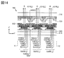
- FIG. 14 is a diagram illustrating a configuration of a display panel according to an embodiment.
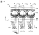
- FIG. 15 is a diagram illustrating a configuration of a display panel according to an embodiment.
- FIG. 16 is a diagram illustrating a configuration of a display panel according to an embodiment.
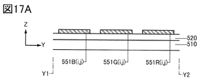
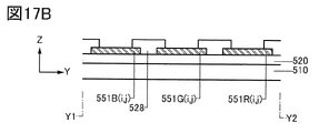
- 17A and 17B are diagrams illustrating a method of manufacturing a display panel according to an embodiment.
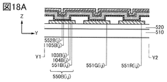
- 18A to 18C are diagrams illustrating a method of manufacturing a display panel according to an embodiment.
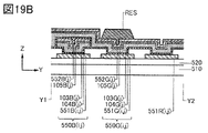
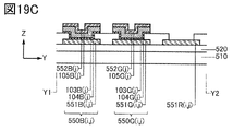
- 19A to 19C are diagrams illustrating a method of manufacturing a display panel according to an embodiment.
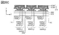
- 20A to 20C are diagrams illustrating a method of manufacturing a display panel according to an embodiment.
- 21A to 21C are diagrams illustrating a method of manufacturing a display panel according to an embodiment.
- 22A to 22C are diagrams illustrating a method of manufacturing a display panel according to an embodiment.
- 23A and 23B are diagrams illustrating a method of manufacturing a display panel according to an embodiment.
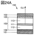
- 24A and 24B are diagrams illustrating the configuration of the light emitting device according to the embodiment.
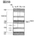
- 25A and 25B are diagrams illustrating the configuration of the light emitting device according to the embodiment.
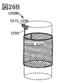
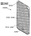
- 26A to 26E are diagrams illustrating the configuration of the information processing apparatus according to the embodiment.
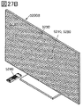
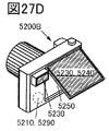
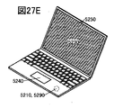
- 27A to 27E are diagrams illustrating the configuration of the information processing apparatus according to the embodiment.
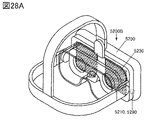
- 28A and 28B are diagrams illustrating the configuration of the information processing apparatus according to the embodiment.
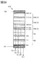
- FIG. 29 is a diagram illustrating a configuration of a light emitting device according to an embodiment.
- the display panel of one aspect of the present invention has a first light emitting device, a second light emitting device, and a partition wall.
- the first light emitting device comprises a first electrode, a second electrode and a first layer, the first layer comprising a region sandwiched between the second electrode and the first electrode. Further, the first layer contains a material having a first hole transport property and a substance having a first acceptor property, and the first layer is 1 ⁇ 10 2 [ ⁇ ⁇ cm] or more and 1 ⁇ 10 8 It has an electrical resistivity of [ ⁇ ⁇ cm] or less.
- the second light emitting device comprises a third electrode, a fourth electrode and a second layer, the second layer comprising a region sandwiched between the fourth electrode and the third electrode.
- the second layer contains a material having a first hole transporting property and a substance having a first accepting property, and the second layer has a first gap between the material and the first layer. ..
- the first gap comprises a region overlapping the bulkhead, the first gap interfering with electrical conduction between the first layer and the second layer.
- FIG. 1 is a diagram illustrating a configuration of a display panel according to an aspect of the present invention.
- FIG. 1A is a top view illustrating a display panel according to an aspect of the present invention
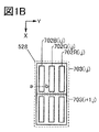
- FIG. 1B is a top view illustrating a part of the display panel.
- FIG. 1C is a cross-sectional view illustrating the direction of light emitted by the display panel of one aspect of the present invention.
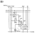
- FIG. 2 is a circuit diagram illustrating pixels of a display panel according to an aspect of the present invention.
- FIG. 3 is a cross-sectional view illustrating the configuration of a display panel according to an aspect of the present invention.
- FIG. 3A is a diagram illustrating a cross section of a cutting line X1-X2, a cutting line X3-X4 and a set of pixels 703 (i, j) shown in FIG. 1A.
- FIG. 3B is a cross-sectional view illustrating a transistor that can be used in the display panel of one aspect of the present invention.
- FIG. 3C is a cross-sectional view illustrating the direction of light emitted by the display panel of one aspect of the present invention, and FIG. 3D is different from the display panel of one aspect of the present invention described with reference to FIG. 3C. It is sectional drawing explaining the direction of the light emitted by the display panel of one aspect of the invention.
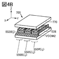
- FIG. 4 is a diagram illustrating a configuration of a display panel according to an aspect of the present invention.
- 4A is a cross-sectional view of the pixels of the display panel of one aspect of the present invention
- FIG. 4B is a perspective view of the pixels shown in FIG. 4A
- FIG. 4C is a top view of the pixels shown in FIG. 4A.
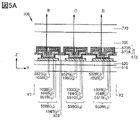
- FIG. 5 is a diagram illustrating a configuration of a display panel according to an aspect of the present invention.
- 5A is a cross-sectional view of the pixels of the display panel of one aspect of the present invention
- FIG. 5B is a perspective view of the pixels shown in FIG. 5A
- FIG. 5C is a top view of the pixels shown in FIG. 5A.
- FIG. 5A is different from the pixels shown in FIG. 4A in that an insulating film is provided
- FIGS. 5A and 5C are views in which the insulating film is omitted in order to avoid the complexity of the drawings.
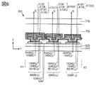
- FIG. 6 is a cross-sectional view illustrating the configuration of a display panel according to an aspect of the present invention.
- FIG. 7 is a cross-sectional view of pixels of a display panel according to an aspect of the present invention, and FIG. 7 is a diagram illustrating a part of the pixels shown in FIG.
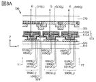
- FIG. 8 is a diagram illustrating a configuration of a display panel according to an aspect of the present invention.
- FIG. 8A is a cross-sectional view of pixels of a display panel according to an aspect of the present invention
- FIG. 8B is a cross-sectional view illustrating a part of the display panel shown in FIG. 8A.
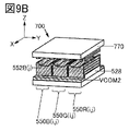
- FIG. 9 is a diagram illustrating a configuration of a display panel according to an aspect of the present invention.
- 9A is a cross-sectional view of the pixels of the display panel of one aspect of the present invention
- FIG. 9B is a perspective view of the pixels shown in FIG. 9A
- FIG. 9C is a top view of the pixels shown in FIG. 9A.
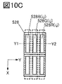
- FIG. 10 is a diagram illustrating a configuration of a display panel according to an aspect of the present invention.
- 10A is a cross-sectional view of the pixels of the display panel of one aspect of the present invention
- FIG. 10B is a perspective view of the pixels shown in FIG. 10A
- FIG. 10C is a top view of the pixels shown in FIG. 10A.
- FIG. 10A is different from the pixels shown in FIG. 9A in that an insulating film is provided
- FIGS. 10B and 10C are views in which the insulating film is omitted in order to avoid the complexity of the drawings.
- FIG. 11 is a cross-sectional view of pixels of a display panel according to an aspect of the present invention, and is a diagram illustrating a part of the pixels shown in FIG. 10A.
- FIG. 12 is a cross-sectional view illustrating the configuration of a display panel according to an aspect of the present invention.
- FIG. 13 is a cross-sectional view illustrating the configuration of a display panel according to an aspect of the present invention.
- FIG. 14 is a cross-sectional view illustrating the configuration of a display panel according to an aspect of the present invention.
- FIG. 15 is a cross-sectional view illustrating the configuration of a display panel according to an aspect of the present invention.
- FIG. 16 is a cross-sectional view illustrating the configuration of a display panel according to an aspect of the present invention.
- a device using a metal mask or an FMM may be referred to as an MM (metal mask) structure.
- MM metal mask
- MML metal maskless
- SBS Side
- a light emitting device capable of emitting white light may be referred to as a white light emitting device.
- the white light emitting device can be combined with a colored layer (for example, a color filter) to form a full color display light emitting device.
- the light emitting device can be roughly classified into a single structure and a tandem structure.
- a device having a single structure preferably has one light emitting unit between a pair of electrodes, and the light emitting unit is preferably configured to include one or more light emitting layers.
- a light emitting layer may be selected so that the light emission of each of the two or more light emitting layers has a complementary color relationship. For example, by making the emission color of the first light emitting layer and the emission color of the second light emitting layer have a complementary color relationship, it is possible to obtain a configuration in which the entire light emitting device emits white light. The same applies to a light emitting device having three or more light emitting layers.
- the device having a tandem structure preferably has two or more light emitting units between a pair of electrodes, and each light emitting unit is preferably configured to include one or more light emitting layers.
- each light emitting unit is preferably configured to include one or more light emitting layers.
- the light emitted from the light emitting layers of a plurality of light emitting units may be combined to obtain white light emission.
- the configuration for obtaining white light emission is the same as the configuration for a single structure.
- the SBS structure light emitting device can have lower power consumption than the white light emitting device.
- a light emitting device having an SBS structure it is preferable to use a light emitting device having an SBS structure.
- the white light emitting device is suitable because the manufacturing process is simpler than that of the light emitting device having an SBS structure, so that the manufacturing cost can be lowered or the manufacturing yield can be increased.
- a variable having an integer of 1 or more as a value may be used as a code.
- (p) containing a variable p having a value of one or more integers may be used as a part of a code for specifying any of the maximum p components.
- a variable m having a value of one or more integers and a variable (m, n) including the variable n may be used as a part of a code for specifying any of a maximum of m ⁇ n components.
- the display panel 700 includes a display area 231, which has a set of pixels 703 (i, j) (see FIG. 1A). Further, a set of pixels 703 (i + 1, j) adjacent to the set of pixels 703 (i, j) is provided (see FIG. 1B).
- the display area 231 comprises a set of 500 or more pixels per inch. It also comprises a set of pixels in a group of 1000 or more, preferably 5000 or more, more preferably 10000 or more per inch. Thereby, for example, when the display panel 700 is used for a goggle type display device, the screen door effect can be reduced.
- the display area 231 includes a plurality of pixels in a matrix.
- the display area 231 includes 7600 or more pixels in the row direction, and the display area 231 includes 4300 or more pixels in the column direction. Specifically, 7680 pixels are provided in the row direction, and 4320 pixels are provided in the column direction.
- the display area 231 has a diagonal length of 32 inches or more, preferably 55 inches or more, and more preferably 80 inches or more. Further, it is preferable that the diagonal length of the display area 231 is, for example, 200 inches or less because the weight can be reduced.
- a plurality of pixels can be used for the pixel 703 (i, j) (see FIG. 1B). For example, it is possible to use a plurality of pixels that display colors having different hues from each other. It should be noted that each of the plurality of pixels can be paraphrased as a sub-pixel. Alternatively, a plurality of sub-pixels can be combined into a set and paraphrased as a pixel.
- the colors displayed by the plurality of pixels can be additively mixed or subtractively mixed.
- the pixel 702B (i, j) displaying blue, the pixel 702G (i, j) displaying green, and the pixel 702R (i, j) displaying red are used for the pixel 703 (i, j). be able to. Further, each of the pixels 702B (i, j), the pixels 702G (i, j) and the pixels 702R (i, j) can be paraphrased as sub-pixels.
- a pixel displaying white or the like can be used for the pixel 703 (i, j) in addition to the above set.
- a pixel displaying cyan, a pixel displaying magenta, and a pixel displaying yellow can be used for the pixel 703 (i, j).
- a pixel that emits infrared rays can be added to the above set and used for the pixel 703 (i, j).
- a pixel that emits light having a wavelength of 650 nm or more and 1000 nm or less can be used for the pixel 703 (i, j).
- the display panel 700 described in this embodiment has a drive circuit GD and a drive circuit SD (see FIGS. 1A and 3A). It also has a terminal 519B.
- the terminal 519B can be electrically connected to, for example, the flexible print circuit FPC1.
- the drive circuit GD has a function of supplying a first selection signal and a second selection signal.
- the drive circuit GD is electrically connected to the conductive film G1 (i) to supply a first selection signal, and is electrically connected to the conductive film G2 (i) to supply a second selection signal.
- the drive circuit SD has a function of supplying an image signal and a control signal, and the control signal includes a first level and a second level.
- the drive circuit SD is electrically connected to the conductive film S1g (j) to supply an image signal, and is electrically connected to the conductive film S2g (j) to supply a control signal.
- the display panel 700 has a set of pixels 703 (i, j) and a functional layer 520 (see FIG. 3A).
- a set of pixels 703 (i, j) comprises pixels 702B (i, j), pixels 702G (i, j) and a partition wall 528 (see FIG. 1B).
- Pixels 702B include a light emitting device 550B (i, j) and a pixel circuit 530B (i, j) (see FIG. 3A).
- the pixel 702G (i, j) includes a light emitting device 550G (i, j).
- the display panel 700 includes a base material 510, a base material 770, and a functional layer 520 (see FIG. 3A).
- the functional layer 520 is sandwiched between the base material 770 and the base material 510.
- the display panel 700 includes an insulating layer 705, and the insulating layer 705 has a function of bonding the base material 770 and the functional layer 520.
- the functional layer 520 includes a pixel circuit 530B (i, j), a pixel circuit 530G (i, j), and a drive circuit GD.
- the pixel circuit 530B (i, j) is electrically connected to the light emitting device 550B (i, j) via the opening 591B, and the pixel circuit 530G (i, j) is connected to the light emitting device 550G (i, j). It is electrically connected via the opening 591G.
- the display panel 700 displays information through the base material 770 (see FIG. 3C).
- the light emitting device 550B (i, j) emits light in the direction in which the functional layer 520 is not arranged. Further, the light emitting device 550B (i, j) can be said to be a top emission type light emitting element.
- a base material having a touch sensor in a matrix can be used for the base material 770.
- a capacitive touch sensor or an optical touch sensor can be used for the base material 770.
- the display panel of one aspect of the present invention can be used as a touch panel.
- the display panel 700 includes a base material 510, a base material 770, and a functional layer 520 (see FIG. 3D).
- the display panel 700 described with reference to FIG. 3D is different from the display panel 700 described with reference to FIG. 3C in that the display panel 700 is displayed through the base material 510.
- the light emitting device 550B (i, j) emits light toward the functional layer 520.
- the light emitting device 550B (i, j) can be said to be a bottom emission type light emitting element.
- the functional layer 520 includes a pixel circuit 530B (i, j) and a translucent region 520T (see FIGS. 3A and 3D).
- the pixel circuit 530B (i, j) is electrically connected to the light emitting device 550B (i, j), and the translucent region 520T transmits the light emitted from the light emitting device 550B (i, j). ..
- the display panel 700 has a conductive film G1 (i), a conductive film G2 (i), a conductive film S1g (j), a conductive film S2g (j), a conductive film ANO, and a conductive film VCOM2 (see FIG. 2). ).
- the conductive film G1 (i) is supplied with a first selection signal
- the conductive film G2 (i) is supplied with a second selection signal
- the conductive film S1g (j) is supplied with an image signal to conduct conductivity.
- the film S2g (j) is supplied with a control signal.
- a set of pixels 703 (i, j) comprises pixels 702G (i, j) (see FIG. 1B).
- Pixels 702G (i, j) include a pixel circuit 530G (i, j) and a light emitting device 550G (i, j) (see FIG. 2).
- the pixel circuit 530G (i, j) is supplied with the first selection signal, and the pixel circuit 530G (i, j) acquires an image signal based on the first selection signal.
- the conductive film G1 (i) can be used to supply the first selection signal (see FIG. 2).
- the image signal can be supplied by using the conductive film S1g (j).
- the operation of supplying the first selection signal and causing the pixel circuit 530G (i, j) to acquire the image signal can be referred to as "writing".
- the pixel circuit 530G (i, j) includes a switch SW21, a switch SW22, a transistor M21, a capacitance C21, and a node N21 (see FIG. 2). Further, the pixel circuit 530G (i, j) includes a node N22, a capacitance C22, and a switch SW23.
- the transistor M21 has a gate electrode electrically connected to the node N21, a first electrode electrically connected to the light emitting device 550G (i, j), and a second electrode electrically connected to the conductive film ANO. With electrodes.
- the switch SW21 is based on the potential of the first terminal electrically connected to the node N21, the second terminal electrically connected to the conductive film S1g (j), and the conductive film G1 (i). It has a function to control the conduction state or the non-conduction state.
- the switch SW22 has a first terminal electrically connected to the conductive film S2g (j) and a function of controlling a conductive state or a non-conducting state based on the potential of the conductive film G2 (i).
- the capacitance C21 includes a conductive film electrically connected to the node N21 and a conductive film electrically connected to the second electrode of the switch SW22.
- the image signal can be stored in the node N21.
- the potential of the node N21 can be changed by using the switch SW22.
- the intensity of the light emitted by the light emitting device 550G (i, j) can be controlled by using the potential of the node N21.
- a bottom gate type transistor, a top gate type transistor, or the like can be used for the functional layer 520. Specifically, a transistor can be used as a switch.
- the transistor M21 includes a semiconductor film 508, a conductive film 504, a conductive film 512A and a conductive film 512B (see FIG. 3B).
- the transistor M21 is formed on, for example, the insulating film 501C.
- the insulating film 518 may be formed, and the transistor M21 may be sandwiched between the insulating film 501C and the insulating film 518.
- the insulating film 516 may be formed between the insulating film 518 and the insulating film 501C, and the semiconductor film 508 may be sandwiched between the insulating film 516 and the insulating film 501C.
- a film in which the insulating film 516A and the insulating film 516B are laminated can be used for the insulating film 516.
- the semiconductor film 508 includes a region 508A electrically connected to the conductive film 512A and a region 508B electrically connected to the conductive film 512B.
- the semiconductor film 508 includes a region 508C between the regions 508A and 508B.
- the conductive film 504 includes a region overlapping the region 508C, and the conductive film 504 has a function of a first gate electrode.
- the insulating film 506 includes a region sandwiched between the semiconductor film 508 and the conductive film 504.
- the insulating film 506 has the function of the first gate insulating film.
- the conductive film 512A has either the function of the source electrode or the function of the drain electrode, and the conductive film 512B has the function of the source electrode or the function of the drain electrode.
- the conductive film 524 can be used for the transistor M21.
- the conductive film 524 includes a region sandwiching the semiconductor film 508 with the conductive film 504.
- the conductive film 524 has the function of a second gate electrode.
- the insulating film 501D is sandwiched between the semiconductor film 508 and the conductive film 524, and has the function of a second gate insulating film.
- the semiconductor film used for the transistor of the pixel circuit can be formed.
- a semiconductor film having the same composition as the semiconductor film used for the transistor of the pixel circuit can be used for the drive circuit.
- a semiconductor containing a Group 14 element can be used for the semiconductor film 508.
- a semiconductor containing silicon can be used for the semiconductor film 508.
- Hydroated amorphous silicon can be used for the semiconductor film 508.
- microcrystalline silicon or the like can be used for the semiconductor film 508. Thereby, for example, it is possible to provide a display panel having less display unevenness than a display panel using polysilicon for the semiconductor film 508. Alternatively, it is easy to increase the size of the display panel.
- polysilicon can be used for the semiconductor film 508.
- the electric field effect mobility of the transistor can be made higher than that of the transistor using hydrogenated amorphous silicon for the semiconductor film 508.
- the driving ability can be enhanced as compared with a transistor using hydrogenated amorphous silicon for the semiconductor film 508.
- the aperture ratio of the pixel can be improved as compared with a transistor using hydrogenated amorphous silicon for the semiconductor film 508.
- the reliability of the transistor can be improved as compared with a transistor using hydrogenated amorphous silicon for the semiconductor film 508.
- the temperature required for manufacturing the transistor can be made lower than that of a transistor using, for example, single crystal silicon.
- the semiconductor film used for the transistor of the drive circuit can be formed by the same process as the semiconductor film used for the transistor of the pixel circuit.
- the drive circuit can be formed on the same substrate as the substrate on which the pixel circuit is formed. Alternatively, the number of parts constituting the electronic device can be reduced.
- single crystal silicon can be used for the semiconductor film 508.
- the definition can be improved as compared with the display panel in which hydrogenated amorphous silicon is used for the semiconductor film 508.
- a smart glass or a head-mounted display can be provided.
- a metal oxide can be used for the semiconductor film 508.
- the selection signal can be supplied at a frequency of less than 30 Hz, preferably less than 1 Hz, more preferably less than once a minute, while suppressing the occurrence of flicker.
- the fatigue accumulated in the user of the information processing apparatus can be reduced.
- the power consumption associated with driving can be reduced.
- a transistor using an oxide semiconductor can be used.
- an oxide semiconductor containing indium, an oxide semiconductor containing indium, gallium and zinc, or an oxide semiconductor containing indium, gallium, zinc and tin can be used for the semiconductor film.
- a transistor whose leakage current in the off state is smaller than that of a transistor using amorphous silicon for the semiconductor film can be used.
- a transistor using an oxide semiconductor as a semiconductor film can be used for a switch or the like. This makes it possible to maintain the potential of the floating node for a longer time than in a circuit that uses a transistor using amorphous silicon as a switch.
- the light emitting device 550G (i, j) is electrically connected to the pixel circuit 530G (i, j) (see FIG. 2). Further, the light emitting device 550G (i, j) includes an electrode 551G (i, j) electrically connected to the pixel circuit 530G (i, j) and an electrode 552 electrically connected to the conductive film VCOM2. (See FIGS. 2 and 4A).
- the light emitting device 550G (i, j) has a function of operating based on the potential of the node N21.
- an organic electroluminescence element for example, an organic electroluminescence element, an inorganic electroluminescence element, a light emitting diode, a QDLED (Quantum Dot LED), or the like can be used for the light emitting device 550G (i, j).
- a QDLED Quantum Dot LED
- the display panel 700 described in this embodiment has a light emitting device 550B (i, j), a light emitting device 550G (i, j), a partition wall 528, and a light emitting device 550R (i, j) (FIG. See 4A).
- the light emitting device 550B (i, j) includes an electrode 551B (i, j), an electrode 552B (j), a unit 103B (j), and a layer 104B (j) (see FIG. 4A). It also includes layer 105B (j).
- the layer 105B (j) can be used, for example, as an electron injection layer.
- the electrode 552B (j) overlaps the electrode 551B (i, j), and the unit 103B (j) includes a region sandwiched between the electrode 552B (j) and the electrode 551B (i, j).
- the unit 103B (j) includes a light emitting layer and has a function of emitting light. For example, it can emit blue light.
- a layer selected from a hole transport layer, an electron transport layer, a carrier block layer, and the like can be used for the unit 103B (j).
- the layer 104B (j) comprises a region sandwiched between the unit 103B (j) and the electrode 551B (i, j) and contains a material having hole transport properties and a substance having acceptor properties. Further, the layer 104B (j) has an electrical resistivity of 1 ⁇ 10 2 [ ⁇ ⁇ cm] or more and 1 ⁇ 10 8 [ ⁇ ⁇ cm] or less. The layer 104B (j) can be used, for example, in the hole injection layer.
- the light emitting device 550G (i, j) includes an electrode 551G (i, j), an electrode 552G (j), a unit 103G (j), and a layer 104G (j). It also includes a layer 105G (j).
- the layer 105G (j) can be used, for example, as an electron injection layer.
- the electrode 552G (j) overlaps the electrode 551G (i, j), and the unit 103G (j) includes a region sandwiched between the electrode 552G (j) and the electrode 551G (i, j).
- the unit 103G (j) includes a light emitting layer and has a function of emitting light. For example, it can emit green light.
- a layer selected from a hole transport layer, an electron transport layer, a carrier block layer, and the like can be used for the unit 103G (j).
- the layer 104G (j) comprises a region sandwiched between the unit 103G (j) and the electrodes 551G (i, j), and the layer 104G (j) is a material having the same hole transport properties as the layer 104B (j). Contains substances with acceptability.
- the layer 104G (j) can be used, for example, in the hole injection layer.
- the layer 104G (j) has a gap 104S (j) between the layer 104G (j) and the layer 104B (j). Since the layer 104B (j) and the layer 104G (j) have conductivity, the gap 104S (j) has a function of preventing electrical conduction between the layer 104B (j) and the layer 104G (j).
- an aromatic amine compound or an organic compound having a ⁇ -electron excess type heteroaromatic ring can be used as a material having a hole transport property.
- the layer 104G (j) of the light emitting device 550G (i, j) is separated from the layer 104B (j) of the light emitting device 550B (i, j), the crosstalk phenomenon can be suppressed. As a result, it is possible to provide a new display panel having excellent convenience, usefulness or reliability.
- a compound having an aromatic amine skeleton, a carbazole derivative, an aromatic hydrocarbon, an aromatic hydrocarbon having a vinyl group, a polymer compound (oligomer, dendrimer, polymer, etc.) and the like are transported through holes in a composite material. It can be used for materials having properties. Further, a material having a hole mobility of 1 ⁇ 10 -6 cm 2 / Vs or more can be preferably used as a material having a hole transport property.
- Examples of the compound having an aromatic amine skeleton include N, N'-di (p-tolyl) -N, N'-diphenyl-p-phenylenediamine (abbreviation: DTDPPA), 4,4'-bis [N- (4-Diphenylaminophenyl) -N-phenylamino] biphenyl (abbreviation: DPAB), N, N'-bis ⁇ 4- [bis (3-methylphenyl) amino] phenyl ⁇ -N, N'-diphenyl-( 1,1'-biphenyl) -4,4'-diamine (abbreviation: DNTPD), 1,3,5-tris [N- (4-diphenylaminophenyl) -N-phenylamino] benzene (abbreviation: DPA3B), Etc. can be used.
- DTDPPA 4,4'-bis [N- (4-Diphenylaminophenyl) -N
- carbazole derivative examples include 3- [N- (9-phenylcarbazole-3-yl) -N-phenylamino] -9-phenylcarbazole (abbreviation: PCzPCA1) and 3,6-bis [N- (9-).
- PCzPCA2 4,4
- aromatic hydrocarbon examples include 2-tert-butyl-9,10-di (2-naphthyl) anthracene (abbreviation: t-BuDNA) and 2-tert-butyl-9,10-di (1-naphthyl).
- aromatic hydrocarbons having a vinyl group examples include 4,4'-bis (2,2-diphenylvinyl) biphenyl (abbreviation: DPVBi) and 9,10-bis [4- (2,2-).
- Diphenylvinyl) phenyl] anthracene (abbreviation: DPVPA), etc. can be used.
- polymer compound examples include poly (N-vinylcarbazole) (abbreviation: PVK), poly (4-vinyltriphenylamine) (abbreviation: PVTPA), and poly [N- (4- ⁇ N'-[4- (4-Diphenylamino) phenyl] phenyl-N'-phenylamino ⁇ phenyl) methacrylicamide] (abbreviation: PTPDMA), poly [N, N'-bis (4-butylphenyl) -N, N'-bis (phenyl) ) Benzidine] (abbreviation: Poly-TPD), etc. can be used.
- PVK poly (N-vinylcarbazole)
- PVTPA poly (4-vinyltriphenylamine)
- PTPDMA poly [N- (4- ⁇ N'-[4- (4-Diphenylamino) phenyl] phenyl-N'-phenylamino ⁇ phenyl)
- a substance having any one of a carbazole skeleton, a dibenzofuran skeleton, a dibenzothiophene skeleton and an anthracene skeleton can be preferably used as a material having a hole transport property of a composite material.
- a substance comprising an aromatic amine having a substituent containing a dibenzofuran ring or a dibenzothiophene ring, an aromatic monoamine having a naphthalene ring, or an aromatic monoamine in which a 9-fluorenyl group is bonded to the nitrogen of the amine via an arylene group. Can be used for a material having a hole transport property of a composite material.
- a substance having an N, N-bis (4-biphenyl) amino group is used, the reliability of the light emitting device can be improved.
- N- (4-biphenyl) -6 N-diphenylbenzo [b] naphtho [1,2-d] furan-8-amine (abbreviation: BnfABP), N, N-bis (abbreviation: BnfABP).
- an organic compound containing a fluorine or a cyano group or a transition metal oxide can be used as a substance having acceptability.
- the acceptable substance can extract electrons from the adjacent hole transport layer or the hole transport material by applying an electric field. It should be noted that the organic compound having acceptability is easy to be deposited and easily formed. This makes it possible to increase the productivity of the light emitting device.
- a compound such as HAT-CN in which an electron-withdrawing group is bonded to a fused aromatic ring having a plurality of complex atoms is thermally stable and preferable.
- the [3] radialene derivative having an electron-withdrawing group is preferable because it has very high electron acceptability.
- ⁇ , ⁇ ', ⁇ ''-1,2,3-cyclopropanetriylidentris [4-cyano-2,3,5,6-tetrafluorobenzene acetonitrile], ⁇ , ⁇ ', ⁇ '' -1,2,3-Cyclopropanetriylidentris [2,6-dichloro-3,5-difluoro-4- (trifluoromethyl) benzene acetonitrile], ⁇ , ⁇ ', ⁇ ''-1,2 , 3-Cyclopropanetriylidentris [2,3,4,5,6-pentafluorobenzene acetonitrile], etc. can be used.
- molybdenum oxide, vanadium oxide, ruthenium oxide, tungsten oxide, manganese oxide and the like can be used as a substance having acceptability.
- a phthalocyanine-based complex compound such as phthalocyanine (abbreviation: H 2 Pc) and copper phthalocyanine (CuPc), 4,4'-bis [N- (4-diphenylaminophenyl) -N-phenylamino] biphenyl (abbreviation: abbreviation:).
- DPAB 4,4'-bis [N- (4-diphenylaminophenyl) -N-phenylamino] biphenyl
- DPAB N, N'-bis ⁇ 4- [bis (3-methylphenyl) amino] phenyl ⁇ -N, N'-diphenyl- (1,1'-biphenyl) -4,4'-diamine
- a compound having an aromatic amine skeleton such as DNTPD
- polymer such as poly (3,4-ethylenedioxythiophene) / poly (styrene sulfonic acid) (PEDOT / PSS) can be used.
- the partition wall 528 comprises an opening 528B (i, j) and an opening 528G (i, j) (see FIG. 4C).
- the opening 528B (i, j) overlaps the electrode 551B (i, j), and the opening 528G (i, j) overlaps the electrode 551G (i, j).
- the partition wall 528 includes an opening 528R (i, j).
- the partition wall 528 overlaps the gap 104S (j) between the openings 528B (i, j) and the openings 528G (i, j) (see FIG. 4A).
- An inorganic material, an organic material, or a composite material of an inorganic material and an organic material can be used for the partition wall 528.
- an inorganic oxide film, an inorganic nitride film, an inorganic nitride film, or a laminated material selected from these, in which a plurality of laminated materials are laminated can be used for the partition wall 528.
- a silicon oxide film, a film containing an acrylic resin, a film containing polyimide, or the like can be used for the partition wall 528.
- the light emitting device 550R (i, j) includes an electrode 551R (i, j), an electrode 552R (j), a unit 103R (j), and a layer 104R (j).
- the unit 103R (j) has a function of emitting light. For example, it can emit red light.
- the layer 104R (j) can be used, for example, as a hole injection layer.
- the layer 105R (j) is provided, and the layer 105R (j) can be used, for example, as an electron injection layer.
- the blue light emitting material can be used for the unit 103B (j)
- the green light emitting material can be used for the unit 103G (j)
- the red light emitting material can be used for the unit 103R (j). This makes it possible to increase the luminous efficiency of each light emitting device. In addition, the light emitted by the light emitting device can be efficiently used.
- the display panel 700 described in this embodiment has an insulating layer 705 (see FIG. 4A).
- the insulating layer 705 fills the gap 104S (j), and the insulating layer 705 fills the space between the unit 103B (j) and the unit 103G (j).
- the insulating layer 705 includes a region sandwiched between the functional layer 520 and the base material 770, and has a function of bonding the functional layer 520 and the base material 770 together.
- An inorganic material, an organic material, a composite material of an inorganic material and an organic material, or the like can be used for the insulating layer 705.
- an inorganic oxide film, an inorganic nitride film, an inorganic nitride film, or a laminated material in which a plurality of laminated materials selected from these can be laminated can be used for the insulating layer 705.
- a film containing a silicon oxide film, a silicon nitride film, a silicon nitride film, an aluminum oxide film, or a laminated material obtained by laminating a plurality of these can be used for the insulating layer 705.
- the silicon nitride film is a dense film and has an excellent function of suppressing the diffusion of impurities.
- an oxide semiconductor for example, an IGZO film or the like
- a laminated structure of an aluminum oxide film and an IGZO film on the aluminum oxide film can be used.
- polyester, polyolefin, polyamide, polyimide, polycarbonate, polysiloxane, acrylic resin, etc., or a laminated material or a composite material of a plurality of resins selected from these can be used for the insulating layer 705.
- an organic material such as a reaction-curable adhesive, a photo-curable adhesive, a thermosetting adhesive and / or an anaerobic adhesive can be used for the insulating layer 705.
- the display panel 700 is different from the display panel 700 described with reference to FIG. 4 in that the display panel 700 is provided with the insulating film 573.
- insulating film 573 sandwiches the electrode 552B (j) between the electrode 551B (i, j) and the electrode 552G (j) between the electrode 551G (i, j) (see FIG. 5A).
- aluminum oxide, magnesium oxide, hafnium oxide, gallium oxide, indium gallium zinc oxide, silicon nitride, silicon nitride and the like can be used for the insulating film 573.
- an oxide having an amorphous structure can be used for the insulating film 573A.
- a metal oxide such as aluminum oxide (AlO x : x is an arbitrary number larger than 0) or magnesium oxide (MgO y : y is an arbitrary number larger than 0) can be preferably used.
- AlO x : x is an arbitrary number larger than 0
- magnesium oxide MgO y : y is an arbitrary number larger than 0
- the insulating film 573A contains at least oxygen and aluminum.
- an oxygen atom may have a dangling bond, and the dangling bond may have a property of capturing or fixing hydrogen or a molecule containing hydrogen. This allows water or water present around the light emitting device 550G (i, j) to be captured or fixed.
- the insulating film 573A preferably has an amorphous structure, but a crystal region may be partially formed. Further, the insulating film 573A may have a multilayer structure in which a layer having an amorphous structure and a layer having a crystal region are laminated. For example, the insulating film 573A may have a laminated structure in which a layer having a crystal region, typically a layer having a polycrystalline structure, is formed on a layer having an amorphous structure.
- a laminated film in which a plurality of layers are laminated can be used for the insulating film 573A.
- a laminated film obtained by laminating aluminum oxide formed by an atomic layer deposition (ALD) method and aluminum oxide formed by a sputtering method can be used for the insulating film 573A.
- insulating film 573A Sputtering method, Chemical Vapor Deposition (CVD) method, Molecular Beam Epitaxy (MBE) method, Pulsed Laser Deposition (PLD) method, ALD method, etc. Can be formed. Further, the insulating film 573A can be formed into a predetermined shape by using a lithography method or the like.
- aluminum oxide can be formed by using a pulse DC sputtering method using an aluminum target in an atmosphere containing oxygen gas.
- the insulating film 573A can be formed by using the sputtering method without using a gas containing hydrogen molecules as the film-forming gas.
- the hydrogen concentration of the insulating film 573A can be reduced.
- more impurities such as water contained in the light emitting device 550G (i, j) can be captured or fixed.
- insulating film 573B For example, silicon nitride (SiN x : x is an arbitrary number larger than 0) can be preferably used.
- the insulating film 573B is an insulating film containing at least nitrogen and silicon. Silicon nitride has a high ability to suppress the diffusion of impurities such as water.
- a laminated film in which a plurality of layers are laminated can be used for the insulating film 573B.
- a laminated film obtained by laminating silicon nitride formed by a sputtering method and silicon nitride formed by a plasma atomic layer deposition (PEALD) method can be used for the insulating film 573B.
- PEALD plasma atomic layer deposition
- the heat treatment can be performed after the insulating film 573B is formed.
- the water contained in the light emitting device 550G (i, j) can be desorbed and diffused from the light emitting device 550G (i, j) to the insulating film 573A.
- the concentration of water contained in the light emitting device 550G (i, j) can be reduced.
- the insulating film 573B can suppress the diffusion of water from the outside of the insulating film 573B to the light emitting device 550G (i, j).
- partition wall 528 is in contact with the insulating film 573A, and the partition wall 528 contains silicon nitride.
- An insulating film having a high ability to suppress the diffusion of impurities such as water can be used for the partition wall 528.
- the same configuration as the insulating film 573B can be preferably used.
- the partition wall 528 is in contact with the insulating film 573A in a region that does not overlap with the light emitting device 550G (i, j). In other words, the light emitting device 550G (i, j) can be sealed by the insulating film 573A, the insulating film 573B, and the partition wall 528.
- insulating film 573 ⁇ Configuration example 2 of the insulating film 573
- the insulating film 573 (1), the insulating film 573 (2) and the insulating film 573 (3) can be used as the insulating film 573 (see FIGS. 6 and 7).
- the insulating film 573 (1) includes an insulating film 573C, an insulating film 573D, an insulating film 573E, and an insulating film 573F.
- the insulating film 573C is in contact with the side wall WL1 and the partition wall 528 of the layer 104B (j).
- the insulating film 573D sandwiches the insulating film 573C between the insulating film 573D and the electrode 552B (j).
- the insulating film 573 (2) includes an insulating film 573D, an insulating film 573E, and an insulating film 573F.
- the insulating film 573D is in contact with the side wall WL2 and the partition wall 528 of the layer 104G (j).
- the insulating film 573E sandwiches the insulating film 573D between the insulating film 573E and the electrode 552G (j).
- the insulating film 573 (3) includes an insulating film 573E and an insulating film 573F.
- the insulating film 573E is in contact with the side wall and the partition wall 528 of the layer 104R (j).
- the insulating film 573F sandwiches the insulating film 573E between the insulating film 573F and the electrode 552R (j). Further, the insulating film 573F covers the insulating film 573E.
- the light emitting device 550B (i, j) can be formed, then the insulating film 573C can be formed, and then the light emitting device 550G (i, j) can be formed.
- the light emitting device 550G (i, j) can be formed, then the insulating film 573D can be formed, and then the light emitting device 550R (i, j) can be formed.
- the insulating film 573C can be used to protect the light emitting device 550B (i, j).
- the insulating film 573D can be used to protect the light emitting device 550G (i, j).
- the insulating film 573 (3) can be used to protect the light emitting device 550B (i, j), the light emitting device 550G (i, j), and the light emitting device 550R (i, j).
- the point that the light emitting device 550B (i, j), the light emitting device 550G (i, j), and the light emitting device 550R (i, j) all emit white light is described with reference to FIG. It is different from the panel 700.
- the display panel 700 described with reference to FIG. 5 it is different from the display panel 700 described with reference to FIG. 5 in that it has a colored layer CFB (j), a colored layer CFG (j), and a colored layer CFR (j) (see FIG. 8A). .
- the different parts will be described in detail, and the above description will be used for the parts where the same configuration can be used.
- Configuration example 1 of unit 103B (j) For example, the layer 111B that emits the blue light EL (1), the layer 111G that emits the green light EL (2), and the layer 111R that emits the red light EL (3) are combined into one unit 103B (j). It can be used (see FIG. 8B). This makes it possible to emit white light.
- the unit 103B has a structure in which a layer 111B containing a blue luminescent material, a layer 111G containing a green luminescent material, and a layer 111R containing a red luminescent material are laminated. It can be used in (j) (see FIG. 8B).
- a layer containing a hole transporting material, a layer containing an electron transporting material, and a layer containing a bipolar material can be used for the unit 103B (j).
- a hole transporting material can be used for layer 112 (1).
- an electron transporting material can be used for the layer 113.
- a bipolar material can be used for the layer 112 (2).
- the configuration used for the unit 103B (j) can be used for the unit 103G (j) and the unit 103R (j).
- the colored layer CFB (j) overlaps the light emitting device 550B (i, j), the colored layer CFG (j) overlaps the light emitting device 550G (i, j), and the colored layer CFG (j) is the colored layer CFB (j). It transmits light of a different color from. Further, the colored layer CFR (j) overlaps with the light emitting device 550R (i, j), and the colored layer CFR (j) transmits light having a color different from that of the colored layer CFB (j) and the colored layer CFG (j). ..
- a material that preferentially transmits blue light can be used for the colored layer CFB (j). This makes it possible to extract blue light from white light.
- a material that preferentially transmits green light can be used for the colored layer CFG (j). This makes it possible to extract green light from white light.
- a material that preferentially transmits red light can be used for the colored layer CFR (j). This makes it possible to extract red light from white light.
- ⁇ Configuration example 2 of unit 103B (j) For example, a blue luminescent material can be used for the unit 103B (j), the unit 103G (j) and the unit 103R (j). As a result, the light emitting device 550B (i, j), the light emitting device 550G (i, j), and the light emitting device 550R (i, j) can emit blue light.
- a color conversion layer can be used instead of the colored layer.
- nanoparticles, quantum dots, and the like can be used for the color conversion layer.
- a color conversion layer that converts blue light into green light can be used instead of the colored layer CFG (j).
- the blue light emitted by the light emitting device 550G (i, j) can be converted into green light.
- a color conversion layer that converts blue light into red light can be used instead of the colored layer CFR (j).
- the blue light emitted by the light emitting device 550R (i, j) can be converted into red light.
- the second light emitting device can also be formed. Further, the hue can be changed by using the first light emitting device and the second light emitting device. As a result, it is possible to provide a new display panel having excellent convenience, usefulness or reliability.
- the light emitting device 550B (i, j) includes the unit 103B2 (j) and the intermediate layer 106B (j), and the light emitting device 550G (i, j) includes the unit 103G2 (j) and the intermediate layer 106G (j). However, it is different from the display panel 700 described with reference to FIG. Further, the light emitting device 550R (i, j) includes a unit 103R2 (j) and an intermediate layer 106R (j).
- the different parts will be described in detail, and the above description will be used for the parts where the same configuration can be used.
- the light emitting device 550B (i, j) includes a unit 103B2 (j) and an intermediate layer 106B (j) (see FIG. 9A).
- the unit 103B2 (j) includes a region sandwiched between the electrodes 552B (j) and the unit 103B (j).
- the intermediate layer 106B (j) comprises a region sandwiched between units 103B2 (j) and 103B (j) and contains a material having hole transport properties and a substance having acceptor properties. Further, the intermediate layer 106B (j) has an electrical resistivity of 1 ⁇ 10 2 [ ⁇ ⁇ cm] or more and 1 ⁇ 10 8 [ ⁇ ⁇ cm] or less.
- the intermediate layer 106B (j) has a function of supplying electrons to the anode side and supplying holes to the cathode side by applying a voltage.
- a material having a hole transporting property and a substance having an accepting property can be used for the intermediate layer 106B (j).
- the configuration that can be used for the layer 104B (j) and the layer 104G (j) can be used for the intermediate layer 106B (j).
- a configuration having a different emission color from the emission color of the unit 103B (j) can be used for the unit 103B2 (j).
- a unit 103B (j) that emits red light and green light and a unit 103B2 (j) that emits blue light can be used. This makes it possible to provide a light emitting device that emits light of a desired color. For example, it is possible to provide a light emitting device that emits white light.
- the colored layer CFB (j) can be used to extract blue light from the white light emitted by the light emitting device, and the colored layer CFG (j) can be used to extract green light from the white light emitted by the light emitting device.
- the light of the above can be extracted, and the red light can be extracted from the white light emitted by the light emitting device by using the colored layer CFR (j).
- the emission colors of the unit 103B (j) and the unit 103B2 (j) can be the same. Specifically, a unit 103B (j) that emits blue light and a unit 103B2 (j) that emits blue light can be used. As a result, it is possible to obtain high-luminance light emission while suppressing power consumption.
- blue light can be converted into green light or red light.
- nanoparticles, quantum dots, and the like can be used for the color conversion layer.
- the light emitting device 550G (i, j) comprises a unit 103G2 (j) and an intermediate layer 106G (j), and the unit 103G2 (j) comprises a region sandwiched between the electrodes 552G (j) and the unit 103G (j).
- the intermediate layer 106G (j) comprises a region sandwiched between the units 103G2 (j) and the unit 103G (j), and the intermediate layer 106G (j) has the same hole transport properties as the intermediate layer 106B (j). Contains substances with acceptability. Further, the intermediate layer 106G (j) is provided with a gap 106S (j) between the intermediate layer 106G (j) and the intermediate layer 106B (j). Since the intermediate layer 106B (j) and the intermediate layer 106G (j) have conductivity, the gap 106S (j) hinders electrical conduction between the intermediate layer 106B (j) and the intermediate layer 106G (j). It has a function.
- partition wall 528 overlaps the gap 106S (j) between the openings 528B (i, j) and the openings 528G (i, j) (see FIGS. 9A and 9C).
- ⁇ Configuration example 11 of display panel 700> The configuration of the display panel according to one aspect of the present invention will be described with reference to FIGS. 10 and 11.
- Layer 104B (j) comprises a first side wall WL1 and layer 104G (j) comprises a second side wall WL2 (see FIG. 11).
- the second side wall WL2 faces the first side wall WL1, and the second side wall WL2 sandwiches a gap 104S (j) from the first side wall WL1.
- Configuration example 3 of the insulating film 573 >> The insulating film 573 is in contact with the first side wall WL1 and the second side wall WL2.
- Configuration example 4 of insulating film 573 >> Further, the insulating film 573 is in contact with the partition wall 528 (see FIG. 11).
- the insulating film 573 includes an insulating film 573A and an insulating film 573B.
- the insulating film 573A is sandwiched between the insulating film 573B and the electrode 552B (j), and the insulating film 573A is sandwiched between the insulating film 573B and the electrode 552G (j).
- the colored layer CFG (j) has a gap CFS (j) between the colored layer CFG (j) and the colored layer CFB (j), and the insulating film 573 is provided between the colored layer CFB (j) and the electrode 552B (j).
- the colored layer CFG (j) is provided with a gap CFS (j) between the colored layer CFG (j) and the colored layer CFB (j) (see FIG. 12). Further, the colored layer CFG (j) is provided with a third side wall on the colored layer CFB (j) side.
- the unit 103G2 (j) has a fourth side wall continuous with the third side wall, and the unit 103G (j) has a fifth side wall continuous with the fourth side wall.
- the light emitted by the light emitting device 550G (i, j) can be efficiently guided to the colored layer CFG (j).
- the display panel of one aspect of the present invention includes an insulating film 573 between the colored layer CFB (j) and the electrode 552B (j) and between the colored layer CFG (j) and the electrode 552G (j) (FIG. 12). reference). Further, an insulating film 573 is provided between the colored layer CFR (j) and the electrode 552R (j).
- a laminated film in which an organic material and an inorganic material are laminated can be used for the insulating film 573.
- a high-quality insulating film 573 with few defects can be formed.
- the insulating film 573 is sandwiched between the insulating film 573 and the electrodes 551B (i, j). Can protect the configuration. Further, it is possible to suppress the phenomenon that impurities are diffused to the light emitting device 550B (i, j), the light emitting device 550G (i, j) and the light emitting device 550R (i, j).
- the point that the insulating film 573 is provided between the colored layer CFB (j) and the electrode 552B (j) and the point that the insulating film 573 fills the gap 104S (j) are the points described with reference to FIG. Is different.
- the partition wall 528 (2) is provided on the partition wall 528, and the electrode 552 is one of the light emitting device 550B (i, j), the light emitting device 550G (i, j), and the light emitting device 550R (i, j). It differs from the display panel 700 described with reference to FIG. 9 in that it functions as an electrode.
- the partition wall 528 (2) is formed on the partition wall 528 by the photolithography method. be able to. Further, the electrode 552 can be formed so as to cover the unit 103B (j) and the partition wall 528.
- the partition wall 528 (2) is provided on the partition wall 528, the partition wall 528 (2) is provided with a large step between the electrodes 551B (i, j), and the partition wall 528 (2) is located above the lower portion. It is different from the display panel 700 described with reference to FIG. 9 in that it has a shape that protrudes into a shape. This prevents electrical conduction between layer 104B (j) and layer 104G (j) and electrical conduction between intermediate layer 106B (j) and intermediate layer 106G (j).
- the point that the unit 1032 functions as one unit of the light emitting device 550B (i, j), the light emitting device 550G (i, j), and the light emitting device 550R (i, j) and the electrode 552 are the light emitting device 550B.
- (I, j) is different from the display panel 700 described with reference to FIG. 9 in that it functions as one electrode of the light emitting device 550G (i, j) and the light emitting device 550R (i, j).
- 17 to 20 are views illustrating a method of manufacturing a display panel according to an aspect of the present invention.
- FIG. 21 is a diagram illustrating a method of manufacturing a display panel of one aspect of the present invention, which is different from the display panel of one aspect of the present invention described with reference to FIGS. 17 to 20.
- FIGS. 17 to 20 are diagrams illustrating a method of manufacturing a display panel of one aspect of the present invention, which is different from the display panel of one aspect of the present invention described with reference to FIGS. 17 to 20.
- Example 1 of manufacturing method of display panel includes the following first to thirteenth steps.
- the display panel 700 according to one aspect of the present invention described with reference to FIG. 5 can be manufactured.
- First step the electrodes 551B (i, j) and the electrodes 551G (i, j) are formed. Further, the electrode 551R (i, j) is formed. For example, a conductive film is formed on the base material 510 and processed into a predetermined shape by using a photolithography method (see FIG. 17A).
- a partition wall 528 is formed between the electrodes 551B (i, j) and the electrodes 551G (i, j), and between the electrodes 551G (i, j) and the electrodes 551R (i, j).
- an insulating film covering the electrodes 551B (i, j) to 551R (i, j) is formed, an opening is formed using a photolithography method, and the electrodes 551B (i, j) to 551R (i, j) are formed. A part of j) is exposed (see FIG. 17B).
- the layer 104B (j) is formed on the electrodes 551B (i, j) and the electrodes 551G (i, j).
- a vacuum vapor deposition method is used to form the electrodes 551B (i, j) and the electrodes 551G (i, j) so as to cover them.
- the electrode 551R (i, j) is also covered.
- the unit 103B (j) is formed on the layer 104B (j). For example, it is formed by using a vacuum vapor deposition method.
- the layer 105B (j) and the electrode 552B (j) are formed on the unit 103B (j). For example, it is formed by using a vacuum vapor deposition method (see FIG. 18A).
- the layer 104B (j), the unit 103B (j), and the electrode 552B (j) are processed into a predetermined shape (see FIG. 18C).
- the layer 104B (j), the unit 103B (j) and the electrode 552B (j) on the electrode 551G (i, j) are removed, and the remaining layer 104B (j), the unit 103B ( j) and the electrode 552B (j) are processed into a strip shape extending in a direction intersecting the paper surface.
- the light emitting device 550B (i, j) is formed.
- the layer 104B (j), the unit 103B (j) and the electrode 552B (j) on the electrode 551R (i, j) are also removed.
- a resist RES formed on the electrode 552B (j) is used (see FIG. 18B). Further, the partition wall 528 can be used as an etching stopper.
- the layer 104G (j) is formed on the electrode 552B (j) and the electrode 551G (i, j).
- a vacuum vapor deposition method is used to form the electrodes 551B (i, j) and the electrodes 551G (i, j) so as to cover them.
- the electrode 551R (i, j) is also covered.
- the unit 103G (j) is formed on the layer 104G (j). For example, it is formed by using a vacuum vapor deposition method.
- the electrode 552G (j) is formed on the unit 103G (j). For example, it is formed by using a vacuum vapor deposition method (see FIG. 19A).
- the layer 104G (j), the unit 103G (j), and the electrode 552G (j) are processed into a predetermined shape (see FIG. 19C).
- the layer 104G (j), the unit 103G (j) and the electrode 552G (j) on the electrode 552B (i, j) are removed, and the remaining layer 104G (j), the unit 103G ( j) and the electrode 552G (j) are processed into a strip shape extending in a direction intersecting the paper surface, and separated from the light emitting device 550B (i, j).
- the light emitting device 550G (i, j) is formed.
- the layer 104G (j), the unit 103G (j), and the electrode 552G (j) on the electrode 551R (i, j) are also removed.
- a resist RES formed on the electrode 552G (j) is used (see FIG. 19B). Further, the partition wall 528 can be used as an etching stopper.
- the layer 104R (j), the unit 103R (j), the layer 105R (j), and the electrode 552R (j) are formed in this order.
- the electrode 551R (i, j) is formed so as to cover the electrode 551R (i, j) by using a vacuum vapor deposition method (see FIG. 20A).
- ⁇ 12th step >>
- the layer 104R (j), the unit 103R (j), and the electrode 552R (j) are processed into a predetermined shape (see FIG. 20C). For example, it is processed into a strip shape extending in a direction intersecting the paper surface.
- a resist RES formed on the layer 104R (j), the unit 103R (j) and the electrode 552R (j) and an etching method are used (see FIG. 20B). Further, the electrode 552B (j), the electrode 552G (j) and the partition wall 528 can be used as the etching stopper.
- the light emitting device 550B (i, j), the light emitting device 550G (i, j), and the light emitting device 550R (i, j) can be separated and formed.
- ⁇ 13th step an insulating film 573 in contact with the partition wall 528 is formed to cover the light emitting device 550B (i, j), the light emitting device 550G (i, j), and the light emitting device 550R (i, j).
- the light emitting device 550B (i, j), the light emitting device 550G (i, j), and the light emitting device 550R (i, j) can be protected by using the insulating film 573 (see FIG. 20C).
- the method for manufacturing a display panel according to one aspect of the present invention includes the following first to eighth steps.
- the display panel 700 according to one aspect of the present invention described with reference to FIG. 12 can be manufactured.
- First step the electrodes 551B (i, j) and the electrodes 551G (i, j) are formed. Further, the electrode 551R (i, j) is formed. For example, a conductive film is formed on the base material 510 and processed into a predetermined shape by using a photolithography method (see FIG. 17A).
- Second step a partition wall 528 is formed between the electrodes 551B (i, j) and the electrodes 551G (i, j).
- an insulating film covering the electrodes 551B (i, j) to 551R (i, j) is formed, an opening is formed using a photolithography method, and the electrodes 551B (i, j) to 551R (i, j) are formed. A part of j) is exposed (see FIG. 17B).
- the layer 104 is formed on the electrode 551B (i, j) and the electrode 551G (i, j).
- a vacuum vapor deposition method is used to form the electrodes 551B (i, j) and the electrodes 551G (i, j) so as to cover them.
- the electrode 551R (i, j) is also covered.
- the unit 103 is formed on the layer 104.
- the unit 103 is formed by using a vacuum vapor deposition method.
- the layer 106 is formed on the unit 103.
- it is formed by using a vacuum vapor deposition method.
- the unit 1032 is formed on the layer 106.
- it is formed by using a vacuum vapor deposition method.
- the electrode 552 is formed on the unit 1032.
- it is formed by using a vacuum vapor deposition method (see FIG. 21A).
- an insulating film 573 is formed on the electrode 552, and a colored layer CFB (j), a colored layer CFG (j), and a colored layer CFR (j) are formed on the insulating film 573, respectively (see FIG. 21B).
- a flat film and a dense film are laminated to form an insulating film 573.
- a flat film is formed by using a coating method, and a dense film is laminated on the flat film by using a chemical vapor deposition method or an atomic layer deposition method (ALD: Atomic Layer Deposition). ..
- ALD Atomic Layer Deposition
- a color resist is used to form the colored layer CFB (j), the colored layer CFG (j), and the colored layer CFR (j) into predetermined shapes.
- the colored layer CFG (j) is formed at a position away from the colored layer CFB (j), and a gap CFS (j) is formed between the colored layer CFG (j) and the colored layer CFB (j).
- ⁇ 8th step the layer 104, the unit 103, the layer 106, the unit 1032, the electrode 552, and the insulating film 573 are processed into a predetermined shape (see FIG. 21C). For example, it is processed into a strip shape extending in a direction intersecting the paper surface.
- a resist formed on the colored layer CFB (j), the colored layer CFG (j), and the colored layer CFR (j) and an etching method are used to remove the portion overlapping with the gap CFS (j).
- the colored layer CFB (j), the colored layer CFG (j) and the colored layer CFR (j) may be used as the resist.
- the partition wall 528 can be used as an etching stopper.
- the layer 104 is processed into a layer 104B (j), a layer 104G (j) and a layer 104R (j).
- the unit 103 is processed into a unit 103B (j), a unit 103G (j), and a unit 103R (j).
- the layer 106 is processed into an intermediate layer 106B (j), an intermediate layer 106G (j), and an intermediate layer 106R (j).
- the unit 1032 is processed into a unit 103B2 (j), a unit 103G2 (j), and a unit 103R2 (j).
- the electrode 552 is processed into an electrode 552B (j), an electrode 552G (j), and an electrode 552R (j).
- the gap 104S (j) prevents electrical conduction between layer 104B (j) and layer 104G (j) and electrical conduction between intermediate layer 106B (j) and intermediate layer 106G (j). Hinder.
- the light emitting device 550B (i, j), the light emitting device 550G (i, j), and the light emitting device 550R (i, j) can be separated and formed.
- the method for manufacturing a display panel according to one aspect of the present invention includes the following first to sixth steps.
- the display panel 700 according to one aspect of the present invention described with reference to FIG. 16 can be manufactured.
- First step the electrode 551B (i, j) and the electrode 551G (i, j) are formed. Further, the electrode 551R (i, j) is formed. For example, a conductive film is formed on the base material 510 and processed into a predetermined shape by using a photolithography method (see FIG. 17A).
- a partition wall 528 is formed between the electrodes 551B (i, j) and the electrodes 551G (i, j), and between the electrodes 551G (i, j) and the electrodes 551R (i, j).
- an insulating film covering the electrodes 551B (i, j) to 551R (i, j) is formed, an opening is formed using a photolithography method, and the electrodes 551B (i, j) to 551R (i, j) are formed. A part of j) is exposed (see FIG. 17B).
- the layer 104, the unit 103, and the layer 106 are formed on the electrode 551B (i, j) and the electrode 551G (i, j) in this order (see FIG. 22A).
- a vacuum vapor deposition method is used to form the electrodes 551B (i, j) and the electrodes 551G (i, j) so as to cover them.
- the electrode 551R (i, j) is also covered.
- the layer 104, the unit 103, and the layer 106 are processed into a predetermined shape (see FIG. 22C). For example, it is processed into an island shape that overlaps the electrode 551B (i, j) and an island shape that overlaps the electrode 551G (i, j). Alternatively, it may be processed into a strip shape extending in a direction intersecting the paper surface. Further, it is processed into a shape that overlaps with the electrode 551R (i, j).
- the resist RES formed on the layer 104, the unit 103 and the layer 106 and the etching method are used (see FIG. 22B). Further, the partition wall 528 can be used as an etching stopper.
- the layer 104 is processed into a layer 104B (i, j), a layer 104G (i, j) and a layer 104R (i, j).
- the unit 103 is processed into a unit 103B (i, j), a unit 103G (i, j) and a unit 103R (i, j).
- the layer 106 is processed into an intermediate layer 106B (i, j), an intermediate layer 106G (i, j), and an intermediate layer 106R (i, j).
- the gap 104S (j) interferes with electrical conduction between layer 104B (i, j) and layer 104G (i, j), and intermediate layer 106B (i, j) and intermediate layer 106G (i, j). ) Interferes with electrical continuity.
- ⁇ Fifth step the unit 1032, the layer 105, and the electrode 552 are formed in this order (see FIG. 23A).
- a vacuum vapor deposition method is used to cover the intermediate layer 106B (i, j), the intermediate layer 106G (i, j), and the intermediate layer 106R (i, j).
- ⁇ 6th step >> In the sixth step, the insulating film 573 and the colored layer CFB (j), the colored layer CFG (j), and the colored layer CFR (j) are formed (see FIG. 23B).
- a flat film and a dense film are laminated to form an insulating film 573.
- a flat film is formed by using a coating method, and a dense film is laminated on the flat film by using a chemical vapor deposition method or an atomic layer deposition method (ALD: Atomic Layer Deposition). ..
- ALD Atomic Layer Deposition
- a color resist is used to form the colored layer CFB (j), the colored layer CFG (j), and the colored layer CFR (j) into predetermined shapes.
- the colored layer CFR (j) and the colored layer CFB (j) are processed so as to overlap each other on the partition wall 528. As a result, it is possible to suppress the phenomenon that the light emitted by the adjacent light emitting device wraps around.
- the configuration of the light emitting device 150 applicable to the display panel of one aspect of the present invention will be described with reference to FIG. 24A.
- the configuration that can be used for the light emitting device 150 is used, for example, for the light emitting device 550B (i, j), the light emitting device 550G (i, j), or the light emitting device 550R (i, j) described in the first embodiment. be able to.
- the light emitting device 150 described in this embodiment includes an electrode 101, an electrode 102, and a unit 103.
- the electrode 102 includes a region overlapping the electrode 101
- the unit 103 includes a region sandwiched between the electrode 101 and the electrode 102.
- the configuration that can be used for the unit 103 can be used, for example, for the unit 103B (j), the unit 103G (j), or the unit 103R (j) described in the first embodiment.
- the unit 103 has a single-layer structure or a laminated structure.
- the unit 103 includes a layer 111, a layer 112, and a layer 113 (see FIG. 24A).
- the unit 103 has a function of emitting light EL1.
- the layer 111 comprises a region sandwiched between the layers 112 and 113
- the layer 112 comprises a region sandwiched between the electrodes 101 and 111
- the layer 113 comprises a region sandwiched between the electrodes 102 and 111. ..
- a layer selected from a light emitting layer, a hole transport layer, an electron transport layer, a carrier block layer, and the like can be used for the unit 103.
- a layer selected from a hole injection layer, an electron injection layer, an exciton block layer, a charge generation layer, and the like can be used for the unit 103.
- a material having hole transport properties can be used for layer 112.
- the layer 112 can be referred to as a hole transport layer. It is preferable to use a material having a band gap larger than that of the luminescent material contained in the layer 111 for the layer 112. As a result, the energy transfer from the excitons generated in the layer 111 to the layer 112 can be suppressed.
- a material having a hole mobility of 1 ⁇ 10 -6 cm 2 / Vs or more can be preferably used as a material having a hole transport property.
- an amine compound or an organic compound having a ⁇ -electron excess type heteroaromatic ring skeleton can be used as a material having a hole transport property.
- a compound having an aromatic amine skeleton, a compound having a carbazole skeleton, a compound having a thiophene skeleton, a compound having a furan skeleton, and the like can be used.
- a compound having an aromatic amine skeleton or a compound having a carbazole skeleton is preferable because it has good reliability, high hole transportability, and contributes to reduction of driving voltage.
- ⁇ Configuration example of layer 113 For example, a material having electron transportability, a material having an anthracene skeleton, a mixed material, and the like can be used for the layer 113. Further, the layer 113 can be referred to as an electron transport layer. It is preferable to use a material having a band gap larger than that of the luminescent material contained in the layer 111 for the layer 113. As a result, the energy transfer from the excitons generated in the layer 111 to the layer 113 can be suppressed.
- an organic compound having a metal complex or a ⁇ -electron deficient heteroaromatic ring skeleton can be used as a material having electron transportability.
- a material having an electron mobility of 1 ⁇ 10 -7 cm 2 / Vs or more and 5 ⁇ 10 -5 cm 2 / Vs or less can be used for electron transport. It can be suitably used for the material to be possessed. Thereby, the electron transportability in the electron transport layer can be controlled. Alternatively, the amount of electrons injected into the light emitting layer can be controlled. Alternatively, it is possible to prevent the light emitting layer from becoming in a state of excessive electrons.
- Examples of the organic compound having a ⁇ -electron-deficient heteroarocyclic skeleton include a heterocyclic compound having a polyazole skeleton, a heterocyclic compound having a diazine skeleton, a heterocyclic compound having a pyridine skeleton, and a heterocyclic compound having a triazine skeleton.
- a heterocyclic compound having a diazine skeleton or a heterocyclic compound having a pyridine skeleton is preferable because it has good reliability.
- the heterocyclic compound having a diazine (pyrimidine or pyrazine) skeleton has high electron transport property and can reduce the driving voltage.
- An organic compound having an anthracene skeleton can be used for layer 113.
- an organic compound containing both an anthracene skeleton and a heterocyclic skeleton can be preferably used.
- an organic compound containing both an anthracene skeleton and a nitrogen-containing 5-membered ring skeleton can be used.
- an organic compound containing both a nitrogen-containing 5-membered ring skeleton and an anthracene skeleton containing two complex atoms in the ring can be used.
- a pyrazole ring, an imidazole ring, an oxazole ring, a thiazole ring, or the like can be preferably used for the heterocyclic skeleton.
- an organic compound containing both an anthracene skeleton and a nitrogen-containing 6-membered ring skeleton can be used.
- an organic compound containing both a nitrogen-containing 6-membered ring skeleton and an anthracene skeleton containing two complex atoms in the ring can be used.
- a pyrazine ring, a pyrimidine ring, a pyridazine ring, or the like can be preferably used for the heterocyclic skeleton.
- a material obtained by mixing a plurality of kinds of substances can be used for the layer 113.
- a mixed material containing an alkali metal, an alkali metal compound or an alkali metal complex and a substance having an electron transporting property can be used for the layer 113. It is more preferable that the HOMO level of the material having electron transport property is ⁇ 6.0 eV or more.
- a composite material of a substance having an accepting property and a material having a hole transporting property can be used for the layer 104.
- a composite material of a substance having acceptability and a substance having a relatively deep HOMO level HOMO1 of -5.7 eV or more and -5.4 eV or less can be used for the layer 104 (see FIG. 24B). ).
- the mixed material can be suitably used for layer 113. This makes it possible to improve the reliability of the light emitting device.
- the mixed material can be suitably used by combining the structure in which the mixed material is used for the layer 113 and the composite material for the layer 104, and the structure in which the material having hole transport property is used for the layer 112.
- a substance having the HOMO level HOMO2 in the range of ⁇ 0.2 eV or more and 0 eV or less with respect to the relatively deep HOMO level HOMO1 can be used for the layer 112 (see FIG. 24B). This makes it possible to improve the reliability of the light emitting device.
- the alkali metal, the alkali metal compound or the alkali metal complex is present with a concentration difference (including the case of 0) in the thickness direction of the layer 113.
- a metal complex containing an 8-hydroxyquinolinato structure can be used.
- a methyl substituted product of a metal complex containing an 8-hydroxyquinolinato structure (for example, a 2-methyl substituted product or a 5-methyl substituted product) can also be used.
- ⁇ Configuration example 1 of layer 111 For example, a luminescent material, or a luminescent material and a host material can be used for layer 111. Further, the layer 111 can be referred to as a light emitting layer. It is preferable to arrange the layer 111 in the region where holes and electrons are recombined. As a result, the energy generated by the recombination of carriers can be efficiently converted into light and emitted. Further, it is preferable to arrange the layer 111 away from the metal used for the electrode or the like. This makes it possible to suppress the quenching phenomenon caused by the metal used for the electrodes and the like.
- a fluorescent light-emitting substance a phosphorescent light-emitting substance, or a substance (also referred to as TADF material) exhibiting Thermally Delayed Fluorescence TADF (Thermally Delayed Fluorescent TADF) can be used as the light-emitting material.
- TADF material a substance exhibiting Thermally Delayed Fluorescence TADF (Thermally Delayed Fluorescent TADF)
- the energy generated by the recombination of the carriers can be emitted from the luminescent material as light EL1 (see FIG. 24A).
- a fluorescent luminescent material can be used for layer 111.
- the fluorescent luminescent material exemplified below can be used for the layer 111.
- various known fluorescent light emitting substances can be used for the layer 111.
- condensed aromatic diamine compounds typified by pyrenediamine compounds such as 1,6FLPAPrn or 1,6 mMlemFLPARn, 1,6BnfAPrn-03 are preferable because they have high hole trapping properties and excellent luminous efficiency or reliability.
- a phosphorescent material can be used for layer 111.
- the phosphorescent light emitting substance exemplified below can be used for the layer 111.
- various known phosphorescent luminescent substances can be used for the layer 111.
- an organometallic iridium complex having a 4H-triazole skeleton for example, an organometallic iridium complex having a 4H-triazole skeleton, an organometallic iridium complex having a 1H-triazole skeleton, an organometallic iridium complex having an imidazole skeleton, and an organometallic iridium having a phenylpyridine derivative having an electron-withdrawing group as a ligand.
- a complex, an organometallic iridium complex having a pyrimidine skeleton, an organometallic iridium complex having a pyrazine skeleton, an organometallic iridium complex having a pyridine skeleton, a rare earth metal complex, a platinum complex, or the like can be used for the layer 111.
- TADF material can be used for layer 111.
- the TADF materials exemplified below can be used as luminescent materials.
- various known TADF materials can be used as the luminescent material.
- the TADF material has a small difference between the S1 level and the T1 level, and can be up-converted from a triplet excited state to a singlet excited state with a small amount of thermal energy. As a result, the singlet excited state can be efficiently generated from the triplet excited state. In addition, triplet excitation energy can be converted into light emission.
- an excited complex also referred to as an exciplex, an exciplex or an Exciplex
- the difference between the S1 level and the T1 level is extremely small, and the triplet excitation energy is the singlet excitation energy. It has a function as a TADF material that can be converted into.
- a phosphorescence spectrum observed at a low temperature may be used.
- a tangent line is drawn at the hem on the short wavelength side of the fluorescence spectrum
- the energy of the wavelength of the extrawire is set to the S1 level
- a tangent line is drawn at the hem on the short wavelength side of the phosphorescent spectrum, and the extrapolation thereof is performed.
- the difference between S1 and T1 is preferably 0.3 eV or less, and more preferably 0.2 eV or less.
- the S1 level of the host material is higher than the S1 level of the TADF material. Further, it is preferable that the T1 level of the host material is higher than the T1 level of the TADF material.
- fullerene and its derivatives, acridine and its derivatives, eosin derivatives and the like can be used as TADF materials.
- metal-containing porphyrin containing magnesium (Mg), zinc (Zn), cadmium (Cd), tin (Sn), platinum (Pt), indium (In), palladium (Pd) and the like can be used as the TADF material. can.
- a heterocyclic compound having one or both of a ⁇ -electron excess type heteroaromatic ring and a ⁇ -electron deficiency type heteroaromatic ring can be used as the TADF material.
- the heterocyclic compound has a ⁇ -electron excess type heteroaromatic ring and a ⁇ -electron deficiency type heteroaromatic ring, both electron transportability and hole transportability are high, which is preferable.
- the pyridine skeleton, the diazine skeleton (pyrimidine skeleton, pyrazine skeleton, pyridazine skeleton), and triazine skeleton are preferable because they are stable and have good reliability.
- the benzoflopyrimidine skeleton, the benzochenopyrazine skeleton, the benzoflopyrazine skeleton, and the benzothienopyrazine skeleton are preferable because they have high acceptability and good reliability.
- the acridine skeleton, the phenoxazine skeleton, the phenoxazine skeleton, the furan skeleton, the thiophene skeleton, and the pyrrole skeleton are stable and have good reliability, and therefore at least one of the skeletons. It is preferable to have.
- the furan skeleton is preferably a dibenzofuran skeleton
- the thiophene skeleton is preferably a dibenzothiophene skeleton.
- an indole skeleton, a carbazole skeleton, an indolecarbazole skeleton, a bicarbazole skeleton, and a 3- (9-phenyl-9H-carbazole-3-yl) -9H-carbazole skeleton are particularly preferable.
- the substance in which the ⁇ -electron-rich heteroaromatic ring and the ⁇ -electron-deficient heteroaromatic ring are directly bonded has both the electron donating property of the ⁇ -electron-rich heteroaromatic ring and the electron acceptability of the ⁇ -electron-deficient heteroaromatic ring. It becomes stronger and the energy difference between the S1 level and the T1 level becomes smaller, which is particularly preferable because the heat-activated delayed fluorescence can be efficiently obtained.
- an aromatic ring to which an electron-withdrawing group such as a cyano group is bonded may be used.
- an aromatic amine skeleton, a phenazine skeleton, or the like can be used as the ⁇ -electron excess type skeleton.
- An aromatic ring or a heteroaromatic ring having a group or a cyano group, a carbonyl skeleton such as benzophenone, a phosphine oxide skeleton, a sulfone skeleton and the like can be used.
- a ⁇ -electron-deficient skeleton and a ⁇ -electron-rich skeleton can be used in place of at least one of the ⁇ -electron-deficient heteroaromatic ring and the ⁇ -electron-rich heteroaromatic ring.
- a material having carrier transportability can be used as the host material.
- a material having hole transporting property, a material having electron transporting property, a substance exhibiting Thermally Delayed Fluorescence TADF (Thermally Delayed Fluorescence), a material having an anthracene skeleton, a mixed material and the like can be used as a host material. It is preferable to use a material having a band gap larger than that of the luminescent material contained in the layer 111 as the host material. This makes it possible to suppress the energy transfer from the excitons generated in the layer 111 to the host material.
- a material having a hole mobility of 1 ⁇ 10 -6 cm 2 / Vs or more can be preferably used as a material having a hole transport property.
- a material having hole transport properties that can be used for layer 112 can be used for layer 111.
- a material having a hole transporting property that can be used for the hole transporting layer can be used for the layer 111.
- a material having electron transportability that can be used for layer 113 can be used for layer 111.
- a material having electron transportability that can be used for the electron transport layer can be used for the layer 111.
- An organic compound having an anthracene skeleton can be used as a host material.
- an organic compound having an anthracene skeleton is suitable. This makes it possible to realize a light emitting device having good luminous efficiency and durability.
- a diphenylanthracene skeleton particularly an organic compound having a 9,10-diphenylanthracene skeleton is preferable because it is chemically stable.
- the host material has a carbazole skeleton, it is preferable because the hole injection / transportability is enhanced.
- the host material contains a dibenzocarbazole skeleton, the HOMO level is shallower than that of carbazole by about 0.1 eV, holes are easily entered, holes are easily transported, and heat resistance is high, which is suitable. Is.
- a benzofluorene skeleton or a dibenzofluorene skeleton may be used instead of the carbazole skeleton.
- a substance having both a 9,10-diphenylanthracene skeleton and a carbazole skeleton, a substance having both a 9,10-diphenylanthracene skeleton and a benzocarbazole skeleton, and a substance having both a 9,10-diphenylanthracene skeleton and a dibenzocarbazole skeleton are included.
- TADF materials can be used as host materials.
- the triplet excitation energy generated by the TADF material can be converted into singlet excitation energy by crossing between inverse terms.
- the excitation energy can be transferred to the luminescent material.
- the TADF material acts as an energy donor and the luminescent material acts as an energy acceptor. This makes it possible to increase the luminous efficiency of the light emitting device.
- the S1 level of the TADF material is higher than the S1 level of the fluorescent light emitting substance.
- the T1 level of the TADF material is preferably higher than the S1 level of the fluorescent light emitting substance. Therefore, the T1 level of the TADF material is preferably higher than the T1 level of the fluorescent light emitting substance.
- a TADF material that emits light so as to overlap the wavelength of the absorption band on the lowest energy side of the fluorescent light emitting substance.
- the fluorescent light-emitting substance has a protecting group around the light-emitting group (skeleton that causes light emission) of the fluorescent light-emitting substance.
- a substituent having no ⁇ bond is preferable, a saturated hydrocarbon is preferable, specifically, an alkyl group having 3 or more and 10 or less carbon atoms, and a substituted or unsubstituted cyclo having 3 or more and 10 or less carbon atoms. Examples thereof include an alkyl group and a trialkylsilyl group having 3 or more and 10 or less carbon atoms, and it is more preferable that there are a plurality of protective groups.
- Substituents that do not have ⁇ bonds have a poor ability to transport carriers, so they can increase the distance between the TADF material and the fluorescent group of the fluorescent luminescent material with little effect on carrier transport or carrier recombination. ..
- the luminescent group refers to an atomic group (skeleton) that causes light emission in a fluorescent luminescent substance.
- the luminescent group preferably has a skeleton having a ⁇ bond, preferably contains an aromatic ring, and preferably has a condensed aromatic ring or a condensed complex aromatic ring.
- fused aromatic ring or the condensed heteroaromatic ring examples include a phenanthrene skeleton, a stilbene skeleton, an acridone skeleton, a phenoxazine skeleton, and a phenothiazine skeleton.
- fluorescent substances having a naphthalene skeleton, anthracene skeleton, fluorene skeleton, chrysene skeleton, triphenylene skeleton, tetracene skeleton, pyrene skeleton, perylene skeleton, coumarin skeleton, quinacridone skeleton, and naphthobisbenzofuran skeleton are preferable because of their high fluorescence quantum yield. ..
- TADF material that can be used as a luminescent material can be used as the host material.
- a material in which a plurality of kinds of substances are mixed can be used as a host material.
- a material having an electron transporting property and a material having a hole transporting property can be used as a mixed material.
- the carrier transportability of the layer 111 can be easily adjusted.
- the recombination region can be easily controlled.
- a material mixed with a phosphorescent substance can be used as a host material.
- the phosphorescent light-emitting substance can be used as an energy donor that supplies excitation energy to the fluorescent light-emitting substance when the fluorescent light-emitting substance is used as the light-emitting substance.
- a mixed material containing a material forming an excited complex can be used as the host material.
- a material whose emission spectrum of the formed excitation complex overlaps with the wavelength of the absorption band on the lowest energy side of the luminescent substance can be used as the host material.
- the drive voltage can be suppressed.
- a phosphorescent substance can be used for at least one of the materials forming the excited complex. This makes it possible to utilize the inverse intersystem crossing. Alternatively, the triplet excitation energy can be efficiently converted into the singlet excitation energy.
- the HOMO level of the material having hole transportability is equal to or higher than the HOMO level of the material having electron transportability.
- the LUMO level of the material having hole transportability is equal to or higher than the LUMO level of the material having electron transportability. This makes it possible to efficiently form an excited complex.
- the LUMO level and HOMO level of the material can be derived from the electrochemical properties (reduction potential and oxidation potential). Specifically, the reduction potential and the oxidation potential can be measured by using the cyclic voltammetry (CV) measurement method.
- the emission spectrum of the material having hole transport property, the emission spectrum of the material having electron transport property, and the emission spectrum of the mixed film in which these materials are mixed are compared, and the emission spectrum of the mixed film is compared.
- the transient photoluminescence (PL) of the material having hole transportability, the transient PL of the material having electron transportability, and the transient PL of the mixed membrane in which these materials are mixed are compared, and the transient PL lifetime of the mixed membrane is determined.
- transient PL may be read as transient electroluminescence (EL). That is, the formation of an excited complex can also be formed by comparing the transient EL of the material having hole transportability, the transient EL of the material having electron transportability, and the transient EL of the mixed membrane thereof, and observing the difference in the transient response. You can check.
- EL transient electroluminescence
- the configuration of the light emitting device 150 applicable to the display panel of one aspect of the present invention will be described with reference to FIG. 24A.
- the configuration that can be used for the light emitting device 150 is used, for example, for the light emitting device 550B (i, j), the light emitting device 550G (i, j), or the light emitting device 550R (i, j) described in the first embodiment. be able to.
- the light emitting device 150 described in this embodiment includes an electrode 101, an electrode 102, a unit 103, and a layer 104.
- the electrode 102 includes a region overlapping the electrode 101
- the unit 103 includes a region sandwiched between the electrode 101 and the electrode 102.
- the layer 104 includes a region sandwiched between the electrode 101 and the unit 103.
- the configuration that can be used for the electrode 101 can be used, for example, for the electrode 551B (i, j), the electrode 551G (i, j), or the electrode 551R (i, j) described in the first embodiment.
- the configuration that can be used for the layer 104 can be used, for example, for the layer 104B (j), the layer 104G (j), or the layer 104R (j) described in the first embodiment.
- a conductive material can be used for the electrode 101.
- a metal, an alloy, a conductive compound, a mixture thereof, or the like can be used for the electrode 101.
- a material having a work function of 4.0 eV or more can be preferably used.
- ITO Indium Tin Oxide
- indium tin oxide containing silicon or silicon oxide indium tin oxide-zinc oxide
- indium oxide containing tungsten oxide and zinc oxide IWZO
- IWZO indium oxide containing tungsten oxide and zinc oxide
- gold Au
- platinum Pt
- nickel Ni
- tungsten W
- Cr chromium
- Mo molybdenum
- iron Fe
- Co cobalt
- Cu copper
- palladium Pd
- a nitride of a metallic material for example, titanium nitride
- graphene can be used.
- Configuration example 1 of layer 104 For example, a material having hole injectability can be used for the layer 104. Further, the layer 104 can be referred to as a hole injection layer.
- a material having a hole mobility of 1 ⁇ 10 -3 cm / Vs or less can be used for the layer 104 when the square root of the electric field strength [V / cm] is 600.
- a film having a resistivity of 1 ⁇ 10 4 [ ⁇ ⁇ cm] or more and 1 ⁇ 10 7 [ ⁇ ⁇ cm] or less can be used for the layer 104.
- the layer 104 has a resistivity of 5 ⁇ 10 4 [ ⁇ ⁇ cm] or more and 1 ⁇ 10 7 [ ⁇ ⁇ cm] or less, and more preferably 1 ⁇ 10 5 [ ⁇ ⁇ cm] or more and 1 It has a resistivity of ⁇ 10 7 [ ⁇ ⁇ cm] or less.
- ⁇ Configuration example 2 of layer 104 >> Specifically, a substance having acceptability can be used for the layer 104. Alternatively, a composite material containing a plurality of substances can be used for the layer 104. This makes it easier to inject holes, for example, from the electrode 101. Alternatively, the drive voltage of the light emitting device 150 can be reduced.
- Organic compounds and inorganic compounds can be used for substances having acceptability.
- the acceptable substance can extract electrons from the adjacent hole transport layer or the hole transport material by applying an electric field.
- a compound having an electron-withdrawing group (halogen group or cyano group) can be used for a substance having acceptability. It should be noted that the organic compound having acceptability is easy to be deposited and easily formed. This makes it possible to increase the productivity of the light emitting device 150.
- a compound such as HAT-CN in which an electron-withdrawing group is bonded to a condensed aromatic ring having a plurality of complex atoms is thermally stable and preferable.
- the [3] radialene derivative having an electron-withdrawing group is preferable because it has very high electron acceptability.
- ⁇ , ⁇ ', ⁇ ''-1,2,3-cyclopropanetriylidentris [4-cyano-2,3,5,6-tetrafluorobenzene acetonitrile], ⁇ , ⁇ ', ⁇ '' -1,2,3-Cyclopropanetriylidentris [2,6-dichloro-3,5-difluoro-4- (trifluoromethyl) benzene acetonitrile], ⁇ , ⁇ ', ⁇ ''-1,2 , 3-Cyclopropanetriylidentris [2,3,4,5,6-pentafluorobenzene acetonitrile], etc. can be used.
- molybdenum oxide, vanadium oxide, ruthenium oxide, tungsten oxide, manganese oxide and the like can be used as a substance having acceptability.
- a phthalocyanine-based complex compound such as phthalocyanine (abbreviation: H 2 Pc) and copper phthalocyanine (CuPc), 4,4'-bis [N- (4-diphenylaminophenyl) -N-phenylamino] biphenyl (abbreviation: abbreviation:).
- DPAB 4,4'-bis [N- (4-diphenylaminophenyl) -N-phenylamino] biphenyl
- DPAB N, N'-bis ⁇ 4- [bis (3-methylphenyl) amino] phenyl ⁇ -N, N'-diphenyl- (1,1'-biphenyl) -4,4'-diamine
- a compound having an aromatic amine skeleton such as DNTPD
- polymer such as poly (3,4-ethylenedioxythiophene) / poly (styrene sulfonic acid) (PEDOT / PSS) can be used.
- a composite material containing a substance having an acceptor property and a material having a hole transport property can be used for the layer 104.
- a material having a large work function but also a material having a small work function can be used for the electrode 101.
- the material used for the electrode 101 can be selected from a wide range of materials regardless of the work function.
- a compound having an aromatic amine skeleton, a carbazole derivative, an aromatic hydrocarbon, an aromatic hydrocarbon having a vinyl group, a polymer compound (oligomer, dendrimer, polymer, etc.) and the like are transported through holes in a composite material. It can be used for materials having properties. Further, a material having a hole mobility of 1 ⁇ 10 -6 cm 2 / Vs or more can be preferably used as a material having a hole transport property of a composite material.
- a substance having a relatively deep HOMO level can be suitably used as a material having a hole transport property of a composite material.
- the HOMO level is -5.7 eV or more and -5.4 eV or less. This makes it possible to facilitate the injection of holes into the unit 103. In addition, it is possible to facilitate the injection of holes into the layer 112. In addition, the reliability of the light emitting device 150 can be improved.
- Examples of the compound having an aromatic amine skeleton include N, N'-di (p-tolyl) -N, N'-diphenyl-p-phenylenediamine (abbreviation: DTDPPA), 4,4'-bis [N- (4-Diphenylaminophenyl) -N-phenylamino] biphenyl (abbreviation: DPAB), N, N'-bis ⁇ 4- [bis (3-methylphenyl) amino] phenyl ⁇ -N, N'-diphenyl-( 1,1'-biphenyl) -4,4'-diamine (abbreviation: DNTPD), 1,3,5-tris [N- (4-diphenylaminophenyl) -N-phenylamino] benzene (abbreviation: DPA3B), Etc. can be used.
- DTDPPA 4,4'-bis [N- (4-Diphenylaminophenyl) -N
- carbazole derivative examples include 3- [N- (9-phenylcarbazole-3-yl) -N-phenylamino] -9-phenylcarbazole (abbreviation: PCzPCA1) and 3,6-bis [N- (9-).
- PCzPCA2 4,4
- aromatic hydrocarbon examples include 2-tert-butyl-9,10-di (2-naphthyl) anthracene (abbreviation: t-BuDNA) and 2-tert-butyl-9,10-di (1-naphthyl).
- aromatic hydrocarbons having a vinyl group examples include 4,4'-bis (2,2-diphenylvinyl) biphenyl (abbreviation: DPVBi) and 9,10-bis [4- (2,2-).
- Diphenylvinyl) phenyl] anthracene (abbreviation: DPVPA), etc. can be used.
- polymer compound examples include poly (N-vinylcarbazole) (abbreviation: PVK), poly (4-vinyltriphenylamine) (abbreviation: PVTPA), and poly [N- (4- ⁇ N'-[4- (4-Diphenylamino) phenyl] phenyl-N'-phenylamino ⁇ phenyl) methacrylicamide] (abbreviation: PTPDMA), poly [N, N'-bis (4-butylphenyl) -N, N'-bis (phenyl) ) Benzidine] (abbreviation: Poly-TPD), etc. can be used.
- PVK poly (N-vinylcarbazole)
- PVTPA poly (4-vinyltriphenylamine)
- PTPDMA poly [N- (4- ⁇ N'-[4- (4-Diphenylamino) phenyl] phenyl-N'-phenylamino ⁇ phenyl)
- a substance having any one of a carbazole skeleton, a dibenzofuran skeleton, a dibenzothiophene skeleton and an anthracene skeleton can be preferably used as a material having a hole transport property of a composite material.
- a substance comprising an aromatic amine having a substituent containing a dibenzofuran ring or a dibenzothiophene ring, an aromatic monoamine having a naphthalene ring, or an aromatic monoamine in which a 9-fluorenyl group is bonded to the nitrogen of the amine via an arylene group. Can be used for a material having a hole transport property of a composite material.
- the reliability of the light emitting device 150 can be improved by using a substance having an N, N-bis (4-biphenyl) amino group.
- N- (4-biphenyl) -6 N-diphenylbenzo [b] naphtho [1,2-d] furan-8-amine (abbreviation: BnfABP), N, N-bis (abbreviation: BnfABP).
- a composite material containing a substance having an acceptor property, a material having a hole transport property, and a fluoride of an alkali metal or a fluoride of an alkaline earth metal may be used as a material having a hole injecting property.
- a composite material having a fluorine atom of 20% or more in terms of atomic ratio can be preferably used. This makes it possible to reduce the refractive index of the layer 104.
- a layer having a low refractive index can be formed inside the light emitting device 150.
- the external quantum efficiency of the light emitting device 150 can be improved.
- the configuration of the light emitting device 150 applicable to the display panel of one aspect of the present invention will be described with reference to FIG. 24A.
- the configuration that can be used for the light emitting device 150 is used, for example, for the light emitting device 550B (i, j), the light emitting device 550G (i, j), or the light emitting device 550R (i, j) described in the first embodiment. be able to.
- the light emitting device 150 described in this embodiment includes an electrode 101, an electrode 102, a unit 103, and a layer 105.
- the electrode 102 includes a region overlapping the electrode 101
- the unit 103 includes a region sandwiched between the electrode 101 and the electrode 102.
- the layer 105 includes a region sandwiched between the unit 103 and the electrode 102.
- the configuration described in the third embodiment can be used for the unit 103.
- the configuration that can be used for the electrode 102 can be used, for example, for the electrode 552B (j), the electrode 552G (j), or the electrode 552R (j) described in the first embodiment.
- the material that can be used for the layer 105 can be used, for example, for the layer 105B (j), the layer 105G (j), or the layer 105R (j) described in the first embodiment.
- a conductive material can be used for the electrode 102.
- a metal, an alloy, a conductive compound, a mixture thereof, or the like can be used for the electrode 102.
- a material having a work function smaller than that of the electrode 101 can be preferably used for the electrode 102.
- a material having a work function of 3.8 eV or less is preferable.
- an element belonging to Group 1 of the Periodic Table of the Elements, an element belonging to Group 2 of the Periodic Table of the Elements, a rare earth metal, and an alloy containing these can be used for the electrode 102.
- lithium (Li), cesium (Cs) and the like, magnesium (Mg), calcium (Ca), strontium (Sr) and the like, europium (Eu), itterbium (Yb) and the like, and alloys containing these (MgAg, AlLi) can be used for the electrode 102.
- ⁇ Configuration example of layer 105 For example, a material having electron injectability can be used for the layer 105. Further, the layer 105 can be referred to as an electron injection layer.
- a substance having a donor property can be used for the layer 105.
- a material obtained by combining a substance having a donor property and a material having an electron transport property can be used for the layer 105.
- electride can be used for layer 105. This makes it easy to inject electrons from, for example, the electrode 102.
- the material used for the electrode 102 can be selected from a wide range of materials regardless of the work function. Specifically, indium oxide-tin oxide containing Al, Ag, ITO, silicon or silicon oxide can be used for the electrode 102.
- the drive voltage of the light emitting device can be reduced.
- alkali metals, alkaline earth metals, rare earth metals or compounds thereof can be used as substances having donor properties.
- an organic compound such as tetrathianaphthalsen (abbreviation: TTN), nickelocene, or decamethylnickelocene can be used as a substance having donor properties.
- a material in which a plurality of kinds of substances are combined can be used as a material having electron injectability.
- a substance having a donor property and a material having an electron transport property can be used as a composite material.
- an organic compound having a metal complex or a ⁇ -electron deficient heteroaromatic ring skeleton can be used as a material having electron transportability.
- a material having electron transportability that can be used for the unit 103 can be used as a composite material.
- a material having electron transportability and a fluoride of an alkali metal in a microcrystalline state can be used as a composite material.
- a material having an electron transport property with a fluoride of an alkaline earth metal in a microcrystalline state can be used as a composite material.
- a composite material containing 50 wt% or more of an alkali metal fluoride or an alkaline earth metal fluoride can be preferably used.
- a composite material containing an organic compound having a bipyridine skeleton can be preferably used. This makes it possible to reduce the refractive index of the layer 105. Alternatively, the external quantum efficiency of the light emitting device can be improved.
- Electrode For example, a substance in which electrons are added at a high concentration to a mixed oxide of calcium and aluminum can be used as a material having electron injectability.
- FIG. 25A is a cross-sectional view illustrating the configuration of a light emitting device applicable to the display panel of one aspect of the present invention.
- the light emitting device 150 described in this embodiment has an electrode 101, an electrode 102, a unit 103, and a layer 106 (see FIG. 25A).
- the electrode 102 includes a region overlapping the electrode 101
- the unit 103 includes a region sandwiched between the electrode 101 and the electrode 102.
- the layer 106 includes a region sandwiched between the unit 103 and the electrode 102.
- the layer 106 includes a layer 106 (1) and a layer 106 (2).
- the layer 106 (2) includes a region sandwiched between the layer 106 (1) and the electrode 102.
- a material having electron transportability can be used for layer 106 (1).
- the layer 106 (1) can be referred to as an electronic relay layer.
- the layer in contact with the anode side of the layer 106 (1) can be kept away from the layer in contact with the cathode side of the layer 106 (1).
- the interaction between the layer in contact with the anode side of the layer 106 (1) and the layer in contact with the cathode side of the layer 106 (1) can be reduced. Electrons can be smoothly supplied to the layer in contact with the anode side of the layer 106 (1).
- the LUMO level is between the LUMO level of the substance having acceptability contained in the layer in contact with the anode side of the layer 106 (1) and the LUMO level of the substance contained in the layer in contact with the cathode side of the layer 106 (1).
- a substance having a cathode level can be suitably used for the layer 106 (1).
- a material having a LUMO level in the range of ⁇ 5.0 eV or higher, preferably ⁇ 5.0 eV or higher and ⁇ 3.0 eV or lower can be used for layer 106 (1).
- a phthalocyanine-based material can be used for layer 106 (1).
- a metal complex having a metal-oxygen bond and an aromatic ligand can be used for layer 106 (1).
- ⁇ Configuration example of layer 106 (2) For example, a material that supplies electrons to the anode side and holes to the cathode side by applying a voltage can be used for the layer 106 (2). Specifically, electrons can be supplied to the unit 103 arranged on the anode side. Further, the layer 106 (2) can be referred to as a charge generation layer.
- a material having hole injectability that can be used for layer 104 can be used for layer 106 (2).
- the composite material can be used for layer 106 (2).
- a laminated film in which a film containing the composite material and a film containing a material having a hole transport property are laminated can be used for the layer 106 (2).
- FIG. 25B is a cross-sectional view illustrating the configuration of a light emitting device applicable to the display panel of one aspect of the present invention having a configuration different from the configuration shown in FIG. 25A.
- FIG. 29 is a cross-sectional view illustrating the configuration of a light emitting device applicable to the display panel of one aspect of the present invention having a configuration different from the configuration shown in FIG. 25B.
- the light emitting device 150 described in this embodiment includes an electrode 101, an electrode 102, a unit 103, a layer 106, and a unit 103 (12) (see FIG. 25B).
- the electrode 102 includes a region overlapping the electrode 101
- the unit 103 comprises a region sandwiched between the electrode 101 and the electrode 102
- the layer 106 comprises a region sandwiched between the unit 103 and the electrode 102.
- the unit 103 (12) has a region sandwiched between the layer 106 and the electrode 102
- the unit 103 (12) has a function of emitting light EL1 (2).
- the configuration including the layer 106 and a plurality of units may be referred to as a stacked light emitting device or a tandem type light emitting device. This makes it possible to obtain high-luminance light emission while keeping the current density low. Alternatively, reliability can be improved. Alternatively, the drive voltage can be reduced as compared with the same brightness. Alternatively, power consumption can be suppressed.
- Configuration example of unit 103 (12) The configuration that can be used for the unit 103 can be used for the unit 103 (12).
- the light emitting device 150 has a plurality of stacked units.
- the number of stacked units is not limited to 2, and 3 or more units can be stacked.
- unit 103 The same configuration as unit 103 can be used for unit 103 (12). Alternatively, a configuration different from that of the unit 103 can be used for the unit 103 (12).
- a configuration having a different emission color from the emission color of the unit 103 can be used for the unit 103 (12).
- a unit 103 that emits red light and green light, and a unit 103 (12) that emits blue light can be used. This makes it possible to provide a light emitting device that emits light of a desired color. For example, it is possible to provide a light emitting device that emits white light.
- the layer 106 has a function of supplying electrons to one of the units 103 or 103 (12) and supplying holes to the other.
- the layer 106 described in the sixth embodiment can be used.
- the light emitting device 150 described in the present embodiment includes an electrode 101, an electrode 102, a unit 103, a layer 106, a unit 103 (12), a unit 103 (13), a layer 105 (12), and a layer. It has 105 (13) and layer 106 (13) (see FIG. 29).
- the light emitting device 150 is different from the light emitting device 150 described with reference to FIG. 25B in that the unit 103 (13), the layer 105 (13), and the layer 106 (13) are provided between the layer 106 and the unit 103 (12).
- the layer 111 has a function of emitting light EL1
- the layer 111 (12) has a function of emitting light EL1 (2)
- the layer 111 (13) has a function of emitting light EL1 (3)
- the layer 111 has a function of emitting light EL1 (3).
- (14) has a function of emitting light EL1 (4).
- a luminescent material that emits blue light can be used for layer 111 and layer 111 (12). Further, for example, a luminescent material that emits yellow light can be used for the layer 111 (13). Further, for example, a luminescent material that emits red light can be used for the layer 111 (14).
- a configuration that can be used for unit 103 can be used for unit 103 (13), and a configuration that can be used for layer 105 can be used for layer 105 (12) and layer 105 (13), layer 106. Can be used for layer 106 (13).
- each layer of the electrode 101, the electrode 102, the unit 103, the layer 106, and the unit 103 (12) is formed by using a dry method, a wet method, a vapor deposition method, a droplet ejection method, a coating method, a printing method, or the like. Can be done. Also, different methods can be used to form each configuration.
- the light emitting device 150 can be manufactured by using a vacuum vapor deposition apparatus, an inkjet apparatus, a coating apparatus such as a spin coater, a gravure printing apparatus, an offset printing apparatus, a screen printing apparatus, and the like.
- the electrodes can be formed using a wet method using a paste of a metallic material or a sol-gel method.
- an indium oxide-zinc oxide film can be formed by a sputtering method using a target in which zinc oxide of 1 wt% or more and 20 wt% or less is added to indium oxide.
- indium oxide containing tungsten oxide and zinc oxide by a sputtering method using a target containing 0.5 wt% or more and 5 wt% or less of tungsten oxide and 0.1 wt% or more and 1 wt% or less of zinc oxide with respect to indium oxide.
- IWZO IWZO
- 26 to 28 are diagrams illustrating the configuration of the information processing apparatus according to one aspect of the present invention.
- 26A is a block diagram of the information processing apparatus
- FIGS. 26B to 26E are perspective views illustrating the configuration of the information processing apparatus.
- 27A to 27E are perspective views illustrating the configuration of the information processing apparatus.
- 28A and 28B are perspective views illustrating the configuration of the information processing apparatus.
- the information processing device 5200B described in this embodiment includes an arithmetic unit 5210 and an input / output device 5220 (see FIG. 26A).
- the arithmetic unit 5210 has a function of supplying operation information, and has a function of supplying image information based on the operation information.
- the input / output device 5220 includes a display unit 5230, an input unit 5240, a detection unit 5250, a communication unit 5290, a function of supplying operation information, and a function of supplying image information. Further, the input / output device 5220 has a function of supplying detection information, a function of supplying communication information, and a function of supplying communication information.
- the input unit 5240 has a function of supplying operation information.
- the input unit 5240 supplies operation information based on the operation of the user of the information processing apparatus 5200B.
- a keyboard a hardware button, a pointing device, a touch sensor, an illuminance sensor, an image pickup device, a voice input device, a line-of-sight input device, an attitude detection device, and the like can be used for the input unit 5240.
- the display unit 5230 has a display panel and a function of displaying image information.
- the display panel described in the first embodiment can be used for the display unit 5230.
- the detection unit 5250 has a function of supplying detection information. For example, it has a function of detecting the surrounding environment in which the information processing device is used and supplying it as detection information.
- an illuminance sensor an image pickup device, an attitude detection device, a pressure sensor, a motion sensor, and the like can be used for the detection unit 5250.
- the communication unit 5290 has a function of supplying communication information and a function of supplying communication information. For example, it has a function of connecting to another electronic device or communication network by wireless communication or wired communication. Specifically, it has functions such as wireless premises communication, telephone communication, and short-range wireless communication.
- Configuration example 1 of information processing device For example, an outer shape along a cylindrical pillar or the like can be applied to the display unit 5230 (see FIG. 26B). It also has a function to change the display method according to the illuminance of the usage environment. It also has a function to detect the presence of a person and change the displayed contents. Thereby, for example, it can be installed on a pillar of a building. Alternatively, advertisements, information, etc. can be displayed. Alternatively, it can be used for digital signage and the like.
- Configuration example 2 of information processing device has a function of generating image information based on the locus of a pointer used by the user (see FIG. 26C).
- a display panel having a diagonal length of 20 inches or more, preferably 40 inches or more, and more preferably 55 inches or more can be used.
- a plurality of display panels can be arranged side by side and used for one display area.
- a plurality of display panels can be arranged side by side and used for a multi-screen. Thereby, for example, it can be used for an electronic blackboard, an electronic bulletin board, an electronic signboard, and the like.
- Information can be received from other devices and displayed on the display unit 5230 (see FIG. 26D). Alternatively, you can view several options. Alternatively, the user can select some of the options and reply to the source of the information. Alternatively, for example, it has a function of changing the display method according to the illuminance of the usage environment. Thereby, for example, the power consumption of the portable electronic device can be reduced. Alternatively, the image can be displayed on a portable electronic device so that it can be suitably used even in an environment with strong external light such as outdoors in fine weather.
- the display unit 5230 includes, for example, a curved surface that gently bends along the side surface of the housing (see FIG. 26E).
- the display unit 5230 includes a display panel, and the display panel has, for example, a function of displaying on the front surface, the side surface, the top surface, and the back surface. Thereby, for example, information can be displayed not only on the front surface of the mobile phone but also on the side surface, the top surface and the back surface.
- Configuration example 5 of information processing device For example, information can be received from the Internet and displayed on the display unit 5230 (see FIG. 27A). Alternatively, the created message can be confirmed on the display unit 5230. Alternatively, the created message can be sent to another device. Alternatively, for example, it has a function of changing the display method according to the illuminance of the usage environment. As a result, the power consumption of the smartphone can be reduced. Alternatively, the image can be displayed on the smartphone so that it can be suitably used even in an environment with strong outside light such as outdoors in fine weather.
- a remote controller can be used for the input unit 5240 (see FIG. 27B).
- information can be received from a broadcasting station or the Internet and displayed on the display unit 5230.
- the user can be photographed using the detection unit 5250.
- the user's video can be transmitted.
- the viewing history of the user can be acquired and provided to the cloud service.
- the recommendation information can be acquired from the cloud service and displayed on the display unit 5230.
- the program or video can be displayed based on the recommendation information.
- it has a function of changing the display method according to the illuminance of the usage environment. As a result, the image can be displayed on the television system so that it can be suitably used even when it is exposed to strong outside light that is inserted indoors on a sunny day.
- teaching materials can be received from the Internet and displayed on the display unit 5230 (see FIG. 27C).
- the input unit 5240 can be used to input a report and send it to the Internet.
- the correction result or evaluation of the report can be acquired from the cloud service and displayed on the display unit 5230.
- suitable teaching materials can be selected and displayed based on the evaluation.
- an image signal can be received from another information processing device and displayed on the display unit 5230.
- the display unit 5230 can be used as a sub-display by leaning against a stand or the like. This makes it possible to display an image on a tablet computer so that it can be suitably used even in an environment with strong external light such as outdoors in fine weather.
- the information processing apparatus includes, for example, a plurality of display units 5230 (see FIG. 27D). For example, it can be displayed on the display unit 5230 while being photographed by the detection unit 5250. Alternatively, the captured image can be displayed on the detection unit. Alternatively, the input unit 5240 can be used to decorate the captured image. Alternatively, you can attach a message to the captured video. Or you can send it to the internet. Alternatively, it has a function to change the shooting conditions according to the illuminance of the usage environment. This makes it possible to display the subject on the digital camera so that the subject can be suitably viewed even in an environment with strong outside light such as outdoors in fine weather.
- Configuration example 9 of information processing device For example, another information processing device can be used as a slave, and the information processing device of the present embodiment can be used as a master to control the other information processing device (see FIG. 27E).
- a part of the image information can be displayed on the display unit 5230, and another part of the image information can be displayed on the display unit of another information processing apparatus.
- Image signals can be supplied.
- the communication unit 5290 can be used to acquire information to be written from the input unit of another information processing device. This makes it possible to utilize a wide display area, for example, by using a portable personal computer.
- the information processing device includes, for example, a detection unit 5250 that detects acceleration or direction (see FIG. 28A).
- the detection unit 5250 can supply information regarding the position of the user or the direction in which the user is facing.
- the information processing apparatus can generate image information for the right eye and image information for the left eye based on the position of the user or the direction in which the user is facing.
- the display unit 5230 includes a display area for the right eye and a display area for the left eye. As a result, for example, an image of a virtual reality space that gives an immersive feeling can be displayed on a goggle-type information processing device.
- the information processing device includes, for example, an image pickup device and a detection unit 5250 that detects acceleration or direction (see FIG. 28B).
- the detection unit 5250 can supply information regarding the position of the user or the direction in which the user is facing.
- the information processing apparatus can generate image information based on the position of the user or the direction in which the user is facing. Thereby, for example, information can be attached and displayed on a real landscape. Alternatively, the image of the augmented reality space can be displayed on a glasses-type information processing device.
- ANO conductive film, CFB: colored layer, CFG: colored layer, CFR: colored layer, CFS: gap, C21: capacitance, C22: capacitance, G1: conductive film, G2: conductive film, M21: transistor, N21: node, N22: node, S1g: conductive film, S2g: conductive film, SW21: switch, SW22: switch, SW23: switch, VCOM2: conductive film, WL1: side wall, WL2: side wall, 101: electrode, 102: electrode, 103: unit , 103B: Unit, 103B2: Unit, 103G: Unit, 103G2: Unit, 103R: Unit, 103R2: Unit, 104: Layer, 104B: Layer, 104G: Layer, 104R: Layer, 104S: Gap, 105: Layer, 105B : Layer, 105G: Layer, 105R: Layer, 106: Layer, 106 (1): Layer, 106 (2): Layer, 106 (1
Landscapes
- Engineering & Computer Science (AREA)
- Physics & Mathematics (AREA)
- Microelectronics & Electronic Packaging (AREA)
- Optics & Photonics (AREA)
- Geometry (AREA)
- Manufacturing & Machinery (AREA)
- General Physics & Mathematics (AREA)
- Theoretical Computer Science (AREA)
- Electroluminescent Light Sources (AREA)
- Devices For Indicating Variable Information By Combining Individual Elements (AREA)
Abstract
Description
図2は、実施の形態に係る表示パネルの画素を説明する回路図である。
図3A乃至図3Dは実施の形態に係る表示パネルの構成を説明する図である。
図4A乃至図4Cは実施の形態に係る表示パネルの構成を説明する図である。
図5A乃至図5Cは実施の形態に係る表示パネルの構成を説明する図である。
図6は、実施の形態に係る表示パネルの構成を説明する図である。
図7は、図6の一部を説明する図である。
図8Aおよび図8Bは、実施の形態に係る表示パネルの構成を説明する図である。
図9A乃至図9Cは実施の形態に係る表示パネルの構成を説明する図である。
図10A乃至図10Cは実施の形態に係る表示パネルの構成を説明する図である。
図11は、図10Aの一部を説明する図である。
図12は、実施の形態に係る表示パネルの構成を説明する図である。
図13は、実施の形態に係る表示パネルの構成を説明する図である。
図14は、実施の形態に係る表示パネルの構成を説明する図である。
図15は、実施の形態に係る表示パネルの構成を説明する図である。
図16は、実施の形態に係る表示パネルの構成を説明する図である。
図17Aおよび図17Bは、実施の形態に係る表示パネルの製造方法を説明する図である。
図18A乃至図18Cは、実施の形態に係る表示パネルの製造方法を説明する図である。
図19A乃至図19Cは、実施の形態に係る表示パネルの製造方法を説明する図である。
図20A乃至図20Cは、実施の形態に係る表示パネルの製造方法を説明する図である。
図21A乃至図21Cは、実施の形態に係る表示パネルの製造方法を説明する図である。
図22A乃至図22Cは、実施の形態に係る表示パネルの製造方法を説明する図である。
図23Aおよび図23Bは、実施の形態に係る表示パネルの製造方法を説明する図である。
図24Aおよび図24Bは、実施の形態に係る発光デバイスの構成を説明する図である。
図25Aおよび図25Bは、実施の形態に係る発光デバイスの構成を説明する図である。
図26A乃至図26Eは、実施の形態に係る情報処理装置の構成を説明する図である。
図27A乃至図27Eは、実施の形態に係る情報処理装置の構成を説明する図である。
図28Aおよび図28Bは、実施の形態に係る情報処理装置の構成を説明する図である。
図29は、実施の形態に係る発光デバイスの構成を説明する図である。
本実施の形態では、本発明の一態様の表示パネルの構成について、図1乃至図16を参照しながら説明する。
表示パネル700は、表示領域231を備え、表示領域231は一組の画素703(i,j)を有する(図1A参照)。また、一組の画素703(i,j)に隣接する一組の画素703(i+1,j)を備える(図1B参照)。
例えば、表示領域231は、1インチあたり500個以上の一組の画素を備える。また、1インチあたり1000個以上、好ましくは5000個以上、より好ましくは10000個以上の一群の一組の画素を備える。これにより、例えば、表示パネル700をゴーグル型の表示装置に用いる場合、スクリーン・ドア効果を軽減することができる。
例えば、表示領域231は、複数の画素を行列状に備える。例えば、表示領域231は、7600個以上の画素を行方向に備え、表示領域231は4300個以上の画素を列方向に備える。具体的には、7680個の画素を行方向に備え、4320個の画素を列方向に備える。
例えば、表示パネル700をテレビジョンシステムに用いる場合、表示領域231は、対角線の長さが32インチ以上、好ましくは55インチ以上、より好ましくは80インチ以上である。また、表示領域231は、対角線の長さが例えば200インチ以下であると、重量を軽くできるため好ましい。
複数の画素を画素703(i,j)に用いることができる(図1B参照)。例えば、色相が互いに異なる色を表示する複数の画素を用いることができる。なお、複数の画素のそれぞれを副画素と言い換えることができる。または、複数の副画素を一組にして、画素と言い換えることができる。
本実施の形態で説明する表示パネル700は、駆動回路GDと、駆動回路SDと、を有する(図1Aおよび図3A参照)。また、端子519Bを備える。端子519Bは、例えば、フレキシブルプリント回路FPC1と電気的に接続できる。
駆動回路GDは、第1の選択信号および第2の選択信号を供給する機能を備える。例えば、駆動回路GDは導電膜G1(i)と電気的に接続され、第1の選択信号を供給し、導電膜G2(i)と電気的に接続され、第2の選択信号を供給する。
駆動回路SDは、画像信号および制御信号を供給する機能を備え、制御信号は第1のレベルおよび第2のレベルを含む。例えば、駆動回路SDは導電膜S1g(j)と電気的に接続され、画像信号を供給し、導電膜S2g(j)と電気的に接続され、制御信号を供給する。
表示パネル700は、一組の画素703(i,j)と、機能層520と、を有する(図3A参照)。
表示パネル700は基材510、基材770および機能層520を備える(図3D参照)。なお、図3Dを用いて説明する表示パネル700は、基材510を通して表示をする点が、図3Cを用いて説明する表示パネル700とは異なる。換言すれば、発光デバイス550B(i,j)は光を機能層520に向けて射出する。また、発光デバイス550B(i,j)をボトムエミッション型の発光素子ということができる。
表示パネル700は導電膜G1(i)と、導電膜G2(i)と、導電膜S1g(j)と、導電膜S2g(j)と、導電膜ANOと、導電膜VCOM2を有する(図2参照)。
一組の画素703(i,j)は画素702G(i,j)を備える(図1B参照)。画素702G(i,j)は画素回路530G(i,j)および発光デバイス550G(i,j)を備える(図2参照)。
画素回路530G(i,j)は第1の選択信号を供給され、画素回路530G(i,j)は、第1の選択信号に基づいて、画像信号を取得する。例えば、導電膜G1(i)を用いて、第1の選択信号を供給することができる(図2参照)。または、導電膜S1g(j)を用いて画像信号を供給することができる。なお、第1の選択信号を供給し、画像信号を画素回路530G(i,j)に取得させる動作を「書き込み」ということができる。
画素回路530G(i,j)は、スイッチSW21、スイッチSW22、トランジスタM21、容量C21およびノードN21を備える(図2参照)。また、画素回路530G(i,j)はノードN22、容量C22およびスイッチSW23を備える。
ボトムゲート型のトランジスタまたはトップゲート型のトランジスタなどを、機能層520に用いることができる。具体的には、トランジスタをスイッチに用いることができる。
例えば、14族の元素を含む半導体を半導体膜508に用いることができる。具体的には、シリコンを含む半導体を半導体膜508に用いることができる。
例えば、水素化アモルファスシリコンを半導体膜508に用いることができる。または、微結晶シリコンなどを半導体膜508に用いることができる。これにより、例えば、ポリシリコンを半導体膜508に用いる表示パネルより、表示ムラが少ない表示パネルを提供することができる。または、表示パネルの大型化が容易である。
例えば、ポリシリコンを半導体膜508に用いることができる。これにより、例えば、水素化アモルファスシリコンを半導体膜508に用いるトランジスタより、トランジスタの電界効果移動度を高くすることができる。または、例えば、水素化アモルファスシリコンを半導体膜508に用いるトランジスタより、駆動能力を高めることができる。または、例えば、水素化アモルファスシリコンを半導体膜508に用いるトランジスタより、画素の開口率を向上することができる。
例えば、単結晶シリコンを半導体膜508に用いることができる。これにより、例えば、水素化アモルファスシリコンを半導体膜508に用いる表示パネルより、精細度を高めることができる。または、例えば、ポリシリコンを半導体膜508に用いる表示パネルより、表示ムラが少ない表示パネルを提供することができる。または、例えば、スマートグラスまたはヘッドマウントディスプレイを提供することができる。
例えば、金属酸化物を半導体膜508に用いることができる。これにより、アモルファスシリコンを半導体膜に用いたトランジスタを利用する画素回路と比較して、画素回路が画像信号を保持することができる時間を長くすることができる。具体的には、フリッカーの発生を抑制しながら、選択信号を30Hz未満、好ましくは1Hz未満、より好ましくは一分に一回未満の頻度で供給することができる。その結果、情報処理装置の使用者に蓄積する疲労を低減することができる。また、駆動に伴う消費電力を低減することができる。
発光デバイス550G(i,j)は画素回路530G(i,j)と電気的に接続される(図2参照)。また、発光デバイス550G(i,j)は、画素回路530G(i,j)と電気的に接続される電極551G(i,j)と、導電膜VCOM2と電気的に接続される電極552を備える(図2および図4A参照)。なお、発光デバイス550G(i,j)は、ノードN21の電位に基づいて動作する機能を備える。
本実施の形態で説明する表示パネル700は、発光デバイス550B(i,j)と、発光デバイス550G(i,j)と、隔壁528と、発光デバイス550R(i,j)と、を有する(図4A参照)。
発光デバイス550B(i,j)は、電極551B(i,j)、電極552B(j)、ユニット103B(j)および層104B(j)を備える(図4A参照)。また、層105B(j)を備える。なお、層105B(j)は、例えば、電子注入層に用いることができる。
発光デバイス550G(i,j)は、電極551G(i,j)、電極552G(j)、ユニット103G(j)および層104G(j)を備える。また、層105G(j)を備える。なお、層105G(j)は、例えば、電子注入層に用いることができる。
正孔輸送性を有する材料およびアクセプタ性を有する物質を、層104B(j)および層104G(j)に用いることができる。
例えば、芳香族アミン化合物またはπ電子過剰型複素芳香環を備える有機化合物を、正孔輸送性を有する材料に用いることができる。
例えば、フッ素もしくはシアノ基を含む有機化合物または遷移金属酸化物を、アクセプタ性を有する物質に用いることができる。アクセプタ性を有する物質は、電界の印加により、隣接する正孔輸送層あるいは正孔輸送性を有する材料から電子を引き抜くことができる。なお、アクセプタ性を有する有機化合物は蒸着が容易で成膜がしやすい。これにより、発光デバイスの生産性を高めることができる。
隔壁528は、開口部528B(i,j)および開口部528G(i,j)を備える(図4C参照)。開口部528B(i,j)は電極551B(i,j)と重なり、開口部528G(i,j)は電極551G(i,j)と重なる。また、隔壁528は、開口部528R(i,j)を備える。
発光デバイス550R(i,j)は、電極551R(i,j)、電極552R(j)、ユニット103R(j)および層104R(j)を備える。ユニット103R(j)は光を射出する機能を備える。例えば、赤色の光を射出することができる。また、層104R(j)は、例えば、正孔注入層に用いることができる。また、層105R(j)を備え、層105R(j)は、例えば、電子注入層に用いることができる。
本実施の形態で説明する表示パネル700は、絶縁層705を有する(図4A参照)。
絶縁層705は間隙104S(j)を満たし、絶縁層705はユニット103B(j)およびユニット103G(j)の間を満たす。
本発明の一態様の表示パネルの構成について、図5を参照しながら説明する。
絶縁膜573は、電極551B(i,j)との間に電極552B(j)を挟み、電極551G(i,j)との間に電極552G(j)を挟む(図5A参照)。
例えば、アモルファス構造を有する酸化物を絶縁膜573Aに用いることができる。具体的には、酸化アルミニウム(AlOx:xは0より大きい任意数)、または酸化マグネシウム(MgOy:yは0より大きい任意数)などの金属酸化物を、好適に用いることができる。酸化アルミニウムを絶縁膜573Aに用いる場合、絶縁膜573Aは、少なくとも酸素と、アルミニウムと、を含む。
スパッタリング法、化学気相成長(CVD:Chemical Vapor Deposition)法、分子線エピタキシー(MBE:Molecular Beam Epitaxy)法、パルスレーザー堆積(PLD:Pulsed Laser Deposition)法、ALD法などを用いて、絶縁膜573Aを形成することができる。また、リソグラフィー法などを用いて、絶縁膜573Aを所定の形状にすることができる。
例えば、窒化シリコン(SiNx:xは0より大きい任意数。)を、好適に用いることができる。この場合、絶縁膜573Bは、少なくとも窒素と、シリコンと、を含む絶縁膜となる。窒化シリコンは、水などの不純物の拡散を抑制する能力が高い。
隔壁528は絶縁膜573Aと接し、隔壁528は窒化シリコンを含む。
また、絶縁膜573(1)、絶縁膜573(2)および絶縁膜573(3)を絶縁膜573に用いることができる(図6および図7参照)。
本発明の一態様の表示パネルの構成について、図8を参照しながら説明する。
例えば、青色の光EL(1)を射出する層111B、緑色の光EL(2)を射出する層111Gおよび赤色の光EL(3)を射出する層111Rを、一つのユニット103B(j)に用いることができる(図8B参照)。これにより、白色の光を射出することができる。
着色層CFB(j)は発光デバイス550B(i,j)と重なり、着色層CFG(j)は発光デバイス550G(i,j)と重なり、着色層CFG(j)は、着色層CFB(j)とは異なる色の光を透過する。また、着色層CFR(j)は発光デバイス550R(i,j)と重なり、着色層CFR(j)は、着色層CFB(j)および着色層CFG(j)とは異なる色の光を透過する。
例えば、青色の発光性の材料を、ユニット103B(j)、ユニット103G(j)およびユニット103R(j)に、用いることができる。これにより、発光デバイス550B(i,j)、発光デバイス550G(i,j)および発光デバイス550R(i,j)は青色の光を射出することができる。
本発明の一態様の表示パネルの構成について、図9を参照しながら説明する。
発光デバイス550B(i,j)はユニット103B2(j)および中間層106B(j)を備える(図9A参照)。
中間層106B(j)はユニット103B2(j)およびユニット103B(j)の間に挟まれる領域を備え、正孔輸送性を有する材料およびアクセプタ性を有する物質を含む。また、中間層106B(j)は、1×10²[Ω・cm]以上1×10⁸[Ω・cm]以下の電気抵抗率を備える。なお、中間層106B(j)は、電圧を加えることにより、陽極側に電子を供給し、陰極側に正孔を供給する機能を備える。
発光デバイス550G(i,j)はユニット103G2(j)および中間層106G(j)を備え、ユニット103G2(j)は電極552G(j)およびユニット103G(j)の間に挟まれる領域を備える。
隔壁528は開口部528B(i,j)および開口部528G(i,j)の間において、間隙106S(j)と重なる(図9Aおよび図9C参照)。
本発明の一態様の表示パネルの構成について、図10および図11を参照しながら説明する。
層104B(j)は第1の側壁WL1を備え、層104G(j)は第2の側壁WL2を備える(図11参照)。
絶縁膜573は第1の側壁WL1および第2の側壁WL2と接する。
また、絶縁膜573は隔壁528と接する(図11参照)。
絶縁膜573は、絶縁膜573Aおよび絶縁膜573Bを備える。
本発明の一態様の表示パネルの構成について、図12を参照しながら説明する。
また、本発明の一態様の表示パネルは、着色層CFG(j)が着色層CFB(j)との間に間隙CFS(j)を備える(図12参照)。また、着色層CFG(j)は、着色層CFB(j)側に第3の側壁を備える。
ユニット103G2(j)は第3の側壁と連続する第4の側壁を備え、ユニット103G(j)は第4の側壁と連続する第5の側壁を備える。
本発明の一態様の表示パネルは、着色層CFB(j)および電極552B(j)の間と、着色層CFG(j)および電極552G(j)の間に、絶縁膜573を備える(図12参照)。また、着色層CFR(j)および電極552R(j)の間に、絶縁膜573を備える。
本発明の一態様の表示パネルの構成について、図13を参照しながら説明する。
本発明の一態様の表示パネルの構成について、図14を参照しながら説明する。
本発明の一態様の表示パネルの構成について、図15を参照しながら説明する。
本発明の一態様の表示パネルの構成について、図16を参照しながら説明する。
本実施の形態では、本発明の一態様の表示パネルの製造方法について、図17乃至図23を参照しながら説明する。
本発明の一態様の表示パネルの製造方法は、以下の第1のステップ乃至第13のステップを有する。例えば、図5を用いて説明する本発明の一態様の表示パネル700を作製することができる。
第1のステップにおいて、電極551B(i,j)、電極551G(i,j)を形成する。また、電極551R(i,j)を形成する。例えば、基材510上に導電膜を形成し、フォトリソグラフィ法を用いて、所定の形状に加工する(図17A参照)。
第2のステップにおいて、電極551B(i,j)および電極551G(i,j)の間、電極551G(i,j)および電極551R(i,j)の間に隔壁528を形成する。例えば、電極551B(i,j)乃至電極551R(i,j)を覆う絶縁膜を形成し、フォトリソグラフィ法を用いて開口部を形成し、電極551B(i,j)乃至電極551R(i,j)の一部を露出させる(図17B参照)。
第3のステップにおいて、電極551B(i,j)および電極551G(i,j)上に層104B(j)を形成する。例えば、真空蒸着法を用いて、電極551B(i,j)および電極551G(i,j)上に、これらを覆うように形成する。なお、電極551R(i,j)も覆われる。
第4のステップにおいて、層104B(j)上にユニット103B(j)を形成する。例えば、真空蒸着法を用いて形成する。
第5のステップにおいて、ユニット103B(j)上に層105B(j)および電極552B(j)を形成する。例えば、真空蒸着法を用いて形成する(図18A参照)。
第6のステップにおいて、層104B(j)、ユニット103B(j)および電極552B(j)を所定の形状に加工する(図18C参照)。例えば、フォトエッチング法を用いて、電極551G(i,j)上の層104B(j)、ユニット103B(j)および電極552B(j)を取り除いて、残った層104B(j)、ユニット103B(j)および電極552B(j)を紙面と交差する方向に延びる帯状の形状に加工する。これにより、発光デバイス550B(i,j)を形成する。なお、電極551R(i,j)上の層104B(j)、ユニット103B(j)および電極552B(j)も取り除かれる。
第7のステップにおいて、電極552B(j)および電極551G(i,j)上に層104G(j)を形成する。例えば、真空蒸着法を用いて、電極551B(i,j)および電極551G(i,j)上に、これらを覆うように形成する。なお、電極551R(i,j)も覆われる。
第8のステップにおいて、層104G(j)上にユニット103G(j)を形成する。例えば、真空蒸着法を用いて形成する。
第9のステップにおいて、ユニット103G(j)上に、電極552G(j)を形成する。例えば、真空蒸着法を用いて形成する(図19A参照)。
第10のステップにおいて、層104G(j)、ユニット103G(j)および電極552G(j)を所定の形状に加工する(図19C参照)。例えば、フォトエッチング法を用いて、電極552B(i,j)上の層104G(j)、ユニット103G(j)および電極552G(j)を取り除いて、残った層104G(j)、ユニット103G(j)および電極552G(j)を紙面と交差する方向に延びる帯状の形状に加工し、発光デバイス550B(i,j)から分離する。これにより、発光デバイス550G(i,j)を形成する。なお、電極551R(i,j)上の層104G(j)、ユニット103G(j)および電極552G(j)も取り除かれる。
第11のステップにおいて、層104R(j)、ユニット103R(j)、層105R(j)および電極552R(j)を、この順に形成する。例えば、真空蒸着法を用いて、電極551R(i,j)を覆うように形成する(図20A参照)。
第12のステップにおいて、層104R(j)、ユニット103R(j)および電極552R(j)を所定の形状に加工する(図20C参照)。例えば、紙面と交差する方向に延びる帯状の形状に加工する。
また、第13のステップにおいて、隔壁528に接する絶縁膜573を形成して、発光デバイス550B(i,j)、発光デバイス550G(i,j)および発光デバイス550R(i,j)を覆う。以上の工程により、発光デバイス550B(i,j)、発光デバイス550G(i,j)および発光デバイス550R(i,j)を、絶縁膜573を用いて保護することができる(図20C参照)。
本発明の一態様の表示パネルの製造方法は、以下の第1のステップ乃至第8のステップを有する。例えば、図12を用いて説明する本発明の一態様の表示パネル700を作製することができる。
第1のステップにおいて、電極551B(i,j)、電極551G(i,j)を形成する。また、電極551R(i,j)を形成する。例えば、基材510上に導電膜を形成し、フォトリソグラフィ法を用いて、所定の形状に加工する(図17A参照)。
第2のステップにおいて、電極551B(i,j)および電極551G(i,j)の間に隔壁528を形成する。例えば、電極551B(i,j)乃至電極551R(i,j)を覆う絶縁膜を形成し、フォトリソグラフィ法を用いて開口部を形成し、電極551B(i,j)乃至電極551R(i,j)の一部を露出させる(図17B参照)。
第3のステップにおいて、電極551B(i,j)および電極551G(i,j)上に層104を形成する。例えば、真空蒸着法を用いて、電極551B(i,j)および電極551G(i,j)上に、これらを覆うように形成する。なお、電極551R(i,j)も覆われる。
第4のステップにおいて、層104上にユニット103を形成する。例えば、真空蒸着法を用いて形成する。
第5のステップにおいて、ユニット103上に層106を形成する。例えば、真空蒸着法を用いて形成する。
第6のステップにおいて、層106上にユニット1032を形成する。例えば、真空蒸着法を用いて形成する。
第7のステップにおいて、ユニット1032上に電極552を形成する。例えば、真空蒸着法を用いて形成する(図21A参照)。
第8のステップにおいて、層104、ユニット103、層106、ユニット1032、電極552および絶縁膜573を所定の形状に加工する(図21C参照)。例えば、紙面と交差する方向に延びる帯状の形状に加工する。
本発明の一態様の表示パネルの製造方法は、以下の第1のステップ乃至第6のステップを有する。例えば、図16を用いて説明する本発明の一態様の表示パネル700を作製することができる。
第1のステップにおいて、電極551B(i,j)および電極551G(i,j)を形成する。また、電極551R(i,j)を形成する。例えば、基材510上に導電膜を形成し、フォトリソグラフィ法を用いて、所定の形状に加工する(図17A参照)。
第2のステップにおいて、電極551B(i,j)および電極551G(i,j)の間、電極551G(i,j)および電極551R(i,j)の間に隔壁528を形成する。例えば、電極551B(i,j)乃至電極551R(i,j)を覆う絶縁膜を形成し、フォトリソグラフィ法を用いて開口部を形成し、電極551B(i,j)乃至電極551R(i,j)の一部を露出させる(図17B参照)。
第3のステップにおいて、電極551B(i,j)および電極551G(i,j)上に層104、ユニット103および層106を、この順に形成する(図22A参照)。例えば、真空蒸着法を用いて、電極551B(i,j)および電極551G(i,j)上に、これらを覆うように形成する。なお、電極551R(i,j)も覆われる。
第4のステップにおいて、層104、ユニット103および層106を所定の形状に加工する(図22C参照)。例えば、電極551B(i,j)に重なる島状の形状と、電極551G(i,j)に重なる島状の形状に加工する。または、紙面と交差する方向に延びる帯状の形状に加工してもよい。また、電極551R(i,j)に重なる形状に加工する。
第5のステップにおいて、ユニット1032、層105および電極552をこの順に形成する(図23A参照)。例えば、真空蒸着法を用いて、中間層106B(i,j)、中間層106G(i,j)および中間層106R(i,j)を覆うように形成する。
第6のステップにおいて、絶縁膜573および着色層CFB(j)、着色層CFG(j)並びに着色層CFR(j)を形成する(図23B参照)。
本実施の形態では、本発明の一態様の表示パネルに適用可能な発光デバイス150の構成について、図24Aを参照しながら説明する。なお、発光デバイス150に用いることができる構成を、例えば、実施の形態1において説明する発光デバイス550B(i,j)、発光デバイス550G(i,j)または発光デバイス550R(i,j)に用いることができる。
本実施の形態で説明する発光デバイス150は、電極101と、電極102と、ユニット103と、を有する。電極102は、電極101と重なる領域を備え、ユニット103は、電極101および電極102の間に挟まれる領域を備える。なお、ユニット103に用いることができる構成を、例えば、実施の形態1において説明するユニット103B(j)、ユニット103G(j)またはユニット103R(j)に用いることができる。
ユニット103は単層構造または積層構造を備える。例えば、ユニット103は、層111、層112および層113を備える(図24A参照)。ユニット103は光EL1を射出する機能を備える。
例えば、正孔輸送性を有する材料を、層112に用いることができる。また、層112を正孔輸送層ということができる。なお、層111に含まれる発光性の材料より大きいバンドギャップを備える材料を、層112に用いる構成が好ましい。これにより、層111において生じる励起子から層112へのエネルギー移動を、抑制することができる。
正孔移動度が、1×10⁻⁶cm2/Vs以上である材料を、正孔輸送性を有する材料に好適に用いることができる。
例えば、電子輸送性を有する材料、アントラセン骨格を有する材料および混合材料等を、層113に用いることができる。また、層113を電子輸送層ということができる。なお、層111に含まれる発光性の材料より大きいバンドギャップを有する材料を、層113に用いる構成が好ましい。これにより、層111において生じる励起子から層113へのエネルギー移動を、抑制することができる。
例えば、金属錯体またはπ電子不足型複素芳香環骨格を有する有機化合物を、電子輸送性を有する材料に用いることができる。
アントラセン骨格を有する有機化合物を、層113に用いることができる。特に、アントラセン骨格と複素環骨格の両方を含む有機化合物を好適に用いることができる。
また、複数種の物質を混合した材料を、層113に用いることができる。具体的には、アルカリ金属、アルカリ金属化合物またはアルカリ金属錯体と、電子輸送性を有する物質とを含む混合材料を、層113に用いることができる。なお、電子輸送性を有する材料のHOMO準位が−6.0eV以上であるとより好ましい。
例えば、発光性の材料、または発光性の材料およびホスト材料を、層111に用いることができる。また、層111を発光層ということができる。なお、正孔と電子が再結合する領域に層111を配置する構成が好ましい。これにより、キャリアの再結合により生じるエネルギーを、効率よく光にして射出することができる。また、電極等に用いる金属から遠ざけて層111を配置する構成が好ましい。これにより、電極等に用いる金属による消光現象を抑制することができる。
蛍光発光物質を層111に用いることができる。例えば、以下に例示する蛍光発光物質を層111に用いることができる。なお、これに限定されず、さまざまな公知の蛍光性発光物質を層111に用いることができる。
りん光発光物質を層111に用いることができる。例えば、以下に例示するりん光発光物質を層111に用いることができる。なお、これに限定されず、さまざまな公知のりん光性発光物質を層111に用いることができる。
TADF材料を層111に用いることができる。例えば、以下に例示するTADF材料を発光性の材料に用いることができる。なお、これに限定されず、さまざまな公知のTADF材料を、発光性の材料に用いることができる。
キャリア輸送性を備える材料をホスト材料に用いることができる。例えば、正孔輸送性を有する材料、電子輸送性を有する材料、熱活性化遅延蛍光TADF(Thermally Delayed Fluorescence)を示す物質、アントラセン骨格を有する材料および混合材料等をホスト材料に用いることができる。なお、層111に含まれる発光性の材料より大きいバンドギャップを備える材料を、ホスト材料に用いる構成が好ましい。これにより、層111において生じる励起子からホスト材料へのエネルギー移動を、抑制することができる。
正孔移動度が、1×10⁻⁶cm2/Vs以上である材料を、正孔輸送性を有する材料に好適に用いることができる。
例えば、層113に用いることができる電子輸送性を有する材料を、層111に用いることができる。具体的には、電子輸送層に用いることができる電子輸送性を有する材料を、層111に用いることができる。
アントラセン骨格を有する有機化合物を、ホスト材料に用いることができる。特に、発光物質に蛍光発光物質を用いる場合において、アントラセン骨格を有する有機化合物は好適である。これにより、発光効率および耐久性が良好な発光デバイスを実現することができる。
TADF材料をホスト材料に用いることができる。TADF材料をホスト材料に用いると、TADF材料で生成した三重項励起エネルギーを、逆項間交差によって一重項励起エネルギーに変換することができる。さらに、励起エネルギーを発光物質に移動することができる。換言すれば、TADF材料はエネルギードナーとして機能し、発光物質はエネルギーアクセプターとして機能する。これにより、発光デバイスの発光効率を高めることができる。
また、複数種の物質を混合した材料を、ホスト材料に用いることができる。例えば、電子輸送性を有する材料と正孔輸送性を有する材料を、混合材料に用いることができる。混合材料に含まれる正孔輸送性を有する材料と電子輸送性を有する材料の重量比の値は、(正孔輸送性を有する材料/電子輸送性を有する材料)=(1/19)以上(19/1)以下とすればよい。これにより、層111のキャリア輸送性を容易に調整することができる。また、再結合領域の制御も簡便に行うことができる。
りん光発光物質を混合した材料を、ホスト材料に用いることができる。りん光発光物質は、発光物質として蛍光発光物質を用いる際に蛍光発光物質へ励起エネルギーを供与するエネルギードナーとして用いることができる。
本実施の形態では、本発明の一態様の表示パネルに適用可能な発光デバイス150の構成について、図24Aを参照しながら説明する。なお、発光デバイス150に用いることができる構成を、例えば、実施の形態1において説明する発光デバイス550B(i,j)、発光デバイス550G(i,j)または発光デバイス550R(i,j)に用いることができる。
本実施の形態で説明する発光デバイス150は、電極101と、電極102と、ユニット103と、層104と、を有する。電極102は、電極101と重なる領域を備え、ユニット103は、電極101および電極102の間に挟まれる領域を備える。また、層104は、電極101およびユニット103の間に挟まれる領域を備える。なお、電極101に用いることができる構成を、例えば、実施の形態1において説明する電極551B(i,j)、電極551G(i,j)または電極551R(i,j)に用いることができる。また、層104に用いることができる構成を、例えば、実施の形態1において説明する層104B(j)、層104G(j)または層104R(j)に用いることができる。
例えば、導電性材料を電極101に用いることができる。具体的には、金属、合金、導電性化合物およびこれらの混合物などを、電極101に用いることができる。例えば、4.0eV以上の仕事関数を備える材料を好適に用いることができる。
例えば、正孔注入性を有する材料を、層104に用いることができる。また、層104を正孔注入層ということができる。
具体的には、アクセプタ性を有する物質を、層104に用いることができる。または、複数種の物質を含む複合材料を、層104に用いることができる。これにより、正孔を、例えば、電極101から注入しやすくすることができる。または、発光デバイス150の駆動電圧を小さくすることができる。
有機化合物および無機化合物を、アクセプタ性を有する物質に用いることができる。アクセプタ性を有する物質は、電界の印加により、隣接する正孔輸送層あるいは正孔輸送性を有する材料から電子を引き抜くことができる。
また、例えば、アクセプタ性を有する物質と正孔輸送性を有する材料を含む複合材料を層104に用いることができる。これにより、仕事関数が大きい材料だけでなく、仕事関数の小さい材料を電極101に用いることができる。または、仕事関数に依らず、広い範囲の材料から、電極101に用いる材料を選ぶことができる。
例えば、アクセプタ性を有する物質と、正孔輸送性を有する材料と、アルカリ金属のフッ化物またはアルカリ土類金属のフッ化物とを、含む複合材料を、正孔注入性を有する材料に用いることができる。特に、原子比率において、フッ素原子が20%以上である複合材料を好適に用いることができる。これにより、層104の屈折率を低下することができる。または、発光デバイス150の内部に屈折率の低い層を形成することができる。または、発光デバイス150の外部量子効率を向上することができる。
本実施の形態では、本発明の一態様の表示パネルに適用可能な発光デバイス150の構成について、図24Aを参照しながら説明する。なお、発光デバイス150に用いることができる構成を、例えば、実施の形態1において説明する発光デバイス550B(i,j)、発光デバイス550G(i,j)または発光デバイス550R(i,j)に用いることができる。
本実施の形態で説明する発光デバイス150は、電極101と、電極102と、ユニット103と、層105と、を有する。電極102は、電極101と重なる領域を備え、ユニット103は、電極101および電極102の間に挟まれる領域を備える。また、層105は、ユニット103および電極102の間に挟まれる領域を備える。なお、例えば、実施の形態3において説明する構成を、ユニット103に用いることができる。また、電極102に用いることができる構成を、例えば、実施の形態1において説明する電極552B(j)、電極552G(j)または電極552R(j)に用いることができる。また、層105に用いることができる材料を、例えば、実施の形態1において説明する層105B(j)、層105G(j)または層105R(j)に用いることができる。
例えば、導電性材料を電極102に用いることができる。具体的には、金属、合金、導電性化合物およびこれらの混合物などを、電極102に用いることができる。例えば、電極101より仕事関数が小さい材料を電極102に好適に用いることができる。具体的には、仕事関数が3.8eV以下である材料が好ましい。
例えば、電子注入性を有する材料を、層105に用いることができる。また、層105を電子注入層ということができる。
例えば、アルカリ金属、アルカリ土類金属、希土類金属またはこれらの化合物(酸化物、ハロゲン化物、炭酸塩等)を、ドナー性を有する物質に用いることができる。または、テトラチアナフタセン(略称:TTN)、ニッケロセン、デカメチルニッケロセン等の有機化合物を、ドナー性を有する物質に用いることもできる。
また、複数種の物質を複合した材料を、電子注入性を有する材料に用いることができる。例えば、ドナー性を有する物質と電子輸送性を有する材料を、複合材料に用いることができる。
例えば、金属錯体またはπ電子不足型複素芳香環骨格を有する有機化合物を、電子輸送性を有する材料に用いることができる。
また、微結晶状態のアルカリ金属のフッ化物と電子輸送性を有する材料を、複合材料に用いることができる。または、微結晶状態のアルカリ土類金属のフッ化物と電子輸送性を有する材料を、複合材料に用いることができる。特に、アルカリ金属のフッ化物またはアルカリ土類金属のフッ化物を50wt%以上含む複合材料を好適に用いることができる。または、ビピリジン骨格を有する有機化合物を含む複合材料を好適に用いることができる。これにより、層105の屈折率を低下することができる。または、発光デバイスの外部量子効率を向上することができる。
例えば、カルシウムとアルミニウムの混合酸化物に電子を高濃度添加した物質等を、電子注入性を有する材料に用いることができる。
本実施の形態では、本発明の一態様の表示パネルに適用可能な発光デバイス150の構成について、図25Aを参照しながら説明する。
また、本実施の形態で説明する発光デバイス150は、電極101と、電極102と、ユニット103と、層106と、を有する(図25A参照)。電極102は、電極101と重なる領域を備え、ユニット103は、電極101および電極102の間に挟まれる領域を備える。層106は、ユニット103および電極102の間に挟まれる領域を備える。
層106は、層106(1)および層106(2)を備える。層106(2)は、層106(1)および電極102の間に挟まれる領域を備える。
例えば、電子輸送性を有する材料を層106(1)に用いることができる。また、層106(1)を電子リレー層ということができる。層106(1)を用いると、層106(1)の陽極側に接する層を、層106(1)の陰極側に接する層から遠ざけることができる。層106(1)の陽極側に接する層と、層106(1)の陰極側に接する層の間の相互作用を軽減することができる。層106(1)の陽極側に接する層に電子をスムーズに供給することができる。
例えば、電圧を加えることにより、陽極側に電子を供給し、陰極側に正孔を供給する材料を、層106(2)に用いることができる。具体的には、陽極側に配置されるユニット103に電子を供給することができる。また、層106(2)を電荷発生層ということができる。
本実施の形態では、本発明の一態様の表示パネルに適用可能な発光デバイス150の構成について、図25Bおよび図29を参照しながら説明する。
本実施の形態で説明する発光デバイス150は、電極101と、電極102と、ユニット103と、層106と、ユニット103(12)と、を有する(図25B参照)。電極102は、電極101と重なる領域を備え、ユニット103は、電極101および電極102の間に挟まれる領域を備え、層106は、ユニット103および電極102の間に挟まれる領域を備える。また、ユニット103(12)は、層106および電極102の間に挟まれる領域を備え、ユニット103(12)は、光EL1(2)を射出する機能を備える。
ユニット103に用いることができる構成を、ユニット103(12)に用いることができる。言い換えると、発光デバイス150は、積層された複数のユニットを有する。なお、積層された複数のユニットの数は2に限られず、3以上のユニットを積層することができる。
層106は、ユニット103またはユニット103(12)の一方に電子を供給し、他方に正孔を供給する機能を備える。例えば、実施の形態6で説明する層106を用いることができる。
本実施の形態で説明する発光デバイス150は、電極101と、電極102と、ユニット103と、層106と、ユニット103(12)と、ユニット103(13)と、層105(12)と、層105(13)と、層106(13)とを有する(図29参照)。
例えば、乾式法、湿式法、蒸着法、液滴吐出法、塗布法または印刷法等を用いて、電極101、電極102、ユニット103、層106、およびユニット103(12)の各層を形成することができる。また、異なる方法を各構成の形成に用いることができる。
本実施の形態では、本発明の一態様の情報処理装置の構成について、図26乃至図28を参照しながら説明する。
本実施の形態で説明する情報処理装置5200Bは、演算装置5210と、入出力装置5220と、を有する(図26A参照)。
例えば、円筒状の柱などに沿った外形を表示部5230に適用することができる(図26B参照)。また、使用環境の照度に応じて、表示方法を変更する機能を備える。また、人の存在を検知して、表示内容を変更する機能を備える。これにより、例えば、建物の柱に設置することができる。または、広告または案内等を表示することができる。または、デジタル・サイネージ等に用いることができる。
例えば、使用者が使用するポインタの軌跡に基づいて画像情報を生成する機能を備える(図26C参照)。具体的には、対角線の長さが20インチ以上、好ましくは40インチ以上、より好ましくは55インチ以上の表示パネルを用いることができる。または、複数の表示パネルを並べて1つの表示領域に用いることができる。または、複数の表示パネルを並べてマルチスクリーンに用いることができる。これにより、例えば、電子黒板、電子掲示板、電子看板等に用いることができる。
他の装置から情報を受信して、表示部5230に表示することができる(図26D参照)。または、いくつかの選択肢を表示できる。または、使用者は選択肢からいくつかを選択し、当該情報の送信元に返信できる。または、例えば、使用環境の照度に応じて、表示方法を変更する機能を備える。これにより、例えば、携帯型電子機器の消費電力を低減することができる。または、例えば、晴天の屋外等の外光の強い環境においても好適に使用できるように、画像を携帯型電子機器に表示することができる。
表示部5230は、例えば、筐体の側面に沿って緩やかに曲がる曲面を備える(図26E参照)。または、表示部5230は表示パネルを備え、表示パネルは、例えば、前面、側面、上面および背面に表示する機能を備える。これにより、例えば、携帯電話の前面だけでなく、側面、上面および背面に情報を表示することができる。
例えば、インターネットから情報を受信して、表示部5230に表示することができる(図27A参照)。または、作成したメッセージを表示部5230で確認することができる。または、作成したメッセージを他の装置に送信できる。または、例えば、使用環境の照度に応じて、表示方法を変更する機能を備える。これにより、スマートフォンの消費電力を低減することができる。または、例えば、晴天の屋外等の外光の強い環境においても好適に使用できるように、画像をスマートフォンに表示することができる。
リモートコントローラーを入力部5240に用いることができる(図27B参照)。または、例えば、放送局またはインターネットから情報を受信して、表示部5230に表示することができる。または、検知部5250を用いて使用者を撮影できる。または、使用者の映像を送信できる。または、使用者の視聴履歴を取得して、クラウド・サービスに提供できる。または、クラウド・サービスから、レコメンド情報を取得して、表示部5230に表示できる。または、レコメンド情報に基づいて、番組または動画を表示できる。または、例えば、使用環境の照度に応じて、表示方法を変更する機能を備える。これにより、晴天の日に屋内に差し込む強い外光が当たっても好適に使用できるように、映像をテレビジョンシステムに表示することができる。
例えば、インターネットから教材を受信して、表示部5230に表示することができる(図27C参照)。または、入力部5240を用いて、レポートを入力し、インターネットに送信することができる。または、クラウド・サービスから、レポートの添削結果または評価を取得して、表示部5230に表示できる。または、評価に基づいて、好適な教材を選択し、表示できる。
情報処理装置は、例えば、複数の表示部5230を備える(図27D参照)。例えば、検知部5250で撮影しながら表示部5230に表示することができる。または、撮影した映像を検知部に表示することができる。または、入力部5240を用いて、撮影した映像に装飾を施せる。または、撮影した映像にメッセージを添付できる。または、インターネットに送信できる。または、使用環境の照度に応じて、撮影条件を変更する機能を備える。これにより、例えば、晴天の屋外等の外光の強い環境においても好適に閲覧できるように、被写体をデジタルカメラに表示することができる。
例えば、他の情報処理装置をスレイブに用い、本実施の形態の情報処理装置をマスターに用いて、他の情報処理装置を制御することができる(図27E参照)。または、例えば、画像情報の一部を表示部5230に表示し、画像情報の他の一部を他の情報処理装置の表示部に表示することができる。画像信号を供給することができる。または、通信部5290を用いて、他の情報処理装置の入力部から書き込む情報を取得できる。これにより、例えば、携帯可能なパーソナルコンピュータを用いて、広い表示領域を利用することができる。
情報処理装置は、例えば、加速度または方位を検知する検知部5250を備える(図28A参照)。または、検知部5250は、使用者の位置または使用者が向いている方向に係る情報を供給することができる。または、情報処理装置は、使用者の位置または使用者が向いている方向に基づいて、右目用の画像情報および左目用の画像情報を生成することができる。または、表示部5230は、右目用の表示領域および左目用の表示領域を備える。これにより、例えば、没入感を得られる仮想現実空間の映像を、ゴーグル型の情報処理装置に表示することができる。
情報処理装置は、例えば、撮像装置、加速度または方位を検知する検知部5250を備える(図28B参照)。または、検知部5250は、使用者の位置または使用者が向いている方向に係る情報を供給することができる。または、情報処理装置は、使用者の位置または使用者が向いている方向に基づいて、画像情報を生成することができる。これにより、例えば、現実の風景に情報を添付して表示することができる。または、拡張現実空間の映像を、めがね型の情報処理装置に表示することができる。
Claims (15)
- 第1の発光デバイスと、
第2の発光デバイスと、
隔壁と、を有し、
前記第1の発光デバイスは、第1の電極、第2の電極および第1の層を備え、
前記第1の層は、前記第2の電極および前記第1の電極の間に挟まれる領域を備え、
前記第1の層は、第1の正孔輸送性を有する材料および第1のアクセプタ性を有する物質を含み、
前記第1の層は、1×10²[Ω・cm]以上1×10⁸[Ω・cm]以下の電気抵抗率を備え、
前記第2の発光デバイスは、第3の電極、第4の電極および第2の層を備え、
前記第2の層は、前記第4の電極および前記第3の電極の間に挟まれる領域を備え、
前記第2の層は、前記第1の正孔輸送性を有する材料および前記第1のアクセプタ性を有する物質を含み、
前記第2の層は、前記第1の層との間に第1の間隙を備え、
前記第1の間隙は、前記隔壁と重なる領域を備え、
前記第1の間隙は、前記第1の層および前記第2の層の間の電気的な導通を妨げる、表示パネル。 - 第1の発光デバイスと、
第2の発光デバイスと、
隔壁と、を有し、
前記第1の発光デバイスは、第1の電極、第2の電極、第1のユニットおよび第1の層を備え、
前記第2の電極は、前記第1の電極と重なり、
前記第1のユニットは、前記第2の電極および前記第1の電極の間に挟まれる領域を備え、
前記第1の層は、前記第1のユニットおよび前記第1の電極の間に挟まれる領域を備え、
前記第1の層は、第1の正孔輸送性を有する材料および第1のアクセプタ性を有する物質を含み、
前記第1の層は、1×10²[Ω・cm]以上1×10⁸[Ω・cm]以下の電気抵抗率を備え、
前記第2の発光デバイスは、第3の電極、第4の電極、第2のユニットおよび第2の層を備え、
前記第4の電極は、前記第3の電極と重なり、
前記第2のユニットは、前記第4の電極および前記第3の電極の間に挟まれる領域を備え、
前記第2の層は、前記第2のユニットおよび前記第1の電極の間に挟まれる領域を備え、
前記第2の層は、前記第1の正孔輸送性を有する材料および前記第1のアクセプタ性を有する物質を含み、
前記第2の層は、前記第1の層との間に第1の間隙を備え、
前記隔壁は、第1の開口部および第2の開口部を備え、
前記第1の開口部は、前記第1の電極と重なり、
前記第2の開口部は、前記第3の電極と重なり、
前記隔壁は、前記第1の開口部および前記第2の開口部の間において、前記第1の間隙と重なる、表示パネル。 - 前記第1の発光デバイスは、第3のユニットおよび第1の中間層を備え、
前記第3のユニットは、前記第2の電極および前記第1のユニットの間に挟まれる領域を備え、
前記第1の中間層は、前記第3のユニットおよび前記第1のユニットの間に挟まれる領域を備え、
前記第1の中間層は、第2の正孔輸送性を有する材料および第2のアクセプタ性を有する物質を含み、
前記第1の中間層は、1×10²[Ω・cm]以上1×10⁸[Ω・cm]以下の電気抵抗率を備え、
前記第2の発光デバイスは、第4のユニットおよび第2の中間層を備え、
前記第4のユニットは、前記第4の電極および前記第2のユニットの間に挟まれる領域を備え、
前記第2の中間層は、前記第4のユニットおよび前記第2のユニットの間に挟まれる領域を備え、
前記第2の中間層は、前記第2の正孔輸送性を有する材料および前記第2のアクセプタ性を有する物質を含み、
前記第2の中間層は、前記第1の中間層との間に第2の間隙を備え、
前記隔壁は、前記第1の開口部および前記第2の開口部の間において、前記第2の間隙と重なる、請求項2に記載の表示パネル。 - 前記第1の正孔輸送性を有する材料は、芳香族アミン化合物またはπ電子過剰型複素芳香環を備える有機化合物であり、
前記第1のアクセプタ性を有する物質は、フッ素もしくはシアノ基を含む有機化合物または遷移金属酸化物である、請求項1乃至請求項3のいずれか一に記載の表示パネル。 - 第1の絶縁膜を有し、
前記第1の絶縁膜は、前記第1の電極との間に前記第2の電極を挟み、
前記第1の絶縁膜は、前記第3の電極との間に前記第4の電極を挟む、請求項1乃至請求項4のいずれか一に記載の表示パネル。 - 前記第1の層は、第1の側壁を備え、
前記第2の層は、第2の側壁を備え、
前記第2の側壁は、前記第1の側壁と対向し、
前記第2の側壁は、前記第1の側壁との間に、前記第1の間隙を挟み、
前記第1の絶縁膜は、前記第1の側壁および前記第2の側壁と接する、請求項5に記載の表示パネル。 - 前記第1の絶縁膜は、前記隔壁と接する、請求項5または請求項6に記載の表示パネル。
- 前記第1の絶縁膜は、第2の絶縁膜および第3の絶縁膜を備え、
前記第2の絶縁膜は、前記第3の絶縁膜および前記第2の電極の間に挟まれ、
前記第2の絶縁膜は、前記第3の絶縁膜および前記第4の電極の間に挟まれ、
前記第2の絶縁膜は、酸素とアルミニウムを含み、
前記第3の絶縁膜は、窒素とシリコンを含む、請求項5乃至請求項7のいずれか一に記載の表示パネル。 - 前記隔壁は、前記第2の絶縁膜と接し、
前記隔壁は、窒素とシリコンを含む、請求項8に記載の表示パネル。 - 絶縁層を有し、
前記絶縁層は、前記第1の間隙を満たし、
前記絶縁層は、前記第1のユニットおよび前記第2のユニットの間を満たす、請求項2乃至請求項9のいずれか一に記載の表示パネル。 - 第1の着色層と、
第2の着色層と、を有し、
前記第1の着色層は、前記第1の発光デバイスと重なり、
前記第2の着色層は、前記第2の発光デバイスと重なり、
前記第2の着色層は、前記第1の着色層との間に第3の間隙を備え、
前記第2の着色層は、前記第1の着色層の側に第1の側壁を備え、
前記第4のユニットは、第1の側壁と連続する第2の側壁を備え、
前記第2のユニットは、第2の側壁と連続する第3の側壁を備える、請求項3に記載の表示パネル。 - 機能層と、
第1の画素と、
第2の画素と、を有し、
前記第1の画素は、前記第1の発光デバイスおよび画素回路を備え、
前記機能層は、前記画素回路および透光性を有する領域を備え、
前記画素回路は、前記第1の発光デバイスと電気的に接続され、
透光性を有する前記領域は、前記第1の発光デバイスから射出される光を透過し、
前記第2の画素は、前記第2の発光デバイスを備える、請求項1乃至請求項10のいずれか一に記載の表示パネル。 - キーボード、ハードウェアボタン、ポインティングデバイス、タッチセンサ、照度センサ、撮像装置、音声入力装置、視線入力装置、姿勢検出装置、のうち一以上と、請求項1乃至請求項12のいずれか一に記載の表示パネルと、を含む、情報処理装置。
- 第1のステップにおいて、第1の電極および第2の電極を形成し、
第2のステップにおいて、前記第1の電極および前記第2の電極の間に隔壁を形成し、
第3のステップにおいて、前記第1の電極および前記第2の電極上に第1の層を形成し、
第4のステップにおいて、前記第1の層上に第1のユニットを形成し、
第5のステップにおいて、前記第1のユニット上に、第3の電極を形成し、
第6のステップにおいて、フォトエッチング法を用いて、前記第2の電極上の前記第1の層、前記第1のユニットおよび前記第3の電極を取り除いて、第1の発光デバイスを形成し、
第7のステップにおいて、前記第3の電極および前記第2の電極上に第2の層を形成し、
第8のステップにおいて、前記第2の層上に第2のユニットを形成し、
第9のステップにおいて、前記第2のユニット上に、第4の電極を形成し、
第10のステップにおいて、フォトエッチング法を用いて、前記第3の電極上の前記第2の層、前記第2のユニットおよび前記第4の電極を取り除いて、前記第1の発光デバイスから分離して、第2の発光デバイスを形成する、表示パネルの製造方法。 - 第1のステップにおいて、第1の電極および第2の電極を形成し、
第2のステップにおいて、前記第1の電極および前記第2の電極の間に隔壁を形成し、
第3のステップにおいて、前記第1の電極および前記第2の電極上に層を形成し、
第4のステップにおいて、前記層上に第1のユニットを形成し、
第5のステップにおいて、前記第1のユニット上に、中間層を形成し、
第6のステップにおいて、前記中間層上に、第2のユニットを形成し、
第7のステップにおいて、前記第2のユニット上に、導電膜を形成し、
第8のステップにおいて、フォトエッチング法を用いて前記隔壁上の、前記層、前記第1のユニット、前記中間層、前記第2のユニットおよび前記導電膜を取り除いて、第1の発光デバイスおよび第2の発光デバイスを形成する、表示パネルの製造方法。
Priority Applications (6)
| Application Number | Priority Date | Filing Date | Title |
|---|---|---|---|
| CN202180076971.2A CN116569240A (zh) | 2020-11-17 | 2021-11-05 | 显示面板、数据处理装置、显示面板的制造方法 |
| KR1020237020147A KR20230107851A (ko) | 2020-11-17 | 2021-11-05 | 표시 패널, 정보 처리 장치, 표시 패널의 제조 방법 |
| US18/033,846 US20230403881A1 (en) | 2020-11-17 | 2021-11-05 | Display panel, data processing device, and method for manufacturing display panel |
| JP2022563251A JPWO2022106949A5 (ja) | 2021-11-05 | 表示パネル | |
| JP2024003794A JP2024036368A (ja) | 2020-11-17 | 2024-01-15 | 表示パネル |
| JP2024003838A JP7498875B2 (ja) | 2020-11-17 | 2024-01-15 | 表示パネルの製造方法 |
Applications Claiming Priority (6)
| Application Number | Priority Date | Filing Date | Title |
|---|---|---|---|
| JP2020-191144 | 2020-11-17 | ||
| JP2020191144 | 2020-11-17 | ||
| JP2020196998 | 2020-11-27 | ||
| JP2020-196998 | 2020-11-27 | ||
| JP2020202373 | 2020-12-07 | ||
| JP2020-202373 | 2020-12-07 |
Publications (1)
| Publication Number | Publication Date |
|---|---|
| WO2022106949A1 true WO2022106949A1 (ja) | 2022-05-27 |
Family
ID=81708440
Family Applications (1)
| Application Number | Title | Priority Date | Filing Date |
|---|---|---|---|
| PCT/IB2021/060241 Ceased WO2022106949A1 (ja) | 2020-11-17 | 2021-11-05 | 表示パネル、情報処理装置、表示パネルの製造方法 |
Country Status (5)
| Country | Link |
|---|---|
| US (1) | US20230403881A1 (ja) |
| JP (2) | JP7498875B2 (ja) |
| KR (1) | KR20230107851A (ja) |
| TW (1) | TW202224224A (ja) |
| WO (1) | WO2022106949A1 (ja) |
Cited By (1)
| Publication number | Priority date | Publication date | Assignee | Title |
|---|---|---|---|---|
| US12604650B2 (en) | 2021-12-20 | 2026-04-14 | Semiconductor Energy Laboratory Co., Ltd. | Method for manufacturing light-emitting element and light-emitting device using photolithography technique |
Families Citing this family (2)
| Publication number | Priority date | Publication date | Assignee | Title |
|---|---|---|---|---|
| JP7797414B2 (ja) | 2020-12-07 | 2026-01-13 | 株式会社半導体エネルギー研究所 | 表示装置 |
| KR20250026660A (ko) | 2023-08-17 | 2025-02-25 | 주식회사 엘지에너지솔루션 | 안전성이 강화된 배터리 모듈 및 배터리 팩 |
Citations (3)
| Publication number | Priority date | Publication date | Assignee | Title |
|---|---|---|---|---|
| JP2009164107A (ja) * | 2007-12-14 | 2009-07-23 | Canon Inc | 有機el表示装置 |
| JP2012227137A (ja) * | 2011-04-07 | 2012-11-15 | Semiconductor Energy Lab Co Ltd | 発光装置、及び発光装置の作製方法 |
| JP2012238587A (ja) * | 2011-04-27 | 2012-12-06 | Semiconductor Energy Lab Co Ltd | 発光装置およびその作製方法 |
Family Cites Families (7)
| Publication number | Priority date | Publication date | Assignee | Title |
|---|---|---|---|---|
| JP4544811B2 (ja) * | 2002-05-09 | 2010-09-15 | 大日本印刷株式会社 | エレクトロルミネッセント素子の製造方法 |
| US20080238297A1 (en) | 2007-03-29 | 2008-10-02 | Masuyuki Oota | Organic el display and method of manufacturing the same |
| JP5901325B2 (ja) * | 2011-03-30 | 2016-04-06 | キヤノン株式会社 | 有機el表示装置の製造方法 |
| KR101933952B1 (ko) * | 2011-07-01 | 2018-12-31 | 가부시키가이샤 한도오따이 에네루기 켄큐쇼 | 발광 장치, 전자 기기 및 조명 장치 |
| WO2017037560A1 (en) * | 2015-08-28 | 2017-03-09 | Semiconductor Energy Laboratory Co., Ltd. | Display device |
| US11678550B2 (en) * | 2018-06-25 | 2023-06-13 | Sony Semiconductor Solutions Corporation | Organic EL device and method for manufacturing organic EL devices |
| US12477918B2 (en) * | 2021-03-31 | 2025-11-18 | Semiconductor Energy Laboratory Co., Ltd. | Display apparatus, display module, electronic device, and method for manufacturing display apparatus |
-
2021
- 2021-10-29 TW TW110140213A patent/TW202224224A/zh unknown
- 2021-11-05 KR KR1020237020147A patent/KR20230107851A/ko active Pending
- 2021-11-05 US US18/033,846 patent/US20230403881A1/en active Pending
- 2021-11-05 WO PCT/IB2021/060241 patent/WO2022106949A1/ja not_active Ceased
-
2024
- 2024-01-15 JP JP2024003838A patent/JP7498875B2/ja active Active
- 2024-01-15 JP JP2024003794A patent/JP2024036368A/ja not_active Withdrawn
Patent Citations (3)
| Publication number | Priority date | Publication date | Assignee | Title |
|---|---|---|---|---|
| JP2009164107A (ja) * | 2007-12-14 | 2009-07-23 | Canon Inc | 有機el表示装置 |
| JP2012227137A (ja) * | 2011-04-07 | 2012-11-15 | Semiconductor Energy Lab Co Ltd | 発光装置、及び発光装置の作製方法 |
| JP2012238587A (ja) * | 2011-04-27 | 2012-12-06 | Semiconductor Energy Lab Co Ltd | 発光装置およびその作製方法 |
Cited By (1)
| Publication number | Priority date | Publication date | Assignee | Title |
|---|---|---|---|---|
| US12604650B2 (en) | 2021-12-20 | 2026-04-14 | Semiconductor Energy Laboratory Co., Ltd. | Method for manufacturing light-emitting element and light-emitting device using photolithography technique |
Also Published As
| Publication number | Publication date |
|---|---|
| KR20230107851A (ko) | 2023-07-18 |
| JP2024026764A (ja) | 2024-02-28 |
| JPWO2022106949A1 (ja) | 2022-05-27 |
| JP2024036368A (ja) | 2024-03-15 |
| JP7498875B2 (ja) | 2024-06-12 |
| US20230403881A1 (en) | 2023-12-14 |
| TW202224224A (zh) | 2022-06-16 |
Similar Documents
| Publication | Publication Date | Title |
|---|---|---|
| JP6970499B2 (ja) | 発光素子、発光装置、電子機器及び照明装置 | |
| JP7498875B2 (ja) | 表示パネルの製造方法 | |
| US12527190B2 (en) | Display panel with a reduced driving voltage without using an alkali metal | |
| JP2018092887A (ja) | 発光装置および電子機器 | |
| KR20150005489A (ko) | 발광 소자, 발광 장치, 조명 장치 및 전자 기기 | |
| JP2022104825A (ja) | 発光デバイス、発光装置、電子機器、および照明装置 | |
| CN115548239A (zh) | 发光器件及发光装置 | |
| JP2026050469A (ja) | 発光デバイス | |
| US12604640B2 (en) | Display panel, data processing device, and manufacturing method of the display panel | |
| JP2024110948A (ja) | 発光デバイス | |
| CN116830803A (zh) | 发光器件、发光装置、电子设备以及照明装置 | |
| US20260136796A1 (en) | Display Panel, Data Processing Device, And Method For Manufacturing Display Panel | |
| CN115148919A (zh) | 发光器件用混合材料 | |
| CN116569240A (zh) | 显示面板、数据处理装置、显示面板的制造方法 | |
| KR20240113708A (ko) | 발광 디바이스, 발광 장치, 전자 기기, 및 조명 장치 | |
| JP2026069485A (ja) | 発光デバイス | |
| CN117016047A (zh) | 发光器件、发光装置、电子设备以及照明装置 | |
| CN116830804A (zh) | 发光器件、发光装置、电子设备以及照明装置 | |
| CN116848953A (zh) | 发光器件、发光装置、电子设备以及照明装置 | |
| KR20240062975A (ko) | 유기 금속 착체, 발광 디바이스 | |
| KR20240002706A (ko) | 발광 디바이스, 발광 장치, 전자 기기, 및 조명 장치 | |
| CN117337120A (zh) | 发光器件、发光装置、电子设备以及照明装置 |
Legal Events
| Date | Code | Title | Description |
|---|---|---|---|
| 121 | Ep: the epo has been informed by wipo that ep was designated in this application |
Ref document number: 21894133 Country of ref document: EP Kind code of ref document: A1 |
|
| ENP | Entry into the national phase |
Ref document number: 2022563251 Country of ref document: JP Kind code of ref document: A |
|
| WWE | Wipo information: entry into national phase |
Ref document number: 202180076971.2 Country of ref document: CN |
|
| ENP | Entry into the national phase |
Ref document number: 20237020147 Country of ref document: KR Kind code of ref document: A |
|
| NENP | Non-entry into the national phase |
Ref country code: DE |
|
| 122 | Ep: pct application non-entry in european phase |
Ref document number: 21894133 Country of ref document: EP Kind code of ref document: A1 |