WO2022102025A1 - Power storage device and power system stabilization system - Google Patents
Power storage device and power system stabilization system Download PDFInfo
- Publication number
- WO2022102025A1 WO2022102025A1 PCT/JP2020/042122 JP2020042122W WO2022102025A1 WO 2022102025 A1 WO2022102025 A1 WO 2022102025A1 JP 2020042122 W JP2020042122 W JP 2020042122W WO 2022102025 A1 WO2022102025 A1 WO 2022102025A1
- Authority
- WO
- WIPO (PCT)
- Prior art keywords
- power storage
- storage device
- cells
- power
- voltage
- Prior art date
Links
- 230000006641 stabilisation Effects 0.000 title claims description 32
- 238000011105 stabilization Methods 0.000 title claims description 32
- 239000004065 semiconductor Substances 0.000 claims abstract description 12
- 238000007600 charging Methods 0.000 claims description 51
- 238000006243 chemical reaction Methods 0.000 claims description 11
- 238000007599 discharging Methods 0.000 claims description 9
- 230000000087 stabilizing effect Effects 0.000 claims description 4
- FDWIKIIKBRJSHK-UHFFFAOYSA-N 2-(2-methyl-4-oxochromen-5-yl)acetic acid Chemical compound C1=CC=C2OC(C)=CC(=O)C2=C1CC(O)=O FDWIKIIKBRJSHK-UHFFFAOYSA-N 0.000 description 37
- 238000010586 diagram Methods 0.000 description 23
- 239000006096 absorbing agent Substances 0.000 description 22
- 239000003990 capacitor Substances 0.000 description 20
- 238000000034 method Methods 0.000 description 20
- 239000000758 substrate Substances 0.000 description 11
- 238000001514 detection method Methods 0.000 description 7
- 238000004146 energy storage Methods 0.000 description 6
- 230000007423 decrease Effects 0.000 description 5
- 101100436077 Caenorhabditis elegans asm-1 gene Proteins 0.000 description 4
- 101100204282 Neurospora crassa (strain ATCC 24698 / 74-OR23-1A / CBS 708.71 / DSM 1257 / FGSC 987) Asm-1 gene Proteins 0.000 description 4
- 238000012545 processing Methods 0.000 description 4
- 239000003381 stabilizer Substances 0.000 description 4
- 238000004804 winding Methods 0.000 description 4
- 230000005611 electricity Effects 0.000 description 3
- 230000006870 function Effects 0.000 description 3
- 238000009434 installation Methods 0.000 description 3
- 238000009413 insulation Methods 0.000 description 3
- 230000005540 biological transmission Effects 0.000 description 2
- 239000012212 insulator Substances 0.000 description 2
- 230000000149 penetrating effect Effects 0.000 description 2
- NTONRRCTPDMZTP-UHFFFAOYSA-N 2-(2-hydroxy-2-methyl-4-oxo-3h-chromen-5-yl)acetic acid Chemical compound C1=CC=C2OC(C)(O)CC(=O)C2=C1CC(O)=O NTONRRCTPDMZTP-UHFFFAOYSA-N 0.000 description 1
- PRGXFAWAMOFULD-UHFFFAOYSA-N 2-(methylamino)-1-(2-methylphenyl)propan-1-one Chemical compound CNC(C)C(=O)C1=CC=CC=C1C PRGXFAWAMOFULD-UHFFFAOYSA-N 0.000 description 1
- 201000008217 Aggressive systemic mastocytosis Diseases 0.000 description 1
- 101100443255 Arabidopsis thaliana DIR10 gene Proteins 0.000 description 1
- 230000001174 ascending effect Effects 0.000 description 1
- 238000004891 communication Methods 0.000 description 1
- 238000010277 constant-current charging Methods 0.000 description 1
- 230000000694 effects Effects 0.000 description 1
- 238000003780 insertion Methods 0.000 description 1
- 230000037431 insertion Effects 0.000 description 1
- 238000012986 modification Methods 0.000 description 1
- 230000004048 modification Effects 0.000 description 1
- 239000003607 modifier Substances 0.000 description 1
- 239000013307 optical fiber Substances 0.000 description 1
- 238000010248 power generation Methods 0.000 description 1
- 238000005070 sampling Methods 0.000 description 1
- 230000035939 shock Effects 0.000 description 1
- 230000001629 suppression Effects 0.000 description 1
- 238000003079 width control Methods 0.000 description 1
Images


Classifications
-
- H—ELECTRICITY
- H02—GENERATION; CONVERSION OR DISTRIBUTION OF ELECTRIC POWER
- H02J—CIRCUIT ARRANGEMENTS OR SYSTEMS FOR SUPPLYING OR DISTRIBUTING ELECTRIC POWER; SYSTEMS FOR STORING ELECTRIC ENERGY
- H02J7/00—Circuit arrangements for charging or depolarising batteries or for supplying loads from batteries
- H02J7/0013—Circuit arrangements for charging or depolarising batteries or for supplying loads from batteries acting upon several batteries simultaneously or sequentially
- H02J7/0024—Parallel/serial switching of connection of batteries to charge or load circuit
-
- H—ELECTRICITY
- H02—GENERATION; CONVERSION OR DISTRIBUTION OF ELECTRIC POWER
- H02M—APPARATUS FOR CONVERSION BETWEEN AC AND AC, BETWEEN AC AND DC, OR BETWEEN DC AND DC, AND FOR USE WITH MAINS OR SIMILAR POWER SUPPLY SYSTEMS; CONVERSION OF DC OR AC INPUT POWER INTO SURGE OUTPUT POWER; CONTROL OR REGULATION THEREOF
- H02M1/00—Details of apparatus for conversion
- H02M1/0067—Converter structures employing plural converter units, other than for parallel operation of the units on a single load
- H02M1/007—Plural converter units in cascade
-
- H—ELECTRICITY
- H02—GENERATION; CONVERSION OR DISTRIBUTION OF ELECTRIC POWER
- H02J—CIRCUIT ARRANGEMENTS OR SYSTEMS FOR SUPPLYING OR DISTRIBUTING ELECTRIC POWER; SYSTEMS FOR STORING ELECTRIC ENERGY
- H02J7/00—Circuit arrangements for charging or depolarising batteries or for supplying loads from batteries
- H02J7/0013—Circuit arrangements for charging or depolarising batteries or for supplying loads from batteries acting upon several batteries simultaneously or sequentially
- H02J7/0014—Circuits for equalisation of charge between batteries
- H02J7/0016—Circuits for equalisation of charge between batteries using shunting, discharge or bypass circuits
-
- H—ELECTRICITY
- H02—GENERATION; CONVERSION OR DISTRIBUTION OF ELECTRIC POWER
- H02J—CIRCUIT ARRANGEMENTS OR SYSTEMS FOR SUPPLYING OR DISTRIBUTING ELECTRIC POWER; SYSTEMS FOR STORING ELECTRIC ENERGY
- H02J7/00—Circuit arrangements for charging or depolarising batteries or for supplying loads from batteries
- H02J7/02—Circuit arrangements for charging or depolarising batteries or for supplying loads from batteries for charging batteries from ac mains by converters
- H02J7/04—Regulation of charging current or voltage
- H02J7/06—Regulation of charging current or voltage using discharge tubes or semiconductor devices
-
- H—ELECTRICITY
- H02—GENERATION; CONVERSION OR DISTRIBUTION OF ELECTRIC POWER
- H02J—CIRCUIT ARRANGEMENTS OR SYSTEMS FOR SUPPLYING OR DISTRIBUTING ELECTRIC POWER; SYSTEMS FOR STORING ELECTRIC ENERGY
- H02J7/00—Circuit arrangements for charging or depolarising batteries or for supplying loads from batteries
- H02J7/34—Parallel operation in networks using both storage and other dc sources, e.g. providing buffering
- H02J7/345—Parallel operation in networks using both storage and other dc sources, e.g. providing buffering using capacitors as storage or buffering devices
-
- H—ELECTRICITY
- H02—GENERATION; CONVERSION OR DISTRIBUTION OF ELECTRIC POWER
- H02M—APPARATUS FOR CONVERSION BETWEEN AC AND AC, BETWEEN AC AND DC, OR BETWEEN DC AND DC, AND FOR USE WITH MAINS OR SIMILAR POWER SUPPLY SYSTEMS; CONVERSION OF DC OR AC INPUT POWER INTO SURGE OUTPUT POWER; CONTROL OR REGULATION THEREOF
- H02M7/00—Conversion of ac power input into dc power output; Conversion of dc power input into ac power output
- H02M7/02—Conversion of ac power input into dc power output without possibility of reversal
- H02M7/04—Conversion of ac power input into dc power output without possibility of reversal by static converters
- H02M7/06—Conversion of ac power input into dc power output without possibility of reversal by static converters using discharge tubes without control electrode or semiconductor devices without control electrode
-
- H—ELECTRICITY
- H02—GENERATION; CONVERSION OR DISTRIBUTION OF ELECTRIC POWER
- H02M—APPARATUS FOR CONVERSION BETWEEN AC AND AC, BETWEEN AC AND DC, OR BETWEEN DC AND DC, AND FOR USE WITH MAINS OR SIMILAR POWER SUPPLY SYSTEMS; CONVERSION OF DC OR AC INPUT POWER INTO SURGE OUTPUT POWER; CONTROL OR REGULATION THEREOF
- H02M7/00—Conversion of ac power input into dc power output; Conversion of dc power input into ac power output
- H02M7/02—Conversion of ac power input into dc power output without possibility of reversal
- H02M7/04—Conversion of ac power input into dc power output without possibility of reversal by static converters
- H02M7/12—Conversion of ac power input into dc power output without possibility of reversal by static converters using discharge tubes with control electrode or semiconductor devices with control electrode
- H02M7/145—Conversion of ac power input into dc power output without possibility of reversal by static converters using discharge tubes with control electrode or semiconductor devices with control electrode using devices of a thyratron or thyristor type requiring extinguishing means
- H02M7/155—Conversion of ac power input into dc power output without possibility of reversal by static converters using discharge tubes with control electrode or semiconductor devices with control electrode using devices of a thyratron or thyristor type requiring extinguishing means using semiconductor devices only
- H02M7/162—Conversion of ac power input into dc power output without possibility of reversal by static converters using discharge tubes with control electrode or semiconductor devices with control electrode using devices of a thyratron or thyristor type requiring extinguishing means using semiconductor devices only in a bridge configuration
-
- H—ELECTRICITY
- H02—GENERATION; CONVERSION OR DISTRIBUTION OF ELECTRIC POWER
- H02M—APPARATUS FOR CONVERSION BETWEEN AC AND AC, BETWEEN AC AND DC, OR BETWEEN DC AND DC, AND FOR USE WITH MAINS OR SIMILAR POWER SUPPLY SYSTEMS; CONVERSION OF DC OR AC INPUT POWER INTO SURGE OUTPUT POWER; CONTROL OR REGULATION THEREOF
- H02M7/00—Conversion of ac power input into dc power output; Conversion of dc power input into ac power output
- H02M7/42—Conversion of dc power input into ac power output without possibility of reversal
- H02M7/44—Conversion of dc power input into ac power output without possibility of reversal by static converters
- H02M7/48—Conversion of dc power input into ac power output without possibility of reversal by static converters using discharge tubes with control electrode or semiconductor devices with control electrode
- H02M7/483—Converters with outputs that each can have more than two voltages levels
- H02M7/4835—Converters with outputs that each can have more than two voltages levels comprising two or more cells, each including a switchable capacitor, the capacitors having a nominal charge voltage which corresponds to a given fraction of the input voltage, and the capacitors being selectively connected in series to determine the instantaneous output voltage
-
- H—ELECTRICITY
- H02—GENERATION; CONVERSION OR DISTRIBUTION OF ELECTRIC POWER
- H02J—CIRCUIT ARRANGEMENTS OR SYSTEMS FOR SUPPLYING OR DISTRIBUTING ELECTRIC POWER; SYSTEMS FOR STORING ELECTRIC ENERGY
- H02J2207/00—Indexing scheme relating to details of circuit arrangements for charging or depolarising batteries or for supplying loads from batteries
- H02J2207/50—Charging of capacitors, supercapacitors, ultra-capacitors or double layer capacitors
-
- H—ELECTRICITY
- H02—GENERATION; CONVERSION OR DISTRIBUTION OF ELECTRIC POWER
- H02J—CIRCUIT ARRANGEMENTS OR SYSTEMS FOR SUPPLYING OR DISTRIBUTING ELECTRIC POWER; SYSTEMS FOR STORING ELECTRIC ENERGY
- H02J3/00—Circuit arrangements for ac mains or ac distribution networks
- H02J3/28—Arrangements for balancing of the load in a network by storage of energy
- H02J3/32—Arrangements for balancing of the load in a network by storage of energy using batteries with converting means
-
- H—ELECTRICITY
- H02—GENERATION; CONVERSION OR DISTRIBUTION OF ELECTRIC POWER
- H02J—CIRCUIT ARRANGEMENTS OR SYSTEMS FOR SUPPLYING OR DISTRIBUTING ELECTRIC POWER; SYSTEMS FOR STORING ELECTRIC ENERGY
- H02J7/00—Circuit arrangements for charging or depolarising batteries or for supplying loads from batteries
- H02J7/0047—Circuit arrangements for charging or depolarising batteries or for supplying loads from batteries with monitoring or indicating devices or circuits
- H02J7/0048—Detection of remaining charge capacity or state of charge [SOC]
Definitions
- This disclosure relates to a power storage device and a power system stabilization system.
- a frequency stabilizer (FS: Frequency Stabilizer) equipped with a large-capacity capacitor called a supercapacitor is known.
- Supercapacitors are also referred to as electric double layer EDLC (Electrical Double Layer Capacitor) or Ultra Capacitor.
- EDLC Electro Double Layer Capacitor
- Ultra Capacitor the discharge energy of the large-capacity capacitor provided on the DC side is converted into AC power by a self-excited converter and discharged to the AC power system.
- the AC power of the power system is converted into DC power by the self-excited converter, and is absorbed by the large-capacity capacitor as charging energy.
- the battery interconnection equipment called BESS (Battery Energy Storage System) can realize the same function as the equipment equipped with the above supercapacitor. That is, the discharge energy of the storage battery on the DC side is discharged to the AC power system via the self-excited converter, and conversely, the AC power of the AC power system is absorbed by the storage battery as charging energy via the self-excited converter.
- BESS Battery Energy Storage System
- the stored DC energy is utilized for frequency stabilization and load leveling of the power system. It can be used as a backup.
- Patent Document 1 Japanese Unexamined Patent Publication No. 2001-197660 discloses an example of a system stabilization system including a capacitor power storage device including a plurality of capacitors.
- a plurality of capacitors can be connected in series or a part of a plurality of capacitors can be connected in parallel by switching a plurality of switches.
- Patent Document 2 Japanese Unexamined Patent Publication No. 2020-43653 discloses an example of a power storage device configured by a storage battery.
- the power storage device of this document includes a plurality of power storage units connected in series.
- Each storage unit includes a charging switch connected in series with the storage device between the charging / discharging terminals and a bypass switch that bypasses between the charging / discharging terminals.
- Patent Document 3 Patent No. 5189105
- Non-Patent Document 1 E. Spahic et al., CIGRE Winnipeg 2017 Colloquium, B4-56, Sep. 2017
- MMC self-excited AC / DC converters
- a configuration example of Modular Multilevel Convertor is disclosed. The former is a case where each converter cell has a half-bridge configuration, and the latter is a case where each converter cell has a full-bridge configuration.
- Patent Document 4 International Publication No. 2016/152366
- Non-Patent Document 2 Ishibashi et al., IEEJ Journal D (Industrial Application Division), Vol.138 (1), p.58-66, 2018
- a configuration example of a self-excited DC / DC converter will be disclosed.
- Patent Document 5 Japanese Unexamined Patent Publication No. 2008-178215 discloses a frequency adjustment system including a power consumption means composed of a variable resistor instead of the charging / discharging means composed of a secondary battery or the like.
- the energy storage element used in the power system stabilization system has a problem that the input / output DC voltage fluctuates according to the amount of electricity stored (SOC: State of Charge). Therefore, if an attempt is made to keep the fluctuation of the input / output voltage small, the fluctuation range of the SOC of the energy storage element is limited.
- SOC State of Charge
- Patent Document 1 Japanese Patent Laid-Open No. 2001-197660
- Patent Document 2 Japanese Patent Laid-Open No. 2020-43653
- the present disclosure has been made in consideration of the above-mentioned problems, and an object in a certain aspect is to provide a power storage device capable of suppressing fluctuations in input / output voltage and current even if the SOC fluctuation range is wide. That is.
- the power storage device of one embodiment includes a power storage bank including a plurality of power storage elements connected to each other, and one or a plurality of first cells.
- the storage bank and one or more first cells are connected in series with each other.
- Each of the first cell or the plurality of first cells has an input / output node pair, a bridge circuit including at least two semiconductor switching elements, and a storage element connected to the input / output node pair via the bridge circuit.
- the storage capacity of the storage element of one first cell or the storage capacity of each of the storage elements of the plurality of first cells is smaller than the storage capacity of the storage bank.
- the input / output voltage and the current can be changed even if the SOC fluctuation range of the power storage device is widened. Can be suppressed.
- FIG. It is a flowchart which shows the charging procedure of the power storage device of Embodiment 1.
- FIG. It is a flowchart which shows the discharge procedure of the power storage device of Embodiment 1.
- FIG. 1 is a block diagram showing a schematic configuration of a power system stabilization system.
- FIG. 1A shows a configuration example of a power system stabilizing system 8A connected to an AC power system 10A
- FIG. 1B shows a configuration of a power system stabilizing system 8B connected to a DC power system 10B. An example is shown.
- the power system stabilization system 8A includes a transformer 11, an AC / DC converter 12A, a power storage device 13, and a control device 14.
- the AC / DC converter 12A is connected between the AC power system 10A and the power storage device 13, and performs forward conversion that converts alternating current to direct current and reverse conversion that converts direct current to direct current. More specifically, the AC / DC converter 12A converts the AC power of the AC power system 10A into DC power and causes the power storage device 13 to absorb the AC power as charging energy. On the contrary, the AC / DC converter 12A converts the discharge energy of the power storage device 13 into AC power and discharges it to the AC power system 10A.
- the AC / DC converter 12A may be any of a 2-level / 3-level further multi-level system, an MMC system, a transformer multiplex system, a reactor parallel system, and a combination thereof.
- MMC multi-level multi-level system
- a transformer multiplex system a reactor parallel system
- a combination thereof A more detailed configuration example of the MMC type AC / DC converter 12A will be described later with reference to FIGS. 3 and 4.
- the AC / DC converter 12A is also referred to as a power converter 12A.
- the transformer 11 is connected between the AC power system 10A and the AC / DC converter 12A.
- An interconnection reactor may be used instead of the transformer 11.
- the power storage device 13 charges and discharges DC energy.
- the energy stored in the power storage device 13 is utilized for frequency stabilization and load leveling of the electric power system, and is further utilized as a reserve capacity (backup).
- a more detailed configuration of the power storage device 13 will be described later with reference to FIG.
- the control device 14 controls the operation of the AC / DC converter 12A and the power storage device 13 based on the detected values of the current and the voltage.
- a hardware configuration example of the control device 14 will be described later with reference to FIG.
- the control device 14 may be included in either the power storage device 13 or the AC / DC converter 12A.
- the power system stabilization system 8B includes a DC / DC converter 12B, a power storage device 13, and a control device 14.
- the DC / DC converter 12B is connected between the DC power system 10B and the power storage device 13 to perform level conversion of the DC voltage. More specifically, the DC / DC converter 12B charges the power storage device 13 by converting the voltage level of the DC voltage of the DC power system 10B and supplying the DC voltage after the level conversion to the power storage device 13. On the contrary, the DC / DC converter 12B converts the voltage level of the DC voltage discharged from the power storage device 13, and outputs the DC voltage after the level conversion to the DC power system 10B.
- Patent Document 4 International Publication No. 2016/152366
- Non-Patent Document 2 Ishibashi et al., IEEJ Transactions on Electrical Engineers of Japan D (Industrial Application Division), Vol.138 (1), p. Insulated DC-AC-DC converters, as disclosed in 58-66, 2018
- the DC / DC converter 12B may be a non-isolated chopper type converter or the above combination.
- the DC / DC converter 12B is also referred to as a power converter 12B.
- FIG. 2 is a circuit diagram showing a schematic configuration of the power storage device of FIG.
- the power storage device 13 includes a power storage bank ESB connected in series with each other and one or more (n) submodules BSM1 to BSMn.
- the submodules BSM1 to BSMn are also referred to as booster cells BSM1 to BSMn or first cell BSM1 to BSMn.
- the storage bank ESB and one or more booster cells BSM1 to BSMn are connected in series between the positive electrode terminal Tp and the negative electrode terminal Tn of the power storage device 13.
- the order of the storage bank ESB and the plurality of booster cells BSM1 to BSMn may be any order.
- booster cells BSM1 to BSMn are generically referred to or one of them is shown, they are referred to as booster cells BSM.
- the storage bank ESB includes a plurality of storage elements 30 connected in series and in parallel between the positive electrode node 32p and the negative electrode node 32n.
- the power storage element 30 may be a supercapacitor or a storage battery, and is not particularly limited as long as it is an element capable of storing charges.
- the storage bank ESB further includes a voltage detector 31 that detects the DC voltage Vb between the positive electrode node 32p and the negative electrode node 32n.
- the storage bank ESB is not configured so that the connection of the individual storage elements 30 can be switched by a switch.
- Each booster cell BSM has a circuit configuration called a half-bridge configuration in the example of FIG.
- the booster cell BSM is a series body formed by connecting two switching elements 20p and 20n in series, diodes 21p and 21n, a power storage element 22, a voltage detector 23, and input / output nodes 24p and 24n. And prepare.
- the series of switching elements 20p and 20n and the power storage element 22 are connected in parallel.
- the diodes 21p and 21n are connected to the switching elements 20p and 20n in antiparallel, respectively.
- the voltage detector 23 detects the voltage V (V1 to Vn) between both ends of the power storage element 22.
- the power storage element 22 may be a supercapacitor or a storage battery, and is not particularly limited as long as it is an element capable of storing electric charges.
- the storage capacity of the storage element 22 of each booster cell BSM is smaller than the storage capacity of the storage bank ESB.
- the storage capacity means the amount of electric charge (that is, current ⁇ time) required to charge up to the rated voltage.
- switching elements 20p and 20n for example, self-extinguishing semiconductor switching elements such as IGBT (Insulated Gate Bipolar Transistor) and GCT (Gate Commutated Turn-off) thyristor are used.
- IGBT Insulated Gate Bipolar Transistor
- GCT Gate Commutated Turn-off
- Both terminals of the switching element 20n of each booster cell BSM are connected to the input / output nodes 24p and 24n, respectively.
- the switching operation of the switching elements 20p and 20n it is possible to switch between the inserted state in which the power storage element 22 is inserted between the input / output nodes 24p and 24n and the bypass state in which the input / output nodes 24p and 24n are short-circuited. That is, when the switching element 20p is on and the switching element 20n is off, the power storage element 22 is connected between the input / output nodes 24p and 24n.
- the input / output nodes 24p and 24n are in a bypass state coupled via the switching element 20n. In the bypass state, the positive electrode terminal of the power storage element 22 is separated from the input / output node 24p.
- each booster cell BSM is connected to an adjacent booster cell BSM or an adjacent storage bank ESB or a positive electrode terminal Tp or a negative electrode terminal Tn via an input / output node 24p or 24n.
- the storage bank ESB is connected to the adjacent booster cell BSM or the positive electrode terminal Tp or the negative electrode terminal Tn via the positive electrode node 32p or the negative electrode node 32n.
- each booster cell BSM may be a full bridge configuration as shown in FIG. 4 (A). Therefore, each booster cell BSM includes a bridge circuit 25 composed of at least two switching elements 20, a power storage element 22, a voltage detector 23, and input / output nodes 24p and 24n. The power storage element 22 is connected to the input / output nodes 24p and 24n via the bridge circuit 25.
- FIG. 3 is a diagram showing an example of a schematic configuration of the hardware of the AC / DC converter of FIG.
- FIG. 3 shows an example in which the AC / DC converter 12A of FIG. 1 is configured by a modular multi-level converter.
- the AC / DC converter 12A includes a plurality of converter cells 43 connected in series with each other.
- the "converter cell” is also called a “submodule” or a “unit converter”.
- the AC / DC converter 12A performs power conversion between the DC circuit (DC wiring 52A, 52B) and the AC power system 10A.
- the AC / DC converter 12A has a plurality of leg circuits 40u, which are connected in parallel between the positive electrode DC terminal (that is, the high potential side DC terminal) Np and the negative electrode DC terminal (that is, the low potential side DC terminal) Nn. Includes 40v, 40w (referred to as leg circuit 40 when generically or arbitrarily.).
- the leg circuit 40 is provided in each of the plurality of phases constituting the alternating current.
- the leg circuit 40 is connected between the AC power system 10A and the DC wirings 52A and 52B, and performs power conversion between the AC system and the DC system.
- three leg circuits 40u, 40v, and 40w are provided corresponding to the U phase, the V phase, and the W phase, respectively.
- the AC input terminals Nu, Nv, Nw provided in the leg circuits 40u, 40v, 40w, respectively, are connected to the AC power system 10A via the transformer 11.
- the connection between the AC input terminals Nv, Nw and the transformer 11 is not shown.
- the high potential side DC terminal Np and the low potential side DC terminal Nn commonly connected to each leg circuit 40 are connected to the DC wiring 52A and the DC wiring 52B, respectively.
- the leg circuits 40u, 40v, 40w are provided with primary windings, respectively, and the leg circuits 40u, 40v, are provided via the secondary windings magnetically coupled to the primary windings.
- 40w may be connected to the transformer 11 or the interconnection reactor in an alternating current manner.
- the primary winding may be the following reactors 44, 45.
- the leg circuit 40u includes an upper arm 41 from the high potential side DC terminal Np to the AC input terminal Nu, and a lower arm 42 from the low potential side DC terminal Nn to the AC input terminal Nu.
- the AC input terminal Nu which is a connection point between the upper arm 41 and the lower arm 42, is connected to the transformer 11. Since the leg circuits 40v and 40w have the same configuration, the configuration of the leg circuit 40u will be described below as a representative.
- the upper arm 41 includes a plurality of converter cells 43 connected in cascade and a reactor 44.
- the plurality of converter cells 43 and the reactor 44 are connected in series.
- the lower arm 42 includes a plurality of cascaded transducer cells 43 and a reactor 45.
- the plurality of converter cells 43 and the reactor 45 are connected in series.
- the AC / DC converter 12A further includes a voltage transformer 49, a current transformer 48, and DC voltage detectors 50A and 50B as detectors for measuring the amount of electricity (current, voltage, etc.) used for control.
- Each leg circuit 40 includes current modifiers 46 and 47 and a direct current detector 51. The signal detected by these detectors is input to the control device 14.
- the signal line of the signal input from each detector to the control device 14 and the signal line of the signal input / output between the control device 14 and each converter cell 43 Is partially described together, but is actually provided for each detector and each converter cell 43.
- the signal line between each converter cell 43 and the control device 14 may be provided separately for transmission and reception.
- the signal line is composed of, for example, an optical fiber.
- the voltage transformer 49 detects the U-phase AC voltage Vacu, the V-phase AC voltage Vacv, and the W-phase AC voltage Vacw of the AC power system 10A.
- the current transformer 48 detects the U-phase AC current Iacu, the V-phase AC current Iacv, and the W-phase AC current Iacw of the AC power system 10A.
- the DC voltage detector 50A detects the DC voltage Vdcp of the high potential side DC terminal Np connected to the DC wiring 52A.
- the DC voltage detector 50B detects the DC voltage Vdcn of the low potential side DC terminal Nn connected to the DC wiring 52B. The difference between the DC voltage Vdcp and the DC voltage Vdcn is defined as the DC voltage Vdc.
- the DC current detector 51 detects the DC current Idc flowing through the high potential side DC terminal Np or the low potential side DC terminal Nn.
- the current transformers 46 and 47 provided in the U-phase leg circuit 40u detect the upper arm current Ipu flowing through the upper arm 41 and the lower arm current Inu flowing through the lower arm 42, respectively.
- the current transformers 46 and 47 provided in the leg circuit 40v for the V phase detect the upper arm current Ipv and the lower arm current Inv, respectively.
- the current transformers 46 and 47 provided in the leg circuit 40w for the W phase detect the upper arm current Ipw and the lower arm current Inw, respectively.
- FIG. 4 is a circuit diagram showing a configuration example of a converter cell 43 constituting the self-excited AC / DC converter shown in FIG.
- the converter cell 43 shown in FIG. 4A has a circuit configuration called a full bridge configuration.
- the converter cell 43 includes a first series body formed by connecting two switching elements 55p1 and 55n1 in series, and a second series body formed by connecting two switching elements 55p2 and 55n2 in series. , A storage element 56, a voltage detector 57, and input / output nodes 58p, 58n.
- the first series body, the second series body, and the power storage element 56 are connected in parallel.
- the voltage detector 57 detects the voltage Vc between both ends of the power storage element 56.
- the midpoint of the switching element 55p1 and the switching element 55n1 is connected to the input / output node 58p.
- the midpoint of the switching element 55p2 and the switching element 55n2 is connected to the input / output node 58n.
- the converter cell 43 outputs the voltage Vc, ⁇ Vc, or zero voltage of the power storage element 56 between the input / output nodes 58p and 58n by the switching operation of the switching elements 55p1,55n1,55p2,55n2.
- the converter cell 43 shown in FIG. 4B has a circuit configuration called a half-bridge configuration.
- the converter cell 43 includes a series body formed by connecting two switching elements 55p and 55n in series, a power storage element 56, a voltage detector 57, and input / output nodes 58p and 58n.
- the series of switching elements 55p and 55n and the power storage element 56 are connected in parallel.
- the voltage detector 57 detects the voltage Vc between both ends of the power storage element 56.
- Both terminals of the switching element 55n are connected to the input / output nodes 58p and 58n, respectively.
- the converter cell 43 outputs the voltage Vc or zero voltage of the power storage element 56 between the input / output nodes 58p and 58n by the switching operation of the switching elements 55p and 55n.
- the switching element 55p is turned on and the switching element 55n is turned off, the voltage Vc of the power storage element 56 is output from the converter cell 43.
- the switching element 55p is off and the switching element 55n is on, the converter cell 43 outputs a zero voltage.
- the switching elements 55p, 55n, 55p1, 55n1, 55p2, 55n2 are FWD (Freewheeling Diode) for self-extinguishing semiconductor switching elements such as IGBTs and GCT thyristors. Are connected in anti-parallel to each other.
- FWD Freewheeling Diode
- a capacitor such as a film capacitor is mainly used for the power storage element 56.
- the power storage element 56 may be referred to as a capacitor in the following description.
- the voltage Vc of the power storage element 56 is also referred to as a capacitor voltage Vc.
- the converter cells 43 are cascade-connected.
- the input / output node 58p is the input / output node 58n of the adjacent converter cell 43 or the high potential side direct current. It is connected to the terminal Np, and the input / output node 58n is connected to the input / output node 58p of the adjacent converter cell 43 or the AC input terminal Nu.
- the input / output node 58p is connected to the input / output node 58n or the AC input terminal Nu of the adjacent converter cell 43, and the input / output node 58n is adjacent. It is connected to the input / output node 58p of the converter cell 43 or the low potential side DC terminal Nn.
- a converter cell other than the configuration exemplified above for example, a converter cell to which a circuit configuration called a clamped double cell is applied may be used, and the switching element and the power storage element are not limited to the above examples. ..
- the AC / DC converter 12A is one in which the DC voltage can be adjusted between 0V and the rated voltage (hereinafter referred to as type 1) and one in which the DC voltage can be adjusted in a limited voltage range near the rated voltage (hereinafter referred to as type 2). Is called).
- the MMC configured by the converter cell 43 having a full bridge configuration shown in FIG. 4 (A) is a type 1 AC / DC converter 12A.
- the MMC configured by the converter cell 43 having a half-bridge configuration shown in FIG. 4B is a type 2 AC / DC converter 12A.
- the range of DC voltage is about 0.8 to 1 PU.
- PU represents the unit method.
- the type 1 AC / DC converter 12A charges the DC voltage supplied to the power storage device 13 from 0 V to the rated voltage by constant current charging. It can be changed gradually.
- FIG. 5 is a diagram for explaining initial charging of the power storage device.
- 5 (A) shows the configuration of the power system stabilization system 8A further including the initial charging device 60
- FIGS. 5 (B) and 5 (C) show a configuration example of the initial charging device 60.
- the initial charging device 60 is connected to the DC wirings 52A and 52B connecting between the type 2 AC / DC converter 12A and the power storage device 13 via the switch 61.
- the control device 14 controls the operation of the initial charging device 60 and the switch 61.
- the control device 14 charges the power storage device 13 to a lower limit voltage that can be adjusted by the AC / DC converter 12A using the initial charging device 60 by turning on the switch 61 at the start of charging of the power storage device 13.
- the control device 14 turns off the switch 61, connects the AC / DC converter 12A to the power storage device 13, and starts the control device 14. As a result, the power storage device 13 is further charged by the AC / DC converter 12A.
- the initial charging device 60 can be configured using a thyristor rectifier.
- the thyristor rectifier includes U-phase thyristors 65pu and 65nu, V-phase thyristors 65pv and 65nv, and W-phase thyristors 65pw and 65nw connected between the input / output terminals 64p and 64n of the initial charging device 60. include.
- connection node 62u of the thyristors 65pu and 65nu connected in series, the connection node 62v of the thyristors 65pv and 65nv connected in series, and the connection node 62w of the thyristors 65pw and 65nw connected in series are supplied with an internal power supply via a transformer 67. AC voltage is supplied from 68.
- the common cathode side node 63p of the thyristors 65pu, 65pv, 65pw is connected to the positive input / output node 64p via the reactor 66.
- the common cathode side node 63p of the thyristors 65nu, 65nv, 65nw is connected to the negative input / output node 64n.
- the initial charging device 60 can be configured using a diode rectifier.
- the diode rectifier includes U-phase diodes 70pu and 70nu, V-phase diodes 70pv and 70nv, and W-phase diodes 70pw and 70nw connected between the input / output terminals 64p and 64n of the initial charging device 60. include.
- the connection node 62u of the diodes 70pu and 70nu connected in series, the connection node 62v of the diodes 70pv and 70nv connected in series, and the connection node 62w of the diodes 70pw and 70nw connected in series are connected to the in-house power supply via the transformer 67. AC voltage is supplied from 68.
- the common cathode side node 63p of the diodes 70pu, 70pv, 70pw is connected to the positive input / output node 64p via the resistance element 71 for suppressing the inrush current and the reactor 66.
- the common cathode side node 63p of the diodes 70nu, 70nv, 70nw is connected to the negative input / output node 64n.
- a bypass switch 72 is provided on the resistance element 71.
- the control device 14 suppresses the inrush current by controlling the bypass switch 72 to the off state at the initial stage of charging. After that, the control device 14 controls the bypass switch 72 to be in the ON state.
- the FWD of the MMC configured by the converter cell 43 having a half-bridge configuration can be replaced with a thyristor to replace the initial charging device 60.
- the control device 14 controls the thyristor to ignite only at the time of initial charging, and controls the thyristor to be fully conductive after the charging is completed.
- FIG. 6 is a block diagram showing a hardware configuration example of the control device of FIG. FIG. 6 shows an example in which the control device 14 is configured by a computer.
- the control device 14 includes one or more input converters 80, one or more sample hold (S / H) circuits 81, a multiplexer (MUX) 82, and an A / D (Analog to). Digital) includes a converter 83. Further, the control device 14 includes one or more CPUs (Central Processing Units) 84, a RAM (Random Access Memory) 85, and a ROM (Read Only Memory) 86. Further, the control device 14 includes one or more input / output interfaces 87 and an auxiliary storage device 88. The control device 14 further includes a bus 89 that interconnects the above components.
- S / H sample hold
- MUX multiplexer
- a / D Analog to
- Digital includes a converter 83.
- the control device 14 includes one or more CPUs (Central Processing Units) 84, a RAM (Random Access Memory) 85, and a ROM (Read Only Memory) 86.
- the control device 14 includes one or more input / output interfaces 87
- the input converter 80 has an auxiliary transformer (not shown) for each input channel.
- Each auxiliary transformer converts the detection signal by each current transformer, voltage transformer, etc. in FIG. 3 into a signal having a voltage level suitable for subsequent signal processing.
- the sample hold circuit 81 is provided for each input converter 80.
- the sample hold circuit 81 samples and holds a signal representing the amount of electricity received from the corresponding input converter 80 at a specified sampling frequency.
- the multiplexer 82 sequentially selects signals held in a plurality of sample hold circuits 81.
- the A / D converter 83 converts the signal selected by the multiplexer 82 into a digital value. By providing a plurality of A / D converters 83, A / D conversion may be executed in parallel for the detection signals of the plurality of input channels.
- the input / output interface 87 is an interface circuit for communication between the CPU 84 and an external device. For example, the detection values of the voltage detector 23 and the voltage detector 31 of FIG. 2 and the voltage detector 57 of FIG. 4 are taken into the CPU 84 via the input / output interface 87.
- the CPU 84 controls the entire control device and executes arithmetic processing according to a program. For example, the CPU 84 controls the operation of the AC / DC converter 12A based on the detection signals of the current transformer, the voltage transformer, and the like in FIG. Further, the CPU 84 performs the operation of the power storage device 13, that is, the opening / closing operation of the switching elements 20p and 20n, based on the detection values of the voltage detector 23 and the voltage detector 31 of FIG. 2 and the voltage detector 57 of FIG. Control.
- the RAM 85 as the volatile memory and the ROM 86 as the non-volatile memory are used as the main memory of the CPU 84.
- the ROM 86 stores programs, setting values for signal processing, and the like.
- the auxiliary storage device 88 is a non-volatile memory having a larger capacity than the ROM 86, and stores programs, data of electric quantity detection values, and the like.
- the program may be provided as a non-temporary storage medium or may be provided via a network.
- control device 14 can be configured by using a circuit such as FPGA (Field Programmable Gate Array) and ASIC (Application Specific Integrated Circuit). That is, the function of each functional block shown in FIG. 3 can be configured based on the computer illustrated in FIG. 6, or at least a part thereof can be configured by using circuits such as FPGA and ASIC. can. Further, at least a part of the functions of each functional block can be configured by an analog circuit.
- FPGA Field Programmable Gate Array
- ASIC Application Specific Integrated Circuit
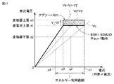
- FIG. 7 is a diagram showing the relationship between the amount of electric charge of the power storage device configured by the capacitor and the DC voltage.
- the amount of charge is equal to the product of charging current and time.
- FIG. 7A shows the characteristics of the DC voltages V1 and V2 of the individual booster cells BSM and the characteristics of the DC voltage Vb of the storage bank ESB. Let the number n of booster cells BSM be 2. It is assumed that the storage capacity of the booster cell BSM1 is smaller than the storage capacity of the booster cell BSM2.
- FIG. 7B shows the relationship between the amount of electric charge in the entire power storage device 13 and the DC voltage Vdc.
- the storage bank ESB and the booster cell BSM can be charged with a constant current, so that the storage bank ESB and the booster cell BSM can be charged at a constant speed.
- the DC voltage Vd of the storage bank ESB and the DC voltage V1 and V2 of the booster cell BSM increase.
- the operating range of the converter (voltage d2 to voltage d1) is determined so that the charging current and the discharging current charged / discharged from the storage bank ESB are within a certain range. Therefore, the energy utilization range only in the storage bank ESB is in the range from the charge amount q2 to the charge amount q1.
- the power storage device 13 When the power storage device 13 is composed of a storage battery, the relationship between the amount of charge and the DC voltage is not a straight line passing through the origin. In this case, if the characteristic curve of the storage battery is linearized near the rated voltage, it can be handled in the same manner as in the case of the type 1 capacitor.
- FIG. 8 is a diagram conceptually showing the characteristic curve of the storage battery. As shown in FIG. 8, the characteristic curve showing the relationship between the charge amount of the storage battery and the DC voltage is a curve that does not pass through the origin. Therefore, the following description can be applied by using an approximate straight line linearized near the rated voltage Vr of the storage battery.
- FIG. 9 is a flowchart showing a charging procedure of the power storage device according to the first embodiment.
- step S10 of FIG. 9 the control device 14 (specifically, the CPU 84) is driven by the AC / DC converter 12A by turning on the switching elements 20p of the booster cells BSM1 and BSM2 and turning off the switching elements 20n. Charging of the booster cells BSM1 and BSM2 and the storage bank ESB is started.
- the booster cell BSM with a small storage capacity reaches the rated voltage before the storage bank ESB.
- the rated voltage is reached in ascending order of storage capacity. Therefore, when the DC voltage V1 of the storage bank ESB1 having the smallest storage capacity reaches the rated voltage (YES in step S20), the control device 14 puts the booster cell BSM1 in the bypass state (step S30). That is, the control device 14 turns off the switching element 20p of the booster cell BSM1 and turns on the switching element 20n.
- the booster cell BSM2 and the storage bank ESB continue to be charged.
- the control device 14 reaches the DC voltage V2 rated voltage of the storage bank ESB2 having the next smaller storage capacity (YES in step S40)
- the control device 14 bypasses the booster cell BSM2 (step S50).
- the control device. 14 puts the booster cell BSM2 in the bypass state (step S50).
- step S60 the control device 14 stops charging the storage bank ESB (step S70).
- FIG. 10 is a flowchart showing a discharge procedure of the power storage device according to the first embodiment.
- the charge amount (SOC) of the storage bank ESB is 100%, and the charge amount of each booster cell BSM is also 100%.
- step S110 of FIG. 10 the control device 14 (specifically, the CPU 84) puts the booster cells BSM1 and BSM2 in a bypass state and operates the AC / DC converter 12A as an inverse conversion device to operate the storage bank ESB. Start discharging.
- step S120 When the DC voltage Vb of the storage bank ESB drops to the lower limit voltage d2 of the AC / DC converter 12A (YES in step S120), the control device 14 puts the booster cell BSM2 in the inserted state (step S130). That is, the control device 14 turns off the switching element 20n of the booster cell BSM2 and turns on the switching element 20p.
- the minimum voltage that can be used differs depending on the type of power storage element 22. For example, when the power storage element 22 is a storage battery, the minimum voltage is about 0.7 PU, and when the power storage element 22 is a supercapacitor, the minimum voltage is about 0.3 PU.
- the storage bank ESB and the booster cells BSM1 and BSM2 continue to be discharged.
- the control device 14 is YES in step S160.
- the discharge of the power storage device 13 is completed (step S170).
- the discharge of the power storage device 13 can be continued until the DC voltage Vdc of the power storage device 13 becomes 0V.
- the DC voltage Vdc of the power storage device 13 can further continue the discharge of the power storage device 13 up to the adjustable lower limit voltage of the AC / DC converter 12A.
- the power storage device 13 of the first embodiment suppresses the fluctuation range of the DC voltage as compared with the case of the storage bank ESB alone, and then the power storage device 13
- the range of energy use can be expanded. Specifically, in the case of FIG. 7, the energy utilization range is expanded from the charge amount q1-q2 to the charge amount q1-q4.
- the power system stabilization system 8A When the target power system to which the power system stabilization system 8A of the present embodiment is connected receives power interchange from another area, there is a risk of frequency decrease if the power interchange is cut off.
- the power system stabilization system 8A causes both the storage bank ESB and each booster cell BSM to stand by in a fully charged state for frequency stabilization (hereinafter, referred to as a first standby mode).
- the power system stabilization system 8A performs a discharge operation of the power storage device 13 when the frequency is lowered due to the interruption of power interchange.
- the power system stabilization system 8A puts the storage bank ESB and each booster cell BSM on standby in the lowest charged state for frequency stabilization (hereinafter, referred to as a second standby mode).
- the power system stabilization system 8A performs a charging operation of the power storage device 13 when the frequency rises due to the power supply being cut off.
- the power system stabilization system 8A shall be used for frequency.
- both the power storage bank ESB and each booster cell BSM are put on standby in an intermediate charging state.
- the storage bank ESB of the power storage device 13 has a problem in that its DC voltage Vb fluctuates according to the energy storage amount (that is, SOC) of the storage bank ESB. Therefore, when the storage bank ESB is directly connected to the AC / DC converter 12A, it is necessary to enable the AC / DC converter 12A even when the SOC of the storage bank ESB is lowered (that is, the DC voltage Vb is lowered). There is. Therefore, it is necessary to change the AC / DC converter 12A to an MMC having a full bridge configuration or to add a DC / DC converter, which increases the cost of the power system stabilization system.
- the DC voltage Vb of the storage bank ESB changes between 0.5 and 1 PU due to charging and discharging
- the input / output power is maintained at 1 PU
- the fluctuation range of the DC voltage Vb of the storage bank ESB is suppressed to 0.8 to 1 PU
- the amount of change in current can be suppressed to 1 to 1.25 PU.
- the energy utilization rate of the storage bank ESB decreases, it is necessary to increase the number and size of the storage elements 30 constituting the storage bank ESB.
- the power storage device 13 when the power storage device 13 is used for frequency stabilization of the electric power system, the power storage device 13 is used after about 10 seconds have elapsed from the power storage device 13 before the frequency stabilization control of the generator such as the governor control responds. It is necessary to release energy to the power system or absorb energy from the power system to the power storage device 13. In this case, the power storage device 13 releases or absorbs the maximum amount of energy immediately after the occurrence of the accident, and then gradually reduces the amount of energy released or absorbed to near 0, thereby stabilizing the frequency of the generator without shock. It is desirable to take over to control.
- the power storage device 13 When the power storage device 13 is made to stand by in a fully charged state, the above change in the amount of energy released can be naturally realized, but conversely, the power storage device 13 is made to stand by in the minimum charge state or the intermediate charge state. In some cases, it is necessary to improve the current rating.
- a booster cell BSM is provided in series with the power storage bank ESB.
- the energy utilization rate of the storage bank ESB can be increased while suppressing the fluctuation range of the voltage Vdc of the entire power storage device 13. Further, a sufficient charge current and discharge current can be secured immediately after the accident occurs. Further, by suppressing the fluctuation range of the voltage Vdc of the power storage device 13, an inexpensive half-bridge MMC can be used as the AC / DC converter 12A.
- Embodiment 2 In the second embodiment, a method of further expanding the energy utilization range of the power storage device 13 by appropriately selecting the storage capacity and the capacitance of the power storage element 22 of the booster cell BSM will be described.
- FIG. 11 is a diagram showing the relationship between the amount of electric charge and the DC voltage in the power storage device of the second embodiment.
- FIG. 11A shows the characteristics of the DC voltages V1 and V2 of the individual booster cells BSM and the characteristics of the DC voltage Vb of the storage bank ESB. Let the number n of booster cells BSM be 2.
- FIG. 11B shows the relationship between the amount of electric charge and the DC voltage Vdc in the entire power storage device 13.
- the storage capacity of the booster cell BSM1 is set smaller than the storage capacity of the booster cell BSM2. Further, the voltage value of each booster cell BSM when each booster cell BSM is fully charged is set equally to the operating range (d1-d2) of the converter. Further, when the type 1 AC / DC converter 12A is used and the minimum voltage used is set for the storage bank ESB, the difference between the voltage when the storage bank ESB is fully charged and the minimum voltage used is added to each booster cell BSM. Equalize the voltage values when fully charged.
- equal voltage values mean that they are substantially equal, and they do not have to be completely the same. For example, if the actual voltage value is within the range of ⁇ 5% of the ideal target value, the energy utilization range of the power storage device 13 can be sufficiently expanded. Further, even if the actual voltage value is within the range of ⁇ 10% of the ideal target value, the energy utilization range of the power storage device 13 can be expanded to some extent.
- each booster cell BSM When the power storage element 22 of each booster cell BSM is a capacitor, the above voltage setting is possible by adjusting the capacitance. As shown in FIG. 11A, the slopes of the characteristic straight lines are different between the booster cell BSM1 and the booster cell BSM2 by making the capacitance different. Further, as shown in FIG. 11B, the amount of voltage change when each booster cell BSM is put into the bypass state or the inserted state is all equal. As a result, the energy utilization range (q1-q6) of the power storage device 13 can be further expanded.
- the number n of booster cells BSM is 3 or more. Specifically, by making the storage capacities of the n booster cells BSM different from each other, it is controlled so that the bypass state is obtained in order from the one having the smallest storage capacity at the time of charging. Further, the voltage when the booster cell BSM is fully charged is made equal to the difference between the minimum voltage and the maximum voltage of the storage bank ESB when the power storage device 13 is used. As a result, the energy utilization range of the power storage device 13 can be further expanded.
- Embodiment 3 a case where the switching elements 20p and 20n of the booster cell BSM are operated by the chopper will be described. Although the switching loss increases, the direct current voltage Vdc of the power storage device 13 can be kept substantially constant. Further, when the AC / DC converter 12A is configured by the MMC, since the reactor is included in each arm, the possibility of sudden change in the current due to the chopper operation is small.
- the state in which the switching elements 20p and 20n of the booster cell BSM are operating as a chopper is referred to as a chopper state.
- FIG. 12 is a diagram showing the relationship between the amount of electric charge and the DC voltage in the power storage device of the third embodiment.
- the voltage / charge characteristics shown in FIG. 12 correspond to those in FIG. 7 (B).
- FIG. 12 further shows the on ratio of the booster cell BSM1 and the on ratio of the booster cell BSM2.
- the time when the switching element 20p is on and the switching element 20n is controlled to be off is referred to as an on time
- the time when the switching element 20p is off and the switching element 20n is controlled to be on is referred to as an off time.
- the on ratio is the ratio of the on time to the on time + the off time.
- the chopper control may be pulse width control, pulse frequency control, or other pulse control.
- control method of the power storage device 13 having a charge amount of 0 to q3 is the same as that of FIG. 7 (B). That is, the control device 14 controls both the booster cells BSM1 and BSM2 in the inserted state.
- the control device 14 puts the booster cell BSM2 in the inserted state and controls the booster cell BSM1 in the chopper state.
- the voltage Vdc of the power storage device 13 is made equal to the upper limit voltage d1 of the AC / DC converter 12A.
- the on ratio of the booster cell BSM1 decreases.
- the control device 14 controls the booster cell BSM1 in the bypass state and the booster cell BSM2 in the chopper state.
- the voltage Vdc of the power storage device 13 is made equal to the upper limit voltage d1 of the AC / DC converter 12A.
- the on ratio of the booster cell BSM2 decreases. Charging of the power storage device 13 is completed when the amount of charge stored in the power storage device 13 reaches q1. At this point, both booster cells BSM1 and BSM2 are in the bypass state.
- FIG. 13 is a flowchart showing a charging procedure of the power storage device according to the third embodiment.
- step S210 of FIG. 13 the control device 14 (specifically, CPU 84) is driven by the AC / DC converter 12A by turning on the switching elements 20p of the booster cells BSM1 and BSM2 and turning off the switching elements 20n. Charging of the booster cells BSM1 and BSM2 and the storage bank ESB is started.
- the control device 14 switches the booster cell BSM1 having the smallest storage capacity to the chopper control to control the voltage of the power storage device 13. Keep Vdc at the upper limit voltage d1 (step S230). In this state, the booster cell BSM2 remains in the inserted state.
- step S240 when the sum of the DC voltage V2 of the booster cell BSM and the DC voltage Vb of the storage bank ESB reaches the upper limit voltage d1 of the AC / DC converter 12A (YES in step S240), the control device 14 bypasses the booster cell BSM1. Then, the booster cell BSM2 having the smaller storage capacity is switched to the chopper control (step S250). As a result, the control device 14 keeps the voltage Vdc of the power storage device 13 at the upper limit voltage d1.
- Step S270 when the DC voltage Vb of the storage bank ESB reaches the upper limit voltage d1 of the AC / DC converter 12A (YES in step S260), the control device 14 switches the booster cell BSM2 to the bypass state and stops charging the storage bank ESB. (Step S270).
- the control device 14 shifts each booster cell BSM from the inserted state to the bypass state via the chopper state.
- FIG. 14 is a flowchart showing a discharge procedure of the power storage device according to the third embodiment.
- the charge amount (SOC) of the storage bank ESB is 100%, and the charge amount of each booster cell BSM is also 100%.
- step S310 of FIG. 14 the control device 14 (specifically, the CPU 84) starts discharging the storage bank ESB.
- the control device 14 further puts the booster cell BSM1 in a bypass state and controls the booster cell BSM2 with a chopper to keep the voltage Vdc of the power storage device 13 at the upper limit voltage d1 of the AC / DC converter 12A.
- the control device 14 ends the chopper operation of the booster cell BSM2 and switches to the inserted state (step S330). Further, the control device 14 keeps the voltage Vdc of the power storage device 13 at the upper limit voltage d1 of the AC / DC converter 12A by controlling the booster cell BSM1 with a chopper (step S340).
- step S350 when the DC voltage V1 of the booster cell BSM1 reaches the minimum usable voltage (YES in step S350), the control device 14 ends the chopper operation of the booster cell BSM1 and switches to the inserted state (step S360).
- the control device 14 shifts each booster cell BSM from the bypass state to the insertion state via the chopper state. As a result, the voltage Vdc of the power storage device 13 can be kept within a certain range.
- Embodiment 4 A case where the target power system to which the power system stabilization system 8A is connected may have a frequency increase and the power storage device 13 stands by in the lowest charged state will be described.
- a submodule ASM including a resistance element and a semiconductor bypass switch connected in parallel to the resistance element can be used instead of the submodule BSM including the power storage element 22 .
- a plurality of submodule ASMs including a resistance element may be connected in series to the storage bank ESB.
- the submodule ASM including the resistance element is also referred to as an absorber cell ASM or a second cell ASM.
- the power system stabilization system 8A absorbs more energy by inserting the resistance element of the absorber cell ASM and dissipating excess energy to the absorber cell ASM. can.
- the DC voltage Vdc increases by the voltage generated in the resistance element from the upper limit voltage of the storage bank ESB.
- the AC / DC converter 12A must be operable with respect to the upper limit voltage including the voltage increase due to this resistance element.
- the bypass switch 90 is controlled to be in the ON state.
- FIG. 15 is a circuit diagram showing a schematic configuration of the power storage device according to the fourth embodiment.
- the power storage device 13 of FIG. 15 is different from the power storage device 13 of FIG. 2 in that each of the power storage devices 13 further includes one or more (m pieces) absorber cells ASM1 to ASMm including the resistance element 92.
- One or more absorber cells ASM1 to ASMm, a storage bank ESB, and one or more booster cells BSM1 to BSMn are connected in series between the positive electrode terminal Tp and the negative electrode terminal Tn of the power storage device 13. These orders may be in any order.
- the absorber cells ASM1 to ASMn are generically referred to or any one of them is indicated, they are referred to as absorber ASM1 to ASMn.
- Each absorber cell ASM includes a bypass switch 90 formed of a semiconductor element, a diode 91, a resistance element 92, and a voltage detector 93 for detecting the voltage Va (Va1 to Vam) generated in the resistance element 92. These components are connected in parallel between the input / output nodes 94p and 94n.
- the diode 91 is connected in antiparallel to the bypass switch 90.
- the control device 14 controls the opening and closing of the bypass switch 90 and acquires the detection value of the voltage detector 93.
- Each absorber cell ASM passes through the input / output node 94p to the input / output node 94n of the adjacent absorber cell ASM, the input / output node 24n of the adjacent booster cell BSM, or the negative electrode node 32n of the adjacent storage bank ESB, or the positive electrode. It is connected to the terminal Tp.
- Each absorber cell ASM passes through the input / output node 94n to the input / output node 94p of the adjacent absorber cell ASM, the input / output node 24p of the adjacent booster cell BSM, or the positive electrode node 32p or the negative electrode of the adjacent storage bank ESB. It is connected to the terminal Tn.
- FIG. 16 is a diagram for explaining a first operation example of the power storage device according to the fourth embodiment.
- FIG. 16 shows the relationship between the amount of electric charge of the power storage device 13 and the DC voltage.
- the operation example of FIG. 16 corresponds to FIG. 7 (B).
- the charging current is i
- the resistance value of the resistance element 92 of all absorber cells ASM is R.
- FIG. 17 is a diagram for explaining a second operation example of the power storage device according to the fourth embodiment.
- FIG. 17 shows the relationship between the amount of electric charge of the power storage device 13 and the DC voltage.
- the operation example of FIG. 16 corresponds to FIG. 12.
- the booster cells BSM1 and BSM2 are chopper-operated as in the case of FIG.
- the resistance element 92 is inserted between the input / output nodes 94p and 94n by turning off the bypass switch 90 (that is, when the absorber cell is on)
- the power storage device 13 further absorbs energy corresponding to the additional voltage VR .
- FIG. 18 is a diagram for explaining a third operation example of the power storage device according to the fourth embodiment.
- FIG. 18 shows the relationship between the amount of electric charge of the power storage device 13 and the DC voltage.
- the operation example of FIG. 18 corresponds to FIG. 7 (B).
- the control device 14 choppers the bypass switch 90 of each absorber cell ASM, so that the voltage VR added to the DC voltage Vdc of the power storage device 13 in the case of FIG. 7 (B) is increased. Control so that the added voltage becomes a constant value. Specifically, the control device 14 determines the ratio of the absorber cell ASM to be bypassed and the absorber cell ASM to control the chopper according to the detected values of the DC voltage V1 and V2 of the booster cell BSM and the DC voltage Vb of the storage bank ESB. The energization rate of the resistance element 92 in the above is adjusted. As a result, the voltage upper limit d1 of the power storage device 13 can be suppressed.
- Embodiment 5 the specific structure and arrangement of the booster cell BSM and the storage bank ESB constituting the power storage device 13 will be described.
- FIG. 19 is a circuit diagram for explaining the specific arrangement of the AC / DC converter, the booster cell, and the storage bank constituting the power system stabilization system.
- booster cell BSM1, booster cell BSM2, storage bank ESB, booster cell BSM4, and booster cell BSM3 are arranged in series between the positive electrode terminal Tp and the negative electrode terminal Tn in this order. Further, the positive electrode terminal Tp is connected to the high potential side DC terminal Np of the AC / DC converter 12A, and the negative electrode terminal Tn is connected to the low potential side DC terminal Nn of the AC / DC converter 12A.
- each booster cell BSM and the AC / DC converter 12A are housed in a common rack 110
- the power storage element 22 of each booster cell BSM and the power storage bank ESB are housed in a common rack 120.
- FIG. 20 is a side view and a plan view showing an implementation example corresponding to the circuit diagram of FIG. 20 (A) shows a side view, and FIG. 20 (B) shows a plan view.
- the rack 110 has a structure in which a plurality of stages 115 are laminated. Each stage 115 is supported on the installation surface 130 by columns 114 penetrating insulators attached to the four corners of the insulating substrate 111. An insulating shield 112 is attached to the outer periphery of the insulating substrate 111 so as to surround the insulating substrate 111 inside.
- the bridge circuit 25 portion of each booster cell BSM and each converter cell 43 of the AC / DC converter 12A are arranged on the insulating substrate 111 substrate.
- the rack 120 has a structure in which a plurality of stages 125 are laminated. Each stage 125 is supported on the installation surface 130 by columns 124 penetrating insulators attached to the four corners of the insulating substrate 121. An insulating shield 122 is attached to the outer periphery of the insulating substrate 121 so as to surround the insulating substrate 121 inside.
- the power storage element 22 of each booster cell BSM and the power storage element 30 of the power storage bank ESB are arranged on the insulating substrate 121 substrate.
- each booster cell BSM is arranged close to the converter cell 43 in the same rack as the AC / DC converter 12A. Further, the power storage element 22 of each booster cell BSM is arranged close to the power storage element 30 in a rack common to the power storage bank ESB. Such an arrangement can simplify the insulation and support structure.
- the above arrangement is particularly effective when the rated voltage of the switching elements 20p and 20n of each booster cell BSM and the rated voltage of the power storage element 22 are different.
- the booster cell BSM having a full bridge configuration it is effective when the DC voltage Vdc of the AC / DC converter 12A is set lower than the DC voltage Vb of the storage bank ESB.
- the bypass switch 90 and the diode 91 constituting the absorber cell ASM are housed in the rack 110, and the resistance element.
- the 92 is housed in the rack 120.
- 8A, 8B power system stabilization system 10A AC power system, 10B DC power system, 11 transformer, 12A AC / DC converter, 12B DC / DC converter, 13 power storage device, 14 control device, 20,55 switching element, 21 , 70 diode, 22, 30, 56 energy storage element, 23, 31, 57, 93 voltage detector, 24n, 24p, 58n, 58p, 94n, 94p input / output node, 25 bridge circuit, 32n negative current node, 32p positive current node, 40, 40u, 40v, 40w leg circuit, 41 upper arm, 42 lower arm, 43 converter cell, 60 initial charging device, 61 switch, 92 resistance element, 90 bypass switch, 84 CPU, 110, 120 rack, 111, 121 Insulation substrate, 112, 122 insulation shield, 114, 124 columns, 115, 125 stages, ASM submodule (absorber cell), BSM submodule (booster cell), ESB storage bank, Nn low potential side DC terminal, Np high potential side DC terminal, Nu, N
Abstract
Description
特許文献3(特許第5189105号公報)および非特許文献1(E.Spahic et al.,CIGRE Winnipeg 2017 Colloquium,B4-56,Sep. 2017)は、自励式の交直変換器の一例であるMMC(Modular Multilevel Convertor)の構成例を開示する。前者は各変換器セルがハーフブリッジ構成の場合あり、後者は各変換器セルがフルブリッジ構成の場合である。 Hereinafter, the prior art documents related to a part of the present disclosure are introduced.
Patent Document 3 (Patent No. 5189105) and Non-Patent Document 1 (E. Spahic et al., CIGRE Winnipeg 2017 Colloquium, B4-56, Sep. 2017) are examples of self-excited AC / DC converters (MMC). A configuration example of Modular Multilevel Convertor) is disclosed. The former is a case where each converter cell has a half-bridge configuration, and the latter is a case where each converter cell has a full-bridge configuration.
[電力系統安定化システムの概略構成]
図1は、電力系統安定化システムの概略構成を示すブロック図である。図1(A)は、交流電力系統10Aに接続される電力系統安定化システム8Aの構成例を示し、図1(B)は、直流電力系統10Bに接続される電力系統安定化システム8Bの構成例を示す。
[Outline configuration of power system stabilization system]
FIG. 1 is a block diagram showing a schematic configuration of a power system stabilization system. FIG. 1A shows a configuration example of a power
図2は、図1の蓄電装置の概略構成を示す回路図である。図2を参照して、蓄電装置13は、互いに直列に接続された蓄電バンクESBと、1つ以上(n個)のサブモジュールBSM1~BSMnとを含む。本開示では、サブモジュールBSM1~BSMnを、ブースターセルBSM1~BSMnまたは第1セルBSM1~BSMnとも称する。 [Configuration example of power storage device]
FIG. 2 is a circuit diagram showing a schematic configuration of the power storage device of FIG. With reference to FIG. 2, the
図3は、図1の交直変換器のハードウェアの概略構成の一例を示す図である。図3では、図1の交直変換器12Aがモジュラーマルチレベル変換器によって構成される例が示されている。 [Example of AC / DC converter configuration]
FIG. 3 is a diagram showing an example of a schematic configuration of the hardware of the AC / DC converter of FIG. FIG. 3 shows an example in which the AC /
図4は、図3に示す自励式の交直変換器を構成する変換器セル43の構成例を示す回路図である。 [Example of converter cell configuration]
FIG. 4 is a circuit diagram showing a configuration example of a
交直変換器12Aは、直流電圧を0Vと定格電圧との間で調整可能なもの(以下、タイプ1と称する)と、定格電圧近辺の限られた電圧範囲で調整可能なもの(以下、タイプ2と称する)とがある。たとえば、図4(A)に示すフルブリッジ構成の変換器セル43によって構成されたMMCは、タイプ1の交直変換器12Aである。図4(B)に示すハーフブリッジ構成の変換器セル43によって構成されたMMCは、タイプ2の交直変換器12Aである。タイプ2のMMCの場合、直流電圧の範囲は0.8~1PU程度である。ここで、PUは単位法を表す。 [Initial charging device]
The AC /
図6は、図1の制御装置のハードウェア構成例を示すブロック図である。図6には、コンピュータによって制御装置14を構成する例が示される。 [Control device configuration example]
FIG. 6 is a block diagram showing a hardware configuration example of the control device of FIG. FIG. 6 shows an example in which the
次に蓄電装置13の制御手順について説明する。以下では、蓄電装置13がキャパシタ(電気二重層を含む)によって構成される場合について説明する。 [Control procedure of power storage device]
Next, the control procedure of the
以下、交流電力系統10A用の電力系統安定化システム8Aの使用方法について補足する。 [Usage example of power
Hereinafter, the method of using the power
以下では、まず従来技術の問題点を説明し、次に実施の形態1の蓄電装置13ではそれらの問題点が克服されていることを説明する。 [Effect of Embodiment 1]
Hereinafter, the problems of the prior art will be described first, and then the
実施の形態2では、ブースターセルBSMの蓄電素子22について、その蓄電容量および静電容量を適切に選択することにより、蓄電装置13のエネルギー利用範囲をさらに広げる方法について説明する。 Embodiment 2.
In the second embodiment, a method of further expanding the energy utilization range of the
実施の形態3では、ブースターセルBSMのスイッチング素子20p,20nをチョッパ動作させる場合について説明する。スイッチング損失は増えるが、蓄電装置13の直電流電圧Vdcをほぼ一定に保つことができる。また、交直変換器12AがMMCによって構成されている場合には各アーム内にリアクトルを含むので、チョッパ動作による電流急変の可能性は少ない。以下、ブースターセルBSMのスイッチング素子20p,20nがチョッパ動作している状態をチョッパ状態と称する。 Embodiment 3.
In the third embodiment, a case where the
電力系統安定化システム8Aが接続されている対象電力系統が周波数上昇の恐れがあり、蓄電装置13を最低充電状態で待機する場合について説明する。この場合、蓄電素子22を含むサブモジュールBSMに代えて、抵抗素子とそれに並列接続された半導体バイパススイッチとを含むサブモジュールASMを用いることができる。抵抗素子を含むサブモジュールASMを複数個直列に蓄電バンクESBに接続してもよい。本開示では、抵抗素子を含むサブモジュールASMを、アブソーバセルASMまたは第2セルASMとも称する。
A case where the target power system to which the power
実施の形態5では、蓄電装置13を構成するブースターセルBSMおよび蓄電バンクESBの具体的な構造および配置について説明する。 Embodiment 5.
In the fifth embodiment, the specific structure and arrangement of the booster cell BSM and the storage bank ESB constituting the
Claims (12)
- 互いに接続された複数の蓄電素子を含む蓄電バンクと、
1つまたは複数の第1セルとを備え、
前記蓄電バンクおよび前記1つまたは複数の第1セルは、互いに直列に接続され、
前記1つの第1セルまたは前記複数の第1セルの各々は、
入出力ノード対と、
少なくとも2つの半導体スイッチング素子を含むブリッジ回路と、
前記ブリッジ回路を介して前記入出力ノード対に接続される蓄電素子とを含み、
前記1つの第1セルの前記蓄電素子の蓄電容量または前記複数の第1セルの各々の前記蓄電素子の蓄電容量は、前記蓄電バンクの蓄電容量よりも小さい、蓄電装置。 A storage bank containing multiple storage elements connected to each other,
With one or more first cells
The storage bank and the one or more first cells are connected in series with each other.
Each of the one first cell or the plurality of first cells
I / O node pair and
A bridge circuit containing at least two semiconductor switching elements,
Including a power storage element connected to the input / output node pair via the bridge circuit.
A power storage device in which the storage capacity of the storage element of the one first cell or the storage capacity of each of the storage elements of the plurality of first cells is smaller than the storage capacity of the storage bank. - 前記蓄電装置は、前記1つまたは複数の第1セルとして、複数の第1セルを備え、
前記複数の第1セルの各々の蓄電容量は、互いに異なる、請求項1に記載の蓄電装置。 The power storage device includes a plurality of first cells as the one or more first cells.
The power storage device according to claim 1, wherein the storage capacities of the plurality of first cells are different from each other. - 前記複数の第1セルの各々の前記蓄電素子が満充電されたときの電圧は、互いに等しい、請求項2に記載の蓄電装置。 The power storage device according to claim 2, wherein the voltages when the power storage elements of each of the plurality of first cells are fully charged are equal to each other.
- 前記蓄電装置は、前記複数の第1セルの各々を制御する制御装置をさらに備え、
前記制御装置は、前記複数の第1セルの各々を、前記蓄電素子が前記入出力ノード対に挿入された挿入状態、または、前記入出力ノード対が短絡されたバイパス状態に切り替える、請求項2または3に記載の蓄電装置。 The power storage device further includes a control device that controls each of the plurality of first cells.
2. The control device switches each of the plurality of first cells to an inserted state in which the power storage element is inserted into the input / output node pair or a bypass state in which the input / output node pair is short-circuited. Or the power storage device according to 3. - 前記制御装置は、前記蓄電装置を充電する場合には、前記複数の第1セルの各々を前記挿入状態にしてから充電を開始し、前記蓄電装置の電圧に応じて、前記複数の第1セルのうちの蓄電容量が小さい第1セルから順番に前記バイパス状態に切り替える、請求項4に記載の蓄電装置。 When charging the power storage device, the control device puts each of the plurality of first cells into the inserted state and then starts charging, and the plurality of first cells are charged according to the voltage of the power storage device. The power storage device according to claim 4, wherein the first cell having the smallest storage capacity is switched to the bypass state in order.
- 前記制御装置は、前記蓄電装置を放電する場合には、前記複数の第1セルの各々を前記バイパス状態にしてから放電を開始し、前記蓄電装置の電圧に応じて、前記複数の第1セルの各々を順番に前記挿入状態に切り替える、請求項4または5に記載の蓄電装置。 When discharging the power storage device, the control device puts each of the plurality of first cells in the bypass state and then starts discharging, and the plurality of first cells according to the voltage of the power storage device. The power storage device according to claim 4 or 5, wherein each of the above is sequentially switched to the inserted state.
- 前記制御装置は、前記複数の第1セルの各々を、前記バイパス状態から前記挿入状態にまたはその逆に切り替える場合に、前記蓄電装置の電圧を一定範囲内に保つように前記少なくとも2つの半導体スイッチング素子をチョッパ動作させるチョッパ状態を介在させる、請求項5または6に記載の蓄電装置。 The control device switches the at least two semiconductors so as to keep the voltage of the power storage device within a certain range when switching each of the plurality of first cells from the bypass state to the inserted state and vice versa. The power storage device according to claim 5 or 6, wherein a chopper state in which the element is chopper-operated is interposed.
- 前記制御装置は、他地域から電力融通を受けている電力系統に前記蓄電装置が接続されている場合に使用される第1の待機モードと、他地域に電力供給を行っている電力系統に前記蓄電装置が接続されている場合に使用される第2の待機モードとを有し、
前記制御装置は、前記第1の待機モードにおいて、前記蓄電バンクおよび前記複数の第1セルを満充電状態にし、
前記制御装置は、前記第2の待機モードにおいて、前記蓄電バンクおよび前記複数の第1セルを最低充電状態にする、請求項4~7のいずれか1項に記載の蓄電装置。 The control device is described in a first standby mode used when the power storage device is connected to a power system that receives power interchange from another area, and to a power system that supplies power to another area. It has a second standby mode used when a power storage device is connected, and has a second standby mode.
In the first standby mode, the control device brings the storage bank and the plurality of first cells into a fully charged state.
The power storage device according to any one of claims 4 to 7, wherein the control device puts the power storage bank and the plurality of first cells into a minimum charge state in the second standby mode. - 前記蓄電装置は、1つまたは複数の第2セルをさらに備え、
前記蓄電バンク、前記1つまたは複数の第1セル、および前記1つまたは複数の第2セルは、互いに直列に接続され、
前記1つの第2セルまたは前記複数の第2セルの各々は、
入出力ノード対と、
前記入出力ノード対の間に接続された抵抗素子と、
前記抵抗素子をバイパスする半導体スイッチング素子とを含む、請求項1に記載の蓄電装置。 The power storage device further comprises one or more second cells.
The storage bank, the one or more first cells, and the one or more second cells are connected in series with each other.
Each of the one second cell or the plurality of second cells
I / O node pair and
The resistance element connected between the input / output node pairs and
The power storage device according to claim 1, further comprising a semiconductor switching element that bypasses the resistance element. - 前記蓄電装置は、前記1つまたは複数の第1セルおよび前記1つまたは複数の第2セルを制御する制御装置をさらに備え、
前記制御装置は、前記1つの第2セルの前記半導体スイッチング素子または前記複数の第2セルの各々の前記半導体スイッチング素子を、前記蓄電素子を充電する場合にはオフ状態に制御し、前記蓄電装置を放電する場合にはオン状態に制御する、請求項9に記載の蓄電装置。 The power storage device further includes a control device for controlling the one or more first cells and the one or more second cells.
The control device controls the semiconductor switching element of the one second cell or the semiconductor switching element of each of the plurality of second cells to an off state when charging the power storage element, and the power storage device. The power storage device according to claim 9, wherein the power storage device is controlled to be turned on when the battery is discharged. - 請求項1~10のいずれか1項に記載の蓄電装置と、
電力系統と前記蓄電装置との間に接続された電力変換装置とを備える、電力系統安定化システム。 The power storage device according to any one of claims 1 to 10,
A power system stabilizing system including a power conversion device connected between a power system and the power storage device. - 前記1つの第1セルまたは前記複数の第1セルの各々に含まれる前記ブリッジ回路は、前記電力変換装置と共に第1のラックに収納され、
前記1つの第1セルまたは前記複数の第1セルの各々に含まれる前記蓄電素子は、前記蓄電バンクと共に前記第1のラックと異なる第2のラックに収納される、請求項11に記載の電力系統安定化システム。 The bridge circuit included in each of the one first cell or the plurality of first cells is housed in a first rack together with the power conversion device.
The electric power according to claim 11, wherein the power storage element included in each of the one first cell or the plurality of first cells is housed together with the power storage bank in a second rack different from the first rack. System stabilization system.
Priority Applications (4)
| Application Number | Priority Date | Filing Date | Title |
|---|---|---|---|
| PCT/JP2020/042122 WO2022102025A1 (en) | 2020-11-11 | 2020-11-11 | Power storage device and power system stabilization system |
| JP2021503079A JP6861923B1 (en) | 2020-11-11 | 2020-11-11 | Power storage device and power system stabilization system |
| EP20961553.3A EP4246765A4 (en) | 2020-11-11 | 2020-11-11 | Power storage device and power system stabilization system |
| US18/251,613 US20240014669A1 (en) | 2020-11-11 | 2020-11-11 | Power Storage Apparatus and Power System Stabilization System |
Applications Claiming Priority (1)
| Application Number | Priority Date | Filing Date | Title |
|---|---|---|---|
| PCT/JP2020/042122 WO2022102025A1 (en) | 2020-11-11 | 2020-11-11 | Power storage device and power system stabilization system |
Publications (1)
| Publication Number | Publication Date |
|---|---|
| WO2022102025A1 true WO2022102025A1 (en) | 2022-05-19 |
Family
ID=75520978
Family Applications (1)
| Application Number | Title | Priority Date | Filing Date |
|---|---|---|---|
| PCT/JP2020/042122 WO2022102025A1 (en) | 2020-11-11 | 2020-11-11 | Power storage device and power system stabilization system |
Country Status (4)
| Country | Link |
|---|---|
| US (1) | US20240014669A1 (en) |
| EP (1) | EP4246765A4 (en) |
| JP (1) | JP6861923B1 (en) |
| WO (1) | WO2022102025A1 (en) |
Cited By (1)
| Publication number | Priority date | Publication date | Assignee | Title |
|---|---|---|---|---|
| WO2024053731A1 (en) * | 2022-09-08 | 2024-03-14 | Azapa株式会社 | Electric power conversion device |
Families Citing this family (2)
| Publication number | Priority date | Publication date | Assignee | Title |
|---|---|---|---|---|
| JP7008895B1 (en) * | 2021-05-24 | 2022-01-25 | 三菱電機株式会社 | Power converter |
| WO2022254580A1 (en) * | 2021-06-01 | 2022-12-08 | 三菱電機株式会社 | Power system stabilization system |
Citations (8)
| Publication number | Priority date | Publication date | Assignee | Title |
|---|---|---|---|---|
| JP2001197660A (en) | 2000-01-12 | 2001-07-19 | Takashi Hiyama | Power system stabilizing system |
| JP2001211549A (en) * | 2000-01-25 | 2001-08-03 | Okamura Kenkyusho:Kk | Control system for instantaneous incoming power |
| JP2008178215A (en) | 2007-01-18 | 2008-07-31 | Toshiba Corp | Frequency regulation system and method |
| JP5189105B2 (en) | 2006-12-08 | 2013-04-24 | シーメンス アクチエンゲゼルシヤフト | Current converter |
| JP2015213384A (en) * | 2014-05-01 | 2015-11-26 | 日本電信電話株式会社 | Battery voltage compensation system |
| WO2016152366A1 (en) | 2015-03-24 | 2016-09-29 | 三菱電機株式会社 | Power conversion device |
| JP2020043653A (en) | 2018-09-07 | 2020-03-19 | Fdk株式会社 | Power storage device and charging method |
| JP6685477B1 (en) * | 2019-02-12 | 2020-04-22 | 三菱電機株式会社 | Power conversion device and power conversion system |
-
2020
- 2020-11-11 EP EP20961553.3A patent/EP4246765A4/en active Pending
- 2020-11-11 WO PCT/JP2020/042122 patent/WO2022102025A1/en active Application Filing
- 2020-11-11 JP JP2021503079A patent/JP6861923B1/en active Active
- 2020-11-11 US US18/251,613 patent/US20240014669A1/en active Pending
Patent Citations (8)
| Publication number | Priority date | Publication date | Assignee | Title |
|---|---|---|---|---|
| JP2001197660A (en) | 2000-01-12 | 2001-07-19 | Takashi Hiyama | Power system stabilizing system |
| JP2001211549A (en) * | 2000-01-25 | 2001-08-03 | Okamura Kenkyusho:Kk | Control system for instantaneous incoming power |
| JP5189105B2 (en) | 2006-12-08 | 2013-04-24 | シーメンス アクチエンゲゼルシヤフト | Current converter |
| JP2008178215A (en) | 2007-01-18 | 2008-07-31 | Toshiba Corp | Frequency regulation system and method |
| JP2015213384A (en) * | 2014-05-01 | 2015-11-26 | 日本電信電話株式会社 | Battery voltage compensation system |
| WO2016152366A1 (en) | 2015-03-24 | 2016-09-29 | 三菱電機株式会社 | Power conversion device |
| JP2020043653A (en) | 2018-09-07 | 2020-03-19 | Fdk株式会社 | Power storage device and charging method |
| JP6685477B1 (en) * | 2019-02-12 | 2020-04-22 | 三菱電機株式会社 | Power conversion device and power conversion system |
Non-Patent Citations (5)
| Title |
|---|
| E. SPAHIC ET AL.: "Frequency Stability in Case of Interconnectors (AC and DC) and the Impact of Frequency Stabilizer", CIGRE WINNIPEG 2017 COLLOQUIUM, September 2017 (2017-09-01), pages B4 - 56 |
| ISHIHASHI ET AL., IEEJ TRANSACTIONS ON INDUSTRY APPLICATIONS, vol. 138, no. 1, 2018, pages 58 - 66 |
| ISHIHASHI ET AL., JOURNAL OF THE INSTITUTE OF ELECTRICAL ENGINEERS OF JAPAN D (JOURNAL OF INDUSTRIAL APPLICATIONS, vol. 138, no. 1, 2018, pages 58 - 66 |
| ISHIHASHI ET AL.: "Circuit Topology and Control Scheme of a High-Power High-Voltage DC/DC Converter for Large Scale Offshore Wind Project with DC Collector Grids", IEEJ TRANSACTIONS ON INDUSTRY APPLICATIONS, vol. 138, no. 1, 2018, pages 58 - 66 |
| See also references of EP4246765A4 |
Cited By (1)
| Publication number | Priority date | Publication date | Assignee | Title |
|---|---|---|---|---|
| WO2024053731A1 (en) * | 2022-09-08 | 2024-03-14 | Azapa株式会社 | Electric power conversion device |
Also Published As
| Publication number | Publication date |
|---|---|
| JP6861923B1 (en) | 2021-04-21 |
| EP4246765A1 (en) | 2023-09-20 |
| US20240014669A1 (en) | 2024-01-11 |
| EP4246765A4 (en) | 2024-01-17 |
| JPWO2022102025A1 (en) | 2022-05-19 |
Similar Documents
| Publication | Publication Date | Title |
|---|---|---|
| WO2022102025A1 (en) | Power storage device and power system stabilization system | |
| US11108338B2 (en) | Dual submodule for a modular multilevel converter and modular multilevel converter including the same | |
| US20110127837A1 (en) | Power conversion apparatus | |
| US20150003134A1 (en) | Modular multilevel converter using asymmetry | |
| US20090285005A1 (en) | Space-saving inverter with reduced switching losses and increased life | |
| JPWO2016147935A1 (en) | Power converter | |
| JP6943184B2 (en) | Modular multi-level cascade converter | |
| RU2649888C2 (en) | Assembly for compensating reactive power and active power in a high-voltage network | |
| US20160352239A1 (en) | Power electronic converter | |
| JPWO2019215842A1 (en) | Power converter | |
| CA2894127C (en) | Switching stage, energy conversion circuit, and conversion stage for wind turbines comprising the energy conversion circuit | |
| KR20160040378A (en) | Dab convertor with multi-phase structure | |
| US20220393616A1 (en) | Power conversion device | |
| Hassan et al. | Double modulation control (DMC) for dual full bridge current flow controller (2FB-CFC) | |
| Kolli et al. | Design considerations of three phase active front end converter for 13.8 kv asynchronous microgrid power conditioning system enabled by series connection of gen-3 10 kv sic mosfets | |
| CN108604797B (en) | Multilevel power converter and method for controlling multilevel power converter | |
| JP2014033553A (en) | Dc-dc power conversion device and power conditioner for photovoltaic power generation system | |
| JP2008104253A (en) | Power conversion device | |
| JP2013258841A (en) | Transformer multiple power converter | |
| CN106787824B (en) | Sub-module circuit, control method and modularized multi-level converter | |
| KR20190101066A (en) | Snubber Circuit for Solar Generation System | |
| JP7254256B1 (en) | Power system stabilization system | |
| JP2020205681A (en) | Power converter | |
| JP7134306B2 (en) | Power conversion system and its controller | |
| JP7418675B1 (en) | power converter |
Legal Events
| Date | Code | Title | Description |
|---|---|---|---|
| ENP | Entry into the national phase |
Ref document number: 2021503079 Country of ref document: JP Kind code of ref document: A |
|
| 121 | Ep: the epo has been informed by wipo that ep was designated in this application |
Ref document number: 20961553 Country of ref document: EP Kind code of ref document: A1 |
|
| WWE | Wipo information: entry into national phase |
Ref document number: 18251613 Country of ref document: US |
|
| NENP | Non-entry into the national phase |
Ref country code: DE |
|
| ENP | Entry into the national phase |
Ref document number: 2020961553 Country of ref document: EP Effective date: 20230612 |