WO2022085666A1 - Method for manufacturing electronic light control device, electronic element for light control, and electronic light control eyeglasses - Google Patents
Method for manufacturing electronic light control device, electronic element for light control, and electronic light control eyeglasses Download PDFInfo
- Publication number
- WO2022085666A1 WO2022085666A1 PCT/JP2021/038550 JP2021038550W WO2022085666A1 WO 2022085666 A1 WO2022085666 A1 WO 2022085666A1 JP 2021038550 W JP2021038550 W JP 2021038550W WO 2022085666 A1 WO2022085666 A1 WO 2022085666A1
- Authority
- WO
- WIPO (PCT)
- Prior art keywords
- dimming
- electronic
- pair
- outer diameter
- electrode layers
- Prior art date
Links
- 238000004519 manufacturing process Methods 0.000 title claims abstract description 30
- 238000000034 method Methods 0.000 title claims abstract description 18
- 230000003287 optical effect Effects 0.000 claims abstract description 37
- 230000015572 biosynthetic process Effects 0.000 claims abstract description 30
- 230000000694 effects Effects 0.000 claims abstract description 13
- 230000002093 peripheral effect Effects 0.000 claims description 20
- 238000006479 redox reaction Methods 0.000 claims description 6
- 230000002441 reversible effect Effects 0.000 claims description 3
- 238000010030 laminating Methods 0.000 abstract description 3
- 239000000758 substrate Substances 0.000 description 34
- 239000011521 glass Substances 0.000 description 15
- 239000000463 material Substances 0.000 description 10
- 238000002834 transmittance Methods 0.000 description 6
- 230000004048 modification Effects 0.000 description 5
- 238000012986 modification Methods 0.000 description 5
- 229910003437 indium oxide Inorganic materials 0.000 description 4
- PJXISJQVUVHSOJ-UHFFFAOYSA-N indium(iii) oxide Chemical compound [O-2].[O-2].[O-2].[In+3].[In+3] PJXISJQVUVHSOJ-UHFFFAOYSA-N 0.000 description 4
- 239000004973 liquid crystal related substance Substances 0.000 description 4
- 229920003002 synthetic resin Polymers 0.000 description 3
- 239000000057 synthetic resin Substances 0.000 description 3
- 230000005540 biological transmission Effects 0.000 description 2
- HTXDPTMKBJXEOW-UHFFFAOYSA-N dioxoiridium Chemical compound O=[Ir]=O HTXDPTMKBJXEOW-UHFFFAOYSA-N 0.000 description 2
- 238000001962 electrophoresis Methods 0.000 description 2
- 229910000457 iridium oxide Inorganic materials 0.000 description 2
- 238000000465 moulding Methods 0.000 description 2
- BPUBBGLMJRNUCC-UHFFFAOYSA-N oxygen(2-);tantalum(5+) Chemical compound [O-2].[O-2].[O-2].[O-2].[O-2].[Ta+5].[Ta+5] BPUBBGLMJRNUCC-UHFFFAOYSA-N 0.000 description 2
- 239000007784 solid electrolyte Substances 0.000 description 2
- PBCFLUZVCVVTBY-UHFFFAOYSA-N tantalum pentoxide Inorganic materials O=[Ta](=O)O[Ta](=O)=O PBCFLUZVCVVTBY-UHFFFAOYSA-N 0.000 description 2
- 238000010521 absorption reaction Methods 0.000 description 1
- 239000011248 coating agent Substances 0.000 description 1
- 238000000576 coating method Methods 0.000 description 1
- 239000004020 conductor Substances 0.000 description 1
- 239000006059 cover glass Substances 0.000 description 1
- 230000007547 defect Effects 0.000 description 1
- 230000002950 deficient Effects 0.000 description 1
- 230000008021 deposition Effects 0.000 description 1
- 230000001747 exhibiting effect Effects 0.000 description 1
- 239000005357 flat glass Substances 0.000 description 1
- AMGQUBHHOARCQH-UHFFFAOYSA-N indium;oxotin Chemical compound [In].[Sn]=O AMGQUBHHOARCQH-UHFFFAOYSA-N 0.000 description 1
- 229910010272 inorganic material Inorganic materials 0.000 description 1
- 239000011147 inorganic material Substances 0.000 description 1
- 239000011368 organic material Substances 0.000 description 1
- 239000003566 sealing material Substances 0.000 description 1
- 239000000126 substance Substances 0.000 description 1
- QHGNHLZPVBIIPX-UHFFFAOYSA-N tin(ii) oxide Chemical compound [Sn]=O QHGNHLZPVBIIPX-UHFFFAOYSA-N 0.000 description 1
- 239000012780 transparent material Substances 0.000 description 1
- ZNOKGRXACCSDPY-UHFFFAOYSA-N tungsten trioxide Chemical compound O=[W](=O)=O ZNOKGRXACCSDPY-UHFFFAOYSA-N 0.000 description 1
Images


Classifications
-
- G—PHYSICS
- G02—OPTICS
- G02F—OPTICAL DEVICES OR ARRANGEMENTS FOR THE CONTROL OF LIGHT BY MODIFICATION OF THE OPTICAL PROPERTIES OF THE MEDIA OF THE ELEMENTS INVOLVED THEREIN; NON-LINEAR OPTICS; FREQUENCY-CHANGING OF LIGHT; OPTICAL LOGIC ELEMENTS; OPTICAL ANALOGUE/DIGITAL CONVERTERS
- G02F1/00—Devices or arrangements for the control of the intensity, colour, phase, polarisation or direction of light arriving from an independent light source, e.g. switching, gating or modulating; Non-linear optics
- G02F1/01—Devices or arrangements for the control of the intensity, colour, phase, polarisation or direction of light arriving from an independent light source, e.g. switching, gating or modulating; Non-linear optics for the control of the intensity, phase, polarisation or colour
- G02F1/15—Devices or arrangements for the control of the intensity, colour, phase, polarisation or direction of light arriving from an independent light source, e.g. switching, gating or modulating; Non-linear optics for the control of the intensity, phase, polarisation or colour based on an electrochromic effect
- G02F1/153—Constructional details
- G02F1/155—Electrodes
-
- G—PHYSICS
- G02—OPTICS
- G02C—SPECTACLES; SUNGLASSES OR GOGGLES INSOFAR AS THEY HAVE THE SAME FEATURES AS SPECTACLES; CONTACT LENSES
- G02C7/00—Optical parts
- G02C7/10—Filters, e.g. for facilitating adaptation of the eyes to the dark; Sunglasses
- G02C7/101—Filters, e.g. for facilitating adaptation of the eyes to the dark; Sunglasses having an electro-optical light valve
-
- G—PHYSICS
- G02—OPTICS
- G02F—OPTICAL DEVICES OR ARRANGEMENTS FOR THE CONTROL OF LIGHT BY MODIFICATION OF THE OPTICAL PROPERTIES OF THE MEDIA OF THE ELEMENTS INVOLVED THEREIN; NON-LINEAR OPTICS; FREQUENCY-CHANGING OF LIGHT; OPTICAL LOGIC ELEMENTS; OPTICAL ANALOGUE/DIGITAL CONVERTERS
- G02F1/00—Devices or arrangements for the control of the intensity, colour, phase, polarisation or direction of light arriving from an independent light source, e.g. switching, gating or modulating; Non-linear optics
- G02F1/01—Devices or arrangements for the control of the intensity, colour, phase, polarisation or direction of light arriving from an independent light source, e.g. switching, gating or modulating; Non-linear optics for the control of the intensity, phase, polarisation or colour
- G02F1/15—Devices or arrangements for the control of the intensity, colour, phase, polarisation or direction of light arriving from an independent light source, e.g. switching, gating or modulating; Non-linear optics for the control of the intensity, phase, polarisation or colour based on an electrochromic effect
- G02F1/153—Constructional details
- G02F1/1533—Constructional details structural features not otherwise provided for
-
- G—PHYSICS
- G02—OPTICS
- G02F—OPTICAL DEVICES OR ARRANGEMENTS FOR THE CONTROL OF LIGHT BY MODIFICATION OF THE OPTICAL PROPERTIES OF THE MEDIA OF THE ELEMENTS INVOLVED THEREIN; NON-LINEAR OPTICS; FREQUENCY-CHANGING OF LIGHT; OPTICAL LOGIC ELEMENTS; OPTICAL ANALOGUE/DIGITAL CONVERTERS
- G02F1/00—Devices or arrangements for the control of the intensity, colour, phase, polarisation or direction of light arriving from an independent light source, e.g. switching, gating or modulating; Non-linear optics
- G02F1/01—Devices or arrangements for the control of the intensity, colour, phase, polarisation or direction of light arriving from an independent light source, e.g. switching, gating or modulating; Non-linear optics for the control of the intensity, phase, polarisation or colour
- G02F1/15—Devices or arrangements for the control of the intensity, colour, phase, polarisation or direction of light arriving from an independent light source, e.g. switching, gating or modulating; Non-linear optics for the control of the intensity, phase, polarisation or colour based on an electrochromic effect
- G02F1/153—Constructional details
- G02F1/157—Structural association of cells with optical devices, e.g. reflectors or illuminating devices
-
- G—PHYSICS
- G02—OPTICS
- G02F—OPTICAL DEVICES OR ARRANGEMENTS FOR THE CONTROL OF LIGHT BY MODIFICATION OF THE OPTICAL PROPERTIES OF THE MEDIA OF THE ELEMENTS INVOLVED THEREIN; NON-LINEAR OPTICS; FREQUENCY-CHANGING OF LIGHT; OPTICAL LOGIC ELEMENTS; OPTICAL ANALOGUE/DIGITAL CONVERTERS
- G02F1/00—Devices or arrangements for the control of the intensity, colour, phase, polarisation or direction of light arriving from an independent light source, e.g. switching, gating or modulating; Non-linear optics
- G02F1/01—Devices or arrangements for the control of the intensity, colour, phase, polarisation or direction of light arriving from an independent light source, e.g. switching, gating or modulating; Non-linear optics for the control of the intensity, phase, polarisation or colour
- G02F1/15—Devices or arrangements for the control of the intensity, colour, phase, polarisation or direction of light arriving from an independent light source, e.g. switching, gating or modulating; Non-linear optics for the control of the intensity, phase, polarisation or colour based on an electrochromic effect
- G02F1/163—Operation of electrochromic cells, e.g. electrodeposition cells; Circuit arrangements therefor
-
- G—PHYSICS
- G02—OPTICS
- G02C—SPECTACLES; SUNGLASSES OR GOGGLES INSOFAR AS THEY HAVE THE SAME FEATURES AS SPECTACLES; CONTACT LENSES
- G02C2202/00—Generic optical aspects applicable to one or more of the subgroups of G02C7/00
- G02C2202/16—Laminated or compound lenses
Definitions
- the present invention relates to a method for manufacturing an electronic dimming device, an electronic element for dimming, and electronic dimming glasses.
- an electronic dimming device that obtains a dimming effect by superimposing an electronic element on an optical element and supplying electrical energy to the electronic element.
- an electronic dimming spectacle in which an electronic element is provided on the surface or inside of the spectacle lens and the optical characteristics (light transmittance, color, etc.) are changed by changing the state of the electronic element.
- Electrochromic elements (EC elements), liquid crystal elements, and the like are known as electronic elements used in this type of electronic dimming eyeglasses.
- the electrochromic element utilizes a phenomenon (electrochromism) in which optical absorption occurs reversibly due to an electrochemical redox reaction or the like when an electric charge is applied to a substance.
- the electrochromic element used in an electronic dimming device generally has a laminated structure in which a pair of electrode layers for a positive electrode and a negative electrode are arranged so as to sandwich a dimming layer made of a material exhibiting electrochromism.
- an electronic element such as an electrochromic element
- a mask that matches the outer shape of the lens and use this mask to pattern a film forming area such as an electrode.
- a dimming region active area
- a terminal electrode divided into two as a positive electrode and a negative electrode is formed on the outer edge of the lens.
- the shape of the spectacle lens varies depending on the user's preference and the design of the frame, and in order to obtain an electronic element corresponding to this, individually prepare a mask for film formation with lenses having different shapes and conduct electrodes. It is necessary to change the film formation pattern such as. However, it takes a lot of cost and time to manufacture a mask for film formation. Further, it is inferior in production efficiency to switch to a different mask for each lens having a different shape to form a film. Conversely, if the film formation pattern of the electronic element is set first, the degree of freedom in selecting the lens shape is hindered.
- An object of the present invention is to provide a method for manufacturing an electronic dimming device having excellent production efficiency, an electronic element for dimming, and electronic dimming glasses in order to solve the above problems.
- the present invention is a method for manufacturing an electronic dimming device that obtains a dimming effect by supplying electric energy to an electronic element overlapping an optical element, and comprises a pair of electrode layers and a dimming layer between the pair of electrode layers. , Are formed, and in the laminated body, a superposed region having a shape overlapping with the optical element is set in the forming region of the dimming layer, and one and the other of the pair of electrode layers are outside the superposed region. It is characterized in that two or more terminal regions existing independently are set, and a portion including a superposed region and a terminal region is cut out from the laminated body to form an electronic element.
- the dimming layer in the laminated body is made substantially circular, and the pair of electrode layers in the laminated body are arranged continuously in a substantially circular circular portion overlapping the dimming layer and outside the circular portion in the radial direction.
- the laminated body is formed so that the outer diameter portions of the pair of electrode layers do not overlap each other in a front view.
- a superimposing region is set so that the outer shape of the optical element is inscribed at two points on the substantially circular outer peripheral shape of the dimming layer, and one and the other of the pair of electrode layers are set outside the two inscribed points. Set the terminal area by positioning the outer diameter part.
- each circular portion of the pair of electrode layers has a smaller diameter than that of the dimming layer.
- the outer diameter portion of the pair of electrode layers is a part of a circle having a larger diameter than the circular portion, and one outer diameter portion and the other outer diameter portion are related to the center of the circular portion when viewed from the front. It is preferably arranged symmetrically.
- the electronic element can be an electrochromic element that causes a reversible change in optical properties due to a redox reaction in the dimming layer by applying a voltage to the electrode layer.
- the present invention is particularly suitable as a method for manufacturing electronic dimming eyeglasses in which an electronic element is arranged on the surface or inside of a lens which is an optical element.
- the present invention is an electronic element for dimming that is arranged so as to overlap an optical element and obtains a dimming effect by supplying electric energy, and has a pair of electrode layers and a dimming layer between the pair of electrode layers. It has a laminated body, and the laminated body is located in a region where a dimming layer is formed, and has a superimposed region which is a region overlapping with an optical element and one of a pair of electrode layers which are continuously outside the superimposed region.
- the other is included with two or more terminal regions existing independently, and is characterized in that the superimposed region and the terminal region can be set for a plurality of optical elements having different shapes.
- the dimming layer in the laminated body has a substantially circular shape in which the outer diameter of the optical element can be inscribed in the outer periphery at two points, and each pair of electrode layers in the laminated body has a substantially circular circular portion overlapping with the dimming layer.
- the shape is such that the outer diameter portions are continuously arranged on the outside of the circular portion in the radial direction, and the outer diameter portions of the pair of electrode layers do not overlap each other in the front view.
- the terminal region is located on a pair of electrode layers outside the two locations where the outer shape of the optical element is inscribed in the outer periphery of the dimming layer.
- the optical element is a lens
- the dimming electronic element has a superposed region having a shape corresponding to this lens and two or more terminal regions outside the superposed region.
- the electronic dimming spectacles are configured by the dimming lens in which the dimming electronic element is located on the surface or the inside of the lens, and the frame holding the dimming lens.
- an electronic element with an electrode corresponding to an optical element having a wide variety of shapes can be easily obtained from one kind of laminated body, and an electronic dimming spectacle or the like can be easily obtained. It is possible to significantly improve the production efficiency of electronic dimming devices and electronic elements for dimming.
- FIG. 1 It is a figure which shows the electronic dimmer eyeglass which is one form of an electronic dimmer. It is a front view of the electrochromic laminate which is the basis of the electrochromic element which constitutes the electronic dimming spectacles. It is sectional drawing which follows the line III-III of FIG. It is a front view which showed each layer of an electrochromic laminated body separately. It is a perspective view which showed each layer of an electrochromic laminated body separately. It is a perspective view of the laminated state of an electrochromic laminated body. It is sectional drawing which shows the electrochromic laminated body of a modification. It is a front view which shows the electrode layer of the modification.
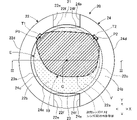
- FIG. 1 shows an electronic dimming eyeglass 10 which is a form of an electronic dimming device to which the present invention is applied.
- the electronic photochromic glasses 10 have left and right photochromic lenses 11 and 12 and a frame 13.
- the frame 13 has left and right annular rims 14, 15 for holding the photochromic lenses 11, 12, temples 16, 17 extending from the rims 14, 15, and a bridge 18 connecting the rims 14, 15.
- the left-right direction of the electronic dimming glasses 10 is the X-axis direction
- the top-bottom direction is the Y-axis direction.
- the dimming lenses 11 and 12 are electronic dimming in which an electrochromic element (EC element) 19 which is an electronic element for dimming is superimposed on the surface of the lens 30 which is an optical element. It is a lens.
- the front surface side of the lens 30 is convex and the back surface side is concave, and the sheet-shaped electrochromic element 19 has a curved shape along the convex surface of the lens 30.
- the power and the like can be adjusted by processing the shape of the concave surface of the lens 30.
- a coat layer having a predetermined function may be formed on the surface side of the electrochromic element 19.
- the lens 30 and the electrochromic element 19 are manufactured separately, the electrochromic element 19 is preformed into a curved shape corresponding to the surface of the lens 30, and then the electrochromic element is manufactured. It is possible to bond the 19 and the lens 30 together. Alternatively, it is also possible to obtain the photochromic lenses 11 and 12 by integrally molding the electrochromic element 19 at the time of molding the lens 30.
- the electrochromic element 19 contains an electrochromic material that reversibly changes the photophysical properties by an oxidation-reduction reaction by applying a voltage, and becomes transparent (highest visible light transmittance) in a normal state without applying a voltage. Yes, when a voltage is applied, it is colored in a predetermined color corresponding to the electrochromic material and the light transmission rate is lowered.
- the configuration of the electrochromic element 19 will be described later.
- the frame 13 is provided with a power supply, a control unit, and an operation unit (not shown). Further, inside the frame 13, a conductive portion for supplying power to the electrochromic element 19 of the photochromic lenses 11 and 12 is provided, and the conductive portion is connected to the terminal regions T1 and T2 of the electrochromic element 19. There is.
- the energization control of the electrochromic element 19 is performed by the control of the control unit, and the dimming effect of the photochromic lenses 11 and 12 can be obtained.
- the control unit may change the dimming effect (light transmittance) of the photochromic lenses 11 and 12 in a plurality of stages according to the operation of the operation unit.
- various dimming lenses 11 and 12 can be selected based on the user's preference and the design of the frame 13.
- a manufacturing method for efficiently producing the electrochromic element 19 corresponding to the dimming lenses 11 and 12 having different shapes will be described below.
- the electrochromic laminate 20 that is the source of the electrochromic element 19 is formed. Then, a part of the electrochromic laminate 20 is cut out into an arbitrary shape corresponding to the lens 30 of the individual photochromic lenses 11 and 12, and the electrochromic element 19 for the photochromic lenses 11 and 12 is obtained.
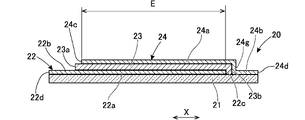
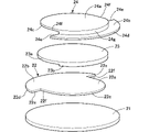
- FIG. 3 and FIG. 6 show a state in which each layer constituting the electrochromic laminate 20 is laminated
- FIGS. 4 and 5 show each layer of the electrochromic laminate 20 separately.
- the electrochromic laminate 20 is configured by laminating a first electrode layer 22, an electrochromic layer (dimming layer) 23, and a second electrode layer 24 on a substrate 21 made of synthetic resin.
- the materials and roles of each layer constituting the electrochromic laminate 20 are based on the existing electrochromic elements, and will be briefly described.
- the first electrode layer 22 and the second electrode layer 24 are transparent conductive films made of a transparent and conductive material, respectively.
- a transparent and conductive material for example, as the material of the first electrode layer 22 and the second electrode layer 24, indium tin oxide (ITO) obtained by adding tin oxide (Sn2O2) to indium oxide (In2O3) is suitable, but other materials may be used. May be good.
- the thickness of the first electrode layer 22 and the second electrode layer 24 is set to a predetermined value at which the electric resistance value required for the redox reaction in the electrochromic layer 23 can be obtained.
- the electrochromic layer 23 is a three-layer film composed of an electrochromic electrode layer, a solid electrolyte layer, and a counter electrode layer.
- a tungsten oxide (WO3) film is suitable as the electrochromic electrode layer
- a tantalum pentoxide (Ta2O5) film is suitable as the solid electrolyte layer
- an iridium oxide (Ir2O2) film or an indium oxide (In2O3) film is suitable as the counter electrode layer. Materials other than the above may be used.
- Each of the first electrode layer 22, the second electrode layer 24, and the electrochromic layer 23 is formed from a well-known film forming method (various coating film forming methods, vacuum film forming methods, etc.) depending on the material and purpose. It can be selected arbitrarily.
- the substrate 21 in the electrochromic laminate 20 has a substantially circular shape centered on the film formation center C shown in FIG.
- the electrochromic layer 23 has a substantially circular shape centered on the film formation center C, and has an outer shape of an annular outer peripheral portion 23a surrounding the film formation center C in front view as shown in FIGS. 2 and 4.
- the diameter D2 (FIG. 4) of the electrochromic layer 23 is smaller (smaller diameter) than the diameter D1 (FIG. 4) of the substrate 21.
- a part of the vicinity of the outer edge of the electrochromic layer 23 is an extension portion 23b that extends in the thickness direction of the electrochromic laminate 20 and is in contact with the substrate 21.
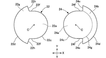
- the first electrode layer 22 and the second electrode layer 24 have shapes symmetrical with respect to the center line extending in the Y-axis direction through the film formation center C in the front view (FIGS. 2 and 4) of the electrochromic laminate 20. .. That is, the first electrode layer 22 and the second electrode layer 24 have a symmetrical shape with the film formation center C as the center when viewed from the front. Specifically, the first electrode layer 22 and the second electrode layer 24 each have the shapes described below.
- the first electrode layer 22 has a central circular portion 22a and an outer diameter portion 22b continuously arranged outside the central circular portion 22a in the radial direction.
- the central circular portion 22a is a substantially circular portion centered on the film formation center C, and the diameter D3 (FIG. 4) of the central circular portion 22a is set to be slightly smaller than the diameter D2 (FIG. 4) of the electrochromic layer 23. Has been done.
- the outer diameter portion 22b is a part of a circle having a larger diameter than the central circular portion 22a, and more specifically, is a part of a circle having the same outer peripheral shape (radius size) as the substrate 21.
- the outer diameter portion 22b is formed in a portion biased to a region on the left side in the X-axis direction with respect to the film formation center C in the front view of the electrochromic laminate 20.
- the outer shape of the first electrode layer 22 is a pair of straight lines extending in the Y-axis direction from both ends of the semicircular outer peripheral portion 22c in the central circular portion 22a, the arc portion 22d in the outer diameter portion 22b, and the arc portion 22d. It is composed of a pair of straight line portions 22e and a pair of straight line portions 22f extending from the pair of straight line portions 22e in the X-axis direction and connected to the semicircular outer peripheral portion 22c.
- the arc portion 22d has a shape that substantially matches a part of the outer peripheral shape of the substrate 21.
- the second electrode layer 24 has a central circular portion 24a and an outer diameter portion 24b arranged outside the central circular portion 24a in the radial direction.
- the central circular portion 24a is a substantially circular portion centered on the film formation center C, and the diameter D4 (FIG. 4) of the central circular portion 24a is set to be slightly smaller than the diameter D2 (FIG. 4) of the electrochromic layer 23. Has been done.
- the diameter D3 of the central circular portion 22a of the first electrode layer 22 and the diameter D4 of the central circular portion 24a of the second electrode layer 24 are of the same size.
- the outer diameter portion 24b is a part of a circle having a larger diameter than the central circular portion 24a, and more specifically, is a part of a circle having the same outer peripheral shape (radius size) as the substrate 21.
- the outer diameter portion 24b is formed in a portion biased to a region on the right side in the X-axis direction with respect to the film formation center C in the front view of the electrochromic laminated body 20. As shown in FIG. 5, the central circular portion 24a and the outer diameter portion 24b are positioned differently in the thickness direction of the electrochromic laminate 20, and the outer edge portion of the central circular portion 24a and the inner edge portion of the outer diameter portion 24b are separated from each other.
- the connecting portion 24g is connected.
- the external shape of the second electrode layer 24 when viewed from the front is a semicircular semicircular outer peripheral portion 24c in the central circular portion 24a, an arc portion 24d in the outer diameter portion 24b, and both ends of the arc portion 24d in the Y-axis direction. It is composed of a pair of straight line portions 24e extending and a pair of straight line portions 24f extending from the pair of straight line portions 24e in the X-axis direction and connected to the outer peripheral portion 24c of the semicircle.
- the arc portion 24d has a shape that substantially matches a part of the outer peripheral shape of the substrate 21. Since there is a step due to the connecting portion 24g between the central circular portion 24a and the outer diameter portion 24b, the pair of straight portions 24e and the pair of straight portions 24f are not directly connected (see FIG. 5).
- the centers of the central circular portions 22a and 24a are positioned at the film forming center C, respectively, and the outer diameter portion 22b and the outer diameter portion 24b are located with respect to the film forming center C in front view. It is formed and arranged symmetrically. As shown in FIG. 3, for the first electrode layer 22, both the central circular portion 22a and the outer diameter portion 22b are in contact with the substrate 21, and for the second electrode layer 24, the outer diameter portion 24b is on the substrate 21. I'm in contact.
- the region where the first electrode layer 22 (central circular portion 22a), the electrochromic layer 23, and the second electrode layer 24 (central circular portion 24a) all overlap in the thickness direction of the electrochromic laminate 20 is colored by applying a voltage. It is a dimming region E (FIGS. 2 and 3) in which a change (change in transmittance) occurs.
- the dimming region E In the front view of the electrochromic laminate 20, the circular region surrounded by the semicircular outer peripheral portion 22c of the central circular portion 22a and the semicircular outer peripheral portion 24c of the central circular portion 24a is the dimming region E (see FIG. 2). ).
- the outer diameter portion 22b of the first electrode layer 22 and the outer diameter portion 24b of the second electrode layer 24 are separated from each other in the X-axis direction without overlapping each other. Then, when viewed from the front of the electrochromic laminated body 20, there is a gap in the X-axis direction between the pair of straight line portions 22e in the outer diameter portion 22b and the pair of straight line portions 24e in the outer diameter portion 24b. As shown in FIG. 6, the outer diameter portion 22b and the outer diameter portion 24b are positioned differently from each other in the thickness direction of the electrochromic laminate 20.
- the dimensions (particularly, diameters D1 to D4) of each part in the electrochromic laminated body 20 are the lenses 30 of a plurality of types (different shapes and sizes) of dimming lenses 11 and 12 that are expected to be used in the electronic dimming spectacles 10.
- the outer shape of the electrochromic layer 23 is set to fit inside the outer peripheral portion 23a of the electrochromic layer 23.
- the diameter D1 of the substrate 21 is 40 mm
- the diameter D2 of the electrochromic layer 23 is 30 mm
- the diameter D3 of the central circular portion 22a and the diameter D4 of the central circular portion 24a are 28 mm, respectively.
- the dimming region E is a circular region having a diameter of 28 mm centered on the film formation center C.
- the diameter D2 of the electrochromic layer 23 is made larger than the diameters D3 and D4 of the central circular portion 22a and the central circular portion 24a, respectively, and a margin of about 1 mm is provided in the radial direction centered on the film formation center C. Further, the outer diameter portion 22b and the outer diameter portion 24b are arranged apart from each other in the X-axis direction. As a result, there is no portion where the first electrode layer 22 and the second electrode layer 24 directly face each other in the thickness direction of the electrochromic laminate 20, and a short circuit between the first electrode layer 22 and the second electrode layer 24 is prevented. There is.
- the electrochromic element 19 customized for the lens is obtained by cutting out the electrochromic laminate 20 configured as described above into a shape corresponding to the outer shape of the photochromic lenses 11 and 12.
- a condition setting for obtaining the electrochromic element 19 from the electrochromic laminated body 20 first, in front view, an overlapping region having a shape overlapping the outer shape of the lens 30 in the forming region of the electrochromic layer 23 (inside the outer peripheral portion 23a).
- V Fig. 2
- T1 and T2 (FIG. 2) are set.
- the portion where the superposed region V and the terminal regions T1 and T2 are combined is cut out from the electrochromic laminate 20 to obtain the electrochromic element 19.
- the outer shape of the lens 30 in the photochromic lenses 11 and 12 is inscribed at two points (inner contacts P1 and P2) with respect to the substantially circular outer peripheral portion 23a of the electrochromic layer 23. As described above, the arrangement of the superimposed region V is set.
- one inner contact P1 is located in the forming range of the outer diameter portion 22b of the first electrode layer 22 (inner diameter side of the arc portion 22d) in the circumferential direction centered on the film formation center C, and the other inner contact.
- P2 is positioned in the circumferential direction centered on the film formation center C in the formation range of the outer diameter portion 24b of the second electrode layer 24 (inner diameter side of the arc portion 24d).
- the inner contact P1 and the inner contact P2 are at least in the X-axis direction.
- the positions are different from each other.
- the inner contact P1 and the inner contact P2 are at substantially the same position in the Y-axis direction, but depending on the outer shape of the lens 30 and the arrangement of the overlapping region V, the inner contact P1 may be located in the Y-axis direction.
- the position and the position of the internal contact P2 may be different from each other.
- the terminal region T1 may be provided with a condition that it extends from the inner contact P2 to a position exceeding at least the thickness of the connection portion 24 g in the front view toward the outer diameter side.
- an electrochromic element 19 that can be applied to a lens 30 of any shape can be provided as long as it satisfies the above setting conditions regarding the arrangement of the superimposed region V and the terminal regions T1 and T2. It can be obtained from various types of electrochromic laminates 20. Therefore, an electrochromic element 19 with an electrode arrangement customized for each lens is produced with little effort and low cost without performing film forming processing using individual mask patterns corresponding to a plurality of types of lens shapes. Will be possible.
- the electrochromic layer 23 in the electrochromic laminate 20 is an extremely simple circular shape when viewed from the front. Further, the first electrode layer 22 and the second electrode layer 24 each have a relatively simple shape obtained by removing a part from the circular shape of the substrate 21 when viewed from the front. Therefore, each layer of the electrochromic laminate 20 can be easily formed without using a complicated mask pattern, and the electrochromic laminate is compared with a film forming process using a complicated mask pattern tailored to an individual lens shape.
- the body 20 can be created inexpensively and efficiently.
- the terminal regions T1 and T2 in the electrochromic element 19 come into contact with the conductive portion arranged in the frame 13 in a conductive state.
- the contact points between the terminal regions T1 and T2 and the conductive portion are covered with the rims 14 and 15 in the frame 13 and are not exposed to the appearance of the electronic dimming glasses 10 (see FIG. 1).
- the outer peripheral portion of the electrochromic element 19 after being cut out from the electrochromic laminate 20 may be sealed with a sealing material or the like. Thereby, the durability of the electrochromic element 19 can be improved.
- the first electrode layer 22 and the second electrode layer 24 have a large substrate 21 except for the space between the straight line portion 22e and the straight line portion 24e. It covers the part.
- the first electrode layer 22 and the second electrode layer 24 have a large substrate 21 except for the space between the straight line portion 22e and the straight line portion 24e. It covers the part.
- the first electrode layer 22 and the second electrode layer 24 are formed in a shape that covers the outer edge shape of the substrate 21 as large as possible.
- the range that can be selected as V and the terminal areas T1 and T2 is widened, and the variation of the lens shape that can be supported is widened.
- the same lens shape can be obtained.
- the degree of freedom in selecting the arrangement of the superposed area V and the terminal areas T1 and T2 is increased.
- the outer shape of the lens 30 is inscribed at two points with respect to the outer peripheral portion 23a of the electrochromic layer 23.
- the setting condition that the terminal regions T1 and T2 are arranged in the outer diameter portions 22b and 24b can be satisfied.
- the outer diameter portions 22b and 24b outside the central circular portions 22a and 24a are arranged so as not to overlap each other in the front view.
- the straight line portion 22e, which is the edge portion of the outer diameter portion 22b, and the straight line portion 24e, which is the edge portion of the outer diameter portion 24b are separated by a predetermined value or more in the X-axis direction. It has a structure with a gap.
- the temples 16 and 17 and the bridge 18 are connected to the upper edges of the left and right rims 14 and 15. Therefore, the conductive portion that supplies power to the electrochromic elements 19 of the left and right photochromic lenses 11 and 12 is easily arranged along the upper edge side of the frame 13. That is, it is assumed that a conductive portion extending substantially in the X-axis direction along the upper edge side of the frame 13 is adopted. In this case, as a terminal arrangement on the electrochromic element 19 side that can be easily connected to the conductive portion, as shown in FIGS. 1 and 2, in the X-axis direction near the upper edge of each of the photochromic lenses 11 and 12 (superimposed region V).
- the outer diameter portions 22b and 24b which are the sources of the terminal regions T1 and T2, are arranged on both sides in the X-axis direction.
- the electrochromic laminate 20 shown in FIG. 2 may be rotated by 90 degrees so that the outer diameter portions 22b and 24b are separated from each other in the Y-axis direction.
- the overlapping region is divided so that the two internal contacts whose outer shape of the lens 30 is inscribed in the outer peripheral portion 23a of the electrochromic layer 23 are distributed to the upper side and the lower side in the Y-axis direction sandwiching the film formation center C. Change the angle and position.
- the two terminal regions provided outside the two internal contacts are also arranged so as to be distributed to the upper side and the lower side in the Y-axis direction.
- the diameter of the dimming region E can be appropriately set by the diameters D2 to D4 of the electrochromic layer 23, the central circular portion 22a of the first electrode layer 22, and the central circular portion 24a of the second electrode layer 24, and is circular. It is a minor change of changing the diameter of the part. Therefore, even if a plurality of types of electrochromic laminates are prepared, the labor and cost can be kept low as compared with the case of changing to different film formation patterns for each lens shape.
- the lens center may be eccentric from the film formation center C of the electrochromic laminate 20, but this can be dealt with by designing the lens in consideration of the eccentricity. Is. Such a correspondence can also be realized by, for example, processing on the back surface (concave surface) performed when finishing the lens 30 shown in FIG. 1 into the final shape.
- FIG. 7 shows an electrochromic laminate 120 which is a modified example.
- the electrochromic laminate 20 described above is formed by laminating a first electrode layer 22, an electrochromic layer 23, and a second electrode layer 24 on one substrate 21 (see FIG. 3).
- the electrochromic laminate 120 of FIG. 7 has a substrate 25 made of another synthetic resin in addition to the substrate 21, and a first electrode layer 22 is provided between the substrate 21 and the substrate 25. The structure sandwiches the electrochromic layer 23 and the second electrode layer 24.
- the substrate 25 has a substantially circular shape centered on the film formation center C shown in FIG. 2, and has substantially the same diameter as the substrate 21.
- the first electrode layer 22 is formed on the substrate 21, the second electrode layer 24 is formed on the substrate 25, and the electrochromic layer 23 is arranged between the first electrode layer 22 and the second electrode layer 24 which are opposed to each other. The result is an electrochromic laminate 120.
- the positions of the substrate 21 and the substrate 25 are determined so that their centers (deposition center C) coincide with each other.
- the shape and arrangement of the first electrode layer 22 on the substrate 21 are set in the same manner as in the electrochromic laminate 20.
- the outer diameter portion 24h on the outer side of the central circular portion 24a is located at the same position as the central circular portion 24a in the thickness direction of the electrochromic laminate 120, and the central circular portion 24a and the outer diameter portion 24h Both are in contact with the substrate 25. That is, unlike the electrochromic laminate 20 of the previous embodiment, the second electrode layer 24 of the electrochromic laminate 120 has a flat structure in which the central circular portion 24a and the outer diameter portion 24h are continuous without a connecting portion. Is.
- the arc portion 24i which is the outer edge of the outer diameter portion 24h, has a shape substantially matching a part of the outer peripheral shape of the substrate 25.
- the shapes and positional relationships of the first electrode layer 22, the electrochromic layer 23, and the second electrode layer 24 in the front view of the electrochromic laminate 120 are the same as those of the electrochromic laminate 20 described above. Therefore, the manufacturing method using the electrochromic laminate 120 can obtain the same effect as the manufacturing method using the electrochromic laminate 20.
- the outer diameter portion 22b of the first electrode layer 22 and the outer diameter portion 24b of the second electrode layer 24 shown in FIGS. 2 and 4 have shapes optimized so as to largely cover the outer diameter portion of the substrate 21.
- the shape of the outer diameter portion of each of the electrode layers 22 and 24 may be changed.
- the outer diameter portion 22b and the outer diameter portion 24b are symmetrical with respect to the film formation center C in the front view, but each electrode layer 22. , 24 It is also possible to make the shape of the outer diameter portion asymmetrical in front view.
- FIG. 8 shows a modified example of the first electrode layer 22 having the outer diameter portion 22 g whose shape has been changed.
- the edge portion is a straight line portion 22h extending in the radial direction about the film formation center C instead of the straight line portion 22e (see FIG. 4) described above. That is, the outer diameter portion 22 g has a fan shape that requires the film formation center C.
- the outer diameter portion 24b of the second electrode layer 24 in FIG. 8 has the same shape as that of FIG. Therefore, the outer diameter portion 22g of the first electrode layer 22 and the outer diameter portion 24b of the second electrode layer 24 have asymmetrical shapes with respect to the film formation center C when viewed from the front. Even if the outer diameter portion 22g and the outer diameter portion 24b have such an asymmetrical shape, they may satisfy the condition that the terminal regions T1 and T2 (FIG. 2) can be set without overlapping each other.
- the outer diameter portion of the second electrode layer 24 is formed into a fan shape similar to the outer diameter portion 22 g of the first electrode layer 22, and the outer diameters of the respective electrode layers 22 and 24 are viewed from the front.
- the portion may be configured symmetrically with respect to the film forming center C.
- outer diameter portion of the first electrode layer 22 and the outer diameter portion of the second electrode layer 24 may be changed to a shape other than the fan shape as shown in FIG.
- the dimensions of the substrate 21, the first electrode layer 22, the electrochromic layer 23, the second electrode layer 24, and the substrate 25 described above are examples, and may be changed to different sizes.
- the dimming region E and the electrochromic layer 23 are circular. This shape is excellent in high versatility that it is easy to correspond to various lens shapes without being biased in a specific direction. However, if there are some common geometrical features in the assumed lens shape, the dimming region and electrochromic layer are set in a non-circular (for example, elliptical) shape that reflects the geometrical features. It is also possible.
- the photochromic lenses 11 and 12 of the above embodiment have a structure in which an electrochromic element 19 is superposed on the surface (convex surface) of the lens 30. Unlike this, a dimming lens having a structure in which an electrochromic element is arranged (sandwiched) inside the lens in the thickness direction may be used.
- Each portion constituting the electrochromic element 19 may be formed of a material other than those described above.
- the substrate may be made of glass instead of synthetic resin.
- the electrochromic material may be used as an organic material instead of the above-mentioned inorganic material.
- the electrochromic element 19 is applied as the electronic element constituting the photochromic lenses 11 and 12, but it can also be applied to an electronic element other than the electrochromic element.
- a liquid crystal element, an electrophoresis element, and the like are common to an electrochromic element in that the optical properties are changed by supplying electric energy. Therefore, even in an electronic dimming device that uses a liquid crystal element or an electrophoresis element as an electronic element, the same effect can be obtained by applying the above-mentioned technique in the manufacture of an electronic element including an electrode.
- dimming in the present invention means all the optical effects of such various electronic elements on the optical element, and is used to change the light transmittance (light transmittance) and color in a narrow sense. Not limited. For example, information display (superimpose) using a liquid crystal element in an optical device is also a form of dimming.
- the electronic photochromic spectacles 10 of the above embodiment are particularly useful in the present invention because of the degree of freedom in selecting the shapes of the photochromic lenses 11 and 12.
- the present invention can also be applied to electronic dimming devices other than electronic dimming glasses.
- it can be applied to electronic dimming glass (electronic blinds) for windows and privacy filters for displays of portable electronic devices.
- the window glass, the cover glass of the display, and the like are the optical elements in the present invention.
Abstract
Description
Claims (12)
- 光学素子に重なる電子素子への電気エネルギーの供給によって調光効果を得る電子調光装置の製造方法であって、
一対の電極層と、前記一対の電極層の間の調光層と、を積層した積層体を形成し、
前記積層体のうち、前記調光層の形成領域内に前記光学素子と重なる形状の重畳領域を設定し、且つ前記重畳領域の外側に連続して前記一対の電極層の一方と他方が単独で存在する2箇所以上の端子領域を設定し、前記重畳領域と前記端子領域を含む部分を前記積層体から切り出して前記電子素子を形成することを特徴とする電子調光装置の製造方法。 It is a method of manufacturing an electronic dimming device that obtains a dimming effect by supplying electric energy to an electronic element that overlaps with an optical element.
A laminated body in which a pair of electrode layers and a dimming layer between the pair of electrode layers are laminated is formed.
In the laminated body, a superimposing region having a shape overlapping with the optical element is set in the forming region of the dimming layer, and one and the other of the pair of electrode layers are continuously outside the superimposing region. A method for manufacturing an electronic dimming device, which comprises setting two or more existing terminal regions and cutting out a portion including the superposed region and the terminal region from the laminated body to form the electronic element. - 前記積層体における前記調光層は略円形であり、
前記積層体における前記一対の電極層はそれぞれ、前記調光層と重なる略円形の円形部と、径方向で前記円形部の外側に配置される外径部と、を有し、
前記一対の電極層の互いの前記外径部が正面視で重ならない配置で前記積層体を形成し、
前記光学素子の外形が前記調光層の略円形の外周形状に2箇所で内接するように前記重畳領域を設定し、且つ該2箇所の内接箇所の外側に前記一対の電極層の一方と他方の前記外径部を位置させて前記端子領域を設定することを特徴とする請求項1に記載の電子調光装置の製造方法。 The dimming layer in the laminated body is substantially circular and has a substantially circular shape.
Each of the pair of electrode layers in the laminated body has a substantially circular circular portion overlapping the dimming layer and an outer diameter portion arranged outside the circular portion in the radial direction.
The laminated body is formed in such an arrangement that the outer diameter portions of the pair of electrode layers do not overlap each other in a front view.
The superimposing region is set so that the outer shape of the optical element is inscribed at two points on the substantially circular outer peripheral shape of the dimming layer, and one of the pair of electrode layers is placed outside the two inscribed points. The method for manufacturing an electronic dimmer according to claim 1, wherein the terminal region is set by locating the other outer diameter portion. - 前記積層体において、前記一対の電極層のそれぞれの前記円形部は、前記調光層よりも小径であることを特徴とする請求項2に記載の電子調光装置の製造方法。 The method for manufacturing an electronic dimming device according to claim 2, wherein in the laminated body, each of the circular portions of the pair of electrode layers has a smaller diameter than the dimming layer.
- 前記積層体において、前記一対の電極層の前記外径部はそれぞれ、前記円形部よりも大径の円形の一部であり、
一方の前記外径部と他方の前記外径部が、正面視で前記円形部の中心に関して対称に配置されていることを特徴とする請求項2又は3に記載の電子調光装置の製造方法。 In the laminated body, the outer diameter portion of the pair of electrode layers is a part of a circle having a larger diameter than the circular portion.
The method for manufacturing an electronic dimming device according to claim 2 or 3, wherein one of the outer diameter portions and the other outer diameter portion are arranged symmetrically with respect to the center of the circular portion in a front view. .. - 前記電子素子は、前記電極層への電圧印加によって前記調光層で酸化還元反応による光物性の可逆的な変化を発生するエレクトロクロミック素子であることを特徴とする請求項1から4のいずれか1項に記載の電子調光装置の製造方法。 Any of claims 1 to 4, wherein the electronic element is an electrochromic element that generates a reversible change in optical properties due to a redox reaction in the dimming layer by applying a voltage to the electrode layer. The method for manufacturing an electronic dimmer according to item 1.
- 前記電子調光装置は、前記光学素子であるレンズの表面又は内部に前記電子素子を配置した電子調光眼鏡であることを特徴とする請求項1から5のいずれか1項に記載の電子調光装置の製造方法。 The electronic dimming device according to any one of claims 1 to 5, wherein the electronic dimming device is an electronic dimming eyeglass in which the electronic element is arranged on the surface or inside of a lens which is the optical element. Manufacturing method of optical equipment.
- 光学素子に重なって配置されて電気エネルギーの供給によって調光効果を得る調光用電子素子であって、
一対の電極層と、前記一対の電極層の間の調光層と、を積層した積層体を有し、
前記積層体は、
正面視で、前記調光層の形成領域内に位置して、前記光学素子と重なる領域である重畳領域と、
前記重畳領域の外側に連続して前記一対の電極層の一方と他方が単独で存在する2箇所以上の端子領域とを含み、
形状が異なる複数の前記光学素子に対して前記重畳領域と前記端子領域を設定可能な形状であることを特徴とする調光用電子素子。 An electronic element for dimming that is placed on top of an optical element and obtains a dimming effect by supplying electrical energy.
It has a laminated body in which a pair of electrode layers and a dimming layer between the pair of electrode layers are laminated.
The laminated body is
When viewed from the front, the superimposed region, which is located in the formation region of the dimming layer and overlaps with the optical element,
The outside of the superposed region includes one of the pair of electrode layers and two or more terminal regions in which the other is independently present.
A dimming electronic element having a shape in which the superimposed region and the terminal region can be set for a plurality of optical elements having different shapes. - 前記積層体における前記調光層は、前記光学素子の外形が2箇所で外周に内接可能な略円形であり、
前記積層体における前記一対の電極層はそれぞれ、前記調光層と重なる略円形の円形部と、径方向で前記円形部の外側に配置される外径部と、を有し、
前記一対の電極層の互いの前記外径部が正面視で重ならない配置であり、
前記端子領域は、前記光学素子の外形が前記調光層の外周に内接する前記2箇所の外側で前記一対の電極層上に位置することを特徴とする請求項7に記載の調光用電子素子。 The dimming layer in the laminated body has a substantially circular shape in which the outer shape of the optical element can be inscribed in the outer periphery at two points.
Each of the pair of electrode layers in the laminated body has a substantially circular circular portion overlapping the dimming layer and an outer diameter portion arranged outside the circular portion in the radial direction.
The outer diameter portions of the pair of electrode layers do not overlap each other in front view.
The dimming electron according to claim 7, wherein the terminal region is located on the pair of electrode layers outside the two locations where the outer shape of the optical element is inscribed in the outer periphery of the dimming layer. element. - 前記積層体において、前記一対の電極層のそれぞれの前記円形部は、前記調光層よりも小径であることを特徴とする請求項8に記載の調光用電子素子。 The dimming electronic element according to claim 8, wherein in the laminated body, each of the circular portions of the pair of electrode layers has a smaller diameter than the dimming layer.
- 前記積層体において、前記一対の電極層の前記外径部はそれぞれ、前記円形部よりも大径の円形の一部であり、
一方の前記外径部と他方の前記外径部が、正面視で前記円形部の中心に関して対称に配置されていることを特徴とする請求項8又は9に記載の調光用電子素子。 In the laminated body, the outer diameter portion of the pair of electrode layers is a part of a circle having a larger diameter than the circular portion.
The dimming electronic element according to claim 8 or 9, wherein one outer diameter portion and the other outer diameter portion are arranged symmetrically with respect to the center of the circular portion in a front view. - 前記電極層への電圧印加によって前記調光層で酸化還元反応による光物性の可逆的な変化を発生するエレクトロクロミック素子であることを特徴とする請求項7から10のいずれか1項に記載の調光用電子素子。 The invention according to any one of claims 7 to 10, wherein the electrochromic element is an electrochromic element that generates a reversible change in optical properties due to a redox reaction in the dimming layer by applying a voltage to the electrode layer. Electronic element for dimming.
- 請求項7から11のいずれか1項に記載の調光用電子素子を備える電子調光眼鏡であって、
前記光学素子はレンズであり、
前記調光用電子素子は、前記レンズに対応する形状の前記重畳領域と、前記重畳領域の外側の2箇所以上の前記端子領域と、を有し、
前記レンズの表面又は内部に前記調光用電子素子が位置する調光レンズと、前記調光レンズを保持するフレームと、により構成されることを特徴とする電子調光眼鏡。 An electronic dimming eyeglass provided with the dimming electronic element according to any one of claims 7 to 11.
The optical element is a lens.
The dimming electronic element has the superimposed region having a shape corresponding to the lens, and two or more terminal regions outside the superimposed region.
Electronic dimming spectacles comprising a dimming lens in which the dimming electronic element is located on the surface or inside of the lens, and a frame for holding the dimming lens.
Priority Applications (4)
| Application Number | Priority Date | Filing Date | Title |
|---|---|---|---|
| US18/032,956 US20240019716A1 (en) | 2020-10-20 | 2021-10-19 | Method for manufacturing electronic light-modulating device, light-modulating electronic element, and electronic light-modulating glasses |
| JP2022557548A JPWO2022085666A1 (en) | 2020-10-20 | 2021-10-19 | |
| EP21882807.7A EP4235287A1 (en) | 2020-10-20 | 2021-10-19 | Method for manufacturing electronic light control device, electronic element for light control, and electronic light control eyeglasses |
| KR1020237017161A KR20230118818A (en) | 2020-10-20 | 2021-10-19 | Manufacturing method of electronic dimming device, electronic device for dimming and electronic dimmable glasses |
Applications Claiming Priority (2)
| Application Number | Priority Date | Filing Date | Title |
|---|---|---|---|
| JP2020-175961 | 2020-10-20 | ||
| JP2020175961 | 2020-10-20 |
Publications (1)
| Publication Number | Publication Date |
|---|---|
| WO2022085666A1 true WO2022085666A1 (en) | 2022-04-28 |
Family
ID=81114052
Family Applications (1)
| Application Number | Title | Priority Date | Filing Date |
|---|---|---|---|
| PCT/JP2021/038550 WO2022085666A1 (en) | 2020-10-20 | 2021-10-19 | Method for manufacturing electronic light control device, electronic element for light control, and electronic light control eyeglasses |
Country Status (6)
| Country | Link |
|---|---|
| US (1) | US20240019716A1 (en) |
| EP (1) | EP4235287A1 (en) |
| JP (1) | JPWO2022085666A1 (en) |
| KR (1) | KR20230118818A (en) |
| CN (2) | CN114384734A (en) |
| WO (1) | WO2022085666A1 (en) |
Citations (7)
| Publication number | Priority date | Publication date | Assignee | Title |
|---|---|---|---|---|
| JPH0324206B2 (en) | 1983-11-14 | 1991-04-02 | Sm Ind Co Ltd | |
| JP5511997B2 (en) | 2007-12-21 | 2014-06-04 | パナソニックヘルスケア株式会社 | Electronic glasses |
| JP2014106265A (en) * | 2012-11-26 | 2014-06-09 | Hoya Corp | Lens processing system, processed size managing apparatus, processed size managing method, and spectacle lens manufacturing method |
| JP2016509264A (en) * | 2013-03-07 | 2016-03-24 | スイッチ マテリアルズ インコーポレイテッドSwitch Materials Inc. | Seals and seal systems for laminar devices |
| JP2016148805A (en) * | 2015-02-13 | 2016-08-18 | 株式会社リコー | Electrochromic device |
| WO2017104466A1 (en) * | 2015-12-15 | 2017-06-22 | 株式会社リコー | Electrochromic apparatus |
| JP2017526949A (en) * | 2014-06-17 | 2017-09-14 | セイジ・エレクトロクロミクス,インコーポレイテッド | Controlled switching of electrochromic devices |
Family Cites Families (1)
| Publication number | Priority date | Publication date | Assignee | Title |
|---|---|---|---|---|
| JPS5511997U (en) | 1979-08-10 | 1980-01-25 |
-
2021
- 2021-10-19 EP EP21882807.7A patent/EP4235287A1/en active Pending
- 2021-10-19 WO PCT/JP2021/038550 patent/WO2022085666A1/en active Application Filing
- 2021-10-19 JP JP2022557548A patent/JPWO2022085666A1/ja active Pending
- 2021-10-19 KR KR1020237017161A patent/KR20230118818A/en unknown
- 2021-10-19 US US18/032,956 patent/US20240019716A1/en active Pending
- 2021-10-20 CN CN202111219662.4A patent/CN114384734A/en active Pending
- 2021-10-20 CN CN202122530403.5U patent/CN216310489U/en active Active
Patent Citations (7)
| Publication number | Priority date | Publication date | Assignee | Title |
|---|---|---|---|---|
| JPH0324206B2 (en) | 1983-11-14 | 1991-04-02 | Sm Ind Co Ltd | |
| JP5511997B2 (en) | 2007-12-21 | 2014-06-04 | パナソニックヘルスケア株式会社 | Electronic glasses |
| JP2014106265A (en) * | 2012-11-26 | 2014-06-09 | Hoya Corp | Lens processing system, processed size managing apparatus, processed size managing method, and spectacle lens manufacturing method |
| JP2016509264A (en) * | 2013-03-07 | 2016-03-24 | スイッチ マテリアルズ インコーポレイテッドSwitch Materials Inc. | Seals and seal systems for laminar devices |
| JP2017526949A (en) * | 2014-06-17 | 2017-09-14 | セイジ・エレクトロクロミクス,インコーポレイテッド | Controlled switching of electrochromic devices |
| JP2016148805A (en) * | 2015-02-13 | 2016-08-18 | 株式会社リコー | Electrochromic device |
| WO2017104466A1 (en) * | 2015-12-15 | 2017-06-22 | 株式会社リコー | Electrochromic apparatus |
Also Published As
| Publication number | Publication date |
|---|---|
| CN114384734A (en) | 2022-04-22 |
| KR20230118818A (en) | 2023-08-14 |
| EP4235287A1 (en) | 2023-08-30 |
| JPWO2022085666A1 (en) | 2022-04-28 |
| US20240019716A1 (en) | 2024-01-18 |
| CN216310489U (en) | 2022-04-15 |
Similar Documents
| Publication | Publication Date | Title |
|---|---|---|
| US9588396B2 (en) | Laser patterning of conductive films for electro-active lenses | |
| EP2530511B1 (en) | Method for manufacturing electronic glasses and liquid-crystal lenses | |
| EP2657750B1 (en) | Semifinished blank for varifocal lens, varifocal lens machined from the blank, and varifocal glasses using the lens | |
| EP3418795A1 (en) | Multifunctional device for an ophthalmic lens | |
| TWI534518B (en) | Electrochromic device | |
| JP5523125B2 (en) | Electronic spectacle lens, electronic spectacles, and method for manufacturing electronic spectacle lenses | |
| CN108646448A (en) | A kind of eyeglass substrate, liquid crystal lens and liquid crystal glasses | |
| WO2022085666A1 (en) | Method for manufacturing electronic light control device, electronic element for light control, and electronic light control eyeglasses | |
| JP6824289B2 (en) | Lens and eyewear | |
| JP5581195B2 (en) | Semi-finished blank for variable focus lens, variable focus lens and variable focus glasses | |
| JPH06300992A (en) | Production of dioptric electrochromic spectacle lens and the lens | |
| WO2018146858A1 (en) | Lens, lens blank, and eyewear | |
| KR20230118860A (en) | Optical device for forming an electrochromic ophthalmic lens, spectacles including the same, and method for manufacturing the same | |
| JP2022176428A (en) | Electronic element for electronic photochromic spectacles | |
| JPH07168209A (en) | Production of electrochromic spectacle lens with diopter | |
| WO2023210796A1 (en) | Electrochromic element, eyeglass lens, eyeglasses, and method for producing electrochromic element | |
| JP7260046B1 (en) | Electrochromic sheets, laminates, spectacle lenses and spectacles | |
| JP7248185B1 (en) | Electrochromic sheets, laminates, spectacle lenses and spectacles | |
| JP7260047B1 (en) | Laminates, spectacle lenses and spectacles | |
| JP2024052472A (en) | Electrochromic sheet, laminate, eyeglass lens and eyeglasses | |
| JP2024020668A (en) | Metal salt precipitation type element |
Legal Events
| Date | Code | Title | Description |
|---|---|---|---|
| 121 | Ep: the epo has been informed by wipo that ep was designated in this application |
Ref document number: 21882807 Country of ref document: EP Kind code of ref document: A1 |
|
| ENP | Entry into the national phase |
Ref document number: 2022557548 Country of ref document: JP Kind code of ref document: A |
|
| WWE | Wipo information: entry into national phase |
Ref document number: 18032956 Country of ref document: US |
|
| NENP | Non-entry into the national phase |
Ref country code: DE |
|
| ENP | Entry into the national phase |
Ref document number: 2021882807 Country of ref document: EP Effective date: 20230522 |