WO2022080077A1 - Microchannel chip - Google Patents
Microchannel chip Download PDFInfo
- Publication number
- WO2022080077A1 WO2022080077A1 PCT/JP2021/033930 JP2021033930W WO2022080077A1 WO 2022080077 A1 WO2022080077 A1 WO 2022080077A1 JP 2021033930 W JP2021033930 W JP 2021033930W WO 2022080077 A1 WO2022080077 A1 WO 2022080077A1
- Authority
- WO
- WIPO (PCT)
- Prior art keywords
- resin
- resin film
- adhesive layer
- flow path
- resin substrate
- Prior art date
Links
- 229920005989 resin Polymers 0.000 claims abstract description 653
- 239000011347 resin Substances 0.000 claims abstract description 653
- 239000000758 substrate Substances 0.000 claims abstract description 275
- 239000000463 material Substances 0.000 claims abstract description 230
- 239000012790 adhesive layer Substances 0.000 claims abstract description 227
- 239000010410 layer Substances 0.000 claims abstract description 168
- 230000014509 gene expression Effects 0.000 claims abstract description 51
- 239000004925 Acrylic resin Substances 0.000 claims description 24
- 229920005672 polyolefin resin Polymers 0.000 claims description 14
- 125000004122 cyclic group Chemical group 0.000 claims description 10
- 229920005668 polycarbonate resin Polymers 0.000 claims description 7
- 239000004431 polycarbonate resin Substances 0.000 claims description 7
- 229920005990 polystyrene resin Polymers 0.000 claims description 7
- 239000010408 film Substances 0.000 description 307
- 238000010438 heat treatment Methods 0.000 description 63
- 230000003746 surface roughness Effects 0.000 description 63
- 239000007788 liquid Substances 0.000 description 48
- 238000000034 method Methods 0.000 description 40
- 238000004519 manufacturing process Methods 0.000 description 38
- 238000005304 joining Methods 0.000 description 36
- -1 polyethylene Polymers 0.000 description 34
- 229920000089 Cyclic olefin copolymer Polymers 0.000 description 31
- 229920003229 poly(methyl methacrylate) Polymers 0.000 description 30
- 239000004926 polymethyl methacrylate Substances 0.000 description 29
- 229920000515 polycarbonate Polymers 0.000 description 25
- 239000004417 polycarbonate Substances 0.000 description 25
- 239000004793 Polystyrene Substances 0.000 description 24
- 238000007667 floating Methods 0.000 description 24
- 239000000853 adhesive Substances 0.000 description 20
- 230000001070 adhesive effect Effects 0.000 description 20
- 238000012937 correction Methods 0.000 description 19
- XLYOFNOQVPJJNP-UHFFFAOYSA-N water Substances O XLYOFNOQVPJJNP-UHFFFAOYSA-N 0.000 description 19
- 125000000524 functional group Chemical group 0.000 description 15
- 229920000139 polyethylene terephthalate Polymers 0.000 description 14
- 239000005020 polyethylene terephthalate Substances 0.000 description 14
- 238000003860 storage Methods 0.000 description 14
- 230000000694 effects Effects 0.000 description 13
- 239000004698 Polyethylene Substances 0.000 description 12
- 239000004743 Polypropylene Substances 0.000 description 12
- 229920001707 polybutylene terephthalate Polymers 0.000 description 12
- 229920000573 polyethylene Polymers 0.000 description 12
- 229920001155 polypropylene Polymers 0.000 description 12
- 238000004381 surface treatment Methods 0.000 description 12
- 229920001577 copolymer Polymers 0.000 description 11
- 239000003522 acrylic cement Substances 0.000 description 9
- 239000001301 oxygen Substances 0.000 description 9
- 229910052760 oxygen Inorganic materials 0.000 description 9
- 229920002223 polystyrene Polymers 0.000 description 9
- 238000012360 testing method Methods 0.000 description 9
- 230000009477 glass transition Effects 0.000 description 7
- 239000002184 metal Substances 0.000 description 7
- QVGXLLKOCUKJST-UHFFFAOYSA-N atomic oxygen Chemical compound [O] QVGXLLKOCUKJST-UHFFFAOYSA-N 0.000 description 6
- 238000002788 crimping Methods 0.000 description 6
- 238000000465 moulding Methods 0.000 description 6
- JRZJOMJEPLMPRA-UHFFFAOYSA-N olefin Natural products CCCCCCCC=C JRZJOMJEPLMPRA-UHFFFAOYSA-N 0.000 description 6
- 229920001225 polyester resin Polymers 0.000 description 6
- 239000004645 polyester resin Substances 0.000 description 6
- 239000011112 polyethylene naphthalate Substances 0.000 description 6
- 239000011116 polymethylpentene Substances 0.000 description 6
- 229920002635 polyurethane Polymers 0.000 description 6
- 239000004814 polyurethane Substances 0.000 description 6
- 239000002356 single layer Substances 0.000 description 6
- 230000015572 biosynthetic process Effects 0.000 description 5
- 238000004458 analytical method Methods 0.000 description 4
- 230000004927 fusion Effects 0.000 description 4
- 239000007789 gas Substances 0.000 description 4
- 238000001746 injection moulding Methods 0.000 description 4
- JOYRKODLDBILNP-UHFFFAOYSA-N Ethyl urethane Chemical compound CCOC(N)=O JOYRKODLDBILNP-UHFFFAOYSA-N 0.000 description 3
- 239000004820 Pressure-sensitive adhesive Substances 0.000 description 3
- 125000005396 acrylic acid ester group Chemical group 0.000 description 3
- 239000000654 additive Substances 0.000 description 3
- 230000000996 additive effect Effects 0.000 description 3
- 125000003172 aldehyde group Chemical group 0.000 description 3
- 239000003963 antioxidant agent Substances 0.000 description 3
- 239000002216 antistatic agent Substances 0.000 description 3
- 239000012298 atmosphere Substances 0.000 description 3
- 230000036760 body temperature Effects 0.000 description 3
- 125000002915 carbonyl group Chemical group [*:2]C([*:1])=O 0.000 description 3
- 125000003178 carboxy group Chemical group [H]OC(*)=O 0.000 description 3
- 238000006243 chemical reaction Methods 0.000 description 3
- 239000011248 coating agent Substances 0.000 description 3
- 239000011247 coating layer Substances 0.000 description 3
- 238000000576 coating method Methods 0.000 description 3
- 230000000052 comparative effect Effects 0.000 description 3
- 238000007872 degassing Methods 0.000 description 3
- 238000001514 detection method Methods 0.000 description 3
- 239000004205 dimethyl polysiloxane Substances 0.000 description 3
- 239000000975 dye Substances 0.000 description 3
- 125000003700 epoxy group Chemical group 0.000 description 3
- 125000001033 ether group Chemical group 0.000 description 3
- 239000003063 flame retardant Substances 0.000 description 3
- 239000011521 glass Substances 0.000 description 3
- 125000002887 hydroxy group Chemical group [H]O* 0.000 description 3
- 230000001771 impaired effect Effects 0.000 description 3
- 125000000468 ketone group Chemical group 0.000 description 3
- 150000002926 oxygen Chemical class 0.000 description 3
- 125000002081 peroxide group Chemical group 0.000 description 3
- 239000000049 pigment Substances 0.000 description 3
- 239000004014 plasticizer Substances 0.000 description 3
- 229920000435 poly(dimethylsiloxane) Polymers 0.000 description 3
- 238000000926 separation method Methods 0.000 description 3
- 239000013464 silicone adhesive Substances 0.000 description 3
- 229920002050 silicone resin Polymers 0.000 description 3
- 239000002904 solvent Substances 0.000 description 3
- 239000010409 thin film Substances 0.000 description 3
- 238000007740 vapor deposition Methods 0.000 description 3
- 238000013459 approach Methods 0.000 description 2
- 239000002131 composite material Substances 0.000 description 2
- 239000000470 constituent Substances 0.000 description 2
- 238000011156 evaluation Methods 0.000 description 2
- 238000011534 incubation Methods 0.000 description 2
- 239000012528 membrane Substances 0.000 description 2
- 238000012986 modification Methods 0.000 description 2
- 230000004048 modification Effects 0.000 description 2
- 238000005498 polishing Methods 0.000 description 2
- 229920013716 polyethylene resin Polymers 0.000 description 2
- 230000008961 swelling Effects 0.000 description 2
- 238000012546 transfer Methods 0.000 description 2
- 238000001721 transfer moulding Methods 0.000 description 2
- NIXOWILDQLNWCW-UHFFFAOYSA-M Acrylate Chemical compound [O-]C(=O)C=C NIXOWILDQLNWCW-UHFFFAOYSA-M 0.000 description 1
- 229920000178 Acrylic resin Polymers 0.000 description 1
- 240000007594 Oryza sativa Species 0.000 description 1
- 235000007164 Oryza sativa Nutrition 0.000 description 1
- 239000003153 chemical reaction reagent Substances 0.000 description 1
- 238000004140 cleaning Methods 0.000 description 1
- 238000013461 design Methods 0.000 description 1
- 239000003814 drug Substances 0.000 description 1
- 238000005516 engineering process Methods 0.000 description 1
- 230000002708 enhancing effect Effects 0.000 description 1
- 102000039446 nucleic acids Human genes 0.000 description 1
- 108020004707 nucleic acids Proteins 0.000 description 1
- 150000007523 nucleic acids Chemical class 0.000 description 1
- 238000007517 polishing process Methods 0.000 description 1
- 238000012545 processing Methods 0.000 description 1
- 102000004169 proteins and genes Human genes 0.000 description 1
- 108090000623 proteins and genes Proteins 0.000 description 1
- 235000009566 rice Nutrition 0.000 description 1
- 238000012216 screening Methods 0.000 description 1
- 238000003786 synthesis reaction Methods 0.000 description 1
Images


Classifications
-
- C—CHEMISTRY; METALLURGY
- C09—DYES; PAINTS; POLISHES; NATURAL RESINS; ADHESIVES; COMPOSITIONS NOT OTHERWISE PROVIDED FOR; APPLICATIONS OF MATERIALS NOT OTHERWISE PROVIDED FOR
- C09J—ADHESIVES; NON-MECHANICAL ASPECTS OF ADHESIVE PROCESSES IN GENERAL; ADHESIVE PROCESSES NOT PROVIDED FOR ELSEWHERE; USE OF MATERIALS AS ADHESIVES
- C09J7/00—Adhesives in the form of films or foils
- C09J7/30—Adhesives in the form of films or foils characterised by the adhesive composition
- C09J7/38—Pressure-sensitive adhesives [PSA]
- C09J7/381—Pressure-sensitive adhesives [PSA] based on macromolecular compounds obtained by reactions involving only carbon-to-carbon unsaturated bonds
- C09J7/385—Acrylic polymers
-
- B—PERFORMING OPERATIONS; TRANSPORTING
- B29—WORKING OF PLASTICS; WORKING OF SUBSTANCES IN A PLASTIC STATE IN GENERAL
- B29C—SHAPING OR JOINING OF PLASTICS; SHAPING OF MATERIAL IN A PLASTIC STATE, NOT OTHERWISE PROVIDED FOR; AFTER-TREATMENT OF THE SHAPED PRODUCTS, e.g. REPAIRING
- B29C65/00—Joining or sealing of preformed parts, e.g. welding of plastics materials; Apparatus therefor
- B29C65/48—Joining or sealing of preformed parts, e.g. welding of plastics materials; Apparatus therefor using adhesives, i.e. using supplementary joining material; solvent bonding
- B29C65/4805—Joining or sealing of preformed parts, e.g. welding of plastics materials; Apparatus therefor using adhesives, i.e. using supplementary joining material; solvent bonding characterised by the type of adhesives
- B29C65/481—Non-reactive adhesives, e.g. physically hardening adhesives
- B29C65/4825—Pressure sensitive adhesives
-
- B—PERFORMING OPERATIONS; TRANSPORTING
- B01—PHYSICAL OR CHEMICAL PROCESSES OR APPARATUS IN GENERAL
- B01L—CHEMICAL OR PHYSICAL LABORATORY APPARATUS FOR GENERAL USE
- B01L3/00—Containers or dishes for laboratory use, e.g. laboratory glassware; Droppers
- B01L3/50—Containers for the purpose of retaining a material to be analysed, e.g. test tubes
- B01L3/502—Containers for the purpose of retaining a material to be analysed, e.g. test tubes with fluid transport, e.g. in multi-compartment structures
- B01L3/5027—Containers for the purpose of retaining a material to be analysed, e.g. test tubes with fluid transport, e.g. in multi-compartment structures by integrated microfluidic structures, i.e. dimensions of channels and chambers are such that surface tension forces are important, e.g. lab-on-a-chip
- B01L3/502707—Containers for the purpose of retaining a material to be analysed, e.g. test tubes with fluid transport, e.g. in multi-compartment structures by integrated microfluidic structures, i.e. dimensions of channels and chambers are such that surface tension forces are important, e.g. lab-on-a-chip characterised by the manufacture of the container or its components
-
- B—PERFORMING OPERATIONS; TRANSPORTING
- B29—WORKING OF PLASTICS; WORKING OF SUBSTANCES IN A PLASTIC STATE IN GENERAL
- B29C—SHAPING OR JOINING OF PLASTICS; SHAPING OF MATERIAL IN A PLASTIC STATE, NOT OTHERWISE PROVIDED FOR; AFTER-TREATMENT OF THE SHAPED PRODUCTS, e.g. REPAIRING
- B29C65/00—Joining or sealing of preformed parts, e.g. welding of plastics materials; Apparatus therefor
- B29C65/02—Joining or sealing of preformed parts, e.g. welding of plastics materials; Apparatus therefor by heating, with or without pressure
- B29C65/18—Joining or sealing of preformed parts, e.g. welding of plastics materials; Apparatus therefor by heating, with or without pressure using heated tools
-
- B—PERFORMING OPERATIONS; TRANSPORTING
- B29—WORKING OF PLASTICS; WORKING OF SUBSTANCES IN A PLASTIC STATE IN GENERAL
- B29C—SHAPING OR JOINING OF PLASTICS; SHAPING OF MATERIAL IN A PLASTIC STATE, NOT OTHERWISE PROVIDED FOR; AFTER-TREATMENT OF THE SHAPED PRODUCTS, e.g. REPAIRING
- B29C65/00—Joining or sealing of preformed parts, e.g. welding of plastics materials; Apparatus therefor
- B29C65/48—Joining or sealing of preformed parts, e.g. welding of plastics materials; Apparatus therefor using adhesives, i.e. using supplementary joining material; solvent bonding
- B29C65/50—Joining or sealing of preformed parts, e.g. welding of plastics materials; Apparatus therefor using adhesives, i.e. using supplementary joining material; solvent bonding using adhesive tape, e.g. thermoplastic tape; using threads or the like
- B29C65/5057—Joining or sealing of preformed parts, e.g. welding of plastics materials; Apparatus therefor using adhesives, i.e. using supplementary joining material; solvent bonding using adhesive tape, e.g. thermoplastic tape; using threads or the like positioned between the surfaces to be joined
-
- B—PERFORMING OPERATIONS; TRANSPORTING
- B29—WORKING OF PLASTICS; WORKING OF SUBSTANCES IN A PLASTIC STATE IN GENERAL
- B29C—SHAPING OR JOINING OF PLASTICS; SHAPING OF MATERIAL IN A PLASTIC STATE, NOT OTHERWISE PROVIDED FOR; AFTER-TREATMENT OF THE SHAPED PRODUCTS, e.g. REPAIRING
- B29C66/00—General aspects of processes or apparatus for joining preformed parts
- B29C66/01—General aspects dealing with the joint area or with the area to be joined
- B29C66/05—Particular design of joint configurations
- B29C66/10—Particular design of joint configurations particular design of the joint cross-sections
- B29C66/11—Joint cross-sections comprising a single joint-segment, i.e. one of the parts to be joined comprising a single joint-segment in the joint cross-section
- B29C66/112—Single lapped joints
- B29C66/1122—Single lap to lap joints, i.e. overlap joints
-
- B—PERFORMING OPERATIONS; TRANSPORTING
- B29—WORKING OF PLASTICS; WORKING OF SUBSTANCES IN A PLASTIC STATE IN GENERAL
- B29C—SHAPING OR JOINING OF PLASTICS; SHAPING OF MATERIAL IN A PLASTIC STATE, NOT OTHERWISE PROVIDED FOR; AFTER-TREATMENT OF THE SHAPED PRODUCTS, e.g. REPAIRING
- B29C66/00—General aspects of processes or apparatus for joining preformed parts
- B29C66/01—General aspects dealing with the joint area or with the area to be joined
- B29C66/05—Particular design of joint configurations
- B29C66/303—Particular design of joint configurations the joint involving an anchoring effect
- B29C66/3032—Particular design of joint configurations the joint involving an anchoring effect making use of protusions or cavities belonging to at least one of the parts to be joined
- B29C66/30321—Particular design of joint configurations the joint involving an anchoring effect making use of protusions or cavities belonging to at least one of the parts to be joined making use of protusions belonging to at least one of the parts to be joined
- B29C66/30322—Particular design of joint configurations the joint involving an anchoring effect making use of protusions or cavities belonging to at least one of the parts to be joined making use of protusions belonging to at least one of the parts to be joined in the form of rugosity
-
- B—PERFORMING OPERATIONS; TRANSPORTING
- B29—WORKING OF PLASTICS; WORKING OF SUBSTANCES IN A PLASTIC STATE IN GENERAL
- B29C—SHAPING OR JOINING OF PLASTICS; SHAPING OF MATERIAL IN A PLASTIC STATE, NOT OTHERWISE PROVIDED FOR; AFTER-TREATMENT OF THE SHAPED PRODUCTS, e.g. REPAIRING
- B29C66/00—General aspects of processes or apparatus for joining preformed parts
- B29C66/40—General aspects of joining substantially flat articles, e.g. plates, sheets or web-like materials; Making flat seams in tubular or hollow articles; Joining single elements to substantially flat surfaces
- B29C66/41—Joining substantially flat articles ; Making flat seams in tubular or hollow articles
- B29C66/45—Joining of substantially the whole surface of the articles
-
- B—PERFORMING OPERATIONS; TRANSPORTING
- B29—WORKING OF PLASTICS; WORKING OF SUBSTANCES IN A PLASTIC STATE IN GENERAL
- B29C—SHAPING OR JOINING OF PLASTICS; SHAPING OF MATERIAL IN A PLASTIC STATE, NOT OTHERWISE PROVIDED FOR; AFTER-TREATMENT OF THE SHAPED PRODUCTS, e.g. REPAIRING
- B29C66/00—General aspects of processes or apparatus for joining preformed parts
- B29C66/50—General aspects of joining tubular articles; General aspects of joining long products, i.e. bars or profiled elements; General aspects of joining single elements to tubular articles, hollow articles or bars; General aspects of joining several hollow-preforms to form hollow or tubular articles
- B29C66/51—Joining tubular articles, profiled elements or bars; Joining single elements to tubular articles, hollow articles or bars; Joining several hollow-preforms to form hollow or tubular articles
- B29C66/53—Joining single elements to tubular articles, hollow articles or bars
- B29C66/534—Joining single elements to open ends of tubular or hollow articles or to the ends of bars
- B29C66/5346—Joining single elements to open ends of tubular or hollow articles or to the ends of bars said single elements being substantially flat
- B29C66/53461—Joining single elements to open ends of tubular or hollow articles or to the ends of bars said single elements being substantially flat joining substantially flat covers and/or substantially flat bottoms to open ends of container bodies
-
- B—PERFORMING OPERATIONS; TRANSPORTING
- B29—WORKING OF PLASTICS; WORKING OF SUBSTANCES IN A PLASTIC STATE IN GENERAL
- B29C—SHAPING OR JOINING OF PLASTICS; SHAPING OF MATERIAL IN A PLASTIC STATE, NOT OTHERWISE PROVIDED FOR; AFTER-TREATMENT OF THE SHAPED PRODUCTS, e.g. REPAIRING
- B29C66/00—General aspects of processes or apparatus for joining preformed parts
- B29C66/70—General aspects of processes or apparatus for joining preformed parts characterised by the composition, physical properties or the structure of the material of the parts to be joined; Joining with non-plastics material
- B29C66/71—General aspects of processes or apparatus for joining preformed parts characterised by the composition, physical properties or the structure of the material of the parts to be joined; Joining with non-plastics material characterised by the composition of the plastics material of the parts to be joined
-
- B—PERFORMING OPERATIONS; TRANSPORTING
- B29—WORKING OF PLASTICS; WORKING OF SUBSTANCES IN A PLASTIC STATE IN GENERAL
- B29C—SHAPING OR JOINING OF PLASTICS; SHAPING OF MATERIAL IN A PLASTIC STATE, NOT OTHERWISE PROVIDED FOR; AFTER-TREATMENT OF THE SHAPED PRODUCTS, e.g. REPAIRING
- B29C66/00—General aspects of processes or apparatus for joining preformed parts
- B29C66/70—General aspects of processes or apparatus for joining preformed parts characterised by the composition, physical properties or the structure of the material of the parts to be joined; Joining with non-plastics material
- B29C66/72—General aspects of processes or apparatus for joining preformed parts characterised by the composition, physical properties or the structure of the material of the parts to be joined; Joining with non-plastics material characterised by the structure of the material of the parts to be joined
- B29C66/723—General aspects of processes or apparatus for joining preformed parts characterised by the composition, physical properties or the structure of the material of the parts to be joined; Joining with non-plastics material characterised by the structure of the material of the parts to be joined being multi-layered
-
- B—PERFORMING OPERATIONS; TRANSPORTING
- B29—WORKING OF PLASTICS; WORKING OF SUBSTANCES IN A PLASTIC STATE IN GENERAL
- B29C—SHAPING OR JOINING OF PLASTICS; SHAPING OF MATERIAL IN A PLASTIC STATE, NOT OTHERWISE PROVIDED FOR; AFTER-TREATMENT OF THE SHAPED PRODUCTS, e.g. REPAIRING
- B29C66/00—General aspects of processes or apparatus for joining preformed parts
- B29C66/70—General aspects of processes or apparatus for joining preformed parts characterised by the composition, physical properties or the structure of the material of the parts to be joined; Joining with non-plastics material
- B29C66/73—General aspects of processes or apparatus for joining preformed parts characterised by the composition, physical properties or the structure of the material of the parts to be joined; Joining with non-plastics material characterised by the intensive physical properties of the material of the parts to be joined, by the optical properties of the material of the parts to be joined, by the extensive physical properties of the parts to be joined, by the state of the material of the parts to be joined or by the material of the parts to be joined being a thermoplastic or a thermoset
- B29C66/739—General aspects of processes or apparatus for joining preformed parts characterised by the composition, physical properties or the structure of the material of the parts to be joined; Joining with non-plastics material characterised by the intensive physical properties of the material of the parts to be joined, by the optical properties of the material of the parts to be joined, by the extensive physical properties of the parts to be joined, by the state of the material of the parts to be joined or by the material of the parts to be joined being a thermoplastic or a thermoset characterised by the material of the parts to be joined being a thermoplastic or a thermoset
- B29C66/7392—General aspects of processes or apparatus for joining preformed parts characterised by the composition, physical properties or the structure of the material of the parts to be joined; Joining with non-plastics material characterised by the intensive physical properties of the material of the parts to be joined, by the optical properties of the material of the parts to be joined, by the extensive physical properties of the parts to be joined, by the state of the material of the parts to be joined or by the material of the parts to be joined being a thermoplastic or a thermoset characterised by the material of the parts to be joined being a thermoplastic or a thermoset characterised by the material of at least one of the parts being a thermoplastic
- B29C66/73921—General aspects of processes or apparatus for joining preformed parts characterised by the composition, physical properties or the structure of the material of the parts to be joined; Joining with non-plastics material characterised by the intensive physical properties of the material of the parts to be joined, by the optical properties of the material of the parts to be joined, by the extensive physical properties of the parts to be joined, by the state of the material of the parts to be joined or by the material of the parts to be joined being a thermoplastic or a thermoset characterised by the material of the parts to be joined being a thermoplastic or a thermoset characterised by the material of at least one of the parts being a thermoplastic characterised by the materials of both parts being thermoplastics
-
- B—PERFORMING OPERATIONS; TRANSPORTING
- B29—WORKING OF PLASTICS; WORKING OF SUBSTANCES IN A PLASTIC STATE IN GENERAL
- B29C—SHAPING OR JOINING OF PLASTICS; SHAPING OF MATERIAL IN A PLASTIC STATE, NOT OTHERWISE PROVIDED FOR; AFTER-TREATMENT OF THE SHAPED PRODUCTS, e.g. REPAIRING
- B29C66/00—General aspects of processes or apparatus for joining preformed parts
- B29C66/90—Measuring or controlling the joining process
- B29C66/91—Measuring or controlling the joining process by measuring or controlling the temperature, the heat or the thermal flux
- B29C66/919—Measuring or controlling the joining process by measuring or controlling the temperature, the heat or the thermal flux characterised by specific temperature, heat or thermal flux values or ranges
- B29C66/9192—Measuring or controlling the joining process by measuring or controlling the temperature, the heat or the thermal flux characterised by specific temperature, heat or thermal flux values or ranges in explicit relation to another variable, e.g. temperature diagrams
- B29C66/91921—Measuring or controlling the joining process by measuring or controlling the temperature, the heat or the thermal flux characterised by specific temperature, heat or thermal flux values or ranges in explicit relation to another variable, e.g. temperature diagrams in explicit relation to another temperature, e.g. to the softening temperature or softening point, to the thermal degradation temperature or to the ambient temperature
- B29C66/91941—Measuring or controlling the joining process by measuring or controlling the temperature, the heat or the thermal flux characterised by specific temperature, heat or thermal flux values or ranges in explicit relation to another variable, e.g. temperature diagrams in explicit relation to another temperature, e.g. to the softening temperature or softening point, to the thermal degradation temperature or to the ambient temperature in explicit relation to Tg, i.e. the glass transition temperature, of the material of one of the parts to be joined
- B29C66/91943—Measuring or controlling the joining process by measuring or controlling the temperature, the heat or the thermal flux characterised by specific temperature, heat or thermal flux values or ranges in explicit relation to another variable, e.g. temperature diagrams in explicit relation to another temperature, e.g. to the softening temperature or softening point, to the thermal degradation temperature or to the ambient temperature in explicit relation to Tg, i.e. the glass transition temperature, of the material of one of the parts to be joined higher than said glass transition temperature
-
- B—PERFORMING OPERATIONS; TRANSPORTING
- B29—WORKING OF PLASTICS; WORKING OF SUBSTANCES IN A PLASTIC STATE IN GENERAL
- B29C—SHAPING OR JOINING OF PLASTICS; SHAPING OF MATERIAL IN A PLASTIC STATE, NOT OTHERWISE PROVIDED FOR; AFTER-TREATMENT OF THE SHAPED PRODUCTS, e.g. REPAIRING
- B29C66/00—General aspects of processes or apparatus for joining preformed parts
- B29C66/90—Measuring or controlling the joining process
- B29C66/91—Measuring or controlling the joining process by measuring or controlling the temperature, the heat or the thermal flux
- B29C66/919—Measuring or controlling the joining process by measuring or controlling the temperature, the heat or the thermal flux characterised by specific temperature, heat or thermal flux values or ranges
- B29C66/9192—Measuring or controlling the joining process by measuring or controlling the temperature, the heat or the thermal flux characterised by specific temperature, heat or thermal flux values or ranges in explicit relation to another variable, e.g. temperature diagrams
- B29C66/91921—Measuring or controlling the joining process by measuring or controlling the temperature, the heat or the thermal flux characterised by specific temperature, heat or thermal flux values or ranges in explicit relation to another variable, e.g. temperature diagrams in explicit relation to another temperature, e.g. to the softening temperature or softening point, to the thermal degradation temperature or to the ambient temperature
- B29C66/91941—Measuring or controlling the joining process by measuring or controlling the temperature, the heat or the thermal flux characterised by specific temperature, heat or thermal flux values or ranges in explicit relation to another variable, e.g. temperature diagrams in explicit relation to another temperature, e.g. to the softening temperature or softening point, to the thermal degradation temperature or to the ambient temperature in explicit relation to Tg, i.e. the glass transition temperature, of the material of one of the parts to be joined
- B29C66/91945—Measuring or controlling the joining process by measuring or controlling the temperature, the heat or the thermal flux characterised by specific temperature, heat or thermal flux values or ranges in explicit relation to another variable, e.g. temperature diagrams in explicit relation to another temperature, e.g. to the softening temperature or softening point, to the thermal degradation temperature or to the ambient temperature in explicit relation to Tg, i.e. the glass transition temperature, of the material of one of the parts to be joined lower than said glass transition temperature
-
- B—PERFORMING OPERATIONS; TRANSPORTING
- B32—LAYERED PRODUCTS
- B32B—LAYERED PRODUCTS, i.e. PRODUCTS BUILT-UP OF STRATA OF FLAT OR NON-FLAT, e.g. CELLULAR OR HONEYCOMB, FORM
- B32B27/00—Layered products comprising a layer of synthetic resin
- B32B27/06—Layered products comprising a layer of synthetic resin as the main or only constituent of a layer, which is next to another layer of the same or of a different material
- B32B27/08—Layered products comprising a layer of synthetic resin as the main or only constituent of a layer, which is next to another layer of the same or of a different material of synthetic resin
-
- B—PERFORMING OPERATIONS; TRANSPORTING
- B32—LAYERED PRODUCTS
- B32B—LAYERED PRODUCTS, i.e. PRODUCTS BUILT-UP OF STRATA OF FLAT OR NON-FLAT, e.g. CELLULAR OR HONEYCOMB, FORM
- B32B27/00—Layered products comprising a layer of synthetic resin
- B32B27/30—Layered products comprising a layer of synthetic resin comprising vinyl (co)polymers; comprising acrylic (co)polymers
- B32B27/302—Layered products comprising a layer of synthetic resin comprising vinyl (co)polymers; comprising acrylic (co)polymers comprising aromatic vinyl (co)polymers, e.g. styrenic (co)polymers
-
- B—PERFORMING OPERATIONS; TRANSPORTING
- B32—LAYERED PRODUCTS
- B32B—LAYERED PRODUCTS, i.e. PRODUCTS BUILT-UP OF STRATA OF FLAT OR NON-FLAT, e.g. CELLULAR OR HONEYCOMB, FORM
- B32B27/00—Layered products comprising a layer of synthetic resin
- B32B27/30—Layered products comprising a layer of synthetic resin comprising vinyl (co)polymers; comprising acrylic (co)polymers
- B32B27/308—Layered products comprising a layer of synthetic resin comprising vinyl (co)polymers; comprising acrylic (co)polymers comprising acrylic (co)polymers
-
- B—PERFORMING OPERATIONS; TRANSPORTING
- B32—LAYERED PRODUCTS
- B32B—LAYERED PRODUCTS, i.e. PRODUCTS BUILT-UP OF STRATA OF FLAT OR NON-FLAT, e.g. CELLULAR OR HONEYCOMB, FORM
- B32B27/00—Layered products comprising a layer of synthetic resin
- B32B27/32—Layered products comprising a layer of synthetic resin comprising polyolefins
- B32B27/325—Layered products comprising a layer of synthetic resin comprising polyolefins comprising polycycloolefins
-
- B—PERFORMING OPERATIONS; TRANSPORTING
- B32—LAYERED PRODUCTS
- B32B—LAYERED PRODUCTS, i.e. PRODUCTS BUILT-UP OF STRATA OF FLAT OR NON-FLAT, e.g. CELLULAR OR HONEYCOMB, FORM
- B32B27/00—Layered products comprising a layer of synthetic resin
- B32B27/36—Layered products comprising a layer of synthetic resin comprising polyesters
- B32B27/365—Layered products comprising a layer of synthetic resin comprising polyesters comprising polycarbonates
-
- B—PERFORMING OPERATIONS; TRANSPORTING
- B32—LAYERED PRODUCTS
- B32B—LAYERED PRODUCTS, i.e. PRODUCTS BUILT-UP OF STRATA OF FLAT OR NON-FLAT, e.g. CELLULAR OR HONEYCOMB, FORM
- B32B3/00—Layered products comprising a layer with external or internal discontinuities or unevennesses, or a layer of non-planar form; Layered products having particular features of form
- B32B3/26—Layered products comprising a layer with external or internal discontinuities or unevennesses, or a layer of non-planar form; Layered products having particular features of form characterised by a particular shape of the outline of the cross-section of a continuous layer; characterised by a layer with cavities or internal voids ; characterised by an apertured layer
- B32B3/30—Layered products comprising a layer with external or internal discontinuities or unevennesses, or a layer of non-planar form; Layered products having particular features of form characterised by a particular shape of the outline of the cross-section of a continuous layer; characterised by a layer with cavities or internal voids ; characterised by an apertured layer characterised by a layer formed with recesses or projections, e.g. hollows, grooves, protuberances, ribs
-
- B—PERFORMING OPERATIONS; TRANSPORTING
- B32—LAYERED PRODUCTS
- B32B—LAYERED PRODUCTS, i.e. PRODUCTS BUILT-UP OF STRATA OF FLAT OR NON-FLAT, e.g. CELLULAR OR HONEYCOMB, FORM
- B32B7/00—Layered products characterised by the relation between layers; Layered products characterised by the relative orientation of features between layers, or by the relative values of a measurable parameter between layers, i.e. products comprising layers having different physical, chemical or physicochemical properties; Layered products characterised by the interconnection of layers
- B32B7/02—Physical, chemical or physicochemical properties
-
- B—PERFORMING OPERATIONS; TRANSPORTING
- B32—LAYERED PRODUCTS
- B32B—LAYERED PRODUCTS, i.e. PRODUCTS BUILT-UP OF STRATA OF FLAT OR NON-FLAT, e.g. CELLULAR OR HONEYCOMB, FORM
- B32B7/00—Layered products characterised by the relation between layers; Layered products characterised by the relative orientation of features between layers, or by the relative values of a measurable parameter between layers, i.e. products comprising layers having different physical, chemical or physicochemical properties; Layered products characterised by the interconnection of layers
- B32B7/04—Interconnection of layers
- B32B7/12—Interconnection of layers using interposed adhesives or interposed materials with bonding properties
-
- C—CHEMISTRY; METALLURGY
- C09—DYES; PAINTS; POLISHES; NATURAL RESINS; ADHESIVES; COMPOSITIONS NOT OTHERWISE PROVIDED FOR; APPLICATIONS OF MATERIALS NOT OTHERWISE PROVIDED FOR
- C09J—ADHESIVES; NON-MECHANICAL ASPECTS OF ADHESIVE PROCESSES IN GENERAL; ADHESIVE PROCESSES NOT PROVIDED FOR ELSEWHERE; USE OF MATERIALS AS ADHESIVES
- C09J7/00—Adhesives in the form of films or foils
- C09J7/20—Adhesives in the form of films or foils characterised by their carriers
- C09J7/29—Laminated material
-
- B—PERFORMING OPERATIONS; TRANSPORTING
- B01—PHYSICAL OR CHEMICAL PROCESSES OR APPARATUS IN GENERAL
- B01L—CHEMICAL OR PHYSICAL LABORATORY APPARATUS FOR GENERAL USE
- B01L2300/00—Additional constructional details
- B01L2300/08—Geometry, shape and general structure
- B01L2300/0809—Geometry, shape and general structure rectangular shaped
- B01L2300/0816—Cards, e.g. flat sample carriers usually with flow in two horizontal directions
-
- B—PERFORMING OPERATIONS; TRANSPORTING
- B01—PHYSICAL OR CHEMICAL PROCESSES OR APPARATUS IN GENERAL
- B01L—CHEMICAL OR PHYSICAL LABORATORY APPARATUS FOR GENERAL USE
- B01L2300/00—Additional constructional details
- B01L2300/08—Geometry, shape and general structure
- B01L2300/0887—Laminated structure
-
- B—PERFORMING OPERATIONS; TRANSPORTING
- B29—WORKING OF PLASTICS; WORKING OF SUBSTANCES IN A PLASTIC STATE IN GENERAL
- B29L—INDEXING SCHEME ASSOCIATED WITH SUBCLASS B29C, RELATING TO PARTICULAR ARTICLES
- B29L2031/00—Other particular articles
- B29L2031/756—Microarticles, nanoarticles
-
- B—PERFORMING OPERATIONS; TRANSPORTING
- B32—LAYERED PRODUCTS
- B32B—LAYERED PRODUCTS, i.e. PRODUCTS BUILT-UP OF STRATA OF FLAT OR NON-FLAT, e.g. CELLULAR OR HONEYCOMB, FORM
- B32B2250/00—Layers arrangement
- B32B2250/24—All layers being polymeric
-
- B—PERFORMING OPERATIONS; TRANSPORTING
- B32—LAYERED PRODUCTS
- B32B—LAYERED PRODUCTS, i.e. PRODUCTS BUILT-UP OF STRATA OF FLAT OR NON-FLAT, e.g. CELLULAR OR HONEYCOMB, FORM
- B32B2307/00—Properties of the layers or laminate
- B32B2307/50—Properties of the layers or laminate having particular mechanical properties
- B32B2307/538—Roughness
-
- B—PERFORMING OPERATIONS; TRANSPORTING
- B32—LAYERED PRODUCTS
- B32B—LAYERED PRODUCTS, i.e. PRODUCTS BUILT-UP OF STRATA OF FLAT OR NON-FLAT, e.g. CELLULAR OR HONEYCOMB, FORM
- B32B2307/00—Properties of the layers or laminate
- B32B2307/70—Other properties
- B32B2307/732—Dimensional properties
- B32B2307/737—Dimensions, e.g. volume or area
- B32B2307/7375—Linear, e.g. length, distance or width
- B32B2307/7376—Thickness
Definitions
- the present invention relates to a microchannel chip used in the pharmaceutical industry and the like.
- microchannel chips may be used for analysis, synthesis, screening, etc. of nucleic acids, proteins, sugar chains, etc.
- a microchannel groove also called a microchannel
- a sample can be chemically reacted, separated, detected, analyzed, etc. in space (for example, Patent Document 1).
- the microchannel chip used for such analysis or the like includes a substrate (resin substrate) made of resin and having microchannels or the like formed on the surface, and a resin film bonded to the resin substrate.
- a substrate resin substrate
- resin film bonded to the resin substrate.
- the bonding between the resin substrate and the resin film is mainly performed by heat fusion or by bonding with an adhesive layer provided on the resin film.
- the portion of the bonded surface where the adhesive layer does not sufficiently follow the resin substrate (low followability). (Parts) are likely to occur, that is, minute floating of the film is likely to occur on the joint surface, and gas invades into the flow path groove from this minute floating portion during or after the liquid is sent to the flow path groove. There is a problem that bubbles that hinder liquid feeding, chemical reaction, separation / detection, etc. are generated and remain.
- the liquid is sent to the flow path groove of the micro flow path chip previously stored in the low temperature range (0 to 10 ° C.), or the micro flow path chip is sent to the micro flow path chip at 35 to 40 ° C. after the liquid is sent to the flow path groove. It may be stored at a certain degree (for example, near body temperature), but in such a case, the above-mentioned problem tends to occur more easily.
- the present invention has been made in view of the above problems, and an object of the present invention is to provide a microchannel chip having less bubble generation and bubble residue during liquid feeding to a flow path groove and storage after liquid feeding. do.
- the microchannel chip according to the first aspect of the present invention has a resin substrate having a channel groove formed on at least one surface, a base material layer, and an adhesive layer, and the adhesive layer covers the channel groove.
- the resin film bonded to the resin substrate as described above is provided, and the surface roughness (Rz) of the bonded surface to which the resin substrate and the adhesive layer of the resin film are bonded is 7 ⁇ m or less.
- the microchannel chip according to the second aspect of the present invention has a resin substrate having a channel groove formed on at least one surface, a base material layer, and an adhesive layer, and the adhesive layer covers the channel groove.
- the thickness of the base material layer of the resin film is X ( ⁇ m)
- the thickness of the adhesive layer is Y ( ⁇ m)
- the relational expression (1) It is characterized in that Y ⁇ 0.4 X-25, the relational expression (2) 50 ⁇ Y ⁇ 3, and the relational expression (3) X ⁇ 40 are all satisfied.
- the microchannel chip according to the third aspect of the present invention has a resin substrate having a channel groove formed on at least one surface, a base material layer, and an adhesive layer, and the adhesive layer covers the channel groove.
- the square of the surface roughness (Rz) of the joint surface to which the resin film bonded to the resin substrate and the adhesive layer of the resin film are bonded is X ( ⁇ m 2 ), the joint surface.
- Y ( ⁇ m 2 ) When the total film floating area of the resin film per 100 ⁇ m 2 is Y ( ⁇ m 2 ), it is characterized by satisfying all of the following relational expressions (1) to (3).
- the adhesion of the adhesive layer of the resin film to the resin substrate on the joint surface is high, and there are few bubbles generated and bubbles remaining during liquid feeding to the flow path groove and storage after liquid feeding. A flow path chip can be obtained.
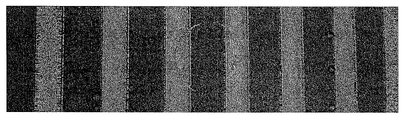
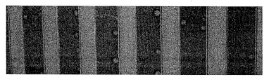
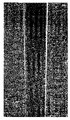
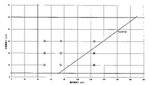
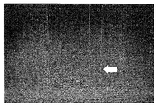
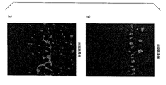
- the relationship between the square (X: ⁇ m 2 ) of the surface roughness (Rz) of the joint surface of the microchannel chip and the total film floating area (Y: ⁇ m 2 ) of the resin film per 100 ⁇ m 2 of the joint surface is shown. It is a graph. It is an image of the joint surface of the microchannel chips of Samples 1 and 2 shown in Example 3 taken with a laser microscope (photograph substitute for drawing). (A) is a photographed image of the joint surface of sample 1, and (b) is a photographed image of the joint surface of sample 2. It is an image of the joint surface of the microchannel chips of Samples 3 and 4 shown in Example 3 taken with a laser microscope (photograph substitute for drawing). (C) is a photographed image of the joint surface of the sample 3, and (d) is a photographed image of the joint surface of the sample 4.
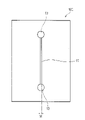
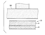
- FIG. 1 is a schematic enlarged cross-sectional view of the vicinity of the flow path groove 11 of the micro flow path chip 100 according to the present embodiment.
- FIG. 2 is a front view of the microchannel chip 100 according to the present embodiment.
- the microchannel chip 100 has a resin substrate 10 having a channel groove 11 formed on at least one surface, a substrate layer 21 and an adhesive layer 23, as shown in FIGS. 1 and 2.
- the adhesive layer 23 is provided with a resin film 20 bonded to the resin substrate 10 so as to cover the flow path groove 11, and further, the resin substrate 10 and the adhesive layer 23 of the resin film 20 are bonded to each other. It is characterized in that the surface roughness (Rz: maximum height roughness) of the joint surface 30 which is the surface is 7 ⁇ m or less.
- the microchannel chip 100 has not only a structure in which one resin substrate 10 and one resin film 20 are bonded as shown in FIGS. 1 and 2, but also on both sides of the resin substrate 10.
- a flow path groove 11 is formed, resin films 20 are bonded to both sides thereof, and the surface roughness (Rz) of both of the bonded surfaces 30 is within a predetermined range, or the base material of the resin film 20.
- Adhesive layers 23 are provided on both surfaces of the layer 21, and surfaces on which the flow path grooves 11 of the resin substrate 10 are formed are joined to both of the adhesive layers 23, respectively, and the surface roughness (Rz) of both of the joint surfaces 30 is joined. ) May be within a predetermined range.
- the microchannel chip 100 may have an inlet or outlet for a sample or the like, a degassing port, or the like, as shown in FIG. 2, on at least one surface of the resin substrate 10.
- the above port 13 may be formed.
- the port 13 may have a cylindrical shape as shown in FIG. 2, or may have another shape such as a rectangular tubular shape, and is further formed so as to penetrate the resin substrate 10. Is also good.
- the overall shape (outer shape) of the microchannel chip 100 is preferably a square plate shape from the viewpoint of ease of use in equipment and the like and handleability, but is a circular plate. It may be in the shape of a plate, and is not particularly limited as long as it is in the shape of a plate.
- the microchannel chip 100 has the surface roughness (Rz) of the bonding surface 30 to which the surface of the resin substrate 10 on which the channel groove 11 is formed and the adhesive layer 23 of the resin film 20 are bonded.
- Rz surface roughness
- Very high followability That is, there is very little minute floating of the resin film 20 on the bonding surface 30 (a portion where the adhesive layer 23 of the resin film 20 does not sufficiently follow the surface of the resin substrate 10 to be bonded and floats slightly apart). ..
- the microchannel tip 100 according to the present embodiment can be used when the liquid is fed to the channel groove 11 or when the microchannel chip 100 is stored after the liquid is fed.
- the intrusion of gas from the joint surface 30 into the flow path groove 11 is extremely small, and the generation of bubbles and the residual bubbles in the flow path groove 11 are very small.
- the microchannel tip may be stored at about 35 to 40 ° C. for several tens of minutes to several hours (incubation, etc.) after the liquid is sent to the channel groove. Even in such a case, the present embodiment is also used.
- the microchannel chip 100 is characterized in that the resin film 20 is unlikely to generate minute floats on the joint surface 30, and similarly, the generation of bubbles and the residual bubbles in the channel groove 11 are very small. Further, if the surface roughness (Rz) of the joint surface 30 is less than 6 ⁇ m, the microchannel tip 100 is placed in a low temperature region (0) before the liquid is fed to the channel groove 11. Even when stored at (about 10 ° C.), there is very little bubble generation and bubble residue in the flow path groove 11 during liquid feeding and storage after liquid feeding.
- the "surface roughness (Rz)” means the maximum height roughness defined by JIS B 0601 (2013). That is, the reference length is extracted from the roughness curve of the surface (joint surface 30 or the like in the present invention) in the direction of the average line, and the value of the maximum mountain height Zp and the maximum valley depth Zv of the roughness curve in this extracted portion are The sum with the value is expressed in ⁇ m. Further, the surface roughness (Rz) is measured by using a non-contact measuring device (for example, a laser microscope VK-9710 manufactured by KEYENCE) with respect to the measuring surface (joint surface 30 or the like in the present invention). conduct.
- a non-contact measuring device for example, a laser microscope VK-9710 manufactured by KEYENCE
- the resin substrate 10 of the microchannel chip 100 is a plate-shaped substrate made of resin in which a channel groove 11 is formed on at least one surface, and the size thereof is, for example, a square. If so, examples thereof include 10 mm or more and 100 mm or less ⁇ 10 mm or more and 200 mm or less, and a thickness of 0.5 mm or more and 3.0 mm or less.
- the flow path groove 11 formed in the resin substrate 10 may be a fine groove and may have an opening width and a depth through which a liquid sample can pass, but for example, the opening width
- the opening length of the flow path groove 11 in the lateral direction: the length of the portion indicated by W in the embodiments of FIGS. 1 and 2) is 1 mm or less, preferably 20 ⁇ m or more and 500 ⁇ m or less, and the depth thereof is 10 ⁇ m or more. Examples thereof are those having a size of 500 ⁇ m or less, preferably 20 ⁇ m or more and 100 ⁇ m or less.
- a mold that can form the flow path groove 11 when molding the resin substrate 10 by injection molding of the resin is used, or the molded resin substrate 10 is finely processed (cut). Or by adding a member).
- the shape of the flow path groove 11 is not particularly limited such that the cross-sectional shape is rectangular, polygonal, or semicircular, but the cross-sectional shape is trapezoidal or trapezoidal because the liquid feeding is easy to be stable. It is preferably semi-circular.
- the number of flow path grooves 11 formed in the resin substrate 10 is not limited to one, and a plurality of flow path grooves 11 may be formed in series or in parallel.
- the flow path groove 11 may be branched or intersected, and can be appropriately designed according to the intended use, including the above-mentioned cross-sectional shape, number, opening width, depth, and the like.
- the depth of the flow path groove 11 formed in the resin substrate 10 of the micro flow path chip 100 is the length of the flow path groove 11 in the resin substrate 10 in the thickness direction. That is, in the flow path groove 11 formed in the resin substrate 10, a perpendicular line (a line parallel to the thickness direction of the resin substrate 10) from the virtual outer surface of the resin substrate 10 that existed before the flow path groove 11 was formed. Is the longest distance among the distances to the point where the surface intersecting the surface constituting the flow path groove 11 when drawn. For example, in the embodiment shown in FIG. 1, the depth of the flow path groove 11 is the line on the upper side of the flow path groove 11 formed in the resin substrate 10 before the resin film 20 is joined (resin film 20).
- the surface of the flow path groove 11 of the resin substrate 10 (the surface constituting the flow path groove 11) is subjected to surface treatment such as hydrophilization treatment and surface treatment functional group formation treatment. May be.
- a surface treatment for example, a treatment for introducing an oxygen-containing functional group is shown. By introducing this oxygen-containing functional group, the hydrophilicity of the surface is improved, and a smoother sample (sample containing water or a hydrophilic solvent) can be passed through.
- oxygen-containing functional group examples include a group of functional groups having polarities such as a carbonyl group such as an aldehyde group and a ketone group, a carboxyl group, a hydroxyl group, an ether group, a peroxide group and an epoxy group.
- a group of functional groups having polarities such as a carbonyl group such as an aldehyde group and a ketone group, a carboxyl group, a hydroxyl group, an ether group, a peroxide group and an epoxy group.
- the resin substrate 10 is made of a resin material.
- the fact that the resin material is composed means that the resin material is the main material (60% by mass or more, more preferably 70% by mass or more, still more preferably 80% by mass of the resin material in the total mass of the resin substrate 10). Above, more preferably, it is contained in an amount of 90% by mass or more).
- the resin substrate 10 may be, for example, one having a layer made of a material other than the resin material (for example, glass) on a part of the surface side that is not bonded to the resin film 20. It is preferable that the entire resin substrate 10 is made of a resin material (particularly the same resin material). This is because it is easier to mold the resin substrate 10 itself. Further, the flow path groove 11 may be formed on both surfaces of the resin substrate 10.
- Examples of the resin material used for producing the resin substrate 10 include polyolefin resins such as polyethylene (PE), polypropylene (PP), and polymethylpentene (PMP), cycloolefin polymers (COP), and cycloolefin copolymers (COC). Cyclic olefin resin, polystyrene resin such as polystyrene (PS), polycarbonate resin such as polycarbonate (PC), polyacrylic resin such as polymethylmethacrylate (PMMA), polyethylene terephthalate (PET), polybutylene terephthalate (PBT) , Polyethylene naphthalate (PEN) and other polyester resins, but are not limited thereto. In addition, these may be used alone or in combination of two or more.
- the resin substrate 10 can be configured by using such a resin material as a main material.
- the resin substrate 10 is more preferably composed of any one selected from the group consisting of a polystyrene-based resin, a polycarbonate-based resin, a polyacrylic-based resin, and a cyclic olefin-based resin. It is more preferably composed of any one selected from the group consisting of polystyrene (PS), polycarbonate (PC), polymethylmethacrylate (PMMA), and cycloolefin copolymer (COC).
- PS polystyrene
- PC polycarbonate
- PMMA polymethylmethacrylate
- COC cycloolefin copolymer
- the channel groove 11 is used.
- the surface roughness (Rz) of the surface on which the resin film 20 is formed is 7 ⁇ m or less, more preferably less than 6 ⁇ m, still more preferably less than 5.5 ⁇ m, still more preferably less than 5 ⁇ m.
- a resin substrate 10 is prepared and used for bonding with the resin film 20.
- the large resin substrate 10 and the resin substrate 10 having a large number of flow path grooves 11 are polished because the surface roughness (Rz) of the surface on which the flow path grooves 11 are formed tends to be large during molding or the like. It is preferable to adjust the surface roughness (Rz) so as to be within the above range.
- the surface (the inner surface of the flow path groove 11) constituting the flow path groove 11 of the resin substrate 10 is different from the surface to be joined to the adhesive layer 23 of the resin film 20, and its surface roughness (Rz) is different. May be more than 7 ⁇ m. That is, in the microchannel chip 100 according to the present embodiment, the surface roughness (Rz) of the bonding surface 30 which is the surface where the resin substrate 10 and the resin film 20 are bonded and the surface of the surface of the channel groove 11
- the configuration may be different from the roughness (Rz). With such a configuration, it is not necessary to adjust the surface roughness (Rz) of the surface of the flow path groove 11 to be small, so that the resin substrate 10 used for manufacturing the micro flow path chip 100 according to the present embodiment can be molded. It is preferable because the formation of the flow path groove 11 becomes easier.
- the resin film 20 of the microchannel chip 100 has a base material layer 21 as a base material (base material of the film) and an adhesive layer 23 containing an adhesive component, and this base material layer. 21 and the adhesive layer 23 are laminated. Then, the adhesive layer 23 of the resin film 20 and the surface of the resin substrate 10 on which the flow path groove 11 is formed are joined.
- the base material layer 21 may be a single layer (single layer), or may have a structure in which a plurality of base material layers are laminated.
- the adhesive layer 23 is provided on at least one surface of the base material layer 21, but has a structure in which the adhesive layers 23 are provided on both surfaces of the base material layer 21, and the adhesive layer 23 is provided on one surface of the base material layer 21.
- It may be a configuration formed by a specific pattern (pattern coating). Further, a group in which a plurality of base material layers are laminated between the base material layer 21 and the adhesive layer 23, on the surface side facing (opposite) the surface side of the base material layer 21 to be bonded to the resin substrate 10, and on the surface side. Other layers (for example, a coating layer, an adhesive layer (laminate adhesive layer), etc.) may be included between the layers of the material layer 21.
- the size of the resin film 20 for example, in the case of a square, the same size as the above-mentioned resin substrate 10, that is, 10 mm or more and 100 mm or less ⁇ 10 mm or more and 200 mm or less is exemplified.
- the lower limit of the total thickness of the resin film 20 is preferably 0.01 mm or more, more preferably 0.02 mm or more, and 0, from the viewpoint of ease of joining with the resin substrate 10. It is more preferably .03 mm or more.
- the upper limit is preferably 1.0 mm or less, more preferably 0.5 mm or less, and more preferably 0, because it does not easily affect the followability of the resin film 20 to the resin substrate 10 on the joint surface 30.
- the total thickness of the resin film 20 is defined by measuring the length between the main surfaces (between the front and back outer surfaces) of the resin film 20 at 10 arbitrary points in the normal vector direction of the main surface of the resin film 20. , It is obtained by calculating the average.
- the thickness (X) of the base material layer 21 of the resin film 20 preferably has a lower limit of 50 ⁇ m or more, more preferably 70 ⁇ m or more, further preferably 80 ⁇ m or more, and more than 85 ⁇ m. It is more preferably 90 ⁇ m or more, still more preferably 100 ⁇ m or more.
- the upper limit is preferably 130 ⁇ m or less, and more preferably 125 ⁇ m or less. This is because the resin film 20 has an appropriate hardness and is easily bonded to the resin substrate 10.
- the thickness (X) of the base material layer 21 is the length between the main surfaces of the base material layer 21 (between both surfaces) in the normal vector direction of the main surface of the base material layer 21.
- the thickness (X) of the base material layer 21 is the thickness of each layer to be the laminated base materials. It is the total value of the above calculated in the same manner as above.
- the upper limit of the thickness (Y) of the adhesive layer 23 of the resin film 20 is preferably less than 20 ⁇ m, more preferably less than 15 ⁇ m, and further preferably 10 ⁇ m or less.
- the cost can be further reduced, the swelling of the adhesive layer 23 into the flow path groove 11 is further suppressed when the adhesive layer 23 is joined to the resin substrate 10, and the internal volume of the flow path groove 11 can be more easily secured (liquid). This is because the flow path groove 11 is likely to have a more stable liquid feeding speed and the like).
- the surface roughness (Rz) of the joint surface 30 is within a predetermined range, so that the resin substrate 10 is used.
- the lower limit of the thickness of the adhesive layer 23 is preferably 3 ⁇ m or more, more preferably 5 ⁇ m or more, from the viewpoint of keeping the function of the adhesive layer 23 at a certain level or more.
- the thickness (Y) of the adhesive layer 23 is the distance between the main surfaces of the adhesive layer 23 (both surfaces) in the normal vector direction of the main surface of the adhesive layer 23 bonded to one resin substrate 10. It is obtained by arbitrarily measuring the length (one of which is between the joint surfaces 30) at 10 points and calculating the average (Y in FIG. 1 is an understanding of the thickness of the adhesive layer 23). Is shown to facilitate).
- the thickness (Y) of the adhesive layer 23 is the thickness (Y) of the adhesive layer 23 on one surface (one side surface) bonded to the resin substrate 10. It is the thickness of the adhesive layer 23, not the total value of the thicknesses of the adhesive layers 23 on both surfaces.
- the resin material used for the base material layer 21 of the resin film 20 is, for example, the same as the resin material used for the resin substrate 10, that is, polyethylene (PE), polypropylene (PP), polymethylpentene (PMP), or the like.
- Examples thereof include polyacrylic resins such as polyethylene terephthalate (PET), polybutylene terephthalate (PBT), and polyester resins such as polyethylene naphthalate (PEN).
- two or more kinds of resin materials may be mixed and used, or two or more kinds of layers formed of a single resin material may be laminated and used.
- a resin material is contained as a main material (for example, 60% by mass or more, more preferably 70% by mass or more, still more preferably 80% by mass or more, still more preferably 90% by mass or more of the total mass of the base material layer 21.
- the base material layer 21 of the resin film 20 can be formed.
- the base material layer 21 of the resin film 20 is made of polystyrene (PS), polycarbonate (PC), polymethylmethacrylate (). It is preferably composed of any one selected from the group consisting of PMMA) and cycloolefin copolymer (COC) (used as a main material).
- the resin substrate 10 described above and the base material layer 21 of the resin film 20 are made of the same resin material, and the resin materials are polystyrene (PS), polycarbonate (PC), polymethylmethacrylate (PMMA), and cyclo. Any one selected from the group consisting of olefin copolymer (COC) is more preferable from the viewpoint of ensuring the transparency of the obtained microchannel chip 100 (easiness of observation work and the like).
- PS polystyrene
- PC polycarbonate
- PMMA polymethylmethacrylate
- cyclo any one selected from the group consisting of olefin copolymer (COC) is more preferable from the viewpoint of ensuring the transparency of the obtained microchannel chip 100 (easiness of observation work and the like).
- Examples of the adhesive component used for the adhesive layer 23 of the resin film 20 include a polyacrylic resin (acrylic adhesive) such as an acrylic acid ester, a silicone resin (silicone adhesive) such as polydimethylsiloxane, and the like.
- a polyacrylic resin such as an acrylic acid ester
- silicone resin silicone resin
- polyurethane-based resins such as polyurethane can be mentioned.
- Such an adhesive component is contained as a main component (for example, 60% by mass or more, more preferably 70% by mass or more, still more preferably 80% by mass or more, still more preferably 90% by mass or more of the total mass of the adhesive layer 23).
- the adhesive layer 23 of the resin film 20 can be formed.
- the adhesive component constituting the adhesive layer 23 is a polyacrylic resin (acrylic adhesive)
- the resin film 20 is formed on the surface of the resin substrate 10 where the flow path groove 11 is formed due to the characteristics of the acrylic adhesive. Is very suitable because it tends to follow suit more easily.
- the resin substrate 10 is also made of a polyacrylic resin which is a resin material of the same type.
- the resin film 20 of the microchannel chip 100 according to the present embodiment may contain plasticizers, antioxidants, flame retardants, antistatic agents, pigments, dyes and the like as long as the effects of the present invention are not impaired. It may further contain an additive. This also applies to the resin substrate 10 described above.
- the resin film 20 may be formed with an electrode portion made of metal vapor deposition, a metal thin film, or the like so as to correspond to the flow path groove 11 or the port 13 formed in the resin substrate 10, for example.
- the microchannel chip 100 presses the resin substrate 10 and the resin film 20 as described above so as to cover the adhesive layer 23 of the resin film 20 on the surface of the resin substrate 10 on which the channel groove 11 is formed. It is manufactured by joining them together.
- the bonding step by crimping the resin substrate 10 and the resin film 20 can be performed by using a press machine or the like, but unlike the bonding process by heat fusion, the bonding is performed by the adhesiveness of the adhesive layer 23. No heating is performed to melt the resin during crimping. Then, the bonding conditions and the like may be adjusted so that the surface roughness (Rz) of the bonding surface 30 between the resin substrate 10 and the resin film 20 is within a predetermined range.
- the surface roughness (Rz) of the bonding surface 30 after the bonding between the resin substrate 10 and the resin film 20 is set within a predetermined range. Therefore, the surface roughness (Rz) of the surface on which the flow path groove 11 is formed (the surface to be bonded to the adhesive layer 23 of the resin film 20) is 7 ⁇ m or less, more preferably less than 6 ⁇ m, and further preferably 5.5 ⁇ m. A resin substrate 10 adjusted to less than, more preferably less than 5 ⁇ m is prepared and used.
- Such a resin substrate 10 can be used for a method of polishing the surface of a mold used for injection molding of the resin substrate 10 (excluding the mold portion for forming the flow path groove 11) or a mold portion of the flow path groove 11.
- a molding die can be manufactured by transfer using a machined die, and the resin substrate 10 can be molded using this molding die (transfer molding method). From the viewpoint of easy adjustment of surface roughness, it is preferable to mold the resin substrate 10 by a transfer molding method.
- the microchannel chip 100 it is also possible to further combine a membrane body, a pump, a valve, a sensor, a motor, a mixer, a gear, a clutch, a microlens, an electric circuit, and the like into a composite. be.
- the microchannel chip according to the present invention including the above-described embodiment can be used for sample separation, detection, analysis, etc., and two or more types of samples are brought into contact with each other to perform a chemical reaction or the like. Is also possible. Further, the generation of bubbles and the residual bubbles during the liquid feeding to the flow path groove and the storage after the liquid feeding are extremely small, and the product can be used very preferably. In particular, the above effect is exhibited even when the microchannel chip is stored in the vicinity of the body temperature range (35 to 40 ° C.) of the living body after the liquid is sent to the channel groove, and further, the temperature is low in advance. It is also possible to use a microchannel chip that exhibits the above effect even when stored in a region (0 to 10 ° C.).
- a microchannel chip comprising a film and having a surface roughness (Rz) of 7 ⁇ m or less on a bonding surface to which the resin substrate and the adhesive layer of the resin film are bonded.
- the resin substrate is composed of any one selected from the group consisting of polystyrene-based resin, polycarbonate-based resin, polyacrylic-based resin, and cyclic olefin-based resin, according to (1) to (4).
- the microchannel chip according to any one.
- FIG. 1 is a schematic enlarged cross-sectional view of the vicinity of the flow path groove 11 of the micro flow path chip 100 according to the present embodiment.
- FIG. 2 is a front view of the microchannel chip 100 according to the present embodiment.
- the microchannel chip 100 has a resin substrate 10 having a channel groove 11 formed on at least one surface, a substrate layer 21 and an adhesive layer 23, as shown in FIGS. 1 and 2.
- a resin film 20 bonded to the resin substrate 10 so as to cover the flow path groove 11 by the adhesive layer 23 is provided, and the thickness of the base material layer 21 of the resin film 20 is X ( ⁇ m).
- the thickness of the adhesive layer 23 bonded to the resin substrate 10 is Y ( ⁇ m)
- the microchannel chip 100 has not only a structure in which one resin substrate 10 and one resin film 20 are bonded as shown in FIGS. 1 and 2, but also on both sides of the resin substrate 10.
- the flow path groove 11 is formed, and the resin film 20 having the above-mentioned characteristics is bonded to both surfaces thereof, and the thickness of both surfaces of the base material layer 21 of the resin film 20 satisfies the above relational expression.
- the adhesive layer 23 may be provided, and the surfaces of the resin substrate 10 on which the flow path groove 11 is formed may be joined to both of the adhesive layers 23.
- the microchannel chip 100 may have an inlet or outlet for a sample or the like, a degassing port, or the like, as shown in FIG. 2, on at least one surface of the resin substrate 10.
- the above port 13 may be formed.
- the port 13 may have a cylindrical shape as shown in FIG. 2, or may have another shape such as a rectangular tubular shape, and is further formed so as to penetrate the resin substrate 10. Is also good.
- the overall shape (outer shape) of the microchannel chip 100 is preferably a square plate shape from the viewpoint of ease of use in equipment and the like and handleability, but is a circular plate. It may be in the shape of a plate, and is not particularly limited as long as it is in the shape of a plate.
- the microchannel chip 100 has a rough surface of the bonding surface 30 which is a surface where the surface of the resin substrate 10 on which the channel groove 11 is formed and the adhesive layer 23 of the resin film 20 are bonded. Even if the resin (Rz: maximum height roughness) is, for example, 5 ⁇ m or more, 5.5 ⁇ m or more, 6 ⁇ m or more, 7 ⁇ m or more, 8 ⁇ m or more, 9 ⁇ m or more, or 10 ⁇ m or more.
- the thickness (X) of the base material layer 21 of the resin film 20 and the thickness (Y) of the adhesive layer 23 have the above-mentioned configurations, so that the adhesive layer of the resin film 20 to the resin substrate 10 on the joint surface 30 is provided.
- the surface roughness of the surface (the surface to be joined to the adhesive layer 23 of the resin film 20) on which the channel groove 11 of the resin substrate 10 to be prepared is formed is rough.
- the adjustment for reducing (Rz) may be omitted.
- the surface roughness (Rz) of the joint surface 30 is more preferably 20 ⁇ m or less, further preferably 18 ⁇ m or less, and further preferably 15 ⁇ m or less. Is even more preferable.
- the adhesive layer of the resin film does not sufficiently follow the surface of the resin substrate to be bonded on the joint surface.
- the surface roughness (Rz) of the joint surface 30 is more than a certain level, although there may be many portions (micro-floating of the film) that are slightly separated from each other. Even so, the thickness (X) of the base material layer 21 of the resin film 20 and the thickness (Y) of the adhesive layer 23 bonded to the resin substrate 10 are the above-mentioned (1) to (3).
- the adhesive layer 23 of the resin film 20 is sufficiently followed and bonded to the surface of the resin substrate 10, and the bonding surface 30 (particularly, the bonding surface 30 near the flow path groove 11) is bonded.
- the feature is that the film micro-floating is extremely small.
- the microchannel tip 100 according to the present embodiment having such a configuration flows when the liquid is fed to the channel groove 11 or when the microchannel chip 100 is stored after the liquid is fed.
- the intrusion of gas from the joint surface 30 into the path groove 11 is extremely small, and the generation of bubbles and the residual bubbles in the flow path groove 11 are extremely small.
- the microchannel tip when the microchannel tip is stored in a refrigerator before the liquid is fed to the channel groove, or after the liquid is fed to the channel groove, the microchannel tip is stored at about 35 to 40 ° C. for several tens of minutes to several minutes. It may be stored for about an hour (incubation, etc.), but even in such a case, the microchannel chip 100 according to the present embodiment is unlikely to generate minute floating of the resin film 20 on the joint surface 30, and similarly flows. There are very few bubbles generated and bubbles remaining in the path groove 11.
- the "surface roughness (Rz)” means the maximum height roughness defined by JIS B 0601 (2013). That is, the reference length is extracted from the roughness curve of the surface (joint surface 30 or the like in the present invention) in the direction of the average line, and the value of the maximum mountain height Zp and the maximum valley depth Zv of the roughness curve in this extracted portion are The sum with the value is expressed in ⁇ m. Further, the surface roughness (Rz) is measured by using a non-contact measuring device (for example, a laser microscope VK-9710 manufactured by KEYENCE) with respect to the measuring surface (joint surface 30 or the like in the present invention). conduct.
- a non-contact measuring device for example, a laser microscope VK-9710 manufactured by KEYENCE
- the resin substrate 10 of the microchannel chip 100 is a plate-shaped substrate made of resin in which a channel groove 11 is formed on at least one surface, and the size thereof is, for example, a square. If so, examples thereof include 10 mm or more and 100 mm or less ⁇ 10 mm or more and 200 mm or less, and a thickness of 0.5 mm or more and 3.0 mm or less.
- the flow path groove 11 formed in the resin substrate 10 may be a fine groove and may have an opening width and a depth through which a liquid sample can pass, but for example, the opening width
- the opening length of the flow path groove 11 in the lateral direction: the length of the portion indicated by W in the embodiments of FIGS. 1 and 2) is 1 mm or less, preferably 20 ⁇ m or more and 500 ⁇ m or less, and the depth thereof is 10 ⁇ m or more. Examples thereof are those having a size of 500 ⁇ m or less, preferably 20 ⁇ m or more and 100 ⁇ m or less.
- a mold that can form the flow path groove 11 when molding the resin substrate 10 by injection molding of the resin is used, or the molded resin substrate 10 is finely processed (cut). Or by adding a member).
- the shape of the flow path groove 11 is not particularly limited such that the cross-sectional shape is rectangular, polygonal, or semicircular, but the cross-sectional shape is trapezoidal or trapezoidal because the liquid feeding is easy to be stable. It is preferably semi-circular.
- the number of flow path grooves 11 formed in the resin substrate 10 is not limited to one, and a plurality of flow path grooves 11 may be formed in series or in parallel.
- the flow path groove 11 may be branched or intersected, and can be appropriately designed according to the intended use, including the above-mentioned cross-sectional shape, number, opening width, depth, and the like.
- the depth of the flow path groove 11 formed in the resin substrate 10 of the micro flow path chip 100 is the length of the flow path groove 11 in the resin substrate 10 in the thickness direction. That is, in the flow path groove 11 formed in the resin substrate 10, a perpendicular line (a line parallel to the thickness direction of the resin substrate 10) from the virtual outer surface of the resin substrate 10 that existed before the flow path groove 11 was formed. Is the longest distance among the distances to the point where the surface intersecting the surface constituting the flow path groove 11 when drawn. For example, in the embodiment shown in FIG. 1, the depth of the flow path groove 11 is the line on the upper side of the flow path groove 11 formed in the resin substrate 10 before the resin film 20 is joined (resin film 20).
- the surface of the flow path groove 11 of the resin substrate 10 (the surface constituting the flow path groove 11) is subjected to surface treatment such as hydrophilization treatment and surface treatment functional group formation treatment. May be.
- a surface treatment for example, a treatment for introducing an oxygen-containing functional group is shown. By introducing this oxygen-containing functional group, the hydrophilicity of the surface is improved, and a smoother sample (sample containing water or a hydrophilic solvent) can be passed through.
- oxygen-containing functional group examples include a group of functional groups having polarities such as a carbonyl group such as an aldehyde group and a ketone group, a carboxyl group, a hydroxyl group, an ether group, a peroxide group and an epoxy group.
- a group of functional groups having polarities such as a carbonyl group such as an aldehyde group and a ketone group, a carboxyl group, a hydroxyl group, an ether group, a peroxide group and an epoxy group.
- the resin substrate 10 is made of a resin material.
- the fact that the resin material is composed means that the resin material is the main material (60% by mass or more, more preferably 70% by mass or more, still more preferably 80% by mass of the resin material in the total mass of the resin substrate 10). Above, more preferably, it is contained in an amount of 90% by mass or more).
- the resin substrate 10 may be, for example, one having a layer made of a material other than the resin material (for example, glass) on a part of the surface side that is not bonded to the resin film 20. It is preferable that the entire resin substrate 10 is made of a resin material (particularly the same resin material). This is because it is easier to mold the resin substrate 10 itself. Further, the flow path groove 11 may be formed on both surfaces of the resin substrate 10.
- Examples of the resin material used for producing the resin substrate 10 include polyolefin resins such as polyethylene (PE), polypropylene (PP), and polymethylpentene (PMP), cycloolefin polymers (COP), and cycloolefin copolymers (COC). Cyclic olefin resin, polystyrene resin such as polystyrene (PS), polycarbonate resin such as polycarbonate (PC), polyacrylic resin such as polymethylmethacrylate (PMMA), polyethylene terephthalate (PET), polybutylene terephthalate (PBT) , Polyethylene naphthalate (PEN) and other polyester resins, but are not limited thereto. In addition, these may be used alone or in combination of two or more.
- the resin substrate 10 can be configured by using such a resin material as a main material.
- the resin substrate 10 is selected from the group consisting of polystyrene-based resin, polycarbonate-based resin, polyacrylic-based resin, and cyclic olefin-based resin. It is more preferably composed of any one selected from the group consisting of polystyrene (PS), polycarbonate (PC), polymethylmethacrylate (PMMA), and cycloolefin copolymer (COC). Is even more preferable.
- PS polystyrene
- PC polycarbonate
- PMMA polymethylmethacrylate
- COC cycloolefin copolymer
- the resin film 20 of the microchannel chip 100 has a base material layer 21 as a base material (base material of the film) and an adhesive layer 23 containing an adhesive component, and this base material layer. 21 and the adhesive layer 23 are laminated. Then, the adhesive layer 23 of the resin film 20 and the surface of the resin substrate 10 on which the flow path groove 11 is formed are joined.
- the base material layer 21 may be a single layer (single layer), or may have a structure in which a plurality of base material layers are laminated.
- the adhesive layer 23 is provided on at least one surface of the base material layer 21, but has a structure in which the adhesive layers 23 are provided on both surfaces of the base material layer 21, and the adhesive layer 23 is provided on one surface of the base material layer 21.
- It may be a configuration formed by a specific pattern (pattern coating). Further, a group in which a plurality of base material layers are laminated between the base material layer 21 and the adhesive layer 23, on the surface side facing (opposite) the surface side of the base material layer 21 to be bonded to the resin substrate 10, and on the surface side. Other layers (for example, a coating layer, an adhesive layer (laminate adhesive layer), etc.) may be included between the layers of the material layer 21.
- the size of the resin film 20 for example, in the case of a square, the same size as the above-mentioned resin substrate 10, that is, 10 mm or more and 100 mm or less ⁇ 10 mm or more and 200 mm or less is exemplified.
- the overall thickness of the resin film 20 is the thickness (X) of the base material layer 21 and the thickness of the adhesive layer 23 bonded to the resin substrate 10 from the viewpoint of ease of bonding with the resin substrate 10.
- the lower limit is preferably 0.01 mm or more, more preferably 0.02 mm or more, and 0.03 mm or more while satisfying all of the relational expressions (1) to (3) described later. It is even more preferable to have it.
- the thickness (Y) of the adhesive layer 23 is preferably 1.0 mm or less, more preferably 0.5 mm or less, while satisfying all of the relational expressions (1) to (3) described later. It is more preferably 2 mm or less.
- the total thickness of the resin film 20 is defined by measuring the length between the main surfaces (between the front and back outer surfaces) of the resin film 20 at 10 arbitrary points in the normal vector direction of the main surface of the resin film 20. , It is obtained by calculating the average.
- the resin film 20 of the microchannel chip 100 has the thickness of the base material layer 21 (X: ⁇ m) and the thickness of the adhesive layer 23 bonded to the resin substrate 10 (Y: ⁇ m). ) Satisfies all of the relational expression (1) Y ⁇ 0.4X-25, the relational expression (2) 50 ⁇ Y ⁇ 3, and the relational expression (3) X ⁇ 40 (see FIG. 8). .. With such a configuration, the adhesive layer 23 of the resin film 20 sufficiently follows the surface (the surface to be joined) in which the flow path groove 11 of the resin substrate 10 is formed on the bonding surface 30. There is very little film micro-floating on the joint surface 30.
- the thickness (X) of the base material layer 21 and the thickness of one of the adhesive layers 23 bonded to the resin substrate 10 It suffices if (Y) satisfies the relational expression (1) to (3) above, but when both of the adhesive layers 23 are bonded to the resin substrate 10, the thickness of the base material layer 21 is sufficient. It is necessary that the (X) and the thickness (Y) of each adhesive layer 23 individually (independently) satisfy the relational expressions (1) to (3) above. That is, the relational expressions (1) to (3) above are the thickness (X) of the base material layer 21 of the resin film 20 and the adhesive layer bonded to the resin substrate 10 on one side surface of the base material layer 21. It is a relational expression with the thickness (Y) of 23.
- the resin film 20 of the microchannel chip 100 according to the present embodiment is based on the above-mentioned group from the viewpoint of further enhancing the followability of the resin substrate 10 on the joint surface 30 to the surface on which the channel groove 11 is formed. It is more preferable that the thickness (X) of the material layer 21 and the thickness (Y) of the adhesive layer 23 further satisfy the relational expression (4) Y ⁇ 0.4X-22, and the relational expression (5) Y ⁇ 0. It is more preferable to satisfy 4X-20.
- the lower limit of the thickness (X) of the base material layer 21 of the resin film 20 is preferably 45 ⁇ m or more (X ⁇ 45), more preferably 50 ⁇ m or more (X ⁇ 50), and 70 ⁇ m or more (X ⁇ 50). It is more preferable that X ⁇ 70).
- the upper limit thereof is preferably 130 ⁇ m or less (130 ⁇ X), more preferably 125 ⁇ m or less (125 ⁇ X), further preferably 110 ⁇ m or less (110 ⁇ X), and less than 100 ⁇ m (100 ⁇ m). It is more preferably 100> X), further preferably less than 90 ⁇ m (90> X), and even more preferably 85 ⁇ m or less (85 ⁇ X).
- the thickness (X) of the base material layer 21 is the length between the main surfaces of the base material layer 21 (between both surfaces) in the normal vector direction of the main surface of the base material layer 21. It is obtained by arbitrarily measuring 10 points and calculating the average (X in FIG.
- the thickness (X) of the base material layer 21 is the thickness of each layer to be the laminated base materials. It is the total value of the above calculated in the same manner as above.
- the thickness (Y) of the adhesive layer 23 of the resin film 20 preferably has a lower limit of 5 ⁇ m or more (Y ⁇ 5), more preferably more than 10 ⁇ m (Y> 10), and more preferably 15 ⁇ m or more (Y). ⁇ 15) is more preferable, and 20 ⁇ m or more (Y ⁇ 20) is further preferable.
- the upper limit thereof is preferably 45 ⁇ m or less (45 ⁇ Y), more preferably 40 ⁇ m or less (40 ⁇ Y), further preferably 35 ⁇ m or less (35 ⁇ Y), and 30 ⁇ m or less (30 ⁇ m or less). It is more preferable that 30 ⁇ Y).
- Y 5 ⁇ m or more and 40 ⁇ m or less (40 ⁇ Y ⁇ 5) is exemplified. Even if the surface roughness (Rz) of the surface of the resin substrate 10 before joining where the flow path groove 11 is formed is equal to or higher than a certain level, the resin substrate 10 of the resin film 20 on the joining surface 30 of the obtained microchannel chip 100 The adhesive layer 23 is less likely to swell into the flow path groove 11 and the internal volume of the flow path groove 11 is less likely to decrease (a flow path in which the liquid feeding rate and the like are more stable). This is because it tends to be a groove 11).
- the thickness (Y) of the adhesive layer 23 is the distance between the main surfaces of the adhesive layer 23 (both surfaces) in the normal vector direction of the main surface of the adhesive layer 23 bonded to one resin substrate 10. It is obtained by arbitrarily measuring the length (one of which is between the joint surfaces 30) at 10 points and calculating the average (Y in FIG. 1 is an understanding of the thickness of the adhesive layer 23). Is shown to facilitate). Therefore, in the case of the resin film 20 having the adhesive layer 23 on both surfaces of the base material layer 21, the thickness (Y) of the adhesive layer 23 is the thickness (Y) of the adhesive layer 23 on one surface (one side surface) bonded to the resin substrate 10. It is the thickness of the adhesive layer 23, not the total value of the thicknesses of the adhesive layers 23 on both surfaces.
- the resin material used for the base material layer 21 of the resin film 20 is, for example, the same as the resin material used for the resin substrate 10, that is, polyethylene (PE), polypropylene (PP), polymethylpentene (PMP), or the like.
- Examples thereof include polyacrylic resins such as polyethylene terephthalate (PET), polybutylene terephthalate (PBT), and polyester resins such as polyethylene naphthalate (PEN).
- two or more kinds of resin materials may be mixed and used, or two or more kinds of layers formed of a single resin material may be laminated and used.
- a resin material is contained as a main material (for example, 60% by mass or more, more preferably 70% by mass or more, still more preferably 80% by mass or more, still more preferably 90% by mass or more of the total mass of the base material layer 21.
- the base material layer 21 of the resin film 20 can be formed.
- the base material layer 21 is made of a polystyrene-based resin or a polycarbonate-based resin. It is preferably composed of any one selected from the group consisting of a polyacrylic resin and a cyclic olefin resin (used as a main material), and is preferably polystyrene (PS), polycarbonate (PC), or polymethyl. It is more preferably composed of any one selected from the group consisting of a metal acrylate (PMMA) and a cycloolefin copolymer (COC).
- PMMA metal acrylate
- COC cycloolefin copolymer
- the resin substrate 10 described above and the base material layer 21 of the resin film 20 are made of the same resin material, and the resin materials are polystyrene (PS), polycarbonate (PC), polymethylmethacrylate (PMMA), and cyclo. Any one selected from the group consisting of olefin copolymer (COC) is more preferable from the viewpoint of ensuring the transparency of the obtained microchannel chip 100 (easiness of observation work and the like).
- PS polystyrene
- PC polycarbonate
- PMMA polymethylmethacrylate
- cyclo any one selected from the group consisting of olefin copolymer (COC) is more preferable from the viewpoint of ensuring the transparency of the obtained microchannel chip 100 (easiness of observation work and the like).
- Examples of the adhesive component used for the adhesive layer 23 of the resin film 20 include a polyacrylic resin (acrylic adhesive) such as an acrylic acid ester, a silicone resin (silicone adhesive) such as polydimethylsiloxane, and the like.
- a polyacrylic resin such as an acrylic acid ester
- silicone resin silicone resin
- polyurethane-based resins such as polyurethane can be mentioned.
- Such an adhesive component is contained as a main component (for example, 60% by mass or more, more preferably 70% by mass or more, still more preferably 80% by mass or more, still more preferably 90% by mass or more of the total mass of the adhesive layer 23).
- the adhesive layer 23 of the resin film 20 can be formed.
- the resin substrate 10 depends on the characteristics of the acrylic adhesive in the adhesive layer 23 having a thickness satisfying the above-mentioned relational expression. It is very suitable because the resin film 20 tends to follow the surface on which the flow path groove 11 is formed. In this case, it is more preferable that the resin substrate 10 is also made of a polyacrylic resin which is a resin material of the same type.
- the resin film 20 of the microchannel chip 100 according to the present embodiment may contain plasticizers, antioxidants, flame retardants, antistatic agents, pigments, dyes and the like as long as the effects of the present invention are not impaired. It may further contain an additive. This also applies to the resin substrate 10 described above.
- the resin film 20 may be formed with an electrode portion made of metal vapor deposition, a metal thin film, or the like so as to correspond to the flow path groove 11 or the port 13 formed in the resin substrate 10, for example.
- the microchannel chip 100 presses the resin substrate 10 and the resin film 20 as described above so as to cover the adhesive layer 23 of the resin film 20 on the surface of the resin substrate 10 on which the channel groove 11 is formed. It is manufactured by joining them together.
- the bonding step by crimping the resin substrate 10 and the resin film 20 can be performed by using a press machine or the like, but unlike the bonding process by heat fusion, the bonding is performed by the adhesiveness of the adhesive layer 23. No heating is performed to melt the resin during crimping.
- the resin film 20 before joining used for manufacturing the microchannel chip 100 according to the present embodiment is a base material layer after bonding with the resin substrate 10, that is, in the state of the microchannel chip, as described above.
- the thickness (X) of 21 and the thickness (Y) of the adhesive layer 23 bonded to the resin substrate 10 are the relational expression (1) Y ⁇ 0.4X-25 and the relational expression (2) 50 ⁇ Y ⁇ 3.
- the thickness (X) of the base material layer 21 and the thickness (Y) of the adhesive layer 23 are adjusted in advance so as to satisfy all of the relational expressions (3) X ⁇ 40. All you need is.
- the thickness (X) of the base material layer 21 and the thickness (Y) of the adhesive layer 23 have a relational expression (1) Y ⁇ 0.4X-25, a relational expression. It is preferable that the configuration satisfies both (2) 50 ⁇ Y ⁇ 3 and the relational expression (3) X ⁇ 40.
- the thickness of the base material layer 21 of the resin film 20 in the obtained microchannel chip 100 by adjusting the joining conditions (pressure, etc.) may be configured to satisfy all of the above relational expressions.
- the microchannel chip 100 it is also possible to further combine a membrane body, a pump, a valve, a sensor, a motor, a mixer, a gear, a clutch, a microlens, an electric circuit, and the like into a composite. be.
- the microchannel chip according to the present invention including the above-described embodiment can be used for sample separation, detection, analysis, etc., and two or more types of samples are brought into contact with each other to perform a chemical reaction or the like. Is also possible. Further, the generation of bubbles and the residual bubbles during the liquid feeding to the flow path groove and the storage after the liquid feeding are extremely small, and the product can be used very preferably. In particular, when the microchannel chip is stored in a low temperature range (0 to 10 ° C) in advance, or after the liquid is sent to the channel groove, the microchannel chip is stored near the body temperature range (35 to 40 ° C) of the living body. Even when it is stored, the resin film is unlikely to float on the joint surface, and the above effect is similarly exhibited.
- the thickness of the base material layer of the resin film is X ( ⁇ m)
- the thickness of the adhesive layer is Y ( ⁇ m)
- the following relational expressions (1) to (3) are used.
- a micro flow path chip that meets all of the requirements.
- ⁇ 4> The micro flow according to any one of ⁇ 1> to ⁇ 3>, wherein the thickness X ( ⁇ m) of the base material layer of the resin film is 50 ⁇ m or more and 130 ⁇ m or less (130 ⁇ X ⁇ 50). Road tip.
- ⁇ 5> The microchannel chip according to any one of ⁇ 1> to ⁇ 4>, wherein the adhesive layer of the resin film is made of a polyacrylic resin.
- the base material layer of the resin film is composed of any one selected from the group consisting of polystyrene-based resin, polycarbonate-based resin, polyacrylic-based resin, and cyclic olefin-based resin.
- FIG. 1 is a schematic enlarged cross-sectional view of the vicinity of the flow path groove 11 of the micro flow path chip 100 according to the present embodiment.
- FIG. 2 is a front view of the microchannel chip 100 according to the present embodiment.
- FIG. 13 shows the square of the surface roughness (Rz) of the joint surface 30 of the microchannel chip 100 according to the present embodiment (X: ⁇ m 2 ) and the resin film 20 per 100 ⁇ m 2 of the joint surface 30. It is a graph which shows the relationship with the total floating area (Y: ⁇ m 2 ) of a film.
- the microchannel chip 100 has a resin substrate 10 having a channel groove 11 formed on at least one surface, a substrate layer 21 and an adhesive layer 23, as shown in FIGS. 1 and 2.
- the adhesive layer 23 includes a resin film 20 bonded to the resin substrate 10 so as to cover the flow path groove 11. Then, the square of the surface roughness (maximum height roughness: Rz) of the bonding surface 30 to which the resin substrate 10 and the adhesive layer 23 of the resin film 20 are bonded is set to X ( ⁇ m 2 ), and the bonding surface 30.
- the microchannel chip 100 according to the present embodiment can be obtained by the method for manufacturing the microchannel chip 100 according to the present embodiment, which includes a pre-bonding heating step described later.
- these numerical values are significant figures up to the displayed place (the same applies to the following).
- the "film float" in the microchannel chip 100 of the present embodiment is slightly that the adhesive layer 23 of the resin film 20 does not sufficiently follow the surface of the resin substrate 10 to be bonded on the bonding surface 30. It is a part that floats apart (a minute float of the film). In addition, in FIG. 1 and the like, the film floating on the joint surface 30 may not be clearly shown.
- the microchannel chip 100 has not only a structure in which one resin substrate 10 and one resin film 20 are bonded as shown in FIGS. 1 and 2, but also on both sides of the resin substrate 10.
- a flow path groove 11 is formed, and resin films 20 are bonded to both sides thereof, and adhesive layers 23 are provided on both surfaces of the base material layer 21 of the resin film 20, and both adhesive layers 23 are provided with adhesive layers 23.
- the surface of the resin substrate 10 on which the flow path groove 11 is formed may be joined to each other.
- the microchannel chip 100 may have an introduction port or an discharge port for a sample or the like, a degassing port, or the like, as shown in FIG. 2, on at least one surface of the resin substrate 10.
- the above port 13 may be formed.
- the port 13 may have a cylindrical shape as shown in FIG. 2, or may have another shape such as a rectangular tubular shape, and is further formed so as to penetrate the resin substrate 10. Is also good.
- the overall shape (outer shape) of the microchannel chip 100 is preferably a square plate shape from the viewpoint of ease of use in equipment and the like and handleability, but is a circular plate. It may be in the shape of a plate, and is not particularly limited as long as it is in the shape of a plate.
- the microchannel chip 100 has the square of the surface roughness (Rz) of the joint surface 30 (X: ⁇ m 2 ) and the resin film per 100 ⁇ m 2 of the joint surface 30.
- the total film floating area (Y: ⁇ m 2 ) of 20 is the relational expression (1) Y ⁇ 0.64X-12.2, the relational expression (2) X ⁇ 23.0, and the relational expression (3) Y ⁇ 20.
- it satisfies all of 0.0 (the ratio of the total floating area of the film on the bonding surface 30 is 20.0% or less) (FIG. 13 and the like)
- the resin film 20 is bonded to both sides of the resin substrate 10 described above.
- X and Y are related to the above relational expressions (1) to (3) on at least one of the bonding surfaces 30. ) Shall be satisfied, and it is more preferable that X and Y satisfy all of the above relational expressions (1) to (3) on any of the joint surfaces 30.
- the lower limit of X is more preferably 25.0 or more (X ⁇ 25.0, Rz is 5 ⁇ m or more), and 30.25 or more (X ⁇ 30.25, Rz). It is more preferably 5.5 ⁇ m or more), further preferably 31.6 or more (X ⁇ 31.6), further preferably 33.0 or more (X ⁇ 33.0), and 34. It is more preferably 3 or more (X ⁇ 34.3). This is because, in the production of the microchannel chip 100 according to the present embodiment, the effect of the pre-bonding heating step (heating of the resin film 20 before bonding under predetermined conditions) described later is more likely to be exhibited. Further, the lower limit of X may be 35.0 or more (X ⁇ 35.0) or 36.0 or more (X ⁇ 36.0, Rz is 6 ⁇ m or more).
- the upper limit of X is more preferably less than 64.0 (X ⁇ 64.0, Rz is less than 8 ⁇ m), and 56.25 or less (X ⁇ 56.25, Rz is 7.5 ⁇ m or less). It is even more preferable to have it. This is because, in the production of the microchannel chip 100 of the present embodiment, it is easier to adjust the conditions of the pre-bonding heating step described later. However, even when X is larger, the above relationship can be obtained by adjusting the conditions of the pre-bonding heating step described later (for example, setting the heating temperature and / or the heating time near the upper limit within a predetermined range).
- the microchannel chip 100 of the present embodiment that also satisfies the formulas (1) and (3) can be manufactured.
- the upper limit of X is more preferably 52.0 or less (X ⁇ 52.0), further preferably 51.4 or less (X ⁇ 51.4), and 50.3 or less (X ⁇ 51.4).
- ⁇ 50.3) is more preferable
- 49.0 or less (X ⁇ 49.0, Rz is 7 ⁇ m or less) is further preferable
- 48.7 or less (X ⁇ 48.7) is more preferable.
- It is more preferably 45.6 or less (X ⁇ 45.6), still more preferably 42.5 or less (X ⁇ 42.5). This is because the microchannel chip 100 having a smaller value of Y (for example, less than 19.0, more than 17.0, and even less than 15.0) is likely to be obtained.
- the joint surface between the resin substrate and the adhesive layer of the resin film is due to problems in processing and difficulty in polishing.
- the surface roughness (Rz) of the above may exceed a certain level. In such a case, there is a possibility that a lot of film floating occurs on this joint surface, but in the microchannel chip 100 according to the present embodiment, the surface roughness (Rz) of the joint surface 30 is relatively large. Even in this case, since the resin film 20 is heated under predetermined conditions in the pre-bonding heating step described later and then bonded, X and Y all have the above-mentioned relational expressions (1) to (3).
- the microchannel tip 100 according to the present embodiment having such a configuration is used when the liquid is fed to the channel groove 11 or when the microchannel chip 100 is stored after the liquid is fed (for example, at room temperature (for example, room temperature (for example)). During storage at 25 ° C.), gas intrusion from the joint surface 30 into the flow path groove 11 is extremely small, and bubble generation and bubble residual in the flow path groove 11 are extremely small.
- the "surface roughness (Rz)” means the maximum height roughness defined by JIS B 0601 (2013). That is, the reference length is extracted from the roughness curve of the surface (joint surface 30 or the like in the present invention) in the direction of the average line, and the value of the maximum mountain height Zp and the maximum valley depth Zv of the roughness curve in this extracted portion are The sum with the value is expressed in ⁇ m. Further, the surface roughness (Rz) is measured by using a non-contact measuring device (for example, a laser microscope VK-9710 manufactured by KEYENCE) with respect to the measuring surface (joint surface 30 or the like in the present invention). conduct.
- a non-contact measuring device for example, a laser microscope VK-9710 manufactured by KEYENCE
- the resin substrate 10 of the microchannel chip 100 is a plate-shaped substrate made of resin in which a channel groove 11 is formed on at least one surface, and the size thereof is, for example, a square. If so, examples thereof include 10 mm or more and 100 mm or less ⁇ 10 mm or more and 200 mm or less, and a thickness of 0.5 mm or more and 3.0 mm or less.
- the flow path groove 11 formed in the resin substrate 10 may be a fine groove and may have an opening width and a depth through which a liquid sample can pass, but for example, the opening width
- the opening length of the flow path groove 11 in the lateral direction: the length of the portion indicated by W in the embodiments of FIGS. 1 and 2) is 1 mm or less, preferably 20 ⁇ m or more and 500 ⁇ m or less, and the depth thereof is 10 ⁇ m or more. Examples thereof are those having a size of 500 ⁇ m or less, preferably 20 ⁇ m or more and 100 ⁇ m or less.
- a mold that can form the flow path groove 11 when molding the resin substrate 10 by injection molding of the resin is used, or the molded resin substrate 10 is finely processed (cut). Or by adding a member).
- the shape of the flow path groove 11 is not particularly limited such that the cross-sectional shape is rectangular, polygonal, or semicircular, but the cross-sectional shape is trapezoidal or trapezoidal because the liquid feeding is easy to be stable. It is preferably semi-circular.
- the number of flow path grooves 11 formed in the resin substrate 10 is not limited to one, and a plurality of flow path grooves 11 may be formed in series or in parallel.
- the flow path groove 11 may be branched or intersected, and can be appropriately designed according to the intended use, including the above-mentioned cross-sectional shape, number, opening width, depth, and the like.
- the depth of the flow path groove 11 formed in the resin substrate 10 of the micro flow path chip 100 is the length of the flow path groove 11 in the resin substrate 10 in the thickness direction. That is, in the flow path groove 11 formed in the resin substrate 10, a perpendicular line (a line parallel to the thickness direction of the resin substrate 10) from the virtual outer surface of the resin substrate 10 that existed before the flow path groove 11 was formed. Is the longest distance among the distances to the point where the surface intersecting the surface constituting the flow path groove 11 when drawn. For example, in the embodiment shown in FIG. 1, the depth of the flow path groove 11 is the line on the upper side of the flow path groove 11 formed in the resin substrate 10 before the resin film 20 is joined (resin film 20).
- the surface of the flow path groove 11 of the resin substrate 10 (the surface constituting the flow path groove 11) is subjected to surface treatment such as hydrophilization treatment and surface treatment functional group formation treatment. May be.
- a surface treatment for example, a treatment for introducing an oxygen-containing functional group is shown. By introducing this oxygen-containing functional group, the hydrophilicity of the surface is improved, and a smoother sample (sample containing water or a hydrophilic solvent) can be passed through.
- oxygen-containing functional group examples include a group of functional groups having polarities such as a carbonyl group such as an aldehyde group and a ketone group, a carboxyl group, a hydroxyl group, an ether group, a peroxide group and an epoxy group.
- a group of functional groups having polarities such as a carbonyl group such as an aldehyde group and a ketone group, a carboxyl group, a hydroxyl group, an ether group, a peroxide group and an epoxy group.
- the resin substrate 10 is made of a resin material.
- the fact that the resin material is composed means that the resin material is the main material (60% by mass or more, more preferably 70% by mass or more, still more preferably 80% by mass of the resin material in the total mass of the resin substrate 10). Above, more preferably, it is contained in an amount of 90% by mass or more).
- the resin substrate 10 may be, for example, one having a layer made of a material other than the resin material (for example, glass) on a part of the surface side that is not bonded to the resin film 20. It is preferable that the entire resin substrate 10 is made of a resin material (particularly the same resin material). This is because it is easier to mold the resin substrate 10 itself. Further, the flow path groove 11 may be formed on both surfaces of the resin substrate 10.
- Examples of the resin material used for producing the resin substrate 10 include polyolefin resins such as polyethylene (PE), polypropylene (PP), and polymethylpentene (PMP), cycloolefin polymers (COP), and cycloolefin copolymers (COC). Cyclic olefin resin, polystyrene resin such as polystyrene (PS), polycarbonate resin such as polycarbonate (PC), polyacrylic resin such as polymethylmethacrylate (PMMA), polyethylene terephthalate (PET), polybutylene terephthalate (PBT) , Polyethylene naphthalate (PEN) and other polyester resins, but are not limited thereto. In addition, these may be used alone or in combination of two or more.
- the resin substrate 10 can be configured by using such a resin material as a main material.
- the resin substrate 10 is made of polystyrene-based resin, polycarbonate-based resin, or polyacrylic-based resin because it is easy to bond the resin film 20 to the adhesive layer 23 and secure the transparency of the resin substrate 10. It is more preferably composed of any one selected from the group consisting of resins and cyclic olefin resins, preferably polystyrene (PS), polycarbonate (PC), polymethylmethacrylate (PMMA), and cycloolefin copolymers ( It is more preferable that it is composed of any one selected from the group consisting of COC).
- PS polystyrene
- PC polycarbonate
- PMMA polymethylmethacrylate
- COC cycloolefin copolymers
- the resin film 20 of the microchannel chip 100 has a base material layer 21 as a base material (base material of the film) and an adhesive layer 23 containing an adhesive component, and this base material layer. 21 and the adhesive layer 23 are laminated. Then, the adhesive layer 23 of the resin film 20 and the surface of the resin substrate 10 on which the flow path groove 11 is formed are joined.
- the base material layer 21 may be a single layer (single layer), or may have a structure in which a plurality of base material layers are laminated.
- the adhesive layer 23 is provided on at least one surface of the base material layer 21, but has a structure in which the adhesive layers 23 are provided on both surfaces of the base material layer 21, and the adhesive layer 23 is provided on one surface of the base material layer 21.
- It may be a configuration formed by a specific pattern (pattern coating). Further, a group in which a plurality of base material layers are laminated between the base material layer 21 and the adhesive layer 23, on the surface side facing (opposite) the surface side of the base material layer 21 to be bonded to the resin substrate 10, and on the surface side. Other layers (for example, a coating layer, an adhesive layer (laminate adhesive layer), etc.) may be included between the layers of the material layer 21.
- the size of the resin film 20 for example, in the case of a square, the same size as the above-mentioned resin substrate 10, that is, 10 mm or more and 100 mm or less ⁇ 10 mm or more and 200 mm or less is exemplified.
- the lower limit of the total thickness of the resin film 20 is preferably 0.01 mm or more, more preferably 0.02 mm or more, and 0, from the viewpoint of ease of joining with the resin substrate 10. It is more preferably .03 mm or more.
- the upper limit is preferably 1.0 mm or less, more preferably 0.5 mm or less, and more preferably 0, because it does not easily affect the followability of the resin film 20 to the resin substrate 10 on the joint surface 30.
- the total thickness of the resin film 20 is defined by measuring the length between the main surfaces (between the front and back outer surfaces) of the resin film 20 at 10 arbitrary points in the normal vector direction of the main surface of the resin film 20. , It is obtained by calculating the average.
- the lower limit of the thickness of the base material layer 21 of the resin film 20 is preferably 50 ⁇ m or more, more preferably 70 ⁇ m or more, further preferably 80 ⁇ m or more, and further preferably more than 85 ⁇ m. It is more preferably 90 ⁇ m or more, and even more preferably 100 ⁇ m or more.
- the upper limit is preferably 130 ⁇ m or less, and more preferably 125 ⁇ m or less. This is because the hardness of the resin film 20 tends to be in a preferable state by heating in the pre-bonding heating step described later, and the resin substrate 10 tends to bond.
- the thickness of the base material layer 21 means that the length between the main surfaces of the base material layer 21 (between both surfaces) is arbitrarily 10 in the normal vector direction of the main surface of the base material layer 21. It is obtained by measuring the location and calculating the average.
- the thickness of the base material layer 21 is the thickness of each layer to be the laminated base material as described above. It is the total value of those calculated in the same manner.
- the upper limit of the thickness of the adhesive layer 23 of the resin film 20 is preferably less than 20 ⁇ m, more preferably less than 15 ⁇ m, and further preferably 10 ⁇ m or less.
- the viscosity can be easily lowered by heating in the pre-bonding heating step described later, the manufacturing cost can be further reduced by reducing the thickness of the adhesive layer 23, and the adhesive layer can be further reduced when bonded to the resin substrate 10. This is because the swelling of the 23 into the flow path groove 11 is more suppressed, and the internal volume of the flow path groove 11 is more likely to be secured (the flow path groove 11 with a more stable liquid feeding speed and the like is likely to be obtained).
- the lower limit of the thickness of the adhesive layer 23 is preferably 3 ⁇ m or more, more preferably 5 ⁇ m or more, from the viewpoint of maintaining the function of the adhesive layer 23.
- the thickness of the adhesive layer 23 is the distance between the main surfaces of the adhesive layer 23 (both surfaces (one is bonded) in the normal vector direction of the main surface of the adhesive layer 23 bonded to one resin substrate 10. It is obtained by arbitrarily measuring the length between the surfaces 30) at 10 points and calculating the average thereof. Therefore, in the case of the resin film 20 having the adhesive layer 23 on both surfaces of the base material layer 21, the thickness of the adhesive layer 23 is the adhesive layer 23 on one surface (one side surface) bonded to the resin substrate 10. Is not the sum of the thicknesses of the adhesive layers 23 on both surfaces.
- the resin material used for the base material layer 21 of the resin film 20 includes, for example, a polyolefin resin such as polyethylene (PE), polypropylene (PP), and polymethylpentene (PMP), cycloolefin polymer (COP), and cyclo.
- Cyclic olefin resin such as olefin copolymer (COC), polystyrene resin such as polystyrene (PS), polycarbonate resin such as polycarbonate (PC), polyacrylic resin such as polymethylmethacrylate (PMMA), polyethylene terephthalate (PET) , Polybutylene terephthalate (PBT), polyethylene naphthalate (PEN) and other polyester resins and the like can be mentioned.
- two or more kinds of resin materials may be mixed and used, or two or more kinds of layers formed of a single resin material may be laminated and used.
- a resin material is contained as a main material (for example, 60% by mass or more, more preferably 70% by mass or more, still more preferably 80% by mass or more, still more preferably 90% by mass or more of the total mass of the base material layer 21.
- the base material layer 21 of the resin film 20 can be formed.
- the base material layer 21 of the resin film 20 is made of polystyrene-based resin, polycarbonate-based resin, or poly. It is more preferable that the base material layer 21 is composed of any one selected from the group consisting of an acrylic resin and a cyclic olefin resin (used as a main material), and the base material layer 21 is polystyrene (PS) or polycarbonate. It is more preferably composed of any one selected from the group consisting of (PC), polymethylmethacrylate (PMMA), and cycloolefin copolymer (COC).
- PC polystyrene
- PMMA polymethylmethacrylate
- COC cycloolefin copolymer
- the resin substrate 10 described above and the base material layer 21 of the resin film 20 are made of the same resin material, and the resin materials are polystyrene (PS), polycarbonate (PC), polymethylmethacrylate (PMMA), and cyclo. Any one selected from the group consisting of olefin copolymer (COC) is more preferable from the viewpoint of ensuring the transparency of the obtained microchannel chip 100 (easiness of observation work and the like).
- PS polystyrene
- PC polycarbonate
- PMMA polymethylmethacrylate
- cyclo any one selected from the group consisting of olefin copolymer (COC) is more preferable from the viewpoint of ensuring the transparency of the obtained microchannel chip 100 (easiness of observation work and the like).
- Examples of the adhesive component used for the adhesive layer 23 of the resin film 20 include a polyacrylic resin (acrylic adhesive) such as an acrylic acid ester, a silicone resin (silicone adhesive) such as polydimethylsiloxane, and the like.
- a polyacrylic resin such as an acrylic acid ester
- silicone resin silicone resin
- polyurethane-based resins such as polyurethane can be mentioned.
- Such an adhesive component is contained as a main component (for example, 60% by mass or more, more preferably 70% by mass or more, still more preferably 80% by mass or more, still more preferably 90% by mass or more of the total mass of the adhesive layer 23).
- the adhesive layer 23 of the resin film 20 can be formed.
- the adhesive component constituting the adhesive layer 23 is a polyacrylic resin (acrylic adhesive)
- the effect of heating in the pre-bonding heating step described later is more likely to be exhibited, and the characteristics of the acrylic adhesive.
- the resin film 20 tends to follow the surface of the resin substrate 10 on which the flow path groove 11 is formed.
- the resin substrate 10 is also made of a polyacrylic resin which is a resin material of the same type.
- the resin film 20 of the microchannel chip 100 according to the present embodiment may contain plasticizers, antioxidants, flame retardants, antistatic agents, pigments, dyes and the like as long as the effects of the present invention are not impaired. It may further contain an additive. This also applies to the resin substrate 10 described above.
- the resin film 20 may be formed with an electrode portion made of metal vapor deposition, a metal thin film, or the like so as to correspond to the flow path groove 11 or the port 13 formed in the resin substrate 10, for example.
- the resin film 20 may be one in which the release film 25 is bonded to the adhesive layer 23 before joining with the resin substrate 10.
- the release film 25 is not particularly limited as long as it is a film that can be peeled off from the adhesive layer 23, but a material that does not easily affect the characteristics of the adhesive layer 23 of the resin film 20 when the release film 25 is peeled off (for example, a resin material (for example, a resin material). It is preferably made of polyethylene terephthalate (PET) or the like), a paper material, or the like), strength, and thickness.
- PET polyethylene terephthalate
- the size thereof is not particularly limited as long as it can be bonded to the adhesive layer 23 of the resin film 20, but the resin film 20 can be easily peeled off from the adhesive layer 23. It is more likely that at least a part of the release film 25 protrudes from the outer shape of the resin film 20 when it is bonded to the adhesive layer 23 of 20 or is larger than the size of the resin film 20 that is bonded. Suitable.
- FIG. 11 schematically shows the resin film 20 or the microchannel chip 100 in each of the peeling step, the pre-bonding heating step, and the bonding step of the method for manufacturing the microchannel chip 100 according to the present embodiment. It is a cross-sectional view, and FIG. 12 is a schematic enlarged cross-sectional view of the resin film 20 in the pre-bonding heating step of the modified example of the manufacturing method of the microchannel chip 100 according to the present embodiment.
- the resin film 20 before being bonded to the resin substrate 10 is attached to the glass transition point (Tg) of the resin material constituting the base material layer 21 of the resin film 20.
- the pre-bonding heating step of heating at a temperature within the range of ⁇ 20 ° C. around the center, the adhesive layer 23 of the heated resin film 20 after the pre-bonding heating step, and the flow path of the resin substrate 10. It is characterized by including a joining step of joining the surface on which the groove 11 is formed by crimping.
- the method for manufacturing the microchannel chip 100 according to the present embodiment may include any steps other than the above-mentioned pre-bonding heating step and joining step as long as the effect of the present invention is not affected. .. For example, even if a step of cleaning the resin substrate 10 before joining, a step of combining a film body, a pump, a valve, a sensor, a motor, a mixer, a gear, a clutch, a microlens, an electric circuit, etc. good.
- the resin film 20 and the resin substrate 10 of the above-described embodiment can be used.
- the square of the surface roughness (Rz) of the joint surface 30 of the obtained microchannel chip 100 is within a predetermined range. Therefore, the surface roughness (Rz) of the surface on which the flow path groove 11 is formed (the surface to be joined to the adhesive layer 23 of the resin film 20) may be adjusted by polishing or the like.
- the resin film 20 before being bonded to the resin substrate 10 is transferred to the glass transition point of the resin material constituting the base material layer 21 of the resin film 20. It is heated for 1 to 300 seconds at a temperature within the range of ⁇ 20 ° C. (Tg-20 ° C. or higher and Tg + 20 ° C. or lower) centered on Tg).
- Tg-20 ° C. or higher and Tg + 20 ° C. or lower centered on Tg.
- the resin film 20 is heated by directly contacting the resin film 20 with a heat source such as a heater 300 (for example, (II) in FIG. 11), or by using the heat source to heat the resin film 20 through the atmosphere or medium of the resin film 20. It can be done by the method of squeezing (for example, FIG. 12).
- a heat source such as a heater 300 (for example, (II) in FIG. 11)
- the heat source to heat the resin film 20 through the atmosphere or medium of the resin film 20. It can be done by the method of squeezing (for example, FIG. 12).
- the heating temperature is the temperature of the heat source when the resin film 20 to be heated is in direct contact with the heat source, and is the temperature of the heat source when the resin film 20 to be heated and the heat source are not in direct contact with each other.
- the lower limit of the heating time is more preferably 2 seconds or longer, further preferably 3 seconds or longer, and further preferably 5 seconds or longer.
- the upper limit of the heating time is more preferably 270 seconds or less, further preferably 240 seconds or less, and further preferably 210 seconds or less.
- this pre-bonding heating step it is more preferable to heat the resin film 20 in which the surface of the pressure-sensitive adhesive layer 23 to be bonded to the resin substrate 10 is exposed. Since it is not necessary to peel off the release film 25 after heating, it is easy to maintain the state of the heated adhesive layer 23 until the joining step described later, and the resin substrate 10 keeps the state of the heated adhesive layer 23. This is because the resin film 20 can be bonded to the resin substrate 10 and the followability of the resin film 20 to the resin substrate 10 is further enhanced. For example, it is preferable to heat the resin film 20 from which the release film 25 bonded to the adhesive layer 23 has been peeled off in the peeling step ((I) of FIG.
- the pre-bonding heating step in this pre-bonding heating step. Further, it may be an embodiment in which the peeling step and the pre-bonding heating step are continuously performed. However, in the method for manufacturing the microchannel chip 100 according to the present embodiment, there may be an embodiment in which the resin film 20 with the release film 25 is heated in the pre-bonding heating step and then the release film 25 is peeled off.
- the surface of the adhesive layer 23 is exposed means that the area of the surface of the adhesive layer 23 to be joined to the surface of the resin substrate 10 on which the flow path groove 11 is formed is 70% or more. Is exposed (not in contact with or laminated with other layers), and it is more preferable that 80% or more of the area is exposed, and more preferably 90% or more is exposed. It is even more preferable that it is 100% exposed.
- this pre-bonding heating step it is more preferable to heat the resin film 20 with a heat source provided on the side opposite to the side of the adhesive layer 23 to be bonded to the resin substrate 10.
- a heat source provided on the side opposite to the side of the adhesive layer 23 to be bonded to the resin substrate 10.
- the side of the base material layer 21 on the side of the adhesive layer 23. Heating is performed by the heat source provided on the opposite side).
- the base material layer 21 of the resin film 20 becomes more flexible and is likely to be in a state suitable for joining, and the viscosity of the adhesive layer 23 to be bonded to the resin substrate 10 is also appropriately lowered.
- the step of directly contacting the heater with the surface of the layer 21 (the other surface described above) for heating (for example, (II) of FIG. 11) and the surface of the base material layer 21 are not in contact with the surface of the base layer 21.
- An example is a step of heating through an atmosphere by a heater installed substantially parallel to the surface on the side (for example, FIG. 12).
- this pre-bonding heating step it is more preferable to heat the resin film 20 at a temperature higher than the glass transition point (Tg) of the adhesive component constituting the adhesive layer 23 to be bonded to the resin substrate 10.
- Tg glass transition point
- the viscosity of the adhesive layer 23 to be bonded to the resin substrate 10 is further lowered in this pre-bonding heating step. This is because it is easy and the followability of the resin film 20 to the resin substrate 10 is further enhanced in the subsequent joining step.
- a press machine or the like can be used to bond the resin substrate 10 and the resin film 20, but unlike the bonding by heat fusion, the bonding is performed by the adhesiveness of the adhesive layer 23, so that the resin is melted at the time of pressure bonding. Do not heat. However, this joining step is started as soon as possible before the effect of heating the resin film 20 in the above-mentioned pre-bonding heating step is lost, that is, after the pre-bonding heating step. In particular, it is preferable to start the bonding step while the temperature of the resin film 20 is within the range of ⁇ 20 ° C. around the glass transition point (Tg) of the resin material constituting the base material layer 21.
- the microchannel chip 100 obtained by the method for manufacturing the microchannel chip of the above embodiment is a surface on which the resin substrate 10 and the adhesive layer 23 of the resin film 20 are bonded.
- the square of the surface roughness (Rz) of the joint surface 30 is X ( ⁇ m 2 ) and the total film floating area of the resin film 20 per 100 ⁇ m 2 of the joint surface 30 is Y ( ⁇ m 2 )
- the relational expression ( 1) Y ⁇ 0.64X-12.2, relational expression (2) X ⁇ 23.0, and relational expression (3) Y ⁇ 20.0 are all satisfied.
- the microchannel tip 100 has less bubbles generated and less bubbles remaining during liquid feeding to the flow path groove 11 and during storage after liquid feeding.
- a film is provided, and the square of the surface roughness (Rz) of the bonding surface to which the resin substrate and the adhesive layer of the resin film are bonded is X ( ⁇ m 2 ), and the said per 100 ⁇ m 2 of the bonding surface.
- the base material layer of the resin film is composed of any one selected from the group consisting of polystyrene-based resin, polycarbonate-based resin, polyacrylic-based resin, and cyclic olefin-based resin.
- a method for manufacturing a microchannel chip comprising a film, wherein the resin film before being bonded to the resin substrate is a glass transition point (Tg) of a resin material constituting the base material layer of the resin film.
- Tg glass transition point
- a method for manufacturing a microchannel chip which comprises a joining step of joining a surface on which a path groove is formed by crimping.
- ⁇ 6> The method for manufacturing a microchannel chip according to ⁇ 5>, wherein the resin film whose surface of the adhesive layer is exposed is heated in the pre-bonding heating step.
- ⁇ 7> The method for manufacturing a microchannel chip according to ⁇ 5> or ⁇ 6>, wherein in the pre-bonding heating step, the resin film is heated by a heat source provided on a side opposite to the side of the adhesive layer.
- any one of ⁇ 5> to ⁇ 7> which heats the resin film at a temperature higher than the glass transition point (Tg) of the adhesive component constituting the adhesive layer.
- the method for manufacturing a microchannel chip according to the above. ⁇ 9> The base material layer of the resin film to be heated in the pre-bonding heating step is made of any one selected from the group consisting of polystyrene-based resin, polycarbonate-based resin, polyacrylic-based resin, and cyclic olefin-based resin.
- the method for manufacturing a microchannel chip according to any one of ⁇ 5> to ⁇ 8> which is configured.
- Example 1 It is made of a polyacrylic resin and has a flow path groove (including a region having a flow path groove opening width (W) of 200 ⁇ m and a flow path groove depth (D) of 30 ⁇ m as a length of 10 mm or more) on one surface.
- the base material layer (thickness (X) of the base material layer) composed of various resin substrates having different surface roughness (Rz) of the surface on which the flow path groove is formed and the polyacrylic resin is used.
- a resin film having an adhesive layer (the thickness (Y) of the adhesive layer is 10 ⁇ m) provided on one surface of the resin film (125 ⁇ m) is prepared, and the adhesive layer is formed on the surface of the various resin substrates on which the flow path grooves are formed.
- the resin film was crimped to prepare four types of microchannel chip samples (samples 1 to 4) having different surface roughness (Rz) of the joint surface between the adhesive layer of the resin film and the resin substrate.
- the surface roughness (Rz) of the joint surface of each obtained sample is shown in Table 1-1 and Table 1-2 below.
- the surface roughness (Rz) of these joint surfaces was measured in a non-contact manner using a laser microscope VK-9710 manufactured by KEYENCE CORPORATION.
- the maximum number of bubbles generated per 10 mm of channel groove length is 1 or less: ⁇
- the maximum number of bubbles generated per 10 mm of channel groove length is 2.
- the maximum number of bubbles generated per 10 mm of channel groove length is 3-4: ⁇
- the maximum number of bubbles generated per 10 mm of channel groove length is 5 to 6: XX
- the maximum number of bubbles generated per 10 mm of channel groove length is 7 or more: XXX
- Example 2 It is made of a polyacrylic resin and has a flow path groove (including a region having a flow path groove opening width (W) of 200 ⁇ m and a flow path groove depth (D) of 30 ⁇ m as a length of 10 mm or more) on one surface.
- Various resin films having the same square size as the above resin substrate, each having a 60 mm ⁇ 100 mm square resin substrate, a base material layer made of a polyacrylic resin, and an adhesive layer provided on one surface thereof. These resin films are prepared and pressure-bonded to the surface of the resin substrate on which the flow path groove is formed via the adhesive layer, and the base material layer thickness (X) or the adhesive layer thickness (Y) of the resin film is different.
- samples 1 to 9 Nine kinds of microchannel chip samples (samples 1 to 9) were prepared.
- the surface roughness (Rz) of the joint surface between the resin substrate and the resin film was 12.476 ⁇ m.
- the surface roughness (Rz) of these joint surfaces was measured in a non-contact manner using a laser microscope VK-9710 manufactured by KEYENCE CORPORATION.
- the base material layer thickness (X: ⁇ m) and the adhesive layer thickness (Y: ⁇ m) of the resin film of each sample are shown in Table 2-1 below.
- the maximum number of bubbles generated per 10 mm of channel groove length is 1 or less: ⁇
- the maximum number of bubbles generated per 10 mm of channel groove length is 2 or more: ⁇
- the thickness of the base material layer and the adhesive layer of the resin film approaches (smaller) to 50 ⁇ m, or the thickness of the adhesive layer of the resin film ( It was also clarified that as Y) approaches (larger) to 30 ⁇ m, the followability between the adhesive layer of the resin film and the resin substrate becomes higher, which is more preferable in terms of suppressing the generation of bubbles and the remaining of bubbles (Y). Table 2-1 and FIG. 8).
- Example 3 Two types of square resin substrates, each of which is made of a polyacrylic resin and has a flow path groove formed on one surface and has a different surface roughness (Rz) on the surface on which the flow path groove is formed, are both made of polyacrylic.
- a resin film having a base material layer made of a based resin and an adhesive layer provided on one of the surfaces base material layer: thickness 125 ⁇ m, constituent resin material (PMMA) Tg 100 ° C., adhesive layer: thickness 10 ⁇ m, constituent adhesive
- the sex component polyacrylic pressure-sensitive adhesive
- Examples 1 and 3 Two types of microchannel chips according to the comparative example were also manufactured in the same manner as in Example 3 above except that the resin film was not heated (the pre-bonding heating step was not included) (Samples 1 and 3). ..
- the surface roughness (Rz) of these joint surfaces was measured in a non-contact manner using a laser microscope VK-9710 manufactured by KEYENCE, and as shown in Table 3-1 below, the joints of Samples 1 and 2 were joined.
- the surface roughness (Rz) was 6.346 ⁇ m
- the surface roughness (Rz) of the joint surfaces of Samples 3 and 4 was 5.007 ⁇ m.
- FIG. 14 is sample 2), and the joint.
- the photographed image of the microchannel chip having a surface roughness (Rz) of 5.007 ⁇ m is shown in FIG. 15 (FIG. 15 (c) is sample 3 and FIG. 15 (d) is sample 4).
- FIG. 15 (c) is sample 3
- FIG. 15 (d) is sample 4).
- the side on which the flow path groove is formed is shown as a reference, and in each case, the light-colored portion in the image is the film floating. It is a part.
- any of the microchannel chips (samples 2 and 4) of Example 3 can be obtained from the microchannel chips of the respective comparative examples (samples 2 and 4).
- the total area of film floating on the joint surface was significantly reduced from Samples 1 and 3) (Table 3-1 and FIGS. 13-15).
- the total film floating area per 100 ⁇ m 2 of the bonded surface is the total area of the sample 1 produced without heating the resin film before bonding.
Landscapes
- Mechanical Engineering (AREA)
- Engineering & Computer Science (AREA)
- Chemical & Material Sciences (AREA)
- Organic Chemistry (AREA)
- Chemical Kinetics & Catalysis (AREA)
- Thermal Sciences (AREA)
- Health & Medical Sciences (AREA)
- Physics & Mathematics (AREA)
- Dispersion Chemistry (AREA)
- Analytical Chemistry (AREA)
- General Health & Medical Sciences (AREA)
- Hematology (AREA)
- Clinical Laboratory Science (AREA)
- Micromachines (AREA)
- Automatic Analysis And Handling Materials Therefor (AREA)
- Physical Or Chemical Processes And Apparatus (AREA)
Abstract
The present invention provides a microchannel chip that comprises: a resin substrate, at least one surface of which is provided with a channel groove; and a resin film which comprises a base material layer and an adhesive layer, and which is bonded to the resin substrate by means of the adhesive layer so as to cover the channel groove. If X (μm) is the thickness of the base material layer of the resin film, and Y (μm) is the thickness of the adhesive layer of the resin film, all of the relational expressions (1) to (3) described below are satisfied. (1): Y ≥ 0.4X -25
(2): 50 ≥ Y ≥ 3
(3): X ≥ 40
Description
本発明は、医薬品工業などに用いられるマイクロ流路チップに関する。
The present invention relates to a microchannel chip used in the pharmaceutical industry and the like.
医薬品や試薬の製造等に関する医薬品工業などの分野においては、核酸、タンパク質、糖鎖等の分析や合成、スクリーニングなどのためにマイクロ流路チップが使用される場合がある。このマイクロ流路チップは、微細加工技術などを利用して、樹脂などにより構成される基板等に微細な流路溝(マイクロ流路とも呼ばれる)が形成されており、このマイクロ流路を含む微小空間内において、試料の化学反応、分離、検出、分析などを行うことができるものである(例えば特許文献1など)。
In fields such as the pharmaceutical industry related to the manufacture of pharmaceuticals and reagents, microchannel chips may be used for analysis, synthesis, screening, etc. of nucleic acids, proteins, sugar chains, etc. In this microchannel chip, a microchannel groove (also called a microchannel) is formed on a substrate or the like made of resin or the like by using microfabrication technology or the like, and the microchannel including this microchannel is formed. A sample can be chemically reacted, separated, detected, analyzed, etc. in space (for example, Patent Document 1).
そして、このような分析等に用いるマイクロ流路チップとしては、樹脂により構成され且つ表面にマイクロ流路等が形成された基板(樹脂基板)と、この樹脂基板に接合された樹脂フィルムとを備えるものが多い。ここで、この樹脂基板と樹脂フィルムとの接合は、主として、熱融着により行われているものと、樹脂フィルムに備わる粘着層による貼着により行われているものとがある。
The microchannel chip used for such analysis or the like includes a substrate (resin substrate) made of resin and having microchannels or the like formed on the surface, and a resin film bonded to the resin substrate. There are many things. Here, the bonding between the resin substrate and the resin film is mainly performed by heat fusion or by bonding with an adhesive layer provided on the resin film.
しかしながら、樹脂基板と樹脂フィルムとを粘着層による貼着(粘着層を介した貼り合わせ)により接合した場合、その接合面において粘着層が樹脂基板に十分に追随していない部位(追随性が低い部位)が生じ易く、つまり接合面においてフィルムの微小浮きが生じ易く、流路溝への液体送液時や液体送液後において、この微小浮き部分から流路溝内に気体が侵入して、送液、化学反応、分離・検出などの妨げとなる気泡が発生し、残存してしまうという課題があった。特に、予め低温域(0~10℃)で保管していたマイクロ流路チップの流路溝に液体を送液したり、流路溝への液体送液後にマイクロ流路チップを35~40℃程度(例えば体温付近など)で保管したりする場合があるが、このような場合において上記課題はより発生し易くなる傾向にあった。
However, when the resin substrate and the resin film are bonded by bonding with an adhesive layer (bonding via the adhesive layer), the portion of the bonded surface where the adhesive layer does not sufficiently follow the resin substrate (low followability). (Parts) are likely to occur, that is, minute floating of the film is likely to occur on the joint surface, and gas invades into the flow path groove from this minute floating portion during or after the liquid is sent to the flow path groove. There is a problem that bubbles that hinder liquid feeding, chemical reaction, separation / detection, etc. are generated and remain. In particular, the liquid is sent to the flow path groove of the micro flow path chip previously stored in the low temperature range (0 to 10 ° C.), or the micro flow path chip is sent to the micro flow path chip at 35 to 40 ° C. after the liquid is sent to the flow path groove. It may be stored at a certain degree (for example, near body temperature), but in such a case, the above-mentioned problem tends to occur more easily.
本発明は上記課題に鑑みてなされたものであり、流路溝への液体送液時ならびに液体送液後の保管時における気泡発生および気泡残存が少ないマイクロ流路チップを提供することを目的とする。
The present invention has been made in view of the above problems, and an object of the present invention is to provide a microchannel chip having less bubble generation and bubble residue during liquid feeding to a flow path groove and storage after liquid feeding. do.
本発明の第1態様に係るマイクロ流路チップは、少なくとも一方の面に流路溝が形成された樹脂基板と、基材層および粘着層を有し、この粘着層により、流路溝を覆うように樹脂基板に接合された樹脂フィルムと、を備え、樹脂基板と樹脂フィルムの粘着層とが接合している接合面の表面粗さ(Rz)が7μm以下であることを特徴とする。
The microchannel chip according to the first aspect of the present invention has a resin substrate having a channel groove formed on at least one surface, a base material layer, and an adhesive layer, and the adhesive layer covers the channel groove. The resin film bonded to the resin substrate as described above is provided, and the surface roughness (Rz) of the bonded surface to which the resin substrate and the adhesive layer of the resin film are bonded is 7 μm or less.
本発明の第2態様に係るマイクロ流路チップは、少なくとも一方の面に流路溝が形成された樹脂基板と、基材層および粘着層を有し、この粘着層により、流路溝を覆うように樹脂基板に接合された樹脂フィルムと、を備え、樹脂フィルムの基材層の厚さをX(μm)、粘着層の厚さをY(μm)とした場合に、関係式(1)Y≧0.4X-25、関係式(2)50≧Y≧3、および関係式(3)X≧40をいずれも満たすことを特徴とする。
The microchannel chip according to the second aspect of the present invention has a resin substrate having a channel groove formed on at least one surface, a base material layer, and an adhesive layer, and the adhesive layer covers the channel groove. When the resin film bonded to the resin substrate as described above is provided, the thickness of the base material layer of the resin film is X (μm), and the thickness of the adhesive layer is Y (μm), the relational expression (1) It is characterized in that Y ≧ 0.4 X-25, the relational expression (2) 50 ≧ Y ≧ 3, and the relational expression (3) X ≧ 40 are all satisfied.
本発明の第3態様に係るマイクロ流路チップは、少なくとも一方の面に流路溝が形成された樹脂基板と、基材層および粘着層を有し、この粘着層により、流路溝を覆うように樹脂基板に接合された樹脂フィルムと、を備え、樹脂基板と樹脂フィルムの粘着層とが接合している接合面の表面粗さ(Rz)の2乗をX(μm2)、接合面100μm2当たりの樹脂フィルムのフィルム浮き合計面積をY(μm2)とした場合に、下記関係式(1)~(3)をいずれも満たすことを特徴とする。
(1)Y≦0.64X-12.2
(2)X≧23.0
(3)Y≦20.0 The microchannel chip according to the third aspect of the present invention has a resin substrate having a channel groove formed on at least one surface, a base material layer, and an adhesive layer, and the adhesive layer covers the channel groove. The square of the surface roughness (Rz) of the joint surface to which the resin film bonded to the resin substrate and the adhesive layer of the resin film are bonded is X (μm 2 ), the joint surface. When the total film floating area of the resin film per 100 μm 2 is Y (μm 2 ), it is characterized by satisfying all of the following relational expressions (1) to (3).
(1) Y ≦ 0.64X-12.2.
(2) X ≧ 23.0
(3) Y ≦ 20.0
本発明によれば、接合面における樹脂基板への樹脂フィルムの粘着層の追随性が高く、流路溝への液体送液時ならびに液体送液後の保管時における気泡発生および気泡残存が少ないマイクロ流路チップを得ることができる。
According to the present invention, the adhesion of the adhesive layer of the resin film to the resin substrate on the joint surface is high, and there are few bubbles generated and bubbles remaining during liquid feeding to the flow path groove and storage after liquid feeding. A flow path chip can be obtained.
[規則91に基づく訂正 19.11.2021]
本実施形態に係るマイクロ流路チップの流路溝付近を拡大した拡大断面図である。
本実施形態に係るマイクロ流路チップの正面図である。
実施例1に示すサンプル1のマイクロ流路チップ(室温保管)の流路溝にインク水を送液して、37℃で1hr保管した状態での撮影画像である(図面代用写真)。
実施例1に示すサンプル3のマイクロ流路チップ(室温保管)にインク水を送液して、37℃で1hr保管した状態での撮影画像である(図面代用写真)。
実施例1に示すサンプル1のマイクロ流路チップ(冷蔵保管後)の流路溝にインク水を送液して、37℃で1hr保管した状態での撮影画像である(図面代用写真)。
実施例1に示すサンプル3のマイクロ流路チップ(冷蔵保管後)の流路溝にインク水を送液して、37℃で1hr保管した状態での撮影画像である(図面代用写真)。
実施例1に示すサンプル4のマイクロ流路チップ(冷蔵保管後)の流路溝にインク水を送液して、37℃で1hr保管した状態での撮影画像である(図面代用写真)。
実施例2に示すサンプル1~9のマイクロ流路チップ(冷蔵保管後)の流路溝に水を送液して37℃で1hr保管した状態での気泡発生状況と、マイクロ流路チップにおける樹脂フィルムの基材層の厚さ(X:μm)および粘着層の厚さ(Y:μm)の関係式とを示すグラフである。
実施例2に示すサンプル1のマイクロ流路チップ(冷蔵保管後)の流路溝に水を送液して、37℃で1hr保管した状態での撮影画像である(図面代用写真)。
実施例2に示すサンプル9のマイクロ流路チップ(冷蔵保管後)の流路溝に水を送液して、37℃で1hr保管した状態での撮影画像である(図面代用写真)。
本実施形態に係るマイクロ流路チップの製造方法における剥離工程(I)、接合前加熱工程(II)、および接合工程(III)での樹脂フィルムまたはマイクロ流路チップの拡大断面図である。
本実施形態に係るマイクロ流路チップの製造方法における接合前加熱工程の変形例での樹脂フィルムの拡大断面図である。
マイクロ流路チップの接合面の表面粗さ(Rz)の2乗(X:μm2)と、この接合面100μm2当たりの樹脂フィルムのフィルム浮き合計面積(Y:μm2)との関係を示すグラフである。
実施例3に示すサンプル1および2のマイクロ流路チップの接合面をレーザ顕微鏡で撮影した画像である(図面代用写真)。(a)がサンプル1の接合面の撮影画像であり、(b)がサンプル2の接合面の撮影画像である。
実施例3に示すサンプル3および4のマイクロ流路チップの接合面をレーザ顕微鏡で撮影した画像である(図面代用写真)。(c)がサンプル3の接合面の撮影画像であり、(d)がサンプル4の接合面の撮影画像である。
[Correction under Rule 91 19.11.2021]
It is an enlarged sectional view around the flow path groove of the micro flow path chip which concerns on this embodiment. It is a front view of the microchannel chip which concerns on this embodiment. It is a photographed image in a state where ink water was sent to the flow path groove of the micro flow path chip (stored at room temperature) of sample 1 shown in Example 1 and stored at 37 ° C. for 1 hr (drawing substitute photograph). It is a photographed image in a state where ink water was sent to the microchannel chip (stored at room temperature) of sample 3 shown in Example 1 and stored at 37 ° C. for 1 hr (drawing substitute photograph). It is a photographed image in a state where ink water was sent to the flow path groove of the micro flow path chip (after refrigerated storage) of sample 1 shown in Example 1 and stored at 37 ° C. for 1 hr (drawing substitute photograph). It is a photographed image in a state where ink water was sent to the flow path groove of the micro flow path chip (after refrigerated storage) of sample 3 shown in Example 1 and stored at 37 ° C. for 1 hr (drawing substitute photograph). It is a photographed image in a state where ink water was sent to the flow path groove of the micro flow path chip (after refrigerated storage) of sample 4 shown in Example 1 and stored at 37 ° C. for 1 hr (drawing substitute photograph). Bubble generation in a state where water was sent to the flow path grooves of the micro flow path chips (after refrigerated storage) of Samples 1 to 9 shown in Example 2 and stored at 37 ° C. for 1 hr, and the resin in the micro flow path chips. It is a graph which shows the relational expression of the thickness (X: μm) of the base material layer of a film, and the thickness (Y: μm) of an adhesive layer. It is a photographed image in a state where water was sent to the flow path groove of the micro flow path chip (after refrigerated storage) of sample 1 shown in Example 2 and stored at 37 ° C. for 1 hr (drawing substitute photograph). It is a photographed image in a state where water was sent to the flow path groove of the micro flow path chip (after refrigerated storage) of the sample 9 shown in Example 2 and stored at 37 ° C. for 1 hr (drawing substitute photograph). It is an enlarged cross-sectional view of the resin film or the microchannel chip in the peeling step (I), the pre-bonding heating step (II), and the bonding step (III) in the method of manufacturing a microchannel chip according to this embodiment. It is an enlarged cross-sectional view of the resin film in the modification of the pre-bonding heating step in the manufacturing method of the microchannel chip which concerns on this embodiment. The relationship between the square (X: μm 2 ) of the surface roughness (Rz) of the joint surface of the microchannel chip and the total film floating area (Y: μm 2 ) of the resin film per 100 μm 2 of the joint surface is shown. It is a graph. It is an image of the joint surface of the microchannel chips of Samples 1 and 2 shown in Example 3 taken with a laser microscope (photograph substitute for drawing). (A) is a photographed image of the joint surface of sample 1, and (b) is a photographed image of the joint surface of sample 2. It is an image of the joint surface of the microchannel chips of Samples 3 and 4 shown in Example 3 taken with a laser microscope (photograph substitute for drawing). (C) is a photographed image of the joint surface of the sample 3, and (d) is a photographed image of the joint surface of the sample 4.
以下、本発明に係るマイクロ流路チップ、およびその製造方法の実施形態を図面に基づいて説明する。
なお、以下に説明する実施形態は、本発明の理解を容易にするための一例に過ぎず、本発明を限定するものではない。すなわち、以下に説明する部材の形状、寸法、配置等については、本発明の趣旨を逸脱することなく、変更、改良され得るとともに、本発明にはその等価物が含まれることは勿論である。
また、すべての図面において、同様な構成要素には同様の符号を付し、重複する説明は適宜省略する。なお、いずれの図面についても、便宜上、符号を付していない(省略している)箇所がある。さらに、図面に示された各部材の寸法比率は、発明の理解を容易にするために、実際の寸法比率とは異なる場合がある。 Hereinafter, embodiments of the microchannel chip according to the present invention and a method for manufacturing the same will be described with reference to the drawings.
It should be noted that the embodiments described below are merely examples for facilitating the understanding of the present invention, and do not limit the present invention. That is, the shapes, dimensions, arrangements, and the like of the members described below can be changed and improved without departing from the spirit of the present invention, and it goes without saying that the present invention includes equivalents thereof.
Further, in all the drawings, similar components are designated by the same reference numerals, and duplicate description will be omitted as appropriate. For convenience, some drawings are not marked (omitted). Further, the dimensional ratio of each member shown in the drawings may differ from the actual dimensional ratio in order to facilitate understanding of the invention.
[第1実施形態]
<概要>
まず、本発明の第1実施形態に係るマイクロ流路チップの概要について、図1および図2を参照して説明する。なお、図1は、本実施形態に係るマイクロ流路チップ100の流路溝11付近を模式的に拡大した断面図である。また、図2は、本実施形態に係るマイクロ流路チップ100を正面から示した図である。 [First Embodiment]
<Overview>
First, an outline of the microchannel chip according to the first embodiment of the present invention will be described with reference to FIGS. 1 and 2. Note that FIG. 1 is a schematic enlarged cross-sectional view of the vicinity of theflow path groove 11 of the micro flow path chip 100 according to the present embodiment. Further, FIG. 2 is a front view of the microchannel chip 100 according to the present embodiment.
<概要>
まず、本発明の第1実施形態に係るマイクロ流路チップの概要について、図1および図2を参照して説明する。なお、図1は、本実施形態に係るマイクロ流路チップ100の流路溝11付近を模式的に拡大した断面図である。また、図2は、本実施形態に係るマイクロ流路チップ100を正面から示した図である。 [First Embodiment]
<Overview>
First, an outline of the microchannel chip according to the first embodiment of the present invention will be described with reference to FIGS. 1 and 2. Note that FIG. 1 is a schematic enlarged cross-sectional view of the vicinity of the
本実施形態に係るマイクロ流路チップ100は、図1および図2に示すような、少なくとも一方の面に流路溝11が形成された樹脂基板10と、基材層21および粘着層23を有し、この粘着層23により、流路溝11を覆うように樹脂基板10に接合された樹脂フィルム20と、を備え、さらに、この樹脂基板10と樹脂フィルム20の粘着層23とが接合している面である接合面30の表面粗さ(Rz:最大高さ粗さ)が7μm以下であることを特徴とする。
The microchannel chip 100 according to the present embodiment has a resin substrate 10 having a channel groove 11 formed on at least one surface, a substrate layer 21 and an adhesive layer 23, as shown in FIGS. 1 and 2. The adhesive layer 23 is provided with a resin film 20 bonded to the resin substrate 10 so as to cover the flow path groove 11, and further, the resin substrate 10 and the adhesive layer 23 of the resin film 20 are bonded to each other. It is characterized in that the surface roughness (Rz: maximum height roughness) of the joint surface 30 which is the surface is 7 μm or less.
そして、本実施形態に係るマイクロ流路チップ100は、図1および図2に示すような1つの樹脂基板10と1つの樹脂フィルム20とが接合された構成だけでなく、樹脂基板10の両面に流路溝11が形成され、この両面にそれぞれ樹脂フィルム20が接合され、この両方の接合面30の表面粗さ(Rz)がいずれも所定の範囲内である構成や、樹脂フィルム20の基材層21の両方の表面に粘着層23が備わり、この両方の粘着層23にそれぞれ樹脂基板10の流路溝11が形成された面が接合され、この両方の接合面30の表面粗さ(Rz)がいずれも所定の範囲内である構成であっても良い。
The microchannel chip 100 according to the present embodiment has not only a structure in which one resin substrate 10 and one resin film 20 are bonded as shown in FIGS. 1 and 2, but also on both sides of the resin substrate 10. A flow path groove 11 is formed, resin films 20 are bonded to both sides thereof, and the surface roughness (Rz) of both of the bonded surfaces 30 is within a predetermined range, or the base material of the resin film 20. Adhesive layers 23 are provided on both surfaces of the layer 21, and surfaces on which the flow path grooves 11 of the resin substrate 10 are formed are joined to both of the adhesive layers 23, respectively, and the surface roughness (Rz) of both of the joint surfaces 30 is joined. ) May be within a predetermined range.
なお、本実施形態に係るマイクロ流路チップ100には、樹脂基板10の少なくとも一方の面に、例えば図2に示すような、試料等の導入口あるいは排出口や、脱気口などとなり得る1以上のポート13が形成されていても良い。そして、このポート13は、図2に示すような円筒状であっても良く、あるいは方形の筒状など他の形状であっても良く、さらには、樹脂基板10を貫通して形成されていても良い。
The microchannel chip 100 according to the present embodiment may have an inlet or outlet for a sample or the like, a degassing port, or the like, as shown in FIG. 2, on at least one surface of the resin substrate 10. The above port 13 may be formed. The port 13 may have a cylindrical shape as shown in FIG. 2, or may have another shape such as a rectangular tubular shape, and is further formed so as to penetrate the resin substrate 10. Is also good.
また、本実施形態に係るマイクロ流路チップ100の全体形状(外形形状)は、機器等での使用のし易さやハンドリング性などの観点から方形の板状であるのが好ましいが、円形の板状などであっても良く、板状であれば特段限定されない。
Further, the overall shape (outer shape) of the microchannel chip 100 according to the present embodiment is preferably a square plate shape from the viewpoint of ease of use in equipment and the like and handleability, but is a circular plate. It may be in the shape of a plate, and is not particularly limited as long as it is in the shape of a plate.
そして、本実施形態に係るマイクロ流路チップ100は、樹脂基板10の流路溝11が形成された面と樹脂フィルム20の粘着層23とが接合している接合面30の表面粗さ(Rz)が7μm以下、より好ましくは6μm未満、さらに好ましくは5.5μm未満、さらに好ましくは5μm未満であり、この接合面30において、樹脂基板10の流路溝11が形成された面に対する粘着層23の追随性が非常に高い。つまり、この接合面30における樹脂フィルム20の微小浮き(樹脂フィルム20の粘着層23が接合すべき樹脂基板10の面に十分に追随せずにわずかに離れて浮いている部分)が非常に少ない。
このような構成であることにより、本実施形態に係るマイクロ流路チップ100は、流路溝11への液体送液時や、この液体送液後におけるマイクロ流路チップ100の保管時などにおいて、流路溝11への接合面30からの気体侵入が極めて少なく、流路溝11での気泡発生および気泡残存が非常に少ない。特に、流路溝への液体送液後にマイクロ流路チップを35~40℃程度で数十分から数時間程度保管する(インキュベーション等)場合があるが、このような場合においても、本実施形態に係るマイクロ流路チップ100は、接合面30における樹脂フィルム20の微小浮き発生が起こり難く、同様に流路溝11での気泡発生および気泡残存が非常に少ないことが特徴である。また、上記した接合面30の表面粗さ(Rz)が6μm未満のマイクロ流路チップ100であると、このマイクロ流路チップ100を流路溝11への液体送液前に予め低温域(0~10℃程度)で保存しておいた場合でも、液体送液時および液体送液後の保管時における流路溝11での気泡発生および気泡残存が非常に少ない。 Themicrochannel chip 100 according to the present embodiment has the surface roughness (Rz) of the bonding surface 30 to which the surface of the resin substrate 10 on which the channel groove 11 is formed and the adhesive layer 23 of the resin film 20 are bonded. ) Is 7 μm or less, more preferably less than 6 μm, still more preferably less than 5.5 μm, still more preferably less than 5 μm, and the adhesive layer 23 for the surface of the resin substrate 10 on which the flow path groove 11 is formed is formed. Very high followability. That is, there is very little minute floating of the resin film 20 on the bonding surface 30 (a portion where the adhesive layer 23 of the resin film 20 does not sufficiently follow the surface of the resin substrate 10 to be bonded and floats slightly apart). ..
With such a configuration, themicrochannel tip 100 according to the present embodiment can be used when the liquid is fed to the channel groove 11 or when the microchannel chip 100 is stored after the liquid is fed. The intrusion of gas from the joint surface 30 into the flow path groove 11 is extremely small, and the generation of bubbles and the residual bubbles in the flow path groove 11 are very small. In particular, the microchannel tip may be stored at about 35 to 40 ° C. for several tens of minutes to several hours (incubation, etc.) after the liquid is sent to the channel groove. Even in such a case, the present embodiment is also used. The microchannel chip 100 according to the above is characterized in that the resin film 20 is unlikely to generate minute floats on the joint surface 30, and similarly, the generation of bubbles and the residual bubbles in the channel groove 11 are very small. Further, if the surface roughness (Rz) of the joint surface 30 is less than 6 μm, the microchannel tip 100 is placed in a low temperature region (0) before the liquid is fed to the channel groove 11. Even when stored at (about 10 ° C.), there is very little bubble generation and bubble residue in the flow path groove 11 during liquid feeding and storage after liquid feeding.
このような構成であることにより、本実施形態に係るマイクロ流路チップ100は、流路溝11への液体送液時や、この液体送液後におけるマイクロ流路チップ100の保管時などにおいて、流路溝11への接合面30からの気体侵入が極めて少なく、流路溝11での気泡発生および気泡残存が非常に少ない。特に、流路溝への液体送液後にマイクロ流路チップを35~40℃程度で数十分から数時間程度保管する(インキュベーション等)場合があるが、このような場合においても、本実施形態に係るマイクロ流路チップ100は、接合面30における樹脂フィルム20の微小浮き発生が起こり難く、同様に流路溝11での気泡発生および気泡残存が非常に少ないことが特徴である。また、上記した接合面30の表面粗さ(Rz)が6μm未満のマイクロ流路チップ100であると、このマイクロ流路チップ100を流路溝11への液体送液前に予め低温域(0~10℃程度)で保存しておいた場合でも、液体送液時および液体送液後の保管時における流路溝11での気泡発生および気泡残存が非常に少ない。 The
With such a configuration, the
ここで、本発明において「表面粗さ(Rz)」とは、JIS B 0601(2013)で規定される最大高さ粗さを意味する。つまり、面(本発明では接合面30など)の粗さ曲線からその平均線の方向に基準長さを抜き取り、この抜き取り部分における粗さ曲線の最大山高さZpの値と最大谷深さZvの値との和をμmで表したものである。
また、この表面粗さ(Rz)の測定は、測定面(本発明では接合面30など)に対して、非接触式の測定機器(例えばキーエンス社製のレーザ顕微鏡VK-9710など)を用いて行う。 Here, in the present invention, the "surface roughness (Rz)" means the maximum height roughness defined by JIS B 0601 (2013). That is, the reference length is extracted from the roughness curve of the surface (joint surface 30 or the like in the present invention) in the direction of the average line, and the value of the maximum mountain height Zp and the maximum valley depth Zv of the roughness curve in this extracted portion are The sum with the value is expressed in μm.
Further, the surface roughness (Rz) is measured by using a non-contact measuring device (for example, a laser microscope VK-9710 manufactured by KEYENCE) with respect to the measuring surface (joint surface 30 or the like in the present invention). conduct.
また、この表面粗さ(Rz)の測定は、測定面(本発明では接合面30など)に対して、非接触式の測定機器(例えばキーエンス社製のレーザ顕微鏡VK-9710など)を用いて行う。 Here, in the present invention, the "surface roughness (Rz)" means the maximum height roughness defined by JIS B 0601 (2013). That is, the reference length is extracted from the roughness curve of the surface (
Further, the surface roughness (Rz) is measured by using a non-contact measuring device (for example, a laser microscope VK-9710 manufactured by KEYENCE) with respect to the measuring surface (
<樹脂基板>
次に、本実施形態に係るマイクロ流路チップ100の樹脂基板10について、詳細に説明する。 <Resin substrate>
Next, theresin substrate 10 of the microchannel chip 100 according to the present embodiment will be described in detail.
次に、本実施形態に係るマイクロ流路チップ100の樹脂基板10について、詳細に説明する。 <Resin substrate>
Next, the
本実施形態に係るマイクロ流路チップ100の樹脂基板10は、少なくとも一方の面に流路溝11が形成された、樹脂により構成される板状の基板であり、その大きさとしては、例えば方形であれば、10mm以上100mm以下×10mm以上200mm以下、厚さ0.5mm以上3.0mm以下程度が例示される。
The resin substrate 10 of the microchannel chip 100 according to the present embodiment is a plate-shaped substrate made of resin in which a channel groove 11 is formed on at least one surface, and the size thereof is, for example, a square. If so, examples thereof include 10 mm or more and 100 mm or less × 10 mm or more and 200 mm or less, and a thickness of 0.5 mm or more and 3.0 mm or less.
また、樹脂基板10に形成された流路溝11は、微細な溝であって、液体試料の通液が可能な開口幅および深さを有していれば良いが、例えば、その開口幅(流路溝11の短手方向における開口長さ:図1および図2の実施形態ではWで示される部分の長さ)は1mm以下、好ましくは20μm以上500μm以下であり、その深さは10μm以上500μm以下、好ましくは20μm以上100μm以下であるものが例示される。そして、この流路溝11は、樹脂の射出成形によって樹脂基板10を成形する際に流路溝11も形成できるような金型を使用したり、成形された樹脂基板10を微細加工する(削ったり、部材を付加したりする)ことにより形成することができる。
Further, the flow path groove 11 formed in the resin substrate 10 may be a fine groove and may have an opening width and a depth through which a liquid sample can pass, but for example, the opening width ( The opening length of the flow path groove 11 in the lateral direction: the length of the portion indicated by W in the embodiments of FIGS. 1 and 2) is 1 mm or less, preferably 20 μm or more and 500 μm or less, and the depth thereof is 10 μm or more. Examples thereof are those having a size of 500 μm or less, preferably 20 μm or more and 100 μm or less. Then, for the flow path groove 11, a mold that can form the flow path groove 11 when molding the resin substrate 10 by injection molding of the resin is used, or the molded resin substrate 10 is finely processed (cut). Or by adding a member).
さらに、この流路溝11の形状は、横断面形状が矩形、多角形、半円状であるなど特段限定されないが、液体の送液が安定し易いことなどから、横断面形状が台形状あるいは半円状であるのが好ましい。また、樹脂基板10に形成される流路溝11の本数も1本に限定されず、直列や並列などに複数本形成されたものであっても良い。そして、この流路溝11は分岐や交差をしていても良く、上記した横断面形状、本数、開口幅、深さなども含めて、使用用途に応じて適宜設計することができる。
Further, the shape of the flow path groove 11 is not particularly limited such that the cross-sectional shape is rectangular, polygonal, or semicircular, but the cross-sectional shape is trapezoidal or trapezoidal because the liquid feeding is easy to be stable. It is preferably semi-circular. Further, the number of flow path grooves 11 formed in the resin substrate 10 is not limited to one, and a plurality of flow path grooves 11 may be formed in series or in parallel. The flow path groove 11 may be branched or intersected, and can be appropriately designed according to the intended use, including the above-mentioned cross-sectional shape, number, opening width, depth, and the like.
ここで、本実施形態に係るマイクロ流路チップ100の樹脂基板10に形成された流路溝11の深さとは、流路溝11の、樹脂基板10における厚み方向の長さである。つまり、樹脂基板10に形成された流路溝11において、流路溝11が形成される前に存在していた樹脂基板10の仮想の外面から垂線(樹脂基板10の厚み方向と平行な線)を引いたときに、流路溝11を構成する面と交わる点までの距離のうち、最長の距離である。例えば、図1に示す実施形態においては、流路溝11の深さは、樹脂フィムル20を接合前の樹脂基板10において、形成されている流路溝11の上部側の線(樹脂フィルム20の側の仮想の外面)から下部側に垂線を引いたときに、この垂線が流路溝11の下部側の線(逆台形状の断面である流路溝11を構成している底面)と交わる2点間の距離のうち最長の距離である(図1のD)。
Here, the depth of the flow path groove 11 formed in the resin substrate 10 of the micro flow path chip 100 according to the present embodiment is the length of the flow path groove 11 in the resin substrate 10 in the thickness direction. That is, in the flow path groove 11 formed in the resin substrate 10, a perpendicular line (a line parallel to the thickness direction of the resin substrate 10) from the virtual outer surface of the resin substrate 10 that existed before the flow path groove 11 was formed. Is the longest distance among the distances to the point where the surface intersecting the surface constituting the flow path groove 11 when drawn. For example, in the embodiment shown in FIG. 1, the depth of the flow path groove 11 is the line on the upper side of the flow path groove 11 formed in the resin substrate 10 before the resin film 20 is joined (resin film 20). When a perpendicular line is drawn from the virtual outer surface on the side to the lower side, this perpendicular line intersects with the lower line of the flow path groove 11 (the bottom surface constituting the flow path groove 11 having an inverted trapezoidal cross section). This is the longest distance between the two points (D in FIG. 1).
さらに、この樹脂基板10の流路溝11については、その表面(流路溝11を構成する面)が、親水化処理や表面処置官能基の形成処理などの表面処理が施されたものであっても良い。このような表面処理としては、例えば含酸素官能基を導入する処理などが示される。この含酸素官能基を導入することにより、この表面の親水性が向上し、よりスムーズな試料(水または親水性溶媒を含む試料)の通液が可能となる。含酸素官能基としては、アルデヒド基やケトン基などのカルボニル基、カルボキシル基、水酸基、エーテル基、パーオキサイト基、エポキシ基などの極性を有した官能基群が例示される。また、その導入処理としては例えば、プラズマ処理、コロナ放電処理、エキシマレーザー処理、フレーム処理などを用いることができる。この表面処理については、後述する樹脂フィルム20の流路溝11を覆う部分の表面(粘着層23の表面)にも同様に施されていても良い。
Further, the surface of the flow path groove 11 of the resin substrate 10 (the surface constituting the flow path groove 11) is subjected to surface treatment such as hydrophilization treatment and surface treatment functional group formation treatment. May be. As such a surface treatment, for example, a treatment for introducing an oxygen-containing functional group is shown. By introducing this oxygen-containing functional group, the hydrophilicity of the surface is improved, and a smoother sample (sample containing water or a hydrophilic solvent) can be passed through. Examples of the oxygen-containing functional group include a group of functional groups having polarities such as a carbonyl group such as an aldehyde group and a ketone group, a carboxyl group, a hydroxyl group, an ether group, a peroxide group and an epoxy group. Further, as the introduction process, for example, plasma process, corona discharge process, excimer laser process, frame process and the like can be used. This surface treatment may be similarly applied to the surface of the portion of the resin film 20 that covers the flow path groove 11 (the surface of the adhesive layer 23), which will be described later.
そして、この樹脂基板10は、樹脂素材により構成されるものである。ここで、樹脂素材により構成されるとは、樹脂素材が主材であること(樹脂基板10の総質量において樹脂素材が60質量%以上、より好ましくは70質量%以上、さらに好ましくは80質量%以上、さらに好ましくは90質量%以上含まれること)を意味する。なお、この樹脂基板10は、例えば樹脂フィルム20と接合しない面側の一部に樹脂素材以外の材料(例えばガラスなど)により構成される層を有しているものなどであっても良いが、樹脂基板10全体が樹脂素材(特に同じ樹脂素材)により構成されているものであるのが好ましい。樹脂基板10自体の成形がより行い易いからである。また、流路溝11は、樹脂基板10において両方の表面に形成されていても良い。
The resin substrate 10 is made of a resin material. Here, the fact that the resin material is composed means that the resin material is the main material (60% by mass or more, more preferably 70% by mass or more, still more preferably 80% by mass of the resin material in the total mass of the resin substrate 10). Above, more preferably, it is contained in an amount of 90% by mass or more). The resin substrate 10 may be, for example, one having a layer made of a material other than the resin material (for example, glass) on a part of the surface side that is not bonded to the resin film 20. It is preferable that the entire resin substrate 10 is made of a resin material (particularly the same resin material). This is because it is easier to mold the resin substrate 10 itself. Further, the flow path groove 11 may be formed on both surfaces of the resin substrate 10.
この樹脂基板10の作製に用いる樹脂素材としては、ポリエチレン(PE)、ポリプロピレン(PP)、ポリメチルペンテン(PMP)などのポリオレフィン系樹脂、シクロオレフィンポリマー(COP)やシクロオレフィンコポリマー(COC)などの環状オレフィン系樹脂、ポリスチレン(PS)などのポリスチレン系樹脂、ポリカーボネート(PC)などのポリカーボネート系樹脂、ポリメチルメタクリレート(PMMA)などのポリアクリル系樹脂、ポリエチレンテレフタレート(PET)、ポリブチレンテレフタレート(PBT)、ポリエチレンナフタレート(PEN)などのポリエステル系樹脂等を挙げることができるが、これらに限定されるものではない。また、これらは、1種単独で用いても良く、2種以上を併用しても良い。このような樹脂素材を主材として、樹脂基板10を構成することができる。
Examples of the resin material used for producing the resin substrate 10 include polyolefin resins such as polyethylene (PE), polypropylene (PP), and polymethylpentene (PMP), cycloolefin polymers (COP), and cycloolefin copolymers (COC). Cyclic olefin resin, polystyrene resin such as polystyrene (PS), polycarbonate resin such as polycarbonate (PC), polyacrylic resin such as polymethylmethacrylate (PMMA), polyethylene terephthalate (PET), polybutylene terephthalate (PBT) , Polyethylene naphthalate (PEN) and other polyester resins, but are not limited thereto. In addition, these may be used alone or in combination of two or more. The resin substrate 10 can be configured by using such a resin material as a main material.
特に、樹脂フィルム20との接合面30の表面粗さ(Rz)を所定の範囲内に調整し易く、また、樹脂フィルム20の粘着層23との接合もし易く、さらに樹脂基板10の透明性も確保し易いことから、この樹脂基板10は、ポリスチレン系樹脂、ポリカーボネート系樹脂、ポリアクリル系樹脂、および環状オレフィン系樹脂からなる群から選ばれるいずれか1つにより構成されていることがより好ましく、ポリスチレン(PS)、ポリカーボネート(PC)、ポリメチルメタアクリレート(PMMA)、およびシクロオレフィンコポリマー(COC)からなる群から選ばれるいずれか1つにより構成されていることがさらに好ましい。
In particular, it is easy to adjust the surface roughness (Rz) of the bonding surface 30 with the resin film 20 within a predetermined range, it is easy to bond the resin film 20 with the adhesive layer 23, and the transparency of the resin substrate 10 is also easy. Since it is easy to secure, the resin substrate 10 is more preferably composed of any one selected from the group consisting of a polystyrene-based resin, a polycarbonate-based resin, a polyacrylic-based resin, and a cyclic olefin-based resin. It is more preferably composed of any one selected from the group consisting of polystyrene (PS), polycarbonate (PC), polymethylmethacrylate (PMMA), and cycloolefin copolymer (COC).
そして、樹脂基板10と樹脂フィルム20との接合面30の表面粗さ(Rz)を所定の範囲内とするために、本実施形態に係るマイクロ流路チップ100の製造においては、流路溝11が形成された面(樹脂フィルム20の粘着層23と接合させる面)の表面粗さ(Rz)が7μm以下、より好ましくは6μm未満、さらに好ましくは5.5μm未満、さらに好ましくは5μm未満である樹脂基板10を準備し、これを樹脂フィルム20との接合に使用する。特に、大型の樹脂基板10や、流路溝11の本数が多い樹脂基板10は、その成形時などにおいて流路溝11が形成された面の表面粗さ(Rz)が大きくなり易いため、研磨などによって、表面粗さ(Rz)が上記範囲内となるように調整を行うのが好適である。
Then, in order to keep the surface roughness (Rz) of the joint surface 30 between the resin substrate 10 and the resin film 20 within a predetermined range, in the production of the microchannel chip 100 according to the present embodiment, the channel groove 11 is used. The surface roughness (Rz) of the surface on which the resin film 20 is formed (the surface to be bonded to the adhesive layer 23 of the resin film 20) is 7 μm or less, more preferably less than 6 μm, still more preferably less than 5.5 μm, still more preferably less than 5 μm. A resin substrate 10 is prepared and used for bonding with the resin film 20. In particular, the large resin substrate 10 and the resin substrate 10 having a large number of flow path grooves 11 are polished because the surface roughness (Rz) of the surface on which the flow path grooves 11 are formed tends to be large during molding or the like. It is preferable to adjust the surface roughness (Rz) so as to be within the above range.
なお、この樹脂基板10の流路溝11を構成する面(流路溝11の内部の表面)については、樹脂フィルム20の粘着層23と接合させる面とは異なり、その表面粗さ(Rz)が7μm超であっても良い。つまり、本実施形態に係るマイクロ流路チップ100は、樹脂基板10と樹脂フィルム20とが接合している面である接合面30の表面粗さ(Rz)と、流路溝11の表面の表面粗さ(Rz)とが異なる構成であっても良い。このような構成であると、流路溝11の表面の表面粗さ(Rz)は小さく調整する必要がないため、本実施形態に係るマイクロ流路チップ100の製造に用いる樹脂基板10の成形や流路溝11の形成がより容易となるため好ましい。
The surface (the inner surface of the flow path groove 11) constituting the flow path groove 11 of the resin substrate 10 is different from the surface to be joined to the adhesive layer 23 of the resin film 20, and its surface roughness (Rz) is different. May be more than 7 μm. That is, in the microchannel chip 100 according to the present embodiment, the surface roughness (Rz) of the bonding surface 30 which is the surface where the resin substrate 10 and the resin film 20 are bonded and the surface of the surface of the channel groove 11 The configuration may be different from the roughness (Rz). With such a configuration, it is not necessary to adjust the surface roughness (Rz) of the surface of the flow path groove 11 to be small, so that the resin substrate 10 used for manufacturing the micro flow path chip 100 according to the present embodiment can be molded. It is preferable because the formation of the flow path groove 11 becomes easier.
<樹脂フィルム>
次に、本実施形態に係るマイクロ流路チップ100の樹脂フィルム20について、詳細に説明する。 <Resin film>
Next, theresin film 20 of the microchannel chip 100 according to the present embodiment will be described in detail.
次に、本実施形態に係るマイクロ流路チップ100の樹脂フィルム20について、詳細に説明する。 <Resin film>
Next, the
本実施形態に係るマイクロ流路チップ100の樹脂フィルム20は、その基材(フィルムの基礎材料)となる基材層21と、粘着性成分を含む粘着層23とを有し、この基材層21と粘着層23とが積層された構成である。そして、この樹脂フィルム20の粘着層23と、樹脂基板10の流路溝11が形成された面とが接合している。なお、この基材層21は、単一の層(単層)であっても良いし、あるいは複数の基材となる層が積層された構成であっても良い。そして、粘着層23は、基材層21の少なくとも一方の表面に備わるが、基材層21の両側の表面に粘着層23を有する構成や、基材層21の一方の表面に粘着層23が特定のパターンで形成(パターンコーティング)されている構成などであっても良い。さらに、基材層21と粘着層23との間や、基材層21の樹脂基板10と接合する面側と対向する(反対の)表面側、複数の基材となる層が積層された基材層21の積層間などに他の層(例えば塗工層や接着層(ラミネート接着層)など)が含まれていても良い。
The resin film 20 of the microchannel chip 100 according to the present embodiment has a base material layer 21 as a base material (base material of the film) and an adhesive layer 23 containing an adhesive component, and this base material layer. 21 and the adhesive layer 23 are laminated. Then, the adhesive layer 23 of the resin film 20 and the surface of the resin substrate 10 on which the flow path groove 11 is formed are joined. The base material layer 21 may be a single layer (single layer), or may have a structure in which a plurality of base material layers are laminated. The adhesive layer 23 is provided on at least one surface of the base material layer 21, but has a structure in which the adhesive layers 23 are provided on both surfaces of the base material layer 21, and the adhesive layer 23 is provided on one surface of the base material layer 21. It may be a configuration formed by a specific pattern (pattern coating). Further, a group in which a plurality of base material layers are laminated between the base material layer 21 and the adhesive layer 23, on the surface side facing (opposite) the surface side of the base material layer 21 to be bonded to the resin substrate 10, and on the surface side. Other layers (for example, a coating layer, an adhesive layer (laminate adhesive layer), etc.) may be included between the layers of the material layer 21.
この樹脂フィルム20の大きさとしては、例えば方形であれば、上記した樹脂基板10と同様の大きさ、つまり10mm以上100mm以下×10mm以上200mm以下が例示される。そして、樹脂フィルム20の全体の厚さは、樹脂基板10との接合のし易さという観点から、下限が0.01mm以上であるのが好ましく、0.02mm以上であるのがより好ましく、0.03mm以上であるのがさらに好ましい。また、上限は、接合面30における樹脂フィルム20の樹脂基板10への追随性に影響を与えにくいことから、1.0mm以下であるのが好ましく、0.5mm以下であるのがより好ましく、0.2mm以下であるのがさらに好ましい。
ここで、樹脂フィルム20の全体の厚さとは、樹脂フィルム20の主面の法線ベクトル方向において、樹脂フィルム20の主面間(表裏外面間)の長さを任意に10か所測定して、その平均を算出することにより求められるものである。 As the size of theresin film 20, for example, in the case of a square, the same size as the above-mentioned resin substrate 10, that is, 10 mm or more and 100 mm or less × 10 mm or more and 200 mm or less is exemplified. The lower limit of the total thickness of the resin film 20 is preferably 0.01 mm or more, more preferably 0.02 mm or more, and 0, from the viewpoint of ease of joining with the resin substrate 10. It is more preferably .03 mm or more. Further, the upper limit is preferably 1.0 mm or less, more preferably 0.5 mm or less, and more preferably 0, because it does not easily affect the followability of the resin film 20 to the resin substrate 10 on the joint surface 30. It is more preferably .2 mm or less.
Here, the total thickness of theresin film 20 is defined by measuring the length between the main surfaces (between the front and back outer surfaces) of the resin film 20 at 10 arbitrary points in the normal vector direction of the main surface of the resin film 20. , It is obtained by calculating the average.
ここで、樹脂フィルム20の全体の厚さとは、樹脂フィルム20の主面の法線ベクトル方向において、樹脂フィルム20の主面間(表裏外面間)の長さを任意に10か所測定して、その平均を算出することにより求められるものである。 As the size of the
Here, the total thickness of the
また、樹脂フィルム20の基材層21の厚さ(X)は、下限が50μm以上であるのが好ましく、70μm以上であるのがより好ましく、80μm以上であるのがさらに好ましく、85μm超であるのがさらに好ましく、90μm以上であるのがさらに好ましく、100μm以上であるのがさらに好ましい。そして、上限は、130μm以下であるのが好ましく、125μm以下であるのがより好ましい。樹脂フィルム20が適度な硬さを有するため樹脂基板10に接合させ易いからである。
ここで、この基材層21の厚さ(X)とは、基材層21の主面の法線ベクトル方向において、基材層21の主面間(両方の表面の間)の長さを任意に10か所測定して、その平均を算出することにより求められるものである(図1中のXは基材層21の厚さの理解を容易とするために示したものである)。なお、基材層21が、複数の基材となる層が積層された構成である場合には、この基材層21の厚さ(X)とは、積層された基材となる各層の厚さを上記と同様にして算出したものの合算値である。 The thickness (X) of thebase material layer 21 of the resin film 20 preferably has a lower limit of 50 μm or more, more preferably 70 μm or more, further preferably 80 μm or more, and more than 85 μm. It is more preferably 90 μm or more, still more preferably 100 μm or more. The upper limit is preferably 130 μm or less, and more preferably 125 μm or less. This is because the resin film 20 has an appropriate hardness and is easily bonded to the resin substrate 10.
Here, the thickness (X) of thebase material layer 21 is the length between the main surfaces of the base material layer 21 (between both surfaces) in the normal vector direction of the main surface of the base material layer 21. It is obtained by arbitrarily measuring 10 points and calculating the average (X in FIG. 1 is shown to facilitate understanding of the thickness of the base material layer 21). When the base material layer 21 has a structure in which a plurality of layers to be base materials are laminated, the thickness (X) of the base material layer 21 is the thickness of each layer to be the laminated base materials. It is the total value of the above calculated in the same manner as above.
ここで、この基材層21の厚さ(X)とは、基材層21の主面の法線ベクトル方向において、基材層21の主面間(両方の表面の間)の長さを任意に10か所測定して、その平均を算出することにより求められるものである(図1中のXは基材層21の厚さの理解を容易とするために示したものである)。なお、基材層21が、複数の基材となる層が積層された構成である場合には、この基材層21の厚さ(X)とは、積層された基材となる各層の厚さを上記と同様にして算出したものの合算値である。 The thickness (X) of the
Here, the thickness (X) of the
さらに、樹脂フィルム20の粘着層23の厚さ(Y)は、上限が20μm未満であるのが好ましく、15μm未満であるのがより好ましく、10μm以下であるのがさらに好ましい。コストをより低減することができ、さらに樹脂基板10と接合した際に粘着層23の流路溝11への膨出がより抑制され、流路溝11の内部容積をより確保し易い(液体の送液速度等がより安定した流路溝11となり易い)からである。そして、本実施形態においては、このように粘着層23の厚さが小さい樹脂フィルム20を用いても、接合面30の表面粗さ(Rz)が所定の範囲内であることによって、樹脂基板10への樹脂フィルム20の追随性は高く維持される。また、粘着層23の厚さの下限は、粘着層23の機能を一定以上に保つという観点から、3μm以上、さらには5μm以上であるのが好ましい。
ここで、この粘着層23の厚さ(Y)とは、1つの樹脂基板10と接合されている粘着層23の主面の法線ベクトル方向において、粘着層23の主面間(両方の表面(一方は接合面30)の間)の長さを任意に10か所測定して、その平均を算出することにより求められるものである(図1中のYは粘着層23の厚さの理解を容易とするために示したものである)。したがって、基材層21の両方の表面に粘着層23が備わる樹脂フィルム20の場合、この粘着層23の厚さ(Y)は、樹脂基板10と接合している一方の表面(片側面)の粘着層23の厚さであり、両方の表面の粘着層23の厚さの合算値ではない。 Further, the upper limit of the thickness (Y) of theadhesive layer 23 of the resin film 20 is preferably less than 20 μm, more preferably less than 15 μm, and further preferably 10 μm or less. The cost can be further reduced, the swelling of the adhesive layer 23 into the flow path groove 11 is further suppressed when the adhesive layer 23 is joined to the resin substrate 10, and the internal volume of the flow path groove 11 can be more easily secured (liquid). This is because the flow path groove 11 is likely to have a more stable liquid feeding speed and the like). Further, in the present embodiment, even if the resin film 20 having such a small thickness of the adhesive layer 23 is used, the surface roughness (Rz) of the joint surface 30 is within a predetermined range, so that the resin substrate 10 is used. The followability of the resin film 20 to the resin film 20 is maintained high. Further, the lower limit of the thickness of the adhesive layer 23 is preferably 3 μm or more, more preferably 5 μm or more, from the viewpoint of keeping the function of the adhesive layer 23 at a certain level or more.
Here, the thickness (Y) of theadhesive layer 23 is the distance between the main surfaces of the adhesive layer 23 (both surfaces) in the normal vector direction of the main surface of the adhesive layer 23 bonded to one resin substrate 10. It is obtained by arbitrarily measuring the length (one of which is between the joint surfaces 30) at 10 points and calculating the average (Y in FIG. 1 is an understanding of the thickness of the adhesive layer 23). Is shown to facilitate). Therefore, in the case of the resin film 20 having the adhesive layer 23 on both surfaces of the base material layer 21, the thickness (Y) of the adhesive layer 23 is the thickness (Y) of the adhesive layer 23 on one surface (one side surface) bonded to the resin substrate 10. It is the thickness of the adhesive layer 23, not the total value of the thicknesses of the adhesive layers 23 on both surfaces.
ここで、この粘着層23の厚さ(Y)とは、1つの樹脂基板10と接合されている粘着層23の主面の法線ベクトル方向において、粘着層23の主面間(両方の表面(一方は接合面30)の間)の長さを任意に10か所測定して、その平均を算出することにより求められるものである(図1中のYは粘着層23の厚さの理解を容易とするために示したものである)。したがって、基材層21の両方の表面に粘着層23が備わる樹脂フィルム20の場合、この粘着層23の厚さ(Y)は、樹脂基板10と接合している一方の表面(片側面)の粘着層23の厚さであり、両方の表面の粘着層23の厚さの合算値ではない。 Further, the upper limit of the thickness (Y) of the
Here, the thickness (Y) of the
そして、この樹脂フィルム20の基材層21に用いる樹脂素材としては、例えば樹脂基板10に用いる樹脂素材と同様のもの、つまりポリエチレン(PE)、ポリプロピレン(PP)、ポリメチルペンテン(PMP)などのポリオレフィン系樹脂、シクロオレフィンポリマー(COP)やシクロオレフィンコポリマー(COC)などの環状オレフィン系樹脂、ポリスチレン(PS)などのポリスチレン系樹脂、ポリカーボネート(PC)などのポリカーボネート系樹脂、ポリメチルメタクリレート(PMMA)などのポリアクリル系樹脂、ポリエチレンテレフタレート(PET)、ポリブチレンテレフタレート(PBT)、ポリエチレンナフタレート(PEN)などのポリエステル系樹脂等を挙げることができる。また、これらも、1種単独で用いても良く、2種以上を併用しても良い。2種以上の併用の場合、2種以上の樹脂素材を混合して使用しても良く、あるいは単独の樹脂素材で形成された層を2種以上積層して使用しても良い。このような樹脂素材を主材として(例えば基材層21の総質量の60質量%以上、より好ましくは70質量%以上、さらに好ましくは80質量%以上、さらに好ましくは90質量%以上含まれるようにして)、樹脂フィルム20の基材層21を構成することができる。なお、上記した樹脂基板10と同様に、樹脂フィルム20の透明性を確保し易いことなどから、樹脂フィルム20の基材層21は、ポリスチレン(PS)、ポリカーボネート(PC)、ポリメチルメタアクリレート(PMMA)、およびシクロオレフィンコポリマー(COC)からなる群から選ばれるいずれか1つにより構成されている(主材として用いられている)ことが好ましい。
The resin material used for the base material layer 21 of the resin film 20 is, for example, the same as the resin material used for the resin substrate 10, that is, polyethylene (PE), polypropylene (PP), polymethylpentene (PMP), or the like. Polyethylene resin, cyclic olefin resin such as cycloolefin polymer (COP) and cycloolefin copolymer (COC), polystyrene resin such as polystyrene (PS), polycarbonate resin such as polycarbonate (PC), polymethylmethacrylate (PMMA) Examples thereof include polyacrylic resins such as polyethylene terephthalate (PET), polybutylene terephthalate (PBT), and polyester resins such as polyethylene naphthalate (PEN). In addition, these may be used alone or in combination of two or more. In the case of the combined use of two or more kinds, two or more kinds of resin materials may be mixed and used, or two or more kinds of layers formed of a single resin material may be laminated and used. Such a resin material is contained as a main material (for example, 60% by mass or more, more preferably 70% by mass or more, still more preferably 80% by mass or more, still more preferably 90% by mass or more of the total mass of the base material layer 21. The base material layer 21 of the resin film 20 can be formed. As with the resin substrate 10 described above, since it is easy to ensure the transparency of the resin film 20, the base material layer 21 of the resin film 20 is made of polystyrene (PS), polycarbonate (PC), polymethylmethacrylate (). It is preferably composed of any one selected from the group consisting of PMMA) and cycloolefin copolymer (COC) (used as a main material).
さらに、前述した樹脂基板10とこの樹脂フィルム20の基材層21とが同じ樹脂素材により構成され、この樹脂素材がポリスチレン(PS)、ポリカーボネート(PC)、ポリメチルメタアクリレート(PMMA)、およびシクロオレフィンコポリマー(COC)からなる群から選ばれるいずれか1つであると、得られるマイクロ流路チップ100の透明性の確保(観察作業等のし易さ)などの観点からより好適である。
Further, the resin substrate 10 described above and the base material layer 21 of the resin film 20 are made of the same resin material, and the resin materials are polystyrene (PS), polycarbonate (PC), polymethylmethacrylate (PMMA), and cyclo. Any one selected from the group consisting of olefin copolymer (COC) is more preferable from the viewpoint of ensuring the transparency of the obtained microchannel chip 100 (easiness of observation work and the like).
また、樹脂フィルム20の粘着層23に用いる粘着性成分としては、例えば、アクリル酸エステルなどのポリアクリル系樹脂(アクリル系粘着剤)、ポリジメチルシロキサンなどのシリコーン系樹脂(シリコーン系粘着剤)、ポリウレタンなどのポリウレタン系樹脂(ウレタン系粘着剤)から選ばれる1種以上を挙げることができる。このような粘着性成分を主成分として(例えば粘着層23の総質量の60質量%以上、より好ましくは70質量%以上、さらに好ましくは80質量%以上、さらに好ましくは90質量%以上含まれるようにして)、樹脂フィルム20の粘着層23を構成することができる。
Examples of the adhesive component used for the adhesive layer 23 of the resin film 20 include a polyacrylic resin (acrylic adhesive) such as an acrylic acid ester, a silicone resin (silicone adhesive) such as polydimethylsiloxane, and the like. One or more selected from polyurethane-based resins (urethane-based adhesives) such as polyurethane can be mentioned. Such an adhesive component is contained as a main component (for example, 60% by mass or more, more preferably 70% by mass or more, still more preferably 80% by mass or more, still more preferably 90% by mass or more of the total mass of the adhesive layer 23). The adhesive layer 23 of the resin film 20 can be formed.
なお、粘着層23を構成する粘着性成分がポリアクリル系樹脂(アクリル系粘着剤)であると、アクリル系粘着剤の特性によって樹脂基板10の流路溝11が形成された面に樹脂フィルム20がより追随したものとなり易いため非常に好適である。そして、この場合に、樹脂基板10も同種の樹脂素材であるポリアクリル系樹脂により構成されたものであるとさらに好ましい。
When the adhesive component constituting the adhesive layer 23 is a polyacrylic resin (acrylic adhesive), the resin film 20 is formed on the surface of the resin substrate 10 where the flow path groove 11 is formed due to the characteristics of the acrylic adhesive. Is very suitable because it tends to follow suit more easily. In this case, it is more preferable that the resin substrate 10 is also made of a polyacrylic resin which is a resin material of the same type.
また、本実施形態に係るマイクロ流路チップ100の樹脂フィルム20には、本発明の効果を損なわない範囲であれば、可塑剤、酸化防止剤、難燃剤、帯電防止剤、顔料、染料などの添加剤をさらに含んでいても良い。なお、これは前述した樹脂基板10も同様である。
Further, the resin film 20 of the microchannel chip 100 according to the present embodiment may contain plasticizers, antioxidants, flame retardants, antistatic agents, pigments, dyes and the like as long as the effects of the present invention are not impaired. It may further contain an additive. This also applies to the resin substrate 10 described above.
さらに、この樹脂フィルム20には、例えば樹脂基板10に形成された流路溝11やポート13に対応するように、金属蒸着や金属の薄膜などによる電極部が形成されていても良い。
Further, the resin film 20 may be formed with an electrode portion made of metal vapor deposition, a metal thin film, or the like so as to correspond to the flow path groove 11 or the port 13 formed in the resin substrate 10, for example.
<マイクロ流路チップの製造方法について>
次に、本実施形態に係るマイクロ流路チップ100の製造方法について説明する。 <Manufacturing method of microchannel chip>
Next, a method for manufacturing themicrochannel chip 100 according to the present embodiment will be described.
次に、本実施形態に係るマイクロ流路チップ100の製造方法について説明する。 <Manufacturing method of microchannel chip>
Next, a method for manufacturing the
本実施形態に係るマイクロ流路チップ100は、上記した樹脂基板10と樹脂フィルム20とを、樹脂基板10の流路溝11が形成された面に樹脂フィルム20の粘着層23を覆うように圧着して接合することにより製造される。この樹脂基板10と樹脂フィルム20との圧着による接合工程は、プレス機などを用いて行うことができるが、熱融着による接合工程とは異なり、粘着層23の粘着性によって接合を行うため、圧着時に樹脂を溶融させるような加熱は行わない。そして、樹脂基板10と樹脂フィルム20との接合面30の表面粗さ(Rz)が所定の範囲内となるように接合条件などを調整しても良い。
The microchannel chip 100 according to the present embodiment presses the resin substrate 10 and the resin film 20 as described above so as to cover the adhesive layer 23 of the resin film 20 on the surface of the resin substrate 10 on which the channel groove 11 is formed. It is manufactured by joining them together. The bonding step by crimping the resin substrate 10 and the resin film 20 can be performed by using a press machine or the like, but unlike the bonding process by heat fusion, the bonding is performed by the adhesiveness of the adhesive layer 23. No heating is performed to melt the resin during crimping. Then, the bonding conditions and the like may be adjusted so that the surface roughness (Rz) of the bonding surface 30 between the resin substrate 10 and the resin film 20 is within a predetermined range.
ここで、本実施形態に係るマイクロ流路チップ100の製造では、前述したように、樹脂基板10と樹脂フィルム20との接合後の接合面30の表面粗さ(Rz)を所定の範囲内とするために、予め流路溝11が形成された面(樹脂フィルム20の粘着層23と接合させる面)の表面粗さ(Rz)が7μm以下、より好ましくは6μm未満、さらに好ましくは5.5μm未満、さらに好ましくは5μm未満に調整された樹脂基板10を準備して用いる。このような樹脂基板10は、樹脂基板10の射出成形等に用いる金型の表面(流路溝11の形成のための型部分を除く)を研磨する方法や、流路溝11の型部分を削って加工した金型を用いて転写により成形用金型を作製し、この成形用金型を用いて樹脂基板10を成形する方法(転写成形方法)などにより製造することができるが、上記した表面粗さの調整をし易いという観点から、転写成形方法により樹脂基板10を成形するのが好ましい。
Here, in the production of the microchannel chip 100 according to the present embodiment, as described above, the surface roughness (Rz) of the bonding surface 30 after the bonding between the resin substrate 10 and the resin film 20 is set within a predetermined range. Therefore, the surface roughness (Rz) of the surface on which the flow path groove 11 is formed (the surface to be bonded to the adhesive layer 23 of the resin film 20) is 7 μm or less, more preferably less than 6 μm, and further preferably 5.5 μm. A resin substrate 10 adjusted to less than, more preferably less than 5 μm is prepared and used. Such a resin substrate 10 can be used for a method of polishing the surface of a mold used for injection molding of the resin substrate 10 (excluding the mold portion for forming the flow path groove 11) or a mold portion of the flow path groove 11. A molding die can be manufactured by transfer using a machined die, and the resin substrate 10 can be molded using this molding die (transfer molding method). From the viewpoint of easy adjustment of surface roughness, it is preferable to mold the resin substrate 10 by a transfer molding method.
なお、本実施形態に係るマイクロ流路チップ100の製造では、さらに膜体、ポンプ、バルブ、センサー、モーター、ミキサー、ギア、クラッチ、マイクロレンズ、電気回路等を組み合わせて複合化させることも可能である。
In the manufacture of the microchannel chip 100 according to the present embodiment, it is also possible to further combine a membrane body, a pump, a valve, a sensor, a motor, a mixer, a gear, a clutch, a microlens, an electric circuit, and the like into a composite. be.
以上のような実施形態を含む本発明に係るマイクロ流路チップは、試料の分離、検出、分析などに使用することが可能であり、2種類以上の試料を接触させて化学反応などを行うことも可能である。そして、流路溝への液体送液時およびこの液体送液後の保管時における気泡発生や気泡残存が極めて少なく、非常に好適に使用することができる。特に、流路溝への液体送液後にマイクロ流路チップを生体の体温域付近(35~40℃)で保管する場合などにおいても上記効果が発揮されることが特徴であり、さらに、予め低温域(0~10℃)で保管しておいた場合でも上記効果が発揮されるマイクロ流路チップとすることもできる。
The microchannel chip according to the present invention including the above-described embodiment can be used for sample separation, detection, analysis, etc., and two or more types of samples are brought into contact with each other to perform a chemical reaction or the like. Is also possible. Further, the generation of bubbles and the residual bubbles during the liquid feeding to the flow path groove and the storage after the liquid feeding are extremely small, and the product can be used very preferably. In particular, the above effect is exhibited even when the microchannel chip is stored in the vicinity of the body temperature range (35 to 40 ° C.) of the living body after the liquid is sent to the channel groove, and further, the temperature is low in advance. It is also possible to use a microchannel chip that exhibits the above effect even when stored in a region (0 to 10 ° C.).
そして、上記実施形態は、以下の技術思想を包含するものである。
(1)少なくとも一方の面に流路溝が形成された樹脂基板と、基材層および粘着層を有し、前記粘着層により、前記流路溝を覆うように前記樹脂基板に接合された樹脂フィルムと、を備え、前記樹脂基板と前記樹脂フィルムの前記粘着層とが接合している接合面の表面粗さ(Rz)が7μm以下である、マイクロ流路チップ。
(2)前記接合面の表面粗さ(Rz)が6μm未満である、(1)に記載のマイクロ流路チップ。
(3)前記樹脂フィルムの前記粘着層の厚さが20μm未満である、(1)または(2)に記載のマイクロ流路チップ。
(4)前記樹脂フィルムの前記粘着層がポリアクリル系樹脂により構成されている、(1)~(3)のいずれか1つに記載のマイクロ流路チップ。
(5)前記樹脂基板が、ポリスチレン系樹脂、ポリカーボネート系樹脂、ポリアクリル系樹脂、および環状オレフィン系樹脂からなる群から選ばれるいずれか1つにより構成されている、(1)~(4)のいずれか1つに記載のマイクロ流路チップ。 The above-mentioned embodiment includes the following technical ideas.
(1) A resin having a resin substrate having a flow path groove formed on at least one surface, a base material layer, and an adhesive layer, and bonded to the resin substrate by the adhesive layer so as to cover the flow path groove. A microchannel chip comprising a film and having a surface roughness (Rz) of 7 μm or less on a bonding surface to which the resin substrate and the adhesive layer of the resin film are bonded.
(2) The microchannel tip according to (1), wherein the surface roughness (Rz) of the joint surface is less than 6 μm.
(3) The microchannel chip according to (1) or (2), wherein the thickness of the adhesive layer of the resin film is less than 20 μm.
(4) The microchannel chip according to any one of (1) to (3), wherein the adhesive layer of the resin film is made of a polyacrylic resin.
(5) The resin substrate is composed of any one selected from the group consisting of polystyrene-based resin, polycarbonate-based resin, polyacrylic-based resin, and cyclic olefin-based resin, according to (1) to (4). The microchannel chip according to any one.
[第2実施形態]
<概要>
まず、本発明の第2実施形態に係るマイクロ流路チップの概要について、図1および図2を参照して説明する。なお、図1は、本実施形態に係るマイクロ流路チップ100の流路溝11付近を模式的に拡大した断面図である。また、図2は、本実施形態に係るマイクロ流路チップ100を正面から示した図である。 [Second Embodiment]
<Overview>
First, an outline of the microchannel chip according to the second embodiment of the present invention will be described with reference to FIGS. 1 and 2. Note that FIG. 1 is a schematic enlarged cross-sectional view of the vicinity of the flow path groove 11 of the microflow path chip 100 according to the present embodiment. Further, FIG. 2 is a front view of the microchannel chip 100 according to the present embodiment.
<概要>
まず、本発明の第2実施形態に係るマイクロ流路チップの概要について、図1および図2を参照して説明する。なお、図1は、本実施形態に係るマイクロ流路チップ100の流路溝11付近を模式的に拡大した断面図である。また、図2は、本実施形態に係るマイクロ流路チップ100を正面から示した図である。 [Second Embodiment]
<Overview>
First, an outline of the microchannel chip according to the second embodiment of the present invention will be described with reference to FIGS. 1 and 2. Note that FIG. 1 is a schematic enlarged cross-sectional view of the vicinity of the flow path groove 11 of the micro
本実施形態に係るマイクロ流路チップ100は、図1および図2に示すような、少なくとも一方の面に流路溝11が形成された樹脂基板10と、基材層21および粘着層23を有し、この粘着層23により、流路溝11を覆うように樹脂基板10に接合された樹脂フィルム20と、を備え、さらに、この樹脂フィルム20の基材層21の厚さをX(μm)、樹脂基板10と接合されている粘着層23の厚さをY(μm)とした場合に、関係式(1)Y≧0.4X-25、関係式(2)50≧Y≧3、および関係式(3)X≧40をいずれも満たすことを特徴とする。
The microchannel chip 100 according to the present embodiment has a resin substrate 10 having a channel groove 11 formed on at least one surface, a substrate layer 21 and an adhesive layer 23, as shown in FIGS. 1 and 2. A resin film 20 bonded to the resin substrate 10 so as to cover the flow path groove 11 by the adhesive layer 23 is provided, and the thickness of the base material layer 21 of the resin film 20 is X (μm). When the thickness of the adhesive layer 23 bonded to the resin substrate 10 is Y (μm), the relational expression (1) Y ≧ 0.4X-25, the relational expression (2) 50 ≧ Y ≧ 3, and the relational expression (2) 50 ≧ Y ≧ 3. It is characterized in that all of the relational expressions (3) X ≧ 40 are satisfied.
そして、本実施形態に係るマイクロ流路チップ100は、図1および図2に示すような1つの樹脂基板10と1つの樹脂フィルム20とが接合された構成だけでなく、樹脂基板10の両面に流路溝11が形成され、この両面にそれぞれ上記した特徴を有する樹脂フィルム20が接合されている構成や、樹脂フィルム20の基材層21の両方の表面にそれぞれ上記関係式を満たす厚さの粘着層23が備わり、この両方の粘着層23にいずれも樹脂基板10の流路溝11が形成された面が接合されている構成であっても良い。
The microchannel chip 100 according to the present embodiment has not only a structure in which one resin substrate 10 and one resin film 20 are bonded as shown in FIGS. 1 and 2, but also on both sides of the resin substrate 10. The flow path groove 11 is formed, and the resin film 20 having the above-mentioned characteristics is bonded to both surfaces thereof, and the thickness of both surfaces of the base material layer 21 of the resin film 20 satisfies the above relational expression. The adhesive layer 23 may be provided, and the surfaces of the resin substrate 10 on which the flow path groove 11 is formed may be joined to both of the adhesive layers 23.
なお、本実施形態に係るマイクロ流路チップ100には、樹脂基板10の少なくとも一方の面に、例えば図2に示すような、試料等の導入口あるいは排出口や、脱気口などとなり得る1以上のポート13が形成されていても良い。そして、このポート13は、図2に示すような円筒状であっても良く、あるいは方形の筒状など他の形状であっても良く、さらには、樹脂基板10を貫通して形成されていても良い。
The microchannel chip 100 according to the present embodiment may have an inlet or outlet for a sample or the like, a degassing port, or the like, as shown in FIG. 2, on at least one surface of the resin substrate 10. The above port 13 may be formed. The port 13 may have a cylindrical shape as shown in FIG. 2, or may have another shape such as a rectangular tubular shape, and is further formed so as to penetrate the resin substrate 10. Is also good.
また、本実施形態に係るマイクロ流路チップ100の全体形状(外形形状)は、機器等での使用のし易さやハンドリング性などの観点から方形の板状であるのが好ましいが、円形の板状などであっても良く、板状であれば特段限定されない。
Further, the overall shape (outer shape) of the microchannel chip 100 according to the present embodiment is preferably a square plate shape from the viewpoint of ease of use in equipment and the like and handleability, but is a circular plate. It may be in the shape of a plate, and is not particularly limited as long as it is in the shape of a plate.
そして、本実施形態に係るマイクロ流路チップ100は、樹脂基板10の流路溝11が形成された面と樹脂フィルム20の粘着層23とが接合している面である接合面30の表面粗さ(Rz:最大高さ粗さ)が例えば5μm以上、さらには5.5μm以上、さらには6μm以上、さらには7μm超、さらには8μm以上、さらには9μm以上、さらには10μm以上であっても、樹脂フィルム20の基材層21の厚さ(X)および粘着層23の厚さ(Y)が前述した構成を備えることにより、この接合面30における樹脂基板10への樹脂フィルム20の粘着層23の追随性が高いことが特徴である。したがって、本実施形態に係るマイクロ流路チップ100の製造においては、準備する樹脂基板10の流路溝11が形成されている面(樹脂フィルム20の粘着層23と接合する面)の表面粗さ(Rz)を小さくする調整を省略しても良い。但し、本発明の効果が十分に発揮され易いことから、この接合面30の表面粗さ(Rz)は20μm以下であるのがより好ましく、18μm以下であるのがさらに好ましく、15μm以下であるのがさらに好ましい。
The microchannel chip 100 according to the present embodiment has a rough surface of the bonding surface 30 which is a surface where the surface of the resin substrate 10 on which the channel groove 11 is formed and the adhesive layer 23 of the resin film 20 are bonded. Even if the resin (Rz: maximum height roughness) is, for example, 5 μm or more, 5.5 μm or more, 6 μm or more, 7 μm or more, 8 μm or more, 9 μm or more, or 10 μm or more. The thickness (X) of the base material layer 21 of the resin film 20 and the thickness (Y) of the adhesive layer 23 have the above-mentioned configurations, so that the adhesive layer of the resin film 20 to the resin substrate 10 on the joint surface 30 is provided. It is characterized by high followability of 23. Therefore, in the production of the microchannel chip 100 according to the present embodiment, the surface roughness of the surface (the surface to be joined to the adhesive layer 23 of the resin film 20) on which the channel groove 11 of the resin substrate 10 to be prepared is formed is rough. The adjustment for reducing (Rz) may be omitted. However, since the effect of the present invention is easily exhibited, the surface roughness (Rz) of the joint surface 30 is more preferably 20 μm or less, further preferably 18 μm or less, and further preferably 15 μm or less. Is even more preferable.
従来のマイクロ流路チップにおいては、この接合面の表面粗さ(Rz)が一定以上であると、この接合面において、樹脂フィルムの粘着層が接合すべき樹脂基板の面に十分に追随せずにわずかに離れて浮いている部分(フィルムの微小浮き)が多く生じている場合があるが、本実施形態に係るマイクロ流路チップ100は、接合面30の表面粗さ(Rz)が一定以上であっても、樹脂フィルム20の基材層21の厚さ(X)と、樹脂基板10と接合されている粘着層23の厚さ(Y)とが前述した(1)~(3)の関係式を全て満たしていることにより、樹脂フィルム20の粘着層23が樹脂基板10の面に十分に追随して接合されており、その接合面30(特に流路溝11付近の接合面30)のフィルム微小浮きが極めて少ないのが特徴である。
そして、このような構成である本実施形態に係るマイクロ流路チップ100は、流路溝11への液体送液時や、この液体送液後におけるマイクロ流路チップ100の保管時などにおいて、流路溝11への接合面30からの気体侵入が極めて少なく、流路溝11での気泡発生および気泡残存が非常に少ない。また、流路溝への液体送液前にマイクロ流路チップを冷蔵保存しておく場合や、流路溝への液体送液後にマイクロ流路チップを35~40℃程度で数十分から数時間程度保管する(インキュベーション等)場合があるが、このような場合においても、本実施形態に係るマイクロ流路チップ100は、接合面30における樹脂フィルム20の微小浮き発生が起こり難く、同様に流路溝11での気泡発生および気泡残存が非常に少ない。 In the conventional microchannel chip, when the surface roughness (Rz) of the joint surface is above a certain level, the adhesive layer of the resin film does not sufficiently follow the surface of the resin substrate to be bonded on the joint surface. In themicrochannel chip 100 according to the present embodiment, the surface roughness (Rz) of the joint surface 30 is more than a certain level, although there may be many portions (micro-floating of the film) that are slightly separated from each other. Even so, the thickness (X) of the base material layer 21 of the resin film 20 and the thickness (Y) of the adhesive layer 23 bonded to the resin substrate 10 are the above-mentioned (1) to (3). By satisfying all the relational expressions, the adhesive layer 23 of the resin film 20 is sufficiently followed and bonded to the surface of the resin substrate 10, and the bonding surface 30 (particularly, the bonding surface 30 near the flow path groove 11) is bonded. The feature is that the film micro-floating is extremely small.
Themicrochannel tip 100 according to the present embodiment having such a configuration flows when the liquid is fed to the channel groove 11 or when the microchannel chip 100 is stored after the liquid is fed. The intrusion of gas from the joint surface 30 into the path groove 11 is extremely small, and the generation of bubbles and the residual bubbles in the flow path groove 11 are extremely small. Further, when the microchannel tip is stored in a refrigerator before the liquid is fed to the channel groove, or after the liquid is fed to the channel groove, the microchannel tip is stored at about 35 to 40 ° C. for several tens of minutes to several minutes. It may be stored for about an hour (incubation, etc.), but even in such a case, the microchannel chip 100 according to the present embodiment is unlikely to generate minute floating of the resin film 20 on the joint surface 30, and similarly flows. There are very few bubbles generated and bubbles remaining in the path groove 11.
そして、このような構成である本実施形態に係るマイクロ流路チップ100は、流路溝11への液体送液時や、この液体送液後におけるマイクロ流路チップ100の保管時などにおいて、流路溝11への接合面30からの気体侵入が極めて少なく、流路溝11での気泡発生および気泡残存が非常に少ない。また、流路溝への液体送液前にマイクロ流路チップを冷蔵保存しておく場合や、流路溝への液体送液後にマイクロ流路チップを35~40℃程度で数十分から数時間程度保管する(インキュベーション等)場合があるが、このような場合においても、本実施形態に係るマイクロ流路チップ100は、接合面30における樹脂フィルム20の微小浮き発生が起こり難く、同様に流路溝11での気泡発生および気泡残存が非常に少ない。 In the conventional microchannel chip, when the surface roughness (Rz) of the joint surface is above a certain level, the adhesive layer of the resin film does not sufficiently follow the surface of the resin substrate to be bonded on the joint surface. In the
The
ここで、本発明において「表面粗さ(Rz)」とは、JIS B 0601(2013)で規定される最大高さ粗さを意味する。つまり、面(本発明では接合面30など)の粗さ曲線からその平均線の方向に基準長さを抜き取り、この抜き取り部分における粗さ曲線の最大山高さZpの値と最大谷深さZvの値との和をμmで表したものである。
また、この表面粗さ(Rz)の測定は、測定面(本発明では接合面30など)に対して、非接触式の測定機器(例えばキーエンス社製のレーザ顕微鏡VK-9710など)を用いて行う。 Here, in the present invention, the "surface roughness (Rz)" means the maximum height roughness defined by JIS B 0601 (2013). That is, the reference length is extracted from the roughness curve of the surface (joint surface 30 or the like in the present invention) in the direction of the average line, and the value of the maximum mountain height Zp and the maximum valley depth Zv of the roughness curve in this extracted portion are The sum with the value is expressed in μm.
Further, the surface roughness (Rz) is measured by using a non-contact measuring device (for example, a laser microscope VK-9710 manufactured by KEYENCE) with respect to the measuring surface (joint surface 30 or the like in the present invention). conduct.
また、この表面粗さ(Rz)の測定は、測定面(本発明では接合面30など)に対して、非接触式の測定機器(例えばキーエンス社製のレーザ顕微鏡VK-9710など)を用いて行う。 Here, in the present invention, the "surface roughness (Rz)" means the maximum height roughness defined by JIS B 0601 (2013). That is, the reference length is extracted from the roughness curve of the surface (
Further, the surface roughness (Rz) is measured by using a non-contact measuring device (for example, a laser microscope VK-9710 manufactured by KEYENCE) with respect to the measuring surface (
<樹脂基板>
次に、本実施形態に係るマイクロ流路チップ100の樹脂基板10について、詳細に説明する。 <Resin substrate>
Next, theresin substrate 10 of the microchannel chip 100 according to the present embodiment will be described in detail.
次に、本実施形態に係るマイクロ流路チップ100の樹脂基板10について、詳細に説明する。 <Resin substrate>
Next, the
本実施形態に係るマイクロ流路チップ100の樹脂基板10は、少なくとも一方の面に流路溝11が形成された、樹脂により構成される板状の基板であり、その大きさとしては、例えば方形であれば、10mm以上100mm以下×10mm以上200mm以下、厚さ0.5mm以上3.0mm以下程度が例示される。
The resin substrate 10 of the microchannel chip 100 according to the present embodiment is a plate-shaped substrate made of resin in which a channel groove 11 is formed on at least one surface, and the size thereof is, for example, a square. If so, examples thereof include 10 mm or more and 100 mm or less × 10 mm or more and 200 mm or less, and a thickness of 0.5 mm or more and 3.0 mm or less.
また、樹脂基板10に形成された流路溝11は、微細な溝であって、液体試料の通液が可能な開口幅および深さを有していれば良いが、例えば、その開口幅(流路溝11の短手方向における開口長さ:図1および図2の実施形態ではWで示される部分の長さ)は1mm以下、好ましくは20μm以上500μm以下であり、その深さは10μm以上500μm以下、好ましくは20μm以上100μm以下であるものが例示される。そして、この流路溝11は、樹脂の射出成形によって樹脂基板10を成形する際に流路溝11も形成できるような金型を使用したり、成形された樹脂基板10を微細加工する(削ったり、部材を付加したりする)ことにより形成することができる。
Further, the flow path groove 11 formed in the resin substrate 10 may be a fine groove and may have an opening width and a depth through which a liquid sample can pass, but for example, the opening width ( The opening length of the flow path groove 11 in the lateral direction: the length of the portion indicated by W in the embodiments of FIGS. 1 and 2) is 1 mm or less, preferably 20 μm or more and 500 μm or less, and the depth thereof is 10 μm or more. Examples thereof are those having a size of 500 μm or less, preferably 20 μm or more and 100 μm or less. Then, for the flow path groove 11, a mold that can form the flow path groove 11 when molding the resin substrate 10 by injection molding of the resin is used, or the molded resin substrate 10 is finely processed (cut). Or by adding a member).
さらに、この流路溝11の形状は、横断面形状が矩形、多角形、半円状であるなど特段限定されないが、液体の送液が安定し易いことなどから、横断面形状が台形状あるいは半円状であるのが好ましい。また、樹脂基板10に形成される流路溝11の本数も1本に限定されず、直列や並列などに複数本形成されたものであっても良い。そして、この流路溝11は分岐や交差をしていても良く、上記した横断面形状、本数、開口幅、深さなども含めて、使用用途に応じて適宜設計することができる。
Further, the shape of the flow path groove 11 is not particularly limited such that the cross-sectional shape is rectangular, polygonal, or semicircular, but the cross-sectional shape is trapezoidal or trapezoidal because the liquid feeding is easy to be stable. It is preferably semi-circular. Further, the number of flow path grooves 11 formed in the resin substrate 10 is not limited to one, and a plurality of flow path grooves 11 may be formed in series or in parallel. The flow path groove 11 may be branched or intersected, and can be appropriately designed according to the intended use, including the above-mentioned cross-sectional shape, number, opening width, depth, and the like.
ここで、本実施形態に係るマイクロ流路チップ100の樹脂基板10に形成された流路溝11の深さとは、流路溝11の、樹脂基板10における厚み方向の長さである。つまり、樹脂基板10に形成された流路溝11において、流路溝11が形成される前に存在していた樹脂基板10の仮想の外面から垂線(樹脂基板10の厚み方向と平行な線)を引いたときに、流路溝11を構成する面と交わる点までの距離のうち、最長の距離である。例えば、図1に示す実施形態においては、流路溝11の深さは、樹脂フィムル20を接合前の樹脂基板10において、形成されている流路溝11の上部側の線(樹脂フィルム20の側の仮想の外面)から下部側に垂線を引いたときに、この垂線が流路溝11の下部側の線(逆台形状の断面である流路溝11を構成している底面)と交わる2点間の距離のうち最長の距離である(図1のD)。
Here, the depth of the flow path groove 11 formed in the resin substrate 10 of the micro flow path chip 100 according to the present embodiment is the length of the flow path groove 11 in the resin substrate 10 in the thickness direction. That is, in the flow path groove 11 formed in the resin substrate 10, a perpendicular line (a line parallel to the thickness direction of the resin substrate 10) from the virtual outer surface of the resin substrate 10 that existed before the flow path groove 11 was formed. Is the longest distance among the distances to the point where the surface intersecting the surface constituting the flow path groove 11 when drawn. For example, in the embodiment shown in FIG. 1, the depth of the flow path groove 11 is the line on the upper side of the flow path groove 11 formed in the resin substrate 10 before the resin film 20 is joined (resin film 20). When a perpendicular line is drawn from the virtual outer surface on the side to the lower side, this perpendicular line intersects with the lower line of the flow path groove 11 (the bottom surface constituting the flow path groove 11 having an inverted trapezoidal cross section). This is the longest distance between the two points (D in FIG. 1).
さらに、この樹脂基板10の流路溝11については、その表面(流路溝11を構成する面)が、親水化処理や表面処置官能基の形成処理などの表面処理が施されたものであっても良い。このような表面処理としては、例えば含酸素官能基を導入する処理などが示される。この含酸素官能基を導入することにより、この表面の親水性が向上し、よりスムーズな試料(水または親水性溶媒を含む試料)の通液が可能となる。含酸素官能基としては、アルデヒド基やケトン基などのカルボニル基、カルボキシル基、水酸基、エーテル基、パーオキサイト基、エポキシ基などの極性を有した官能基群が例示される。また、その導入処理としては例えば、プラズマ処理、コロナ放電処理、エキシマレーザー処理、フレーム処理などを用いることができる。この表面処理については、後述する樹脂フィルム20の流路溝11を覆う部分の表面(粘着層23の表面)にも同様に施されていても良い。
Further, the surface of the flow path groove 11 of the resin substrate 10 (the surface constituting the flow path groove 11) is subjected to surface treatment such as hydrophilization treatment and surface treatment functional group formation treatment. May be. As such a surface treatment, for example, a treatment for introducing an oxygen-containing functional group is shown. By introducing this oxygen-containing functional group, the hydrophilicity of the surface is improved, and a smoother sample (sample containing water or a hydrophilic solvent) can be passed through. Examples of the oxygen-containing functional group include a group of functional groups having polarities such as a carbonyl group such as an aldehyde group and a ketone group, a carboxyl group, a hydroxyl group, an ether group, a peroxide group and an epoxy group. Further, as the introduction process, for example, plasma process, corona discharge process, excimer laser process, frame process and the like can be used. This surface treatment may be similarly applied to the surface of the portion of the resin film 20 that covers the flow path groove 11 (the surface of the adhesive layer 23), which will be described later.
そして、この樹脂基板10は、樹脂素材により構成されるものである。ここで、樹脂素材により構成されるとは、樹脂素材が主材であること(樹脂基板10の総質量において樹脂素材が60質量%以上、より好ましくは70質量%以上、さらに好ましくは80質量%以上、さらに好ましくは90質量%以上含まれること)を意味する。なお、この樹脂基板10は、例えば樹脂フィルム20と接合しない面側の一部に樹脂素材以外の材料(例えばガラスなど)により構成される層を有しているものなどであっても良いが、樹脂基板10全体が樹脂素材(特に同じ樹脂素材)により構成されているものであるのが好ましい。樹脂基板10自体の成形がより行い易いからである。また、流路溝11は、樹脂基板10において両方の表面に形成されていても良い。
The resin substrate 10 is made of a resin material. Here, the fact that the resin material is composed means that the resin material is the main material (60% by mass or more, more preferably 70% by mass or more, still more preferably 80% by mass of the resin material in the total mass of the resin substrate 10). Above, more preferably, it is contained in an amount of 90% by mass or more). The resin substrate 10 may be, for example, one having a layer made of a material other than the resin material (for example, glass) on a part of the surface side that is not bonded to the resin film 20. It is preferable that the entire resin substrate 10 is made of a resin material (particularly the same resin material). This is because it is easier to mold the resin substrate 10 itself. Further, the flow path groove 11 may be formed on both surfaces of the resin substrate 10.
この樹脂基板10の作製に用いる樹脂素材としては、ポリエチレン(PE)、ポリプロピレン(PP)、ポリメチルペンテン(PMP)などのポリオレフィン系樹脂、シクロオレフィンポリマー(COP)やシクロオレフィンコポリマー(COC)などの環状オレフィン系樹脂、ポリスチレン(PS)などのポリスチレン系樹脂、ポリカーボネート(PC)などのポリカーボネート系樹脂、ポリメチルメタクリレート(PMMA)などのポリアクリル系樹脂、ポリエチレンテレフタレート(PET)、ポリブチレンテレフタレート(PBT)、ポリエチレンナフタレート(PEN)などのポリエステル系樹脂等を挙げることができるが、これらに限定されるものではない。また、これらは、1種単独で用いても良く、2種以上を併用しても良い。このような樹脂素材を主材として、樹脂基板10を構成することができる。
Examples of the resin material used for producing the resin substrate 10 include polyolefin resins such as polyethylene (PE), polypropylene (PP), and polymethylpentene (PMP), cycloolefin polymers (COP), and cycloolefin copolymers (COC). Cyclic olefin resin, polystyrene resin such as polystyrene (PS), polycarbonate resin such as polycarbonate (PC), polyacrylic resin such as polymethylmethacrylate (PMMA), polyethylene terephthalate (PET), polybutylene terephthalate (PBT) , Polyethylene naphthalate (PEN) and other polyester resins, but are not limited thereto. In addition, these may be used alone or in combination of two or more. The resin substrate 10 can be configured by using such a resin material as a main material.
特に、樹脂基板10の透明性を確保し易いことなどから、この樹脂基板10は、ポリスチレン系樹脂、ポリカーボネート系樹脂、ポリアクリル系樹脂、および環状オレフィン系樹脂からなる群から選ばれるいずれか1つにより構成されていることがより好ましく、ポリスチレン(PS)、ポリカーボネート(PC)、ポリメチルメタアクリレート(PMMA)、およびシクロオレフィンコポリマー(COC)からなる群から選ばれるいずれか1つにより構成されていることがさらに好ましい。
In particular, since it is easy to ensure the transparency of the resin substrate 10, the resin substrate 10 is selected from the group consisting of polystyrene-based resin, polycarbonate-based resin, polyacrylic-based resin, and cyclic olefin-based resin. It is more preferably composed of any one selected from the group consisting of polystyrene (PS), polycarbonate (PC), polymethylmethacrylate (PMMA), and cycloolefin copolymer (COC). Is even more preferable.
<樹脂フィルム>
次に、本実施形態に係るマイクロ流路チップ100の樹脂フィルム20について、詳細に説明する。 <Resin film>
Next, theresin film 20 of the microchannel chip 100 according to the present embodiment will be described in detail.
次に、本実施形態に係るマイクロ流路チップ100の樹脂フィルム20について、詳細に説明する。 <Resin film>
Next, the
本実施形態に係るマイクロ流路チップ100の樹脂フィルム20は、その基材(フィルムの基礎材料)となる基材層21と、粘着性成分を含む粘着層23とを有し、この基材層21と粘着層23とが積層された構成である。そして、この樹脂フィルム20の粘着層23と、樹脂基板10の流路溝11が形成された面とが接合している。なお、この基材層21は、単一の層(単層)であっても良いし、あるいは複数の基材となる層が積層された構成であっても良い。そして、粘着層23は、基材層21の少なくとも一方の表面に備わるが、基材層21の両側の表面に粘着層23を有する構成や、基材層21の一方の表面に粘着層23が特定のパターンで形成(パターンコーティング)されている構成などであっても良い。さらに、基材層21と粘着層23との間や、基材層21の樹脂基板10と接合する面側と対向する(反対の)表面側、複数の基材となる層が積層された基材層21の積層間などに他の層(例えば塗工層や接着層(ラミネート接着層)など)が含まれていても良い。
The resin film 20 of the microchannel chip 100 according to the present embodiment has a base material layer 21 as a base material (base material of the film) and an adhesive layer 23 containing an adhesive component, and this base material layer. 21 and the adhesive layer 23 are laminated. Then, the adhesive layer 23 of the resin film 20 and the surface of the resin substrate 10 on which the flow path groove 11 is formed are joined. The base material layer 21 may be a single layer (single layer), or may have a structure in which a plurality of base material layers are laminated. The adhesive layer 23 is provided on at least one surface of the base material layer 21, but has a structure in which the adhesive layers 23 are provided on both surfaces of the base material layer 21, and the adhesive layer 23 is provided on one surface of the base material layer 21. It may be a configuration formed by a specific pattern (pattern coating). Further, a group in which a plurality of base material layers are laminated between the base material layer 21 and the adhesive layer 23, on the surface side facing (opposite) the surface side of the base material layer 21 to be bonded to the resin substrate 10, and on the surface side. Other layers (for example, a coating layer, an adhesive layer (laminate adhesive layer), etc.) may be included between the layers of the material layer 21.
この樹脂フィルム20の大きさとしては、例えば方形であれば、上記した樹脂基板10と同様の大きさ、つまり10mm以上100mm以下×10mm以上200mm以下が例示される。そして、樹脂フィルム20の全体の厚さは、樹脂基板10との接合のし易さという観点から、基材層21の厚さ(X)と樹脂基板10と接合されている粘着層23の厚さ(Y)とが後述する関係式(1)~(3)を全て満たしつつ、下限が0.01mm以上であるのが好ましく、0.02mm以上であるのがより好ましく、0.03mm以上であるのがさらに好ましい。また、その上限は、接合面30における樹脂フィルム20の樹脂基板10への追随性に影響を与えにくいことから、これも基材層21の厚さ(X)と樹脂基板10と接合されている粘着層23の厚さ(Y)とが後述する関係式(1)~(3)を全て満たしつつ、1.0mm以下であるのが好ましく、0.5mm以下であるのがより好ましく、0.2mm以下であるのがさらに好ましい。
ここで、樹脂フィルム20の全体の厚さとは、樹脂フィルム20の主面の法線ベクトル方向において、樹脂フィルム20の主面間(表裏外面間)の長さを任意に10か所測定して、その平均を算出することにより求められるものである。 As the size of theresin film 20, for example, in the case of a square, the same size as the above-mentioned resin substrate 10, that is, 10 mm or more and 100 mm or less × 10 mm or more and 200 mm or less is exemplified. The overall thickness of the resin film 20 is the thickness (X) of the base material layer 21 and the thickness of the adhesive layer 23 bonded to the resin substrate 10 from the viewpoint of ease of bonding with the resin substrate 10. The lower limit is preferably 0.01 mm or more, more preferably 0.02 mm or more, and 0.03 mm or more while satisfying all of the relational expressions (1) to (3) described later. It is even more preferable to have it. Further, since the upper limit does not easily affect the followability of the resin film 20 to the resin substrate 10 on the bonding surface 30, this is also bonded to the thickness (X) of the base material layer 21 and the resin substrate 10. The thickness (Y) of the adhesive layer 23 is preferably 1.0 mm or less, more preferably 0.5 mm or less, while satisfying all of the relational expressions (1) to (3) described later. It is more preferably 2 mm or less.
Here, the total thickness of theresin film 20 is defined by measuring the length between the main surfaces (between the front and back outer surfaces) of the resin film 20 at 10 arbitrary points in the normal vector direction of the main surface of the resin film 20. , It is obtained by calculating the average.
ここで、樹脂フィルム20の全体の厚さとは、樹脂フィルム20の主面の法線ベクトル方向において、樹脂フィルム20の主面間(表裏外面間)の長さを任意に10か所測定して、その平均を算出することにより求められるものである。 As the size of the
Here, the total thickness of the
[規則91に基づく訂正 19.11.2021]
そして、本実施形態に係るマイクロ流路チップ100の樹脂フィルム20は、基材層21の厚さ(X:μm)と、樹脂基板10と接合されている粘着層23の厚さ(Y:μm)とが関係式(1)Y≧0.4X-25、関係式(2)50≧Y≧3、および関係式(3)X≧40をいずれも満たすような構成である(図8参照)。このような構成であることにより、樹脂フィルム20の粘着層23が、接合面30において樹脂基板10の流路溝11が形成されている面(接合すべき面)に十分に追随しており、接合面30のフィルム微小浮きが非常に少ない。ここで、基材層21の両方の表面に粘着層23が備わる樹脂フィルム20では、基材層21の厚さ(X)と、樹脂基板10と接合されている一方の粘着層23の厚さ(Y)とが上記(1)~(3)の関係式を満たしていれば良いが、この両方の粘着層23がそれぞれ樹脂基板10と接合されている場合においては、基材層21の厚さ(X)と、それぞれの粘着層23の厚さ(Y)とが個別に(それぞれ独立に)上記(1)~(3)の関係式を満たしている必要がある。つまり、上記(1)~(3)の関係式は、樹脂フィルム20の基材層21の厚さ(X)と、この基材層21の片側面の樹脂基板10に接合されている粘着層23の厚さ(Y)との関係式である。[Correction under Rule 91 19.11.2021]
Theresin film 20 of the microchannel chip 100 according to the present embodiment has the thickness of the base material layer 21 (X: μm) and the thickness of the adhesive layer 23 bonded to the resin substrate 10 (Y: μm). ) Satisfies all of the relational expression (1) Y ≧ 0.4X-25, the relational expression (2) 50 ≧ Y ≧ 3, and the relational expression (3) X ≧ 40 (see FIG. 8). .. With such a configuration, the adhesive layer 23 of the resin film 20 sufficiently follows the surface (the surface to be joined) in which the flow path groove 11 of the resin substrate 10 is formed on the bonding surface 30. There is very little film micro-floating on the joint surface 30. Here, in the resin film 20 having the adhesive layers 23 on both surfaces of the base material layer 21, the thickness (X) of the base material layer 21 and the thickness of one of the adhesive layers 23 bonded to the resin substrate 10 It suffices if (Y) satisfies the relational expression (1) to (3) above, but when both of the adhesive layers 23 are bonded to the resin substrate 10, the thickness of the base material layer 21 is sufficient. It is necessary that the (X) and the thickness (Y) of each adhesive layer 23 individually (independently) satisfy the relational expressions (1) to (3) above. That is, the relational expressions (1) to (3) above are the thickness (X) of the base material layer 21 of the resin film 20 and the adhesive layer bonded to the resin substrate 10 on one side surface of the base material layer 21. It is a relational expression with the thickness (Y) of 23.
そして、本実施形態に係るマイクロ流路チップ100の樹脂フィルム20は、基材層21の厚さ(X:μm)と、樹脂基板10と接合されている粘着層23の厚さ(Y:μm)とが関係式(1)Y≧0.4X-25、関係式(2)50≧Y≧3、および関係式(3)X≧40をいずれも満たすような構成である(図8参照)。このような構成であることにより、樹脂フィルム20の粘着層23が、接合面30において樹脂基板10の流路溝11が形成されている面(接合すべき面)に十分に追随しており、接合面30のフィルム微小浮きが非常に少ない。ここで、基材層21の両方の表面に粘着層23が備わる樹脂フィルム20では、基材層21の厚さ(X)と、樹脂基板10と接合されている一方の粘着層23の厚さ(Y)とが上記(1)~(3)の関係式を満たしていれば良いが、この両方の粘着層23がそれぞれ樹脂基板10と接合されている場合においては、基材層21の厚さ(X)と、それぞれの粘着層23の厚さ(Y)とが個別に(それぞれ独立に)上記(1)~(3)の関係式を満たしている必要がある。つまり、上記(1)~(3)の関係式は、樹脂フィルム20の基材層21の厚さ(X)と、この基材層21の片側面の樹脂基板10に接合されている粘着層23の厚さ(Y)との関係式である。[Correction under Rule 91 19.11.2021]
The
なお、本実施形態に係るマイクロ流路チップ100の樹脂フィルム20は、接合面30における樹脂基板10の流路溝11が形成されている面への追随性をより高めるという観点から、上記した基材層21の厚さ(X)と粘着層23の厚さ(Y)とがさらに関係式(4)Y≧0.4X-22を満たすのがより好ましく、関係式(5)Y≧0.4X-20を満たすのがさらに好ましい。
The resin film 20 of the microchannel chip 100 according to the present embodiment is based on the above-mentioned group from the viewpoint of further enhancing the followability of the resin substrate 10 on the joint surface 30 to the surface on which the channel groove 11 is formed. It is more preferable that the thickness (X) of the material layer 21 and the thickness (Y) of the adhesive layer 23 further satisfy the relational expression (4) Y ≧ 0.4X-22, and the relational expression (5) Y ≧ 0. It is more preferable to satisfy 4X-20.
そして、樹脂フィルム20の基材層21の厚さ(X)は、下限が45μm以上(X≧45)であるのが好ましく、50μm以上(X≧50)であるのがより好ましく、70μm以上(X≧70)であるのがさらに好ましい。そして、その上限は、130μm以下(130≧X)であるのが好ましく、125μm以下(125≧X)であるのがより好ましく、110μm以下(110≧X)であるのがさらに好ましく、100μm未満(100>X)であるのがさらに好ましく、90μm未満(90>X)であるのがさらに好ましく、85μm以下(85≧X)であるのがさらに好ましい。例えば、Xの好ましい範囲として、50μm以上130μm以下(130≧X≧50)が例示される。本実施形態に係るマイクロ流路チップ100の製造において、樹脂フィルム20が適度な硬さを有するため樹脂基板10に接合させ易く、且つ、得られたマイクロ流路チップ100の接合面30における樹脂基板10への樹脂フィルム20の追随性も高く維持されるからである。
ここで、この基材層21の厚さ(X)とは、基材層21の主面の法線ベクトル方向において、基材層21の主面間(両方の表面の間)の長さを任意に10か所測定して、その平均を算出することにより求められるものである(図1中のXは基材層21の厚さの理解を容易とするために示したものである)。なお、基材層21が、複数の基材となる層が積層された構成である場合には、この基材層21の厚さ(X)とは、積層された基材となる各層の厚さを上記と同様にして算出したものの合算値である。 The lower limit of the thickness (X) of thebase material layer 21 of the resin film 20 is preferably 45 μm or more (X ≧ 45), more preferably 50 μm or more (X ≧ 50), and 70 μm or more (X ≧ 50). It is more preferable that X ≧ 70). The upper limit thereof is preferably 130 μm or less (130 ≧ X), more preferably 125 μm or less (125 ≧ X), further preferably 110 μm or less (110 ≧ X), and less than 100 μm (100 μm). It is more preferably 100> X), further preferably less than 90 μm (90> X), and even more preferably 85 μm or less (85 ≧ X). For example, as a preferable range of X, 50 μm or more and 130 μm or less (130 ≧ X ≧ 50) is exemplified. In the production of the microchannel chip 100 according to the present embodiment, since the resin film 20 has an appropriate hardness, it is easy to bond to the resin substrate 10, and the resin substrate on the bonding surface 30 of the obtained microchannel chip 100 This is because the followability of the resin film 20 to 10 is also maintained high.
Here, the thickness (X) of thebase material layer 21 is the length between the main surfaces of the base material layer 21 (between both surfaces) in the normal vector direction of the main surface of the base material layer 21. It is obtained by arbitrarily measuring 10 points and calculating the average (X in FIG. 1 is shown to facilitate understanding of the thickness of the base material layer 21). When the base material layer 21 has a structure in which a plurality of layers to be base materials are laminated, the thickness (X) of the base material layer 21 is the thickness of each layer to be the laminated base materials. It is the total value of the above calculated in the same manner as above.
ここで、この基材層21の厚さ(X)とは、基材層21の主面の法線ベクトル方向において、基材層21の主面間(両方の表面の間)の長さを任意に10か所測定して、その平均を算出することにより求められるものである(図1中のXは基材層21の厚さの理解を容易とするために示したものである)。なお、基材層21が、複数の基材となる層が積層された構成である場合には、この基材層21の厚さ(X)とは、積層された基材となる各層の厚さを上記と同様にして算出したものの合算値である。 The lower limit of the thickness (X) of the
Here, the thickness (X) of the
さらに、樹脂フィルム20の粘着層23の厚さ(Y)は、下限が5μm以上(Y≧5)であるのが好ましく、10μm超(Y>10)であるのがより好ましく、15μm以上(Y≧15)であるのがさらに好ましく、20μm以上(Y≧20)であるのがさらに好ましい。そして、その上限は、45μm以下(45≧Y)であるのが好ましく、40μm以下(40≧Y)であるのがより好ましく、35μm以下(35≧Y)であるのがさらに好ましく、30μm以下(30≧Y)であるのがさらに好ましい。例えば、Yの好ましい範囲として、5μm以上40μm以下(40≧Y≧5)が例示される。接合前の樹脂基板10の流路溝11が形成された面の表面粗さ(Rz)が一定以上であっても、得られるマイクロ流路チップ100の接合面30における樹脂フィルム20の樹脂基板10への追随性が高くなり、且つ、接合された粘着層23が流路溝11に膨出し難く、流路溝11の内部容積が低下し難い(液体の送液速度等がより安定した流路溝11となり易い)からである。
ここで、この粘着層23の厚さ(Y)とは、1つの樹脂基板10と接合されている粘着層23の主面の法線ベクトル方向において、粘着層23の主面間(両方の表面(一方は接合面30)の間)の長さを任意に10か所測定して、その平均を算出することにより求められるものである(図1中のYは粘着層23の厚さの理解を容易とするために示したものである)。したがって、基材層21の両方の表面に粘着層23が備わる樹脂フィルム20の場合、この粘着層23の厚さ(Y)は、樹脂基板10と接合している一方の表面(片側面)の粘着層23の厚さであり、両方の表面の粘着層23の厚さの合算値ではない。 Further, the thickness (Y) of theadhesive layer 23 of the resin film 20 preferably has a lower limit of 5 μm or more (Y ≧ 5), more preferably more than 10 μm (Y> 10), and more preferably 15 μm or more (Y). ≧ 15) is more preferable, and 20 μm or more (Y ≧ 20) is further preferable. The upper limit thereof is preferably 45 μm or less (45 ≧ Y), more preferably 40 μm or less (40 ≧ Y), further preferably 35 μm or less (35 ≧ Y), and 30 μm or less (30 μm or less). It is more preferable that 30 ≧ Y). For example, as a preferable range of Y, 5 μm or more and 40 μm or less (40 ≧ Y ≧ 5) is exemplified. Even if the surface roughness (Rz) of the surface of the resin substrate 10 before joining where the flow path groove 11 is formed is equal to or higher than a certain level, the resin substrate 10 of the resin film 20 on the joining surface 30 of the obtained microchannel chip 100 The adhesive layer 23 is less likely to swell into the flow path groove 11 and the internal volume of the flow path groove 11 is less likely to decrease (a flow path in which the liquid feeding rate and the like are more stable). This is because it tends to be a groove 11).
Here, the thickness (Y) of theadhesive layer 23 is the distance between the main surfaces of the adhesive layer 23 (both surfaces) in the normal vector direction of the main surface of the adhesive layer 23 bonded to one resin substrate 10. It is obtained by arbitrarily measuring the length (one of which is between the joint surfaces 30) at 10 points and calculating the average (Y in FIG. 1 is an understanding of the thickness of the adhesive layer 23). Is shown to facilitate). Therefore, in the case of the resin film 20 having the adhesive layer 23 on both surfaces of the base material layer 21, the thickness (Y) of the adhesive layer 23 is the thickness (Y) of the adhesive layer 23 on one surface (one side surface) bonded to the resin substrate 10. It is the thickness of the adhesive layer 23, not the total value of the thicknesses of the adhesive layers 23 on both surfaces.
ここで、この粘着層23の厚さ(Y)とは、1つの樹脂基板10と接合されている粘着層23の主面の法線ベクトル方向において、粘着層23の主面間(両方の表面(一方は接合面30)の間)の長さを任意に10か所測定して、その平均を算出することにより求められるものである(図1中のYは粘着層23の厚さの理解を容易とするために示したものである)。したがって、基材層21の両方の表面に粘着層23が備わる樹脂フィルム20の場合、この粘着層23の厚さ(Y)は、樹脂基板10と接合している一方の表面(片側面)の粘着層23の厚さであり、両方の表面の粘着層23の厚さの合算値ではない。 Further, the thickness (Y) of the
Here, the thickness (Y) of the
そして、この樹脂フィルム20の基材層21に用いる樹脂素材としては、例えば樹脂基板10に用いる樹脂素材と同様のもの、つまりポリエチレン(PE)、ポリプロピレン(PP)、ポリメチルペンテン(PMP)などのポリオレフィン系樹脂、シクロオレフィンポリマー(COP)やシクロオレフィンコポリマー(COC)などの環状オレフィン系樹脂、ポリスチレン(PS)などのポリスチレン系樹脂、ポリカーボネート(PC)などのポリカーボネート系樹脂、ポリメチルメタクリレート(PMMA)などのポリアクリル系樹脂、ポリエチレンテレフタレート(PET)、ポリブチレンテレフタレート(PBT)、ポリエチレンナフタレート(PEN)などのポリエステル系樹脂等を挙げることができる。また、これらも、1種単独で用いても良く、2種以上を併用しても良い。2種以上の併用の場合、2種以上の樹脂素材を混合して使用しても良く、あるいは単独の樹脂素材で形成された層を2種以上積層して使用しても良い。このような樹脂素材を主材として(例えば基材層21の総質量の60質量%以上、より好ましくは70質量%以上、さらに好ましくは80質量%以上、さらに好ましくは90質量%以上含まれるようにして)、樹脂フィルム20の基材層21を構成することができる。
The resin material used for the base material layer 21 of the resin film 20 is, for example, the same as the resin material used for the resin substrate 10, that is, polyethylene (PE), polypropylene (PP), polymethylpentene (PMP), or the like. Polyethylene resin, cyclic olefin resin such as cycloolefin polymer (COP) and cycloolefin copolymer (COC), polystyrene resin such as polystyrene (PS), polycarbonate resin such as polycarbonate (PC), polymethylmethacrylate (PMMA) Examples thereof include polyacrylic resins such as polyethylene terephthalate (PET), polybutylene terephthalate (PBT), and polyester resins such as polyethylene naphthalate (PEN). In addition, these may be used alone or in combination of two or more. In the case of the combined use of two or more kinds, two or more kinds of resin materials may be mixed and used, or two or more kinds of layers formed of a single resin material may be laminated and used. Such a resin material is contained as a main material (for example, 60% by mass or more, more preferably 70% by mass or more, still more preferably 80% by mass or more, still more preferably 90% by mass or more of the total mass of the base material layer 21. The base material layer 21 of the resin film 20 can be formed.
なお、本発明の効果がより発揮され易く、また、前述した樹脂基板10と同様に樹脂フィルム20の透明性を確保し易いことから、この基材層21は、ポリスチレン系樹脂、ポリカーボネート系樹脂、ポリアクリル系樹脂、および環状オレフィン系樹脂からなる群から選ばれるいずれか1つにより構成されている(主材として用いられている)のが好ましく、ポリスチレン(PS)、ポリカーボネート(PC)、ポリメチルメタアクリレート(PMMA)、およびシクロオレフィンコポリマー(COC)からなる群から選ばれるいずれか1つにより構成されているのがさらに好ましい。
Since the effect of the present invention is more easily exhibited and the transparency of the resin film 20 is easily ensured like the resin substrate 10 described above, the base material layer 21 is made of a polystyrene-based resin or a polycarbonate-based resin. It is preferably composed of any one selected from the group consisting of a polyacrylic resin and a cyclic olefin resin (used as a main material), and is preferably polystyrene (PS), polycarbonate (PC), or polymethyl. It is more preferably composed of any one selected from the group consisting of a metal acrylate (PMMA) and a cycloolefin copolymer (COC).
さらに、前述した樹脂基板10とこの樹脂フィルム20の基材層21とが同じ樹脂素材により構成され、この樹脂素材がポリスチレン(PS)、ポリカーボネート(PC)、ポリメチルメタアクリレート(PMMA)、およびシクロオレフィンコポリマー(COC)からなる群から選ばれるいずれか1つであると、得られるマイクロ流路チップ100の透明性の確保(観察作業等のし易さ)などの観点からより好適である。
Further, the resin substrate 10 described above and the base material layer 21 of the resin film 20 are made of the same resin material, and the resin materials are polystyrene (PS), polycarbonate (PC), polymethylmethacrylate (PMMA), and cyclo. Any one selected from the group consisting of olefin copolymer (COC) is more preferable from the viewpoint of ensuring the transparency of the obtained microchannel chip 100 (easiness of observation work and the like).
また、樹脂フィルム20の粘着層23に用いる粘着性成分としては、例えば、アクリル酸エステルなどのポリアクリル系樹脂(アクリル系粘着剤)、ポリジメチルシロキサンなどのシリコーン系樹脂(シリコーン系粘着剤)、ポリウレタンなどのポリウレタン系樹脂(ウレタン系粘着剤)から選ばれる1種以上を挙げることができる。このような粘着性成分を主成分として(例えば粘着層23の総質量の60質量%以上、より好ましくは70質量%以上、さらに好ましくは80質量%以上、さらに好ましくは90質量%以上含まれるようにして)、樹脂フィルム20の粘着層23を構成することができる。
Examples of the adhesive component used for the adhesive layer 23 of the resin film 20 include a polyacrylic resin (acrylic adhesive) such as an acrylic acid ester, a silicone resin (silicone adhesive) such as polydimethylsiloxane, and the like. One or more selected from polyurethane-based resins (urethane-based adhesives) such as polyurethane can be mentioned. Such an adhesive component is contained as a main component (for example, 60% by mass or more, more preferably 70% by mass or more, still more preferably 80% by mass or more, still more preferably 90% by mass or more of the total mass of the adhesive layer 23). The adhesive layer 23 of the resin film 20 can be formed.
なお、粘着層23を構成する粘着性成分がポリアクリル系樹脂(アクリル系粘着剤)であると、前述した関係式を満たす厚さの粘着層23において、アクリル系粘着剤の特性によって樹脂基板10の流路溝11が形成された面に樹脂フィルム20がより追随したものとなり易いため非常に好適である。そして、この場合に、樹脂基板10も同種の樹脂素材であるポリアクリル系樹脂により構成されたものであるとさらに好ましい。
When the adhesive component constituting the adhesive layer 23 is a polyacrylic resin (acrylic adhesive), the resin substrate 10 depends on the characteristics of the acrylic adhesive in the adhesive layer 23 having a thickness satisfying the above-mentioned relational expression. It is very suitable because the resin film 20 tends to follow the surface on which the flow path groove 11 is formed. In this case, it is more preferable that the resin substrate 10 is also made of a polyacrylic resin which is a resin material of the same type.
また、本実施形態に係るマイクロ流路チップ100の樹脂フィルム20には、本発明の効果を損なわない範囲であれば、可塑剤、酸化防止剤、難燃剤、帯電防止剤、顔料、染料などの添加剤をさらに含んでいても良い。なお、これは前述した樹脂基板10も同様である。
Further, the resin film 20 of the microchannel chip 100 according to the present embodiment may contain plasticizers, antioxidants, flame retardants, antistatic agents, pigments, dyes and the like as long as the effects of the present invention are not impaired. It may further contain an additive. This also applies to the resin substrate 10 described above.
さらに、この樹脂フィルム20には、例えば樹脂基板10に形成された流路溝11やポート13に対応するように、金属蒸着や金属の薄膜などによる電極部が形成されていても良い。
Further, the resin film 20 may be formed with an electrode portion made of metal vapor deposition, a metal thin film, or the like so as to correspond to the flow path groove 11 or the port 13 formed in the resin substrate 10, for example.
<マイクロ流路チップの製造方法について>
次に、本実施形態に係るマイクロ流路チップ100の製造方法について説明する。 <Manufacturing method of microchannel chip>
Next, a method for manufacturing themicrochannel chip 100 according to the present embodiment will be described.
次に、本実施形態に係るマイクロ流路チップ100の製造方法について説明する。 <Manufacturing method of microchannel chip>
Next, a method for manufacturing the
本実施形態に係るマイクロ流路チップ100は、上記した樹脂基板10と樹脂フィルム20とを、樹脂基板10の流路溝11が形成された面に樹脂フィルム20の粘着層23を覆うように圧着して接合することにより製造される。この樹脂基板10と樹脂フィルム20との圧着による接合工程は、プレス機などを用いて行うことができるが、熱融着による接合工程とは異なり、粘着層23の粘着性によって接合を行うため、圧着時に樹脂を溶融させるような加熱は行わない。
The microchannel chip 100 according to the present embodiment presses the resin substrate 10 and the resin film 20 as described above so as to cover the adhesive layer 23 of the resin film 20 on the surface of the resin substrate 10 on which the channel groove 11 is formed. It is manufactured by joining them together. The bonding step by crimping the resin substrate 10 and the resin film 20 can be performed by using a press machine or the like, but unlike the bonding process by heat fusion, the bonding is performed by the adhesiveness of the adhesive layer 23. No heating is performed to melt the resin during crimping.
ここで、本実施形態に係るマイクロ流路チップ100の製造に用いる接合前の樹脂フィルム20は、前述したように、樹脂基板10との接合後、つまりマイクロ流路チップの状態において、基材層21の厚さ(X)と樹脂基板10と接合されている粘着層23の厚さ(Y)とが関係式(1)Y≧0.4X-25、関係式(2)50≧Y≧3、および関係式(3)X≧40をいずれも満たすような構成となるように、予め基材層21の厚さ(X)と粘着層23の厚さ(Y)とが調整されたものであれば良い。特に、樹脂基板10との接合前においても、その基材層21の厚さ(X)と粘着層23の厚さ(Y)とが関係式(1)Y≧0.4X-25、関係式(2)50≧Y≧3、および関係式(3)X≧40をいずれも満たすような構成であるものが好適である。あるいは、樹脂基板10と樹脂フィルム20の粘着層23との接合において、その接合条件(圧力など)を調整して、得られるマイクロ流路チップ100における樹脂フィルム20の基材層21の厚さ(X)と樹脂基板10と接合されている粘着層23の厚さ(Y)とが上記関係式をいずれも満たすような構成となるようにしても良い。
Here, the resin film 20 before joining used for manufacturing the microchannel chip 100 according to the present embodiment is a base material layer after bonding with the resin substrate 10, that is, in the state of the microchannel chip, as described above. The thickness (X) of 21 and the thickness (Y) of the adhesive layer 23 bonded to the resin substrate 10 are the relational expression (1) Y ≧ 0.4X-25 and the relational expression (2) 50 ≧ Y ≧ 3. , And the thickness (X) of the base material layer 21 and the thickness (Y) of the adhesive layer 23 are adjusted in advance so as to satisfy all of the relational expressions (3) X ≧ 40. All you need is. In particular, even before the bonding with the resin substrate 10, the thickness (X) of the base material layer 21 and the thickness (Y) of the adhesive layer 23 have a relational expression (1) Y ≧ 0.4X-25, a relational expression. It is preferable that the configuration satisfies both (2) 50 ≧ Y ≧ 3 and the relational expression (3) X ≧ 40. Alternatively, in the joining of the resin substrate 10 and the adhesive layer 23 of the resin film 20, the thickness of the base material layer 21 of the resin film 20 in the obtained microchannel chip 100 by adjusting the joining conditions (pressure, etc.) ( The X) and the thickness (Y) of the adhesive layer 23 bonded to the resin substrate 10 may be configured to satisfy all of the above relational expressions.
なお、本実施形態に係るマイクロ流路チップ100の製造では、さらに膜体、ポンプ、バルブ、センサー、モーター、ミキサー、ギア、クラッチ、マイクロレンズ、電気回路等を組み合わせて複合化させることも可能である。
In the manufacture of the microchannel chip 100 according to the present embodiment, it is also possible to further combine a membrane body, a pump, a valve, a sensor, a motor, a mixer, a gear, a clutch, a microlens, an electric circuit, and the like into a composite. be.
以上のような実施形態を含む本発明に係るマイクロ流路チップは、試料の分離、検出、分析などに使用することが可能であり、2種類以上の試料を接触させて化学反応などを行うことも可能である。そして、流路溝への液体送液時およびこの液体送液後の保管時における気泡発生や気泡残存が極めて少なく、非常に好適に使用することができる。特に、予めマイクロ流路チップを低温域(0~10℃)で保管しておく場合や、流路溝への液体送液後にマイクロ流路チップを生体の体温域付近(35~40℃)で保管する場合などにおいても、接合面における樹脂フィルムの微小浮きが起こり難く、同様に上記効果が発揮されることが特徴である。
The microchannel chip according to the present invention including the above-described embodiment can be used for sample separation, detection, analysis, etc., and two or more types of samples are brought into contact with each other to perform a chemical reaction or the like. Is also possible. Further, the generation of bubbles and the residual bubbles during the liquid feeding to the flow path groove and the storage after the liquid feeding are extremely small, and the product can be used very preferably. In particular, when the microchannel chip is stored in a low temperature range (0 to 10 ° C) in advance, or after the liquid is sent to the channel groove, the microchannel chip is stored near the body temperature range (35 to 40 ° C) of the living body. Even when it is stored, the resin film is unlikely to float on the joint surface, and the above effect is similarly exhibited.
そして、上記実施形態は、以下の技術思想を包含するものである。
<1>少なくとも一方の面に流路溝が形成された樹脂基板と、基材層および粘着層を有し、前記粘着層により、前記流路溝を覆うように前記樹脂基板に接合された樹脂フィルムと、を備え、前記樹脂フィルムの前記基材層の厚さをX(μm)、前記粘着層の厚さをY(μm)とした場合に、下記関係式(1)~(3)をいずれも満たす、マイクロ流路チップ。
(1)Y≧0.4X-25
(2)50≧Y≧3
(3)X≧40
<2> 前記樹脂フィルムの前記基材層の厚さX(μm)と、前記粘着層の厚さY(μm)とが、さらに下記関係式(4)を満たす、<1>に記載のマイクロ流路チップ。
(4)Y≧0.4X-22
<3>前記樹脂フィルムの前記粘着層の厚さY(μm)が40μm以下(40≧Y)である、<1>または<2>に記載のマイクロ流路チップ。
<4>前記樹脂フィルムの前記基材層の厚さX(μm)が50μm以上130μm以下(130≧X≧50)である、<1>~<3>のいずれか1つに記載のマイクロ流路チップ。
<5>前記樹脂フィルムの前記粘着層がポリアクリル系樹脂により構成されている、<1>~<4>のいずれか1つに記載のマイクロ流路チップ。
<6>前記樹脂フィルムの前記基材層が、ポリスチレン系樹脂、ポリカーボネート系樹脂、ポリアクリル系樹脂、および環状オレフィン系樹脂からなる群から選ばれるいずれか1つにより構成されている、<1>~<5>のいずれか1つに記載のマイクロ流路チップ。 The above-mentioned embodiment includes the following technical ideas.
<1> A resin having a resin substrate having a flow path groove formed on at least one surface, a base material layer, and an adhesive layer, and bonded to the resin substrate by the adhesive layer so as to cover the flow path groove. When the film is provided, the thickness of the base material layer of the resin film is X (μm), and the thickness of the adhesive layer is Y (μm), the following relational expressions (1) to (3) are used. A micro flow path chip that meets all of the requirements.
(1) Y ≧ 0.4X-25
(2) 50 ≧ Y ≧ 3
(3) X ≧ 40
<2> The micro according to <1>, wherein the thickness X (μm) of the base material layer of the resin film and the thickness Y (μm) of the adhesive layer further satisfy the following relational expression (4). Channel tip.
(4) Y ≧ 0.4X-22
<3> The microchannel chip according to <1> or <2>, wherein the thickness Y (μm) of the adhesive layer of the resin film is 40 μm or less (40 ≧ Y).
<4> The micro flow according to any one of <1> to <3>, wherein the thickness X (μm) of the base material layer of the resin film is 50 μm or more and 130 μm or less (130 ≧ X ≧ 50). Road tip.
<5> The microchannel chip according to any one of <1> to <4>, wherein the adhesive layer of the resin film is made of a polyacrylic resin.
<6> The base material layer of the resin film is composed of any one selected from the group consisting of polystyrene-based resin, polycarbonate-based resin, polyacrylic-based resin, and cyclic olefin-based resin. <1> The microchannel chip according to any one of <5>.
[規則91に基づく訂正 19.11.2021]
[第3実施形態]
<概要>
まず、本発明の第3実施形態に係るマイクロ流路チップの概要について、図1、図2、図13等を参照して説明する。なお、図1は、本実施形態に係るマイクロ流路チップ100の流路溝11付近を模式的に拡大した断面図である。また、図2は、本実施形態に係るマイクロ流路チップ100を正面から示した図である。さらに、図13は、本実施形態に係るマイクロ流路チップ100の接合面30の表面粗さ(Rz)の2乗(X:μm2)と、接合面30の100μm2当たりの樹脂フィルム20のフィルム浮き合計面積(Y:μm2)との関係を示すグラフである。[Correction under Rule 91 19.11.2021]
[Third Embodiment]
<Overview>
First, an outline of the microchannel chip according to the third embodiment of the present invention will be described with reference to FIGS. 1, 2, 13, and the like. Note that FIG. 1 is a schematic enlarged cross-sectional view of the vicinity of the flow path groove 11 of the microflow path chip 100 according to the present embodiment. Further, FIG. 2 is a front view of the microchannel chip 100 according to the present embodiment. Further, FIG. 13 shows the square of the surface roughness (Rz) of the joint surface 30 of the microchannel chip 100 according to the present embodiment (X: μm 2 ) and the resin film 20 per 100 μm 2 of the joint surface 30. It is a graph which shows the relationship with the total floating area (Y: μm 2 ) of a film.
[第3実施形態]
<概要>
まず、本発明の第3実施形態に係るマイクロ流路チップの概要について、図1、図2、図13等を参照して説明する。なお、図1は、本実施形態に係るマイクロ流路チップ100の流路溝11付近を模式的に拡大した断面図である。また、図2は、本実施形態に係るマイクロ流路チップ100を正面から示した図である。さらに、図13は、本実施形態に係るマイクロ流路チップ100の接合面30の表面粗さ(Rz)の2乗(X:μm2)と、接合面30の100μm2当たりの樹脂フィルム20のフィルム浮き合計面積(Y:μm2)との関係を示すグラフである。[Correction under Rule 91 19.11.2021]
[Third Embodiment]
<Overview>
First, an outline of the microchannel chip according to the third embodiment of the present invention will be described with reference to FIGS. 1, 2, 13, and the like. Note that FIG. 1 is a schematic enlarged cross-sectional view of the vicinity of the flow path groove 11 of the micro
[規則91に基づく訂正 19.11.2021]
本実施形態に係るマイクロ流路チップ100は、図1および図2に示すような、少なくとも一方の面に流路溝11が形成された樹脂基板10と、基材層21および粘着層23を有し、この粘着層23により、流路溝11を覆うように樹脂基板10に接合された樹脂フィルム20と、を備える。そして、この樹脂基板10と樹脂フィルム20の粘着層23とが接合している接合面30の表面粗さ(最大高さ粗さ:Rz)の2乗をX(μm2)、接合面30の100μm2当たりの樹脂フィルム20のフィルム浮き合計面積をY(μm2)とした場合に、関係式(1)Y≦0.64X-12.2、関係式(2)X≧23.0、および関係式(3)Y≦20.0をいずれも満たすことを特徴とする。これは、後述する実施例のデータ(図13等)に示されるように、マイクロ流路チップ100の接合面30の表面粗さ(Rz)が一定以上となる場合に、接合前の樹脂フィルム20を所定の条件において加熱してから樹脂基板10と接合させることによって、この接合面30の表面粗さ(Rz)の2乗との関係において接合面30におけるフィルム浮き合計面積を一定以下とでき、流路溝11での気泡発生や気泡残存がより起こり難いことを見出したことによるものである。したがって、このような本実施形態に係るマイクロ流路チップ100は、後述する接合前加熱工程を含む本実施形態に係るマイクロ流路チップ100の製造方法によって得ることができる。なお、これらの数値は、表示された位までを有効数字とする(以下も同様である)。
ここで、本実施形態のマイクロ流路チップ100における「フィルム浮き」とは、接合面30において、樹脂フィルム20の粘着層23が接合すべき樹脂基板10の面に十分に追随せずにわずかに離れて浮いている部分(フィルムの微小浮き)である。なお、図1等では、接合面30におけるフィルム浮きを明示していない場合がある。[Correction under Rule 91 19.11.2021]
Themicrochannel chip 100 according to the present embodiment has a resin substrate 10 having a channel groove 11 formed on at least one surface, a substrate layer 21 and an adhesive layer 23, as shown in FIGS. 1 and 2. The adhesive layer 23 includes a resin film 20 bonded to the resin substrate 10 so as to cover the flow path groove 11. Then, the square of the surface roughness (maximum height roughness: Rz) of the bonding surface 30 to which the resin substrate 10 and the adhesive layer 23 of the resin film 20 are bonded is set to X (μm 2 ), and the bonding surface 30. When the total film floating area of the resin film 20 per 100 μm 2 is Y (μm 2 ), the relational expression (1) Y ≦ 0.64X-12.2, the relational expression (2) X ≧ 23.0, and It is characterized in that all of the relational expressions (3) Y ≦ 20.0 are satisfied. This is because the resin film 20 before joining is performed when the surface roughness (Rz) of the joining surface 30 of the microchannel chip 100 is equal to or higher than a certain level, as shown in the data of Examples described later (FIG. 13 and the like). By heating the film under predetermined conditions and then joining the resin substrate 10, the total area of the film floating on the joint surface 30 can be kept below a certain level in relation to the square of the surface roughness (Rz) of the joint surface 30. This is because it was found that the generation of bubbles and the residual bubbles in the flow path groove 11 are less likely to occur. Therefore, the microchannel chip 100 according to the present embodiment can be obtained by the method for manufacturing the microchannel chip 100 according to the present embodiment, which includes a pre-bonding heating step described later. In addition, these numerical values are significant figures up to the displayed place (the same applies to the following).
Here, the "film float" in themicrochannel chip 100 of the present embodiment is slightly that the adhesive layer 23 of the resin film 20 does not sufficiently follow the surface of the resin substrate 10 to be bonded on the bonding surface 30. It is a part that floats apart (a minute float of the film). In addition, in FIG. 1 and the like, the film floating on the joint surface 30 may not be clearly shown.
本実施形態に係るマイクロ流路チップ100は、図1および図2に示すような、少なくとも一方の面に流路溝11が形成された樹脂基板10と、基材層21および粘着層23を有し、この粘着層23により、流路溝11を覆うように樹脂基板10に接合された樹脂フィルム20と、を備える。そして、この樹脂基板10と樹脂フィルム20の粘着層23とが接合している接合面30の表面粗さ(最大高さ粗さ:Rz)の2乗をX(μm2)、接合面30の100μm2当たりの樹脂フィルム20のフィルム浮き合計面積をY(μm2)とした場合に、関係式(1)Y≦0.64X-12.2、関係式(2)X≧23.0、および関係式(3)Y≦20.0をいずれも満たすことを特徴とする。これは、後述する実施例のデータ(図13等)に示されるように、マイクロ流路チップ100の接合面30の表面粗さ(Rz)が一定以上となる場合に、接合前の樹脂フィルム20を所定の条件において加熱してから樹脂基板10と接合させることによって、この接合面30の表面粗さ(Rz)の2乗との関係において接合面30におけるフィルム浮き合計面積を一定以下とでき、流路溝11での気泡発生や気泡残存がより起こり難いことを見出したことによるものである。したがって、このような本実施形態に係るマイクロ流路チップ100は、後述する接合前加熱工程を含む本実施形態に係るマイクロ流路チップ100の製造方法によって得ることができる。なお、これらの数値は、表示された位までを有効数字とする(以下も同様である)。
ここで、本実施形態のマイクロ流路チップ100における「フィルム浮き」とは、接合面30において、樹脂フィルム20の粘着層23が接合すべき樹脂基板10の面に十分に追随せずにわずかに離れて浮いている部分(フィルムの微小浮き)である。なお、図1等では、接合面30におけるフィルム浮きを明示していない場合がある。[Correction under Rule 91 19.11.2021]
The
Here, the "film float" in the
そして、本実施形態に係るマイクロ流路チップ100は、図1および図2に示すような1つの樹脂基板10と1つの樹脂フィルム20とが接合された構成だけでなく、樹脂基板10の両面に流路溝11が形成され、この両面にそれぞれ樹脂フィルム20が接合されている構成や、樹脂フィルム20の基材層21の両方の表面にそれぞれ粘着層23が備わり、この両方の粘着層23にそれぞれ樹脂基板10の流路溝11が形成された面が接合されている構成であっても良い。
The microchannel chip 100 according to the present embodiment has not only a structure in which one resin substrate 10 and one resin film 20 are bonded as shown in FIGS. 1 and 2, but also on both sides of the resin substrate 10. A flow path groove 11 is formed, and resin films 20 are bonded to both sides thereof, and adhesive layers 23 are provided on both surfaces of the base material layer 21 of the resin film 20, and both adhesive layers 23 are provided with adhesive layers 23. The surface of the resin substrate 10 on which the flow path groove 11 is formed may be joined to each other.
さらに、本実施形態に係るマイクロ流路チップ100には、樹脂基板10の少なくとも一方の面に、例えば図2に示すような、試料等の導入口あるいは排出口や、脱気口などとなり得る1以上のポート13が形成されていても良い。そして、このポート13は、図2に示すような円筒状であっても良く、あるいは方形の筒状など他の形状であっても良く、さらには、樹脂基板10を貫通して形成されていても良い。
Further, the microchannel chip 100 according to the present embodiment may have an introduction port or an discharge port for a sample or the like, a degassing port, or the like, as shown in FIG. 2, on at least one surface of the resin substrate 10. The above port 13 may be formed. The port 13 may have a cylindrical shape as shown in FIG. 2, or may have another shape such as a rectangular tubular shape, and is further formed so as to penetrate the resin substrate 10. Is also good.
また、本実施形態に係るマイクロ流路チップ100の全体形状(外形形状)は、機器等での使用のし易さやハンドリング性などの観点から方形の板状であるのが好ましいが、円形の板状などであっても良く、板状であれば特段限定されない。
Further, the overall shape (outer shape) of the microchannel chip 100 according to the present embodiment is preferably a square plate shape from the viewpoint of ease of use in equipment and the like and handleability, but is a circular plate. It may be in the shape of a plate, and is not particularly limited as long as it is in the shape of a plate.
[規則91に基づく訂正 19.11.2021]
そして、本実施形態に係るマイクロ流路チップ100は、前述したように、接合面30の表面粗さ(Rz)の2乗(X:μm2)と、接合面30の100μm2当たりの樹脂フィルム20のフィルム浮き合計面積(Y:μm2)とが、関係式(1)Y≦0.64X-12.2、関係式(2)X≧23.0、および関係式(3)Y≦20.0(接合面30におけるフィルム浮き合計面積の割合が20.0%以下)をいずれも満たすものであるが(図13等)、上記した樹脂基板10の両面にそれぞれ樹脂フィルム20が接合されている構成や、樹脂フィルム20の両方の表面にいずれも樹脂基板10が接合されている構成の場合には、少なくともいずれかの接合面30においてXとYとが上記関係式(1)~(3)を全て満たしている構成であれば良く、さらに、いずれの接合面30においてもXとYとが上記関係式(1)~(3)を全て満たしている構成であるとより好適である。[Correction under Rule 91 19.11.2021]
Then, as described above, themicrochannel chip 100 according to the present embodiment has the square of the surface roughness (Rz) of the joint surface 30 (X: μm 2 ) and the resin film per 100 μm 2 of the joint surface 30. The total film floating area (Y: μm 2 ) of 20 is the relational expression (1) Y ≦ 0.64X-12.2, the relational expression (2) X ≧ 23.0, and the relational expression (3) Y ≦ 20. Although it satisfies all of 0.0 (the ratio of the total floating area of the film on the bonding surface 30 is 20.0% or less) (FIG. 13 and the like), the resin film 20 is bonded to both sides of the resin substrate 10 described above. In the case of the above-mentioned structure or the structure in which the resin substrate 10 is bonded to both surfaces of the resin film 20, X and Y are related to the above relational expressions (1) to (3) on at least one of the bonding surfaces 30. ) Shall be satisfied, and it is more preferable that X and Y satisfy all of the above relational expressions (1) to (3) on any of the joint surfaces 30.
そして、本実施形態に係るマイクロ流路チップ100は、前述したように、接合面30の表面粗さ(Rz)の2乗(X:μm2)と、接合面30の100μm2当たりの樹脂フィルム20のフィルム浮き合計面積(Y:μm2)とが、関係式(1)Y≦0.64X-12.2、関係式(2)X≧23.0、および関係式(3)Y≦20.0(接合面30におけるフィルム浮き合計面積の割合が20.0%以下)をいずれも満たすものであるが(図13等)、上記した樹脂基板10の両面にそれぞれ樹脂フィルム20が接合されている構成や、樹脂フィルム20の両方の表面にいずれも樹脂基板10が接合されている構成の場合には、少なくともいずれかの接合面30においてXとYとが上記関係式(1)~(3)を全て満たしている構成であれば良く、さらに、いずれの接合面30においてもXとYとが上記関係式(1)~(3)を全て満たしている構成であるとより好適である。[Correction under Rule 91 19.11.2021]
Then, as described above, the
[規則91に基づく訂正 19.11.2021]
ここで、上記関係式(1)に関して、これは後述する実施例のデータ(図13等)を基にして導き出されたものであるが、本実施形態に係るマイクロ流路チップ100では、さらにY≦0.64X-12.5(関係式(4))を満たすものであっても良く、さらにはY≦0.64X-12.8(関係式(5))を満たすものであっても良い。[Correction under Rule 91 19.11.2021]
Here, regarding the above relational expression (1), this is derived based on the data (FIG. 13 and the like) of the embodiment described later, but in themicrochannel chip 100 according to the present embodiment, further Y It may satisfy ≦ 0.64X-12.5 (relational formula (4)), and may further satisfy Y ≦ 0.64X-12.8 (relational formula (5)). ..
ここで、上記関係式(1)に関して、これは後述する実施例のデータ(図13等)を基にして導き出されたものであるが、本実施形態に係るマイクロ流路チップ100では、さらにY≦0.64X-12.5(関係式(4))を満たすものであっても良く、さらにはY≦0.64X-12.8(関係式(5))を満たすものであっても良い。[Correction under Rule 91 19.11.2021]
Here, regarding the above relational expression (1), this is derived based on the data (FIG. 13 and the like) of the embodiment described later, but in the
また、上記関係式(2)に関して、Xの下限は25.0以上(X≧25.0、Rzが5μm以上)であるのがより好ましく、30.25以上(X≧30.25、Rzが5.5μm以上)であるのがさらに好ましく、31.6以上(X≧31.6)であるのがさらに好ましく、33.0以上(X≧33.0)であるのがさらに好ましく、34.3以上(X≧34.3)であるのがさらに好ましい。本実施形態に係るマイクロ流路チップ100の製造において、後述する接合前加熱工程(所定条件による接合前の樹脂フィルム20の加熱)の効果がより発揮され易いからである。また、Xの下限は35.0以上(X≧35.0)であっても良く、36.0以上(X≧36.0、Rzが6μm以上)であっても良い。
Further, regarding the above relational expression (2), the lower limit of X is more preferably 25.0 or more (X ≧ 25.0, Rz is 5 μm or more), and 30.25 or more (X ≧ 30.25, Rz). It is more preferably 5.5 μm or more), further preferably 31.6 or more (X ≧ 31.6), further preferably 33.0 or more (X ≧ 33.0), and 34. It is more preferably 3 or more (X ≧ 34.3). This is because, in the production of the microchannel chip 100 according to the present embodiment, the effect of the pre-bonding heating step (heating of the resin film 20 before bonding under predetermined conditions) described later is more likely to be exhibited. Further, the lower limit of X may be 35.0 or more (X ≧ 35.0) or 36.0 or more (X ≧ 36.0, Rz is 6 μm or more).
そして、Xの上限については、64.0未満(X<64.0、Rzが8μm未満)であるのがより好ましく、56.25以下(X≦56.25、Rzが7.5μm以下)であるのがさらに好ましい。本実施形態のマイクロ流路チップ100の製造において、後述する接合前加熱工程の条件調整がよりし易いからである。しかしながら、Xがより大きい場合であっても、後述する接合前加熱工程の条件調整を行うことにより(例えば加熱温度および/または加熱時間を所定の範囲内の上限近くに設定するなど)、上記関係式(1)および(3)も満たす本実施形態のマイクロ流路チップ100を製造することができる。また、このXの上限は、52.0以下(X≦52.0)であるのがさらに好ましく、51.4以下(X≦51.4)であるのがさらに好ましく、50.3以下(X≦50.3)であるのがさらに好ましく、49.0以下(X≦49.0、Rzが7μm以下)であるのがさらに好ましく、48.7以下(X≦48.7)であるのがさらに好ましく、45.6以下(X≦45.6)であるのがさらに好ましく、42.5以下(X≦42.5)であるのがさらに好ましい。Yの値がより小さい(例えば19.0未満、さらには17.0未満、さらには15.0以下である)マイクロ流路チップ100となり易いからである。
The upper limit of X is more preferably less than 64.0 (X <64.0, Rz is less than 8 μm), and 56.25 or less (X ≦ 56.25, Rz is 7.5 μm or less). It is even more preferable to have it. This is because, in the production of the microchannel chip 100 of the present embodiment, it is easier to adjust the conditions of the pre-bonding heating step described later. However, even when X is larger, the above relationship can be obtained by adjusting the conditions of the pre-bonding heating step described later (for example, setting the heating temperature and / or the heating time near the upper limit within a predetermined range). The microchannel chip 100 of the present embodiment that also satisfies the formulas (1) and (3) can be manufactured. Further, the upper limit of X is more preferably 52.0 or less (X ≦ 52.0), further preferably 51.4 or less (X ≦ 51.4), and 50.3 or less (X ≦ 51.4). ≦ 50.3) is more preferable, 49.0 or less (X ≦ 49.0, Rz is 7 μm or less) is further preferable, and 48.7 or less (X ≦ 48.7) is more preferable. It is more preferably 45.6 or less (X ≦ 45.6), still more preferably 42.5 or less (X ≦ 42.5). This is because the microchannel chip 100 having a smaller value of Y (for example, less than 19.0, more than 17.0, and even less than 15.0) is likely to be obtained.
マイクロ流路チップは、目的に応じて流路溝の本数やパターンなどを設計する必要があるため、その加工上の問題や研磨の難しさなどから樹脂基板と樹脂フィルムの粘着層との接合面の表面粗さ(Rz)が一定以上となってしまう場合がある。そのような場合、この接合面においてフィルム浮きが多く生じてしまっている可能性があるが、本実施形態に係るマイクロ流路チップ100は、接合面30の表面粗さ(Rz)が比較的大きい場合であっても、後述する接合前加熱工程において樹脂フィルム20を所定の条件で加熱してから接合したものであるため、XとYとが上記した関係式(1)~(3)を全て満たすものとなり、その接合面30(特に流路溝11付近の接合面30)のフィルム微小浮きが極めて少ないのが特徴である。そして、このような構成である本実施形態に係るマイクロ流路チップ100は、流路溝11への液体送液時や、この液体送液後におけるマイクロ流路チップ100の保管時(例えば室温(25℃)での保管時)において、流路溝11への接合面30からの気体侵入が極めて少なく、流路溝11での気泡発生および気泡残存が非常に少ない。
Since it is necessary to design the number and patterns of flow path grooves in the micro flow path chip according to the purpose, the joint surface between the resin substrate and the adhesive layer of the resin film is due to problems in processing and difficulty in polishing. The surface roughness (Rz) of the above may exceed a certain level. In such a case, there is a possibility that a lot of film floating occurs on this joint surface, but in the microchannel chip 100 according to the present embodiment, the surface roughness (Rz) of the joint surface 30 is relatively large. Even in this case, since the resin film 20 is heated under predetermined conditions in the pre-bonding heating step described later and then bonded, X and Y all have the above-mentioned relational expressions (1) to (3). It is characterized in that the film is satisfied and the film minute floating on the joint surface 30 (particularly, the joint surface 30 near the flow path groove 11) is extremely small. The microchannel tip 100 according to the present embodiment having such a configuration is used when the liquid is fed to the channel groove 11 or when the microchannel chip 100 is stored after the liquid is fed (for example, at room temperature (for example, room temperature (for example)). During storage at 25 ° C.), gas intrusion from the joint surface 30 into the flow path groove 11 is extremely small, and bubble generation and bubble residual in the flow path groove 11 are extremely small.
ここで、本発明において「表面粗さ(Rz)」とは、JIS B 0601(2013)で規定される最大高さ粗さを意味する。つまり、面(本発明では接合面30など)の粗さ曲線からその平均線の方向に基準長さを抜き取り、この抜き取り部分における粗さ曲線の最大山高さZpの値と最大谷深さZvの値との和をμmで表したものである。
また、この表面粗さ(Rz)の測定は、測定面(本発明では接合面30など)に対して、非接触式の測定機器(例えばキーエンス社製のレーザ顕微鏡VK-9710など)を用いて行う。 Here, in the present invention, the "surface roughness (Rz)" means the maximum height roughness defined by JIS B 0601 (2013). That is, the reference length is extracted from the roughness curve of the surface (joint surface 30 or the like in the present invention) in the direction of the average line, and the value of the maximum mountain height Zp and the maximum valley depth Zv of the roughness curve in this extracted portion are The sum with the value is expressed in μm.
Further, the surface roughness (Rz) is measured by using a non-contact measuring device (for example, a laser microscope VK-9710 manufactured by KEYENCE) with respect to the measuring surface (joint surface 30 or the like in the present invention). conduct.
また、この表面粗さ(Rz)の測定は、測定面(本発明では接合面30など)に対して、非接触式の測定機器(例えばキーエンス社製のレーザ顕微鏡VK-9710など)を用いて行う。 Here, in the present invention, the "surface roughness (Rz)" means the maximum height roughness defined by JIS B 0601 (2013). That is, the reference length is extracted from the roughness curve of the surface (
Further, the surface roughness (Rz) is measured by using a non-contact measuring device (for example, a laser microscope VK-9710 manufactured by KEYENCE) with respect to the measuring surface (
<樹脂基板>
次に、本実施形態に係るマイクロ流路チップ100の樹脂基板10について、詳細に説明する。 <Resin substrate>
Next, theresin substrate 10 of the microchannel chip 100 according to the present embodiment will be described in detail.
次に、本実施形態に係るマイクロ流路チップ100の樹脂基板10について、詳細に説明する。 <Resin substrate>
Next, the
本実施形態に係るマイクロ流路チップ100の樹脂基板10は、少なくとも一方の面に流路溝11が形成された、樹脂により構成される板状の基板であり、その大きさとしては、例えば方形であれば、10mm以上100mm以下×10mm以上200mm以下、厚さ0.5mm以上3.0mm以下程度が例示される。
The resin substrate 10 of the microchannel chip 100 according to the present embodiment is a plate-shaped substrate made of resin in which a channel groove 11 is formed on at least one surface, and the size thereof is, for example, a square. If so, examples thereof include 10 mm or more and 100 mm or less × 10 mm or more and 200 mm or less, and a thickness of 0.5 mm or more and 3.0 mm or less.
また、樹脂基板10に形成された流路溝11は、微細な溝であって、液体試料の通液が可能な開口幅および深さを有していれば良いが、例えば、その開口幅(流路溝11の短手方向における開口長さ:図1および図2の実施形態ではWで示される部分の長さ)は1mm以下、好ましくは20μm以上500μm以下であり、その深さは10μm以上500μm以下、好ましくは20μm以上100μm以下であるものが例示される。そして、この流路溝11は、樹脂の射出成形によって樹脂基板10を成形する際に流路溝11も形成できるような金型を使用したり、成形された樹脂基板10を微細加工する(削ったり、部材を付加したりする)ことにより形成することができる。
Further, the flow path groove 11 formed in the resin substrate 10 may be a fine groove and may have an opening width and a depth through which a liquid sample can pass, but for example, the opening width ( The opening length of the flow path groove 11 in the lateral direction: the length of the portion indicated by W in the embodiments of FIGS. 1 and 2) is 1 mm or less, preferably 20 μm or more and 500 μm or less, and the depth thereof is 10 μm or more. Examples thereof are those having a size of 500 μm or less, preferably 20 μm or more and 100 μm or less. Then, for the flow path groove 11, a mold that can form the flow path groove 11 when molding the resin substrate 10 by injection molding of the resin is used, or the molded resin substrate 10 is finely processed (cut). Or by adding a member).
さらに、この流路溝11の形状は、横断面形状が矩形、多角形、半円状であるなど特段限定されないが、液体の送液が安定し易いことなどから、横断面形状が台形状あるいは半円状であるのが好ましい。また、樹脂基板10に形成される流路溝11の本数も1本に限定されず、直列や並列などに複数本形成されたものであっても良い。そして、この流路溝11は分岐や交差をしていても良く、上記した横断面形状、本数、開口幅、深さなども含めて、使用用途に応じて適宜設計することができる。
Further, the shape of the flow path groove 11 is not particularly limited such that the cross-sectional shape is rectangular, polygonal, or semicircular, but the cross-sectional shape is trapezoidal or trapezoidal because the liquid feeding is easy to be stable. It is preferably semi-circular. Further, the number of flow path grooves 11 formed in the resin substrate 10 is not limited to one, and a plurality of flow path grooves 11 may be formed in series or in parallel. The flow path groove 11 may be branched or intersected, and can be appropriately designed according to the intended use, including the above-mentioned cross-sectional shape, number, opening width, depth, and the like.
ここで、本実施形態に係るマイクロ流路チップ100の樹脂基板10に形成された流路溝11の深さとは、流路溝11の、樹脂基板10における厚み方向の長さである。つまり、樹脂基板10に形成された流路溝11において、流路溝11が形成される前に存在していた樹脂基板10の仮想の外面から垂線(樹脂基板10の厚み方向と平行な線)を引いたときに、流路溝11を構成する面と交わる点までの距離のうち、最長の距離である。例えば、図1に示す実施形態においては、流路溝11の深さは、樹脂フィムル20を接合前の樹脂基板10において、形成されている流路溝11の上部側の線(樹脂フィルム20の側の仮想の外面)から下部側に垂線を引いたときに、この垂線が流路溝11の下部側の線(逆台形状の断面である流路溝11を構成している底面)と交わる2点間の距離のうち最長の距離である(図1のD)。
Here, the depth of the flow path groove 11 formed in the resin substrate 10 of the micro flow path chip 100 according to the present embodiment is the length of the flow path groove 11 in the resin substrate 10 in the thickness direction. That is, in the flow path groove 11 formed in the resin substrate 10, a perpendicular line (a line parallel to the thickness direction of the resin substrate 10) from the virtual outer surface of the resin substrate 10 that existed before the flow path groove 11 was formed. Is the longest distance among the distances to the point where the surface intersecting the surface constituting the flow path groove 11 when drawn. For example, in the embodiment shown in FIG. 1, the depth of the flow path groove 11 is the line on the upper side of the flow path groove 11 formed in the resin substrate 10 before the resin film 20 is joined (resin film 20). When a perpendicular line is drawn from the virtual outer surface on the side to the lower side, this perpendicular line intersects with the lower line of the flow path groove 11 (the bottom surface constituting the flow path groove 11 having an inverted trapezoidal cross section). This is the longest distance between the two points (D in FIG. 1).
さらに、この樹脂基板10の流路溝11については、その表面(流路溝11を構成する面)が、親水化処理や表面処置官能基の形成処理などの表面処理が施されたものであっても良い。このような表面処理としては、例えば含酸素官能基を導入する処理などが示される。この含酸素官能基を導入することにより、この表面の親水性が向上し、よりスムーズな試料(水または親水性溶媒を含む試料)の通液が可能となる。含酸素官能基としては、アルデヒド基やケトン基などのカルボニル基、カルボキシル基、水酸基、エーテル基、パーオキサイト基、エポキシ基などの極性を有した官能基群が例示される。また、その導入処理としては例えば、プラズマ処理、コロナ放電処理、エキシマレーザー処理、フレーム処理などを用いることができる。この表面処理については、後述する樹脂フィルム20の流路溝11を覆う部分の表面(粘着層23の表面)にも同様に施されていても良い。
Further, the surface of the flow path groove 11 of the resin substrate 10 (the surface constituting the flow path groove 11) is subjected to surface treatment such as hydrophilization treatment and surface treatment functional group formation treatment. May be. As such a surface treatment, for example, a treatment for introducing an oxygen-containing functional group is shown. By introducing this oxygen-containing functional group, the hydrophilicity of the surface is improved, and a smoother sample (sample containing water or a hydrophilic solvent) can be passed through. Examples of the oxygen-containing functional group include a group of functional groups having polarities such as a carbonyl group such as an aldehyde group and a ketone group, a carboxyl group, a hydroxyl group, an ether group, a peroxide group and an epoxy group. Further, as the introduction process, for example, plasma process, corona discharge process, excimer laser process, frame process and the like can be used. This surface treatment may be similarly applied to the surface of the portion of the resin film 20 that covers the flow path groove 11 (the surface of the adhesive layer 23), which will be described later.
そして、この樹脂基板10は、樹脂素材により構成されるものである。ここで、樹脂素材により構成されるとは、樹脂素材が主材であること(樹脂基板10の総質量において樹脂素材が60質量%以上、より好ましくは70質量%以上、さらに好ましくは80質量%以上、さらに好ましくは90質量%以上含まれること)を意味する。なお、この樹脂基板10は、例えば樹脂フィルム20と接合しない面側の一部に樹脂素材以外の材料(例えばガラスなど)により構成される層を有しているものなどであっても良いが、樹脂基板10全体が樹脂素材(特に同じ樹脂素材)により構成されているものであるのが好ましい。樹脂基板10自体の成形がより行い易いからである。また、流路溝11は、樹脂基板10において両方の表面に形成されていても良い。
The resin substrate 10 is made of a resin material. Here, the fact that the resin material is composed means that the resin material is the main material (60% by mass or more, more preferably 70% by mass or more, still more preferably 80% by mass of the resin material in the total mass of the resin substrate 10). Above, more preferably, it is contained in an amount of 90% by mass or more). The resin substrate 10 may be, for example, one having a layer made of a material other than the resin material (for example, glass) on a part of the surface side that is not bonded to the resin film 20. It is preferable that the entire resin substrate 10 is made of a resin material (particularly the same resin material). This is because it is easier to mold the resin substrate 10 itself. Further, the flow path groove 11 may be formed on both surfaces of the resin substrate 10.
この樹脂基板10の作製に用いる樹脂素材としては、ポリエチレン(PE)、ポリプロピレン(PP)、ポリメチルペンテン(PMP)などのポリオレフィン系樹脂、シクロオレフィンポリマー(COP)やシクロオレフィンコポリマー(COC)などの環状オレフィン系樹脂、ポリスチレン(PS)などのポリスチレン系樹脂、ポリカーボネート(PC)などのポリカーボネート系樹脂、ポリメチルメタクリレート(PMMA)などのポリアクリル系樹脂、ポリエチレンテレフタレート(PET)、ポリブチレンテレフタレート(PBT)、ポリエチレンナフタレート(PEN)などのポリエステル系樹脂等を挙げることができるが、これらに限定されるものではない。また、これらは、1種単独で用いても良く、2種以上を併用しても良い。このような樹脂素材を主材として、樹脂基板10を構成することができる。
Examples of the resin material used for producing the resin substrate 10 include polyolefin resins such as polyethylene (PE), polypropylene (PP), and polymethylpentene (PMP), cycloolefin polymers (COP), and cycloolefin copolymers (COC). Cyclic olefin resin, polystyrene resin such as polystyrene (PS), polycarbonate resin such as polycarbonate (PC), polyacrylic resin such as polymethylmethacrylate (PMMA), polyethylene terephthalate (PET), polybutylene terephthalate (PBT) , Polyethylene naphthalate (PEN) and other polyester resins, but are not limited thereto. In addition, these may be used alone or in combination of two or more. The resin substrate 10 can be configured by using such a resin material as a main material.
特に、前述した樹脂フィルム20の粘着層23との接合のし易さや、樹脂基板10の透明性を確保し易いことなどから、この樹脂基板10は、ポリスチレン系樹脂、ポリカーボネート系樹脂、ポリアクリル系樹脂、および環状オレフィン系樹脂からなる群から選ばれるいずれか1つにより構成されていることがより好ましく、ポリスチレン(PS)、ポリカーボネート(PC)、ポリメチルメタアクリレート(PMMA)、およびシクロオレフィンコポリマー(COC)からなる群から選ばれるいずれか1つにより構成されていることがさらに好ましい。
In particular, the resin substrate 10 is made of polystyrene-based resin, polycarbonate-based resin, or polyacrylic-based resin because it is easy to bond the resin film 20 to the adhesive layer 23 and secure the transparency of the resin substrate 10. It is more preferably composed of any one selected from the group consisting of resins and cyclic olefin resins, preferably polystyrene (PS), polycarbonate (PC), polymethylmethacrylate (PMMA), and cycloolefin copolymers ( It is more preferable that it is composed of any one selected from the group consisting of COC).
<樹脂フィルム>
次に、本実施形態に係るマイクロ流路チップ100の樹脂フィルム20について、詳細に説明する。 <Resin film>
Next, theresin film 20 of the microchannel chip 100 according to the present embodiment will be described in detail.
次に、本実施形態に係るマイクロ流路チップ100の樹脂フィルム20について、詳細に説明する。 <Resin film>
Next, the
本実施形態に係るマイクロ流路チップ100の樹脂フィルム20は、その基材(フィルムの基礎材料)となる基材層21と、粘着性成分を含む粘着層23とを有し、この基材層21と粘着層23とが積層された構成である。そして、この樹脂フィルム20の粘着層23と、樹脂基板10の流路溝11が形成された面とが接合している。なお、この基材層21は、単一の層(単層)であっても良いし、あるいは複数の基材となる層が積層された構成であっても良い。そして、粘着層23は、基材層21の少なくとも一方の表面に備わるが、基材層21の両側の表面に粘着層23を有する構成や、基材層21の一方の表面に粘着層23が特定のパターンで形成(パターンコーティング)されている構成などであっても良い。さらに、基材層21と粘着層23との間や、基材層21の樹脂基板10と接合する面側と対向する(反対の)表面側、複数の基材となる層が積層された基材層21の積層間などに他の層(例えば塗工層や接着層(ラミネート接着層)など)が含まれていても良い。
The resin film 20 of the microchannel chip 100 according to the present embodiment has a base material layer 21 as a base material (base material of the film) and an adhesive layer 23 containing an adhesive component, and this base material layer. 21 and the adhesive layer 23 are laminated. Then, the adhesive layer 23 of the resin film 20 and the surface of the resin substrate 10 on which the flow path groove 11 is formed are joined. The base material layer 21 may be a single layer (single layer), or may have a structure in which a plurality of base material layers are laminated. The adhesive layer 23 is provided on at least one surface of the base material layer 21, but has a structure in which the adhesive layers 23 are provided on both surfaces of the base material layer 21, and the adhesive layer 23 is provided on one surface of the base material layer 21. It may be a configuration formed by a specific pattern (pattern coating). Further, a group in which a plurality of base material layers are laminated between the base material layer 21 and the adhesive layer 23, on the surface side facing (opposite) the surface side of the base material layer 21 to be bonded to the resin substrate 10, and on the surface side. Other layers (for example, a coating layer, an adhesive layer (laminate adhesive layer), etc.) may be included between the layers of the material layer 21.
この樹脂フィルム20の大きさとしては、例えば方形であれば、上記した樹脂基板10と同様の大きさ、つまり10mm以上100mm以下×10mm以上200mm以下が例示される。そして、樹脂フィルム20の全体の厚さは、樹脂基板10との接合のし易さという観点から、下限が0.01mm以上であるのが好ましく、0.02mm以上であるのがより好ましく、0.03mm以上であるのがさらに好ましい。また、上限は、接合面30における樹脂フィルム20の樹脂基板10への追随性に影響を与えにくいことから、1.0mm以下であるのが好ましく、0.5mm以下であるのがより好ましく、0.2mm以下であるのがさらに好ましい。
ここで、樹脂フィルム20の全体の厚さとは、樹脂フィルム20の主面の法線ベクトル方向において、樹脂フィルム20の主面間(表裏外面間)の長さを任意に10か所測定して、その平均を算出することにより求められるものである。 As the size of theresin film 20, for example, in the case of a square, the same size as the above-mentioned resin substrate 10, that is, 10 mm or more and 100 mm or less × 10 mm or more and 200 mm or less is exemplified. The lower limit of the total thickness of the resin film 20 is preferably 0.01 mm or more, more preferably 0.02 mm or more, and 0, from the viewpoint of ease of joining with the resin substrate 10. It is more preferably .03 mm or more. Further, the upper limit is preferably 1.0 mm or less, more preferably 0.5 mm or less, and more preferably 0, because it does not easily affect the followability of the resin film 20 to the resin substrate 10 on the joint surface 30. It is more preferably .2 mm or less.
Here, the total thickness of theresin film 20 is defined by measuring the length between the main surfaces (between the front and back outer surfaces) of the resin film 20 at 10 arbitrary points in the normal vector direction of the main surface of the resin film 20. , It is obtained by calculating the average.
ここで、樹脂フィルム20の全体の厚さとは、樹脂フィルム20の主面の法線ベクトル方向において、樹脂フィルム20の主面間(表裏外面間)の長さを任意に10か所測定して、その平均を算出することにより求められるものである。 As the size of the
Here, the total thickness of the
また、樹脂フィルム20の基材層21の厚さは、下限が50μm以上であるのが好ましく、70μm以上であるのがより好ましく、80μm以上であるのがさらに好ましく、85μm超であるのがさらに好ましく、90μm以上であるのがさらに好ましく、100μm以上であるのがさらに好ましい。そして、上限は、130μm以下であるのが好ましく、125μm以下であるのがより好ましい。後述する接合前加熱工程における加熱により樹脂フィルム20の硬さが好ましい状態となり易く、樹脂基板10により接合させ易いからである。
ここで、この基材層21の厚さとは、基材層21の主面の法線ベクトル方向において、基材層21の主面間(両方の表面の間)の長さを任意に10か所測定して、その平均を算出することにより求められるものである。なお、基材層21が、複数の基材となる層が積層された構成である場合には、この基材層21の厚さとは、積層された基材となる各層の厚さを上記と同様にして算出したものの合算値である。 The lower limit of the thickness of thebase material layer 21 of the resin film 20 is preferably 50 μm or more, more preferably 70 μm or more, further preferably 80 μm or more, and further preferably more than 85 μm. It is more preferably 90 μm or more, and even more preferably 100 μm or more. The upper limit is preferably 130 μm or less, and more preferably 125 μm or less. This is because the hardness of the resin film 20 tends to be in a preferable state by heating in the pre-bonding heating step described later, and the resin substrate 10 tends to bond.
Here, the thickness of thebase material layer 21 means that the length between the main surfaces of the base material layer 21 (between both surfaces) is arbitrarily 10 in the normal vector direction of the main surface of the base material layer 21. It is obtained by measuring the location and calculating the average. When the base material layer 21 has a structure in which a plurality of layers to be base materials are laminated, the thickness of the base material layer 21 is the thickness of each layer to be the laminated base material as described above. It is the total value of those calculated in the same manner.
ここで、この基材層21の厚さとは、基材層21の主面の法線ベクトル方向において、基材層21の主面間(両方の表面の間)の長さを任意に10か所測定して、その平均を算出することにより求められるものである。なお、基材層21が、複数の基材となる層が積層された構成である場合には、この基材層21の厚さとは、積層された基材となる各層の厚さを上記と同様にして算出したものの合算値である。 The lower limit of the thickness of the
Here, the thickness of the
さらに、樹脂フィルム20の粘着層23の厚さは、上限が20μm未満であるのが好ましく、15μm未満であるのがより好ましく、10μm以下であるのがさらに好ましい。後述する接合前加熱工程における加熱により粘度を低下させ易く、また、この粘着層23の厚さを小さくすることにより製造コストをより低減することができ、さらに樹脂基板10と接合した際に粘着層23の流路溝11への膨出がより抑制され、流路溝11の内部容積をより確保し易い(液体の送液速度等がより安定した流路溝11となり易い)からである。そして、粘着層23の厚さの下限は、粘着層23の機能を保つという観点から、3μm以上、さらには5μm以上であるのが好ましい。
ここで、この粘着層23の厚さとは、1つの樹脂基板10と接合されている粘着層23の主面の法線ベクトル方向において、粘着層23の主面間(両方の表面(一方は接合面30)の間)の長さを任意に10か所測定して、その平均を算出することにより求められるものである。したがって、基材層21の両方の表面に粘着層23が備わる樹脂フィルム20の場合、この粘着層23の厚さは、樹脂基板10と接合している一方の表面(片側面)の粘着層23の厚さであり、両方の表面の粘着層23の厚さの合算値ではない。 Further, the upper limit of the thickness of theadhesive layer 23 of the resin film 20 is preferably less than 20 μm, more preferably less than 15 μm, and further preferably 10 μm or less. The viscosity can be easily lowered by heating in the pre-bonding heating step described later, the manufacturing cost can be further reduced by reducing the thickness of the adhesive layer 23, and the adhesive layer can be further reduced when bonded to the resin substrate 10. This is because the swelling of the 23 into the flow path groove 11 is more suppressed, and the internal volume of the flow path groove 11 is more likely to be secured (the flow path groove 11 with a more stable liquid feeding speed and the like is likely to be obtained). The lower limit of the thickness of the adhesive layer 23 is preferably 3 μm or more, more preferably 5 μm or more, from the viewpoint of maintaining the function of the adhesive layer 23.
Here, the thickness of theadhesive layer 23 is the distance between the main surfaces of the adhesive layer 23 (both surfaces (one is bonded) in the normal vector direction of the main surface of the adhesive layer 23 bonded to one resin substrate 10. It is obtained by arbitrarily measuring the length between the surfaces 30) at 10 points and calculating the average thereof. Therefore, in the case of the resin film 20 having the adhesive layer 23 on both surfaces of the base material layer 21, the thickness of the adhesive layer 23 is the adhesive layer 23 on one surface (one side surface) bonded to the resin substrate 10. Is not the sum of the thicknesses of the adhesive layers 23 on both surfaces.
ここで、この粘着層23の厚さとは、1つの樹脂基板10と接合されている粘着層23の主面の法線ベクトル方向において、粘着層23の主面間(両方の表面(一方は接合面30)の間)の長さを任意に10か所測定して、その平均を算出することにより求められるものである。したがって、基材層21の両方の表面に粘着層23が備わる樹脂フィルム20の場合、この粘着層23の厚さは、樹脂基板10と接合している一方の表面(片側面)の粘着層23の厚さであり、両方の表面の粘着層23の厚さの合算値ではない。 Further, the upper limit of the thickness of the
Here, the thickness of the
そして、この樹脂フィルム20の基材層21に用いる樹脂素材としては、例えば、ポリエチレン(PE)、ポリプロピレン(PP)、ポリメチルペンテン(PMP)などのポリオレフィン系樹脂、シクロオレフィンポリマー(COP)やシクロオレフィンコポリマー(COC)などの環状オレフィン系樹脂、ポリスチレン(PS)などのポリスチレン系樹脂、ポリカーボネート(PC)などのポリカーボネート系樹脂、ポリメチルメタクリレート(PMMA)などのポリアクリル系樹脂、ポリエチレンテレフタレート(PET)、ポリブチレンテレフタレート(PBT)、ポリエチレンナフタレート(PEN)などのポリエステル系樹脂等を挙げることができる。また、これらは1種単独で用いても良く、2種以上を併用しても良い。2種以上の併用の場合、2種以上の樹脂素材を混合して使用しても良く、あるいは単独の樹脂素材で形成された層を2種以上積層して使用しても良い。このような樹脂素材を主材として(例えば基材層21の総質量の60質量%以上、より好ましくは70質量%以上、さらに好ましくは80質量%以上、さらに好ましくは90質量%以上含まれるようにして)、樹脂フィルム20の基材層21を構成することができる。
The resin material used for the base material layer 21 of the resin film 20 includes, for example, a polyolefin resin such as polyethylene (PE), polypropylene (PP), and polymethylpentene (PMP), cycloolefin polymer (COP), and cyclo. Cyclic olefin resin such as olefin copolymer (COC), polystyrene resin such as polystyrene (PS), polycarbonate resin such as polycarbonate (PC), polyacrylic resin such as polymethylmethacrylate (PMMA), polyethylene terephthalate (PET) , Polybutylene terephthalate (PBT), polyethylene naphthalate (PEN) and other polyester resins and the like can be mentioned. In addition, these may be used alone or in combination of two or more. In the case of the combined use of two or more kinds, two or more kinds of resin materials may be mixed and used, or two or more kinds of layers formed of a single resin material may be laminated and used. Such a resin material is contained as a main material (for example, 60% by mass or more, more preferably 70% by mass or more, still more preferably 80% by mass or more, still more preferably 90% by mass or more of the total mass of the base material layer 21. The base material layer 21 of the resin film 20 can be formed.
なお、後述する接合前加熱工程における加熱の効果がより発揮され易く、さらに樹脂フィルム20の透明性も確保し易いことから、樹脂フィルム20の基材層21がポリスチレン系樹脂、ポリカーボネート系樹脂、ポリアクリル系樹脂、および環状オレフィン系樹脂からなる群から選ばれるいずれか1つにより構成されている(主材として用いられている)ことがより好ましく、この基材層21がポリスチレン(PS)、ポリカーボネート(PC)、ポリメチルメタアクリレート(PMMA)、およびシクロオレフィンコポリマー(COC)からなる群から選ばれるいずれか1つにより構成されていることがさらに好ましい。
Since the effect of heating in the pre-bonding heating step described later is more likely to be exhibited and the transparency of the resin film 20 is easily ensured, the base material layer 21 of the resin film 20 is made of polystyrene-based resin, polycarbonate-based resin, or poly. It is more preferable that the base material layer 21 is composed of any one selected from the group consisting of an acrylic resin and a cyclic olefin resin (used as a main material), and the base material layer 21 is polystyrene (PS) or polycarbonate. It is more preferably composed of any one selected from the group consisting of (PC), polymethylmethacrylate (PMMA), and cycloolefin copolymer (COC).
さらに、前述した樹脂基板10とこの樹脂フィルム20の基材層21とが同じ樹脂素材により構成され、この樹脂素材がポリスチレン(PS)、ポリカーボネート(PC)、ポリメチルメタアクリレート(PMMA)、およびシクロオレフィンコポリマー(COC)からなる群から選ばれるいずれか1つであると、得られるマイクロ流路チップ100の透明性の確保(観察作業等のし易さ)などの観点からさらに好適である。
Further, the resin substrate 10 described above and the base material layer 21 of the resin film 20 are made of the same resin material, and the resin materials are polystyrene (PS), polycarbonate (PC), polymethylmethacrylate (PMMA), and cyclo. Any one selected from the group consisting of olefin copolymer (COC) is more preferable from the viewpoint of ensuring the transparency of the obtained microchannel chip 100 (easiness of observation work and the like).
また、樹脂フィルム20の粘着層23に用いる粘着性成分としては、例えば、アクリル酸エステルなどのポリアクリル系樹脂(アクリル系粘着剤)、ポリジメチルシロキサンなどのシリコーン系樹脂(シリコーン系粘着剤)、ポリウレタンなどのポリウレタン系樹脂(ウレタン系粘着剤)から選ばれる1種以上を挙げることができる。このような粘着性成分を主成分として(例えば粘着層23の総質量の60質量%以上、より好ましくは70質量%以上、さらに好ましくは80質量%以上、さらに好ましくは90質量%以上含まれるようにして)、樹脂フィルム20の粘着層23を構成することができる。
Examples of the adhesive component used for the adhesive layer 23 of the resin film 20 include a polyacrylic resin (acrylic adhesive) such as an acrylic acid ester, a silicone resin (silicone adhesive) such as polydimethylsiloxane, and the like. One or more selected from polyurethane-based resins (urethane-based adhesives) such as polyurethane can be mentioned. Such an adhesive component is contained as a main component (for example, 60% by mass or more, more preferably 70% by mass or more, still more preferably 80% by mass or more, still more preferably 90% by mass or more of the total mass of the adhesive layer 23). The adhesive layer 23 of the resin film 20 can be formed.
なお、粘着層23を構成する粘着性成分がポリアクリル系樹脂(アクリル系粘着剤)であると、後述する接合前加熱工程における加熱の効果がより発揮され易く、また、アクリル系粘着剤の特性によって樹脂基板10の流路溝11が形成された面に樹脂フィルム20がより追随したものとなり易いため非常に好適である。そして、この場合に、樹脂基板10も同種の樹脂素材であるポリアクリル系樹脂により構成されたものであるとさらに好ましい。
When the adhesive component constituting the adhesive layer 23 is a polyacrylic resin (acrylic adhesive), the effect of heating in the pre-bonding heating step described later is more likely to be exhibited, and the characteristics of the acrylic adhesive. This is very suitable because the resin film 20 tends to follow the surface of the resin substrate 10 on which the flow path groove 11 is formed. In this case, it is more preferable that the resin substrate 10 is also made of a polyacrylic resin which is a resin material of the same type.
また、本実施形態に係るマイクロ流路チップ100の樹脂フィルム20には、本発明の効果を損なわない範囲であれば、可塑剤、酸化防止剤、難燃剤、帯電防止剤、顔料、染料などの添加剤をさらに含んでいても良い。なお、これは前述した樹脂基板10も同様である。
Further, the resin film 20 of the microchannel chip 100 according to the present embodiment may contain plasticizers, antioxidants, flame retardants, antistatic agents, pigments, dyes and the like as long as the effects of the present invention are not impaired. It may further contain an additive. This also applies to the resin substrate 10 described above.
さらに、この樹脂フィルム20には、例えば樹脂基板10に形成された流路溝11やポート13に対応するように、金属蒸着や金属の薄膜などによる電極部が形成されていても良い。
Further, the resin film 20 may be formed with an electrode portion made of metal vapor deposition, a metal thin film, or the like so as to correspond to the flow path groove 11 or the port 13 formed in the resin substrate 10, for example.
また、この樹脂フィルム20は、樹脂基板10との接合前に、その粘着層23に剥離フィルム25が貼り合わされていたものであっても良い。この剥離フィルム25は、粘着層23から剥離可能なフィルムであれば特段限定されないが、剥離フィルム25を剥離する際に樹脂フィルム20の粘着層23の特性に影響を与えにくい材質(例えば樹脂素材(ポリエチレンテレフタレート(PET)等)や紙材などにより構成されるもの)、強度、および厚さであるのが好適である。また、その大きさも、樹脂フィルム20の粘着層23と貼り合わせることが可能な大きさであれば特段限定されないが、樹脂フィルム20の粘着層23からの剥離がより容易となることから、樹脂フィルム20の粘着層23に貼り合わされたときに剥離フィルム25の少なくとも一部が樹脂フィルム20の外形よりも突出しているものや、貼り合わされている樹脂フィルム20の大きさよりも大きいものなどであるとより好適である。
Further, the resin film 20 may be one in which the release film 25 is bonded to the adhesive layer 23 before joining with the resin substrate 10. The release film 25 is not particularly limited as long as it is a film that can be peeled off from the adhesive layer 23, but a material that does not easily affect the characteristics of the adhesive layer 23 of the resin film 20 when the release film 25 is peeled off (for example, a resin material (for example, a resin material). It is preferably made of polyethylene terephthalate (PET) or the like), a paper material, or the like), strength, and thickness. Further, the size thereof is not particularly limited as long as it can be bonded to the adhesive layer 23 of the resin film 20, but the resin film 20 can be easily peeled off from the adhesive layer 23. It is more likely that at least a part of the release film 25 protrudes from the outer shape of the resin film 20 when it is bonded to the adhesive layer 23 of 20 or is larger than the size of the resin film 20 that is bonded. Suitable.
[規則91に基づく訂正 19.11.2021]
<マイクロ流路チップの製造方法>
次に、本実施形態に係るマイクロ流路チップ100の製造方法について、図11および図12を参照して説明する。なお、図11は、本実施形態に係るマイクロ流路チップ100の製造方法の剥離工程、接合前加熱工程、および接合工程の各工程における樹脂フィルム20またはマイクロ流路チップ100を模式的に拡大した断面図であり、図12は、本実施形態に係るマイクロ流路チップ100の製造方法の変形例の接合前加熱工程における樹脂フィルム20を模式的に拡大した断面図である。[Correction under Rule 91 19.11.2021]
<Manufacturing method of microchannel chip>
Next, a method for manufacturing themicrochannel chip 100 according to the present embodiment will be described with reference to FIGS. 11 and 12. Note that FIG. 11 schematically shows the resin film 20 or the microchannel chip 100 in each of the peeling step, the pre-bonding heating step, and the bonding step of the method for manufacturing the microchannel chip 100 according to the present embodiment. It is a cross-sectional view, and FIG. 12 is a schematic enlarged cross-sectional view of the resin film 20 in the pre-bonding heating step of the modified example of the manufacturing method of the microchannel chip 100 according to the present embodiment.
<マイクロ流路チップの製造方法>
次に、本実施形態に係るマイクロ流路チップ100の製造方法について、図11および図12を参照して説明する。なお、図11は、本実施形態に係るマイクロ流路チップ100の製造方法の剥離工程、接合前加熱工程、および接合工程の各工程における樹脂フィルム20またはマイクロ流路チップ100を模式的に拡大した断面図であり、図12は、本実施形態に係るマイクロ流路チップ100の製造方法の変形例の接合前加熱工程における樹脂フィルム20を模式的に拡大した断面図である。[Correction under Rule 91 19.11.2021]
<Manufacturing method of microchannel chip>
Next, a method for manufacturing the
本実施形態に係るマイクロ流路チップ100の製造方法は、樹脂基板10に接合される前の樹脂フィルム20を、この樹脂フィルム20の基材層21を構成する樹脂素材のガラス転移点(Tg)を中心として±20℃の範囲内の温度で1~300秒間加熱する接合前加熱工程と、この接合前加熱工程後の加熱されている樹脂フィルム20の粘着層23と、樹脂基板10の流路溝11が形成された面と、を圧着により接合する接合工程と、を含むことを特徴とする。
In the method for manufacturing the microchannel chip 100 according to the present embodiment, the resin film 20 before being bonded to the resin substrate 10 is attached to the glass transition point (Tg) of the resin material constituting the base material layer 21 of the resin film 20. The pre-bonding heating step of heating at a temperature within the range of ± 20 ° C. around the center, the adhesive layer 23 of the heated resin film 20 after the pre-bonding heating step, and the flow path of the resin substrate 10. It is characterized by including a joining step of joining the surface on which the groove 11 is formed by crimping.
そして、本実施形態に係るマイクロ流路チップ100の製造方法には、本発明の効果に影響を与えない範囲において、上記した接合前加熱工程および接合工程以外の任意の工程を含んでいても良い。例えば、接合前の樹脂基板10の洗浄工程や、膜体、ポンプ、バルブ、センサー、モーター、ミキサー、ギア、クラッチ、マイクロレンズ、電気回路等を組み合わせて複合化させる複合工程などが含まれても良い。
The method for manufacturing the microchannel chip 100 according to the present embodiment may include any steps other than the above-mentioned pre-bonding heating step and joining step as long as the effect of the present invention is not affected. .. For example, even if a step of cleaning the resin substrate 10 before joining, a step of combining a film body, a pump, a valve, a sensor, a motor, a mixer, a gear, a clutch, a microlens, an electric circuit, etc. good.
また、本実施形態に係るマイクロ流路チップ100の製造方法には、前述した実施形態の樹脂フィルム20および樹脂基板10を用いることができる。
ここで、本実施形態に係るマイクロ流路チップ100の製造方法に用いる樹脂基板10は、得られるマイクロ流路チップ100の接合面30の表面粗さ(Rz)の2乗を所定の範囲内とするために、研磨などによって、流路溝11が形成された面(樹脂フィルム20の粘着層23と接合させる面)の表面粗さ(Rz)が調整されたものであっても良い。 Further, in the method for manufacturing themicrochannel chip 100 according to the present embodiment, the resin film 20 and the resin substrate 10 of the above-described embodiment can be used.
Here, in theresin substrate 10 used in the method for manufacturing the microchannel chip 100 according to the present embodiment, the square of the surface roughness (Rz) of the joint surface 30 of the obtained microchannel chip 100 is within a predetermined range. Therefore, the surface roughness (Rz) of the surface on which the flow path groove 11 is formed (the surface to be joined to the adhesive layer 23 of the resin film 20) may be adjusted by polishing or the like.
ここで、本実施形態に係るマイクロ流路チップ100の製造方法に用いる樹脂基板10は、得られるマイクロ流路チップ100の接合面30の表面粗さ(Rz)の2乗を所定の範囲内とするために、研磨などによって、流路溝11が形成された面(樹脂フィルム20の粘着層23と接合させる面)の表面粗さ(Rz)が調整されたものであっても良い。 Further, in the method for manufacturing the
Here, in the
<接合前加熱工程>
次に、本実施形態に係るマイクロ流路チップ100の製造方法の接合前加熱工程について詳細に説明する。 <Heating process before joining>
Next, the pre-bonding heating step of the method for manufacturing themicrochannel chip 100 according to the present embodiment will be described in detail.
次に、本実施形態に係るマイクロ流路チップ100の製造方法の接合前加熱工程について詳細に説明する。 <Heating process before joining>
Next, the pre-bonding heating step of the method for manufacturing the
[規則91に基づく訂正 19.11.2021]
この接合前加熱工程では、図11の(II)に示すように、樹脂基板10に接合される前の樹脂フィルム20を、樹脂フィルム20の基材層21を構成する樹脂素材のガラス転移点(Tg)を中心として±20℃の範囲内の温度(Tg-20℃以上Tg+20℃以下の温度)で1~300秒間加熱する。これにより、基材層21の硬さを適度に低下させる(柔らかくする)ことができ且つ粘着層23の粘着性成分の粘度も適度に低下させることができ、後述する接合工程において樹脂基板10に十分に追随する樹脂フィルム20となる。なお、樹脂フィルム20の加熱は、樹脂フィルム20にヒーター300などの熱源を直接接触させて加熱したり(例えば図11の(II))、熱源により樹脂フィルム20の雰囲気や媒体を介して加熱したり(例えば図12)する方法により行うことができる。[Correction under Rule 91 19.11.2021]
In this pre-bonding heating step, as shown in FIG. 11 (II), theresin film 20 before being bonded to the resin substrate 10 is transferred to the glass transition point of the resin material constituting the base material layer 21 of the resin film 20. It is heated for 1 to 300 seconds at a temperature within the range of ± 20 ° C. (Tg-20 ° C. or higher and Tg + 20 ° C. or lower) centered on Tg). As a result, the hardness of the base material layer 21 can be appropriately reduced (softened), and the viscosity of the adhesive component of the pressure-sensitive adhesive layer 23 can also be appropriately reduced. The resin film 20 sufficiently follows. The resin film 20 is heated by directly contacting the resin film 20 with a heat source such as a heater 300 (for example, (II) in FIG. 11), or by using the heat source to heat the resin film 20 through the atmosphere or medium of the resin film 20. It can be done by the method of squeezing (for example, FIG. 12).
この接合前加熱工程では、図11の(II)に示すように、樹脂基板10に接合される前の樹脂フィルム20を、樹脂フィルム20の基材層21を構成する樹脂素材のガラス転移点(Tg)を中心として±20℃の範囲内の温度(Tg-20℃以上Tg+20℃以下の温度)で1~300秒間加熱する。これにより、基材層21の硬さを適度に低下させる(柔らかくする)ことができ且つ粘着層23の粘着性成分の粘度も適度に低下させることができ、後述する接合工程において樹脂基板10に十分に追随する樹脂フィルム20となる。なお、樹脂フィルム20の加熱は、樹脂フィルム20にヒーター300などの熱源を直接接触させて加熱したり(例えば図11の(II))、熱源により樹脂フィルム20の雰囲気や媒体を介して加熱したり(例えば図12)する方法により行うことができる。[Correction under Rule 91 19.11.2021]
In this pre-bonding heating step, as shown in FIG. 11 (II), the
ここで、この加熱の温度とは、加熱する樹脂フィルム20と熱源とが直接接触している場合には熱源の温度であり、加熱する樹脂フィルム20と熱源とが直接接触していない場合にはこの樹脂フィルム20と接触している雰囲気または媒体の温度である。そして、樹脂フィルム20をより接合に適した状態とし易いことから、加熱温度は、樹脂フィルム20の基材層21を構成する樹脂素材のガラス転移点(Tg)を中心として±15℃の範囲内であるのがより好ましく、±10℃の範囲内であるのがさらに好ましい。また、同様の理由から、加熱時間の下限は2秒間以上であるのがより好ましく、3秒間以上であるのがさらに好ましく、5秒間以上であるのがさらに好ましい。加熱時間の上限についても、270秒間以下であるのがより好ましく、240秒間以下であるのがさらに好ましく、210秒間以下であるのがさらに好ましい。そして、樹脂フィルム20と接合させる樹脂基板10の面の表面粗さ(Rz)が比較的大きい場合には、加熱温度や加熱時間を上記範囲内において上限に近い領域で調整を行うと好適である。
Here, the heating temperature is the temperature of the heat source when the resin film 20 to be heated is in direct contact with the heat source, and is the temperature of the heat source when the resin film 20 to be heated and the heat source are not in direct contact with each other. The temperature of the atmosphere or medium in contact with the resin film 20. Since it is easy to make the resin film 20 more suitable for joining, the heating temperature is within ± 15 ° C. around the glass transition point (Tg) of the resin material constituting the base material layer 21 of the resin film 20. Is more preferable, and it is more preferable that the temperature is within the range of ± 10 ° C. Further, for the same reason, the lower limit of the heating time is more preferably 2 seconds or longer, further preferably 3 seconds or longer, and further preferably 5 seconds or longer. The upper limit of the heating time is more preferably 270 seconds or less, further preferably 240 seconds or less, and further preferably 210 seconds or less. When the surface roughness (Rz) of the surface of the resin substrate 10 to be bonded to the resin film 20 is relatively large, it is preferable to adjust the heating temperature and the heating time in a region close to the upper limit within the above range. ..
[規則91に基づく訂正 19.11.2021]
そして、特にこの接合前加熱工程において、樹脂基板10と接合させる粘着層23の表面が露出された樹脂フィルム20を加熱するのがより好ましい。加熱後に剥離フィルム25の剥離などを行う必要がないため、後述する接合工程まで加熱されている粘着層23の状態を維持し易く、加熱されている粘着層23の状態を保ったまま樹脂基板10と接合させることができ、樹脂フィルム20の樹脂基板10への追随性がより高まるからである。例えば、粘着層23に貼り合わされた剥離フィルム25が剥離工程(図11の(I))において剥離された樹脂フィルム20をこの接合前加熱工程において加熱するのが好適である。また、この剥離工程と接合前加熱工程とを連続的に行う実施形態としても良い。しかしながら、本実施形態に係るマイクロ流路チップ100の製造方法においては、剥離フィルム25付きの樹脂フィルム20を接合前加熱工程において加熱してから剥離フィルム25を剥離する実施形態であっても良い。
ここで、本実施形態において「粘着層23の表面が露出された」とは、樹脂基板10の流路溝11が形成された面と接合させる粘着層23の表面のうち、面積として70%以上が露出している(他の層などと接触、積層していない)状態であり、面積として80%以上が露出しているのがより好ましく、90%以上が露出しているのがさらに好ましく、100%露出しているのがさらに好ましい。[Correction under Rule 91 19.11.2021]
In particular, in this pre-bonding heating step, it is more preferable to heat theresin film 20 in which the surface of the pressure-sensitive adhesive layer 23 to be bonded to the resin substrate 10 is exposed. Since it is not necessary to peel off the release film 25 after heating, it is easy to maintain the state of the heated adhesive layer 23 until the joining step described later, and the resin substrate 10 keeps the state of the heated adhesive layer 23. This is because the resin film 20 can be bonded to the resin substrate 10 and the followability of the resin film 20 to the resin substrate 10 is further enhanced. For example, it is preferable to heat the resin film 20 from which the release film 25 bonded to the adhesive layer 23 has been peeled off in the peeling step ((I) of FIG. 11) in this pre-bonding heating step. Further, it may be an embodiment in which the peeling step and the pre-bonding heating step are continuously performed. However, in the method for manufacturing the microchannel chip 100 according to the present embodiment, there may be an embodiment in which the resin film 20 with the release film 25 is heated in the pre-bonding heating step and then the release film 25 is peeled off.
Here, in the present embodiment, "the surface of theadhesive layer 23 is exposed" means that the area of the surface of the adhesive layer 23 to be joined to the surface of the resin substrate 10 on which the flow path groove 11 is formed is 70% or more. Is exposed (not in contact with or laminated with other layers), and it is more preferable that 80% or more of the area is exposed, and more preferably 90% or more is exposed. It is even more preferable that it is 100% exposed.
そして、特にこの接合前加熱工程において、樹脂基板10と接合させる粘着層23の表面が露出された樹脂フィルム20を加熱するのがより好ましい。加熱後に剥離フィルム25の剥離などを行う必要がないため、後述する接合工程まで加熱されている粘着層23の状態を維持し易く、加熱されている粘着層23の状態を保ったまま樹脂基板10と接合させることができ、樹脂フィルム20の樹脂基板10への追随性がより高まるからである。例えば、粘着層23に貼り合わされた剥離フィルム25が剥離工程(図11の(I))において剥離された樹脂フィルム20をこの接合前加熱工程において加熱するのが好適である。また、この剥離工程と接合前加熱工程とを連続的に行う実施形態としても良い。しかしながら、本実施形態に係るマイクロ流路チップ100の製造方法においては、剥離フィルム25付きの樹脂フィルム20を接合前加熱工程において加熱してから剥離フィルム25を剥離する実施形態であっても良い。
ここで、本実施形態において「粘着層23の表面が露出された」とは、樹脂基板10の流路溝11が形成された面と接合させる粘着層23の表面のうち、面積として70%以上が露出している(他の層などと接触、積層していない)状態であり、面積として80%以上が露出しているのがより好ましく、90%以上が露出しているのがさらに好ましく、100%露出しているのがさらに好ましい。[Correction under Rule 91 19.11.2021]
In particular, in this pre-bonding heating step, it is more preferable to heat the
Here, in the present embodiment, "the surface of the
[規則91に基づく訂正 19.11.2021]
また、この接合前加熱工程において、樹脂フィルム20を、樹脂基板10と接合させる粘着層23の側とは反対側に備わる熱源により加熱するのがより好ましい。例えば、基材層21の一方の表面に粘着層23を有し、もう一方の表面には粘着層23を有さない樹脂フィルム20の場合、基材層21の側(粘着層23の側の反対側)に備わる熱源により加熱を行う。この接合前加熱工程において樹脂フィルム20の基材層21がより柔軟となって接合に適した状態となり易く、且つ樹脂基板10と接合させる粘着層23の粘度も適度に低下し、後述する接合工程における樹脂フィルム20の樹脂基板10への追随性がより高まるからである。具体的には、基材層21の一方の表面に粘着層23を有し、もう一方の表面には粘着層23などの基材層21以外の層を有さない樹脂フィルム20の、基材層21の表面(上記したもう一方の表面)にヒーターを直接接触させて加熱する工程や(例えば図11の(II))、この基材層21の表面とは接触していないが、この表面側においてこの表面と略平行に設置されたヒーターにより雰囲気を介して加熱する工程(例えば図12)などが例示される。[Correction under Rule 91 19.11.2021]
Further, in this pre-bonding heating step, it is more preferable to heat theresin film 20 with a heat source provided on the side opposite to the side of the adhesive layer 23 to be bonded to the resin substrate 10. For example, in the case of a resin film 20 having an adhesive layer 23 on one surface of the base material layer 21 and no adhesive layer 23 on the other surface, the side of the base material layer 21 (on the side of the adhesive layer 23). Heating is performed by the heat source provided on the opposite side). In this pre-bonding heating step, the base material layer 21 of the resin film 20 becomes more flexible and is likely to be in a state suitable for joining, and the viscosity of the adhesive layer 23 to be bonded to the resin substrate 10 is also appropriately lowered. This is because the followability of the resin film 20 to the resin substrate 10 is further enhanced. Specifically, the base material of the resin film 20 having the adhesive layer 23 on one surface of the base material layer 21 and having no layer other than the base material layer 21 such as the adhesive layer 23 on the other surface. The step of directly contacting the heater with the surface of the layer 21 (the other surface described above) for heating (for example, (II) of FIG. 11) and the surface of the base material layer 21 are not in contact with the surface of the base layer 21. An example is a step of heating through an atmosphere by a heater installed substantially parallel to the surface on the side (for example, FIG. 12).
また、この接合前加熱工程において、樹脂フィルム20を、樹脂基板10と接合させる粘着層23の側とは反対側に備わる熱源により加熱するのがより好ましい。例えば、基材層21の一方の表面に粘着層23を有し、もう一方の表面には粘着層23を有さない樹脂フィルム20の場合、基材層21の側(粘着層23の側の反対側)に備わる熱源により加熱を行う。この接合前加熱工程において樹脂フィルム20の基材層21がより柔軟となって接合に適した状態となり易く、且つ樹脂基板10と接合させる粘着層23の粘度も適度に低下し、後述する接合工程における樹脂フィルム20の樹脂基板10への追随性がより高まるからである。具体的には、基材層21の一方の表面に粘着層23を有し、もう一方の表面には粘着層23などの基材層21以外の層を有さない樹脂フィルム20の、基材層21の表面(上記したもう一方の表面)にヒーターを直接接触させて加熱する工程や(例えば図11の(II))、この基材層21の表面とは接触していないが、この表面側においてこの表面と略平行に設置されたヒーターにより雰囲気を介して加熱する工程(例えば図12)などが例示される。[Correction under Rule 91 19.11.2021]
Further, in this pre-bonding heating step, it is more preferable to heat the
さらに、この接合前加熱工程において、樹脂フィルム20を、樹脂基板10と接合させる粘着層23を構成する粘着性成分のガラス転移点(Tg)よりも高い温度で加熱するのがより好ましい。基材層21を構成する樹脂素材のTgと近いTgを有する粘着性成分により構成された粘着層23の場合、この接合前加熱工程において樹脂基板10と接合させる粘着層23の粘度をより低下させ易く、後の接合工程において樹脂フィルム20の樹脂基板10への追随性がより高まるからである。
Further, in this pre-bonding heating step, it is more preferable to heat the resin film 20 at a temperature higher than the glass transition point (Tg) of the adhesive component constituting the adhesive layer 23 to be bonded to the resin substrate 10. In the case of the adhesive layer 23 composed of an adhesive component having a Tg close to the Tg of the resin material constituting the base material layer 21, the viscosity of the adhesive layer 23 to be bonded to the resin substrate 10 is further lowered in this pre-bonding heating step. This is because it is easy and the followability of the resin film 20 to the resin substrate 10 is further enhanced in the subsequent joining step.
<接合工程>
次に、本実施形態に係るマイクロ流路チップ100の製造方法の接合工程について詳細に説明する。 <Joining process>
Next, the joining step of the manufacturing method of themicrochannel chip 100 according to the present embodiment will be described in detail.
次に、本実施形態に係るマイクロ流路チップ100の製造方法の接合工程について詳細に説明する。 <Joining process>
Next, the joining step of the manufacturing method of the
[規則91に基づく訂正 19.11.2021]
この接合工程では、図11の(III)に示すように、上記した接合前加熱工程によって加熱されている樹脂フィルム20の粘着層23と、樹脂基板10の流路溝11が形成された面との接合を行う。具体的には、この樹脂基板10と加熱されている樹脂フィルム20とを、樹脂基板10の流路溝11が形成された面に樹脂フィルム20の粘着層23を覆うように圧着して接合し、マイクロ流路チップ100を得る。この樹脂基板10と樹脂フィルム20との接合はプレス機などを用いることができるが、熱融着による接合とは異なり、粘着層23の粘着性によって接合を行うため、圧着時に樹脂を溶融させるような加熱は行わない。しかしながら、前述した接合前加熱工程における樹脂フィルム20の加熱の効果が失われないうちに、つまり接合前加熱工程後にできる限り早くこの接合工程を開始する。特に、樹脂フィルム20の温度が基材層21を構成する樹脂素材のガラス転移点(Tg)を中心として±20℃の範囲内にある間に接合工程を開始するのが好適である。[Correction under Rule 91 19.11.2021]
In this joining step, as shown in FIG. 11 (III), theadhesive layer 23 of the resin film 20 heated by the above-mentioned pre-joining heating step and the surface of the resin substrate 10 on which the flow path groove 11 is formed are formed. To join. Specifically, the resin substrate 10 and the heated resin film 20 are pressure-bonded to the surface of the resin substrate 10 on which the flow path groove 11 is formed so as to cover the adhesive layer 23 of the resin film 20. , Obtain a microchannel chip 100. A press machine or the like can be used to bond the resin substrate 10 and the resin film 20, but unlike the bonding by heat fusion, the bonding is performed by the adhesiveness of the adhesive layer 23, so that the resin is melted at the time of pressure bonding. Do not heat. However, this joining step is started as soon as possible before the effect of heating the resin film 20 in the above-mentioned pre-bonding heating step is lost, that is, after the pre-bonding heating step. In particular, it is preferable to start the bonding step while the temperature of the resin film 20 is within the range of ± 20 ° C. around the glass transition point (Tg) of the resin material constituting the base material layer 21.
この接合工程では、図11の(III)に示すように、上記した接合前加熱工程によって加熱されている樹脂フィルム20の粘着層23と、樹脂基板10の流路溝11が形成された面との接合を行う。具体的には、この樹脂基板10と加熱されている樹脂フィルム20とを、樹脂基板10の流路溝11が形成された面に樹脂フィルム20の粘着層23を覆うように圧着して接合し、マイクロ流路チップ100を得る。この樹脂基板10と樹脂フィルム20との接合はプレス機などを用いることができるが、熱融着による接合とは異なり、粘着層23の粘着性によって接合を行うため、圧着時に樹脂を溶融させるような加熱は行わない。しかしながら、前述した接合前加熱工程における樹脂フィルム20の加熱の効果が失われないうちに、つまり接合前加熱工程後にできる限り早くこの接合工程を開始する。特に、樹脂フィルム20の温度が基材層21を構成する樹脂素材のガラス転移点(Tg)を中心として±20℃の範囲内にある間に接合工程を開始するのが好適である。[Correction under Rule 91 19.11.2021]
In this joining step, as shown in FIG. 11 (III), the
そして、この接合工程では、図1に示すような1つの樹脂基板10と1つの樹脂フィルム20との接合だけでなく、両面に流路溝11が形成された樹脂基板10に、この両面にそれぞれ樹脂フィルム20を接合したり、基材層21の両方の表面に粘着層23を有する樹脂フィルム20に、この両方の粘着層23にそれぞれ別の樹脂基板10の流路溝11が形成された面を接合したりしても良い。
Then, in this joining step, not only the one resin substrate 10 and one resin film 20 are joined as shown in FIG. 1, but also the resin substrate 10 having the flow path grooves 11 formed on both sides thereof is formed on both sides thereof. A surface on which a resin film 20 is bonded or a resin film 20 having adhesive layers 23 on both surfaces of a base material layer 21 is formed with flow path grooves 11 of different resin substrates 10 in both adhesive layers 23. May be joined.
以上のような実施形態のマイクロ流路チップの製造方法により得られたマイクロ流路チップ100は、前述したように、樹脂基板10と樹脂フィルム20の粘着層23とが接合している面である接合面30の表面粗さ(Rz)の2乗をX(μm2)、接合面30の100μm2当たりの樹脂フィルム20のフィルム浮き合計面積をY(μm2)とした場合に、関係式(1)Y≦0.64X-12.2、関係式(2)X≧23.0、および関係式(3)Y≦20.0をいずれも満たすものとなる。そして、このマイクロ流路チップ100は、流路溝11への液体送液時ならびに液体送液後の保管時における気泡発生および気泡残存が少ない。
As described above, the microchannel chip 100 obtained by the method for manufacturing the microchannel chip of the above embodiment is a surface on which the resin substrate 10 and the adhesive layer 23 of the resin film 20 are bonded. When the square of the surface roughness (Rz) of the joint surface 30 is X (μm 2 ) and the total film floating area of the resin film 20 per 100 μm 2 of the joint surface 30 is Y (μm 2 ), the relational expression ( 1) Y ≦ 0.64X-12.2, relational expression (2) X ≧ 23.0, and relational expression (3) Y ≦ 20.0 are all satisfied. The microchannel tip 100 has less bubbles generated and less bubbles remaining during liquid feeding to the flow path groove 11 and during storage after liquid feeding.
そして、上記実施形態は、以下の技術思想を包含するものである。
<1>少なくとも一方の面に流路溝が形成された樹脂基板と、基材層および粘着層を有し、前記粘着層により、前記流路溝を覆うように前記樹脂基板に接合された樹脂フィルムと、を備え、前記樹脂基板と前記樹脂フィルムの前記粘着層とが接合している接合面の表面粗さ(Rz)の2乗をX(μm2)、前記接合面100μm2当たりの前記樹脂フィルムのフィルム浮き合計面積をY(μm2)とした場合に、下記関係式(1)~(3)をいずれも満たす、マイクロ流路チップ。
(1)Y≦0.64X-12.2
(2)X≧23.0
(3)Y≦20.0
<2>前記接合面の表面粗さ(Rz)の2乗が30.25以上(X≧30.25)である、<1>に記載のマイクロ流路チップ。
<3>前記接合面の表面粗さ(Rz)の2乗が56.25以下(X≦56.25)である、<1>または<2>に記載のマイクロ流路チップ。
<4>前記樹脂フィルムの前記基材層が、ポリスチレン系樹脂、ポリカーボネート系樹脂、ポリアクリル系樹脂、および環状オレフィン系樹脂からなる群から選ばれるいずれか1つにより構成されている、<1>~<3>のいずれか1つに記載のマイクロ流路チップ。
<5>少なくとも一方の面に流路溝が形成された樹脂基板と、基材層および粘着層を有し、前記粘着層により、前記流路溝を覆うように前記樹脂基板に接合された樹脂フィルムと、を備えるマイクロ流路チップの製造方法であって、前記樹脂基板に接合される前の前記樹脂フィルムを、前記樹脂フィルムの前記基材層を構成する樹脂素材のガラス転移点(Tg)を中心として±20℃の範囲内の温度で1~300秒間加熱する接合前加熱工程と、前記接合前加熱工程後の加熱されている前記樹脂フィルムの前記粘着層と、前記樹脂基板の前記流路溝が形成された面と、を圧着により接合する接合工程と、を含むマイクロ流路チップの製造方法。
<6>前記接合前加熱工程において、前記粘着層の表面が露出された前記樹脂フィルムを加熱する、<5>に記載のマイクロ流路チップの製造方法。
<7>前記接合前加熱工程において、前記樹脂フィルムを、前記粘着層の側とは反対側に備わる熱源により加熱する、<5>または<6>に記載のマイクロ流路チップの製造方法。
<8>前記接合前加熱工程において、前記樹脂フィルムを、前記粘着層を構成する粘着性成分のガラス転移点(Tg)よりも高い温度で加熱する、<5>~<7>のいずれか1つに記載のマイクロ流路チップの製造方法。
<9>前記接合前加熱工程において加熱する前記樹脂フィルムの前記基材層が、ポリスチレン系樹脂、ポリカーボネート系樹脂、ポリアクリル系樹脂、および環状オレフィン系樹脂からなる群から選ばれるいずれか1つにより構成されている、<5>~<8>のいずれか1つに記載のマイクロ流路チップの製造方法。 The above-mentioned embodiment includes the following technical ideas.
<1> A resin having a resin substrate having a flow path groove formed on at least one surface, a base material layer, and an adhesive layer, and bonded to the resin substrate by the adhesive layer so as to cover the flow path groove. A film is provided, and the square of the surface roughness (Rz) of the bonding surface to which the resin substrate and the adhesive layer of the resin film are bonded is X (μm 2 ), and the said per 100 μm 2 of the bonding surface. A microchannel chip that satisfies all of the following relational expressions (1) to (3) when the total film floating area of the resin film is Y (μm 2 ).
(1) Y ≦ 0.64X-12.2.
(2) X ≧ 23.0
(3) Y ≦ 20.0
<2> The microchannel tip according to <1>, wherein the square of the surface roughness (Rz) of the joint surface is 30.25 or more (X ≧ 30.25).
<3> The microchannel tip according to <1> or <2>, wherein the square of the surface roughness (Rz) of the joint surface is 56.25 or less (X ≦ 56.25).
<4> The base material layer of the resin film is composed of any one selected from the group consisting of polystyrene-based resin, polycarbonate-based resin, polyacrylic-based resin, and cyclic olefin-based resin. <1> The microchannel chip according to any one of <3>.
<5> A resin having a resin substrate having a flow path groove formed on at least one surface, a base material layer, and an adhesive layer, and bonded to the resin substrate by the adhesive layer so as to cover the flow path groove. A method for manufacturing a microchannel chip comprising a film, wherein the resin film before being bonded to the resin substrate is a glass transition point (Tg) of a resin material constituting the base material layer of the resin film. The pre-bonding heating step of heating at a temperature within the range of ± 20 ° C. around the center, the adhesive layer of the resin film being heated after the pre-bonding heating step, and the flow of the resin substrate. A method for manufacturing a microchannel chip, which comprises a joining step of joining a surface on which a path groove is formed by crimping.
<6> The method for manufacturing a microchannel chip according to <5>, wherein the resin film whose surface of the adhesive layer is exposed is heated in the pre-bonding heating step.
<7> The method for manufacturing a microchannel chip according to <5> or <6>, wherein in the pre-bonding heating step, the resin film is heated by a heat source provided on a side opposite to the side of the adhesive layer.
<8> In the pre-bonding heating step, any one of <5> to <7>, which heats the resin film at a temperature higher than the glass transition point (Tg) of the adhesive component constituting the adhesive layer. The method for manufacturing a microchannel chip according to the above.
<9> The base material layer of the resin film to be heated in the pre-bonding heating step is made of any one selected from the group consisting of polystyrene-based resin, polycarbonate-based resin, polyacrylic-based resin, and cyclic olefin-based resin. The method for manufacturing a microchannel chip according to any one of <5> to <8>, which is configured.
以下、本発明の実施例について説明するが、本発明は以下の実施例に限定されるものではなく、本発明の技術的思想内において様々な変形が可能である。
Hereinafter, examples of the present invention will be described, but the present invention is not limited to the following examples, and various modifications can be made within the technical idea of the present invention.
(実施例1)
ポリアクリル系樹脂により構成され且つ一方の面に流路溝(流路溝開口幅(W)が200μmおよび流路溝深さ(D)が30μmである領域を長さとして10mm以上含む)が形成された、この流路溝が形成された面の表面粗さ(Rz)が異なる各種樹脂基板と、いずれもポリアクリル系樹脂により構成された基材層(基材層の厚さ(X)は125μm)およびその一方の面に備わる粘着層(粘着層の厚さ(Y)は10μm)を有する樹脂フィルムを準備し、この各種樹脂基板の流路溝が形成された面に粘着層を介して樹脂フィルムを圧着し、樹脂フィルムの粘着層と樹脂基板との接合面の表面粗さ(Rz)が異なる4種類のマイクロ流路チップサンプル(サンプル1~4)を作製した。得られた各サンプルの接合面の表面粗さ(Rz)を下記表1-1および表1-2に示した。なお、これらの接合面の表面粗さ(Rz)は、いずれもキーエンス社製のレーザ顕微鏡VK-9710を用いて非接触で測定した。 (Example 1)
It is made of a polyacrylic resin and has a flow path groove (including a region having a flow path groove opening width (W) of 200 μm and a flow path groove depth (D) of 30 μm as a length of 10 mm or more) on one surface. The base material layer (thickness (X) of the base material layer) composed of various resin substrates having different surface roughness (Rz) of the surface on which the flow path groove is formed and the polyacrylic resin is used. A resin film having an adhesive layer (the thickness (Y) of the adhesive layer is 10 μm) provided on one surface of the resin film (125 μm) is prepared, and the adhesive layer is formed on the surface of the various resin substrates on which the flow path grooves are formed. The resin film was crimped to prepare four types of microchannel chip samples (samples 1 to 4) having different surface roughness (Rz) of the joint surface between the adhesive layer of the resin film and the resin substrate. The surface roughness (Rz) of the joint surface of each obtained sample is shown in Table 1-1 and Table 1-2 below. The surface roughness (Rz) of these joint surfaces was measured in a non-contact manner using a laser microscope VK-9710 manufactured by KEYENCE CORPORATION.
このサンプル1~4のマイクロ流路チップを用いて、赤いインクにより着色された水(インク水)を流路溝に送液する送液試験を実施した。なお、この送液試験では、室温(25℃)で保管されていたサンプル1~4のマイクロ流路チップをそのまま室温において用いた試験だけでなく、予め冷蔵庫(4℃)で一晩(約10時間)保管されたサンプル1~4のマイクロ流路チップを室温において用いた試験もあわせて実施した。
Using the microchannel chips of Samples 1 to 4, a liquid feeding test was conducted in which water (ink water) colored with red ink was sent to the channel groove. In this liquid transfer test, not only the test using the microchannel chips of Samples 1 to 4 stored at room temperature (25 ° C) as they are at room temperature, but also the test in the refrigerator (4 ° C) overnight (about 10 ° C) in advance. Time) A test using the stored microchannel chips of Samples 1 to 4 at room temperature was also performed.
そして、インク水の送液時、インク水送液後に室温で1hr保管した後(室温1hr後)、およびインク水送液後に37℃で1hr保管した後(37℃1hr後)の各サンプルについて、以下に示す評価基準により上記流路溝の流路溝開口幅(W)が200μmおよび流路溝深さ(D)が30μmである領域における気泡発生状況を評価した。
Then, during the ink water feeding, after the ink water is fed and stored at room temperature for 1 hr (after room temperature 1 hr), and after the ink water is fed and stored at 37 ° C. for 1 hr (37 ° C. after 1 hr), each sample is subjected to. Based on the evaluation criteria shown below, the state of bubble generation in the region where the flow path groove opening width (W) of the flow path groove was 200 μm and the flow path groove depth (D) was 30 μm was evaluated.
流路溝の長さ10mm当たりの最多気泡発生数が1個以下:○
流路溝の長さ10mm当たりの最多気泡発生数が2個:△
流路溝の長さ10mm当たりの最多気泡発生数が3~4個:×
流路溝の長さ10mm当たりの最多気泡発生数が5~6個:××
流路溝の長さ10mm当たりの最多気泡発生数が7個以上:××× The maximum number of bubbles generated per 10 mm of channel groove length is 1 or less: ○
The maximum number of bubbles generated per 10 mm of channel groove length is 2.
The maximum number of bubbles generated per 10 mm of channel groove length is 3-4: ×
The maximum number of bubbles generated per 10 mm of channel groove length is 5 to 6: XX
The maximum number of bubbles generated per 10 mm of channel groove length is 7 or more: XXX
これらの結果について、室温で保管されていたサンプル1~4のマイクロ流路チップを用いた試験の結果を下記表1-1に、予め冷蔵保管されたサンプル1~4のマイクロ流路チップを用いた試験の結果を下記表1-2に示した。
Regarding these results, the results of the test using the microchannel chips of Samples 1 to 4 stored at room temperature are shown in Table 1-1 below, and the microchannel chips of Samples 1 to 4 refrigerated in advance are used. The results of the tests were shown in Table 1-2 below.


[規則91に基づく訂正 19.11.2021]
また、上記表1-1のサンプル1およびサンプル4、ならびに、上記表1-2のサンプル1、サンプル3、およびサンプル4の37℃1hr後の各状態について、顕微鏡(オリンパス社製、実体顕微鏡SZ61)を使用して流路溝付近を観察し、それぞれ撮影を行った。これらの撮影画像を図3~7に示す。なお、表1-1のサンプル1が図3、表1-1のサンプル4が図4、表1-2のサンプル1が図5、表1-2のサンプル3が図6、表1-2のサンプル4が図7である。[Correction under Rule 91 19.11.2021]
Further, for each state of Samples 1 and 4 in Table 1-1 and Samples 1, 3 and 4 in Table 1-2 after 1 hr at 37 ° C., a microscope (manufactured by Olympus Corporation, stereomicroscope SZ61). ) Was used to observe the vicinity of the flow path groove, and photographs were taken for each. These captured images are shown in FIGS. 3 to 7. The sample 1 in Table 1-1 is shown in FIG. 3, the sample 4 in Table 1-1 is shown in FIG. 4, the sample 1 in Table 1-2 is shown in FIG. 5, and the sample 3 in Table 1-2 is shown in FIGS. 6 and 1-2. Sample 4 is shown in FIG.
[規則91に基づく訂正 19.11.2021]
以上の結果から、樹脂基板と樹脂フィルムとを貼着により接合して得られたマイクロ流路チップにおいて、その樹脂基板と樹脂フィルムの粘着層との接合面の表面粗さ(Rz)が7μm以下であるものを用いることにより、流路溝への液体送液後に37℃で保管しても流路溝での気泡発生や気泡残存が極めて少ないことが明らかとなった。例えば、サンプル1~2のマイクロ流路チップでは、37℃1hr後に、上記流路溝の領域において長さ10mm当たりの気泡発生数(気泡残存数)が最多で3~4個であったのに対し(表1-1、図3)、サンプル3およびサンプル4のマイクロ流路チップでは、この条件で上記流路溝の領域において気泡発生および気泡残存は認められなかった(表1-1、図4)。[Correction under Rule 91 19.11.2021]
From the above results, in the microchannel chip obtained by bonding the resin substrate and the resin film by bonding, the surface roughness (Rz) of the bonding surface between the resin substrate and the adhesive layer of the resin film is 7 μm or less. It was clarified that even if the liquid was stored at 37 ° C. after the liquid was sent to the flow path groove, the generation of bubbles and the residual bubbles in the flow path groove were extremely small. For example, in the microchannel chips of Samples 1 and 2, the number of bubbles generated per 10 mm in length (the number of remaining bubbles) was 3 to 4 at the maximum in the region of the channel groove after 1 hr at 37 ° C. On the other hand, in the microchannel chips of Samples 3 and 4 (Table 1-1, FIG. 3), no bubbles were generated and bubbles remained in the region of the channel groove under these conditions (Table 1-1, FIG. 4).
[規則91に基づく訂正 19.11.2021]
特に、樹脂基板と樹脂フィルムの粘着層との接合面の表面粗さ(Rz)が6μm未満であると、予め冷蔵保管されていたものであっても、流路溝への液体送液後に室温や37℃で保管した場合の流路溝での気泡発生や気泡残存が極めて少ないことが明らかとなった。例えば、予め冷蔵保管されたサンプル1~3のマイクロ流路チップでは、上記流路溝の領域において長さ10mm当たりの気泡発生数(気泡残存数)が室温1hr後において最多で5~6個(表1-2)、37℃1hr後において最多で7個以上であったのに対し(表1-2、図5、図6)、予め冷蔵保管されたサンプル4のマイクロ流路チップでは、これらの条件でいずれも上記流路溝の領域において気泡発生および気泡残存は認められなかった(表1-2、図7)。[Correction under Rule 91 19.11.2021]
In particular, if the surface roughness (Rz) of the joint surface between the resin substrate and the adhesive layer of the resin film is less than 6 μm, even if it has been stored refrigerated in advance, it will be at room temperature after the liquid is sent to the flow path groove. It was clarified that the generation of bubbles and the residual bubbles in the flow path groove when stored at 37 ° C. were extremely small. For example, in the microchannel chips of the samples 1 to 3 that have been refrigerated in advance, the number of bubbles generated per 10 mm in length (the number of remaining bubbles) in the region of the channel groove is 5 to 6 at the maximum after 1 hr at room temperature. In Table 1-2), the maximum number was 7 or more after 1 hr at 37 ° C (Table 1-2, FIGS. 5, 6), whereas in the microchannel chip of the sample 4 refrigerated in advance, these were found. No bubbles were generated or bubbles remained in the region of the flow path groove under the above conditions (Table 1-2, FIG. 7).
(実施例2)
ポリアクリル系樹脂により構成され且つ一方の面に流路溝(流路溝開口幅(W)が200μmおよび流路溝深さ(D)が30μmである領域を長さとして10mm以上含む)が形成された、60mm×100mmの方形の樹脂基板と、いずれもポリアクリル系樹脂により構成された基材層およびその一方の面に備わる粘着層を有する、上記樹脂基板と同じ方形サイズの各種樹脂フィルムを準備し、この樹脂基板の流路溝が形成された面に粘着層を介してこれらの樹脂フィルムを圧着し、樹脂フィルムの基材層厚さ(X)または粘着層厚さ(Y)が異なる9種類のマイクロ流路チップサンプル(サンプル1~9)を作製した。いずれのサンプルも、樹脂基板と樹脂フィルムとの接合面の表面粗さ(Rz)は12.476μmであった。なお、これらの接合面の表面粗さ(Rz)は、いずれもキーエンス社製のレーザ顕微鏡VK-9710を用いて非接触で測定した。また、各サンプルの樹脂フィルムの基材層厚さ(X:μm)および粘着層厚さ(Y:μm)を下記表2-1に示した。 (Example 2)
It is made of a polyacrylic resin and has a flow path groove (including a region having a flow path groove opening width (W) of 200 μm and a flow path groove depth (D) of 30 μm as a length of 10 mm or more) on one surface. Various resin films having the same square size as the above resin substrate, each having a 60 mm × 100 mm square resin substrate, a base material layer made of a polyacrylic resin, and an adhesive layer provided on one surface thereof. These resin films are prepared and pressure-bonded to the surface of the resin substrate on which the flow path groove is formed via the adhesive layer, and the base material layer thickness (X) or the adhesive layer thickness (Y) of the resin film is different. Nine kinds of microchannel chip samples (samples 1 to 9) were prepared. In each sample, the surface roughness (Rz) of the joint surface between the resin substrate and the resin film was 12.476 μm. The surface roughness (Rz) of these joint surfaces was measured in a non-contact manner using a laser microscope VK-9710 manufactured by KEYENCE CORPORATION. Further, the base material layer thickness (X: μm) and the adhesive layer thickness (Y: μm) of the resin film of each sample are shown in Table 2-1 below.
[規則91に基づく訂正 19.11.2021]
このサンプル1~9のマイクロ流路チップを用いて、水を流路溝に送液する送液試験を実施した。なお、この送液試験では、予め冷蔵庫(4℃)で一晩(約10時間)保管された各サンプルを室温(25℃)において用いた。
そして、水の送液直後、および水送液後に37℃で1hr保管した後(37℃1hr後)の各マイクロ流路チップサンプルについて、以下に示す評価基準により上記流路溝の流路溝開口幅(W)が200μmおよび流路溝深さ(D)が30μmである領域における気泡発生状況を評価した。この結果も、下記表2-1に示した。また、37℃1hr後の結果については、図8にも示した。[Correction under Rule 91 19.11.2021]
Using the microchannel chips of Samples 1 to 9, a liquid feeding test was carried out in which water was fed to the channel groove. In this liquid feeding test, each sample previously stored in a refrigerator (4 ° C.) overnight (about 10 hours) was used at room temperature (25 ° C.).
Then, for each microchannel chip sample immediately after water feeding and after storing at 37 ° C. for 1 hr after water feeding (after 37 ° C. for 1 hr), the channel groove opening of the channel groove is based on the evaluation criteria shown below. The state of bubble generation in the region where the width (W) was 200 μm and the flow path groove depth (D) was 30 μm was evaluated. This result is also shown in Table 2-1 below. The results after 1 hr at 37 ° C. are also shown in FIG.
流路溝の長さ10mm当たりの最多気泡発生数が1個以下:○
流路溝の長さ10mm当たりの最多気泡発生数が2個以上:× The maximum number of bubbles generated per 10 mm of channel groove length is 1 or less: ○
The maximum number of bubbles generated per 10 mm of channel groove length is 2 or more: ×
流路溝の長さ10mm当たりの最多気泡発生数が2個以上:× The maximum number of bubbles generated per 10 mm of channel groove length is 1 or less: ○
The maximum number of bubbles generated per 10 mm of channel groove length is 2 or more: ×

[規則91に基づく訂正 19.11.2021]
また、上記表2-1のサンプル1およびサンプル9の37℃1hr後の各状態について、顕微鏡(オリンパス社製、実体顕微鏡SZ61)を使用して流路溝付近を観察し、それぞれ撮影を行った。これらの撮影画像を図9~10に示す。なお、サンプル1の撮影画像が図9、およびサンプル9の撮影画像が図10である。[Correction under Rule 91 19.11.2021]
In addition, each state of Sample 1 and Sample 9 in Table 2-1 after 1 hr at 37 ° C. was photographed by observing the vicinity of the flow path groove using a microscope (stereomicroscope SZ61 manufactured by Olympus Corporation). .. These captured images are shown in FIGS. 9 to 10. The captured image of the sample 1 is shown in FIG. 9, and the captured image of the sample 9 is shown in FIG.
[規則91に基づく訂正 19.11.2021]
以上の結果(特に図8のグラフ)から、樹脂基板と樹脂フィルムとを粘着層による貼着により接合して得られたマイクロ流路チップにおいて、樹脂フィルムの基材層の厚さ(X)と、樹脂基板に接合されている粘着層の厚さ(Y)とが関係式(1)Y≧0.4X-25を満たすものを用いることにより、流路溝への液体送液後に37℃で保管しても流路溝での気泡発生や気泡残存が極めて少ないことが明らかとなった。例えば、サンプル1およびサンプル2のマイクロ流路チップでは、37℃1hr後に、上記流路溝の領域において長さ10mm当たり最多で2個以上の気泡発生および残存が認められたのに対し(表2-1、図9の矢印)、サンプル3~9のマイクロ流路チップでは、このような条件でも上記流路溝の領域において長さ10mm当たりの気泡発生および残存はいずれも認められなかった(表2-1、図10)。また、樹脂フィルムの基材層と粘着層のそれぞれの厚さについては、樹脂フィルムの基材層厚さ(X)が50μmに近づく(小さくなる)ほど、または、樹脂フィルムの粘着層厚さ(Y)が30μmに近づく(大きくなる)ほど、樹脂フィルムの粘着層と樹脂基板との追随性がより高まったものとなり、気泡発生や気泡残存の抑制という点においてより好ましいことも明らかとなった(表2-1、図8)。[Correction under Rule 91 19.11.2021]
From the above results (particularly the graph in FIG. 8), the thickness (X) of the base material layer of the resin film in the microchannel chip obtained by joining the resin substrate and the resin film by bonding with the adhesive layer. By using a film in which the thickness (Y) of the adhesive layer bonded to the resin substrate satisfies the relational expression (1) Y ≧ 0.4X-25, the liquid is sent to the flow path groove at 37 ° C. It was clarified that the generation of bubbles and the residual bubbles in the flow path groove were extremely small even after storage. For example, in the microchannel chips of Sample 1 and Sample 2, after 1 hr at 37 ° C, a maximum of two or more bubbles were generated and remained in the region of the channel groove per 10 mm in length (Table 2). -1, In the microchannel chips of Samples 3 to 9 (arrow in FIG. 9), no bubbles were generated or remained per 10 mm in length in the region of the channel groove even under such conditions (Table). 2-1 in FIG. 10). Regarding the thickness of the base material layer and the adhesive layer of the resin film, the thickness of the base material layer (X) of the resin film approaches (smaller) to 50 μm, or the thickness of the adhesive layer of the resin film ( It was also clarified that as Y) approaches (larger) to 30 μm, the followability between the adhesive layer of the resin film and the resin substrate becomes higher, which is more preferable in terms of suppressing the generation of bubbles and the remaining of bubbles (Y). Table 2-1 and FIG. 8).
(実施例3)
ポリアクリル系樹脂により構成され且つ一方の面に流路溝が形成された、流路溝が形成された面の表面粗さ(Rz)が異なる2種類の方形の樹脂基板と、いずれもポリアクリル系樹脂により構成された基材層およびその一方の面に備わる粘着層を有する樹脂フィルム(基材層:厚さ125μm、構成樹脂素材(PMMA)のTg100℃,粘着層:厚さ10μm、構成粘着性成分(ポリアクリル系粘着剤)のTg10℃)を準備した。そして、この樹脂フィルムを、樹脂基板との接合前において、粘着層が露出された状態で、基材層の側をオーブン(東京理化器械社製、送風定温乾燥機WFO-520)のステンレス棚に接するように静置し、100℃の温度で2分間(120秒間)加熱した。そして、上記樹脂基板の流路溝が形成された面に、加熱されている樹脂フィルムを、その粘着層を介して圧着して接合し、実施例3に係る2種類のマイクロ流路チップを製造した(サンプル2、4)。なお、樹脂フィルムの加熱を行わない(接合前加熱工程を含まない)以外は上記した実施例3と同様にして、比較例に係る2種類のマイクロ流路チップも製造した(サンプル1、3)。また、これらの接合面の表面粗さ(Rz)はいずれもキーエンス社製のレーザ顕微鏡VK-9710を用いて非接触で測定し、下記表3-1に示すように、サンプル1および2の接合面の表面粗さ(Rz)は6.346μm、サンプル3および4の接合面の表面粗さ(Rz)は5.007μmであった。 (Example 3)
Two types of square resin substrates, each of which is made of a polyacrylic resin and has a flow path groove formed on one surface and has a different surface roughness (Rz) on the surface on which the flow path groove is formed, are both made of polyacrylic. A resin film having a base material layer made of a based resin and an adhesive layer provided on one of the surfaces (base material layer: thickness 125 μm, constituent resin material (PMMA)Tg 100 ° C., adhesive layer: thickness 10 μm, constituent adhesive The sex component (polyacrylic pressure-sensitive adhesive) Tg 10 ° C.) was prepared. Then, before joining this resin film to the resin substrate, with the adhesive layer exposed, the side of the base material layer is placed on the stainless shelf of an oven (manufactured by Tokyo Rika Kikai Co., Ltd., blower constant temperature dryer WFO-520). It was allowed to stand in contact and heated at a temperature of 100 ° C. for 2 minutes (120 seconds). Then, a heated resin film is pressure-bonded to the surface of the resin substrate on which the flow path groove is formed via the adhesive layer thereof to bond the two types of micro flow path chips according to the third embodiment. (Samples 2 and 4). Two types of microchannel chips according to the comparative example were also manufactured in the same manner as in Example 3 above except that the resin film was not heated (the pre-bonding heating step was not included) (Samples 1 and 3). .. The surface roughness (Rz) of these joint surfaces was measured in a non-contact manner using a laser microscope VK-9710 manufactured by KEYENCE, and as shown in Table 3-1 below, the joints of Samples 1 and 2 were joined. The surface roughness (Rz) was 6.346 μm, and the surface roughness (Rz) of the joint surfaces of Samples 3 and 4 was 5.007 μm.
ポリアクリル系樹脂により構成され且つ一方の面に流路溝が形成された、流路溝が形成された面の表面粗さ(Rz)が異なる2種類の方形の樹脂基板と、いずれもポリアクリル系樹脂により構成された基材層およびその一方の面に備わる粘着層を有する樹脂フィルム(基材層:厚さ125μm、構成樹脂素材(PMMA)のTg100℃,粘着層:厚さ10μm、構成粘着性成分(ポリアクリル系粘着剤)のTg10℃)を準備した。そして、この樹脂フィルムを、樹脂基板との接合前において、粘着層が露出された状態で、基材層の側をオーブン(東京理化器械社製、送風定温乾燥機WFO-520)のステンレス棚に接するように静置し、100℃の温度で2分間(120秒間)加熱した。そして、上記樹脂基板の流路溝が形成された面に、加熱されている樹脂フィルムを、その粘着層を介して圧着して接合し、実施例3に係る2種類のマイクロ流路チップを製造した(サンプル2、4)。なお、樹脂フィルムの加熱を行わない(接合前加熱工程を含まない)以外は上記した実施例3と同様にして、比較例に係る2種類のマイクロ流路チップも製造した(サンプル1、3)。また、これらの接合面の表面粗さ(Rz)はいずれもキーエンス社製のレーザ顕微鏡VK-9710を用いて非接触で測定し、下記表3-1に示すように、サンプル1および2の接合面の表面粗さ(Rz)は6.346μm、サンプル3および4の接合面の表面粗さ(Rz)は5.007μmであった。 (Example 3)
Two types of square resin substrates, each of which is made of a polyacrylic resin and has a flow path groove formed on one surface and has a different surface roughness (Rz) on the surface on which the flow path groove is formed, are both made of polyacrylic. A resin film having a base material layer made of a based resin and an adhesive layer provided on one of the surfaces (base material layer: thickness 125 μm, constituent resin material (PMMA)
[規則91に基づく訂正 19.11.2021]
この実施例3および比較例に係るマイクロ流路チップ4種類の、樹脂基板と樹脂フィルムとの接合面について、レーザ顕微鏡(キーエンス社製、VK-9710、倍率50倍)を用いて観察し、撮影を行うとともに解析ソフト(キーエンス社製、VK-Analyzer)によりフィルム浮き合計面積の算出を行った。これらの結果を下記表3-1および図13(黒丸)に、撮影画像を図14~15に示す。なお、接合面の表面粗さ(Rz)が6.346μmのマイクロ流路チップの撮影画像が図14(図14の(a)がサンプル1、図14の(b)がサンプル2)、および接合面の表面粗さ(Rz)が5.007μmのマイクロ流路チップの撮影画像が図15(図15の(c)がサンプル3、図15の(d)がサンプル4)である。そして、図14および図15のいずれの撮影画像においても流路溝が形成されている側(流路溝側)を参照として示しており、また、いずれも画像中の色が薄い部分がフィルム浮き部分である。[Correction under Rule 91 19.11.2021]
The joint surface between the resin substrate and the resin film of the four types of microchannel chips according to Example 3 and Comparative Example was observed and photographed using a laser microscope (manufactured by KEYENCE, VK-9710,magnification 50 times). And the total area of the film floating was calculated by analysis software (VK-Analyzer manufactured by KEYENCE CORPORATION). These results are shown in Table 3-1 and FIG. 13 (black circles) below, and the captured images are shown in FIGS. 14 to 15. The captured image of the microchannel chip having a surface roughness (Rz) of 6.346 μm on the joint surface is shown in FIG. 14 ((a) in FIG. 14 is sample 1, (b) in FIG. 14 is sample 2), and the joint. The photographed image of the microchannel chip having a surface roughness (Rz) of 5.007 μm is shown in FIG. 15 (FIG. 15 (c) is sample 3 and FIG. 15 (d) is sample 4). Further, in both the captured images of FIGS. 14 and 15, the side on which the flow path groove is formed (flow path groove side) is shown as a reference, and in each case, the light-colored portion in the image is the film floating. It is a part.
この実施例3および比較例に係るマイクロ流路チップ4種類の、樹脂基板と樹脂フィルムとの接合面について、レーザ顕微鏡(キーエンス社製、VK-9710、倍率50倍)を用いて観察し、撮影を行うとともに解析ソフト(キーエンス社製、VK-Analyzer)によりフィルム浮き合計面積の算出を行った。これらの結果を下記表3-1および図13(黒丸)に、撮影画像を図14~15に示す。なお、接合面の表面粗さ(Rz)が6.346μmのマイクロ流路チップの撮影画像が図14(図14の(a)がサンプル1、図14の(b)がサンプル2)、および接合面の表面粗さ(Rz)が5.007μmのマイクロ流路チップの撮影画像が図15(図15の(c)がサンプル3、図15の(d)がサンプル4)である。そして、図14および図15のいずれの撮影画像においても流路溝が形成されている側(流路溝側)を参照として示しており、また、いずれも画像中の色が薄い部分がフィルム浮き部分である。[Correction under Rule 91 19.11.2021]
The joint surface between the resin substrate and the resin film of the four types of microchannel chips according to Example 3 and Comparative Example was observed and photographed using a laser microscope (manufactured by KEYENCE, VK-9710,
[規則91に基づく訂正 19.11.2021]
この結果、樹脂フィルムを接合前に所定の条件で加熱してから接合することにより、実施例3のいずれのマイクロ流路チップ(サンプル2、4)も、それぞれの比較例のマイクロ流路チップ(サンプル1、3)より接合面におけるフィルム浮き合計面積が大幅に減少していた(表3-1、図13-15)。特に、接合面の表面粗さ(Rz)が6.346μmとより大きいマイクロ流路チップでは、樹脂フィルムを接合前に加熱しないで製造したサンプル1については接合面100μm2当たりのフィルム浮き合計面積が27.68μm2(割合として27.68%)であり(表3-1、図14の(a)等)、流路溝に液体を送液し室温(25℃)で保管したときに気泡発生および気泡残存が目立つものであったが、樹脂フィルムを接合前に加熱してから接合して製造したサンプル2については接合面100μm2当たりのフィルム浮き合計面積が12.65μm2(割合として12.65%)であり(表3-1、図14の(b)等)、流路溝に液体を送液し室温(25℃)で保管しても気泡発生および気泡残存がほとんどないものであった。[Correction under Rule 91 19.11.2021]
As a result, by heating the resin film under predetermined conditions before joining and then joining, any of the microchannel chips (samples 2 and 4) of Example 3 can be obtained from the microchannel chips of the respective comparative examples (samples 2 and 4). The total area of film floating on the joint surface was significantly reduced from Samples 1 and 3) (Table 3-1 and FIGS. 13-15). In particular, in the case of a microchannel chip having a surface roughness (Rz) larger than 6.346 μm on the bonded surface, the total film floating area per 100 μm 2 of the bonded surface is the total area of the sample 1 produced without heating the resin film before bonding. It is 27.68 μm 2 (27.68% as a ratio) (Table 3-1; (a) in FIG. 14 etc.), and bubbles are generated when the liquid is sent to the flow path groove and stored at room temperature (25 ° C.). And, although the residual air bubbles were conspicuous, the total film floating area per 100 μm 2 of the joint surface was 12.65 μm 2 (12. as a ratio) for the sample 2 produced by heating the resin film before joining and then joining. 65%) (Table 3-1; (b) in FIG. 14 etc.), and even if the liquid is sent to the flow path groove and stored at room temperature (25 ° C.), there is almost no bubble generation and bubble residue. rice field.

10 樹脂基板
11 流路溝
13 ポート
20 樹脂フィルム
21 基材層
23 粘着層
25 剥離フィルム
30 接合面
100 マイクロ流路チップ
300 ヒーター
X 基材層厚さ
Y 粘着層厚さ
D 流路溝深さ
W 流路溝開口幅 10Resin substrate 11 Flow path groove 13 Port 20 Resin film 21 Base material layer 23 Adhesive layer 25 Peeling film 30 Joint surface 100 Micro flow path chip 300 Heater X Base material layer thickness Y Adhesive layer thickness D Flow path groove depth W Channel groove opening width
11 流路溝
13 ポート
20 樹脂フィルム
21 基材層
23 粘着層
25 剥離フィルム
30 接合面
100 マイクロ流路チップ
300 ヒーター
X 基材層厚さ
Y 粘着層厚さ
D 流路溝深さ
W 流路溝開口幅 10
Claims (6)
- 少なくとも一方の面に流路溝が形成された樹脂基板と、
基材層および粘着層を有し、前記粘着層により、前記流路溝を覆うように前記樹脂基板に接合された樹脂フィルムと、を備え、
前記樹脂フィルムの前記基材層の厚さをX(μm)、前記粘着層の厚さをY(μm)とした場合に、下記関係式(1)~(3)をいずれも満たす、マイクロ流路チップ。
(1)Y≧0.4X-25
(2)50≧Y≧3
(3)X≧40 A resin substrate having a flow path groove formed on at least one surface,
A resin film having a base material layer and an adhesive layer and bonded to the resin substrate by the adhesive layer so as to cover the flow path groove is provided.
When the thickness of the base material layer of the resin film is X (μm) and the thickness of the adhesive layer is Y (μm), all of the following relational expressions (1) to (3) are satisfied. Road tip.
(1) Y ≧ 0.4X-25
(2) 50 ≧ Y ≧ 3
(3) X ≧ 40 - 前記樹脂フィルムの前記基材層の厚さX(μm)と、前記粘着層の厚さY(μm)とが、さらに下記関係式(4)を満たす、請求項1に記載のマイクロ流路チップ。
(4)Y≧0.4X-22 The microchannel chip according to claim 1, wherein the thickness X (μm) of the base material layer of the resin film and the thickness Y (μm) of the adhesive layer further satisfy the following relational expression (4). ..
(4) Y ≧ 0.4X-22 - 前記樹脂フィルムの前記粘着層の厚さY(μm)が40μm以下(40≧Y)である、請求項1または2に記載のマイクロ流路チップ。 The microchannel chip according to claim 1 or 2, wherein the thickness Y (μm) of the adhesive layer of the resin film is 40 μm or less (40 ≧ Y).
- 前記樹脂フィルムの前記基材層の厚さX(μm)が50μm以上130μm以下(130≧X≧50)である、請求項1~3のいずれか1項に記載のマイクロ流路チップ。 The microchannel chip according to any one of claims 1 to 3, wherein the thickness X (μm) of the base material layer of the resin film is 50 μm or more and 130 μm or less (130 ≧ X ≧ 50).
- 前記樹脂フィルムの前記粘着層がポリアクリル系樹脂により構成されている、請求項1~4のいずれか1項に記載のマイクロ流路チップ。 The microchannel chip according to any one of claims 1 to 4, wherein the adhesive layer of the resin film is made of a polyacrylic resin.
- 前記樹脂フィルムの前記基材層が、ポリスチレン系樹脂、ポリカーボネート系樹脂、ポリアクリル系樹脂、および環状オレフィン系樹脂からなる群から選ばれるいずれか1つにより構成されている、請求項1~5のいずれか1項に記載のマイクロ流路チップ。 The base material layer of the resin film is made of any one selected from the group consisting of a polystyrene resin, a polycarbonate resin, a polyacrylic resin, and a cyclic olefin resin, according to claims 1 to 5. The microchannel chip according to any one item.
Priority Applications (2)
| Application Number | Priority Date | Filing Date | Title |
|---|---|---|---|
| US18/018,045 US20230279274A1 (en) | 2020-10-16 | 2021-09-15 | Microchannel chip |
| EP21879819.7A EP4230573A1 (en) | 2020-10-16 | 2021-09-15 | Microchannel chip |
Applications Claiming Priority (6)
| Application Number | Priority Date | Filing Date | Title |
|---|---|---|---|
| JP2020-174882 | 2020-10-16 | ||
| JP2020-174883 | 2020-10-16 | ||
| JP2020174882A JP2022066007A (en) | 2020-10-16 | 2020-10-16 | Micro flow channel chip |
| JP2020174883A JP2022066008A (en) | 2020-10-16 | 2020-10-16 | Micro flow channel chip, and method for manufacturing micro flow channel chip |
| JP2020174881A JP2022066006A (en) | 2020-10-16 | 2020-10-16 | Microchannel chip |
| JP2020-174881 | 2020-10-16 |
Publications (1)
| Publication Number | Publication Date |
|---|---|
| WO2022080077A1 true WO2022080077A1 (en) | 2022-04-21 |
Family
ID=81209024
Family Applications (1)
| Application Number | Title | Priority Date | Filing Date |
|---|---|---|---|
| PCT/JP2021/033930 WO2022080077A1 (en) | 2020-10-16 | 2021-09-15 | Microchannel chip |
Country Status (3)
| Country | Link |
|---|---|
| US (1) | US20230279274A1 (en) |
| EP (1) | EP4230573A1 (en) |
| WO (1) | WO2022080077A1 (en) |
Citations (2)
| Publication number | Priority date | Publication date | Assignee | Title |
|---|---|---|---|---|
| JP2007240461A (en) * | 2006-03-10 | 2007-09-20 | Sumitomo Bakelite Co Ltd | Plastic microchip, joining method therefor, and biochip or micro analytical chip using the same |
| JP2014206512A (en) | 2013-04-16 | 2014-10-30 | 新藤電子工業株式会社 | Microchannel chip and method for manufacturing the same |
-
2021
- 2021-09-15 US US18/018,045 patent/US20230279274A1/en active Pending
- 2021-09-15 EP EP21879819.7A patent/EP4230573A1/en active Pending
- 2021-09-15 WO PCT/JP2021/033930 patent/WO2022080077A1/en unknown
Patent Citations (2)
| Publication number | Priority date | Publication date | Assignee | Title |
|---|---|---|---|---|
| JP2007240461A (en) * | 2006-03-10 | 2007-09-20 | Sumitomo Bakelite Co Ltd | Plastic microchip, joining method therefor, and biochip or micro analytical chip using the same |
| JP2014206512A (en) | 2013-04-16 | 2014-10-30 | 新藤電子工業株式会社 | Microchannel chip and method for manufacturing the same |
Also Published As
| Publication number | Publication date |
|---|---|
| EP4230573A1 (en) | 2023-08-23 |
| US20230279274A1 (en) | 2023-09-07 |
Similar Documents
| Publication | Publication Date | Title |
|---|---|---|
| KR100833586B1 (en) | Light diffusing film and method for preparation thereof | |
| WO2013118447A1 (en) | Fluid handling apparatus and method for manufacturing same | |
| JP4993243B2 (en) | Manufacturing method of resin microchannel chemical device and resin microchannel chemical device structure manufactured by the manufacturing method | |
| TWI327105B (en) | Thermal adhesive polyester film, production method of ic card or ic tag using it, and ic card or ic tag | |
| CN107428134B (en) | Thermoplastic resin film and method for producing same, label for in-mold molding, labeled plastic container and method for producing same | |
| WO2007119552A1 (en) | Process for production of resin composite molded article | |
| TW200907428A (en) | Optical article and method of making | |
| JP2008008880A (en) | Microchip made from plastic, manufacturing method therefor, and biochip or microanalytical chip using the same | |
| JP5948248B2 (en) | Microchip and method for manufacturing microchip | |
| JP6786930B2 (en) | Manufacturing method of thermoplastic resin film | |
| WO2022080077A1 (en) | Microchannel chip | |
| JPWO2010131514A1 (en) | Microchip | |
| JP2011214838A (en) | Resin microchannel chip | |
| JP2022066008A (en) | Micro flow channel chip, and method for manufacturing micro flow channel chip | |
| JP2007240461A (en) | Plastic microchip, joining method therefor, and biochip or micro analytical chip using the same | |
| JP2022066006A (en) | Microchannel chip | |
| JP6531749B2 (en) | Method of bonding substrates, microchip and method of manufacturing the same | |
| JP6366969B2 (en) | Substrate-less double-sided pressure-sensitive adhesive tape and method for producing the substrate-less double-sided adhesive tape | |
| JP2022066007A (en) | Micro flow channel chip | |
| JP2018105655A (en) | Inspection cover film, inspection member, and method for manufacturing inspection member | |
| JP2001269389A (en) | Method of manufacturing for medical container and medical container | |
| JP5859974B2 (en) | Microchip and manufacturing method of microchip | |
| JP2021002035A (en) | Observation plate | |
| JP2007253508A (en) | Ultrasonic fusion body | |
| JP6550911B2 (en) | Method for manufacturing resin microchannel device and microchannel device |
Legal Events
| Date | Code | Title | Description |
|---|---|---|---|
| 121 | Ep: the epo has been informed by wipo that ep was designated in this application |
Ref document number: 21879819 Country of ref document: EP Kind code of ref document: A1 |
|
| NENP | Non-entry into the national phase |
Ref country code: DE |
|
| ENP | Entry into the national phase |
Ref document number: 2021879819 Country of ref document: EP Effective date: 20230516 |