WO2022065033A1 - 電子機器及び電子機器の制御方法 - Google Patents
電子機器及び電子機器の制御方法 Download PDFInfo
- Publication number
- WO2022065033A1 WO2022065033A1 PCT/JP2021/032981 JP2021032981W WO2022065033A1 WO 2022065033 A1 WO2022065033 A1 WO 2022065033A1 JP 2021032981 W JP2021032981 W JP 2021032981W WO 2022065033 A1 WO2022065033 A1 WO 2022065033A1
- Authority
- WO
- WIPO (PCT)
- Prior art keywords
- unit
- user
- electronic device
- image
- analysis unit
- Prior art date
- Legal status (The legal status is an assumption and is not a legal conclusion. Google has not performed a legal analysis and makes no representation as to the accuracy of the status listed.)
- Ceased
Links
Images


















Classifications
-
- G—PHYSICS
- G06—COMPUTING OR CALCULATING; COUNTING
- G06F—ELECTRIC DIGITAL DATA PROCESSING
- G06F3/00—Input arrangements for transferring data to be processed into a form capable of being handled by the computer; Output arrangements for transferring data from processing unit to output unit, e.g. interface arrangements
- G06F3/01—Input arrangements or combined input and output arrangements for interaction between user and computer
- G06F3/011—Arrangements for interaction with the human body, e.g. for user immersion in virtual reality
-
- G—PHYSICS
- G09—EDUCATION; CRYPTOGRAPHY; DISPLAY; ADVERTISING; SEALS
- G09G—ARRANGEMENTS OR CIRCUITS FOR CONTROL OF INDICATING DEVICES USING STATIC MEANS TO PRESENT VARIABLE INFORMATION
- G09G3/00—Control arrangements or circuits, of interest only in connection with visual indicators other than cathode-ray tubes
- G09G3/20—Control arrangements or circuits, of interest only in connection with visual indicators other than cathode-ray tubes for presentation of an assembly of a number of characters, e.g. a page, by composing the assembly by combination of individual elements arranged in a matrix no fixed position being assigned to or needed to be assigned to the individual characters or partial characters
- G09G3/22—Control arrangements or circuits, of interest only in connection with visual indicators other than cathode-ray tubes for presentation of an assembly of a number of characters, e.g. a page, by composing the assembly by combination of individual elements arranged in a matrix no fixed position being assigned to or needed to be assigned to the individual characters or partial characters using controlled light sources
- G09G3/30—Control arrangements or circuits, of interest only in connection with visual indicators other than cathode-ray tubes for presentation of an assembly of a number of characters, e.g. a page, by composing the assembly by combination of individual elements arranged in a matrix no fixed position being assigned to or needed to be assigned to the individual characters or partial characters using controlled light sources using electroluminescent panels
- G09G3/32—Control arrangements or circuits, of interest only in connection with visual indicators other than cathode-ray tubes for presentation of an assembly of a number of characters, e.g. a page, by composing the assembly by combination of individual elements arranged in a matrix no fixed position being assigned to or needed to be assigned to the individual characters or partial characters using controlled light sources using electroluminescent panels semiconductive, e.g. using light-emitting diodes [LED]
-
- G—PHYSICS
- G06—COMPUTING OR CALCULATING; COUNTING
- G06F—ELECTRIC DIGITAL DATA PROCESSING
- G06F3/00—Input arrangements for transferring data to be processed into a form capable of being handled by the computer; Output arrangements for transferring data from processing unit to output unit, e.g. interface arrangements
- G06F3/01—Input arrangements or combined input and output arrangements for interaction between user and computer
- G06F3/011—Arrangements for interaction with the human body, e.g. for user immersion in virtual reality
- G06F3/013—Eye tracking input arrangements
-
- G—PHYSICS
- G06—COMPUTING OR CALCULATING; COUNTING
- G06F—ELECTRIC DIGITAL DATA PROCESSING
- G06F3/00—Input arrangements for transferring data to be processed into a form capable of being handled by the computer; Output arrangements for transferring data from processing unit to output unit, e.g. interface arrangements
- G06F3/14—Digital output to display device ; Cooperation and interconnection of the display device with other functional units
-
- G—PHYSICS
- G06—COMPUTING OR CALCULATING; COUNTING
- G06T—IMAGE DATA PROCESSING OR GENERATION, IN GENERAL
- G06T5/00—Image enhancement or restoration
- G06T5/50—Image enhancement or restoration using two or more images, e.g. averaging or subtraction
-
- G—PHYSICS
- G06—COMPUTING OR CALCULATING; COUNTING
- G06V—IMAGE OR VIDEO RECOGNITION OR UNDERSTANDING
- G06V40/00—Recognition of biometric, human-related or animal-related patterns in image or video data
- G06V40/10—Human or animal bodies, e.g. vehicle occupants or pedestrians; Body parts, e.g. hands
- G06V40/16—Human faces, e.g. facial parts, sketches or expressions
- G06V40/168—Feature extraction; Face representation
- G06V40/171—Local features and components; Facial parts ; Occluding parts, e.g. glasses; Geometrical relationships
-
- G—PHYSICS
- G09—EDUCATION; CRYPTOGRAPHY; DISPLAY; ADVERTISING; SEALS
- G09G—ARRANGEMENTS OR CIRCUITS FOR CONTROL OF INDICATING DEVICES USING STATIC MEANS TO PRESENT VARIABLE INFORMATION
- G09G3/00—Control arrangements or circuits, of interest only in connection with visual indicators other than cathode-ray tubes
- G09G3/20—Control arrangements or circuits, of interest only in connection with visual indicators other than cathode-ray tubes for presentation of an assembly of a number of characters, e.g. a page, by composing the assembly by combination of individual elements arranged in a matrix no fixed position being assigned to or needed to be assigned to the individual characters or partial characters
-
- G—PHYSICS
- G09—EDUCATION; CRYPTOGRAPHY; DISPLAY; ADVERTISING; SEALS
- G09G—ARRANGEMENTS OR CIRCUITS FOR CONTROL OF INDICATING DEVICES USING STATIC MEANS TO PRESENT VARIABLE INFORMATION
- G09G5/00—Control arrangements or circuits for visual indicators common to cathode-ray tube indicators and other visual indicators
- G09G5/12—Synchronisation between the display unit and other units, e.g. other display units, video-disc players
-
- G—PHYSICS
- G06—COMPUTING OR CALCULATING; COUNTING
- G06F—ELECTRIC DIGITAL DATA PROCESSING
- G06F2203/00—Indexing scheme relating to G06F3/00 - G06F3/048
- G06F2203/01—Indexing scheme relating to G06F3/01
- G06F2203/011—Emotion or mood input determined on the basis of sensed human body parameters such as pulse, heart rate or beat, temperature of skin, facial expressions, iris, voice pitch, brain activity patterns
-
- G—PHYSICS
- G06—COMPUTING OR CALCULATING; COUNTING
- G06T—IMAGE DATA PROCESSING OR GENERATION, IN GENERAL
- G06T2207/00—Indexing scheme for image analysis or image enhancement
- G06T2207/20—Special algorithmic details
- G06T2207/20036—Morphological image processing
- G06T2207/20044—Skeletonization; Medial axis transform
-
- G—PHYSICS
- G06—COMPUTING OR CALCULATING; COUNTING
- G06T—IMAGE DATA PROCESSING OR GENERATION, IN GENERAL
- G06T2207/00—Indexing scheme for image analysis or image enhancement
- G06T2207/20—Special algorithmic details
- G06T2207/20212—Image combination
- G06T2207/20221—Image fusion; Image merging
-
- G—PHYSICS
- G06—COMPUTING OR CALCULATING; COUNTING
- G06T—IMAGE DATA PROCESSING OR GENERATION, IN GENERAL
- G06T2207/00—Indexing scheme for image analysis or image enhancement
- G06T2207/30—Subject of image; Context of image processing
- G06T2207/30196—Human being; Person
- G06T2207/30201—Face
-
- G—PHYSICS
- G06—COMPUTING OR CALCULATING; COUNTING
- G06V—IMAGE OR VIDEO RECOGNITION OR UNDERSTANDING
- G06V2201/00—Indexing scheme relating to image or video recognition or understanding
- G06V2201/07—Target detection
-
- G—PHYSICS
- G09—EDUCATION; CRYPTOGRAPHY; DISPLAY; ADVERTISING; SEALS
- G09G—ARRANGEMENTS OR CIRCUITS FOR CONTROL OF INDICATING DEVICES USING STATIC MEANS TO PRESENT VARIABLE INFORMATION
- G09G2354/00—Aspects of interface with display user
Definitions
- This disclosure relates to electronic devices and control methods for electronic devices.
- Synchronous solid-state image sensors that image image data (frames) in synchronization with a synchronization signal such as a vertical synchronization signal are used in electronic devices and the like.
- image data can be acquired only every synchronization signal cycle (for example, 1/60 second), so faster processing can be performed in fields related to transportation and robots. It becomes difficult to respond when requested. Therefore, an asynchronous solid-state image sensor has been proposed in which a detection circuit for detecting in real time as an address event that the amount of light of the pixel exceeds a threshold value is provided for each pixel address.
- Such a solid-state image sensor that detects an address event for each pixel is called an EVS (Event base Vision Sensor).
- the state of the front part of the electronic device may be observed by the EVS image based on the detection signal generated by the EVS pixel.
- the arrangement of the EVS pixels is at the end of the surface portion of the electronic device, and there is a possibility that occlusion or the like is likely to occur.
- the present disclosure provides an electronic device capable of arranging an EVS pixel in a more central portion and a control method for the electronic device.
- a display unit having a display area in which display elements are arranged in an array in a first direction and a second direction different from the first direction, and a display unit.
- an image pickup element that overlaps with the display area and is arranged on the side opposite to the display surface of the display unit and has a plurality of pixels is provided.
- the display unit transmits the incident light and transmits the incident light.
- the plurality of pixels are provided with an electronic device that outputs an event signal when the change in the brightness of the light incident on the display unit is larger than a predetermined threshold value.
- a state analysis unit that analyzes the behavior of the user in the contact operation with the display unit and estimates the user emotion may be further provided.
- a contact position analysis unit that estimates the position where the user touches the display unit may be further provided by using the information of the event signal.
- the contact position analysis unit may distinguish what is touched on the display unit by using the propagation information of the event signal.
- a control unit for controlling the display unit is further provided.
- the display content to be displayed on the display unit may be changed depending on the contacted position and at least one touched object.
- the display content to be displayed on the display unit may be changed based on the vibration image of the user generated using the information of the event signal.
- a state analysis unit that estimates the user's emotions based on the user's vibration image generated using the event signal information may be further provided.
- a state processing unit for displaying an image on the display unit according to the estimation result of the state analysis unit may be further provided.
- the state processing unit may display an image for healthcare according to the estimation result of the state analysis unit on the display unit.
- the state processing unit may display the selection branch of the content on the display unit according to the estimation result of the state analysis unit.
- the state processing unit may display an action proposal to the user according to the estimation result of the state analysis unit on the display unit.
- the action proposal may be based on the information of the improvement example of the third party acquired from the external server.
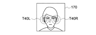
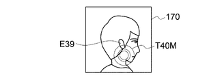
- the speaker part that emits sound and A voice arrival position analysis unit that estimates where the sound emitted from the speaker unit hits the user by using the information of the event signal may be further provided.
- the voice arrival position analysis unit may determine whether or not the sound emitted from the speaker unit hits the user's ear.
- a sound wave direction adjusting unit that controls the direction of the speaker may be further provided according to the voice arrival position analyzed by the voice arrival position analysis unit.
- a face shape analysis unit may be further provided to record the three-dimensional position information of both eyes, both ears, nose, and mouth in the user's three-dimensional image in the recording unit.
- the face shape analysis unit uses the three-dimensional position information of the user's eyes, ears, nose, and mouth, which are recorded in advance, and the rotation angle of the user's three-dimensional image in the three images in the diagonal direction of the user.
- the position of the ear may be estimated.
- the voice arrival position analysis unit may be able to change the arrival position extracted by analysis according to the voice wavelength of the speaker.
- the depth sensor that captures the three-dimensional image of the user may be activated.
- the voice arrival position analysis unit may fuse the image based on the event signal and the image based on the depth sensor to acquire three-dimensional position information of the user's eyes, ears, nose, and mouth.
- the face shape analysis unit may generate a three-dimensional image of the user by skeleton estimation after the depth sensor is activated.
- the event signal may always be acquired.
- the display unit may emit light so as to satisfy the sensitivities of the plurality of pixels.
- a display unit having a display region in which display elements are arranged in an array in a first direction of light and a second direction different from the first direction.
- An electron including an image pickup device that overlaps with the display area and is arranged on the side opposite to the display surface of the display unit and has a plurality of pixels in a third direction different from the first direction and the second direction. It ’s a device control method.
- the display unit transmits the incident light and transmits the incident light.
- a control method for an electronic device in which the plurality of pixels output an event signal when the change in the brightness of the light incident on the display unit is larger than a predetermined threshold value.
- the block diagram which shows one configuration example of the electronic device in embodiment of this technique The figure which shows an example of the laminated structure of the solid-state image sensor in embodiment of the technique. Schematic cross-sectional view of the electronic device according to the first embodiment.
- the schematic external view of the electronic device of FIG. The block diagram which shows the structural example of the solid-state image sensor.
- the figure which shows the structure of a pixel block schematically.
- the block diagram which shows the configuration example of another AD converter The figure which shows the composition example of the gradation pixel.
- Circuit diagram showing an example of the configuration of a subtractor and a quantizer The block diagram which shows the 2nd configuration example of AFE for EVS.
- FIG. 1 is a block diagram showing a configuration example of an electronic device 100 according to an embodiment of the present technology.
- the electronic device 100 includes an image pickup lens 110, a solid-state image pickup element 200, a recording unit 120, a control unit 130, a miracle unit 140, a communication unit 150, and a speaker unit 160.
- the electronic device 100 is, for example, a smartphone, a mobile phone, a PC (Personal Computer), or the like.
- the image pickup lens 110 collects the incident light and guides it to the solid-state image pickup element 200.
- the solid-state image sensor 200 has an EVS pixel and a gradation pixel.
- the EVS pixel can detect that the absolute value of the change in luminance exceeds the threshold value as an address event.
- This address event includes, for example, an on event indicating that the amount of increase in luminance exceeds the upper limit threshold value and an off event indicating that the amount of decrease in luminance is below the lower limit threshold value less than the upper limit threshold value. Then, the solid-state image sensor 200 generates a detection signal indicating the detection result of the address event for each pixel for EVS.
- Each detection signal includes an on-event detection signal VCH indicating the presence or absence of an on-event and an off-event detection signal VCL indicating the presence or absence of an off-event.
- the solid-state image sensor 200 detects the presence or absence of both on-events and off-events, but it is also possible to detect only one of them.
- the EVS pixel according to the present embodiment can output an EVS luminance signal in addition to the detection signal. As a result, a first EVS image based on the detection signal of the EVS pixel and a second EVS image based on the luminance signal of the EVS pixel are configured.
- the gradation pixel outputs a gradation luminance signal.
- a gradation image is configured based on the gradation luminance signal output by the gradation pixels.
- the image based on the detection signal of the EVS pixel is referred to as a first EVS image
- the image based on the brightness signal of the EVS pixel is referred to as a second EVS image
- the based image is referred to as a gradation image.
- the present embodiment has a first mode in which both the gradation pixel and the EVS pixel are driven, a second mode in which only the EVS pixel is driven, and a third mode.
- the second mode is a mode in which the first EVS image based on the detection signal of the EVS pixel and the second EVS image based on the luminance signal of the EVS pixel are configured.
- the third mode is a mode in which the first EVS image based on the detection signal of the EVS pixel is formed. Since the gradation pixel and the EVS pixel can be driven independently, the gradation pixel can be imaged at an imaging rate of, for example, 60 fps, whereas the second mode can be imaged at a rate of 200 fps or the like. Further, in the third mode, since the luminance signal is not read from the pixels for EVS, it is possible to take an image at a higher frame rate.
- the power consumption is the lowest in the third mode, followed by the second mode. Therefore, it is possible to constantly drive the EVS pixel in the third mode and monitor the state based on the first EVS image based on the detection signal of the EVS pixel.
- the solid-state image sensor 200 executes predetermined signal processing such as image processing on the first EVS image, the second EVS image, and the gradation image, and outputs the processed data to the recording unit 120 via the signal line 209. do.
- the recording unit 120 records data from the solid-state image sensor 200 and the like.
- the control unit 130 controls the entire electronic device 100. For example, the control unit 130 controls the solid-state image sensor 200 to capture image data.
- the analysis unit 140 performs a predetermined analysis process using at least one of the first EVS image, the second EVS image, and the gradation image.
- the communication unit 150 performs wireless communication with an external device. As a result, the content or the like is received from the external server and recorded in the recording unit 120 via the control unit 130.
- the control unit 130 causes the display unit 170 to display an image based on this content, for example.
- the speaker unit 160 is provided with a highly directional speaker and can transmit voice information only to the user.
- the speaker unit 160 can change the direction in which voice is transmitted.
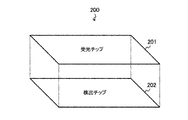
- FIG. 2 is a diagram showing an example of a laminated structure of the solid-state image pickup device 200 according to the embodiment of the present technology.
- the solid-state image sensor 200 includes a detection chip 202 and a light receiving chip 201 laminated on the detection chip 202. These boards are electrically connected via a connection such as a via. In addition to vias, it can also be connected by Cu-Cu bonding or bumps.
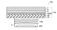
- FIG. 3 is a schematic cross-sectional view of the electronic device 100 according to the first embodiment. It is an example of an electronic device 100 having an optical system 110, and is an arbitrary electronic device having both a display function and a shooting function, such as a smartphone, a mobile phone, a tablet, a barcode reader, and a PC.
- a camera module 3 arranged on the side opposite to the display surface of the display unit 170 is provided. That is, the optical system 110 and the solid-state image sensor 200 are arranged in the camera module 3.
- the camera module 3 is provided on the back side of the display surface of the display unit 170. Therefore, the camera module 3 shoots through the display unit 170.
- the camera module 3 can be installed near the center of the electronic device 100, it is possible to reduce occlusion. Further, it is possible to increase the sensitivity by utilizing the light emission of the display unit 170 itself. Further, since the camera module 3 is provided on the back side of the display surface of the display unit 170, there is a space to allow the optical system 110 to have a thickness. This makes it possible to use a fisheye lens or the like for the optical system 110, and it is possible to acquire a wide range of images.
- FIG. 4 is a schematic external view of the electronic device 100 of FIG. 1, the left figure is an external view of the display unit 170 side, and the right figure is a cross-sectional view of the display unit 170 in the A-A line direction.
- the display screen 1a is expanded to be close to the external size of the electronic device 100, but the bezel 1b is equipped with a front camera and a depth sensor (not shown).
- the camera module 3 is arranged on the back surface side of the substantially central portion of the display screen 1a, but in the present embodiment, it may be on the back surface side of the display screen 1a. As described above, the camera module 3 in the present embodiment is arranged at an arbitrary position on the back surface side overlapping with the display screen 1a.
- the display unit 170 includes a polarizing plate 4c, a quarter wave plate 4b, a display panel 4 (4a), a touch panel 5, a circular polarizing plate 6, and a cover glass 7 (may include a touch panel). It is a structure laminated in order. Further, the circular polarizing plate 6 has a polarizing plate 6a and a quarter wave plate 6b as described later.
- the polarizing plate 4c and the quarter wave plate 4b suppress the internally reflected light from being incident on the camera module 3.
- Display elements are arranged in an array on the display panel 4.
- the display panel 4 may be, for example, an organic light emitting diode (OLED: Organic Light Emitting Device), a liquid crystal display unit, a MicroLED, or a display panel based on other display principles.
- OLED Organic Light Emitting Device
- the display panel 4 such as the OLED unit is composed of a plurality of layers.
- the display panel 4 is often provided with a member having a low transmittance such as a color filter layer.
- a through hole may be formed in the member having a low transmittance in the display panel 4 according to the arrangement location of the camera module 3. If the subject light passing through the through hole is incident on the camera module 3, the image quality of the image captured by the camera module 3 can be improved.
- the circular polarizing plate 6 is provided to reduce glare and improve the visibility of the display screen 1a even in a bright environment.
- a touch sensor is incorporated in the touch panel 5. There are various types of touch sensors such as a capacitance type and a resistance film type, and any method may be used. Further, the touch panel 5 and the display panel 4 may be integrated.
- the cover glass 7 is provided to protect the display panel 4 and the like.
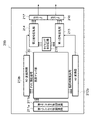
- FIG. 5 is a block diagram showing a configuration example of the solid-state image sensor 200.
- the solid-state image sensor 200 according to the present disclosure is an apparatus capable of performing asynchronous type imaging called EVS and synchronous type imaging for gradation images in parallel.
- the solid-state image sensor 200 includes a pixel array unit 30, a first access control circuit 211a, a second access control circuit 211b, an AD converter 212a, an AD converter 212b, a first signal processing unit 213, and a first signal processing unit 213. It has two signal processing units 214, a timing control circuit 215, and output interfaces 216 and 217.
- FIG. 6 is a diagram schematically showing pixel blocks 30a arranged in a matrix in the pixel array unit 30. As shown in FIG. 6, a plurality of pixel blocks 30a are two-dimensionally arranged in a matrix (array) in the pixel array unit 30.
- FIG. 7 is a diagram schematically showing the configuration of the pixel block 30a.
- the pixel block 30a has a plurality of gradation pixels 308a, EVS pixels 308b, and EVS AFE (analog front end: Analog Front End) 314.
- a plurality of gradation pixels 308a and EVS pixels 308b are arranged in a matrix.
- a vertical signal line VSL1 which will be described later, is wired to each pixel array of the gradation pixels 308a with respect to this pixel array.
- a vertical signal line VSL2 independent of the vertical signal line VSL1 is wired for each pixel row of the EVS pixel 308b.
- Each of the plurality of gradation pixels 308a generates an analog signal having a voltage corresponding to the photocurrent as a gradation luminance signal (second luminance signal), and outputs the analog signal to the AD converter 212a (see FIG. 5).
- the EVS pixel 308b In the first mode and the second mode, the EVS pixel 308b outputs an analog signal having a voltage corresponding to the photocurrent to the EVS AFE314. Further, the EVS pixel 308b generates an analog signal having a voltage corresponding to the photocurrent as an EVS luminance signal (first luminance signal), and when an address event occurs, the AD converter circuit 212b (see FIG. 5) is used. Output.
- the EVS pixel 308b does not output the EVS luminance signal to the AD converter circuit 212b (see FIG. 5), but to the EVS AFE (analog front end) 314. Only outputs the luminance signal for EVS.
- the EVS AFE (Analog Front End) 314 generates a detection signal from a voltage signal based on the output of the EVS pixel 308b, and outputs the detection signal to the second signal processing unit 214 (see FIG. 3). More specifically, the EVS AFE314 detects the presence or absence of an address event depending on whether or not the amount of change in the photocurrent in the EVS pixel 308b exceeds a predetermined threshold value. Then, the EVS AFE314 outputs the detection signal to the second signal processing unit 214.
- the EVS AFE314 uses the detected active pixel address information (X, Y), time stamp information T, and address event information VCH, VCL, for example, event information (X, Y, T, VCH, VCL). Is output to the second signal processing unit 214. Further, the EVS AFE314 is configured on the detection chip 202. These plurality of gradation pixels 308a, EVS pixels 308b, and EVS AFE314 can be operated in parallel by independent control systems. The detailed configurations of the gradation pixel 308a, the EVS pixel 308b, and the EVS AFE314 will be described later.
- the first access control circuit 211a controls a plurality of gradation pixels 308a.
- the first access control circuit 211a controls resetting of the stored charge of each of the plurality of gradation pixels 308a, generation of a gradation luminance signal according to the accumulated amount of photoelectric conversion current, output of the gradation luminance signal, and the like.
- the first access control circuit 211a causes the AD converter 212a to output the photoelectric conversion currents accumulated in each of the plurality of gradation pixels 308a as gradation luminance signals in order for each row. The details of the control operation of the gradation pixel 308a will be described later.
- the second access control circuit 211b controls a plurality of EVS pixels 308b and a plurality of EVS AFE314s.
- the second access control circuit 211b according to the present embodiment causes a plurality of EVS AFE314s to detect address events in order for each row, and outputs the detection signals to the second signal processing unit 214 in order for each row.
- the second access control circuit 211b outputs the luminance signals of the plurality of EVS pixels 308b to the EVS read circuit 212b in order for each row.
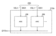
- FIG. 8 is a block diagram showing a configuration example of the AD converter 212a.
- the AD converter 212a includes an ADC 230 for each row of gradation pixels 308a arranged for each pixel block 30a.
- the ADC 230 converts the analog luminance signal SIG supplied via the vertical signal line VSL1 into a digital signal. This digital signal is converted into a digital pixel signal having a larger number of bits than the luminance signal SIG1 for gradation. For example, assuming that the luminance signal SIG1 for gradation is 2 bits, the pixel signal is converted into a digital signal having 3 bits or more (16 bits or the like).
- the ADC 230 supplies the generated digital signal to the first signal processing unit 213.
- the area of the plurality of gradation pixels 308a in the pixel array unit 30 may be divided into a plurality of areas, and the AD converter 212a may read out the gradation luminance signal SIG1 for each of the plurality of areas. This makes it possible to read the luminance signal SIG1 for gradation at a higher speed.
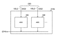
- FIG. 9 is a block diagram showing a configuration example of the AD converter 212b.
- the AD converter 212b for EVS includes an ADC 230 for each row of pixels 308b for EVS arranged for each pixel block 307.
- the ADC 230 converts the analog luminance signal SIG2 for EVS supplied via the vertical signal line VSL2 into a digital signal.
- This digital signal is converted into a digital pixel signal having a larger number of bits than the EVS luminance signal SIG2. For example, assuming that the EVS luminance signal SIG2 has 2 bits, the pixel signal is converted into a digital signal having 3 bits or more (16 bits or the like).
- the ADC 230 supplies the generated digital signal to the second signal processing unit 214.
- the first signal processing unit 213 executes predetermined signal processing such as CDS (Correlated Double Sampleting) processing on the digital signal from the AD converter 212a.
- the signal processing unit 212 supplies the data indicating the processing result and the detection signal to the recording unit 120 via the signal line 209.
- the timing control circuit 215 controls the timing of each configuration of the solid-state image sensor 200 based on the time stamp information.
- the timing control circuit 212d controls the timing of the first access control circuit 211a and the second access control circuit 211b. Thereby, it is also possible to synchronize the luminance signal of the gradation pixel 308a read by the AD converter 212a with the EVS luminance signal of the EVS pixel 308b read by the EVS readout circuit 212b.
- the first signal processing unit 213 executes predetermined signal processing such as CDS (Correlated Double Sampleting) processing on the digital signal from the AD converter 212a.
- the signal processing unit 212 supplies the data indicating the processing result and the detection signal to the recording unit 120 via the signal line 209. Further, the first signal processing unit 213 generates image data in a predetermined data format from the digital signal from the AD converter 212a.
- the second signal processing unit 214 executes predetermined signal processing for the detection signals from the plurality of EVS AFE314s.
- the second signal processing unit 214 for example, arranges the detected signals as pixel signals in a two-dimensional grid pattern to generate a first EVS image.
- the output interface 216 outputs image data and the like supplied from the first signal processing unit 213 to the recording unit 120.
- the output interface 217 outputs image data and the like supplied from the second signal processing unit 214 to the recording unit 120.
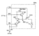
- FIG. 10 is a diagram showing a configuration example of the gradation pixel 308a.
- the gradation pixel 308a includes a reset transistor 321, an amplification transistor 322, a selection transistor 323, a floating diffusion layer 324, and a light receiving unit 330.
- the selection transistor 323 and the transfer transistor 3310 for example, an N-type MOS (Metal-Oxide-Semiconductor Dutor) transistor is used.
- the photoelectric conversion element 311 is arranged on the light receiving chip 201. All of the elements other than the photoelectric conversion element 311 are arranged on the detection chip 202.
- the photoelectric conversion element 311 photoelectrically converts the incident light to generate an electric charge.
- the electric charge converted photoelectric by the photoelectric conversion element 311 is supplied to the floating diffusion layer 324 by the transfer transistor 3310 from the photoelectric conversion element 311.
- the electric charge supplied from the photoelectric conversion element 311 is accumulated in the floating diffusion layer 324.
- the floating diffusion layer 324 generates a voltage signal having a voltage value according to the amount of accumulated charge.
- the amplification transistor 322 is connected in series with the selection transistor 323 between the power supply line of the power supply voltage VDD and the vertical signal line VSL1.
- the amplification transistor 322 amplifies the charge-voltage-converted voltage signal in the stray diffusion layer 324.
- a selection signal SEL is supplied from the first access control circuit 211a to the gate electrode of the selection transistor 323.
- the selection transistor 323 outputs the voltage signal amplified by the amplification transistor 322 as a pixel signal SIG to the AD converter 212a (see FIG. 5) via the vertical signal line VSL1.
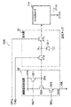
- FIG. 11 is a diagram showing a configuration example of the EVS pixel 308b.
- Each of the plurality of EVS pixels 308b has a light receiving unit 31, a pixel signal generation unit 32, and an EVS AFE314.
- the light receiving unit 31 has a light receiving element (photoelectric conversion element) 311, a transfer transistor 312, and an OFG (Over Flow Gate) transistor 313.
- a light receiving element photoelectric conversion element
- a transfer transistor 312 As the transfer transistor 312 and the OFG transistor 313, for example, an N-type MOS (Metal Oxide Semiconductor) transistor is used.
- the transfer transistor 312 and the OFG transistor 313 are connected in series with each other.
- the light receiving element 311 is connected between the common connection node N1 of the transfer transistor 312 and the OFG transistor 313 and the ground, and photoelectrically converts the incident light to generate a charge amount corresponding to the light amount of the incident light. ..
- the transfer signal TRG is supplied to the gate electrode of the transfer transistor 312 from the second access control circuit 211b shown in FIG.
- the transfer transistor 312 supplies the charge photoelectrically converted by the light receiving element 311 to the pixel signal generation unit 32 in response to the transfer signal TRG.
- a control signal OFG is supplied from the second access control circuit 211b to the gate electrode of the OFG transistor 313.
- the OFG transistor 313 supplies an electric signal generated by the light receiving element 311 to the EVS AFE 314 in response to the control signal OFG.
- the electrical signal supplied to the EVS AFE314 is a photocurrent consisting of electric charges.
- the pixel signal generation unit 32 has a reset transistor 321, an amplification transistor 322, a selection transistor 323, and a stray diffusion layer 324.
- a reset transistor 321, an amplification transistor 322, a selection transistor 323, and a stray diffusion layer 324 As the reset transistor 321 and the amplification transistor 322 and the selection transistor 323, for example, an N-type MOS transistor is used.
- the pixel signal generation unit 32 is supplied with the electric charge converted photoelectric by the light receiving element 311 by the transfer transistor 312 from the light receiving unit 31.
- the electric charge supplied from the light receiving unit 31 is accumulated in the floating diffusion layer 324.
- the floating diffusion layer 324 generates a voltage signal having a voltage value according to the amount of accumulated charge. That is, the floating diffusion layer 324 converts the electric charge into a voltage.
- the reset transistor 321 is connected between the power supply line of the power supply voltage VDD and the stray diffusion layer 324.
- a reset signal RST is supplied from the second access control circuit 211b to the gate electrode of the reset transistor 321.
- the reset transistor 321 initializes (reset) the charge amount of the floating diffusion layer 324 in response to the reset signal RST.
- the amplification transistor 322 is connected in series with the selection transistor 323 between the power supply line of the power supply voltage VDD and the vertical signal line VSL.
- the amplification transistor 322 amplifies the charge-voltage-converted voltage signal in the stray diffusion layer 324.
- a selection signal SEL is supplied to the gate electrode of the selection transistor 323 from the second access control circuit 211b.
- the selection transistor 323 outputs the voltage signal amplified by the amplification transistor 322 as a pixel signal SIG to the EVS read circuit 212b (see FIG. 2) via the vertical signal line VSL.
- the second access control circuit 211b is instructed by the control unit 130 shown in FIG. 1 to start detecting an address event. Then, by supplying the control signal OFG to the OFG transistor 313 of the light receiving unit 31, the OFG transistor 313 is driven to supply the photocurrent to the EVS AFE314.
- the second access control circuit 211b turns off the OFG transistor 313 of the EVS pixel 308b and stops the supply of the photocurrent to the EVS AFE314. ..
- the second access control circuit 211b drives the transfer transistor 312 by supplying the transfer signal TRG to the transfer transistor 312, and transfers the charge photoelectrically converted by the light receiving element 311 to the floating diffusion layer 324.
- the electronic device 100 having the pixel array unit 30 in which the EVS pixels 308b having the above configuration are two-dimensionally arranged reads only the pixel signal of the EVS pixels 308b in which the address event is detected in the EVS readout circuit 212b. Output to.
- the power consumption of the electronic device 100 and the processing amount of image processing can be reduced as compared with the case where the pixel signals of all the pixels are output regardless of the presence or absence of the address event.
- the configuration of the EVS pixel 308b exemplified here is an example, and is not limited to this configuration example.
- the OFG transistor 313 may be omitted in the light receiving unit 31, and the transfer transistor 312 may have the function of the OFG transistor 313.
- FIG. 12 is a block diagram showing a first configuration example of the EVS AFE314.
- the EVS AFE 314 according to this configuration example has a current / voltage conversion unit 331, a buffer 332, a subtractor 333, a quantizer 334, and a transfer unit 335.
- the current / voltage conversion unit 331 converts the photocurrent from the light receiving unit 31 of the gradation pixel 308a into a logarithmic voltage signal.
- the current-voltage conversion unit 331 supplies the converted voltage signal to the buffer 332.
- the buffer 332 buffers the voltage signal supplied from the current-voltage conversion unit 331 and supplies it to the subtractor 333.
- a row drive signal is supplied to the subtractor 333 from the second access control circuit 211b.
- the subtractor 333 lowers the level of the voltage signal supplied from the buffer 332 according to the row drive signal. Then, the subtractor 333 supplies the voltage signal after the level drop to the quantizer 334.
- the quantizer 334 quantizes the voltage signal supplied from the subtractor 333 into a digital signal and outputs it to the transfer unit 335 as an address event detection signal.
- the transfer unit 335 transfers the detection signal of the address event supplied from the quantizer 334 to the second signal processing unit 214 or the like. When the address event is detected, the transfer unit 335 supplies the detection signal of the address event to the second signal processing unit 214 and the second access control circuit 211b.
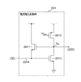
- FIG. 13 is a circuit diagram showing an example of the configuration of the current-voltage conversion unit 331 in the EVS AFE314.
- the current-voltage conversion unit 331 according to this example has a circuit configuration including an N-type transistor 3311, a P-type transistor 3312, and an N-type transistor 3313.
- transistors 3311 to 3313 for example, MOS transistors are used.
- the N-type transistor 3311 is connected between the power supply line of the power supply voltage VDD and the signal input line 3314.
- the P-type transistor 3312 and the N-type transistor 3313 are connected in series between the power supply line of the power supply voltage VDD and the ground.
- the gate electrode of the N-type transistor 3311 and the input terminal of the buffer 332 shown in FIG. 11 are connected to the common connection node N2 of the P-type transistor 3312 and the N-type transistor 3313.
- a predetermined bias voltage Vbias is applied to the gate electrode of the P-type transistor 3312.
- the P-type transistor 3312 supplies a constant current to the N-type transistor 3313.
- Photocurrent is input from the light receiving unit 31 to the gate electrode of the N-type transistor 3313 through the signal input line 3314.
- the drain electrodes of the N-type transistor 3311 and the N-type transistor 3313 are connected to the power supply side, and such a circuit is called a source follower.
- the photocurrent from the light receiving unit 31 is converted into a logarithmic voltage signal by these two source followers connected in a loop.
- FIG. 14 is a circuit diagram showing an example of the configuration of the subtractor 333 and the quantizer 334 in the EVS AFE314.
- the subtractor 333 has a configuration including a capacitance element 3331, an inverter circuit 3332, a capacitance element 3333, and a switch element 3334.
- the capacitive element 3331 is connected to the output terminal of the buffer 332 shown in FIG. 14, and the other end is connected to the input terminal of the inverter circuit 3332.
- the capacitive element 3333 is connected in parallel to the inverter circuit 3332.
- the switch element 3334 is connected between both ends of the capacitive element 3333.
- a row drive signal is supplied to the switch element 3334 from the second access control circuit 211b as an open / close control signal.
- the switch element 3334 opens and closes a path connecting both ends of the capacitive element 3333 according to the row drive signal.
- the inverter circuit 3332 inverts the polarity of the voltage signal input via the capacitive element 3331.
- the voltage signal Vinit is input to the terminal on the buffer 332 side of the capacitive element 3331, and the terminal on the opposite side is the virtual ground terminal. Become. The potential of this virtual ground terminal is set to zero for convenience.
- the charge Qinit stored in the capacitance element 3331 is expressed by the following equation (1), where the capacitance value of the capacitance element 3331 is C1.
- the accumulated charge becomes zero.
- Qinit C1 x Vinit ... (1)
- the charge Q2 stored in the capacitance element 3333 is expressed by the following equation (3), where the capacitance value of the capacitance element 3333 is C2 and the output voltage is Vout.
- Q2 -C2 x Vout ... (3)
- Equation (5) represents the subtraction operation of the voltage signal, and the gain of the subtraction result is C1 / C2. Since it is usually desired to maximize the gain, it is preferable to design C1 to be large and C2 to be small. On the other hand, if C2 is too small, kTC noise may increase and noise characteristics may deteriorate. Therefore, the capacity reduction of C2 is limited to the range in which noise can be tolerated. Further, since the EVS AFE314 including the subtractor 333 is mounted on each EVS pixel 308b, the capacitive element 3331 and the capacitive element 3333 have an area limitation. In consideration of these, the capacitance values C1 and C2 of the capacitance elements 3331 and 3333 are determined.
- the quantizer 334 is configured to have a comparator 3341.
- the comparator 3341 has an output signal of the inverter circuit 3332, that is, a voltage signal from the subtractor 333 as a non-inverting (+) input, and a predetermined threshold voltage Vth as an inverting ( ⁇ ) input. Then, the comparator 3341 compares the voltage signal from the subtractor 333 with the predetermined threshold voltage Vth, and outputs a signal indicating the comparison result to the transfer unit 335 as an address event detection signal.
- FIG. 15 is a block diagram showing a second configuration example of the EVS AFE14.
- the EVS AFE314 according to this configuration example has a storage unit 336 and a control unit in addition to the current-voltage conversion unit 331, the buffer 332, the subtractor 333, the quantizer 334, and the transfer unit 335. It has a configuration having 337.
- the storage unit 336 is provided between the quantizer 334 and the transfer unit 335, and based on the sample signal supplied from the control unit 337, the output of the quantizer 334, that is, the comparison result of the comparator 3341 is obtained. accumulate.
- the storage unit 336 may be a sampling circuit such as a switch, plastic, or capacitance, or may be a digital memory circuit such as a latch or flip-flop.
- the control unit 337 supplies a predetermined threshold voltage Vth to the inverting ( ⁇ ) input terminal of the comparator 3341.
- the threshold voltage Vth supplied from the control unit 337 to the comparator 3341 may have different voltage values in time division.
- the control unit 337 corresponds to the threshold voltage Vth1 corresponding to the on-event indicating that the change amount of the photocurrent exceeds the upper limit threshold value, and the off event indicating that the change amount is below the lower limit threshold value.
- the threshold voltage Vth2 By supplying the threshold voltage Vth2 to be performed at different timings, one comparator 3341 can detect a plurality of types of address events.
- the storage unit 336 is, for example, a comparator using the threshold voltage Vth1 corresponding to the on-event during the period in which the threshold voltage Vth2 corresponding to the off-event is supplied from the control unit 337 to the inverted (-) input terminal of the comparator 3341.
- the comparison result of 3341 may be accumulated.
- the storage unit 336 may be inside the EVS pixel 308b or may be outside the EVS pixel 308b. Further, the storage unit 336 is not an essential component of the AFE314 for EVS. That is, the storage unit 336 may be omitted.
- the individual image sensor 200 having a plurality of EVS pixels 308b is arranged on the side opposite to the display surface of the display unit 170. I decided. This makes it possible to output an event signal when the change in the luminance of the light incident on the display unit 170 is larger than a predetermined threshold value according to the luminance signals of the plurality of EVS pixels 308b. Further, by providing the individual image sensor 200 provided with the EVS pixel 308b under the display unit 170, occlusion can be suppressed. Moreover, a wide-angle lens having a predetermined thickness, such as a fisheye lens, can be arranged in the optical system 110.
- the electronic device 100 according to the second embodiment is different from the electronic device 100 according to the first embodiment in that it further includes a function capable of estimating the emotional state of the user.
- a function capable of estimating the emotional state of the user is described.
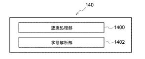
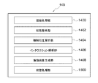
- FIG. 16 is a block diagram showing a configuration example of the analysis unit 140.
- the analysis unit 140 includes a recognition processing unit 1400 and a state analysis unit 1402.
- the analysis unit 140 includes, for example, a CPU (Central Processing Unit).
- the recording unit 120 (see FIG. 1) also stores various programs for executing the processing in the analysis unit 140.
- the analysis unit 140 constitutes each unit by, for example, executing a program stored in the recording unit 120.
- FIG. 17 is a schematic diagram in which the movement of the fingertip region f16 is captured via the display unit 170. As shown in FIG. 17, the fingertip region f16 starts mapping from the end of the display unit 170 to the first EVS image and moves to the target position g16 to be touched by the fingertip region f16.
- the recognition processing unit 1400 recognizes the observation target based on, for example, the first EVS image.
- the recognition target is, for example, a fingertip.
- a general processing algorithm can be used for the recognition processing.
- the area where the address event occurs in the first EVS image is labeled, and if the area in the area labeled in a U-shape or a ring shape is within a predetermined range, it is recognized as a fingertip.
- the area corresponding to the edge portion to be observed is the area where the address event occurs. Therefore, in the case of a fingertip, for example, the area where the address event occurs is labeled in a U-shape or a ring shape.
- the recognition processing unit 1400 outputs a recognition signal including information indicating that the observation target is a finger and information indicating the coordinates of the center of gravity of the fingertip region f16 to the state analysis unit 1402 in order.
- the state analysis unit 1402 estimates the user's emotion based on the behavior (such as hesitation) in the touch panel operation with respect to the user's display unit 160.
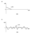
- FIG. 18 is a diagram showing an example of data used by the state analysis unit 1402 for analysis.
- the horizontal axis indicates time, and the vertical axis indicates, for example, a vertical distance from the target position g16.
- the target position g16 is shown as 0.
- FIG. 18A is a diagram showing a state in which the user has no hesitation with respect to the target position g16, that is, is mentally stable.
- (b) is a diagram showing a state in which the user is uncertain about the target position g16, that is, mentally unstable.
- the state analysis unit 1402 generates an evaluation value based on the time until the target position g16 is touched and the vibration state, and evaluates the mental state based on the evaluation value. For example, the evaluation value generated by the state analysis unit 1402 becomes larger as the time until the target position g16 is touched becomes longer, and becomes larger as the frequency increases. As a result, the state analysis unit 1402 is stable if the evaluation value is equal to or less than the first threshold value, unstable if it is equal to or more than the second threshold value, and normal if it is larger than the first threshold value and less than the second threshold value. presume. In this way, by estimating the emotional state until the target position g16 is touched, it is possible to field back to improve the operability. For example, when hesitation is presumed, it is possible to improve the display form such as the size and display color of the target position g16.
- the target position g16 is a content selection button for e-commerce
- the user's psychological state can be fed back and reflected in the method of attracting customers, the method of advertising, and the like. For example, when hesitation is presumed, it is possible to improve the method of attracting customers and the method of advertising so as to reduce the hesitation.
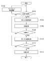
- FIG. 19 is a flowchart showing a processing example of the second embodiment.
- the control unit 130 first determines in the first mode whether or not the brightness with respect to the object is appropriate from the gradation image by the gradation pixels (step S100). In this case, a preliminary shooting is performed in advance in the first mode by displaying "Please present your finger" on the display unit 170. When the brightness adjustment is inappropriate (N in step S100), the light amount of the display unit 170 is adjusted (step S102).
- control unit 130 shifts to the third mode and repeats imaging of only the first EVS image (step S104). Subsequently, the recognition processing unit 1400 recognizes the observation target based on, for example, the first EVS image (step S106).
- the state analysis unit 1402 determines whether or not the recognition processing unit 1400 has recognized the finger (step S108).
- the state analysis unit 1402 determines that the finger has been recognized (Y in step S108)
- the state analysis unit 1402 captures only the first EVS image (step s106), and the position coordinates of the fingertip until the user's finger touches the display unit 170. And the time are recorded in the recording unit 120.
- the state analysis unit 1402 determines whether or not the user's finger touches the display unit 170 based on the signal from the touch panel 5 (see FIG. 3) (step S112). When it is determined that the touch is made, the state analysis unit 1402 performs a state analysis (step S114) and ends the whole process. On the other hand, when it is determined that the user's finger has not touched the display unit 170 (N in step S112), the process from step S110 is repeated.
- the state analysis unit 1402 records the behavior of the user's display unit 170 with respect to the touch panel operation, and uses the vibration of the user's finger with respect to the target position g160 and the time until touch as evaluation values, and the physical state. Decided to estimate. This makes it possible to objectively estimate the psychological state of the user. In addition, the relationship between the operation and the psychological state makes it possible to perform a feedback to improve the operability. Furthermore, when the target position g16 is a content selection button for e-commerce, the user's psychological state at the time of selecting the content can be fed back and reflected in the method of attracting customers, the method of advertising, and the like.
- the electronic device 100 according to the third embodiment is different from the electronic device 100 according to the second embodiment in that it further includes a function capable of estimating the touch position of the user from the first EVS image.
- a function capable of estimating the touch position of the user from the first EVS image the differences from the electronic device 100 according to the second embodiment will be described.
- FIG. 20 is a block diagram showing a configuration example of the analysis unit 140 according to the third embodiment. As shown in FIG. 20, the analysis unit 140 according to the third embodiment further includes a contact position analysis unit 1404.
- FIG. 21 is a diagram in which a time-series image of the first EVS image when the area f16 of the fingertip touches the cover glass 7 (see FIG. 4) of the display unit 170 is schematically superimposed and displayed at the same position.
- the ripple T20 propagates as the value of the address event. That is, in FIG. 21, it is shown that time elapses as the ring shape becomes larger.
- the ripple T20 which is a propagation pattern of the unique address event value, is observed. In this case, different propagation patterns are observed when the finger is touched with the pad of the finger and when the finger is touched with the tip of the toe.
- the contact position analysis unit 1404 determines whether or not there is a finger touch on the cover glass 7 of the display unit 170 from the form of spreading the value of the address event of the first EVS image taken in time series. Then, when it is determined that there is a touch, the contact position analysis unit 1404 analyzes the coordinates of the touch center. For example, the center of gravity of the address event value spreading in a rippled ring shape is set as the touch center.
- the contact position analysis unit 1404 performs a two-dimensional Fourier analysis on the superimposed image of the first EVS image in time series. As a result, the amplitude component for each frequency is analyzed, and it is determined whether the touch is the pad of the finger or the tip of a finger such as a nail. For example, when the touch is the pad of the finger, the ratio of the value of the amplitude component from the low frequency to the value of the amplitude component from the high frequency is larger than when the touch is the fingertip such as a nail. ..
- the contact position analysis unit 1404 determines whether the touch was the pad of the finger or the touch was the fingertip such as a nail, depending on the ratio of the value of the amplitude component from the low frequency and the value of the amplitude component from the high frequency. To judge. Then, the control unit 130 (see FIG. 1) changes the display content displayed on the display unit 170 according to the contact position of the finger analyzed by the contact position analysis unit 1404. Further, the control unit 130 (see FIG. 1) changes the display content displayed on the display unit 170 depending on the contacted object analyzed by the contact position analysis unit 1404, for example, the pad of a finger or a nail.
- the contact position analysis unit 1404 has decided to analyze the coordinates of the touch center from the form of the spread of the value of the address event of the first EVS image taken in time series. This makes it possible for the user to detect the touch position of the cover glass 7 (see FIG. 4) even when the electronic device 100 does not have a touch panel.
- the electronic device 100 according to the fourth embodiment is different from the electronic device 100 according to the third embodiment in that it further includes a function capable of estimating the interaction between the user and a surrounding person by the first EVS image.
- a function capable of estimating the interaction between the user and a surrounding person by the first EVS image is different from the electronic device 100 according to the third embodiment in that it further includes a function capable of estimating the interaction between the user and a surrounding person by the first EVS image.
- FIG. 22 is a block diagram showing a configuration example of the analysis unit 140 according to the fourth embodiment. As shown in FIG. 22, the analysis unit 140 according to the fourth embodiment further includes an interaction analysis unit 1406.
- FIG. 23 is a diagram showing face regions a230, a232, and a234 recognized by the recognition processing unit 1400. It is a figure which shows typically the face area a230, a232, a234 in the 1st EVS image.
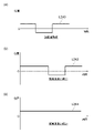
- FIG. 24 is a schematic diagram showing changes in the position of the lower jaw portion of the face in chronological order.
- the horizontal axis shows time, and the vertical axis shows the position of the mandibular part.
- FIG. 24 (a) shows an operation example in the face region a230 of the subject on the line L240, and FIGS. L244 is shown.
- the values of lines L240, L242, and L244 indicate the values of the vertical coordinates of the lower jaw in the first EVS image.
- the region below 0 of the line L240 in FIG. 24A shows how the subject nods.
- the line L242 in the face area a232 of FIG. 24B also shows a nodding motion so as to synchronize with the nodding of the face area a230 of the subject.
- the value of the line L244 in the face region a234 of FIG. 24 (b) is constant, that is, the position of the lower jaw is constant, and it can be seen that the subject is not synchronized with the nod of the face region a230.
- the interaction analysis unit 1406 estimates the interaction between the subject and the surrounding person based on the time-varying form of the position of the lower jaw of the first EVS image taken in time series. For example, if the movement of the jaw of the subject is seen and the movement of the jaw of a person in the vicinity is seen so as to be linked, it is presumed that the degree of consent is high. On the other hand, if there is no interlocking jaw movements made by those in the vicinity, it is presumed that the degree of consent is low.
- the interaction analysis unit 1406 records the position coordinates of the address event value corresponding to the position of the lower jaw in each of the face regions a230, a232, and a234, for example, the vertical coordinates in chronological order as the position information of the lower jaw. (See Fig. 1). Then, the interaction analysis unit 1406 calculates the correlation value between the time-series variation value of the face region a230 of the subject and the time-series variation value for each of the face region of the comparer, a232, and a234. The interaction analysis unit 1406 estimates that the higher the correlation value, the higher the degree of consent.
- the interaction analysis unit 1406 sets a threshold value of 0.6, and if the correlation value between L240, L242, and L244 is 0.6 or more, it is estimated that the degree of consent is high, and it is less than 0.6. If so, it is presumed that the degree of consent is low.
- the threshold value is an example and is not limited to this.
- the interaction analysis unit 1406 sets the threshold values to 0.65 and 0.55, and if it is 0.65 or more, it is estimated that the degree of consent is high, and if it is less than 0.55, the degree of consent is low. You may estimate.
- the interaction analysis unit 1406 has decided to analyze the time change of the position of the lower jaw in the first EVS image taken in time series. As a result, if the movement of the jaws of those in the vicinity is seen in conjunction with the position of the lower jaw of the subject, it can be estimated that the degree of consent is high, and the movements of the jaws of those in the vicinity can be seen. Without it, it can be estimated that the degree of consent is low.
- the electronic device 100 according to the fifth embodiment is different from the electronic device 100 according to the fourth embodiment in that it further has a function of estimating a psychological state by analyzing the vibration of the user by the first EVS image.
- the differences from the electronic device 100 according to the fourth embodiment will be described.
- FIG. 25 is a block diagram showing a configuration example of the analysis unit 140 according to the fifth embodiment. As shown in FIG. 25, the analysis unit 140 according to the fifth embodiment further includes a vibration image generation unit 1408 and a state processing unit 1500.
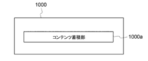
- FIG. 26 is a diagram schematically showing a server 1000 that supplies contents to the electronic device 100.
- the server 1000 has a content storage unit 1000a.
- Emotional information is associated with the content accumulated by the content storage unit 1000a in chronological order. For example, for example, 1000 subjects are made to appreciate the content in advance, and emotional information obtained by measuring the psychological state in time series is acquired. For example, if the most people show stability at a certain point in time, the emotional information at that time is stabilized. On the other hand, if the most people show instability at another point in time, the emotional information at that time is made unstable.
- improvement example is also stored in association with emotional information.
- improvements include operation examples such as viewing relaxing content, deep breathing, and relaxing operations such as stretching.
- FIG. 27 is a diagram showing an example of a first EVS image captured in time series.
- FIG. 27 shows a first EVS image captured in time series from time t0 to t3.
- the first EVS image is composed of the value of the address event. For example, it is 1 if there is an address event, and 0 if there is no address event. Therefore, for example, if the cycle of the address event 1 of a certain pixel is analyzed, the information of the vibration state of the user in that pixel is acquired.
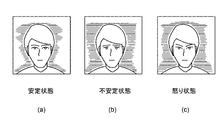
- the vibration image generation unit 1408 generates a vibration image of the user based on the cycle of the address event for each pixel acquired in time series.
- FIG. 28 is a diagram schematically showing a vibration image generated by the vibration image generation unit 1408.
- FIG. 28 (a) is a stable state
- FIG. 28 (b) is, for example, an unstable state
- FIG. 28 (c) is, for example, an angry state, for example, a state in which aggression is increased.
- FIG. 28 (a) is a stable state
- FIG. 28 (b) is, for example, an unstable state
- FIG. 28 (c) is, for example, an angry state, for example, a state in which aggression is increased. It is known that the movement characteristics and the speed of tremors of various parts of the human body depend on the psychophysiological state, and only a little on the motor activity itself and macro movement.
- the state analysis unit 1402 according to the fifth embodiment estimates the user's psychological state, for example, emotions, based on the vibration image generated by the vibration image generation unit 1408. For this estimation method, for example, the technique disclosed in Patent Document 2 can be used.
- the state analysis unit 1402 according to the fifth embodiment is different from the technique disclosed in Patent Document 2 in that the vibration image generated by the vibration image generation unit 1408 is used.
- the state processing unit 1500 displays an image in a display form on the display unit 170 according to the estimation result of the state analysis unit 1402.
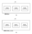
- FIG. 29 is a diagram showing an example of an image displayed by the state processing unit 1500.
- FIG. 29A is an image displayed when the emotion is stable in the estimation result of the state analysis unit 1402.
- FIG. 29B is an image displayed when emotions are unstable in the estimation result of the state analysis unit 1402.
- FIG. 29 (a) when the overall emotion is stable, it is determined that the content being displayed is satisfied, and the content of the same type is displayed on the display unit 170 as a selection branch. do.
- FIG. 30 is a diagram showing another image example displayed by the state processing unit 1500.
- FIG. 30 is an image displayed when emotions are unstable in the estimation result of the state analysis unit 1402.
- the state processing unit 1500 causes the display unit 170 to display images that promote actions that promote relaxation, such as "estimated physical condition", “let's take a rest", and “let's take a deep breath”. In this way, it is possible to propose an action to the user according to the emotion sensing result of the user. As a result, the user can suppress an increase in stress by noticing his / her psychological state and performing an action according to the display.
- the state processing unit 1500 can also make an action proposal to the user shown in FIG. 30 based on the information of the improvement example of the third party associated with the content being displayed from the content storage unit 1000a of the server 1000. Is.
- FIG. 31 is a diagram showing an example of an image using external information displayed by the state processing unit 1500.
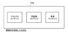
- FIG. 31 is an image displayed when emotions are unstable in the estimation result of the state analysis unit 1402.
- the state processing unit 1500 acquires information on an improvement example associated with the displayed content from the content storage unit 1000a of the server 1000.
- relaxed content is proven content that stabilizes the emotions of many.
- viewing this content has been shown to stabilize the pulse and lower blood pressure in many people.
- mood-changing content is proven content that has uplifted the emotions of many.
- viewing this content has been found to motivate many people.
- music content is proven content that has stabilized the emotions of many.
- viewing this content has been shown to stabilize the pulse and lower blood pressure in many people.
- the state processing unit 1500 can display more suitable healthcare content according to the estimation result of the state analysis unit 1402.
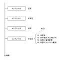
- FIG. 32 is a diagram schematically showing the recording state of the estimation result in the state analysis unit 1402.
- the vertical axis shows time.
- the state analysis unit 1402 records the psychological state when displaying the content in the recording unit 120 (see FIG. 1), and transmits the psychological state to the server 1000 via the communication unit 150 (see FIG. 1).
- the server 1000 increases the accumulation of information as an example of the user's psychological state with respect to the content. Time-series emotions and actions at that time may be recorded so as to be displayed in the area A31 of the content 13. This also makes it possible to analyze the relationship between the content, the user's emotions, and the user's behavior.
- FIG. 33 is a diagram schematically showing the recording state of the estimation result in the state analysis unit 1402 when the image is taken in the second mode.
- the vertical axis shows time.
- the luminance moving image which is a moving image of the second EVS image, is also captured.
- FIG. 34 is a flowchart showing the flow of user state analysis using the user's vibration image.
- the vibration image generation unit 1408 acquires the first EVS image recorded in the recording unit 120 in chronological order (step S200). Subsequently, the vibration image generation unit 1408 determines whether or not a predetermined number of first EVS images capable of generating vibration images have been acquired (step S202). If the image has not been acquired (N in step S202), the process from step S200 is repeated.
- step S204 the state analysis unit 1402 estimates the psychological state of the user using the vibration image generated by the vibration image generation unit 1408. The state analysis unit 1402 further determines whether or not to end the process (step S208), and if the process is not completed (N in step S208), repeats the process from step S200. On the other hand, when the process is terminated (Y in step S208), the entire process is terminated.
- FIG. 35 is a flowchart showing the flow of user state analysis at the time of content display.
- the state processing unit 1500 acquires the content information selected by the user (step S300). Subsequently, the state processing unit 1500 acquires information on the psychological state of the user sequentially estimated by the state analysis unit 1402 (step S302).
- step S304 determines whether or not the user's psychological state acquired from the state analysis unit 1402 is unstable (step S304). If it is not unstable (N in step S304), the process from step S300 is repeated.
- the state processing unit 1500 causes the display unit 170 to display the content having an improvement record as the recommended content as a user's selection branch based on the information of the improvement example associated with the displayed content (step S308).
- step S310 determines whether or not to end the entire processing. When it is determined that the process is not completed (N in step S310), the process from step S300 is repeated. On the other hand, when it is determined that the process is completed (Y in step S310), the entire process is terminated.
- the state analysis unit 1402 has decided to estimate the physical state of estimating the user's psychological state using the user's vibration image generated by the vibration image generation unit 1408. This makes it possible to objectively estimate the psychological state of the user. Further, since the psychological state of the user who is displaying the content can be estimated, the selection branch of the next content can be changed according to the psychological state of the user.
- the content corresponding to the improvement measure associated with the content is displayed on the display unit 170 as a selection branch. This makes it possible for the user to select content that has a proven track record of improvement.
- the electronic device 100 according to the sixth embodiment further includes a function of changing the reach area of the voice emitted by the speaker unit 160 by analyzing the reach area of the voice emitted by the speaker unit 160, according to the fifth embodiment. It is different from the electronic device 100.
- the differences from the electronic device 100 according to the fifth embodiment will be described.
- FIG. 36 is a block diagram showing a configuration example of the analysis unit 140 according to the sixth embodiment.
- the analysis unit 140 according to the sixth embodiment further includes a face shape analysis unit 1502, a voice arrival position analysis unit 1504, and a sound wave direction adjustment unit 1506.
- FIG. 37 is a diagram schematically showing a sensor configuration of the electronic device 100 according to the sixth embodiment.
- the electronic device 100 according to the sixth embodiment includes an individual image sensor 200 and a depth sensor 2000.
- the depth sensor 2000 is a sensor capable of generating three-dimensional shape data of the user B37.
- the images captured by the solid-state image sensor 200 and the depth sensor 2000 can be associated with the coordinates of their respective pixels and can be processed by fusion.
- FIG. 38 is a diagram schematically showing a vertical cross section of the speaker unit 160 of the electronic device 100 according to the sixth embodiment.
- the electronic device 100 according to the sixth embodiment has a first speaker 160a having high directivity and a second speaker 160b having high directivity as well.
- the baseline BL corresponds to the horizontal plane of the display unit 170.
- the first speaker 160a and the second speaker 160b are configured so that the orientation from the baseline BL can be changed according to the angles ⁇ 1 and ⁇ 2.
- the first speaker 160a emits a highly directional sound wave Sa in a direction corresponding to the angle ⁇ 1.
- the second speaker 160b emits a highly directional sound wave Sb in a direction corresponding to the angle ⁇ 2.
- the speaker unit 160 is configured so that the sound waves Sa and Sb can only be heard by the user B37.
- FIG. 39A is a diagram showing a three-dimensional image of the front of the user B37 captured by the depth sensor 2000.
- FIG. 39B is a diagram showing an oblique three-dimensional image of the user B37 captured by the depth sensor 2000.
- FIG. 39C is an image obtained by rotating the three-dimensional image in front of the user B37 so as to match the three-dimensional image in the diagonal direction of the user B37.
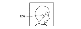
- FIG. 39D is a diagram in which the position information of the ear E39 is acquired using the rotation angle and the three-dimensional position information of both eyes, both ears, the nose, and the mouth.
- the face shape analysis unit 1502 records in advance a three-dimensional image whose skeleton is estimated based on the three-dimensional image in front of the user B37 in the recording unit 120 (see FIG. 1). Further, a gradation image when the front surface of the user B37 shown in 30A is photographed is also acquired and recorded in advance in the recording unit 120 (see FIG. 1).
- the face shape generation unit 1502 uses the recognition processing results of both eyes, both ears, nose, and mouth by the recognition processing unit 1400 to estimate both eyes, both ears, nose, and mouth in a three-dimensional image by skeletal estimation of the front of the user B37.
- the three-dimensional position information of the mouth is recorded in the recording unit 120.
- the face shape analysis unit 1502 rotates the three-dimensional image in front of the user B37, and the user B37 Calculate the rotation position that matches the 3D image in the diagonal direction.
- the face shape analysis unit 1502 uses the three-dimensional position information and the angle of rotation of the user B37's eyes, ears, nose, and mouth recorded in advance to provide the user B37 in an oblique three-dimensional direction. Estimate the position of ear E39 in the image. Further, since the face shape analysis unit 1502 is associated with the coordinates of the gradation image, the first EVS image, and the three-dimensional image in advance, the area information of the ear E39 acquired by the face shape analysis unit 1502 is used on the first EVS image. The region of the ear E39 can be estimated. In this case, even if the ear E39 of the user B37 is hidden by hair or the like, the position of the ear E39 which is the target portion can be estimated from the positional relationship of other parts (eyes, mouth, etc.).
- FIG. 40A is a diagram showing a first EVS image in front of the user B37 captured in time series.
- T40L and R are regions exposed to sound waves, and the regions exposed to sound expand in a wavy manner with the passage of time.
- FIG. 40B is a diagram showing a first EVS image in front of the user B37 captured in time series after adjusting the sound wave direction.
- FIG. 40C is a diagram showing a first EVS image in the oblique direction of the user B37 captured in time series.
- T40 is a region exposed to sound waves, and the region exposed to sound spreads in a wavy manner with the passage of time.
- FIG. 40D is a diagram showing a first EVS image in the oblique direction of the user B37 captured in time series after adjusting the sound wave direction.
- the voice arrival position analysis unit 1504 estimates the ring-shaped expanding region as the regions T40L and R exposed to the sound wave. Similarly, even if only one ear is imaged, it is estimated as the region T40M. Further, the voice arrival position analysis unit 1504 can analyze the time-series first EVS image and determine whether or not the user B37 is hit by a sound wave.
- the sound wave direction adjusting unit 1506 includes the position of the ear E39 estimated by the face shape analysis unit 1502 and the regions T40L and R in which the sound wave is applied, which is estimated by the voice arrival position analysis unit 1504. , The angles ⁇ 1 and ⁇ 2 between the first speaker 160a and the second speaker 160b are adjusted so that the T40Ms match. In this way, it is possible to constantly apply sound waves to the region of the ear E39 of the user B37.
- the voice arrival position analysis unit 1504 can also perform frequency analysis in the region where the sound hits by the two-dimensional Fourier transform. In this case, only the region corresponding to the frequency of the sound emitted from the speaker unit 160 can be estimated as the region of the ear E39. Therefore, when there are a large number of sound sources, it is possible to further improve the estimation accuracy.
- the sound wave direction adjusting unit 1506 can synthesize the wavefronts of the sound waves Sa and Sb of the first speaker 160a and the second speaker 160b to generate a sound field specialized for the user B37. More specifically, the sound wave direction adjusting unit 1506 adjusts the orientation of the first speaker 160a and the second speaker 160b and the overlap of the wavefronts of the waves Sa and Sb, and the sound field reaches more intensively in the region of the ear E39. To generate. Further, the sound wave direction adjusting unit 1506 may determine whether or not there is a person nearby based on the processing result of the recognition processing unit 1400, and change the intensity and range of the transmitted sound when there is a person nearby. It is possible.
- FIG. 41 is a flowchart showing the flow of a processing example for changing the direction of the sound.
- the voice arrival position analysis unit 1504 analyzes the time-series first EVS image and determines whether or not the user B37 is hit by a sound wave (step S400). When no sound wave is applied (N in step S400), the process of step S400 is repeated. On the other hand, when a sound wave is applied (Y in step S400), the control unit 130 activates the gradation pixel 308a and the depth sensor 2000 (see FIG. 37) in addition to the EVS pixel 308b (see FIG. 7) (see FIG. 37). Step S402). As a result, the first EVS image, the depth image, and the gradation image are acquired.
- the face shape analysis unit 1502 generates a three-dimensional image of the user B37 based on the depth image of the depth sensor 2000 (step S404). Subsequently, the face shape analysis unit 1502 rotates the front three-dimensional face image recorded in advance, and determines the face orientation of the user B37 by an angle matching the three-dimensional face image generated in step S404 (). Step S406).
- the face shape analysis unit 1502 uses the three-dimensional position information of the eyes, ears, nose, and mouth that have been pre-colored, and the rotation angle, that is, the information on the orientation of the face, and the ears in the first EVS image. Estimate the position of (step S408).
- the voice arrival position analysis unit 1504 estimates the area exposed to the sound wave (step S410). Subsequently, the sound wave direction adjusting unit 1506 determines whether or not the ear position estimated by the face shape analysis unit 1502 and the area exposed to the sound wave estimated by the voice arrival position analysis unit 1504 match (step S412). ). Then, when the regions match, the sound wave direction adjusting unit 1506 repeats the process from step S402 (Y in step S412).
- the sound wave direction adjusting unit 1506 hits the ear position estimated by the face shape analysis unit 1502 and the sound wave estimated by the voice arrival position analysis unit 1504.
- the angles ⁇ 1 and ⁇ 2 between the first speaker 160a and the second speaker 160b are adjusted so that the regions match (step S414).
- the sound wave direction adjusting unit 1506 determines whether or not to end the entire process (step S416), and if it is determined not to end (step S416), repeats the process from step S402.
- the state voice arrival position analysis unit 1504 estimates the region exposed to the sound wave using the first EVS image, and the sound wave direction adjustment unit 1506 is estimated by the face shape analysis unit 1502. It was decided to adjust the angles ⁇ 1 and ⁇ 2 between the first speaker 160a and the second speaker 160b so that the position of the ear and the area exposed to the sound wave estimated by the voice arrival position analysis unit 1504 match. As a result, even if the user B37 moves, the sound wave can always be applied to the region of the ear E39 of the user B37.
- a display unit having a display area in which display elements are arranged in an array in a first direction and a second direction different from the first direction. In a third direction different from the first direction and the second direction, an image pickup element that overlaps with the display area and is arranged on the side opposite to the display surface of the display unit and has a plurality of pixels is provided.
- the display unit transmits the incident light and transmits the incident light.
- the plurality of pixels are electronic devices that output an event signal when the change in the brightness of the light incident on the display unit is larger than a predetermined threshold value.
- a control unit for controlling the display unit is further provided.
- the electronic device further comprising a state analysis unit that estimates the user's emotions based on the user's vibration image generated using the information of the event signal.
- the electronic device further comprising a sound wave direction adjusting unit that controls the direction of the speaker according to the voice arrival position analyzed by the voice arrival position analysis unit.
- the electronic device further comprising a face shape analysis unit that records the three-dimensional position information of both eyes, ears, nose, and mouth in the user's three-dimensional image in the recording unit.
- the face shape analysis unit uses the three-dimensional position information of the user's eyes, ears, nose, and mouth, which are recorded in advance, and the rotation angle of the user's three-dimensional image, in the diagonal direction of the user. 3.
- the voice arrival position analysis unit fuses an image based on the event signal and an image based on the depth sensor, and acquires three-dimensional position information of the user's eyes, ears, nose, and mouth.
- the electronic device according to (20).
- a display unit having a display area in which display elements are arranged in an array in a first direction and a second direction different from the first direction.
- An electron including an image pickup device that overlaps with the display area and is arranged on the side opposite to the display surface of the display unit and has a plurality of pixels in a third direction different from the first direction and the second direction. It ’s a device control method.
- the display unit transmits the incident light and transmits the incident light.
- a method for controlling an electronic device wherein the plurality of pixels output an event signal when a change in the brightness of light incident on the display unit is larger than a predetermined threshold value.
- 100 Electronic device, 130: Control unit, 160: Speaker unit, 170: Display unit, 200: Solid-state image sensor, 1000: Server, 1402: State analysis unit, 1404: Contact position analysis unit, 1504: Voice arrival position analysis unit , 1506: Sound wave direction adjustment unit, 2000: Depth sensor.
Landscapes
- Engineering & Computer Science (AREA)
- Theoretical Computer Science (AREA)
- Physics & Mathematics (AREA)
- General Physics & Mathematics (AREA)
- General Engineering & Computer Science (AREA)
- Human Computer Interaction (AREA)
- Computer Hardware Design (AREA)
- Health & Medical Sciences (AREA)
- Oral & Maxillofacial Surgery (AREA)
- General Health & Medical Sciences (AREA)
- Multimedia (AREA)
- Computer Vision & Pattern Recognition (AREA)
- Studio Devices (AREA)
- Transforming Light Signals Into Electric Signals (AREA)
Abstract
[課題]本開示では、より中央部にEVS画素の配置が可能な電子機器及び電子機器の制御方法を提供する。 [解決手段]電子機器は、第1の方向と第1の方向と異なる第2の方向において、アレイ状に表示素子が配置される表示領域を有する表示部と、第1の方向と第2の方向と異なる第3の方向において、表示領域と重なって表示部の表示面と反対側に配置され、複数の画素を備える撮像素子と、を備え、表示部は、入射した光を透過し、複数の画素は、表示部を介して入射した光の輝度の変化が、所定の閾値より大きい場合にイベント信号を出力する、電子機器。
Description
本開示は、電子機器及び電子機器の制御方法に関する。
垂直同期信号などの同期信号に同期して画像データ(フレーム)を撮像する同期型の固体撮像素子が、電子機器などにおいて用いられている。この一般的な同期型の固体撮像素子では、同期信号の周期(例えば、1/60秒)ごとにしか画像データを取得することができないため、交通やロボットなどに関する分野において、より高速な処理が要求された場合に対応することが困難になる。そこで、画素アドレスごとに、その画素の光量が閾値を超えた旨をアドレスイベントとしてリアルタイムに検出する検出回路を画素毎に設けた非同期型の固体撮像素子が提案されている。このように、画素毎にアドレスイベントを検出する固体撮像素子は、EVS(Event base Vision Sensor)と呼ばれる。
一方で、EVS用画素で生成した検出信号に基づくEVS画像により、電子機器前部の状態観察が行われる場合がある。ところが、EVS画素の配置は電子機器の表面部の端部であり、オクルージョンなどが発生しやすくなる恐れがある。
そこで、本開示では、より中央部にEVS画素の配置が可能な電子機器及び電子機器の制御方法を提供するものである。
上記の課題を解決するために、本開示によれば、第1の方向と前記第1の方向と異なる第2の方向において、アレイ状に表示素子が配置される表示領域を有する表示部と、
前記第1の方向と前記第2の方向と異なる第3の方向において、前記表示領域と重なって前記表示部の表示面と反対側に配置され、複数の画素を備える撮像素子と、を備え、
前記表示部は、入射した光を透過し、
前記複数の画素は、前記表示部を介して入射した光の輝度の変化が、所定の閾値より大きい場合にイベント信号を出力する、電子機器が提供される。
前記第1の方向と前記第2の方向と異なる第3の方向において、前記表示領域と重なって前記表示部の表示面と反対側に配置され、複数の画素を備える撮像素子と、を備え、
前記表示部は、入射した光を透過し、
前記複数の画素は、前記表示部を介して入射した光の輝度の変化が、所定の閾値より大きい場合にイベント信号を出力する、電子機器が提供される。
前記イベント信号の情報を用いて、ユーザの前記表示部に対する接触動作における挙動を解析し、ユーザ感情を推定する状態解析部を更に備えてもよい。
前記イベント信号の情報を用いて、ユーザが前記表示部を接触した位置を推定する接触位置解析部を更に備えてもよい。
接触位置解析部は、前記イベント信号の伝搬情報を用いて、前記表示部にタッチしたものを区別してもよい。
前記表示部を制御する制御部を更に備え、
前記接触した位置、及びタッチしたもの少なくともいずれかに応じて、前記表示部に表示させる表示内容を変更してもよい。
前記接触した位置、及びタッチしたもの少なくともいずれかに応じて、前記表示部に表示させる表示内容を変更してもよい。
前記イベント信号の情報を用いて生成したユーザの振動画像に基づき、前記表示部に表示させる表示内容を変更してもよい。
前記イベント信号の情報を用いて生成したユーザの振動画像に基づき、ユーザの感情を推定する状態解析部を更に備えてもよい。
前記状態解析部の推定結果に応じた、画像を前記表示部に表示させる状態処理部を更に備えてもよい。
前記状態処理部は、前記状態解析部の推定結果に応じた、ヘルスケア用の画像を前記表示部に表示させてもよい。
前記状態処理部は、前記状態解析部の推定結果に応じた、コンテンツの選択枝を前記表示部に表示させてもよい。
前記状態処理部は、前記状態解析部の推定結果に応じた、ユーザへの行動提案を前記表示部に表示させてもよい。
前記行動提案は、外部のサーバから取得された第3者の改善例の情報に基づいてもよい。
音声を発するスピーカ部と、
前記イベント信号の情報を用いて、前記スピーカ部から発せられた音が、ユーザのどこにあたっているかを推定する音声到達位置解析部と、を更に備えてもよい。
前記イベント信号の情報を用いて、前記スピーカ部から発せられた音が、ユーザのどこにあたっているかを推定する音声到達位置解析部と、を更に備えてもよい。
前記音声到達位置解析部は、前記スピーカ部から発せられた音が、ユーザの耳にあたっているか否かを判別してもよい。
前記音声到達位置解析部が解析した音声の到達位置に応じて、スピーカの向きを制御する音波方向調整部を更に備えてもよい。
前記ユーザの3次元画像における両目、両耳、鼻、及び口の3次元位置情報を記録部に記録する顔形状解析部を更に備えてもよい。
前記顔形状解析部は、予め記録され前記ユーザの両目、両耳、鼻、及び口の3次元位置情報と前記ユーザの3次元画像の回転角を用いて、前記ユーザの斜め方向の3画像における耳の位置を推定してもよい。
前記音声到達位置解析部は、前記スピーカの音声波長に応じて、解析により抽出する到達位置を変更可能であってもよい。
前記音声到達位置解析部が前記イベント信号に基づき、音声が前記ユーザに音声が到達していると判定する場合に、前記ユーザの3次元画像を撮像する深度センサを起動してもよい。
前記音声到達位置解析部は、前記イベント信号に基づく画像と、前記深度センサに基づく画像を融合し、前記ユーザの両目、両耳、鼻、及び口の3次元位置情報を取得してもよい。
前記顔形状解析部は、前記深度センサの起動後に骨格推定による前記ユーザの3次元画像を生成してもよい。
前記イベント信号は常に取得されてもよい。
前記複数の画素の感度を満たすように、前記表示部を発光させてもよい。
本開示によれば、光第1の方向と前記第1の方向と異なる第2の方向において、アレイ状に表示素子が配置される表示領域を有する表示部と、
前記第1の方向と前記第2の方向と異なる第3の方向において、前記表示領域と重なって前記表示部の表示面と反対側に配置され、複数の画素を備える撮像素子と、を備える電子機器の制御方法であって、
前記表示部は、入射した光を透過し、
前記複数の画素は、前記表示部を介して入射した光の輝度の変化が、所定の閾値より大きい場合にイベント信号を出力する、電子機器の制御方法が提供される。
前記第1の方向と前記第2の方向と異なる第3の方向において、前記表示領域と重なって前記表示部の表示面と反対側に配置され、複数の画素を備える撮像素子と、を備える電子機器の制御方法であって、
前記表示部は、入射した光を透過し、
前記複数の画素は、前記表示部を介して入射した光の輝度の変化が、所定の閾値より大きい場合にイベント信号を出力する、電子機器の制御方法が提供される。
以下、図面を参照して、電子機器及び電子機器の制御方法の実施形態について説明する。以下では、電子機器の主要な構成部分を中心に説明するが、電子機器には、図示又は説明されていない構成部分や機能が存在しうる。以下の説明は、図示又は説明されていない構成部分や機能を除外するものではない。
(第1実施形態)
[電子機器の構成例]
図1は、本技術の実施の形態における電子機器100の一構成例を示すブロック図である。この電子機器100は、撮像レンズ110、固体撮像素子200、記録部120、制御部130、奇跡部140、通信部150、及びスピーカ部160を備える。電子機器100は、例えば、スマートフォンや携帯電話、PC(Personal Computer)などである。
[電子機器の構成例]
図1は、本技術の実施の形態における電子機器100の一構成例を示すブロック図である。この電子機器100は、撮像レンズ110、固体撮像素子200、記録部120、制御部130、奇跡部140、通信部150、及びスピーカ部160を備える。電子機器100は、例えば、スマートフォンや携帯電話、PC(Personal Computer)などである。
撮像レンズ110は、入射光を集光して固体撮像素子200に導くものである。固体撮像素子200は、EVS用画素と階調用画素を有する。EVS用画素は、輝度の変化量の絶対値が閾値を超えた旨をアドレスイベントとして検出することが可能である。このアドレスイベントは、例えば、輝度の上昇量が上限閾値を超えた旨を示すオンイベントと、輝度の低下量が上限閾値未満の下限閾値を下回った旨を示すオフイベントとを含む。そして、固体撮像素子200は、アドレスイベントの検出結果を示す検出信号をEVS用の画素毎に生成する。それぞれの検出信号は、オンイベントの有無を示すオンイベント検出信号VCHと、オフイベントの有無を示すオフイベント検出信号VCLとを含む。なお、固体撮像素子200は、オンイベントおよびオフイベントの両方の有無を検出しているが、一方のみを検出することもできる。また、本実施形態に係るEVS用画素は、検知信号の他に、EVS輝度信号を出力することも可能である。これにより、EVS用画素の検出信号に基づく第1EVS画像と、EVS用画素の輝度信号に基づく第2EVS画像とが構成される。
一方で、階調用画素は階調用輝度信号を出力する。階調用画素が出力する階調用輝度信号に基づき、階調用画像が構成される。なお、本実施形態では、EVS用画素の検出信号に基づく画像を第1EVS画像と称し、EVS用画素の輝度信号に基づく画像を第2EVS画像と称し、階調用画素が出力する階調用輝度信号に基づく画像を階調用画像と称する。本実実施形態では、階調用画素と、EVS用画素とが共に駆動される第1モードと、EVS用画素のみが駆動される第2モード、及び第3モードを有する。第2モードは、EVS用画素の検出信号に基づく第1EVS画像と、EVS用画素の輝度信号に基づく第2EVS画像とが構成されるモードである。これに対して、第3モードは、EVS用画素の検出信号に基づく第1EVS画像が構成されるモードである。階調用画素と、EVS用画素とは独立に駆動できるので、階調用画素は、例えば60fpsの撮像レートであるのに対し、第2モードは、200fpsなどのレートで撮像可能である。更に第3モードは、EVS用の画素から輝度信号を読み出さないので、更に高速のフレームレートで撮像可能である。
電力消費は、第3モードが最も少なく、次に第2モードである。このため、第3モードで常にEVS用の画素を駆動し、EVS用画素の検出信号に基づく第1EVS画像に基づく、状態監視などが可能となる。
固体撮像素子200は、第1EVS画像、第2EVS画像、及び階調用画像に対し、画像処理などの所定の信号処理を実行し、その処理後のデータを記録部120に信号線209を介して出力する。
記録部120は、固体撮像素子200からのデータなどを記録するものである。制御部130は、電子機器100全体を制御する。例えば、制御部130は、固体撮像素子200を制御して画像データを撮像させるものである。
解析部140は、第1EVS画像、第2EVS画像、及び階調用画像の少なくともいずれかを用いて、所定の解析処理を行う。
通信部150は、外部装置と無線通信を行う。これにより、外部のサーバからコンテンツなどを受信し、制御部130を介して記録部120に記録する。制御部130は、例えばこのコンテンツに基づく画像を表示部170に表示させる。
通信部150は、外部装置と無線通信を行う。これにより、外部のサーバからコンテンツなどを受信し、制御部130を介して記録部120に記録する。制御部130は、例えばこのコンテンツに基づく画像を表示部170に表示させる。
スピーカ部160は、高指向性のスピーカを備え、ユーザのみに音声情報を伝達可能である。このスピーカ部160は、音声の伝達する向きを変更可能である。
[固体撮像素子の構成例]
図2は、本技術の実施の形態における固体撮像素子200の積層構造の一例を示す図である。この固体撮像素子200は、検出チップ202と、その検出チップ202に積層された受光チップ201とを備える。これらの基板は、ビアなどの接続部を介して電気的に接続される。なお、ビアの他、Cu-Cu接合やバンプにより接続することもできる。
図2は、本技術の実施の形態における固体撮像素子200の積層構造の一例を示す図である。この固体撮像素子200は、検出チップ202と、その検出チップ202に積層された受光チップ201とを備える。これらの基板は、ビアなどの接続部を介して電気的に接続される。なお、ビアの他、Cu-Cu接合やバンプにより接続することもできる。
図3は、第1実施形態による電子機器100の模式的な断面図である。光学系110を有する電子機器100の例であり、スマートフォンや携帯電話、タブレット、バーコードリーダ、PCなど、表示機能と撮影機能を兼ね備えた任意の電子機器である。表示部170の表示面とは反対側に配置されるカメラモジュール3を備えている。すなわち、カメラモジュール3内に、光学系110及び固体撮像素子200が配置される。このように、図1の電子機器1は、表示部170の表示面の裏側にカメラモジュール3を設けられる。したがって、カメラモジュール3は、表示部170を通して撮影を行うことになる。このように、電子機器100の中心付近にカメラモジュール3を設置できるため、オクルージョンを低減させることが可能となる。更に、表示部170そのものの発光を利用して高感度化させることも可能となる。また、表示部170の表示面の裏側にカメラモジュール3を設けているので、光学系110に厚みを持たせる空間的な余裕ができる。これにより、光学系110に魚眼レンズなどを用いることが可能となり、広範囲の画像を取得可能となる。
図4は、図1の電子機器100の模式的な外観図、左図は、表示部170側の外観図であり、右図は、A-A線方向の表示部170の断面図である。図4の例では、電子機器100の外形サイズの近くまで表示画面1aが広がって記載しているが、ベゼル1bには、不図示のフロントカメラ、深度センサが搭載される。
なお、図4では、表示画面1aの略中央部の裏面側にカメラモジュール3を配置しているが、本実施形態では、表示画面1aの裏面側であればよい。このように、本実施形態におけるカメラモジュール3は、表示画面1aと重なる裏面側の任意の位置に配置される。
図4に示すように、表示部170は、偏光板4c、4分の1波長板4b、表示パネル4(4a)、タッチパネル5、円偏光板6、カバーガラス7(タッチパネルを含んでもよい)を順に積層した構造体である。また、円偏光板6は、後述するように偏光板6a、4分の1波長板6bを有する。
偏光板4c、及び4分の1波長板4bは、内部反射光がカメラモジュール3に入射するのを抑制する。表示パネル4は、アレイ状に表示素子が配置される。表示パネル4は、例えば有機発光ダイオード(OLED:Organic Light Emitting Device)でもよいし、液晶表示部でもよいし、MicroLEDでもよいし、その他の表示原理に基づく表示パネルでもよい。
OLED部等の表示パネル4は、複数の層で構成されている。表示パネル4には、カラーフィルタ層等の透過率が低い部材が設けられることが多い。表示パネル4における透過率が低い部材には、カメラモジュール3の配置場所に合わせて、貫通孔を形成してもよい。貫通孔を通った被写体光がカメラモジュール3に入射されるようにすれば、カメラモジュール3で撮像される画像の画質を向上できる。
円偏光板6は、ギラツキを低減したり、明るい環境下でも表示画面1aの視認性を高めたり、するために設けられている。タッチパネル5には、タッチセンサが組み込まれている。タッチセンサには、静電容量型や抵抗膜型など、種々の方式があるが、いずれの方式を用いてもよい。また、タッチパネル5と表示パネル4を一体化してもよい。カバーガラス7は、表示パネル4等を保護するために設けられている。
図5は、固体撮像素子200の構成例を示すブロック図である。図5に示すように、本開示に係る固体撮像素子200は、EVSと呼ばれる非同期型の撮像と、階調画像用の同期型の撮像とが並行して可能な装置である。この固体撮像素子200は、画素アレイ部30と、第1アクセス制御回路211aと、第2アクセス制御回路211bと、AD変換器212aと、AD変換器212bと、第1信号処理部213と、第2信号処理部214と、タイミング制御回路215と、出力インターフェース216、217とを有する。
ここで、図6及び図7に基づき、画素アレイ部30の構成を説明する。図6は、画素アレイ部30に行列状に配置される画素ブロック30aを模式的に示す図である。図6に示すように、画素アレイ部30には、複数の画素ブロック30aが行列状(アレイ状)に2次元配列されている。
図7に基づき、画素ブロック30aの構成を説明する。図7は、画素ブロック30aの構成を模式的に示す図である。図7に示すように、画素ブロック30aは、複数の階調用画素308aと、EVS用画素308bと、EVS用AFE(アナログ・フロント・エンド:Analog Front End)314とを有する。この画素ブロック30aには、複数の階調用画素308aとEVS用画素308bとが行列状に配置される。この画素配列に対して、階調用画素308aの画素列毎に、後述する垂直信号線VSL1が配線される。また、垂直信号線VSL1とは独立した垂直信号線VSL2が、EVS用画素308bの画素列毎に配線される。複数の階調用画素308aのそれぞれは、光電流に応じた電圧のアナログ信号を階調用輝度信号(第2輝度信号)として生成し、AD変換器212a(図5参照)に出力する。
EVS用画素308bは、第1モード及び第2モードでは、光電流に応じた電圧のアナログ信号をEVS用AFE314に出力する。また、EVS用画素308bは、光電流に応じた電圧のアナログ信号をEVS用輝度信号(第1輝度信号)として生成し、アドレスイベントが生じた場合にAD変換器回路212b(図5参照)に出力する。
一方で、第3モードでは、EVS用画素308bは、EVS用輝度信号をAD変換器回路212b(図5参照)に出力せず、EVS用AFE(アナログ・フロント・エンド:Analog Front End)314にのみEVS用輝度信号を出力する。
EVS用AFE(アナログ・フロント・エンド:Analog Front End)314は、EVS用画素308bの出力に基づく電圧信号から検出信号を生成し、第2信号処理部214(図3参照)に出力する。より詳細には、EVS用AFE314は、EVS用画素308bにおける光電流の変化量が所定の閾値を超えたか否かにより、アドレスイベントの有無を検出する。そして、EVS用AFE314は、検出信号を第2信号処理部214に出力する。例えば、EVS用AFE314は、検出した活性画素のアドレス情報(X、Y)、タイムスタンプ情報T、及びアドレスイベント情報VCH、VCLを、例えば、イベント情報(X、Y、T、VCH、VCL))として、第2信号処理部214に出力する。また、EVS用AFE314は、検出チップ202に構成される。これらの複数の階調用画素308aと、EVS用画素308b及びEVS用AFE314とは、独立した制御系により、並列動作が可能である。なお、階調用画素308a、EVS用画素308b、及びEVS用AFE314の詳細な構成は、後述する。
再び図5に戻り、第1アクセス制御回路211aは、複数の階調用画素308aを制御する。第1アクセス制御回路211aは、複数の階調用画素308aそれぞれの蓄積電荷のリセット、光電変換電流の蓄積量に応じた階調用輝度信号の生成、階調用輝度信号の出力などを制御する。例えば、第1アクセス制御回路211aは、複数の階調用画素308aそれぞれに蓄積された光電変換電流を、行毎に順に階調用輝度信号としてAD変換器212aに出力させる。なお、階調用画素308aの制御動作の詳細は後述する。
第2アクセス制御回路211bは、複数のEVS用画素308bと、複数のEVS用AFE314と、を制御する。本実施形態に係る第2アクセス制御回路211bは、複数のEVS用AFE314に対して行毎にアドレスイベントを順に検出させ、検出信号を第2信号処理部214に対して行毎に順に出力させる。
また、第2アクセス制御回路211bは、アドレスイベントが検出された場合に、複数のEVS用画素308bの輝度信号をEVS読み出し回路212bに対して行毎に順に出力させる。
図8に基づき、AD変換器212aの構成例を説明する。図8は、AD変換器212aの構成例を示すブロック図である。このAD変換器212aは、画素ブロック30a毎に配置される階調用画素308aの列ごとにADC230を備える。ADC230は、垂直信号線VSL1を介して供給されたアナログの階調用輝度信号SIGをデジタル信号に変換する。このデジタル信号は、階調用輝度信号SIG1よりもビット数の多いデジタルの画素信号に変換される。例えば、階調用輝度信号SIG1を2ビットとすると、画素信号は、3ビット以上(16ビットなど)のデジタル信号に変換される。ADC230は、生成したデジタル信号を第1信号処理部213に供給する。なお、画素アレイ部30における複数の階調用画素308aの領域を複数の領域に分け、AD変換器212aは、複数の領域毎に階調用輝度信号SIG1を読み出してもよい。これにより、より高速に階調用輝度信号SIG1を読み出すことが可能となる。
図9に基づき、EVS用のAD変換器212bの構成例を説明する。図9は、AD変換器212bの構成例を示すブロック図である。このEVS用のAD変換器212bは、画素ブロック307毎に配置されるEVS用画素308bの列ごとにADC230を備える。ADC230は、垂直信号線VSL2を介して供給されたアナログのEVS用輝度信号SIG2をデジタル信号に変換する。このデジタル信号は、EVS用輝度信号SIG2よりもビット数の多いデジタルの画素信号に変換される。例えば、EVS用輝度信号SIG2を2ビットとすると、画素信号は、3ビット以上(16ビットなど)のデジタル信号に変換される。ADC230は、生成したデジタル信号を第2信号処理部214に供給する。
再び図5に示すように、第1信号処理部213は、AD変換器212aからのデジタル信号に対し、CDS(Correlated Double Sampling)処理などの所定の信号処理を実行するものである。この信号処理部212は、処理結果を示すデータと検出信号とを信号線209を介して記録部120に供給する。
タイミング制御回路215は、タイムスタンプ情報に基づき固体撮像素子200の各構成のタイミングを制御する。例えば、タイミング制御回路212dは、第1アクセス制御回路211a、及び第2アクセス制御回路211bのタイミングを制御する。これにより、AD変換器212aに読み出される階調用画素308aの輝度信号と、EVS読み出し回路212bに読み出されるEVS用画素308bのEVS用輝度信号とを同期させることも可能である。
再び図5に示すように、第1信号処理部213は、AD変換器212aからのデジタル信号に対し、CDS(Correlated Double Sampling)処理などの所定の信号処理を実行するものである。この信号処理部212は、処理結果を示すデータと検出信号とを信号線209を介して記録部120に供給する。また、第1信号処理部213は、AD変換器212aからのデジタル信号を所定のデータ形式の画像データを生成する。
第2信号処理部214は、複数のEVS用AFE314からの検出信号に対して所定の信号処理を実行する。第2信号処理部214は、例えば検出信号を画素信号として二次元格子状に配列し、第1EVS画像を生成する。
図5に示すように、出力インターフェース216は、第1信号処理部213から供給される画像データなどを記録部120に出力する。同様に、出力インターフェース217は、第2信号処理部214から供給される画像データなどを記録部120に出力する。
ここで、図10に基づき、階調用画素308aの詳細な構成例及び制御動作例を説明する。図10は、階調用画素308aの構成例を示す図である。図10に示すように、階調用画素308aは、リセットトランジスタ321、増幅トランジスタ322、選択トランジスタ323および浮遊拡散層324、受光部330を有する。
リセットトランジスタ321、増幅トランジスタ322、選択トランジスタ323および転送トランジスタ3310として、例えば、N型のMOS(Metal-Oxide-Semiconductor)トランジタが用いられる。また、光電変換素子311は、受光チップ201に配置される。光電変換素子311以外の素子の全ては、検出チップ202に配置される。
光電変換素子311は、入射光を光電変換して電荷を生成する。
光電変換素子311から転送トランジスタ3310によって、光電変換素子311で光電変換された電荷が浮遊拡散層324に供給される。光電変換素子311から供給される電荷は、浮遊拡散層324に蓄積される。浮遊拡散層324は、蓄積した電荷の量に応じた電圧値の電圧信号を生成する。
光電変換素子311から転送トランジスタ3310によって、光電変換素子311で光電変換された電荷が浮遊拡散層324に供給される。光電変換素子311から供給される電荷は、浮遊拡散層324に蓄積される。浮遊拡散層324は、蓄積した電荷の量に応じた電圧値の電圧信号を生成する。
増幅トランジスタ322は、電源電圧VDDの電源ラインと垂直信号線VSL1との間に、選択トランジスタ323と直列に接続されている。増幅トランジスタ322は、浮遊拡散層324で電荷電圧変換された電圧信号を増幅する。
選択トランジスタ323のゲート電極には、第1アクセス制御回路211aから選択信号SELが供給される。選択トランジスタ323は、選択信号SELに応答して、増幅トランジスタ322によって増幅された電圧信号を画素信号SIGとして垂直信号線VSL1を介してAD変換器212a(図5参照)へ出力する。
[EVS用画素の回路構成例]
ここで、図11に基づき、EVS用画素308bの詳細な構成例を説明する。図11は、EVS用画素308bの構成例を示す図である。複数のEVS用画素308bのそれぞれは、受光部31、画素信号生成部32、及び、EVS用AFE314を有する構成となっている。
ここで、図11に基づき、EVS用画素308bの詳細な構成例を説明する。図11は、EVS用画素308bの構成例を示す図である。複数のEVS用画素308bのそれぞれは、受光部31、画素信号生成部32、及び、EVS用AFE314を有する構成となっている。
上記の構成のEVS用画素308bにおいて、受光部31は、受光素子(光電変換素子)311、転送トランジスタ312、及び、OFG(Over Flow Gate)トランジスタ313を有する構成となっている。転送トランジスタ312及びOFGトランジスタ313としては、例えば、N型のMOS(Metal Oxide Semiconductor)トランジスタが用いられる。転送トランジスタ312及びOFGトランジスタ313は、互いに直列に接続されている。
受光素子311は、転送トランジスタ312とOFGトランジスタ313との共通接続ノードN1とグランドとの間に接続されており、入射光を光電変換して入射光の光量に応じた電荷量の電荷を生成する。
転送トランジスタ312のゲート電極には、図2に示す第2アクセス制御回路211bから転送信号TRGが供給される。転送トランジスタ312は、転送信号TRGに応答して、受光素子311で光電変換された電荷を画素信号生成部32に供給する。
OFGトランジスタ313のゲート電極には、第2アクセス制御回路211bから制御信号OFGが供給される。OFGトランジスタ313は、制御信号OFGに応答して、受光素子311で生成された電気信号をEVS用AFE314に供給する。EVS用AFE314に供給される電気信号は、電荷からなる光電流である。
画素信号生成部32は、リセットトランジスタ321、増幅トランジスタ322、選択トランジスタ323、及び、浮遊拡散層324を有する構成となっている。リセットトランジスタ321、増幅トランジスタ322、及び、選択トランジスタ323としては、例えば、N型のMOSトランジスタが用いられる。
画素信号生成部32には、受光部31から転送トランジスタ312によって、受光素子311で光電変換された電荷が供給される。受光部31から供給される電荷は、浮遊拡散層324に蓄積される。浮遊拡散層324は、蓄積した電荷の量に応じた電圧値の電圧信号を生成する。すなわち、浮遊拡散層324は、電荷を電圧に変換する。
リセットトランジスタ321は、電源電圧VDDの電源ラインと浮遊拡散層324との間に接続されている。リセットトランジスタ321のゲート電極には、第2アクセス制御回路211bからリセット信号RSTが供給される。リセットトランジスタ321は、リセット信号RSTに応答して、浮遊拡散層324の電荷量を初期化(リセット)する。
増幅トランジスタ322は、電源電圧VDDの電源ラインと垂直信号線VSLとの間に、選択トランジスタ323と直列に接続されている。増幅トランジスタ322は、浮遊拡散層324で電荷電圧変換された電圧信号を増幅する。
選択トランジスタ323のゲート電極には、第2アクセス制御回路211bから選択信号SELが供給される。選択トランジスタ323は、選択信号SELに応答して、増幅トランジスタ322によって増幅された電圧信号を画素信号SIGとして垂直信号線VSLを介してEVS読み出し回路212b(図2参照)へ出力する。
上記の構成のEVS用画素308bが2次元配置されて成る画素アレイ部30を有する電子機器100において、第2アクセス制御回路211bは、図1に示す制御部130によりアドレスイベントの検出開始が指示されると、受光部31のOFGトランジスタ313に制御信号OFGを供給することによって当該OFGトランジスタ313を駆動してEVS用AFE314に光電流を供給させる。
そして、あるEVS用画素308bにおいてアドレスイベントが検出されると、第2アクセス制御回路211bは、そのEVS用画素308bのOFGトランジスタ313をオフ状態にしてEVS用AFE314への光電流の供給を停止させる。次いで、第2アクセス制御回路211bは、転送トランジスタ312に転送信号TRGを供給することによって当該転送トランジスタ312を駆動して、受光素子311で光電変換された電荷を浮遊拡散層324に転送させる。
このようにして、上記の構成のEVS用画素308bが2次元配置されて成る画素アレイ部30を有する電子機器100は、アドレスイベントが検出されたEVS用画素308bの画素信号のみをEVS読み出し回路212bに出力する。これにより、アドレスイベントの有無に関わらず、全画素の画素信号を出力する場合と比較して、電子機器100の消費電力や、画像処理の処理量を低減することができる。
尚、ここで例示したEVS用画素308bの構成は一例であって、この構成例に限定されるものではない。例えば、画素信号生成部32を備えない画素構成とすることもできる。この画素構成の場合は、受光部31において、OFGトランジスタ313を省略し、当該OFGトランジスタ313の機能を転送トランジスタ312に持たせるようにすればよい。
[EVS用AFEの第1構成例]
図12は、EVS用AFE314の第1構成例を示すブロック図である。図12に示すように、本構成例に係るEVS用AFE314は、電流電圧変換部331、バッファ332、減算器333、量子化器334、及び、転送部335を有する構成となっている。
図12は、EVS用AFE314の第1構成例を示すブロック図である。図12に示すように、本構成例に係るEVS用AFE314は、電流電圧変換部331、バッファ332、減算器333、量子化器334、及び、転送部335を有する構成となっている。
電流電圧変換部331は、階調用画素308aの受光部31からの光電流を、その対数の電圧信号に変換する。電流電圧変換部331は、変換した電圧信号をバッファ332に供給する。バッファ332は、電流電圧変換部331から供給される電圧信号をバッファリングし、減算器333に供給する。
減算器333には、第2アクセス制御回路211bから行駆動信号が供給される。減算器333は、行駆動信号に従って、バッファ332から供給される電圧信号のレベルを低下させる。そして、減算器333は、レベル低下後の電圧信号を量子化器334に供給する。量子化器334は、減算器333から供給される電圧信号をデジタル信号に量子化してアドレスイベントの検出信号として転送部335に出力する。
転送部335は、量子化器334から供給されるアドレスイベントの検出信号を第2信号処理部214等に転送する。この転送部335は、アドレスイベントが検出された際に、アドレスイベントの検出信号を第2信号処理部214及び第2アクセス制御回路211bに供給する。
続いて、EVS用AFE314における電流電圧変換部331、減算器333、及び、量子化器334の構成例について説明する。
(電流電圧変換部の構成例)
図13は、EVS用AFE314における電流電圧変換部331の構成の一例を示す回路図である。図13に示すように、本例に係る電流電圧変換部331は、N型トランジスタ3311、P型トランジスタ3312、及び、N型トランジスタ3313を有する回路構成となっている。これらのトランジスタ3311~3313としては、例えば、MOSトランジスタが用いられる。
図13は、EVS用AFE314における電流電圧変換部331の構成の一例を示す回路図である。図13に示すように、本例に係る電流電圧変換部331は、N型トランジスタ3311、P型トランジスタ3312、及び、N型トランジスタ3313を有する回路構成となっている。これらのトランジスタ3311~3313としては、例えば、MOSトランジスタが用いられる。
N型トランジスタ3311は、電源電圧VDDの電源ラインと信号入力線3314との間に接続されている。P型トランジスタ3312及びN型トランジスタ3313は、電源電圧VDDの電源ラインとグランドとの間に直列に接続されている。そして、P型トランジスタ3312及びN型トランジスタ3313の共通接続ノードN2には、N型トランジスタ3311のゲート電極と、図11に示すバッファ332の入力端子とが接続されている。
P型トランジスタ3312のゲート電極には、所定のバイアス電圧Vbiasが印加される。これにより、P型トランジスタ3312は、一定の電流をN型トランジスタ3313に供給する。N型トランジスタ3313のゲート電極には、信号入力線3314を通して、受光部31から光電流が入力される。
N型トランジスタ3311及びN型トランジスタ3313のドレイン電極は電源側に接続されており、このような回路はソースフォロワと呼ばれる。これらのループ状に接続された2つのソースフォロワにより、受光部31からの光電流は、その対数の電圧信号に変換される。
(減算器及び量子化器の構成例)
図14は、EVS用AFE314における減算器333及び量子化器334の構成の一例を示す回路図である。
図14は、EVS用AFE314における減算器333及び量子化器334の構成の一例を示す回路図である。
本例に係る減算器333は、容量素子3331、インバータ回路3332、容量素子3333、及び、スイッチ素子3334を有する構成となっている。
容量素子3331の一端は、図14に示すバッファ332の出力端子に接続され、その他端は、インバータ回路3332の入力端子に接続されている。容量素子3333は、インバータ回路3332に対して並列に接続されている。スイッチ素子3334は、容量素子3333の両端間に接続されている。スイッチ素子3334にはその開閉制御信号として、第2アクセス制御回路211bから行駆動信号が供給される。スイッチ素子3334は、行駆動信号に応じて、容量素子3333の両端を接続する経路を開閉する。インバータ回路3332は、容量素子3331を介して入力される電圧信号の極性を反転する。
上記の構成の減算器333において、スイッチ素子3334をオン(閉)状態とした際に、容量素子3331のバッファ332側の端子に電圧信号Vinitが入力され、その逆側の端子は仮想接地端子となる。この仮想接地端子の電位を、便宜上、ゼロとする。このとき、容量素子3331に蓄積されている電荷Qinitは、容量素子3331の容量値をC1とすると、次式(1)により表される。一方、容量素子3333の両端は、短絡されているため、その蓄積電荷はゼロとなる。
Qinit=C1×Vinit ・・・(1)
Qinit=C1×Vinit ・・・(1)
次に、スイッチ素子3334がオフ(開)状態となり、容量素子3331のバッファ332側の端子の電圧が変化してVafterになった場合を考えると、容量素子3331に蓄積される電荷Qafterは、次式(2)により表される。
Qafter=C1×Vafter ・・・(2)
Qafter=C1×Vafter ・・・(2)
一方、容量素子3333に蓄積される電荷Q2は、容量素子3333の容量値をC2とし、出力電圧をVoutとすると、次式(3)により表される。
Q2=-C2×Vout ・・・(3)
Q2=-C2×Vout ・・・(3)
このとき、容量素子3331及び容量素子3333の総電荷量は変化しないため、次の式(4)が成立する。
Qinit=Qafter+Q2 ・・・(4)
Qinit=Qafter+Q2 ・・・(4)
式(4)に式(1)乃至式(3)を代入して変形すると、次式(5)が得られる。
Vout=-(C1/C2)×(Vafter-Vinit)
・・・(5)
Vout=-(C1/C2)×(Vafter-Vinit)
・・・(5)
式(5)は、電圧信号の減算動作を表し、減算結果の利得はC1/C2となる。通常、利得を最大化することが望まれるため、C1を大きく、C2を小さく設計することが好ましい。一方、C2が小さすぎると、kTCノイズが増大し、ノイズ特性が悪化するおそれがあるため、C2の容量削減は、ノイズを許容することができる範囲に制限される。また、EVS用画素308b毎に減算器333を含むEVS用AFE314が搭載されるため、容量素子3331や容量素子3333には、面積上の制約がある。これらを考慮して、容量素子3331、3333の容量値C1、C2が決定される。
図14において、量子化器334は、コンパレータ3341を有する構成となっている。コンパレータ3341は、インバータ回路3332の出力信号、即ち、減算器333からの電圧信号を非反転(+)入力とし、所定の閾値電圧Vthを反転(-)入力としている。そして、コンパレータ3341は、減算器333からの電圧信号と所定の閾値電圧Vthとを比較し、比較結果を示す信号をアドレスイベントの検出信号として転送部335に出力する。
[EVS用AFEの第2構成例]
図15は、EVS用AFE14の第2構成例を示すブロック図である。図15に示すように、本構成例に係るEVS用AFE314は、電流電圧変換部331、バッファ332、減算器333、量子化器334、及び、転送部335の他に、記憶部336及び制御部337を有する構成となっている。
図15は、EVS用AFE14の第2構成例を示すブロック図である。図15に示すように、本構成例に係るEVS用AFE314は、電流電圧変換部331、バッファ332、減算器333、量子化器334、及び、転送部335の他に、記憶部336及び制御部337を有する構成となっている。
記憶部336は、量子化器334と転送部335との間に設けられており、制御部337から供給されるサンプル信号に基づいて、量子化器334の出力、即ち、コンパレータ3341の比較結果を蓄積する。記憶部336は、スイッチ、プラスチック、容量などのサンプリング回路であってもよいし、ラッチやフリップフロップなどのデジタルメモリ回路でもあってもよい。
制御部337は、コンパレータ3341の反転(-)入力端子に対して所定の閾値電圧Vthを供給する。制御部337からコンパレータ3341に供給される閾値電圧Vthは、時分割で異なる電圧値であってもよい。例えば、制御部337は、光電流の変化量が上限の閾値を超えた旨を示すオンイベントに対応する閾値電圧Vth1、及び、その変化量が下限の閾値を下回った旨を示すオフイベントに対応する閾値電圧Vth2を異なるタイミングで供給することで、1つのコンパレータ3341で複数種類のアドレスイベントの検出が可能になる。
記憶部336は、例えば、制御部337からコンパレータ3341の反転(-)入力端子に、オフイベントに対応する閾値電圧Vth2が供給されている期間に、オンイベントに対応する閾値電圧Vth1を用いたコンパレータ3341の比較結果を蓄積するようにしてもよい。尚、記憶部336は、EVS用画素308bの内部にあってもよいし、EVS用画素308bの外部にあってもよい。また、記憶部336は、EVS用AFE314の必須の構成要素ではない。すなわち、記憶部336は、無くてもよい。
以上説明したように、本実施形態によれば、以上説明したように、本実施形態によれば、表示部170の表示面と反対側に複数のEVS画素308bを備える個体撮像素子200を配置することとした。これにより、複数のEVS画素308bの輝度信号に応じて、表示部170を介して入射した光の輝度の変化が、所定の閾値より大きい場合イベント信号を出力することが可能となる。また、表示部170の下にEVS画素308bを備える個体撮像素子200を設けることで、オクルージョンを抑制可能となり、
なおかつ魚眼レンズのような所定の厚さを有する広角レンズを光学系110に配置可能となる。
なおかつ魚眼レンズのような所定の厚さを有する広角レンズを光学系110に配置可能となる。
(第2実施形態)
第2実施形態に係る電子機器100は、ユーザの感情状態を推定可能な機能を更に搭載する点で、第1実施形態に係る電子機器100と相違する。以下では、第1実施形態に係る電子機器100と相違する点に関して説明する。
第2実施形態に係る電子機器100は、ユーザの感情状態を推定可能な機能を更に搭載する点で、第1実施形態に係る電子機器100と相違する。以下では、第1実施形態に係る電子機器100と相違する点に関して説明する。
図16は、解析部140の構成例を示すブロック図である。図16に示すように、解析部140は、認識処理部1400と、状態解析部1402とを有する。解析部140は、例えば、CPU(Central Processing Unit)を含んで構成される。例えば記録部120(図1参照)は、解析部140における処理を実行するための各種のプログラムも記憶している。これにより、解析部140は、例えば記録部120に記憶されるプログラムを実行することにより、各部を構成する。
図17は、指先の領域f16の移動が表示部170を介して撮像された模式図である。図17に示すように、指先の領域f16は、表示部170の端部から第1EVS画像への写像が開始され、指先の領域f16がタッチする目的の位置g16まで移動する。
認識処理部1400は、観察対象を例えば第1EVS画像に基づき、認識する。本実施形態に係る認識対象は、例えば指先である。認識処理には、一般的な処理アルゴリズムを用いることが可能である。例えば第1EVS画像におけるアドレスイベントの発生領域をラベリングし、U字形、またはリング状にラベリングされた領域内の面積が、所定の範囲内であれば指先として認識する。第1EVS画像では、観察対象のエッジ部分に対応する領域がアドレスイベントの発生領域となる。このため、指先の場合、例えばアドレスイベントの発生領域はU字形、またはリング状にラベリングされる。そして、認識処理部1400は、観察対象が指であることを示す情報と、指先の領域f16の重心座標を示す情報を含む認識信号を順に状態解析部1402に出力する。
状態解析部1402は、ユーザの表示部160に対するタッチパネル動作における挙動(迷いなど)を元にユーザ感情を推定する。
図18は、状態解析部1402が解析に用いるデータ例を示す図である。横軸は時間を示し、縦軸は目的の位置g16からの例えば縦方向の距離を示す。ここでは、目的の位置g16を0として示している。
図18は、状態解析部1402が解析に用いるデータ例を示す図である。横軸は時間を示し、縦軸は目的の位置g16からの例えば縦方向の距離を示す。ここでは、目的の位置g16を0として示している。
図18の(a)は、目的の位置g16に対してユーザに迷いがない、すなわち精神的に安定している状態を示す図である。一方で、(b)は、目的の位置g16に対してユーザに迷いがある、すなわち精神的に不安定な状態を示す図である。
図18の(a)で示すように、迷いがない場合には、より短時間で、目的の位置g16に達する。一方で、図18の(b)で示すように、迷いがある場合には、目的の位置g16に指が達しても、指先の位置が振動し、目的の位置g16をタッチするまでより時間がかかる傾向を示す。
そこで、状態解析部1402は、目的の位置g16をタッチするまでの時間と、振動状態とに基づく評価値を生成し、評価値に基づき精神状態を評価する。例えば、状態解析部1402が生成する評価値は、目的の位置g16をタッチするまでの時間が長くなるほど、より大きくなり、振動数が増加するほど、より大きくなる。これにより、状態解析部1402は、評価値が第1閾値以下であれば、安定、第2閾値以上であれば、不安定、第1閾値より大きく、且つ第2閾値未満であれば、通常と推定する。このように、目的の位置g16をタッチするまでの感情状態を推定することにより、操作性改善にフイードバックすることが可能となる。例えば、迷いが推定される場合には、目的の位置g16の大きさや表示色などの表示形態を改善することが可能である。
また、目的の位置g16がeコマース用に関するコンテンツの選択ボタンである場合には、ユーザの心理状態をフイードバックし、集客方法、宣伝方法などに反映させることが可能となる。例えば、迷いが推定される場合には、迷いが低減されるような集客方法、宣伝方法に改善することが可能である。
図19は、第2実施形態の処理例を示すフローチャートである。図19に示すように、制御部130は、まず第1モードで階調画素による階調用画像から対象物に対する輝度が適切か否かを判定する(ステップS100)。この場合、表示部170に「指を提示してください」などの表示により、予め第1モードで予備撮影が行われる。輝度調整が不適切である場合(ステップS100のN)には、表示部170の光量を調整する(ステップS102)。
一方で、外部環境の輝度が適切である場合(ステップS100のY)には、制御部130は、第3モードに移行し、第1EVS画像のみの撮像を繰り返す(ステップS104)。続けて、認識処理部1400は、観察対象を例えば第1EVS画像に基づき、認識する(ステップS106)。
次に、状態解析部1402は、認識処理部1400が指を認識したか否かを判定する(ステップS108)。状態解析部1402は、指を認識したと判定した場合(ステップS108のY)、第1EVS画像のみの撮像を行い(ステップs106)、ユーザの指が表示部170にタッチするまでの指先の位置座標と時間を記録部120に記録する。
次に、状態解析部1402は、タッチパネル5(図3参照)からの信号に基づき、ユーザの指が表示部170にタッチしたか否かを判定する(ステップS112)。タッチしたと判定した場合に、状態解析部1402は、状態分析を行い(ステップS114)、全体処理を終了する。一方で、ユーザの指が表示部170にタッチしていないと判定する場合(ステップS112のN)、ステップS110からの処理を繰り返す。
以上説明したように、状態解析部1402は、ユーザの表示部170のタッチパネル動作に対する挙動を記録し、その目的の位置g160に対するユーザの指の振動及び、タッチまでの時間を評価値とし、理状態が推定することとした。これにより、客観的にユーザの心理状態が推定可能となる。また、操作と心理状態の関係性により、操作性改善のフイードバックを行うことが可能となる。さらにまた、目的の位置g16がeコマース用に関するコンテンツの選択ボタンである場合には、コンテンツの選択時におけるユーザの心理状態をフイードバックし、集客方法、宣伝方法などに反映させることが可能となる。
(第3実施形態)
第3実施形態に係る電子機器100は、第1EVS画像によりユーザのタッチ位置を推定可能な機能を更に搭載する点で、第2実施形態に係る電子機器100と相違する。以下では、第2実施形態に係る電子機器100と相違する点に関して説明する。
第3実施形態に係る電子機器100は、第1EVS画像によりユーザのタッチ位置を推定可能な機能を更に搭載する点で、第2実施形態に係る電子機器100と相違する。以下では、第2実施形態に係る電子機器100と相違する点に関して説明する。
図20は、第3実施形態に係る解析部140の構成例を示すブロック図である。図20に示すように、第3実施形態に係る解析部140は、接触位置解析部1404を更に有する。
図21は、指先の領域f16が表示部170のカバーガラス7(図4参照)をタッチした際の第1EVS画像の時系列画像を同一の位置で模式的に重畳表示した図である。図21に示すように、カバーガラス7(図4参照)をタッチした後には、波紋T20がアドレスイベントの値として伝搬していく。すなわち、図21では、リング形状は、大きくなるに従い時間が経過していることを示す。このように、表示部170のカバーガラス7をタッチした場合には、特有のアドレスイベン値の伝搬パターンである波紋T20が観察される。この場合、指の腹でタッチした場合と、爪先でタッチした場合とで、異なる伝搬パターンが観察される。
接触位置解析部1404は、時系列に撮影された第1EVS画像のアドレスイベントの値の広がりの形態から、表示部170のカバーガラス7に指のタッチがあったか否かを判定する。そして、接触位置解析部1404は、タッチがあったと判定する場合、タッチ中心の座標を解析する。例えば、波紋状のリング形状に広がるアドレスイベント値の重心座標をタッチ中心とする。
また、接触位置解析部1404は、時系列な第1EVS画像の重畳画像における2次元フーリエ解析を行う。これにより、周波数毎の振幅成分を解析し、タッチが指の腹であったか、爪などの指先であったかを判定する。例えば、タッチが指の腹であった場合には、低周波よりの振幅成分の値と、高周波よりの振幅成分の値との比率が、タッチが爪などの指先であった場合よりも大きくなる。このように、接触位置解析部1404は、低周波よりの振幅成分の値と、高周波よりの振幅成分の値との比率により、タッチが指の腹であったか、タッチが爪などの指先であったか、を判定する。そして、制御部130(図1参照)は、接触位置解析部1404が解析した指の接触位置に応じて、表示部170に表示する表示内容を変更する。また、制御部130(図1参照)は、接触位置解析部1404が解析した接触したもの、例えば指の腹、爪により、表示部170に表示する表示内容を変更する。
以上説明したように、接触位置解析部1404は、時系列に撮影された第1EVS画像のアドレスイベントの値の広がりの形態から、タッチ中心の座標を解析することとした。これにより、電子機器100がタッチパネルを有さない場合にも、ユーザによるカバーガラス7(図4参照)のタッチ位置を検出可能となる。
(第4実施形態)
第4実施形態に係る電子機器100は、第1EVS画像により、ユーザと周囲の人物とのインタラクションを推定可能な機能を更に搭載する点で、第3実施形態に係る電子機器100と相違する。以下では、第2実施形態に係る電子機器100と相違する点に関して説明する。
第4実施形態に係る電子機器100は、第1EVS画像により、ユーザと周囲の人物とのインタラクションを推定可能な機能を更に搭載する点で、第3実施形態に係る電子機器100と相違する。以下では、第2実施形態に係る電子機器100と相違する点に関して説明する。
図22は、第4実施形態に係る解析部140の構成例を示すブロック図である。図22に示すように、第4実施形態に係る解析部140は、インタラクション解析部1406を更に有する。
図23は、認識処理部1400により認識された顔領域a230、a232、a234を示す図である。第1EVS画像内の顔領域a230、a232、a234を模式的に示した図である。
図24は、顔の下顎部分の位置の変化を時系列に示した模式図である。横軸は時間を示し、縦軸は下顎部分の位置を示す。図24(a)は、対象者の顔領域a230における動作例をラインL240で示し、図24(b)、(c)は、周辺にいる者の顔領域a232、a234の動作例をラインL242、L244示している。ラインL240、L242、L244の値は、第1EVS画像における下あごの垂直座標の値を示している。
例えば、図24(a)におけるラインL240の0より下の領域は、対象者がうなずいている様子を示している。図24(b)の顔領域a232おけるラインL242にも、対象者の顔領域a230のうなずきに同調するようにうなずきの動作がみられる。一方で、図24(b)の顔領域a234おけるラインL244の値は一定であり、つまり下顎の位置は一定であり、対象者の顔領域a230のうなずきに同調していない様子がみられる。
インタラクション解析部1406は、時系列に撮影された第1EVS画像の下顎の位置の時間変化の形態により、対象者と周囲の人物とのインタラクションを推定する。例えば、対象者にした顎の動きが見られ、連動するように、周辺にいる者のした顎の動きが見られると、同意度合いが高いと推定する。一方で、周辺にいる者のした顎の動きの連動が見られない場合には、同意度合いが低いと推定とする。
より詳細には、インタラクション解析部1406は、顔領域a230、a232、a234毎の下顎の位置に対応するアドレスイベント値の位置座標、例えば垂直座標を、下顎の位置情報として時系列に記録部120(図1参照)に記録する。そして、インタラクション解析部1406は、対象者の顔領域a230の時系列変動値と、比較者の顔領域、a232、a234毎の時系列変動値との相関値を計算する。インタラクション解析部1406は、相関値が高いほど、同意度合いが高いと推定する。例えば、インタラクション解析部1406は、閾値を0.6の設定し、L240と、L242、及びL244それぞれとの相関値が0.6以上であれば、同意度合いが高いと推定し、0.6未満であれば、同意度合いが低いと推定する。なお、閾値は、一例であり、これに限定されない。例えば、インタラクション解析部1406は、閾値を0.65と0.55に設定し、0.65以上であれば、同意度合いが高いと推定し、0.55未満であれば、同意度合いが低いと推定してもよい。
以上説明したように、インタラクション解析部1406は、時系列に撮影された第1EVS画像における下顎の位置の時間変化を解析することとした。これにより、対象者の下顎の位置に連動して、周辺にいる者のした顎の動きが見られると、同意度合いが高いと推定可能であり、周辺にいる者のした顎の動きが見られないと、同意度合いが低いと推定可能である。
(第5実施形態)
第5実施形態に係る電子機器100は、第1EVS画像により、ユーザの振動を解析することにより心理状態を推定する機能を更に備える点で、第4実施形態に係る電子機器100と相違する。以下では、第4実施形態に係る電子機器100と相違する点に関して説明する。
第5実施形態に係る電子機器100は、第1EVS画像により、ユーザの振動を解析することにより心理状態を推定する機能を更に備える点で、第4実施形態に係る電子機器100と相違する。以下では、第4実施形態に係る電子機器100と相違する点に関して説明する。
図25は、第5実施形態に係る解析部140の構成例を示すブロック図である。図25に示すように、第5実施形態に係る解析部140は、振動画像生成部1408と、状態処理部1500とを更に有する。
図26は、電子機器100にコンテンツを供給するサーバ1000を模式的に示す図である。サーバ1000は、コンテンツ蓄積部1000aを有する。コンテンツ蓄積部1000aが蓄積するコンテンツには、時系列に感情情報が関連付けられている。例えば、事前に例えば被験者1000人にコンテンツを鑑賞させ、心理状態を時系列に計測した感情情報が取得されている。例えば、ある時点で、最も多くの人が安定を示した場合には、その時点の感情情報を安定とする。一方で、別のある時点で、最も多くの人が不安定を示した場合には、その時点の感情情報を不安定とする。
また、ある時点で、最も多くの人が不安定を示した場合には、その人たちの感情を安定化させる改善例を知見として、取得している。この改善例も感情情報に関連付けて記憶されている。改善例としては、リラックスするコンテンツを視聴させる、深呼吸や、ストレッチなどのリラック動作をさせる、などの動作例がある。
図27は、時系列に撮像された第1EVS画像の例を示す図である。図27では、時間t0からt3まで時系列に撮像された第1EVS画像を示す。第1EVS画像はアドレスイベントの値で構成される。例えば、アドレスイベントがあれば1であり、アドレスイベントがなければ0である。このため、例えば、ある画素のアドレスイベント1の周期を解析すれば、その画素におけるユーザの振動状態の情報が取得される。
振動画像生成部1408は、時系列に取得された画素毎のアドレスイベントの周期に基づき、ユーザの振動画像を生成する。
図28は、振動画像生成部1408が生成した振動画像を模式的に示す図である。例えば図28(a)が安定状態であり、図28(b)が例えば不安定状態であり、図28(c)が例えば怒り状態、例えば攻撃性が増している状態である。人体の様々な部分の動きの特徴と微動の速度は精神生理学的状態に依存し、その運動活動自体やマクロ運動には少ししか依存しないということが知られている。攻撃性、ストレス、不安のレベルが高まった、活発な精神生理学的状態においては、体全体の微動(力学的な観点から見れば振動)の特徴が精神生理学的プロセスによって決定され、肩、胸、骨盤の動きは頭部の微動と高い相関性を有していることが知れている。
図28は、振動画像生成部1408が生成した振動画像を模式的に示す図である。例えば図28(a)が安定状態であり、図28(b)が例えば不安定状態であり、図28(c)が例えば怒り状態、例えば攻撃性が増している状態である。人体の様々な部分の動きの特徴と微動の速度は精神生理学的状態に依存し、その運動活動自体やマクロ運動には少ししか依存しないということが知られている。攻撃性、ストレス、不安のレベルが高まった、活発な精神生理学的状態においては、体全体の微動(力学的な観点から見れば振動)の特徴が精神生理学的プロセスによって決定され、肩、胸、骨盤の動きは頭部の微動と高い相関性を有していることが知れている。
第5実施形態に係る状態解析部1402は、振動画像生成部1408が生成した振動画像に基づき、ユーザの心理状態、例えば感情を推定する。この推定方法には、例えば特許文献2に開示される技術を用いることが可能である。第5実施形態に係る状態解析部1402は、振動画像生成部1408が生成した振動画像を用いる点で、特許文献2に開示される技術と相違する。
状態処理部1500は、状態解析部1402の推定結果に応じた、表示形態の画像を表示部170に表示する。
図29は、状態処理部1500が表示する画像例を示す図である。図29の(a)は、状態解析部1402の推定結果において感情が安定している場合に表示される画像である。図29の(b)は、状態解析部1402の推定結果において感情が不安定である場合に表示される画像である。図29の(a)に示すようよう、全体的な感情が安定している場合には、表示中のコンテンツに満足していると判定し、同系統のコンテンツを選択枝として表示部170に表示する。
図29は、状態処理部1500が表示する画像例を示す図である。図29の(a)は、状態解析部1402の推定結果において感情が安定している場合に表示される画像である。図29の(b)は、状態解析部1402の推定結果において感情が不安定である場合に表示される画像である。図29の(a)に示すようよう、全体的な感情が安定している場合には、表示中のコンテンツに満足していると判定し、同系統のコンテンツを選択枝として表示部170に表示する。
一方で、図29の(b)に示すようよう、全体的な感情が不安定である場合には、表示中のコンテンツに満足していないと判定し、表示中のコンテンツと異なる系統のコンテンツを選択枝として表示部170に表示する。このように、ユーザの感情に応じて、選択可能なコンテンツを変えることにより、ユーザの意思により近いコンテンツを選択肢として表示可能となる。
図30は、状態処理部1500が表示する別の画像例を示す図である。図30は、状態解析部1402の推定結果において感情が不安定である場合に表示される画像である。例えば、状態処理部1500は、「体調不全が推定されます」、「少し休みましょう」、「深呼吸しましょう」などと、リラックスを促す行動を進める画像を表示部170に表示させる。このように、ユーザの感情センシング結果に応じて、ユーザへの行動提案を行うことが可能となる。これにより、ユーザは、自身の心理状態に気づき、表示にしたがった行動を行うことで、ストレスの増加などを抑制可能となる。また、状態処理部1500は、サーバ1000のコンテンツ蓄積部1000aから表示中のコンテンツに関連付けられている第3者の改善例の情報に基づき、図30に示すユーザへの行動提案を行うことも可能である。
図31は、状態処理部1500が表示する外部情報を用いた画像例を示す図である。図31は、状態解析部1402の推定結果において、感情が不安定である場合に表示される画像である。状態処理部1500は、サーバ1000のコンテンツ蓄積部1000aから表示中のコンテンツに関連付けられている改善例の情報を取得する。例えば、リラックスコンテンツは、多くの人の感情を安定化させた実績のあるコンテンツである。例えば、このコンテンツを表示すると、多くの人の脈拍が安定化し、血圧も低下することが分かっている。同様に、気分転換コンテンツは、多くの人の感情を高揚化させた実績のあるコンテンツである。例えば、このコンテンツを表示すると、多くの人がやる気を出すことが分かっている。同様に、音楽コンテンツは多くの人の感情を安定化させた実績のあるコンテンツである。例えば、このコンテンツを表示すると、多くの人の脈拍が安定化し、血圧も低下することが分かっている。このように、状態処理部1500は、状態解析部1402の推定結果に応じて、より適したヘルスケアのコンテンツを表示可能となる。
図32は、状態解析部1402における推定結果の記録状態を模式的に示す図である。縦軸は時間を示す。状態解析部1402は、コンテンツを表示している際の心理状態を記録部120(図1参照)に記録し、通信部150(図1参照)を介してサーバ1000に送信する。サーバ1000は、コンテンツに対するユーザの心理状態の一例として、情報の蓄積を増加させる。コンテンツ13の領域A31に表示するように、時系列な感情と、その時の行動とを、記録してもよい。これにより、コンテンツの内容と、ユーザの感情と、ユーザの行動との関係を分析することも可能となる。
図33は、第2モードで撮像した場合の、状態解析部1402における推定結果の記録状態を模式的に示す図である。縦軸は時間を示す。上述のように、第2モードでは、第2EVS画像の動画である輝度動画も撮像される。
図33に示すように、状態解析部1402ユーザの行動と感情を記録することで、特定の行為、例えば善行為、不法行為など、への関与を検出することが可能となる。例えば、不安定状態の輝度画像を解析すると、不法行為などがより効率的に検出できる。一方で、安定状態の輝度画像を解析すると、善行為などがより効率的に検出できる。
図34は、ユーザの振動画像を用いたユーザの状態分析の流れを示すフローチャートである。まず、振動画像生成部1408は、記録部120に記録される第1EVS画像を時系列に取得する(ステップS200)。続けて、振動画像生成部1408は、振動画像が生成可能な所定枚数の第1EVS画像が取得されたか、否かを判定する(ステップS202)。画像が取得されていない場合(ステップS202のN)、ステップS200からの処理を繰り返す。
一方で、画像が取得された場合(ステップS202のY)、振動画像生成部1408は、振動画像を生成する(ステップS204)。
次に、状態解析部1402は、振動画像生成部1408が生成した振動画像を用いてユーザの心理状態を推定する。状態解析部1402は、更に続けて、処理を終了するか否かを判定し(ステップS208)、処理を終了しない場合(ステップS208のN)、ステップS200からの処理を繰り返す。一方で、処理を終了する場合(ステップS208のY)、全体処理を終了する。
次に、状態解析部1402は、振動画像生成部1408が生成した振動画像を用いてユーザの心理状態を推定する。状態解析部1402は、更に続けて、処理を終了するか否かを判定し(ステップS208)、処理を終了しない場合(ステップS208のN)、ステップS200からの処理を繰り返す。一方で、処理を終了する場合(ステップS208のY)、全体処理を終了する。
図35は、コンテンツ表示時のユーザの状態分析の流れを示すフローチャートである。まず、状態処理部1500は、ユーザが選択したコンテンツ情報を取得する(ステップS300)。続けて、状態処理部1500は、状態解析部1402が順次に推定しているユーザの心理状態の情報を取得する(ステップS302)。
次に、状態処理部1500は、状態解析部1402から取得したユーザの心理状態が不安定であるか否かを判定する(ステップS304)。不安定でない場合(ステップS304のN)、ステップS300からの処理を繰り返す。
一方で、不安定である場合(ステップS304のY)、サーバ1000のコンテンツ蓄積部1000aから表示中のコンテンツに関連付けられた改善例の情報を、通信部150(図1参照)を介して取得する(ステップS306)。そして、状態処理部1500は、表示中のコンテンツに関連付けられた改善例の情報に基づき、表示部170に推奨コンテンツとして改善実績のあるコンテンツをユーザの選択枝として表示させる(ステップS308)。
次に、状態処理部1500は、全体処理を終了するか否かを判定する(ステップS310)。終了しないと判定する場合(ステップS310のN)、ステップS300からの処理を繰り返す。一方で、終了すると判定する場合(ステップS310のY)、全体処理を終了する。
以上説明したように、本実施形態に係る状態解析部1402は、振動画像生成部1408が生成したユーザの振動画像を用いてユーザの心理状態を推定する理状態が推定することとした。これにより、客観的にユーザの心理状態が推定可能となる。また、コンテンツを表示中のユーザの心理状態が推定可能であるので、次のコンテンツの選択枝をユーザの心理状態に応じて変更できる。
また、コンテンツを表示中のユーザの心理状態が不安定である場合、そのコンテンツに関連付けられた改善策に対応するコンテンツを選択枝として表示部170に表示することとした。これにより、改善実績のあるコンテンツをユーザに選択させることが可能となる。
(第6実施形態)
第6実施形態に係る電子機器100は、スピーカ部160が発する音声の到達領域を解析することによりスピーカ部160が発する音声の到達領域を変更する機能を更に備える点で、第5実施形態に係る電子機器100と相違する。以下では、第5実施形態に係る電子機器100と相違する点に関して説明する。
第6実施形態に係る電子機器100は、スピーカ部160が発する音声の到達領域を解析することによりスピーカ部160が発する音声の到達領域を変更する機能を更に備える点で、第5実施形態に係る電子機器100と相違する。以下では、第5実施形態に係る電子機器100と相違する点に関して説明する。
図36は、第6実施形態に係る解析部140の構成例を示すブロック図である。図36に示すように、第6実施形態に係る解析部140は、顔形状解析部1502と、音声到達位置解析部1504と、音波方向調整部1506とを更に有する。
図37は、第6実施形態に係る電子機器100のセンサ構成を模式的に示す図である。図37に示すように、第6実施形態に係る電子機器100は、個体撮像素子200と、深度センサ2000とを有する。深度センサ2000は、ユーザB37の3次元形状データを生成可能なセンサである。個体撮像素子200と、深度センサ2000との撮像画像は、それぞれの画素の座標を関連付けることが可能であり融合(Fusion)させて処理することができる。
図38は、第6実施形態に係る電子機器100のスピーカ部160の垂直断面を模式的に示す図である。図38に示すように、第6実施形態に係る電子機器100は、指向性の高い第1スピーカ160aと、同様に指向性の高い第2スピーカ160bと、を有する。ベースラインBLが表示部170の水平面に対応する。第1スピーカ160aと第2スピーカ160bとは、ベースラインBLからの向きを角度θ1、θ2に応じて変更可能に構成されている。第1スピーカ160aは、指向性の高い音波Saを角度θ1に応じた向きに発する。同様に、第2スピーカ160bは、指向性の高い音波Sbを角度θ2に応じた向きに発する。これらの音波Sa、Sbは指向性が高いので、音波Sa、Sbが到達しているユーザB37以外が視聴されることは抑制される。このように、スピーカ部160は、音波Sa、SbがユーザB37しか聞こえないように構成される。
図39A乃至図39Dを用いて顔形状解析部1502の処理例を説明する。図39Aは、深度センサ2000により撮像されたユーザB37の正面の3次元画像を示す図である。図39Bは、深度センサ2000により撮像されたユーザB37の斜め方向の3次元画像を示す図である。
図39Cは、ユーザB37の正面の3次元画像をユーザB37の斜め方向の3次元画像と一致するように回転させた画像である。図39Dは、回転角と両目、両耳、鼻、及び口の3次元位置情報を用いて耳E39の位置情報を取得した図である。
図39Aに示すように、顔形状解析部1502は、ユーザB37の正面の3次元画像に基づき骨格推定した3次元画像を予め記録部120(図1参照)に記録する。また、30Aに示すユーザB37の正面を撮影した際の階調画像も取得し、予め記録部120(図1参照)に記録する。顔形状生成部1502は、認識処理部1400による、両目、両耳、鼻、及び口の認識処理結果を用いて、ユーザB37の正面の骨格推定による3次元画像における両目、両耳、鼻、及び口の3次元位置情報を記録部120に記録する。
図39B、Cに示すように、顔形状解析部1502は、深度センサ2000によりユーザB37の斜め方向の3次元画像が撮像された場合、ユーザB37の正面の3次元画像を回転させ、ユーザB37の斜め方向の3次元画像に一致する回転位置を演算する。
図39Dに示すように、顔形状解析部1502は、予め記録されるユーザB37の両目、両耳、鼻、及び口の3次元位置情報と回転角を用いて、ユーザB37の斜め方向の3次元画像における耳E39の位置を推定する。また、顔形状解析部1502は、階調画像、第1EVS画像、3次元画像の座標は予め対応付けられているため、顔形状解析部1502が取得した耳E39の領域情報により、第1EVS画像上の耳E39の領域を推定可能である。この場合、ユーザB37の耳E39が髪などで隠れていても、他部位(眼や口など)の位置関係からターゲット部位である耳E39の位置を推定することができる。
図40A乃至図40Dを用いて音声到達位置解析部1504、及び音波方向調整部1506の処理例を説明する。図40Aは、時系列に撮像されたユーザB37の正面の第1EVS画像を示す図である。T40L、Rは、音波のあたっている領域であり、時間経過とともに音のあたっている領域が波状に広がっている。図40Bは、音波方向調整後の時系列に撮像されたユーザB37の正面の第1EVS画像を示す図である。図40Cは、時系列に撮像されたユーザB37の斜め方向の第1EVS画像を示す図である。T40は、音波のあたっている領域であり、時間経過とともに音のあたっている領域が波状に広がっている。図40Dは、音波方向調整後の時系列に撮像されたユーザB37の斜め方向の第1EVS画像を示す図である。
図40Aに示すように、音声到達位置解析部1504は、リング状に広がる領域を音波のあたっている領域T40L、Rとして推定する。同様に、耳が一つしか撮像されていない場合にも、領域T40Mとして推定する。また、音声到達位置解析部1504は、時系列な第1EVS画像を解析し、ユーザB37に音波があたっているか否かを判定することも可能である。
図40B、及び図40Dに示すように、音波方向調整部1506は、顔形状解析部1502が推定した耳E39の位置と、音声到達位置解析部1504が推定した音波のあたっている領域T40L、R、T40Mが一致するように、第1スピーカ160aと第2スピーカ160bとの角度θ1とθ2を調整する。このように、常にユーザB37の耳E39の領域に音波をあてることが可能となる。
また、音声到達位置解析部1504は、二次元のフーリエ変換により、音のあたっている領域の周波数分析を行うことも可能である。この場合、スピーカ部160から発せられる音の周波数に対応する領域のみを耳E39の領域として推定できる。このため、多数の音源がある場合には、より推定精度を上げることが可能となる。
また、音波方向調整部1506は、第1スピーカ160aと第2スピーカ160bとの音波Sa、Sbの波面を合成し、ユーザB37に特化した音場を生成することが可能である。より詳細には、音波方向調整部1506は、第1スピーカ160aと第2スピーカ160bとの向きと、波Sa、Sbの波面の重なりを調整し、耳E39の領域により集中的に到達する音場を生成する。また、音波方向調整部1506は、認識処理部1400の処理結果に基づき、近くに人がいるかどうかをセンサで判定し、近くに人がいる場合に、発信する音の強さや範囲を変えることも可能である。
図41は、音声の向きを変更する処理例の流れを示すフローチャートである。まず、音声到達位置解析部1504は、時系列な第1EVS画像を解析し、ユーザB37に音波があたっているか否かを判定する(ステップS400)。音波があたっていない場合(ステップS400のN)、ステップS400の処理を繰り返す。一方で、音波があたっている場合(ステップS400のY)、制御部130は、EVS画素308b(図7参照)の他に階調用画素308a及び、深度センサ2000(図37参照)を起動する(ステップS402)。これにより、第1EVS画像、深度画像、及び階調画像が取得される。
次に、顔形状解析部1502は、深度センサ2000の深度画像に基づきユーザB37の3次元画像を生成する(ステップS404)。続けて、顔形状解析部1502は、予め記録される正面の三次元顔画像を回転させ、ステップS404で生成された三次元顔画像と一致する角度により、ユーザB37の顔の向きを判定する(ステップS406)。
次に、顔形状解析部1502は、予め色くされた両目、両耳、鼻、及び口の3次元位置情報と、回転角、すなわち顔の向きの情報を用いて、第1EVS画像内の耳の位置を推定する(ステップS408)。
次に、音声到達位置解析部1504は、音波のあたっている領域を推定する(ステップS410)。続けて、音波方向調整部1506は、顔形状解析部1502が推定した耳の位置と、音声到達位置解析部1504が推定した音波のあたっている領域が一致するか否かを判定する(ステップS412)。そして、音波方向調整部1506は、領域が一致する場合、(ステップS412のY)、ステップS402からの処理を繰り返す。
一方で、領域が一致しない場合、(ステップS412のN)、音波方向調整部1506は、顔形状解析部1502が推定した耳の位置と、音声到達位置解析部1504が推定した音波のあたっている領域が一致するように、第1スピーカ160aと第2スピーカ160bとの角度θ1とθ2を調整する(ステップS414)。次に、音波方向調整部1506は、全体処理を終了するか否かを判定し(ステップS416)、終了しないと判定する場合(ステップS416)に、ステップS402からの処理を繰り返す。
以上説明したように、本実施形態に係る状音声到達位置解析部1504は、第1EVS画像を用いて音波のあたっている領域を推定し、音波方向調整部1506は、顔形状解析部1502が推定した耳の位置と、音声到達位置解析部1504が推定した音波のあたっている領域が一致するように、第1スピーカ160aと第2スピーカ160bとの角度θ1とθ2を調整することとした。これにより、ユーザB37が移動しても、常にユーザB37の耳E39の領域に音波をあてることが可能となる。
なお、本技術は以下のような構成を取ることができる。
(1)第1の方向と前記第1の方向と異なる第2の方向において、アレイ状に表示素子が配置される表示領域を有する表示部と、
前記第1の方向と前記第2の方向と異なる第3の方向において、前記表示領域と重なって前記表示部の表示面と反対側に配置され、複数の画素を備える撮像素子と、を備え、
前記表示部は、入射した光を透過し、
前記複数の画素は、前記表示部を介して入射した光の輝度の変化が、所定の閾値より大きい場合にイベント信号を出力する、電子機器。
前記第1の方向と前記第2の方向と異なる第3の方向において、前記表示領域と重なって前記表示部の表示面と反対側に配置され、複数の画素を備える撮像素子と、を備え、
前記表示部は、入射した光を透過し、
前記複数の画素は、前記表示部を介して入射した光の輝度の変化が、所定の閾値より大きい場合にイベント信号を出力する、電子機器。
(2)前記イベント信号の情報を用いて、ユーザの前記表示部に対する接触動作における挙動を解析し、ユーザ感情を推定する状態解析部を更に備える、(1)に記載の電子機器。
(3)前記イベント信号の情報を用いて、ユーザが前記表示部を接触した位置を推定する接触位置解析部を更に備える、(1)又は(2)に記載の電子機器。
(4)接触位置解析部は、前記イベント信号の伝搬情報を用いて、前記表示部にタッチしたものを区別する、(3)に記載の電子機器。
(5)前記表示部を制御する制御部を更に備え、
前記接触した位置、及びタッチしたもの少なくともいずれかに応じて、前記表示部に表示させる表示内容を変更する、(4)に記載の電子機器。
前記接触した位置、及びタッチしたもの少なくともいずれかに応じて、前記表示部に表示させる表示内容を変更する、(4)に記載の電子機器。
(6)前記イベント信号の情報を用いて生成したユーザの振動画像に基づき、前記表示部に表示させる表示内容を変更する、(1)に記載の電子機器。
(7)前記イベント信号の情報を用いて生成したユーザの振動画像に基づき、ユーザの感情を推定する状態解析部を更に備える、(6)に記載の電子機器。
(8)前記状態解析部の推定結果に応じた、画像を前記表示部に表示させる状態処理部を更に備える、、(7)に記載の電子機器。
(9)前記状態処理部は、前記状態解析部の推定結果に応じた、ヘルスケア用の画像を前記表示部に表示させる、(7)に記載の電子機器。
(10)前記状態処理部は、前記状態解析部の推定結果に応じた、コンテンツの選択枝を前記表示部に表示させる、(8)に記載の電子機器。
(11)前記状態処理部は、前記状態解析部の推定結果に応じた、ユーザへの行動提案を前記表示部に表示させる、(8)に記載の電子機器。
(12)前記行動提案は、外部のサーバから取得された第3者の改善例の情報に基づく、(11)に記載の電子機器。
(13)音声を発するスピーカ部と、
前記イベント信号の情報を用いて、前記スピーカ部から発せられた音が、ユーザのどこにあたっているかを推定する音声到達位置解析部と、を更に備える、(1)に記載の電子機器。
前記イベント信号の情報を用いて、前記スピーカ部から発せられた音が、ユーザのどこにあたっているかを推定する音声到達位置解析部と、を更に備える、(1)に記載の電子機器。
(14)前記音声到達位置解析部は、前記スピーカ部から発せられた音が、ユーザの耳にあたっているか否かを判別する、(13)に記載の電子機器。
(15)前記音声到達位置解析部が解析した音声の到達位置に応じて、スピーカの向きを制御する音波方向調整部を更に備える、(14)に記載の電子機器。
(16)前記音波方向調整部は、ユーザの耳に直接音が到達するように、スピーカの向きを制御する、(15)に記載の電子機器。
(17)前記ユーザの3次元画像における両目、両耳、鼻、及び口の3次元位置情報を記録部に記録する顔形状解析部を更に備える、(16)に記載の電子機器。
(18)前記顔形状解析部は、予め記録され前記ユーザの両目、両耳、鼻、及び口の3次元位置情報と前記ユーザの3次元画像の回転角を用いて、前記ユーザの斜め方向の3画像における耳の位置を推定する、(17)に記載の電子機器。
(19)前記音声到達位置解析部は、前記スピーカの音声波長に応じて、解析により抽出する到達位置を変更可能である、(18)に記載の電子機器。
(20)前記音声到達位置解析部が前記イベント信号に基づき、音声が前記ユーザに音声が到達していると判定する場合に、前記ユーザの3次元画像を撮像する深度センサを起動する、(19)に記載の電子機器。
(21)前記音声到達位置解析部は、前記イベント信号に基づく画像と、前記深度センサに基づく画像を融合し、前記ユーザの両目、両耳、鼻、及び口の3次元位置情報を取得する、(20)に記載の電子機器。
(22)前記顔形状解析部は、前記深度センサの起動後に骨格推定による前記ユーザの3次元画像を生成する、(21)に記載の電子機器。
(23)前記イベント信号は常に取得される、(1)に記載の電子機器。
(24)前記複数の画素の感度を満たすように、前記表示部を発光させる、(1)に記載の電子機器。
(25)第1の方向と前記第1の方向と異なる第2の方向において、アレイ状に表示素子が配置される表示領域を有する表示部と、
前記第1の方向と前記第2の方向と異なる第3の方向において、前記表示領域と重なって前記表示部の表示面と反対側に配置され、複数の画素を備える撮像素子と、を備える電子機器の制御方法であって、
前記表示部は、入射した光を透過し、
前記複数の画素は、前記表示部を介して入射した光の輝度の変化が、所定の閾値より大きい場合にイベント信号を出力する、電子機器の制御方法。
前記第1の方向と前記第2の方向と異なる第3の方向において、前記表示領域と重なって前記表示部の表示面と反対側に配置され、複数の画素を備える撮像素子と、を備える電子機器の制御方法であって、
前記表示部は、入射した光を透過し、
前記複数の画素は、前記表示部を介して入射した光の輝度の変化が、所定の閾値より大きい場合にイベント信号を出力する、電子機器の制御方法。
本開示の態様は、上述した個々の実施形態に限定されるものではなく、当業者が想到しうる種々の変形も含むものであり、本開示の効果も上述した内容に限定されない。すなわち、特許請求の範囲に規定された内容およびその均等物から導き出される本開示の概念的な思想と趣旨を逸脱しない範囲で種々の追加、変更および部分的削除が可能である。
100:電子機器、130:制御部、160:スピーカ部、170:表示部、200:固体撮像素子、1000:サーバ、1402:状態解析部、1404:接触位置解析部、1504:音声到達位置解析部、1506:音波方向調整部、2000:深度センサ。
Claims (25)
- 第1の方向と前記第1の方向と異なる第2の方向において、アレイ状に表示素子が配置される表示領域を有する表示部と、
前記第1の方向と前記第2の方向と異なる第3の方向において、前記表示領域と重なって前記表示部の表示面と反対側に配置され、複数の画素を備える撮像素子と、を備え、
前記表示部は、入射した光を透過し、
前記複数の画素は、前記表示部を介して入射した光の輝度の変化が、所定の閾値より大きい場合にイベント信号を出力する、電子機器。 - 前記イベント信号の情報を用いて、ユーザの前記表示部に対する接触動作における挙動を解析し、ユーザ感情を推定する状態解析部を更に備える、請求項1に記載の電子機器。
- 前記イベント信号の情報を用いて、ユーザが前記表示部を接触した位置を推定する接触位置解析部を更に備える、請求項1に記載の電子機器。
- 接触位置解析部は、前記イベント信号の伝搬情報を用いて、前記表示部にタッチしたものを区別する、請求項3に記載の電子機器。
- 前記表示部を制御する制御部を更に備え、
前記制御部は、前記接触した位置、及びタッチしたもの少なくともいずれかに応じて、前記表示部に表示させる表示内容を変更する、請求項4に記載の電子機器。 - 前記イベント信号の情報を用いて生成したユーザの振動画像に基づき、前記表示部に表示させる表示内容を変更する、請求項1に記載の電子機器。
- 前記イベント信号の情報を用いて生成したユーザの振動画像に基づき、ユーザの感情を推定する状態解析部を更に備える、請求項6に記載の電子機器。
- 前記状態解析部の推定結果に応じた、画像を前記表示部に表示させる状態処理部を更に備える、請求項7に記載の電子機器。
- 前記状態処理部は、前記状態解析部の推定結果に応じた、ヘルスケア用の画像を前記表示部に表示させる、請求項8に記載の電子機器。
- 前記状態処理部は、前記状態解析部の推定結果に応じた、コンテンツの選択枝を前記表示部に表示させる、請求項8に記載の電子機器。
- 前記状態処理部は、前記状態解析部の推定結果に応じた、ユーザへの行動提案を前記表示部に表示させる、請求項8に記載の電子機器。
- 前記行動提案は、外部のサーバから取得された第3者の改善例の情報に基づく、請求項11に記載の電子機器。
- 音声を発するスピーカ部と、
前記イベント信号の情報を用いて、前記スピーカ部から発せられた音が、ユーザのどこにあたっているかを推定する音声到達位置解析部と、を更に備える、請求項1に記載の電子機器。 - 前記音声到達位置解析部は、前記スピーカ部から発せられた音が、ユーザの耳にあたっているか否かを判別する、請求項13に記載の電子機器。
- 前記音声到達位置解析部が解析した音声の到達位置に応じて、スピーカの向きを制御する音波方向調整部を更に備える、請求項14に記載の電子機器。
- 前記音波方向調整部は、ユーザの耳に直接音が到達するように、スピーカの向きを制御する、請求項15に記載の電子機器。
- 前記ユーザの3次元画像における両目、両耳、鼻、及び口の3次元位置情報を記録部に記録する顔形状解析部を更に備える、請求項16に記載の電子機器。
- 前記顔形状解析部は、予め記録され前記ユーザの両目、両耳、鼻、及び口の3次元位置情報と前記ユーザの3次元画像の回転角を用いて、前記ユーザの斜め方向の3画像における耳の位置を推定する、請求項17に記載の電子機器。
- 前記音声到達位置解析部は、前記スピーカの音声波長に応じて、解析により抽出する到達位置を変更可能である、請求項18に記載の電子機器。
- 前記音声到達位置解析部が前記イベント信号に基づき、音声が前記ユーザに音声が到達していると判定する場合に、前記ユーザの3次元画像を撮像する深度センサを起動する、請求項19に記載の電子機器。
- 前記音声到達位置解析部は、前記イベント信号に基づく画像と、前記深度センサに基づく画像を融合し、前記ユーザの両目、両耳、鼻、及び口の3次元位置情報を取得する、請求項20に記載の電子機器。
- 前記顔形状解析部は、前記深度センサの起動後に骨格推定による前記ユーザの3次元画像を生成する、請求項21に記載の電子機器。
- 前記イベント信号は常に取得される、請求項1に記載の電子機器。
- 前記複数の画素の感度を満たすように、前記表示部を発光させる、請求項1に記載の電子機器。
- 第1の方向と前記第1の方向と異なる第2の方向において、アレイ状に表示素子が配置される表示領域を有する表示部と、
前記第1の方向と前記第2の方向と異なる第3の方向において、前記表示領域と重なって前記表示部の表示面と反対側に配置され、複数の画素を備える撮像素子と、を備える電子機器の制御方法であって、
前記表示部は、入射した光を透過し、
前記複数の画素は、前記表示部を介して入射した光の輝度の変化が、所定の閾値より大きい場合にイベント信号を出力する、電子機器の制御方法。
Priority Applications (4)
| Application Number | Priority Date | Filing Date | Title |
|---|---|---|---|
| CN202180064650.0A CN116324959A (zh) | 2020-09-28 | 2021-09-08 | 电子设备和控制电子设备的方法 |
| DE112021005083.4T DE112021005083T5 (de) | 2020-09-28 | 2021-09-08 | Elektronische vorrichtung und verfahren zum steuern der elektronischen vorrichtung |
| JP2022551855A JPWO2022065033A1 (ja) | 2020-09-28 | 2021-09-08 | |
| US18/044,517 US20230335043A1 (en) | 2020-09-28 | 2021-09-08 | Electronic device and method of controlling electronic device |
Applications Claiming Priority (2)
| Application Number | Priority Date | Filing Date | Title |
|---|---|---|---|
| JP2020-162530 | 2020-09-28 | ||
| JP2020162530 | 2020-09-28 |
Publications (1)
| Publication Number | Publication Date |
|---|---|
| WO2022065033A1 true WO2022065033A1 (ja) | 2022-03-31 |
Family
ID=80845187
Family Applications (1)
| Application Number | Title | Priority Date | Filing Date |
|---|---|---|---|
| PCT/JP2021/032981 Ceased WO2022065033A1 (ja) | 2020-09-28 | 2021-09-08 | 電子機器及び電子機器の制御方法 |
Country Status (5)
| Country | Link |
|---|---|
| US (1) | US20230335043A1 (ja) |
| JP (1) | JPWO2022065033A1 (ja) |
| CN (1) | CN116324959A (ja) |
| DE (1) | DE112021005083T5 (ja) |
| WO (1) | WO2022065033A1 (ja) |
Families Citing this family (1)
| Publication number | Priority date | Publication date | Assignee | Title |
|---|---|---|---|---|
| JP7793301B2 (ja) * | 2021-06-10 | 2026-01-05 | キヤノン株式会社 | 情報処理装置、情報処理方法およびプログラム |
Citations (4)
| Publication number | Priority date | Publication date | Assignee | Title |
|---|---|---|---|---|
| JP2010250789A (ja) * | 2008-06-10 | 2010-11-04 | Akira Tomono | カメラ付き表示装置 |
| US20100315413A1 (en) * | 2009-06-16 | 2010-12-16 | Microsoft Corporation | Surface Computer User Interaction |
| WO2019175733A1 (en) * | 2018-03-14 | 2019-09-19 | Insightness Ag | Event-based vision sensor manufactured with 3d-ic technology |
| US20200125842A1 (en) * | 2014-09-30 | 2020-04-23 | Qualcomm Incorporated | Low-power iris scan initialization |
Family Cites Families (1)
| Publication number | Priority date | Publication date | Assignee | Title |
|---|---|---|---|---|
| US11082656B2 (en) | 2017-10-30 | 2021-08-03 | Sony Semiconductor Solutions Corporation | Solid-state imaging device |
-
2021
- 2021-09-08 WO PCT/JP2021/032981 patent/WO2022065033A1/ja not_active Ceased
- 2021-09-08 CN CN202180064650.0A patent/CN116324959A/zh active Pending
- 2021-09-08 US US18/044,517 patent/US20230335043A1/en not_active Abandoned
- 2021-09-08 DE DE112021005083.4T patent/DE112021005083T5/de active Pending
- 2021-09-08 JP JP2022551855A patent/JPWO2022065033A1/ja not_active Abandoned
Patent Citations (4)
| Publication number | Priority date | Publication date | Assignee | Title |
|---|---|---|---|---|
| JP2010250789A (ja) * | 2008-06-10 | 2010-11-04 | Akira Tomono | カメラ付き表示装置 |
| US20100315413A1 (en) * | 2009-06-16 | 2010-12-16 | Microsoft Corporation | Surface Computer User Interaction |
| US20200125842A1 (en) * | 2014-09-30 | 2020-04-23 | Qualcomm Incorporated | Low-power iris scan initialization |
| WO2019175733A1 (en) * | 2018-03-14 | 2019-09-19 | Insightness Ag | Event-based vision sensor manufactured with 3d-ic technology |
Also Published As
| Publication number | Publication date |
|---|---|
| DE112021005083T5 (de) | 2023-08-31 |
| JPWO2022065033A1 (ja) | 2022-03-31 |
| US20230335043A1 (en) | 2023-10-19 |
| CN116324959A (zh) | 2023-06-23 |
Similar Documents
| Publication | Publication Date | Title |
|---|---|---|
| US9973741B2 (en) | Three-dimensional image sensors | |
| KR102865279B1 (ko) | 손가락 거리 또는 손 근접에 기초하는 페이드-인 사용자 인터페이스 디스플레이 | |
| EP2720464B1 (en) | Generating image information | |
| EP2899618A1 (en) | Control device and recording medium | |
| US11470247B2 (en) | Information processing device, information processing method, program, and information processing system | |
| KR20160016948A (ko) | 사고를 통한 증강 현실에서의 가상 물체의 조작 | |
| US11928892B2 (en) | Motion recognition apparatus using ToF sensor and method for operating the same | |
| TW201129088A (en) | Display device with image pickup function, driving method, and electronic device | |
| TW201032091A (en) | Optical displacement detecting device and operating method thereof | |
| CN110463185B (zh) | 摄像装置、摄像方法及存储介质 | |
| JP6427720B2 (ja) | 撮像素子及び撮像装置 | |
| KR102155521B1 (ko) | 카메라를 구비하는 전자 장치의 부가 정보 획득 방법 및 장치 | |
| US12445743B2 (en) | Solid-state imaging element, electronic device, and imaging method | |
| US20200359900A1 (en) | Biometric signal measuring device | |
| US20210036046A1 (en) | Display, electronic device having the display, and method of estimating bio-information using the electronic device | |
| WO2022065033A1 (ja) | 電子機器及び電子機器の制御方法 | |
| US11877071B1 (en) | Flicker and proximity detection in image sensors with embedded low power readout circuitry | |
| Kim et al. | Sensor organic light-emitting diode display, combining fingerprint and biomarker capturing | |
| JP6805350B2 (ja) | 撮像素子、撮像装置、および距離画像の取得方法 | |
| JP2005303966A (ja) | 情報処理装置および方法、記録媒体、プログラム、並びに表示装置 | |
| US10930184B1 (en) | Display panel uniformity calibration system | |
| US20220167855A1 (en) | Biological information measuring apparatus and electronic device including the same | |
| CN108965704B (zh) | 一种图像传感器、移动终端及图像拍摄方法 | |
| US10284161B1 (en) | Electronic device with in-pocket audio transducer adjustment and corresponding methods | |
| CN108600623B (zh) | 重聚焦显示方法以及终端设备 |
Legal Events
| Date | Code | Title | Description |
|---|---|---|---|
| 121 | Ep: the epo has been informed by wipo that ep was designated in this application |
Ref document number: 21872164 Country of ref document: EP Kind code of ref document: A1 |
|
| ENP | Entry into the national phase |
Ref document number: 2022551855 Country of ref document: JP Kind code of ref document: A |
|
| 122 | Ep: pct application non-entry in european phase |
Ref document number: 21872164 Country of ref document: EP Kind code of ref document: A1 |