WO2022059656A1 - Optical film and display device - Google Patents
Optical film and display device Download PDFInfo
- Publication number
- WO2022059656A1 WO2022059656A1 PCT/JP2021/033615 JP2021033615W WO2022059656A1 WO 2022059656 A1 WO2022059656 A1 WO 2022059656A1 JP 2021033615 W JP2021033615 W JP 2021033615W WO 2022059656 A1 WO2022059656 A1 WO 2022059656A1
- Authority
- WO
- WIPO (PCT)
- Prior art keywords
- optical
- parallel
- film
- angle
- pair
- Prior art date
Links
- 239000012788 optical film Substances 0.000 title claims abstract description 129
- 230000003287 optical effect Effects 0.000 claims abstract description 161
- 239000010408 film Substances 0.000 claims abstract description 130
- 239000004973 liquid crystal related substance Substances 0.000 claims description 6
- 239000010410 layer Substances 0.000 description 64
- 230000000052 comparative effect Effects 0.000 description 35
- 239000011295 pitch Substances 0.000 description 34
- 230000008859 change Effects 0.000 description 23
- 239000000463 material Substances 0.000 description 13
- 230000009467 reduction Effects 0.000 description 13
- 239000011347 resin Substances 0.000 description 12
- 229920005989 resin Polymers 0.000 description 12
- 230000006870 function Effects 0.000 description 11
- 230000004048 modification Effects 0.000 description 10
- 238000012986 modification Methods 0.000 description 10
- 239000006059 cover glass Substances 0.000 description 9
- 239000012790 adhesive layer Substances 0.000 description 7
- 238000000034 method Methods 0.000 description 7
- 238000002834 transmittance Methods 0.000 description 7
- 238000011156 evaluation Methods 0.000 description 6
- VZSRBBMJRBPUNF-UHFFFAOYSA-N 2-(2,3-dihydro-1H-inden-2-ylamino)-N-[3-oxo-3-(2,4,6,7-tetrahydrotriazolo[4,5-c]pyridin-5-yl)propyl]pyrimidine-5-carboxamide Chemical compound C1C(CC2=CC=CC=C12)NC1=NC=C(C=N1)C(=O)NCCC(N1CC2=C(CC1)NN=N2)=O VZSRBBMJRBPUNF-UHFFFAOYSA-N 0.000 description 5
- 238000005520 cutting process Methods 0.000 description 4
- 230000000694 effects Effects 0.000 description 4
- 239000004925 Acrylic resin Substances 0.000 description 3
- 229920000178 Acrylic resin Polymers 0.000 description 3
- 230000006866 deterioration Effects 0.000 description 3
- 239000011521 glass Substances 0.000 description 3
- YLZOPXRUQYQQID-UHFFFAOYSA-N 3-(2,4,6,7-tetrahydrotriazolo[4,5-c]pyridin-5-yl)-1-[4-[2-[[3-(trifluoromethoxy)phenyl]methylamino]pyrimidin-5-yl]piperazin-1-yl]propan-1-one Chemical compound N1N=NC=2CN(CCC=21)CCC(=O)N1CCN(CC1)C=1C=NC(=NC=1)NCC1=CC(=CC=C1)OC(F)(F)F YLZOPXRUQYQQID-UHFFFAOYSA-N 0.000 description 2
- NIPNSKYNPDTRPC-UHFFFAOYSA-N N-[2-oxo-2-(2,4,6,7-tetrahydrotriazolo[4,5-c]pyridin-5-yl)ethyl]-2-[[3-(trifluoromethoxy)phenyl]methylamino]pyrimidine-5-carboxamide Chemical compound O=C(CNC(=O)C=1C=NC(=NC=1)NCC1=CC(=CC=C1)OC(F)(F)F)N1CC2=C(CC1)NN=N2 NIPNSKYNPDTRPC-UHFFFAOYSA-N 0.000 description 2
- AFCARXCZXQIEQB-UHFFFAOYSA-N N-[3-oxo-3-(2,4,6,7-tetrahydrotriazolo[4,5-c]pyridin-5-yl)propyl]-2-[[3-(trifluoromethoxy)phenyl]methylamino]pyrimidine-5-carboxamide Chemical compound O=C(CCNC(=O)C=1C=NC(=NC=1)NCC1=CC(=CC=C1)OC(F)(F)F)N1CC2=C(CC1)NN=N2 AFCARXCZXQIEQB-UHFFFAOYSA-N 0.000 description 2
- 239000003086 colorant Substances 0.000 description 2
- 238000010586 diagram Methods 0.000 description 2
- 229910003460 diamond Inorganic materials 0.000 description 2
- 239000010432 diamond Substances 0.000 description 2
- 238000010894 electron beam technology Methods 0.000 description 2
- 239000003822 epoxy resin Substances 0.000 description 2
- 239000002184 metal Substances 0.000 description 2
- 229920000647 polyepoxide Polymers 0.000 description 2
- -1 polyethylene terephthalate Polymers 0.000 description 2
- 239000000126 substance Substances 0.000 description 2
- 229920001187 thermosetting polymer Polymers 0.000 description 2
- 230000000007 visual effect Effects 0.000 description 2
- 229920002284 Cellulose triacetate Polymers 0.000 description 1
- 240000004050 Pentaglottis sempervirens Species 0.000 description 1
- 235000004522 Pentaglottis sempervirens Nutrition 0.000 description 1
- 239000004952 Polyamide Substances 0.000 description 1
- 239000004820 Pressure-sensitive adhesive Substances 0.000 description 1
- NNLVGZFZQQXQNW-ADJNRHBOSA-N [(2r,3r,4s,5r,6s)-4,5-diacetyloxy-3-[(2s,3r,4s,5r,6r)-3,4,5-triacetyloxy-6-(acetyloxymethyl)oxan-2-yl]oxy-6-[(2r,3r,4s,5r,6s)-4,5,6-triacetyloxy-2-(acetyloxymethyl)oxan-3-yl]oxyoxan-2-yl]methyl acetate Chemical compound O([C@@H]1O[C@@H]([C@H]([C@H](OC(C)=O)[C@H]1OC(C)=O)O[C@H]1[C@@H]([C@@H](OC(C)=O)[C@H](OC(C)=O)[C@@H](COC(C)=O)O1)OC(C)=O)COC(=O)C)[C@@H]1[C@@H](COC(C)=O)O[C@@H](OC(C)=O)[C@H](OC(C)=O)[C@H]1OC(C)=O NNLVGZFZQQXQNW-ADJNRHBOSA-N 0.000 description 1
- NIXOWILDQLNWCW-UHFFFAOYSA-N acrylic acid group Chemical group C(C=C)(=O)O NIXOWILDQLNWCW-UHFFFAOYSA-N 0.000 description 1
- 230000009471 action Effects 0.000 description 1
- 239000000853 adhesive Substances 0.000 description 1
- 230000001070 adhesive effect Effects 0.000 description 1
- 230000015572 biosynthetic process Effects 0.000 description 1
- 238000004364 calculation method Methods 0.000 description 1
- 238000009826 distribution Methods 0.000 description 1
- 238000005516 engineering process Methods 0.000 description 1
- 230000006872 improvement Effects 0.000 description 1
- 230000001788 irregular Effects 0.000 description 1
- 238000010030 laminating Methods 0.000 description 1
- 238000004519 manufacturing process Methods 0.000 description 1
- 229920000058 polyacrylate Polymers 0.000 description 1
- 229920002647 polyamide Polymers 0.000 description 1
- 229920000515 polycarbonate Polymers 0.000 description 1
- 239000004417 polycarbonate Substances 0.000 description 1
- 229920000139 polyethylene terephthalate Polymers 0.000 description 1
- 239000005020 polyethylene terephthalate Substances 0.000 description 1
- 230000009993 protective function Effects 0.000 description 1
- 230000001603 reducing effect Effects 0.000 description 1
Images


Classifications
-
- G—PHYSICS
- G02—OPTICS
- G02B—OPTICAL ELEMENTS, SYSTEMS OR APPARATUS
- G02B5/00—Optical elements other than lenses
- G02B5/18—Diffraction gratings
- G02B5/1866—Transmission gratings characterised by their structure, e.g. step profile, contours of substrate or grooves, pitch variations, materials
-
- G—PHYSICS
- G02—OPTICS
- G02B—OPTICAL ELEMENTS, SYSTEMS OR APPARATUS
- G02B5/00—Optical elements other than lenses
- G02B5/18—Diffraction gratings
- G02B5/1814—Diffraction gratings structurally combined with one or more further optical elements, e.g. lenses, mirrors, prisms or other diffraction gratings
- G02B5/1819—Plural gratings positioned on the same surface, e.g. array of gratings
-
- G—PHYSICS
- G02—OPTICS
- G02B—OPTICAL ELEMENTS, SYSTEMS OR APPARATUS
- G02B5/00—Optical elements other than lenses
-
- G—PHYSICS
- G02—OPTICS
- G02B—OPTICAL ELEMENTS, SYSTEMS OR APPARATUS
- G02B5/00—Optical elements other than lenses
- G02B5/02—Diffusing elements; Afocal elements
-
- G—PHYSICS
- G02—OPTICS
- G02B—OPTICAL ELEMENTS, SYSTEMS OR APPARATUS
- G02B5/00—Optical elements other than lenses
- G02B5/02—Diffusing elements; Afocal elements
- G02B5/0205—Diffusing elements; Afocal elements characterised by the diffusing properties
- G02B5/021—Diffusing elements; Afocal elements characterised by the diffusing properties the diffusion taking place at the element's surface, e.g. by means of surface roughening or microprismatic structures
- G02B5/0215—Diffusing elements; Afocal elements characterised by the diffusing properties the diffusion taking place at the element's surface, e.g. by means of surface roughening or microprismatic structures the surface having a regular structure
-
- G—PHYSICS
- G02—OPTICS
- G02B—OPTICAL ELEMENTS, SYSTEMS OR APPARATUS
- G02B5/00—Optical elements other than lenses
- G02B5/02—Diffusing elements; Afocal elements
- G02B5/0205—Diffusing elements; Afocal elements characterised by the diffusing properties
- G02B5/021—Diffusing elements; Afocal elements characterised by the diffusing properties the diffusion taking place at the element's surface, e.g. by means of surface roughening or microprismatic structures
- G02B5/0231—Diffusing elements; Afocal elements characterised by the diffusing properties the diffusion taking place at the element's surface, e.g. by means of surface roughening or microprismatic structures the surface having microprismatic or micropyramidal shape
-
- G—PHYSICS
- G02—OPTICS
- G02B—OPTICAL ELEMENTS, SYSTEMS OR APPARATUS
- G02B5/00—Optical elements other than lenses
- G02B5/04—Prisms
- G02B5/045—Prism arrays
-
- G—PHYSICS
- G02—OPTICS
- G02B—OPTICAL ELEMENTS, SYSTEMS OR APPARATUS
- G02B5/00—Optical elements other than lenses
- G02B5/18—Diffraction gratings
-
- G—PHYSICS
- G02—OPTICS
- G02B—OPTICAL ELEMENTS, SYSTEMS OR APPARATUS
- G02B5/00—Optical elements other than lenses
- G02B5/18—Diffraction gratings
- G02B5/1842—Gratings for image generation
-
- G—PHYSICS
- G02—OPTICS
- G02B—OPTICAL ELEMENTS, SYSTEMS OR APPARATUS
- G02B5/00—Optical elements other than lenses
- G02B5/30—Polarising elements
-
- G—PHYSICS
- G02—OPTICS
- G02B—OPTICAL ELEMENTS, SYSTEMS OR APPARATUS
- G02B5/00—Optical elements other than lenses
- G02B5/30—Polarising elements
- G02B5/3025—Polarisers, i.e. arrangements capable of producing a definite output polarisation state from an unpolarised input state
-
- G—PHYSICS
- G02—OPTICS
- G02B—OPTICAL ELEMENTS, SYSTEMS OR APPARATUS
- G02B5/00—Optical elements other than lenses
- G02B5/30—Polarising elements
- G02B5/3083—Birefringent or phase retarding elements
-
- G—PHYSICS
- G02—OPTICS
- G02F—OPTICAL DEVICES OR ARRANGEMENTS FOR THE CONTROL OF LIGHT BY MODIFICATION OF THE OPTICAL PROPERTIES OF THE MEDIA OF THE ELEMENTS INVOLVED THEREIN; NON-LINEAR OPTICS; FREQUENCY-CHANGING OF LIGHT; OPTICAL LOGIC ELEMENTS; OPTICAL ANALOGUE/DIGITAL CONVERTERS
- G02F1/00—Devices or arrangements for the control of the intensity, colour, phase, polarisation or direction of light arriving from an independent light source, e.g. switching, gating or modulating; Non-linear optics
- G02F1/01—Devices or arrangements for the control of the intensity, colour, phase, polarisation or direction of light arriving from an independent light source, e.g. switching, gating or modulating; Non-linear optics for the control of the intensity, phase, polarisation or colour
- G02F1/13—Devices or arrangements for the control of the intensity, colour, phase, polarisation or direction of light arriving from an independent light source, e.g. switching, gating or modulating; Non-linear optics for the control of the intensity, phase, polarisation or colour based on liquid crystals, e.g. single liquid crystal display cells
- G02F1/133—Constructional arrangements; Operation of liquid crystal cells; Circuit arrangements
- G02F1/1333—Constructional arrangements; Manufacturing methods
- G02F1/1335—Structural association of cells with optical devices, e.g. polarisers or reflectors
- G02F1/133504—Diffusing, scattering, diffracting elements
-
- G—PHYSICS
- G09—EDUCATION; CRYPTOGRAPHY; DISPLAY; ADVERTISING; SEALS
- G09F—DISPLAYING; ADVERTISING; SIGNS; LABELS OR NAME-PLATES; SEALS
- G09F9/00—Indicating arrangements for variable information in which the information is built-up on a support by selection or combination of individual elements
- G09F9/30—Indicating arrangements for variable information in which the information is built-up on a support by selection or combination of individual elements in which the desired character or characters are formed by combining individual elements
-
- H—ELECTRICITY
- H05—ELECTRIC TECHNIQUES NOT OTHERWISE PROVIDED FOR
- H05B—ELECTRIC HEATING; ELECTRIC LIGHT SOURCES NOT OTHERWISE PROVIDED FOR; CIRCUIT ARRANGEMENTS FOR ELECTRIC LIGHT SOURCES, IN GENERAL
- H05B33/00—Electroluminescent light sources
- H05B33/02—Details
-
- H—ELECTRICITY
- H10—SEMICONDUCTOR DEVICES; ELECTRIC SOLID-STATE DEVICES NOT OTHERWISE PROVIDED FOR
- H10K—ORGANIC ELECTRIC SOLID-STATE DEVICES
- H10K50/00—Organic light-emitting devices
-
- H—ELECTRICITY
- H10—SEMICONDUCTOR DEVICES; ELECTRIC SOLID-STATE DEVICES NOT OTHERWISE PROVIDED FOR
- H10K—ORGANIC ELECTRIC SOLID-STATE DEVICES
- H10K59/00—Integrated devices, or assemblies of multiple devices, comprising at least one organic light-emitting element covered by group H10K50/00
-
- H—ELECTRICITY
- H10—SEMICONDUCTOR DEVICES; ELECTRIC SOLID-STATE DEVICES NOT OTHERWISE PROVIDED FOR
- H10K—ORGANIC ELECTRIC SOLID-STATE DEVICES
- H10K59/00—Integrated devices, or assemblies of multiple devices, comprising at least one organic light-emitting element covered by group H10K50/00
- H10K59/40—OLEDs integrated with touch screens
-
- H—ELECTRICITY
- H10—SEMICONDUCTOR DEVICES; ELECTRIC SOLID-STATE DEVICES NOT OTHERWISE PROVIDED FOR
- H10K—ORGANIC ELECTRIC SOLID-STATE DEVICES
- H10K59/00—Integrated devices, or assemblies of multiple devices, comprising at least one organic light-emitting element covered by group H10K50/00
- H10K59/80—Constructional details
- H10K59/875—Arrangements for extracting light from the devices
- H10K59/879—Arrangements for extracting light from the devices comprising refractive means, e.g. lenses
-
- H—ELECTRICITY
- H10—SEMICONDUCTOR DEVICES; ELECTRIC SOLID-STATE DEVICES NOT OTHERWISE PROVIDED FOR
- H10K—ORGANIC ELECTRIC SOLID-STATE DEVICES
- H10K59/00—Integrated devices, or assemblies of multiple devices, comprising at least one organic light-emitting element covered by group H10K50/00
- H10K59/80—Constructional details
- H10K59/8793—Arrangements for polarized light emission
Definitions
- the present disclosure relates to an optical film that exerts an optical effect on light for forming a display image.
- the present disclosure also relates to a display device including the optical film.
- a liquid crystal display device which is an example of a display device, is used in various fields. Recently, organic LED (Organic Light Emitting Diode) display devices are also becoming widespread.
- organic LED Organic Light Emitting Diode
- the color of the displayed image within the viewing angle may change significantly due to changes in light intensity according to the viewing angle, light leakage in the diagonal direction, and the like.
- the displayed image may be simply referred to as an image.
- the blue shift is a phenomenon in which an image viewed in an oblique direction becomes bluer than an image viewed in a front view. That is, even in the image displayed by the organic LED display device, for example, the color tone within the viewing angle may be significantly changed due to such a blue shift.
- the color change within the viewing angle as described above may deteriorate the display quality of the image. Therefore, the applicant has previously proposed a technique for suppressing such a color change in JP6447654B.
- this technology by diffusing the light emitted from the liquid crystal panel, a plurality of types of light having different colors are mixed within the viewing angle. As a result, the variation in color tone within the viewing angle is suppressed.
- a plurality of optical elements formed at the interface between the high refractive index layer and the low refractive index layer form a columnar shape. Then, this optical element extends in a long shape between the opposite edges of the optical film.
- the optical element is a portion that can also be called an optical functional portion, an optical structure, an optical interface portion, or the like.
- US9507059B2 proposes an optical film having a plurality of optical elements arranged two-dimensionally.
- US9507059B2 discloses a truncated cone-shaped optical element, which can uniformly diffuse light in all directions.
- a quadrangular pyramid may be used as the shape of such an optical element.
- the optical film in which the optical elements are two-dimensionally arranged can generate moire by overlapping with pixels on a display device. That is, in an optical film in which optical elements are arranged two-dimensionally, the optical function of the optical elements causes in-plane luminance unevenness or transmittance unevenness when observed from a specific direction, which forms a lattice pattern. Can be.
- the optical element has a square pyramid shape
- the transmittance at the side surface portion may decrease with respect to the tip when observed from the front.
- the transmittance may change even at the ridges and joints on the side surfaces.
- a lattice pattern can be formed by such a change in transmittance.
- the transmittance may change and a lattice pattern may be formed because the optical function may change at the joint.
- a grid pattern is also formed between the plurality of pixels. Moire can occur due to the overlap of such grid patterns.
- general moire means a relatively rough striped pattern, in this specification, a general term for patterns generated by overlapping is referred to as moire. For example, a fine particle-like light-dark pattern is also called moire.
- the moire caused by the overlap of the two grid patterns can be reduced by tilting one grid pattern with respect to the other grid pattern. That is, it is a so-called bias.
- this method for example, when the optical element of the optical film is in the shape of a quadrangular frustum, simply tilting the entire optical film with respect to the pixels may cause discomfort to the visual sense of the viewer.
- an optical film having a quadrangular pyramid-shaped optical element when incorporated in a display device whose vertical and horizontal directions are defined, usually two of the four sides of the optical element are parallel to each other in the vertical direction. And make the other two sides parallel to the left and right. That is, since the display device is usually designed so that the optical characteristics of the displayed image are axisymmetric with respect to the vertical axis and the horizontal axis, the optical film is arranged as described above.
- the side surface of the optical element is tilted in the vertical direction or the horizontal direction. At this time, the direction of the peak of the optical function performed by the optical element is inclined with respect to the vertical and horizontal directions, and as a result, there is a possibility that the visual sense of the viewer is unpleasant.
- the optical function of the optical element does not change depending on the orientation of the optical element with respect to the pixel.
- the original plate or roll type for duplication is generally made by cutting a metal plate or metal layer with a cutting tool, but while the square pyramid can be used for straight cutting, the truncated cone requires rotary cutting. Therefore, the production time and cost increase.
- the present disclosure has been made in consideration of the above circumstances, and is an optical film that transmits light emitted from pixels for forming a display image, and displays a displayed image by transmitting light emitted from pixels.
- An optical film capable of suppressing deterioration of visibility of the displayed image due to moire while preferably ensuring optical characteristics having axial symmetry with respect to two axes orthogonal to each other as a reference of the pixel arrangement. It is an object of the present invention to provide a display device with an optical film provided with the above.
- the optical film according to the embodiment is an optical film including a plurality of optical elements, and a first reference line parallel to the film surface is extended in the horizontal direction from the first optical element among the plurality of optical elements.
- the second optical element adjacent to the first optical element is arranged at a predetermined interval in the direction forming the first angle with respect to the first reference line, and the first optical element is arranged.
- the third optical element adjacent to the element is arranged at a predetermined interval in a direction forming a second angle with respect to the second reference line orthogonal to the first reference line and parallel to the film surface.
- optical elements among the plurality of optical elements are also arranged with a predetermined distance from the optical elements adjacent to each other in the direction forming the first angle, and are adjacent to the optical elements adjacent to each other in the direction forming the second angle. Arranged at predetermined intervals.
- the centers of the optical elements adjacent to each other in the direction of the first reference line are not aligned on the first reference line, and the centers of the optical elements adjacent to each other in the direction of the second reference line are aligned on the second reference line.
- the optical element may have sides parallel to the first reference line or the second reference line.
- the centers of the optical elements adjacent to each other in the direction forming the first angle are aligned in the direction forming the first angle, and the centers of the optical elements adjacent to each other in the direction forming the second angle are the centers of the optical elements. They may be lined up in the direction forming the angle of.
- the optical elements may be arranged at a constant pitch in the direction forming the first angle, and may be arranged at a constant pitch in the direction forming the second angle.
- the pitch in the direction forming the first angle and the pitch in the direction forming the second angle may be 2 ⁇ m or more and 50 ⁇ m or less, respectively.
- the opposite sides of the optical elements adjacent to each other in the direction forming the first angle are parallel to each other, and when viewed in the normal direction of the film surface.
- the opposite sides of the optical elements adjacent to each other in the direction forming the second angle may be parallel to each other.
- the first angle may be 5 degrees or more and 40 degrees or less.
- the second angle may be 5 degrees or more and 40 degrees or less.
- the side surface of the optical element may have an element side surface that is non-parallel to the direction forming the first angle and the direction forming the second angle.
- the direction of passing through both ends of the side surface of the element in a direction parallel to the film surface may be non-parallel at an angle different from 45 degrees with respect to the direction forming the first angle and the direction forming the second angle. ..
- the optical film according to an embodiment is an optical film including a plurality of optical elements, and the plurality of optical elements are arranged in each of a first direction and a second direction parallel to the film surface and intersecting each other. When viewed in the normal direction of the film surface, the tangents of the pair of opposite sides of the optical element are non-parallel to the first direction and the second direction.
- the optical film according to the embodiment is an optical film including a plurality of optical elements, and the plurality of optical elements are parallel to the film surface and intersect with each other in the first direction and the second direction, respectively. Arranged so that the center of the optical element is located, when viewed in the normal direction of the film surface, the tangents of the pair of opposite sides of the optical element are not in the first direction and the second direction. It is parallel.
- the optical film according to one embodiment is an optical film including a plurality of optical elements, and the plurality of optical elements are arranged in a first direction and a second direction parallel to the film surface and intersecting each other, respectively.
- the optical element projects to one or the other side of the film surface in the normal direction and has a side surface between the tip and the proximal end, or is on one or the other side of the film surface in the normal direction. It has a side surface between the dented start edge and the bottom end, and the side surface is in a direction orthogonal to the direction in which the pair of first element side surfaces facing each other and the pair of first element side surfaces face each other.
- each of the pair of first element side surfaces is a surface including the first direction and the normal direction of the film surface and the second direction.
- / or the normal direction of each of the pair of second element side surfaces is the normal direction of the first direction and the film surface. It is non-parallel to the surface including the surface including the above and the surface including the second direction and the normal direction of the film surface.
- the optical elements may be arranged at a constant pitch in each of the first direction and the second direction.
- the adjacent optical elements When viewed in the normal direction of the film surface, the adjacent optical elements do not line up along the surface including the normal direction of each of the pair of first element side surfaces and the normal direction of the film surface, and , It is not necessary to line up along the surface including the normal direction of each of the pair of second element side surfaces and the normal direction of the film surface.
- the direction parallel to the surface including the normal direction of each of the pair of first element side surfaces and the normal direction of the film surface is 5 degrees with the first direction.
- the angle may be 40 degrees or more or 50 degrees or more and 85 degrees or less.
- the direction parallel to the surface including the normal direction of each of the pair of second element side surfaces and the normal direction of the film surface is 5 degrees or more and 40 degrees or less or 50 degrees or more and 85 degrees with the first direction. The following angles may be made.
- the optical film When viewed in the normal direction of the film surface, the optical film is rectangular, and the first direction and the second direction are each non-parallel to the four sides of the rectangular optical film, and the four sides are A pair of first sides facing each other and a pair of second sides facing each other in a direction orthogonal to the direction in which the pair of first sides face each other, when viewed in the normal direction of the film surface.
- the pair of side surfaces of the first element may face each other in the direction in which the second side extends, and the pair of side surfaces of the second element may face each other in the direction in which the first side extends.
- the optical elements adjacent to each other in the first direction are adjacent to each other with a gap in either the direction in which the pair of first sides face each other or the direction in which the pair of second sides face each other. It is defined by dividing the dimension at the midpoint of the film surface between the pair of first element sides or the pair of second element sides in the normal direction by the pitch of the optical element in the first direction.
- the first duty may be 0.5 or more and 0.8 or less.
- the optical elements adjacent to each other in the second direction are adjacent to each other with a gap in either the direction in which the pair of first sides face each other or the direction in which the pair of second sides face each other. It is defined by dividing the dimension at the midpoint of the film surface between the pair of first element sides or the pair of second element sides in the normal direction by the pitch of the optical element in the second direction.
- the second duty may be 0.5 or more and 0.8 or less.
- the optical element has a quadrangular frustum shape, and its tip surface may be parallel to the film surface.
- the ridgeline on the side surface of the optical element may be rounded.
- the optical element is a diffraction grid having a plurality of grooves recessed on one side or the other side in the normal direction of the film surface and elongated in a direction parallel to the first side, and is formed in each of the grooves.
- the normal direction of each of the first element side surfaces is non-parallel to the surface including the first direction and the normal direction of the film surface and the surface including the second direction and the normal direction of the film surface.
- the normal direction of each of the second element side surfaces formed in each of the grooves is the surface including the first direction and the normal direction of the film surface, and the second direction and the normal direction of the film surface.
- the first element and the second element are arranged in a mixed manner in each of the first direction and the second direction. May be.
- the display device includes a display panel in which a plurality of pixels are arranged in each of the first pixel arrangement direction and the second pixel arrangement direction orthogonal to the first pixel arrangement direction, and the optical film.
- the optical film is provided so that the first direction and the second direction, which are the arrangement directions of the optical elements, are non-parallel to the first pixel arrangement direction and the second pixel arrangement direction, respectively.
- the normal direction of each of the pair of first element side surfaces is parallel to the first pixel arrangement direction, and the pair.
- the normal direction of each of the side surfaces of the second element is parallel to the direction of the second pixel arrangement.
- the display panel may be an organic LED panel or a liquid crystal panel.
- the array of sub-pixels in the pixel may be a pentile array.
- the pitch of the optical element may be less than half the width of the subpixel.
- the display image when displaying a display image by transmitting light emitted from a pixel, it is desirable in the display image to have optical characteristics having axial symmetry with respect to two axes orthogonal to each other, which is a reference of the pixel arrangement. While ensuring this, it is possible to suppress the deterioration of the visibility of the displayed image due to moire.
- sheet is a concept that includes members that may also be referred to as films or plates.
- sheet surface plate surface, film surface
- the normal direction of the sheet-shaped member refers to the normal direction of the target sheet-shaped member to the seat surface.
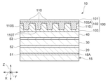
- FIG. 1 is a front view of a display device 10 with an optical film (hereinafter, simply a display device 10) including the optical film 100.
- FIG. 2 is a schematic cross-sectional view of a part of the display device 10 in the thickness direction Z of the display device 10.
- the optical film 100 forms the outermost surface of the display device 10. The display image of the display device 10 is projected to the viewer side through the optical film 100.
- reference numeral X indicates a left-right direction of the display device 10.
- Reference numeral Y indicates a vertical direction of the display device 10 orthogonal to the horizontal direction X.
- the thickness direction Z is a direction orthogonal to both the left-right direction X and the up-down direction Y.
- the optical film 100 of the illustrated example has a rectangular shape having a longitudinal direction in the vertical direction Y.
- the optical film 100 extends in the vertical direction Y and faces each other in the horizontal direction X, and a pair of first sides 100A and 100A and a direction extending in the horizontal direction X and orthogonal to the direction in which the first side 100A faces each other, that is, the vertical direction. It has a pair of second sides 100B and 100B facing each other at Y.
- an organic LED (Organic Light Emitting Diode) panel 15, a circular polarizing plate 20, a touch panel 30, a cover glass 40, and an optical film 100 are laminated in this order. It is configured.
- the organic LED panel 15, the circular polarizing plate 20, the touch panel 30, and the cover glass 40 also have a rectangular shape having a longitudinal direction in the vertical direction Y.
- the optical film 100 forms the outermost surface of the display device 10, but other layers may form the outermost surface.
- the display device 10 is configured as a smartphone as an example.
- the display device 10 may be a tablet terminal, a television, a computer display, a car navigation system, or the like.
- the display surface (front surface) 15A of the organic LED panel 15 and the back surface of the circularly polarizing plate 20 are bonded by a first adhesive layer 51.
- the front surface of the circular polarizing plate 20 and the back surface of the touch panel 30 are bonded by a second adhesive layer 52.
- the front surface of the touch panel 30 and the back surface of the cover glass 40 are bonded to each other by a third adhesive layer 53.
- Each of the adhesive layers 51 to 53 is a so-called OCA (Optical Clear Adhesive) and has a high light transmittance.
- the optical film 100 is arranged on the surface of the cover glass 40. In this example, the optical film 100 and the cover glass 40 are not bonded by an adhesive layer. However, the optical film 100 and the cover glass 40 may be bonded by an adhesive layer.
- the organic LED panel 15 is an organic LED panel that adopts a microcavity structure.
- the organic LED panel 15 may be of another type such as a color filter method.
- a blue shift is likely to occur in an image visually recognized from an angle, and the color change in the viewing angle may be large due to the blue shift. Therefore, in the display device 10, the optical film 100 is used to suppress the color change in the viewing angle.
- the circular polarizing plate 20 has a polarizing element and a retardation plate.
- the retardation plate is arranged on the organic LED panel 15 side.
- the splitter is joined to the surface of the retardation plate opposite to the organic LED panel 15 side. Specifically, the splitter is a linear splitter and the retardation plate is a ⁇ / 4 retardation plate.
- the touch panel 30 includes a transparent glass plate, and it is desirable to adopt a capacitance method. Although the cover glass 40 has a protective function, it may have other functions such as an antireflection function.
- the optical film 100 has a base material 101, a low refractive index layer 102, and a high refractive index layer 103.
- the base material 101, the low refractive index layer 102, and the high refractive index layer 103 are laminated in this order from the side where the viewer is located with respect to the display device 10 toward the organic LED panel 15.
- the base material 101, the low refractive index layer 102, and the high refractive index layer 103 are laminated in this order from the viewer side toward the inside of the device in the thickness direction Z.
- the base material 101 is in the form of a film, and is bonded to the low refractive index layer 102 on the back surface of the front surface and the back surface.
- the base material 101 is a transparent base material made of resin, glass, or the like and having light transmittance.
- the base material 101 is composed of, for example, polyethylene terephthalate, polyoliphin, polycarbonate, polyacrylate, polyamide, a film containing triacetyl cellulose as a main component, glass, and the like.
- the thickness of the base material 101 is, for example, 10 ⁇ m or more and 200 ⁇ m or less.
- the refractive index of the base material 101 is, for example, 1.46 or more and 1.67 or less.
- the main component means a component contained in a ratio of 50% or more with respect to the whole substance among a plurality of components constituting a certain substance, or a component contained most. Further, although the optical film 100 in the present embodiment includes the base material 101, the optical film 100 does not have to have the base material 101.
- FIG. 3 is a partial perspective view of the optical film 100, specifically, a partial perspective view of the low refractive index layer 102.
- FIG. 4 is a view of the low refractive index layer 102 in the normal direction, in other words, a view in the thickness direction Z.
- FIG. 4 schematically shows the arrangement of the lens unit 110 described later included in the low refractive index layer 102.
- FIG. 5 is a cross-sectional view when the optical film 100 is cut in the direction along the VV line of FIG.
- the low refractive index layer 102 has a film-like layer body 102A having a front surface and a back surface, and the back surface of the layer body 102A along the first direction D 1 and the second direction D 2 . It integrally has a plurality of lens units 110, which is an example of two-dimensionally arranged optical elements. As shown in FIG. 3, the lens portions 110 are arranged along the first direction D 1 and the second direction D 2 that diagonally intersect both the left-right direction X and the up-down direction Y.
- FIG. 2 is a schematic cross-sectional view, and for convenience of explanation, the lens portions 110 are shown so as to be arranged in the left-right direction X. However, in practice, the lens portions 110 in the present embodiment are arranged along the first direction D 1 and the second direction D 2 .
- the first direction D 1 and the second direction D 2 are directions parallel to the film surface of the optical film 100 and intersecting each other. Further, the first direction D 1 and the second direction D 2 are directions that are not parallel to the four sides of the optical film 100, respectively.
- the plurality of lens units 110 are arranged at intervals on each grid line of the grid pattern formed by the plurality of grid lines extending in each of the first direction D 1 and the second direction D 2 .
- the grid lines referred to here are virtual lines.
- the high refractive index layer 103 is joined to the low refractive index layer 102 so as to cover the lens portion 110 and fill the space between the plurality of lens portions 110.
- the interface between the low refractive index layer 102 and the high refractive index layer 103 forms an uneven shape.
- the high-refractive index layer 103 has a film shape having a plurality of holes for accommodating the plurality of lens portions 110, and is at least partially lattice-shaped.
- the low refractive index layer 102 does not have the layer body 102A, and may be composed of a set of a plurality of lens portions 110. Further, the optical film 100 does not have to include the high refractive index layer 103. Further, the low refractive index layer 102 may not be provided. That is, the low refractive index layer 102 may be formed of an air layer. In this case, the space surrounded by the grid-like portion of the high refractive index layer 103 forms the optical element.
- the refractive index of the low refractive index layer 102 is, for example, 1.40 or more and 1.55 or less.
- the refractive index of the high refractive index layer 103 is, for example, 1.55 or more and 1.90 or less, which is larger than the refractive index of the low refractive index layer 102.
- the low refractive index is such that the difference between the refractive index of the low refractive index layer 102 and the refractive index of the high refractive index layer 103 is in the range of 0.05 or more and 0.50 or less.
- the layer 102 and the high refractive index layer 103 are selected.
- the high refractive index layer 103 of the low refractive index layer 102 and the high refractive index layer 103 is arranged closer to the organic LED panel 15 than the low refractive index layer 102, but in this arrangement order. May be the other way around.
- the low refractive index layer 102 may be formed by, for example, curing an ultraviolet curable resin, an electron beam curable resin, or a thermosetting resin.
- the ultraviolet curable resin may contain an acrylic resin or an epoxy resin.
- the high refractive index layer 103 may be formed by curing, for example, an ultraviolet curable resin, an electron beam curable resin, or a thermosetting resin.
- the ultraviolet curable resin may contain an acrylic resin or an epoxy resin.
- the high refractive index layer 103 may be formed of an acrylic resin pressure-sensitive adhesive.
- the dimension (thickness) of the layer body 102A in the low refractive index layer 102 in the thickness direction Z is, for example, 0.5 ⁇ m or more and 30 ⁇ m or less.
- the height of the lens unit 110 is, for example, 1.0 ⁇ m or more and 30 ⁇ m or less.
- the thickness of the high refractive index layer 103 is, for example, 5 ⁇ m or more and 100 ⁇ m or less.
- the configuration of the lens unit 110 which is an optical element, will be described in detail.
- the lens portion 110 has a quadrangular frustum shape as an example.
- the lens unit 110 has a front end surface 110T parallel to the film surface and a side surface 110S located between the front end surface 110T and the base end on the opposite side thereof.
- the side surface 110S has a tapered shape toward the organic LED panel 15 side, which is one side in the normal direction of the film surface of the optical film 100.
- the side surface 110S has a pair of first element side surfaces 111 and 111 facing each other and a pair of second side surfaces facing each other in a direction orthogonal to the direction in which the pair of first element side surfaces 111 and 111 face each other. It has element sides 112 and 112.
- the pair of first element side surfaces 111 and 111 and the pair of second element side surfaces 112 and 112 are flat surfaces, respectively.
- at least one of the pair of first element side surfaces 111 and 111 and the pair of second element side surfaces 112 and 112 may be curved or stepped.
- the lens unit 110 may be, for example, a quadrangular pyramid, an octagonal pyramid, an octagonal frustum, or the like.
- reference numerals N1 and N1 indicate the normal directions of the pair of first element side surfaces 111 and 111, respectively.
- these normal directions N1 and N1 are the surface including the normal direction of the first direction D1 and the normal direction of the film surface of the optical film 100, and the normal of the second direction D2 and the film surface, respectively. It is non-parallel to the plane including the direction.
- the normal directions N1 and N1 are parallel to the second side 100B of the optical film 100, respectively.
- the normal directions N1 and N1 are parallel to the left-right direction X, respectively.
- the first element side surfaces 111 and 111 which are flat surfaces, are parallel to the first side 100A and the vertical direction Y. Further, the first element side surfaces 111 and 111 face each other in the direction in which the second side 100B extends, that is, in the left-right direction X.
- the reference numerals N2 and N2 indicate the normal directions of the pair of second element side surfaces 112 and 112, respectively. These normal directions N2 and N2 are also non-parallel to the surface including the first direction D1 and the normal direction of the film surface of the optical film 100 and the surface including the second direction D2 and the normal direction of the film surface, respectively. Is. On the other hand, the normal directions N2 and N2 are parallel to the first side 100A of the optical film 100, respectively. In other words, the normals N2 and N2 are parallel to each other in the vertical direction Y. Further, the second element side surfaces 112 and 112, which are flat surfaces, are parallel to the second side 100B and the left-right direction X.
- the second element side surfaces 112 and 112 face each other in the direction in which the first side 100A extends, that is, in the vertical direction Y.
- the normal directions N1 and N1 and the normal directions N2 and N2 are orthogonal to each other.
- the plurality of lens portions 110 are formed by a plurality of grid lines extending in the first direction D 1 and the second direction D 2 diagonally intersecting both the left-right direction X and the vertical direction Y. Arranged along a grid pattern.
- the first element side surfaces 111, 111 and the second element side surfaces 112, 112 face either the left-right direction X or the up-down direction Y.
- the lens unit 110 diffuses and deflects most of the light emitted by the organic LED panel 15 from the first element side surfaces 111 and 111 along a surface including the normal directions N1 and N1 and the normal direction of the film surface.
- the lens unit 110 directs the surfaces (111, 112) on which the optical function is effectively exhibited in the left-right direction X or the up-down direction Y, while the first direction D 1 and the second direction, which are the arrangement directions thereof.
- D 2 is tilted with respect to the left-right direction X and the up-down direction Y.
- the adjacent lens portions 110 among the plurality of lens portions 110 are the normal directions N1 and N1 and the film surface of the pair of first element side surfaces 111 and 111, respectively. Not aligned along a plane including the normal direction of, in other words, not aligned linearly in a direction parallel to the plane. Further, the adjacent lens portions 110 among the plurality of lens portions 110 are arranged side by side along a surface including the normal directions N2 and N2 of each of the pair of second element side surfaces 112 and 112 and the normal direction of the film surface. No, in other words, they are not aligned linearly in the direction parallel to the plane.
- the pitch P1 of the lens unit 110 arranged in the first direction D1 and the pitch P2 of the lens unit 110 arranged in the second direction D2 are equal pitches, that is, constant pitches in the present embodiment, respectively. And the values are the same as each other. However, each pitch is not limited to equal pitches. Further, as described above, at least one of the pair of first element side surfaces 111 and 111 and the pair of second element side surfaces 112 and 112 may be curved or stepped. Here, when the first element side surface 111 and / or the second element side surface 112 is a curved surface, the normal direction determined at least in the center of the width direction of the curved surface is the normal direction of the film surface of the first direction D1 and the optical film 100.
- the normal direction of the plane including the side on the tip end side and the side on the base end side is the first direction D 1 and the optical film. It suffices to be non-parallel to the surface including the normal direction of the film surface of 100 and the surface including the normal direction of the second direction D2 and the film surface.
- the configuration of the lens unit 110 as an optical element in the present embodiment will be described in another way with reference to FIG. 4 as follows.
- the first reference line SL1 horizontally parallel to the film surface is extended from the first lens unit 110 (reference numeral 110-1) among the plurality of lens units 110, the first lens unit 110 (reference numeral 110-).
- the second lens unit 110 (reference numeral 110-2) adjacent to 1 ) has a predetermined interval in the direction forming the first angle ⁇ a with respect to the first reference line SL1 (that is, the first direction D1). Is placed.
- the third lens unit 110 (reference numeral 110-3) adjacent to the first lens unit 110 (reference numeral 110-1) with respect to the second reference line SL2 orthogonal to the first reference line SL1 and parallel to the film surface. They are arranged at predetermined intervals in the direction forming the second angle ⁇ b (that is, the second direction D 2 ).
- the other lens portions 110 among the plurality of lens portions 110 are also arranged at a predetermined distance from the adjacent lens portions 110 in the direction forming the first angle ⁇ a, and are arranged in the direction forming the second angle ⁇ b. It is arranged at a predetermined distance from the adjacent lens portions 110.
- the first reference line SL1 is parallel to the second side 100B of the optical film 100.
- the second reference line SL2 is parallel to the first side 100A of the optical film 100.
- the centers C of the lens portions 110 adjacent to each other in the direction of the first reference line SL1 do not line up on the first reference line SL1. Further, the centers C of the lens portions 110 adjacent to each other in the direction of the second reference line SL2 do not line up on the second reference line SL2.
- the centers C of the lens portions 110 adjacent to each other in the direction forming the first angle ⁇ a are aligned in the direction forming the first angle ⁇ a, to be exact, on a straight line extending in the direction forming the first angle ⁇ a. line up.
- the centers C of the lens portions 110 adjacent to each other in the direction forming the second angle ⁇ b are arranged in the direction forming the second angle ⁇ b, to be exact, arranged on a straight line extending in the direction forming the second angle ⁇ b.
- the center of the lens unit 110 is the center of the lens unit 110 when viewed in the normal direction of the film surface.
- the lens unit 110 has a side parallel to the first reference line SL1 or the second reference line SL2. More specifically, the side side 111p on the proximal end side and the side 111d on the distal end side of the side surface 110S of the lens portion 110 of the first element side surface 111 are parallel to the second reference line SL2. The side 112p on the base end side and the side 112d on the tip end side of the second element side surface 112 are parallel to the first reference line SL1. When viewed in the normal direction of the film surface, the opposing sides of the adjacent lens portions 110 in the direction forming the first angle ⁇ a are parallel to each other.
- the sides 111p and 111d of one of the adjacent lens portions 110 facing each other and the sides 111p and 111d of the other lens portion 110 are parallel to each other. Further, when viewed in the normal direction of the film surface, the opposite sides of the lens portions 110 adjacent to each other in the direction forming the second angle ⁇ b are parallel to each other. That is, the sides 112p and 112d of one of the adjacent lens portions 110 facing each other and the sides 112p and 112d of the other lens portion 110 are parallel to each other.
- the tangent line of the side 111p on the base end side and the tangent line of the side 111d on the tip end side of the side surface 110S of the first element on the side surface 110S of the lens unit 110 form a direction forming the first angle ⁇ a (that is, the first direction D 1 ).
- the direction forming the second angle ⁇ b that is, the second direction D2
- the tangent line of the side 112p on the base end side of the second element side surface 112 and the tangent line of the side 112d on the tip end side form a direction forming the first angle ⁇ a (that is, the first direction D 1 ) and a direction forming the second angle ⁇ b. It is non-parallel to (that is, the second direction D 2 ) and parallel to the first reference line SL1.
- the above relationship is also established when the first element side surface 111 and the second element side surface 112 are curved surfaces.
- the direction parallel to the film surface and passing through both ends of the first element side surface 111 is a direction forming the first angle ⁇ a and a second angle. It is non-parallel to the direction forming ⁇ b, and in the present embodiment, it is non-parallel at an angle different from 45 degrees.
- the direction parallel to the film surface and passing through both ends of the second element side surface 112 is a direction forming the first angle ⁇ a and a second angle. It is non-parallel to the direction forming ⁇ b, and in the present embodiment, it is non-parallel at an angle different from 45 degrees.
- the first angle ⁇ a is preferably 5 degrees or more and 40 degrees or less.
- the second angle ⁇ b is preferably 5 degrees or more and 40 degrees or less.
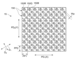
- FIG. 6A is a diagram showing a pixel arrangement of the organic LED panel 15.
- the organic LED panel 15 has a plurality of pixels 150 including a plurality of subpixels having different colors from each other.
- the plurality of pixels 150 have equal pitches on each grid line of the grid pattern formed by the grid lines extending in each of the second pixel array direction PD 2 orthogonal to the first pixel array direction PD 1 and the first pixel array direction PD 1 . That is, they are arranged at a constant pitch.
- the arrangement of the sub-pixels is, for example, the diamond pentile arrangement among the pentile arrangements. That is, the pixel 150 is composed of a pair of a sub-pixel 150R that emits red light and a sub-pixel 150G that emits green light, or a pair of a sub-pixel 150B that emits blue light and a sub-pixel 150G that emits green light.
- the plurality of sub-pixels in one pixel 150 are arranged in a direction diagonally intersecting the first pixel arrangement direction PD 1 and the second pixel arrangement direction PD 2 . Specifically, the diagonally intersecting directions are directions that form 45 degrees with each of the first pixel arrangement direction PD 1 and the second pixel arrangement direction PD 2 .
- two R sub-pixels, two B sub-pixels, and four G sub-pixels are referred to as one pixel, but in the present embodiment, one R sub-pixel and G are used.
- a pair of one subpixel of B or one subpixel of B and one subpixel of G is called a pixel.
- the first pixel arrangement direction PD 1 coincides with the left-right direction X
- the second pixel arrangement direction PD 2 coincides with the vertical direction Y. Therefore, the first direction D 1 and the second direction D 2 , which are the arrangement directions of the lens unit 110, are not parallel to the first pixel arrangement direction PD 1 and the second pixel arrangement direction PD 2 , respectively. Further, in the present embodiment, the first direction D 1 and the second direction D 2 are not parallel to the direction in which the plurality of subpixels are arranged in the pixel 150, respectively.
- the normal directions N1 and N1 of each of the pair of first element side surfaces 111 and 111 are parallel to the first pixel arrangement direction PD 1 and the pair of first elements.
- the normal directions N2 and N2 of the two element side surfaces 112 and 112 are parallel to the second pixel arrangement direction PD 2 .
- the lens unit 110 directs the surface (111, 112) on which the optical function is effectively exhibited toward the first pixel arrangement direction PD 1 or the second pixel arrangement direction PD 2 , while the arrangement direction is the first. It is tilted with respect to the pixel arrangement direction PD 1 and the second pixel arrangement direction PD 2 . Further, in the present embodiment, the arrangement direction of the lens unit 110 is also tilted with respect to the direction in which the sub-pixels diagonally intersecting the first pixel arrangement direction PD 1 and the second pixel arrangement direction PD 2 are arranged. In the present embodiment, by adopting these configurations, the optical function of the lens unit 110 is effectively exhibited in the first pixel arrangement direction PD 1 and the second pixel arrangement direction PD 2 .
- the grid pattern formed by the arrangement of the plurality of lens portions 110 is tilted with respect to the grid pattern formed by the pixel 150 and the grid pattern formed by the sub-pixels 150R, G, B, so that moire is generated. Reduced or less noticeable.
- the arrangement of the sub-pixels in the pixel 150 is not particularly limited, and may be a striped arrangement as shown in FIG. 6B.
- reference numeral ⁇ 1 is formed by a direction parallel to the surface including the normal directions N1 and N1 of each of the pair of first element side surfaces 111 and 111 and the normal direction of the film surface as the first direction D1. Shows the angle.
- Reference numeral ⁇ 2 indicates an angle formed by the direction parallel to the surface including the normal directions N2 and N2 of each of the pair of second element side surfaces 112 and 112 and the normal direction of the film surface with the first direction D1.
- the angle ⁇ 1 and the angle ⁇ 2 are 5 degrees or more and 40 degrees or less, particularly 10 degrees or more and 40 degrees or less, or 50 degrees or more and 85 degrees or less, particularly 50 degrees or more and 80 degrees or less. More specifically, the angle ⁇ 1 is 5 degrees or more and 40 degrees or less and the angle ⁇ 2 is 50 degrees or more and 85 degrees or less, or the angle ⁇ 1 is 50 degrees or more and 85 degrees or less and the angle. It is preferable that ⁇ 2 is 5 degrees or more and 40 degrees or less.
- the angle ⁇ 1 is 10 degrees or more and 40 degrees or less and the angle ⁇ 2 is 50 degrees or more and 80 degrees or less, or the angle ⁇ 1 is 50 degrees or more and 80 degrees or less and the angle ⁇ 2 is. It is 10 degrees or more and 40 degrees or less.
- the preferred ranges of the angle ⁇ 1 and the angle ⁇ 2 described above mean the following in the present embodiment.
- the first direction D 1 is 5 degrees or more and 40 degrees or less, or 50 degrees or more and 85 degrees or less, and 10 degrees or more and 40 degrees or less with the left-right direction X and the first pixel arrangement direction PD 1 .
- the second direction D 2 is preferably 5 degrees or more and 40 degrees or less, or 50 degrees or more and 85 degrees or less, and 10 degrees or more and 40 degrees or less with the left-right direction X and the first pixel arrangement direction PD 1 .
- the above-mentioned conditions are the angle formed by the first direction D 1 in the left-right direction X and the first pixel arrangement direction PD 1 and the angle formed by the second direction D 2 in the left-right direction X and the first pixel arrangement direction PD 1 . If so, moire is effectively reduced or less noticeable.
- bias angle the angle formed by the first direction D 1 in the left-right direction X and the first pixel arrangement direction PD 1 and the angle formed by the second direction D 2 in the left-right direction X and the first pixel arrangement direction PD 1 is hereinafter referred to as bias.
- the bias angle at which the moire reducing effect is preferably obtained can be selected by calculating, for example, a value that minimizes moire. Such selection can be performed, for example, by the following procedure (1st to 7th steps).
- the organic LED panel 15 and the optical film 100 are overlapped at a certain bias angle.
- the brightness reduction amount of any of the sub-pixels in any of the plurality of pixels 150 is calculated.
- the front end surface 110T of the lens portion 110 is treated as transparent (light transmitting state), and the side surface 110S is treated as shielding (light non-transmitting state). That is, the brightness reduction amount is calculated based on the ratio of the area in the subpixels shielded by the side surface 110S.
- the brightness reduction amount of the remaining subpixels in the pixel 150 including the subpixel whose brightness reduction amount is calculated in the second step is calculated by the same method as in the second step.
- the third step ends after the luminance reduction amount for this is calculated.
- the number of remaining sub-pixels in the pixel 150 is two.
- the brightness reduction amount of the other is calculated.
- the second step and the third step are performed for all the other pixels 150 among the plurality of pixels 150, and the brightness reduction amount of each subpixel in all the pixels 150 is specified. Then, based on the information on the amount of decrease in luminance in all the pixels 150, a moire image showing luminance unevenness with respect to the sub-pixels of each color is formed.
- the maximum luminance and the minimum luminance in the moire image for each sub-pixel are specified based on the amount of luminance decrease, and the luminance unevenness (referred to as monochromatic luminance unevenness) in each sub-pixel is calculated by, for example, the following equation.
- Monochromatic brightness unevenness (maximum brightness-minimum brightness) / (maximum brightness + minimum brightness)
- 6th step Next, the average value of the monochromatic luminance unevenness of each subpixel is calculated and specified as a representative value of the luminance unevenness.
- the representative value of the luminance unevenness for a plurality of bias angles is specified. Then, a bias angle at which the moire reduction effect can be preferably obtained is selected based on the representative values of the plurality of luminance irregularities.
- Reference numeral P1 indicates the pitch of the lens unit 110 in the first direction D1.
- Reference numeral P2 indicates the pitch of the lens unit 110 in the second direction D2.
- the pitch P1 is, for example, 2 ⁇ m or more and 50 ⁇ m or less.
- the pitch P2 is, for example, 2 ⁇ m or more and 50 ⁇ m or less.
- the pitch P1 and the pitch P2 are constant values, which are the same values. However, the pitch P1 and the pitch P2 do not have to be the same value.
- reference numeral H indicates the height of the lens portion 110 in the thickness direction Z.
- the height of the lens unit 110 is, for example, 1 ⁇ m or more and 30 ⁇ m or less.
- the symbol Wex indicates the outer frame width which is the width between both ends of the lens portion 110 in the left-right direction X.
- the outer frame width Wex is, for example, 2 ⁇ m or more and 40 ⁇ m or less.
- the reference numeral Wit indicates an intermediate width which is a dimension between the pair of first element side surfaces 111 and 111 at the center of the lens unit 110 in the height direction.
- the intermediate width Wit has a dimension smaller than the outer frame width Wex, and is, for example, 2 ⁇ m or more and 40 ⁇ m or less.
- the symbol Wsi is a side width which is a dimension in the left-right direction X of one first element side surface 111.
- the side width Wsi is, for example, 0.2 ⁇ m or more and 4 ⁇ m or less.
- the symbol ⁇ R indicates the inclination angle of the side surface 111 of the first element.
- the inclination angle ⁇ R is, for example, 2 degrees or more and 30 degrees or less.
- the lens portion 110 in the present embodiment has a regular quadrangular pyramid shape. Therefore, the outer frame width, the intermediate width, the side surface width, and the inclination angle in the vertical direction Y are the same as those in the horizontal direction X.
- the optical elements 110 adjacent to each other in the first direction D1 are adjacent to each other with a gap in the direction in which the pair of first sides 100A and 100A face each other, in other words, with a predetermined interval.
- the pair of first element side surfaces 111 and 111 separately face a gap in the direction in which the pair of first sides 100A and 100A face each other.
- the first duty D1 is defined by dividing the intermediate width Wit of the pair of first element side surfaces 111 and 111 by the pitch P1 of the lens unit 110 in the first direction D1.
- the optical elements 110 adjacent to each other in the second direction D2 are adjacent to each other with a gap in the direction in which the pair of second sides 100B and 100B face each other, in other words, with a predetermined interval.
- the pair of second element side surfaces 112 and 112 separately face a gap in the direction in which the pair of second sides 100B and 100B face each other.
- the second duty D2 is defined by dividing the intermediate width of the pair of second element side surfaces 112 and 112 by the pitch P2 of the lens unit 110 in the second direction D2.
- the first duty D1 and the second duty D2 are preferably 0.5 or more and 0.8 or less, respectively.
- the optical elements 110 adjacent to each other in the first direction D1 may have a gap in the direction in which the pair of first sides 100A and 100A face each other and in the direction in which the pair of second sides 100B and 100B face each other.
- the first duty D1 is obtained by dividing the intermediate width of the pair of first element side surfaces 111 and 111 by the pitch P1 and the intermediate width of the pair of second element side surfaces 112 and 112 by the pitch P1.
- the moire reduction effect by shifting the lattice pattern, that is, biasing tends to be difficult to appear.
- the first duty D1 and the second duty D2 become larger than 0.8, moire tends to increase due to the adjacent lens portions 110 being excessively close to each other. It is presumed that when the adjacent lens portions 110 are excessively close to each other, the in-plane unevenness of the portion of the subpixel that is shielded by the side surface 110S of the lens portion 110 tends to increase, which tends to increase the moire. Will be done.
- the reference numeral Wp in FIG. 6A indicates the minimum width of the subpixel in the pixel 150 in a plan view.
- the green subpixel 150G is smaller than the other subpixels. Therefore, the width Wp is the minimum width of the subpixel 150G.
- the pitch P1 of the lens unit 110 in the first direction D1 and the pitch P2 of the lens unit 110 in the second direction D2 are each half or less of the width Wp of the subpixel. This is because if there is only one lens unit 110 located in one subpixel, the moire reduction effect due to the bias tends to be less likely to appear.
- the light passes through the circularly polarizing plate 20, the touch panel 30, and the cover glass 40 and is incident on the optical film 100.
- the light directed toward the flat portion of the layer body 102A between the front end surface 110T of the lens portion 110 or the adjacent lens portions 110 along the front view direction does not change the angle in the traveling direction.
- it is emitted from the low refractive index layer 102 with almost no change, and does not affect the optical characteristics.
- the light directed to the side surface 110S of the lens unit 110 is diffused in a wide range.
- the light on the high angle side and the light on the low angle side are exchanged. This reduces the blue shift.
- some of the diffused light moves to the higher angle side. This prevents a large amount of light from concentrating in the front view direction, and makes it possible to visually recognize a high-brightness display image even in an oblique direction view.
- the lens unit 110 has a pair of first element side surfaces 111 and 111 and a pair of second element side surfaces 112 and 112 as surfaces on which the optical function is effectively exhibited.
- the first element side surfaces 111 and 111 face the first pixel arrangement direction PD 1
- the second element side surfaces 112 and 112 face the second pixel arrangement direction PD 2 .
- the optical function of the lens unit 110 is effectively generated in the first pixel arrangement direction PD 1 and the second pixel arrangement direction PD 2 .
- the display quality in the first pixel arrangement direction PD 1 and the second pixel arrangement direction PD 2 in the display image becomes good, and in particular, the surface including the first pixel arrangement direction PD 1 and the normal direction of the film surface and the second pixel.
- the tint in the oblique direction on the surface including the arrangement direction PD 2 and the normal direction of the film surface becomes good.
- the pair of first element side surfaces 111 and 111 are symmetrical with respect to the axis along the second pixel arrangement direction PD 2 . Further, the pair of second element side surfaces 112 and 112 are symmetrical with respect to the axis along the first pixel arrangement direction PD 1 . Therefore, in the optical characteristics of the displayed image, axial symmetry is ensured for each axis of the first pixel arrangement direction PD 1 and the second pixel arrangement direction PD 2 .
- first direction D 1 and the second direction D 2 which are the arrangement directions of the lens unit 110, are inclined with respect to the first pixel arrangement direction PD 1 or the second pixel arrangement direction PD 2 .
- first direction D 1 and the second direction D 2 also correspond to the direction in which the sub-pixels diagonally intersecting the first pixel arrangement direction PD 1 and the second pixel arrangement direction PD 2 are lined up. Tilt.
- the grid pattern formed by the arrangement of the plurality of lens portions 110 is tilted with respect to the grid pattern formed by the pixel 150 and the grid pattern formed by the sub-pixels 150R, G, B. This effectively reduces or makes moire less noticeable.
- the present embodiment when displaying the display image by transmitting the light emitted from the pixel 150, at least one of the two axes orthogonal to each other, which is the reference of the pixel arrangement (this). In the embodiment, it is possible to suppress the deterioration of the visibility of the displayed image due to moire while ensuring the optical characteristics having axial symmetry with respect to both) in the displayed image.
- the display device 10'with an optical film according to the modification shown in FIG. 7 is configured by laminating an organic LED panel 15, an optical film 100, a circular polarizing plate 20, a touch panel 30, and a cover glass 40 in this order. Has been done. That is, in this modification, the position of the optical film 100 is different from that of the above-described embodiment.
- the display panel is an organic LED panel, but the display panel may be a liquid crystal panel.
- the lens portions 110 shown in FIG. 7 are arranged along the first direction D 1 and the second direction D 2 that diagonally intersect both the left-right direction X and the up-down direction Y, as in the above-described embodiment. To. FIG.
- the lens portions 110 are shown so as to be arranged in the left-right direction X. However, in practice, the lens portions 110 in the present embodiment are arranged along the first direction D 1 and the second direction D 2 .
- the four corners formed by the first element side surface 111 and the second element side surface 112 of the quadrangular pyramid-shaped lens portion 110 are rounded.
- the ridgeline of the side surface 110S of the lens portion 110 is rounded.
- the embodiment shown in FIG. 8 may be used.
- the portion of the side surface 111 of the first element located between the rounds R at both ends is a surface including the first direction D 1 and the normal direction of the film surface of the optical film 100 and the second direction D 2 . It is non-parallel to the surface including the normal direction of the film surface.
- the portion of the second element side surface 112 located between the rounded ends R is the surface including the first direction D 1 and the normal direction of the film surface of the optical film 100, and the second direction D 2 and the normal direction of the film surface. It is non-parallel to the surface containing and.
- the normal directions N1 and N1 of the portions located between the rounded edges R at both ends of the first element side surface 111 are parallel to the second side 100B of the optical film 100, respectively.
- the normal directions N1 and N1 are parallel to the left-right direction X, respectively.
- the portion of the first element side surface 111 which is a flat surface, located between the roundnesses R at both ends is parallel to the first side 100A and the vertical direction Y. Further, the first element side surfaces 111 and 111 face each other in the direction in which the second side 100B extends, that is, in the left-right direction X. Further, the normal directions N2 and N2 of the portions located between the roundnesses R at both ends of the second element side surface 112 are parallel to the first side 100A of the optical film 100, respectively. In other words, the normal directions N2 and N2 are parallel to the vertical direction Y, respectively.
- the portion of the second element side surface 112, which is a flat surface, located between the rounded edges R at both ends is parallel to the second side 100B and the left-right direction X. Further, the second element side surfaces 112 and 112 face each other in the direction in which the first side 100A extends, that is, in the vertical direction Y.
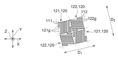
- the optical element 120 made of a diffraction grating is adopted instead of the lens unit 110 in the above-described embodiment.
- the optical element 120 has a first element 121 and a second element 122.
- a plurality of first elements 121 are recessed on one side or the other side in the normal direction of the film surface of the optical film 100 and are elongated in a direction parallel to the first side 100A of the optical film 100.
- the normal direction of each of the first element side surfaces 111 and 111 formed in each groove 121g is a surface including the first direction D1 and the normal direction of the film surface and the second.
- each groove 121g contains a diffraction grating that is non-parallel to the plane containing the direction D 2 and the normal direction of the film plane.
- a side surface 110S is formed between the dent start edge and the bottom end.
- the dent start edge means a portion where the groove 121 g begins to dent with respect to the outermost surface of the low refractive index layer 102 or the high refractive index layer 103.
- the first element side surfaces 111 and 111 formed in each groove 121 g include a surface including the first direction D 1 and the normal direction of the film surface of the optical film 100, and the second direction D 2 and the normal direction of the film surface. It is non-parallel to the surface containing. With reference to FIGS.
- the normal directions of the first element side surfaces 111 and 111 formed in each groove 121 g are parallel to the second side 100B of the optical film 100. In other words, each of these normal directions is parallel to the left-right direction X.
- the first element side surface 111 which is a flat surface, is parallel to the first side 100A and the vertical direction Y. Further, the first element side surfaces 111 and 111 face each other in the direction in which the second side 100B extends, that is, in the left-right direction X.
- the second element 122 is a diffraction grating having a plurality of grooves 122g which are recessed on one side or the other side in the normal direction of the film surface of the optical film 100 and are elongated in the direction parallel to the second side 100B.
- the normal directions of the second element side surfaces 112 and 112 formed in each groove 122 g are the surface including the first direction D 1 and the normal direction of the film surface, and the method of the second direction D 2 and the film surface. It contains a diffraction grating that is non-parallel to the plane containing the normal direction.
- a side surface 110S is formed between the dent start edge and the bottom end.
- the second element side surfaces 112 and 112 formed in each groove 122 g include a surface including the first direction D 1 and the normal direction of the film surface of the optical film 100, and the second direction D 2 and the normal direction of the film surface. It is non-parallel to the surface containing.
- the normal directions of the second element side surfaces 112 and 112 formed in each groove 122 g are parallel to the first side 100A of the optical film 100. In other words, each of these normal directions is parallel to the vertical direction Y.
- the second element side surface 112, which is a flat surface, is parallel to the second side 100B and the left-right direction X.
- the second element side surfaces 112 and 112 face each other in the direction in which the first side 100A extends, that is, in the vertical direction Y.
- the first element 121 and the second element 122 are arranged in a mixed manner in each of the first direction D 1 and the second direction D 2 .
- the first element 121 and the second element 122 are preferably arranged alternately.
- the normal directions of the second element side surfaces 112 and 112 of the first element 121 are the surface including the first direction D1 and the normal direction of the film surface and the second direction D. It may or may not be non-parallel to the surface including 2 and the normal direction of the film surface.
- the normal directions of the first element side surfaces 111 and 111 in the second element 122 are also the normal directions of the surface including the first direction D 1 and the normal direction of the film surface and the normal directions of the second direction D 2 and the film surface. It may or may not be non-parallel to the surface containing and.
- the recess formed in the low refractive index layer 102 forms the optical element 110'.
- 10A is a view of the optical element 110'viewed in the thickness direction Z
- FIG. 10B is a cross-sectional view taken along the line XB-XB of FIG. 10A.
- FIG. 10C is a perspective view of the high refractive index layer 103 from a bird's-eye view.
- the optical element 110' is formed by a concave recess having an irregular pyramid shape.
- the side surface 110S of the optical element 110' is formed between the recessed start edge and the bottom edge of the recess.
- the first element side surfaces 111 and 111 of the side surfaces 110S face the left-right direction X, and their normal directions N1 and N1 are parallel to the left-right direction X.
- the second element side surfaces 112 and 112 of the side surfaces 110S face the vertical direction Y, and their normal directions N2 and N2 are parallel to the vertical direction Y.
- the first element side surface 111 is non-parallel to the surface including the first direction D 1 and the normal direction of the film surface of the optical film 100 and the surface including the second direction D 2 and the normal direction of the film surface.
- the second element side surface 112 is non-parallel to the surface including the first direction D 1 and the normal direction of the film surface of the optical film 100 and the surface including the second direction D 2 and the normal direction of the film surface.
- the normal directions N1 and N1 of the first element side surface 111 are parallel to the second side 100B of the optical film 100, respectively.
- the normal directions N1 and N1 are parallel to the left-right direction X, respectively.
- the first element side surface 111 which is a flat surface, is parallel to the first side 100A and the vertical direction Y.
- the first element side surfaces 111 and 111 face each other in the direction in which the second side 100B extends, that is, in the left-right direction X.
- the normal directions N2 and N2 of the second element side surface 112 are parallel to the first side 100A of the optical film 100, respectively.
- the normal directions N2 and N2 are parallel to the vertical direction Y, respectively.
- the second element side surface 112 which is a flat surface, is parallel to the second side 100B and the left-right direction X.
- the second element side surfaces 112 and 112 face each other in the direction in which the first side 100A extends, that is, in the vertical direction Y.
- the high refractive index layer 103 is provided with a plurality of pyramid-shaped convex portions embedded in the concave optical element 110'.
- the four faces of the convex portion forming the quadrangular pyramid have two faces having a normal line matching the normal line N1 and two faces having a normal line matching the normal line N2.
- 10C shows the normal lines N1 and N2 projected onto the film surface for convenience of explanation.
- the convex portions of the high refractive index layer 103 are arranged at a predetermined pitch in the first direction D1 and at a predetermined pitch in the second direction D2.
- the normal line that coincides with the normal line N1 and the normal line that coincides with the normal line N2 of the convex portion of the high refractive index layer 103 are non-parallel to the first direction D 1 and the second direction D 2 .
- the convex portions of the high refractive index layer 103 arranged in the second direction D 2 are also arranged in the same arrangement as the convex portions arranged in the first direction D 1 , although the directions are different. Therefore, both ends of the side surfaces of the first element side surfaces 111 and 111 of the optical element 110'are displaced in the direction of the normal line N1 when the normal line N1 is projected onto the film surface, that is, in the left-right direction X. Then, the adjacent optical elements 110'are positioned in a state where the sides on the base end side facing each other are parallel to each other.
- the optical elements 110' are aligned in the direction of the normal line N1 when the normal line N1 is projected onto the film surface, that is, in the first direction D1 different from the left-right direction X.
- the optical elements 110'arranged in the second direction D 2 are also arranged in the same arrangement as the optical elements 110'arranged in the first direction D 1 , although the directions are different.
- Examples 1 to 3 of the present disclosure an optical film 100 having a lens portion 110 having a shape according to the dimensions shown in Table 1 below was created (see also FIGS. 4 and 5). Then, at the bias angle ⁇ 1 shown in Table 1, a display device 10 in which each optical film 100 is superimposed on the pixels 150 of the organic LED panel 15 is configured.
- Comparative Examples 1-1 to 1-3 each include an optical film having a lens portion having the same dimensions as the lens portion 110 according to Examples 1 to 3, but the lens portion is parallel to the left-right direction X and the vertical direction Y, respectively. They are arranged along a grid pattern consisting of grid lines. That is, there is no bias angle in Comparative Examples 1-1 to 1-3. Further, Comparative Examples 2-1 to 2-3 each include an optical film having a lens portion having the same dimensions as the lens portion 110 according to the first to third embodiments, and the lens portion is the lens of the first to third embodiments.
- the portions 110 are arranged in the same direction as the arrangement direction, but the four side surfaces are inclined with respect to the left-right direction X and the up-down direction Y (parallel to the direction of the bias angle). Further, the organic LED panel in the comparative example is the same as that in the embodiment and the organic LED panel 15.
- FIG. 11 is a diagram showing an arrangement of lens portions and an arrangement of subpixels between an example and a comparative example.
- FIG. 11A shows an array of lens units 110 and an array of sub-pixels of Examples 1 to 3.
- FIG. 11B shows the arrangement of the lens portions and the arrangement of the sub-pixels of Comparative Examples 1-1 to 1-3.
- FIG. 11C shows the arrangement of the lens portions and the arrangement of the sub-pixels of Comparative Examples 2-1 to 2-3.
- the material of the lens portion 110 (low refractive index layer 102) in Examples 1 to 3 is an acrylic ultraviolet curable resin, and the refractive index thereof is 1.48.
- the lens portion (low refractive index layer) according to the comparative example is made of the same material as that of the example.
- the pitch PP1 of the pixels 150 in the first pixel arrangement direction PD 1 in the organic LED panel 15 in the embodiment is 55.5 ⁇ m
- the pitch PP2 of the pixels 150 in the second pixel arrangement direction PD 2 is It is 55.5 ⁇ m
- the width Wp of the green subpixel 150G is 15.8 ⁇ m.
- two R sub-pixels, two B sub-pixels, and four G sub-pixels form one unit.
- the R sub-pixels are used.
- a pair of one pixel and one G subpixel, or a pair of one B subpixel and one G subpixel are collectively called a pixel.
- the color coordinates x and y in the front view (0 degree) and the left and right direction X are tilted 45 degrees to the right with respect to the front view.
- the color coordinates x and y when viewed in the direction were specified.
- the specified color coordinates x and y were converted into the color coordinates u'and v'in the uniform color space.
- the color coordinates u'and v' are calculated from the following equations (1-1) and (1-2), respectively.
- the color change ⁇ u'v'of the light emitted in the direction forming 45 degrees with respect to the color of the light emitted in the front view direction was calculated from the color coordinates u'and v'.
- the color change ⁇ u'v' indicates a color difference, and the smaller the value, the smaller the difference between the color of the light emitted in the front view direction and the color of the light at 45 degrees.
- the value of ⁇ u'v'at the angle ⁇ in the viewing angle is expressed by the following equation (2).
- Luminance unevenness means that the smaller the value, the larger the reduction level of moire.
- the axisymmetry of the displayed image regarding the vertical axis and the horizontal axis was visually evaluated based on the angular distribution of the color coordinates x and y specified in all directions.
- Examples 1 to 3 and Comparative Examples 1-1 to 1-3 since the four side surfaces of the lens portion face the left-right direction or the up-down direction, the axial symmetry of the displayed image regarding the up-down direction axis and the left-right direction axis is ensured.
- Examples 2-1 to 2-3 since the four side surfaces of the lens portion do not face the left-right direction or the up-down direction, the axes of the display images relating to the up-down direction axis and the left-right direction axis are different from those of Examples 1 to 3. Symmetry is not ensured.
- Tables 2 to 4 below, " ⁇ " is indicated when the axial symmetry of the displayed image regarding the vertical axis and the horizontal axis is secured, and " ⁇ " is indicated when the axial symmetry is not secured. Is written.
- Example 1 Comparative Example 1-1, and Comparative Example 2-1 Color coordinates x, y at 0 and 45 degrees, color coordinates u', v', and color change ⁇ u'at 0 and 45 degrees, respectively.
- the values of v'and luminance unevenness, and the evaluation results of the axial symmetry of the optical characteristics are shown in Table 2 below.
- Example 2 Comparative Example 1-2, and Comparative Example 2-2 with color coordinates x, y at 0 and 45 degrees, color coordinates u', v', and color change ⁇ u'at 0 and 45 degrees, respectively.
- the values of v'and luminance unevenness, and the evaluation results of the axial symmetry of the optical characteristics are shown in Table 3 below.
- Example 3 Comparative Example 1-3, and Comparative Example 2-3 Color coordinates x, y at 0 and 45 degrees, color coordinates u', v', and color change ⁇ u'at 0 and 45 degrees, respectively.
- the values of v'and luminance unevenness, and the evaluation results of the axial symmetry of the optical characteristics are shown in Table 4 below.
- the color change ⁇ u'v'of Example 1 is the color change ⁇ u'v'of Comparative Example 1-1 and Comparative Example 2-1. It is equivalent to, and both are suppressed to be lower than the value of 0.01617 when there is no optical film.
- the luminance unevenness of Example 1 is suppressed more than the luminance unevenness of Comparative Example 1-1. Further, the luminance unevenness of Example 1 is equivalent to the luminance unevenness of Comparative Example 2-1.
- Example 1 the axial symmetry of the optical characteristics of the displayed image can be ensured, but in Comparative Example 2-1 it cannot be ensured.
- Example 1 is more advantageous than Comparative Example 1-1 and Comparative Example 2-1 in the case of suppressing color change and moire while ensuring the axial symmetry of the optical characteristics.
- Example 2 Comparative Example 1-2, and Comparative Example 2-2, and the comparison of Example 3, Comparative Example 1-3, and Comparative Example 2-3.
Abstract
Description
また、前記一対の第2要素側面それぞれの法線方向と前記フィルム面の法線方向とを含む面と平行な方向が、前記第1方向と、5度以上40度以下又は50度以上85度以下の角度をなしてもよい。 When viewed in the normal direction of the film surface, the direction parallel to the surface including the normal direction of each of the pair of first element side surfaces and the normal direction of the film surface is 5 degrees with the first direction. The angle may be 40 degrees or more or 50 degrees or more and 85 degrees or less.
Further, the direction parallel to the surface including the normal direction of each of the pair of second element side surfaces and the normal direction of the film surface is 5 degrees or more and 40 degrees or less or 50 degrees or more and 85 degrees with the first direction. The following angles may be made.
図1は、光学フィルム100を備える光学フィルム付き表示装置10(以下、単に表示装置10)の正面図である。図2は、表示装置10の厚み方向Zにおける表示装置10の一部の概略的な断面図である。本実施の形態では、光学フィルム100が表示装置10の最表面を形成する。表示装置10の表示画像は、光学フィルム100を通して視認者側に映し出される。 <Display device>
FIG. 1 is a front view of a
以下、光学フィルム100について詳しく説明する。光学フィルム100は、基材101と、低屈折率層102と、高屈折率層103とを有している。基材101、低屈折率層102及び高屈折率層103は、表示装置10に対して視認者が位置する側から有機LEDパネル15側に向けてこの順で積層されている。言い換えると、基材101、低屈折率層102及び高屈折率層103は、厚み方向Zで視認者側から装置内部に向けてこの順で積層されている。 <Optical film>
Hereinafter, the
複数のレンズ部110のうちの第1のレンズ部110(符号110-1)から水平方向にフィルム面に平行な第1基準線SL1を延ばした場合に、第1のレンズ部110(符号110-1)と隣り合う第2のレンズ部110(符号110-2)は、第1基準線SL1に対して第1の角度θaをなす方向(つまり、第1方向D1)に所定の間隔を空けて配置される。第1のレンズ部110(符号110-1)と隣り合う第3のレンズ部110(符号110-3)は、第1基準線SL1と直交しフィルム面に平行な第2基準線SL2に対して第2の角度θbをなす方向(つまり、第2方向D2)に所定の間隔を空けて配置される。そして、複数のレンズ部110のうちの他のレンズ部110も、第1の角度θaをなす方向で隣り合うレンズ部110と所定の間隔を空けて配置され、第2の角度θbをなす方向で隣り合うレンズ部110と所定の間隔を空けて配置される。
なお、本実施の形態では、第1基準線SL1が光学フィルム100の第2辺100Bと平行になる。第2基準線SL2が光学フィルム100の第1辺100Aと平行になる。 Further, the configuration of the
When the first reference line SL1 horizontally parallel to the film surface is extended from the first lens unit 110 (reference numeral 110-1) among the plurality of
In this embodiment, the first reference line SL1 is parallel to the
そして、フィルム面の法線方向で見たとき、第1の角度θaをなす方向で隣り合うレンズ部110の互いに対向する辺は、互いに平行である。つまり、互いに対向する、隣り合うレンズ部110のうちの一方のレンズ部110の辺111p,111dと、他方のレンズ部110の辺111p,111dとが、互いに平行である。また、フィルム面の法線方向で見たとき、第2の角度θbをなす方向で隣り合うレンズ部110の互いに対向する辺が、互いに平行である。つまり、互いに対向する、隣り合うレンズ部110のうちの一方のレンズ部110の辺112p,112dと、他方のレンズ部110の辺112p,112dとが、互いに平行である。 Further, the
When viewed in the normal direction of the film surface, the opposing sides of the
第1方向D1が、左右方向X及び第1画素配列方向PD1と、5度以上40度以下をなすか、又は、50度以上85度以下をなすことが好ましく、10度以上40度以下をなすか、又は、50度以上80度以下をなすことがより好ましい。
第2方向D2が、左右方向X及び第1画素配列方向PD1と、5度以上40度以下をなすか、又は、50度以上85度以下をなすことが好ましく、10度以上40度以下をなすか、又は、50度以上80度以下をなすことがより好ましい。 The preferred ranges of the angle θ1 and the angle θ2 described above mean the following in the present embodiment.
It is preferable that the first direction D 1 is 5 degrees or more and 40 degrees or less, or 50 degrees or more and 85 degrees or less, and 10 degrees or more and 40 degrees or less with the left-right direction X and the first pixel arrangement direction PD 1 . Or more preferably 50 degrees or more and 80 degrees or less.
The second direction D 2 is preferably 5 degrees or more and 40 degrees or less, or 50 degrees or more and 85 degrees or less, and 10 degrees or more and 40 degrees or less with the left-right direction X and the first pixel arrangement direction PD 1 . Or more preferably 50 degrees or more and 80 degrees or less.
まず、有機LEDパネル15と光学フィルム100とをあるバイアス角で重ねる。
(第2工程)
次に、複数の画素150のうちのいずれかの画素150におけるいずれかのサブピクセルの輝度減少量を計算する。このとき、レンズ部110の先端面110Tは、透明(光透過状態)として取り扱い、側面110Sは遮蔽(光非透過状態)として取り扱う。つまり、側面110Sによって遮蔽されたサブピクセル内の面積の割合に基づいて、輝度減少量が計算される。
(第3工程)
次に、第2工程で輝度減少量を計算されたサブピクセルを含む画素150における残りのサブピクセルの輝度減少量を第2工程と同じ手法で計算する。本実施の形態では、画素150における残りのサブピクセルは1つであるので、これについての輝度減少量が計算された後、第3工程が終了する。一方で、例えばストライプ配列であるときには、上記画素150における残りのサブピクセルが2つになる。この場合には、残りのサブピクセルのうちの一方の輝度減少量を計算した後、他方の輝度減少量を計算する。
(第4工程)
次に、複数の画素150のうちの他の全ての画素150について、第2工程と第3工程を行い、全画素150における各サブピクセルの輝度減少量を特定する。そして、このような全画素150における輝度減少量の情報を基に、各色のサブピクセルに関する輝度ムラを示すモアレ画像を形成する。
(第5工程)
次に、各サブピクセルに関するモアレ画像における最大輝度と最小輝度とを輝度減少量に基づいて特定し、各サブピクセルにおける輝度ムラ(単色輝度ムラと呼ぶ。)を、例えば以下の式により計算する。
単色輝度ムラ=(最大輝度-最小輝度)/(最大輝度+最小輝度)
(第6工程)
次に、各サブピクセルの単色輝度ムラの平均値を計算し、輝度ムラの代表値として特定する。
(第7工程)
そして、バイアス角を順次変更し、第2~第6工程を行うことで、複数のバイアス角についての輝度ムラの代表値を特定する。そして、複数の輝度ムラの代表値に基づいてモアレ低減効果が好適に得られるバイアス角を選択する。 (First step)
First, the
(Second step)
Next, the brightness reduction amount of any of the sub-pixels in any of the plurality of
(Third step)
Next, the brightness reduction amount of the remaining subpixels in the
(4th step)
Next, the second step and the third step are performed for all the
(Fifth step)
Next, the maximum luminance and the minimum luminance in the moire image for each sub-pixel are specified based on the amount of luminance decrease, and the luminance unevenness (referred to as monochromatic luminance unevenness) in each sub-pixel is calculated by, for example, the following equation.
Monochromatic brightness unevenness = (maximum brightness-minimum brightness) / (maximum brightness + minimum brightness)
(6th step)
Next, the average value of the monochromatic luminance unevenness of each subpixel is calculated and specified as a representative value of the luminance unevenness.
(7th step)
Then, by sequentially changing the bias angle and performing the second to sixth steps, the representative value of the luminance unevenness for a plurality of bias angles is specified. Then, a bias angle at which the moire reduction effect can be preferably obtained is selected based on the representative values of the plurality of luminance irregularities.
次に、本実施の形態にかかる表示装置10の作用について説明する。 <Action>
Next, the operation of the
図7に示す変形例にかかる光学フィルム付き表示装置10’は、有機LEDパネル15と、光学フィルム100と、円偏光板20と、タッチパネル30と、カバーガラス40と、をこの順に積層して構成されている。すなわち、この変形例では、光学フィルム100の位置が上述の実施の形態に対して異なる。なお、上述の実施の形態及び図7の変形例では、表示パネルが有機LEDパネルであるが、表示パネルは液晶パネルでもよい。なお、図7に示すレンズ部110は、上述の実施の形態と同様に、左右方向X及び上下方向Yの両方に斜めに交差する第1方向D1及び第2方向D2に沿って配列される。図7は概略の断面図であり、説明の便宜のために、レンズ部110が左右方向Xに並ぶように示されている。しかし、実際上は、本実施の形態におけるレンズ部110は、第1方向D1及び第2方向D2に沿って並ぶ。 <Modification example>
The display device 10'with an optical film according to the modification shown in FIG. 7 is configured by laminating an
図4等で示した実施の形態の変形例として図8のような形態でも良い。図8の構成では、第1要素側面111における両端の丸みR間に位置する部分は、第1方向D1と光学フィルム100のフィルム面の法線方向とを含む面及び第2方向D2とフィルム面の法線方向とを含む面と非平行である。第2要素側面112における両端の丸みR間に位置する部分は、第1方向D1と光学フィルム100のフィルム面の法線方向とを含む面及び第2方向D2とフィルム面の法線方向とを含む面と非平行である。
一方で、図4及び図8を参照し、第1要素側面111における両端の丸みR間に位置する部分の法線方向N1,N1はそれぞれ、光学フィルム100の第2辺100Bと平行になる。言い換えると、法線方向N1,N1はそれぞれ、左右方向Xに平行となる。また、平坦面である第1要素側面111における両端の丸みR間に位置する部分は、第1辺100A及び上下方向Yと平行になる。また、第1要素側面111,111は、第2辺100Bが延びる方向で、つまり左右方向Xで向き合っている。さらに、第2要素側面112における両端の丸みR間に位置する部分の法線方向N2,N2はそれぞれ、光学フィルム100の第1辺100Aと平行になる。言い換えると、法線方向N2,N2はそれぞれ、上下方向Yに平行となる。また、平坦面である第2要素側面112における両端の丸みR間に位置する部分は、第2辺100B及び左右方向Xと平行になる。また、第2要素側面112,112は、第1辺100Aが延びる方向で、つまり上下方向Yで向き合っている。 In the modified example shown in FIG. 8, the four corners formed by the first
As a modification of the embodiment shown in FIG. 4 and the like, the embodiment shown in FIG. 8 may be used. In the configuration of FIG. 8, the portion of the
On the other hand, referring to FIGS. 4 and 8, the normal directions N1 and N1 of the portions located between the rounded edges R at both ends of the first
図1も参照し、第1要素121は、光学フィルム100のフィルム面の法線方向の一方側又は他方側に凹み且つ光学フィルム100の第1辺100Aと平行な方向に長尺となる複数の溝121gを有する回折格子であって、各溝121gに形成される第1要素側面111,111それぞれの法線方向が、第1方向D1とフィルム面の法線方向とを含む面及び第2方向D2とフィルム面の法線方向とを含む面と非平行となる回折格子を含んでいる。各溝121gにおいては、凹み開始縁と底端との間に側面110Sが形成される。凹み開始縁とは、溝121gが低屈折率層102又は高屈折率層103の最表面に対して凹み始める部分のことを意味する。各溝121gに形成される第1要素側面111,111は、第1方向D1と光学フィルム100のフィルム面の法線方向とを含む面及び第2方向D2とフィルム面の法線方向とを含む面と非平行である。図4及び図9を参照し、各溝121gに形成される第1要素側面111,111それぞれの法線方向は、光学フィルム100の第2辺100Bと平行になる。言い換えると、これら法線方向はそれぞれ、左右方向Xに平行となる。また、平坦面である第1要素側面111は、第1辺100A及び上下方向Yと平行になる。また、第1要素側面111,111は、第2辺100Bが延びる方向で、つまり左右方向Xで向き合っている。
また、第2要素122は、光学フィルム100のフィルム面の法線方向の一方側又は他方側に凹み且つ第2辺100Bと平行な方向に長尺となる複数の溝122gを有する回折格子であって、各溝122gに形成される第2要素側面112,112それぞれの法線方向が、第1方向D1とフィルム面の法線方向とを含む面及び第2方向D2とフィルム面の法線方向とを含む面と非平行となる回折格子を含んでいる。各溝122gにおいては、凹み開始縁と底端との間に側面110Sが形成される。各溝122gに形成される第2要素側面112,112は、第1方向D1と光学フィルム100のフィルム面の法線方向とを含む面及び第2方向D2とフィルム面の法線方向とを含む面と非平行である。図4及び図9を参照し、各溝122gに形成される第2要素側面112,112それぞれの法線方向は、光学フィルム100の第1辺100Aと平行になる。言い換えると、これら法線方向はそれぞれ、上下方向Yに平行となる。また、平坦面である第2要素側面112は、第2辺100B及び左右方向Xと平行になる。また、第2要素側面112,112は、第1辺100Aが延びる方向で、つまり上下方向Yで向き合っている。
そして、第1方向D1及び第2方向D2のそれぞれで、第1要素121と第2要素122とが混在して配列されている。ここで、第1要素121と第2要素122とは、好ましくは交互に配列される。なお、図9の変形例においては、第1要素121における第2要素側面112,112それぞれの法線方向は、第1方向D1とフィルム面の法線方向とを含む面及び第2方向D2とフィルム面の法線方向とを含む面と非平行でもよいし、そうでなくもよい。また、第2要素122における第1要素側面111,111それぞれの法線方向も、第1方向D1とフィルム面の法線方向とを含む面及び第2方向D2とフィルム面の法線方向とを含む面と非平行でもよいし、そうでなくもよい。 In the modified example shown in FIG. 9, the optical element 120 made of a diffraction grating is adopted instead of the
Also referring to FIG. 1, a plurality of first elements 121 are recessed on one side or the other side in the normal direction of the film surface of the
Further, the second element 122 is a diffraction grating having a plurality of
The first element 121 and the second element 122 are arranged in a mixed manner in each of the first direction D 1 and the second direction D 2 . Here, the first element 121 and the second element 122 are preferably arranged alternately. In the modified example of FIG. 9, the normal directions of the second element side surfaces 112 and 112 of the first element 121 are the surface including the first direction D1 and the normal direction of the film surface and the second direction D. It may or may not be non-parallel to the surface including 2 and the normal direction of the film surface. Further, the normal directions of the first element side surfaces 111 and 111 in the second element 122 are also the normal directions of the surface including the first direction D 1 and the normal direction of the film surface and the normal directions of the second direction D 2 and the film surface. It may or may not be non-parallel to the surface containing and.
第1要素側面111は、第1方向D1と光学フィルム100のフィルム面の法線方向とを含む面及び第2方向D2とフィルム面の法線方向とを含む面と非平行である。第2要素側面112は、第1方向D1と光学フィルム100のフィルム面の法線方向とを含む面及び第2方向D2とフィルム面の法線方向とを含む面と非平行である。
一方で、図4及び図10(A)を参照し、第1要素側面111の法線方向N1,N1はそれぞれ、光学フィルム100の第2辺100Bと平行になる。言い換えると、法線方向N1,N1はそれぞれ、左右方向Xに平行となる。また、平坦面である第1要素側面111は、第1辺100A及び上下方向Yと平行になる。また、第1要素側面111,111は、第2辺100Bが延びる方向で、つまり左右方向Xで向き合っている。さらに、第2要素側面112の法線方向N2,N2はそれぞれ、光学フィルム100の第1辺100Aと平行になる。言い換えると、法線方向N2,N2はそれぞれ、上下方向Yに平行となる。また、平坦面である第2要素側面112は、第2辺100B及び左右方向Xと平行になる。また、第2要素側面112,112は、第1辺100Aが延びる方向で、つまり上下方向Yで向き合っている。
図10(C)に示すように、高屈折率層103には、凹状となる光学要素110’に埋め込まれるピラミッド形状の複数の凸部が設けられる。四角錐となる凸部の4面は、法線N1と一致する法線を有する2つの面と、法線N2と一致する法線を有する2つの面とを有する。図10(C)には、説明の便宜のために、法線N1,N2をフィルム面に投影させる状態で示している。高屈折率層103の凸部は、第1方向D1に所定のピッチで配置されるとともに、第2方向D2に所定のピッチで配置される。図示から明らかなように、高屈折率層103の凸部の法線N1と一致する法線及び法線N2と一致する法線は、第1方向D1及び第2方向D2と非平行になる。
この例では、高屈折率層103の凸部における法線N1と一致する法線を有する2つの面のそれぞれの基端側の辺の両端が、法線N1をフィルム面に投影させた場合の法線N1の方向でずれる。そして、隣り合う高屈折率層103の凸部は、互いに向き合わせる基端側の辺を平行にした状態で位置する。これにより、高屈折率層103の凸部は、法線N1をフィルム面に投影させた場合の法線N1の方向とは異なる第1方向D1に並ぶ。第2方向D2に並ぶ高屈折率層103の凸部も、方向は異なるが、第1方向D1に並ぶ凸部と同様の配置態様で並ぶ。
したがって、光学要素110’の第1要素側面111,111は、凹み開始縁側の辺の両端が、法線N1をフィルム面に投影させた場合の法線N1の方向、つまり左右方向Xでずれる。そして、隣り合う光学要素110’は、互いに向き合わせる基端側の辺を平行にした状態で位置する。これにより、光学要素110’は、法線N1をフィルム面に投影させた場合の法線N1の方向、つまり左右方向Xとは異なる第1方向D1に並ぶ。第2方向D2に並ぶ光学要素110’も、方向は異なるが、第1方向D1に並ぶ光学要素110’と同様の配置態様で並ぶ。 In the modified example of FIG. 10, instead of the
The first
On the other hand, referring to FIGS. 4 and 10A, the normal directions N1 and N1 of the first
As shown in FIG. 10C, the high
In this example, when both ends of the sides on the proximal end side of each of the two surfaces having a normal line matching the normal line N1 in the convex portion of the high
Therefore, both ends of the side surfaces of the first element side surfaces 111 and 111 of the optical element 110'are displaced in the direction of the normal line N1 when the normal line N1 is projected onto the film surface, that is, in the left-right direction X. Then, the adjacent optical elements 110'are positioned in a state where the sides on the base end side facing each other are parallel to each other. As a result, the optical elements 110'are aligned in the direction of the normal line N1 when the normal line N1 is projected onto the film surface, that is, in the first direction D1 different from the left-right direction X. The optical elements 110'arranged in the second direction D 2 are also arranged in the same arrangement as the optical elements 110'arranged in the first direction D 1 , although the directions are different.
本開示の実施例1~3では、以下の表1に示す寸法に従った形状のレンズ部110を有する光学フィルム100を作成した(図4及び図5も参照のこと)。そして、表1に示すバイアス角θ1で、各光学フィルム100を有機LEDパネル15の画素150上に重ねた表示装置10を構成した。 (Conditions such as dimensions and arrangement)
In Examples 1 to 3 of the present disclosure, an

また、比較例2-1~2-3はそれぞれ、実施例1~3にかかるレンズ部110と同じ寸法のレンズ部を有する光学フィルムを備えており、レンズ部は、実施例1~3のレンズ部110の配列方向と同じ方向に配列されるが、4つの側面が左右方向X及び上下方向Yに対して傾いている(バイアス角の方向に平行である)。
また、比較例における有機LEDパネルは、実施例と有機LEDパネル15と同じものである。 Comparative Examples 1-1 to 1-3 each include an optical film having a lens portion having the same dimensions as the
Further, Comparative Examples 2-1 to 2-3 each include an optical film having a lens portion having the same dimensions as the
Further, the organic LED panel in the comparative example is the same as that in the embodiment and the
実施例及び比較例の評価を行うにあたり、実施例及び比較例のそれぞれで白画像を表示し、全方位における色座標x、yを測定した。色座標x、yは、CIE1931色空間(CIE xyY色空間)で規定される色座標x,yである。色座標x、yの測定は、トプコン社製・色彩輝度系BM-7を用いて行った。 (Evaluation methods)
In evaluating the examples and the comparative examples, white images were displayed in each of the examples and the comparative examples, and the color coordinates x and y in all directions were measured. The color coordinates x and y are the color coordinates x and y defined in the CIE 1931 color space (CIE xyY color space). The color coordinates x and y were measured using a color luminance system BM-7 manufactured by Topcon.


Claims (27)
- 複数の光学要素を備える光学フィルムであって、
前記複数の光学要素のうちの第1の光学要素から水平方向にフィルム面に平行な第1基準線を延ばした場合に、前記第1の光学要素と隣り合う第2の光学要素は、前記第1基準線に対して第1の角度をなす方向に所定の間隔を空けて配置され、前記第1の光学要素と隣り合う第3の光学要素は、前記第1基準線と直交し前記フィルム面に平行な第2基準線に対して第2の角度をなす方向に所定の間隔を空けて配置され、
前記複数の光学要素のうちの他の光学要素も、前記第1の角度をなす方向で隣り合う光学要素と所定の間隔を空けて配置され、前記第2の角度をなす方向で隣り合う光学要素と所定の間隔を空けて配置される、光学フィルム。 An optical film with multiple optical elements
When a first reference line parallel to the film surface is extended horizontally from the first optical element among the plurality of optical elements, the second optical element adjacent to the first optical element is the first. The third optical element, which is arranged at a predetermined interval in the direction forming the first angle with respect to the reference line and is adjacent to the first optical element, is orthogonal to the first reference line and the film surface. Arranged at a predetermined interval in the direction forming the second angle with respect to the second reference line parallel to.
Other optical elements among the plurality of optical elements are also arranged at a predetermined distance from the optical elements adjacent to each other in the direction forming the first angle, and the optical elements adjacent to each other in the direction forming the second angle. An optical film that is placed at regular intervals. - 前記第1基準線の方向で隣り合う前記光学要素の中心は、前記第1基準線上で並ばず、
前記第2基準線の方向で隣り合う前記光学要素の中心は、前記第2基準線上で並ばず、
前記光学要素は前記第1基準線または前記第2基準線に平行な辺を有する、請求項1に記載の光学フィルム。 The centers of the optical elements adjacent to each other in the direction of the first reference line do not line up on the first reference line.
The centers of the optical elements adjacent to each other in the direction of the second reference line do not line up on the second reference line.
The optical film according to claim 1, wherein the optical element has a side parallel to the first reference line or the second reference line. - 前記第1の角度をなす方向で隣り合う前記光学要素の中心は、前記第1の角度をなす方向で並び、
前記第2の角度をなす方向で隣り合う前記光学要素の中心は、前記第2の角度をなす方向で並ぶ、請求項1に記載の光学フィルム。 The centers of the optical elements adjacent to each other in the direction forming the first angle are aligned in the direction forming the first angle.
The optical film according to claim 1, wherein the centers of the optical elements adjacent to each other in the direction forming the second angle are aligned in the direction forming the second angle. - 前記光学要素は、前記第1の角度をなす方向に一定のピッチで配列されるとともに、前記第2の角度をなす方向に一定のピッチで配列される、請求項1に記載の光学フィルム。 The optical film according to claim 1, wherein the optical elements are arranged at a constant pitch in the direction forming the first angle and at a constant pitch in the direction forming the second angle.
- 前記第1の角度をなす方向での前記ピッチ及び前記第2の角度をなす方向での前記ピッチはそれぞれ、2μm以上50μm以下である、に請求項4に記載の光学フィルム。 The optical film according to claim 4, wherein the pitch in the direction forming the first angle and the pitch in the direction forming the second angle are 2 μm or more and 50 μm or less, respectively.
- 前記フィルム面の法線方向で見たとき、前記第1の角度をなす方向で隣り合う前記光学要素の互いに対向する辺が、互いに平行であり、
前記フィルム面の法線方向で見たとき、前記第2の角度をなす方向で隣り合う前記光学要素の互いに対向する辺が、互いに平行である、
請求項1に記載の光学フィルム。 When viewed in the normal direction of the film surface, the opposing sides of the optical elements adjacent to each other in the direction forming the first angle are parallel to each other.
When viewed in the normal direction of the film surface, the opposite sides of the optical elements adjacent to each other in the direction forming the second angle are parallel to each other.
The optical film according to claim 1. - 前記第1の角度は、5度以上40度以下である、請求項1に記載の光学フィルム。 The optical film according to claim 1, wherein the first angle is 5 degrees or more and 40 degrees or less.
- 前記第2の角度は、5度以上40度以下である、請求項1に記載の光学フィルム。 The optical film according to claim 1, wherein the second angle is 5 degrees or more and 40 degrees or less.
- 前記光学要素の側面は、前記第1の角度をなす方向及び前記第2の角度をなす方向に対して非平行な要素側面を有する、請求項1に記載の光学フィルム。 The optical film according to claim 1, wherein the side surface of the optical element has an element side surface that is non-parallel to the direction forming the first angle and the direction forming the second angle.
- 前記フィルム面に平行な方向に前記要素側面の両端を通過する方向は、前記第1の角度をなす方向及び前記第2の角度をなす方向に対して45度とは異なる角度で非平行となる、請求項9に記載の光学フィルム。 The direction parallel to the film surface and passing through both ends of the side surface of the element is non-parallel at an angle different from 45 degrees with respect to the direction forming the first angle and the direction forming the second angle. , The optical film according to claim 9.
- 複数の光学要素を備える光学フィルムであって、
前記複数の光学要素は、フィルム面に平行で且つ互いに交差する第1方向及び第2方向のそれぞれに配列され、
前記フィルム面の法線方向で見たとき、前記光学要素の互いに対向する一対の辺の接線が、前記第1方向及び前記第2方向と非平行である、光学フィルム。 An optical film with multiple optical elements
The plurality of optical elements are arranged in the first direction and the second direction, which are parallel to the film plane and intersect with each other.
An optical film in which the tangents of a pair of opposite sides of the optical element are non-parallel to the first direction and the second direction when viewed in the normal direction of the film surface. - 複数の光学要素を備える光学フィルムであって、
前記複数の光学要素は、フィルム面に平行で且つ互いに交差する第1方向及び第2方向のそれぞれに、各前記光学要素の中心が位置するように配列され、
前記フィルム面の法線方向で見たとき、前記光学要素の互いに対向する一対の辺の接線が、前記第1方向及び前記第2方向と非平行である、光学フィルム。 An optical film with multiple optical elements
The plurality of optical elements are arranged so that the center of each of the optical elements is located in each of the first direction and the second direction parallel to the film plane and intersecting each other.
An optical film in which the tangents of a pair of opposite sides of the optical element are non-parallel to the first direction and the second direction when viewed in the normal direction of the film surface. - 複数の光学要素を備える光学フィルムであって、
前記複数の光学要素は、フィルム面に平行で且つ互いに交差する第1方向及び第2方向に配列され、
各前記光学要素は、前記フィルム面の法線方向の一方側又は他方側に突出して先端と基端との間に側面を有するか、又は、前記フィルム面の法線方向の一方側又は他方側に凹んで凹み開始縁と底端との間に側面を有しており、
前記側面は、互いに対向する一対の第1要素側面と、前記一対の第1要素側面が対向する方向と直交する方向で互いに対向する一対の第2要素側面と、を有し、
前記一対の第1要素側面それぞれの法線方向が、前記第1方向と前記フィルム面の法線方向とを含む面及び前記第2方向と前記フィルム面の法線方向とを含む面と非平行であるか、及び/又は、前記一対の第2要素側面それぞれの法線方向が、前記第1方向と前記フィルム面の法線方向とを含む面及び前記第2方向と前記フィルム面の法線方向とを含む面と非平行である、光学フィルム。 An optical film with multiple optical elements
The plurality of optical elements are arranged in a first direction and a second direction parallel to the film plane and intersecting each other.
Each of the optical elements projects to one or the other side of the film surface in the normal direction and has a side surface between the tip and the proximal end, or one or the other side of the film surface in the normal direction. It has a side surface between the start edge and the bottom edge of the dent.
The side surface has a pair of first element side surfaces facing each other and a pair of second element side surfaces facing each other in a direction orthogonal to the direction in which the pair of first element side surfaces face each other.
The normal direction of each of the pair of first element side surfaces is non-parallel to the surface including the first direction and the normal direction of the film surface and the surface including the second direction and the normal direction of the film surface. And / or the normal direction of each of the pair of second element side surfaces is a surface including the first direction and the normal direction of the film surface, and the normal direction of the second direction and the film surface. An optical film that is non-parallel to the plane containing the orientation. - 前記光学要素は、前記第1方向及び前記第2方向のそれぞれにおいて一定のピッチで配列されている、請求項13に記載の光学フィルム。 The optical film according to claim 13, wherein the optical elements are arranged at a constant pitch in each of the first direction and the second direction.
- 前記フィルム面の法線方向で見たとき、
隣り合う前記光学要素は、前記一対の第1要素側面それぞれの法線方向と前記フィルム面の法線方向とを含む面に沿って並ばず、且つ、前記一対の第2要素側面それぞれの法線方向と前記フィルム面の法線方向とを含む面に沿って並ばない、請求項13又は14に記載の光学フィルム。 When viewed in the normal direction of the film surface,
The adjacent optical elements do not line up along a surface including the normal direction of each of the pair of first element side surfaces and the normal direction of the film surface, and the normals of each of the pair of second element side surfaces. The optical film according to claim 13 or 14, which does not line up along a surface including a direction and a normal direction of the film surface. - 前記フィルム面の法線方向で見たとき、
前記一対の第1要素側面それぞれの法線方向と前記フィルム面の法線方向とを含む面と平行な方向が、前記第1方向と、5度以上40度以下又は50度以上85度以下の角度をなす、請求項13乃至15のいずれかに記載の光学フィルム。 When viewed in the normal direction of the film surface,
The direction parallel to the surface including the normal direction of each of the pair of first element side surfaces and the normal direction of the film surface is 5 degrees or more and 40 degrees or less or 50 degrees or more and 85 degrees or less with the first direction. The optical film according to any one of claims 13 to 15, which forms an angle. - 前記一対の第2要素側面それぞれの法線方向と前記フィルム面の法線方向とを含む面と平行な方向が、前記第1方向と、5度以上40度以下又は50度以上85度以下の角度をなす、請求項13乃至16のいずれかに記載の光学フィルム。 The direction parallel to the surface including the normal direction of each of the pair of second element side surfaces and the normal direction of the film surface is 5 degrees or more and 40 degrees or less or 50 degrees or more and 85 degrees or less with the first direction. The optical film according to any one of claims 13 to 16, which forms an angle.
- 前記フィルム面の法線方向で見たとき、当該光学フィルムは矩形状であり、
前記第1方向及び前記第2方向はそれぞれ、矩形状の当該光学フィルムの四辺と非平行であり、
前記四辺は、互いに対向する一対の第1辺と、前記一対の第1辺が対向する方向と直交する方向で互いに対向する一対の第2辺とを有し、
前記フィルム面の法線方向で見たとき、前記一対の第1要素側面は、前記第2辺が延びる方向で向き合い、前記一対の第2要素側面は、前記第1辺が延びる方向で向き合う、請求項13乃至17のいずれかに記載の光学フィルム。 When viewed in the normal direction of the film surface, the optical film has a rectangular shape.
The first direction and the second direction are each non-parallel to the four sides of the rectangular optical film.
The four sides have a pair of first sides facing each other and a pair of second sides facing each other in a direction orthogonal to the direction in which the pair of first sides face each other.
When viewed in the normal direction of the film surface, the pair of first element side surfaces face each other in the direction in which the second side extends, and the pair of second element sides face each other in the direction in which the first side extends. The optical film according to any one of claims 13 to 17. - 前記第1方向で隣り合う前記光学要素は、前記一対の第1辺が対向する方向又は前記一対の第2辺が対向する方向のうちのいずれかの方向に隙間を空けて隣り合っており、
前記一対の第1要素側面又は前記一対の第2要素側面の間の前記フィルム面の法線方向での中点における寸法を、前記第1方向における前記光学要素のピッチで割ることにより規定される第1デューティが、0.5以上0.8以下である、請求項18に記載の光学フィルム。 The optical elements adjacent to each other in the first direction are adjacent to each other with a gap in either the direction in which the pair of first sides face each other or the direction in which the pair of second sides face each other.
It is defined by dividing the dimension at the midpoint of the film surface between the pair of first element sides or the pair of second element sides in the normal direction by the pitch of the optical element in the first direction. The optical film according to claim 18, wherein the first duty is 0.5 or more and 0.8 or less. - 前記第2方向で隣り合う前記光学要素は、前記一対の第1辺が対向する方向又は前記一対の第2辺が対向する方向のうちのいずれかの方向に隙間を空けて隣り合っており、
前記一対の第1要素側面又は前記一対の第2要素側面の間の前記フィルム面の法線方向での中点における寸法を、前記第2方向における前記光学要素のピッチで割ることにより規定される第2デューティが、0.5以上0.8以下である、請求項18又は19に記載の光学フィルム。 The optical elements adjacent to each other in the second direction are adjacent to each other with a gap in either the direction in which the pair of first sides face each other or the direction in which the pair of second sides face each other.
It is defined by dividing the dimension at the midpoint of the film surface between the pair of first element sides or the pair of second element sides in the normal direction by the pitch of the optical element in the second direction. The optical film according to claim 18 or 19, wherein the second duty is 0.5 or more and 0.8 or less. - 前記光学要素は四角錐台状であり、その先端面は前記フィルム面と平行である、請求項13乃至20のいずれかに記載の光学フィルム。 The optical film according to any one of claims 13 to 20, wherein the optical element has a quadrangular frustum shape, and its tip surface is parallel to the film surface.
- 前記光学要素の側面における稜線に丸みがつけられている、請求項21に記載の光学フィルム。 The optical film according to claim 21, wherein the ridgeline on the side surface of the optical element is rounded.
- 前記光学要素は、前記フィルム面の法線方向の一方側又は他方側に凹み且つ前記第1辺と平行な方向に長尺となる複数の溝を有する回折格子であって、各前記溝に形成される前記第1要素側面それぞれの法線方向が、前記第1方向と前記フィルム面の法線方向とを含む面及び前記第2方向と前記フィルム面の法線方向とを含む面と非平行となる回折格子を含む第1要素と、前記フィルム面の法線方向の一方側又は他方側に凹み且つ前記第2辺と平行な方向に長尺となる複数の溝を有する回折格子であって、各前記溝に形成される前記第2要素側面それぞれの法線方向が、前記第1方向と前記フィルム面の法線方向とを含む面及び前記第2方向と前記フィルム面の法線方向とを含む面と非平行となる回折格子を含む第2要素と、を有し、
前記第1方向及び前記第2方向のそれぞれで、前記第1要素と前記第2要素とが混在して配列される、請求項18に記載の光学フィルム。 The optical element is a diffraction grid having a plurality of grooves recessed on one side or the other side in the normal direction of the film surface and elongated in a direction parallel to the first side, and is formed in each of the grooves. The normal direction of each of the first element side surfaces is non-parallel to the surface including the first direction and the normal direction of the film surface and the surface including the second direction and the normal direction of the film surface. A diffraction grid having a first element including a diffraction grid, and a plurality of grooves recessed on one side or the other side in the normal direction of the film surface and elongated in a direction parallel to the second side. , The normal direction of each of the second element side surfaces formed in each of the grooves is the surface including the first direction and the normal direction of the film surface, and the second direction and the normal direction of the film surface. With a second element, including a diffraction normal that is non-parallel to the plane containing
The optical film according to claim 18, wherein the first element and the second element are arranged in a mixed manner in each of the first direction and the second direction. - 第1画素配列方向及び前記第1画素配列方向に直交する第2画素配列方向のそれぞれに複数の画素が配列される表示パネルと、
請求項13乃至23のいずれかに記載の光学フィルムと、を備え、
前記光学フィルムは、前記光学要素の配列方向である前記第1方向及び前記第2方向がそれぞれ、前記第1画素配列方向及び前記第2画素配列方向と非平行になるように前記複数の画素上に配置され、
前記光学フィルムのフィルム面の法線方向で見たとき、前記一対の第1要素側面それぞれの法線方向は、前記第1画素配列方向と平行となり、前記一対の第2要素側面それぞれの法線方向は、前記第2画素配列方向と平行となる、表示装置。 A display panel in which a plurality of pixels are arranged in each of the first pixel arrangement direction and the second pixel arrangement direction orthogonal to the first pixel arrangement direction, and
The optical film according to any one of claims 13 to 23 is provided.
The optical film is formed on the plurality of pixels so that the first direction and the second direction, which are the arrangement directions of the optical elements, are not parallel to the first pixel arrangement direction and the second pixel arrangement direction, respectively. Placed in
When viewed in the normal direction of the film surface of the optical film, the normal direction of each of the pair of first element side surfaces is parallel to the first pixel arrangement direction, and the normal direction of each of the pair of second element side surfaces is parallel. A display device whose direction is parallel to the second pixel arrangement direction. - 前記表示パネルは、有機LEDパネル又は液晶パネルである、請求項24に記載の表示装置。 The display device according to claim 24, wherein the display panel is an organic LED panel or a liquid crystal panel.
- 前記画素におけるサブピクセルの配列がペンタイル配列である、請求項25に記載の表示装置。 The display device according to claim 25, wherein the arrangement of sub-pixels in the pixels is a pentile arrangement.
- 前記光学要素のピッチは、前記サブピクセルの幅の半分以下である、請求項26に記載の表示装置。 The display device according to claim 26, wherein the pitch of the optical element is not more than half the width of the subpixel.
Priority Applications (5)
| Application Number | Priority Date | Filing Date | Title |
|---|---|---|---|
| US18/245,018 US20230367045A1 (en) | 2020-09-15 | 2021-09-13 | Optical film and display device |
| JP2022535044A JP7148903B2 (en) | 2020-09-15 | 2021-09-13 | Optical film and display device |
| CN202180062938.4A CN116113857A (en) | 2020-09-15 | 2021-09-13 | Optical film and display device |
| KR1020237012455A KR20230066102A (en) | 2020-09-15 | 2021-09-13 | Optical Films and Display Devices |
| JP2022149268A JP2022188099A (en) | 2020-09-15 | 2022-09-20 | Optical film and display device |
Applications Claiming Priority (2)
| Application Number | Priority Date | Filing Date | Title |
|---|---|---|---|
| JP2020154785 | 2020-09-15 | ||
| JP2020-154785 | 2020-09-15 |
Publications (1)
| Publication Number | Publication Date |
|---|---|
| WO2022059656A1 true WO2022059656A1 (en) | 2022-03-24 |
Family
ID=80776061
Family Applications (1)
| Application Number | Title | Priority Date | Filing Date |
|---|---|---|---|
| PCT/JP2021/033615 WO2022059656A1 (en) | 2020-09-15 | 2021-09-13 | Optical film and display device |
Country Status (6)
| Country | Link |
|---|---|
| US (1) | US20230367045A1 (en) |
| JP (2) | JP7148903B2 (en) |
| KR (1) | KR20230066102A (en) |
| CN (1) | CN116113857A (en) |
| TW (1) | TW202234095A (en) |
| WO (1) | WO2022059656A1 (en) |
Citations (11)
| Publication number | Priority date | Publication date | Assignee | Title |
|---|---|---|---|---|
| JPH08313733A (en) * | 1995-05-18 | 1996-11-29 | Dainippon Printing Co Ltd | Lens arranging sheet, surface light source and transmission type display |
| JP2000275065A (en) * | 1999-03-25 | 2000-10-06 | Mitsutoyo Corp | Optical encoder |
| JP2001066407A (en) * | 1999-08-24 | 2001-03-16 | Toppan Printing Co Ltd | Diffraction grating pattern |
| JP2001188110A (en) * | 1999-12-28 | 2001-07-10 | Hitachi Chem Co Ltd | Diffuse reflective plate, precursory substrate of same and method for producing those |
| WO2004017106A1 (en) * | 2002-08-13 | 2004-02-26 | Zeon Corporation | Lens array sheet |
| JP2006086075A (en) * | 2004-09-17 | 2006-03-30 | Alps Electric Co Ltd | Surface-emitting device, back surface-lighting system and liquid crystal display |
| JP2011158836A (en) * | 2010-02-03 | 2011-08-18 | Dainippon Printing Co Ltd | Optical sheet, surface light source device and transmission type display device |
| JP2011530090A (en) * | 2008-07-31 | 2011-12-15 | ランバス インターナショナル リミテッド | Light transmissive substrate, light emitting assembly, method for manufacturing the same, and image display method using light transmissive substrate and light emitting assembly |
| CN103399368A (en) * | 2013-08-15 | 2013-11-20 | 东南大学 | Microlens, microlens array structure and manufacturing process thereof |
| JP2015035122A (en) * | 2013-08-09 | 2015-02-19 | 株式会社ジャパンディスプレイ | Touch panel, and liquid crystal display device including the same |
| WO2018174057A1 (en) * | 2017-03-23 | 2018-09-27 | 大日本印刷株式会社 | Diffractive optical element |
Family Cites Families (2)
| Publication number | Priority date | Publication date | Assignee | Title |
|---|---|---|---|---|
| JPWO2005083475A1 (en) | 2004-02-26 | 2007-11-22 | タキロン株式会社 | Light diffusion sheet and backlight unit using the light diffusion sheet |
| JP2007180001A (en) | 2005-03-29 | 2007-07-12 | Konica Minolta Holdings Inc | Surface light emitter and display apparatus |
-
2021
- 2021-09-13 CN CN202180062938.4A patent/CN116113857A/en active Pending
- 2021-09-13 KR KR1020237012455A patent/KR20230066102A/en active Search and Examination
- 2021-09-13 US US18/245,018 patent/US20230367045A1/en active Pending
- 2021-09-13 WO PCT/JP2021/033615 patent/WO2022059656A1/en active Application Filing
- 2021-09-13 JP JP2022535044A patent/JP7148903B2/en active Active
- 2021-09-15 TW TW110134400A patent/TW202234095A/en unknown
-
2022
- 2022-09-20 JP JP2022149268A patent/JP2022188099A/en active Pending
Patent Citations (11)
| Publication number | Priority date | Publication date | Assignee | Title |
|---|---|---|---|---|
| JPH08313733A (en) * | 1995-05-18 | 1996-11-29 | Dainippon Printing Co Ltd | Lens arranging sheet, surface light source and transmission type display |
| JP2000275065A (en) * | 1999-03-25 | 2000-10-06 | Mitsutoyo Corp | Optical encoder |
| JP2001066407A (en) * | 1999-08-24 | 2001-03-16 | Toppan Printing Co Ltd | Diffraction grating pattern |
| JP2001188110A (en) * | 1999-12-28 | 2001-07-10 | Hitachi Chem Co Ltd | Diffuse reflective plate, precursory substrate of same and method for producing those |
| WO2004017106A1 (en) * | 2002-08-13 | 2004-02-26 | Zeon Corporation | Lens array sheet |
| JP2006086075A (en) * | 2004-09-17 | 2006-03-30 | Alps Electric Co Ltd | Surface-emitting device, back surface-lighting system and liquid crystal display |
| JP2011530090A (en) * | 2008-07-31 | 2011-12-15 | ランバス インターナショナル リミテッド | Light transmissive substrate, light emitting assembly, method for manufacturing the same, and image display method using light transmissive substrate and light emitting assembly |
| JP2011158836A (en) * | 2010-02-03 | 2011-08-18 | Dainippon Printing Co Ltd | Optical sheet, surface light source device and transmission type display device |
| JP2015035122A (en) * | 2013-08-09 | 2015-02-19 | 株式会社ジャパンディスプレイ | Touch panel, and liquid crystal display device including the same |
| CN103399368A (en) * | 2013-08-15 | 2013-11-20 | 东南大学 | Microlens, microlens array structure and manufacturing process thereof |
| WO2018174057A1 (en) * | 2017-03-23 | 2018-09-27 | 大日本印刷株式会社 | Diffractive optical element |
Also Published As
| Publication number | Publication date |
|---|---|
| KR20230066102A (en) | 2023-05-12 |
| TW202234095A (en) | 2022-09-01 |
| JP2022188099A (en) | 2022-12-20 |
| US20230367045A1 (en) | 2023-11-16 |
| CN116113857A (en) | 2023-05-12 |
| JP7148903B2 (en) | 2022-10-06 |
| JPWO2022059656A1 (en) | 2022-03-24 |
Similar Documents
| Publication | Publication Date | Title |
|---|---|---|
| US10317688B2 (en) | Display panel | |
| US8558961B2 (en) | Display device and lenticular sheet of the display device | |
| US8582041B2 (en) | Liquid crystal display device having a lens array being arranged the extending direction of the longitudinal axis of the lens | |
| US20120176423A1 (en) | Display device and light source device | |
| WO2012125323A2 (en) | Microreplicated film for autostereoscopic displays | |
| KR20100115876A (en) | Stereo-scopic image display device | |
| JP2006284611A (en) | Semitransmissive liquid crystal display panel and color liquid crystal display device | |
| CN108605121B (en) | Method and system for reducing Moire interference in autostereoscopic displays using a refractive beam mapper with square element profiles | |
| US10477196B2 (en) | Method and system using refractive bam mapper to reduce moire interference in a display system including multiple displays | |
| JP5961958B2 (en) | Microlouver laminate and image display device | |
| KR20200040681A (en) | Optical sheet, backlight unit, liquid crystal display device, and information equipment | |
| WO2022059656A1 (en) | Optical film and display device | |
| JP7045655B2 (en) | Display device and optical film manufacturing method | |
| US10684491B2 (en) | Method and system using refractive beam mapper having square element profiles to reduce moire interference in a display system including multiple displays | |
| JP2024056858A (en) | Optical film and display device | |
| US20230093069A1 (en) | Display device and method for manufacturing optical film | |
| JP7057910B2 (en) | Optical film, polarizing plate with optical film and display device | |
| US20130083259A1 (en) | Optical enhancement for display touchscreen systems | |
| WO2018199252A1 (en) | Display device | |
| TWM576261U (en) | Stereoscopic display device for naked eyes and its lens structure layer |
Legal Events
| Date | Code | Title | Description |
|---|---|---|---|
| 121 | Ep: the epo has been informed by wipo that ep was designated in this application |
Ref document number: 21869343 Country of ref document: EP Kind code of ref document: A1 |
|
| ENP | Entry into the national phase |
Ref document number: 2022535044 Country of ref document: JP Kind code of ref document: A |
|
| ENP | Entry into the national phase |
Ref document number: 20237012455 Country of ref document: KR Kind code of ref document: A |
|
| NENP | Non-entry into the national phase |
Ref country code: DE |
|
| 122 | Ep: pct application non-entry in european phase |
Ref document number: 21869343 Country of ref document: EP Kind code of ref document: A1 |