WO2022030127A1 - Semiconductor light emitting device - Google Patents
Semiconductor light emitting device Download PDFInfo
- Publication number
- WO2022030127A1 WO2022030127A1 PCT/JP2021/023768 JP2021023768W WO2022030127A1 WO 2022030127 A1 WO2022030127 A1 WO 2022030127A1 JP 2021023768 W JP2021023768 W JP 2021023768W WO 2022030127 A1 WO2022030127 A1 WO 2022030127A1
- Authority
- WO
- WIPO (PCT)
- Prior art keywords
- light emitting
- emitting device
- semiconductor light
- semiconductor
- mounting
- Prior art date
Links
Images


Classifications
-
- H—ELECTRICITY
- H01—ELECTRIC ELEMENTS
- H01S—DEVICES USING THE PROCESS OF LIGHT AMPLIFICATION BY STIMULATED EMISSION OF RADIATION [LASER] TO AMPLIFY OR GENERATE LIGHT; DEVICES USING STIMULATED EMISSION OF ELECTROMAGNETIC RADIATION IN WAVE RANGES OTHER THAN OPTICAL
- H01S5/00—Semiconductor lasers
- H01S5/02—Structural details or components not essential to laser action
- H01S5/022—Mountings; Housings
- H01S5/023—Mount members, e.g. sub-mount members
-
- H—ELECTRICITY
- H01—ELECTRIC ELEMENTS
- H01S—DEVICES USING THE PROCESS OF LIGHT AMPLIFICATION BY STIMULATED EMISSION OF RADIATION [LASER] TO AMPLIFY OR GENERATE LIGHT; DEVICES USING STIMULATED EMISSION OF ELECTROMAGNETIC RADIATION IN WAVE RANGES OTHER THAN OPTICAL
- H01S5/00—Semiconductor lasers
- H01S5/40—Arrangement of two or more semiconductor lasers, not provided for in groups H01S5/02 - H01S5/30
- H01S5/4025—Array arrangements, e.g. constituted by discrete laser diodes or laser bar
- H01S5/4031—Edge-emitting structures
-
- H—ELECTRICITY
- H01—ELECTRIC ELEMENTS
- H01S—DEVICES USING THE PROCESS OF LIGHT AMPLIFICATION BY STIMULATED EMISSION OF RADIATION [LASER] TO AMPLIFY OR GENERATE LIGHT; DEVICES USING STIMULATED EMISSION OF ELECTROMAGNETIC RADIATION IN WAVE RANGES OTHER THAN OPTICAL
- H01S5/00—Semiconductor lasers
- H01S5/02—Structural details or components not essential to laser action
- H01S5/022—Mountings; Housings
- H01S5/0233—Mounting configuration of laser chips
- H01S5/0234—Up-side down mountings, e.g. Flip-chip, epi-side down mountings or junction down mountings
-
- H—ELECTRICITY
- H01—ELECTRIC ELEMENTS
- H01S—DEVICES USING THE PROCESS OF LIGHT AMPLIFICATION BY STIMULATED EMISSION OF RADIATION [LASER] TO AMPLIFY OR GENERATE LIGHT; DEVICES USING STIMULATED EMISSION OF ELECTROMAGNETIC RADIATION IN WAVE RANGES OTHER THAN OPTICAL
- H01S5/00—Semiconductor lasers
- H01S5/02—Structural details or components not essential to laser action
- H01S5/022—Mountings; Housings
- H01S5/0235—Method for mounting laser chips
- H01S5/02355—Fixing laser chips on mounts
- H01S5/0237—Fixing laser chips on mounts by soldering
-
- H—ELECTRICITY
- H01—ELECTRIC ELEMENTS
- H01S—DEVICES USING THE PROCESS OF LIGHT AMPLIFICATION BY STIMULATED EMISSION OF RADIATION [LASER] TO AMPLIFY OR GENERATE LIGHT; DEVICES USING STIMULATED EMISSION OF ELECTROMAGNETIC RADIATION IN WAVE RANGES OTHER THAN OPTICAL
- H01S5/00—Semiconductor lasers
- H01S5/04—Processes or apparatus for excitation, e.g. pumping, e.g. by electron beams
- H01S5/042—Electrical excitation ; Circuits therefor
- H01S5/0425—Electrodes, e.g. characterised by the structure
- H01S5/04256—Electrodes, e.g. characterised by the structure characterised by the configuration
-
- H—ELECTRICITY
- H01—ELECTRIC ELEMENTS
- H01S—DEVICES USING THE PROCESS OF LIGHT AMPLIFICATION BY STIMULATED EMISSION OF RADIATION [LASER] TO AMPLIFY OR GENERATE LIGHT; DEVICES USING STIMULATED EMISSION OF ELECTROMAGNETIC RADIATION IN WAVE RANGES OTHER THAN OPTICAL
- H01S5/00—Semiconductor lasers
- H01S5/10—Construction or shape of the optical resonator, e.g. extended or external cavity, coupled cavities, bent-guide, varying width, thickness or composition of the active region
- H01S5/16—Window-type lasers, i.e. with a region of non-absorbing material between the active region and the reflecting surface
-
- H—ELECTRICITY
- H01—ELECTRIC ELEMENTS
- H01S—DEVICES USING THE PROCESS OF LIGHT AMPLIFICATION BY STIMULATED EMISSION OF RADIATION [LASER] TO AMPLIFY OR GENERATE LIGHT; DEVICES USING STIMULATED EMISSION OF ELECTROMAGNETIC RADIATION IN WAVE RANGES OTHER THAN OPTICAL
- H01S5/00—Semiconductor lasers
- H01S5/20—Structure or shape of the semiconductor body to guide the optical wave ; Confining structures perpendicular to the optical axis, e.g. index or gain guiding, stripe geometry, broad area lasers, gain tailoring, transverse or lateral reflectors, special cladding structures, MQW barrier reflection layers
- H01S5/22—Structure or shape of the semiconductor body to guide the optical wave ; Confining structures perpendicular to the optical axis, e.g. index or gain guiding, stripe geometry, broad area lasers, gain tailoring, transverse or lateral reflectors, special cladding structures, MQW barrier reflection layers having a ridge or stripe structure
-
- H—ELECTRICITY
- H01—ELECTRIC ELEMENTS
- H01S—DEVICES USING THE PROCESS OF LIGHT AMPLIFICATION BY STIMULATED EMISSION OF RADIATION [LASER] TO AMPLIFY OR GENERATE LIGHT; DEVICES USING STIMULATED EMISSION OF ELECTROMAGNETIC RADIATION IN WAVE RANGES OTHER THAN OPTICAL
- H01S5/00—Semiconductor lasers
- H01S5/30—Structure or shape of the active region; Materials used for the active region
- H01S5/32—Structure or shape of the active region; Materials used for the active region comprising PN junctions, e.g. hetero- or double- heterostructures
- H01S5/3211—Structure or shape of the active region; Materials used for the active region comprising PN junctions, e.g. hetero- or double- heterostructures characterised by special cladding layers, e.g. details on band-discontinuities
- H01S5/3216—Structure or shape of the active region; Materials used for the active region comprising PN junctions, e.g. hetero- or double- heterostructures characterised by special cladding layers, e.g. details on band-discontinuities quantum well or superlattice cladding layers
-
- H—ELECTRICITY
- H01—ELECTRIC ELEMENTS
- H01S—DEVICES USING THE PROCESS OF LIGHT AMPLIFICATION BY STIMULATED EMISSION OF RADIATION [LASER] TO AMPLIFY OR GENERATE LIGHT; DEVICES USING STIMULATED EMISSION OF ELECTROMAGNETIC RADIATION IN WAVE RANGES OTHER THAN OPTICAL
- H01S5/00—Semiconductor lasers
- H01S5/30—Structure or shape of the active region; Materials used for the active region
- H01S5/34—Structure or shape of the active region; Materials used for the active region comprising quantum well or superlattice structures, e.g. single quantum well [SQW] lasers, multiple quantum well [MQW] lasers or graded index separate confinement heterostructure [GRINSCH] lasers
- H01S5/343—Structure or shape of the active region; Materials used for the active region comprising quantum well or superlattice structures, e.g. single quantum well [SQW] lasers, multiple quantum well [MQW] lasers or graded index separate confinement heterostructure [GRINSCH] lasers in AIIIBV compounds, e.g. AlGaAs-laser, InP-based laser
- H01S5/34333—Structure or shape of the active region; Materials used for the active region comprising quantum well or superlattice structures, e.g. single quantum well [SQW] lasers, multiple quantum well [MQW] lasers or graded index separate confinement heterostructure [GRINSCH] lasers in AIIIBV compounds, e.g. AlGaAs-laser, InP-based laser with a well layer based on Ga(In)N or Ga(In)P, e.g. blue laser
Definitions
- This disclosure relates to a semiconductor light emitting device.
- a semiconductor light emitting device is used as a high-output and high-efficiency light source.
- a high-output semiconductor light-emitting device includes, for example, a semiconductor light-emitting device such as a semiconductor laser device and a submount on which the semiconductor light-emitting device is mounted.
- the semiconductor light emitting element is mounted on a submount using a bonding member such as solder.
- solder may flow out from between the exit surface that emits light from the semiconductor light emitting device and the submount.
- solder that flows out in this way solidifies in a state of protruding near the emission surface of the semiconductor light emitting device, blocks the light from the semiconductor light emitting element, or interferes with the optical element arranged near the emission surface of the semiconductor light emitting element. ..
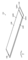
- FIG. 13A is a schematic cross-sectional view showing the configuration of the semiconductor light emitting device described in Patent Document 1.
- FIG. 13B is a schematic perspective view showing the configuration of the submount 1020 described in Patent Document 1.
- the semiconductor light emitting device described in Patent Document 1 includes a submount 1020 and a semiconductor laser element 1001 mounted on the submount 1020 via a solder 1006.
- the submount 1020 is located on the heat sink 1003.
- guide portions 1021 are formed on the end faces 1020a and 1020b of the submount 1020 made of AlN (aluminum nitride).
- the guide portion 1021 is a portion in which Pt having better wettability than the submount 1020 is embedded in the recess formed in the submount 1020 with respect to the solder 1006.
- the emission surface of the semiconductor light emitting device is arranged near the guide portion 1021.
- the solder 1006 is thinly spread on the surface of the guide portion 1021 to prevent the solder 1006 from protruding near the emission surface of the semiconductor laser element 1001.
- the vicinity of the emission surface is the hottest portion.
- Pt arranged in the guide portion 1021 has a lower thermal conductivity than AlN. Therefore, by embedding Pt in the submount 1020, the heat dissipation characteristics near the emission surface of the semiconductor laser device 1001 are deteriorated. Therefore, when a high-output semiconductor laser device 1001 is used, COD (Catatropic Optical Damage) may occur in the vicinity of the emission surface of the semiconductor laser device 1001.
- COD Catatropic Optical Damage
- an object of the present invention is to provide a semiconductor light emitting device having good heat dissipation characteristics and capable of suppressing protrusion of a bonding member near the emission surface of a semiconductor light emitting device. do.
- one aspect of the semiconductor light emitting device includes a semiconductor light emitting element that emits light and a submount having a mounting surface on which the semiconductor light emitting element is mounted via a bonding member.
- a semiconductor light emitting device including a semiconductor laminate having a facing surface facing the mounting surface and an emission surface located at an end of the facing surface and emitting the light. It has one or more mounting electrodes arranged on the facing surface of the semiconductor laminate and extending in the emission direction of the light, and the emitting surface is located outside the mounting surface from the end portion of the mounting surface.
- One or more grooves extending in the emission direction are formed on the facing surface of the semiconductor laminate along the one or more mounting electrodes, and the first distance between the emission surface and the one or more grooves is formed. Is greater than zero and less than the second distance between the exit surface and the mounting surface.
- the joining member can be guided to the groove, so that the joining member flowing out from between the semiconductor light emitting device and the submount can be reduced.
- the joining member flowing out from between the semiconductor light emitting device and the submount through the groove is along the side wall substantially parallel to the exit surface of the groove. It is guided to flow in the direction. That is, the joining member is guided to flow in the direction along the end surface located at the end of the mounting surface of the submount. Therefore, it is possible to prevent the joining member from projecting in the vicinity of the exit surface in the direction perpendicular to the exit surface. Further, since the mounting electrode near the emission surface is bonded to the submount, the heat dissipation characteristics of the semiconductor light emitting device near the emission surface are not impaired.
- the second distance may be smaller than the third distance between the exit surface and the one or more mounting electrodes.
- the heat generated near the end near the exit surface of the mounting electrode of the semiconductor light emitting element is not only in the direction perpendicular to the mounting surface but also in the submount. It is also dissipated in the direction toward the end face, that is, in the direction inclined with respect to the mounting surface. Therefore, the heat dissipation characteristics of the semiconductor light emitting device 101 can be improved.
- the semiconductor laminate is arranged above the substrate, the first conductive type first semiconductor layer arranged above the substrate, and the first semiconductor layer.
- the light emitting layer is provided with a second semiconductor layer of a second conductive type different from the first conductive type arranged above the light emitting layer, and the one or more mounting electrodes are of the second semiconductor layer. It may be placed above.
- the semiconductor light emitting device is mounted at the junction down.
- the light emitting layer having a large calorific value can be arranged near the submount as compared with the case where the semiconductor light emitting element is mounted in a junction-up manner, so that the heat dissipation characteristics of the semiconductor light emitting device can be improved.
- the one or more mounting electrodes include a first mounting electrode
- the one or more grooves include a first groove adjacent to the first mounting electrode.
- the average distance between the portion of the first groove adjacent to the first mounting electrode in the direction perpendicular to the emission direction and the direction perpendicular to the emission direction of the first mounting electrode is the average distance of the first groove. It may be smaller than the average distance between the portion arranged closer to the emission surface than the first mounting electrode and the first mounting electrode in the direction perpendicular to the emission direction.
- the band gap of the light emitting layer becomes smaller.
- each side wall of the one or more grooves may include a layer having a higher wettability of the bonding member than the semiconductor laminate.
- the wettability of the side wall of the groove can be enhanced, so that the effect of guiding the joining member to the inside of the groove can be further enhanced.
- each side wall of the one or more grooves may include an Au layer.
- the wettability of the side wall of the groove can be enhanced, so that the effect of guiding the joining member to the inside of the groove can be further enhanced.
- one or more convex portions may be formed in each of the one or more grooves.
- the area of the highly wettable surface can be increased, so that the effect of inducing the joining member from the inside of the groove can be further enhanced.
- the one or more mounting electrodes may include a plurality of mounting electrodes
- the one or more grooves may include a plurality of grooves.
- the semiconductor light emitting device is a multi-emitter type
- the amount of heat generated by the semiconductor light emitting device is further increased, but the heat dissipation characteristics due to the submount are good, so that the generation of COD can be suppressed.
- the present disclosure it is possible to provide a semiconductor light emitting device having good heat dissipation characteristics and capable of suppressing protrusion of a bonding member near the emission surface of the semiconductor light emitting device.
- FIG. 1 is a schematic perspective view showing the overall configuration of the semiconductor light emitting device according to the first embodiment.
- FIG. 2 is a schematic perspective view showing the overall configuration of the semiconductor light emitting device according to the first embodiment.
- FIG. 3 is a schematic plan view showing a configuration in the vicinity of the emission surface of the semiconductor light emitting device according to the first embodiment.
- FIG. 4 is a schematic first cross-sectional view showing the configuration of the semiconductor light emitting device according to the first embodiment.
- FIG. 5 is a schematic second sectional view showing the configuration of the semiconductor light emitting device according to the first embodiment.
- FIG. 6 is a schematic third sectional view showing the configuration of the semiconductor light emitting device according to the first embodiment.
- FIG. 1 is a schematic perspective view showing the overall configuration of the semiconductor light emitting device according to the first embodiment.
- FIG. 2 is a schematic perspective view showing the overall configuration of the semiconductor light emitting device according to the first embodiment.
- FIG. 3 is a schematic plan view showing a configuration in the vicinity of the
- FIG. 7 is a schematic first cross-sectional view illustrating the operation of the semiconductor light emitting device according to the first embodiment.
- FIG. 8 is a schematic second sectional view illustrating the operation of the semiconductor light emitting device according to the first embodiment.
- FIG. 9 is a schematic plan view showing a configuration in the vicinity of the emission surface of the semiconductor light emitting device included in the semiconductor light emitting device according to the second embodiment.
- FIG. 10 is a schematic plan view showing a configuration in the vicinity of the emission surface of the semiconductor light emitting device included in the semiconductor light emitting device according to the third embodiment.
- FIG. 11 is a schematic plan view showing a configuration in the vicinity of the emission surface of the semiconductor light emitting device according to the fourth embodiment.
- FIG. 12 is a schematic cross-sectional view showing a configuration near an emission surface of the semiconductor light emitting device according to the fourth embodiment.
- FIG. 13A is a schematic cross-sectional view showing the configuration of the semiconductor light emitting device described in Patent Document 1.
- FIG. 13B is a schematic perspective view showing the configuration of the submount described in Patent Document 1.
- each figure is a schematic diagram and is not necessarily exactly illustrated. Therefore, the scales and the like do not always match in each figure.
- the same reference numerals are given to substantially the same configurations, and duplicate explanations will be omitted or simplified.
- the terms “upper” and “lower” do not refer to the upward direction (vertically upward) and the downward direction (vertically downward) in absolute spatial recognition, but are based on the stacking order in the laminated configuration. It is used as a term defined by the relative positional relationship. Also, the terms “upper” and “lower” are used not only when the two components are spaced apart from each other and another component exists between the two components, but also when the two components are present. It also applies when they are placed in contact with each other.
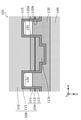
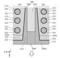
- 1 and 2 are schematic perspective views showing the overall configuration of the semiconductor light emitting device 100 and the semiconductor light emitting device 101 according to the present embodiment, respectively.
- FIG. 3 is a schematic plan view showing a configuration in the vicinity of the emission surface 100F of the semiconductor light emitting device 101 according to the present embodiment.
- FIG. 3 shows a plan view of the position corresponding to the inside of the dashed line frame III of FIG.
- the illustration of the submount 140 is partially omitted, and only the position of the end face of the submount 140 is shown by a broken line.
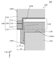
- FIG. 4 to 6 are schematic cross-sectional views showing the configuration of the semiconductor light emitting device 101 according to the present embodiment.
- FIG. 5, and FIG. 6 show cross sections of the semiconductor light emitting device 101 shown in FIG. 3 in the IV-IV line, the VV line, and the VI-VI line, respectively.
- each figure shows an X-axis, a Y-axis, and a Z-axis which are perpendicular to each other.
- a semiconductor light emitting element 100 that emits light and a semiconductor light emitting element 100 are mounted via a bonding member 130 (see FIGS. 4 to 6). It is a device including a submount 140 having a mounting surface 140 m to be mounted.
- the semiconductor light emitting device 101 further includes a joining member 130 for joining the semiconductor light emitting element 100 and the submount 140.
- the submount 140 is a base on which the semiconductor light emitting element 100 is mounted and has a high thermal conductivity, and has a function of dissipating the heat generated by the semiconductor light emitting element 100.
- the semiconductor light emitting device 100 is mounted on the submount 140 via the bonding member 130.
- the submount 140 is formed of AlN, diamond, or the like, and has a rectangular parallelepiped shape.
- the joining member 130 is not particularly limited as long as it is a member capable of joining the semiconductor light emitting device 100 and the submount 140, but is, for example, a solder containing AuSn or the like.
- the semiconductor light emitting device 100 has a semiconductor laminate 108 and a mounting electrode 114.
- the semiconductor light emitting device 100 is a multi-emitter type semiconductor laser array that emits a plurality of laser beams.
- the light emitting direction of the semiconductor light emitting device 100 is a direction parallel to the Y-axis direction in each figure.
- the light emission direction of the semiconductor light emitting device 100 corresponds to the resonance direction of the laser light.
- the semiconductor laminate 108 is a rectangular parallelepiped element, and as shown in FIG. 2, has a facing surface 100m facing the mounting surface 140m of the submount 140 and an emission surface 100F for emitting light.
- the semiconductor laminate 108 further has a rear end surface 100R facing back to the exit surface 100F.
- the facing surface 100m is a surface perpendicular to the Z-axis direction in FIG. 2
- the exit surface 100F is a surface perpendicular to the Y-axis direction in FIG.
- light resonates between the exit surface 100F and the rear end surface 100R.
- the exit surface 100F of the semiconductor laminate 108 is located outside the mounting surface 140m from the end of the mounting surface 140m of the submount 140.
- one or more mounting electrodes 114 are arranged on the facing surface 100m of the semiconductor laminate 108, and one or more grooves 120 extending in the emission direction along the mounting electrodes 114 are formed.
- a plurality of grooves 120 are formed in the semiconductor laminate 108.
- the plurality of grooves 120 are arranged in a direction perpendicular to the emission direction and parallel to the facing surface 100 m.
- Each of the plurality of grooves 120 has a pair of side walls 120a and 120b extending in the exit direction, as shown in FIGS. 3 and 4. As shown in FIG.
- the first distance L1 between the emission surface 100F of the semiconductor light emitting device 100 and each of the plurality of grooves 120 is larger than zero. That is, each of the plurality of grooves 120 is not formed on the exit surface 100F.
- the first distance L1 is more accurately between the exit surface 100F and the position closest to the exit surface 100F among each of the plurality of grooves 120 (that is, the position closest to the exit surface 100F). Defined by distance.
- the first distance L1 is smaller than the second distance L2 between the exit surface 100F and the mounting surface 140 m. The action and effect of the relationship between the first distance L1 and the second distance L2 will be described later.
- the groove 120 is formed by etching the crystal growth layer 109 by, for example, a wet etching method or a dry etching method. In this embodiment, a part of the substrate 110 is also etched.
- the semiconductor laminate 108 has a substrate 110, a crystal growth layer 109, and an insulating layer 115.
- the substrate 110 is the base of the semiconductor light emitting device 100.
- the substrate 110 is an n-type GaN substrate having a thickness of 80 ⁇ m.
- the crystal growth layer 109 is a semiconductor layer in which crystals are grown on the main surface of the substrate 110.
- the crystal growth layer 109 has a first semiconductor layer 111, a light emitting layer 112, and a second semiconductor layer 113.
- Each layer of the crystal growth layer 109 is formed by, for example, an organic metal vapor phase growth method (MOCVD) or the like.
- the first semiconductor layer 111 is a first conductive type semiconductor layer arranged above the substrate 110.
- the first conductive type is n-type
- the first semiconductor layer 111 includes an n-type clad layer made of n—Al 0.03 Ga 0.97 N having a thickness of 3 ⁇ m.
- the first semiconductor layer 111 may include a layer other than the n-type clad layer.
- the first semiconductor layer 111 may include a buffer layer or the like arranged between the substrate 110 and the n-type clad layer.
- the light emitting layer 112 is a layer arranged above the first semiconductor layer 111.
- the light emitting layer 112 is a quantum well active layer in which a well layer having a thickness of 5 nm made of In 0.06 Ga 0.94 N and a barrier layer having a thickness of 10 nm made of GaN are alternately laminated. Including, it has two well layers.
- the light emitting layer 112 may include a layer other than the quantum well active layer.
- the light emitting layer 112 may include an optical guide layer or the like.
- the second semiconductor layer 113 is a second conductive type semiconductor layer different from the first conductive type, which is arranged above the light emitting layer 112.
- the second conductive type is a p type
- the second semiconductor layer 113 is a layer having a thickness of 3 nm made of p—Al 0.06 Ga 0.94 N and a thickness of 3 nm made of GaN.
- the second semiconductor layer 113 may include a layer other than the p-type clad layer.
- the second semiconductor layer 113 may include a p-type contact layer arranged between the p-type clad layer and the mounting electrode 114. Further, as shown in FIGS. 4 to 6, a ridge portion 113r for confining light and current is formed in the second semiconductor layer 113. The ridge portion 113r is formed by etching the second semiconductor layer 113, for example, by a dry etching method.
- the insulating layer 115 is a layer formed of an insulating material arranged above the second semiconductor layer 113. An opening is formed in the insulating layer 115, and the mounting electrode 114 is arranged in the opening. The opening is formed in a portion of the insulating layer 115 on the ridge portion 113r. The surface layer of the groove 120 is also formed of the insulating layer 115.
- the insulating layer 115 is a SiO 2 layer having a thickness of 300 nm.
- the illustration of the insulating layer 115 is omitted.
- the insulating layer 115 is formed by, for example, a plasma CVD method.
- the mounting electrode 114 is an electrode that is arranged on the facing surface 100 m of the semiconductor laminate 108 and extends in the light emitting direction.
- the semiconductor light emitting device 100 has a plurality of mounting electrodes 114.
- the mounting electrode 114 has a rectangular shape in which the longitudinal direction is the light emitting direction.
- the mounting electrode 114 is a laminated film arranged above the second semiconductor layer 113 and in which Pd and Pt are laminated in order from the second semiconductor layer 113 side.
- the mounting electrode 114 is not formed near the exit surface 100F of the semiconductor laminate 108. That is, a non-injection region in which no current is injected is formed between the mounting electrode 114 and the exit surface 100F.
- the mounting electrode 114 arranged above the second semiconductor layer 113 is arranged facing the mounting surface 114m of the submount 140. That is, the semiconductor light emitting device 100 is junction-down mounted on the submount 140.
- the light emitting layer 112 having a larger heat generation amount can be arranged closer to the submount 140 than when the semiconductor light emitting element 100 is mounted in a junction-up manner, so that the heat dissipation characteristics of the semiconductor light emitting device 101 can be improved.
- the third distance L3 between the exit surface 100F and the mounting electrodes 114 is larger than zero.
- the second distance L2 between the exit surface 100F and the mounting surface 140m of the submount 140 is smaller than the third distance L3 between the exit surface 100F and the mounting electrode 114. The action and effect of the relationship between the second distance L2 and the third distance L3 will be described later.
- the mounting electrode 114 is arranged between two adjacent grooves 120 in a plan view of the facing surface 100 m of the semiconductor light emitting device 100.
- the mounting electrode 114 is arranged on the ridge portion 113r.
- the current is supplied to the portion of the light emitting layer 112 located below the mounting electrode 114. Therefore, light is generated in the portion of the light emitting layer 112 that faces the mounting electrode 114 (that is, the portion located below the ridge portion 113r).
- a back surface electrode is formed on the main surface on the back side of the main surface on which the crystal growth layer 109 of the substrate 110 is formed.
- the back surface electrode is, for example, a laminated film in which Ti, Pt, and Au are formed in this order from the substrate 110.
- the mounting electrode 114 and the back surface electrode according to this embodiment are formed by, for example, a vacuum vapor deposition method.
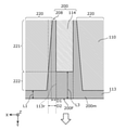
- FIGS. 7 and 8 are schematic cross-sectional views illustrating the operation of the semiconductor light emitting device 101 according to the present embodiment. 7 and 8 show cross sections of the semiconductor light emitting device 101 shown in FIG. 3 on the VII-VII line and the VIII-VIII line, respectively.
- the bonding member 130 arranged between the submount 140 and the semiconductor light emitting element 100 is melted by heating.
- the semiconductor light emitting element 100 is mounted on the submount 140, the semiconductor light emitting element 100 is pressed against the joining member 130 of the submount 140.
- a part of the joining member 130 arranged between the submount 140 and the mounting electrode 114 shown in FIG. 8 is pushed outward from between the submount 140 and the mounting electrode 114.
- the extruded joining member 130 flows into the groove 120 as shown in FIG. 7. Therefore, it is possible to reduce the number of joining members 130 flowing out from between the emission surface 100F of the semiconductor light emitting device 100 and the submount 140.
- the joining member 130 that has flowed into the groove 120 may flow out from between the exit surface 100F of the semiconductor light emitting element 100 and the submount 140.
- the first distance L1 between the exit surface 100F and the groove 120 is from the second distance L2 between the exit surface 100F and the mounting surface 140m of the submount 140. small. That is, the side wall 120e of the groove 120 facing back to the exit surface 100F is located outside the submount 140 from the end surface 140e of the submount 140. Therefore, the joining member 130 flowing out from between the semiconductor light emitting device 100 and the submount 140 through the groove 120 is guided to flow in the direction along the side wall 120e of the groove 120 substantially parallel to the exit surface 100F.
- the joining member 130 is guided to flow in the direction along the end surface 140e located at the end of the mounting surface 140m of the submount 140. Therefore, it is possible to prevent the joining member 130 from projecting in the vicinity of the exit surface 100F in a direction perpendicular to the exit surface 100F.
- the mounting electrode 114 near the exit surface 100F is joined to the submount 140.
- the joining member 130 is suppressed from protruding in the vicinity of the exit surface 100F as described above, the thermal conductivity is suppressed in the vicinity of the exit surface 100F of the submount 140 as in the submount described in Patent Document 1.
- the heat dissipation characteristics of the semiconductor light emitting device 101 near the emission surface 100F are not impaired.
- the second distance L2 is smaller than the third distance L3 between the exit surface 100F and the mounting electrode 114.
- the heat generated near the end of the mounting electrode 114 of the semiconductor light emitting element 100 near the exit surface 100F is not only in the direction perpendicular to the mounting surface 140m (that is, below the mounting electrode 114 in FIG. 8), but also in the sub. It is also dissipated in the direction toward the end surface 140e of the mount 140, that is, in the direction inclined with respect to the mounting surface 140 m (see the broken line arrow in FIG. 8).
- the second distance L2 is equal to or greater than the third distance L3, that is, when the mounting electrode 114 is arranged up to the end of the mounting surface 140m of the submount 140, it is close to the exit surface 100F of the mounting electrode 114.
- the heat generated near the end is dissipated only in the direction perpendicular to the mounting surface 140 m. Therefore, since the second distance L2 is smaller than the third distance L3, the heat dissipation characteristics of the semiconductor light emitting device 101 can be improved as compared with the case where the second distance L2 is the third distance L3 or more.
- the semiconductor light emitting device 101 has good heat dissipation characteristics and can suppress the joining member 130 from protruding near the emission surface 100F of the semiconductor light emitting element 100.
- the semiconductor light emitting device 100 is a multi-emitter type as in the present embodiment, the amount of heat generated by the semiconductor light emitting device 100 is further increased, but the heat dissipation characteristics of the submount 140 are good, so that the COD Occurrence can be suppressed.
- the semiconductor light emitting device according to the second embodiment will be described.
- the semiconductor light emitting device according to the present embodiment is different from the semiconductor light emitting device 101 according to the first embodiment in the shape of the groove formed in the semiconductor light emitting device.
- the semiconductor light emitting device according to the present embodiment will be described with reference to FIG. 9, focusing on the differences from the semiconductor light emitting device 101 according to the first embodiment.
- FIG. 9 is a schematic plan view showing a configuration in the vicinity of the emission surface 200F of the semiconductor light emitting device 200 included in the semiconductor light emitting device according to the present embodiment.
- FIG. 9 shows a plan view of the facing surface 200 m of the semiconductor light emitting device 200 in a plan view.
- the semiconductor light emitting device includes a semiconductor light emitting element 200 and a submount 140.
- the semiconductor light emitting device 200 includes a semiconductor laminate 208 and one or more mounting electrodes 114.
- the semiconductor laminate 208 according to the present embodiment one or more mounting electrodes 114 are arranged, and one or more grooves 220 extending in the emission direction along the mounting electrodes 114 are formed.
- the semiconductor light emitting device 200 according to the present embodiment is different from the semiconductor light emitting device 100 according to the first embodiment in the shape of the groove 220, and is the same in other configurations.
- the first portion 221 of the groove 220 adjacent to the mounting electrode 114 in the direction perpendicular to the exit direction (and the stacking direction of the semiconductor laminate 208) (that is, the X-axis direction in FIG. 9).
- the average distance D1 in the direction perpendicular to the emission direction with the mounting electrode 114 (and the stacking direction of the semiconductor laminate 208) is the second portion 222 of the groove 220 arranged closer to the emission surface than the mounting electrode 114. Is smaller than the average distance D2 in the direction perpendicular to the emission direction with the mounting electrode 114 (and the stacking direction of the semiconductor laminate 208).
- the average distance D1 between the first portion 221 of the groove 220 adjacent to the mounting electrode 114 in the X-axis direction and the ridge portion 113r of the second semiconductor layer 113 is the emission surface from the mounting electrode 114 of the groove 220. It is smaller than the average distance D2 between the second portion 222 arranged at a position close to the ridge portion 113r and the ridge portion 113r.
- the semiconductor light emitting device 200 has the above-mentioned configuration.
- the light emitting layer 112 arranged between the mounting electrode 114 and the emission surface 200F, that is, the light emitting layer 112 in the non-injection region is the light emitting layer 112 in the portion facing the mounting electrode 114, that is, the injection region.
- the average bandgap is larger than that of the light emitting layer 112 in. Therefore, since the light absorption in the light emitting layer in the non-injection region near the exit surface 200F can be reduced, the calorific value in the non-injection region becomes small. Therefore, according to the semiconductor light emitting device 200 according to the present embodiment, it is possible to suppress the generation of COD in the non-injection region.
- the shape of the side surface of the groove 220 near the mounting electrode 114 is linear in plan view, but may be curved.
- the semiconductor light emitting device according to the third embodiment will be described.
- the semiconductor light emitting device according to the present embodiment is different from the semiconductor light emitting device according to the second embodiment in the internal configuration of the groove formed in the semiconductor light emitting device.
- the semiconductor light emitting device according to the present embodiment will be described with reference to FIG. 10, focusing on the differences from the semiconductor light emitting device according to the second embodiment.
- FIG. 10 is a schematic plan view showing a configuration in the vicinity of the emission surface 300F of the semiconductor light emitting element 300 included in the semiconductor light emitting device according to the present embodiment.
- FIG. 10 shows a plan view of the facing surface 300 m facing the submount 140 of the semiconductor light emitting device 300 in a plan view.
- the semiconductor light emitting device includes a semiconductor light emitting element 300 and a submount 140.
- the semiconductor light emitting device 300 includes a semiconductor laminate 308 and one or more mounting electrodes 114.
- one or more mounting electrodes 114 are arranged, and one or more grooves 320 extending in the emission direction along the mounting electrodes 114 are formed.
- the semiconductor light emitting device 300 according to the present embodiment is different from the semiconductor light emitting device 200 according to the second embodiment in the internal configuration of the groove 320, and is the same in other configurations.
- the side wall 320a of the groove 320 includes an Au layer 322 having a higher wettability of the joining member 130 than the semiconductor laminate 308. Therefore, since the wettability of the joining member 130 on the side wall 320a of the groove 320 can be enhanced, the effect of guiding the joining member 130 to the inside of the groove 320 along the side wall 320a can be enhanced.
- each of the convex portions 321 is a columnar portion erected on the bottom surface of the groove 320.
- the convex portion 321 may be formed, for example, by leaving a portion that is not removed by etching inside the groove 320 when the groove 320 is formed by etching or the like.
- the convex portion 321 is formed by leaving a part of the second semiconductor layer 113 of the semiconductor laminate 308 as a portion that is not removed during etching.
- the convex portion 321 By forming such a convex portion 321 inside the groove 320, the contact area between the joining member 130 and the inside of the groove 320 can be increased. Therefore, the effect of inducing the joining member 130 inside the groove 320 can be further enhanced. Further, as shown in FIG. 10, the convex portion 321 may also include the Au layer 322 like the side wall 320a. Thereby, the effect of guiding the joining member 130 into the groove 320 can be further enhanced. Although not shown in FIG. 10, an insulating layer formed of SiO 2 or the like is arranged between the Au layer 322 and a semiconductor such as the second semiconductor layer 113.
- the bottom surface of the groove 320 may also include an Au layer. Thereby, the effect of guiding the joining member 130 into the groove 320 can be further enhanced.
- the Au layer 322 is used as the layer having good wettability of the joining member 130, but a metal layer such as an Ag layer, a Sn layer, a Ni layer, or a Pd layer other than the Au layer 322 may be used. good.
- the semiconductor light emitting device according to the fourth embodiment will be described.
- the semiconductor light emitting device according to the present embodiment is different from the semiconductor light emitting device 101 according to the first embodiment in that a groove is formed from the substrate side of the semiconductor light emitting device.
- the semiconductor light emitting device according to the present embodiment will be described with reference to FIGS. 11 and 12, focusing on the differences from the semiconductor light emitting device 101 according to the first embodiment.
- FIG. 11 and 12 are schematic plan views and cross-sectional views showing the configuration of the semiconductor light emitting device 401 according to the present embodiment in the vicinity of the emission surface 400F, respectively.
- FIG. 11 in order to show the configuration of the semiconductor light emitting device 400 included in the semiconductor light emitting device 401, the illustration of the submount 140 is partially omitted, and only the position of the end face of the submount 140 is shown by a broken line. ..
- FIG. 12 shows a cross section of the semiconductor light emitting device 401 shown in FIG. 11 in line XII-XII.
- the semiconductor light emitting device 401 includes a semiconductor light emitting element 400 and a submount 140. As shown in FIG. 12, the semiconductor light emitting device 401 further includes a joining member 130.
- the semiconductor light emitting device 400 has a semiconductor laminate 408, one or more mounting electrodes 419, and one or more back surface electrodes 414.
- the semiconductor laminate 408 has a substrate 410 and a crystal growth layer 409.
- the crystal growth layer 409 has a first semiconductor layer 411, a light emitting layer 412, and a second semiconductor layer 413.
- the substrate 410, the first semiconductor layer 411, the light emitting layer 412, and the second semiconductor layer 413 are the substrate 110, the first semiconductor layer 411, the light emitting layer 412, and the second semiconductor layer 100 of the semiconductor light emitting device 100 according to the first embodiment, respectively. It has the same material and thickness as the semiconductor layer 413.
- a back surface electrode 414 is arranged above the second semiconductor layer 413.
- the back surface electrode 414 has the same configuration as the mounting electrode 114 according to the first embodiment.
- the facing surface 400 m facing the submount 140 of the semiconductor laminate 408 is the main surface on the back side of the main surface on which the crystal growth layer 409 of the substrate 410 is laminated, as shown in FIG. ..
- One or more mounting electrodes 419 are arranged on the facing surface 400m, and one or more grooves 420 extending in the emission direction along the mounting electrodes 419 are formed.
- the semiconductor light emitting device 400 has a plurality of mounting electrodes 419, and a plurality of grooves 420 are formed on the facing surface 400 m.
- Each of the plurality of grooves 420 has a pair of side walls 420a and 420b extending in the exit direction, as shown in FIGS. 11 and 12.
- the first distance L1 between the emission surface 400F of the semiconductor light emitting device 400 and each of the plurality of grooves 420 is larger than zero. That is, each of the plurality of grooves 420 is not formed on the exit surface 400F. Further, the first distance L1 is smaller than the second distance L2 up to the exit surface 400F and the mounting surface 140 m.
- the groove 420 is formed in the semiconductor light emitting device 400 along the mounting electrode 419, the joining member 130 extruded at the time of mounting is grooved as in the semiconductor light emitting device 101 according to the first embodiment. It flows into 420. Therefore, it is possible to reduce the number of joining members 130 flowing out from between the emission surface 400F of the semiconductor light emitting device 400 and the submount 140.
- the third distance L3 between the exit surface 400F and the mounting electrode 419 is larger than zero.
- the second distance L2 between the exit surface 400F and the mounting surface 140m of the submount 140 is smaller than the third distance L3 between the exit surface 400F and the mounting electrode 419.
- the semiconductor light emitting element is a semiconductor laser element
- the semiconductor light emitting element is not limited to the semiconductor laser element.
- the semiconductor light emitting device may be a superluminescent diode.
- the first conductive type is n type, but may be p type.
- the semiconductor light emitting device is a multi-emitter type having a plurality of mounting electrodes, but the semiconductor light emitting device may be a single emitter type having a single mounting electrode. That is, the semiconductor light emitting device may have one or more mounting electrodes.
- a plurality of grooves are formed in the semiconductor light emitting device, but a single groove may be formed in the semiconductor light emitting device. That is, it is sufficient that one or more grooves are formed in the semiconductor light emitting device.
- the configuration near the emission surface of the semiconductor light emitting device is shown, but the vicinity of the rear end surface of the semiconductor light emitting device may have the same configuration as the vicinity of the emission surface. That is, the first distance between the rear end surface and one or more grooves may be greater than zero and less than the second distance between the rear end surface and the mounting surface of the submount. Further, the second distance may be smaller than the third distance between the rear end surface and one or more mounting electrodes. As a result, the same effect as that of each embodiment is obtained.
- the plurality of grooves are formed from the surface of the second semiconductor layer 113 to the middle of the substrate 110, but the configuration of the plurality of grooves is not limited to this.
- Each of the plurality of grooves may not be formed from the surface of the second semiconductor layer 113 to the substrate 110, and may be formed, for example, from the surface of the second semiconductor layer 113 to the middle of the first semiconductor layer 111. ..
- the semiconductor light emitting device 200 may have a single mounting electrode 114 or a plurality of mounting electrodes 114. May have a mounting electrode 114 of.
- the semiconductor light emitting device 200 has a plurality of mounting electrodes 114, only one mounting electrode 114 and the groove 220 adjacent to the mounting electrode 114 may have the configuration according to the second embodiment, or may be combined with another mounting electrode 114.
- the groove 220 adjacent to the groove 220 may also have the configuration according to the second embodiment.
- one or more mounting electrodes include a first mounting electrode
- one or more grooves include a first groove adjacent to the first mounting electrode
- the first mounting is performed in the direction perpendicular to the exit direction among the first grooves.
- the average distance between the portion adjacent to the electrode and the first mounting electrode in the direction perpendicular to the emission direction is the portion of the first groove located closer to the emission surface than the first mounting electrode and the first mounting electrode. It may be smaller than the average distance in the direction perpendicular to the emission direction of.
- the insulating layer may be formed in the region where the mounting electrode 419 is not formed in the facing surface 400 m of the semiconductor laminate 408.
- the semiconductor light emitting device of the present disclosure can be applied to a processing machine, a projector, etc. as a high output and high efficiency light source, for example.
Abstract
A semiconductor light emitting device (101) is provided with: a semiconductor light emitting element (100); and a submount (140) having a mounting surface (140m). The semiconductor light emitting element (100) has: a semiconductor laminated body (108) having an opposed surface (100m) opposed to the mounting surface (140m) and an emission surface (100F); and a mounted electrode (114) that is arranged on the opposed surface (100m) and that extends in the light emission direction. The emission surface (100F) is located at a position farther on the outer side of the mounting surface (140m) than an end section of the mounting surface (140m) is. Grooves (120) extending in the emission direction along the mounted electrode (114) are formed in the opposed surface (100m) of the semiconductor laminated body (108). A first distance (L1) between the emission surface (100F) and a groove (120) is larger than zero and smaller than a second distance (L2) between the emission surface (100F) and the mounting surface (140m).
Description
本開示は、半導体発光装置に関する。
This disclosure relates to a semiconductor light emitting device.
従来、レーザ光などの光が加工用途に使用されており、高出力かつ高効率な光源が必要とされている。高出力かつ高効率な光源として、半導体発光装置が利用されている。このような高出力な半導体発光装置は、例えば、半導体レーザ素子などの半導体発光素子と、半導体発光素子が実装されるサブマウントとを備える。このような半導体発光装置において、半導体発光素子は、半田などの接合部材を用いてサブマウントに実装される。半導体発光素子をサブマウントに実装する際に、半導体発光素子の光を出射する出射面とサブマウントとの間から半田が流れ出る場合がある。このように流れ出た半田は、半導体発光素子の出射面付近に突出した状態で固まり、半導体発光素子からの光を遮ったり、半導体発光素子の出射面付近に配置される光学素子と干渉したりする。
Conventionally, light such as laser light has been used for processing applications, and a high-output and high-efficiency light source is required. A semiconductor light emitting device is used as a high-output and high-efficiency light source. Such a high-output semiconductor light-emitting device includes, for example, a semiconductor light-emitting device such as a semiconductor laser device and a submount on which the semiconductor light-emitting device is mounted. In such a semiconductor light emitting device, the semiconductor light emitting element is mounted on a submount using a bonding member such as solder. When mounting a semiconductor light emitting device on a submount, solder may flow out from between the exit surface that emits light from the semiconductor light emitting device and the submount. The solder that flows out in this way solidifies in a state of protruding near the emission surface of the semiconductor light emitting device, blocks the light from the semiconductor light emitting element, or interferes with the optical element arranged near the emission surface of the semiconductor light emitting element. ..
このような問題を解決する従来技術について図13A及び図13Bを用いて説明する。図13Aは、特許文献1に記載された半導体発光装置の構成を示す模式的な断面図である。図13Bは、特許文献1に記載されたサブマウント1020の構成を示す模式的な斜視図である。図13Aに示されるように、特許文献1に記載された半導体発光装置は、サブマウント1020と、サブマウント1020に半田1006を介して実装される半導体レーザ素子1001とを備える。サブマウント1020は、ヒートシンク1003上に配置される。図13A及び図13Bに示されるように、AlN(窒化アルミ)で形成されたサブマウント1020の端面1020a及び1020bには、案内部1021が形成されている。案内部1021は、サブマウント1020に形成された凹部に、半田1006に対してサブマウント1020より濡れ性のよいPtが埋め込まれた部分である。案内部1021付近に半導体発光素子の出射面が配置される。これにより、半田1006を案内部1021の表面に薄く広がらせることで、半導体レーザ素子1001の出射面付近に半田1006が突出することを抑制しようとしている。
The conventional technique for solving such a problem will be described with reference to FIGS. 13A and 13B. FIG. 13A is a schematic cross-sectional view showing the configuration of the semiconductor light emitting device described in Patent Document 1. FIG. 13B is a schematic perspective view showing the configuration of the submount 1020 described in Patent Document 1. As shown in FIG. 13A, the semiconductor light emitting device described in Patent Document 1 includes a submount 1020 and a semiconductor laser element 1001 mounted on the submount 1020 via a solder 1006. The submount 1020 is located on the heat sink 1003. As shown in FIGS. 13A and 13B, guide portions 1021 are formed on the end faces 1020a and 1020b of the submount 1020 made of AlN (aluminum nitride). The guide portion 1021 is a portion in which Pt having better wettability than the submount 1020 is embedded in the recess formed in the submount 1020 with respect to the solder 1006. The emission surface of the semiconductor light emitting device is arranged near the guide portion 1021. As a result, the solder 1006 is thinly spread on the surface of the guide portion 1021 to prevent the solder 1006 from protruding near the emission surface of the semiconductor laser element 1001.
特許文献1に記載された半導体レーザ素子1001において、出射面付近は最も高温になる部分である。一方、案内部1021に配置されるPtは、AlNより熱伝導率が低い。したがって、サブマウント1020にPtを埋め込むことにより、半導体レーザ素子1001の出射面付近の放熱特性が劣化する。このため、高出力な半導体レーザ素子1001を用いる場合には、半導体レーザ素子1001の出射面付近において、COD(Catastrophic Optical Damage)が発生するおそれがある。
In the semiconductor laser device 1001 described in Patent Document 1, the vicinity of the emission surface is the hottest portion. On the other hand, Pt arranged in the guide portion 1021 has a lower thermal conductivity than AlN. Therefore, by embedding Pt in the submount 1020, the heat dissipation characteristics near the emission surface of the semiconductor laser device 1001 are deteriorated. Therefore, when a high-output semiconductor laser device 1001 is used, COD (Catatropic Optical Damage) may occur in the vicinity of the emission surface of the semiconductor laser device 1001.
本開示は、このような課題を解決するものであり、良好な放熱特性を有し、半導体発光素子の出射面付近に接合部材が突出することを抑制できる半導体発光装置を提供することを目的とする。
The present disclosure has been made to solve such a problem, and an object of the present invention is to provide a semiconductor light emitting device having good heat dissipation characteristics and capable of suppressing protrusion of a bonding member near the emission surface of a semiconductor light emitting device. do.
上記課題を解決するために、本開示に係る半導体発光装置の一態様は、光を出射する半導体発光素子と、前記半導体発光素子が接合部材を介して実装される実装面を有するサブマウントとを備える半導体発光装置であって、前記半導体発光素子は、前記実装面と対向する対向面と、前記対向面の端部に位置し、前記光を出射する出射面とを有する半導体積層体と、前記半導体積層体の前記対向面に配置され、前記光の出射方向に延びる1以上の実装電極とを有し、前記出射面は、前記実装面の端部より前記実装面の外側に位置し、前記半導体積層体の前記対向面には、前記1以上の実装電極に沿って前記出射方向に延びる1以上の溝が形成されており、前記出射面と前記1以上の溝との間の第1距離はゼロより大きく、かつ、前記出射面と前記実装面との間の第2距離より小さい。
In order to solve the above problems, one aspect of the semiconductor light emitting device according to the present disclosure includes a semiconductor light emitting element that emits light and a submount having a mounting surface on which the semiconductor light emitting element is mounted via a bonding member. A semiconductor light emitting device including a semiconductor laminate having a facing surface facing the mounting surface and an emission surface located at an end of the facing surface and emitting the light. It has one or more mounting electrodes arranged on the facing surface of the semiconductor laminate and extending in the emission direction of the light, and the emitting surface is located outside the mounting surface from the end portion of the mounting surface. One or more grooves extending in the emission direction are formed on the facing surface of the semiconductor laminate along the one or more mounting electrodes, and the first distance between the emission surface and the one or more grooves is formed. Is greater than zero and less than the second distance between the exit surface and the mounting surface.
これにより、接合部材を溝に誘導することができるため、半導体発光素子とサブマウントとの間から流れ出る接合部材を削減できる。また、第1距離、第2距離、及び第3距離の相対関係により、溝を介して半導体発光素子とサブマウントとの間から流れ出る接合部材は、溝の出射面とほぼ平行な側壁に沿った向きに流れるように誘導される。つまり、接合部材は、サブマウントの実装面の端部に位置する端面に沿った方向に流れるように誘導される。このため、接合部材が、出射面付近において出射面と垂直な方向に突出することを抑制できる。また、出射面付近の実装電極は、サブマウントに接合されるため、出射面付近における半導体発光装置の放熱特性は損なわれない。
As a result, the joining member can be guided to the groove, so that the joining member flowing out from between the semiconductor light emitting device and the submount can be reduced. Further, due to the relative relationship between the first distance, the second distance, and the third distance, the joining member flowing out from between the semiconductor light emitting device and the submount through the groove is along the side wall substantially parallel to the exit surface of the groove. It is guided to flow in the direction. That is, the joining member is guided to flow in the direction along the end surface located at the end of the mounting surface of the submount. Therefore, it is possible to prevent the joining member from projecting in the vicinity of the exit surface in the direction perpendicular to the exit surface. Further, since the mounting electrode near the emission surface is bonded to the submount, the heat dissipation characteristics of the semiconductor light emitting device near the emission surface are not impaired.
また、本開示に係る半導体発光素子の一態様において、前記第2距離は、前記出射面と前記1以上の実装電極との間の第3距離より小さくてもよい。
Further, in one aspect of the semiconductor light emitting device according to the present disclosure, the second distance may be smaller than the third distance between the exit surface and the one or more mounting electrodes.
このように、第2距離が、第3距離より小さいことにより、半導体発光素子の実装電極の出射面に近い端部付近で発生した熱は、実装面に垂直な方向だけでなく、サブマウントの端面に向かう向き、つまり、実装面に対して傾斜した向きにも放散される。したがって、半導体発光装置101の放熱特性を高めることができる。
As described above, since the second distance is smaller than the third distance, the heat generated near the end near the exit surface of the mounting electrode of the semiconductor light emitting element is not only in the direction perpendicular to the mounting surface but also in the submount. It is also dissipated in the direction toward the end face, that is, in the direction inclined with respect to the mounting surface. Therefore, the heat dissipation characteristics of the semiconductor light emitting device 101 can be improved.
また、本開示に係る半導体発光素子の一態様において、前記半導体積層体は、基板と、基板の上方に配置される第1導電型の第1半導体層と、前記第1半導体層の上方に配置される発光層と、前記発光層の上方に配置される前記第1導電型と異なる第2導電型の第2半導体層とを有し、前記1以上の実装電極は、前記第2半導体層の上方に配置されてもよい。
Further, in one aspect of the semiconductor light emitting element according to the present disclosure, the semiconductor laminate is arranged above the substrate, the first conductive type first semiconductor layer arranged above the substrate, and the first semiconductor layer. The light emitting layer is provided with a second semiconductor layer of a second conductive type different from the first conductive type arranged above the light emitting layer, and the one or more mounting electrodes are of the second semiconductor layer. It may be placed above.
この場合、半導体発光素子は、ジャンクションダウン実装される。これにより、半導体発光素子がジャンクションアップ実装される場合より、発熱量の大きい発光層をサブマウントの近くに配置できるため、半導体発光装置の放熱特性を高めることができる。
In this case, the semiconductor light emitting device is mounted at the junction down. As a result, the light emitting layer having a large calorific value can be arranged near the submount as compared with the case where the semiconductor light emitting element is mounted in a junction-up manner, so that the heat dissipation characteristics of the semiconductor light emitting device can be improved.
また、本開示に係る半導体発光素子の一態様において、前記1以上の実装電極は、第1実装電極を含み、前記1以上の溝は、前記第1実装電極と隣り合う第1溝を含み、前記第1溝のうち前記出射方向に垂直な方向において前記第1実装電極と隣り合う部分と、前記第1実装電極との前記出射方向に垂直な方向における平均距離は、前記第1溝のうち前記第1実装電極より前記出射面から近い位置に配置される部分と、前記第1実装電極との前記出射方向に垂直な方向における平均距離より小さくてもよい。
Further, in one aspect of the semiconductor light emitting element according to the present disclosure, the one or more mounting electrodes include a first mounting electrode, and the one or more grooves include a first groove adjacent to the first mounting electrode. The average distance between the portion of the first groove adjacent to the first mounting electrode in the direction perpendicular to the emission direction and the direction perpendicular to the emission direction of the first mounting electrode is the average distance of the first groove. It may be smaller than the average distance between the portion arranged closer to the emission surface than the first mounting electrode and the first mounting electrode in the direction perpendicular to the emission direction.
このように、発光層付近に溝が形成されることによって、発光層のバンドギャップが小さくなる。発光層から溝までの距離が小さいほど、発光層のバンドギャップが小さくなる。このため、実装電極から出射面までの電流が注入されない非注入領域における溝までの距離を、実装電極から溝までの距離より大きくすることで、非注入領域における発光層のバンドギャップを、実装電極によって電流が注入される注入領域における発光層のバンドギャップより大きくできる。したがって、非注入領域における発光層での光吸収を低減できる。これにより、非注入領域における発熱量を低減できるため、CODの発生を抑制できる。
By forming a groove near the light emitting layer in this way, the band gap of the light emitting layer becomes smaller. The smaller the distance from the light emitting layer to the groove, the smaller the band gap of the light emitting layer. Therefore, by making the distance from the mounting electrode to the groove in the non-injection region where the current is not injected larger than the distance from the mounting electrode to the groove, the band gap of the light emitting layer in the non-injection region can be set to the mounting electrode. Can be larger than the bandgap of the light emitting layer in the injection region where the current is injected. Therefore, it is possible to reduce the light absorption in the light emitting layer in the non-injection region. As a result, the calorific value in the non-injection region can be reduced, so that the generation of COD can be suppressed.
また、本開示に係る半導体発光素子の一態様において、前記1以上の溝の各々の側壁は、前記半導体積層体より前記接合部材の濡れ性が高い層を含んでもよい。
Further, in one aspect of the semiconductor light emitting device according to the present disclosure, each side wall of the one or more grooves may include a layer having a higher wettability of the bonding member than the semiconductor laminate.
これにより、溝の側壁の濡れ性を高めることができるため、接合部材を溝の内部に誘導する効果をより一層高めることができる。
As a result, the wettability of the side wall of the groove can be enhanced, so that the effect of guiding the joining member to the inside of the groove can be further enhanced.
また、本開示に係る半導体発光素子の一態様において、前記1以上の溝の各々の側壁は、Au層を含んでもよい。
Further, in one aspect of the semiconductor light emitting device according to the present disclosure, each side wall of the one or more grooves may include an Au layer.
これにより、溝の側壁の濡れ性を高めることができるため、接合部材を溝の内部に誘導する効果をより一層高めることができる。
As a result, the wettability of the side wall of the groove can be enhanced, so that the effect of guiding the joining member to the inside of the groove can be further enhanced.
また、本開示に係る半導体発光素子の一態様において、前記1以上の溝の各々には、1以上の凸部が形成されていてもよい。
Further, in one aspect of the semiconductor light emitting device according to the present disclosure, one or more convex portions may be formed in each of the one or more grooves.
これにより、濡れ性の高い表面の面積を増大させることができるため、接合部材を溝の内部により誘導する効果をより一層高めることができる。
As a result, the area of the highly wettable surface can be increased, so that the effect of inducing the joining member from the inside of the groove can be further enhanced.
また、本開示に係る半導体発光素子の一態様において、前記1以上の実装電極は、複数の実装電極を含み、前記1以上の溝は、複数の溝を含んでもよい。
Further, in one aspect of the semiconductor light emitting device according to the present disclosure, the one or more mounting electrodes may include a plurality of mounting electrodes, and the one or more grooves may include a plurality of grooves.
このように、半導体発光素子がマルチエミッタ型である場合には、半導体発光素子における発熱量がより一層大きくなるが、サブマウントによる放熱特性が良好であるため、CODの発生を抑制できる。
As described above, when the semiconductor light emitting device is a multi-emitter type, the amount of heat generated by the semiconductor light emitting device is further increased, but the heat dissipation characteristics due to the submount are good, so that the generation of COD can be suppressed.
本開示によれば、良好な放熱特性を有し、半導体発光素子の出射面付近に接合部材が突出することを抑制できる半導体発光装置を提供できる。
According to the present disclosure, it is possible to provide a semiconductor light emitting device having good heat dissipation characteristics and capable of suppressing protrusion of a bonding member near the emission surface of the semiconductor light emitting device.
以下、本開示の実施の形態について、図面を参照しながら説明する。なお、以下に説明する実施の形態は、いずれも本開示の一具体例を示すものである。したがって、以下の実施の形態で示される、数値、形状、材料、構成要素、及び、構成要素の配置位置や接続形態などは、一例であって本開示を限定する主旨ではない。
Hereinafter, embodiments of the present disclosure will be described with reference to the drawings. It should be noted that all of the embodiments described below show a specific example of the present disclosure. Therefore, the numerical values, shapes, materials, components, the arrangement positions of the components, the connection form, and the like shown in the following embodiments are examples and do not limit the present disclosure.
また、各図は模式図であり、必ずしも厳密に図示されたものではない。したがって、各図において縮尺等は必ずしも一致していない。なお、各図において、実質的に同一の構成に対しては同一の符号を付しており、重複する説明は省略又は簡略化する。
Also, each figure is a schematic diagram and is not necessarily exactly illustrated. Therefore, the scales and the like do not always match in each figure. In each figure, the same reference numerals are given to substantially the same configurations, and duplicate explanations will be omitted or simplified.
また、本明細書において、「上方」及び「下方」という用語は、絶対的な空間認識における上方向(鉛直上方)及び下方向(鉛直下方)を指すものではなく、積層構成における積層順を基に相対的な位置関係により規定される用語として用いる。また、「上方」及び「下方」という用語は、2つの構成要素が互いに間隔をあけて配置されて2つの構成要素の間に別の構成要素が存在する場合のみならず、2つの構成要素が互いに接する状態で配置される場合にも適用される。
Further, in the present specification, the terms "upper" and "lower" do not refer to the upward direction (vertically upward) and the downward direction (vertically downward) in absolute spatial recognition, but are based on the stacking order in the laminated configuration. It is used as a term defined by the relative positional relationship. Also, the terms "upper" and "lower" are used not only when the two components are spaced apart from each other and another component exists between the two components, but also when the two components are present. It also applies when they are placed in contact with each other.
(実施の形態1)
実施の形態1に係る半導体発光装置について説明する。 (Embodiment 1)
The semiconductor light emitting device according to the first embodiment will be described.
実施の形態1に係る半導体発光装置について説明する。 (Embodiment 1)
The semiconductor light emitting device according to the first embodiment will be described.
[1-1.全体構成]
まず、本実施の形態に係る半導体発光装置の全体構成について図1~図6を用いて説明する。図1及び図2は、それぞれ、本実施の形態に係る半導体発光素子100及び半導体発光装置101の全体構成を示す模式的な斜視図である。図3は、本実施の形態に係る半導体発光装置101の出射面100F付近の構成を示す模式的な平面図である。図3には、図1の破線枠IIIの内部に対応する位置の平面図が示されている。図3においては、半導体発光素子100の構成を示すために、サブマウント140の図示は一部省略されており、サブマウント140の端面の位置だけが破線で示されている。図4~図6は、本実施の形態に係る半導体発光装置101の構成を示す模式的な断面図である。図4、図5、及び図6には、それぞれ、図3に示される半導体発光装置101のIV-IV線、V-V線、及びVI-VI線における断面が示されている。なお、各図には、互いに垂直なX軸、Y軸、及びZ軸が示されている。 [1-1. overall structure]
First, the overall configuration of the semiconductor light emitting device according to the present embodiment will be described with reference to FIGS. 1 to 6. 1 and 2 are schematic perspective views showing the overall configuration of the semiconductorlight emitting device 100 and the semiconductor light emitting device 101 according to the present embodiment, respectively. FIG. 3 is a schematic plan view showing a configuration in the vicinity of the emission surface 100F of the semiconductor light emitting device 101 according to the present embodiment. FIG. 3 shows a plan view of the position corresponding to the inside of the dashed line frame III of FIG. In FIG. 3, in order to show the configuration of the semiconductor light emitting device 100, the illustration of the submount 140 is partially omitted, and only the position of the end face of the submount 140 is shown by a broken line. 4 to 6 are schematic cross-sectional views showing the configuration of the semiconductor light emitting device 101 according to the present embodiment. 4, FIG. 5, and FIG. 6 show cross sections of the semiconductor light emitting device 101 shown in FIG. 3 in the IV-IV line, the VV line, and the VI-VI line, respectively. In addition, each figure shows an X-axis, a Y-axis, and a Z-axis which are perpendicular to each other.
まず、本実施の形態に係る半導体発光装置の全体構成について図1~図6を用いて説明する。図1及び図2は、それぞれ、本実施の形態に係る半導体発光素子100及び半導体発光装置101の全体構成を示す模式的な斜視図である。図3は、本実施の形態に係る半導体発光装置101の出射面100F付近の構成を示す模式的な平面図である。図3には、図1の破線枠IIIの内部に対応する位置の平面図が示されている。図3においては、半導体発光素子100の構成を示すために、サブマウント140の図示は一部省略されており、サブマウント140の端面の位置だけが破線で示されている。図4~図6は、本実施の形態に係る半導体発光装置101の構成を示す模式的な断面図である。図4、図5、及び図6には、それぞれ、図3に示される半導体発光装置101のIV-IV線、V-V線、及びVI-VI線における断面が示されている。なお、各図には、互いに垂直なX軸、Y軸、及びZ軸が示されている。 [1-1. overall structure]
First, the overall configuration of the semiconductor light emitting device according to the present embodiment will be described with reference to FIGS. 1 to 6. 1 and 2 are schematic perspective views showing the overall configuration of the semiconductor
本実施の形態に係る半導体発光装置101は、図2に示されるように、光を出射する半導体発光素子100と、半導体発光素子100が接合部材130(図4~図6参照)を介して実装される実装面140mを有するサブマウント140とを備える装置である。半導体発光装置101は、半導体発光素子100と、サブマウント140とを接合する接合部材130をさらに備える。
In the semiconductor light emitting device 101 according to the present embodiment, as shown in FIG. 2, a semiconductor light emitting element 100 that emits light and a semiconductor light emitting element 100 are mounted via a bonding member 130 (see FIGS. 4 to 6). It is a device including a submount 140 having a mounting surface 140 m to be mounted. The semiconductor light emitting device 101 further includes a joining member 130 for joining the semiconductor light emitting element 100 and the submount 140.
サブマウント140は、半導体発光素子100が実装される熱伝導率が高い基台であり、半導体発光素子100で発生した熱を放散する機能を有する。半導体発光素子100は、接合部材130を介してサブマウント140に実装される。本実施の形態では、サブマウント140は、AlN、ダイヤモンドなどで形成され、直方体状の形状を有する。
The submount 140 is a base on which the semiconductor light emitting element 100 is mounted and has a high thermal conductivity, and has a function of dissipating the heat generated by the semiconductor light emitting element 100. The semiconductor light emitting device 100 is mounted on the submount 140 via the bonding member 130. In the present embodiment, the submount 140 is formed of AlN, diamond, or the like, and has a rectangular parallelepiped shape.
接合部材130は、半導体発光素子100と、サブマウント140とを接合し得る部材であれば特に限定されないが、例えば、AuSnなどを含む半田である。
The joining member 130 is not particularly limited as long as it is a member capable of joining the semiconductor light emitting device 100 and the submount 140, but is, for example, a solder containing AuSn or the like.
半導体発光素子100は、図1に示されるように、半導体積層体108と、実装電極114とを有する。本実施の形態では、半導体発光素子100は、複数のレーザ光を出射するマルチエミッタ型の半導体レーザアレイである。半導体発光素子100の光の出射方向は、各図のY軸方向に平行な方向である。本実施の形態では、半導体発光素子100の光の出射方向は、レーザ光の共振方向に相当する。
As shown in FIG. 1, the semiconductor light emitting device 100 has a semiconductor laminate 108 and a mounting electrode 114. In the present embodiment, the semiconductor light emitting device 100 is a multi-emitter type semiconductor laser array that emits a plurality of laser beams. The light emitting direction of the semiconductor light emitting device 100 is a direction parallel to the Y-axis direction in each figure. In the present embodiment, the light emission direction of the semiconductor light emitting device 100 corresponds to the resonance direction of the laser light.
半導体積層体108は、直方体状の素子であり、図2に示されるように、サブマウント140の実装面140mと対向する対向面100mと、光を出射する出射面100Fとを有する。半導体積層体108は、出射面100Fと背向する後端面100Rをさらに有する。対向面100mは、図2のZ軸方向に垂直な面であり、出射面100Fは、図2のY軸方向に垂直な面である。本実施の形態では、出射面100Fと後端面100Rとの間で光が共振する。図3に示されるように、半導体積層体108の出射面100Fは、サブマウント140の実装面140mの端部より実装面140mの外側に位置する。
The semiconductor laminate 108 is a rectangular parallelepiped element, and as shown in FIG. 2, has a facing surface 100m facing the mounting surface 140m of the submount 140 and an emission surface 100F for emitting light. The semiconductor laminate 108 further has a rear end surface 100R facing back to the exit surface 100F. The facing surface 100m is a surface perpendicular to the Z-axis direction in FIG. 2, and the exit surface 100F is a surface perpendicular to the Y-axis direction in FIG. In this embodiment, light resonates between the exit surface 100F and the rear end surface 100R. As shown in FIG. 3, the exit surface 100F of the semiconductor laminate 108 is located outside the mounting surface 140m from the end of the mounting surface 140m of the submount 140.
図1に示されるように、半導体積層体108の対向面100mには、1以上の実装電極114が配置され、かつ、実装電極114に沿って出射方向に延びる1以上の溝120が形成されている。本実施の形態では、半導体積層体108には、複数の溝120が形成されている。図1に示されるように、複数の溝120は、出射方向に垂直で、かつ、対向面100mに平行な方向に配列されている。複数の溝120の各々は、図3及び図4に示されるように、出射方向に延びる一対の側壁120a及び120bを有する。図3に示されるように、半導体発光素子100の出射面100Fと複数の溝120の各々との間の第1距離L1は、ゼロより大きい。つまり、複数の溝120の各々は、出射面100Fには形成されていない。ここで、第1距離L1は、より正確には、出射面100Fと、複数の溝120の各々の中で最も出射面100F寄りの位置(つまり、出射面100Fから最も近い位置)との間の距離で定義される。また、第1距離L1は、出射面100Fと実装面140mとの間の第2距離L2より小さい。第1距離L1と第2距離L2との関係による作用及び効果については後述する。
As shown in FIG. 1, one or more mounting electrodes 114 are arranged on the facing surface 100m of the semiconductor laminate 108, and one or more grooves 120 extending in the emission direction along the mounting electrodes 114 are formed. There is. In the present embodiment, a plurality of grooves 120 are formed in the semiconductor laminate 108. As shown in FIG. 1, the plurality of grooves 120 are arranged in a direction perpendicular to the emission direction and parallel to the facing surface 100 m. Each of the plurality of grooves 120 has a pair of side walls 120a and 120b extending in the exit direction, as shown in FIGS. 3 and 4. As shown in FIG. 3, the first distance L1 between the emission surface 100F of the semiconductor light emitting device 100 and each of the plurality of grooves 120 is larger than zero. That is, each of the plurality of grooves 120 is not formed on the exit surface 100F. Here, the first distance L1 is more accurately between the exit surface 100F and the position closest to the exit surface 100F among each of the plurality of grooves 120 (that is, the position closest to the exit surface 100F). Defined by distance. Further, the first distance L1 is smaller than the second distance L2 between the exit surface 100F and the mounting surface 140 m. The action and effect of the relationship between the first distance L1 and the second distance L2 will be described later.
溝120は、例えば、ウェットエッチング法、ドライエッチング法などによって、結晶成長層109をエッチングすることによって形成される。なお、本実施の形態では、基板110の一部もエッチングされる。
The groove 120 is formed by etching the crystal growth layer 109 by, for example, a wet etching method or a dry etching method. In this embodiment, a part of the substrate 110 is also etched.
半導体積層体108は、図4~図6に示されるように、基板110と、結晶成長層109と、絶縁層115とを有する。
As shown in FIGS. 4 to 6, the semiconductor laminate 108 has a substrate 110, a crystal growth layer 109, and an insulating layer 115.
基板110は、半導体発光素子100の基台である。本実施の形態では、基板110は、厚さ80μmのn型GaN基板である。
The substrate 110 is the base of the semiconductor light emitting device 100. In the present embodiment, the substrate 110 is an n-type GaN substrate having a thickness of 80 μm.
結晶成長層109は、基板110の主面に結晶成長させた半導体層である。結晶成長層109は、第1半導体層111と、発光層112と、第2半導体層113とを有する。結晶成長層109の各層は、例えば、有機金属気相成長法(MOCVD)などにより形成される。
The crystal growth layer 109 is a semiconductor layer in which crystals are grown on the main surface of the substrate 110. The crystal growth layer 109 has a first semiconductor layer 111, a light emitting layer 112, and a second semiconductor layer 113. Each layer of the crystal growth layer 109 is formed by, for example, an organic metal vapor phase growth method (MOCVD) or the like.
第1半導体層111は、基板110の上方に配置される第1導電型の半導体層である。本実施の形態では、第1導電型はn型であり、第1半導体層111は、厚さ3μmのn-Al0.03Ga0.97Nからなるn型クラッド層を含む。第1半導体層111は、n型クラッド層以外の層を含んでもよい。例えば、第1半導体層111は、基板110とn型クラッド層との間に配置されるバッファ層などを含んでもよい。
The first semiconductor layer 111 is a first conductive type semiconductor layer arranged above the substrate 110. In the present embodiment, the first conductive type is n-type, and the first semiconductor layer 111 includes an n-type clad layer made of n—Al 0.03 Ga 0.97 N having a thickness of 3 μm. The first semiconductor layer 111 may include a layer other than the n-type clad layer. For example, the first semiconductor layer 111 may include a buffer layer or the like arranged between the substrate 110 and the n-type clad layer.
発光層112は、第1半導体層111の上方に配置される層である。本実施の形態では、発光層112は、In0.06Ga0.94Nからなる厚さ5nmの井戸層とGaNからなる厚さ10nmの障壁層とが交互に積層された量子井戸活性層を含み、2層の井戸層を有する。発光層112は、量子井戸活性層以外の層を含んでもよい。例えば、発光層112は、光ガイド層などを含んでもよい。
The light emitting layer 112 is a layer arranged above the first semiconductor layer 111. In the present embodiment, the light emitting layer 112 is a quantum well active layer in which a well layer having a thickness of 5 nm made of In 0.06 Ga 0.94 N and a barrier layer having a thickness of 10 nm made of GaN are alternately laminated. Including, it has two well layers. The light emitting layer 112 may include a layer other than the quantum well active layer. For example, the light emitting layer 112 may include an optical guide layer or the like.
第2半導体層113は、発光層112の上方に配置される、第1導電型と異なる第2導電型の半導体層である。本実施の形態では、第2導電型は、p型であり、第2半導体層113は、p-Al0.06Ga0.94Nからなる厚さ3nmの層と、GaNからなる厚さ3nmの層とが交互に100層ずつ積層された厚さ0.6μmの超格子層からなるp型クラッド層を含む。第2半導体層113は、p型クラッド層以外の層を含んでもよい。例えば、第2半導体層113は、p型クラッド層と実装電極114との間に配置されるp型コンタクト層を含んでもよい。また、図4~図6に示されるように、第2半導体層113には、光及び電流を閉じ込めるためのリッジ部113rが形成される。リッジ部113rは、例えば、ドライエッチング法によって、第2半導体層113をエッチングすることによって形成される。
The second semiconductor layer 113 is a second conductive type semiconductor layer different from the first conductive type, which is arranged above the light emitting layer 112. In the present embodiment, the second conductive type is a p type, and the second semiconductor layer 113 is a layer having a thickness of 3 nm made of p—Al 0.06 Ga 0.94 N and a thickness of 3 nm made of GaN. Includes a p-type clad layer consisting of a 0.6 μm-thick superlattice layer in which 100 layers are alternately laminated. The second semiconductor layer 113 may include a layer other than the p-type clad layer. For example, the second semiconductor layer 113 may include a p-type contact layer arranged between the p-type clad layer and the mounting electrode 114. Further, as shown in FIGS. 4 to 6, a ridge portion 113r for confining light and current is formed in the second semiconductor layer 113. The ridge portion 113r is formed by etching the second semiconductor layer 113, for example, by a dry etching method.
絶縁層115は、第2半導体層113の上方に配置される絶縁材料で形成される層である。絶縁層115には開口部が形成されており、開口部内に実装電極114が配置される。開口部は、絶縁層115のリッジ部113r上の部分に形成される。また、溝120の表層も絶縁層115で形成される。本実施の形態では、絶縁層115は、厚さ300nmのSiO2層である。なお、図3では、絶縁層115の図示は省略されている。絶縁層115は、例えば、プラズマCVD法によって形成される。
The insulating layer 115 is a layer formed of an insulating material arranged above the second semiconductor layer 113. An opening is formed in the insulating layer 115, and the mounting electrode 114 is arranged in the opening. The opening is formed in a portion of the insulating layer 115 on the ridge portion 113r. The surface layer of the groove 120 is also formed of the insulating layer 115. In the present embodiment, the insulating layer 115 is a SiO 2 layer having a thickness of 300 nm. In addition, in FIG. 3, the illustration of the insulating layer 115 is omitted. The insulating layer 115 is formed by, for example, a plasma CVD method.
実装電極114は、半導体積層体108の対向面100mに配置され、光の出射方向に延びる電極である。本実施の形態では、図1に示されるように半導体発光素子100は、複数の実装電極114を有する。実装電極114は、長手方向が光の出射方向である長方形状の形状を有する。実装電極114は、第2半導体層113の上方に配置され、第2半導体層113側から順にPd及びPtが積層された積層膜である。実装電極114は、半導体積層体108の出射面100F付近には形成されない。つまり、実装電極114と出射面100Fとの間には、電流が注入されない非注入領域が形成されている。これにより、半導体発光素子100において最も高温となる出射面100F付近に電流が供給されないため、出射面100F付近における温度を抑制できる。したがって、出射面100F付近においてCODが発生することを抑制できる。また、本実施の形態では、第2半導体層113の上方に配置される実装電極114が、サブマウント140の実装面114mに対向して配置される。つまり、半導体発光素子100は、サブマウント140にジャンクションダウン実装される。これにより、半導体発光素子100がジャンクションアップ実装される場合より、発熱量の大きい発光層112をサブマウント140の近くに配置できるため、半導体発光装置101の放熱特性を高めることができる。
The mounting electrode 114 is an electrode that is arranged on the facing surface 100 m of the semiconductor laminate 108 and extends in the light emitting direction. In this embodiment, as shown in FIG. 1, the semiconductor light emitting device 100 has a plurality of mounting electrodes 114. The mounting electrode 114 has a rectangular shape in which the longitudinal direction is the light emitting direction. The mounting electrode 114 is a laminated film arranged above the second semiconductor layer 113 and in which Pd and Pt are laminated in order from the second semiconductor layer 113 side. The mounting electrode 114 is not formed near the exit surface 100F of the semiconductor laminate 108. That is, a non-injection region in which no current is injected is formed between the mounting electrode 114 and the exit surface 100F. As a result, the current is not supplied to the vicinity of the emission surface 100F, which is the highest temperature in the semiconductor light emitting device 100, so that the temperature in the vicinity of the emission surface 100F can be suppressed. Therefore, it is possible to suppress the generation of COD in the vicinity of the exit surface 100F. Further, in the present embodiment, the mounting electrode 114 arranged above the second semiconductor layer 113 is arranged facing the mounting surface 114m of the submount 140. That is, the semiconductor light emitting device 100 is junction-down mounted on the submount 140. As a result, the light emitting layer 112 having a larger heat generation amount can be arranged closer to the submount 140 than when the semiconductor light emitting element 100 is mounted in a junction-up manner, so that the heat dissipation characteristics of the semiconductor light emitting device 101 can be improved.
また、実装電極114の配置に関して、図3に示されるように、出射面100Fと実装電極114との間の第3距離L3は、ゼロより大きい。また、出射面100Fとサブマウント140の実装面140mまでの第2距離L2は、出射面100Fと実装電極114との間の第3距離L3より小さい。第2距離L2と第3距離L3との関係による作用及び効果については後述する。
Further, regarding the arrangement of the mounting electrodes 114, as shown in FIG. 3, the third distance L3 between the exit surface 100F and the mounting electrodes 114 is larger than zero. Further, the second distance L2 between the exit surface 100F and the mounting surface 140m of the submount 140 is smaller than the third distance L3 between the exit surface 100F and the mounting electrode 114. The action and effect of the relationship between the second distance L2 and the third distance L3 will be described later.
図3に示されるように、半導体発光素子100の対向面100mの平面視において、隣り合う二つの溝120の間に実装電極114が配置される。本実施の形態では、図4に示されるように、実装電極114は、リッジ部113r上に配置される。これにより、発光層112のうち、実装電極114の下方に位置する部分に電流が供給される。したがって発光層112のうち、実装電極114と対向する部分(つまり、リッジ部113rの下方に位置する部分)において光が発生する。
As shown in FIG. 3, the mounting electrode 114 is arranged between two adjacent grooves 120 in a plan view of the facing surface 100 m of the semiconductor light emitting device 100. In this embodiment, as shown in FIG. 4, the mounting electrode 114 is arranged on the ridge portion 113r. As a result, the current is supplied to the portion of the light emitting layer 112 located below the mounting electrode 114. Therefore, light is generated in the portion of the light emitting layer 112 that faces the mounting electrode 114 (that is, the portion located below the ridge portion 113r).
なお、図示しないが、半導体発光素子100は、基板110の結晶成長層109が形成される主面の裏側の主面には、裏面電極が形成される。裏面電極は、例えば、基板110から順にTi、Pt、及びAuが形成された積層膜である。
Although not shown, in the semiconductor light emitting device 100, a back surface electrode is formed on the main surface on the back side of the main surface on which the crystal growth layer 109 of the substrate 110 is formed. The back surface electrode is, for example, a laminated film in which Ti, Pt, and Au are formed in this order from the substrate 110.
本実施の形態に係る実装電極114及び裏面電極は、例えば、真空蒸着法などによって形成される。
The mounting electrode 114 and the back surface electrode according to this embodiment are formed by, for example, a vacuum vapor deposition method.
[1-2.作用及び効果]
次に、本実施の形態に係る半導体発光装置101の作用及び効果について図7及び図8を用いて説明する。図7及び図8は、本実施の形態に係る半導体発光装置101の作用を説明する模式的な断面図である。図7及び図8には、それぞれ、図3に示される半導体発光装置101のVII-VII線、及びVIII-VIII線における断面が示されている。 [1-2. Action and effect]
Next, the operation and effect of the semiconductorlight emitting device 101 according to the present embodiment will be described with reference to FIGS. 7 and 8. 7 and 8 are schematic cross-sectional views illustrating the operation of the semiconductor light emitting device 101 according to the present embodiment. 7 and 8 show cross sections of the semiconductor light emitting device 101 shown in FIG. 3 on the VII-VII line and the VIII-VIII line, respectively.
次に、本実施の形態に係る半導体発光装置101の作用及び効果について図7及び図8を用いて説明する。図7及び図8は、本実施の形態に係る半導体発光装置101の作用を説明する模式的な断面図である。図7及び図8には、それぞれ、図3に示される半導体発光装置101のVII-VII線、及びVIII-VIII線における断面が示されている。 [1-2. Action and effect]
Next, the operation and effect of the semiconductor
サブマウント140に半導体発光素子100を実装するために、サブマウント140と半導体発光素子100との間に配置された接合部材130が加熱により溶融される。サブマウント140に半導体発光素子100を実装する際に、半導体発光素子100は、サブマウント140の接合部材130に押し当てられる。これにより、図8に示されるサブマウント140と実装電極114との間に配置される接合部材130の一部が、サブマウント140と実装電極114との間から外側に押し出される。本実施の形態では、半導体発光素子100には、実装電極114に沿って溝120が形成されているため、図7に示されるように、押し出された接合部材130が溝120に流れ込む。したがって、半導体発光素子100の出射面100Fとサブマウント140との間から流れ出る接合部材130を削減できる。
In order to mount the semiconductor light emitting element 100 on the submount 140, the bonding member 130 arranged between the submount 140 and the semiconductor light emitting element 100 is melted by heating. When the semiconductor light emitting element 100 is mounted on the submount 140, the semiconductor light emitting element 100 is pressed against the joining member 130 of the submount 140. As a result, a part of the joining member 130 arranged between the submount 140 and the mounting electrode 114 shown in FIG. 8 is pushed outward from between the submount 140 and the mounting electrode 114. In the present embodiment, since the groove 120 is formed in the semiconductor light emitting device 100 along the mounting electrode 114, the extruded joining member 130 flows into the groove 120 as shown in FIG. 7. Therefore, it is possible to reduce the number of joining members 130 flowing out from between the emission surface 100F of the semiconductor light emitting device 100 and the submount 140.
また、溝120に流れ込んだ接合部材130の一部が半導体発光素子100の出射面100Fとサブマウント140との間から流れ出る場合がある。本実施の形態では、図7に示されるように、出射面100Fと溝120との間の第1距離L1は、出射面100Fとサブマウント140の実装面140mとの間の第2距離L2より小さい。つまり、出射面100Fと背向する溝120の側壁120eは、サブマウント140の端面140eよりサブマウント140の外側に位置する。したがって、溝120を介して半導体発光素子100とサブマウント140との間から流れ出る接合部材130は、出射面100Fとほぼ平行な溝120の側壁120eに沿った向きに流れるように誘導される。つまり、接合部材130は、サブマウント140の実装面140mの端部に位置する端面140eに沿った方向に流れるように誘導される。このため、接合部材130が、出射面100F付近において出射面100Fと垂直な方向に突出することを抑制できる。
Further, a part of the joining member 130 that has flowed into the groove 120 may flow out from between the exit surface 100F of the semiconductor light emitting element 100 and the submount 140. In the present embodiment, as shown in FIG. 7, the first distance L1 between the exit surface 100F and the groove 120 is from the second distance L2 between the exit surface 100F and the mounting surface 140m of the submount 140. small. That is, the side wall 120e of the groove 120 facing back to the exit surface 100F is located outside the submount 140 from the end surface 140e of the submount 140. Therefore, the joining member 130 flowing out from between the semiconductor light emitting device 100 and the submount 140 through the groove 120 is guided to flow in the direction along the side wall 120e of the groove 120 substantially parallel to the exit surface 100F. That is, the joining member 130 is guided to flow in the direction along the end surface 140e located at the end of the mounting surface 140m of the submount 140. Therefore, it is possible to prevent the joining member 130 from projecting in the vicinity of the exit surface 100F in a direction perpendicular to the exit surface 100F.
また、図8に示されるように、出射面100F付近の実装電極114は、サブマウント140に接合される。ここで、上述のとおり接合部材130が出射面100F付近において突出することが抑制されるため、サブマウント140の出射面100F付近に、特許文献1に記載されたサブマウントのように熱伝導率が低い部材を配置する必要がない。したがって、本実施の形態では、出射面100F付近における半導体発光装置101の放熱特性は損なわれない。さらに、本実施の形態では、図8に示されるように、第2距離L2は、出射面100Fと実装電極114との間の第3距離L3より小さい。これにより、半導体発光素子100の実装電極114の出射面100Fに近い端部付近で発生した熱は、実装面140mに垂直な方向(つまり、図8の実装電極114の下方)だけでなく、サブマウント140の端面140eに向かう向き、つまり、実装面140mに対して傾斜した向きにも放散される(図8の破線矢印参照)。一方、第2距離L2が第3距離L3以上である場合、つまり、実装電極114が、サブマウント140の実装面140mの端部まで配置される場合には、実装電極114の出射面100Fに近い端部付近で発生した熱は、実装面140mに垂直な方向だけにしか放散されない。したがって、第2距離L2が第3距離L3より小さいことにより、第2距離L2が第3距離L3以上である場合より、半導体発光装置101の放熱特性を高めることができる。
Further, as shown in FIG. 8, the mounting electrode 114 near the exit surface 100F is joined to the submount 140. Here, since the joining member 130 is suppressed from protruding in the vicinity of the exit surface 100F as described above, the thermal conductivity is suppressed in the vicinity of the exit surface 100F of the submount 140 as in the submount described in Patent Document 1. There is no need to place low members. Therefore, in the present embodiment, the heat dissipation characteristics of the semiconductor light emitting device 101 near the emission surface 100F are not impaired. Further, in the present embodiment, as shown in FIG. 8, the second distance L2 is smaller than the third distance L3 between the exit surface 100F and the mounting electrode 114. As a result, the heat generated near the end of the mounting electrode 114 of the semiconductor light emitting element 100 near the exit surface 100F is not only in the direction perpendicular to the mounting surface 140m (that is, below the mounting electrode 114 in FIG. 8), but also in the sub. It is also dissipated in the direction toward the end surface 140e of the mount 140, that is, in the direction inclined with respect to the mounting surface 140 m (see the broken line arrow in FIG. 8). On the other hand, when the second distance L2 is equal to or greater than the third distance L3, that is, when the mounting electrode 114 is arranged up to the end of the mounting surface 140m of the submount 140, it is close to the exit surface 100F of the mounting electrode 114. The heat generated near the end is dissipated only in the direction perpendicular to the mounting surface 140 m. Therefore, since the second distance L2 is smaller than the third distance L3, the heat dissipation characteristics of the semiconductor light emitting device 101 can be improved as compared with the case where the second distance L2 is the third distance L3 or more.
以上のように、本実施の形態に係る半導体発光装置101によれば、良好な放熱特性を有し、半導体発光素子100の出射面100F付近に接合部材130が突出することを抑制できる。本実施の形態のように、半導体発光素子100がマルチエミッタ型である場合には、半導体発光素子100における発熱量がより一層大きくなるが、サブマウント140による放熱特性が良好であるため、CODの発生を抑制できる。
As described above, the semiconductor light emitting device 101 according to the present embodiment has good heat dissipation characteristics and can suppress the joining member 130 from protruding near the emission surface 100F of the semiconductor light emitting element 100. When the semiconductor light emitting device 100 is a multi-emitter type as in the present embodiment, the amount of heat generated by the semiconductor light emitting device 100 is further increased, but the heat dissipation characteristics of the submount 140 are good, so that the COD Occurrence can be suppressed.
(実施の形態2)
実施の形態2に係る半導体発光装置について説明する。本実施の形態に係る半導体発光装置は、半導体発光素子に形成された溝の形状において実施の形態1に係る半導体発光装置101と相違する。以下、本実施の形態に係る半導体発光装置について、実施の形態1に係る半導体発光装置101との相違点を中心に図9を用いて説明する。 (Embodiment 2)
The semiconductor light emitting device according to the second embodiment will be described. The semiconductor light emitting device according to the present embodiment is different from the semiconductorlight emitting device 101 according to the first embodiment in the shape of the groove formed in the semiconductor light emitting device. Hereinafter, the semiconductor light emitting device according to the present embodiment will be described with reference to FIG. 9, focusing on the differences from the semiconductor light emitting device 101 according to the first embodiment.
実施の形態2に係る半導体発光装置について説明する。本実施の形態に係る半導体発光装置は、半導体発光素子に形成された溝の形状において実施の形態1に係る半導体発光装置101と相違する。以下、本実施の形態に係る半導体発光装置について、実施の形態1に係る半導体発光装置101との相違点を中心に図9を用いて説明する。 (Embodiment 2)
The semiconductor light emitting device according to the second embodiment will be described. The semiconductor light emitting device according to the present embodiment is different from the semiconductor
図9は、本実施の形態に係る半導体発光装置が備える半導体発光素子200の出射面200F付近の構成を示す模式的な平面図である。図9には、半導体発光素子200の対向面200mの平面視における平面図が示されている。
FIG. 9 is a schematic plan view showing a configuration in the vicinity of the emission surface 200F of the semiconductor light emitting device 200 included in the semiconductor light emitting device according to the present embodiment. FIG. 9 shows a plan view of the facing surface 200 m of the semiconductor light emitting device 200 in a plan view.
本実施の形態に係る半導体発光装置は、半導体発光素子200とサブマウント140とを備える。
The semiconductor light emitting device according to the present embodiment includes a semiconductor light emitting element 200 and a submount 140.
本実施の形態に係る半導体発光素子200は、半導体積層体208と、1以上の実装電極114とを備える。本実施の形態に係る半導体積層体208には、1以上の実装電極114が配置され、かつ、実装電極114に沿って出射方向に延びる1以上の溝220が形成されている。本実施の形態に係る半導体発光素子200は、溝220の形状において、実施の形態1に係る半導体発光素子100と相違し、その他の構成において一致する。
The semiconductor light emitting device 200 according to the present embodiment includes a semiconductor laminate 208 and one or more mounting electrodes 114. In the semiconductor laminate 208 according to the present embodiment, one or more mounting electrodes 114 are arranged, and one or more grooves 220 extending in the emission direction along the mounting electrodes 114 are formed. The semiconductor light emitting device 200 according to the present embodiment is different from the semiconductor light emitting device 100 according to the first embodiment in the shape of the groove 220, and is the same in other configurations.
図9に示されるように、溝220のうち出射方向(及び半導体積層体208の積層方向)に垂直な方向(つまり、図9のX軸方向)において実装電極114と隣り合う第1部分221と、実装電極114との出射方向(及び半導体積層体208の積層方向)に垂直な方向における平均距離D1は、溝220のうち、実装電極114より出射面から近い位置に配置される第2部分222と、実装電極114との出射方向(及び半導体積層体208の積層方向)に垂直な方向における平均距離D2より小さい。言い換えると、溝220のうち、X軸方向において実装電極114と隣り合う第1部分221と、第2半導体層113のリッジ部113rとの平均距離D1は、溝220のうち実装電極114より出射面から近い位置に配置される第2部分222と、リッジ部113rとの平均距離D2より小さい。
As shown in FIG. 9, the first portion 221 of the groove 220 adjacent to the mounting electrode 114 in the direction perpendicular to the exit direction (and the stacking direction of the semiconductor laminate 208) (that is, the X-axis direction in FIG. 9). The average distance D1 in the direction perpendicular to the emission direction with the mounting electrode 114 (and the stacking direction of the semiconductor laminate 208) is the second portion 222 of the groove 220 arranged closer to the emission surface than the mounting electrode 114. Is smaller than the average distance D2 in the direction perpendicular to the emission direction with the mounting electrode 114 (and the stacking direction of the semiconductor laminate 208). In other words, the average distance D1 between the first portion 221 of the groove 220 adjacent to the mounting electrode 114 in the X-axis direction and the ridge portion 113r of the second semiconductor layer 113 is the emission surface from the mounting electrode 114 of the groove 220. It is smaller than the average distance D2 between the second portion 222 arranged at a position close to the ridge portion 113r and the ridge portion 113r.
以下、本実施の形態に係る半導体発光素子200の作用及び効果について説明する。発明者は、溝220が形成されることで、その近傍に位置する発光層112に印加される歪が大きくなり、発光層112におけるバンドギャップが小さくなることを見出した。このため、発光層112から溝220までの平均距離が小さいほど発光層112におけるバンドギャップが小さくなる。本実施の形態では、半導体発光素子200が、上述した構成を有する。これにより、実装電極114と出射面200Fとの間に配置される発光層112、つまり、非注入領域における発光層112の方が、実装電極114と対向する部分における発光層112、つまり、注入領域における発光層112より、平均バンドギャップが大きくなる。したがって、出射面200F付近の非注入領域における発光層での光吸収を低減できるため、非注入領域における発熱量が小さくなる。よって、本実施の形態に係る半導体発光素子200によれば、非注入領域におけるCODの発生を抑制できる。
Hereinafter, the operation and effect of the semiconductor light emitting device 200 according to the present embodiment will be described. The inventor has found that the formation of the groove 220 increases the strain applied to the light emitting layer 112 located in the vicinity thereof and reduces the band gap in the light emitting layer 112. Therefore, the smaller the average distance from the light emitting layer 112 to the groove 220, the smaller the band gap in the light emitting layer 112. In this embodiment, the semiconductor light emitting device 200 has the above-mentioned configuration. As a result, the light emitting layer 112 arranged between the mounting electrode 114 and the emission surface 200F, that is, the light emitting layer 112 in the non-injection region is the light emitting layer 112 in the portion facing the mounting electrode 114, that is, the injection region. The average bandgap is larger than that of the light emitting layer 112 in. Therefore, since the light absorption in the light emitting layer in the non-injection region near the exit surface 200F can be reduced, the calorific value in the non-injection region becomes small. Therefore, according to the semiconductor light emitting device 200 according to the present embodiment, it is possible to suppress the generation of COD in the non-injection region.
なお、図9に示される例では、溝220の実装電極114に近い側面の平面視における形状は直線状であるが、曲線状であってもよい。
In the example shown in FIG. 9, the shape of the side surface of the groove 220 near the mounting electrode 114 is linear in plan view, but may be curved.
(実施の形態3)
実施の形態3に係る半導体発光装置について説明する。本実施の形態に係る半導体発光装置は、半導体発光素子に形成された溝の内部の構成において実施の形態2に係る半導体発光装置と相違する。以下、本実施の形態に係る半導体発光装置について、実施の形態2に係る半導体発光装置との相違点を中心に図10を用いて説明する。 (Embodiment 3)
The semiconductor light emitting device according to the third embodiment will be described. The semiconductor light emitting device according to the present embodiment is different from the semiconductor light emitting device according to the second embodiment in the internal configuration of the groove formed in the semiconductor light emitting device. Hereinafter, the semiconductor light emitting device according to the present embodiment will be described with reference to FIG. 10, focusing on the differences from the semiconductor light emitting device according to the second embodiment.
図10は、本実施の形態に係る半導体発光装置が備える半導体発光素子300の出射面300F付近の構成を示す模式的な平面図である。図10には、半導体発光素子300のサブマウント140と対向する対向面300mの平面視における平面図が示されている。
FIG. 10 is a schematic plan view showing a configuration in the vicinity of the emission surface 300F of the semiconductor light emitting element 300 included in the semiconductor light emitting device according to the present embodiment. FIG. 10 shows a plan view of the facing surface 300 m facing the submount 140 of the semiconductor light emitting device 300 in a plan view.
本実施の形態に係る半導体発光装置は、半導体発光素子300とサブマウント140とを備える。
The semiconductor light emitting device according to the present embodiment includes a semiconductor light emitting element 300 and a submount 140.
本実施の形態に係る半導体発光素子300は、半導体積層体308と、1以上の実装電極114とを備える。本実施の形態に係る半導体積層体308には、1以上の実装電極114が配置され、かつ、実装電極114に沿って出射方向に延びる1以上の溝320が形成されている。本実施の形態に係る半導体発光素子300は、溝320の内部の構成において、実施の形態2に係る半導体発光素子200と相違し、その他の構成において一致する。
The semiconductor light emitting device 300 according to the present embodiment includes a semiconductor laminate 308 and one or more mounting electrodes 114. In the semiconductor laminate 308 according to the present embodiment, one or more mounting electrodes 114 are arranged, and one or more grooves 320 extending in the emission direction along the mounting electrodes 114 are formed. The semiconductor light emitting device 300 according to the present embodiment is different from the semiconductor light emitting device 200 according to the second embodiment in the internal configuration of the groove 320, and is the same in other configurations.
本実施の形態では、溝320の側壁320aは、半導体積層体308より接合部材130の濡れ性が高いAu層322を含む。したがって、溝320の側壁320aにおける接合部材130の濡れ性を高めることができるため、接合部材130を側壁320aに沿って溝320の内部へ誘導する効果を高めることができる。
In the present embodiment, the side wall 320a of the groove 320 includes an Au layer 322 having a higher wettability of the joining member 130 than the semiconductor laminate 308. Therefore, since the wettability of the joining member 130 on the side wall 320a of the groove 320 can be enhanced, the effect of guiding the joining member 130 to the inside of the groove 320 along the side wall 320a can be enhanced.
また、本実施の形態では、溝320には、1以上の凸部321が形成されている。図10に示される例では、凸部321の各々は、溝320の底面に立設された円柱状の部分である。凸部321は、例えば、溝320をエッチングなどにより形成する際に、溝320の内部にエッチングによって除去されない部分を残すことで形成されてもよい。図10に示される例では、凸部321は、半導体積層体308の第2半導体層113の一部などをエッチング時に除去されない部分として残すことで形成される。このような凸部321が溝320の内部に形成されることで、接合部材130と溝320の内部との接触面積を増大させることができる。したがって、溝320の内部に接合部材130が誘導される効果をより一層高めることができる。さらに、図10に示されるように、凸部321も側壁320aと同様にAu層322を含んでもよい。これにより、接合部材130を溝320の内部へ誘導する効果をさらに高めることができる。なお、図10には示されないが、Au層322と、第2半導体層113などの半導体との間には、SiO2などで形成される絶縁層が配置される。
Further, in the present embodiment, one or more convex portions 321 are formed in the groove 320. In the example shown in FIG. 10, each of the convex portions 321 is a columnar portion erected on the bottom surface of the groove 320. The convex portion 321 may be formed, for example, by leaving a portion that is not removed by etching inside the groove 320 when the groove 320 is formed by etching or the like. In the example shown in FIG. 10, the convex portion 321 is formed by leaving a part of the second semiconductor layer 113 of the semiconductor laminate 308 as a portion that is not removed during etching. By forming such a convex portion 321 inside the groove 320, the contact area between the joining member 130 and the inside of the groove 320 can be increased. Therefore, the effect of inducing the joining member 130 inside the groove 320 can be further enhanced. Further, as shown in FIG. 10, the convex portion 321 may also include the Au layer 322 like the side wall 320a. Thereby, the effect of guiding the joining member 130 into the groove 320 can be further enhanced. Although not shown in FIG. 10, an insulating layer formed of SiO 2 or the like is arranged between the Au layer 322 and a semiconductor such as the second semiconductor layer 113.
また、溝320の底面も、Au層を含んでもよい。これにより、接合部材130を溝320の内部へ誘導する効果をさらに高めることができる。
Further, the bottom surface of the groove 320 may also include an Au layer. Thereby, the effect of guiding the joining member 130 into the groove 320 can be further enhanced.
なお、本実施の形態では、接合部材130の濡れ性がよい層としてAu層322を用いたが、Au層322以外のAg層、Sn層、Ni層、Pd層などの金属層を用いてもよい。
In the present embodiment, the Au layer 322 is used as the layer having good wettability of the joining member 130, but a metal layer such as an Ag layer, a Sn layer, a Ni layer, or a Pd layer other than the Au layer 322 may be used. good.
(実施の形態4)
実施の形態4に係る半導体発光装置について説明する。本実施の形態に係る半導体発光装置は、半導体発光素子の基板側から溝が形成される点において、実施の形態1に係る半導体発光装置101と相違する。以下、本実施の形態に係る半導体発光装置について、実施の形態1に係る半導体発光装置101との相違点を中心に図11及び図12を用いて説明する。 (Embodiment 4)
The semiconductor light emitting device according to the fourth embodiment will be described. The semiconductor light emitting device according to the present embodiment is different from the semiconductorlight emitting device 101 according to the first embodiment in that a groove is formed from the substrate side of the semiconductor light emitting device. Hereinafter, the semiconductor light emitting device according to the present embodiment will be described with reference to FIGS. 11 and 12, focusing on the differences from the semiconductor light emitting device 101 according to the first embodiment.
実施の形態4に係る半導体発光装置について説明する。本実施の形態に係る半導体発光装置は、半導体発光素子の基板側から溝が形成される点において、実施の形態1に係る半導体発光装置101と相違する。以下、本実施の形態に係る半導体発光装置について、実施の形態1に係る半導体発光装置101との相違点を中心に図11及び図12を用いて説明する。 (Embodiment 4)
The semiconductor light emitting device according to the fourth embodiment will be described. The semiconductor light emitting device according to the present embodiment is different from the semiconductor
図11及び図12は、それぞれ、本実施の形態に係る半導体発光装置401の出射面400F付近の構成を示す模式的な平面図及び断面図である。図11においては、半導体発光装置401が備える半導体発光素子400の構成を示すために、サブマウント140の図示は一部省略されており、サブマウント140の端面の位置だけが破線で示されている。図12には、図11に示される半導体発光装置401のXII-XII線における断面が示されている。
11 and 12 are schematic plan views and cross-sectional views showing the configuration of the semiconductor light emitting device 401 according to the present embodiment in the vicinity of the emission surface 400F, respectively. In FIG. 11, in order to show the configuration of the semiconductor light emitting device 400 included in the semiconductor light emitting device 401, the illustration of the submount 140 is partially omitted, and only the position of the end face of the submount 140 is shown by a broken line. .. FIG. 12 shows a cross section of the semiconductor light emitting device 401 shown in FIG. 11 in line XII-XII.
図11及び図12に示されるように、本実施の形態に係る半導体発光装置401は、半導体発光素子400と、サブマウント140とを備える。図12に示されるように、半導体発光装置401は、接合部材130をさらに備える。
As shown in FIGS. 11 and 12, the semiconductor light emitting device 401 according to the present embodiment includes a semiconductor light emitting element 400 and a submount 140. As shown in FIG. 12, the semiconductor light emitting device 401 further includes a joining member 130.
本実施の形態に係る半導体発光素子400は、図12に示されるように、半導体積層体408と、1以上の実装電極419と、1以上の裏面電極414とを有する。半導体積層体408は、基板410と、結晶成長層409とを有する。結晶成長層409は、第1半導体層411と、発光層412と、第2半導体層413とを有する。基板410、第1半導体層411、発光層412、及び第2半導体層413は、それぞれ、実施の形態1に係る半導体発光素子100の基板110、第1半導体層411、発光層412、及び第2半導体層413と同様の材料及び厚さを有する。第2半導体層413の上方には、裏面電極414が配置されている。裏面電極414は、実施の形態1に係る実装電極114と同様の構成を有する。
As shown in FIG. 12, the semiconductor light emitting device 400 according to the present embodiment has a semiconductor laminate 408, one or more mounting electrodes 419, and one or more back surface electrodes 414. The semiconductor laminate 408 has a substrate 410 and a crystal growth layer 409. The crystal growth layer 409 has a first semiconductor layer 411, a light emitting layer 412, and a second semiconductor layer 413. The substrate 410, the first semiconductor layer 411, the light emitting layer 412, and the second semiconductor layer 413 are the substrate 110, the first semiconductor layer 411, the light emitting layer 412, and the second semiconductor layer 100 of the semiconductor light emitting device 100 according to the first embodiment, respectively. It has the same material and thickness as the semiconductor layer 413. A back surface electrode 414 is arranged above the second semiconductor layer 413. The back surface electrode 414 has the same configuration as the mounting electrode 114 according to the first embodiment.
本実施の形態では、半導体積層体408のサブマウント140と対向する対向面400mは、図12に示されるように、基板410の結晶成長層409が積層される主面の裏側の主面である。対向面400mには、1以上の実装電極419が配置され、かつ、実装電極419に沿って出射方向に延びる1以上の溝420が形成されている。本実施の形態では、半導体発光素子400は、複数の実装電極419を有し、対向面400mには、複数の溝420が形成されている。複数の溝420の各々は、図11及び図12に示されるように、出射方向に延びる一対の側壁420a及び420bを有する。
In the present embodiment, the facing surface 400 m facing the submount 140 of the semiconductor laminate 408 is the main surface on the back side of the main surface on which the crystal growth layer 409 of the substrate 410 is laminated, as shown in FIG. .. One or more mounting electrodes 419 are arranged on the facing surface 400m, and one or more grooves 420 extending in the emission direction along the mounting electrodes 419 are formed. In the present embodiment, the semiconductor light emitting device 400 has a plurality of mounting electrodes 419, and a plurality of grooves 420 are formed on the facing surface 400 m. Each of the plurality of grooves 420 has a pair of side walls 420a and 420b extending in the exit direction, as shown in FIGS. 11 and 12.
図11に示されるように、半導体発光素子400の出射面400Fと複数の溝420の各々との間の第1距離L1は、ゼロより大きい。つまり、複数の溝420の各々は、出射面400Fには形成されていない。また、第1距離L1は、出射面400Fと実装面140mまでの第2距離L2より小さい。以上のように、半導体発光素子400には、実装電極419に沿って溝420が形成されているため、実施の形態1に係る半導体発光装置101と同様に、実装時に押し出される接合部材130が溝420に流れ込む。したがって、半導体発光素子400の出射面400Fとサブマウント140との間から流れ出る接合部材130を削減できる。
As shown in FIG. 11, the first distance L1 between the emission surface 400F of the semiconductor light emitting device 400 and each of the plurality of grooves 420 is larger than zero. That is, each of the plurality of grooves 420 is not formed on the exit surface 400F. Further, the first distance L1 is smaller than the second distance L2 up to the exit surface 400F and the mounting surface 140 m. As described above, since the groove 420 is formed in the semiconductor light emitting device 400 along the mounting electrode 419, the joining member 130 extruded at the time of mounting is grooved as in the semiconductor light emitting device 101 according to the first embodiment. It flows into 420. Therefore, it is possible to reduce the number of joining members 130 flowing out from between the emission surface 400F of the semiconductor light emitting device 400 and the submount 140.
また、実装電極419の配置に関して、図11に示されるように、出射面400Fと実装電極419との間の第3距離L3は、ゼロより大きい。また、出射面400Fとサブマウント140の実装面140mまでの第2距離L2は、出射面400Fと実装電極419との間の第3距離L3より小さい。これにより、実施の形態1に係る半導体発光装置101と同様に、半導体発光装置401の放熱特性を高めることができる。
Further, regarding the arrangement of the mounting electrode 419, as shown in FIG. 11, the third distance L3 between the exit surface 400F and the mounting electrode 419 is larger than zero. Further, the second distance L2 between the exit surface 400F and the mounting surface 140m of the submount 140 is smaller than the third distance L3 between the exit surface 400F and the mounting electrode 419. As a result, the heat dissipation characteristics of the semiconductor light emitting device 401 can be enhanced as in the semiconductor light emitting device 101 according to the first embodiment.
(変形例など)
以上、本開示に係る半導体発光装置について、各実施の形態に基づいて説明したが、本開示は、上記各実施の形態に限定されるものではない。 (Variations, etc.)
The semiconductor light emitting device according to the present disclosure has been described above based on each embodiment, but the present disclosure is not limited to each of the above embodiments.
以上、本開示に係る半導体発光装置について、各実施の形態に基づいて説明したが、本開示は、上記各実施の形態に限定されるものではない。 (Variations, etc.)
The semiconductor light emitting device according to the present disclosure has been described above based on each embodiment, but the present disclosure is not limited to each of the above embodiments.
例えば、上記各実施の形態においては、半導体発光素子が半導体レーザ素子である例を示したが、半導体発光素子は、半導体レーザ素子に限定されない。例えば、半導体発光素子は、スーパールミネッセントダイオードであってもよい。
For example, in each of the above embodiments, an example in which the semiconductor light emitting element is a semiconductor laser element is shown, but the semiconductor light emitting element is not limited to the semiconductor laser element. For example, the semiconductor light emitting device may be a superluminescent diode.
また、上記各実施の形態では、第1導電型は、n型であったが、p型であってもよい。
Further, in each of the above embodiments, the first conductive type is n type, but may be p type.
また、上記各実施の形態においては、半導体発光素子は、複数の実装電極を有するマルチエミッタ型であったが、半導体発光素子は、単一の実装電極を有するシングルエミッタ型であってもよい。つまり、半導体発光素子は、1以上の実装電極を有していればよい。
Further, in each of the above embodiments, the semiconductor light emitting device is a multi-emitter type having a plurality of mounting electrodes, but the semiconductor light emitting device may be a single emitter type having a single mounting electrode. That is, the semiconductor light emitting device may have one or more mounting electrodes.
また、上記各実施の形態においては、半導体発光素子には、複数の溝が形成されたが、半導体発光素子には、単一の溝が形成されてもよい。つまり、半導体発光素子には、1以上の溝が形成されていればよい。
Further, in each of the above embodiments, a plurality of grooves are formed in the semiconductor light emitting device, but a single groove may be formed in the semiconductor light emitting device. That is, it is sufficient that one or more grooves are formed in the semiconductor light emitting device.
また、上記各実施の形態では、半導体発光素子の出射面付近の構成を示したが、半導体発光素子の後端面付近においても、出射面付近と同様の構成を有してもよい。つまり、後端面と1以上の溝との間の第1距離はゼロより大きく、かつ、後端面とサブマウントの実装面との間の第2距離より小さくてもよい。また、第2距離は、後端面と1以上の実装電極との間の第3距離より小さくてもよい。これにより、各実施の形態と同様の効果が奏される。
Further, in each of the above embodiments, the configuration near the emission surface of the semiconductor light emitting device is shown, but the vicinity of the rear end surface of the semiconductor light emitting device may have the same configuration as the vicinity of the emission surface. That is, the first distance between the rear end surface and one or more grooves may be greater than zero and less than the second distance between the rear end surface and the mounting surface of the submount. Further, the second distance may be smaller than the third distance between the rear end surface and one or more mounting electrodes. As a result, the same effect as that of each embodiment is obtained.
また、上記実施の形態1~3では、複数の溝は、第2半導体層113の表面から基板110の途中まで形成されたが、複数の溝の構成はこれに限定されない。複数の溝の各々は、第2半導体層113の表面から基板110まで形成されていなくてもよく、例えば、第2半導体層113の表面から第1半導体層111の途中まで形成されていてもよい。
Further, in the above-described first to third embodiments, the plurality of grooves are formed from the surface of the second semiconductor layer 113 to the middle of the substrate 110, but the configuration of the plurality of grooves is not limited to this. Each of the plurality of grooves may not be formed from the surface of the second semiconductor layer 113 to the substrate 110, and may be formed, for example, from the surface of the second semiconductor layer 113 to the middle of the first semiconductor layer 111. ..
また、実施の形態2では、一つの実装電極114と、その実装電極114と隣り合う溝220について説明したが、半導体発光素子200は、単一の実装電極114を有してもよいし、複数の実装電極114を有してもよい。半導体発光素子200が複数の実装電極114を有する場合には、一つの実装電極114とそれと隣り合う溝220だけが実施の形態2に係る構成を有してもよいし、他の実装電極114と、それと隣り合う溝220についても実施の形態2に係る構成を有してもよい。つまり、1以上の実装電極は、第1実装電極を含み、1以上の溝は、第1実装電極と隣り合う第1溝を含み、第1溝のうち出射方向に垂直な方向において第1実装電極と隣り合う部分と、第1実装電極との出射方向に垂直な方向における平均距離は、第1溝のうち第1実装電極より出射面から近い位置に配置される部分と、第1実装電極との出射方向に垂直な方向における平均距離より小さくてもよい。
Further, in the second embodiment, one mounting electrode 114 and the groove 220 adjacent to the mounting electrode 114 have been described, but the semiconductor light emitting device 200 may have a single mounting electrode 114 or a plurality of mounting electrodes 114. May have a mounting electrode 114 of. When the semiconductor light emitting device 200 has a plurality of mounting electrodes 114, only one mounting electrode 114 and the groove 220 adjacent to the mounting electrode 114 may have the configuration according to the second embodiment, or may be combined with another mounting electrode 114. The groove 220 adjacent to the groove 220 may also have the configuration according to the second embodiment. That is, one or more mounting electrodes include a first mounting electrode, and one or more grooves include a first groove adjacent to the first mounting electrode, and the first mounting is performed in the direction perpendicular to the exit direction among the first grooves. The average distance between the portion adjacent to the electrode and the first mounting electrode in the direction perpendicular to the emission direction is the portion of the first groove located closer to the emission surface than the first mounting electrode and the first mounting electrode. It may be smaller than the average distance in the direction perpendicular to the emission direction of.
また、上記実施の形態4において、半導体積層体408の対向面400mのうち、実装電極419が形成されない領域に絶縁層が形成されてもよい。
Further, in the fourth embodiment, the insulating layer may be formed in the region where the mounting electrode 419 is not formed in the facing surface 400 m of the semiconductor laminate 408.
また、上記各実施の形態に対して当業者が思いつく各種変形を施して得られる形態や、本開示の趣旨を逸脱しない範囲で上記各実施の形態における構成要素及び機能を任意に組み合わせることで実現される形態も本開示に含まれる。
Further, it is realized by arbitrarily combining the components and functions in each of the above-described embodiments to the extent obtained by applying various modifications that can be conceived by those skilled in the art to the above-mentioned embodiments and to the extent that the purpose of the present disclosure is not deviated. The form to be used is also included in the present disclosure.
本開示の半導体発光素子は、例えば、高出力かつ高効率な光源として加工機、プロジェクタなどに適用できる。
The semiconductor light emitting device of the present disclosure can be applied to a processing machine, a projector, etc. as a high output and high efficiency light source, for example.
100、200、300、400 半導体発光素子
100F、200F、300F、400F 出射面
100m、200m、300m、400m 対向面
100R 後端面
101、401 半導体発光装置
108、208、308、408 半導体積層体
109、409 結晶成長層
110、410 基板
111、411 第1半導体層
112、412 発光層
113、413 第2半導体層
113r リッジ部
114、419 実装電極
115 絶縁層
120、220、320、420 溝
120a、120b、120e、320a、420a、420b 側壁
130 接合部材
140、1020 サブマウント
140e、1020a、1020b 端面
140m 実装面
221 第1部分
222 第2部分
321 凸部
322 Au層
414 裏面電極
1001 半導体レーザ素子
1003 ヒートシンク
1006 半田
1021 案内部 100, 200, 300, 400 Semiconductor light emitting device 100F, 200F, 300F, 400F Output surface 100m, 200m, 300m, 400m Opposing surface 100R Rear end surface 101, 401 Semiconductor light emitting device 108, 208, 308, 408 Semiconductor laminate 109, 409 Crystal growth layer 110, 410 Substrate 111, 411 First semiconductor layer 112, 412 Light emitting layer 113, 413 Second semiconductor layer 113r Ridge portion 114, 419 Mounting electrode 115 Insulation layer 120, 220, 320, 420 Grooves 120a, 120b, 120e , 320a, 420a, 420b Side wall 130 Joining member 140, 1020 Submount 140e, 1020a, 1020b End face 140m Mounting surface 221 First part 222 Second part 321 Convex part 322 Au layer 414 Back side electrode 1001 Semiconductor laser element 1003 Heat sink 1006 Solder 1021 Information section
100F、200F、300F、400F 出射面
100m、200m、300m、400m 対向面
100R 後端面
101、401 半導体発光装置
108、208、308、408 半導体積層体
109、409 結晶成長層
110、410 基板
111、411 第1半導体層
112、412 発光層
113、413 第2半導体層
113r リッジ部
114、419 実装電極
115 絶縁層
120、220、320、420 溝
120a、120b、120e、320a、420a、420b 側壁
130 接合部材
140、1020 サブマウント
140e、1020a、1020b 端面
140m 実装面
221 第1部分
222 第2部分
321 凸部
322 Au層
414 裏面電極
1001 半導体レーザ素子
1003 ヒートシンク
1006 半田
1021 案内部 100, 200, 300, 400 Semiconductor light emitting
Claims (8)
- 光を出射する半導体発光素子と、前記半導体発光素子が接合部材を介して実装される実装面を有するサブマウントとを備える半導体発光装置であって、
前記半導体発光素子は、
前記実装面と対向する対向面と、前記対向面の端部に位置し、前記光を出射する出射面とを有する半導体積層体と、
前記半導体積層体の前記対向面に配置され、前記光の出射方向に延びる1以上の実装電極とを有し、
前記出射面は、前記実装面の端部より前記実装面の外側に位置し、
前記半導体積層体の前記対向面には、前記1以上の実装電極に沿って前記出射方向に延びる1以上の溝が形成されており、
前記出射面と前記1以上の溝との間の第1距離はゼロより大きく、かつ、前記出射面と前記実装面との間の第2距離より小さい
半導体発光装置。 A semiconductor light emitting device including a semiconductor light emitting device that emits light and a submount having a mounting surface on which the semiconductor light emitting device is mounted via a bonding member.
The semiconductor light emitting device is
A semiconductor laminate having a facing surface facing the mounting surface and an emitting surface located at an end of the facing surface and emitting the light.
It has one or more mounting electrodes arranged on the facing surface of the semiconductor laminate and extending in the light emitting direction.
The exit surface is located outside the mounting surface from the end of the mounting surface.
On the facing surface of the semiconductor laminate, one or more grooves extending in the emission direction are formed along the one or more mounting electrodes.
A semiconductor light emitting device in which the first distance between the emission surface and the one or more grooves is greater than zero and smaller than the second distance between the emission surface and the mounting surface. - 前記第2距離は、前記出射面と前記1以上の実装電極との間の第3距離より小さい
請求項1に記載の半導体発光装置。 The semiconductor light emitting device according to claim 1, wherein the second distance is smaller than the third distance between the emission surface and the one or more mounting electrodes. - 前記半導体積層体は、
基板と、
基板の上方に配置される第1導電型の第1半導体層と、
前記第1半導体層の上方に配置される発光層と、
前記発光層の上方に配置される前記第1導電型と異なる第2導電型の第2半導体層とを有し、
前記1以上の実装電極は、前記第2半導体層の上方に配置される
請求項1又は2に記載の半導体発光装置。 The semiconductor laminate is
With the board
The first conductive type first semiconductor layer arranged above the substrate,
A light emitting layer arranged above the first semiconductor layer and
It has a second conductive type second semiconductor layer different from the first conductive type, which is arranged above the light emitting layer.
The semiconductor light emitting device according to claim 1 or 2, wherein the one or more mounting electrodes are arranged above the second semiconductor layer. - 前記1以上の実装電極は、第1実装電極を含み、
前記1以上の溝は、前記第1実装電極と隣り合う第1溝を含み、
前記第1溝のうち前記出射方向に垂直な方向において前記第1実装電極と隣り合う部分と、前記第1実装電極との前記出射方向に垂直な方向における平均距離は、前記第1溝のうち前記第1実装電極より前記出射面から近い位置に配置される部分と、前記第1実装電極との前記出射方向に垂直な方向における平均距離より小さい
請求項3に記載の半導体発光装置。 The one or more mounting electrodes include the first mounting electrode.
The one or more grooves include a first groove adjacent to the first mounting electrode.
The average distance between the portion of the first groove adjacent to the first mounting electrode in the direction perpendicular to the emission direction and the direction perpendicular to the emission direction of the first mounting electrode is the average distance of the first groove. The semiconductor light emitting device according to claim 3, wherein the portion smaller than the average distance between the portion arranged closer to the emission surface than the first mounting electrode and the first mounting electrode in the direction perpendicular to the emission direction. - 前記1以上の溝の各々の側壁は、前記半導体積層体より前記接合部材の濡れ性が高い層を含む
請求項1~4のいずれか1項に記載の半導体発光装置。 The semiconductor light emitting device according to any one of claims 1 to 4, wherein each side wall of the one or more grooves includes a layer having a higher wettability of the joining member than the semiconductor laminate. - 前記1以上の溝の各々の側壁は、Au層を含む
請求項5に記載の半導体発光装置。 The semiconductor light emitting device according to claim 5, wherein each side wall of the one or more grooves includes an Au layer. - 前記1以上の溝の各々には、1以上の凸部が形成されている
請求項1~6のいずれか1項に記載の半導体発光装置。 The semiconductor light emitting device according to any one of claims 1 to 6, wherein one or more convex portions are formed in each of the one or more grooves. - 前記1以上の実装電極は、複数の実装電極を含み、
前記1以上の溝は、複数の溝を含む
請求項1~7のいずれか1項に記載の半導体発光装置。 The one or more mounting electrodes include a plurality of mounting electrodes.
The semiconductor light emitting device according to any one of claims 1 to 7, wherein the one or more grooves include a plurality of grooves.
Priority Applications (3)
| Application Number | Priority Date | Filing Date | Title |
|---|---|---|---|
| DE112021004159.2T DE112021004159T5 (en) | 2020-08-04 | 2021-06-23 | semiconductor light emitting device |
| JP2022541148A JPWO2022030127A1 (en) | 2020-08-04 | 2021-06-23 | |
| US18/098,825 US20230155346A1 (en) | 2020-08-04 | 2023-01-19 | Semiconductor light emitting device |
Applications Claiming Priority (2)
| Application Number | Priority Date | Filing Date | Title |
|---|---|---|---|
| JP2020-132661 | 2020-08-04 | ||
| JP2020132661 | 2020-08-04 |
Related Child Applications (1)
| Application Number | Title | Priority Date | Filing Date |
|---|---|---|---|
| US18/098,825 Continuation US20230155346A1 (en) | 2020-08-04 | 2023-01-19 | Semiconductor light emitting device |
Publications (1)
| Publication Number | Publication Date |
|---|---|
| WO2022030127A1 true WO2022030127A1 (en) | 2022-02-10 |
Family
ID=80117972
Family Applications (1)
| Application Number | Title | Priority Date | Filing Date |
|---|---|---|---|
| PCT/JP2021/023768 WO2022030127A1 (en) | 2020-08-04 | 2021-06-23 | Semiconductor light emitting device |
Country Status (4)
| Country | Link |
|---|---|
| US (1) | US20230155346A1 (en) |
| JP (1) | JPWO2022030127A1 (en) |
| DE (1) | DE112021004159T5 (en) |
| WO (1) | WO2022030127A1 (en) |
Cited By (1)
| Publication number | Priority date | Publication date | Assignee | Title |
|---|---|---|---|---|
| WO2023182156A1 (en) * | 2022-03-25 | 2023-09-28 | ヌヴォトンテクノロジージャパン株式会社 | Semiconductor light-emitting device, base, base with solder, and method for manufacturing semiconductor light-emitting device |
Citations (10)
| Publication number | Priority date | Publication date | Assignee | Title |
|---|---|---|---|---|
| JPH11220204A (en) * | 1998-01-30 | 1999-08-10 | Mitsubishi Electric Corp | Arrayed semiconductor laser system and its manufacture |
| JP2003037323A (en) * | 2001-07-25 | 2003-02-07 | Sony Corp | Submount for semiconductor laser array device, semiconductor laser array device and its forming method |
| JP2003318475A (en) * | 2002-04-24 | 2003-11-07 | Kyocera Corp | Mounting structure for optical semiconductor element |
| US20070286252A1 (en) * | 2006-06-08 | 2007-12-13 | Samsung Electronics Co., Ltd. | Submount of a multi-beam laser diode module |
| US20090104727A1 (en) * | 2007-09-20 | 2009-04-23 | Bookham Technology Plc | High power semiconductor laser diodes |
| JP2011233717A (en) * | 2010-04-27 | 2011-11-17 | Sharp Corp | Semiconductor laser device |
| JP2015135911A (en) * | 2014-01-17 | 2015-07-27 | 日本オクラロ株式会社 | Semiconductor optical element and optical module |
| JP2015173218A (en) * | 2014-03-12 | 2015-10-01 | 三菱電機株式会社 | semiconductor laser light source |
| WO2018203466A1 (en) * | 2017-05-01 | 2018-11-08 | パナソニックIpマネジメント株式会社 | Nitride-based light emitting device |
| JP2019129217A (en) * | 2018-01-24 | 2019-08-01 | パナソニック株式会社 | Semiconductor laser element and semiconductor laser device |
-
2021
- 2021-06-23 DE DE112021004159.2T patent/DE112021004159T5/en active Pending
- 2021-06-23 JP JP2022541148A patent/JPWO2022030127A1/ja active Pending
- 2021-06-23 WO PCT/JP2021/023768 patent/WO2022030127A1/en active Application Filing
-
2023
- 2023-01-19 US US18/098,825 patent/US20230155346A1/en active Pending
Patent Citations (10)
| Publication number | Priority date | Publication date | Assignee | Title |
|---|---|---|---|---|
| JPH11220204A (en) * | 1998-01-30 | 1999-08-10 | Mitsubishi Electric Corp | Arrayed semiconductor laser system and its manufacture |
| JP2003037323A (en) * | 2001-07-25 | 2003-02-07 | Sony Corp | Submount for semiconductor laser array device, semiconductor laser array device and its forming method |
| JP2003318475A (en) * | 2002-04-24 | 2003-11-07 | Kyocera Corp | Mounting structure for optical semiconductor element |
| US20070286252A1 (en) * | 2006-06-08 | 2007-12-13 | Samsung Electronics Co., Ltd. | Submount of a multi-beam laser diode module |
| US20090104727A1 (en) * | 2007-09-20 | 2009-04-23 | Bookham Technology Plc | High power semiconductor laser diodes |
| JP2011233717A (en) * | 2010-04-27 | 2011-11-17 | Sharp Corp | Semiconductor laser device |
| JP2015135911A (en) * | 2014-01-17 | 2015-07-27 | 日本オクラロ株式会社 | Semiconductor optical element and optical module |
| JP2015173218A (en) * | 2014-03-12 | 2015-10-01 | 三菱電機株式会社 | semiconductor laser light source |
| WO2018203466A1 (en) * | 2017-05-01 | 2018-11-08 | パナソニックIpマネジメント株式会社 | Nitride-based light emitting device |
| JP2019129217A (en) * | 2018-01-24 | 2019-08-01 | パナソニック株式会社 | Semiconductor laser element and semiconductor laser device |
Cited By (1)
| Publication number | Priority date | Publication date | Assignee | Title |
|---|---|---|---|---|
| WO2023182156A1 (en) * | 2022-03-25 | 2023-09-28 | ヌヴォトンテクノロジージャパン株式会社 | Semiconductor light-emitting device, base, base with solder, and method for manufacturing semiconductor light-emitting device |
Also Published As
| Publication number | Publication date |
|---|---|
| US20230155346A1 (en) | 2023-05-18 |
| DE112021004159T5 (en) | 2023-06-22 |
| JPWO2022030127A1 (en) | 2022-02-10 |
Similar Documents
| Publication | Publication Date | Title |
|---|---|---|
| JP4352337B2 (en) | Semiconductor laser and semiconductor laser device | |
| JP6337036B2 (en) | Semiconductor laser diode | |
| JP5465514B2 (en) | Optical semiconductor device | |
| JP5368957B2 (en) | Manufacturing method of semiconductor laser chip | |
| JP6922074B2 (en) | End face emission type laser bar | |
| US20060249745A1 (en) | Heat dissipating structure and light emitting device having the same | |
| JP4966283B2 (en) | Semiconductor laser device and manufacturing method thereof | |
| US20200295533A1 (en) | Semiconductor laser diode and semiconductor component | |
| WO2020225952A1 (en) | Semiconductor laser device and external resonance-type laser device | |
| WO2022030127A1 (en) | Semiconductor light emitting device | |
| JP5103008B2 (en) | Semiconductor laser device and semiconductor laser device | |
| US20070025406A1 (en) | Semiconductor laser array and semiconductor laser device | |
| JP2006303299A (en) | Semiconductor laser | |
| JPWO2012172995A1 (en) | Optical device, optical device manufacturing method, and laser module | |
| JP4697488B2 (en) | Multi-beam semiconductor laser | |
| JP4573882B2 (en) | Semiconductor laser device | |
| JP4737387B2 (en) | Semiconductor laser element | |
| JP2009188273A (en) | Junction-down type optical semiconductor element, and optical semiconductor device | |
| JP2630206B2 (en) | High power pulse laser diode module | |
| KR101136161B1 (en) | Laser Diode | |
| KR101789175B1 (en) | Laser diode bar module for excellent heat dissipation | |
| WO2018158934A1 (en) | Semiconductor laser and method for manufacturing same | |
| JP7245061B2 (en) | Semiconductor light-emitting device and method for manufacturing semiconductor light-emitting device | |
| JP2010098001A (en) | Semiconductor laser device and method of manufacturing the same | |
| US10707651B2 (en) | Semiconductor laser element |
Legal Events
| Date | Code | Title | Description |
|---|---|---|---|
| 121 | Ep: the epo has been informed by wipo that ep was designated in this application |
Ref document number: 21854046 Country of ref document: EP Kind code of ref document: A1 |
|
| ENP | Entry into the national phase |
Ref document number: 2022541148 Country of ref document: JP Kind code of ref document: A |
|
| 122 | Ep: pct application non-entry in european phase |
Ref document number: 21854046 Country of ref document: EP Kind code of ref document: A1 |