WO2022014608A1 - 弾性波装置 - Google Patents
弾性波装置 Download PDFInfo
- Publication number
- WO2022014608A1 WO2022014608A1 PCT/JP2021/026354 JP2021026354W WO2022014608A1 WO 2022014608 A1 WO2022014608 A1 WO 2022014608A1 JP 2021026354 W JP2021026354 W JP 2021026354W WO 2022014608 A1 WO2022014608 A1 WO 2022014608A1
- Authority
- WO
- WIPO (PCT)
- Prior art keywords
- electrode
- elastic wave
- electrode film
- wave device
- thickness
- Prior art date
- Legal status (The legal status is an assumption and is not a legal conclusion. Google has not performed a legal analysis and makes no representation as to the accuracy of the status listed.)
- Ceased
Links
Images













Classifications
-
- H—ELECTRICITY
- H03—ELECTRONIC CIRCUITRY
- H03H—IMPEDANCE NETWORKS, e.g. RESONANT CIRCUITS; RESONATORS
- H03H9/00—Networks comprising electromechanical or electro-acoustic elements; Electromechanical resonators
- H03H9/02—Details
- H03H9/125—Driving means, e.g. electrodes, coils
- H03H9/145—Driving means, e.g. electrodes, coils for networks using surface acoustic waves
Definitions
- the present invention relates to an elastic wave device.
- Patent Document 1 discloses an elastic wave device using a lamb wave as a plate wave.
- a piezoelectric substrate is provided on the support.
- the piezoelectric substrate consists of LiNbO 3 or LiTaO 3 .
- An IDT electrode is provided on the upper surface of the piezoelectric substrate.
- a voltage is applied between the plurality of electrode fingers connected to one potential of the IDT electrode and the plurality of electrode fingers connected to the other potential. This encourages Lamb waves.
- Reflectors are provided on both sides of the IDT electrode. As a result, an elastic wave resonator using a plate wave is constructed.
- Patent Document 2 discloses an example of a ladder type filter.
- a plurality of elastic wave devices are connected by a plurality of wirings.
- the plurality of wires includes a wire connected to a hot potential and a wire connected to a ground potential.
- the wiring connected to the hot potential and the wiring connected to the ground potential face each other.
- an unnecessary bulk wave may be excited. This bulk wave propagates in the thickness direction of the piezoelectric substrate. Therefore, it may be reflected on the support.
- an unnecessary bulk wave signal may be taken out by one of the wirings. Unwanted bulk wave signals may be picked up by one of the opposing busbars. In these cases, ripple may occur in the frequency characteristics of the elastic wave device.
- An object of the present invention is to provide an elastic wave device capable of suppressing ripples in frequency characteristics.
- the elastic wave device is provided on the support substrate, the piezoelectric layer provided on the support substrate, the functional electrodes provided on the piezoelectric layer, and the piezoelectric layer, respectively.
- a first electrode film and a second electrode film that face each other and have different potentials from each other are provided, and at least a part of the thickness of the first electrode film and at least a part of the second electrode film are provided. It is different from some thickness.
- an elastic wave device capable of suppressing ripples in frequency characteristics.
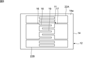
- FIG. 1 is a plan view of an elastic wave device according to a first embodiment of the present invention.
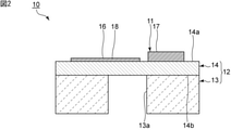
- FIG. 2 is a cross-sectional view taken along the line I-I in FIG.
- FIG. 3 is a cross-sectional view taken along the line II-II in FIG.
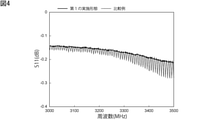
- FIG. 4 is a diagram showing the reflection characteristics of the first embodiment of the present invention and the comparative example.
- FIG. 5 is a cross-sectional view showing a portion corresponding to the cross section shown in FIG. 3 of the elastic wave device according to the first modification of the first embodiment of the present invention.
- FIG. 6 is a cross-sectional view showing a portion corresponding to the cross section shown in FIG. 3 of the elastic wave device according to the second modification of the first embodiment of the present invention.
- FIG. 5 is a cross-sectional view showing a portion corresponding to the cross section shown in FIG. 3 of the elastic wave device according to the first modification of the first embodiment of the present invention.
- FIG. 7 is a cross-sectional view showing a portion corresponding to the cross section shown in FIG. 3 of the elastic wave device according to the third modification of the first embodiment of the present invention.
- FIG. 8 is a plan view of the elastic wave device according to the fourth modification of the first embodiment of the present invention.
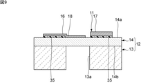
- FIG. 9 is a cross-sectional view showing a portion corresponding to the cross section shown in FIG. 2 of the elastic wave device according to the second embodiment of the present invention.
- FIG. 10 is a cross-sectional view showing a portion corresponding to the cross section shown in FIG. 2 of the elastic wave device according to the modified example of the second embodiment of the present invention.
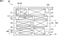
- FIG. 11 is a schematic plan view of the elastic wave device according to the third embodiment of the present invention.
- FIG. 12 is a cross-sectional view taken along the line III-III in FIG.
- FIG. 13 is a circuit diagram of an elastic wave device according to a third embodiment of the present invention.
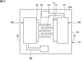
- FIG. 14 is a plan view of the elastic wave device according to the fourth embodiment of the present invention.
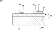
- FIG. 15 is a cross-sectional view taken along the line IV-IV in FIG.
- FIG. 16 is a plan view of the elastic wave device according to the fifth embodiment of the present invention.
- FIG. 17 is a cross-sectional view taken along the line VV in FIG.
- FIG. 18 is a plan view of the elastic wave device according to the sixth embodiment of the present invention.
- FIG. 19 is a cross-sectional view taken along the line VI-VI in FIG.
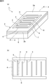
- FIG. 20 (a) is a schematic perspective view showing the appearance of an elastic wave device using a bulk wave in a thickness slip mode
- FIG. 20 (b) is a plan view showing an electrode structure on a piezoelectric layer
- FIG. 21 is a cross-sectional view of a portion along the line AA in FIG. 20 (a).
- FIG. 22A is a schematic front sectional view for explaining a Lamb wave propagating in the piezoelectric film of the elastic wave device
- FIG. 22B is a thickness slip propagating in the piezoelectric film in the elastic wave device. It is a schematic front sectional view for explaining the bulk wave of a mode.
- FIG. 23 is a diagram showing the amplitude direction of the bulk wave in the thickness slip mode.
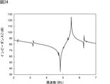
- FIG. 24 is a diagram showing resonance characteristics of an elastic wave device that utilizes a bulk wave in a thickness slip mode.
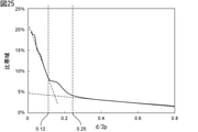
- FIG. 25 is a diagram showing the relationship between d / 2p and the specific band as a resonator when the distance between the centers of adjacent electrodes is p and the thickness of the piezoelectric layer is d.
- FIG. 26 is a plan view of an elastic wave device using a bulk wave in a thickness slip mode. 27, the Euler angles of LiNbO 3 in the case of close to 0 as possible the d / p (0 °, ⁇ , ⁇ ) is a diagram showing a map of a specific band for. Is.
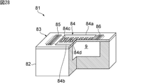
- FIG. 28 is a partially cutaway perspective view for explaining an elastic wave device using a Lamb wave.
- FIG. 1 is a plan view of an elastic wave device according to a first embodiment of the present invention.
- FIG. 2 is a cross-sectional view taken along the line I-I in FIG.
- FIG. 3 is a cross-sectional view taken along the line II-II in FIG.
- the elastic wave device 10 has a piezoelectric substrate 12 and an IDT electrode 11.
- the piezoelectric substrate 12 has a support member 13 and a piezoelectric layer 14.
- the support member 13 is composed of only a support substrate.
- the support member 13 may be, for example, a laminated body including a support substrate and an insulating layer.
- the support member 13 is provided with a through hole 13a as a hollow portion.
- a piezoelectric layer 14 is provided so as to cover the through hole 13a of the support member 13.
- the piezoelectric layer 14 is a lithium niobate layer in this embodiment. More specifically, the piezoelectric layer 14 is a LiNbO 3 layer. However, the piezoelectric layer 14 may be a lithium tantalate layer such as a LiTaO 3 layer.
- the support substrate is a silicon substrate in this embodiment.
- the material of the support substrate is not limited to the above.
- the IDT electrode 11 is provided on the piezoelectric layer 14.
- the IDT electrode 11 has a first bus bar 16 and a second bus bar 17, and a plurality of first electrode fingers 18 and a plurality of second electrode fingers 19.
- the first bus bar 16 is the first electrode film in the present invention.
- the second bus bar 17 is the second electrode film in the present invention. As shown in FIG. 3, the first bus bar 16 and the second bus bar 17 face each other.
- the thickness of the first bus bar 16 and the thickness of the second bus bar are different. More specifically, the thickness of the first bus bar 16 is thinner than the thickness of the second bus bar 17.
- the thickness of the first electrode film is the dimension of the first electrode film along the direction orthogonal to the main surface of the piezoelectric layer 14.
- the thickness of the second electrode film is the dimension of the second electrode film along the direction orthogonal to the main surface of the piezoelectric layer 14.
- the first bus bar 16 and the second bus bar 17 are connected to different potentials from each other.
- the first bus bar 16 is connected to the hot potential and the second bus bar 17 is connected to the ground potential.
- the potential to which the first bus bar 16 and the second bus bar 17 are connected is not limited to the above.
- the first bus bar 16 may be connected to the ground potential and the second bus bar 17 may be connected to the hot potential.
- the plurality of first electrode fingers 18 and the plurality of second electrode fingers 19 shown in FIG. 1 are at least a pair of electrodes in the present invention. At least one pair of electrodes are opposed to each other. More specifically, the first electrode finger 18 is the first electrode in the present invention. The plurality of first electrode fingers 18 are periodically arranged. One end of each of the plurality of first electrode fingers 18 is connected to the first bus bar 16. The second electrode finger 19 is the second electrode in the present invention. The plurality of second electrode fingers 19 are periodically arranged. One end of each of the plurality of second electrode fingers 19 is connected to the second bus bar 17. The plurality of first electrode fingers 18 and the plurality of second electrode fingers 19 are interleaved with each other.
- the thickness of the plurality of first electrode fingers 18 and the thickness of the plurality of second electrode fingers 19 are the same.
- the first electrode finger 18 and the second electrode finger 19 may be simply referred to as an electrode finger.
- the IDT electrode 11 may be made of a single-layer metal film or may be made of a laminated metal film.
- the elastic wave device 10 a plurality of electrode fingers as at least one pair of electrodes are functional electrodes in the present invention. Elastic waves are excited by applying an AC voltage to the functional electrodes of the IDT electrode 11.
- the elastic wave device 10 utilizes a bulk wave in a thickness slip mode. More specifically, the elastic wave device 10 utilizes a bulk wave in the thickness slip primary mode.
- the elastic wave device 10 may be an elastic wave device that utilizes a plate wave such as a lamb wave.
- the SH wave is excited as an unnecessary bulk wave.
- the direction in which the first electrode finger 18 and the second electrode finger 19 face each other is defined as the electrode finger facing direction.
- the region where adjacent electrode fingers overlap each other when viewed from the electrode finger facing direction is the crossing region D.
- the crossing region D is a region of the IDT electrode 11 including the electrode finger at one end to the electrode finger at the other end in the direction facing the electrode finger. More specifically, the crossing region D extends from the outer edge portion of the electrode finger at one end in the direction facing the electrode finger to the outer edge portion of the electrode finger at the other end in the direction facing the electrode finger. including.
- the elastic wave device 10 has a plurality of excitation regions C.
- the excitation region C is also a region where adjacent electrode fingers overlap each other when viewed from the direction in which the electrode fingers face each other.
- Each excitation region C is a region between a pair of electrode fingers. More specifically, the excitation region C is a region from the center of one electrode finger in the direction facing the electrode finger to the center of the other electrode finger in the direction facing the electrode finger. Therefore, the crossover region D includes a plurality of excitation regions C.
- the bulk wave in the thickness slip mode is excited in each excitation region C.
- the crossover region D is an excitation region.
- the feature of this embodiment is that the first bus bar 16 as the first electrode film and the second bus bar 17 as the second electrode film are provided on the piezoelectric layer 14 and face each other. , The thickness of the first electrode film and the thickness of the second electrode film are different. Thereby, unnecessary bulk waves can be suppressed, and ripples in the frequency characteristics of the elastic wave device 10 can be suppressed. The details are shown below by comparing the present embodiment and comparative examples.
- the comparative example is different from the first embodiment in that the thickness of the first bus bar and the thickness of the second bus bar are the same.
- the reflection characteristic as the frequency characteristic between the first bus bar and the second bus bar was measured.
- the reflection characteristics between the first bus bar and the second bus bar were measured.
- FIG. 4 is a diagram showing the reflection characteristics of the first embodiment and the comparative example.
- the reflection characteristic shown in FIG. 4 is the relationship between S11 and the frequency.
- the support member 13 is composed of only a support substrate.
- the support member 13 may be a laminate of a support substrate and an insulating layer.
- the piezoelectric layer 14 is provided on the insulating layer.
- a silicon oxide layer, silicon nitride, tantalum oxide, or the like can be used as the material of the insulating layer.
- the cavity is not limited to the through hole.
- the hollow portion may be, for example, a hollow portion.
- the hollow portion is composed of, for example, a recess provided in the support member. More specifically, the hollow portion is formed by sealing the concave portion with the piezoelectric layer 14 or the like.
- the piezoelectric layer 14 may be provided with a recess that opens on the support member 13 side.
- the cavity may be formed.
- the support member 13 may not be provided with a recess or a through hole.
- the thickness of the first electrode film and the second electrode film are all different.
- the thickness of at least a part of the first electrode film and the thickness of at least a part of the second electrode film may be different.
- the first to third embodiments of the first embodiment wherein only the thickness of the first bus bar as the first electrode film or the second bus bar as the second electrode film is different from the first embodiment. A modified example is shown. Even in the first to third modifications, the ripple in the frequency characteristics can be suppressed.
- the thickness of a part of the first bus bar 26A is thicker than the thickness of the other part.
- the second bus bar 17 is configured in the same manner as in the first embodiment. The thickness of both the thick portion and the thin portion of the first bus bar 26A is different from the thickness of the second bus bar 17.
- the thickness of a part of the first bus bar 26B is thicker than the thickness of the other part, as in the first modification.
- the second bus bar 17 is configured in the same manner as in the first embodiment.
- the thickness of the thick portion of the first bus bar 26B is different from the thickness of the second bus bar 17.
- the thickness of the thin portion of the first bus bar 26A is the same as the thickness of the second bus bar 17.
- the first bus bar 26A is configured in the same manner as the first modification. Further, the thickness of a part of the second bus bar is thicker than the thickness of the other part. The thickness of both the thick portion and the thin portion of the first bus bar 26A is different from the thickness of both the thick portion and the thin portion of the second bus bar 17.
- the part of the first electrode film means a part in the direction parallel to the main surface of the piezoelectric layer.
- the first electrode film and the second electrode film may each have at least one electrode layer, and may have a plurality of electrode layers.
- the difference between the thickness of at least a part of the first electrode film and the thickness of at least a part of the second electrode film is the thickness of at least one layer of the first electrode film and the second. It also includes that the thickness of at least one layer of the electrode film of the above is different.
- FIG. 8 shows an example in which the elastic wave device uses a plate wave as a fourth modification of the first embodiment.
- a pair of reflectors 22A and 22B are provided on both sides of the IDT electrode 11 in the electrode finger facing direction on the piezoelectric layer 14.
- the resonance characteristic can be suitably improved.
- the first bus bar 16 as the first electrode film and the second bus bar 17 as the second electrode film are configured in the same manner as in the first embodiment. Therefore, it is possible to suppress the ripple in the frequency characteristic.
- FIG. 9 is a cross-sectional view showing a portion corresponding to the cross section shown in FIG. 2 of the elastic wave device according to the second embodiment.
- This embodiment is different from the first embodiment in that a dielectric film 35 is provided between the first bus bar 16 and the second bus bar 17 and the piezoelectric layer 14, respectively. Except for the above points, the elastic wave device of the present embodiment has the same configuration as the elastic wave device 10 of the first embodiment.
- the electromechanical coupling coefficient changes as compared with the case where the dielectric film 35 is not provided. Thereby, the ripple in the frequency characteristic can be further suppressed.
- the material of the dielectric film 35 for example, silicon oxide, silicon nitride, resin, or the like can be used.
- the dielectric film 35 is provided between at least one of the first bus bar 16 and the second bus bar 17 and the piezoelectric layer 14. Thereby, the ripple in the frequency characteristic can be effectively suppressed.
- a dielectric film 35 is provided between one of the first bus bar 16 and the second bus bar 17 and the piezoelectric layer 14. More specifically, a dielectric film 35 is provided between the first bus bar 16 and the piezoelectric layer 14. On the other hand, the dielectric film 35 is not provided between the second bus bar 17 and the piezoelectric layer 14.
- an example is shown in which an unnecessary bulk wave signal propagating from one of a pair of bus bars can be suppressed from the influence of the signal when it is taken out by the other bus bar. rice field. It should be noted that unnecessary bulk wave signals may be propagated and taken out even between the wiring electrode films in the filter device.
- the elastic wave device is a filter device is shown.
- FIG. 11 is a schematic plan view of the elastic wave device according to the third embodiment.
- elastic wave resonators are shown by a schematic diagram in which two diagonal lines are added to a polygon.
- the elastic wave device 40 has a plurality of elastic wave resonators.
- the elastic wave device 40 is a filter device.
- Each elastic wave resonator of the elastic wave device 40 has a functional electrode. More specifically, each elastic wave resonator of the elastic wave apparatus 40 has an IDT electrode.
- Each IDT electrode includes a pair of busbars and a plurality of electrode fingers as functional electrodes.
- the first electrode film 48 and the second electrode film 49 are wiring electrode films.
- the wiring electrode film is the wiring portion in the present invention. That is, in the elastic wave device 40, the first electrode film 48 is the first wiring portion in the present invention.
- the second electrode film 49 is the second wiring portion in the present invention.
- the first electrode film 48 and the second electrode film 49 are provided on the piezoelectric layer 14, and a plurality of elastic wave resonators are configured on the piezoelectric layer 14.
- the wiring electrode film as the first electrode film 48 and the wiring electrode film as the second electrode film 49 are each drawn from different elastic wave resonators. That is, the first electrode film 48 and the second electrode film 49 are each connected to a plurality of electrode fingers as functional electrodes via a bus bar.
- the first electrode film 48 is connected to the hot potential
- the second electrode film 49 is connected to the ground potential.
- FIG. 12 is a cross-sectional view taken along the line III-III in FIG.
- the first electrode film 48 and the second electrode film 49 face each other.
- the thickness of the first electrode film 48 and the thickness of the second electrode film 49 are different. Therefore, as in the first embodiment, the mode of propagation of the bulk wave can be different between the first electrode film 48 and the second electrode film 49. Therefore, the ripple in the frequency characteristic can be suppressed.
- the circuit configuration in this embodiment is shown below.
- FIG. 13 is a circuit diagram of the elastic wave device according to the third embodiment.
- the elastic wave device 40 is a ladder type filter.
- the plurality of elastic wave resonators of the present embodiment include a series arm resonator S1, a series arm resonator S2, a series arm resonator S3, a series arm resonator S4, a series arm resonator S5 and a series arm resonator S6, and parallel.
- the elastic wave device 40 has a first signal terminal 45 and a second signal terminal 46.
- a series arm resonator S1 is connected between the connection point between the series arm resonator S1 and the series arm resonator S2 and the ground potential.
- the parallel arm resonator P2 is connected between the connection point between the series arm resonator S3 and the series arm resonator S4 and the ground potential.
- a parallel arm resonator P3 is connected between the connection point between the series arm resonator S5 and the series arm resonator S6 and the ground potential.
- the elastic wave device 40 has a plurality of ground terminals 47. Each parallel arm resonator is connected to the ground potential via any of the ground terminals 47.
- the circuit configuration described above is an example, and the circuit configuration of the elastic wave device 40 is not particularly limited.
- the first electrode film 48 is a wiring electrode film connecting the series arm resonator S1 and the parallel arm resonator P1.
- the second electrode film 49 is a wiring electrode film connecting the parallel arm resonator P2 and the ground terminal 47.
- the distance L between the first electrode film 48 and the second electrode film 49 is an elastic wave resonator different from each elastic wave resonator to which the first electrode film 48 and the second electrode film 49 are connected.
- the length is different from the opening length M of.
- the opening length of the elastic wave resonator means the distance between a pair of bus bars of the elastic wave resonator. As shown in FIG.
- the opening length of the series arm resonator S3 is M3
- the opening length of the series arm resonator S6 is M6.
- the distance L may be longer or shorter than, for example, the shortest opening length M among the opening lengths M of the other elastic wave resonators.
- the distance L may be longer or shorter than the shortest opening length of the opening lengths M6, for example.
- FIG. 14 is a plan view of the elastic wave device according to the fourth embodiment.
- FIG. 15 is a cross-sectional view taken along the line IV-IV in FIG.
- the present embodiment differs from the first embodiment in that the first electrode film 58 and the second electrode film 59 are laminated films of a plurality of electrode layers. Further, the present embodiment is different from the first embodiment in that the first electrode film 58 and the second electrode film 59 each include both a bus bar and a wiring electrode film. Except for the above points, the elastic wave device of the present embodiment has the same configuration as the elastic wave device 10 of the first embodiment.
- the first electrode film 58 includes a first bus bar 16 as a first layer and a first wiring electrode film 56 as a second layer. A part of the first wiring electrode film 56 is laminated on the first bus bar 16. The other part of the first wiring electrode film 56 is provided directly on the piezoelectric layer 14.
- the second electrode film 59 includes a second bus bar 17 as a first layer and a second wiring electrode film 57 as a second layer. A part of the second wiring electrode film 57 is laminated on the second bus bar 17. As shown in FIG. 14, the other part of the second wiring electrode film 57 is provided directly on the piezoelectric layer 14.
- the first bus bar 16 and the second bus bar 17 face each other.
- the first electrode film 58 and the second electrode film 59 face each other.
- the total thickness of the first electrode film 58 and the total thickness of the second electrode film 59 are different. Thereby, as in the first embodiment, the influence of unnecessary bulk waves on the frequency characteristics can be suppressed, and the ripple in the frequency characteristics can be suppressed.
- the total thickness of the first electrode film 58 is the total thickness of all the electrode layers of the first electrode film 58.
- the total thickness of the second electrode film 59 is the total thickness of all the electrode layers of the second electrode film 59.
- the thickness of the first bus bar 16 as the first layer of the first electrode film 58 is the second layer of the second electrode film 59 as the first layer. It is different from the thickness of the bus bar 17.
- the thickness of the first bus bar 16 is different from the thickness of the second wiring electrode film 57 as the second layer of the second electrode film 59. Further, the thickness of the first bus bar 16 is also different from the total thickness of the second electrode film 59.
- the thickness of the first wiring electrode film 56 as the second layer of the first electrode film 58 is the thickness of the second bus bar 17, the thickness of the second wiring electrode film 57, and the thickness of the second electrode film 59. It is different from any of the total thickness.
- the thickness of the second bus bar 17 and the thickness of the second wiring electrode film 57 are the thickness of the first bus bar 16, the thickness of the first wiring electrode film 56, and the total thickness of the first electrode film 58, respectively. It is different from any of.
- At least one of the thickness of any electrode layer of the second electrode film 59 and the total thickness of the second electrode film 59 is the thickness of the first layer of the first electrode film 58, the second. It may be different from both the thickness of the layer and the total thickness of the first electrode film 58.
- both the first electrode film 58 and the second electrode film 59 are laminated films.
- the second electrode film 59 may be a bus bar as in the first embodiment, or may be a wiring electrode film as in the third embodiment.
- FIG. 16 is a plan view of the elastic wave device according to the fifth embodiment.
- FIG. 17 is a cross-sectional view taken along the line VV in FIG.
- the first electrode film 58 is a laminated film similar to the fourth embodiment, and the second electrode film 69 is the second wiring electrode film. It differs from the first embodiment in that it is. Further, it is different from the first embodiment in that the second electrode film 69 is connected to the second bus bar 17. Except for the above points, the elastic wave device of the present embodiment has the same configuration as the elastic wave device 10 of the first embodiment.
- the second electrode film 69 has a portion laminated on the second bus bar 17 and a portion directly provided on the piezoelectric layer 14. As shown in FIG. 17, the first electrode film 58 and the second electrode film 69 face each other.
- the thickness of the second electrode film 69 is the thickness of the first bus bar 16 as the first layer of the first electrode film 58, the thickness of the first wiring electrode film 56 as the second layer, and the first. It is different from any of the total thickness of the electrode film 58.
- FIG. 18 is a plan view of the elastic wave device according to the sixth embodiment.
- FIG. 19 is a cross-sectional view taken along the line VI-VI in FIG.
- the functional electrode has an upper electrode 71A and a lower electrode 71B.
- the upper electrode 71A is provided on the first main surface 14a of the piezoelectric layer 14.
- the lower electrode 71B is provided on the second main surface 14b of the piezoelectric layer 14.
- the upper electrode 71A and the lower electrode 71B face each other with the piezoelectric layer 14 interposed therebetween.
- the upper electrode 71A and the lower electrode 71B are connected to different potentials from each other.
- the region where the upper electrode 71A and the lower electrode 71B face each other is the excitation region.
- a first electrode film 48 and a second electrode film 49 are provided on the first main surface 14a of the piezoelectric layer 14.
- the first electrode film 48 and the second electrode film 49 are wiring electrode films.
- the first electrode film 48 is connected to the upper electrode 71A.
- a connection electrode 72 is provided on the second main surface 14b of the piezoelectric layer 14.
- the connection electrode 72 is connected to the lower electrode 71B.
- the piezoelectric layer 14 is provided with a through hole.
- the connection electrode 72 passes through the through hole and is connected to the second electrode film 49. Therefore, the second electrode film 49 is connected to the lower electrode 71B via the connection electrode 72.
- the first electrode film 48 and the second electrode film 49 face each other.
- the thickness of the first electrode film 48 and the thickness of the second electrode film 49 are different. Thereby, as in the first embodiment, the influence of unnecessary bulk waves on the frequency characteristics can be suppressed, and the ripple in the frequency characteristics can be suppressed.
- BAW Bit Acoustic Wave
- the first electrode film and the second electrode film may be wiring electrode membranes connected to different elastic wave resonators.
- the support member in the following example corresponds to the support substrate in the present invention.
- FIG. 20 (a) is a schematic perspective view showing the appearance of an elastic wave device using a bulk wave in a thickness slip mode
- FIG. 20 (b) is a plan view showing an electrode structure on a piezoelectric layer
- FIG. 21 is a cross-sectional view of a portion along the line AA in FIG. 20 (a).
- the elastic wave device 1 has a piezoelectric layer 2 made of LiNbO 3.
- the piezoelectric layer 2 may be made of LiTaO 3.
- the cut angle of LiNbO 3 and LiTaO 3 is Z-cut, but may be rotary Y-cut or X-cut.
- the thickness of the piezoelectric layer 2 is not particularly limited, but in order to effectively excite the thickness slip mode, it is preferably 40 nm or more and 1000 nm or less, and more preferably 50 nm or more and 600 nm or less.
- the piezoelectric layer 2 has first and second main surfaces 2a and 2b facing each other.
- the electrode 3 and the electrode 4 are provided on the first main surface 2a.
- the electrode 3 is an example of the “first electrode”
- the electrode 4 is an example of the “second electrode”.
- a plurality of electrodes 3 are connected to the first bus bar 5.
- the plurality of electrodes 4 are connected to the second bus bar 6.
- the plurality of electrodes 3 and the plurality of electrodes 4 are interleaved with each other.
- the electrode 3 and the electrode 4 have a rectangular shape and have a length direction.
- the electrode 3 and the adjacent electrode 4 face each other in a direction orthogonal to the length direction. Both the length direction of the electrodes 3 and 4 and the direction orthogonal to the length direction of the electrodes 3 and 4 are directions intersecting with each other in the thickness direction of the piezoelectric layer 2.
- the electrode 3 and the adjacent electrode 4 face each other in the direction of crossing in the thickness direction of the piezoelectric layer 2.
- the length directions of the electrodes 3 and 4 may be replaced with the directions orthogonal to the length directions of the electrodes 3 and 4 shown in FIGS. 20 (a) and 20 (b). That is, in FIGS. 20 (a) and 20 (b), the electrodes 3 and 4 may be extended in the direction in which the first bus bar 5 and the second bus bar 6 are extended. In that case, the first bus bar 5 and the second bus bar 6 extend in the direction in which the electrodes 3 and 4 extend in FIGS. 20 (a) and 20 (b).
- a pair of structures in which the electrode 3 connected to one potential and the electrode 4 connected to the other potential are adjacent to each other are provided in a direction orthogonal to the length direction of the electrodes 3 and 4.
- the case where the electrode 3 and the electrode 4 are adjacent to each other does not mean that the electrode 3 and the electrode 4 are arranged so as to be in direct contact with each other, but that the electrode 3 and the electrode 4 are arranged so as to be spaced apart from each other. Point to. Further, when the electrode 3 and the electrode 4 are adjacent to each other, the electrode connected to the hot electrode or the ground electrode, including the other electrodes 3 and 4, is not arranged between the electrode 3 and the electrode 4.
- This logarithm does not have to be an integer pair, and may be 1.5 pairs, 2.5 pairs, or the like.
- the distance between the centers of the electrodes 3 and 4, that is, the pitch is preferably in the range of 1 ⁇ m or more and 10 ⁇ m or less.
- the width of the electrodes 3 and 4, that is, the dimensions of the electrodes 3 and 4 in the opposite direction are preferably in the range of 50 nm or more and 1000 nm or less, and more preferably in the range of 150 nm or more and 1000 nm or less.
- the distance between the centers of the electrodes 3 and 4 is the center of the dimension (width dimension) of the electrode 3 in the direction orthogonal to the length direction of the electrode 3 and the electrode 4 in the direction orthogonal to the length direction of the electrode 4. It is the distance connected to the center of the dimension (width dimension) of.
- the direction orthogonal to the length direction of the electrodes 3 and 4 is the direction orthogonal to the polarization direction of the piezoelectric layer 2. This does not apply when a piezoelectric material having another cut angle is used as the piezoelectric layer 2.
- “orthogonal” is not limited to the case of being strictly orthogonal, and is substantially orthogonal (the angle formed by the direction orthogonal to the length direction of the electrodes 3 and 4 and the polarization direction is, for example, 90 ° ⁇ 10 °). Within the range).
- a support member 8 is laminated on the second main surface 2b side of the piezoelectric layer 2 via an insulating layer 7.
- the insulating layer 7 and the support member 8 have a frame-like shape, and as shown in FIG. 21, have through holes (cavities) 7a and 8a. As a result, the cavity 9 is formed.
- the cavity 9 is provided so as not to interfere with the vibration of the excitation region of the piezoelectric layer 2. Therefore, the support member 8 is laminated on the second main surface 2b via the insulating layer 7 at a position where it does not overlap with the portion where at least one pair of electrodes 3 and 4 are provided.
- the insulating layer 7 may not be provided. Therefore, the support member 8 may be directly or indirectly laminated on the second main surface 2b of the piezoelectric layer 2.
- the insulating layer 7 is made of silicon oxide. However, in addition to silicon oxide, an appropriate insulating material such as silicon nitride or alumina can be used.
- the support member 8 is made of Si. The plane orientation of Si on the surface of the piezoelectric layer 2 side may be (100), (110), or (111).
- the Si constituting the support member 8 preferably has a high resistance having a resistivity of 2 k ⁇ or more, and more preferably has a high resistance having a resistivity of 4 k ⁇ or more.
- the support member 8 can also be configured by using an appropriate insulating material or semiconductor material.
- the plurality of electrodes 3, 4 and the first and second bus bars 5, 6 are made of an appropriate metal or alloy such as an Al or AlCu alloy.
- the electrodes 3 and 4 and the first and second bus bars 5 and 6 have a structure in which an Al film is laminated on a Ti film.
- An adhesive layer other than the Ti film may be used.
- an AC voltage is applied between the plurality of electrodes 3 and the plurality of electrodes 4. More specifically, an AC voltage is applied between the first bus bar 5 and the second bus bar 6.
- d / p is 0. It is said to be 5 or less. Therefore, the bulk wave in the thickness slip mode is effectively excited, and good resonance characteristics can be obtained. More preferably, d / p is 0.24 or less, in which case even better resonance characteristics can be obtained.
- the Q value is unlikely to decrease even if the logarithm of the electrodes 3 and 4 is reduced in order to reduce the size. This is because the propagation loss is small even if the number of electrode fingers in the reflectors on both sides is reduced. Further, the reason why the number of the electrode fingers can be reduced is that the bulk wave in the thickness slip mode is used. The difference between the lamb wave used in the elastic wave device and the bulk wave in the thickness slip mode will be described with reference to FIGS. 22 (a) and 22 (b).
- FIG. 22A is a schematic front sectional view for explaining a Lamb wave propagating in a piezoelectric film of an elastic wave device as described in Patent Document 1.
- the wave propagates in the piezoelectric film 201 as shown by an arrow.
- the first main surface 201a and the second main surface 201b face each other, and the thickness direction connecting the first main surface 201a and the second main surface 201b is the Z direction.
- the X direction is the direction in which the electrode fingers of the IDT electrodes are lined up.
- the wave propagates in the X direction as shown in the figure.
- the piezoelectric film 201 vibrates as a whole because it is a plate wave, the wave propagates in the X direction, so reflectors are arranged on both sides to obtain resonance characteristics. Therefore, a wave propagation loss occurs, and the Q value decreases when the size is reduced, that is, when the logarithm of the electrode fingers is reduced.
- the wave is generated by the first main surface 2a and the second main surface of the piezoelectric layer 2. It propagates substantially in the direction connecting 2b, that is, in the Z direction, and resonates. That is, the X-direction component of the wave is significantly smaller than the Z-direction component. Since the resonance characteristic is obtained by the propagation of the wave in the Z direction, the propagation loss is unlikely to occur even if the number of electrode fingers of the reflector is reduced. Further, even if the logarithm of the electrode pair consisting of the electrodes 3 and 4 is reduced in order to promote miniaturization, the Q value is unlikely to decrease.
- the amplitude direction of the bulk wave in the thickness slip mode is opposite between the first region 451 included in the excitation region of the piezoelectric layer 2 and the second region 452 included in the excitation region.
- FIG. 23 schematically shows a bulk wave when a voltage at which the electrode 4 has a higher potential than that of the electrode 3 is applied between the electrode 3 and the electrode 4.
- the first region 451 is a region of the excitation region between the virtual plane VP1 orthogonal to the thickness direction of the piezoelectric layer 2 and dividing the piezoelectric layer 2 into two, and the first main surface 2a.
- the second region 452 is a region of the excitation region between the virtual plane VP1 and the second main surface 2b.
- the elastic wave device 1 at least one pair of electrodes consisting of the electrodes 3 and 4 is arranged, but since the waves are not propagated in the X direction, they are composed of the electrodes 3 and 4.
- the number of pairs of electrodes does not have to be multiple. That is, it is only necessary to provide at least one pair of electrodes.
- the electrode 3 is an electrode connected to a hot potential
- the electrode 4 is an electrode connected to a ground potential.
- the electrode 3 may be connected to the ground potential and the electrode 4 may be connected to the hot potential.
- at least one pair of electrodes is an electrode connected to a hot potential or an electrode connected to a ground potential as described above, and is not provided with a floating electrode.
- FIG. 24 is a diagram showing the resonance characteristics of the elastic wave device shown in FIG. 21.
- the design parameters of the elastic wave device 1 that has obtained this resonance characteristic are as follows.
- Insulation layer 7 1 ⁇ m thick silicon oxide film.
- Support member 8 Si.
- the length of the excitation region C is a dimension along the length direction of the electrodes 3 and 4 of the excitation region C.
- the distances between the electrodes of the electrode pairs consisting of the electrodes 3 and 4 were all equal in the plurality of pairs. That is, the electrodes 3 and 4 are arranged at equal pitches.
- d / p is more preferably 0.5 or less. Is 0.24 or less. This will be described with reference to FIG.
- FIG. 25 is a diagram showing the relationship between this d / 2p and the specific band as a resonator of the elastic wave device.
- the ratio band is less than 5% even if d / p is adjusted.
- the specific band can be set to 5% or more by changing d / p within that range. That is, a resonator having a high coupling coefficient can be constructed.
- the specific band can be increased to 7% or more.
- a resonator having a wider specific band can be obtained, and a resonator having a higher coupling coefficient can be realized. Therefore, it can be seen that by setting d / p to 0.5 or less, a resonator having a high coupling coefficient can be configured by utilizing the bulk wave in the thickness slip mode.
- the above p is the distance between the centers of the adjacent electrodes 3 and 4.
- the thickness d of the piezoelectric layer if the piezoelectric layer 2 has a thickness variation, a value obtained by averaging the thickness may be adopted.
- FIG. 26 is a plan view of an elastic wave device that utilizes a bulk wave in a thickness slip mode.
- the elastic wave device 80 a pair of electrodes having an electrode 3 and an electrode 4 is provided on the first main surface 2a of the piezoelectric layer 2.
- K in FIG. 26 is the crossover width.
- the logarithm of the electrodes may be one pair. Even in this case, if the d / p is 0.5 or less, the bulk wave in the thickness slip mode can be effectively excited.
- the Euler angles of LiNbO 3 in the case of close to 0 as possible is a diagram showing a map of a specific band for.
- the portion shown with hatching in FIG. 27 is a region where a specific band of at least 5% or more can be obtained, and when the range of the region is approximated, the following equations (1), (2) and (3) are approximated. ).
- Equation (1) (0 ° ⁇ 10 °, 20 ° ⁇ 80 °, 0 ° ⁇ 60 ° (1- ( ⁇ -50) 2/900) 1/2) or (0 ° ⁇ 10 °, 20 ° ⁇ 80 °, [180 ° -60 ° (1- ( ⁇ - 50) 2/900) 1/2] ⁇ 180 °) ... equation (2) (0 ° ⁇ 10 °, [ 180 ° -30 ° (1- ( ⁇ -90) 2/8100) 1/2] ⁇ 180 °, any [psi) ... Equation (3)
- the specific band can be sufficiently widened, which is preferable.
- FIG. 28 is a partially cutaway perspective view for explaining an elastic wave device using a Lamb wave.
- the broken line in FIG. 28 indicates the position of the cavity 9 as seen from the piezoelectric layer 83 side.
- the elastic wave device 81 has a support substrate 82.
- the support substrate 82 is provided with a recess opened on the upper surface.
- the piezoelectric layer 83 is laminated on the support substrate 82.
- the cavity 9 is configured.
- An IDT electrode 84 is provided on the piezoelectric layer 83 above the cavity 9. Reflectors 85 and 86 are provided on both sides of the IDT electrode 84 in the elastic wave propagation direction. In FIG. 28, the outer peripheral edge of the cavity 9 is shown by a broken line.
- the IDT electrode 84 has first and second bus bars 84a and 84b, a plurality of first electrode fingers 84c, and a plurality of second electrode fingers 84d.
- the plurality of first electrode fingers 84c are connected to the first bus bar 84a.
- the plurality of second electrode fingers 84d are connected to the second bus bar 84b.
- the plurality of first electrode fingers 84c and the plurality of second electrode fingers 84d are interleaved with each other.
- a lamb wave as a plate wave is excited by applying an AC electric field to the IDT electrode 84 on the cavity 9. Since the reflectors 85 and 86 are provided on both sides, the resonance characteristic due to the Lamb wave can be obtained.
Landscapes
- Physics & Mathematics (AREA)
- Acoustics & Sound (AREA)
- Surface Acoustic Wave Elements And Circuit Networks Thereof (AREA)
Abstract
周波数特性におけるリップルを抑制することができる、弾性波装置を提供する。 本発明の弾性波装置10は、支持基板13と、支持基板13上に設けられている圧電層14と、圧電層14上に設けられている機能電極と、圧電層14上にそれぞれ設けられており、互いに対向し合っており、かつ互いに異なる電位である第1の電極膜(第1のバスバー16)及び第2の電極膜(第2のバスバー17)とを備える。第1の電極膜の少なくとも一部の厚みと、第2の電極膜の少なくとも一部の厚みとが異なる。
Description
本発明は、弾性波装置に関する。
従来、LiNbO3またはLiTaO3からなる圧電膜を伝搬する板波を利用した弾性波装置が知られている。例えば、下記の特許文献1では、板波としてのラム波を利用した弾性波装置が開示されている。この弾性波装置においては、支持体上に圧電基板が設けられている。圧電基板はLiNbO3またはLiTaO3からなる。圧電基板の上面にIDT電極が設けられている。IDT電極の一方電位に接続される複数の電極指と、他方電位に接続される複数の電極指との間に電圧が印加される。それによって、ラム波が励振される。このIDT電極の両側には反射器が設けられている。それによって、板波を利用した弾性波共振子が構成されている。
下記の特許文献2には、ラダー型フィルタの例が開示されている。このラダー型フィルタにおいては、複数の弾性波装置が複数の配線により接続されている。複数の配線は、ホット電位に接続される配線及びグラウンド電位に接続される配線を含む。ホット電位に接続される配線及びグラウンド電位に接続される配線が対向し合っている。
特許文献1に記載のような弾性波共振子においては、不要なバルク波が励振されることがある。このバルク波は、圧電基板の厚み方向に伝搬する。そのため、、支持体において反射されることがある。特許文献2のように、異なる電位に接続される配線が対向し合っている場合には、一方の配線により、不要なバルク波の信号が取り出されることがある。不要なバルク波の信号は、対向し合うバスバーのうち一方により取り出されることもある。これらの場合、弾性波装置の周波数特性においてリップルが生じるおそれがある。
本発明の目的は、周波数特性におけるリップルを抑制することができる、弾性波装置を提供することにある。
本発明に係る弾性波装置は、支持基板と、前記支持基板上に設けられている圧電層と、前記圧電層上に設けられている機能電極と、前記圧電層上にそれぞれ設けられており、互いに対向し合っており、かつ互いに異なる電位である第1の電極膜及び第2の電極膜とを備え、前記第1の電極膜の少なくとも一部の厚みと、前記第2の電極膜の少なくとも一部の厚みとが異なる。
本発明によれば、周波数特性におけるリップルを抑制することができる、弾性波装置を提供することができる。
以下、図面を参照しつつ、本発明の具体的な実施形態を説明することにより、本発明を明らかにする。
なお、本明細書に記載の各実施形態は、例示的なものであり、異なる実施形態間において、構成の部分的な置換または組み合わせが可能であることを指摘しておく。
図1は、本発明の第1の実施形態に係る弾性波装置の平面図である。図2は、図1中のI-I線に沿う断面図である。図3は、図1中のII-II線に沿う断面図である。
図1に示すように、弾性波装置10は、圧電性基板12と、IDT電極11とを有する。図2に示すように、圧電性基板12は、支持部材13と、圧電層14とを有する。本実施形態では、支持部材13は支持基板のみからなる。もっとも、支持部材13は、例えば、支持基板及び絶縁層を含む積層体であってもよい。
支持部材13には空洞部としての、貫通孔13aが設けられている。支持部材13の貫通孔13aを覆うように、圧電層14が設けられている。
圧電層14は、本実施形態では、ニオブ酸リチウム層である。より具体的には、圧電層14はLiNbO3層である。もっとも、圧電層14は、例えばLiTaO3層などの、タンタル酸リチウム層であってもよい。
支持基板は、本実施形態ではシリコン基板である。もっとも、支持基板の材料は上記に限定されない。
図1に戻り、圧電層14上にIDT電極11が設けられている。IDT電極11は、第1のバスバー16及び第2のバスバー17と、複数の第1の電極指18及び複数の第2の電極指19とを有する。第1のバスバー16は、本発明における第1の電極膜である。第2のバスバー17は、本発明における第2の電極膜である。図3に示すように、第1のバスバー16及び第2のバスバー17は対向し合っている。第1のバスバー16の厚みと第2のバスバーの厚みとは異なる。より具体的には、第1のバスバー16の厚みは第2のバスバー17の厚みよりも薄い。なお、第1の電極膜の厚みは、圧電層14の主面と直交する方向に沿う第1の電極膜の寸法である。同様に、第2の電極膜の厚みは、圧電層14の主面と直交する方向に沿う第2の電極膜の寸法である。
第1のバスバー16及び第2のバスバー17は、互いに異なる電位に接続される。本実施形態では、第1のバスバー16はホット電位に接続され、第2のバスバー17はグラウンド電位に接続される。もっとも、第1のバスバー16及び第2のバスバー17が接続される電位は上記に限定されない。例えば、第1のバスバー16がグラウンド電位に接続され、第2のバスバー17がホット電位に接続されてもよい。
一方で、図1に示す複数の第1の電極指18及び複数の第2の電極指19は、本発明における少なくとも1対の電極である。少なくとも1対の電極は互いに対向し合っている。より具体的には、第1の電極指18は本発明における第1電極である。複数の第1の電極指18は周期的に配置されている。複数の第1の電極指18の一端はそれぞれ、第1のバスバー16に接続されている。第2の電極指19は本発明における第2電極である。複数の第2の電極指19は周期的に配置されている。複数の第2の電極指19の一端はそれぞれ、第2のバスバー17に接続されている。複数の第1の電極指18及び複数の第2の電極指19は互いに間挿し合っている。なお、複数の第1の電極指18の厚み及び複数の第2の電極指19の厚みは同じである。以下においては、第1の電極指18及び第2の電極指19を単に電極指と記載することもある。IDT電極11は、単層の金属膜からなっていてもよく、あるいは積層金属膜からなっていてもよい。
弾性波装置10においては、少なくとも1対の電極としての複数の電極指が、本発明における機能電極である。IDT電極11における機能電極に交流電圧を印加することにより弾性波が励振される。本実施形態では、弾性波装置10は、厚み滑りモードのバルク波を利用している。より具体的には、弾性波装置10は、厚み滑り1次モードのバルク波を利用している。なお、弾性波装置10は、ラム波などの板波を利用する弾性波装置であってもよい。他方、本実施形態では、不要バルク波として、SH波が励振される。
ここで、平面視において、第1の電極指18及び第2の電極指19が対向する方向を電極指対向方向とする。電極指対向方向から見たときに、隣り合う電極指同士が重なり合う領域が交叉領域Dである。交叉領域Dは、IDT電極11の、電極指対向方向における一方端の電極指から他方端の電極指までを含む領域である。より具体的には、交叉領域Dは、上記一方端の電極指の、電極指対向方向における外側の端縁部から、上記他方端の電極指の、電極指対向方向における外側の端縁部までを含む。
さらに、弾性波装置10は、複数の励振領域Cを有する。励振領域Cも、電極指対向方向から見たときに、隣り合う電極指同士が重なり合う領域である。なお、各励振領域Cはそれぞれ、1対の電極指間の領域である。より詳細には、励振領域Cは、一方の電極指の電極指対向方向における中心から、他方の電極指の電極指対向方向における中心までの領域である。よって、交叉領域Dは、複数の励振領域Cを含む。厚み滑りモードのバルク波は、各励振領域Cにおいて励振される。他方、弾性波装置10が板波を利用する場合には、交叉領域Dが励振領域である。
本実施形態の特徴は、第1の電極膜としての第1のバスバー16及び第2の電極膜としての第2のバスバー17が、圧電層14上に設けられており、互いに対向し合っており、第1の電極膜の厚みと第2の電極膜の厚みとが異なることにある。それによって、不要なバルク波を抑制することができ、弾性波装置10の周波数特性におけるリップルを抑制することができる。この詳細を、本実施形態及び比較例を比較することにより、以下において示す。
比較例は、第1のバスバーの厚み及び第2のバスバーの厚みが同じである点において、第1の実施形態と異なる。第1の実施形態において、第1のバスバー及び第2のバスバーの間の、上記周波数特性としての反射特性を測定した。同様に、比較例において、第1のバスバー及び第2のバスバーの間の反射特性を測定した。
図4は、第1の実施形態及び比較例の反射特性を示す図である。図4に示す反射特性は、S11と周波数との関係である。
図4に示すように、比較例の反射特性では、図4に示す周波数帯域の全域においてリップルが生じていることがわかる。一方で、第1の実施形態の反射特性では、リップルが抑制されていることがわかる。第1の実施形態のように、第1の電極膜の厚みと第2の電極膜との厚みを異ならせることにより、第1の電極膜及び第2の電極膜の間において、バルク波の伝搬の態様を異ならせることができる。それによって、不要なバルク波による反射特性に対する影響を抑制することができる。
図1に戻り、第1の実施形態では、支持部材13は支持基板のみからなる。もっとも、支持部材13は、支持基板及び絶縁層の積層体であってもよい。この場合、絶縁層上に圧電層14が設けられている。絶縁層の材料としては、例えば、酸化ケイ素層、窒化ケイ素または酸化タンタルなどを用いることができる。
空洞部は貫通孔に限られるものではない。空洞部は、例えば中空部であってもよい。中空部は、例えば、支持部材に設けられた凹部により構成される。より具体的には、該凹部が圧電層14などにより封止されることによって、中空部が構成される。あるいは、圧電層14に、支持部材13側に開口する凹部が設けられていてもよい。これにより、空洞部が構成されていてもよい。この場合、支持部材13には、凹部または貫通孔は設けられていなくともよい。
弾性波装置10においては、第1の電極膜及び第2の電極膜の全部において厚みが異なる。なお、第1の電極膜の少なくとも一部の厚みと、第2の電極膜の少なくとも一部の厚みとが異なっていればよい。以下において、第1の電極膜としての第1のバスバーまたは第2の電極膜としての第2のバスバーの厚みのみが第1の実施形態と異なる、第1の実施形態の第1~第3の変形例を示す。第1~第3の変形例においても、周波数特性におけるリップルを抑制することができる。
図5に示す第1の変形例においては、第1のバスバー26Aの一部の厚みが、他の部分の厚みよりも厚い。他方、第2のバスバー17は、第1の実施形態と同様に構成されている。第1のバスバー26Aにおける厚い部分及び薄い部分の双方の厚みが、第2のバスバー17の厚みと異なる。
図6に示す第2の変形例においては、第1の変形例と同様に、第1のバスバー26Bの一部の厚みが、他の部分の厚みよりも厚い。第2のバスバー17は、第1の実施形態と同様に構成されている。第1のバスバー26Bにおける厚い部分の厚みは、第2のバスバー17の厚みと異なる。他方、第1のバスバー26Aにおける薄い部分の厚みは、第2のバスバー17の厚みと同じである。
図7に示す第3の変形例においては、第1のバスバー26Aは第1の変形例と同様に構成されている。さらに、第2のバスバーの一部の厚みが、他の部分の厚みよりも厚い。なお、第1のバスバー26Aにおける厚い部分及び薄い部分の双方の厚みが、第2のバスバー17の厚い部分及び薄い部分の双方の厚みと異なる。
第1~第3の変形例においては、第1の電極膜の一部とは、圧電層の主面と平行な方向における一部をいう。第2の電極膜においても同様である。なお、第1の電極膜及び第2の電極膜はそれぞれ、少なくとも1層の電極層を有していればよく、複数の電極層を有していてもよい。本明細書において、第1の電極膜の少なくとも一部の厚みと、第2の電極膜の少なくとも一部の厚みとが異なるとは、第1の電極膜の少なくとも1層の厚みと、第2の電極膜の少なくとも1層の厚みとが異なることも含む。
図8には、第1の実施形態の第4の変形例として、弾性波装置が板波を利用する場合の例を示す。図8に示すように、平面視において、圧電層14上におけるIDT電極11の電極指対向方向両側に、1対の反射器22A及び反射器22Bが設けられている。それによって、板波を利用する場合において、共振特性を好適に高めることができる。本変形例においても、第1の電極膜としての第1のバスバー16及び第2の電極膜としての第2のバスバー17は、第1の実施形態と同様に構成されている。よって、周波数特性におけるリップルを抑制することができる。
図9は、第2の実施形態に係る弾性波装置の、図2に示した断面に相当する部分を示す断面図である。
本実施形態は、第1のバスバー16及び第2のバスバー17と、圧電層14との間にそれぞれ、誘電体膜35が設けられている点において第1の実施形態と異なる。上記の点以外においては、本実施形態の弾性波装置は第1の実施形態の弾性波装置10と同様の構成を有する。
誘電体膜35が設けられていることにより、誘電体膜35が設けられていない場合と比較して、電気機械結合係数が変化する。それによって、周波数特性におけるリップルをより一層抑制することができる。誘電体膜35の材料としては、例えば、酸化ケイ素、窒化ケイ素または樹脂などを用いることができる。
なお、第1のバスバー16及び第2のバスバー17のうち少なくとも一方と、圧電層14との間に誘電体膜35が設けられていればよい。それによって、周波数特性におけるリップルを効果的に抑制することができる。例えば、図10に示す第2の実施形態の変形例においては、第1のバスバー16及び第2のバスバー17のうち一方と、圧電層14との間に誘電体膜35が設けられている。より具体的には、第1のバスバー16及び圧電層14の間に誘電体膜35が設けられている。他方、第2のバスバー17及び圧電層14の間には、誘電体膜35は設けられていない。
第1の実施形態及び第2の実施形態では、1対のバスバーのうち一方から伝搬した不要なバルク波の信号が、他方のバスバーにより取り出される場合において、該信号の影響を抑制できる例を示した。なお、フィルタ装置における配線電極膜間においても、不要なバルク波の信号の伝搬及び取り出しが生じることもある。以下の第3の実施形態においては、弾性波装置がフィルタ装置である例を示す。
図11は、第3の実施形態に係る弾性波装置の略図的平面図である。図11においては、弾性波共振子を、多角形に2本の対角線を加えた略図により示す。
図11に示すように、弾性波装置40は複数の弾性波共振子を有する。弾性波装置40はフィルタ装置である。弾性波装置40の各弾性波共振子はそれぞれ機能電極を有する。より具体的には、弾性波装置40の各弾性波共振子はそれぞれIDT電極を有する。各IDT電極は、1対のバスバーと、機能電極としての複数の電極指とを含む。本実施形態においては、第1の電極膜48及び第2の電極膜49は配線電極膜である。なお、配線電極膜は本発明における配線部である。すなわち、弾性波装置40では、第1の電極膜48は本発明における第1の配線部である。第2の電極膜49は本発明における第2の配線部である。
第1の電極膜48及び第2の電極膜49は圧電層14上に設けられており、かつ該圧電層14上において複数の弾性波共振子が構成されている。第1の電極膜48としての配線電極膜及び第2の電極膜49としての配線電極膜は、それぞれ、異なる弾性波共振子から引き出されている。すなわち、第1の電極膜48及び第2の電極膜49はそれぞれ、機能電極としての複数の電極指に、バスバーを介して接続されている。第1の電極膜48はホット電位に接続され、第2の電極膜49はグラウンド電位に接続される。
図12は、図11中のIII-III線に沿う断面図である。
第1の電極膜48及び第2の電極膜49は対向し合っている。第1の電極膜48の厚みと、第2の電極膜49の厚みとは異なる。よって、第1の実施形態と同様に、第1の電極膜48及び第2の電極膜49の間において、バルク波の伝搬の態様を異ならせることができる。従って、周波数特性におけるリップルを抑制することができる。なお、以下において、本実施形態における回路構成を示す。
図13は、第3の実施形態に係る弾性波装置の回路図である。
弾性波装置40はラダー型フィルタである。本実施形態の複数の弾性波共振子は、直列腕共振子S1、直列腕共振子S2、直列腕共振子S3、直列腕共振子S4、直列腕共振子S5及び直列腕共振子S6、並びに並列腕共振子P1、並列腕共振子P2及び並列腕共振子P3である。さらに、弾性波装置40は、第1の信号端子45及び第2の信号端子46を有する。
第1の信号端子45及び第2の信号端子46の間に、直列腕共振子S1、直列腕共振子S2、直列腕共振子S3、直列腕共振子S4、直列腕共振子S5及び直列腕共振子S6が、この順序において互いに直列に接続されている。直列腕共振子S1及び直列腕共振子S2の間の接続点とグラウンド電位との間に、並列腕共振子P1が接続されている。直列腕共振子S3及び直列腕共振子S4の間の接続点とグラウンド電位との間に、並列腕共振子P2が接続されている。直列腕共振子S5及び直列腕共振子S6の間の接続点とグラウンド電位との間に、並列腕共振子P3が接続されている。なお、図11に示すように、弾性波装置40は複数のグラウンド端子47を有する。各並列腕共振子はそれぞれ、いずれかのグラウンド端子47を介してグラウンド電位に接続される。なお、上記の回路構成は一例であって、弾性波装置40の回路構成は特に限定されない。
弾性波装置40においては、第1の電極膜48は、直列腕共振子S1及び並列腕共振子P1を接続している配線電極膜である。第2の電極膜49は、並列腕共振子P2及びグラウンド端子47を接続している配線電極膜である。第1の電極膜48及び第2の電極膜49の間の距離Lは、第1の電極膜48及び第2の電極膜49が接続された各弾性波共振子とは別の弾性波共振子の開口長Mとは異なる長さである。弾性波共振子の開口長とは、該弾性波共振子の1対のバスバー間の距離をいう。図11に示すように、例えば、直列腕共振子S3の開口長はM3であり、直列腕共振子S6の開口長はM6である。距離Lは、例えば、上記別の弾性波共振子の開口長Mのうち最も短い開口長より長くてもよく、短くてもよい。直列腕共振子S6のように開口長M6が一定でない場合には、距離Lは例えば、開口長M6のうち最も短い開口長より長くてもよく、短くてもよい。
図14は、第4の実施形態に係る弾性波装置の平面図である。図15は、図14中のIV-IV線に沿う断面図である。
図14及び図15に示すように、本実施形態は、第1の電極膜58及び第2の電極膜59が、複数の電極層の積層膜である点において第1の実施形態と異なる。さらに、本実施形態は、第1の電極膜58及び第2の電極膜59がそれぞれ、バスバー及び配線電極膜の双方を含む点において、第1の実施形態と異なる。上記の点以外においては、本実施形態の弾性波装置は第1の実施形態の弾性波装置10と同様の構成を有する。
第1の電極膜58は、第1の層としての第1のバスバー16と、第2の層としての第1の配線電極膜56とを含む。第1のバスバー16上に第1の配線電極膜56の一部が積層されている。第1の配線電極膜56の他の一部は、圧電層14上に直接的に設けられている。
同様に、第2の電極膜59は、第1の層としての第2のバスバー17と、第2の層としての第2の配線電極膜57とを含む。第2のバスバー17上に第2の配線電極膜57の一部が積層されている。図14に示すように、第2の配線電極膜57の他の一部は、圧電層14上に直接的に設けられている。
図15に示すように、第1のバスバー16及び第2のバスバー17は対向し合っている。この部分において、第1の電極膜58及び第2の電極膜59は対向し合っている。第1の電極膜58の総厚みと、第2の電極膜59の総厚みとは異なる。それによって、第1の実施形態と同様に、不要なバルク波による周波数特性に対する影響を抑制することができ、周波数特性におけるリップルを抑制することができる。なお、第1の電極膜58の総厚みとは、第1の電極膜58の全ての電極層の厚みの合計である。同様に、第2の電極膜59の総厚みとは、第2の電極膜59の全ての電極層の厚みの合計である。
本実施形態では、具体的には、第1の電極膜58の第1の層としての、第1のバスバー16の厚みは、第2の電極膜59の第1の層としての、第2のバスバー17の厚みと異なる。第1のバスバー16の厚みは、第2の電極膜59の第2の層としての、第2の配線電極膜57の厚みと異なる。さらに、第1のバスバー16の厚みは、第2の電極膜59の総厚みとも異なる。第1の電極膜58の第2の層としての、第1の配線電極膜56の厚みは、第2のバスバー17の厚み、第2の配線電極膜57の厚み及び第2の電極膜59の総厚みのいずれとも異なる。同様に、第2のバスバー17の厚み及び第2の配線電極膜57の厚みはそれぞれ、第1のバスバー16の厚み、第1の配線電極膜56の厚み及び第1の電極膜58の総厚みのいずれとも異なる。
もっとも、第2の電極膜59のいずれかの電極層の厚み及び第2の電極膜59の総厚みのうち少なくともいずれかが、第1の電極膜58の第1の層の厚み、第2の層の厚み及び第1の電極膜58の総厚みのいずれとも異なっていればよい。
本実施形態では、第1の電極膜58及び第2の電極膜59の双方が積層膜である。もっとも、例えば、第2の電極膜59は、第1の実施形態と同様にバスバーであってもよく、第3の実施形態と同様に配線電極膜であってもよい。
図16は、第5の実施形態に係る弾性波装置の平面図である。図17は、図16中のV-V線に沿う断面図である。
図16及び図17に示すように、本実施形態は、第1の電極膜58が第4の実施形態と同様の積層膜である点、及び第2の電極膜69が第2の配線電極膜である点において第1の実施形態と異なる。さらに、第2のバスバー17に第2の電極膜69が接続されている点においても第1の実施形態と異なる。上記の点以外においては、本実施形態の弾性波装置は第1の実施形態の弾性波装置10と同様の構成を有する。
第2の電極膜69は、第2のバスバー17上に積層されている部分と、圧電層14上に直接的に設けられている部分とを有する。図17に示すように、第1の電極膜58及び第2の電極膜69は対向し合っている。第2の電極膜69の厚みは、第1の電極膜58の第1の層としての第1のバスバー16の厚み、第2の層としての第1の配線電極膜56の厚み及び第1の電極膜58の総厚みのいずれとも異なる。それによって、第1の実施形態と同様に、不要なバルク波による周波数特性に対する影響を抑制することができ、周波数特性におけるリップルを抑制することができる。
図18は、第6の実施形態に係る弾性波装置の平面図である。図19は、図18中のVI-VI線に沿う断面図である。
図18及び図19に示すように、本実施形態においては、機能電極が上部電極71A及び下部電極71Bを有する。上部電極71Aは圧電層14の第1の主面14aに設けられている。下部電極71Bは圧電層14の第2の主面14bに設けられている。上部電極71A及び下部電極71Bは圧電層14を挟み対向し合っている。上部電極71A及び下部電極71Bは互いに異なる電位に接続されている。上部電極71A及び下部電極71Bが対向し合っている領域が励振領域である。
図18に示すように、圧電層14の第1の主面14aには、第1の電極膜48及び第2の電極膜49が設けられている。本実施形態では、第1の電極膜48及び第2の電極膜49は配線電極膜である。第1の電極膜48は上部電極71Aに接続されている。他方、圧電層14の第2の主面14bには、接続電極72が設けられている。接続電極72は下部電極71Bに接続されている。圧電層14には貫通孔が設けられている。接続電極72は、貫通孔を通り、第2の電極膜49に接続されている。よって、第2の電極膜49は、接続電極72を介して下部電極71Bに接続されている。
第1の電極膜48及び第2の電極膜49は対向し合っている。第1の電極膜48の厚みと第2の電極膜49厚みとは異なる。それによって、第1の実施形態と同様に、不要なバルク波による周波数特性に対する影響を抑制することができ、周波数特性におけるリップルを抑制することができる。
本実施形態の弾性波装置のようなBAW(Bulk Acoustic Wave)を、図11に示したようなフィルタ装置に適用してもよい。この場合、第3の実施形態と同様に、第1の電極膜及び第2の電極膜は、異なる弾性波共振子に接続された配線電極膜であってもよい。
以下において、厚み滑りモード及び板波の詳細を説明する。以下の例における支持部材は、本発明における支持基板に相当する。
図20(a)は、厚み滑りモードのバルク波を利用する弾性波装置の外観を示す略図的斜視図であり、図20(b)は、圧電層上の電極構造を示す平面図であり、図21は、図20(a)中のA-A線に沿う部分の断面図である。
弾性波装置1は、LiNbO3からなる圧電層2を有する。圧電層2は、LiTaO3からなるものであってもよい。LiNbO3やLiTaO3のカット角は、Zカットであるが、回転YカットやXカットであってもよい。圧電層2の厚みは、特に限定されないが、厚み滑りモードを効果的に励振するには、40nm以上、1000nm以下であることが好ましく、50nm以上、600nm以下であることがより好ましい。圧電層2は、対向し合う第1,第2の主面2a,2bを有する。第1の主面2a上に、電極3及び電極4が設けられている。ここで電極3が「第1電極」の一例であり、電極4が「第2電極」の一例である。図20(a)及び図20(b)では、複数の電極3が、第1のバスバー5に接続されている。複数の電極4は、第2のバスバー6に接続されている。複数の電極3及び複数の電極4は、互いに間挿し合っている。電極3及び電極4は、矩形形状を有し、長さ方向を有する。この長さ方向と直交する方向において、電極3と、隣りの電極4とが対向している。電極3,4の長さ方向、及び、電極3,4の長さ方向と直交する方向はいずれも、圧電層2の厚み方向に交叉する方向である。このため、電極3と、隣りの電極4とは、圧電層2の厚み方向に交叉する方向において対向しているともいえる。また、電極3,4の長さ方向が図20(a)及び図20(b)に示す電極3,4の長さ方向に直交する方向と入れ替わっても良い。すなわち、図20(a)及び図20(b)において、第1のバスバー5及び第2のバスバー6が延びている方向に電極3,4を延ばしてもよい。その場合、第1のバスバー5及び第2のバスバー6は、図20(a)及び図20(b)において電極3,4が延びている方向に延びることとなる。そして、一方電位に接続される電極3と、他方電位に接続される電極4とが隣り合う1対の構造が、上記電極3,4の長さ方向と直交する方向に、複数対設けられている。ここで電極3と電極4とが隣り合うとは、電極3と電極4とが直接接触するように配置されている場合ではなく、電極3と電極4とが間隔を介して配置されている場合を指す。また、電極3と電極4とが隣り合う場合、電極3と電極4との間には、他の電極3,4を含む、ホット電極やグラウンド電極に接続される電極は配置されない。この対数は、整数対である必要はなく、1.5対や2.5対などであってもよい。電極3,4間の中心間距離すなわちピッチは、1μm以上、10μm以下の範囲が好ましい。また、電極3,4の幅、すなわち電極3,4の対向方向の寸法は、50nm以上、1000nm以下の範囲であることが好ましく、150nm以上、1000nm以下の範囲であることがより好ましい。なお、電極3,4間の中心間距離とは、電極3の長さ方向と直交する方向における電極3の寸法(幅寸法)の中心と、電極4の長さ方向と直交する方向における電極4の寸法(幅寸法)の中心とを結んだ距離となる。
また、本実施形態では、Zカットの圧電層を用いているため、電極3,4の長さ方向と直交する方向は、圧電層2の分極方向に直交する方向となる。圧電層2として他のカット角の圧電体を用いた場合には、この限りでない。ここにおいて、「直交」とは、厳密に直交する場合のみに限定されず、略直交(電極3,4の長さ方向と直交する方向と分極方向とのなす角度が例えば90°±10°の範囲内)でもよい。
圧電層2の第2の主面2b側には、絶縁層7を介して支持部材8が積層されている。絶縁層7及び支持部材8は、枠状の形状を有し、図21に示すように、貫通孔(空洞部)7a,8aを有する。それによって、空洞部9が形成されている。空洞部9は、圧電層2の励振領域の振動を妨げないために設けられている。従って、上記支持部材8は、少なくとも1対の電極3,4が設けられている部分と重ならない位置において、第2の主面2bに絶縁層7を介して積層されている。なお、絶縁層7は設けられずともよい。従って、支持部材8は、圧電層2の第2の主面2bに直接または間接に積層され得る。
絶縁層7は、酸化ケイ素からなる。もっとも、酸化ケイ素の他、酸窒化ケイ素、アルミナなどの適宜の絶縁性材料を用いることができる。支持部材8は、Siからなる。Siの圧電層2側の面における面方位は(100)であってもよく、(110)であってもよく、(111)であってもよい。支持部材8を構成するSiは、抵抗率2kΩ以上の高抵抗であることが好ましく、抵抗率4kΩ以上の高抵抗であることがより好ましい。もっとも、支持部材8についても適宜の絶縁性材料や半導体材料を用いて構成することができる。
上記複数の電極3,4及び第1,第2のバスバー5,6は、Al、AlCu合金などの適宜の金属もしくは合金からなる。本実施形態では、電極3,4及び第1,第2のバスバー5,6は、Ti膜上にAl膜を積層した構造を有する。なお、Ti膜以外の密着層を用いてもよい。
駆動に際しては、複数の電極3と、複数の電極4との間に交流電圧を印加する。より具体的には、第1のバスバー5と第2のバスバー6との間に交流電圧を印加する。それによって、圧電層2において励振される厚み滑りモードのバルク波を利用した、共振特性を得ることが可能とされている。また、弾性波装置1では、圧電層2の厚みをd、複数対の電極3,4のうちいずれかの隣り合う電極3,4の中心間距離をpとした場合、d/pは0.5以下とされている。そのため、上記厚み滑りモードのバルク波が効果的に励振され、良好な共振特性を得ることができる。より好ましくは、d/pは0.24以下であり、その場合には、より一層良好な共振特性を得ることができる。
弾性波装置1では、上記構成を備えるため、小型化を図ろうとして、電極3,4の対数を小さくしたとしても、Q値の低下が生じ難い。これは、両側の反射器における電極指の本数を少なくしても、伝搬ロスが少ないためである。また、上記電極指の本数を少なくできるのは、厚み滑りモードのバルク波を利用していることによる。弾性波装置で利用したラム波と、上記厚み滑りモードのバルク波の相違を、図22(a)及び図22(b)を参照して説明する。
図22(a)は、特許文献1に記載のような弾性波装置の圧電膜を伝搬するラム波を説明するための模式的正面断面図である。ここでは、圧電膜201中を矢印で示すように波が伝搬する。ここで、圧電膜201では、第1の主面201aと、第2の主面201bとが対向しており、第1の主面201aと第2の主面201bとを結ぶ厚み方向がZ方向である。X方向は、IDT電極の電極指が並んでいる方向である。図22(a)に示すように、ラム波では、波が図示のように、X方向に伝搬していく。板波であるため、圧電膜201が全体として振動するものの、波はX方向に伝搬するため、両側に反射器を配置して、共振特性を得ている。そのため、波の伝搬ロスが生じ、小型化を図った場合、すなわち電極指の対数を少なくした場合、Q値が低下する。
これに対して、図22(b)に示すように、弾性波装置1では、振動変位は厚み滑り方向であるから、波は、圧電層2の第1の主面2aと第2の主面2bとを結ぶ方向、すなわちZ方向にほぼ伝搬し、共振する。すなわち、波のX方向成分がZ方向成分に比べて著しく小さい。そして、このZ方向の波の伝搬により共振特性が得られるため、反射器の電極指の本数を少なくしても、伝搬損失は生じ難い。さらに、小型化を進めようとして、電極3,4からなる電極対の対数を減らしたとしても、Q値の低下が生じ難い。
なお、厚み滑りモードのバルク波の振幅方向は、図23に示すように、圧電層2の励振領域に含まれる第1領域451と、励振領域に含まれる第2領域452とで逆になる。図23では、電極3と電極4との間に、電極4が電極3よりも高電位となる電圧が印加された場合のバルク波を模式的に示してある。第1領域451は、励振領域のうち、圧電層2の厚み方向に直交し圧電層2を2分する仮想平面VP1と、第1の主面2aとの間の領域である。第2領域452は、励振領域のうち、仮想平面VP1と、第2の主面2bとの間の領域である。
上記のように、弾性波装置1では、電極3と電極4とからなる少なくとも1対の電極が配置されているが、X方向に波を伝搬させるものではないため、この電極3,4からなる電極対の対数は複数対ある必要はない。すなわち、少なくとも1対の電極が設けられてさえおればよい。
例えば、上記電極3がホット電位に接続される電極であり、電極4がグラウンド電位に接続される電極である。もっとも、電極3がグラウンド電位に、電極4がホット電位に接続されてもよい。本実施形態では、少なくとも1対の電極は、上記のように、ホット電位に接続される電極またはグラウンド電位に接続される電極であり、浮き電極は設けられていない。
図24は、図21に示す弾性波装置の共振特性を示す図である。なお、この共振特性を得た弾性波装置1の設計パラメータは以下の通りである。
圧電層2:オイラー角(0°,0°,90°)のLiNbO3、厚み=400nm。
電極3と電極4の長さ方向と直交する方向に見たときに、電極3と電極4とが重なっている領域、すなわち励振領域Cの長さ=40μm、電極3,4からなる電極の対数=21対、電極間中心距離=3μm、電極3,4の幅=500nm、d/p=0.133。
絶縁層7:1μmの厚みの酸化ケイ素膜。
支持部材8:Si。
電極3と電極4の長さ方向と直交する方向に見たときに、電極3と電極4とが重なっている領域、すなわち励振領域Cの長さ=40μm、電極3,4からなる電極の対数=21対、電極間中心距離=3μm、電極3,4の幅=500nm、d/p=0.133。
絶縁層7:1μmの厚みの酸化ケイ素膜。
支持部材8:Si。
なお、励振領域Cの長さとは、励振領域Cの電極3,4の長さ方向に沿う寸法である。
弾性波装置1では、電極3,4からなる電極対の電極間距離は、複数対において全て等しくした。すなわち、電極3と電極4とを等ピッチで配置した。
図24から明らかなように、反射器を有しないにも関わらず、比帯域が12.5%である良好な共振特性が得られている。
ところで、上記圧電層2の厚みをd、電極3と電極4との電極の中心間距離をpとした場合、前述したように、本実施形態では、d/pは0.5以下、より好ましくは0.24以下である。これを、図25を参照して説明する。
図24に示した共振特性を得た弾性波装置と同様に、但しd/2pを変化させ、複数の弾性波装置を得た。図25は、このd/2pと、弾性波装置の共振子としての比帯域との関係を示す図である。
図25から明らかなように、d/2pが0.25を超えると、すなわちd/p>0.5では、d/pを調整しても、比帯域は5%未満である。これに対して、d/2p≦0.25、すなわちd/p≦0.5の場合には、その範囲内でd/pを変化させれば、比帯域を5%以上とすることができ、すなわち高い結合係数を有する共振子を構成することができる。また、d/2pが0.12以下の場合、すなわちd/pが0.24以下の場合には、比帯域を7%以上と高めることができる。加えて、d/pをこの範囲内で調整すれば、より一層比帯域の広い共振子を得ることができ、より一層高い結合係数を有する共振子を実現することができる。従って、d/pを0.5以下とすることにより、上記厚み滑りモードのバルク波を利用した、高い結合係数を有する共振子を構成し得ることがわかる。
なお、前述したように、上記pは、1対の電極の場合、隣り合う電極3,4の中心間距離とする。
また、圧電層の厚みdについては、圧電層2が厚みばらつきを有する場合、その厚みを平均化した値を採用してもよい。
図26は、厚み滑りモードのバルク波を利用する弾性波装置の平面図である。弾性波装置80では、圧電層2の第1の主面2a上において、電極3と電極4とを有する1対の電極が設けられている。なお、図26中のKが交叉幅となる。前述したように、本発明の弾性波装置では、電極の対数は1対であってもよい。この場合においても、上記d/pが0.5以下であれば、厚み滑りモードのバルク波を効果的に励振することができる。
図27は、d/pを限りなく0に近づけた場合のLiNbO3のオイラー角(0°,θ,ψ)に対する比帯域のマップを示す図である。図27のハッチングを付して示した部分が、少なくとも5%以上の比帯域が得られる領域であり、当該領域の範囲を近似すると、下記の式(1)、式(2)及び式(3)で表される範囲となる。
(0°±10°,0°~20°,任意のψ) …式(1)
(0°±10°,20°~80°,0°~60°(1-(θ-50)2/900)1/2) または (0°±10°,20°~80°,[180°-60°(1-(θ-50)2/900)1/2]~180°) …式(2)
(0°±10°,[180°-30°(1-(ψ-90)2/8100)1/2]~180°,任意のψ) …式(3)
(0°±10°,20°~80°,0°~60°(1-(θ-50)2/900)1/2) または (0°±10°,20°~80°,[180°-60°(1-(θ-50)2/900)1/2]~180°) …式(2)
(0°±10°,[180°-30°(1-(ψ-90)2/8100)1/2]~180°,任意のψ) …式(3)
従って、上記式(1)、式(2)または式(3)のオイラー角範囲の場合、比帯域を十分に広くすることができ、好ましい。
図28は、ラム波を利用する弾性波装置を説明するための部分切り欠き斜視図である。なお、図28中の破線は、圧電層83側から見た空洞部9の位置を示す。
弾性波装置81は、支持基板82を有する。支持基板82には、上面に開いた凹部が設けられている。支持基板82上に圧電層83が積層されている。それによって、空洞部9が構成されている。この空洞部9の上方において圧電層83上に、IDT電極84が設けられている。IDT電極84の弾性波伝搬方向両側に、反射器85,86が設けられている。図28において、空洞部9の外周縁を破線で示す。ここでは、IDT電極84は、第1,第2のバスバー84a,84bと、複数本の第1の電極指84c及び複数本の第2の電極指84dとを有する。複数本の第1の電極指84cは、第1のバスバー84aに接続されている。複数本の第2の電極指84dは、第2のバスバー84bに接続されている。複数本の第1の電極指84cと、複数本の第2の電極指84dとは間挿し合っている。
弾性波装置81では、上記空洞部9上のIDT電極84に、交流電界を印加することにより、板波としてのラム波が励振される。そして、反射器85,86が両側に設けられているため、上記ラム波による共振特性を得ることができる。
1…弾性波装置
2…圧電層
2a…第1の主面
2b…第2の主面
3,4…電極
5,6…第1,第2のバスバー
7…絶縁層
7a…貫通孔
8…支持部材
8a…貫通孔
9…空洞部
10…弾性波装置
11…IDT電極
12…圧電性基板
13…支持部材
13a…貫通孔
14…圧電層
14a,14b…第1,第2の主面
16,17…第1,第2のバスバー
18,19…第1,第2の電極指
22A,22B…反射器
26A,26B…第1のバスバー
27…第2のバスバー
35…誘電体膜
40…弾性波装置
45,46…第1,第2の信号端子
47…グラウンド端子
48,49…第1,第2の電極膜
56,57…第1,第2の配線電極膜
58,59…第1,第2の電極膜
69…第2の電極膜
71A…上部電極
71B…下部電極
72…接続電極
80…弾性波装置
81…弾性波装置
82…支持基板
83…圧電層
84…IDT電極
84a,84b…第1,第2のバスバー
84c,84d…第1,第2の電極指
85,86…反射器
201…圧電膜
201a,201b…第1,第2の主面
451,452…第1,第2領域
C…励振領域
D…交叉領域
P1~P3…並列腕共振子
S1~S6…直列腕共振子
VP1…仮想平面
2…圧電層
2a…第1の主面
2b…第2の主面
3,4…電極
5,6…第1,第2のバスバー
7…絶縁層
7a…貫通孔
8…支持部材
8a…貫通孔
9…空洞部
10…弾性波装置
11…IDT電極
12…圧電性基板
13…支持部材
13a…貫通孔
14…圧電層
14a,14b…第1,第2の主面
16,17…第1,第2のバスバー
18,19…第1,第2の電極指
22A,22B…反射器
26A,26B…第1のバスバー
27…第2のバスバー
35…誘電体膜
40…弾性波装置
45,46…第1,第2の信号端子
47…グラウンド端子
48,49…第1,第2の電極膜
56,57…第1,第2の配線電極膜
58,59…第1,第2の電極膜
69…第2の電極膜
71A…上部電極
71B…下部電極
72…接続電極
80…弾性波装置
81…弾性波装置
82…支持基板
83…圧電層
84…IDT電極
84a,84b…第1,第2のバスバー
84c,84d…第1,第2の電極指
85,86…反射器
201…圧電膜
201a,201b…第1,第2の主面
451,452…第1,第2領域
C…励振領域
D…交叉領域
P1~P3…並列腕共振子
S1~S6…直列腕共振子
VP1…仮想平面
Claims (15)
- 支持基板と、
前記支持基板上に設けられている圧電層と、
前記圧電層上に設けられている機能電極と、
前記圧電層上にそれぞれ設けられており、互いに対向し合っており、かつ互いに異なる電位である第1の電極膜及び第2の電極膜と、
を備え、
前記第1の電極膜の少なくとも一部の厚みと、前記第2の電極膜の少なくとも一部の厚みとが異なる、弾性波装置。 - 前記第1の電極膜が、前記圧電層上に設けられた第1の層と、前記第1の層上に少なくとも一部が設けられた第2の層と、を含み、
前記第2の電極膜が、前記圧電層上に設けられた少なくとも1層の電極層を含み、
前記第2の電極膜のいずれかの前記電極層の厚み、及び、前記第2の電極膜の総厚みのうち少なくともいずれかは、前記第1の電極膜における前記第1の層の厚み、前記第1の電極膜における前記第2の層の厚み、及び、前記第1の電極膜における前記第1の層と前記第2の層との総厚みとのいずれとも異なる、請求項1に記載の弾性波装置。 - 前記第1の電極膜の全部の厚みと、前記第2の電極膜の全部の厚みとが異なる、請求項1または2に記載の弾性波装置。
- 前記第1の電極膜において、一部の厚みが他の部分の厚みと異なる、請求項1~3のいずれか1項に記載の弾性波装置。
- 前記第1の電極膜と前記圧電層との間、及び前記第2の電極膜と前記圧電層との間のうち少なくとも一方に、誘電体膜が設けられている、請求項1~4のいずれか1項に記載の弾性波装置。
- SH波が励振される、請求項1~5のいずれか1項に記載の弾性波装置。
- 前記圧電層が、ニオブ酸リチウムまたはタンタル酸リチウムからなる、請求項1~6のいずれか1項に記載の弾性波装置。
- 前記圧電層上に機能電極が設けられており、
前記機能電極が、互いに対向し合う少なくとも1対の電極を含み、
厚み滑りモードのバルク波を利用可能なように構成されている、請求項7に記載の弾性波装置。 - 前記圧電層上に機能電極が設けられており、
前記機能電極が、互いに対向し合う少なくとも1対の電極を含み、
前記圧電層の厚みをd、隣り合う前記電極の中心間距離をpとした場合、d/p≦0.5である、請求項7に記載の弾性波装置。 - 前記圧電層を構成しているニオブ酸リチウムまたはタンタル酸リチウムのオイラー角(φ,θ,ψ)が、以下の式(1)、式(2)または式(3)の範囲にある、請求項8または9に記載の弾性波装置。
(0°±10°,0°~20°,任意のψ) …式(1)
(0°±10°,20°~80°,0°~60°(1-(θ-50)2/900)1/2) または (0°±10°,20°~80°,[180°-60°(1-(θ-50)2/900)1/2]~180°) …式(2)
(0°±10°,[180°-30°(1-(ψ-90)2/8100)1/2]~180°,任意のψ) …式(3) - 前記圧電層上に、前記機能電極と、1対のバスバーと、を含むIDT電極が設けられており、前記機能電極である前記少なくとも1対の電極が前記IDT電極の複数の電極指であり、前記複数の電極指のうち一部の電極指が一方の前記バスバーに接続されており、前記複数の電極指のうち他の一部の電極指が他方の前記バスバーに接続されている、請求項9または10に記載の弾性波装置。
- 前記圧電層上に、前記機能電極と、1対のバスバーと、を含むIDT電極が設けられており、前記機能電極である前記少なくとも1対の電極が前記IDT電極の複数の電極指であり、前記複数の電極指のうち一部の電極指が一方の前記バスバーに接続されており、前記複数の電極指のうち他の一部の電極指が他方の前記バスバーに接続されており、
板波を利用可能なように構成されている、請求項1~8のいずれか1項に記載の弾性波装置。 - 前記圧電層上に機能電極が設けられており、
前記圧電層が、互いに対向し合う第1の主面及び第2の主面を有し、
前記第1の主面に前記第1の電極膜及び前記第2の電極膜が設けられており、
前記機能電極が、前記第1の主面に設けられている上部電極と、前記第2の主面に設けられている下部電極とを有し、
前記上部電極及び前記下部電極が対向し合っている、請求項1~7のいずれか1項に記載の弾性波装置。 - 一方の前記バスバーが前記第1の電極膜であり、他方の前記バスバーが前記第2の電極膜である、請求項11または12に記載の弾性波装置。
- 前記機能電極に、互いに異なる電位である第1の配線部及び第2の配線部が接続されており、
前記第1の配線部が前記第1の電極膜であり、前記第2の配線部が前記第2の電極膜である、請求項1~14のいずれか1項に記載の弾性波装置。
Applications Claiming Priority (2)
| Application Number | Priority Date | Filing Date | Title |
|---|---|---|---|
| US202063052146P | 2020-07-15 | 2020-07-15 | |
| US63/052,146 | 2020-07-15 |
Publications (1)
| Publication Number | Publication Date |
|---|---|
| WO2022014608A1 true WO2022014608A1 (ja) | 2022-01-20 |
Family
ID=79555620
Family Applications (1)
| Application Number | Title | Priority Date | Filing Date |
|---|---|---|---|
| PCT/JP2021/026354 Ceased WO2022014608A1 (ja) | 2020-07-15 | 2021-07-13 | 弾性波装置 |
Country Status (1)
| Country | Link |
|---|---|
| WO (1) | WO2022014608A1 (ja) |
Citations (6)
| Publication number | Priority date | Publication date | Assignee | Title |
|---|---|---|---|---|
| JP2005286945A (ja) * | 2004-03-31 | 2005-10-13 | Fujitsu Media Device Kk | 共振子、フィルタおよび共振子の製造 |
| JP2007228341A (ja) * | 2006-02-24 | 2007-09-06 | Ngk Insulators Ltd | 圧電薄膜デバイス |
| JP2017152868A (ja) * | 2016-02-23 | 2017-08-31 | 太陽誘電株式会社 | デュプレクサ |
| WO2017188342A1 (ja) * | 2016-04-27 | 2017-11-02 | 京セラ株式会社 | 弾性波素子および通信装置 |
| WO2019138810A1 (ja) * | 2018-01-12 | 2019-07-18 | 株式会社村田製作所 | 弾性波装置、マルチプレクサ、高周波フロントエンド回路及び通信装置 |
| WO2020100949A1 (ja) * | 2018-11-14 | 2020-05-22 | 京セラ株式会社 | 弾性波装置、分波器および通信装置 |
-
2021
- 2021-07-13 WO PCT/JP2021/026354 patent/WO2022014608A1/ja not_active Ceased
Patent Citations (6)
| Publication number | Priority date | Publication date | Assignee | Title |
|---|---|---|---|---|
| JP2005286945A (ja) * | 2004-03-31 | 2005-10-13 | Fujitsu Media Device Kk | 共振子、フィルタおよび共振子の製造 |
| JP2007228341A (ja) * | 2006-02-24 | 2007-09-06 | Ngk Insulators Ltd | 圧電薄膜デバイス |
| JP2017152868A (ja) * | 2016-02-23 | 2017-08-31 | 太陽誘電株式会社 | デュプレクサ |
| WO2017188342A1 (ja) * | 2016-04-27 | 2017-11-02 | 京セラ株式会社 | 弾性波素子および通信装置 |
| WO2019138810A1 (ja) * | 2018-01-12 | 2019-07-18 | 株式会社村田製作所 | 弾性波装置、マルチプレクサ、高周波フロントエンド回路及び通信装置 |
| WO2020100949A1 (ja) * | 2018-11-14 | 2020-05-22 | 京セラ株式会社 | 弾性波装置、分波器および通信装置 |
Similar Documents
| Publication | Publication Date | Title |
|---|---|---|
| US20240154596A1 (en) | Acoustic wave device and filter device | |
| CN113169722B (zh) | 弹性波装置、分波器以及通信装置 | |
| WO2021246447A1 (ja) | 弾性波装置 | |
| WO2022163865A1 (ja) | 弾性波装置 | |
| WO2022138457A1 (ja) | 弾性波装置 | |
| WO2022044869A1 (ja) | 弾性波装置 | |
| WO2021200835A1 (ja) | 弾性波装置 | |
| WO2022239630A1 (ja) | 圧電バルク波装置 | |
| WO2022054773A1 (ja) | 弾性波装置 | |
| WO2021187537A1 (ja) | 弾性波装置 | |
| WO2022014496A1 (ja) | フィルタ | |
| WO2024043343A1 (ja) | 弾性波装置 | |
| US20230155566A1 (en) | Acoustic wave device | |
| WO2022059759A1 (ja) | 弾性波装置 | |
| WO2023190721A1 (ja) | 弾性波装置 | |
| WO2023140327A1 (ja) | 弾性波装置 | |
| US20250167760A1 (en) | Acoustic wave device | |
| WO2023204272A1 (ja) | 弾性波装置 | |
| WO2023223906A1 (ja) | 弾性波素子 | |
| WO2023191089A1 (ja) | 弾性波装置 | |
| WO2023145878A1 (ja) | 弾性波装置 | |
| WO2023136293A1 (ja) | 弾性波装置 | |
| WO2022211087A1 (ja) | 弾性波装置 | |
| WO2022138328A1 (ja) | 弾性波装置 | |
| WO2022014495A1 (ja) | 弾性波装置 |
Legal Events
| Date | Code | Title | Description |
|---|---|---|---|
| 121 | Ep: the epo has been informed by wipo that ep was designated in this application |
Ref document number: 21841827 Country of ref document: EP Kind code of ref document: A1 |
|
| NENP | Non-entry into the national phase |
Ref country code: DE |
|
| 122 | Ep: pct application non-entry in european phase |
Ref document number: 21841827 Country of ref document: EP Kind code of ref document: A1 |
|
| NENP | Non-entry into the national phase |
Ref country code: JP |