WO2022004792A1 - 駆動ユニット、光学素子駆動装置、カメラモジュール、及びカメラ搭載装置 - Google Patents
駆動ユニット、光学素子駆動装置、カメラモジュール、及びカメラ搭載装置 Download PDFInfo
- Publication number
- WO2022004792A1 WO2022004792A1 PCT/JP2021/024767 JP2021024767W WO2022004792A1 WO 2022004792 A1 WO2022004792 A1 WO 2022004792A1 JP 2021024767 W JP2021024767 W JP 2021024767W WO 2022004792 A1 WO2022004792 A1 WO 2022004792A1
- Authority
- WO
- WIPO (PCT)
- Prior art keywords
- ois
- drive unit
- unit
- stage
- active
- Prior art date
Links
- 230000003287 optical effect Effects 0.000 title claims description 68
- 239000011247 coating layer Substances 0.000 claims abstract description 30
- 230000033001 locomotion Effects 0.000 claims abstract description 21
- 239000000463 material Substances 0.000 claims description 30
- 238000012545 processing Methods 0.000 claims description 12
- 239000000758 substrate Substances 0.000 claims description 12
- 238000005498 polishing Methods 0.000 claims description 10
- 239000010935 stainless steel Substances 0.000 claims description 10
- 229910001220 stainless steel Inorganic materials 0.000 claims description 10
- 238000000034 method Methods 0.000 claims description 5
- OKTJSMMVPCPJKN-UHFFFAOYSA-N Carbon Chemical compound [C] OKTJSMMVPCPJKN-UHFFFAOYSA-N 0.000 claims description 3
- 229910052799 carbon Inorganic materials 0.000 claims description 3
- 230000008569 process Effects 0.000 claims description 2
- 230000010355 oscillation Effects 0.000 abstract 3
- 230000005540 biological transmission Effects 0.000 description 53
- 238000012937 correction Methods 0.000 description 10
- 238000001514 detection method Methods 0.000 description 10
- 238000003384 imaging method Methods 0.000 description 9
- 229920001230 polyarylate Polymers 0.000 description 9
- MCMNRKCIXSYSNV-UHFFFAOYSA-N Zirconium dioxide Chemical compound O=[Zr]=O MCMNRKCIXSYSNV-UHFFFAOYSA-N 0.000 description 8
- 230000036316 preload Effects 0.000 description 8
- 230000006399 behavior Effects 0.000 description 7
- 229910052751 metal Inorganic materials 0.000 description 6
- 239000002184 metal Substances 0.000 description 6
- 230000002093 peripheral effect Effects 0.000 description 5
- 229920000106 Liquid crystal polymer Polymers 0.000 description 4
- 239000004977 Liquid-crystal polymers (LCPs) Substances 0.000 description 4
- 238000010586 diagram Methods 0.000 description 4
- 230000006866 deterioration Effects 0.000 description 3
- 239000011347 resin Substances 0.000 description 3
- 229920005989 resin Polymers 0.000 description 3
- 238000000926 separation method Methods 0.000 description 3
- 229910045601 alloy Inorganic materials 0.000 description 2
- 239000000956 alloy Substances 0.000 description 2
- 239000000919 ceramic Substances 0.000 description 2
- 229910010293 ceramic material Inorganic materials 0.000 description 2
- 239000004020 conductor Substances 0.000 description 2
- 238000005530 etching Methods 0.000 description 2
- 230000013011 mating Effects 0.000 description 2
- 238000000465 moulding Methods 0.000 description 2
- 238000009832 plasma treatment Methods 0.000 description 2
- 239000002436 steel type Substances 0.000 description 2
- 229910000831 Steel Inorganic materials 0.000 description 1
- 230000004520 agglutination Effects 0.000 description 1
- -1 and for example Substances 0.000 description 1
- 238000013459 approach Methods 0.000 description 1
- 230000008901 benefit Effects 0.000 description 1
- 230000008859 change Effects 0.000 description 1
- 239000011248 coating agent Substances 0.000 description 1
- 238000000576 coating method Methods 0.000 description 1
- 230000000295 complement effect Effects 0.000 description 1
- 230000008094 contradictory effect Effects 0.000 description 1
- 230000007423 decrease Effects 0.000 description 1
- 230000009977 dual effect Effects 0.000 description 1
- 230000000694 effects Effects 0.000 description 1
- 239000008151 electrolyte solution Substances 0.000 description 1
- 230000001747 exhibiting effect Effects 0.000 description 1
- 230000005484 gravity Effects 0.000 description 1
- 238000009499 grossing Methods 0.000 description 1
- 230000001771 impaired effect Effects 0.000 description 1
- 238000003780 insertion Methods 0.000 description 1
- 230000037431 insertion Effects 0.000 description 1
- 230000001678 irradiating effect Effects 0.000 description 1
- 239000007769 metal material Substances 0.000 description 1
- 229910044991 metal oxide Inorganic materials 0.000 description 1
- 150000004706 metal oxides Chemical class 0.000 description 1
- 150000002739 metals Chemical class 0.000 description 1
- 238000012986 modification Methods 0.000 description 1
- 230000004048 modification Effects 0.000 description 1
- 239000012778 molding material Substances 0.000 description 1
- 238000007747 plating Methods 0.000 description 1
- 230000009467 reduction Effects 0.000 description 1
- 239000004065 semiconductor Substances 0.000 description 1
- 230000006641 stabilisation Effects 0.000 description 1
- 238000011105 stabilization Methods 0.000 description 1
- 239000010959 steel Substances 0.000 description 1
- 230000003746 surface roughness Effects 0.000 description 1
Images


Classifications
-
- H—ELECTRICITY
- H02—GENERATION; CONVERSION OR DISTRIBUTION OF ELECTRIC POWER
- H02N—ELECTRIC MACHINES NOT OTHERWISE PROVIDED FOR
- H02N2/00—Electric machines in general using piezoelectric effect, electrostriction or magnetostriction
- H02N2/10—Electric machines in general using piezoelectric effect, electrostriction or magnetostriction producing rotary motion, e.g. rotary motors
- H02N2/12—Constructional details
Definitions
- the present invention relates to a drive unit, an optical element drive device, a camera module, and a camera mounting device.
- AF function Autofocus function
- OIS function Optical Image Stabilization
- a lens drive device having an AF function and an OIS function has an autofocus drive unit (hereinafter referred to as "AF drive unit”) for moving the lens unit in the optical axis direction and a plane in which the lens unit is orthogonal to the optical axis direction. It is provided with a runout correction drive unit (hereinafter referred to as “OIS drive unit”) for swinging the lens.
- AF drive unit autofocus drive unit
- OIS drive unit runout correction drive unit
- an ultrasonic motor type drive unit is applied to the AF drive unit and the OIS drive unit.
- the active element composed of the resonance portion and the passive element that moves relative to the active element come into contact with each other in an urged state, and both slide during driving. Therefore, there is a risk that the drive performance will be impaired over time due to wear.
- a frictional force that allows the passive element to move between the active element and the passive element is required, it is important to balance these because the contact portion tends to wear as the frictional force increases.
- An object of the present invention is to provide a highly reliable drive unit, optical element drive device, camera module, and camera-mounted device capable of suppressing deterioration of drive performance over time due to wear.
- the drive unit according to the present invention is Piezoelectric element that generates vibration by applying voltage,
- An active element (resonator) that has an arm portion that resonates with the vibration of the piezoelectric element and deforms, and converts the vibration of the piezoelectric element into linear motion.
- a drive unit comprising a passive element that is arranged in contact with the arm portion in an urged state and moves relative to the active element.
- the passive element has a coating layer on the contact surface with the active element. The hardness and shear strength of the coating layer are higher than those of the active element.
- the optical element driving device is Fixed part and A movable part that is arranged away from the fixed part and holds the optical element, A support portion that supports the movable portion with respect to the fixed portion, It is composed of the above-mentioned drive unit, and includes a drive unit for moving the movable portion with respect to the fixed portion.
- the camera module according to the present invention is With the above optical element drive device,
- the lens unit which is the optical element, and
- An imaging unit that captures a subject image imaged by the lens unit, and an imaging unit.
- a camera module With a camera module.
- the camera-mounted device is A camera-mounted device that is an information device or a transportation device. With the above camera module, It includes an image processing unit that processes the image information obtained by the camera module.
- a highly reliable drive unit an optical element drive device, a camera module, and a camera-mounted device capable of suppressing deterioration of drive performance over time due to wear are provided.
- FIG. 1A and 1B are views showing a smartphone equipped with a camera module according to an embodiment of the present invention.
- FIG. 2 is an external perspective view of the camera module.
- 3A and 3B are external perspective views of the optical element driving device according to the embodiment.
- FIG. 4 is an exploded perspective view of the optical element driving device.
- FIG. 5 is an exploded perspective view of the optical element driving device.
- FIG. 6 is a plan view showing the wiring structure of the base.
- 7A and 7B are perspective views of the OIS drive unit.
- FIG. 8 is an exploded perspective view of the OIS movable portion.
- FIG. 9 is an exploded perspective view of the OIS movable portion.
- FIG. 10 is an exploded perspective view of the OIS movable portion.
- 11A and 11B are perspective views of the AF drive unit.
- 12A and 12B are diagrams showing an automobile as a camera-mounted device for mounting an in-vehicle camera module.
- FIGS. 1A and 1B are diagrams showing a smartphone M (an example of a camera-mounted device) equipped with a camera module A according to an embodiment of the present invention.
- 1A is a front view of the smartphone M
- FIG. 1B is a rear view of the smartphone M.
- the smartphone M has a dual camera including two rear cameras OC1 and OC2.
- the camera module A is applied to the rear cameras OC1 and OC2.
- the camera module A has an AF function and an OIS function, automatically adjusts the focus when shooting a subject, and optically corrects the shake (vibration) that occurs during shooting to shoot an image without blurring. be able to.
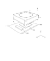
- FIG. 2 is an external perspective view of the camera module A.
- 3A and 3B are external perspective views of the optical element driving device 1 according to the embodiment.
- FIG. 3B shows a state in which FIG. 3A is rotated by 180 ° around the Z axis.
- an orthogonal coordinate system (X, Y, Z) will be used in the embodiments. Also in the figure described later, it is shown by a common Cartesian coordinate system (X, Y, Z).
- the X direction is the vertical direction (or the horizontal direction)
- the Y direction is the horizontal direction (or the vertical direction)
- the Z direction is the front-back direction. It will be installed. That is, the Z direction is the optical axis direction, the upper side (+ Z side) in the figure is the optical axis direction light receiving side, and the lower side ( ⁇ Z side) is the optical axis direction imaging side.
- the X direction and the Y direction orthogonal to the Z axis are referred to as "optical axis orthogonal direction”
- the XY plane is referred to as "optical axis orthogonal plane”.
- the camera module A includes an optical element driving device 1 that realizes an AF function and an OIS function, a lens unit 2 in which a lens is housed in a cylindrical lens barrel, and a lens.
- An image pickup unit 3 or the like for capturing an image of a subject imaged by the unit 2 is provided. That is, the optical drive device 1 is a so-called lens drive device that drives the lens unit 2 as an optical element.
- the imaging unit 3 is arranged on the optical axis direction imaging side of the optical element driving device 1.
- the image pickup unit 3 has, for example, an image sensor board 301, an image pickup element 302 mounted on the image sensor board 301, and a control unit 303.
- the image pickup device 302 is composed of, for example, a CCD (charge-coupled device) type image sensor, a CMOS (complementary metal oxide semiconductor) type image sensor, or the like, and captures an image of a subject imaged by the lens unit 2.
- the control unit 303 is composed of, for example, a control IC, and controls the drive of the optical element drive device 1.
- the optical element driving device 1 is mounted on the image sensor substrate 301 and is mechanically and electrically connected.
- the control unit 303 may be provided on the image sensor board 301, or may be provided on a camera-mounted device (in the embodiment, a smartphone M) on which the camera module A is mounted.
- the outside of the optical element drive device 1 is covered with a cover 24.
- the cover 24 is a covered square cylinder having a rectangular shape in a plan view when viewed from the optical axis direction. In the embodiment, the cover 24 has a square shape in a plan view.
- the cover 24 has a substantially circular opening 241 on the upper surface.
- the lens portion 2 faces the outside from the opening 241 of the cover 24, and is configured to project toward the light receiving side from the opening surface of the cover 24, for example, as it moves in the optical axis direction.
- the cover 24 is fixed to the base 21 (see FIG. 4) of the OIS fixing portion 20 of the optical element driving device 1, for example, by adhesion.
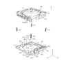
- FIG. 4 and 5 are exploded perspective views of the optical element driving device 1.
- FIG. 5 shows a state in which FIG. 4 is rotated by 180 ° around the Z axis.
- FIG. 4 shows a state in which the OIS drive unit 30 and the sensor board 22 are attached, and
- FIG. 5 shows a state in which the OIS drive unit 30 and the sensor board 22 are removed.
- the optical element driving device 1 includes an OIS movable portion 10 (second movable portion), an OIS fixing portion 20 (second fixed portion), and an OIS driving unit 30 (OIS driving unit 30). It includes an XY direction drive unit) and an OIS support unit 40 (second support unit).
- the OIS drive unit 30 has a first OIS drive unit 30X (X direction drive unit) and a second OIS drive unit 30Y (Y direction drive unit).
- the OIS movable portion 10 is a portion that swings in the plane orthogonal to the optical axis during runout correction.
- the OIS movable portion 10 includes an AF unit, a second stage 13, and X-direction reference balls 42A to 42C (see FIG. 8 and the like).
- the AF unit has an AF movable portion 11 (first movable portion), a first stage 12 (first fixed portion), an AF drive portion 14 (Z-direction drive portion), and an AF support portion 15 (first support portion) ( 8 to 10).
- the OIS fixing portion 20 is a portion to which the OIS movable portion 10 is connected via the OIS support portion 40.
- the OIS fixing portion 20 includes a base 21.
- the OIS movable portion 10 is arranged apart from the OIS fixing portion 20 in the optical axis direction, and is connected to the OIS fixing portion 20 via the OIS support portion 40. Further, the OIS movable portion 10 and the OIS fixing portion 20 are urged in a direction approaching each other by the OIS urging member 50.
- the OIS urging members 50 are arranged at the four corners in the plan view of the optical element driving device 1.
- the entire OIS movable portion 10 including the AF unit moves as a movable body.
- the AF unit moves as a movable body. That is, with respect to the movement in the X direction, the second stage 13 constitutes the OIS fixing portion 20 together with the base 21, and the X direction reference balls 42A to 42C function as the OIS support portion 40.
- the base 21 is formed of, for example, a polyarylate (PAR), a PAR alloy (for example, PAR / PC) in which a plurality of resin materials including PAR are mixed, or a molding material made of a liquid crystal polymer.
- the base 21 is a rectangular member in a plan view and has a circular opening 211 in the center.
- the base 21 has a first base portion 212 and a second base portion 213 forming the main surface of the base 21.
- the second base portion 213 is a portion of the OIS movable portion 10 protruding toward the optical axis direction imaging side, that is, the protruding portions 112A to 112D of the AF movable portion 11 and the AF motor fixing portion 125 of the first stage 12 (FIG. 8, FIG. (See FIG. 9).
- the second base portion 213 is formed to be one size larger in plan view than the protruding portions 112A to 112D and the AF motor fixing portion 125 so that interference does not occur during runout correction.
- the sensor substrate 22 is arranged so that a part (the portion corresponding to the protruding portions 112B and 112C) is exposed.
- the second base portion 213 is formed so as to be recessed with respect to the first base portion 212, whereby the moving stroke of the AF movable portion 11 is secured and the height of the optical element driving device 1 is reduced.
- the sensor substrate 22 is located in a region where the AF drive unit 14 and the OIS drive unit 30 are not arranged, that is, a region corresponding to one side (fourth side) of the rectangular shape of the base 21. It is provided. As a result, the feeding lines and signal lines for the magnetic sensors 25X, 25Y, and 25Z can be integrated, and the wiring structure in the base 21 can be simplified (see FIG. 6).
- the base 21 has an OIS motor fixing portion 215 in which the second OIS drive portion 30Y is arranged.
- the OIS motor fixing portion 215 is provided, for example, at a corner portion of the base 21, is formed so as to project from the first base portion 212 toward the light receiving side in the optical axis direction, and has a shape capable of holding the second OIS drive portion 30Y. Have.
- Terminal fittings 23A to 23C are arranged on the base 21 by, for example, insert molding.
- the terminal fitting 23A includes a power supply line to the AF drive unit 14 and the first OIS drive unit 30X.
- the terminal fitting 23A is exposed from, for example, the openings 216 formed at the four corners of the base 21, and is electrically connected to the OIS urging member 50.
- the power supply to the AF drive unit 14 and the first OIS drive unit 30X is performed via the OIS urging member 50.
- the terminal fitting 23B includes a feeding line (for example, 4 lines) and a signal line (for example, 6 lines) to the magnetic sensors 25X, 25Y, and 25Z.
- the terminal fitting 23B is electrically connected to a wiring (not shown) formed on the sensor substrate 22.
- the terminal fitting 23C includes a power supply line to the second OIS drive unit 30Y.
- the base 21 has Y-direction reference ball holding portions 217A to 217C in which Y-direction reference balls 41A to 41C constituting the OIS support portion 40 are arranged.
- the Y-direction reference ball holding portions 217A to 217C are formed by being recessed in a rectangular shape extending in the Y direction.
- the Y-direction reference ball holding portions 217A to 217C are formed in a substantially V-shaped (tapered shape) in cross section so that the groove width becomes narrower toward the bottom surface side.
- the Y-direction reference ball holding portions 217A and 217B are provided on the side (third side) where the second OIS driving unit 30Y of the base 21 is arranged, and the Y-direction reference ball holding portion 217C is provided.
- the OIS movable portion 10 (second stage 13) is supported at three points by the Y-direction reference balls 41A to 41C, which are provided on the side (fourth side) on which the sensor board 22 is arranged. There is.
- the sensor board 22 has wiring (not shown) including a feeding line and a signal line for the magnetic sensors 25X, 25Y, and 25Z.
- Magnetic sensors 25X, 25Y, and 25Z are mounted on the sensor board 22.
- the magnetic sensors 25X, 25Y, and 25Z are composed of, for example, a Hall element or a TMR (Tunnel Magneto Resistance) sensor, and are electrically connected to the terminal fitting 23B via wiring (not shown) formed on the sensor substrate 22. Will be done.
- an opening 221 is provided in a portion corresponding to the Y direction reference ball holding portion 217C.
- magnets 16X and 16Y are arranged at positions facing the magnetic sensors 25X and 25Y (see FIG. 10).
- the position detection unit including the magnetic sensors 25X and 25Y and the magnets 16X and 16Y detects the positions of the OIS movable portion 10 in the X and Y directions.
- a magnet 16Z is arranged at a position facing the magnetic sensor 25Z (see FIG. 10). The position of the AF movable portion 11 in the Z direction is detected by the position detection unit including the magnetic sensor 25Z and the magnet 16Z.
- an optical sensor such as a photoreflector is used to determine the X-direction and Y-direction positions of the OIS movable portion 10 and the Z-direction position of the AF movable portion 11. It may be detected.
- the OIS urging member 50 is composed of, for example, a tension coil spring, and connects the OIS movable portion 10 and the OIS fixing portion 20.
- one end of the OIS urging member 50 is connected to the terminal fitting 23A of the base 21, and the other end is connected to the wirings 17A and 17B of the first stage 12.
- the OIS urging member 50 receives a tensile load when the OIS movable portion 10 and the OIS fixing portion 20 are connected, and acts so that the OIS movable portion 10 and the OIS fixing portion 20 approach each other.
- the OIS movable portion 10 is oscillatedly held in the XY plane in a state of being urged in the optical axis direction (a state of being pressed against the base 21) by the OIS urging member 50.
- the OIS urging member 50 functions as a feeding line to the AF drive unit 14 and the first OIS drive unit 30X.
- the OIS support portion 40 supports the OIS movable portion 10 with respect to the OIS fixing portion 20 in a state of being separated in the optical axis direction.
- the OIS support portion 40 includes three Y-direction reference balls 41A to 41C interposed between the OIS movable portion 10 (second stage 13) and the base 21. Further, the OIS support portion 40 includes three X-direction reference balls 42A to 42C interposed between the first stage 12 and the second stage 13 in the OIS movable portion 10 (see FIG. 8 and the like).
- the OIS movable portion 10 is accurately shaken in the XY plane by restricting the rollable directions of the Y-direction reference balls 41A to 41C and the X-direction reference balls 42A to 42C (six in total). You can move it.
- the number of Y-direction reference balls and X-direction reference balls constituting the OIS support portion 40 can be appropriately changed.
- the OIS drive unit 30 is an actuator that moves the OIS movable unit 10 in the X direction and the Y direction.
- the OIS drive unit 30 includes a first OIS drive unit 30X (first XY direction drive unit) that moves the OIS movable unit 10 (AF unit only) in the X direction, and the entire OIS movable unit 10. It is composed of a second OIS drive unit 30Y (second XY direction drive unit) that moves in the Y direction.
- the first OIS drive unit 30X and the second OIS drive unit 30Y are composed of an ultrasonic motor.
- the first OIS drive unit 30X is fixed to the OIS motor fixing unit 124 along the X direction of the first stage 12 (see FIG. 9).
- the second OIS drive unit 30Y is fixed to the OIS motor fixing unit 215 of the base 21 so as to extend along the Y direction. That is, the first OIS drive unit 30X and the second OIS drive unit 30Y are arranged along the sides orthogonal to each other.
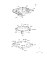
- FIGS. 7A and 7B The configuration of the OIS drive unit 30 is shown in FIGS. 7A and 7B.
- FIG. 7A shows a state in which each member of the OIS drive unit 30 is assembled
- FIG. 7B shows a state in which each member of the OIS drive unit 30 is disassembled.
- 7A and 7B show the second OIS drive unit 30Y, but the main configuration of the first OIS drive unit 30X, specifically, the configuration except for the shape of the OIS electrode 33 is the same.
- OIS drive unit 30 is treated as a diagram.
- the OIS drive unit 30 includes an OIS resonance unit 31, an OIS piezoelectric element 32, an OIS electrode 33, and an OIS power transmission unit 34.
- the driving force of the OIS drive unit 30 is transmitted to the second stage 13 via the OIS power transmission unit 34.
- the first OIS drive unit 30X is connected to the second stage 13 via the first OIS power transmission unit 34X
- the second OIS drive unit 30Y is connected to the second stage 13 via the second OIS power transmission unit 34Y. Is connected to the second stage 13.
- the OIS piezoelectric element 32 is, for example, a plate-shaped element made of a ceramic material, and generates vibration by applying a high frequency voltage. Two OIS piezoelectric elements 32 are arranged so as to sandwich the body portion 311 of the OIS resonance portion 31.
- the OIS electrode 33 sandwiches the OIS resonance portion 31 and the OIS piezoelectric element 32, and applies a voltage to the OIS piezoelectric element 32.
- the OIS electrode 33 of the first OIS drive unit 30X is electrically connected to the wiring 17A of the first stage 12, and the OIS electrode 33 of the second OIS drive unit 30Y is electrically connected to the terminal fitting 23C of the base 21. Be connected.
- the OIS resonance portion 31 is formed of a conductive material and resonates with the vibration of the OIS piezoelectric element 32 to convert the vibration motion into a linear motion.
- the OIS resonance portion 31 is formed by, for example, laser processing, etching processing, press processing, or the like of a metal plate.
- the OIS resonance portion 31 has a substantially rectangular body portion 311 sandwiched between the OIS piezoelectric elements 32, and two arm portions 312 extending in the X direction or the Y direction from the upper and lower portions of the body portion 311.
- the energizing unit 314 of the first OIS drive unit 30X is electrically connected to the wiring 17A of the first stage 12, and the energizing unit 314 of the second OIS drive unit 30Y is electrically connected to the terminal fitting 23C of the base 21. Be connected.
- the OIS piezoelectric element 32 is attached to the body portion 311 of the OIS resonance portion 31 from the thickness direction and is sandwiched by the OIS electrode 33, so that they are electrically connected to each other. For example, when one of the feeding paths is connected to the OIS electrode 33 and the other is connected to the energized portion 314 of the OIS resonance portion 31, a voltage is applied to the OIS piezoelectric element 32 and vibration is generated.
- the OIS resonance unit 31 has at least two resonance frequencies, and is deformed with different behaviors with respect to each resonance frequency.
- the overall shape of the OIS resonant portion 31 is set so that it deforms with different behaviors with respect to the two resonant frequencies.
- the different behaviors are the behavior of moving the OIS power transmission unit 34 forward in the X direction or the Y direction and the behavior of moving it backward.
- the OIS power transmission unit 34 is a chucking guide extending in one direction, one end of which is connected to the arm portion 312 of the OIS resonance portion 31, and the other end of which is connected to the second stage 13.
- the OIS power transmission unit 34 has an OIS motor contact portion 341, a stage fixing portion 343, and a connecting portion 342.
- the OIS motor contact portion 341 comes into contact with the free end portion of the arm portion 312 of the OIS resonance portion 31.
- the stage fixing portion 343 is arranged at the end of the OIS power transmission portion 34 and is fixed to the OIS chucking guide fixing portion 135 (see FIG. 8 and the like) of the second stage 13.
- the connecting portion 342 is a portion that connects the OIS motor contact portion 341 and the stage fixing portion 343, and is branched into two from the stage fixing portion 343 and is formed substantially parallel to each other.
- the width between the OIS motor contact portions 341 is set wider than the width between the free ends of the arm portions 312 of the OIS resonance portion 31.
- a separation portion 344 larger than the width of the connection end portion is interposed between the two connecting portions 342, thereby between the OIS motor contact portions 341.
- the width can be expanded.
- the separation portion 344 is integrally formed with, for example, the stage fixing portion 343.
- stage fixing portion 343 in the stage fixing portion 343, one side of the mounting portion of the connecting portion 342 is open, but the stage fixing portion 343 is the base of the connecting portion 342 (the stage fixing portion 343 side). It may have a structure that sandwiches the end portion of the). In this case, it is possible to prevent the connecting portion 342 from shifting and falling off over time, and the reliability is improved.
- the outer shape of the optical element drive device 1 is increased only by increasing the contact portion in the X direction or the Y direction.
- the moving stroke of the OIS movable portion 10 can be lengthened without any problem.
- the first OIS drive unit 30X is fixed to the OIS movable unit 10 (first stage 12), is connected to the second stage 13 via the OIS power transmission unit 34X, and is Y by the second OIS drive unit 30Y. At the time of runout correction in the direction, it moves together with the OIS movable portion 10.
- the second OIS drive unit 30Y is fixed to the OIS fixing unit 20 (base 21), connected to the second stage 13 via the OIS power transmission unit 34Y, and X by the first OIS drive unit 30X. Not affected by directional runout correction. That is, the movement of the OIS movable portion 10 by one OIS drive unit 30 is not hindered by the structure of the other OIS drive unit 30. Therefore, it is possible to prevent the OIS movable portion 10 from rotating around the Z axis, and the OIS movable portion 10 can be swung accurately in the XY plane.
- FIG. 9 shows a state in which FIG. 8 is rotated by 180 ° around the Z axis.
- FIG. 10 is a downward perspective view showing a state in which FIG. 8 is rotated by 180 ° around the Z axis.
- the AF drive unit 14 and the first OIS drive unit 30X are in a state of being removed from the first stage 12.
- the side on which the AF drive unit 14 is arranged is the “first side”
- the side on which the first OIS drive unit 30X is arranged is the “second side”.
- the side on which the second OIS drive unit 30Y is arranged is referred to as a "side”
- the remaining side is referred to as a "fourth side".
- the OIS movable unit 10 includes an AF movable unit 11, a first stage 12, a second stage 13, an AF drive unit 14, an AF support unit 15, and the like.
- the entire OIS movable portion 10 including the first stage 12 and the second stage 13 is a movable body, whereas the second stage 13 is the OIS fixed portion 20 for the movement in the X direction.
- the first stage 12 functions as an AF fixing portion that supports the AF movable portion 11.
- the AF movable portion 11 is a lens holder that holds the lens portion 2 (see FIG. 2), and moves in the optical axis direction at the time of focusing.
- the AF movable portion 11 is arranged radially inward with respect to the first stage 12 (AF fixing portion), and is supported in a state of being urged to the first stage 12 via the AF support portion 15.
- the AF movable portion 11 is formed of, for example, polyarylate (PAR), a PAR alloy in which a plurality of resin materials including PAR are mixed, a liquid crystal polymer, or the like.
- the AF movable portion 11 has a cylindrical lens accommodating portion 111.
- the lens portion 2 is fixed to the inner peripheral surface of the lens accommodating portion 111 by, for example, adhesion.
- the AF movable portion 11 has protruding portions 112A to 112D protruding outward in the radial direction and extending in the optical axis direction on the outer peripheral surface of the lens accommodating portion 111.
- the protrusions 112A to 112D are preferably arranged symmetrically with respect to the optical axis. In the present embodiment, protrusions 112A to 112D are provided around the optical axis at intervals of approximately 90 °.
- the protruding portions 112A to 112D project toward the optical axis direction imaging side from the lower surface of the lens accommodating portion 111, and abut against the second base portion 213 of the base 21 to cause the AF movable portion 11 to form an optical axis direction imaging side ( Restrict movement to the lower side).
- the protrusions 112A to 112D come into contact with the second base portion 213 of the base 21 in the reference state in which the AF drive portion 14 is not driven.
- the protrusions 112A and 112B on the AF drive unit 14 side hold the AF support unit 15 together with the first stage 12.
- One protruding portion 112A accommodates a first Z-direction reference ball 15A constituting the AF support portion 15.
- the other protruding portion 112B accommodates a second Z-direction reference ball 15B constituting the AF support portion 15.
- the protruding portions 112A and 112B accommodate the first preload balls 15C and the second preload balls 15D, which constitute the AF support portion 15, respectively.
- a magnet accommodating portion 114 accommodating the magnet 16Z for Z position detection is provided on the outer peripheral surface of the lens accommodating portion 111.
- the magnet 16Z is arranged in the magnet accommodating portion 114.
- a magnetic sensor 25Z for Z position detection is arranged at a position facing the magnet 16Z in the optical axis direction (see FIG. 4).
- the AF power transmission portion 144 is arranged between the protrusions 112A and 112B.
- the AF power transmission unit 144 is a chucking guide having a predetermined length in the Z direction, and has a side wall facing the X direction and projecting in the Y direction (-side).
- the arm portion 141b of the resonance portion 141 of the AF drive portion 14 abuts so as to expand the side wall of the AF power transmission portion 144, and the power of the AF drive portion 14 is transmitted to the AF movable portion 11.
- the side wall of the AF power transmission portion 144 functions as a leaf spring, so that the driving force generated by the deformation of the resonance portion 141 is efficiently transmitted.
- the structure of the AF power transmission unit 144 can be arbitrarily changed.
- the side wall may be folded back in the Z direction to form a leaf spring so as to be located inside the side wall in the X direction so that the urging force is exerted in the direction of pushing back the arm portion 141b of the AF drive portion 14.
- the driving force generated by the deformation of the resonance unit 141 is more efficiently transmitted to the AF power transmission unit 144.
- the AF power transmission unit 144 is composed of a separate member from the AF movable unit 11.
- the AF power transmission unit 144 has, for example, a U-shape in a plan view, and the bottom surface portion is fixed to the outer peripheral surface of the lens accommodating portion 111 in a state where the side surface portions face each other in the X direction.
- the AF power transmission unit 144 is made of, for example, a metal material.
- the first stage 12 supports the AF movable portion 11 via the AF support portion 15.
- the second stage 13 is arranged on the optical axis direction imaging side of the first stage 12 via the X-direction reference balls 42A to 42C.
- the first stage 12 moves in the X direction and the Y direction at the time of runout correction, and the second stage 13 moves only in the Y direction at the time of runout correction.
- the first stage 12 is a member having a substantially rectangular shape in a plan view seen from the optical axis direction, and is formed of, for example, a liquid crystal polymer.
- the first stage 12 has a substantially circular opening 121 in a portion corresponding to the AF movable portion 11.
- the opening 121 is formed with notches 122 corresponding to the protrusions 112A to 112D of the AF movable portion 11 and the magnet accommodating portion 114.
- the portion corresponding to the first OIS drive unit 30X (the outer surface of the side wall along the second side) can be arranged so that the first OIS drive unit 30X can be arranged without protruding outward in the radial direction.
- the portion corresponding to the second OIS drive unit 30Y (the outer surface of the side wall along the third side) is also formed to be recessed inward in the radial direction.
- the first stage 12 has X-direction reference ball holding portions 123A to 123C on the lower surface for holding the X-direction reference balls 42A to 42C.
- the X-direction reference ball holding portions 123A to 123C are formed by being recessed in a rectangular shape extending in the X direction.
- the X-direction reference ball holding portions 123A to 123C face the X-direction reference ball holding portions 133A to 133C of the second stage 13 in the Z direction.
- the X-direction reference ball holding portions 123A and 123B are formed in a substantially V-shaped (tapered shape) so that the groove width becomes narrower toward the bottom surface side, and the X-direction reference ball holding portions 123C are substantially U. It is formed in a character shape.
- an AF motor fixing portion 125 in which the AF drive portion 14 is arranged is formed on one side wall along the X direction (the side wall along the first side).
- the AF motor fixing portion 125 has an upper fixing plate (reference numeral omitted) and a lower fixing plate 125a, and the AF driving portion 14 is sandwiched between them.
- the AF resonance unit 141 is inserted into an insertion hole (reference numeral omitted) provided in the upper fixing plate and the lower fixing plate 125a, and is fixed by adhesion.
- the upper fixing plate is composed of a part of the wiring 17B, and the AF resonance portion 141 is electrically connected to the wiring 17B.
- magnets 16X and 16Y for XY position detection are arranged on one side wall along the Y direction (side wall along the fourth side).
- the magnet 16X is magnetized in the X direction
- the magnet 16Y is magnetized in the Y direction
- magnetic sensors 25X and 25Y for XY position detection are arranged at positions facing the magnets 16X and 16Y in the optical axis direction (see FIG. 4).
- wirings 17A and 17B are embedded in the first stage 12 by, for example, insert molding.
- the wirings 17A and 17B are arranged along the first side and the second side, for example.
- the wirings 17A and 17B are exposed from the four corners of the first stage 12, and one end of the OIS urging member 50 is connected to these portions. Power is supplied to the first OIS drive unit 30X via the wiring 17A, and power is supplied to the AF drive unit 14 via the wiring 17B.
- the second stage 13 is a member having a substantially rectangular shape in a plan view seen from the optical axis direction, and is formed of, for example, a liquid crystal polymer.
- the inner peripheral surface 131 of the second stage 13 is formed corresponding to the outer shape of the AF movable portion 11.
- the portions corresponding to the first OIS drive unit 30X and the second OIS drive unit 30Y are the same as those in the first stage 12. In addition, it is formed by denting inward in the radial direction.
- the second stage 13 has Y-direction reference ball holding portions 134A to 134C on the lower surface, which accommodate the Y-direction reference balls 41A to 41C.
- the Y-direction reference ball holding portions 134A to 134C are formed by being recessed in a rectangular shape extending in the Y direction.
- the Y-direction reference ball holding portions 134A to 134C face the Y-direction reference ball holding portions 217A to 217C of the base 21 in the Z direction.
- the Y-direction reference ball holding portions 134A and 134B are formed in a substantially V-shaped (tapered shape) so that the groove width becomes narrower toward the bottom surface side, and the Y-direction reference ball holding portion 134C is substantially U. It is formed in a character shape.
- the second stage 13 has X-direction reference ball holding portions 133A to 133C on the upper surface, which accommodate the X-direction reference balls 42A to 42C.
- the X-direction reference ball holding portions 133A to 133C are formed by being recessed in a rectangular shape extending in the X direction.
- the X-direction reference ball holding portions 133A to 133C face the X-direction reference ball holding portions 123A to 123C of the first stage 12 in the Z direction.
- the X-direction reference ball holding portions 133A to 133C are formed in a substantially V-shaped (tapered shape) in cross section so that the groove width becomes narrower toward the bottom surface side.
- the X-direction reference ball holding portions 133A and 133B are provided on the side (second side) where the first OIS driving unit 30X of the second stage 13 is arranged, and the X-direction reference ball holding portion is provided.
- the 133C is provided on the side (first side) where the AF drive unit 14 is arranged, and the first stage 12 is supported at three points by the X-direction reference balls 42A to 42C.
- the Y-direction reference balls 41A to 41C constituting the OIS support portion 40 are sandwiched by the Y-direction reference ball holding portions 217A to 217C of the base 21 and the Y-direction reference ball holding portions 134A to 134C of the second stage 13 by multipoint contact. Will be done. Therefore, the Y-direction reference balls 41A to 41C stably roll in the Y-direction.
- the X-direction reference balls 42A to 42C are sandwiched by the X-direction reference ball holding portions 133A to 133C of the second stage 13 and the X-direction reference ball holding portions 123A to 123C of the first stage 12 in a multi-point contact. Therefore, the X-direction reference balls 42A to 42C stably roll in the X-direction.
- the AF support portion 15 is a portion that supports the AF movable portion 11 with respect to the first stage 12 (AF fixing portion).
- the AF support portion 15 is composed of a first Z-direction reference ball 15A, a second Z-direction reference ball 15B, a first preload ball 15C, and a second preload ball 15D.
- the first Z-direction reference ball 15A, the second Z-direction reference ball 15B, the first preload ball 15C, and the second preload ball 15D are each a plurality of balls arranged side by side in the Z direction. It is composed of (here, 3 pieces).
- the intermediate ball is provided to secure the separation distance between the upper and lower balls, and may have a smaller diameter than the upper and lower balls.
- the AF drive unit 14 is an actuator that moves the AF movable unit 11 in the Z direction. Like the OIS drive unit 30, the AF drive unit 14 is composed of an ultrasonic motor. The AF drive unit 14 is fixed to the AF motor fixing unit 125 of the first stage 12 so that the arm unit 141b extends in the Z direction.
- FIGS. 11A and 11B The configuration of the AF drive unit 14 is shown in FIGS. 11A and 11B.
- FIG. 11A shows a state in which each member of the AF drive unit 14 is assembled
- FIG. 11B shows a state in which each member of the AF drive unit 14 is disassembled.
- the configuration of the AF drive unit 14 is almost the same as that of the OIS drive unit 30.
- the AF drive unit 14 includes an AF resonance unit 141, an AF piezoelectric element 142, an AF electrode 143, and an AF power transmission unit 144.
- the driving force of the AF driving unit 14 is transmitted to the AF movable unit 11 via the AF power transmission unit 144.
- the AF piezoelectric element 142 is, for example, a plate-shaped element made of a ceramic material, and generates vibration by applying a high frequency voltage.
- Two AF piezoelectric elements 142 are arranged so as to sandwich the body portion 141a of the AF resonance portion 141.
- the AF electrode 143 sandwiches the AF resonance portion 141 and the AF piezoelectric element 142, and applies a voltage to the AF piezoelectric element 142.
- the AF resonance portion 141 is formed of a conductive material and resonates with the vibration of the AF piezoelectric element 142 to convert the vibration motion into a linear motion.
- the AF resonance portion 141 is formed by, for example, laser processing, etching processing, press processing, or the like of a metal plate.
- the AF resonance portion 141 is a substantially rectangular body portion 141a sandwiched between the AF piezoelectric elements 142, two arm portions 141b extending in the Z direction from the body portion 141a, and a central portion of the body portion 141a.
- the current-carrying portion 141c extending in the Z direction from the center and electrically connected to the power feeding path (wiring 17B (upper fixing plate 125a) of the first stage 12) and the side opposite to the current-carrying portion 141c from the central portion of the body portion 141a.
- the two arm portions 141b have a symmetrical shape and are symmetrically deformed in resonance with the vibration of the AF piezoelectric element 142.
- the AF drive portion 14 has a stage fixing portion 141d extending to the AF drive portion 14.
- the two arm portions 141b extend in the Z direction and are arranged so as to sandwich the AF power transmission portion 144 at the free end portion.
- the AF piezoelectric element 142 is attached to the body portion 141a of the AF resonance portion 141 from the thickness direction and is sandwiched by the AF electrode 143 so that they are electrically connected to each other.
- a voltage is applied to the AF piezoelectric element 142 and vibration is generated.
- the AF resonance unit 141 has at least two resonance frequencies, and is deformed with different behaviors with respect to each resonance frequency.
- the AF resonance portion 141 is set to have an overall shape so as to be deformed with different behaviors with respect to the two resonance frequencies.
- the AF piezoelectric element 142 vibrates and the AF resonance unit 141 is deformed according to the frequency.
- the AF power transmission unit 144 is slid in the Z direction by the driving force of the AF drive unit 14. Along with this, the AF movable portion 11 moves in the Z direction, and focusing is performed. Since the AF support portion 15 is composed of balls, the AF movable portion 11 can smoothly move in the Z direction. Further, since the AF drive unit 14 and the AF power transmission unit 144 are only in contact with each other in an urged state, simply increasing the contact portion in the Z direction impairs the reduction in height of the optical element drive device 1. Without this, the moving stroke of the AF movable portion 11 can be easily lengthened.
- the OIS piezoelectric element 32 vibrates and the OIS resonance unit 31 is deformed according to the frequency.
- the driving force of the OIS driving unit 30 causes the OIS power transmitting unit 34 to slide in the X direction or the Y direction.
- the OIS movable portion 10 moves in the X direction or the Y direction, and runout correction is performed. Since the OIS support portion 40 is composed of balls, the OIS movable portion 10 can smoothly move in the X direction or the Y direction.
- the first stage 12 to the second stage 13 in which the first OIS drive unit 30X is arranged are arranged. Power is transmitted to.
- the ball 41 sandwiched between the second stage 13 and the base 21 cannot roll in the X direction, the position of the second stage 13 in the X direction with respect to the base 21 is maintained.
- the ball 42 sandwiched between the first stage 12 and the second stage 13 can roll in the X direction, the first stage 12 moves in the X direction with respect to the second stage 13. That is, the second stage 13 constitutes the OIS fixing portion 20, and the first stage 12 constitutes the OIS movable portion 10.
- the second OIS drive unit 30Y when the second OIS drive unit 30Y is driven and the OIS power transmission unit 34 moves in the Y direction, power is transmitted from the base 21 in which the second OIS drive unit 30Y is arranged to the second stage 13. To. At this time, since the ball 42 sandwiched between the first stage 12 and the second stage 13 cannot roll in the Y direction, the position of the first stage 12 in the Y direction with respect to the second stage is maintained. On the other hand, since the ball 41 sandwiched between the second stage 13 and the base 21 can roll in the Y direction, the second stage 13 moves in the Y direction with respect to the base 21. The first stage 12 also follows the second stage 13 and moves in the Y direction. That is, the base 21 constitutes the OIS fixing portion 20, and the AF unit including the first stage 12 and the second stage 13 constitutes the OIS movable portion 10.
- the OIS movable portion 10 swings in the XY plane, and runout correction is performed.
- the energizing voltage to the OIS drive unit 30 is set based on the detection signal indicating the angular vibration from the vibration detection unit (for example, a gyro sensor, not shown) so that the angular vibration of the camera module A is offset. Be controlled.
- the vibration detection unit for example, a gyro sensor, not shown
- the AF resonance unit 141 and the AF power transmission unit 144 are in contact with each other and slide with each other during driving.
- the OIS resonance unit 31 and the OIS power transmission unit 34 are in contact with each other and slide with each other during drive. That is, the AF drive unit 14 and the OIS drive unit 30 are ultrasonic motor type drive units that move the passive element relative to the active element.
- the active element is composed of an AF resonance unit 141 having an arm unit 141b that resonates with the vibration of the AF piezoelectric element 142 and deforms, and linearly moves the vibration motion of the AF piezoelectric element 142. Convert to.
- the passive element is composed of an AF power transmission unit 144 and is arranged so as to come into contact with the arm unit 141b in an urged state.
- the active element is composed of an OIS resonance unit 31 having an arm unit 31b that resonates with the vibration of the OIS piezoelectric element and deforms, and converts the vibration motion of the OIS piezoelectric element 32 into a linear motion.
- the passive element is composed of the OIS power transmission unit 34 and is arranged so as to come into contact with the arm unit 31b in a urged state.
- the passive element is moved to the combination of sliding members that slide with each other, that is, the combination of the AF resonance unit 141 and the AF power transmission unit 144, and the combination of the OIS resonance unit 31 and the OIS power transmission unit 34. It is required to have excellent wear resistance for a long period of time while exhibiting a frictional force to the extent possible. However, it is not easy to balance these because the frictional force and the wear resistance have contradictory characteristics, such that the wear resistance decreases when the frictional force is increased. As a result of diligent studies on the combination of sliding members, the present inventors have come up with a combination that can satisfy the requirements for the AF drive unit 14 and the OIS drive unit 30, and have completed the present invention. In the present embodiment, by applying the drive unit according to the present invention to the AF drive unit 14 and the OIS drive unit 30, the drive performance of the AF drive unit 14 and the OIS drive unit 30 is improved.
- the AF power transmission unit 144 which is a passive element, has a coating layer on the contact surface with the AF resonance unit 141, which is an active element, and the coating layer has a hardness and a shear strength higher than those of the AF resonance unit 141. big.
- the OIS power transmission unit 34 which is a passive element, has a coating layer on the contact surface with the OIS resonance unit 31, which is an active element, and the coating layer has a hardness and a shear strength higher than those of the OIS resonance unit 34. big.
- the active element side AF resonance portion 141, OIS resonance portion 31
- the wear resistance can be easily improved by controlling the surface state of the contact surface on the active element side.
- the stability of operation can be improved. That is, if a streak-like wear mark is formed on the contact surface due to local wear on the passive element side, unexpected operation may occur when the active side element is removed from the wear mark. It is possible to prevent such a problem from occurring.
- the contact surfaces of the AF resonance portion 141 and the OIS resonance portion 31, which are active elements, may be provided with a coating layer such as hard plating or coating, or may be surface-treated other than the coating layer. good.
- the coating layer may be formed directly on the active side base material which is the main material of the active element, or another member such as a plate having the coating layer may be attached to the active side base material. good.
- the active-side base material which is the main material of the active element, may be any metal having predetermined conductivity, shear strength, hardness, specific gravity, Young's modulus, etc., and for example, stainless steel is suitable.
- the Vickers hardness of the stainless steel rope is 180 to 400 HV.
- the AF power transmission unit 144 and the OIS power transmission unit 34 which are passive elements, are composed of a passive side base material which is a main material and a coating layer. By providing a coating layer having higher hardness and shear strength than the active element on the passive element side, wear of the passive element can be suppressed.
- the passive side base material preferably has a rigidity equal to or higher than that of the active side base material, and for example, stainless steel is suitable.
- the AF power transmission unit 144 and the OIS power transmission unit 34 can be imparted with self-restoring property to function as leaf springs, and it becomes easy to develop a desired frictional force between the active element and the passive element.
- the stainless steel rope forming the active side base material and the stainless steel rope forming the passive side base material may be of the same steel type or different steel types. For example, an appropriate steel grade is selected in consideration of the transmission of force from the active element to the passive element.
- the coating layer of the passive element for example, fine ceramics such as diamond-like carbon (DLC) and zirconia (ZnO 2) are suitable.
- DLC diamond-like carbon
- ZnO 2 zirconia
- the Vickers hardness of DLC is 1100 to 7000 HV
- the Vickers hardness of zirconia is 1200 to 1400 HV, both of which are harder than stainless steel. If the contact surfaces of the active element and the passive element are made of metals, agglutination may occur. Therefore, the coating layer is preferably formed of a material other than the metal.
- DLC when DLC is applied to the coating layer, the amount of wear of the active element and passive element when the urging load (friction force) is increased is smaller than that when zirconia is applied, and there is almost no change. It has been confirmed experimentally. Further, DLC is known to have self-lubricating property, and although it has a higher hardness than ceramics such as zirconia, it can be expected to have an effect of suppressing wear generated on the active side. From this, DLC is more suitable for the coating layer from the viewpoint that it can easily cope with the required urging load.
- the coating layer on the passive element side is made of a material harder than the active element, wear mainly occurs in the active element.
- the actual amount of wear is determined by a combination of multiple factors such as the hardness of the sliding member, compatibility with the mating material, and the environment in which it is used. When it is about 2.5 times or more of, it is considered that almost no wear of the coating layer occurs regardless of other factors. Therefore, by focusing on the wear resistance of the active element, the wear resistance of the drive unit can be improved.
- the active-side substrate of the AF resonance portion 141 and the OIS resonance portion 31 is flattened at least on the contact surface with the mating material (coating layer on the passive side). As a result, the surface texture is improved as compared with the state after processing, and the wear resistance of the active side base material is improved.
- Electropolishing is a method in which a polishing object is made a positive electrode and a DC current is passed through an electrolytic solution to melt and smooth the metal surface.
- mechanical polishing using a machine tool such as a grinder is performed to some extent. It is done after smoothing.
- Barrel polishing is a method in which an object to be polished, an abrasive, or the like is placed in a barrel tank and subjected to rotation or vibration for polishing.
- Plasma treatment is a method of chemically modifying the surface of an object by irradiating it with plasma, and has an advantage that it can be applied to a sheet-shaped object.
- the peak density Spd of the peak on the contact surface with the passive element is 200,000 to 1,500,000.
- the true contact area with the passive element is appropriately controlled, and cohesive wear including fretting wear and abstract wear can be suppressed, so that wear resistance is improved.
- the AF drive unit 14 (drive unit) according to the embodiment has an AF piezoelectric element 142 that generates vibration by applying a voltage, and an arm unit 141b that resonates with the vibration of the AF piezoelectric element 142 and deforms.
- the AF resonance portion 141 active element that converts the vibrational motion of the AF piezoelectric element 142 into a linear motion is arranged so as to be in contact with the arm portion 141b in an urged state, and is relatively relative to the AF resonance portion 141. It has a moving AF power transmission unit 144 (passive element).
- the OIS drive unit 30 (drive unit) has an OIS piezoelectric element 32 that generates vibration by applying a voltage and an arm portion 31b that resonates with the vibration of the OIS piezoelectric element 32 and deforms, and the vibration motion of the OIS piezoelectric element 32.
- the OIS resonance unit 31 active element that converts the (Passive element) and.
- the AF power transmission unit 144 and the OIS power transmission unit 34 which are passive elements, have a coating layer on the contact surface with the AF resonance unit 141 and the OIS resonance unit 31, which are active elements. The hardness and shear strength of the coating layer are larger than those of the active element.
- the coating layer of the passive element is preferably about 2.5 times or more the hardness of the active side base material which is the main material of the active element.
- the active side base material is formed of stainless steel and the coating layer of the passive element is formed of diamond-like carbon (DLC).
- the passive side base material is preferably made of stainless steel as in the active side base material.
- the active side base material has a flattening treatment on the contact surface with the passive element. As the flattening treatment, barrel polishing or electrolytic polishing is suitable. Further, the active side base material preferably has a peak density Spd of 200,000 to 1.5 million on the contact surface with the passive element.
- the AF drive unit 141 and the OIS drive unit 30 (drive unit) it is possible to suppress deterioration of drive performance over time due to wear and improve the reliability of the product to which the drive unit is applied. can.
- a smartphone M which is a mobile terminal with a camera
- the present invention uses the camera module and the image information obtained by the camera module. It can be applied to a camera-mounted device having an image processing unit for processing.
- Camera-mounted devices include information equipment and transportation equipment.
- the information device includes, for example, a mobile phone with a camera, a notebook computer, a tablet terminal, a portable game machine, a web camera, and an in-vehicle device with a camera (for example, a back monitor device and a drive recorder device).
- the transportation equipment includes, for example, an automobile.
- FIGS. 12A and 12B are diagrams showing an automobile V as a camera-mounted device for mounting an in-vehicle camera module VC (Vehicle Camera).
- 12A is a front view of the automobile V
- FIG. 12B is a rear perspective view of the automobile V.
- the automobile V is equipped with the camera module A described in the embodiment as the in-vehicle camera module VC.
- the vehicle-mounted camera module VC may be attached to the windshield toward the front or attached to the rear gate toward the rear, for example.
- This in-vehicle camera module VC is used for a back monitor, a drive recorder, a collision avoidance control, an automatic driving control, and the like.
- the optical element driving device 1 for driving the lens unit 2 as an optical element has been described, but the optical element to be driven may be an optical element other than the lens such as a mirror or a prism.
- Optical element drive device 10 OIS movable part (movable part) 12 First stage (fixed part) 13 Second stage 14 AF drive unit (drive unit) 141 AF resonance part (active element) 142 AF Piezoelectric element (active element) 143 AF electrode 144 AF power transmission unit (passive element) 15 AF support part 20 OIS fixing part (fixing part) 21 Base 30 OIS drive unit (drive unit) 31 OIS resonance part (active element) 32 OIS Piezoelectric element (active element) 33 OIS electrode 34 OIS power transmission unit (passive element) 40 OIS support 50 OIS urging member A Camera module M Smartphone (camera-mounted device)
Landscapes
- Lens Barrels (AREA)
- Adjustment Of Camera Lenses (AREA)
Abstract
駆動ユニットは、電圧印可により振動を発生する圧電素子と、圧電素子の振動に共振して変形するアーム部を有し圧電素子の振動を直線運動に変換する能動要素と、付勢された状態で前記アーム部に接触するように配置され、能動要素に対して相対的に移動する受動要素とを備え、受動要素は、能動要素との接触面にコーティング層を有し、コーティング層の硬度及びせん断強度が、能動要素よりも大きい。
Description
本発明は、駆動ユニット、光学素子駆動装置、カメラモジュール、及びカメラ搭載装置に関する。
一般に、スマートフォン等の携帯端末には、小型のカメラモジュールが搭載されている。このようなカメラモジュールには、被写体を撮影するときのピント合わせを自動的に行うオートフォーカス機能(以下「AF機能」と称する、AF:Auto Focus)及び撮影時に生じる振れ(振動)を光学的に補正して画像の乱れを軽減する振れ補正機能(以下「OIS機能」と称する、OIS:Optical Image Stabilization)を有するレンズ駆動装置が適用される(例えば、特許文献1)。
AF機能及びOIS機能を有するレンズ駆動装置は、レンズ部を光軸方向に移動させるためのオートフォーカス駆動部(以下「AF駆動部」と称する)と、レンズ部を光軸方向に直交する平面内で揺動させるための振れ補正駆動部(以下「OIS駆動部」と称する)と、を備える。特許文献1では、AF駆動部及びOIS駆動部に超音波モーター型の駆動ユニットが適用されている。
しかしながら、超音波モーター型の駆動ユニットにおいては、共振部からなる能動要素と、能動要素に対して相対的に移動する受動要素とが、付勢された状態で接触し、駆動時には両者が摺動することとなるため、摩耗によって経時的に駆動性能が損なわれる虞がある。特に、能動要素と受動要素との間で受動要素を移動できる程度の摩擦力が必要である一方、摩擦力が増大すると接触部分が摩耗しやすくなるため、これらをバランスさせることが重要となる。
本発明の目的は、摩耗による経時的な駆動性能の低下を抑制できる、信頼性の高い駆動ユニット、光学素子駆動装置、カメラモジュール及びカメラ搭載装置を提供することである。
本発明に係る駆動ユニットは、
電圧印可により振動を発生する圧電素子と、
前記圧電素子の振動に共振して変形するアーム部を有し前記圧電素子の振動を直線運動に変換する能動要素(共振器)と、
付勢された状態で前記アーム部に接触するように配置され、前記能動要素に対して相対的に移動する受動要素と、を備える駆動ユニットであって、
前記受動要素は、前記能動要素との接触面にコーティング層を有し、
前記コーティング層の硬度及びせん断強度が、前記能動要素よりも大きい。
電圧印可により振動を発生する圧電素子と、
前記圧電素子の振動に共振して変形するアーム部を有し前記圧電素子の振動を直線運動に変換する能動要素(共振器)と、
付勢された状態で前記アーム部に接触するように配置され、前記能動要素に対して相対的に移動する受動要素と、を備える駆動ユニットであって、
前記受動要素は、前記能動要素との接触面にコーティング層を有し、
前記コーティング層の硬度及びせん断強度が、前記能動要素よりも大きい。
本発明に係る光学素子駆動装置は、
固定部と、
前記固定部から離間して配置され光学素子を保持する可動部と、
前記固定部に対して前記可動部を支持する支持部と、
上記の駆動ユニットで構成され、前記固定部に対して前記可動部を移動させる駆動部と、を備える。
固定部と、
前記固定部から離間して配置され光学素子を保持する可動部と、
前記固定部に対して前記可動部を支持する支持部と、
上記の駆動ユニットで構成され、前記固定部に対して前記可動部を移動させる駆動部と、を備える。
本発明に係るカメラモジュールは、
上記の光学素子駆動装置と、
前記光学素子であるレンズ部と、
前記レンズ部により結像された被写体像を撮像する撮像部と、
を備える、カメラモジュール。
上記の光学素子駆動装置と、
前記光学素子であるレンズ部と、
前記レンズ部により結像された被写体像を撮像する撮像部と、
を備える、カメラモジュール。
本発明に係るカメラ搭載装置は、
情報機器又は輸送機器であるカメラ搭載装置であって、
上記のカメラモジュールと、
前記カメラモジュールで得られた画像情報を処理する画像処理部と、を備える。
情報機器又は輸送機器であるカメラ搭載装置であって、
上記のカメラモジュールと、
前記カメラモジュールで得られた画像情報を処理する画像処理部と、を備える。
本発明によれば、摩耗による経時的な駆動性能の低下を抑制できる、信頼性の高い駆動ユニット、光学素子駆動装置、カメラモジュール及びカメラ搭載装置が提供される。
以下、本発明の実施の形態を図面に基づいて詳細に説明する。
図1A、図1Bは、本発明の一実施の形態に係るカメラモジュールAを搭載するスマートフォンM(カメラ搭載装置の一例)を示す図である。図1AはスマートフォンMの正面図であり、図1BはスマートフォンMの背面図である。
スマートフォンMは、2つの背面カメラOC1、OC2からなるデュアルカメラを有する。本実施の形態では、背面カメラOC1、OC2に、カメラモジュールAが適用されている。
カメラモジュールAは、AF機能及びOIS機能を備え、被写体を撮影するときのピント合わせを自動的に行うとともに、撮影時に生じる振れ(振動)を光学的に補正して像ぶれのない画像を撮影することができる。
カメラモジュールAは、AF機能及びOIS機能を備え、被写体を撮影するときのピント合わせを自動的に行うとともに、撮影時に生じる振れ(振動)を光学的に補正して像ぶれのない画像を撮影することができる。
図2は、カメラモジュールAの外観斜視図である。図3A、図3Bは、実施の形態に係る光学素子駆動装置1の外観斜視図である。図3Bは、図3AをZ軸周りに180°回転した状態を示す。図2、図3A及び図3Bに示すように、実施の形態では、直交座標系(X,Y,Z)を使用して説明する。後述する図においても共通の直交座標系(X,Y,Z)で示している。
カメラモジュールAは、例えば、スマートフォンMで実際に撮影が行われる場合に、X方向が上下方向(又は左右方向)、Y方向が左右方向(又は上下方向)、Z方向が前後方向となるように搭載される。すなわち、Z方向が光軸方向であり、図中上側(+Z側)が光軸方向受光側、下側(-Z側)が光軸方向結像側である。また、Z軸に直交するX方向及びY方向を「光軸直交方向」と称し、XY面を「光軸直交面」と称する。
図2、図3A及び図3Bに示すように、カメラモジュールAは、AF機能及びOIS機能を実現する光学素子駆動装置1、円筒形状のレンズバレルにレンズが収容されてなるレンズ部2、及びレンズ部2により結像された被写体像を撮像する撮像部3等を備える。すなわち、光学駆動装置1は、光学素子としてレンズ部2を駆動する、いわゆるレンズ駆動装置である。
撮像部3は、光学素子駆動装置1の光軸方向結像側に配置される。撮像部3は、例えば、イメージセンサー基板301、イメージセンサー基板301に実装される撮像素子302及び制御部303を有する。撮像素子302は、例えば、CCD(charge-coupled device)型イメージセンサー、CMOS(complementary metal oxide semiconductor)型イメージセンサー等により構成され、レンズ部2により結像された被写体像を撮像する。制御部303は、例えば、制御ICで構成され、光学素子駆動装置1の駆動制御を行う。光学素子駆動装置1は、イメージセンサー基板301に搭載され、機械的かつ電気的に接続される。なお、制御部303は、イメージセンサー基板301に設けられてもよいし、カメラモジュールAが搭載されるカメラ搭載機器(実施の形態では、スマートフォンM)に設けられてもよい。
光学素子駆動装置1は、外側をカバー24で覆われている。カバー24は、光軸方向から見た平面視で矩形状の有蓋四角筒体である。実施の形態では、カバー24は、平面視で正方形状を有している。カバー24は、上面に略円形の開口241を有する。レンズ部2は、カバー24の開口241から外部に臨み、例えば、光軸方向における移動に伴い、カバー24の開口面よりも受光側に突出するように構成される。カバー24は、光学素子駆動装置1のOIS固定部20のベース21(図4参照)に、例えば、接着により固定される。
図4、図5は、光学素子駆動装置1の分解斜視図である。図5は、図4をZ軸周りに180°回転した状態を示す。図4は、OIS駆動部30及びセンサー基板22を取り付けた状態を示し、図5は、OIS駆動部30及びセンサー基板22を取り外した状態を示している。
図4、図5に示すように、本実施の形態において、光学素子駆動装置1は、OIS可動部10(第2可動部)、OIS固定部20(第2固定部)、OIS駆動部30(XY方向駆動部)及びOIS支持部40(第2支持部)を備える。OIS駆動部30は、第1のOIS駆動部30X(X方向駆動部)及び第2のOIS駆動部30Y(Y方向駆動部)を有する。
OIS可動部10は、振れ補正時に光軸直交面内で揺動する部分である。OIS可動部10は、AFユニット、第2ステージ13及びX方向基準ボール42A~42C(図8等参照)を含む。AFユニットは、AF可動部11(第1可動部)、第1ステージ12(第1固定部)、AF駆動部14(Z方向駆動部)及びAF支持部15(第1支持部)を有する(図8~図10参照)。
OIS固定部20は、OIS支持部40を介してOIS可動部10が接続される部分である。OIS固定部20は、ベース21を含む。
OIS可動部10は、OIS固定部20に対して光軸方向に離間して配置され、OIS支持部40を介してOIS固定部20と連結される。また、OIS可動部10とOIS固定部20は、OIS用付勢部材50によって、互いに近づく方向に付勢されている。本実施の形態では、OIS用付勢部材50は、光学素子駆動装置1の平面視における四隅に配置されている。
OIS固定部20は、OIS支持部40を介してOIS可動部10が接続される部分である。OIS固定部20は、ベース21を含む。
OIS可動部10は、OIS固定部20に対して光軸方向に離間して配置され、OIS支持部40を介してOIS固定部20と連結される。また、OIS可動部10とOIS固定部20は、OIS用付勢部材50によって、互いに近づく方向に付勢されている。本実施の形態では、OIS用付勢部材50は、光学素子駆動装置1の平面視における四隅に配置されている。
本実施の形態では、Y方向の移動に関しては、AFユニットを含むOIS可動部10の全体が可動体として移動する。一方、X方向の移動に関しては、AFユニットだけが可動体として移動する。つまり、X方向の移動に関しては、第2ステージ13は、ベース21とともにOIS固定部20を構成し、X方向基準ボール42A~42CはOIS支持部40として機能する。
ベース21は、例えば、ポリアリレート(PAR)、PARを含む複数の樹脂材料を混合したPARアロイ(例えば、PAR/PC)、又は液晶ポリマーからなる成形材料で形成される。ベース21は、平面視で矩形状の部材であり、中央に円形の開口211を有する。
ベース21は、ベース21の主面を形成する第1ベース部212及び第2ベース部213を有する。第2ベース部213は、OIS可動部10の光軸方向結像側に突出する部分、すなわち、AF可動部11の突出部112A~112D及び第1ステージ12のAFモーター固定部125(図8、図9参照)に対応して設けられている。第2ベース部213は、振れ補正時に干渉が生じないように、突出部112A~112D及びAFモーター固定部125よりも、平面視において一回り大きく形成されている。第2ベース部213のうち、端子金具23Bが配置される領域には、一部(突出部112B、112Cに対応する部分)が露出するようにセンサー基板22が配置される。第2ベース部213は、第1ベース部212に対して凹んで形成され、これにより、AF可動部11の移動ストロークの確保と光学素子駆動装置1の低背化が図られている。
本実施の形態では、センサー基板22は、AF駆動部14及びOIS駆動部30が配置されていない領域、すなわち、ベース21の平面形状である矩形の一辺(第4の辺)に対応する領域に設けられている。これにより、磁気センサー25X、25Y、25Z用の給電ライン及び信号ラインを集約することができ、ベース21における配線構造を簡略化することができる(図6参照)。
ベース21は、第2のOIS駆動部30Yが配置されるOISモーター固定部215を有する。OISモーター固定部215は、例えば、ベース21の角部に設けられ、第1ベース部212から光軸方向受光側に向けて突出して形成され、第2のOIS駆動部30Yを保持可能な形状を有している。
ベース21には、例えば、インサート成形により、端子金具23A~23Cが配置される。端子金具23Aは、AF駆動部14及び第1のOIS駆動部30Xへの給電ラインを含む。端子金具23Aは、例えば、ベース21の四隅に形成された開口216から露出し、OIS用付勢部材50と電気的に接続される。AF駆動部14及び第1のOIS駆動部30Xへの給電は、OIS用付勢部材50を介して行われる。端子金具23Bは、磁気センサー25X、25Y、25Zへの給電ライン(例えば、4本)及び信号ライン(例えば、6本)を含む。端子金具23Bは、センサー基板22に形成された配線(図示略)と電気的に接続される。端子金具23Cは、第2のOIS駆動部30Yへの給電ラインを含む。
また、ベース21は、OIS支持部40を構成するY方向基準ボール41A~41Cが配置されるY方向基準ボール保持部217A~217Cを有する。Y方向基準ボール保持部217A~217Cは、Y方向に延びる矩形状に凹んで形成されている。Y方向基準ボール保持部217A~217Cは、底面側に向けて溝幅が狭くなるように断面形状が略V字状(テーパー形状)に形成される。
本実施の形態では、Y方向基準ボール保持部217A、217Bは、ベース21の第2のOIS駆動部30Yが配置される辺(第3の辺)に設けられ、Y方向基準ボール保持部217Cは、センサー基板22が配置される辺(第4の辺)に設けられており、Y方向基準ボール41A~41CによってOIS可動部10(第2ステージ13)が3点で支持されるようになっている。
センサー基板22は、磁気センサー25X、25Y、25Z用の給電ライン及び信号ラインを含む配線(図示略)を有する。センサー基板22には、磁気センサー25X、25Y、25Zが実装される。磁気センサー25X、25Y、25Zは、例えば、ホール素子又はTMR(Tunnel Magneto Resistance)センサー等で構成され、センサー基板22に形成された配線(図示略)を介して、端子金具23Bと電気的に接続される。また、センサー基板22において、Y方向基準ボール保持部217Cに対応する部分には、開口221が設けられている。
OIS可動部10の第1ステージ12において、磁気センサー25X、25Yに対向する位置にはマグネット16X、16Yが配置される(図10参照)。磁気センサー25X、25Y及びマグネット16X、16Yからなる位置検出部により、OIS可動部10のX方向及びY方向の位置が検出される。
また、OIS可動部10のAF可動部11において、磁気センサー25Zに対向する位置にはマグネット16Zが配置される(図10参照)。磁気センサー25Z及びマグネット16Zからなる位置検出部により、AF可動部11のZ方向の位置が検出される。なお、マグネット16X、16Y、16Zと磁気センサー25X、25Y、25Zに代えて、フォトリフレクター等の光センサーによりOIS可動部10のX方向及びY方向の位置並びにAF可動部11のZ方向の位置を検出するようにしてもよい。
また、OIS可動部10のAF可動部11において、磁気センサー25Zに対向する位置にはマグネット16Zが配置される(図10参照)。磁気センサー25Z及びマグネット16Zからなる位置検出部により、AF可動部11のZ方向の位置が検出される。なお、マグネット16X、16Y、16Zと磁気センサー25X、25Y、25Zに代えて、フォトリフレクター等の光センサーによりOIS可動部10のX方向及びY方向の位置並びにAF可動部11のZ方向の位置を検出するようにしてもよい。
OIS用付勢部材50は、例えば、引張コイルばねで構成され、OIS可動部10とOIS固定部20を連結する。本実施の形態では、OIS用付勢部材50の一端は、ベース21の端子金具23Aに接続され、他端は、第1ステージ12の配線17A、17Bに接続されている。OIS用付勢部材50は、OIS可動部10とOIS固定部20を連結したときの引張荷重を受けて、OIS可動部10とOIS固定部20が互いに近づくように作用する。すなわち、OIS可動部10は、OIS用付勢部材50によって、光軸方向に付勢された状態(ベース21に押し付けられた状態)で、XY面内で揺動可能に保持されている。これにより、OIS可動部10をがたつきのない安定した状態で保持することができる。
また、本実施の形態では、OIS用付勢部材50は、AF駆動部14及び第1のOIS駆動部30Xへの給電ラインとして機能する。
また、本実施の形態では、OIS用付勢部材50は、AF駆動部14及び第1のOIS駆動部30Xへの給電ラインとして機能する。
OIS支持部40は、OIS固定部20に対して、OIS可動部10を光軸方向に離間した状態で支持する。本実施の形態では、OIS支持部40は、OIS可動部10(第2ステージ13)とベース21の間に介在する3個のY方向基準ボール41A~41Cを含む。
また、OIS支持部40は、OIS可動部10において、第1ステージ12と第2ステージ13の間に介在する3個のX方向基準ボール42A~42Cを含む(図8等参照)。
本実施の形態では、Y方向基準ボール41A~41C及びX方向基準ボール42A~42C(計6個)の転動可能な方向を規制することにより、OIS可動部10をXY面内で精度よく揺動できるようになっている。なお、OIS支持部40を構成するY方向基準ボール及びX方向基準ボールの数は、適宜変更することができる。
また、OIS支持部40は、OIS可動部10において、第1ステージ12と第2ステージ13の間に介在する3個のX方向基準ボール42A~42Cを含む(図8等参照)。
本実施の形態では、Y方向基準ボール41A~41C及びX方向基準ボール42A~42C(計6個)の転動可能な方向を規制することにより、OIS可動部10をXY面内で精度よく揺動できるようになっている。なお、OIS支持部40を構成するY方向基準ボール及びX方向基準ボールの数は、適宜変更することができる。
OIS駆動部30は、OIS可動部10をX方向及びY方向に移動させるアクチュエーターである。具体的には、OIS駆動部30は、OIS可動部10(AFユニットのみ)をX方向に移動させる第1のOIS駆動部30X(第1のXY方向駆動部)と、OIS可動部10全体をY方向に移動させる第2のOIS駆動部30Y(第2のXY方向駆動部)とで構成される。
第1のOIS駆動部30X及び第2のOIS駆動部30Yは、超音波モーターで構成される。第1のOIS駆動部30Xは、第1ステージ12のX方向に沿うOISモーター固定部124に固定される(図9参照)。第2のOIS駆動部30Yは、Y方向に沿って延在するように、ベース21のOISモーター固定部215に固定される。すなわち、第1のOIS駆動部30X及び第2のOIS駆動部30Yは、互いに直交する辺に沿って配置されている。
第1のOIS駆動部30X及び第2のOIS駆動部30Yは、超音波モーターで構成される。第1のOIS駆動部30Xは、第1ステージ12のX方向に沿うOISモーター固定部124に固定される(図9参照)。第2のOIS駆動部30Yは、Y方向に沿って延在するように、ベース21のOISモーター固定部215に固定される。すなわち、第1のOIS駆動部30X及び第2のOIS駆動部30Yは、互いに直交する辺に沿って配置されている。
OIS駆動部30の構成を図7A、図7Bに示す。図7Aは、OIS駆動部30の各部材を組み付けた状態を示し、図7Bは、OIS駆動部30の各部材を分解した状態を示す。なお、図7A、図7Bは、第2のOIS駆動部30Yを示しているが、第1のOIS駆動部30Xの主要構成、具体的にはOIS電極33の形状を除く構成は同様であるので、OIS駆動部30を示す図として扱う。
図7A、図7Bに示すように、OIS駆動部30は、OIS共振部31、OIS圧電素子32、OIS電極33及びOIS動力伝達部34を有する。OIS駆動部30の駆動力は、OIS動力伝達部34を介して第2ステージ13に伝達される。具体的には、第1のOIS駆動部30Xは第1のOIS動力伝達部34Xを介して第2ステージ13に接続され、第2のOIS駆動部30Yは第2のOIS動力伝達部34Yを介して第2ステージ13に接続されている。
OIS圧電素子32は、例えば、セラミック材料で形成された板状素子であり、高周波電圧を印加することにより振動を発生する。OIS共振部31の胴部311を挟み込むように、2枚のOIS圧電素子32が配置される。
OIS電極33は、OIS共振部31及びOIS圧電素子32を挟持し、OIS圧電素子32に電圧を印加する。第1のOIS駆動部30XのOIS電極33は、第1ステージ12の配線17Aと電気的に接続され、第2のOIS駆動部30YのOIS電極33は、ベース21の端子金具23Cと電気的に接続される。
OIS電極33は、OIS共振部31及びOIS圧電素子32を挟持し、OIS圧電素子32に電圧を印加する。第1のOIS駆動部30XのOIS電極33は、第1ステージ12の配線17Aと電気的に接続され、第2のOIS駆動部30YのOIS電極33は、ベース21の端子金具23Cと電気的に接続される。
OIS共振部31は、導電性材料で形成され、OIS圧電素子32の振動に共振して、振動運動を直線運動に変換する。OIS共振部31は、例えば、金属板のレーザー加工、エッチング加工又はプレス加工等により形成される。本実施の形態では、OIS共振部31は、OIS圧電素子32に挟持される略矩形状の胴部311、胴部311の上部及び下部からX方向又はY方向に延在する2つのアーム部312、胴部311の中央部からX方向又はY方向に延在する突出部313、及び、胴部311の中央部から突出部313とは反対側に延在する通電部314を有している。2つのアーム部312は対称的な形状を有し、それぞれの自由端部がOIS動力伝達部34に当接し、OIS圧電素子32の振動に共振して対称的に変形する。第1のOIS駆動部30Xの通電部314は、第1ステージ12の配線17Aと電気的に接続され、第2のOIS駆動部30Yの通電部314は、ベース21の端子金具23Cと電気的に接続される。
OIS共振部31の胴部311に、厚さ方向からOIS圧電素子32が貼り合わされ、OIS電極33により挟持されることにより、これらは互いに電気的に接続される。例えば、給電経路の一方がOIS電極33に接続され、他方がOIS共振部31の通電部314に接続されることで、OIS圧電素子32に電圧が印加され、振動が発生する。
OIS共振部31は、少なくとも2つの共振周波数を有し、それぞれの共振周波数に対して、異なる挙動で変形する。言い換えると、OIS共振部31は、2つの共振周波数に対して異なる挙動で変形するように、全体の形状が設定されている。異なる挙動とは、OIS動力伝達部34をX方向又はY方向に前進させる挙動と、後退させる挙動である。
OIS動力伝達部34は、一方向に延在するチャッキングガイドであり、一端がOIS共振部31のアーム部312に接続され、他端が第2ステージ13に接続される。OIS動力伝達部34は、OISモーター当接部341、ステージ固定部343、及び連結部342を有する。OISモーター当接部341は、OIS共振部31のアーム部312の自由端部と当接する。ステージ固定部343は、OIS動力伝達部34の端部に配置され、第2ステージ13のOISチャッキングガイド固定部135(図8等参照)に固定される。連結部342は、OISモーター当接部341とステージ固定部343を連結する部分であり、ステージ固定部343から2つに分岐して互いに略平行に形成されている。
OISモーター当接部341間の幅は、OIS共振部31のアーム部312の自由端部間の幅よりも広く設定される。例えば、連結部342とステージ固定部343との接続部分において、2つの連結部342の間に、接続端部の幅よりも大きい離隔部344を介在させることで、OISモーター当接部341間の幅を拡げることができる。これにより、OIS共振部31のアーム部312の間にOIS動力伝達部34を取り付けたときに、連結部342が板バネとして機能し、アーム部312を押し広げる方向に付勢力が作用する。この付勢力により、アーム部312の自由端部間にOIS動力伝達部34が保持され、OIS共振部31からの駆動力がOIS動力伝達部34に効率よく伝達される。離隔部344は、例えば、ステージ固定部343と一体的に形成される。
なお、図7A、図7Bに示す例では、ステージ固定部343において、連結部342の取付部分の片側が開放しているが、ステージ固定部343は、連結部342の根元(ステージ固定部343側の端部)を挟み込む構造を有してもよい。この場合、経時的に連結部342がずれて脱落するのを防止でき、信頼性が向上する。
OIS共振部31とOIS動力伝達部34は、付勢された状態で当接しているだけなので、当接部分をX方向又はY方向に大きくするだけで、光学素子駆動装置1の外形を大きくすることなく、OIS可動部10の移動ストロークを長くすることができる。
第1のOIS駆動部30Xは、OIS可動部10(第1ステージ12)に固定され、OIS動力伝達部34Xを介して第2ステージ13と接続されており、第2のOIS駆動部30YによるY方向の振れ補正時は、OIS可動部10とともに移動する。一方、第2のOIS駆動部30Yは、OIS固定部20(ベース21)に固定され、OIS動力伝達部34Yを介して第2ステージ13と接続されており、第1のOIS駆動部30XによるX方向の振れ補正に影響を受けない。すなわち、一方のOIS駆動部30によるOIS可動部10の移動は、他方のOIS駆動部30の構造によって妨げられない。したがって、OIS可動部10のZ軸周りの回転を防止することができ、OIS可動部10をXY平面内で精度よく揺動させることができる。
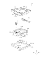
図8~図10は、OIS可動部10の分解斜視図である。図9は、図8をZ軸周りに180°回転させた状態を示す。図10は、図8をZ軸周りに180°回転させた状態を示す下方斜視図である。なお、図9では、AF駆動部14及び第1のOIS駆動部30Xが第1ステージ12から取り外した状態となっている。
以下において、光学素子駆動装置1の平面形状である矩形において、AF駆動部14が配置される辺を「第1の辺」、第1のOIS駆動部30Xが配置される辺を「第2の辺」、第2のOIS駆動部30Yが配置される辺を「第3の辺」、残りの一辺を「第4の辺」と称する。
以下において、光学素子駆動装置1の平面形状である矩形において、AF駆動部14が配置される辺を「第1の辺」、第1のOIS駆動部30Xが配置される辺を「第2の辺」、第2のOIS駆動部30Yが配置される辺を「第3の辺」、残りの一辺を「第4の辺」と称する。
図8~図10に示すように、本実施の形態において、OIS可動部10は、AF可動部11、第1ステージ12、第2ステージ13、AF駆動部14及びAF支持部15等を有する。Y方向の移動に関しては、第1ステージ12及び第2ステージ13を含むOIS可動部10全体が可動体となるのに対して、X方向の移動に関しては、第2ステージ13はOIS固定部20として機能し、AFユニット(AF可動部11及び第1ステージ12)だけがOIS可動部10として機能する。また、第1ステージ12は、AF可動部11を支持するAF固定部として機能する。
AF可動部11は、レンズ部2(図2参照)を保持するレンズホルダーであり、ピント合わせ時に光軸方向に移動する。AF可動部11は、第1ステージ12(AF固定部)に対して径方向内側に離間して配置され、AF支持部15を介して第1ステージ12に付勢された状態で支持される。
AF可動部11は、例えば、ポリアリレート(PAR)、PARを含む複数の樹脂材料を混合したPARアロイ、液晶ポリマー等で形成される。AF可動部11は、筒状のレンズ収容部111を有する。レンズ収容部111の内周面には、レンズ部2が、例えば、接着により固定される。
AF可動部11は、レンズ収容部111の外周面に、径方向外側に突出し光軸方向に延在する突出部112A~112Dを有する。突出部112A~112Dは、好ましくは、光軸を基準として対称的に配置される。本実施の形態では、光軸周りに略90°間隔で、突出部112A~112Dが設けられている。突出部112A~112Dは、レンズ収容部111の下面よりも光軸方向結像側に突出し、ベース21の第2ベース部213と当接することにより、AF可動部11の光軸方向結像側(下側)への移動を規制する。本実施の形態では、突出部112A~112Dは、AF駆動部14が駆動されていない基準状態において、ベース21の第2ベース部213に当接する。
AF駆動部14側の突出部112A、112Bは、第1ステージ12とともに、AF支持部15を保持する。一方の突出部112Aは、AF支持部15を構成する第1のZ方向基準ボール15Aを収容する。他方の突出部112Bは、AF支持部15を構成する第2のZ方向基準ボール15Bを収容する。また、突出部112A、112Bは、それぞれ、AF支持部15を構成する第1予圧ボール15C、第2予圧ボール15Dを収容する。
また、レンズ収容部111の外周面には、Z位置検出用のマグネット16Zを収容するマグネット収容部114が設けられている。マグネット収容部114にマグネット16Zが配置される。センサー基板22において、マグネット16Zと光軸方向に対向する位置に、Z位置検出用の磁気センサー25Zが配置される(図4参照)。
また、AF可動部11において、突出部112A、112Bの間には、AF動力伝達部144が配置されている。AF動力伝達部144は、Z方向に所定の長さを有するチャッキングガイドであり、X方向に対向し、Y方向(-側)に突出する側壁を有する。AF動力伝達部144の側壁を押し拡げるように、AF駆動部14の共振部141のアーム部141bが当接し、AF駆動部14の動力がAF可動部11に伝達される。2つのアーム部141bがAF動力伝達部144の側壁に当接したときに、AF動力伝達部144の側壁が板バネとして機能することで、共振部141の変形によって生じる駆動力が効率よく伝達される。
なお、AF動力伝達部144の構造は適宜任意に変更可能である。例えば、側壁をZ方向に折り返して側壁よりもX方向内側に位置するように板バネを形成し、AF駆動部14のアーム部141bを押し返す方向に付勢力が発現するようにしてもよい。これにより、共振部141の変形によって生じる駆動力が、AF動力伝達部144に、より効率よく伝達される。
本実施の形態では、AF動力伝達部144は、AF可動部11と別部材で構成されている。AF動力伝達部144は、例えば、平面視でU字形状を有し、側面部がX方向に対向した状態で、底面部がレンズ収容部111の外周面に固定される。AF動力伝達部144は、例えば、金属材料で形成される。これにより、AF駆動部30のアーム部141bが、樹脂成形品であるAF可動部11に当接する場合に比較して、AF駆動部14の駆動力が効率よく伝達される。なお、AF動力伝達部144は、AF可動部11と一体的に成形されてもよい。
第1ステージ12は、AF支持部15を介してAF可動部11を支持する。第1ステージ12の光軸方向結像側には、X方向基準ボール42A~42Cを介して第2ステージ13が配置される。第1ステージ12は、振れ補正時にX方向及びY方向に移動し、第2ステージ13は、振れ補正時にY方向のみに移動する。
第1ステージ12は、光軸方向から見た平面視において略矩形状を有する部材であり、例えば、液晶ポリマーで形成される。第1ステージ12は、AF可動部11に対応する部分に略円形状の開口121を有する。開口121には、AF可動部11の突出部112A~112D及びマグネット収容部114に対応する切欠部122が形成されている。第1ステージ12において、第1のOIS駆動部30Xに対応する部分(第2の辺に沿う側壁の外側面)は、径方向外側にはみ出すことなく第1のOIS駆動部30Xを配置できるように、径方向内側に凹んで形成されている(OISモーター固定部124)。また、第1ステージ12において、第2のOIS駆動部30Yに対応する部分(第3の辺に沿う側壁の外側面)も同様に、径方向内側に凹んで形成されている。
第1ステージ12は、下面に、X方向基準ボール42A~42Cを保持するX方向基準ボール保持部123A~123Cを有する。X方向基準ボール保持部123A~123Cは、X方向に延びる矩形状に凹んで形成されている。X方向基準ボール保持部123A~123Cは、第2ステージ13のX方向基準ボール保持部133A~133CとZ方向において対向する。X方向基準ボール保持部123A、123Bは、底面側に向けて溝幅狭くなるように断面形状が略V字状(テーパー形状)に形成されており、X方向基準ボール保持部123Cは、略U字状に形成されている。
第1ステージ12において、X方向に沿う一方の側壁(第1の辺に沿う側壁)には、AF駆動部14が配置されるAFモーター固定部125が形成されている。AFモーター固定部125は、上部固定板(符号略)及び下部固定板125aを有し、これらの間にAF駆動部14が挟持される。AF駆動部14は、例えば、上部固定板及び下部固定板125aに設けられた挿入穴(符号略)にAF共振部141が挿入され、接着により固定される。上部固定板は、配線17Bの一部によって構成されており、AF共振部141は、配線17Bと電気的に接続される。
第1ステージ12において、Y方向に沿う一方の側壁(第4の辺に沿う側壁)には、XY位置検出用のマグネット16X、16Yが配置される。例えば、マグネット16XはX方向に着磁され、マグネット16YはY方向に着磁される。センサー基板22において、マグネット16X,16Yと光軸方向に対向する位置に、XY位置検出用の磁気センサー25X、25Yが配置される(図4参照)。
また、第1ステージ12には、例えば、インサート成形により、配線17A、17Bが埋設されている。配線17A、17Bは、例えば、第1の辺及び第2の辺に沿って配置される。配線17A、17Bは、第1ステージ12の四隅から露出しており、この部分に、OIS用付勢部材50の一端が接続される。配線17Aを介して第1のOIS駆動部30Xへの給電が行われる、配線17Bを介してAF駆動部14への給電が行われる。
第2ステージ13は、光軸方向から見た平面視において略矩形状を有する部材であり、例えば、液晶ポリマーで形成される。第2ステージ13の内周面131は、AF可動部11の外形に対応して形成されている。第2ステージ13において、第1のOIS駆動部30X及び第2のOIS駆動部30Yに対応する部分(第2の辺及び第3の辺に沿う側壁の外側面)は、第1ステージ12と同様に、径方向内側に凹んで形成されている。
第2ステージ13は、下面に、Y方向基準ボール41A~41Cを収容するY方向基準ボール保持部134A~134Cを有する。Y方向基準ボール保持部134A~134Cは、Y方向に延びる矩形状に凹んで形成されている。Y方向基準ボール保持部134A~134Cは、ベース21のY方向基準ボール保持部217A~217CとZ方向において対向する。Y方向基準ボール保持部134A、134Bは、底面側に向けて溝幅狭くなるように断面形状が略V字状(テーパー形状)に形成されており、Y方向基準ボール保持部134Cは、略U字状に形成されている。
また、第2ステージ13は、上面に、X方向基準ボール42A~42Cを収容するX方向基準ボール保持部133A~133Cを有する。X方向基準ボール保持部133A~133Cは、X方向に延びる矩形状に凹んで形成されている。X方向基準ボール保持部133A~133Cは、第1ステージ12のX方向基準ボール保持部123A~123CとZ方向において対向する。X方向基準ボール保持部133A~133Cは、底面側に向けて溝幅が狭くなるように断面形状が略V字状(テーパー形状)に形成されている。本実施の形態では、X方向基準ボール保持部133A、133Bは、第2ステージ13の第1のOIS駆動部30Xが配置される辺(第2の辺)に設けられ、X方向基準ボール保持部133Cは、AF駆動部14が配置される辺(第1の辺)に設けられており、X方向基準ボール42A~42Cによって第1ステージ12が3点で支持されるようになっている。
OIS支持部40を構成するY方向基準ボール41A~41Cは、ベース21のY方向基準ボール保持部217A~217Cと第2ステージ13のY方向基準ボール保持部134A~134Cにより、多点接触で挟持される。したがって、Y方向基準ボール41A~41Cは、安定してY方向に転動する。
また、X方向基準ボール42A~42Cは、第2ステージ13のX方向基準ボール保持部133A~133Cと第1ステージ12のX方向基準ボール保持部123A~123Cにより、多点接触で挟持される。したがって、X方向基準ボール42A~42Cは、安定してX方向に転動する。
また、X方向基準ボール42A~42Cは、第2ステージ13のX方向基準ボール保持部133A~133Cと第1ステージ12のX方向基準ボール保持部123A~123Cにより、多点接触で挟持される。したがって、X方向基準ボール42A~42Cは、安定してX方向に転動する。
AF支持部15は、第1ステージ12(AF固定部)に対してAF可動部11を支持する部分である。AF支持部15は、第1のZ方向基準ボール15A、第2のZ方向基準ボール15B、第1予圧ボール15C及び第2予圧ボール15Dで構成される。本実施の形態では、第1のZ方向基準ボール15A、第2のZ方向基準ボール15B、第1予圧ボール15C、第2予圧ボール15Dは、それぞれ、Z方向に並んで配置された複数のボール(ここでは、3個)で構成されている。
第1のZ方向基準ボール15A、第2のZ方向基準ボール15B、第1予圧ボール15C、第2予圧ボール15Dにおいては、少なくとも、上下2つのボールがAF可動部11と第1ステージ12とによって挟持されていればよい。すなわち、中間のボールは上下2つのボールの離間距離を確保するために設けられるものであり、上下2つのボールよりも小径であってもよい。
AF駆動部14は、AF可動部11をZ方向に移動させるアクチュエーターである。AF駆動部14は、OIS駆動部30と同様に、超音波モーターで構成されている。AF駆動部14は、アーム部141bがZ方向に延在するように、第1ステージ12のAFモーター固定部125に固定される。
AF駆動部14の構成を図11A、図11Bに示す。図11Aは、AF駆動部14の各部材を組み付けた状態を示し、図11Bは、AF駆動部14の各部材を分解した状態を示す。AF駆動部14の構成は、OIS駆動部30とほぼ同様である。
図11A、図11Bに示すように、AF駆動部14は、AF共振部141、AF圧電素子142、AF電極143及びAF動力伝達部144を有する。AF駆動部14の駆動力は、AF動力伝達部144を介してAF可動部11に伝達される。
AF圧電素子142は、例えば、セラミック材料で形成された板状素子であり、高周波電圧を印加することにより振動を発生する。AF共振部141の胴部141aを挟み込むように、2枚のAF圧電素子142が配置される。
AF電極143は、AF共振部141及びAF圧電素子142を挟持し、AF圧電素子142に電圧を印加する。
AF電極143は、AF共振部141及びAF圧電素子142を挟持し、AF圧電素子142に電圧を印加する。
AF共振部141は、導電性材料で形成され、AF圧電素子142の振動に共振して、振動運動を直線運動に変換する。AF共振部141は、例えば、金属板のレーザー加工、エッチング加工又はプレス加工等により形成される。本実施の形態では、AF共振部141は、AF圧電素子142に挟持される略矩形状の胴部141a、胴部141aからZ方向に延在する2つのアーム部141b、胴部141aの中央部からZ方向に延在し給電経路(第1ステージ12の配線17B(上部固定板125a)と電気的に接続される通電部141c、及び、胴部141aの中央部から通電部141cとは反対側に延在するステージ固定部141dを有している。2つのアーム部141bは対称的な形状を有し、AF圧電素子142の振動に共振して対称的に変形する。AF駆動部14は、2つのアーム部141bがZ方向に延在して、自由端部でAF動力伝達部144を挟持するように配置される。
AF共振部141の胴部141aに、厚さ方向からAF圧電素子142が貼り合わされ、AF電極143により挟持されることにより、これらは互いに電気的に接続される。AF共振部141の通電部141d及びAF電極143が第1ステージ12の配線17Bに接続されることで、AF圧電素子142に電圧が印加され、振動が発生する。
AF共振部141は、OIS共振部31と同様に、少なくとも2つの共振周波数を有し、それぞれの共振周波数に対して、異なる挙動で変形する。言い換えると、AF共振部141は、2つの共振周波数に対して異なる挙動で変形するように、全体の形状が設定されている。
光学素子駆動装置1において、AF駆動部14に電圧を印加すると、AF圧電素子142が振動し、AF共振部141が周波数に応じた挙動で変形する。AF駆動部14の駆動力により、AF動力伝達部144がZ方向に摺動される。これに伴い、AF可動部11がZ方向に移動し、ピント合わせが行われる。AF支持部15がボールで構成されているので、AF可動部11はZ方向にスムーズに移動することができる。また、AF駆動部14とAF動力伝達部144は、付勢された状態で当接しているだけなので、当接部分をZ方向に大きくするだけで、光学素子駆動装置1の低背化を損なうことなく、AF可動部11の移動ストロークを容易に長くすることができる。
光学素子駆動装置1において、OIS駆動部30に電圧を印加すると、OIS圧電素子32が振動し、OIS共振部31が周波数に応じた挙動で変形する。OIS駆動部30の駆動力により、OIS動力伝達部34がX方向又はY方向に摺動される。これに伴い、OIS可動部10がX方向又はY方向に移動し、振れ補正が行われる。OIS支持部40がボールで構成されているので、OIS可動部10はX方向又はY方向にスムーズに移動することができる。
具体的には、第1のOIS駆動部30Xが駆動され、OIS動力伝達部34がX方向に移動する場合、第1のOIS駆動部30Xが配置されている第1ステージ12から第2ステージ13に動力が伝達される。このとき、第2ステージ13とベース21とで挟持されているボール41は、X方向に転動できないので、ベース21に対する第2ステージ13のX方向の位置は維持される。一方、第1ステージ12と第2ステージ13とで挟持されているボール42は、X方向に転動できるので、第2ステージ13に対して第1ステージ12がX方向に移動する。つまり、第2ステージ13がOIS固定部20を構成し、第1ステージ12がOIS可動部10を構成する。
また、第2のOIS駆動部30Yが駆動され、OIS動力伝達部34がY方向に移動する場合、第2のOIS駆動部30Yが配置されているベース21から第2ステージ13に動力が伝達される。このとき、第1ステージ12と第2ステージ13とで挟持されているボール42は、Y方向に転動できないので、第2ステージに対する第1ステージ12のY方向の位置は維持される。一方、第2ステージ13とベース21とで挟持されているボール41は、Y方向に転動できるので、ベース21に対して第2ステージ13がY方向に移動する。第1ステージ12も第2ステージ13に追従してY方向に移動することになる。つまり、ベース21がOIS固定部20を構成し、第1ステージ12及び第2ステージ13を含むAFユニットがOIS可動部10を構成する。
このようにして、OIS可動部10がXY平面内で揺動し、振れ補正が行われる。具体的には、カメラモジュールAの角度振れが相殺されるように、振れ検出部(例えばジャイロセンサー、図示略)からの角度振れを示す検出信号に基づいて、OIS駆動部30への通電電圧が制御される。このとき、マグネット16X、16Y及び磁気センサー25X、25Yで構成されるXY位置検出部の検出結果をフィードバックすることで、OIS可動部10の並進移動を正確に制御することができる。
以上説明したように、AF駆動部14においては、AF共振部141とAF動力伝達部144とが当接し、駆動時には、互いに摺動する。同様に、OIS駆動部30においては、OIS共振部31とOIS動力伝達部34とが当接し、駆動時には、互いに摺動する。
すなわち、AF駆動部14及びOIS駆動部30は、能動要素に対して受動要素を相対的に移動させる超音波モーター式の駆動ユニットである。
すなわち、AF駆動部14及びOIS駆動部30は、能動要素に対して受動要素を相対的に移動させる超音波モーター式の駆動ユニットである。
具体的には、AF駆動部14において、能動要素は、AF圧電素子142の振動に共振して変形するアーム部141bを有するAF共振部141で構成され、AF圧電素子142の振動運動を直線運動に変換する。受動要素は、AF動力伝達部144で構成され、付勢された状態でアーム部141bに接触するように配置されている。
また、OIS駆動部30において、能動要素は、OIS圧電素子の振動に共振して変形するアーム部31bを有するOIS共振部31で構成され、OIS圧電素子32の振動運動を直線運動に変換する。受動要素は、OIS動力伝達部34で構成され、付勢された状態でアーム部31bに接触するように配置されている。
ここで、互いに摺動することとなる摺動部材の組み合わせ、すなわちAF共振部141とAF動力伝達部144の組合せ、及びOIS共振部31とOIS動力伝達部34の組合せには、受動要素を移動できる程度の摩擦力を発揮しつつ、長期にわたって耐摩耗性に優れることが要求される。しかし、摩擦力を増大させると耐摩耗性は低下するというように、摩擦力と耐摩耗性は相反する特性であるため、これらをバランスさせることは容易ではない。本発明者等は、摺動部材の組合せについて鋭意検討を重ねた結果、AF駆動部14及びOIS駆動部30に対する要求を満足しうる組合せに想到し、本発明を完成するに至った。
本実施の形態では、AF駆動部14及びOIS駆動部30に、本発明に係る駆動ユニットを適用することで、AF駆動部14及びOIS駆動部30の駆動性能の向上が図られている。
本実施の形態では、AF駆動部14及びOIS駆動部30に、本発明に係る駆動ユニットを適用することで、AF駆動部14及びOIS駆動部30の駆動性能の向上が図られている。
すなわち、受動要素であるAF動力伝達部144は、能動要素であるAF共振部141との接触面にコーティング層を有しており、コーティング層は、硬度及びせん断強度が、AF共振部141よりも大きい。また、受動要素であるOIS動力伝達部34は、能動要素であるOIS共振部31との接触面にコーティング層を有しており、コーティング層は、硬度及びせん断強度が、OIS共振部34よりも大きい。
これにより、主として能動要素側(AF共振部141、OIS共振部31)が削れることとなるので、能動要素側の接触面の表面状態をコントロールすることで、容易に耐摩耗性を向上することができる。また、受動要素側(AF動力伝達部144、OIS動力伝達部34)に摩耗を生じさせないことで、動作の安定性を向上することができる。すなわち、受動要素側が局所的に摩耗することにより接触面に筋状の摩耗跡が形成されると、この摩耗跡から能動側要素が外れたときに想定外の動作が生じる虞があるが、このような不具合が生じるのを防止することができる。
これにより、主として能動要素側(AF共振部141、OIS共振部31)が削れることとなるので、能動要素側の接触面の表面状態をコントロールすることで、容易に耐摩耗性を向上することができる。また、受動要素側(AF動力伝達部144、OIS動力伝達部34)に摩耗を生じさせないことで、動作の安定性を向上することができる。すなわち、受動要素側が局所的に摩耗することにより接触面に筋状の摩耗跡が形成されると、この摩耗跡から能動側要素が外れたときに想定外の動作が生じる虞があるが、このような不具合が生じるのを防止することができる。
なお、能動要素であるAF共振部141及びOIS共振部31の接触面には、例えば、硬質メッキや塗装などのコーティング層が設けられてもよいし、コーティング層以外の表面処理が施されてもよい。コーティング層を設ける場合、能動要素の主材である能動側基材に直接コーティング層を形成してもよいし、コーティング層を有するプレートなどの別部材を能動側基材に貼り付けるようにしてもよい。
能動要素の主材である能動側基材は、所定の導電性、せん断強度、硬度、比重、ヤング率等を有する金属であればよく、例えば、ステンレス綱が好適である。ステンレス綱のビッカース硬度は、180~400HVである。
また、受動要素であるAF動力伝達部144及びOIS動力伝達部34は、主材である受動側基材と、コーティング層と、で構成される。受動要素側に能動要素よりも硬度及びせん断強度が高いコーティング層を設けることで、受動要素の摩耗を抑制することができる。
受動側基材は、能動側基材と同等以上の剛性を有することが好ましく、例えば、ステンレス鋼が好適である。これにより、AF動力伝達部144及びOIS動力伝達部34に自己復元性を付与して板バネとして機能させることができ、能動要素と受動要素との間で所望の摩擦力を発現させやすくなる。なお、能動側基材を形成するステンレス綱と受動側基材を形成するステンレス綱は、同じ鋼種であってもよいし、異なる鋼種であってもよい。例えば、能動要素から受動要素への力の伝達等を考慮して、適切な鋼種が選択される。
受動要素のコーティング層は、例えば、ダイヤモンドライクカーボン(DLC)や、ジルコニア(ZnO2)等のファインセラミックスが好適である。DLCのビッカース硬度は1100~7000HV、ジルコニアのビッカース硬度は1200~1400HVであり、いずれもステンレス綱よりも硬い。なお、能動要素と受動要素の接触面が金属同士だと凝集が生じる虞があるため、コーティング層は、金属以外の材料で形成されることが好ましい。
特に、コーティング層にDLCを適用した場合、付勢荷重(摩擦力)を増大させたときの能動要素及び受動要素の摩耗量は、ジルコニアを適用した場合に比較して少なく、ほとんど変化しないことが実験的に確認されている。また、DLCは、自己潤滑性を有することが知られており、ジルコニア等のセラミックよりも硬度が高いにも関わらず、能動側に生じる摩耗の抑制効果を期待できる。これより、コーティング層は、要求される付勢荷重に対応しやすい観点から、DLCがより好適である。
上述したように、受動要素側のコーティング層を、能動要素よりも硬い材料で形成した場合、主に、能動要素において摩耗が生じる。実際の摩耗量は、摺動部材の硬度、相手材との相性、及び使用環境などの複数の要因が重なり合って決定されるが、接触面において、コーティング層の硬度が、能動側基材の硬度の約2.5倍以上である場合、その他の要因に関わらず、コーティング層の摩耗はほとんど発生しないと考えられる。したがって、能動要素の耐摩耗性を重点的に検討することで、駆動ユニットの耐摩耗性を向上することができる。
一般に、摩耗は、接触面の表面性状(例えば、表面粗さ)に影響を受けることが知られており、接触面が滑らか(平坦)である方が摩耗は少ない。また、加工後の能動側基材は、表面が粗雑であり、受動要素のコーティング層に削れ又は割れ等の損傷を生じさせる可能性が高い。そこで、本実施の形態では、AF共振部141及びOIS共振部31の能動側基材は、少なくとも相手材(受動側のコーティング層)との接触面に平坦化処理が施されている。これにより、加工後の状態に比較して表面性状が改善され、能動側基材の耐摩耗性が向上する。
平坦化処理としては、例えば、電解研磨、バレル研磨又はプラズマ処理等を適用できる。電解研磨は、研磨対象物をプラス極にして電解液を介して直流電流を流し、金属表面を溶解して平滑化する方法であり、例えば、グラインダー等の工作機械を用いた機械的研磨によりある程度平滑にした後で行われる。バレル研磨は、研磨対象物と研磨材等をバレル槽に入れ、回転や振動を与えて研磨する方法である。プラズマ処理は、プラズマを照射することにより対象物の表面を化学的に改質する方法であり、シート状の対象物にも適用できるという利点がある。
能動側基材の表面性状を定量的に規定すると、受動要素との接触面における山の頂点密度Spdが20万~150万あることが好ましい。これにより、受動要素との真の接触面積が適正に制御され、フレッティング摩耗を含む凝集磨耗や、アブレッシブ磨耗を抑制できるので、耐摩耗性が向上する。
このように、実施の形態に係るAF駆動部14(駆動ユニット)は、電圧印加により振動を発生するAF圧電素子142と、AF圧電素子142の振動に共振して変形するアーム部141bを有しAF圧電素子142の振動運動を直線運動に変換するAF共振部141(能動要素)と、付勢された状態でアーム部141bに接触するように配置され、AF共振部141に対して相対的に移動するAF動力伝達部144(受動要素)と、を有する。
また、OIS駆動部30(駆動ユニット)は、電圧印加により振動を発生するOIS圧電素子32と、OIS圧電素子32の振動に共振して変形するアーム部31bを有しOIS圧電素子32の振動運動を直線運動に変換するOIS共振部31(能動要素)と、付勢された状態でアーム部31bに接触するように配置され、OIS共振部31に対して相対的に移動するOIS動力伝達部34(受動要素)と、を有する。
そして、AF駆動部14及びOIS駆動部30において、受動要素であるAF動力伝達部144及びOIS動力伝達部34は、能動要素であるAF共振部141、OIS共振部31との接触面にコーティング層を有し、コーティング層の硬度及びせん断強度が、能動要素よりも大きい。
また、受動要素のコーティング層は、能動要素の主材である能動側基材の硬度の約2.5倍以上であることが好ましい。また、能動側基材は、ステンレス綱で形成され、受動要素のコーティング層は、ダイヤモンドライクカーボン(DLC)で形成されることが好ましい。この場合、受動側基材は、能動側基材と同様に、ステンレス綱で形成されることが好ましい。また、能動側基材は、前記受動要素との接触面に、平坦化処理が施されていることが好ましい。平坦化処理としては、バレル研磨又は電解研磨が好適である。
また、能動側基材は、受動要素との接触面における山の頂点密度Spdが20万~150万であることが好ましい。
また、能動側基材は、受動要素との接触面における山の頂点密度Spdが20万~150万であることが好ましい。
実施の形態に係るAF駆動部141及びOIS駆動部30(駆動ユニット)によれば、摩耗による経時的な駆動性能の低下を抑制でき、当該駆動ユニットを適用した製品の信頼性を向上することができる。
以上、本発明者によってなされた発明を実施の形態に基づいて具体的に説明したが、本発明は上記実施の形態に限定されるものではなく、その要旨を逸脱しない範囲で変更可能である。
例えば、実施の形態では、カメラモジュールAを備えるカメラ搭載装置の一例として、カメラ付き携帯端末であるスマートフォンMを挙げて説明したが、本発明は、カメラモジュールとカメラモジュールで得られた画像情報を処理する画像処理部を有するカメラ搭載装置に適用できる。カメラ搭載装置は、情報機器及び輸送機器を含む。情報機器は、例えば、カメラ付き携帯電話機、ノート型パソコン、タブレット端末、携帯型ゲーム機、webカメラ、カメラ付き車載装置(例えば、バックモニター装置、ドライブレコーダー装置)を含む。また、輸送機器は、例えば自動車を含む。
図12A、図12Bは、車載用カメラモジュールVC(Vehicle Camera)を搭載するカメラ搭載装置としての自動車Vを示す図である。図12Aは自動車Vの正面図であり、図12Bは自動車Vの後方斜視図である。自動車Vは、車載用カメラモジュールVCとして、実施の形態で説明したカメラモジュールAを搭載する。図12A、図12Bに示すように、車載用カメラモジュールVCは、例えば前方に向けてフロントガラスに取り付けられたり、後方に向けてリアゲートに取り付けられたりする。この車載用カメラモジュールVCは、バックモニター用、ドライブレコーダー用、衝突回避制御用、自動運転制御用等として使用される。
また、実施の形態では、光学素子としてレンズ部2を駆動する光学素子駆動装置1について説明したが、駆動対象となる光学素子は、ミラーやプリズムなどのレンズ以外の光学素子であってもよい。
今回開示された実施の形態はすべての点で例示であって制限的なものではないと考えられるべきである。本発明の範囲は上記した説明ではなくて特許請求の範囲によって示され、特許請求の範囲と均等の意味および範囲内でのすべての変更が含まれることが意図される。
2020年6月30日出願の米国仮出願63/045,859に含まれる明細書、図面および要約書の開示内容は、すべて本願に援用される。
1 光学素子駆動装置
10 OIS可動部(可動部)
12 第1ステージ(固定部)
13 第2ステージ
14 AF駆動部(駆動ユニット)
141 AF共振部(能動要素)
142 AF圧電素子(能動要素)
143 AF電極
144 AF動力伝達部(受動要素)
15 AF支持部
20 OIS固定部(固定部)
21 ベース
30 OIS駆動部(駆動ユニット)
31 OIS共振部(能動要素)
32 OIS圧電素子(能動要素)
33 OIS電極
34 OIS動力伝達部(受動要素)
40 OIS支持部
50 OIS用付勢部材
A カメラモジュール
M スマートフォン(カメラ搭載装置)
10 OIS可動部(可動部)
12 第1ステージ(固定部)
13 第2ステージ
14 AF駆動部(駆動ユニット)
141 AF共振部(能動要素)
142 AF圧電素子(能動要素)
143 AF電極
144 AF動力伝達部(受動要素)
15 AF支持部
20 OIS固定部(固定部)
21 ベース
30 OIS駆動部(駆動ユニット)
31 OIS共振部(能動要素)
32 OIS圧電素子(能動要素)
33 OIS電極
34 OIS動力伝達部(受動要素)
40 OIS支持部
50 OIS用付勢部材
A カメラモジュール
M スマートフォン(カメラ搭載装置)
Claims (11)
- 電圧印可により振動を発生する圧電素子と、
前記圧電素子の振動に共振して変形するアーム部を有し前記圧電素子の振動を直線運動に変換する能動要素(共振器)と、
付勢された状態で前記アーム部に接触するように配置され、前記能動要素に対して相対的に移動する受動要素と、を備える駆動ユニットであって、
前記受動要素は、前記能動要素との接触面にコーティング層を有し、
前記コーティング層の硬度及びせん断強度が、前記能動要素よりも大きい、
駆動ユニット。 - 前記能動要素と前記受動要素の接触面において、前記受動要素の硬度は、前記能動要素の硬度の約2.5倍以上である、
請求項1に記載の駆動ユニット。 - 前記能動要素の主材である能動側基材は、ステンレス綱で形成され、
前記コーティング層は、ダイヤモンドライクカーボン(DLC)で形成されている、
請求項1又は2に記載の駆動ユニット。 - 前記受動要素の主材である受動側基材は、ステンレス鋼で形成されている、
請求項3に記載の駆動ユニット。 - 前記能動側基材は、前記受動要素との接触面に、平坦化処理が施されている、
請求項3又は4に記載の駆動ユニット。 - 前記平坦化処理は、バレル研磨又は電解研磨である、
請求項5に記載の駆動ユニット。 - 前記能動側基材は、前記受動要素との接触面における山の頂点密度Spdが20万~150万である、
請求項5又は6に記載の駆動ユニット。 - 固定部と、
前記固定部から離間して配置され光学素子を保持する可動部と、
前記固定部に対して前記可動部を支持する支持部と、
請求項1から7のいずれか一項に記載の駆動ユニットで構成され、前記固定部に対して前記可動部を移動させる駆動部と、を備える、
光学素子駆動装置。 - 前記固定部に前記能動要素が配置され、
前記可動部に前記受動要素が配置されている、
請求項8に記載の光学素子駆動装置。 - 請求項8又は9に記載の光学素子駆動装置と、
前記光学素子であるレンズ部と、
前記レンズ部により結像された被写体像を撮像する撮像部と、を備える、
カメラモジュール。 - 情報機器又は輸送機器であるカメラ搭載装置であって、
請求項10に記載のカメラモジュールと、
前記カメラモジュールで得られた画像情報を処理する画像処理部と、を備える、
カメラ搭載装置。
Applications Claiming Priority (2)
| Application Number | Priority Date | Filing Date | Title |
|---|---|---|---|
| US202063045859P | 2020-06-30 | 2020-06-30 | |
| US63/045,859 | 2020-06-30 |
Publications (1)
| Publication Number | Publication Date |
|---|---|
| WO2022004792A1 true WO2022004792A1 (ja) | 2022-01-06 |
Family
ID=79316326
Family Applications (1)
| Application Number | Title | Priority Date | Filing Date |
|---|---|---|---|
| PCT/JP2021/024767 WO2022004792A1 (ja) | 2020-06-30 | 2021-06-30 | 駆動ユニット、光学素子駆動装置、カメラモジュール、及びカメラ搭載装置 |
Country Status (1)
| Country | Link |
|---|---|
| WO (1) | WO2022004792A1 (ja) |
Citations (6)
| Publication number | Priority date | Publication date | Assignee | Title |
|---|---|---|---|---|
| JP2000245179A (ja) * | 1998-12-21 | 2000-09-08 | Seiko Epson Corp | 圧電アクチュエータ、携帯機器および時計 |
| JP2001258276A (ja) * | 2000-03-10 | 2001-09-21 | Nikon Corp | 振動アクチュエータ |
| JP2011091957A (ja) * | 2009-10-23 | 2011-05-06 | Sharp Corp | 駆動装置、及びこれを備えた電子機器 |
| JP2015107001A (ja) * | 2013-11-29 | 2015-06-08 | 株式会社ニコン | 振動アクチュエータ、振動アクチュエータの制御装置、レンズ鏡筒及び電子機器 |
| JP2016201906A (ja) * | 2015-04-10 | 2016-12-01 | キヤノン株式会社 | 振動波モータ |
| JP2018050467A (ja) * | 2017-11-29 | 2018-03-29 | 株式会社ニコン | 振動アクチュエータ、レンズ鏡筒及び電子機器 |
-
2021
- 2021-06-30 WO PCT/JP2021/024767 patent/WO2022004792A1/ja active Application Filing
Patent Citations (6)
| Publication number | Priority date | Publication date | Assignee | Title |
|---|---|---|---|---|
| JP2000245179A (ja) * | 1998-12-21 | 2000-09-08 | Seiko Epson Corp | 圧電アクチュエータ、携帯機器および時計 |
| JP2001258276A (ja) * | 2000-03-10 | 2001-09-21 | Nikon Corp | 振動アクチュエータ |
| JP2011091957A (ja) * | 2009-10-23 | 2011-05-06 | Sharp Corp | 駆動装置、及びこれを備えた電子機器 |
| JP2015107001A (ja) * | 2013-11-29 | 2015-06-08 | 株式会社ニコン | 振動アクチュエータ、振動アクチュエータの制御装置、レンズ鏡筒及び電子機器 |
| JP2016201906A (ja) * | 2015-04-10 | 2016-12-01 | キヤノン株式会社 | 振動波モータ |
| JP2018050467A (ja) * | 2017-11-29 | 2018-03-29 | 株式会社ニコン | 振動アクチュエータ、レンズ鏡筒及び電子機器 |
Similar Documents
| Publication | Publication Date | Title |
|---|---|---|
| JP2021165847A (ja) | レンズの振れ補正装置、カメラモジュール、及びカメラ搭載装置 | |
| JP7104365B2 (ja) | 光学素子駆動装置、カメラモジュール、及びカメラ搭載装置 | |
| WO2021117374A1 (ja) | レンズ駆動装置、カメラモジュール、及びカメラ搭載装置 | |
| JP7075030B1 (ja) | 光学素子駆動装置、カメラモジュール、及びカメラ搭載装置 | |
| JP7075029B2 (ja) | レンズ駆動装置、カメラモジュール、及びカメラ搭載装置 | |
| WO2022097389A1 (ja) | 光学素子駆動装置、カメラモジュール、及びカメラ搭載装置 | |
| WO2022097388A1 (ja) | 光学素子駆動装置、カメラモジュール、及びカメラ搭載装置 | |
| WO2022004792A1 (ja) | 駆動ユニット、光学素子駆動装置、カメラモジュール、及びカメラ搭載装置 | |
| JP7295447B2 (ja) | 駆動ユニット、光学素子駆動装置、カメラモジュール、及びカメラ搭載装置 | |
| JP7093050B2 (ja) | レンズ駆動装置、カメラモジュール、及びカメラ搭載装置 | |
| JP7372563B2 (ja) | レンズ駆動装置、カメラモジュール、及びカメラ搭載装置 | |
| JP7269521B2 (ja) | レンズ駆動装置、カメラモジュール、及びカメラ搭載装置 | |
| CN118091877A (zh) | 光学元件驱动装置、摄像机模块及摄像机搭载装置 | |
| CN118091878A (zh) | 光学元件驱动装置、摄像机模块及摄像机搭载装置 |
Legal Events
| Date | Code | Title | Description |
|---|---|---|---|
| 121 | Ep: the epo has been informed by wipo that ep was designated in this application |
Ref document number: 21832693 Country of ref document: EP Kind code of ref document: A1 |
|
| NENP | Non-entry into the national phase |
Ref country code: DE |
|
| 122 | Ep: pct application non-entry in european phase |
Ref document number: 21832693 Country of ref document: EP Kind code of ref document: A1 |
|
| NENP | Non-entry into the national phase |
Ref country code: JP |