WO2021200569A1 - Sensor device and method for manufacturing same - Google Patents
Sensor device and method for manufacturing same Download PDFInfo
- Publication number
- WO2021200569A1 WO2021200569A1 PCT/JP2021/012619 JP2021012619W WO2021200569A1 WO 2021200569 A1 WO2021200569 A1 WO 2021200569A1 JP 2021012619 W JP2021012619 W JP 2021012619W WO 2021200569 A1 WO2021200569 A1 WO 2021200569A1
- Authority
- WO
- WIPO (PCT)
- Prior art keywords
- layer
- sensor device
- vibrator
- electrode
- drain electrode
- Prior art date
Links
Images


Classifications
-
- G—PHYSICS
- G01—MEASURING; TESTING
- G01N—INVESTIGATING OR ANALYSING MATERIALS BY DETERMINING THEIR CHEMICAL OR PHYSICAL PROPERTIES
- G01N27/00—Investigating or analysing materials by the use of electric, electrochemical, or magnetic means
-
- G—PHYSICS
- G01—MEASURING; TESTING
- G01N—INVESTIGATING OR ANALYSING MATERIALS BY DETERMINING THEIR CHEMICAL OR PHYSICAL PROPERTIES
- G01N5/00—Analysing materials by weighing, e.g. weighing small particles separated from a gas or liquid
- G01N5/02—Analysing materials by weighing, e.g. weighing small particles separated from a gas or liquid by absorbing or adsorbing components of a material and determining change of weight of the adsorbent, e.g. determining moisture content
Definitions
- the present invention relates to a sensor device and a method for manufacturing the same.
- the gas sensor described in Non-Patent Document 1 has a substrate, a gate electrode, a drain electrode and a source electrode arranged on the substrate, and a graphene layer.
- This gas sensor has a structure that vibratesly supports the graphene layer between the drain electrode and the source electrode, and detects the gas component based on the amount of change in the resonance frequency of the graphene layer due to the adsorption of gas.
- the vibrator of the gas sensor In order to perform gas detection with higher sensitivity, it is necessary for the vibrator of the gas sensor to detect the change in resonance frequency due to gas adsorption with high accuracy. This means that the Q value of the oscillator needs to be high. Furthermore, in order to specify the vibration mode required for gas detection, it is required that the vibrator does not generate a natural vibration mode that interferes with the desired vibration mode.
- an object of the present invention is to provide a sensor device capable of increasing the detection sensitivity of gas and a method for manufacturing the same.
- the sensor device includes a substrate, an insulating film, a gate electrode, a source electrode, a drain electrode, and a vibrator.
- the insulating film is formed on the substrate.
- the gate electrode is arranged on the insulating film.
- the source electrode has a first conductor layer and a second conductor layer provided on the first conductor layer, and is arranged on the insulating film.
- the drain electrode has a third conductor layer and a fourth conductor layer provided on the third conductor layer, and is arranged on the insulating film.
- the vibrator includes a first end portion sandwiched between the first and second conductor layers, a second end portion sandwiched between the third and fourth conductor layers, and a vibrating portion facing the gate electrode. Has.
- the above oscillator may include a graphene layer.
- the vibrator may further include a sensitive film formed on the graphene layer.
- the sensitive membrane may be a porous membrane.
- the porous membrane may be a carbon-based material.
- the first to fourth conductor layers may be made of the same type of metal material.
- the source electrode is arranged between the first and second conductor layers and further has an adhesion layer in close contact with the vibrator, and the drain electrode is arranged between the third and fourth conductor layers.
- An adhesion layer that is in close contact with the vibrator may be further provided.
- the gate electrode may be arranged between the substrate and the vibrator.
- a method for manufacturing a sensor device includes forming a lower electrode layer on a substrate.
- a graphene layer is formed on the lower electrode layer.
- An upper electrode layer is formed on the graphene layer.
- the gas detection sensitivity can be increased.
- FIG. 1 is a schematic diagram showing the configuration of a gas determination system.
- FIG. 2 is a schematic view showing the configuration of the sensor device 10 that constitutes a part of the gas determination system.
- the gas determination system 1 includes a sensor device 2, an information processing device 4, a display device 5, and a storage unit 6.
- the sensor device 2 includes a storage chamber 20, a sensor device 10, a UV (ultraviolet) light source 23, and a heating unit 26.
- the storage chamber 20 houses the sensor device 10, the UV light source 23, and the heating unit 26.
- the accommodation chamber 20 has an intake port 21 for sucking gas from the outside and an exhaust port 22 for exhausting the gas introduced into the accommodation chamber 20 from the accommodation chamber 20 to the outside.
- the intake port 21 is provided with a valve 24 for adjusting the inflow of gas into the accommodation chamber 20, and the exhaust port 22 is provided with a valve 25 for adjusting the outflow of gas in the accommodation chamber 20 to the outside.
- the UV light source 23 emits ultraviolet rays (UV) to irradiate the sensor device 10. Cleaning of the vibrator 16 is performed by irradiating the vibrator 16 of the sensor device 10 described later with UV. By performing UV irradiation, the gas is efficiently adsorbed on the vibrator 16. This is because O 2 , H 2 O, etc. are removed from the surface of the vibrator 16 by UV irradiation (cleaning effect), and between adsorption of gas molecules on the surface of the vibrator 16 and photoexcitation desorption.
- UV ultraviolet rays
- the heating unit 26 is, for example, a heater and heats the sensor device 10. By heating the sensor device 10 by the heating unit 26, the gas adsorption effect of the vibrator 16 can be obtained.
- the sensor device 10 includes a substrate 11, an insulating film 12, a gate electrode 13, a source electrode 14, a drain electrode 15, and a vibrator 16.
- the substrate 11 is typically a silicon substrate, but may be a semiconductor substrate or a glass substrate other than silicon.
- the insulating film 12 is formed on the substrate 11.
- the insulating film 12 is typically a silicon oxide film, and when the substrate 11 is a silicon substrate, it is a thermal oxide film formed on the surface thereof.
- the gate electrode 13, the source electrode 14, and the drain electrode 15 are formed on the insulating film 12.
- the gate electrode 13 is arranged between the source electrode 14 and the drain electrode 15.
- the gate electrode 13, the source electrode 14, and the drain electrode 15 are typically metal films, and in this embodiment, they are composed of a laminated film of chromium (Cr) and gold (Au).
- the vibrator 16 is arranged between the source electrode 14 and the drain electrode 15 so as to face the gate electrode 13.
- the vibrator 16 is arranged with a gap so as not to come into contact with the gate electrode 13.
- the vibrator 16 is made of a conductive material, and in this embodiment, is made of a graphene layer.
- the graphene layer is composed of a single layer film, but may be a multilayer film.
- the vibrator 16 may be made of another conductive material such as a metal film or a silicon thin film.
- the vibrator 16 is composed of a laminated film of a graphene layer 160 and a sensitive film 17 formed on the surface thereof.
- the sensitive film 17 is made of, for example, a material capable of adsorbing the gas to be detected.
- the material constituting the sensitive film 17 can be arbitrarily selected depending on the type of gas to be detected, and typically, an organic polymer film (organic polymer film, organic low molecular weight film), an organic dye film, an inorganic film, or the like is used. be able to.
- the sensitive film 17 may be a porous film.
- the porous film is formed by decorating the surface of the graphene layer 160 with activated carbon.
- the material constituting the porous film is not limited to activated carbon, and may be more porous than the graphene layer 160, and may have conductive properties similar to the graphene layer 160.
- the porous membrane is made of the same carbon-based material as the graphene layer 160.
- a carbon-based material is a substance containing carbon as a main component.
- the porous membrane Since the porous membrane has a function of promoting gas adsorption, it has a large adsorption surface area due to its porosity, and since it has many dangling bonds, it can efficiently adsorb gas. Since the porous film has conductive properties, the adsorption surface area is larger and the surface has many dangling bonds as compared with the case where a film having no conductive properties is provided on the graphene layer 160 as an adsorption film. , Gas molecule adsorption is promoted.
- the thickness of the porous film is not particularly limited, and may be the same as the thickness of the graphene layer 160, or may be thinner or thicker than the thickness of the graphene layer 160.
- the graphene layer 160 has a thickness of 1 nm and the porous film has a thickness of 1 nm.
- the porous film is formed so as to cover the entire surface of the graphene layer 160, but is not limited to this, and may be formed so as to cover at least a part of the surface of the graphene layer 160.
- the information processing device 4 includes an acquisition unit 41, a determination unit 42, an output unit 43, and a control unit 44.
- the information processing device 4 controls the drive of the sensor device 10, determines the detection component of the gas based on the amount of change in the resonance frequency of the vibrator 16, and outputs the determination result.
- the control unit 44 resonates the vibrator 16 by inputting a high frequency signal of a predetermined frequency between the gate electrode 13 and the source electrode 14 of the sensor device 10.
- the acquisition unit 41 acquires a high-frequency signal (drain current) corresponding to the resonance frequency of the vibrator 16 from the drain electrode 15 and converts it into a change in the resonance frequency of the vibrator 16 based on the drain current.
- the determination unit 42 determines the type or concentration of the gas based on the plurality of resonance frequency changes acquired by the acquisition unit 41 with reference to the resonance frequency information stored in the storage unit 6.
- the output unit 43 outputs the determination result by the determination unit 42 to the display device 5.
- the mass of the vibrator 16 changes due to the adsorption of the gas on the vibrator 16, and the resonance frequency of the vibrator 16 decreases based on the amount of change in the mass. ..
- the mass of the vibrator 16 before gas adsorption is m
- the amount of change in the mass of the vibrator 16 due to gas adsorption is ⁇ m
- the resonance frequency of the vibrator 16 is f0
- the amount of change ⁇ f in the resonance frequency of the vibrator 16 is expressed by the formula. Calculated in (1).
- ⁇ f ⁇ m ⁇ f0 / (2 ⁇ m) ⁇ ⁇ ⁇ (1)
- the vibrator 16 is composed of carbon, which is a light element, and graphene, which has excellent electrical and mechanical properties, the frequency change can be detected with high sensitivity.
- the information processing device 4 acquires resonance frequency information for each of a plurality of different types of gases in advance and stores them in the storage unit 6.
- the determination unit 42 identifies and determines the type of gas detected by the sensor device 10 with reference to the resonance frequency information stored in the storage unit 6.
- the output unit 43 outputs the determination result such as the resonance frequency information acquired by the acquisition unit 41 and the type and concentration of the gas determined by the determination unit 42 to the display device 5.
- the display device 5 has a display unit, and displays the type and concentration of gas output from the information processing device 4 on the display unit. The user can grasp the gas determination result by checking the display unit.
- the storage unit 6 acquires in advance resonance frequency information for each of a plurality of known gases of different types detected by the gas determination system 1 and stores them as reference data.
- the storage unit 6 is composed of a storage device such as an HDD (Hard Disk Drive) or a semiconductor memory.
- the storage unit 6 may be on a cloud server on which the information processing device 4 can communicate, or may be provided in the information processing device 4.
- FIG. 4 is a side sectional view of the sensor device 10.
- the vibrator 16 is arranged between the source electrode 14 and the drain electrode 15 so as to face the gate electrode 13. More specifically, the vibrator 16 has a first end portion 161 supported by the source electrode 14, a second end portion 162 supported by the drain electrode 15, and a vibrating portion 163 facing the gate electrode 13. ..
- the vibrator 16 is arranged with a predetermined gap (for example, 100 nm) in the thickness direction of the substrate 11 with respect to the gate electrode 13 so that the vibrating portion 163 can vibrate.
- the source electrode 14 and the drain electrode 15 have a laminated structure of at least two conductor layers. That is, the source electrode 14 includes a first source electrode layer 141 (first conductor layer) provided on the insulating film 12 and a second source electrode layer 142 (first conductor layer) provided on the first source electrode layer 141. It has two conductor layers). Further, the drain electrode 15 includes a first drain electrode layer 151 (third conductor layer) provided on the insulating film 12 and a second drain electrode layer 152 (third conductor layer) provided on the first drain electrode layer 151. It has 4 conductor layers).
- the first end portion 161 of the vibrator 16 is arranged between the electrode layers 141 and 142 so as to be sandwiched between the first source electrode layer 141 and the second source electrode layer 142.
- the second end portion 162 of the vibrator 16 is arranged between the electrode layers 151 and 152 so as to be sandwiched between the first drain electrode layer 151 and the second drain electrode layer 152.
- the first source electrode layer 141 and the first drain electrode layer 151 are formed to have a thickness larger than that of the gate electrode 13, so that the predetermined gap is formed between the vibrating portion 163 of the vibrator 16 and the gate electrode 13. Will be done.
- both ends of the vibrator 16 are supported so as to be sandwiched between the conductor layers (electrode layers) constituting the source electrode 14 and the drain electrode 15. ,
- the vibrator 16 can be stably held. Therefore, since the vibrator 16 is less likely to come off, deterioration of the sensor device 10 over time can be suppressed and durability can be improved.
- a close contact layer such as chromium (Cr) that is in close contact with the first end portion 161 of the vibrator 16 may be provided between the first source electrode layer 141 and the second source electrode layer 142.
- a close contact layer such as Cr that is in close contact with the second end portion 162 of the vibrator 16 may be provided between the first drain electrode 151 and the second drain electrode 152.
- first source electrode layer 141 and the second source electrode layer 142 are each made of the same type of metal material.
- first drain electrode layer 151 and the second drain electrode layer 152 are each made of the same type of metal material.
- the same kind of metal material means an alloy material having the same main metal material as well as the same metal material.
- FIG. 5 is a side sectional view showing the configuration of the sensor device 110 according to the comparative example.
- the source electrode 114 and the drain electrode 115 are formed on the insulating film 12 of the substrate 11, and the insulating film 12 between the source electrode 114 and the drain electrode 115 has a recess for arranging the gate electrode 13. 120 is formed.
- the vibrator 116 is arranged in the recess 120 so as to face the gate electrode 13, and the upper surfaces of both ends of the vibrator 116 are supported by the lower surfaces of the source electrode 114 and the drain electrode 115, respectively.
- the recess 120 is formed by a wet etching method using the source electrode 114 and the drain electrode 115 as masks. Since wet etching is isotropic etching, the recess 120 is accompanied by under-etching that erodes a part of the interface between the insulating film 12 and the source electrode 114 and the drain electrode 115. As a result, in the source electrode 114 and the drain electrode 115, a region that is not supported by the insulating film 12 that is the base layer is generated in the vicinity of the end portion that supports the vibrator 116.
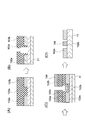
- FIG. 6A and 6 (B) are simulation results for evaluating the vibration mode of the sensor device 110 according to the comparative example.
- FIG. 6A shows the sensor in the primary vibration mode of the device
- FIG. 6B shows the secondary vibration mode thereof.
- the thickness of the source electrode 114 and the drain electrode 115 is 75 nm
- the thickness of the insulating film 12 is 280 nm
- the width of the source electrode 114 and the drain electrode 115 is 3 ⁇ m
- the facing distance L1 between the source electrode 114 and the drain electrode 115 FIG. 5
- the vibrator 116 has two natural frequencies of 19.7 MHz and 20.2 MHz
- the Q value of each is 3080 in the case of 19.7 MHz and 1509 in the case of 20.2 MHz. Met.
- FIGS. 7A and 7B are simulation results for evaluating the vibration mode of the sensor device 10 according to the present embodiment shown in FIG.
- FIG. 7A shows the sensor in the primary vibration mode of the device
- FIG. 7B shows the secondary vibration mode thereof.
- the thickness of the source electrode 14 and the drain electrode 15 is 150 nm (the thickness of each of the first source electrode layer 141, the second source electrode layer 142, the first drain electrode layer 151, and the second drain electrode layer 152 is 75 nm).
- the thickness of the insulating film 12 was 280 nm, the width of the source electrode 14 and the drain electrode 15 was 3 ⁇ m, and the facing distance between the source electrode 14 and the drain electrode 15 (the length of the vibrating portion 163 of the vibrator 16) was 1 ⁇ m.
- the vibrator 16 has two natural frequencies of 26.9 MHz and 77.6 MHz, and the Q value of each is 10087 in the case of 26.9 MHz and 10009 in the case of 77.6 MHz. Met.
- the Q value of the vibrator which is more than 3 times higher than that of the comparative example, was obtained. It is probable that the result in the comparative example is that the vibrator is not sufficiently fixed because the vibrator is formed by the under-etching of the insulating film 12, and the Q value of the vibrator 116 is lowered because the vibration energy is dissipated to the outside. ..
- both ends of the vibrator 16 are sandwiched between the layers constituting the source electrode 14 and the drain electrode 15 and are firmly fixed, so that the energy of vibration is not dissipated to the outside and is high. It is probable that the Q value was obtained.
- the responsiveness of the gas can be significantly improved as compared with the structure of the comparative example.
- the difference between the two natural frequencies was small, and the values were close to each other. This indicates that if one is selected as the primary vibration mode for gas sensing, interference with the other vibration mode is unavoidable. This is brought about by the fact that the source electrode 114 and the drain electrode 115 function as a part of the vibrator 116, thereby forming an undesired vibration mode.
- the difference between the two natural frequencies is large. This means that when one vibration mode is used for gas sensing, the influence of the other vibration mode hardly appears, and the generation of extra vibration mode that can be caused by underetching is suppressed. Shown.
- the insulating film 12 is formed on the substrate 11.
- the first resist resin layer 101a is formed on the substrate 110
- the second resist resin layer 101b is formed on the first resist resin layer 101a.
- MMA methyl methacrylate
- PMMA polymethylmethacrylate
- a resist pattern is formed by exposing and developing the first resist resin layer 101a and the second resist resin layer 101b using electron beam lithography technology or the like.
- an opening pattern in which the pattern width of the second resist resin layer 101b is larger than the pattern width of the first resist resin layer 101a is formed.
- the first metal layer 102a is formed on the surface of the second resist resin layer 101b and inside the opening thereof.
- the first metal layer 102a is patterned (lifted off) by removing the first and second resist resin layers 101a and 101b, and the pattern of the first metal layer 102a is applied to the substrate 11. Form on top.
- the first metal layer 102a may be a single layer or may have a multi-layer structure.
- chromium (Cr) having a thickness of about 10 nm is formed as an adhesion material
- gold (Au) having a thickness of about 130 nm is formed on the chromium (Cr) as an electrode material.
- the film forming method of the first metal layer 102a is not particularly limited, and may be a sputtering method or a vacuum vapor deposition method.
- the first metal layer 102a is formed by the electron beam deposition method.
- the first metal layer 102a corresponds to the first source electrode layer 141 and the first drain electrode layer 151 in the sensor device 10 shown in FIG.
- the third resist resin layer 103a is formed on the substrate 11, and the fourth resist resin layer 103b is formed on the third resist resin layer 103a.
- the third resist resin layer 103a for example, a methyl methacrylate (MMA) film is used
- the fourth resist resin layer 103b for example, a polymethylmethacrylate (PMMA) film is used. Used.
- a resist pattern is formed by exposing and developing the third resist resin layer 103a and the fourth resist resin layer 103b using electron beam lithography technology or the like.
- an opening pattern in which the opening width of the third resist resin layer 103a is larger than the opening width of the fourth resist resin layer 103b is formed.
- a second metal layer 102b is formed on the surface of the fourth resist resin layer 103b and inside the opening thereof, and then the sacrificial layer 104 is formed on the surface of the second metal layer 102b.
- the sacrificial layer 104 is made of, for example, a resist resin.
- the third and fourth resist resin layers 103a and 103b and the second metal layer 102b formed on the fourth resist resin layer 103b are removed.
- the sacrificial layer 104 formed on the second metal layer 102b and the second metal layer 102b is patterned (lifted off), and the pattern of the second metal layer 102b and the sacrificial layer 104 is formed on the substrate 11.
- the second metal layer 102b may be a single layer or may have a multi-layer structure.
- chromium (Cr) having a thickness of about 10 nm is formed as an adhesion material
- gold (Au) having a thickness of about 30 nm is formed on the chromium (Cr) as an electrode material.
- the film forming method of the second metal layer 102b is not particularly limited, and may be a sputtering method or a vacuum vapor deposition method. In this embodiment, the second metal layer 102b is formed by the electron beam deposition method.
- the second metal layer 102b corresponds to the gate electrode 13 in the sensor device 10 shown in FIG. Further, the laminated thickness of the second metal layer 102b and the sacrificial layer 104 is typically the same as the thickness of the first metal layer 102a. In the present embodiment, since the opening width of the third resist resin layer 103a is larger than the opening width of the fourth resist resin layer 103b, the second metal layer 102b is less likely to come into contact with the side surface of the opening of the third resist resin layer 103a. As a result, the patterning accuracy of the second metal layer 102b at the time of lift-off can be improved.
- the laminate of the graphene layer 105 and the protective layer 106 is transferred to the first metal layer 102a.
- the protective layer 106 is made of, for example, a resist resin.
- the protective layer 106 is removed.
- the graphene layer 105 corresponds to the vibrator 16 in the sensor device 10 of FIG.
- the third metal layer 102c is formed on the first metal layer 102a.
- the third metal layer 102c is formed, and then the resist pattern is removed to form the third metal layer 102c. Patterning (lift off).
- the third metal layer 102c faces the first metal layer 102a with the graphene layer 105 interposed therebetween.
- the shape of the third metal layer 102c is not particularly limited, and in the present embodiment, the third metal layer 102c is formed in an area smaller than that of the first metal layer 102a.
- the third metal layer 102c corresponds to the second source electrode 142 and the second drain electrode 152 in the sensor device 10 of FIG.
- the fifth resist resin layer 107a is formed on the graphene layer 105 and the third metal layer 102c, and the sixth resist resin layer 107b is formed on the fifth resist resin layer 107a.
- the fifth resist resin layer 107a for example, a polymethylmethacrylate (PMMA) film is used
- the sixth resist resin layer 107b for example, an AR-N film is used.
- a resist pattern is formed by exposing and developing only the sixth resist resin layer 107b using electron beam lithography technology or the like.
- the fifth resist resin layer 107a and the graphene layer 105 that are not coated with the sixth resist resin layer 107b are removed by dry etching.
- dry etching method for example, O 2 plasma is used.
- FIG. 11B the fifth and sixth resist resin layers 107a and 107b are removed, and as shown in FIG. 11C, the sacrificial layer 104 is removed.
- the sensor device 10 having a bottom gate structure in which the gate electrode 13 is arranged between the insulating film 12 of the substrate 11 and the vibrator 16 has been described as an example, but the present invention is not limited to this.
- the present invention is also applicable to a sensor device having a top gate structure in which the electrodes are located directly above the vibrator.
Abstract
[Problem] To provide: a sensor device by which it is possible to improve the detection accuracy for a gas; and a method for manufacturing the same. [Solution] A sensor device according to one aspect of the present invention comprises: a substrate; a gate electrode; a source electrode; a drain electrode; and an oscillator. The gate electrode is disposed on the substrate. The source electrode is disposed on the substrate and has a first conductive layer and a second conductive layer that is provided on the first conductive layer. The drain electrode is disposed on the substrate and has a third conductive layer and a fourth conductive layer that is provided on the third conductive layer. The oscillator has: a first end part disposed between the first and the second conductive layers; a second end part disposed between the third and the fourth conductive layers; and an oscillating part that opposes the gate electrode.
Description
本発明は、センサデバイスおよびその製造方法に関する。
The present invention relates to a sensor device and a method for manufacturing the same.
非特許文献1に記載されるガスセンサは、基板と、基板上に配置されたゲート電極、ドレイン電極およびソース電極と、グラフェン層とを有する。このガスセンサは、ドレイン電極およびソース電極との間でグラフェン層を振動可能に支持する構造を有し、ガスの吸着によるグラフェン層の共振周波数の変化量に基づいて、ガス成分を検出する。
The gas sensor described in Non-Patent Document 1 has a substrate, a gate electrode, a drain electrode and a source electrode arranged on the substrate, and a graphene layer. This gas sensor has a structure that vibratesly supports the graphene layer between the drain electrode and the source electrode, and detects the gas component based on the amount of change in the resonance frequency of the graphene layer due to the adsorption of gas.
より高感度なガス検出を行うために、ガスセンサの振動子にはガス吸着による共振周波数の変化を高精度に検出する必要がある。これは、振動子のQ値が高い必要があることを意味する。さらには、ガス検出に必要な振動モードを特定するために、所望の振動モードと干渉するような固有振動モードが振動子で発生しないことが求められる。
In order to perform gas detection with higher sensitivity, it is necessary for the vibrator of the gas sensor to detect the change in resonance frequency due to gas adsorption with high accuracy. This means that the Q value of the oscillator needs to be high. Furthermore, in order to specify the vibration mode required for gas detection, it is required that the vibrator does not generate a natural vibration mode that interferes with the desired vibration mode.
以上のような事情に鑑み、本発明の目的は、ガスの検出感度を高めることができるセンサデバイスおよびその製造方法を提供することにある。
In view of the above circumstances, an object of the present invention is to provide a sensor device capable of increasing the detection sensitivity of gas and a method for manufacturing the same.
本発明の一形態に係るセンサデバイスは、基板と、絶縁膜と、ゲート電極と、ソース電極と、ドレイン電極と、振動子とを具備する。
上記絶縁膜は、上記基板上に形成される。
上記ゲート電極は、上記絶縁膜上に配置される。
上記ソース電極は、第1導体層と、上記第1導体層の上に設けられた第2導体層とを有し、上記絶縁膜上に配置される。
上記ドレイン電極は、第3導体層と、上記第3導体層の上に設けられた第4導体層とを有し、上記絶縁膜上に配置される。
上記振動子は、上記第1および第2導体層に挟まれた第1端部と、上記第3および第4導体層に挟まれた第2端部と、上記ゲート電極に対向する振動部とを有する。 The sensor device according to one embodiment of the present invention includes a substrate, an insulating film, a gate electrode, a source electrode, a drain electrode, and a vibrator.
The insulating film is formed on the substrate.
The gate electrode is arranged on the insulating film.
The source electrode has a first conductor layer and a second conductor layer provided on the first conductor layer, and is arranged on the insulating film.
The drain electrode has a third conductor layer and a fourth conductor layer provided on the third conductor layer, and is arranged on the insulating film.
The vibrator includes a first end portion sandwiched between the first and second conductor layers, a second end portion sandwiched between the third and fourth conductor layers, and a vibrating portion facing the gate electrode. Has.
上記振動子は、グラフェン層を含んでもよい。
The above oscillator may include a graphene layer.
上記振動子は、上記グラフェン層上に形成された感応膜をさらに含んでもよい。
The vibrator may further include a sensitive film formed on the graphene layer.
上記感応膜は、多孔質膜であってもよい。
The sensitive membrane may be a porous membrane.
上記多孔質膜は、炭素系材料であってもよい。
The porous membrane may be a carbon-based material.
上記第1~第4導体層は、同種の金属材料であってもよい。
The first to fourth conductor layers may be made of the same type of metal material.
上記ソース電極は、上記第1および第2導体層の間に配置され上記振動子と密着する密着層をさらに有し、上記ドレイン電極は、上記第3および第4導体層の間に配置され上記振動子と密着する密着層をさらに有してもよい。
The source electrode is arranged between the first and second conductor layers and further has an adhesion layer in close contact with the vibrator, and the drain electrode is arranged between the third and fourth conductor layers. An adhesion layer that is in close contact with the vibrator may be further provided.
上記ゲート電極は、上記基板と上記振動子との間に配置されてもよい。
The gate electrode may be arranged between the substrate and the vibrator.
本発明の一形態に係るセンサデバイスの製造方法は、基板上に、下部電極層を形成することを含む。
上記下部電極層上にグラフェン層が形成される。
上記グラフェン層上に上部電極層が形成される。
上記下部電極層および上記上部電極層をパターニングすることで、上記グラフェン層を振動可能に上記グラフェン層の一端を支持するソース電極と、上記グラフェン層を振動可能に上記グラフェン層の他端を支持するドレイン電極と、上記グラフェン層と上記基板の厚み方向に所定の間隙をおいて対向するゲート電極がそれぞれ形成される。 A method for manufacturing a sensor device according to an embodiment of the present invention includes forming a lower electrode layer on a substrate.
A graphene layer is formed on the lower electrode layer.
An upper electrode layer is formed on the graphene layer.
By patterning the lower electrode layer and the upper electrode layer, the source electrode that supports one end of the graphene layer so that the graphene layer can vibrate and the other end of the graphene layer that vibrates the graphene layer are supported. A drain electrode and a gate electrode facing the graphene layer with a predetermined gap in the thickness direction of the substrate are formed.
本発明によれば、ガスの検出感度を高めることができる。
According to the present invention, the gas detection sensitivity can be increased.
以下、図面を参照しながら、本発明の実施形態を説明する。
[ガス判定システムの概要]
図1はガス判定システムの構成を示す模式図である。図2は、ガス判定システムの一部を構成するセンサデバイス10の構成を示す模式図である。 Hereinafter, embodiments of the present invention will be described with reference to the drawings.
[Overview of gas judgment system]
FIG. 1 is a schematic diagram showing the configuration of a gas determination system. FIG. 2 is a schematic view showing the configuration of thesensor device 10 that constitutes a part of the gas determination system.
[ガス判定システムの概要]
図1はガス判定システムの構成を示す模式図である。図2は、ガス判定システムの一部を構成するセンサデバイス10の構成を示す模式図である。 Hereinafter, embodiments of the present invention will be described with reference to the drawings.
[Overview of gas judgment system]
FIG. 1 is a schematic diagram showing the configuration of a gas determination system. FIG. 2 is a schematic view showing the configuration of the
図1に示すように、ガス判定システム1は、センサ装置2と、情報処理装置4と、表示装置5と、記憶部6と、を備える。
センサ装置2は、収容室20と、センサデバイス10と、UV(紫外線)光源23と、加熱部26と、を備える。 As shown in FIG. 1, thegas determination system 1 includes a sensor device 2, an information processing device 4, a display device 5, and a storage unit 6.
Thesensor device 2 includes a storage chamber 20, a sensor device 10, a UV (ultraviolet) light source 23, and a heating unit 26.
センサ装置2は、収容室20と、センサデバイス10と、UV(紫外線)光源23と、加熱部26と、を備える。 As shown in FIG. 1, the
The
収容室20は、センサデバイス10と、UV光源23と、加熱部26と、を収容する。収容室20は、外部からガスを吸気する吸気口21と、収容室20内に導入されたガスを収容室20から外部に排気する排気口22とを有する。吸気口21には収容室20内へのガスの流入を調節するバルブ24が設けられ、排気口22には収容室20内のガスの外部への流出を調節するバルブ25が設けられている。
The storage chamber 20 houses the sensor device 10, the UV light source 23, and the heating unit 26. The accommodation chamber 20 has an intake port 21 for sucking gas from the outside and an exhaust port 22 for exhausting the gas introduced into the accommodation chamber 20 from the accommodation chamber 20 to the outside. The intake port 21 is provided with a valve 24 for adjusting the inflow of gas into the accommodation chamber 20, and the exhaust port 22 is provided with a valve 25 for adjusting the outflow of gas in the accommodation chamber 20 to the outside.
UV光源23は、センサデバイス10に対して照射する紫外線(UV)を発する。後述するセンサデバイス10の振動子16にUVを照射することにより、振動子16のクリーニングが行われる。UV照射を行うことによりガスが効率よく振動子16に吸着される。これは、UV照射することにより、振動子16の表面からO2、H2O等が除去される(クリーニング効果)とともに、振動子16の表面上でのガス分子の吸着と光励起脱着との間の動的平衡が導かれて振動子16のガスの有効利用な吸着サイトが増加するため、及び、吸着分子の状態変化(イオン化など)により吸着が加速されるため、と考えられる。
The UV light source 23 emits ultraviolet rays (UV) to irradiate the sensor device 10. Cleaning of the vibrator 16 is performed by irradiating the vibrator 16 of the sensor device 10 described later with UV. By performing UV irradiation, the gas is efficiently adsorbed on the vibrator 16. This is because O 2 , H 2 O, etc. are removed from the surface of the vibrator 16 by UV irradiation (cleaning effect), and between adsorption of gas molecules on the surface of the vibrator 16 and photoexcitation desorption. It is considered that this is because the dynamic equilibrium of the gas is induced and the number of effective adsorption sites for the gas of the vibrator 16 is increased, and the adsorption is accelerated by the state change (ionization or the like) of the adsorbed molecules.
加熱部26は、例えばヒータであり、センサデバイス10を加熱する。加熱部26によるセンサデバイス10の加熱により、振動子16によるガスの吸着効果が得られる。
The heating unit 26 is, for example, a heater and heats the sensor device 10. By heating the sensor device 10 by the heating unit 26, the gas adsorption effect of the vibrator 16 can be obtained.
図2に示すように、センサデバイス10は、基板11と、絶縁膜12と、ゲート電極13と、ソース電極14と、ドレイン電極15と、振動子16とを有する。
As shown in FIG. 2, the sensor device 10 includes a substrate 11, an insulating film 12, a gate electrode 13, a source electrode 14, a drain electrode 15, and a vibrator 16.
基板11は、典型的にはシリコン基板であるが、シリコン以外の他の半導体基板やガラス基板などであってもよい。絶縁膜12は、基板11上に形成される。絶縁膜12は、典型的にはシリコン酸化膜であり、基板11がシリコン基板の場合はその表面に形成された熱酸化膜である。
The substrate 11 is typically a silicon substrate, but may be a semiconductor substrate or a glass substrate other than silicon. The insulating film 12 is formed on the substrate 11. The insulating film 12 is typically a silicon oxide film, and when the substrate 11 is a silicon substrate, it is a thermal oxide film formed on the surface thereof.
ゲート電極13、ソース電極14およびドレイン電極15は、絶縁膜12の上に形成される。ゲート電極13は、ソース電極14とドレイン電極15との間に配置される。ゲート電極13、ソース電極14およびドレイン電極15は、典型的には金属膜であり、本実施形態ではクロム(Cr)および金(Au)の積層膜で構成される。
The gate electrode 13, the source electrode 14, and the drain electrode 15 are formed on the insulating film 12. The gate electrode 13 is arranged between the source electrode 14 and the drain electrode 15. The gate electrode 13, the source electrode 14, and the drain electrode 15 are typically metal films, and in this embodiment, they are composed of a laminated film of chromium (Cr) and gold (Au).
振動子16は、ゲート電極13と対向するようにソース電極14とドレイン電極15との間に配置される。振動子16は、ゲート電極13に接触しない程度に間隙を持って配置される。振動子16は、導電性材料で構成され、本実施形態ではグラフェン層で構成される。グラフェン層は単層膜で構成されるが、多層膜であってもよい。振動子16は、グラフェン層以外にも、金属膜やシリコン薄膜などの他の導電性材料で構成されてもよい。
The vibrator 16 is arranged between the source electrode 14 and the drain electrode 15 so as to face the gate electrode 13. The vibrator 16 is arranged with a gap so as not to come into contact with the gate electrode 13. The vibrator 16 is made of a conductive material, and in this embodiment, is made of a graphene layer. The graphene layer is composed of a single layer film, but may be a multilayer film. In addition to the graphene layer, the vibrator 16 may be made of another conductive material such as a metal film or a silicon thin film.
振動子16は、図3に示すように、グラフェン層160とその表面に形成された感応膜17との積層膜で構成される。感応膜17は、例えば、検出対象のガスを吸着可能な材料で構成される。感応膜17を構成する材料は、検出対象のガスの種類によって任意に選択でき、典型的には、有機ポリマー膜(有機高分子膜、有機低分子膜)、有機色素膜または無機膜等を用いることができる。
As shown in FIG. 3, the vibrator 16 is composed of a laminated film of a graphene layer 160 and a sensitive film 17 formed on the surface thereof. The sensitive film 17 is made of, for example, a material capable of adsorbing the gas to be detected. The material constituting the sensitive film 17 can be arbitrarily selected depending on the type of gas to be detected, and typically, an organic polymer film (organic polymer film, organic low molecular weight film), an organic dye film, an inorganic film, or the like is used. be able to.
感応膜17は、多孔質膜であってもよい。多孔質膜は、グラフェン層160の表面を活性炭で装飾することで形成される。多孔質膜を構成する材料は活性炭に限られず、グラフェン層160よりも多孔性であればよく、グラフェン層160と同様に導電特性を持てばよい。多孔質層17を構成する導電性材料には、例えば、炭素系材料、導電性ポリマー、導電性セラミックス、ポーラスシリコンを用いてもよい。好ましくは、多孔質膜は、グラフェン層160と同一の炭素系材料で構成される。炭素系材料とは、炭素を主な成分とする物質である。
The sensitive film 17 may be a porous film. The porous film is formed by decorating the surface of the graphene layer 160 with activated carbon. The material constituting the porous film is not limited to activated carbon, and may be more porous than the graphene layer 160, and may have conductive properties similar to the graphene layer 160. As the conductive material constituting the porous layer 17, for example, a carbon-based material, a conductive polymer, conductive ceramics, or porous silicon may be used. Preferably, the porous membrane is made of the same carbon-based material as the graphene layer 160. A carbon-based material is a substance containing carbon as a main component.
多孔質膜はガス吸着を促進する働きをするので、多孔性であることによって吸着表面積を大きくし、また多くのダングリングボンドを有していることから、効率よくガスを吸着できる。多孔質膜は導電特性を持つので、グラフェン層160上に導電特性を持たない膜を吸着膜として設けた場合に比較して、吸着表面積が大きくなる上、表面に多くのダングリングボンドを有するため、ガス分子吸着が促進される。
Since the porous membrane has a function of promoting gas adsorption, it has a large adsorption surface area due to its porosity, and since it has many dangling bonds, it can efficiently adsorb gas. Since the porous film has conductive properties, the adsorption surface area is larger and the surface has many dangling bonds as compared with the case where a film having no conductive properties is provided on the graphene layer 160 as an adsorption film. , Gas molecule adsorption is promoted.
多孔質膜の厚みは特に限定されず、グラフェン層160の厚みと同一であってもよいし、グラフェン層160の厚みよりも薄く、あるいは、厚くてもよい。典型的には、グラフェン層160の厚みは1nm、多孔質膜の厚みは1nmである。多孔質膜は、グラフェン層160の表面全域を被覆するように形成されるが、これに限られず、グラフェン層160の表面の少なくとも一部を被覆するように形成されてもよい。
The thickness of the porous film is not particularly limited, and may be the same as the thickness of the graphene layer 160, or may be thinner or thicker than the thickness of the graphene layer 160. Typically, the graphene layer 160 has a thickness of 1 nm and the porous film has a thickness of 1 nm. The porous film is formed so as to cover the entire surface of the graphene layer 160, but is not limited to this, and may be formed so as to cover at least a part of the surface of the graphene layer 160.
情報処理装置4は、取得部41と、判定部42と、出力部43と、制御部44と、を備える。情報処理装置4はセンサデバイス10の駆動を制御し、振動子16の共振周波数の変化量に基づいてガスの検出成分を判定し、その判定結果を出力する部分である。
The information processing device 4 includes an acquisition unit 41, a determination unit 42, an output unit 43, and a control unit 44. The information processing device 4 controls the drive of the sensor device 10, determines the detection component of the gas based on the amount of change in the resonance frequency of the vibrator 16, and outputs the determination result.
制御部44は、センサデバイス10のゲート電極13とソース電極14との間に所定周波数の高周波信号を入力することで振動子16を共振させる。取得部41は、振動子16の共振周波数に対応する高周波信号(ドレイン電流)をドレイン電極15から取得し、ドレイン電流に基づき、振動子16の共振周波数の変化に変換する。判定部42は、取得部41で取得された複数の共振周波数変化に基づき、記憶部6に記憶されている共振周波数情報を参照してガスの種類あるいは濃度を判定する。出力部43は、判定部42による判定結果を表示装置5へ出力する。
The control unit 44 resonates the vibrator 16 by inputting a high frequency signal of a predetermined frequency between the gate electrode 13 and the source electrode 14 of the sensor device 10. The acquisition unit 41 acquires a high-frequency signal (drain current) corresponding to the resonance frequency of the vibrator 16 from the drain electrode 15 and converts it into a change in the resonance frequency of the vibrator 16 based on the drain current. The determination unit 42 determines the type or concentration of the gas based on the plurality of resonance frequency changes acquired by the acquisition unit 41 with reference to the resonance frequency information stored in the storage unit 6. The output unit 43 outputs the determination result by the determination unit 42 to the display device 5.
収容室20に検出対象のガスが導入されると、振動子16にガスが吸着することで振動子16の質量が変化し、その質量の変化量に基づき、振動子16の共振周波数が低下する。ガス吸着前の振動子16の質量をm、ガス吸着による振動子16の質量の変化量をΔm、振動子16の共振周波数をf0とすると、振動子16の共振周波数の変化量Δfは、式(1)で算出される。
Δf=Δm×f0/(2×m) ・・・(1) When the gas to be detected is introduced into theaccommodation chamber 20, the mass of the vibrator 16 changes due to the adsorption of the gas on the vibrator 16, and the resonance frequency of the vibrator 16 decreases based on the amount of change in the mass. .. Assuming that the mass of the vibrator 16 before gas adsorption is m, the amount of change in the mass of the vibrator 16 due to gas adsorption is Δm, and the resonance frequency of the vibrator 16 is f0, the amount of change Δf in the resonance frequency of the vibrator 16 is expressed by the formula. Calculated in (1).
Δf = Δm × f0 / (2 × m) ・ ・ ・ (1)
Δf=Δm×f0/(2×m) ・・・(1) When the gas to be detected is introduced into the
Δf = Δm × f0 / (2 × m) ・ ・ ・ (1)
式(1)で表されるように、振動子16の質量は小さい方が大きな振動数変化を示すため、振動子16の質量は小さい方が好ましい。本実施形態では、振動子16が軽元素である炭素で構成され、優れた電気的・機械的特性を有するグラフェンで構成されるため、振動数変化を高感度に検出することができる。
As represented by the equation (1), the smaller the mass of the vibrator 16, the larger the frequency change, and therefore the smaller the mass of the vibrator 16 is, the more preferable it is. In the present embodiment, since the vibrator 16 is composed of carbon, which is a light element, and graphene, which has excellent electrical and mechanical properties, the frequency change can be detected with high sensitivity.
情報処理装置4は、予め異なる種類の複数のガス毎の共振周波数情報を取得し、記憶部6に記憶しておく。判定部42は記憶部6に記憶されている共振周波数情報を参照して、センサデバイス10で検知したガスの種類を識別し判定する。
出力部43は、取得部41で取得される共振周波数情報、判定部42により判定されたガスの種類や濃度といった判定結果を表示装置5へ出力する。 Theinformation processing device 4 acquires resonance frequency information for each of a plurality of different types of gases in advance and stores them in the storage unit 6. The determination unit 42 identifies and determines the type of gas detected by the sensor device 10 with reference to the resonance frequency information stored in the storage unit 6.
Theoutput unit 43 outputs the determination result such as the resonance frequency information acquired by the acquisition unit 41 and the type and concentration of the gas determined by the determination unit 42 to the display device 5.
出力部43は、取得部41で取得される共振周波数情報、判定部42により判定されたガスの種類や濃度といった判定結果を表示装置5へ出力する。 The
The
表示装置5は表示部を有し、情報処理装置4から出力されたガスの種類や濃度等を表示部に表示する。ユーザは、表示部を確認することによりガス判定結果を把握することができる。
記憶部6は、ガス判定システム1で検出された異なる種類の複数の既知のガス毎の共振周波数情報を予め取得し、参照データとして記憶する。記憶部6は、HDD(Hard Disk Drive)や半導体メモリ等の記憶装置で構成される。記憶部6は、情報処理装置4が通信可能なクラウドサーバ上にあってもよいし、情報処理装置4が備えていてもよい。 Thedisplay device 5 has a display unit, and displays the type and concentration of gas output from the information processing device 4 on the display unit. The user can grasp the gas determination result by checking the display unit.
Thestorage unit 6 acquires in advance resonance frequency information for each of a plurality of known gases of different types detected by the gas determination system 1 and stores them as reference data. The storage unit 6 is composed of a storage device such as an HDD (Hard Disk Drive) or a semiconductor memory. The storage unit 6 may be on a cloud server on which the information processing device 4 can communicate, or may be provided in the information processing device 4.
記憶部6は、ガス判定システム1で検出された異なる種類の複数の既知のガス毎の共振周波数情報を予め取得し、参照データとして記憶する。記憶部6は、HDD(Hard Disk Drive)や半導体メモリ等の記憶装置で構成される。記憶部6は、情報処理装置4が通信可能なクラウドサーバ上にあってもよいし、情報処理装置4が備えていてもよい。 The
The
[センサデバイスの詳細]
[Details of sensor device]
続いて、センサデバイス10の詳細について説明する。図4は、センサデバイス10の側断面図である。
Next, the details of the sensor device 10 will be described. FIG. 4 is a side sectional view of the sensor device 10.
上述のように、振動子16は、ゲート電極13と対向するようにソース電極14とドレイン電極15との間に配置される。より具体的に、振動子16は、ソース電極14に支持される第1端部161と、ドレイン電極15に支持される第2端部162と、ゲート電極13と対向する振動部163とを有する。振動子16は、振動部163が振動可能なように、ゲート電極13に対して基板11の厚み方向に所定の間隙(例えば、100nm)をおいて配置される。
As described above, the vibrator 16 is arranged between the source electrode 14 and the drain electrode 15 so as to face the gate electrode 13. More specifically, the vibrator 16 has a first end portion 161 supported by the source electrode 14, a second end portion 162 supported by the drain electrode 15, and a vibrating portion 163 facing the gate electrode 13. .. The vibrator 16 is arranged with a predetermined gap (for example, 100 nm) in the thickness direction of the substrate 11 with respect to the gate electrode 13 so that the vibrating portion 163 can vibrate.
一方、ソース電極14およびドレイン電極15は、少なくとも2層の導体層の積層構造を有する。すなわち、ソース電極14は、絶縁膜12の上に設けられた第1ソース電極層141(第1導体層)と、第1ソース電極層141の上に設けられた第2ソース電極層142(第2導体層)とを有する。また、ドレイン電極15は、絶縁膜12の上に設けられた第1ドレイン電極層151(第3導体層)と、第1ドレイン電極層151の上に設けられた第2ドレイン電極層152(第4導体層)とを有する。
On the other hand, the source electrode 14 and the drain electrode 15 have a laminated structure of at least two conductor layers. That is, the source electrode 14 includes a first source electrode layer 141 (first conductor layer) provided on the insulating film 12 and a second source electrode layer 142 (first conductor layer) provided on the first source electrode layer 141. It has two conductor layers). Further, the drain electrode 15 includes a first drain electrode layer 151 (third conductor layer) provided on the insulating film 12 and a second drain electrode layer 152 (third conductor layer) provided on the first drain electrode layer 151. It has 4 conductor layers).
振動子16の第1端部161は、第1ソース電極層141と第2ソース電極層142とに挟まれるようにしてこれら電極層141,142の間に配置される。振動子16の第2端部162は、第1ドレイン電極層151と第2ドレイン電極層152とに挟まれるようにしてこれら電極層151,152の間に配置される。第1ソース電極層141および第1ドレイン電極層151は、ゲート電極13よりも大きな厚みで形成されることで、振動子16の振動部163とゲート電極13との間に上記所定の間隙が形成される。
The first end portion 161 of the vibrator 16 is arranged between the electrode layers 141 and 142 so as to be sandwiched between the first source electrode layer 141 and the second source electrode layer 142. The second end portion 162 of the vibrator 16 is arranged between the electrode layers 151 and 152 so as to be sandwiched between the first drain electrode layer 151 and the second drain electrode layer 152. The first source electrode layer 141 and the first drain electrode layer 151 are formed to have a thickness larger than that of the gate electrode 13, so that the predetermined gap is formed between the vibrating portion 163 of the vibrator 16 and the gate electrode 13. Will be done.
このように本実施形態のセンサデバイス10においては、振動子16の両端がソース電極14およびドレイン電極15を構成する導体層(電極層)の間にそれぞれ挟持されるようにして支持されているため、振動子16を安定に保持することができる。よって、振動子16が剥がれ落ちにくくなるので、センサデバイス10の経時劣化を抑制し、耐久性を向上することができる。第1ソース電極層141と第2ソース電極層142との間には、振動子16の第1端部161と密着するクロム(Cr)などの密着層が設けられてもよい。同様に、第1ドレイン電極151と第2ドレイン電極152との間には、振動子16の第2端部162と密着するCrなどの密着層が設けられてもよい。これにより、振動子16とソース電極14およびドレイン電極15との密着性が高められるため、センサデバイス10の耐久性を向上させることができる。
As described above, in the sensor device 10 of the present embodiment, both ends of the vibrator 16 are supported so as to be sandwiched between the conductor layers (electrode layers) constituting the source electrode 14 and the drain electrode 15. , The vibrator 16 can be stably held. Therefore, since the vibrator 16 is less likely to come off, deterioration of the sensor device 10 over time can be suppressed and durability can be improved. A close contact layer such as chromium (Cr) that is in close contact with the first end portion 161 of the vibrator 16 may be provided between the first source electrode layer 141 and the second source electrode layer 142. Similarly, a close contact layer such as Cr that is in close contact with the second end portion 162 of the vibrator 16 may be provided between the first drain electrode 151 and the second drain electrode 152. As a result, the adhesion between the vibrator 16 and the source electrode 14 and the drain electrode 15 is enhanced, so that the durability of the sensor device 10 can be improved.
第1ソース電極層141と第2ソース電極層142は、それぞれ同種の金属材料で構成されるのが好ましい。同様に、第1ドレイン電極層151と第2ドレイン電極層152は、それぞれ同種の金属材料で構成されるのが好ましい。これにより、熱膨張係数の差に起因する各電極層の界面での熱応力の発生を防ぐことができるため、振動子16の各端部161,162をより安定に支持することができる。同種の金属材料とは、同一の金属材料のほか、主金属材料が同一の合金材料をいう。
It is preferable that the first source electrode layer 141 and the second source electrode layer 142 are each made of the same type of metal material. Similarly, it is preferable that the first drain electrode layer 151 and the second drain electrode layer 152 are each made of the same type of metal material. As a result, it is possible to prevent the generation of thermal stress at the interface of each electrode layer due to the difference in the coefficient of thermal expansion, so that each end portion 161, 162 of the vibrator 16 can be supported more stably. The same kind of metal material means an alloy material having the same main metal material as well as the same metal material.
図5は、比較例に係るセンサデバイス110の構成を示す側断面図である。このセンサデバイス110は、基板11の絶縁膜12上にソース電極114およびドレイン電極115が形成され、ソース電極114およびドレイン電極115の間の絶縁膜12には、ゲート電極13を配置するための凹部120が形成される。振動子116は、凹部120内にゲート電極13と対向するように配置され、振動子116の両端の上面は、ソース電極114およびドレイン電極115の下面にそれぞれ支持される。
FIG. 5 is a side sectional view showing the configuration of the sensor device 110 according to the comparative example. In this sensor device 110, the source electrode 114 and the drain electrode 115 are formed on the insulating film 12 of the substrate 11, and the insulating film 12 between the source electrode 114 and the drain electrode 115 has a recess for arranging the gate electrode 13. 120 is formed. The vibrator 116 is arranged in the recess 120 so as to face the gate electrode 13, and the upper surfaces of both ends of the vibrator 116 are supported by the lower surfaces of the source electrode 114 and the drain electrode 115, respectively.
ここで、凹部120は、ソース電極114およびドレイン電極115をマスクとするウェットエッチング法により形成される。ウェットエッチングは等方的エッチングであるため、凹部120は、絶縁膜12とソース電極114およびドレイン電極115の界面の一部を浸食するアンダーエッチングを伴う。これにより、ソース電極114およびドレイン電極115には、振動子116を支持する端部近傍において下地層である絶縁膜12に支持されない領域が発生する。そして、振動子116にも絶縁膜12によって支持されない領域が発生し、ソース電極114およびドレイン電極115によって両端部の上面のみが支持される。その結果、振動子116の両端部を支持する部位の剛性が低下し、振動子116の振動に伴ってソース電極114およびドレイン電極115の端部も振動することで、振動子116を所望とする振動モードで振動させることが困難となる。
Here, the recess 120 is formed by a wet etching method using the source electrode 114 and the drain electrode 115 as masks. Since wet etching is isotropic etching, the recess 120 is accompanied by under-etching that erodes a part of the interface between the insulating film 12 and the source electrode 114 and the drain electrode 115. As a result, in the source electrode 114 and the drain electrode 115, a region that is not supported by the insulating film 12 that is the base layer is generated in the vicinity of the end portion that supports the vibrator 116. Then, a region not supported by the insulating film 12 is also generated in the vibrator 116, and only the upper surfaces of both ends are supported by the source electrode 114 and the drain electrode 115. As a result, the rigidity of the portion supporting both ends of the vibrator 116 is reduced, and the ends of the source electrode 114 and the drain electrode 115 also vibrate with the vibration of the vibrator 116, so that the vibrator 116 is desired. It becomes difficult to vibrate in the vibration mode.
図6(A),(B)は、比較例に係るセンサデバイス110の振動モードを評価したシミュレーション結果である。図6(A)は、センサでデバイスの一次振動モード、図6(B)はその二次振動モードである。ここでは、ソース電極114およびドレイン電極115の厚みを75nm、絶縁膜12の厚みを280nm、ソース電極114およびドレイン電極115の幅を3μm、ソース電極114-ドレイン電極115間の対向距離L1(図5参照)を1μm、ソース電極114およびドレイン電極115の凹部120への張出し長L2(図5参照)を2μmとした。
同図の例において振動子116は、19.7MHzおよび20.2MHzの2つの固有振動数を有しており、それぞれのQ値は、19.7MHzの場合は3080、20.2MHzの場合は1509であった。 6 (A) and 6 (B) are simulation results for evaluating the vibration mode of thesensor device 110 according to the comparative example. FIG. 6A shows the sensor in the primary vibration mode of the device, and FIG. 6B shows the secondary vibration mode thereof. Here, the thickness of the source electrode 114 and the drain electrode 115 is 75 nm, the thickness of the insulating film 12 is 280 nm, the width of the source electrode 114 and the drain electrode 115 is 3 μm, and the facing distance L1 between the source electrode 114 and the drain electrode 115 (FIG. 5). (See) was set to 1 μm, and the overhang length L2 (see FIG. 5) of the source electrode 114 and the drain electrode 115 into the recess 120 was set to 2 μm.
In the example of the figure, thevibrator 116 has two natural frequencies of 19.7 MHz and 20.2 MHz, and the Q value of each is 3080 in the case of 19.7 MHz and 1509 in the case of 20.2 MHz. Met.
同図の例において振動子116は、19.7MHzおよび20.2MHzの2つの固有振動数を有しており、それぞれのQ値は、19.7MHzの場合は3080、20.2MHzの場合は1509であった。 6 (A) and 6 (B) are simulation results for evaluating the vibration mode of the
In the example of the figure, the
一方、図7(A),(B)は、図4に示した本実施形態に係るセンサデバイス10の振動モードを評価したシミュレーション結果である。図7(A)は、センサでデバイスの一次振動モード、図7(B)はその二次振動モードである。ここでは、ソース電極14およびドレイン電極15の厚みを150nm(第1ソース電極層141、第2ソース電極層142、第1ドレイン電極層151および第2ドレイン電極層152のそれぞれの厚みを75nm)、絶縁膜12の厚みを280nm、ソース電極14およびドレイン電極15の幅を3μm、ソース電極14-ドレイン電極15間の対向距離(振動子16の振動部163の長さ)を1μmとした。
同図の例において振動子16は、26.9MHzおよび77.6MHzの2つの固有振動数を有しており、それぞれのQ値は、26.9MHzの場合は10008、77.6MHzの場合は10009であった。 On the other hand, FIGS. 7A and 7B are simulation results for evaluating the vibration mode of thesensor device 10 according to the present embodiment shown in FIG. FIG. 7A shows the sensor in the primary vibration mode of the device, and FIG. 7B shows the secondary vibration mode thereof. Here, the thickness of the source electrode 14 and the drain electrode 15 is 150 nm (the thickness of each of the first source electrode layer 141, the second source electrode layer 142, the first drain electrode layer 151, and the second drain electrode layer 152 is 75 nm). The thickness of the insulating film 12 was 280 nm, the width of the source electrode 14 and the drain electrode 15 was 3 μm, and the facing distance between the source electrode 14 and the drain electrode 15 (the length of the vibrating portion 163 of the vibrator 16) was 1 μm.
In the example of the figure, thevibrator 16 has two natural frequencies of 26.9 MHz and 77.6 MHz, and the Q value of each is 10087 in the case of 26.9 MHz and 10009 in the case of 77.6 MHz. Met.
同図の例において振動子16は、26.9MHzおよび77.6MHzの2つの固有振動数を有しており、それぞれのQ値は、26.9MHzの場合は10008、77.6MHzの場合は10009であった。 On the other hand, FIGS. 7A and 7B are simulation results for evaluating the vibration mode of the
In the example of the figure, the
図6および図7の結果から明らかなように、本実施形態によれば、比較例よりも3倍以上も高い振動子のQ値が得られた。比較例での結果は、絶縁膜12のアンダーエッチングによって振動子が形成されているため固定が十分ではなく、振動のエネルギーが外部に散逸するために振動子116のQ値が低下したためと考えられる。これに対して、本実施形態においては振動子16の両端がソース電極14およびドレイン電極15を構成する各層によって挟み込まれ、強固に固定されたことにより、振動のエネルギーが外部に散逸せず、高いQ値が得られたためと考えられる。これにより本実施形態によれば、比較例の構造と比較して、ガスの応答性を大幅に向上させることができる。
As is clear from the results of FIGS. 6 and 7, according to the present embodiment, the Q value of the vibrator, which is more than 3 times higher than that of the comparative example, was obtained. It is probable that the result in the comparative example is that the vibrator is not sufficiently fixed because the vibrator is formed by the under-etching of the insulating film 12, and the Q value of the vibrator 116 is lowered because the vibration energy is dissipated to the outside. .. On the other hand, in the present embodiment, both ends of the vibrator 16 are sandwiched between the layers constituting the source electrode 14 and the drain electrode 15 and are firmly fixed, so that the energy of vibration is not dissipated to the outside and is high. It is probable that the Q value was obtained. Thereby, according to the present embodiment, the responsiveness of the gas can be significantly improved as compared with the structure of the comparative example.
さらに、比較例のセンサデバイス110においては、2つの固有振動数の差は小さく、互いに近接した値を示した。これは、どちらか一方をガスセンシングのための主要な振動モードとして選択した場合、他方の振動モードとの干渉が避けられないことを示している。これは、ソース電極114およびドレイン電極115が振動子116の一部として機能してしまうことにより、望んでいない振動モードが形成されているためにもたらされる。
Furthermore, in the sensor device 110 of the comparative example, the difference between the two natural frequencies was small, and the values were close to each other. This indicates that if one is selected as the primary vibration mode for gas sensing, interference with the other vibration mode is unavoidable. This is brought about by the fact that the source electrode 114 and the drain electrode 115 function as a part of the vibrator 116, thereby forming an undesired vibration mode.
これに対して、本実施形態のセンサデバイス10においては、2つの固有振動数の差が大きい。これは、一方の振動モードをガスセンシングに利用した場合、他方の振動モードの影響がほとんど現れないことを意味しており、アンダーエッチングによって生じ得る余分な振動モードの発生が抑えられていることを示している。
On the other hand, in the sensor device 10 of the present embodiment, the difference between the two natural frequencies is large. This means that when one vibration mode is used for gas sensing, the influence of the other vibration mode hardly appears, and the generation of extra vibration mode that can be caused by underetching is suppressed. Shown.
[センサデバイスの製造方法]
続いて、以上のように構成される本実施形態のセンサデバイス10の製造方法について説明する。 [Manufacturing method of sensor device]
Subsequently, a method of manufacturing thesensor device 10 of the present embodiment configured as described above will be described.
続いて、以上のように構成される本実施形態のセンサデバイス10の製造方法について説明する。 [Manufacturing method of sensor device]
Subsequently, a method of manufacturing the
まず、図8(A)に示すように、基板11上に絶縁膜12が形成される。続いて、図8(B)に示すように、基板110上に、第1レジスト樹脂層101aを形成し、その上に第2レジスト樹脂層101bを形成する。第1レジスト樹脂層101aには、例えばメタクリル酸メチル(methyl meth acrylate、MMA)膜が用いられ、第2レジスト樹脂層101bには、例えば、ポリメタクリル酸メチル(poly methyl meth acrylate、PMMA)膜が用いられる。
First, as shown in FIG. 8A, the insulating film 12 is formed on the substrate 11. Subsequently, as shown in FIG. 8B, the first resist resin layer 101a is formed on the substrate 110, and the second resist resin layer 101b is formed on the first resist resin layer 101a. For the first resist resin layer 101a, for example, a methyl methacrylate (MMA) film is used, and for the second resist resin layer 101b, for example, a polymethylmethacrylate (PMMA) film is used. Used.
続いて、図8(C)に示すように、電子線リソグラフィ技術などを用いて第1レジスト樹脂層101aおよび第2レジスト樹脂層101bを露光および現像することで、レジストパターンを形成する。本実施形態では、第2レジスト樹脂層101bのパターン幅が第1レジスト樹脂層101aのパターン幅よりも大きい開口パターンが形成される。
Subsequently, as shown in FIG. 8C, a resist pattern is formed by exposing and developing the first resist resin layer 101a and the second resist resin layer 101b using electron beam lithography technology or the like. In the present embodiment, an opening pattern in which the pattern width of the second resist resin layer 101b is larger than the pattern width of the first resist resin layer 101a is formed.
続いて、図8(D)に示すように、第2レジスト樹脂層101bの表面およびその開口部の内部に第1金属層102aを形成する。その後、図8(E)に示すように、第1および第2レジスト樹脂層101a,101bを除去することで第1金属層102aをパターニングし(リフトオフ)、第1金属層102aのパターンを基板11上に形成する。
Subsequently, as shown in FIG. 8D, the first metal layer 102a is formed on the surface of the second resist resin layer 101b and inside the opening thereof. After that, as shown in FIG. 8 (E), the first metal layer 102a is patterned (lifted off) by removing the first and second resist resin layers 101a and 101b, and the pattern of the first metal layer 102a is applied to the substrate 11. Form on top.
第1金属層102aは単層でもよいし、多層構造であってもよい。本実施形態では、密着材料として厚さが10nm程度のクロム(Cr)が形成され、その上に電極材料として厚さが130nm程度の金(Au)が形成される。第1金属層102aの成膜方法も特に限定されず、スパッタ法でもよいし、真空蒸着法であってもよい。本実施形態では、電子ビーム蒸着法によって第1金属層102aが形成される。第1金属層102aは、図2に示したセンサデバイス10における第1ソース電極層141および第1ドレイン電極層151に相当する。
The first metal layer 102a may be a single layer or may have a multi-layer structure. In the present embodiment, chromium (Cr) having a thickness of about 10 nm is formed as an adhesion material, and gold (Au) having a thickness of about 130 nm is formed on the chromium (Cr) as an electrode material. The film forming method of the first metal layer 102a is not particularly limited, and may be a sputtering method or a vacuum vapor deposition method. In this embodiment, the first metal layer 102a is formed by the electron beam deposition method. The first metal layer 102a corresponds to the first source electrode layer 141 and the first drain electrode layer 151 in the sensor device 10 shown in FIG.
続いて、図9(A)に示すように、基板11上に、第3レジスト樹脂層103aを形成し、その上に第4レジスト樹脂層103bを形成する。第3レジスト樹脂層103aには、例えばメタクリル酸メチル(methyl meth acrylate、MMA)膜が用いられ、第4レジスト樹脂層103bには、例えば、ポリメタクリル酸メチル(poly methyl meth acrylate、PMMA)膜が用いられる。
Subsequently, as shown in FIG. 9A, the third resist resin layer 103a is formed on the substrate 11, and the fourth resist resin layer 103b is formed on the third resist resin layer 103a. For the third resist resin layer 103a, for example, a methyl methacrylate (MMA) film is used, and for the fourth resist resin layer 103b, for example, a polymethylmethacrylate (PMMA) film is used. Used.
続いて、図9(B)に示すように、電子線リソグラフィ技術などを用いて第3レジスト樹脂層103aおよび第4レジスト樹脂層103bを露光および現像することで、レジストパターンを形成する。本実施形態では、第3レジスト樹脂層103aの開口幅が第4レジスト樹脂層103bの開口幅よりも大きい開口パターンが形成される。
Subsequently, as shown in FIG. 9B, a resist pattern is formed by exposing and developing the third resist resin layer 103a and the fourth resist resin layer 103b using electron beam lithography technology or the like. In the present embodiment, an opening pattern in which the opening width of the third resist resin layer 103a is larger than the opening width of the fourth resist resin layer 103b is formed.
続いて、図9(C)に示すように、第4レジスト樹脂層103bの表面およびその開口部の内部に第2金属層102bを形成し、その後、第2金属層102bの表面に犠牲層104を形成する。犠牲層104は、例えば、レジスト樹脂で構成される。
Subsequently, as shown in FIG. 9C, a second metal layer 102b is formed on the surface of the fourth resist resin layer 103b and inside the opening thereof, and then the sacrificial layer 104 is formed on the surface of the second metal layer 102b. To form. The sacrificial layer 104 is made of, for example, a resist resin.
その後、図9(D)および図10(A)に示すように、第3および第4レジスト樹脂層103a,103bと、第4レジスト樹脂層103b上に形成された第2金属層102bを除去することで第2金属層102bと第2金属層102bに形成された犠牲層104をパターニングし(リフトオフ)、第2金属層102bおよび犠牲層104のパターンを基板11上に形成する。
Then, as shown in FIGS. 9D and 10A, the third and fourth resist resin layers 103a and 103b and the second metal layer 102b formed on the fourth resist resin layer 103b are removed. As a result, the sacrificial layer 104 formed on the second metal layer 102b and the second metal layer 102b is patterned (lifted off), and the pattern of the second metal layer 102b and the sacrificial layer 104 is formed on the substrate 11.
第2金属層102bは単層でもよいし、多層構造であってもよい。本実施形態では、密着材料として厚さが10nm程度のクロム(Cr)が形成され、その上に電極材料として厚さが30nm程度の金(Au)が形成される。第2金属層102bの成膜方法も特に限定されず、スパッタ法でもよいし、真空蒸着法であってもよい。本実施形態では、電子ビーム蒸着法によって第2金属層102bが形成される。
The second metal layer 102b may be a single layer or may have a multi-layer structure. In the present embodiment, chromium (Cr) having a thickness of about 10 nm is formed as an adhesion material, and gold (Au) having a thickness of about 30 nm is formed on the chromium (Cr) as an electrode material. The film forming method of the second metal layer 102b is not particularly limited, and may be a sputtering method or a vacuum vapor deposition method. In this embodiment, the second metal layer 102b is formed by the electron beam deposition method.
第2金属層102bは、図2に示したセンサデバイス10におけるゲート電極13に相当する。また、第2金属層102bと犠牲層104との積層厚みは、典型的には、第1金属層102aの厚みと同一とされる。本実施形態では、第3レジスト樹脂層103aの開口幅が第4レジスト樹脂層103bの開口幅よりも大きいため、第2金属層102bは、第3レジスト樹脂層103aの開口部側面に接触しにくく、これによりリフトオフの際の第2金属層102bのパターニング精度を高めることができる。
The second metal layer 102b corresponds to the gate electrode 13 in the sensor device 10 shown in FIG. Further, the laminated thickness of the second metal layer 102b and the sacrificial layer 104 is typically the same as the thickness of the first metal layer 102a. In the present embodiment, since the opening width of the third resist resin layer 103a is larger than the opening width of the fourth resist resin layer 103b, the second metal layer 102b is less likely to come into contact with the side surface of the opening of the third resist resin layer 103a. As a result, the patterning accuracy of the second metal layer 102b at the time of lift-off can be improved.
その後、図10(B)に示すように、グラフェン層105と保護層106の積層体を第1金属層102aに転写する。保護層106は、例えば、レジスト樹脂で構成される。その後、図10(C)に示すように、保護層106を除去する。グラフェン層105は、図2のセンサデバイス10における振動子16に相当する。
After that, as shown in FIG. 10B, the laminate of the graphene layer 105 and the protective layer 106 is transferred to the first metal layer 102a. The protective layer 106 is made of, for example, a resist resin. Then, as shown in FIG. 10 (C), the protective layer 106 is removed. The graphene layer 105 corresponds to the vibrator 16 in the sensor device 10 of FIG.
その後、図10(D)に示すように、第3金属層102cを第1金属層102aの上に形成する。第3金属層102cの形成方法としては、例えば、グラフェン層105上に、レジストパターンを形成した後、第3金属層102cを形成し、続いてレジストパターンを除去することで第3金属層102cをパターニングする(リフトオフ)。
After that, as shown in FIG. 10D, the third metal layer 102c is formed on the first metal layer 102a. As a method for forming the third metal layer 102c, for example, after forming a resist pattern on the graphene layer 105, the third metal layer 102c is formed, and then the resist pattern is removed to form the third metal layer 102c. Patterning (lift off).
第3金属層102cは、グラフェン層105を挟んで第1金属層102aに対向する。第3金属層102cの形状は特に限定されず、本実施形態では、第1金属層102aよりも小さい面積で形成される。第3金属層102cは、図2のセンサデバイス10における第2ソース電極142および第2ドレイン電極152に相当する。
The third metal layer 102c faces the first metal layer 102a with the graphene layer 105 interposed therebetween. The shape of the third metal layer 102c is not particularly limited, and in the present embodiment, the third metal layer 102c is formed in an area smaller than that of the first metal layer 102a. The third metal layer 102c corresponds to the second source electrode 142 and the second drain electrode 152 in the sensor device 10 of FIG.
続いて、図10(E)に示すように、グラフェン層105および第3金属層102c上に、第5レジスト樹脂層107aを形成し、その上に第6レジスト樹脂層107bを形成する。第5レジスト樹脂層107aには、例えばポリメタクリル酸メチル(poly methyl meth acrylate、PMMA)膜が用いられ、第6レジスト樹脂層107bには、例えば、AR-N膜が用いられる。
Subsequently, as shown in FIG. 10 (E), the fifth resist resin layer 107a is formed on the graphene layer 105 and the third metal layer 102c, and the sixth resist resin layer 107b is formed on the fifth resist resin layer 107a. For the fifth resist resin layer 107a, for example, a polymethylmethacrylate (PMMA) film is used, and for the sixth resist resin layer 107b, for example, an AR-N film is used.
続いて、図10(F)に示すように、電子線リソグラフィ技術などを用いて第6レジスト樹脂層107bのみを露光および現像することで、レジストパターンを形成する。
Subsequently, as shown in FIG. 10 (F), a resist pattern is formed by exposing and developing only the sixth resist resin layer 107b using electron beam lithography technology or the like.
続いて、図11(A)に示すように、ドライエッチングによって、第6レジスト樹脂層107bで被覆されていない第5レジスト樹脂層107aとグラフェン層105を除去する。ドライエッチング方法には、例えば、O2プラズマが用いられる。続いて、図11(B)に示すように、第5および第6レジスト樹脂層107a,107bを除去し、図11(C)に示すように、犠牲層104を除去する。
Subsequently, as shown in FIG. 11A, the fifth resist resin layer 107a and the graphene layer 105 that are not coated with the sixth resist resin layer 107b are removed by dry etching. For the dry etching method, for example, O 2 plasma is used. Subsequently, as shown in FIG. 11B, the fifth and sixth resist resin layers 107a and 107b are removed, and as shown in FIG. 11C, the sacrificial layer 104 is removed.
以上、本発明の実施形態について説明したが、本発明は上述の実施形態にのみ限定されるものではなく、本発明の要旨を逸脱しない範囲内において種々変更を加え得ることは勿論である。
Although the embodiments of the present invention have been described above, the present invention is not limited to the above-described embodiments, and it goes without saying that various modifications can be made without departing from the gist of the present invention.
例えば以上の実施形態では、ゲート電極13が基板11の絶縁膜12と振動子16との間に配置されるボトムゲート構造のセンサデバイス10を例に挙げて説明したが、これに限られず、ゲート電極が振動子の直上に位置するトップゲート構造のセンサデバイスにも本発明は適用可能である。
For example, in the above embodiment, the sensor device 10 having a bottom gate structure in which the gate electrode 13 is arranged between the insulating film 12 of the substrate 11 and the vibrator 16 has been described as an example, but the present invention is not limited to this. The present invention is also applicable to a sensor device having a top gate structure in which the electrodes are located directly above the vibrator.
1…ガス判定システム
4…情報処理装置
10…センサデバイス
11…基板
12…絶縁膜
13…ゲート電極
14…ソース電極
15…ドレイン電極
16…振動子
141…第1ソース電極(第1導体層)
142…第2ソース電極(第2導体層)
151…第1ドレイン電極(第3導体層)
152…第2ドレイン電極(第4導体層)
161…第1端部
162…第2端部
163…振動部 1 ...Gas judgment system 4 ... Information processing device 10 ... Sensor device 11 ... Substrate 12 ... Insulating film 13 ... Gate electrode 14 ... Source electrode 15 ... Drain electrode 16 ... Transducer 141 ... First source electrode (first conductor layer)
142 ... Second source electrode (second conductor layer)
151 ... 1st drain electrode (3rd conductor layer)
152 ... 2nd drain electrode (4th conductor layer)
161 ...1st end 162 ... 2nd end 163 ... Vibration
4…情報処理装置
10…センサデバイス
11…基板
12…絶縁膜
13…ゲート電極
14…ソース電極
15…ドレイン電極
16…振動子
141…第1ソース電極(第1導体層)
142…第2ソース電極(第2導体層)
151…第1ドレイン電極(第3導体層)
152…第2ドレイン電極(第4導体層)
161…第1端部
162…第2端部
163…振動部 1 ...
142 ... Second source electrode (second conductor layer)
151 ... 1st drain electrode (3rd conductor layer)
152 ... 2nd drain electrode (4th conductor layer)
161 ...
Claims (9)
- 基板と、
前記基板上に形成された絶縁膜と、
前記絶縁膜上に配置されたゲート電極と、
第1導体層と、前記第1導体層の上に設けられた第2導体層とを有し、前記絶縁膜上に配置されたソース電極と、
第3導体層と、前記第3導体層の上に設けられた第4導体層とを有し、前記絶縁膜上に配置されたドレイン電極と、
前記第1および第2導体層に挟まれた第1端部と、前記第3および第4導体層に挟まれた第2端部と、前記ゲート電極に対向する振動部とを有する振動子と、
を具備するセンサデバイス。 With the board
The insulating film formed on the substrate and
With the gate electrode arranged on the insulating film,
A source electrode having a first conductor layer and a second conductor layer provided on the first conductor layer and arranged on the insulating film, and
A drain electrode having a third conductor layer and a fourth conductor layer provided on the third conductor layer and arranged on the insulating film, and a drain electrode.
An oscillator having a first end portion sandwiched between the first and second conductor layers, a second end portion sandwiched between the third and fourth conductor layers, and a vibrating portion facing the gate electrode. ,
A sensor device comprising. - 請求項1に記載のセンサデバイスであって、
前記振動子は、グラフェン層を含む
センサデバイス。 The sensor device according to claim 1.
The vibrator is a sensor device including a graphene layer. - 請求項2に記載のセンサデバイスであって、
前記振動子は、前記グラフェン層上に形成された感応膜をさらに含む
センサデバイス。 The sensor device according to claim 2.
The vibrator is a sensor device further including a sensitive film formed on the graphene layer. - 請求項3に記載のセンサデバイスであって、
前記感応膜は、多孔質膜である
センサデバイス。 The sensor device according to claim 3.
The sensitive film is a sensor device that is a porous film. - 請求項4に記載のセンサデバイスであって、
前記多孔質膜は、炭素系材料である
センサデバイス。 The sensor device according to claim 4.
The porous membrane is a sensor device made of a carbon-based material. - 請求項1~5のいずれか1つに記載のセンサデバイスであって、
前記第1~第4導体層は、同種の金属材料である
センサデバイス。 The sensor device according to any one of claims 1 to 5.
The first to fourth conductor layers are sensor devices made of the same type of metal material. - 請求項1~6のいずれか1つに記載のセンサデバイスであって、
前記ソース電極は、前記第1および第2導体層の間に配置され前記振動子と密着する密着層をさらに有し、
前記ドレイン電極は、前記第3および第4導体層の間に配置され前記振動子と密着する密着層をさらに有する
センサデバイス。 The sensor device according to any one of claims 1 to 6.
The source electrode further has an adhesion layer arranged between the first and second conductor layers and in close contact with the vibrator.
The drain electrode is a sensor device that is arranged between the third and fourth conductor layers and further has an adhesion layer that is in close contact with the vibrator. - 請求項1~6のいずれか1つに記載のセンサデバイスであって、
前記ゲート電極は、前記基板と前記振動子との間に配置される
センサデバイス。 The sensor device according to any one of claims 1 to 6.
The gate electrode is a sensor device arranged between the substrate and the vibrator. - 基板上に、下部電極層を形成し、
前記下部電極層上にグラフェン層を形成し、
前記グラフェン層上に上部電極層を形成し、
前記下部電極層および前記上部電極層をパターニングすることで、前記グラフェン層を振動可能に前記グラフェン層の一端を支持するソース電極と、前記グラフェン層を振動可能に前記グラフェン層の他端を支持するドレイン電極と、前記グラフェン層と前記基板の厚み方向に所定の間隙をおいて対向するゲート電極とをそれぞれ形成する
センサデバイスの製造方法。 A lower electrode layer is formed on the substrate,
A graphene layer is formed on the lower electrode layer,
An upper electrode layer is formed on the graphene layer,
By patterning the lower electrode layer and the upper electrode layer, the source electrode that supports one end of the graphene layer so that the graphene layer can vibrate and the other end of the graphene layer that vibrates the graphene layer are supported. A method for manufacturing a sensor device in which a drain electrode, a graphene layer, and a gate electrode facing each other with a predetermined gap in the thickness direction of the substrate are formed.
Priority Applications (1)
| Application Number | Priority Date | Filing Date | Title |
|---|---|---|---|
| JP2022512078A JPWO2021200569A1 (en) | 2020-03-31 | 2021-03-25 |
Applications Claiming Priority (2)
| Application Number | Priority Date | Filing Date | Title |
|---|---|---|---|
| JP2020063788 | 2020-03-31 | ||
| JP2020-063788 | 2020-03-31 |
Publications (1)
| Publication Number | Publication Date |
|---|---|
| WO2021200569A1 true WO2021200569A1 (en) | 2021-10-07 |
Family
ID=77928833
Family Applications (1)
| Application Number | Title | Priority Date | Filing Date |
|---|---|---|---|
| PCT/JP2021/012619 WO2021200569A1 (en) | 2020-03-31 | 2021-03-25 | Sensor device and method for manufacturing same |
Country Status (2)
| Country | Link |
|---|---|
| JP (1) | JPWO2021200569A1 (en) |
| WO (1) | WO2021200569A1 (en) |
Citations (5)
| Publication number | Priority date | Publication date | Assignee | Title |
|---|---|---|---|---|
| US20120206012A1 (en) * | 2008-12-01 | 2012-08-16 | The Trustees Of Columbia University In The City Of New York | Electromechanical devices and methods for fabrication of the same |
| CN102862949A (en) * | 2012-09-07 | 2013-01-09 | 清华大学 | Double-cantilever-beam MEMS (Micro-electromechanical System) device based on inversion process and forming method thereof |
| KR20130134538A (en) * | 2012-05-31 | 2013-12-10 | 연세대학교 산학협력단 | Ultra-sensitive graphene sensor for controlling efficiency, and manufacturing method thereof |
| JP2015019142A (en) * | 2013-07-09 | 2015-01-29 | 日本電波工業株式会社 | Piezoelectric device and method for manufacturing piezoelectric device |
| WO2018180793A1 (en) * | 2017-03-28 | 2018-10-04 | 富士フイルム株式会社 | Gas detection element and method for producing same |
-
2021
- 2021-03-25 WO PCT/JP2021/012619 patent/WO2021200569A1/en active Application Filing
- 2021-03-25 JP JP2022512078A patent/JPWO2021200569A1/ja active Pending
Patent Citations (5)
| Publication number | Priority date | Publication date | Assignee | Title |
|---|---|---|---|---|
| US20120206012A1 (en) * | 2008-12-01 | 2012-08-16 | The Trustees Of Columbia University In The City Of New York | Electromechanical devices and methods for fabrication of the same |
| KR20130134538A (en) * | 2012-05-31 | 2013-12-10 | 연세대학교 산학협력단 | Ultra-sensitive graphene sensor for controlling efficiency, and manufacturing method thereof |
| CN102862949A (en) * | 2012-09-07 | 2013-01-09 | 清华大学 | Double-cantilever-beam MEMS (Micro-electromechanical System) device based on inversion process and forming method thereof |
| JP2015019142A (en) * | 2013-07-09 | 2015-01-29 | 日本電波工業株式会社 | Piezoelectric device and method for manufacturing piezoelectric device |
| WO2018180793A1 (en) * | 2017-03-28 | 2018-10-04 | 富士フイルム株式会社 | Gas detection element and method for producing same |
Non-Patent Citations (1)
| Title |
|---|
| ZHU ALEXANDER Y ET AL.: "Optoelectromechanical Multimodal Biosensor with Graphene active Region", NANO LETTERS, vol. 14, 2014, pages 5641 - 5649, XP055792254, DOI: 10.1021/nl502279c * |
Also Published As
| Publication number | Publication date |
|---|---|
| JPWO2021200569A1 (en) | 2021-10-07 |
Similar Documents
| Publication | Publication Date | Title |
|---|---|---|
| Zhou et al. | Self-excited piezoelectric microcantilever for gas detection | |
| US20060257286A1 (en) | Self-sensing array of microcantilevers for chemical detection | |
| US20080245135A1 (en) | Microfluidic encapsulated nems resonators | |
| JP3955323B2 (en) | Gas channel having selectively permeable surface and method for producing the permeable surface | |
| US9927401B2 (en) | Gravimetric gas sensor having a lowered detection limit | |
| JP2008261838A (en) | Detection sensor, vibrator | |
| JP2009236607A (en) | Qcm device | |
| Chen et al. | Biosensor for human IgE detection using shear-mode FBAR devices | |
| JP4497202B2 (en) | Micro-flap type nano-micro mechanical element and manufacturing method thereof | |
| JP2010117184A (en) | Detection sensor | |
| WO2021200569A1 (en) | Sensor device and method for manufacturing same | |
| JP2010020820A (en) | Magnetic disk apparatus, gas sensor, and their manufacture method | |
| Hallam et al. | Large area suspended graphene for nano‐mechanical devices | |
| KR101608817B1 (en) | Electrode structure for capacitive biosensor having interdigitated electrode, method for manufacturing the electrode structure, and capacitive biosensor having the electrode structure | |
| US9164051B2 (en) | Electrically responsive device | |
| RU2349542C1 (en) | Nanoelectromechanical structure (versions) and method of its production (versions) | |
| KR100845717B1 (en) | Biomaker sensor and module using micro bridge mass sensor | |
| KR20160081256A (en) | Graphene Gas-Sensor using Surface Acoustic Wave | |
| Darbari et al. | Branched carbon nanotubes to realize a novel capacitive sensor and actuator device | |
| Hanein | Carbon nanotube integration into MEMS devices | |
| JP2009139601A (en) | Actuator, optical scanner and image forming apparatus | |
| Wu et al. | Transformation from Helmholtz to membrane resonance by electro‐adhesive zip of a double‐layer micro‐slit acoustic absorber | |
| Kashan et al. | QCM coupled resonating systems under vacuum: Sensitivity and characteristics | |
| Hajjam et al. | MEMS resonant sensors for detection of gasoline vapor | |
| Ivaldi et al. | 50 nm thick AlN resonant micro-cantilever for gas sensing application |
Legal Events
| Date | Code | Title | Description |
|---|---|---|---|
| 121 | Ep: the epo has been informed by wipo that ep was designated in this application |
Ref document number: 21779867 Country of ref document: EP Kind code of ref document: A1 |
|
| ENP | Entry into the national phase |
Ref document number: 2022512078 Country of ref document: JP Kind code of ref document: A |
|
| NENP | Non-entry into the national phase |
Ref country code: DE |
|
| 122 | Ep: pct application non-entry in european phase |
Ref document number: 21779867 Country of ref document: EP Kind code of ref document: A1 |