WO2021199652A1 - 照明装置 - Google Patents
照明装置 Download PDFInfo
- Publication number
- WO2021199652A1 WO2021199652A1 PCT/JP2021/003745 JP2021003745W WO2021199652A1 WO 2021199652 A1 WO2021199652 A1 WO 2021199652A1 JP 2021003745 W JP2021003745 W JP 2021003745W WO 2021199652 A1 WO2021199652 A1 WO 2021199652A1
- Authority
- WO
- WIPO (PCT)
- Prior art keywords
- prism array
- guide plate
- light guide
- liquid crystal
- prism
- Prior art date
- Legal status (The legal status is an assumption and is not a legal conclusion. Google has not performed a legal analysis and makes no representation as to the accuracy of the status listed.)
- Ceased
Links
Images


















Classifications
-
- G—PHYSICS
- G02—OPTICS
- G02B—OPTICAL ELEMENTS, SYSTEMS OR APPARATUS
- G02B6/00—Light guides; Structural details of arrangements comprising light guides and other optical elements, e.g. couplings
- G02B6/0001—Light guides; Structural details of arrangements comprising light guides and other optical elements, e.g. couplings specially adapted for lighting devices or systems
- G02B6/0011—Light guides; Structural details of arrangements comprising light guides and other optical elements, e.g. couplings specially adapted for lighting devices or systems the light guides being planar or of plate-like form
- G02B6/0033—Means for improving the coupling-out of light from the light guide
- G02B6/0035—Means for improving the coupling-out of light from the light guide provided on the surface of the light guide or in the bulk of it
- G02B6/0038—Linear indentations or grooves, e.g. arc-shaped grooves or meandering grooves, extending over the full length or width of the light guide
-
- G—PHYSICS
- G02—OPTICS
- G02B—OPTICAL ELEMENTS, SYSTEMS OR APPARATUS
- G02B6/00—Light guides; Structural details of arrangements comprising light guides and other optical elements, e.g. couplings
- G02B6/0001—Light guides; Structural details of arrangements comprising light guides and other optical elements, e.g. couplings specially adapted for lighting devices or systems
- G02B6/0011—Light guides; Structural details of arrangements comprising light guides and other optical elements, e.g. couplings specially adapted for lighting devices or systems the light guides being planar or of plate-like form
- G02B6/0033—Means for improving the coupling-out of light from the light guide
- G02B6/005—Means for improving the coupling-out of light from the light guide provided by one optical element, or plurality thereof, placed on the light output side of the light guide
- G02B6/0053—Prismatic sheet or layer; Brightness enhancement element, sheet or layer
-
- F—MECHANICAL ENGINEERING; LIGHTING; HEATING; WEAPONS; BLASTING
- F21—LIGHTING
- F21S—NON-PORTABLE LIGHTING DEVICES; SYSTEMS THEREOF; VEHICLE LIGHTING DEVICES SPECIALLY ADAPTED FOR VEHICLE EXTERIORS
- F21S2/00—Systems of lighting devices, not provided for in main groups F21S4/00 - F21S10/00 or F21S19/00, e.g. of modular construction
-
- F—MECHANICAL ENGINEERING; LIGHTING; HEATING; WEAPONS; BLASTING
- F21—LIGHTING
- F21V—FUNCTIONAL FEATURES OR DETAILS OF LIGHTING DEVICES OR SYSTEMS THEREOF; STRUCTURAL COMBINATIONS OF LIGHTING DEVICES WITH OTHER ARTICLES, NOT OTHERWISE PROVIDED FOR
- F21V9/00—Elements for modifying spectral properties, polarisation or intensity of the light emitted, e.g. filters
- F21V9/40—Elements for modifying spectral properties, polarisation or intensity of the light emitted, e.g. filters with provision for controlling spectral properties, e.g. colour, or intensity
-
- G—PHYSICS
- G02—OPTICS
- G02B—OPTICAL ELEMENTS, SYSTEMS OR APPARATUS
- G02B5/00—Optical elements other than lenses
- G02B5/04—Prisms
-
- G—PHYSICS
- G02—OPTICS
- G02B—OPTICAL ELEMENTS, SYSTEMS OR APPARATUS
- G02B6/00—Light guides; Structural details of arrangements comprising light guides and other optical elements, e.g. couplings
- G02B6/0001—Light guides; Structural details of arrangements comprising light guides and other optical elements, e.g. couplings specially adapted for lighting devices or systems
- G02B6/0011—Light guides; Structural details of arrangements comprising light guides and other optical elements, e.g. couplings specially adapted for lighting devices or systems the light guides being planar or of plate-like form
- G02B6/0033—Means for improving the coupling-out of light from the light guide
- G02B6/0035—Means for improving the coupling-out of light from the light guide provided on the surface of the light guide or in the bulk of it
- G02B6/0045—Means for improving the coupling-out of light from the light guide provided on the surface of the light guide or in the bulk of it by shaping at least a portion of the light guide
-
- G—PHYSICS
- G02—OPTICS
- G02B—OPTICAL ELEMENTS, SYSTEMS OR APPARATUS
- G02B6/00—Light guides; Structural details of arrangements comprising light guides and other optical elements, e.g. couplings
- G02B6/0001—Light guides; Structural details of arrangements comprising light guides and other optical elements, e.g. couplings specially adapted for lighting devices or systems
- G02B6/0011—Light guides; Structural details of arrangements comprising light guides and other optical elements, e.g. couplings specially adapted for lighting devices or systems the light guides being planar or of plate-like form
- G02B6/0033—Means for improving the coupling-out of light from the light guide
- G02B6/005—Means for improving the coupling-out of light from the light guide provided by one optical element, or plurality thereof, placed on the light output side of the light guide
- G02B6/0055—Reflecting element, sheet or layer
-
- G—PHYSICS
- G02—OPTICS
- G02B—OPTICAL ELEMENTS, SYSTEMS OR APPARATUS
- G02B6/00—Light guides; Structural details of arrangements comprising light guides and other optical elements, e.g. couplings
- G02B6/0001—Light guides; Structural details of arrangements comprising light guides and other optical elements, e.g. couplings specially adapted for lighting devices or systems
- G02B6/0011—Light guides; Structural details of arrangements comprising light guides and other optical elements, e.g. couplings specially adapted for lighting devices or systems the light guides being planar or of plate-like form
- G02B6/0066—Light guides; Structural details of arrangements comprising light guides and other optical elements, e.g. couplings specially adapted for lighting devices or systems the light guides being planar or of plate-like form characterised by the light source being coupled to the light guide
- G02B6/0068—Arrangements of plural sources, e.g. multi-colour light sources
-
- G—PHYSICS
- G02—OPTICS
- G02B—OPTICAL ELEMENTS, SYSTEMS OR APPARATUS
- G02B6/00—Light guides; Structural details of arrangements comprising light guides and other optical elements, e.g. couplings
- G02B6/0001—Light guides; Structural details of arrangements comprising light guides and other optical elements, e.g. couplings specially adapted for lighting devices or systems
- G02B6/0011—Light guides; Structural details of arrangements comprising light guides and other optical elements, e.g. couplings specially adapted for lighting devices or systems the light guides being planar or of plate-like form
- G02B6/0066—Light guides; Structural details of arrangements comprising light guides and other optical elements, e.g. couplings specially adapted for lighting devices or systems the light guides being planar or of plate-like form characterised by the light source being coupled to the light guide
- G02B6/0073—Light emitting diode [LED]
-
- G—PHYSICS
- G02—OPTICS
- G02F—OPTICAL DEVICES OR ARRANGEMENTS FOR THE CONTROL OF LIGHT BY MODIFICATION OF THE OPTICAL PROPERTIES OF THE MEDIA OF THE ELEMENTS INVOLVED THEREIN; NON-LINEAR OPTICS; FREQUENCY-CHANGING OF LIGHT; OPTICAL LOGIC ELEMENTS; OPTICAL ANALOGUE/DIGITAL CONVERTERS
- G02F1/00—Devices or arrangements for the control of the intensity, colour, phase, polarisation or direction of light arriving from an independent light source, e.g. switching, gating or modulating; Non-linear optics
- G02F1/01—Devices or arrangements for the control of the intensity, colour, phase, polarisation or direction of light arriving from an independent light source, e.g. switching, gating or modulating; Non-linear optics for the control of the intensity, phase, polarisation or colour
- G02F1/13—Devices or arrangements for the control of the intensity, colour, phase, polarisation or direction of light arriving from an independent light source, e.g. switching, gating or modulating; Non-linear optics for the control of the intensity, phase, polarisation or colour based on liquid crystals, e.g. single liquid crystal display cells
- G02F1/137—Devices or arrangements for the control of the intensity, colour, phase, polarisation or direction of light arriving from an independent light source, e.g. switching, gating or modulating; Non-linear optics for the control of the intensity, phase, polarisation or colour based on liquid crystals, e.g. single liquid crystal display cells characterised by the electro-optical or magneto-optical effect, e.g. field-induced phase transition, orientation effect, guest-host interaction or dynamic scattering
- G02F1/139—Devices or arrangements for the control of the intensity, colour, phase, polarisation or direction of light arriving from an independent light source, e.g. switching, gating or modulating; Non-linear optics for the control of the intensity, phase, polarisation or colour based on liquid crystals, e.g. single liquid crystal display cells characterised by the electro-optical or magneto-optical effect, e.g. field-induced phase transition, orientation effect, guest-host interaction or dynamic scattering based on orientation effects in which the liquid crystal remains transparent
Definitions
- the present invention relates to a lighting device having a small light distribution angle and capable of easily changing the white color temperature.
- LEDs Light emitting diodes
- LEDs Light Emitting Diodes
- LEDs have good luminous efficiency and are advantageous in reducing power consumption.
- the LED is a point light source, it needs to be converted into a surface light source in order to be used as a lighting device.
- the emission surface is a flat surface
- the back surface is a reflection surface having a predetermined angle with respect to the emission surface
- light from an LED incident from the side is reflected by the reflection surface
- the light is emitted from the emission surface.
- a lighting device is described in which a surface light source is obtained by allowing the surface light source to be obtained.
- Patent Document 2 in a lighting device having the configuration as described in Patent Document 1, a neutral white LED, an LED that emits light from a light bulb, and the like are arranged in parallel on the side, and each LED is turned on at the same time. A configuration for obtaining a surface light source having a desired color temperature is described. Further, Patent Document 2 describes a configuration in which a white color having a different color temperature is obtained by turning on only a part of the LEDs.
- Patent Document 3 describes a configuration in which the shape of a light beam is controlled by using a liquid crystal lens.
- white In indoor lighting, white is generally used. Even though it is white, there are whites having various color temperatures. For example, neutral white (color temperature of about 5000K), warm white (color temperature of about 3500K), light bulb color (color temperature of about 2800K), and the like. When switching the white temperature, it was necessary to change the light source itself.
- An object of the present invention is to realize lighting that is thin, can easily switch the color temperature, and has a small light distribution angle.
- the present invention solves the above problems, and the main specific means are as follows.
- the first white LED, the second white LED, and the third white LED are arranged at equal intervals on the first side surface of the light guide plate and the second side surface facing the first side surface.
- a first prism array is formed on the main surface of the light guide plate extending in a direction perpendicular to the first side surface and arranged in a parallel direction, and on the back surface of the light guide plate, the first side surface and the first side surface are formed.
- a second prism array is formed by extending in a parallel direction and arranging in a perpendicular direction, a reflective sheet is arranged on the back surface side of the light guide plate, and a first on the main surface side of the light guide plate.
- a third prism array is arranged, and a third prism array extending in a direction parallel to the first side surface of the light guide plate and arranged in a perpendicular direction is provided on the surface of the first prism sheet on the light guide plate side.
- a lighting device characterized by being formed.
- First white LEDs are arranged at equal intervals on the first side surface of the light guide plate, and the second side surface facing the first side surface has a color temperature different from that of the first white LED.
- Different second white LEDs are arranged at equal intervals, and the main surface of the light guide plate extends in a direction perpendicular to the first side surface and is arranged in a parallel direction to form a first prism array.
- a second prism array is formed on the back surface of the light guide plate by extending in a direction parallel to the first side surface and arranging in a perpendicular direction, and a reflective sheet is arranged on the back surface side of the light guide plate.
- a first prism sheet is arranged on the main surface side of the light guide plate, and extends in a direction parallel to the first side surface of the light guide plate on the surface of the first prism sheet on the light guide plate side.
- An illuminating device that exists and is characterized in that a third prism array arranged in a perpendicular direction is formed.
- a plurality of first liquid crystal lenses extending in the first direction and arranged in the second direction are arranged above the first prism sheet (1).
- the liquid crystal display device according to (2) is arranged above the first prism sheet (1).
- a second liquid crystal lens extending in the second direction and arranged in the first direction is arranged above the first liquid crystal lens (3).
- FIG. 3 is a cross-sectional view taken along the line AA of FIG. It is a top view of the lighting apparatus according to Example 1.
- FIG. 5 is a cross-sectional view taken along the line BB of FIG.
- FIG. 5 is a cross-sectional view taken along the line CC of FIG.
- FIG. It is a perspective view of the lighting apparatus according to Example 1.
- FIG. It is a top view and a cross-sectional view of a lower prism sheet.
- FIG. 5 is a plan view of the lighting device according to the second embodiment. It is a top view which shows Embodiment 1 of Example 2.
- FIG. 2 is a top view which shows Embodiment 2 of Example 2.
- FIG. 2 is a top view which shows Embodiment 3 of Example 2.
- FIG. 5 is a plan view of the lighting device according to the second embodiment. It is a top view which shows Embodiment 1 of Example 2.
- FIG. It is a top view which shows Embodiment 2 of Example 2.
- FIG. It is a top view which shows Embodiment 3 of Example 2.
- FIG. 24 is a cross-sectional view taken along the line DD of FIG. 24.
- FIG. 1 is an example of a lighting device 10 used for a spotlight.
- the light from the lighting device 10 is collimated, and the spot-shaped light 130 is irradiated from the exit surface 110 to the display surface 120.
- the light distribution angle of the emitted light is, for example, about 12 degrees.
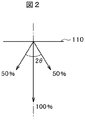
- FIG. 2 is a diagram showing the definition of the light distribution angle.
- FIG. 2 is a view when a light spot is irradiated from an exit surface 110 arranged on the ceiling toward the floor surface, for example.
- the light intensity in the normal direction of the exit surface 110 is the highest, and the light intensity decreases as the polar angle increases.
- the orientation angle is 2 ⁇ .
- the light distribution angle required for general collimated light is 12 degrees or less.
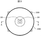
- FIG. 3 is a plan view of an illuminating device using the parabolic mirror 200
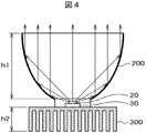
- FIG. 4 is a cross-sectional view of the illuminating device.
- the LED 20 is arranged in the center of the parabolic mirror 200.
- the LED 20 is arranged on, for example, the LED PCB substrate 30. Since the LED 20 uses a high-luminance LED, it is arranged on the heat sink 300 in order to reach a high temperature. In FIG. 3, a part of the heat sink 300 is visible on the back surface of the parabolic mirror 200.
- FIG. 4 is a cross-sectional view taken along the line AA of FIG.
- the LED 20 is arranged on the bottom surface of the parabolic mirror 200.
- the light emitted from the LED 20 is reflected by the parabolic mirror 200 in addition to the light directly upward, and becomes light parallel to the optical axis.
- the height h1 of the parabolic mirror 200 is required.
- the height h1 of the parabolic mirror needs to be about 60 mm.
- the thickness of the entire lighting device needs to be 80 mm or more.
- white lighting is used for lighting, but white lighting also has various color temperatures. For example, neutral white (color temperature of about 5000K), warm white (color temperature of about 3500K), light bulb color (color temperature of about 2800K), and the like. There may be cases where you want to change the white color temperature according to your preference. In order to meet such a requirement by a lighting device having a parabolic mirror as shown in FIGS. 3 and 4, it is necessary to replace the lighting device itself.
- An object of the present invention is to realize a thin lighting device in which the color temperature can be easily changed in the lighting device that emits collimated light.
- the present invention will be described in detail below with reference to examples.
- FIG. 5 is a plan view of the lighting device 10 according to the first embodiment
- FIG. 6 is a cross-sectional view taken along the line BB of FIG. 5
- FIG. 7 is a cross-sectional view taken along the line CC of FIG.
- LEDs 21, 22, and 23 as light sources are arranged on the side surface of the light guide plate 13.
- a prism sheet 15 is arranged on the light guide plate 13 in order to reduce the light distribution angle of the emitted light.
- LEDs 21, 22 and 23 are all white LEDs, but their color temperatures are different.
- the LED 21 emits neutral white (color temperature of about 5000 K)
- the LED 22 emits warm white (color temperature of about 3500 K)
- the LED 23 emits light bulb color (color temperature of about 2800 K).
- the feature of FIG. 5 is that the LEDs 21, 22, and 23 having different color temperatures are arranged on the side surface of the light guide plate 13 at an equal pitch.
- the red, green, and blue LEDs may be turned on at the same time to obtain white light.
- the red, green, and blue LEDs are placed as close as possible. It is necessary to arrange it. That is, in the backlight of the display device, the interval between the three color sets is much larger than the interval between the LEDs in the three color set. In this respect, the present invention is significantly different from conventional backlights.
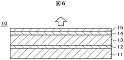
- FIG. 6 is a cross-sectional view taken along the line BB of FIG.
- the reflective sheet 12 is arranged on the substrate 11 that constitutes the frame of the lighting device.
- the light guide plate 13 is arranged on the reflective sheet 12, and the lower prism sheet 14 and the upper prism sheet 15 are arranged on the light guide plate 13 in order to reduce the light distribution angle of light.
- only one prism sheet may be used.
- FIG. 7 is a cross-sectional view taken along the line CC of FIG.
- LEDs 21, 22, and 23 are arranged on the side surface of the light guide plate 13.
- white LEDs 21, 22, and 23 having different color temperatures are arranged on the side surface of the light guide plate 13 at equal intervals.
- Other configurations of FIG. 7 are as described with reference to FIG.
- FIG. 8 is a perspective view of the lighting device shown in FIG. However, in order not to complicate the figure, the upper prism sheet is omitted in FIG. In FIG. 8, LEDs 21, 22, and 23 are arranged at equal intervals on the two side surfaces of the light guide plate 13. A reflective sheet 12 is arranged on the lower surface of the light guide plate 13. The reflective sheet 12 reflects light downward from the light guide plate 13 and directs it toward the upper side, which is the exit surface side. As the reflective sheet 12, for example, an ESR (Enhanced Specular Reflector) manufactured by 3M can be used. The thickness is, for example, about 70 ⁇ m.
- ESR Enhanced Specular Reflector
- the light guide plate 13 is arranged on the reflective sheet 12.
- the thickness of the light guide plate 13 is about 2 mm.
- the light guide plate 13 has a role of directing the light from the LEDs 21, 22, and 23 incident from the side surface upward, which is the exit surface.
- the light directed toward the lower surface of the light guide plate 13 is reflected upward by the reflective sheet 12, which is the exit surface.
- the light guide plate 13 has prism arrays formed on the upper surface and the lower surface in order to efficiently emit light incident from the side from the main surface to serve as a surface light source.
- the prism arrays formed on the upper surface and the lower surface of the light guide plate 13 are formed on the lower prism sheet 14, the prism array formed on the upper prism sheet 15, or the light guide plate used in a display device or the like, which will be described later. It is very different from the prism array that can be. That is, the protrusions (or grooves) and pitches of the prism array formed on the light guide plate 13 in this embodiment are extremely smaller than the protrusions and pitches formed on the prism sheet 14 and the like. Since FIG. 8 is a schematic view, such a dimensional difference of the prism array is not reflected.
- the prism array on the lower surface of the light guide plate 13 extends in the y direction and is arranged in the x direction.
- the height hb of the protrusions of the prism array is, for example, 0.002 ⁇ m, and the pitch px is, for example, 0.1 ⁇ m.
- the apex angle ⁇ b of the prism is, for example, 90 degrees.
- the protrusions of the prism array on the upper surface of the light guide plate 13 extend in the x direction and are arranged in the y direction.
- the height ht of the protrusion is, for example, 0.1 ⁇ m
- the pitch py is, for example, 0.2 ⁇ m.
- the apex angle ⁇ t of the prism is, for example, 90 degrees.
- both the height and pitch of the prism array formed on the upper surface of the light guide plate 13 are larger than the height and pitch of the prism array formed on the lower surface of the light guide plate 13. The same effect can be obtained even if the prism arrays formed on the upper surface and the lower surface of the light guide plate 13 are formed by forming V grooves on the surface of the light guide plate 13 instead of the protrusions.
- the lower prism sheet 14 is arranged on the light guide plate 13.
- the lower prism sheet 14 is a so-called antiprism sheet in which the prism surface is on the lower side.
- prism arrays having a triangular cross section extend in the y direction and are arranged in the x direction with a pitch px. That is, the extending direction of the prism array of the lower prism sheet 14 is a direction perpendicular to the extending direction of the prism array formed on the upper surface of the light guide plate 13, and is the same direction as the prism array formed on the lower surface of the light guide plate 13. Is.
- FIG. 9 is a diagram of a lower prism sheet when a prism array is formed on the prism sheet 14 by V-grooves.
- the prism arrays extend in the y direction and are arranged in the x direction.
- the thickness tp of the lower prism sheet 14 is, for example, 125 microns
- the depth Vd of the V groove is, for example, 75 microns
- the apex angle ⁇ p is, for example, 66 degrees
- the pitch pp is, for example, 100 microns.
- the lower prism sheet 14 of FIG. 9 acts to collect light that is about to spread in the x direction in the exit surface direction, that is, in the z direction.
- FIG. 10 is a view of the upper prism sheet 15 arranged on the lower prism sheet 14.
- the upper prism sheet 15 is omitted in FIG.
- the prism array of the upper prism sheet 15 extends in the x direction and is arranged in the y direction.
- the upper prism sheet 15 is also an antiprism, and the thickness tp of the upper prism sheet 15 is, for example, 125 microns, the depth Vd of the V groove is, for example, 75 microns, and the apex angle ⁇ p is, for example, 66.
- the degree and pitch pp are, for example, 100 microns.
- the upper prism sheet acts to collect light that is about to spread in the y direction in the exit surface direction, that is, in the z direction.
- the height (or the depth of the V groove) and the pitch of the prism arrays formed on the upper surface and the lower surface of the light guide plate 13 are the heights of the prism arrays formed on the lower prism sheet 14 and the upper prism sheet 15. (Or the depth of the V-groove) and the pitch are two orders of magnitude or more, and in some cases, three orders of magnitude or more smaller.
- FIG. 11 is a plan view showing a first embodiment of the first embodiment shown in FIG. In FIG. 11, of the three types of white LEDs 21, 22, and 23 arranged on the side surface of the light guide plate 13, only the neutral white LED 21 is lit, and the emission surface, in this case, the neutral white light from the upper prism sheet 15. Is emitted.
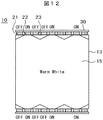
- FIG. 12 is a plan view showing a second embodiment of the first embodiment shown in FIG. In FIG. 12, of the three types of white LEDs 21, 22, and 23 arranged on the side surface of the light guide plate 13, only the warm white LED 22 is lit, and the warm white light is emitted from the exit surface, in this case, the upper prism sheet 15. Is emitted.
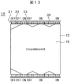
- FIG. 13 is a plan view showing a third embodiment of the first embodiment shown in FIG. In FIG. 13, of the three types of white LEDs 21, 22, and 23 arranged on the side surface of the light guide plate 13, only the light bulb color LED 23 is lit, and the light bulb color light is emitted from the exit surface, in this case, the upper prism sheet 15. It is emitted.
- FIG. 14 is a plan view showing a fourth embodiment of the first embodiment shown in FIG. In FIG. 14, all three types of white LEDs 21, 22, and 23 arranged on the side surface of the light guide plate 13 are lit, and mixed white light of neutral white, warm white, and light bulb color is emitted.
- the mixed white color is not limited to the case shown in FIG. 14, and a combination of two of the three types of white color is also possible.
- white illumination having different color temperatures can be obtained with one remote switch.
- FIG. 15 is a plan view of the lighting device 10 of the second embodiment.
- the cross-sectional structure of FIG. 15 is the same as that of FIG.
- the difference between FIG. 15 and FIG. 5 of the first embodiment is that the LEDs arranged on one side of the light guide plate 13 are white light of the same color.
- the LEDs are all arranged at the same pitch p1 as in the first embodiment.
- FIG. 16 is a plan view showing the first embodiment of the second embodiment.
- only the neutral white LED 21 arranged on one side surface of the light guide plate 13 is lit, and the neutral white light is emitted from the exit surface, in this case, the upper prism sheet 15.
- a brighter light source can be used.
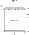
- FIG. 17 is a plan view showing a second embodiment of the second embodiment.
- the warm white LED 22 arranged on the other side surface of the light guide plate 13 is lit, and the warm white light is emitted from the exit surface, in this case, the upper prism sheet 15.
- a brighter light source can be used.
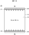
- FIG. 18 is a plan view showing a third embodiment of the second embodiment.
- a mixed white color of neutral white and warm white is emitted.
- NS. 15 to 18 are examples of combining the neutral white LED 21 and the warm white LED 22, but any LED may be replaced with another white LED, for example, a light bulb color LED 23.
- Example 3 is an example in which different white LEDs 21, 22, and 23 are arranged on the three sides of the light guide plate 13.
- FIG. 19 is a plan view showing the first embodiment of the third embodiment.
- a neutral white LED 21, a warm white LED 22, and a light bulb color LED 23 are arranged at the same pitch on each side surface of the light guide plate 13. By turning on any of the LEDs, white light having a required color temperature can be obtained.
- FIG. 20 is a plan view showing the second embodiment of the third embodiment.
- only one of the neutral white LED 21, the warm white LED 22, and the light bulb color LED 23 is arranged on each of the three sides of the light guide plate 13. By turning on the LED on either side, white light having a required color temperature can be obtained.
- Example 3 By turning on a plurality of types of LEDs as needed, it is possible to obtain white with the required color temperature. In Example 3, brighter lighting can be obtained than in the cases of Example 1 and Example 2.
- Example 4 is an example in which different white LEDs 21, 22, and 23 are arranged on the four sides of the light guide plate 13.
- FIG. 21 is a plan view showing the first embodiment of the fourth embodiment.
- a neutral white LED 21, a warm white LED 22, and a light bulb color LED 23 are arranged at the same pitch on each side surface of the light guide plate 13. By turning on any of the LEDs, white light having a required color temperature can be obtained.
- Example 4 can obtain brighter lighting than the configurations of Examples 1 to 3.
- FIG. 22 is a plan view showing the second embodiment of the fourth embodiment.
- a neutral white LED 21, a warm white LED 22, a light bulb color LED 23, and an LED having another color temperature is arranged on each of the four sides of the light guide plate. By turning on the LED on either side, white light having a required color temperature can be obtained. It is the same as in the second and third embodiments that the white color having the required color temperature can be obtained by lighting a plurality of types of LEDs as needed.
- Example 5 relates to a configuration for controlling the emitted light of the lighting device 10 in which the liquid crystal lens is arranged on the front surface of the prism sheet.
- 23A to 23C are diagrams showing a concept for operating the liquid crystal lens.
- FIG. 23C is a cross-sectional view of the lighting device 10.
- the exit surface 110 is divided into regions A, B, C, and the like. Light is emitted from each region with a predetermined light distribution angle.
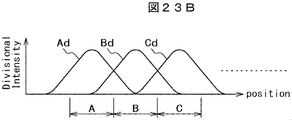
- FIG. 23B shows an example of the illuminance at a place dz away from the exit surface in FIG. 23C.
- the vertical axis of FIG. 23B is the illuminance of light from each region A, B, C or the like. Ad, Bd, and Cd are illuminance distributions, and have a shape close to a normal distribution, for example.
- FIG. 23A is the illuminance when the amount of light from each region shown in FIG. 23B is totaled.
- the vertical axis of FIG. 23 is the total illuminance from each region of the exit surface 110.
- the position distant from the emission surface 110 of the illuminating device that is, the illuminance distribution as a whole on the irradiated surface 120 is shown to be trapezoidal.
- the illuminance distribution of the light emitted from each region A, B, C or the like at a predetermined distance dz that is, the illuminance distributions Ad, Bd in FIG. 23B. , Cd, etc. are changed to control the illuminance distribution on the entire surface of the irradiated surface 120.
- FIG. 24 is a plan view of the lighting device of the fifth embodiment.
- FIG. 24 is the same as FIG. 5 of the first embodiment except that the upper polarizing plate 70 for the liquid crystal lens is present on the outermost surface of the illumination device 10.
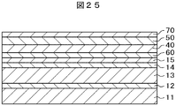
- FIG. 25 is a cross-sectional view taken along the line DD of FIG. 24.
- the configuration from the substrate 11 to the upper prism sheet 15 is the same as in FIG.
- a lower polarizing plate 60 for a liquid crystal lens is arranged on an upper prism sheet 15
- a lower liquid crystal lens 40 is arranged on the lower polarizing plate 60
- an upper liquid crystal lens 50 is arranged on the lower polarizing plate 60
- the upper liquid crystal lens 50 is arranged on the lower polarizing plate 60.
- the upper polarizing plate 70 is arranged.
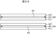
- FIG. 26 is a cross-sectional view of the lower liquid crystal lens 40 and the upper liquid crystal lens 50.
- the first substrate 41 and the second substrate 42 are adhered to each other by a sealing material 45 at the periphery, and the liquid crystal 43 is sealed inside.
- the third substrate 51 and the fourth substrate 52 are adhered to each other by a sealing material 55 at the periphery, and the liquid crystal 53 is sealed inside.
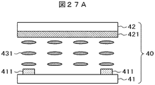
- 27A to 27C are cross-sectional views illustrating the operation of the liquid crystal lens.
- 27A to 27C are described by taking the first liquid crystal lens 40 as an example.
- a comb-shaped electrode 411 is formed on the first substrate 41, and a planar electrode 421 is formed on the second substrate 42. If no voltage is applied between these electrodes, the liquid crystal molecules 431 are oriented parallel to the substrate.
- FIG. 27B is an example of an electric line of force LF when a voltage is applied between the comb tooth electrode 411 of the first substrate 41 and the planar electrode 421 of the second substrate 42.
- the liquid crystal molecules 431 are oriented along the electric line of force LF, the refractive index is distributed in the liquid crystal layer, and a liquid crystal lens is formed.
- a lens is called a refractive index distribution type GRIN (Gradient Index) lens.
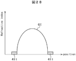
- FIG. 28 is a diagram showing an example of a refractive index distribution type lens.
- the vertical axis of FIG. 28 is the refractive index.
- the refractive index is the smallest on the comb-tooth electrode, which is the first electrode 411, and is the largest at the midpoint between the comb-tooth electrode 411 and the comb-tooth electrode 411.
- FIG. 28 shows a beautiful quadratic curve, but the distribution of the refractive index shows the applied voltage between the first electrode 411 and the second electrode 412, the distance between the comb tooth electrodes of the first electrode 411, and the layer thickness of the liquid crystal 43. It can be greatly changed by such factors.
- the above operation is the same for the second liquid crystal lens 50.
- FIG. 29A is a plan view of the second electrode 421, which is a flat electrode formed on the second substrate 42 of the first liquid crystal lens 40.
- FIG. 29B is an example of the first electrode 411, which is a comb tooth electrode formed on the first substrate 41 of the first liquid crystal lens 40. Both the first electrode 411 and the second electrode 421 are formed of a transparent conductive film such as ITO (Indium Tin Oxide).
- ITO Indium Tin Oxide
- FIG. 29B the comb tooth electrodes 411 extend in the y direction and are arranged in the x direction.
- FIG. 30 is a plan view showing a third electrode 511 formed on the third substrate 51 of the second liquid crystal lens, which is the upper liquid crystal lens 50.
- the fourth electrode on the fourth substrate 52 has the same shape as that in FIG. 29A.
- the comb tooth electrodes in the third electrode 511 extend in the direction perpendicular to the first electrode 411, that is, in the x direction, and are arranged in the y direction.
- FIG. 31 is a schematic view showing the lower liquid crystal lens 40 formed in this way.
- cylinder-shaped liquid crystal lenses extending in the y direction are arranged in the x direction.
- the pitch of the liquid crystal lens in the x direction is p1
- the exit surface of the illuminating device is divided into nine regions.
- the pitch p1 of the liquid crystal lens 40 can be set to a dimension that makes it easy to make the liquid crystal lens 40.
- each liquid crystal lens is a convex lens in FIG. 31, various lens shapes can be obtained depending on the electrode arrangement of the liquid crystal lens and the voltage application direction.
- the pitch p1 of the liquid crystal lens is often larger than the pitch of the prism array formed on the upper prism sheet 15 or the lower prism sheet 14.
- FIG. 32 is a schematic view showing the configuration of the upper liquid crystal lens 50.
- the upper liquid crystal lens 50 cylinder-shaped liquid crystal lenses extending in the x direction are arranged in the y direction.
- the pitch of the liquid crystal lens in the y direction is p2.
- the operation of the liquid crystal lens 50 in FIG. 32 is the same as that described in FIG. 31, except that the light-collecting direction by the lens is a right-angled direction from that in FIG. 31.
- the pitch p2 of the liquid crystal lens is often larger than the pitch of the prism array formed on the upper prism sheet 15 or the lower prism sheet 14.
- the cylinder-shaped liquid crystal lens array shown in FIGS. 31 and 32 is formed in one liquid crystal lens.
- FIG. 33 is a diagram showing the orientation direction and the refractive index distribution of the liquid crystal molecules 431 when the interval s of the comb tooth electrodes 411 is considerably larger than the layer thickness g of the liquid crystal.
- the vertical axis represents the average refractive index at each position in the liquid crystal lens, and ⁇ neff is the difference in the refractive index in the liquid crystal lens.
- a lens having a small radius of curvature is formed in the vicinity of the comb electrode 411, and a lens having a relatively large radius of curvature is formed between the comb electrode 411 and the comb electrode 411.
- FIG. 34 is a cross-sectional view showing an example of a configuration in which the lens shape is made into a quadratic curve or a smooth curve without changing the pitch of the lens or the layer thickness of the liquid crystal display.
- one lens is formed by seven electrodes 411, and different voltages are applied to each electrode 411 to control the orientation of the liquid crystal molecules 413 so that the refractive index becomes close to a quadratic curve. This is an example.
- a voltage such as V1> V2> V3> V4 is applied.
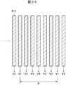
- FIG. 35 is a plan view of the comb tooth electrode 411 corresponding to FIG. 34.
- the area B in FIG. 35 corresponds to, for example, the area B in FIG. 23C.
- FIG. 36 shows an example in which light is emitted from each of the regions A, B, and C in a direction of an angle ⁇ , not in a direction perpendicular to the exit surface 110.
- Such an action is possible by making the shape of the liquid crystal lens arranged in each region asymmetric.
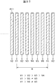
- FIG. 37 is a plan view of the comb tooth electrode 411 showing a case where the applied voltage is made asymmetric in order to make the lens asymmetric.
- the applied voltage is V1> V2> V3> V4, and V1> V5 ⁇ V3 and V1> V6 ⁇ V2.
- the liquid crystal molecules 431 can be oriented so as to form an asymmetric liquid crystal lens.
- the liquid crystal lens can be realized not only by the liquid crystal in the case of homogeneous orientation as shown in FIG. 27A or FIG. 34, but also by various types of liquid crystal devices.
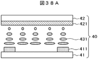
- 38A and 38B are examples in which a liquid crystal lens is configured by a TN (Twisted Nematic) type liquid crystal.
- TN Transmission Nematic
- the orientation direction of the liquid crystal molecules 431 is rotated by 90 degrees between the first substrate 41 and the second substrate 42.
- FIG. 38A shows a case where no voltage is applied between the first electrode 411 and the second electrode 421.
- the liquid crystal molecules 431 are oriented in the direction parallel to the first substrate 41 or the second substrate 42, but the directions are rotated by 90 degrees in the vicinity of the first substrate 41 and the vicinity of the second substrate 42.
- FIG. 38B shows a case where a voltage is applied between the first electrode 411 and the second electrode 421.
- the liquid crystal molecules 431 are oriented in the direction perpendicular to the substrate 41, so that light is blocked.
- the liquid crystal molecule 431 is not affected by the electric field and maintains a rotation of 90 degrees in the direction parallel to the substrate 41, so that the transmittance is high. Not subject to change.
- the refractive index is the smallest immediately above the comb tooth electrode 411, and the refractive index is the largest between the comb tooth electrode 411 and the comb tooth electrode 411. Therefore, a refractive index distribution type GRIN (Gradient Index) lens is formed. Even when the liquid crystal lens is made of TN type liquid crystal, various lens shapes can be formed by arranging the electrodes as shown in FIG. 34 or 37.
- GRIN Gradient Index
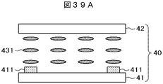
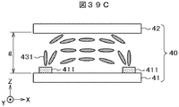
- FIG. 39A to 39C are cross-sectional views showing an example in which a liquid crystal lens is constructed by applying a voltage between the comb-shaped first electrodes 411.
- a comb-shaped electrode 411 is formed on the first substrate 41.
- the second substrate 42 does not have an electrode. That is, the second electrode 421 is not always necessary because the liquid crystal lens is formed by applying a voltage between the comb tooth electrodes, which are the first electrodes 411, of the liquid crystal molecules.
- the second electrode 421 is formed of a transparent conductive film such as ITO (Indium Tin Oxide), but the transparent conductive film reflects and absorbs light to some extent, so the absence of the second electrode 421 means that the lens is not present. It is advantageous in terms of transmittance. However, if it is desired to change the lens shape, the second electrode 421 may be formed on the second substrate 42.
- FIG. 39B shows the lines of electric force LF generated when a voltage is applied between the comb tooth electrodes 411. That is, the lines of electric force LF are directed in the direction perpendicular to the substrate 41 directly above the comb electrode 411, and in the direction parallel to the substrate 41 between the comb electrode 411 and the comb electrode 411.
- the liquid crystal molecule 431 will be oriented along the electric line of force LF.
- FIG. 39C is a cross-sectional view showing a state in which the liquid crystal molecules 431 are oriented along the electric field as shown in FIG. 39B.
- the refractive index immediately above the comb electrode 411 is the smallest, and the refractive index between the comb electrode 411 and the comb electrode 411 is the largest. Therefore, in this case as well, a refractive index distribution type GRIN (Gradient Index) lens is formed.
- GRIN Gradient Index
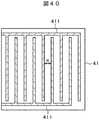
- FIG. 40 is a plan view of the first electrode 411 formed on the first substrate 41.
- the first comb tooth electrode 411 and the second comb tooth electrode 411 are arranged in a nested manner.
- a liquid crystal lens as shown in FIG. 39 is formed by applying a voltage between the first comb tooth electrode 411 and the second comb tooth electrode 411.
- liquid crystal lenses having various shapes can be formed by changing the thickness g of the liquid crystal layer, the distance s between the comb-tooth electrodes, and the voltage V between the comb-tooth electrodes.
- the liquid crystal lens can form a lens having various actions not only by the distance between the electrodes constituting the lens, the layer thickness of the liquid crystal layer, and the applied voltage, but also by the method of the liquid crystal lens.
- FIG. 41 shows an example in which the illuminance distribution is changed by using a liquid crystal lens.
- FIG. 41 has the same configuration as that of FIGS. 23B and 23C, but only the light emitted from the region A is shown.
- FIG. 41 shows that the distribution of the emitted light from the region A can be changed into various shapes by the liquid crystal lens arranged in the region A.
- Ad1 has a shape in which the illuminance distribution is close to the normal distribution
- Ad2 has a shape close to the normal distribution but is more focused
- Ad3 is a case where the illuminance distribution is close to a trapezoid by making the liquid crystal lens like a divergence lens
- Ad3 is a case where the liquid crystal lens is asymmetrical and the center of the illuminance distribution is shifted.
- the illuminance distribution of light on the screen is a collection of light from each region of the exit surface of the lighting device. That is, the illuminance distribution of the light projected on the irradiated body 120 can be arbitrarily changed by changing the illuminance distribution from the regions A, B, C and the like on the exit surface.
- the extending direction of the cylindrical liquid crystal lens schematically shown in FIGS. 31 and 32 is set on the main surface or the back surface of the light guide plate 13, or the lower prism sheet 14 and the upper prism sheet 15 in order to prevent the occurrence of moire.
- the angle in this case is, for example, about 5 to 15 degrees.
- the extending direction of the prism array is set. For example, it may be better to shift it by about 5 to 15 degrees.
- exit surface 120 ... covered Irradiation surface, 130 ... irradiation spot, 200 ... parabolic mirror, 300 ... heat sink, 411 ... 1st electrode, 412 ... 2nd electrode, 413 ... liquid crystal molecule, 511 ... 3rd electrode, 521 ... 4th electrode
Landscapes
- Physics & Mathematics (AREA)
- General Physics & Mathematics (AREA)
- Optics & Photonics (AREA)
- Engineering & Computer Science (AREA)
- Nonlinear Science (AREA)
- General Engineering & Computer Science (AREA)
- Spectroscopy & Molecular Physics (AREA)
- Liquid Crystal (AREA)
- Microelectronics & Electronic Packaging (AREA)
- Chemical & Material Sciences (AREA)
- Crystallography & Structural Chemistry (AREA)
- Planar Illumination Modules (AREA)
Abstract
白色の色温度および光スポットの照度分布を容易に変えることが出来る表示装置を実現することである。このために、本発明は次のような構成をとる。すなわち、導光板13の第1の側面および前記第1の側面に対向する第2の側面に、第1の白色LED21と第2の白色LED22と第3の白色LED23が等間隔に配置し、前記導光板13の主面には、前記第1の側面と直角方向に延在し、平行方向に配列して第1のプリズムアレイが形成され、前記導光板13の裏面には、前記第1の側面と平行方向に延在し、直角方向に配列して第2のプリズムアレイが形成され、前記導光板13の裏面側には反射シート12が配置し、前記導光板13の前記主面側には、第1のプリズムシートが14配置し、前記第1のプリズムシート14の前記導光板13側の面には、前記導光板13の前記第1の側面と平行方向に延在し、直角方向に配列した第3のプリズムアレイが形成されていることを特徴とする照明装置。
Description
本発明は、配光角度が小さく、かつ、白色色温度を容易に変えることが出来る照明装置に関する。
照明装置として発光ダイオード(LED、Light Emitting Diode)が用いられるようになってきている。LEDは発光効率が良く、消費電力低減に有利である。しかし、LEDは、点光源なので、照明装置として用いるには面光源に変換する必要がある。
特許文献1には、出射面が平面であり、背面を出射面に対して所定の角度を持つ反射面とし、サイドから入射したLEDからの光を前記反射面において反射させ、前記出射面から出射させることによって面光源を得る照明装置が記載されている。
特許文献2には、特許文献1に記載のような構成を有する照明装置において、サイドに昼白色のLED、電球光を発光するLED等を並列して配置し、各LEDを同時に点灯させることによって所望の色温度の面光源を得る構成が記載されている。また、特許文献2には、一部のLEDのみを点灯させることによって、色温度の異なる白色を得る構成が記載されている。
特許文献3には、液晶レンズを用いて光ビーム形状を制御する構成が記載されている。
室内照明では、一般には白色が使用される。白色といっても種々の色温度の白色が存在する。例えば昼白色(色温度5000K程度)、温白色(色温度3500K程度)、電球色(色温度2800K程度)等である。白色温度を切り替える場合は、光源そのものを変える必要があった。
一方、照明装置でも、例えば、スポットライトとして使用したい場合等では、高い指向性を持った光、すなわち、配光角度の小さい光源が要求される。このような光源には、従来は、放物面鏡を用いて平行光を形成する構成が用いられてきた。しかし、このような光源は、奥行きが必要であり光源自体を小型化、あるいは、薄型化することが難しい。
本発明の課題は、薄型で、色温度を容易に切り替えることが出来、かつ、配光角度の小さい照明を実現することである。
本発明は上記課題を解決するものであり、主な具体的な手段は次のとおりである。
(1)導光板の第1の側面および前記第1の側面に対向する第2の側面に、第1の白色LEDと第2の白色LEDと第3の白色LEDが等間隔に配置し、前記導光板の主面には、前記第1の側面と直角方向に延在し、平行方向に配列して第1のプリズムアレイが形成され、前記導光板の裏面には、前記第1の側面と平行方向に延在し、直角方向に配列して第2のプリズムアレイが形成され、前記導光板の裏面側には反射シートが配置し、前記導光板の前記主面側には、第1のプリズムシートが配置し、前記第1のプリズムシートの前記導光板側の面には、前記導光板の前記第1の側面と平行方向に延在し、直角方向に配列した第3のプリズムアレイが形成されていることを特徴とする照明装置。
(2)導光板の第1の側面には第1の白色LEDが等間隔で配置し、前記第1の側面に対向する第2の側面には、前記第1の白色LEDとは色温度が異なる第2の白色LEDが等間隔で配置し、前記導光板の主面には、前記第1の側面と直角方向に延在し、平行方向に配列して第1のプリズムアレイが形成され、前記導光板の裏面には、前記第1の側面と平行方向に延在し、直角方向に配列して第2のプリズムアレイが形成され、前記導光板の裏面側には反射シートが配置し、前記導光板の前記主面側には、第1のプリズムシートが配置し、前記第1のプリズムシートの前記導光板側の面には、前記導光板の前記第1の側面と平行方向に延在し、直角方向に配列した第3のプリズムアレイが形成されていることを特徴とする照明装置。
(3)前記第1のプリズムシートの上方には、第1の方向に延在し、第2の方向に配列した複数の第1の液晶レンズが配置していることを特徴とする(1)または(2)に記載の液晶表示装置。
(4)前記第1の液晶レンズの上方には、前記第2の方向に延在し、前記第1の方向に配列した第2の液晶レンズが配置していることを特徴とする(3)に記載の液晶表示装置。
図1はスポットライトに使用される照明装置10の例である。この照明装置10からの光は、コリメートされており、出射面110から、被表示面120にスポット状の光130が照射される。スポット状の光130を得るために、出射光の配光角度は例えば12度程度となっている。
図2は、配光角度の定義を示す図である。図2は、例えば天井に配置された出射面110から床面に向けて光スポットを照射した場合の図である。出射面110の法線方向の光強度が最も大きく、極角が大きくなるにしたがって、光の強度は小さくなる。法線方向の光の強度を100%とし、光強度が50%となるときの極角をθとした場合、配向角は2θである。一般的なコリメート光において要求される配光角度は12度以下である。
このようなコリメート光を得るためには、従来はいわゆる放物線ミラー200が使用されていた。図3は、放物線ミラー200を用いた照明装置の平面図であり、図4は、該照明装置の断面図である。図3において、放物線ミラー200の中央にLED20が配置している。LED20は、例えば、LED用PCB基板30に配置している。LED20は、高輝度LEDを使用しているので、高温になるために、ヒートシンク300の上に配置している。図3において、放物線ミラー200の背面にヒートシンク300の一部が見えている。
図4は図3のA-A断面図である。図4において、放物線ミラー200の底面にLED20が配置している。LED20から出射した光は、直上に向かう光の他は、放物線ミラー200において反射し、光軸に平行な光となる。しかし、放物線ミラー200を十分に機能させるためには、放物線ミラー200の高さh1が必要となる。配光角度12度程度を得るためには、放物線ミラーの高さh1は、60mm程度は必要である。実際には、これに、ヒートシンクの高さh2、例えば20mm程度が加わるので、照明装置全体の厚さは80mm以上必要になる。
一般には、照明には白色照明が使用されるが、白色照明にも種々の色温度が存在する。例えば昼白色(色温度5000K程度)、温白色(色温度3500K程度)、電球色(色温度2800K)等である。白色色温度を好みによって変えたい場合が生ずる。図3及び図4に示すような、放物線ミラーを有する照明装置によってこのような要求を満たすためには、照明装置自体を替える必要がある。
本発明の課題は、コリメート光を出射する照明装置において、色温度を容易に変更することが出来、かつ、薄型の照明装置を実現することである。以下に実施例を用いて本発明を詳細に説明する。
図5は、実施例1による照明装置10の平面図であり、図6は、図5のB-B断面図であり、図7は、図5のC-C断面図である。図5において、光源としてのLED21、22、23が導光板13の側面に配置している。導光板13の上には、出射光の配光角度を小さくするために、プリズムシート15が配置している。図6において、LED21、22、23は全て白色LEDであるが、色温度が異なる。LED21は昼白色(色温度5000K程度)を、LED22は温白色(色温度3500K程度)を、LED23は電球色(色温度2800K程度)を発光する。
図5の特徴は、これらの色温度の異なるLED21、22、23を均等のピッチで導光板13の側面に配置していることである。図5の構成では、3種類のLEDの1種類を使用することによって、所望の色温度に切り替えることが出来る。表示装置のバックライトにおいて、赤、緑、青の3色のLEDを同時に点灯して白色光を得る場合があるが、このためには、赤、緑、青の3色のLEDを出来る限り近接して配置する必要がある。すなわち、表示装置のバックライトでは、3色セットの間隔は、3色セット内の各LEDの間隔よりもはるかに大きい。この点で、本発明は従来のバックライトとは大きく異なっている。
図6は、図5のB-B断面図である。図6において、照明装置のフレームを構成する基板11の上に反射シート12が配置している。反射シート12の上に導光板13が配置し、導光板13の上に光の配光角度を小さくするために、下プリズムシート14と上プリズムシート15が配置している。なお、照明装置によっては、プリズムシートを1枚のみ使用する場合もある。
図7は、図5のC-C断面図である。図7において、導光板13の側面にLED21、22、23が配置している。図5で説明したように、色温度の異なる白色LED21、22、23が導光板13の側面に等間隔で配置している。その他の図7の構成は図6で説明したとおりである。
図8は、図5に示す照明装置の斜視図である。ただし、図を複雑にしないために、図8では、上プリズムシートは省略している。図8において、導光板13の2つの側面にLED21、22、23が等間隔で配置している。導光板13の下面に反射シート12が配置している。反射シート12は、導光板13から下方に向かう光を反射して出射面側である上側に向ける。反射シート12は、例えば、3M製のESR(Enhanced Specular Reflector)を用いることが出来る。厚さは例えば70μm程度である。
図8において、反射シート12の上に導光板13が配置している。導光板13の厚さは2mm程度である。導光板13は、側面から入射したLED21、22、23からの光を出射面である上方向に向ける役割を有する。導光板13の下面方向に向かう光は、反射シート12によって、出射面である、上方向に反射される。
導光板13は、サイドから入射した光を効率よく、主面から出射させて面光源とするために、上面及び下面にプリズムアレイが形成されている。導光板13の上面及び下面に形成されたプリズムアレイは、後で説明する下プリズムシート14、上プリズムシート15に形成されたプリズムアレイ、あるいは、表示装置等に使用されている導光板に形成されることがあるプリズムアレイとは非常に異なっている。すなわち、本実施例における導光板13に形成されたプリズムアレイの突起(あるいは溝)とピッチとは、プリズムシート14等に形成された突起やピッチよりも極端に小さい。なお、図8は模式図なので、プリズムアレイのこのような寸法差は反映されていない。
図8において、導光板13の下面のプリズムアレイはy方向に延在し、x方向に配列している。プリズムアレイの突起の高さhbは例えば、0.002μm、ピッチpxは例えば0.1μmである。プリズムの頂角θbは、例えば90度である。導光板13の上面のプリズムアレイの突起はx方向に延在し、y方向に配列している。突起の高さhtは例えば、0.1μm、ピッチpyは例えば0.2μmである。プリズムの頂角θtは、例えば90度である。このように、導光板13の上面に形成されたプリズムアレイの高さ、ピッチとも、導光板13の下面に形成されたプリズムアレイの高さ、ピッチよりも大きい。なお、導光板13の上面及び下面に形成されるプリズムアレイは、突起ではなく、導光板13の表面にV溝を形成することによって形成しても同様な効果を得ることが出来る。
導光板13の上には下プリズムシート14が配置している。下プリズムシート14はプリズム面が下側にある、いわゆる逆プリズムシートである。図8において、断面が3角形のプリズムアレイがy方向に延在し、x方向にピッチpxで配列している。すなわち、下プリズムシート14のプリズムアレイの延在方向は、導光板13の上面に形成されたプリズムアレイの延在方向と直角方向であり、導光板13の下面に形成されたプリズムアレイと同方向である。
図9は、プリズムシート14にプリズムアレイをV溝によって形成した場合の下プリズムシートの図である。図9において、プリズムアレイはy方向に延在し、x方向に配列している。図9において、下プリズムシート14の厚さtpは例えば125ミクロン、V溝の深さVdは例えば75ミクロン、頂角θpは例えば66度、ピッチppは、例えば100ミクロンである。図9の下プリズムシート14は、x方向に広がろうとする光を出射面方向、すなわち、z方向に集める作用をする。
図10は、下プリズムシート14の上に配置する上プリズムシート15の図である。なお、上プリズムシート15は図8では省略されている。上プリズムシート15のプリズムアレイは、x方向に延在してy方向に配列している。上プリズムシート15も下プリズムシート14と同様に、逆プリズムとなっており、上プリズムシート15の厚さtpは例えば125ミクロン、V溝の深さVdは例えば75ミクロン、頂角θpは例えば66度、ピッチppは、例えば100ミクロンである。上プリズムシートはy方向に広がろうとする光を出射面方向、すなわち、z方向に集める作用をする。
このように、導光板13の上面と下面に形成されたプリズムアレイの高さ(あるいはV溝の深さ)及びピッチは、下プリズムシート14、上プリズムシート15に形成されたプリズムアレイの高さ(あるいはV溝の深さ)及びピッチよりも、2桁以上、場合によっては、3桁以上小さい。このような、導光板13と下プリズムシート14、上プリズムシート15を組み合わせることによって、光の利用効率の高い、かつ、配光角の小さい照明を得ることが出来る。
図11は、図5に示す実施例1の第1実施形態を示す平面図である。図11において、導光板13の側面に配置された3種類の白色LED21、22、23のうち、昼白色LED21のみ点灯しており、出射面、この場合は、上プリズムシート15からは昼白色光が出射される。
図12は、図5に示す実施例1の第2実施形態を示す平面図である。図12において、導光板13の側面に配置された3種類の白色LED21、22、23のうち、温白色LED22のみ点灯しており、出射面、この場合は、上プリズムシート15からは温白色光が出射される。
図13は、図5に示す実施例1の第3実施形態を示す平面図である。図13において、導光板13の側面に配置された3種類の白色LED21、22、23のうち、電球色LED23のみ点灯しており、出射面、この場合は、上プリズムシート15からは電球色光が出射される。
図14は、図5に示す実施例1の第4実施形態を示す平面図である。図14において、導光板13の側面に配置された3種類の白色LED21、22、23の全部が点灯しており、昼白色、温白色、電球色の混合白色光が出射される。
なお、混合白色は、図14の場合に限らず、3種類の白色のうちの2種類の組み合わせも可能である。このように、実施例1を用いれば、例えば、リモートスイッチ一つで色温度の異なる白色照明を得ることが出来る。
図15は、実施例2の照明装置10の平面図である。図15の断面構成は、図6と同様である。図15が実施例1の図5と異なる点は、導光板13の1辺に配置したLEDが同じ色の白色光だということである。例えば、図15では、1辺には昼白色LED21のみが配置し、対向する辺には、温白色LED22のみが配置している。LEDは、実施例1同様、すべて同じピッチp1で配置している。
図16は、実施例2の第1実施形態を示す平面図である。図16において、導光板13の一方の側面に配置された昼白色LED21のみ点灯しており、出射面、この場合は上プリズムシート15、からは昼白色光が出射される。図16の場合、実施例1の実施形態1の場合よりも、点灯している昼白色LED21の数が多いので、より明るい光源とすることが出来る。
図17は、実施例2の第2実施形態を示す平面図である。図17において、導光板13の他方の側面に配置された温白色LED22のみ点灯しており、出射面、この場合は上プリズムシート15、からは温白色光が出射される。図17の場合、実施例1の実施形態2の場合よりも、点灯している昼白色LED22の数が多いので、より明るい光源とすることが出来る。
図18は、実施例2の第3実施形態を示す平面図である。図18において、導光板13の一方の側面に配置された昼白色LED21と、他方の側面に配置された温白色LED22のいずれも点灯しているので、昼白色と温白色の混合白色が出射される。図15乃至図18は、昼白色LED21と温白色LED22を組み合わせた例であるが、いずれかのLEDを他の白色LED、例えば、電球色LED23と置き換えてもよい。
実施例3は、導光板13の3辺に異なる白色LED21、22、23を配置した場合の例である。図19は、実施例3の第1形態を示す平面図である。図19において、導光板13の各側面には、昼白色LED21、温白色LED22、電球色LED23が同じピッチで配置している。いずれかのLEDを点灯することによって、必要な色温度を有する白色光を得ることが出来る。
図20は、実施例3の第2形態を示す平面図である。図20において、導光板13の3辺のうちの各辺には、昼白色LED21、温白色LED22、電球色LED23のいずれかのLEDのみが配置している。いずれかの辺のLEDを点灯することによって、必要な色温度を有する白色光を得ることが出来る。
必要に応じて、複数種類のLEDを点灯することによって、必要な色温度の白色を得ることが出来る。実施例3は、実施例1および実施例2の場合よりも明るい照明を得ることが出来る。
実施例4は、導光板13の4辺に異なる白色LED21、22、23を配置した場合の例である。図21は、実施例4の第1形態を示す平面図である。図21において、導光板13の各側面には、昼白色LED21、温白色LED22、電球色LED23が同じピッチで配置している。いずれかのLEDを点灯することによって、必要な色温度を有する白色光を得ることが出来る。実施例4は、実施例1乃至3の構成よりもより明るい照明を得ることが出来る。
図22は、実施例4の第2形態を示す平面図である。図22において、導光板の4辺の各辺には、昼白色LED21、温白色LED22、電球色LED23、および、他の色温度のLEDのいずれかのLEDのみが配置している。いずれかの辺のLEDを点灯することによって、必要な色温度を有する白色光を得ることが出来る。必要に応じて、複数種類のLEDを点灯することによって、必要な色温度の白色を得ることが出来ることは、実施例2、実施例3の場合と同じである。
実施例5はプリズムシートの前面に液晶レンズを配置した照明装置10の出射光を制御する構成に関する。図23A乃至図23Cは、液晶レンズを作用させるための、概念を示す図である。図23Cは照明装置10の断面図である。図23Cにおいて、出射面110を各領域A、B、C等に分割する。各領域からは、所定の配光角をもって光が出射する。
図23Bは、図23Cにおける出射面からdz離れた場所における照度の例を示す。図23Bの縦軸は各領域A、B、C等からの光の照度である。Ad、Bd、Cdは照度分布であり、例えば、正規分布に近い形をしている。図23Aは、図23Bに示す各領域からの光量を合計した場合の照度である。図23の縦軸は、出射面110の各領域からの照度の合計である。図23Aでは、照明装置の出射面110からdz離れた位置、すなわち被照射面120における全体としての照度分布は、台形であることを示している。
実施例5は、出射面110に液晶レンズを配置することによって、所定の距離dzにおける各領域A、B、C等からの照射される光の照度分布、すなわち、図23Bにおける照度分布Ad、Bd、Cd等を変化させることによって、被照射面120全面における照度分布を制御するものである。
図24は実施例5の照明装置の平面図である。図24は、照明装置10の最表面に、液晶レンズのための上偏光板70が存在している他は、実施例1の図5と同じである。図25は、図24のD-D断面図である。図25において、基板11から上プリズムシート15までの構成は図6と同じである。図25において、上プリズムシート15の上に、液晶レンズのための下偏光板60が配置し、その上に下液晶レンズ40が配置し、その上に上液晶レンズ50が配置し、その上に上偏光板70が配置している。
図26は下液晶レンズ40と上液晶レンズ50の断面図である。下液晶レンズ40において、第1基板41と第2基板42が周辺でシール材45によって接着し、内部に液晶43が封止されている。上液晶レンズ50において、第3基板51と第4基板52が周辺でシール材55によって接着し、内部に液晶53が封止されている。
図27A乃至図27Cは液晶レンズの動作を説明する断面図である。図27A乃至図27Cは第1液晶レンズ40を例にとって説明している。図27Aにおいて、第1基板41には、櫛歯状の電極411が形成され、第2基板42には、平面状の電極421が形成されている。これらの電極間に電圧が印加されなければ液晶分子431は、基板と平行に配向している。
図27Bは、第1基板41の櫛歯電極411と第2基板42の平面電極421との間に電圧を印加した場合の電気力線LFの例である。図27Cにおいて、液晶分子431が電気力線LFに沿って配向し、液晶層内において、屈折率に分布が生じ、液晶レンズが形成される。このようなレンズは、屈折率分布型GRIN(Gradient Index)レンズとよばれている。
図28は屈折率分布型レンズの例を示す図である。図28の縦軸は屈折率である。屈折率は、第1電極411である櫛歯電極上で最も小さく、櫛歯電極411と櫛歯電極411の中間地点で最も大きい。図28はきれいな2次曲線となっているが、屈折率の分布は、第1電極411と第2電極412間の印加電圧、第1電極411である櫛歯電極の間隔、液晶43の層厚等によって大きく変化させることが出来る。以上の動作は、第2液晶レンズ50の場合も同様である。
図29Aは、第1液晶レンズ40の第2基板42に形成された平面電極である第2電極421の平面図である。図29Bは、第1液晶レンズ40の第1基板41に形成された櫛歯電極である第1電極411の例である。第1電極411も第2電極421もITO(Indium Tin Oxide)等の透明導電膜で形成されている。図29Bでは、櫛歯電極411はy方向に延在し、x方向に配列している。図30は上液晶レンズ50である、第2液晶レンズにおける第3基板51に形成された第3電極511を示す平面図である。第4基板52における第4電極は、図29Aと同じ形状である。第3電極511における、櫛歯電極は、第1電極411とは直角方向、すなわち、x方向に延在し、y方向に配列している。
図31は、このようにして形成された下液晶レンズ40を示す模式図である。図31において、y方向に延在するシリンダ状の液晶レンズがx方向に配列している。図31では、液晶レンズのx方向のピッチはp1であり、この場合、照明装置の出射面は9個の領域に分割されている。液晶レンズ40のピッチp1は、液晶レンズ40を作りやすい寸法に設定することが出来る。また、図31は、各液晶レンズは、凸レンズとなっているが、液晶レンズの電極配置、電圧印加方向によってさまざまなレンズ形状とすることが出来る。なお、液晶レンズのピッチp1は、上プリズムシート15あるいは下プリズムシート14に形成されたプリズムアレイのピッチよりも大きいことが多い。
図32は、上液晶レンズ50の構成を示す模式図である。上液晶レンズ50では、x方向に延在するシリンダ状の液晶レンズがy方向に配列している。液晶レンズのy方向のピッチはp2である。図32の液晶レンズ50の作用は、レンズによる集光方向が図31の場合とは、直角方向である点を除いては、図31で説明したのと同様である。なお、液晶レンズのピッチp2は、上プリズムシート15あるいは下プリズムシート14に形成されたプリズムアレイのピッチよりも大きいことが多い。図31、図32に示すシリンダ状の液晶レンズアレイは、1枚の液晶レンズ中に形成されている。
液晶レンズのピッチp1あるいはp2は、出射面の分割数によって決められることが多い。一方、液晶レンズにおける液晶の層厚gは制限がある場合が多い。図33は、櫛歯電極411の間隔sが液晶の層厚gに比べてかなり大きい場合における液晶分子431の配向方向と屈折率分布を示す図である。図33において、縦軸は液晶レンズ内の各位置における平均屈折率であり、Δneffは液晶レンズにおける屈折率の差である。図33のレンズでは、櫛歯電極411の付近において、曲率半径の小さなレンズが形成され、櫛歯電極411と櫛歯電極411の間では、比較的大きな曲率半径を有するレンズが形成される。
図33に示すような、曲率を有するレンズを使用する場合もあるが、レンズの曲率が、2次曲線のような分布をした液晶レンズが必要な場合もある。図34は、レンズのピッチ、あるいは、液晶の層厚を変えずに、レンズ形状を2次曲線、あるいは滑らかな曲線にする構成の例を示す断面図である。図34では、1つのレンズを7個の電極411によって形成し、各電極411に異なった電圧を印加することによって、屈折率が2次曲線に近い形になるように液晶分子413の配向を制御した例である。図34においては、V1>V2>V3>V4のような電圧印加をしている。図35は、図34に対応する櫛歯電極411の平面図である。図35における領域Bは、例えば図23Cにおける領域Bに対応している。
照明装置10からの出射光の向きを出射面110に垂直な方向ではなく、ある方向に向けて出射したい場合がある。図36は、各領域A、B、Cから、出射面110に対して垂直方向ではなく、角度φの方向に光を出射させる場合の例である。このような作用は、各領域に配置した液晶レンズの形状を非対称とすることによって可能である。
図37は、レンズを非対称とするために、印加電圧を非対称にした場合を示す櫛歯電極411の平面図である。図37に示すように、印加電圧は、V1>V2>V3>V4であり、かつ、V1>V5≠V3およびV1>V6≠V2である。これによって、図34に示す液晶レンズの断面図において、非対称な液晶レンズを形成するように、液晶分子431を配向させることが出来る。
液晶レンズは、図27Aあるいは図34等で示したような、ホモジニアス配向の場合の液晶だけではなく、種々の方式の液晶装置で実現することが出来る。図38Aおよび図38Bは、TN(Twisted Nematic)方式の液晶によって、液晶レンズを構成した例である。TN方式は、第1基板41と第2基板42の間において、液晶分子431の配向方向が90度回転する。
図38Aは、第1電極411と第2電極421の間に電圧が印加されていない場合である。この場合、液晶分子431は、第1基板41あるいは第2基板42と平行方向に配向しているが、第1基板41付近と第2基板42付近では、方向が90度回転している。図38Bは第1電極411と第2電極421の間に電圧を印加した場合である。この場合、第1電極411である櫛歯電極の直上では、液晶分子431が基板41に対して垂直方向に配向するので、光は遮断される。しかし、櫛歯電極411と櫛歯電極411との中間地点では、液晶分子431は、電界の影響を受けず、基板41と平行方向において、90度の回転を維持しているので、透過率は変化を受けない。
図38Bの構成をレンズとして評価すると、櫛歯電極411の直上は屈折率が最も小さく、櫛歯電極411と櫛歯電極411の中間は、屈折率が最も大きい。したがって、屈折率分布型GRIN(Gradient Index)レンズが形成される。液晶レンズをTN型液晶で構成する場合も、図34あるいは、図37のような電極配置とすることによって種々のレンズ形状を構成することが出来る。
図39A乃至図39Cは、櫛歯状の第1電極411間に電圧を印加することによって液晶レンズを構成する場合の例を示す断面図である。図39Aにおいて、第1基板41には、櫛歯状電極411が形成されている。一方、第2基板42には、電極は存在していない。すなわち、液晶分子を第1電極411である、櫛歯電極間に電圧を印加することによって液晶レンズを構成するので、第2電極421は必ずしも必要ではない。第2電極421はITO(Indium Tin Oxide)等の透明導電膜で形成するが、透明導電膜といっても、ある程度光を反射、吸収するので、第2電極421が存在しないということは、レンズの透過率という面からは有利である。ただし、レンズ形状を変化させたいというような場合は、第2基板42に第2電極421を形成してもよい。
図39Bは、櫛歯電極411間に電圧を印加した場合に発生する電気力線LFを示す。すなわち、電気力線LFは、櫛歯電極411の直上では基板41に対して垂直方向に向かい、櫛歯電極411と櫛歯電極411の間では、基板41と平行方向に向かう。液晶分子431は、この電気力線LFに沿って配向することになる。
図39Cは、図39Bのような電界に沿って液晶分子431が配向した状態を示す断面図である。図39Cにおいて、櫛歯電極411の直上の屈折率が最も小さく、櫛歯電極411と櫛歯電極411の中間が最も屈折率が大きい。したがって、この場合も、屈折率分布型GRIN(Gradient Index)レンズが形成される。
図40は、第1基板41に形成される第1電極411の平面図である。図40において、第1の櫛歯電極411と第2の櫛歯電極411が入れ子になって配置している。第1の櫛歯電極411と第2の櫛歯電極411の間に電圧を印加することによって図39に示すような液晶レンズが形成される。この場合も、液晶層の厚さg、櫛歯電極間の距離s、櫛歯電極間の電圧Vを変化させることによって種々の形状の液晶レンズを形成することが出来る。
このように、液晶レンズは、レンズを構成する電極間距離、液晶層の層厚、印加電圧のみでなく、液晶レンズの方式によっても、種々の作用を持つレンズを形成することが出来る。図41に液晶レンズを用いて照度分布を変化させる場合の例を示す。図41は、図23B、図23Cと同じ構成であるが、領域Aからの出射光のみ記載している。図41は、領域Aからの出射光の分布を、領域Aに配置された液晶レンズによって、いろいろな形状に変えることが出来ることを示している。
Ad1は照度分布が正規分布に近い形状であり、Ad2は正規分布に近いが、より集光された形となっている。Ad3は、液晶レンズを発散レンズのようにすることによって、台形に近い照度分布とした場合であり、Ad3は、液晶レンズを非対称にして照度分布の中心をずらせた場合である。
図23A乃至図23Cで説明したように、スクリーンにおける光の照度分布は、照明装置の出射面の各領域からの光を集積したものになる。つまり、被照射体120に投射される光の照度分布は、出射面の領域A、B、C等からの照度分布を変えることによって、任意に変えることが出来る。
図31、図32に模式的に示されるシリンドリカル液晶レンズの延在方向は、モアレの発生を防止するために、導光板13の主面、裏面、あるいは、下プリズムシート14、上プリズムシート15に形成されているプリズムアレイの延在方向とは、若干角度を持たせた方がよい場合もある。この場合の角度は、例えば5度乃至15度程度である。また、導光板13の主面、裏面、あるいは、下プリズムシート14、上プリズムシート15に形成されているプリズムアレイどうしの間でも、モアレの発生を防止するために、プリズムアレイの延在方向を例えば5度乃至15度程度ずらせたほうが良い場合がある。
10…照明装置、 11…基板、 12…反射シート、 13…導光板、 14…下プリズムシート、 15…上プリズムシート、 16…TFT、 17…蓄積容量、 20…LED、 21…昼白色LED、 22…温白色LED、 23…電球色LED、 24…第4の白色LED、 30…LED用基板、 40…下液晶レンズ、 41…第1基板、 42…第2基板、 43…液晶、 45…シール材、 50…上液晶レンズ、 51…第3基板、 52…第4基板、 53…液晶、 55…シール材、 60…下偏光板、 70…上偏光板、 110…出射面、 120…被照射面、 130…照射スポット、 200…放物線鏡、 300…ヒートシンク、 411…第1電極、 412…第2電極、 413…液晶分子、 511…第3電極、 521…第4電極
Claims (19)
- 導光板の第1の側面および前記第1の側面に対向する第2の側面に、第1の白色LEDと第2の白色LEDと第3の白色LEDが等間隔に配置し、
前記導光板の主面には、前記第1の側面と直角方向に延在し、平行方向に配列して第1のプリズムアレイが形成され、
前記導光板の裏面には、前記第1の側面と平行方向に延在し、直角方向に配列して第2のプリズムアレイが形成され、
前記導光板の裏面側には反射シートが配置し、
前記導光板の前記主面側には、第1のプリズムシートが配置し、
前記第1のプリズムシートの前記導光板側の面には、前記導光板の前記第1の側面と平行方向に延在し、直角方向に配列した第3のプリズムアレイが形成されていることを特徴とする照明装置。 - 前記第1のプリズムシートの上には、第2のプリズムシートが配置し、
前記第2のプリズムシートの前記導光板側の面には、前記導光板の前記第1の側面と直角方向に延在し、平行方向に配列した第4のプリズムアレイが形成されていることを特徴とする請求項1に記載の照明装置。 - 前記第1の白色LEDの色温度は5000K程度であり、前記第2の白色LEDの色温度は3500K程度であり、前記第3の白色LEDの色温度は2800K程度であることを特徴とする請求項1に記載の照明装置。
- 前記第1のプリズムアレイ及び前記第2のプリズムアレイのピッチは、前記第3のプリズムアレイ及び前記第4のプリズムアレイのピッチよりも小さいことを特徴とする請求項1に記載の照明装置。
- 前記第1のプリズムアレイ及び前記第2のプリズムアレイの高さ、前記第3のプリズムアレイ及び前記第4のプリズムアレイの高さよりも小さいことを特徴とする請求項1に記載の照明装置。
- 前記第1のプリズムアレイ及び前記第2のプリズムアレイのピッチは、前記第3のプリズムアレイ及び前記第4のプリズムアレイのピッチよりも2桁のオーダーで小さいことを特徴とする請求項1に記載の照明装置。
- 前記第1のプリズムアレイ及び前記第2のプリズムアレイの高さ、前記第3のプリズムアレイ及び前記第4のプリズムアレイの高さよりも2桁のオーダーで小さいことを特徴とする請求項1に記載の照明装置。
- 導光板の第1の側面には第1の白色LEDが等間隔で配置し、前記第1の側面に対向する第2の側面には、前記第1の白色LEDとは色温度が異なる第2の白色LEDが等間隔で配置し、
前記導光板の主面には、前記第1の側面と直角方向に延在し、平行方向に配列して第1のプリズムアレイが形成され、
前記導光板の裏面には、前記第1の側面と平行方向に延在し、直角方向に配列して第2のプリズムアレイが形成され、
前記導光板の裏面側には反射シートが配置し、
前記導光板の前記主面側には、第1のプリズムシートが配置し、
前記第1のプリズムシートの前記導光板側の面には、前記導光板の前記第1の側面と平行方向に延在し、直角方向に配列した第3のプリズムアレイが形成されていることを特徴とする照明装置。 - 前記第1のプリズムシートの上には、第2のプリズムシートが配置し、
前記第2のプリズムシートの前記導光板側の面には、前記導光板の前記第1の側面と直角方向に延在し、平行方向に配列した第4のプリズムアレイが形成されていることを特徴とする請求項8に記載の照明装置。 - 前記第1の白色LEDは、色温度が5000K程度の白色LED、色温度が3500K程度の白色LED、または、色温度が2800K程度の白色LEDのいずれかであり、
前記第2の白色LEDは、色温度が5000K程度の白色LED、色温度が3500K程度の白色LED、または、色温度が2800K程度の白色LEDのいずれかであることを特徴とする請求項8に記載の照明装置。 - 前記第1のプリズムアレイ及び前記第2のプリズムアレイのピッチは、前記第3のプリズムアレイ及び前記第4のプリズムアレイのピッチよりも小さいことを特徴とする請求項8に記載の照明装置。
- 前記第1のプリズムアレイ及び前記第2のプリズムアレイの高さ、前記第3のプリズムアレイ及び前記第4のプリズムアレイの高さよりも小さいことを特徴とする請求項8に記載の照明装置。
- 前記第1のプリズムアレイ及び前記第2のプリズムアレイのピッチは、前記第3のプリズムアレイ及び前記第4のプリズムアレイのピッチよりも2桁のオーダーで小さいことを特徴とする請求項8に記載の照明装置。
- 前記第1のプリズムアレイ及び前記第2のプリズムアレイの高さ、前記第3のプリズムアレイ及び前記第4のプリズムアレイの高さよりも2桁のオーダーで小さいことを特徴とする請求項8に記載の照明装置。
- 前記第1のプリズムシートの上方には、第1の方向に延在し、第2の方向に配列した複数の第1の液晶レンズが配置していることを特徴とする請求項1または8に記載の照明装置。
- 前記第2のプリズムシートの上方には、第1の方向に延在し、第2の方向に配列した複数の第1の液晶レンズが配置していることを特徴とする請求項2または9に記載の照明装置。
- 前記第1の液晶レンズの上方には、前記第2の方向に延在し、前記第1の方向に配列した第2の液晶レンズが配置していることを特徴とする請求項15に記載の照明装置。
- 前記第1の液晶レンズの上方には、前記第2の方向に延在し、前記第1の方向に配列した第2の液晶レンズが配置していることを特徴とする請求項16に記載の照明装置。
- 前記第1の液晶レンズの前記第2の方向のピッチおよび前記第2の液晶レンズの前記第1の方向のピッチは、前記導光板に形成された第1のプリズムアレイのピッチよりも大きいことを特徴とする請求項15乃至18のいずれか1項に記載の照明装置。
Priority Applications (3)
| Application Number | Priority Date | Filing Date | Title |
|---|---|---|---|
| JP2022511591A JP7346719B2 (ja) | 2020-04-03 | 2021-02-02 | 照明装置 |
| CN202180025560.0A CN115349101B (zh) | 2020-04-03 | 2021-02-02 | 照明装置 |
| US17/954,371 US11934001B2 (en) | 2020-04-03 | 2022-09-28 | Lighting device having a light guide with prism array formed thereon and a prism sheet and white LEDs |
Applications Claiming Priority (2)
| Application Number | Priority Date | Filing Date | Title |
|---|---|---|---|
| JP2020-067326 | 2020-04-03 | ||
| JP2020067326 | 2020-04-03 |
Related Child Applications (1)
| Application Number | Title | Priority Date | Filing Date |
|---|---|---|---|
| US17/954,371 Continuation US11934001B2 (en) | 2020-04-03 | 2022-09-28 | Lighting device having a light guide with prism array formed thereon and a prism sheet and white LEDs |
Publications (1)
| Publication Number | Publication Date |
|---|---|
| WO2021199652A1 true WO2021199652A1 (ja) | 2021-10-07 |
Family
ID=77928999
Family Applications (1)
| Application Number | Title | Priority Date | Filing Date |
|---|---|---|---|
| PCT/JP2021/003745 Ceased WO2021199652A1 (ja) | 2020-04-03 | 2021-02-02 | 照明装置 |
Country Status (4)
| Country | Link |
|---|---|
| US (1) | US11934001B2 (ja) |
| JP (1) | JP7346719B2 (ja) |
| CN (1) | CN115349101B (ja) |
| WO (1) | WO2021199652A1 (ja) |
Cited By (1)
| Publication number | Priority date | Publication date | Assignee | Title |
|---|---|---|---|---|
| US12610446B2 (en) | 2021-04-27 | 2026-04-21 | University Of Washington | Adaptive illuminance control |
Citations (2)
| Publication number | Priority date | Publication date | Assignee | Title |
|---|---|---|---|---|
| JP2013004197A (ja) * | 2011-06-13 | 2013-01-07 | Canon Inc | バックライト装置 |
| WO2013122155A1 (ja) * | 2012-02-17 | 2013-08-22 | 学校法人慶應義塾 | 液晶表示装置 |
Family Cites Families (9)
| Publication number | Priority date | Publication date | Assignee | Title |
|---|---|---|---|---|
| KR20080048759A (ko) * | 2006-11-29 | 2008-06-03 | 삼성전자주식회사 | 도광 유닛, 이를 채용한 백라이트 유닛 및 디스플레이 장치 |
| CN201083931Y (zh) * | 2007-09-18 | 2008-07-09 | 台湾奈普光电科技股份有限公司 | 背光模块 |
| JP5343752B2 (ja) * | 2009-07-31 | 2013-11-13 | 大日本印刷株式会社 | 導光板、導光板の製造方法、面光源装置および液晶表示装置 |
| CN103930710A (zh) | 2011-12-01 | 2014-07-16 | 夏普株式会社 | 照明装置、照明灯、背光源、液晶显示装置以及电视接收装置 |
| WO2013094481A1 (ja) | 2011-12-19 | 2013-06-27 | シャープ株式会社 | 照明装置、シーリングライト、バックライト、液晶表示装置、及びテレビジョン受信装置 |
| EP3347759B1 (en) | 2015-09-12 | 2024-03-20 | LensVector Inc. | Liquid crystal beam control device |
| KR102485634B1 (ko) * | 2016-09-09 | 2023-01-05 | 엘지디스플레이 주식회사 | 액정표시장치 |
| JP2019216017A (ja) * | 2018-06-13 | 2019-12-19 | パナソニックIpマネジメント株式会社 | 照明装置 |
| KR102221196B1 (ko) * | 2018-11-16 | 2021-03-03 | 주식회사 엘엠에스 | 차폐 성능이 향상된 확산 시트 및 이를 포함하는 백라이트 유닛 |
-
2021
- 2021-02-02 CN CN202180025560.0A patent/CN115349101B/zh active Active
- 2021-02-02 WO PCT/JP2021/003745 patent/WO2021199652A1/ja not_active Ceased
- 2021-02-02 JP JP2022511591A patent/JP7346719B2/ja active Active
-
2022
- 2022-09-28 US US17/954,371 patent/US11934001B2/en active Active
Patent Citations (2)
| Publication number | Priority date | Publication date | Assignee | Title |
|---|---|---|---|---|
| JP2013004197A (ja) * | 2011-06-13 | 2013-01-07 | Canon Inc | バックライト装置 |
| WO2013122155A1 (ja) * | 2012-02-17 | 2013-08-22 | 学校法人慶應義塾 | 液晶表示装置 |
Cited By (1)
| Publication number | Priority date | Publication date | Assignee | Title |
|---|---|---|---|---|
| US12610446B2 (en) | 2021-04-27 | 2026-04-21 | University Of Washington | Adaptive illuminance control |
Also Published As
| Publication number | Publication date |
|---|---|
| US20230015472A1 (en) | 2023-01-19 |
| JPWO2021199652A1 (ja) | 2021-10-07 |
| CN115349101A (zh) | 2022-11-15 |
| CN115349101B (zh) | 2024-02-13 |
| JP7346719B2 (ja) | 2023-09-19 |
| US11934001B2 (en) | 2024-03-19 |
Similar Documents
| Publication | Publication Date | Title |
|---|---|---|
| US12493214B2 (en) | Planar lighting device | |
| CN113531487B (zh) | 照明装置 | |
| JP7483474B2 (ja) | 照明装置 | |
| CN102279436B (zh) | 背光模组及显示装置 | |
| JP7408777B2 (ja) | 照明装置 | |
| JP7346719B2 (ja) | 照明装置 | |
| CN202362487U (zh) | 导光板、背光模组及显示装置 | |
| JP2023044236A (ja) | 照明装置 |
Legal Events
| Date | Code | Title | Description |
|---|---|---|---|
| 121 | Ep: the epo has been informed by wipo that ep was designated in this application |
Ref document number: 21780770 Country of ref document: EP Kind code of ref document: A1 |
|
| ENP | Entry into the national phase |
Ref document number: 2022511591 Country of ref document: JP Kind code of ref document: A |
|
| NENP | Non-entry into the national phase |
Ref country code: DE |
|
| 122 | Ep: pct application non-entry in european phase |
Ref document number: 21780770 Country of ref document: EP Kind code of ref document: A1 |